Embed Size (px)
Citation preview

MCP4921/492212-Bit DAC with SPI™ Interface
Features
• 12-Bit Resolution
• ±0.2 LSB DNL (typ)• ±2 LSB INL (typ)• Single or Dual Channel
• Rail-to-Rail Output• SPI™ Interface with 20 MHz Clock Support• Simultaneous Latching of the Dual DACs w/LDAC
• Fast Settling Time of 4.5 µs• Selectable Unity or 2x Gain Output• 450 kHz Multiplier Mode
• External VREF Input• 2.7V to 5.5V Single-Supply Operation• Extended Temperature Range: -40°C to +125°C
Applications
• Set Point or Offset Trimming
• Sensor Calibration• Digitally-Controlled Multiplier/Divider• Portable Instrumentation (Battery-Powered)
• Motor Feedback Loop Control
Block Diagram
Description
The Microchip Technology Inc. MCP492X are 2.7 –5.5V, low-power, low DNL, 12-Bit Digital-to-Analog Con-verters (DACs) with optional 2x buffered output and SPIinterface.
The MCP492X are DACs that provide high accuracyand low noise performance for industrial applicationswhere calibration or compensation of signals (such astemperature, pressure and humidity) are required. The MCP492X are available in the extended tempera-ture range and PDIP, SOIC, MSOP and TSSOPpackages.
The MCP492X devices utilize a resistive string archi-tecture, with its inherent advantages of low DNL error,low ratio metric temperature coefficient and fast settlingtime. These devices are specified over the extendedtemperature range. The MCP492X include double-buffered inputs, allowing simultaneous updates usingthe LDAC pin. These devices also incorporate aPower-On Reset (POR) circuit to ensure reliablepower-up.
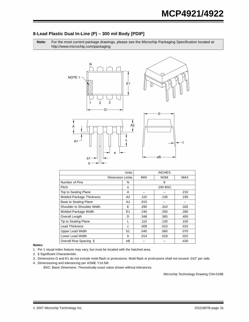
Package Types
Op Amps
VDD
AVSS
CS SDI SCK
Interface Logic
Input Register A Register B
Input
DACA Register Register
DACB
StringDACB
StringDACA
VREF
OutputLogic
Power-on Reset
VREF
A B
VOUTA VOUTB
LDAC
Buffer Buffer
SHDN
Output
GainLogic
GainLogic
14
MC
P4921
8-Pin PDIP, SOIC, MSOP
1
2
3
4
8
7
6
5
CS
SCK
SDI
VDD
AVSS
VOUTA
VREFA
LDAC
MC
P4922
1
2
3
4
13
12
11
10
9
8
5
6
7
14-Pin PDIP, SOIC, TSSOPVDD
NC
CS
SCK VREFB
NC
NC
SDI
LDAC
SHDN
VOUTB
VOUTA
VREFA
AVSS
© 2007 Microchip Technology Inc. DS21897B-page 1

MCP4921/4922
1.0 ELECTRICAL CHARACTERISTICS
Absolute Maximum Ratings †
VDD............................................................................................................. 6.5V
All inputs and outputs w.r.t ............. AVSS –0.3V to VDD+0.3V
Current at Input Pins ....................................................±2 mA
Current at Supply Pins ...............................................±50 mA
Current at Output Pins ...............................................±25 mA
Storage temperature .....................................-65°C to +150°C
Ambient temp. with power applied ................-55°C to +125°C
ESD protection on all pins ........... ≥ 4 kV (HBM), ≥ 400V (MM)
Maximum Junction Temperature (TJ) . .........................+150°C
† Notice: Stresses above those listed under “Maximum Rat-ings” may cause permanent damage to the device. This is astress rating only and functional operation of the device atthose or any other conditions above those indicated in theoperational listings of this specification is not implied. Expo-sure to maximum rating conditions for extended periods mayaffect device reliability.
5V AC/DC CHARACTERISTICSElectrical Specifications: Unless otherwise indicated, VDD = 5V, AVSS = 0V, VREF = 2.048V, output buffer gain (G) = 2x, RL = 5 kΩ to GND, CL = 100 pF TA = -40 to +85°C. Typical values at +25°C.
Parameters Sym Min Typ Max Units Conditions
Power Requirements
Input Voltage VDD 2.7 — 5.5
Input Current - MCP4921Input Current - MCP4922
IDD ——
175350
350700
µA Input unbuffered, digital inputs grounded, output unloaded, code at 0x000
Hardware Shutdown Current ISHDN — 0.3 2 µA
Software Shutdown Current ISHDN_SW — 3.3 6 µA
Power-on-Reset Threshold VPOR — 2.0 — V
DC Accuracy
Resolution n 12 — — Bits
INL Error INL -12 2 12 LSB
DNL DNL -0.75 ±0.2 +0.75 LSB Device is Monotonic
Offset Error VOS — ±0.02 1 % of FSR Code 0x000h
Offset Error TemperatureCoefficient
VOS/°C — 0.16 — ppm/°C -45°C to 25°C
— -0.44 — ppm/°C +25°C to 85°C
Gain Error gE — -0.10 1 % of FSR Code 0xFFFh, not including offset error.
Gain Error Temperature Coefficient
ΔG/°C — -3 — ppm/°C
Input Amplifier (VREF Input)
Input Range - Buffered Mode VREF 0.040 — VDD – 0.040 V Note 1Code = 2048VREF = 0.2v p-p, f = 100 Hz and 1 kHz
Input Range - Unbuffered Mode
VREF 0 — VDD V
Input Impedance RVREF — 165 — kΩ Unbuffered Mode
Input Capacitance - Unbuffered Mode
CVREF — 7 — pF
Multiplier Mode -3 dB Bandwidth
fVREF — 450 — kHz VREF = 2.5V ±0.2Vp-p, Unbuffered,G = 1
fVREF — 400 — kHz VREF = 2.5V ±0.2 Vp-p, Unbuffered,G = 2
Multiplier Mode - Total Harmonic Distortion
THDVREF — -73 — dB VREF = 2.5V ±0.2Vp-p,Frequency = 1 kHz
Note 1: By design, not production tested.2: Too small to quantify.
DS21897B-page 2 © 2007 Microchip Technology Inc.

MCP4921/4922
Output Amplifier
Output Swing VOUT — 0.010 to VDD – 0.040
— Accuracy is better than 1 LSB forVOUT = 10 mV to (VDD – 40 mV)
Phase Margin θm — 66 — degrees
Slew Rate SR — 0.55 — V/µs
Short Circuit Current ISC — 15 24 mA
Settling Time tsettling — 4.5 — µs Within 1/2 LSB of final value from 1/4 to 3/4 full-scale range
Dynamic Performance
DAC-to-DAC Crosstalk — 10 — nV-s Note 2
Major Code Transition Glitch — 45 — nV-s 1 LSB change around major carry (0111...1111 to 1000...0000)
Digital Feedthrough — 10 — nV-s Note 2
Analog Crosstalk — 10 — nV-s Note 2
5V AC/DC CHARACTERISTICS (CONTINUED)Electrical Specifications: Unless otherwise indicated, VDD = 5V, AVSS = 0V, VREF = 2.048V, output buffer gain (G) = 2x, RL = 5 kΩ to GND, CL = 100 pF TA = -40 to +85°C. Typical values at +25°C.
Parameters Sym Min Typ Max Units Conditions
Note 1: By design, not production tested.2: Too small to quantify.
3V AC/DC CHARACTERISTICSElectrical Specifications: Unless otherwise indicated, VDD = 3V, AVSS = 0V, VREF = 2.048V external, output buffer gain (G) = 1x, RL = 5 kΩ to GND, CL = 100 pF TA = -40 to +85°C. Typical values at 25°C
Parameters Sym Min Typ Max Units Conditions
Power Requirements
Input Voltage VDD 2.7 — 5.5
Input Current - MCP4921Input Current - MCP4922
IDD ——
125250
250500
µA Input unbuffered, digital inputs grounded, output unloaded, code at 0x000
Hardware Shutdown Current ISHDN — 0.25 2 µA
Software Shutdown Current ISHDN_SW — 2 6 µA
Power-On Reset threshold VPOR — 2.0 — V
DC Accuracy
Resolution n 12 — — Bits
INL Error INL -12 ±3 +12 LSB
DNL DNL -0.75 ±0.3 +0.75 LSB Device is Monotonic
Offset Error VOS — ±0.02 1 % of FSR Code 0x000h
Offset Error TemperatureCoefficient
VOS/°C — 0.5 — ppm/°C -45°C to 25°C
— -0.77 — ppm/°C +25°C to 85°C
Gain Error gE — -0.15 1 % of FSR Code 0xFFFh, not including offset error.
Gain Error Temperature Coefficient
ΔG/°C — -3 — ppm/°C
Input Amplifier (VREF Input)
Input Range - Buffered Mode VREF 0.040 — VDD-0.040 V Note 1Code = 2048, VREF = 0.2v p-p, f = 100 Hz and 1 kHz
Input Range - Unbuffered Mode
VREF 0 — VDD V
Input Impedance RVREF — 165 — kΩ Unbuffered Mode
Note 1: By design, not production tested.2: Too small to quantify.
© 2007 Microchip Technology Inc. DS21897B-page 3

MCP4921/4922
Input Capacitance – Unbuffered Mode
CVREF — 7 — pF
Multiplier Mode -3 dB Bandwidth
fVREF — 440 — kHz VREF = 2.048V ±0.1 Vp-p, unbuffered, G = 1
fVREF — 390 — kHz VREF = 2.048V ±0.1 Vp-p, unbuffered, G = 2
Multiplier Mode – Total Harmonic Distortion
THDVREF — -73 — dB VREF = 2.5V ±0.1 Vp-p, Frequency = 1 kHz
Output Amplifier
Output Swing VOUT — 0.010 to VDD – 0.040
— Accuracy is better than 1 LSB for VOUT = 10 mV to (VDD – 40 mV)
Phase Margin θm — 66 — degrees
Slew Rate SR — 0.55 — V/µs
Short Circuit Current ISC — 14 24 mA
Settling Time tsettling — 4.5 — µs Within 1/2 LSB of final value from 1/4 to 3/4 full-scale range
Dynamic Performance
DAC-to-DAC Crosstalk — 10 — nV-s Note 2
Major Code Transition Glitch — 45 — nV-s 1 LSB change around major carry (0111...1111 to 1000...0000)
Digital Feedthrough — 10 — nV-s Note 2
Analog Crosstalk — 10 — nV-s Note 2
3V AC/DC CHARACTERISTICS (CONTINUED)Electrical Specifications: Unless otherwise indicated, VDD = 3V, AVSS = 0V, VREF = 2.048V external, output buffer gain (G) = 1x, RL = 5 kΩ to GND, CL = 100 pF TA = -40 to +85°C. Typical values at 25°C
Parameters Sym Min Typ Max Units Conditions
Note 1: By design, not production tested.2: Too small to quantify.
5V EXTENDED TEMPERATURE SPECIFICATIONSElectrical Specifications: Unless otherwise indicated, VDD = 5V, AVSS = 0V, VREF = 2.048V, output buffer gain (G) = 2x, RL = 5 kΩ to GND, CL = 100 pF. Typical values at +125°C by characterization or simulation.
Parameters Sym Min Typ Max Units Conditions
Power Requirements
Input Voltage VDD 2.7 — 5.5
Input Current - MCP4921Input Current - MCP4922
IDD ——
200400
——
µA Input unbuffered, digital inputs grounded, output unloaded, code at 0x000
Hardware Shutdown Current ISHDN — 1.5 — µA
Software Shutdown Current ISHDN_SW — 5 — µA
Power-On Reset threshold VPOR — 1.85 — V
DC Accuracy
Resolution n 12 — — Bits
INL Error INL — ±4 — LSB
DNL DNL — ±0.25 — LSB Device is Monotonic
Offset Error VOS — ±0.02 — % of FSR Code 0x000h
Offset Error TemperatureCoefficient
VOS/°C — -5 — ppm/°C +25°C to +125°C
Note 1: By design, not production tested.2: Too small to quantify.
DS21897B-page 4 © 2007 Microchip Technology Inc.

MCP4921/4922
Gain Error gE — -0.10 — % of FSR Code 0xFFFh, not including offset error
Gain Error Temperature Coefficient
ΔG/°C — -3 — ppm/°C
Input Amplifier (VREF Input)
Input Range - Buffered Mode VREF — 0.040 to VDD-0.040
— V Note 1Code = 2048, VREF = 0.2v p-p, f = 100 Hz and 1 kHz
Input Range - Unbuffered Mode
VREF 0 — VDD V
Input Impedance RVREF — 174 — kΩ Unbuffered Mode
Input Capacitance - Unbuffered Mode
CVREF — 7 — pF
Multiplying Mode -3 dB Bandwidth
fVREF — 450 — kHz VREF = 2.5V ±0.1 Vp-p, Unbuffered, G=1
fVREF — 400 — kHz VREF = 2.5V ±0.1 Vp-p, Unbuffered, G = 2
Multiplying Mode - Total Harmonic Distortion
THDVREF — — — dB VREF = 2.5V ±0.1Vp-p, Frequency = 1 kHz
Output Amplifier
Output Swing VOUT — 0.010 to VDD – 0.040
— Accuracy is better than 1 LSB for VOUT = 10 mV to (VDD – 40 mV)
Phase Margin θm — 66 — degrees
Slew Rate SR — 0.55 — V/µs
Short Circuit Current ISC — 17 — mA
Settling Time tsettling — 4.5 — µs Within 1/2 LSB of final value from 1/4 to 3/4 full-scale range
Dynamic Performance
DAC to DAC Crosstalk — 10 — nV-s Note 2
Major Code Transition Glitch — 45 — nV-s 1 LSB change around major carry (0111...1111 to 1000...0000)
Digital Feedthrough — 10 — nV-s Note 2
Analog Crosstalk — 10 — nV-s Note 2
5V EXTENDED TEMPERATURE SPECIFICATIONS (CONTINUED)Electrical Specifications: Unless otherwise indicated, VDD = 5V, AVSS = 0V, VREF = 2.048V, output buffer gain (G) = 2x, RL = 5 kΩ to GND, CL = 100 pF. Typical values at +125°C by characterization or simulation.
Parameters Sym Min Typ Max Units Conditions
Note 1: By design, not production tested.2: Too small to quantify.
© 2007 Microchip Technology Inc. DS21897B-page 5
MCP4921/4922
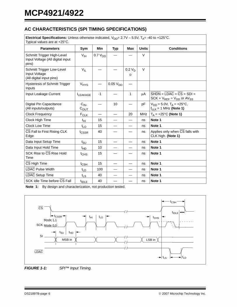
AC CHARACTERISTICS (SPI TIMING SPECIFICATIONS)
FIGURE 1-1: SPI™ Input Timing.
Electrical Specifications: Unless otherwise indicated, VDD= 2.7V – 5.5V, TA= -40 to +125°C. Typical values are at +25°C.
Parameters Sym Min Typ Max Units Conditions
Schmitt Trigger High-Level Input Voltage (All digital input pins)
VIH 0.7 VDD — — V
Schmitt Trigger Low-Level Input Voltage (All digital input pins)
VIL — — 0.2 VD
D
V
Hysteresis of Schmitt Trigger Inputs
VHYS — 0.05 VDD —
Input Leakage Current ILEAKAGE -1 — 1 μA SHDN = LDAC = CS = SDI = SCK + VREF = VDD or AVSS
Digital Pin Capacitance(All inputs/outputs)
CIN, COUT
— 10 — pF VDD = 5.0V, TA = +25°C, fcLK = 1 MHz (Note 1)
Clock Frequency FCLK — — 20 MHz TA = +25°C (Note 1)
Clock High Time tHI 15 — — ns Note 1
Clock Low Time tLO 15 — — ns Note 1
CS Fall to First Rising CLK Edge
tCSSR 40 — — ns Applies only when CS falls with CLK high. (Note 1)
Data Input Setup Time tSU 15 — — ns Note 1
Data Input Hold Time tHD 10 — — ns Note 1
SCK Rise to CS Rise Hold Time
tCHS 15 — — ns Note 1
CS High Time tCSH 15 — — ns Note 1
LDAC Pulse Width tLD 100 — — ns Note 1
LDAC Setup Time tLS 40 — — ns Note 1
SCK Idle Time before CS Fall tIDLE 40 — — ns Note 1
Note 1: By design and characterization, not production tested.
CS
SCK
SI
LDAC
tCSSR
tHDtSU
tLO
tCSH
tCHS
LSB inMSB in
tIDLE
Mode 1,1
Mode 0,0
tHI
tLDtLS
DS21897B-page 6 © 2007 Microchip Technology Inc.

MCP4921/4922
TEMPERATURE CHARACTERISTICSElectrical Specifications: Unless otherwise indicated, VDD = +2.7V to +5.5V, AVSS = GND.
Parameters Sym Min Typ Max Units Conditions
Temperature Ranges
Specified Temperature Range TA -40 — +125 °C
Operating Temperature Range TA -40 — +125 °C Note 1
Storage Temperature Range TA -65 — +150 °C
Thermal Package Resistances
Thermal Resistance, 8L-PDIP θJA — 85 — °C/W
Thermal Resistance, 8L-SOIC θJA — 163 — °C/W
Thermal Resistance, 8L-MSOP θJA — 206 — °C/W
Thermal Resistance, 14L-PDIP θJA — 70 — °C/W
Thermal Resistance, 14L-SOIC θJA — 120 — °C/W
Thermal Resistance, 14L-TSSOP θJA — 100 — °C/W
Note 1: The MCP492X family of DACs operate over this extended temperature range, but with reduced performance. Operation in this range must not cause TJ to exceed the Maximum Junction Temperature of 150°C.
© 2007 Microchip Technology Inc. DS21897B-page 7

MCP4921/4922
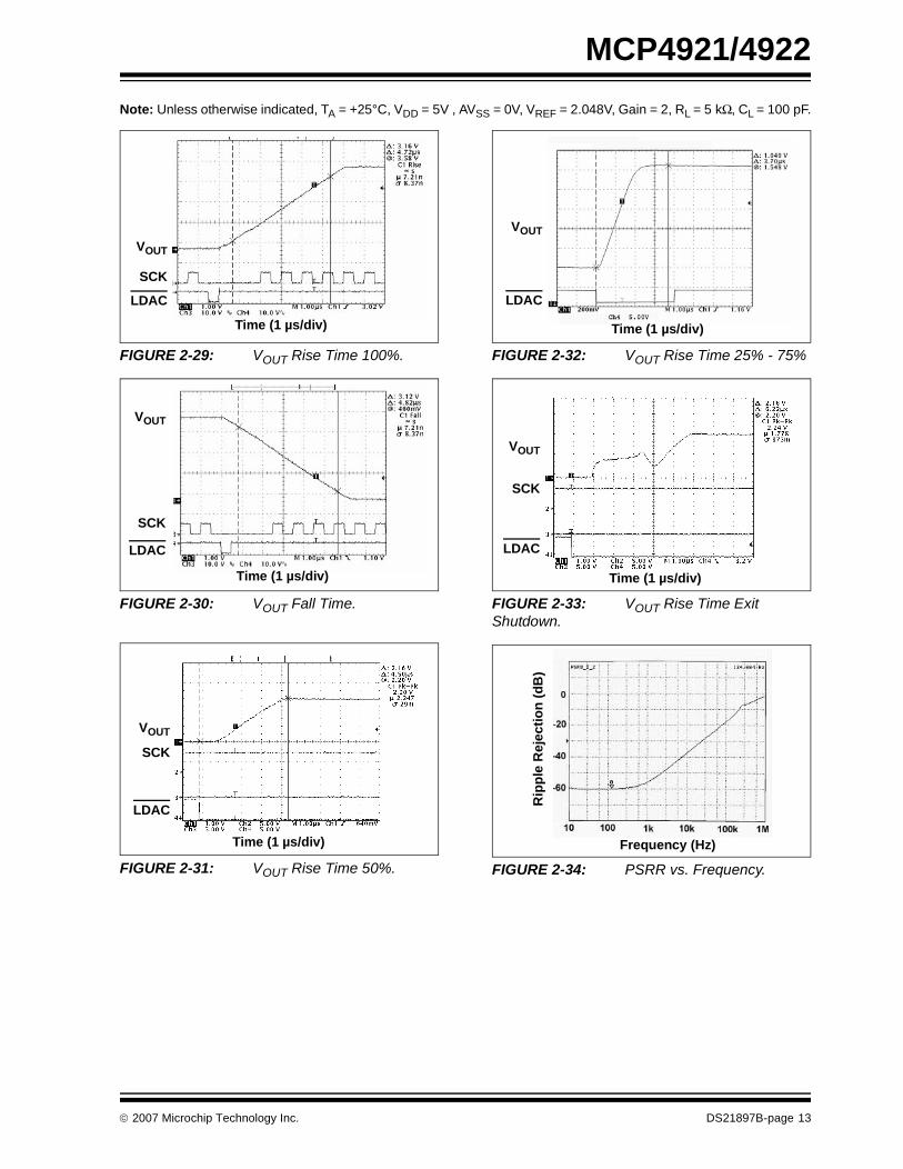
2.0 TYPICAL PERFORMANCE CURVES
Note: Unless otherwise indicated, TA = +25°C, VDD = 5V , AVSS = 0V, VREF = 2.048V, Gain = 2, RL = 5 kΩ, CL = 100 pF.
FIGURE 2-1: DNL vs. Code.
FIGURE 2-2: DNL vs. Code and Ambient Temperature.
FIGURE 2-3: DNL vs. Code and VREF. Gain=1.
FIGURE 2-4: Absolute DNL vs. Ambient Temperature.
FIGURE 2-5: Absolute DNL vs. Voltage Reference.
Note: The graphs and tables provided following this note are a statistical summary based on a limited number ofsamples and are provided for informational purposes only. The performance characteristics listed hereinare not tested or guaranteed. In some graphs or tables, the data presented may be outside the specifiedoperating range (e.g., outside specified power supply range) and therefore outside the warranted range.
-0.3
-0.2
-0.1
0
0.1
0.2
0.3
0 1024 2048 3072 4096
Code (Decimal)
DN
L (
LS
B)
-0.2
-0.1
0
0.1
0.2
0 1024 2048 3072 4096
Code (Decimal)
DN
L (
LS
B)
125C 85C 25C
-0.4
-0.3
-0.2
-0.1
0
0.1
0.2
0.3
0.4
0 1024 2048 3072 4096
Code (Decimal)
DN
L (
LS
B)
1 2 3 4 5.5
0.075
0.0752
0.0754
0.0756
0.0758
0.076
0.0762
0.0764
0.0766
-40 -20 0 20 40 60 80 100 120
Ambient Temperature (ºC)
Ab
so
lute
DN
L (
LS
B)
0
0.05
0.1
0.15
0.2
0.25
0.3
0.35
1 2 3 4 5
Voltage Reference (V)
Ab
so
lute
DN
L (
LS
B)
DS21897B-page 8 © 2007 Microchip Technology Inc.

MCP4921/4922
Note: Unless otherwise indicated, TA = +25°C, VDD = 5V , AVSS = 0V, VREF = 2.048V, Gain = 2, RL = 5 kΩ, CL = 100 pF.
FIGURE 2-6: INL vs. Code and Ambient Temperature.
FIGURE 2-7: Absolute INL vs. Ambient Temperature.
FIGURE 2-8: Absolute INL vs. VREF.
FIGURE 2-9: INL vs. Code and VREF.
FIGURE 2-10: INL vs. Code.
-5
-4
-3
-2
-1
0
1
2
3
4
5
0 1024 2048 3072 4096
Code (Decimal)
INL
(L
SB
)
125C 85 25
Ambient Temperature
0
0.5
1
1.5
2
2.5
-40 -20 0 20 40 60 80 100 120
Ambient Temperature (ºC)
Ab
so
lute
IN
L (
LS
B)
0
0.5
1
1.5
2
2.5
3
1 2 3 4 5
Voltage Reference (V)
Ab
so
lute
IN
L (
LS
B)
Note: Single device graph (Figure 2-10) forillustration of 64 code effect.
-4
-3
-2
-1
0
1
2
3
0 1024 2048 3072 4096
Code (Decimal)
INL
(L
SB
)
1 2 3 4 5.5
VREF
-6
-4
-2
0
2
0 1024 2048 3072 4096
Code (Decimal)
INL
(L
SB
)
© 2007 Microchip Technology Inc. DS21897B-page 9

MCP4921/4922
Note: Unless otherwise indicated, TA = +25°C, VDD = 5V, AVSS = 0V, VREF = 2.048V, Gain = 2.
FIGURE 2-11: MCP4921 IDD vs. Ambient Temperature and VDD.
FIGURE 2-12: MCP4921 IDD Histogram (VDD = 2.7V).
FIGURE 2-13: MCP4921 IDD Histogram (VDD = 5.0V).
FIGURE 2-14: MCP4922 IDD vs. Ambient Temperature and VDD.
FIGURE 2-15: MCP4922 IDD Histogram (VDD = 2.7V).
FIGURE 2-16: MCP4922 IDD Histogram (VDD = 5.0V).
110
130
150
170
190
210
-40 -20 0 20 40 60 80 100 120Ambient Temperature (°C)
I DD (
µA)
VDD
5.5V
4.0V
5.0V
3.0V2.7V
0
2
4
6
8
10
12
14
16
18
143
145
147
149
151
153
155
157
159
161
163
165
167
IDD (μA)
Occu
rren
ce
0
1
2
3
4
5
6
7
8
9
151 156 161 166 171 176 181 186 191 196 201
IDD (μA)
Occu
rren
ce
200
250
300
350
400
-40 -20 0 20 40 60 80 100 120Ambient Temperature (ºC)
I DD (
µA) VDD
5.5V
4.0V5.0V
3.0V2.7V
0
2
4
6
8
10
12
14
16
18
20
215
225
235
245
255
265
275
285
295
305
315
325
IDD (μA)
Occu
rren
ce
0
2
4
6
8
10
12
14
16
250
265
280
295
310
325
340
355
370
385
400
415
IDD (μA)
Occu
rren
ce
DS21897B-page 10 © 2007 Microchip Technology Inc.

MCP4921/4922
Note: Unless otherwise indicated, TA = +25°C, VDD = 5V , AVSS = 0V, VREF = 2.048V, Gain = 2, RL = 5 kΩ, CL = 100 pF.
FIGURE 2-17: Hardware Shutdown Current vs. Ambient Temperature and VDD.
FIGURE 2-18: Software Shutdown Current vs. Ambient Temperature and VDD.
FIGURE 2-19: Offset Error vs. Ambient Temperature and VDD.
FIGURE 2-20: Gain Error vs. Ambient Temperature and VDD.
FIGURE 2-21: VIN High Threshold vs Ambient Temperature and VDD.
FIGURE 2-22: VIN Low Threshold vs Ambient Temperature and VDD.
0
0.5
1
1.5
2
-40 -20 0 20 40 60 80 100 120
Ambient Temperature (ºC)
I SH
DN (
μA
)
VDD
5.5V
4.0V
5.0V
3.0V2.7V
0
1
2
3
4
5
6
-40 -20 0 20 40 60 80 100 120
Ambient Temperature (ºC)
I SH
DN
_S
W (
μA
)
VDD
5.5V
4.0V
5.0V
3.0V2.7V
-0.02
0
0.02
0.04
0.06
0.08
0.1
0.12
-40 -20 0 20 40 60 80 100 120
Ambient Temperature (ºC)
Off
se
t E
rro
r (%
)
VDD
5.5V
4.0V5.0V
3.0V2.7V
-0.16
-0.14
-0.12
-0.1
-0.08
-40 -20 0 20 40 60 80 100 120
Ambient Temperature (ºC)
Ga
in E
rro
r (%
)
VDD
5.5V
4.0V
5.0V
3.0V2.7V
1
1.5
2
2.5
3
3.5
4
-40 -20 0 20 40 60 80 100 120Ambient Temperature (ºC)
VIN
Hi
Th
res
ho
ld (
V)
VDD
5.5V
4.0V
5.0V
3.0V
2.7V
0.8
0.9
1
1.1
1.2
1.3
1.4
1.5
1.6
-40 -20 0 20 40 60 80 100 120
Ambient Temperature (ºC)
VIN
Lo
w T
hre
sh
old
(V
)
VDD
5.5V
4.0V
5.0V
3.0V
2.7V
© 2007 Microchip Technology Inc. DS21897B-page 11

MCP4921/4922
Note: Unless otherwise indicated, TA = +25°C, VDD = 5V , AVSS = 0V, VREF = 2.048V, Gain = 2, RL = 5 kΩ, CL = 100 pF.
FIGURE 2-23: Input Hysteresis vs. Ambient Temperature and VDD.
FIGURE 2-24: VREF Input Impedance vs. Ambient Temperature and VDD.
FIGURE 2-25: VOUT High Limit vs. Ambient Temperature and VDD.
FIGURE 2-26: VOUT Low Limit vs. Ambient Temperature and VDD.
FIGURE 2-27: IOUT High Short vs. Ambient Temperature and VDD.
FIGURE 2-28: IOUT vs VOUT. Gain = 1.
0
0.25
0.5
0.75
1
1.25
1.5
1.75
2
2.25
2.5
-40 -20 0 20 40 60 80 100 120
Ambient Temperature (ºC)
VIN
_S
PI H
yste
resis
(V
)
VDD
5.5V
4.0V
5.0V
3.0V2.7V
155
160
165
170
175
-40 -20 0 20 40 60 80 100 120
Ambient Temperature (ºC)
VR
EF
_U
NB
UF
FE
RE
D Im
ped
an
ce
(kO
hm
)
VDD
5.5V -2.7V
0
0.005
0.01
0.015
0.02
0.025
0.03
0.035
0.04
0.045
-40 -20 0 20 40 60 80 100 120
Ambient Temperature (ºC)
VO
UT
_H
I Lim
it (
VD
D-Y
)(V
)
VDD
5.5V
4.0V
5.0V
3.0V
2.7V
0.0015
0.002
0.0025
0.003
0.0035
0.004
0.0045
-40 -20 0 20 40 60 80 100 120
Ambient Temperature (ºC)
VO
UT
_L
OW
Lim
it (
Y-A
VS
S)(
V)
VDD
5.5V
4.0V
5.0V
3.0V2.7V
10
11
12
13
14
15
16
17
18
-40 -20 0 20 40 60 80 100 120
Ambient Temperature (ºC)
I OU
T_H
I_S
HO
RT
ED (
mA
)
VDD
5.5V
4.0V5.0V
3.0V2.7V
0.0
1.0
2.0
3.0
4.0
5.0
6.0
0 2 4 6 8 10 12 14 16
IOUT (mA)
VO
UT (
V)
VREF=4.0
Output Shorted to VSS
Output Shorted to VDD
DS21897B-page 12 © 2007 Microchip Technology Inc.
MCP4921/4922
Note: Unless otherwise indicated, TA = +25°C, VDD = 5V , AVSS = 0V, VREF = 2.048V, Gain = 2, RL = 5 kΩ, CL = 100 pF.
FIGURE 2-29: VOUT Rise Time 100%.
FIGURE 2-30: VOUT Fall Time.
FIGURE 2-31: VOUT Rise Time 50%.
FIGURE 2-32: VOUT Rise Time 25% - 75%
FIGURE 2-33: VOUT Rise Time Exit Shutdown.
FIGURE 2-34: PSRR vs. Frequency.
VOUT
SCK
LDAC
Time (1 µs/div)
VOUT
SCK
LDAC
Time (1 µs/div)
VOUT
SCK
LDAC
Time (1 µs/div)
Time (1 µs/div)
VOUT
LDAC
Time (1 µs/div)
VOUT
SCK
LDACR
ipp
le R
ejec
tio
n (
dB
)
Frequency (Hz)
© 2007 Microchip Technology Inc. DS21897B-page 13

MCP4921/4922
Note: Unless otherwise indicated, TA = +25°C, VDD = 5V , AVSS = 0V, VREF = 2.50V, Gain = 2, RL = 5 kΩ, CL = 100 pF.
FIGURE 2-35: Multiplier Mode Bandwidth.
FIGURE 2-36: -3 db Bandwidth vs. Worst Codes.
FIGURE 2-37: Phase Shift.
-12
-10
-8
-6
-4
-2
0
100 1,000Frequency (kHz)
Att
en
ua
tio
n (
dB
)
D = 160
D = 416
D = 672
D = 928
D = 1184
D = 1440
D = 1696
D = 1952
D = 2208
D = 2464
D = 2720
D = 2976
D = 3232
D = 3488
D = 3744
Figure 2-35 calculation:Attenuation (dB) = 20 log (VOUT/VREF) – 20 log (G(D/4096))
400
420
440
460
480
500
520
540
560
580
600
160416
672928
1184
1440
1696
1952
2208
2464
2720
2976
3232
3488
3744
Worst Case Codes (decimal)
Ban
dw
idth
(kH
z)
G = 1
G = 2
-180
-135
-90
-45
0
100 1,000Frequency (kHz)
qV
RE
F –
qV
OU
T
D = 160D = 416D = 672D = 928D = 1184D = 1440D = 1696D = 1952D = 2208D = 2464D = 2720D = 2976D = 3232D = 3488D = 3744
DS21897B-page 14 © 2007 Microchip Technology Inc.

MCP4921/4922
3.0 PIN DESCRIPTIONS
The descriptions of the pins are listed in Table 3-1.
TABLE 3-1: PIN FUNCTION TABLE
3.1 Positive Power Supply Input (VDD)
VDD is the positive power supply input. The input powersupply is relative to AVSS and can range from 2.7V to5.5V. A decoupling capacitor on VDD is recommendedto achieve maximum performance.
3.2 Chip Select (CS)
CS is the chip select input, which requires an active-lowsignal to enable serial clock and data functions.
3.3 Serial Clock Input (SCK)
SCK is the SPI compatible serial clock input.
3.4 Serial Data Input (SDI)
SDI is the SPI compatible serial data input.
3.5 Latch DAC Input (LDAC)
LDAC (the latch DAC syncronization input) transfersthe input latch registers to the DAC registers (outputlatches) when low. Can also be tied low if transfer onthe rising edge of CS is desired.
3.6 Hardware Shutdown Input (SHDN)
SHDN is the hardware shutdown input that requires anactive-low input signal to configure the DACs in theirlow-power Standby mode.
3.7 DACx Outputs (VOUTA, VOUTB)
VOUTA and VOUTB are DAC outputs. The DAC outputamplifier drives these pins with a range of AVSS to VDD.
3.8 DACX Voltage Reference Inputs(VREFA, VREFB)
VREFA and VREFB are DAC voltage reference inputs.The analog signal on these pins is utilized to set the ref-erence voltage on the string DAC. The input signal canrange from AVSS to VDD.
3.9 Analog Ground (AVSS)
AVSS is the analog ground pin.
MCP4921Pin No.
MCP4922Pin No.
Symbol Function
1 1 VDD Positive Power Supply Input (2.7V to 5.5V)
— 2 NC No Connection
2 3 CS Chip Select Input
3 4 SCK Serial Clock Input
4 5 SDI Serial Data Input
— 6 NC No Connection
— 7 NC No Connection
5 8 LDAC Syncronization input used to transfer DAC settings from serial latches to the output latches.
— 9 SHDN Hardware Shutdown Input
— 10 VOUTB DACB Output
— 11 VREFB DACB Voltage Input (AVSS to VDD)
7 12 AVSS Analog ground
6 13 VREFA DACA Voltage Input (AVSS to VDD)
8 14 VOUTA DACA Output
© 2007 Microchip Technology Inc. DS21897B-page 15

MCP4921/4922
4.0 GENERAL OVERVIEW
The MCP492X devices are voltage output string DACs.These devices include input amplifiers, rail-to-rail out-put amplifiers, reference buffers, shutdown and reset-management circuitry. Serial communication conformsto the SPI protocol. The MCP492X operates from 2.7Vto 5.5V supplies.
The coding of these devices is straight binary and theideal output voltage is given by Equation 4-1, where Gis the selected gain (1x or 2x), DN represents the digitalinput value and n represents the number of bits ofresolution (n = 12).
EQUATION 4-1: LSB SIZE
1 LSB is the ideal voltage difference between twosuccessive codes. Table 4-1 illustrates how to calculateLSB.
4.0.1 INL ACCURACY
INL error for these devices is the maximum deviationbetween an actual code transition point and its corre-sponding ideal transition point once offset and gainerrors have been removed. These endpoints are from0x000 to 0xFFF. Refer to Figure 4-1.
Positive INL means transition(s) later than ideal.Negative INL means transition(s) earlier than ideal.
FIGURE 4-1: INL Accuracy.
4.0.2 DNL ACCURACY
DNL error is the measure of variations in code widthsfrom the ideal code width. A DNL error of zero wouldimply that every code is exactly 1 LSB wide.
FIGURE 4-2: DNL Accuracy.
4.0.3 OFFSET ERROR
Offset error is the deviation from zero voltage outputwhen the digital input code is zero.
4.0.4 GAIN ERROR
Gain error is the deviation from the ideal output, VREF– 1 LSB, excluding the effects of offset error.
TABLE 4-1: LSB SIZESDevice VREF, GAIN LSB SIZE
MCP492X External VREF, 1x VREF/4096MCP492X External VREF, 2x 2 VREF/4096
VOUT
VREFGDN
2n
-------------------------=
111
110
101
100
011
010
001
000
DigitalInputCode
Actualtransferfunction
INL < 0
Ideal transferfunction
INL < 0
DAC Output
111
110
101
100
011
010
001
000
DigitalInputCode
Actualtransferfunction
Ideal transferfunction
Narrow code < 1 LSB
DAC Output
Wide code, > 1 LSB
DS21897B-page 16 © 2007 Microchip Technology Inc.

MCP4921/4922
4.1 Circuit Descriptions
4.1.1 OUTPUT AMPLIFIERS
The DACs’ outputs are buffered with a low-power,precision CMOS amplifier. This amplifier provides lowoffset voltage and low noise. The output stage enablesthe device to operate with output voltages close to thepower supply rails. Refer to Section 1.0 “ElectricalCharacteristics” for range and load conditions.
In addition to resistive load driving capability, the ampli-fier will also drive high capacitive loads without oscilla-tion. The amplifiers’ strong outputs allow VOUT to beused as a programmable voltage reference in asystem.
Selecting a gain of 2 reduces the bandwidth of theamplifier in Multiplying mode. Refer to Section 1.0“Electrical Characteristics” for the Multiplying modebandwidth for given load conditions.
4.1.1.1 Programmable Gain Block
The rail-to-rail output amplifier has configurable gainallowing optimal full-scale outputs for differing voltagereference inputs. The output amplifier gain has twoselections, a gain of 1 V/V (GA = 1) or a gain of 2 V/V(GA = 0).
The output range is ideally 0.000V to 4095/4096 * VREFwhen G = 1, and 0.000 to 4095/4096 * VREF whenG = 2. The default value for this bit is a gain of 2, yield-ing an ideal full-scale output of 0.000V to 4.096V whenutilizing a 2.048V VREF. Note that the near rail-to-railCMOS output buffer’s ability to approach AVSS andVDD establish practical range limitations. The outputswing specification in Section 1.0 “Electrical Charac-teristics” defines the range for a given load condition.
4.1.2 VOLTAGE REFERENCE AMPLIFIERS
The input buffer amplifiers for the MCP492X devicesprovide low offset voltage and low noise. A configura-tion bit for each DAC allows the VREF input to bypassthe input buffer amplifiers, achieving a Buffered orUnbuffered mode. The default value for this bit isunbuffered. Buffered mode provides a very high inputimpedance, with only minor limitations on the inputrange and frequency response. Unbuffered modeprovides a wide input range (0V to VDD), with a typicalinput impedance of 165 kΩ w/7 pF.
4.1.3 POWER-ON RESET CIRCUIT
The Power-On Reset (POR) circuit ensures that theDACs power-up with SHDN = 0 (high-impedance). Thedevices will continue to have a high-impedance outputuntil a valid write command is performed to either of theDAC registers and the LDAC pin meets the input lowthreshold.
If the power supply voltage is less than the PORthreshold (VPOR = 2.0V, typical), the DACs will be heldin their reset state. They will remain in that state untilVDD > VPOR and a subsequent write command isreceived.
Figure 4-3 shows a typical power supply transientpulse and the duration required to cause a reset tooccur, as well as the relationship between the durationand trip voltage. A 0.1 µF decoupling capacitormounted as close as possible to the VDD pin providesadditional transient immunity.
FIGURE 4-3: Typical Transient Response.
4.1.4 SHUTDOWN MODE
Shutdown mode can be entered by using either hard-ware or software commands. The hardware pin(SHDN) is only available on the MCP4922. DuringShutdown mode, the supply current is isolated frommost of the internal circuitry. The serial interfaceremains active, thus allowing a write command tobring the device out of Shutdown mode. When theoutput amplifiers are shut down, the feedback resis-tance (typically 500 kΩ) produces a high-impedancepath to AVSS. The device will remain in Shutdownmode until the SHDN pin is brought high and a writecommand with SD = 1 is latched into the device.When a DAC is changed from Shutdown to Activemode, the output settling time takes < 10 µs, butgreater than the standard Active mode settling time(4.5 µs).
Transients above the curvewill cause a reset
Transients below the curvewill NOT cause a reset
5V
Time
Su
pp
ly V
olta
ges
Transient Duration
VPOR
VDD - VPOR
TA = +25°C
Tran
sien
t D
ura
tio
n (
µs)
10
8
6
4
2
01 2 3 4 5
VDD – VPOR (V)
© 2007 Microchip Technology Inc. DS21897B-page 17

MCP4921/4922
5.0 SERIAL INTERFACE
5.1 Overview
The MCP492X family is designed to interface directlywith the Serial Peripheral Interface (SPI) port, availableon many microcontrollers, and supports Mode 0,0 andMode 1,1. Commands and data are sent to the devicevia the SDI pin, with data being clocked-in on the risingedge of SCK. The communications are unidirectionaland, thus, data cannot be read out of the MCP492X.The CS pin must be held low for the duration of a writecommand. The write command consists of 16 bits andis used to configure the DAC’s control and data latches.Register 5-1 details the input registers used to config-ure and load the DACA and DACB registers. Refer toFigure 1-1 and Section 1.0 “Electrical Characteris-tics” AC Electrical Characteristics table for detailedinput and output timing specifications for both Mode 0,0and Mode 1,1 operation.
5.2 Write Command
The write command is initiated by driving the CS pinlow, followed by clocking the four configuration bits andthe 12 data bits into the SDI pin on the rising edge ofSCK. The CS pin is then raised, causing the data tobe latched into the selected DAC’s input registers. TheMCP492X utilizes a double-buffered latch structure toallow both DACA’s and DACB’s outputs to besyncronized with the LDAC pin, if desired. Upon theLDAC pin achieving a low state, the values held in theDAC’s input registers are transferred into the DACs’output registers. The outputs will transition to the valueand held in the DACX register.
All writes to the MCP492X are 16-bit words. Anyclocks past 16 will be ignored. The most significantfour bits are configuration bits. The remaining 12 bitsare data bits. No data can be transferred into thedevice with CS high. This transfer will only occur if 16clocks have been transferred into the device. If the ris-ing edge of CS occurs prior, shifting of data into theinput registers will be aborted.
REGISTER 5-1: WRITE COMMAND REGISTER
bit 15 A/B: DACA or DACB Select bit1 = Write to DACB0 = Write to DACA
bit 14 BUF: VREF Input Buffer Control bit1 = Buffered0 = Unbuffered
bit 13 GA: Output Gain Select bit
1 = 1x (VOUT = VREF * D/4096)0 = 2x (VOUT = 2 * VREF * D/4096)
bit 12 SHDN: Output Power Down Control bit1 = Output Power Down Control bit0 = Output buffer disabled, Output is high impedance
bit 11-0 D11:D0: DAC Data bits12 bit number “D” which sets the output value. Contains a value between 0 and 4095.
Upper Half:
W-x W-x W-x W-0 W-x W-x W-x W-x
A/B BUF GA SHDN D11 D10 D9 D8
bit 15 bit 8
Lower Half:W-x W-x W-x W-x W-x W-x W-x W-xD7 D6 D5 D4 D3 D2 D1 D0
bit 7 bit 0
Legend
R = Readable bit W = Writable bit U = Unimplemented bit, read as ‘0’
-n = Value at POR 1 = bit is set 0 = bit is cleared x = bit is unknown
DS21897B-page 18 © 2007 Microchip Technology Inc.

MCP4921/4922
FIGURE 5-1: Write Command.
SDI
SCK
CS
0 21
A/B BUF GA SHDN D11 D10
config bits 12 data bits
LDAC
3 4
D9
5 6 7
D8 D7 D6
8 9 10 12
D5 D4 D3 D2 D1 D0
11 13 14 15
VOUT
(mode 1,1)
(mode 0,0)
© 2007 Microchip Technology Inc. DS21897B-page 19

MCP4921/4922
6.0 TYPICAL APPLICATIONS
The MCP492X devices are general purpose DACsintended to be used in applications where a precision,low-power DAC with moderate bandwidth is required.
Applications generally suited for the MCP492X devicesinclude:
• Set Point or Offset Trimming• Sensor Calibration• Digitally-Controlled Multiplier/Divider
• Portable Instrumentation (Battery Powered)• Motor Feedback Loop Control
6.1 Digital Interface
The MCP492X utilizes a 3-wire syncronous serialprotocol to transfer the DACs’ setup and output valuesfrom the digital source. The serial protocol can be inter-faced to SPI™ or Microwire peripherals common onmany microcontrollers, including Microchip’s PIC®
MCUs & dsPICTM DSC family of microcontrollers. Inaddition to the three serial connections (CS, SCK andSDI), the LDAC signal syncronizes when the serialsettings are latched into the DAC’s output from theserial input latch. Figure 6-1 illustrates the requiredconnections. Note that LDAC is active-low. If desired,this input can be tied low to reduce the required con-nections from 4 to 3. Write commands will be latcheddirectly into the output latch when a valid 16 clocktransmission has been received and CS has beenraised.
6.2 Power Supply Considerations
The typical application will require a by-pass capacitorin order to filter high-frequency noise. The noise canbe induced onto the power supply's traces or as a resultof changes on the DAC's output. The bypass capacitorhelps to minimize the effect of these noise sources onsignal integrity. Figure 6-1 illustrates an appropriatebypass strategy.
In this example, the recommended bypass capacitorvalue is 0.1 µF. This capacitor should be placed asclose to the device power pin (VDD) as possible (within4 mm).
The power source supplying these devices should beas clean as possible. If the application circuit has sep-arate digital and analog power supplies, AVDD andAVSS should reside on the analog plane.
FIGURE 6-1: Typical Connection Diagram.
6.3 Layout Considerations
Inductively-coupled AC transients and digital switchingnoise can degrade the input and output signal integrity,potentially masking the MCP492X’s performance.Careful board layout will minimize these effects andincrease the signal-to-noise ratio (SNR). Bench testinghas shown that a multi-layer board utilizing a low-induc-tance ground plane, isolated inputs, isolated outputsand proper decoupling are critical to achieving theperformance that the silicon is capable of providing.Particularly harsh environments may require shieldingof critical signals.
Breadboards and wire-wrapped boards are notrecommended if low noise is desired.
Note: At the time of this data sheet’s release,circuit examples had not completedtesting. Your results may vary.
MC
P49
2X
VDD
VDD VDD
AVSS
AVSS AVSS
VREFA
VOUTA
VREFB
VOUTB
MC
P49
2X
0.1 µF
PIC
® M
icro
con
tro
ller
0.1 µF 0.1 µF
VREFA
VOUTA
VREFB
VOUTB
SDI
SDI
CS1
SDO
SCK
LDAC
CS0
DS21897B-page 20 © 2007 Microchip Technology Inc.

MCP4921/4922
6.4 Single-Supply Operation
The MCP492X is a rail-to-rail (R-R) input and outputDAC designed to operate with a VDD range of 2.7V to5.5V. Its output amplifier is robust enough to drive com-mon, small-signal loads directly, thus eliminating thecost and size of an external buffer for most applications.
6.4.1 DC SET POINT OR CALIBRATION
A common application for a DAC with the MCP492X’sperformance is digitally-controlled set points and/orcalibration of variable parameters, such as sensor off-set or slope. 12-bit resolution provides 4096 outputsteps. If a 4.096V VREF is provided, an LSB wouldrepresent 1 mV of resolution. If a smaller output stepsize is desired, the output range would need to bereduced.
6.4.1.1 Decreasing The Output Step Size
If the output range is reduced relative to AVSS, simplyreducing VREF will reduce the magnitude of each out-put step. If the application is calibrating the thresholdof a diode, transistor or resistor tied to AVSS or VREF,a theshold range of 0.8V may be desired to provide200 µV resolution. Two common methods to achieve a0.8V range is to either reduce VREF to 0.82V or use avoltage divider on the DAC’s output. If a VREF is avail-able with the desired output value, using that VREF is anoption. Occasionally, when using a low-voltage VREF,the noise floor causes SNR error that is intolerable.The voltage divider method provides some advantageswhen VREF needs to be very low or when the desiredoutput voltage is not available. In this case, a largervalue VREF is used while two resistors scale the outputrange down to the precise desired level. Using a com-mon VREF output has availability and cost advantages.Example 6-1 illustrates this concept. Note that the volt-age divider can be connected to AVSS or VREF,depending on the application’s requirements.
The MCP492X’s low, ±0.75 (max.) DNL performanceis critical to meeting calibration accuracy in production.
EXAMPLE 6-1: Set Point or Threshold Calibration.
VREF
MCP492X
VDD
SPI™3
VtripR1
R2 0.1 uF
Comparator
G = Gain select (1x or 2x)D = Digital value of DAC (0 – 4096)
VOUT VREFGD
212
-------=
VCC+
VCC–
VOUT
Vtrip VOUT
R2
R1 R2+------------------⎝ ⎠⎛ ⎞=
VDD
Rsense
© 2007 Microchip Technology Inc. DS21897B-page 21

MCP4921/4922
6.4.1.2 Building a “Window” DAC
When calibrating a set point or threshold of a sensor,rarely does the sensor utilize the entire output range ofthe DAC. If the LSB size is adequate to meet the appli-cation’s accuracy needs, then the resolution is sacri-ficed without consequences. If greater accuracy isneeded, then the output range will need to be reducedto increase the resolution around the desired threshold.
If the threshold is not near VREF or AVSS, then creatinga “window” around the threshold has several advan-tages. One simple method to create this “window” is touse a voltage divider network with a pull-up and pull-down resistor. Example 6-2 and Example 6-4illustrates this concept.
The MCP492X’s low, ±0.75 (max.) DNL performanceis critical to meet calibration accuracy in production.
EXAMPLE 6-2: Single-Supply “Window” DAC.
VREF
MCP492X
VDD
SPI™3
VtripR1
R2 0.1 µF
ComparatorR3
VCC-
G = Gain select (1x or 2x)D = Digital value of DAC (0 – 4096)
VCC+VCC+
VCC-
VOUT
VOUT VREFGD
212
-------=
R23
R2R3
R2 R3+------------------=
V23
VCC+R2( ) VCC-R3( )+
R2 R3+------------------------------------------------------=
Vtrip
VOUTR23 V23R1+
R2 R23+--------------------------------------------=
R1
R23
V23
VOUT VOTheveninEquivalent
Rsense
DS21897B-page 22 © 2007 Microchip Technology Inc.

MCP4921/4922
6.5 Bipolar Operation
Bipolar operation is achievable using the MCP492X byusing an external operational amplifier (op amp). Thisconfiguration is desirable due to the wide variety andavailability of op amps. This allows a general purposeDAC, with its cost and availability advantages, to meetalmost any desired output voltage range, power andnoise performance.
Example 6-3 illustrates a simple bipolar voltage sourceconfiguration. R1 and R2 allow the gain to be selected,while R3 and R4 shift the DAC's output to a selectedoffset. Note that R4 can be tied to VREF, instead ofAVSS, if a higher offset is desired. Note that a pull-up toVREF could be used, instead of R4, if a higher offset isdesired.
EXAMPLE 6-3: Digitally-Controlled Bipolar Voltage Source.
6.5.1 DESIGN A BIPOLAR DAC USING EXAMPLE 6-3
An output step magnitude of 1 mV with an output rangeof ±2.05V is desired for a particular application.
1. Calculate the range: +2.05V – (-2.05V) = 4.1V.2. Calculate the resolution needed:
4.1V/1 mV = 4100
Since 212 = 4096, 12-bit resolution is desired.
3. The amplifier gain (R2/R1), multiplied by VREF,must be equal to the desired minimum output toachieve bipolar operation. Since any gain canbe realized by choosing resistor values (R1+R2),the VREF source needs to be determined first. Ifa VREF of 4.1V is used, solve for the gain bysetting the DAC to 0, knowing that the outputneeds to be -2.05V. The equation can besimplified to:
4. Next, solve for R3 and R4 by setting the DAC to4096, knowing that the output needs to be+2.05V.
VREF
MCP492X
VREF
VDD
SPI™3
VOUTR3
R4
R2
R1
VIN+
G = Gain select (1x or 2x)D = Digital value of DAC (0 – 4096)
0.1 µF
VCC+
VCC–
VOUT VREFGD
212
-------=
VIN+
VOUTR4
R3 R4+--------------------=
VO
VO VIN+ 1R2
R1------+⎝ ⎠
⎛ ⎞ VREF
R2
R1------⎝ ⎠⎛ ⎞–=
R2–
R1--------- 2.05–
VREF------------- 2.05–
4.1-------------= =
If R1 = 20 kΩ and R2 = 10 kΩ, the gain will be 0.5.
R2
R1------ 1
2---=
R4
R3 R4+( )-----------------------
2.05V 0.5VREF+
1.5VREF----------------------------------------- 2
3---= =
If R4 = 20 kΩ, then R3 = 10 kΩ
© 2007 Microchip Technology Inc. DS21897B-page 23

MCP4921/4922
6.6 Selectable Gain and Offset Bipolar Voltage Output Using A Dual DAC
In some applications, precision digital control of theoutput range is desirable. Example 6-4 illustrates howto use the MCP4922 to achieve this in a bipolar orsingle-supply application.
This circuit is typically used in Multiplier mode and isideal for linearizing a sensor whose slope and offsetvaries. Refer to Section 6.9 “Using Multiplier Mode”for more information on Multiplier mode.
The equation to design a bipolar “window” DAC wouldbe utilized if R3, R4 and R5 are populated.
EXAMPLE 6-4: Bipolar Voltage Source With Selectable Gain and Offset.
VREFA
MCP492X
VDD
R3
R4
R2
VO
MCP492X
VDD
R1
DACA (Gain Adjust)
DACB (Offset Adjust)SPI™
3
R5
VCC+
Thevenin
Bipolar “Window” DAC using R4 and R5
G = Gain select (1x or 2x)
D = Digital value of DAC (0 – 4096)
0.1uF
VCC–
AVSS = GND
VCC+
VCC–
VOUTB VREFBGB( )DB
212
-------=
VOUTA
VOUTB
VOUTA VREFAGA( )DA
212
-------=
VIN+
VOUTBR4 VCC-R3+
R3 R4+------------------------------------------------=
VO VIN+ 1R2
R1------+⎝ ⎠
⎛ ⎞ VOUTA
R2
R1------⎝ ⎠⎛ ⎞–=
Equivalent V45
VCC+R4 VCC-R5+
R4 R5+--------------------------------------------= R45
R4R5
R4 R5+------------------=
VIN+
VOUTBR45 V45R3+
R3 R45+-----------------------------------------------= VO VIN+ 1
R2
R1------+⎝ ⎠
⎛ ⎞ VOUTA
R2
R1------⎝ ⎠⎛ ⎞–=
Offset Adjust Gain Adjust
Offset Adjust Gain Adjust
VREFB
DS21897B-page 24 © 2007 Microchip Technology Inc.

MCP4921/4922
6.7 Designing A Double-Precision DAC Using A Dual DAC
Example 6-5 illustrates how to design a single-supplyvoltage output capable of up to 24-bit resolution from adual 12-bit DAC. This design is simply a voltage dividerwith a buffered output.
As an example, if a similar application to the one devel-oped in Section 6.5.1 “Design a bipolar dac usingExample 6-3” required a resolution of 1 µV instead of1 mV and a range of 0V to 4.1V, then 12-bit resolutionwould not be adequate.
1. Calculate the resolution needed:4.1V/1uV = 4.1e06. Since 222 = 4.2e06, 22-bitresolution is desired. Since DNL = ±0.75 LSB,this design can be attempted with theMCP492X.
2. Since DACB‘s VOUTB has a resolution of 1 mV,its output only needs to be “pulled” 1/1000 tomeet the 1 µV target. Dividing VOUTA by 1000would allow the application to compensate forDACB‘s DNL error.
3. If R2 is 100Ω, then R1 needs to be 100 kΩ.4. The resulting transfer function is not perfectly
linear, as shown in the equation of Example 6-5.
EXAMPLE 6-5: Simple, Double-Precision DAC.
VREF
MCP492X
VDD
R2
VOMCP492X
VDD
R1
DACA (Fine Adjust)
DACB (Course Adjust)SPI™
3
R1 >> R2
VO
VOUTAR2 VOUTBR1+
R1 R2+-----------------------------------------------------=
G = Gain select (1x or 2x)D = Digital value of DAC (0 – 4096)
0.1 µF
VCC+
VCC–
VOUTA VREFAGA
DA
212
-------= VOUTB VREFBGB
DB
212
-------=
VOUTA
VOUTB
© 2007 Microchip Technology Inc. DS21897B-page 25

MCP4921/4922
6.8 Building A Programmable Current Source
Example 6-6 illustrates a variation on a voltage followerdesign where a sense resistor is used to convert theDAC’s voltage output into a digitally-selectable currentsource.
Adding the resistor network from Example 6-2 wouldbe advantageous in this application. The smaller Rsenseis, the less power dissipated across it. However, thisalso reduces the resolution that the current can becontrolled with. The voltage divider, or “window”, DACconfiguration would allow the range to be reduced, thusincreasing resolution around the range of interest.When working with very small sensor voltages, plan oneliminating the amplifier's offset error by storing theDAC's setting under known sensor conditions.
EXAMPLE 6-6: Digitally-Controlled Current Source.
6.9 Using Multiplier Mode
The MCP492X is ideally suited for use as a multiplier/divider in a signal chain. Common applications include:precision programmable gain/attenuator amplifiers andloop controls (motor feedback). The wide input range(0V – VDD) is an Unbuffered mode and near R-R rangein Buffered mode: the > 400 kHz bandwidth, selectible1x/2x gain and its low power consumption givemaximum flexibility to meet the application's needs.
To configure the MCP492X in Multiplier mode, connectthe input signal to VREF and serially configure theDAC’s input buffer, gain and output value. The DAC’soutput can utilize any of Examples 6-1 to 6-6, depend-ing on the application requirements. Example 6-7 is anillustration of how the DAC can operate in a motorcontrol feedback loop.
If the Gain Select bit is configured for 1x mode (GA = 1),the resulting input signal will be attenuated by D/4096.If the Gain Select bit is configured for 2x mode (GA = 0),codes < 2048 attenuate the signal, while codes > 2048gain the signal. VOUT = VIN (D/2048).
A 12-bit DAC provides significantly more gain/attenua-tion resolution when compared to typical ProgrammableGain Amplifiers. Adding an op amp to buffer the output,as illustrated in Examples 6-2 to 6-6, extends theoutput range and power to meet the precise needs ofthe application.
EXAMPLE 6-7: Multiplier Mode.
VREF
MCP492X
Rsense
Ib
LOAD
IL
VDD
SPI™3
VCC+
VCC–
VOUT
G = Gain select (1x or 2x)D = Digital value of DAC (0 – 4096)
IL
VOUT
Rsense--------------- β
β 1+------------×=
VOUT VREFGD
212
-------=
Ib
IL
β----=
VCC+
VCC–
VREFMCP492X
VRPM
+
–
VDD
SPI™
3
VOUT
Rsense
VRPM_SET
ZFB
DS21897B-page 26 © 2007 Microchip Technology Inc.

MCP4921/4922
7.0 DEVELOPMENT SUPPORT
7.1 Evaluation & Demonstration Boards
The Mixed Signal PICtailTM Board supports theMCP492X family of devices. Please refer towww.microchip.com for further information on thisproducts capabilities and availability.
7.2 Application Notes and Tech Briefs
Application notes illustrating the performace and imple-mentation of the MCP492X are planned but currentlynot released. Please refer to www.microchip.com forfurther information.
© 2007 Microchip Technology Inc. DS21897B-page 27

MCP4921/4922
8.0 PACKAGING INFORMATION
8.1 Package Marking Information
Legend: XX...X Customer-specific informationY Year code (last digit of calendar year)YY Year code (last 2 digits of calendar year)WW Week code (week of January 1 is week ‘01’)NNN Alphanumeric traceability code Pb-free JEDEC designator for Matte Tin (Sn)* This package is Pb-free. The Pb-free JEDEC designator ( )
can be found on the outer packaging for this package.
Note: In the event the full Microchip part number cannot be marked on one line, it willbe carried over to the next line, thus limiting the number of available charactersfor customer-specific information.
3e
3e
XXXXXXXXXXXXXNNN
YYWW
8-Lead PDIP (300 mil) Example:
8-Lead SOIC (150 mil) Example:
XXXXXXXXXXXXYYWW
NNN
MCP4921E/P 256
0712
MCP4921E/SN 0712
256
8-Lead MSOP Example:
XXXXXX
YWWNNN
4921E
712256
3e
3e
3e
DS21897B-page 28 © 2007 Microchip Technology Inc.

MCP4921/4922
Package Marking Information (Continued)
14-Lead PDIP (300 mil) Example:
14-Lead TSSOP Example:
14-Lead SOIC (150 mil) Example:
XXXXXXXXXXXXXXXXXXXXXXXXXXXX
YYWWNNN
XXXXXXXXXX
YYWWNNN
XXXXXXYYWW
NNN
MCP4922E/P
0712256
4922E/ST0712
256
XXXXXXXXXXMCP4922E/SL
0712256
3e
3e
3e
© 2007 Microchip Technology Inc. DS21897B-page 29

MCP4921/4922
8-Lead Plastic Micro Small Outline Package (MS) [MSOP]
Notes:1. Pin 1 visual index feature may vary, but must be located within the hatched area.2. Dimensions D and E1 do not include mold flash or protrusions. Mold flash or protrusions shall not exceed 0.15 mm per side.3. Dimensioning and tolerancing per ASME Y14.5M.
BSC: Basic Dimension. Theoretically exact value shown without tolerances.REF: Reference Dimension, usually without tolerance, for information purposes only.
Note: For the most current package drawings, please see the Microchip Packaging Specification located at http://www.microchip.com/packaging
Units MILLIMETERS
Dimension Limits MIN NOM MAX
Number of Pins N 8
Pitch e 0.65 BSC
Overall Height A – – 1.10
Molded Package Thickness A2 0.75 0.85 0.95
Standoff A1 0.00 – 0.15
Overall Width E 4.90 BSC
Molded Package Width E1 3.00 BSC
Overall Length D 3.00 BSC
Foot Length L 0.40 0.60 0.80
Footprint L1 0.95 REF
Foot Angle φ 0° – 8°
Lead Thickness c 0.08 – 0.23
Lead Width b 0.22 – 0.40
D
N
E
E1
NOTE 1
1 2
e
b
A
A1
A2c
L1 L
φ
Microchip Technology Drawing C04-111B
DS21897B-page 30 © 2007 Microchip Technology Inc.
MCP4921/4922
8-Lead Plastic Dual In-Line (P) – 300 mil Body [PDIP]
Notes:1. Pin 1 visual index feature may vary, but must be located with the hatched area.2. § Significant Characteristic.3. Dimensions D and E1 do not include mold flash or protrusions. Mold flash or protrusions shall not exceed .010" per side.4. Dimensioning and tolerancing per ASME Y14.5M.
BSC: Basic Dimension. Theoretically exact value shown without tolerances.
Note: For the most current package drawings, please see the Microchip Packaging Specification located at http://www.microchip.com/packaging
Units INCHES
Dimension Limits MIN NOM MAX
Number of Pins N 8
Pitch e .100 BSC
Top to Seating Plane A – – .210
Molded Package Thickness A2 .115 .130 .195
Base to Seating Plane A1 .015 – –
Shoulder to Shoulder Width E .290 .310 .325
Molded Package Width E1 .240 .250 .280
Overall Length D .348 .365 .400
Tip to Seating Plane L .115 .130 .150
Lead Thickness c .008 .010 .015
Upper Lead Width b1 .040 .060 .070
Lower Lead Width b .014 .018 .022
Overall Row Spacing § eB – – .430
N
E1
NOTE 1
D
1 2 3
A
A1
A2
L
b1
b
e
E
eB
c
Microchip Technology Drawing C04-018B
© 2007 Microchip Technology Inc. DS21897B-page 31

MCP4921/4922
8-Lead Plastic Small Outline (SN) – Narrow, 3.90 mm Body [SOIC]
Notes:1. Pin 1 visual index feature may vary, but must be located within the hatched area.2. § Significant Characteristic.3. Dimensions D and E1 do not include mold flash or protrusions. Mold flash or protrusions shall not exceed 0.15 mm per side.4. Dimensioning and tolerancing per ASME Y14.5M.
BSC: Basic Dimension. Theoretically exact value shown without tolerances.REF: Reference Dimension, usually without tolerance, for information purposes only.
Note: For the most current package drawings, please see the Microchip Packaging Specification located at http://www.microchip.com/packaging
Units MILLMETERS
Dimension Limits MIN NOM MAX
Number of Pins N 8
Pitch e 1.27 BSC
Overall Height A – – 1.75
Molded Package Thickness A2 1.25 – –
Standoff § A1 0.10 – 0.25
Overall Width E 6.00 BSC
Molded Package Width E1 3.90 BSC
Overall Length D 4.90 BSC
Chamfer (optional) h 0.25 – 0.50
Foot Length L 0.40 – 1.27
Footprint L1 1.04 REF
Foot Angle φ 0° – 8°
Lead Thickness c 0.17 – 0.25
Lead Width b 0.31 – 0.51
Mold Draft Angle Top α 5° – 15°
Mold Draft Angle Bottom β 5° – 15°
D
N
e
E
E1
NOTE 1
1 2 3
b
A
A1
A2
L
L1
c
h
h
φ
β
α
Microchip Technology Drawing C04-057B
DS21897B-page 32 © 2007 Microchip Technology Inc.

MCP4921/4922
14-Lead Plastic Dual In-Line (P) – 300 mil Body [PDIP]
Notes:1. Pin 1 visual index feature may vary, but must be located with the hatched area.2. § Significant Characteristic.3. Dimensions D and E1 do not include mold flash or protrusions. Mold flash or protrusions shall not exceed .010" per side.4. Dimensioning and tolerancing per ASME Y14.5M.
BSC: Basic Dimension. Theoretically exact value shown without tolerances.
Note: For the most current package drawings, please see the Microchip Packaging Specification located at http://www.microchip.com/packaging
Units INCHES
Dimension Limits MIN NOM MAX
Number of Pins N 14
Pitch e .100 BSC
Top to Seating Plane A – – .210
Molded Package Thickness A2 .115 .130 .195
Base to Seating Plane A1 .015 – –
Shoulder to Shoulder Width E .290 .310 .325
Molded Package Width E1 .240 .250 .280
Overall Length D .735 .750 .775
Tip to Seating Plane L .115 .130 .150
Lead Thickness c .008 .010 .015
Upper Lead Width b1 .045 .060 .070
Lower Lead Width b .014 .018 .022
Overall Row Spacing § eB – – .430
N
E1
D
NOTE 1
1 2 3
E
c
eB
A2
L
A
A1b1
b e
Microchip Technology Drawing C04-005B
© 2007 Microchip Technology Inc. DS21897B-page 33

MCP4921/4922
14-Lead Plastic Small Outline (SL) – Narrow, 3.90 mm Body [SOIC]
Notes:1. Pin 1 visual index feature may vary, but must be located within the hatched area.2. § Significant Characteristic.3. Dimensions D and E1 do not include mold flash or protrusions. Mold flash or protrusions shall not exceed 0.15 mm per side.4. Dimensioning and tolerancing per ASME Y14.5M.
BSC: Basic Dimension. Theoretically exact value shown without tolerances.REF: Reference Dimension, usually without tolerance, for information purposes only.
Note: For the most current package drawings, please see the Microchip Packaging Specification located at http://www.microchip.com/packaging
Units MILLMETERS
Dimension Limits MIN NOM MAX
Number of Pins N 14
Pitch e 1.27 BSC
Overall Height A – – 1.75
Molded Package Thickness A2 1.25 – –
Standoff § A1 0.10 – 0.25
Overall Width E 6.00 BSC
Molded Package Width E1 3.90 BSC
Overall Length D 8.65 BSC
Chamfer (optional) h 0.25 – 0.50
Foot Length L 0.40 – 1.27
Footprint L1 1.04 REF
Foot Angle φ 0° – 8°
Lead Thickness c 0.17 – 0.25
Lead Width b 0.31 – 0.51
Mold Draft Angle Top α 5° – 15°
Mold Draft Angle Bottom β 5° – 15°
NOTE 1
N
D
E
E1
1 2 3
b
e
A
A1
A2
L
L1
c
h
hα
β
φ
Microchip Technology Drawing C04-065B
DS21897B-page 34 © 2007 Microchip Technology Inc.

MCP4921/4922
14-Lead Plastic Thin Shrink Small Outline (ST) – 4.4 mm Body [TSSOP]
Notes:1. Pin 1 visual index feature may vary, but must be located within the hatched area.2. Dimensions D and E1 do not include mold flash or protrusions. Mold flash or protrusions shall not exceed 0.15 mm per side.3. Dimensioning and tolerancing per ASME Y14.5M.
BSC: Basic Dimension. Theoretically exact value shown without tolerances.REF: Reference Dimension, usually without tolerance, for information purposes only.
Note: For the most current package drawings, please see the Microchip Packaging Specification located at http://www.microchip.com/packaging
Units MILLIMETERS
Dimension Limits MIN NOM MAX
Number of Pins N 14
Pitch e 0.65 BSC
Overall Height A – – 1.20
Molded Package Thickness A2 0.80 1.00 1.05
Standoff A1 0.05 – 0.15
Overall Width E 6.40 BSC
Molded Package Width E1 4.30 4.40 4.50
Molded Package Length D 4.90 5.00 5.10
Foot Length L 0.45 0.60 0.75
Footprint L1 1.00 REF
Foot Angle φ 0° – 8°
Lead Thickness c 0.09 – 0.20
Lead Width b 0.19 – 0.30
NOTE 1
D
N
E
E1
1 2
e
b
c
A
A1
A2
L1 L
φ
Microchip Technology Drawing C04-087B
© 2007 Microchip Technology Inc. DS21897B-page 35

MCP4921/4922
NOTES:
DS21897B-page 36 © 2007 Microchip Technology Inc.

MCP4921/4922
APPENDIX A: REVISION HISTORY
Revision B (February 2007)
This revision includes updates to the packaging diagrams.
© 2007 Microchip Technology Inc. DS21897B-page 37

MCP4921/4922
NOTES:
DS21897B-page 38 © 2007 Microchip Technology Inc.

MCP4921/4922
PRODUCT IDENTIFICATION SYSTEM
To order or obtain information, e.g., on pricing or delivery, refer to the factory or the listed sales office.
PART NO. X /XX
PackageTemperatureRange
Device
Device: MCP4921: 12-Bit DAC with SPI InterfaceMCP4921T: 12-Bit DAC with SPI Interface
(Tape and Reel) (SOIC, MSOP)MCP4922: 12-Bit DAC with SPI InterfaceMCP4922T: 12-Bit DAC with SPI Interface
(Tape and Reel) (SOIC, MSOP)
Temperature Range: E = -40°C to +125°C
Package: MS = Plastic MSOP, 8-leadP = Plastic DIP (300 mil Body), 8-lead, 14-leadSN = Plastic SOIC, (150 mil Body), 8-leadSL = Plastic SOIC (150 mil Body), 14-leadST = Plastic TSSOP (4.4mm Body), 14-lead
Examples:
a) MCP4921T-E/SN: Tape and ReelExtended Temperature,8LD SOIC package.
b) MCP4921T-E/MS: Tape and ReelExtended Temperature,8LD MSOP package.
c) MCP4921-E/SN: Extended Temperature,8LD SOIC package.
d) MCP4921-E/MS: Extended Temperature,8LD MSOP package.
e) MCP4921-E/P: Extended Temperature,8LD PDIP package.
a) MCP4922T-E/SL: Tape and ReelExtended Temperature,14LD SOIC package.
b) MCP4922T-E/ST: Tape and ReelExtended Temperature,14LD TSSOP package.
c) MCP4922-E/P: Extended Temperature,14LD PDIP package.
d) MCP4922-E/SL: Extended Temperature,14LD SOIC package.
e) MCP4922-E/ST: Extended Temperature,14LD TSSOP package.
© 2007 Microchip Technology Inc. DS21897B-page 39
MCP4921/4922
NOTES:
DS21897B-page 40 © 2007 Microchip Technology Inc.

Note the following details of the code protection feature on Microchip devices:
• Microchip products meet the specification contained in their particular Microchip Data Sheet.
• Microchip believes that its family of products is one of the most secure families of its kind on the market today, when used in the intended manner and under normal conditions.
• There are dishonest and possibly illegal methods used to breach the code protection feature. All of these methods, to our knowledge, require using the Microchip products in a manner outside the operating specifications contained in Microchip’s Data Sheets. Most likely, the person doing so is engaged in theft of intellectual property.
• Microchip is willing to work with the customer who is concerned about the integrity of their code.
• Neither Microchip nor any other semiconductor manufacturer can guarantee the security of their code. Code protection does not mean that we are guaranteeing the product as “unbreakable.”
Code protection is constantly evolving. We at Microchip are committed to continuously improving the code protection features of ourproducts. Attempts to break Microchip’s code protection feature may be a violation of the Digital Millennium Copyright Act. If such actsallow unauthorized access to your software or other copyrighted work, you may have a right to sue for relief under that Act.
Information contained in this publication regarding deviceapplications and the like is provided only for your convenienceand may be superseded by updates. It is your responsibility toensure that your application meets with your specifications.MICROCHIP MAKES NO REPRESENTATIONS ORWARRANTIES OF ANY KIND WHETHER EXPRESS ORIMPLIED, WRITTEN OR ORAL, STATUTORY OROTHERWISE, RELATED TO THE INFORMATION,INCLUDING BUT NOT LIMITED TO ITS CONDITION,QUALITY, PERFORMANCE, MERCHANTABILITY ORFITNESS FOR PURPOSE. Microchip disclaims all liabilityarising from this information and its use. Use of Microchipdevices in life support and/or safety applications is entirely atthe buyer’s risk, and the buyer agrees to defend, indemnify andhold harmless Microchip from any and all damages, claims,suits, or expenses resulting from such use. No licenses areconveyed, implicitly or otherwise, under any Microchipintellectual property rights.
© 2007 Microchip Technology Inc.
Trademarks
The Microchip name and logo, the Microchip logo, Accuron, dsPIC, KEELOQ, microID, MPLAB, PIC, PICmicro, PICSTART, PRO MATE, PowerSmart, rfPIC, and SmartShunt are registered trademarks of Microchip Technology Incorporated in the U.S.A. and other countries.
AmpLab, FilterLab, Migratable Memory, MXDEV, MXLAB, SEEVAL, SmartSensor and The Embedded Control Solutions Company are registered trademarks of Microchip Technology Incorporated in the U.S.A.
Analog-for-the-Digital Age, Application Maestro, CodeGuard, dsPICDEM, dsPICDEM.net, dsPICworks, ECAN, ECONOMONITOR, FanSense, FlexROM, fuzzyLAB, In-Circuit Serial Programming, ICSP, ICEPIC, Linear Active Thermistor, Mindi, MiWi, MPASM, MPLIB, MPLINK, PICkit, PICDEM, PICDEM.net, PICLAB, PICtail, PowerCal, PowerInfo, PowerMate, PowerTool, REAL ICE, rfLAB, rfPICDEM, Select Mode, Smart Serial, SmartTel, Total Endurance, UNI/O, WiperLock and ZENA are trademarks of Microchip Technology Incorporated in the U.S.A. and other countries.
SQTP is a service mark of Microchip Technology Incorporated in the U.S.A.
All other trademarks mentioned herein are property of their respective companies.
© 2007, Microchip Technology Incorporated, Printed in the U.S.A., All Rights Reserved.
Printed on recycled paper.
DS21897B-page 41
Microchip received ISO/TS-16949:2002 certification for its worldwide headquarters, design and wafer fabrication facilities in Chandler and Tempe, Arizona, Gresham, Oregon and Mountain View, California. The Company’s quality system processes and procedures are for its PIC®
MCUs and dsPIC DSCs, KEELOQ® code hopping devices, Serial EEPROMs, microperipherals, nonvolatile memory and analog products. In addition, Microchip’s quality system for the design and manufacture of development systems is ISO 9001:2000 certified.

DS21897B-page 42 © 2007 Microchip Technology Inc.
AMERICASCorporate Office2355 West Chandler Blvd.Chandler, AZ 85224-6199Tel: 480-792-7200 Fax: 480-792-7277Technical Support: http://support.microchip.comWeb Address: www.microchip.com
AtlantaDuluth, GA Tel: 678-957-9614 Fax: 678-957-1455
BostonWestborough, MA Tel: 774-760-0087 Fax: 774-760-0088
ChicagoItasca, IL Tel: 630-285-0071 Fax: 630-285-0075
DallasAddison, TX Tel: 972-818-7423 Fax: 972-818-2924
DetroitFarmington Hills, MI Tel: 248-538-2250Fax: 248-538-2260
KokomoKokomo, IN Tel: 765-864-8360Fax: 765-864-8387
Los AngelesMission Viejo, CA Tel: 949-462-9523 Fax: 949-462-9608
Santa ClaraSanta Clara, CA Tel: 408-961-6444Fax: 408-961-6445
TorontoMississauga, Ontario, CanadaTel: 905-673-0699 Fax: 905-673-6509
ASIA/PACIFICAsia Pacific OfficeSuites 3707-14, 37th FloorTower 6, The GatewayHabour City, KowloonHong KongTel: 852-2401-1200Fax: 852-2401-3431
Australia - SydneyTel: 61-2-9868-6733Fax: 61-2-9868-6755
China - BeijingTel: 86-10-8528-2100 Fax: 86-10-8528-2104
China - ChengduTel: 86-28-8665-5511Fax: 86-28-8665-7889
China - FuzhouTel: 86-591-8750-3506 Fax: 86-591-8750-3521
China - Hong Kong SARTel: 852-2401-1200 Fax: 852-2401-3431
China - QingdaoTel: 86-532-8502-7355Fax: 86-532-8502-7205
China - ShanghaiTel: 86-21-5407-5533 Fax: 86-21-5407-5066
China - ShenyangTel: 86-24-2334-2829Fax: 86-24-2334-2393
China - ShenzhenTel: 86-755-8203-2660 Fax: 86-755-8203-1760
China - ShundeTel: 86-757-2839-5507 Fax: 86-757-2839-5571
China - WuhanTel: 86-27-5980-5300Fax: 86-27-5980-5118
China - XianTel: 86-29-8833-7250Fax: 86-29-8833-7256
ASIA/PACIFICIndia - BangaloreTel: 91-80-4182-8400 Fax: 91-80-4182-8422
India - New DelhiTel: 91-11-4160-8631Fax: 91-11-4160-8632
India - PuneTel: 91-20-2566-1512Fax: 91-20-2566-1513
Japan - YokohamaTel: 81-45-471- 6166 Fax: 81-45-471-6122
Korea - GumiTel: 82-54-473-4301Fax: 82-54-473-4302
Korea - SeoulTel: 82-2-554-7200Fax: 82-2-558-5932 or 82-2-558-5934
Malaysia - PenangTel: 60-4-646-8870Fax: 60-4-646-5086
Philippines - ManilaTel: 63-2-634-9065Fax: 63-2-634-9069
SingaporeTel: 65-6334-8870Fax: 65-6334-8850
Taiwan - Hsin ChuTel: 886-3-572-9526Fax: 886-3-572-6459
Taiwan - KaohsiungTel: 886-7-536-4818Fax: 886-7-536-4803
Taiwan - TaipeiTel: 886-2-2500-6610 Fax: 886-2-2508-0102
Thailand - BangkokTel: 66-2-694-1351Fax: 66-2-694-1350
EUROPEAustria - WelsTel: 43-7242-2244-39Fax: 43-7242-2244-393Denmark - CopenhagenTel: 45-4450-2828 Fax: 45-4485-2829
France - ParisTel: 33-1-69-53-63-20 Fax: 33-1-69-30-90-79
Germany - MunichTel: 49-89-627-144-0 Fax: 49-89-627-144-44
Italy - Milan Tel: 39-0331-742611 Fax: 39-0331-466781
Netherlands - DrunenTel: 31-416-690399 Fax: 31-416-690340
Spain - MadridTel: 34-91-708-08-90Fax: 34-91-708-08-91
UK - WokinghamTel: 44-118-921-5869Fax: 44-118-921-5820
WORLDWIDE SALES AND SERVICE
12/08/06