Embed Size (px)
Citation preview
© 2009 Microchip Technology Inc. DS51567B
MCP3905A/06AEvaluation Board
User’s Guide

Note the following details of the code protection feature on Microchip devices:• Microchip products meet the specification contained in their particular Microchip Data Sheet.
• Microchip believes that its family of products is one of the most secure families of its kind on the market today, when used in the intended manner and under normal conditions.
• There are dishonest and possibly illegal methods used to breach the code protection feature. All of these methods, to our knowledge, require using the Microchip products in a manner outside the operating specifications contained in Microchip’s Data Sheets. Most likely, the person doing so is engaged in theft of intellectual property.
• Microchip is willing to work with the customer who is concerned about the integrity of their code.
• Neither Microchip nor any other semiconductor manufacturer can guarantee the security of their code. Code protection does not mean that we are guaranteeing the product as “unbreakable.”
Code protection is constantly evolving. We at Microchip are committed to continuously improving the code protection features of ourproducts. Attempts to break Microchip’s code protection feature may be a violation of the Digital Millennium Copyright Act. If such actsallow unauthorized access to your software or other copyrighted work, you may have a right to sue for relief under that Act.
Information contained in this publication regarding deviceapplications and the like is provided only for your convenienceand may be superseded by updates. It is your responsibility toensure that your application meets with your specifications.MICROCHIP MAKES NO REPRESENTATIONS ORWARRANTIES OF ANY KIND WHETHER EXPRESS ORIMPLIED, WRITTEN OR ORAL, STATUTORY OROTHERWISE, RELATED TO THE INFORMATION,INCLUDING BUT NOT LIMITED TO ITS CONDITION,QUALITY, PERFORMANCE, MERCHANTABILITY ORFITNESS FOR PURPOSE. Microchip disclaims all liabilityarising from this information and its use. Use of Microchipdevices in life support and/or safety applications is entirely atthe buyer’s risk, and the buyer agrees to defend, indemnify andhold harmless Microchip from any and all damages, claims,suits, or expenses resulting from such use. No licenses areconveyed, implicitly or otherwise, under any Microchipintellectual property rights.
DS51567B-page 2
Trademarks
The Microchip name and logo, the Microchip logo, dsPIC, KEELOQ, KEELOQ logo, MPLAB, PIC, PICmicro, PICSTART, rfPIC and UNI/O are registered trademarks of Microchip Technology Incorporated in the U.S.A. and other countries.
FilterLab, Hampshire, HI-TECH C, Linear Active Thermistor, MXDEV, MXLAB, SEEVAL and The Embedded Control Solutions Company are registered trademarks of Microchip Technology Incorporated in the U.S.A.
Analog-for-the-Digital Age, Application Maestro, CodeGuard, dsPICDEM, dsPICDEM.net, dsPICworks, dsSPEAK, ECAN, ECONOMONITOR, FanSense, HI-TIDE, In-Circuit Serial Programming, ICSP, Mindi, MiWi, MPASM, MPLAB Certified logo, MPLIB, MPLINK, mTouch, Octopus, Omniscient Code Generation, PICC, PICC-18, PICDEM, PICDEM.net, PICkit, PICtail, PIC32 logo, REAL ICE, rfLAB, Select Mode, Total Endurance, TSHARC, UniWinDriver, WiperLock and ZENA are trademarks of Microchip Technology Incorporated in the U.S.A. and other countries.
SQTP is a service mark of Microchip Technology Incorporated in the U.S.A.
All other trademarks mentioned herein are property of their respective companies.
© 2009, Microchip Technology Incorporated, Printed in the U.S.A., All Rights Reserved.
Printed on recycled paper.
© 2009 Microchip Technology Inc.
Microchip received ISO/TS-16949:2002 certification for its worldwide headquarters, design and wafer fabrication facilities in Chandler and Tempe, Arizona; Gresham, Oregon and design centers in California and India. The Company’s quality system processes and procedures are for its PIC® MCUs and dsPIC® DSCs, KEELOQ® code hopping devices, Serial EEPROMs, microperipherals, nonvolatile memory and analog products. In addition, Microchip’s quality system for the design and manufacture of development systems is ISO 9001:2000 certified.
MCP3905A/06A EVALUATION BOARDUSER’S GUIDE
Table of Contents
Preface ........................................................................................................................... 5Chapter 1. Product Overview
1.1 Introduction ..................................................................................................... 91.2 What is the MCP3905A/06A Evaluation Board? ............................................ 91.3 What the MCP3905A/06A Evaluation Board Kit Includes .............................. 9
Chapter 2. Installation and Operation2.1 Introduction ................................................................................................... 112.2 Features ....................................................................................................... 122.3 Getting Started ............................................................................................. 122.4 MCP3905A/06A Evaluation Board Overview ............................................... 142.5 Functional Block Descriptions ...................................................................... 15
Appendix A. Schematics and LayoutsA.1 Introduction .................................................................................................. 19A.2 Schematics and PCB Layout ....................................................................... 19A.3 Board Schematic ........................................................................................ 20A.4 Board Layout – Top Layer and Silk-screen ................................................. 21A.5 Board Layout – Bottom Layer .................................................................... 22
Appendix B. Bill Of Materials (BOM)Worldwide Sales and Service .................................................................................... 26
© 2009 Microchip Technology Inc. DS51567B-page 3

MCP3905A/06A Evaluation Board User’s Guide
DS51567B-page 4 © 2009 Microchip Technology Inc.

MCP3905A/06A EVALUATIONBOARD USER’S GUIDE
Preface
INTRODUCTIONThis chapter contains general information that will be useful to know before using the MCP3905A/06A Evaluation Board. Items discussed in this chapter include:• Document Layout• Conventions Used in this Guide• Recommended Reading• The Microchip Web Site• Customer Support• Document Revision History
DOCUMENT LAYOUTThis document describes how to use the MCP3905A/06A Evaluation Board as a development tool to emulate and debug firmware on a target board. The manual layout is as follows:• Chapter 1. “Product Overview” – Important information about the
MCP3905A/06A Evaluation Board.• Chapter 2. “Installation and Operation” – Includes a detailed description of
each block and instructions on how to get started with this board.• Appendix A. “Schematics and Layouts” – Shows the schematic and board
layout diagrams for the MCP3905A/06A Evaluation Board.• Appendix B. “Bill Of Materials (BOM)” – Lists the parts used to build the
MCP3905A/06A Evaluation Board.
NOTICE TO CUSTOMERS
All documentation becomes dated, and this manual is no exception. Microchip tools and documentation are constantly evolving to meet customer needs, so some actual dialogs and/or tool descriptions may differ from those in this document. Please refer to our web site (www.microchip.com) to obtain the latest documentation available.
Documents are identified with a “DS” number. This number is located on the bottom of each page, in front of the page number. The numbering convention for the DS number is “DSXXXXXA”, where “XXXXX” is the document number and “A” is the revision level of the document.
For the most up-to-date information on development tools, see the MPLAB® IDE on-line help. Select the Help menu, and then Topics to open a list of available on-line help files.
© 2009 Microchip Technology Inc. DS51567B-page 5

MCP3905A/06A Evaluation Board User’s Guide
CONVENTIONS USED IN THIS GUIDEThis manual uses the following documentation conventions:
DOCUMENTATION CONVENTIONSDescription Represents Examples
Arial font:Italic characters Referenced books MPLAB® IDE User’s Guide
Emphasized text ...is the only compiler...Initial caps A window the Output window
A dialog the Settings dialogA menu selection select Enable Programmer
Quotes A field name in a window or dialog
“Save project before build”
Underlined, italic text with right angle bracket
A menu path File>Save
Bold characters A dialog button Click OKA tab Click the Power tab
N‘Rnnnn A number in verilog format, where N is the total number of digits, R is the radix and n is a digit.
4‘b0010, 2‘hF1
Text in angle brackets < > A key on the keyboard Press <Enter>, <F1>Courier New font:Plain Courier New Sample source code #define START
Filenames autoexec.batFile paths c:\mcc18\h
Keywords _asm, _endasm, static
Command-line options -Opa+, -Opa-Bit values 0, 1
Constants 0xFF, ‘A’
Italic Courier New A variable argument file.o, where file can be any valid filename
Square brackets [ ] Optional arguments mcc18 [options] file [options]
Curly brackets and pipe character: { | }
Choice of mutually exclusive arguments; an OR selection
errorlevel {0|1}
Ellipses... Replaces repeated text var_name [, var_name...]
Represents code supplied by user
void main (void){ ...}
DS51567B-page 6 © 2009 Microchip Technology Inc.

Preface
RECOMMENDED READINGThis user's guide describes how to use MCP3905A/06A Evaluation Board. Other useful documents are listed below. The following Microchip documents are available and recommended as supplemental reference resources.MCP3905A Data Sheet, “Energy Metering IC with Active Real Power Pulse Output” (DS21948)This data sheet provides detailed information regarding the MCP3905 device.AN994 “IEC Compliant Active Energy Meter Design Using The MCP3905A/06A” (DS00994)This application note documents the design decisions associated with this reference design.MCP3905A/06A Energy Meter Reference Design (DS51565)This reference design is a stand-alone, low-cost energy meter. It can act as either a stand-alone energy meter, or as the analog front-end design for LCD microcontroller-based meters. This reference design is compliant with EMC requirements per energy metering standards IEC62053 and legacy IEC61036, IEC1046 and IEC687.
THE MICROCHIP WEB SITEMicrochip provides online support via our web site at www.microchip.com. This web site is used as a means to make files and information easily available to customers. Accessible by using your favorite Internet browser, the web site contains the following information:• Product Support – Data sheets and errata, application notes and sample
programs, design resources, user’s guides and hardware support documents, latest software releases and archived software
• General Technical Support – Frequently Asked Questions (FAQs), technical support requests, online discussion groups, Microchip consultant program member listing
• Business of Microchip – Product selector and ordering guides, latest Microchip press releases, listing of seminars and events, listings of Microchip sales offices, distributors and factory representatives
CUSTOMER SUPPORTUsers of Microchip products can receive assistance through several channels:• Distributor or Representative• Local Sales Office• Field Application Engineer (FAE)• Technical SupportCustomers should contact their distributor, representative or field application engineer (FAE) for support. Local sales offices are also available to help customers. A listing of sales offices and locations is included in the back of this document.Technical support is available through the web site at: http://support.microchip.com.
© 2009 Microchip Technology Inc. DS51567B-page 7

MCP3905A/06A Evaluation Board User’s Guide
DOCUMENT REVISION HISTORY
Revision B (August 2009)• Update from MCP3905/06 to MCP3905A/06A devices.
Revision A (August 2005)• Initial Release of this Document.
DS51567B-page 8 © 2009 Microchip Technology Inc.

MCP3905A/06A EVALUATION BOARDUSER’S GUIDE
Chapter 1. Product Overview
1.1 INTRODUCTIONThis chapter provides an overview of the MCP3905A/06A Evaluation Board and covers the following topics:• What is the MCP3905A/06A Evaluation Board?• What the MCP3905A/06A Evaluation Board kit includes
1.2 WHAT IS THE MCP3905A/06A EVALUATION BOARD?The MCP3905A/06A Evaluation Board is designed to test a variety of meter designs using the MCP3905A/06A energy metering Integrated Circuit (IC). Stand-alone MCP3905A energy meter designs, as well as those using a PICmicro® Microcontroller Unit (MCU), are easily designed using this evaluation board as the prototype Analog Front-End (AFE).
1.3 WHAT THE MCP3905A/06A EVALUATION BOARD KIT INCLUDESThis MCP3905A/06A Evaluation Board Kit includes:• The MCP3905A/06A Evaluation Board (with MCP3905A installed)(102-00057)• Important Information Sheet
© 2009 Microchip Technology Inc. DS51567B-page 9

MCP3905A/06A Evaluation Board User’s Guide
NOTES:
DS51567B-page 10 © 2009 Microchip Technology Inc.
MCP3905A/06A EVALUATION BOARDUSER’S GUIDE
Chapter 2. Installation and Operation
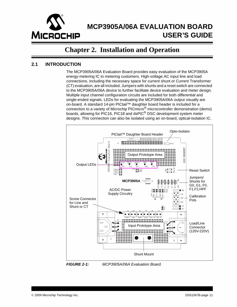
2.1 INTRODUCTIONThe MCP3905A/06A Evaluation Board provides easy evaluation of the MCP3905A energy-metering IC to metering customers. High-voltage AC input line and load connections, including the necessary space for current shunt or Current Transformer (CT) evaluation, are all included. Jumpers with shunts and a reset switch are connected to the MCP3905A/06A device to further facilitate device evaluation and meter design. Multiple input channel configuration circuits are included for both differential and single-ended signals. LEDs for evaluating the MCP3905A/06A output visually are on-board. A standard 14-pin PICtail™ daughter board header is included for a connection to a variety of Microchip PICmicro® microcontroller demonstration (demo) boards, allowing for PIC16, PIC18 and dsPIC® DSC development system meter designs. This connection can also be isolated using an on-board, optical-isolation IC.
FIGURE 2-1: MCP3905A/06A Evaluation Board.
PICtail™Daughter Board
PICtail™ Daughter Board HeaderOpto-Isolator
Output Prototype Area
Shunt Mount
Load/LineConnector(120V-220V)
Screw Connectorfor Line andShunt or CT
Input Prototype Area
Reset Switch
Jumpers/Shunts forG0, G1, F0,F1,F2,HPF
CalibrationPots
AC/DC PowerSupply Circuitry
Output LEDs
MCP3905A
© 2009 Microchip Technology Inc. DS51567B-page 11

MCP3905A/06A Evaluation Board User’s Guide
2.2 FEATURESThe MCP3905A/06A Evaluation Board has the following features:• Large space for easy connection to AC line and loads provide area for
experiments using different current-sensing elements• Easy connection to both PICDEM™ demonstration boards for a variety of
PICmicro® MCU-based meter designs• Jumpers and shunts for simple device configuration• On-board, low-cost AC-to-DC power supply circuitry to demonstrate the low-cost
MCP3905 AFE design used in the MCP3905A/06A Energy Meter Reference Design (DS51565)
• EMC immunity and Printed Circuit Board (PCB) design as used in the MCP3905A/06A Energy Meter Reference Design (DS51565)
• Designed to fit inside recommended plastic enclosure for safe, high-voltage demonstrations and experiments (enclosure is optional and is not included)
2.3 GETTING STARTEDThe following example is given to describe how to use this evaluation board using a current-sensing shunt, 220 VAC line voltage and a 10A load. All connections described in this section are dependent on the choice of current-sensing element. A 250 µΩ shunt is selected as the current-sensing element.
2.3.1 Step 1: Install Current-Sensing Element and Make Appropriate Input Connections
Use the input prototype area to connect the line/load and current-sensing elements to the appropriate screw-type connector. An example of connecting the shunt is shown in Figure 2-2. Please note that the phase-side of the line should be used as the GND reference to the MCP3905A/06A Evaluation Board when using the AC/DC power supply circuit in shunt examples like the one in Figure 2-2.
FIGURE 2-2: Example Input Prototype Area Connections Using Shunt. The system is biased to the line-side of the two-wire power supply.
L
LOA
D, 1
0A
220
VAC
CH0+ CH0- CH1A CH1BHigh Low
J11
GN
LJ12
GN
250 µΩ Shunt
DS51567B-page 12 © 2009 Microchip Technology Inc.

Installation and Operation
2.3.2 Step 2: Select Channel 0 Input MethodResistor sockets R11 and R12 should be left open when using a shunt. JP3, JP13 and JP14 should also be open. This configuration puts the shunt across the channel inputs differentially with the users option of a RC filter.
FIGURE 2-3: Channel 0 Jumpers for 250 µΩ Shunt Selection.
2.3.3 Step 3: Select Channel 1 Input MethodUsing JP18, JP19, JP20 and JP21, select if Channel 1 will be single-ended or differential, and which input will be tied to the voltage divider and potentiometer. In Figure 2-4, the voltage divider and potentiometer are connected to the positive input, while the negative input is connected to AGND through the RC.
FIGURE 2-4: Channel 1 Input Method Example.
J5C
H0+
J6C
H0-
CH0+
CH0-
JP3
z11
z12
open
open
open+
-
250
µΩ S
hunt
C10.033 µF
R1
1 kΩ
C10.033 µF
R1
1 kΩJP13
JP14
RC to Voltage Divider & Potentiometer (Circuit A)
J8C
HA
J7C
HB
CH1+CH1-
CH1+CH1-
JP20
JP18C10.033 µF
R1
1 kΩ
JP21
JP19
© 2009 Microchip Technology Inc. DS51567B-page 13

MCP3905A/06A Evaluation Board User’s Guide
2.3.4 Step 4: Select desired output evaluation methodJumpers JP5 and JP6 select the output evaluation method. In this example, we are selecting HFOUT connected to the LED for blink.
FIGURE 2-5: Connecting the MCP3905A High-Frequency Output to the LED.
2.3.5 Step 5: Select +5V SourceWith the connections for J9 and J11 made in Figure 2-2, the 220V AC/DC power supply circuit can be used as the +5V supply. Here we put JP4 in the “INT” position for internal connection.
2.3.6 Step 6: Connect Line and Load and Observe MCP3905A OutputOnce all jumper positions have been selected, connecting 220V with the correct L,G,N connections and an appropriate load (10A in this example) will power both the MCP3905A/06A Evaluation Board and create the MCP3905A output (LED, BLINKING) in Figure 2-5.
2.4 MCP3905A/06A EVALUATION BOARD OVERVIEWThe functional blocks of the MCP3905A/06A Evaluation Board will be described in this section. For more detailed information regarding design decisions and approaches to IEC1036 compliance, refer to AN994, “IEC Compliant Active Energy Meter Design Using The MCP3905A/06A” (DS00994). For a detailed circuit schematic, refer to Appendix A. “Schematics and Layouts” and Appendix B. “Bill Of Materials (BOM)” for a list of the parts used to build the MCP3905A/06A Evaluation Board.
JP6
OPTLEDHFOUT PULSE
MCP3905A
DS51567B-page 14 © 2009 Microchip Technology Inc.

Installation and Operation
2.5 FUNCTIONAL BLOCK DESCRIPTIONS
2.5.1 Input Prototype AreaAll line/load, shunt and CT connections are to be made next to the screw-typeconnectors J5-J12. This area includes two mounting holes for a standard shuntconnector. All high-voltage connections go onto this prototype area.
2.5.2 High-Voltage Input Connections (J5-12) These screw-type connections are for shunts, CTs, line and load. The shunt resistance should be placed in parallel with J5 and J6. A variety of experiments using shunts and CTs can be performed here in conjunction with the input prototype area.J9 and J10 feed the AC/DC power supply circuitry. J10 is the reference connection to the entire board. Shunt-type meters should be connected to the line-side. One example is given in the figure below.
\
FIGURE 2-6: Example Wiring Using Two-Wire System with Shunt.
2.5.3 Jumpers and Shunts for MCP3905 Gain and Frequency Constant FC Selection (JP1, 2, 9-12)
Jumpers and shunts for both logic-high and logic-low are included for all gain and frequency constant selections, with filter options Off and On columns being clearly labelled.
FIGURE 2-7: MCP3905A Jumper Selections.
L
LOA
D, 1
0A
220
VAC
CH0+ CH0- CH1A CH1BHigh Low
J11
GN
L
J12
GN
250 µΩ Shunt
HP
F F2 F1 F0 G0
G0
JP12
JP8
JP2
JP11
JP1
JP10
OFF
ON
© 2009 Microchip Technology Inc. DS51567B-page 15
MCP3905A/06A Evaluation Board User’s Guide
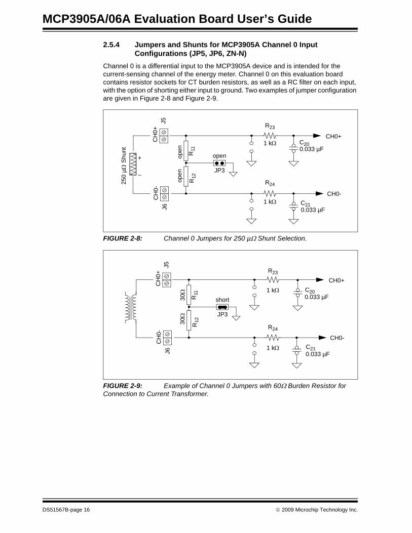
2.5.4 Jumpers and Shunts for MCP3905A Channel 0 Input Configurations (JP5, JP6, ZN-N)
Channel 0 is a differential input to the MCP3905A device and is intended for the current-sensing channel of the energy meter. Channel 0 on this evaluation board contains resistor sockets for CT burden resistors, as well as a RC filter on each input, with the option of shorting either input to ground. Two examples of jumper configuration are given in Figure 2-8 and Figure 2-9.
FIGURE 2-8: Channel 0 Jumpers for 250 µΩ Shunt Selection.
FIGURE 2-9: Example of Channel 0 Jumpers with 60Ω Burden Resistor for Connection to Current Transformer.
J5C
H0+
J6C
H0-
CH0+
CH0-
JP3
R11
R12
open
open
open+
–
250
µΩ S
hunt
0.033 µF
R24
1 kΩ
C200.033 µF
R23
1 kΩ
C21
J5C
H0+
J6C
H0-
CH0+
CH0-
JP3
R11
R12
30Ω
30Ω
short
C210.033 µF
R24
1 kΩ
C200.033 µF
R23
1 kΩ
DS51567B-page 16 © 2009 Microchip Technology Inc.

Installation and Operation
2.5.5 Channel 1 RC Circuit with AGND Option – Circuit AChannel 1 is a differential input with two possible circuit selections for each single-ended input (circuit A and circuit B). Using the MCP3905A/06A Evaluation Board, either of the inputs can be connected to the RC or to AGND, allowing single-ended or differential experiments. JPX should be shorted to ground for all single-ended input configurations.
FIGURE 2-10: Channel 1 RC Circuit A.
2.5.6 Channel 1 Voltage Divider Circuit and Calibration Potentiometer – Circuit B
Circuit B includes 4 resistor sockets and a mechanical potentiometer. This allows for experiments calibrating the output of the MCP3905A by changing Channel 1’s input signal amplitude.
FIGURE 2-11: Voltage Divider on Channel 1 Including Potentiometers VR1, VR2 and VR6 for Calibration Experiments, Labeled Circuit B on the PCB Silk-Screen.
2.5.7 MCP3905ACenter-of-board, 24-lead surface-mount package. Refer to the MCP3905A Data Sheet, “Energy Metering IC with Active Real Power Pulse Output” (DS21948) for a detailed description.
J8C
H1A
JP20C10.033 µF
R1
1 kΩ
R3 R4
R8500Ω
VR1VR2VR6
1 kΩ/25 T100 kΩ/25 T300 kΩ/25 T
© 2009 Microchip Technology Inc. DS51567B-page 17

MCP3905A/06A Evaluation Board User’s Guide
2.5.8 DC Power SupplyA low-cost DC power supply circuit is included on the MCP3905A/06A Evaluation Board. This is the same DC power supply circuit used in the MCP3905A/06A Energy Meter Reference Design. The DC power supply is created from a half-wave zener diode-limited AC signal feeding a 7805 +5V regulator.C17 and C16 divide the AC signal coming directly from the line, with their values depending on the AC source expected. The board comes populated with a series capacitor of 0.47 µF, designed to divide down an AC line voltage of 220 VRMS. If the DC power supply is to be used with a 120 VRMS AC source capacitor, C16 should change to 1 µF. Refer to Appendix B. “Bill Of Materials (BOM)” for detailed part information.For more detail on this circuit design, as well as for 120V circuit specifications, refer to AN994 “IEC Compliant Active Energy Meter Design Using The MCP3905A/06A” (DS00994).
2.5.9 Output Prototype AreaA second prototype area is included for experiments using the MCP3905A output.All MCP3905A outputs (FOUT0, FOUT1, HFOUT, REVP) are brought out to the prototypearea.
2.5.10 Connecting the MCP3905A/06A Evaluation Board to a PICDEM™ Demonstration Board
A standard 14-pin PICtail™ daughter board connector is included on this board, asshown in Figure 2-12. Any number of MCP3905A with PICmicro MCU meter designscan be developed. An optical isolator is included with the MCP3905A/06A EnergyMeter Reference Design as an additional level of protection for direct-connect metersusing a shunt. It is connected to the selected output of the MCP3905A via JP5.A pull-up resistor is required on the output of the optical isolator to allow the selectedlogic signal to appear on the PICmicro MCU-based demo board, which is isolatedentirely from the MCP3905A/06A Evaluation Board. The output of the optical isolatoris connected to RC0 on this connector, as shown in Figure 2-12. RC0 was chosen tobe the default output due to the timer1 clock input on many PICmicro® MCUs.
FIGURE 2-12: Optical isolation of the MCP3905A outputs to the PICkit™ header. The output is connected to RC0 using a 10 kΩ pull-up resistor to the PICtail™ daughter board header +5V and the PICmicro® MCU header, GND.
1RA52RA43RA34RC55RC46RC37RA08RA19RA2101112RC213VCC14PIC®_MCU_GND
RC0RC1
10 kΩPull-up
Standard PICtail™
To AGND (possible bias to 110 or 220V with direct-connect meters)
NEGHFOUTFOUT1FOUT0
JP5
OUT
2
1
4
3
U3
Stan
dard
I/O
PIC
kit™
Sta
rter K
it C
onne
ctor
Daughter Board Connector
Resistor
MCP3905A OUTPUT SELECTION
DS51567B-page 18 © 2009 Microchip Technology Inc.

MCP3905A/06A EVALUATION BOARDUSER’S GUIDE
Appendix A. Schematics and Layouts
A.1 INTRODUCTIONThis appendix contains the following schematics and layouts for the MCP3905A/06A Evaluation Board User’s Guide:• Board Schematic• Board – Top Layer and Silk-Screen• Board – Bottom Layer
A.2 SCHEMATICS AND PCB LAYOUTThe layer order is shown in Figure A-1.
FIGURE A-1: Layer Order.
Top Layer
Bottom Layer
© 2009 Microchip Technology Inc. DS51567B-page 19
MCP3905A/06A Evaluation Board User’s Guide
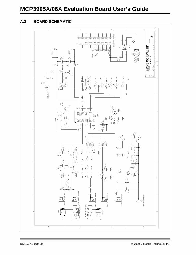
A.3 BOARD SCHEMATIC
12
34
56
ABCD
65
43
21
D C B A
Title
Num
ber
Revi
sion
Size B Dat
e:21
-Jun
-200
5Sh
eet
of
File
:C:
\Act
ive
Boar
d Fi
les\1
02-0
0051
thru
102
-000
60\1
02-0
0057
\PCB
Pro
tel
File
s\MCP
3905
C13
10 μ
F
C11
220
μFC1
20.
1 μF
C17
0.47
μF
C16
0.01
μF
C15
0.1
μF
C14
0.1
μF
C922
pF
C822
pF
C18
470
μF
D3
1N47
44AD2 1N
4004
VO
UT
1V
IN8
G1 2
G4 7
G2 3
G3 6
U2
7805
Z2
R22
10
R20
20 R19
20
C10
0.1
μF
R21
470
MO
V1
C19
0.1
μF
AV
DD
Y1
3.57
9545
M H
ZR18
820
+ -
D1
GRE
EN
4 3
1 2
U3
PS25
01
Z1
MC
P390
5 EV
AL
BD
210
3-00
057
J3A
C IN
J1
AC
OU
T
JP10
G0
JP1
G1
JP11
F0
JP2
F1
JP9
F2
AV
DD
JP12
HPF
AV
DD
R1 1K
C1 0.03
3 μF
VR1
1K/ 2
5T
Z3Z4
Z8 500
21
JP20
CH1-
21
JP21
CH1+
R5 1KC3 0.
033
μF
2 1
JP15
JUM
PER
21
JP18
CH1-
21
JP19
CH1+
2 1
JP13 JU
MPE
R
R2 1K
C2 0.03
3 μF
2 1
JP14
JUM
PER
HPF
HPF
21
JP3
JUM
PER
R11
30 R12
30
TP2
TP3
REV
P
R7 820
+-
D4
RED
REV
P
12 4
3
SW1
MCL
R
TP7
VRE
F
R9 470
R10
4.7K
C4 0.1
μF
AV
DD
JP4
PWR
TP8
+5V
TP6
GN
D
12
34
56
78
910
1112
1314
1516
1718
1920
2122
2324
2526
2728
2930
3132
3334
3536
3738
3940
4142
4344
4546
4748
4950
J2
FEM
ALE
HEA
DER
25X
2
FOU
T0
FOU
T1
HFO
UT
R13
1K
JP5
OU
T
HFO
UT2
FOU
T0FO
UT1
REV
P
TP1
TP5
JP6
HFO
UT
R14
820
HFO
UT2
J5
2-PI
N T
ERM
INA
L BL
OCK
J6
2-PI
N T
ERM
INA
L BL
OCK
J7
2-PI
N T
ERM
INA
L BL
OCK
J8
2-PI
N T
ERM
INA
L BL
OCK
J9
2-PI
N T
ERM
INA
L BL
OCK
J10
2-PI
N T
ERM
INA
L BL
OCK
31
2
J12
3- PI
N T
ERM
INA
L BL
OCK
31
2
J11
3-PI
N T
ERM
INA
L BL
OCK
RA1
RA0
RC3
RC4
RC5
RA3
RA4
RA5
RA2
R23
1K
C20
0.03
3 μF
R24
1K
C21
0.03
3 μF
DV
DD
1
HPF
2
AV
DD
3
NC1
4
CH0+
5
CH0-
6
CH1-
7
CH1+
8
MCL
R9
REFI
N/O
UT
10
AG
ND
11
F212
F113
F014
G1
15G
016
OSC
217
OSC
118
NC2
19N
EG20
DG
ND
21H
FOU
T22
FOU
T123
FOU
T024
U1
MCP3905
-SSO
P24
C6 0.1
μFC5 10
μF
VR6
300K
/25
T
VR2
100K
/25
T
RC0
RC1
RC2
PIC
®_M
CU
_+5
PIC
®__M
CU
_GN
D
PIC
tail™
DS51567B-page 20 © 2009 Microchip Technology Inc.

Schematics and Layouts
A.4 BOARD LAYOUT – TOP LAYER AND SILK-SCREEN P
ICtail™
Dau
gh
ter Bo
ard
© 2009 Microchip Technology Inc. DS51567B-page 21

MCP3905A/06A Evaluation Board User’s Guide
A.5 BOARD LAYOUT – BOTTOM LAYER
DS51567B-page 22 © 2009 Microchip Technology Inc.

MCP3905A/06A EVALUATION BOARDUSER’S GUIDE
Appendix B. Bill Of Materials (BOM)
TABLE B-1: BILL OF MATERIALS (BOM)Qty Reference Description Manufacturer Part Number
5 C1, C2, C3, C20, C21
033 µF 100V 10% MONOLIT CERM CAP
EPCOS B37987M1333K000
7 C4, C6, C10, C12, C14, C15, C19
CAP .1 µF 16V CERAMIC X7R 0805 Panasonic® - ECG ECJ-2VB1C104K
2 C5, C13 CAPACITOR TANT 10 µF 6.3V 20% SMD
Nichon F930J106MAA
2 C8, C9 CAP 22 PF 50V CERAMIC 0402 SMD Panasonic - ECG ECJ-0EC1H220J1 C11 CAP 220 µF 10V ELECT FC RADIAL Panasonic - ECG EEU-FC1A221S1 C16 01 µF INTERFERFENCE METAL CAP Panasonic - ECG ECQ-U2A103MN1 C17 .47 µF/630VDC METAL POLY CAP Panasonic - ECG ECQ-E6474KF1 C18 CAP 470 µF 35V ELECT FC RADIAL Panasonic - ECG EEU-FC1V47130 C1, C2, C3,
C20, C21, R1, R2, R5, R11, R12, R23, R24, Z3, Z4, Z8
PIN RECPT .015/.025 DIA 0252 SER Note* - 2 Pins per Location
Mill-Max® Manufacturing Corp.
0252-0-15-15-30-27-10-0
1 D1 LED GREEN CLEAR 5MM ROUND Panasonic - SSG LN31GCPH1 D2 RECTIFIER GPP 400V 1A DO-41 Diodes Inc 1N4004-T1 D3 DIODE ZENER 15V 1W 5% DO-41 Diodes Inc 1N4744A-T1 D4 LED RED CLEAR 5MM ROUND Panasonic - SSG LN21RCPH1 J1 AC OUTPUT CONN
Top or Bottom placementSCHURTER 4300.0251
1 J2 “DO NOT INSTALL” — —1 J3 AC INPUT CONN
Top or Bottom placementSCHURTER GSP1.8101.1
6 J5, J6, J7, J8, J9, J10
TERMINAL BLOCK 5MM VERT 2POS PCB
Jameco Valuepro TERM BLK-R
4 J1 & J3 SCREW MACH PHIL 4-40X3/8 NYLON Building Fasteners NY PMS 440 0038 PH4 J1 & J3 NUT HEX 4-40 NYLON Building Fasteners NY HN 4407 JP1, JP2, JP4,
JP9, JP10, JP11, JP12
HEADER, .1"ST MALE, 1RW, 3PIN, (10) .025"PST, .23"GOLDTAIL
Jameco Valuepro 7000-1X3SG-R
8 JP3, JP15, JP13, JP14, JP18, JP20, JP21, JP19
"HEADER, .1""ST MALE, 1RW, 2PIN, (10) .025""PST, .21""GOLDTAIL
Jameco Valuepro 7000-1X2SG-R
1 JP5 HEADER,.1"ST MALE,2RW,8PIN, .025"PST,.23"GOLDTAIL (10)
Jameco Valuepro 0-2X4SG-R
Note 1: The components listed in this Bill of Materials are representative of the PCB assembly. The released BOM used in manufacturing uses all RoHS-compliant components.
© 2009 Microchip Technology Inc. DS51567B-page 23

MCP3905A/06A Evaluation Board User’s Guide
1 JP6 HEADER, ST MALE, 2RW, 4PIN, .1""CTR, .025 PST,
Jameco Valuepro 2X2SG-R
2 J11, J12 TERMINAL BLOCK 5MM VERT 3POS PCB
Jameco Valuepro DT128V3P-R
15 JP1, JP2, JP3, JP4, JP5, JP6, JP9, JP10, JP11, JP12, JP13, JP14, JP15, JP19, JP20
.100" Shorting Block with Handle Jameco Valuepro 2012JH-R
1 MOV1 Suppressors;Clamping Voltage Max.:710V; Peak Surge
EPCOS SIOV-S20K275
1 PCB RoHS Compliant Bare PCB, MCP3905A/06A Evaluation Board
Microchip Technology Inc.
104-00057
5 R1, R2, R5 R23, R24
RES 1.00K OHM 1/4W 1% METAL FILM Yageo® America MFR-25FBF-1K00
3 R7, R14, R18 RES 820 OHM 1/4W 5% 1206 SMD Yageo America RC1206JR-07820RL1 R9 RES 475 OHM 1/10W 1% 0805 SMD Panasonic - ECG ERJ-6ENF4750V1 R10 RES 4.75K OHM 1/10W 1% 0805 SMD Panasonic - ECG ERJ-6ENF4751V2 R11, R12 RES 30.1 OHM 1/4W 1% METAL FILM Yageo America MFR-25FBF-30R11 R13 RES 10.0K OHM 1/10W 1% 0805 SMD Panasonic - ECG ERJ-6ENF1002V2 R19, R20 RES 20.0 OHM 1/8W 1% 1206 SMD Panasonic - ECG ERJ-8ENF20R0V1 R21 RES 470 OHM 1W 5% METAL OXIDE Yageo America RSF100JB-470K1 R22 RES 10 OHM 1/8W 1% 1206 SMD Panasonic - ECG ERJ-8ENF10R0V1 SW1 SWITCH TACT 6MM MOM 100GF Omron Electronics
Inc.B3F-1000
7 TP1, TP2, TP3, TP5, TP6, TP7, TP8
“DO NOT POPULATE” Keystone Electronics®
5012
1 U1 MCP3905A PWR Meter Chip Microchip Technology Inc.
MCP3905A-I/SS
1 U2 IC VOLT REG 5V 100MA 8-SOIC Fairchild Semiconductor®
KA78L05AD
1 U3 1 CHANNEL OPTO COUPLER TRANS DIP
NEC PS2501-1-A
1 VR1 POT 1.0K OHM 3/8" SQ CERM SL MT Bourns Inc. 3296Y-1-102LF1 VR2 POT 100K OHM 3/8" SQ CERM SL MT Bourns Inc. 3296Y-1-104LF1 VR6 POT 500K OHM 3/8" SQ CERM SL MT Bourns Inc. 3296Y-1-504LF1 Y1 CRYSTAL 3.579545MHZ 17PF
HC49/USECS Inc. ECS-35-17-4X
2 Z1, Z2 BEAD CORE SINGLE 3.5X9MM AXIAL Panasonic - ECG EXC-ELSA392 Z3, Z4 RES 332K OHM 1/4W 1% METAL FILM
SocketYageo America MFR-25FBF-332K
1 Z8 RES 499 OHM 1/4W 1% METAL FILM Yageo America MFR-25FBF-499R5 EA corner of
PCB and on in the middle
BUMPON TALL TAPER SQ .50X.23 BK 3M/ESM SJ-5518 (BLACK)
TABLE B-1: BILL OF MATERIALS (BOM) (CONTINUED)Qty Reference Description Manufacturer Part Number
Note 1: The components listed in this Bill of Materials are representative of the PCB assembly. The released BOM used in manufacturing uses all RoHS-compliant components.
DS51567B-page 24 © 2009 Microchip Technology Inc.

Bill Of Materials (BOM)
NOTES:
© 2009 Microchip Technology Inc. DS51567B-page 25

DS51567B-page 26 © 2009 Microchip Technology Inc.
AMERICASCorporate Office2355 West Chandler Blvd.Chandler, AZ 85224-6199Tel: 480-792-7200 Fax: 480-792-7277Technical Support: http://support.microchip.comWeb Address: www.microchip.comAtlantaDuluth, GA Tel: 678-957-9614 Fax: 678-957-1455BostonWestborough, MA Tel: 774-760-0087 Fax: 774-760-0088ChicagoItasca, IL Tel: 630-285-0071 Fax: 630-285-0075ClevelandIndependence, OH Tel: 216-447-0464 Fax: 216-447-0643DallasAddison, TX Tel: 972-818-7423 Fax: 972-818-2924DetroitFarmington Hills, MI Tel: 248-538-2250Fax: 248-538-2260KokomoKokomo, IN Tel: 765-864-8360Fax: 765-864-8387Los AngelesMission Viejo, CA Tel: 949-462-9523 Fax: 949-462-9608Santa ClaraSanta Clara, CA Tel: 408-961-6444Fax: 408-961-6445TorontoMississauga, Ontario, CanadaTel: 905-673-0699 Fax: 905-673-6509
ASIA/PACIFICAsia Pacific OfficeSuites 3707-14, 37th FloorTower 6, The GatewayHarbour City, KowloonHong KongTel: 852-2401-1200Fax: 852-2401-3431Australia - SydneyTel: 61-2-9868-6733Fax: 61-2-9868-6755China - BeijingTel: 86-10-8528-2100 Fax: 86-10-8528-2104China - ChengduTel: 86-28-8665-5511Fax: 86-28-8665-7889China - Hong Kong SARTel: 852-2401-1200 Fax: 852-2401-3431China - NanjingTel: 86-25-8473-2460Fax: 86-25-8473-2470China - QingdaoTel: 86-532-8502-7355Fax: 86-532-8502-7205China - ShanghaiTel: 86-21-5407-5533 Fax: 86-21-5407-5066China - ShenyangTel: 86-24-2334-2829Fax: 86-24-2334-2393China - ShenzhenTel: 86-755-8203-2660 Fax: 86-755-8203-1760China - WuhanTel: 86-27-5980-5300Fax: 86-27-5980-5118China - XiamenTel: 86-592-2388138 Fax: 86-592-2388130China - XianTel: 86-29-8833-7252Fax: 86-29-8833-7256China - ZhuhaiTel: 86-756-3210040 Fax: 86-756-3210049
ASIA/PACIFICIndia - BangaloreTel: 91-80-3090-4444 Fax: 91-80-3090-4080India - New DelhiTel: 91-11-4160-8631Fax: 91-11-4160-8632India - PuneTel: 91-20-2566-1512Fax: 91-20-2566-1513Japan - YokohamaTel: 81-45-471- 6166 Fax: 81-45-471-6122Korea - DaeguTel: 82-53-744-4301Fax: 82-53-744-4302Korea - SeoulTel: 82-2-554-7200Fax: 82-2-558-5932 or 82-2-558-5934Malaysia - Kuala LumpurTel: 60-3-6201-9857Fax: 60-3-6201-9859Malaysia - PenangTel: 60-4-227-8870Fax: 60-4-227-4068Philippines - ManilaTel: 63-2-634-9065Fax: 63-2-634-9069SingaporeTel: 65-6334-8870Fax: 65-6334-8850Taiwan - Hsin ChuTel: 886-3-6578-300Fax: 886-3-6578-370Taiwan - KaohsiungTel: 886-7-536-4818Fax: 886-7-536-4803Taiwan - TaipeiTel: 886-2-2500-6610 Fax: 886-2-2508-0102Thailand - BangkokTel: 66-2-694-1351Fax: 66-2-694-1350
EUROPEAustria - WelsTel: 43-7242-2244-39Fax: 43-7242-2244-393Denmark - CopenhagenTel: 45-4450-2828 Fax: 45-4485-2829France - ParisTel: 33-1-69-53-63-20 Fax: 33-1-69-30-90-79Germany - MunichTel: 49-89-627-144-0 Fax: 49-89-627-144-44Italy - Milan Tel: 39-0331-742611 Fax: 39-0331-466781Netherlands - DrunenTel: 31-416-690399 Fax: 31-416-690340Spain - MadridTel: 34-91-708-08-90Fax: 34-91-708-08-91UK - WokinghamTel: 44-118-921-5869Fax: 44-118-921-5820
WORLDWIDE SALES AND SERVICE
03/26/09