Embed Size (px)
Citation preview

HCS12XMicrocontrollers
freescale.com
MC9S12XDP512Data Sheet
CoversS12XD, S12XB & S12XA Families
MC9S12XDP512RMV2Rev. 2.21October 2009

MC9S12XDP512RMV2 Data Sheet
MC9S12XDP512RMV2Rev. 2.21
October 2009

MC9S12XDP512 Data Sheet, Rev. 2.21
4 Freescale Semiconductor
To provide the most up-to-date information, the revision of our documents on the World Wide Web will bethe most current. Your printed copy may be an earlier revision. To verify you have the latest informationavailable, refer to:
http://freescale.com/
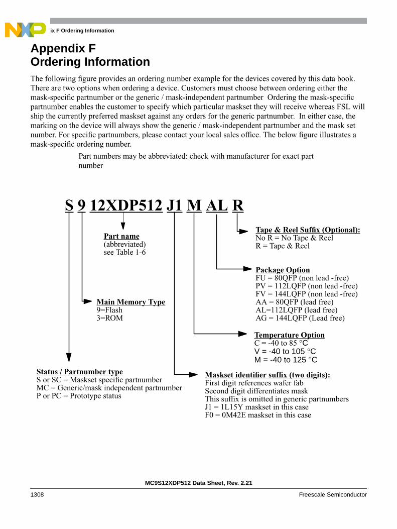
A full list of family members and options is included in the appendices.
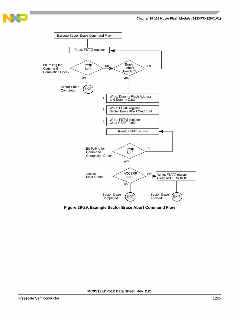
Read page 29 first to understand the maskset specific chapters of this document
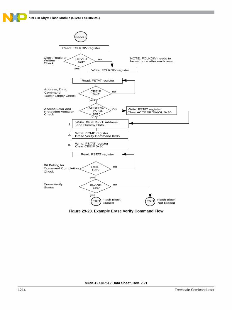
This document contains information for all constituent modules, with the exception of the S12X CPU. ForS12X CPU information please refer to the CPU S12X Reference Manual.
Freescale™ and the Freescale logo are trademarks of Freescale Semiconductor, Inc.This product incorporates SuperFlash® technology licensed from SST.
© Freescale Semiconductor, Inc., 2008. All rights reserved.
MC9S12XDP512 Data Sheet, Rev. 2.21
Freescale Semiconductor 5
Revision History
DateRevision
LevelDescription
April, 2005 02.07 New Book
May, 2005 02.08 Minor corrections
May, 2005 02.09
removed ESD Machine Model from electrical characteristicsadded thermal characteristicsadded more details to run current measurement configurationsVDDA supply voltage range 3.15V - 3.6V fot ATD Operating CharacteristicsI/O Chararcteristics for alll pins except EXTAL, XTAL ....corrected VREG electrical specIDD wait max 95mA
May 2005 02.10 Improvements to NVM reliabity spec, added part numbers
July 2005 02.11 Added ROM parts to App.
October 2005 02.12 Single Souce S12XD Fam. Document, New Memory Map Figures,
May 2006 2.13
SPI electricals updatedVoltage Regulator electricals updatedAdded Partnumbers and 1L15Y masksetUpdated App. E 6SCI’s on 112 pin DT/P512 and 3 SPI’s on all D256 parts
June 2006 2.14Data Sheet covers S12XD/B & A FamilyIncluded differnt pull device specification for differnt masksets
July 2006 2.15 Minor Corrections and Improvments
June 2007 2.16 Added 2M42E and 1M84E masksets
July 2007 2.17 Modified Appendix
April 2008 2.18Better explanation of ATD0/1 for S12XD-Family see page 1305S12XB256 ATD specification changed see Appendix E.6added M23S maskset
August 2008 2.19Corrected XGRAMSIZE of S12XD256 on page 44Corrected 17.4.2.4 XGATE Memory Map SchemeCorrected 18.4.2.4 XGATE Memory Map Scheme
September2009
2.20 Corrected Table E-6 , 30K flash memory available for XGATE on B256
October 2009 2.21 Corrected Footnote in Appendix E3 regarding Shared XGATE/CPU area

MC9S12XDP512 Data Sheet, Rev. 2.21
6 Freescale Semiconductor
MC9S12XDP512 Data Sheet, Rev. 2.21
Freescale Semiconductor 5
Section Number Title Page
Chapter 1 Device Overview MC9S12XD-Family . . . . . . . . . . . . . . . . . . . .31
Chapter 2 Clocks and Reset Generator (S12CRGV6) . . . . . . . . . . . . . . . .79
Chapter 3 Pierce Oscillator (S12XOSCLCPV1) . . . . . . . . . . . . . . . . . . . .119
Chapter 4 Analog-to-Digital Converter (ATD10B16CV4)Block Description125
Chapter 5 Analog-to-Digital Converter (S12ATD10B8CV3) . . . . . . . . . .159
Chapter 6 XGATE (S12XGATEV2). . . . . . . . . . . . . . . . . . . . . . . . . . . . . . .183
Chapter 7 Enhanced Capture Timer (S12ECT16B8CV2) . . . . . . . . . . . .309
Chapter 8 Pulse-Width Modulator (S12PWM8B8CV1) . . . . . . . . . . . . . .363
Chapter 9 Inter-Integrated Circuit (IICV2) Block Description. . . . . . . . .395
Chapter 10 Freescale’s Scalable Controller Area Network (S12MSCANV3).419
Chapter 11 Serial Communication Interface (S12SCIV5) . . . . . . . . . . . . .477
Chapter 12 Serial Peripheral Interface (S12SPIV4) . . . . . . . . . . . . . . . . . .515
Chapter 13 Periodic Interrupt Timer (S12PIT24B4CV1) . . . . . . . . . . . . . .541
Chapter 14 Voltage Regulator (S12VREG3V3V5) . . . . . . . . . . . . . . . . . . .555
Chapter 15 Background Debug Module (S12XBDMV2) . . . . . . . . . . . . . .569
Chapter 16 Interrupt (S12XINTV1) . . . . . . . . . . . . . . . . . . . . . . . . . . . . . . .595
Chapter 17 Memory Mapping Control (S12XMMCV2) . . . . . . . . . . . . . . . .613
Chapter 18 Memory Mapping Control (S12XMMCV3) . . . . . . . . . . . . . . .651
Chapter 19 S12X Debug (S12XDBGV2) Module . . . . . . . . . . . . . . . . . . . .693
Chapter 20 S12X Debug (S12XDBGV3) Module . . . . . . . . . . . . . . . . . . . .745
Chapter 21 External Bus Interface (S12XEBIV2) . . . . . . . . . . . . . . . . . . .787
Chapter 22 DP512 Port Integration Module (S12XDP512PIMV2) . . . . . . .807
Chapter 23 DQ256 Port Integration Module (S12XDQ256PIMV2) . . . . . .901
Chapter 24 DG128 Port Integration Module (S12XDG128PIMV2) . . . . . .975
MC9S12XDP512 Data Sheet, Rev. 2.21
6 Freescale Semiconductor
Section Number Title Page
Chapter 25 2 Kbyte EEPROM Module (S12XEETX2KV1) . . . . . . . . . . . .1039
Chapter 26 4 Kbyte EEPROM Module (S12XEETX4KV2) . . . . . . . . . . . .1073
Chapter 27 512 Kbyte Flash Module (S12XFTX512K4V2). . . . . . . . . . . .1107
Chapter 28 256 Kbyte Flash Module (S12XFTX256K2V1). . . . . . . . . . . .1149
Chapter 29 128 Kbyte Flash Module (S12XFTX128K1V1). . . . . . . . . . . .1191
Chapter 30 Security (S12X9SECV2) . . . . . . . . . . . . . . . . . . . . . . . . . . . .1231
Appendix A Electrical Characteristics. . . . . . . . . . . . . . . . . . . . . . . . . . . .1239
Appendix B Package Information . . . . . . . . . . . . . . . . . . . . . . . . . . . . . . .1290
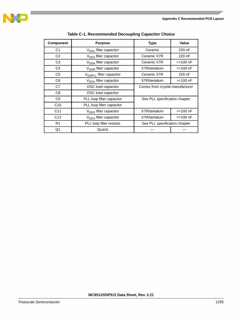
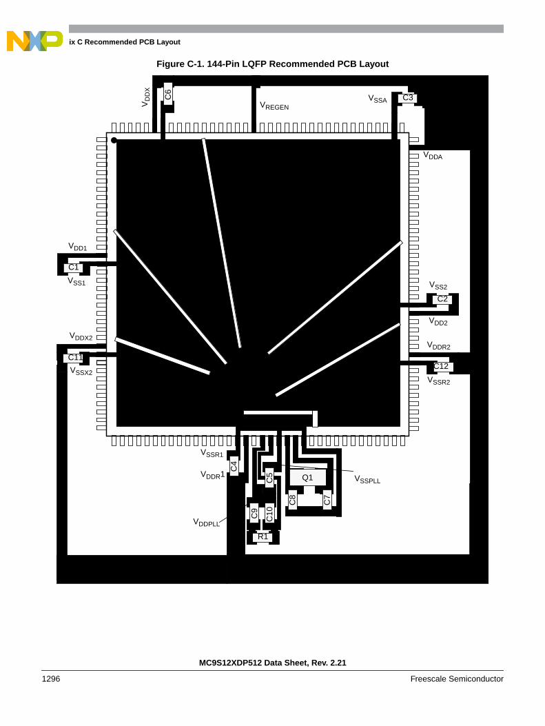
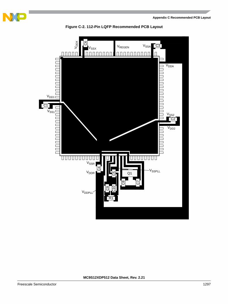
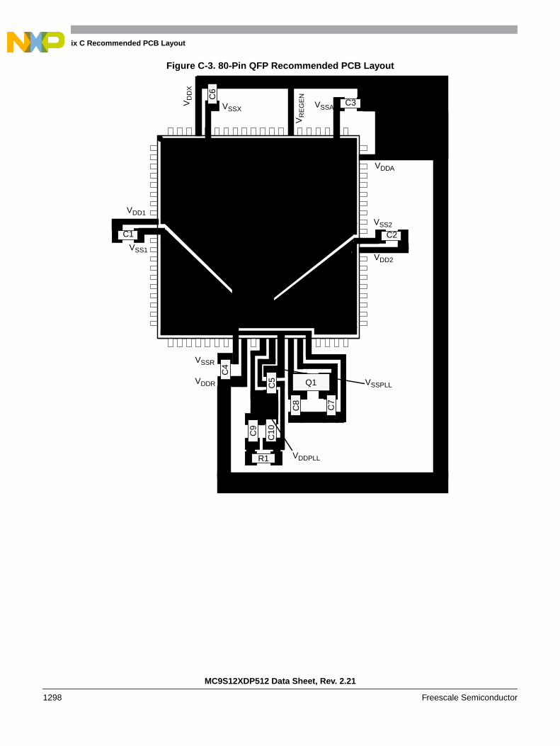
Appendix C Recommended PCB Layout . . . . . . . . . . . . . . . . . . . . . . . . .1294
Appendix D Using L15Y Silicon . . . . . . . . . . . . . . . . . . . . . . . . . . . . . . . . .1299
Appendix E Derivative Differences . . . . . . . . . . . . . . . . . . . . . . . . . . . . . .1300
Appendix F Ordering Information . . . . . . . . . . . . . . . . . . . . . . . . . . . . . . .1308
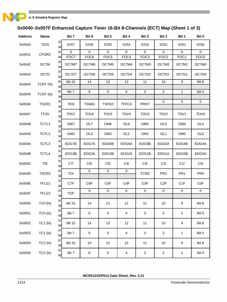
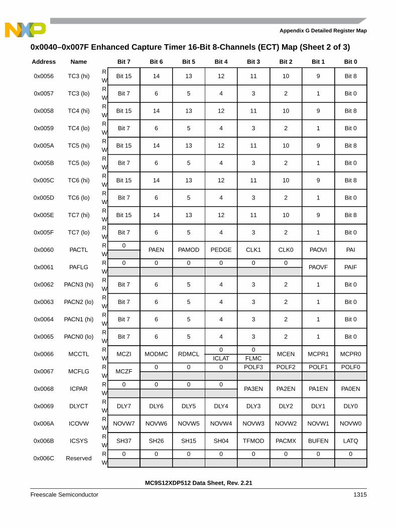
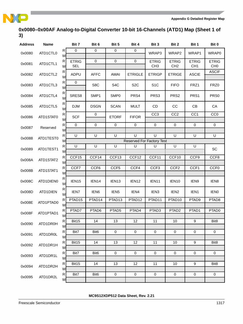
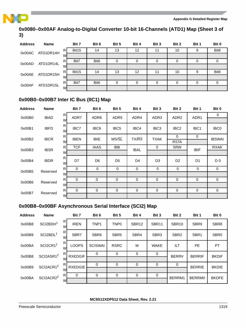
Appendix G Detailed Register Map . . . . . . . . . . . . . . . . . . . . . . . . . . . . . .1309
MC9S12XDP512 Data Sheet, Rev. 2.21
Freescale Semiconductor 9
Section Number Title Page
Chapter 1Device Overview MC9S12XD-Family1.1 Introduction . . . . . . . . . . . . . . . . . . . . . . . . . . . . . . . . . . . . . . . . . . . . . . . . . . . . . . . . . . . . . . . . . . 31
1.1.1 MC9S12XD/B/A Family Features . . . . . . . . . . . . . . . . . . . . . . . . . . . . . . . . . . . . . . . . . . 321.1.2 Modes of Operation . . . . . . . . . . . . . . . . . . . . . . . . . . . . . . . . . . . . . . . . . . . . . . . . . . . . . 341.1.3 Block Diagram . . . . . . . . . . . . . . . . . . . . . . . . . . . . . . . . . . . . . . . . . . . . . . . . . . . . . . . . . 341.1.4 Device Memory Map . . . . . . . . . . . . . . . . . . . . . . . . . . . . . . . . . . . . . . . . . . . . . . . . . . . . 371.1.5 Part ID Assignments & Maskset Numbers . . . . . . . . . . . . . . . . . . . . . . . . . . . . . . . . . . . 47
1.2 Signal Description . . . . . . . . . . . . . . . . . . . . . . . . . . . . . . . . . . . . . . . . . . . . . . . . . . . . . . . . . . . . . 471.2.1 Device Pinout . . . . . . . . . . . . . . . . . . . . . . . . . . . . . . . . . . . . . . . . . . . . . . . . . . . . . . . . . . 471.2.2 Signal Properties Summary . . . . . . . . . . . . . . . . . . . . . . . . . . . . . . . . . . . . . . . . . . . . . . . 521.2.3 Detailed Signal Descriptions . . . . . . . . . . . . . . . . . . . . . . . . . . . . . . . . . . . . . . . . . . . . . . 551.2.4 Power Supply Pins . . . . . . . . . . . . . . . . . . . . . . . . . . . . . . . . . . . . . . . . . . . . . . . . . . . . . . 65
1.3 System Clock Description . . . . . . . . . . . . . . . . . . . . . . . . . . . . . . . . . . . . . . . . . . . . . . . . . . . . . . . 681.4 Chip Configuration Summary . . . . . . . . . . . . . . . . . . . . . . . . . . . . . . . . . . . . . . . . . . . . . . . . . . . . 691.5 Modes of Operation . . . . . . . . . . . . . . . . . . . . . . . . . . . . . . . . . . . . . . . . . . . . . . . . . . . . . . . . . . . . 71
1.5.1 User Modes . . . . . . . . . . . . . . . . . . . . . . . . . . . . . . . . . . . . . . . . . . . . . . . . . . . . . . . . . . . 711.5.2 Low-Power Modes . . . . . . . . . . . . . . . . . . . . . . . . . . . . . . . . . . . . . . . . . . . . . . . . . . . . . . 711.5.3 Freeze Mode . . . . . . . . . . . . . . . . . . . . . . . . . . . . . . . . . . . . . . . . . . . . . . . . . . . . . . . . . . . 72
1.6 Resets and Interrupts . . . . . . . . . . . . . . . . . . . . . . . . . . . . . . . . . . . . . . . . . . . . . . . . . . . . . . . . . . . 721.6.1 Vectors . . . . . . . . . . . . . . . . . . . . . . . . . . . . . . . . . . . . . . . . . . . . . . . . . . . . . . . . . . . . . . . 721.6.2 Effects of Reset . . . . . . . . . . . . . . . . . . . . . . . . . . . . . . . . . . . . . . . . . . . . . . . . . . . . . . . . 76
1.7 COP Configuration . . . . . . . . . . . . . . . . . . . . . . . . . . . . . . . . . . . . . . . . . . . . . . . . . . . . . . . . . . . . . 761.8 ATD0 External Trigger Input Connection . . . . . . . . . . . . . . . . . . . . . . . . . . . . . . . . . . . . . . . . . . . 771.9 ATD1 External Trigger Input Connection . . . . . . . . . . . . . . . . . . . . . . . . . . . . . . . . . . . . . . . . . . . 77
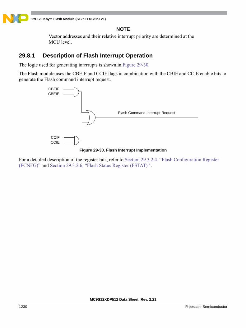
Chapter 2Clocks and Reset Generator (S12CRGV6)
2.1 Introduction . . . . . . . . . . . . . . . . . . . . . . . . . . . . . . . . . . . . . . . . . . . . . . . . . . . . . . . . . . . . . . . . . . 792.1.1 Features . . . . . . . . . . . . . . . . . . . . . . . . . . . . . . . . . . . . . . . . . . . . . . . . . . . . . . . . . . . . . . 792.1.2 Modes of Operation . . . . . . . . . . . . . . . . . . . . . . . . . . . . . . . . . . . . . . . . . . . . . . . . . . . . . 802.1.3 Block Diagram . . . . . . . . . . . . . . . . . . . . . . . . . . . . . . . . . . . . . . . . . . . . . . . . . . . . . . . . . 81
2.2 External Signal Description . . . . . . . . . . . . . . . . . . . . . . . . . . . . . . . . . . . . . . . . . . . . . . . . . . . . . . 822.2.1 VDDPLL and VSSPLL — Operating and Ground Voltage Pins . . . . . . . . . . . . . . . . . . . . . 822.2.2 XFC — External Loop Filter Pin . . . . . . . . . . . . . . . . . . . . . . . . . . . . . . . . . . . . . . . . . . . 822.2.3 RESET — Reset Pin . . . . . . . . . . . . . . . . . . . . . . . . . . . . . . . . . . . . . . . . . . . . . . . . . . . . 82
2.3 Memory Map and Register Definition . . . . . . . . . . . . . . . . . . . . . . . . . . . . . . . . . . . . . . . . . . . . . . 822.3.1 Module Memory Map . . . . . . . . . . . . . . . . . . . . . . . . . . . . . . . . . . . . . . . . . . . . . . . . . . . 832.3.2 Register Descriptions . . . . . . . . . . . . . . . . . . . . . . . . . . . . . . . . . . . . . . . . . . . . . . . . . . . . 84
2.4 Functional Description . . . . . . . . . . . . . . . . . . . . . . . . . . . . . . . . . . . . . . . . . . . . . . . . . . . . . . . . . . 982.4.1 Functional Blocks . . . . . . . . . . . . . . . . . . . . . . . . . . . . . . . . . . . . . . . . . . . . . . . . . . . . . . 982.4.2 Operating Modes . . . . . . . . . . . . . . . . . . . . . . . . . . . . . . . . . . . . . . . . . . . . . . . . . . . . . . 1032.4.3 Low Power Options . . . . . . . . . . . . . . . . . . . . . . . . . . . . . . . . . . . . . . . . . . . . . . . . . . . . 104
MC9S12XDP512 Data Sheet, Rev. 2.21
10 Freescale Semiconductor
Section Number Title Page
2.5 Resets . . . . . . . . . . . . . . . . . . . . . . . . . . . . . . . . . . . . . . . . . . . . . . . . . . . . . . . . . . . . . . . . . . . . . . 1132.5.1 Description of Reset Operation . . . . . . . . . . . . . . . . . . . . . . . . . . . . . . . . . . . . . . . . . . . 1132.5.2 Clock Monitor Reset . . . . . . . . . . . . . . . . . . . . . . . . . . . . . . . . . . . . . . . . . . . . . . . . . . . 1152.5.3 Computer Operating Properly Watchdog (COP) Reset . . . . . . . . . . . . . . . . . . . . . . . . . 1152.5.4 Power On Reset, Low Voltage Reset . . . . . . . . . . . . . . . . . . . . . . . . . . . . . . . . . . . . . . . 115
2.6 Interrupts . . . . . . . . . . . . . . . . . . . . . . . . . . . . . . . . . . . . . . . . . . . . . . . . . . . . . . . . . . . . . . . . . . . 1162.6.1 Real Time Interrupt . . . . . . . . . . . . . . . . . . . . . . . . . . . . . . . . . . . . . . . . . . . . . . . . . . . . 1162.6.2 PLL Lock Interrupt . . . . . . . . . . . . . . . . . . . . . . . . . . . . . . . . . . . . . . . . . . . . . . . . . . . . 1172.6.3 Self Clock Mode Interrupt . . . . . . . . . . . . . . . . . . . . . . . . . . . . . . . . . . . . . . . . . . . . . . . 117
Chapter 3Pierce Oscillator (S12XOSCLCPV1)
3.1 Introduction . . . . . . . . . . . . . . . . . . . . . . . . . . . . . . . . . . . . . . . . . . . . . . . . . . . . . . . . . . . . . . . . . 1193.1.1 Features . . . . . . . . . . . . . . . . . . . . . . . . . . . . . . . . . . . . . . . . . . . . . . . . . . . . . . . . . . . . . 1193.1.2 Modes of Operation . . . . . . . . . . . . . . . . . . . . . . . . . . . . . . . . . . . . . . . . . . . . . . . . . . . . 1193.1.3 Block Diagram . . . . . . . . . . . . . . . . . . . . . . . . . . . . . . . . . . . . . . . . . . . . . . . . . . . . . . . . 120
3.2 External Signal Description . . . . . . . . . . . . . . . . . . . . . . . . . . . . . . . . . . . . . . . . . . . . . . . . . . . . . 1203.2.1 VDDPLL and VSSPLL — Operating and Ground Voltage Pins . . . . . . . . . . . . . . . . . . . . 1203.2.2 EXTAL and XTAL — Input and Output Pins . . . . . . . . . . . . . . . . . . . . . . . . . . . . . . . . 1203.2.3 XCLKS — Input Signal . . . . . . . . . . . . . . . . . . . . . . . . . . . . . . . . . . . . . . . . . . . . . . . . . 122
3.3 Memory Map and Register Definition . . . . . . . . . . . . . . . . . . . . . . . . . . . . . . . . . . . . . . . . . . . . . 1223.4 Functional Description . . . . . . . . . . . . . . . . . . . . . . . . . . . . . . . . . . . . . . . . . . . . . . . . . . . . . . . . . 122
3.4.1 Gain Control . . . . . . . . . . . . . . . . . . . . . . . . . . . . . . . . . . . . . . . . . . . . . . . . . . . . . . . . . . 1223.4.2 Clock Monitor . . . . . . . . . . . . . . . . . . . . . . . . . . . . . . . . . . . . . . . . . . . . . . . . . . . . . . . . 1223.4.3 Wait Mode Operation . . . . . . . . . . . . . . . . . . . . . . . . . . . . . . . . . . . . . . . . . . . . . . . . . . . 1233.4.4 Stop Mode Operation . . . . . . . . . . . . . . . . . . . . . . . . . . . . . . . . . . . . . . . . . . . . . . . . . . . 123
Chapter 4Analog-to-Digital Converter (ATD10B16CV4)
Block Description4.1 Introduction . . . . . . . . . . . . . . . . . . . . . . . . . . . . . . . . . . . . . . . . . . . . . . . . . . . . . . . . . . . . . . . . . 125
4.1.1 Features . . . . . . . . . . . . . . . . . . . . . . . . . . . . . . . . . . . . . . . . . . . . . . . . . . . . . . . . . . . . . 1254.1.2 Modes of Operation . . . . . . . . . . . . . . . . . . . . . . . . . . . . . . . . . . . . . . . . . . . . . . . . . . . . 1254.1.3 Block Diagram . . . . . . . . . . . . . . . . . . . . . . . . . . . . . . . . . . . . . . . . . . . . . . . . . . . . . . . . 125
4.2 External Signal Description . . . . . . . . . . . . . . . . . . . . . . . . . . . . . . . . . . . . . . . . . . . . . . . . . . . . . 1274.2.1 ANx (x = 15, 14, 13, 12, 11, 10, 9, 8, 7, 6, 5, 4, 3, 2, 1, 0) — Analog Input Channel x Pins
1274.2.2 ETRIG3, ETRIG2, ETRIG1, ETRIG0 — External Trigger Pins . . . . . . . . . . . . . . . . . 1274.2.3 VRH, VRL — High Reference Voltage Pin, Low Reference Voltage Pin . . . . . . . . . . . . 1274.2.4 VDDA, VSSA — Analog Circuitry Power Supply Pins . . . . . . . . . . . . . . . . . . . . . . . . . 127
4.3 Memory Map and Register Definition . . . . . . . . . . . . . . . . . . . . . . . . . . . . . . . . . . . . . . . . . . . . . 127
MC9S12XDP512 Data Sheet, Rev. 2.21
Freescale Semiconductor 11
Section Number Title Page
4.3.1 Module Memory Map . . . . . . . . . . . . . . . . . . . . . . . . . . . . . . . . . . . . . . . . . . . . . . . . . . 1274.3.2 Register Descriptions . . . . . . . . . . . . . . . . . . . . . . . . . . . . . . . . . . . . . . . . . . . . . . . . . . . 129
4.4 Functional Description . . . . . . . . . . . . . . . . . . . . . . . . . . . . . . . . . . . . . . . . . . . . . . . . . . . . . . . . . 1524.4.1 Analog Sub-block . . . . . . . . . . . . . . . . . . . . . . . . . . . . . . . . . . . . . . . . . . . . . . . . . . . . . 1524.4.2 Digital Sub-Block . . . . . . . . . . . . . . . . . . . . . . . . . . . . . . . . . . . . . . . . . . . . . . . . . . . . . 1534.4.3 Operation in Low Power Modes . . . . . . . . . . . . . . . . . . . . . . . . . . . . . . . . . . . . . . . . . . 154
4.5 Resets . . . . . . . . . . . . . . . . . . . . . . . . . . . . . . . . . . . . . . . . . . . . . . . . . . . . . . . . . . . . . . . . . . . . . . 1554.6 Interrupts . . . . . . . . . . . . . . . . . . . . . . . . . . . . . . . . . . . . . . . . . . . . . . . . . . . . . . . . . . . . . . . . . . . 155
Chapter 5Analog-to-Digital Converter (S12ATD10B8CV3)5.1 Introduction . . . . . . . . . . . . . . . . . . . . . . . . . . . . . . . . . . . . . . . . . . . . . . . . . . . . . . . . . . . . . . . . . 159
5.1.1 Features . . . . . . . . . . . . . . . . . . . . . . . . . . . . . . . . . . . . . . . . . . . . . . . . . . . . . . . . . . . . . 1595.1.2 Modes of Operation . . . . . . . . . . . . . . . . . . . . . . . . . . . . . . . . . . . . . . . . . . . . . . . . . . . . 1595.1.3 Block Diagram . . . . . . . . . . . . . . . . . . . . . . . . . . . . . . . . . . . . . . . . . . . . . . . . . . . . . . . . 160
5.2 External Signal Description . . . . . . . . . . . . . . . . . . . . . . . . . . . . . . . . . . . . . . . . . . . . . . . . . . . . . 1605.2.1 ANx (x = 7, 6, 5, 4, 3, 2, 1, 0) — Analog Input Pin . . . . . . . . . . . . . . . . . . . . . . . . . . . 1605.2.2 ETRIG3, ETRIG2, ETRIG1, and ETRIG0 — External Trigger Pins . . . . . . . . . . . . . . 1605.2.3 VRH and VRL — High and Low Reference Voltage Pins . . . . . . . . . . . . . . . . . . . . . . . . 1605.2.4 VDDA and VSSA — Power Supply Pins . . . . . . . . . . . . . . . . . . . . . . . . . . . . . . . . . . . . . 160
5.3 Memory Map and Register Definition . . . . . . . . . . . . . . . . . . . . . . . . . . . . . . . . . . . . . . . . . . . . . 1625.3.1 Module Memory Map . . . . . . . . . . . . . . . . . . . . . . . . . . . . . . . . . . . . . . . . . . . . . . . . . . 1625.3.2 Register Descriptions . . . . . . . . . . . . . . . . . . . . . . . . . . . . . . . . . . . . . . . . . . . . . . . . . . . 162
5.4 Functional Description . . . . . . . . . . . . . . . . . . . . . . . . . . . . . . . . . . . . . . . . . . . . . . . . . . . . . . . . . 1805.4.1 Analog Sub-Block . . . . . . . . . . . . . . . . . . . . . . . . . . . . . . . . . . . . . . . . . . . . . . . . . . . . . 1805.4.2 Digital Sub-Block . . . . . . . . . . . . . . . . . . . . . . . . . . . . . . . . . . . . . . . . . . . . . . . . . . . . . 181
5.5 Resets . . . . . . . . . . . . . . . . . . . . . . . . . . . . . . . . . . . . . . . . . . . . . . . . . . . . . . . . . . . . . . . . . . . . . . 1825.6 Interrupts . . . . . . . . . . . . . . . . . . . . . . . . . . . . . . . . . . . . . . . . . . . . . . . . . . . . . . . . . . . . . . . . . . . 182
Chapter 6XGATE (S12XGATEV2)
6.1 Introduction . . . . . . . . . . . . . . . . . . . . . . . . . . . . . . . . . . . . . . . . . . . . . . . . . . . . . . . . . . . . . . . . . 1836.1.1 Glossary of Terms . . . . . . . . . . . . . . . . . . . . . . . . . . . . . . . . . . . . . . . . . . . . . . . . . . . . . 1836.1.2 Features . . . . . . . . . . . . . . . . . . . . . . . . . . . . . . . . . . . . . . . . . . . . . . . . . . . . . . . . . . . . . 1846.1.3 Modes of Operation . . . . . . . . . . . . . . . . . . . . . . . . . . . . . . . . . . . . . . . . . . . . . . . . . . . . 1846.1.4 Block Diagram . . . . . . . . . . . . . . . . . . . . . . . . . . . . . . . . . . . . . . . . . . . . . . . . . . . . . . . . 185
6.2 External Signal Description . . . . . . . . . . . . . . . . . . . . . . . . . . . . . . . . . . . . . . . . . . . . . . . . . . . . . 1856.3 Memory Map and Register Definition . . . . . . . . . . . . . . . . . . . . . . . . . . . . . . . . . . . . . . . . . . . . . 186
6.3.1 Register Descriptions . . . . . . . . . . . . . . . . . . . . . . . . . . . . . . . . . . . . . . . . . . . . . . . . . . . 1866.4 Functional Description . . . . . . . . . . . . . . . . . . . . . . . . . . . . . . . . . . . . . . . . . . . . . . . . . . . . . . . . . 202
6.4.1 XGATE RISC Core . . . . . . . . . . . . . . . . . . . . . . . . . . . . . . . . . . . . . . . . . . . . . . . . . . . . 2026.4.2 Programmer’s Model . . . . . . . . . . . . . . . . . . . . . . . . . . . . . . . . . . . . . . . . . . . . . . . . . . . 2026.4.3 Memory Map . . . . . . . . . . . . . . . . . . . . . . . . . . . . . . . . . . . . . . . . . . . . . . . . . . . . . . . . . 203
MC9S12XDP512 Data Sheet, Rev. 2.21
12 Freescale Semiconductor
Section Number Title Page
6.4.4 Semaphores . . . . . . . . . . . . . . . . . . . . . . . . . . . . . . . . . . . . . . . . . . . . . . . . . . . . . . . . . . 2046.4.5 Software Error Detection . . . . . . . . . . . . . . . . . . . . . . . . . . . . . . . . . . . . . . . . . . . . . . . . 205
6.5 Interrupts . . . . . . . . . . . . . . . . . . . . . . . . . . . . . . . . . . . . . . . . . . . . . . . . . . . . . . . . . . . . . . . . . . . 2066.5.1 Incoming Interrupt Requests . . . . . . . . . . . . . . . . . . . . . . . . . . . . . . . . . . . . . . . . . . . . . 2066.5.2 Outgoing Interrupt Requests . . . . . . . . . . . . . . . . . . . . . . . . . . . . . . . . . . . . . . . . . . . . . 206
6.6 Debug Mode . . . . . . . . . . . . . . . . . . . . . . . . . . . . . . . . . . . . . . . . . . . . . . . . . . . . . . . . . . . . . . . . . 2066.6.1 Debug Features . . . . . . . . . . . . . . . . . . . . . . . . . . . . . . . . . . . . . . . . . . . . . . . . . . . . . . . 2066.6.2 Entering Debug Mode . . . . . . . . . . . . . . . . . . . . . . . . . . . . . . . . . . . . . . . . . . . . . . . . . . 2076.6.3 Leaving Debug Mode . . . . . . . . . . . . . . . . . . . . . . . . . . . . . . . . . . . . . . . . . . . . . . . . . . . 208
6.7 Security . . . . . . . . . . . . . . . . . . . . . . . . . . . . . . . . . . . . . . . . . . . . . . . . . . . . . . . . . . . . . . . . . . . . . 2086.8 Instruction Set . . . . . . . . . . . . . . . . . . . . . . . . . . . . . . . . . . . . . . . . . . . . . . . . . . . . . . . . . . . . . . . 208
6.8.1 Addressing Modes . . . . . . . . . . . . . . . . . . . . . . . . . . . . . . . . . . . . . . . . . . . . . . . . . . . . . 2086.8.2 Instruction Summary and Usage . . . . . . . . . . . . . . . . . . . . . . . . . . . . . . . . . . . . . . . . . . 2126.8.3 Cycle Notation . . . . . . . . . . . . . . . . . . . . . . . . . . . . . . . . . . . . . . . . . . . . . . . . . . . . . . . . 2156.8.4 Thread Execution . . . . . . . . . . . . . . . . . . . . . . . . . . . . . . . . . . . . . . . . . . . . . . . . . . . . . . 2156.8.5 Instruction Glossary . . . . . . . . . . . . . . . . . . . . . . . . . . . . . . . . . . . . . . . . . . . . . . . . . . . . 2156.8.6 Instruction Coding . . . . . . . . . . . . . . . . . . . . . . . . . . . . . . . . . . . . . . . . . . . . . . . . . . . . . 288
6.9 Initialization and Application Information . . . . . . . . . . . . . . . . . . . . . . . . . . . . . . . . . . . . . . . . . . 2916.9.1 Initialization . . . . . . . . . . . . . . . . . . . . . . . . . . . . . . . . . . . . . . . . . . . . . . . . . . . . . . . . . . 2916.9.2 Code Example (Transmit "Hello World!" on SCI) . . . . . . . . . . . . . . . . . . . . . . . . . . . . 291
Chapter 7Enhanced Capture Timer (S12ECT16B8CV2)
7.1 Introduction . . . . . . . . . . . . . . . . . . . . . . . . . . . . . . . . . . . . . . . . . . . . . . . . . . . . . . . . . . . . . . . . . 3097.1.1 Features . . . . . . . . . . . . . . . . . . . . . . . . . . . . . . . . . . . . . . . . . . . . . . . . . . . . . . . . . . . . . 3097.1.2 Modes of Operation . . . . . . . . . . . . . . . . . . . . . . . . . . . . . . . . . . . . . . . . . . . . . . . . . . . . 3097.1.3 Block Diagram . . . . . . . . . . . . . . . . . . . . . . . . . . . . . . . . . . . . . . . . . . . . . . . . . . . . . . . . 310
7.2 External Signal Description . . . . . . . . . . . . . . . . . . . . . . . . . . . . . . . . . . . . . . . . . . . . . . . . . . . . . 3117.2.1 IOC7 — Input Capture and Output Compare Channel 7 . . . . . . . . . . . . . . . . . . . . . . . . 3117.2.2 IOC6 — Input Capture and Output Compare Channel 6 . . . . . . . . . . . . . . . . . . . . . . . . 3117.2.3 IOC5 — Input Capture and Output Compare Channel 5 . . . . . . . . . . . . . . . . . . . . . . . . 3117.2.4 IOC4 — Input Capture and Output Compare Channel 4 . . . . . . . . . . . . . . . . . . . . . . . . 3117.2.5 IOC3 — Input Capture and Output Compare Channel 3 . . . . . . . . . . . . . . . . . . . . . . . . 3117.2.6 IOC2 — Input Capture and Output Compare Channel 2 . . . . . . . . . . . . . . . . . . . . . . . . 3117.2.7 IOC1 — Input Capture and Output Compare Channel 1 . . . . . . . . . . . . . . . . . . . . . . . . 3117.2.8 IOC0 — Input Capture and Output Compare Channel 0 . . . . . . . . . . . . . . . . . . . . . . . . 311
7.3 Memory Map and Register Definition . . . . . . . . . . . . . . . . . . . . . . . . . . . . . . . . . . . . . . . . . . . . . 3127.3.1 Module Memory Map . . . . . . . . . . . . . . . . . . . . . . . . . . . . . . . . . . . . . . . . . . . . . . . . . . 3127.3.2 Register Descriptions . . . . . . . . . . . . . . . . . . . . . . . . . . . . . . . . . . . . . . . . . . . . . . . . . . . 314
7.4 Functional Description . . . . . . . . . . . . . . . . . . . . . . . . . . . . . . . . . . . . . . . . . . . . . . . . . . . . . . . . . 3507.4.1 Enhanced Capture Timer Modes of Operation . . . . . . . . . . . . . . . . . . . . . . . . . . . . . . . 3577.4.2 Reset . . . . . . . . . . . . . . . . . . . . . . . . . . . . . . . . . . . . . . . . . . . . . . . . . . . . . . . . . . . . . . . . 360
MC9S12XDP512 Data Sheet, Rev. 2.21
Freescale Semiconductor 13
Section Number Title Page
7.4.3 Interrupts . . . . . . . . . . . . . . . . . . . . . . . . . . . . . . . . . . . . . . . . . . . . . . . . . . . . . . . . . . . . 361
Chapter 8Pulse-Width Modulator (S12PWM8B8CV1)
8.1 Introduction . . . . . . . . . . . . . . . . . . . . . . . . . . . . . . . . . . . . . . . . . . . . . . . . . . . . . . . . . . . . . . . . . 3638.1.1 Features . . . . . . . . . . . . . . . . . . . . . . . . . . . . . . . . . . . . . . . . . . . . . . . . . . . . . . . . . . . . . 3638.1.2 Modes of Operation . . . . . . . . . . . . . . . . . . . . . . . . . . . . . . . . . . . . . . . . . . . . . . . . . . . . 3638.1.3 Block Diagram . . . . . . . . . . . . . . . . . . . . . . . . . . . . . . . . . . . . . . . . . . . . . . . . . . . . . . . . 364
8.2 External Signal Description . . . . . . . . . . . . . . . . . . . . . . . . . . . . . . . . . . . . . . . . . . . . . . . . . . . . . 3648.2.1 PWM7 — PWM Channel 7 . . . . . . . . . . . . . . . . . . . . . . . . . . . . . . . . . . . . . . . . . . . . . . 3648.2.2 PWM6 — PWM Channel 6 . . . . . . . . . . . . . . . . . . . . . . . . . . . . . . . . . . . . . . . . . . . . . . 3648.2.3 PWM5 — PWM Channel 5 . . . . . . . . . . . . . . . . . . . . . . . . . . . . . . . . . . . . . . . . . . . . . . 3658.2.4 PWM4 — PWM Channel 4 . . . . . . . . . . . . . . . . . . . . . . . . . . . . . . . . . . . . . . . . . . . . . . 3658.2.5 PWM3 — PWM Channel 3 . . . . . . . . . . . . . . . . . . . . . . . . . . . . . . . . . . . . . . . . . . . . . . 3658.2.6 PWM3 — PWM Channel 2 . . . . . . . . . . . . . . . . . . . . . . . . . . . . . . . . . . . . . . . . . . . . . . 3658.2.7 PWM3 — PWM Channel 1 . . . . . . . . . . . . . . . . . . . . . . . . . . . . . . . . . . . . . . . . . . . . . . 3658.2.8 PWM3 — PWM Channel 0 . . . . . . . . . . . . . . . . . . . . . . . . . . . . . . . . . . . . . . . . . . . . . . 365
8.3 Memory Map and Register Definition . . . . . . . . . . . . . . . . . . . . . . . . . . . . . . . . . . . . . . . . . . . . . 3658.3.1 Module Memory Map . . . . . . . . . . . . . . . . . . . . . . . . . . . . . . . . . . . . . . . . . . . . . . . . . . 3658.3.2 Register Descriptions . . . . . . . . . . . . . . . . . . . . . . . . . . . . . . . . . . . . . . . . . . . . . . . . . . . 366
8.4 Functional Description . . . . . . . . . . . . . . . . . . . . . . . . . . . . . . . . . . . . . . . . . . . . . . . . . . . . . . . . . 3808.4.1 PWM Clock Select . . . . . . . . . . . . . . . . . . . . . . . . . . . . . . . . . . . . . . . . . . . . . . . . . . . . . 3808.4.2 PWM Channel Timers . . . . . . . . . . . . . . . . . . . . . . . . . . . . . . . . . . . . . . . . . . . . . . . . . . 384
8.5 Resets . . . . . . . . . . . . . . . . . . . . . . . . . . . . . . . . . . . . . . . . . . . . . . . . . . . . . . . . . . . . . . . . . . . . . . 3928.6 Interrupts . . . . . . . . . . . . . . . . . . . . . . . . . . . . . . . . . . . . . . . . . . . . . . . . . . . . . . . . . . . . . . . . . . . 393
Chapter 9Inter-Integrated Circuit (IICV2) Block Description
9.1 Introduction . . . . . . . . . . . . . . . . . . . . . . . . . . . . . . . . . . . . . . . . . . . . . . . . . . . . . . . . . . . . . . . . . 3959.1.1 Features . . . . . . . . . . . . . . . . . . . . . . . . . . . . . . . . . . . . . . . . . . . . . . . . . . . . . . . . . . . . . 3959.1.2 Modes of Operation . . . . . . . . . . . . . . . . . . . . . . . . . . . . . . . . . . . . . . . . . . . . . . . . . . . . 3969.1.3 Block Diagram . . . . . . . . . . . . . . . . . . . . . . . . . . . . . . . . . . . . . . . . . . . . . . . . . . . . . . . . 396
9.2 External Signal Description . . . . . . . . . . . . . . . . . . . . . . . . . . . . . . . . . . . . . . . . . . . . . . . . . . . . . 3979.2.1 IIC_SCL — Serial Clock Line Pin . . . . . . . . . . . . . . . . . . . . . . . . . . . . . . . . . . . . . . . . 3979.2.2 IIC_SDA — Serial Data Line Pin . . . . . . . . . . . . . . . . . . . . . . . . . . . . . . . . . . . . . . . . . 397
9.3 Memory Map and Register Definition . . . . . . . . . . . . . . . . . . . . . . . . . . . . . . . . . . . . . . . . . . . . . 3979.3.1 Module Memory Map . . . . . . . . . . . . . . . . . . . . . . . . . . . . . . . . . . . . . . . . . . . . . . . . . . 3979.3.2 Register Descriptions . . . . . . . . . . . . . . . . . . . . . . . . . . . . . . . . . . . . . . . . . . . . . . . . . . . 398
9.4 Functional Description . . . . . . . . . . . . . . . . . . . . . . . . . . . . . . . . . . . . . . . . . . . . . . . . . . . . . . . . . 4099.4.1 I-Bus Protocol . . . . . . . . . . . . . . . . . . . . . . . . . . . . . . . . . . . . . . . . . . . . . . . . . . . . . . . . 4099.4.2 Operation in Run Mode . . . . . . . . . . . . . . . . . . . . . . . . . . . . . . . . . . . . . . . . . . . . . . . . . 4129.4.3 Operation in Wait Mode . . . . . . . . . . . . . . . . . . . . . . . . . . . . . . . . . . . . . . . . . . . . . . . . . 412

MC9S12XDP512 Data Sheet, Rev. 2.21
14 Freescale Semiconductor
Section Number Title Page
9.4.4 Operation in Stop Mode . . . . . . . . . . . . . . . . . . . . . . . . . . . . . . . . . . . . . . . . . . . . . . . . . 4129.5 Resets . . . . . . . . . . . . . . . . . . . . . . . . . . . . . . . . . . . . . . . . . . . . . . . . . . . . . . . . . . . . . . . . . . . . . . 4139.6 Interrupts . . . . . . . . . . . . . . . . . . . . . . . . . . . . . . . . . . . . . . . . . . . . . . . . . . . . . . . . . . . . . . . . . . . 4139.7 Initialization/Application Information . . . . . . . . . . . . . . . . . . . . . . . . . . . . . . . . . . . . . . . . . . . . . 413
9.7.1 IIC Programming Examples . . . . . . . . . . . . . . . . . . . . . . . . . . . . . . . . . . . . . . . . . . . . . 413
Chapter 10Freescale’s Scalable Controller Area Network (S12MSCANV3)
10.1 Introduction . . . . . . . . . . . . . . . . . . . . . . . . . . . . . . . . . . . . . . . . . . . . . . . . . . . . . . . . . . . . . . . . . 41910.1.1 Glossary . . . . . . . . . . . . . . . . . . . . . . . . . . . . . . . . . . . . . . . . . . . . . . . . . . . . . . . . . . . . . 41910.1.2 Block Diagram . . . . . . . . . . . . . . . . . . . . . . . . . . . . . . . . . . . . . . . . . . . . . . . . . . . . . . . . 42010.1.3 Features . . . . . . . . . . . . . . . . . . . . . . . . . . . . . . . . . . . . . . . . . . . . . . . . . . . . . . . . . . . . . 42010.1.4 Modes of Operation . . . . . . . . . . . . . . . . . . . . . . . . . . . . . . . . . . . . . . . . . . . . . . . . . . . . 421
10.2 External Signal Description . . . . . . . . . . . . . . . . . . . . . . . . . . . . . . . . . . . . . . . . . . . . . . . . . . . . . 42110.2.1 RXCAN — CAN Receiver Input Pin . . . . . . . . . . . . . . . . . . . . . . . . . . . . . . . . . . . . . . 42110.2.2 TXCAN — CAN Transmitter Output Pin . . . . . . . . . . . . . . . . . . . . . . . . . . . . . . . . . . 42110.2.3 CAN System . . . . . . . . . . . . . . . . . . . . . . . . . . . . . . . . . . . . . . . . . . . . . . . . . . . . . . . . . 421
10.3 Memory Map and Register Definition . . . . . . . . . . . . . . . . . . . . . . . . . . . . . . . . . . . . . . . . . . . . . 42210.3.1 Module Memory Map . . . . . . . . . . . . . . . . . . . . . . . . . . . . . . . . . . . . . . . . . . . . . . . . . . 42210.3.2 Register Descriptions . . . . . . . . . . . . . . . . . . . . . . . . . . . . . . . . . . . . . . . . . . . . . . . . . . . 42410.3.3 Programmer’s Model of Message Storage . . . . . . . . . . . . . . . . . . . . . . . . . . . . . . . . . . . 445
10.4 Functional Description . . . . . . . . . . . . . . . . . . . . . . . . . . . . . . . . . . . . . . . . . . . . . . . . . . . . . . . . . 45610.4.1 General . . . . . . . . . . . . . . . . . . . . . . . . . . . . . . . . . . . . . . . . . . . . . . . . . . . . . . . . . . . . . . 45610.4.2 Message Storage . . . . . . . . . . . . . . . . . . . . . . . . . . . . . . . . . . . . . . . . . . . . . . . . . . . . . . 45710.4.3 Identifier Acceptance Filter . . . . . . . . . . . . . . . . . . . . . . . . . . . . . . . . . . . . . . . . . . . . . . 46010.4.4 Modes of Operation . . . . . . . . . . . . . . . . . . . . . . . . . . . . . . . . . . . . . . . . . . . . . . . . . . . . 46610.4.5 Low-Power Options . . . . . . . . . . . . . . . . . . . . . . . . . . . . . . . . . . . . . . . . . . . . . . . . . . . . 46710.4.6 Reset Initialization . . . . . . . . . . . . . . . . . . . . . . . . . . . . . . . . . . . . . . . . . . . . . . . . . . . . . 47210.4.7 Interrupts . . . . . . . . . . . . . . . . . . . . . . . . . . . . . . . . . . . . . . . . . . . . . . . . . . . . . . . . . . . . 472
10.5 Initialization/Application Information . . . . . . . . . . . . . . . . . . . . . . . . . . . . . . . . . . . . . . . . . . . . . 47410.5.1 MSCAN initialization . . . . . . . . . . . . . . . . . . . . . . . . . . . . . . . . . . . . . . . . . . . . . . . . . . 47410.5.2 Bus-Off Recovery . . . . . . . . . . . . . . . . . . . . . . . . . . . . . . . . . . . . . . . . . . . . . . . . . . . . . 474
Chapter 11Serial Communication Interface (S12SCIV5)
11.1 Introduction . . . . . . . . . . . . . . . . . . . . . . . . . . . . . . . . . . . . . . . . . . . . . . . . . . . . . . . . . . . . . . . . . 47711.1.1 Glossary . . . . . . . . . . . . . . . . . . . . . . . . . . . . . . . . . . . . . . . . . . . . . . . . . . . . . . . . . . . . . 47711.1.2 Features . . . . . . . . . . . . . . . . . . . . . . . . . . . . . . . . . . . . . . . . . . . . . . . . . . . . . . . . . . . . . 47711.1.3 Modes of Operation . . . . . . . . . . . . . . . . . . . . . . . . . . . . . . . . . . . . . . . . . . . . . . . . . . . . 47811.1.4 Block Diagram . . . . . . . . . . . . . . . . . . . . . . . . . . . . . . . . . . . . . . . . . . . . . . . . . . . . . . . . 478
11.2 External Signal Description . . . . . . . . . . . . . . . . . . . . . . . . . . . . . . . . . . . . . . . . . . . . . . . . . . . . . 48011.2.1 TXD — Transmit Pin . . . . . . . . . . . . . . . . . . . . . . . . . . . . . . . . . . . . . . . . . . . . . . . . . . . 480
MC9S12XDP512 Data Sheet, Rev. 2.21
Freescale Semiconductor 15
Section Number Title Page
11.2.2 RXD — Receive Pin . . . . . . . . . . . . . . . . . . . . . . . . . . . . . . . . . . . . . . . . . . . . . . . . . . . 48011.3 Memory Map and Register Definition . . . . . . . . . . . . . . . . . . . . . . . . . . . . . . . . . . . . . . . . . . . . . 480
11.3.1 Module Memory Map and Register Definition . . . . . . . . . . . . . . . . . . . . . . . . . . . . . . . 48011.3.2 Register Descriptions . . . . . . . . . . . . . . . . . . . . . . . . . . . . . . . . . . . . . . . . . . . . . . . . . . . 481
11.4 Functional Description . . . . . . . . . . . . . . . . . . . . . . . . . . . . . . . . . . . . . . . . . . . . . . . . . . . . . . . . . 49311.4.1 Infrared Interface Submodule . . . . . . . . . . . . . . . . . . . . . . . . . . . . . . . . . . . . . . . . . . . . 49411.4.2 LIN Support . . . . . . . . . . . . . . . . . . . . . . . . . . . . . . . . . . . . . . . . . . . . . . . . . . . . . . . . . . 49411.4.3 Data Format . . . . . . . . . . . . . . . . . . . . . . . . . . . . . . . . . . . . . . . . . . . . . . . . . . . . . . . . . . 49511.4.4 Baud Rate Generation . . . . . . . . . . . . . . . . . . . . . . . . . . . . . . . . . . . . . . . . . . . . . . . . . . 49611.4.5 Transmitter . . . . . . . . . . . . . . . . . . . . . . . . . . . . . . . . . . . . . . . . . . . . . . . . . . . . . . . . . . . 49711.4.6 Receiver . . . . . . . . . . . . . . . . . . . . . . . . . . . . . . . . . . . . . . . . . . . . . . . . . . . . . . . . . . . . . 50211.4.7 Single-Wire Operation . . . . . . . . . . . . . . . . . . . . . . . . . . . . . . . . . . . . . . . . . . . . . . . . . . 51011.4.8 Loop Operation . . . . . . . . . . . . . . . . . . . . . . . . . . . . . . . . . . . . . . . . . . . . . . . . . . . . . . . 511
11.5 Initialization/Application Information . . . . . . . . . . . . . . . . . . . . . . . . . . . . . . . . . . . . . . . . . . . . . 51111.5.1 Reset Initialization . . . . . . . . . . . . . . . . . . . . . . . . . . . . . . . . . . . . . . . . . . . . . . . . . . . . . 51111.5.2 Modes of Operation . . . . . . . . . . . . . . . . . . . . . . . . . . . . . . . . . . . . . . . . . . . . . . . . . . . . 51111.5.3 Interrupt Operation . . . . . . . . . . . . . . . . . . . . . . . . . . . . . . . . . . . . . . . . . . . . . . . . . . . . . 51211.5.4 Recovery from Wait Mode . . . . . . . . . . . . . . . . . . . . . . . . . . . . . . . . . . . . . . . . . . . . . . . 51411.5.5 Recovery from Stop Mode . . . . . . . . . . . . . . . . . . . . . . . . . . . . . . . . . . . . . . . . . . . . . . . 514
Chapter 12Serial Peripheral Interface (S12SPIV4)
12.1 Introduction . . . . . . . . . . . . . . . . . . . . . . . . . . . . . . . . . . . . . . . . . . . . . . . . . . . . . . . . . . . . . . . . . 51512.1.1 Glossary of Terms . . . . . . . . . . . . . . . . . . . . . . . . . . . . . . . . . . . . . . . . . . . . . . . . . . . . . 51512.1.2 Features . . . . . . . . . . . . . . . . . . . . . . . . . . . . . . . . . . . . . . . . . . . . . . . . . . . . . . . . . . . . . 51512.1.3 Modes of Operation . . . . . . . . . . . . . . . . . . . . . . . . . . . . . . . . . . . . . . . . . . . . . . . . . . . . 51512.1.4 Block Diagram . . . . . . . . . . . . . . . . . . . . . . . . . . . . . . . . . . . . . . . . . . . . . . . . . . . . . . . . 516
12.2 External Signal Description . . . . . . . . . . . . . . . . . . . . . . . . . . . . . . . . . . . . . . . . . . . . . . . . . . . . . 51712.2.1 MOSI — Master Out/Slave In Pin . . . . . . . . . . . . . . . . . . . . . . . . . . . . . . . . . . . . . . . . . 51712.2.2 MISO — Master In/Slave Out Pin . . . . . . . . . . . . . . . . . . . . . . . . . . . . . . . . . . . . . . . . . 51712.2.3 SS — Slave Select Pin . . . . . . . . . . . . . . . . . . . . . . . . . . . . . . . . . . . . . . . . . . . . . . . . . . 51812.2.4 SCK — Serial Clock Pin . . . . . . . . . . . . . . . . . . . . . . . . . . . . . . . . . . . . . . . . . . . . . . . . 518
12.3 Memory Map and Register Definition . . . . . . . . . . . . . . . . . . . . . . . . . . . . . . . . . . . . . . . . . . . . . 51812.3.1 Module Memory Map . . . . . . . . . . . . . . . . . . . . . . . . . . . . . . . . . . . . . . . . . . . . . . . . . . 51812.3.2 Register Descriptions . . . . . . . . . . . . . . . . . . . . . . . . . . . . . . . . . . . . . . . . . . . . . . . . . . . 519
12.4 Functional Description . . . . . . . . . . . . . . . . . . . . . . . . . . . . . . . . . . . . . . . . . . . . . . . . . . . . . . . . . 52812.4.1 Master Mode . . . . . . . . . . . . . . . . . . . . . . . . . . . . . . . . . . . . . . . . . . . . . . . . . . . . . . . . . 52912.4.2 Slave Mode . . . . . . . . . . . . . . . . . . . . . . . . . . . . . . . . . . . . . . . . . . . . . . . . . . . . . . . . . . 53012.4.3 Transmission Formats . . . . . . . . . . . . . . . . . . . . . . . . . . . . . . . . . . . . . . . . . . . . . . . . . . 53112.4.4 SPI Baud Rate Generation . . . . . . . . . . . . . . . . . . . . . . . . . . . . . . . . . . . . . . . . . . . . . . . 53512.4.5 Special Features . . . . . . . . . . . . . . . . . . . . . . . . . . . . . . . . . . . . . . . . . . . . . . . . . . . . . . . 53512.4.6 Error Conditions . . . . . . . . . . . . . . . . . . . . . . . . . . . . . . . . . . . . . . . . . . . . . . . . . . . . . . . 537
MC9S12XDP512 Data Sheet, Rev. 2.21
16 Freescale Semiconductor
Section Number Title Page
12.4.7 Low Power Mode Options . . . . . . . . . . . . . . . . . . . . . . . . . . . . . . . . . . . . . . . . . . . . . . . 537
Chapter 13Periodic Interrupt Timer (S12PIT24B4CV1)
13.1 Introduction . . . . . . . . . . . . . . . . . . . . . . . . . . . . . . . . . . . . . . . . . . . . . . . . . . . . . . . . . . . . . . . . . 54113.1.1 Glossary . . . . . . . . . . . . . . . . . . . . . . . . . . . . . . . . . . . . . . . . . . . . . . . . . . . . . . . . . . . . . 54113.1.2 Features . . . . . . . . . . . . . . . . . . . . . . . . . . . . . . . . . . . . . . . . . . . . . . . . . . . . . . . . . . . . . 54113.1.3 Modes of Operation . . . . . . . . . . . . . . . . . . . . . . . . . . . . . . . . . . . . . . . . . . . . . . . . . . . . 54113.1.4 Block Diagram . . . . . . . . . . . . . . . . . . . . . . . . . . . . . . . . . . . . . . . . . . . . . . . . . . . . . . . . 542
13.2 External Signal Description . . . . . . . . . . . . . . . . . . . . . . . . . . . . . . . . . . . . . . . . . . . . . . . . . . . . . 54213.3 Memory Map and Register Definition . . . . . . . . . . . . . . . . . . . . . . . . . . . . . . . . . . . . . . . . . . . . . 54313.4 Functional Description . . . . . . . . . . . . . . . . . . . . . . . . . . . . . . . . . . . . . . . . . . . . . . . . . . . . . . . . . 551
13.4.1 Timer . . . . . . . . . . . . . . . . . . . . . . . . . . . . . . . . . . . . . . . . . . . . . . . . . . . . . . . . . . . . . . . 55113.4.2 Interrupt Interface . . . . . . . . . . . . . . . . . . . . . . . . . . . . . . . . . . . . . . . . . . . . . . . . . . . . . 55213.4.3 Hardware Trigger . . . . . . . . . . . . . . . . . . . . . . . . . . . . . . . . . . . . . . . . . . . . . . . . . . . . . . 553
13.5 Initialization/Application Information . . . . . . . . . . . . . . . . . . . . . . . . . . . . . . . . . . . . . . . . . . . . . 55313.5.1 Startup . . . . . . . . . . . . . . . . . . . . . . . . . . . . . . . . . . . . . . . . . . . . . . . . . . . . . . . . . . . . . . 55313.5.2 Shutdown . . . . . . . . . . . . . . . . . . . . . . . . . . . . . . . . . . . . . . . . . . . . . . . . . . . . . . . . . . . . 55313.5.3 Flag Clearing . . . . . . . . . . . . . . . . . . . . . . . . . . . . . . . . . . . . . . . . . . . . . . . . . . . . . . . . . 553
Chapter 14Voltage Regulator (S12VREG3V3V5)
14.1 Introduction . . . . . . . . . . . . . . . . . . . . . . . . . . . . . . . . . . . . . . . . . . . . . . . . . . . . . . . . . . . . . . . . . 55514.1.1 Features . . . . . . . . . . . . . . . . . . . . . . . . . . . . . . . . . . . . . . . . . . . . . . . . . . . . . . . . . . . . . 55514.1.2 Modes of Operation . . . . . . . . . . . . . . . . . . . . . . . . . . . . . . . . . . . . . . . . . . . . . . . . . . . . 55514.1.3 Block Diagram . . . . . . . . . . . . . . . . . . . . . . . . . . . . . . . . . . . . . . . . . . . . . . . . . . . . . . . . 556
14.2 External Signal Description . . . . . . . . . . . . . . . . . . . . . . . . . . . . . . . . . . . . . . . . . . . . . . . . . . . . . 55714.2.1 VDDR — Regulator Power Input Pins . . . . . . . . . . . . . . . . . . . . . . . . . . . . . . . . . . . . . 55714.2.2 VDDA, VSSA — Regulator Reference Supply Pins . . . . . . . . . . . . . . . . . . . . . . . . . . . 55714.2.3 VDD, VSS — Regulator Output1 (Core Logic) Pins . . . . . . . . . . . . . . . . . . . . . . . . . . 55714.2.4 VDDPLL, VSSPLL — Regulator Output2 (PLL) Pins . . . . . . . . . . . . . . . . . . . . . . . . . 55814.2.5 VREGEN — Optional Regulator Enable Pin . . . . . . . . . . . . . . . . . . . . . . . . . . . . . . . . . . 558
14.3 Memory Map and Register Definition . . . . . . . . . . . . . . . . . . . . . . . . . . . . . . . . . . . . . . . . . . . . . 55814.3.1 Module Memory Map . . . . . . . . . . . . . . . . . . . . . . . . . . . . . . . . . . . . . . . . . . . . . . . . . . 55814.3.2 Register Descriptions . . . . . . . . . . . . . . . . . . . . . . . . . . . . . . . . . . . . . . . . . . . . . . . . . . . 559
14.4 Functional Description . . . . . . . . . . . . . . . . . . . . . . . . . . . . . . . . . . . . . . . . . . . . . . . . . . . . . . . . . 56414.4.1 General . . . . . . . . . . . . . . . . . . . . . . . . . . . . . . . . . . . . . . . . . . . . . . . . . . . . . . . . . . . . . . 56414.4.2 Regulator Core (REG) . . . . . . . . . . . . . . . . . . . . . . . . . . . . . . . . . . . . . . . . . . . . . . . . . . 56414.4.3 Low-Voltage Detect (LVD) . . . . . . . . . . . . . . . . . . . . . . . . . . . . . . . . . . . . . . . . . . . . . . 56514.4.4 Power-On Reset (POR) . . . . . . . . . . . . . . . . . . . . . . . . . . . . . . . . . . . . . . . . . . . . . . . . . 56514.4.5 Low-Voltage Reset (LVR) . . . . . . . . . . . . . . . . . . . . . . . . . . . . . . . . . . . . . . . . . . . . . . . 56514.4.6 Regulator Control (CTRL) . . . . . . . . . . . . . . . . . . . . . . . . . . . . . . . . . . . . . . . . . . . . . . . 565
MC9S12XDP512 Data Sheet, Rev. 2.21
Freescale Semiconductor 17
Section Number Title Page
14.4.7 Autonomous Periodical Interrupt (API) . . . . . . . . . . . . . . . . . . . . . . . . . . . . . . . . . . . . . 56514.4.8 Resets . . . . . . . . . . . . . . . . . . . . . . . . . . . . . . . . . . . . . . . . . . . . . . . . . . . . . . . . . . . . . . . 56614.4.9 Description of Reset Operation . . . . . . . . . . . . . . . . . . . . . . . . . . . . . . . . . . . . . . . . . . . 56614.4.10Interrupts . . . . . . . . . . . . . . . . . . . . . . . . . . . . . . . . . . . . . . . . . . . . . . . . . . . . . . . . . . . . 566
Chapter 15Background Debug Module (S12XBDMV2)
15.1 Introduction . . . . . . . . . . . . . . . . . . . . . . . . . . . . . . . . . . . . . . . . . . . . . . . . . . . . . . . . . . . . . . . . . 56915.1.1 Features . . . . . . . . . . . . . . . . . . . . . . . . . . . . . . . . . . . . . . . . . . . . . . . . . . . . . . . . . . . . . 56915.1.2 Modes of Operation . . . . . . . . . . . . . . . . . . . . . . . . . . . . . . . . . . . . . . . . . . . . . . . . . . . . 57015.1.3 Block Diagram . . . . . . . . . . . . . . . . . . . . . . . . . . . . . . . . . . . . . . . . . . . . . . . . . . . . . . . . 571
15.2 External Signal Description . . . . . . . . . . . . . . . . . . . . . . . . . . . . . . . . . . . . . . . . . . . . . . . . . . . . . 57215.3 Memory Map and Register Definition . . . . . . . . . . . . . . . . . . . . . . . . . . . . . . . . . . . . . . . . . . . . . 572
15.3.1 Module Memory Map . . . . . . . . . . . . . . . . . . . . . . . . . . . . . . . . . . . . . . . . . . . . . . . . . . 57215.3.2 Register Descriptions . . . . . . . . . . . . . . . . . . . . . . . . . . . . . . . . . . . . . . . . . . . . . . . . . . . 57315.3.3 Family ID Assignment . . . . . . . . . . . . . . . . . . . . . . . . . . . . . . . . . . . . . . . . . . . . . . . . . . 577
15.4 Functional Description . . . . . . . . . . . . . . . . . . . . . . . . . . . . . . . . . . . . . . . . . . . . . . . . . . . . . . . . . 57815.4.1 Security . . . . . . . . . . . . . . . . . . . . . . . . . . . . . . . . . . . . . . . . . . . . . . . . . . . . . . . . . . . . . 57815.4.2 Enabling and Activating BDM . . . . . . . . . . . . . . . . . . . . . . . . . . . . . . . . . . . . . . . . . . . 57815.4.3 BDM Hardware Commands . . . . . . . . . . . . . . . . . . . . . . . . . . . . . . . . . . . . . . . . . . . . . 57915.4.4 Standard BDM Firmware Commands . . . . . . . . . . . . . . . . . . . . . . . . . . . . . . . . . . . . . . 58015.4.5 BDM Command Structure . . . . . . . . . . . . . . . . . . . . . . . . . . . . . . . . . . . . . . . . . . . . . . . 58215.4.6 BDM Serial Interface . . . . . . . . . . . . . . . . . . . . . . . . . . . . . . . . . . . . . . . . . . . . . . . . . . . 58415.4.7 Serial Interface Hardware Handshake Protocol . . . . . . . . . . . . . . . . . . . . . . . . . . . . . . . 58615.4.8 Hardware Handshake Abort Procedure . . . . . . . . . . . . . . . . . . . . . . . . . . . . . . . . . . . . . 58815.4.9 SYNC — Request Timed Reference Pulse . . . . . . . . . . . . . . . . . . . . . . . . . . . . . . . . . . 59115.4.10Instruction Tracing . . . . . . . . . . . . . . . . . . . . . . . . . . . . . . . . . . . . . . . . . . . . . . . . . . . . . 59215.4.11Serial Communication Time Out . . . . . . . . . . . . . . . . . . . . . . . . . . . . . . . . . . . . . . . . . . 593
Chapter 16Interrupt (S12XINTV1)
16.1 Introduction . . . . . . . . . . . . . . . . . . . . . . . . . . . . . . . . . . . . . . . . . . . . . . . . . . . . . . . . . . . . . . . . . 59516.1.1 Glossary . . . . . . . . . . . . . . . . . . . . . . . . . . . . . . . . . . . . . . . . . . . . . . . . . . . . . . . . . . . . . 59616.1.2 Features . . . . . . . . . . . . . . . . . . . . . . . . . . . . . . . . . . . . . . . . . . . . . . . . . . . . . . . . . . . . . 59616.1.3 Modes of Operation . . . . . . . . . . . . . . . . . . . . . . . . . . . . . . . . . . . . . . . . . . . . . . . . . . . . 59616.1.4 Block Diagram . . . . . . . . . . . . . . . . . . . . . . . . . . . . . . . . . . . . . . . . . . . . . . . . . . . . . . . . 598
16.2 External Signal Description . . . . . . . . . . . . . . . . . . . . . . . . . . . . . . . . . . . . . . . . . . . . . . . . . . . . . 59916.3 Memory Map and Register Definition . . . . . . . . . . . . . . . . . . . . . . . . . . . . . . . . . . . . . . . . . . . . . 599
16.3.1 Register Descriptions . . . . . . . . . . . . . . . . . . . . . . . . . . . . . . . . . . . . . . . . . . . . . . . . . . . 60016.4 Functional Description . . . . . . . . . . . . . . . . . . . . . . . . . . . . . . . . . . . . . . . . . . . . . . . . . . . . . . . . . 607
16.4.1 S12X Exception Requests . . . . . . . . . . . . . . . . . . . . . . . . . . . . . . . . . . . . . . . . . . . . . . . 60716.4.2 Interrupt Prioritization . . . . . . . . . . . . . . . . . . . . . . . . . . . . . . . . . . . . . . . . . . . . . . . . . . 607
MC9S12XDP512 Data Sheet, Rev. 2.21
18 Freescale Semiconductor
Section Number Title Page
16.4.3 XGATE Requests . . . . . . . . . . . . . . . . . . . . . . . . . . . . . . . . . . . . . . . . . . . . . . . . . . . . . . 60816.4.4 Priority Decoders . . . . . . . . . . . . . . . . . . . . . . . . . . . . . . . . . . . . . . . . . . . . . . . . . . . . . . 60816.4.5 Reset Exception Requests . . . . . . . . . . . . . . . . . . . . . . . . . . . . . . . . . . . . . . . . . . . . . . . 60916.4.6 Exception Priority . . . . . . . . . . . . . . . . . . . . . . . . . . . . . . . . . . . . . . . . . . . . . . . . . . . . . 609
16.5 Initialization/Application Information . . . . . . . . . . . . . . . . . . . . . . . . . . . . . . . . . . . . . . . . . . . . . 61016.5.1 Initialization . . . . . . . . . . . . . . . . . . . . . . . . . . . . . . . . . . . . . . . . . . . . . . . . . . . . . . . . . . 61016.5.2 Interrupt Nesting . . . . . . . . . . . . . . . . . . . . . . . . . . . . . . . . . . . . . . . . . . . . . . . . . . . . . . 61016.5.3 Wake Up from Stop or Wait Mode . . . . . . . . . . . . . . . . . . . . . . . . . . . . . . . . . . . . . . . . 611
Chapter 17Memory Mapping Control (S12XMMCV2)
17.1 Introduction . . . . . . . . . . . . . . . . . . . . . . . . . . . . . . . . . . . . . . . . . . . . . . . . . . . . . . . . . . . . . . . . . 61317.1.1 Features . . . . . . . . . . . . . . . . . . . . . . . . . . . . . . . . . . . . . . . . . . . . . . . . . . . . . . . . . . . . . 61317.1.2 Modes of Operation . . . . . . . . . . . . . . . . . . . . . . . . . . . . . . . . . . . . . . . . . . . . . . . . . . . . 61317.1.3 Block Diagram . . . . . . . . . . . . . . . . . . . . . . . . . . . . . . . . . . . . . . . . . . . . . . . . . . . . . . . . 614
17.2 External Signal Description . . . . . . . . . . . . . . . . . . . . . . . . . . . . . . . . . . . . . . . . . . . . . . . . . . . . . 61417.3 Memory Map and Registers . . . . . . . . . . . . . . . . . . . . . . . . . . . . . . . . . . . . . . . . . . . . . . . . . . . . . 616
17.3.1 Module Memory Map . . . . . . . . . . . . . . . . . . . . . . . . . . . . . . . . . . . . . . . . . . . . . . . . . . 61617.3.2 Register Descriptions . . . . . . . . . . . . . . . . . . . . . . . . . . . . . . . . . . . . . . . . . . . . . . . . . . . 617
17.4 Functional Description . . . . . . . . . . . . . . . . . . . . . . . . . . . . . . . . . . . . . . . . . . . . . . . . . . . . . . . . . 63017.4.1 MCU Operating Mode . . . . . . . . . . . . . . . . . . . . . . . . . . . . . . . . . . . . . . . . . . . . . . . . . . 63017.4.2 Memory Map Scheme . . . . . . . . . . . . . . . . . . . . . . . . . . . . . . . . . . . . . . . . . . . . . . . . . . 63117.4.3 Chip Access Restrictions . . . . . . . . . . . . . . . . . . . . . . . . . . . . . . . . . . . . . . . . . . . . . . . . 64017.4.4 Chip Bus Control . . . . . . . . . . . . . . . . . . . . . . . . . . . . . . . . . . . . . . . . . . . . . . . . . . . . . . 64217.4.5 Interrupts . . . . . . . . . . . . . . . . . . . . . . . . . . . . . . . . . . . . . . . . . . . . . . . . . . . . . . . . . . . . 643
17.5 Initialization/Application Information . . . . . . . . . . . . . . . . . . . . . . . . . . . . . . . . . . . . . . . . . . . . . 64317.5.1 CALL and RTC Instructions . . . . . . . . . . . . . . . . . . . . . . . . . . . . . . . . . . . . . . . . . . . . . 64317.5.2 Port Replacement Registers (PRRs) . . . . . . . . . . . . . . . . . . . . . . . . . . . . . . . . . . . . . . . 64417.5.3 On-Chip ROM Control . . . . . . . . . . . . . . . . . . . . . . . . . . . . . . . . . . . . . . . . . . . . . . . . . 646
Chapter 18Memory Mapping Control (S12XMMCV3)
18.1 Introduction . . . . . . . . . . . . . . . . . . . . . . . . . . . . . . . . . . . . . . . . . . . . . . . . . . . . . . . . . . . . . . . . . 65118.1.1 Terminology . . . . . . . . . . . . . . . . . . . . . . . . . . . . . . . . . . . . . . . . . . . . . . . . . . . . . . . . . . 65218.1.2 Features . . . . . . . . . . . . . . . . . . . . . . . . . . . . . . . . . . . . . . . . . . . . . . . . . . . . . . . . . . . . . 65218.1.3 S12X Memory Mapping . . . . . . . . . . . . . . . . . . . . . . . . . . . . . . . . . . . . . . . . . . . . . . . . 65318.1.4 Modes of Operation . . . . . . . . . . . . . . . . . . . . . . . . . . . . . . . . . . . . . . . . . . . . . . . . . . . . 65318.1.5 Block Diagram . . . . . . . . . . . . . . . . . . . . . . . . . . . . . . . . . . . . . . . . . . . . . . . . . . . . . . . . 654
18.2 External Signal Description . . . . . . . . . . . . . . . . . . . . . . . . . . . . . . . . . . . . . . . . . . . . . . . . . . . . . 65418.3 Memory Map and Registers . . . . . . . . . . . . . . . . . . . . . . . . . . . . . . . . . . . . . . . . . . . . . . . . . . . . . 656
18.3.1 Module Memory Map . . . . . . . . . . . . . . . . . . . . . . . . . . . . . . . . . . . . . . . . . . . . . . . . . . 65618.3.2 Register Descriptions . . . . . . . . . . . . . . . . . . . . . . . . . . . . . . . . . . . . . . . . . . . . . . . . . . . 657
MC9S12XDP512 Data Sheet, Rev. 2.21
Freescale Semiconductor 19
Section Number Title Page
18.4 Functional Description . . . . . . . . . . . . . . . . . . . . . . . . . . . . . . . . . . . . . . . . . . . . . . . . . . . . . . . . . 67118.4.1 MCU Operating Mode . . . . . . . . . . . . . . . . . . . . . . . . . . . . . . . . . . . . . . . . . . . . . . . . . . 67118.4.2 Memory Map Scheme . . . . . . . . . . . . . . . . . . . . . . . . . . . . . . . . . . . . . . . . . . . . . . . . . . 67218.4.3 Chip Access Restrictions . . . . . . . . . . . . . . . . . . . . . . . . . . . . . . . . . . . . . . . . . . . . . . . . 68118.4.4 Chip Bus Control . . . . . . . . . . . . . . . . . . . . . . . . . . . . . . . . . . . . . . . . . . . . . . . . . . . . . . 68318.4.5 Interrupts . . . . . . . . . . . . . . . . . . . . . . . . . . . . . . . . . . . . . . . . . . . . . . . . . . . . . . . . . . . . 684
18.5 Initialization/Application Information . . . . . . . . . . . . . . . . . . . . . . . . . . . . . . . . . . . . . . . . . . . . . 68418.5.1 CALL and RTC Instructions . . . . . . . . . . . . . . . . . . . . . . . . . . . . . . . . . . . . . . . . . . . . . 68418.5.2 Port Replacement Registers (PRRs) . . . . . . . . . . . . . . . . . . . . . . . . . . . . . . . . . . . . . . . 68518.5.3 On-Chip ROM Control . . . . . . . . . . . . . . . . . . . . . . . . . . . . . . . . . . . . . . . . . . . . . . . . . 687
Chapter 19S12X Debug (S12XDBGV2) Module
19.1 Introduction . . . . . . . . . . . . . . . . . . . . . . . . . . . . . . . . . . . . . . . . . . . . . . . . . . . . . . . . . . . . . . . . . 69319.1.1 Glossary of Terms . . . . . . . . . . . . . . . . . . . . . . . . . . . . . . . . . . . . . . . . . . . . . . . . . . . . . 69319.1.2 Features . . . . . . . . . . . . . . . . . . . . . . . . . . . . . . . . . . . . . . . . . . . . . . . . . . . . . . . . . . . . . 69419.1.3 Modes of Operation . . . . . . . . . . . . . . . . . . . . . . . . . . . . . . . . . . . . . . . . . . . . . . . . . . . . 69419.1.4 Block Diagram . . . . . . . . . . . . . . . . . . . . . . . . . . . . . . . . . . . . . . . . . . . . . . . . . . . . . . . . 695
19.2 External Signal Description . . . . . . . . . . . . . . . . . . . . . . . . . . . . . . . . . . . . . . . . . . . . . . . . . . . . . 69519.3 Memory Map and Register Definition . . . . . . . . . . . . . . . . . . . . . . . . . . . . . . . . . . . . . . . . . . . . . 697
19.3.1 Register Descriptions . . . . . . . . . . . . . . . . . . . . . . . . . . . . . . . . . . . . . . . . . . . . . . . . . . . 69719.4 Functional Description . . . . . . . . . . . . . . . . . . . . . . . . . . . . . . . . . . . . . . . . . . . . . . . . . . . . . . . . . 714
19.4.1 DBG Operation . . . . . . . . . . . . . . . . . . . . . . . . . . . . . . . . . . . . . . . . . . . . . . . . . . . . . . . 71419.4.2 Comparator Modes . . . . . . . . . . . . . . . . . . . . . . . . . . . . . . . . . . . . . . . . . . . . . . . . . . . . . 71519.4.3 Trigger Modes . . . . . . . . . . . . . . . . . . . . . . . . . . . . . . . . . . . . . . . . . . . . . . . . . . . . . . . . 71819.4.4 State Sequence Control . . . . . . . . . . . . . . . . . . . . . . . . . . . . . . . . . . . . . . . . . . . . . . . . . 72019.4.5 Trace Buffer Operation . . . . . . . . . . . . . . . . . . . . . . . . . . . . . . . . . . . . . . . . . . . . . . . . . 72119.4.6 Tagging . . . . . . . . . . . . . . . . . . . . . . . . . . . . . . . . . . . . . . . . . . . . . . . . . . . . . . . . . . . . . 72819.4.7 Breakpoints . . . . . . . . . . . . . . . . . . . . . . . . . . . . . . . . . . . . . . . . . . . . . . . . . . . . . . . . . . 729
Chapter 20S12X Debug (S12XDBGV3) Module
20.1 Introduction . . . . . . . . . . . . . . . . . . . . . . . . . . . . . . . . . . . . . . . . . . . . . . . . . . . . . . . . . . . . . . . . . 74520.1.1 Glossary Of Terms . . . . . . . . . . . . . . . . . . . . . . . . . . . . . . . . . . . . . . . . . . . . . . . . . . . . . 74520.1.2 Overview . . . . . . . . . . . . . . . . . . . . . . . . . . . . . . . . . . . . . . . . . . . . . . . . . . . . . . . . . . . . 74520.1.3 Features . . . . . . . . . . . . . . . . . . . . . . . . . . . . . . . . . . . . . . . . . . . . . . . . . . . . . . . . . . . . . 74620.1.4 Modes of Operation . . . . . . . . . . . . . . . . . . . . . . . . . . . . . . . . . . . . . . . . . . . . . . . . . . . . 74620.1.5 Block Diagram . . . . . . . . . . . . . . . . . . . . . . . . . . . . . . . . . . . . . . . . . . . . . . . . . . . . . . . . 747
20.2 External Signal Description . . . . . . . . . . . . . . . . . . . . . . . . . . . . . . . . . . . . . . . . . . . . . . . . . . . . . 74720.3 Memory Map and Registers . . . . . . . . . . . . . . . . . . . . . . . . . . . . . . . . . . . . . . . . . . . . . . . . . . . . . 748
20.3.1 Module Memory Map . . . . . . . . . . . . . . . . . . . . . . . . . . . . . . . . . . . . . . . . . . . . . . . . . . 74820.3.2 Register Descriptions . . . . . . . . . . . . . . . . . . . . . . . . . . . . . . . . . . . . . . . . . . . . . . . . . . . 749
MC9S12XDP512 Data Sheet, Rev. 2.21
20 Freescale Semiconductor
Section Number Title Page
20.4 Functional Description . . . . . . . . . . . . . . . . . . . . . . . . . . . . . . . . . . . . . . . . . . . . . . . . . . . . . . . . . 76820.4.1 S12XDBG Operation . . . . . . . . . . . . . . . . . . . . . . . . . . . . . . . . . . . . . . . . . . . . . . . . . . . 76820.4.2 Comparator Modes . . . . . . . . . . . . . . . . . . . . . . . . . . . . . . . . . . . . . . . . . . . . . . . . . . . . . 76920.4.3 Trigger Modes . . . . . . . . . . . . . . . . . . . . . . . . . . . . . . . . . . . . . . . . . . . . . . . . . . . . . . . . 77220.4.4 State Sequence Control . . . . . . . . . . . . . . . . . . . . . . . . . . . . . . . . . . . . . . . . . . . . . . . . . 77420.4.5 Trace Buffer Operation . . . . . . . . . . . . . . . . . . . . . . . . . . . . . . . . . . . . . . . . . . . . . . . . . 77520.4.6 Tagging . . . . . . . . . . . . . . . . . . . . . . . . . . . . . . . . . . . . . . . . . . . . . . . . . . . . . . . . . . . . . 78220.4.7 Breakpoints . . . . . . . . . . . . . . . . . . . . . . . . . . . . . . . . . . . . . . . . . . . . . . . . . . . . . . . . . . 783
Chapter 21External Bus Interface (S12XEBIV2)
21.1 Introduction . . . . . . . . . . . . . . . . . . . . . . . . . . . . . . . . . . . . . . . . . . . . . . . . . . . . . . . . . . . . . . . . . 78721.1.1 Features . . . . . . . . . . . . . . . . . . . . . . . . . . . . . . . . . . . . . . . . . . . . . . . . . . . . . . . . . . . . . 78721.1.2 Modes of Operation . . . . . . . . . . . . . . . . . . . . . . . . . . . . . . . . . . . . . . . . . . . . . . . . . . . . 78721.1.3 Block Diagram . . . . . . . . . . . . . . . . . . . . . . . . . . . . . . . . . . . . . . . . . . . . . . . . . . . . . . . . 788
21.2 External Signal Description . . . . . . . . . . . . . . . . . . . . . . . . . . . . . . . . . . . . . . . . . . . . . . . . . . . . . 78821.3 Memory Map and Register Definition . . . . . . . . . . . . . . . . . . . . . . . . . . . . . . . . . . . . . . . . . . . . . 790
21.3.1 Module Memory Map . . . . . . . . . . . . . . . . . . . . . . . . . . . . . . . . . . . . . . . . . . . . . . . . . . 79021.3.2 Register Descriptions . . . . . . . . . . . . . . . . . . . . . . . . . . . . . . . . . . . . . . . . . . . . . . . . . . . 790
21.4 Functional Description . . . . . . . . . . . . . . . . . . . . . . . . . . . . . . . . . . . . . . . . . . . . . . . . . . . . . . . . . 79421.4.1 Operating Modes and External Bus Properties . . . . . . . . . . . . . . . . . . . . . . . . . . . . . . . 79421.4.2 Internal Visibility . . . . . . . . . . . . . . . . . . . . . . . . . . . . . . . . . . . . . . . . . . . . . . . . . . . . . . 79521.4.3 Accesses to Port Replacement Registers . . . . . . . . . . . . . . . . . . . . . . . . . . . . . . . . . . . . 79821.4.4 Stretched External Bus Accesses . . . . . . . . . . . . . . . . . . . . . . . . . . . . . . . . . . . . . . . . . . 79821.4.5 Data Select and Data Direction Signals . . . . . . . . . . . . . . . . . . . . . . . . . . . . . . . . . . . . . 79921.4.6 Low-Power Options . . . . . . . . . . . . . . . . . . . . . . . . . . . . . . . . . . . . . . . . . . . . . . . . . . . . 801
21.5 Initialization/Application Information . . . . . . . . . . . . . . . . . . . . . . . . . . . . . . . . . . . . . . . . . . . . . 80121.5.1 Normal Expanded Mode . . . . . . . . . . . . . . . . . . . . . . . . . . . . . . . . . . . . . . . . . . . . . . . . 80221.5.2 Emulation Modes . . . . . . . . . . . . . . . . . . . . . . . . . . . . . . . . . . . . . . . . . . . . . . . . . . . . . . 803
Chapter 22DP512 Port Integration Module (S12XDP512PIMV2)
22.1 Introduction . . . . . . . . . . . . . . . . . . . . . . . . . . . . . . . . . . . . . . . . . . . . . . . . . . . . . . . . . . . . . . . . . 80722.1.1 Features . . . . . . . . . . . . . . . . . . . . . . . . . . . . . . . . . . . . . . . . . . . . . . . . . . . . . . . . . . . . . 80822.1.2 Block Diagram . . . . . . . . . . . . . . . . . . . . . . . . . . . . . . . . . . . . . . . . . . . . . . . . . . . . . . . . 808
22.2 External Signal Description . . . . . . . . . . . . . . . . . . . . . . . . . . . . . . . . . . . . . . . . . . . . . . . . . . . . . 81022.2.1 Signal Properties . . . . . . . . . . . . . . . . . . . . . . . . . . . . . . . . . . . . . . . . . . . . . . . . . . . . . . 810
22.3 Memory Map and Register Definition . . . . . . . . . . . . . . . . . . . . . . . . . . . . . . . . . . . . . . . . . . . . . 81722.3.1 Module Memory Map . . . . . . . . . . . . . . . . . . . . . . . . . . . . . . . . . . . . . . . . . . . . . . . . . . 81722.3.2 Register Descriptions . . . . . . . . . . . . . . . . . . . . . . . . . . . . . . . . . . . . . . . . . . . . . . . . . . . 820
22.4 Functional Description . . . . . . . . . . . . . . . . . . . . . . . . . . . . . . . . . . . . . . . . . . . . . . . . . . . . . . . . . 88122.4.1 Registers . . . . . . . . . . . . . . . . . . . . . . . . . . . . . . . . . . . . . . . . . . . . . . . . . . . . . . . . . . . . . 881
MC9S12XDP512 Data Sheet, Rev. 2.21
Freescale Semiconductor 21
Section Number Title Page
22.4.2 Ports . . . . . . . . . . . . . . . . . . . . . . . . . . . . . . . . . . . . . . . . . . . . . . . . . . . . . . . . . . . . . . . . 88322.4.3 Pin Interrupts . . . . . . . . . . . . . . . . . . . . . . . . . . . . . . . . . . . . . . . . . . . . . . . . . . . . . . . . . 88722.4.4 Expanded Bus Pin Functions . . . . . . . . . . . . . . . . . . . . . . . . . . . . . . . . . . . . . . . . . . . . . 88822.4.5 Low-Power Options . . . . . . . . . . . . . . . . . . . . . . . . . . . . . . . . . . . . . . . . . . . . . . . . . . . . 889
22.5 Initialization and Application Information . . . . . . . . . . . . . . . . . . . . . . . . . . . . . . . . . . . . . . . . . . 889
Chapter 23DQ256 Port Integration Module (S12XDQ256PIMV2)
Chapter 23Introduction . . . . . . . . . . . . . . . . . . . . . . . . . . . . . . . . . . . . . . . . . . . . . . . . . . . . . . . . . . . . . 90123.0.1 Features . . . . . . . . . . . . . . . . . . . . . . . . . . . . . . . . . . . . . . . . . . . . . . . . . . . . . . . . . . . . . 90123.0.2 Block Diagram . . . . . . . . . . . . . . . . . . . . . . . . . . . . . . . . . . . . . . . . . . . . . . . . . . . . . . . . 902
Figure 23-1.External Signal Description . . . . . . . . . . . . . . . . . . . . . . . . . . . . . . . . . . . . . . . . . . . . . . . . 90423.0.3 Signal Properties . . . . . . . . . . . . . . . . . . . . . . . . . . . . . . . . . . . . . . . . . . . . . . . . . . . . . . 904
Table 23-1.Memory Map and Register Definition . . . . . . . . . . . . . . . . . . . . . . . . . . . . . . . . . . . . . . . . . 91023.0.4 Module Memory Map . . . . . . . . . . . . . . . . . . . . . . . . . . . . . . . . . . . . . . . . . . . . . . . . . . 91023.0.5 Register Descriptions . . . . . . . . . . . . . . . . . . . . . . . . . . . . . . . . . . . . . . . . . . . . . . . . . . . 913
Table 23-66.Functional Description . . . . . . . . . . . . . . . . . . . . . . . . . . . . . . . . . . . . . . . . . . . . . . . . . . . . 96223.0.6 Registers . . . . . . . . . . . . . . . . . . . . . . . . . . . . . . . . . . . . . . . . . . . . . . . . . . . . . . . . . . . . . 96323.0.7 Ports . . . . . . . . . . . . . . . . . . . . . . . . . . . . . . . . . . . . . . . . . . . . . . . . . . . . . . . . . . . . . . . . 96523.0.8 Pin Interrupts . . . . . . . . . . . . . . . . . . . . . . . . . . . . . . . . . . . . . . . . . . . . . . . . . . . . . . . . . 96823.0.9 Expanded Bus Pin Functions . . . . . . . . . . . . . . . . . . . . . . . . . . . . . . . . . . . . . . . . . . . . . 96923.0.10Low-Power Options . . . . . . . . . . . . . . . . . . . . . . . . . . . . . . . . . . . . . . . . . . . . . . . . . . . . 971
23.0.10.3Initialization and Application Information . . . . . . . . . . . . . . . . . . . . . . . . . . . . . . . . . . . . . . . 971
Chapter 24DG128 Port Integration Module (S12XDG128PIMV2)
Chapter 24Introduction . . . . . . . . . . . . . . . . . . . . . . . . . . . . . . . . . . . . . . . . . . . . . . . . . . . . . . . . . . . . . 97524.0.1 Features . . . . . . . . . . . . . . . . . . . . . . . . . . . . . . . . . . . . . . . . . . . . . . . . . . . . . . . . . . . . . 97524.0.2 Block Diagram . . . . . . . . . . . . . . . . . . . . . . . . . . . . . . . . . . . . . . . . . . . . . . . . . . . . . . . . 976
Figure 24-1.External Signal Description . . . . . . . . . . . . . . . . . . . . . . . . . . . . . . . . . . . . . . . . . . . . . . . . 97824.0.3 Signal Properties . . . . . . . . . . . . . . . . . . . . . . . . . . . . . . . . . . . . . . . . . . . . . . . . . . . . . . 978
Table 24-1.Memory Map and Register Definition . . . . . . . . . . . . . . . . . . . . . . . . . . . . . . . . . . . . . . . . . 98324.0.4 Module Memory Map . . . . . . . . . . . . . . . . . . . . . . . . . . . . . . . . . . . . . . . . . . . . . . . . . . 98324.0.5 Register Descriptions . . . . . . . . . . . . . . . . . . . . . . . . . . . . . . . . . . . . . . . . . . . . . . . . . . . 985
Table 24-59.Functional Description . . . . . . . . . . . . . . . . . . . . . . . . . . . . . . . . . . . . . . . . . . . . . . . . . . . 102824.0.6 Registers . . . . . . . . . . . . . . . . . . . . . . . . . . . . . . . . . . . . . . . . . . . . . . . . . . . . . . . . . . . . 102924.0.7 Ports . . . . . . . . . . . . . . . . . . . . . . . . . . . . . . . . . . . . . . . . . . . . . . . . . . . . . . . . . . . . . . . 103124.0.8 Pin Interrupts . . . . . . . . . . . . . . . . . . . . . . . . . . . . . . . . . . . . . . . . . . . . . . . . . . . . . . . . 103324.0.9 Low-Power Options . . . . . . . . . . . . . . . . . . . . . . . . . . . . . . . . . . . . . . . . . . . . . . . . . . . 1034
24.0.9.3Initialization and Application Information . . . . . . . . . . . . . . . . . . . . . . . . . . . . . . . . . . . . . . . 1035

MC9S12XDP512 Data Sheet, Rev. 2.21
22 Freescale Semiconductor
Section Number Title Page
Chapter 252 Kbyte EEPROM Module (S12XEETX2KV1)
25.1 Introduction . . . . . . . . . . . . . . . . . . . . . . . . . . . . . . . . . . . . . . . . . . . . . . . . . . . . . . . . . . . . . . . . 103925.1.1 Glossary . . . . . . . . . . . . . . . . . . . . . . . . . . . . . . . . . . . . . . . . . . . . . . . . . . . . . . . . . . . . 103925.1.2 Features . . . . . . . . . . . . . . . . . . . . . . . . . . . . . . . . . . . . . . . . . . . . . . . . . . . . . . . . . . . . 103925.1.3 Modes of Operation . . . . . . . . . . . . . . . . . . . . . . . . . . . . . . . . . . . . . . . . . . . . . . . . . . . 103925.1.4 Block Diagram . . . . . . . . . . . . . . . . . . . . . . . . . . . . . . . . . . . . . . . . . . . . . . . . . . . . . . . 1040
25.2 External Signal Description . . . . . . . . . . . . . . . . . . . . . . . . . . . . . . . . . . . . . . . . . . . . . . . . . . . . 104025.3 Memory Map and Register Definition . . . . . . . . . . . . . . . . . . . . . . . . . . . . . . . . . . . . . . . . . . . . 1040
25.3.1 Module Memory Map . . . . . . . . . . . . . . . . . . . . . . . . . . . . . . . . . . . . . . . . . . . . . . . . . 104025.3.2 Register Descriptions . . . . . . . . . . . . . . . . . . . . . . . . . . . . . . . . . . . . . . . . . . . . . . . . . . 1043
25.4 Functional Description . . . . . . . . . . . . . . . . . . . . . . . . . . . . . . . . . . . . . . . . . . . . . . . . . . . . . . . . 105125.4.1 EEPROM Command Operations . . . . . . . . . . . . . . . . . . . . . . . . . . . . . . . . . . . . . . . . . 105125.4.2 EEPROM Commands . . . . . . . . . . . . . . . . . . . . . . . . . . . . . . . . . . . . . . . . . . . . . . . . . 105425.4.3 Illegal EEPROM Operations . . . . . . . . . . . . . . . . . . . . . . . . . . . . . . . . . . . . . . . . . . . . 1068
25.5 Operating Modes . . . . . . . . . . . . . . . . . . . . . . . . . . . . . . . . . . . . . . . . . . . . . . . . . . . . . . . . . . . . 106925.5.1 Wait Mode . . . . . . . . . . . . . . . . . . . . . . . . . . . . . . . . . . . . . . . . . . . . . . . . . . . . . . . . . . 106925.5.2 Stop Mode . . . . . . . . . . . . . . . . . . . . . . . . . . . . . . . . . . . . . . . . . . . . . . . . . . . . . . . . . . 106925.5.3 Background Debug Mode . . . . . . . . . . . . . . . . . . . . . . . . . . . . . . . . . . . . . . . . . . . . . . 1069
25.6 EEPROM Module Security . . . . . . . . . . . . . . . . . . . . . . . . . . . . . . . . . . . . . . . . . . . . . . . . . . . . 106925.6.1 Unsecuring the MCU in Special Single Chip Mode using BDM . . . . . . . . . . . . . . . . 1070
25.7 Resets . . . . . . . . . . . . . . . . . . . . . . . . . . . . . . . . . . . . . . . . . . . . . . . . . . . . . . . . . . . . . . . . . . . . . 107025.7.1 EEPROM Reset Sequence . . . . . . . . . . . . . . . . . . . . . . . . . . . . . . . . . . . . . . . . . . . . . . 107025.7.2 Reset While EEPROM Command Active . . . . . . . . . . . . . . . . . . . . . . . . . . . . . . . . . . 1070
25.8 Interrupts . . . . . . . . . . . . . . . . . . . . . . . . . . . . . . . . . . . . . . . . . . . . . . . . . . . . . . . . . . . . . . . . . . 107025.8.1 Description of EEPROM Interrupt Operation . . . . . . . . . . . . . . . . . . . . . . . . . . . . . . . 1071
Chapter 264 Kbyte EEPROM Module (S12XEETX4KV2)
26.1 Introduction . . . . . . . . . . . . . . . . . . . . . . . . . . . . . . . . . . . . . . . . . . . . . . . . . . . . . . . . . . . . . . . . 107326.1.1 Glossary . . . . . . . . . . . . . . . . . . . . . . . . . . . . . . . . . . . . . . . . . . . . . . . . . . . . . . . . . . . . 107326.1.2 Features . . . . . . . . . . . . . . . . . . . . . . . . . . . . . . . . . . . . . . . . . . . . . . . . . . . . . . . . . . . . 107326.1.3 Modes of Operation . . . . . . . . . . . . . . . . . . . . . . . . . . . . . . . . . . . . . . . . . . . . . . . . . . . 107326.1.4 Block Diagram . . . . . . . . . . . . . . . . . . . . . . . . . . . . . . . . . . . . . . . . . . . . . . . . . . . . . . . 1074
26.2 External Signal Description . . . . . . . . . . . . . . . . . . . . . . . . . . . . . . . . . . . . . . . . . . . . . . . . . . . . 107426.3 Memory Map and Register Definition . . . . . . . . . . . . . . . . . . . . . . . . . . . . . . . . . . . . . . . . . . . . 1074
26.3.1 Module Memory Map . . . . . . . . . . . . . . . . . . . . . . . . . . . . . . . . . . . . . . . . . . . . . . . . . 107426.3.2 Register Descriptions . . . . . . . . . . . . . . . . . . . . . . . . . . . . . . . . . . . . . . . . . . . . . . . . . . 1078
26.4 Functional Description . . . . . . . . . . . . . . . . . . . . . . . . . . . . . . . . . . . . . . . . . . . . . . . . . . . . . . . . 108626.4.1 EEPROM Command Operations . . . . . . . . . . . . . . . . . . . . . . . . . . . . . . . . . . . . . . . . . 108626.4.2 EEPROM Commands . . . . . . . . . . . . . . . . . . . . . . . . . . . . . . . . . . . . . . . . . . . . . . . . . 108926.4.3 Illegal EEPROM Operations . . . . . . . . . . . . . . . . . . . . . . . . . . . . . . . . . . . . . . . . . . . . 1103
MC9S12XDP512 Data Sheet, Rev. 2.21
Freescale Semiconductor 23
Section Number Title Page
26.5 Operating Modes . . . . . . . . . . . . . . . . . . . . . . . . . . . . . . . . . . . . . . . . . . . . . . . . . . . . . . . . . . . . 110426.5.1 Wait Mode . . . . . . . . . . . . . . . . . . . . . . . . . . . . . . . . . . . . . . . . . . . . . . . . . . . . . . . . . . 110426.5.2 Stop Mode . . . . . . . . . . . . . . . . . . . . . . . . . . . . . . . . . . . . . . . . . . . . . . . . . . . . . . . . . . 110426.5.3 Background Debug Mode . . . . . . . . . . . . . . . . . . . . . . . . . . . . . . . . . . . . . . . . . . . . . . 1104
26.6 EEPROM Module Security . . . . . . . . . . . . . . . . . . . . . . . . . . . . . . . . . . . . . . . . . . . . . . . . . . . . 110426.6.1 Unsecuring the MCU in Special Single Chip Mode using BDM . . . . . . . . . . . . . . . . 1105
26.7 Resets . . . . . . . . . . . . . . . . . . . . . . . . . . . . . . . . . . . . . . . . . . . . . . . . . . . . . . . . . . . . . . . . . . . . . 110526.7.1 EEPROM Reset Sequence . . . . . . . . . . . . . . . . . . . . . . . . . . . . . . . . . . . . . . . . . . . . . . 110526.7.2 Reset While EEPROM Command Active . . . . . . . . . . . . . . . . . . . . . . . . . . . . . . . . . . 1105
26.8 Interrupts . . . . . . . . . . . . . . . . . . . . . . . . . . . . . . . . . . . . . . . . . . . . . . . . . . . . . . . . . . . . . . . . . . 110526.8.1 Description of EEPROM Interrupt Operation . . . . . . . . . . . . . . . . . . . . . . . . . . . . . . . 1106
Chapter 27512 Kbyte Flash Module (S12XFTX512K4V2)
27.1 Introduction . . . . . . . . . . . . . . . . . . . . . . . . . . . . . . . . . . . . . . . . . . . . . . . . . . . . . . . . . . . . . . . . 110727.1.1 Glossary . . . . . . . . . . . . . . . . . . . . . . . . . . . . . . . . . . . . . . . . . . . . . . . . . . . . . . . . . . . . 110727.1.2 Features . . . . . . . . . . . . . . . . . . . . . . . . . . . . . . . . . . . . . . . . . . . . . . . . . . . . . . . . . . . . 110727.1.3 Modes of Operation . . . . . . . . . . . . . . . . . . . . . . . . . . . . . . . . . . . . . . . . . . . . . . . . . . . 110827.1.4 Block Diagram . . . . . . . . . . . . . . . . . . . . . . . . . . . . . . . . . . . . . . . . . . . . . . . . . . . . . . . 1108
27.2 External Signal Description . . . . . . . . . . . . . . . . . . . . . . . . . . . . . . . . . . . . . . . . . . . . . . . . . . . . 110927.3 Memory Map and Register Definition . . . . . . . . . . . . . . . . . . . . . . . . . . . . . . . . . . . . . . . . . . . . 1110
27.3.1 Module Memory Map . . . . . . . . . . . . . . . . . . . . . . . . . . . . . . . . . . . . . . . . . . . . . . . . . 111027.3.2 Register Descriptions . . . . . . . . . . . . . . . . . . . . . . . . . . . . . . . . . . . . . . . . . . . . . . . . . . 1113
27.4 Functional Description . . . . . . . . . . . . . . . . . . . . . . . . . . . . . . . . . . . . . . . . . . . . . . . . . . . . . . . . 112627.4.1 Flash Command Operations . . . . . . . . . . . . . . . . . . . . . . . . . . . . . . . . . . . . . . . . . . . . . 112627.4.2 Flash Commands . . . . . . . . . . . . . . . . . . . . . . . . . . . . . . . . . . . . . . . . . . . . . . . . . . . . . 112927.4.3 Illegal Flash Operations . . . . . . . . . . . . . . . . . . . . . . . . . . . . . . . . . . . . . . . . . . . . . . . . 1144
27.5 Operating Modes . . . . . . . . . . . . . . . . . . . . . . . . . . . . . . . . . . . . . . . . . . . . . . . . . . . . . . . . . . . . 114527.5.1 Wait Mode . . . . . . . . . . . . . . . . . . . . . . . . . . . . . . . . . . . . . . . . . . . . . . . . . . . . . . . . . . 114527.5.2 Stop Mode . . . . . . . . . . . . . . . . . . . . . . . . . . . . . . . . . . . . . . . . . . . . . . . . . . . . . . . . . . 114527.5.3 Background Debug Mode . . . . . . . . . . . . . . . . . . . . . . . . . . . . . . . . . . . . . . . . . . . . . . 1145
27.6 Flash Module Security . . . . . . . . . . . . . . . . . . . . . . . . . . . . . . . . . . . . . . . . . . . . . . . . . . . . . . . . 114527.6.1 Unsecuring the MCU using Backdoor Key Access . . . . . . . . . . . . . . . . . . . . . . . . . . . 114627.6.2 Unsecuring the MCU in Special Single Chip Mode using BDM . . . . . . . . . . . . . . . . 1147
27.7 Resets . . . . . . . . . . . . . . . . . . . . . . . . . . . . . . . . . . . . . . . . . . . . . . . . . . . . . . . . . . . . . . . . . . . . . 114727.7.1 Flash Reset Sequence . . . . . . . . . . . . . . . . . . . . . . . . . . . . . . . . . . . . . . . . . . . . . . . . . . 114727.7.2 Reset While Flash Command Active . . . . . . . . . . . . . . . . . . . . . . . . . . . . . . . . . . . . . . 1147
27.8 Interrupts . . . . . . . . . . . . . . . . . . . . . . . . . . . . . . . . . . . . . . . . . . . . . . . . . . . . . . . . . . . . . . . . . . 114727.8.1 Description of Flash Interrupt Operation . . . . . . . . . . . . . . . . . . . . . . . . . . . . . . . . . . . 1148
MC9S12XDP512 Data Sheet, Rev. 2.21
24 Freescale Semiconductor
Section Number Title Page
Chapter 28256 Kbyte Flash Module (S12XFTX256K2V1)
28.1 Introduction . . . . . . . . . . . . . . . . . . . . . . . . . . . . . . . . . . . . . . . . . . . . . . . . . . . . . . . . . . . . . . . . 114928.1.1 Glossary . . . . . . . . . . . . . . . . . . . . . . . . . . . . . . . . . . . . . . . . . . . . . . . . . . . . . . . . . . . . 114928.1.2 Features . . . . . . . . . . . . . . . . . . . . . . . . . . . . . . . . . . . . . . . . . . . . . . . . . . . . . . . . . . . . 114928.1.3 Modes of Operation . . . . . . . . . . . . . . . . . . . . . . . . . . . . . . . . . . . . . . . . . . . . . . . . . . . 115028.1.4 Block Diagram . . . . . . . . . . . . . . . . . . . . . . . . . . . . . . . . . . . . . . . . . . . . . . . . . . . . . . . 1150
28.2 External Signal Description . . . . . . . . . . . . . . . . . . . . . . . . . . . . . . . . . . . . . . . . . . . . . . . . . . . . 115028.3 Memory Map and Register Definition . . . . . . . . . . . . . . . . . . . . . . . . . . . . . . . . . . . . . . . . . . . . 1151
28.3.1 Module Memory Map . . . . . . . . . . . . . . . . . . . . . . . . . . . . . . . . . . . . . . . . . . . . . . . . . 115128.3.2 Register Descriptions . . . . . . . . . . . . . . . . . . . . . . . . . . . . . . . . . . . . . . . . . . . . . . . . . . 1153
28.4 Functional Description . . . . . . . . . . . . . . . . . . . . . . . . . . . . . . . . . . . . . . . . . . . . . . . . . . . . . . . . 116628.4.1 Flash Command Operations . . . . . . . . . . . . . . . . . . . . . . . . . . . . . . . . . . . . . . . . . . . . . 116628.4.2 Flash Commands . . . . . . . . . . . . . . . . . . . . . . . . . . . . . . . . . . . . . . . . . . . . . . . . . . . . . 116928.4.3 Illegal Flash Operations . . . . . . . . . . . . . . . . . . . . . . . . . . . . . . . . . . . . . . . . . . . . . . . . 1185
28.5 Operating Modes . . . . . . . . . . . . . . . . . . . . . . . . . . . . . . . . . . . . . . . . . . . . . . . . . . . . . . . . . . . . 118628.5.1 Wait Mode . . . . . . . . . . . . . . . . . . . . . . . . . . . . . . . . . . . . . . . . . . . . . . . . . . . . . . . . . . 118628.5.2 Stop Mode . . . . . . . . . . . . . . . . . . . . . . . . . . . . . . . . . . . . . . . . . . . . . . . . . . . . . . . . . . 118628.5.3 Background Debug Mode . . . . . . . . . . . . . . . . . . . . . . . . . . . . . . . . . . . . . . . . . . . . . . 1186
28.6 Flash Module Security . . . . . . . . . . . . . . . . . . . . . . . . . . . . . . . . . . . . . . . . . . . . . . . . . . . . . . . . 118628.6.1 Unsecuring the MCU using Backdoor Key Access . . . . . . . . . . . . . . . . . . . . . . . . . . . 118728.6.2 Unsecuring the MCU in Special Single Chip Mode using BDM . . . . . . . . . . . . . . . . 1188
28.7 Resets . . . . . . . . . . . . . . . . . . . . . . . . . . . . . . . . . . . . . . . . . . . . . . . . . . . . . . . . . . . . . . . . . . . . . 118828.7.1 Flash Reset Sequence . . . . . . . . . . . . . . . . . . . . . . . . . . . . . . . . . . . . . . . . . . . . . . . . . . 118828.7.2 Reset While Flash Command Active . . . . . . . . . . . . . . . . . . . . . . . . . . . . . . . . . . . . . . 1188
28.8 Interrupts . . . . . . . . . . . . . . . . . . . . . . . . . . . . . . . . . . . . . . . . . . . . . . . . . . . . . . . . . . . . . . . . . . 118828.8.1 Description of Flash Interrupt Operation . . . . . . . . . . . . . . . . . . . . . . . . . . . . . . . . . . . 1189
Chapter 29128 Kbyte Flash Module (S12XFTX128K1V1)
29.1 Introduction . . . . . . . . . . . . . . . . . . . . . . . . . . . . . . . . . . . . . . . . . . . . . . . . . . . . . . . . . . . . . . . . 119129.1.1 Glossary . . . . . . . . . . . . . . . . . . . . . . . . . . . . . . . . . . . . . . . . . . . . . . . . . . . . . . . . . . . . 119129.1.2 Features . . . . . . . . . . . . . . . . . . . . . . . . . . . . . . . . . . . . . . . . . . . . . . . . . . . . . . . . . . . . 119129.1.3 Modes of Operation . . . . . . . . . . . . . . . . . . . . . . . . . . . . . . . . . . . . . . . . . . . . . . . . . . . 119229.1.4 Block Diagram . . . . . . . . . . . . . . . . . . . . . . . . . . . . . . . . . . . . . . . . . . . . . . . . . . . . . . . 1192
29.2 External Signal Description . . . . . . . . . . . . . . . . . . . . . . . . . . . . . . . . . . . . . . . . . . . . . . . . . . . . 119229.3 Memory Map and Register Definition . . . . . . . . . . . . . . . . . . . . . . . . . . . . . . . . . . . . . . . . . . . . 1193
29.3.1 Module Memory Map . . . . . . . . . . . . . . . . . . . . . . . . . . . . . . . . . . . . . . . . . . . . . . . . . 119329.3.2 Register Descriptions . . . . . . . . . . . . . . . . . . . . . . . . . . . . . . . . . . . . . . . . . . . . . . . . . . 1195
29.4 Functional Description . . . . . . . . . . . . . . . . . . . . . . . . . . . . . . . . . . . . . . . . . . . . . . . . . . . . . . . . 120829.4.1 Flash Command Operations . . . . . . . . . . . . . . . . . . . . . . . . . . . . . . . . . . . . . . . . . . . . . 120829.4.2 Flash Commands . . . . . . . . . . . . . . . . . . . . . . . . . . . . . . . . . . . . . . . . . . . . . . . . . . . . . 1211
MC9S12XDP512 Data Sheet, Rev. 2.21
Freescale Semiconductor 25
Section Number Title Page
29.4.3 Illegal Flash Operations . . . . . . . . . . . . . . . . . . . . . . . . . . . . . . . . . . . . . . . . . . . . . . . . 122629.5 Operating Modes . . . . . . . . . . . . . . . . . . . . . . . . . . . . . . . . . . . . . . . . . . . . . . . . . . . . . . . . . . . . 1227
29.5.1 Wait Mode . . . . . . . . . . . . . . . . . . . . . . . . . . . . . . . . . . . . . . . . . . . . . . . . . . . . . . . . . . 122729.5.2 Stop Mode . . . . . . . . . . . . . . . . . . . . . . . . . . . . . . . . . . . . . . . . . . . . . . . . . . . . . . . . . . 122729.5.3 Background Debug Mode . . . . . . . . . . . . . . . . . . . . . . . . . . . . . . . . . . . . . . . . . . . . . . 1227
29.6 Flash Module Security . . . . . . . . . . . . . . . . . . . . . . . . . . . . . . . . . . . . . . . . . . . . . . . . . . . . . . . . 122729.6.1 Unsecuring the MCU using Backdoor Key Access . . . . . . . . . . . . . . . . . . . . . . . . . . . 122729.6.2 Unsecuring the MCU in Special Single Chip Mode using BDM . . . . . . . . . . . . . . . . 1229
29.7 Resets . . . . . . . . . . . . . . . . . . . . . . . . . . . . . . . . . . . . . . . . . . . . . . . . . . . . . . . . . . . . . . . . . . . . . 122929.7.1 Flash Reset Sequence . . . . . . . . . . . . . . . . . . . . . . . . . . . . . . . . . . . . . . . . . . . . . . . . . . 122929.7.2 Reset While Flash Command Active . . . . . . . . . . . . . . . . . . . . . . . . . . . . . . . . . . . . . . 1229
29.8 Interrupts . . . . . . . . . . . . . . . . . . . . . . . . . . . . . . . . . . . . . . . . . . . . . . . . . . . . . . . . . . . . . . . . . . 122929.8.1 Description of Flash Interrupt Operation . . . . . . . . . . . . . . . . . . . . . . . . . . . . . . . . . . . 1230
Chapter 30Security (S12X9SECV2)
30.1 Introduction . . . . . . . . . . . . . . . . . . . . . . . . . . . . . . . . . . . . . . . . . . . . . . . . . . . . . . . . . . . . . . . . 123130.1.1 Features . . . . . . . . . . . . . . . . . . . . . . . . . . . . . . . . . . . . . . . . . . . . . . . . . . . . . . . . . . . . 123130.1.2 Modes of Operation . . . . . . . . . . . . . . . . . . . . . . . . . . . . . . . . . . . . . . . . . . . . . . . . . . . 123230.1.3 Securing the Microcontroller . . . . . . . . . . . . . . . . . . . . . . . . . . . . . . . . . . . . . . . . . . . . 123230.1.4 Operation of the Secured Microcontroller . . . . . . . . . . . . . . . . . . . . . . . . . . . . . . . . . . 123330.1.5 Unsecuring the Microcontroller . . . . . . . . . . . . . . . . . . . . . . . . . . . . . . . . . . . . . . . . . . 123530.1.6 Reprogramming the Security Bits . . . . . . . . . . . . . . . . . . . . . . . . . . . . . . . . . . . . . . . . 123630.1.7 Complete Memory Erase (Special Modes) . . . . . . . . . . . . . . . . . . . . . . . . . . . . . . . . . 1236
Appendix AElectrical Characteristics
A.1 General . . . . . . . . . . . . . . . . . . . . . . . . . . . . . . . . . . . . . . . . . . . . . . . . . . . . . . . . . . . . . . . . . . . . 1239A.1.1 Parameter Classification . . . . . . . . . . . . . . . . . . . . . . . . . . . . . . . . . . . . . . . . . . . . . . . . 1239A.1.2 Power Supply . . . . . . . . . . . . . . . . . . . . . . . . . . . . . . . . . . . . . . . . . . . . . . . . . . . . . . . . 1239A.1.3 Pins . . . . . . . . . . . . . . . . . . . . . . . . . . . . . . . . . . . . . . . . . . . . . . . . . . . . . . . . . . . . . . . . 1240A.1.4 Current Injection . . . . . . . . . . . . . . . . . . . . . . . . . . . . . . . . . . . . . . . . . . . . . . . . . . . . . . 1240A.1.5 Absolute Maximum Ratings . . . . . . . . . . . . . . . . . . . . . . . . . . . . . . . . . . . . . . . . . . . . . 1241A.1.6 ESD Protection and Latch-up Immunity. . . . . . . . . . . . . . . . . . . . . . . . . . . . . . . . . . . . 1241A.1.7 Operating Conditions . . . . . . . . . . . . . . . . . . . . . . . . . . . . . . . . . . . . . . . . . . . . . . . . . . 1243A.1.8 Power Dissipation and Thermal Characteristics . . . . . . . . . . . . . . . . . . . . . . . . . . . . . . 1244A.1.9 I/O Characteristics . . . . . . . . . . . . . . . . . . . . . . . . . . . . . . . . . . . . . . . . . . . . . . . . . . . . 1246A.1.10 Supply Currents . . . . . . . . . . . . . . . . . . . . . . . . . . . . . . . . . . . . . . . . . . . . . . . . . . . . . . 1249
A.2 ATD Characteristics . . . . . . . . . . . . . . . . . . . . . . . . . . . . . . . . . . . . . . . . . . . . . . . . . . . . . . . . . . 1253A.2.1 ATD Operating Characteristics. . . . . . . . . . . . . . . . . . . . . . . . . . . . . . . . . . . . . . . . . . . 1253A.2.2 Factors Influencing Accuracy . . . . . . . . . . . . . . . . . . . . . . . . . . . . . . . . . . . . . . . . . . . . 1254A.2.3 ATD Accuracy . . . . . . . . . . . . . . . . . . . . . . . . . . . . . . . . . . . . . . . . . . . . . . . . . . . . . . . 1256
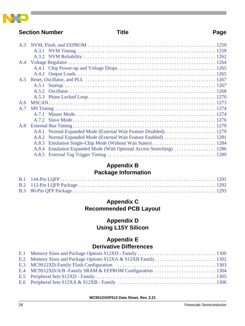
MC9S12XDP512 Data Sheet, Rev. 2.21
26 Freescale Semiconductor
Section Number Title Page
A.3 NVM, Flash, and EEPROM . . . . . . . . . . . . . . . . . . . . . . . . . . . . . . . . . . . . . . . . . . . . . . . . . . . . 1259A.3.1 NVM Timing . . . . . . . . . . . . . . . . . . . . . . . . . . . . . . . . . . . . . . . . . . . . . . . . . . . . . . . . 1259A.3.2 NVM Reliability . . . . . . . . . . . . . . . . . . . . . . . . . . . . . . . . . . . . . . . . . . . . . . . . . . . . . . 1262
A.4 Voltage Regulator . . . . . . . . . . . . . . . . . . . . . . . . . . . . . . . . . . . . . . . . . . . . . . . . . . . . . . . . . . . . 1264A.4.1 Chip Power-up and Voltage Drops . . . . . . . . . . . . . . . . . . . . . . . . . . . . . . . . . . . . . . . . 1265A.4.2 Output Loads. . . . . . . . . . . . . . . . . . . . . . . . . . . . . . . . . . . . . . . . . . . . . . . . . . . . . . . . . 1265
A.5 Reset, Oscillator, and PLL . . . . . . . . . . . . . . . . . . . . . . . . . . . . . . . . . . . . . . . . . . . . . . . . . . . . . 1267A.5.1 Startup . . . . . . . . . . . . . . . . . . . . . . . . . . . . . . . . . . . . . . . . . . . . . . . . . . . . . . . . . . . . . . 1267A.5.2 Oscillator. . . . . . . . . . . . . . . . . . . . . . . . . . . . . . . . . . . . . . . . . . . . . . . . . . . . . . . . . . . . 1268A.5.3 Phase Locked Loop. . . . . . . . . . . . . . . . . . . . . . . . . . . . . . . . . . . . . . . . . . . . . . . . . . . . 1270
A.6 MSCAN. . . . . . . . . . . . . . . . . . . . . . . . . . . . . . . . . . . . . . . . . . . . . . . . . . . . . . . . . . . . . . . . . . . . 1273A.7 SPI Timing . . . . . . . . . . . . . . . . . . . . . . . . . . . . . . . . . . . . . . . . . . . . . . . . . . . . . . . . . . . . . . . . . 1274
A.7.1 Master Mode . . . . . . . . . . . . . . . . . . . . . . . . . . . . . . . . . . . . . . . . . . . . . . . . . . . . . . . . . 1274A.7.2 Slave Mode . . . . . . . . . . . . . . . . . . . . . . . . . . . . . . . . . . . . . . . . . . . . . . . . . . . . . . . . . . 1276
A.8 External Bus Timing . . . . . . . . . . . . . . . . . . . . . . . . . . . . . . . . . . . . . . . . . . . . . . . . . . . . . . . . . . 1279A.8.1 Normal Expanded Mode (External Wait Feature Disabled). . . . . . . . . . . . . . . . . . . . . 1279A.8.2 Normal Expanded Mode (External Wait Feature Enabled) . . . . . . . . . . . . . . . . . . . . . 1281A.8.3 Emulation Single-Chip Mode (Without Wait States) . . . . . . . . . . . . . . . . . . . . . . . . . . 1284A.8.4 Emulation Expanded Mode (With Optional Access Stretching) . . . . . . . . . . . . . . . . . 1286A.8.5 External Tag Trigger Timing . . . . . . . . . . . . . . . . . . . . . . . . . . . . . . . . . . . . . . . . . . . . 1289
Appendix BPackage Information
B.1 144-Pin LQFP . . . . . . . . . . . . . . . . . . . . . . . . . . . . . . . . . . . . . . . . . . . . . . . . . . . . . . . . . . . . . . . 1291B.2 112-Pin LQFP Package . . . . . . . . . . . . . . . . . . . . . . . . . . . . . . . . . . . . . . . . . . . . . . . . . . . . . . . . 1292B.3 80-Pin QFP Package . . . . . . . . . . . . . . . . . . . . . . . . . . . . . . . . . . . . . . . . . . . . . . . . . . . . . . . . . . 1293
Appendix CRecommended PCB Layout
Appendix DUsing L15Y Silicon
Appendix EDerivative Differences
E.1 Memory Sizes and Package Options S12XD - Family . . . . . . . . . . . . . . . . . . . . . . . . . . . . . . . . 1300E.2 Memory Sizes and Package Options S12XA & S12XB Family. . . . . . . . . . . . . . . . . . . . . . . . . 1302E.3 MC9S12XD-Family Flash Configuration . . . . . . . . . . . . . . . . . . . . . . . . . . . . . . . . . . . . . . . . 1303E.4 MC9S12XD/A/B -Family SRAM & EEPROM Configuration . . . . . . . . . . . . . . . . . . . . . . . . . 1304E.5 Peripheral Sets S12XD - Family . . . . . . . . . . . . . . . . . . . . . . . . . . . . . . . . . . . . . . . . . . . . . . . . . 1305E.6 Peripheral Sets S12XA & S12XB - Family . . . . . . . . . . . . . . . . . . . . . . . . . . . . . . . . . . . . . . . . 1306

MC9S12XDP512 Data Sheet, Rev. 2.21
Freescale Semiconductor 27
Section Number Title Page
E.7 Pinout explanations: . . . . . . . . . . . . . . . . . . . . . . . . . . . . . . . . . . . . . . . . . . . . . . . . . . . . . . . . . . 1307
Appendix FOrdering Information
Appendix GDetailed Register Map

MC9S12XDP512 Data Sheet, Rev. 2.21
28 Freescale Semiconductor
Section Number Title Page
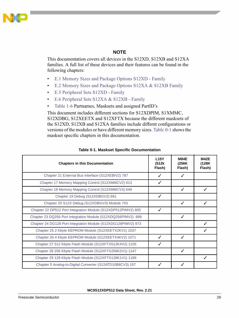
MC9S12XDP512 Data Sheet, Rev. 2.21
Freescale Semiconductor 29
NOTEThis documentation covers all devices in the S12XD, S12XB and S12XAfamilies. A full list of these devices and their features can be found in thefollowing chapters:
• E.1 Memory Sizes and Package Options S12XD - Family
• E.2 Memory Sizes and Package Options S12XA & S12XB Family
• E.5 Peripheral Sets S12XD - Family
• E.6 Peripheral Sets S12XA & S12XB - Family
• Table 1-6 Partnames, Masksets and assigned PartID’s
This document includes different sections for S12XDPIM, S1XMMC,S12XDBG, S12XEETX and S12XFTX because the different masksets ofthe S12XD, S12XB and S12XA families include differnt configurations orversions of the modules or have different memory sizes. Table 0-1 shows themaskset specific chapters in this documentation.
Table 0-1. Maskset Specific Documentation
Chapters in this DocumentationL15Y(512kFlash)
M84E(256KFlash)
M42E(128KFlash)
Chapter 21 External Bus Interface (S12XEBIV2) 787
Chapter 17 Memory Mapping Control (S12XMMCV2) 613
Chapter 18 Memory Mapping Control (S12XMMCV3) 649
Chapter 19 Debug (S12XDBGV2) 691
Chapter 20 S12X Debug (S12XDBGV3) Module 743
Chapter 22 DP512 Port Integration Module (S12XDP512PIMV2) 805
Chapter 23 DQ256 Port Integration Module (S12XDQ256PIMV2) 899
Chapter 24 DG128 Port Integration Module (S12XDG128PIMV2) 973
Chapter 25 2 Kbyte EEPROM Module (S12XEETX2KV1) 1037
Chapter 26 4 Kbyte EEPROM Module (S12XEETX4KV2) 1071
Chapter 27 512 Kbyte Flash Module (S12XFTX512K4V2) 1105
Chapter 28 256 Kbyte Flash Module (S12XFTX256K2V1) 1147
Chapter 29 128 Kbyte Flash Module (S12XFTX128K1V1) 1189
Chapter 5 Analog-to-Digital Converter (S12ATD10B8CV3) 157

MC9S12XDP512 Data Sheet, Rev. 2.21
30 Freescale Semiconductor
Chapter 1 Device Overview MC9S12XD-Family describes pinouts, detailed pin description , interruptsand register map of the cover part MC9S12XDP512 (maskset L15Y). For availability of the modules onother members of the S12XA, S12XB and S12XD families please refer to Appendix E DerivativeDifferences. For pinout explanations of the different parts refer to E.7 Pinout explanations:. For a list ofavailable partnames /masksets refer to Table 1-6.

Chapter 1 Device Overview MC9S12XD-Family
MC9S12XDP512 Data Sheet, Rev. 2.21
Freescale Semiconductor 31
Chapter 1 Device Overview MC9S12XD-Family
1.1 IntroductionThe MC9S12XD family will retain the low cost, power consumption, EMC and code-size efficiencyadvantages currently enjoyed by users of Freescale's existing 16-Bit MC9S12 MCU Family.
Based around an enhanced S12 core, the MC9S12XD family will deliver 2 to 5 times the performance ofa 25-MHz S12 whilst retaining a high degree of pin and code compatibility with the S12.
The MC9S12XD family introduces the performance boosting XGATE module. Using enhanced DMAfunctionality, this parallel processing module offloads the CPU by providing high-speed data processingand transfer between peripheral modules, RAM, Flash EEPROM and I/O ports. Providing up to 80 MIPSof performance additional to the CPU, the XGATE can access all peripherals, Flash EEPROM and theRAM block.
The MC9S12XD family is composed of standard on-chip peripherals including up to 512 Kbytes of FlashEEPROM, 32 Kbytes of RAM, 4 Kbytes of EEPROM, six asynchronous serial communications interfaces(SCI), three serial peripheral interfaces (SPI), an 8-channel IC/OC enhanced capture timer, an 8-channel,10-bit analog-to-digital converter, a 16-channel, 10-bit analog-to-digital converter, an 8-channelpulse-width modulator (PWM), five CAN 2.0 A, B software compatible modules (MSCAN12), twointer-IC bus blocks, and a periodic interrupt timer. The MC9S12XD family has full 16-bit data pathsthroughout.
The non-multiplexed expanded bus interface available on the 144-pin versions allows an easy interface toexternal memories
The inclusion of a PLL circuit allows power consumption and performance to be adjusted to suitoperational requirements. System power consumption can be further improved with the new “fast exit fromstop mode” feature.
In addition to the I/O ports available in each module, up to 25 further I/O ports are available with interruptcapability allowing wake-up from stop or wait mode.
Family members in 144-pin LQFP will be available with external bus interface and parts in 112-pin LQFPor 80-pin QFP package without external bus interface. See Appendix E Derivative Differences for packageoptions.
Chapter 1 Device Overview MC9S12XD-Family
MC9S12XDP512 Data Sheet, Rev. 2.21
32 Freescale Semiconductor
1.1.1 MC9S12XD/B/A Family FeaturesThis section lists the features which are available onMC9S12XDP512RMV2. See Appendix E Derivative Differences foravailability of features and memory sizes on other family members.
• HCS12X Core— 16-bit HCS12X CPU
– Upward compatible with MC9S12 instruction set
– Interrupt stacking and programmer’s model identical to MC9S12
– Instruction queue
– Enhanced indexed addressing
– Enhanced instruction set
— EBI (external bus interface)— MMC (module mapping control)— INT (interrupt controller)— DBG (debug module to monitor HCS12X CPU and XGATE bus activity)— BDM (background debug mode)
• XGATE (peripheral coprocessor)— Parallel processing module off loads the CPU by providing high-speed data processing and
transfer— Data transfer between Flash EEPROM, RAM, peripheral modules, and I/O ports
• PIT (periodic interrupt timer)— Four timers with independent time-out periods— Time-out periods selectable between 1 and 224 bus clock cycles
• CRG (clock and reset generator)— Low noise/low power Pierce oscillator— PLL— COP watchdog— Real time interrupt— Clock monitor— Fast wake-up from stop mode
• Port H & Port J with interrupt functionality— Digital filtering— Programmable rising or falling edge trigger
• Memory— 512, 256 and 128-Kbyte Flash EEPROM— 4 and 2-Kbyte EEPROM— 32, 16 and 12-Kbyte RAM
• One 16-channel and one 8-channel ADC (analog-to-digital converter)
Chapter 1 Device Overview MC9S12XD-Family
MC9S12XDP512 Data Sheet, Rev. 2.21
Freescale Semiconductor 33
— 10-bit resolution— External and internal conversion trigger capabilityFiveFourTwo 1M bit per second,
CAN 2.0 A, B software compatible modules— Five receive and three transmit buffers— Flexible identifier filter programmable as 2 x 32 bit, 4 x 16 bit, or 8 x 8 bit— Four separate interrupt channels for Rx, Tx, error, and wake-up— Low-pass filter wake-up function— Loop-back for self-test operation
• ECT (enhanced capture timer)— 16-bit main counter with 7-bit prescaler— 8 programmable input capture or output compare channels— Four 8-bit or two 16-bit pulse accumulators
• 8 PWM (pulse-width modulator) channels— Programmable period and duty cycle— 8-bit 8-channel or 16-bit 4-channel— Separate control for each pulse width and duty cycle— Center-aligned or left-aligned outputs— Programmable clock select logic with a wide range of frequencies— Fast emergency shutdown input
• Serial interfaces— SixFourTwo asynchronous serial communication interfaces (SCI) with additional LIN support
and selectable IrDA 1.4 return-to-zero-inverted (RZI) format with programmable pulse width— ThreeTwo Synchronous Serial Peripheral Interfaces (SPI)
• TwoOne IIC (Inter-IC bus) Modules— Compatible with IIC bus standard— Multi-master operation— Software programmable for one of 256 different serial clock frequencies
• On-Chip Voltage Regulator— Two parallel, linear voltage regulators with bandgap reference— Low-voltage detect (LVD) with low-voltage interrupt (LVI)— Power-on reset (POR) circuit— 3.3-V–5.5-V operation— Low-voltage reset (LVR)— Ultra low-power wake-up timer
• 144-pin LQFP, 112-pin LQFP, and 80-pin QFP packages— I/O lines with 5-V input and drive capability— Input threshold on external bus interface inputs switchable for 3.3-V or 5-V operation— 5-V A/D converter inputs— Operation at 80 MHz equivalent to 40-MHz bus speed

Chapter 1 Device Overview MC9S12XD-Family
MC9S12XDP512 Data Sheet, Rev. 2.21
34 Freescale Semiconductor
• Development support— Single-wire background debug™ mode (BDM)— Four on-chip hardware breakpoints
1.1.2 Modes of OperationNormal expanded mode, Emulation of single-chip mode and Emulation ofexpanded mode are ony available on family members with an external businterface in 144-pin LQFP. See Appendix E Derivative Differences forpackage options.
User modes:
• Normal and emulation operating modes— Normal single-chip mode— Normal expanded mode— Emulation of single-chip mode— Emulation of expanded mode
• Special Operating Modes— Special single-chip mode with active background debug mode— Special test mode (Freescale use only)
Low-power modes:
• System stop modes— Pseudo stop mode— Full stop mode
• System wait mode
1.1.3 Block Diagram
Figure 1-1 shows a block diagram of theMC9S12X-Family. The block diagram shows all modulesavailable on cover part MC9S12XDP512RMV2. Availability of modules on other family members seeAppendix E Derivative Differences. Figure 1-2 shows blocks integrated on maskset M42E. The 16 channelATD Converter is routed to pins PAD00 - PAD15 on maskset M42E. See Chapter 4 Analog-to-DigitalConverter (ATD10B16CV4) Block Description 123.
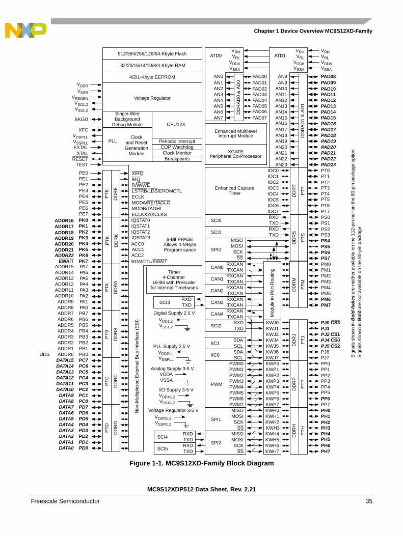
Chapter 1 Device Overview MC9S12XD-Family
MC9S12XDP512 Data Sheet, Rev. 2.21
Freescale Semiconductor 35
Figure 1-1. MC9S12XD-Family Block Diagram
512/384/256/128/64-Kbyte Flash
32/20/16/14/10/8/4-Kbyte RAM
Enhanced Capture
RESET
EXTALXTAL
SCI0
4/2/1-Kbyte EEPROM
BKGD
R/W/WE
MODB/TAGHI
XIRQ
ECLKX2/XCLKS
CPU12X
Periodic InterruptCOP WatchdogClock MonitorBreakpoints
PLLVSSPLL
XFCVDDPLL
VDDAVSSA
VRHVRLATD0
IRQ
LSTRB/LDS/EROMCTLECLKMODA/RE/TAGLO
PA4PA3PA2PA1PA0
PA7PA6PA5
TEST
ADDR12ADDR11ADDR10ADDR9ADDR8
ADDR15ADDR14ADDR13
PB4PB3PB2PB1PB0
PB7PB6PB5
ADDR4ADDR3ADDR2ADDR1
ADDR7ADDR6ADDR5
PE3PE4PE5PE6PE7
PE0PE1PE2
AN2
AN6
AN0
AN7
AN1
AN3AN4AN5
PAD03PAD04PAD05PAD06PAD07
PAD00PAD01PAD02
IOC2
IOC6
IOC0
IOC7
IOC1
IOC3IOC4IOC5
PT3PT4PT5PT6PT7
PT0PT1PT2
RXDTXD
MISOMOSI
PS3PS4PS5
PS0PS1PS2
SCI1RXDTXD
PP3PP4PP5PP6PP7
PP0PP1PP2
SCKSS
PS6PS7
SPI0
IIC0SDASCL
PJ2 CS1PJ4 CS0
CAN0RXCANTXCAN PM1
PM0
CAN1RXCANTXCAN
PM2PM3
CAN2RXCANTXCAN
PM4PM5PM6PM7
KWH2
KWH6
KWH0
KWH7
KWH1
KWH3KWH4KWH5
PH3PH4PH5PH6PH7
PH0PH1PH2
KWJ0KWJ1
PJ0 CS3PJ1
DD
RA
DD
RB
PTA
PT
B
DD
RE
PT
E
DD
RA
D0
& A
D0
PT
T
DD
RT
PT
P
DD
RP
PT
S
DD
RS
PT
M
DD
RM
PT
H
DD
RH
PT
J
DD
RJ
VDDR1,2VSSR1,2
Voltage Regulator 3-5 V
CAN4RXCANTXCAN
MISOMOSISCK
SS
SPI2
MISOMOSISCK
SS
SPI1
KWP2
KWP6
KWP0
KWP7
KWP1
KWP3KWP4KWP5
KWJ2KWJ4
Timer
Sig
nals
sho
wn
inB
old
-Ita
lics
are
neith
er a
vaila
ble
on th
e 11
2-pi
n no
r on
the
80-p
in o
acka
ge o
ptio
n
Mod
ule
to P
ort R
outin
g
PWM2
PWM6
PWM0
PWM7
PWM1
PWM3PWM4PWM5
PWM
8-Bit PPAGE
IQSTAT2
IQSTAT0IQSTAT1
ACC2
PK3
PK6
PK0PK1
ADDR19
EWAIT
ADDR16ADDR17ADDR18
PT
K
DD
RK
PK2
ACC1PK4PK5
ADDR20ADDR21
ROMCTL/EWAITPK7ADDR22
VRHVRL
VDDAVSSA
VRHVRLATD1
AN10
AN14
AN8
AN15
AN9
AN11AN12AN13
PAD11PAD12PAD13PAD14PAD15
PAD08PAD09PAD10
VDDAVSSA
DD
RA
D1
& A
D1
AN18
AN22
AN16
AN23
AN17
AN19AN20AN21
PAD19PAD20PAD21PAD22PAD23
PAD16PAD17PAD18
PC4PC3PC2PC1PC0
PC7PC6PC5
DATA12DATA11DATA10DATA9DATA8
DATA15DATA14DATA13
PD4PD3PD2PD1PD0
PD7PD6PD5
DATA4DATA3DATA2DATA1DATA0
DATA7DATA6DATA5
DD
RC
DD
RD
PT
CP
TD
SCI2RXDTXD
PJ6PJ7
PJ5 CS2KWJ5KWJ6KWJ7
Non
-Mul
tiple
xed
Ext
erna
l Bus
Inte
rfac
e (E
BI)
VDDX1,2VSSX1,2
I/O Supply 3-5 V
VDDAVSSA
Analog Supply 3-5 V
VDDPLLVSSPLL
PLL Supply 2.5 V
Enhanced MultilevelInterrupt Module
XGATEPeripheral Co-Processor
VDD1,2VSS1,2
Digital Supply 2.5 V
Sig
nals
sho
wn
inB
old
are
not
ava
ilabl
e on
the
80-p
in p
acka
ge
Allows 4-MByteProgram space
SCI3RXDTXD
SCI4RXDTXD
SCI5RXDTXD
IIC1SDASCL
Timer4-Channel
16-Bit with Prescalerfor Internal Timebases
CAN3RXCANTXCAN
ADDR0UDS
IQSTAT3ACC0
Single-WireBackground
Debug Module
VDDR
Voltage Regulator
VSSR
VDD1,2VSS1,2
VREGEN
Clockand ResetGeneration
Module
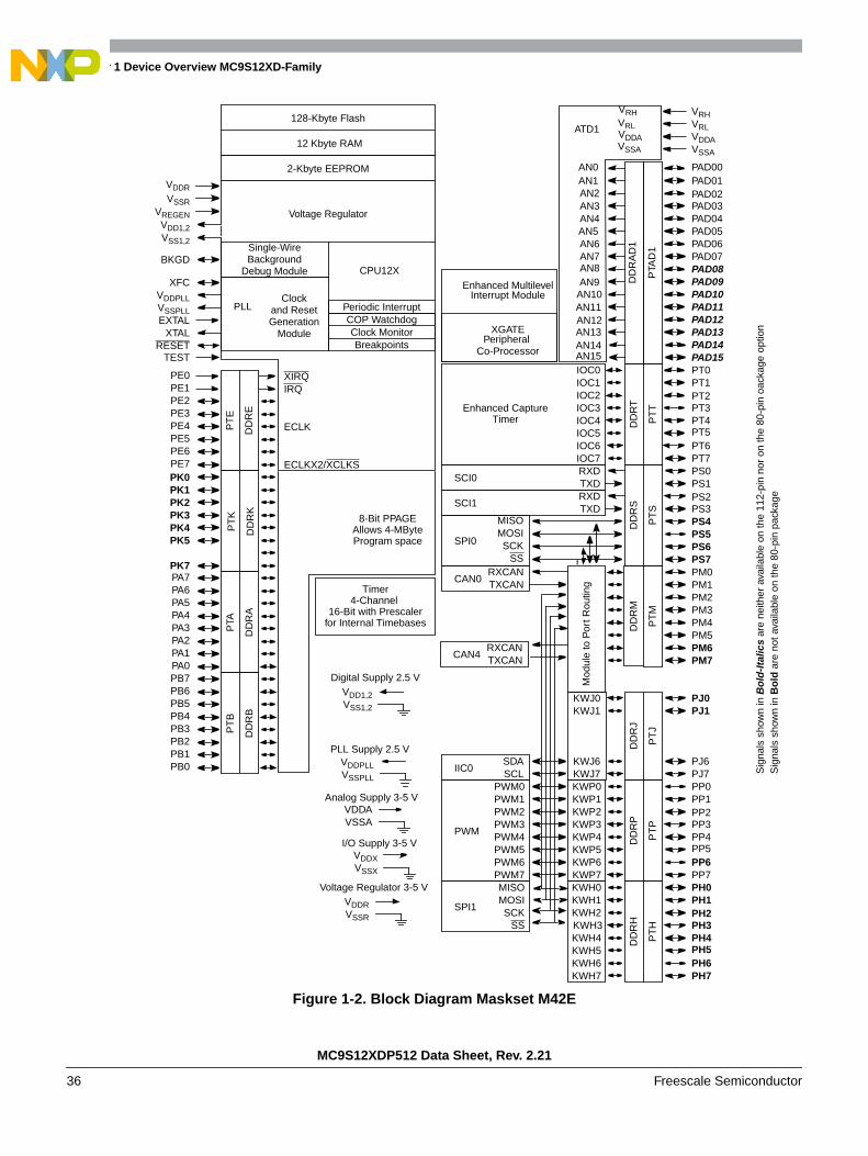
Chapter 1 Device Overview MC9S12XD-Family
MC9S12XDP512 Data Sheet, Rev. 2.21
36 Freescale Semiconductor
Figure 1-2. Block Diagram Maskset M42E
128-Kbyte Flash
12 Kbyte RAM
Enhanced Capture
RESET
EXTALXTAL
SCI0
2-Kbyte EEPROM
BKGD
XIRQ
ECLKX2/XCLKS
CPU12X
Periodic InterruptCOP WatchdogClock MonitorBreakpoints
PLLVSSPLL
XFCVDDPLL
IRQ
ECLK
PA4PA3PA2PA1PA0
PA7PA6PA5
TEST
PB4PB3PB2PB1PB0
PB7PB6PB5
PE3PE4PE5PE6PE7
PE0PE1PE2 IOC2
IOC6
IOC0
IOC7
IOC1
IOC3IOC4IOC5
PT3PT4PT5PT6PT7
PT0PT1PT2
RXDTXD
MISOMOSI
PS3PS4PS5
PS0PS1PS2
SCI1RXDTXD
PP3PP4PP5PP6PP7
PP0PP1PP2
SCKSS
PS6PS7
SPI0
IIC0SDASCL
CAN0RXCANTXCAN PM1
PM0
PM2PM3PM4PM5PM6PM7
KWH2
KWH6
KWH0
KWH7
KWH1
KWH3KWH4KWH5
PH3PH4PH5PH6PH7
PH0PH1PH2
KWJ0KWJ1
PJ0PJ1
DD
RA
DD
RB
PTA
PT
B
DD
RE
PT
E
PT
T
DD
RT
PT
P
DD
RP
PT
S
DD
RS
PT
M
DD
RM
PT
H
DD
RH
PT
J
DD
RJ
VDDRVSSR
Voltage Regulator 3-5 V MISOMOSISCK
SS
SPI1
KWP2
KWP6
KWP0
KWP7
KWP1
KWP3KWP4KWP5
Timer
Sig
nals
sho
wn
inB
old
-Ita
lics
are
neith
er a
vaila
ble
on th
e 11
2-pi
n no
r on
the
80-p
in o
acka
ge o
ptio
n
Mod
ule
to P
ort R
outin
g
PWM2
PWM6
PWM0
PWM7
PWM1
PWM3PWM4PWM5
PWM
8-Bit PPAGEPK3
PK0PK1
PT
K
DD
RK
PK2
PK4PK5
PK7
VRHVRLATD1
AN2
AN6
AN0
AN7
AN1
AN3AN4AN5
PAD03PAD04PAD05PAD06PAD07
PAD00PAD01PAD02
VDDAVSSA
PTA
D1
AN10
AN8AN9
AN11 PAD11PAD12PAD13PAD14PAD15
PAD08PAD09PAD10
PJ6PJ7
KWJ6KWJ7
VDDXVSSX
I/O Supply 3-5 V
VDDAVSSA
Analog Supply 3-5 V
VDDPLLVSSPLL
PLL Supply 2.5 V
Enhanced MultilevelInterrupt Module
XGATEPeripheral
VDD1,2VSS1,2
Digital Supply 2.5 V
Sig
nals
sho
wn
inB
old
are
not
ava
ilabl
e on
the
80-p
in p
acka
ge
Allows 4-MByteProgram space
Timer4-Channel
16-Bit with Prescalerfor Internal Timebases
Single-WireBackground
Debug Module
VDDR
Voltage Regulator
VSSR
VDD1,2VSS1,2
VREGEN
Clockand ResetGeneration
Module
CAN4RXCANTXCAN
Co-Processor AN15AN14AN13AN12
DD
RA
D1
VDDAVSSA
VRHVRL
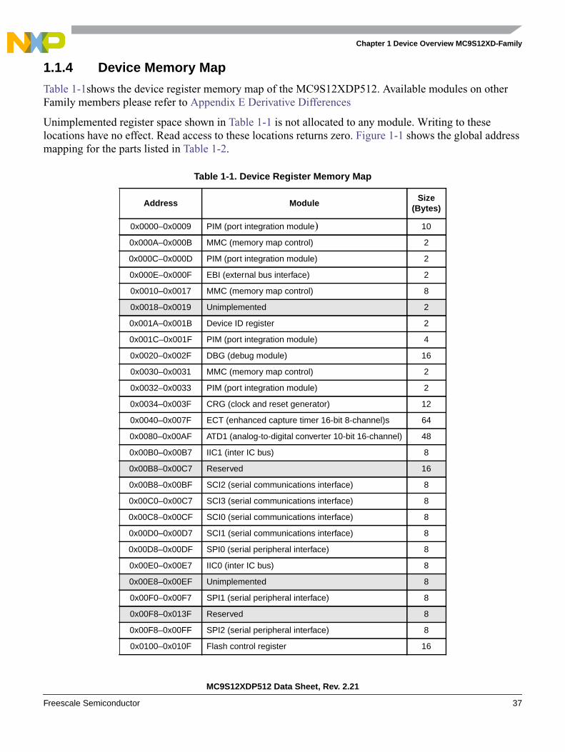
Chapter 1 Device Overview MC9S12XD-Family
MC9S12XDP512 Data Sheet, Rev. 2.21
Freescale Semiconductor 37
1.1.4 Device Memory Map
Table 1-1shows the device register memory map of the MC9S12XDP512. Available modules on otherFamily members please refer to Appendix E Derivative Differences
Unimplemented register space shown in Table 1-1 is not allocated to any module. Writing to theselocations have no effect. Read access to these locations returns zero. Figure 1-1 shows the global addressmapping for the parts listed in Table 1-2.
Table 1-1. Device Register Memory Map
Address ModuleSize
(Bytes)
0x0000–0x0009 PIM (port integration module) 10
0x000A–0x000B MMC (memory map control) 2
0x000C–0x000D PIM (port integration module) 2
0x000E–0x000F EBI (external bus interface) 2
0x0010–0x0017 MMC (memory map control) 8
0x0018–0x0019 Unimplemented 2
0x001A–0x001B Device ID register 2
0x001C–0x001F PIM (port integration module) 4
0x0020–0x002F DBG (debug module) 16
0x0030–0x0031 MMC (memory map control) 2
0x0032–0x0033 PIM (port integration module) 2
0x0034–0x003F CRG (clock and reset generator) 12
0x0040–0x007F ECT (enhanced capture timer 16-bit 8-channel)s 64
0x0080–0x00AF ATD1 (analog-to-digital converter 10-bit 16-channel) 48
0x00B0–0x00B7 IIC1 (inter IC bus) 8
0x00B8–0x00C7 Reserved 16
0x00B8–0x00BF SCI2 (serial communications interface) 8
0x00C0–0x00C7 SCI3 (serial communications interface) 8
0x00C8–0x00CF SCI0 (serial communications interface) 8
0x00D0–0x00D7 SCI1 (serial communications interface) 8
0x00D8–0x00DF SPI0 (serial peripheral interface) 8
0x00E0–0x00E7 IIC0 (inter IC bus) 8
0x00E8–0x00EF Unimplemented 8
0x00F0–0x00F7 SPI1 (serial peripheral interface) 8
0x00F8–0x013F Reserved 8
0x00F8–0x00FF SPI2 (serial peripheral interface) 8
0x0100–0x010F Flash control register 16

Chapter 1 Device Overview MC9S12XD-Family
MC9S12XDP512 Data Sheet, Rev. 2.21
38 Freescale Semiconductor
0x0110–0x011B EEPROM control register 12
0x011C–0x011F MMC (memory map control) 4
0x0120–0x012F INT (interrupt module) 16
0x0130–0x013F Reserved 16
0x0130–0x0137 SCI4 (serial communications interface) 8
0x0138–0x013F SCI5 (serial communications interface) 8
0x0140–0x017F CAN0 (scalable CAN) 64
0x0180–0x01BF CAN1 (scalable CAN) 64
0x0180–0x023F Reserved 192
0x01C0–0x01FF CAN2 (scalable CAN) 64
0x0200–0x023F Reserved 64
0x0200–0x023F CAN3 (scalable CAN) 64
0x0240–0x027F PIM (port integration module) 64
0x0280–0x02BF CAN4 (scalable CAN) 64
0x02C0–0x02DF Reserved 32
0x02C0–0x02DF ATD0 (analog-to-digital converter 10 bit 8-channel) 32
0x02E0–0x02EF Unimplemented 16
0x02F0–0x02F7 Voltage regulator 8
0x02F8–0x02FF Unimplemented 8
0x0300–0x0327 PWM (pulse-width modulator 8 channels) 40
0x0328–0x033F Unimplemented 24
0x0340–0x0367 Periodic interrupt timer 40
0x0368–0x037F Unimplemented 24
0x0380–0x03BF XGATE 64
0x03C0–0x03FF Unimplemented 64
0x0400–0x07FF Unimplemented 1024
Table 1-1. Device Register Memory Map (continued)
Address ModuleSize
(Bytes)

Chapter 1 Device Overview MC9S12XD-Family
MC9S12XDP512 Data Sheet, Rev. 2.21
Freescale Semiconductor 39
Figure 1-3. S12X CPU & BDM Global Address Mapping
0x7F_FFFF
0x00_0000
0x13_FFFF
0x0F_FFFF
EEPROM
RAM
0x00_07FF
EPAGE
RPAGE
PPAGE 0x3F_FFFF
CPU and BDMLocal Memory Map
Global Memory Map
FLA
SH
SIZ
EE
EP
RO
MS
IZE
RA
MS
IZE
UnimplementedEEPROM
CS
3C
S2
CS
1C
S0
0x1F_FFFF
CS
2
0xFFFF Reset Vectors
0xC000
0x8000
Unpaged
0x4000
0x1000
0x0000
16K FLASH window
0x0C00
0x2000
0x0800
8K RAM
4K RAM window
1K EEPROM
2K REGISTERS
1K EEPROM window
16K FLASH
Unpaged16K FLASH
2K REGISTERS
UnimplementedRAM
ExternalSpace
RAM_LOW
EEPROM_LOW
FLASH
FLASH_LOW
UnimplementedFLASH

Chapter 1 Device Overview MC9S12XD-Family
MC9S12XDP512 Data Sheet, Rev. 2.21
40 Freescale Semiconductor
Table 1-2. Device Internal Resources (see Figure 1-3)
DeviceRAMSIZE/RAM_LOW
EEPROMSIZE/EEPROM_LOW
FLASHSIZE/FLASH_LOW
9S12XDP512 32K0x0F_8000
4K0x13_F000
512K0x78_0000
9S12XDT512 20K0x0F_B000
4K0x13_F000
512K0x78_0000
9S12XA512 32K0x0F_8000
4K0x13_F000
512K0x78_0000
9S12XDG128 12K0x0F_D000
2K0x13_F800
128K7E_0000
3S12XDG128 12K0x0F_D000
2K0x13_F800
128K7E_0000
9S12XD128 8K0x0F_E000
2K0x13_F800
128K7E_0000
9S12XD64 4K0x0F_F000
1K0x13_FC00
64K7F_0000
9S12XB128 6K0x0F_E800
1K0x13_FC00
128K7E_0000
9S12XA128 12K0x0F_D000
2K0x13_F800
128K7E_0000

Chapter 1 Device Overview MC9S12XD-Family
MC9S12XDP512 Data Sheet, Rev. 2.21
Freescale Semiconductor 41
Figure 1-4. S12X CPU & BDM Global Address Mapping
0x7F_FFFF
0x00_0000
0x13_FFFF
0x0F_FFFF
EEPROM
RAM
0x00_07FF
EPAGE
RPAGE
PPAGE 0x3F_FFFF
CPU and BDMLocal Memory Map
Global Memory Map
FLA
SH
SIZ
EE
EP
RO
MS
IZE
RA
MS
IZE
UnimplementedEEPROM
UnimplementedFLASH
CS
3C
S2
CS
1C
S0
0x1F_FFFF
CS
2
0xFFFF Reset Vectors
0xC000
0x8000
Unpaged
0x4000
0x1000
0x0000
16K FLASH window
0x0C00
0x2000
0x0800
8K RAM
4K RAM window
1K EEPROM
2K REGISTERS
1K EEPROM window
16K FLASH
Unpaged16K FLASH
2K REGISTERS
UnimplementedRAM
ExternalSpace
RAM_LOW
EEPROM_LOW
0x78_0000
FLASH1
FLASH0_LOW
FLASH1_HIGH
FLASH0
UnimplementedFLASH C
S0
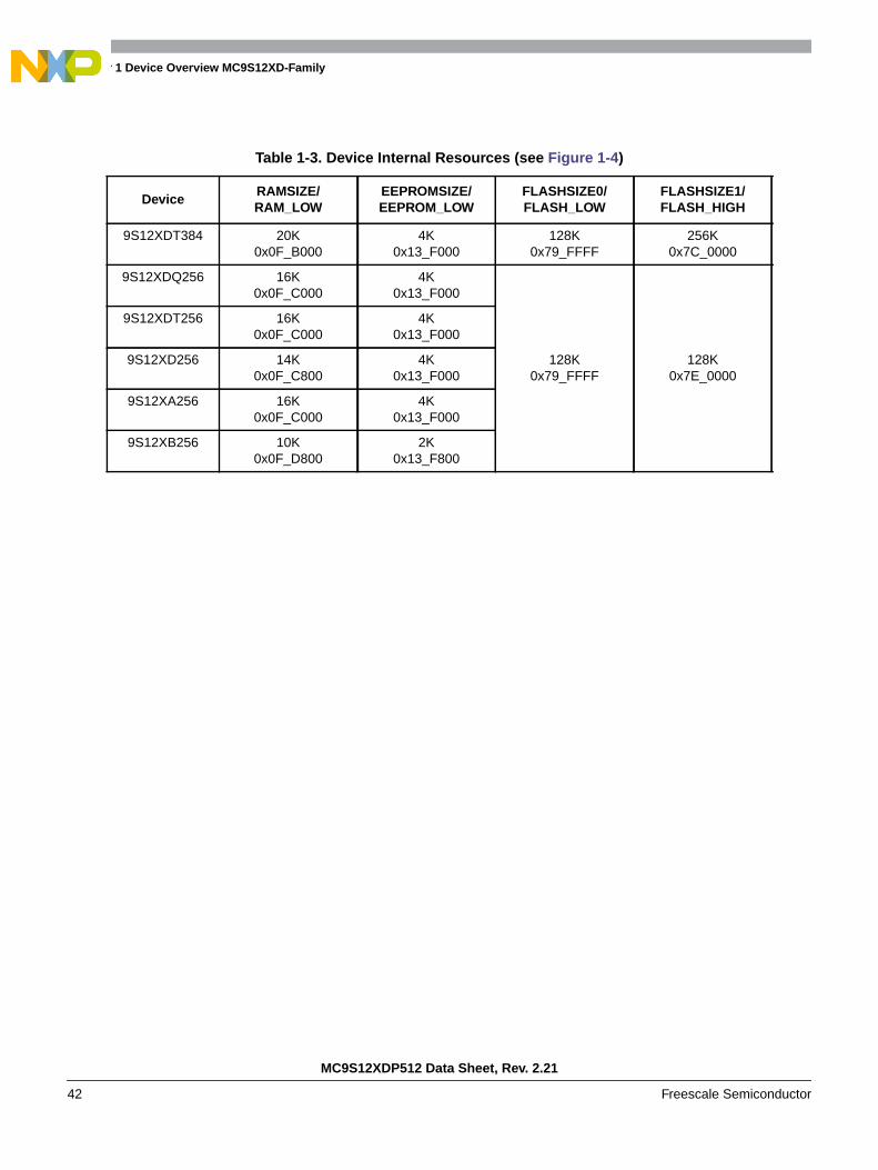
Chapter 1 Device Overview MC9S12XD-Family
MC9S12XDP512 Data Sheet, Rev. 2.21
42 Freescale Semiconductor
Table 1-3. Device Internal Resources (see Figure 1-4)
DeviceRAMSIZE/RAM_LOW
EEPROMSIZE/EEPROM_LOW
FLASHSIZE0/FLASH_LOW
FLASHSIZE1/FLASH_HIGH
9S12XDT384 20K0x0F_B000
4K0x13_F000
128K0x79_FFFF
256K0x7C_0000
9S12XDQ256 16K0x0F_C000
4K0x13_F000
128K0x79_FFFF
128K0x7E_0000
9S12XDT256 16K0x0F_C000
4K0x13_F000
9S12XD256 14K0x0F_C800
4K0x13_F000
9S12XA256 16K0x0F_C000
4K0x13_F000
9S12XB256 10K0x0F_D800
2K0x13_F800

Chapter 1 Device Overview MC9S12XD-Family
MC9S12XDP512 Data Sheet, Rev. 2.21
Freescale Semiconductor 43
Figure 1-5. GATE Global Address Mapping
0x7F_FFFF
0x00_0000
0x0F_FFFF
0xFFFF
0x0000
Registers
FLASH
RAM
0x0800
Registers0x00_07FF
XGATELocal Memory Map
Global Memory Map
FLA
SH
SIZ
E
XG
RA
MS
IZE
RA
MS
IZE
0x78_0800FLASH
RAM
XGRAM_LOW
XGFLASH_HIGH
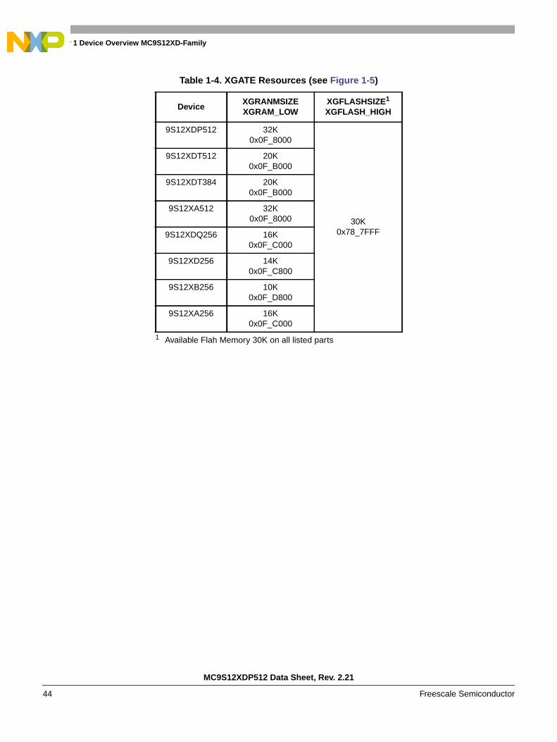
Chapter 1 Device Overview MC9S12XD-Family
MC9S12XDP512 Data Sheet, Rev. 2.21
44 Freescale Semiconductor
Table 1-4. XGATE Resources (see Figure 1-5)
DeviceXGRANMSIZEXGRAM_LOW
XGFLASHSIZE1
XGFLASH_HIGH
1 Available Flah Memory 30K on all listed parts
9S12XDP512 32K0x0F_8000
30K0x78_7FFF
9S12XDT512 20K0x0F_B000
9S12XDT384 20K0x0F_B000
9S12XA512 32K0x0F_8000
9S12XDQ256 16K0x0F_C000
9S12XD256 14K0x0F_C800
9S12XB256 10K0x0F_D800
9S12XA256 16K0x0F_C000
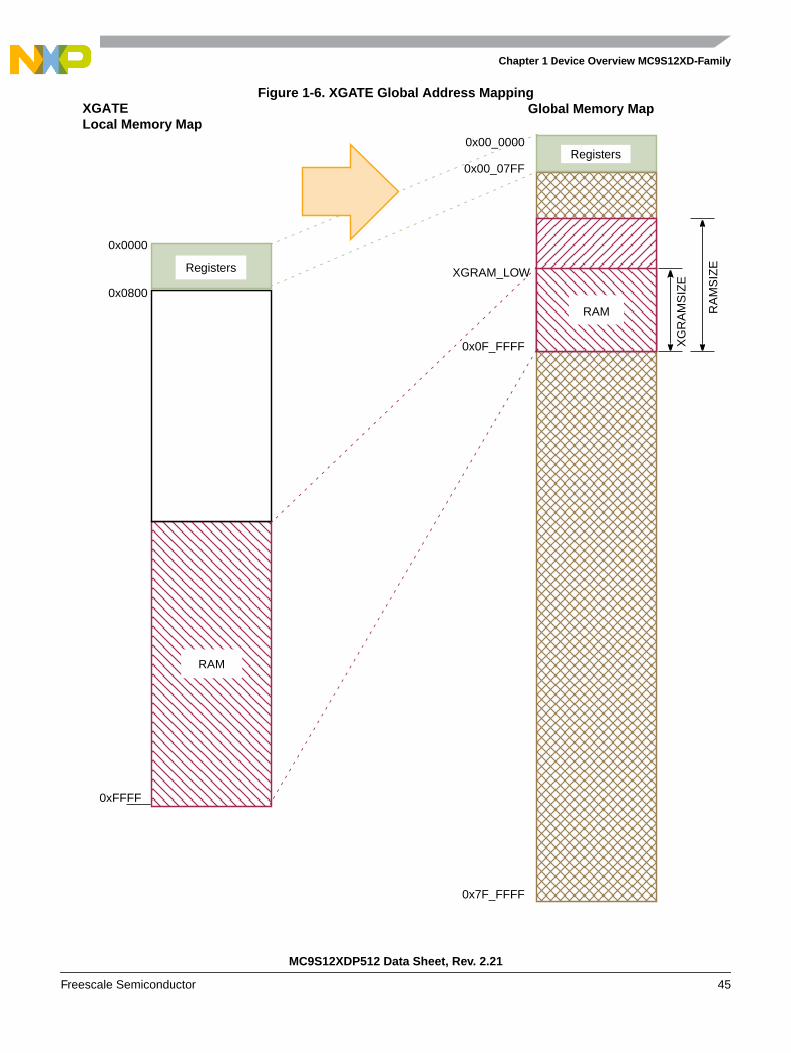
Chapter 1 Device Overview MC9S12XD-Family
MC9S12XDP512 Data Sheet, Rev. 2.21
Freescale Semiconductor 45
Figure 1-6. XGATE Global Address Mapping
0x7F_FFFF
0x00_0000
0x0F_FFFF
0xFFFF
0x0000
Registers
RAM
0x0800
Registers0x00_07FF
XGATELocal Memory Map
Global Memory Map
XG
RA
MS
IZE
RA
MS
IZE
RAM
XGRAM_LOW
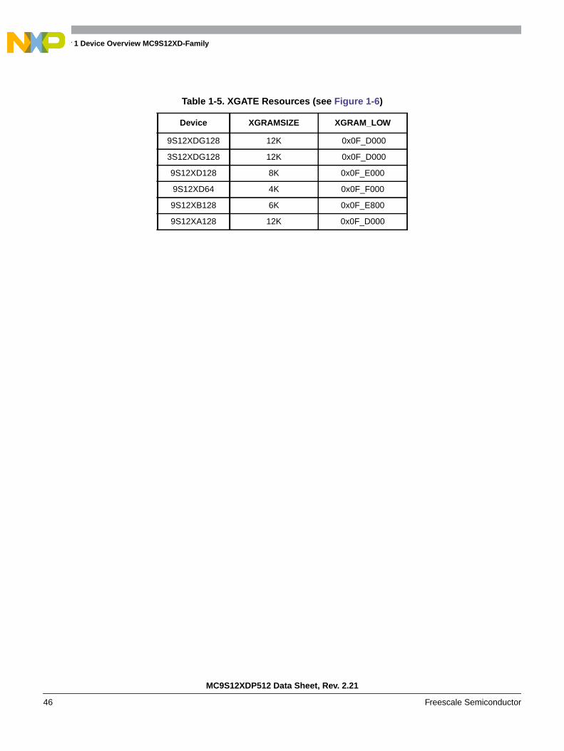
Chapter 1 Device Overview MC9S12XD-Family
MC9S12XDP512 Data Sheet, Rev. 2.21
46 Freescale Semiconductor
Table 1-5. XGATE Resources (see Figure 1-6)
Device XGRAMSIZE XGRAM_LOW
9S12XDG128 12K 0x0F_D000
3S12XDG128 12K 0x0F_D000
9S12XD128 8K 0x0F_E000
9S12XD64 4K 0x0F_F000
9S12XB128 6K 0x0F_E800
9S12XA128 12K 0x0F_D000

Chapter 1 Device Overview MC9S12XD-Family
MC9S12XDP512 Data Sheet, Rev. 2.21
Freescale Semiconductor 47
1.1.5 Part ID Assignments & Maskset Numbers
The part ID is located in two 8-bit registers PARTIDH and PARTIDL (addresses 0x001A and 0x001B).The read-only value is a unique part ID for each revision of the chip. Table 1-6 shows the assigned part IDnumber and Mask Set number.
1.2 Signal DescriptionThis section describes signals that connect off-chip. It includes a pinout diagram, a table of signalproperties, and detailed discussion of signals.
1.2.1 Device Pinout
The MC9S12XD family of devices offers pin-compatible packaged devices to assist with systemdevelopment and accommodate expansion of the application.
Table 1-6. Part Names, Masksets and Assigned Part ID Numbers
Part Names Mask Set Number Part ID1
1 The coding is as follows:Bit 15-12: Major family identifierBit 11-8: Minor family identifierBit 7-4: Major mask set revision number including FAB transfersBit 3-0: Minor — non full — mask set revision
MC9S12XDP512 0L15Y/1L15Y/0M23S 0xC410/0xC411/0xC412
MC9S12XDT512 0L15Y/1L15Y/0M23S 0xC410/0xC411/0xC412
MC9S12XA512 0L15Y/1L15Y/0M23S 0xC410/0xC411/0xC412
MC9S12XDT384 0L15Y/1L15Y/0M23S 0xC410/0xC411/0xC412
MC9S12XDQ2560L15Y/1L15Y/0M23S 0xC410/0xC411/0xC412
0M84E/1M84E 0xC000/0xC001
MC9S12XDT2560L15Y/1L15Y/0M23S 0xC410/0xC4110xC412
0M84E/1M84E 0xC000/0xC001
MC9S12XD2560L15Y/1L15Y/0M23S 0xC410/0xC411/0xC412
0M84E/1M84E 0xC000/0xC001
MC9S12XB256 0L15Y/1L15Y/0M23S 0xC410/0xC411/0xC412
0M84E/1M84E 0xC000/0xC001
MC9S12XA256 0L15Y/1L15Y/0M23S 0xC410/0xC411/0xC412
0M84E/1M84E 0xC000/0xC001
MC9S12XDG1280L15Y/1L15Y/0M23S 0xC410/0xC411/0xC412
0M42E/1M42E/2M42E 0xC100/0xC101/0xC102
MC9S12XD1280L15Y/1L15Y/0M23S 0xC410/0xC4110xC412
0M42E/1M42E/2M42E 0xC100/0xC101/0xC102
MC9S12XA128 0L15Y/1L15Y/0M23S 0xC410/0xC411/0xC412
0M42E/1M42E/2M42E 0xC100/0xC101/0xC102
MC9S12XB128 0L15Y/1L15Y/0M23S 0xC410/0xC411/0xC412
0M42E/1M42E/2M42E 0xC100/0xC101/0xC102

Chapter 1 Device Overview MC9S12XD-Family
MC9S12XDP512 Data Sheet, Rev. 2.21
48 Freescale Semiconductor
The S12XD, S12XA and S12XB family devices are offered in the following packages:
• 144-pin LQFP package with an external bus interface (address/data bus)
• 112-pin LQFP without external bus interface
• 80-pin QFP without external bus interface
See Appendix E Derivative Differences for package options.
CAUTIONMost the I/O Pins have different functionality depending on the moduleconfiguration. Not all functions are shown in the following pinouts. Pleaserefer to Table 1-7 for a complete description. For avalability of the moduleson different family members refer to Appendix E Derivative Differences.For pinout explanations of the different parts refer to E.7 Pinoutexplanations:
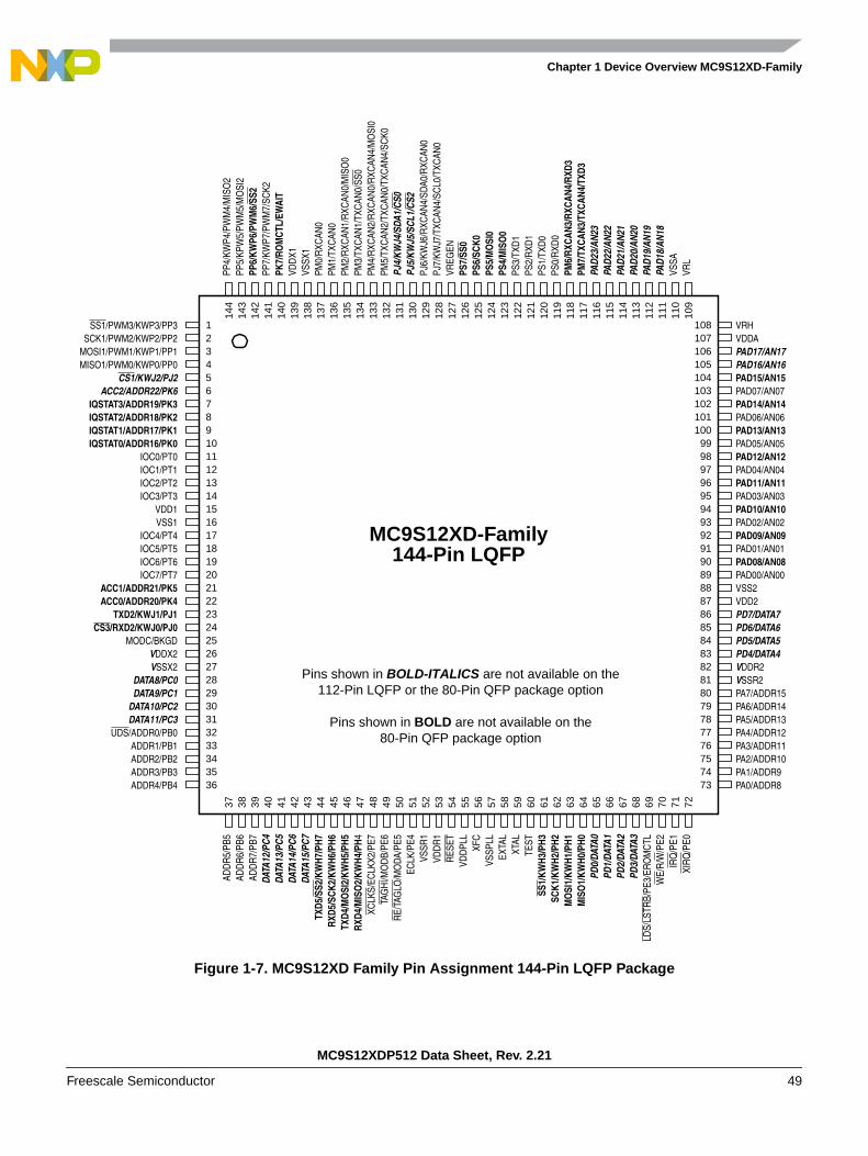
Chapter 1 Device Overview MC9S12XD-Family
MC9S12XDP512 Data Sheet, Rev. 2.21
Freescale Semiconductor 49
Figure 1-7. MC9S12XD Family Pin Assignment 144-Pin LQFP Package
SS1/PWM3/KWP3/PP3SCK1/PWM2/KWP2/PP2
MOSI1/PWM1/KWP1/PP1MISO1/PWM0/KWP0/PP0
CS1/KWJ2/PJ2ACC2/ADDR22/PK6
IQSTAT3/ADDR19/PK3IQSTAT2/ADDR18/PK2IQSTAT1/ADDR17/PK1IQSTAT0/ADDR16/PK0
IOC0/PT0IOC1/PT1IOC2/PT2IOC3/PT3
VDD1VSS1
IOC4/PT4IOC5/PT5IOC6/PT6IOC7/PT7
ACC1/ADDR21/PK5ACC0/ADDR20/PK4
TXD2/KWJ1/PJ1CS3/RXD2/KWJ0/PJ0
MODC/BKGDVDDX2VSSX2
DATA8/PC0DATA9/PC1
DATA10/PC2DATA11/PC3
UDS/ADDR0/PB0ADDR1/PB1ADDR2/PB2ADDR3/PB3ADDR4/PB4
ADD
R5/
PB5
ADD
R6/
PB6
ADD
R7/
PB7
DATA
12/P
C4DA
TA13
/PC5
DATA
14/P
C6DA
TA15
/PC7
TXD5
/ SS2
/KW
H7/P
H7RX
D5/S
CK2/
KWH6
/PH6
TXD4
/MO
SI2/
KWH5
/PH5
RXD4
/MIS
O2/
KWH4
/PH4
XCLK
S/EC
LKX2
/PE7
TAG
HI/M
OD
B/PE
6R
E/TA
GLO
/MO
DA/P
E5EC
LK/P
E4VS
SR1
VDD
R1
RES
ETVD
DPL
LXF
CVS
SPLL
EXTA
LXT
ALTE
STSS
1/KW
H3/P
H3SC
K1/K
WH2
/PH2
MO
SI1/
KWH1
/PH1
MIS
O1/
KWH0
/PH0
PD0/
DATA
0PD
1/DA
TA1
PD2/
DATA
2PD
3/DA
TA3
LDS/
LSTR
B/PE
3/ER
OM
CTL
WE/
R/W
/PE2
IRQ
/PE1
XIR
Q/P
E0
VRHVDDAPAD17/AN17PAD16/AN16PAD15/AN15PAD07/AN07PAD14/AN14PAD06/AN06PAD13/AN13PAD05/AN05PAD12/AN12PAD04/AN04PAD11/AN11PAD03/AN03PAD10/AN10PAD02/AN02PAD09/AN09PAD01/AN01PAD08/AN08PAD00/AN00VSS2VDD2PD7/DATA7PD6/DATA6PD5/DATA5PD4/DATA4VDDR2VSSR2PA7/ADDR15PA6/ADDR14PA5/ADDR13PA4/ADDR12PA3/ADDR11PA2/ADDR10PA1/ADDR9PA0/ADDR8
PP4/
KWP4
/PW
M4/
MIS
O2
PP5/
KPW
5/PW
M5/
MO
SI2
PP6/
KWP6
/PW
M6/
SS2
PP7/
KWP7
/PW
M7/
SCK2
PK7/
ROM
CTL/
EWAI
TVD
DX1
VSSX
1PM
0/R
XCAN
0PM
1/TX
CAN
0PM
2/R
XCAN
1/R
XCAN
0/M
ISO
0PM
3/TX
CAN
1/TX
CAN
0/SS
0PM
4/R
XCAN
2/R
XCAN
0/R
XCAN
4/M
OSI
0PM
5/TX
CAN
2/TX
CAN
0/TX
CAN
4/SC
K0PJ
4/KW
J4/S
DA1/
CS0
PJ5/
KWJ5
/SCL
1/CS
2PJ
6/KW
J6/R
XCAN
4/SD
A0/R
XCAN
0PJ
7/KW
J7/T
XCAN
4/SC
L0/T
XCAN
0VR
EGEN
PS7/
SS0
PS6/
SCK0
PS5/
MO
SI0
PS4/
MIS
O0
PS3/
TXD
1PS
2/R
XD1
PS1/
TXD
0PS
0/R
XD0
PM6/
RXCA
N3/R
XCAN
4/RX
D3PM
7/TX
CAN3
/TXC
AN4/
TXD3
PAD2
3/AN
23PA
D22/
AN22
PAD2
1/AN
21PA
D20/
AN20
PAD1
9/AN
19PA
D18/
AN18
VSSA
VRL
MC9S12XD-Family144-Pin LQFP
123456789101112131415161718192021222324252627282930313233343536
37 38 39 40 41 42 43 44 45 46 47 48 49 50 51 52 53 54 55 56 57 58 59 60 61 62 63 64 65 66 67 68 69 70 71 72
108107106105104103102101100999897969594939291908988878685848382818079787776757473
144
143
142
141
140
139
138
137
136
135
134
133
132
131
130
129
128
127
126
125
124
123
122
121
120
119
118
117
116
115
114
113
112
111
110
109
Pins shown in BOLD-ITALICS are not available on the112-Pin LQFP or the 80-Pin QFP package option
Pins shown in BOLD are not available on the80-Pin QFP package option
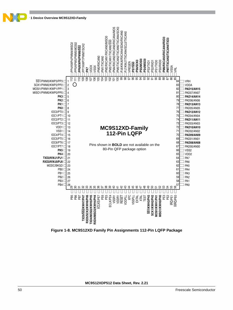
Chapter 1 Device Overview MC9S12XD-Family
MC9S12XDP512 Data Sheet, Rev. 2.21
50 Freescale Semiconductor
Figure 1-8. MC9S12XD Family Pin Assignments 112-Pin LQFP Package
VRHVDDAPAD15/AN15PAD07/AN07PAD14/AN14PAD06/AN06PAD13/AN13PAD05/AN05PAD12/AN12PAD04/AN04PAD11/AN11PAD03/AN03PAD10/AN10PAD02/AN02PAD09/AN09PAD01/AN01PAD08/AN08PAD00/AN00VSS2VDD2PA7PA6PA5PA4PA3PA2PA1PA0
PP4/
KWP4
/PW
M4/
MIS
O2
PP5/
KPW
5/PW
M5/
MO
SI2
PP6/
KWP6
/PW
M6/
SS2
PP7/
KWP7
/PW
M7/
SCK2
PK7
VDD
XVS
SXPM
0/R
XCAN
0PM
1/TX
CAN
0PM
2/R
XCAN
1/R
XCAN
0/M
ISO
0PM
3/TX
CAN
1/TX
CAN
0/SS
0PM
4/R
XCAN
2/R
XCAN
0/R
XCAN
4/M
OS
PM5/
TXC
AN2/
TXC
AN0/
TXC
AN4/
SCK0
PJ6/
KWJ6
/RXC
AN4/
SDA0
/RXC
AN0
PJ7/
KWJ7
/TXC
AN4/
SCL0
/TXC
AN0
VREG
ENPS
7/SS
0PS
6/SC
K0PS
5/M
OSI
0PS
4/M
ISO
0PS
3/TX
D1
PS2/
RXD
1PS
1/TX
D0
PS0/
RXD
0PM
6/RX
CAN3
/RXC
AN4/
RXD3
PM7/
TXCA
N3/T
XCAN
4/TX
D3VS
SAVR
L
SS1/PWM3/KWP3/PP3SCK1/PWM2/KWP2/PP2
MOSI1/PWM1/KWP1/PP1MISO1/PWM0/KWP0/PP0
PK3PK2PK1PK0
IOC0/PT0IOC1/PT1IOC2/PT2IOC3/PT3
VDD1VSS1
IOC4/PT4IOC5/PT5IOC6/PT6IOC7/PT7
PK5PK4
TXD2/KWJ1/PJ1RXD2/KWJ0/PJ0
MODC/BKGDPB0PB1PB2PB3PB4
PB5
PB6
PB7
TXD5
/SS2
/KW
H7/P
H7RX
D5/S
CK2/
KWH6
/PH6
TXD4
/MO
SI2/
KWH5
/PH5
RXD4
/MIS
O2/
KWH4
/PH4
XCLK
S/PE
7PE
6PE
5EC
LK/P
E4VS
SR1
VDD
R1
RES
ETVD
DPL
LXF
CVS
SPLL
EXTA
LXT
ALTE
STSS
1/KW
H3/P
H3SC
K1/K
WH2
/PH2
MO
SI1/
KWH1
/PH1
MIS
O1/
KWH0
/PH0 PE
3PE
2IR
Q/P
E1XI
RQ
/PE0
MC9S12XD-Family112-Pin LQFP
112
111
110
109
108
107
106
105
104
103
102
101
100 99 98 97 96 95 94 93 92 91 90 89 88 87 86 85
12345678910111213141516171819202122232425262728
29 30 31 32 33 34 35 36 37 38 39 40 41 42 43 44 45 46 47 48 49 50 51 52 53 54 55 56
84838281807978777675747372717069686766656463626160595857
Pins shown in BOLD are not available on the80-Pin QFP package option

Chapter 1 Device Overview MC9S12XD-Family
MC9S12XDP512 Data Sheet, Rev. 2.21
Freescale Semiconductor 51
Figure 1-9. MC9S12XD Family Pin Assignments 80-Pin QFP Package
1234567891011121314151617181920
80 79 78 77 76 75 74 73 72 71 70 69 68 67 66 65 64 63 62 61
21 22 23 24 25 26 27 28 29 30 31 32 33 34 35 36 37 38 39 40
MC9S12XD-Family80-Pin QFP
VRHVDDAPAD07/AN07PAD06/AN06PAD05/AN05PAD04/AN04PAD03/AN03PAD02/AN02PAD01/AN01PAD00/AN00VSS2VDD2PA7PA6PA5PA4PA3PA2PA1PA0
PP4/
KWP4
/PW
M4/
MIS
O2
PP5/
KWP5
/PW
M5/
MO
SI2
PP7/
KWP7
/PW
M7/
SCK2
VDD
XVS
SXPM
0/R
XCAN
0PM
1/TX
CAN
0PM
2/R
XCAN
1/R
XCAN
0/M
ISO
0PM
3/TX
CAN
1/TX
CAN
0/SS
0PM
4/R
XCAN
2/R
XCAN
0/R
XCAN
4/M
OSI
0PM
5/TX
CAN
2/TX
CAN
0/TX
CAN
4/SC
K0PJ
6/KW
J6/R
XCAN
4/SD
A0/R
XCAN
0PJ
7/KW
J7/T
XCAN
4/SC
L0/T
XCAN
0V R
EGEN
PS3/
TXD
1PS
2/R
XD1
PS1/
TXD
0PS
0/R
XD0
VSSA
VRL
SS1/PWM3/KWP3/PP3SCK1/PWM2/KWP2/PP2
MOSI1/PWM1/KWP1/PP1MISO1/PWM0/KWP0/PP0
IOC0/PT0IOC1/PT1IOC2/PT2IOC3/PT3
VDD1VSS1
IOC4/PT4IOC5/PT5IOC6/PT6IOC7/PT7
MODC/BKGDPB0PB1PB2PB3PB4
PB5
PB6
PB7
XCLK
S/PE
7PE
6PE
5EC
LK/P
E4VS
SR1
VDD
R1
RES
ETVD
DPL
LXF
CVS
SPLL
EXTA
LXT
ALTE
ST PE3
PE2
IRQ
/PE1
XIR
Q/P
E0
6059585756555453525150494847464544434241
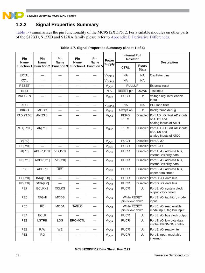
Chapter 1 Device Overview MC9S12XD-Family
MC9S12XDP512 Data Sheet, Rev. 2.21
52 Freescale Semiconductor
1.2.2 Signal Properties Summary
Table 1-7 summarizes the pin functionality of the MC9S12XDP512. For available modules on other partsof the S12XD, S12XB and S12XA family please refer to Appendix E Derivative Differences.
Table 1-7. Signal Properties Summary (Sheet 1 of 4)
PinName
Function 1
PinName
Function 2
PinName
Function 3
PinName
Function 4
PinName
Function 5
PowerSupply
Internal PullResistor
Description
CTRLResetState
EXTAL — — — — VDDPLL NA NA Oscillator pins
XTAL — — — — VDDPLL NA NA
RESET — — — — VDDR PULLUP External reset
TEST — — — — N.A. RESET pin DOWN Test input
VREGEN — — — — VDDX PUCR Up Voltage regulator enableInput
XFC — — — — VDDPLL NA NA PLL loop filter
BKGD MODC — — — VDDX Always on Up Background debug
PAD[23:08] AN[23:8] — — — VDDA PER0/PER1
Disabled Port AD I/O, Port AD inputsof ATD1 andanalog inputs of ATD1
PAD[07:00] AN[7:0] — — — VDDA PER1 Disabled Port AD I/O, Port AD inputsof ATD0 andanalog inputs of ATD0
PA[7:0] — — — — VDDR PUCR Disabled Port A I/O
PB[7:0] — — — — VDDR PUCR Disabled Port BI/O
PA[7:0] ADDR[15:8] IVD[15:8] — — VDDR PUCR Disabled Port A I/O, address bus,internal visibility data
PB[7:1] ADDR[7:1] IVD[7:0] — — VDDR PUCR Disabled Port B I/O, address bus,internal visibility data
PB0 ADDR0 UDS VDDR PUCR Disabled Port B I/O, address bus,upper data strobe
PC[7:0] DATA[15:8] — — — VDDR PUCR Disabled Port C I/O, data bus
PD[7:0] DATA[7:0] — — — VDDR PUCR Disabled Port D I/O, data bus
PE7 ECLKX2 XCLKS — — VDDR PUCR Up Port E I/O, system clockoutput, clock select
PE6 TAGHI MODB — — VDDR While RESETpin is low: down
Port E I/O, tag high, modeinput
PE5 RE MODA TAGLO — VDDR While RESETpin is low: down
Port E I/O, read enable,mode input, tag low input
PE4 ECLK — — — VDDR PUCR Up Port E I/O, bus clock output
PE3 LSTRB LDS EROMCTL — VDDR PUCR Up Port E I/O, low byte datastrobe, EROMON control
PE2 R/W WE — — VDDR PUCR Up Port E I/O, read/write
PE1 IRQ — — — VDDR PUCR Up Port E Input, maskableinterrupt
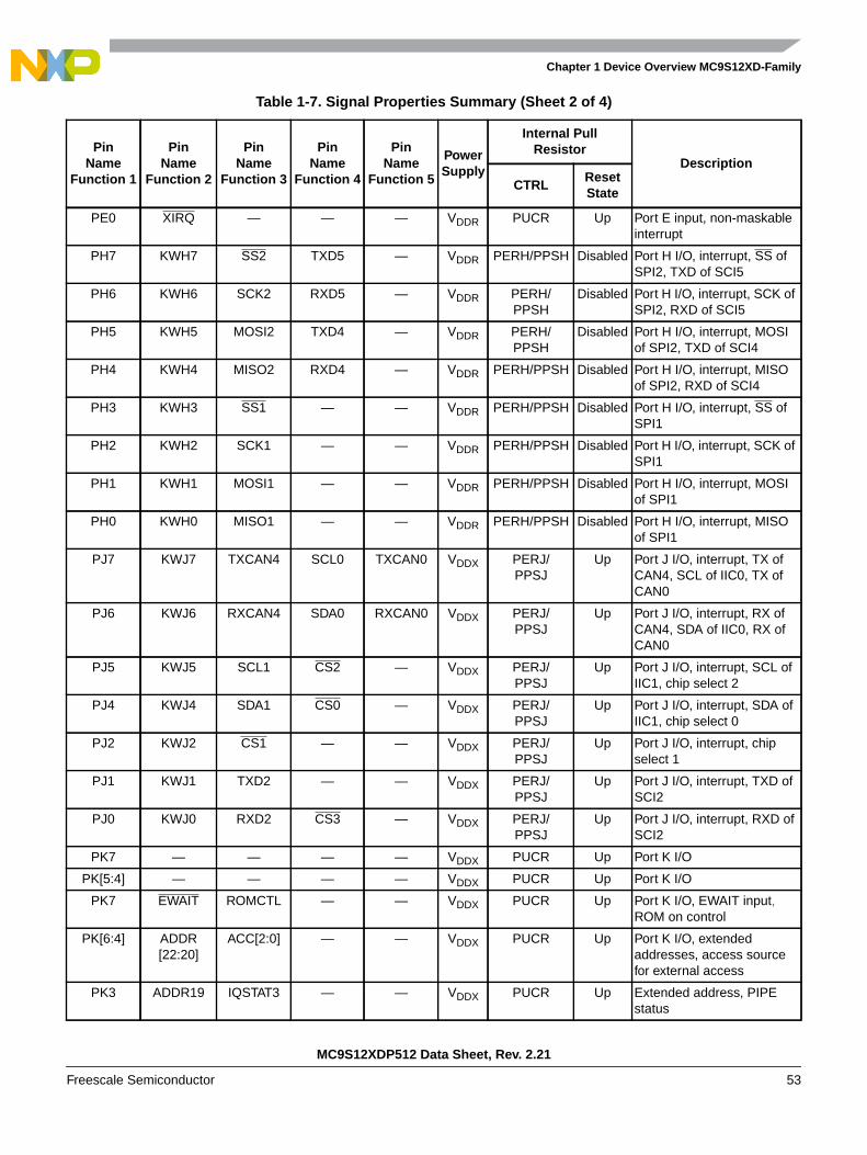
Chapter 1 Device Overview MC9S12XD-Family
MC9S12XDP512 Data Sheet, Rev. 2.21
Freescale Semiconductor 53
PE0 XIRQ — — — VDDR PUCR Up Port E input, non-maskableinterrupt
PH7 KWH7 SS2 TXD5 — VDDR PERH/PPSH Disabled Port H I/O, interrupt, SS ofSPI2, TXD of SCI5
PH6 KWH6 SCK2 RXD5 — VDDR PERH/PPSH
Disabled Port H I/O, interrupt, SCK ofSPI2, RXD of SCI5
PH5 KWH5 MOSI2 TXD4 — VDDR PERH/PPSH
Disabled Port H I/O, interrupt, MOSIof SPI2, TXD of SCI4
PH4 KWH4 MISO2 RXD4 — VDDR PERH/PPSH Disabled Port H I/O, interrupt, MISOof SPI2, RXD of SCI4
PH3 KWH3 SS1 — — VDDR PERH/PPSH Disabled Port H I/O, interrupt, SS ofSPI1
PH2 KWH2 SCK1 — — VDDR PERH/PPSH Disabled Port H I/O, interrupt, SCK ofSPI1
PH1 KWH1 MOSI1 — — VDDR PERH/PPSH Disabled Port H I/O, interrupt, MOSIof SPI1
PH0 KWH0 MISO1 — — VDDR PERH/PPSH Disabled Port H I/O, interrupt, MISOof SPI1
PJ7 KWJ7 TXCAN4 SCL0 TXCAN0 VDDX PERJ/PPSJ
Up Port J I/O, interrupt, TX ofCAN4, SCL of IIC0, TX ofCAN0
PJ6 KWJ6 RXCAN4 SDA0 RXCAN0 VDDX PERJ/PPSJ
Up Port J I/O, interrupt, RX ofCAN4, SDA of IIC0, RX ofCAN0
PJ5 KWJ5 SCL1 CS2 — VDDX PERJ/PPSJ
Up Port J I/O, interrupt, SCL ofIIC1, chip select 2
PJ4 KWJ4 SDA1 CS0 — VDDX PERJ/PPSJ
Up Port J I/O, interrupt, SDA ofIIC1, chip select 0
PJ2 KWJ2 CS1 — — VDDX PERJ/PPSJ
Up Port J I/O, interrupt, chipselect 1
PJ1 KWJ1 TXD2 — — VDDX PERJ/PPSJ
Up Port J I/O, interrupt, TXD ofSCI2
PJ0 KWJ0 RXD2 CS3 — VDDX PERJ/PPSJ
Up Port J I/O, interrupt, RXD ofSCI2
PK7 — — — — VDDX PUCR Up Port K I/O
PK[5:4] — — — — VDDX PUCR Up Port K I/O
PK7 EWAIT ROMCTL — — VDDX PUCR Up Port K I/O, EWAIT input,ROM on control
PK[6:4] ADDR[22:20]
ACC[2:0] — — VDDX PUCR Up Port K I/O, extendedaddresses, access sourcefor external access
PK3 ADDR19 IQSTAT3 — — VDDX PUCR Up Extended address, PIPEstatus
Table 1-7. Signal Properties Summary (Sheet 2 of 4)
PinName
Function 1
PinName
Function 2
PinName
Function 3
PinName
Function 4
PinName
Function 5
PowerSupply
Internal PullResistor
Description
CTRLResetState

Chapter 1 Device Overview MC9S12XD-Family
MC9S12XDP512 Data Sheet, Rev. 2.21
54 Freescale Semiconductor
PK2 ADDR18 IQSTAT2 — — VDDX PUCR Up Extended address, PIPEstatus
PK1 ADDR17 IQSTAT1 — — VDDX PUCR Up Extended address, PIPEstatus
PK0 ADDR16 IQSTAT0 — — VDDX PUCR Up Extended address, PIPEstatus
PM7 TXCAN3 TXD3 TXCAN4 — VDDX PERM/PPSM
Disabled Port M I/O, TX of CAN3 andCAN4, TXD of SCI3
PM6 RXCAN3 RXD3 RXCAN4 — VDDX PERM/PPSM Disabled Port M I/O RX of CAN3 andCAN4, RXD of SCI3
PM5 TXCAN2 TXCAN0 TXCAN4 SCK0 VDDX PERM/PPSM Disabled Port M I/O CAN0, CAN2,CAN4, SCK of SPI0
PM4 RXCAN2 RXCAN0 RXCAN4 MOSI0 VDDX PERM/PPSM Disabled Port M I/O, CAN0, CAN2,CAN4, MOSI of SPI0
PM3 TXCAN1 TXCAN0 — SS0 VDDX PERM/PPSM Disabled Port M I/O TX of CAN1,CAN0, SS of SPI0
PM2 RXCAN1 RXCAN0 — MISO0 VDDX PERM/PPSM Disabled Port M I/O, RX of CAN1,CAN0, MISO of SPI0
PM1 TXCAN0 — — VDDX PERM/PPSM Disabled Port M I/O, TX of CAN0
PM0 RXCAN0 — — VDDX PERM/PPSM Disabled Port M I/O, RX of CAN0
PP7 KWP7 PWM7 SCK2 — VDDX PERP/PPSP
Disabled Port P I/O, interrupt, channel7of PWM, SCK of SPI2
PP6 KWP6 PWM6 SS2 — VDDX PERP/PPSP
Disabled Port P I/O, interrupt, channel6 of PWM, SS of SPI2
PP5 KWP5 PWM5 MOSI2 — VDDX PERP/PPSP
Disabled Port P I/O, interrupt, channel5 of PWM, MOSI of SPI2
PP4 KWP4 PWM4 MISO2 — VDDX PERP/PPSP
Disabled Port P I/O, interrupt, channel4 of PWM, MISO2 of SPI2
PP3 KWP3 PWM3 SS1 — VDDX PERP/PPSP
Disabled Port P I/O, interrupt, channel3 of PWM, SS of SPI1
PP2 KWP2 PWM2 SCK1 — VDDX PERP/PPSP
Disabled Port P I/O, interrupt, channel2 of PWM, SCK of SPI1
PP1 KWP1 PWM1 MOSI1 — VDDX PERP/PPSP
Disabled Port P I/O, interrupt, channel1 of PWM, MOSI of SPI1
PP0 KWP0 PWM0 MISO1 — VDDX PERP/PPSP
Disabled Port P I/O, interrupt, channel0 of PWM, MISO2 of SPI1
PS7 SS0 — — — VDDX PERS/PPSS
Up Port S I/O, SS of SPI0
PS6 SCK0 — — — VDDX PERS/PPSS
Up Port S I/O, SCK of SPI0
Table 1-7. Signal Properties Summary (Sheet 3 of 4)
PinName
Function 1
PinName
Function 2
PinName
Function 3
PinName
Function 4
PinName
Function 5
PowerSupply
Internal PullResistor
Description
CTRLResetState

Chapter 1 Device Overview MC9S12XD-Family
MC9S12XDP512 Data Sheet, Rev. 2.21
Freescale Semiconductor 55
NOTEFor devices assembled in 80-pin and 112-pin packages all non-bonded outpins should be configured as outputs after reset in order to avoid currentdrawn from floating inputs. Refer to Table 1-7 for affected pins.
1.2.3 Detailed Signal Descriptions
NOTEThis section describes all pins which are availabe on the cover partMC9S12XDP512 in 144-pin LQFP package. For modules and pinoutexplanations of the different family members refer to E.7 Pinoutexplanations: and E.5 Peripheral Sets S12XD - Family and E.6 PeripheralSets S12XA & S12XB - Family
1.2.3.1 EXTAL, XTAL — Oscillator Pins
EXTAL and XTAL are the crystal driver and external clock pins. On reset all the device clocks are derivedfrom the EXTAL input frequency. XTAL is the crystal output.
1.2.3.2 RESET — External Reset Pin
The RESET pin is an active low bidirectional control signal. It acts as an input to initialize the MCU to aknown start-up state. As an output it is driven ;ow to indicate when any internal MCU reset source triggers.The RESET pin has an internal pullup device.
PS5 MOSI0 — — — VDDX PERS/PPSS
Up Port S I/O, MOSI of SPI0
PS4 MISO0 — — — VDDX PERS/PPSS
Up Port S I/O, MISO of SPI0
PS3 TXD1 — — — VDDX PERS/PPSS
Up Port S I/O, TXD of SCI1
PS2 RXD1 — — — VDDX PERS/PPSS
Up Port S I/O, RXD of SCI1
PS1 TXD0 — — — VDDX PERS/PPSS
Up Port S I/O, TXD of SCI0
PS0 RXD0 — — — VDDX PERS/PPSS
Up Port S I/O, RXD of SCI0
PT[7:0] IOC[7:0] — — — VDDX PERT/PPST
Disabled Port T I/O, timer channels
Table 1-7. Signal Properties Summary (Sheet 4 of 4)
PinName
Function 1
PinName
Function 2
PinName
Function 3
PinName
Function 4
PinName
Function 5
PowerSupply
Internal PullResistor
Description
CTRLResetState

Chapter 1 Device Overview MC9S12XD-Family
MC9S12XDP512 Data Sheet, Rev. 2.21
56 Freescale Semiconductor
1.2.3.3 TEST — Test Pin
This input only pin is reserved for test. This pin has a pulldown device.
NOTEThe TEST pin must be tied to VSS in all applications.
1.2.3.4 VREGEN — Voltage Regulator Enable Pin
This input only pin enables or disables the on-chip voltage regulator. The input has a pullup device.
1.2.3.5 XFC — PLL Loop Filter Pin
Please ask your Freescale representative for the interactive application note to compute PLL loop filterelements. Any current leakage on this pin must be avoided.
Figure 1-10. PLL Loop Filter Connections
1.2.3.6 BKGD / MODC — Background Debug and Mode Pin
The BKGD/MODC pin is used as a pseudo-open-drain pin for the background debug communication. Itis used as a MCU operating mode select pin during reset. The state of this pin is latched to the MODC bitat the rising edge of RESET. The BKGD pin has a pullup device.
1.2.3.7 PAD[23:8] / AN[23:8] — Port AD Input Pins of ATD1
PAD[23:8] are general-purpose input or output pins and analog inputs AN[23:8] of the analog-to-digitalconverter ATD1.
1.2.3.8 PAD[7:0] / AN[7:0] — Port AD Input Pins of ATD0
PAD[7:0] are general-purpose input or output pins and analog inputs AN[7:0] of the analog-to-digitalconverter ATD0.
1.2.3.9 PAD[15:0] / AN[15:0] — Port AD Input Pins of ATD1
PAD[15:0] are general-purpose input or output pins and analog inputs AN[15:0] of the analog-to-digitalconverter ATD1.
MCU
XFC
R0
CS
CP
VDDPLLVDDPLL

Chapter 1 Device Overview MC9S12XD-Family
MC9S12XDP512 Data Sheet, Rev. 2.21
Freescale Semiconductor 57
1.2.3.10 PA[7:0] / ADDR[15:8] / IVD[15:8] — Port A I/O Pins
PA[7:0] are general-purpose input or output pins. In MCU expanded modes of operation, these pins areused for the external address bus. In MCU emulation modes of operation, these pins are used for externaladdress bus and internal visibility read data.
1.2.3.11 PB[7:1] / ADDR[7:1] / IVD[7:1] — Port B I/O Pins
PB[7:1] are general-purpose input or output pins. In MCU expanded modes of operation, these pins areused for the external address bus. In MCU emulation modes of operation, these pins are used for externaladdress bus and internal visibility read data.
1.2.3.12 PB0 / ADDR0 / UDS / IVD[0] — Port B I/O Pin 0
PB0 is a general-purpose input or output pin. In MCU expanded modes of operation, this pin is used forthe external address bus ADDR0 or as upper data strobe signal. In MCU emulation modes of operation,this pin is used for external address bus ADDR0 and internal visibility read data IVD0.
1.2.3.13 PB[7:0] — Port B I/O Pins
PB[7:0] are general-purpose input or output pins.
1.2.3.14 PC[7:0] / DATA [15:8] — Port C I/O Pins
PC[7:0] are general-purpose input or output pins. In MCU expanded modes of operation, these pins areused for the external data bus.
The input voltage thresholds for PC[7:0] can be configured to reduced levels, to allow data from an external3.3-V peripheral to be read by the MCU operating at 5.0 V. The input voltage thresholds for PC[7:0] areconfigured to reduced levels out of reset in expanded and emulation modes. The input voltage thresholdsfor PC[7:0] are configured to 5-V levels out of reset in normal modes.
1.2.3.15 PD[7:0] / DATA [7:0] — Port D I/O Pins
PD[7:0] are general-purpose input or output pins. In MCU expanded modes of operation, these pins areused for the external data bus.
The input voltage thresholds for PD[7:0] can be configured to reduced levels, to allow data from anexternal 3.3-V peripheral to be read by the MCU operating at 5.0 V. The input voltage thresholds forPD[7:0] are configured to reduced levels out of reset in expanded and emulation modes. The input voltagethresholds for PC[7:0] are configured to 5-V levels out of reset in normal modes.
1.2.3.16 PE7 / ECLKX2 / XCLKS — Port E I/O Pin 7
PE7 is a general-purpose input or output pin. The XCLKS is an input signal which controls whether acrystal in combination with the internal loop controlled (low power) Pierce oscillator is used or whetherfull swing Pierce oscillator/external clock circuitry is used.
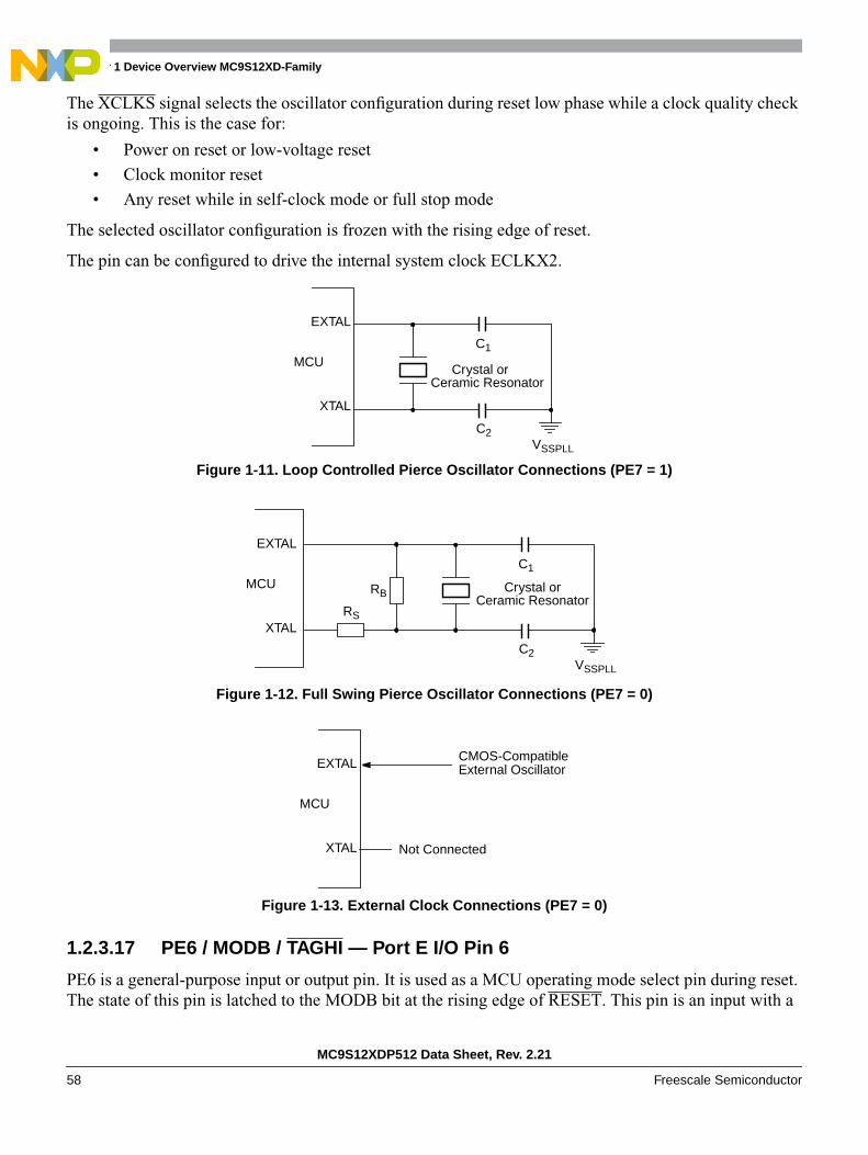
Chapter 1 Device Overview MC9S12XD-Family
MC9S12XDP512 Data Sheet, Rev. 2.21
58 Freescale Semiconductor
The XCLKS signal selects the oscillator configuration during reset low phase while a clock quality checkis ongoing. This is the case for:
• Power on reset or low-voltage reset
• Clock monitor reset
• Any reset while in self-clock mode or full stop mode
The selected oscillator configuration is frozen with the rising edge of reset.
The pin can be configured to drive the internal system clock ECLKX2.
Figure 1-11. Loop Controlled Pierce Oscillator Connections (PE7 = 1)
Figure 1-12. Full Swing Pierce Oscillator Connections (PE7 = 0)
Figure 1-13. External Clock Connections (PE7 = 0)
1.2.3.17 PE6 / MODB / TAGHI — Port E I/O Pin 6
PE6 is a general-purpose input or output pin. It is used as a MCU operating mode select pin during reset.The state of this pin is latched to the MODB bit at the rising edge of RESET. This pin is an input with a
MCU
EXTAL
XTAL
VSSPLL
Crystal orCeramic Resonator
C2
C1
MCU
EXTAL
XTALRS
RB
VSSPLL
Crystal orCeramic Resonator
C2
C1
MCU
EXTAL
XTAL
CMOS-CompatibleExternal Oscillator
Not Connected
Chapter 1 Device Overview MC9S12XD-Family
MC9S12XDP512 Data Sheet, Rev. 2.21
Freescale Semiconductor 59
pull-down device which is only active when RESET is low. TAGHI is used to tag the high half of theinstruction word being read into the instruction queue.
The input voltage threshold for PE6 can be configured to reduced levels, to allow data from an external3.3-V peripheral to be read by the MCU operating at 5.0 V. The input voltage threshold for PE6 isconfigured to reduced levels out of reset in expanded and emulation modes.
1.2.3.18 PE5 / MODA / TAGLO / RE — Port E I/O Pin 5
PE5 is a general-purpose input or output pin. It is used as a MCU operating mode select pin during reset.The state of this pin is latched to the MODA bit at the rising edge of RESET. This pin is shared with theread enable RE output. This pin is an input with a pull-down device which is only active when RESET islow. TAGLO is used to tag the low half of the instruction word being read into the instruction queue.
The input voltage threshold for PE5 can be configured to reduced levels, to allow data from an external3.3-V peripheral to be read by the MCU operating at 5.0 V. The input voltage threshold for PE5 isconfigured to reduced levels out of reset in expanded and emulation modes.
1.2.3.19 PE4 / ECLK — Port E I/O Pin 4
PE4 is a general-purpose input or output pin. It can be configured to drive the internal bus clock ECLK.ECLK can be used as a timing reference.
1.2.3.20 PE3 / LSTRB / LDS / EROMCTL— Port E I/O Pin 3
PE3 is a general-purpose input or output pin. In MCU expanded modes of operation, LSTRB or LDS canbe used for the low byte strobe function to indicate the type of bus access. At the rising edge of RESETthe state of this pin is latched to the EROMON bit.
1.2.3.21 PE2 / R/W / WE— Port E I/O Pin 2
PE2 is a general-purpose input or output pin. In MCU expanded modes of operations, this pin drives theread/write output signal or write enable output signal for the external bus. It indicates the direction of dataon the external bus
1.2.3.22 PE[6:2] — Port E I/O Pins
PE[6:2] are general-purpose input or output pins.
1.2.3.23 PE1 / IRQ — Port E Input Pin 1
PE1 is a general-purpose input pin and the maskable interrupt request input that provides a means ofapplying asynchronous interrupt requests. This will wake up the MCU from stop or wait mode.
1.2.3.24 PE0 / XIRQ — Port E Input Pin 0
PE0 is a general-purpose input pin and the non-maskable interrupt request input that provides a means ofapplying asynchronous interrupt requests. This will wake up the MCU from stop or wait mode.
Chapter 1 Device Overview MC9S12XD-Family
MC9S12XDP512 Data Sheet, Rev. 2.21
60 Freescale Semiconductor
1.2.3.25 PH7 / KWH7 / SS2 / TXD5 — Port H I/O Pin 7
PH7 is a general-purpose input or output pin. It can be configured to generate an interrupt causing theMCU to exit stop or wait mode. It can be configured as slave select pin SS of the serial peripheralinterface 2 (SPI2). It can be configured as the transmit pin TXD of serial communication interface 5(SCI5).
1.2.3.26 PH6 / KWH6 / SCK2 / RXD5 — Port H I/O Pin 6
PH6 is a general-purpose input or output pin. It can be configured to generate an interrupt causing theMCU to exit stop or wait mode. It can be configured as serial clock pin SCK of the serial peripheralinterface 2 (SPI2). It can be configured as the receive pin (RXD) of serial communication interface 5(SCI5).
1.2.3.27 PH5 / KWH5 / MOSI2 / TXD4 — Port H I/O Pin 5
PH5 is a general-purpose input or output pin. It can be configured to generate an interrupt causing theMCU to exit stop or wait mode. It can be configured as master output (during master mode) or slave inputpin (during slave mode) MOSI of the serial peripheral interface 2 (SPI2). It can be configured as thetransmit pin TXD of serial communication interface 4 (SCI4).
1.2.3.28 PH4 / KWH4 / MISO2 / RXD4 — Port H I/O Pin 4
PH4 is a general-purpose input or output pin. It can be configured to generate an interrupt causing theMCU to exit stop or wait mode. It can be configured as master input (during master mode) or slave output(during slave mode) pin MISO of the serial peripheral interface 2 (SPI2). It can be configured as the receivepin RXD of serial communication interface 4 (SCI4).
1.2.3.29 PH3 / KWH3 / SS1 — Port H I/O Pin 3
PH3 is a general-purpose input or output pin. It can be configured to generate an interrupt causing theMCU to exit stop or wait mode. It can be configured as slave select pin SS of the serial peripheralinterface 1 (SPI1).
1.2.3.30 PH2 / KWH2 / SCK1 — Port H I/O Pin 2
PH2 is a general-purpose input or output pin. It can be configured to generate an interrupt causing theMCU to exit stop or wait mode. It can be configured as serial clock pin SCK of the serial peripheralinterface 1 (SPI1).
1.2.3.31 PH1 / KWH1 / MOSI1 — Port H I/O Pin 1
PH1 is a general-purpose input or output pin. It can be configured to generate an interrupt causing theMCU to exit stop or wait mode. It can be configured as master output (during master mode) or slave inputpin (during slave mode) MOSI of the serial peripheral interface 1 (SPI1).

Chapter 1 Device Overview MC9S12XD-Family
MC9S12XDP512 Data Sheet, Rev. 2.21
Freescale Semiconductor 61
1.2.3.32 PH0 / KWH0 / MISO1 — Port H I/O Pin 0
PH0 is a general-purpose input or output pin. It can be configured to generate an interrupt causing theMCU to exit stop or wait mode. It can be configured as master input (during master mode) or slave output(during slave mode) pin MISO of the serial peripheral interface 1 (SPI1).
1.2.3.33 PJ7 / KWJ7 / TXCAN4 / SCL0 / TXCAN0— PORT J I/O Pin 7
PJ7 is a general-purpose input or output pin. It can be configured to generate an interrupt causing the MCUto exit stop or wait mode. It can be configured as the transmit pin TXCAN for the scalable controller areanetwork controller 0 or 4 (CAN0 or CAN4) or as the serial clock pin SCL of the IIC0 module.
1.2.3.34 PJ6 / KWJ6 / RXCAN4 / SDA0 / RXCAN0 — PORT J I/O Pin 6
PJ6 is a general-purpose input or output pin. It can be configured to generate an interrupt causing the MCUto exit stop or wait mode. It can be configured as the receive pin RXCAN for the scalable controller areanetwork controller 0 or 4 (CAN0 or CAN4) or as the serial data pin SDA of the IIC0 module.
1.2.3.35 PJ5 / KWJ5 / SCL1 / CS2 — PORT J I/O Pin 5
PJ5 is a general-purpose input or output pin. It can be configured to generate an interrupt causing the MCUto exit stop or wait mode. It can be configured as the serial clock pin SCL of the IIC1 module. It can beconfigured to provide a chip-select output.
1.2.3.36 PJ4 / KWJ4 / SDA1 / CS0 — PORT J I/O Pin 4
PJ4 is a general-purpose input or output pin. It can be configured to generate an interrupt causing the MCUto exit stop or wait mode. It can be configured as the serial data pin SDA of the IIC1 module. It can beconfigured to provide a chip-select output.
1.2.3.37 PJ2 / KWJ2 / CS1 — PORT J I/O Pin 2
PJ2 is a general-purpose input or output pins. It can be configured to generate an interrupt causing theMCU to exit stop or wait mode. It can be configured to provide a chip-select output.
1.2.3.38 PJ1 / KWJ1 / TXD2 — PORT J I/O Pin 1
PJ1 is a general-purpose input or output pin. It can be configured to generate an interrupt causing the MCUto exit stop or wait mode. It can be configured as the transmit pin TXD of the serial communicationinterface 2 (SCI2).
1.2.3.39 PJ0 / KWJ0 / RXD2 / CS3 — PORT J I/O Pin 0
PJ0 is a general-purpose input or output pin. It can be configured to generate an interrupt causing the MCUto exit stop or wait mode. It can be configured as the receive pin RXD of the serial communication interface2 (SCI2).It can be configured to provide a chip-select output.
Chapter 1 Device Overview MC9S12XD-Family
MC9S12XDP512 Data Sheet, Rev. 2.21
62 Freescale Semiconductor
1.2.3.40 PK7 / EWAIT / ROMCTL — Port K I/O Pin 7
PK7 is a general-purpose input or output pin. During MCU emulation modes and normal expanded modesof operation, this pin is used to enable the Flash EEPROM memory in the memory map (ROMCTL). Atthe rising edge of RESET, the state of this pin is latched to the ROMON bit. The EWAIT input signalmaintains the external bus access until the external device is ready to capture data (write) or provide data(read).
The input voltage threshold for PK7 can be configured to reduced levels, to allow data from an external3.3-V peripheral to be read by the MCU operating at 5.0 V. The input voltage threshold for PK7 isconfigured to reduced levels out of reset in expanded and emulation modes.
1.2.3.41 PK[6:4] / ADDR[22:20] / ACC[2:0] — Port K I/O Pin [6:4]
PK[6:4] are general-purpose input or output pins. During MCU expanded modes of operation, theACC[2:0] signals are used to indicate the access source of the bus cycle. This pins also provide theexpanded addresses ADDR[22:20] for the external bus. In Emulation modes ACC[2:0] is available and istime multiplexed with the high addresses
1.2.3.42 PK[3:0] / ADDR[19:16] / IQSTAT[3:0] — Port K I/O Pins [3:0]
PK3-PK0 are general-purpose input or output pins. In MCU expanded modes of operation, these pinsprovide the expanded address ADDR[19:16] for the external bus and carry instruction pipe information.
1.2.3.43 PK7,PK[5:0] — Port K I/O Pins 7 & [5:0]
PK7 and PK[5:0] are general-purpose input or output pins.
1.2.3.44 PM7 / TXCAN3 / TXCAN4 / TXD3 — Port M I/O Pin 7
PM7 is a general-purpose input or output pin. It can be configured as the transmit pin TXCAN of thescalable controller area network controller 3 or 4 (CAN3 or CAN4). PM7 can be configured as the transmitpin TXD3 of the serial communication interface 3 (SCI3).
1.2.3.45 PM6 / RXCAN3 / RXCAN4 / RXD3 — Port M I/O Pin 6
PM6 is a general-purpose input or output pin. It can be configured as the receive pin RXCAN of thescalable controller area network controller 3 or 4 (CAN3 or CAN4). PM6 can be configured as the receivepin RXD3 of the serial communication interface 3 (SCI3).
1.2.3.46 PM5 / TXCAN0 / TXCAN2 / TXCAN4 / SCK0 — Port M I/O Pin 5
PM5 is a general-purpose input or output pin. It can be configured as the transmit pin TXCAN of thescalable controller area network controllers 0, 2 or 4 (CAN0, CAN2, or CAN4). It can be configured asthe serial clock pin SCK of the serial peripheral interface 0 (SPI0).
Chapter 1 Device Overview MC9S12XD-Family
MC9S12XDP512 Data Sheet, Rev. 2.21
Freescale Semiconductor 63
1.2.3.47 PM4 / RXCAN0 / RXCAN2 / RXCAN4 / MOSI0 — Port M I/O Pin 4
PM4 is a general-purpose input or output pin. It can be configured as the receive pin RXCAN of thescalable controller area network controllers 0, 2, or 4 (CAN0, CAN2, or CAN4). It can be configured asthe master output (during master mode) or slave input pin (during slave mode) MOSI for the serialperipheral interface 0 (SPI0).
1.2.3.48 PM3 / TXCAN1 / TXCAN0 / SS0 — Port M I/O Pin 3
PM3 is a general-purpose input or output pin. It can be configured as the transmit pin TXCAN of thescalable controller area network controllers 1 or 0 (CAN1 or CAN0). It can be configured as the slaveselect pin SS of the serial peripheral interface 0 (SPI0).
1.2.3.49 PM2 / RXCAN1 / RXCAN0 / MISO0 — Port M I/O Pin 2
PM2 is a general-purpose input or output pin. It can be configured as the receive pin RXCAN of thescalable controller area network controllers 1 or 0 (CAN1 or CAN0). It can be configured as the masterinput (during master mode) or slave output pin (during slave mode) MISO for the serial peripheralinterface 0 (SPI0).
1.2.3.50 PM1 / TXCAN0 — Port M I/O Pin 1
PM1 is a general-purpose input or output pin. It can be configured as the transmit pin TXCAN of thescalable controller area network controller 0 (CAN0).
1.2.3.51 PM0 / RXCAN0 — Port M I/O Pin 0
PM0 is a general-purpose input or output pin. It can be configured as the receive pin RXCAN of thescalable controller area network controller 0 (CAN0).
1.2.3.52 PP7 / KWP7 / PWM7 / SCK2 — Port P I/O Pin 7
PP7 is a general-purpose input or output pin. It can be configured to generate an interrupt causing the MCUto exit stop or wait mode. It can be configured as pulse width modulator (PWM) channel 7 output. It canbe configured as serial clock pin SCK of the serial peripheral interface 2 (SPI2).
1.2.3.53 PP6 / KWP6 / PWM6 / SS2 — Port P I/O Pin 6
PP6 is a general-purpose input or output pin. It can be configured to generate an interrupt causing the MCUto exit stop or wait mode. It can be configured as pulse width modulator (PWM) channel 6 output. It canbe configured as slave select pin SS of the serial peripheral interface 2 (SPI2).
1.2.3.54 PP5 / KWP5 / PWM5 / MOSI2 — Port P I/O Pin 5
PP5 is a general-purpose input or output pin. It can be configured to generate an interrupt causing the MCUto exit stop or wait mode. It can be configured as pulse width modulator (PWM) channel 5 output. It can

Chapter 1 Device Overview MC9S12XD-Family
MC9S12XDP512 Data Sheet, Rev. 2.21
64 Freescale Semiconductor
be configured as master output (during master mode) or slave input pin (during slave mode) MOSI of theserial peripheral interface 2 (SPI2).
1.2.3.55 PP4 / KWP4 / PWM4 / MISO2 — Port P I/O Pin 4
PP4 is a general-purpose input or output pin. It can be configured to generate an interrupt causing the MCUto exit stop or wait mode. It can be configured as pulse width modulator (PWM) channel 4 output. It canbe configured as master input (during master mode) or slave output (during slave mode) pin MISO of theserial peripheral interface 2 (SPI2).
1.2.3.56 PP3 / KWP3 / PWM3 / SS1 — Port P I/O Pin 3
PP3 is a general-purpose input or output pin. It can be configured to generate an interrupt causing the MCUto exit stop or wait mode. It can be configured as pulse width modulator (PWM) channel 3 output. It canbe configured as slave select pin SS of the serial peripheral interface 1 (SPI1).
1.2.3.57 PP2 / KWP2 / PWM2 / SCK1 — Port P I/O Pin 2
PP2 is a general-purpose input or output pin. It can be configured to generate an interrupt causing the MCUto exit stop or wait mode. It can be configured as pulse width modulator (PWM) channel 2 output. It canbe configured as serial clock pin SCK of the serial peripheral interface 1 (SPI1).
1.2.3.58 PP1 / KWP1 / PWM1 / MOSI1 — Port P I/O Pin 1
PP1 is a general-purpose input or output pin. It can be configured to generate an interrupt causing the MCUto exit stop or wait mode. It can be configured as pulse width modulator (PWM) channel 1 output. It canbe configured as master output (during master mode) or slave input pin (during slave mode) MOSI of theserial peripheral interface 1 (SPI1).
1.2.3.59 PP0 / KWP0 / PWM0 / MISO1 — Port P I/O Pin 0
PP0 is a general-purpose input or output pin. It can be configured to generate an interrupt causing the MCUto exit stop or wait mode. It can be configured as pulse width modulator (PWM) channel 0 output. It canbe configured as master input (during master mode) or slave output (during slave mode) pin MISO of theserial peripheral interface 1 (SPI1).
1.2.3.60 PS7 / SS0 — Port S I/O Pin 7
PS7 is a general-purpose input or output pin. It can be configured as the slave select pin SS of the serialperipheral interface 0 (SPI0).
1.2.3.61 PS6 / SCK0 — Port S I/O Pin 6
PS6 is a general-purpose input or output pin. It can be configured as the serial clock pin SCK of the serialperipheral interface 0 (SPI0).
Chapter 1 Device Overview MC9S12XD-Family
MC9S12XDP512 Data Sheet, Rev. 2.21
Freescale Semiconductor 65
1.2.3.62 PS5 / MOSI0 — Port S I/O Pin 5
PS5 is a general-purpose input or output pin. It can be configured as master output (during master mode)or slave input pin (during slave mode) MOSI of the serial peripheral interface 0 (SPI0).
1.2.3.63 PS4 / MISO0 — Port S I/O Pin 4
PS4 is a general-purpose input or output pin. It can be configured as master input (during master mode) orslave output pin (during slave mode) MOSI of the serial peripheral interface 0 (SPI0).
1.2.3.64 PS3 / TXD1 — Port S I/O Pin 3
PS3 is a general-purpose input or output pin. It can be configured as the transmit pin TXD of serialcommunication interface 1 (SCI1).
1.2.3.65 PS2 / RXD1 — Port S I/O Pin 2
PS2 is a general-purpose input or output pin. It can be configured as the receive pin RXD of serialcommunication interface 1 (SCI1).
1.2.3.66 PS1 / TXD0 — Port S I/O Pin 1
PS1 is a general-purpose input or output pin. It can be configured as the transmit pin TXD of serialcommunication interface 0 (SCI0).
1.2.3.67 PS0 / RXD0 — Port S I/O Pin 0
PS0 is a general-purpose input or output pin. It can be configured as the receive pin RXD of serialcommunication interface 0 (SCI0).
1.2.3.68 PT[7:0] / IOC[7:0] — Port T I/O Pins [7:0]
PT[7:0] are general-purpose input or output pins. They can be configured as input capture or outputcompare pins IOC[7:0] of the enhanced capture timer (ECT).
1.2.4 Power Supply Pins
MC9S12XDP512RMV2 power and ground pins are described below.
NOTEAll VSS pins must be connected together in the application.
1.2.4.1 VDDX1, VDDX2, VSSX1,VSSX2 — Power and Ground Pins for I/O Drivers
External power and ground for I/O drivers. Because fast signal transitions place high, short-durationcurrent demands on the power supply, use bypass capacitors with high-frequency characteristics and placethem as close to the MCU as possible. Bypass requirements depend on how heavily the MCU pins areloaded.

Chapter 1 Device Overview MC9S12XD-Family
MC9S12XDP512 Data Sheet, Rev. 2.21
66 Freescale Semiconductor
1.2.4.2 VDDR1, VDDR2, VSSR1, VSSR2 — Power and Ground Pins for I/O Driversand for Internal Voltage Regulator
External power and ground for I/O drivers and input to the internal voltage regulator. Because fast signaltransitions place high, short-duration current demands on the power supply, use bypass capacitors withhigh-frequency characteristics and place them as close to the MCU as possible. Bypass requirementsdepend on how heavily the MCU pins are loaded.
1.2.4.3 VDD1, VDD2, VSS1, VSS2 — Core Power Pins
Power is supplied to the MCU through VDD and VSS. Because fast signal transitions place high,short-duration current demands on the power supply, use bypass capacitors with high-frequencycharacteristics and place them as close to the MCU as possible. This 2.5-V supply is derived from theinternal voltage regulator. There is no static load on those pins allowed. The internal voltage regulator isturned off, if VREGEN is tied to ground.
NOTENo load allowed except for bypass capacitors.
1.2.4.4 VDDA, VSSA — Power Supply Pins for ATD and VREG
VDDA, VSSA are the power supply and ground input pins for the voltage regulator and the analog-to-digitalconverters.
1.2.4.5 VRH, VRL — ATD Reference Voltage Input Pins
VRH and VRL are the reference voltage input pins for the analog-to-digital converter.
1.2.4.6 VDDPLL, VSSPLL — Power Supply Pins for PLL
Provides operating voltage and ground for the oscillator and the phased-locked loop. This allows thesupply voltage to the oscillator and PLL to be bypassed independently. This 2.5-V voltage is generated bythe internal voltage regulator.
NOTENo load allowed except for bypass capacitors.

Chapter 1 Device Overview MC9S12XD-Family
MC9S12XDP512 Data Sheet, Rev. 2.21
Freescale Semiconductor 67
Table 1-8. MC9S12XD Family Power and Ground Connection Summary
Mnemonic
Pin NumberNominalVoltage
Description144-PinLQFP
112-PinLQFP
80-PinQFP
VDD1, 2 15, 87 13, 65 9, 49 2.5 V Internal power and ground generated byinternal regulator
VSS1, 2 16, 88 14, 66 10, 50 0V
VDDR1 53 41 29 5.0 V External power and ground, supply to pindrivers and internal voltage regulator
VSSR1 52 40 28 0 V
VDDX1 139 107 77 5.0 V External power and ground, supply to pindrivers
VSSX1 138 106 76 0 V
VDDX2 26 N.A. N.A. 5.0 V External power and ground, supply to pindrivers
VSSX2 27 N.A. N.A. 0 V
VDDR2 82 N.A. N.A. 5.0 V External power and ground, supply to pindrivers
VSSR2 81 N.A. N.A. 0 V
VDDA 107 83 59 5.0 V Operating voltage and ground for theanalog-to-digital converters and thereference for the internal voltage regulator,allows the supply voltage to the A/D to bebypassed independently.
VSSA 110 86 62 0 V
VRL 109 85 61 0 V Reference voltages for the analog-to-digitalconverter.
VRH 108 84 60 5.0 V
VDDPLL 55 43 31 2.5 V Provides operating voltage and ground forthe phased-locked loop. This allows thesupply voltage to the PLL to be bypassedindependently. Internal power and groundgenerated by internal regulator.
VSSPLL 57 45 33 0 V

Chapter 1 Device Overview MC9S12XD-Family
MC9S12XDP512 Data Sheet, Rev. 2.21
68 Freescale Semiconductor
1.3 System Clock DescriptionThe clock and reset generator module (CRG) provides the internal clock signals for the core and allperipheral modules. Figure 1-12 shows the clock connections from the CRG to all modules.
See 79Chapterf or details on clock generation.
Figure 1-14. MC9S12XD Family Clock Connections
The MCU’s system clock can be supplied in several ways enabling a range of system operating frequenciesto be supported:
• The on-chip phase locked loop (PLL)
• the PLL self clocking
• the oscillator
The clock generated by the PLL or oscillator provides the main system clock frequencies core clock andbus clock. As shown in Figure 1-12, this system clocks are used throughout the MCU to drive the core, thememories, and the peripherals.
The program Flash memory and the EEPROM are supplied by the bus clock and the oscillator clock.Theoscillator clock is used as a time base to derive the program and erase times for the NVM’s. See the Flashand EEPROM section for more details on the operation of the NVM’s.
SCI Modules SPI Modules IIC Modules ATD ModulesCAN Modules
CRG
Bus Clock
EXTAL
XTAL
Core Clock
Oscillator Clock
RAM S12X XGATE EEPROMFLASH
PIT
ECT
PIM

Chapter 1 Device Overview MC9S12XD-Family
MC9S12XDP512 Data Sheet, Rev. 2.21
Freescale Semiconductor 69
The CAN modules may be configured to have their clock sources derived either from the bus clock ordirectly from the oscillator clock. This allows the user to select its clock based on the required jitterperformance. Consult MSCAN block description for more details on the operation and configuration ofthe CAN blocks.
In order to ensure the presence of the clock the MCU includes an on-chip clock monitor connected to theoutput of the oscillator. The clock monitor can be configured to invoke the PLL self-clocking mode or togenerate a system reset if it is allowed to time out as a result of no oscillator clock being present.
In addition to the clock monitor, the MCU also provides a clock quality checker which performs a moreaccurate check of the clock. The clock quality checker counts a predetermined number of clock edgeswithin a defined time window to insure that the clock is running. The checker can be invoked followingspecific events such as on wake-up or clock monitor failure.
1.4 Chip Configuration SummaryCAUTION
Emulation single chip mode, Normal expanded mode, Emulation expandedmode and ROMCTL/EROMCTL functionality is only available on partswith external bus interface in 144 LQFP package. see Appendix EDerivative Differences.
The MCU can operate in six different modes. The different modes, the state of ROMCTL and EROMCTLsignal on rising edge of RESET, and the security state of the MCU affects the following devicecharacteristics:
• External bus interface configuration
• Flash in memory map, or not
• Debug features enabled or disabled
The operating mode out of reset is determined by the states of the MODC, MODB, and MODA signalsduring reset (see Table 1-9). The MODC, MODB, and MODA bits in the MODE register show the currentoperating mode and provide limited mode switching during operation. The states of the MODC, MODB,and MODA signals are latched into these bits on the rising edge of RESET.
In normal expanded mode and in emulation modes the ROMON bit and the EROMON bit in theMMCCTL1 register defines if the on chip flash memory is the memory map, or not. (See Table 1-9.) Fora detailed description of the ROMON and EROMON bits refer to the S12X_MMC section.
The state of the ROMCTL signal is latched into the ROMON bit in the MMCCTL1 register on the risingedge of RESET. The state of the EROMCTL signal is latched into the EROMON bit in the MISC registeron the rising edge of RESET.
The MCU can operate in two different modes. The operating mode out of reset is determined by the stateof the MODC signal during reset. The MODC bit in the MODE register shows the current operating modeand provide limited mode switching during operation. The state of the MODC signal is latched into thisbit on the rising edge of RESET.
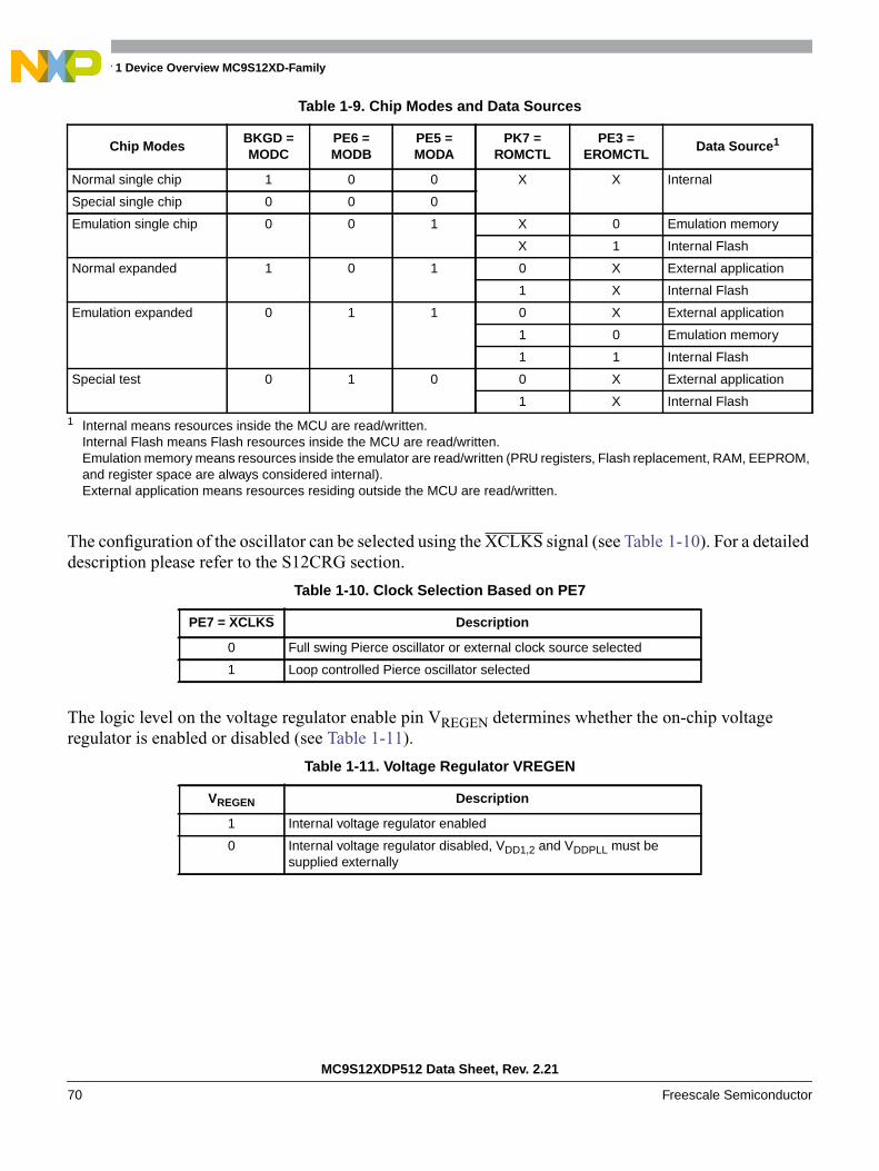
Chapter 1 Device Overview MC9S12XD-Family
MC9S12XDP512 Data Sheet, Rev. 2.21
70 Freescale Semiconductor
The configuration of the oscillator can be selected using the XCLKS signal (see Table 1-10). For a detaileddescription please refer to the S12CRG section.
The logic level on the voltage regulator enable pin VREGEN determines whether the on-chip voltageregulator is enabled or disabled (see Table 1-11).
Table 1-9. Chip Modes and Data Sources
Chip ModesBKGD =MODC
PE6 =MODB
PE5 =MODA
PK7 =ROMCTL
PE3 =EROMCTL
Data Source1
1 Internal means resources inside the MCU are read/written.Internal Flash means Flash resources inside the MCU are read/written.Emulation memory means resources inside the emulator are read/written (PRU registers, Flash replacement, RAM, EEPROM,and register space are always considered internal).External application means resources residing outside the MCU are read/written.
Normal single chip 1 0 0 X X Internal
Special single chip 0 0 0
Emulation single chip 0 0 1 X 0 Emulation memory
X 1 Internal Flash
Normal expanded 1 0 1 0 X External application
1 X Internal Flash
Emulation expanded 0 1 1 0 X External application
1 0 Emulation memory
1 1 Internal Flash
Special test 0 1 0 0 X External application
1 X Internal Flash
Table 1-10. Clock Selection Based on PE7
PE7 = XCLKS Description
0 Full swing Pierce oscillator or external clock source selected
1 Loop controlled Pierce oscillator selected
Table 1-11. Voltage Regulator VREGEN
VREGEN Description
1 Internal voltage regulator enabled
0 Internal voltage regulator disabled, VDD1,2 and VDDPLL must besupplied externally

Chapter 1 Device Overview MC9S12XD-Family
MC9S12XDP512 Data Sheet, Rev. 2.21
Freescale Semiconductor 71
1.5 Modes of Operation
1.5.1 User Modes
1.5.1.1 Normal Expanded Mode
Ports K, A, and B are configured as a 23-bit address bus, ports C and D are configured as a 16-bit data bus,and port E provides bus control and status signals. This mode allows 16-bit external memory andperipheral devices to be interfaced to the system. The fastest external bus rate is divide by 2 from theinternal bus rate.
1.5.1.2 Normal Single-Chip Mode
There is no external bus in this mode. The processor program is executed from internal memory. Ports A,B,C,D, K, and most pins of port E are available as general-purpose I/O.
1.5.1.3 Special Single-Chip Mode
This mode is used for debugging single-chip operation, boot-strapping, or security related operations. Thebackground debug module BDM is active in this mode. The CPU executes a monitor program located inan on-chip ROM. BDM firmware is waiting for additional serial commands through the BKGD pin. Thereis no external bus after reset in this mode.
1.5.1.4 Emulation of Expanded Mode
Developers use this mode for emulation systems in which the users target application is normal expandedmode. Code is executed from external memory or from internal memory depending on the state ofROMON and EROMON bit. In this mode the internal operation is visible on external bus interface.
1.5.1.5 Emulation of Single-Chip Mode
Developers use this mode for emulation systems in which the user’s target application is normalsingle-chip mode. Code is executed from external memory or from internal memory depending on the stateof ROMON and EROMON bit. In this mode the internal operation is visible on external bus interface.
1.5.1.6 Special Test Mode
Freescale internal use only.
1.5.2 Low-Power Modes
The microcontroller features two main low-power modes. Consult the respective sections for informationon the module behavior in system stop, system pseudo stop, and system wait mode. An important sourceof information about the clock system is the Clock and Reset Generator S12CRG section.
Chapter 1 Device Overview MC9S12XD-Family
MC9S12XDP512 Data Sheet, Rev. 2.21
72 Freescale Semiconductor
1.5.2.1 System Stop Modes
The system stop modes are entered if the CPU executes the STOP instruction and the XGATE doesn’texecute a thread and the XGFACT bit in the XGMCTL register is cleared. Depending on the state of thePSTP bit in the CLKSEL register the MCU goes into pseudo stop mode or full stop mode. Please refer toCRG section. Asserting RESET, XIRQ, IRQ or any other interrupt ends the system stop modes.
1.5.2.2 Pseudo Stop Mode
In this mode the clocks are stopped but the oscillator is still running and the real time interrupt (RTI) orwatchdog (COP) submodule can stay active. Other peripherals are turned off. This mode consumes morecurrent than the system stop mode, but the wake up time from this mode is significantly shorter.
1.5.2.3 Full Stop Mode
The oscillator is stopped in this mode. All clocks are switched off. All counters and dividers remain frozen.
1.5.2.4 System Wait Mode
This mode is entered when the CPU executes the WAI instruction. In this mode the CPU will not executeinstructions. The internal CPU clock is switched off. All peripherals and the XGATE can be active insystem wait mode. For further power consumption the peripherals can individually turn off their localclocks. Asserting RESET, XIRQ, IRQ or any other interrupt that has not been masked ends system waitmode.
1.5.3 Freeze Mode
The enhanced capture timer, pulse width modulator, analog-to-digital converters, the periodic interrupttimer and the XGATE module provide a software programmable option to freeze the module status duringthe background debug module is active. This is useful when debugging application software. For detaileddescription of the behavior of the ATD0, ATD1, ECT, PWM, XGATE and PIT when the background debugmodule is active consult the corresponding sections..
1.6 Resets and InterruptsConsult the S12XCPU Block Guide for information on exception processing.
1.6.1 Vectors
Table 1-12 lists all interrupt sources and vectors in the default order of priority. The interrupt module(S12XINT) provides an interrupt vector base register (IVBR) to relocate the vectors. Associated with eachI-bit maskable service request is a configuration register. It selects if the service request is enabled, theservice request priority level and whether the service request is handled either by the S12X CPU or by theXGATE module.
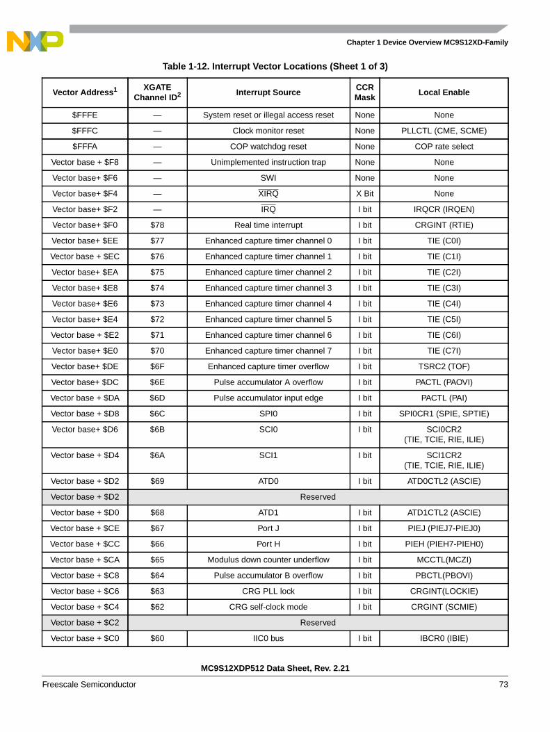
Chapter 1 Device Overview MC9S12XD-Family
MC9S12XDP512 Data Sheet, Rev. 2.21
Freescale Semiconductor 73
Table 1-12. Interrupt Vector Locations (Sheet 1 of 3)
Vector Address1 XGATEChannel ID2 Interrupt Source
CCRMask
Local Enable
$FFFE — System reset or illegal access reset None None
$FFFC — Clock monitor reset None PLLCTL (CME, SCME)
$FFFA — COP watchdog reset None COP rate select
Vector base + $F8 — Unimplemented instruction trap None None
Vector base+ $F6 — SWI None None
Vector base+ $F4 — XIRQ X Bit None
Vector base+ $F2 — IRQ I bit IRQCR (IRQEN)
Vector base+ $F0 $78 Real time interrupt I bit CRGINT (RTIE)
Vector base+ $EE $77 Enhanced capture timer channel 0 I bit TIE (C0I)
Vector base + $EC $76 Enhanced capture timer channel 1 I bit TIE (C1I)
Vector base+ $EA $75 Enhanced capture timer channel 2 I bit TIE (C2I)
Vector base+ $E8 $74 Enhanced capture timer channel 3 I bit TIE (C3I)
Vector base+ $E6 $73 Enhanced capture timer channel 4 I bit TIE (C4I)
Vector base+ $E4 $72 Enhanced capture timer channel 5 I bit TIE (C5I)
Vector base + $E2 $71 Enhanced capture timer channel 6 I bit TIE (C6I)
Vector base+ $E0 $70 Enhanced capture timer channel 7 I bit TIE (C7I)
Vector base+ $DE $6F Enhanced capture timer overflow I bit TSRC2 (TOF)
Vector base+ $DC $6E Pulse accumulator A overflow I bit PACTL (PAOVI)
Vector base + $DA $6D Pulse accumulator input edge I bit PACTL (PAI)
Vector base + $D8 $6C SPI0 I bit SPI0CR1 (SPIE, SPTIE)
Vector base+ $D6 $6B SCI0 I bit SCI0CR2(TIE, TCIE, RIE, ILIE)
Vector base + $D4 $6A SCI1 I bit SCI1CR2(TIE, TCIE, RIE, ILIE)
Vector base + $D2 $69 ATD0 I bit ATD0CTL2 (ASCIE)
Vector base + $D2 Reserved
Vector base + $D0 $68 ATD1 I bit ATD1CTL2 (ASCIE)
Vector base + $CE $67 Port J I bit PIEJ (PIEJ7-PIEJ0)
Vector base + $CC $66 Port H I bit PIEH (PIEH7-PIEH0)
Vector base + $CA $65 Modulus down counter underflow I bit MCCTL(MCZI)
Vector base + $C8 $64 Pulse accumulator B overflow I bit PBCTL(PBOVI)
Vector base + $C6 $63 CRG PLL lock I bit CRGINT(LOCKIE)
Vector base + $C4 $62 CRG self-clock mode I bit CRGINT (SCMIE)
Vector base + $C2 Reserved
Vector base + $C0 $60 IIC0 bus I bit IBCR0 (IBIE)
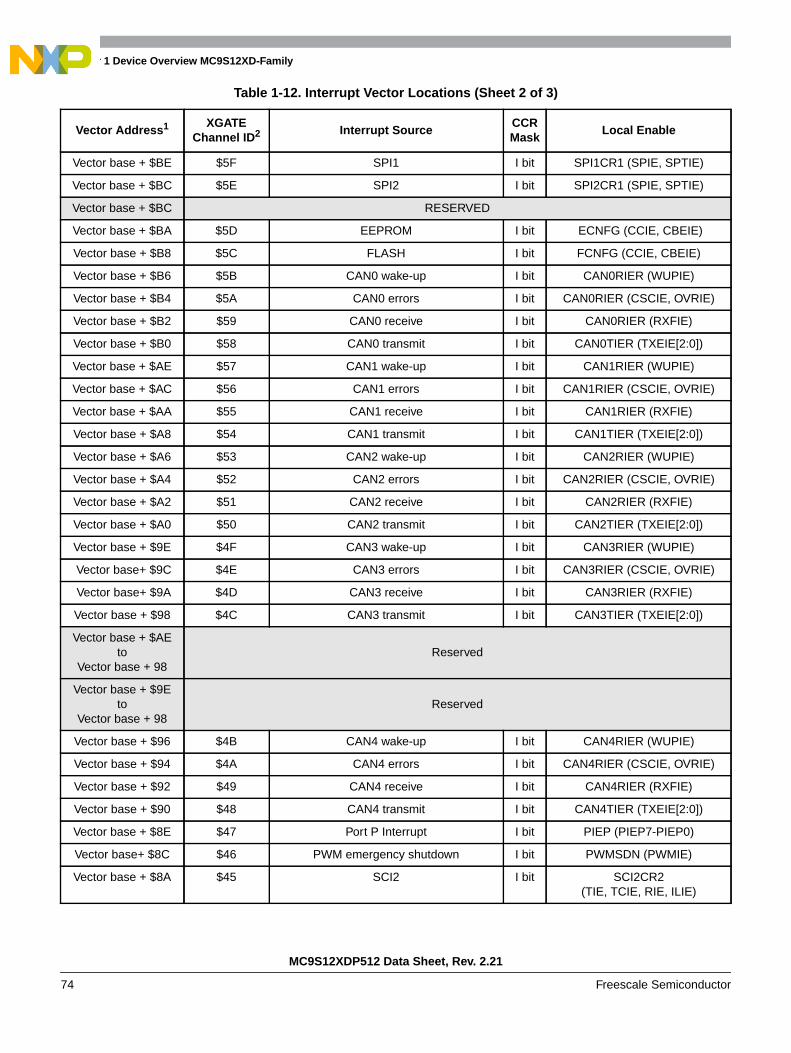
Chapter 1 Device Overview MC9S12XD-Family
MC9S12XDP512 Data Sheet, Rev. 2.21
74 Freescale Semiconductor
Vector base + $BE $5F SPI1 I bit SPI1CR1 (SPIE, SPTIE)
Vector base + $BC $5E SPI2 I bit SPI2CR1 (SPIE, SPTIE)
Vector base + $BC RESERVED
Vector base + $BA $5D EEPROM I bit ECNFG (CCIE, CBEIE)
Vector base + $B8 $5C FLASH I bit FCNFG (CCIE, CBEIE)
Vector base + $B6 $5B CAN0 wake-up I bit CAN0RIER (WUPIE)
Vector base + $B4 $5A CAN0 errors I bit CAN0RIER (CSCIE, OVRIE)
Vector base + $B2 $59 CAN0 receive I bit CAN0RIER (RXFIE)
Vector base + $B0 $58 CAN0 transmit I bit CAN0TIER (TXEIE[2:0])
Vector base + $AE $57 CAN1 wake-up I bit CAN1RIER (WUPIE)
Vector base + $AC $56 CAN1 errors I bit CAN1RIER (CSCIE, OVRIE)
Vector base + $AA $55 CAN1 receive I bit CAN1RIER (RXFIE)
Vector base + $A8 $54 CAN1 transmit I bit CAN1TIER (TXEIE[2:0])
Vector base + $A6 $53 CAN2 wake-up I bit CAN2RIER (WUPIE)
Vector base + $A4 $52 CAN2 errors I bit CAN2RIER (CSCIE, OVRIE)
Vector base + $A2 $51 CAN2 receive I bit CAN2RIER (RXFIE)
Vector base + $A0 $50 CAN2 transmit I bit CAN2TIER (TXEIE[2:0])
Vector base + $9E $4F CAN3 wake-up I bit CAN3RIER (WUPIE)
Vector base+ $9C $4E CAN3 errors I bit CAN3RIER (CSCIE, OVRIE)
Vector base+ $9A $4D CAN3 receive I bit CAN3RIER (RXFIE)
Vector base + $98 $4C CAN3 transmit I bit CAN3TIER (TXEIE[2:0])
Vector base + $AEto
Vector base + 98Reserved
Vector base + $9Eto
Vector base + 98Reserved
Vector base + $96 $4B CAN4 wake-up I bit CAN4RIER (WUPIE)
Vector base + $94 $4A CAN4 errors I bit CAN4RIER (CSCIE, OVRIE)
Vector base + $92 $49 CAN4 receive I bit CAN4RIER (RXFIE)
Vector base + $90 $48 CAN4 transmit I bit CAN4TIER (TXEIE[2:0])
Vector base + $8E $47 Port P Interrupt I bit PIEP (PIEP7-PIEP0)
Vector base+ $8C $46 PWM emergency shutdown I bit PWMSDN (PWMIE)
Vector base + $8A $45 SCI2 I bit SCI2CR2(TIE, TCIE, RIE, ILIE)
Table 1-12. Interrupt Vector Locations (Sheet 2 of 3)
Vector Address1 XGATEChannel ID2 Interrupt Source
CCRMask
Local Enable

Chapter 1 Device Overview MC9S12XD-Family
MC9S12XDP512 Data Sheet, Rev. 2.21
Freescale Semiconductor 75
Vector base + $88 $44 SCI3 I bit SCI3CR2(TIE, TCIE, RIE, ILIE)
Vector base + $8Ato
Vector base + $88Reserved
Vector base + $86 $43 SCI4 I bit SCI4CR2(TIE, TCIE, RIE, ILIE)
Vector base + $84 $42 SCI5 I bit SCI5CR2(TIE, TCIE, RIE, ILIE)
Vector base + $86to
Vector base + $84Reserved
Vector base + $82 $41 IIC1 Bus I bit IBCR (IBIE)
Vector base + $82 Reserved
Vector base + $80 $40 Low-voltage interrupt (LVI) I bit VREGCTRL (LVIE)
Vector base + $7E $3F Autonomous periodical interrupt (API) I bit VREGAPICTRL (APIE)
Vector base + $7C Reserved
Vector base + $7A $3D Periodic interrupt timer channel 0 I bit PITINTE (PINTE0)
Vector base + $78 $3C Periodic interrupt timer channel 1 I bit PITINTE (PINTE1)
Vector base + $76 $3B Periodic interrupt timer channel 2 I bit PITINTE (PINTE2)
Vector base + $74 $3A Periodic interrupt timer channel 3 I bit PITINTE (PINTE3)
Vector base + $72 $39 XGATE software trigger 0 I bit XGMCTL (XGIE)
Vector base + $70 $38 XGATE software trigger 1 I bit XGMCTL (XGIE)
Vector base + $6E $37 XGATE software trigger 2 I bit XGMCTL (XGIE)
Vector base + $6C $36 XGATE software trigger 3 I bit XGMCTL (XGIE)
Vector base + $6A $35 XGATE software trigger 4 I bit XGMCTL (XGIE)
Vector base + $68 $34 XGATE software trigger 5 I bit XGMCTL (XGIE)
Vector base + $66 $33 XGATE software trigger 6 I bit XGMCTL (XGIE)
Vector base + $64 $32 XGATE software trigger 7 I bit XGMCTL (XGIE)
Vector base + $62 — XGATE software error interrupt I bit XGMCTL (XGIE)
Vector base + $60 — S12XCPU RAM access violation I bit RAMWPC (AVIE)
Vector base+ $12 to
Vector base + $5E
Reserved
Vector base + $10 — Spurious interrupt — None
1 16 bits vector address based2 For detailed description of XGATE channel ID refer to XGATE Block Guide
Table 1-12. Interrupt Vector Locations (Sheet 3 of 3)
Vector Address1 XGATEChannel ID2 Interrupt Source
CCRMask
Local Enable
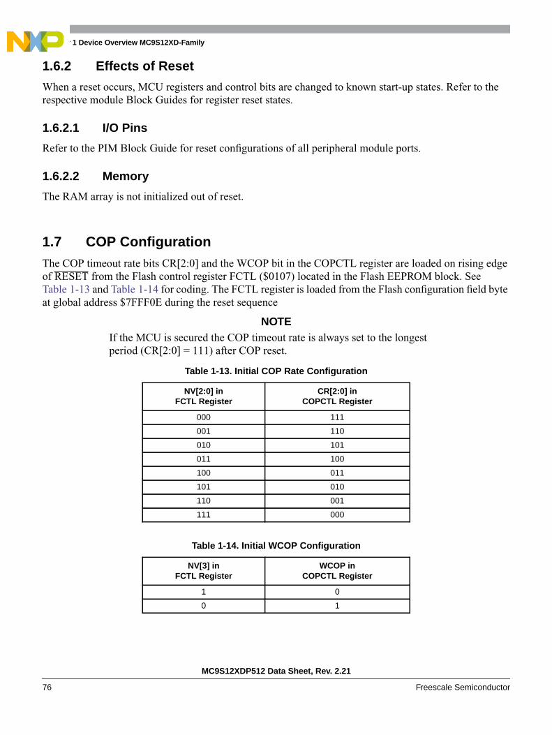
Chapter 1 Device Overview MC9S12XD-Family
MC9S12XDP512 Data Sheet, Rev. 2.21
76 Freescale Semiconductor
1.6.2 Effects of Reset
When a reset occurs, MCU registers and control bits are changed to known start-up states. Refer to therespective module Block Guides for register reset states.
1.6.2.1 I/O Pins
Refer to the PIM Block Guide for reset configurations of all peripheral module ports.
1.6.2.2 Memory
The RAM array is not initialized out of reset.
1.7 COP ConfigurationThe COP timeout rate bits CR[2:0] and the WCOP bit in the COPCTL register are loaded on rising edgeof RESET from the Flash control register FCTL ($0107) located in the Flash EEPROM block. SeeTable 1-13 and Table 1-14 for coding. The FCTL register is loaded from the Flash configuration field byteat global address $7FFF0E during the reset sequence
NOTEIf the MCU is secured the COP timeout rate is always set to the longestperiod (CR[2:0] = 111) after COP reset.
Table 1-13. Initial COP Rate Configuration
NV[2:0] inFCTL Register
CR[2:0] inCOPCTL Register
000 111
001 110
010 101
011 100
100 011
101 010
110 001
111 000
Table 1-14. Initial WCOP Configuration
NV[3] inFCTL Register
WCOP inCOPCTL Register
1 0
0 1
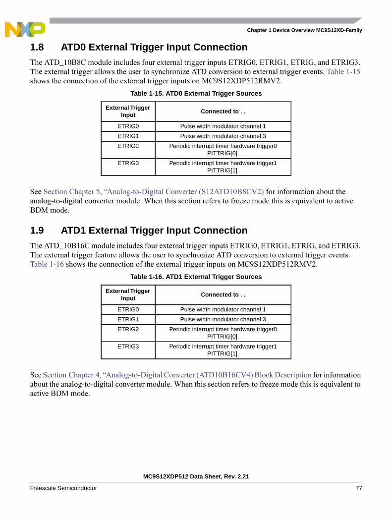
Chapter 1 Device Overview MC9S12XD-Family
MC9S12XDP512 Data Sheet, Rev. 2.21
Freescale Semiconductor 77
1.8 ATD0 External Trigger Input ConnectionThe ATD_10B8C module includes four external trigger inputs ETRIG0, ETRIG1, ETRIG, and ETRIG3.The external trigger allows the user to synchronize ATD conversion to external trigger events. Table 1-15shows the connection of the external trigger inputs on MC9S12XDP512RMV2.
See Section Chapter 5, “Analog-to-Digital Converter (S12ATD10B8CV2) for information about theanalog-to-digital converter module. When this section refers to freeze mode this is equivalent to activeBDM mode.
1.9 ATD1 External Trigger Input ConnectionThe ATD_10B16C module includes four external trigger inputs ETRIG0, ETRIG1, ETRIG, and ETRIG3.The external trigger feature allows the user to synchronize ATD conversion to external trigger events.Table 1-16 shows the connection of the external trigger inputs on MC9S12XDP512RMV2.
See Section Chapter 4, “Analog-to-Digital Converter (ATD10B16CV4) Block Description for informationabout the analog-to-digital converter module. When this section refers to freeze mode this is equivalent toactive BDM mode.
Table 1-15. ATD0 External Trigger Sources
External TriggerInput
Connected to . .
ETRIG0 Pulse width modulator channel 1
ETRIG1 Pulse width modulator channel 3
ETRIG2 Periodic interrupt timer hardware trigger0PITTRIG[0].
ETRIG3 Periodic interrupt timer hardware trigger1PITTRIG[1].
Table 1-16. ATD1 External Trigger Sources
External TriggerInput
Connected to . .
ETRIG0 Pulse width modulator channel 1
ETRIG1 Pulse width modulator channel 3
ETRIG2 Periodic interrupt timer hardware trigger0PITTRIG[0].
ETRIG3 Periodic interrupt timer hardware trigger1PITTRIG[1].

Chapter 1 Device Overview MC9S12XD-Family
MC9S12XDP512 Data Sheet, Rev. 2.21
78 Freescale Semiconductor
MC9S12XDP512 Data Sheet, Rev. 2.21
Freescale Semiconductor 79
Chapter 2Clocks and Reset Generator (S12CRGV6)
2.1 IntroductionThis specification describes the function of the clocks and reset generator (CRG).
2.1.1 Features
The main features of this block are:
• Phase locked loop (PLL) frequency multiplier
— Reference divider
— Automatic bandwidth control mode for low-jitter operation
— Automatic frequency lock detector
— Interrupt request on entry or exit from locked condition
— Self clock mode in absence of reference clock
• System clock generator
— Clock quality check
— User selectable fast wake-up from Stop in self-clock mode for power saving and immediateprogram execution
— Clock switch for either oscillator or PLL based system clocks
• Computer operating properly (COP) watchdog timer with time-out clear window
• System reset generation from the following possible sources:
— Power on reset
— Low voltage reset
— Illegal address reset
— COP reset
— Loss of clock reset
— External pin reset
• Real-time interrupt (RTI)
Chapter 2 Clocks and Reset Generator (S12CRGV6)
MC9S12XDP512 Data Sheet, Rev. 2.21
80 Freescale Semiconductor
2.1.2 Modes of Operation
This subsection lists and briefly describes all operating modes supported by the CRG.
• Run mode
All functional parts of the CRG are running during normal run mode. If RTI or COP functionalityis required, the individual bits of the associated rate select registers (COPCTL, RTICTL) have tobe set to a nonzero value.
• Wait mode
In this mode, the PLL can be disabled automatically depending on the PLLSEL bit in the CLKSELregister.
• Stop mode
Depending on the setting of the PSTP bit, stop mode can be differentiated between full stop mode(PSTP = 0) and pseudo stop mode (PSTP = 1).
— Full stop mode
The oscillator is disabled and thus all system and core clocks are stopped. The COP and theRTI remain frozen.
— Pseudo stop mode
The oscillator continues to run and most of the system and core clocks are stopped. If therespective enable bits are set, the COP and RTI will continue to run, or else they remain frozen.
• Self clock mode
Self clock mode will be entered if the clock monitor enable bit (CME) and the self clock modeenable bit (SCME) are both asserted and the clock monitor in the oscillator block detects a loss ofclock. As soon as self clock mode is entered, the CRG starts to perform a clock quality check. Selfclock mode remains active until the clock quality check indicates that the required quality of theincoming clock signal is met (frequency and amplitude). Self clock mode should be used for safetypurposes only. It provides reduced functionality to the MCU in case a loss of clock is causingsevere system conditions.
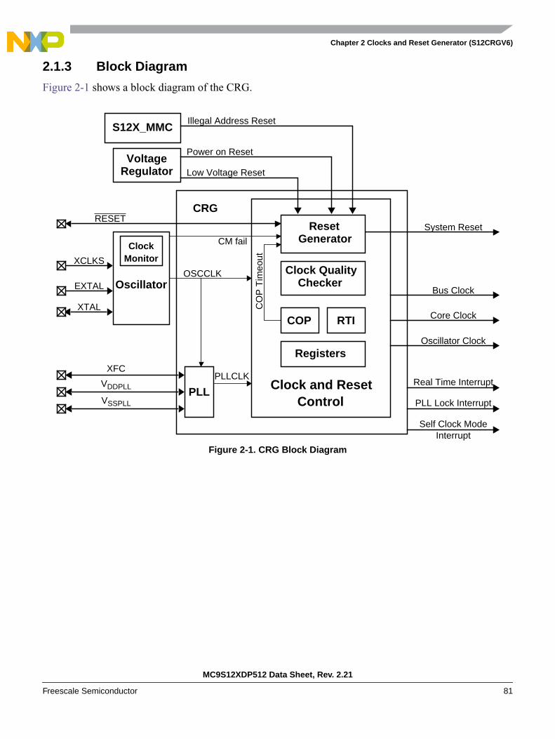
Chapter 2 Clocks and Reset Generator (S12CRGV6)
MC9S12XDP512 Data Sheet, Rev. 2.21
Freescale Semiconductor 81
2.1.3 Block Diagram
Figure 2-1 shows a block diagram of the CRG.
Figure 2-1. CRG Block Diagram
CRG
Registers
Clock and Reset
COP
RESET
RTI
PLL
XFC
VDDPLL
VSSPLL
OscillatorEXTAL
XTAL
Control
Bus Clock
System Reset
Oscillator Clock
PLLCLK
OSCCLK
Core Clock
CM fail
Clock QualityChecker
ResetGenerator
XCLKS
Power on Reset
Low Voltage Reset
CO
P T
imeo
ut
Real Time Interrupt
PLL Lock Interrupt
Self Clock ModeInterrupt
VoltageRegulator
S12X_MMCIllegal Address Reset
ClockMonitor
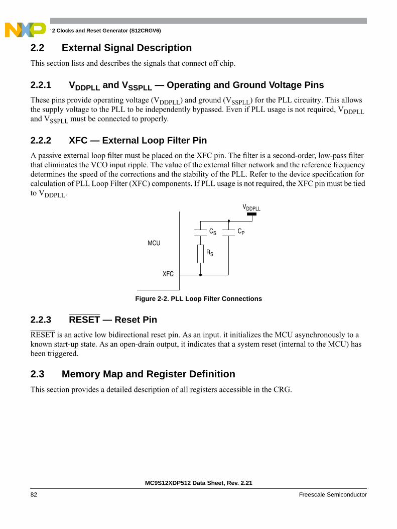
Chapter 2 Clocks and Reset Generator (S12CRGV6)
MC9S12XDP512 Data Sheet, Rev. 2.21
82 Freescale Semiconductor
2.2 External Signal DescriptionThis section lists and describes the signals that connect off chip.
2.2.1 VDDPLL and VSSPLL — Operating and Ground Voltage Pins
These pins provide operating voltage (VDDPLL) and ground (VSSPLL) for the PLL circuitry. This allowsthe supply voltage to the PLL to be independently bypassed. Even if PLL usage is not required, VDDPLLand VSSPLL must be connected to properly.
2.2.2 XFC — External Loop Filter Pin
A passive external loop filter must be placed on the XFC pin. The filter is a second-order, low-pass filterthat eliminates the VCO input ripple. The value of the external filter network and the reference frequencydetermines the speed of the corrections and the stability of the PLL. Refer to the device specification forcalculation of PLL Loop Filter (XFC) components. If PLL usage is not required, the XFC pin must be tiedto VDDPLL.
Figure 2-2. PLL Loop Filter Connections
2.2.3 RESET — Reset Pin
RESET is an active low bidirectional reset pin. As an input. it initializes the MCU asynchronously to aknown start-up state. As an open-drain output, it indicates that a system reset (internal to the MCU) hasbeen triggered.
2.3 Memory Map and Register DefinitionThis section provides a detailed description of all registers accessible in the CRG.
MCU
XFC
RS
CS
VDDPLL
CP

Chapter 2 Clocks and Reset Generator (S12CRGV6)
MC9S12XDP512 Data Sheet, Rev. 2.21
Freescale Semiconductor 83
2.3.1 Module Memory Map
Table 2-1 gives an overview on all CRG registers.
NOTERegister Address = Base Address + Address Offset, where the Base Addressis defined at the MCU level and the Address Offset is defined at the modulelevel.
Table 2-1. CRG Memory Map
AddressOffset
Use Access
0x_00 CRG Synthesizer Register (SYNR) R/W
0x_01 CRG Reference Divider Register (REFDV) R/W
0x_02 CRG Test Flags Register (CTFLG)1
1 CTFLG is intended for factory test purposes only.
R/W
0x_03 CRG Flags Register (CRGFLG) R/W
0x_04 CRG Interrupt Enable Register (CRGINT) R/W
0x_05 CRG Clock Select Register (CLKSEL) R/W
0x_06 CRG PLL Control Register (PLLCTL) R/W
0x_07 CRG RTI Control Register (RTICTL) R/W
0x_08 CRG COP Control Register (COPCTL) R/W
0x_09 CRG Force and Bypass Test Register (FORBYP)2
2 FORBYP is intended for factory test purposes only.
R/W
0x_0A CRG Test Control Register (CTCTL)3
3 CTCTL is intended for factory test purposes only.
R/W
0x_0B CRG COP Arm/Timer Reset (ARMCOP) R/W
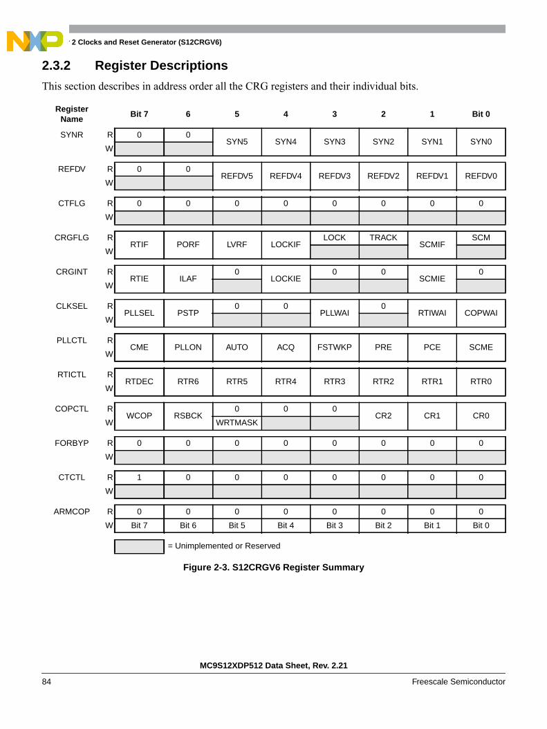
Chapter 2 Clocks and Reset Generator (S12CRGV6)
MC9S12XDP512 Data Sheet, Rev. 2.21
84 Freescale Semiconductor
2.3.2 Register Descriptions
This section describes in address order all the CRG registers and their individual bits.
RegisterName
Bit 7 6 5 4 3 2 1 Bit 0
SYNR R 0 0SYN5 SYN4 SYN3 SYN2 SYN1 SYN0
W
REFDV R 0 0REFDV5 REFDV4 REFDV3 REFDV2 REFDV1 REFDV0
W
CTFLG R 0 0 0 0 0 0 0 0
W
CRGFLG RRTIF PORF LVRF LOCKIF
LOCK TRACKSCMIF
SCM
W
CRGINT RRTIE ILAF
0LOCKIE
0 0SCMIE
0
W
CLKSEL RPLLSEL PSTP
0 0PLLWAI
0RTIWAI COPWAI
W
PLLCTL RCME PLLON AUTO ACQ FSTWKP PRE PCE SCME
W
RTICTL RRTDEC RTR6 RTR5 RTR4 RTR3 RTR2 RTR1 RTR0
W
COPCTL RWCOP RSBCK
0 0 0CR2 CR1 CR0
W WRTMASK
FORBYP R 0 0 0 0 0 0 0 0
W
CTCTL R 1 0 0 0 0 0 0 0
W
ARMCOP R 0 0 0 0 0 0 0 0
W Bit 7 Bit 6 Bit 5 Bit 4 Bit 3 Bit 2 Bit 1 Bit 0
= Unimplemented or Reserved
Figure 2-3. S12CRGV6 Register Summary

Chapter 2 Clocks and Reset Generator (S12CRGV6)
MC9S12XDP512 Data Sheet, Rev. 2.21
Freescale Semiconductor 85
2.3.2.1 CRG Synthesizer Register (SYNR)
The SYNR register controls the multiplication factor of the PLL. If the PLL is on, the count in the loopdivider (SYNR) register effectively multiplies up the PLL clock (PLLCLK) from the reference frequencyby 2 x (SYNR + 1). PLLCLK will not be below the minimum VCO frequency (fSCM).
NOTEIf PLL is selected (PLLSEL=1), Bus Clock = PLLCLK / 2Bus Clock must not exceed the maximum operating system frequency.
Read: Anytime
Write: Anytime except if PLLSEL = 1
NOTEWrite to this register initializes the lock detector bit and the track detectorbit.
2.3.2.2 CRG Reference Divider Register (REFDV)
The REFDV register provides a finer granularity for the PLL multiplier steps. The count in the referencedivider divides OSCCLK frequency by REFDV + 1.
Read: Anytime
Write: Anytime except when PLLSEL = 1
NOTEWrite to this register initializes the lock detector bit and the track detectorbit.
7 6 5 4 3 2 1 0
R 0 0SYN5 SYN4 SYN3 SYN2 SYN1 SYN0
W
Reset 0 0 0 0 0 0 0 0
= Unimplemented or Reserved
Figure 2-4. CRG Synthesizer Register (SYNR)
7 6 5 4 3 2 1 0
R 0 0REFDV5 REFDV4 REFDV3 REFDV2 REFDV1 REFDV0
W
Reset 0 0 0 0 0 0 0 0
= Unimplemented or Reserved
Figure 2-5. CRG Reference Divider Register (REFDV)
PLLCLK 2xOSCCLKxSYNR 1+( )
REFDV 1+( )------------------------------------=
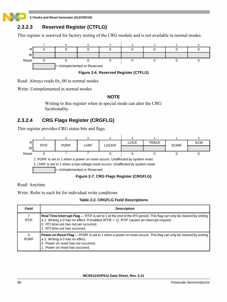
Chapter 2 Clocks and Reset Generator (S12CRGV6)
MC9S12XDP512 Data Sheet, Rev. 2.21
86 Freescale Semiconductor
2.3.2.3 Reserved Register (CTFLG)
This register is reserved for factory testing of the CRG module and is not available in normal modes.
Read: Always reads 0x_00 in normal modes
Write: Unimplemented in normal modes
NOTEWriting to this register when in special mode can alter the CRGfucntionality.
2.3.2.4 CRG Flags Register (CRGFLG)
This register provides CRG status bits and flags.
Read: Anytime
Write: Refer to each bit for individual write conditions
7 6 5 4 3 2 1 0
R 0 0 0 0 0 0 0 0
W
Reset 0 0 0 0 0 0 0 0
= Unimplemented or Reserved
Figure 2-6. Reserved Register (CTFLG)
7 6 5 4 3 2 1 0
RRTIF PORF LVRF LOCKIF
LOCK TRACKSCMIF
SCM
W
Reset 0 1 2 0 0 0 0 0
1. PORF is set to 1 when a power on reset occurs. Unaffected by system reset.2. LVRF is set to 1 when a low-voltage reset occurs. Unaffected by system reset.
= Unimplemented or Reserved
Figure 2-7. CRG Flags Register (CRGFLG)
Table 2-2. CRGFLG Field Descriptions
Field Description
7RTIF
Real Time Interrupt Flag — RTIF is set to 1 at the end of the RTI period. This flag can only be cleared by writinga 1. Writing a 0 has no effect. If enabled (RTIE = 1), RTIF causes an interrupt request.0 RTI time-out has not yet occurred.1 RTI time-out has occurred.
6PORF
Power on Reset Flag — PORF is set to 1 when a power on reset occurs. This flag can only be cleared by writinga 1. Writing a 0 has no effect.0 Power on reset has not occurred.1 Power on reset has occurred.

Chapter 2 Clocks and Reset Generator (S12CRGV6)
MC9S12XDP512 Data Sheet, Rev. 2.21
Freescale Semiconductor 87
5LVRF
Low Voltage Reset Flag — If low voltage reset feature is not available (see device specification) LVRF alwaysreads 0. LVRF is set to 1 when a low voltage reset occurs. This flag can only be cleared by writing a 1. Writinga 0 has no effect.0 Low voltage reset has not occurred.1 Low voltage reset has occurred.
4LOCKIF
PLL Lock Interrupt Flag — LOCKIF is set to 1 when LOCK status bit changes. This flag can only be clearedby writing a 1. Writing a 0 has no effect.If enabled (LOCKIE = 1), LOCKIF causes an interrupt request.0 No change in LOCK bit.1 LOCK bit has changed.
3LOCK
Lock Status Bit — LOCK reflects the current state of PLL lock condition. This bit is cleared in self clock mode.Writes have no effect.0 PLL VCO is not within the desired tolerance of the target frequency.1 PLL VCO is within the desired tolerance of the target frequency.
2TRACK
Track Status Bit — TRACK reflects the current state of PLL track condition. This bit is cleared in self clock mode.Writes have no effect.0 Acquisition mode status.1Tracking mode status.
1SCMIF
Self Clock Mode Interrupt Flag — SCMIF is set to 1 when SCM status bit changes. This flag can only becleared by writing a 1. Writing a 0 has no effect. If enabled (SCMIE = 1), SCMIF causes an interrupt request.0 No change in SCM bit.1 SCM bit has changed.
0SCM
Self Clock Mode Status Bit — SCM reflects the current clocking mode. Writes have no effect.0 MCU is operating normally with OSCCLK available.1 MCU is operating in self clock mode with OSCCLK in an unknown state. All clocks are derived from PLLCLK
running at its minimum frequency fSCM.
Table 2-2. CRGFLG Field Descriptions (continued)
Field Description

Chapter 2 Clocks and Reset Generator (S12CRGV6)
MC9S12XDP512 Data Sheet, Rev. 2.21
88 Freescale Semiconductor
2.3.2.5 CRG Interrupt Enable Register (CRGINT)
This register enables CRG interrupt requests.
Read: Anytime
Write: Anytime
7 6 5 4 3 2 1 0
RRTIE ILAF
0LOCKIE
0 0SCMIE
0
W
Reset 0 1 0 0 0 0 0 0
1. ILAF is set to 1 when an illegal address reset occurs. Unaffected by system reset. Cleared by power on or lowvoltage reset.
= Unimplemented or Reserved
Figure 2-8. CRG Interrupt Enable Register (CRGINT)
Table 2-3. CRGINT Field Descriptions
Field Description
7RTIE
Real Time Interrupt Enable Bit0 Interrupt requests from RTI are disabled.1 Interrupt will be requested whenever RTIF is set.
6ILAF
Illegal Address Reset Flag — ILAF is set to 1 when an illegal address reset occurs. Refer to S12XMMC BlockGuide for details. This flag can only be cleared by writing a 1. Writing a 0 has no effect.0 Illegal address reset has not occurred.1 Illegal address reset has occurred.
4LOCKIE
Lock Interrupt Enable Bit0 LOCK interrupt requests are disabled.1 Interrupt will be requested whenever LOCKIF is set.
1SCMIE
Self ClockMmode Interrupt Enable Bit0 SCM interrupt requests are disabled.1 Interrupt will be requested whenever SCMIF is set.

Chapter 2 Clocks and Reset Generator (S12CRGV6)
MC9S12XDP512 Data Sheet, Rev. 2.21
Freescale Semiconductor 89
2.3.2.6 CRG Clock Select Register (CLKSEL)
This register controls CRG clock selection. Refer to Figure 2-17 for more details on the effect of each bit.
Read: Anytime
Write: Refer to each bit for individual write conditions
7 6 5 4 3 2 1 0
RPLLSEL PSTP
0 0PLLWAI
0RTIWAI COPWAI
W
Reset 0 0 0 0 0 0 0 0
= Unimplemented or Reserved
Figure 2-9. CRG Clock Select Register (CLKSEL)
Table 2-4. CLKSEL Field Descriptions
Field Description
7PLLSEL
PLL Select Bit — Write anytime. Writing a1 when LOCK = 0 and AUTO = 1, or TRACK = 0 and AUTO = 0 hasno effect This prevents the selection of an unstable PLLCLK as SYSCLK. PLLSEL bit is cleared when the MCUenters self clock mode, Stop mode or wait mode with PLLWAI bit set.0 System clocks are derived from OSCCLK (Bus Clock = OSCCLK / 2).1 System clocks are derived from PLLCLK (Bus Clock = PLLCLK / 2).
6PSTP
Pseudo Stop BitWrite: AnytimeThis bit controls the functionality of the oscillator during stop mode.0 Oscillator is disabled in stop mode.1 Oscillator continues to run in stop mode (pseudo stop).Note: Pseudo stop mode allows for faster STOP recovery and reduces the mechanical stress and aging of the
resonator in case of frequent STOP conditions at the expense of a slightly increased power consumption.
3PLLWAI
PLL Stops in Wait Mode BitWrite: AnytimeIf PLLWAI is set, the CRG will clear the PLLSEL bit before entering wait mode. The PLLON bit remains set duringwait mode, but the PLL is powered down. Upon exiting wait mode, the PLLSEL bit has to be set manually if PLLclock is required.While the PLLWAI bit is set, the AUTO bit is set to 1 in order to allow the PLL to automatically lock on the selectedtarget frequency after exiting wait mode.0 PLL keeps running in wait mode.1 PLL stops in wait mode.
1RTIWAI
RTI Stops in Wait Mode BitWrite: Anytime0 RTI keeps running in wait mode.1 RTI stops and initializes the RTI dividers whenever the part goes into wait mode.
0COPWAI
COP Stops in Wait Mode BitNormal modes: Write onceSpecial modes: Write anytime0 COP keeps running in wait mode.1 COP stops and initializes the COP counter whenever the part goes into wait mode.
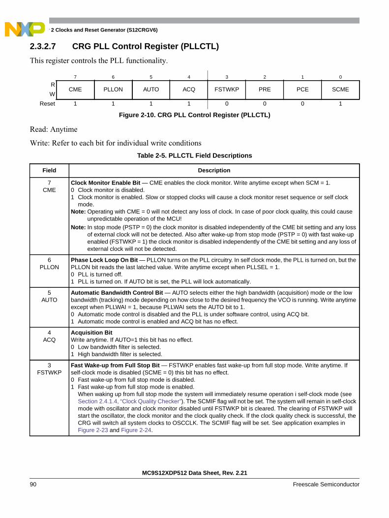
Chapter 2 Clocks and Reset Generator (S12CRGV6)
MC9S12XDP512 Data Sheet, Rev. 2.21
90 Freescale Semiconductor
2.3.2.7 CRG PLL Control Register (PLLCTL)
This register controls the PLL functionality.
Read: Anytime
Write: Refer to each bit for individual write conditions
7 6 5 4 3 2 1 0
RCME PLLON AUTO ACQ FSTWKP PRE PCE SCME
W
Reset 1 1 1 1 0 0 0 1
Figure 2-10. CRG PLL Control Register (PLLCTL)
Table 2-5. PLLCTL Field Descriptions
Field Description
7CME
Clock Monitor Enable Bit — CME enables the clock monitor. Write anytime except when SCM = 1.0 Clock monitor is disabled.1 Clock monitor is enabled. Slow or stopped clocks will cause a clock monitor reset sequence or self clock
mode.Note: Operating with CME = 0 will not detect any loss of clock. In case of poor clock quality, this could cause
unpredictable operation of the MCU!Note: In stop mode (PSTP = 0) the clock monitor is disabled independently of the CME bit setting and any loss
of external clock will not be detected. Also after wake-up from stop mode (PSTP = 0) with fast wake-upenabled (FSTWKP = 1) the clock monitor is disabled independently of the CME bit setting and any loss ofexternal clock will not be detected.
6PLLON
Phase Lock Loop On Bit — PLLON turns on the PLL circuitry. In self clock mode, the PLL is turned on, but thePLLON bit reads the last latched value. Write anytime except when PLLSEL = 1.0 PLL is turned off.1 PLL is turned on. If AUTO bit is set, the PLL will lock automatically.
5AUTO
Automatic Bandwidth Control Bit — AUTO selects either the high bandwidth (acquisition) mode or the lowbandwidth (tracking) mode depending on how close to the desired frequency the VCO is running. Write anytimeexcept when PLLWAI = 1, because PLLWAI sets the AUTO bit to 1.0 Automatic mode control is disabled and the PLL is under software control, using ACQ bit.1 Automatic mode control is enabled and ACQ bit has no effect.
4ACQ
Acquisition BitWrite anytime. If AUTO=1 this bit has no effect.0 Low bandwidth filter is selected.1 High bandwidth filter is selected.
3FSTWKP
Fast Wake-up from Full Stop Bit — FSTWKP enables fast wake-up from full stop mode. Write anytime. Ifself-clock mode is disabled (SCME = 0) this bit has no effect.0 Fast wake-up from full stop mode is disabled.1 Fast wake-up from full stop mode is enabled.
When waking up from full stop mode the system will immediately resume operation i self-clock mode (seeSection 2.4.1.4, “Clock Quality Checker”). The SCMIF flag will not be set. The system will remain in self-clockmode with oscillator and clock monitor disabled until FSTWKP bit is cleared. The clearing of FSTWKP willstart the oscillator, the clock monitor and the clock quality check. If the clock quality check is successful, theCRG will switch all system clocks to OSCCLK. The SCMIF flag will be set. See application examples inFigure 2-23 and Figure 2-24.

Chapter 2 Clocks and Reset Generator (S12CRGV6)
MC9S12XDP512 Data Sheet, Rev. 2.21
Freescale Semiconductor 91
2.3.2.8 CRG RTI Control Register (RTICTL)
This register selects the timeout period for the real time interrupt.
Read: Anytime
Write: Anytime
NOTEA write to this register initializes the RTI counter.
2PRE
RTI Enable during Pseudo Stop Bit — PRE enables the RTI during pseudo stop mode. Write anytime.0 RTI stops running during pseudo stop mode.1 RTI continues running during pseudo stop mode.Note: If the PRE bit is cleared the RTI dividers will go static while pseudo stop mode is active. The RTI dividers
will not initialize like in wait mode with RTIWAI bit set.
1PCE
COP Enable during Pseudo Stop Bit — PCE enables the COP during pseudo stop mode. Write anytime.0 COP stops running during pseudo stop mode1 COP continues running during pseudo stop modeNote: If the PCE bit is cleared, the COP dividers will go static while pseudo stop mode is active. The COP
dividers will not initialize like in wait mode with COPWAI bit set.
0SCME
Self Clock Mode Enable BitNormal modes: Write onceSpecial modes: Write anytimeSCME can not be cleared while operating in self clock mode (SCM = 1).0 Detection of crystal clock failure causes clock monitor reset (see Section 2.5.2, “Clock Monitor Reset”).1 Detection of crystal clock failure forces the MCU in self clock mode (see Section 2.4.2.2, “Self Clock Mode”).
7 6 5 4 3 2 1 0
RRTDEC RTR6 RTR5 RTR4 RTR3 RTR2 RTR1 RTR0
W
Reset 0 0 0 0 0 0 0 0
Figure 2-11. CRG RTI Control Register (RTICTL)
Table 2-6. RTICTL Field Descriptions
Field Description
7RTDEC
Decimal or Binary Divider Select Bit — RTDEC selects decimal or binary based prescaler values.0 Binary based divider value. See Table 2-71 Decimal based divider value. See Table 2-8
6–4RTR[6:4]
Real Time Interrupt Prescale Rate Select Bits — These bits select the prescale rate for the RTI. See Table 2-7and Table 2-8.
3–0RTR[3:0]
Real Time Interrupt Modulus Counter Select Bits — These bits select the modulus counter target value toprovide additional granularity.Table 2-7 and Table 2-8 show all possible divide values selectable by the RTICTLregister. The source clock for the RTI is OSCCLK.
Table 2-5. PLLCTL Field Descriptions (continued)
Field Description

Chapter 2 Clocks and Reset Generator (S12CRGV6)
MC9S12XDP512 Data Sheet, Rev. 2.21
92 Freescale Semiconductor
Table 2-7. RTI Frequency Divide Rates for RTDEC = 0
RTR[3:0]
RTR[6:4] =
000(OFF)
001(210)
010(211)
011(212)
100(213)
101(214)
110(215)
111(216)
0000 (÷1) OFF* 210 211 212 213 214 215 216
0001 (÷2) OFF 2x210 2x211 2x212 2x213 2x214 2x215 2x216
0010 (÷3) OFF 3x210 3x211 3x212 3x213 3x214 3x215 3x216
0011 (÷4) OFF 4x210 4x211 4x212 4x213 4x214 4x215 4x216
0100 (÷5) OFF 5x210 5x211 5x212 5x213 5x214 5x215 5x216
0101 (÷6) OFF 6x210 6x211 6x212 6x213 6x214 6x215 6x216
0110 (÷7) OFF 7x210 7x211 7x212 7x213 7x214 7x215 7x216
0111 (÷8) OFF 8x210 8x211 8x212 8x213 8x214 8x215 8x216
1000 (÷9) OFF 9x210 9x211 9x212 9x213 9x214 9x215 9x216
1001 (÷10) OFF 10x210 10x211 10x212 10x213 10x214 10x215 10x216
1010 (÷11) OFF 11x210 11x211 11x212 11x213 11x214 11x215 11x216
1011 (÷12) OFF 12x210 12x211 12x212 12x213 12x214 12x215 12x216
1100 (÷13) OFF 13x210 13x211 13x212 13x213 13x214 13x215 13x216
1101 (÷14) OFF 14x210 14x211 14x212 14x213 14x214 14x215 14x216
1110 (÷15) OFF 15x210 15x211 15x212 15x213 15x214 15x215 15x216
1111 (÷16) OFF 16x210 16x211 16x212 16x213 16x214 16x215 16x216
* Denotes the default value out of reset.This value should be used to disable the RTI to ensure future backwards compatibility.

Chapter 2 Clocks and Reset Generator (S12CRGV6)
MC9S12XDP512 Data Sheet, Rev. 2.21
Freescale Semiconductor 93
Table 2-8. RTI Frequency Divide Rates for RTDEC = 1
RTR[3:0]
RTR[6:4] =
000(1x10³)
001(2x10³)
010(5x10³)
011(10x103)
100(20x103)
101(50x103)
110(100x103)
111(200x103)
0000 (÷1) 1x10³ 2x10³ 5x10³ 10x103 20x103 50x103 100x103 200x103
0001 (÷2) 2x10³ 4x10³ 10x103 20x103 40x103 100x103 200x103 400x103
0010 (÷3) 3x10³ 6x10³ 15x103 30x103 60x103 150x103 300x103 600x103
0011 (÷4) 4x10³ 8x10³ 20x103 40x103 80x103 200x103 400x103 800x103
0100 (÷5) 5x10³ 10x103 25x103 50x103 100x103 250x103 500x103 1x10⁶
0101 (÷6) 6x10³ 12x103 30x103 60x103 120x103 300x103 600x103 1.2x10⁶
0110 (÷7) 7x10³ 14x103 35x103 70x103 140x103 350x103 700x103 1.4x10⁶
0111 (÷8) 8x10³ 16x103 40x103 80x103 160x103 400x103 800x103 1.6x10⁶
1000 (÷9) 9x10³ 18x103 45x103 90x103 180x103 450x103 900x103 1.8x10⁶
1001 (÷10) 10 x103 20x103 50x103 100x103 200x103 500x103 1x10⁶ 2x10⁶
1010 (÷11) 11 x103 22x103 55x103 110x103 220x103 550x103 1.1x10⁶ 2.2x10⁶
1011 (÷12) 12x103 24x103 60x103 120x103 240x103 600x103 1.2x10⁶ 2.4x10⁶
1100 (÷13) 13x103 26x103 65x103 130x103 260x103 650x103 1.3x10⁶ 2.6x10⁶
1101 (÷14) 14x103 28x103 70x103 140x103 280x103 700x103 1.4x10⁶ 2.8x10⁶
1110 (÷15) 15x103 30x103 75x103 150x103 300x103 750x103 1.5x10⁶ 3x10⁶
1111 (÷16) 16x103 32x103 80x103 160x103 320x103 800x103 1.6x10⁶ 3.2x10⁶
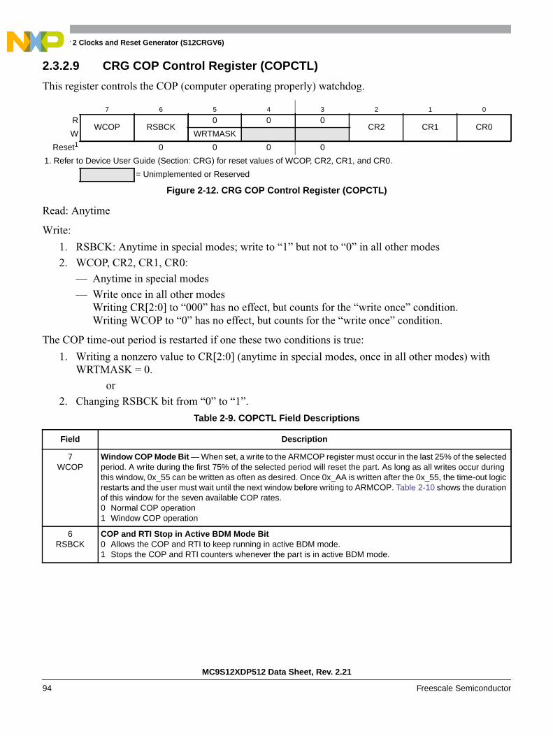
Chapter 2 Clocks and Reset Generator (S12CRGV6)
MC9S12XDP512 Data Sheet, Rev. 2.21
94 Freescale Semiconductor
2.3.2.9 CRG COP Control Register (COPCTL)
This register controls the COP (computer operating properly) watchdog.
Read: Anytime
Write:
1. RSBCK: Anytime in special modes; write to “1” but not to “0” in all other modes
2. WCOP, CR2, CR1, CR0:
— Anytime in special modes
— Write once in all other modesWriting CR[2:0] to “000” has no effect, but counts for the “write once” condition.Writing WCOP to “0” has no effect, but counts for the “write once” condition.
The COP time-out period is restarted if one these two conditions is true:
1. Writing a nonzero value to CR[2:0] (anytime in special modes, once in all other modes) withWRTMASK = 0.
or
2. Changing RSBCK bit from “0” to “1”.
7 6 5 4 3 2 1 0
RWCOP RSBCK
0 0 0CR2 CR1 CR0
W WRTMASK
Reset1 0 0 0 0
1. Refer to Device User Guide (Section: CRG) for reset values of WCOP, CR2, CR1, and CR0.
= Unimplemented or Reserved
Figure 2-12. CRG COP Control Register (COPCTL)
Table 2-9. COPCTL Field Descriptions
Field Description
7WCOP
Window COP Mode Bit — When set, a write to the ARMCOP register must occur in the last 25% of the selectedperiod. A write during the first 75% of the selected period will reset the part. As long as all writes occur duringthis window, 0x_55 can be written as often as desired. Once 0x_AA is written after the 0x_55, the time-out logicrestarts and the user must wait until the next window before writing to ARMCOP. Table 2-10 shows the durationof this window for the seven available COP rates.0 Normal COP operation1 Window COP operation
6RSBCK
COP and RTI Stop in Active BDM Mode Bit0 Allows the COP and RTI to keep running in active BDM mode.1 Stops the COP and RTI counters whenever the part is in active BDM mode.
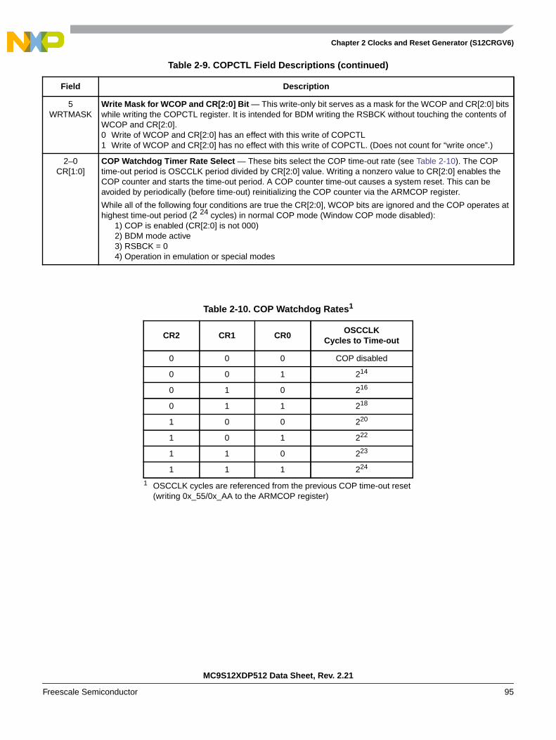
Chapter 2 Clocks and Reset Generator (S12CRGV6)
MC9S12XDP512 Data Sheet, Rev. 2.21
Freescale Semiconductor 95
5WRTMASK
Write Mask for WCOP and CR[2:0] Bit — This write-only bit serves as a mask for the WCOP and CR[2:0] bitswhile writing the COPCTL register. It is intended for BDM writing the RSBCK without touching the contents ofWCOP and CR[2:0].0 Write of WCOP and CR[2:0] has an effect with this write of COPCTL1 Write of WCOP and CR[2:0] has no effect with this write of COPCTL. (Does not count for “write once”.)
2–0CR[1:0]
COP Watchdog Timer Rate Select — These bits select the COP time-out rate (see Table 2-10). The COPtime-out period is OSCCLK period divided by CR[2:0] value. Writing a nonzero value to CR[2:0] enables theCOP counter and starts the time-out period. A COP counter time-out causes a system reset. This can beavoided by periodically (before time-out) reinitializing the COP counter via the ARMCOP register.
While all of the following four conditions are true the CR[2:0], WCOP bits are ignored and the COP operates athighest time-out period (2 24 cycles) in normal COP mode (Window COP mode disabled):
1) COP is enabled (CR[2:0] is not 000)2) BDM mode active3) RSBCK = 04) Operation in emulation or special modes
Table 2-10. COP Watchdog Rates1
1 OSCCLK cycles are referenced from the previous COP time-out reset(writing 0x_55/0x_AA to the ARMCOP register)
CR2 CR1 CR0OSCCLK
Cycles to Time-out
0 0 0 COP disabled
0 0 1 214
0 1 0 216
0 1 1 218
1 0 0 220
1 0 1 222
1 1 0 223
1 1 1 224
Table 2-9. COPCTL Field Descriptions (continued)
Field Description
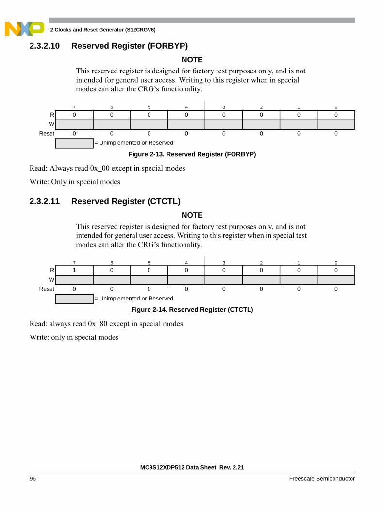
Chapter 2 Clocks and Reset Generator (S12CRGV6)
MC9S12XDP512 Data Sheet, Rev. 2.21
96 Freescale Semiconductor
2.3.2.10 Reserved Register (FORBYP)
NOTEThis reserved register is designed for factory test purposes only, and is notintended for general user access. Writing to this register when in specialmodes can alter the CRG’s functionality.
Read: Always read 0x_00 except in special modes
Write: Only in special modes
2.3.2.11 Reserved Register (CTCTL)
NOTEThis reserved register is designed for factory test purposes only, and is notintended for general user access. Writing to this register when in special testmodes can alter the CRG’s functionality.
Read: always read 0x_80 except in special modes
Write: only in special modes
7 6 5 4 3 2 1 0
R 0 0 0 0 0 0 0 0
W
Reset 0 0 0 0 0 0 0 0
= Unimplemented or Reserved
Figure 2-13. Reserved Register (FORBYP)
7 6 5 4 3 2 1 0
R 1 0 0 0 0 0 0 0
W
Reset 0 0 0 0 0 0 0 0
= Unimplemented or Reserved
Figure 2-14. Reserved Register (CTCTL)

Chapter 2 Clocks and Reset Generator (S12CRGV6)
MC9S12XDP512 Data Sheet, Rev. 2.21
Freescale Semiconductor 97
2.3.2.12 CRG COP Timer Arm/Reset Register (ARMCOP)
This register is used to restart the COP time-out period.
Read: Always reads 0x_00
Write: Anytime
When the COP is disabled (CR[2:0] = “000”) writing to this register has no effect.
When the COP is enabled by setting CR[2:0] nonzero, the following applies:
Writing any value other than 0x_55 or 0x_AA causes a COP reset. To restart the COP time-outperiod you must write 0x_55 followed by a write of 0x_AA. Other instructions may be executedbetween these writes but the sequence (0x_55, 0x_AA) must be completed prior to COP end oftime-out period to avoid a COP reset. Sequences of 0x_55 writes or sequences of 0x_AA writesare allowed. When the WCOP bit is set, 0x_55 and 0x_AA writes must be done in the last 25% ofthe selected time-out period; writing any value in the first 75% of the selected period will cause aCOP reset.
7 6 5 4 3 2 1 0
R 0 0 0 0 0 0 0 0
W Bit 7 Bit 6 Bit 5 Bit 4 Bit 3 Bit 2 Bit 1 Bit 0
Reset 0 0 0 0 0 0 0 0
Figure 2-15. ARMCOP Register Diagram
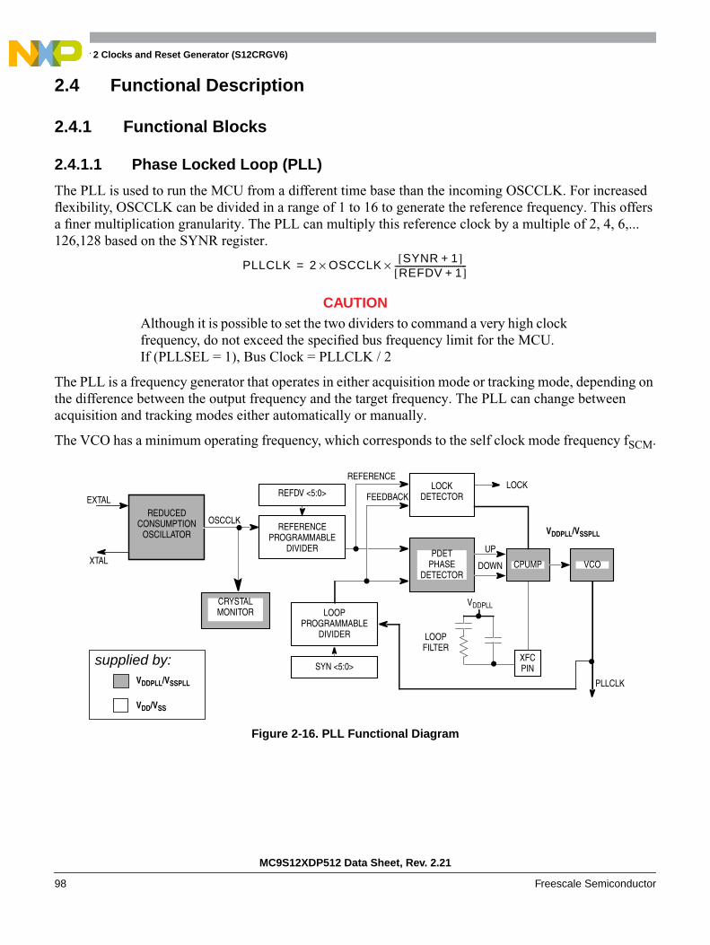
Chapter 2 Clocks and Reset Generator (S12CRGV6)
MC9S12XDP512 Data Sheet, Rev. 2.21
98 Freescale Semiconductor
2.4 Functional Description
2.4.1 Functional Blocks
2.4.1.1 Phase Locked Loop (PLL)
The PLL is used to run the MCU from a different time base than the incoming OSCCLK. For increasedflexibility, OSCCLK can be divided in a range of 1 to 16 to generate the reference frequency. This offersa finer multiplication granularity. The PLL can multiply this reference clock by a multiple of 2, 4, 6,...126,128 based on the SYNR register.
CAUTIONAlthough it is possible to set the two dividers to command a very high clockfrequency, do not exceed the specified bus frequency limit for the MCU.If (PLLSEL = 1), Bus Clock = PLLCLK / 2
The PLL is a frequency generator that operates in either acquisition mode or tracking mode, depending onthe difference between the output frequency and the target frequency. The PLL can change betweenacquisition and tracking modes either automatically or manually.
The VCO has a minimum operating frequency, which corresponds to the self clock mode frequency fSCM.
Figure 2-16. PLL Functional Diagram
PLLCLK 2 OSCCLKSYNR 1+[ ]
REFDV 1+[ ]------------------------------------××=
REDUCEDCONSUMPTION
OSCILLATOR
EXTAL
XTAL
OSCCLK
PLLCLK
REFERENCEPROGRAMMABLE
DIVIDER PDETPHASE
DETECTOR
REFDV <5:0>
LOOPPROGRAMMABLE
DIVIDER
SYN <5:0>
CPUMP VCO
LOCK
LOOPFILTER
XFCPIN
UP
DOWN
LOCKDETECTOR
REFERENCE
FEEDBACK
VDDPLL
VDDPLL/VSSPLL
CRYSTALMONITOR
VDDPLL/VSSPLL
VDD/VSS
supplied by:

Chapter 2 Clocks and Reset Generator (S12CRGV6)
MC9S12XDP512 Data Sheet, Rev. 2.21
Freescale Semiconductor 99
2.4.1.1.1 PLL Operation
The oscillator output clock signal (OSCCLK) is fed through the reference programmable divider and isdivided in a range of 1 to 64 (REFDV + 1) to output the REFERENCE clock. The VCO output clock,(PLLCLK) is fed back through the programmable loop divider and is divided in a range of 2 to 128 inincrements of [2 x (SYNR + 1)] to output the FEEDBACK clock. Figure 2-16.
The phase detector then compares the FEEDBACK clock, with the REFERENCE clock. Correction pulsesare generated based on the phase difference between the two signals. The loop filter then slightly alters theDC voltage on the external filter capacitor connected to XFC pin, based on the width and direction of thecorrection pulse. The filter can make fast or slow corrections depending on its mode, as described in thenext subsection. The values of the external filter network and the reference frequency determine the speedof the corrections and the stability of the PLL.
The minimum VCO frequency is reached with the XFC pin forced to VDDPLL. This is the self clock modefrequency.
2.4.1.1.2 Acquisition and Tracking Modes
The lock detector compares the frequencies of the FEEDBACK clock, and the REFERENCE clock.Therefore, the speed of the lock detector is directly proportional to the final reference frequency. Thecircuit determines the mode of the PLL and the lock condition based on this comparison.
The PLL filter can be manually or automatically configured into one of two possible operating modes:
• Acquisition mode
In acquisition mode, the filter can make large frequency corrections to the VCO. This mode is usedat PLL start-up or when the PLL has suffered a severe noise hit and the VCO frequency is far offthe desired frequency. When in acquisition mode, the TRACK status bit is cleared in the CRGFLGregister.
• Tracking mode
In tracking mode, the filter makes only small corrections to the frequency of the VCO. PLL jitteris much lower in tracking mode, but the response to noise is also slower. The PLL enters trackingmode when the VCO frequency is nearly correct and the TRACK bit is set in the CRGFLG register.
The PLL can change the bandwidth or operational mode of the loop filter manually or automatically.
In automatic bandwidth control mode (AUTO = 1), the lock detector automatically switches betweenacquisition and tracking modes. Automatic bandwidth control mode also is used to determine when thePLL clock (PLLCLK) is safe to use as the source for the system and core clocks. If PLL LOCK interruptrequests are enabled, the software can wait for an interrupt request and then check the LOCK bit. Ifinterrupt requests are disabled, software can poll the LOCK bit continuously (during PLL start-up, usually)or at periodic intervals. In either case, only when the LOCK bit is set, is the PLLCLK clock safe to use asthe source for the system and core clocks. If the PLL is selected as the source for the system and core clocksand the LOCK bit is clear, the PLL has suffered a severe noise hit and the software must take appropriateaction, depending on the application.
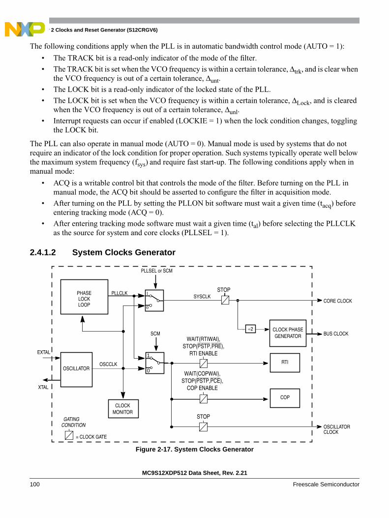
Chapter 2 Clocks and Reset Generator (S12CRGV6)
MC9S12XDP512 Data Sheet, Rev. 2.21
100 Freescale Semiconductor
The following conditions apply when the PLL is in automatic bandwidth control mode (AUTO = 1):
• The TRACK bit is a read-only indicator of the mode of the filter.
• The TRACK bit is set when the VCO frequency is within a certain tolerance, ∆trk, and is clear whenthe VCO frequency is out of a certain tolerance, ∆unt.
• The LOCK bit is a read-only indicator of the locked state of the PLL.
• The LOCK bit is set when the VCO frequency is within a certain tolerance, ∆Lock, and is clearedwhen the VCO frequency is out of a certain tolerance, ∆unl.
• Interrupt requests can occur if enabled (LOCKIE = 1) when the lock condition changes, togglingthe LOCK bit.
The PLL can also operate in manual mode (AUTO = 0). Manual mode is used by systems that do notrequire an indicator of the lock condition for proper operation. Such systems typically operate well belowthe maximum system frequency (fsys) and require fast start-up. The following conditions apply when inmanual mode:
• ACQ is a writable control bit that controls the mode of the filter. Before turning on the PLL inmanual mode, the ACQ bit should be asserted to configure the filter in acquisition mode.
• After turning on the PLL by setting the PLLON bit software must wait a given time (tacq) beforeentering tracking mode (ACQ = 0).
• After entering tracking mode software must wait a given time (tal) before selecting the PLLCLKas the source for system and core clocks (PLLSEL = 1).
2.4.1.2 System Clocks Generator
Figure 2-17. System Clocks Generator
OSCILLATOR
PHASELOCKLOOP
EXTAL
XTAL
SYSCLK
RTIOSCCLK
PLLCLK
CLOCK PHASEGENERATOR BUS CLOCK
CLOCKMONITOR
1
0
PLLSEL or SCM
÷2
CORE CLOCK
COP
OSCILLATOR
= CLOCK GATE
GATINGCONDITION
WAIT(RTIWAI),STOP(PSTP,PRE),
RTI ENABLE
WAIT(COPWAI),STOP(PSTP,PCE),
COP ENABLE
STOP
1
0
SCM
CLOCK
STOP
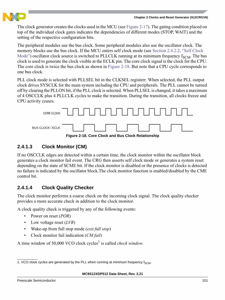
Chapter 2 Clocks and Reset Generator (S12CRGV6)
MC9S12XDP512 Data Sheet, Rev. 2.21
Freescale Semiconductor 101
The clock generator creates the clocks used in the MCU (see Figure 2-17). The gating condition placed ontop of the individual clock gates indicates the dependencies of different modes (STOP, WAIT) and thesetting of the respective configuration bits.
The peripheral modules use the bus clock. Some peripheral modules also use the oscillator clock. Thememory blocks use the bus clock. If the MCU enters self clock mode (see Section 2.4.2.2, “Self ClockMode”) oscillator clock source is switched to PLLCLK running at its minimum frequency fSCM. The busclock is used to generate the clock visible at the ECLK pin. The core clock signal is the clock for the CPU.The core clock is twice the bus clock as shown in Figure 2-18. But note that a CPU cycle corresponds toone bus clock.
PLL clock mode is selected with PLLSEL bit in the CLKSEL registerr. When selected, the PLL outputclock drives SYSCLK for the main system including the CPU and peripherals. The PLL cannot be turnedoff by clearing the PLLON bit, if the PLL clock is selected. When PLLSEL is changed, it takes a maximumof 4 OSCCLK plus 4 PLLCLK cycles to make the transition. During the transition, all clocks freeze andCPU activity ceases.
Figure 2-18. Core Clock and Bus Clock Relationship
2.4.1.3 Clock Monitor (CM)
If no OSCCLK edges are detected within a certain time, the clock monitor within the oscillator blockgenerates a clock monitor fail event. The CRG then asserts self clock mode or generates a system resetdepending on the state of SCME bit. If the clock monitor is disabled or the presence of clocks is detectedno failure is indicated by the oscillator block.The clock monitor function is enabled/disabled by the CMEcontrol bit.
2.4.1.4 Clock Quality Checker
The clock monitor performs a coarse check on the incoming clock signal. The clock quality checkerprovides a more accurate check in addition to the clock monitor.
A clock quality check is triggered by any of the following events:
• Power on reset (POR)
• Low voltage reset (LVR)
• Wake-up from full stop mode (exit full stop)
• Clock monitor fail indication (CM fail)
A time window of 50,000 VCO clock cycles1 is called check window.
1. VCO clock cycles are generated by the PLL when running at minimum frequency fSCM.
CORE CLOCK
BUS CLOCK / ECLK
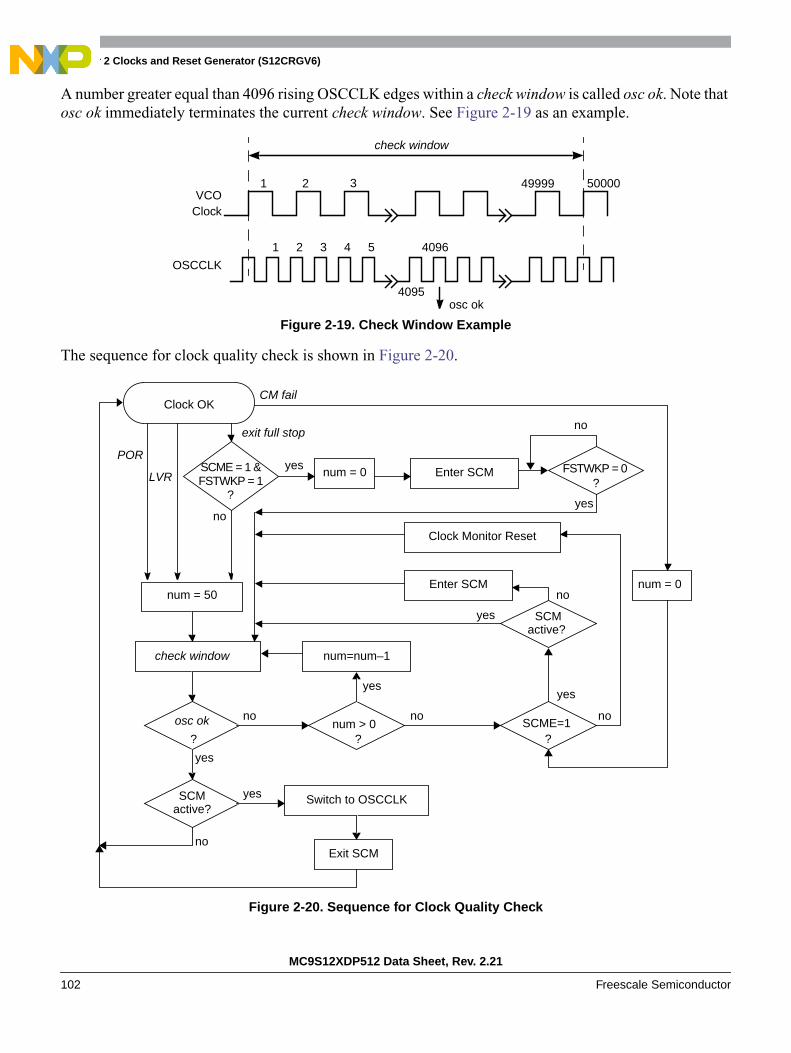
Chapter 2 Clocks and Reset Generator (S12CRGV6)
MC9S12XDP512 Data Sheet, Rev. 2.21
102 Freescale Semiconductor
A number greater equal than 4096 rising OSCCLK edges within a check window is called osc ok. Note thatosc ok immediately terminates the current check window. See Figure 2-19 as an example.
Figure 2-19. Check Window Example
The sequence for clock quality check is shown in Figure 2-20.
Figure 2-20. Sequence for Clock Quality Check
1 2 49999 50000VCO
Clock
check window
1 2 3 4 5
4095
4096
3
OSCCLK
osc ok
check window
osc ok
?
SCMactive?
Switch to OSCCLK
Exit SCM
Clock OK
num = 50
num > 0?
num=num–1
yes
no
yes
SCME=1?
no
Enter SCM
SCMactive?
yes
Clock Monitor Reset
no
yes
no
num = 0
yes
no
POR
exit full stop
CM fail
LVRyes
no
?FSTWKP = 0
no
num = 0 Enter SCM
yes
SCME = 1 &FSTWKP = 1
?
Chapter 2 Clocks and Reset Generator (S12CRGV6)
MC9S12XDP512 Data Sheet, Rev. 2.21
Freescale Semiconductor 103
NOTERemember that in parallel to additional actions caused by self clock modeor clock monitor reset1 handling the clock quality checker continues tocheck the OSCCLK signal.
The clock quality checker enables the PLL and the voltage regulator(VREG) anytime a clock check has to be performed. An ongoing clockquality check could also cause a running PLL (fSCM) and an active VREGduring pseudo stop mode or wait mode.
2.4.1.5 Computer Operating Properly Watchdog (COP)
The COP (free running watchdog timer) enables the user to check that a program is running andsequencing properly. When the COP is being used, software is responsible for keeping the COP fromtiming out. If the COP times out it is an indication that the software is no longer being executed in theintended sequence; thus a system reset is initiated (see Section 2.4.1.5, “Computer Operating ProperlyWatchdog (COP)”). The COP runs with a gated OSCCLK. Three control bits in the COPCTL registerallow selection of seven COP time-out periods.
When COP is enabled, the program must write 0x_55 and 0x_AA (in this order) to the ARMCOP registerduring the selected time-out period. Once this is done, the COP time-out period is restarted. If the programfails to do this and the COP times out, the part will reset. Also, if any value other than 0x_55 or 0x_AA iswritten, the part is immediately reset.
Windowed COP operation is enabled by setting WCOP in the COPCTL register. In this mode, writes tothe ARMCOP register to clear the COP timer must occur in the last 25% of the selected time-out period.A premature write will immediately reset the part.
If PCE bit is set, the COP will continue to run in pseudo stop mode.
2.4.1.6 Real Time Interrupt (RTI)
The RTI can be used to generate a hardware interrupt at a fixed periodic rate. If enabled (by settingRTIE = 1), this interrupt will occur at the rate selected by the RTICTL register. The RTI runs with a gatedOSCCLK. At the end of the RTI time-out period the RTIF flag is set to 1 and a new RTI time-out periodstarts immediately.
A write to the RTICTL register restarts the RTI time-out period.
If the PRE bit is set, the RTI will continue to run in pseudo stop mode.
2.4.2 Operating Modes
2.4.2.1 Normal Mode
The CRG block behaves as described within this specification in all normal modes.
1. A Clock Monitor Reset will always set the SCME bit to logical 1.

Chapter 2 Clocks and Reset Generator (S12CRGV6)
MC9S12XDP512 Data Sheet, Rev. 2.21
104 Freescale Semiconductor
2.4.2.2 Self Clock Mode
The VCO has a minimum operating frequency, fSCM. If the external clock frequency is not available dueto a failure or due to long crystal start-up time, the bus clock and the core clock are derived from the VCOrunning at minimum operating frequency; this mode of operation is called self clock mode. This requiresCME = 1 and SCME = 1. If the MCU was clocked by the PLL clock prior to entering self clock mode, thePLLSEL bit will be cleared. If the external clock signal has stabilized again, the CRG will automaticallyselect OSCCLK to be the system clock and return to normal mode. Section 2.4.1.4, “Clock QualityChecker” for more information on entering and leaving self clock mode.
NOTEIn order to detect a potential clock loss the CME bit should be alwaysenabled (CME = 1)!
If CME bit is disabled and the MCU is configured to run on PLL clock(PLLCLK), a loss of external clock (OSCCLK) will not be detected and willcause the system clock to drift towards the VCO’s minimum frequencyfSCM. As soon as the external clock is available again the system clockramps up to its PLL target frequency. If the MCU is running on externalclock any loss of clock will cause the system to go static.
2.4.3 Low Power Options
This section summarizes the low power options available in the CRG.
2.4.3.1 Run Mode
The RTI can be stopped by setting the associated rate select bits to 0.
The COP can be stopped by setting the associated rate select bits to 0.
2.4.3.2 Wait Mode
The WAI instruction puts the MCU in a low power consumption stand-by mode depending on setting ofthe individual bits in the CLKSEL register. All individual wait mode configuration bits can be superposed.This provides enhanced granularity in reducing the level of power consumption during wait mode.Table 2-11 lists the individual configuration bits and the parts of the MCU that are affected in wait mode
.
After executing the WAI instruction the core requests the CRG to switch MCU into wait mode. The CRGthen checks whether the PLLWAI bit is asserted (Figure 2-21). Depending on the configuration, the CRGswitches the system and core clocks to OSCCLK by clearing the PLLSEL bit and disables the PLL. Assoon as all clocks are switched off wait mode is active.
Table 2-11. MCU Configuration During Wait Mode
PLLWAI RTIWAI COPWAI
PLL Stopped — —
RTI — Stopped —
COP — — Stopped
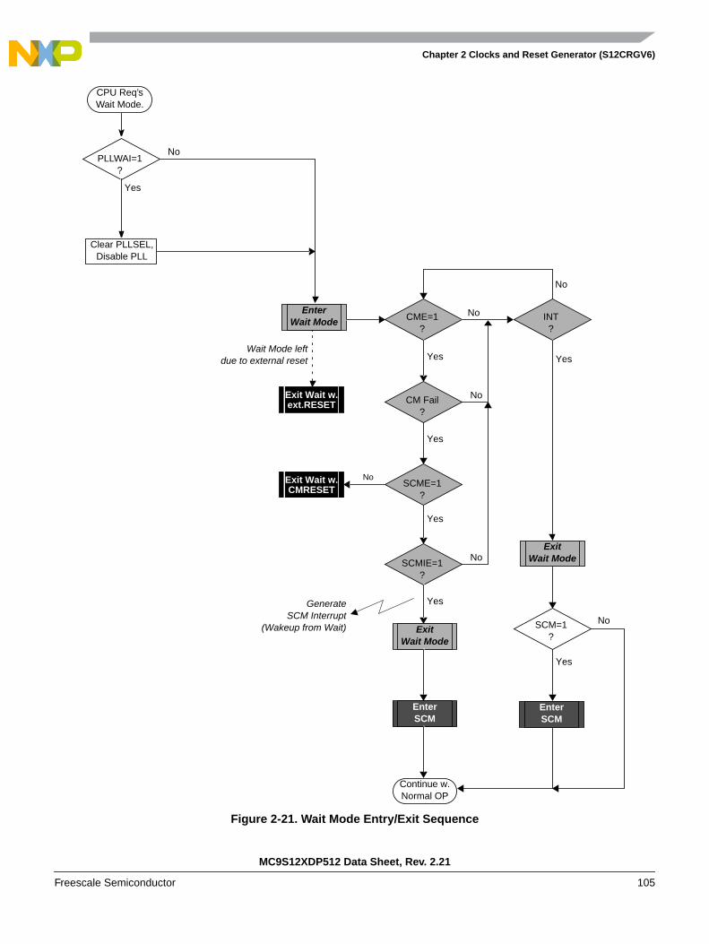
Chapter 2 Clocks and Reset Generator (S12CRGV6)
MC9S12XDP512 Data Sheet, Rev. 2.21
Freescale Semiconductor 105
Figure 2-21. Wait Mode Entry/Exit Sequence
EnterWait Mode
PLLWAI=1?
Exit Wait w.CMRESET
Exit Wait w.ext.RESET
ExitWait Mode
EnterSCM
ExitWait Mode
CPU Req’sWait Mode.
Clear PLLSEL,Disable PLL
CME=1?
INT?
CM Fail?
SCME=1?
SCMIE=1?
Continue w.Normal OP
No
No
No
No
No
Yes
Yes
Yes
Yes
Yes
No
Yes
Wait Mode leftdue to external reset
GenerateSCM Interrupt
(Wakeup from Wait) SCM=1?
EnterSCM
No
Yes
Chapter 2 Clocks and Reset Generator (S12CRGV6)
MC9S12XDP512 Data Sheet, Rev. 2.21
106 Freescale Semiconductor
There are four different scenarios for the CRG to restart the MCU from wait mode:
• External reset• Clock monitor reset• COP reset• Any interrupt
If the MCU gets an external reset or COP reset during wait mode active, the CRG asynchronously restoresall configuration bits in the register space to its default settings and starts the reset generator. Aftercompleting the reset sequence processing begins by fetching the normal or COP reset vector. Wait modeis left and the MCU is in run mode again.
If the clock monitor is enabled (CME = 1) the MCU is able to leave wait mode when loss ofoscillator/external clock is detected by a clock monitor fail. If the SCME bit is not asserted the CRGgenerates a clock monitor fail reset (CMRESET). The CRG’s behavior for CMRESET is the samecompared to external reset, but another reset vector is fetched after completion of the reset sequence. If theSCME bit is asserted the CRG generates a SCM interrupt if enabled (SCMIE = 1). After generating theinterrupt the CRG enters self-clock mode and starts the clock quality checker (Section 2.4.1.4, “ClockQuality Checker”). Then the MCU continues with normal operation.If the SCM interrupt is blocked bySCMIE = 0, the SCMIF flag will be asserted and clock quality checks will be performed but the MCU willnot wake-up from wait-mode.
If any other interrupt source (e.g., RTI) triggers exit from wait mode, the MCU immediately continues withnormal operation. If the PLL has been powered-down during wait mode, the PLLSEL bit is cleared andthe MCU runs on OSCCLK after leaving wait mode. The software must manually set the PLLSEL bitagain, in order to switch system and core clocks to the PLLCLK.
If wait mode is entered from self-clock mode the CRG will continue to check the clock quality until clockcheck is successful. The PLL and voltage regulator (VREG) will remain enabled.
Table 2-12 summarizes the outcome of a clock loss while in wait mode.
2.4.3.3 System Stop Mode
All clocks are stopped in STOP mode, dependent of the setting of the PCE, PRE, and PSTP bit. Theoscillator is disabled in STOP mode unless the PSTP bit is set. All counters and dividers remain frozen butdo not initialize. If the PRE or PCE bits are set, the RTI or COP continues to run in pseudo stop mode. Inaddition to disabling system and core clocks the CRG requests other functional units of the MCU (e.g.,voltage-regulator) to enter their individual power saving modes (if available). This is the main differencebetween pseudo stop mode and wait mode.
If the PLLSEL bit is still set when entering stop mode, the CRG will switch the system and core clocks toOSCCLK by clearing the PLLSEL bit. Then the CRG disables the PLL, disables the core clock and finallydisables the remaining system clocks. As soon as all clocks are switched off, stop mode is active.
If pseudo stop mode (PSTP = 1) is entered from self-clock mode, the CRG will continue to check the clockquality until clock check is successful. The PLL and the voltage regulator (VREG) will remain enabled. Iffull stop mode (PSTP = 0) is entered from self-clock mode, an ongoing clock quality check will bestopped. A complete timeout window check will be started when stop mode is left again.
Wake-up from stop mode also depends on the setting of the PSTP bit.
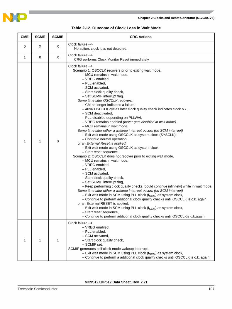
Chapter 2 Clocks and Reset Generator (S12CRGV6)
MC9S12XDP512 Data Sheet, Rev. 2.21
Freescale Semiconductor 107
Table 2-12. Outcome of Clock Loss in Wait Mode
CME SCME SCMIE CRG Actions
0 X XClock failure --> No action, clock loss not detected.
1 0 XClock failure --> CRG performs Clock Monitor Reset immediately
1 1 0
Clock failure -->Scenario 1: OSCCLK recovers prior to exiting wait mode.
– MCU remains in wait mode,– VREG enabled,– PLL enabled,– SCM activated,– Start clock quality check,– Set SCMIF interrupt flag.
Some time later OSCCLK recovers.– CM no longer indicates a failure,– 4096 OSCCLK cycles later clock quality check indicates clock o.k.,– SCM deactivated,– PLL disabled depending on PLLWAI,– VREG remains enabled (never gets disabled in wait mode).– MCU remains in wait mode.
Some time later either a wakeup interrupt occurs (no SCM interrupt)– Exit wait mode using OSCCLK as system clock (SYSCLK),– Continue normal operation.
or an External Reset is applied.– Exit wait mode using OSCCLK as system clock,– Start reset sequence.
Scenario 2: OSCCLK does not recover prior to exiting wait mode.– MCU remains in wait mode,– VREG enabled,– PLL enabled,– SCM activated,– Start clock quality check,– Set SCMIF interrupt flag,– Keep performing clock quality checks (could continue infinitely) while in wait mode.
Some time later either a wakeup interrupt occurs (no SCM interrupt)– Exit wait mode in SCM using PLL clock (fSCM) as system clock,– Continue to perform additional clock quality checks until OSCCLK is o.k. again.
or an External RESET is applied.– Exit wait mode in SCM using PLL clock (fSCM) as system clock,– Start reset sequence,– Continue to perform additional clock quality checks until OSCCLKis o.k.again.
1 1 1
Clock failure -->– VREG enabled,– PLL enabled,– SCM activated,– Start clock quality check,– SCMIF set.
SCMIF generates self clock mode wakeup interrupt.– Exit wait mode in SCM using PLL clock (fSCM) as system clock,– Continue to perform a additional clock quality checks until OSCCLK is o.k. again.
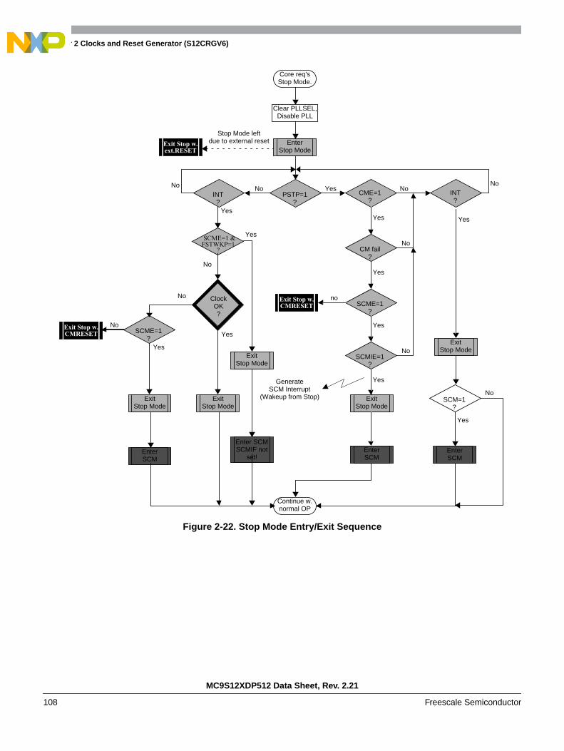
Chapter 2 Clocks and Reset Generator (S12CRGV6)
MC9S12XDP512 Data Sheet, Rev. 2.21
108 Freescale Semiconductor
Figure 2-22. Stop Mode Entry/Exit Sequence
Exit Stop w.CMRESET
ExitStop Mode
EnterSCM
ExitStop Mode
Core req’sStop Mode.
Clear PLLSEL,Disable PLL
CME=1?
INT?
CM fail?
SCME=1?
SCMIE=1?
Continue w.normal OP
No
No
no
No
Yes
Yes
Yes
Yes
Yes
GenerateSCM Interrupt
(Wakeup from Stop)
EnterStop Mode
Exit Stop w.ext.RESET
Stop Mode leftdue to external reset
ClockOK?
SCME=1?
EnterSCM
Yes
No
Yes
Exit Stop w.CMRESET
No
NoNoPSTP=1
?INT?
YesNo
Yes
ExitStop Mode
ExitStop Mode
SCM=1?
EnterSCM
No
Yes
Yes
No
SCME=1 &FSTWKP=1
?
ExitStop Mode
Enter SCMSCMIF not
set!

Chapter 2 Clocks and Reset Generator (S12CRGV6)
MC9S12XDP512 Data Sheet, Rev. 2.21
Freescale Semiconductor 109
2.4.3.3.1 Wake-up from Pseudo Stop Mode (PSTP=1)
Wake-up from pseudo stop mode is the same as wake-up from wait mode. There are also four differentscenarios for the CRG to restart the MCU from pseudo stop mode:
• External reset
• Clock monitor fail
• COP reset
• Wake-up interrupt
If the MCU gets an external reset or COP reset during pseudo stop mode active, the CRG asynchronouslyrestores all configuration bits in the register space to its default settings and starts the reset generator. Aftercompleting the reset sequence processing begins by fetching the normal or COP reset vector. pseudo stopmode is left and the MCU is in run mode again.
If the clock monitor is enabled (CME = 1), the MCU is able to leave pseudo stop mode when loss ofoscillator/external clock is detected by a clock monitor fail. If the SCME bit is not asserted the CRGgenerates a clock monitor fail reset (CMRESET). The CRG’s behavior for CMRESET is the samecompared to external reset, but another reset vector is fetched after completion of the reset sequence. If theSCME bit is asserted the CRG generates a SCM interrupt if enabled (SCMIE = 1). After generating theinterrupt the CRG enters self-clock mode and starts the clock quality checker (Section 2.4.1.4, “ClockQuality Checker”). Then the MCU continues with normal operation. If the SCM interrupt is blocked bySCMIE=0, the SCMIF flag will be asserted but the CRG will not wake-up from pseudo stop mode.
If any other interrupt source (e.g., RTI) triggers exit from pseudo stop mode, the MCU immediatelycontinues with normal operation. Because the PLL has been powered-down during stop mode, thePLLSEL bit is cleared and the MCU runs on OSCCLK after leaving stop mode. The software must set thePLLSEL bit again, in order to switch system and core clocks to the PLLCLK.
Table 2-13 summarizes the outcome of a clock loss while in pseudo stop mode.
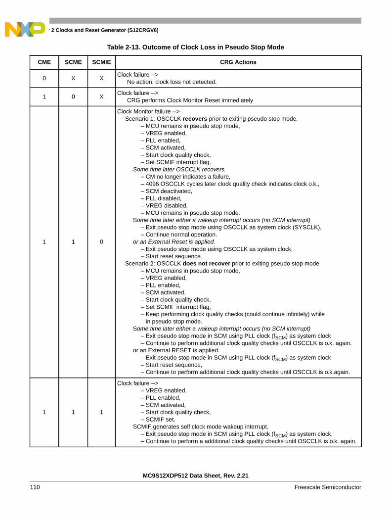
Chapter 2 Clocks and Reset Generator (S12CRGV6)
MC9S12XDP512 Data Sheet, Rev. 2.21
110 Freescale Semiconductor
Table 2-13. Outcome of Clock Loss in Pseudo Stop Mode
CME SCME SCMIE CRG Actions
0 X XClock failure --> No action, clock loss not detected.
1 0 XClock failure --> CRG performs Clock Monitor Reset immediately
1 1 0
Clock Monitor failure -->Scenario 1: OSCCLK recovers prior to exiting pseudo stop mode.
– MCU remains in pseudo stop mode,– VREG enabled,– PLL enabled,– SCM activated,– Start clock quality check,– Set SCMIF interrupt flag.
Some time later OSCCLK recovers.– CM no longer indicates a failure,– 4096 OSCCLK cycles later clock quality check indicates clock o.k.,– SCM deactivated,– PLL disabled,– VREG disabled.– MCU remains in pseudo stop mode.
Some time later either a wakeup interrupt occurs (no SCM interrupt)– Exit pseudo stop mode using OSCCLK as system clock (SYSCLK),– Continue normal operation.
or an External Reset is applied.– Exit pseudo stop mode using OSCCLK as system clock,– Start reset sequence.
Scenario 2: OSCCLK does not recover prior to exiting pseudo stop mode.– MCU remains in pseudo stop mode,– VREG enabled,– PLL enabled,– SCM activated,– Start clock quality check,– Set SCMIF interrupt flag,– Keep performing clock quality checks (could continue infinitely) while
in pseudo stop mode.Some time later either a wakeup interrupt occurs (no SCM interrupt)
– Exit pseudo stop mode in SCM using PLL clock (fSCM) as system clock– Continue to perform additional clock quality checks until OSCCLK is o.k. again.
or an External RESET is applied.– Exit pseudo stop mode in SCM using PLL clock (fSCM) as system clock– Start reset sequence,– Continue to perform additional clock quality checks until OSCCLK is o.k.again.
1 1 1
Clock failure -->– VREG enabled,– PLL enabled,– SCM activated,– Start clock quality check,– SCMIF set.
SCMIF generates self clock mode wakeup interrupt.– Exit pseudo stop mode in SCM using PLL clock (fSCM) as system clock,– Continue to perform a additional clock quality checks until OSCCLK is o.k. again.
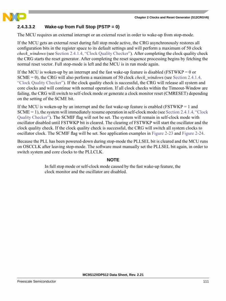
Chapter 2 Clocks and Reset Generator (S12CRGV6)
MC9S12XDP512 Data Sheet, Rev. 2.21
Freescale Semiconductor 111
2.4.3.3.2 Wake-up from Full Stop (PSTP = 0)
The MCU requires an external interrupt or an external reset in order to wake-up from stop-mode.
If the MCU gets an external reset during full stop mode active, the CRG asynchronously restores allconfiguration bits in the register space to its default settings and will perform a maximum of 50 clockcheck_windows (see Section 2.4.1.4, “Clock Quality Checker”). After completing the clock quality checkthe CRG starts the reset generator. After completing the reset sequence processing begins by fetching thenormal reset vector. Full stop-mode is left and the MCU is in run mode again.
If the MCU is woken-up by an interrupt and the fast wake-up feature is disabled (FSTWKP = 0 orSCME = 0), the CRG will also perform a maximum of 50 clock check_windows (see Section 2.4.1.4,“Clock Quality Checker”). If the clock quality check is successful, the CRG will release all system andcore clocks and will continue with normal operation. If all clock checks within the Timeout-Window arefailing, the CRG will switch to self-clock mode or generate a clock monitor reset (CMRESET) dependingon the setting of the SCME bit.
If the MCU is woken-up by an interrupt and the fast wake-up feature is enabled (FSTWKP = 1 andSCME = 1), the system will immediately resume operation in self-clock mode (see Section 2.4.1.4, “ClockQuality Checker”). The SCMIF flag will not be set. The system will remain in self-clock mode withoscillator disabled until FSTWKP bit is cleared. The clearing of FSTWKP will start the oscillator and theclock quality check. If the clock quality check is successful, the CRG will switch all system clocks tooscillator clock. The SCMIF flag will be set. See application examples in Figure 2-23 and Figure 2-24.
Because the PLL has been powered-down during stop-mode the PLLSEL bit is cleared and the MCU runson OSCCLK after leaving stop-mode. The software must manually set the PLLSEL bit again, in order toswitch system and core clocks to the PLLCLK.
NOTEIn full stop mode or self-clock mode caused by the fast wake-up feature, theclock monitor and the oscillator are disabled.

Chapter 2 Clocks and Reset Generator (S12CRGV6)
MC9S12XDP512 Data Sheet, Rev. 2.21
112 Freescale Semiconductor
Figure 2-23. Fast Wake-up from Full Stop Mode: Example 1
.
Figure 2-24. Fast Wake-up from Full Stop Mode: Example 2
Oscillator Clock
PLL Clock
Core Clock
Instruction
STOP IRQ ServiceFSTWKP=1
Interrupt
IRQ Service
Interrupt Interrupt
STOP STOP IRQ Service
Oscillator Disabled
Power Saving
Self-Clock Mode
SCME=1
CPU resumes program execution immediately
Oscillator Clock
PLL Clock
Core Clock
Instruction
Clock Quality Check
STOP IRQ ServiceFSTWKP=1
IRQ Interrupt
FSTWKP=0 SCMIE=1 Freq. UncriticalInstructions
Freq. CriticalInstr. Possible
OSC StartupOscillator Disabled
CPU resumes program execution immediately
SCM Interrupt
Self-Clock Mode
SCME=1
Chapter 2 Clocks and Reset Generator (S12CRGV6)
MC9S12XDP512 Data Sheet, Rev. 2.21
Freescale Semiconductor 113
2.5 ResetsThis section describes how to reset the CRG, and how the CRG itself controls the reset of the MCU. Itexplains all special reset requirements. Since the reset generator for the MCU is part of the CRG, thissection also describes all automatic actions that occur during or as a result of individual reset conditions.The reset values of registers and signals are provided in Section 2.3, “Memory Map and RegisterDefinition”. All reset sources are listed in Table 2-14. Refer to MCU specification for related vectoraddresses and priorities.
2.5.1 Description of Reset Operation
The reset sequence is initiated by any of the following events:
• Low level is detected at the RESET pin (external reset)
• Power on is detected
• Low voltage is detected
• Illegal Address Reset is detected (see S12XMMC Block Guide for details)
• COP watchdog times out
• Clock monitor failure is detected and self-clock mode was disabled (SCME=0)
Upon detection of any reset event, an internal circuit drives the RESET pin low for 128 SYSCLK cycles(see Figure 2-25). Since entry into reset is asynchronous, it does not require a running SYSCLK. However,the internal reset circuit of the CRG cannot sequence out of current reset condition without a runningSYSCLK. The number of 128 SYSCLK cycles might be increased by n = 3 to 6 additional SYSCLK cyclesdepending on the internal synchronization latency. After 128 + n SYSCLK cycles the RESET pin isreleased. The reset generator of the CRG waits for additional 64 SYSCLK cycles and then samples theRESET pin to determine the originating source. Table 2-15 shows which vector will be fetched.
Table 2-14. Reset Summary
Reset Source Local Enable
Power on Reset None
Low Voltage Reset None
External Reset None
Illegal Address Reset None
Clock Monitor Reset PLLCTL (CME = 1, SCME = 0)
COP Watchdog Reset COPCTL (CR[2:0] nonzero)
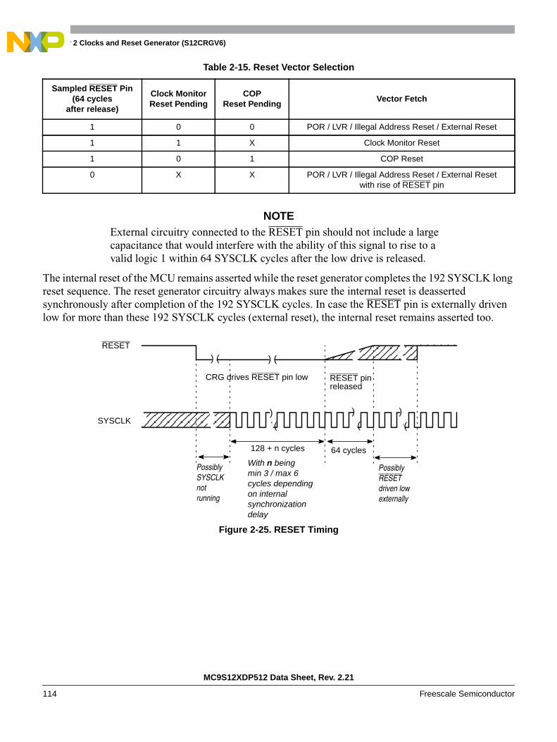
Chapter 2 Clocks and Reset Generator (S12CRGV6)
MC9S12XDP512 Data Sheet, Rev. 2.21
114 Freescale Semiconductor
NOTEExternal circuitry connected to the RESET pin should not include a largecapacitance that would interfere with the ability of this signal to rise to avalid logic 1 within 64 SYSCLK cycles after the low drive is released.
The internal reset of the MCU remains asserted while the reset generator completes the 192 SYSCLK longreset sequence. The reset generator circuitry always makes sure the internal reset is deassertedsynchronously after completion of the 192 SYSCLK cycles. In case the RESET pin is externally drivenlow for more than these 192 SYSCLK cycles (external reset), the internal reset remains asserted too.
Figure 2-25. RESET Timing
Table 2-15. Reset Vector Selection
Sampled RESET Pin(64 cycles
after release)
Clock MonitorReset Pending
COPReset Pending
Vector Fetch
1 0 0 POR / LVR / Illegal Address Reset / External Reset
1 1 X Clock Monitor Reset
1 0 1 COP Reset
0 X X POR / LVR / Illegal Address Reset / External Resetwith rise of RESET pin
) ( ) (
)
(
)SYSCLK
128 + n cycles 64 cycles
With n beingmin 3 / max 6cycles dependingon internalsynchronizationdelay
CRG drives RESET pin low
PossiblySYSCLKnotrunning
PossiblyRESETdriven lowexternally
)((
RESET
RESET pinreleased
Chapter 2 Clocks and Reset Generator (S12CRGV6)
MC9S12XDP512 Data Sheet, Rev. 2.21
Freescale Semiconductor 115
2.5.2 Clock Monitor Reset
The CRG generates a clock monitor reset in case all of the following conditions are true:
• Clock monitor is enabled (CME = 1)
• Loss of clock is detected
• Self-clock mode is disabled (SCME = 0).
The reset event asynchronously forces the configuration registers to their default settings (see Section 2.3,“Memory Map and Register Definition”). In detail the CME and the SCME are reset to logical ‘1’ (whichdoesn’t change the state of the CME bit, because it has already been set). As a consequence the CRGimmediately enters self clock mode and starts its internal reset sequence. In parallel the clock quality checkstarts. As soon as clock quality check indicates a valid oscillator clock the CRG switches to OSCCLK andleaves self clock mode. Since the clock quality checker is running in parallel to the reset generator, theCRG may leave self clock mode while still completing the internal reset sequence. When the resetsequence is finished, the CRG checks the internally latched state of the clock monitor fail circuit. If a clockmonitor fail is indicated, processing begins by fetching the clock monitor reset vector.
2.5.3 Computer Operating Properly Watchdog (COP) Reset
When COP is enabled, the CRG expects sequential write of 0x_55 and 0x_AA (in this order) to theARMCOP register during the selected time-out period. Once this is done, the COP time-out period restarts.If the program fails to do this the CRG will generate a reset. Also, if any value other than 0x_55 or 0x_AAis written, the CRG immediately generates a reset. In case windowed COP operation is enabled writes(0x_55 or 0x_AA) to the ARMCOP register must occur in the last 25% of the selected time-out period. Apremature write the CRG will immediately generate a reset.
As soon as the reset sequence is completed the reset generator checks the reset condition. If no clockmonitor failure is indicated and the latched state of the COP timeout is true, processing begins by fetchingthe COP vector.
2.5.4 Power On Reset, Low Voltage Reset
The on-chip voltage regulator detects when VDD to the MCU has reached a certain level and asserts poweron reset or low voltage reset or both. As soon as a power on reset or low voltage reset is triggered the CRGperforms a quality check on the incoming clock signal. As soon as clock quality check indicates a validoscillator clock signal, the reset sequence starts using the oscillator clock. If after 50 check windows theclock quality check indicated a non-valid oscillator clock, the reset sequence starts using self-clock mode.
Figure 2-26 and Figure 2-27 show the power-up sequence for cases when the RESET pin is tied to VDDand when the RESET pin is held low.

Chapter 2 Clocks and Reset Generator (S12CRGV6)
MC9S12XDP512 Data Sheet, Rev. 2.21
116 Freescale Semiconductor
Figure 2-26. RESET Pin Tied to VDD (by a pull-up resistor)
Figure 2-27. RESET Pin Held Low Externally
2.6 InterruptsThe interrupts/reset vectors requested by the CRG are listed in Table 2-16. Refer to MCU specification forrelated vector addresses and priorities.
2.6.1 Real Time Interrupt
The CRG generates a real time interrupt when the selected interrupt time period elapses. RTI interrupts arelocally disabled by setting the RTIE bit to 0. The real time interrupt flag (RTIF) is set to1 when a timeoutoccurs, and is cleared to 0 by writing a 1 to the RTIF bit.
The RTI continues to run during pseudo stop mode if the PRE bit is set to 1. This feature can be used forperiodic wakeup from pseudo stop if the RTI interrupt is enabled.
Table 2-16. CRG Interrupt Vectors
Interrupt SourceCCRMask
Local Enable
Real time interrupt I bit CRGINT (RTIE)
LOCK interrupt I bit CRGINT (LOCKIE)
SCM interrupt I bit CRGINT (SCMIE)
RESET
Internal POR
128 SYSCLK
64 SYSCLKInternal RESET
Clock Quality Check(no Self-Clock Mode)
) (
) (
) (
Clock Quality CheckRESET
Internal POR
Internal RESET
128 SYSCLK
64 SYSCLK
(no Self Clock Mode)) (
) (
) (
Chapter 2 Clocks and Reset Generator (S12CRGV6)
MC9S12XDP512 Data Sheet, Rev. 2.21
Freescale Semiconductor 117
2.6.2 PLL Lock Interrupt
The CRG generates a PLL Lock interrupt when the LOCK condition of the PLL has changed, either froma locked state to an unlocked state or vice versa. Lock interrupts are locally disabled by setting theLOCKIE bit to 0. The PLL Lock interrupt flag (LOCKIF) is set to1 when the LOCK condition haschanged, and is cleared to 0 by writing a 1 to the LOCKIF bit.
2.6.3 Self Clock Mode Interrupt
The CRG generates a self clock mode interrupt when the SCM condition of the system has changed, eitherentered or exited self clock mode. SCM conditions can only change if the self clock mode enable bit(SCME) is set to 1. SCM conditions are caused by a failing clock quality check after power on reset (POR)or low voltage reset (LVR) or recovery from full stop mode (PSTP = 0) or clock monitor failure. For detailson the clock quality check refer to Section 2.4.1.4, “Clock Quality Checker”. If the clock monitor isenabled (CME = 1) a loss of external clock will also cause a SCM condition (SCME = 1).
SCM interrupts are locally disabled by setting the SCMIE bit to 0. The SCM interrupt flag (SCMIF) is setto1 when the SCM condition has changed, and is cleared to 0 by writing a 1 to the SCMIF bit.

Chapter 2 Clocks and Reset Generator (S12CRGV6)
MC9S12XDP512 Data Sheet, Rev. 2.21
118 Freescale Semiconductor

MC9S12XDP512 Data Sheet, Rev. 2.21
Freescale Semiconductor 119
Chapter 3Pierce Oscillator (S12XOSCLCPV1)
3.1 IntroductionThe Pierce oscillator (XOSC) module provides a robust, low-noise and low-power clock source. Themodule will be operated from the VDDPLL supply rail (2.5 V nominal) and require the minimum numberof external components. It is designed for optimal start-up margin with typical crystal oscillators.
3.1.1 Features
The XOSC will contain circuitry to dynamically control current gain in the output amplitude. This ensuresa signal with low harmonic distortion, low power and good noise immunity.
• High noise immunity due to input hysteresis
• Low RF emissions with peak-to-peak swing limited dynamically
• Transconductance (gm) sized for optimum start-up margin for typical oscillators
• Dynamic gain control eliminates the need for external current limiting resistor
• Integrated resistor eliminates the need for external bias resistor
• Low power consumption:
— Operates from 2.5 V (nominal) supply
— Amplitude control limits power
• Clock monitor
3.1.2 Modes of Operation
Two modes of operation exist:
1. Loop controlled Pierce oscillator
2. External square wave mode featuring also full swing Pierce without internal feedback resistor

Chapter 3 Pierce Oscillator (S12XOSCLCPV1)
MC9S12XDP512 Data Sheet, Rev. 2.21
120 Freescale Semiconductor
3.1.3 Block Diagram
Figure 3-1 shows a block diagram of the XOSC.
Figure 3-1. XOSC Block Diagram
3.2 External Signal DescriptionThis section lists and describes the signals that connect off chip
3.2.1 VDDPLL and VSSPLL — Operating and Ground Voltage Pins
Theses pins provides operating voltage (VDDPLL) and ground (VSSPLL) for the XOSC circuitry. Thisallows the supply voltage to the XOSC to be independently bypassed.
3.2.2 EXTAL and XTAL — Input and Output Pins
These pins provide the interface for either a crystal or a CMOS compatible clock to control the internalclock generator circuitry. EXTAL is the external clock input or the input to the crystal oscillator amplifier.XTAL is the output of the crystal oscillator amplifier. The MCU internal system clock is derived from the
EXTAL XTAL
Gain Control
VDDPLL = 2.5 V
Rf
OSCCLK
Monitor_FailureClock
Monitor
PeakDetector

Chapter 3 Pierce Oscillator (S12XOSCLCPV1)
MC9S12XDP512 Data Sheet, Rev. 2.21
Freescale Semiconductor 121
EXTAL input frequency. In full stop mode (PSTP = 0), the EXTAL pin is pulled down by an internalresistor of typical 200 kΩ.
NOTEFreescale recommends an evaluation of the application board and chosenresonator or crystal by the resonator or crystal supplier.
Loop controlled circuit is not suited for overtone resonators and crystals.
Figure 3-2. Loop Controlled Pierce Oscillator Connections (XCLKS = 1)
NOTEFull swing Pierce circuit is not suited for overtone resonators and crystalswithout a careful component selection.
Figure 3-3. Full Swing Pierce Oscillator Connections (XCLKS = 0)
Figure 3-4. External Clock Connections (XCLKS = 0)
MCU
EXTAL
XTAL
VSSPLL
Crystal orCeramic Resonator
C2
C1
* Rs can be zero (shorted) when use with higher frequency crystals.Refer to manufacturer’s data.
MCU
EXTAL
XTALRS*
RB
VSSPLL
Crystal orCeramic Resonator
C2
C1
MCU
EXTAL
XTAL Not Connected
CMOS CompatibleExternal Oscillator
(VDDPLL Level)
Chapter 3 Pierce Oscillator (S12XOSCLCPV1)
MC9S12XDP512 Data Sheet, Rev. 2.21
122 Freescale Semiconductor
3.2.3 XCLKS — Input Signal
The XCLKS is an input signal which controls whether a crystal in combination with the internal loopcontrolled (low power) Pierce oscillator is used or whether full swing Pierce oscillator/external clockcircuitry is used. Refer to the Device Overview chapter for polarity and sampling conditions of the XCLKSpin. Table 3-1 lists the state coding of the sampled XCLKS signal.
.
3.3 Memory Map and Register DefinitionThe CRG contains the registers and associated bits for controlling and monitoring the oscillator module.
3.4 Functional DescriptionThe XOSC module has control circuitry to maintain the crystal oscillator circuit voltage level to an optimallevel which is determined by the amount of hysteresis being used and the maximum oscillation range.
The oscillator block has two external pins, EXTAL and XTAL. The oscillator input pin, EXTAL, isintended to be connected to either a crystal or an external clock source. The selection of loop controlledPierce oscillator or full swing Pierce oscillator/external clock depends on the XCLKS signal which issampled during reset. The XTAL pin is an output signal that provides crystal circuit feedback.
A buffered EXTAL signal becomes the internal clock. To improve noise immunity, the oscillator ispowered by the VDDPLL and VSSPLL power supply pins.
3.4.1 Gain Control
A closed loop control system will be utilized whereby the amplifier is modulated to keep the outputwaveform sinusoidal and to limit the oscillation amplitude. The output peak to peak voltage will be keptabove twice the maximum hysteresis level of the input buffer. Electrical specification details are providedin the Electrical Characteristics appendix.
3.4.2 Clock Monitor
The clock monitor circuit is based on an internal RC time delay so that it can operate without any MCUclocks. If no OSCCLK edges are detected within this RC time delay, the clock monitor indicates failurewhich asserts self-clock mode or generates a system reset depending on the state of SCME bit. If the clockmonitor is disabled or the presence of clocks is detected no failure is indicated.The clock monitor functionis enabled/disabled by the CME control bit, described in the CRG block description chapter.
Table 3-1. Clock Selection Based on XCLKS
XCLKS Description
1 Loop controlled Pierce oscillator selected
0 Full swing Pierce oscillator/external clock selected

Chapter 3 Pierce Oscillator (S12XOSCLCPV1)
MC9S12XDP512 Data Sheet, Rev. 2.21
Freescale Semiconductor 123
3.4.3 Wait Mode Operation
During wait mode, XOSC is not impacted.
3.4.4 Stop Mode Operation
XOSC is placed in a static state when the part is in stop mode except when pseudo-stop mode is enabled.During pseudo-stop mode, XOSC is not impacted.

Chapter 3 Pierce Oscillator (S12XOSCLCPV1)
MC9S12XDP512 Data Sheet, Rev. 2.21
124 Freescale Semiconductor
MC9S12XDP512 Data Sheet, Rev. 2.21
Freescale Semiconductor 125
Chapter 4Analog-to-Digital Converter (ATD10B16CV4)Block Description
4.1 IntroductionThe ATD10B16C is a 16-channel, 10-bit, multiplexed input successive approximation analog-to-digitalconverter. Refer to the Electrical Specifications chapter for ATD accuracy.
4.1.1 Features• 8-/10-bit resolution
• 7 µs, 10-bit single conversion time
• Sample buffer amplifier
• Programmable sample time
• Left/right justified, signed/unsigned result data
• External trigger control
• Conversion completion interrupt generation
• Analog input multiplexer for 16 analog input channels
• Analog/digital input pin multiplexing
• 1 to 16 conversion sequence lengths
• Continuous conversion mode
• Multiple channel scans
• Configurable external trigger functionality on any AD channel or any of four additional triggerinputs. The four additional trigger inputs can be chip external or internal. Refer to devicespecification for availability and connectivity
• Configurable location for channel wrap around (when converting multiple channels in a sequence)
4.1.2 Modes of Operation
There is software programmable selection between performing single or continuous conversion on asingle channel or multiple channels.
4.1.3 Block Diagram
Refer to Figure 4-1 for a block diagram of the ATD0B16C block.

Chapter 4 Analog-to-Digital Converter (ATD10B16CV4) Block Description
MC9S12XDP512 Data Sheet, Rev. 2.21
126 Freescale Semiconductor
Figure 4-1. ATD10B16C Block Diagram
VSSA
AN8
ATD10B16C
AnalogMUX
Mode and
SuccessiveApproximationRegister (SAR)
ResultsATD 0ATD 1ATD 2ATD 3ATD 4ATD 5ATD 6ATD 7
and DAC
Sample & Hold
11
VDDA
VRL
VRH
Sequence Complete
Interrupt
+
-
Comparator
ClockPrescaler
Bus Clock ATD clock
ATD 8ATD 9ATD 10ATD 11ATD 12ATD 13ATD 14ATD 15
AN7
AN6
AN5
AN4
AN3
AN2
AN1
AN0
AN9
AN10
AN11
AN12
AN13
AN14
AN15
ETRIG0
(see Device Overviewchapter for availability
ETRIG1
ETRIG2
ETRIG3
and connectivity)
Timing Control
ATDDIENATDCTL1
PORTAD
TriggerMux

Chapter 4 Analog-to-Digital Converter (ATD10B16CV4) Block Description
MC9S12XDP512 Data Sheet, Rev. 2.21
Freescale Semiconductor 127
4.2 External Signal DescriptionThis section lists all inputs to the ATD10B16C block.
4.2.1 ANx (x = 15, 14, 13, 12, 11, 10, 9, 8, 7, 6, 5, 4, 3, 2, 1, 0) — Analog InputChannel x Pins
This pin serves as the analog input channel x. It can also be configured as general-purpose digital inputand/or external trigger for the ATD conversion.
4.2.2 ETRIG3, ETRIG2, ETRIG1, ETRIG0 — External Trigger Pins
These inputs can be configured to serve as an external trigger for the ATD conversion.
Refer to the Device Overview chapter for availability and connectivity of these inputs.
4.2.3 VRH, VRL — High Reference Voltage Pin, Low Reference Voltage Pin
VRH is the high reference voltage, VRL is the low reference voltage for ATD conversion.
4.2.4 VDDA, VSSA — Analog Circuitry Power Supply Pins
These pins are the power supplies for the analog circuitry of the ATD10B16CV4 block.
4.3 Memory Map and Register DefinitionThis section provides a detailed description of all registers accessible in the ATD10B16C.
4.3.1 Module Memory Map
Table 4-1 gives an overview of all ATD10B16C registers
Chapter 4 Analog-to-Digital Converter (ATD10B16CV4) Block Description
MC9S12XDP512 Data Sheet, Rev. 2.21
128 Freescale Semiconductor
.
NOTERegister Address = Base Address + Address Offset, where the Base Addressis defined at the MCU level and the Address Offset is defined at the modulelevel.
Table 4-1. ATD10B16CV4 Memory Map
Address Offset Use Access
0x0000 ATD Control Register 0 (ATDCTL0) R/W
0x0001 ATD Control Register 1 (ATDCTL1) R/W
0x0002 ATD Control Register 2 (ATDCTL2) R/W
0x0003 ATD Control Register 3 (ATDCTL3) R/W
0x0004 ATD Control Register 4 (ATDCTL4) R/W
0x0005 ATD Control Register 5 (ATDCTL5) R/W
0x0006 ATD Status Register 0 (ATDSTAT0) R/W
0x0007 Unimplemented
0x0008 ATD Test Register 0 (ATDTEST0)1
1 ATDTEST0 is intended for factory test purposes only.
R
0x0009 ATD Test Register 1 (ATDTEST1) R/W
0x000A ATD Status Register 2 (ATDSTAT2) R
0x000B ATD Status Register 1 (ATDSTAT1) R
0x000C ATD Input Enable Register 0 (ATDDIEN0) R/W
0x000D ATD Input Enable Register 1 (ATDDIEN1) R/W
0x000E Port Data Register 0 (PORTAD0) R
0x000F Port Data Register 1 (PORTAD1) R
0x0010, 0x0011 ATD Result Register 0 (ATDDR0H, ATDDR0L) R/W
0x0012, 0x0013 ATD Result Register 1 (ATDDR1H, ATDDR1L) R/W
0x0014, 0x0015 ATD Result Register 2 (ATDDR2H, ATDDR2L) R/W
0x0016, 0x0017 ATD Result Register 3 (ATDDR3H, ATDDR3L) R/W
0x0018, 0x0019 ATD Result Register 4 (ATDDR4H, ATDDR4L) R/W
0x001A, 0x001B ATD Result Register 5 (ATDDR5H, ATDDR5L) R/W
0x001C, 0x001D ATD Result Register 6 (ATDDR6H, ATDDR6L) R/W
0x001E, 0x001F ATD Result Register 7 (ATDDR7H, ATDDR7L) R/W
0x0020, 0x0021 ATD Result Register 8 (ATDDR8H, ATDDR8L) R/W
0x0022, 0x0023 ATD Result Register 9 (ATDDR9H, ATDDR9L) R/W
0x0024, 0x0025 ATD Result Register 10 (ATDDR10H, ATDDR10L) R/W
0x0026, 0x0027 ATD Result Register 11 (ATDDR11H, ATDDR11L) R/W
0x0028, 0x0029 ATD Result Register 12 (ATDDR12H, ATDDR12L) R/W
0x002A, 0x002B ATD Result Register 13 (ATDDR13H, ATDDR13L) R/W
0x002C, 0x002D ATD Result Register 14 (ATDDR14H, ATDDR14L) R/W
0x002E, 0x002F ATD Result Register 15 (ATDDR15H, ATDDR15L) R/W
Chapter 4 Analog-to-Digital Converter (ATD10B16CV4) Block Description
MC9S12XDP512 Data Sheet, Rev. 2.21
Freescale Semiconductor 129
4.3.2 Register Descriptions
This section describes in address order all the ATD10B16C registers and their individual bits.
RegisterName
Bit 7 6 5 4 3 2 1 Bit 0
0x0000ATDCTL0
R 0 0 0 0WRAP3 WRAP2 WRAP1 WRAP0
W
0x0001ATDCTL1
RETRIGSEL
0 0 0ETRIGCH3 ETRIGCH2 ETRIGCH1 ETRIGCH0
W
0x0002ATDCTL2
RADPU AFFC AWAI ETRIGLE ETRIGP ETRIGE ASCIE
ASCIF
W
0x0003ATDCTL3
R 0S8C S4C S2C S1C FIFO FRZ1 FRZ0
W
0x0004ATDCTL4
RSRES8 SMP1 SMP0 PRS4 PRS3 PRS2 PRS1 PRS0
W
0x0005ATDCTL5
RDJM DSGN SCAN MULT CD CC CB CA
W
0x0006ATDSTAT0
RSCF
0ETORF FIFOR
CC3 CC2 CC1 CC0
W
0x0007Unimplemented
R
W
0x0008ATDTEST0
R Unimplemented
W
0x0009ATDTEST1
R UnimplementedSC
W
0x000AATDSTAT2
R CCF15 CCF14 CCF13 CCF12 CCF11 CCF10 CCF9 CCF8
W
0x000BATDSTAT1
R CCF7 CCF6 CCF5 CCF4 CCF3 CCF2 CCF1 CCF0
W
0x000CATDDIEN0
RIEN15 IEN14 IEN13 IEN12 IEN11 IEN10 IEN9 IEN8
W
= Unimplemented or Reserved u = Unaffected
Figure 4-2. ATD Register Summary

Chapter 4 Analog-to-Digital Converter (ATD10B16CV4) Block Description
MC9S12XDP512 Data Sheet, Rev. 2.21
130 Freescale Semiconductor
4.3.2.1 ATD Control Register 0 (ATDCTL0)
Writes to this register will abort current conversion sequence but will not start a new sequence.
Read: Anytime
Write: Anytime
0x000DATDDIEN1
RIEN7 IEN6 IEN5 IEN4 IEN3 IEN2 IEN1 IEN0
W
0x000EPORTAD0
R PTAD15 PTAD14 PTAD13 PTAD12 PTAD11 PTAD10 PTAD9 PTAD8
W
0x000FPORTAD1
R PTAD7 PTAD6 PTAD5 PTAD4 PTAD3 PTAD2 PTAD1 PTAD0
W
R BIT 9 MSBBIT 7 MSB
BIT 8BIT 6
BIT 7BIT 5
BIT 6BIT 4
BIT 5BIT 3
BIT 4BIT 2
BIT 3BIT 1
BIT 2BIT 0
0x0010–0x002FATDDRxH–
ATDDRxL
W
R BIT 1u
BIT 0u
00
00
00
00
00
00
W
7 6 5 4 3 2 1 0
R 0 0 0 0WRAP3 WRAP2 WRAP1 WRAP0
W
Reset 0 0 0 0 1 1 1 1
= Unimplemented or Reserved
Figure 4-3. ATD Control Register 0 (ATDCTL0)
Table 4-2. ATDCTL0 Field Descriptions
Field Description
3:0WRAP[3:0]
Wrap Around Channel Select Bits — These bits determine the channel for wrap around when doingmulti-channel conversions. The coding is summarized in Table 4-3.
RegisterName
Bit 7 6 5 4 3 2 1 Bit 0
= Unimplemented or Reserved u = Unaffected
Figure 4-2. ATD Register Summary (continued)
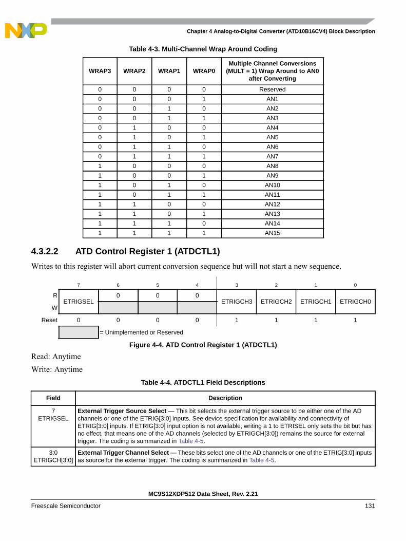
Chapter 4 Analog-to-Digital Converter (ATD10B16CV4) Block Description
MC9S12XDP512 Data Sheet, Rev. 2.21
Freescale Semiconductor 131
4.3.2.2 ATD Control Register 1 (ATDCTL1)
Writes to this register will abort current conversion sequence but will not start a new sequence.
Read: Anytime
Write: Anytime
Table 4-3. Multi-Channel Wrap Around Coding
WRAP3 WRAP2 WRAP1 WRAP0Multiple Channel Conversions
(MULT = 1) Wrap Around to AN0after Converting
0 0 0 0 Reserved
0 0 0 1 AN1
0 0 1 0 AN2
0 0 1 1 AN3
0 1 0 0 AN4
0 1 0 1 AN5
0 1 1 0 AN6
0 1 1 1 AN7
1 0 0 0 AN8
1 0 0 1 AN9
1 0 1 0 AN10
1 0 1 1 AN11
1 1 0 0 AN12
1 1 0 1 AN13
1 1 1 0 AN14
1 1 1 1 AN15
7 6 5 4 3 2 1 0
RETRIGSEL
0 0 0ETRIGCH3 ETRIGCH2 ETRIGCH1 ETRIGCH0
W
Reset 0 0 0 0 1 1 1 1
= Unimplemented or Reserved
Figure 4-4. ATD Control Register 1 (ATDCTL1)
Table 4-4. ATDCTL1 Field Descriptions
Field Description
7ETRIGSEL
External Trigger Source Select — This bit selects the external trigger source to be either one of the ADchannels or one of the ETRIG[3:0] inputs. See device specification for availability and connectivity ofETRIG[3:0] inputs. If ETRIG[3:0] input option is not available, writing a 1 to ETRISEL only sets the bit but hasno effect, that means one of the AD channels (selected by ETRIGCH[3:0]) remains the source for externaltrigger. The coding is summarized in Table 4-5.
3:0ETRIGCH[3:0]
External Trigger Channel Select — These bits select one of the AD channels or one of the ETRIG[3:0] inputsas source for the external trigger. The coding is summarized in Table 4-5.

Chapter 4 Analog-to-Digital Converter (ATD10B16CV4) Block Description
MC9S12XDP512 Data Sheet, Rev. 2.21
132 Freescale Semiconductor
4.3.2.3 ATD Control Register 2 (ATDCTL2)
This register controls power down, interrupt and external trigger. Writes to this register will abort currentconversion sequence but will not start a new sequence.
Table 4-5. External Trigger Channel Select Coding
ETRIGSEL ETRIGCH3 ETRIGCH2 ETRIGCH1 ETRIGCH0 External Trigger Source
0 0 0 0 0 AN0
0 0 0 0 1 AN1
0 0 0 1 0 AN2
0 0 0 1 1 AN3
0 0 1 0 0 AN4
0 0 1 0 1 AN5
0 0 1 1 0 AN6
0 0 1 1 1 AN7
0 1 0 0 0 AN8
0 1 0 0 1 AN9
0 1 0 1 0 AN10
0 1 0 1 1 AN11
0 1 1 0 0 AN12
0 1 1 0 1 AN13
0 1 1 1 0 AN14
0 1 1 1 1 AN15
1 0 0 0 0 ETRIG01
1 Only if ETRIG[3:0] input option is available (see device specification), else ETRISEL is ignored, that meansexternal trigger source remains on one of the AD channels selected by ETRIGCH[3:0]
1 0 0 0 1 ETRIG11
1 0 0 1 0 ETRIG21
1 0 0 1 1 ETRIG31
1 0 1 X X Reserved
1 1 X X X Reserved

Chapter 4 Analog-to-Digital Converter (ATD10B16CV4) Block Description
MC9S12XDP512 Data Sheet, Rev. 2.21
Freescale Semiconductor 133
Read: Anytime
Write: Anytime
7 6 5 4 3 2 1 0
RADPU AFFC AWAI ETRIGLE ETRIGP ETRIGE ASCIE
ASCIF
W
Reset 0 0 0 0 0 0 0 0
= Unimplemented or Reserved
Figure 4-5. ATD Control Register 2 (ATDCTL2)
Table 4-6. ATDCTL2 Field Descriptions
Field Description
7ADPU
ATD Power Down — This bit provides on/off control over the ATD10B16C block allowing reduced MCU powerconsumption. Because analog electronic is turned off when powered down, the ATD requires a recovery timeperiod after ADPU bit is enabled.0 Power down ATD1 Normal ATD functionality
6AFFC
ATD Fast Flag Clear All0 ATD flag clearing operates normally (read the status register ATDSTAT1 before reading the result register
to clear the associate CCF flag).1 Changes all ATD conversion complete flags to a fast clear sequence. Any access to a result register will
cause the associate CCF flag to clear automatically.
5AWAI
ATD Power Down in Wait Mode — When entering Wait Mode this bit provides on/off control over theATD10B16C block allowing reduced MCU power. Because analog electronic is turned off when powered down,the ATD requires a recovery time period after exit from Wait mode.0 ATD continues to run in Wait mode1 Halt conversion and power down ATD during Wait mode
After exiting Wait mode with an interrupt conversion will resume. But due to the recovery time the result ofthis conversion should be ignored.
4ETRIGLE
External Trigger Level/Edge Control — This bit controls the sensitivity of the external trigger signal. SeeTable 4-7 for details.
3ETRIGP
External Trigger Polarity — This bit controls the polarity of the external trigger signal. See Table 4-7 fordetails.
2ETRIGE
External Trigger Mode Enable — This bit enables the external trigger on one of the AD channels or one ofthe ETRIG[3:0] inputs as described in Table 4-5. If external trigger source is one of the AD channels, the digitalinput buffer of this channel is enabled. The external trigger allows to synchronize the start of conversion withexternal events.0 Disable external trigger1 Enable external trigger
1ASCIE
ATD Sequence Complete Interrupt Enable0 ATD Sequence Complete interrupt requests are disabled.1 ATD Interrupt will be requested whenever ASCIF = 1 is set.
0ASCIF
ATD Sequence Complete Interrupt Flag — If ASCIE = 1 the ASCIF flag equals the SCF flag (seeSection 4.3.2.7, “ATD Status Register 0 (ATDSTAT0)”), else ASCIF reads zero. Writes have no effect.0 No ATD interrupt occurred1 ATD sequence complete interrupt pending

Chapter 4 Analog-to-Digital Converter (ATD10B16CV4) Block Description
MC9S12XDP512 Data Sheet, Rev. 2.21
134 Freescale Semiconductor
Table 4-7. External Trigger Configurations
ETRIGLE ETRIGP External Trigger Sensitivity
0 0 Falling Edge
0 1 Ring Edge
1 0 Low Level
1 1 High Level

Chapter 4 Analog-to-Digital Converter (ATD10B16CV4) Block Description
MC9S12XDP512 Data Sheet, Rev. 2.21
Freescale Semiconductor 135
4.3.2.4 ATD Control Register 3 (ATDCTL3)
This register controls the conversion sequence length, FIFO for results registers and behavior in FreezeMode. Writes to this register will abort current conversion sequence but will not start a new sequence.
Read: Anytime
Write: Anytime
7 6 5 4 3 2 1 0
R 0S8C S4C S2C S1C FIFO FRZ1 FRZ0
W
Reset 0 0 1 0 0 0 0 0
= Unimplemented or Reserved
Figure 4-6. ATD Control Register 3 (ATDCTL3)
Table 4-8. ATDCTL3 Field Descriptions
Field Description
6S8C
Conversion Sequence Length — This bit controls the number of conversions per sequence. Table 4-9 showsall combinations. At reset, S4C is set to 1 (sequence length is 4). This is to maintain software continuity to HC12Family.
5S4C
Conversion Sequence Length — This bit controls the number of conversions per sequence. Table 4-9 showsall combinations. At reset, S4C is set to 1 (sequence length is 4). This is to maintain software continuity to HC12Family.
4S2C
Conversion Sequence Length — This bit controls the number of conversions per sequence. Table 4-9 showsall combinations. At reset, S4C is set to 1 (sequence length is 4). This is to maintain software continuity to HC12Family.
3S1C
Conversion Sequence Length — This bit controls the number of conversions per sequence. Table 4-9 showsall combinations. At reset, S4C is set to 1 (sequence length is 4). This is to maintain software continuity to HC12Family.

Chapter 4 Analog-to-Digital Converter (ATD10B16CV4) Block Description
MC9S12XDP512 Data Sheet, Rev. 2.21
136 Freescale Semiconductor
2FIFO
Result Register FIFO Mode —If this bit is zero (non-FIFO mode), the A/D conversion results map into theresult registers based on the conversion sequence; the result of the first conversion appears in the first resultregister, the second result in the second result register, and so on.If this bit is one (FIFO mode) the conversion counter is not reset at the beginning or ending of a conversionsequence; sequential conversion results are placed in consecutive result registers. In a continuously scanningconversion sequence, the result register counter will wrap around when it reaches the end of the result registerfile. The conversion counter value (CC3-0 in ATDSTAT0) can be used to determine where in the result registerfile, the current conversion result will be placed.Aborting a conversion or starting a new conversion by write to an ATDCTL register (ATDCTL5-0) clears theconversion counter even if FIFO=1. So the first result of a new conversion sequence, started by writing toATDCTL5, will always be place in the first result register (ATDDDR0). Intended usage of FIFO mode iscontinuos conversion (SCAN=1) or triggered conversion (ETRIG=1).Finally, which result registers hold valid data can be tracked using the conversion complete flags. Fast flag clearmode may or may not be useful in a particular application to track valid data.0 Conversion results are placed in the corresponding result register up to the selected sequence length.1 Conversion results are placed in consecutive result registers (wrap around at end).
1:0FRZ[1:0]
Background Debug Freeze Enable — When debugging an application, it is useful in many cases to have theATD pause when a breakpoint (Freeze Mode) is encountered. These 2 bits determine how the ATD will respondto a breakpoint as shown in Table 4-10. Leakage onto the storage node and comparator reference capacitorsmay compromise the accuracy of an immediately frozen conversion depending on the length of the freezeperiod.
Table 4-9. Conversion Sequence Length Coding
S8C S4C S2C S1CNumber of Conversions
per Sequence
0 0 0 0 16
0 0 0 1 1
0 0 1 0 2
0 0 1 1 3
0 1 0 0 4
0 1 0 1 5
0 1 1 0 6
0 1 1 1 7
1 0 0 0 8
1 0 0 1 9
1 0 1 0 10
1 0 1 1 11
1 1 0 0 12
1 1 0 1 13
1 1 1 0 14
1 1 1 1 15
Table 4-8. ATDCTL3 Field Descriptions (continued)
Field Description

Chapter 4 Analog-to-Digital Converter (ATD10B16CV4) Block Description
MC9S12XDP512 Data Sheet, Rev. 2.21
Freescale Semiconductor 137
Table 4-10. ATD Behavior in Freeze Mode (Breakpoint)
FRZ1 FRZ0 Behavior in Freeze Mode
0 0 Continue conversion
0 1 Reserved
1 0 Finish current conversion, then freeze
1 1 Freeze Immediately
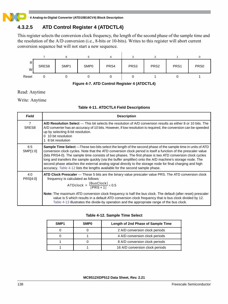
Chapter 4 Analog-to-Digital Converter (ATD10B16CV4) Block Description
MC9S12XDP512 Data Sheet, Rev. 2.21
138 Freescale Semiconductor
4.3.2.5 ATD Control Register 4 (ATDCTL4)
This register selects the conversion clock frequency, the length of the second phase of the sample time andthe resolution of the A/D conversion (i.e., 8-bits or 10-bits). Writes to this register will abort currentconversion sequence but will not start a new sequence.
Read: Anytime
Write: Anytime
7 6 5 4 3 2 1 0
RSRES8 SMP1 SMP0 PRS4 PRS3 PRS2 PRS1 PRS0
W
Reset 0 0 0 0 0 1 0 1
Figure 4-7. ATD Control Register 4 (ATDCTL4)
Table 4-11. ATDCTL4 Field Descriptions
Field Description
7SRES8
A/D Resolution Select — This bit selects the resolution of A/D conversion results as either 8 or 10 bits. TheA/D converter has an accuracy of 10 bits. However, if low resolution is required, the conversion can be speededup by selecting 8-bit resolution.0 10 bit resolution1 8 bit resolution
6:5SMP[1:0]
Sample Time Select —These two bits select the length of the second phase of the sample time in units of ATDconversion clock cycles. Note that the ATD conversion clock period is itself a function of the prescaler value(bits PRS4-0). The sample time consists of two phases. The first phase is two ATD conversion clock cycleslong and transfers the sample quickly (via the buffer amplifier) onto the A/D machine’s storage node. Thesecond phase attaches the external analog signal directly to the storage node for final charging and highaccuracy. Table 4-12 lists the lengths available for the second sample phase.
4:0PRS[4:0]
ATD Clock Prescaler — These 5 bits are the binary value prescaler value PRS. The ATD conversion clockfrequency is calculated as follows:
Note: The maximum ATD conversion clock frequency is half the bus clock. The default (after reset) prescalervalue is 5 which results in a default ATD conversion clock frequency that is bus clock divided by 12.Table 4-13 illustrates the divide-by operation and the appropriate range of the bus clock.
Table 4-12. Sample Time Select
SMP1 SMP0 Length of 2nd Phase of Sample Time
0 0 2 A/D conversion clock periods
0 1 4 A/D conversion clock periods
1 0 8 A/D conversion clock periods
1 1 16 A/D conversion clock periods
ATDclockBusClock[ ]PRS 1+[ ]-------------------------------- 0.5×=
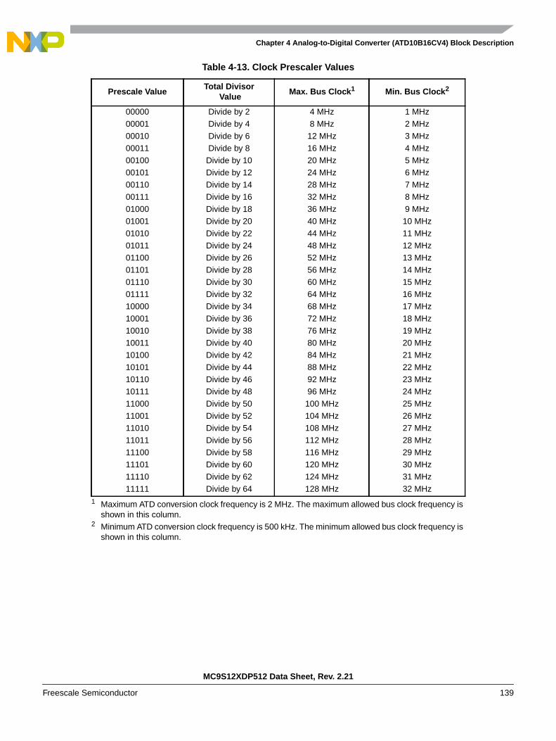
Chapter 4 Analog-to-Digital Converter (ATD10B16CV4) Block Description
MC9S12XDP512 Data Sheet, Rev. 2.21
Freescale Semiconductor 139
Table 4-13. Clock Prescaler Values
Prescale ValueTotal Divisor
ValueMax. Bus Clock1
1 Maximum ATD conversion clock frequency is 2 MHz. The maximum allowed bus clock frequency isshown in this column.
Min. Bus Clock2
2 Minimum ATD conversion clock frequency is 500 kHz. The minimum allowed bus clock frequency isshown in this column.
000000000100010000110010000101001100011101000
0100101010010110110001101011100111110000100011001010011101001010110110101111100011001110101101111100111011111011111
Divide by 2Divide by 4Divide by 6Divide by 8Divide by 10Divide by 12Divide by 14Divide by 16Divide by 18
Divide by 20Divide by 22Divide by 24Divide by 26Divide by 28Divide by 30Divide by 32Divide by 34Divide by 36Divide by 38Divide by 40Divide by 42Divide by 44Divide by 46Divide by 48Divide by 50Divide by 52Divide by 54Divide by 56Divide by 58Divide by 60Divide by 62Divide by 64
4 MHz8 MHz
12 MHz16 MHz20 MHz24 MHz28 MHz32 MHz36 MHz
40 MHz44 MHz48 MHz52 MHz56 MHz60 MHz64 MHz68 MHz72 MHz76 MHz80 MHz84 MHz88 MHz92 MHz96 MHz100 MHz104 MHz108 MHz112 MHz116 MHz120 MHz124 MHz128 MHz
1 MHz2 MHz3 MHz4 MHz5 MHz6 MHz7 MHz8 MHz9 MHz
10 MHz11 MHz12 MHz13 MHz14 MHz15 MHz16 MHz17 MHz18 MHz19 MHz20 MHz21 MHz22 MHz23 MHz24 MHz25 MHz26 MHz27 MHz28 MHz29 MHz30 MHz31 MHz32 MHz

Chapter 4 Analog-to-Digital Converter (ATD10B16CV4) Block Description
MC9S12XDP512 Data Sheet, Rev. 2.21
140 Freescale Semiconductor
4.3.2.6 ATD Control Register 5 (ATDCTL5)
This register selects the type of conversion sequence and the analog input channels sampled. Writes to thisregister will abort current conversion sequence and start a new conversion sequence. If external trigger isenabled (ETRIGE = 1) an initial write to ATDCTL5 is required to allow starting of a conversion sequencewhich will then occur on each trigger event. Start of conversion means the beginning of the samplingphase.
Read: Anytime
Write: Anytime
7 6 5 4 3 2 1 0
RDJM DSGN SCAN MULT CD CC CB CA
W
Reset 0 0 0 0 0 0 0 0
Figure 4-8. ATD Control Register 5 (ATDCTL5)
Table 4-14. ATDCTL5 Field Descriptions
Field Description
7DJM
Result Register Data Justification — This bit controls justification of conversion data in the result registers.See Section 4.3.2.16, “ATD Conversion Result Registers (ATDDRx)” for details.0 Left justified data in the result registers.1 Right justified data in the result registers.
6DSGN
Result Register Data Signed or Unsigned Representation — This bit selects between signed and unsignedconversion data representation in the result registers. Signed data is represented as 2’s complement. Signeddata is not available in right justification. See <st-bold>4.3.2.16 ATD Conversion Result Registers (ATDDRx)for details.0 Unsigned data representation in the result registers.1 Signed data representation in the result registers.Table 4-15 summarizes the result data formats available and how they are set up using the control bits.Table 4-16 illustrates the difference between the signed and unsigned, left justified output codes for an inputsignal range between 0 and 5.12 Volts.
5SCAN
Continuous Conversion Sequence Mode — This bit selects whether conversion sequences are performedcontinuously or only once. If external trigger is enabled (ETRIGE=1) setting this bit has no effect, that meanseach trigger event starts a single conversion sequence.0 Single conversion sequence1 Continuous conversion sequences (scan mode)
4MULT
Multi-Channel Sample Mode — When MULT is 0, the ATD sequence controller samples only from thespecified analog input channel for an entire conversion sequence. The analog channel is selected by channelselection code (control bits CD/CC/CB/CA located in ATDCTL5). When MULT is 1, the ATD sequence controllersamples across channels. The number of channels sampled is determined by the sequence length value (S8C,S4C, S2C, S1C). The first analog channel examined is determined by channel selection code (CC, CB, CAcontrol bits); subsequent channels sampled in the sequence are determined by incrementing the channelselection code or wrapping around to AN0 (channel 0.0 Sample only one channel1 Sample across several channels

Chapter 4 Analog-to-Digital Converter (ATD10B16CV4) Block Description
MC9S12XDP512 Data Sheet, Rev. 2.21
Freescale Semiconductor 141
3:0C[D:A
Analog Input Channel Select Code — These bits select the analog input channel(s) whose signals aresampled and converted to digital codes. Table 4-17 lists the coding used to select the various analog inputchannels.In the case of single channel conversions (MULT = 0), this selection code specified the channel to be examined.In the case of multiple channel conversions (MULT = 1), this selection code represents the first channel to beexamined in the conversion sequence. Subsequent channels are determined by incrementing the channelselection code or wrapping around to AN0 (after converting the channel defined by the Wrap Around ChannelSelect Bits WRAP[3:0] in ATDCTL0). In case starting with a channel number higher than the one defined byWRAP[3:0] the first wrap around will be AN15 to AN0.
Table 4-15. Available Result Data Formats.
SRES8 DJM DSGNResult Data Formats
Description and Bus Bit Mapping
1
1
1
0
0
0
0
0
1
0
0
1
0
1
X
0
1
X
8-bit / left justified / unsigned — bits 15:8
8-bit / left justified / signed — bits 15:8
8-bit / right justified / unsigned — bits 7:0
10-bit / left justified / unsigned — bits 15:6
10-bit / left justified / signed -— bits 15:6
10-bit / right justified / unsigned — bits 9:0
Table 4-16. Left Justified, Signed and Unsigned ATD Output Codes.
Input SignalVRL = 0 Volts
VRH = 5.12 Volts
Signed8-Bit Codes
Unsigned8-Bit Codes
Signed10-Bit Codes
Unsigned10-Bit Codes
5.120 Volts
5.100
5.080
2.580
2.560
2.540
0.020
0.000
7F
7F
7E
01
00
FF
81
80
FF
FF
FE
81
80
7F
01
00
7FC0
7F00
7E00
0100
0000
FF00
8100
8000
FFC0
FF00
FE00
8100
8000
7F00
0100
0000
Table 4-14. ATDCTL5 Field Descriptions (continued)
Field Description

Chapter 4 Analog-to-Digital Converter (ATD10B16CV4) Block Description
MC9S12XDP512 Data Sheet, Rev. 2.21
142 Freescale Semiconductor
Table 4-17. Analog Input Channel Select Coding
CD CC CB CAAnalog Input
Channel
0 0 0 0 AN0
0 0 0 1 AN1
0 0 1 0 AN2
0 0 1 1 AN3
0 1 0 0 AN4
0 1 0 1 AN5
0 1 1 0 AN6
0 1 1 1 AN7
1 0 0 0 AN8
1 0 0 1 AN9
1 0 1 0 AN10
1 0 1 1 AN11
1 1 0 0 AN12
1 1 0 1 AN13
1 1 1 0 AN14
1 1 1 1 AN15

Chapter 4 Analog-to-Digital Converter (ATD10B16CV4) Block Description
MC9S12XDP512 Data Sheet, Rev. 2.21
Freescale Semiconductor 143
4.3.2.7 ATD Status Register 0 (ATDSTAT0)
This read-only register contains the Sequence Complete Flag, overrun flags for external trigger and FIFOmode, and the conversion counter.
Read: Anytime
Write: Anytime (No effect on CC[3:0])
7 6 5 4 3 2 1 0
RSCF
0ETORF FIFOR
CC3 CC2 CC1 CC0
W
Reset 0 0 0 0 0 0 0 0
= Unimplemented or Reserved
Figure 4-9. ATD Status Register 0 (ATDSTAT0)
Table 4-18. ATDSTAT0 Field Descriptions
Field Description
7SCF
Sequence Complete Flag — This flag is set upon completion of a conversion sequence. If conversionsequences are continuously performed (SCAN = 1), the flag is set after each one is completed. This flag iscleared when one of the following occurs:
• Write “1” to SCF • Write to ATDCTL5 (a new conversion sequence is started) • If AFFC = 1 and read of a result register
0 Conversion sequence not completed1 Conversion sequence has completed
5ETORF
External Trigger Overrun Flag —While in edge trigger mode (ETRIGLE = 0), if additional active edges aredetected while a conversion sequence is in process the overrun flag is set. This flag is cleared when one of thefollowing occurs:
• Write “1” to ETORF • Write to ATDCTL0,1,2,3,4 (a conversion sequence is aborted) • Write to ATDCTL5 (a new conversion sequence is started)
0 No External trigger over run error has occurred1 External trigger over run error has occurred
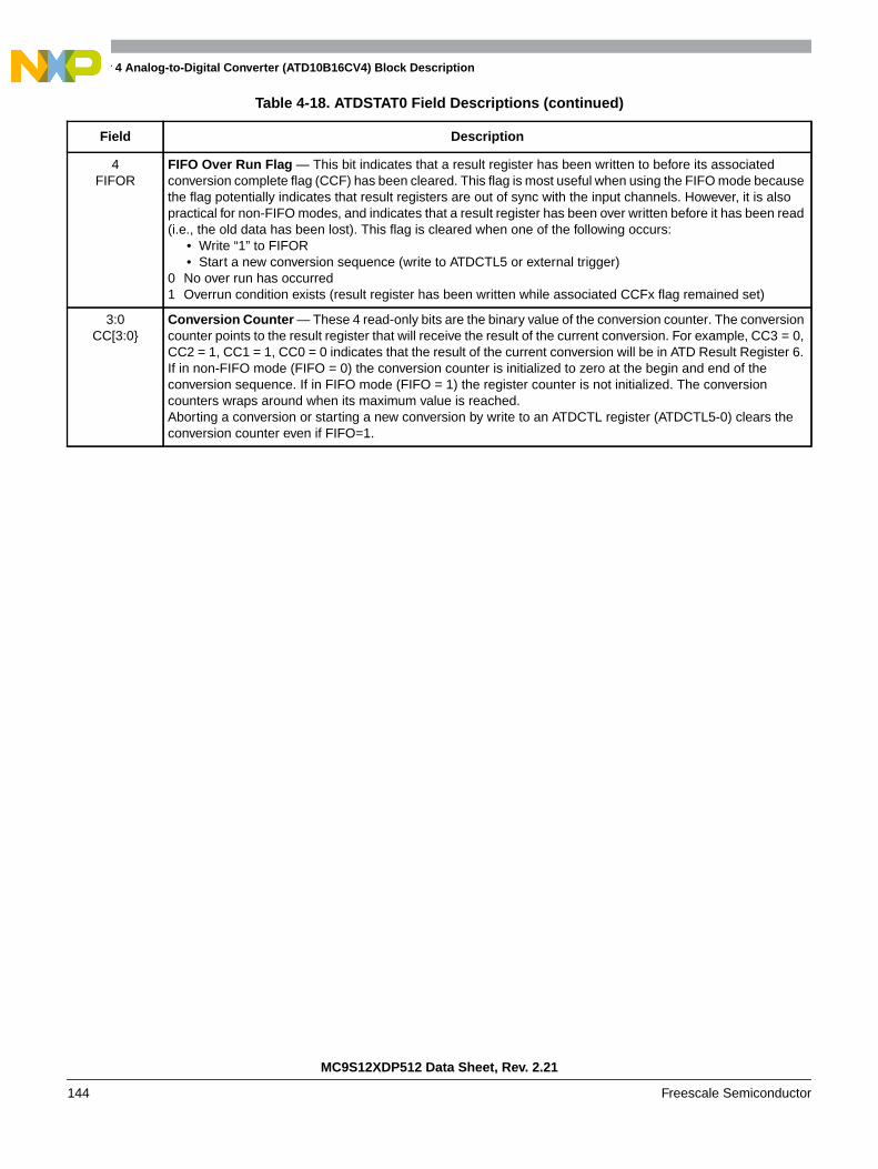
Chapter 4 Analog-to-Digital Converter (ATD10B16CV4) Block Description
MC9S12XDP512 Data Sheet, Rev. 2.21
144 Freescale Semiconductor
4FIFOR
FIFO Over Run Flag — This bit indicates that a result register has been written to before its associatedconversion complete flag (CCF) has been cleared. This flag is most useful when using the FIFO mode becausethe flag potentially indicates that result registers are out of sync with the input channels. However, it is alsopractical for non-FIFO modes, and indicates that a result register has been over written before it has been read(i.e., the old data has been lost). This flag is cleared when one of the following occurs:
• Write “1” to FIFOR • Start a new conversion sequence (write to ATDCTL5 or external trigger)
0 No over run has occurred1 Overrun condition exists (result register has been written while associated CCFx flag remained set)
3:0CC[3:0
Conversion Counter — These 4 read-only bits are the binary value of the conversion counter. The conversioncounter points to the result register that will receive the result of the current conversion. For example, CC3 = 0,CC2 = 1, CC1 = 1, CC0 = 0 indicates that the result of the current conversion will be in ATD Result Register 6.If in non-FIFO mode (FIFO = 0) the conversion counter is initialized to zero at the begin and end of theconversion sequence. If in FIFO mode (FIFO = 1) the register counter is not initialized. The conversioncounters wraps around when its maximum value is reached.Aborting a conversion or starting a new conversion by write to an ATDCTL register (ATDCTL5-0) clears theconversion counter even if FIFO=1.
Table 4-18. ATDSTAT0 Field Descriptions (continued)
Field Description

Chapter 4 Analog-to-Digital Converter (ATD10B16CV4) Block Description
MC9S12XDP512 Data Sheet, Rev. 2.21
Freescale Semiconductor 145
4.3.2.8 Reserved Register 0 (ATDTEST0)
Read: Anytime, returns unpredictable values
Write: Anytime in special modes, unimplemented in normal modes
NOTEWriting to this register when in special modes can alter functionality.
4.3.2.9 ATD Test Register 1 (ATDTEST1)
This register contains the SC bit used to enable special channel conversions.
Read: Anytime, returns unpredictable values for bit 7 and bit 6
Write: Anytime
NOTEWriting to this register when in special modes can alter functionality.
7 6 5 4 3 2 1 0
R u u u u u u u u
W
Reset 1 0 0 0 0 0 0 0
= Unimplemented or Reserved u = Unaffected
Figure 4-10. Reserved Register 0 (ATDTEST0)
7 6 5 4 3 2 1 0
R u u u u u u uSC
W
Reset 0 0 0 0 0 0 0 0
= Unimplemented or Reserved u = Unaffected
Figure 4-11. Reserved Register 1 (ATDTEST1)
Table 4-19. ATDTEST1 Field Descriptions
Field Description
0SC
Special Channel Conversion Bit — If this bit is set, then special channel conversion can be selected usingCC, CB, and CA of ATDCTL5. Table 4-20 lists the coding.0 Special channel conversions disabled1 Special channel conversions enabled

Chapter 4 Analog-to-Digital Converter (ATD10B16CV4) Block Description
MC9S12XDP512 Data Sheet, Rev. 2.21
146 Freescale Semiconductor
4.3.2.10 ATD Status Register 2 (ATDSTAT2)
This read-only register contains the Conversion Complete Flags CCF15 to CCF8.
Read: Anytime
Write: Anytime, no effect
Table 4-20. Special Channel Select Coding
SC CD CC CB CA Analog Input Channel
1 0 0 X X Reserved
1 0 1 0 0 VRH
1 0 1 0 1 VRL
1 0 1 1 0 (VRH+VRL) / 2
1 0 1 1 1 Reserved
1 1 X X X Reserved
7 6 5 4 3 2 1 0
R CCF15 CCF14 CCF13 CCF12 CCF11 CCF10 CCF9 CCF8
W
Reset 0 0 0 0 0 0 0 0
= Unimplemented or Reserved
Figure 4-12. ATD Status Register 2 (ATDSTAT2)
Table 4-21. ATDSTAT2 Field Descriptions
Field Description
7:0CCF[15:8]
Conversion Complete Flag Bits — A conversion complete flag is set at the end of each conversion in aconversion sequence. The flags are associated with the conversion position in a sequence (and also the resultregister number). Therefore, CCF8 is set when the ninth conversion in a sequence is complete and the resultis available in result register ATDDR8; CCF9 is set when the tenth conversion in a sequence is complete andthe result is available in ATDDR9, and so forth. A flag CCFx (x = 15, 14, 13, 12, 11, 10, 9, 8) is cleared whenone of the following occurs:
• Write to ATDCTL5 (a new conversion sequence is started) • If AFFC = 0 and read of ATDSTAT2 followed by read of result register ATDDRx • If AFFC = 1 and read of result register ATDDRx
In case of a concurrent set and clear on CCFx: The clearing by method A) will overwrite the set. The clearingby methods B) or C) will be overwritten by the set.0 Conversion number x not completed1 Conversion number x has completed, result ready in ATDDRx
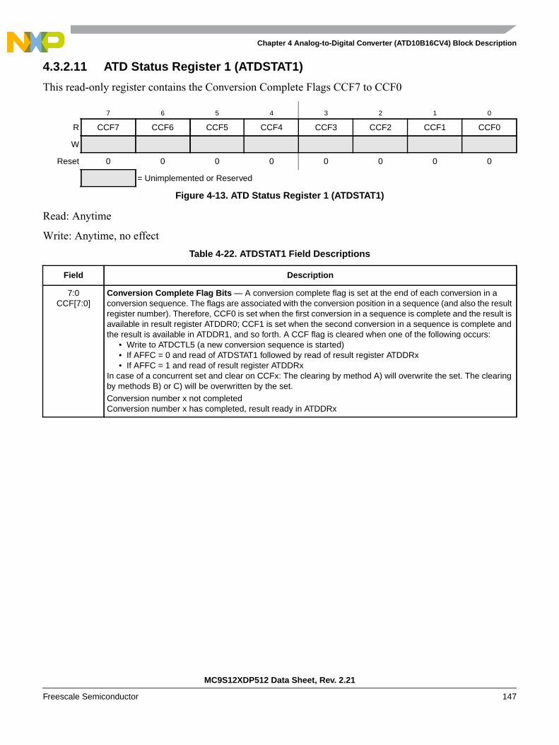
Chapter 4 Analog-to-Digital Converter (ATD10B16CV4) Block Description
MC9S12XDP512 Data Sheet, Rev. 2.21
Freescale Semiconductor 147
4.3.2.11 ATD Status Register 1 (ATDSTAT1)
This read-only register contains the Conversion Complete Flags CCF7 to CCF0
Read: Anytime
Write: Anytime, no effect
7 6 5 4 3 2 1 0
R CCF7 CCF6 CCF5 CCF4 CCF3 CCF2 CCF1 CCF0
W
Reset 0 0 0 0 0 0 0 0
= Unimplemented or Reserved
Figure 4-13. ATD Status Register 1 (ATDSTAT1)
Table 4-22. ATDSTAT1 Field Descriptions
Field Description
7:0CCF[7:0]
Conversion Complete Flag Bits — A conversion complete flag is set at the end of each conversion in aconversion sequence. The flags are associated with the conversion position in a sequence (and also the resultregister number). Therefore, CCF0 is set when the first conversion in a sequence is complete and the result isavailable in result register ATDDR0; CCF1 is set when the second conversion in a sequence is complete andthe result is available in ATDDR1, and so forth. A CCF flag is cleared when one of the following occurs:
• Write to ATDCTL5 (a new conversion sequence is started) • If AFFC = 0 and read of ATDSTAT1 followed by read of result register ATDDRx • If AFFC = 1 and read of result register ATDDRx
In case of a concurrent set and clear on CCFx: The clearing by method A) will overwrite the set. The clearingby methods B) or C) will be overwritten by the set.Conversion number x not completedConversion number x has completed, result ready in ATDDRx
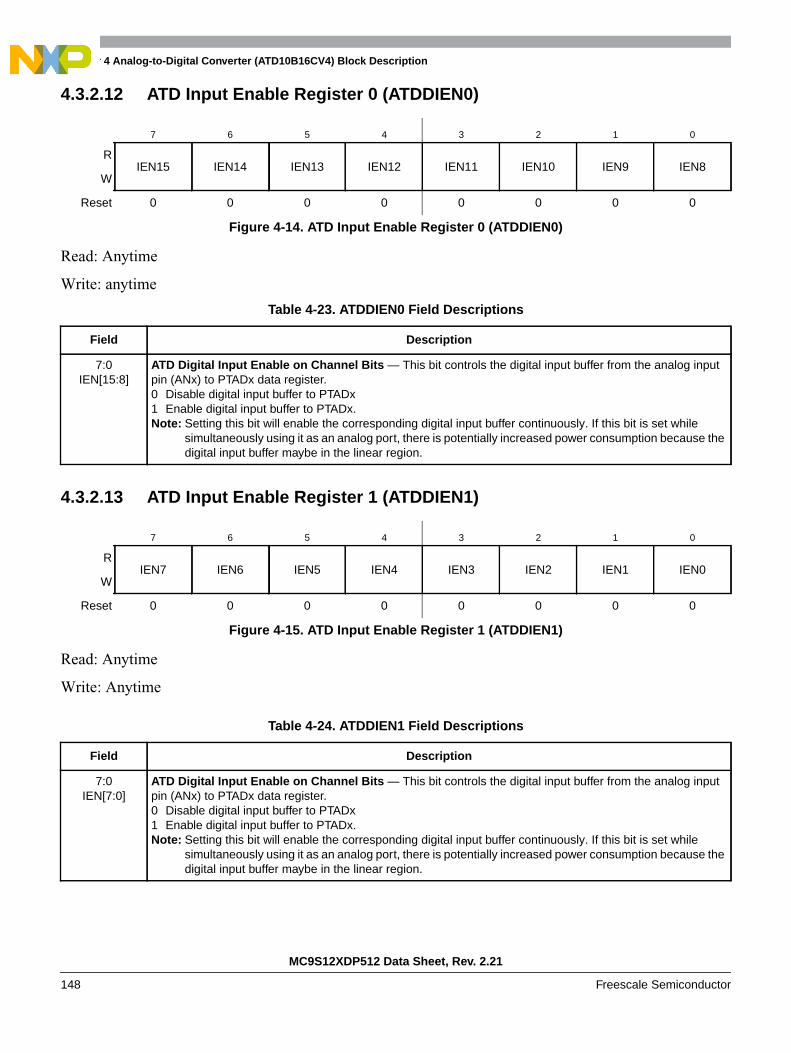
Chapter 4 Analog-to-Digital Converter (ATD10B16CV4) Block Description
MC9S12XDP512 Data Sheet, Rev. 2.21
148 Freescale Semiconductor
4.3.2.12 ATD Input Enable Register 0 (ATDDIEN0)
Read: Anytime
Write: anytime
4.3.2.13 ATD Input Enable Register 1 (ATDDIEN1)
Read: Anytime
Write: Anytime
7 6 5 4 3 2 1 0
RIEN15 IEN14 IEN13 IEN12 IEN11 IEN10 IEN9 IEN8
W
Reset 0 0 0 0 0 0 0 0
Figure 4-14. ATD Input Enable Register 0 (ATDDIEN0)
Table 4-23. ATDDIEN0 Field Descriptions
Field Description
7:0IEN[15:8]
ATD Digital Input Enable on Channel Bits — This bit controls the digital input buffer from the analog inputpin (ANx) to PTADx data register.0 Disable digital input buffer to PTADx1 Enable digital input buffer to PTADx.Note: Setting this bit will enable the corresponding digital input buffer continuously. If this bit is set while
simultaneously using it as an analog port, there is potentially increased power consumption because thedigital input buffer maybe in the linear region.
7 6 5 4 3 2 1 0
RIEN7 IEN6 IEN5 IEN4 IEN3 IEN2 IEN1 IEN0
W
Reset 0 0 0 0 0 0 0 0
Figure 4-15. ATD Input Enable Register 1 (ATDDIEN1)
Table 4-24. ATDDIEN1 Field Descriptions
Field Description
7:0IEN[7:0]
ATD Digital Input Enable on Channel Bits — This bit controls the digital input buffer from the analog inputpin (ANx) to PTADx data register.0 Disable digital input buffer to PTADx1 Enable digital input buffer to PTADx.Note: Setting this bit will enable the corresponding digital input buffer continuously. If this bit is set while
simultaneously using it as an analog port, there is potentially increased power consumption because thedigital input buffer maybe in the linear region.

Chapter 4 Analog-to-Digital Converter (ATD10B16CV4) Block Description
MC9S12XDP512 Data Sheet, Rev. 2.21
Freescale Semiconductor 149
4.3.2.14 Port Data Register 0 (PORTAD0)
The data port associated with the ATD is input-only. The port pins are shared with the analog A/D inputsAN[15:8].
Read: Anytime
Write: Anytime, no effect
The A/D input channels may be used for general-purpose digital input.
7 6 5 4 3 2 1 0
R PTAD15 PTAD14 PTAD13 PTAD12 PTAD11 PTAD10 PTAD9 PTAD8
W
Reset 1 1 1 1 1 1 1 1
PinFunction
AN15 AN14 AN13 AN12 AN11 AN10 AN9 AN8
= Unimplemented or Reserved
Figure 4-16. Port Data Register 0 (PORTAD0)
Table 4-25. PORTAD0 Field Descriptions
Field Description
7:0PTAD[15:8]
A/D Channel x (ANx) Digital Input Bits— If the digital input buffer on the ANx pin is enabled (IENx = 1) orchannel x is enabled as external trigger (ETRIGE = 1, ETRIGCH[3-0] = x, ETRIGSEL = 0) read returns thelogic level on ANx pin (signal potentials not meeting VIL or VIH specifications will have an indeterminate value)).If the digital input buffers are disabled (IENx = 0) and channel x is not enabled as external trigger, read returnsa “1”.Reset sets all PORTAD0 bits to “1”.
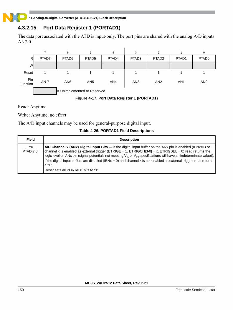
Chapter 4 Analog-to-Digital Converter (ATD10B16CV4) Block Description
MC9S12XDP512 Data Sheet, Rev. 2.21
150 Freescale Semiconductor
4.3.2.15 Port Data Register 1 (PORTAD1)
The data port associated with the ATD is input-only. The port pins are shared with the analog A/D inputsAN7-0.
Read: Anytime
Write: Anytime, no effect
The A/D input channels may be used for general-purpose digital input.
7 6 5 4 3 2 1 0
R PTAD7 PTAD6 PTAD5 PTAD4 PTAD3 PTAD2 PTAD1 PTAD0
W
Reset 1 1 1 1 1 1 1 1
PinFunction
AN 7 AN6 AN5 AN4 AN3 AN2 AN1 AN0
= Unimplemented or Reserved
Figure 4-17. Port Data Register 1 (PORTAD1)
Table 4-26. PORTAD1 Field Descriptions
Field Description
7:0PTAD[7:8]
A/D Channel x (ANx) Digital Input Bits — If the digital input buffer on the ANx pin is enabled (IENx=1) orchannel x is enabled as external trigger (ETRIGE = 1, ETRIGCH[3-0] = x, ETRIGSEL = 0) read returns thelogic level on ANx pin (signal potentials not meeting VIL or VIH specifications will have an indeterminate value)).If the digital input buffers are disabled (IENx = 0) and channel x is not enabled as external trigger, read returnsa “1”.Reset sets all PORTAD1 bits to “1”.
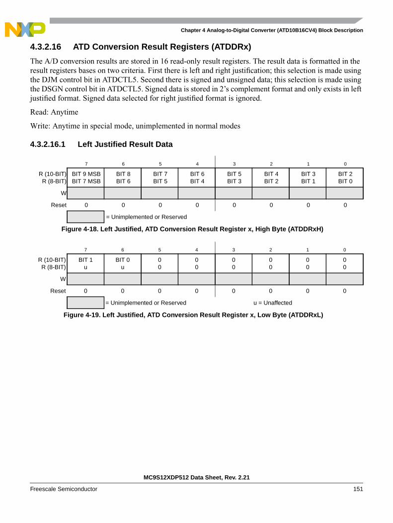
Chapter 4 Analog-to-Digital Converter (ATD10B16CV4) Block Description
MC9S12XDP512 Data Sheet, Rev. 2.21
Freescale Semiconductor 151
4.3.2.16 ATD Conversion Result Registers (ATDDRx)
The A/D conversion results are stored in 16 read-only result registers. The result data is formatted in theresult registers bases on two criteria. First there is left and right justification; this selection is made usingthe DJM control bit in ATDCTL5. Second there is signed and unsigned data; this selection is made usingthe DSGN control bit in ATDCTL5. Signed data is stored in 2’s complement format and only exists in leftjustified format. Signed data selected for right justified format is ignored.
Read: Anytime
Write: Anytime in special mode, unimplemented in normal modes
4.3.2.16.1 Left Justified Result Data
7 6 5 4 3 2 1 0
R (10-BIT)R (8-BIT)
BIT 9 MSBBIT 7 MSB
BIT 8BIT 6
BIT 7BIT 5
BIT 6BIT 4
BIT 5BIT 3
BIT 4BIT 2
BIT 3BIT 1
BIT 2BIT 0
W
Reset 0 0 0 0 0 0 0 0
= Unimplemented or Reserved
Figure 4-18. Left Justified, ATD Conversion Result Register x, High Byte (ATDDRxH)
7 6 5 4 3 2 1 0
R (10-BIT)R (8-BIT)
BIT 1u
BIT 0u
00
00
00
00
00
00
W
Reset 0 0 0 0 0 0 0 0
= Unimplemented or Reserved u = Unaffected
Figure 4-19. Left Justified, ATD Conversion Result Register x, Low Byte (ATDDRxL)
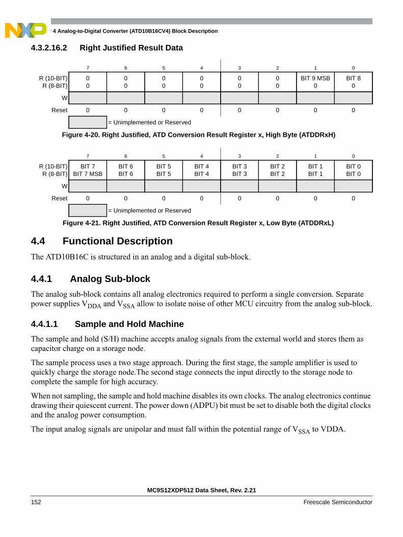
Chapter 4 Analog-to-Digital Converter (ATD10B16CV4) Block Description
MC9S12XDP512 Data Sheet, Rev. 2.21
152 Freescale Semiconductor
4.3.2.16.2 Right Justified Result Data
4.4 Functional DescriptionThe ATD10B16C is structured in an analog and a digital sub-block.
4.4.1 Analog Sub-block
The analog sub-block contains all analog electronics required to perform a single conversion. Separatepower supplies VDDA and VSSA allow to isolate noise of other MCU circuitry from the analog sub-block.
4.4.1.1 Sample and Hold Machine
The sample and hold (S/H) machine accepts analog signals from the external world and stores them ascapacitor charge on a storage node.
The sample process uses a two stage approach. During the first stage, the sample amplifier is used toquickly charge the storage node.The second stage connects the input directly to the storage node tocomplete the sample for high accuracy.
When not sampling, the sample and hold machine disables its own clocks. The analog electronics continuedrawing their quiescent current. The power down (ADPU) bit must be set to disable both the digital clocksand the analog power consumption.
The input analog signals are unipolar and must fall within the potential range of VSSA to VDDA.
7 6 5 4 3 2 1 0
R (10-BIT)R (8-BIT)
00
00
00
00
00
00
BIT 9 MSB0
BIT 80
W
Reset 0 0 0 0 0 0 0 0
= Unimplemented or Reserved
Figure 4-20. Right Justified, ATD Conversion Result Register x, High Byte (ATDDRxH)
7 6 5 4 3 2 1 0
R (10-BIT)R (8-BIT)
BIT 7BIT 7 MSB
BIT 6BIT 6
BIT 5BIT 5
BIT 4BIT 4
BIT 3BIT 3
BIT 2BIT 2
BIT 1BIT 1
BIT 0BIT 0
W
Reset 0 0 0 0 0 0 0 0
= Unimplemented or Reserved
Figure 4-21. Right Justified, ATD Conversion Result Register x, Low Byte (ATDDRxL)
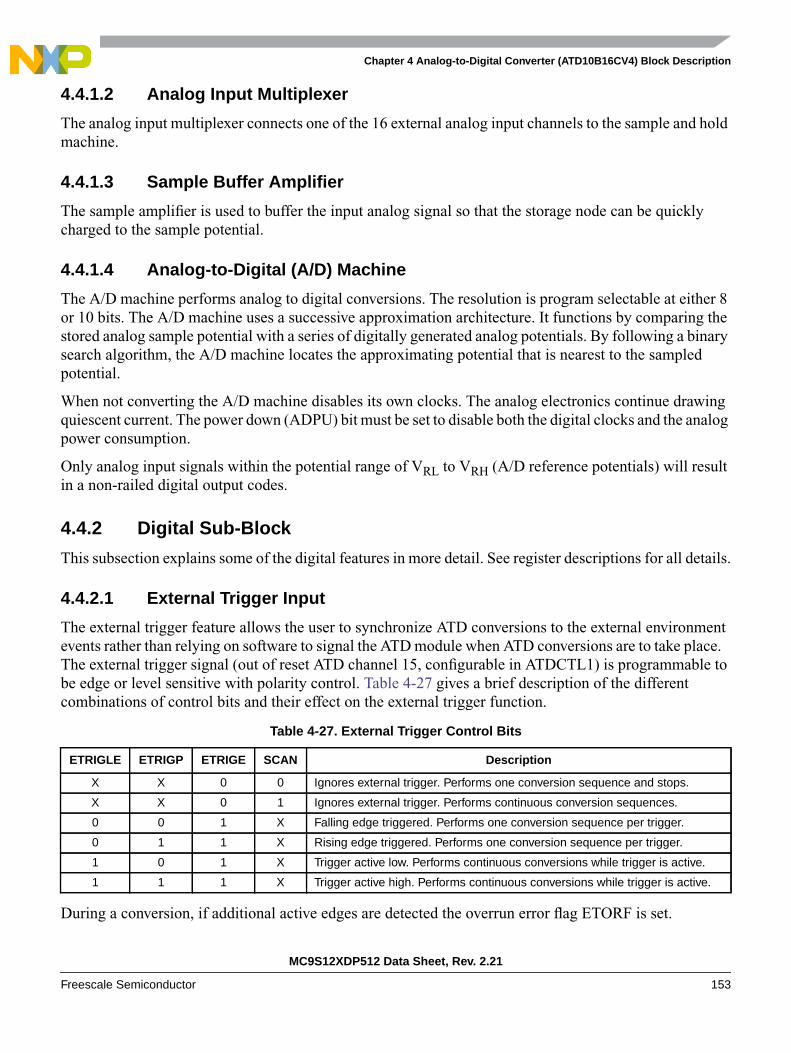
Chapter 4 Analog-to-Digital Converter (ATD10B16CV4) Block Description
MC9S12XDP512 Data Sheet, Rev. 2.21
Freescale Semiconductor 153
4.4.1.2 Analog Input Multiplexer
The analog input multiplexer connects one of the 16 external analog input channels to the sample and holdmachine.
4.4.1.3 Sample Buffer Amplifier
The sample amplifier is used to buffer the input analog signal so that the storage node can be quicklycharged to the sample potential.
4.4.1.4 Analog-to-Digital (A/D) Machine
The A/D machine performs analog to digital conversions. The resolution is program selectable at either 8or 10 bits. The A/D machine uses a successive approximation architecture. It functions by comparing thestored analog sample potential with a series of digitally generated analog potentials. By following a binarysearch algorithm, the A/D machine locates the approximating potential that is nearest to the sampledpotential.
When not converting the A/D machine disables its own clocks. The analog electronics continue drawingquiescent current. The power down (ADPU) bit must be set to disable both the digital clocks and the analogpower consumption.
Only analog input signals within the potential range of VRL to VRH (A/D reference potentials) will resultin a non-railed digital output codes.
4.4.2 Digital Sub-Block
This subsection explains some of the digital features in more detail. See register descriptions for all details.
4.4.2.1 External Trigger Input
The external trigger feature allows the user to synchronize ATD conversions to the external environmentevents rather than relying on software to signal the ATD module when ATD conversions are to take place.The external trigger signal (out of reset ATD channel 15, configurable in ATDCTL1) is programmable tobe edge or level sensitive with polarity control. Table 4-27 gives a brief description of the differentcombinations of control bits and their effect on the external trigger function.
During a conversion, if additional active edges are detected the overrun error flag ETORF is set.
Table 4-27. External Trigger Control Bits
ETRIGLE ETRIGP ETRIGE SCAN Description
X X 0 0 Ignores external trigger. Performs one conversion sequence and stops.
X X 0 1 Ignores external trigger. Performs continuous conversion sequences.
0 0 1 X Falling edge triggered. Performs one conversion sequence per trigger.
0 1 1 X Rising edge triggered. Performs one conversion sequence per trigger.
1 0 1 X Trigger active low. Performs continuous conversions while trigger is active.
1 1 1 X Trigger active high. Performs continuous conversions while trigger is active.

Chapter 4 Analog-to-Digital Converter (ATD10B16CV4) Block Description
MC9S12XDP512 Data Sheet, Rev. 2.21
154 Freescale Semiconductor
In either level or edge triggered modes, the first conversion begins when the trigger is received. In bothcases, the maximum latency time is one bus clock cycle plus any skew or delay introduced by the triggercircuitry.
After ETRIGE is enabled, conversions cannot be started by a write to ATDCTL5, but rather must betriggered externally.
If the level mode is active and the external trigger both de-asserts and re-asserts itself during a conversionsequence, this does not constitute an overrun. Therefore, the flag is not set. If the trigger remains assertedin level mode while a sequence is completing, another sequence will be triggered immediately.
4.4.2.2 General-Purpose Digital Input Port Operation
The input channel pins can be multiplexed between analog and digital data. As analog inputs, they aremultiplexed and sampled to supply signals to the A/D converter. As digital inputs, they supply externalinput data that can be accessed through the digital port registers (PORTAD0 & PORTAD1) (input-only).
The analog/digital multiplex operation is performed in the input pads. The input pad is always connectedto the analog inputs of the ATD10B16C. The input pad signal is buffered to the digital port registers. Thisbuffer can be turned on or off with the ATDDIEN0 & ATDDIEN1 register. This is important so that thebuffer does not draw excess current when analog potentials are presented at its input.
4.4.3 Operation in Low Power Modes
The ATD10B16C can be configured for lower MCU power consumption in three different ways:
• Stop ModeStop Mode: This halts A/D conversion. Exit from Stop mode will resume A/D conversion, But dueto the recovery time the result of this conversion should be ignored.
Entering stop mode causes all clocks to halt and thus the system is placed in a minimum powerstandby mode. This halts any conversion sequence in progress. During recovery from stop mode,there must be a minimum delay for the stop recovery time tSR before initiating a new ATDconversion sequence.
• Wait ModeWait Mode with AWAI = 1: This halts A/D conversion. Exit from Wait mode will resume A/Dconversion, but due to the recovery time the result of this conversion should be ignored.
Entering wait mode, the ATD conversion either continues or halts for low power depending on thelogical value of the AWAIT bit.
• Freeze ModeWriting ADPU = 0 (Note that all ATD registers remain accessible.): This aborts any A/Dconversion in progress.
In freeze mode, the ATD10B16C will behave according to the logical values of the FRZ1 and FRZ0bits. This is useful for debugging and emulation.
NOTEThe reset value for the ADPU bit is zero. Therefore, when this module isreset, it is reset into the power down state.
Chapter 4 Analog-to-Digital Converter (ATD10B16CV4) Block Description
MC9S12XDP512 Data Sheet, Rev. 2.21
Freescale Semiconductor 155
4.5 ResetsAt reset the ATD10B16C is in a power down state. The reset state of each individual bit is listed withinSection 4.3, “Memory Map and Register Definition,” which details the registers and their bit fields.
4.6 InterruptsThe interrupt requested by the ATD10B16C is listed in Table 4-28. Refer to MCU specification for relatedvector address and priority.
See Section 4.3.2, “Register Descriptions,” for further details.
Table 4-28. ATD Interrupt Vectors
Interrupt Source CCR Mask Local Enable
Sequence Complete Interrupt I bit ASCIE in ATDCTL2

Chapter 4 Analog-to-Digital Converter (ATD10B16CV4) Block Description
MC9S12XDP512 Data Sheet, Rev. 2.21
156 Freescale Semiconductor

Chapter 4 Analog-to-Digital Converter (ATD10B16CV4) Block Description
MC9S12XDP512 Data Sheet, Rev. 2.21
Freescale Semiconductor 157

Chapter 4 Analog-to-Digital Converter (ATD10B16CV4) Block Description
MC9S12XDP512 Data Sheet, Rev. 2.21
158 Freescale Semiconductor
MC9S12XDP512 Data Sheet, Rev. 2.21
Freescale Semiconductor 159
Chapter 5 Analog-to-Digital Converter (S12ATD10B8CV2)
5.1 IntroductionThe ATD10B8C is an 8-channel, 10-bit, multiplexed input successive approximation analog-to-digitalconverter. Refer to device electrical specifications for ATD accuracy.
5.1.1 Features• 8/10-bit resolution
• 7 µsec, 10-bit single conversion time
• Sample buffer amplifier
• Programmable sample time
• Left/right justified, signed/unsigned result data
• External trigger control
• Conversion completion interrupt generation
• Analog input multiplexer for 8 analog input channels
• Analog/digital input pin multiplexing
• 1-to-8 conversion sequence lengths
• Continuous conversion mode
• Multiple channel scans
• Configurable external trigger functionality on any AD channel or any of four additional externaltrigger inputs. The four additional trigger inputs can be chip external or internal. Refer to the deviceoverview chapter for availability and connectivity.
• Configurable location for channel wrap around (when converting multiple channels in a sequence).
5.1.2 Modes of Operation
5.1.2.1 Conversion Modes
There is software programmable selection between performing single or continuous conversion on a singlechannel or multiple channels.
Chapter 5 Analog-to-Digital Converter (S12ATD10B8CV2)
MC9S12XDP512 Data Sheet, Rev. 2.21
160 Freescale Semiconductor
5.1.2.2 MCU Operating Modes
• Stop mode
Entering stop mode causes all clocks to halt and thus the system is placed in a minimum powerstandby mode. This aborts any conversion sequence in progress. During recovery from stop mode,there must be a minimum delay for the stop recovery time tSR before initiating a new ATDconversion sequence.
• Wait mode
Entering wait mode the ATD conversion either continues or aborts for low power depending on thelogical value of the AWAIT bit.
• Freeze mode
In freeze mode the ATD will behave according to the logical values of the FRZ1 and FRZ0 bits.This is useful for debugging and emulation.
5.1.3 Block Diagram
Figure 5-1 shows a block diagram of the ATD.
5.2 External Signal DescriptionThis section lists all inputs to the ATD block.
5.2.1 ANx (x = 7, 6, 5, 4, 3, 2, 1, 0) — Analog Input Pin
This pin serves as the analog input channel x. It can also be configured as general purpose digital port pinand/or external trigger for the ATD conversion.
5.2.2 ETRIG3, ETRIG2, ETRIG1, and ETRIG0 — External Trigger Pins
These inputs can be configured to serve as an external trigger for the ATD conversion.
Refer to the device overview chapter for availability and connectivity of these inputs.
5.2.3 VRH and VRL — High and Low Reference Voltage Pins
VRH is the high reference voltage and VRL is the low reference voltage for ATD conversion.
5.2.4 VDDA and VSSA — Power Supply Pins
These pins are the power supplies for the analog circuitry of the ATD block.

Chapter 5 Analog-to-Digital Converter (S12ATD10B8CV2)
MC9S12XDP512 Data Sheet, Rev. 2.21
Freescale Semiconductor 161
Figure 5-1. ATD Block Diagram
VSSA
ATD10B8C
Analog
MUX
Mode and
SuccessiveApproximationRegister (SAR)
Results
ATD 0ATD 1ATD 2ATD 3ATD 4ATD 5ATD 6ATD 7
and DAC
Sample & Hold
11
VDDA
VRL
VRH
Sequence Complete
Interrupt
+
–
Comparator
ClockPrescaler
Bus Clock ATD clock
AN7
AN6
AN5
AN4
AN3
AN2
AN1
AN0
ETRIG0
(See Device Overviewchapter for availability
ETRIG1
ETRIG2
ETRIG3
and connectivity)
Timing Control
ATDDIENATDCTL1
PORTAD
TriggerMux
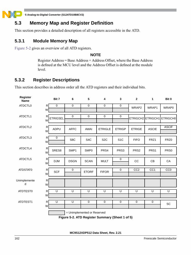
Chapter 5 Analog-to-Digital Converter (S12ATD10B8CV2)
MC9S12XDP512 Data Sheet, Rev. 2.21
162 Freescale Semiconductor
5.3 Memory Map and Register DefinitionThis section provides a detailed description of all registers accessible in the ATD.
5.3.1 Module Memory Map
Figure 5-2 gives an overview of all ATD registers.
NOTERegister Address = Base Address + Address Offset, where the Base Addressis defined at the MCU level and the Address Offset is defined at the modulelevel.
5.3.2 Register Descriptions
This section describes in address order all the ATD registers and their individual bits.
RegisterName
Bit 7 6 5 4 3 2 1 Bit 0
ATDCTL0 R 0 0 0 0 0WRAP2 WRAP1 WRAP0
W
ATDCTL1 RETRIGSEL
0 0 0 0ETRIGCH2 ETRIGCH1 ETRIGCH0
W
ATDCTL2 RADPU AFFC AWAI ETRIGLE ETRIGP ETRIGE ASCIE
ASCIFW
ATDCTL3 R 0S8C S4C S2C S1C FIFO FRZ1 FRZ0
W
ATDCTL4 RSRES8 SMP1 SMP0 PRS4 PRS3 PRS2 PRS1 PRS0
W
ATDCTL5 RDJM DSGN SCAN MULT
0CC CB CA
W
ATDSTAT0 RSCF
0ETORF FIFOR
0 CC2 CC1 CC0W
Unimplemented
RW
ATDTEST0 R U U U U U U U UW
ATDTEST1 R U U 0 0 0 0 0SC
W
= Unimplemented or Reserved
Figure 5-2. ATD Register Summary (Sheet 1 of 5)
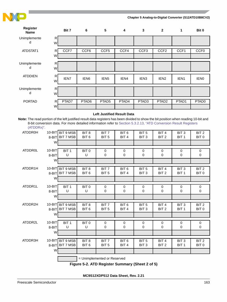
Chapter 5 Analog-to-Digital Converter (S12ATD10B8CV2)
MC9S12XDP512 Data Sheet, Rev. 2.21
Freescale Semiconductor 163
Unimplemented
RW
ATDSTAT1 R CCF7 CCF6 CCF5 CCF4 CCF3 CCF2 CCF1 CCF0W
Unimplemented
RW
ATDDIEN RIEN7 IEN6 IEN5 IEN4 IEN3 IEN2 IEN1 IEN0
W
Unimplemented
RW
PORTAD R PTAD7 PTAD6 PTAD5 PTAD4 PTAD3 PTAD2 PTAD1 PTAD0W
Left Justified Result DataNote: The read portion of the left justified result data registers has been divided to show the bit position when reading 10-bit and
8-bit conversion data. For more detailed information refer to Section 5.3.2.13, “ATD Conversion Result Registers(ATDDRx)”.
ATDDR0H 10-BIT BIT 9 MSBBIT 7 MSB
BIT 8BIT 6
BIT 7BIT 5
BIT 6BIT 4
BIT 5BIT 3
BIT 4BIT 2
BIT 3BIT 1
BIT 2BIT 08-BIT
W
ATDDR0L 10-BIT BIT 1U
BIT 0U
00
00
00
00
00
008-BIT
W
ATDDR1H 10-BIT BIT 9 MSBBIT 7 MSB
BIT 8BIT 6
BIT 7BIT 5
BIT 6BIT 4
BIT 5BIT 3
BIT 4BIT 2
BIT 3BIT 1
BIT 2BIT 08-BIT
W
ATDDR1L 10-BIT BIT 1U
BIT 0U
00
00
00
00
00
008-BIT
W
ATDDR2H 10-BIT BIT 9 MSBBIT 7 MSB
BIT 8BIT 6
BIT 7BIT 5
BIT 6BIT 4
BIT 5BIT 3
BIT 4BIT 2
BIT 3BIT 1
BIT 2BIT 08-BIT
W
ATDDR2L 10-BIT BIT 1U
BIT 0U
00
00
00
00
00
008-BIT
W
ATDDR3H 10-BIT BIT 9 MSBBIT 7 MSB
BIT 8BIT 6
BIT 7BIT 5
BIT 6BIT 4
BIT 5BIT 3
BIT 4BIT 2
BIT 3BIT 1
BIT 2BIT 08-BIT
W
RegisterName
Bit 7 6 5 4 3 2 1 Bit 0
= Unimplemented or Reserved
Figure 5-2. ATD Register Summary (Sheet 2 of 5)
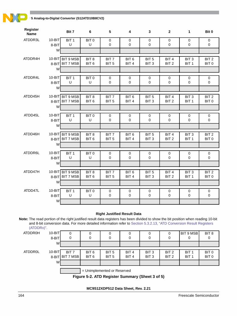
Chapter 5 Analog-to-Digital Converter (S12ATD10B8CV2)
MC9S12XDP512 Data Sheet, Rev. 2.21
164 Freescale Semiconductor
ATDDR3L 10-BIT BIT 1U
BIT 0U
00
00
00
00
00
008-BIT
W
ATDDR4H 10-BIT BIT 9 MSBBIT 7 MSB
BIT 8BIT 6
BIT 7BIT 5
BIT 6BIT 4
BIT 5BIT 3
BIT 4BIT 2
BIT 3BIT 1
BIT 2BIT 08-BIT
W
ATDDR4L 10-BIT BIT 1U
BIT 0U
00
00
00
00
00
008-BIT
W
ATDD45H 10-BIT BIT 9 MSBBIT 7 MSB
BIT 8BIT 6
BIT 7BIT 5
BIT 6BIT 4
BIT 5BIT 3
BIT 4BIT 2
BIT 3BIT 1
BIT 2BIT 08-BIT
W
ATDD45L 10-BIT BIT 1U
BIT 0U
00
00
00
00
00
008-BIT
W
ATDD46H 10-BIT BIT 9 MSBBIT 7 MSB
BIT 8BIT 6
BIT 7BIT 5
BIT 6BIT 4
BIT 5BIT 3
BIT 4BIT 2
BIT 3BIT 1
BIT 2BIT 08-BIT
W
ATDDR6L 10-BIT BIT 1U
BIT 0U
00
00
00
00
00
008-BIT
W
ATDD47H 10-BIT BIT 9 MSBBIT 7 MSB
BIT 8BIT 6
BIT 7BIT 5
BIT 6BIT 4
BIT 5BIT 3
BIT 4BIT 2
BIT 3BIT 1
BIT 2BIT 08-BIT
W
ATDD47L 10-BIT BIT 1U
BIT 0U
00
00
00
00
00
008-BIT
W
Right Justified Result DataNote: The read portion of the right justified result data registers has been divided to show the bit position when reading 10-bit
and 8-bit conversion data. For more detailed information refer to Section 5.3.2.13, “ATD Conversion Result Registers(ATDDRx)”.
ATDDR0H 10-BIT 00
00
00
00
00
00
BIT 9 MSB0
BIT 808-BIT
W
ATDDR0L 10-BIT BIT 7BIT 7 MSB
BIT 6BIT 6
BIT 5BIT 5
BIT 4BIT 4
BIT 3BIT 3
BIT 2BIT 2
BIT 1BIT 1
BIT 0BIT 08-BIT
W
RegisterName
Bit 7 6 5 4 3 2 1 Bit 0
= Unimplemented or Reserved
Figure 5-2. ATD Register Summary (Sheet 3 of 5)
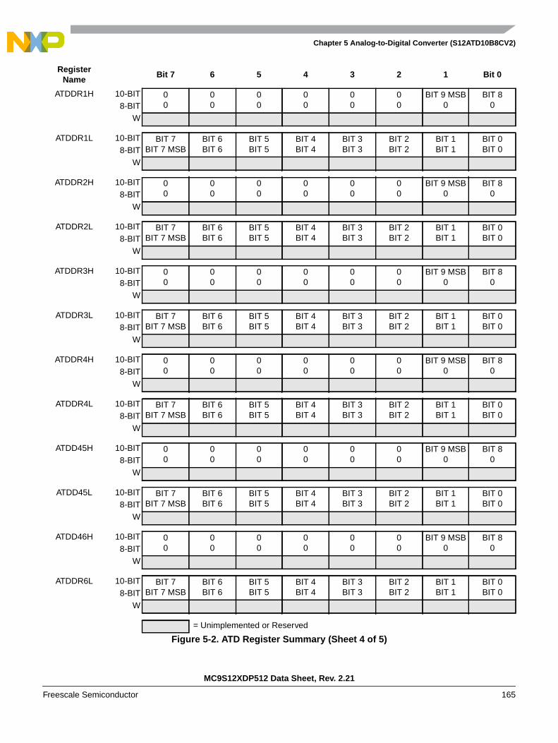
Chapter 5 Analog-to-Digital Converter (S12ATD10B8CV2)
MC9S12XDP512 Data Sheet, Rev. 2.21
Freescale Semiconductor 165
ATDDR1H 10-BIT 00
00
00
00
00
00
BIT 9 MSB0
BIT 808-BIT
W
ATDDR1L 10-BIT BIT 7BIT 7 MSB
BIT 6BIT 6
BIT 5BIT 5
BIT 4BIT 4
BIT 3BIT 3
BIT 2BIT 2
BIT 1BIT 1
BIT 0BIT 08-BIT
W
ATDDR2H 10-BIT 00
00
00
00
00
00
BIT 9 MSB0
BIT 808-BIT
W
ATDDR2L 10-BIT BIT 7BIT 7 MSB
BIT 6BIT 6
BIT 5BIT 5
BIT 4BIT 4
BIT 3BIT 3
BIT 2BIT 2
BIT 1BIT 1
BIT 0BIT 08-BIT
W
ATDDR3H 10-BIT 00
00
00
00
00
00
BIT 9 MSB0
BIT 808-BIT
W
ATDDR3L 10-BIT BIT 7BIT 7 MSB
BIT 6BIT 6
BIT 5BIT 5
BIT 4BIT 4
BIT 3BIT 3
BIT 2BIT 2
BIT 1BIT 1
BIT 0BIT 08-BIT
W
ATDDR4H 10-BIT 00
00
00
00
00
00
BIT 9 MSB0
BIT 808-BIT
W
ATDDR4L 10-BIT BIT 7BIT 7 MSB
BIT 6BIT 6
BIT 5BIT 5
BIT 4BIT 4
BIT 3BIT 3
BIT 2BIT 2
BIT 1BIT 1
BIT 0BIT 08-BIT
W
ATDD45H 10-BIT 00
00
00
00
00
00
BIT 9 MSB0
BIT 808-BIT
W
ATDD45L 10-BIT BIT 7BIT 7 MSB
BIT 6BIT 6
BIT 5BIT 5
BIT 4BIT 4
BIT 3BIT 3
BIT 2BIT 2
BIT 1BIT 1
BIT 0BIT 08-BIT
W
ATDD46H 10-BIT 00
00
00
00
00
00
BIT 9 MSB0
BIT 808-BIT
W
ATDDR6L 10-BIT BIT 7BIT 7 MSB
BIT 6BIT 6
BIT 5BIT 5
BIT 4BIT 4
BIT 3BIT 3
BIT 2BIT 2
BIT 1BIT 1
BIT 0BIT 08-BIT
W
RegisterName
Bit 7 6 5 4 3 2 1 Bit 0
= Unimplemented or Reserved
Figure 5-2. ATD Register Summary (Sheet 4 of 5)

Chapter 5 Analog-to-Digital Converter (S12ATD10B8CV2)
MC9S12XDP512 Data Sheet, Rev. 2.21
166 Freescale Semiconductor
5.3.2.1 ATD Control Register 0 (ATDCTL0)
Writes to this register will abort current conversion sequence but will not start a new sequence.
Read: Anytime
Write: Anytime
ATDD47H 10-BIT 00
00
00
00
00
00
BIT 9 MSB0
BIT 808-BIT
W
ATDD47L 10-BIT BIT 7BIT 7 MSB
BIT 6BIT 6
BIT 5BIT 5
BIT 4BIT 4
BIT 3BIT 3
BIT 2BIT 2
BIT 1BIT 1
BIT 0BIT 0
8-BIT
7 6 5 4 3 2 1 0
R 0 0 0 0 0WRAP2 WRAP1 WRAP0
W
Reset 0 0 0 0 0 1 1 1
= Unimplemented or Reserved
Figure 5-3. ATD Control Register 0 (ATDCTL0)
Table 5-1. ATDCTL0 Field Descriptions
Field Description
2–0WRAP[2:0]
Wrap Around Channel Select Bits — These bits determine the channel for wrap around when doingmulti-channel conversions. The coding is summarized in Table 5-2.
Table 5-2. Multi-Channel Wrap Around Coding
WRAP2 WRAP1 WRAP0Multiple Channel Conversions (MULT = 1)
Wrap Around to AN0 after Converting
0 0 0 Reserved
0 0 1 AN1
0 1 0 AN2
0 1 1 AN3
1 0 0 AN4
1 0 1 AN5
1 1 0 AN6
1 1 1 AN7
RegisterName
Bit 7 6 5 4 3 2 1 Bit 0
= Unimplemented or Reserved
Figure 5-2. ATD Register Summary (Sheet 5 of 5)
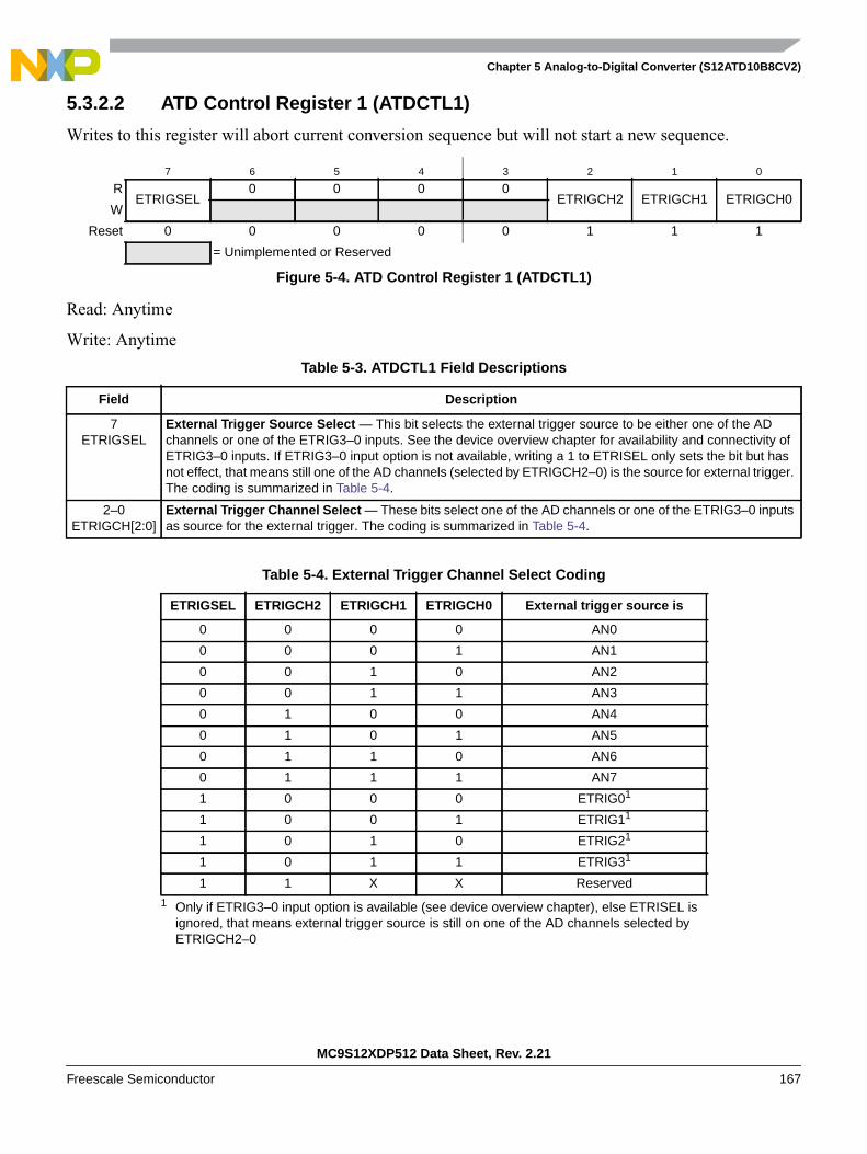
Chapter 5 Analog-to-Digital Converter (S12ATD10B8CV2)
MC9S12XDP512 Data Sheet, Rev. 2.21
Freescale Semiconductor 167
5.3.2.2 ATD Control Register 1 (ATDCTL1)
Writes to this register will abort current conversion sequence but will not start a new sequence.
Read: Anytime
Write: Anytime
7 6 5 4 3 2 1 0
RETRIGSEL
0 0 0 0ETRIGCH2 ETRIGCH1 ETRIGCH0
W
Reset 0 0 0 0 0 1 1 1
= Unimplemented or Reserved
Figure 5-4. ATD Control Register 1 (ATDCTL1)
Table 5-3. ATDCTL1 Field Descriptions
Field Description
7ETRIGSEL
External Trigger Source Select — This bit selects the external trigger source to be either one of the ADchannels or one of the ETRIG3–0 inputs. See the device overview chapter for availability and connectivity ofETRIG3–0 inputs. If ETRIG3–0 input option is not available, writing a 1 to ETRISEL only sets the bit but hasnot effect, that means still one of the AD channels (selected by ETRIGCH2–0) is the source for external trigger.The coding is summarized in Table 5-4.
2–0ETRIGCH[2:0]
External Trigger Channel Select — These bits select one of the AD channels or one of the ETRIG3–0 inputsas source for the external trigger. The coding is summarized in Table 5-4.
Table 5-4. External Trigger Channel Select Coding
ETRIGSEL ETRIGCH2 ETRIGCH1 ETRIGCH0 External trigger source is
0 0 0 0 AN0
0 0 0 1 AN1
0 0 1 0 AN2
0 0 1 1 AN3
0 1 0 0 AN4
0 1 0 1 AN5
0 1 1 0 AN6
0 1 1 1 AN7
1 0 0 0 ETRIG01
1 Only if ETRIG3–0 input option is available (see device overview chapter), else ETRISEL isignored, that means external trigger source is still on one of the AD channels selected byETRIGCH2–0
1 0 0 1 ETRIG11
1 0 1 0 ETRIG21
1 0 1 1 ETRIG31
1 1 X X Reserved

Chapter 5 Analog-to-Digital Converter (S12ATD10B8CV2)
MC9S12XDP512 Data Sheet, Rev. 2.21
168 Freescale Semiconductor
5.3.2.3 ATD Control Register 2 (ATDCTL2)
This register controls power down, interrupt and external trigger. Writes to this register will abort currentconversion sequence but will not start a new sequence.
Read: Anytime
Write: Anytime
7 6 5 4 3 2 1 0
RADPU AFFC AWAI ETRIGLE ETRIGP ETRIGE ASCIE
ASCIF
W
Reset 0 0 0 0 0 0 0 0
= Unimplemented or Reserved
Figure 5-5. ATD Control Register 2 (ATDCTL2)
Table 5-5. ATDCTL2 Field Descriptions
Field Description
7ADPU
ATD Power Up — This bit provides on/off control over the ATD block allowing reduced MCU powerconsumption. Because analog electronic is turned off when powered down, the ATD requires a recovery timeperiod after ADPU bit is enabled.0 Power down ATD1 Normal ATD functionality
6AFFC
ATD Fast Flag Clear All0 ATD flag clearing operates normally (read the status register ATDSTAT1 before reading the result register to
clear the associate CCF flag).1 Changes all ATD conversion complete flags to a fast clear sequence. Any access to a result register will
cause the associate CCF flag to clear automatically.
5AWAI
ATD Power Down in Wait Mode — When entering wait mode this bit provides on/off control over the ATD blockallowing reduced MCU power. Because analog electronic is turned off when powered down, the ATD requiresa recovery time period after exit from Wait mode.0 ATD continues to run in Wait mode1 Halt conversion and power down ATD during wait mode
After exiting wait mode with an interrupt conversion will resume. But due to the recovery time the result ofthis conversion should be ignored.
4ETRIGLE
External Trigger Level/Edge Control — This bit controls the sensitivity of the external trigger signal. SeeTable 5-6 for details.
3ETRIGP
External Trigger Polarity — This bit controls the polarity of the external trigger signal. See Table 5-6 fordetails.
2ETRIGE
External Trigger Mode Enable — This bit enables the external trigger on one of the AD channels or one ofthe ETRIG3–0 inputs as described in Table 5-4. If external trigger source is one of the AD channels, the digitalinput buffer of this channel is enabled. The external trigger allows to synchronize sample and ATD conversionsprocesses with external events.0 Disable external trigger1 Enable external triggerNote: If using one of the AD channel as external trigger (ETRIGSEL = 0) the conversion results for this channel
have no meaning while external trigger mode is enabled.
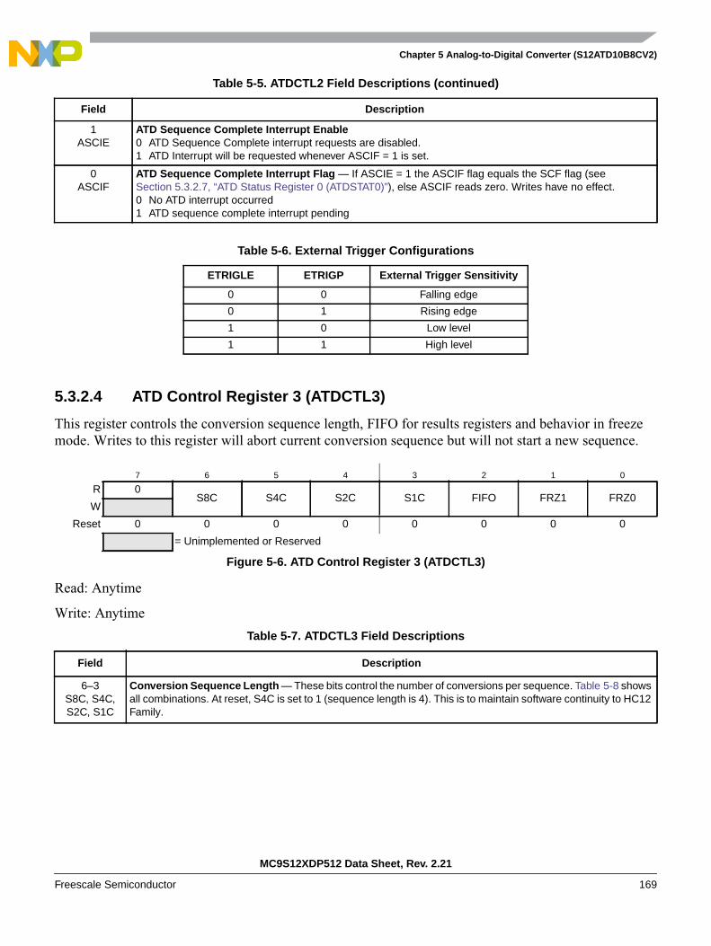
Chapter 5 Analog-to-Digital Converter (S12ATD10B8CV2)
MC9S12XDP512 Data Sheet, Rev. 2.21
Freescale Semiconductor 169
5.3.2.4 ATD Control Register 3 (ATDCTL3)
This register controls the conversion sequence length, FIFO for results registers and behavior in freezemode. Writes to this register will abort current conversion sequence but will not start a new sequence.
Read: Anytime
Write: Anytime
1ASCIE
ATD Sequence Complete Interrupt Enable0 ATD Sequence Complete interrupt requests are disabled.1 ATD Interrupt will be requested whenever ASCIF = 1 is set.
0ASCIF
ATD Sequence Complete Interrupt Flag — If ASCIE = 1 the ASCIF flag equals the SCF flag (seeSection 5.3.2.7, “ATD Status Register 0 (ATDSTAT0)”), else ASCIF reads zero. Writes have no effect.0 No ATD interrupt occurred1 ATD sequence complete interrupt pending
Table 5-6. External Trigger Configurations
ETRIGLE ETRIGP External Trigger Sensitivity
0 0 Falling edge
0 1 Rising edge
1 0 Low level
1 1 High level
7 6 5 4 3 2 1 0
R 0S8C S4C S2C S1C FIFO FRZ1 FRZ0
W
Reset 0 0 0 0 0 0 0 0
= Unimplemented or Reserved
Figure 5-6. ATD Control Register 3 (ATDCTL3)
Table 5-7. ATDCTL3 Field Descriptions
Field Description
6–3S8C, S4C,S2C, S1C
Conversion Sequence Length — These bits control the number of conversions per sequence. Table 5-8 showsall combinations. At reset, S4C is set to 1 (sequence length is 4). This is to maintain software continuity to HC12Family.
Table 5-5. ATDCTL2 Field Descriptions (continued)
Field Description

Chapter 5 Analog-to-Digital Converter (S12ATD10B8CV2)
MC9S12XDP512 Data Sheet, Rev. 2.21
170 Freescale Semiconductor
2FIFO
Result Register FIFO Mode — If this bit is zero (non-FIFO mode), the A/D conversion results map into the resultregisters based on the conversion sequence; the result of the first conversion appears in the first result register,the second result in the second result register, and so on.If this bit is one (FIFO mode) the conversion counter is not reset at the beginning or ending of a conversionsequence; sequential conversion results are placed in consecutive result registers. In a continuously scanningconversion sequence, the result register counter will wrap around when it reaches the end of the result registerfile. The conversion counter value (CC2-0 in ATDSTAT0) can be used to determine where in the result registerfile, the current conversion result will be placed.Aborting a conversion or starting a new conversion by write to an ATDCTL register (ATDCTL5-0) clears theconversion counter even if FIFO=1. So the first result of a new conversion sequence, started by writing toATDCTL5, will always be place in the first result register (ATDDDR0). Intended usage of FIFO mode is continuosconversion (SCAN=1) or triggered conversion (ETRIG=1).Finally, which result registers hold valid data can be tracked using the conversion complete flags. Fast flag clearmode may or may not be useful in a particular application to track valid data.0 Conversion results are placed in the corresponding result register up to the selected sequence length.1 Conversion results are placed in consecutive result registers (wrap around at end).
1–0FRZ[1:0]
Background Debug Freeze Enable — When debugging an application, it is useful in many cases to have theATD pause when a breakpoint (Freeze Mode) is encountered. These 2 bits determine how the ATD will respondto a breakpoint as shown in Table 5-9. Leakage onto the storage node and comparator reference capacitors maycompromise the accuracy of an immediately frozen conversion depending on the length of the freeze period.
Table 5-8. Conversion Sequence Length Coding
S8C S4C S2C S1CNumber of Conversions
per Sequence
0 0 0 0 8
0 0 0 1 1
0 0 1 0 2
0 0 1 1 3
0 1 0 0 4
0 1 0 1 5
0 1 1 0 6
0 1 1 1 7
1 X X X 8
Table 5-9. ATD Behavior in Freeze Mode (Breakpoint)
FRZ1 FRZ0 Behavior in Freeze Mode
0 0 Continue conversion
0 1 Reserved
1 0 Finish current conversion, then freeze
1 1 Freeze Immediately
Table 5-7. ATDCTL3 Field Descriptions (continued)
Field Description
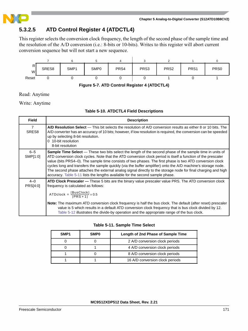
Chapter 5 Analog-to-Digital Converter (S12ATD10B8CV2)
MC9S12XDP512 Data Sheet, Rev. 2.21
Freescale Semiconductor 171
5.3.2.5 ATD Control Register 4 (ATDCTL4)
This register selects the conversion clock frequency, the length of the second phase of the sample time andthe resolution of the A/D conversion (i.e.: 8-bits or 10-bits). Writes to this register will abort currentconversion sequence but will not start a new sequence.
Read: Anytime
Write: Anytime
7 6 5 4 3 2 1 0
RSRES8 SMP1 SMP0 PRS4 PRS3 PRS2 PRS1 PRS0
W
Reset 0 0 0 0 0 1 0 1
Figure 5-7. ATD Control Register 4 (ATDCTL4)
Table 5-10. ATDCTL4 Field Descriptions
Field Description
7SRES8
A/D Resolution Select — This bit selects the resolution of A/D conversion results as either 8 or 10 bits. TheA/D converter has an accuracy of 10 bits; however, if low resolution is required, the conversion can be speededup by selecting 8-bit resolution.0 10-bit resolution
8-bit resolution
6–5SMP[1:0]
Sample Time Select — These two bits select the length of the second phase of the sample time in units ofATD conversion clock cycles. Note that the ATD conversion clock period is itself a function of the prescalervalue (bits PRS4–0). The sample time consists of two phases. The first phase is two ATD conversion clockcycles long and transfers the sample quickly (via the buffer amplifier) onto the A/D machine’s storage node.The second phase attaches the external analog signal directly to the storage node for final charging and highaccuracy. Table 5-11 lists the lengths available for the second sample phase.
4–0PRS[4:0]
ATD Clock Prescaler — These 5 bits are the binary value prescaler value PRS. The ATD conversion clockfrequency is calculated as follows:
Note: The maximum ATD conversion clock frequency is half the bus clock. The default (after reset) prescalervalue is 5 which results in a default ATD conversion clock frequency that is bus clock divided by 12.Table 5-12 illustrates the divide-by operation and the appropriate range of the bus clock.
Table 5-11. Sample Time Select
SMP1 SMP0 Length of 2nd Phase of Sample Time
0 0 2 A/D conversion clock periods
0 1 4 A/D conversion clock periods
1 0 8 A/D conversion clock periods
1 1 16 A/D conversion clock periods
ATDclockBusClock[ ]PRS 1+[ ]--------------------------------- 0.5×=
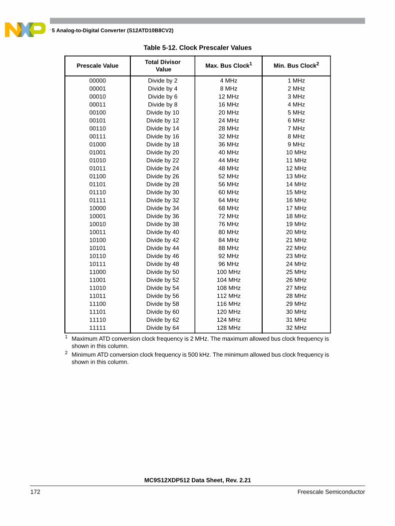
Chapter 5 Analog-to-Digital Converter (S12ATD10B8CV2)
MC9S12XDP512 Data Sheet, Rev. 2.21
172 Freescale Semiconductor
Table 5-12. Clock Prescaler Values
Prescale ValueTotal Divisor
ValueMax. Bus Clock1
1 Maximum ATD conversion clock frequency is 2 MHz. The maximum allowed bus clock frequency isshown in this column.
Min. Bus Clock2
2 Minimum ATD conversion clock frequency is 500 kHz. The minimum allowed bus clock frequency isshown in this column.
0000000001000100001100100001010011000111010000100101010010110110001101011100111110000100011001010011101001010110110101111100011001110101101111100111011111011111
Divide by 2Divide by 4Divide by 6Divide by 8Divide by 10Divide by 12Divide by 14Divide by 16Divide by 18Divide by 20Divide by 22Divide by 24Divide by 26Divide by 28Divide by 30Divide by 32Divide by 34Divide by 36Divide by 38Divide by 40Divide by 42Divide by 44Divide by 46Divide by 48Divide by 50Divide by 52Divide by 54Divide by 56Divide by 58Divide by 60Divide by 62Divide by 64
4 MHz8 MHz
12 MHz16 MHz20 MHz24 MHz28 MHz32 MHz36 MHz40 MHz44 MHz48 MHz52 MHz56 MHz60 MHz64 MHz68 MHz72 MHz76 MHz80 MHz84 MHz88 MHz92 MHz96 MHz100 MHz104 MHz108 MHz112 MHz116 MHz120 MHz124 MHz128 MHz
1 MHz2 MHz3 MHz4 MHz5 MHz6 MHz7 MHz8 MHz9 MHz10 MHz11 MHz12 MHz13 MHz14 MHz15 MHz16 MHz17 MHz18 MHz19 MHz20 MHz21 MHz22 MHz23 MHz24 MHz25 MHz26 MHz27 MHz28 MHz29 MHz30 MHz31 MHz32 MHz

Chapter 5 Analog-to-Digital Converter (S12ATD10B8CV2)
MC9S12XDP512 Data Sheet, Rev. 2.21
Freescale Semiconductor 173
5.3.2.6 ATD Control Register 5 (ATDCTL5)
This register selects the type of conversion sequence and the analog input channels sampled. Writes to thisregister will abort current conversion sequence and start a new conversion sequence.
Read: Anytime
Write: Anytime
7 6 5 4 3 2 1 0
RDJM DSGN SCAN MULT
0CC CB CA
W
Reset 0 0 0 0 0 0 0 0
= Unimplemented or Reserved
Figure 5-8. ATD Control Register 5 (ATDCTL5)
Table 5-13. ATDCTL5 Field Descriptions
Field Description
7DJM
Result Register Data Justification — This bit controls justification of conversion data in the result registers.See Section 5.3.2.13, “ATD Conversion Result Registers (ATDDRx),” for details.0 Left justified data in the result registers1 Right justified data in the result registers
6DSGN
Result Register Data Signed or Unsigned Representation — This bit selects between signed and unsignedconversion data representation in the result registers. Signed data is represented as 2’s complement. Signeddata is not available in right justification. See Section 5.3.2.13, “ATD Conversion Result Registers (ATDDRx),”for details.0 Unsigned data representation in the result registers1 Signed data representation in the result registersTable 5-14 summarizes the result data formats available and how they are set up using the control bits.Table 5-15 illustrates the difference between the signed and unsigned, left justified output codes for an inputsignal range between 0 and 5.12 Volts.
5SCAN
Continuous Conversion Sequence Mode — This bit selects whether conversion sequences are performedcontinuously or only once.0 Single conversion sequence1 Continuous conversion sequences (scan mode)
4MULT
Multi-Channel Sample Mode — When MULT is 0, the ATD sequence controller samples only from the specifiedanalog input channel for an entire conversion sequence. The analog channel is selected by channel selectioncode (control bits CC/CB/CA located in ATDCTL5). When MULT is 1, the ATD sequence controller samplesacross channels. The number of channels sampled is determined by the sequence length value (S8C, S4C,S2C, S1C). The first analog channel examined is determined by channel selection code (CC, CB, CA controlbits); subsequent channels sampled in the sequence are determined by incrementing the channel selectioncode.0 Sample only one channel1 Sample across several channels
2–0CC, CB, CA
Analog Input Channel Select Code — These bits select the analog input channel(s) whose signals aresampled and converted to digital codes. Table 5-16 lists the coding used to select the various analog inputchannels. In the case of single channel scans (MULT = 0), this selection code specified the channel examined.In the case of multi-channel scans (MULT = 1), this selection code represents the first channel to be examinedin the conversion sequence. Subsequent channels are determined by incrementing channel selection code;selection codes that reach the maximum value wrap around to the minimum value.
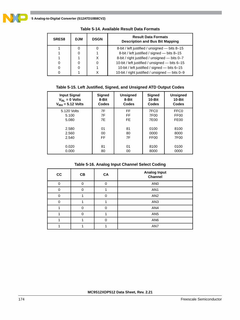
Chapter 5 Analog-to-Digital Converter (S12ATD10B8CV2)
MC9S12XDP512 Data Sheet, Rev. 2.21
174 Freescale Semiconductor
Table 5-14. Available Result Data Formats
SRES8 DJM DSGNResult Data Formats
Description and Bus Bit Mapping
111000
001001
01X01X
8-bit / left justified / unsigned — bits 8–158-bit / left justified / signed — bits 8–15
8-bit / right justified / unsigned — bits 0–710-bit / left justified / unsigned — bits 6–1510-bit / left justified / signed — bits 6–15
10-bit / right justified / unsigned — bits 0–9
Table 5-15. Left Justified, Signed, and Unsigned ATD Output Codes
Input SignalVRL = 0 Volts
VRH = 5.12 Volts
Signed8-Bit
Codes
Unsigned8-Bit
Codes
Signed10-BitCodes
Unsigned10-BitCodes
5.120 Volts5.1005.080
2.5802.5602.540
0.0200.000
7F7F7E
0100FF
8180
FFFFFE
81807F
0100
7FC07F007E00
01000000FF00
81008000
FFC0FF00FE00
810080007F00
01000000
Table 5-16. Analog Input Channel Select Coding
CC CB CAAnalog Input
Channel
0 0 0 AN0
0 0 1 AN1
0 1 0 AN2
0 1 1 AN3
1 0 0 AN4
1 0 1 AN5
1 1 0 AN6
1 1 1 AN7
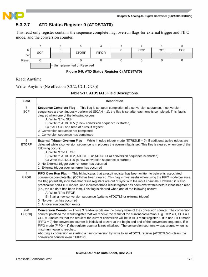
Chapter 5 Analog-to-Digital Converter (S12ATD10B8CV2)
MC9S12XDP512 Data Sheet, Rev. 2.21
Freescale Semiconductor 175
5.3.2.7 ATD Status Register 0 (ATDSTAT0)
This read-only register contains the sequence complete flag, overrun flags for external trigger and FIFOmode, and the conversion counter.
Read: Anytime
Write: Anytime (No effect on (CC2, CC1, CC0))
7 6 5 4 3 2 1 0
RSCF
0ETORF FIFOR
0 CC2 CC1 CC0
W
Reset 0 0 0 0 0 0 0 0
= Unimplemented or Reserved
Figure 5-9. ATD Status Register 0 (ATDSTAT0)
Table 5-17. ATDSTAT0 Field Descriptions
Field Description
7SCF
Sequence Complete Flag — This flag is set upon completion of a conversion sequence. If conversionsequences are continuously performed (SCAN = 1), the flag is set after each one is completed. This flag iscleared when one of the following occurs:
A) Write “1” to SCFB) Write to ATDCTL5 (a new conversion sequence is started)C) If AFFC=1 and read of a result register
0 Conversion sequence not completed1 Conversion sequence has completed
5ETORF
External Trigger Overrun Flag — While in edge trigger mode (ETRIGLE = 0), if additional active edges aredetected while a conversion sequence is in process the overrun flag is set. This flag is cleared when one of thefollowing occurs:
A) Write “1” to ETORFB) Write to ATDCTL2, ATDCTL3 or ATDCTL4 (a conversion sequence is aborted)C) Write to ATDCTL5 (a new conversion sequence is started)
0 No External trigger over run error has occurred1 External trigger over run error has occurred
4FIFOR
FIFO Over Run Flag — This bit indicates that a result register has been written to before its associatedconversion complete flag (CCF) has been cleared. This flag is most useful when using the FIFO mode becausethe flag potentially indicates that result registers are out of sync with the input channels. However, it is alsopractical for non-FIFO modes, and indicates that a result register has been over written before it has been read(i.e., the old data has been lost). This flag is cleared when one of the following occurs:
A) Write “1” to FIFORB) Start a new conversion sequence (write to ATDCTL5 or external trigger)
0 No over run has occurred1 An over run condition exists
2–0CC[2:0]
Conversion Counter — These 3 read-only bits are the binary value of the conversion counter. The conversioncounter points to the result register that will receive the result of the current conversion. E.g. CC2 = 1, CC1 = 1,CC0 = 0 indicates that the result of the current conversion will be in ATD result register 6. If in non-FIFO mode(FIFO = 0) the conversion counter is initialized to zero at the begin and end of the conversion sequence. If inFIFO mode (FIFO = 1) the register counter is not initialized. The conversion counters wraps around when itsmaximum value is reached.Aborting a conversion or starting a new conversion by write to an ATDCTL register (ATDCTL5-0) clears theconversion counter even if FIFO=1.
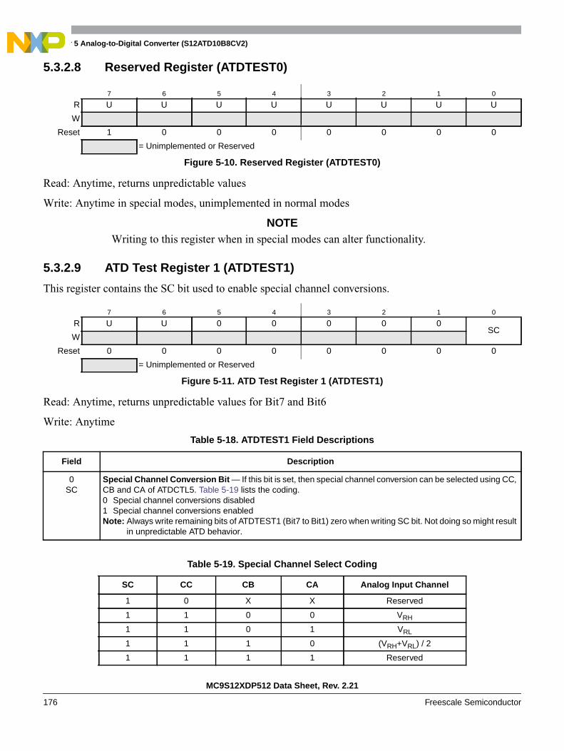
Chapter 5 Analog-to-Digital Converter (S12ATD10B8CV2)
MC9S12XDP512 Data Sheet, Rev. 2.21
176 Freescale Semiconductor
5.3.2.8 Reserved Register (ATDTEST0)
Read: Anytime, returns unpredictable values
Write: Anytime in special modes, unimplemented in normal modes
NOTEWriting to this register when in special modes can alter functionality.
5.3.2.9 ATD Test Register 1 (ATDTEST1)
This register contains the SC bit used to enable special channel conversions.
Read: Anytime, returns unpredictable values for Bit7 and Bit6
Write: Anytime
7 6 5 4 3 2 1 0
R U U U U U U U U
W
Reset 1 0 0 0 0 0 0 0
= Unimplemented or Reserved
Figure 5-10. Reserved Register (ATDTEST0)
7 6 5 4 3 2 1 0
R U U 0 0 0 0 0SC
W
Reset 0 0 0 0 0 0 0 0
= Unimplemented or Reserved
Figure 5-11. ATD Test Register 1 (ATDTEST1)
Table 5-18. ATDTEST1 Field Descriptions
Field Description
0SC
Special Channel Conversion Bit — If this bit is set, then special channel conversion can be selected using CC,CB and CA of ATDCTL5. Table 5-19 lists the coding.0 Special channel conversions disabled1 Special channel conversions enabledNote: Always write remaining bits of ATDTEST1 (Bit7 to Bit1) zero when writing SC bit. Not doing so might result
in unpredictable ATD behavior.
Table 5-19. Special Channel Select Coding
SC CC CB CA Analog Input Channel
1 0 X X Reserved
1 1 0 0 VRH
1 1 0 1 VRL
1 1 1 0 (VRH+VRL) / 2
1 1 1 1 Reserved

Chapter 5 Analog-to-Digital Converter (S12ATD10B8CV2)
MC9S12XDP512 Data Sheet, Rev. 2.21
Freescale Semiconductor 177
5.3.2.10 ATD Status Register 1 (ATDSTAT1)
This read-only register contains the conversion complete flags.
Read: Anytime
Write: Anytime, no effect
7 6 5 4 3 2 1 0
R CCF7 CCF6 CCF5 CCF4 CCF3 CCF2 CCF1 CCF0
W
Reset 0 0 0 0 0 0 0 0
= Unimplemented or Reserved
Figure 5-12. ATD Status Register 1 (ATDSTAT1)
Table 5-20. ATDSTAT1 Field Descriptions
Field Description
7–0CCF[7:0]
Conversion Complete Flag x (x = 7, 6, 5, 4, 3, 2, 1, 0) — A conversion complete flag is set at the end of eachconversion in a conversion sequence. The flags are associated with the conversion position in a sequence (andalso the result register number). Therefore, CCF0 is set when the first conversion in a sequence is complete andthe result is available in result register ATDDR0; CCF1 is set when the second conversion in a sequence iscomplete and the result is available in ATDDR1, and so forth. A flag CCFx (x = 7, 6, 5, 4, 3, 2,1, 70) is clearedwhen one of the following occurs:
A) Write to ATDCTL5 (a new conversion sequence is started)B) If AFFC=0 and read of ATDSTAT1 followed by read of result register ATDDRxC) If AFFC=1 and read of result register ATDDRx
In case of a concurrent set and clear on CCFx: The clearing by method A) will overwrite the set. The clearing bymethods B) or C) will be overwritten by the set.0 Conversion number x not completed1 Conversion number x has completed, result ready in ATDDRx
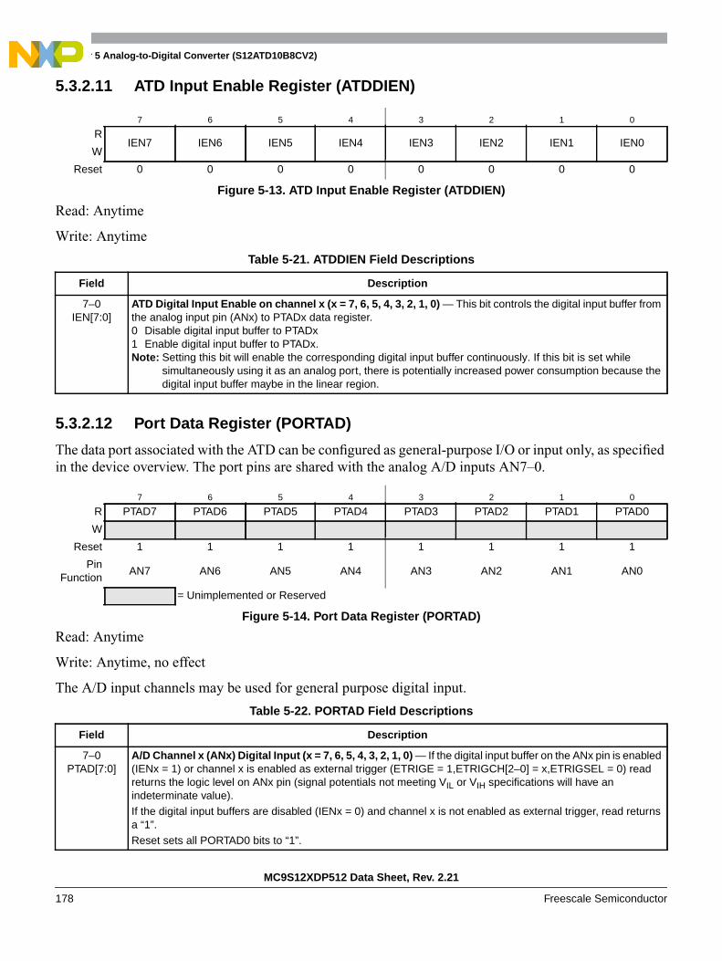
Chapter 5 Analog-to-Digital Converter (S12ATD10B8CV2)
MC9S12XDP512 Data Sheet, Rev. 2.21
178 Freescale Semiconductor
5.3.2.11 ATD Input Enable Register (ATDDIEN)
Read: Anytime
Write: Anytime
5.3.2.12 Port Data Register (PORTAD)
The data port associated with the ATD can be configured as general-purpose I/O or input only, as specifiedin the device overview. The port pins are shared with the analog A/D inputs AN7–0.
Read: Anytime
Write: Anytime, no effect
The A/D input channels may be used for general purpose digital input.
7 6 5 4 3 2 1 0
RIEN7 IEN6 IEN5 IEN4 IEN3 IEN2 IEN1 IEN0
W
Reset 0 0 0 0 0 0 0 0
Figure 5-13. ATD Input Enable Register (ATDDIEN)
Table 5-21. ATDDIEN Field Descriptions
Field Description
7–0IEN[7:0]
ATD Digital Input Enable on channel x (x = 7, 6, 5, 4, 3, 2, 1, 0) — This bit controls the digital input buffer fromthe analog input pin (ANx) to PTADx data register.0 Disable digital input buffer to PTADx1 Enable digital input buffer to PTADx.Note: Setting this bit will enable the corresponding digital input buffer continuously. If this bit is set while
simultaneously using it as an analog port, there is potentially increased power consumption because thedigital input buffer maybe in the linear region.
7 6 5 4 3 2 1 0
R PTAD7 PTAD6 PTAD5 PTAD4 PTAD3 PTAD2 PTAD1 PTAD0
W
Reset 1 1 1 1 1 1 1 1
PinFunction
AN7 AN6 AN5 AN4 AN3 AN2 AN1 AN0
= Unimplemented or Reserved
Figure 5-14. Port Data Register (PORTAD)
Table 5-22. PORTAD Field Descriptions
Field Description
7–0PTAD[7:0]
A/D Channel x (ANx) Digital Input (x = 7, 6, 5, 4, 3, 2, 1, 0) — If the digital input buffer on the ANx pin is enabled(IENx = 1) or channel x is enabled as external trigger (ETRIGE = 1,ETRIGCH[2–0] = x,ETRIGSEL = 0) readreturns the logic level on ANx pin (signal potentials not meeting VIL or VIH specifications will have anindeterminate value).If the digital input buffers are disabled (IENx = 0) and channel x is not enabled as external trigger, read returnsa “1”.Reset sets all PORTAD0 bits to “1”.

Chapter 5 Analog-to-Digital Converter (S12ATD10B8CV2)
MC9S12XDP512 Data Sheet, Rev. 2.21
Freescale Semiconductor 179
5.3.2.13 ATD Conversion Result Registers (ATDDRx)
The A/D conversion results are stored in 8 read-only result registers. The result data is formatted in theresult registers based on two criteria. First there is left and right justification; this selection is made usingthe DJM control bit in ATDCTL5. Second there is signed and unsigned data; this selection is made usingthe DSGN control bit in ATDCTL5. Signed data is stored in 2’s complement format and only exists in leftjustified format. Signed data selected for right justified format is ignored.
Read: Anytime
Write: Anytime in special mode, unimplemented in normal modes
5.3.2.13.1 Left Justified Result Data
5.3.2.13.2 Right Justified Result Data
7 6 5 4 3 2 1 0
RR
BIT 9 MSBBIT 7 MSB
BIT 8BIT 6
BIT 7BIT 5
BIT 6BIT 4
BIT 5BIT 3
BIT 4BIT 2
BIT 3BIT 1
BIT 2BIT 0
10-bit data8-bit data
W
Reset 0 0 0 0 0 0 0 0
= Unimplemented or Reserved
Figure 5-15. Left Justified, ATD Conversion Result Register, High Byte (ATDDRxH)
7 6 5 4 3 2 1 0
RR
BIT 1U
BIT 0U
00
00
00
00
00
00
W
Reset 0 0 0 0 0 0 0 0
= Unimplemented or Reserved
Figure 5-16. Left Justified, ATD Conversion Result Register, Low Byte (ATDDRxL)
7 6 5 4 3 2 1 0
RR
00
00
00
00
00
00
BIT 9 MSB0
BIT 80
10-bit data8-bit data
W
Reset 0 0 0 0 0 0 0 0
= Unimplemented or Reserved
Figure 5-17. Right Justified, ATD Conversion Result Register, High Byte (ATDDRxH)
7 6 5 4 3 2 1 0
RR
BIT 7BIT 7 MSB
BIT 6BIT 6
BIT 5BIT 5
BIT 4BIT 4
BIT 3BIT 3
BIT 2BIT 2
BIT 1BIT 1
BIT 0BIT 0
10-bit data8-bit data
W
Reset 0 0 0 0 0 0 0 0
= Unimplemented or Reserved
Figure 5-18. Right Justified, ATD Conversion Result Register, Low Byte (ATDDRxL)

Chapter 5 Analog-to-Digital Converter (S12ATD10B8CV2)
MC9S12XDP512 Data Sheet, Rev. 2.21
180 Freescale Semiconductor
5.4 Functional DescriptionThe ATD is structured in an analog and a digital sub-block.
5.4.1 Analog Sub-Block
The analog sub-block contains all analog electronics required to perform a single conversion. Separatepower supplies VDDA and VSSA allow to isolate noise of other MCU circuitry from the analog sub-block.
5.4.1.1 Sample and Hold Machine
The sample and hold (S/H) machine accepts analog signals from the external surroundings and stores themas capacitor charge on a storage node.
The sample process uses a two stage approach. During the first stage, the sample amplifier is used toquickly charge the storage node.The second stage connects the input directly to the storage node tocomplete the sample for high accuracy.
When not sampling, the sample and hold machine disables its own clocks. The analog electronics still drawtheir quiescent current. The power down (ADPU) bit must be set to disable both the digital clocks and theanalog power consumption.
The input analog signals are unipolar and must fall within the potential range of VSSA to VDDA.
5.4.1.2 Analog Input Multiplexer
The analog input multiplexer connects one of the 8 external analog input channels to the sample and holdmachine.
5.4.1.3 Sample Buffer Amplifier
The sample amplifier is used to buffer the input analog signal so that the storage node can be quicklycharged to the sample potential.
5.4.1.4 Analog-to-Digital (A/D) Machine
The A/D Machine performs analog to digital conversions. The resolution is program selectable at either 8or 10 bits. The A/D machine uses a successive approximation architecture. It functions by comparing thestored analog sample potential with a series of digitally generated analog potentials. By following a binarysearch algorithm, the A/D machine locates the approximating potential that is nearest to the sampledpotential.
When not converting the A/D machine disables its own clocks. The analog electronics still draws quiescentcurrent. The power down (ADPU) bit must be set to disable both the digital clocks and the analog powerconsumption.
Only analog input signals within the potential range of VRL to VRH (A/D reference potentials) will resultin a non-railed digital output codes.
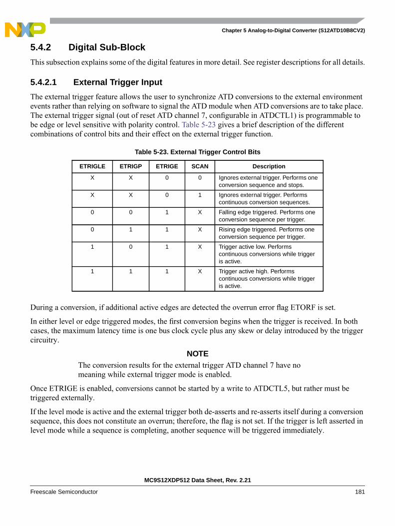
Chapter 5 Analog-to-Digital Converter (S12ATD10B8CV2)
MC9S12XDP512 Data Sheet, Rev. 2.21
Freescale Semiconductor 181
5.4.2 Digital Sub-Block
This subsection explains some of the digital features in more detail. See register descriptions for all details.
5.4.2.1 External Trigger Input
The external trigger feature allows the user to synchronize ATD conversions to the external environmentevents rather than relying on software to signal the ATD module when ATD conversions are to take place.The external trigger signal (out of reset ATD channel 7, configurable in ATDCTL1) is programmable tobe edge or level sensitive with polarity control. Table 5-23 gives a brief description of the differentcombinations of control bits and their effect on the external trigger function.
During a conversion, if additional active edges are detected the overrun error flag ETORF is set.
In either level or edge triggered modes, the first conversion begins when the trigger is received. In bothcases, the maximum latency time is one bus clock cycle plus any skew or delay introduced by the triggercircuitry.
NOTEThe conversion results for the external trigger ATD channel 7 have nomeaning while external trigger mode is enabled.
Once ETRIGE is enabled, conversions cannot be started by a write to ATDCTL5, but rather must betriggered externally.
If the level mode is active and the external trigger both de-asserts and re-asserts itself during a conversionsequence, this does not constitute an overrun; therefore, the flag is not set. If the trigger is left asserted inlevel mode while a sequence is completing, another sequence will be triggered immediately.
Table 5-23. External Trigger Control Bits
ETRIGLE ETRIGP ETRIGE SCAN Description
X X 0 0 Ignores external trigger. Performs oneconversion sequence and stops.
X X 0 1 Ignores external trigger. Performscontinuous conversion sequences.
0 0 1 X Falling edge triggered. Performs oneconversion sequence per trigger.
0 1 1 X Rising edge triggered. Performs oneconversion sequence per trigger.
1 0 1 X Trigger active low. Performscontinuous conversions while triggeris active.
1 1 1 X Trigger active high. Performscontinuous conversions while triggeris active.
Chapter 5 Analog-to-Digital Converter (S12ATD10B8CV2)
MC9S12XDP512 Data Sheet, Rev. 2.21
182 Freescale Semiconductor
5.4.2.2 General Purpose Digital Input Port Operation
The input channel pins can be multiplexed between analog and digital data. As analog inputs, they aremultiplexed and sampled to supply signals to the A/D converter. As digital inputs, they supply externalinput data that can be accessed through the digital port register PORTAD (input-only).
The analog/digital multiplex operation is performed in the input pads. The input pad is always connectedto the analog inputs of the ATD. The input pad signal is buffered to the digital port registers. This buffercan be turned on or off with the ATDDIEN register. This is important so that the buffer does not drawexcess current when analog potentials are presented at its input.
5.4.2.3 Low Power Modes
The ATD can be configured for lower MCU power consumption in 3 different ways:
1. Stop mode: This halts A/D conversion. Exit from stop mode will resume A/D conversion, but dueto the recovery time the result of this conversion should be ignored.
2. Wait mode with AWAI = 1: This halts A/D conversion. Exit from wait mode will resume A/Dconversion, but due to the recovery time the result of this conversion should be ignored.
3. Writing ADPU = 0 (Note that all ATD registers remain accessible.): This aborts any A/Dconversion in progress.
Note that the reset value for the ADPU bit is zero. Therefore, when this module is reset, it is reset into thepower down state.
5.5 ResetsAt reset the ATD is in a power down state. The reset state of each individual bit is listed within the RegisterDescription section (see Section 5.3, “Memory Map and Register Definition”), which details the registersand their bit-field.
5.6 InterruptsThe interrupt requested by the ATD is listed in Table 5-24. Refer to the device overview chapter for relatedvector address and priority.
See register descriptions for further details.
Table 5-24. ATD Interrupt Vectors
Interrupt SourceCCRMask
Local Enable
Sequence completeinterrupt
I bit ASCIE in ATDCTL2

MC9S12XDP512 Data Sheet, Rev. 2.21Freescale Semiconductor 183
Chapter 6XGATE (S12XGATEV2)
6.1 IntroductionThe XGATE module is a peripheral co-processor that allows autonomous data transfers between theMCU’s peripherals and the internal memories. It has a built in RISC core that is able to pre-process thetransferred data and perform complex communication protocols.
The XGATE module is intended to increase the MCU’s data throughput by lowering the S12X_CPU’sinterrupt load.
Figure 6-1 gives an overview on the XGATE architecture.
This document describes the functionality of the XGATE module, including:
• XGATE registers (Section 6.3, “Memory Map and Register Definition”)
• XGATE RISC core (Section 6.4.1, “XGATE RISC Core”)
• Hardware semaphores (Section 6.4.4, “Semaphores”)
• Interrupt handling (Section 6.5, “Interrupts”)
• Debug features (Section 6.6, “Debug Mode”)
• Security (Section 6.7, “Security”)
• Instruction set (Section 6.8, “Instruction Set”)
6.1.1 Glossary of Terms
XGATE Request
A service request from a peripheral module which is directed to the XGATE by the S12X_INTmodule (see Figure 6-1).
XGATE Channel
The resources in the XGATE module (i.e. Channel ID number, Priority level, Service RequestVector, Interrupt Flag) which are associated with a particular XGATE Request.
XGATE Channel ID
A 7-bit identifier associated with an XGATE channel. In S12X designs valid Channel IDs rangefrom $78 to $09.
XGATE Channel Interrupt
An S12X_CPU interrupt that is triggered by a code sequence running on the XGATE module.
XGATE Software Channel

Chapter 6 XGATE (S12XGATEV2)
MC9S12XDP512 Data Sheet, Rev. 2.21184 Freescale Semiconductor
Special XGATE channel that is not associated with any peripheral service request. A SoftwareChannel is triggered by its Software Trigger Bit which is implemented in the XGATE module.
XGATE Semaphore
A set of hardware flip-flops that can be exclusively set by either the S12X_CPU or the XGATE.(see 6.4.4/6-204)
XGATE Thread
A code sequence which is executed by the XGATE’s RISC core after receiving an XGATE request.
XGATE Debug Mode
A special mode in which the XGATE’s RISC core is halted for debug purposes. This mode enablesthe XGATE’s debug features (see 6.6/6-206).
XGATE Software Error
The XGATE is able to detect a number of error conditions caused by erratic software (see6.4.5/6-205). These error conditions will cause the XGATE to seize program execution and flag anInterrupt to the S12X_CPU.
Word
A 16 bit entity.
Byte
An 8 bit entity.
6.1.2 Features
The XGATE module includes these features:
• Data movement between various targets (i.e Flash, RAM, and peripheral modules)
• Data manipulation through built in RISC core
• Provides up to 112 XGATE channels
— 104 hardware triggered channels
— 8 software triggered channels
• Hardware semaphores which are shared between the S12X_CPU and the XGATE module
• Able to trigger S12X_CPU interrupts upon completion of an XGATE transfer
• Software error detection to catch erratic application code
6.1.3 Modes of Operation
There are four run modes on S12X devices.
• Run mode, wait mode, stop mode
The XGATE is able to operate in all of these three system modes. Clock activity will beautomatically stopped when the XGATE module is idle.
• Freeze mode (BDM active)
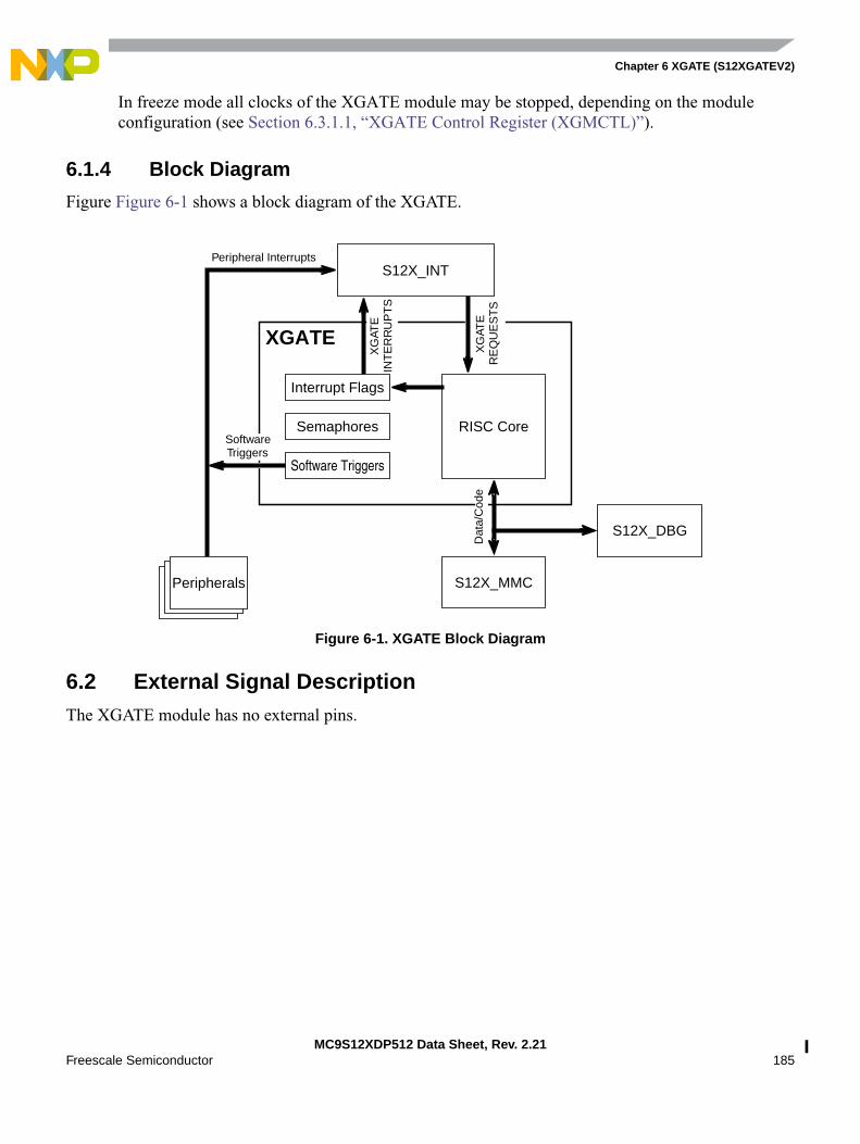
Chapter 6 XGATE (S12XGATEV2)
MC9S12XDP512 Data Sheet, Rev. 2.21Freescale Semiconductor 185
In freeze mode all clocks of the XGATE module may be stopped, depending on the moduleconfiguration (see Section 6.3.1.1, “XGATE Control Register (XGMCTL)”).
6.1.4 Block Diagram
Figure Figure 6-1 shows a block diagram of the XGATE.
Figure 6-1. XGATE Block Diagram
6.2 External Signal DescriptionThe XGATE module has no external pins.
INT
ER
RU
PT
SX
GAT
E
RE
QU
ES
TS
RISC Core
S12X_MMC
XGATE
Peripherals
Semaphores
Interrupt Flags
Software Triggers
Peripheral Interrupts
S12X_DBG
Dat
a/C
ode
SoftwareTriggers
XG
ATE
S12X_INT
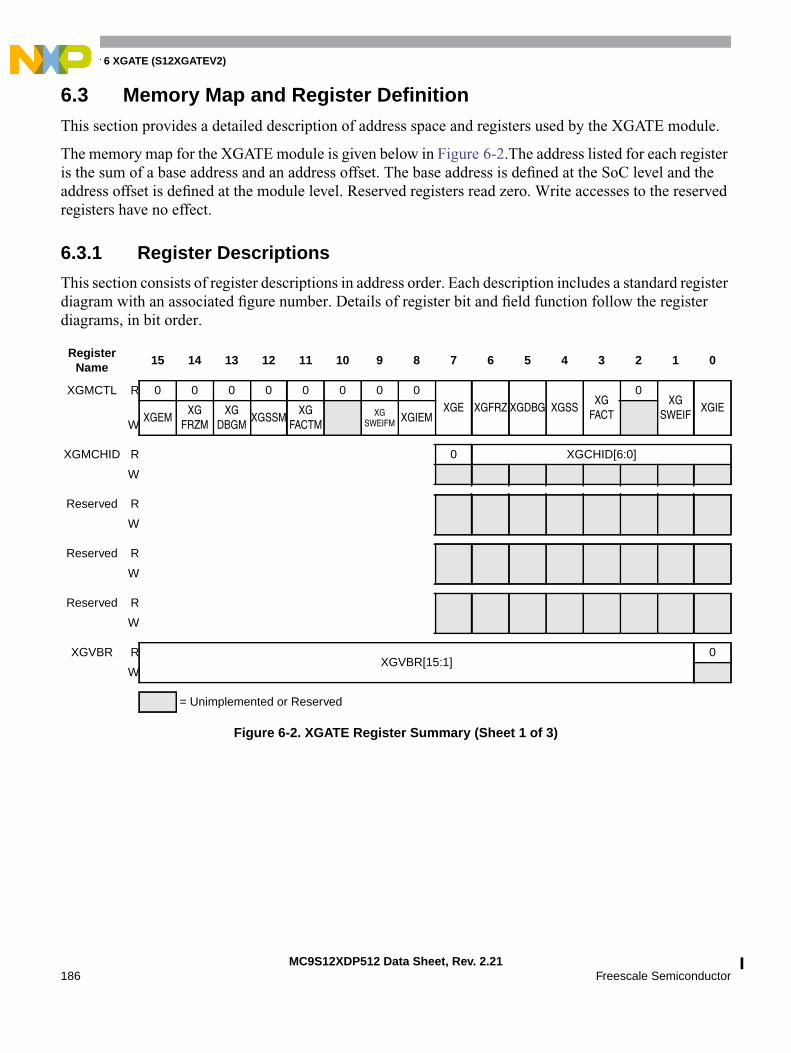
Chapter 6 XGATE (S12XGATEV2)
MC9S12XDP512 Data Sheet, Rev. 2.21186 Freescale Semiconductor
6.3 Memory Map and Register DefinitionThis section provides a detailed description of address space and registers used by the XGATE module.
The memory map for the XGATE module is given below in Figure 6-2.The address listed for each registeris the sum of a base address and an address offset. The base address is defined at the SoC level and theaddress offset is defined at the module level. Reserved registers read zero. Write accesses to the reservedregisters have no effect.
6.3.1 Register Descriptions
This section consists of register descriptions in address order. Each description includes a standard registerdiagram with an associated figure number. Details of register bit and field function follow the registerdiagrams, in bit order.
RegisterName
15 14 13 12 11 10 9 8 7 6 5 4 3 2 1 0
XGMCTL R 0 0 0 0 0 0 0 0XGE XGFRZ XGDBG XGSS
XGFACT
0XG
SWEIFXGIE
WXGEM
XGFRZM
XGDBGM
XGSSMXG
FACTMXG
SWEIFM XGIEM
XGMCHID R 0 XGCHID[6:0]
W
Reserved R
W
Reserved R
W
Reserved R
W
XGVBR RXGVBR[15:1]
0
W
= Unimplemented or Reserved
Figure 6-2. XGATE Register Summary (Sheet 1 of 3)

Chapter 6 XGATE (S12XGATEV2)
MC9S12XDP512 Data Sheet, Rev. 2.21Freescale Semiconductor 187
127 126 125 124 123 122 121 120 119 118 117 116 115 114 113 112
XGIF R 0 0 0 0 0 0 0XGIF_78 XGF_77 XGIF_76 XGIF_75 XGIF_74 XGIF_73 XGIF_72 XGIF_71 XGIF_70
W
111 110 109 108 107 106 105 104 103 102 101 100 99 98 97 96
XGIF RXGIF_6F XGIF_6E XGIF_6D XGIF_6C XGIF_6B XGIF_6A XGIF_69 XGIF_68 XGF_67 XGIF_66 XGIF_65 XGIF_64 XGIF_63 XGIF_62 XGIF_61 XGIF_60
W
95 94 93 92 91 90 89 88 87 86 85 84 83 82 81 80
XGIF RXGIF_5F XGIF_5E XGIF_5D XGIF_5C XGIF_5B XGIF_5A XGIF_59 XGIF_58 XGF_57 XGIF_56 XGIF_55 XGIF_54 XGIF_53 XGIF_52 XGIF_51 XGIF_50
W
79 78 77 76 75 74 73 72 71 70 69 68 67 66 65 64
XGIF RXGIF_4F XGIF_4E XGIF_4D XGIF_4C XGIF_4B XGIF_4A XGIF_49 XGIF_48 XGF _47 XGIF_46 XGIF_45 XGIF_44 XGIF_43 XGIF_42 XGIF_41 XGIF_40
W
RegisterName
63 62 61 60 59 58 57 56 55 54 53 52 51 50 49 48
XGIF RXGIF_3F XGIF_3E XGIF_3D XGIF_3C XGIF_3B XGIF_3A XGIF_39 XGIF_38 XGF _37 XGIF_36 XGIF_35 XGIF_34 XGIF_33 XGIF_32 XGIF_31 XGIF_30
W
47 46 45 44 43 42 41 40 39 38 37 36 35 34 33 32
XGIF RXGIF_2F XGIF_2E XGIF_2D XGIF_2C XGIF_2B XGIF_2A XGIF_29 XGIF_28 XGF _27 XGIF_26 XGIF_25 XGIF_24 XGIF_23 XGIF_22 XGIF_21 XGIF_20
W
31 30 29 28 27 26 25 24 23 22 21 20 19 18 17 16
XGIF RXGIF_1F XGIF_1E XGIF_1D XGIF_1C XGIF_1B XGIF_1A XGIF_19 XGIF_18 XGF _17 XGIF_16 XGIF_15 XGIF_14 XGIF_13 XGIF_12 XGIF_11 XGIF_10
W
15 14 13 12 11 10 9 8 7 6 5 4 3 2 1 0
XGIF RXGIF_0F XGIF_0E XGIF_0D XGIF_0C XGIF_0B XGIF_0A XGIF_09
0 0 0 0 0 0 0 0 0
W
= Unimplemented or Reserved
Figure 6-2. XGATE Register Summary (Sheet 2 of 3)

Chapter 6 XGATE (S12XGATEV2)
MC9S12XDP512 Data Sheet, Rev. 2.21188 Freescale Semiconductor
15 14 13 12 11 10 9 8 7 6 5 4 3 2 1 0
XGSWTM R 0 0 0 0 0 0 0 0XGSWT[7:0]
W XGSWTM[7:0]
XGSEMM R 0 0 0 0 0 0 0 0XGSEM[7:0]
W XGSEMM[7:0]
Reserved R
W
XGCCR R 0 0 0 0XGN XGZ XGV XGC
W
XGPC RXGPC
W
Reserved R
W
Reserved R
W
XGR1 RXGR1
W
XGR2 RXGR2
W
XGR3 RXGR3
W
XGR4 RXGR4
W
XGR5 RXGR5
W
XGR6 RXGR6
W
XGR7 RXGR7
W
= Unimplemented or Reserved
Figure 6-2. XGATE Register Summary (Sheet 3 of 3)
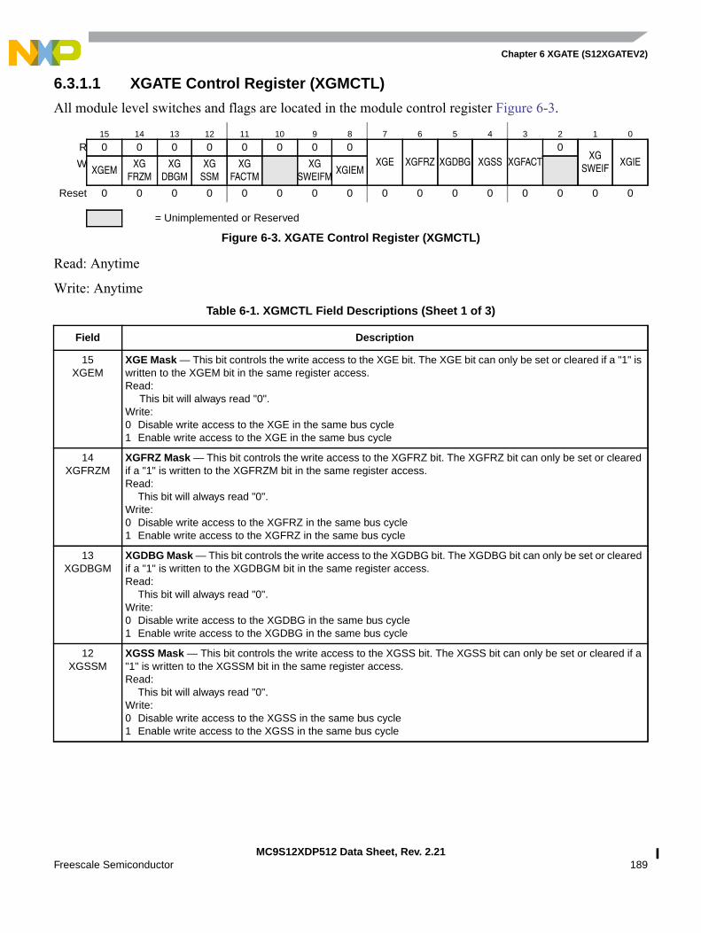
Chapter 6 XGATE (S12XGATEV2)
MC9S12XDP512 Data Sheet, Rev. 2.21Freescale Semiconductor 189
6.3.1.1 XGATE Control Register (XGMCTL)
All module level switches and flags are located in the module control register Figure 6-3.
Read: Anytime
Write: Anytime
15 14 13 12 11 10 9 8 7 6 5 4 3 2 1 0
R 0 0 0 0 0 0 0 0XGE XGFRZ XGDBG XGSS XGFACT
0XG
SWEIFXGIEW
XGEMXG
FRZMXG
DBGMXG
SSMXG
FACTMXG
SWEIFMXGIEM
Reset 0 0 0 0 0 0 0 0 0 0 0 0 0 0 0 0
= Unimplemented or Reserved
Figure 6-3. XGATE Control Register (XGMCTL)
Table 6-1. XGMCTL Field Descriptions (Sheet 1 of 3)
Field Description
15XGEM
XGE Mask — This bit controls the write access to the XGE bit. The XGE bit can only be set or cleared if a "1" iswritten to the XGEM bit in the same register access.Read:
This bit will always read "0".Write:0 Disable write access to the XGE in the same bus cycle1 Enable write access to the XGE in the same bus cycle
14XGFRZM
XGFRZ Mask — This bit controls the write access to the XGFRZ bit. The XGFRZ bit can only be set or clearedif a "1" is written to the XGFRZM bit in the same register access.Read:
This bit will always read "0".Write:0 Disable write access to the XGFRZ in the same bus cycle1 Enable write access to the XGFRZ in the same bus cycle
13XGDBGM
XGDBG Mask — This bit controls the write access to the XGDBG bit. The XGDBG bit can only be set or clearedif a "1" is written to the XGDBGM bit in the same register access.Read:
This bit will always read "0".Write:0 Disable write access to the XGDBG in the same bus cycle1 Enable write access to the XGDBG in the same bus cycle
12XGSSM
XGSS Mask — This bit controls the write access to the XGSS bit. The XGSS bit can only be set or cleared if a"1" is written to the XGSSM bit in the same register access.Read:
This bit will always read "0".Write:0 Disable write access to the XGSS in the same bus cycle1 Enable write access to the XGSS in the same bus cycle

Chapter 6 XGATE (S12XGATEV2)
MC9S12XDP512 Data Sheet, Rev. 2.21190 Freescale Semiconductor
11XGFACTM
XGFACT Mask — This bit controls the write access to the XGFACT bit. The XGFACT bit can only be set orcleared if a "1" is written to the XGFACTM bit in the same register access.Read:
This bit will always read "0".Write:0 Disable write access to the XGFACT in the same bus cycle1 Enable write access to the XGFACT in the same bus cycle
9XGSWEIFM
XGSWEIF Mask — This bit controls the write access to the XGSWEIF bit. The XGSWEIF bit can only be clearedif a "1" is written to the XGSWEIFM bit in the same register access.Read:
This bit will always read "0".Write:0 Disable write access to the XGSWEIF in the same bus cycle1 Enable write access to the XGSWEIF in the same bus cycle
8XGIEM
XGIE Mask — This bit controls the write access to the XGIE bit. The XGIE bit can only be set or cleared if a "1"is written to the XGIEM bit in the same register access.Read:
This bit will always read "0".Write:0 Disable write access to the XGIE in the same bus cycle1 Enable write access to the XGIE in the same bus cycle
7XGE
XGATE Module Enable — This bit enables the XGATE module. If the XGATE module is disabled, pendingXGATE requests will be ignored. The thread that is executed by the RISC core while the XGE bit is cleared willcontinue to run.Read:0 XGATE module is disabled1 XGATE module is enabledWrite:0 Disable XGATE module1 Enable XGATE module
6XGFRZ
Halt XGATE in Freeze Mode — The XGFRZ bit controls the XGATE operation in Freeze Mode (BDM active).Read:0 RISC core operates normally in Freeze (BDM active)1 RISC core stops in Freeze Mode (BDM active)Write:0 Don’t stop RISC core in Freeze Mode (BDM active)1 Stop RISC core in Freeze Mode (BDM active)
5XGDBG
XGATE Debug Mode — This bit indicates that the XGATE is in Debug Mode (see Section 6.6, “Debug Mode”).Debug Mode can be entered by Software Breakpoints (BRK instruction), Tagged or Forced Breakpoints (seeS12X_DBG Section), or by writing a "1" to this bit.Read:0 RISC core is not in Debug Mode1 RISC core is in Debug ModeWrite:0 Leave Debug Mode1 Enter Debug ModeNote: Freeze Mode and Software Error Interrupts have no effect on the XGDBG bit.
Table 6-1. XGMCTL Field Descriptions (Sheet 2 of 3)
Field Description

Chapter 6 XGATE (S12XGATEV2)
MC9S12XDP512 Data Sheet, Rev. 2.21Freescale Semiconductor 191
4XGSS
XGATE Single Step — This bit forces the execution of a single instruction if the XGATE is in DEBUG Mode andno software error has occurred (XGSWEIF cleared).Read:0 No single step in progress1 Single step in progressWrite0 No effect1 Execute a single RISC instructionNote: Invoking a Single Step will cause the XGATE to temporarily leave Debug Mode until the instruction has
been executed.
3XGFACT
Fake XGATE Activity — This bit forces the XGATE to flag activity to the MCU even when it is idle. When it is setthe MCU will never enter system stop mode which assures that peripheral modules will be clocked during XGATEidle periodsRead:0 XGATE will only flag activity if it is not idle or in debug mode.1 XGATE will always signal activity to the MCU.Write:0 Only flag activity if not idle or in debug mode.1 Always signal XGATE activity.
1XGSWEIF
XGATE Software Error Interrupt Flag — This bit signals a pending Software Error Interrupt. It is set if the RISCcore detects an error condition (see Section 6.4.5, “Software Error Detection”). The RISC core is stopped whilethis bit is set. Clearing this bit will terminate the current thread and cause the XGATE to become idle.Read:0 Software Error Interrupt is not pending1 Software Error Interrupt is pending if XGIE is setWrite:0 No effect1 Clears the XGSWEIF bit
0XGIE
XGATE Interrupt Enable — This bit acts as a global interrupt enable for the XGATE moduleRead:0 All XGATE interrupts disabled1 All XGATE interrupts enabledWrite:0 Disable all XGATE interrupts1 Enable all XGATE interrupts
Table 6-1. XGMCTL Field Descriptions (Sheet 3 of 3)
Field Description

Chapter 6 XGATE (S12XGATEV2)
MC9S12XDP512 Data Sheet, Rev. 2.21192 Freescale Semiconductor
6.3.1.2 XGATE Channel ID Register (XGCHID)
The XGATE channel ID register (Figure 6-4) shows the identifier of the XGATE channel that is currentlyactive. This register will read “$00” if the XGATE module is idle. In debug mode this register can be usedto start and terminate threads (see Section 6.6.1, “Debug Features”).
Read: Anytime
Write: In Debug Mode
6.3.1.3 XGATE Vector Base Address Register (XGVBR)
The vector base address register (Figure 6-5 and Figure 6-6) determines the location of the XGATE vectorblock.
Read: Anytime
Write: Only if the module is disabled (XGE = 0) and idle (XGCHID = $00))
7 6 5 4 3 2 1 0
R 0 XGCHID[6:0]
W
Reset 0 0 0 0 0 0 0 0
= Unimplemented or Reserved
Figure 6-4. XGATE Channel ID Register (XGCHID)
Table 6-2. XGCHID Field Descriptions
Field Description
6–0XGCHID[6:0]
Request Identifier — ID of the currently active channel
15 14 13 12 11 10 9 8 7 6 5 4 3 2 1 0
RXGVBR[15:1]
0
W
Reset 0 0 0 0 0 0 0 0 0 0 0 0 0 0 0 0
= Unimplemented or Reserved
Figure 6-5. XGATE Vector Base Address Register (XGVBR)
Table 6-3. XGVBR Field Descriptions
Field Description
15–1XBVBR[15:1]
Vector Base Address — The XGVBR register holds the start address of the vector block in the XGATEmemory map.
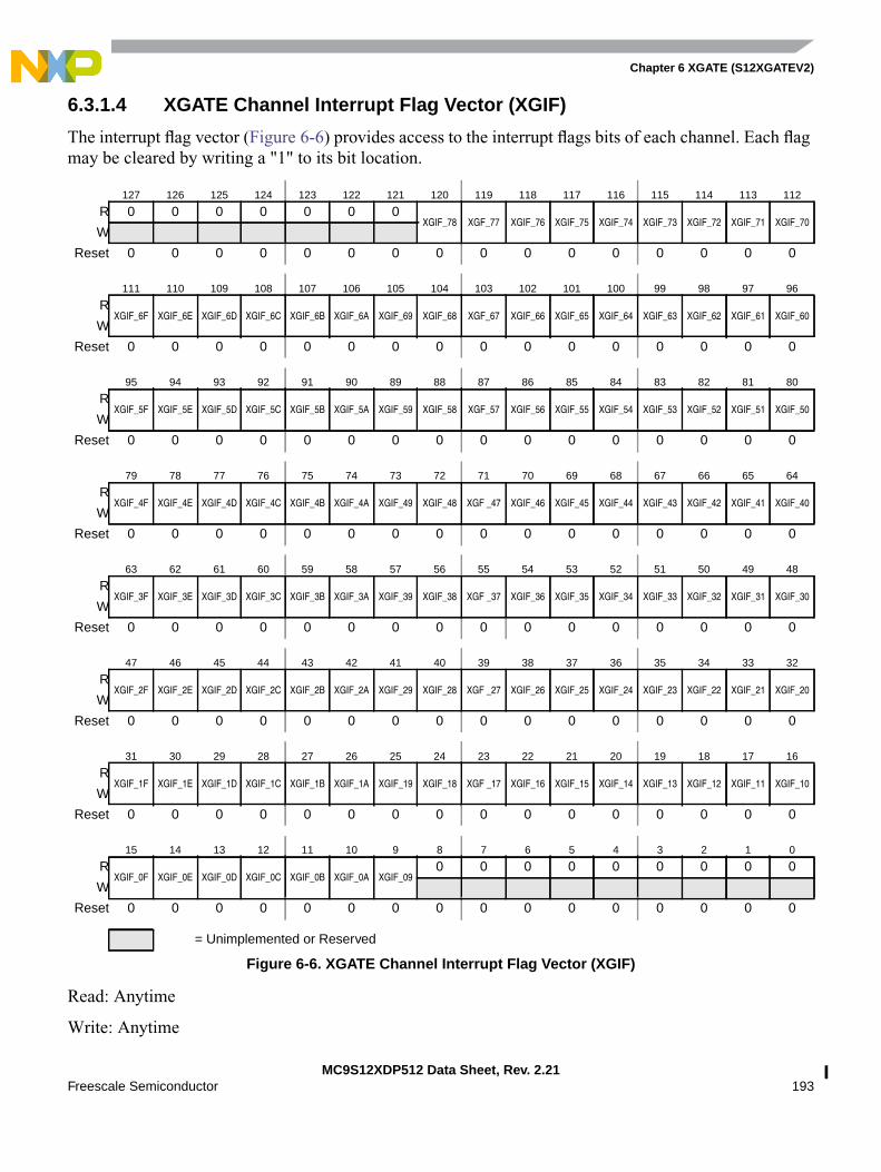
Chapter 6 XGATE (S12XGATEV2)
MC9S12XDP512 Data Sheet, Rev. 2.21Freescale Semiconductor 193
6.3.1.4 XGATE Channel Interrupt Flag Vector (XGIF)
The interrupt flag vector (Figure 6-6) provides access to the interrupt flags bits of each channel. Each flagmay be cleared by writing a "1" to its bit location.
Read: Anytime
Write: Anytime
127 126 125 124 123 122 121 120 119 118 117 116 115 114 113 112
R 0 0 0 0 0 0 0XGIF_78 XGF_77 XGIF_76 XGIF_75 XGIF_74 XGIF_73 XGIF_72 XGIF_71 XGIF_70
W
Reset 0 0 0 0 0 0 0 0 0 0 0 0 0 0 0 0
111 110 109 108 107 106 105 104 103 102 101 100 99 98 97 96
RXGIF_6F XGIF_6E XGIF_6D XGIF_6C XGIF_6B XGIF_6A XGIF_69 XGIF_68 XGF_67 XGIF_66 XGIF_65 XGIF_64 XGIF_63 XGIF_62 XGIF_61 XGIF_60
W
Reset 0 0 0 0 0 0 0 0 0 0 0 0 0 0 0 0
95 94 93 92 91 90 89 88 87 86 85 84 83 82 81 80
RXGIF_5F XGIF_5E XGIF_5D XGIF_5C XGIF_5B XGIF_5A XGIF_59 XGIF_58 XGF_57 XGIF_56 XGIF_55 XGIF_54 XGIF_53 XGIF_52 XGIF_51 XGIF_50
W
Reset 0 0 0 0 0 0 0 0 0 0 0 0 0 0 0 0
79 78 77 76 75 74 73 72 71 70 69 68 67 66 65 64
RXGIF_4F XGIF_4E XGIF_4D XGIF_4C XGIF_4B XGIF_4A XGIF_49 XGIF_48 XGF _47 XGIF_46 XGIF_45 XGIF_44 XGIF_43 XGIF_42 XGIF_41 XGIF_40
W
Reset 0 0 0 0 0 0 0 0 0 0 0 0 0 0 0 0
63 62 61 60 59 58 57 56 55 54 53 52 51 50 49 48
RXGIF_3F XGIF_3E XGIF_3D XGIF_3C XGIF_3B XGIF_3A XGIF_39 XGIF_38 XGF _37 XGIF_36 XGIF_35 XGIF_34 XGIF_33 XGIF_32 XGIF_31 XGIF_30
W
Reset 0 0 0 0 0 0 0 0 0 0 0 0 0 0 0 0
47 46 45 44 43 42 41 40 39 38 37 36 35 34 33 32
RXGIF_2F XGIF_2E XGIF_2D XGIF_2C XGIF_2B XGIF_2A XGIF_29 XGIF_28 XGF _27 XGIF_26 XGIF_25 XGIF_24 XGIF_23 XGIF_22 XGIF_21 XGIF_20
W
Reset 0 0 0 0 0 0 0 0 0 0 0 0 0 0 0 0
31 30 29 28 27 26 25 24 23 22 21 20 19 18 17 16
RXGIF_1F XGIF_1E XGIF_1D XGIF_1C XGIF_1B XGIF_1A XGIF_19 XGIF_18 XGF _17 XGIF_16 XGIF_15 XGIF_14 XGIF_13 XGIF_12 XGIF_11 XGIF_10
W
Reset 0 0 0 0 0 0 0 0 0 0 0 0 0 0 0 0
15 14 13 12 11 10 9 8 7 6 5 4 3 2 1 0
RXGIF_0F XGIF_0E XGIF_0D XGIF_0C XGIF_0B XGIF_0A XGIF_09
0 0 0 0 0 0 0 0 0
W
Reset 0 0 0 0 0 0 0 0 0 0 0 0 0 0 0 0
= Unimplemented or Reserved
Figure 6-6. XGATE Channel Interrupt Flag Vector (XGIF)
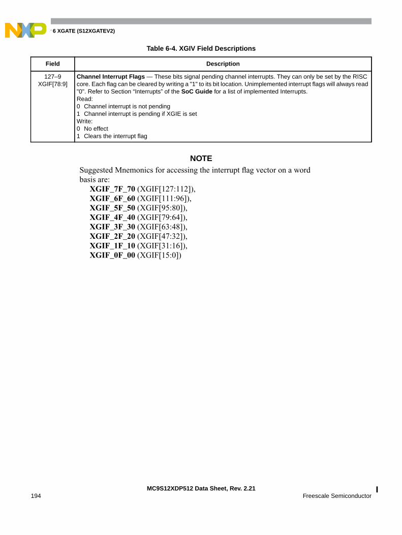
Chapter 6 XGATE (S12XGATEV2)
MC9S12XDP512 Data Sheet, Rev. 2.21194 Freescale Semiconductor
NOTESuggested Mnemonics for accessing the interrupt flag vector on a wordbasis are:
XGIF_7F_70 (XGIF[127:112]),XGIF_6F_60 (XGIF[111:96]),XGIF_5F_50 (XGIF[95:80]),XGIF_4F_40 (XGIF[79:64]),XGIF_3F_30 (XGIF[63:48]),XGIF_2F_20 (XGIF[47:32]),XGIF_1F_10 (XGIF[31:16]),XGIF_0F_00 (XGIF[15:0])
Table 6-4. XGIV Field Descriptions
Field Description
127–9XGIF[78:9]
Channel Interrupt Flags — These bits signal pending channel interrupts. They can only be set by the RISCcore. Each flag can be cleared by writing a "1" to its bit location. Unimplemented interrupt flags will always read"0". Refer to Section “Interrupts” of the SoC Guide for a list of implemented Interrupts.Read:0 Channel interrupt is not pending1 Channel interrupt is pending if XGIE is setWrite:0 No effect1 Clears the interrupt flag

Chapter 6 XGATE (S12XGATEV2)
MC9S12XDP512 Data Sheet, Rev. 2.21Freescale Semiconductor 195
6.3.1.5 XGATE Software Trigger Register (XGSWT)
The eight software triggers of the XGATE module can be set and cleared through the XGATE softwaretrigger register (Figure 6-7). The upper byte of this register, the software trigger mask, controls the writeaccess to the lower byte, the software trigger bits. These bits can be set or cleared if a "1" is written to theassociated mask in the same bus cycle.
Read: Anytime
Write: Anytime
NOTEThe XGATE channel IDs that are associated with the eight software triggersare determined on chip integration level. (see Section “Interrupts” of the SocGuide)
XGATE software triggers work like any peripheral interrupt. They can beused as XGATE requests as well as S12X_CPU interrupts. The target of thesoftware trigger must be selected in the S12X_INT module.
15 14 13 12 11 10 9 8 7 6 5 4 3 2 1 0
R 0 0 0 0 0 0 0 0XGSWT[7:0]
W XGSWTM[7:0]
Reset 0 0 0 0 0 0 0 0 0 0 0 0 0 0 0 0
Figure 6-7. XGATE Software Trigger Register (XGSWT)
Table 6-5. XGSWT Field Descriptions
Field Description
15–8XGSWTM[7:0]
Software Trigger Mask — These bits control the write access to the XGSWT bits. Each XGSWT bit can onlybe written if a "1" is written to the corresponding XGSWTM bit in the same access.Read:These bits will always read "0".Write:0 Disable write access to the XGSWT in the same bus cycle1 Enable write access to the corresponding XGSWT bit in the same bus cycle
7–0XGSWT[7:0]
Software Trigger Bits — These bits act as interrupt flags that are able to trigger XGATE software channels.They can only be set and cleared by software.Read:0 No software trigger pending1 Software trigger pending if the XGIE bit is setWrite:0 Clear Software Trigger1 Set Software Trigger
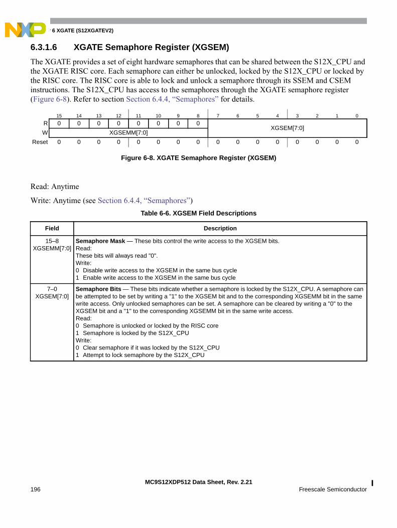
Chapter 6 XGATE (S12XGATEV2)
MC9S12XDP512 Data Sheet, Rev. 2.21196 Freescale Semiconductor
6.3.1.6 XGATE Semaphore Register (XGSEM)
The XGATE provides a set of eight hardware semaphores that can be shared between the S12X_CPU andthe XGATE RISC core. Each semaphore can either be unlocked, locked by the S12X_CPU or locked bythe RISC core. The RISC core is able to lock and unlock a semaphore through its SSEM and CSEMinstructions. The S12X_CPU has access to the semaphores through the XGATE semaphore register(Figure 6-8). Refer to section Section 6.4.4, “Semaphores” for details.
Read: Anytime
Write: Anytime (see Section 6.4.4, “Semaphores”)
15 14 13 12 11 10 9 8 7 6 5 4 3 2 1 0
R 0 0 0 0 0 0 0 0XGSEM[7:0]
W XGSEMM[7:0]
Reset 0 0 0 0 0 0 0 0 0 0 0 0 0 0 0 0
Figure 6-8. XGATE Semaphore Register (XGSEM)
Table 6-6. XGSEM Field Descriptions
Field Description
15–8XGSEMM[7:0]
Semaphore Mask — These bits control the write access to the XGSEM bits.Read:These bits will always read "0".Write:0 Disable write access to the XGSEM in the same bus cycle1 Enable write access to the XGSEM in the same bus cycle
7–0XGSEM[7:0]
Semaphore Bits — These bits indicate whether a semaphore is locked by the S12X_CPU. A semaphore canbe attempted to be set by writing a "1" to the XGSEM bit and to the corresponding XGSEMM bit in the samewrite access. Only unlocked semaphores can be set. A semaphore can be cleared by writing a "0" to theXGSEM bit and a "1" to the corresponding XGSEMM bit in the same write access.Read:0 Semaphore is unlocked or locked by the RISC core1 Semaphore is locked by the S12X_CPUWrite:0 Clear semaphore if it was locked by the S12X_CPU1 Attempt to lock semaphore by the S12X_CPU

Chapter 6 XGATE (S12XGATEV2)
MC9S12XDP512 Data Sheet, Rev. 2.21Freescale Semiconductor 197
6.3.1.7 XGATE Condition Code Register (XGCCR)
The XGCCR register (Figure 6-9) provides access to the RISC core’s condition code register.
Read: In debug mode if unsecured
Write: In debug mode if unsecured
7 6 5 4 3 2 1 0
R 0 0 0 0XGN XGZ XGV XGC
W
Reset 0 0 0 0 0 0 0 0
= Unimplemented or Reserved
Figure 6-9. XGATE Condition Code Register (XGCCR)
Table 6-7. XGCCR Field Descriptions
Field Description
3XGN
Sign Flag — The RISC core’s Sign flag
2XGZ
Zero Flag — The RISC core’s Zero flag
1XGV
Overflow Flag — The RISC core’s Overflow flag
0XGC
Carry Flag — The RISC core’s Carry flag

Chapter 6 XGATE (S12XGATEV2)
MC9S12XDP512 Data Sheet, Rev. 2.21198 Freescale Semiconductor
6.3.1.8 XGATE Program Counter Register (XGPC)
The XGPC register (Figure 6-10) provides access to the RISC core’s program counter.
Read: In debug mode if unsecured
Write: In debug mode if unsecured
6.3.1.9 XGATE Register 1 (XGR1)
The XGR1 register (Figure 6-12) provides access to the RISC core’s register 1.
Read: In debug mode if unsecured
Write: In debug mode if unsecured
15 14 13 12 11 10 9 8 7 6 5 4 3 2 1 0
RXGPC
W
Reset 0 0 0 0 0 0 0 0 0 0 0 0 0 0 0 0
Figure 6-10. XGATE Program Counter Register (XGPC)
Figure 6-11.
Table 6-8. XGPC Field Descriptions
Field Description
15–0XGPC[15:0]
Program Counter — The RISC core’s program counter
15 14 13 12 11 10 9 8 7 6 5 4 3 2 1 0
RXGR1
W
Reset 0 0 0 0 0 0 0 0 0 0 0 0 0 0 0 0
Figure 6-12. XGATE Register 1 (XGR1)
Table 6-9. XGR1 Field Descriptions
Field Description
15–0XGR1[15:0]
XGATE Register 1 — The RISC core’s register 1

Chapter 6 XGATE (S12XGATEV2)
MC9S12XDP512 Data Sheet, Rev. 2.21Freescale Semiconductor 199
6.3.1.10 XGATE Register 2 (XGR2)
The XGR2 register (Figure 6-13) provides access to the RISC core’s register 2.
Read: In debug mode if unsecured
Write: In debug mode if unsecured
6.3.1.11 XGATE Register 3 (XGR3)
The XGR3 register (Figure 6-14) provides access to the RISC core’s register 3.
Read: In debug mode if unsecured
Write: In debug mode if unsecured
15 14 13 12 11 10 9 8 7 6 5 4 3 2 1 0
RXGR2
W
Reset 0 0 0 0 0 0 0 0 0 0 0 0 0 0 0 0
Figure 6-13. XGATE Register 2 (XGR2)
Table 6-10. XGR2 Field Descriptions
Field Description
15–0XGR2[15:0]
XGATE Register 2 — The RISC core’s register 2
15 14 13 12 11 10 9 8 7 6 5 4 3 2 1 0
RXGR3
W
Reset 0 0 0 0 0 0 0 0 0 0 0 0 0 0 0 0
Figure 6-14. XGATE Register 3 (XGR3)
Table 6-11. XGR3 Field Descriptions
Field Description
15–0XGR3[15:0]
XGATE Register 3 — The RISC core’s register 3
Chapter 6 XGATE (S12XGATEV2)
MC9S12XDP512 Data Sheet, Rev. 2.21200 Freescale Semiconductor
6.3.1.12 XGATE Register 4 (XGR4)
The XGR4 register (Figure 6-15) provides access to the RISC core’s register 4.
Read: In debug mode if unsecured
Write: In debug mode if unsecured
6.3.1.13 XGATE Register 5 (XGR5)
The XGR5 register (Figure 6-16) provides access to the RISC core’s register 5.
Read: In debug mode if unsecured
Write: In debug mode if unsecured
15 14 13 12 11 10 9 8 7 6 5 4 3 2 1 0
RXGR4
W
Reset 0 0 0 0 0 0 0 0 0 0 0 0 0 0 0 0
Figure 6-15. XGATE Register 4 (XGR4)
Table 6-12. XGR4 Field Descriptions
Field Description
15–0XGR4[15:0]
XGATE Register 4 — The RISC core’s register 4
15 14 13 12 11 10 9 8 7 6 5 4 3 2 1 0
RXGR5
W
Reset 0 0 0 0 0 0 0 0 0 0 0 0 0 0 0 0
Figure 6-16. XGATE Register 5 (XGR5)
Table 6-13. XGR5 Field Descriptions
Field Description
15–0XGR5[15:0]
XGATE Register 5 — The RISC core’s register 5
Chapter 6 XGATE (S12XGATEV2)
MC9S12XDP512 Data Sheet, Rev. 2.21Freescale Semiconductor 201
6.3.1.14 XGATE Register 6 (XGR6)
The XGR6 register (Figure 6-17) provides access to the RISC core’s register 6.
Read: In debug mode if unsecured
Write: In debug mode if unsecured
6.3.1.15 XGATE Register 7 (XGR7)
The XGR7 register (Figure 6-18) provides access to the RISC core’s register 7.
Read: In debug mode if unsecured
Write: In debug mode if unsecured
15 14 13 12 11 10 9 8 7 6 5 4 3 2 1 0
RXGR6
W
Reset 0 0 0 0 0 0 0 0 0 0 0 0 0 0 0 0
Figure 6-17. XGATE Register 6 (XGR6)
Table 6-14. XGR6 Field Descriptions
Field Description
15–0XGR6[15:0]
XGATE Register 6 — The RISC core’s register 6
15 14 13 12 11 10 9 8 7 6 5 4 3 2 1 0
RXGR7
W
Reset 0 0 0 0 0 0 0 0 0 0 0 0 0 0 0 0
Figure 6-18. XGATE Register 7 (XGR7)
Table 6-15. XGR7 Field Descriptions
Field Description
15–0XGR7[15:0]
XGATE Register 7 — The RISC core’s register 7

Chapter 6 XGATE (S12XGATEV2)
MC9S12XDP512 Data Sheet, Rev. 2.21202 Freescale Semiconductor
6.4 Functional DescriptionThe core of the XGATE module is a RISC processor which is able to access the MCU’s internal memoriesand peripherals (see Figure 6-1). The RISC processor always remains in an idle state until it is triggeredby an XGATE request. Then it executes a code sequence that is associated with the request and optionallytriggers an interrupt to the S12X_CPU upon completion. Code sequences are not interruptible. A newXGATE request can only be serviced when the previous sequence is finished and the RISC core becomesidle.
The XGATE module also provides a set of hardware semaphores which are necessary to ensure dataconsistency whenever RAM locations or peripherals are shared with the S12X_CPU.
The following sections describe the components of the XGATE module in further detail.
6.4.1 XGATE RISC Core
The RISC core is a 16 bit processor with an instruction set that is well suited for data transfers, bitmanipulations, and simple arithmetic operations (see Section 6.8, “Instruction Set”).
It is able to access the MCU’s internal memories and peripherals without blocking these resources fromthe S12X_CPU1. Whenever the S12X_CPU and the RISC core access the same resource, the RISC corewill be stalled until the resource becomes available again1.
The XGATE offers a high access rate to the MCU’s internal RAM. Depending on the bus load, the RISCcore can perform up to two RAM accesses per S12X_CPU bus cycle.
Bus accesses to peripheral registers or flash are slower. A transfer rate of one bus access per S12X_CPUcycle can not be exceeded.
The XGATE module is intended to execute short interrupt service routines that are triggered by peripheralmodules or by software.
6.4.2 Programmer’s Model
Figure 6-19. Programmer’s Model
1. With the exception of PRR registers (see Section “S12X_MMC”).
R7
R6
R5
R4
R3
R2
R1
R0 = 0
V C
Register Block Program Counter
ConditionCode
Register
15
15
15
15
15
15
15
15
0
0
0
0
0
0
0
0
1 0
(Variable Pointer)
PC15 0
N Z
3 2

Chapter 6 XGATE (S12XGATEV2)
MC9S12XDP512 Data Sheet, Rev. 2.21Freescale Semiconductor 203
The programmer’s model of the XGATE RISC core is shown in Figure 6-19. The processor offers a set ofseven general purpose registers (R1 - R7), which serve as accumulators and index registers. An additionaleighth register (R0) is tied to the value “$0000”. Register R1 has an additional functionality. It is preloadedwith the initial variable pointer of the channel’s service request vector (see Figure 6-20). The initial contentof the remaining general purpose registers is undefined.
The 16 bit program counter allows the addressing of a 64 kbyte address space.
The condition code register contains four bits: the sign bit (S), the zero flag (Z), the overflow flag (V), andthe carry bit (C). The initial content of the condition code register is undefined.
6.4.3 Memory Map
The XGATE’s RISC core is able to access an address space of 64K bytes. The allocation of memory blockswithin this address space is determined on chip level. Refer to the S12X_MMC Section for a detailedinformation.
The XGATE vector block assigns a start address and a variable pointer to each XGATE channel. Itsposition in the XGATE memory map can be adjusted through the XGVBR register (see Section 6.3.1.3,“XGATE Vector Base Address Register (XGVBR)”). Figure 6-20 shows the layout of the vector block.Each vector consists of two 16 bit words. The first contains the start address of the service routine. Thisvalue will be loaded into the program counter before a service routine is executed. The second word is apointer to the service routine’s variable space. This value will be loaded into register R1 before a serviceroutine is executed.
Figure 6-20. XGATE Vector Block
+$0000
unused
+$0024
+$0028
+$002C
+$0030
+$01E0
Code
Variables
Code
Variables
XGVBR
Channel $0A Initial Program Counter
Channel $0A Initial Variable Pointer
Channel $09 Initial Program Counter
Channel $09 Initial Variable Pointer
Channel $0B Initial Program Counter
Channel $0B Initial Variable Pointer
Channel $0C Initial Program Counter
Channel $0C Initial Variable Pointer
Channel $78 Initial Program Counter
Channel $78 Initial Variable Pointer
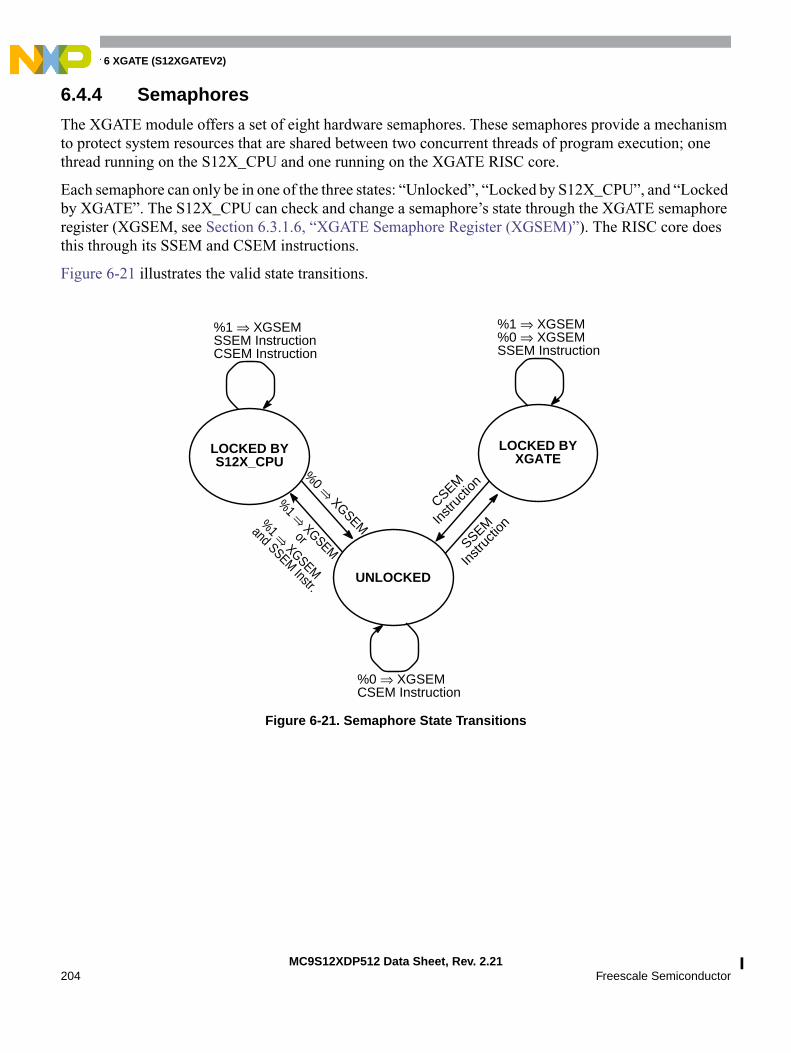
Chapter 6 XGATE (S12XGATEV2)
MC9S12XDP512 Data Sheet, Rev. 2.21204 Freescale Semiconductor
6.4.4 Semaphores
The XGATE module offers a set of eight hardware semaphores. These semaphores provide a mechanismto protect system resources that are shared between two concurrent threads of program execution; onethread running on the S12X_CPU and one running on the XGATE RISC core.
Each semaphore can only be in one of the three states: “Unlocked”, “Locked by S12X_CPU”, and “Lockedby XGATE”. The S12X_CPU can check and change a semaphore’s state through the XGATE semaphoreregister (XGSEM, see Section 6.3.1.6, “XGATE Semaphore Register (XGSEM)”). The RISC core doesthis through its SSEM and CSEM instructions.
Figure 6-21 illustrates the valid state transitions.
Figure 6-21. Semaphore State Transitions
UNLOCKED
LOCKED BYS12X_CPU
LOCKED BYXGATE
CSEM Instruction%0 ⇒ XGSEM
CSEM InstructionSSEM Instruction%1 ⇒ XGSEM
SSEM Instruction%0 ⇒ XGSEM%1 ⇒ XGSEM
CSEM
Instr
uctio
n%
0 ⇒ XGSEM
%1 ⇒ XGSEM SSEM
Instr
uctio
nor
%1 ⇒ XGSEM
and SSEM Instr.
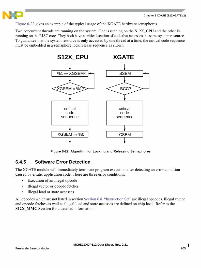
Chapter 6 XGATE (S12XGATEV2)
MC9S12XDP512 Data Sheet, Rev. 2.21Freescale Semiconductor 205
Figure 6-22 gives an example of the typical usage of the XGATE hardware semaphores.
Two concurrent threads are running on the system. One is running on the S12X_CPU and the other isrunning on the RISC core. They both have a critical section of code that accesses the same system resource.To guarantee that the system resource is only accessed by one thread at a time, the critical code sequencemust be embedded in a semaphore lock/release sequence as shown.
Figure 6-22. Algorithm for Locking and Releasing Semaphores
6.4.5 Software Error Detection
The XGATE module will immediately terminate program execution after detecting an error conditioncaused by erratic application code. There are three error conditions:
• Execution of an illegal opcode
• Illegal vector or opcode fetches
• Illegal load or store accesses
All opcodes which are not listed in section Section 6.8, “Instruction Set” are illegal opcodes. Illegal vectorand opcode fetches as well as illegal load and store accesses are defined on chip level. Refer to theS12X_MMC Section for a detailed information.
SSEM
XGSEM ≡ %1?
XGSEM ⇒ %0
BCC?
%1 ⇒ XGSEMx
CSEM
......... .........
..................
criticalcode
sequence
criticalcode
sequence
S12X_CPU XGATE
Chapter 6 XGATE (S12XGATEV2)
MC9S12XDP512 Data Sheet, Rev. 2.21206 Freescale Semiconductor
6.5 Interrupts
6.5.1 Incoming Interrupt Requests
XGATE threads are triggered by interrupt requests which are routed to the XGATE module (seeS12X_INT Section). Only a subset of the MCU’s interrupt requests can be routed to the XGATE. Whichspecific interrupt requests these are and which channel ID they are assigned to is documented in Section“Interrupts” of the SoC Guide.
6.5.2 Outgoing Interrupt Requests
There are three types of interrupt requests which can be triggered by the XGATE module:
4. Channel interrupts
For each XGATE channel there is an associated interrupt flag in the XGATE interrupt flag vector(XGIF, see Section 6.3.1.4, “XGATE Channel Interrupt Flag Vector (XGIF)”). These flags can beset through the "SIF" instruction by the RISC core. They are typically used to flag an interrupt tothe S12X_CPU when the XGATE has completed one of its tasks.
5. Software triggers
Software triggers are interrupt flags, which can be set and cleared by software (see Section 6.3.1.5,“XGATE Software Trigger Register (XGSWT)”). They are typically used to trigger XGATE tasksby the S12X_CPU software. However these interrupts can also be routed to the S12X_CPU (seeS12X_INT Section) and triggered by the XGATE software.
6. Software error interrupt
The software error interrupt signals to the S12X_CPU the detection of an error condition in theXGATE application code (see Section 6.4.5, “Software Error Detection”).
All XGATE interrupts can be disabled by the XGIE bit in the XGATE module control register (XGMCTL,see Section 6.3.1.1, “XGATE Control Register (XGMCTL)”).
6.6 Debug ModeThe XGATE debug mode is a feature to allow debugging of application code.
6.6.1 Debug Features
In debug mode the RISC core will be halted and the following debug features will be enabled:
• Read and Write accesses to RISC core registers (XGCCR, XGPC, XGR1–XGR7)1
All RISC core registers can be modified. Leaving debug mode will cause the RISC core to continueprogram execution with the modified register values.
1. Only possible if MCU is unsecured
Chapter 6 XGATE (S12XGATEV2)
MC9S12XDP512 Data Sheet, Rev. 2.21Freescale Semiconductor 207
• Single Stepping
Writing a "1" to the XGSS bit will call the RISC core to execute a single instruction. All RISC coreregisters will be updated accordingly.
• Write accesses to the XGCHID register
Three operations can be performed by writing to the XGCHID register:
– Change of channel ID
If a non-zero value is written to the XGCHID while a thread is active (XGCHID ≠ $00), thenthe current channel ID will be changed without any influence on the program counter or theother RISC core registers.
– Start of a thread
If a non-zero value is written to the XGCHID while the XGATE is idle (XGCHID = $00),then the thread that is associated with the new channel ID will be executed upon leavingdebug mode.
– Termination of a thread
If zero is written to the XGCHID while a thread is active (XGCHID ≠ $00), then the currentthread will be terminated and the XGATE will become idle.
6.6.2 Entering Debug Mode
Debug mode can be entered in four ways:
1. Setting XGDBG to "1"
Writing a "1" to XGDBG and XGDBGM in the same write access causes the XGATE to enterdebug mode upon completion of the current instruction.
NOTEAfter writing to the XGDBG bit the XGATE will not immediately enterdebug mode. Depending on the instruction that is executed at this time theremay be a delay of several clock cycles. The XGDBG will read "0" untildebug mode is entered.
2. Software breakpoints
XGATE programs which are stored in the internal RAM allow the use of software breakpoints. Asoftware breakpoint is set by replacing an instruction of the program code with the "BRK"instruction.
As soon as the program execution reaches the "BRK" instruction, the XGATE enters debug mode.Additionally a software breakpoint request is sent to the S12X_DBG module (see section 4.9 ofthe S12X_DBG Section).
Upon entering debug mode, the program counter will point to the "BRK" instruction. The otherRISC core registers will hold the result of the previous instruction.
To resume program execution, the "BRK" instruction must be replaced by the original instructionbefore leaving debug mode.
Chapter 6 XGATE (S12XGATEV2)
MC9S12XDP512 Data Sheet, Rev. 2.21208 Freescale Semiconductor
3. Tagged Breakpoints
The S12X_DBG module is able to place tags on fetched opcodes. The XGATE is able to enterdebug mode right before a tagged opcode is executed (see section 4.9 of the S12X_DBG Section).Upon entering debug mode, the program counter will point to the tagged instruction. The otherRISC core registers will hold the result of the previous instruction.
4. Forced Breakpoints
Forced breakpoints are triggered by the S12X_DBG module (see section 4.9 of the S12X_DBGSection). When a forced breakpoint occurs, the XGATE will enter debug mode upon completionof the current instruction.
6.6.3 Leaving Debug Mode
Debug mode can only be left by setting the XGDBG bit to "0". If a thread is active (XGCHID has not beencleared in debug mode), program execution will resume at the value of XGPC.
6.7 SecurityIn order to protect XGATE application code on secured S12X devices, a few restrictions in the debugfeatures have been made. These are:
• Registers XGCCR, XGPC, and XGR1–XGR7 will read zero on a secured device
• Registers XGCCR, XGPC, and XGR1–XGR7 can not be written on a secured device
• Single stepping is not possible on a secured device
6.8 Instruction Set
6.8.1 Addressing Modes
For the ease of implementation the architecture is a strict Load/Store RISC machine, which means alloperations must have one of the eight general purpose registers R0 … R7 as their source as well theirdestination.
All word accesses must work with a word aligned address, that is A[0] = 0!

Chapter 6 XGATE (S12XGATEV2)
MC9S12XDP512 Data Sheet, Rev. 2.21Freescale Semiconductor 209
6.8.1.1 Naming Conventions
RD Destination register, allowed range is R0–R7
RD.L Low byte of the destination register, bits [7:0]
RD.H High byte of the destination register, bits [15:8]
RS, RS1, RS2 Source register, allowed range is R0–R7
RS.L, RS1.L, RS2.L Low byte of the source register, bits [7:0]
RS.H, RS1.H, RS2.H High byte of the source register, bits[15:8]
RB Base register for indexed addressing modes, allowedrange is R0–R7
RI Offset register for indexed addressing modes withregister offset, allowed range is R0–R7
RI+ Offset register for indexed addressing modes withregister offset and post-increment,Allowed range is R0–R7 (R0+ is equivalent to R0)
–RI Offset register for indexed addressing modes withregister offset and pre-decrement,Allowed range is R0–R7 (–R0 is equivalent to R0)
NOTEEven though register R1 is intended to be used as a pointer to the variablesegment, it may be used as a general purpose data register as well.
Selecting R0 as destination register will discard the result of the instruction.Only the condition code register will be updated
6.8.1.2 Inherent Addressing Mode (INH)
Instructions that use this addressing mode either have no operands or all operands are in internal XGATEregisters:.
ExamplesBRKRTS
6.8.1.3 Immediate 3-Bit Wide (IMM3)
Operands for immediate mode instructions are included in the instruction stream and are fetched into theinstruction queue along with the rest of the 16 bit instruction. The ’#’ symbol is used to indicate animmediate addressing mode operand. This address mode is used for semaphore instructions.
Examples:CSEM #1 ; Unlock semaphore 1SSEM #3 ; Lock Semaphore 3
Chapter 6 XGATE (S12XGATEV2)
MC9S12XDP512 Data Sheet, Rev. 2.21210 Freescale Semiconductor
6.8.1.4 Immediate 4 Bit Wide (IMM4)
The 4 bit wide immediate addressing mode is supported by all shift instructions.
RD = RD ∗ imm4
Examples:LSL R4,#1 ; R4 = R4 << 1; shift register R4 by 1 bit to the leftLSR R4,#3 ; R4 = R4 >> 3; shift register R4 by 3 bits to the right
6.8.1.5 Immediate 8 Bit Wide (IMM8)
The 8 bit wide immediate addressing mode is supported by four major commands (ADD, SUB, LD, CMP).
RD = RD ∗ imm8
Examples:ADDL R1,#1 ; adds an 8 bit value to register R1SUBL R2,#2 ; subtracts an 8 bit value from register R2LDH R3,#3 ; loads an 8 bit immediate into the high byte of Register R3CMPL R4,#4 ; compares the low byte of register R4 with an immediate value
6.8.1.6 Immediate 16 Bit Wide (IMM16)
The 16 bit wide immediate addressing mode is a construct to simplify assembler code. Instructions whichoffer this mode are translated into two opcodes using the eight bit wide immediate addressing mode.
RD = RD ∗ imm16
Examples:LDW R4,#$1234 ; translated to LDL R4,#$34; LDH R4,#$12ADD R4,#$5678 ; translated to ADDL R4,#$78; ADDH R4,#$56
6.8.1.7 Monadic Addressing (MON)
In this addressing mode only one operand is explicitly given. This operand can either be the source (f(RD)),the target (RD = f()), or both source and target of the operation (RD = f(RD)).
Examples:JAL R1 ; PC = R1, R1 = PC+2SIF R2 ; Trigger IRQ associated with the channel number in R2.L

Chapter 6 XGATE (S12XGATEV2)
MC9S12XDP512 Data Sheet, Rev. 2.21Freescale Semiconductor 211
6.8.1.8 Dyadic Addressing (DYA)
In this mode the result of an operation between two registers is stored in one of the registers used asoperands.
RD = RD ∗ RS is the general register to register format, with register RD being the first operand and RSthe second. RD and RS can be any of the 8 general purpose registers R0 … R7. If R0 is used as thedestination register, only the condition code flags are updated. This addressing mode is used only for shiftoperations with a variable shift value
Examples:LSL R4,R5 ; R4 = R4 << R5LSR R4,R5 ; R4 = R4 >> R5
6.8.1.9 Triadic Addressing (TRI)
In this mode the result of an operation between two or three registers is stored into a third one.RD = RS1 ∗ RS2 is the general format used in the order RD, RS1, RS1. RD, RS1, RS2 can be any of the8 general purpose registers R0 … R7. If R0 is used as the destination register RD, only the condition codeflags are updated. This addressing mode is used for all arithmetic and logical operations.
Examples:ADC R5,R6,R7 ; R5 = R6 + R7 + CarrySUB R5,R6,R7 ; R5 = R6 - R7
6.8.1.10 Relative Addressing 9-Bit Wide (REL9)
A 9-bit signed word address offset is included in the instruction word. This addressing mode is used forconditional branch instructions.
Examples:BCC REL9 ; PC = PC + 2 + (REL9 << 1)BEQ REL9 ; PC = PC + 2 + (REL9 << 1)
6.8.1.11 Relative Addressing 10-Bit Wide (REL10)
An 11-bit signed word address offset is included in the instruction word. This addressing mode is used forthe unconditional branch instruction.
Examples:BRA REL10 ; PC = PC + 2 + (REL10 << 1)
6.8.1.12 Index Register plus Immediate Offset (IDO5)
(RS, #offset5) provides an unsigned offset from the base register.
Examples:LDB R4,(R1,#offset) ; loads a byte from R1+offset into R4STW R4,(R1,#offset) ; stores R4 as a word to R1+offset
Chapter 6 XGATE (S12XGATEV2)
MC9S12XDP512 Data Sheet, Rev. 2.21212 Freescale Semiconductor
6.8.1.13 Index Register plus Register Offset (IDR)
For load and store instructions (RS, RI) provides a variable offset in a register.
Examples:LDB R4,(R1,R2) ; loads a byte from R1+R2 into R4STW R4,(R1,R2) ; stores R4 as a word to R1+R2
6.8.1.14 Index Register plus Register Offset with Post-increment (IDR+)
[RS, RI+] provides a variable offset in a register, which is incremented after accessing the memory. In caseof a byte access the index register will be incremented by one. In case of a word access it will beincremented by two.
Examples:LDB R4,(R1,R2+) ; loads a byte from R1+R2 into R4, R2+=1STW R4,(R1,R2+) ; stores R4 as a word to R1+R2, R2+=2
6.8.1.15 Index Register plus Register Offset with Pre-decrement (–IDR)
[RS, -RI] provides a variable offset in a register, which is decremented before accessing the memory. Incase of a byte access the index register will be decremented by one. In case of a word access it will bedecremented by two.
Examples:LDB R4,(R1,-R2) ; R2 -=1, loads a byte from R1+R2 into R4STW R4,(R1,-R2) ; R2 -=2, stores R4 as a word to R1+R2
6.8.2 Instruction Summary and Usage
6.8.2.1 Load & Store Instructions
Any register can be loaded either with an immediate or from the address space using indexed addressingmodes.
LDL RD,#IMM8 ; loads an immediate 8 bit value to the lower byte of RDLDW RD,(RB,RI) ; loads data using RB+RI as effective address
LDB RD,(RB, RI+) ; loads data using RB+RI as effective address; followed by an increment of RI depending on; the size of the operation
The same set of modes is available for the store instructionsSTB RS,(RB, RI) ; stores data using RB+RI as effective address
STW RS,(RB, RI+) ; stores data using RB+RI as effective address; followed by an increment of RI depending on; the size of the operation.
Chapter 6 XGATE (S12XGATEV2)
MC9S12XDP512 Data Sheet, Rev. 2.21Freescale Semiconductor 213
6.8.2.2 Logic and Arithmetic Instructions
All logic and arithmetic instructions support the 8 bit immediate addressing mode (IMM8: RD = RD ∗#IMM8) and the triadic addressing mode (TRI: RD = RS1 ∗ RS2).
All arithmetic is considered as signed, sign, overflow, zero and carry flag will be updated. The carry willnot be affected for logical operations.
ADDL R2,#1 ; increment R2ANDH R4,#$FE ; R4.H = R4.H & $FE, clear lower bit of higher byte
ADD R3,R4,R5 ; R3 = R4 + R5SUB R3,R4,R5 ; R3 = R4 - R5
AND R3,R4,R5 ; R3 = R4 & R5 logical AND on the whole wordOR R3,R4,R5 ; R3 = R4 | R5
6.8.2.3 Register – Register Transfers
This group comprises transfers from and to some special registersTFR R3,CCR ; transfers the condition code register to the low byte of
; register R3Branch Instructions
The branch offset is +255 words or -256 words counted from the beginning of the next instruction. Sinceinstructions have a fixed 16 bit width, the branch offsets are word aligned by shifting the offset value by 2.
BEQ label ; if Z flag = 1 branch to label
An unconditional branch allows a +511 words or -512 words branch distance.BRA label
6.8.2.4 Shift Instructions
Shift operations allow the use of a 4 bit wide immediate value to identify a shift width within a 16 bit word.For shift operations a value of 0 does not shift at all, while a value of 15 shifts the register RD by 15 bits.In a second form the shift value is contained in the bits 3:0 of the register RS.
Examples:LSL R4,#1 ; R4 = R4 << 1; shift register R4 by 1 bit to the leftLSR R4,#3 ; R4 = R4 >> 3; shift register R4 by 3 bits to the rightASR R4,R2 ; R4 = R4 >> R2;arithmetic shift register R4 right by the amount
; of bits contained in R2[3:0].

Chapter 6 XGATE (S12XGATEV2)
MC9S12XDP512 Data Sheet, Rev. 2.21214 Freescale Semiconductor
6.8.2.5 Bit Field Operations
This addressing mode is used to identify the position and size of a bit field for insertion or extraction. Thewidth and offset are coded in the lower byte of the source register 2, RS2. The content of the upper byte isignored. An offset of 0 denotes the right most position and a width of 0 denotes 1 bit. These instructionsare very useful to extract, insert, clear, set or toggle portions of a 16 bit word.
Figure 6-23. Bit Field Addressing
BFEXT R3,R4,R5 ; R5: W4 bits offset O4, will be extracted from R4 into R3
6.8.2.6 Special Instructions for DMA Usage
The XGATE offers a number of additional instructions for flag manipulation, program flow control anddebugging:
1. SIF: Set a channel interrupt flag
2. SSEM: Test and set a hardware semaphore
3. CSEM: Clear a hardware semaphore
4. BRK: Software breakpoint
5. NOP: No Operation
6. RTS: Terminate the current thread
W4 O4
15 025
W4=3, O4=2
15 03
Bit Field Extract
Bit Field Insert
RS2
RS1
RD

Chapter 6 XGATE (S12XGATEV2)
MC9S12XDP512 Data Sheet, Rev. 2.21Freescale Semiconductor 215
6.8.3 Cycle Notation
Table 6-16 show the XGATE access detail notation. Each code letter equals one XGATE cycle. Each letterimplies additional wait cycles if memories or peripherals are not accessible. Memories or peripherals arenot accessible if they are blocked by the S12X_CPU. In addition to this Peripherals are only accessibleevery other XGATE cycle. Uppercase letters denote 16 bit operations. Lowercase letters denote 8 bitoperations. The XGATE is able to perform two bus or wait cycles per S12X_CPU cycle.
6.8.4 Thread Execution
When the RISC core is triggered by an interrupt request (see Figure 6-1) it first executes a vector fetchsequence which performs three bus accesses:
1. A V-cycle to fetch the initial content of the program counter.
2. A V-cycle to fetch the initial content of the data segment pointer (R1).
3. A P-cycle to load the initial opcode.
Afterwards a sequence of instructions (thread) is executed which is terminated by an "RTS" instruction. Iffurther interrupt requests are pending after a thread has been terminated, a new vector fetch will beperformed. Otherwise the RISC core will idle until a new interrupt request is received. A thread can not beinterrupted by an interrupt request.
6.8.5 Instruction Glossary
This section describes the XGATE instruction set in alphabetical order.
Table 6-16. Access Detail Notation
V — Vector fetch: always an aligned word read, lasts for at least one RISC core cycle
P — Program word fetch: always an aligned word read, lasts for at least one RISC core cycle
r — 8 bit data read: lasts for at least one RISC core cycle
R — 16 bit data read: lasts for at least one RISC core cycle
w — 8 bit data write: lasts for at least one RISC core cycle
W — 16 bit data write: lasts for at least one RISC core cycle
A — Alignment cycle: no read or write, lasts for zero or one RISC core cycles
f — Free cycle: no read or write, lasts for one RISC core cycles
Special Cases
PP/P — Branch: PP if branch taken, P if not

Chapter 6 XGATE (S12XGATEV2)
MC9S12XDP512 Data Sheet, Rev. 2.21216 Freescale Semiconductor
Operation
RS1 + RS2 + C ⇒ RD
Adds the content of register RS1, the content of register RS2 and the value of the Carry bit using binaryaddition and stores the result in the destination register RD. The Zero Flag is also carried forward from theprevious operation allowing 32 and more bit additions.
Example:ADC R6,R2,R2ADC R7,R3,R3 ; R7:R6 = R5:R4 + R3:R2BCC ; conditional branch on 32 bit addition
CCR Effects
Code and CPU Cycles
ADC Add with Carry ADC
N Z V C
∆ ∆ ∆ ∆
N: Set if bit 15 of the result is set; cleared otherwise.
Z: Set if the result is $0000 and Z was set before this operation; cleared otherwise.
V: Set if a two´s complement overflow resulted from the operation; cleared otherwise.RS1[15] & RS2[15] & RD[15]new | RS1[15] & RS2[15] & RD[15]new
C: Set if there is a carry from bit 15 of the result; cleared otherwise.RS1[15] & RS2[15] | RS1[15] & RD[15]new | RS2[15] & RD[15]new
Source FormAddress
ModeMachine Code Cycles
ADC RD, RS1, RS2 TRI 0 0 0 1 1 RD RS1 RS2 1 1 P

Chapter 6 XGATE (S12XGATEV2)
MC9S12XDP512 Data Sheet, Rev. 2.21Freescale Semiconductor 217
Operation
RS1 + RS2 ⇒ RDRD + IMM16 ⇒ RD (translates to ADDL RD, #IMM16[7:0]; ADDH RD, #[15:8])
Performs a 16 bit addition and stores the result in the destination register RD.
CCR Effects
Code and CPU Cycles
ADD Add without Carry ADD
N Z V C
∆ ∆ ∆ ∆
N: Set if bit 15 of the result is set; cleared otherwise.Z: Set if the result is $0000; cleared otherwise.V: Set if a two´s complement overflow resulted from the operation; cleared otherwise.
RS1[15] & RS2[15] & RD[15]new | RS1[15] & RS2[15] & RD[15]newRefer to ADDH instruction for #IMM16 operations.
C: Set if there is a carry from bit 15 of the result; cleared otherwise.RS1[15] & RS2[15] | RS1[15] & RD[15]new | RS2[15] & RD[15]newRefer to ADDH instruction for #IMM16 operations.
Source FormAddress
ModeMachine Code Cycles
ADD RD, RS1, RS2 TRI 0 0 0 1 1 RD RS1 RS2 1 0 P
ADD RD, #IMM16 IMM8 1 1 1 0 0 RD IMM16[7:0] P
IMM8 1 1 1 0 1 RD IMM16[15:8] P
Chapter 6 XGATE (S12XGATEV2)
MC9S12XDP512 Data Sheet, Rev. 2.21218 Freescale Semiconductor
Operation
RD + IMM8:$00 ⇒ RD
Adds the content of high byte of register RD and a signed immediate 8 bit constant using binary additionand stores the result in the high byte of the destination register RD. This instruction can be used after anADDL for a 16 bit immediate addition.
Example:ADDL R2,#LOWBYTEADDH R2,#HIGHBYTE ; R2 = R2 + 16 bit immediate
CCR Effects
Code and CPU Cycles
ADDH Add Immediate 8 bit Constant(High Byte) ADDH
N Z V C
∆ ∆ ∆ ∆
N: Set if bit 15 of the result is set; cleared otherwise.Z: Set if the result is $0000; cleared otherwise.V: Set if a two´s complement overflow resulted from the operation; cleared otherwise.
RD[15]old & IMM8[7] & RD[15]new | RD[15]old & IMM8[7] & RD[15]newC: Set if there is a carry from the bit 15 of the result; cleared otherwise.
RD[15]old & IMM8[7] | RD[15]old & RD[15]new | IMM8[7] & RD[15]new
Source FormAddress
ModeMachine Code Cycles
ADDH RD, #IMM8 IMM8 1 1 1 0 1 RD IMM8 P
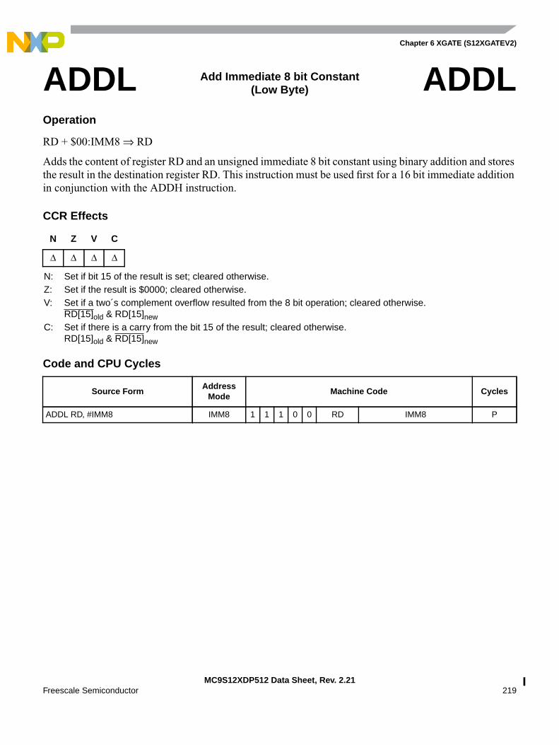
Chapter 6 XGATE (S12XGATEV2)
MC9S12XDP512 Data Sheet, Rev. 2.21Freescale Semiconductor 219
Operation
RD + $00:IMM8 ⇒ RD
Adds the content of register RD and an unsigned immediate 8 bit constant using binary addition and storesthe result in the destination register RD. This instruction must be used first for a 16 bit immediate additionin conjunction with the ADDH instruction.
CCR Effects
Code and CPU Cycles
ADDL Add Immediate 8 bit Constant(Low Byte) ADDL
N Z V C
∆ ∆ ∆ ∆
N: Set if bit 15 of the result is set; cleared otherwise.Z: Set if the result is $0000; cleared otherwise.V: Set if a two´s complement overflow resulted from the 8 bit operation; cleared otherwise.
RD[15]old & RD[15]newC: Set if there is a carry from the bit 15 of the result; cleared otherwise.
RD[15]old & RD[15]new
Source FormAddress
ModeMachine Code Cycles
ADDL RD, #IMM8 IMM8 1 1 1 0 0 RD IMM8 P
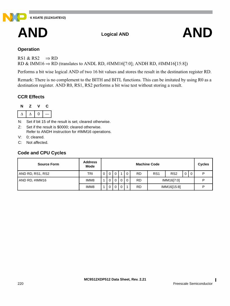
Chapter 6 XGATE (S12XGATEV2)
MC9S12XDP512 Data Sheet, Rev. 2.21220 Freescale Semiconductor
Operation
RS1 & RS2 ⇒ RDRD & IMM16 ⇒ RD (translates to ANDL RD, #IMM16[7:0]; ANDH RD, #IMM16[15:8])
Performs a bit wise logical AND of two 16 bit values and stores the result in the destination register RD.
Remark: There is no complement to the BITH and BITL functions. This can be imitated by using R0 as adestination register. AND R0, RS1, RS2 performs a bit wise test without storing a result.
CCR Effects
Code and CPU Cycles
AND Logical AND AND
N Z V C
∆ ∆ 0 —
N: Set if bit 15 of the result is set; cleared otherwise.Z: Set if the result is $0000; cleared otherwise.
Refer to ANDH instruction for #IMM16 operations.V: 0; cleared.C: Not affected.
Source FormAddress
ModeMachine Code Cycles
AND RD, RS1, RS2 TRI 0 0 0 1 0 RD RS1 RS2 0 0 P
AND RD, #IMM16 IMM8 1 0 0 0 0 RD IMM16[7:0] P
IMM8 1 0 0 0 1 RD IMM16[15:8] P
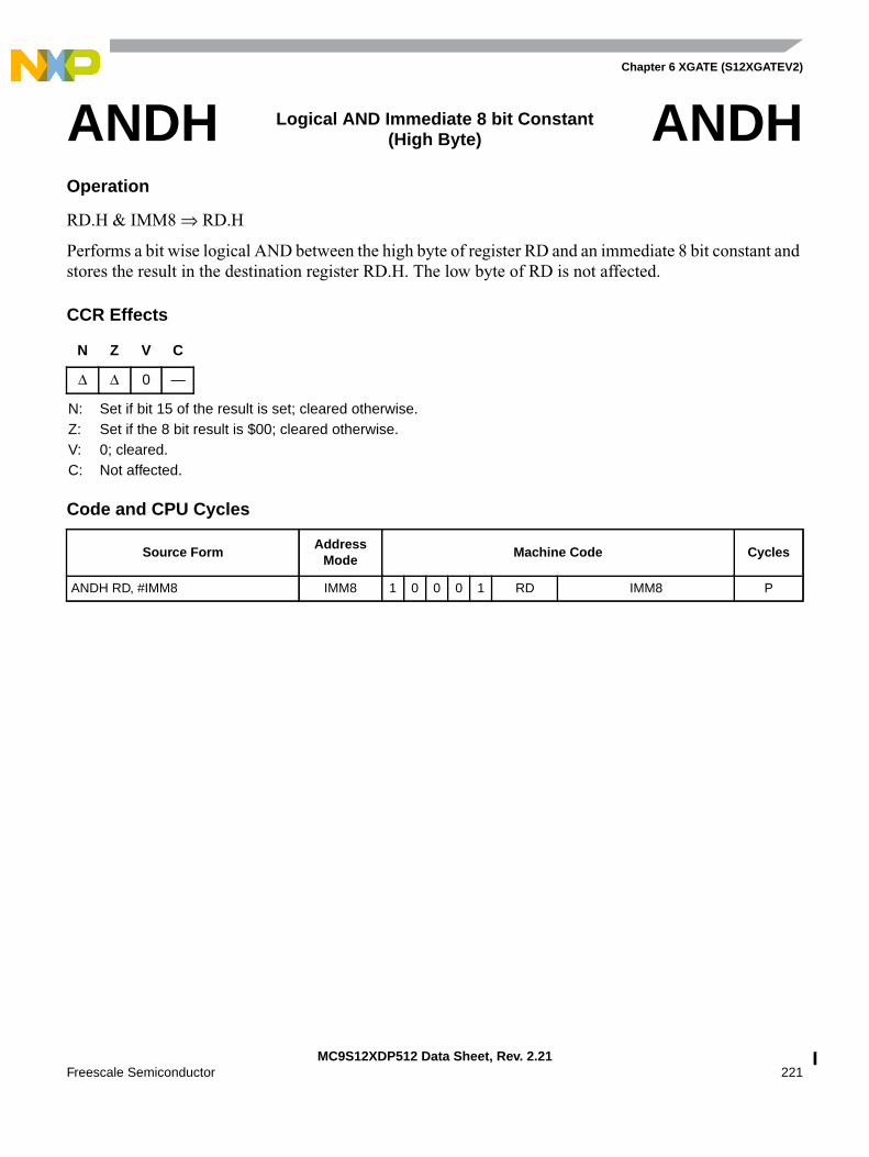
Chapter 6 XGATE (S12XGATEV2)
MC9S12XDP512 Data Sheet, Rev. 2.21Freescale Semiconductor 221
Operation
RD.H & IMM8 ⇒ RD.H
Performs a bit wise logical AND between the high byte of register RD and an immediate 8 bit constant andstores the result in the destination register RD.H. The low byte of RD is not affected.
CCR Effects
Code and CPU Cycles
ANDH Logical AND Immediate 8 bit Constant(High Byte) ANDH
N Z V C
∆ ∆ 0 —
N: Set if bit 15 of the result is set; cleared otherwise.Z: Set if the 8 bit result is $00; cleared otherwise.V: 0; cleared.C: Not affected.
Source FormAddress
ModeMachine Code Cycles
ANDH RD, #IMM8 IMM8 1 0 0 0 1 RD IMM8 P
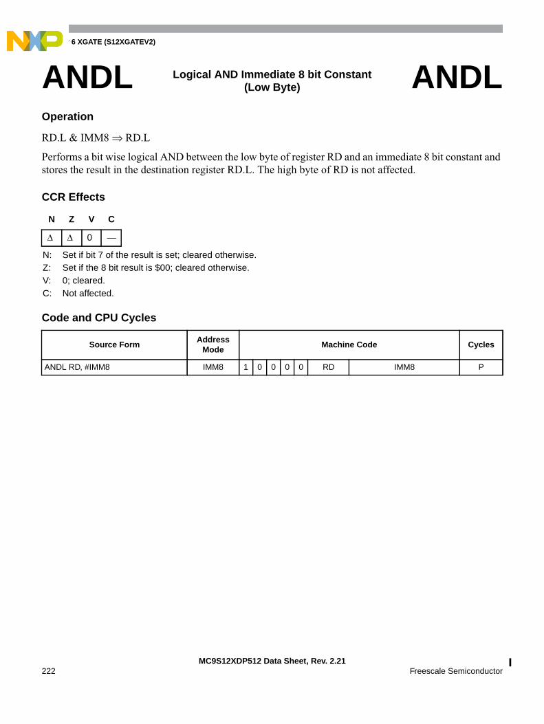
Chapter 6 XGATE (S12XGATEV2)
MC9S12XDP512 Data Sheet, Rev. 2.21222 Freescale Semiconductor
Operation
RD.L & IMM8 ⇒ RD.L
Performs a bit wise logical AND between the low byte of register RD and an immediate 8 bit constant andstores the result in the destination register RD.L. The high byte of RD is not affected.
CCR Effects
Code and CPU Cycles
ANDL Logical AND Immediate 8 bit Constant(Low Byte) ANDL
N Z V C
∆ ∆ 0 —
N: Set if bit 7 of the result is set; cleared otherwise.Z: Set if the 8 bit result is $00; cleared otherwise.V: 0; cleared.C: Not affected.
Source FormAddress
ModeMachine Code Cycles
ANDL RD, #IMM8 IMM8 1 0 0 0 0 RD IMM8 P
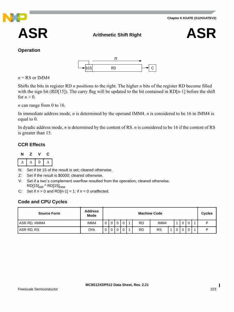
Chapter 6 XGATE (S12XGATEV2)
MC9S12XDP512 Data Sheet, Rev. 2.21Freescale Semiconductor 223
Operation
n = RS or IMM4
Shifts the bits in register RD n positions to the right. The higher n bits of the register RD become filledwith the sign bit (RD[15]). The carry flag will be updated to the bit contained in RD[n-1] before the shiftfor n > 0.
n can range from 0 to 16.
In immediate address mode, n is determined by the operand IMM4. n is considered to be 16 in IMM4 isequal to 0.
In dyadic address mode, n is determined by the content of RS. n is considered to be 16 if the content of RSis greater than 15.
CCR Effects
Code and CPU Cycles
ASR Arithmetic Shift Right ASR
N Z V C
∆ ∆ 0 ∆
N: Set if bit 15 of the result is set; cleared otherwise.Z: Set if the result is $0000; cleared otherwise.V: Set if a two´s complement overflow resulted from the operation; cleared otherwise.
RD[15]old ^ RD[15]newC: Set if n > 0 and RD[n-1] = 1; if n = 0 unaffected.
Source FormAddress
ModeMachine Code Cycles
ASR RD, #IMM4 IMM4 0 0 0 0 1 RD IMM4 1 0 0 1 P
ASR RD, RS DYA 0 0 0 0 1 RD RS 1 0 0 0 1 P
b15 RD C
n
Chapter 6 XGATE (S12XGATEV2)
MC9S12XDP512 Data Sheet, Rev. 2.21224 Freescale Semiconductor
Operation
If C = 0, then PC + $0002 + (REL9 << 1) ⇒ PC
Tests the Carry flag and branches if C = 0.
CCR Effects
Code and CPU Cycles
BCC Branch if Carry Cleared(Same as BHS) BCC
N Z V C
— — — —
N: Not affected.Z: Not affected.V: Not affected.C: Not affected.
Source FormAddress
ModeMachine Code Cycles
BCC REL9 REL9 0 0 1 0 0 0 0 REL9 PP/P
Chapter 6 XGATE (S12XGATEV2)
MC9S12XDP512 Data Sheet, Rev. 2.21Freescale Semiconductor 225
Operation
If C = 1, then PC + $0002 + (REL9 << 1) ⇒ PC
Tests the Carry flag and branches if C = 1.
CCR Effects
Code and CPU Cycles
BCS Branch if Carry Set(Same as BLO) BCS
N Z V C
— — — —
N: Not affected.Z: Not affected.V: Not affected.C: Not affected.
Source FormAddress
ModeMachine Code Cycles
BCS REL9 REL9 0 0 1 0 0 0 1 REL9 PP/P
Chapter 6 XGATE (S12XGATEV2)
MC9S12XDP512 Data Sheet, Rev. 2.21226 Freescale Semiconductor
Operation
If Z = 1, then PC + $0002 + (REL9 << 1) ⇒ PC
Tests the Zero flag and branches if Z = 1.
CCR Effects
Code and CPU Cycles
BEQ Branch if Equal BEQ
N Z V C
— — — —
N: Not affected.Z: Not affected.V: Not affected.C: Not affected.
Source FormAddress
ModeMachine Code Cycles
BEQ REL9 REL9 0 0 1 0 0 1 1 REL9 PP/P

Chapter 6 XGATE (S12XGATEV2)
MC9S12XDP512 Data Sheet, Rev. 2.21Freescale Semiconductor 227
Operation
RS1[(o+w):o] ⇒ RD[w:0]; 0 ⇒ RD[15:(w+1)]
w = (RS2[7:4])
o = (RS2[3:0])
Extracts w+1 bits from register RS1 starting at position o and writes them right aligned into register RD.The remaining bits in RD will be cleared. If (o+w) > 15 only bits [15:o] get extracted.
CCR Effects
Code and CPU Cycles
BFEXT Bit Field Extract BFEXT
N Z V C
0 ∆ 0 ∆
N: Set if bit 15 of the result is set; cleared otherwise.Z: Set if the result is $0000; cleared otherwise.V: 0; cleared.C: Not affected.
Source FormAddress
ModeMachine Code Cycles
BFEXT RD, RS1, RS2 TRI 0 1 1 0 0 RD RS1 RS2 1 1 P
W4 O4
15 025
W4=3, O4=2
15 03
Bit Field Extract
RS2
RS1
RD0
15 037 4
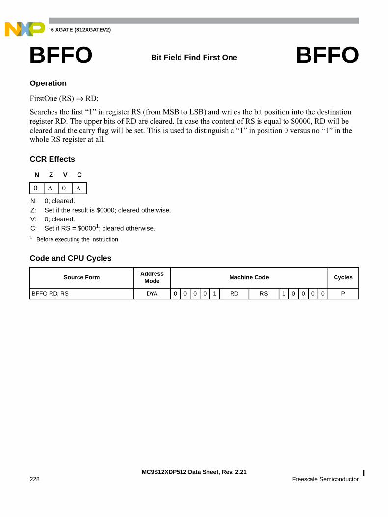
Chapter 6 XGATE (S12XGATEV2)
MC9S12XDP512 Data Sheet, Rev. 2.21228 Freescale Semiconductor
Operation
FirstOne (RS) ⇒ RD;
Searches the first “1” in register RS (from MSB to LSB) and writes the bit position into the destinationregister RD. The upper bits of RD are cleared. In case the content of RS is equal to $0000, RD will becleared and the carry flag will be set. This is used to distinguish a “1” in position 0 versus no “1” in thewhole RS register at all.
CCR Effects
Code and CPU Cycles
BFFO Bit Field Find First One BFFO
N Z V C
0 ∆ 0 ∆
N: 0; cleared.Z: Set if the result is $0000; cleared otherwise.V: 0; cleared.C: Set if RS = $00001; cleared otherwise.1 Before executing the instruction
Source FormAddress
ModeMachine Code Cycles
BFFO RD, RS DYA 0 0 0 0 1 RD RS 1 0 0 0 0 P
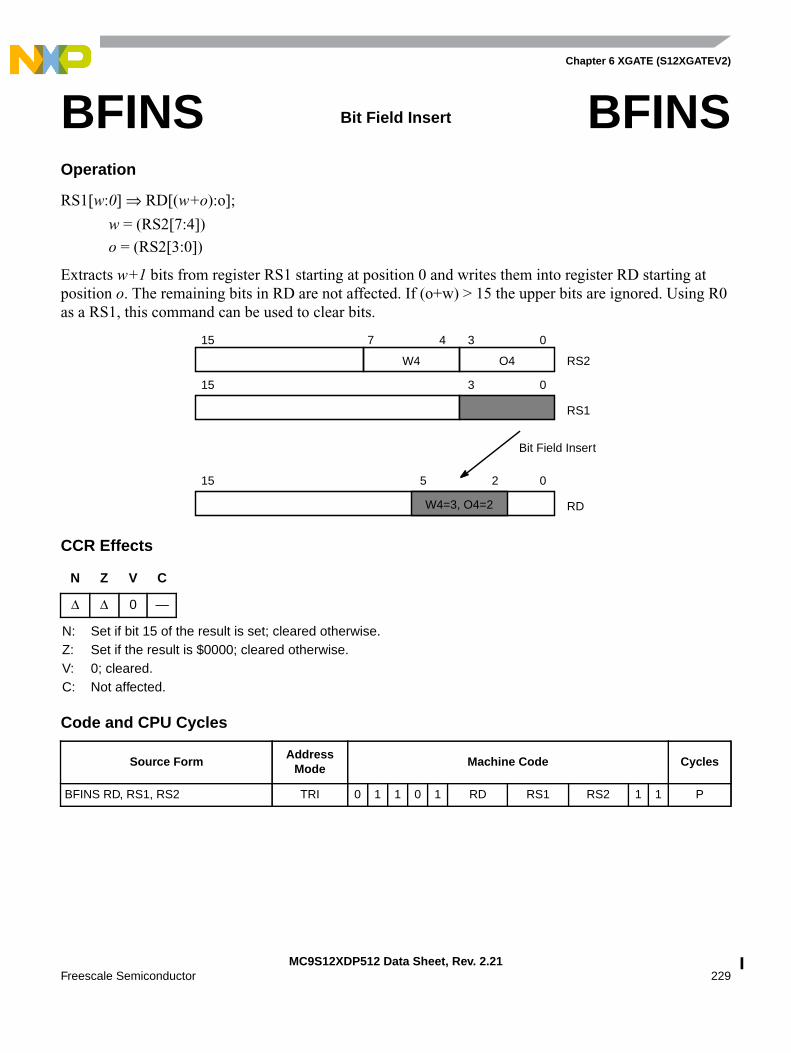
Chapter 6 XGATE (S12XGATEV2)
MC9S12XDP512 Data Sheet, Rev. 2.21Freescale Semiconductor 229
Operation
RS1[w:0] ⇒ RD[(w+o):o];
w = (RS2[7:4])
o = (RS2[3:0])
Extracts w+1 bits from register RS1 starting at position 0 and writes them into register RD starting atposition o. The remaining bits in RD are not affected. If (o+w) > 15 the upper bits are ignored. Using R0as a RS1, this command can be used to clear bits.
CCR Effects
Code and CPU Cycles
BFINS Bit Field Insert BFINS
N Z V C
∆ ∆ 0 —
N: Set if bit 15 of the result is set; cleared otherwise.Z: Set if the result is $0000; cleared otherwise.V: 0; cleared.C: Not affected.
Source FormAddress
ModeMachine Code Cycles
BFINS RD, RS1, RS2 TRI 0 1 1 0 1 RD RS1 RS2 1 1 P
W4 O4
15 025
W4=3, O4=2
15 03
Bit Field Insert
RS2
RD
RS1
15 037 4

Chapter 6 XGATE (S12XGATEV2)
MC9S12XDP512 Data Sheet, Rev. 2.21230 Freescale Semiconductor
Operation
!RS1[w:0] ⇒ RD[w+o:o];
w = (RS2[7:4])
o = (RS2[3:0])
Extracts w+1 bits from register RS1 starting at position 0, inverts them and writes into register RD startingat position o. The remaining bits in RD are not affected. If (o+w) > 15 the upper bits are ignored. UsingR0 as a RS1, this command can be used to set bits.
CCR Effects
Code and CPU Cycles
BFINSI Bit Field Insert and Invert BFINSI
N Z V C
∆ ∆ 0 —
N: Set if bit 15 of the result is set; cleared otherwise.Z: Set if the result is $0000; cleared otherwise.V: 0; cleared.C: Not affected.
Source FormAddress
ModeMachine Code Cycles
BFINSI RD, RS1, RS2 TRI 0 1 1 1 0 RD RS1 RS2 1 1 P
W4 O4
15 025
W4=3, O4=2
15 03
Inverted Bit Field Insert
RS2
RD
RS1
15 037 4
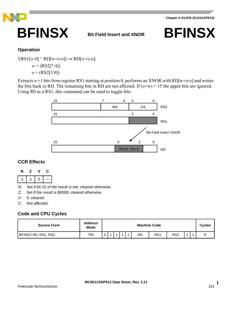
Chapter 6 XGATE (S12XGATEV2)
MC9S12XDP512 Data Sheet, Rev. 2.21Freescale Semiconductor 231
Operation
!(RS1[w:0] ^ RD[w+o:o]) ⇒ RD[w+o:o];
w = (RS2[7:4])
o = (RS2[3:0])
Extracts w+1 bits from register RS1 starting at position 0, performs an XNOR with RD[w+o:o] and writesthe bits back io RD. The remaining bits in RD are not affected. If (o+w) > 15 the upper bits are ignored.Using R0 as a RS1, this command can be used to toggle bits.
CCR Effects
Code and CPU Cycles
BFINSX Bit Field Insert and XNOR BFINSX
N Z V C
∆ ∆ 0 —
N: Set if bit 15 of the result is set; cleared otherwise.Z: Set if the result is $0000; cleared otherwise.V: 0; cleared.C: Not affected.
Source FormAddress
ModeMachine Code Cycles
BFINSX RD, RS1, RS2 TRI 0 1 1 1 1 RD RS1 RS2 1 1 P
W4 O4
15 025
W4=3, O4=2
15 03
Bit Field Insert XNOR
RS2
RD
RS1
15 037 4

Chapter 6 XGATE (S12XGATEV2)
MC9S12XDP512 Data Sheet, Rev. 2.21232 Freescale Semiconductor
Operation
If N ^ V = 0, then PC + $0002 + (REL9 << 1) ⇒ PC
Branch instruction to compare signed numbers.
Branch if RS1 ≥ RS2:SUB R0,RS1,RS2BGE REL9
CCR Effects
Code and CPU Cycles
BGE Branch if Greater than or Equal to Zero BGE
N Z V C
— — — —
N: Not affected.Z: Not affected.V: Not affected.C: Not affected.
Source FormAddress
ModeMachine Code Cycles
BGE REL9 REL9 0 0 1 1 0 1 0 REL9 PP/P
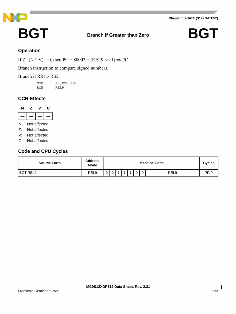
Chapter 6 XGATE (S12XGATEV2)
MC9S12XDP512 Data Sheet, Rev. 2.21Freescale Semiconductor 233
Operation
If Z | (N ^ V) = 0, then PC + $0002 + (REL9 << 1) ⇒ PC
Branch instruction to compare signed numbers.
Branch if RS1 > RS2:SUB R0,RS1,RS2BGE REL9
CCR Effects
Code and CPU Cycles
BGT Branch if Greater than Zero BGT
N Z V C
— — — —
N: Not affected.Z: Not affected.V: Not affected.C: Not affected.
Source FormAddress
ModeMachine Code Cycles
BGT REL9 REL9 0 0 1 1 1 0 0 REL9 PP/P

Chapter 6 XGATE (S12XGATEV2)
MC9S12XDP512 Data Sheet, Rev. 2.21234 Freescale Semiconductor
Operation
If C | Z = 0, then PC + $0002 + (REL9 << 1) ⇒ PC
Branch instruction to compare unsigned numbers.
Branch if RS1 > RS2:SUB R0,RS1,RS2BHI REL9
CCR Effects
Code and CPU Cycles
BHI Branch if Higher BHI
N Z V C
— — — —
N: Not affected.Z: Not affected.V: Not affected.C: Not affected.
Source FormAddress
ModeMachine Code Cycles
BHI REL9 REL9 0 0 1 1 0 0 0 REL9 PP/P
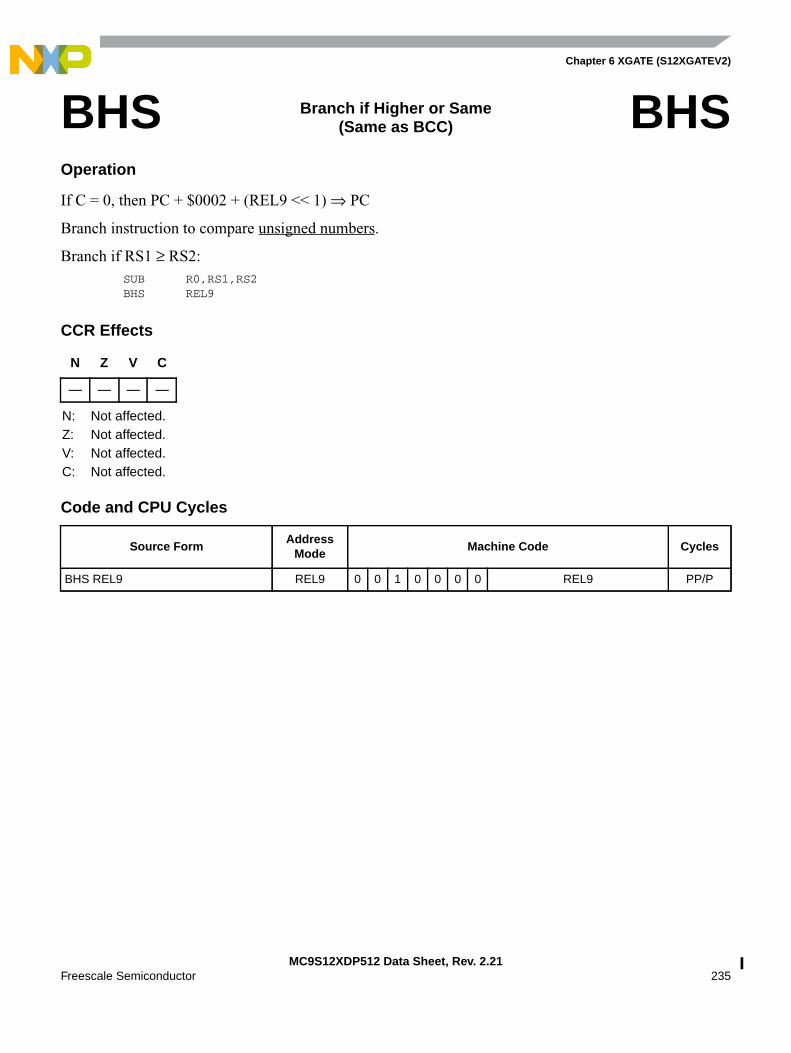
Chapter 6 XGATE (S12XGATEV2)
MC9S12XDP512 Data Sheet, Rev. 2.21Freescale Semiconductor 235
Operation
If C = 0, then PC + $0002 + (REL9 << 1) ⇒ PC
Branch instruction to compare unsigned numbers.
Branch if RS1 ≥ RS2:SUB R0,RS1,RS2BHS REL9
CCR Effects
Code and CPU Cycles
BHS Branch if Higher or Same(Same as BCC) BHS
N Z V C
— — — —
N: Not affected.Z: Not affected.V: Not affected.C: Not affected.
Source FormAddress
ModeMachine Code Cycles
BHS REL9 REL9 0 0 1 0 0 0 0 REL9 PP/P
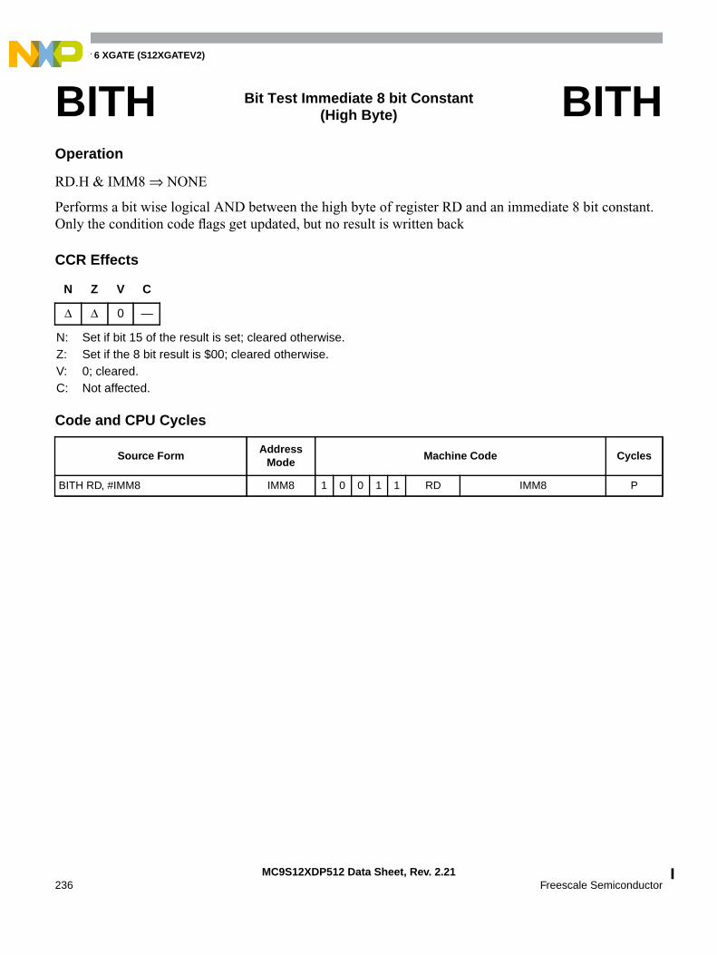
Chapter 6 XGATE (S12XGATEV2)
MC9S12XDP512 Data Sheet, Rev. 2.21236 Freescale Semiconductor
Operation
RD.H & IMM8 ⇒ NONE
Performs a bit wise logical AND between the high byte of register RD and an immediate 8 bit constant.Only the condition code flags get updated, but no result is written back
CCR Effects
Code and CPU Cycles
BITH Bit Test Immediate 8 bit Constant(High Byte) BITH
N Z V C
∆ ∆ 0 —
N: Set if bit 15 of the result is set; cleared otherwise.Z: Set if the 8 bit result is $00; cleared otherwise.V: 0; cleared.C: Not affected.
Source FormAddress
ModeMachine Code Cycles
BITH RD, #IMM8 IMM8 1 0 0 1 1 RD IMM8 P
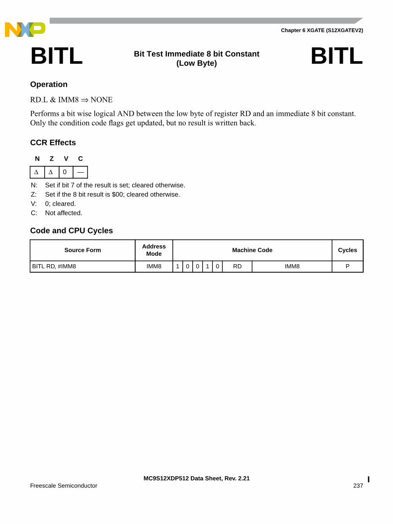
Chapter 6 XGATE (S12XGATEV2)
MC9S12XDP512 Data Sheet, Rev. 2.21Freescale Semiconductor 237
Operation
RD.L & IMM8 ⇒ NONE
Performs a bit wise logical AND between the low byte of register RD and an immediate 8 bit constant.Only the condition code flags get updated, but no result is written back.
CCR Effects
Code and CPU Cycles
BITL Bit Test Immediate 8 bit Constant(Low Byte) BITL
N Z V C
∆ ∆ 0 —
N: Set if bit 7 of the result is set; cleared otherwise.Z: Set if the 8 bit result is $00; cleared otherwise.V: 0; cleared.C: Not affected.
Source FormAddress
ModeMachine Code Cycles
BITL RD, #IMM8 IMM8 1 0 0 1 0 RD IMM8 P
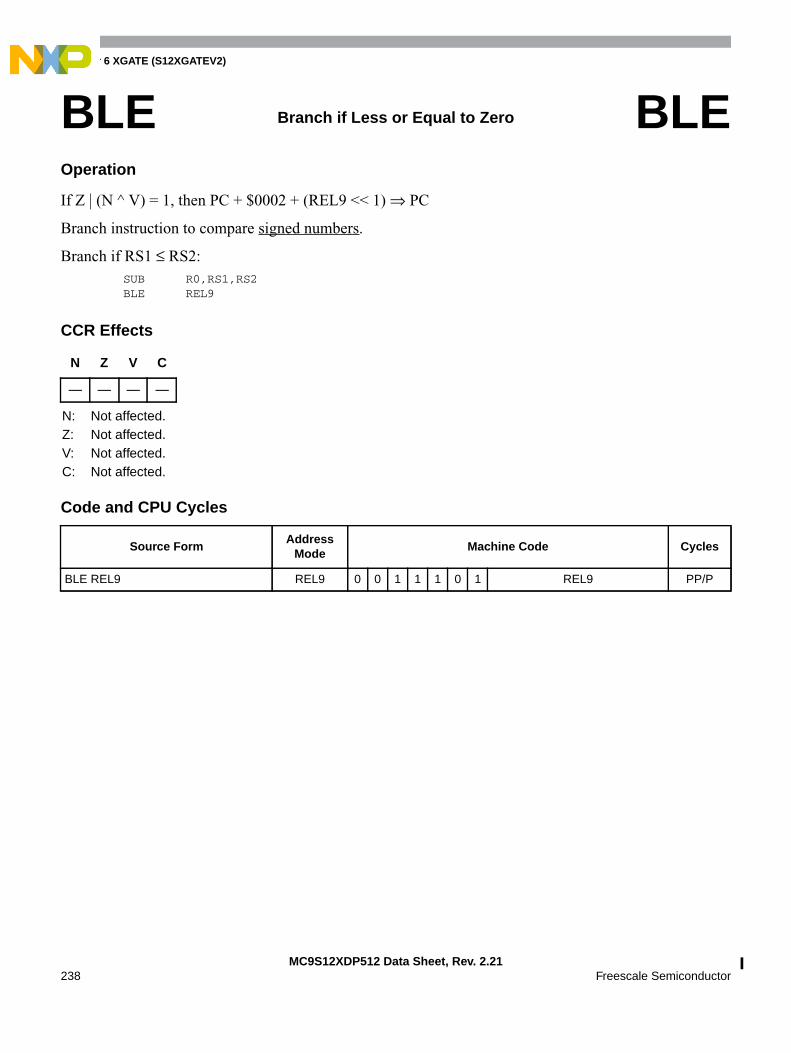
Chapter 6 XGATE (S12XGATEV2)
MC9S12XDP512 Data Sheet, Rev. 2.21238 Freescale Semiconductor
Operation
If Z | (N ^ V) = 1, then PC + $0002 + (REL9 << 1) ⇒ PC
Branch instruction to compare signed numbers.
Branch if RS1 ≤ RS2:SUB R0,RS1,RS2BLE REL9
CCR Effects
Code and CPU Cycles
BLE Branch if Less or Equal to Zero BLE
N Z V C
— — — —
N: Not affected.Z: Not affected.V: Not affected.C: Not affected.
Source FormAddress
ModeMachine Code Cycles
BLE REL9 REL9 0 0 1 1 1 0 1 REL9 PP/P

Chapter 6 XGATE (S12XGATEV2)
MC9S12XDP512 Data Sheet, Rev. 2.21Freescale Semiconductor 239
Operation
If C = 1, then PC + $0002 + (REL9 << 1) ⇒ PC
Branch instruction to compare unsigned numbers.
Branch if RS1 < RS2:SUB R0,RS1,RS2BLO REL9
CCR Effects
Code and CPU Cycles
BLO Branch if Carry Set(Same as BCS) BLO
N Z V C
— — — —
N: Not affected.Z: Not affected.V: Not affected.C: Not affected.
Source FormAddress
ModeMachine Code Cycles
BLO REL9 REL9 0 0 1 0 0 0 1 REL9 PP/P

Chapter 6 XGATE (S12XGATEV2)
MC9S12XDP512 Data Sheet, Rev. 2.21240 Freescale Semiconductor
Operation
If C | Z = 1, then PC + $0002 + (REL9 << 1) ⇒ PC
Branch instruction to compare unsigned numbers.
Branch if RS1 ≤ RS2:SUB R0,RS1,RS2BLS REL9
CCR Effects
Code and CPU Cycles
BLS Branch if Lower or Same BLS
N Z V C
— — — —
N: Not affected.Z: Not affected.V: Not affected.C: Not affected.
Source FormAddress
ModeMachine Code Cycles
BLS REL9 REL9 0 0 1 1 0 0 1 REL9 PP/P

Chapter 6 XGATE (S12XGATEV2)
MC9S12XDP512 Data Sheet, Rev. 2.21Freescale Semiconductor 241
Operation
If N ^ V = 1, then PC + $0002 + (REL9 << 1) ⇒ PC
Branch instruction to compare signed numbers.
Branch if RS1 < RS2:SUB R0,RS1,RS2BLT REL9
CCR Effects
Code and CPU Cycles
BLT Branch if Lower than Zero BLT
N Z V C
— — — —
N: Not affected.Z: Not affected.V: Not affected.C: Not affected.
Source FormAddress
ModeMachine Code Cycles
BLT REL9 REL9 0 0 1 1 0 1 1 REL9 PP/P

Chapter 6 XGATE (S12XGATEV2)
MC9S12XDP512 Data Sheet, Rev. 2.21242 Freescale Semiconductor
Operation
If N = 1, then PC + $0002 + (REL9 << 1) ⇒ PC
Tests the Sign flag and branches if N = 1.
CCR Effects
Code and CPU Cycles
BMI Branch if Minus BMI
N Z V C
— — — —
N: Not affected.Z: Not affected.V: Not affected.C: Not affected.
Source FormAddress
ModeMachine Code Cycles
BMI REL9 REL9 0 0 1 0 1 0 1 REL9 PP/P
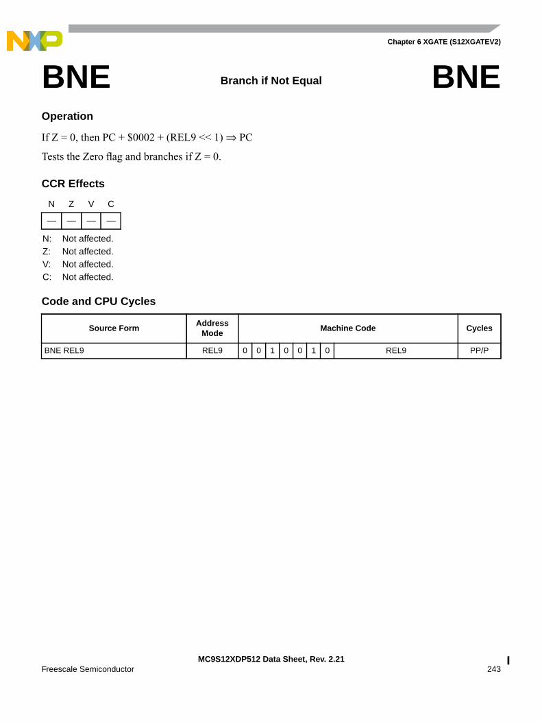
Chapter 6 XGATE (S12XGATEV2)
MC9S12XDP512 Data Sheet, Rev. 2.21Freescale Semiconductor 243
Operation
If Z = 0, then PC + $0002 + (REL9 << 1) ⇒ PC
Tests the Zero flag and branches if Z = 0.
CCR Effects
Code and CPU Cycles
BNE Branch if Not Equal BNE
N Z V C
— — — —
N: Not affected.Z: Not affected.V: Not affected.C: Not affected.
Source FormAddress
ModeMachine Code Cycles
BNE REL9 REL9 0 0 1 0 0 1 0 REL9 PP/P

Chapter 6 XGATE (S12XGATEV2)
MC9S12XDP512 Data Sheet, Rev. 2.21244 Freescale Semiconductor
Operation
If N = 0, then PC + $0002 + (REL9 << 1) ⇒ PC
Tests the Sign flag and branches if N = 0.
CCR Effects
Code and CPU Cycles
BPL Branch if Plus BPL
N Z V C
— — — —
N: Not affected.Z: Not affected.V: Not affected.C: Not affected.
Source FormAddress
ModeMachine Code Cycles
BPL REL9 REL9 0 0 1 0 1 0 0 REL9 PP/P
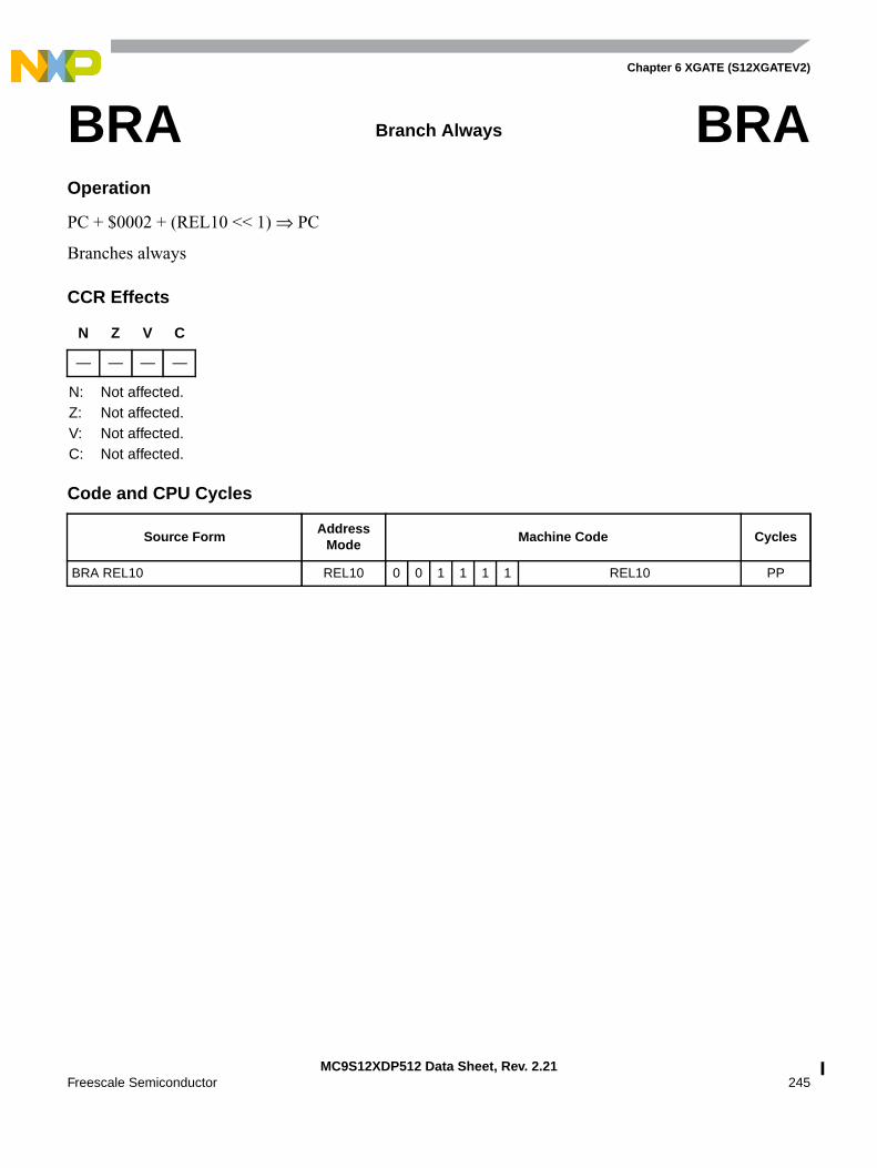
Chapter 6 XGATE (S12XGATEV2)
MC9S12XDP512 Data Sheet, Rev. 2.21Freescale Semiconductor 245
Operation
PC + $0002 + (REL10 << 1) ⇒ PC
Branches always
CCR Effects
Code and CPU Cycles
BRA Branch Always BRA
N Z V C
— — — —
N: Not affected.Z: Not affected.V: Not affected.C: Not affected.
Source FormAddress
ModeMachine Code Cycles
BRA REL10 REL10 0 0 1 1 1 1 REL10 PP

Chapter 6 XGATE (S12XGATEV2)
MC9S12XDP512 Data Sheet, Rev. 2.21246 Freescale Semiconductor
Operation
Put XGATE into Debug Mode (see Section 6.6.2, “Entering Debug Mode”)and signals a Softwarebreakpoint to the S12X_DBG module (see section 4.9 of the S12X_DBG Section).
NOTEIt is not possible to single step over a BRK instruction. This instruction doesnot advance the program counter.
CCR Effects
Code and CPU Cycles
BRK Break BRK
N Z V C
— — — —
N: Not affected.Z: Not affected.V: Not affected.C: Not affected.
Source FormAddress
ModeMachine Code Cycles
BRK INH 0 0 0 0 0 0 0 0 0 0 0 0 0 0 0 0 PAff

Chapter 6 XGATE (S12XGATEV2)
MC9S12XDP512 Data Sheet, Rev. 2.21Freescale Semiconductor 247
Operation
If V = 0, then PC + $0002 + (REL9 << 1) ⇒ PC
Tests the Overflow flag and branches if V = 0.
CCR Effects
Code and CPU Cycles
BVC Branch if Overflow Cleared BVC
N Z V C
— — — —
N: Not affected.Z: Not affected.V: Not affected.C: Not affected.
Source FormAddress
ModeMachine Code Cycles
BVC REL9 REL9 0 0 1 0 1 1 0 REL9 PP/P

Chapter 6 XGATE (S12XGATEV2)
MC9S12XDP512 Data Sheet, Rev. 2.21248 Freescale Semiconductor
Operation
If V = 1, then PC + $0002 + (REL9 << 1) ⇒ PC
Tests the Overflow flag and branches if V = 1.
CCR Effects
Code and CPU Cycles
BVS Branch if Overflow Set BVS
N Z V C
— — — —
N: Not affected.Z: Not affected.V: Not affected.C: Not affected.
Source FormAddress
ModeMachine Code Cycles
BVS REL9 REL9 0 0 1 0 1 1 1 REL9 PP/P

Chapter 6 XGATE (S12XGATEV2)
MC9S12XDP512 Data Sheet, Rev. 2.21Freescale Semiconductor 249
Operation
RS2 – RS1 ⇒ NONE (translates to SUB R0, RS1, RS2)RD – IMM16 ⇒ NONE (translates to CMPL RD, #IMM16[7:0]; CPCH RD, #IMM16[15:8])
Subtracts two 16 bit values and discards the result.
CCR Effects
Code and CPU Cycles
CMP Compare CMP
N Z V C
∆ ∆ ∆ ∆
N: Set if bit 15 of the result is set; cleared otherwise.Z: Set if the result is $0000; cleared otherwise.V: Set if a two´s complement overflow resulted from the operation; cleared otherwise.
RS1[15] & RS2[15] & result[15] | RS1[15] & RS2[15] & result[15]RD[15] & IMM16[15] & result[15] | RD[15] & IMM16[15] & result[15]
C: Set if there is a carry from the bit 15 of the result; cleared otherwise.RS1[15] & RS2[15] | RS1[15] & result[15] | RS2[15] & result[15]RD[15] & IMM16[15] | RD[15] & result[15] | IMM16[15] & result[15]
Source FormAddress
ModeMachine Code Cycles
CMP RS1, RS2 TRI 0 0 0 1 1 0 0 0 RS1 RS2 0 0 P
CMP RS, #IMM16 IMM8 1 1 0 1 0 RS IMM16[7:0] P
IMM8 1 1 0 1 1 RS IMM16[15:8] P
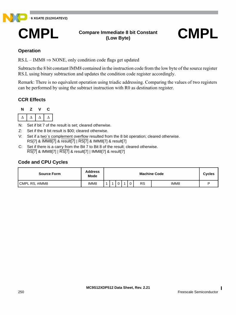
Chapter 6 XGATE (S12XGATEV2)
MC9S12XDP512 Data Sheet, Rev. 2.21250 Freescale Semiconductor
Operation
RS.L – IMM8 ⇒ NONE, only condition code flags get updated
Subtracts the 8 bit constant IMM8 contained in the instruction code from the low byte of the source registerRS.L using binary subtraction and updates the condition code register accordingly.
Remark: There is no equivalent operation using triadic addressing. Comparing the values of two registerscan be performed by using the subtract instruction with R0 as destination register.
CCR Effects
Code and CPU Cycles
CMPL Compare Immediate 8 bit Constant(Low Byte) CMPL
N Z V C
∆ ∆ ∆ ∆
N: Set if bit 7 of the result is set; cleared otherwise.Z: Set if the 8 bit result is $00; cleared otherwise.V: Set if a two´s complement overflow resulted from the 8 bit operation; cleared otherwise.
RS[7] & IMM8[7] & result[7] | RS[7] & IMM8[7] & result[7]C: Set if there is a carry from the Bit 7 to Bit 8 of the result; cleared otherwise.
RS[7] & IMM8[7] | RS[7] & result[7] | IMM8[7] & result[7]
Source FormAddress
ModeMachine Code Cycles
CMPL RS, #IMM8 IMM8 1 1 0 1 0 RS IMM8 P
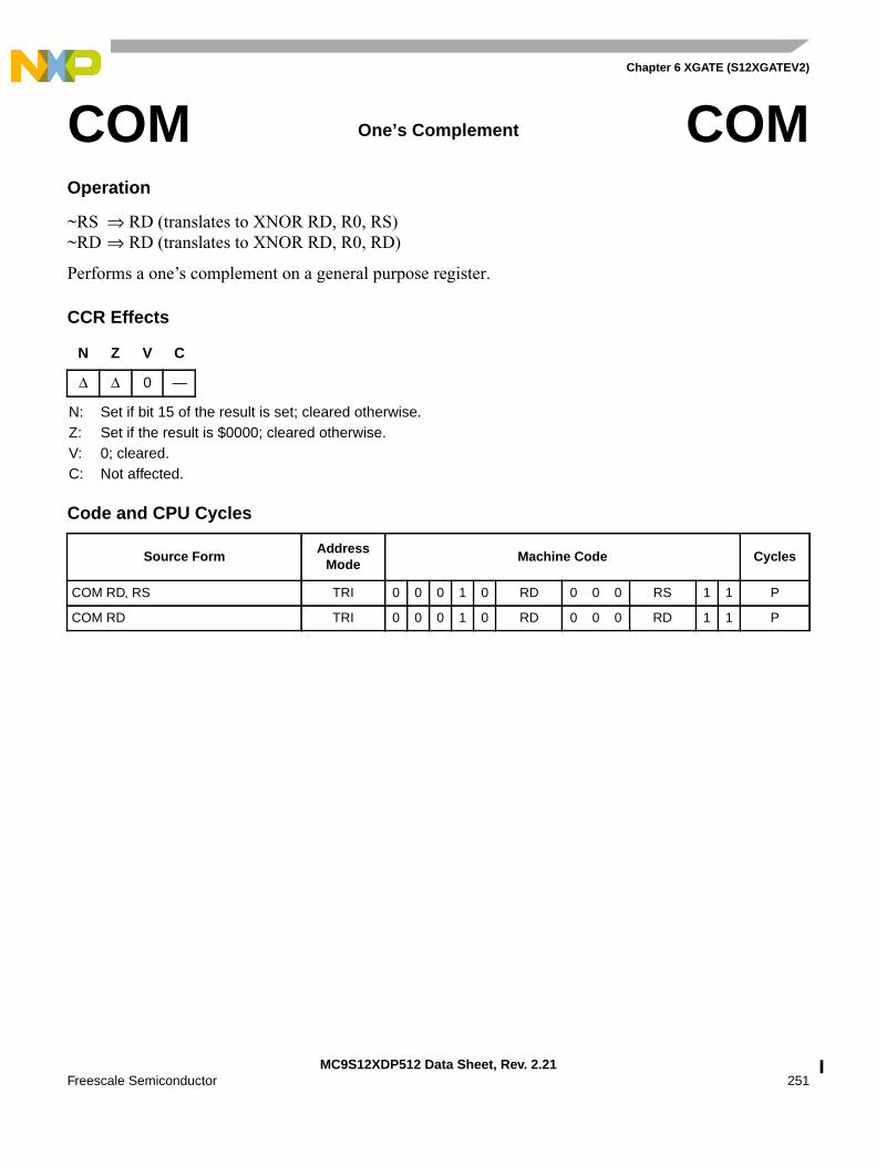
Chapter 6 XGATE (S12XGATEV2)
MC9S12XDP512 Data Sheet, Rev. 2.21Freescale Semiconductor 251
Operation
~RS ⇒ RD (translates to XNOR RD, R0, RS)~RD ⇒ RD (translates to XNOR RD, R0, RD)
Performs a one’s complement on a general purpose register.
CCR Effects
Code and CPU Cycles
COM One’s Complement COM
N Z V C
∆ ∆ 0 —
N: Set if bit 15 of the result is set; cleared otherwise.Z: Set if the result is $0000; cleared otherwise.V: 0; cleared.C: Not affected.
Source FormAddress
ModeMachine Code Cycles
COM RD, RS TRI 0 0 0 1 0 RD 0 0 0 RS 1 1 P
COM RD TRI 0 0 0 1 0 RD 0 0 0 RD 1 1 P
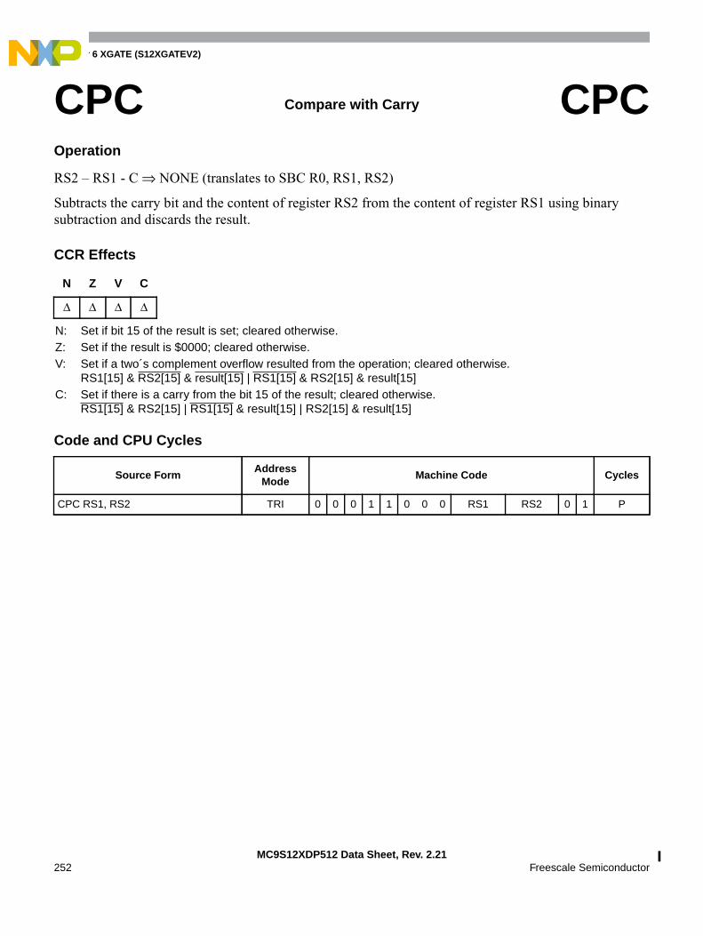
Chapter 6 XGATE (S12XGATEV2)
MC9S12XDP512 Data Sheet, Rev. 2.21252 Freescale Semiconductor
Operation
RS2 – RS1 - C ⇒ NONE (translates to SBC R0, RS1, RS2)
Subtracts the carry bit and the content of register RS2 from the content of register RS1 using binarysubtraction and discards the result.
CCR Effects
Code and CPU Cycles
CPC Compare with Carry CPC
N Z V C
∆ ∆ ∆ ∆
N: Set if bit 15 of the result is set; cleared otherwise.Z: Set if the result is $0000; cleared otherwise.V: Set if a two´s complement overflow resulted from the operation; cleared otherwise.
RS1[15] & RS2[15] & result[15] | RS1[15] & RS2[15] & result[15]C: Set if there is a carry from the bit 15 of the result; cleared otherwise.
RS1[15] & RS2[15] | RS1[15] & result[15] | RS2[15] & result[15]
Source FormAddress
ModeMachine Code Cycles
CPC RS1, RS2 TRI 0 0 0 1 1 0 0 0 RS1 RS2 0 1 P
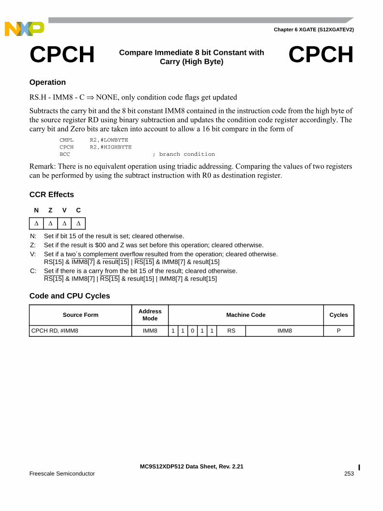
Chapter 6 XGATE (S12XGATEV2)
MC9S12XDP512 Data Sheet, Rev. 2.21Freescale Semiconductor 253
Operation
RS.H - IMM8 - C ⇒ NONE, only condition code flags get updated
Subtracts the carry bit and the 8 bit constant IMM8 contained in the instruction code from the high byte ofthe source register RD using binary subtraction and updates the condition code register accordingly. Thecarry bit and Zero bits are taken into account to allow a 16 bit compare in the form of
CMPL R2,#LOWBYTECPCH R2,#HIGHBYTEBCC ; branch condition
Remark: There is no equivalent operation using triadic addressing. Comparing the values of two registerscan be performed by using the subtract instruction with R0 as destination register.
CCR Effects
Code and CPU Cycles
CPCH Compare Immediate 8 bit Constant withCarry (High Byte) CPCH
N Z V C
∆ ∆ ∆ ∆
N: Set if bit 15 of the result is set; cleared otherwise.Z: Set if the result is $00 and Z was set before this operation; cleared otherwise.V: Set if a two´s complement overflow resulted from the operation; cleared otherwise.
RS[15] & IMM8[7] & result[15] | RS[15] & IMM8[7] & result[15]C: Set if there is a carry from the bit 15 of the result; cleared otherwise.
RS[15] & IMM8[7] | RS[15] & result[15] | IMM8[7] & result[15]
Source FormAddress
ModeMachine Code Cycles
CPCH RD, #IMM8 IMM8 1 1 0 1 1 RS IMM8 P
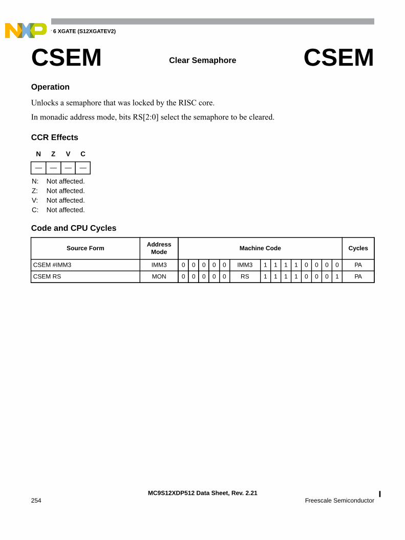
Chapter 6 XGATE (S12XGATEV2)
MC9S12XDP512 Data Sheet, Rev. 2.21254 Freescale Semiconductor
Operation
Unlocks a semaphore that was locked by the RISC core.
In monadic address mode, bits RS[2:0] select the semaphore to be cleared.
CCR Effects
Code and CPU Cycles
CSEM Clear Semaphore CSEM
N Z V C
— — — —
N: Not affected.Z: Not affected.V: Not affected.C: Not affected.
Source FormAddress
ModeMachine Code Cycles
CSEM #IMM3 IMM3 0 0 0 0 0 IMM3 1 1 1 1 0 0 0 0 PA
CSEM RS MON 0 0 0 0 0 RS 1 1 1 1 0 0 0 1 PA
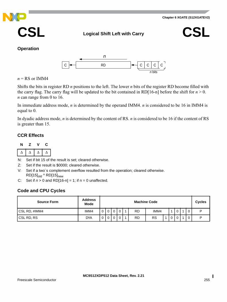
Chapter 6 XGATE (S12XGATEV2)
MC9S12XDP512 Data Sheet, Rev. 2.21Freescale Semiconductor 255
Operation
n = RS or IMM4
Shifts the bits in register RD n positions to the left. The lower n bits of the register RD become filled withthe carry flag. The carry flag will be updated to the bit contained in RD[16-n] before the shift for n > 0.n can range from 0 to 16.
In immediate address mode, n is determined by the operand IMM4. n is considered to be 16 in IMM4 isequal to 0.
In dyadic address mode, n is determined by the content of RS. n is considered to be 16 if the content of RSis greater than 15.
CCR Effects
Code and CPU Cycles
CSL Logical Shift Left with Carry CSL
N Z V C
∆ ∆ ∆ ∆
N: Set if bit 15 of the result is set; cleared otherwise.Z: Set if the result is $0000; cleared otherwise.V: Set if a two´s complement overflow resulted from the operation; cleared otherwise.
RD[15]old ^ RD[15]newC: Set if n > 0 and RD[16-n] = 1; if n = 0 unaffected.
Source FormAddress
ModeMachine Code Cycles
CSL RD, #IMM4 IMM4 0 0 0 0 1 RD IMM4 1 0 1 0 P
CSL RD, RS DYA 0 0 0 0 1 RD RS 1 0 0 1 0 P
CRD C C C
n bits
C
n
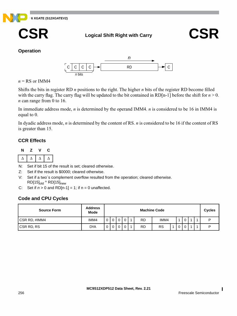
Chapter 6 XGATE (S12XGATEV2)
MC9S12XDP512 Data Sheet, Rev. 2.21256 Freescale Semiconductor
Operation
n = RS or IMM4
Shifts the bits in register RD n positions to the right. The higher n bits of the register RD become filledwith the carry flag. The carry flag will be updated to the bit contained in RD[n-1] before the shift for n > 0.n can range from 0 to 16.
In immediate address mode, n is determined by the operand IMM4. n is considered to be 16 in IMM4 isequal to 0.
In dyadic address mode, n is determined by the content of RS. n is considered to be 16 if the content of RSis greater than 15.
CCR Effects
Code and CPU Cycles
CSR Logical Shift Right with Carry CSR
N Z V C
∆ ∆ ∆ ∆
N: Set if bit 15 of the result is set; cleared otherwise.Z: Set if the result is $0000; cleared otherwise.V: Set if a two´s complement overflow resulted from the operation; cleared otherwise.
RD[15]old ^ RD[15]newC: Set if n > 0 and RD[n-1] = 1; if n = 0 unaffected.
Source FormAddress
ModeMachine Code Cycles
CSR RD, #IMM4 IMM4 0 0 0 0 1 RD IMM4 1 0 1 1 P
CSR RD, RS DYA 0 0 0 0 1 RD RS 1 0 0 1 1 P
C C RDCC
n bits
C
n
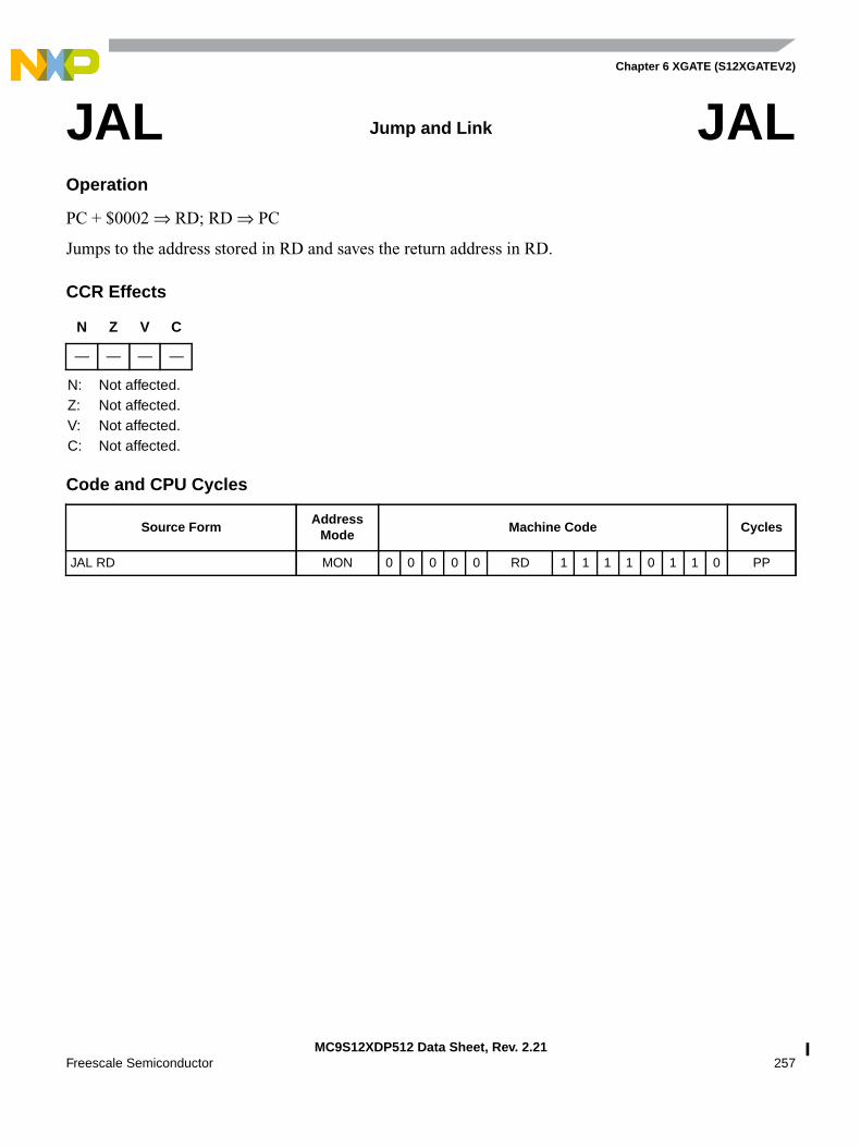
Chapter 6 XGATE (S12XGATEV2)
MC9S12XDP512 Data Sheet, Rev. 2.21Freescale Semiconductor 257
Operation
PC + $0002 ⇒ RD; RD ⇒ PC
Jumps to the address stored in RD and saves the return address in RD.
CCR Effects
Code and CPU Cycles
JAL Jump and Link JAL
N Z V C
— — — —
N: Not affected.Z: Not affected.V: Not affected.C: Not affected.
Source FormAddress
ModeMachine Code Cycles
JAL RD MON 0 0 0 0 0 RD 1 1 1 1 0 1 1 0 PP
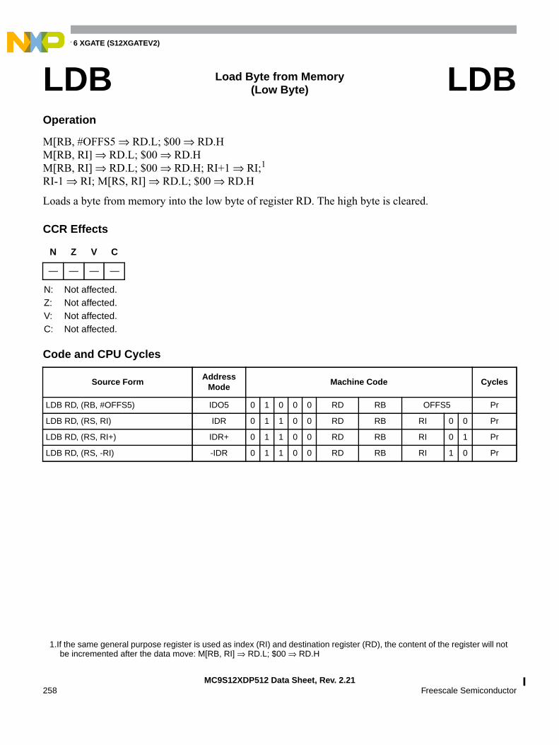
Chapter 6 XGATE (S12XGATEV2)
MC9S12XDP512 Data Sheet, Rev. 2.21258 Freescale Semiconductor
Operation
M[RB, #OFFS5 ⇒ RD.L; $00 ⇒ RD.HM[RB, RI] ⇒ RD.L; $00 ⇒ RD.HM[RB, RI] ⇒ RD.L; $00 ⇒ RD.H; RI+1 ⇒ RI;1
RI-1 ⇒ RI; M[RS, RI] ⇒ RD.L; $00 ⇒ RD.H
Loads a byte from memory into the low byte of register RD. The high byte is cleared.
CCR Effects
Code and CPU Cycles
LDB Load Byte from Memory(Low Byte) LDB
1.If the same general purpose register is used as index (RI) and destination register (RD), the content of the register will notbe incremented after the data move: M[RB, RI] ⇒ RD.L; $00 ⇒ RD.H
N Z V C
— — — —
N: Not affected.Z: Not affected.V: Not affected.C: Not affected.
Source FormAddress
ModeMachine Code Cycles
LDB RD, (RB, #OFFS5) IDO5 0 1 0 0 0 RD RB OFFS5 Pr
LDB RD, (RS, RI) IDR 0 1 1 0 0 RD RB RI 0 0 Pr
LDB RD, (RS, RI+) IDR+ 0 1 1 0 0 RD RB RI 0 1 Pr
LDB RD, (RS, -RI) -IDR 0 1 1 0 0 RD RB RI 1 0 Pr
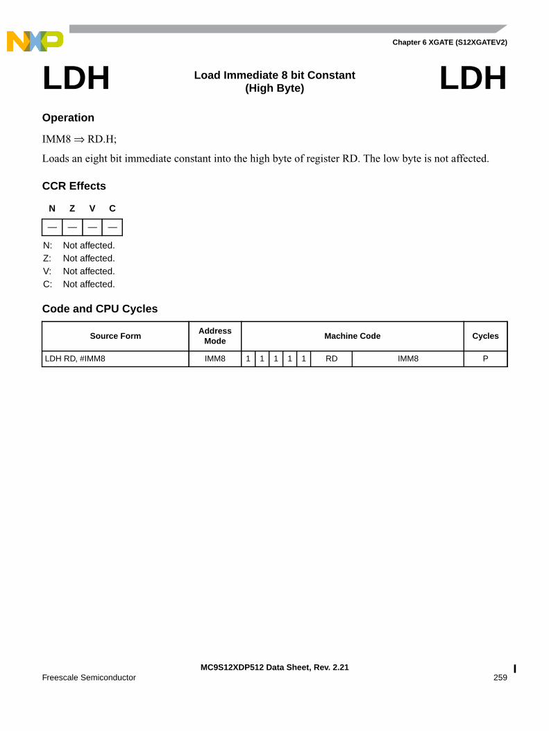
Chapter 6 XGATE (S12XGATEV2)
MC9S12XDP512 Data Sheet, Rev. 2.21Freescale Semiconductor 259
Operation
IMM8 ⇒ RD.H;
Loads an eight bit immediate constant into the high byte of register RD. The low byte is not affected.
CCR Effects
Code and CPU Cycles
LDH Load Immediate 8 bit Constant(High Byte) LDH
N Z V C
— — — —
N: Not affected.Z: Not affected.V: Not affected.C: Not affected.
Source FormAddress
ModeMachine Code Cycles
LDH RD, #IMM8 IMM8 1 1 1 1 1 RD IMM8 P
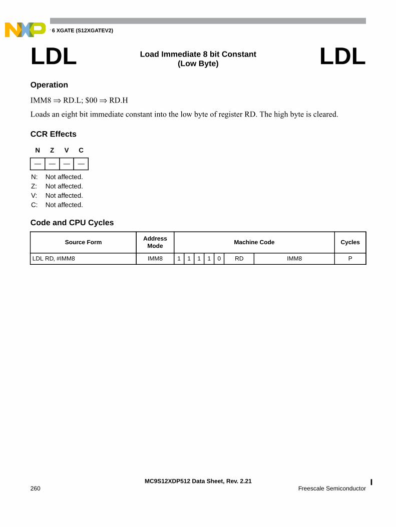
Chapter 6 XGATE (S12XGATEV2)
MC9S12XDP512 Data Sheet, Rev. 2.21260 Freescale Semiconductor
Operation
IMM8 ⇒ RD.L; $00 ⇒ RD.H
Loads an eight bit immediate constant into the low byte of register RD. The high byte is cleared.
CCR Effects
Code and CPU Cycles
LDL Load Immediate 8 bit Constant(Low Byte) LDL
N Z V C
— — — —
N: Not affected.Z: Not affected.V: Not affected.C: Not affected.
Source FormAddress
ModeMachine Code Cycles
LDL RD, #IMM8 IMM8 1 1 1 1 0 RD IMM8 P
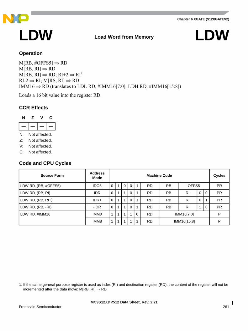
Chapter 6 XGATE (S12XGATEV2)
MC9S12XDP512 Data Sheet, Rev. 2.21Freescale Semiconductor 261
Operation
M[RB, #OFFS5] ⇒ RDM[RB, RI] ⇒ RDM[RB, RI] ⇒ RD; RI+2 ⇒ RI1
RI-2 ⇒ RI; M[RS, RI] ⇒ RDIMM16 ⇒ RD (translates to LDL RD, #IMM16[7:0]; LDH RD, #IMM16[15:8])
Loads a 16 bit value into the register RD.
CCR Effects
Code and CPU Cycles
LDW Load Word from Memory LDW
1. If the same general purpose register is used as index (RI) and destination register (RD), the content of the register will not beincremented after the data move: M[RB, RI] ⇒ RD
N Z V C
— — — —
N: Not affected.Z: Not affected.V: Not affected.C: Not affected.
Source FormAddress
ModeMachine Code Cycles
LDW RD, (RB, #OFFS5) IDO5 0 1 0 0 1 RD RB OFFS5 PR
LDW RD, (RB, RI) IDR 0 1 1 0 1 RD RB RI 0 0 PR
LDW RD, (RB, RI+) IDR+ 0 1 1 0 1 RD RB RI 0 1 PR
LDW RD, (RB, -RI) -IDR 0 1 1 0 1 RD RB RI 1 0 PR
LDW RD, #IMM16 IMM8 1 1 1 1 0 RD IMM16[7:0] P
IMM8 1 1 1 1 1 RD IMM16[15:8] P
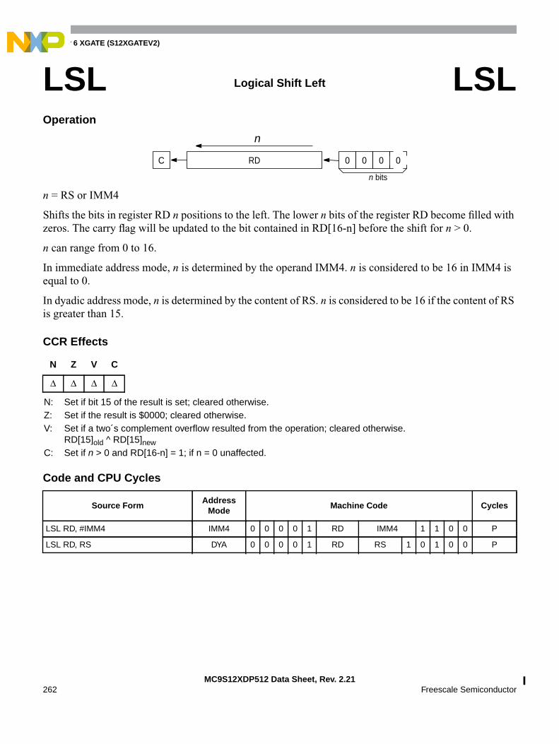
Chapter 6 XGATE (S12XGATEV2)
MC9S12XDP512 Data Sheet, Rev. 2.21262 Freescale Semiconductor
Operation
n = RS or IMM4
Shifts the bits in register RD n positions to the left. The lower n bits of the register RD become filled withzeros. The carry flag will be updated to the bit contained in RD[16-n] before the shift for n > 0.
n can range from 0 to 16.
In immediate address mode, n is determined by the operand IMM4. n is considered to be 16 in IMM4 isequal to 0.
In dyadic address mode, n is determined by the content of RS. n is considered to be 16 if the content of RSis greater than 15.
CCR Effects
Code and CPU Cycles
LSL Logical Shift Left LSL
N Z V C
∆ ∆ ∆ ∆
N: Set if bit 15 of the result is set; cleared otherwise.Z: Set if the result is $0000; cleared otherwise.V: Set if a two´s complement overflow resulted from the operation; cleared otherwise.
RD[15]old ^ RD[15]newC: Set if n > 0 and RD[16-n] = 1; if n = 0 unaffected.
Source FormAddress
ModeMachine Code Cycles
LSL RD, #IMM4 IMM4 0 0 0 0 1 RD IMM4 1 1 0 0 P
LSL RD, RS DYA 0 0 0 0 1 RD RS 1 0 1 0 0 P
0RD 0 0 0
n bits
C
n
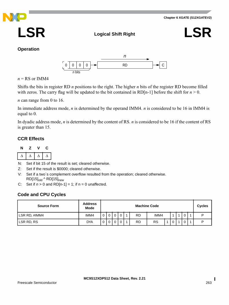
Chapter 6 XGATE (S12XGATEV2)
MC9S12XDP512 Data Sheet, Rev. 2.21Freescale Semiconductor 263
Operation
n = RS or IMM4
Shifts the bits in register RD n positions to the right. The higher n bits of the register RD become filledwith zeros. The carry flag will be updated to the bit contained in RD[n-1] before the shift for n > 0.
n can range from 0 to 16.
In immediate address mode, n is determined by the operand IMM4. n is considered to be 16 in IMM4 isequal to 0.
In dyadic address mode, n is determined by the content of RS. n is considered to be 16 if the content of RSis greater than 15.
CCR Effects
Code and CPU Cycles
LSR Logical Shift Right LSR
N Z V C
∆ ∆ ∆ ∆
N: Set if bit 15 of the result is set; cleared otherwise.Z: Set if the result is $0000; cleared otherwise.V: Set if a two´s complement overflow resulted from the operation; cleared otherwise.
RD[15]old ^ RD[15]newC: Set if n > 0 and RD[n-1] = 1; if n = 0 unaffected.
Source FormAddress
ModeMachine Code Cycles
LSR RD, #IMM4 IMM4 0 0 0 0 1 RD IMM4 1 1 0 1 P
LSR RD, RS DYA 0 0 0 0 1 RD RS 1 0 1 0 1 P
0 RD000
n bits
C
n

Chapter 6 XGATE (S12XGATEV2)
MC9S12XDP512 Data Sheet, Rev. 2.21264 Freescale Semiconductor
Operation
RS ⇒ RD (translates to OR RD, R0, RS)
Copies the content of RS to RD.
CCR Effects
Code and CPU Cycles
MOV Move Register Content MOV
N Z V C
∆ ∆ 0 —
N: Set if bit 15 of the result is set; cleared otherwise.Z: Set if the result is $0000; cleared otherwise.V: 0; cleared.C: Not affected.
Source FormAddress
ModeMachine Code Cycles
MOV RD, RS TRI 0 0 0 1 0 RD 0 0 0 RS 1 0 P

Chapter 6 XGATE (S12XGATEV2)
MC9S12XDP512 Data Sheet, Rev. 2.21Freescale Semiconductor 265
Operation
–RS ⇒ RD (translates to SUB RD, R0, RS)–RD ⇒ RD (translates to SUB RD, R0, RD)
Performs a two’s complement on a general purpose register.
CCR Effects
Code and CPU Cycles
NEG Two’s Complement NEG
N Z V C
∆ ∆ ∆ ∆
N: Set if bit 15 of the result is set; cleared otherwise.Z: Set if the result is $0000; cleared otherwise.V: Set if a two´s complement overflow resulted from the operation; cleared otherwise.
RS[15] & RD[15]newC: Set if there is a carry from the bit 15 of the result; cleared otherwise
RS[15] | RD[15]new
Source FormAddress
ModeMachine Code Cycles
NEG RD, RS TRI 0 0 0 1 1 RD 0 0 0 RS 0 0 P
NEG RD TRI 0 0 0 1 1 RD 0 0 0 RD 0 0 P
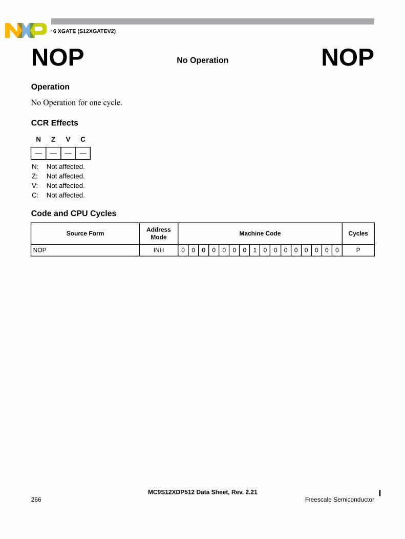
Chapter 6 XGATE (S12XGATEV2)
MC9S12XDP512 Data Sheet, Rev. 2.21266 Freescale Semiconductor
Operation
No Operation for one cycle.
CCR Effects
Code and CPU Cycles
NOP No Operation NOP
N Z V C
— — — —
N: Not affected.Z: Not affected.V: Not affected.C: Not affected.
Source FormAddress
ModeMachine Code Cycles
NOP INH 0 0 0 0 0 0 0 1 0 0 0 0 0 0 0 0 P
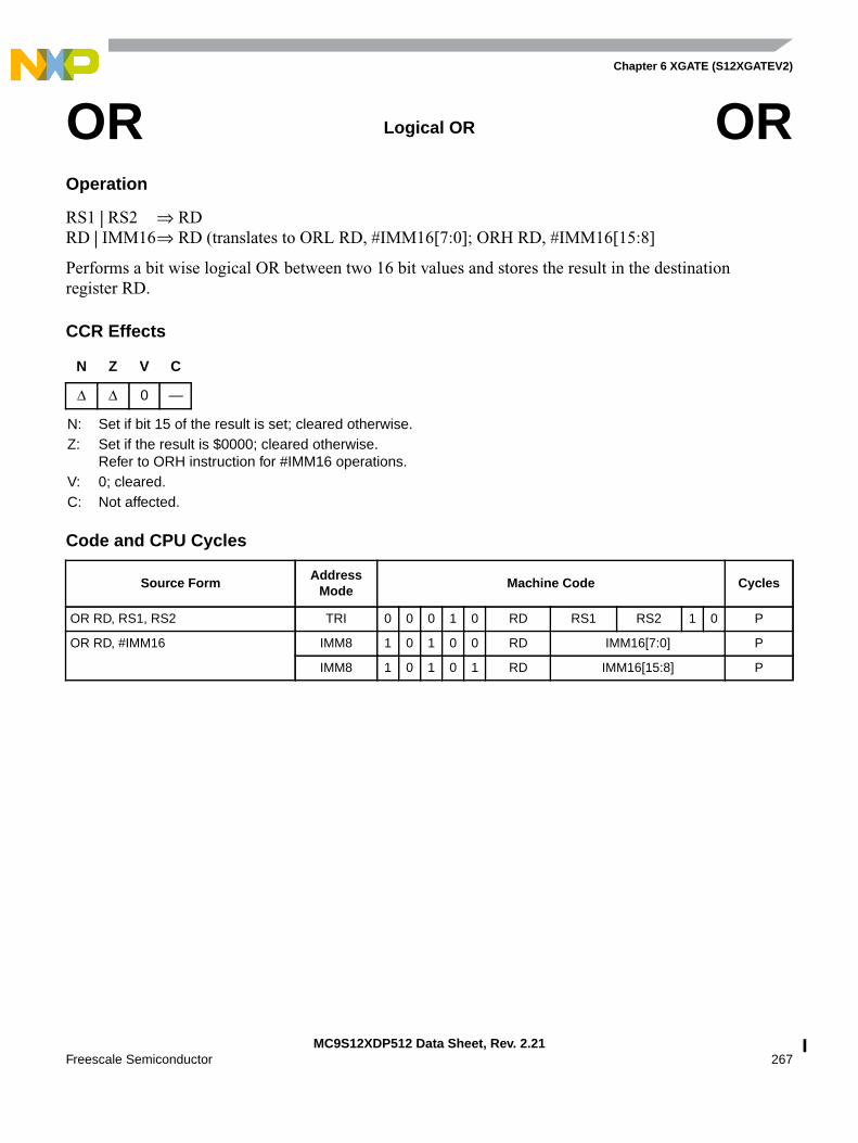
Chapter 6 XGATE (S12XGATEV2)
MC9S12XDP512 Data Sheet, Rev. 2.21Freescale Semiconductor 267
Operation
RS1 | RS2 ⇒ RDRD | IMM16⇒ RD (translates to ORL RD, #IMM16[7:0]; ORH RD, #IMM16[15:8]
Performs a bit wise logical OR between two 16 bit values and stores the result in the destinationregister RD.
CCR Effects
Code and CPU Cycles
OR Logical OR OR
N Z V C
∆ ∆ 0 —
N: Set if bit 15 of the result is set; cleared otherwise.Z: Set if the result is $0000; cleared otherwise.
Refer to ORH instruction for #IMM16 operations.V: 0; cleared.C: Not affected.
Source FormAddress
ModeMachine Code Cycles
OR RD, RS1, RS2 TRI 0 0 0 1 0 RD RS1 RS2 1 0 P
OR RD, #IMM16 IMM8 1 0 1 0 0 RD IMM16[7:0] P
IMM8 1 0 1 0 1 RD IMM16[15:8] P

Chapter 6 XGATE (S12XGATEV2)
MC9S12XDP512 Data Sheet, Rev. 2.21268 Freescale Semiconductor
Operation
RD.H | IMM8 ⇒ RD.H
Performs a bit wise logical OR between the high byte of register RD and an immediate 8 bit constant andstores the result in the destination register RD.H. The low byte of RD is not affected.
CCR Effects
Code and CPU Cycles
ORH Logical OR Immediate 8 bit Constant(High Byte) ORH
N Z V C
∆ ∆ 0 —
N: Set if bit 15 of the result is set; cleared otherwise.Z: Set if the 8 bit result is $00; cleared otherwise.V: 0; cleared.C: Not affected.
Source FormAddress
ModeMachine Code Cycles
ORH RD, #IMM8 IMM8 1 0 1 0 1 RD IMM8 P
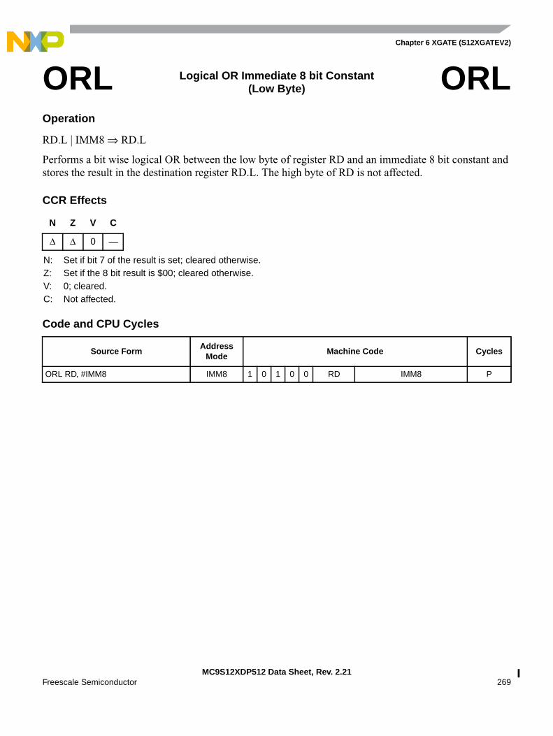
Chapter 6 XGATE (S12XGATEV2)
MC9S12XDP512 Data Sheet, Rev. 2.21Freescale Semiconductor 269
Operation
RD.L | IMM8 ⇒ RD.L
Performs a bit wise logical OR between the low byte of register RD and an immediate 8 bit constant andstores the result in the destination register RD.L. The high byte of RD is not affected.
CCR Effects
Code and CPU Cycles
ORL Logical OR Immediate 8 bit Constant(Low Byte) ORL
N Z V C
∆ ∆ 0 —
N: Set if bit 7 of the result is set; cleared otherwise.Z: Set if the 8 bit result is $00; cleared otherwise.V: 0; cleared.C: Not affected.
Source FormAddress
ModeMachine Code Cycles
ORL RD, #IMM8 IMM8 1 0 1 0 0 RD IMM8 P
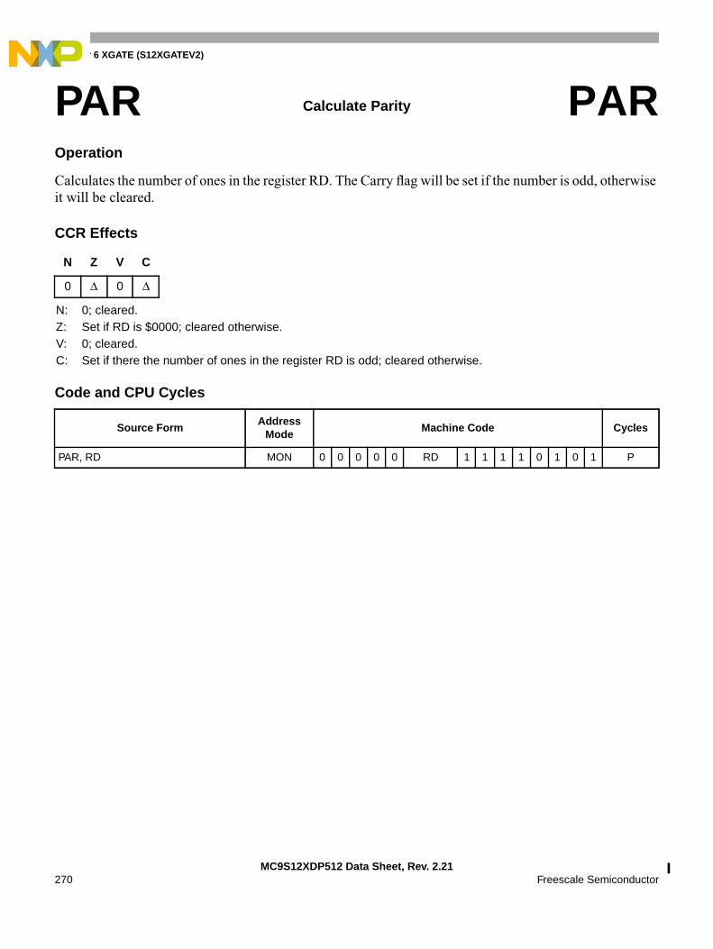
Chapter 6 XGATE (S12XGATEV2)
MC9S12XDP512 Data Sheet, Rev. 2.21270 Freescale Semiconductor
Operation
Calculates the number of ones in the register RD. The Carry flag will be set if the number is odd, otherwiseit will be cleared.
CCR Effects
Code and CPU Cycles
PAR Calculate Parity PAR
N Z V C
0 ∆ 0 ∆
N: 0; cleared.Z: Set if RD is $0000; cleared otherwise.V: 0; cleared.C: Set if there the number of ones in the register RD is odd; cleared otherwise.
Source FormAddress
ModeMachine Code Cycles
PAR, RD MON 0 0 0 0 0 RD 1 1 1 1 0 1 0 1 P
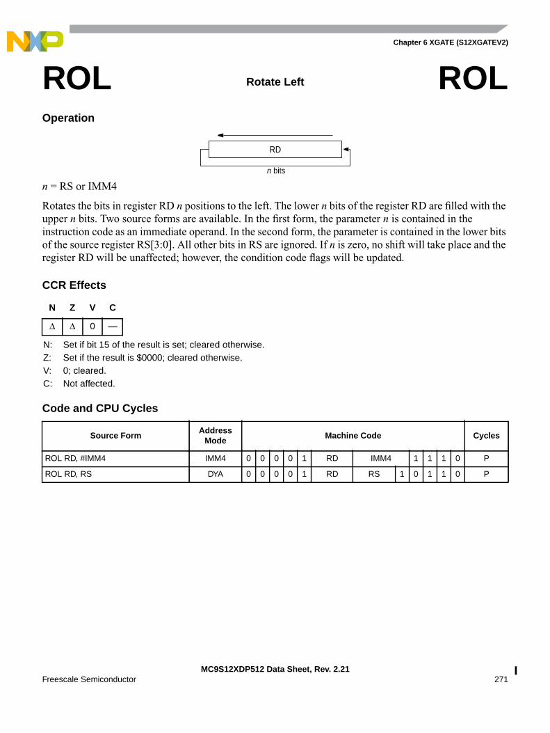
Chapter 6 XGATE (S12XGATEV2)
MC9S12XDP512 Data Sheet, Rev. 2.21Freescale Semiconductor 271
Operation
n = RS or IMM4
Rotates the bits in register RD n positions to the left. The lower n bits of the register RD are filled with theupper n bits. Two source forms are available. In the first form, the parameter n is contained in theinstruction code as an immediate operand. In the second form, the parameter is contained in the lower bitsof the source register RS[3:0]. All other bits in RS are ignored. If n is zero, no shift will take place and theregister RD will be unaffected; however, the condition code flags will be updated.
CCR Effects
Code and CPU Cycles
ROL Rotate Left ROL
N Z V C
∆ ∆ 0 —
N: Set if bit 15 of the result is set; cleared otherwise.Z: Set if the result is $0000; cleared otherwise.V: 0; cleared.C: Not affected.
Source FormAddress
ModeMachine Code Cycles
ROL RD, #IMM4 IMM4 0 0 0 0 1 RD IMM4 1 1 1 0 P
ROL RD, RS DYA 0 0 0 0 1 RD RS 1 0 1 1 0 P
RD
n bits
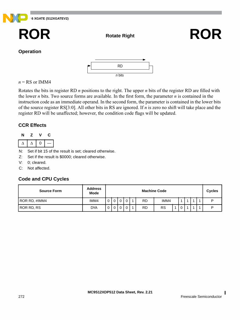
Chapter 6 XGATE (S12XGATEV2)
MC9S12XDP512 Data Sheet, Rev. 2.21272 Freescale Semiconductor
Operation
n = RS or IMM4
Rotates the bits in register RD n positions to the right. The upper n bits of the register RD are filled withthe lower n bits. Two source forms are available. In the first form, the parameter n is contained in theinstruction code as an immediate operand. In the second form, the parameter is contained in the lower bitsof the source register RS[3:0]. All other bits in RS are ignored. If n is zero no shift will take place and theregister RD will be unaffected; however, the condition code flags will be updated.
CCR Effects
Code and CPU Cycles
ROR Rotate Right ROR
N Z V C
∆ ∆ 0 —
N: Set if bit 15 of the result is set; cleared otherwise.Z: Set if the result is $0000; cleared otherwise.V: 0; cleared.C: Not affected.
Source FormAddress
ModeMachine Code Cycles
ROR RD, #IMM4 IMM4 0 0 0 0 1 RD IMM4 1 1 1 1 P
ROR RD, RS DYA 0 0 0 0 1 RD RS 1 0 1 1 1 P
RD
n bits

Chapter 6 XGATE (S12XGATEV2)
MC9S12XDP512 Data Sheet, Rev. 2.21Freescale Semiconductor 273
Operation
Terminates the current thread of program execution and remains idle until a new thread is started by thehardware scheduler.
CCR Effects
Code and CPU Cycles
RTS Return to Scheduler RTS
N Z V C
— — — —
N: Not affected.Z: Not affected.V: Not affected.C: Not affected.
Source FormAddress
ModeMachine Code Cycles
RTS INH 0 0 0 0 0 0 1 0 0 0 0 0 0 0 0 0 PA
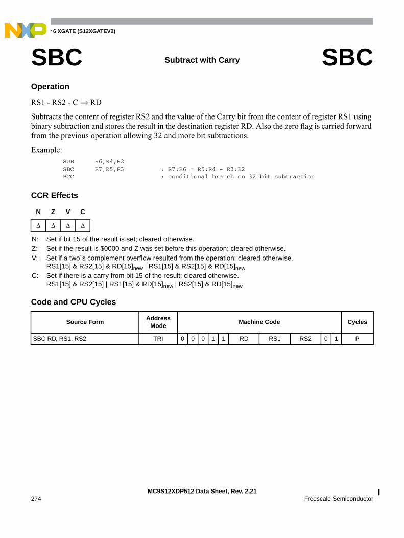
Chapter 6 XGATE (S12XGATEV2)
MC9S12XDP512 Data Sheet, Rev. 2.21274 Freescale Semiconductor
Operation
RS1 - RS2 - C ⇒ RD
Subtracts the content of register RS2 and the value of the Carry bit from the content of register RS1 usingbinary subtraction and stores the result in the destination register RD. Also the zero flag is carried forwardfrom the previous operation allowing 32 and more bit subtractions.
Example:SUB R6,R4,R2SBC R7,R5,R3 ; R7:R6 = R5:R4 - R3:R2BCC ; conditional branch on 32 bit subtraction
CCR Effects
Code and CPU Cycles
SBC Subtract with Carry SBC
N Z V C
∆ ∆ ∆ ∆
N: Set if bit 15 of the result is set; cleared otherwise.Z: Set if the result is $0000 and Z was set before this operation; cleared otherwise.V: Set if a two´s complement overflow resulted from the operation; cleared otherwise.
RS1[15] & RS2[15] & RD[15]new | RS1[15] & RS2[15] & RD[15]newC: Set if there is a carry from bit 15 of the result; cleared otherwise.
RS1[15] & RS2[15] | RS1[15] & RD[15]new | RS2[15] & RD[15]new
Source FormAddress
ModeMachine Code Cycles
SBC RD, RS1, RS2 TRI 0 0 0 1 1 RD RS1 RS2 0 1 P

Chapter 6 XGATE (S12XGATEV2)
MC9S12XDP512 Data Sheet, Rev. 2.21Freescale Semiconductor 275
Operation
The result in RD is the 16 bit sign extended representation of the original two’s complement number in thelow byte of RD.L.
CCR Effects
Code and CPU Cycles
SEX Sign Extend Byte to Word SEX
N Z V C
∆ ∆ 0 —
N: Set if bit 15 of the result is set; cleared otherwise.Z: Set if the result is $0000; cleared otherwise.V: 0; cleared.C: Not affected.
Source FormAddress
ModeMachine Code Cycles
SEX RD MON 0 0 0 0 0 RD 1 1 1 1 0 1 0 0 P

Chapter 6 XGATE (S12XGATEV2)
MC9S12XDP512 Data Sheet, Rev. 2.21276 Freescale Semiconductor
Operation
Sets the Interrupt Flag of an XGATE Channel. This instruction supports two source forms. If inherentaddress mode is used, then the interrupt flag of the current channel (XGCHID) will be set. If the monadicaddress form is used, the interrupt flag associated with the channel id number contained in RS[6:0] is set.The content of RS[15:7] is ignored.
CCR Effects
Code and CPU Cycles
SIF Set Interrupt Flag SIF
N Z V C
— — — —
N: Not affected.Z: Not affected.V: Not affected.C: Not affected.
Source FormAddress
ModeMachine Code Cycles
SIF INH 0 0 0 0 0 0 1 1 0 0 0 0 0 0 0 0 PA
SIF RS MON 0 0 0 0 0 RS 1 1 1 1 0 1 1 1 PA
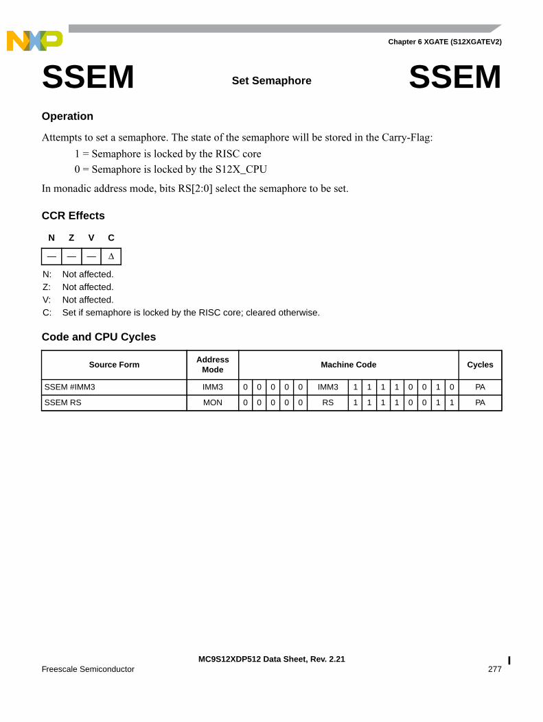
Chapter 6 XGATE (S12XGATEV2)
MC9S12XDP512 Data Sheet, Rev. 2.21Freescale Semiconductor 277
Operation
Attempts to set a semaphore. The state of the semaphore will be stored in the Carry-Flag:
1 = Semaphore is locked by the RISC core
0 = Semaphore is locked by the S12X_CPU
In monadic address mode, bits RS[2:0] select the semaphore to be set.
CCR Effects
Code and CPU Cycles
SSEM Set Semaphore SSEM
N Z V C
— — — ∆
N: Not affected.Z: Not affected.V: Not affected.C: Set if semaphore is locked by the RISC core; cleared otherwise.
Source FormAddress
ModeMachine Code Cycles
SSEM #IMM3 IMM3 0 0 0 0 0 IMM3 1 1 1 1 0 0 1 0 PA
SSEM RS MON 0 0 0 0 0 RS 1 1 1 1 0 0 1 1 PA

Chapter 6 XGATE (S12XGATEV2)
MC9S12XDP512 Data Sheet, Rev. 2.21278 Freescale Semiconductor
Operation
RS.L ⇒ M[RB, #OFFS5]RS.L ⇒ M[RB, RI]RS.L ⇒ M[RB, RI]; RI+1 ⇒ RI;RI–1 ⇒ RI; RS.L ⇒ M[RB, RI]1
Stores the low byte of register RD to memory.
CCR Effects
Code and CPU Cycles
STB Store Byte to Memory(Low Byte) STB
1. If the same general purpose register is used as index (RI) and source register (RS), the unmodified content of the sourceregister is written to the memory: RS.L ⇒ M[RB, RS-1]; RS-1 ⇒ RS
N Z V C
— — — —
N: Not affected.Z: Not affected.V: Not affected.C: Not affected.
Source FormAddress
ModeMachine Code Cycles
STB RS, (RB, #OFFS5), IDO5 0 1 0 1 0 RS RB OFFS5 Pw
STB RS, (RB, RI) IDR 0 1 1 1 0 RS RB RI 0 0 Pw
STB RS, (RB, RI+) IDR+ 0 1 1 1 0 RS RB RI 0 1 Pw
STB RS, (RB, -RI) -IDR 0 1 1 1 0 RS RB RI 1 0 Pw
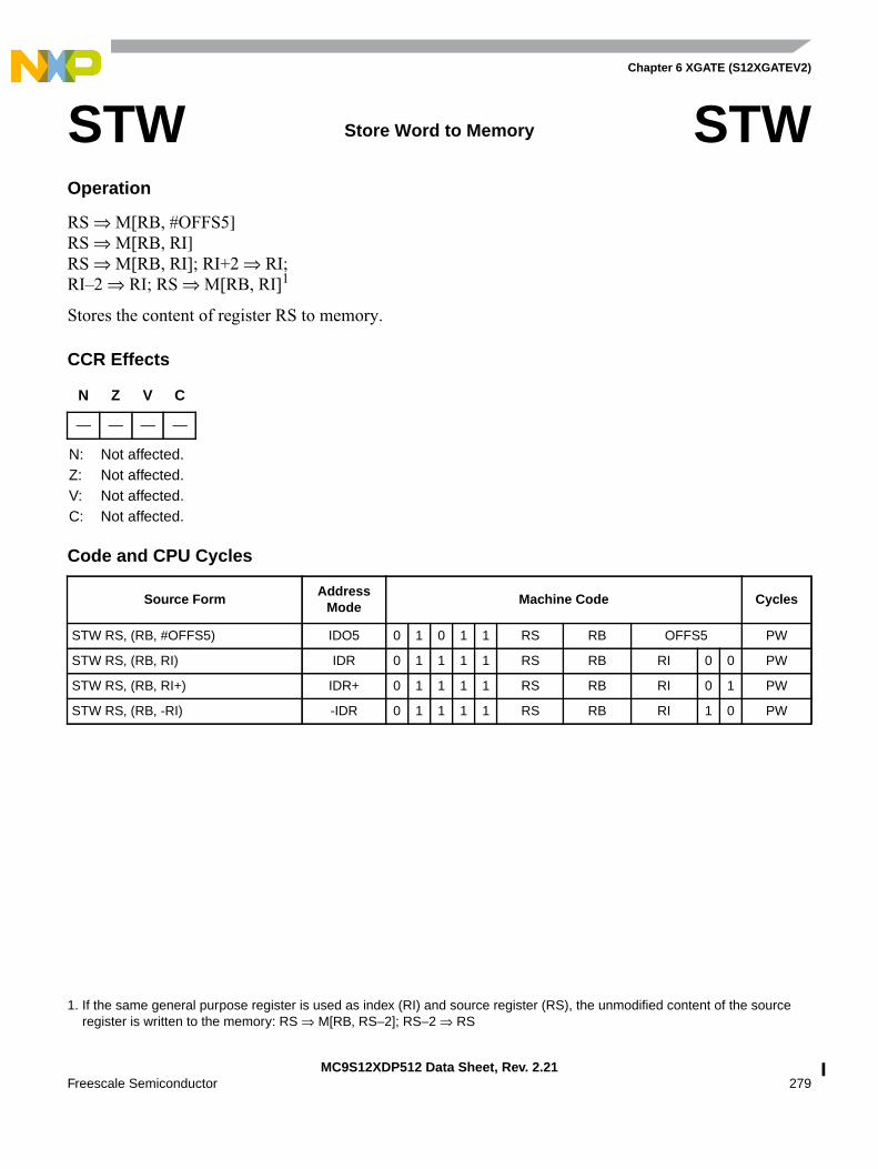
Chapter 6 XGATE (S12XGATEV2)
MC9S12XDP512 Data Sheet, Rev. 2.21Freescale Semiconductor 279
Operation
RS ⇒ M[RB, #OFFS5]RS ⇒ M[RB, RI]RS ⇒ M[RB, RI]; RI+2 ⇒ RI;RI–2 ⇒ RI; RS ⇒ M[RB, RI]1
Stores the content of register RS to memory.
CCR Effects
Code and CPU Cycles
STW Store Word to Memory STW
1. If the same general purpose register is used as index (RI) and source register (RS), the unmodified content of the sourceregister is written to the memory: RS ⇒ M[RB, RS–2]; RS–2 ⇒ RS
N Z V C
— — — —
N: Not affected.Z: Not affected.V: Not affected.C: Not affected.
Source FormAddress
ModeMachine Code Cycles
STW RS, (RB, #OFFS5) IDO5 0 1 0 1 1 RS RB OFFS5 PW
STW RS, (RB, RI) IDR 0 1 1 1 1 RS RB RI 0 0 PW
STW RS, (RB, RI+) IDR+ 0 1 1 1 1 RS RB RI 0 1 PW
STW RS, (RB, -RI) -IDR 0 1 1 1 1 RS RB RI 1 0 PW
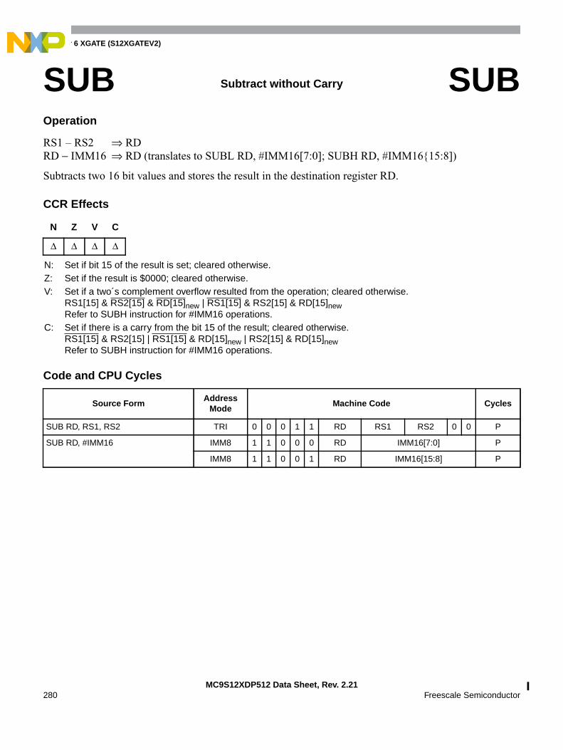
Chapter 6 XGATE (S12XGATEV2)
MC9S12XDP512 Data Sheet, Rev. 2.21280 Freescale Semiconductor
Operation
RS1 – RS2 ⇒ RDRD − IMM16 ⇒ RD (translates to SUBL RD, #IMM16[7:0]; SUBH RD, #IMM1615:8])
Subtracts two 16 bit values and stores the result in the destination register RD.
CCR Effects
Code and CPU Cycles
SUB Subtract without Carry SUB
N Z V C
∆ ∆ ∆ ∆
N: Set if bit 15 of the result is set; cleared otherwise.Z: Set if the result is $0000; cleared otherwise.V: Set if a two´s complement overflow resulted from the operation; cleared otherwise.
RS1[15] & RS2[15] & RD[15]new | RS1[15] & RS2[15] & RD[15]newRefer to SUBH instruction for #IMM16 operations.
C: Set if there is a carry from the bit 15 of the result; cleared otherwise.RS1[15] & RS2[15] | RS1[15] & RD[15]new | RS2[15] & RD[15]newRefer to SUBH instruction for #IMM16 operations.
Source FormAddress
ModeMachine Code Cycles
SUB RD, RS1, RS2 TRI 0 0 0 1 1 RD RS1 RS2 0 0 P
SUB RD, #IMM16 IMM8 1 1 0 0 0 RD IMM16[7:0] P
IMM8 1 1 0 0 1 RD IMM16[15:8] P
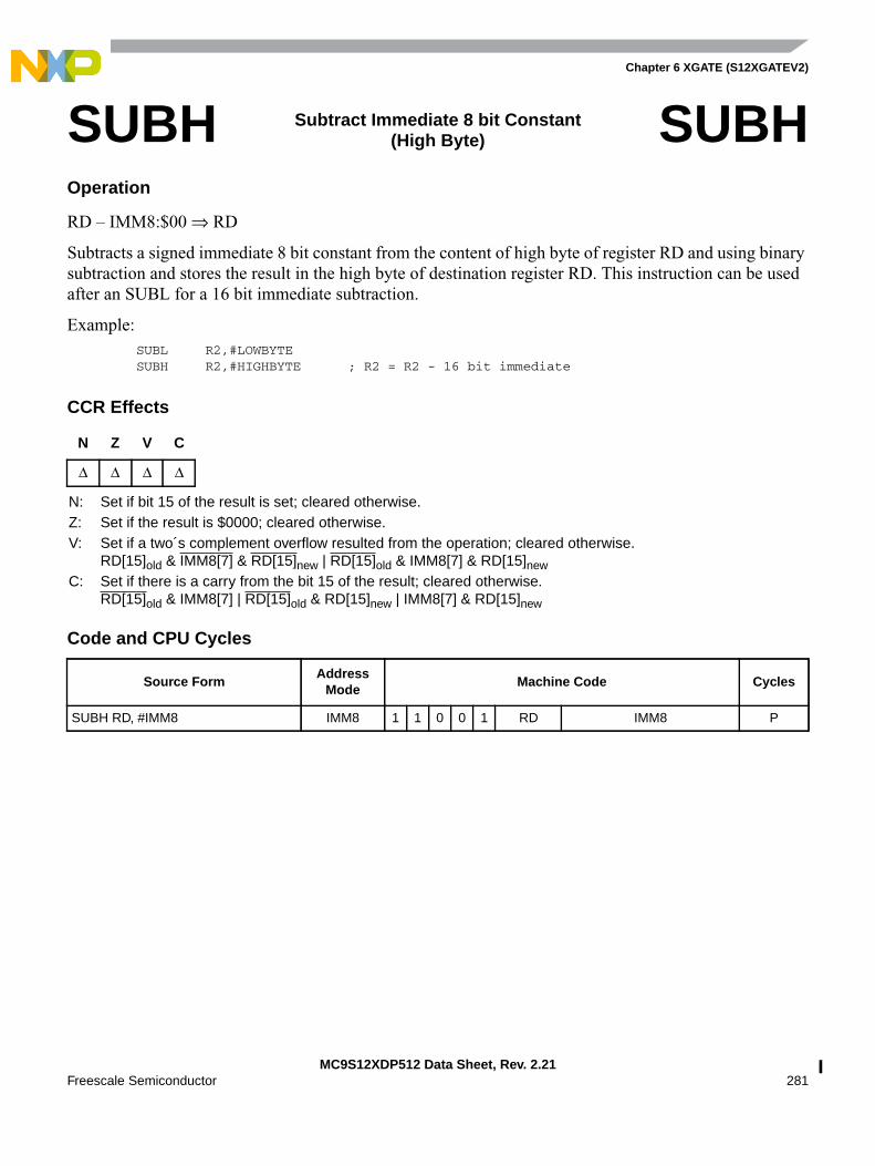
Chapter 6 XGATE (S12XGATEV2)
MC9S12XDP512 Data Sheet, Rev. 2.21Freescale Semiconductor 281
Operation
RD – IMM8:$00 ⇒ RD
Subtracts a signed immediate 8 bit constant from the content of high byte of register RD and using binarysubtraction and stores the result in the high byte of destination register RD. This instruction can be usedafter an SUBL for a 16 bit immediate subtraction.
Example:SUBL R2,#LOWBYTESUBH R2,#HIGHBYTE ; R2 = R2 - 16 bit immediate
CCR Effects
Code and CPU Cycles
SUBH Subtract Immediate 8 bit Constant(High Byte) SUBH
N Z V C
∆ ∆ ∆ ∆
N: Set if bit 15 of the result is set; cleared otherwise.Z: Set if the result is $0000; cleared otherwise.V: Set if a two´s complement overflow resulted from the operation; cleared otherwise.
RD[15]old & IMM8[7] & RD[15]new | RD[15]old & IMM8[7] & RD[15]newC: Set if there is a carry from the bit 15 of the result; cleared otherwise.
RD[15]old & IMM8[7] | RD[15]old & RD[15]new | IMM8[7] & RD[15]new
Source FormAddress
ModeMachine Code Cycles
SUBH RD, #IMM8 IMM8 1 1 0 0 1 RD IMM8 P

Chapter 6 XGATE (S12XGATEV2)
MC9S12XDP512 Data Sheet, Rev. 2.21282 Freescale Semiconductor
Operation
RD – $00:IMM8 ⇒ RD
Subtracts an immediate 8 bit constant from the content of register RD using binary subtraction and storesthe result in the destination register RD.
CCR Effects
Code and CPU Cycles
SUBL Subtract Immediate 8 bit Constant(Low Byte) SUBL
N Z V C
∆ ∆ ∆ ∆
N: Set if bit 15 of the result is set; cleared otherwise.Z: Set if the result is $0000; cleared otherwise.V: Set if a two´s complement overflow resulted from the 8 bit operation; cleared otherwise.
RD[15]old & RD[15]newC: Set if there is a carry from the bit 15 of the result; cleared otherwise.
RD[15]old & RD[15]new
Source FormAddress
ModeMachine Code Cycles
SUBL RD, #IMM8 IMM8 1 1 0 0 0 RD IMM8 P
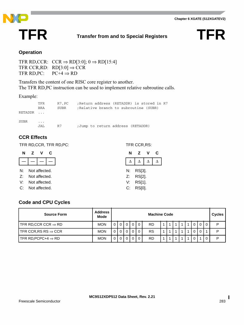
Chapter 6 XGATE (S12XGATEV2)
MC9S12XDP512 Data Sheet, Rev. 2.21Freescale Semiconductor 283
Operation
TFR RD,CCR: CCR ⇒ RD[3:0]; 0 ⇒ RD[15:4]TFR CCR,RD: RD[3:0] ⇒ CCRTFR RD,PC: PC+4 ⇒ RD
Transfers the content of one RISC core register to another.The TFR RD,PC instruction can be used to implement relative subroutine calls.
Example:TFR R7,PC ;Return address (RETADDR) is stored in R7BRA SUBR ;Relative branch to subroutine (SUBR)
RETADDR ...
SUBR ...JAL R7 ;Jump to return address (RETADDR)
CCR Effects
Code and CPU Cycles
TFR Transfer from and to Special Registers TFR
Source FormAddress
ModeMachine Code Cycles
TFR RD,CCR CCR ⇒ RD MON 0 0 0 0 0 RD 1 1 1 1 1 0 0 0 P
TFR CCR,RS RS ⇒ CCR MON 0 0 0 0 0 RS 1 1 1 1 1 0 0 1 P
TFR RD,PCPC+4 ⇒ RD MON 0 0 0 0 0 RD 1 1 1 1 1 0 1 0 P
TFR RD,CCR, TFR RD,PC: TFR CCR,RS:
N Z V C
— — — —
N: Not affected.Z: Not affected.V: Not affected.C: Not affected.
N Z V C
∆ ∆ ∆ ∆
N: RS[3].Z: RS[2].V: RS[1].C: RS[0].
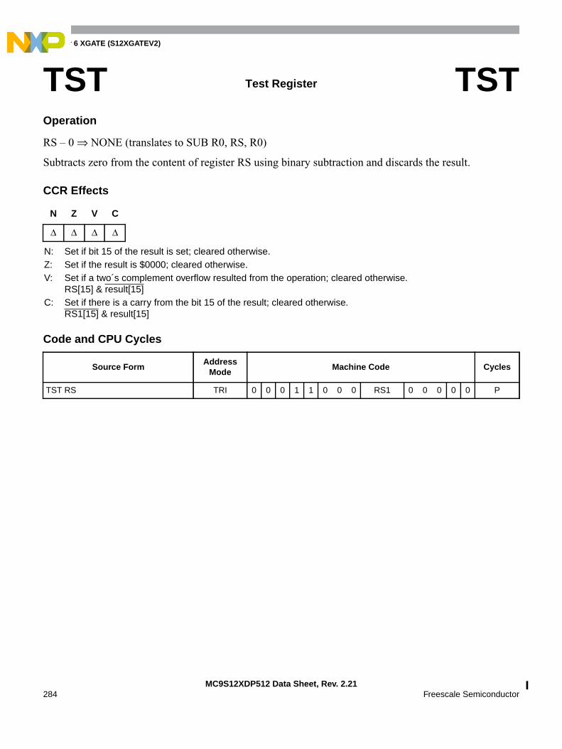
Chapter 6 XGATE (S12XGATEV2)
MC9S12XDP512 Data Sheet, Rev. 2.21284 Freescale Semiconductor
Operation
RS – 0 ⇒ NONE (translates to SUB R0, RS, R0)
Subtracts zero from the content of register RS using binary subtraction and discards the result.
CCR Effects
Code and CPU Cycles
TST Test Register TST
N Z V C
∆ ∆ ∆ ∆
N: Set if bit 15 of the result is set; cleared otherwise.Z: Set if the result is $0000; cleared otherwise.V: Set if a two´s complement overflow resulted from the operation; cleared otherwise.
RS[15] & result[15]C: Set if there is a carry from the bit 15 of the result; cleared otherwise.
RS1[15] & result[15]
Source FormAddress
ModeMachine Code Cycles
TST RS TRI 0 0 0 1 1 0 0 0 RS1 0 0 0 0 0 P

Chapter 6 XGATE (S12XGATEV2)
MC9S12XDP512 Data Sheet, Rev. 2.21Freescale Semiconductor 285
Operation
~(RS1 ^ RS2) ⇒ RD~(RD ^ IMM16)⇒ RD(translates to XNOR RD, #IMM1615:8]; XNOR RD, #IMM16[7:0])
Performs a bit wise logical exclusive NOR between two 16 bit values and stores the result in the destinationregister RD.
Remark: Using R0 as a source registers will calculate the one’s complement of the other source register.Using R0 as both source operands will fill RD with $FFFF.
CCR Effects
Code and CPU Cycles
XNOR Logical Exclusive NOR XNOR
N Z V C
∆ ∆ 0 —
N: Set if bit 15 of the result is set; cleared otherwise.Z: Set if the result is $0000; cleared otherwise.
Refer to XNORH instruction for #IMM16 operations.V: 0; cleared.C: Not affected.
Source FormAddress
ModeMachine Code Cycles
XNOR RD, RS1, RS2 TRI 0 0 0 1 0 RD RS1 RS2 1 1 P
XNOR RD, #IMM16 IMM8 1 0 1 1 0 RD IMM16[7:0] P
IMM8 1 0 1 1 1 RD IMM16[15:8] P
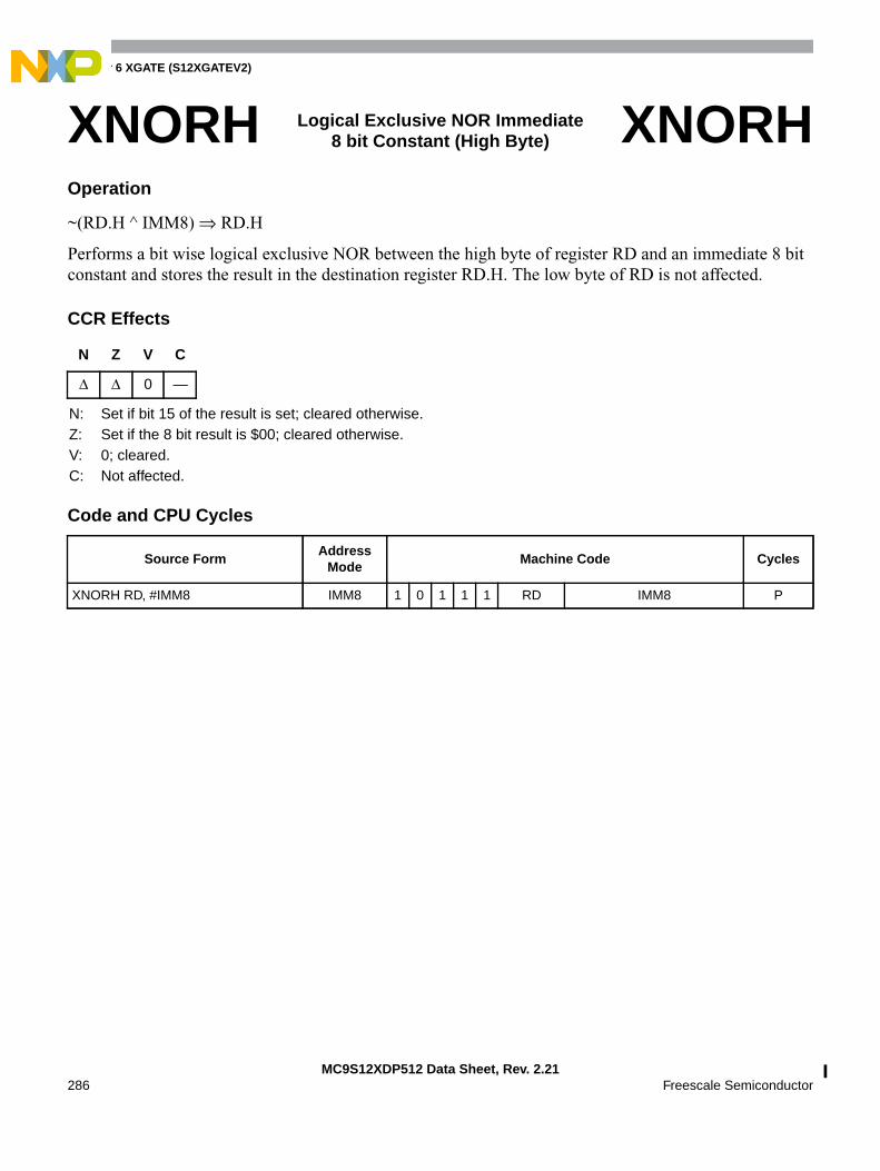
Chapter 6 XGATE (S12XGATEV2)
MC9S12XDP512 Data Sheet, Rev. 2.21286 Freescale Semiconductor
Operation
~(RD.H ^ IMM8) ⇒ RD.H
Performs a bit wise logical exclusive NOR between the high byte of register RD and an immediate 8 bitconstant and stores the result in the destination register RD.H. The low byte of RD is not affected.
CCR Effects
Code and CPU Cycles
XNORH Logical Exclusive NOR Immediate8 bit Constant (High Byte) XNORH
N Z V C
∆ ∆ 0 —
N: Set if bit 15 of the result is set; cleared otherwise.Z: Set if the 8 bit result is $00; cleared otherwise.V: 0; cleared.C: Not affected.
Source FormAddress
ModeMachine Code Cycles
XNORH RD, #IMM8 IMM8 1 0 1 1 1 RD IMM8 P
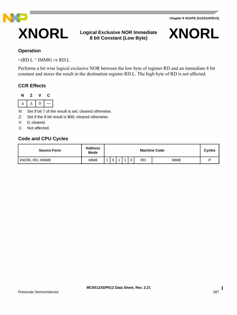
Chapter 6 XGATE (S12XGATEV2)
MC9S12XDP512 Data Sheet, Rev. 2.21Freescale Semiconductor 287
Operation
~(RD.L ^ IMM8) ⇒ RD.L
Performs a bit wise logical exclusive NOR between the low byte of register RD and an immediate 8 bitconstant and stores the result in the destination register RD.L. The high byte of RD is not affected.
CCR Effects
Code and CPU Cycles
XNORL Logical Exclusive NOR Immediate8 bit Constant (Low Byte) XNORL
N Z V C
∆ ∆ 0 —
N: Set if bit 7 of the result is set; cleared otherwise.Z: Set if the 8 bit result is $00; cleared otherwise.V: 0; cleared.C: Not affected.
Source FormAddress
ModeMachine Code Cycles
XNORL RD, #IMM8 IMM8 1 0 1 1 0 RD IMM8 P
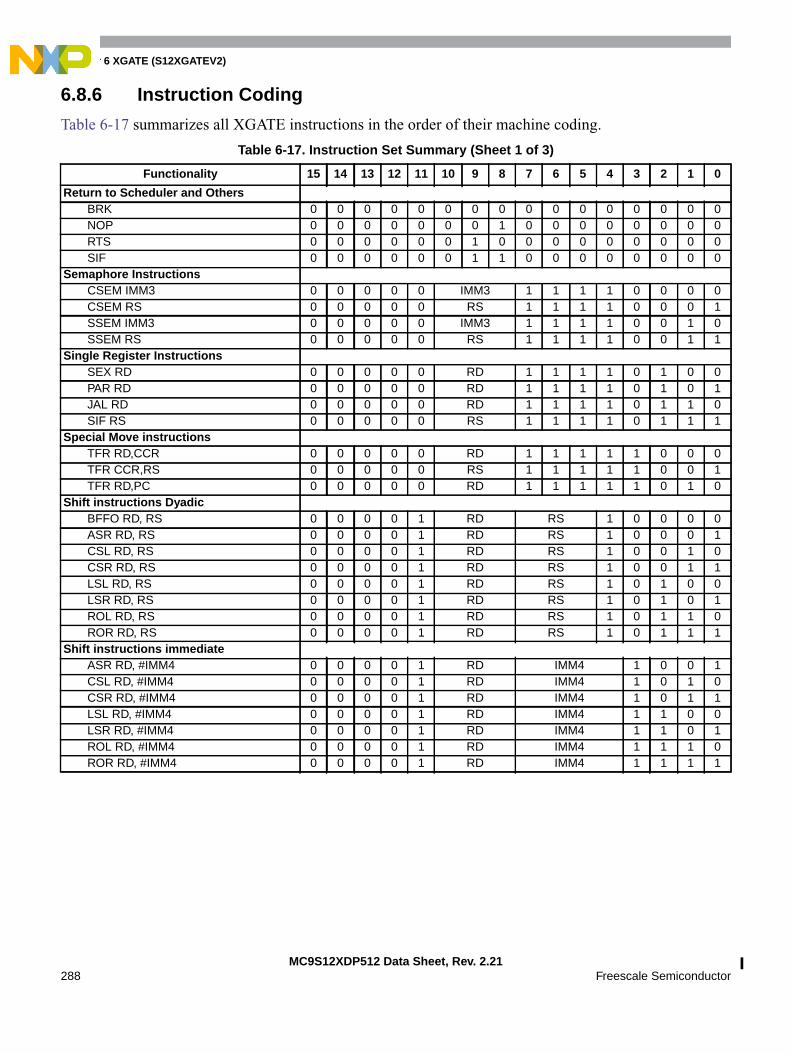
Chapter 6 XGATE (S12XGATEV2)
MC9S12XDP512 Data Sheet, Rev. 2.21288 Freescale Semiconductor
6.8.6 Instruction Coding
Table 6-17 summarizes all XGATE instructions in the order of their machine coding.
Table 6-17. Instruction Set Summary (Sheet 1 of 3)
Functionality 15 14 13 12 11 10 9 8 7 6 5 4 3 2 1 0
Return to Scheduler and OthersBRK 0 0 0 0 0 0 0 0 0 0 0 0 0 0 0 0NOP 0 0 0 0 0 0 0 1 0 0 0 0 0 0 0 0RTS 0 0 0 0 0 0 1 0 0 0 0 0 0 0 0 0SIF 0 0 0 0 0 0 1 1 0 0 0 0 0 0 0 0
Semaphore InstructionsCSEM IMM3 0 0 0 0 0 IMM3 1 1 1 1 0 0 0 0CSEM RS 0 0 0 0 0 RS 1 1 1 1 0 0 0 1SSEM IMM3 0 0 0 0 0 IMM3 1 1 1 1 0 0 1 0SSEM RS 0 0 0 0 0 RS 1 1 1 1 0 0 1 1
Single Register InstructionsSEX RD 0 0 0 0 0 RD 1 1 1 1 0 1 0 0PAR RD 0 0 0 0 0 RD 1 1 1 1 0 1 0 1JAL RD 0 0 0 0 0 RD 1 1 1 1 0 1 1 0SIF RS 0 0 0 0 0 RS 1 1 1 1 0 1 1 1
Special Move instructionsTFR RD,CCR 0 0 0 0 0 RD 1 1 1 1 1 0 0 0TFR CCR,RS 0 0 0 0 0 RS 1 1 1 1 1 0 0 1TFR RD,PC 0 0 0 0 0 RD 1 1 1 1 1 0 1 0
Shift instructions DyadicBFFO RD, RS 0 0 0 0 1 RD RS 1 0 0 0 0ASR RD, RS 0 0 0 0 1 RD RS 1 0 0 0 1CSL RD, RS 0 0 0 0 1 RD RS 1 0 0 1 0CSR RD, RS 0 0 0 0 1 RD RS 1 0 0 1 1LSL RD, RS 0 0 0 0 1 RD RS 1 0 1 0 0LSR RD, RS 0 0 0 0 1 RD RS 1 0 1 0 1ROL RD, RS 0 0 0 0 1 RD RS 1 0 1 1 0ROR RD, RS 0 0 0 0 1 RD RS 1 0 1 1 1
Shift instructions immediateASR RD, #IMM4 0 0 0 0 1 RD IMM4 1 0 0 1CSL RD, #IMM4 0 0 0 0 1 RD IMM4 1 0 1 0CSR RD, #IMM4 0 0 0 0 1 RD IMM4 1 0 1 1LSL RD, #IMM4 0 0 0 0 1 RD IMM4 1 1 0 0LSR RD, #IMM4 0 0 0 0 1 RD IMM4 1 1 0 1ROL RD, #IMM4 0 0 0 0 1 RD IMM4 1 1 1 0ROR RD, #IMM4 0 0 0 0 1 RD IMM4 1 1 1 1

Chapter 6 XGATE (S12XGATEV2)
MC9S12XDP512 Data Sheet, Rev. 2.21Freescale Semiconductor 289
Logical TriadicAND RD, RS1, RS2 0 0 0 1 0 RD RS1 RS2 0 0OR RD, RS1, RS2 0 0 0 1 0 RD RS1 RS2 1 0XNOR RD, RS1, RS2 0 0 0 1 0 RD RS1 RS2 1 1
Arithmetic Triadic For compare use SUB R0,Rs1,Rs2SUB RD, RS1, RS2 0 0 0 1 1 RD RS1 RS2 0 0SBC RD, RS1, RS2 0 0 0 1 1 RD RS1 RS2 0 1ADD RD, RS1, RS2 0 0 0 1 1 RD RS1 RS2 1 0ADC RD, RS1, RS2 0 0 0 1 1 RD RS1 RS2 1 1
BranchesBCC REL9 0 0 1 0 0 0 0 REL9BCS REL9 0 0 1 0 0 0 1 REL9BNE REL9 0 0 1 0 0 1 0 REL9BEQ REL9 0 0 1 0 0 1 1 REL9BPL REL9 0 0 1 0 1 0 0 REL9BMI REL9 0 0 1 0 1 0 1 REL9BVC REL9 0 0 1 0 1 1 0 REL9BVS REL9 0 0 1 0 1 1 1 REL9BHI REL9 0 0 1 1 0 0 0 REL9BLS REL9 0 0 1 1 0 0 1 REL9BGE REL9 0 0 1 1 0 1 0 REL9BLT REL9 0 0 1 1 0 1 1 REL9BGT REL9 0 0 1 1 1 0 0 REL9BLE REL9 0 0 1 1 1 0 1 REL9BRA REL10 0 0 1 1 1 1 REL10
Load and Store InstructionsLDB RD, (RB, #OFFS5) 0 1 0 0 0 RD RB OFFS5LDW RD, (RB, #OFFS5) 0 1 0 0 1 RD RB OFFS5STB RS, (RB, #OFFS5) 0 1 0 1 0 RS RB OFFS5STW RS, (RB, #OFFS5) 0 1 0 1 1 RS RB OFFS5LDB RD, (RB, RI) 0 1 1 0 0 RD RB RI 0 0LDW RD, (RB, RI) 0 1 1 0 1 RD RB RI 0 0STB RS, (RB, RI) 0 1 1 1 0 RS RB RI 0 0STW RS, (RB, RI) 0 1 1 1 1 RS RB RI 0 0LDB RD, (RB, RI+) 0 1 1 0 0 RD RB RI 0 1LDW RD, (RB, RI+) 0 1 1 0 1 RD RB RI 0 1STB RS, (RB, RI+) 0 1 1 1 0 RS RB RI 0 1STW RS, (RB, RI+) 0 1 1 1 1 RS RB RI 0 1LDB RD, (RB, –RI) 0 1 1 0 0 RD RB RI 1 0LDW RD, (RB, –RI) 0 1 1 0 1 RD RB RI 1 0STB RS, (RB, –RI) 0 1 1 1 0 RS RB RI 1 0STW RS, (RB, –RI) 0 1 1 1 1 RS RB RI 1 0
Bit Field InstructionsBFEXT RD, RS1, RS2 0 1 1 0 0 RD RS1 RS2 1 1BFINS RD, RS1, RS2 0 1 1 0 1 RD RS1 RS2 1 1BFINSI RD, RS1, RS2 0 1 1 1 0 RD RS1 RS2 1 1BFINSX RD, RS1, RS2 0 1 1 1 1 RD RS1 RS2 1 1
Logic Immediate InstructionsANDL RD, #IMM8 1 0 0 0 0 RD IMM8
Table 6-17. Instruction Set Summary (Sheet 2 of 3)
Functionality 15 14 13 12 11 10 9 8 7 6 5 4 3 2 1 0

Chapter 6 XGATE (S12XGATEV2)
MC9S12XDP512 Data Sheet, Rev. 2.21290 Freescale Semiconductor
ANDH RD, #IMM8 1 0 0 0 1 RD IMM8BITL RD, #IMM8 1 0 0 1 0 RD IMM8BITH RD, #IMM8 1 0 0 1 1 RD IMM8ORL RD, #IMM8 1 0 1 0 0 RD IMM8ORH RD, #IMM8 1 0 1 0 1 RD IMM8XNORL RD, #IMM8 1 0 1 1 0 RD IMM8XNORH RD, #IMM8 1 0 1 1 1 RD IMM8
Arithmetic Immediate InstructionsSUBL RD, #IMM8 1 1 0 0 0 RD IMM8SUBH RD, #IMM8 1 1 0 0 1 RD IMM8CMPL RS, #IMM8 1 1 0 1 0 RS IMM8CPCH RS, #IMM8 1 1 0 1 1 RS IMM8ADDL RD, #IMM8 1 1 1 0 0 RD IMM8ADDH RD, #IMM8 1 1 1 0 1 RD IMM8LDL RD, #IMM8 1 1 1 1 0 RD IMM8LDH RD, #IMM8 1 1 1 1 1 RD IMM8
Table 6-17. Instruction Set Summary (Sheet 3 of 3)
Functionality 15 14 13 12 11 10 9 8 7 6 5 4 3 2 1 0
Chapter 6 XGATE (S12XGATEV2)
MC9S12XDP512 Data Sheet, Rev. 2.21Freescale Semiconductor 291
6.9 Initialization and Application Information
6.9.1 Initialization
The recommended initialization of the XGATE is as follows:
1. Clear the XGE bit to suppress any incoming service requests.
2. Make sure that no thread is running on the XGATE. This can be done in several ways:
a) Poll the XGCHID register until it reads $00. Also poll XGDBG and XGSWEIF to make surethat the XGATE has not been stopped.
b) Enter Debug Mode by setting the XGDBG bit. Clear the XGCHID register. Clear the XGDBGbit.
The recommended method is a).
3. Set the XGVBR register to the lowest address of the XGATE vector space.
4. Clear all Channel ID flags.
5. Copy XGATE vectors and code into the RAM.
6. Initialize the S12X_INT module.
7. Enable the XGATE by setting the XGE bit.
The following code example implements the XGATE initialization sequence.
6.9.2 Code Example (Transmit "Hello World!" on SCI)CPU S12X;###########################################;# SYMBOLS #;###########################################
SCI_REGS EQU $00C8 ;SCI register spaceSCIBDH EQU SCI_REGS+$00 ;SCI Baud Rate RegisterSCIBDL EQU SCI_REGS+$00 ;SCI Baud Rate RegisterSCICR2 EQU SCI_REGS+$03 ;SCI Control Register 2SCISR1 EQU SCI_REGS+$04 ;SCI Status Register 1SCIDRL EQU SCI_REGS+$07 ;SCI Control Register 2TIE EQU $80 ;TIE bit maskTE EQU $08 ;TE bit maskRE EQU $04 ;RE bit maskSCI_VEC EQU $D6 ;SCI vector number
INT_REGS EQU $0120 ;S12X_INT register spaceINT_CFADDR EQU INT_REGS+$07 ;Interrupt Configuration Address RegisterINT_CFDATA EQU INT_REGS+$08 ;Interrupt Configuration Data RegistersRQST EQU $80 ;RQST bit mask
XGATE_REGS EQU $0380 ;XGATE register spaceXGMCTL EQU XGATE_REGS+$00 ;XGATE Module Control RegisterXGMCTL_CLEAR EQU $FA02 ;Clear all XGMCTL bitsXGMCTL_ENABLE EQU $8282 ;Enable XGATEXGCHID EQU XGATE_REGS+$02 ;XGATE Channel ID RegisterXGVBR EQU XGATE_REGS+$06 ;XGATE ISP Select RegisterXGIF EQU XGATE_REGS+$08 ;XGATE Interrupt Flag Vector

Chapter 6 XGATE (S12XGATEV2)
MC9S12XDP512 Data Sheet, Rev. 2.21292 Freescale Semiconductor
XGSWT EQU XGATE_REGS+$18 ;XGATE Software Trigger RegisterXGSEM EQU XGATE_REGS+$1A ;XGATE Semaphore Register
RPAGE EQU $0016
RAM_SIZE EQU 32*$400 ;32k RAM
RAM_START EQU $1000RAM_START_XG EQU $10000-RAM_SIZERAM_START_GLOB EQU $100000-RAM_SIZE
XGATE_VECTORS EQU RAM_STARTXGATE_VECTORS_XG EQU RAM_START_XG
XGATE_DATA EQU RAM_START+(4*128)XGATE_DATA_XG EQU RAM_START_XG+(4*128)
XGATE_CODE EQU XGATE_DATA+(XGATE_CODE_FLASH-XGATE_DATA_FLASH)XGATE_CODE_XG EQU XGATE_DATA_XG+(XGATE_CODE_FLASH-XGATE_DATA_FLASH)
BUS_FREQ_HZ EQU 40000000
;###########################################;# S12XE VECTOR TABLE #;###########################################ORG $FF10 ;non-maskable interruptsDW DUMMY_ISR DUMMY_ISR DUMMY_ISR DUMMY_ISR
ORG $FFF4 ;non-maskable interruptsDW DUMMY_ISR DUMMY_ISR DUMMY_ISR
;###########################################;# DISABLE COP #;###########################################ORG $FF0EDW $FFFE
ORG $C000START_OF_CODE
;###########################################;# INITIALIZE S12XE CORE #;###########################################SEIMOVB #(RAM_START_GLOB>>12), RPAGE;set RAM page
;###########################################;# INITIALIZE SCI #;###########################################
INIT_SCI MOVW #(BUS_FREQ_HZ/(16*9600)), SCIBDH;set baud rateMOVB #(TIE|TE), SCICR2;enable tx buffer empty interrupt
;###########################################;# INITIALIZE S12X_INT #;###########################################
INIT_INT MOVB #(SCI_VEC&$F0), INT_CFADDR ;switch SCI interrupts to XGATEMOVB #RQST|$01, INT_CFDATA+((SCI_VEC&$0F)>>1)
Chapter 6 XGATE (S12XGATEV2)
MC9S12XDP512 Data Sheet, Rev. 2.21Freescale Semiconductor 293
;###########################################;# INITIALIZE XGATE #;###########################################
INIT_XGATE MOVW #XGMCTL_CLEAR , XGMCTL;clear all XGMCTL bits
INIT_XGATE_BUSY_LOOP TST XGCHID ;wait until current thread is finishedBNE INIT_XGATE_BUSY_LOOP
LDX #XGIF ;clear all channel interrupt flagsLDD #$FFFFSTD 2,X+STD 2,X+STD 2,X+STD 2,X+STD 2,X+STD 2,X+STD 2,X+STD 2,X+
MOVW #XGATE_VECTORS_XG, XGVBR;set vector base register
MOVW #$FF00, XGSWT ;clear all software triggers
;###########################################;# INITIALIZE XGATE VECTOR TABLE #;###########################################LDAA #128 ;build XGATE vector tableLDY #XGATE_VECTORS
INIT_XGATE_VECTAB_LOOP MOVW #XGATE_DUMMY_ISR_XG, 4,Y+DBNE A, INIT_XGATE_VECTAB_LOOP
MOVW #XGATE_CODE_XG, RAM_START+(2*SCI_VEC)MOVW #XGATE_DATA_XG, RAM_START+(2*SCI_VEC)+2
;###########################################;# COPY XGATE CODE #;###########################################
COPY_XGATE_CODE LDX #XGATE_DATA_FLASHCOPY_XGATE_CODE_LOOP MOVW 2,X+, 2,Y+
MOVW 2,X+, 2,Y+MOVW 2,X+, 2,Y+MOVW 2,X+, 2,Y+CPX #XGATE_CODE_FLASH_ENDBLS COPY_XGATE_CODE_LOOP
;###########################################;# START XGATE #;###########################################
START_XGATE MOVW #XGMCTL_ENABLE, XGMCTL;enable XGATEBRA *
;###########################################;# DUMMY INTERRUPT SERVICE ROUTINE #;###########################################
DUMMY_ISR RTI
CPU XGATE
Chapter 6 XGATE (S12XGATEV2)
MC9S12XDP512 Data Sheet, Rev. 2.21294 Freescale Semiconductor
;###########################################;# XGATE DATA #;###########################################ALIGN 1
XGATE_DATA_FLASH EQU *XGATE_DATA_SCI EQU *-XGATE_DATA_FLASH
DW SCI_REGS ;pointer to SCI register spaceXGATE_DATA_IDX EQU *-XGATE_DATA_FLASH
DB XGATE_DATA_MSG ;string pointerXGATE_DATA_MSG EQU *-XGATE_DATA_FLASH
FCC "Hello World! ;ASCII stringDB $0D ;CR
;###########################################;# XGATE CODE #;###########################################ALIGN 1
XGATE_CODE_FLASH LDW R2,(R1,#XGATE_DATA_SCI);SCI -> R2LDB R3,(R1,#XGATE_DATA_IDX);msg -> R3LDB R4,(R1,R3+) ;curr. char -> R4STB R3,(R1,#XGATE_DATA_IDX);R3 -> idxLDB R0,(R2,#(SCISR1-SCI_REGS));initiate SCI transmitSTB R4,(R2,#(SCIDRL-SCI_REGS));initiate SCI transmitCMPL R4,#$0DBEQ XGATE_CODE_DONERTS
XGATE_CODE_DONE LDL R4,#$00 ;disable SCI interruptsSTB R4,(R2,#(SCICR2-SCI_REGS))LDL R3,#XGATE_DATA_MSG;reset R3STB R3,(R1,#XGATE_DATA_IDX)
XGATE_CODE_FLASH_END RTSXGATE_DUMMY_ISR_XG EQU (XGATE_CODE_FLASH_END-XGATE_CODE_FLASH)+XGATE_CODE_XG

Chapter 6 XGATE (S12XGATEV2)
MC9S12XDP512 Data Sheet, Rev. 2.21Freescale Semiconductor 295

Chapter 6 XGATE (S12XGATEV2)
MC9S12XDP512 Data Sheet, Rev. 2.21296 Freescale Semiconductor

Chapter 6 XGATE (S12XGATEV2)
MC9S12XDP512 Data Sheet, Rev. 2.21Freescale Semiconductor 297

Chapter 6 XGATE (S12XGATEV2)
MC9S12XDP512 Data Sheet, Rev. 2.21298 Freescale Semiconductor

Chapter 6 XGATE (S12XGATEV2)
MC9S12XDP512 Data Sheet, Rev. 2.21Freescale Semiconductor 299

Chapter 6 XGATE (S12XGATEV2)
MC9S12XDP512 Data Sheet, Rev. 2.21300 Freescale Semiconductor

Chapter 6 XGATE (S12XGATEV2)
MC9S12XDP512 Data Sheet, Rev. 2.21Freescale Semiconductor 301

Chapter 6 XGATE (S12XGATEV2)
MC9S12XDP512 Data Sheet, Rev. 2.21302 Freescale Semiconductor

Chapter 6 XGATE (S12XGATEV2)
MC9S12XDP512 Data Sheet, Rev. 2.21Freescale Semiconductor 303

Chapter 6 XGATE (S12XGATEV2)
MC9S12XDP512 Data Sheet, Rev. 2.21304 Freescale Semiconductor

Chapter 6 XGATE (S12XGATEV2)
MC9S12XDP512 Data Sheet, Rev. 2.21Freescale Semiconductor 305

Chapter 6 XGATE (S12XGATEV2)
MC9S12XDP512 Data Sheet, Rev. 2.21306 Freescale Semiconductor

Chapter 6 XGATE (S12XGATEV2)
MC9S12XDP512 Data Sheet, Rev. 2.21Freescale Semiconductor 307

Chapter 6 XGATE (S12XGATEV2)
MC9S12XDP512 Data Sheet, Rev. 2.21308 Freescale Semiconductor
MC9S12XDP512 Data Sheet, Rev. 2.21
Freescale Semiconductor 309
Chapter 7Enhanced Capture Timer (S12ECT16B8CV2)
7.1 IntroductionThe HCS12 enhanced capture timer module has the features of the HCS12 standard timer moduleenhanced by additional features in order to enlarge the field of applications, in particular for automotiveABS applications.
This design specification describes the standard timer as well as the additional features.
The basic timer consists of a 16-bit, software-programmable counter driven by a prescaler. This timer canbe used for many purposes, including input waveform measurements while simultaneously generating anoutput waveform. Pulse widths can vary from microseconds to many seconds.
A full access for the counter registers or the input capture/output compare registers will take place in oneclock cycle. Accessing high byte and low byte separately for all of these registers will not yield the sameresult as accessing them in one word.
7.1.1 Features• 16-bit buffer register for four input capture (IC) channels.
• Four 8-bit pulse accumulators with 8-bit buffer registers associated with the four buffered ICchannels. Configurable also as two 16-bit pulse accumulators.
• 16-bit modulus down-counter with 8-bit prescaler.
• Four user-selectable delay counters for input noise immunity increase.
7.1.2 Modes of Operation• Stop — Timer and modulus counter are off since clocks are stopped.
• Freeze — Timer and modulus counter keep on running, unless the TSFRZ bit in the TSCR1 registeris set to one.
• Wait — Counters keep on running, unless the TSWAI bit in the TSCR1 register is set to one.
• Normal — Timer and modulus counter keep on running, unless the TEN bit in the TSCR1 registeror the MCEN bit in the MCCTL register are cleared.
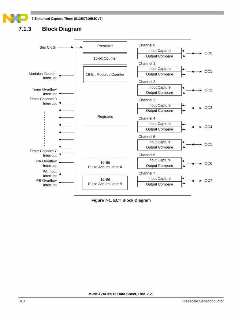
Chapter 7 Enhanced Capture Timer (S12ECT16B8CV2)
MC9S12XDP512 Data Sheet, Rev. 2.21
310 Freescale Semiconductor
7.1.3 Block Diagram
Figure 7-1. ECT Block Diagram
Prescaler
16-bit Counter
16-BitPulse Accumulator B
IOC0
IOC2
IOC1
IOC5
IOC3
IOC4
IOC6
IOC7
PA InputInterrupt
PA OverflowInterrupt
Timer OverflowInterrupt
Timer Channel 0Interrupt
Timer Channel 7Interrupt
Registers
Bus ClockChannel 0
Channel 1
Channel 2
Channel 3
Channel 4
Channel 5
Channel 6
Channel 7
16-BitPulse Accumulator A
PB OverflowInterrupt
Modulus CounterInterrupt
16-Bit Modulus Counter
Input Capture
Output Compare
Input Capture
Input Capture
Input Capture
Input Capture
Input Capture
Input Capture
Input Capture
Output Compare
Output Compare
Output Compare
Output Compare
Output Compare
Output Compare
Output Compare
Chapter 7 Enhanced Capture Timer (S12ECT16B8CV2)
MC9S12XDP512 Data Sheet, Rev. 2.21
Freescale Semiconductor 311
7.2 External Signal DescriptionThe ECT module has a total of eight external pins.
7.2.1 IOC7 — Input Capture and Output Compare Channel 7
This pin serves as input capture or output compare for channel 7.
7.2.2 IOC6 — Input Capture and Output Compare Channel 6
This pin serves as input capture or output compare for channel 6.
7.2.3 IOC5 — Input Capture and Output Compare Channel 5
This pin serves as input capture or output compare for channel 5.
7.2.4 IOC4 — Input Capture and Output Compare Channel 4
This pin serves as input capture or output compare for channel 4.
7.2.5 IOC3 — Input Capture and Output Compare Channel 3
This pin serves as input capture or output compare for channel 3.
7.2.6 IOC2 — Input Capture and Output Compare Channel 2
This pin serves as input capture or output compare for channel 2.
7.2.7 IOC1 — Input Capture and Output Compare Channel 1
This pin serves as input capture or output compare for channel 1.
7.2.8 IOC0 — Input Capture and Output Compare Channel 0
This pin serves as input capture or output compare for channel 0.
NOTE For the description of interrupts see Section 7.4.3, “Interrupts”.
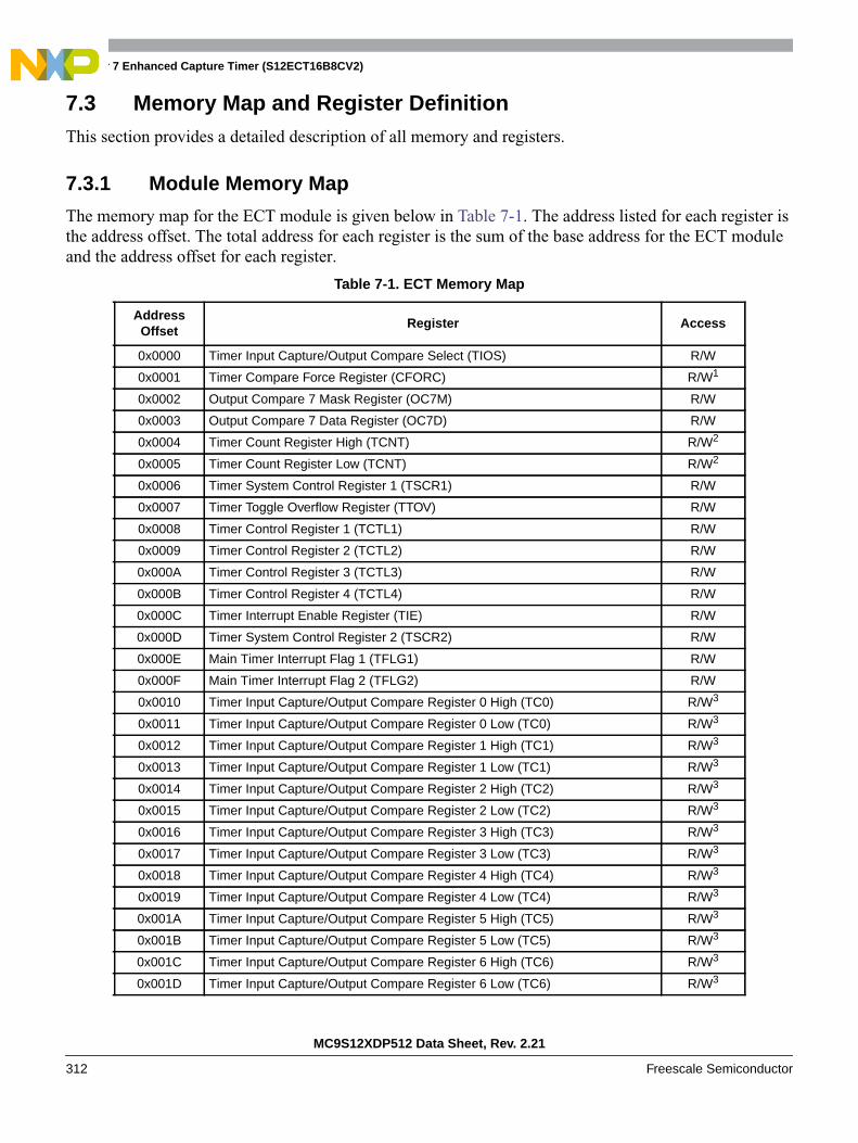
Chapter 7 Enhanced Capture Timer (S12ECT16B8CV2)
MC9S12XDP512 Data Sheet, Rev. 2.21
312 Freescale Semiconductor
7.3 Memory Map and Register DefinitionThis section provides a detailed description of all memory and registers.
7.3.1 Module Memory Map
The memory map for the ECT module is given below in Table 7-1. The address listed for each register isthe address offset. The total address for each register is the sum of the base address for the ECT moduleand the address offset for each register.
Table 7-1. ECT Memory Map
AddressOffset
Register Access
0x0000 Timer Input Capture/Output Compare Select (TIOS) R/W
0x0001 Timer Compare Force Register (CFORC) R/W1
0x0002 Output Compare 7 Mask Register (OC7M) R/W
0x0003 Output Compare 7 Data Register (OC7D) R/W
0x0004 Timer Count Register High (TCNT) R/W2
0x0005 Timer Count Register Low (TCNT) R/W2
0x0006 Timer System Control Register 1 (TSCR1) R/W
0x0007 Timer Toggle Overflow Register (TTOV) R/W
0x0008 Timer Control Register 1 (TCTL1) R/W
0x0009 Timer Control Register 2 (TCTL2) R/W
0x000A Timer Control Register 3 (TCTL3) R/W
0x000B Timer Control Register 4 (TCTL4) R/W
0x000C Timer Interrupt Enable Register (TIE) R/W
0x000D Timer System Control Register 2 (TSCR2) R/W
0x000E Main Timer Interrupt Flag 1 (TFLG1) R/W
0x000F Main Timer Interrupt Flag 2 (TFLG2) R/W
0x0010 Timer Input Capture/Output Compare Register 0 High (TC0) R/W3
0x0011 Timer Input Capture/Output Compare Register 0 Low (TC0) R/W3
0x0012 Timer Input Capture/Output Compare Register 1 High (TC1) R/W3
0x0013 Timer Input Capture/Output Compare Register 1 Low (TC1) R/W3
0x0014 Timer Input Capture/Output Compare Register 2 High (TC2) R/W3
0x0015 Timer Input Capture/Output Compare Register 2 Low (TC2) R/W3
0x0016 Timer Input Capture/Output Compare Register 3 High (TC3) R/W3
0x0017 Timer Input Capture/Output Compare Register 3 Low (TC3) R/W3
0x0018 Timer Input Capture/Output Compare Register 4 High (TC4) R/W3
0x0019 Timer Input Capture/Output Compare Register 4 Low (TC4) R/W3
0x001A Timer Input Capture/Output Compare Register 5 High (TC5) R/W3
0x001B Timer Input Capture/Output Compare Register 5 Low (TC5) R/W3
0x001C Timer Input Capture/Output Compare Register 6 High (TC6) R/W3
0x001D Timer Input Capture/Output Compare Register 6 Low (TC6) R/W3

Chapter 7 Enhanced Capture Timer (S12ECT16B8CV2)
MC9S12XDP512 Data Sheet, Rev. 2.21
Freescale Semiconductor 313
0x001E Timer Input Capture/Output Compare Register 7 High (TC7) R/W3
0x001F Timer Input Capture/Output Compare Register 7 Low (TC7) R/W3
0x0020 16-Bit Pulse Accumulator A Control Register (PACTL) R/W
0x0021 Pulse Accumulator A Flag Register (PAFLG) R/W
0x0022 Pulse Accumulator Count Register 3 (PACN3) R/W
0x0023 Pulse Accumulator Count Register 2 (PACN2) R/W
0x0024 Pulse Accumulator Count Register 1 (PACN1) R/W
0x0025 Pulse Accumulator Count Register 0 (PACN0) R/W
0x0026 16-Bit Modulus Down Counter Register (MCCTL) R/W
0x0027 16-Bit Modulus Down Counter Flag Register (MCFLG) R/W
0x0028 Input Control Pulse Accumulator Register (ICPAR) R/W
0x0029 Delay Counter Control Register (DLYCT) R/W
0x002A Input Control Overwrite Register (ICOVW) R/W
0x002B Input Control System Control Register (ICSYS) R/W4
0x002C Reserved --
0x002D Timer Test Register (TIMTST) R/W2
0x002E Precision Timer Prescaler Select Register (PTPSR) R/W
0x002F Precision Timer Modulus Counter Prescaler Select Register (PTMCPSR) R/W
0x0030 16-Bit Pulse Accumulator B Control Register (PBCTL) R/W
0x0031 16-Bit Pulse Accumulator B Flag Register (PBFLG) R/W
0x0032 8-Bit Pulse Accumulator Holding Register 3 (PA3H) R/W5
0x0033 8-Bit Pulse Accumulator Holding Register 2 (PA2H) R/W5
0x0034 8-Bit Pulse Accumulator Holding Register 1 (PA1H) R/W5
0x0035 8-Bit Pulse Accumulator Holding Register 0 (PA0H) R/W5
0x0036 Modulus Down-Counter Count Register High (MCCNT) R/W
0x0037 Modulus Down-Counter Count Register Low (MCCNT) R/W
0x0038 Timer Input Capture Holding Register 0 High (TC0H) R/W5
0x0039 Timer Input Capture Holding Register 0 Low (TC0H) R/W5
0x003A Timer Input Capture Holding Register 1 High(TC1H) R/W5
0x003B Timer Input Capture Holding Register 1 Low (TC1H) R/W5
0x003C Timer Input Capture Holding Register 2 High (TC2H) R/W5
0x003D Timer Input Capture Holding Register 2 Low (TC2H) R/W5
0x003E Timer Input Capture Holding Register 3 High (TC3H) R/W5
0x003F Timer Input Capture Holding Register 3 Low (TC3H) R/W5
1 Always read 0x0000.2 Only writable in special modes (test_mode = 1).3 Writes to these registers have no meaning or effect during input capture.4 May be written once when not in test00mode but writes are always permitted when test00mode is enabled.5 Writes have no effect.
Table 7-1. ECT Memory Map (continued)
AddressOffset
Register Access
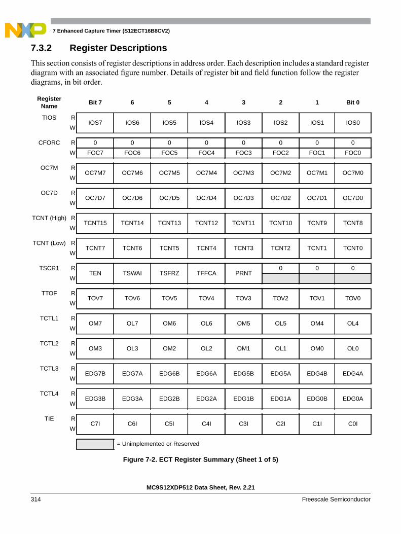
Chapter 7 Enhanced Capture Timer (S12ECT16B8CV2)
MC9S12XDP512 Data Sheet, Rev. 2.21
314 Freescale Semiconductor
7.3.2 Register Descriptions
This section consists of register descriptions in address order. Each description includes a standard registerdiagram with an associated figure number. Details of register bit and field function follow the registerdiagrams, in bit order.
RegisterName
Bit 7 6 5 4 3 2 1 Bit 0
TIOS RIOS7 IOS6 IOS5 IOS4 IOS3 IOS2 IOS1 IOS0
W
CFORC R 0 0 0 0 0 0 0 0
W FOC7 FOC6 FOC5 FOC4 FOC3 FOC2 FOC1 FOC0
OC7M ROC7M7 OC7M6 OC7M5 OC7M4 OC7M3 OC7M2 OC7M1 OC7M0
W
OC7D ROC7D7 OC7D6 OC7D5 OC7D4 OC7D3 OC7D2 OC7D1 OC7D0
W
TCNT (High) RTCNT15 TCNT14 TCNT13 TCNT12 TCNT11 TCNT10 TCNT9 TCNT8
W
TCNT (Low) RTCNT7 TCNT6 TCNT5 TCNT4 TCNT3 TCNT2 TCNT1 TCNT0
W
TSCR1 RTEN TSWAI TSFRZ TFFCA PRNT
0 0 0
W
TTOF RTOV7 TOV6 TOV5 TOV4 TOV3 TOV2 TOV1 TOV0
W
TCTL1 ROM7 OL7 OM6 OL6 OM5 OL5 OM4 OL4
W
TCTL2 ROM3 OL3 OM2 OL2 OM1 OL1 OM0 OL0
W
TCTL3 REDG7B EDG7A EDG6B EDG6A EDG5B EDG5A EDG4B EDG4A
W
TCTL4 REDG3B EDG3A EDG2B EDG2A EDG1B EDG1A EDG0B EDG0A
W
TIE RC7I C6I C5I C4I C3I C2I C1I C0I
W
= Unimplemented or Reserved
Figure 7-2. ECT Register Summary (Sheet 1 of 5)

Chapter 7 Enhanced Capture Timer (S12ECT16B8CV2)
MC9S12XDP512 Data Sheet, Rev. 2.21
Freescale Semiconductor 315
TSCR2 RTOI
0 0 0TCRE PR2 PR1 PR0
W
TFLG1 RC7F C6F C5F C4F C3F C2F C1F C0F
W
TFLG2 RTOF
0 0 0 0 0 0 0
W
TC0 (High) RBit 15 Bit 14 Bit 13 Bit 12 Bit 11 Bit 10 Bit 9 Bit 8
W
TC0 (Low) RBit 7 Bit 6 Bit 5 Bit 4 Bit 3 Bit 2 Bit 1 Bit 0
W
TC1 (High) RBit 15 Bit 14 Bit 13 Bit 12 Bit 11 Bit 10 Bit 9 Bit 8
W
TC1 (Low) RBit 7 Bit 6 Bit 5 Bit 4 Bit 3 Bit 2 Bit 1 Bit 0
W
TC2 (High) RBit 15 Bit 14 Bit 13 Bit 12 Bit 11 Bit 10 Bit 9 Bit 8
W
TC2 (Low) RBit 7 Bit 6 Bit 5 Bit 4 Bit 3 Bit 2 Bit 1 Bit 0
W
TC3 (High) RBit 15 Bit 14 Bit 13 Bit 12 Bit 11 Bit 10 Bit 9 Bit 8
W
TC3 (Low) RBit 7 Bit 6 Bit 5 Bit 4 Bit 3 Bit 2 Bit 1 Bit 0
W
TC4 (High) RBit 15 Bit 14 Bit 13 Bit 12 Bit 11 Bit 10 Bit 9 Bit 8
W
TC4 (Low) RBit 7 Bit 6 Bit 5 Bit 4 Bit 3 Bit 2 Bit 1 Bit 0
W
TC5 (High) RBit 15 Bit 14 Bit 13 Bit 12 Bit 11 Bit 10 Bit 9 Bit 8
W
TC5 (Low) RBit 7 Bit 6 Bit 5 Bit 4 Bit 3 Bit 2 Bit 1 Bit 0
W
RegisterName
Bit 7 6 5 4 3 2 1 Bit 0
= Unimplemented or Reserved
Figure 7-2. ECT Register Summary (Sheet 2 of 5)

Chapter 7 Enhanced Capture Timer (S12ECT16B8CV2)
MC9S12XDP512 Data Sheet, Rev. 2.21
316 Freescale Semiconductor
TC6 (High) RBit 15 Bit 14 Bit 13 Bit 12 Bit 11 Bit 10 Bit 9 Bit 8
W
TC6 (Low) RBit 7 Bit 6 Bit 5 Bit 4 Bit 3 Bit 2 Bit 1 Bit 0
W
TC7 (High) RBit 15 Bit 14 Bit 13 Bit 12 Bit 11 Bit 10 Bit 9 Bit 8
W
TC7 (Low) RBit 7 Bit 6 Bit 5 Bit 4 Bit 3 Bit 2 Bit 1 Bit 0
W
PACTL R 0PAEN PAMOD PEDGE CLK1 CLK0 PA0VI PAI
W
PAFLG R 0 0 0 0 0 0PA0VF PAIF
W
PACN3 RPACNT7(15) PACNT6(14) PACNT5(13) PACNT4(12) PACNT3(11) PACNT2(10) PACNT1(9) PACNT0(8)
W
PACN2 RPACNT7 PACNT6 PACNT5 PACNT4 PACNT3 PACNT2 PACNT1 PACNT0
W
PACN1 RPACNT7(15) PACNT6(14) PACNT5(13) PACNT4(12) PACNT3(11) PACNT2(10) PACNT1(9) PACNT0(8)
W
PACN0 RPACNT7 PACNT6 PACNT5 PACNT4 PACNT3 PACNT2 PACNT1 PACNT0
W
MCCTL RMCZI MODMC RDMCL
0 0MCEN MCPR1 MCPR0
W ICLAT FLMC
MCFLG RMCZF
0 0 0 POLF3 POLF2 POLF1 POLF0
W
ICPAR R 0 0 0 0PA3EN PA2EN PA1EN PA0EN
W
DLYCT RDLY7 DLY6 DLY5 DLY4 DLY3 DLY2 DLY1 DLY0
W
ICOVW RNOVW7 NOVW6 NOVW5 NOVW4 NOVW3 NOVW2 NOVW1 NOVW0
W
RegisterName
Bit 7 6 5 4 3 2 1 Bit 0
= Unimplemented or Reserved
Figure 7-2. ECT Register Summary (Sheet 3 of 5)
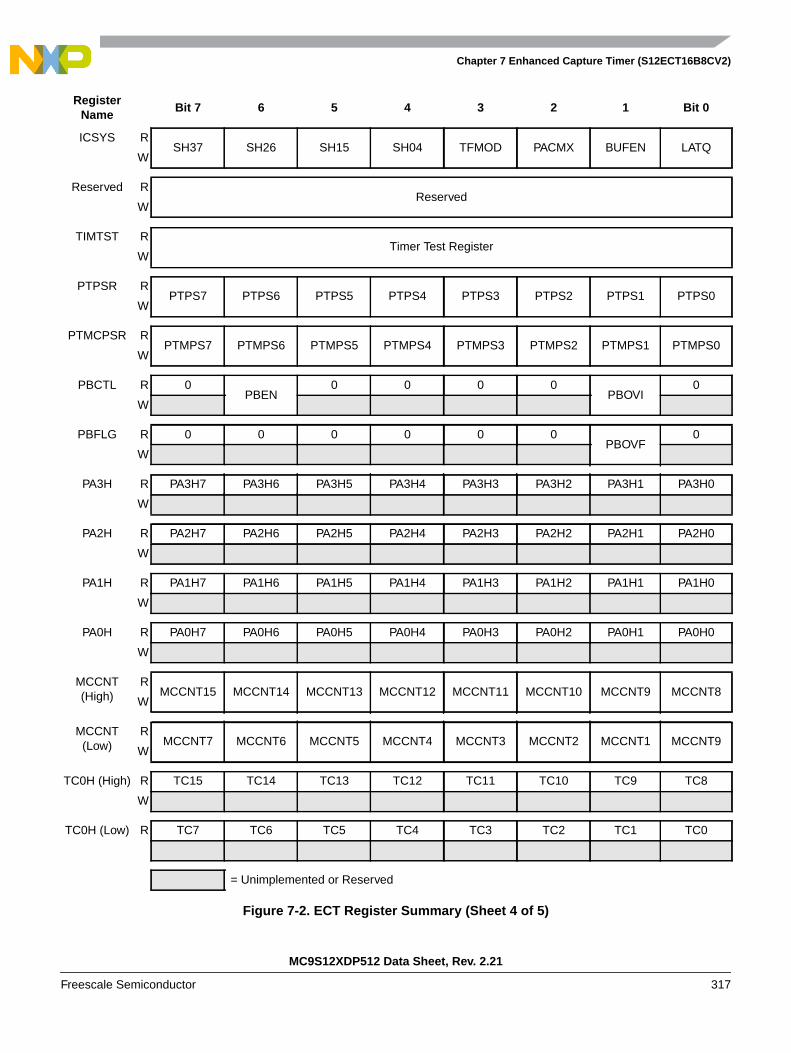
Chapter 7 Enhanced Capture Timer (S12ECT16B8CV2)
MC9S12XDP512 Data Sheet, Rev. 2.21
Freescale Semiconductor 317
ICSYS RSH37 SH26 SH15 SH04 TFMOD PACMX BUFEN LATQ
W
Reserved RReserved
W
TIMTST RTimer Test Register
W
PTPSR RPTPS7 PTPS6 PTPS5 PTPS4 PTPS3 PTPS2 PTPS1 PTPS0
W
PTMCPSR RPTMPS7 PTMPS6 PTMPS5 PTMPS4 PTMPS3 PTMPS2 PTMPS1 PTMPS0
W
PBCTL R 0PBEN
0 0 0 0PBOVI
0
W
PBFLG R 0 0 0 0 0 0PBOVF
0
W
PA3H R PA3H7 PA3H6 PA3H5 PA3H4 PA3H3 PA3H2 PA3H1 PA3H0
W
PA2H R PA2H7 PA2H6 PA2H5 PA2H4 PA2H3 PA2H2 PA2H1 PA2H0
W
PA1H R PA1H7 PA1H6 PA1H5 PA1H4 PA1H3 PA1H2 PA1H1 PA1H0
W
PA0H R PA0H7 PA0H6 PA0H5 PA0H4 PA0H3 PA0H2 PA0H1 PA0H0
W
MCCNT(High)
RMCCNT15 MCCNT14 MCCNT13 MCCNT12 MCCNT11 MCCNT10 MCCNT9 MCCNT8
W
MCCNT(Low)
RMCCNT7 MCCNT6 MCCNT5 MCCNT4 MCCNT3 MCCNT2 MCCNT1 MCCNT9
W
TC0H (High) R TC15 TC14 TC13 TC12 TC11 TC10 TC9 TC8
W
TC0H (Low) R TC7 TC6 TC5 TC4 TC3 TC2 TC1 TC0
RegisterName
Bit 7 6 5 4 3 2 1 Bit 0
= Unimplemented or Reserved
Figure 7-2. ECT Register Summary (Sheet 4 of 5)
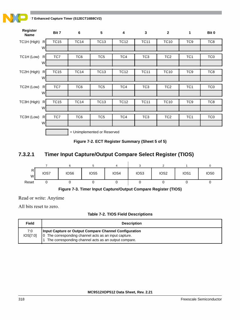
Chapter 7 Enhanced Capture Timer (S12ECT16B8CV2)
MC9S12XDP512 Data Sheet, Rev. 2.21
318 Freescale Semiconductor
7.3.2.1 Timer Input Capture/Output Compare Select Register (TIOS)
Read or write: Anytime
All bits reset to zero.
TC1H (High) R TC15 TC14 TC13 TC12 TC11 TC10 TC9 TC8
W
TC1H (Low) R TC7 TC6 TC5 TC4 TC3 TC2 TC1 TC0
W
TC2H (High) R TC15 TC14 TC13 TC12 TC11 TC10 TC9 TC8
W
TC2H (Low) R TC7 TC6 TC5 TC4 TC3 TC2 TC1 TC0
W
TC3H (High) R TC15 TC14 TC13 TC12 TC11 TC10 TC9 TC8
W
TC3H (Low) R TC7 TC6 TC5 TC4 TC3 TC2 TC1 TC0
W
7 6 5 4 3 2 1 0
RIOS7 IOS6 IOS5 IOS4 IOS3 IOS2 IOS1 IOS0
W
Reset 0 0 0 0 0 0 0 0
Figure 7-3. Timer Input Capture/Output Compare Register (TIOS)
Table 7-2. TIOS Field Descriptions
Field Description
7:0IOS[7:0]
Input Capture or Output Compare Channel Configuration0 The corresponding channel acts as an input capture.1 The corresponding channel acts as an output compare.
RegisterName
Bit 7 6 5 4 3 2 1 Bit 0
= Unimplemented or Reserved
Figure 7-2. ECT Register Summary (Sheet 5 of 5)
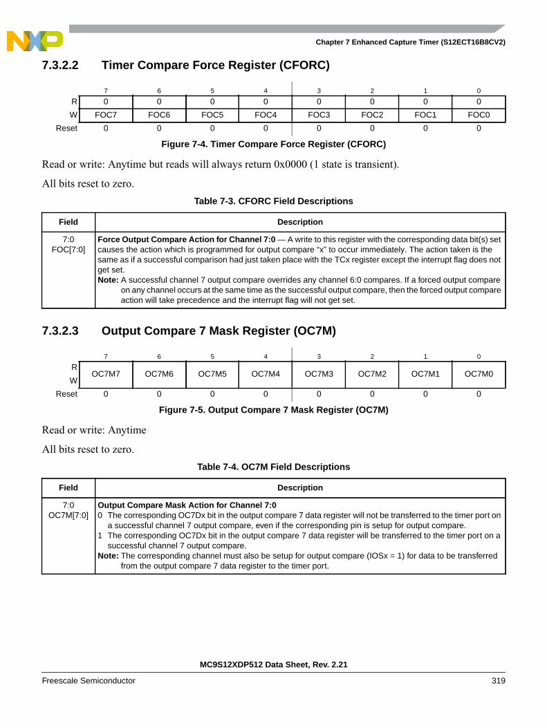
Chapter 7 Enhanced Capture Timer (S12ECT16B8CV2)
MC9S12XDP512 Data Sheet, Rev. 2.21
Freescale Semiconductor 319
7.3.2.2 Timer Compare Force Register (CFORC)
Read or write: Anytime but reads will always return 0x0000 (1 state is transient).
All bits reset to zero.
7.3.2.3 Output Compare 7 Mask Register (OC7M)
Read or write: Anytime
All bits reset to zero.
7 6 5 4 3 2 1 0
R 0 0 0 0 0 0 0 0
W FOC7 FOC6 FOC5 FOC4 FOC3 FOC2 FOC1 FOC0
Reset 0 0 0 0 0 0 0 0
Figure 7-4. Timer Compare Force Register (CFORC)
Table 7-3. CFORC Field Descriptions
Field Description
7:0FOC[7:0]
Force Output Compare Action for Channel 7:0 — A write to this register with the corresponding data bit(s) setcauses the action which is programmed for output compare “x” to occur immediately. The action taken is thesame as if a successful comparison had just taken place with the TCx register except the interrupt flag does notget set.Note: A successful channel 7 output compare overrides any channel 6:0 compares. If a forced output compare
on any channel occurs at the same time as the successful output compare, then the forced output compareaction will take precedence and the interrupt flag will not get set.
7 6 5 4 3 2 1 0
ROC7M7 OC7M6 OC7M5 OC7M4 OC7M3 OC7M2 OC7M1 OC7M0
W
Reset 0 0 0 0 0 0 0 0
Figure 7-5. Output Compare 7 Mask Register (OC7M)
Table 7-4. OC7M Field Descriptions
Field Description
7:0OC7M[7:0]
Output Compare Mask Action for Channel 7:00 The corresponding OC7Dx bit in the output compare 7 data register will not be transferred to the timer port on
a successful channel 7 output compare, even if the corresponding pin is setup for output compare.1 The corresponding OC7Dx bit in the output compare 7 data register will be transferred to the timer port on a
successful channel 7 output compare.Note: The corresponding channel must also be setup for output compare (IOSx = 1) for data to be transferred
from the output compare 7 data register to the timer port.

Chapter 7 Enhanced Capture Timer (S12ECT16B8CV2)
MC9S12XDP512 Data Sheet, Rev. 2.21
320 Freescale Semiconductor
7.3.2.4 Output Compare 7 Data Register (OC7D)
Read or write: Anytime
All bits reset to zero.
7 6 5 4 3 2 1 0
ROC7D7 OC7D6 OC7D5 OC7D4 OC7D3 OC7D2 OC7D1 OC7D0
W
Reset 0 0 0 0 0 0 0 0
Figure 7-6. Output Compare 7 Data Register (OC7D)
Table 7-5. OC7D Field Descriptions
Field Description
7:0OC7D[7:0]
Output Compare 7 Data Bits — A channel 7 output compare can cause bits in the output compare 7 dataregister to transfer to the timer port data register depending on the output compare 7 mask register.

Chapter 7 Enhanced Capture Timer (S12ECT16B8CV2)
MC9S12XDP512 Data Sheet, Rev. 2.21
Freescale Semiconductor 321
7.3.2.5 Timer Count Register (TCNT)
Read: Anytime
Write: Has no meaning or effect
All bits reset to zero.
15 14 13 12 11 10 9 8
RTCNT15 TCNT14 TCNT13 TCNT12 TCNT11 TCNT10 TCNT9 TCNT8
W
Reset 0 0 0 0 0 0 0 0
Figure 7-7. Timer Count Register High (TCNT)
7 6 5 4 3 2 1 0
RTCNT7 TCNT6 TCNT5 TCNT4 TCNT3 TCNT2 TCNT1 TCNT0
W
Reset 0 0 0 0 0 0 0 0
Figure 7-8. Timer Count Register Low (TCNT)
Table 7-6. TCNT Field Descriptions
Field Description
15:0TCNT[15:0]
Timer Counter Bits — The 16-bit main timer is an up counter. A read to this register will return the current valueof the counter. Access to the counter register will take place in one clock cycle.Note: A separate read/write for high byte and low byte in test mode will give a different result than accessing them
as a word. The period of the first count after a write to the TCNT registers may be a different size becausethe write is not synchronized with the prescaler clock.
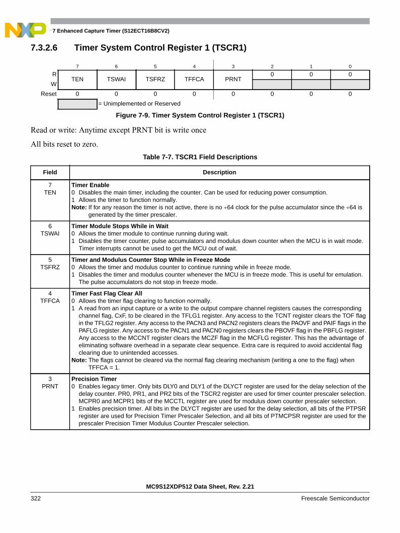
Chapter 7 Enhanced Capture Timer (S12ECT16B8CV2)
MC9S12XDP512 Data Sheet, Rev. 2.21
322 Freescale Semiconductor
7.3.2.6 Timer System Control Register 1 (TSCR1)
Read or write: Anytime except PRNT bit is write once
All bits reset to zero.
7 6 5 4 3 2 1 0
RTEN TSWAI TSFRZ TFFCA PRNT
0 0 0
W
Reset 0 0 0 0 0 0 0 0
= Unimplemented or Reserved
Figure 7-9. Timer System Control Register 1 (TSCR1)
Table 7-7. TSCR1 Field Descriptions
Field Description
7TEN
Timer Enable0 Disables the main timer, including the counter. Can be used for reducing power consumption.1 Allows the timer to function normally.Note: If for any reason the timer is not active, there is no ÷64 clock for the pulse accumulator since the ÷64 is
generated by the timer prescaler.
6TSWAI
Timer Module Stops While in Wait0 Allows the timer module to continue running during wait.1 Disables the timer counter, pulse accumulators and modulus down counter when the MCU is in wait mode.
Timer interrupts cannot be used to get the MCU out of wait.
5TSFRZ
Timer and Modulus Counter Stop While in Freeze Mode0 Allows the timer and modulus counter to continue running while in freeze mode.1 Disables the timer and modulus counter whenever the MCU is in freeze mode. This is useful for emulation.
The pulse accumulators do not stop in freeze mode.
4TFFCA
Timer Fast Flag Clear All0 Allows the timer flag clearing to function normally.1 A read from an input capture or a write to the output compare channel registers causes the corresponding
channel flag, CxF, to be cleared in the TFLG1 register. Any access to the TCNT register clears the TOF flagin the TFLG2 register. Any access to the PACN3 and PACN2 registers clears the PAOVF and PAIF flags in thePAFLG register. Any access to the PACN1 and PACN0 registers clears the PBOVF flag in the PBFLG register.Any access to the MCCNT register clears the MCZF flag in the MCFLG register. This has the advantage ofeliminating software overhead in a separate clear sequence. Extra care is required to avoid accidental flagclearing due to unintended accesses.
Note: The flags cannot be cleared via the normal flag clearing mechanism (writing a one to the flag) whenTFFCA = 1.
3PRNT
Precision Timer0 Enables legacy timer. Only bits DLY0 and DLY1 of the DLYCT register are used for the delay selection of the
delay counter. PR0, PR1, and PR2 bits of the TSCR2 register are used for timer counter prescaler selection.MCPR0 and MCPR1 bits of the MCCTL register are used for modulus down counter prescaler selection.
1 Enables precision timer. All bits in the DLYCT register are used for the delay selection, all bits of the PTPSRregister are used for Precision Timer Prescaler Selection, and all bits of PTMCPSR register are used for theprescaler Precision Timer Modulus Counter Prescaler selection.
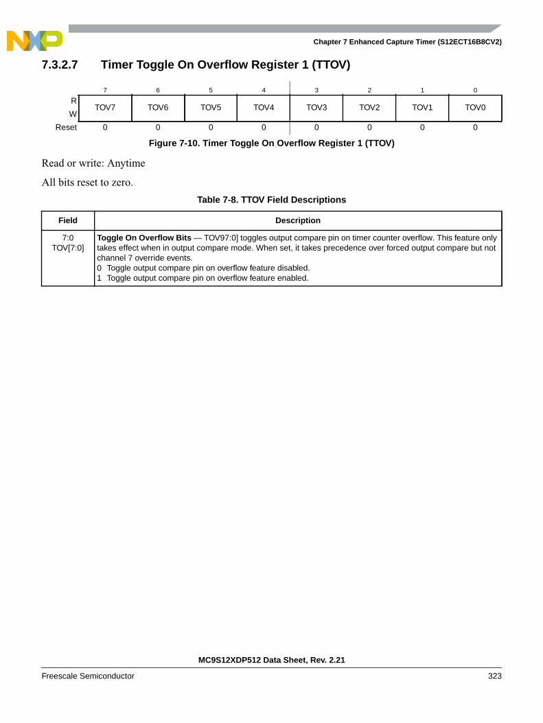
Chapter 7 Enhanced Capture Timer (S12ECT16B8CV2)
MC9S12XDP512 Data Sheet, Rev. 2.21
Freescale Semiconductor 323
7.3.2.7 Timer Toggle On Overflow Register 1 (TTOV)
Read or write: Anytime
All bits reset to zero.
7 6 5 4 3 2 1 0
RTOV7 TOV6 TOV5 TOV4 TOV3 TOV2 TOV1 TOV0
W
Reset 0 0 0 0 0 0 0 0
Figure 7-10. Timer Toggle On Overflow Register 1 (TTOV)
Table 7-8. TTOV Field Descriptions
Field Description
7:0TOV[7:0]
Toggle On Overflow Bits — TOV97:0] toggles output compare pin on timer counter overflow. This feature onlytakes effect when in output compare mode. When set, it takes precedence over forced output compare but notchannel 7 override events.0 Toggle output compare pin on overflow feature disabled.1 Toggle output compare pin on overflow feature enabled.

Chapter 7 Enhanced Capture Timer (S12ECT16B8CV2)
MC9S12XDP512 Data Sheet, Rev. 2.21
324 Freescale Semiconductor
7.3.2.8 Timer Control Register 1/Timer Control Register 2 (TCTL1/TCTL2)
Read or write: Anytime
All bits reset to zero.
NOTETo enable output action by OMx and OLx bits on timer port, thecorresponding bit in OC7M should be cleared.
7 6 5 4 3 2 1 0
ROM7 OL7 OM6 OL6 OM5 OL5 OM4 OL4
W
Reset 0 0 0 0 0 0 0 0
Figure 7-11. Timer Control Register 1 (TCTL1)
7 6 5 4 3 2 1 0
ROM3 OL3 OM2 OL2 OM1 OL1 OM0 OL0
W
Reset 0 0 0 0 0 0 0 0
Figure 7-12. Timer Control Register 2 (TCTL2)
Table 7-9. TCTL1/TCTL2 Field Descriptions
Field Description
OM[7:0]7, 5, 3, 1
OMx — Output ModeOLx — Output LevelThese eight pairs of control bits are encoded to specify the output action to be taken as a result of a successfulOCx compare. When either OMx or OLx is one, the pin associated with OCx becomes an output tied to OCx.See Table 7-10.
OL[7:0]6, 4, 2, 0
Table 7-10. Compare Result Output Action
OMx OLx Action
0 0 Timer disconnected from output pin logic
0 1 Toggle OCx output line
1 0 Clear OCx output line to zero
1 1 Set OCx output line to one

Chapter 7 Enhanced Capture Timer (S12ECT16B8CV2)
MC9S12XDP512 Data Sheet, Rev. 2.21
Freescale Semiconductor 325
7.3.2.9 Timer Control Register 3/Timer Control Register 4 (TCTL3/TCTL4)
Read or write: Anytime
All bits reset to zero.
7 6 5 4 3 2 1 0
REDG7B EDG7A EDG6B EDG6A EDG5B EDG5A EDG4B EDG4A
W
Reset 0 0 0 0 0 0 0 0
Figure 7-13. Timer Control Register 3 (TCTL3)
7 6 5 4 3 2 1 0
REDG3B EDG3A EDG2B EDG2A EDG1B EDG1A EDG0B EDG0A
W
Reset 0 0 0 0 0 0 0 0
Figure 7-14. Timer Control Register 4 (TCTL4)
Table 7-11. TCTL3/TCTL4 Field Descriptions
Field Description
EDG[7:0]B7, 5, 3, 1
Input Capture Edge Control — These eight pairs of control bits configure the input capture edge detectorcircuits for each input capture channel. The four pairs of control bits in TCTL4 also configure the input captureedge control for the four 8-bit pulse accumulators PAC0–PAC3.EDG0B and EDG0A in TCTL4 also determine theactive edge for the 16-bit pulse accumulator PACB. See Table 7-12.EDG[7:0]A
6, 4, 2, 0
Table 7-12. Edge Detector Circuit Configuration
EDGxB EDGxA Configuration
0 0 Capture disabled
0 1 Capture on rising edges only
1 0 Capture on falling edges only
1 1 Capture on any edge (rising or falling)

Chapter 7 Enhanced Capture Timer (S12ECT16B8CV2)
MC9S12XDP512 Data Sheet, Rev. 2.21
326 Freescale Semiconductor
7.3.2.10 Timer Interrupt Enable Register (TIE)
Read or write: Anytime
All bits reset to zero.
The bits C7I–C0I correspond bit-for-bit with the flags in the TFLG1 status register.
7 6 5 4 3 2 1 0
RC7I C6I C5I C4I C3I C2I C1I C0I
W
Reset 0 0 0 0 0 0 0 0
Figure 7-15. Timer Interrupt Enable Register (TIE)
Table 7-13. TIE Field Descriptions
Field Description
7:0C[7:0]I
Input Capture/Output Compare “x” Interrupt Enable0 The corresponding flag is disabled from causing a hardware interrupt.1 The corresponding flag is enabled to cause an interrupt.

Chapter 7 Enhanced Capture Timer (S12ECT16B8CV2)
MC9S12XDP512 Data Sheet, Rev. 2.21
Freescale Semiconductor 327
7.3.2.11 Timer System Control Register 2 (TSCR2)
Read or write: Anytime
All bits reset to zero.
7 6 5 4 3 2 1 0
RTOI
0 0 0TCRE PR2 PR1 PR0
W
Reset 0 0 0 0 0 0 0 0
= Unimplemented or Reserved
Figure 7-16. Timer System Control Register 2 (TSCR2)
Table 7-14. TSCR2 Field Descriptions
Field Description
7TOI
Timer Overflow Interrupt Enable0 Timer overflow interrupt disabled.1 Hardware interrupt requested when TOF flag set.
3TCRE
Timer Counter Reset Enable — This bit allows the timer counter to be reset by a successful channel 7 outputcompare. This mode of operation is similar to an up-counting modulus counter.0 Counter reset disabled and counter free runs.1 Counter reset by a successful output compare on channel 7.Note: If register TC7 = 0x0000 and TCRE = 1, then the TCNT register will stay at 0x0000 continuously. If register
TC7 = 0xFFFF and TCRE = 1, the TOF flag will never be set when TCNT is reset from 0xFFFF to 0x0000.
2:0PR[2:0]
Timer Prescaler Select — These three bits specify the division rate of the main Timer prescaler when the PRNTbit of register TSCR1 is set to 0. The newly selected prescale factor will not take effect until the next synchronizededge where all prescale counter stages equal zero. See Table 7-15.
Table 7-15. Prescaler Selection
PR2 PR1 PR0 Prescale Factor
0 0 0 1
0 0 1 2
0 1 0 4
0 1 1 8
1 0 0 16
1 0 1 32
1 1 0 64
1 1 1 128

Chapter 7 Enhanced Capture Timer (S12ECT16B8CV2)
MC9S12XDP512 Data Sheet, Rev. 2.21
328 Freescale Semiconductor
7.3.2.12 Main Timer Interrupt Flag 1 (TFLG1)
Read: Anytime
Write used in the flag clearing mechanism. Writing a one to the flag clears the flag. Writing a zero will notaffect the current status of the bit.
NOTEWhen TFFCA = 1, the flags cannot be cleared via the normal flag clearingmechanism (writing a one to the flag). Reference Section 7.3.2.6, “TimerSystem Control Register 1 (TSCR1)”.
All bits reset to zero.
TFLG1 indicates when interrupt conditions have occurred. The flags can be cleared via the normal flagclearing mechanism (writing a one to the flag) or via the fast flag clearing mechanism (reference TFFCAbit in Section 7.3.2.6, “Timer System Control Register 1 (TSCR1)”).
Use of the TFMOD bit in the ICSYS register in conjunction with the use of the ICOVW register allows atimer interrupt to be generated after capturing two values in the capture and holding registers, instead ofgenerating an interrupt for every capture.
7 6 5 4 3 2 1 0
RC7F C6F C5F C4F C3F C2F C1F C0F
W
Reset 0 0 0 0 0 0 0 0
Figure 7-17. Main Timer Interrupt Flag 1 (TFLG1)
Table 7-16. TFLG1 Field Descriptions
Field Description
7:0C[7:0]F
Input Capture/Output Compare Channel “x” Flag — A CxF flag is set when a corresponding input capture oroutput compare is detected. C0F can also be set by 16-bit Pulse Accumulator B (PACB). C3F–C0F can also beset by 8-bit pulse accumulators PAC3–PAC0.
If the delay counter is enabled, the CxF flag will not be set until after the delay.
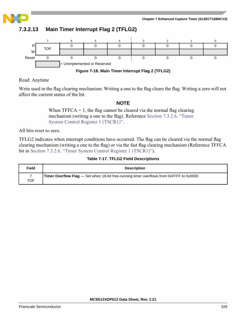
Chapter 7 Enhanced Capture Timer (S12ECT16B8CV2)
MC9S12XDP512 Data Sheet, Rev. 2.21
Freescale Semiconductor 329
7.3.2.13 Main Timer Interrupt Flag 2 (TFLG2)
Read: Anytime
Write used in the flag clearing mechanism. Writing a one to the flag clears the flag. Writing a zero will notaffect the current status of the bit.
NOTEWhen TFFCA = 1, the flag cannot be cleared via the normal flag clearingmechanism (writing a one to the flag). Reference Section 7.3.2.6, “TimerSystem Control Register 1 (TSCR1)”.
All bits reset to zero.
TFLG2 indicates when interrupt conditions have occurred. The flag can be cleared via the normal flagclearing mechanism (writing a one to the flag) or via the fast flag clearing mechanism (Reference TFFCAbit in Section 7.3.2.6, “Timer System Control Register 1 (TSCR1)”).
7 6 5 4 3 2 1 0
RTOF
0 0 0 0 0 0 0
W
Reset 0 0 0 0 0 0 0 0
= Unimplemented or Reserved
Figure 7-18. Main Timer Interrupt Flag 2 (TFLG2)
Table 7-17. TFLG2 Field Descriptions
Field Description
7TOF
Timer Overflow Flag — Set when 16-bit free-running timer overflows from 0xFFFF to 0x0000.

Chapter 7 Enhanced Capture Timer (S12ECT16B8CV2)
MC9S12XDP512 Data Sheet, Rev. 2.21
330 Freescale Semiconductor
7.3.2.14 Timer Input Capture/Output Compare Registers 0–7
15 14 13 12 11 10 9 8
RBit 15 Bit 14 Bit 13 Bit 12 Bit 11 Bit 10 Bit 9 Bit 8
W
Reset 0 0 0 0 0 0 0 0
Figure 7-19. Timer Input Capture/Output Compare Register 0 High (TC0)
7 6 5 4 3 2 1 0
RBit 7 Bit 6 Bit 5 Bit 4 Bit 3 Bit 2 Bit 1 Bit 0
W
Reset 0 0 0 0 0 0 0 0
Figure 7-20. Timer Input Capture/Output Compare Register 0 Low (TC0)
15 14 13 12 11 10 9 8
RBit 15 Bit 14 Bit 13 Bit 12 Bit 11 Bit 10 Bit 9 Bit 8
W
Reset 0 0 0 0 0 0 0 0
Figure 7-21. Timer Input Capture/Output Compare Register 1 High (TC1)
7 6 5 4 3 2 1 0
RBit 7 Bit 6 Bit 5 Bit 4 Bit 3 Bit 2 Bit 1 Bit 0
W
Reset 0 0 0 0 0 0 0 0
Figure 7-22. Timer Input Capture/Output Compare Register 1 Low (TC1)
15 14 13 12 11 10 9 8
RBit 15 Bit 14 Bit 13 Bit 12 Bit 11 Bit 10 Bit 9 Bit 8
W
Reset 0 0 0 0 0 0 0 0
Figure 7-23. Timer Input Capture/Output Compare Register 2 High (TC2)
7 6 5 4 3 2 1 0
RBit 7 Bit 6 Bit 5 Bit 4 Bit 3 Bit 2 Bit 1 Bit 0
W
Reset 0 0 0 0 0 0 0 0
Figure 7-24. Timer Input Capture/Output Compare Register 2 Low (TC2)
15 14 13 12 11 10 9 8
RBit 15 Bit 14 Bit 13 Bit 12 Bit 11 Bit 10 Bit 9 Bit 8
W
Reset 0 0 0 0 0 0 0 0
Figure 7-25. Timer Input Capture/Output Compare Register 3 High (TC3)
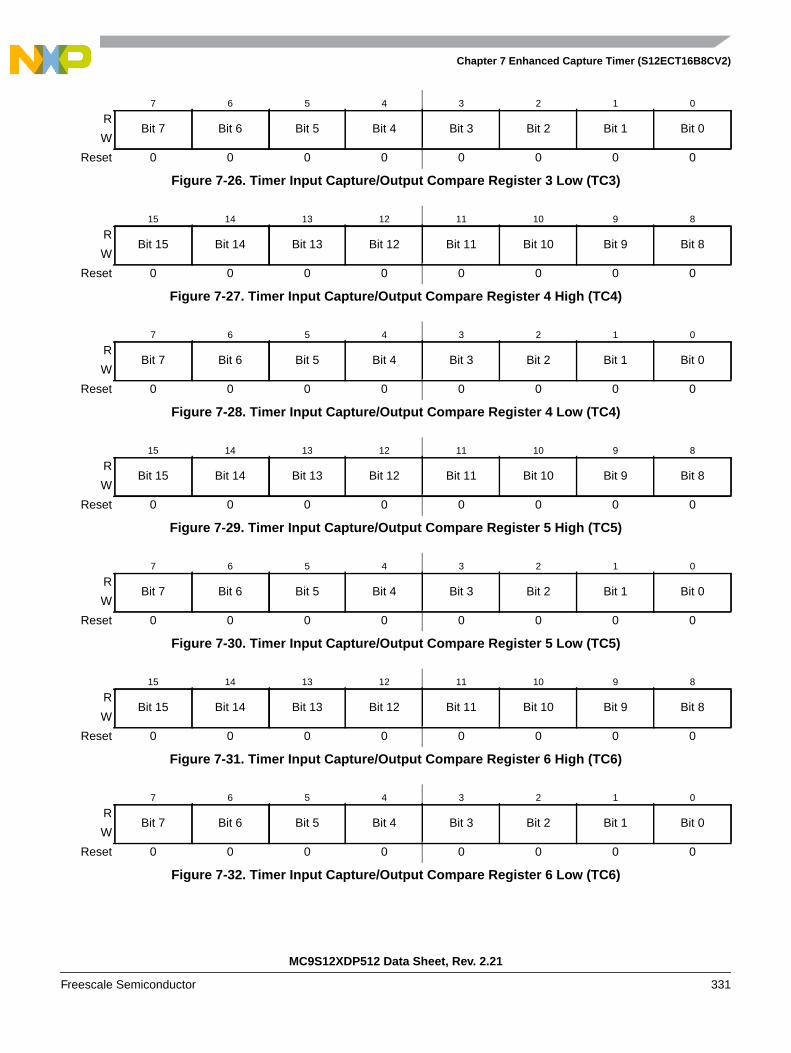
Chapter 7 Enhanced Capture Timer (S12ECT16B8CV2)
MC9S12XDP512 Data Sheet, Rev. 2.21
Freescale Semiconductor 331
7 6 5 4 3 2 1 0
RBit 7 Bit 6 Bit 5 Bit 4 Bit 3 Bit 2 Bit 1 Bit 0
W
Reset 0 0 0 0 0 0 0 0
Figure 7-26. Timer Input Capture/Output Compare Register 3 Low (TC3)
15 14 13 12 11 10 9 8
RBit 15 Bit 14 Bit 13 Bit 12 Bit 11 Bit 10 Bit 9 Bit 8
W
Reset 0 0 0 0 0 0 0 0
Figure 7-27. Timer Input Capture/Output Compare Register 4 High (TC4)
7 6 5 4 3 2 1 0
RBit 7 Bit 6 Bit 5 Bit 4 Bit 3 Bit 2 Bit 1 Bit 0
W
Reset 0 0 0 0 0 0 0 0
Figure 7-28. Timer Input Capture/Output Compare Register 4 Low (TC4)
15 14 13 12 11 10 9 8
RBit 15 Bit 14 Bit 13 Bit 12 Bit 11 Bit 10 Bit 9 Bit 8
W
Reset 0 0 0 0 0 0 0 0
Figure 7-29. Timer Input Capture/Output Compare Register 5 High (TC5)
7 6 5 4 3 2 1 0
RBit 7 Bit 6 Bit 5 Bit 4 Bit 3 Bit 2 Bit 1 Bit 0
W
Reset 0 0 0 0 0 0 0 0
Figure 7-30. Timer Input Capture/Output Compare Register 5 Low (TC5)
15 14 13 12 11 10 9 8
RBit 15 Bit 14 Bit 13 Bit 12 Bit 11 Bit 10 Bit 9 Bit 8
W
Reset 0 0 0 0 0 0 0 0
Figure 7-31. Timer Input Capture/Output Compare Register 6 High (TC6)
7 6 5 4 3 2 1 0
RBit 7 Bit 6 Bit 5 Bit 4 Bit 3 Bit 2 Bit 1 Bit 0
W
Reset 0 0 0 0 0 0 0 0
Figure 7-32. Timer Input Capture/Output Compare Register 6 Low (TC6)

Chapter 7 Enhanced Capture Timer (S12ECT16B8CV2)
MC9S12XDP512 Data Sheet, Rev. 2.21
332 Freescale Semiconductor
Read: Anytime
Write anytime for output compare function. Writes to these registers have no meaning or effect duringinput capture.
All bits reset to zero.
Depending on the TIOS bit for the corresponding channel, these registers are used to latch the value of thefree-running counter when a defined transition is sensed by the corresponding input capture edge detectoror to trigger an output action for output compare.
7.3.2.15 16-Bit Pulse Accumulator A Control Register (PACTL)
Read: Anytime
Write: Anytime
All bits reset to zero.
15 14 13 12 11 10 9 8
RBit 15 Bit 14 Bit 13 Bit 12 Bit 11 Bit 10 Bit 9 Bit 8
W
Reset 0 0 0 0 0 0 0 0
Figure 7-33. Timer Input Capture/Output Compare Register 7 High (TC7)
7 6 5 4 3 2 1 0
RBit 7 Bit 6 Bit 5 Bit 4 Bit 3 Bit 2 Bit 1 Bit 0
W
Reset 0 0 0 0 0 0 0 0
Figure 7-34. Timer Input Capture/Output Compare Register 7 Low (TC7)
7 6 5 4 3 2 1 0
R 0PAEN PAMOD PEDGE CLK1 CLK0 PAOVI PAI
W
Reset 0 0 0 0 0 0 0 0
= Unimplemented or Reserved
Figure 7-35. 16-Bit Pulse Accumulator Control Register (PACTL)
Table 7-18. PACTL Field Descriptions
Field Description
6PAEN
Pulse Accumulator A System Enable — PAEN is independent from TEN. With timer disabled, the pulseaccumulator can still function unless pulse accumulator is disabled.0 16-Bit Pulse Accumulator A system disabled. 8-bit PAC3 and PAC2 can be enabled when their related enable
bits in ICPAR are set. Pulse Accumulator Input Edge Flag (PAIF) function is disabled.1 16-Bit Pulse Accumulator A system enabled. The two 8-bit pulse accumulators PAC3 and PAC2 are cascaded
to form the PACA 16-bit pulse accumulator. When PACA in enabled, the PACN3 and PACN2 registers contentsare respectively the high and low byte of the PACA. PA3EN and PA2EN control bits in ICPAR have no effect.Pulse Accumulator Input Edge Flag (PAIF) function is enabled. The PACA shares the input pin with IC7.

Chapter 7 Enhanced Capture Timer (S12ECT16B8CV2)
MC9S12XDP512 Data Sheet, Rev. 2.21
Freescale Semiconductor 333
.
5PAMOD
Pulse Accumulator Mode — This bit is active only when the Pulse Accumulator A is enabled (PAEN = 1).0 Event counter mode1 Gated time accumulation mode
4PEDGE
Pulse Accumulator Edge Control — This bit is active only when the Pulse Accumulator A is enabled(PAEN = 1). Refer to Table 7-19.
For PAMOD bit = 0 (event counter mode).0 Falling edges on PT7 pin cause the count to be incremented1 Rising edges on PT7 pin cause the count to be incremented
For PAMOD bit = 1 (gated time accumulation mode).0 PT7 input pin high enables bus clock divided by 64 to Pulse Accumulator and the trailing falling edge on PT7
sets the PAIF flag.1 PT7 input pin low enables bus clock divided by 64 to Pulse Accumulator and the trailing rising edge on PT7
sets the PAIF flag.
If the timer is not active (TEN = 0 in TSCR1), there is no divide-by-64 since the ÷64 clock is generated by thetimer prescaler.
3:2CLK[1:0]
Clock Select Bits — For the description of PACLK please refer to Figure 7-70.
If the pulse accumulator is disabled (PAEN = 0), the prescaler clock from the timer is always used as an inputclock to the timer counter. The change from one selected clock to the other happens immediately after these bitsare written. Refer to Table 7-20.
2PAOVI
Pulse Accumulator A Overflow Interrupt Enable0 Interrupt inhibited1 Interrupt requested if PAOVF is set
0PAI
Pulse Accumulator Input Interrupt Enable0 Interrupt inhibited1 Interrupt requested if PAIF is set
Table 7-19. Pin Action
PAMOD PEDGE Pin Action
0 0 Falling edge
0 1 Rising edge
1 0 Divide by 64 clock enabled with pin high level
1 1 Divide by 64 clock enabled with pin low level
Table 7-20. Clock Selection
CLK1 CLK0 Clock Source
0 0 Use timer prescaler clock as timer counter clock
0 1 Use PACLK as input to timer counter clock
1 0 Use PACLK/256 as timer counter clock frequency
1 1 Use PACLK/65536 as timer counter clock frequency
Table 7-18. PACTL Field Descriptions (continued)
Field Description

Chapter 7 Enhanced Capture Timer (S12ECT16B8CV2)
MC9S12XDP512 Data Sheet, Rev. 2.21
334 Freescale Semiconductor
7.3.2.16 Pulse Accumulator A Flag Register (PAFLG)
Read: Anytime
Write used in the flag clearing mechanism. Writing a one to the flag clears the flag. Writing a zero will notaffect the current status of the bit.
NOTEWhen TFFCA = 1, the flags cannot be cleared via the normal flag clearingmechanism (writing a one to the flag). Reference Section 7.3.2.6, “TimerSystem Control Register 1 (TSCR1)”.
All bits reset to zero.
PAFLG indicates when interrupt conditions have occurred. The flags can be cleared via the normal flagclearing mechanism (writing a one to the flag) or via the fast flag clearing mechanism (Reference TFFCAbit in Section 7.3.2.6, “Timer System Control Register 1 (TSCR1)”).
7.3.2.17 Pulse Accumulators Count Registers (PACN3 and PACN2)
7 6 5 4 3 2 1 0
R 0 0 0 0 0 0PAOVF PAIF
W
Reset 0 0 0 0 0 0 0 0
= Unimplemented or Reserved
Figure 7-36. Pulse Accumulator A Flag Register (PAFLG)
Table 7-21. PAFLG Field Descriptions
Field Description
1PAOVF
Pulse Accumulator A Overflow Flag — Set when the 16-bit pulse accumulator A overflows from 0xFFFF to0x0000, or when 8-bit pulse accumulator 3 (PAC3) overflows from 0x00FF to 0x0000.
When PACMX = 1, PAOVF bit can also be set if 8-bit pulse accumulator 3 (PAC3) reaches 0x00FF followed byan active edge on PT3.
0PAIF
Pulse Accumulator Input edge Flag — Set when the selected edge is detected at the PT7 input pin. In eventmode the event edge triggers PAIF and in gated time accumulation mode the trailing edge of the gate signal atthe PT7 input pin triggers PAIF.
7 6 5 4 3 2 1 0
RPACNT7(15) PACNT6(14) PACNT5(13) PACNT4(12) PACNT3(11) PACNT2(10) PACNT1(9) PACNT0(8)
W
Reset 0 0 0 0 0 0 0 0
Figure 7-37. Pulse Accumulators Count Register 3 (PACN3)

Chapter 7 Enhanced Capture Timer (S12ECT16B8CV2)
MC9S12XDP512 Data Sheet, Rev. 2.21
Freescale Semiconductor 335
Read: Anytime
Write: Anytime
All bits reset to zero.
The two 8-bit pulse accumulators PAC3 and PAC2 are cascaded to form the PACA 16-bit pulseaccumulator. When PACA in enabled (PAEN = 1 in PACTL), the PACN3 and PACN2 registers contentsare respectively the high and low byte of the PACA.
When PACN3 overflows from 0x00FF to 0x0000, the interrupt flag PAOVF in PAFLG is set.
Full count register access will take place in one clock cycle.
NOTEA separate read/write for high byte and low byte will give a different resultthan accessing them as a word.
When clocking pulse and write to the registers occurs simultaneously, writetakes priority and the register is not incremented.
7.3.2.18 Pulse Accumulators Count Registers (PACN1 and PACN0)
Read: Anytime
Write: Anytime
All bits reset to zero.
The two 8-bit pulse accumulators PAC1 and PAC0 are cascaded to form the PACB 16-bit pulseaccumulator. When PACB in enabled, (PBEN = 1 in PBCTL) the PACN1 and PACN0 registers contentsare respectively the high and low byte of the PACB.
7 6 5 4 3 2 1 0
RPACNT7 PACNT6 PACNT5 PACNT4 PACNT3 PACNT2 PACNT1 PACNT0
W
Reset 0 0 0 0 0 0 0 0
Figure 7-38. Pulse Accumulators Count Register 2 (PACN2)
7 6 5 4 3 2 1 0
RPACNT7(15) PACNT6(14) PACNT5(13) PACNT4(12) PACNT3(11) PACNT2(10) PACNT1(9) PACNT0(8)
W
Reset 0 0 0 0 0 0 0 0
Figure 7-39. Pulse Accumulators Count Register 1 (PACN1)
7 6 5 4 3 2 1 0
RPACNT7 PACNT6 PACNT5 PACNT4 PACNT3 PACNT2 PACNT1 PACNT0
W
Reset 0 0 0 0 0 0 0 0
Figure 7-40. Pulse Accumulators Count Register 0 (PACN0)

Chapter 7 Enhanced Capture Timer (S12ECT16B8CV2)
MC9S12XDP512 Data Sheet, Rev. 2.21
336 Freescale Semiconductor
When PACN1 overflows from 0x00FF to 0x0000, the interrupt flag PBOVF in PBFLG is set.
Full count register access will take place in one clock cycle.
NOTEA separate read/write for high byte and low byte will give a different resultthan accessing them as a word.
When clocking pulse and write to the registers occurs simultaneously, writetakes priority and the register is not incremented.
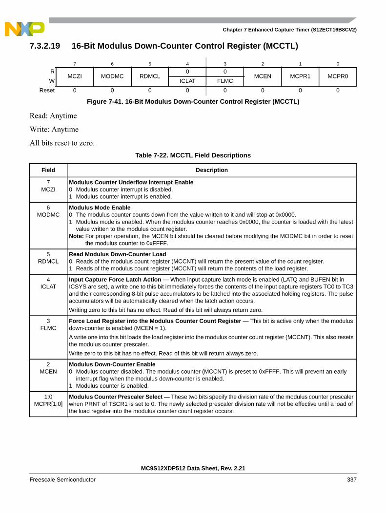
Chapter 7 Enhanced Capture Timer (S12ECT16B8CV2)
MC9S12XDP512 Data Sheet, Rev. 2.21
Freescale Semiconductor 337
7.3.2.19 16-Bit Modulus Down-Counter Control Register (MCCTL)
Read: Anytime
Write: Anytime
All bits reset to zero.
7 6 5 4 3 2 1 0
RMCZI MODMC RDMCL
0 0MCEN MCPR1 MCPR0
W ICLAT FLMC
Reset 0 0 0 0 0 0 0 0
Figure 7-41. 16-Bit Modulus Down-Counter Control Register (MCCTL)
Table 7-22. MCCTL Field Descriptions
Field Description
7MCZI
Modulus Counter Underflow Interrupt Enable0 Modulus counter interrupt is disabled.1 Modulus counter interrupt is enabled.
6MODMC
Modulus Mode Enable0 The modulus counter counts down from the value written to it and will stop at 0x0000.1 Modulus mode is enabled. When the modulus counter reaches 0x0000, the counter is loaded with the latest
value written to the modulus count register.Note: For proper operation, the MCEN bit should be cleared before modifying the MODMC bit in order to reset
the modulus counter to 0xFFFF.
5RDMCL
Read Modulus Down-Counter Load0 Reads of the modulus count register (MCCNT) will return the present value of the count register.1 Reads of the modulus count register (MCCNT) will return the contents of the load register.
4ICLAT
Input Capture Force Latch Action — When input capture latch mode is enabled (LATQ and BUFEN bit inICSYS are set), a write one to this bit immediately forces the contents of the input capture registers TC0 to TC3and their corresponding 8-bit pulse accumulators to be latched into the associated holding registers. The pulseaccumulators will be automatically cleared when the latch action occurs.
Writing zero to this bit has no effect. Read of this bit will always return zero.
3FLMC
Force Load Register into the Modulus Counter Count Register — This bit is active only when the modulusdown-counter is enabled (MCEN = 1).
A write one into this bit loads the load register into the modulus counter count register (MCCNT). This also resetsthe modulus counter prescaler.
Write zero to this bit has no effect. Read of this bit will return always zero.
2MCEN
Modulus Down-Counter Enable0 Modulus counter disabled. The modulus counter (MCCNT) is preset to 0xFFFF. This will prevent an early
interrupt flag when the modulus down-counter is enabled.1 Modulus counter is enabled.
1:0MCPR[1:0]
Modulus Counter Prescaler Select — These two bits specify the division rate of the modulus counter prescalerwhen PRNT of TSCR1 is set to 0. The newly selected prescaler division rate will not be effective until a load ofthe load register into the modulus counter count register occurs.
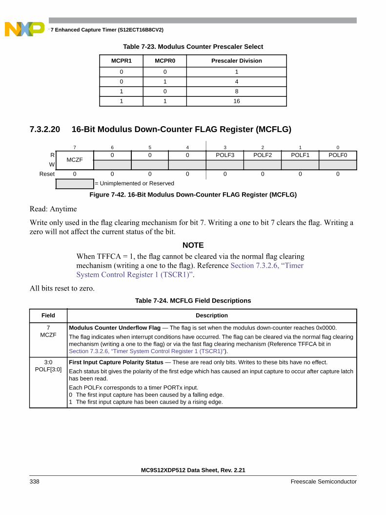
Chapter 7 Enhanced Capture Timer (S12ECT16B8CV2)
MC9S12XDP512 Data Sheet, Rev. 2.21
338 Freescale Semiconductor
7.3.2.20 16-Bit Modulus Down-Counter FLAG Register (MCFLG)
Read: Anytime
Write only used in the flag clearing mechanism for bit 7. Writing a one to bit 7 clears the flag. Writing azero will not affect the current status of the bit.
NOTEWhen TFFCA = 1, the flag cannot be cleared via the normal flag clearingmechanism (writing a one to the flag). Reference Section 7.3.2.6, “TimerSystem Control Register 1 (TSCR1)”.
All bits reset to zero.
Table 7-23. Modulus Counter Prescaler Select
MCPR1 MCPR0 Prescaler Division
0 0 1
0 1 4
1 0 8
1 1 16
7 6 5 4 3 2 1 0
RMCZF
0 0 0 POLF3 POLF2 POLF1 POLF0
W
Reset 0 0 0 0 0 0 0 0
= Unimplemented or Reserved
Figure 7-42. 16-Bit Modulus Down-Counter FLAG Register (MCFLG)
Table 7-24. MCFLG Field Descriptions
Field Description
7MCZF
Modulus Counter Underflow Flag — The flag is set when the modulus down-counter reaches 0x0000.
The flag indicates when interrupt conditions have occurred. The flag can be cleared via the normal flag clearingmechanism (writing a one to the flag) or via the fast flag clearing mechanism (Reference TFFCA bit inSection 7.3.2.6, “Timer System Control Register 1 (TSCR1)”).
3:0POLF[3:0]
First Input Capture Polarity Status — These are read only bits. Writes to these bits have no effect.
Each status bit gives the polarity of the first edge which has caused an input capture to occur after capture latchhas been read.
Each POLFx corresponds to a timer PORTx input.0 The first input capture has been caused by a falling edge.1 The first input capture has been caused by a rising edge.

Chapter 7 Enhanced Capture Timer (S12ECT16B8CV2)
MC9S12XDP512 Data Sheet, Rev. 2.21
Freescale Semiconductor 339
7.3.2.21 ICPAR — Input Control Pulse Accumulators Register (ICPAR)
Read: Anytime
Write: Anytime.
All bits reset to zero.
The 8-bit pulse accumulators PAC3 and PAC2 can be enabled only if PAEN in PACTL is cleared. If PAENis set, PA3EN and PA2EN have no effect.
The 8-bit pulse accumulators PAC1 and PAC0 can be enabled only if PBEN in PBCTL is cleared. If PBENis set, PA1EN and PA0EN have no effect.
7 6 5 4 3 2 1 0
R 0 0 0 0PA3EN PA2EN PA1EN PA0EN
W
Reset 0 0 0 0 0 0 0 0
= Unimplemented or Reserved
Figure 7-43. Input Control Pulse Accumulators Register (ICPAR)
Table 7-25. ICPAR Field Descriptions
Field Description
3:0PA[3:0]EN
8-Bit Pulse Accumulator ‘x’ Enable0 8-Bit Pulse Accumulator is disabled.1 8-Bit Pulse Accumulator is enabled.
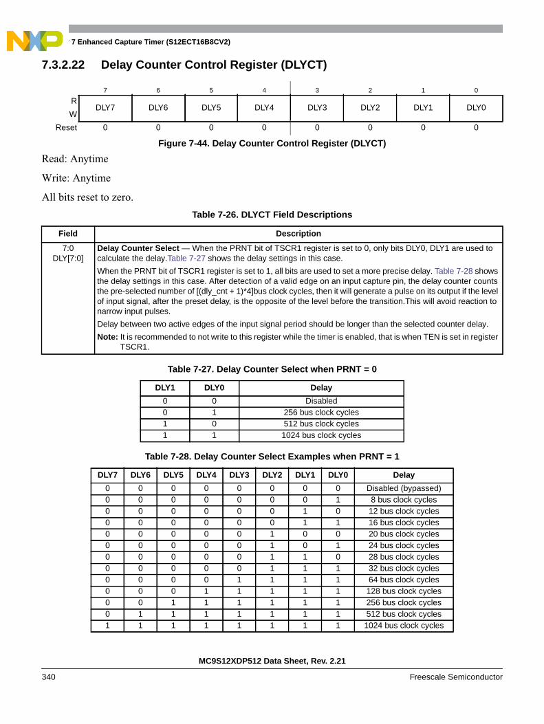
Chapter 7 Enhanced Capture Timer (S12ECT16B8CV2)
MC9S12XDP512 Data Sheet, Rev. 2.21
340 Freescale Semiconductor
7.3.2.22 Delay Counter Control Register (DLYCT)
Read: Anytime
Write: Anytime
All bits reset to zero.
7 6 5 4 3 2 1 0
RDLY7 DLY6 DLY5 DLY4 DLY3 DLY2 DLY1 DLY0
W
Reset 0 0 0 0 0 0 0 0
Figure 7-44. Delay Counter Control Register (DLYCT)
Table 7-26. DLYCT Field Descriptions
Field Description
7:0DLY[7:0]
Delay Counter Select — When the PRNT bit of TSCR1 register is set to 0, only bits DLY0, DLY1 are used tocalculate the delay.Table 7-27 shows the delay settings in this case.
When the PRNT bit of TSCR1 register is set to 1, all bits are used to set a more precise delay. Table 7-28 showsthe delay settings in this case. After detection of a valid edge on an input capture pin, the delay counter countsthe pre-selected number of [(dly_cnt + 1)*4]bus clock cycles, then it will generate a pulse on its output if the levelof input signal, after the preset delay, is the opposite of the level before the transition.This will avoid reaction tonarrow input pulses.
Delay between two active edges of the input signal period should be longer than the selected counter delay.
Note: It is recommended to not write to this register while the timer is enabled, that is when TEN is set in registerTSCR1.
Table 7-27. Delay Counter Select when PRNT = 0
DLY1 DLY0 Delay
0 0 Disabled0 1 256 bus clock cycles1 0 512 bus clock cycles1 1 1024 bus clock cycles
Table 7-28. Delay Counter Select Examples when PRNT = 1
DLY7 DLY6 DLY5 DLY4 DLY3 DLY2 DLY1 DLY0 Delay
0 0 0 0 0 0 0 0 Disabled (bypassed)0 0 0 0 0 0 0 1 8 bus clock cycles0 0 0 0 0 0 1 0 12 bus clock cycles0 0 0 0 0 0 1 1 16 bus clock cycles0 0 0 0 0 1 0 0 20 bus clock cycles0 0 0 0 0 1 0 1 24 bus clock cycles0 0 0 0 0 1 1 0 28 bus clock cycles0 0 0 0 0 1 1 1 32 bus clock cycles0 0 0 0 1 1 1 1 64 bus clock cycles0 0 0 1 1 1 1 1 128 bus clock cycles0 0 1 1 1 1 1 1 256 bus clock cycles0 1 1 1 1 1 1 1 512 bus clock cycles1 1 1 1 1 1 1 1 1024 bus clock cycles
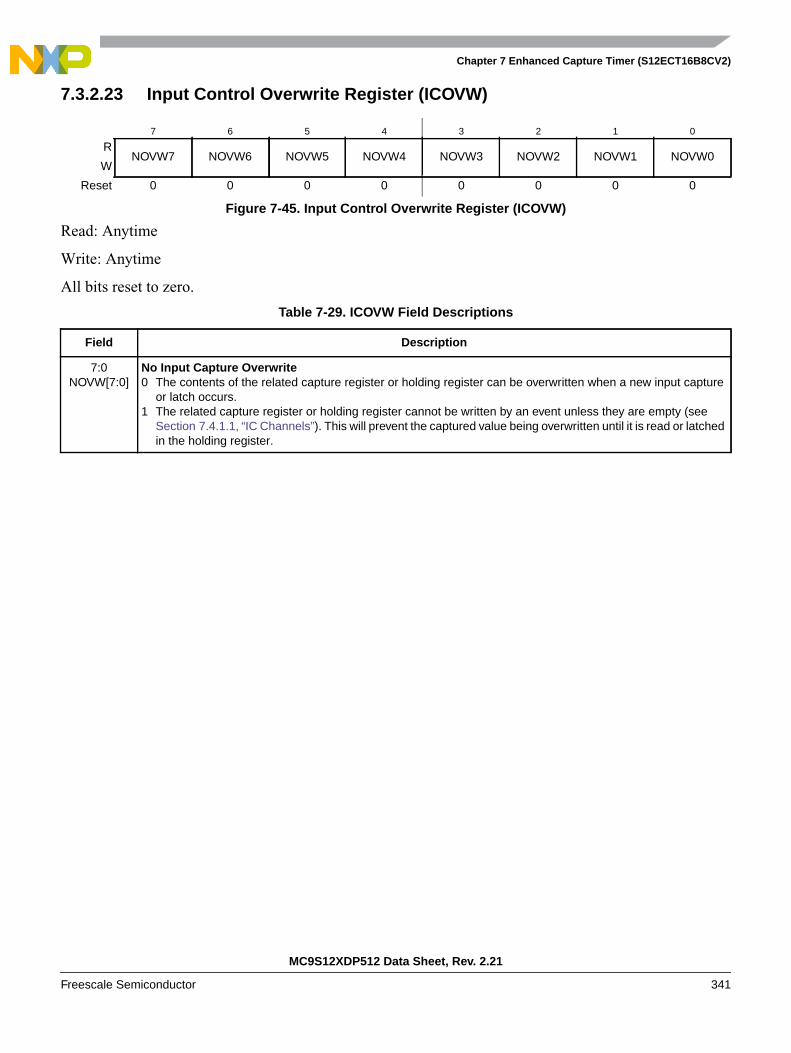
Chapter 7 Enhanced Capture Timer (S12ECT16B8CV2)
MC9S12XDP512 Data Sheet, Rev. 2.21
Freescale Semiconductor 341
7.3.2.23 Input Control Overwrite Register (ICOVW)
Read: Anytime
Write: Anytime
All bits reset to zero.
7 6 5 4 3 2 1 0
RNOVW7 NOVW6 NOVW5 NOVW4 NOVW3 NOVW2 NOVW1 NOVW0
W
Reset 0 0 0 0 0 0 0 0
Figure 7-45. Input Control Overwrite Register (ICOVW)
Table 7-29. ICOVW Field Descriptions
Field Description
7:0NOVW[7:0]
No Input Capture Overwrite0 The contents of the related capture register or holding register can be overwritten when a new input capture
or latch occurs.1 The related capture register or holding register cannot be written by an event unless they are empty (see
Section 7.4.1.1, “IC Channels”). This will prevent the captured value being overwritten until it is read or latchedin the holding register.

Chapter 7 Enhanced Capture Timer (S12ECT16B8CV2)
MC9S12XDP512 Data Sheet, Rev. 2.21
342 Freescale Semiconductor
7.3.2.24 Input Control System Control Register (ICSYS)
Read: Anytime
Write: Once in normal modes
All bits reset to zero.
7 6 5 4 3 2 1 0
RSH37 SH26 SH15 SH04 TFMOD PACMX BUFEN LATQ
W
Reset 0 0 0 0 0 0 0 0
Figure 7-46. Input Control System Register (ICSYS)
Table 7-30. ICSYS Field Descriptions
Field Description
7:4SHxy
Share Input action of Input Capture Channels x and y0 Normal operation1 The channel input ‘x’ causes the same action on the channel ‘y’. The port pin ‘x’ and the corresponding edge
detector is used to be active on the channel ‘y’.
3TFMOD
Timer Flag Setting Mode — Use of the TFMOD bit in conjunction with the use of the ICOVW register allows atimer interrupt to be generated after capturing two values in the capture and holding registers instead ofgenerating an interrupt for every capture.By setting TFMOD in queue mode, when NOVWx bit is set and the corresponding capture and holding registersare emptied, an input capture event will first update the related input capture register with the main timercontents. At the next event, the TCx data is transferred to the TCxH register, the TCx is updated and the CxFinterrupt flag is set. In all other input capture cases the interrupt flag is set by a valid external event on PTx.0 The timer flags C3F–C0F in TFLG1 are set when a valid input capture transition on the corresponding port pin
occurs.1 If in queue mode (BUFEN = 1 and LATQ = 0), the timer flags C3F–C0F in TFLG1 are set only when a latch
on the corresponding holding register occurs. If the queue mode is not engaged, the timer flags C3F–C0F areset the same way as for TFMOD = 0.
2PACMX
8-Bit Pulse Accumulators Maximum Count0 Normal operation. When the 8-bit pulse accumulator has reached the value 0x00FF, with the next active edge,
it will be incremented to 0x0000.1 When the 8-bit pulse accumulator has reached the value 0x00FF, it will not be incremented further. The value
0x00FF indicates a count of 255 or more.
1BUFFEN
IC Buffer Enable0 Input capture and pulse accumulator holding registers are disabled.1 Input capture and pulse accumulator holding registers are enabled. The latching mode is defined by LATQ
control bit.
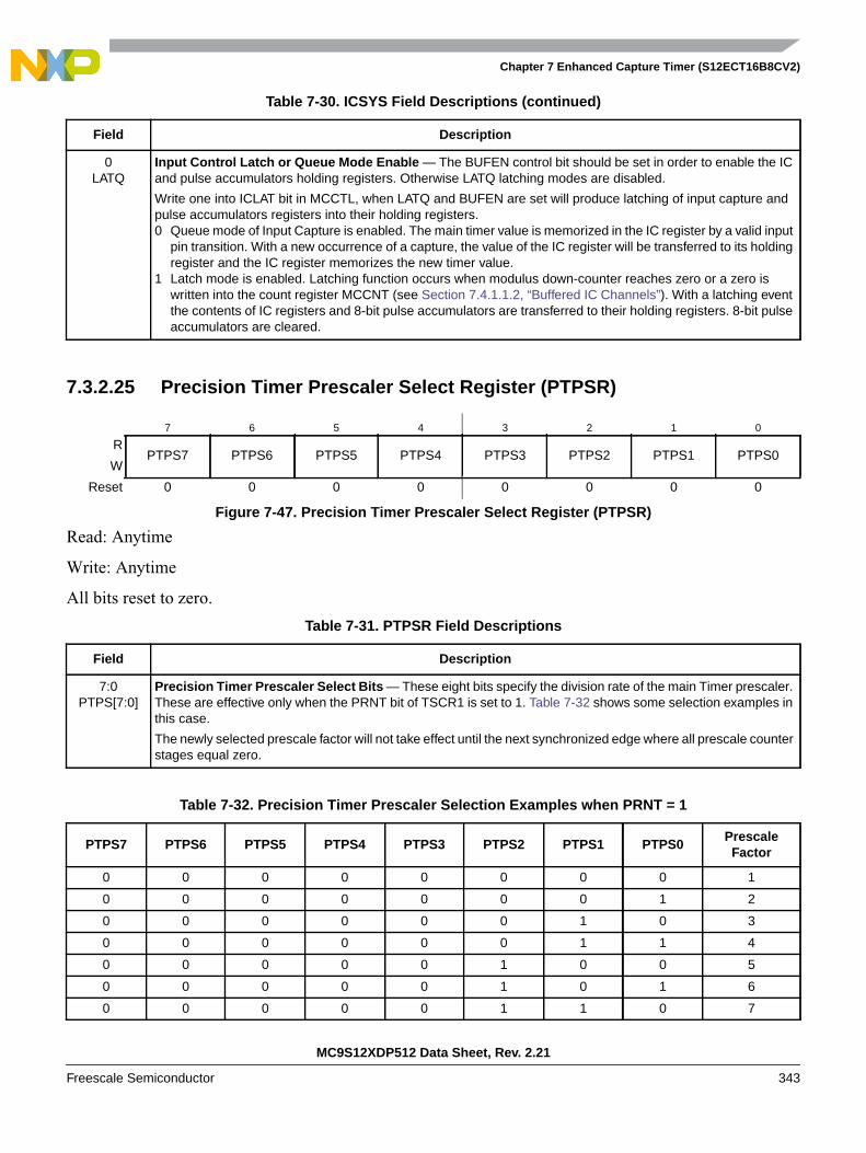
Chapter 7 Enhanced Capture Timer (S12ECT16B8CV2)
MC9S12XDP512 Data Sheet, Rev. 2.21
Freescale Semiconductor 343
7.3.2.25 Precision Timer Prescaler Select Register (PTPSR)
Read: Anytime
Write: Anytime
All bits reset to zero.
0LATQ
Input Control Latch or Queue Mode Enable — The BUFEN control bit should be set in order to enable the ICand pulse accumulators holding registers. Otherwise LATQ latching modes are disabled.
Write one into ICLAT bit in MCCTL, when LATQ and BUFEN are set will produce latching of input capture andpulse accumulators registers into their holding registers.0 Queue mode of Input Capture is enabled. The main timer value is memorized in the IC register by a valid input
pin transition. With a new occurrence of a capture, the value of the IC register will be transferred to its holdingregister and the IC register memorizes the new timer value.
1 Latch mode is enabled. Latching function occurs when modulus down-counter reaches zero or a zero iswritten into the count register MCCNT (see Section 7.4.1.1.2, “Buffered IC Channels”). With a latching eventthe contents of IC registers and 8-bit pulse accumulators are transferred to their holding registers. 8-bit pulseaccumulators are cleared.
7 6 5 4 3 2 1 0
RPTPS7 PTPS6 PTPS5 PTPS4 PTPS3 PTPS2 PTPS1 PTPS0
W
Reset 0 0 0 0 0 0 0 0
Figure 7-47. Precision Timer Prescaler Select Register (PTPSR)
Table 7-31. PTPSR Field Descriptions
Field Description
7:0PTPS[7:0]
Precision Timer Prescaler Select Bits — These eight bits specify the division rate of the main Timer prescaler.These are effective only when the PRNT bit of TSCR1 is set to 1. Table 7-32 shows some selection examples inthis case.
The newly selected prescale factor will not take effect until the next synchronized edge where all prescale counterstages equal zero.
Table 7-32. Precision Timer Prescaler Selection Examples when PRNT = 1
PTPS7 PTPS6 PTPS5 PTPS4 PTPS3 PTPS2 PTPS1 PTPS0PrescaleFactor
0 0 0 0 0 0 0 0 1
0 0 0 0 0 0 0 1 2
0 0 0 0 0 0 1 0 3
0 0 0 0 0 0 1 1 4
0 0 0 0 0 1 0 0 5
0 0 0 0 0 1 0 1 6
0 0 0 0 0 1 1 0 7
Table 7-30. ICSYS Field Descriptions (continued)
Field Description

Chapter 7 Enhanced Capture Timer (S12ECT16B8CV2)
MC9S12XDP512 Data Sheet, Rev. 2.21
344 Freescale Semiconductor
7.3.2.26 Precision Timer Modulus Counter Prescaler Select Register (PTMCPSR)
Read: Anytime
Write: Anytime
All bits reset to zero.
0 0 0 0 0 1 1 1 8
0 0 0 0 1 1 1 1 16
0 0 0 1 1 1 1 1 32
0 0 1 1 1 1 1 1 64
0 1 1 1 1 1 1 1 128
1 1 1 1 1 1 1 1 256
7 6 5 4 3 2 1 0
RPTMPS7 PTMPS6 PTMPS5 PTMPS4 PTMPS3 PTMPS2 PTMPS1 PTMPS0
W
Reset 0 0 0 0 0 0 0 0
Figure 7-48. Precision Timer Modulus Counter Prescaler Select Register (PTMCPSR)
Table 7-33. PTMCPSR Field Descriptions
Field Description
7:0PTMPS[7:0]
Precision Timer Modulus Counter Prescaler Select Bits — These eight bits specify the division rate of themodulus counter prescaler. These are effective only when the PRNT bit of TSCR1 is set to 1. Table 7-34 showssome possible division rates.
The newly selected prescaler division rate will not be effective until a load of the load register into the moduluscounter count register occurs.
Table 7-34. Precision Timer Modulus Counter Prescaler Select Examples when PRNT = 1
PTMPS7 PTMPS6 PTMPS5 PTMPS4 PTMPS3 PTMPS2 PTMPS1 PTMPS0PrescalerDivision
Rate
0 0 0 0 0 0 0 0 1
0 0 0 0 0 0 0 1 2
0 0 0 0 0 0 1 0 3
0 0 0 0 0 0 1 1 4
0 0 0 0 0 1 0 0 5
0 0 0 0 0 1 0 1 6
0 0 0 0 0 1 1 0 7
Table 7-32. Precision Timer Prescaler Selection Examples when PRNT = 1
PTPS7 PTPS6 PTPS5 PTPS4 PTPS3 PTPS2 PTPS1 PTPS0PrescaleFactor
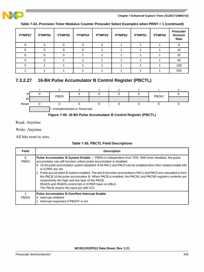
Chapter 7 Enhanced Capture Timer (S12ECT16B8CV2)
MC9S12XDP512 Data Sheet, Rev. 2.21
Freescale Semiconductor 345
7.3.2.27 16-Bit Pulse Accumulator B Control Register (PBCTL)
Read: Anytime
Write: Anytime
All bits reset to zero.
0 0 0 0 0 1 1 1 8
0 0 0 0 1 1 1 1 16
0 0 0 1 1 1 1 1 32
0 0 1 1 1 1 1 1 64
0 1 1 1 1 1 1 1 128
1 1 1 1 1 1 1 1 256
7 6 5 4 3 2 1 0
R 0PBEN
0 0 0 0PBOVI
0
W
Reset 0 0 0 0 0 0 0 0
= Unimplemented or Reserved
Figure 7-49. 16-Bit Pulse Accumulator B Control Register (PBCTL)
Table 7-35. PBCTL Field Descriptions
Field Description
6PBEN
Pulse Accumulator B System Enable — PBEN is independent from TEN. With timer disabled, the pulseaccumulator can still function unless pulse accumulator is disabled.0 16-bit pulse accumulator system disabled. 8-bit PAC1 and PAC0 can be enabled when their related enable bits
in ICPAR are set.1 Pulse accumulator B system enabled. The two 8-bit pulse accumulators PAC1 and PAC0 are cascaded to form
the PACB 16-bit pulse accumulator B. When PACB is enabled, the PACN1 and PACN0 registers contents arerespectively the high and low byte of the PACB.PA1EN and PA0EN control bits in ICPAR have no effect.The PACB shares the input pin with IC0.
1PBOVI
Pulse Accumulator B Overflow Interrupt Enable0 Interrupt inhibited1 Interrupt requested if PBOVF is set
Table 7-34. Precision Timer Modulus Counter Prescaler Select Examples when PRNT = 1 (continued)
PTMPS7 PTMPS6 PTMPS5 PTMPS4 PTMPS3 PTMPS2 PTMPS1 PTMPS0PrescalerDivision
Rate

Chapter 7 Enhanced Capture Timer (S12ECT16B8CV2)
MC9S12XDP512 Data Sheet, Rev. 2.21
346 Freescale Semiconductor
7.3.2.28 Pulse Accumulator B Flag Register (PBFLG)
Read: Anytime
Write used in the flag clearing mechanism. Writing a one to the flag clears the flag. Writing a zero will notaffect the current status of the bit.
NOTEWhen TFFCA = 1, the flag cannot be cleared via the normal flag clearingmechanism (writing a one to the flag). Reference Section 7.3.2.6, “TimerSystem Control Register 1 (TSCR1)”.
All bits reset to zero.
PBFLG indicates when interrupt conditions have occurred. The flag can be cleared via the normal flagclearing mechanism (writing a one to the flag) or via the fast flag clearing mechanism (Reference TFFCAbit in Section 7.3.2.6, “Timer System Control Register 1 (TSCR1)”).
7 6 5 4 3 2 1 0
R 0 0 0 0 0 0PBOVF
0
W
Reset 0 0 0 0 0 0 0 0
= Unimplemented or Reserved
Figure 7-50. Pulse Accumulator B Flag Register (PBFLG)
Table 7-36. PBFLG Field Descriptions
Field Description
1PBOVF
Pulse Accumulator B Overflow Flag — This bit is set when the 16-bit pulse accumulator B overflows from0xFFFF to 0x0000, or when 8-bit pulse accumulator 1 (PAC1) overflows from 0x00FF to 0x0000.
When PACMX = 1, PBOVF bit can also be set if 8-bit pulse accumulator 1 (PAC1) reaches 0x00FF and an activeedge follows on PT1.

Chapter 7 Enhanced Capture Timer (S12ECT16B8CV2)
MC9S12XDP512 Data Sheet, Rev. 2.21
Freescale Semiconductor 347
7.3.2.29 8-Bit Pulse Accumulators Holding Registers (PA3H–PA0H)
Read: Anytime.
Write: Has no effect.
All bits reset to zero.
These registers are used to latch the value of the corresponding pulse accumulator when the related bits inregister ICPAR are enabled (see Section 7.4.1.3, “Pulse Accumulators”).
7 6 5 4 3 2 1 0
R PA3H7 PA3H6 PA3H5 PA3H4 PA3H3 PA3H2 PA3H1 PA3H0
W
Reset 0 0 0 0 0 0 0 0
= Unimplemented or Reserved
Figure 7-51. 8-Bit Pulse Accumulators Holding Register 3 (PA3H)
7 6 5 4 3 2 1 0
R PA2H7 PA2H6 PA2H5 PA2H4 PA2H3 PA2H2 PA2H1 PA2H0
W
Reset 0 0 0 0 0 0 0 0
= Unimplemented or Reserved
Figure 7-52. 8-Bit Pulse Accumulators Holding Register 2 (PA2H)
7 6 5 4 3 2 1 0
R PA1H7 PA1H6 PA1H5 PA1H4 PA1H3 PA1H2 PA1H1 PA1H0
W
Reset 0 0 0 0 0 0 0 0
= Unimplemented or Reserved
Figure 7-53. 8-Bit Pulse Accumulators Holding Register 1 (PA1H)
7 6 5 4 3 2 1 0
R PA0H7 PA0H6 PA0H5 PA0H4 PA0H3 PA0H2 PA0H1 PA0H0
W
Reset 0 0 0 0 0 0 0 0
= Unimplemented or Reserved
Figure 7-54. 8-Bit Pulse Accumulators Holding Register 0 (PA0H)

Chapter 7 Enhanced Capture Timer (S12ECT16B8CV2)
MC9S12XDP512 Data Sheet, Rev. 2.21
348 Freescale Semiconductor
7.3.2.30 Modulus Down-Counter Count Register (MCCNT)
Read: Anytime
Write: Anytime.
All bits reset to one.
A full access for the counter register will take place in one clock cycle.
NOTEA separate read/write for high byte and low byte will give different resultsthan accessing them as a word.
If the RDMCL bit in MCCTL register is cleared, reads of the MCCNT register will return the present valueof the count register. If the RDMCL bit is set, reads of the MCCNT will return the contents of the loadregister.
If a 0x0000 is written into MCCNT when LATQ and BUFEN in ICSYS register are set, the input captureand pulse accumulator registers will be latched.
With a 0x0000 write to the MCCNT, the modulus counter will stay at zero and does not set the MCZF flagin MCFLG register.
If the modulus down counter is enabled (MCEN = 1) and modulus mode is enabled (MODMC = 1), a writeto MCCNT will update the load register with the value written to it. The count register will not be updatedwith the new value until the next counter underflow.
If modulus mode is not enabled (MODMC = 0), a write to MCCNT will clear the modulus prescaler andwill immediately update the counter register with the value written to it and down-counts to 0x0000 andstops.
The FLMC bit in MCCTL can be used to immediately update the count register with the new value if animmediate load is desired.
15 14 13 12 11 10 9 8
RMCCNT15 MCCNT14 MCCNT13 MCCNT12 MCCNT11 MCCNT10 MCCNT9 MCCNT8
W
Reset 1 1 1 1 1 1 1 1
Figure 7-55. Modulus Down-Counter Count Register High (MCCNT)
7 6 5 4 3 2 1 0
RMCCNT7 MCCNT6 MCCNT5 MCCNT4 MCCNT3 MCCNT2 MCCNT1 MCCNT9
W
Reset 1 1 1 1 1 1 1 1
Figure 7-56. Modulus Down-Counter Count Register Low (MCCNT)
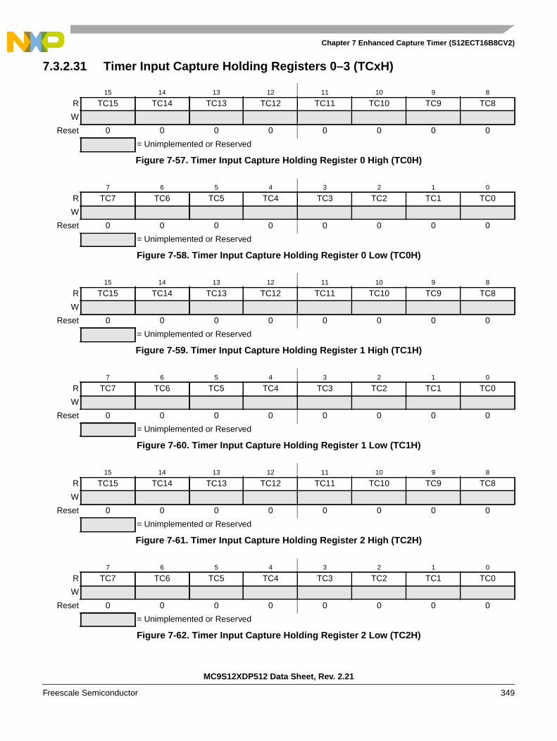
Chapter 7 Enhanced Capture Timer (S12ECT16B8CV2)
MC9S12XDP512 Data Sheet, Rev. 2.21
Freescale Semiconductor 349
7.3.2.31 Timer Input Capture Holding Registers 0–3 (TCxH)
15 14 13 12 11 10 9 8
R TC15 TC14 TC13 TC12 TC11 TC10 TC9 TC8
W
Reset 0 0 0 0 0 0 0 0
= Unimplemented or Reserved
Figure 7-57. Timer Input Capture Holding Register 0 High (TC0H)
7 6 5 4 3 2 1 0
R TC7 TC6 TC5 TC4 TC3 TC2 TC1 TC0
W
Reset 0 0 0 0 0 0 0 0
= Unimplemented or Reserved
Figure 7-58. Timer Input Capture Holding Register 0 Low (TC0H)
15 14 13 12 11 10 9 8
R TC15 TC14 TC13 TC12 TC11 TC10 TC9 TC8
W
Reset 0 0 0 0 0 0 0 0
= Unimplemented or Reserved
Figure 7-59. Timer Input Capture Holding Register 1 High (TC1H)
7 6 5 4 3 2 1 0
R TC7 TC6 TC5 TC4 TC3 TC2 TC1 TC0
W
Reset 0 0 0 0 0 0 0 0
= Unimplemented or Reserved
Figure 7-60. Timer Input Capture Holding Register 1 Low (TC1H)
15 14 13 12 11 10 9 8
R TC15 TC14 TC13 TC12 TC11 TC10 TC9 TC8
W
Reset 0 0 0 0 0 0 0 0
= Unimplemented or Reserved
Figure 7-61. Timer Input Capture Holding Register 2 High (TC2H)
7 6 5 4 3 2 1 0
R TC7 TC6 TC5 TC4 TC3 TC2 TC1 TC0
W
Reset 0 0 0 0 0 0 0 0
= Unimplemented or Reserved
Figure 7-62. Timer Input Capture Holding Register 2 Low (TC2H)
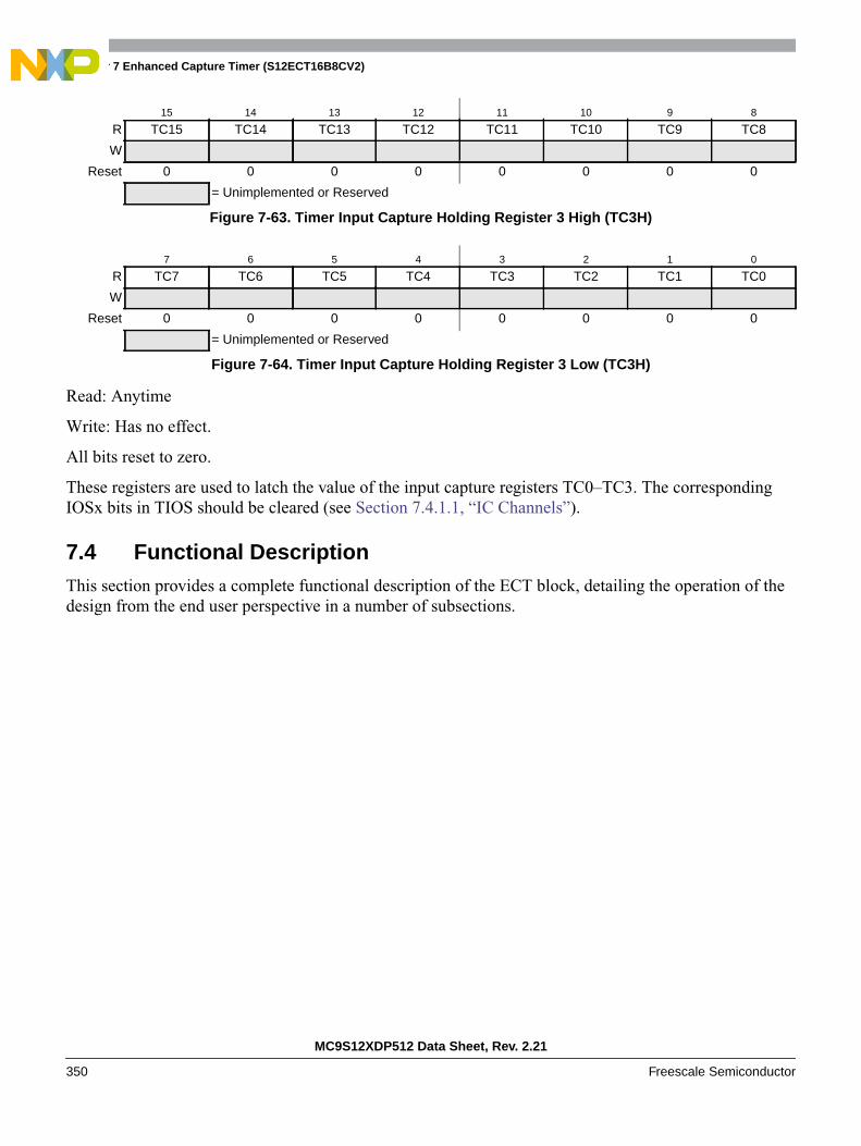
Chapter 7 Enhanced Capture Timer (S12ECT16B8CV2)
MC9S12XDP512 Data Sheet, Rev. 2.21
350 Freescale Semiconductor
Read: Anytime
Write: Has no effect.
All bits reset to zero.
These registers are used to latch the value of the input capture registers TC0–TC3. The correspondingIOSx bits in TIOS should be cleared (see Section 7.4.1.1, “IC Channels”).
7.4 Functional DescriptionThis section provides a complete functional description of the ECT block, detailing the operation of thedesign from the end user perspective in a number of subsections.
15 14 13 12 11 10 9 8
R TC15 TC14 TC13 TC12 TC11 TC10 TC9 TC8
W
Reset 0 0 0 0 0 0 0 0
= Unimplemented or Reserved
Figure 7-63. Timer Input Capture Holding Register 3 High (TC3H)
7 6 5 4 3 2 1 0
R TC7 TC6 TC5 TC4 TC3 TC2 TC1 TC0
W
Reset 0 0 0 0 0 0 0 0
= Unimplemented or Reserved
Figure 7-64. Timer Input Capture Holding Register 3 Low (TC3H)

Chapter 7 Enhanced Capture Timer (S12ECT16B8CV2)
MC9S12XDP512 Data Sheet, Rev. 2.21
Freescale Semiconductor 351
Figure 7-65. Detailed Timer Block Diagram in Latch Mode when PRNT = 0
16 BIT MAIN TIMER
P1
Comparator
TC0H Hold Reg.
P0
P3
P2
P4
P5
P6
P7
EDG0
EDG1
EDG2
EDG3
MUX
Modulus PrescalerBus Clock
16-Bit Load Register
16-Bit Modulus
0 RESET
EDG0
EDG1
EDG2
EDG4
EDG5
EDG3
EDG6
EDG7
÷ 1, 4, 8, 16
16-Bit Free-Running
LAT
CH
Und
erflo
w
Main Timer
Timer Prescaler
TC0 Capture/Compare Reg.
Comparator
TC1 Capture/Compare Reg.
Comparator
TC2 Capture/Compare Reg.
Comparator
TC3 Capture/Compare Reg.
Comparator
TC4 Capture/Compare Reg.
Comparator
TC5 Capture/Compare Reg.
Comparator
TC6 Capture/Compare Reg.
Comparator
TC7 Capture/Compare Reg.
Pin Logic
Pin Logic
Pin Logic
Pin Logic
Pin Logic
Pin Logic
Pin Logic
Pin Logic
Delay
TC1H Hold Reg.
TC2H Hold Reg.
TC3H Hold Reg.
MUX
MUX
MUX
PA0H Hold Reg.
PAC0
0 RESET
PA1H Hold Reg.
PAC1
0 RESET
PA2H Hold Reg.
PAC2
0 RESET
PA3H Hold Reg.
PAC3
Write 0x0000to Modulus Counter
ICLAT, LATQ, BUFEN(Force Latch)
LATQ(MDC Latch Enable)
Down Counter
SH04
SH15
SH26
SH37
Bus Clock
÷ 1, 2, ..., 128
Counter
DelayCounter
DelayCounter
DelayCounter
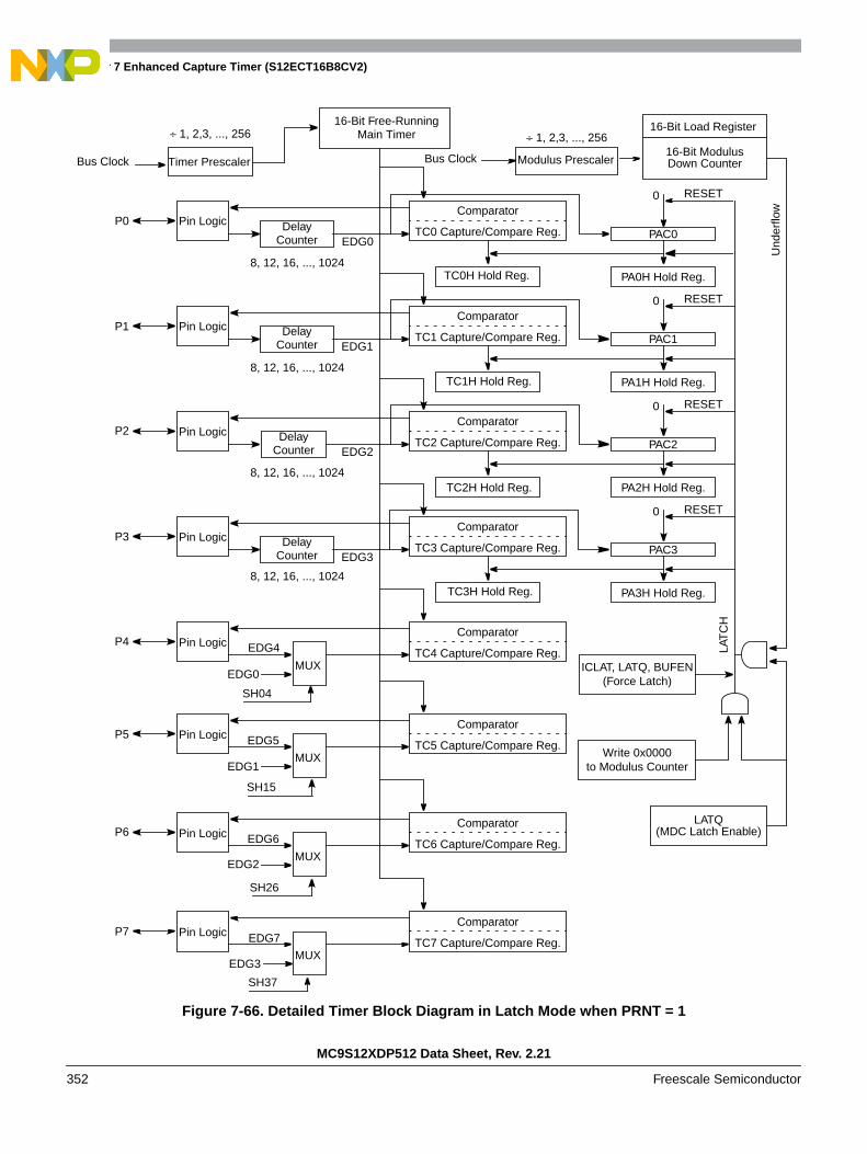
Chapter 7 Enhanced Capture Timer (S12ECT16B8CV2)
MC9S12XDP512 Data Sheet, Rev. 2.21
352 Freescale Semiconductor
Figure 7-66. Detailed Timer Block Diagram in Latch Mode when PRNT = 1
16 BIT MAIN TIMER
P1
Comparator
TC0H Hold Reg.
P0
P3
P2
P4
P5
P6
P7
EDG0
EDG1
EDG2
EDG3
MUX
Modulus PrescalerBus Clock
16-Bit Load Register
16-Bit Modulus
0 RESET
EDG0
EDG1
EDG2
EDG4
EDG5
EDG3
EDG6
EDG7
÷ 1, 2,3, ..., 25616-Bit Free-Running
LAT
CH
Und
erflo
w
Main Timer
Timer Prescaler
TC0 Capture/Compare Reg.
Comparator
TC1 Capture/Compare Reg.
Comparator
TC2 Capture/Compare Reg.
Comparator
TC3 Capture/Compare Reg.
Comparator
TC4 Capture/Compare Reg.
Comparator
TC5 Capture/Compare Reg.
Comparator
TC6 Capture/Compare Reg.
Comparator
TC7 Capture/Compare Reg.
Pin Logic
Pin Logic
Pin Logic
Pin Logic
Pin Logic
Pin Logic
Pin Logic
Pin Logic
Delay
TC1H Hold Reg.
TC2H Hold Reg.
TC3H Hold Reg.
MUX
MUX
MUX
PA0H Hold Reg.
PAC0
0 RESET
PA1H Hold Reg.
PAC1
0 RESET
PA2H Hold Reg.
PAC2
0 RESET
PA3H Hold Reg.
PAC3
Write 0x0000to Modulus Counter
ICLAT, LATQ, BUFEN(Force Latch)
LATQ(MDC Latch Enable)
Down Counter
SH04
SH15
SH26
SH37
Bus Clock
÷ 1, 2,3, ..., 256
Counter
DelayCounter
DelayCounter
DelayCounter
8, 12, 16, ..., 1024
8, 12, 16, ..., 1024
8, 12, 16, ..., 1024
8, 12, 16, ..., 1024

Chapter 7 Enhanced Capture Timer (S12ECT16B8CV2)
MC9S12XDP512 Data Sheet, Rev. 2.21
Freescale Semiconductor 353
Figure 7-67. Detailed Timer Block Diagram in Queue Mode when PRNT = 0
16 BIT MAIN TIMER
P1
TC0H Hold Reg.
P0
P3
P2
P4
P5
P6
P7
EDG0
EDG1
EDG2
EDG3
MUX
Bus Clock
16-Bit Load Register
16-Bit Modulus
0 RESET
EDG0
EDG1
EDG2
EDG4
EDG5
EDG3
EDG6
EDG7
÷1, 2, ..., 128
÷ 1, 4, 8, 16
LAT
CH
0
Pin Logic
Pin Logic
Pin Logic
Pin Logic
Pin Logic
Pin Logic
Pin Logic
Pin Logic
Bus Clock
TC1H Hold Reg.
TC2H Hold Reg.
TC3H Hold Reg.
MUX
MUX
MUX
PA0H Hold Reg.
PAC0
0 RESET
PA1H Hold Reg.
PAC1
0 RESET
PA2H Hold Reg.
PAC2
0 RESET
PA3H Hold Reg.
PAC3
LAT
CH
1
LAT
CH
3LA
TC
H2
LATQ, BUFEN(Queue Mode)
Read TC3HHold Reg.
Read TC2HHold Reg.
Read TC1HHold Reg.
Read TC0HHold Reg.
Down Counter
SH04
SH15
SH26
SH37
TimerPrescaler
16-Bit Free-RunningMain Timer
DelayCounter
DelayCounter
DelayCounter
DelayCounter
ModulusPrescaler
Comparator
TC0 Capture/Compare Reg.
Comparator
TC1 Capture/Compare Reg.
Comparator
TC2 Capture/Compare Reg.
Comparator
TC3 Capture/Compare Reg.
Comparator
TC4 Capture/Compare Reg.
Comparator
TC5 Capture/Compare Reg.
Comparator
TC6 Capture/Compare Reg.
Comparator
TC7 Capture/Compare Reg.

Chapter 7 Enhanced Capture Timer (S12ECT16B8CV2)
MC9S12XDP512 Data Sheet, Rev. 2.21
354 Freescale Semiconductor
Figure 7-68. Detailed Timer Block Diagram in Queue Mode when PRNT = 1
16 BIT MAIN TIMER
P1
TC0H Hold Reg.
P0
P3
P2
P4
P5
P6
P7
EDG0
EDG1
EDG2
EDG3
MUX
Bus Clock
16-Bit Load Register
16-Bit Modulus
0 RESET
EDG0
EDG1
EDG2
EDG4
EDG5
EDG3
EDG6
EDG7
÷1, 2, 3, ... 256
÷ 1, 2, 3, ... 256
LAT
CH
0
Pin Logic
Pin Logic
Pin Logic
Pin Logic
Pin Logic
Pin Logic
Pin Logic
Pin Logic
Bus Clock
TC1H Hold Reg.
TC2H Hold Reg.
TC3H Hold Reg.
MUX
MUX
MUX
PA0H Hold Reg.
PAC0
0 RESET
PA1H Hold Reg.
PAC1
0 RESET
PA2H Hold Reg.
PAC2
0 RESET
PA3H Hold Reg.
PAC3
LAT
CH
1
LAT
CH
3LA
TC
H2
LATQ, BUFEN(Queue Mode)
Read TC3HHold Reg.
Read TC2HHold Reg.
Read TC1HHold Reg.
Read TC0HHold Reg.
Down Counter
SH04
SH15
SH26
SH37
TimerPrescaler
16-Bit Free-RunningMain Timer
DelayCounter
DelayCounter
DelayCounter
DelayCounter
ModulusPrescaler
Comparator
TC0 Capture/Compare Reg.
Comparator
TC1 Capture/Compare Reg.
Comparator
TC2 Capture/Compare Reg.
Comparator
TC3 Capture/Compare Reg.
Comparator
TC4 Capture/Compare Reg.
Comparator
TC5 Capture/Compare Reg.
Comparator
TC6 Capture/Compare Reg.
Comparator
TC7 Capture/Compare Reg.
8, 12, 16, ... 1024
8, 12, 16, ... 1024
8, 12, 16, ... 1024
8, 12, 16, ... 1024
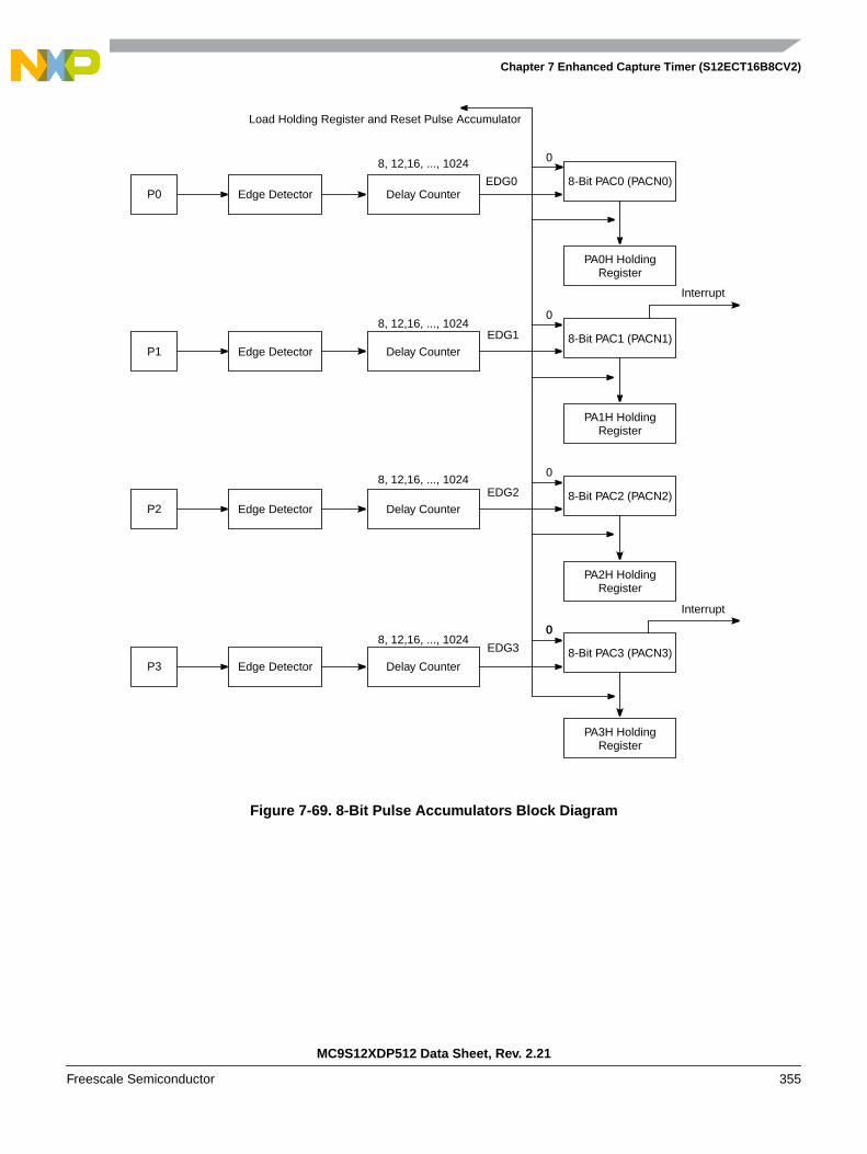
Chapter 7 Enhanced Capture Timer (S12ECT16B8CV2)
MC9S12XDP512 Data Sheet, Rev. 2.21
Freescale Semiconductor 355
Figure 7-69. 8-Bit Pulse Accumulators Block Diagram
P0
Load Holding Register and Reset Pulse Accumulator
0
0
EDG3
EDG2
EDG1
EDG0Edge Detector Delay Counter
Interrupt
Interrupt
P1 Edge Detector Delay Counter
P2 Edge Detector Delay Counter
P3 Edge Detector Delay Counter
PA0H Holding
0
8-Bit PAC1 (PACN1)
0
8-Bit PAC2 (PACN2)
PA2H Holding
0
8-Bit PAC3 (PACN3)
PA3H Holding
8-Bit PAC0 (PACN0)
8, 12,16, ..., 1024
8, 12,16, ..., 1024
8, 12,16, ..., 1024
8, 12,16, ..., 1024
Register
PA1H HoldingRegister
Register
Register
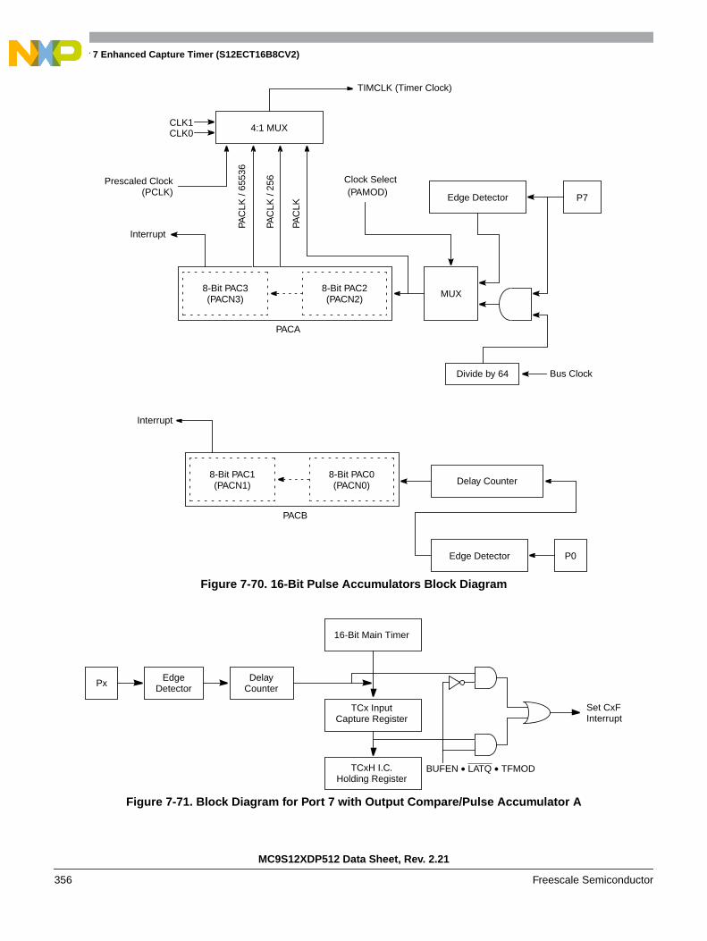
Chapter 7 Enhanced Capture Timer (S12ECT16B8CV2)
MC9S12XDP512 Data Sheet, Rev. 2.21
356 Freescale Semiconductor
Figure 7-70. 16-Bit Pulse Accumulators Block Diagram
Figure 7-71. Block Diagram for Port 7 with Output Compare/Pulse Accumulator A
Edge Detector P7
P0
Bus ClockDivide by 64
Clock Select
CLK0CLK1 4:1 MUX
TIMCLK (Timer Clock)
PAC
LK
PAC
LK /
256
PAC
LK /
6553
6
Prescaled Clock(PCLK)
Interrupt
MUX
(PAMOD)
Edge Detector
PACA
Delay Counter
Interrupt
PACB
8-Bit PAC3(PACN3)
8-Bit PAC2(PACN2)
8-Bit PAC1(PACN1)
8-Bit PAC0(PACN0)
PxEdge Delay
16-Bit Main Timer
TCx Input
TCxH I.C. BUFEN • LATQ • TFMOD
Set CxF
Detector Counter
Capture Register
Holding Register
Interrupt

Chapter 7 Enhanced Capture Timer (S12ECT16B8CV2)
MC9S12XDP512 Data Sheet, Rev. 2.21
Freescale Semiconductor 357
7.4.1 Enhanced Capture Timer Modes of Operation
The enhanced capture timer has 8 input capture, output compare (IC/OC) channels, same as on the HC12standard timer (timer channels TC0 to TC7). When channels are selected as input capture by selecting theIOSx bit in TIOS register, they are called input capture (IC) channels.
Four IC channels (channels 7–4) are the same as on the standard timer with one capture register each thatmemorizes the timer value captured by an action on the associated input pin.
Four other IC channels (channels 3–0), in addition to the capture register, also have one buffer each calleda holding register. This allows two different timer values to be saved without generating any interrupts.
Four 8-bit pulse accumulators are associated with the four buffered IC channels (channels 3–0). Each pulseaccumulator has a holding register to memorize their value by an action on its external input. Each pair ofpulse accumulators can be used as a 16-bit pulse accumulator.
The 16-bit modulus down-counter can control the transfer of the IC registers and the pulse accumulatorscontents to the respective holding registers for a given period, every time the count reaches zero.
The modulus down-counter can also be used as a stand-alone time base with periodic interrupt capability.
7.4.1.1 IC Channels
The IC channels are composed of four standard IC registers and four buffered IC channels.
• An IC register is empty when it has been read or latched into the holding register.
• A holding register is empty when it has been read.
7.4.1.1.1 Non-Buffered IC Channels
The main timer value is memorized in the IC register by a valid input pin transition. If the correspondingNOVWx bit of the ICOVW register is cleared, with a new occurrence of a capture, the contents of ICregister are overwritten by the new value. If the corresponding NOVWx bit of the ICOVW register is set,the capture register cannot be written unless it is empty. This will prevent the captured value from beingoverwritten until it is read.
7.4.1.1.2 Buffered IC Channels
There are two modes of operations for the buffered IC channels:
1. IC latch mode (LATQ = 1)
The main timer value is memorized in the IC register by a valid input pin transition (see Figure 7-65and Figure 7-66).
The value of the buffered IC register is latched to its holding register by the modulus counter for agiven period when the count reaches zero, by a write 0x0000 to the modulus counter or by a writeto ICLAT in the MCCTL register.
If the corresponding NOVWx bit of the ICOVW register is cleared, with a new occurrence of acapture, the contents of IC register are overwritten by the new value. In case of latching, thecontents of its holding register are overwritten.
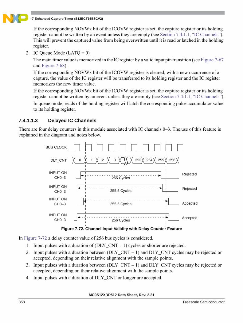
Chapter 7 Enhanced Capture Timer (S12ECT16B8CV2)
MC9S12XDP512 Data Sheet, Rev. 2.21
358 Freescale Semiconductor
If the corresponding NOVWx bit of the ICOVW register is set, the capture register or its holdingregister cannot be written by an event unless they are empty (see Section 7.4.1.1, “IC Channels”).This will prevent the captured value from being overwritten until it is read or latched in the holdingregister.
2. IC Queue Mode (LATQ = 0)
The main timer value is memorized in the IC register by a valid input pin transition (see Figure 7-67and Figure 7-68).
If the corresponding NOVWx bit of the ICOVW register is cleared, with a new occurrence of acapture, the value of the IC register will be transferred to its holding register and the IC registermemorizes the new timer value.
If the corresponding NOVWx bit of the ICOVW register is set, the capture register or its holdingregister cannot be written by an event unless they are empty (see Section 7.4.1.1, “IC Channels”).
In queue mode, reads of the holding register will latch the corresponding pulse accumulator valueto its holding register.
7.4.1.1.3 Delayed IC Channels
There are four delay counters in this module associated with IC channels 0–3. The use of this feature isexplained in the diagram and notes below.
Figure 7-72. Channel Input Validity with Delay Counter Feature
In Figure 7-72 a delay counter value of 256 bus cycles is considered.
1. Input pulses with a duration of (DLY_CNT – 1) cycles or shorter are rejected.
2. Input pulses with a duration between (DLY_CNT – 1) and DLY_CNT cycles may be rejected oraccepted, depending on their relative alignment with the sample points.
3. Input pulses with a duration between (DLY_CNT – 1) and DLY_CNT cycles may be rejected oraccepted, depending on their relative alignment with the sample points.
4. Input pulses with a duration of DLY_CNT or longer are accepted.
1 2 3 253 254 255 256
BUS CLOCK
DLY_CNT
INPUT ONCH0–3
Rejected
AcceptedINPUT ON
CH0–3
INPUT ONCH0–3 Accepted
INPUT ONCH0–3
Rejected
0
255 Cycles
255.5 Cycles
255.5 Cycles
256 Cycles
Chapter 7 Enhanced Capture Timer (S12ECT16B8CV2)
MC9S12XDP512 Data Sheet, Rev. 2.21
Freescale Semiconductor 359
7.4.1.2 OC Channel Initialization
Internal register whose output drives OCx when TIOS is set, can be force loaded with a desired data bywriting to CFORC register before OCx is configured for output compare action. This allows a glitch freeswitch over of port from general purpose I/O to timer output once the output compare is enabled.
7.4.1.3 Pulse Accumulators
There are four 8-bit pulse accumulators with four 8-bit holding registers associated with the four ICbuffered channels 3–0. A pulse accumulator counts the number of active edges at the input of its channel.
The minimum pulse width for the PAI input is greater than two bus clocks.The maximum input frequencyon the pulse accumulator channel is one half the bus frequency or Eclk.
The user can prevent the 8-bit pulse accumulators from counting further than 0x00FF by utilizing thePACMX control bit in the ICSYS register. In this case, a value of 0x00FF means that 255 counts or morehave occurred.
Each pair of pulse accumulators can be used as a 16-bit pulse accumulator (see Figure 7-70).
Pulse accumulator B operates only as an event counter, it does not feature gated time accumulationmode.The edge control for pulse accumulator B as a 16-bit pulse accumulator is defined by TCTL4[1:0].
To operate the 16-bit pulse accumulators A and B (PACA and PACB) independently of input capture oroutput compare 7 and 0 respectively, the user must set the corresponding bits: IOSx = 1, OMx = 0, andOLx = 0. OC7M7 or OC7M0 in the OC7M register must also be cleared.
There are two modes of operation for the pulse accumulators:
• Pulse accumulator latch mode
The value of the pulse accumulator is transferred to its holding register when the modulusdown-counter reaches zero, a write 0x0000 to the modulus counter or when the force latch controlbit ICLAT is written.
At the same time the pulse accumulator is cleared.
• Pulse accumulator queue mode
When queue mode is enabled, reads of an input capture holding register will transfer the contentsof the associated pulse accumulator to its holding register.
At the same time the pulse accumulator is cleared.
7.4.1.4 Modulus Down-Counter
The modulus down-counter can be used as a time base to generate a periodic interrupt. It can also be usedto latch the values of the IC registers and the pulse accumulators to their holding registers.
The action of latching can be programmed to be periodic or only once.
Chapter 7 Enhanced Capture Timer (S12ECT16B8CV2)
MC9S12XDP512 Data Sheet, Rev. 2.21
360 Freescale Semiconductor
7.4.1.5 Precision Timer
By enabling the PRNT bit of the TSCR1 register, the performance of the timer can be enhanced. In thiscase, it is possible to set additional prescaler settings for the main timer counter and modulus down counterand enhance delay counter settings compared to the settings in the present ECT timer.
7.4.1.6 Flag Clearing Mechanisms
The flags in the ECT can be cleared one of two ways:
1. Normal flag clearing mechanism (TFFCA = 0)
Any of the ECT flags can be cleared by writing a one to the flag.
2. Fast flag clearing mechanism (TFFCA = 1)
With the timer fast flag clear all (TFFCA) enabled, the ECT flags can only be cleared by accessingthe various registers associated with the ECT modes of operation as described below. The flagscannot be cleared via the normal flag clearing mechanism. This fast flag clearing mechanism hasthe advantage of eliminating the software overhead required by a separate clear sequence. Extracare must be taken to avoid accidental flag clearing due to unintended accesses.
— Input capture
A read from an input capture channel register causes the corresponding channel flag, CxF, tobe cleared in the TFLG1 register.
— Output compare
A write to the output compare channel register causes the corresponding channel flag, CxF, tobe cleared in the TFLG1 register.
— Timer counter
Any access to the TCNT register clears the TOF flag in the TFLG2 register.
— Pulse accumulator A
Any access to the PACN3 and PACN2 registers clears the PAOVF and PAIF flags in thePAFLG register.
— Pulse accumulator B
Any access to the PACN1 and PACN0 registers clears the PBOVF flag in the PBFLG register.
— Modulus down counter
Any access to the MCCNT register clears the MCZF flag in the MCFLG register.
7.4.2 Reset
The reset state of each individual bit is listed within the register description section (Section 7.3, “MemoryMap and Register Definition”) which details the registers and their bit-fields.
Chapter 7 Enhanced Capture Timer (S12ECT16B8CV2)
MC9S12XDP512 Data Sheet, Rev. 2.21
Freescale Semiconductor 361
7.4.3 Interrupts
This section describes interrupts originated by the ECT block. The MCU must service the interruptrequests. Table 7-37 lists the interrupts generated by the ECT to communicate with the MCU.
Table 7-37. ECT Interrupts
The ECT only originates interrupt requests. The following is a description of how the module makes arequest and how the MCU should acknowledge that request. The interrupt vector offset and interruptnumber are chip dependent.
7.4.3.1 Channel [7:0] Interrupt
This active high output will be asserted by the module to request a timer channel 7–0 interrupt to beserviced by the system controller.
7.4.3.2 Modulus Counter Interrupt
This active high output will be asserted by the module to request a modulus counter underflow interruptto be serviced by the system controller.
7.4.3.3 Pulse Accumulator B Overflow Interrupt
This active high output will be asserted by the module to request a timer pulse accumulator B overflowinterrupt to be serviced by the system controller.
7.4.3.4 Pulse Accumulator A Input Interrupt
This active high output will be asserted by the module to request a timer pulse accumulator A inputinterrupt to be serviced by the system controller.
7.4.3.5 Pulse Accumulator A Overflow Interrupt
This active high output will be asserted by the module to request a timer pulse accumulator A overflowinterrupt to be serviced by the system controller.
7.4.3.6 Timer Overflow Interrupt
This active high output will be asserted by the module to request a timer overflow interrupt to be servicedby the system controller.
Interrupt Source Description
Timer channel 7–0 Active high timer channel interrupts 7–0
Modulus counter underflow Active high modulus counter interrupt
Pulse accumulator B overflow Active high pulse accumulator B interrupt
Pulse accumulator A input Active high pulse accumulator A input interrupt
Pulse accumulator A overflow Pulse accumulator overflow interrupt
Timer overflow Timer 0verflow interrupt

Chapter 7 Enhanced Capture Timer (S12ECT16B8CV2)
MC9S12XDP512 Data Sheet, Rev. 2.21
362 Freescale Semiconductor

MC9S12XDP512 Data Sheet, Rev. 2.21
Freescale Semiconductor 363
Chapter 8Pulse-Width Modulator (S12PWM8B8CV1)
8.1 IntroductionThe PWM definition is based on the HC12 PWM definitions. It contains the basic features from the HC11with some of the enhancements incorporated on the HC12: center aligned output mode and four availableclock sources.The PWM module has eight channels with independent control of left and center alignedoutputs on each channel.
Each of the eight channels has a programmable period and duty cycle as well as a dedicated counter. Aflexible clock select scheme allows a total of four different clock sources to be used with the counters. Eachof the modulators can create independent continuous waveforms with software-selectable duty rates from0% to 100%. The PWM outputs can be programmed as left aligned outputs or center aligned outputs.
8.1.1 Features
The PWM block includes these distinctive features:
• Eight independent PWM channels with programmable period and duty cycle
• Dedicated counter for each PWM channel
• Programmable PWM enable/disable for each channel
• Software selection of PWM duty pulse polarity for each channel
• Period and duty cycle are double buffered. Change takes effect when the end of the effective periodis reached (PWM counter reaches zero) or when the channel is disabled.
• Programmable center or left aligned outputs on individual channels
• Eight 8-bit channel or four 16-bit channel PWM resolution
• Four clock sources (A, B, SA, and SB) provide for a wide range of frequencies
• Programmable clock select logic
• Emergency shutdown
8.1.2 Modes of Operation
There is a software programmable option for low power consumption in wait mode that disables the inputclock to the prescaler.
In freeze mode there is a software programmable option to disable the input clock to the prescaler. This isuseful for emulation.
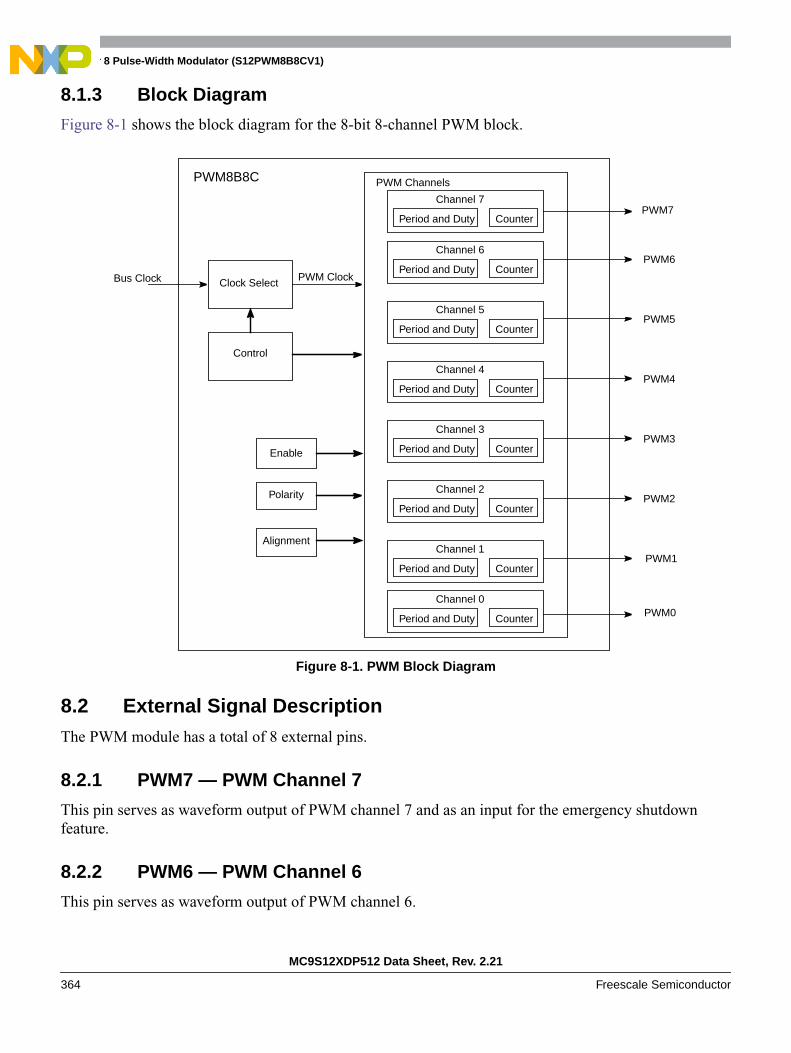
Chapter 8 Pulse-Width Modulator (S12PWM8B8CV1)
MC9S12XDP512 Data Sheet, Rev. 2.21
364 Freescale Semiconductor
8.1.3 Block Diagram
Figure 8-1 shows the block diagram for the 8-bit 8-channel PWM block.
Figure 8-1. PWM Block Diagram
8.2 External Signal DescriptionThe PWM module has a total of 8 external pins.
8.2.1 PWM7 — PWM Channel 7
This pin serves as waveform output of PWM channel 7 and as an input for the emergency shutdownfeature.
8.2.2 PWM6 — PWM Channel 6
This pin serves as waveform output of PWM channel 6.
Period and Duty Counter
Channel 6
Clock Select PWM Clock
Period and Duty Counter
Channel 5
Period and Duty Counter
Channel 4
Period and Duty Counter
Channel 3
Period and Duty Counter
Channel 2
Period and Duty Counter
Channel 1Alignment
Polarity
Control
PWM8B8C
PWM6
PWM5
PWM4
PWM3
PWM2
PWM1
Enable
PWM Channels
Period and Duty Counter
Channel 7
Period and Duty Counter
Channel 0PWM0
PWM7
Bus Clock
Chapter 8 Pulse-Width Modulator (S12PWM8B8CV1)
MC9S12XDP512 Data Sheet, Rev. 2.21
Freescale Semiconductor 365
8.2.3 PWM5 — PWM Channel 5
This pin serves as waveform output of PWM channel 5.
8.2.4 PWM4 — PWM Channel 4
This pin serves as waveform output of PWM channel 4.
8.2.5 PWM3 — PWM Channel 3
This pin serves as waveform output of PWM channel 3.
8.2.6 PWM3 — PWM Channel 2
This pin serves as waveform output of PWM channel 2.
8.2.7 PWM3 — PWM Channel 1
This pin serves as waveform output of PWM channel 1.
8.2.8 PWM3 — PWM Channel 0
This pin serves as waveform output of PWM channel 0.
8.3 Memory Map and Register DefinitionThis section describes in detail all the registers and register bits in the PWM module.
The special-purpose registers and register bit functions that are not normally available to device end users,such as factory test control registers and reserved registers, are clearly identified by means of shading theappropriate portions of address maps and register diagrams. Notes explaining the reasons for restrictingaccess to the registers and functions are also explained in the individual register descriptions.
8.3.1 Module Memory Map
This section describes the content of the registers in the PWM module. The base address of the PWMmodule is determined at the MCU level when the MCU is defined. The register decode map is fixed andbegins at the first address of the module address offset. The figure below shows the registers associatedwith the PWM and their relative offset from the base address. The register detail description follows theorder they appear in the register map.
Reserved bits within a register will always read as 0 and the write will be unimplemented. Unimplementedfunctions are indicated by shading the bit. .
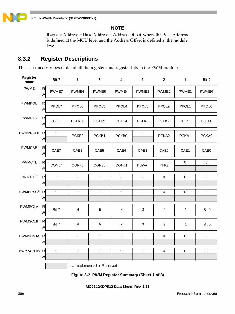
Chapter 8 Pulse-Width Modulator (S12PWM8B8CV1)
MC9S12XDP512 Data Sheet, Rev. 2.21
366 Freescale Semiconductor
NOTERegister Address = Base Address + Address Offset, where the Base Addressis defined at the MCU level and the Address Offset is defined at the modulelevel.
8.3.2 Register Descriptions
This section describes in detail all the registers and register bits in the PWM module.
RegisterName
Bit 7 6 5 4 3 2 1 Bit 0
PWME RPWME7 PWME6 PWME5 PWME4 PWME3 PWME2 PWME1 PWME0
W
PWMPOL RPPOL7 PPOL6 PPOL5 PPOL4 PPOL3 PPOL2 PPOL1 PPOL0
W
PWMCLK RPCLK7 PCLKL6 PCLK5 PCLK4 PCLK3 PCLK2 PCLK1 PCLK0
W
PWMPRCLK R 0PCKB2 PCKB1 PCKB0
0PCKA2 PCKA1 PCKA0
W
PWMCAE RCAE7 CAE6 CAE5 CAE4 CAE3 CAE2 CAE1 CAE0
W
PWMCTL RCON67 CON45 CON23 CON01 PSWAI PFRZ
0 0
W
PWMTST1 R 0 0 0 0 0 0 0 0
W
PWMPRSC1 R 0 0 0 0 0 0 0 0
W
PWMSCLA RBit 7 6 5 4 3 2 1 Bit 0
W
PWMSCLB RBit 7 6 5 4 3 2 1 Bit 0
W
PWMSCNTA1
R 0 0 0 0 0 0 0 0
W
PWMSCNTB1
R 0 0 0 0 0 0 0 0
W
= Unimplemented or Reserved
Figure 8-2. PWM Register Summary (Sheet 1 of 3)
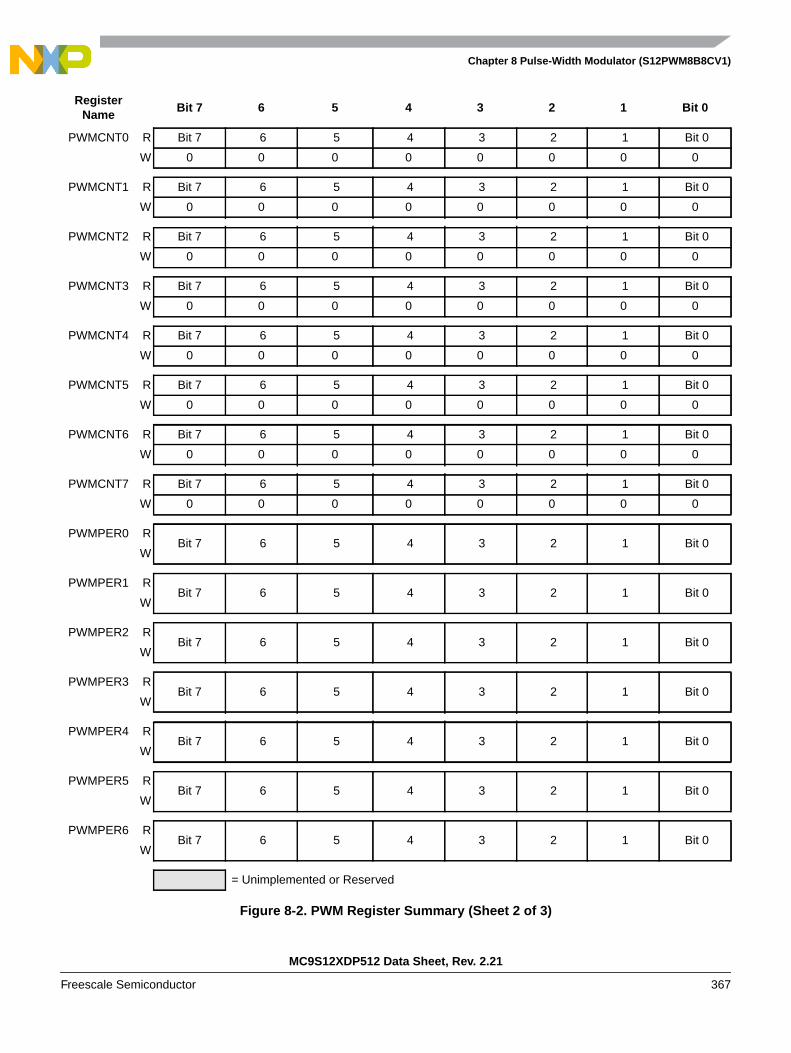
Chapter 8 Pulse-Width Modulator (S12PWM8B8CV1)
MC9S12XDP512 Data Sheet, Rev. 2.21
Freescale Semiconductor 367
PWMCNT0 R Bit 7 6 5 4 3 2 1 Bit 0
W 0 0 0 0 0 0 0 0
PWMCNT1 R Bit 7 6 5 4 3 2 1 Bit 0
W 0 0 0 0 0 0 0 0
PWMCNT2 R Bit 7 6 5 4 3 2 1 Bit 0
W 0 0 0 0 0 0 0 0
PWMCNT3 R Bit 7 6 5 4 3 2 1 Bit 0
W 0 0 0 0 0 0 0 0
PWMCNT4 R Bit 7 6 5 4 3 2 1 Bit 0
W 0 0 0 0 0 0 0 0
PWMCNT5 R Bit 7 6 5 4 3 2 1 Bit 0
W 0 0 0 0 0 0 0 0
PWMCNT6 R Bit 7 6 5 4 3 2 1 Bit 0
W 0 0 0 0 0 0 0 0
PWMCNT7 R Bit 7 6 5 4 3 2 1 Bit 0
W 0 0 0 0 0 0 0 0
PWMPER0 RBit 7 6 5 4 3 2 1 Bit 0
W
PWMPER1 RBit 7 6 5 4 3 2 1 Bit 0
W
PWMPER2 RBit 7 6 5 4 3 2 1 Bit 0
W
PWMPER3 RBit 7 6 5 4 3 2 1 Bit 0
W
PWMPER4 RBit 7 6 5 4 3 2 1 Bit 0
W
PWMPER5 RBit 7 6 5 4 3 2 1 Bit 0
W
PWMPER6 RBit 7 6 5 4 3 2 1 Bit 0
W
RegisterName
Bit 7 6 5 4 3 2 1 Bit 0
= Unimplemented or Reserved
Figure 8-2. PWM Register Summary (Sheet 2 of 3)
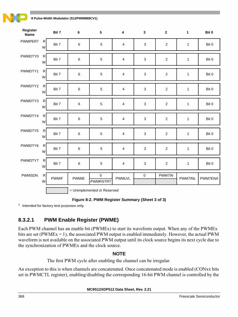
Chapter 8 Pulse-Width Modulator (S12PWM8B8CV1)
MC9S12XDP512 Data Sheet, Rev. 2.21
368 Freescale Semiconductor
8.3.2.1 PWM Enable Register (PWME)
Each PWM channel has an enable bit (PWMEx) to start its waveform output. When any of the PWMExbits are set (PWMEx = 1), the associated PWM output is enabled immediately. However, the actual PWMwaveform is not available on the associated PWM output until its clock source begins its next cycle due tothe synchronization of PWMEx and the clock source.
NOTEThe first PWM cycle after enabling the channel can be irregular.
An exception to this is when channels are concatenated. Once concatenated mode is enabled (CONxx bitsset in PWMCTL register), enabling/disabling the corresponding 16-bit PWM channel is controlled by the
PWMPER7 RBit 7 6 5 4 3 2 1 Bit 0
W
PWMDTY0 RBit 7 6 5 4 3 2 1 Bit 0
W
PWMDTY1 RBit 7 6 5 4 3 2 1 Bit 0
W
PWMDTY2 RBit 7 6 5 4 3 2 1 Bit 0
W
PWMDTY3 RBit 7 6 5 4 3 2 1 Bit 0
W
PWMDTY4 RBit 7 6 5 4 3 2 1 Bit 0
W
PWMDTY5 RBit 7 6 5 4 3 2 1 Bit 0
W
PWMDTY6 RBit 7 6 5 4 3 2 1 Bit 0
W
PWMDTY7 RBit 7 6 5 4 3 2 1 Bit 0
W
PWMSDN RPWMIF PWMIE
0PWMLVL
0 PWM7INPWM7INL PWM7ENA
W PWMRSTRT
1 Intended for factory test purposes only.
RegisterName
Bit 7 6 5 4 3 2 1 Bit 0
= Unimplemented or Reserved
Figure 8-2. PWM Register Summary (Sheet 3 of 3)

Chapter 8 Pulse-Width Modulator (S12PWM8B8CV1)
MC9S12XDP512 Data Sheet, Rev. 2.21
Freescale Semiconductor 369
low order PWMEx bit.In this case, the high order bytes PWMEx bits have no effect and theircorresponding PWM output lines are disabled.
While in run mode, if all eight PWM channels are disabled (PWME7–0 = 0), the prescaler counter shutsoff for power savings.
Read: Anytime
Write: Anytime
7 6 5 4 3 2 1 0
RPWME7 PWME6 PWME5 PWME4 PWME3 PWME2 PWME1 PWME0
W
Reset 0 0 0 0 0 0 0 0
Figure 8-3. PWM Enable Register (PWME)
Table 8-1. PWME Field Descriptions
Field Description
7PWME7
Pulse Width Channel 7 Enable0 Pulse width channel 7 is disabled.1 Pulse width channel 7 is enabled. The pulse modulated signal becomes available at PWM output bit 7 when
its clock source begins its next cycle.
6PWME6
Pulse Width Channel 6 Enable0 Pulse width channel 6 is disabled.1 Pulse width channel 6 is enabled. The pulse modulated signal becomes available at PWM output bit6 when
its clock source begins its next cycle. If CON67=1, then bit has no effect and PWM output line 6 is disabled.
5PWME5
Pulse Width Channel 5 Enable0 Pulse width channel 5 is disabled.1 Pulse width channel 5 is enabled. The pulse modulated signal becomes available at PWM output bit 5 when
its clock source begins its next cycle.
4PWME4
Pulse Width Channel 4 Enable0 Pulse width channel 4 is disabled.1 Pulse width channel 4 is enabled. The pulse modulated signal becomes available at PWM, output bit 4 when
its clock source begins its next cycle. If CON45 = 1, then bit has no effect and PWM output bit4 is disabled.
3PWME3
Pulse Width Channel 3 Enable0 Pulse width channel 3 is disabled.1 Pulse width channel 3 is enabled. The pulse modulated signal becomes available at PWM, output bit 3 when
its clock source begins its next cycle.
2PWME2
Pulse Width Channel 2 Enable0 Pulse width channel 2 is disabled.1 Pulse width channel 2 is enabled. The pulse modulated signal becomes available at PWM, output bit 2 when
its clock source begins its next cycle. If CON23 = 1, then bit has no effect and PWM output bit2 is disabled.
1PWME1
Pulse Width Channel 1 Enable0 Pulse width channel 1 is disabled.1 Pulse width channel 1 is enabled. The pulse modulated signal becomes available at PWM, output bit 1 when
its clock source begins its next cycle.
0PWME0
Pulse Width Channel 0 Enable0 Pulse width channel 0 is disabled.1 Pulse width channel 0 is enabled. The pulse modulated signal becomes available at PWM, output bit 0 when
its clock source begins its next cycle. If CON01 = 1, then bit has no effect and PWM output line0 is disabled.
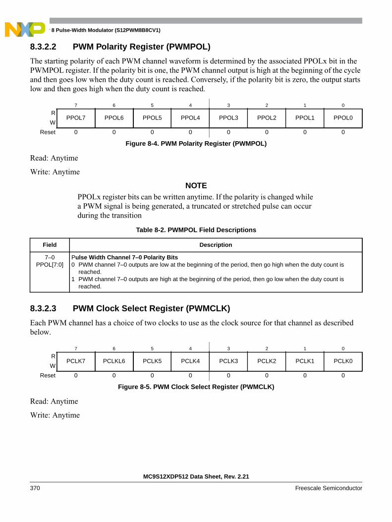
Chapter 8 Pulse-Width Modulator (S12PWM8B8CV1)
MC9S12XDP512 Data Sheet, Rev. 2.21
370 Freescale Semiconductor
8.3.2.2 PWM Polarity Register (PWMPOL)
The starting polarity of each PWM channel waveform is determined by the associated PPOLx bit in thePWMPOL register. If the polarity bit is one, the PWM channel output is high at the beginning of the cycleand then goes low when the duty count is reached. Conversely, if the polarity bit is zero, the output startslow and then goes high when the duty count is reached.
Read: Anytime
Write: Anytime
NOTEPPOLx register bits can be written anytime. If the polarity is changed whilea PWM signal is being generated, a truncated or stretched pulse can occurduring the transition
8.3.2.3 PWM Clock Select Register (PWMCLK)
Each PWM channel has a choice of two clocks to use as the clock source for that channel as describedbelow.
Read: Anytime
Write: Anytime
7 6 5 4 3 2 1 0
RPPOL7 PPOL6 PPOL5 PPOL4 PPOL3 PPOL2 PPOL1 PPOL0
W
Reset 0 0 0 0 0 0 0 0
Figure 8-4. PWM Polarity Register (PWMPOL)
Table 8-2. PWMPOL Field Descriptions
Field Description
7–0PPOL[7:0]
Pulse Width Channel 7–0 Polarity Bits0 PWM channel 7–0 outputs are low at the beginning of the period, then go high when the duty count is
reached.1 PWM channel 7–0 outputs are high at the beginning of the period, then go low when the duty count is
reached.
7 6 5 4 3 2 1 0
RPCLK7 PCLKL6 PCLK5 PCLK4 PCLK3 PCLK2 PCLK1 PCLK0
W
Reset 0 0 0 0 0 0 0 0
Figure 8-5. PWM Clock Select Register (PWMCLK)

Chapter 8 Pulse-Width Modulator (S12PWM8B8CV1)
MC9S12XDP512 Data Sheet, Rev. 2.21
Freescale Semiconductor 371
NOTERegister bits PCLK0 to PCLK7 can be written anytime. If a clock select ischanged while a PWM signal is being generated, a truncated or stretchedpulse can occur during the transition.
8.3.2.4 PWM Prescale Clock Select Register (PWMPRCLK)
This register selects the prescale clock source for clocks A and B independently.
Read: Anytime
Write: Anytime
Table 8-3. PWMCLK Field Descriptions
Field Description
7PCLK7
Pulse Width Channel 7 Clock Select0 Clock B is the clock source for PWM channel 7.1 Clock SB is the clock source for PWM channel 7.
6PCLK6
Pulse Width Channel 6 Clock Select0 Clock B is the clock source for PWM channel 6.1 Clock SB is the clock source for PWM channel 6.
5PCLK5
Pulse Width Channel 5 Clock Select0 Clock A is the clock source for PWM channel 5.1 Clock SA is the clock source for PWM channel 5.
4PCLK4
Pulse Width Channel 4 Clock Select0 Clock A is the clock source for PWM channel 4.1 Clock SA is the clock source for PWM channel 4.
3PCLK3
Pulse Width Channel 3 Clock Select0 Clock B is the clock source for PWM channel 3.1 Clock SB is the clock source for PWM channel 3.
2PCLK2
Pulse Width Channel 2 Clock Select0 Clock B is the clock source for PWM channel 2.1 Clock SB is the clock source for PWM channel 2.
1PCLK1
Pulse Width Channel 1 Clock Select0 Clock A is the clock source for PWM channel 1.1 Clock SA is the clock source for PWM channel 1.
0PCLK0
Pulse Width Channel 0 Clock Select0 Clock A is the clock source for PWM channel 0.1 Clock SA is the clock source for PWM channel 0.
7 6 5 4 3 2 1 0
R 0PCKB2 PCKB1 PCKB0
0PCKA2 PCKA1 PCKA0
W
Reset 0 0 0 0 0 0 0 0
= Unimplemented or Reserved
Figure 8-6. PWM Prescale Clock Select Register (PWMPRCLK)
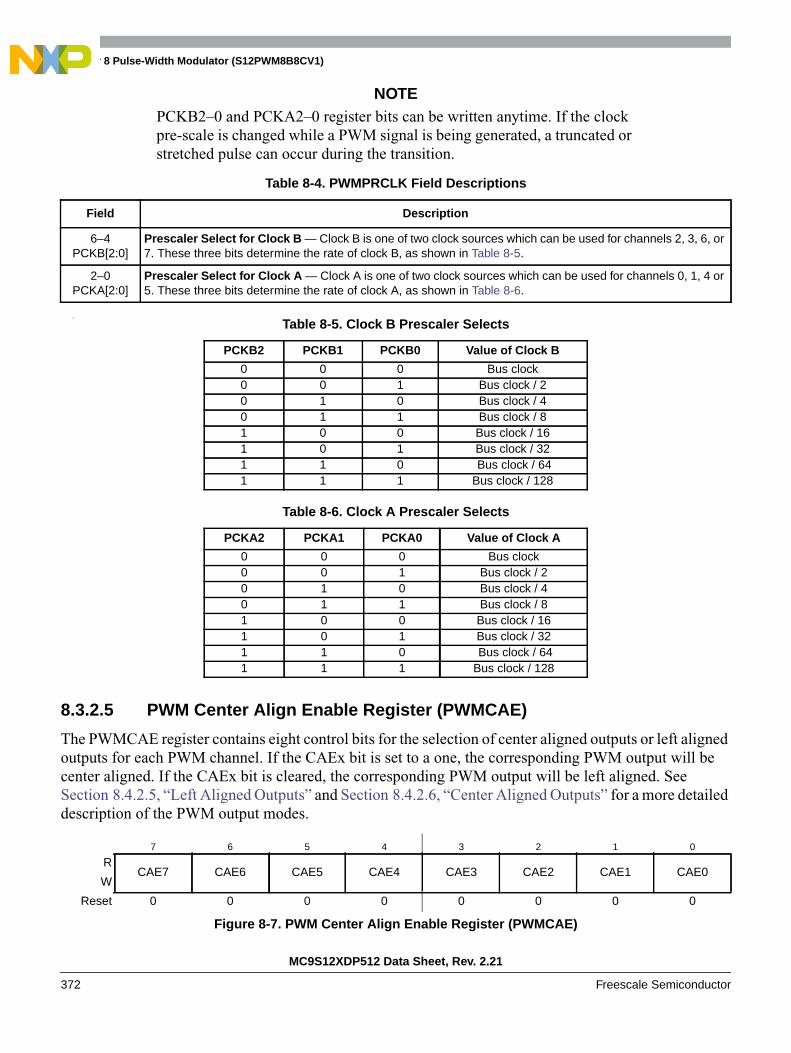
Chapter 8 Pulse-Width Modulator (S12PWM8B8CV1)
MC9S12XDP512 Data Sheet, Rev. 2.21
372 Freescale Semiconductor
NOTEPCKB2–0 and PCKA2–0 register bits can be written anytime. If the clockpre-scale is changed while a PWM signal is being generated, a truncated orstretched pulse can occur during the transition.
s
8.3.2.5 PWM Center Align Enable Register (PWMCAE)
The PWMCAE register contains eight control bits for the selection of center aligned outputs or left alignedoutputs for each PWM channel. If the CAEx bit is set to a one, the corresponding PWM output will becenter aligned. If the CAEx bit is cleared, the corresponding PWM output will be left aligned. SeeSection 8.4.2.5, “Left Aligned Outputs” and Section 8.4.2.6, “Center Aligned Outputs” for a more detaileddescription of the PWM output modes.
Table 8-4. PWMPRCLK Field Descriptions
Field Description
6–4PCKB[2:0]
Prescaler Select for Clock B — Clock B is one of two clock sources which can be used for channels 2, 3, 6, or7. These three bits determine the rate of clock B, as shown in Table 8-5.
2–0PCKA[2:0]
Prescaler Select for Clock A — Clock A is one of two clock sources which can be used for channels 0, 1, 4 or5. These three bits determine the rate of clock A, as shown in Table 8-6.
Table 8-5. Clock B Prescaler Selects
PCKB2 PCKB1 PCKB0 Value of Clock B
0 0 0 Bus clock0 0 1 Bus clock / 20 1 0 Bus clock / 40 1 1 Bus clock / 81 0 0 Bus clock / 161 0 1 Bus clock / 321 1 0 Bus clock / 641 1 1 Bus clock / 128
Table 8-6. Clock A Prescaler Selects
PCKA2 PCKA1 PCKA0 Value of Clock A
0 0 0 Bus clock0 0 1 Bus clock / 20 1 0 Bus clock / 40 1 1 Bus clock / 81 0 0 Bus clock / 161 0 1 Bus clock / 321 1 0 Bus clock / 641 1 1 Bus clock / 128
7 6 5 4 3 2 1 0
RCAE7 CAE6 CAE5 CAE4 CAE3 CAE2 CAE1 CAE0
W
Reset 0 0 0 0 0 0 0 0
Figure 8-7. PWM Center Align Enable Register (PWMCAE)

Chapter 8 Pulse-Width Modulator (S12PWM8B8CV1)
MC9S12XDP512 Data Sheet, Rev. 2.21
Freescale Semiconductor 373
Read: Anytime
Write: Anytime
NOTEWrite these bits only when the corresponding channel is disabled.
8.3.2.6 PWM Control Register (PWMCTL)
The PWMCTL register provides for various control of the PWM module.
Read: Anytime
Write: Anytime
There are three control bits for concatenation, each of which is used to concatenate a pair of PWMchannels into one 16-bit channel. When channels 6 and 7are concatenated, channel 6 registers become thehigh order bytes of the double byte channel. When channels 4 and 5 are concatenated, channel 4 registersbecome the high order bytes of the double byte channel. When channels 2 and 3 are concatenated, channel2 registers become the high order bytes of the double byte channel. When channels 0 and 1 areconcatenated, channel 0 registers become the high order bytes of the double byte channel.
See Section 8.4.2.7, “PWM 16-Bit Functions” for a more detailed description of the concatenation PWMFunction.
NOTEChange these bits only when both corresponding channels are disabled.
Table 8-7. PWMCAE Field Descriptions
Field Description
7–0CAE[7:0]
Center Aligned Output Modes on Channels 7–00 Channels 7–0 operate in left aligned output mode.1 Channels 7–0 operate in center aligned output mode.
7 6 5 4 3 2 1 0
RCON67 CON45 CON23 CON01 PSWAI PFRZ
0 0
W
Reset 0 0 0 0 0 0 0 0
= Unimplemented or Reserved
Figure 8-8. PWM Control Register (PWMCTL)

Chapter 8 Pulse-Width Modulator (S12PWM8B8CV1)
MC9S12XDP512 Data Sheet, Rev. 2.21
374 Freescale Semiconductor
8.3.2.7 Reserved Register (PWMTST)
This register is reserved for factory testing of the PWM module and is not available in normal modes.
Table 8-8. PWMCTL Field Descriptions
Field Description
7CON67
Concatenate Channels 6 and 70 Channels 6 and 7 are separate 8-bit PWMs.1 Channels 6 and 7 are concatenated to create one 16-bit PWM channel. Channel 6 becomes the high order
byte and channel 7 becomes the low order byte. Channel 7 output pin is used as the output for this 16-bitPWM (bit 7 of port PWMP). Channel 7 clock select control-bit determines the clock source, channel 7 polaritybit determines the polarity, channel 7 enable bit enables the output and channel 7 center aligned enable bitdetermines the output mode.
6CON45
Concatenate Channels 4 and 50 Channels 4 and 5 are separate 8-bit PWMs.1 Channels 4 and 5 are concatenated to create one 16-bit PWM channel. Channel 4 becomes the high order
byte and channel 5 becomes the low order byte. Channel 5 output pin is used as the output for this 16-bitPWM (bit 5 of port PWMP). Channel 5 clock select control-bit determines the clock source, channel 5 polaritybit determines the polarity, channel 5 enable bit enables the output and channel 5 center aligned enable bitdetermines the output mode.
5CON23
Concatenate Channels 2 and 30 Channels 2 and 3 are separate 8-bit PWMs.1 Channels 2 and 3 are concatenated to create one 16-bit PWM channel. Channel 2 becomes the high order
byte and channel 3 becomes the low order byte. Channel 3 output pin is used as the output for this 16-bitPWM (bit 3 of port PWMP). Channel 3 clock select control-bit determines the clock source, channel 3 polaritybit determines the polarity, channel 3 enable bit enables the output and channel 3 center aligned enable bitdetermines the output mode.
4CON01
Concatenate Channels 0 and 10 Channels 0 and 1 are separate 8-bit PWMs.1 Channels 0 and 1 are concatenated to create one 16-bit PWM channel. Channel 0 becomes the high order
byte and channel 1 becomes the low order byte. Channel 1 output pin is used as the output for this 16-bitPWM (bit 1 of port PWMP). Channel 1 clock select control-bit determines the clock source, channel 1 polaritybit determines the polarity, channel 1 enable bit enables the output and channel 1 center aligned enable bitdetermines the output mode.
3PSWAI
PWM Stops in Wait Mode — Enabling this bit allows for lower power consumption in wait mode by disablingthe input clock to the prescaler.0 Allow the clock to the prescaler to continue while in wait mode.1 Stop the input clock to the prescaler whenever the MCU is in wait mode.
2PFREZ
PWM Counters Stop in Freeze Mode — In freeze mode, there is an option to disable the input clock to theprescaler by setting the PFRZ bit in the PWMCTL register. If this bit is set, whenever the MCU is in freeze mode,the input clock to the prescaler is disabled. This feature is useful during emulation as it allows the PWM functionto be suspended. In this way, the counters of the PWM can be stopped while in freeze mode so that once normalprogram flow is continued, the counters are re-enabled to simulate real-time operations. Since the registers canstill be accessed in this mode, to re-enable the prescaler clock, either disable the PFRZ bit or exit freeze mode.0 Allow PWM to continue while in freeze mode.1 Disable PWM input clock to the prescaler whenever the part is in freeze mode. This is useful for emulation.
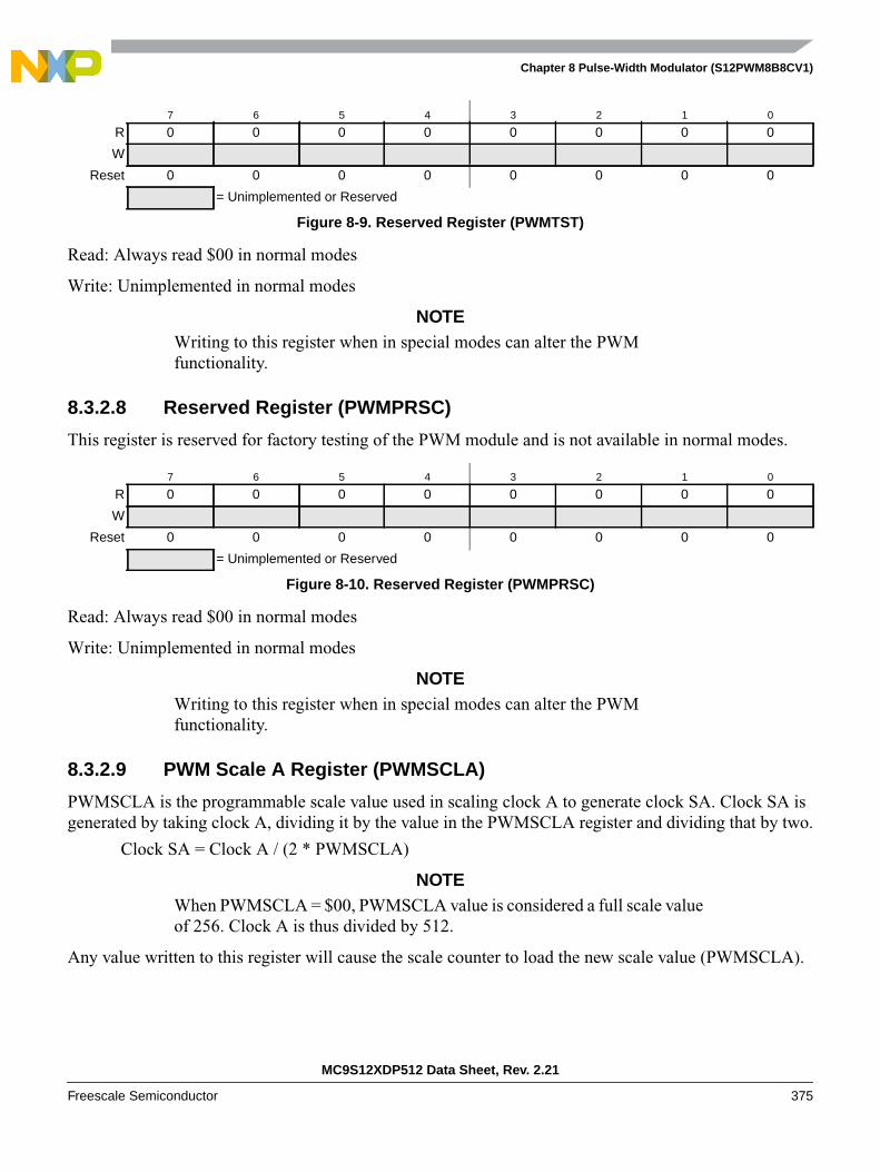
Chapter 8 Pulse-Width Modulator (S12PWM8B8CV1)
MC9S12XDP512 Data Sheet, Rev. 2.21
Freescale Semiconductor 375
Read: Always read $00 in normal modes
Write: Unimplemented in normal modes
NOTEWriting to this register when in special modes can alter the PWMfunctionality.
8.3.2.8 Reserved Register (PWMPRSC)
This register is reserved for factory testing of the PWM module and is not available in normal modes.
Read: Always read $00 in normal modes
Write: Unimplemented in normal modes
NOTEWriting to this register when in special modes can alter the PWMfunctionality.
8.3.2.9 PWM Scale A Register (PWMSCLA)
PWMSCLA is the programmable scale value used in scaling clock A to generate clock SA. Clock SA isgenerated by taking clock A, dividing it by the value in the PWMSCLA register and dividing that by two.
Clock SA = Clock A / (2 * PWMSCLA)
NOTEWhen PWMSCLA = $00, PWMSCLA value is considered a full scale valueof 256. Clock A is thus divided by 512.
Any value written to this register will cause the scale counter to load the new scale value (PWMSCLA).
7 6 5 4 3 2 1 0
R 0 0 0 0 0 0 0 0
W
Reset 0 0 0 0 0 0 0 0
= Unimplemented or Reserved
Figure 8-9. Reserved Register (PWMTST)
7 6 5 4 3 2 1 0
R 0 0 0 0 0 0 0 0
W
Reset 0 0 0 0 0 0 0 0
= Unimplemented or Reserved
Figure 8-10. Reserved Register (PWMPRSC)

Chapter 8 Pulse-Width Modulator (S12PWM8B8CV1)
MC9S12XDP512 Data Sheet, Rev. 2.21
376 Freescale Semiconductor
Read: Anytime
Write: Anytime (causes the scale counter to load the PWMSCLA value)
8.3.2.10 PWM Scale B Register (PWMSCLB)
PWMSCLB is the programmable scale value used in scaling clock B to generate clock SB. Clock SB isgenerated by taking clock B, dividing it by the value in the PWMSCLB register and dividing that by two.
Clock SB = Clock B / (2 * PWMSCLB)
NOTEWhen PWMSCLB = $00, PWMSCLB value is considered a full scale valueof 256. Clock B is thus divided by 512.
Any value written to this register will cause the scale counter to load the new scale value (PWMSCLB).
Read: Anytime
Write: Anytime (causes the scale counter to load the PWMSCLB value).
8.3.2.11 Reserved Registers (PWMSCNTx)
The registers PWMSCNTA and PWMSCNTB are reserved for factory testing of the PWM module and arenot available in normal modes.
Read: Always read $00 in normal modes
Write: Unimplemented in normal modes
7 6 5 4 3 2 1 0
RBit 7 6 5 4 3 2 1 Bit 0
W
Reset 0 0 0 0 0 0 0 0
Figure 8-11. PWM Scale A Register (PWMSCLA)
7 6 5 4 3 2 1 0
RBit 7 6 5 4 3 2 1 Bit 0
W
Reset 0 0 0 0 0 0 0 0
Figure 8-12. PWM Scale B Register (PWMSCLB)
7 6 5 4 3 2 1 0
R 0 0 0 0 0 0 0 0
W
Reset 0 0 0 0 0 0 0 0
= Unimplemented or Reserved
Figure 8-13. Reserved Registers (PWMSCNTx)

Chapter 8 Pulse-Width Modulator (S12PWM8B8CV1)
MC9S12XDP512 Data Sheet, Rev. 2.21
Freescale Semiconductor 377
NOTEWriting to these registers when in special modes can alter the PWMfunctionality.
8.3.2.12 PWM Channel Counter Registers (PWMCNTx)
Each channel has a dedicated 8-bit up/down counter which runs at the rate of the selected clock source.The counter can be read at any time without affecting the count or the operation of the PWM channel. Inleft aligned output mode, the counter counts from 0 to the value in the period register - 1. In center alignedoutput mode, the counter counts from 0 up to the value in the period register and then back down to 0.
Any value written to the counter causes the counter to reset to $00, the counter direction to be set to up,the immediate load of both duty and period registers with values from the buffers, and the output to changeaccording to the polarity bit. The counter is also cleared at the end of the effective period (seeSection 8.4.2.5, “Left Aligned Outputs” and Section 8.4.2.6, “Center Aligned Outputs” for more details).When the channel is disabled (PWMEx = 0), the PWMCNTx register does not count. When a channelbecomes enabled (PWMEx = 1), the associated PWM counter starts at the count in the PWMCNTxregister. For more detailed information on the operation of the counters, see Section 8.4.2.4, “PWM TimerCounters”.
In concatenated mode, writes to the 16-bit counter by using a 16-bit access or writes to either the low orhigh order byte of the counter will reset the 16-bit counter. Reads of the 16-bit counter must be made by16-bit access to maintain data coherency.
NOTEWriting to the counter while the channel is enabled can cause an irregular PWM cycle to occur.
Read: Anytime
Write: Anytime (any value written causes PWM counter to be reset to $00).
8.3.2.13 PWM Channel Period Registers (PWMPERx)
There is a dedicated period register for each channel. The value in this register determines the period ofthe associated PWM channel.
The period registers for each channel are double buffered so that if they change while the channel isenabled, the change will NOT take effect until one of the following occurs:
• The effective period ends
• The counter is written (counter resets to $00)
• The channel is disabled
7 6 5 4 3 2 1 0
R Bit 7 6 5 4 3 2 1 Bit 0
W 0 0 0 0 0 0 0 0
Reset 0 0 0 0 0 0 0 0
Figure 8-14. PWM Channel Counter Registers (PWMCNTx)
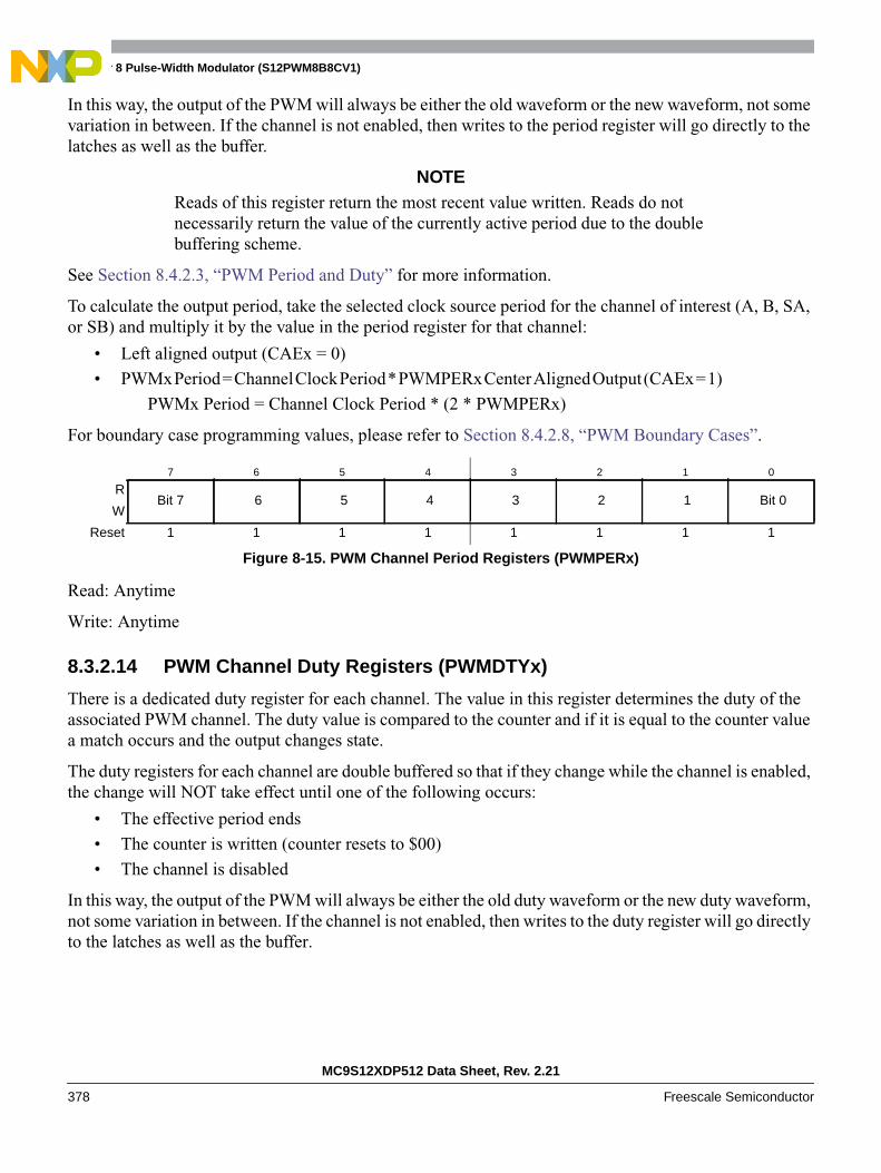
Chapter 8 Pulse-Width Modulator (S12PWM8B8CV1)
MC9S12XDP512 Data Sheet, Rev. 2.21
378 Freescale Semiconductor
In this way, the output of the PWM will always be either the old waveform or the new waveform, not somevariation in between. If the channel is not enabled, then writes to the period register will go directly to thelatches as well as the buffer.
NOTEReads of this register return the most recent value written. Reads do notnecessarily return the value of the currently active period due to the doublebuffering scheme.
See Section 8.4.2.3, “PWM Period and Duty” for more information.
To calculate the output period, take the selected clock source period for the channel of interest (A, B, SA,or SB) and multiply it by the value in the period register for that channel:
• Left aligned output (CAEx = 0)
• PWMxPeriod=ChannelClockPeriod*PWMPERxCenterAlignedOutput(CAEx=1)
PWMx Period = Channel Clock Period * (2 * PWMPERx)
For boundary case programming values, please refer to Section 8.4.2.8, “PWM Boundary Cases”.
Read: Anytime
Write: Anytime
8.3.2.14 PWM Channel Duty Registers (PWMDTYx)
There is a dedicated duty register for each channel. The value in this register determines the duty of theassociated PWM channel. The duty value is compared to the counter and if it is equal to the counter valuea match occurs and the output changes state.
The duty registers for each channel are double buffered so that if they change while the channel is enabled,the change will NOT take effect until one of the following occurs:
• The effective period ends
• The counter is written (counter resets to $00)
• The channel is disabled
In this way, the output of the PWM will always be either the old duty waveform or the new duty waveform,not some variation in between. If the channel is not enabled, then writes to the duty register will go directlyto the latches as well as the buffer.
7 6 5 4 3 2 1 0
RBit 7 6 5 4 3 2 1 Bit 0
W
Reset 1 1 1 1 1 1 1 1
Figure 8-15. PWM Channel Period Registers (PWMPERx)
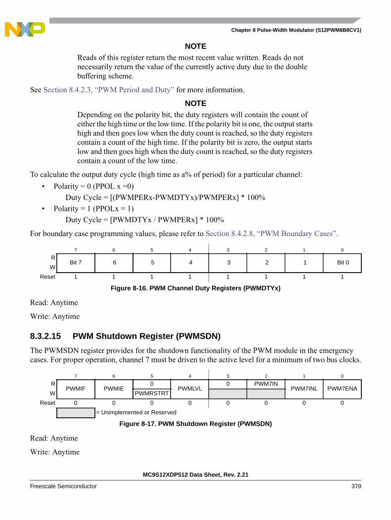
Chapter 8 Pulse-Width Modulator (S12PWM8B8CV1)
MC9S12XDP512 Data Sheet, Rev. 2.21
Freescale Semiconductor 379
NOTEReads of this register return the most recent value written. Reads do notnecessarily return the value of the currently active duty due to the doublebuffering scheme.
See Section 8.4.2.3, “PWM Period and Duty” for more information.
NOTEDepending on the polarity bit, the duty registers will contain the count ofeither the high time or the low time. If the polarity bit is one, the output startshigh and then goes low when the duty count is reached, so the duty registerscontain a count of the high time. If the polarity bit is zero, the output startslow and then goes high when the duty count is reached, so the duty registerscontain a count of the low time.
To calculate the output duty cycle (high time as a% of period) for a particular channel:
• Polarity = 0 (PPOL x =0)
Duty Cycle = [(PWMPERx-PWMDTYx)/PWMPERx] * 100%
• Polarity = 1 (PPOLx = 1)
Duty Cycle = [PWMDTYx / PWMPERx] * 100%
For boundary case programming values, please refer to Section 8.4.2.8, “PWM Boundary Cases”.
Read: Anytime
Write: Anytime
8.3.2.15 PWM Shutdown Register (PWMSDN)
The PWMSDN register provides for the shutdown functionality of the PWM module in the emergencycases. For proper operation, channel 7 must be driven to the active level for a minimum of two bus clocks.
Read: Anytime
Write: Anytime
7 6 5 4 3 2 1 0
RBit 7 6 5 4 3 2 1 Bit 0
W
Reset 1 1 1 1 1 1 1 1
Figure 8-16. PWM Channel Duty Registers (PWMDTYx)
7 6 5 4 3 2 1 0
RPWMIF PWMIE
0PWMLVL
0 PWM7INPWM7INL PWM7ENA
W PWMRSTRT
Reset 0 0 0 0 0 0 0 0
= Unimplemented or Reserved
Figure 8-17. PWM Shutdown Register (PWMSDN)
Chapter 8 Pulse-Width Modulator (S12PWM8B8CV1)
MC9S12XDP512 Data Sheet, Rev. 2.21
380 Freescale Semiconductor
8.4 Functional Description
8.4.1 PWM Clock Select
There are four available clocks: clock A, clock B, clock SA (scaled A), and clock SB (scaled B). Thesefour clocks are based on the bus clock.
Clock A and B can be software selected to be 1, 1/2, 1/4, 1/8,..., 1/64, 1/128 times the bus clock. Clock SAuses clock A as an input and divides it further with a reloadable counter. Similarly, clock SB uses clock Bas an input and divides it further with a reloadable counter. The rates available for clock SA are softwareselectable to be clock A divided by 2, 4, 6, 8,..., or 512 in increments of divide by 2. Similar rates areavailable for clock SB. Each PWM channel has the capability of selecting one of two clocks, either thepre-scaled clock (clock A or B) or the scaled clock (clock SA or SB).
The block diagram in Figure 8-18 shows the four different clocks and how the scaled clocks are created.
Table 8-9. PWMSDN Field Descriptions
Field Description
7PWMIF
PWM Interrupt Flag — Any change from passive to asserted (active) state or from active to passive state willbe flagged by setting the PWMIF flag = 1. The flag is cleared by writing a logic 1 to it. Writing a 0 has no effect.0 No change on PWM7IN input.1 Change on PWM7IN input
6PWMIE
PWM Interrupt Enable — If interrupt is enabled an interrupt to the CPU is asserted.0 PWM interrupt is disabled.1 PWM interrupt is enabled.
5PWMRSTRT
PWM Restart — The PWM can only be restarted if the PWM channel input 7 is de-asserted. After writing a logic1 to the PWMRSTRT bit (trigger event) the PWM channels start running after the corresponding counter passesnext “counter == 0” phase. Also, if the PWM7ENA bit is reset to 0, the PWM do not start before the counterpasses $00. The bit is always read as “0”.
4PWMLVL
PWM Shutdown Output Level If active level as defined by the PWM7IN input, gets asserted all enabled PWMchannels are immediately driven to the level defined by PWMLVL.0 PWM outputs are forced to 01 Outputs are forced to 1.
2PWM7IN
PWM Channel 7 Input Status — This reflects the current status of the PWM7 pin.
1PWM7INL
PWM Shutdown Active Input Level for Channel 7 — If the emergency shutdown feature is enabled(PWM7ENA = 1), this bit determines the active level of the PWM7channel.0 Active level is low1 Active level is high
0PWM7ENA
PWM Emergency Shutdown Enable — If this bit is logic 1, the pin associated with channel 7 is forced to inputand the emergency shutdown feature is enabled. All the other bits in this register are meaningful only ifPWM7ENA = 1.0 PWM emergency feature disabled.1 PWM emergency feature is enabled.

Chapter 8 Pulse-Width Modulator (S12PWM8B8CV1)
MC9S12XDP512 Data Sheet, Rev. 2.21
Freescale Semiconductor 381
8.4.1.1 Prescale
The input clock to the PWM prescaler is the bus clock. It can be disabled whenever the part is in freezemode by setting the PFRZ bit in the PWMCTL register. If this bit is set, whenever the MCU is in freezemode (freeze mode signal active) the input clock to the prescaler is disabled. This is useful for emulationin order to freeze the PWM. The input clock can also be disabled when all eight PWM channels aredisabled (PWME7-0 = 0). This is useful for reducing power by disabling the prescale counter.
Clock A and clock B are scaled values of the input clock. The value is software selectable for both clockA and clock B and has options of 1, 1/2, 1/4, 1/8, 1/16, 1/32, 1/64, or 1/128 times the bus clock. The valueselected for clock A is determined by the PCKA2, PCKA1, PCKA0 bits in the PWMPRCLK register. Thevalue selected for clock B is determined by the PCKB2, PCKB1, PCKB0 bits also in the PWMPRCLKregister.
8.4.1.2 Clock Scale
The scaled A clock uses clock A as an input and divides it further with a user programmable value andthen divides this by 2. The scaled B clock uses clock B as an input and divides it further with a userprogrammable value and then divides this by 2. The rates available for clock SA are software selectable tobe clock A divided by 2, 4, 6, 8,..., or 512 in increments of divide by 2. Similar rates are available for clockSB.

Chapter 8 Pulse-Width Modulator (S12PWM8B8CV1)
MC9S12XDP512 Data Sheet, Rev. 2.21
382 Freescale Semiconductor
Figure 8-18. PWM Clock Select Block Diagram
128
24
816
3264
PC
KB
2P
CK
B1
PC
KB
0
M
U
X
Clock A
Clock B
Clock SA
Clock A/2, A/4, A/6,....A/512
Prescale Scale
Div
ide
byP
FR
ZFr
eeze
Mod
e S
igna
l
Bus
Clo
ck
Clock Select
MUX
PCLK0
Clock toPWM Ch 0
MUX
PCLK2
Clock toPWM Ch 2
MUX
PCLK1
Clock toPWM Ch 1
MUX
PCLK4
Clock toPWM Ch 4
MUX
PCLK5
Clock toPWM Ch 5
MUX
PCLK6
Clock toPWM Ch 6
MUX
PCLK7
Clock toPWM Ch 7
MUX
PCLK3
Clock toPWM Ch 3
Load
DIV 2PWMSCLBClock SB
Clock B/2, B/4, B/6,....B/512
M
U
X
PC
KA
2P
CK
A1
PC
KA
0
PW
ME
7-0
Count = 1
Load
DIV 2PWMSCLA
Count = 18-Bit DownCounter
8-Bit DownCounter
Pre
scal
er T
aps:

Chapter 8 Pulse-Width Modulator (S12PWM8B8CV1)
MC9S12XDP512 Data Sheet, Rev. 2.21
Freescale Semiconductor 383
Clock A is used as an input to an 8-bit down counter. This down counter loads a user programmable scalevalue from the scale register (PWMSCLA). When the down counter reaches one, a pulse is output and the8-bit counter is re-loaded. The output signal from this circuit is further divided by two. This gives a greaterrange with only a slight reduction in granularity. Clock SA equals clock A divided by two times the valuein the PWMSCLA register.
NOTEClock SA = Clock A / (2 * PWMSCLA)
When PWMSCLA = $00, PWMSCLA value is considered a full scale valueof 256. Clock A is thus divided by 512.
Similarly, clock B is used as an input to an 8-bit down counter followed by a divide by two producing clockSB. Thus, clock SB equals clock B divided by two times the value in the PWMSCLB register.
NOTEClock SB = Clock B / (2 * PWMSCLB)
When PWMSCLB = $00, PWMSCLB value is considered a full scale valueof 256. Clock B is thus divided by 512.
As an example, consider the case in which the user writes $FF into the PWMSCLA register. Clock A forthis case will be E divided by 4. A pulse will occur at a rate of once every 255x4 E cycles. Passing thisthrough the divide by two circuit produces a clock signal at an E divided by 2040 rate. Similarly, a valueof $01 in the PWMSCLA register when clock A is E divided by 4 will produce a clock at an E divided by8 rate.
Writing to PWMSCLA or PWMSCLB causes the associated 8-bit down counter to be re-loaded.Otherwise, when changing rates the counter would have to count down to $01 before counting at the properrate. Forcing the associated counter to re-load the scale register value every time PWMSCLA orPWMSCLB is written prevents this.
NOTEWriting to the scale registers while channels are operating can causeirregularities in the PWM outputs.
8.4.1.3 Clock Select
Each PWM channel has the capability of selecting one of two clocks. For channels 0, 1, 4, and 5 the clockchoices are clock A or clock SA. For channels 2, 3, 6, and 7 the choices are clock B or clock SB. The clockselection is done with the PCLKx control bits in the PWMCLK register.
NOTEChanging clock control bits while channels are operating can causeirregularities in the PWM outputs.
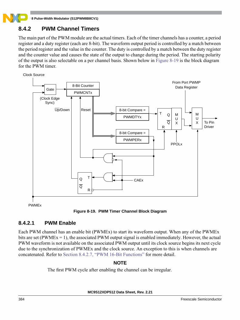
Chapter 8 Pulse-Width Modulator (S12PWM8B8CV1)
MC9S12XDP512 Data Sheet, Rev. 2.21
384 Freescale Semiconductor
8.4.2 PWM Channel Timers
The main part of the PWM module are the actual timers. Each of the timer channels has a counter, a periodregister and a duty register (each are 8-bit). The waveform output period is controlled by a match betweenthe period register and the value in the counter. The duty is controlled by a match between the duty registerand the counter value and causes the state of the output to change during the period. The starting polarityof the output is also selectable on a per channel basis. Shown below in Figure 8-19 is the block diagramfor the PWM timer.
Figure 8-19. PWM Timer Channel Block Diagram
8.4.2.1 PWM Enable
Each PWM channel has an enable bit (PWMEx) to start its waveform output. When any of the PWMExbits are set (PWMEx = 1), the associated PWM output signal is enabled immediately. However, the actualPWM waveform is not available on the associated PWM output until its clock source begins its next cycledue to the synchronization of PWMEx and the clock source. An exception to this is when channels areconcatenated. Refer to Section 8.4.2.7, “PWM 16-Bit Functions” for more detail.
NOTEThe first PWM cycle after enabling the channel can be irregular.
Clock Source
T
R
Q
Q
PPOLx
From Port PWMPData Register
PWMEx
To PinDriver
Gate
8-bit Compare =
PWMDTYx
8-bit Compare =
PWMPERx
CAExT
R
Q
Q
8-Bit Counter
PWMCNTx
MUX
MUX
(Clock EdgeSync)
Up/Down Reset

Chapter 8 Pulse-Width Modulator (S12PWM8B8CV1)
MC9S12XDP512 Data Sheet, Rev. 2.21
Freescale Semiconductor 385
On the front end of the PWM timer, the clock is enabled to the PWM circuit by the PWMEx bit being high.There is an edge-synchronizing circuit to guarantee that the clock will only be enabled or disabled at anedge. When the channel is disabled (PWMEx = 0), the counter for the channel does not count.
8.4.2.2 PWM Polarity
Each channel has a polarity bit to allow starting a waveform cycle with a high or low signal. This is shownon the block diagram as a mux select of either the Q output or the Q output of the PWM output flip flop.When one of the bits in the PWMPOL register is set, the associated PWM channel output is high at thebeginning of the waveform, then goes low when the duty count is reached. Conversely, if the polarity bitis zero, the output starts low and then goes high when the duty count is reached.
8.4.2.3 PWM Period and Duty
Dedicated period and duty registers exist for each channel and are double buffered so that if they changewhile the channel is enabled, the change will NOT take effect until one of the following occurs:
• The effective period ends
• The counter is written (counter resets to $00)
• The channel is disabled
In this way, the output of the PWM will always be either the old waveform or the new waveform, not somevariation in between. If the channel is not enabled, then writes to the period and duty registers will godirectly to the latches as well as the buffer.
A change in duty or period can be forced into effect “immediately” by writing the new value to the dutyand/or period registers and then writing to the counter. This forces the counter to reset and the new dutyand/or period values to be latched. In addition, since the counter is readable, it is possible to know wherethe count is with respect to the duty value and software can be used to make adjustments
NOTEWhen forcing a new period or duty into effect immediately, an irregularPWM cycle can occur.
Depending on the polarity bit, the duty registers will contain the count ofeither the high time or the low time.
8.4.2.4 PWM Timer Counters
Each channel has a dedicated 8-bit up/down counter which runs at the rate of the selected clock source (seeSection 8.4.1, “PWM Clock Select” for the available clock sources and rates). The counter compares totwo registers, a duty register and a period register as shown in Figure 8-19. When the PWM countermatches the duty register, the output flip-flop changes state, causing the PWM waveform to also changestate. A match between the PWM counter and the period register behaves differently depending on whatoutput mode is selected as shown in Figure 8-19 and described in Section 8.4.2.5, “Left Aligned Outputs”and Section 8.4.2.6, “Center Aligned Outputs”.
Chapter 8 Pulse-Width Modulator (S12PWM8B8CV1)
MC9S12XDP512 Data Sheet, Rev. 2.21
386 Freescale Semiconductor
Each channel counter can be read at anytime without affecting the count or the operation of the PWMchannel.
Any value written to the counter causes the counter to reset to $00, the counter direction to be set to up,the immediate load of both duty and period registers with values from the buffers, and the output to changeaccording to the polarity bit. When the channel is disabled (PWMEx = 0), the counter stops. When achannel becomes enabled (PWMEx = 1), the associated PWM counter continues from the count in thePWMCNTx register. This allows the waveform to continue where it left off when the channel isre-enabled. When the channel is disabled, writing “0” to the period register will cause the counter to reseton the next selected clock.
NOTEIf the user wants to start a new “clean” PWM waveform without any“history” from the old waveform, the user must write to channel counter(PWMCNTx) prior to enabling the PWM channel (PWMEx = 1).
Generally, writes to the counter are done prior to enabling a channel in order to start from a known state.However, writing a counter can also be done while the PWM channel is enabled (counting). The effect issimilar to writing the counter when the channel is disabled, except that the new period is startedimmediately with the output set according to the polarity bit.
NOTEWriting to the counter while the channel is enabled can cause an irregularPWM cycle to occur.
The counter is cleared at the end of the effective period (see Section 8.4.2.5, “Left Aligned Outputs” andSection 8.4.2.6, “Center Aligned Outputs” for more details).
8.4.2.5 Left Aligned Outputs
The PWM timer provides the choice of two types of outputs, left aligned or center aligned. They areselected with the CAEx bits in the PWMCAE register. If the CAEx bit is cleared (CAEx = 0), thecorresponding PWM output will be left aligned.
In left aligned output mode, the 8-bit counter is configured as an up counter only. It compares to tworegisters, a duty register and a period register as shown in the block diagram in Figure 8-19. When thePWM counter matches the duty register the output flip-flop changes state causing the PWM waveform toalso change state. A match between the PWM counter and the period register resets the counter and theoutput flip-flop, as shown in Figure 8-19, as well as performing a load from the double buffer period andduty register to the associated registers, as described in Section 8.4.2.3, “PWM Period and Duty”. Thecounter counts from 0 to the value in the period register – 1.
Table 8-10. PWM Timer Counter Conditions
Counter Clears ($00) Counter Counts Counter Stops
When PWMCNTx register written toany value
When PWM channel is enabled(PWMEx = 1). Counts from last value in
PWMCNTx.
When PWM channel is disabled(PWMEx = 0)
Effective period ends
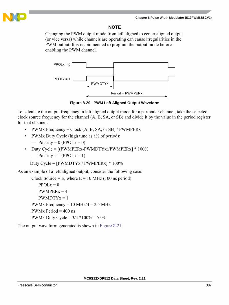
Chapter 8 Pulse-Width Modulator (S12PWM8B8CV1)
MC9S12XDP512 Data Sheet, Rev. 2.21
Freescale Semiconductor 387
NOTEChanging the PWM output mode from left aligned to center aligned output(or vice versa) while channels are operating can cause irregularities in thePWM output. It is recommended to program the output mode beforeenabling the PWM channel.
Figure 8-20. PWM Left Aligned Output Waveform
To calculate the output frequency in left aligned output mode for a particular channel, take the selectedclock source frequency for the channel (A, B, SA, or SB) and divide it by the value in the period registerfor that channel.
• PWMx Frequency = Clock (A, B, SA, or SB) / PWMPERx
• PWMx Duty Cycle (high time as a% of period):
— Polarity = 0 (PPOLx = 0)
• Duty Cycle = [(PWMPERx-PWMDTYx)/PWMPERx] * 100%
— Polarity = 1 (PPOLx = 1)
Duty Cycle = [PWMDTYx / PWMPERx] * 100%
As an example of a left aligned output, consider the following case:
Clock Source = E, where E = 10 MHz (100 ns period)
PPOLx = 0
PWMPERx = 4
PWMDTYx = 1
PWMx Frequency = 10 MHz/4 = 2.5 MHz
PWMx Period = 400 ns
PWMx Duty Cycle = 3/4 *100% = 75%
The output waveform generated is shown in Figure 8-21.
PWMDTYx
Period = PWMPERx
PPOLx = 0
PPOLx = 1
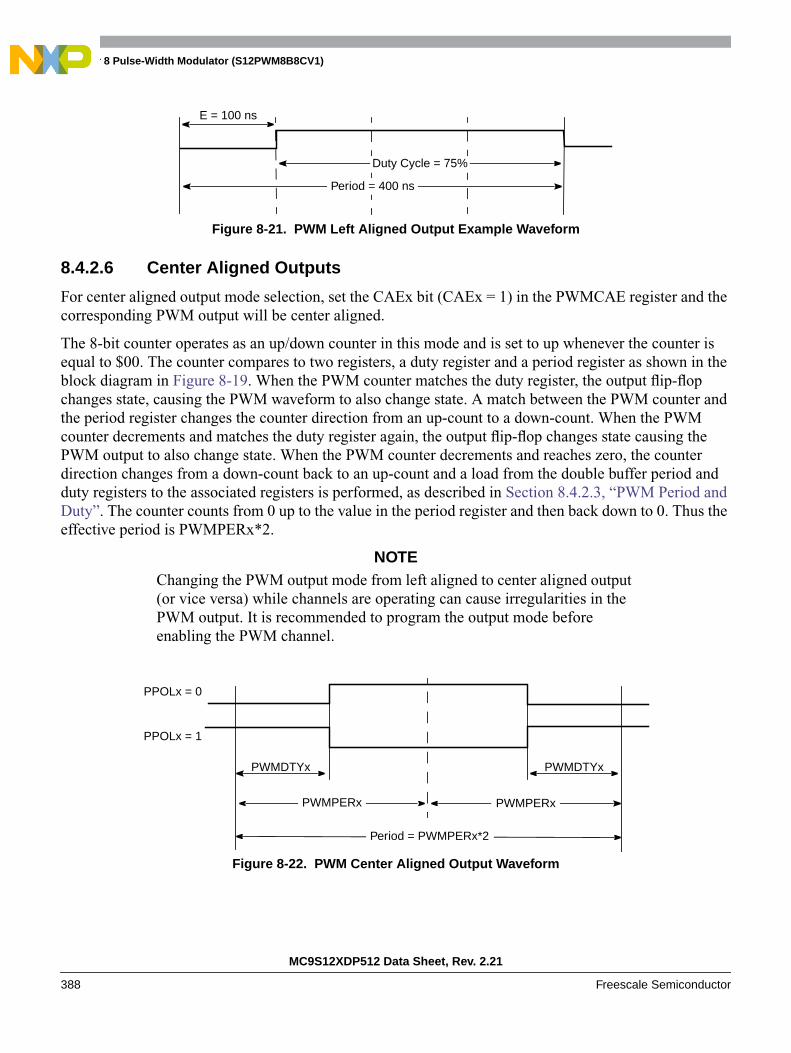
Chapter 8 Pulse-Width Modulator (S12PWM8B8CV1)
MC9S12XDP512 Data Sheet, Rev. 2.21
388 Freescale Semiconductor
Figure 8-21. PWM Left Aligned Output Example Waveform
8.4.2.6 Center Aligned Outputs
For center aligned output mode selection, set the CAEx bit (CAEx = 1) in the PWMCAE register and thecorresponding PWM output will be center aligned.
The 8-bit counter operates as an up/down counter in this mode and is set to up whenever the counter isequal to $00. The counter compares to two registers, a duty register and a period register as shown in theblock diagram in Figure 8-19. When the PWM counter matches the duty register, the output flip-flopchanges state, causing the PWM waveform to also change state. A match between the PWM counter andthe period register changes the counter direction from an up-count to a down-count. When the PWMcounter decrements and matches the duty register again, the output flip-flop changes state causing thePWM output to also change state. When the PWM counter decrements and reaches zero, the counterdirection changes from a down-count back to an up-count and a load from the double buffer period andduty registers to the associated registers is performed, as described in Section 8.4.2.3, “PWM Period andDuty”. The counter counts from 0 up to the value in the period register and then back down to 0. Thus theeffective period is PWMPERx*2.
NOTEChanging the PWM output mode from left aligned to center aligned output(or vice versa) while channels are operating can cause irregularities in thePWM output. It is recommended to program the output mode beforeenabling the PWM channel.
Figure 8-22. PWM Center Aligned Output Waveform
Period = 400 ns
E = 100 ns
Duty Cycle = 75%
PPOLx = 0
PPOLx = 1
PWMDTYx PWMDTYx
Period = PWMPERx*2
PWMPERxPWMPERx

Chapter 8 Pulse-Width Modulator (S12PWM8B8CV1)
MC9S12XDP512 Data Sheet, Rev. 2.21
Freescale Semiconductor 389
To calculate the output frequency in center aligned output mode for a particular channel, take the selectedclock source frequency for the channel (A, B, SA, or SB) and divide it by twice the value in the periodregister for that channel.
• PWMx Frequency = Clock (A, B, SA, or SB) / (2*PWMPERx)
• PWMx Duty Cycle (high time as a% of period):
— Polarity = 0 (PPOLx = 0)
Duty Cycle = [(PWMPERx-PWMDTYx)/PWMPERx] * 100%
— Polarity = 1 (PPOLx = 1)
Duty Cycle = [PWMDTYx / PWMPERx] * 100%

Chapter 8 Pulse-Width Modulator (S12PWM8B8CV1)
MC9S12XDP512 Data Sheet, Rev. 2.21
390 Freescale Semiconductor
As an example of a center aligned output, consider the following case:
Clock Source = E, where E = 10 MHz (100 ns period)
PPOLx = 0
PWMPERx = 4
PWMDTYx = 1
PWMx Frequency = 10 MHz/8 = 1.25 MHz
PWMx Period = 800 ns
PWMx Duty Cycle = 3/4 *100% = 75%
Shown in Figure 8-23 is the output waveform generated.
Figure 8-23. PWM Center Aligned Output Example Waveform
8.4.2.7 PWM 16-Bit Functions
The PWM timer also has the option of generating 8-channels of 8-bits or 4-channels of 16-bits for greaterPWM resolution. This 16-bit channel option is achieved through the concatenation of two 8-bit channels.
The PWMCTL register contains four control bits, each of which is used to concatenate a pair of PWMchannels into one 16-bit channel. Channels 6 and 7 are concatenated with the CON67 bit, channels 4 and5 are concatenated with the CON45 bit, channels 2 and 3 are concatenated with the CON23 bit, andchannels 0 and 1 are concatenated with the CON01 bit.
NOTEChange these bits only when both corresponding channels are disabled.
When channels 6 and 7 are concatenated, channel 6 registers become the high order bytes of the doublebyte channel, as shown in Figure 8-24. Similarly, when channels 4 and 5 are concatenated, channel 4registers become the high order bytes of the double byte channel. When channels 2 and 3 are concatenated,channel 2 registers become the high order bytes of the double byte channel. When channels 0 and 1 areconcatenated, channel 0 registers become the high order bytes of the double byte channel.
When using the 16-bit concatenated mode, the clock source is determined by the low order 8-bit channelclock select control bits. That is channel 7 when channels 6 and 7 are concatenated, channel 5 whenchannels 4 and 5 are concatenated, channel 3 when channels 2 and 3 are concatenated, and channel 1 whenchannels 0 and 1 are concatenated. The resulting PWM is output to the pins of the corresponding low order8-bit channel as also shown in Figure 8-24. The polarity of the resulting PWM output is controlled by thePPOLx bit of the corresponding low order 8-bit channel as well.
E = 100 ns
DUTY CYCLE = 75%
E = 100 ns
PERIOD = 800 ns

Chapter 8 Pulse-Width Modulator (S12PWM8B8CV1)
MC9S12XDP512 Data Sheet, Rev. 2.21
Freescale Semiconductor 391
Figure 8-24. PWM 16-Bit Mode
Once concatenated mode is enabled (CONxx bits set in PWMCTL register), enabling/disabling thecorresponding 16-bit PWM channel is controlled by the low order PWMEx bit. In this case, the high orderbytes PWMEx bits have no effect and their corresponding PWM output is disabled.
In concatenated mode, writes to the 16-bit counter by using a 16-bit access or writes to either the low orhigh order byte of the counter will reset the 16-bit counter. Reads of the 16-bit counter must be made by16-bit access to maintain data coherency.
PWMCNT6 PWCNT7
PWM7
Clock Source 7High Low
Period/Duty Compare
PWMCNT4 PWCNT5
PWM5
Clock Source 5High Low
Period/Duty Compare
PWMCNT2 PWCNT3
PWM3
Clock Source 3High Low
Period/Duty Compare
PWMCNT0 PWCNT1
PWM1
Clock Source 1High Low
Period/Duty Compare

Chapter 8 Pulse-Width Modulator (S12PWM8B8CV1)
MC9S12XDP512 Data Sheet, Rev. 2.21
392 Freescale Semiconductor
Either left aligned or center aligned output mode can be used in concatenated mode and is controlled bythe low order CAEx bit. The high order CAEx bit has no effect.
Table 8-11 is used to summarize which channels are used to set the various control bits when in 16-bitmode.
8.4.2.8 PWM Boundary Cases
Table 8-12 summarizes the boundary conditions for the PWM regardless of the output mode (left alignedor center aligned) and 8-bit (normal) or 16-bit (concatenation).
8.5 ResetsThe reset state of each individual bit is listed within the Section 8.3.2, “Register Descriptions” whichdetails the registers and their bit-fields. All special functions or modes which are initialized during or justfollowing reset are described within this section.
• The 8-bit up/down counter is configured as an up counter out of reset.
• All the channels are disabled and all the counters do not count.
Table 8-11. 16-bit Concatenation Mode Summary
CONxx PWMEx PPOLx PCLKx CAExPWMxOutput
CON67 PWME7 PPOL7 PCLK7 CAE7 PWM7
CON45 PWME5 PPOL5 PCLK5 CAE5 PWM5
CON23 PWME3 PPOL3 PCLK3 CAE3 PWM3
CON01 PWME1 PPOL1 PCLK1 CAE1 PWM1
Table 8-12. PWM Boundary Cases
PWMDTYx PWMPERx PPOLx PWMx Output
$00(indicates no duty)
>$00 1 Always low
$00(indicates no duty)
>$00 0 Always high
XX $001
(indicates no period)
1 Counter = $00 and does not count.
1 Always high
XX $001
(indicates no period)0 Always low
>= PWMPERx XX 1 Always high
>= PWMPERx XX 0 Always low
Chapter 8 Pulse-Width Modulator (S12PWM8B8CV1)
MC9S12XDP512 Data Sheet, Rev. 2.21
Freescale Semiconductor 393
8.6 InterruptsThe PWM module has only one interrupt which is generated at the time of emergency shutdown, if thecorresponding enable bit (PWMIE) is set. This bit is the enable for the interrupt. The interrupt flag PWMIFis set whenever the input level of the PWM7 channel changes while PWM7ENA = 1 or when PWMENAis being asserted while the level at PWM7 is active.
In stop mode or wait mode (with the PSWAI bit set), the emergency shutdown feature will drive the PWMoutputs to their shutdown output levels but the PWMIF flag will not be set.
A description of the registers involved and affected due to this interrupt is explained in Section 8.3.2.15,“PWM Shutdown Register (PWMSDN)”.
The PWM block only generates the interrupt and does not service it. The interrupt signal name is PWMinterrupt signal.

Chapter 8 Pulse-Width Modulator (S12PWM8B8CV1)
MC9S12XDP512 Data Sheet, Rev. 2.21
394 Freescale Semiconductor
MC9S12XDP512 Data Sheet, Rev. 2.21
Freescale Semiconductor 395
Chapter 9Inter-Integrated Circuit (IICV2) Block Description
9.1 IntroductionThe inter-IC bus (IIC) is a two-wire, bidirectional serial bus that provides a simple, efficient method of dataexchange between devices. Being a two-wire device, the IIC bus minimizes the need for large numbers ofconnections between devices, and eliminates the need for an address decoder.
This bus is suitable for applications requiring occasional communications over a short distance between anumber of devices. It also provides flexibility, allowing additional devices to be connected to the bus forfurther expansion and system development.
The interface is designed to operate up to 100 kbps with maximum bus loading and timing. The device iscapable of operating at higher baud rates, up to a maximum of clock/20, with reduced bus loading. Themaximum communication length and the number of devices that can be connected are limited by amaximum bus capacitance of 400 pF.
9.1.1 Features
The IIC module has the following key features:
• Compatible with I2C bus standard
• Multi-master operation
• Software programmable for one of 256 different serial clock frequencies
• Software selectable acknowledge bit
• Interrupt driven byte-by-byte data transfer
• Arbitration lost interrupt with automatic mode switching from master to slave
• Calling address identification interrupt
• Start and stop signal generation/detection
• Repeated start signal generation
• Acknowledge bit generation/detection
• Bus busy detection
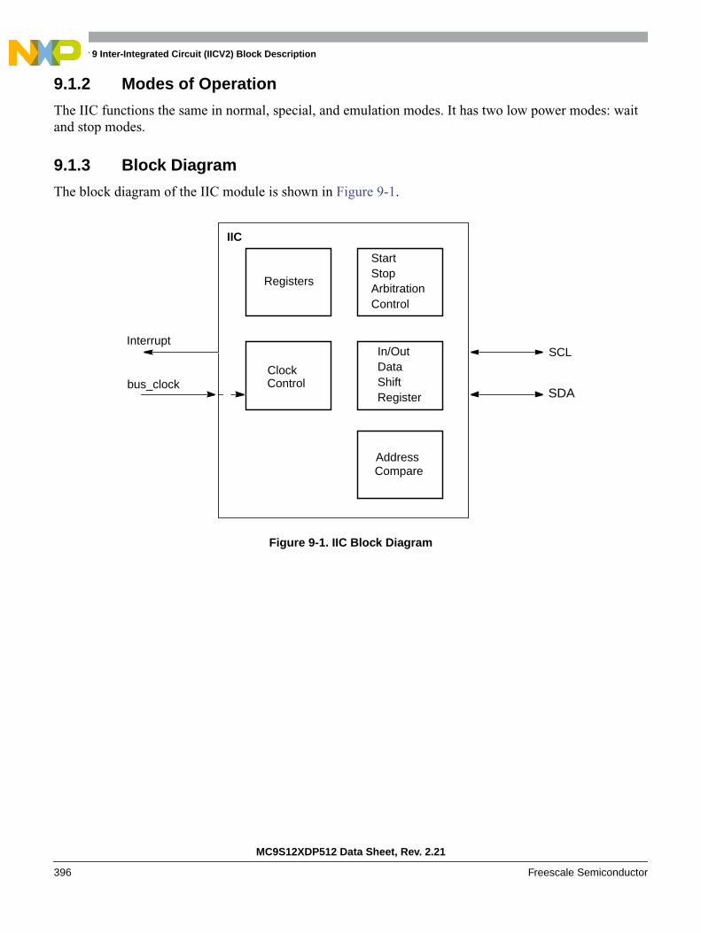
Chapter 9 Inter-Integrated Circuit (IICV2) Block Description
MC9S12XDP512 Data Sheet, Rev. 2.21
396 Freescale Semiconductor
9.1.2 Modes of Operation
The IIC functions the same in normal, special, and emulation modes. It has two low power modes: waitand stop modes.
9.1.3 Block Diagram
The block diagram of the IIC module is shown in Figure 9-1.
Figure 9-1. IIC Block Diagram
In/OutDataShiftRegister
AddressCompare
SDA
Interrupt
ClockControl
StartStopArbitrationControl
SCL
bus_clock
IIC
Registers
Chapter 9 Inter-Integrated Circuit (IICV2) Block Description
MC9S12XDP512 Data Sheet, Rev. 2.21
Freescale Semiconductor 397
9.2 External Signal DescriptionThe IICV2 module has two external pins.
9.2.1 IIC_SCL — Serial Clock Line Pin
This is the bidirectional serial clock line (SCL) of the module, compatible to the IIC bus specification.
9.2.2 IIC_SDA — Serial Data Line Pin
This is the bidirectional serial data line (SDA) of the module, compatible to the IIC bus specification.
9.3 Memory Map and Register DefinitionThis section provides a detailed description of all memory and registers for the IIC module.
9.3.1 Module Memory Map
The memory map for the IIC module is given below in Table 1-1. The address listed for each register isthe address offset.The total address for each register is the sum of the base address for the IIC module andthe address offset for each register.
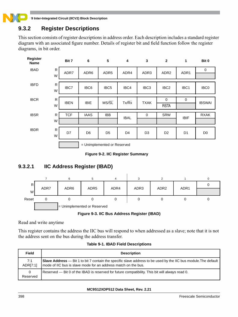
Chapter 9 Inter-Integrated Circuit (IICV2) Block Description
MC9S12XDP512 Data Sheet, Rev. 2.21
398 Freescale Semiconductor
9.3.2 Register Descriptions
This section consists of register descriptions in address order. Each description includes a standard registerdiagram with an associated figure number. Details of register bit and field function follow the registerdiagrams, in bit order.
9.3.2.1 IIC Address Register (IBAD)
Read and write anytime
This register contains the address the IIC bus will respond to when addressed as a slave; note that it is notthe address sent on the bus during the address transfer.
RegisterName
Bit 7 6 5 4 3 2 1 Bit 0
IBAD RADR7 ADR6 ADR5 ADR4 ADR3 ADR2 ADR1
0
W
IBFD RIBC7 IBC6 IBC5 IBC4 IBC3 IBC2 IBC1 IBC0
W
IBCR RIBEN IBIE MS/SL Tx/Rx TXAK
0 0IBSWAI
W RSTA
IBSR R TCF IAAS IBBIBAL
0 SRWIBIF
RXAK
W
IBDR RD7 D6 D5 D4 D3 D2 D1 D0
W
= Unimplemented or Reserved
Figure 9-2. IIC Register Summary
7 6 5 4 3 2 1 0
RADR7 ADR6 ADR5 ADR4 ADR3 ADR2 ADR1
0
W
Reset 0 0 0 0 0 0 0 0
= Unimplemented or Reserved
Figure 9-3. IIC Bus Address Register (IBAD)
Table 9-1. IBAD Field Descriptions
Field Description
7:1ADR[7:1]
Slave Address — Bit 1 to bit 7 contain the specific slave address to be used by the IIC bus module.The defaultmode of IIC bus is slave mode for an address match on the bus.
0Reserved
Reserved — Bit 0 of the IBAD is reserved for future compatibility. This bit will always read 0.

Chapter 9 Inter-Integrated Circuit (IICV2) Block Description
MC9S12XDP512 Data Sheet, Rev. 2.21
Freescale Semiconductor 399
9.3.2.2 IIC Frequency Divider Register (IBFD)
Read and write anytime
7 6 5 4 3 2 1 0
RIBC7 IBC6 IBC5 IBC4 IBC3 IBC2 IBC1 IBC0
W
Reset 0 0 0 0 0 0 0 0
= Unimplemented or Reserved
Figure 9-4. IIC Bus Frequency Divider Register (IBFD)
Table 9-2. IBFD Field Descriptions
Field Description
7:0IBC[7:0]
I Bus Clock Rate 7:0 — This field is used to prescale the clock for bit rate selection. The bit clock generator isimplemented as a prescale divider — IBC7:6, prescaled shift register — IBC5:3 select the prescaler divider andIBC2-0 select the shift register tap point. The IBC bits are decoded to give the tap and prescale values as shownin Table 9-3.
Table 9-3. I-Bus Tap and Prescale Values
IBC2-0(bin)
SCL Tap(clocks)
SDA Tap(clocks)
000 5 1
001 6 1
010 7 2
011 8 2
100 9 3
101 10 3
110 12 4
111 15 4
IBC5-3(bin)
scl2start(clocks)
scl2stop(clocks)
scl2tap(clocks)
tap2tap(clocks)
000 2 7 4 1
001 2 7 4 2
010 2 9 6 4
011 6 9 6 8
100 14 17 14 16
101 30 33 30 32
110 62 65 62 64
111 126 129 126 128
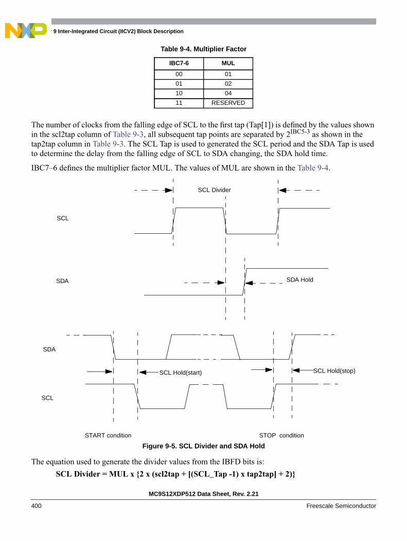
Chapter 9 Inter-Integrated Circuit (IICV2) Block Description
MC9S12XDP512 Data Sheet, Rev. 2.21
400 Freescale Semiconductor
The number of clocks from the falling edge of SCL to the first tap (Tap[1]) is defined by the values shownin the scl2tap column of Table 9-3, all subsequent tap points are separated by 2IBC5-3 as shown in thetap2tap column in Table 9-3. The SCL Tap is used to generated the SCL period and the SDA Tap is usedto determine the delay from the falling edge of SCL to SDA changing, the SDA hold time.
IBC7–6 defines the multiplier factor MUL. The values of MUL are shown in the Table 9-4.
Figure 9-5. SCL Divider and SDA Hold
The equation used to generate the divider values from the IBFD bits is:
SCL Divider = MUL x 2 x (scl2tap + [(SCL_Tap -1) x tap2tap] + 2)
Table 9-4. Multiplier Factor
IBC7-6 MUL
00 01
01 02
10 04
11 RESERVED
SCL Divider
SDA Hold
SCL
SDA
SDA
SCL
START condition STOP condition
SCL Hold(start) SCL Hold(stop)
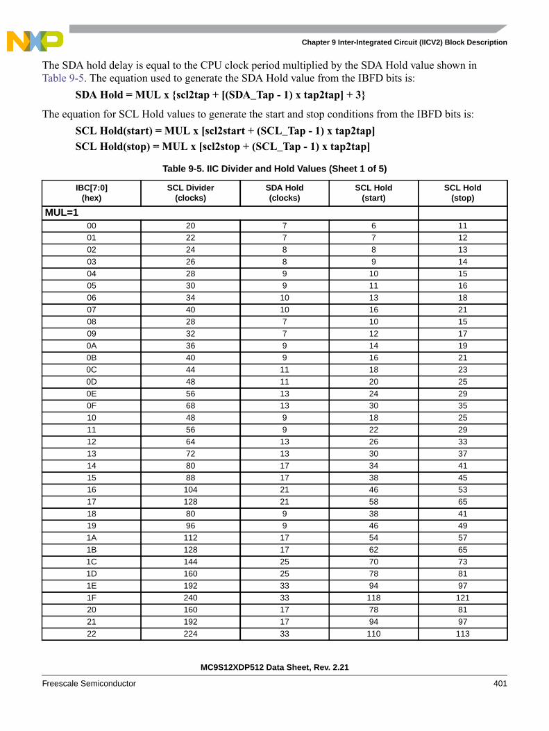
Chapter 9 Inter-Integrated Circuit (IICV2) Block Description
MC9S12XDP512 Data Sheet, Rev. 2.21
Freescale Semiconductor 401
The SDA hold delay is equal to the CPU clock period multiplied by the SDA Hold value shown inTable 9-5. The equation used to generate the SDA Hold value from the IBFD bits is:
SDA Hold = MUL x scl2tap + [(SDA_Tap - 1) x tap2tap] + 3
The equation for SCL Hold values to generate the start and stop conditions from the IBFD bits is:
SCL Hold(start) = MUL x [scl2start + (SCL_Tap - 1) x tap2tap]SCL Hold(stop) = MUL x [scl2stop + (SCL_Tap - 1) x tap2tap]
Table 9-5. IIC Divider and Hold Values (Sheet 1 of 5)
IBC[7:0](hex)
SCL Divider(clocks)
SDA Hold(clocks)
SCL Hold(start)
SCL Hold(stop)
MUL=100 20 7 6 1101 22 7 7 1202 24 8 8 1303 26 8 9 1404 28 9 10 1505 30 9 11 1606 34 10 13 1807 40 10 16 2108 28 7 10 1509 32 7 12 170A 36 9 14 190B 40 9 16 210C 44 11 18 230D 48 11 20 250E 56 13 24 290F 68 13 30 3510 48 9 18 2511 56 9 22 2912 64 13 26 3313 72 13 30 3714 80 17 34 4115 88 17 38 4516 104 21 46 5317 128 21 58 6518 80 9 38 4119 96 9 46 491A 112 17 54 571B 128 17 62 651C 144 25 70 731D 160 25 78 811E 192 33 94 971F 240 33 118 12120 160 17 78 8121 192 17 94 9722 224 33 110 113
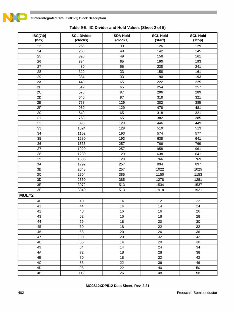
Chapter 9 Inter-Integrated Circuit (IICV2) Block Description
MC9S12XDP512 Data Sheet, Rev. 2.21
402 Freescale Semiconductor
23 256 33 126 12924 288 49 142 14525 320 49 158 16126 384 65 190 19327 480 65 238 24128 320 33 158 16129 384 33 190 1932A 448 65 222 2252B 512 65 254 257
2C 576 97 286 2892D 640 97 318 3212E 768 129 382 3852F 960 129 478 48130 640 65 318 32131 768 65 382 38532 896 129 446 44933 1024 129 510 51334 1152 193 574 57735 1280 193 638 64136 1536 257 766 76937 1920 257 958 96138 1280 129 638 64139 1536 129 766 7693A 1792 257 894 8973B 2048 257 1022 10253C 2304 385 1150 11533D 2560 385 1278 12813E 3072 513 1534 15373F 3840 513 1918 1921
MUL=240 40 14 12 2241 44 14 14 2442 48 16 16 2643 52 16 18 2844 56 18 20 3045 60 18 22 3246 68 20 26 3647 80 20 32 4248 56 14 20 3049 64 14 24 344A 72 18 28 384B 80 18 32 424C 88 22 36 464D 96 22 40 504E 112 26 48 58
Table 9-5. IIC Divider and Hold Values (Sheet 2 of 5)
IBC[7:0](hex)
SCL Divider(clocks)
SDA Hold(clocks)
SCL Hold(start)
SCL Hold(stop)
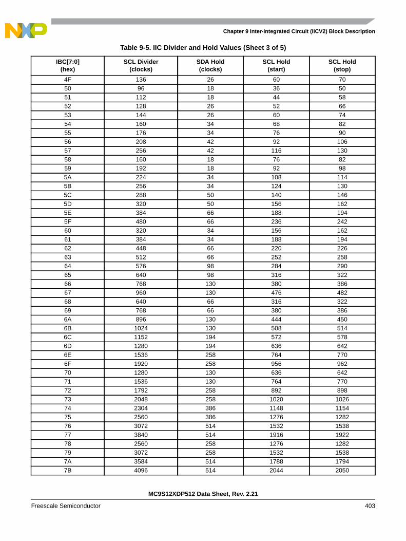
Chapter 9 Inter-Integrated Circuit (IICV2) Block Description
MC9S12XDP512 Data Sheet, Rev. 2.21
Freescale Semiconductor 403
4F 136 26 60 7050 96 18 36 5051 112 18 44 5852 128 26 52 6653 144 26 60 7454 160 34 68 8255 176 34 76 9056 208 42 92 10657 256 42 116 130
58 160 18 76 8259 192 18 92 985A 224 34 108 1145B 256 34 124 1305C 288 50 140 1465D 320 50 156 1625E 384 66 188 1945F 480 66 236 24260 320 34 156 16261 384 34 188 19462 448 66 220 22663 512 66 252 25864 576 98 284 29065 640 98 316 32266 768 130 380 38667 960 130 476 48268 640 66 316 32269 768 66 380 3866A 896 130 444 4506B 1024 130 508 5146C 1152 194 572 5786D 1280 194 636 6426E 1536 258 764 7706F 1920 258 956 96270 1280 130 636 64271 1536 130 764 77072 1792 258 892 89873 2048 258 1020 102674 2304 386 1148 115475 2560 386 1276 128276 3072 514 1532 153877 3840 514 1916 192278 2560 258 1276 128279 3072 258 1532 15387A 3584 514 1788 17947B 4096 514 2044 2050
Table 9-5. IIC Divider and Hold Values (Sheet 3 of 5)
IBC[7:0](hex)
SCL Divider(clocks)
SDA Hold(clocks)
SCL Hold(start)
SCL Hold(stop)
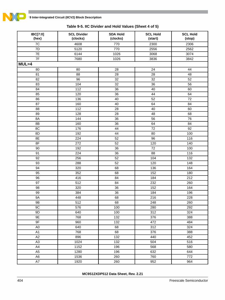
Chapter 9 Inter-Integrated Circuit (IICV2) Block Description
MC9S12XDP512 Data Sheet, Rev. 2.21
404 Freescale Semiconductor
7C 4608 770 2300 23067D 5120 770 2556 25627E 6144 1026 3068 30747F 7680 1026 3836 3842
MUL=480 80 28 24 4481 88 28 28 4882 96 32 32 5283 104 32 36 56
84 112 36 40 6085 120 36 44 6486 136 40 52 7287 160 40 64 8488 112 28 40 6089 128 28 48 688A 144 36 56 768B 160 36 64 848C 176 44 72 928D 192 44 80 1008E 224 52 96 1168F 272 52 120 14090 192 36 72 10091 224 36 88 11692 256 52 104 13293 288 52 120 14894 320 68 136 16495 352 68 152 18096 416 84 184 21297 512 84 232 26098 320 36 152 16499 384 36 184 1969A 448 68 216 2289B 512 68 248 2609C 576 100 280 2929D 640 100 312 3249E 768 132 376 3889F 960 132 472 484A0 640 68 312 324A1 768 68 376 388A2 896 132 440 452A3 1024 132 504 516A4 1152 196 568 580A5 1280 196 632 644A6 1536 260 760 772A7 1920 260 952 964
Table 9-5. IIC Divider and Hold Values (Sheet 4 of 5)
IBC[7:0](hex)
SCL Divider(clocks)
SDA Hold(clocks)
SCL Hold(start)
SCL Hold(stop)

Chapter 9 Inter-Integrated Circuit (IICV2) Block Description
MC9S12XDP512 Data Sheet, Rev. 2.21
Freescale Semiconductor 405
9.3.2.3 IIC Control Register (IBCR)
Read and write anytime
A8 1280 132 632 644A9 1536 132 760 772AA 1792 260 888 900AB 2048 260 1016 1028AC 2304 388 1144 1156AD 2560 388 1272 1284AE 3072 516 1528 1540AF 3840 516 1912 1924B0 2560 260 1272 1284
B1 3072 260 1528 1540B2 3584 516 1784 1796B3 4096 516 2040 2052B4 4608 772 2296 2308B5 5120 772 2552 2564B6 6144 1028 3064 3076B7 7680 1028 3832 3844B8 5120 516 2552 2564B9 6144 516 3064 3076BA 7168 1028 3576 3588BB 8192 1028 4088 4100BC 9216 1540 4600 4612BD 10240 1540 5112 5124BE 12288 2052 6136 6148BF 15360 2052 7672 7684
7 6 5 4 3 2 1 0
RIBEN IBIE MS/SL Tx/Rx TXAK
0 0IBSWAI
W RSTA
Reset 0 0 0 0 0 0 0 0
= Unimplemented or Reserved
Figure 9-6. IIC Bus Control Register (IBCR)
Table 9-5. IIC Divider and Hold Values (Sheet 5 of 5)
IBC[7:0](hex)
SCL Divider(clocks)
SDA Hold(clocks)
SCL Hold(start)
SCL Hold(stop)
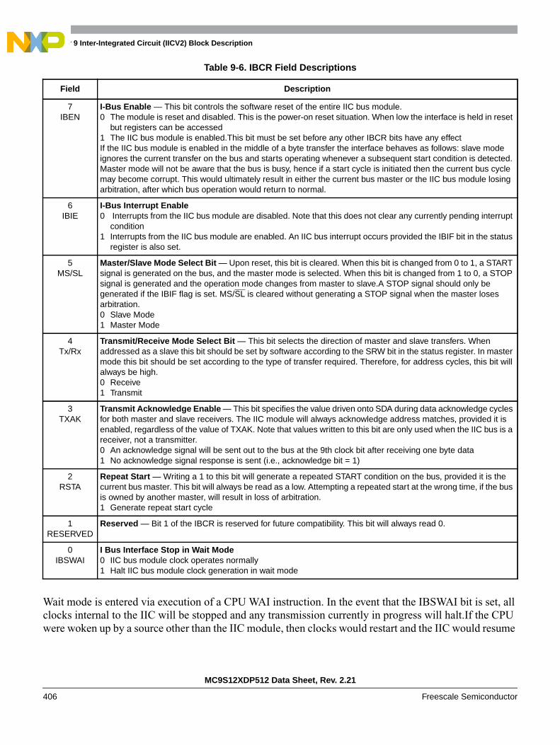
Chapter 9 Inter-Integrated Circuit (IICV2) Block Description
MC9S12XDP512 Data Sheet, Rev. 2.21
406 Freescale Semiconductor
Wait mode is entered via execution of a CPU WAI instruction. In the event that the IBSWAI bit is set, allclocks internal to the IIC will be stopped and any transmission currently in progress will halt.If the CPUwere woken up by a source other than the IIC module, then clocks would restart and the IIC would resume
Table 9-6. IBCR Field Descriptions
Field Description
7IBEN
I-Bus Enable — This bit controls the software reset of the entire IIC bus module.0 The module is reset and disabled. This is the power-on reset situation. When low the interface is held in reset
but registers can be accessed1 The IIC bus module is enabled.This bit must be set before any other IBCR bits have any effectIf the IIC bus module is enabled in the middle of a byte transfer the interface behaves as follows: slave modeignores the current transfer on the bus and starts operating whenever a subsequent start condition is detected.Master mode will not be aware that the bus is busy, hence if a start cycle is initiated then the current bus cyclemay become corrupt. This would ultimately result in either the current bus master or the IIC bus module losingarbitration, after which bus operation would return to normal.
6IBIE
I-Bus Interrupt Enable0 Interrupts from the IIC bus module are disabled. Note that this does not clear any currently pending interrupt
condition1 Interrupts from the IIC bus module are enabled. An IIC bus interrupt occurs provided the IBIF bit in the status
register is also set.
5MS/SL
Master/Slave Mode Select Bit — Upon reset, this bit is cleared. When this bit is changed from 0 to 1, a STARTsignal is generated on the bus, and the master mode is selected. When this bit is changed from 1 to 0, a STOPsignal is generated and the operation mode changes from master to slave.A STOP signal should only begenerated if the IBIF flag is set. MS/SL is cleared without generating a STOP signal when the master losesarbitration.0 Slave Mode1 Master Mode
4Tx/Rx
Transmit/Receive Mode Select Bit — This bit selects the direction of master and slave transfers. Whenaddressed as a slave this bit should be set by software according to the SRW bit in the status register. In mastermode this bit should be set according to the type of transfer required. Therefore, for address cycles, this bit willalways be high.0 Receive1 Transmit
3TXAK
Transmit Acknowledge Enable — This bit specifies the value driven onto SDA during data acknowledge cyclesfor both master and slave receivers. The IIC module will always acknowledge address matches, provided it isenabled, regardless of the value of TXAK. Note that values written to this bit are only used when the IIC bus is areceiver, not a transmitter.0 An acknowledge signal will be sent out to the bus at the 9th clock bit after receiving one byte data1 No acknowledge signal response is sent (i.e., acknowledge bit = 1)
2RSTA
Repeat Start — Writing a 1 to this bit will generate a repeated START condition on the bus, provided it is thecurrent bus master. This bit will always be read as a low. Attempting a repeated start at the wrong time, if the busis owned by another master, will result in loss of arbitration.1 Generate repeat start cycle
1RESERVED
Reserved — Bit 1 of the IBCR is reserved for future compatibility. This bit will always read 0.
0IBSWAI
I Bus Interface Stop in Wait Mode0 IIC bus module clock operates normally1 Halt IIC bus module clock generation in wait mode

Chapter 9 Inter-Integrated Circuit (IICV2) Block Description
MC9S12XDP512 Data Sheet, Rev. 2.21
Freescale Semiconductor 407
from where was during the previous transmission. It is not possible for the IIC to wake up the CPU whenits internal clocks are stopped.
If it were the case that the IBSWAI bit was cleared when the WAI instruction was executed, the IIC internalclocks and interface would remain alive, continuing the operation which was currently underway. It is alsopossible to configure the IIC such that it will wake up the CPU via an interrupt at the conclusion of thecurrent operation. See the discussion on the IBIF and IBIE bits in the IBSR and IBCR, respectively.
9.3.2.4 IIC Status Register (IBSR)
This status register is read-only with exception of bit 1 (IBIF) and bit 4 (IBAL), which are softwareclearable.
7 6 5 4 3 2 1 0
R TCF IAAS IBBIBAL
0 SRWIBIF
RXAK
W
Reset 1 0 0 0 0 0 0 0
= Unimplemented or Reserved
Figure 9-7. IIC Bus Status Register (IBSR)
Table 9-7. IBSR Field Descriptions
Field Description
7TCF
Data Transferring Bit — While one byte of data is being transferred, this bit is cleared. It is set by the fallingedge of the 9th clock of a byte transfer. Note that this bit is only valid during or immediately following a transferto the IIC module or from the IIC module.0 Transfer in progress1 Transfer complete
6IAAS
Addressed as a Slave Bit — When its own specific address (I-bus address register) is matched with the callingaddress, this bit is set.The CPU is interrupted provided the IBIE is set.Then the CPU needs to check the SRWbit and set its Tx/Rx mode accordingly.Writing to the I-bus control register clears this bit.0 Not addressed1 Addressed as a slave
5IBB
Bus Busy Bit0 This bit indicates the status of the bus. When a START signal is detected, the IBB is set. If a STOP signal is
detected, IBB is cleared and the bus enters idle state.1 Bus is busy
4IBAL
Arbitration Lost — The arbitration lost bit (IBAL) is set by hardware when the arbitration procedure is lost.Arbitration is lost in the following circumstances:
1. SDA sampled low when the master drives a high during an address or data transmit cycle.2. SDA sampled low when the master drives a high during the acknowledge bit of a data receive cycle.3. A start cycle is attempted when the bus is busy.4. A repeated start cycle is requested in slave mode.5. A stop condition is detected when the master did not request it.
This bit must be cleared by software, by writing a one to it. A write of 0 has no effect on this bit.
3RESERVED
Reserved — Bit 3 of IBSR is reserved for future use. A read operation on this bit will return 0.
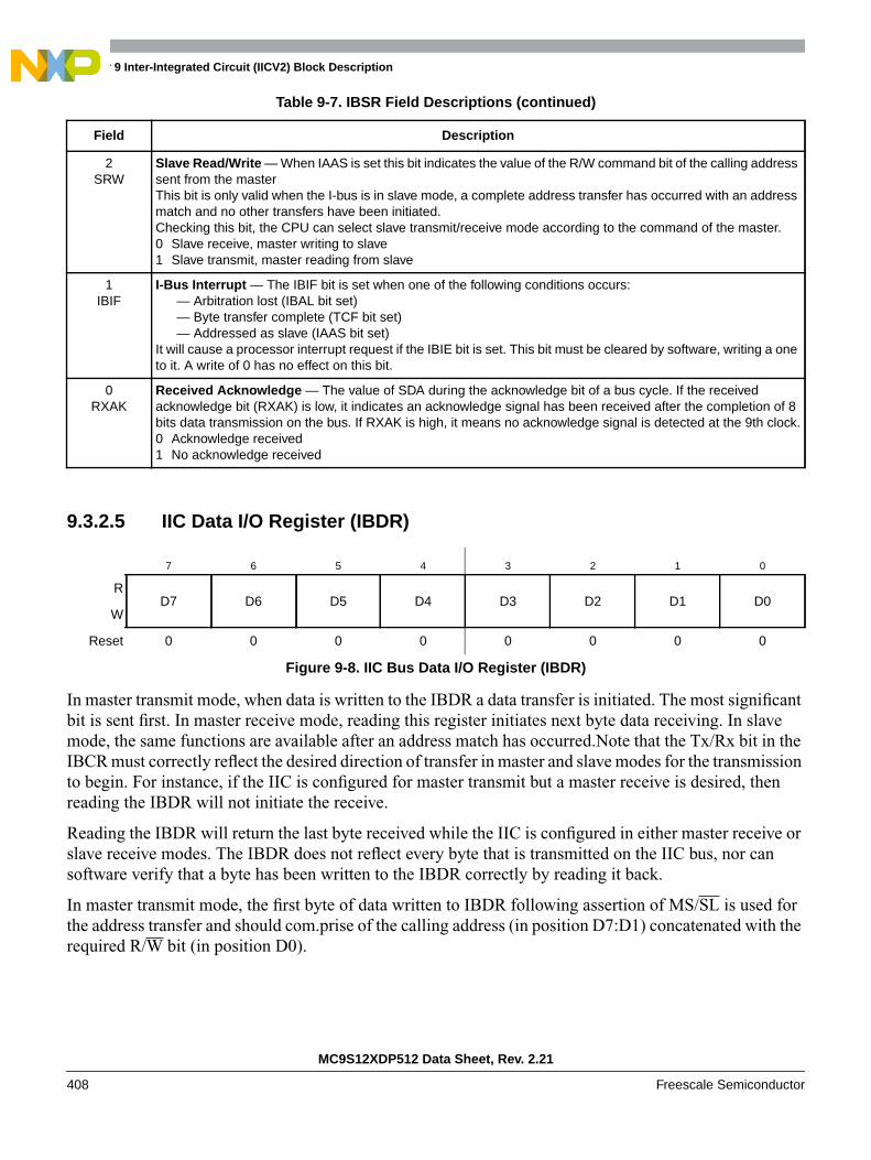
Chapter 9 Inter-Integrated Circuit (IICV2) Block Description
MC9S12XDP512 Data Sheet, Rev. 2.21
408 Freescale Semiconductor
9.3.2.5 IIC Data I/O Register (IBDR)
In master transmit mode, when data is written to the IBDR a data transfer is initiated. The most significantbit is sent first. In master receive mode, reading this register initiates next byte data receiving. In slavemode, the same functions are available after an address match has occurred.Note that the Tx/Rx bit in theIBCR must correctly reflect the desired direction of transfer in master and slave modes for the transmissionto begin. For instance, if the IIC is configured for master transmit but a master receive is desired, thenreading the IBDR will not initiate the receive.
Reading the IBDR will return the last byte received while the IIC is configured in either master receive orslave receive modes. The IBDR does not reflect every byte that is transmitted on the IIC bus, nor cansoftware verify that a byte has been written to the IBDR correctly by reading it back.
In master transmit mode, the first byte of data written to IBDR following assertion of MS/SL is used forthe address transfer and should com.prise of the calling address (in position D7:D1) concatenated with therequired R/W bit (in position D0).
2SRW
Slave Read/Write — When IAAS is set this bit indicates the value of the R/W command bit of the calling addresssent from the masterThis bit is only valid when the I-bus is in slave mode, a complete address transfer has occurred with an addressmatch and no other transfers have been initiated.Checking this bit, the CPU can select slave transmit/receive mode according to the command of the master.0 Slave receive, master writing to slave1 Slave transmit, master reading from slave
1IBIF
I-Bus Interrupt — The IBIF bit is set when one of the following conditions occurs:— Arbitration lost (IBAL bit set)— Byte transfer complete (TCF bit set)— Addressed as slave (IAAS bit set)
It will cause a processor interrupt request if the IBIE bit is set. This bit must be cleared by software, writing a oneto it. A write of 0 has no effect on this bit.
0RXAK
Received Acknowledge — The value of SDA during the acknowledge bit of a bus cycle. If the receivedacknowledge bit (RXAK) is low, it indicates an acknowledge signal has been received after the completion of 8bits data transmission on the bus. If RXAK is high, it means no acknowledge signal is detected at the 9th clock.0 Acknowledge received1 No acknowledge received
7 6 5 4 3 2 1 0
RD7 D6 D5 D4 D3 D2 D1 D0
W
Reset 0 0 0 0 0 0 0 0
Figure 9-8. IIC Bus Data I/O Register (IBDR)
Table 9-7. IBSR Field Descriptions (continued)
Field Description

Chapter 9 Inter-Integrated Circuit (IICV2) Block Description
MC9S12XDP512 Data Sheet, Rev. 2.21
Freescale Semiconductor 409
9.4 Functional DescriptionThis section provides a complete functional description of the IICV2.
9.4.1 I-Bus Protocol
The IIC bus system uses a serial data line (SDA) and a serial clock line (SCL) for data transfer. All devicesconnected to it must have open drain or open collector outputs. Logic AND function is exercised on bothlines with external pull-up resistors. The value of these resistors is system dependent.
Normally, a standard communication is composed of four parts: START signal, slave address transmission,data transfer and STOP signal. They are described briefly in the following sections and illustrated inFigure 9-9.
Figure 9-9. IIC-Bus Transmission Signals
9.4.1.1 START Signal
When the bus is free, i.e. no master device is engaging the bus (both SCL and SDA lines are at logicalhigh), a master may initiate communication by sending a START signal.As shown in Figure 9-9, a STARTsignal is defined as a high-to-low transition of SDA while SCL is high. This signal denotes the beginningof a new data transfer (each data transfer may contain several bytes of data) and brings all slaves out oftheir idle states.
SCL
SDA
StartSignal
AckBit
1 2 3 4 5 6 7 8
MSB LSB
1 2 3 4 5 6 7 8
MSB LSB
StopSignal
No
SCL
SDA
1 2 3 4 5 6 7 8
MSB LSB
1 2 5 6 7 8
MSB LSB
Repeated
3 4
9 9
AD7 AD6 AD5 AD4 AD3 AD2 AD1 R/W XXX D7 D6 D5 D4 D3 D2 D1 D0
Calling Address Read/ Data Byte
AD7 AD6 AD5 AD4 AD3 AD2 AD1 R/W AD7 AD6 AD5 AD4 AD3 AD2 AD1 R/W
New Calling Address
9 9
XX
AckBitWrite
StartSignal
StartSignal
AckBit
Calling Address Read/Write
StopSignal
NoAckBit
Read/Write
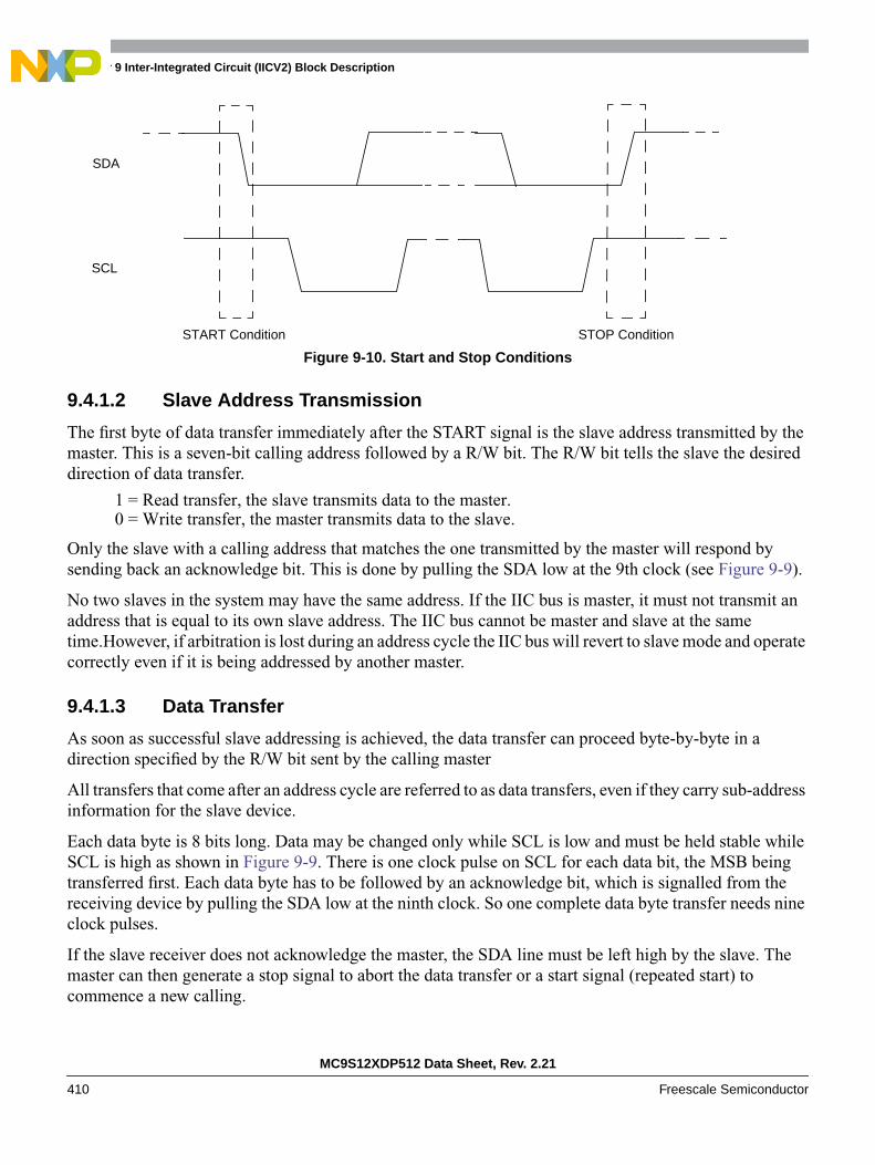
Chapter 9 Inter-Integrated Circuit (IICV2) Block Description
MC9S12XDP512 Data Sheet, Rev. 2.21
410 Freescale Semiconductor
Figure 9-10. Start and Stop Conditions
9.4.1.2 Slave Address Transmission
The first byte of data transfer immediately after the START signal is the slave address transmitted by themaster. This is a seven-bit calling address followed by a R/W bit. The R/W bit tells the slave the desireddirection of data transfer.
1 = Read transfer, the slave transmits data to the master.0 = Write transfer, the master transmits data to the slave.
Only the slave with a calling address that matches the one transmitted by the master will respond bysending back an acknowledge bit. This is done by pulling the SDA low at the 9th clock (see Figure 9-9).
No two slaves in the system may have the same address. If the IIC bus is master, it must not transmit anaddress that is equal to its own slave address. The IIC bus cannot be master and slave at the sametime.However, if arbitration is lost during an address cycle the IIC bus will revert to slave mode and operatecorrectly even if it is being addressed by another master.
9.4.1.3 Data Transfer
As soon as successful slave addressing is achieved, the data transfer can proceed byte-by-byte in adirection specified by the R/W bit sent by the calling master
All transfers that come after an address cycle are referred to as data transfers, even if they carry sub-addressinformation for the slave device.
Each data byte is 8 bits long. Data may be changed only while SCL is low and must be held stable whileSCL is high as shown in Figure 9-9. There is one clock pulse on SCL for each data bit, the MSB beingtransferred first. Each data byte has to be followed by an acknowledge bit, which is signalled from thereceiving device by pulling the SDA low at the ninth clock. So one complete data byte transfer needs nineclock pulses.
If the slave receiver does not acknowledge the master, the SDA line must be left high by the slave. Themaster can then generate a stop signal to abort the data transfer or a start signal (repeated start) tocommence a new calling.
SDA
SCL
START Condition STOP Condition
Chapter 9 Inter-Integrated Circuit (IICV2) Block Description
MC9S12XDP512 Data Sheet, Rev. 2.21
Freescale Semiconductor 411
If the master receiver does not acknowledge the slave transmitter after a byte transmission, it means 'endof data' to the slave, so the slave releases the SDA line for the master to generate STOP or START signal.
9.4.1.4 STOP Signal
The master can terminate the communication by generating a STOP signal to free the bus. However, themaster may generate a START signal followed by a calling command without generating a STOP signalfirst. This is called repeated START. A STOP signal is defined as a low-to-high transition of SDA whileSCL at logical 1 (see Figure 9-9).
The master can generate a STOP even if the slave has generated an acknowledge at which point the slavemust release the bus.
9.4.1.5 Repeated START Signal
As shown in Figure 9-9, a repeated START signal is a START signal generated without first generating aSTOP signal to terminate the communication. This is used by the master to communicate with anotherslave or with the same slave in different mode (transmit/receive mode) without releasing the bus.
9.4.1.6 Arbitration Procedure
The Inter-IC bus is a true multi-master bus that allows more than one master to be connected on it. If twoor more masters try to control the bus at the same time, a clock synchronization procedure determines thebus clock, for which the low period is equal to the longest clock low period and the high is equal to theshortest one among the masters. The relative priority of the contending masters is determined by a dataarbitration procedure, a bus master loses arbitration if it transmits logic 1 while another master transmitslogic 0. The losing masters immediately switch over to slave receive mode and stop driving SDA output.In this case the transition from master to slave mode does not generate a STOP condition. Meanwhile, astatus bit is set by hardware to indicate loss of arbitration.
9.4.1.7 Clock Synchronization
Because wire-AND logic is performed on SCL line, a high-to-low transition on SCL line affects all thedevices connected on the bus. The devices start counting their low period and as soon as a device's clockhas gone low, it holds the SCL line low until the clock high state is reached.However, the change of low tohigh in this device clock may not change the state of the SCL line if another device clock is within its lowperiod. Therefore, synchronized clock SCL is held low by the device with the longest low period. Deviceswith shorter low periods enter a high wait state during this time (see Figure 9-10). When all devicesconcerned have counted off their low period, the synchronized clock SCL line is released and pulled high.There is then no difference between the device clocks and the state of the SCL line and all the devices startcounting their high periods.The first device to complete its high period pulls the SCL line low again.
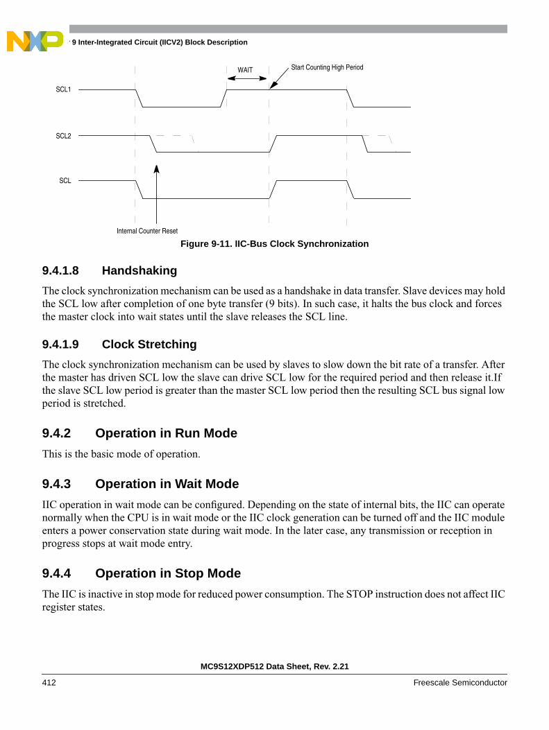
Chapter 9 Inter-Integrated Circuit (IICV2) Block Description
MC9S12XDP512 Data Sheet, Rev. 2.21
412 Freescale Semiconductor
Figure 9-11. IIC-Bus Clock Synchronization
9.4.1.8 Handshaking
The clock synchronization mechanism can be used as a handshake in data transfer. Slave devices may holdthe SCL low after completion of one byte transfer (9 bits). In such case, it halts the bus clock and forcesthe master clock into wait states until the slave releases the SCL line.
9.4.1.9 Clock Stretching
The clock synchronization mechanism can be used by slaves to slow down the bit rate of a transfer. Afterthe master has driven SCL low the slave can drive SCL low for the required period and then release it.Ifthe slave SCL low period is greater than the master SCL low period then the resulting SCL bus signal lowperiod is stretched.
9.4.2 Operation in Run Mode
This is the basic mode of operation.
9.4.3 Operation in Wait Mode
IIC operation in wait mode can be configured. Depending on the state of internal bits, the IIC can operatenormally when the CPU is in wait mode or the IIC clock generation can be turned off and the IIC moduleenters a power conservation state during wait mode. In the later case, any transmission or reception inprogress stops at wait mode entry.
9.4.4 Operation in Stop Mode
The IIC is inactive in stop mode for reduced power consumption. The STOP instruction does not affect IICregister states.
SCL1
SCL2
SCL
Internal Counter Reset
WAIT Start Counting High Period
Chapter 9 Inter-Integrated Circuit (IICV2) Block Description
MC9S12XDP512 Data Sheet, Rev. 2.21
Freescale Semiconductor 413
9.5 ResetsThe reset state of each individual bit is listed in Section 9.3, “Memory Map and Register Definition,” whichdetails the registers and their bit-fields.
9.6 InterruptsIICV2 uses only one interrupt vector.
Table 9-8. Interrupt Summary
Internally there are three types of interrupts in IIC. The interrupt service routine can determine the interrupttype by reading the status register.
IIC Interrupt can be generated on
1. Arbitration lost condition (IBAL bit set)
2. Byte transfer condition (TCF bit set)
3. Address detect condition (IAAS bit set)
The IIC interrupt is enabled by the IBIE bit in the IIC control register. It must be cleared by writing 0 tothe IBF bit in the interrupt service routine.
9.7 Initialization/Application Information
9.7.1 IIC Programming Examples
9.7.1.1 Initialization Sequence
Reset will put the IIC bus control register to its default status. Before the interface can be used to transferserial data, an initialization procedure must be carried out, as follows:
1. Update the frequency divider register (IBFD) and select the required division ratio to obtain SCLfrequency from system clock.
2. Update the IIC bus address register (IBAD) to define its slave address.
3. Set the IBEN bit of the IIC bus control register (IBCR) to enable the IIC interface system.
4. Modify the bits of the IIC bus control register (IBCR) to select master/slave mode, transmit/receivemode and interrupt enable or not.
Interrupt Offset Vector Priority Source Description
IICInterrupt
— — — IBAL, TCF, IAASbits in IBSR
register
When either of IBAL, TCF or IAAS bits is setmay cause an interrupt based on arbitrationlost, transfer complete or address detectconditions

Chapter 9 Inter-Integrated Circuit (IICV2) Block Description
MC9S12XDP512 Data Sheet, Rev. 2.21
414 Freescale Semiconductor
9.7.1.2 Generation of START
After completion of the initialization procedure, serial data can be transmitted by selecting the 'mastertransmitter' mode. If the device is connected to a multi-master bus system, the state of the IIC bus busy bit(IBB) must be tested to check whether the serial bus is free.
If the bus is free (IBB=0), the start condition and the first byte (the slave address) can be sent. The datawritten to the data register comprises the slave calling address and the LSB set to indicate the direction oftransfer required from the slave.
The bus free time (i.e., the time between a STOP condition and the following START condition) is builtinto the hardware that generates the START cycle. Depending on the relative frequencies of the systemclock and the SCL period it may be necessary to wait until the IIC is busy after writing the calling addressto the IBDR before proceeding with the following instructions. This is illustrated in the following example.
An example of a program which generates the START signal and transmits the first byte of data (slaveaddress) is shown below:
9.7.1.3 Post-Transfer Software Response
Transmission or reception of a byte will set the data transferring bit (TCF) to 1, which indicates one bytecommunication is finished. The IIC bus interrupt bit (IBIF) is set also; an interrupt will be generated if theinterrupt function is enabled during initialization by setting the IBIE bit. Software must clear the IBIF bitin the interrupt routine first. The TCF bit will be cleared by reading from the IIC bus data I/O register(IBDR) in receive mode or writing to IBDR in transmit mode.
Software may service the IIC I/O in the main program by monitoring the IBIF bit if the interrupt functionis disabled. Note that polling should monitor the IBIF bit rather than the TCF bit because their operationis different when arbitration is lost.
Note that when an interrupt occurs at the end of the address cycle the master will always be in transmitmode, i.e. the address is transmitted. If master receive mode is required, indicated by R/W bit in IBDR,then the Tx/Rx bit should be toggled at this stage.
During slave mode address cycles (IAAS=1), the SRW bit in the status register is read to determine thedirection of the subsequent transfer and the Tx/Rx bit is programmed accordingly. For slave mode datacycles (IAAS=0) the SRW bit is not valid, the Tx/Rx bit in the control register should be read to determinethe direction of the current transfer.
The following is an example of a software response by a 'master transmitter' in the interrupt routine.
CHFLAG BRSET IBSR,#$20,* ;WAIT FOR IBB FLAG TO CLEAR
TXSTART BSET IBCR,#$30 ;SET TRANSMIT AND MASTER MODE;i.e. GENERATE START CONDITION
MOVB CALLING,IBDR ;TRANSMIT THE CALLING ADDRESS, D0=R/W
IBFREE BRCLR IBSR,#$20,* ;WAIT FOR IBB FLAG TO SET
ISR BCLR IBSR,#$02 ;CLEAR THE IBIF FLAGBRCLR IBCR,#$20,SLAVE ;BRANCH IF IN SLAVE MODEBRCLR IBCR,#$10,RECEIVE ;BRANCH IF IN RECEIVE MODEBRSET IBSR,#$01,END ;IF NO ACK, END OF TRANSMISSION
TRANSMIT MOVB DATABUF,IBDR ;TRANSMIT NEXT BYTE OF DATA
Chapter 9 Inter-Integrated Circuit (IICV2) Block Description
MC9S12XDP512 Data Sheet, Rev. 2.21
Freescale Semiconductor 415
9.7.1.4 Generation of STOP
A data transfer ends with a STOP signal generated by the 'master' device. A master transmitter can simplygenerate a STOP signal after all the data has been transmitted. The following is an example showing howa stop condition is generated by a master transmitter.
If a master receiver wants to terminate a data transfer, it must inform the slave transmitter by notacknowledging the last byte of data which can be done by setting the transmit acknowledge bit (TXAK)before reading the 2nd last byte of data. Before reading the last byte of data, a STOP signal must begenerated first. The following is an example showing how a STOP signal is generated by a master receiver.
9.7.1.5 Generation of Repeated START
At the end of data transfer, if the master continues to want to communicate on the bus, it can generateanother START signal followed by another slave address without first generating a STOP signal. Aprogram example is as shown.
9.7.1.6 Slave Mode
In the slave interrupt service routine, the module addressed as slave bit (IAAS) should be tested to checkif a calling of its own address has just been received. If IAAS is set, software should set the transmit/receivemode select bit (Tx/Rx bit of IBCR) according to the R/W command bit (SRW). Writing to the IBCRclears the IAAS automatically. Note that the only time IAAS is read as set is from the interrupt at the endof the address cycle where an address match occurred, interrupts resulting from subsequent data transferswill have IAAS cleared. A data transfer may now be initiated by writing information to IBDR, for slavetransmits, or dummy reading from IBDR, in slave receive mode. The slave will drive SCL low in-betweenbyte transfers, SCL is released when the IBDR is accessed in the required mode.
MASTX TST TXCNT ;GET VALUE FROM THE TRANSMITING COUNTERBEQ END ;END IF NO MORE DATABRSET IBSR,#$01,END ;END IF NO ACKMOVB DATABUF,IBDR ;TRANSMIT NEXT BYTE OF DATADEC TXCNT ;DECREASE THE TXCNTBRA EMASTX ;EXIT
END BCLR IBCR,#$20 ;GENERATE A STOP CONDITIONEMASTX RTI ;RETURN FROM INTERRUPT
MASR DEC RXCNT ;DECREASE THE RXCNTBEQ ENMASR ;LAST BYTE TO BE READMOVB RXCNT,D1 ;CHECK SECOND LAST BYTEDEC D1 ;TO BE READBNE NXMAR ;NOT LAST OR SECOND LAST
LAMAR BSET IBCR,#$08 ;SECOND LAST, DISABLE ACK;TRANSMITTING
BRA NXMARENMASR BCLR IBCR,#$20 ;LAST ONE, GENERATE ‘STOP’ SIGNALNXMAR MOVB IBDR,RXBUF ;READ DATA AND STORE
RTI
RESTART BSET IBCR,#$04 ;ANOTHER START (RESTART)MOVB CALLING,IBDR ;TRANSMIT THE CALLING ADDRESS;D0=R/W
Chapter 9 Inter-Integrated Circuit (IICV2) Block Description
MC9S12XDP512 Data Sheet, Rev. 2.21
416 Freescale Semiconductor
In slave transmitter routine, the received acknowledge bit (RXAK) must be tested before transmitting thenext byte of data. Setting RXAK means an 'end of data' signal from the master receiver, after which it mustbe switched from transmitter mode to receiver mode by software. A dummy read then releases the SCLline so that the master can generate a STOP signal.
9.7.1.7 Arbitration Lost
If several masters try to engage the bus simultaneously, only one master wins and the others losearbitration. The devices which lost arbitration are immediately switched to slave receive mode by thehardware. Their data output to the SDA line is stopped, but SCL continues to be generated until the end ofthe byte during which arbitration was lost. An interrupt occurs at the falling edge of the ninth clock of thistransfer with IBAL=1 and MS/SL=0. If one master attempts to start transmission while the bus is beingengaged by another master, the hardware will inhibit the transmission; switch the MS/SL bit from 1 to 0without generating STOP condition; generate an interrupt to CPU and set the IBAL to indicate that theattempt to engage the bus is failed. When considering these cases, the slave service routine should test theIBAL first and the software should clear the IBAL bit if it is set.
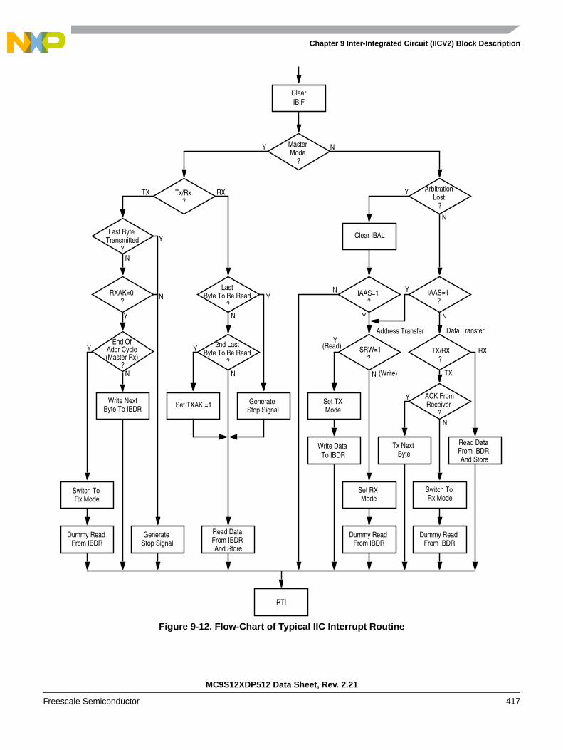
Chapter 9 Inter-Integrated Circuit (IICV2) Block Description
MC9S12XDP512 Data Sheet, Rev. 2.21
Freescale Semiconductor 417
Figure 9-12. Flow-Chart of Typical IIC Interrupt Routine
Clear
MasterMode
?
Tx/Rx?
Last ByteTransmitted
?
RXAK=0?
End OfAddr Cycle(Master Rx)
?
Write NextByte To IBDR
Switch ToRx Mode
Dummy ReadFrom IBDR
GenerateStop Signal
Read DataFrom IBDRAnd Store
Set TXAK =1 GenerateStop Signal
2nd LastByte To Be Read
?
LastByte To Be Read
?
ArbitrationLost
?
Clear IBAL
IAAS=1?
IAAS=1?
SRW=1?
TX/RX?
Set TXMode
Write DataTo IBDR
Set RXMode
Dummy ReadFrom IBDR
ACK FromReceiver
?
Tx NextByte
Read DataFrom IBDRAnd Store
Switch ToRx Mode
Dummy ReadFrom IBDR
RTI
Y N
Y
Y Y
Y
Y
Y
Y
Y
Y
N
N
N
NN
N
N
N
N
Y
TX RX
RX
TX(Write)
(Read)
N
IBIF
Address Transfer Data Transfer

Chapter 9 Inter-Integrated Circuit (IICV2) Block Description
MC9S12XDP512 Data Sheet, Rev. 2.21
418 Freescale Semiconductor

MC9S12XDP512 Data Sheet, Rev. 2.21
Freescale Semiconductor 419
Chapter 10Freescale’s Scalable Controller Area Network(S12MSCANV3)
10.1 IntroductionFreescale’s scalable controller area network (S12MSCANV3) definition is based on the MSCAN12definition, which is the specific implementation of the MSCAN concept targeted for the M68HC12microcontroller family.
The module is a communication controller implementing the CAN 2.0A/B protocol as defined in theBosch specification dated September 1991. For users to fully understand the MSCAN specification, it isrecommended that the Bosch specification be read first to familiarize the reader with the terms andconcepts contained within this document.
Though not exclusively intended for automotive applications, CAN protocol is designed to meet thespecific requirements of a vehicle serial data bus: real-time processing, reliable operation in the EMIenvironment of a vehicle, cost-effectiveness, and required bandwidth.
MSCAN uses an advanced buffer arrangement resulting in predictable real-time behavior and simplifiedapplication software.
10.1.1 Glossary
ACK: Acknowledge of CAN message
CAN: Controller Area Network
CRC: Cyclic Redundancy Code
EOF: End of Frame
FIFO: First-In-First-Out Memory
IFS: Inter-Frame Sequence
SOF: Start of Frame
CPU bus: CPU related read/write data bus
CAN bus: CAN protocol related serial bus
oscillator clock: Direct clock from external oscillator
bus clock: CPU bus realated clock
CAN clock: CAN protocol related clock

Chapter 10 Freescale’s Scalable Controller Area Network (S12MSCANV3)
MC9S12XDP512 Data Sheet, Rev. 2.21
420 Freescale Semiconductor
10.1.2 Block Diagram
Figure 10-1. MSCAN Block Diagram
10.1.3 Features
The basic features of the MSCAN are as follows:
• Implementation of the CAN protocol — Version 2.0A/B
— Standard and extended data frames
— Zero to eight bytes data length
— Programmable bit rate up to 1 Mbps1
— Support for remote frames
• Five receive buffers with FIFO storage scheme
• Three transmit buffers with internal prioritization using a “local priority” concept
• Flexible maskable identifier filter supports two full-size (32-bit) extended identifier filters, or four16-bit filters, or eight 8-bit filters
• Programmable wakeup functionality with integrated low-pass filter
• Programmable loopback mode supports self-test operation
• Programmable listen-only mode for monitoring of CAN bus
• Programmable bus-off recovery functionality
• Separate signalling and interrupt capabilities for all CAN receiver and transmitter error states(warning, error passive, bus-off)
• Programmable MSCAN clock source either bus clock or oscillator clock
1. Depending on the actual bit timing and the clock jitter of the PLL.
RXCAN
TXCAN
Receive/TransmitEngine
MessageFiltering
andBuffering
Controland
StatusWake-Up Interrupt Req.
Errors Interrupt Req.
Receive Interrupt Req.
Transmit Interrupt Req.
CANCLK
Bus Clock
Configuration
Oscillator ClockMUX Presc.
Tq Clk
MSCAN
Low Pass FilterWake-UpRegisters
Chapter 10 Freescale’s Scalable Controller Area Network (S12MSCANV3)
MC9S12XDP512 Data Sheet, Rev. 2.21
Freescale Semiconductor 421
• Internal timer for time-stamping of received and transmitted messages
• Three low-power modes: sleep, power down, and MSCAN enable
• Global initialization of configuration registers
10.1.4 Modes of Operation
The following modes of operation are specific to the MSCAN. See Section 10.4, “Functional Description,”for details.
• Listen-Only Mode
• MSCAN Sleep Mode
• MSCAN Initialization Mode
• MSCAN Power Down Mode
10.2 External Signal DescriptionThe MSCAN uses two external pins:
10.2.1 RXCAN — CAN Receiver Input Pin
RXCAN is the MSCAN receiver input pin.
10.2.2 TXCAN — CAN Transmitter Output Pin
TXCAN is the MSCAN transmitter output pin. The TXCAN output pin represents the logic level on theCAN bus:
0 = Dominant state1 = Recessive state
10.2.3 CAN System
A typical CAN system with MSCAN is shown in Figure 10-2. Each CAN station is connected physicallyto the CAN bus lines through a transceiver device. The transceiver is capable of driving the large currentneeded for the CAN bus and has current protection against defective CAN or defective stations.
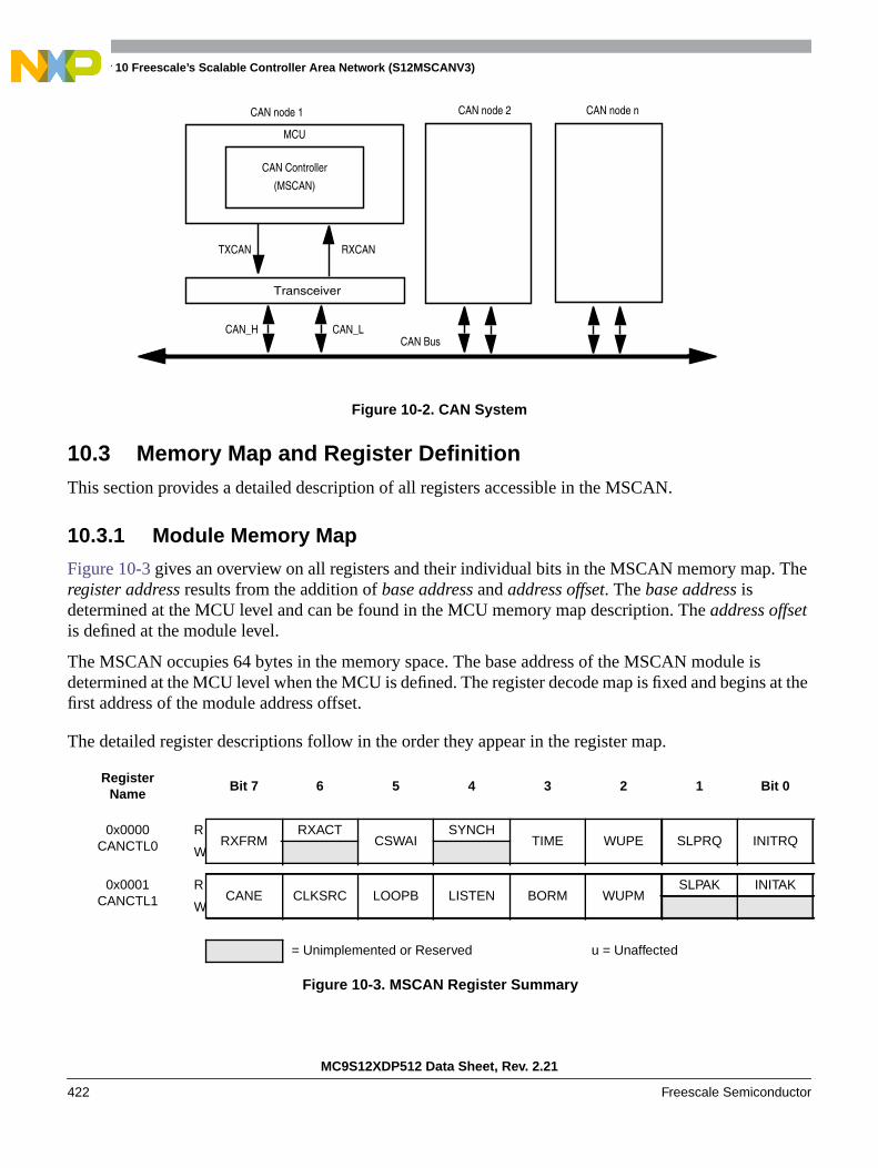
Chapter 10 Freescale’s Scalable Controller Area Network (S12MSCANV3)
MC9S12XDP512 Data Sheet, Rev. 2.21
422 Freescale Semiconductor
Figure 10-2. CAN System
10.3 Memory Map and Register DefinitionThis section provides a detailed description of all registers accessible in the MSCAN.
10.3.1 Module Memory Map
Figure 10-3 gives an overview on all registers and their individual bits in the MSCAN memory map. Theregister address results from the addition of base address and address offset. The base address isdetermined at the MCU level and can be found in the MCU memory map description. The address offsetis defined at the module level.
The MSCAN occupies 64 bytes in the memory space. The base address of the MSCAN module isdetermined at the MCU level when the MCU is defined. The register decode map is fixed and begins at thefirst address of the module address offset.
The detailed register descriptions follow in the order they appear in the register map.
RegisterName
Bit 7 6 5 4 3 2 1 Bit 0
0x0000CANCTL0
RRXFRM
RXACTCSWAI
SYNCHTIME WUPE SLPRQ INITRQ
W
0x0001CANCTL1
RCANE CLKSRC LOOPB LISTEN BORM WUPM
SLPAK INITAK
W
= Unimplemented or Reserved u = Unaffected
Figure 10-3. MSCAN Register Summary
CAN Bus
CAN Controller
(MSCAN)
Transceiver
CAN node 1 CAN node 2 CAN node n
CAN_LCAN_H
MCU
TXCAN RXCAN

Chapter 10 Freescale’s Scalable Controller Area Network (S12MSCANV3)
MC9S12XDP512 Data Sheet, Rev. 2.21
Freescale Semiconductor 423
0x0002CANBTR0
RSJW1 SJW0 BRP5 BRP4 BRP3 BRP2 BRP1 BRP0
W
0x0003CANBTR1
RSAMP TSEG22 TSEG21 TSEG20 TSEG13 TSEG12 TSEG11 TSEG10
W
0x0004CANRFLG
RWUPIF CSCIF
RSTAT1 RSTAT0 TSTAT1 TSTAT0OVRIF RXF
W
0x0005CANRIER
RWUPIE CSCIE RSTATE1 RSTATE0 TSTATE1 TSTATE0 OVRIE RXFIE
W
0x0006CANTFLG
R 0 0 0 0 0TXE2 TXE1 TXE0
W
0x0007CANTIER
R 0 0 0 0 0TXEIE2 TXEIE1 TXEIE0
W
0x0008CANTARQ
R 0 0 0 0 0ABTRQ2 ABTRQ1 ABTRQ0
W
0x0009CANTAAK
R 0 0 0 0 0 ABTAK2 ABTAK1 ABTAK0
W
0x000ACANTBSEL
R 0 0 0 0 0TX2 TX1 TX0
W
0x000BCANIDAC
R 0 0IDAM1 IDAM0
0 IDHIT2 IDHIT1 IDHIT0
W
0x000CReserved
R 0 0 0 0 0 0 0 0
W
0x000DCANMISC
R 0 0 0 0 0 0 0BOHOLD
W
0x000ECANRXERR
R RXERR7 RXERR6 RXERR5 RXERR4 RXERR3 RXERR2 RXERR1 RXERR0
W
0x000FCANTXERR
R TXERR7 TXERR6 TXERR5 TXERR4 TXERR3 TXERR2 TXERR1 TXERR0
W
0x0010–0x0013CANIDAR0–3
RAC7 AC6 AC5 AC4 AC3 AC2 AC1 AC0
W
RegisterName
Bit 7 6 5 4 3 2 1 Bit 0
= Unimplemented or Reserved u = Unaffected
Figure 10-3. MSCAN Register Summary (continued)
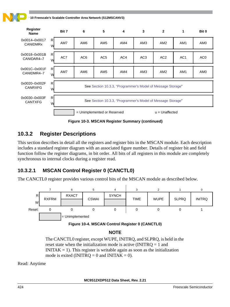
Chapter 10 Freescale’s Scalable Controller Area Network (S12MSCANV3)
MC9S12XDP512 Data Sheet, Rev. 2.21
424 Freescale Semiconductor
10.3.2 Register Descriptions
This section describes in detail all the registers and register bits in the MSCAN module. Each descriptionincludes a standard register diagram with an associated figure number. Details of register bit and fieldfunction follow the register diagrams, in bit order. All bits of all registers in this module are completelysynchronous to internal clocks during a register read.
10.3.2.1 MSCAN Control Register 0 (CANCTL0)
The CANCTL0 register provides various control bits of the MSCAN module as described below.
NOTEThe CANCTL0 register, except WUPE, INITRQ, and SLPRQ, is held in thereset state when the initialization mode is active (INITRQ = 1 andINITAK = 1). This register is writable again as soon as the initializationmode is exited (INITRQ = 0 and INITAK = 0).
Read: Anytime
0x0014–0x0017CANIDMRx
RAM7 AM6 AM5 AM4 AM3 AM2 AM1 AM0
W
0x0018–0x001BCANIDAR4–7
RAC7 AC6 AC5 AC4 AC3 AC2 AC1 AC0
W
0x001C–0x001FCANIDMR4–7
RAM7 AM6 AM5 AM4 AM3 AM2 AM1 AM0
W
0x0020–0x002FCANRXFG
RSee Section 10.3.3, “Programmer’s Model of Message Storage”
W
0x0030–0x003FCANTXFG
RSee Section 10.3.3, “Programmer’s Model of Message Storage”
W
7 6 5 4 3 2 1 0
RRXFRM
RXACTCSWAI
SYNCHTIME WUPE SLPRQ INITRQ
W
Reset: 0 0 0 0 0 0 0 1
= Unimplemented
Figure 10-4. MSCAN Control Register 0 (CANCTL0)
RegisterName
Bit 7 6 5 4 3 2 1 Bit 0
= Unimplemented or Reserved u = Unaffected
Figure 10-3. MSCAN Register Summary (continued)

Chapter 10 Freescale’s Scalable Controller Area Network (S12MSCANV3)
MC9S12XDP512 Data Sheet, Rev. 2.21
Freescale Semiconductor 425
Write: Anytime when out of initialization mode; exceptions are read-only RXACT and SYNCH, RXFRM(which is set by the module only), and INITRQ (which is also writable in initialization mode).
Table 10-1. CANCTL0 Register Field Descriptions
Field Description
7RXFRM1
Received Frame Flag — This bit is read and clear only. It is set when a receiver has received a valid messagecorrectly, independently of the filter configuration. After it is set, it remains set until cleared by software or reset.Clearing is done by writing a 1. Writing a 0 is ignored. This bit is not valid in loopback mode.0 No valid message was received since last clearing this flag1 A valid message was received since last clearing of this flag
6RXACT
Receiver Active Status — This read-only flag indicates the MSCAN is receiving a message. The flag iscontrolled by the receiver front end. This bit is not valid in loopback mode.0 MSCAN is transmitting or idle2
1 MSCAN is receiving a message (including when arbitration is lost)2
5CSWAI3
CAN Stops in Wait Mode — Enabling this bit allows for lower power consumption in wait mode by disabling allthe clocks at the CPU bus interface to the MSCAN module.0 The module is not affected during wait mode1 The module ceases to be clocked during wait mode
4SYNCH
Synchronized Status — This read-only flag indicates whether the MSCAN is synchronized to the CAN bus andable to participate in the communication process. It is set and cleared by the MSCAN.0 MSCAN is not synchronized to the CAN bus1 MSCAN is synchronized to the CAN bus
3TIME
Timer Enable — This bit activates an internal 16-bit wide free running timer which is clocked by the bit clock rate.If the timer is enabled, a 16-bit time stamp will be assigned to each transmitted/received message within theactive TX/RX buffer. Right after the EOF of a valid message on the CAN bus, the time stamp is written to thehighest bytes (0x000E, 0x000F) in the appropriate buffer (see Section 10.3.3, “Programmer’s Model of MessageStorage”). The internal timer is reset (all bits set to 0) when disabled. This bit is held low in initialization mode.0 Disable internal MSCAN timer1 Enable internal MSCAN timer
2WUPE4
Wake-Up Enable — This configuration bit allows the MSCAN to restart from sleep mode when traffic on CAN isdetected (see Section 10.4.5.4, “MSCAN Sleep Mode”). This bit must be configured before sleep mode entry forthe selected function to take effect.0 Wake-up disabled — The MSCAN ignores traffic on CAN1 Wake-up enabled — The MSCAN is able to restart

Chapter 10 Freescale’s Scalable Controller Area Network (S12MSCANV3)
MC9S12XDP512 Data Sheet, Rev. 2.21
426 Freescale Semiconductor
10.3.2.2 MSCAN Control Register 1 (CANCTL1)
The CANCTL1 register provides various control bits and handshake status information of the MSCANmodule as described below.
1SLPRQ5
Sleep Mode Request — This bit requests the MSCAN to enter sleep mode, which is an internal power savingmode (see Section 10.4.5.4, “MSCAN Sleep Mode”). The sleep mode request is serviced when the CAN bus isidle, i.e., the module is not receiving a message and all transmit buffers are empty. The module indicates entryto sleep mode by setting SLPAK = 1 (see Section 10.3.2.2, “MSCAN Control Register 1 (CANCTL1)”). SLPRQcannot be set while the WUPIF flag is set (see Section 10.3.2.5, “MSCAN Receiver Flag Register (CANRFLG)”).Sleep mode will be active until SLPRQ is cleared by the CPU or, depending on the setting of WUPE, the MSCANdetects activity on the CAN bus and clears SLPRQ itself.0 Running — The MSCAN functions normally1 Sleep mode request — The MSCAN enters sleep mode when CAN bus idle
0INITRQ6,7
Initialization Mode Request — When this bit is set by the CPU, the MSCAN skips to initialization mode (seeSection 10.4.5.5, “MSCAN Initialization Mode”). Any ongoing transmission or reception is aborted andsynchronization to the CAN bus is lost. The module indicates entry to initialization mode by setting INITAK = 1(Section 10.3.2.2, “MSCAN Control Register 1 (CANCTL1)”).The following registers enter their hard reset state and restore their default values: CANCTL08, CANRFLG9,CANRIER10, CANTFLG, CANTIER, CANTARQ, CANTAAK, and CANTBSEL.The registers CANCTL1, CANBTR0, CANBTR1, CANIDAC, CANIDAR0-7, and CANIDMR0-7 can only bewritten by the CPU when the MSCAN is in initialization mode (INITRQ = 1 and INITAK = 1). The values of theerror counters are not affected by initialization mode.When this bit is cleared by the CPU, the MSCAN restarts and then tries to synchronize to the CAN bus. If theMSCAN is not in bus-off state, it synchronizes after 11 consecutive recessive bits on the CAN bus; if the MSCANis in bus-off state, it continues to wait for 128 occurrences of 11 consecutive recessive bits.Writing to other bits in CANCTL0, CANRFLG, CANRIER, CANTFLG, or CANTIER must be done only afterinitialization mode is exited, which is INITRQ = 0 and INITAK = 0.0 Normal operation1 MSCAN in initialization mode
1 The MSCAN must be in normal mode for this bit to become set.2 See the Bosch CAN 2.0A/B specification for a detailed definition of transmitter and receiver states.3 In order to protect from accidentally violating the CAN protocol, the TXCAN pin is immediately forced to a recessive state when
the CPU enters wait (CSWAI = 1) or stop mode (see Section 10.4.5.2, “Operation in Wait Mode” and Section 10.4.5.3,“Operation in Stop Mode”).
4 The CPU has to make sure that the WUPE register and the WUPIE wake-up interrupt enable register (see Section 10.3.2.6,“MSCAN Receiver Interrupt Enable Register (CANRIER)) is enabled, if the recovery mechanism from stop or wait is required.
5 The CPU cannot clear SLPRQ before the MSCAN has entered sleep mode (SLPRQ = 1 and SLPAK = 1).6 The CPU cannot clear INITRQ before the MSCAN has entered initialization mode (INITRQ = 1 and INITAK = 1).7 In order to protect from accidentally violating the CAN protocol, the TXCAN pin is immediately forced to a recessive state when
the initialization mode is requested by the CPU. Thus, the recommended procedure is to bring the MSCAN into sleep mode(SLPRQ = 1 and SLPAK = 1) before requesting initialization mode.
8 Not including WUPE, INITRQ, and SLPRQ.9 TSTAT1 and TSTAT0 are not affected by initialization mode.10 RSTAT1 and RSTAT0 are not affected by initialization mode.
Table 10-1. CANCTL0 Register Field Descriptions (continued)
Field Description

Chapter 10 Freescale’s Scalable Controller Area Network (S12MSCANV3)
MC9S12XDP512 Data Sheet, Rev. 2.21
Freescale Semiconductor 427
Read: AnytimeWrite: Anytime when INITRQ = 1 and INITAK = 1, except CANE which is write once in normal andanytime in special system operation modes when the MSCAN is in initialization mode (INITRQ = 1 andINITAK = 1).
7 6 5 4 3 2 1 0
RCANE CLKSRC LOOPB LISTEN BORM WUPM
SLPAK INITAK
W
Reset: 0 0 0 1 0 0 0 1
= Unimplemented
Figure 10-5. MSCAN Control Register 1 (CANCTL1)
Table 10-2. CANCTL1 Register Field Descriptions
Field Description
7CANE
MSCAN Enable0 MSCAN module is disabled1 MSCAN module is enabled
6CLKSRC
MSCAN Clock Source — This bit defines the clock source for the MSCAN module (only for systems with a clockgeneration module; Section 10.4.3.2, “Clock System,” and Section Figure 10-43., “MSCAN Clocking Scheme,”).0 MSCAN clock source is the oscillator clock1 MSCAN clock source is the bus clock
5LOOPB
Loopback Self Test Mode — When this bit is set, the MSCAN performs an internal loopback which can be usedfor self test operation. The bit stream output of the transmitter is fed back to the receiver internally. The RXCANinput pin is ignored and the TXCAN output goes to the recessive state (logic 1). The MSCAN behaves as it doesnormally when transmitting and treats its own transmitted message as a message received from a remote node.In this state, the MSCAN ignores the bit sent during the ACK slot in the CAN frame acknowledge field to ensureproper reception of its own message. Both transmit and receive interrupts are generated.0 Loopback self test disabled1 Loopback self test enabled
4LISTEN
Listen Only Mode — This bit configures the MSCAN as a CAN bus monitor. When LISTEN is set, all valid CANmessages with matching ID are received, but no acknowledgement or error frames are sent out (seeSection 10.4.4.4, “Listen-Only Mode”). In addition, the error counters are frozen. Listen only mode supportsapplications which require “hot plugging” or throughput analysis. The MSCAN is unable to transmit anymessages when listen only mode is active.0 Normal operation1 Listen only mode activated
3BORM
Bus-Off Recovery Mode — This bits configures the bus-off state recovery mode of the MSCAN. Refer toSection 10.5.2, “Bus-Off Recovery,” for details.0 Automatic bus-off recovery (see Bosch CAN 2.0A/B protocol specification)1 Bus-off recovery upon user request
2WUPM
Wake-Up Mode — If WUPE in CANCTL0 is enabled, this bit defines whether the integrated low-pass filter isapplied to protect the MSCAN from spurious wake-up (see Section 10.4.5.4, “MSCAN Sleep Mode”).0 MSCAN wakes up on any dominant level on the CAN bus1 MSCAN wakes up only in case of a dominant pulse on the CAN bus that has a length of Twup

Chapter 10 Freescale’s Scalable Controller Area Network (S12MSCANV3)
MC9S12XDP512 Data Sheet, Rev. 2.21
428 Freescale Semiconductor
10.3.2.3 MSCAN Bus Timing Register 0 (CANBTR0)
The CANBTR0 register configures various CAN bus timing parameters of the MSCAN module.
Read: AnytimeWrite: Anytime in initialization mode (INITRQ = 1 and INITAK = 1)
1SLPAK
Sleep Mode Acknowledge — This flag indicates whether the MSCAN module has entered sleep mode (seeSection 10.4.5.4, “MSCAN Sleep Mode”). It is used as a handshake flag for the SLPRQ sleep mode request.Sleep mode is active when SLPRQ = 1 and SLPAK = 1. Depending on the setting of WUPE, the MSCAN willclear the flag if it detects activity on the CAN bus while in sleep mode.0 Running — The MSCAN operates normally1 Sleep mode active — The MSCAN has entered sleep mode
0INITAK
Initialization Mode Acknowledge — This flag indicates whether the MSCAN module is in initialization mode(see Section 10.4.5.5, “MSCAN Initialization Mode”). It is used as a handshake flag for the INITRQ initializationmode request. Initialization mode is active when INITRQ = 1 and INITAK = 1. The registers CANCTL1,CANBTR0, CANBTR1, CANIDAC, CANIDAR0–CANIDAR7, and CANIDMR0–CANIDMR7 can be written only bythe CPU when the MSCAN is in initialization mode.0 Running — The MSCAN operates normally1 Initialization mode active — The MSCAN has entered initialization mode
7 6 5 4 3 2 1 0
RSJW1 SJW0 BRP5 BRP4 BRP3 BRP2 BRP1 BRP0
W
Reset: 0 0 0 0 0 0 0 0
Figure 10-6. MSCAN Bus Timing Register 0 (CANBTR0)
Table 10-3. CANBTR0 Register Field Descriptions
Field Description
7:6SJW[1:0]
Synchronization Jump Width — The synchronization jump width defines the maximum number of time quanta(Tq) clock cycles a bit can be shortened or lengthened to achieve resynchronization to data transitions on theCAN bus (see Table 10-4).
5:0BRP[5:0]
Baud Rate Prescaler — These bits determine the time quanta (Tq) clock which is used to build up the bit timing(see Table 10-5).
Table 10-4. Synchronization Jump Width
SJW1 SJW0 Synchronization Jump Width
0 0 1 Tq clock cycle
0 1 2 Tq clock cycles
1 0 3 Tq clock cycles
1 1 4 Tq clock cycles
Table 10-2. CANCTL1 Register Field Descriptions (continued)
Field Description
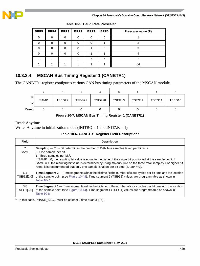
Chapter 10 Freescale’s Scalable Controller Area Network (S12MSCANV3)
MC9S12XDP512 Data Sheet, Rev. 2.21
Freescale Semiconductor 429
10.3.2.4 MSCAN Bus Timing Register 1 (CANBTR1)
The CANBTR1 register configures various CAN bus timing parameters of the MSCAN module.
Read: AnytimeWrite: Anytime in initialization mode (INITRQ = 1 and INITAK = 1)
Table 10-5. Baud Rate Prescaler
BRP5 BRP4 BRP3 BRP2 BRP1 BRP0 Prescaler value (P)
0 0 0 0 0 0 1
0 0 0 0 0 1 2
0 0 0 0 1 0 3
0 0 0 0 1 1 4
: : : : : : :
1 1 1 1 1 1 64
7 6 5 4 3 2 1 0
RSAMP TSEG22 TSEG21 TSEG20 TSEG13 TSEG12 TSEG11 TSEG10
W
Reset: 0 0 0 0 0 0 0 0
Figure 10-7. MSCAN Bus Timing Register 1 (CANBTR1)
Table 10-6. CANBTR1 Register Field Descriptions
Field Description
7SAMP
Sampling — This bit determines the number of CAN bus samples taken per bit time.0 One sample per bit.1 Three samples per bit1.If SAMP = 0, the resulting bit value is equal to the value of the single bit positioned at the sample point. IfSAMP = 1, the resulting bit value is determined by using majority rule on the three total samples. For higher bitrates, it is recommended that only one sample is taken per bit time (SAMP = 0).
1 In this case, PHASE_SEG1 must be at least 2 time quanta (Tq).
6:4TSEG2[2:0]
Time Segment 2 — Time segments within the bit time fix the number of clock cycles per bit time and the locationof the sample point (see Figure 10-44). Time segment 2 (TSEG2) values are programmable as shown inTable 10-7.
3:0TSEG1[3:0]
Time Segment 1 — Time segments within the bit time fix the number of clock cycles per bit time and the locationof the sample point (see Figure 10-44). Time segment 1 (TSEG1) values are programmable as shown inTable 10-8.

Chapter 10 Freescale’s Scalable Controller Area Network (S12MSCANV3)
MC9S12XDP512 Data Sheet, Rev. 2.21
430 Freescale Semiconductor
The bit time is determined by the oscillator frequency, the baud rate prescaler, and the number of timequanta (Tq) clock cycles per bit (as shown in Table 10-7 and Table 10-8).
Eqn. 10-1
10.3.2.5 MSCAN Receiver Flag Register (CANRFLG)
A flag can be cleared only by software (writing a 1 to the corresponding bit position) when the conditionwhich caused the setting is no longer valid. Every flag has an associated interrupt enable bit in theCANRIER register.
Table 10-7. Time Segment 2 Values
TSEG22 TSEG21 TSEG20 Time Segment 2
0 0 0 1 Tq clock cycle1
1 This setting is not valid. Please refer to Table 10-35 for valid settings.
0 0 1 2 Tq clock cycles
: : : :
1 1 0 7 Tq clock cycles
1 1 1 8 Tq clock cycles
Table 10-8. Time Segment 1 Values
TSEG13 TSEG12 TSEG11 TSEG10 Time segment 1
0 0 0 0 1 Tq clock cycle1
1 This setting is not valid. Please refer to Table 10-35 for valid settings.
0 0 0 1 2 Tq clock cycles1
0 0 1 0 3 Tq clock cycles1
0 0 1 1 4 Tq clock cycles
: : : : :
1 1 1 0 15 Tq clock cycles
1 1 1 1 16 Tq clock cycles
7 6 5 4 3 2 1 0
RWUPIF CSCIF
RSTAT1 RSTAT0 TSTAT1 TSTAT0OVRIF RXF
W
Reset: 0 0 0 0 0 0 0 0
= Unimplemented
Figure 10-8. MSCAN Receiver Flag Register (CANRFLG)
Bit Time Prescaler value( )fCANCLK
------------------------------------------------------ 1 TimeSegment1 TimeSegment2+ +( )•=
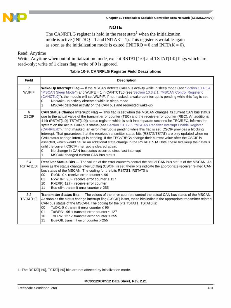
Chapter 10 Freescale’s Scalable Controller Area Network (S12MSCANV3)
MC9S12XDP512 Data Sheet, Rev. 2.21
Freescale Semiconductor 431
NOTEThe CANRFLG register is held in the reset state1 when the initializationmode is active (INITRQ = 1 and INITAK = 1). This register is writable againas soon as the initialization mode is exited (INITRQ = 0 and INITAK = 0).
Read: AnytimeWrite: Anytime when out of initialization mode, except RSTAT[1:0] and TSTAT[1:0] flags which areread-only; write of 1 clears flag; write of 0 is ignored.
1. The RSTAT[1:0], TSTAT[1:0] bits are not affected by initialization mode.
Table 10-9. CANRFLG Register Field Descriptions
Field Description
7WUPIF
Wake-Up Interrupt Flag — If the MSCAN detects CAN bus activity while in sleep mode (see Section 10.4.5.4,“MSCAN Sleep Mode,”) and WUPE = 1 in CANTCTL0 (see Section 10.3.2.1, “MSCAN Control Register 0(CANCTL0)”), the module will set WUPIF. If not masked, a wake-up interrupt is pending while this flag is set.0 No wake-up activity observed while in sleep mode1 MSCAN detected activity on the CAN bus and requested wake-up
6CSCIF
CAN Status Change Interrupt Flag — This flag is set when the MSCAN changes its current CAN bus statusdue to the actual value of the transmit error counter (TEC) and the receive error counter (REC). An additional4-bit (RSTAT[1:0], TSTAT[1:0]) status register, which is split into separate sections for TEC/REC, informs thesystem on the actual CAN bus status (see Section 10.3.2.6, “MSCAN Receiver Interrupt Enable Register(CANRIER)”). If not masked, an error interrupt is pending while this flag is set. CSCIF provides a blockinginterrupt. That guarantees that the receiver/transmitter status bits (RSTAT/TSTAT) are only updated when noCAN status change interrupt is pending. If the TECs/RECs change their current value after the CSCIF isasserted, which would cause an additional state change in the RSTAT/TSTAT bits, these bits keep their statusuntil the current CSCIF interrupt is cleared again.0 No change in CAN bus status occurred since last interrupt1 MSCAN changed current CAN bus status
5:4RSTAT[1:0]
Receiver Status Bits — The values of the error counters control the actual CAN bus status of the MSCAN. Assoon as the status change interrupt flag (CSCIF) is set, these bits indicate the appropriate receiver related CANbus status of the MSCAN. The coding for the bits RSTAT1, RSTAT0 is:00 RxOK: 0 ≤ receive error counter ≤ 9601 RxWRN: 96 < receive error counter ≤ 12710 RxERR: 127 < receive error counter11 Bus-off1: transmit error counter > 255
3:2TSTAT[1:0]
Transmitter Status Bits — The values of the error counters control the actual CAN bus status of the MSCAN.As soon as the status change interrupt flag (CSCIF) is set, these bits indicate the appropriate transmitter relatedCAN bus status of the MSCAN. The coding for the bits TSTAT1, TSTAT0 is:00 TxOK: 0 ≤ transmit error counter ≤ 9601 TxWRN: 96 < transmit error counter ≤ 12710 TxERR: 127 < transmit error counter ≤ 25511 Bus-Off: transmit error counter > 255
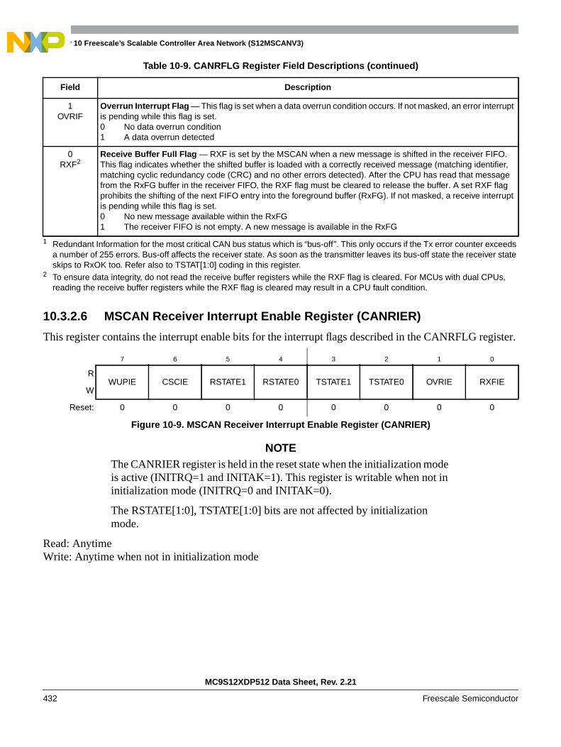
Chapter 10 Freescale’s Scalable Controller Area Network (S12MSCANV3)
MC9S12XDP512 Data Sheet, Rev. 2.21
432 Freescale Semiconductor
10.3.2.6 MSCAN Receiver Interrupt Enable Register (CANRIER)
This register contains the interrupt enable bits for the interrupt flags described in the CANRFLG register.
NOTEThe CANRIER register is held in the reset state when the initialization modeis active (INITRQ=1 and INITAK=1). This register is writable when not ininitialization mode (INITRQ=0 and INITAK=0).
The RSTATE[1:0], TSTATE[1:0] bits are not affected by initializationmode.
Read: AnytimeWrite: Anytime when not in initialization mode
1OVRIF
Overrun Interrupt Flag — This flag is set when a data overrun condition occurs. If not masked, an error interruptis pending while this flag is set.0 No data overrun condition1 A data overrun detected
0RXF2
Receive Buffer Full Flag — RXF is set by the MSCAN when a new message is shifted in the receiver FIFO.This flag indicates whether the shifted buffer is loaded with a correctly received message (matching identifier,matching cyclic redundancy code (CRC) and no other errors detected). After the CPU has read that messagefrom the RxFG buffer in the receiver FIFO, the RXF flag must be cleared to release the buffer. A set RXF flagprohibits the shifting of the next FIFO entry into the foreground buffer (RxFG). If not masked, a receive interruptis pending while this flag is set.0 No new message available within the RxFG1 The receiver FIFO is not empty. A new message is available in the RxFG
1 Redundant Information for the most critical CAN bus status which is “bus-off”. This only occurs if the Tx error counter exceedsa number of 255 errors. Bus-off affects the receiver state. As soon as the transmitter leaves its bus-off state the receiver stateskips to RxOK too. Refer also to TSTAT[1:0] coding in this register.
2 To ensure data integrity, do not read the receive buffer registers while the RXF flag is cleared. For MCUs with dual CPUs,reading the receive buffer registers while the RXF flag is cleared may result in a CPU fault condition.
7 6 5 4 3 2 1 0
RWUPIE CSCIE RSTATE1 RSTATE0 TSTATE1 TSTATE0 OVRIE RXFIE
W
Reset: 0 0 0 0 0 0 0 0
Figure 10-9. MSCAN Receiver Interrupt Enable Register (CANRIER)
Table 10-9. CANRFLG Register Field Descriptions (continued)
Field Description

Chapter 10 Freescale’s Scalable Controller Area Network (S12MSCANV3)
MC9S12XDP512 Data Sheet, Rev. 2.21
Freescale Semiconductor 433
10.3.2.7 MSCAN Transmitter Flag Register (CANTFLG)
The transmit buffer empty flags each have an associated interrupt enable bit in the CANTIER register.
Table 10-10. CANRIER Register Field Descriptions
Field Description
7WUPIE1
1 WUPIE and WUPE (see Section 10.3.2.1, “MSCAN Control Register 0 (CANCTL0)”) must both be enabled if the recoverymechanism from stop or wait is required.
Wake-Up Interrupt Enable0 No interrupt request is generated from this event.1 A wake-up event causes a Wake-Up interrupt request.
6CSCIE
CAN Status Change Interrupt Enable0 No interrupt request is generated from this event.1 A CAN Status Change event causes an error interrupt request.
5:4RSTATE[1:0]
Receiver Status Change Enable — These RSTAT enable bits control the sensitivity level in which receiver statechanges are causing CSCIF interrupts. Independent of the chosen sensitivity level the RSTAT flags continue toindicate the actual receiver state and are only updated if no CSCIF interrupt is pending.00 Do not generate any CSCIF interrupt caused by receiver state changes.01 Generate CSCIF interrupt only if the receiver enters or leaves “bus-off” state. Discard other receiver state
changes for generating CSCIF interrupt.10 Generate CSCIF interrupt only if the receiver enters or leaves “RxErr” or “bus-off”2 state. Discard other
receiver state changes for generating CSCIF interrupt.11 Generate CSCIF interrupt on all state changes.
2 Bus-off state is defined by the CAN standard (see Bosch CAN 2.0A/B protocol specification: for only transmitters. Because theonly possible state change for the transmitter from bus-off to TxOK also forces the receiver to skip its current state to RxOK,the coding of the RXSTAT[1:0] flags define an additional bus-off state for the receiver (see Section 10.3.2.5, “MSCAN ReceiverFlag Register (CANRFLG)”).
3:2TSTATE[1:0]
Transmitter Status Change Enable — These TSTAT enable bits control the sensitivity level in which transmitterstate changes are causing CSCIF interrupts. Independent of the chosen sensitivity level, the TSTAT flagscontinue to indicate the actual transmitter state and are only updated if no CSCIF interrupt is pending.00 Do not generate any CSCIF interrupt caused by transmitter state changes.01 Generate CSCIF interrupt only if the transmitter enters or leaves “bus-off” state. Discard other transmitter
state changes for generating CSCIF interrupt.10 Generate CSCIF interrupt only if the transmitter enters or leaves “TxErr” or “bus-off” state. Discard other
transmitter state changes for generating CSCIF interrupt.11 Generate CSCIF interrupt on all state changes.
1OVRIE
Overrun Interrupt Enable0 No interrupt request is generated from this event.1 An overrun event causes an error interrupt request.
0RXFIE
Receiver Full Interrupt Enable0 No interrupt request is generated from this event.1 A receive buffer full (successful message reception) event causes a receiver interrupt request.

Chapter 10 Freescale’s Scalable Controller Area Network (S12MSCANV3)
MC9S12XDP512 Data Sheet, Rev. 2.21
434 Freescale Semiconductor
NOTEThe CANTFLG register is held in the reset state when the initializationmode is active (INITRQ = 1 and INITAK = 1). This register is writable whennot in initialization mode (INITRQ = 0 and INITAK = 0).
Read: AnytimeWrite: Anytime for TXEx flags when not in initialization mode; write of 1 clears flag, write of 0 is ignored
10.3.2.8 MSCAN Transmitter Interrupt Enable Register (CANTIER)
This register contains the interrupt enable bits for the transmit buffer empty interrupt flags.
7 6 5 4 3 2 1 0
R 0 0 0 0 0TXE2 TXE1 TXE0
W
Reset: 0 0 0 0 0 1 1 1
= Unimplemented
Figure 10-10. MSCAN Transmitter Flag Register (CANTFLG)
Table 10-11. CANTFLG Register Field Descriptions
Field Description
2:0TXE[2:0]
Transmitter Buffer Empty — This flag indicates that the associated transmit message buffer is empty, and thusnot scheduled for transmission. The CPU must clear the flag after a message is set up in the transmit buffer andis due for transmission. The MSCAN sets the flag after the message is sent successfully. The flag is also set bythe MSCAN when the transmission request is successfully aborted due to a pending abort request (seeSection 10.3.2.9, “MSCAN Transmitter Message Abort Request Register (CANTARQ)”). If not masked, atransmit interrupt is pending while this flag is set.Clearing a TXEx flag also clears the corresponding ABTAKx (see Section 10.3.2.10, “MSCAN TransmitterMessage Abort Acknowledge Register (CANTAAK)”). When a TXEx flag is set, the corresponding ABTRQx bitis cleared (see Section 10.3.2.9, “MSCAN Transmitter Message Abort Request Register (CANTARQ)”).When listen-mode is active (see Section 10.3.2.2, “MSCAN Control Register 1 (CANCTL1)”) the TXEx flagscannot be cleared and no transmission is started.Read and write accesses to the transmit buffer will be blocked, if the corresponding TXEx bit is cleared(TXEx = 0) and the buffer is scheduled for transmission.0 The associated message buffer is full (loaded with a message due for transmission)1 The associated message buffer is empty (not scheduled)
7 6 5 4 3 2 1 0
R 0 0 0 0 0TXEIE2 TXEIE1 TXEIE0
W
Reset: 0 0 0 0 0 0 0 0
= Unimplemented
Figure 10-11. MSCAN Transmitter Interrupt Enable Register (CANTIER)
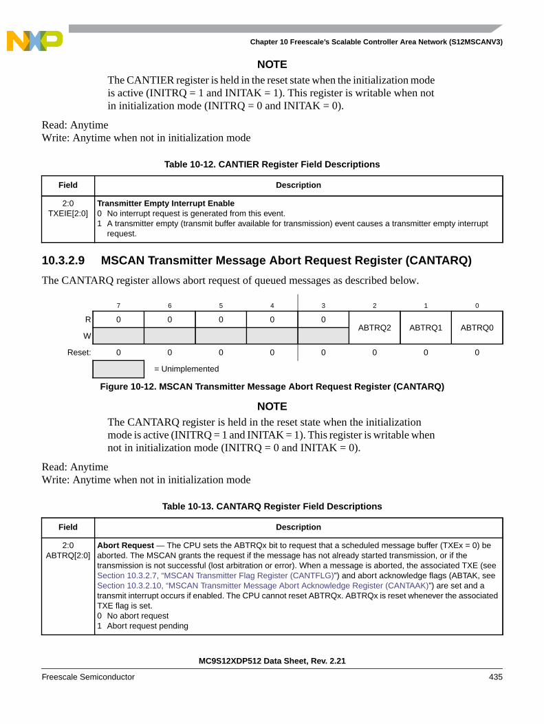
Chapter 10 Freescale’s Scalable Controller Area Network (S12MSCANV3)
MC9S12XDP512 Data Sheet, Rev. 2.21
Freescale Semiconductor 435
NOTEThe CANTIER register is held in the reset state when the initialization modeis active (INITRQ = 1 and INITAK = 1). This register is writable when notin initialization mode (INITRQ = 0 and INITAK = 0).
Read: AnytimeWrite: Anytime when not in initialization mode
10.3.2.9 MSCAN Transmitter Message Abort Request Register (CANTARQ)
The CANTARQ register allows abort request of queued messages as described below.
NOTEThe CANTARQ register is held in the reset state when the initializationmode is active (INITRQ = 1 and INITAK = 1). This register is writable whennot in initialization mode (INITRQ = 0 and INITAK = 0).
Read: AnytimeWrite: Anytime when not in initialization mode
Table 10-12. CANTIER Register Field Descriptions
Field Description
2:0TXEIE[2:0]
Transmitter Empty Interrupt Enable0 No interrupt request is generated from this event.1 A transmitter empty (transmit buffer available for transmission) event causes a transmitter empty interrupt
request.
7 6 5 4 3 2 1 0
R 0 0 0 0 0ABTRQ2 ABTRQ1 ABTRQ0
W
Reset: 0 0 0 0 0 0 0 0
= Unimplemented
Figure 10-12. MSCAN Transmitter Message Abort Request Register (CANTARQ)
Table 10-13. CANTARQ Register Field Descriptions
Field Description
2:0ABTRQ[2:0]
Abort Request — The CPU sets the ABTRQx bit to request that a scheduled message buffer (TXEx = 0) beaborted. The MSCAN grants the request if the message has not already started transmission, or if thetransmission is not successful (lost arbitration or error). When a message is aborted, the associated TXE (seeSection 10.3.2.7, “MSCAN Transmitter Flag Register (CANTFLG)”) and abort acknowledge flags (ABTAK, seeSection 10.3.2.10, “MSCAN Transmitter Message Abort Acknowledge Register (CANTAAK)”) are set and atransmit interrupt occurs if enabled. The CPU cannot reset ABTRQx. ABTRQx is reset whenever the associatedTXE flag is set.0 No abort request1 Abort request pending
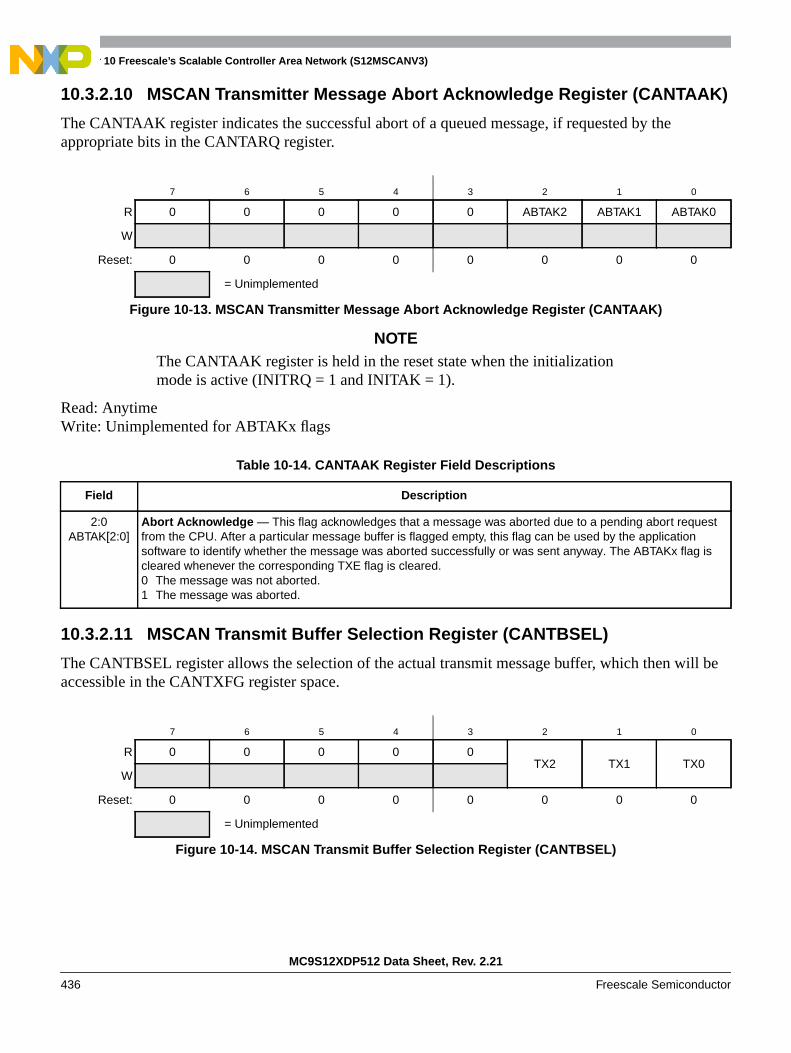
Chapter 10 Freescale’s Scalable Controller Area Network (S12MSCANV3)
MC9S12XDP512 Data Sheet, Rev. 2.21
436 Freescale Semiconductor
10.3.2.10 MSCAN Transmitter Message Abort Acknowledge Register (CANTAAK)
The CANTAAK register indicates the successful abort of a queued message, if requested by theappropriate bits in the CANTARQ register.
NOTEThe CANTAAK register is held in the reset state when the initializationmode is active (INITRQ = 1 and INITAK = 1).
Read: AnytimeWrite: Unimplemented for ABTAKx flags
10.3.2.11 MSCAN Transmit Buffer Selection Register (CANTBSEL)
The CANTBSEL register allows the selection of the actual transmit message buffer, which then will beaccessible in the CANTXFG register space.
7 6 5 4 3 2 1 0
R 0 0 0 0 0 ABTAK2 ABTAK1 ABTAK0
W
Reset: 0 0 0 0 0 0 0 0
= Unimplemented
Figure 10-13. MSCAN Transmitter Message Abort Acknowledge Register (CANTAAK)
Table 10-14. CANTAAK Register Field Descriptions
Field Description
2:0ABTAK[2:0]
Abort Acknowledge — This flag acknowledges that a message was aborted due to a pending abort requestfrom the CPU. After a particular message buffer is flagged empty, this flag can be used by the applicationsoftware to identify whether the message was aborted successfully or was sent anyway. The ABTAKx flag iscleared whenever the corresponding TXE flag is cleared.0 The message was not aborted.1 The message was aborted.
7 6 5 4 3 2 1 0
R 0 0 0 0 0TX2 TX1 TX0
W
Reset: 0 0 0 0 0 0 0 0
= Unimplemented
Figure 10-14. MSCAN Transmit Buffer Selection Register (CANTBSEL)

Chapter 10 Freescale’s Scalable Controller Area Network (S12MSCANV3)
MC9S12XDP512 Data Sheet, Rev. 2.21
Freescale Semiconductor 437
NOTEThe CANTBSEL register is held in the reset state when the initializationmode is active (INITRQ = 1 and INITAK=1). This register is writable whennot in initialization mode (INITRQ = 0 and INITAK = 0).
Read: Find the lowest ordered bit set to 1, all other bits will be read as 0Write: Anytime when not in initialization mode
The following gives a short programming example of the usage of the CANTBSEL register:
To get the next available transmit buffer, application software must read the CANTFLG register and writethis value back into the CANTBSEL register. In this example Tx buffers TX1 and TX2 are available. Thevalue read from CANTFLG is therefore 0b0000_0110. When writing this value back to CANTBSEL, theTx buffer TX1 is selected in the CANTXFG because the lowest numbered bit set to 1 is at bit position 1.Reading back this value out of CANTBSEL results in 0b0000_0010, because only the lowest numberedbit position set to 1 is presented. This mechanism eases the application software the selection of the nextavailable Tx buffer.
• LDD CANTFLG; value read is 0b0000_0110
• STD CANTBSEL; value written is 0b0000_0110
• LDD CANTBSEL; value read is 0b0000_0010
If all transmit message buffers are deselected, no accesses are allowed to the CANTXFG registers.
10.3.2.12 MSCAN Identifier Acceptance Control Register (CANIDAC)
The CANIDAC register is used for identifier acceptance control as described below.
Table 10-15. CANTBSEL Register Field Descriptions
Field Description
2:0TX[2:0]
Transmit Buffer Select — The lowest numbered bit places the respective transmit buffer in the CANTXFGregister space (e.g., TX1 = 1 and TX0 = 1 selects transmit buffer TX0; TX1 = 1 and TX0 = 0 selects transmitbuffer TX1). Read and write accesses to the selected transmit buffer will be blocked, if the corresponding TXExbit is cleared and the buffer is scheduled for transmission (see Section 10.3.2.7, “MSCAN Transmitter FlagRegister (CANTFLG)”).0 The associated message buffer is deselected1 The associated message buffer is selected, if lowest numbered bit
7 6 5 4 3 2 1 0
R 0 0IDAM1 IDAM0
0 IDHIT2 IDHIT1 IDHIT0
W
Reset: 0 0 0 0 0 0 0 0
= Unimplemented
Figure 10-15. MSCAN Identifier Acceptance Control Register (CANIDAC)
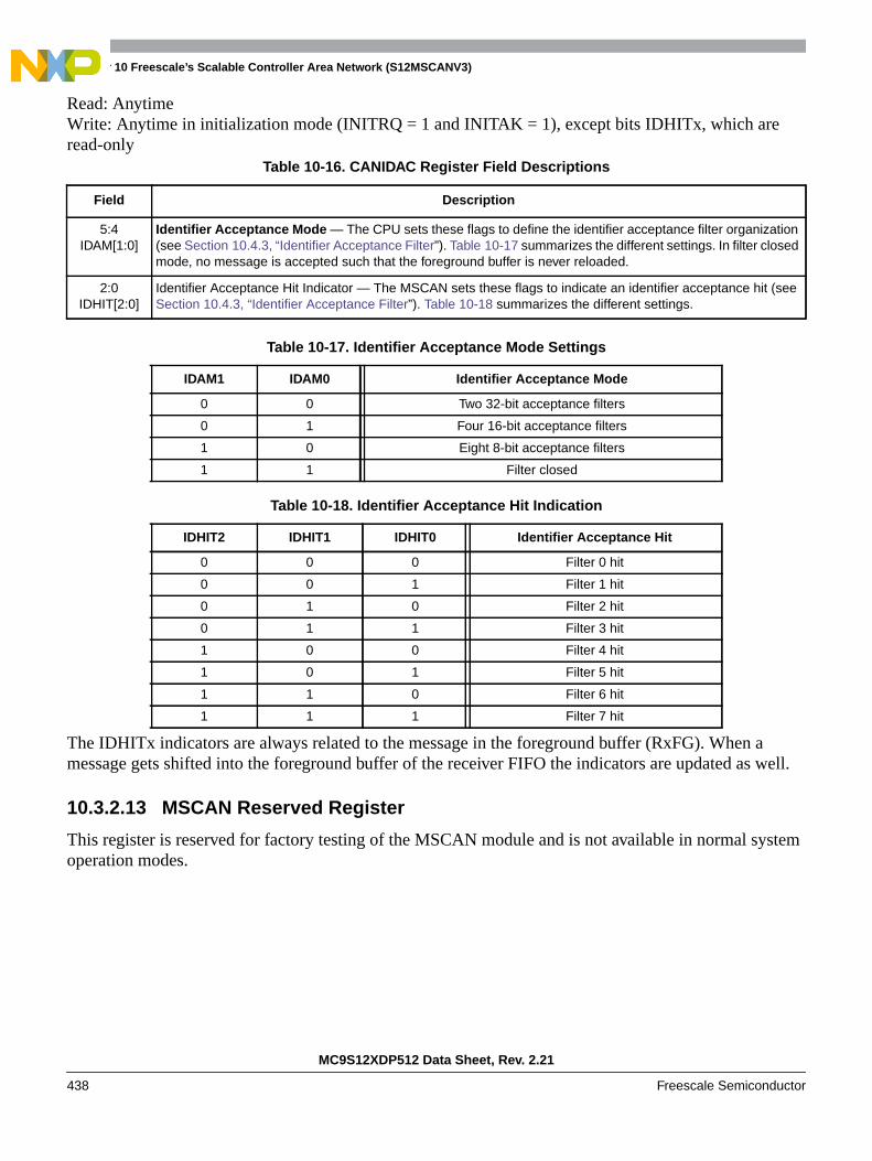
Chapter 10 Freescale’s Scalable Controller Area Network (S12MSCANV3)
MC9S12XDP512 Data Sheet, Rev. 2.21
438 Freescale Semiconductor
Read: AnytimeWrite: Anytime in initialization mode (INITRQ = 1 and INITAK = 1), except bits IDHITx, which areread-only
The IDHITx indicators are always related to the message in the foreground buffer (RxFG). When amessage gets shifted into the foreground buffer of the receiver FIFO the indicators are updated as well.
10.3.2.13 MSCAN Reserved Register
This register is reserved for factory testing of the MSCAN module and is not available in normal systemoperation modes.
Table 10-16. CANIDAC Register Field Descriptions
Field Description
5:4IDAM[1:0]
Identifier Acceptance Mode — The CPU sets these flags to define the identifier acceptance filter organization(see Section 10.4.3, “Identifier Acceptance Filter”). Table 10-17 summarizes the different settings. In filter closedmode, no message is accepted such that the foreground buffer is never reloaded.
2:0IDHIT[2:0]
Identifier Acceptance Hit Indicator — The MSCAN sets these flags to indicate an identifier acceptance hit (seeSection 10.4.3, “Identifier Acceptance Filter”). Table 10-18 summarizes the different settings.
Table 10-17. Identifier Acceptance Mode Settings
IDAM1 IDAM0 Identifier Acceptance Mode
0 0 Two 32-bit acceptance filters
0 1 Four 16-bit acceptance filters
1 0 Eight 8-bit acceptance filters
1 1 Filter closed
Table 10-18. Identifier Acceptance Hit Indication
IDHIT2 IDHIT1 IDHIT0 Identifier Acceptance Hit
0 0 0 Filter 0 hit
0 0 1 Filter 1 hit
0 1 0 Filter 2 hit
0 1 1 Filter 3 hit
1 0 0 Filter 4 hit
1 0 1 Filter 5 hit
1 1 0 Filter 6 hit
1 1 1 Filter 7 hit

Chapter 10 Freescale’s Scalable Controller Area Network (S12MSCANV3)
MC9S12XDP512 Data Sheet, Rev. 2.21
Freescale Semiconductor 439
Read: Always read 0x0000 in normal system operation modesWrite: Unimplemented in normal system operation modes
NOTEWriting to this register when in special modes can alter the MSCANfunctionality.
10.3.2.14 MSCAN Miscellaneous Register (CANMISC)
This register provides additional features.
Read: AnytimeWrite: Anytime; write of ‘1’ clears flag; write of ‘0’ ignored
10.3.2.15 MSCAN Receive Error Counter (CANRXERR)
This register reflects the status of the MSCAN receive error counter.
7 6 5 4 3 2 1 0
R 0 0 0 0 0 0 0 0
W
Reset: 0 0 0 0 0 0 0 0
= Unimplemented
Figure 10-16. MSCAN Reserved Register
7 6 5 4 3 2 1 0
R 0 0 0 0 0 0 0BOHOLD
W
Reset: 0 0 0 0 0 0 0 0
= Unimplemented
Figure 10-17. MSCAN Miscellaneous Register (CANMISC)
Table 10-19. CANMISC Register Field Descriptions
Field Description
0BOHOLD
Bus-off State Hold Until User Request — If BORM is set in Section 10.3.2.2, “MSCAN Control Register 1(CANCTL1), this bit indicates whether the module has entered the bus-off state. Clearing this bit requests therecovery from bus-off. Refer to Section 10.5.2, “Bus-Off Recovery,” for details.0 Module is not bus-off or recovery has been requested by user in bus-off state1 Module is bus-off and holds this state until user request

Chapter 10 Freescale’s Scalable Controller Area Network (S12MSCANV3)
MC9S12XDP512 Data Sheet, Rev. 2.21
440 Freescale Semiconductor
Read: Only when in sleep mode (SLPRQ = 1 and SLPAK = 1) or initialization mode (INITRQ = 1 andINITAK = 1)
Write: Unimplemented
NOTEReading this register when in any other mode other than sleep orinitialization mode may return an incorrect value. For MCUs with dualCPUs, this may result in a CPU fault condition.
Writing to this register when in special modes can alter the MSCANfunctionality.
10.3.2.16 MSCAN Transmit Error Counter (CANTXERR)
This register reflects the status of the MSCAN transmit error counter.
Read: Only when in sleep mode (SLPRQ = 1 and SLPAK = 1) or initialization mode (INITRQ = 1 andINITAK = 1)
Write: Unimplemented
NOTEReading this register when in any other mode other than sleep orinitialization mode, may return an incorrect value. For MCUs with dualCPUs, this may result in a CPU fault condition.
Writing to this register when in special modes can alter the MSCANfunctionality.
7 6 5 4 3 2 1 0
R RXERR7 RXERR6 RXERR5 RXERR4 RXERR3 RXERR2 RXERR1 RXERR0
W
Reset: 0 0 0 0 0 0 0 0
= Unimplemented
Figure 10-18. MSCAN Receive Error Counter (CANRXERR)
7 6 5 4 3 2 1 0
R TXERR7 TXERR6 TXERR5 TXERR4 TXERR3 TXERR2 TXERR1 TXERR0
W
Reset: 0 0 0 0 0 0 0 0
= Unimplemented
Figure 10-19. MSCAN Transmit Error Counter (CANTXERR)
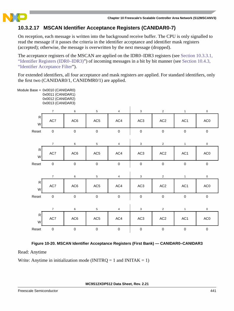
Chapter 10 Freescale’s Scalable Controller Area Network (S12MSCANV3)
MC9S12XDP512 Data Sheet, Rev. 2.21
Freescale Semiconductor 441
10.3.2.17 MSCAN Identifier Acceptance Registers (CANIDAR0-7)
On reception, each message is written into the background receive buffer. The CPU is only signalled toread the message if it passes the criteria in the identifier acceptance and identifier mask registers(accepted); otherwise, the message is overwritten by the next message (dropped).
The acceptance registers of the MSCAN are applied on the IDR0–IDR3 registers (see Section 10.3.3.1,“Identifier Registers (IDR0–IDR3)”) of incoming messages in a bit by bit manner (see Section 10.4.3,“Identifier Acceptance Filter”).
For extended identifiers, all four acceptance and mask registers are applied. For standard identifiers, onlythe first two (CANIDAR0/1, CANIDMR0/1) are applied.
Read: Anytime
Write: Anytime in initialization mode (INITRQ = 1 and INITAK = 1)
Module Base + 0x0010 (CANIDAR0)0x0011 (CANIDAR1)0x0012 (CANIDAR2)0x0013 (CANIDAR3)
7 6 5 4 3 2 1 0
RAC7 AC6 AC5 AC4 AC3 AC2 AC1 AC0
W
Reset 0 0 0 0 0 0 0 0
7 6 5 4 3 2 1 0
RAC7 AC6 AC5 AC4 AC3 AC2 AC1 AC0
W
Reset 0 0 0 0 0 0 0 0
7 6 5 4 3 2 1 0
RAC7 AC6 AC5 AC4 AC3 AC2 AC1 AC0
W
Reset 0 0 0 0 0 0 0 0
7 6 5 4 3 2 1 0
RAC7 AC6 AC5 AC4 AC3 AC2 AC1 AC0
W
Reset 0 0 0 0 0 0 0 0
Figure 10-20. MSCAN Identifier Acceptance Registers (First Bank) — CANIDAR0–CANIDAR3

Chapter 10 Freescale’s Scalable Controller Area Network (S12MSCANV3)
MC9S12XDP512 Data Sheet, Rev. 2.21
442 Freescale Semiconductor
Read: Anytime
Write: Anytime in initialization mode (INITRQ = 1 and INITAK = 1)
Table 10-20. CANIDAR0–CANIDAR3 Register Field Descriptions
Field Description
7:0AC[7:0]
Acceptance Code Bits — AC[7:0] comprise a user-defined sequence of bits with which the corresponding bitsof the related identifier register (IDRn) of the receive message buffer are compared. The result of this comparisonis then masked with the corresponding identifier mask register.
Module Base + 0x0018 (CANIDAR4)0x0019 (CANIDAR5)0x001A (CANIDAR6)0x001B (CANIDAR7)
7 6 5 4 3 2 1 0
RAC7 AC6 AC5 AC4 AC3 AC2 AC1 AC0
W
Reset 0 0 0 0 0 0 0 0
7 6 5 4 3 2 1 0
RAC7 AC6 AC5 AC4 AC3 AC2 AC1 AC0
W
Reset 0 0 0 0 0 0 0 0
7 6 5 4 3 2 1 0
RAC7 AC6 AC5 AC4 AC3 AC2 AC1 AC0
W
Reset 0 0 0 0 0 0 0 0
7 6 5 4 3 2 1 0
RAC7 AC6 AC5 AC4 AC3 AC2 AC1 AC0
W
Reset 0 0 0 0 0 0 0 0
Figure 10-21. MSCAN Identifier Acceptance Registers (Second Bank) — CANIDAR4–CANIDAR7

Chapter 10 Freescale’s Scalable Controller Area Network (S12MSCANV3)
MC9S12XDP512 Data Sheet, Rev. 2.21
Freescale Semiconductor 443
10.3.2.18 MSCAN Identifier Mask Registers (CANIDMR0–CANIDMR7)
The identifier mask register specifies which of the corresponding bits in the identifier acceptance registerare relevant for acceptance filtering. To receive standard identifiers in 32 bit filter mode, it is required toprogram the last three bits (AM[2:0]) in the mask registers CANIDMR1 and CANIDMR5 to “don’t care.”To receive standard identifiers in 16 bit filter mode, it is required to program the last three bits (AM[2:0])in the mask registers CANIDMR1, CANIDMR3, CANIDMR5, and CANIDMR7 to “don’t care.”
Table 10-21. CANIDAR4–CANIDAR7 Register Field Descriptions
Field Description
7:0AC[7:0]
Acceptance Code Bits — AC[7:0] comprise a user-defined sequence of bits with which the corresponding bitsof the related identifier register (IDRn) of the receive message buffer are compared. The result of this comparisonis then masked with the corresponding identifier mask register.
Module Base + 0x0014 (CANIDMR0)0x0015 (CANIDMR1)0x0016 (CANIDMR2)0x0017 (CANIDMR3)
7 6 5 4 3 2 1 0
RAM7 AM6 AM5 AM4 AM3 AM2 AM1 AM0
W
Reset 0 0 0 0 0 0 0 0
7 6 5 4 3 2 1 0
RAM7 AM6 AM5 AM4 AM3 AM2 AM1 AM0
W
Reset 0 0 0 0 0 0 0 0
7 6 5 4 3 2 1 0
RAM7 AM6 AM5 AM4 AM3 AM2 AM1 AM0
W
Reset 0 0 0 0 0 0 0 0
7 6 5 4 3 2 1 0
RAM7 AM6 AM5 AM4 AM3 AM2 AM1 AM0
W
Reset 0 0 0 0 0 0 0 0
Figure 10-22. MSCAN Identifier Mask Registers (First Bank) — CANIDMR0–CANIDMR3
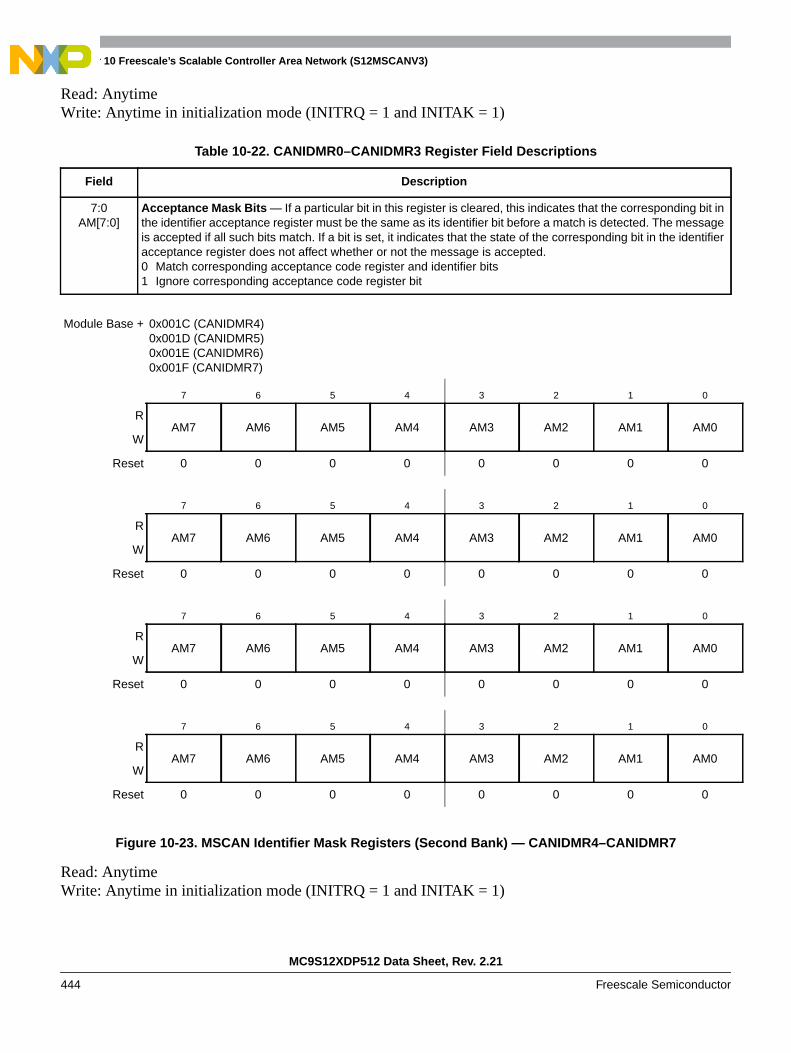
Chapter 10 Freescale’s Scalable Controller Area Network (S12MSCANV3)
MC9S12XDP512 Data Sheet, Rev. 2.21
444 Freescale Semiconductor
Read: AnytimeWrite: Anytime in initialization mode (INITRQ = 1 and INITAK = 1)
Read: AnytimeWrite: Anytime in initialization mode (INITRQ = 1 and INITAK = 1)
Table 10-22. CANIDMR0–CANIDMR3 Register Field Descriptions
Field Description
7:0AM[7:0]
Acceptance Mask Bits — If a particular bit in this register is cleared, this indicates that the corresponding bit inthe identifier acceptance register must be the same as its identifier bit before a match is detected. The messageis accepted if all such bits match. If a bit is set, it indicates that the state of the corresponding bit in the identifieracceptance register does not affect whether or not the message is accepted.0 Match corresponding acceptance code register and identifier bits1 Ignore corresponding acceptance code register bit
Module Base + 0x001C (CANIDMR4)0x001D (CANIDMR5)0x001E (CANIDMR6)0x001F (CANIDMR7)
7 6 5 4 3 2 1 0
RAM7 AM6 AM5 AM4 AM3 AM2 AM1 AM0
W
Reset 0 0 0 0 0 0 0 0
7 6 5 4 3 2 1 0
RAM7 AM6 AM5 AM4 AM3 AM2 AM1 AM0
W
Reset 0 0 0 0 0 0 0 0
7 6 5 4 3 2 1 0
RAM7 AM6 AM5 AM4 AM3 AM2 AM1 AM0
W
Reset 0 0 0 0 0 0 0 0
7 6 5 4 3 2 1 0
RAM7 AM6 AM5 AM4 AM3 AM2 AM1 AM0
W
Reset 0 0 0 0 0 0 0 0
Figure 10-23. MSCAN Identifier Mask Registers (Second Bank) — CANIDMR4–CANIDMR7
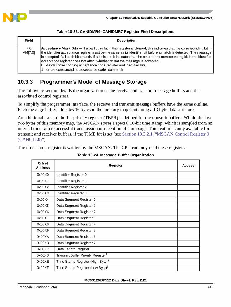
Chapter 10 Freescale’s Scalable Controller Area Network (S12MSCANV3)
MC9S12XDP512 Data Sheet, Rev. 2.21
Freescale Semiconductor 445
10.3.3 Programmer’s Model of Message Storage
The following section details the organization of the receive and transmit message buffers and theassociated control registers.
To simplify the programmer interface, the receive and transmit message buffers have the same outline.Each message buffer allocates 16 bytes in the memory map containing a 13 byte data structure.
An additional transmit buffer priority register (TBPR) is defined for the transmit buffers. Within the lasttwo bytes of this memory map, the MSCAN stores a special 16-bit time stamp, which is sampled from aninternal timer after successful transmission or reception of a message. This feature is only available fortransmit and receiver buffers, if the TIME bit is set (see Section 10.3.2.1, “MSCAN Control Register 0(CANCTL0)”).
The time stamp register is written by the MSCAN. The CPU can only read these registers.
Table 10-23. CANIDMR4–CANIDMR7 Register Field Descriptions
Field Description
7:0AM[7:0]
Acceptance Mask Bits — If a particular bit in this register is cleared, this indicates that the corresponding bit inthe identifier acceptance register must be the same as its identifier bit before a match is detected. The messageis accepted if all such bits match. If a bit is set, it indicates that the state of the corresponding bit in the identifieracceptance register does not affect whether or not the message is accepted.0 Match corresponding acceptance code register and identifier bits1 Ignore corresponding acceptance code register bit
Table 10-24. Message Buffer Organization
OffsetAddress
Register Access
0x00X0 Identifier Register 0
0x00X1 Identifier Register 1
0x00X2 Identifier Register 2
0x00X3 Identifier Register 3
0x00X4 Data Segment Register 0
0x00X5 Data Segment Register 1
0x00X6 Data Segment Register 2
0x00X7 Data Segment Register 3
0x00X8 Data Segment Register 4
0x00X9 Data Segment Register 5
0x00XA Data Segment Register 6
0x00XB Data Segment Register 7
0x00XC Data Length Register
0x00XD Transmit Buffer Priority Register1
0x00XE Time Stamp Register (High Byte)2
0x00XF Time Stamp Register (Low Byte)3

Chapter 10 Freescale’s Scalable Controller Area Network (S12MSCANV3)
MC9S12XDP512 Data Sheet, Rev. 2.21
446 Freescale Semiconductor
Figure 10-24 shows the common 13-byte data structure of receive and transmit buffers for extendedidentifiers. The mapping of standard identifiers into the IDR registers is shown in Figure 10-25.
All bits of the receive and transmit buffers are ‘x’ out of reset because of RAM-based implementation1.All reserved or unused bits of the receive and transmit buffers always read ‘x’.
1 Not applicable for receive buffers2 Read-only for CPU3 Read-only for CPU
1. Exception: The transmit priority registers are 0 out of reset.

Chapter 10 Freescale’s Scalable Controller Area Network (S12MSCANV3)
MC9S12XDP512 Data Sheet, Rev. 2.21
Freescale Semiconductor 447

Chapter 10 Freescale’s Scalable Controller Area Network (S12MSCANV3)
MC9S12XDP512 Data Sheet, Rev. 2.21
448 Freescale Semiconductor
Figure 10-24. Receive/Transmit Message Buffer — Extended Identifier Mapping
RegisterName
Bit 7 6 5 4 3 2 1 Bit0
IDR0R
ID28 ID27 ID26 ID25 ID24 ID23 ID22 ID21W

Chapter 10 Freescale’s Scalable Controller Area Network (S12MSCANV3)
MC9S12XDP512 Data Sheet, Rev. 2.21
Freescale Semiconductor 449
IDR1R
ID20 ID19 ID18 SRR (=1) IDE (=1) ID17 ID16 ID15W
IDR2
RID14 ID13 ID12 ID11 ID10 ID9 ID8 ID7
W
IDR3
RID6 ID5 ID4 ID3 ID2 ID1 ID0 RTR
W
DSR0
RDB7 DB6 DB5 DB4 DB3 DB2 DB1 DB0
W
DSR1
RDB7 DB6 DB5 DB4 DB3 DB2 DB1 DB0
W
DSR2
RDB7 DB6 DB5 DB4 DB3 DB2 DB1 DB0
W
DSR3
RDB7 DB6 DB5 DB4 DB3 DB2 DB1 DB0
W
DSR4
RDB7 DB6 DB5 DB4 DB3 DB2 DB1 DB0
W
DSR5
RDB7 DB6 DB5 DB4 DB3 DB2 DB1 DB0
W
DSR6
RDB7 DB6 DB5 DB4 DB3 DB2 DB1 DB0
W
DSR7
RDB7 DB6 DB5 DB4 DB3 DB2 DB1 DB0
W
DLR
RDLC3 DLC2 DLC1 DLC0
W
= Unused, always read ‘x’
Figure 10-24. Receive/Transmit Message Buffer — Extended Identifier Mapping
RegisterName
Bit 7 6 5 4 3 2 1 Bit0
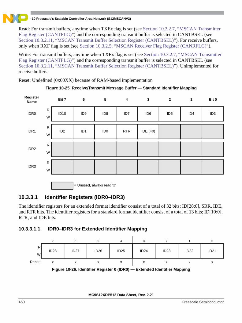
Chapter 10 Freescale’s Scalable Controller Area Network (S12MSCANV3)
MC9S12XDP512 Data Sheet, Rev. 2.21
450 Freescale Semiconductor
Read: For transmit buffers, anytime when TXEx flag is set (see Section 10.3.2.7, “MSCAN TransmitterFlag Register (CANTFLG)”) and the corresponding transmit buffer is selected in CANTBSEL (seeSection 10.3.2.11, “MSCAN Transmit Buffer Selection Register (CANTBSEL)”). For receive buffers,only when RXF flag is set (see Section 10.3.2.5, “MSCAN Receiver Flag Register (CANRFLG)”).
Write: For transmit buffers, anytime when TXEx flag is set (see Section 10.3.2.7, “MSCAN TransmitterFlag Register (CANTFLG)”) and the corresponding transmit buffer is selected in CANTBSEL (seeSection 10.3.2.11, “MSCAN Transmit Buffer Selection Register (CANTBSEL)”). Unimplemented forreceive buffers.
Reset: Undefined (0x00XX) because of RAM-based implementation
10.3.3.1 Identifier Registers (IDR0–IDR3)
The identifier registers for an extended format identifier consist of a total of 32 bits; ID[28:0], SRR, IDE,and RTR bits. The identifier registers for a standard format identifier consist of a total of 13 bits; ID[10:0],RTR, and IDE bits.
10.3.3.1.1 IDR0–IDR3 for Extended Identifier Mapping
Figure 10-25. Receive/Transmit Message Buffer — Standard Identifier Mapping
RegisterName
Bit 7 6 5 4 3 2 1 Bit 0
IDR0R
ID10 ID9 ID8 ID7 ID6 ID5 ID4 ID3W
IDR1R
ID2 ID1 ID0 RTR IDE (=0)W
IDR2R
W
IDR3R
W
= Unused, always read ‘x’
7 6 5 4 3 2 1 0
RID28 ID27 ID26 ID25 ID24 ID23 ID22 ID21
W
Reset: x x x x x x x x
Figure 10-26. Identifier Register 0 (IDR0) — Extended Identifier Mapping
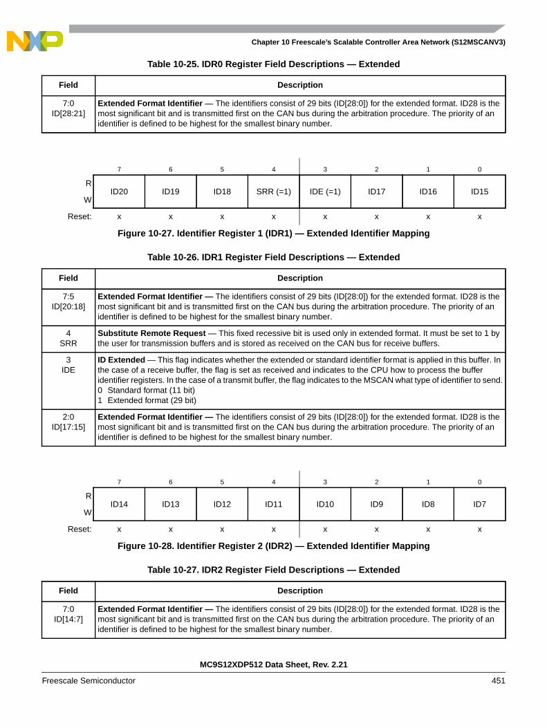
Chapter 10 Freescale’s Scalable Controller Area Network (S12MSCANV3)
MC9S12XDP512 Data Sheet, Rev. 2.21
Freescale Semiconductor 451
Table 10-25. IDR0 Register Field Descriptions — Extended
Field Description
7:0ID[28:21]
Extended Format Identifier — The identifiers consist of 29 bits (ID[28:0]) for the extended format. ID28 is themost significant bit and is transmitted first on the CAN bus during the arbitration procedure. The priority of anidentifier is defined to be highest for the smallest binary number.
7 6 5 4 3 2 1 0
RID20 ID19 ID18 SRR (=1) IDE (=1) ID17 ID16 ID15
W
Reset: x x x x x x x x
Figure 10-27. Identifier Register 1 (IDR1) — Extended Identifier Mapping
Table 10-26. IDR1 Register Field Descriptions — Extended
Field Description
7:5ID[20:18]
Extended Format Identifier — The identifiers consist of 29 bits (ID[28:0]) for the extended format. ID28 is themost significant bit and is transmitted first on the CAN bus during the arbitration procedure. The priority of anidentifier is defined to be highest for the smallest binary number.
4SRR
Substitute Remote Request — This fixed recessive bit is used only in extended format. It must be set to 1 bythe user for transmission buffers and is stored as received on the CAN bus for receive buffers.
3IDE
ID Extended — This flag indicates whether the extended or standard identifier format is applied in this buffer. Inthe case of a receive buffer, the flag is set as received and indicates to the CPU how to process the bufferidentifier registers. In the case of a transmit buffer, the flag indicates to the MSCAN what type of identifier to send.0 Standard format (11 bit)1 Extended format (29 bit)
2:0ID[17:15]
Extended Format Identifier — The identifiers consist of 29 bits (ID[28:0]) for the extended format. ID28 is themost significant bit and is transmitted first on the CAN bus during the arbitration procedure. The priority of anidentifier is defined to be highest for the smallest binary number.
7 6 5 4 3 2 1 0
RID14 ID13 ID12 ID11 ID10 ID9 ID8 ID7
W
Reset: x x x x x x x x
Figure 10-28. Identifier Register 2 (IDR2) — Extended Identifier Mapping
Table 10-27. IDR2 Register Field Descriptions — Extended
Field Description
7:0ID[14:7]
Extended Format Identifier — The identifiers consist of 29 bits (ID[28:0]) for the extended format. ID28 is themost significant bit and is transmitted first on the CAN bus during the arbitration procedure. The priority of anidentifier is defined to be highest for the smallest binary number.
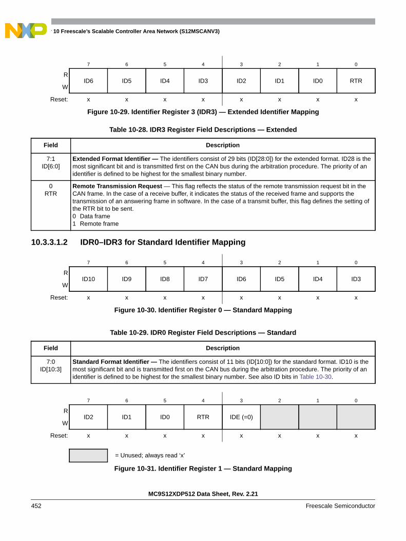
Chapter 10 Freescale’s Scalable Controller Area Network (S12MSCANV3)
MC9S12XDP512 Data Sheet, Rev. 2.21
452 Freescale Semiconductor
10.3.3.1.2 IDR0–IDR3 for Standard Identifier Mapping
7 6 5 4 3 2 1 0
RID6 ID5 ID4 ID3 ID2 ID1 ID0 RTR
W
Reset: x x x x x x x x
Figure 10-29. Identifier Register 3 (IDR3) — Extended Identifier Mapping
Table 10-28. IDR3 Register Field Descriptions — Extended
Field Description
7:1ID[6:0]
Extended Format Identifier — The identifiers consist of 29 bits (ID[28:0]) for the extended format. ID28 is themost significant bit and is transmitted first on the CAN bus during the arbitration procedure. The priority of anidentifier is defined to be highest for the smallest binary number.
0RTR
Remote Transmission Request — This flag reflects the status of the remote transmission request bit in theCAN frame. In the case of a receive buffer, it indicates the status of the received frame and supports thetransmission of an answering frame in software. In the case of a transmit buffer, this flag defines the setting ofthe RTR bit to be sent.0 Data frame1 Remote frame
7 6 5 4 3 2 1 0
RID10 ID9 ID8 ID7 ID6 ID5 ID4 ID3
W
Reset: x x x x x x x x
Figure 10-30. Identifier Register 0 — Standard Mapping
Table 10-29. IDR0 Register Field Descriptions — Standard
Field Description
7:0ID[10:3]
Standard Format Identifier — The identifiers consist of 11 bits (ID[10:0]) for the standard format. ID10 is themost significant bit and is transmitted first on the CAN bus during the arbitration procedure. The priority of anidentifier is defined to be highest for the smallest binary number. See also ID bits in Table 10-30.
7 6 5 4 3 2 1 0
RID2 ID1 ID0 RTR IDE (=0)
W
Reset: x x x x x x x x
= Unused; always read ‘x’
Figure 10-31. Identifier Register 1 — Standard Mapping

Chapter 10 Freescale’s Scalable Controller Area Network (S12MSCANV3)
MC9S12XDP512 Data Sheet, Rev. 2.21
Freescale Semiconductor 453
10.3.3.2 Data Segment Registers (DSR0-7)
The eight data segment registers, each with bits DB[7:0], contain the data to be transmitted or received.The number of bytes to be transmitted or received is determined by the data length code in thecorresponding DLR register.
Table 10-30. IDR1 Register Field Descriptions
Field Description
7:5ID[2:0]
Standard Format Identifier — The identifiers consist of 11 bits (ID[10:0]) for the standard format. ID10 is themost significant bit and is transmitted first on the CAN bus during the arbitration procedure. The priority of anidentifier is defined to be highest for the smallest binary number. See also ID bits in Table 10-29.
4RTR
Remote Transmission Request — This flag reflects the status of the Remote Transmission Request bit in theCAN frame. In the case of a receive buffer, it indicates the status of the received frame and supports thetransmission of an answering frame in software. In the case of a transmit buffer, this flag defines the setting ofthe RTR bit to be sent.0 Data frame1 Remote frame
3IDE
ID Extended — This flag indicates whether the extended or standard identifier format is applied in this buffer. Inthe case of a receive buffer, the flag is set as received and indicates to the CPU how to process the bufferidentifier registers. In the case of a transmit buffer, the flag indicates to the MSCAN what type of identifier to send.0 Standard format (11 bit)1 Extended format (29 bit)
7 6 5 4 3 2 1 0
R
W
Reset: x x x x x x x x
= Unused; always read ‘x’
Figure 10-32. Identifier Register 2 — Standard Mapping
7 6 5 4 3 2 1 0
R
W
Reset: x x x x x x x x
= Unused; always read ‘x’
Figure 10-33. Identifier Register 3 — Standard Mapping
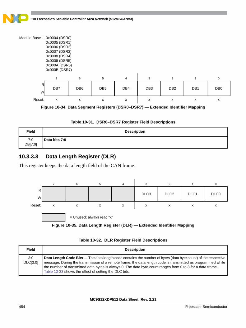
Chapter 10 Freescale’s Scalable Controller Area Network (S12MSCANV3)
MC9S12XDP512 Data Sheet, Rev. 2.21
454 Freescale Semiconductor
10.3.3.3 Data Length Register (DLR)
This register keeps the data length field of the CAN frame.
Module Base + 0x0004 (DSR0)0x0005 (DSR1)0x0006 (DSR2)0x0007 (DSR3)0x0008 (DSR4)0x0009 (DSR5)0x000A (DSR6)0x000B (DSR7)
7 6 5 4 3 2 1 0
RDB7 DB6 DB5 DB4 DB3 DB2 DB1 DB0
W
Reset: x x x x x x x x
Figure 10-34. Data Segment Registers (DSR0–DSR7) — Extended Identifier Mapping
Table 10-31. DSR0–DSR7 Register Field Descriptions
Field Description
7:0DB[7:0]
Data bits 7:0
7 6 5 4 3 2 1 0
RDLC3 DLC2 DLC1 DLC0
W
Reset: x x x x x x x x
= Unused; always read “x”
Figure 10-35. Data Length Register (DLR) — Extended Identifier Mapping
Table 10-32. DLR Register Field Descriptions
Field Description
3:0DLC[3:0]
Data Length Code Bits — The data length code contains the number of bytes (data byte count) of the respectivemessage. During the transmission of a remote frame, the data length code is transmitted as programmed whilethe number of transmitted data bytes is always 0. The data byte count ranges from 0 to 8 for a data frame.Table 10-33 shows the effect of setting the DLC bits.

Chapter 10 Freescale’s Scalable Controller Area Network (S12MSCANV3)
MC9S12XDP512 Data Sheet, Rev. 2.21
Freescale Semiconductor 455
10.3.3.4 Transmit Buffer Priority Register (TBPR)
This register defines the local priority of the associated message buffer. The local priority is used for theinternal prioritization process of the MSCAN and is defined to be highest for the smallest binary number.The MSCAN implements the following internal prioritization mechanisms:
• All transmission buffers with a cleared TXEx flag participate in the prioritization immediatelybefore the SOF (start of frame) is sent.
• The transmission buffer with the lowest local priority field wins the prioritization.
In cases of more than one buffer having the same lowest priority, the message buffer with the lower indexnumber wins.
Read: Anytime when TXEx flag is set (see Section 10.3.2.7, “MSCAN Transmitter Flag Register(CANTFLG)”) and the corresponding transmit buffer is selected in CANTBSEL (see Section 10.3.2.11,“MSCAN Transmit Buffer Selection Register (CANTBSEL)”).
Write: Anytime when TXEx flag is set (see Section 10.3.2.7, “MSCAN Transmitter Flag Register(CANTFLG)”) and the corresponding transmit buffer is selected in CANTBSEL (see Section 10.3.2.11,“MSCAN Transmit Buffer Selection Register (CANTBSEL)”).
10.3.3.5 Time Stamp Register (TSRH–TSRL)
If the TIME bit is enabled, the MSCAN will write a time stamp to the respective registers in the activetransmit or receive buffer right after the EOF of a valid message on the CAN bus (see Section 10.3.2.1,
Table 10-33. Data Length Codes
Data Length Code Data ByteCountDLC3 DLC2 DLC1 DLC0
0 0 0 0 0
0 0 0 1 1
0 0 1 0 2
0 0 1 1 3
0 1 0 0 4
0 1 0 1 5
0 1 1 0 6
0 1 1 1 7
1 0 0 0 8
7 6 5 4 3 2 1 0
RPRIO7 PRIO6 PRIO5 PRIO4 PRIO3 PRIO2 PRIO1 PRIO0
W
Reset: 0 0 0 0 0 0 0 0
Figure 10-36. Transmit Buffer Priority Register (TBPR)

Chapter 10 Freescale’s Scalable Controller Area Network (S12MSCANV3)
MC9S12XDP512 Data Sheet, Rev. 2.21
456 Freescale Semiconductor
“MSCAN Control Register 0 (CANCTL0)”). In case of a transmission, the CPU can only read the timestamp after the respective transmit buffer has been flagged empty.
The timer value, which is used for stamping, is taken from a free running internal CAN bit clock. A timeroverrun is not indicated by the MSCAN. The timer is reset (all bits set to 0) during initialization mode. TheCPU can only read the time stamp registers.
Read: Anytime when TXEx flag is set (see Section 10.3.2.7, “MSCAN Transmitter Flag Register(CANTFLG)”) and the corresponding transmit buffer is selected in CANTBSEL (see Section 10.3.2.11,“MSCAN Transmit Buffer Selection Register (CANTBSEL)”).
Write: Unimplemented
10.4 Functional Description
10.4.1 General
This section provides a complete functional description of the MSCAN. It describes each of the featuresand modes listed in the introduction.
7 6 5 4 3 2 1 0
R TSR15 TSR14 TSR13 TSR12 TSR11 TSR10 TSR9 TSR8
W
Reset: x x x x x x x x
Figure 10-37. Time Stamp Register — High Byte (TSRH)
7 6 5 4 3 2 1 0
R TSR7 TSR6 TSR5 TSR4 TSR3 TSR2 TSR1 TSR0
W
Reset: x x x x x x x x
Figure 10-38. Time Stamp Register — Low Byte (TSRL)
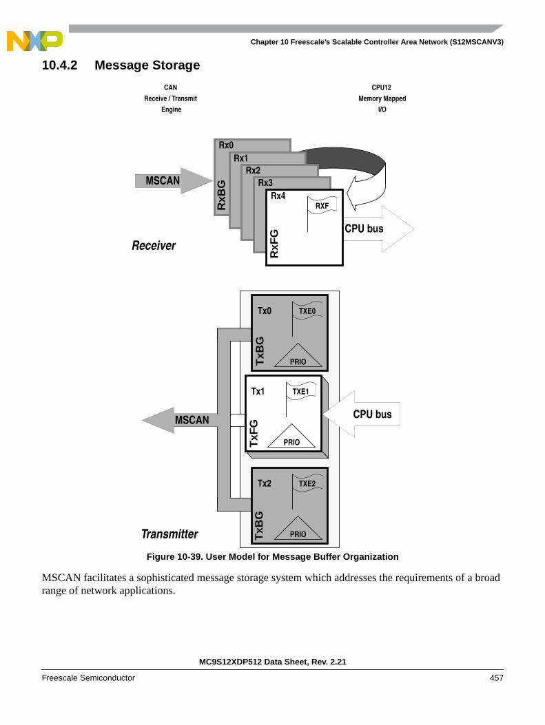
Chapter 10 Freescale’s Scalable Controller Area Network (S12MSCANV3)
MC9S12XDP512 Data Sheet, Rev. 2.21
Freescale Semiconductor 457
10.4.2 Message Storage
Figure 10-39. User Model for Message Buffer Organization
MSCAN facilitates a sophisticated message storage system which addresses the requirements of a broadrange of network applications.
MSCAN
Rx0Rx1
CAN
Receive / Transmit
Engine
CPU12
Memory Mapped
I/O
CPU bus
MSCAN
Tx2 TXE2
PRIO
Receiver
Transmitter
RxB
G
TxB
G
Tx0 TXE0
PRIOTxB
G
Tx1
PRIO
TXE1
TxF
G
CPU bus
Rx2Rx3
Rx4RXF
RxF
G
Chapter 10 Freescale’s Scalable Controller Area Network (S12MSCANV3)
MC9S12XDP512 Data Sheet, Rev. 2.21
458 Freescale Semiconductor
10.4.2.1 Message Transmit Background
Modern application layer software is built upon two fundamental assumptions:
• Any CAN node is able to send out a stream of scheduled messages without releasing the CAN busbetween the two messages. Such nodes arbitrate for the CAN bus immediately after sending theprevious message and only release the CAN bus in case of lost arbitration.
• The internal message queue within any CAN node is organized such that the highest prioritymessage is sent out first, if more than one message is ready to be sent.
The behavior described in the bullets above cannot be achieved with a single transmit buffer. That buffermust be reloaded immediately after the previous message is sent. This loading process lasts a finite amountof time and must be completed within the inter-frame sequence (IFS) to be able to send an uninterruptedstream of messages. Even if this is feasible for limited CAN bus speeds, it requires that the CPU reactswith short latencies to the transmit interrupt.
A double buffer scheme de-couples the reloading of the transmit buffer from the actual message sendingand, therefore, reduces the reactiveness requirements of the CPU. Problems can arise if the sending of amessage is finished while the CPU re-loads the second buffer. No buffer would then be ready fortransmission, and the CAN bus would be released.
At least three transmit buffers are required to meet the first of the above requirements under allcircumstances. The MSCAN has three transmit buffers.
The second requirement calls for some sort of internal prioritization which the MSCAN implements withthe “local priority” concept described in Section 10.4.2.2, “Transmit Structures.”
10.4.2.2 Transmit Structures
The MSCAN triple transmit buffer scheme optimizes real-time performance by allowing multiplemessages to be set up in advance. The three buffers are arranged as shown in Figure 10-39.
All three buffers have a 13-byte data structure similar to the outline of the receive buffers (seeSection 10.3.3, “Programmer’s Model of Message Storage”). An additional Section 10.3.3.4, “TransmitBuffer Priority Register (TBPR) contains an 8-bit local priority field (PRIO) (see Section 10.3.3.4,“Transmit Buffer Priority Register (TBPR)”). The remaining two bytes are used for time stamping of amessage, if required (see Section 10.3.3.5, “Time Stamp Register (TSRH–TSRL)”).
To transmit a message, the CPU must identify an available transmit buffer, which is indicated by a settransmitter buffer empty (TXEx) flag (see Section 10.3.2.7, “MSCAN Transmitter Flag Register(CANTFLG)”). If a transmit buffer is available, the CPU must set a pointer to this buffer by writing to theCANTBSEL register (see Section 10.3.2.11, “MSCAN Transmit Buffer Selection Register(CANTBSEL)”). This makes the respective buffer accessible within the CANTXFG address space (seeSection 10.3.3, “Programmer’s Model of Message Storage”). The algorithmic feature associated with theCANTBSEL register simplifies the transmit buffer selection. In addition, this scheme makes the handlersoftware simpler because only one address area is applicable for the transmit process, and the requiredaddress space is minimized.
The CPU then stores the identifier, the control bits, and the data content into one of the transmit buffers.Finally, the buffer is flagged as ready for transmission by clearing the associated TXE flag.
Chapter 10 Freescale’s Scalable Controller Area Network (S12MSCANV3)
MC9S12XDP512 Data Sheet, Rev. 2.21
Freescale Semiconductor 459
The MSCAN then schedules the message for transmission and signals the successful transmission of thebuffer by setting the associated TXE flag. A transmit interrupt (see Section 10.4.7.2, “Transmit Interrupt”)is generated1 when TXEx is set and can be used to drive the application software to re-load the buffer.
If more than one buffer is scheduled for transmission when the CAN bus becomes available for arbitration,the MSCAN uses the local priority setting of the three buffers to determine the prioritization. For thispurpose, every transmit buffer has an 8-bit local priority field (PRIO). The application software programsthis field when the message is set up. The local priority reflects the priority of this particular messagerelative to the set of messages being transmitted from this node. The lowest binary value of the PRIO fieldis defined to be the highest priority. The internal scheduling process takes place whenever the MSCANarbitrates for the CAN bus. This is also the case after the occurrence of a transmission error.
When a high priority message is scheduled by the application software, it may become necessary to aborta lower priority message in one of the three transmit buffers. Because messages that are already intransmission cannot be aborted, the user must request the abort by setting the corresponding abort requestbit (ABTRQ) (see Section 10.3.2.9, “MSCAN Transmitter Message Abort Request Register(CANTARQ)”.) The MSCAN then grants the request, if possible, by:
1. Setting the corresponding abort acknowledge flag (ABTAK) in the CANTAAK register.
2. Setting the associated TXE flag to release the buffer.
3. Generating a transmit interrupt. The transmit interrupt handler software can determine from thesetting of the ABTAK flag whether the message was aborted (ABTAK = 1) or sent (ABTAK = 0).
10.4.2.3 Receive Structures
The received messages are stored in a five stage input FIFO. The five message buffers are alternatelymapped into a single memory area (see Figure 10-39). The background receive buffer (RxBG) isexclusively associated with the MSCAN, but the foreground receive buffer (RxFG) is addressable by theCPU (see Figure 10-39). This scheme simplifies the handler software because only one address area isapplicable for the receive process.
All receive buffers have a size of 15 bytes to store the CAN control bits, the identifier (standard orextended), the data contents, and a time stamp, if enabled (see Section 10.3.3, “Programmer’s Model ofMessage Storage”).
The receiver full flag (RXF) (see Section 10.3.2.5, “MSCAN Receiver Flag Register (CANRFLG)”)signals the status of the foreground receive buffer. When the buffer contains a correctly received messagewith a matching identifier, this flag is set.
On reception, each message is checked to see whether it passes the filter (see Section 10.4.3, “IdentifierAcceptance Filter”) and simultaneously is written into the active RxBG. After successful reception of avalid message, the MSCAN shifts the content of RxBG into the receiver FIFO2, sets the RXF flag, andgenerates a receive interrupt (see Section 10.4.7.3, “Receive Interrupt”) to the CPU3. The user’s receivehandler must read the received message from the RxFG and then reset the RXF flag to acknowledge theinterrupt and to release the foreground buffer. A new message, which can follow immediately after the IFS
1. The transmit interrupt occurs only if not masked. A polling scheme can be applied on TXEx also.2. Only if the RXF flag is not set.3. The receive interrupt occurs only if not masked. A polling scheme can be applied on RXF also.

Chapter 10 Freescale’s Scalable Controller Area Network (S12MSCANV3)
MC9S12XDP512 Data Sheet, Rev. 2.21
460 Freescale Semiconductor
field of the CAN frame, is received into the next available RxBG. If the MSCAN receives an invalidmessage in its RxBG (wrong identifier, transmission errors, etc.) the actual contents of the buffer will beover-written by the next message. The buffer will then not be shifted into the FIFO.
When the MSCAN module is transmitting, the MSCAN receives its own transmitted messages into thebackground receive buffer, RxBG, but does not shift it into the receiver FIFO, generate a receive interrupt,or acknowledge its own messages on the CAN bus. The exception to this rule is in loopback mode (seeSection 10.3.2.2, “MSCAN Control Register 1 (CANCTL1)”) where the MSCAN treats its own messagesexactly like all other incoming messages. The MSCAN receives its own transmitted messages in the eventthat it loses arbitration. If arbitration is lost, the MSCAN must be prepared to become a receiver.
An overrun condition occurs when all receive message buffers in the FIFO are filled with correctlyreceived messages with accepted identifiers and another message is correctly received from the CAN buswith an accepted identifier. The latter message is discarded and an error interrupt with overrun indicationis generated if enabled (see Section 10.4.7.5, “Error Interrupt”). The MSCAN remains able to transmitmessages while the receiver FIFO being filled, but all incoming messages are discarded. As soon as areceive buffer in the FIFO is available again, new valid messages will be accepted.
10.4.3 Identifier Acceptance Filter
The MSCAN identifier acceptance registers (see Section 10.3.2.12, “MSCAN Identifier AcceptanceControl Register (CANIDAC)”) define the acceptable patterns of the standard or extended identifier(ID[10:0] or ID[28:0]). Any of these bits can be marked ‘don’t care’ in the MSCAN identifier maskregisters (see Section 10.3.2.18, “MSCAN Identifier Mask Registers (CANIDMR0–CANIDMR7)”).
A filter hit is indicated to the application software by a set receive buffer full flag (RXF = 1) and three bitsin the CANIDAC register (see Section 10.3.2.12, “MSCAN Identifier Acceptance Control Register(CANIDAC)”). These identifier hit flags (IDHIT[2:0]) clearly identify the filter section that caused theacceptance. They simplify the application software’s task to identify the cause of the receiver interrupt. Ifmore than one hit occurs (two or more filters match), the lower hit has priority.
A very flexible programmable generic identifier acceptance filter has been introduced to reduce the CPUinterrupt loading. The filter is programmable to operate in four different modes (see Bosch CAN 2.0A/Bprotocol specification):
• Two identifier acceptance filters, each to be applied to:
— The full 29 bits of the extended identifier and to the following bits of the CAN 2.0B frame:
– Remote transmission request (RTR)
– Identifier extension (IDE)
– Substitute remote request (SRR)
— The 11 bits of the standard identifier plus the RTR and IDE bits of the CAN 2.0A/B messages1.This mode implements two filters for a full length CAN 2.0B compliant extended identifier.Figure 10-40 shows how the first 32-bit filter bank (CANIDAR0–CANIDAR3,CANIDMR0–CANIDMR3) produces a filter 0 hit. Similarly, the second filter bank(CANIDAR4–CANIDAR7, CANIDMR4–CANIDMR7) produces a filter 1 hit.
1.Although this mode can be used for standard identifiers, it is recommended to use the four or eight identifier acceptancefilters for standard identifiers

Chapter 10 Freescale’s Scalable Controller Area Network (S12MSCANV3)
MC9S12XDP512 Data Sheet, Rev. 2.21
Freescale Semiconductor 461
• Four identifier acceptance filters, each to be applied to
— a) the 14 most significant bits of the extended identifier plus the SRR and IDE bits of CAN 2.0Bmessages or
— b) the 11 bits of the standard identifier, the RTR and IDE bits of CAN 2.0A/B messages.Figure 10-41 shows how the first 32-bit filter bank (CANIDAR0–CANIDA3,CANIDMR0–3CANIDMR) produces filter 0 and 1 hits. Similarly, the second filter bank(CANIDAR4–CANIDAR7, CANIDMR4–CANIDMR7) produces filter 2 and 3 hits.
• Eight identifier acceptance filters, each to be applied to the first 8 bits of the identifier. This modeimplements eight independent filters for the first 8 bits of a CAN 2.0A/B compliant standardidentifier or a CAN 2.0B compliant extended identifier. Figure 10-42 shows how the first 32-bitfilter bank (CANIDAR0–CANIDAR3, CANIDMR0–CANIDMR3) produces filter 0 to 3 hits.Similarly, the second filter bank (CANIDAR4–CANIDAR7, CANIDMR4–CANIDMR7)produces filter 4 to 7 hits.
• Closed filter. No CAN message is copied into the foreground buffer RxFG, and the RXF flag isnever set.
Figure 10-40. 32-bit Maskable Identifier Acceptance Filter
ID28 ID21IDR0
ID10 ID3IDR0
ID20 ID15IDR1
ID2 IDEIDR1
ID14 ID7IDR2
ID10 ID3IDR2
ID6 RTRIDR3
ID10 ID3IDR3
AC7 AC0CANIDAR0
AM7 AM0CANIDMR0
AC7 AC0CANIDAR1
AM7 AM0CANIDMR1
AC7 AC0CANIDAR2
AM7 AM0CANIDMR2
AC7 AC0CANIDAR3
AM7 AM0CANIDMR3
ID Accepted (Filter 0 Hit)
CAN 2.0BExtended Identifier
CAN 2.0A/BStandard Identifier
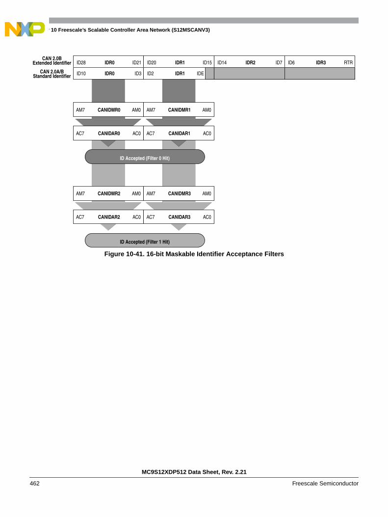
Chapter 10 Freescale’s Scalable Controller Area Network (S12MSCANV3)
MC9S12XDP512 Data Sheet, Rev. 2.21
462 Freescale Semiconductor
Figure 10-41. 16-bit Maskable Identifier Acceptance Filters
ID28 ID21IDR0
ID10 ID3IDR0
ID20 ID15IDR1
ID2 IDEIDR1
ID14 ID7IDR2
ID10 ID3IDR2
ID6 RTRIDR3
ID10 ID3IDR3
AC7 AC0CANIDAR0
AM7 AM0CANIDMR0
AC7 AC0CANIDAR1
AM7 AM0CANIDMR1
ID Accepted (Filter 0 Hit)
AC7 AC0CANIDAR2
AM7 AM0CANIDMR2
AC7 AC0CANIDAR3
AM7 AM0CANIDMR3
ID Accepted (Filter 1 Hit)
CAN 2.0BExtended Identifier
CAN 2.0A/BStandard Identifier
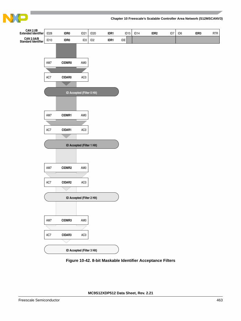
Chapter 10 Freescale’s Scalable Controller Area Network (S12MSCANV3)
MC9S12XDP512 Data Sheet, Rev. 2.21
Freescale Semiconductor 463
Figure 10-42. 8-bit Maskable Identifier Acceptance Filters
CAN 2.0BExtended Identifier
CAN 2.0A/BStandard Identifier
AC7 AC0CIDAR3
AM7 AM0CIDMR3
ID Accepted (Filter 3 Hit)
AC7 AC0CIDAR2
AM7 AM0CIDMR2
ID Accepted (Filter 2 Hit)
AC7 AC0CIDAR1
AM7 AM0CIDMR1
ID Accepted (Filter 1 Hit)
ID28 ID21IDR0
ID10 ID3IDR0
ID20 ID15IDR1
ID2 IDEIDR1
ID14 ID7IDR2
ID10 ID3IDR2
ID6 RTRIDR3
ID10 ID3IDR3
AC7 AC0CIDAR0
AM7 AM0CIDMR0
ID Accepted (Filter 0 Hit)

Chapter 10 Freescale’s Scalable Controller Area Network (S12MSCANV3)
MC9S12XDP512 Data Sheet, Rev. 2.21
464 Freescale Semiconductor
10.4.3.1 Protocol Violation Protection
The MSCAN protects the user from accidentally violating the CAN protocol through programming errors.The protection logic implements the following features:
• The receive and transmit error counters cannot be written or otherwise manipulated.
• All registers which control the configuration of the MSCAN cannot be modified while the MSCANis on-line. The MSCAN has to be in Initialization Mode. The corresponding INITRQ/INITAKhandshake bits in the CANCTL0/CANCTL1 registers (see Section 10.3.2.1, “MSCAN ControlRegister 0 (CANCTL0)”) serve as a lock to protect the following registers:
— MSCAN control 1 register (CANCTL1)
— MSCAN bus timing registers 0 and 1 (CANBTR0, CANBTR1)
— MSCAN identifier acceptance control register (CANIDAC)
— MSCAN identifier acceptance registers (CANIDAR0–CANIDAR7)
— MSCAN identifier mask registers (CANIDMR0–CANIDMR7)
• The TXCAN pin is immediately forced to a recessive state when the MSCAN goes into the powerdown mode or initialization mode (see Section 10.4.5.6, “MSCAN Power Down Mode,” andSection 10.4.5.5, “MSCAN Initialization Mode”).
• The MSCAN enable bit (CANE) is writable only once in normal system operation modes, whichprovides further protection against inadvertently disabling the MSCAN.
10.4.3.2 Clock System
Figure 10-43 shows the structure of the MSCAN clock generation circuitry.
Figure 10-43. MSCAN Clocking Scheme
The clock source bit (CLKSRC) in the CANCTL1 register (10.3.2.2/10-426) defines whether the internalCANCLK is connected to the output of a crystal oscillator (oscillator clock) or to the bus clock.
The clock source has to be chosen such that the tight oscillator tolerance requirements (up to 0.4%) of theCAN protocol are met. Additionally, for high CAN bus rates (1 Mbps), a 45% to 55% duty cycle of theclock is required.
Bus Clock
Oscillator Clock
MSCAN
CANCLK
CLKSRC
CLKSRC
Prescaler(1 .. 64)
Time quanta clock (Tq)

Chapter 10 Freescale’s Scalable Controller Area Network (S12MSCANV3)
MC9S12XDP512 Data Sheet, Rev. 2.21
Freescale Semiconductor 465
If the bus clock is generated from a PLL, it is recommended to select the oscillator clock rather than thebus clock due to jitter considerations, especially at the faster CAN bus rates.
For microcontrollers without a clock and reset generator (CRG), CANCLK is driven from the crystaloscillator (oscillator clock).
A programmable prescaler generates the time quanta (Tq) clock from CANCLK. A time quantum is theatomic unit of time handled by the MSCAN.
Eqn. 10-2
A bit time is subdivided into three segments as described in the Bosch CAN specification. (seeFigure 10-44):
• SYNC_SEG: This segment has a fixed length of one time quantum. Signal edges are expected tohappen within this section.
• Time Segment 1: This segment includes the PROP_SEG and the PHASE_SEG1 of the CANstandard. It can be programmed by setting the parameter TSEG1 to consist of 4 to 16 time quanta.
• Time Segment 2: This segment represents the PHASE_SEG2 of the CAN standard. It can beprogrammed by setting the TSEG2 parameter to be 2 to 8 time quanta long.
Eqn. 10-3
Figure 10-44. Segments within the Bit Time
TqfCANCLK
Prescaler value( )------------------------------------------------------=
Bit RatefTq
number of Time Quanta( )---------------------------------------------------------------------------------=
SYNC_SEG Time Segment 1 Time Segment 2
1 4 ... 16 2 ... 8
8 ... 25 Time Quanta
= 1 Bit Time
NRZ Signal
Sample Point(single or triple sampling)
(PROP_SEG + PHASE_SEG1) (PHASE_SEG2)
Transmit Point
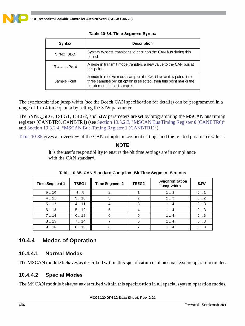
Chapter 10 Freescale’s Scalable Controller Area Network (S12MSCANV3)
MC9S12XDP512 Data Sheet, Rev. 2.21
466 Freescale Semiconductor
The synchronization jump width (see the Bosch CAN specification for details) can be programmed in arange of 1 to 4 time quanta by setting the SJW parameter.
The SYNC_SEG, TSEG1, TSEG2, and SJW parameters are set by programming the MSCAN bus timingregisters (CANBTR0, CANBTR1) (see Section 10.3.2.3, “MSCAN Bus Timing Register 0 (CANBTR0)”and Section 10.3.2.4, “MSCAN Bus Timing Register 1 (CANBTR1)”).
Table 10-35 gives an overview of the CAN compliant segment settings and the related parameter values.
NOTEIt is the user’s responsibility to ensure the bit time settings are in compliancewith the CAN standard.
10.4.4 Modes of Operation
10.4.4.1 Normal Modes
The MSCAN module behaves as described within this specification in all normal system operation modes.
10.4.4.2 Special Modes
The MSCAN module behaves as described within this specification in all special system operation modes.
Table 10-34. Time Segment Syntax
Syntax Description
SYNC_SEGSystem expects transitions to occur on the CAN bus during thisperiod.
Transmit PointA node in transmit mode transfers a new value to the CAN bus atthis point.
Sample PointA node in receive mode samples the CAN bus at this point. If thethree samples per bit option is selected, then this point marks theposition of the third sample.
Table 10-35. CAN Standard Compliant Bit Time Segment Settings
Time Segment 1 TSEG1 Time Segment 2 TSEG2 Synchronization
Jump WidthSJW
5 .. 10 4 .. 9 2 1 1 .. 2 0 .. 1
4 .. 11 3 .. 10 3 2 1 .. 3 0 .. 2
5 .. 12 4 .. 11 4 3 1 .. 4 0 .. 3
6 .. 13 5 .. 12 5 4 1 .. 4 0 .. 3
7 .. 14 6 .. 13 6 5 1 .. 4 0 .. 3
8 .. 15 7 .. 14 7 6 1 .. 4 0 .. 3
9 .. 16 8 .. 15 8 7 1 .. 4 0 .. 3

Chapter 10 Freescale’s Scalable Controller Area Network (S12MSCANV3)
MC9S12XDP512 Data Sheet, Rev. 2.21
Freescale Semiconductor 467
10.4.4.3 Emulation Modes
In all emulation modes, the MSCAN module behaves just like normal system operation modes asdescribed within this specification.
10.4.4.4 Listen-Only Mode
In an optional CAN bus monitoring mode (listen-only), the CAN node is able to receive valid data framesand valid remote frames, but it sends only “recessive” bits on the CAN bus. In addition, it cannot start atransmision. If the MAC sub-layer is required to send a “dominant” bit (ACK bit, overload flag, or activeerror flag), the bit is rerouted internally so that the MAC sub-layer monitors this “dominant” bit, althoughthe CAN bus may remain in recessive state externally.
10.4.4.5 Security Modes
The MSCAN module has no security features.
10.4.5 Low-Power Options
If the MSCAN is disabled (CANE = 0), the MSCAN clocks are stopped for power saving.
If the MSCAN is enabled (CANE = 1), the MSCAN has two additional modes with reduced powerconsumption, compared to normal mode: sleep and power down mode. In sleep mode, power consumptionis reduced by stopping all clocks except those to access the registers from the CPU side. In power downmode, all clocks are stopped and no power is consumed.
Table 10-36 summarizes the combinations of MSCAN and CPU modes. A particular combination ofmodes is entered by the given settings on the CSWAI and SLPRQ/SLPAK bits.
For all modes, an MSCAN wake-up interrupt can occur only if the MSCAN is in sleep mode (SLPRQ = 1and SLPAK = 1), wake-up functionality is enabled (WUPE = 1), and the wake-up interrupt is enabled(WUPIE = 1).
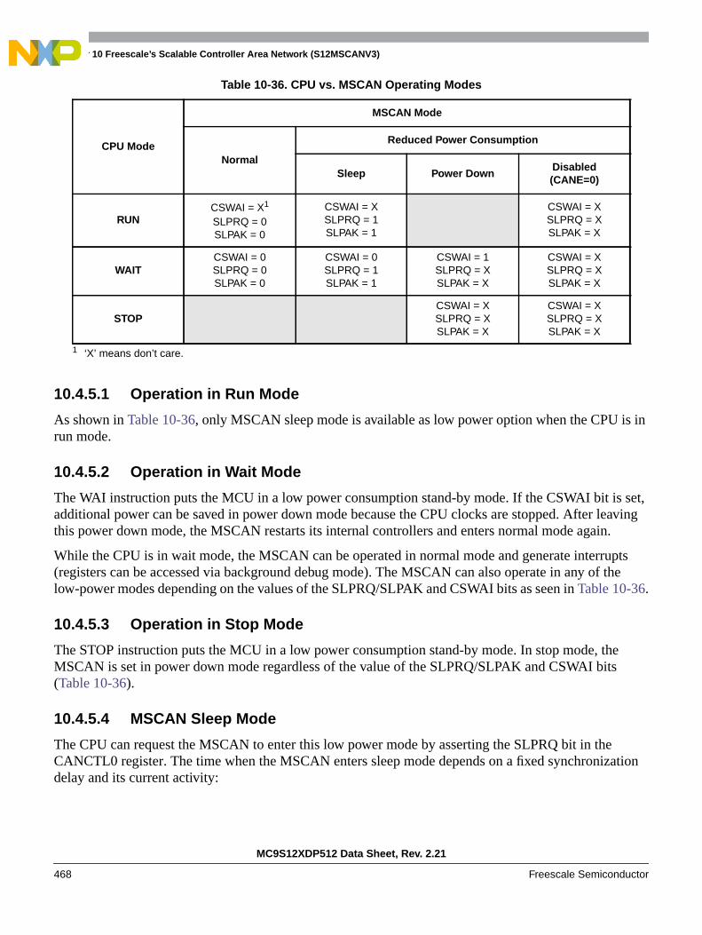
Chapter 10 Freescale’s Scalable Controller Area Network (S12MSCANV3)
MC9S12XDP512 Data Sheet, Rev. 2.21
468 Freescale Semiconductor
10.4.5.1 Operation in Run Mode
As shown in Table 10-36, only MSCAN sleep mode is available as low power option when the CPU is inrun mode.
10.4.5.2 Operation in Wait Mode
The WAI instruction puts the MCU in a low power consumption stand-by mode. If the CSWAI bit is set,additional power can be saved in power down mode because the CPU clocks are stopped. After leavingthis power down mode, the MSCAN restarts its internal controllers and enters normal mode again.
While the CPU is in wait mode, the MSCAN can be operated in normal mode and generate interrupts(registers can be accessed via background debug mode). The MSCAN can also operate in any of thelow-power modes depending on the values of the SLPRQ/SLPAK and CSWAI bits as seen in Table 10-36.
10.4.5.3 Operation in Stop Mode
The STOP instruction puts the MCU in a low power consumption stand-by mode. In stop mode, theMSCAN is set in power down mode regardless of the value of the SLPRQ/SLPAK and CSWAI bits(Table 10-36).
10.4.5.4 MSCAN Sleep Mode
The CPU can request the MSCAN to enter this low power mode by asserting the SLPRQ bit in theCANCTL0 register. The time when the MSCAN enters sleep mode depends on a fixed synchronizationdelay and its current activity:
Table 10-36. CPU vs. MSCAN Operating Modes
CPU Mode
MSCAN Mode
Normal
Reduced Power Consumption
Sleep Power DownDisabled(CANE=0)
RUNCSWAI = X1
SLPRQ = 0SLPAK = 0
1 ‘X’ means don’t care.
CSWAI = XSLPRQ = 1SLPAK = 1
CSWAI = XSLPRQ = XSLPAK = X
WAITCSWAI = 0SLPRQ = 0SLPAK = 0
CSWAI = 0SLPRQ = 1SLPAK = 1
CSWAI = 1SLPRQ = XSLPAK = X
CSWAI = XSLPRQ = XSLPAK = X
STOPCSWAI = XSLPRQ = XSLPAK = X
CSWAI = XSLPRQ = XSLPAK = X

Chapter 10 Freescale’s Scalable Controller Area Network (S12MSCANV3)
MC9S12XDP512 Data Sheet, Rev. 2.21
Freescale Semiconductor 469
• If there are one or more message buffers scheduled for transmission (TXEx = 0), the MSCAN willcontinue to transmit until all transmit message buffers are empty (TXEx = 1, transmittedsuccessfully or aborted) and then goes into sleep mode.
• If the MSCAN is receiving, it continues to receive and goes into sleep mode as soon as the CANbus next becomes idle.
• If the MSCAN is neither transmitting nor receiving, it immediately goes into sleep mode.
Figure 10-45. Sleep Request / Acknowledge Cycle
NOTEThe application software must avoid setting up a transmission (by clearingone or more TXEx flag(s)) and immediately request sleep mode (by settingSLPRQ). Whether the MSCAN starts transmitting or goes into sleep modedirectly depends on the exact sequence of operations.
If sleep mode is active, the SLPRQ and SLPAK bits are set (Figure 10-45). The application software mustuse SLPAK as a handshake indication for the request (SLPRQ) to go into sleep mode.
When in sleep mode (SLPRQ = 1 and SLPAK = 1), the MSCAN stops its internal clocks. However, clocksthat allow register accesses from the CPU side continue to run.
If the MSCAN is in bus-off state, it stops counting the 128 occurrences of 11 consecutive recessive bitsdue to the stopped clocks. The TXCAN pin remains in a recessive state. If RXF = 1, the message can beread and RXF can be cleared. Shifting a new message into the foreground buffer of the receiver FIFO(RxFG) does not take place while in sleep mode.
It is possible to access the transmit buffers and to clear the associated TXE flags. No message abort takesplace while in sleep mode.
If the WUPE bit in CANCTL0 is not asserted, the MSCAN will mask any activity it detects on CAN. TheRXCAN pin is therefore held internally in a recessive state. This locks the MSCAN in sleep mode(Figure 10-46). WUPE must be set before entering sleep mode to take effect.
The MSCAN is able to leave sleep mode (wake up) only when:
• CAN bus activity occurs and WUPE = 1
SYNC
SYNC
Bus Clock Domain CAN Clock Domain
MSCANin Sleep Mode
CPUSleep Request
SLPRQFlag
SLPAKFlag
SLPRQ
sync.SLPAK
sync.SLPRQ
SLPAK

Chapter 10 Freescale’s Scalable Controller Area Network (S12MSCANV3)
MC9S12XDP512 Data Sheet, Rev. 2.21
470 Freescale Semiconductor
or
• the CPU clears the SLPRQ bit
NOTEThe CPU cannot clear the SLPRQ bit before sleep mode (SLPRQ = 1 andSLPAK = 1) is active.
After wake-up, the MSCAN waits for 11 consecutive recessive bits to synchronize to the CAN bus. As aconsequence, if the MSCAN is woken-up by a CAN frame, this frame is not received.
The receive message buffers (RxFG and RxBG) contain messages if they were received before sleep modewas entered. All pending actions will be executed upon wake-up; copying of RxBG into RxFG, messageaborts and message transmissions. If the MSCAN remains in bus-off state after sleep mode was exited, itcontinues counting the 128 occurrences of 11 consecutive recessive bits.
Figure 10-46. Simplified State Transitions for Entering/Leaving Sleep Mode
10.4.5.5 MSCAN Initialization Mode
In initialization mode, any on-going transmission or reception is immediately aborted and synchronizationto the CAN bus is lost, potentially causing CAN protocol violations. To protect the CAN bus system fromfatal consequences of violations, the MSCAN immediately drives the TXCAN pin into a recessive state.
Wait
Idle
Tx/RxMessageActive
CAN ActivityCAN Activity &
Sleep
SLPRQ
StartUp for Idle
(CAN Activity & WUPE) |
(CAN Activity & WUPE) | SLPRQ
CAN Activity
CAN Activity
CAN Activity &
CAN Activity
SLPRQ
SLPRQ
CAN Activity
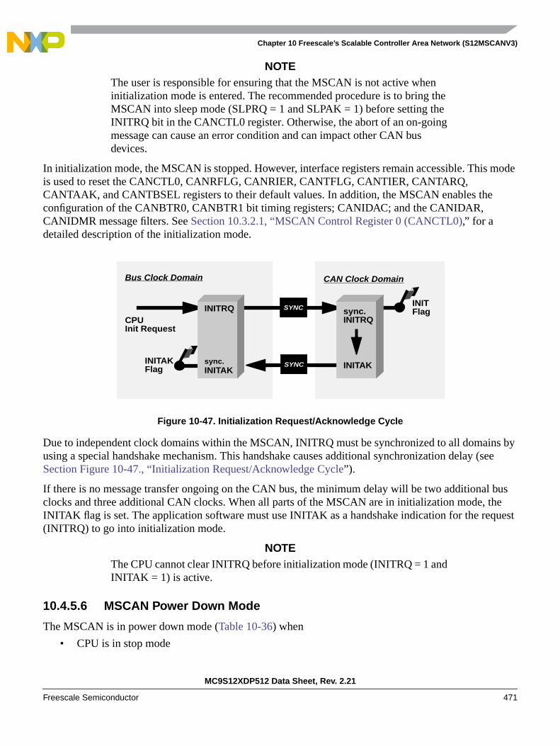
Chapter 10 Freescale’s Scalable Controller Area Network (S12MSCANV3)
MC9S12XDP512 Data Sheet, Rev. 2.21
Freescale Semiconductor 471
NOTEThe user is responsible for ensuring that the MSCAN is not active wheninitialization mode is entered. The recommended procedure is to bring theMSCAN into sleep mode (SLPRQ = 1 and SLPAK = 1) before setting theINITRQ bit in the CANCTL0 register. Otherwise, the abort of an on-goingmessage can cause an error condition and can impact other CAN busdevices.
In initialization mode, the MSCAN is stopped. However, interface registers remain accessible. This modeis used to reset the CANCTL0, CANRFLG, CANRIER, CANTFLG, CANTIER, CANTARQ,CANTAAK, and CANTBSEL registers to their default values. In addition, the MSCAN enables theconfiguration of the CANBTR0, CANBTR1 bit timing registers; CANIDAC; and the CANIDAR,CANIDMR message filters. See Section 10.3.2.1, “MSCAN Control Register 0 (CANCTL0),” for adetailed description of the initialization mode.
Figure 10-47. Initialization Request/Acknowledge Cycle
Due to independent clock domains within the MSCAN, INITRQ must be synchronized to all domains byusing a special handshake mechanism. This handshake causes additional synchronization delay (seeSection Figure 10-47., “Initialization Request/Acknowledge Cycle”).
If there is no message transfer ongoing on the CAN bus, the minimum delay will be two additional busclocks and three additional CAN clocks. When all parts of the MSCAN are in initialization mode, theINITAK flag is set. The application software must use INITAK as a handshake indication for the request(INITRQ) to go into initialization mode.
NOTEThe CPU cannot clear INITRQ before initialization mode (INITRQ = 1 andINITAK = 1) is active.
10.4.5.6 MSCAN Power Down Mode
The MSCAN is in power down mode (Table 10-36) when
• CPU is in stop mode
SYNC
SYNC
Bus Clock Domain CAN Clock Domain
CPUInit Request
INITFlag
INITAKFlag
INITRQ
sync.INITAK
sync.INITRQ
INITAK
Chapter 10 Freescale’s Scalable Controller Area Network (S12MSCANV3)
MC9S12XDP512 Data Sheet, Rev. 2.21
472 Freescale Semiconductor
or
• CPU is in wait mode and the CSWAI bit is set
When entering the power down mode, the MSCAN immediately stops all ongoing transmissions andreceptions, potentially causing CAN protocol violations. To protect the CAN bus system from fatalconsequences of violations to the above rule, the MSCAN immediately drives the TXCAN pin into arecessive state.
NOTEThe user is responsible for ensuring that the MSCAN is not active whenpower down mode is entered. The recommended procedure is to bring theMSCAN into Sleep mode before the STOP or WAI instruction (if CSWAIis set) is executed. Otherwise, the abort of an ongoing message can cause anerror condition and impact other CAN bus devices.
In power down mode, all clocks are stopped and no registers can be accessed. If the MSCAN was not insleep mode before power down mode became active, the module performs an internal recovery cycle afterpowering up. This causes some fixed delay before the module enters normal mode again.
10.4.5.7 Programmable Wake-Up Function
The MSCAN can be programmed to wake up the MSCAN as soon as CAN bus activity is detected (seecontrol bit WUPE in Section 10.3.2.1, “MSCAN Control Register 0 (CANCTL0)”). The sensitivity toexisting CAN bus action can be modified by applying a low-pass filter function to the RXCAN input linewhile in sleep mode (see control bit WUPM in Section 10.3.2.2, “MSCAN Control Register 1(CANCTL1)”).
This feature can be used to protect the MSCAN from wake-up due to short glitches on the CAN bus lines.Such glitches can result from—for example—electromagnetic interference within noisy environments.
10.4.6 Reset Initialization
The reset state of each individual bit is listed in Section 10.3.2, “Register Descriptions,” which details allthe registers and their bit-fields.
10.4.7 Interrupts
This section describes all interrupts originated by the MSCAN. It documents the enable bits and generatedflags. Each interrupt is listed and described separately.
10.4.7.1 Description of Interrupt Operation
The MSCAN supports four interrupt vectors (see Table 10-37), any of which can be individually masked(for details see sections from Section 10.3.2.6, “MSCAN Receiver Interrupt Enable Register(CANRIER),” to Section 10.3.2.8, “MSCAN Transmitter Interrupt Enable Register (CANTIER)”).

Chapter 10 Freescale’s Scalable Controller Area Network (S12MSCANV3)
MC9S12XDP512 Data Sheet, Rev. 2.21
Freescale Semiconductor 473
NOTEThe dedicated interrupt vector addresses are defined in the Resets andInterrupts chapter.
10.4.7.2 Transmit Interrupt
At least one of the three transmit buffers is empty (not scheduled) and can be loaded to schedule a messagefor transmission. The TXEx flag of the empty message buffer is set.
10.4.7.3 Receive Interrupt
A message is successfully received and shifted into the foreground buffer (RxFG) of the receiver FIFO.This interrupt is generated immediately after receiving the EOF symbol. The RXF flag is set. If there aremultiple messages in the receiver FIFO, the RXF flag is set as soon as the next message is shifted to theforeground buffer.
10.4.7.4 Wake-Up Interrupt
A wake-up interrupt is generated if activity on the CAN bus occurs during MSCAN internal sleep mode.WUPE (see Section 10.3.2.1, “MSCAN Control Register 0 (CANCTL0)”) must be enabled.
10.4.7.5 Error Interrupt
An error interrupt is generated if an overrun of the receiver FIFO, error, warning, or bus-off conditionoccurrs. Section 10.3.2.5, “MSCAN Receiver Flag Register (CANRFLG) indicates one of the followingconditions:
• Overrun — An overrun condition of the receiver FIFO as described in Section 10.4.2.3, “ReceiveStructures,” occurred.
• CAN Status Change — The actual value of the transmit and receive error counters control theCAN bus state of the MSCAN. As soon as the error counters skip into a critical range(Tx/Rx-warning, Tx/Rx-error, bus-off) the MSCAN flags an error condition. The status change,which caused the error condition, is indicated by the TSTAT and RSTAT flags (seeSection 10.3.2.5, “MSCAN Receiver Flag Register (CANRFLG)” and Section 10.3.2.6, “MSCANReceiver Interrupt Enable Register (CANRIER)”).
10.4.7.6 Interrupt Acknowledge
Interrupts are directly associated with one or more status flags in either the Section 10.3.2.5, “MSCANReceiver Flag Register (CANRFLG)” or the Section 10.3.2.7, “MSCAN Transmitter Flag Register
Table 10-37. Interrupt Vectors
Interrupt Source CCR Mask Local Enable
Wake-Up Interrupt (WUPIF) I bit CANRIER (WUPIE)
Error Interrupts Interrupt (CSCIF, OVRIF) I bit CANRIER (CSCIE, OVRIE)
Receive Interrupt (RXF) I bit CANRIER (RXFIE)
Transmit Interrupts (TXE[2:0]) I bit CANTIER (TXEIE[2:0])
Chapter 10 Freescale’s Scalable Controller Area Network (S12MSCANV3)
MC9S12XDP512 Data Sheet, Rev. 2.21
474 Freescale Semiconductor
(CANTFLG).” Interrupts are pending as long as one of the corresponding flags is set. The flags inCANRFLG and CANTFLG must be reset within the interrupt handler to handshake the interrupt. The flagsare reset by writing a 1 to the corresponding bit position. A flag cannot be cleared if the respectivecondition prevails.
NOTEIt must be guaranteed that the CPU clears only the bit causing the currentinterrupt. For this reason, bit manipulation instructions (BSET) must not beused to clear interrupt flags. These instructions may cause accidentalclearing of interrupt flags which are set after entering the current interruptservice routine.
10.4.7.7 Recovery from Stop or Wait
The MSCAN can recover from stop or wait via the wake-up interrupt. This interrupt can only occur if theMSCAN was in sleep mode (SLPRQ = 1 and SLPAK = 1) before entering power down mode, the wake-upoption is enabled (WUPE = 1), and the wake-up interrupt is enabled (WUPIE = 1).
10.5 Initialization/Application Information
10.5.1 MSCAN initialization
The procedure to initially start up the MSCAN module out of reset is as follows:
1. Assert CANE
2. Write to the configuration registers in initialization mode
3. Clear INITRQ to leave initialization mode and enter normal mode
If the configuration of registers which are writable in initialization mode needs to be changed only whenthe MSCAN module is in normal mode:
1. Bring the module into sleep mode by setting SLPRQ and awaiting SLPAK to assert after the CANbus becomes idle.
2. Enter initialization mode: assert INITRQ and await INITAK
3. Write to the configuration registers in initialization mode
4. Clear INITRQ to leave initialization mode and continue in normal mode
10.5.2 Bus-Off Recovery
The bus-off recovery is user configurable. The bus-off state can either be left automatically or on userrequest.
For reasons of backwards compatibility, the MSCAN defaults to automatic recovery after reset. In thiscase, the MSCAN will become error active again after counting 128 occurrences of 11 consecutiverecessive bits on the CAN bus (See the Bosch CAN specification for details).

Chapter 10 Freescale’s Scalable Controller Area Network (S12MSCANV3)
MC9S12XDP512 Data Sheet, Rev. 2.21
Freescale Semiconductor 475
If the MSCAN is configured for user request (BORM set in Section 10.3.2.2, “MSCAN Control Register1 (CANCTL1)”), the recovery from bus-off starts after both independent events have become true:
• 128 occurrences of 11 consecutive recessive bits on the CAN bus have been monitored
• BOHOLD in Section 10.3.2.14, “MSCAN Miscellaneous Register (CANMISC) has been clearedby the user
These two events may occur in any order.

Chapter 10 Freescale’s Scalable Controller Area Network (S12MSCANV3)
MC9S12XDP512 Data Sheet, Rev. 2.21
476 Freescale Semiconductor

MC9S12XDP512 Data Sheet, Rev. 2.21
Freescale Semiconductor 477
Chapter 11Serial Communication Interface (S12SCIV5)
11.1 IntroductionThis block guide provides an overview of the serial communication interface (SCI) module.
The SCI allows asynchronous serial communications with peripheral devices and other CPUs.
11.1.1 Glossary
IR: InfraRed
IrDA: Infrared Design Associate
IRQ: Interrupt Request
LIN: Local Interconnect Network
LSB: Least Significant Bit
MSB: Most Significant Bit
NRZ: Non-Return-to-Zero
RZI: Return-to-Zero-Inverted
RXD: Receive Pin
SCI : Serial Communication Interface
TXD: Transmit Pin
11.1.2 Features
The SCI includes these distinctive features:
• Full-duplex or single-wire operation
• Standard mark/space non-return-to-zero (NRZ) format
• Selectable IrDA 1.4 return-to-zero-inverted (RZI) format with programmable pulse widths
• 13-bit baud rate selection
• Programmable 8-bit or 9-bit data format
• Separately enabled transmitter and receiver
• Programmable polarity for transmitter and receiver
Chapter 11 Serial Communication Interface (S12SCIV5)
MC9S12XDP512 Data Sheet, Rev. 2.21
478 Freescale Semiconductor
• Programmable transmitter output parity
• Two receiver wakeup methods:
— Idle line wakeup— Address mark wakeup
• Interrupt-driven operation with eight flags:
— Transmitter empty— Transmission complete— Receiver full— Idle receiver input— Receiver overrun— Noise error— Framing error— Parity error— Receive wakeup on active edge— Transmit collision detect supporting LIN— Break Detect supporting LIN
• Receiver framing error detection
• Hardware parity checking
• 1/16 bit-time noise detection
11.1.3 Modes of Operation
The SCI functions the same in normal, special, and emulation modes. It has two low power modes, waitand stop modes.
• Run mode
• Wait mode
• Stop mode
11.1.4 Block Diagram
Figure 11-1 is a high level block diagram of the SCI module, showing the interaction of various functionblocks.

Chapter 11 Serial Communication Interface (S12SCIV5)
MC9S12XDP512 Data Sheet, Rev. 2.21
Freescale Semiconductor 479
Figure 11-1. SCI Block Diagram
SCI Data Register
RXD Data In
Data Out TXD
Receive Shift RegisterInfraredDecoder
Receive & WakeupControl
Data Format Control
Transmit Control
Baud RateGenerator
Bus Clock
1/16
Transmit Shift Register
SCI Data Register
ReceiveInterrupt
Generation
TransmitInterrupt
Generation
InfraredEncoder
IDLE
RDRF/OR
TC
TDRE
BRKD
BERRRXEDG
SCIInterruptRequest
Chapter 11 Serial Communication Interface (S12SCIV5)
MC9S12XDP512 Data Sheet, Rev. 2.21
480 Freescale Semiconductor
11.2 External Signal DescriptionThe SCI module has a total of two external pins.
11.2.1 TXD — Transmit Pin
The TXD pin transmits SCI (standard or infrared) data. It will idle high in either mode and is highimpedance anytime the transmitter is disabled.
11.2.2 RXD — Receive Pin
The RXD pin receives SCI (standard or infrared) data. An idle line is detected as a line high. This input isignored when the receiver is disabled and should be terminated to a known voltage.
11.3 Memory Map and Register DefinitionThis section provides a detailed description of all the SCI registers.
11.3.1 Module Memory Map and Register Definition
The memory map for the SCI module is given below in Figure 11-2. The address listed for each register isthe address offset. The total address for each register is the sum of the base address for the SCI module andthe address offset for each register.
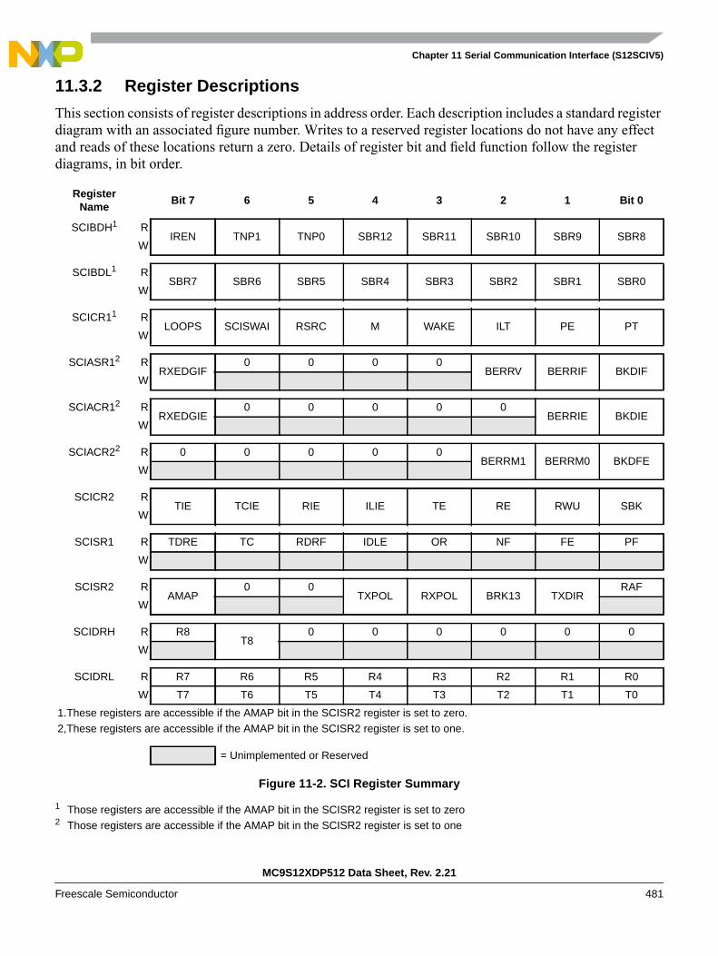
Chapter 11 Serial Communication Interface (S12SCIV5)
MC9S12XDP512 Data Sheet, Rev. 2.21
Freescale Semiconductor 481
11.3.2 Register Descriptions
This section consists of register descriptions in address order. Each description includes a standard registerdiagram with an associated figure number. Writes to a reserved register locations do not have any effectand reads of these locations return a zero. Details of register bit and field function follow the registerdiagrams, in bit order.
RegisterName
Bit 7 6 5 4 3 2 1 Bit 0
SCIBDH1 RIREN TNP1 TNP0 SBR12 SBR11 SBR10 SBR9 SBR8
W
SCIBDL1 RSBR7 SBR6 SBR5 SBR4 SBR3 SBR2 SBR1 SBR0
W
SCICR11 RLOOPS SCISWAI RSRC M WAKE ILT PE PT
W
SCIASR12 RRXEDGIF
0 0 0 0BERRV BERRIF BKDIF
W
SCIACR12 RRXEDGIE
0 0 0 0 0BERRIE BKDIE
W
SCIACR22 R 0 0 0 0 0BERRM1 BERRM0 BKDFE
W
SCICR2 RTIE TCIE RIE ILIE TE RE RWU SBK
W
SCISR1 R TDRE TC RDRF IDLE OR NF FE PF
W
SCISR2 RAMAP
0 0TXPOL RXPOL BRK13 TXDIR
RAF
W
SCIDRH R R8T8
0 0 0 0 0 0
W
SCIDRL R R7 R6 R5 R4 R3 R2 R1 R0
W T7 T6 T5 T4 T3 T2 T1 T0
1.These registers are accessible if the AMAP bit in the SCISR2 register is set to zero.2,These registers are accessible if the AMAP bit in the SCISR2 register is set to one.
= Unimplemented or Reserved
Figure 11-2. SCI Register Summary
1 Those registers are accessible if the AMAP bit in the SCISR2 register is set to zero2 Those registers are accessible if the AMAP bit in the SCISR2 register is set to one
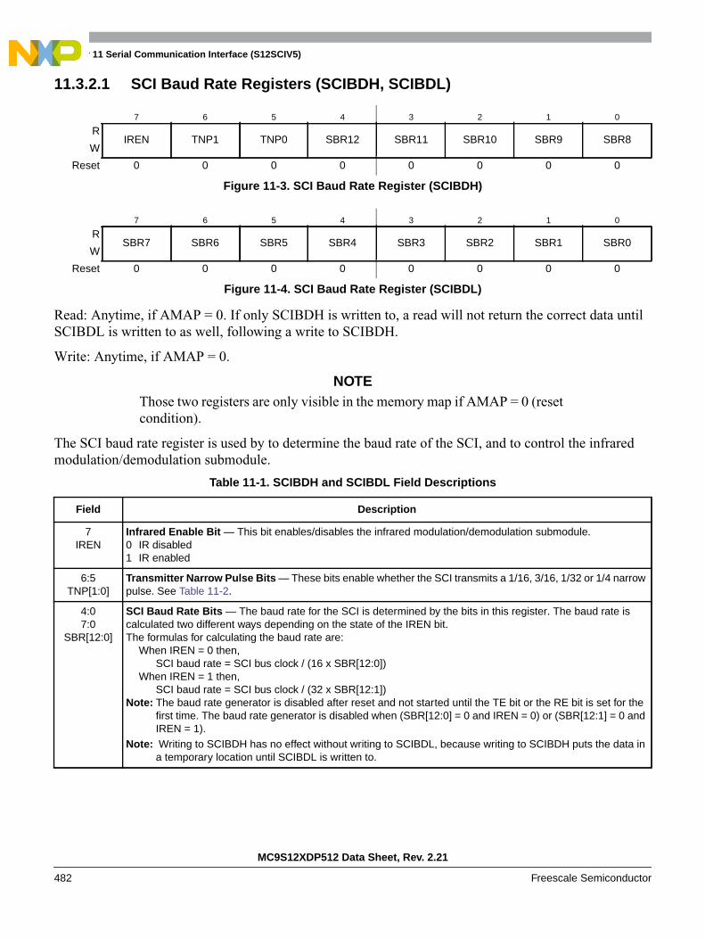
Chapter 11 Serial Communication Interface (S12SCIV5)
MC9S12XDP512 Data Sheet, Rev. 2.21
482 Freescale Semiconductor
11.3.2.1 SCI Baud Rate Registers (SCIBDH, SCIBDL)
Read: Anytime, if AMAP = 0. If only SCIBDH is written to, a read will not return the correct data untilSCIBDL is written to as well, following a write to SCIBDH.
Write: Anytime, if AMAP = 0.
NOTEThose two registers are only visible in the memory map if AMAP = 0 (resetcondition).
The SCI baud rate register is used by to determine the baud rate of the SCI, and to control the infraredmodulation/demodulation submodule.
7 6 5 4 3 2 1 0
RIREN TNP1 TNP0 SBR12 SBR11 SBR10 SBR9 SBR8
W
Reset 0 0 0 0 0 0 0 0
Figure 11-3. SCI Baud Rate Register (SCIBDH)
7 6 5 4 3 2 1 0
RSBR7 SBR6 SBR5 SBR4 SBR3 SBR2 SBR1 SBR0
W
Reset 0 0 0 0 0 0 0 0
Figure 11-4. SCI Baud Rate Register (SCIBDL)
Table 11-1. SCIBDH and SCIBDL Field Descriptions
Field Description
7IREN
Infrared Enable Bit — This bit enables/disables the infrared modulation/demodulation submodule.0 IR disabled1 IR enabled
6:5TNP[1:0]
Transmitter Narrow Pulse Bits — These bits enable whether the SCI transmits a 1/16, 3/16, 1/32 or 1/4 narrowpulse. See Table 11-2.
4:07:0
SBR[12:0]
SCI Baud Rate Bits — The baud rate for the SCI is determined by the bits in this register. The baud rate iscalculated two different ways depending on the state of the IREN bit.The formulas for calculating the baud rate are:
When IREN = 0 then,SCI baud rate = SCI bus clock / (16 x SBR[12:0])
When IREN = 1 then,SCI baud rate = SCI bus clock / (32 x SBR[12:1])
Note: The baud rate generator is disabled after reset and not started until the TE bit or the RE bit is set for thefirst time. The baud rate generator is disabled when (SBR[12:0] = 0 and IREN = 0) or (SBR[12:1] = 0 andIREN = 1).
Note: Writing to SCIBDH has no effect without writing to SCIBDL, because writing to SCIBDH puts the data ina temporary location until SCIBDL is written to.

Chapter 11 Serial Communication Interface (S12SCIV5)
MC9S12XDP512 Data Sheet, Rev. 2.21
Freescale Semiconductor 483
11.3.2.2 SCI Control Register 1 (SCICR1)
Read: Anytime, if AMAP = 0.
Write: Anytime, if AMAP = 0.
NOTEThis register is only visible in the memory map if AMAP = 0 (resetcondition).
Table 11-2. IRSCI Transmit Pulse Width
TNP[1:0] Narrow Pulse Width
11 1/4
10 1/32
01 1/16
00 3/16
7 6 5 4 3 2 1 0
RLOOPS SCISWAI RSRC M WAKE ILT PE PT
W
Reset 0 0 0 0 0 0 0 0
Figure 11-5. SCI Control Register 1 (SCICR1)
Table 11-3. SCICR1 Field Descriptions
Field Description
7LOOPS
Loop Select Bit — LOOPS enables loop operation. In loop operation, the RXD pin is disconnected from the SCIand the transmitter output is internally connected to the receiver input. Both the transmitter and the receiver mustbe enabled to use the loop function.0 Normal operation enabled1 Loop operation enabledThe receiver input is determined by the RSRC bit.
6SCISWAI
SCI Stop in Wait Mode Bit — SCISWAI disables the SCI in wait mode.0 SCI enabled in wait mode1 SCI disabled in wait mode
5RSRC
Receiver Source Bit — When LOOPS = 1, the RSRC bit determines the source for the receiver shift registerinput. See Table 11-4.0 Receiver input internally connected to transmitter output1 Receiver input connected externally to transmitter
4M
Data Format Mode Bit — MODE determines whether data characters are eight or nine bits long.0 One start bit, eight data bits, one stop bit1 One start bit, nine data bits, one stop bit
3WAKE
Wakeup Condition Bit — WAKE determines which condition wakes up the SCI: a logic 1 (address mark) in themost significant bit position of a received data character or an idle condition on the RXD pin.0 Idle line wakeup1 Address mark wakeup
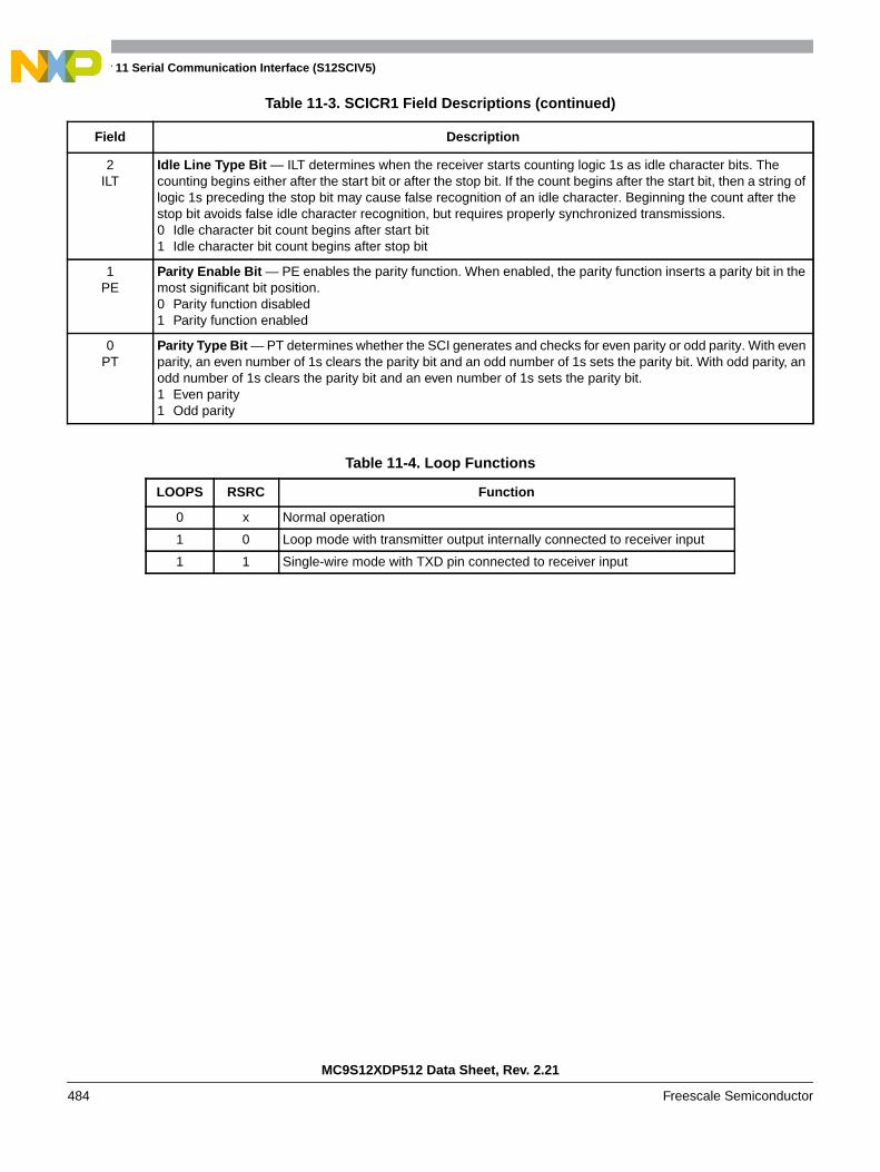
Chapter 11 Serial Communication Interface (S12SCIV5)
MC9S12XDP512 Data Sheet, Rev. 2.21
484 Freescale Semiconductor
2ILT
Idle Line Type Bit — ILT determines when the receiver starts counting logic 1s as idle character bits. Thecounting begins either after the start bit or after the stop bit. If the count begins after the start bit, then a string oflogic 1s preceding the stop bit may cause false recognition of an idle character. Beginning the count after thestop bit avoids false idle character recognition, but requires properly synchronized transmissions.0 Idle character bit count begins after start bit1 Idle character bit count begins after stop bit
1PE
Parity Enable Bit — PE enables the parity function. When enabled, the parity function inserts a parity bit in themost significant bit position.0 Parity function disabled1 Parity function enabled
0PT
Parity Type Bit — PT determines whether the SCI generates and checks for even parity or odd parity. With evenparity, an even number of 1s clears the parity bit and an odd number of 1s sets the parity bit. With odd parity, anodd number of 1s clears the parity bit and an even number of 1s sets the parity bit.1 Even parity1 Odd parity
Table 11-4. Loop Functions
LOOPS RSRC Function
0 x Normal operation
1 0 Loop mode with transmitter output internally connected to receiver input
1 1 Single-wire mode with TXD pin connected to receiver input
Table 11-3. SCICR1 Field Descriptions (continued)
Field Description
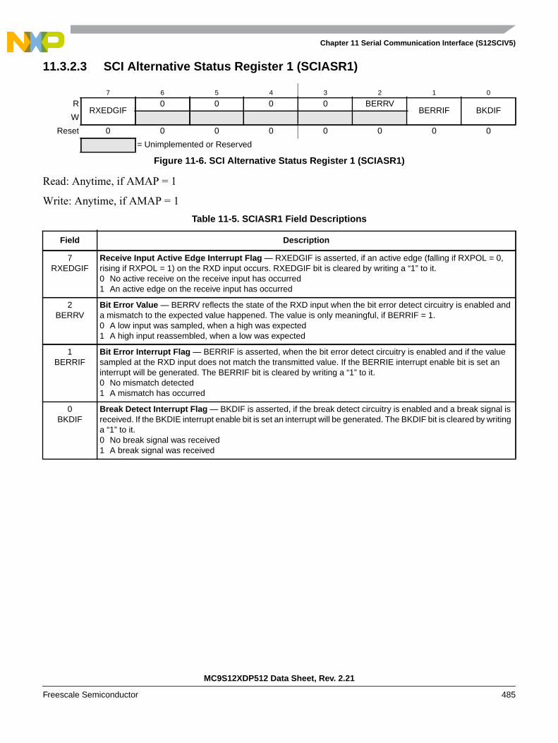
Chapter 11 Serial Communication Interface (S12SCIV5)
MC9S12XDP512 Data Sheet, Rev. 2.21
Freescale Semiconductor 485
11.3.2.3 SCI Alternative Status Register 1 (SCIASR1)
Read: Anytime, if AMAP = 1
Write: Anytime, if AMAP = 1
7 6 5 4 3 2 1 0
RRXEDGIF
0 0 0 0 BERRVBERRIF BKDIF
W
Reset 0 0 0 0 0 0 0 0
= Unimplemented or Reserved
Figure 11-6. SCI Alternative Status Register 1 (SCIASR1)
Table 11-5. SCIASR1 Field Descriptions
Field Description
7RXEDGIF
Receive Input Active Edge Interrupt Flag — RXEDGIF is asserted, if an active edge (falling if RXPOL = 0,rising if RXPOL = 1) on the RXD input occurs. RXEDGIF bit is cleared by writing a “1” to it.0 No active receive on the receive input has occurred1 An active edge on the receive input has occurred
2BERRV
Bit Error Value — BERRV reflects the state of the RXD input when the bit error detect circuitry is enabled anda mismatch to the expected value happened. The value is only meaningful, if BERRIF = 1.0 A low input was sampled, when a high was expected1 A high input reassembled, when a low was expected
1BERRIF
Bit Error Interrupt Flag — BERRIF is asserted, when the bit error detect circuitry is enabled and if the valuesampled at the RXD input does not match the transmitted value. If the BERRIE interrupt enable bit is set aninterrupt will be generated. The BERRIF bit is cleared by writing a “1” to it.0 No mismatch detected1 A mismatch has occurred
0BKDIF
Break Detect Interrupt Flag — BKDIF is asserted, if the break detect circuitry is enabled and a break signal isreceived. If the BKDIE interrupt enable bit is set an interrupt will be generated. The BKDIF bit is cleared by writinga “1” to it.0 No break signal was received1 A break signal was received

Chapter 11 Serial Communication Interface (S12SCIV5)
MC9S12XDP512 Data Sheet, Rev. 2.21
486 Freescale Semiconductor
11.3.2.4 SCI Alternative Control Register 1 (SCIACR1)
Read: Anytime, if AMAP = 1
Write: Anytime, if AMAP = 1
7 6 5 4 3 2 1 0
RRXEDGIE
0 0 0 0 0BERRIE BKDIE
W
Reset 0 0 0 0 0 0 0 0
= Unimplemented or Reserved
Figure 11-7. SCI Alternative Control Register 1 (SCIACR1)
Table 11-6. SCIACR1 Field Descriptions
Field Description
7RSEDGIE
Receive Input Active Edge Interrupt Enable — RXEDGIE enables the receive input active edge interrupt flag,RXEDGIF, to generate interrupt requests.0 RXEDGIF interrupt requests disabled1 RXEDGIF interrupt requests enabled
1BERRIE
Bit Error Interrupt Enable — BERRIE enables the bit error interrupt flag, BERRIF, to generate interruptrequests.0 BERRIF interrupt requests disabled1 BERRIF interrupt requests enabled
0BKDIE
Break Detect Interrupt Enable — BKDIE enables the break detect interrupt flag, BKDIF, to generate interruptrequests.0 BKDIF interrupt requests disabled1 BKDIF interrupt requests enabled

Chapter 11 Serial Communication Interface (S12SCIV5)
MC9S12XDP512 Data Sheet, Rev. 2.21
Freescale Semiconductor 487
11.3.2.5 SCI Alternative Control Register 2 (SCIACR2)
Read: Anytime, if AMAP = 1
Write: Anytime, if AMAP = 1
7 6 5 4 3 2 1 0
R 0 0 0 0 0BERRM1 BERRM0 BKDFE
W
Reset 0 0 0 0 0 0 0 0
= Unimplemented or Reserved
Figure 11-8. SCI Alternative Control Register 2 (SCIACR2)
Table 11-7. SCIACR2 Field Descriptions
Field Description
2:1BERRM[1:0]
Bit Error Mode — Those two bits determines the functionality of the bit error detect feature. See Table 11-8.
0BKDFE
Break Detect Feature Enable — BKDFE enables the break detect circuitry.0 Break detect circuit disabled1 Break detect circuit enabled
Table 11-8. Bit Error Mode Coding
BERRM1 BERRM0 Function
0 0 Bit error detect circuit is disabled
0 1 Receive input sampling occurs during the 9th time tick of a transmitted bit(refer to Figure 11-19)
1 0 Receive input sampling occurs during the 13th time tick of a transmitted bit(refer to Figure 11-19)
1 1 Reserved
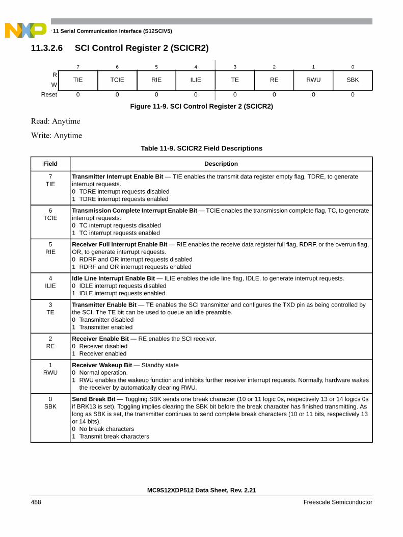
Chapter 11 Serial Communication Interface (S12SCIV5)
MC9S12XDP512 Data Sheet, Rev. 2.21
488 Freescale Semiconductor
11.3.2.6 SCI Control Register 2 (SCICR2)
Read: Anytime
Write: Anytime
7 6 5 4 3 2 1 0
RTIE TCIE RIE ILIE TE RE RWU SBK
W
Reset 0 0 0 0 0 0 0 0
Figure 11-9. SCI Control Register 2 (SCICR2)
Table 11-9. SCICR2 Field Descriptions
Field Description
7TIE
Transmitter Interrupt Enable Bit — TIE enables the transmit data register empty flag, TDRE, to generateinterrupt requests.0 TDRE interrupt requests disabled1 TDRE interrupt requests enabled
6TCIE
Transmission Complete Interrupt Enable Bit — TCIE enables the transmission complete flag, TC, to generateinterrupt requests.0 TC interrupt requests disabled1 TC interrupt requests enabled
5RIE
Receiver Full Interrupt Enable Bit — RIE enables the receive data register full flag, RDRF, or the overrun flag,OR, to generate interrupt requests.0 RDRF and OR interrupt requests disabled1 RDRF and OR interrupt requests enabled
4ILIE
Idle Line Interrupt Enable Bit — ILIE enables the idle line flag, IDLE, to generate interrupt requests.0 IDLE interrupt requests disabled1 IDLE interrupt requests enabled
3TE
Transmitter Enable Bit — TE enables the SCI transmitter and configures the TXD pin as being controlled bythe SCI. The TE bit can be used to queue an idle preamble.0 Transmitter disabled1 Transmitter enabled
2RE
Receiver Enable Bit — RE enables the SCI receiver.0 Receiver disabled1 Receiver enabled
1RWU
Receiver Wakeup Bit — Standby state0 Normal operation.1 RWU enables the wakeup function and inhibits further receiver interrupt requests. Normally, hardware wakes
the receiver by automatically clearing RWU.
0SBK
Send Break Bit — Toggling SBK sends one break character (10 or 11 logic 0s, respectively 13 or 14 logics 0sif BRK13 is set). Toggling implies clearing the SBK bit before the break character has finished transmitting. Aslong as SBK is set, the transmitter continues to send complete break characters (10 or 11 bits, respectively 13or 14 bits).0 No break characters1 Transmit break characters

Chapter 11 Serial Communication Interface (S12SCIV5)
MC9S12XDP512 Data Sheet, Rev. 2.21
Freescale Semiconductor 489
11.3.2.7 SCI Status Register 1 (SCISR1)
The SCISR1 and SCISR2 registers provides inputs to the MCU for generation of SCI interrupts. Also,these registers can be polled by the MCU to check the status of these bits. The flag-clearing proceduresrequire that the status register be read followed by a read or write to the SCI data register.It is permissibleto execute other instructions between the two steps as long as it does not compromise the handling of I/O,but the order of operations is important for flag clearing.
Read: Anytime
Write: Has no meaning or effect
7 6 5 4 3 2 1 0
R TDRE TC RDRF IDLE OR NF FE PF
W
Reset 1 1 0 0 0 0 0 0
= Unimplemented or Reserved
Figure 11-10. SCI Status Register 1 (SCISR1)
Table 11-10. SCISR1 Field Descriptions
Field Description
7TDRE
Transmit Data Register Empty Flag — TDRE is set when the transmit shift register receives a byte from theSCI data register. When TDRE is 1, the transmit data register (SCIDRH/L) is empty and can receive a new valueto transmit.Clear TDRE by reading SCI status register 1 (SCISR1), with TDRE set and then writing to SCI dataregister low (SCIDRL).0 No byte transferred to transmit shift register1 Byte transferred to transmit shift register; transmit data register empty
6TC
Transmit Complete Flag — TC is set low when there is a transmission in progress or when a preamble or breakcharacter is loaded. TC is set high when the TDRE flag is set and no data, preamble, or break character is beingtransmitted.When TC is set, the TXD pin becomes idle (logic 1). Clear TC by reading SCI status register 1(SCISR1) with TC set and then writing to SCI data register low (SCIDRL). TC is cleared automatically when data,preamble, or break is queued and ready to be sent. TC is cleared in the event of a simultaneous set and clear ofthe TC flag (transmission not complete).0 Transmission in progress1 No transmission in progress
5RDRF
Receive Data Register Full Flag — RDRF is set when the data in the receive shift register transfers to the SCIdata register. Clear RDRF by reading SCI status register 1 (SCISR1) with RDRF set and then reading SCI dataregister low (SCIDRL).0 Data not available in SCI data register1 Received data available in SCI data register
4IDLE
Idle Line Flag — IDLE is set when 10 consecutive logic 1s (if M = 0) or 11 consecutive logic 1s (if M =1) appearon the receiver input. Once the IDLE flag is cleared, a valid frame must again set the RDRF flag before an idlecondition can set the IDLE flag.Clear IDLE by reading SCI status register 1 (SCISR1) with IDLE set and thenreading SCI data register low (SCIDRL).0 Receiver input is either active now or has never become active since the IDLE flag was last cleared1 Receiver input has become idleNote: When the receiver wakeup bit (RWU) is set, an idle line condition does not set the IDLE flag.
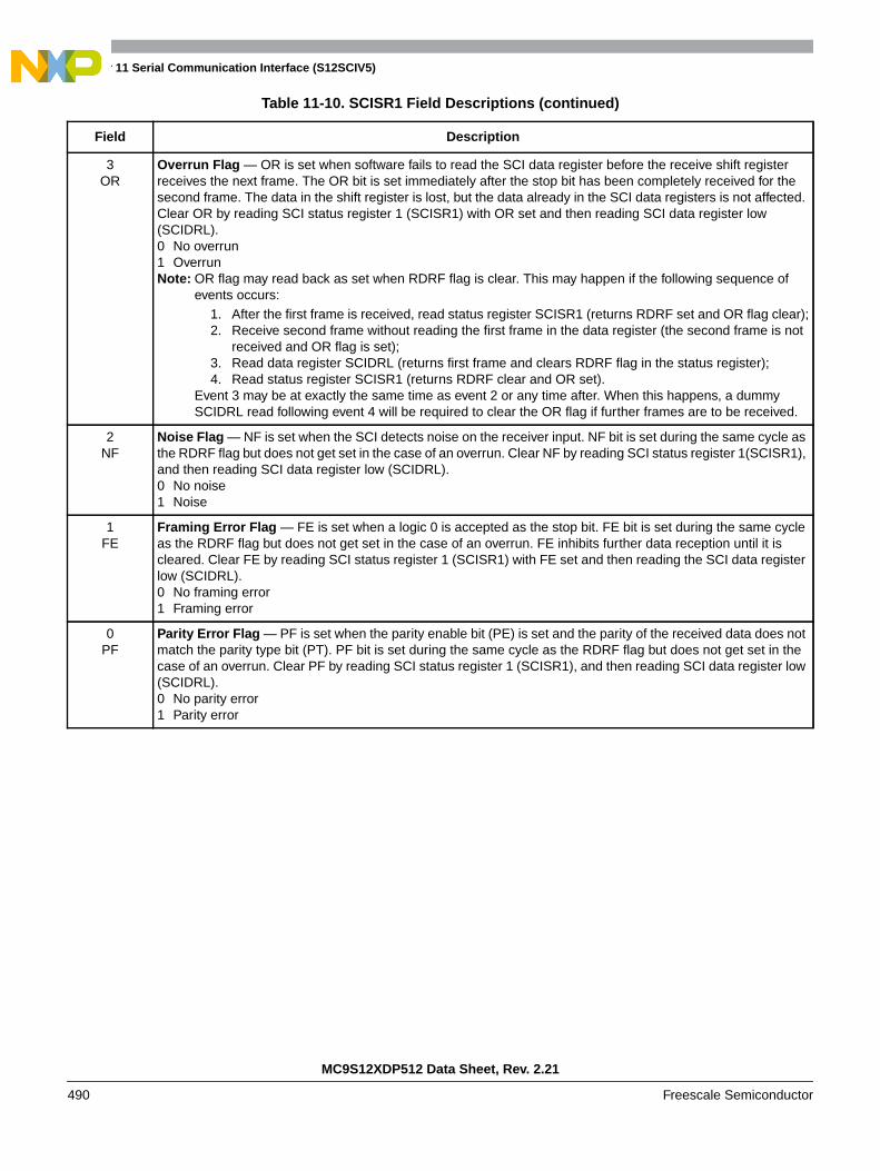
Chapter 11 Serial Communication Interface (S12SCIV5)
MC9S12XDP512 Data Sheet, Rev. 2.21
490 Freescale Semiconductor
3OR
Overrun Flag — OR is set when software fails to read the SCI data register before the receive shift registerreceives the next frame. The OR bit is set immediately after the stop bit has been completely received for thesecond frame. The data in the shift register is lost, but the data already in the SCI data registers is not affected.Clear OR by reading SCI status register 1 (SCISR1) with OR set and then reading SCI data register low(SCIDRL).0 No overrun1 OverrunNote: OR flag may read back as set when RDRF flag is clear. This may happen if the following sequence of
events occurs:1. After the first frame is received, read status register SCISR1 (returns RDRF set and OR flag clear);2. Receive second frame without reading the first frame in the data register (the second frame is not
received and OR flag is set);3. Read data register SCIDRL (returns first frame and clears RDRF flag in the status register);4. Read status register SCISR1 (returns RDRF clear and OR set).
Event 3 may be at exactly the same time as event 2 or any time after. When this happens, a dummySCIDRL read following event 4 will be required to clear the OR flag if further frames are to be received.
2NF
Noise Flag — NF is set when the SCI detects noise on the receiver input. NF bit is set during the same cycle asthe RDRF flag but does not get set in the case of an overrun. Clear NF by reading SCI status register 1(SCISR1),and then reading SCI data register low (SCIDRL).0 No noise1 Noise
1FE
Framing Error Flag — FE is set when a logic 0 is accepted as the stop bit. FE bit is set during the same cycleas the RDRF flag but does not get set in the case of an overrun. FE inhibits further data reception until it iscleared. Clear FE by reading SCI status register 1 (SCISR1) with FE set and then reading the SCI data registerlow (SCIDRL).0 No framing error1 Framing error
0PF
Parity Error Flag — PF is set when the parity enable bit (PE) is set and the parity of the received data does notmatch the parity type bit (PT). PF bit is set during the same cycle as the RDRF flag but does not get set in thecase of an overrun. Clear PF by reading SCI status register 1 (SCISR1), and then reading SCI data register low(SCIDRL).0 No parity error1 Parity error
Table 11-10. SCISR1 Field Descriptions (continued)
Field Description
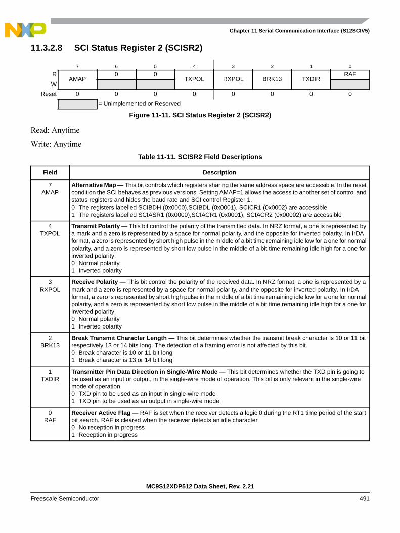
Chapter 11 Serial Communication Interface (S12SCIV5)
MC9S12XDP512 Data Sheet, Rev. 2.21
Freescale Semiconductor 491
11.3.2.8 SCI Status Register 2 (SCISR2)
Read: Anytime
Write: Anytime
7 6 5 4 3 2 1 0
RAMAP
0 0TXPOL RXPOL BRK13 TXDIR
RAF
W
Reset 0 0 0 0 0 0 0 0
= Unimplemented or Reserved
Figure 11-11. SCI Status Register 2 (SCISR2)
Table 11-11. SCISR2 Field Descriptions
Field Description
7AMAP
Alternative Map — This bit controls which registers sharing the same address space are accessible. In the resetcondition the SCI behaves as previous versions. Setting AMAP=1 allows the access to another set of control andstatus registers and hides the baud rate and SCI control Register 1.0 The registers labelled SCIBDH (0x0000),SCIBDL (0x0001), SCICR1 (0x0002) are accessible1 The registers labelled SCIASR1 (0x0000),SCIACR1 (0x0001), SCIACR2 (0x00002) are accessible
4TXPOL
Transmit Polarity — This bit control the polarity of the transmitted data. In NRZ format, a one is represented bya mark and a zero is represented by a space for normal polarity, and the opposite for inverted polarity. In IrDAformat, a zero is represented by short high pulse in the middle of a bit time remaining idle low for a one for normalpolarity, and a zero is represented by short low pulse in the middle of a bit time remaining idle high for a one forinverted polarity.0 Normal polarity1 Inverted polarity
3RXPOL
Receive Polarity — This bit control the polarity of the received data. In NRZ format, a one is represented by amark and a zero is represented by a space for normal polarity, and the opposite for inverted polarity. In IrDAformat, a zero is represented by short high pulse in the middle of a bit time remaining idle low for a one for normalpolarity, and a zero is represented by short low pulse in the middle of a bit time remaining idle high for a one forinverted polarity.0 Normal polarity1 Inverted polarity
2BRK13
Break Transmit Character Length — This bit determines whether the transmit break character is 10 or 11 bitrespectively 13 or 14 bits long. The detection of a framing error is not affected by this bit.0 Break character is 10 or 11 bit long1 Break character is 13 or 14 bit long
1TXDIR
Transmitter Pin Data Direction in Single-Wire Mode — This bit determines whether the TXD pin is going tobe used as an input or output, in the single-wire mode of operation. This bit is only relevant in the single-wiremode of operation.0 TXD pin to be used as an input in single-wire mode1 TXD pin to be used as an output in single-wire mode
0RAF
Receiver Active Flag — RAF is set when the receiver detects a logic 0 during the RT1 time period of the startbit search. RAF is cleared when the receiver detects an idle character.0 No reception in progress1 Reception in progress
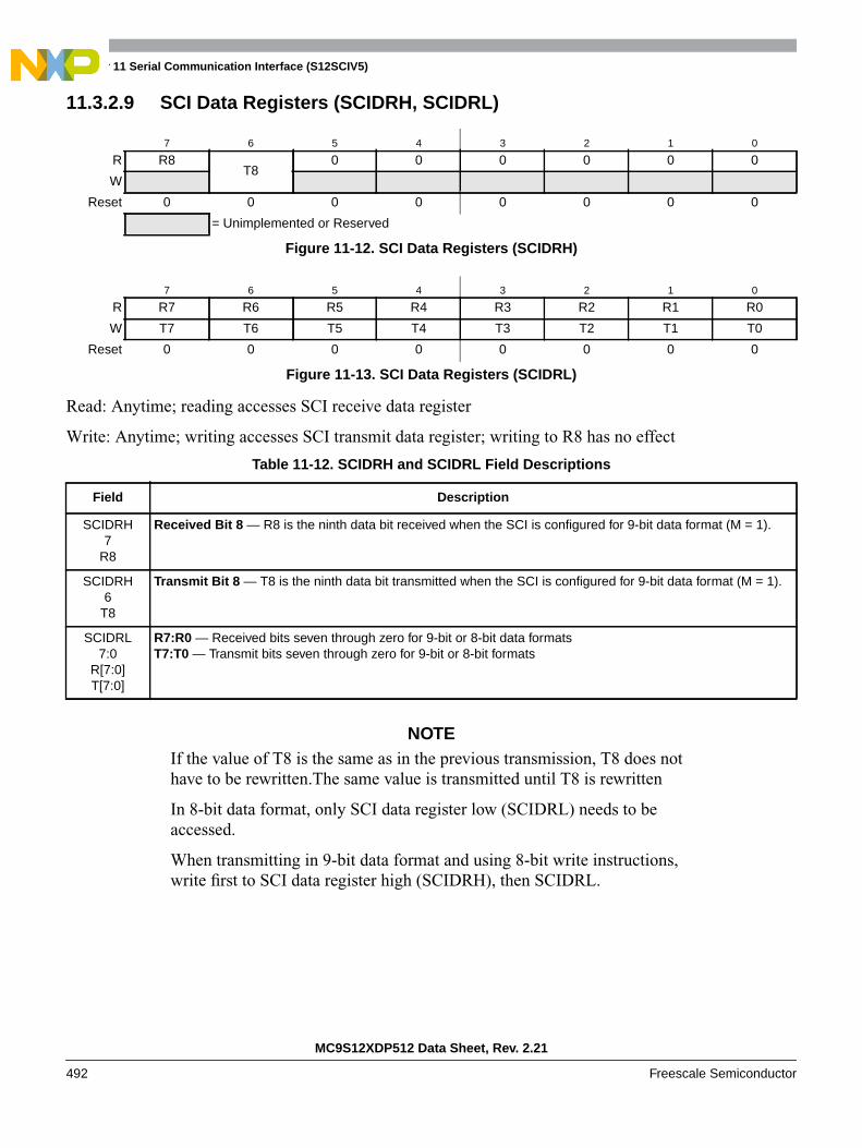
Chapter 11 Serial Communication Interface (S12SCIV5)
MC9S12XDP512 Data Sheet, Rev. 2.21
492 Freescale Semiconductor
11.3.2.9 SCI Data Registers (SCIDRH, SCIDRL)
Read: Anytime; reading accesses SCI receive data register
Write: Anytime; writing accesses SCI transmit data register; writing to R8 has no effect
NOTEIf the value of T8 is the same as in the previous transmission, T8 does nothave to be rewritten.The same value is transmitted until T8 is rewritten
In 8-bit data format, only SCI data register low (SCIDRL) needs to beaccessed.
When transmitting in 9-bit data format and using 8-bit write instructions,write first to SCI data register high (SCIDRH), then SCIDRL.
7 6 5 4 3 2 1 0
R R8T8
0 0 0 0 0 0
W
Reset 0 0 0 0 0 0 0 0
= Unimplemented or Reserved
Figure 11-12. SCI Data Registers (SCIDRH)
7 6 5 4 3 2 1 0
R R7 R6 R5 R4 R3 R2 R1 R0
W T7 T6 T5 T4 T3 T2 T1 T0
Reset 0 0 0 0 0 0 0 0
Figure 11-13. SCI Data Registers (SCIDRL)
Table 11-12. SCIDRH and SCIDRL Field Descriptions
Field Description
SCIDRH7
R8
Received Bit 8 — R8 is the ninth data bit received when the SCI is configured for 9-bit data format (M = 1).
SCIDRH6
T8
Transmit Bit 8 — T8 is the ninth data bit transmitted when the SCI is configured for 9-bit data format (M = 1).
SCIDRL7:0
R[7:0]T[7:0]
R7:R0 — Received bits seven through zero for 9-bit or 8-bit data formatsT7:T0 — Transmit bits seven through zero for 9-bit or 8-bit formats
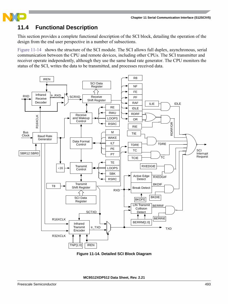
Chapter 11 Serial Communication Interface (S12SCIV5)
MC9S12XDP512 Data Sheet, Rev. 2.21
Freescale Semiconductor 493
11.4 Functional DescriptionThis section provides a complete functional description of the SCI block, detailing the operation of thedesign from the end user perspective in a number of subsections.
Figure 11-14 shows the structure of the SCI module. The SCI allows full duplex, asynchronous, serialcommunication between the CPU and remote devices, including other CPUs. The SCI transmitter andreceiver operate independently, although they use the same baud rate generator. The CPU monitors thestatus of the SCI, writes the data to be transmitted, and processes received data.
Figure 11-14. Detailed SCI Block Diagram
SCI Data
ReceiveShift Register
SCI DataRegister
TransmitShift Register
Register
Baud RateGenerator
SBR12:SBR0
Bus
TransmitControl÷16
Receiveand Wakeup
Data FormatControl
Control
T8
PF
FE
NF
RDRF
IDLE
TIE
OR
TCIE
TDRE
TC
R8
RAF
LOOPS
RWU
RE
PE
ILT
PT
WAKE
MClock
ILIE
RIE
RXD
RSRC
SBK
LOOPS
TE
RSRC
IREN
R16
XC
LK
Ir_RXD
TXDIr_TXD
R16XCLK
R32XCLK
TNP[1:0] IREN
TransmitEncoder
ReceiveDecoder
SCRXD
SCTXD
Infrared
Infrared
TC
TDRE
RD
RF
/OR
IDLE
Active EdgeDetect
Break DetectRXD
BKDFE
BERRM[1:0]
BKDIE
BKDIF
RXEDGIE
RXEDGIF
BERRIE
BERRIF
SCIInterruptRequest
LIN TransmitCollisionDetect
Chapter 11 Serial Communication Interface (S12SCIV5)
MC9S12XDP512 Data Sheet, Rev. 2.21
494 Freescale Semiconductor
11.4.1 Infrared Interface Submodule
This module provides the capability of transmitting narrow pulses to an IR LED and receiving narrowpulses and transforming them to serial bits, which are sent to the SCI. The IrDA physical layerspecification defines a half-duplex infrared communication link for exchange data. The full standardincludes data rates up to 16 Mbits/s. This design covers only data rates between 2.4 Kbits/s and 115.2Kbits/s.
The infrared submodule consists of two major blocks: the transmit encoder and the receive decoder. TheSCI transmits serial bits of data which are encoded by the infrared submodule to transmit a narrow pulsefor every zero bit. No pulse is transmitted for every one bit. When receiving data, the IR pulses should bedetected using an IR photo diode and transformed to CMOS levels by the IR receive decoder (externalfrom the MCU). The narrow pulses are then stretched by the infrared submodule to get back to a serial bitstream to be received by the SCI.The polarity of transmitted pulses and expected receive pulses can beinverted so that a direct connection can be made to external IrDA transceiver modules that uses active lowpulses.
The infrared submodule receives its clock sources from the SCI. One of these two clocks are selected inthe infrared submodule in order to generate either 3/16, 1/16, 1/32 or 1/4 narrow pulses duringtransmission. The infrared block receives two clock sources from the SCI, R16XCLK and R32XCLK,which are configured to generate the narrow pulse width during transmission. The R16XCLK andR32XCLK are internal clocks with frequencies 16 and 32 times the baud rate respectively. BothR16XCLK and R32XCLK clocks are used for transmitting data. The receive decoder uses only theR16XCLK clock.
11.4.1.1 Infrared Transmit Encoder
The infrared transmit encoder converts serial bits of data from transmit shift register to the TXD pin. Anarrow pulse is transmitted for a zero bit and no pulse for a one bit. The narrow pulse is sent in the middleof the bit with a duration of 1/32, 1/16, 3/16 or 1/4 of a bit time. A narrow high pulse is transmitted for azero bit when TXPOL is cleared, while a narrow low pulse is transmitted for a zero bit when TXPOL is set.
11.4.1.2 Infrared Receive Decoder
The infrared receive block converts data from the RXD pin to the receive shift register. A narrow pulse isexpected for each zero received and no pulse is expected for each one received. A narrow high pulse isexpected for a zero bit when RXPOL is cleared, while a narrow low pulse is expected for a zero bit whenRXPOL is set. This receive decoder meets the edge jitter requirement as defined by the IrDA serial infraredphysical layer specification.
11.4.2 LIN Support
This module provides some basic support for the LIN protocol. At first this is a break detect circuitrymaking it easier for the LIN software to distinguish a break character from an incoming data stream. As afurther addition is supports a collision detection at the bit level as well as cancelling pending transmissions.

Chapter 11 Serial Communication Interface (S12SCIV5)
MC9S12XDP512 Data Sheet, Rev. 2.21
Freescale Semiconductor 495
11.4.3 Data Format
The SCI uses the standard NRZ mark/space data format. When Infrared is enabled, the SCI uses RZI dataformat where zeroes are represented by light pulses and ones remain low. See Figure 11-15 below.
Figure 11-15. SCI Data Formats
Each data character is contained in a frame that includes a start bit, eight or nine data bits, and a stop bit.Clearing the M bit in SCI control register 1 configures the SCI for 8-bit data characters. A frame with eightdata bits has a total of 10 bits. Setting the M bit configures the SCI for nine-bit data characters. A framewith nine data bits has a total of 11 bits.
When the SCI is configured for 9-bit data characters, the ninth data bit is the T8 bit in SCI data registerhigh (SCIDRH). It remains unchanged after transmission and can be used repeatedly without rewriting it.A frame with nine data bits has a total of 11 bits.
Table 11-13. Example of 8-Bit Data Formats
StartBit
DataBits
AddressBits
ParityBits
StopBit
1 8 0 0 1
1 7 0 1 1
1 7 11
1 The address bit identifies the frame as an addresscharacter. See Section 11.4.6.6, “Receiver Wakeup”.
0 1
Table 11-14. Example of 9-Bit Data Formats
StartBit
DataBits
AddressBits
ParityBits
StopBit
1 9 0 0 1
1 8 0 1 1
1 8 11 0 1
Bit 5StartBit Bit 0 Bit 1
Next
STOPBit
StartBit
8-Bit Data Format(Bit M in SCICR1 Clear)
StartBit Bit 0
NEXT
STOPBit
STARTBit
9-Bit Data Format(Bit M in SCICR1 Set)
Bit 1 Bit 2 Bit 3 Bit 4 Bit 5 Bit 6 Bit 7 Bit 8
Bit 2 Bit 3 Bit 4 Bit 6 Bit 7
POSSIBLEPARITY
Bit
PossibleParity
BitStandardSCI Data
InfraredSCI Data
StandardSCI Data
InfraredSCI Data

Chapter 11 Serial Communication Interface (S12SCIV5)
MC9S12XDP512 Data Sheet, Rev. 2.21
496 Freescale Semiconductor
11.4.4 Baud Rate Generation
A 13-bit modulus counter in the baud rate generator derives the baud rate for both the receiver and thetransmitter. The value from 0 to 8191 written to the SBR12:SBR0 bits determines the bus clock divisor.The SBR bits are in the SCI baud rate registers (SCIBDH and SCIBDL). The baud rate clock issynchronized with the bus clock and drives the receiver. The baud rate clock divided by 16 drives thetransmitter. The receiver has an acquisition rate of 16 samples per bit time.
Baud rate generation is subject to one source of error:
• Integer division of the bus clock may not give the exact target frequency.
Table 11-15 lists some examples of achieving target baud rates with a bus clock frequency of 25 MHz.
When IREN = 0 then,
SCI baud rate = SCI bus clock / (16 * SCIBR[12:0])
1 The address bit identifies the frame as an addresscharacter. See Section 11.4.6.6, “Receiver Wakeup”.
Table 11-15. Baud Rates (Example: Bus Clock = 25 MHz)
BitsSBR[12:0]
ReceiverClock (Hz)
TransmitterClock (Hz)
TargetBaud Rate
Error(%)
41 609,756.1 38,109.8 38,400 .76
81 308,642.0 19,290.1 19,200 .47
163 153,374.2 9585.9 9,600 .16
326 76,687.1 4792.9 4,800 .15
651 38,402.5 2400.2 2,400 .01
1302 19,201.2 1200.1 1,200 .01
2604 9600.6 600.0 600 .00
5208 4800.0 300.0 300 .00

Chapter 11 Serial Communication Interface (S12SCIV5)
MC9S12XDP512 Data Sheet, Rev. 2.21
Freescale Semiconductor 497
11.4.5 Transmitter
Figure 11-16. Transmitter Block Diagram
11.4.5.1 Transmitter Character Length
The SCI transmitter can accommodate either 8-bit or 9-bit data characters. The state of the M bit in SCIcontrol register 1 (SCICR1) determines the length of data characters. When transmitting 9-bit data, bit T8in SCI data register high (SCIDRH) is the ninth bit (bit 8).
11.4.5.2 Character Transmission
To transmit data, the MCU writes the data bits to the SCI data registers (SCIDRH/SCIDRL), which in turnare transferred to the transmitter shift register. The transmit shift register then shifts a frame out throughthe TXD pin, after it has prefaced them with a start bit and appended them with a stop bit. The SCI dataregisters (SCIDRH and SCIDRL) are the write-only buffers between the internal data bus and the transmitshift register.
PE
PT
H 8 7 6 5 4 3 2 1 0 L
11-Bit Transmit RegisterSto
p
Sta
rt
T8
TIE
TDRE
TCIE
SBK
TC
ParityGeneration
MS
B
SCI Data Registers
Load
from
SC
IDR
Shi
ft E
nabl
e
Pre
ambl
e (A
ll 1s
)
Bre
ak (
All
0s)
Transmitter Control
M
Internal Bus
SBR12:SBR0
Baud Divider ÷ 16BusClock
TE
SCTXDTXPOL
LOOPS
LOOP
RSRC
CONTROLTo Receiver
Transmit Collision Detect
TDRE IRQ
TC IRQ
SCTXD
SCRXD(From Receiver)TCIE
BERRIFBER IRQ
BERRM[1:0]
Chapter 11 Serial Communication Interface (S12SCIV5)
MC9S12XDP512 Data Sheet, Rev. 2.21
498 Freescale Semiconductor
The SCI also sets a flag, the transmit data register empty flag (TDRE), every time it transfers data from thebuffer (SCIDRH/L) to the transmitter shift register.The transmit driver routine may respond to this flag bywriting another byte to the Transmitter buffer (SCIDRH/SCIDRL), while the shift register is still shiftingout the first byte.
To initiate an SCI transmission:
1. Configure the SCI:
a) Select a baud rate. Write this value to the SCI baud registers (SCIBDH/L) to begin the baudrate generator. Remember that the baud rate generator is disabled when the baud rate is zero.Writing to the SCIBDH has no effect without also writing to SCIBDL.
b) Write to SCICR1 to configure word length, parity, and other configuration bits(LOOPS,RSRC,M,WAKE,ILT,PE,PT).
c) Enable the transmitter, interrupts, receive, and wake up as required, by writing to the SCICR2register bits (TIE,TCIE,RIE,ILIE,TE,RE,RWU,SBK). A preamble or idle character will nowbe shifted out of the transmitter shift register.
2. Transmit Procedure for each byte:
a) Poll the TDRE flag by reading the SCISR1 or responding to the TDRE interrupt. Keep in mindthat the TDRE bit resets to one.
b) If the TDRE flag is set, write the data to be transmitted to SCIDRH/L, where the ninth bit iswritten to the T8 bit in SCIDRH if the SCI is in 9-bit data format. A new transmission will notresult until the TDRE flag has been cleared.
3. Repeat step 2 for each subsequent transmission.
NOTEThe TDRE flag is set when the shift register is loaded with the next data tobe transmitted from SCIDRH/L, which happens, generally speaking, a littleover half-way through the stop bit of the previous frame. Specifically, thistransfer occurs 9/16ths of a bit time AFTER the start of the stop bit of theprevious frame.
Writing the TE bit from 0 to a 1 automatically loads the transmit shift register with a preamble of 10 logic1s (if M = 0) or 11 logic 1s (if M = 1). After the preamble shifts out, control logic transfers the data fromthe SCI data register into the transmit shift register. A logic 0 start bit automatically goes into the leastsignificant bit position of the transmit shift register. A logic 1 stop bit goes into the most significant bitposition.
Hardware supports odd or even parity. When parity is enabled, the most significant bit (MSB) of the datacharacter is the parity bit.
The transmit data register empty flag, TDRE, in SCI status register 1 (SCISR1) becomes set when the SCIdata register transfers a byte to the transmit shift register. The TDRE flag indicates that the SCI dataregister can accept new data from the internal data bus. If the transmit interrupt enable bit, TIE, in SCIcontrol register 2 (SCICR2) is also set, the TDRE flag generates a transmitter interrupt request.

Chapter 11 Serial Communication Interface (S12SCIV5)
MC9S12XDP512 Data Sheet, Rev. 2.21
Freescale Semiconductor 499
When the transmit shift register is not transmitting a frame, the TXD pin goes to the idle condition, logic1. If at any time software clears the TE bit in SCI control register 2 (SCICR2), the transmitter enable signalgoes low and the transmit signal goes idle.
If software clears TE while a transmission is in progress (TC = 0), the frame in the transmit shift registercontinues to shift out. To avoid accidentally cutting off the last frame in a message, always wait for TDREto go high after the last frame before clearing TE.
To separate messages with preambles with minimum idle line time, use this sequence between messages:
1. Write the last byte of the first message to SCIDRH/L.
2. Wait for the TDRE flag to go high, indicating the transfer of the last frame to the transmit shiftregister.
3. Queue a preamble by clearing and then setting the TE bit.
4. Write the first byte of the second message to SCIDRH/L.
11.4.5.3 Break Characters
Writing a logic 1 to the send break bit, SBK, in SCI control register 2 (SCICR2) loads the transmit shiftregister with a break character. A break character contains all logic 0s and has no start, stop, or parity bit.Break character length depends on the M bit in SCI control register 1 (SCICR1). As long as SBK is at logic1, transmitter logic continuously loads break characters into the transmit shift register. After softwareclears the SBK bit, the shift register finishes transmitting the last break character and then transmits at leastone logic 1. The automatic logic 1 at the end of a break character guarantees the recognition of the start bitof the next frame.
The SCI recognizes a break character when there are 10 or 11(M = 0 or M = 1) consecutive zero received.Depending if the break detect feature is enabled or not receiving a break character has these effects on SCIregisters.
If the break detect feature is disabled (BKDFE = 0):
• Sets the framing error flag, FE
• Sets the receive data register full flag, RDRF
• Clears the SCI data registers (SCIDRH/L)
• May set the overrun flag, OR, noise flag, NF, parity error flag, PE, or the receiver active flag, RAF(see 3.4.4 and 3.4.5 SCI Status Register 1 and 2)
If the break detect feature is enabled (BKDFE = 1) there are two scenarios1
The break is detected right from a start bit or is detected during a byte reception.
• Sets the break detect interrupt flag, BLDIF
• Does not change the data register full flag, RDRF or overrun flag OR
• Does not change the framing error flag FE, parity error flag PE.
• Does not clear the SCI data registers (SCIDRH/L)
• May set noise flag NF, or receiver active flag RAF.
1. A Break character in this context are either 10 or 11 consecutive zero received bits
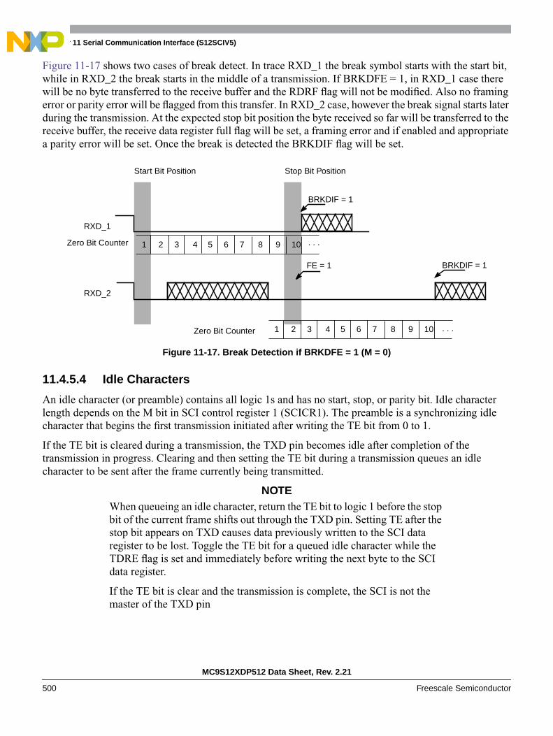
Chapter 11 Serial Communication Interface (S12SCIV5)
MC9S12XDP512 Data Sheet, Rev. 2.21
500 Freescale Semiconductor
Figure 11-17 shows two cases of break detect. In trace RXD_1 the break symbol starts with the start bit,while in RXD_2 the break starts in the middle of a transmission. If BRKDFE = 1, in RXD_1 case therewill be no byte transferred to the receive buffer and the RDRF flag will not be modified. Also no framingerror or parity error will be flagged from this transfer. In RXD_2 case, however the break signal starts laterduring the transmission. At the expected stop bit position the byte received so far will be transferred to thereceive buffer, the receive data register full flag will be set, a framing error and if enabled and appropriatea parity error will be set. Once the break is detected the BRKDIF flag will be set.
Figure 11-17. Break Detection if BRKDFE = 1 (M = 0)
11.4.5.4 Idle Characters
An idle character (or preamble) contains all logic 1s and has no start, stop, or parity bit. Idle characterlength depends on the M bit in SCI control register 1 (SCICR1). The preamble is a synchronizing idlecharacter that begins the first transmission initiated after writing the TE bit from 0 to 1.
If the TE bit is cleared during a transmission, the TXD pin becomes idle after completion of thetransmission in progress. Clearing and then setting the TE bit during a transmission queues an idlecharacter to be sent after the frame currently being transmitted.
NOTEWhen queueing an idle character, return the TE bit to logic 1 before the stopbit of the current frame shifts out through the TXD pin. Setting TE after thestop bit appears on TXD causes data previously written to the SCI dataregister to be lost. Toggle the TE bit for a queued idle character while theTDRE flag is set and immediately before writing the next byte to the SCIdata register.
If the TE bit is clear and the transmission is complete, the SCI is not themaster of the TXD pin
Start Bit Position Stop Bit Position
BRKDIF = 1
FE = 1 BRKDIF = 1
RXD_1
RXD_2
1 2 3 4 5 6 7 8 9 10
1 2 3 4 5 6 7 8 9 10
Zero Bit Counter
Zero Bit Counter . . .
. . .
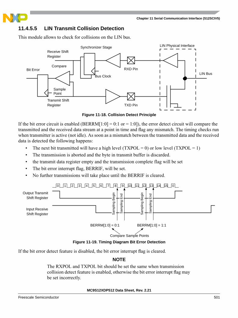
Chapter 11 Serial Communication Interface (S12SCIV5)
MC9S12XDP512 Data Sheet, Rev. 2.21
Freescale Semiconductor 501
11.4.5.5 LIN Transmit Collision Detection
This module allows to check for collisions on the LIN bus.
Figure 11-18. Collision Detect Principle
If the bit error circuit is enabled (BERRM[1:0] = 0:1 or = 1:0]), the error detect circuit will compare thetransmitted and the received data stream at a point in time and flag any mismatch. The timing checks runwhen transmitter is active (not idle). As soon as a mismatch between the transmitted data and the receiveddata is detected the following happens:
• The next bit transmitted will have a high level (TXPOL = 0) or low level (TXPOL = 1)
• The transmission is aborted and the byte in transmit buffer is discarded.
• the transmit data register empty and the transmission complete flag will be set
• The bit error interrupt flag, BERRIF, will be set.
• No further transmissions will take place until the BERRIF is cleared.
Figure 11-19. Timing Diagram Bit Error Detection
If the bit error detect feature is disabled, the bit error interrupt flag is cleared.
NOTEThe RXPOL and TXPOL bit should be set the same when transmissioncollision detect feature is enabled, otherwise the bit error interrupt flag maybe set incorrectly.
TXD Pin
RXD Pin
LIN Physical InterfaceSynchronizer Stage
Bus Clock
Receive ShiftRegister
Transmit ShiftRegister
LIN Bus
Compare
Sample
Bit Error
Point
Output TransmitShift Register
0 1 2 3 4 5 6 7 8 9 10 11 12 13 14 15 0
Input ReceiveShift Register
BERRM[1:0] = 0:1 BERRM[1:0] = 1:1
Compare Sample Points
Sam
plin
g B
egin
Sam
plin
g B
egin
Sam
plin
g E
nd
Sam
plin
g E
nd
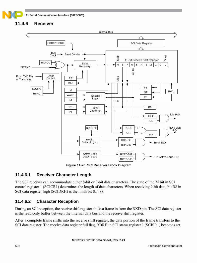
Chapter 11 Serial Communication Interface (S12SCIV5)
MC9S12XDP512 Data Sheet, Rev. 2.21
502 Freescale Semiconductor
11.4.6 Receiver
Figure 11-20. SCI Receiver Block Diagram
11.4.6.1 Receiver Character Length
The SCI receiver can accommodate either 8-bit or 9-bit data characters. The state of the M bit in SCIcontrol register 1 (SCICR1) determines the length of data characters. When receiving 9-bit data, bit R8 inSCI data register high (SCIDRH) is the ninth bit (bit 8).
11.4.6.2 Character Reception
During an SCI reception, the receive shift register shifts a frame in from the RXD pin. The SCI data registeris the read-only buffer between the internal data bus and the receive shift register.
After a complete frame shifts into the receive shift register, the data portion of the frame transfers to theSCI data register. The receive data register full flag, RDRF, in SCI status register 1 (SCISR1) becomes set,
All
1s
M
WAKE
ILT
PE
PT
RE
H 8 7 6 5 4 3 2 1 0 L
11-Bit Receive Shift RegisterSto
p
Sta
rt
Data
Wakeup
ParityChecking
MS
B
SCI Data Register
R8
ILIE
RWU
RDRF
OR
NF
FE
PE
Internal Bus
Bus
SBR12:SBR0
Baud DividerClock
IDLE
RAF
Recovery
Logic
RXPOL
LOOPS
Loop
RSRC
Control
SCRXD
From TXD Pinor Transmitter
Idle IRQ
RDRF/OR IRQ
BreakDetect Logic
Active EdgeDetect Logic
BRKDFE
BRKDIE
BRKDIF
RXEDGIE
RXEDGIF
Break IRQ
RX Active Edge IRQ
RIE
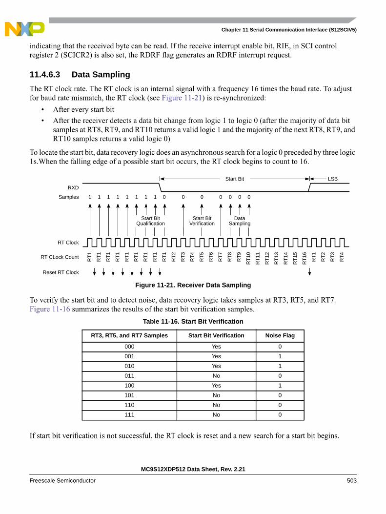
Chapter 11 Serial Communication Interface (S12SCIV5)
MC9S12XDP512 Data Sheet, Rev. 2.21
Freescale Semiconductor 503
indicating that the received byte can be read. If the receive interrupt enable bit, RIE, in SCI controlregister 2 (SCICR2) is also set, the RDRF flag generates an RDRF interrupt request.
11.4.6.3 Data Sampling
The RT clock rate. The RT clock is an internal signal with a frequency 16 times the baud rate. To adjustfor baud rate mismatch, the RT clock (see Figure 11-21) is re-synchronized:
• After every start bit
• After the receiver detects a data bit change from logic 1 to logic 0 (after the majority of data bitsamples at RT8, RT9, and RT10 returns a valid logic 1 and the majority of the next RT8, RT9, andRT10 samples returns a valid logic 0)
To locate the start bit, data recovery logic does an asynchronous search for a logic 0 preceded by three logic1s.When the falling edge of a possible start bit occurs, the RT clock begins to count to 16.
Figure 11-21. Receiver Data Sampling
To verify the start bit and to detect noise, data recovery logic takes samples at RT3, RT5, and RT7.Figure 11-16 summarizes the results of the start bit verification samples.
If start bit verification is not successful, the RT clock is reset and a new search for a start bit begins.
Table 11-16. Start Bit Verification
RT3, RT5, and RT7 Samples Start Bit Verification Noise Flag
000 Yes 0
001 Yes 1
010 Yes 1
011 No 0
100 Yes 1
101 No 0
110 No 0
111 No 0
Reset RT Clock
RT
1
RT
1
RT
1
RT
1
RT
1
RT
1
RT
1
RT
1
RT
1
RT
2
RT
3
RT
4
RT
5
RT
8
RT
7
RT
6
RT
11
RT
10
RT
9
RT
15
RT
14
RT
13
RT
12
RT
16
RT
1
RT
2
RT
3
RT
4
Samples
RT Clock
RT CLock Count
Start Bit
RXD
Start BitQualification
Start Bit DataSampling
1 111111 1 0 0 0 000 0
LSB
Verification
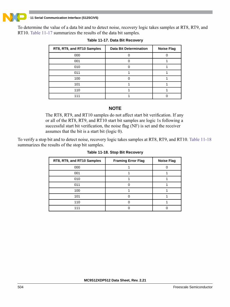
Chapter 11 Serial Communication Interface (S12SCIV5)
MC9S12XDP512 Data Sheet, Rev. 2.21
504 Freescale Semiconductor
To determine the value of a data bit and to detect noise, recovery logic takes samples at RT8, RT9, andRT10. Table 11-17 summarizes the results of the data bit samples.
NOTEThe RT8, RT9, and RT10 samples do not affect start bit verification. If anyor all of the RT8, RT9, and RT10 start bit samples are logic 1s following asuccessful start bit verification, the noise flag (NF) is set and the receiverassumes that the bit is a start bit (logic 0).
To verify a stop bit and to detect noise, recovery logic takes samples at RT8, RT9, and RT10. Table 11-18summarizes the results of the stop bit samples.
Table 11-17. Data Bit Recovery
RT8, RT9, and RT10 Samples Data Bit Determination Noise Flag
000 0 0
001 0 1
010 0 1
011 1 1
100 0 1
101 1 1
110 1 1
111 1 0
Table 11-18. Stop Bit Recovery
RT8, RT9, and RT10 Samples Framing Error Flag Noise Flag
000 1 0
001 1 1
010 1 1
011 0 1
100 1 1
101 0 1
110 0 1
111 0 0

Chapter 11 Serial Communication Interface (S12SCIV5)
MC9S12XDP512 Data Sheet, Rev. 2.21
Freescale Semiconductor 505
In Figure 11-22 the verification samples RT3 and RT5 determine that the first low detected was noise andnot the beginning of a start bit. The RT clock is reset and the start bit search begins again. The noise flagis not set because the noise occurred before the start bit was found.
Figure 11-22. Start Bit Search Example 1
In Figure 11-23, verification sample at RT3 is high. The RT3 sample sets the noise flag. Although theperceived bit time is misaligned, the data samples RT8, RT9, and RT10 are within the bit time and datarecovery is successful.
Figure 11-23. Start Bit Search Example 2
Reset RT Clock
RT
1
RT
1
RT
1
RT
1
RT
2
RT
3
RT
4
RT
5
RT
1
RT
1
RT
2
RT
3
RT
4
RT
7
RT
6
RT
5
RT
10
RT
9
RT
8
RT
14
RT
13
RT
12
RT
11
RT
15
RT
16
RT
1
RT
2
RT
3
Samples
RT Clock
RT Clock Count
Start Bit
RXD
1 1011 1 1 0 0 00 0
LSB
0 0
Reset RT Clock
RT
1
RT
1
RT
1
RT
1
RT
1
RT
1
RT
2
RT
3
RT
4
RT
5
RT
6
RT
7
RT
8
RT
11
RT
10
RT
9
RT
14
RT
13
RT
12
RT
2
RT
1
RT
16
RT
15
RT
3
RT
4
RT
5
RT
6
RT
7
Samples
RT Clock
RT Clock Count
Actual Start Bit
RXD
1 1111 1 0 0 00
LSB
00
Perceived Start Bit

Chapter 11 Serial Communication Interface (S12SCIV5)
MC9S12XDP512 Data Sheet, Rev. 2.21
506 Freescale Semiconductor
In Figure 11-24, a large burst of noise is perceived as the beginning of a start bit, although the test sampleat RT5 is high. The RT5 sample sets the noise flag. Although this is a worst-case misalignment of perceivedbit time, the data samples RT8, RT9, and RT10 are within the bit time and data recovery is successful.
Figure 11-24. Start Bit Search Example 3
Figure 11-25 shows the effect of noise early in the start bit time. Although this noise does not affect propersynchronization with the start bit time, it does set the noise flag.
Figure 11-25. Start Bit Search Example 4
Reset RT Clock
RT
1
RT
1
RT
1
RT
1
RT
2
RT
3
RT
4
RT
5
RT
6
RT
7
RT
8
RT
9
RT
10
RT
13
RT
12
RT
11
RT
16
RT
15
RT
14
RT
4
RT
3
RT
2
RT
1
RT
5
RT
6
RT
7
RT
8
RT
9
Samples
RT Clock
RT Clock Count
Actual Start Bit
RXD
1 011 1 0 0 00
LSB
0
Perceived Start Bit
Reset RT Clock
RT
1
RT
1
RT
1
RT
1
RT
1
RT
1
RT
1
RT
1
RT
1
RT
1
RT
2
RT
3
RT
4
RT
7
RT
6
RT
5
RT
10
RT
9
RT
8
RT
14
RT
13
RT
12
RT
11
RT
15
RT
16
RT
1
RT
2
RT
3
Samples
RT Clock
RT Clock Count
Perceived and Actual Start Bit
RXD
1 111 1 0 01
LSB
11 1 1
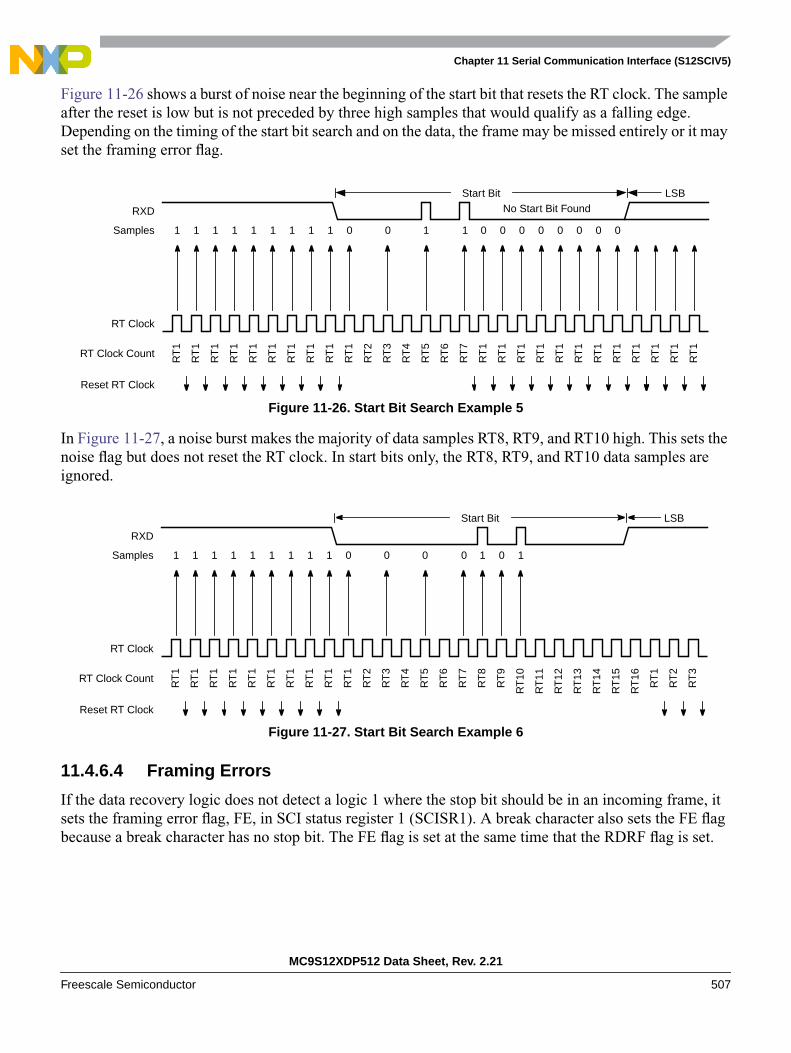
Chapter 11 Serial Communication Interface (S12SCIV5)
MC9S12XDP512 Data Sheet, Rev. 2.21
Freescale Semiconductor 507
Figure 11-26 shows a burst of noise near the beginning of the start bit that resets the RT clock. The sampleafter the reset is low but is not preceded by three high samples that would qualify as a falling edge.Depending on the timing of the start bit search and on the data, the frame may be missed entirely or it mayset the framing error flag.
Figure 11-26. Start Bit Search Example 5
In Figure 11-27, a noise burst makes the majority of data samples RT8, RT9, and RT10 high. This sets thenoise flag but does not reset the RT clock. In start bits only, the RT8, RT9, and RT10 data samples areignored.
Figure 11-27. Start Bit Search Example 6
11.4.6.4 Framing Errors
If the data recovery logic does not detect a logic 1 where the stop bit should be in an incoming frame, itsets the framing error flag, FE, in SCI status register 1 (SCISR1). A break character also sets the FE flagbecause a break character has no stop bit. The FE flag is set at the same time that the RDRF flag is set.
Reset RT Clock
RT
1
RT
1
RT
1
RT
1
RT
1
RT
1
RT
1
RT
1
RT
1
RT
1
RT
2
RT
3
RT
4
RT
7
RT
6
RT
5
RT
1
RT
1
RT
1
RT
1
RT
1
RT
1
RT
1
RT
1
RT
1
RT
1
RT
1
RT
1
Samples
RT Clock
RT Clock Count
Start Bit
RXD
1 111 1 0 10
LSB
11 1 1 1 0 000 000 0
No Start Bit Found
Reset RT Clock
RT
1
RT
1
RT
1
RT
1
RT
1
RT
1
RT
1
RT
1
RT
1
RT
1
RT
2
RT
3
RT
4
RT
7
RT
6
RT
5
RT
10
RT
9
RT
8
RT
14
RT
13
RT
12
RT
11
RT
15
RT
16
RT
1
RT
2
RT
3
Samples
RT Clock
RT Clock Count
Start Bit
RXD
1 111 1 0 00
LSB
11 1 1 0 1 10

Chapter 11 Serial Communication Interface (S12SCIV5)
MC9S12XDP512 Data Sheet, Rev. 2.21
508 Freescale Semiconductor
11.4.6.5 Baud Rate Tolerance
A transmitting device may be operating at a baud rate below or above the receiver baud rate. Accumulatedbit time misalignment can cause one of the three stop bit data samples (RT8, RT9, and RT10) to fall outsidethe actual stop bit. A noise error will occur if the RT8, RT9, and RT10 samples are not all the same logicalvalues. A framing error will occur if the receiver clock is misaligned in such a way that the majority of theRT8, RT9, and RT10 stop bit samples are a logic zero.
As the receiver samples an incoming frame, it re-synchronizes the RT clock on any valid falling edgewithin the frame. Re synchronization within frames will correct a misalignment between transmitter bittimes and receiver bit times.
11.4.6.5.1 Slow Data Tolerance
Figure 11-28 shows how much a slow received frame can be misaligned without causing a noise error ora framing error. The slow stop bit begins at RT8 instead of RT1 but arrives in time for the stop bit datasamples at RT8, RT9, and RT10.
Figure 11-28. Slow Data
Let’s take RTr as receiver RT clock and RTt as transmitter RT clock.
For an 8-bit data character, it takes the receiver 9 bit times x 16 RTr cycles +7 RTr cycles = 151 RTr cyclesto start data sampling of the stop bit.
With the misaligned character shown in Figure 11-28, the receiver counts 151 RTr cycles at the point whenthe count of the transmitting device is 9 bit times x 16 RTt cycles = 144 RTt cycles.
The maximum percent difference between the receiver count and the transmitter count of a slow 8-bit datacharacter with no errors is:
((151 – 144) / 151) x 100 = 4.63%
For a 9-bit data character, it takes the receiver 10 bit times x 16 RTr cycles + 7 RTr cycles = 167 RTr cyclesto start data sampling of the stop bit.
With the misaligned character shown in Figure 11-28, the receiver counts 167 RTr cycles at the point whenthe count of the transmitting device is 10 bit times x 16 RTt cycles = 160 RTt cycles.
The maximum percent difference between the receiver count and the transmitter count of a slow 9-bitcharacter with no errors is:
((167 – 160) / 167) X 100 = 4.19%
MSB Stop
RT
1
RT
2
RT
3
RT
4
RT
5
RT
6
RT
7
RT
8
RT
9
RT
10
RT
11
RT
12
RT
13
RT
14
RT
15
RT
16
DataSamples
ReceiverRT Clock
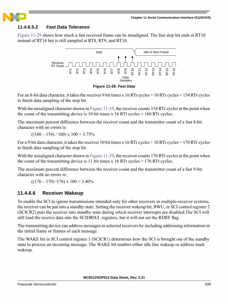
Chapter 11 Serial Communication Interface (S12SCIV5)
MC9S12XDP512 Data Sheet, Rev. 2.21
Freescale Semiconductor 509
11.4.6.5.2 Fast Data Tolerance
Figure 11-29 shows how much a fast received frame can be misaligned. The fast stop bit ends at RT10instead of RT16 but is still sampled at RT8, RT9, and RT10.
Figure 11-29. Fast Data
For an 8-bit data character, it takes the receiver 9 bit times x 16 RTr cycles + 10 RTr cycles = 154 RTr cyclesto finish data sampling of the stop bit.
With the misaligned character shown in Figure 11-29, the receiver counts 154 RTr cycles at the point whenthe count of the transmitting device is 10 bit times x 16 RTt cycles = 160 RTt cycles.
The maximum percent difference between the receiver count and the transmitter count of a fast 8-bitcharacter with no errors is:
((160 – 154) / 160) x 100 = 3.75%
For a 9-bit data character, it takes the receiver 10 bit times x 16 RTr cycles + 10 RTr cycles = 170 RTr cyclesto finish data sampling of the stop bit.
With the misaligned character shown in Figure 11-29, the receiver counts 170 RTr cycles at the point whenthe count of the transmitting device is 11 bit times x 16 RTt cycles = 176 RTt cycles.
The maximum percent difference between the receiver count and the transmitter count of a fast 9-bitcharacter with no errors is:
((176 – 170) /176) x 100 = 3.40%
11.4.6.6 Receiver Wakeup
To enable the SCI to ignore transmissions intended only for other receivers in multiple-receiver systems,the receiver can be put into a standby state. Setting the receiver wakeup bit, RWU, in SCI control register 2(SCICR2) puts the receiver into standby state during which receiver interrupts are disabled.The SCI willstill load the receive data into the SCIDRH/L registers, but it will not set the RDRF flag.
The transmitting device can address messages to selected receivers by including addressing information inthe initial frame or frames of each message.
The WAKE bit in SCI control register 1 (SCICR1) determines how the SCI is brought out of the standbystate to process an incoming message. The WAKE bit enables either idle line wakeup or address markwakeup.
Idle or Next FrameStop
RT
1
RT
2
RT
3
RT
4
RT
5
RT
6
RT
7
RT
8
RT
9
RT
10
RT
11
RT
12
RT
13
RT
14
RT
15
RT
16
DataSamples
ReceiverRT Clock
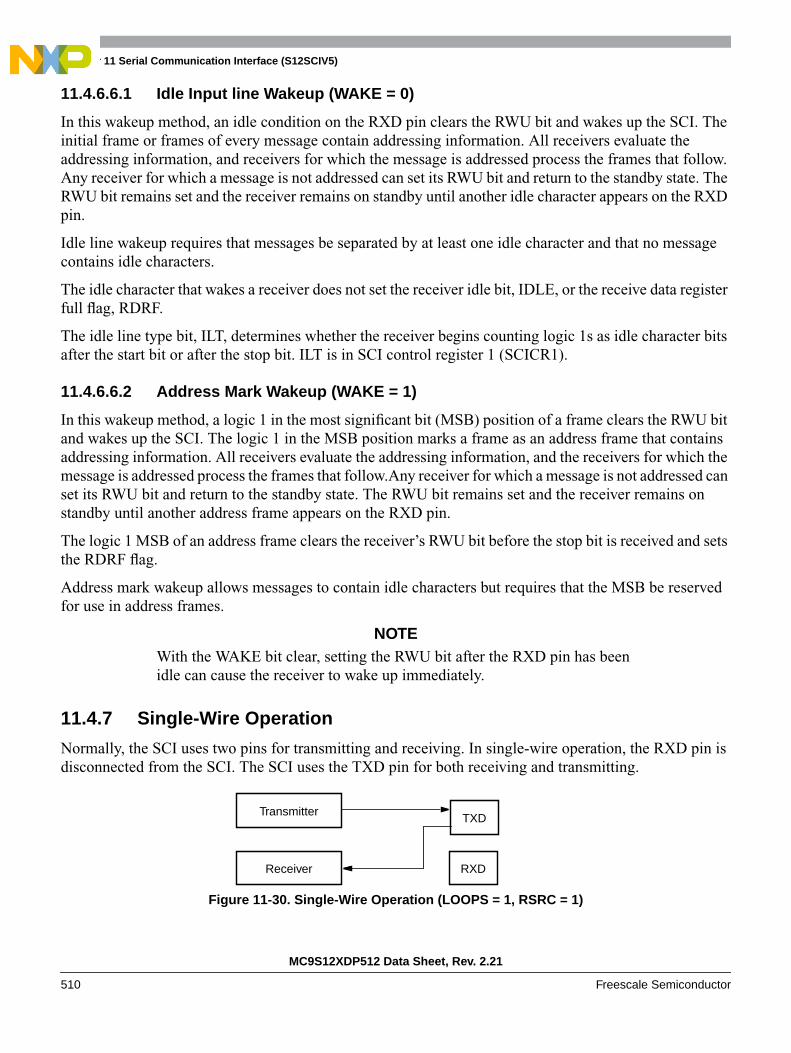
Chapter 11 Serial Communication Interface (S12SCIV5)
MC9S12XDP512 Data Sheet, Rev. 2.21
510 Freescale Semiconductor
11.4.6.6.1 Idle Input line Wakeup (WAKE = 0)
In this wakeup method, an idle condition on the RXD pin clears the RWU bit and wakes up the SCI. Theinitial frame or frames of every message contain addressing information. All receivers evaluate theaddressing information, and receivers for which the message is addressed process the frames that follow.Any receiver for which a message is not addressed can set its RWU bit and return to the standby state. TheRWU bit remains set and the receiver remains on standby until another idle character appears on the RXDpin.
Idle line wakeup requires that messages be separated by at least one idle character and that no messagecontains idle characters.
The idle character that wakes a receiver does not set the receiver idle bit, IDLE, or the receive data registerfull flag, RDRF.
The idle line type bit, ILT, determines whether the receiver begins counting logic 1s as idle character bitsafter the start bit or after the stop bit. ILT is in SCI control register 1 (SCICR1).
11.4.6.6.2 Address Mark Wakeup (WAKE = 1)
In this wakeup method, a logic 1 in the most significant bit (MSB) position of a frame clears the RWU bitand wakes up the SCI. The logic 1 in the MSB position marks a frame as an address frame that containsaddressing information. All receivers evaluate the addressing information, and the receivers for which themessage is addressed process the frames that follow.Any receiver for which a message is not addressed canset its RWU bit and return to the standby state. The RWU bit remains set and the receiver remains onstandby until another address frame appears on the RXD pin.
The logic 1 MSB of an address frame clears the receiver’s RWU bit before the stop bit is received and setsthe RDRF flag.
Address mark wakeup allows messages to contain idle characters but requires that the MSB be reservedfor use in address frames.
NOTEWith the WAKE bit clear, setting the RWU bit after the RXD pin has beenidle can cause the receiver to wake up immediately.
11.4.7 Single-Wire Operation
Normally, the SCI uses two pins for transmitting and receiving. In single-wire operation, the RXD pin isdisconnected from the SCI. The SCI uses the TXD pin for both receiving and transmitting.
Figure 11-30. Single-Wire Operation (LOOPS = 1, RSRC = 1)
RXD
Transmitter
Receiver
TXD

Chapter 11 Serial Communication Interface (S12SCIV5)
MC9S12XDP512 Data Sheet, Rev. 2.21
Freescale Semiconductor 511
Enable single-wire operation by setting the LOOPS bit and the receiver source bit, RSRC, in SCI controlregister 1 (SCICR1). Setting the LOOPS bit disables the path from the RXD pin to the receiver. Settingthe RSRC bit connects the TXD pin to the receiver. Both the transmitter and receiver must be enabled(TE = 1 and RE = 1).The TXDIR bit (SCISR2[1]) determines whether the TXD pin is going to be used asan input (TXDIR = 0) or an output (TXDIR = 1) in this mode of operation.
NOTEIn single-wire operation data from the TXD pin is inverted if RXPOL is set.
11.4.8 Loop Operation
In loop operation the transmitter output goes to the receiver input. The RXD pin is disconnected from theSCI.
Figure 11-31. Loop Operation (LOOPS = 1, RSRC = 0)
Enable loop operation by setting the LOOPS bit and clearing the RSRC bit in SCI control register 1(SCICR1). Setting the LOOPS bit disables the path from the RXD pin to the receiver. Clearing the RSRCbit connects the transmitter output to the receiver input. Both the transmitter and receiver must be enabled(TE = 1 and RE = 1).
NOTEIn loop operation data from the transmitter is not recognized by the receiverif RXPOL and TXPOL are not the same.
11.5 Initialization/Application Information
11.5.1 Reset Initialization
See Section 11.3.2, “Register Descriptions”.
11.5.2 Modes of Operation
11.5.2.1 Run Mode
Normal mode of operation.
To initialize a SCI transmission, see Section 11.4.5.2, “Character Transmission”.
RXD
Transmitter
Receiver
TXD

Chapter 11 Serial Communication Interface (S12SCIV5)
MC9S12XDP512 Data Sheet, Rev. 2.21
512 Freescale Semiconductor
11.5.2.2 Wait Mode
SCI operation in wait mode depends on the state of the SCISWAI bit in the SCI control register 1(SCICR1).
• If SCISWAI is clear, the SCI operates normally when the CPU is in wait mode.
• If SCISWAI is set, SCI clock generation ceases and the SCI module enters a power-conservationstate when the CPU is in wait mode. Setting SCISWAI does not affect the state of the receiverenable bit, RE, or the transmitter enable bit, TE.
If SCISWAI is set, any transmission or reception in progress stops at wait mode entry. Thetransmission or reception resumes when either an internal or external interrupt brings the CPU outof wait mode. Exiting wait mode by reset aborts any transmission or reception in progress andresets the SCI.
11.5.2.3 Stop Mode
The SCI is inactive during stop mode for reduced power consumption. The STOP instruction does notaffect the SCI register states, but the SCI bus clock will be disabled. The SCI operation resumes fromwhere it left off after an external interrupt brings the CPU out of stop mode. Exiting stop mode by resetaborts any transmission or reception in progress and resets the SCI.
The receive input active edge detect circuit is still active in stop mode. An active edge on the receive inputcan be used to bring the CPU out of stop mode.
11.5.3 Interrupt Operation
This section describes the interrupt originated by the SCI block.The MCU must service the interruptrequests. Table 11-19 lists the eight interrupt sources of the SCI.
Table 11-19. SCI Interrupt Sources
Interrupt Source Local Enable Description
TDRE SCISR1[7] TIE Active high level. Indicates that a byte was transferred from SCIDRH/L to thetransmit shift register.
TC SCISR1[6] TCIE Active high level. Indicates that a transmit is complete.
RDRF SCISR1[5] RIE Active high level. The RDRF interrupt indicates that received data is availablein the SCI data register.
OR SCISR1[3] Active high level. This interrupt indicates that an overrun condition has occurred.
IDLE SCISR1[4] ILIE Active high level. Indicates that receiver input has become idle.
RXEDGIF SCIASR1[7] RXEDGIE Active high level. Indicates that an active edge (falling for RXPOL = 0, rising forRXPOL = 1) was detected.
BERRIF SCIASR1[1] BERRIE Active high level. Indicates that a mismatch between transmitted and received datain a single wire application has happened.
BKDIF SCIASR1[0] BRKDIE Active high level. Indicates that a break character has been received.
Chapter 11 Serial Communication Interface (S12SCIV5)
MC9S12XDP512 Data Sheet, Rev. 2.21
Freescale Semiconductor 513
11.5.3.1 Description of Interrupt Operation
The SCI only originates interrupt requests. The following is a description of how the SCI makes a requestand how the MCU should acknowledge that request. The interrupt vector offset and interrupt number arechip dependent. The SCI only has a single interrupt line (SCI Interrupt Signal, active high operation) andall the following interrupts, when generated, are ORed together and issued through that port.
11.5.3.1.1 TDRE Description
The TDRE interrupt is set high by the SCI when the transmit shift register receives a byte from the SCIdata register. A TDRE interrupt indicates that the transmit data register (SCIDRH/L) is empty and that anew byte can be written to the SCIDRH/L for transmission.Clear TDRE by reading SCI status register 1with TDRE set and then writing to SCI data register low (SCIDRL).
11.5.3.1.2 TC Description
The TC interrupt is set by the SCI when a transmission has been completed. Transmission is completedwhen all bits including the stop bit (if transmitted) have been shifted out and no data is queued to betransmitted. No stop bit is transmitted when sending a break character and the TC flag is set (providingthere is no more data queued for transmission) when the break character has been shifted out. A TCinterrupt indicates that there is no transmission in progress. TC is set high when the TDRE flag is set andno data, preamble, or break character is being transmitted. When TC is set, the TXD pin becomes idle(logic 1). Clear TC by reading SCI status register 1 (SCISR1) with TC set and then writing to SCI dataregister low (SCIDRL).TC is cleared automatically when data, preamble, or break is queued and ready tobe sent.
11.5.3.1.3 RDRF Description
The RDRF interrupt is set when the data in the receive shift register transfers to the SCI data register. ARDRF interrupt indicates that the received data has been transferred to the SCI data register and that thebyte can now be read by the MCU. The RDRF interrupt is cleared by reading the SCI status register one(SCISR1) and then reading SCI data register low (SCIDRL).
11.5.3.1.4 OR Description
The OR interrupt is set when software fails to read the SCI data register before the receive shift registerreceives the next frame. The newly acquired data in the shift register will be lost in this case, but the dataalready in the SCI data registers is not affected. The OR interrupt is cleared by reading the SCI statusregister one (SCISR1) and then reading SCI data register low (SCIDRL).
11.5.3.1.5 IDLE Description
The IDLE interrupt is set when 10 consecutive logic 1s (if M = 0) or 11 consecutive logic 1s (if M = 1)appear on the receiver input. Once the IDLE is cleared, a valid frame must again set the RDRF flag beforean idle condition can set the IDLE flag. Clear IDLE by reading SCI status register 1 (SCISR1) with IDLEset and then reading SCI data register low (SCIDRL).

Chapter 11 Serial Communication Interface (S12SCIV5)
MC9S12XDP512 Data Sheet, Rev. 2.21
514 Freescale Semiconductor
11.5.3.1.6 RXEDGIF Description
The RXEDGIF interrupt is set when an active edge (falling if RXPOL = 0, rising if RXPOL = 1) on theRXD pin is detected. Clear RXEDGIF by writing a “1” to the SCIASR1 SCI alternative status register 1.
11.5.3.1.7 BERRIF Description
The BERRIF interrupt is set when a mismatch between the transmitted and the received data in a singlewire application like LIN was detected. Clear BERRIF by writing a “1” to the SCIASR1 SCI alternativestatus register 1. This flag is also cleared if the bit error detect feature is disabled.
11.5.3.1.8 BKDIF Description
The BKDIF interrupt is set when a break signal was received. Clear BKDIF by writing a “1” to theSCIASR1 SCI alternative status register 1. This flag is also cleared if break detect feature is disabled.
11.5.4 Recovery from Wait Mode
The SCI interrupt request can be used to bring the CPU out of wait mode.
11.5.5 Recovery from Stop Mode
An active edge on the receive input can be used to bring the CPU out of stop mode.
MC9S12XDP512 Data Sheet, Rev. 2.21
Freescale Semiconductor 515
Chapter 12Serial Peripheral Interface (S12SPIV4)
12.1 IntroductionThe SPI module allows a duplex, synchronous, serial communication between the MCU and peripheraldevices. Software can poll the SPI status flags or the SPI operation can be interrupt driven.
12.1.1 Glossary of Terms
12.1.2 Features
The SPI includes these distinctive features:
• Master mode and slave mode
• Bidirectional mode
• Slave select output
• Mode fault error flag with CPU interrupt capability
• Double-buffered data register
• Serial clock with programmable polarity and phase
• Control of SPI operation during wait mode
12.1.3 Modes of Operation
The SPI functions in three modes: run, wait, and stop.
• Run mode
This is the basic mode of operation.
• Wait mode
SPI Serial Peripheral Interface
SS Slave Select
SCK Serial Clock
MOSI Master Output, Slave Input
MISO Master Input, Slave Output
MOMI Master Output, Master Input
SISO Slave Input, Slave Output
Chapter 12 Serial Peripheral Interface (S12SPIV4)
MC9S12XDP512 Data Sheet, Rev. 2.21
516 Freescale Semiconductor
SPI operation in wait mode is a configurable low power mode, controlled by the SPISWAI bitlocated in the SPICR2 register. In wait mode, if the SPISWAI bit is clear, the SPI operates like inrun mode. If the SPISWAI bit is set, the SPI goes into a power conservative state, with the SPI clockgeneration turned off. If the SPI is configured as a master, any transmission in progress stops, butis resumed after CPU goes into run mode. If the SPI is configured as a slave, reception andtransmission of a byte continues, so that the slave stays synchronized to the master.
• Stop mode
The SPI is inactive in stop mode for reduced power consumption. If the SPI is configured as amaster, any transmission in progress stops, but is resumed after CPU goes into run mode. If the SPIis configured as a slave, reception and transmission of a byte continues, so that the slave stayssynchronized to the master.
This is a high level description only, detailed descriptions of operating modes are contained inSection 12.4.7, “Low Power Mode Options”.
12.1.4 Block Diagram
Figure 12-1 gives an overview on the SPI architecture. The main parts of the SPI are status, control anddata registers, shifter logic, baud rate generator, master/slave control logic, and port control logic.
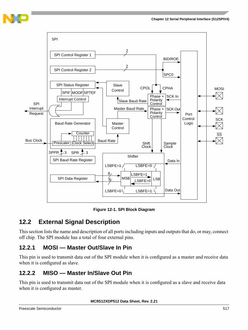
Chapter 12 Serial Peripheral Interface (S12SPIV4)
MC9S12XDP512 Data Sheet, Rev. 2.21
Freescale Semiconductor 517
Figure 12-1. SPI Block Diagram
12.2 External Signal DescriptionThis section lists the name and description of all ports including inputs and outputs that do, or may, connectoff chip. The SPI module has a total of four external pins.
12.2.1 MOSI — Master Out/Slave In Pin
This pin is used to transmit data out of the SPI module when it is configured as a master and receive datawhen it is configured as slave.
12.2.2 MISO — Master In/Slave Out Pin
This pin is used to transmit data out of the SPI module when it is configured as a slave and receive datawhen it is configured as master.
SPI Control Register 1
SPI Control Register 2
SPI Baud Rate Register
SPI Status Register
SPI Data Register
Shifter
PortControlLogic
MOSI
SCK
Interrupt Control
SPI
MSB LSB
LSBFE=1 LSBFE=0
LSBFE=0 LSBFE=1
Data In
LSBFE=1
LSBFE=0
Data Out
8
8
Baud Rate Generator
PrescalerBus Clock
Counter
Clock Select
SPPR 3 3SPR
Baud Rate
Phase +PolarityControl
Master
Slave
SCK In
SCK OutMaster Baud Rate
Slave Baud Rate
Phase +PolarityControl
Control
ControlCPOL CPHA
2
BIDIROE
SPC0
2
Shift SampleClockClock
MODFSPIF SPTEF
SPI
RequestInterrupt
SS
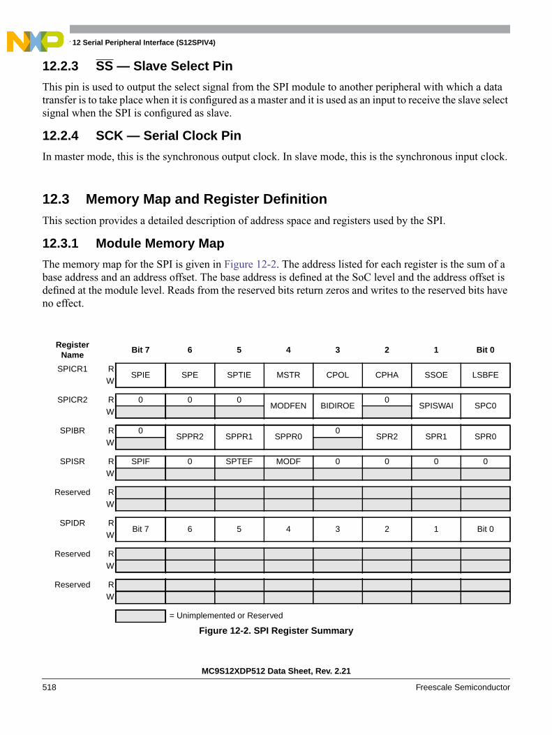
Chapter 12 Serial Peripheral Interface (S12SPIV4)
MC9S12XDP512 Data Sheet, Rev. 2.21
518 Freescale Semiconductor
12.2.3 SS — Slave Select Pin
This pin is used to output the select signal from the SPI module to another peripheral with which a datatransfer is to take place when it is configured as a master and it is used as an input to receive the slave selectsignal when the SPI is configured as slave.
12.2.4 SCK — Serial Clock Pin
In master mode, this is the synchronous output clock. In slave mode, this is the synchronous input clock.
12.3 Memory Map and Register DefinitionThis section provides a detailed description of address space and registers used by the SPI.
12.3.1 Module Memory Map
The memory map for the SPI is given in Figure 12-2. The address listed for each register is the sum of abase address and an address offset. The base address is defined at the SoC level and the address offset isdefined at the module level. Reads from the reserved bits return zeros and writes to the reserved bits haveno effect.
RegisterName
Bit 7 6 5 4 3 2 1 Bit 0
SPICR1 RSPIE SPE SPTIE MSTR CPOL CPHA SSOE LSBFE
W
SPICR2 R 0 0 0MODFEN BIDIROE
0SPISWAI SPC0
W
SPIBR R 0SPPR2 SPPR1 SPPR0
0SPR2 SPR1 SPR0
W
SPISR R SPIF 0 SPTEF MODF 0 0 0 0W
Reserved RW
SPIDR RBit 7 6 5 4 3 2 1 Bit 0
W
Reserved RW
Reserved RW
= Unimplemented or Reserved
Figure 12-2. SPI Register Summary

Chapter 12 Serial Peripheral Interface (S12SPIV4)
MC9S12XDP512 Data Sheet, Rev. 2.21
Freescale Semiconductor 519
12.3.2 Register Descriptions
This section consists of register descriptions in address order. Each description includes a standard registerdiagram with an associated figure number. Details of register bit and field function follow the registerdiagrams, in bit order.
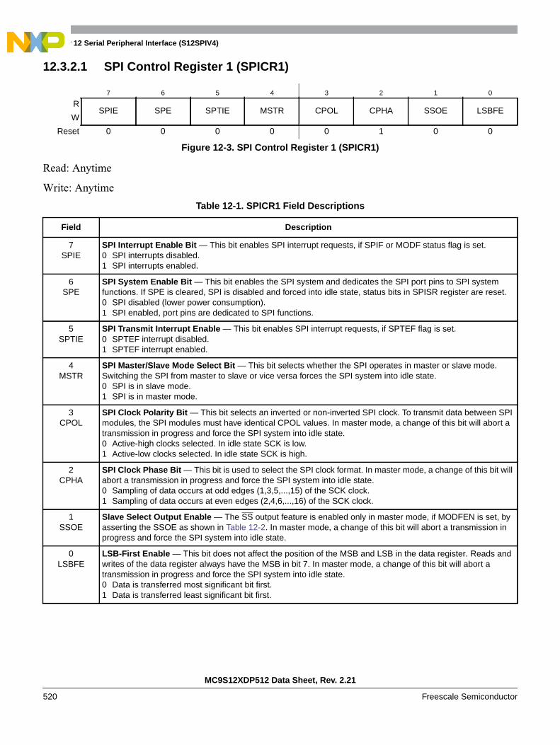
Chapter 12 Serial Peripheral Interface (S12SPIV4)
MC9S12XDP512 Data Sheet, Rev. 2.21
520 Freescale Semiconductor
12.3.2.1 SPI Control Register 1 (SPICR1)
Read: Anytime
Write: Anytime
7 6 5 4 3 2 1 0
RSPIE SPE SPTIE MSTR CPOL CPHA SSOE LSBFE
W
Reset 0 0 0 0 0 1 0 0
Figure 12-3. SPI Control Register 1 (SPICR1)
Table 12-1. SPICR1 Field Descriptions
Field Description
7SPIE
SPI Interrupt Enable Bit — This bit enables SPI interrupt requests, if SPIF or MODF status flag is set.0 SPI interrupts disabled.1 SPI interrupts enabled.
6SPE
SPI System Enable Bit — This bit enables the SPI system and dedicates the SPI port pins to SPI systemfunctions. If SPE is cleared, SPI is disabled and forced into idle state, status bits in SPISR register are reset.0 SPI disabled (lower power consumption).1 SPI enabled, port pins are dedicated to SPI functions.
5SPTIE
SPI Transmit Interrupt Enable — This bit enables SPI interrupt requests, if SPTEF flag is set.0 SPTEF interrupt disabled.1 SPTEF interrupt enabled.
4MSTR
SPI Master/Slave Mode Select Bit — This bit selects whether the SPI operates in master or slave mode.Switching the SPI from master to slave or vice versa forces the SPI system into idle state.0 SPI is in slave mode.1 SPI is in master mode.
3CPOL
SPI Clock Polarity Bit — This bit selects an inverted or non-inverted SPI clock. To transmit data between SPImodules, the SPI modules must have identical CPOL values. In master mode, a change of this bit will abort atransmission in progress and force the SPI system into idle state.0 Active-high clocks selected. In idle state SCK is low.1 Active-low clocks selected. In idle state SCK is high.
2CPHA
SPI Clock Phase Bit — This bit is used to select the SPI clock format. In master mode, a change of this bit willabort a transmission in progress and force the SPI system into idle state.0 Sampling of data occurs at odd edges (1,3,5,...,15) of the SCK clock.1 Sampling of data occurs at even edges (2,4,6,...,16) of the SCK clock.
1SSOE
Slave Select Output Enable — The SS output feature is enabled only in master mode, if MODFEN is set, byasserting the SSOE as shown in Table 12-2. In master mode, a change of this bit will abort a transmission inprogress and force the SPI system into idle state.
0LSBFE
LSB-First Enable — This bit does not affect the position of the MSB and LSB in the data register. Reads andwrites of the data register always have the MSB in bit 7. In master mode, a change of this bit will abort atransmission in progress and force the SPI system into idle state.0 Data is transferred most significant bit first.1 Data is transferred least significant bit first.

Chapter 12 Serial Peripheral Interface (S12SPIV4)
MC9S12XDP512 Data Sheet, Rev. 2.21
Freescale Semiconductor 521
12.3.2.2 SPI Control Register 2 (SPICR2)
Read: Anytime
Write: Anytime; writes to the reserved bits have no effect
Table 12-2. SS Input / Output Selection
MODFEN SSOE Master Mode Slave Mode
0 0 SS not used by SPI SS input
0 1 SS not used by SPI SS input
1 0 SS input with MODF feature SS input
1 1 SS is slave select output SS input
7 6 5 4 3 2 1 0
R 0 0 0MODFEN BIDIROE
0SPISWAI SPC0
W
Reset 0 0 0 0 0 0 0 0
= Unimplemented or Reserved
Figure 12-4. SPI Control Register 2 (SPICR2)
Table 12-3. SPICR2 Field Descriptions
Field Description
4MODFEN
Mode Fault Enable Bit — This bit allows the MODF failure to be detected. If the SPI is in master mode andMODFEN is cleared, then the SS port pin is not used by the SPI. In slave mode, the SS is available only as aninput regardless of the value of MODFEN. For an overview on the impact of the MODFEN bit on the SS port pinconfiguration, refer to Table 12-4. In master mode, a change of this bit will abort a transmission in progress andforce the SPI system into idle state.0 SS port pin is not used by the SPI.1 SS port pin with MODF feature.
3BIDIROE
Output Enable in the Bidirectional Mode of Operation — This bit controls the MOSI and MISO output bufferof the SPI, when in bidirectional mode of operation (SPC0 is set). In master mode, this bit controls the outputbuffer of the MOSI port, in slave mode it controls the output buffer of the MISO port. In master mode, with SPC0set, a change of this bit will abort a transmission in progress and force the SPI into idle state.0 Output buffer disabled.1 Output buffer enabled.
1SPISWAI
SPI Stop in Wait Mode Bit — This bit is used for power conservation while in wait mode.0 SPI clock operates normally in wait mode.1 Stop SPI clock generation when in wait mode.
0SPC0
Serial Pin Control Bit 0 — This bit enables bidirectional pin configurations as shown in Table 12-4. In mastermode, a change of this bit will abort a transmission in progress and force the SPI system into idle state.

Chapter 12 Serial Peripheral Interface (S12SPIV4)
MC9S12XDP512 Data Sheet, Rev. 2.21
522 Freescale Semiconductor
12.3.2.3 SPI Baud Rate Register (SPIBR)
Read: Anytime
Write: Anytime; writes to the reserved bits have no effect
The baud rate divisor equation is as follows:BaudRateDivisor = (SPPR + 1) • 2(SPR + 1) Eqn. 12-1
The baud rate can be calculated with the following equation:Baud Rate = BusClock / BaudRateDivisor Eqn. 12-2
NOTEFor maximum allowed baud rates, please refer to the SPI ElectricalSpecification in the Electricals chapter of this data sheet.
Table 12-4. Bidirectional Pin Configurations
Pin Mode SPC0 BIDIROE MISO MOSI
Master Mode of Operation
Normal 0 X Master In Master Out
Bidirectional 1 0 MISO not used by SPI Master In
1 Master I/O
Slave Mode of Operation
Normal 0 X Slave Out Slave In
Bidirectional 1 0 Slave In MOSI not used by SPI
1 Slave I/O
7 6 5 4 3 2 1 0
R 0SPPR2 SPPR1 SPPR0
0SPR2 SPR1 SPR0
W
Reset 0 0 0 0 0 0 0 0
= Unimplemented or Reserved
Figure 12-5. SPI Baud Rate Register (SPIBR)
Table 12-5. SPIBR Field Descriptions
Field Description
6–4SPPR[2:0]
SPI Baud Rate Preselection Bits — These bits specify the SPI baud rates as shown in Table 12-6. In mastermode, a change of these bits will abort a transmission in progress and force the SPI system into idle state.
2–0SPR[2:0]
SPI Baud Rate Selection Bits — These bits specify the SPI baud rates as shown in Table 12-6. In master mode,a change of these bits will abort a transmission in progress and force the SPI system into idle state.
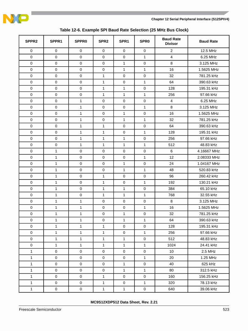
Chapter 12 Serial Peripheral Interface (S12SPIV4)
MC9S12XDP512 Data Sheet, Rev. 2.21
Freescale Semiconductor 523
Table 12-6. Example SPI Baud Rate Selection (25 MHz Bus Clock)
SPPR2 SPPR1 SPPR0 SPR2 SPR1 SPR0Baud Rate
DivisorBaud Rate
0 0 0 0 0 0 2 12.5 MHz
0 0 0 0 0 1 4 6.25 MHz
0 0 0 0 1 0 8 3.125 MHz
0 0 0 0 1 1 16 1.5625 MHz
0 0 0 1 0 0 32 781.25 kHz
0 0 0 1 0 1 64 390.63 kHz
0 0 0 1 1 0 128 195.31 kHz
0 0 0 1 1 1 256 97.66 kHz
0 0 1 0 0 0 4 6.25 MHz
0 0 1 0 0 1 8 3.125 MHz
0 0 1 0 1 0 16 1.5625 MHz
0 0 1 0 1 1 32 781.25 kHz
0 0 1 1 0 0 64 390.63 kHz
0 0 1 1 0 1 128 195.31 kHz
0 0 1 1 1 0 256 97.66 kHz
0 0 1 1 1 1 512 48.83 kHz
0 1 0 0 0 0 6 4.16667 MHz
0 1 0 0 0 1 12 2.08333 MHz
0 1 0 0 1 0 24 1.04167 MHz
0 1 0 0 1 1 48 520.83 kHz
0 1 0 1 0 0 96 260.42 kHz
0 1 0 1 0 1 192 130.21 kHz
0 1 0 1 1 0 384 65.10 kHz
0 1 0 1 1 1 768 32.55 kHz
0 1 1 0 0 0 8 3.125 MHz
0 1 1 0 0 1 16 1.5625 MHz
0 1 1 0 1 0 32 781.25 kHz
0 1 1 0 1 1 64 390.63 kHz
0 1 1 1 0 0 128 195.31 kHz
0 1 1 1 0 1 256 97.66 kHz
0 1 1 1 1 0 512 48.83 kHz
0 1 1 1 1 1 1024 24.41 kHz
1 0 0 0 0 0 10 2.5 MHz
1 0 0 0 0 1 20 1.25 MHz
1 0 0 0 1 0 40 625 kHz
1 0 0 0 1 1 80 312.5 kHz
1 0 0 1 0 0 160 156.25 kHz
1 0 0 1 0 1 320 78.13 kHz
1 0 0 1 1 0 640 39.06 kHz

Chapter 12 Serial Peripheral Interface (S12SPIV4)
MC9S12XDP512 Data Sheet, Rev. 2.21
524 Freescale Semiconductor
1 0 0 1 1 1 1280 19.53 kHz
1 0 1 0 0 0 12 2.08333 MHz
1 0 1 0 0 1 24 1.04167 MHz
1 0 1 0 1 0 48 520.83 kHz
1 0 1 0 1 1 96 260.42 kHz
1 0 1 1 0 0 192 130.21 kHz
1 0 1 1 0 1 384 65.10 kHz
1 0 1 1 1 0 768 32.55 kHz
1 0 1 1 1 1 1536 16.28 kHz
1 1 0 0 0 0 14 1.78571 MHz
1 1 0 0 0 1 28 892.86 kHz
1 1 0 0 1 0 56 446.43 kHz
1 1 0 0 1 1 112 223.21 kHz
1 1 0 1 0 0 224 111.61 kHz
1 1 0 1 0 1 448 55.80 kHz
1 1 0 1 1 0 896 27.90 kHz
1 1 0 1 1 1 1792 13.95 kHz
1 1 1 0 0 0 16 1.5625 MHz
1 1 1 0 0 1 32 781.25 kHz
1 1 1 0 1 0 64 390.63 kHz
1 1 1 0 1 1 128 195.31 kHz
1 1 1 1 0 0 256 97.66 kHz
1 1 1 1 0 1 512 48.83 kHz
1 1 1 1 1 0 1024 24.41 kHz
1 1 1 1 1 1 2048 12.21 kHz
Table 12-6. Example SPI Baud Rate Selection (25 MHz Bus Clock) (continued)
SPPR2 SPPR1 SPPR0 SPR2 SPR1 SPR0Baud Rate
DivisorBaud Rate
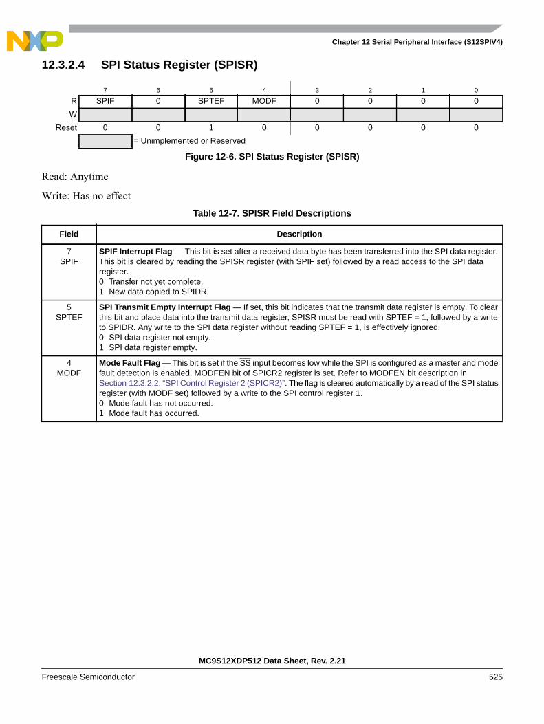
Chapter 12 Serial Peripheral Interface (S12SPIV4)
MC9S12XDP512 Data Sheet, Rev. 2.21
Freescale Semiconductor 525
12.3.2.4 SPI Status Register (SPISR)
Read: Anytime
Write: Has no effect
7 6 5 4 3 2 1 0
R SPIF 0 SPTEF MODF 0 0 0 0
W
Reset 0 0 1 0 0 0 0 0
= Unimplemented or Reserved
Figure 12-6. SPI Status Register (SPISR)
Table 12-7. SPISR Field Descriptions
Field Description
7SPIF
SPIF Interrupt Flag — This bit is set after a received data byte has been transferred into the SPI data register.This bit is cleared by reading the SPISR register (with SPIF set) followed by a read access to the SPI dataregister.0 Transfer not yet complete.1 New data copied to SPIDR.
5SPTEF
SPI Transmit Empty Interrupt Flag — If set, this bit indicates that the transmit data register is empty. To clearthis bit and place data into the transmit data register, SPISR must be read with SPTEF = 1, followed by a writeto SPIDR. Any write to the SPI data register without reading SPTEF = 1, is effectively ignored.0 SPI data register not empty.1 SPI data register empty.
4MODF
Mode Fault Flag — This bit is set if the SS input becomes low while the SPI is configured as a master and modefault detection is enabled, MODFEN bit of SPICR2 register is set. Refer to MODFEN bit description inSection 12.3.2.2, “SPI Control Register 2 (SPICR2)”. The flag is cleared automatically by a read of the SPI statusregister (with MODF set) followed by a write to the SPI control register 1.0 Mode fault has not occurred.1 Mode fault has occurred.

Chapter 12 Serial Peripheral Interface (S12SPIV4)
MC9S12XDP512 Data Sheet, Rev. 2.21
526 Freescale Semiconductor
12.3.2.5 SPI Data Register (SPIDR)
Read: Anytime; normally read only when SPIF is set
Write: Anytime
The SPI data register is both the input and output register for SPI data. A write to this registerallows a data byte to be queued and transmitted. For an SPI configured as a master, a queued databyte is transmitted immediately after the previous transmission has completed. The SPI transmitterempty flag SPTEF in the SPISR register indicates when the SPI data register is ready to accept newdata.
Received data in the SPIDR is valid when SPIF is set.
If SPIF is cleared and a byte has been received, the received byte is transferred from the receiveshift register to the SPIDR and SPIF is set.
If SPIF is set and not serviced, and a second byte has been received, the second received byte iskept as valid byte in the receive shift register until the start of another transmission. The byte in theSPIDR does not change.
If SPIF is set and a valid byte is in the receive shift register, and SPIF is serviced before the start ofa third transmission, the byte in the receive shift register is transferred into the SPIDR and SPIFremains set (see Figure 12-8).
If SPIF is set and a valid byte is in the receive shift register, and SPIF is serviced after the start ofa third transmission, the byte in the receive shift register has become invalid and is not transferredinto the SPIDR (see Figure 12-9).
7 6 5 4 3 2 1 0
RBit 7 6 5 4 3 2 2 Bit 0
W
Reset 0 0 0 0 0 0 0 0
Figure 12-7. SPI Data Register (SPIDR)

Chapter 12 Serial Peripheral Interface (S12SPIV4)
MC9S12XDP512 Data Sheet, Rev. 2.21
Freescale Semiconductor 527
Figure 12-8. Reception with SPIF Serviced in Time
Figure 12-9. Reception with SPIF Serviced too Late
Receive Shift Register
SPIF
SPI Data Register
Data A Data B
Data A
Data A Received Data B Received
Data C
Data C
SPIF Serviced
Data C Received
Data B
= Unspecified = Reception in progress
Receive Shift Register
SPIF
SPI Data Register
Data A Data B
Data A
Data A Received Data B Received
Data C
Data C
SPIF Serviced
Data C ReceivedData B Lost
= Unspecified = Reception in progress
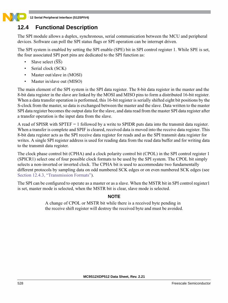
Chapter 12 Serial Peripheral Interface (S12SPIV4)
MC9S12XDP512 Data Sheet, Rev. 2.21
528 Freescale Semiconductor
12.4 Functional DescriptionThe SPI module allows a duplex, synchronous, serial communication between the MCU and peripheraldevices. Software can poll the SPI status flags or SPI operation can be interrupt driven.
The SPI system is enabled by setting the SPI enable (SPE) bit in SPI control register 1. While SPE is set,the four associated SPI port pins are dedicated to the SPI function as:
• Slave select (SS)
• Serial clock (SCK)
• Master out/slave in (MOSI)
• Master in/slave out (MISO)
The main element of the SPI system is the SPI data register. The 8-bit data register in the master and the8-bit data register in the slave are linked by the MOSI and MISO pins to form a distributed 16-bit register.When a data transfer operation is performed, this 16-bit register is serially shifted eight bit positions by theS-clock from the master, so data is exchanged between the master and the slave. Data written to the masterSPI data register becomes the output data for the slave, and data read from the master SPI data register aftera transfer operation is the input data from the slave.
A read of SPISR with SPTEF = 1 followed by a write to SPIDR puts data into the transmit data register.When a transfer is complete and SPIF is cleared, received data is moved into the receive data register. This8-bit data register acts as the SPI receive data register for reads and as the SPI transmit data register forwrites. A single SPI register address is used for reading data from the read data buffer and for writing datato the transmit data register.
The clock phase control bit (CPHA) and a clock polarity control bit (CPOL) in the SPI control register 1(SPICR1) select one of four possible clock formats to be used by the SPI system. The CPOL bit simplyselects a non-inverted or inverted clock. The CPHA bit is used to accommodate two fundamentallydifferent protocols by sampling data on odd numbered SCK edges or on even numbered SCK edges (seeSection 12.4.3, “Transmission Formats”).
The SPI can be configured to operate as a master or as a slave. When the MSTR bit in SPI control register1is set, master mode is selected, when the MSTR bit is clear, slave mode is selected.
NOTEA change of CPOL or MSTR bit while there is a received byte pending inthe receive shift register will destroy the received byte and must be avoided.

Chapter 12 Serial Peripheral Interface (S12SPIV4)
MC9S12XDP512 Data Sheet, Rev. 2.21
Freescale Semiconductor 529
12.4.1 Master Mode
The SPI operates in master mode when the MSTR bit is set. Only a master SPI module can initiatetransmissions. A transmission begins by writing to the master SPI data register. If the shift register isempty, the byte immediately transfers to the shift register. The byte begins shifting out on the MOSI pinunder the control of the serial clock.
• Serial clock
The SPR2, SPR1, and SPR0 baud rate selection bits, in conjunction with the SPPR2, SPPR1, andSPPR0 baud rate preselection bits in the SPI baud rate register, control the baud rate generator anddetermine the speed of the transmission. The SCK pin is the SPI clock output. Through the SCKpin, the baud rate generator of the master controls the shift register of the slave peripheral.
• MOSI, MISO pin
In master mode, the function of the serial data output pin (MOSI) and the serial data input pin(MISO) is determined by the SPC0 and BIDIROE control bits.
• SS pin
If MODFEN and SSOE are set, the SS pin is configured as slave select output. The SS outputbecomes low during each transmission and is high when the SPI is in idle state.
If MODFEN is set and SSOE is cleared, the SS pin is configured as input for detecting mode faulterror. If the SS input becomes low this indicates a mode fault error where another master tries todrive the MOSI and SCK lines. In this case, the SPI immediately switches to slave mode, byclearing the MSTR bit and also disables the slave output buffer MISO (or SISO in bidirectionalmode). So the result is that all outputs are disabled and SCK, MOSI, and MISO are inputs. If atransmission is in progress when the mode fault occurs, the transmission is aborted and the SPI isforced into idle state.
This mode fault error also sets the mode fault (MODF) flag in the SPI status register (SPISR). Ifthe SPI interrupt enable bit (SPIE) is set when the MODF flag becomes set, then an SPI interruptsequence is also requested.
When a write to the SPI data register in the master occurs, there is a half SCK-cycle delay. Afterthe delay, SCK is started within the master. The rest of the transfer operation differs slightly,depending on the clock format specified by the SPI clock phase bit, CPHA, in SPI control register 1(see Section 12.4.3, “Transmission Formats”).
NOTEA change of the bits CPOL, CPHA, SSOE, LSBFE, MODFEN, SPC0, orBIDIROE with SPC0 set, SPPR2-SPPR0 and SPR2-SPR0 in master modewill abort a transmission in progress and force the SPI into idle state. Theremote slave cannot detect this, therefore the master must ensure that theremote slave is returned to idle state.
Chapter 12 Serial Peripheral Interface (S12SPIV4)
MC9S12XDP512 Data Sheet, Rev. 2.21
530 Freescale Semiconductor
12.4.2 Slave Mode
The SPI operates in slave mode when the MSTR bit in SPI control register 1 is clear.
• Serial clock
In slave mode, SCK is the SPI clock input from the master.
• MISO, MOSI pin
In slave mode, the function of the serial data output pin (MISO) and serial data input pin (MOSI)is determined by the SPC0 bit and BIDIROE bit in SPI control register 2.
• SS pin
The SS pin is the slave select input. Before a data transmission occurs, the SS pin of the slave SPImust be low. SS must remain low until the transmission is complete. If SS goes high, the SPI isforced into idle state.
The SS input also controls the serial data output pin, if SS is high (not selected), the serial dataoutput pin is high impedance, and, if SS is low, the first bit in the SPI data register is driven out ofthe serial data output pin. Also, if the slave is not selected (SS is high), then the SCK input isignored and no internal shifting of the SPI shift register occurs.
Although the SPI is capable of duplex operation, some SPI peripherals are capable of onlyreceiving SPI data in a slave mode. For these simpler devices, there is no serial data out pin.
NOTEWhen peripherals with duplex capability are used, take care not tosimultaneously enable two receivers whose serial outputs drive the samesystem slave’s serial data output line.
As long as no more than one slave device drives the system slave’s serial data output line, it is possible forseveral slaves to receive the same transmission from a master, although the master would not receive returninformation from all of the receiving slaves.
If the CPHA bit in SPI control register 1 is clear, odd numbered edges on the SCK input cause the data atthe serial data input pin to be latched. Even numbered edges cause the value previously latched from theserial data input pin to shift into the LSB or MSB of the SPI shift register, depending on the LSBFE bit.
If the CPHA bit is set, even numbered edges on the SCK input cause the data at the serial data input pin tobe latched. Odd numbered edges cause the value previously latched from the serial data input pin to shiftinto the LSB or MSB of the SPI shift register, depending on the LSBFE bit.
When CPHA is set, the first edge is used to get the first data bit onto the serial data output pin. When CPHAis clear and the SS input is low (slave selected), the first bit of the SPI data is driven out of the serial dataoutput pin. After the eighth shift, the transfer is considered complete and the received data is transferredinto the SPI data register. To indicate transfer is complete, the SPIF flag in the SPI status register is set.
NOTEA change of the bits CPOL, CPHA, SSOE, LSBFE, MODFEN, SPC0, orBIDIROE with SPC0 set in slave mode will corrupt a transmission inprogress and must be avoided.
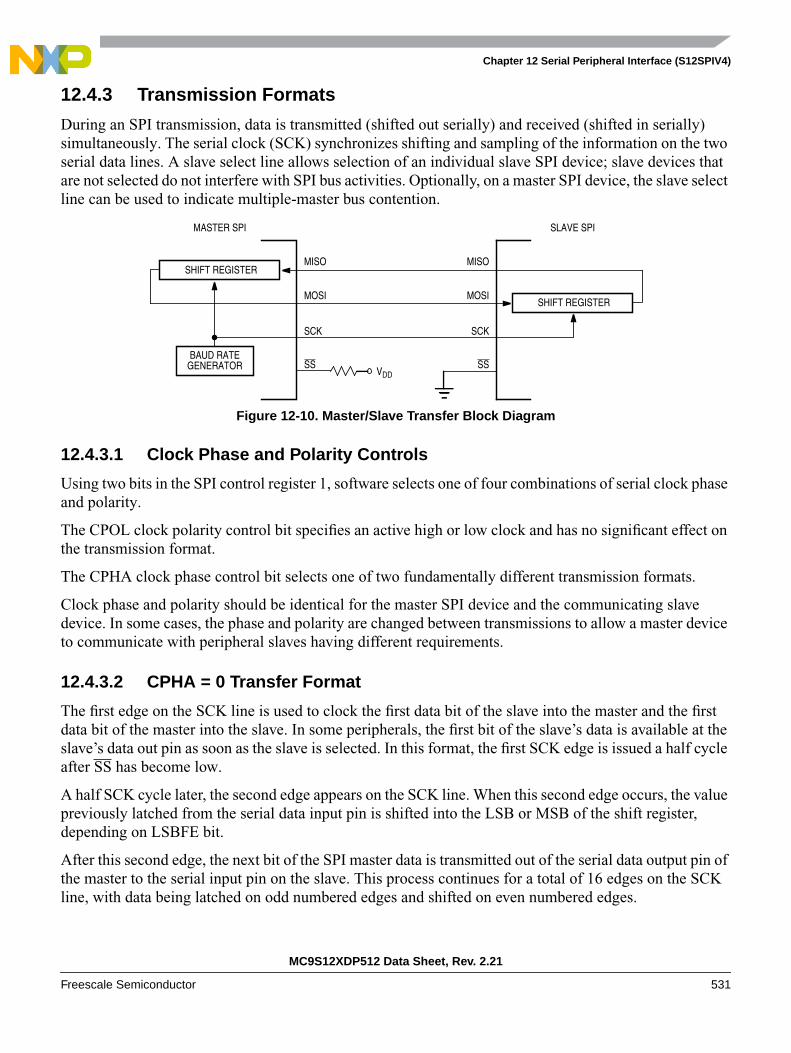
Chapter 12 Serial Peripheral Interface (S12SPIV4)
MC9S12XDP512 Data Sheet, Rev. 2.21
Freescale Semiconductor 531
12.4.3 Transmission Formats
During an SPI transmission, data is transmitted (shifted out serially) and received (shifted in serially)simultaneously. The serial clock (SCK) synchronizes shifting and sampling of the information on the twoserial data lines. A slave select line allows selection of an individual slave SPI device; slave devices thatare not selected do not interfere with SPI bus activities. Optionally, on a master SPI device, the slave selectline can be used to indicate multiple-master bus contention.
Figure 12-10. Master/Slave Transfer Block Diagram
12.4.3.1 Clock Phase and Polarity Controls
Using two bits in the SPI control register 1, software selects one of four combinations of serial clock phaseand polarity.
The CPOL clock polarity control bit specifies an active high or low clock and has no significant effect onthe transmission format.
The CPHA clock phase control bit selects one of two fundamentally different transmission formats.
Clock phase and polarity should be identical for the master SPI device and the communicating slavedevice. In some cases, the phase and polarity are changed between transmissions to allow a master deviceto communicate with peripheral slaves having different requirements.
12.4.3.2 CPHA = 0 Transfer Format
The first edge on the SCK line is used to clock the first data bit of the slave into the master and the firstdata bit of the master into the slave. In some peripherals, the first bit of the slave’s data is available at theslave’s data out pin as soon as the slave is selected. In this format, the first SCK edge is issued a half cycleafter SS has become low.
A half SCK cycle later, the second edge appears on the SCK line. When this second edge occurs, the valuepreviously latched from the serial data input pin is shifted into the LSB or MSB of the shift register,depending on LSBFE bit.
After this second edge, the next bit of the SPI master data is transmitted out of the serial data output pin ofthe master to the serial input pin on the slave. This process continues for a total of 16 edges on the SCKline, with data being latched on odd numbered edges and shifted on even numbered edges.
SHIFT REGISTER
SHIFT REGISTER
BAUD RATEGENERATOR
MASTER SPI SLAVE SPI
MOSI MOSI
MISO MISO
SCK SCK
SS SSVDD
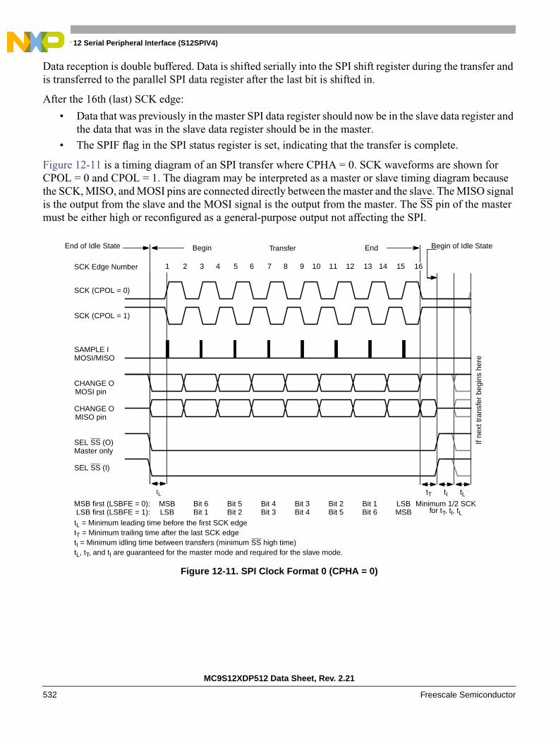
Chapter 12 Serial Peripheral Interface (S12SPIV4)
MC9S12XDP512 Data Sheet, Rev. 2.21
532 Freescale Semiconductor
Data reception is double buffered. Data is shifted serially into the SPI shift register during the transfer andis transferred to the parallel SPI data register after the last bit is shifted in.
After the 16th (last) SCK edge:
• Data that was previously in the master SPI data register should now be in the slave data register andthe data that was in the slave data register should be in the master.
• The SPIF flag in the SPI status register is set, indicating that the transfer is complete.
Figure 12-11 is a timing diagram of an SPI transfer where CPHA = 0. SCK waveforms are shown forCPOL = 0 and CPOL = 1. The diagram may be interpreted as a master or slave timing diagram becausethe SCK, MISO, and MOSI pins are connected directly between the master and the slave. The MISO signalis the output from the slave and the MOSI signal is the output from the master. The SS pin of the mastermust be either high or reconfigured as a general-purpose output not affecting the SPI.
Figure 12-11. SPI Clock Format 0 (CPHA = 0)
tL
Begin End
SCK (CPOL = 0)
SAMPLE I
CHANGE O
SEL SS (O)
Transfer
SCK (CPOL = 1)
MSB first (LSBFE = 0): LSB first (LSBFE = 1):
MSBLSB
LSBMSB
Bit 5Bit 2
Bit 6Bit 1
Bit 4Bit 3
Bit 3Bit 4
Bit 2Bit 5
Bit 1Bit 6
CHANGE O
SEL SS (I)
MOSI pin
MISO pin
Master only
MOSI/MISO
tT
If ne
xt tr
ansf
er b
egin
s he
re
for tT, tl, tLMinimum 1/2 SCK
tI tL
tL = Minimum leading time before the first SCK edgetT = Minimum trailing time after the last SCK edgetI = Minimum idling time between transfers (minimum SS high time)tL, tT, and tI are guaranteed for the master mode and required for the slave mode.
1 2 3 4 5 6 7 8 9 10 11 12 13 14 15 16SCK Edge Number
End of Idle State Begin of Idle State

Chapter 12 Serial Peripheral Interface (S12SPIV4)
MC9S12XDP512 Data Sheet, Rev. 2.21
Freescale Semiconductor 533
In slave mode, if the SS line is not deasserted between the successive transmissions then the content of theSPI data register is not transmitted; instead the last received byte is transmitted. If the SS line is deassertedfor at least minimum idle time (half SCK cycle) between successive transmissions, then the content of theSPI data register is transmitted.
In master mode, with slave select output enabled the SS line is always deasserted and reasserted betweensuccessive transfers for at least minimum idle time.
12.4.3.3 CPHA = 1 Transfer Format
Some peripherals require the first SCK edge before the first data bit becomes available at the data out pin,the second edge clocks data into the system. In this format, the first SCK edge is issued by setting theCPHA bit at the beginning of the 8-cycle transfer operation.
The first edge of SCK occurs immediately after the half SCK clock cycle synchronization delay. This firstedge commands the slave to transfer its first data bit to the serial data input pin of the master.
A half SCK cycle later, the second edge appears on the SCK pin. This is the latching edge for both themaster and slave.
When the third edge occurs, the value previously latched from the serial data input pin is shifted into theLSB or MSB of the SPI shift register, depending on LSBFE bit. After this edge, the next bit of the masterdata is coupled out of the serial data output pin of the master to the serial input pin on the slave.
This process continues for a total of 16 edges on the SCK line with data being latched on even numberededges and shifting taking place on odd numbered edges.
Data reception is double buffered, data is serially shifted into the SPI shift register during the transfer andis transferred to the parallel SPI data register after the last bit is shifted in.
After the 16th SCK edge:
• Data that was previously in the SPI data register of the master is now in the data register of theslave, and data that was in the data register of the slave is in the master.
• The SPIF flag bit in SPISR is set indicating that the transfer is complete.
Figure 12-12 shows two clocking variations for CPHA = 1. The diagram may be interpreted as a master orslave timing diagram because the SCK, MISO, and MOSI pins are connected directly between the masterand the slave. The MISO signal is the output from the slave, and the MOSI signal is the output from themaster. The SS line is the slave select input to the slave. The SS pin of the master must be either high orreconfigured as a general-purpose output not affecting the SPI.
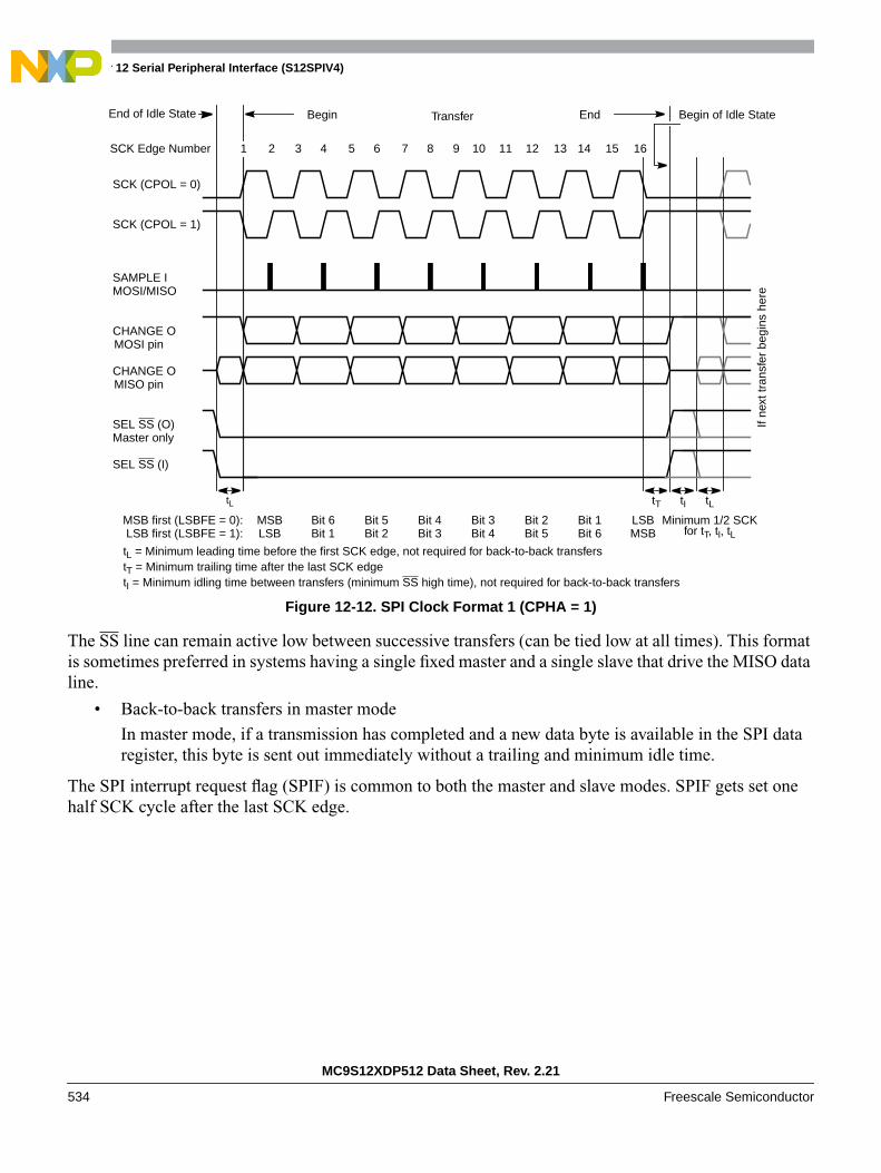
Chapter 12 Serial Peripheral Interface (S12SPIV4)
MC9S12XDP512 Data Sheet, Rev. 2.21
534 Freescale Semiconductor
Figure 12-12. SPI Clock Format 1 (CPHA = 1)
The SS line can remain active low between successive transfers (can be tied low at all times). This formatis sometimes preferred in systems having a single fixed master and a single slave that drive the MISO dataline.
• Back-to-back transfers in master mode
In master mode, if a transmission has completed and a new data byte is available in the SPI dataregister, this byte is sent out immediately without a trailing and minimum idle time.
The SPI interrupt request flag (SPIF) is common to both the master and slave modes. SPIF gets set onehalf SCK cycle after the last SCK edge.
tL tT
for tT, tl, tLMinimum 1/2 SCK
tI tL
If ne
xt tr
ansf
er b
egin
s he
re
Begin End
SCK (CPOL = 0)
SAMPLE I
CHANGE O
SEL SS (O)
Transfer
SCK (CPOL = 1)
MSB first (LSBFE = 0): LSB first (LSBFE = 1):
MSBLSB
LSBMSB
Bit 5Bit 2
Bit 6Bit 1
Bit 4Bit 3
Bit 3Bit 4
Bit 2Bit 5
Bit 1Bit 6
CHANGE O
SEL SS (I)
MOSI pin
MISO pin
Master only
MOSI/MISO
tL = Minimum leading time before the first SCK edge, not required for back-to-back transferstT = Minimum trailing time after the last SCK edgetI = Minimum idling time between transfers (minimum SS high time), not required for back-to-back transfers
1 2 3 4 5 6 7 8 9 10 11 12 13 14 15 16SCK Edge Number
End of Idle State Begin of Idle State

Chapter 12 Serial Peripheral Interface (S12SPIV4)
MC9S12XDP512 Data Sheet, Rev. 2.21
Freescale Semiconductor 535
12.4.4 SPI Baud Rate Generation
Baud rate generation consists of a series of divider stages. Six bits in the SPI baud rate register (SPPR2,SPPR1, SPPR0, SPR2, SPR1, and SPR0) determine the divisor to the SPI module clock which results inthe SPI baud rate.
The SPI clock rate is determined by the product of the value in the baud rate preselection bits(SPPR2–SPPR0) and the value in the baud rate selection bits (SPR2–SPR0). The module clock divisorequation is shown in Equation 12-3.
BaudRateDivisor = (SPPR + 1) • 2(SPR + 1) Eqn. 12-3
When all bits are clear (the default condition), the SPI module clock is divided by 2. When the selectionbits (SPR2–SPR0) are 001 and the preselection bits (SPPR2–SPPR0) are 000, the module clock divisorbecomes 4. When the selection bits are 010, the module clock divisor becomes 8, etc.
When the preselection bits are 001, the divisor determined by the selection bits is multiplied by 2. Whenthe preselection bits are 010, the divisor is multiplied by 3, etc. See Table 12-6 for baud rate calculationsfor all bit conditions, based on a 25 MHz bus clock. The two sets of selects allows the clock to be dividedby a non-power of two to achieve other baud rates such as divide by 6, divide by 10, etc.
The baud rate generator is activated only when the SPI is in master mode and a serial transfer is takingplace. In the other cases, the divider is disabled to decrease IDD current.
NOTEFor maximum allowed baud rates, please refer to the SPI ElectricalSpecification in the Electricals chapter of this data sheet.
12.4.5 Special Features
12.4.5.1 SS Output
The SS output feature automatically drives the SS pin low during transmission to select external devicesand drives it high during idle to deselect external devices. When SS output is selected, the SS output pinis connected to the SS input pin of the external device.
The SS output is available only in master mode during normal SPI operation by asserting SSOE andMODFEN bit as shown in Table 12-2.
The mode fault feature is disabled while SS output is enabled.
NOTECare must be taken when using the SS output feature in a multimastersystem because the mode fault feature is not available for detecting systemerrors between masters.
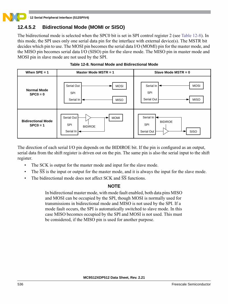
Chapter 12 Serial Peripheral Interface (S12SPIV4)
MC9S12XDP512 Data Sheet, Rev. 2.21
536 Freescale Semiconductor
12.4.5.2 Bidirectional Mode (MOMI or SISO)
The bidirectional mode is selected when the SPC0 bit is set in SPI control register 2 (see Table 12-8). Inthis mode, the SPI uses only one serial data pin for the interface with external device(s). The MSTR bitdecides which pin to use. The MOSI pin becomes the serial data I/O (MOMI) pin for the master mode, andthe MISO pin becomes serial data I/O (SISO) pin for the slave mode. The MISO pin in master mode andMOSI pin in slave mode are not used by the SPI.
The direction of each serial I/O pin depends on the BIDIROE bit. If the pin is configured as an output,serial data from the shift register is driven out on the pin. The same pin is also the serial input to the shiftregister.
• The SCK is output for the master mode and input for the slave mode.
• The SS is the input or output for the master mode, and it is always the input for the slave mode.
• The bidirectional mode does not affect SCK and SS functions.
NOTEIn bidirectional master mode, with mode fault enabled, both data pins MISOand MOSI can be occupied by the SPI, though MOSI is normally used fortransmissions in bidirectional mode and MISO is not used by the SPI. If amode fault occurs, the SPI is automatically switched to slave mode. In thiscase MISO becomes occupied by the SPI and MOSI is not used. This mustbe considered, if the MISO pin is used for another purpose.
Table 12-8. Normal Mode and Bidirectional Mode
When SPE = 1 Master Mode MSTR = 1 Slave Mode MSTR = 0
Normal ModeSPC0 = 0
Bidirectional ModeSPC0 = 1
SPI
MOSI
MISO
Serial Out
Serial In
SPI
MOSI
MISO
Serial In
Serial Out
SPI
MOMISerial Out
Serial In
BIDIROESPI
SISO
Serial In
Serial Out
BIDIROE
Chapter 12 Serial Peripheral Interface (S12SPIV4)
MC9S12XDP512 Data Sheet, Rev. 2.21
Freescale Semiconductor 537
12.4.6 Error Conditions
The SPI has one error condition:
• Mode fault error
12.4.6.1 Mode Fault Error
If the SS input becomes low while the SPI is configured as a master, it indicates a system error where morethan one master may be trying to drive the MOSI and SCK lines simultaneously. This condition is notpermitted in normal operation, the MODF bit in the SPI status register is set automatically, provided theMODFEN bit is set.
In the special case where the SPI is in master mode and MODFEN bit is cleared, the SS pin is not used bythe SPI. In this special case, the mode fault error function is inhibited and MODF remains cleared. In casethe SPI system is configured as a slave, the SS pin is a dedicated input pin. Mode fault error doesn’t occurin slave mode.
If a mode fault error occurs, the SPI is switched to slave mode, with the exception that the slave outputbuffer is disabled. So SCK, MISO, and MOSI pins are forced to be high impedance inputs to avoid anypossibility of conflict with another output driver. A transmission in progress is aborted and the SPI isforced into idle state.
If the mode fault error occurs in the bidirectional mode for a SPI system configured in master mode, outputenable of the MOMI (MOSI in bidirectional mode) is cleared if it was set. No mode fault error occurs inthe bidirectional mode for SPI system configured in slave mode.
The mode fault flag is cleared automatically by a read of the SPI status register (with MODF set) followedby a write to SPI control register 1. If the mode fault flag is cleared, the SPI becomes a normal master orslave again.
NOTEIf a mode fault error occurs and a received data byte is pending in the receiveshift register, this data byte will be lost.
12.4.7 Low Power Mode Options
12.4.7.1 SPI in Run Mode
In run mode with the SPI system enable (SPE) bit in the SPI control register clear, the SPI system is in alow-power, disabled state. SPI registers remain accessible, but clocks to the core of this module aredisabled.
Chapter 12 Serial Peripheral Interface (S12SPIV4)
MC9S12XDP512 Data Sheet, Rev. 2.21
538 Freescale Semiconductor
12.4.7.2 SPI in Wait Mode
SPI operation in wait mode depends upon the state of the SPISWAI bit in SPI control register 2.
• If SPISWAI is clear, the SPI operates normally when the CPU is in wait mode
• If SPISWAI is set, SPI clock generation ceases and the SPI module enters a power conservationstate when the CPU is in wait mode.
– If SPISWAI is set and the SPI is configured for master, any transmission and reception inprogress stops at wait mode entry. The transmission and reception resumes when the SPI exitswait mode.
– If SPISWAI is set and the SPI is configured as a slave, any transmission and reception inprogress continues if the SCK continues to be driven from the master. This keeps the slavesynchronized to the master and the SCK.
If the master transmits several bytes while the slave is in wait mode, the slave will continue tosend out bytes consistent with the operation mode at the start of wait mode (i.e., if the slave iscurrently sending its SPIDR to the master, it will continue to send the same byte. Else if theslave is currently sending the last received byte from the master, it will continue to send eachprevious master byte).
NOTECare must be taken when expecting data from a master while the slave is inwait or stop mode. Even though the shift register will continue to operate,the rest of the SPI is shut down (i.e., a SPIF interrupt will not be generateduntil exiting stop or wait mode). Also, the byte from the shift register willnot be copied into the SPIDR register until after the slave SPI has exited waitor stop mode. In slave mode, a received byte pending in the receive shiftregister will be lost when entering wait or stop mode. An SPIF flag andSPIDR copy is generated only if wait mode is entered or exited during atranmission. If the slave enters wait mode in idle mode and exits wait modein idle mode, neither a SPIF nor a SPIDR copy will occur.
12.4.7.3 SPI in Stop Mode
Stop mode is dependent on the system. The SPI enters stop mode when the module clock is disabled (heldhigh or low). If the SPI is in master mode and exchanging data when the CPU enters stop mode, thetransmission is frozen until the CPU exits stop mode. After stop, data to and from the external SPI isexchanged correctly. In slave mode, the SPI will stay synchronized with the master.
The stop mode is not dependent on the SPISWAI bit.
Chapter 12 Serial Peripheral Interface (S12SPIV4)
MC9S12XDP512 Data Sheet, Rev. 2.21
Freescale Semiconductor 539
12.4.7.4 Reset
The reset values of registers and signals are described in Section 12.3, “Memory Map and RegisterDefinition”, which details the registers and their bit fields.
• If a data transmission occurs in slave mode after reset without a write to SPIDR, it will transmitgarbage, or the byte last received from the master before the reset.
• Reading from the SPIDR after reset will always read a byte of zeros.
12.4.7.5 Interrupts
The SPI only originates interrupt requests when SPI is enabled (SPE bit in SPICR1 set). The following isa description of how the SPI makes a request and how the MCU should acknowledge that request. Theinterrupt vector offset and interrupt priority are chip dependent.
The interrupt flags MODF, SPIF, and SPTEF are logically ORed to generate an interrupt request.
12.4.7.5.1 MODF
MODF occurs when the master detects an error on the SS pin. The master SPI must be configured for theMODF feature (see Table 12-2). After MODF is set, the current transfer is aborted and the following bit ischanged:
• MSTR = 0, The master bit in SPICR1 resets.
The MODF interrupt is reflected in the status register MODF flag. Clearing the flag will also clear theinterrupt. This interrupt will stay active while the MODF flag is set. MODF has an automatic clearingprocess which is described in Section 12.3.2.4, “SPI Status Register (SPISR)”.
12.4.7.5.2 SPIF
SPIF occurs when new data has been received and copied to the SPI data register. After SPIF is set, it doesnot clear until it is serviced. SPIF has an automatic clearing process, which is described inSection 12.3.2.4, “SPI Status Register (SPISR)”.
12.4.7.5.3 SPTEF
SPTEF occurs when the SPI data register is ready to accept new data. After SPTEF is set, it does not clearuntil it is serviced. SPTEF has an automatic clearing process, which is described in Section 12.3.2.4, “SPIStatus Register (SPISR)”.

Chapter 12 Serial Peripheral Interface (S12SPIV4)
MC9S12XDP512 Data Sheet, Rev. 2.21
540 Freescale Semiconductor

MC9S12XDP512 Data Sheet, Rev. 2.21
Freescale Semiconductor 541
Chapter 13Periodic Interrupt Timer (S12PIT24B4CV1)
13.1 IntroductionThe period interrupt timer (PIT) is an array of 24-bit timers that can be used to trigger peripheral modulesor raise periodic interrupts. Refer to Figure 13-1 for a simplified block diagram.
13.1.1 Glossary
13.1.2 Features
The PIT includes these features:
• Four timers implemented as modulus down-counters with independent time-out periods.
• Time-out periods selectable between 1 and 224 bus clock cycles. Time-out equals m*n bus clockcycles with 1 <= m <= 256 and 1 <= n <= 65536.
• Timers that can be enabled individually.
• Four time-out interrupts.
• Four time-out trigger output signals available to trigger peripheral modules.
• Start of timer channels can be aligned to each other.
13.1.3 Modes of Operation
Refer to the SoC guide for a detailed explanation of the chip modes.
• Run mode
This is the basic mode of operation.
• Wait mode
Acronyms and Abbreviations
PIT Periodic Interrupt Timer
ISR Interrupt Service Routine
CCR Condition Code Register
SoC System on Chip
micro time bases clock periods of the 16-bit timer modulus down-counters, which are generated by the 8-bitmodulus down-counters.
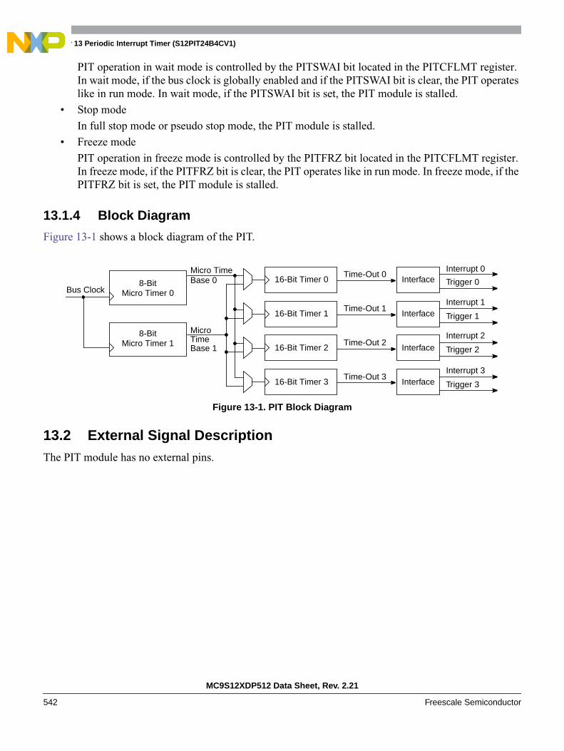
Chapter 13 Periodic Interrupt Timer (S12PIT24B4CV1)
MC9S12XDP512 Data Sheet, Rev. 2.21
542 Freescale Semiconductor
PIT operation in wait mode is controlled by the PITSWAI bit located in the PITCFLMT register.In wait mode, if the bus clock is globally enabled and if the PITSWAI bit is clear, the PIT operateslike in run mode. In wait mode, if the PITSWAI bit is set, the PIT module is stalled.
• Stop mode
In full stop mode or pseudo stop mode, the PIT module is stalled.
• Freeze mode
PIT operation in freeze mode is controlled by the PITFRZ bit located in the PITCFLMT register.In freeze mode, if the PITFRZ bit is clear, the PIT operates like in run mode. In freeze mode, if thePITFRZ bit is set, the PIT module is stalled.
13.1.4 Block Diagram
Figure 13-1 shows a block diagram of the PIT.
Figure 13-1. PIT Block Diagram
13.2 External Signal DescriptionThe PIT module has no external pins.
Time-Out 0
Time-Out 1
Time-Out 2
Time-Out 3
16-Bit Timer 1
16-Bit Timer 3
16-Bit Timer 0
16-Bit Timer 2
Bus Clock
Micro TimeBase 0
MicroTimeBase 1
Interrupt 0
Trigger 0Interface
Interrupt 1
Trigger 1Interface
Interrupt 2
Trigger 2Interface
Interrupt 3
Trigger 3Interface
8-BitMicro Timer 0
8-BitMicro Timer 1
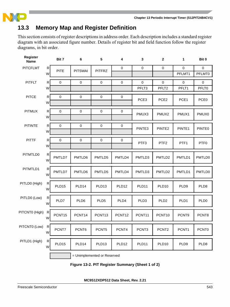
Chapter 13 Periodic Interrupt Timer (S12PIT24B4CV1)
MC9S12XDP512 Data Sheet, Rev. 2.21
Freescale Semiconductor 543
13.3 Memory Map and Register DefinitionThis section consists of register descriptions in address order. Each description includes a standard registerdiagram with an associated figure number. Details of register bit and field function follow the registerdiagrams, in bit order.
RegisterName
Bit 7 6 5 4 3 2 1 Bit 0
PITCFLMT RPITE PITSWAI PITFRZ
0 0 0 0 0
W PFLMT1 PFLMT0
PITFLT R 0 0 0 0 0 0 0 0
W PFLT3 PFLT2 PFLT1 PFLT0
PITCE R 0 0 0 0PCE3 PCE2 PCE1 PCE0
W
PITMUX R 0 0 0 0PMUX3 PMUX2 PMUX1 PMUX0
W
PITINTE R 0 0 0 0PINTE3 PINTE2 PINTE1 PINTE0
W
PITTF R 0 0 0 0PTF3 PTF2 PTF1 PTF0
W
PITMTLD0 RPMTLD7 PMTLD6 PMTLD5 PMTLD4 PMTLD3 PMTLD2 PMTLD1 PMTLD0
W
PITMTLD1 RPMTLD7 PMTLD6 PMTLD5 PMTLD4 PMTLD3 PMTLD2 PMTLD1 PMTLD0
W
PITLD0 (High) RPLD15 PLD14 PLD13 PLD12 PLD11 PLD10 PLD9 PLD8
W
PITLD0 (Low) RPLD7 PLD6 PLD5 PLD4 PLD3 PLD2 PLD1 PLD0
W
PITCNT0 (High) RPCNT15 PCNT14 PCNT13 PCNT12 PCNT11 PCNT10 PCNT9 PCNT8
W
PITCNT0 (Low) RPCNT7 PCNT6 PCNT5 PCNT4 PCNT3 PCNT2 PCNT1 PCNT0
W
PITLD1 (High) RPLD15 PLD14 PLD13 PLD12 PLD11 PLD10 PLD9 PLD8
W
= Unimplemented or Reserved
Figure 13-2. PIT Register Summary (Sheet 1 of 2)
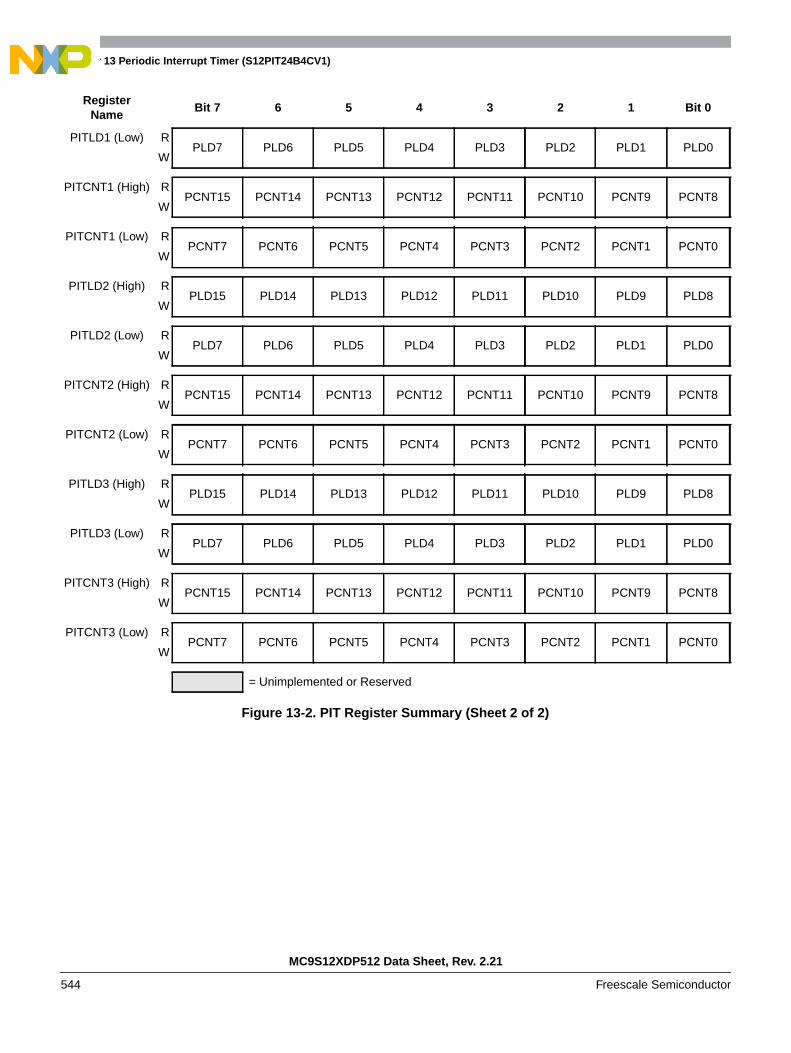
Chapter 13 Periodic Interrupt Timer (S12PIT24B4CV1)
MC9S12XDP512 Data Sheet, Rev. 2.21
544 Freescale Semiconductor
PITLD1 (Low) RPLD7 PLD6 PLD5 PLD4 PLD3 PLD2 PLD1 PLD0
W
PITCNT1 (High) RPCNT15 PCNT14 PCNT13 PCNT12 PCNT11 PCNT10 PCNT9 PCNT8
W
PITCNT1 (Low) RPCNT7 PCNT6 PCNT5 PCNT4 PCNT3 PCNT2 PCNT1 PCNT0
W
PITLD2 (High) RPLD15 PLD14 PLD13 PLD12 PLD11 PLD10 PLD9 PLD8
W
PITLD2 (Low) RPLD7 PLD6 PLD5 PLD4 PLD3 PLD2 PLD1 PLD0
W
PITCNT2 (High) RPCNT15 PCNT14 PCNT13 PCNT12 PCNT11 PCNT10 PCNT9 PCNT8
W
PITCNT2 (Low) RPCNT7 PCNT6 PCNT5 PCNT4 PCNT3 PCNT2 PCNT1 PCNT0
W
PITLD3 (High) RPLD15 PLD14 PLD13 PLD12 PLD11 PLD10 PLD9 PLD8
W
PITLD3 (Low) RPLD7 PLD6 PLD5 PLD4 PLD3 PLD2 PLD1 PLD0
W
PITCNT3 (High) RPCNT15 PCNT14 PCNT13 PCNT12 PCNT11 PCNT10 PCNT9 PCNT8
W
PITCNT3 (Low) RPCNT7 PCNT6 PCNT5 PCNT4 PCNT3 PCNT2 PCNT1 PCNT0
W
RegisterName
Bit 7 6 5 4 3 2 1 Bit 0
= Unimplemented or Reserved
Figure 13-2. PIT Register Summary (Sheet 2 of 2)
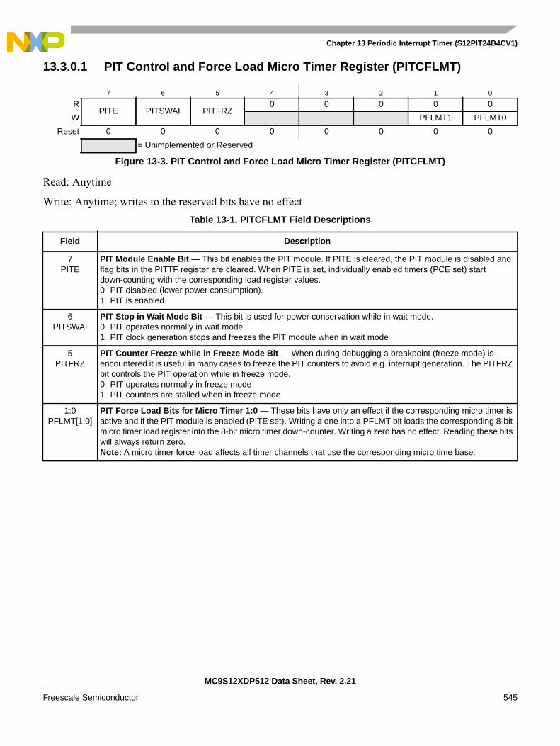
Chapter 13 Periodic Interrupt Timer (S12PIT24B4CV1)
MC9S12XDP512 Data Sheet, Rev. 2.21
Freescale Semiconductor 545
13.3.0.1 PIT Control and Force Load Micro Timer Register (PITCFLMT)
Read: Anytime
Write: Anytime; writes to the reserved bits have no effect
7 6 5 4 3 2 1 0
RPITE PITSWAI PITFRZ
0 0 0 0 0
W PFLMT1 PFLMT0
Reset 0 0 0 0 0 0 0 0
= Unimplemented or Reserved
Figure 13-3. PIT Control and Force Load Micro Timer Register (PITCFLMT)
Table 13-1. PITCFLMT Field Descriptions
Field Description
7PITE
PIT Module Enable Bit — This bit enables the PIT module. If PITE is cleared, the PIT module is disabled andflag bits in the PITTF register are cleared. When PITE is set, individually enabled timers (PCE set) startdown-counting with the corresponding load register values.0 PIT disabled (lower power consumption).1 PIT is enabled.
6PITSWAI
PIT Stop in Wait Mode Bit — This bit is used for power conservation while in wait mode.0 PIT operates normally in wait mode1 PIT clock generation stops and freezes the PIT module when in wait mode
5PITFRZ
PIT Counter Freeze while in Freeze Mode Bit — When during debugging a breakpoint (freeze mode) isencountered it is useful in many cases to freeze the PIT counters to avoid e.g. interrupt generation. The PITFRZbit controls the PIT operation while in freeze mode.0 PIT operates normally in freeze mode1 PIT counters are stalled when in freeze mode
1:0PFLMT[1:0]
PIT Force Load Bits for Micro Timer 1:0 — These bits have only an effect if the corresponding micro timer isactive and if the PIT module is enabled (PITE set). Writing a one into a PFLMT bit loads the corresponding 8-bitmicro timer load register into the 8-bit micro timer down-counter. Writing a zero has no effect. Reading these bitswill always return zero.Note: A micro timer force load affects all timer channels that use the corresponding micro time base.

Chapter 13 Periodic Interrupt Timer (S12PIT24B4CV1)
MC9S12XDP512 Data Sheet, Rev. 2.21
546 Freescale Semiconductor
13.3.0.2 PIT Force Load Timer Register (PITFLT)
Read: Anytime
Write: Anytime; writes to the reserved bits have no effect
13.3.0.3 PIT Channel Enable Register (PITCE)
Read: Anytime
Write: Anytime; writes to the reserved bits have no effect
7 6 5 4 3 2 1 0
R 0 0 0 0 0 0 0 0
W PFLT3 PFLT2 PFLT1 PFLT0
Reset 0 0 0 0 0 0 0 0
= Unimplemented or Reserved
Figure 13-4. PIT Force Load Timer Register (PITFLT)
Table 13-2. PITFLT Field Descriptions
Field Description
3:0PFLT[3:0]
PIT Force Load Bits for Timer 3-0 — These bits have only an effect if the corresponding timer channel (PCEset) is enabled and if the PIT module is enabled (PITE set). Writing a one into a PFLT bit loads the corresponding16-bit timer load register into the 16-bit timer down-counter. Writing a zero has no effect. Reading these bits willalways return zero.
7 6 5 4 3 2 1 0
R 0 0 0 0PCE3 PCE2 PCE1 PCE0
W
Reset 0 0 0 0 0 0 0 0
= Unimplemented or Reserved
Figure 13-5. PIT Channel Enable Register (PITCE)
Table 13-3. PITCE Field Descriptions
Field Description
3:0PCE[3:0]
PIT Enable Bits for Timer Channel 3:0 — These bits enable the PIT channels 3-0. If PCE is cleared, the PITchannel is disabled and the corresponding flag bit in the PITTF register is cleared. When PCE is set, and if thePIT module is enabled (PITE = 1) the 16-bit timer counter is loaded with the start count value and startsdown-counting.0 The corresponding PIT channel is disabled.1 The corresponding PIT channel is enabled.
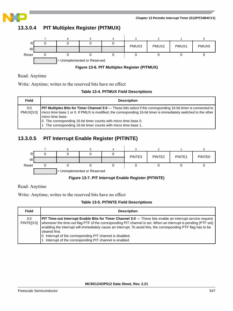
Chapter 13 Periodic Interrupt Timer (S12PIT24B4CV1)
MC9S12XDP512 Data Sheet, Rev. 2.21
Freescale Semiconductor 547
13.3.0.4 PIT Multiplex Register (PITMUX)
Read: Anytime
Write: Anytime; writes to the reserved bits have no effect
13.3.0.5 PIT Interrupt Enable Register (PITINTE)
Read: Anytime
Write: Anytime; writes to the reserved bits have no effect
7 6 5 4 3 2 1 0
R 0 0 0 0PMUX3 PMUX2 PMUX1 PMUX0
W
Reset 0 0 0 0 0 0 0 0
= Unimplemented or Reserved
Figure 13-6. PIT Multiplex Register (PITMUX)
Table 13-4. PITMUX Field Descriptions
Field Description
3:0PMUX[3:0]
PIT Multiplex Bits for Timer Channel 3:0 — These bits select if the corresponding 16-bit timer is connected tomicro time base 1 or 0. If PMUX is modified, the corresponding 16-bit timer is immediately switched to the othermicro time base.0 The corresponding 16-bit timer counts with micro time base 0.1 The corresponding 16-bit timer counts with micro time base 1.
7 6 5 4 3 2 1 0
R 0 0 0 0PINTE3 PINTE2 PINTE1 PINTE0
W
Reset 0 0 0 0 0 0 0 0
= Unimplemented or Reserved
Figure 13-7. PIT Interrupt Enable Register (PITINTE)
Table 13-5. PITINTE Field Descriptions
Field Description
3:0PINTE[3:0]
PIT Time-out Interrupt Enable Bits for Timer Channel 3:0 — These bits enable an interrupt service requestwhenever the time-out flag PTF of the corresponding PIT channel is set. When an interrupt is pending (PTF set)enabling the interrupt will immediately cause an interrupt. To avoid this, the corresponding PTF flag has to becleared first.0 Interrupt of the corresponding PIT channel is disabled.1 Interrupt of the corresponding PIT channel is enabled.
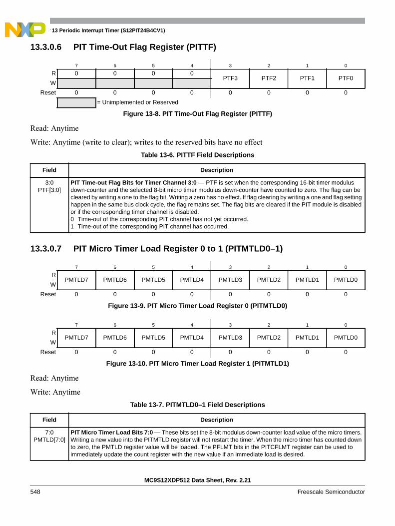
Chapter 13 Periodic Interrupt Timer (S12PIT24B4CV1)
MC9S12XDP512 Data Sheet, Rev. 2.21
548 Freescale Semiconductor
13.3.0.6 PIT Time-Out Flag Register (PITTF)
Read: Anytime
Write: Anytime (write to clear); writes to the reserved bits have no effect
13.3.0.7 PIT Micro Timer Load Register 0 to 1 (PITMTLD0–1)
Read: Anytime
Write: Anytime
7 6 5 4 3 2 1 0
R 0 0 0 0PTF3 PTF2 PTF1 PTF0
W
Reset 0 0 0 0 0 0 0 0
= Unimplemented or Reserved
Figure 13-8. PIT Time-Out Flag Register (PITTF)
Table 13-6. PITTF Field Descriptions
Field Description
3:0PTF[3:0]
PIT Time-out Flag Bits for Timer Channel 3:0 — PTF is set when the corresponding 16-bit timer modulusdown-counter and the selected 8-bit micro timer modulus down-counter have counted to zero. The flag can becleared by writing a one to the flag bit. Writing a zero has no effect. If flag clearing by writing a one and flag settinghappen in the same bus clock cycle, the flag remains set. The flag bits are cleared if the PIT module is disabledor if the corresponding timer channel is disabled.0 Time-out of the corresponding PIT channel has not yet occurred.1 Time-out of the corresponding PIT channel has occurred.
7 6 5 4 3 2 1 0
RPMTLD7 PMTLD6 PMTLD5 PMTLD4 PMTLD3 PMTLD2 PMTLD1 PMTLD0
W
Reset 0 0 0 0 0 0 0 0
Figure 13-9. PIT Micro Timer Load Register 0 (PITMTLD0)
7 6 5 4 3 2 1 0
RPMTLD7 PMTLD6 PMTLD5 PMTLD4 PMTLD3 PMTLD2 PMTLD1 PMTLD0
W
Reset 0 0 0 0 0 0 0 0
Figure 13-10. PIT Micro Timer Load Register 1 (PITMTLD1)
Table 13-7. PITMTLD0–1 Field Descriptions
Field Description
7:0PMTLD[7:0]
PIT Micro Timer Load Bits 7:0 — These bits set the 8-bit modulus down-counter load value of the micro timers.Writing a new value into the PITMTLD register will not restart the timer. When the micro timer has counted downto zero, the PMTLD register value will be loaded. The PFLMT bits in the PITCFLMT register can be used toimmediately update the count register with the new value if an immediate load is desired.
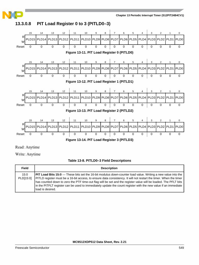
Chapter 13 Periodic Interrupt Timer (S12PIT24B4CV1)
MC9S12XDP512 Data Sheet, Rev. 2.21
Freescale Semiconductor 549
13.3.0.8 PIT Load Register 0 to 3 (PITLD0–3)
Read: Anytime
Write: Anytime
15 14 13 12 11 10 9 8 7 6 5 4 3 2 1 0
RPLD15 PLD14 PLD13 PLD12 PLD11 PLD10 PLD9 PLD8 PLD7 PLD6 PLD5 PLD4 PLD3 PLD2 PLD1 PLD0
W
Reset 0 0 0 0 0 0 0 0 0 0 0 0 0 0 0 0
Figure 13-11. PIT Load Register 0 (PITLD0)
15 14 13 12 11 10 9 8 7 6 5 4 3 2 1 0
RPLD15 PLD14 PLD13 PLD12 PLD11 PLD10 PLD9 PLD8 PLD7 PLD6 PLD5 PLD4 PLD3 PLD2 PLD1 PLD0
W
Reset 0 0 0 0 0 0 0 0 0 0 0 0 0 0 0 0
Figure 13-12. PIT Load Register 1 (PITLD1)
15 14 13 12 11 10 9 8 7 6 5 4 3 2 1 0
RPLD15 PLD14 PLD13 PLD12 PLD11 PLD10 PLD9 PLD8 PLD7 PLD6 PLD5 PLD4 PLD3 PLD2 PLD1 PLD0
W
Reset 0 0 0 0 0 0 0 0 0 0 0 0 0 0 0 0
Figure 13-13. PIT Load Register 2 (PITLD2)
15 14 13 12 11 10 9 8 7 6 5 4 3 2 1 0
RPLD15 PLD14 PLD13 PLD12 PLD11 PLD10 PLD9 PLD8 PLD7 PLD6 PLD5 PLD4 PLD3 PLD2 PLD1 PLD0
W
Reset 0 0 0 0 0 0 0 0 0 0 0 0 0 0 0 0
Figure 13-14. PIT Load Register 3 (PITLD3)
Table 13-8. PITLD0–3 Field Descriptions
Field Description
15:0PLD[15:0]
PIT Load Bits 15:0 — These bits set the 16-bit modulus down-counter load value. Writing a new value into thePITLD register must be a 16-bit access, to ensure data consistency. It will not restart the timer. When the timerhas counted down to zero the PTF time-out flag will be set and the register value will be loaded. The PFLT bitsin the PITFLT register can be used to immediately update the count register with the new value if an immediateload is desired.

Chapter 13 Periodic Interrupt Timer (S12PIT24B4CV1)
MC9S12XDP512 Data Sheet, Rev. 2.21
550 Freescale Semiconductor
13.3.0.9 PIT Count Register 0 to 3 (PITCNT0–3)
Read: Anytime
Write: Has no meaning or effect
15 14 13 12 11 10 9 8 7 6 5 4 3 2 1 0
R PCNT15
PCNT14
PCNT13
PCNT12
PCNT11
PCNT10
PCNT9
PCNT8
PCNT7
PCNT6
PCNT5
PCNT4
PCNT3
PCNT2
PCNT1
PCNT0W
Reset 0 0 0 0 0 0 0 0 0 0 0 0 0 0 0 0
Figure 13-15. PIT Count Register 0 (PITCNT0)
15 14 13 12 11 10 9 8 7 6 5 4 3 2 1 0
R PCNT15
PCNT14
PCNT13
PCNT12
PCNT11
PCNT10
PCNT9
PCNT8
PCNT7
PCNT6
PCNT5
PCNT4
PCNT3
PCNT2
PCNT1
PCNT0W
Reset 0 0 0 0 0 0 0 0 0 0 0 0 0 0 0 0
Figure 13-16. PIT Count Register 1 (PITCNT1)
15 14 13 12 11 10 9 8 7 6 5 4 3 2 1 0
R PCNT15
PCNT14
PCNT13
PCNT12
PCNT11
PCNT10
PCNT9
PCNT8
PCNT7
PCNT6
PCNT5
PCNT4
PCNT3
PCNT2
PCNT1
PCNT0W
Reset 0 0 0 0 0 0 0 0 0 0 0 0 0 0 0 0
Figure 13-17. PIT Count Register 2 (PITCNT2)
15 14 13 12 11 10 9 8 7 6 5 4 3 2 1 0
R PCNT15
PCNT14
PCNT13
PCNT12
PCNT11
PCNT10
PCNT9
PCNT8
PCNT7
PCNT6
PCNT5
PCNT4
PCNT3
PCNT2
PCNT1
PCNT0W
Reset 0 0 0 0 0 0 0 0 0 0 0 0 0 0 0 0
Figure 13-18. PIT Count Register 3 (PITCNT3)
Table 13-9. PITCNT0–3 Field Descriptions
Field Description
15:0PCNT[15:0]
PIT Count Bits 15-0 — These bits represent the current 16-bit modulus down-counter value. The read accessfor the count register must take place in one clock cycle as a 16-bit access.
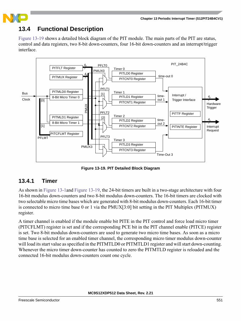
Chapter 13 Periodic Interrupt Timer (S12PIT24B4CV1)
MC9S12XDP512 Data Sheet, Rev. 2.21
Freescale Semiconductor 551
13.4 Functional DescriptionFigure 13-19 shows a detailed block diagram of the PIT module. The main parts of the PIT are status,control and data registers, two 8-bit down-counters, four 16-bit down-counters and an interrupt/triggerinterface.
Figure 13-19. PIT Detailed Block Diagram
13.4.1 Timer
As shown in Figure 13-1and Figure 13-19, the 24-bit timers are built in a two-stage architecture with four16-bit modulus down-counters and two 8-bit modulus down-counters. The 16-bit timers are clocked withtwo selectable micro time bases which are generated with 8-bit modulus down-counters. Each 16-bit timeris connected to micro time base 0 or 1 via the PMUX[3:0] bit setting in the PIT Multiplex (PITMUX)register.
A timer channel is enabled if the module enable bit PITE in the PIT control and force load micro timer(PITCFLMT) register is set and if the corresponding PCE bit in the PIT channel enable (PITCE) registeris set. Two 8-bit modulus down-counters are used to generate two micro time bases. As soon as a microtime base is selected for an enabled timer channel, the corresponding micro timer modulus down-counterwill load its start value as specified in the PITMTLD0 or PITMTLD1 register and will start down-counting.Whenever the micro timer down-counter has counted to zero the PITMTLD register is reloaded and theconnected 16-bit modulus down-counters count one cycle.
PITMLD0 Register
8-Bit Micro Timer 0
PITCFLMT Register
PITLD0 Register
PITMLD1 Register
8-Bit Micro Timer 1
PITMUX Register
PITFLT Register
PITCNT0 Register
Timer 0PMUX0
PFLT04
4
PITTF Register
PITINTE Register
Interrupt /
HardwareTrigger
4
InterruptRequest
4
PITLD1 Register
PITCNT1 Register
Timer 1[1]
PFLT1
PITLD2 Register
PITCNT2 Register
Timer 2[2]
PFLT2
PITLD3 Register
PITCNT3 Register
Timer 3
PMUX3
PFLT3
time-out 0
time-out 1
time-out 2
Time-Out 3
PFLMT
[1]
[0]
PM
UX
Trigger Interface
Bus
Clock
PIT_24B4C
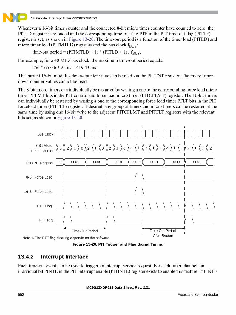
Chapter 13 Periodic Interrupt Timer (S12PIT24B4CV1)
MC9S12XDP512 Data Sheet, Rev. 2.21
552 Freescale Semiconductor
Whenever a 16-bit timer counter and the connected 8-bit micro timer counter have counted to zero, thePITLD register is reloaded and the corresponding time-out flag PTF in the PIT time-out flag (PITTF)register is set, as shown in Figure 13-20. The time-out period is a function of the timer load (PITLD) andmicro timer load (PITMTLD) registers and the bus clock fBUS:
time-out period = (PITMTLD + 1) * (PITLD + 1) / fBUS.
For example, for a 40 MHz bus clock, the maximum time-out period equals:
256 * 65536 * 25 ns = 419.43 ms.
The current 16-bit modulus down-counter value can be read via the PITCNT register. The micro timerdown-counter values cannot be read.
The 8-bit micro timers can individually be restarted by writing a one to the corresponding force load microtimer PFLMT bits in the PIT control and force load micro timer (PITCFLMT) register. The 16-bit timerscan individually be restarted by writing a one to the corresponding force load timer PFLT bits in the PITforceload timer (PITFLT) register. If desired, any group of timers and micro timers can be restarted at thesame time by using one 16-bit write to the adjacent PITCFLMT and PITFLT registers with the relevantbits set, as shown in Figure 13-20.
Figure 13-20. PIT Trigger and Flag Signal Timing
13.4.2 Interrupt Interface
Each time-out event can be used to trigger an interrupt service request. For each timer channel, anindividual bit PINTE in the PIT interrupt enable (PITINTE) register exists to enable this feature. If PINTE
Bus Clock
0 2 1 08-Bit Micro
2 1 0 2 1 0 2 1 2 1 0
PITCNT Register 0001 000000 0001 0000
8-Bit Force Load
2 1 02 1 0
PTF Flag1
PITTRIG
16-Bit Force Load
0001 0000 0001
2
Time-Out PeriodTime-Out PeriodAfter Restart
Timer Counter
Note 1. The PTF flag clearing depends on the software
Chapter 13 Periodic Interrupt Timer (S12PIT24B4CV1)
MC9S12XDP512 Data Sheet, Rev. 2.21
Freescale Semiconductor 553
is set, an interrupt service is requested whenever the corresponding time-out flag PTF in the PIT time-outflag (PITTF) register is set. The flag can be cleared by writing a one to the flag bit.
NOTEBe careful when resetting the PITE, PINTE or PITCE bits in case of pendingPIT interrupt requests, to avoid spurious interrupt requests.
13.4.3 Hardware Trigger
The PIT module contains four hardware trigger signal lines PITTRIG[3:0], one for each timer channel.These signals can be connected on SoC level to peripheral modules enabling e.g. periodic ATD conversion(please refer to the SoC Guide for the mapping of PITTRIG[3:0] signals to peripheral modules).
Whenever a timer channel time-out is reached, the corresponding PTF flag is set and the correspondingtrigger signal PITTRIG triggers a rising edge. The trigger feature requires a minimum time-out period oftwo bus clock cycles because the trigger is asserted high for at least one bus clock cycle. For load registervalues PITLD = 0x0001 and PITMTLD = 0x0002 the flag setting, trigger timing and a restart with forceload is shown in Figure 13-20.
13.5 Initialization/Application Information
13.5.1 Startup
Set the configuration registers before the PITE bit in the PITCFLMT register is set. Before PITE is set, theconfiguration registers can be written in arbitrary order.
13.5.2 Shutdown
When the PITCE register bits, the PITINTE register bits or the PITE bit in the PITCFLMT register arecleared, the corresponding PIT interrupt flags are cleared. In case of a pending PIT interrupt request, aspurious interrupt can be generated. Two strategies, which avoid spurious interrupts, are recommended:
1. Reset the PIT interrupt flags only in an ISR. When entering the ISR, the I mask bit in the CCR isset automatically. The I mask bit must not be cleared before the PIT interrupt flags are cleared.
2. After setting the I mask bit with the SEI instruction, the PIT interrupt flags can be cleared. Thenclear the I mask bit with the CLI instruction to re-enable interrupts.
13.5.3 Flag Clearing
A flag is cleared by writing a one to the flag bit. Always use store or move instructions to write a one incertain bit positions. Do not use the BSET instructions. Do not use any C-constructs that compile to BSETinstructions. “BSET flag_register, #mask” must not be used for flag clearing because BSET is aread-modify-write instruction which writes back the “bit-wise or” of the flag_register and the mask intothe flag_register. BSET would clear all flag bits that were set, independent from the mask.
For example, to clear flag bit 0 use: MOVB #$01,PITTF.

Chapter 13 Periodic Interrupt Timer (S12PIT24B4CV1)
MC9S12XDP512 Data Sheet, Rev. 2.21
554 Freescale Semiconductor
MC9S12XDP512 Data Sheet, Rev. 2.21
Freescale Semiconductor 555
Chapter 14Voltage Regulator (S12VREG3V3V5)
14.1 IntroductionModule VREG_3V3 is a dual output voltage regulator that provides two separate 2.5V (typical) suppliesdiffering in the amount of current that can be sourced. The regulator input voltage range is from 3.3V upto 5V (typical).
14.1.1 Features
Module VREG_3V3 includes these distinctive features:
• Two parallel, linear voltage regulators— Bandgap reference
• Low-voltage detect (LVD) with low-voltage interrupt (LVI)• Power-on reset (POR)• Low-voltage reset (LVR)• Autonomous periodical interrupt (API)
14.1.2 Modes of Operation
There are three modes VREG_3V3 can operate in:
1. Full performance mode (FPM) (MCU is not in stop mode)The regulator is active, providing the nominal supply voltage of 2.5 V with full current sourcingcapability at both outputs. Features LVD (low-voltage detect), LVR (low-voltage reset), and POR(power-on reset) are available. The API is available.
2. Reduced power mode (RPM) (MCU is in stop mode)The purpose is to reduce power consumption of the device. The output voltage may degrade to alower value than in full performance mode, additionally the current sourcing capability issubstantially reduced. Only the POR is available in this mode, LVD and LVR are disabled. The APIis available.
3. Shutdown modeControlled by VREGEN (see device level specification for connectivity of VREGEN).
This mode is characterized by minimum power consumption. The regulator outputs are in ahigh-impedance state, only the POR feature is available, LVD and LVR are disabled. The APIinternal RC oscillator clock is not available.
This mode must be used to disable the chip internal regulator VREG_3V3, i.e., to bypass theVREG_3V3 to use external supplies.

Chapter 14 Voltage Regulator (S12VREG3V3V5)
MC9S12XDP512 Data Sheet, Rev. 2.21
556 Freescale Semiconductor
14.1.3 Block Diagram
Figure 14-1 shows the function principle of VREG_3V3 by means of a block diagram. The regulator coreREG consists of two parallel subblocks, REG1 and REG2, providing two independent output voltages.
Figure 14-1. VREG_3V3 Block Diagram
LVRLVD POR
VDDR
VDD
LVI
PORLVR
CTRL
VSS
VDDPLL
VSSPLL
VREGEN
RE
G
REG2
REG1
PIN
VDDA
VSSA
REG: Regulator Core
CTRL: Regulator Control
LVD: Low-Voltage Detect
LVR: Low-Voltage Reset
POR: Power-On Reset
APIAPI
API: Auto. Periodical Interrupt
VBG
APIRateSelect
Bus Clock

Chapter 14 Voltage Regulator (S12VREG3V3V5)
MC9S12XDP512 Data Sheet, Rev. 2.21
Freescale Semiconductor 557
14.2 External Signal DescriptionDue to the nature of VREG_3V3 being a voltage regulator providing the chip internal power supplyvoltages, most signals are power supply signals connected to pads.
Table 14-1 shows all signals of VREG_3V3 associated with pins.
NOTECheck device level specification for connectivity of the signals.
14.2.1 VDDR — Regulator Power Input Pins
Signal VDDR is the power input of VREG_3V3. All currents sourced into the regulator loads flow throughthis pin. A chip external decoupling capacitor (>=100 nF, X7R ceramic) between VDDR and VSSR (if VSSRis not available VSS) can smooth ripple on VDDR.
For entering Shutdown Mode, pin VDDR should also be tied to ground on devices without VREGEN pin.
14.2.2 VDDA, VSSA — Regulator Reference Supply Pins
Signals VDDA/VSSA, which are supposed to be relatively quiet, are used to supply the analog parts of theregulator. Internal precision reference circuits are supplied from these signals. A chip external decouplingcapacitor (>=100 nF, X7R ceramic) between VDDA and VSSA can further improve the quality of thissupply.
14.2.3 VDD, VSS — Regulator Output1 (Core Logic) Pins
Signals VDD/VSS are the primary outputs of VREG_3V3 that provide the power supply for the core logic.These signals are connected to device pins to allow external decoupling capacitors (220 nF, X7R ceramic).
In Shutdown Mode an external supply driving VDD/VSS can replace the voltage regulator.
Table 14-1. Signal Properties
Name Function Reset State Pull Up
VDDR Power input (positive supply) — —
VDDA Quiet input (positive supply) — —
VSSA Quiet input (ground) — —
VDD Primary output (positive supply) — —
VSS Primary output (ground) — —
VDDPLL Secondary output (positive supply) — —
VSSPLL Secondary output (ground) — —
VREGEN (optional) Optional Regulator Enable — —
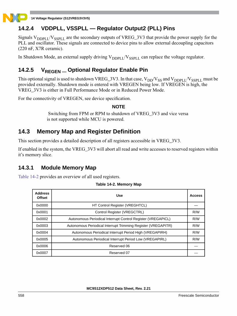
Chapter 14 Voltage Regulator (S12VREG3V3V5)
MC9S12XDP512 Data Sheet, Rev. 2.21
558 Freescale Semiconductor
14.2.4 VDDPLL, VSSPLL — Regulator Output2 (PLL) Pins
Signals VDDPLL/VSSPLL are the secondary outputs of VREG_3V3 that provide the power supply for thePLL and oscillator. These signals are connected to device pins to allow external decoupling capacitors(220 nF, X7R ceramic).
In Shutdown Mode, an external supply driving VDDPLL/VSSPLL can replace the voltage regulator.
14.2.5 VREGEN — Optional Regulator Enable Pin
This optional signal is used to shutdown VREG_3V3. In that case, VDD/VSS and VDDPLL/VSSPLL must beprovided externally. Shutdown mode is entered with VREGEN being low. If VREGEN is high, theVREG_3V3 is either in Full Performance Mode or in Reduced Power Mode.
For the connectivity of VREGEN, see device specification.
NOTE Switching from FPM or RPM to shutdown of VREG_3V3 and vice versais not supported while MCU is powered.
14.3 Memory Map and Register DefinitionThis section provides a detailed description of all registers accessible in VREG_3V3.
If enabled in the system, the VREG_3V3 will abort all read and write accesses to reserved registers withinit’s memory slice.
14.3.1 Module Memory Map
Table 14-2 provides an overview of all used registers.
Table 14-2. Memory Map
AddressOffset
Use Access
0x0000 HT Control Register (VREGHTCL) —
0x0001 Control Register (VREGCTRL) R/W
0x0002 Autonomous Periodical Interrupt Control Register (VREGAPICL) R/W
0x0003 Autonomous Periodical Interrupt Trimming Register (VREGAPITR) R/W
0x0004 Autonomous Periodical Interrupt Period High (VREGAPIRH) R/W
0x0005 Autonomous Periodical Interrupt Period Low (VREGAPIRL) R/W
0x0006 Reserved 06 —
0x0007 Reserved 07 —
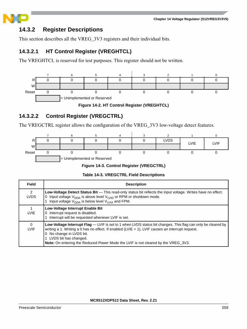
Chapter 14 Voltage Regulator (S12VREG3V3V5)
MC9S12XDP512 Data Sheet, Rev. 2.21
Freescale Semiconductor 559
14.3.2 Register Descriptions
This section describes all the VREG_3V3 registers and their individual bits.
14.3.2.1 HT Control Register (VREGHTCL)
The VREGHTCL is reserved for test purposes. This register should not be written.
14.3.2.2 Control Register (VREGCTRL)
The VREGCTRL register allows the configuration of the VREG_3V3 low-voltage detect features.
7 6 5 4 3 2 1 0
R 0 0 0 0 0 0 0 0
W
Reset 0 0 0 0 0 0 0 0
= Unimplemented or Reserved
Figure 14-2. HT Control Register (VREGHTCL)
7 6 5 4 3 2 1 0
R 0 0 0 0 0 LVDSLVIE LVIF
W
Reset 0 0 0 0 0 0 0 0
= Unimplemented or Reserved
Figure 14-3. Control Register (VREGCTRL)
Table 14-3. VREGCTRL Field Descriptions
Field Description
2LVDS
Low-Voltage Detect Status Bit — This read-only status bit reflects the input voltage. Writes have no effect.0 Input voltage VDDA is above level VLVID or RPM or shutdown mode.1 Input voltage VDDA is below level VLVIA and FPM.
1LVIE
Low-Voltage Interrupt Enable Bit0 Interrupt request is disabled.1 Interrupt will be requested whenever LVIF is set.
0LVIF
Low-Voltage Interrupt Flag — LVIF is set to 1 when LVDS status bit changes. This flag can only be cleared bywriting a 1. Writing a 0 has no effect. If enabled (LVIE = 1), LVIF causes an interrupt request.0 No change in LVDS bit.1 LVDS bit has changed.Note: On entering the Reduced Power Mode the LVIF is not cleared by the VREG_3V3.

Chapter 14 Voltage Regulator (S12VREG3V3V5)
MC9S12XDP512 Data Sheet, Rev. 2.21
560 Freescale Semiconductor
14.3.2.3 Autonomous Periodical Interrupt Control Register (VREGAPICL)
The VREGAPICL register allows the configuration of the VREG_3V3 autonomous periodical interruptfeatures.
7 6 5 4 3 2 1 0
RAPICLK
0 0 0 0APIFE APIE APIF
W
Reset 0 0 0 0 0 0 0 0
= Unimplemented or Reserved
Figure 14-4. Autonomous Periodical Interrupt Control Register (VREGAPICL)
Table 14-4. VREGAPICL Field Descriptions
Field Description
7APICLK
Autonomous Periodical Interrupt Clock Select Bit — Selects the clock source for the API. Writable only ifAPIFE = 0; APICLK cannot be changed if APIFE is set by the same write operation.0 Autonomous periodical interrupt clock used as source.1 Bus clock used as source.
2APIFE
Autonomous Periodical Interrupt Feature Enable Bit — Enables the API feature and starts the API timerwhen set.0 Autonomous periodical interrupt is disabled.1 Autonomous periodical interrupt is enabled and timer starts running.
1APIE
Autonomous Periodical Interrupt Enable Bit0 API interrupt request is disabled.1 API interrupt will be requested whenever APIF is set.
0APIF
Autonomous Periodical Interrupt Flag — APIF is set to 1 when the in the API configured time has elapsed.This flag can only be cleared by writing a 1 to it. Clearing of the flag has precedence over setting.Writing a 0 has no effect. If enabled (APIE = 1), APIF causes an interrupt request.0 API timeout has not yet occurred.1 API timeout has occurred.
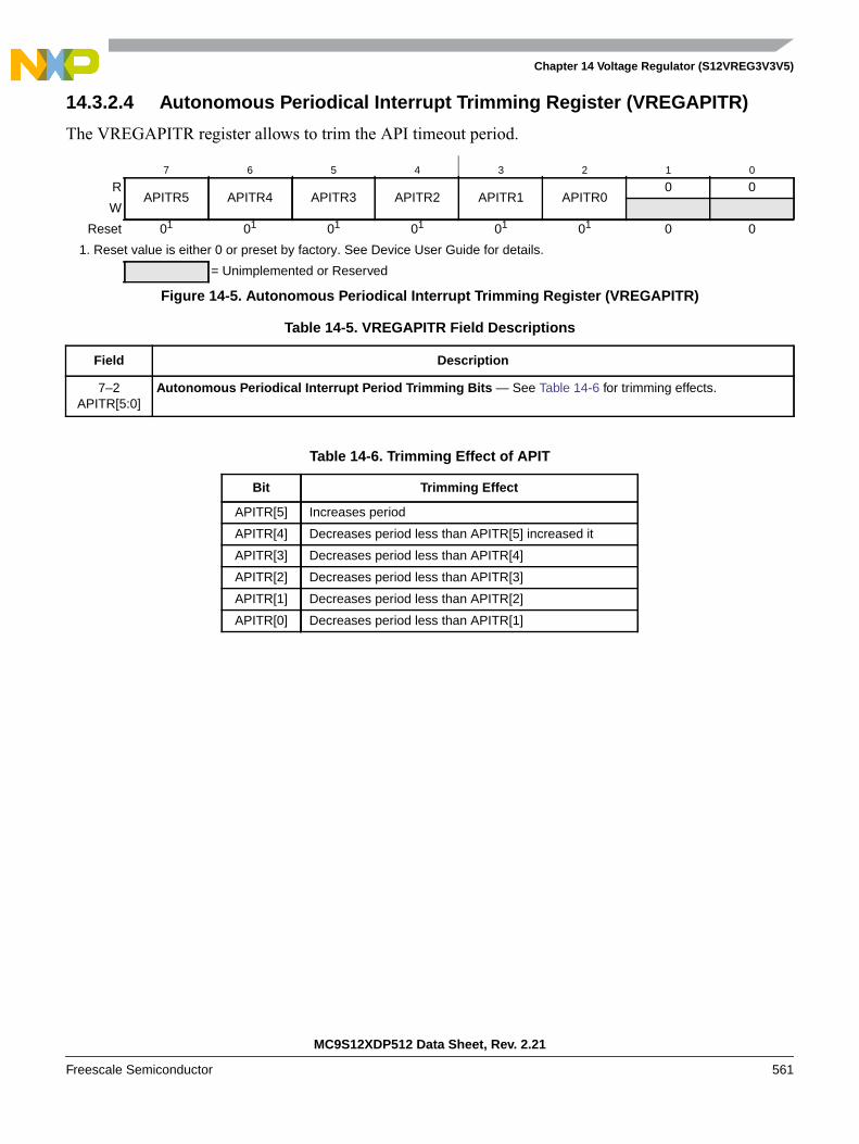
Chapter 14 Voltage Regulator (S12VREG3V3V5)
MC9S12XDP512 Data Sheet, Rev. 2.21
Freescale Semiconductor 561
14.3.2.4 Autonomous Periodical Interrupt Trimming Register (VREGAPITR)
The VREGAPITR register allows to trim the API timeout period.
7 6 5 4 3 2 1 0
RAPITR5 APITR4 APITR3 APITR2 APITR1 APITR0
0 0
W
Reset 01 01 01 01 01 01 0 0
1. Reset value is either 0 or preset by factory. See Device User Guide for details.
= Unimplemented or Reserved
Figure 14-5. Autonomous Periodical Interrupt Trimming Register (VREGAPITR)
Table 14-5. VREGAPITR Field Descriptions
Field Description
7–2APITR[5:0]
Autonomous Periodical Interrupt Period Trimming Bits — See Table 14-6 for trimming effects.
Table 14-6. Trimming Effect of APIT
Bit Trimming Effect
APITR[5] Increases period
APITR[4] Decreases period less than APITR[5] increased it
APITR[3] Decreases period less than APITR[4]
APITR[2] Decreases period less than APITR[3]
APITR[1] Decreases period less than APITR[2]
APITR[0] Decreases period less than APITR[1]

Chapter 14 Voltage Regulator (S12VREG3V3V5)
MC9S12XDP512 Data Sheet, Rev. 2.21
562 Freescale Semiconductor
14.3.2.5 Autonomous Periodical Interrupt Rate High and Low Register(VREGAPIRH / VREGAPIRL)
The VREGAPIRH and VREGAPIRL register allows the configuration of the VREG_3V3 autonomousperiodical interrupt rate.
7 6 5 4 3 2 1 0
R 0 0 0 0APIR11 APIR10 APIR9 APIR8
W
Reset 0 0 0 0 0 0 0 0
= Unimplemented or Reserved
Figure 14-6. Autonomous Periodical Interrupt Rate High Register (VREGAPIRH)
7 6 5 4 3 2 1 0
RAPIR7 APIR6 APIR5 APIR4 APIR3 APIR2 APIR1 APIR0
W
Reset 0 0 0 0 0 0 0 0
Figure 14-7. Autonomous Periodical Interrupt Rate Low Register (VREGAPIRL)
Table 14-7. VREGAPIRH / VREGAPIRL Field Descriptions
Field Description
11-0APIR[11:0]
Autonomous Periodical Interrupt Rate Bits — These bits define the timeout period of the API. See Table 14-8for details of the effect of the autonomous periodical interrupt rate bits. Writable only if APIFE = 0 of VREGAPICLregister.
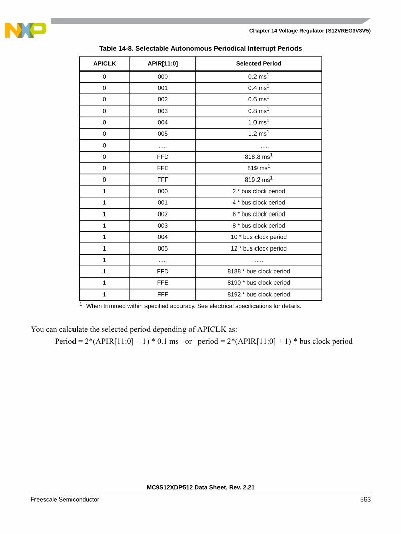
Chapter 14 Voltage Regulator (S12VREG3V3V5)
MC9S12XDP512 Data Sheet, Rev. 2.21
Freescale Semiconductor 563
You can calculate the selected period depending of APICLK as:
Period = 2*(APIR[11:0] + 1) * 0.1 ms or period = 2*(APIR[11:0] + 1) * bus clock period
Table 14-8. Selectable Autonomous Periodical Interrupt Periods
APICLK APIR[11:0] Selected Period
0 000 0.2 ms1
1 When trimmed within specified accuracy. See electrical specifications for details.
0 001 0.4 ms1
0 002 0.6 ms1
0 003 0.8 ms1
0 004 1.0 ms1
0 005 1.2 ms1
0 ..... .....
0 FFD 818.8 ms1
0 FFE 819 ms1
0 FFF 819.2 ms1
1 000 2 * bus clock period
1 001 4 * bus clock period
1 002 6 * bus clock period
1 003 8 * bus clock period
1 004 10 * bus clock period
1 005 12 * bus clock period
1 ..... .....
1 FFD 8188 * bus clock period
1 FFE 8190 * bus clock period
1 FFF 8192 * bus clock period
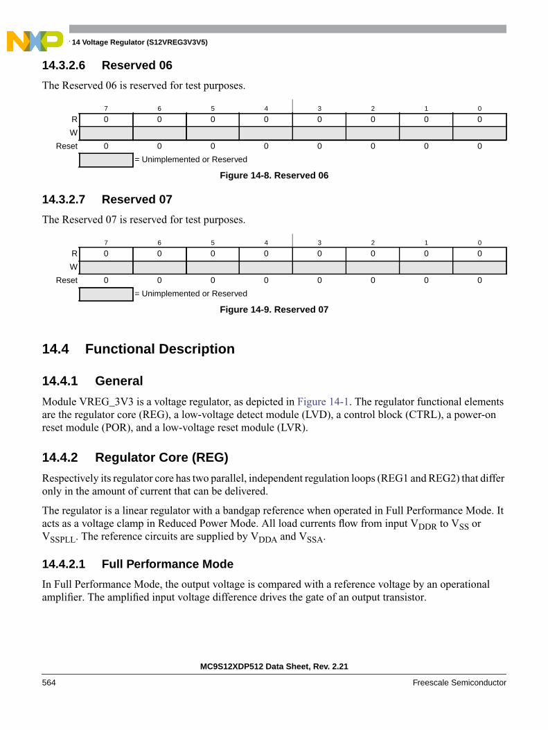
Chapter 14 Voltage Regulator (S12VREG3V3V5)
MC9S12XDP512 Data Sheet, Rev. 2.21
564 Freescale Semiconductor
14.3.2.6 Reserved 06
The Reserved 06 is reserved for test purposes.
14.3.2.7 Reserved 07
The Reserved 07 is reserved for test purposes.
14.4 Functional Description
14.4.1 General
Module VREG_3V3 is a voltage regulator, as depicted in Figure 14-1. The regulator functional elementsare the regulator core (REG), a low-voltage detect module (LVD), a control block (CTRL), a power-onreset module (POR), and a low-voltage reset module (LVR).
14.4.2 Regulator Core (REG)
Respectively its regulator core has two parallel, independent regulation loops (REG1 and REG2) that differonly in the amount of current that can be delivered.
The regulator is a linear regulator with a bandgap reference when operated in Full Performance Mode. Itacts as a voltage clamp in Reduced Power Mode. All load currents flow from input VDDR to VSS orVSSPLL. The reference circuits are supplied by VDDA and VSSA.
14.4.2.1 Full Performance Mode
In Full Performance Mode, the output voltage is compared with a reference voltage by an operationalamplifier. The amplified input voltage difference drives the gate of an output transistor.
7 6 5 4 3 2 1 0
R 0 0 0 0 0 0 0 0
W
Reset 0 0 0 0 0 0 0 0
= Unimplemented or Reserved
Figure 14-8. Reserved 06
7 6 5 4 3 2 1 0
R 0 0 0 0 0 0 0 0
W
Reset 0 0 0 0 0 0 0 0
= Unimplemented or Reserved
Figure 14-9. Reserved 07
Chapter 14 Voltage Regulator (S12VREG3V3V5)
MC9S12XDP512 Data Sheet, Rev. 2.21
Freescale Semiconductor 565
14.4.2.2 Reduced Power Mode
In Reduced Power Mode, the gate of the output transistor is connected directly to a reference voltage toreduce power consumption.
14.4.3 Low-Voltage Detect (LVD)
Subblock LVD is responsible for generating the low-voltage interrupt (LVI). LVD monitors the inputvoltage (VDDA–VSSA) and continuously updates the status flag LVDS. Interrupt flag LVIF is set wheneverstatus flag LVDS changes its value. The LVD is available in FPM and is inactive in Reduced Power Modeor Shutdown Mode.
14.4.4 Power-On Reset (POR)
This functional block monitors VDD. If VDD is below VPORD, POR is asserted; if VDD exceeds VPORD,the POR is deasserted. POR asserted forces the MCU into Reset. POR Deasserted will trigger the power-onsequence.
14.4.5 Low-Voltage Reset (LVR)
Block LVR monitors the primary output voltage VDD. If it drops below the assertion level (VLVRA) signal,LVR asserts; if VDD rises above the deassertion level (VLVRD) signal, LVR deasserts. The LVR functionis available only in Full Performance Mode.
14.4.6 Regulator Control (CTRL)
This part contains the register block of VREG_3V3 and further digital functionality needed to control theoperating modes. CTRL also represents the interface to the digital core logic.
14.4.7 Autonomous Periodical Interrupt (API)
Subblock API can generate periodical interrupts independent of the clock source of the MCU. To enablethe timer, the bit APIFE needs to be set.
The API timer is either clocked by a trimmable internal RC oscillator or the bus clock. Timer operationwill freeze when MCU clock source is selected and bus clock is turned off. See CRG specification fordetails. The clock source can be selected with bit APICLK. APICLK can only be written when APIFE isnot set.
The APIR[11:0] bits determine the interrupt period. APIR[11:0] can only be written when APIFE iscleared. As soon as APIFE is set, the timer starts running for the period selected by APIR[11:0] bits. Whenthe configured time has elapsed, the flag APIF is set. An interrupt, indicated by flag APIF = 1, is triggeredif interrupt enable bit APIE = 1. The timer is started automatically again after it has set APIF.
The procedure to change APICLK or APIR[11:0] is first to clear APIFE, then write to APICLK orAPIR[11:0], and afterwards set APIFE.

Chapter 14 Voltage Regulator (S12VREG3V3V5)
MC9S12XDP512 Data Sheet, Rev. 2.21
566 Freescale Semiconductor
The API Trimming bits APITR[5:0] must be set so the minimum period equals 0.2 ms if stable frequencyis desired.
See Table 14-6 for the trimming effect of APITR.
NOTEThe first period after enabling the counter by APIFE might be reduced.
The API internal RC oscillator clock is not available if VREG_3V3 is inShutdown Mode.
14.4.8 Resets
This section describes how VREG_3V3 controls the reset of the MCU.The reset values of registers andsignals are provided in Section 14.3, “Memory Map and Register Definition”. Possible reset sources arelisted in Table 14-9.
14.4.9 Description of Reset Operation
14.4.9.1 Power-On Reset (POR)
During chip power-up the digital core may not work if its supply voltage VDD is below the PORdeassertion level (VPORD). Therefore, signal POR, which forces the other blocks of the device into reset,is kept high until VDD exceeds VPORD. The MCU will run the start-up sequence after POR deassertion.The power-on reset is active in all operation modes of VREG_3V3.
14.4.9.2 Low-Voltage Reset (LVR)
For details on low-voltage reset, see Section 14.4.5, “Low-Voltage Reset (LVR)”.
14.4.10 Interrupts
This section describes all interrupts originated by VREG_3V3.
The interrupt vectors requested by VREG_3V3 are listed in Table 14-10. Vector addresses and interruptpriorities are defined at MCU level.
Table 14-9. Reset Sources
Reset Source Local Enable
Power-on reset Always active
Low-voltage reset Available only in Full Performance Mode
Table 14-10. Interrupt Vectors
Interrupt Source Local Enable
Low-voltage interrupt (LVI) LVIE = 1; available only in Full PerformanceMode

Chapter 14 Voltage Regulator (S12VREG3V3V5)
MC9S12XDP512 Data Sheet, Rev. 2.21
Freescale Semiconductor 567
14.4.10.1 Low-Voltage Interrupt (LVI)
In FPM, VREG_3V3 monitors the input voltage VDDA. Whenever VDDA drops below level VLVIA, thestatus bit LVDS is set to 1. On the other hand, LVDS is reset to 0 when VDDA rises above level VLVID. Aninterrupt, indicated by flag LVIF = 1, is triggered by any change of the status bit LVDS if interrupt enablebit LVIE = 1.
NOTEOn entering the Reduced Power Mode, the LVIF is not cleared by theVREG_3V3.
14.4.10.2 Autonomous Periodical Interrupt (API)
As soon as the configured timeout period of the API has elapsed, the APIF bit is set. An interrupt, indicatedby flag APIF = 1, is triggered if interrupt enable bit APIE = 1.
Autonomous periodical interrupt (API) APIE = 1
Table 14-10. Interrupt Vectors
Interrupt Source Local Enable

Chapter 14 Voltage Regulator (S12VREG3V3V5)
MC9S12XDP512 Data Sheet, Rev. 2.21
568 Freescale Semiconductor

MC9S12XDP512 Data Sheet, Rev. 2.21
Freescale Semiconductor 569
Chapter 15Background Debug Module (S12XBDMV2)
15.1 IntroductionThis section describes the functionality of the background debug module (BDM) sub-block of theHCS12X core platform.
The background debug module (BDM) sub-block is a single-wire, background debug system implementedin on-chip hardware for minimal CPU intervention. All interfacing with the BDM is done via the BKGDpin.
The BDM has enhanced capability for maintaining synchronization between the target and host whileallowing more flexibility in clock rates. This includes a sync signal to determine the communication rateand a handshake signal to indicate when an operation is complete. The system is backwards compatible tothe BDM of the S12 family with the following exceptions:
• TAGGO command no longer supported by BDM
• External instruction tagging feature now part of DBG module
• BDM register map and register content extended/modified
• Global page access functionality
• Enabled but not active out of reset in emulation modes
• CLKSW bit set out of reset in emulation mode.
• Family ID readable from firmware ROM at global address 0x7FFF0F (value for HCS12X devicesis 0xC1)
15.1.1 Features
The BDM includes these distinctive features:
• Single-wire communication with host development system
• Enhanced capability for allowing more flexibility in clock rates
• SYNC command to determine communication rate
• GO_UNTIL command
• Hardware handshake protocol to increase the performance of the serial communication
• Active out of reset in special single chip mode
• Nine hardware commands using free cycles, if available, for minimal CPU intervention
• Hardware commands not requiring active BDM
• 14 firmware commands execute from the standard BDM firmware lookup table
Chapter 15 Background Debug Module (S12XBDMV2)
MC9S12XDP512 Data Sheet, Rev. 2.21
570 Freescale Semiconductor
• Software control of BDM operation during wait mode
• Software selectable clocks
• Global page access functionality
• Enabled but not active out of reset in emulation modes
• CLKSW bit set out of reset in emulation mode.
• When secured, hardware commands are allowed to access the register space in special single chipmode, if the Flash and EEPROM erase tests fail.
• Family ID readable from firmware ROM at global address 0x7FFF0F (value for HCS12X devicesis 0xC1)
• BDM hardware commands are operational until system stop mode is entered (all bus masters arein stop mode)
15.1.2 Modes of Operation
BDM is available in all operating modes but must be enabled before firmware commands are executed.Some systems may have a control bit that allows suspending the function during background debug mode.
15.1.2.1 Regular Run Modes
All of these operations refer to the part in run mode and not being secured. The BDM does not providecontrols to conserve power during run mode.
• Normal modes
General operation of the BDM is available and operates the same in all normal modes.
• Special single chip mode
In special single chip mode, background operation is enabled and active out of reset. This allowsprogramming a system with blank memory.
• Emulation modes
In emulation mode, background operation is enabled but not active out of reset. This allowsdebugging and programming a system in this mode more easily.
15.1.2.2 Secure Mode Operation
If the device is in secure mode, the operation of the BDM is reduced to a small subset of its regular runmode operation. Secure operation prevents access to Flash or EEPROM other than allowing erasure. Formore information please see Section 15.4.1, “Security”.
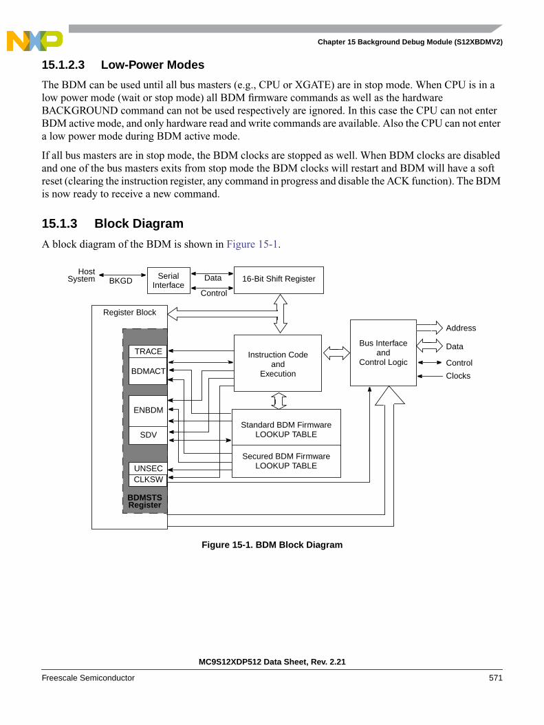
Chapter 15 Background Debug Module (S12XBDMV2)
MC9S12XDP512 Data Sheet, Rev. 2.21
Freescale Semiconductor 571
15.1.2.3 Low-Power Modes
The BDM can be used until all bus masters (e.g., CPU or XGATE) are in stop mode. When CPU is in alow power mode (wait or stop mode) all BDM firmware commands as well as the hardwareBACKGROUND command can not be used respectively are ignored. In this case the CPU can not enterBDM active mode, and only hardware read and write commands are available. Also the CPU can not entera low power mode during BDM active mode.
If all bus masters are in stop mode, the BDM clocks are stopped as well. When BDM clocks are disabledand one of the bus masters exits from stop mode the BDM clocks will restart and BDM will have a softreset (clearing the instruction register, any command in progress and disable the ACK function). The BDMis now ready to receive a new command.
15.1.3 Block Diagram
A block diagram of the BDM is shown in Figure 15-1.
Figure 15-1. BDM Block Diagram
ENBDM
CLKSW
BDMACT
TRACE
SDV
16-Bit Shift RegisterBKGDHost
System SerialInterface
Data
Control
UNSEC
Register Block
RegisterBDMSTS
Instruction Codeand
Execution
Standard BDM FirmwareLOOKUP TABLE
Secured BDM FirmwareLOOKUP TABLE
Bus Interfaceand
Control Logic
Address
Data
Control
Clocks

Chapter 15 Background Debug Module (S12XBDMV2)
MC9S12XDP512 Data Sheet, Rev. 2.21
572 Freescale Semiconductor
15.2 External Signal DescriptionA single-wire interface pin called the background debug interface (BKGD) pin is used to communicatewith the BDM system. During reset, this pin is a mode select input which selects between normal andspecial modes of operation. After reset, this pin becomes the dedicated serial interface pin for thebackground debug mode.
15.3 Memory Map and Register Definition
15.3.1 Module Memory Map
Table 15-1 shows the BDM memory map when BDM is active.
Table 15-1. BDM Memory Map
Global Address ModuleSize
(Bytes)
0x7FFF00–0x7FFF0B BDM registers 12
0x7FFF0C–0x7FFF0E BDM firmware ROM 3
0x7FFF0F Family ID (part of BDM firmware ROM) 1
0x7FFF10–0x7FFFFF BDM firmware ROM 240
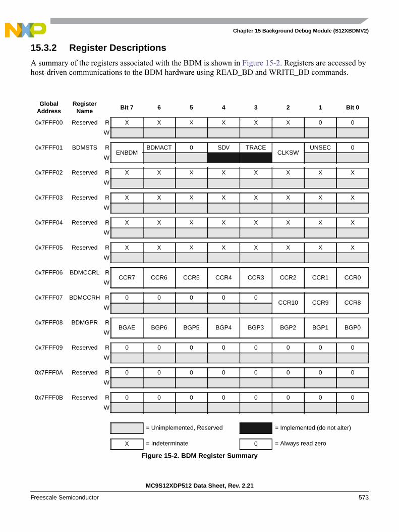
Chapter 15 Background Debug Module (S12XBDMV2)
MC9S12XDP512 Data Sheet, Rev. 2.21
Freescale Semiconductor 573
15.3.2 Register Descriptions
A summary of the registers associated with the BDM is shown in Figure 15-2. Registers are accessed byhost-driven communications to the BDM hardware using READ_BD and WRITE_BD commands.
GlobalAddress
RegisterName
Bit 7 6 5 4 3 2 1 Bit 0
0x7FFF00 Reserved R X X X X X X 0 0
W
0x7FFF01 BDMSTS RENBDM
BDMACT 0 SDV TRACECLKSW
UNSEC 0
W
0x7FFF02 Reserved R X X X X X X X X
W
0x7FFF03 Reserved R X X X X X X X X
W
0x7FFF04 Reserved R X X X X X X X X
W
0x7FFF05 Reserved R X X X X X X X X
W
0x7FFF06 BDMCCRL RCCR7 CCR6 CCR5 CCR4 CCR3 CCR2 CCR1 CCR0
W
0x7FFF07 BDMCCRH R 0 0 0 0 0CCR10 CCR9 CCR8
W
0x7FFF08 BDMGPR RBGAE BGP6 BGP5 BGP4 BGP3 BGP2 BGP1 BGP0
W
0x7FFF09 Reserved R 0 0 0 0 0 0 0 0
W
0x7FFF0A Reserved R 0 0 0 0 0 0 0 0
W
0x7FFF0B Reserved R 0 0 0 0 0 0 0 0
W
= Unimplemented, Reserved = Implemented (do not alter)
X = Indeterminate 0 = Always read zero
Figure 15-2. BDM Register Summary
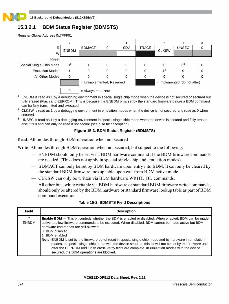
Chapter 15 Background Debug Module (S12XBDMV2)
MC9S12XDP512 Data Sheet, Rev. 2.21
574 Freescale Semiconductor
15.3.2.1 BDM Status Register (BDMSTS)
Figure 15-3. BDM Status Register (BDMSTS)
Read: All modes through BDM operation when not secured
Write: All modes through BDM operation when not secured, but subject to the following:
— ENBDM should only be set via a BDM hardware command if the BDM firmware commandsare needed. (This does not apply in special single chip and emulation modes).
— BDMACT can only be set by BDM hardware upon entry into BDM. It can only be cleared bythe standard BDM firmware lookup table upon exit from BDM active mode.
— CLKSW can only be written via BDM hardware WRITE_BD commands.
— All other bits, while writable via BDM hardware or standard BDM firmware write commands,should only be altered by the BDM hardware or standard firmware lookup table as part of BDMcommand execution.
Register Global Address 0x7FFF01
7 6 5 4 3 2 1 0
RENBDM
BDMACT 0 SDV TRACECLKSW
UNSEC 0
W
Reset
Special Single-Chip Mode 01
1 ENBDM is read as 1 by a debugging environment in special single chip mode when the device is not secured or secured butfully erased (Flash and EEPROM). This is because the ENBDM bit is set by the standard firmware before a BDM commandcan be fully transmitted and executed.
1 0 0 0 0 03
3 UNSEC is read as 1 by a debugging environment in special single chip mode when the device is secured and fully erased,else it is 0 and can only be read if not secure (see also bit description).
0
Emulation Modes 1 0 0 0 0 12
2 CLKSW is read as 1 by a debugging environment in emulation modes when the device is not secured and read as 0 whensecured.
0 0
All Other Modes 0 0 0 0 0 0 0 0
= Unimplemented, Reserved = Implemented (do not alter)
0 = Always read zero
Table 15-2. BDMSTS Field Descriptions
Field Description
7ENBDM
Enable BDM — This bit controls whether the BDM is enabled or disabled. When enabled, BDM can be madeactive to allow firmware commands to be executed. When disabled, BDM cannot be made active but BDMhardware commands are still allowed.0 BDM disabled1 BDM enabledNote: ENBDM is set by the firmware out of reset in special single chip mode and by hardware in emulation
modes. In special single chip mode with the device secured, this bit will not be set by the firmware untilafter the EEPROM and Flash erase verify tests are complete. In emulation modes with the devicesecured, the BDM operations are blocked.
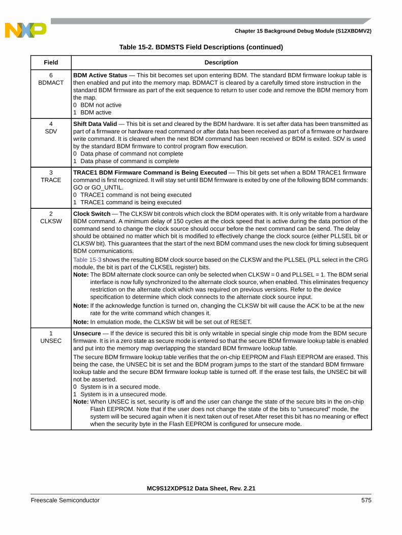
Chapter 15 Background Debug Module (S12XBDMV2)
MC9S12XDP512 Data Sheet, Rev. 2.21
Freescale Semiconductor 575
6BDMACT
BDM Active Status — This bit becomes set upon entering BDM. The standard BDM firmware lookup table isthen enabled and put into the memory map. BDMACT is cleared by a carefully timed store instruction in thestandard BDM firmware as part of the exit sequence to return to user code and remove the BDM memory fromthe map.0 BDM not active1 BDM active
4SDV
Shift Data Valid — This bit is set and cleared by the BDM hardware. It is set after data has been transmitted aspart of a firmware or hardware read command or after data has been received as part of a firmware or hardwarewrite command. It is cleared when the next BDM command has been received or BDM is exited. SDV is usedby the standard BDM firmware to control program flow execution.0 Data phase of command not complete1 Data phase of command is complete
3TRACE
TRACE1 BDM Firmware Command is Being Executed — This bit gets set when a BDM TRACE1 firmwarecommand is first recognized. It will stay set until BDM firmware is exited by one of the following BDM commands:GO or GO_UNTIL.0 TRACE1 command is not being executed1 TRACE1 command is being executed
2CLKSW
Clock Switch — The CLKSW bit controls which clock the BDM operates with. It is only writable from a hardwareBDM command. A minimum delay of 150 cycles at the clock speed that is active during the data portion of thecommand send to change the clock source should occur before the next command can be send. The delayshould be obtained no matter which bit is modified to effectively change the clock source (either PLLSEL bit orCLKSW bit). This guarantees that the start of the next BDM command uses the new clock for timing subsequentBDM communications.Table 15-3 shows the resulting BDM clock source based on the CLKSW and the PLLSEL (PLL select in the CRGmodule, the bit is part of the CLKSEL register) bits.Note: The BDM alternate clock source can only be selected when CLKSW = 0 and PLLSEL = 1. The BDM serial
interface is now fully synchronized to the alternate clock source, when enabled. This eliminates frequencyrestriction on the alternate clock which was required on previous versions. Refer to the devicespecification to determine which clock connects to the alternate clock source input.
Note: If the acknowledge function is turned on, changing the CLKSW bit will cause the ACK to be at the newrate for the write command which changes it.
Note: In emulation mode, the CLKSW bit will be set out of RESET.
1UNSEC
Unsecure — If the device is secured this bit is only writable in special single chip mode from the BDM securefirmware. It is in a zero state as secure mode is entered so that the secure BDM firmware lookup table is enabledand put into the memory map overlapping the standard BDM firmware lookup table.The secure BDM firmware lookup table verifies that the on-chip EEPROM and Flash EEPROM are erased. Thisbeing the case, the UNSEC bit is set and the BDM program jumps to the start of the standard BDM firmwarelookup table and the secure BDM firmware lookup table is turned off. If the erase test fails, the UNSEC bit willnot be asserted.0 System is in a secured mode.1 System is in a unsecured mode.Note: When UNSEC is set, security is off and the user can change the state of the secure bits in the on-chip
Flash EEPROM. Note that if the user does not change the state of the bits to “unsecured” mode, thesystem will be secured again when it is next taken out of reset.After reset this bit has no meaning or effectwhen the security byte in the Flash EEPROM is configured for unsecure mode.
Table 15-2. BDMSTS Field Descriptions (continued)
Field Description

Chapter 15 Background Debug Module (S12XBDMV2)
MC9S12XDP512 Data Sheet, Rev. 2.21
576 Freescale Semiconductor
15.3.2.2 BDM CCR LOW Holding Register (BDMCCRL)
Figure 15-4. BDM CCR LOW Holding Register (BDMCCRL)
Read: All modes through BDM operation when not secured
Write: All modes through BDM operation when not secured
NOTEWhen BDM is made active, the CPU stores the content of its CCRL registerin the BDMCCRL register. However, out of special single-chip reset, theBDMCCRL is set to 0xD8 and not 0xD0 which is the reset value of theCCRL register in this CPU mode. Out of reset in all other modes theBDMCCRL register is read zero.
When entering background debug mode, the BDM CCR LOW holding register is used to save the low byteof the condition code register of the user’s program. It is also used for temporary storage in the standardBDM firmware mode. The BDM CCR LOW holding register can be written to modify the CCR value.
Table 15-3. BDM Clock Sources
PLLSEL CLKSW BDMCLK
0 0 Bus clock dependent on oscillator
0 1 Bus clock dependent on oscillator
1 0 Alternate clock (refer to the device specification to determine the alternate clock source)
1 1 Bus clock dependent on the PLL
Register Global Address 0x7FFF06
7 6 5 4 3 2 1 0
RCCR7 CCR6 CCR5 CCR4 CCR3 CCR2 CCR1 CCR0
W
Reset
Special Single-Chip Mode 1 1 0 0 1 0 0 0
All Other Modes 0 0 0 0 0 0 0 0

Chapter 15 Background Debug Module (S12XBDMV2)
MC9S12XDP512 Data Sheet, Rev. 2.21
Freescale Semiconductor 577
15.3.2.3 BDM CCR HIGH Holding Register (BDMCCRH)
Figure 15-5. BDM CCR HIGH Holding Register (BDMCCRH)
Read: All modes through BDM operation when not secured
Write: All modes through BDM operation when not secured
When entering background debug mode, the BDM CCR HIGH holding register is used to save the highbyte of the condition code register of the user’s program. The BDM CCR HIGH holding register can bewritten to modify the CCR value.
15.3.2.4 BDM Global Page Index Register (BDMGPR)
Figure 15-6. BDM Global Page Register (BDMGPR)
Read: All modes through BDM operation when not secured
Write: All modes through BDM operation when not secured
15.3.3 Family ID Assignment
The family ID is a 8-bit value located in the firmware ROM (at global address: 0x7FFF0F). The read-onlyvalue is a unique family ID which is 0xC1 for S12X devices.
Register Global Address 0x7FFF07
7 6 5 4 3 2 1 0
R 0 0 0 0 0CCR10 CCR9 CCR8
W
Reset 0 0 0 0 0 0 0 0
= Unimplemented or Reserved
Register Global Address 0x7FFF08
7 6 5 4 3 2 1 0
RBGAE BGP6 BGP5 BGP4 BGP3 BGP2 BGP1 BGP0
W
Reset 0 0 0 0 0 0 0 0
Table 15-4. BDMGPR Field Descriptions
Field Description
7BGAE
BDM Global Page Access Enable Bit — BGAE enables global page access for BDM hardware and firmwareread/write instructions The BDM hardware commands used to access the BDM registers (READ_BD_ andWRITE_BD_) can not be used for global accesses even if the BGAE bit is set.0 BDM Global Access disabled1 BDM Global Access enabled
6–0BGP[6:0]
BDM Global Page Index Bits 6–0 — These bits define the extended address bits from 22 to 16. For moredetailed information regarding the global page window scheme, please refer to the S12X_MMC Block Guide.
Chapter 15 Background Debug Module (S12XBDMV2)
MC9S12XDP512 Data Sheet, Rev. 2.21
578 Freescale Semiconductor
15.4 Functional DescriptionThe BDM receives and executes commands from a host via a single wire serial interface. There are twotypes of BDM commands: hardware and firmware commands.
Hardware commands are used to read and write target system memory locations and to enter activebackground debug mode, see Section 15.4.3, “BDM Hardware Commands”. Target system memoryincludes all memory that is accessible by the CPU.
Firmware commands are used to read and write CPU resources and to exit from active background debugmode, see Section 15.4.4, “Standard BDM Firmware Commands”. The CPU resources referred to are theaccumulator (D), X index register (X), Y index register (Y), stack pointer (SP), and program counter (PC).
Hardware commands can be executed at any time and in any mode excluding a few exceptions ashighlighted (see Section 15.4.3, “BDM Hardware Commands”) and in secure mode (see Section 15.4.1,“Security”). Firmware commands can only be executed when the system is not secure and is in activebackground debug mode (BDM).
15.4.1 Security
If the user resets into special single chip mode with the system secured, a secured mode BDM firmwarelookup table is brought into the map overlapping a portion of the standard BDM firmware lookup table.The secure BDM firmware verifies that the on-chip EEPROM and Flash EEPROM are erased. This beingthe case, the UNSEC and ENBDM bit will get set. The BDM program jumps to the start of the standardBDM firmware and the secured mode BDM firmware is turned off and all BDM commands are allowed.If the EEPROM or Flash do not verify as erased, the BDM firmware sets the ENBDM bit, without assertingUNSEC, and the firmware enters a loop. This causes the BDM hardware commands to become enabled,but does not enable the firmware commands. This allows the BDM hardware to be used to erase theEEPROM and Flash.
BDM operation is not possible in any other mode than special single chip mode when the device is secured.The device can only be unsecured via BDM serial interface in special single chip mode. For moreinformation regarding security, please see the S12X_9SEC Block Guide.
15.4.2 Enabling and Activating BDM
The system must be in active BDM to execute standard BDM firmware commands. BDM can be activatedonly after being enabled. BDM is enabled by setting the ENBDM bit in the BDM status (BDMSTS)register. The ENBDM bit is set by writing to the BDM status (BDMSTS) register, via the single-wireinterface, using a hardware command such as WRITE_BD_BYTE.

Chapter 15 Background Debug Module (S12XBDMV2)
MC9S12XDP512 Data Sheet, Rev. 2.21
Freescale Semiconductor 579
After being enabled, BDM is activated by one of the following1:
• Hardware BACKGROUND command
• CPU BGND instruction
• External instruction tagging mechanism2
• Breakpoint force or tag mechanism2
When BDM is activated, the CPU finishes executing the current instruction and then begins executing thefirmware in the standard BDM firmware lookup table. When BDM is activated by a breakpoint, the typeof breakpoint used determines if BDM becomes active before or after execution of the next instruction.
NOTEIf an attempt is made to activate BDM before being enabled, the CPUresumes normal instruction execution after a brief delay. If BDM is notenabled, any hardware BACKGROUND commands issued are ignored bythe BDM and the CPU is not delayed.
In active BDM, the BDM registers and standard BDM firmware lookup table are mapped to addresses0x7FFF00 to 0x7FFFFF. BDM registers are mapped to addresses 0x7FFF00 to 0x7FFF0B. The BDM usesthese registers which are readable anytime by the BDM. However, these registers are not readable by userprograms.
15.4.3 BDM Hardware Commands
Hardware commands are used to read and write target system memory locations and to enter activebackground debug mode. Target system memory includes all memory that is accessible by the CPU suchas on-chip RAM, EEPROM, Flash EEPROM, I/O and control registers, and all external memory.
Hardware commands are executed with minimal or no CPU intervention and do not require the system tobe in active BDM for execution, although, they can still be executed in this mode. When executing ahardware command, the BDM sub-block waits for a free bus cycle so that the background access does notdisturb the running application program. If a free cycle is not found within 128 clock cycles, the CPU ismomentarily frozen so that the BDM can steal a cycle. When the BDM finds a free cycle, the operationdoes not intrude on normal CPU operation provided that it can be completed in a single cycle. However,if an operation requires multiple cycles the CPU is frozen until the operation is complete, even though theBDM found a free cycle.
The BDM hardware commands are listed in Table 15-5.
The READ_BD and WRITE_BD commands allow access to the BDM register locations. These locationsare not normally in the system memory map but share addresses with the application in memory. Todistinguish between physical memory locations that share the same address, BDM memory resources areenabled just for the READ_BD and WRITE_BD access cycle. This allows the BDM to access BDMlocations unobtrusively, even if the addresses conflict with the application memory map.
1. BDM is enabled and active immediately out of special single-chip reset.2. This method is provided by the S12X_DBG module.
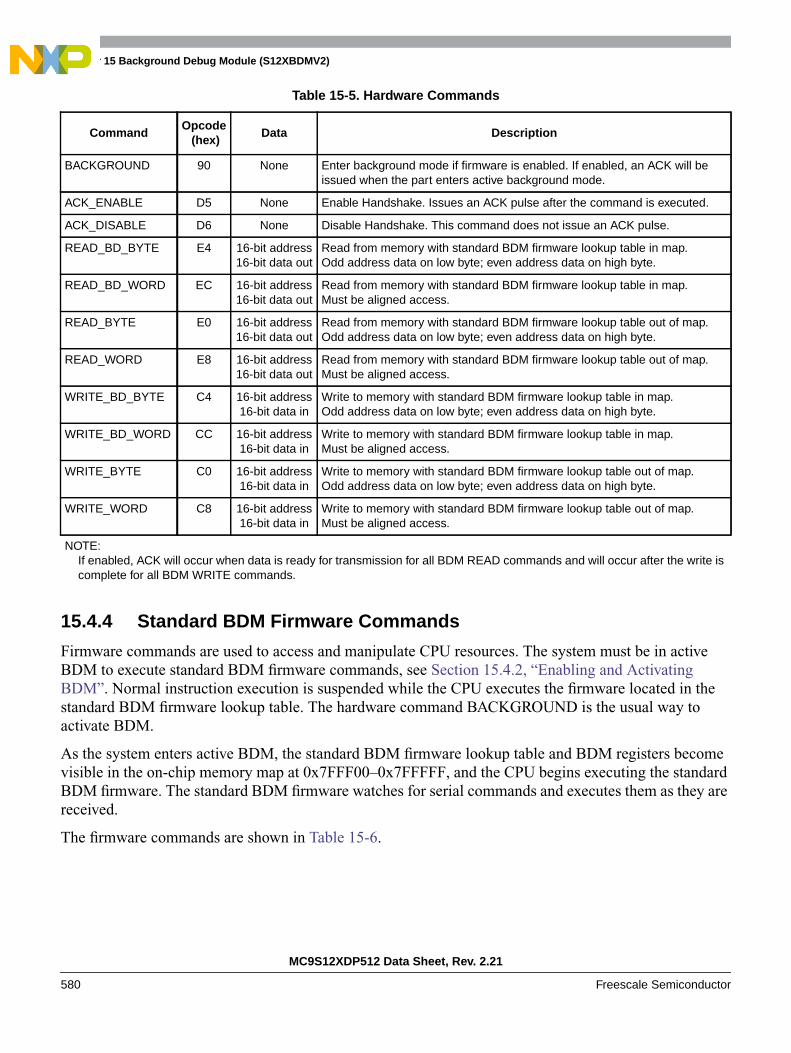
Chapter 15 Background Debug Module (S12XBDMV2)
MC9S12XDP512 Data Sheet, Rev. 2.21
580 Freescale Semiconductor
15.4.4 Standard BDM Firmware Commands
Firmware commands are used to access and manipulate CPU resources. The system must be in activeBDM to execute standard BDM firmware commands, see Section 15.4.2, “Enabling and ActivatingBDM”. Normal instruction execution is suspended while the CPU executes the firmware located in thestandard BDM firmware lookup table. The hardware command BACKGROUND is the usual way toactivate BDM.
As the system enters active BDM, the standard BDM firmware lookup table and BDM registers becomevisible in the on-chip memory map at 0x7FFF00–0x7FFFFF, and the CPU begins executing the standardBDM firmware. The standard BDM firmware watches for serial commands and executes them as they arereceived.
The firmware commands are shown in Table 15-6.
Table 15-5. Hardware Commands
CommandOpcode (hex)
Data Description
BACKGROUND 90 None Enter background mode if firmware is enabled. If enabled, an ACK will beissued when the part enters active background mode.
ACK_ENABLE D5 None Enable Handshake. Issues an ACK pulse after the command is executed.
ACK_DISABLE D6 None Disable Handshake. This command does not issue an ACK pulse.
READ_BD_BYTE E4 16-bit address16-bit data out
Read from memory with standard BDM firmware lookup table in map.Odd address data on low byte; even address data on high byte.
READ_BD_WORD EC 16-bit address16-bit data out
Read from memory with standard BDM firmware lookup table in map.Must be aligned access.
READ_BYTE E0 16-bit address16-bit data out
Read from memory with standard BDM firmware lookup table out of map.Odd address data on low byte; even address data on high byte.
READ_WORD E8 16-bit address16-bit data out
Read from memory with standard BDM firmware lookup table out of map.Must be aligned access.
WRITE_BD_BYTE C4 16-bit address16-bit data in
Write to memory with standard BDM firmware lookup table in map.Odd address data on low byte; even address data on high byte.
WRITE_BD_WORD CC 16-bit address16-bit data in
Write to memory with standard BDM firmware lookup table in map.Must be aligned access.
WRITE_BYTE C0 16-bit address16-bit data in
Write to memory with standard BDM firmware lookup table out of map.Odd address data on low byte; even address data on high byte.
WRITE_WORD C8 16-bit address16-bit data in
Write to memory with standard BDM firmware lookup table out of map.Must be aligned access.
NOTE:If enabled, ACK will occur when data is ready for transmission for all BDM READ commands and will occur after the write iscomplete for all BDM WRITE commands.
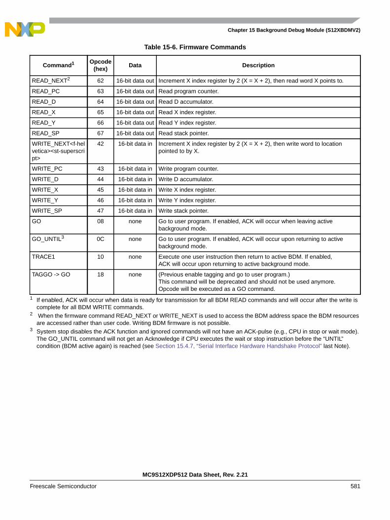
Chapter 15 Background Debug Module (S12XBDMV2)
MC9S12XDP512 Data Sheet, Rev. 2.21
Freescale Semiconductor 581
Table 15-6. Firmware Commands
Command1
1 If enabled, ACK will occur when data is ready for transmission for all BDM READ commands and will occur after the write iscomplete for all BDM WRITE commands.
Opcode(hex)
Data Description
READ_NEXT2
2 When the firmware command READ_NEXT or WRITE_NEXT is used to access the BDM address space the BDM resourcesare accessed rather than user code. Writing BDM firmware is not possible.
62 16-bit data out Increment X index register by 2 (X = X + 2), then read word X points to.
READ_PC 63 16-bit data out Read program counter.
READ_D 64 16-bit data out Read D accumulator.
READ_X 65 16-bit data out Read X index register.
READ_Y 66 16-bit data out Read Y index register.
READ_SP 67 16-bit data out Read stack pointer.
WRITE_NEXT<f-helvetica><st-superscript>
42 16-bit data in Increment X index register by 2 (X = X + 2), then write word to locationpointed to by X.
WRITE_PC 43 16-bit data in Write program counter.
WRITE_D 44 16-bit data in Write D accumulator.
WRITE_X 45 16-bit data in Write X index register.
WRITE_Y 46 16-bit data in Write Y index register.
WRITE_SP 47 16-bit data in Write stack pointer.
GO 08 none Go to user program. If enabled, ACK will occur when leaving activebackground mode.
GO_UNTIL3
3 System stop disables the ACK function and ignored commands will not have an ACK-pulse (e.g., CPU in stop or wait mode).The GO_UNTIL command will not get an Acknowledge if CPU executes the wait or stop instruction before the “UNTIL”condition (BDM active again) is reached (see Section 15.4.7, “Serial Interface Hardware Handshake Protocol” last Note).
0C none Go to user program. If enabled, ACK will occur upon returning to activebackground mode.
TRACE1 10 none Execute one user instruction then return to active BDM. If enabled,ACK will occur upon returning to active background mode.
TAGGO -> GO 18 none (Previous enable tagging and go to user program.)This command will be deprecated and should not be used anymore.Opcode will be executed as a GO command.

Chapter 15 Background Debug Module (S12XBDMV2)
MC9S12XDP512 Data Sheet, Rev. 2.21
582 Freescale Semiconductor
15.4.5 BDM Command Structure
Hardware and firmware BDM commands start with an 8-bit opcode followed by a 16-bit address and/or a16-bit data word depending on the command. All the read commands return 16 bits of data despite the byteor word implication in the command name.
8-bit reads return 16-bits of data, of which, only one byte will contain validdata. If reading an even address, the valid data will appear in the MSB. Ifreading an odd address, the valid data will appear in the LSB.
16-bit misaligned reads and writes are generally not allowed. If attemptedby BDM hardware command, the BDM will ignore the least significant bitof the address and will assume an even address from the remaining bits.
The following cycle count information is only valid when the external waitfunction is not used (see wait bit of EBI sub-block). During an external waitthe BDM can not steal a cycle. Hence be careful with the external waitfunction if the BDM serial interface is much faster than the bus, because ofthe BDM soft-reset after time-out (see Section 15.4.11, “SerialCommunication Time Out”).
For hardware data read commands, the external host must wait at least 150 bus clock cycles after sendingthe address before attempting to obtain the read data. This is to be certain that valid data is available in theBDM shift register, ready to be shifted out. For hardware write commands, the external host must wait150 bus clock cycles after sending the data to be written before attempting to send a new command. Thisis to avoid disturbing the BDM shift register before the write has been completed. The 150 bus clock cycledelay in both cases includes the maximum 128 cycle delay that can be incurred as the BDM waits for afree cycle before stealing a cycle.
For firmware read commands, the external host should wait at least 48 bus clock cycles after sending thecommand opcode and before attempting to obtain the read data. This includes the potential of extra cycleswhen the access is external and stretched (+1 to maximum +7 cycles) or to registers of the PRU (portreplacement unit) in emulation mode. The 48 cycle wait allows enough time for the requested data to bemade available in the BDM shift register, ready to be shifted out.
NOTEThis timing has increased from previous BDM modules due to the newcapability in which the BDM serial interface can potentially run faster thanthe bus. On previous BDM modules this extra time could be hidden withinthe serial time.
For firmware write commands, the external host must wait 36 bus clock cycles after sending the data to bewritten before attempting to send a new command. This is to avoid disturbing the BDM shift registerbefore the write has been completed.

Chapter 15 Background Debug Module (S12XBDMV2)
MC9S12XDP512 Data Sheet, Rev. 2.21
Freescale Semiconductor 583
The external host should wait at least for 76 bus clock cycles after a TRACE1 or GO command beforestarting any new serial command. This is to allow the CPU to exit gracefully from the standard BDMfirmware lookup table and resume execution of the user code. Disturbing the BDM shift registerprematurely may adversely affect the exit from the standard BDM firmware lookup table.
NOTEIf the bus rate of the target processor is unknown or could be changing or theexternal wait function is used, it is recommended that the ACK(acknowledge function) is used to indicate when an operation is complete.When using ACK, the delay times are automated.
Figure 15-7 represents the BDM command structure. The command blocks illustrate a series of eight bittimes starting with a falling edge. The bar across the top of the blocks indicates that the BKGD line idlesin the high state. The time for an 8-bit command is 8 × 16 target clock cycles.1
Figure 15-7. BDM Command Structure
1. Target clock cycles are cycles measured using the target MCU’s serial clock rate. See Section 15.4.6, “BDM Serial Interface”and Section 15.3.2.1, “BDM Status Register (BDMSTS)” for information on how serial clock rate is selected.
Hardware
Hardware
Firmware
Firmware
GO,
48-BC
BC = Bus Clock Cycles
Command Address
150-BCDelay
Next
DELAY
8 BitsAT ~16 TC/Bit
16 BitsAT ~16 TC/Bit
16 BitsAT ~16 TC/Bit
Command Address Data Next
DataRead
Write
Read
Write
TRACE
Command Next
Command Data
76-BCDelay
Next
Command
150-BCDelay
36-BCDELAY
Command
Command
Command
CommandData
NextCommand
TC = Target Clock Cycles
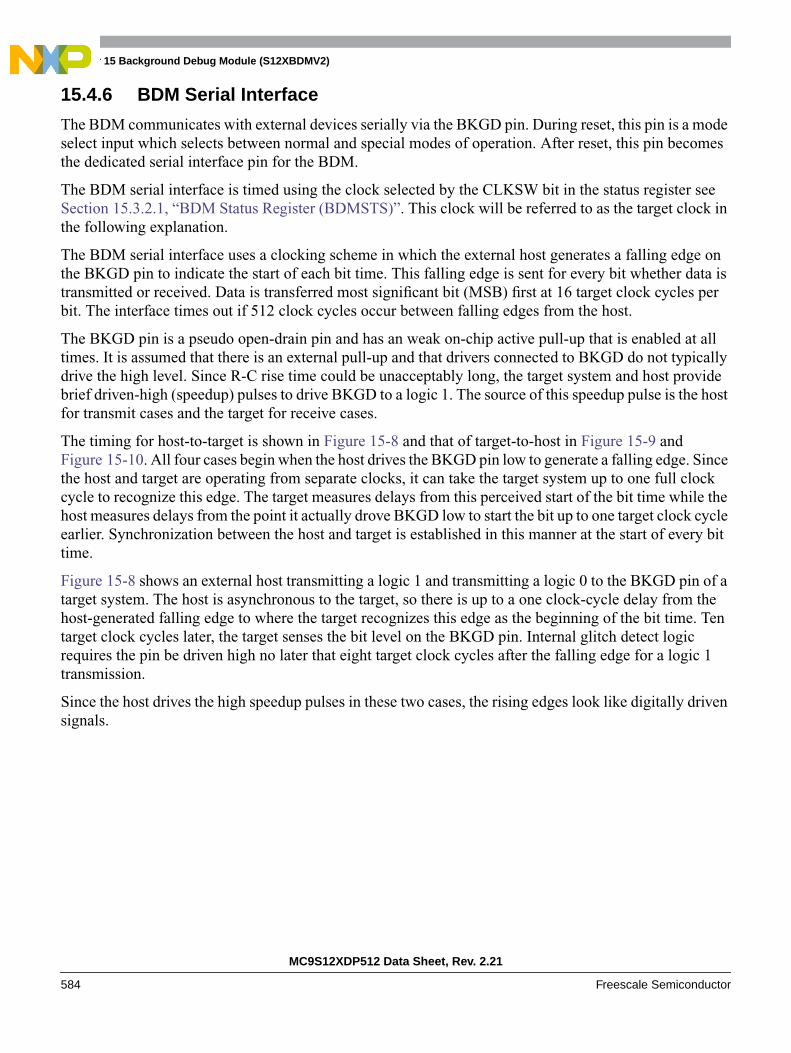
Chapter 15 Background Debug Module (S12XBDMV2)
MC9S12XDP512 Data Sheet, Rev. 2.21
584 Freescale Semiconductor
15.4.6 BDM Serial Interface
The BDM communicates with external devices serially via the BKGD pin. During reset, this pin is a modeselect input which selects between normal and special modes of operation. After reset, this pin becomesthe dedicated serial interface pin for the BDM.
The BDM serial interface is timed using the clock selected by the CLKSW bit in the status register seeSection 15.3.2.1, “BDM Status Register (BDMSTS)”. This clock will be referred to as the target clock inthe following explanation.
The BDM serial interface uses a clocking scheme in which the external host generates a falling edge onthe BKGD pin to indicate the start of each bit time. This falling edge is sent for every bit whether data istransmitted or received. Data is transferred most significant bit (MSB) first at 16 target clock cycles perbit. The interface times out if 512 clock cycles occur between falling edges from the host.
The BKGD pin is a pseudo open-drain pin and has an weak on-chip active pull-up that is enabled at alltimes. It is assumed that there is an external pull-up and that drivers connected to BKGD do not typicallydrive the high level. Since R-C rise time could be unacceptably long, the target system and host providebrief driven-high (speedup) pulses to drive BKGD to a logic 1. The source of this speedup pulse is the hostfor transmit cases and the target for receive cases.
The timing for host-to-target is shown in Figure 15-8 and that of target-to-host in Figure 15-9 andFigure 15-10. All four cases begin when the host drives the BKGD pin low to generate a falling edge. Sincethe host and target are operating from separate clocks, it can take the target system up to one full clockcycle to recognize this edge. The target measures delays from this perceived start of the bit time while thehost measures delays from the point it actually drove BKGD low to start the bit up to one target clock cycleearlier. Synchronization between the host and target is established in this manner at the start of every bittime.
Figure 15-8 shows an external host transmitting a logic 1 and transmitting a logic 0 to the BKGD pin of atarget system. The host is asynchronous to the target, so there is up to a one clock-cycle delay from thehost-generated falling edge to where the target recognizes this edge as the beginning of the bit time. Tentarget clock cycles later, the target senses the bit level on the BKGD pin. Internal glitch detect logicrequires the pin be driven high no later that eight target clock cycles after the falling edge for a logic 1transmission.
Since the host drives the high speedup pulses in these two cases, the rising edges look like digitally drivensignals.

Chapter 15 Background Debug Module (S12XBDMV2)
MC9S12XDP512 Data Sheet, Rev. 2.21
Freescale Semiconductor 585
Figure 15-8. BDM Host-to-Target Serial Bit Timing
The receive cases are more complicated. Figure 15-9 shows the host receiving a logic 1 from the targetsystem. Since the host is asynchronous to the target, there is up to one clock-cycle delay from thehost-generated falling edge on BKGD to the perceived start of the bit time in the target. The host holds theBKGD pin low long enough for the target to recognize it (at least two target clock cycles). The host mustrelease the low drive before the target drives a brief high speedup pulse seven target clock cycles after theperceived start of the bit time. The host should sample the bit level about 10 target clock cycles after itstarted the bit time.
Figure 15-9. BDM Target-to-Host Serial Bit Timing (Logic 1)
Target Senses Bit
10 Cycles
SynchronizationUncertainty
BDM Clock(Target MCU)
HostTransmit 1
HostTransmit 0
PerceivedStart of Bit Time
EarliestStart ofNext Bit
High-Impedance
EarliestStart ofNext Bit
R-C Rise
10 Cycles10 Cycles
Host SamplesBKGD Pin
PerceivedStart of Bit Time
BKGD Pin
BDM Clock(Target MCU)
HostDrive to
BKGD Pin
Target SystemSpeedup
Pulse
High-Impedance
High-Impedance
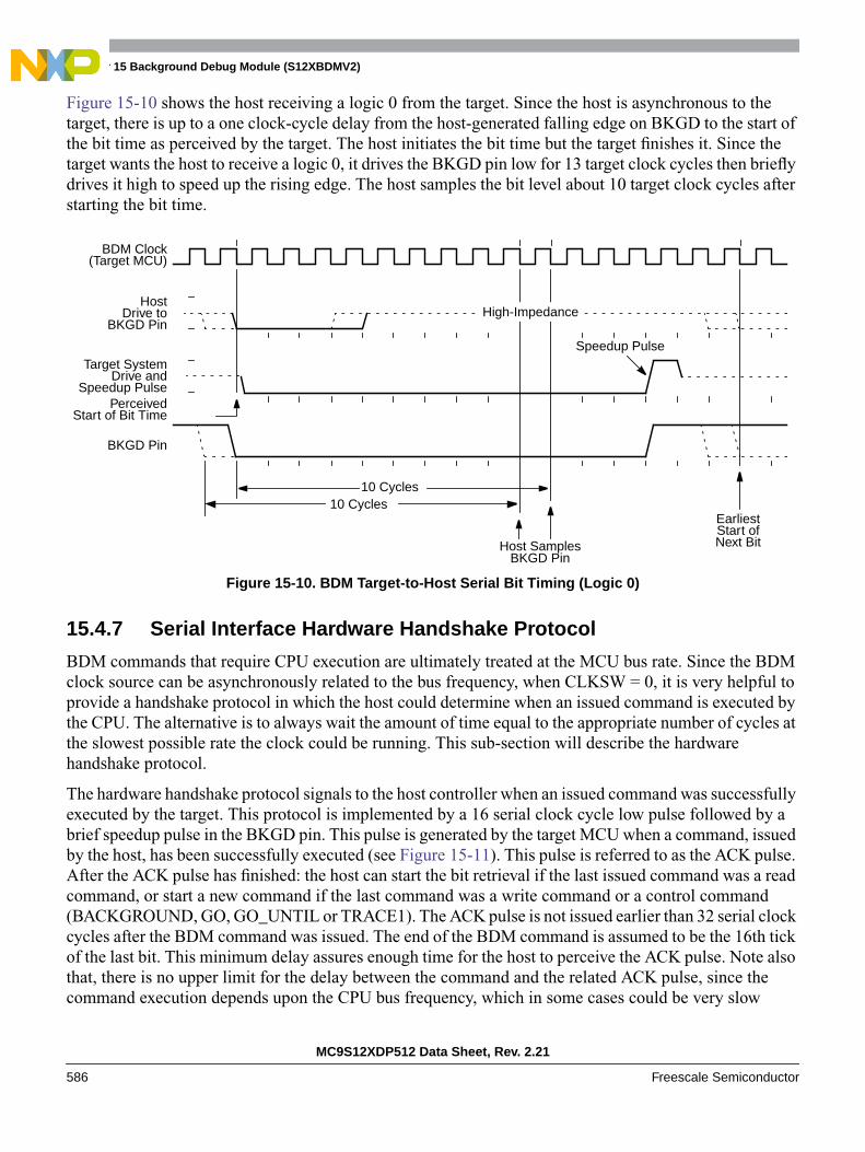
Chapter 15 Background Debug Module (S12XBDMV2)
MC9S12XDP512 Data Sheet, Rev. 2.21
586 Freescale Semiconductor
Figure 15-10 shows the host receiving a logic 0 from the target. Since the host is asynchronous to thetarget, there is up to a one clock-cycle delay from the host-generated falling edge on BKGD to the start ofthe bit time as perceived by the target. The host initiates the bit time but the target finishes it. Since thetarget wants the host to receive a logic 0, it drives the BKGD pin low for 13 target clock cycles then brieflydrives it high to speed up the rising edge. The host samples the bit level about 10 target clock cycles afterstarting the bit time.
Figure 15-10. BDM Target-to-Host Serial Bit Timing (Logic 0)
15.4.7 Serial Interface Hardware Handshake Protocol
BDM commands that require CPU execution are ultimately treated at the MCU bus rate. Since the BDMclock source can be asynchronously related to the bus frequency, when CLKSW = 0, it is very helpful toprovide a handshake protocol in which the host could determine when an issued command is executed bythe CPU. The alternative is to always wait the amount of time equal to the appropriate number of cycles atthe slowest possible rate the clock could be running. This sub-section will describe the hardwarehandshake protocol.
The hardware handshake protocol signals to the host controller when an issued command was successfullyexecuted by the target. This protocol is implemented by a 16 serial clock cycle low pulse followed by abrief speedup pulse in the BKGD pin. This pulse is generated by the target MCU when a command, issuedby the host, has been successfully executed (see Figure 15-11). This pulse is referred to as the ACK pulse.After the ACK pulse has finished: the host can start the bit retrieval if the last issued command was a readcommand, or start a new command if the last command was a write command or a control command(BACKGROUND, GO, GO_UNTIL or TRACE1). The ACK pulse is not issued earlier than 32 serial clockcycles after the BDM command was issued. The end of the BDM command is assumed to be the 16th tickof the last bit. This minimum delay assures enough time for the host to perceive the ACK pulse. Note alsothat, there is no upper limit for the delay between the command and the related ACK pulse, since thecommand execution depends upon the CPU bus frequency, which in some cases could be very slow
EarliestStart ofNext Bit
BDM Clock(Target MCU)
HostDrive to
BKGD Pin
BKGD Pin
PerceivedStart of Bit Time
10 Cycles10 Cycles
Host SamplesBKGD Pin
Target SystemDrive and
Speedup Pulse
Speedup Pulse
High-Impedance
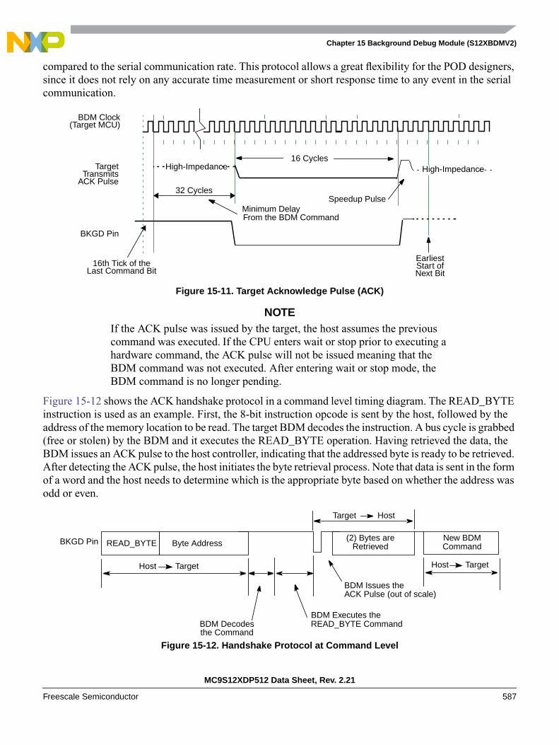
Chapter 15 Background Debug Module (S12XBDMV2)
MC9S12XDP512 Data Sheet, Rev. 2.21
Freescale Semiconductor 587
compared to the serial communication rate. This protocol allows a great flexibility for the POD designers,since it does not rely on any accurate time measurement or short response time to any event in the serialcommunication.
Figure 15-11. Target Acknowledge Pulse (ACK)
NOTEIf the ACK pulse was issued by the target, the host assumes the previouscommand was executed. If the CPU enters wait or stop prior to executing ahardware command, the ACK pulse will not be issued meaning that theBDM command was not executed. After entering wait or stop mode, theBDM command is no longer pending.
Figure 15-12 shows the ACK handshake protocol in a command level timing diagram. The READ_BYTEinstruction is used as an example. First, the 8-bit instruction opcode is sent by the host, followed by theaddress of the memory location to be read. The target BDM decodes the instruction. A bus cycle is grabbed(free or stolen) by the BDM and it executes the READ_BYTE operation. Having retrieved the data, theBDM issues an ACK pulse to the host controller, indicating that the addressed byte is ready to be retrieved.After detecting the ACK pulse, the host initiates the byte retrieval process. Note that data is sent in the formof a word and the host needs to determine which is the appropriate byte based on whether the address wasodd or even.
Figure 15-12. Handshake Protocol at Command Level
16 Cycles
BDM Clock(Target MCU)
TargetTransmits
ACK Pulse
High-Impedance
BKGD Pin
Minimum DelayFrom the BDM Command
32 Cycles
EarliestStart ofNext Bit
Speedup Pulse
16th Tick of theLast Command Bit
High-Impedance
READ_BYTE
BDM Issues the
BKGD Pin Byte Address
BDM Executes theREAD_BYTE Command
Host Target
HostTarget
BDM Decodesthe Command
ACK Pulse (out of scale)
Host Target
(2) Bytes areRetrieved
New BDMCommand
Chapter 15 Background Debug Module (S12XBDMV2)
MC9S12XDP512 Data Sheet, Rev. 2.21
588 Freescale Semiconductor
Differently from the normal bit transfer (where the host initiates the transmission), the serial interface ACKhandshake pulse is initiated by the target MCU by issuing a negative edge in the BKGD pin. The hardwarehandshake protocol in Figure 15-11 specifies the timing when the BKGD pin is being driven, so the hostshould follow this timing constraint in order to avoid the risk of an electrical conflict in the BKGD pin.
NOTEThe only place the BKGD pin can have an electrical conflict is when oneside is driving low and the other side is issuing a speedup pulse (high). Other“highs” are pulled rather than driven. However, at low rates the time of thespeedup pulse can become lengthy and so the potential conflict timebecomes longer as well.
The ACK handshake protocol does not support nested ACK pulses. If a BDM command is notacknowledge by an ACK pulse, the host needs to abort the pending command first in order to be able toissue a new BDM command. When the CPU enters wait or stop while the host issues a hardware command(e.g., WRITE_BYTE), the target discards the incoming command due to the wait or stop being detected.Therefore, the command is not acknowledged by the target, which means that the ACK pulse will not beissued in this case. After a certain time the host (not aware of stop or wait) should decide to abort anypossible pending ACK pulse in order to be sure a new command can be issued. Therefore, the protocolprovides a mechanism in which a command, and its corresponding ACK, can be aborted.
NOTEThe ACK pulse does not provide a time out. This means for the GO_UNTILcommand that it can not be distinguished if a stop or wait has been executed(command discarded and ACK not issued) or if the “UNTIL” condition(BDM active) is just not reached yet. Hence in any case where the ACKpulse of a command is not issued the possible pending command should beaborted before issuing a new command. See the handshake abort proceduredescribed in Section 15.4.8, “Hardware Handshake Abort Procedure”.
15.4.8 Hardware Handshake Abort Procedure
The abort procedure is based on the SYNC command. In order to abort a command, which had not issuedthe corresponding ACK pulse, the host controller should generate a low pulse in the BKGD pin by drivingit low for at least 128 serial clock cycles and then driving it high for one serial clock cycle, providing aspeedup pulse. By detecting this long low pulse in the BKGD pin, the target executes the SYNC protocol,see Section 15.4.9, “SYNC — Request Timed Reference Pulse”, and assumes that the pending commandand therefore the related ACK pulse, are being aborted. Therefore, after the SYNC protocol has beencompleted the host is free to issue new BDM commands. For Firmware READ or WRITE commands itcan not be guaranteed that the pending command is aborted when issuing a SYNC before thecorresponding ACK pulse. There is a short latency time from the time the READ or WRITE access beginsuntil it is finished and the corresponding ACK pulse is issued. The latency time depends on the firmwareREAD or WRITE command that is issued and if the serial interface is running on a different clock ratethan the bus. When the SYNC command starts during this latency time the READ or WRITE commandwill not be aborted, but the corresponding ACK pulse will be aborted. A pending GO, TRACE1 or
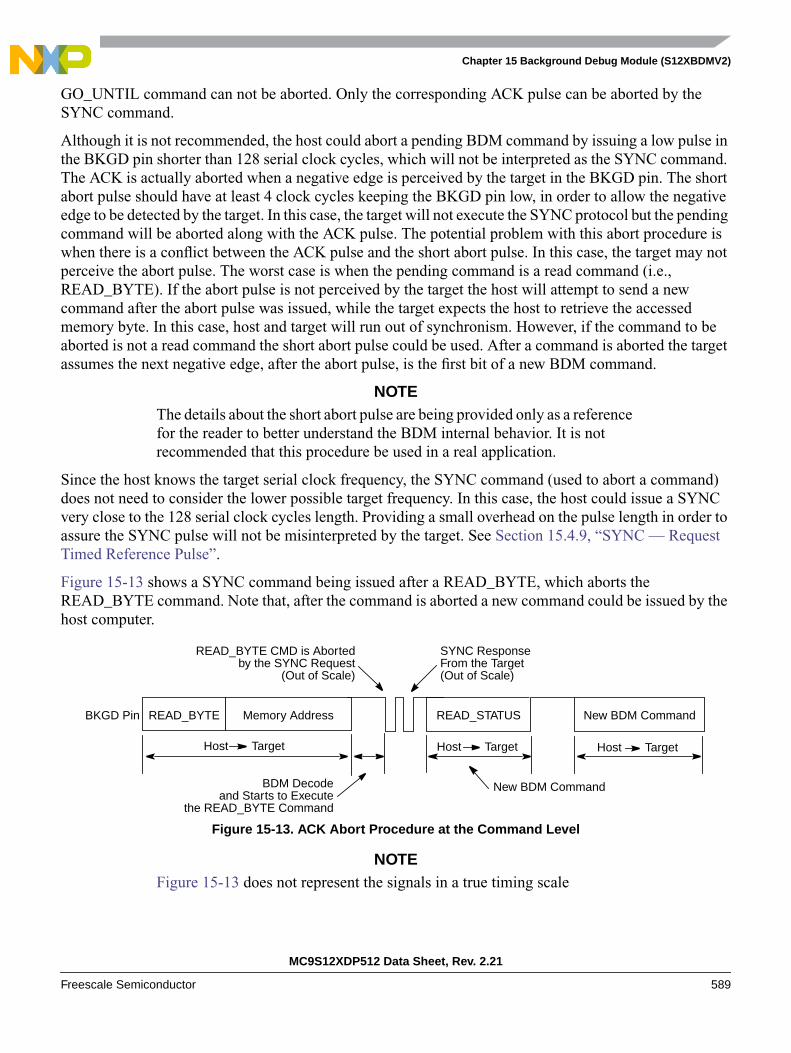
Chapter 15 Background Debug Module (S12XBDMV2)
MC9S12XDP512 Data Sheet, Rev. 2.21
Freescale Semiconductor 589
GO_UNTIL command can not be aborted. Only the corresponding ACK pulse can be aborted by theSYNC command.
Although it is not recommended, the host could abort a pending BDM command by issuing a low pulse inthe BKGD pin shorter than 128 serial clock cycles, which will not be interpreted as the SYNC command.The ACK is actually aborted when a negative edge is perceived by the target in the BKGD pin. The shortabort pulse should have at least 4 clock cycles keeping the BKGD pin low, in order to allow the negativeedge to be detected by the target. In this case, the target will not execute the SYNC protocol but the pendingcommand will be aborted along with the ACK pulse. The potential problem with this abort procedure iswhen there is a conflict between the ACK pulse and the short abort pulse. In this case, the target may notperceive the abort pulse. The worst case is when the pending command is a read command (i.e.,READ_BYTE). If the abort pulse is not perceived by the target the host will attempt to send a newcommand after the abort pulse was issued, while the target expects the host to retrieve the accessedmemory byte. In this case, host and target will run out of synchronism. However, if the command to beaborted is not a read command the short abort pulse could be used. After a command is aborted the targetassumes the next negative edge, after the abort pulse, is the first bit of a new BDM command.
NOTEThe details about the short abort pulse are being provided only as a referencefor the reader to better understand the BDM internal behavior. It is notrecommended that this procedure be used in a real application.
Since the host knows the target serial clock frequency, the SYNC command (used to abort a command)does not need to consider the lower possible target frequency. In this case, the host could issue a SYNCvery close to the 128 serial clock cycles length. Providing a small overhead on the pulse length in order toassure the SYNC pulse will not be misinterpreted by the target. See Section 15.4.9, “SYNC — RequestTimed Reference Pulse”.
Figure 15-13 shows a SYNC command being issued after a READ_BYTE, which aborts theREAD_BYTE command. Note that, after the command is aborted a new command could be issued by thehost computer.
Figure 15-13. ACK Abort Procedure at the Command Level
NOTEFigure 15-13 does not represent the signals in a true timing scale
READ_BYTE READ_STATUSBKGD Pin Memory Address New BDM Command
New BDM Command
Host Target Host Target Host Target
SYNC ResponseFrom the Target(Out of Scale)
BDM Decodeand Starts to Execute
the READ_BYTE Command
READ_BYTE CMD is Abortedby the SYNC Request
(Out of Scale)
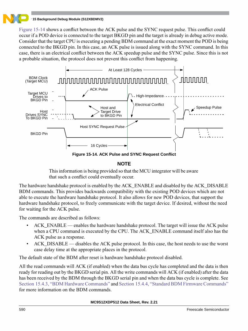
Chapter 15 Background Debug Module (S12XBDMV2)
MC9S12XDP512 Data Sheet, Rev. 2.21
590 Freescale Semiconductor
Figure 15-14 shows a conflict between the ACK pulse and the SYNC request pulse. This conflict couldoccur if a POD device is connected to the target BKGD pin and the target is already in debug active mode.Consider that the target CPU is executing a pending BDM command at the exact moment the POD is beingconnected to the BKGD pin. In this case, an ACK pulse is issued along with the SYNC command. In thiscase, there is an electrical conflict between the ACK speedup pulse and the SYNC pulse. Since this is nota probable situation, the protocol does not prevent this conflict from happening.
Figure 15-14. ACK Pulse and SYNC Request Conflict
NOTEThis information is being provided so that the MCU integrator will be awarethat such a conflict could eventually occur.
The hardware handshake protocol is enabled by the ACK_ENABLE and disabled by the ACK_DISABLEBDM commands. This provides backwards compatibility with the existing POD devices which are notable to execute the hardware handshake protocol. It also allows for new POD devices, that support thehardware handshake protocol, to freely communicate with the target device. If desired, without the needfor waiting for the ACK pulse.
The commands are described as follows:
• ACK_ENABLE — enables the hardware handshake protocol. The target will issue the ACK pulsewhen a CPU command is executed by the CPU. The ACK_ENABLE command itself also has theACK pulse as a response.
• ACK_DISABLE — disables the ACK pulse protocol. In this case, the host needs to use the worstcase delay time at the appropriate places in the protocol.
The default state of the BDM after reset is hardware handshake protocol disabled.
All the read commands will ACK (if enabled) when the data bus cycle has completed and the data is thenready for reading out by the BKGD serial pin. All the write commands will ACK (if enabled) after the datahas been received by the BDM through the BKGD serial pin and when the data bus cycle is complete. SeeSection 15.4.3, “BDM Hardware Commands” and Section 15.4.4, “Standard BDM Firmware Commands”for more information on the BDM commands.
BDM Clock(Target MCU)
Target MCUDrives to
BKGD Pin
BKGD Pin
16 Cycles
Speedup Pulse
High-Impedance
HostDrives SYNCTo BKGD Pin
ACK Pulse
Host SYNC Request Pulse
At Least 128 Cycles
Electrical ConflictHost andTarget Driveto BKGD Pin
Chapter 15 Background Debug Module (S12XBDMV2)
MC9S12XDP512 Data Sheet, Rev. 2.21
Freescale Semiconductor 591
The ACK_ENABLE sends an ACK pulse when the command has been completed. This feature could beused by the host to evaluate if the target supports the hardware handshake protocol. If an ACK pulse isissued in response to this command, the host knows that the target supports the hardware handshakeprotocol. If the target does not support the hardware handshake protocol the ACK pulse is not issued. Inthis case, the ACK_ENABLE command is ignored by the target since it is not recognized as a validcommand.
The BACKGROUND command will issue an ACK pulse when the CPU changes from normal tobackground mode. The ACK pulse related to this command could be aborted using the SYNC command.
The GO command will issue an ACK pulse when the CPU exits from background mode. The ACK pulserelated to this command could be aborted using the SYNC command.
The GO_UNTIL command is equivalent to a GO command with exception that the ACK pulse, in thiscase, is issued when the CPU enters into background mode. This command is an alternative to the GOcommand and should be used when the host wants to trace if a breakpoint match occurs and causes theCPU to enter active background mode. Note that the ACK is issued whenever the CPU enters BDM, whichcould be caused by a breakpoint match or by a BGND instruction being executed. The ACK pulse relatedto this command could be aborted using the SYNC command.
The TRACE1 command has the related ACK pulse issued when the CPU enters background active modeafter one instruction of the application program is executed. The ACK pulse related to this command couldbe aborted using the SYNC command.
15.4.9 SYNC — Request Timed Reference Pulse
The SYNC command is unlike other BDM commands because the host does not necessarily know thecorrect communication speed to use for BDM communications until after it has analyzed the response tothe SYNC command. To issue a SYNC command, the host should perform the following steps:
1. Drive the BKGD pin low for at least 128 cycles at the lowest possible BDM serial communicationfrequency (the lowest serial communication frequency is determined by the crystal oscillator or theclock chosen by CLKSW.)
2. Drive BKGD high for a brief speedup pulse to get a fast rise time (this speedup pulse is typicallyone cycle of the host clock.)
3. Remove all drive to the BKGD pin so it reverts to high impedance.4. Listen to the BKGD pin for the sync response pulse.
Upon detecting the SYNC request from the host, the target performs the following steps:
1. Discards any incomplete command received or bit retrieved.2. Waits for BKGD to return to a logic one.3. Delays 16 cycles to allow the host to stop driving the high speedup pulse.4. Drives BKGD low for 128 cycles at the current BDM serial communication frequency.5. Drives a one-cycle high speedup pulse to force a fast rise time on BKGD.6. Removes all drive to the BKGD pin so it reverts to high impedance.
The host measures the low time of this 128 cycle SYNC response pulse and determines the correct speedfor subsequent BDM communications. Typically, the host can determine the correct communication speed

Chapter 15 Background Debug Module (S12XBDMV2)
MC9S12XDP512 Data Sheet, Rev. 2.21
592 Freescale Semiconductor
within a few percent of the actual target speed and the communication protocol can easily tolerate speederrors of several percent.
As soon as the SYNC request is detected by the target, any partially received command or bit retrieved isdiscarded. This is referred to as a soft-reset, equivalent to a time-out in the serial communication. After theSYNC response, the target will consider the next negative edge (issued by the host) as the start of a newBDM command or the start of new SYNC request.
Another use of the SYNC command pulse is to abort a pending ACK pulse. The behavior is exactly thesame as in a regular SYNC command. Note that one of the possible causes for a command to not beacknowledged by the target is a host-target synchronization problem. In this case, the command may nothave been understood by the target and so an ACK response pulse will not be issued.
15.4.10 Instruction Tracing
When a TRACE1 command is issued to the BDM in active BDM, the CPU exits the standard BDMfirmware and executes a single instruction in the user code. Once this has occurred, the CPU is forced toreturn to the standard BDM firmware and the BDM is active and ready to receive a new command. If theTRACE1 command is issued again, the next user instruction will be executed. This facilitates stepping ortracing through the user code one instruction at a time.
If an interrupt is pending when a TRACE1 command is issued, the interrupt stacking operation occurs butno user instruction is executed. Once back in standard BDM firmware execution, the program counterpoints to the first instruction in the interrupt service routine.
Be aware when tracing through the user code that the execution of the user code is done step by step butall peripherals are free running. Hence possible timing relations between CPU code execution andoccurrence of events of other peripherals no longer exist.
Do not trace the CPU instruction BGND used for soft breakpoints. Tracing the BGND instruction willresult in a return address pointing to BDM firmware address space.
When tracing through user code which contains stop or wait instructions the following will happen whenthe stop or wait instruction is traced:
The CPU enters stop or wait mode and the TRACE1 command can not be finished before leavingthe low power mode. This is the case because BDM active mode can not be entered after CPUexecuted the stop instruction. However all BDM hardware commands except the BACKGROUNDcommand are operational after tracing a stop or wait instruction and still being in stop or waitmode. If system stop mode is entered (all bus masters are in stop mode) no BDM command isoperational.
As soon as stop or wait mode is exited the CPU enters BDM active mode and the saved PC valuepoints to the entry of the corresponding interrupt service routine.
In case the handshake feature is enabled the corresponding ACK pulse of the TRACE1 commandwill be discarded when tracing a stop or wait instruction. Hence there is no ACK pulse when BDMactive mode is entered as part of the TRACE1 command after CPU exited from stop or wait mode.All valid commands sent during CPU being in stop or wait mode or after CPU exited from stop orwait mode will have an ACK pulse. The handshake feature becomes disabled only when system
Chapter 15 Background Debug Module (S12XBDMV2)
MC9S12XDP512 Data Sheet, Rev. 2.21
Freescale Semiconductor 593
stop mode has been reached. Hence after a system stop mode the handshake feature must beenabled again by sending the ACK_ENABLE command.
15.4.11 Serial Communication Time Out
The host initiates a host-to-target serial transmission by generating a falling edge on the BKGD pin. IfBKGD is kept low for more than 128 target clock cycles, the target understands that a SYNC commandwas issued. In this case, the target will keep waiting for a rising edge on BKGD in order to answer theSYNC request pulse. If the rising edge is not detected, the target will keep waiting forever without anytime-out limit.
Consider now the case where the host returns BKGD to logic one before 128 cycles. This is interpreted asa valid bit transmission, and not as a SYNC request. The target will keep waiting for another falling edgemarking the start of a new bit. If, however, a new falling edge is not detected by the target within 512 clockcycles since the last falling edge, a time-out occurs and the current command is discarded without affectingmemory or the operating mode of the MCU. This is referred to as a soft-reset.
If a read command is issued but the data is not retrieved within 512 serial clock cycles, a soft-reset willoccur causing the command to be disregarded. The data is not available for retrieval after the time-out hasoccurred. This is the expected behavior if the handshake protocol is not enabled. However, consider thebehavior where the BDM is running in a frequency much greater than the CPU frequency. In this case, thecommand could time out before the data is ready to be retrieved. In order to allow the data to be retrievedeven with a large clock frequency mismatch (between BDM and CPU) when the hardware handshakeprotocol is enabled, the time out between a read command and the data retrieval is disabled. Therefore, thehost could wait for more then 512 serial clock cycles and still be able to retrieve the data from an issuedread command. However, once the handshake pulse (ACK pulse) is issued, the time-out feature isre-activated, meaning that the target will time out after 512 clock cycles. Therefore, the host needs toretrieve the data within a 512 serial clock cycles time frame after the ACK pulse had been issued. Afterthat period, the read command is discarded and the data is no longer available for retrieval. Any negativeedge in the BKGD pin after the time-out period is considered to be a new command or a SYNC request.
Note that whenever a partially issued command, or partially retrieved data, has occurred the time out in theserial communication is active. This means that if a time frame higher than 512 serial clock cycles isobserved between two consecutive negative edges and the command being issued or data being retrievedis not complete, a soft-reset will occur causing the partially received command or data retrieved to bedisregarded. The next negative edge in the BKGD pin, after a soft-reset has occurred, is considered by thetarget as the start of a new BDM command, or the start of a SYNC request pulse.

Chapter 15 Background Debug Module (S12XBDMV2)
MC9S12XDP512 Data Sheet, Rev. 2.21
594 Freescale Semiconductor

MC9S12XDP512 Data Sheet, Rev. 2.21
Freescale Semiconductor 595
Chapter 16Interrupt (S12XINTV1)
16.1 IntroductionThe XINT module decodes the priority of all system exception requests and provides the applicable vectorfor processing the exception to either the CPU or the XGATE module. The XINT module supports:
• I bit and X bit maskable interrupt requests
• A non-maskable unimplemented opcode trap
• A non-maskable software interrupt (SWI) or background debug mode request
• A spurious interrupt vector request
• Three system reset vector requests
Each of the I bit maskable interrupt requests can be assigned to one of seven priority levels supporting aflexible priority scheme. For interrupt requests that are configured to be handled by the CPU, the priorityscheme can be used to implement nested interrupt capability where interrupts from a lower level areautomatically blocked if a higher level interrupt is being processed. Interrupt requests configured to behandled by the XGATE module cannot be nested because the XGATE module cannot be interrupted whileprocessing.
NOTEThe HPRIO register and functionality of the XINT module is no longersupported, since it is superseded by the 7-level interrupt request priorityscheme.

Chapter 16 Interrupt (S12XINTV1)
MC9S12XDP512 Data Sheet, Rev. 2.21
596 Freescale Semiconductor
16.1.1 Glossary
The following terms and abbreviations are used in the document.
16.1.2 Features• Interrupt vector base register (IVBR)
• One spurious interrupt vector (at address vector base1 + 0x0010).
• 2–113 I bit maskable interrupt vector requests (at addresses vector base + 0x0012–0x00F2).
• Each I bit maskable interrupt request has a configurable priority level and can be configured to behandled by either the CPU or the XGATE module2.
• I bit maskable interrupts can be nested, depending on their priority levels.
• One X bit maskable interrupt vector request (at address vector base + 0x00F4).
• One non-maskable software interrupt request (SWI) or background debug mode vector request (ataddress vector base + 0x00F6).
• One non-maskable unimplemented opcode trap (TRAP) vector (at address vector base + 0x00F8).
• Three system reset vectors (at addresses 0xFFFA–0xFFFE).
• Determines the highest priority DMA and interrupt vector requests, drives the vector to the XGATEmodule or to the bus on CPU request, respectively.
• Wakes up the system from stop or wait mode when an appropriate interrupt request occurs orwhenever XIRQ is asserted, even if X interrupt is masked.
• XGATE can wake up and execute code, even with the CPU remaining in stop or wait mode.
16.1.3 Modes of Operation• Run mode
This is the basic mode of operation.
Table 16-1. Terminology
Term Meaning
CCR Condition Code Register (in the S12X CPU)
DMA Direct Memory Access
INT Interrupt
IPL Interrupt Processing Level
ISR Interrupt Service Routine
MCU Micro-Controller Unit
XGATE please refer to the "XGATE Block Guide"
IRQ refers to the interrupt request associated with the IRQ pin
XIRQ refers to the interrupt request associated with the XIRQ pin
1. The vector base is a 16-bit address which is accumulated from the contents of the interrupt vector base register (IVBR, usedas upper byte) and 0x00 (used as lower byte).
2. The IRQ interrupt can only be handled by the CPU

Chapter 16 Interrupt (S12XINTV1)
MC9S12XDP512 Data Sheet, Rev. 2.21
Freescale Semiconductor 597
• Wait mode
In wait mode, the XINT module is frozen. It is however capable of either waking up the CPU if aninterrupt occurs or waking up the XGATE if an XGATE request occurs. Please refer toSection 16.5.3, “Wake Up from Stop or Wait Mode” for details.
• Stop Mode
In stop mode, the XINT module is frozen. It is however capable of either waking up the CPU if aninterrupt occurs or waking up the XGATE if an XGATE request occurs. Please refer toSection 16.5.3, “Wake Up from Stop or Wait Mode” for details.
• Freeze mode (BDM active)
In freeze mode (BDM active), the interrupt vector base register is overridden internally. Pleaserefer to Section 16.3.1.1, “Interrupt Vector Base Register (IVBR)” for details.
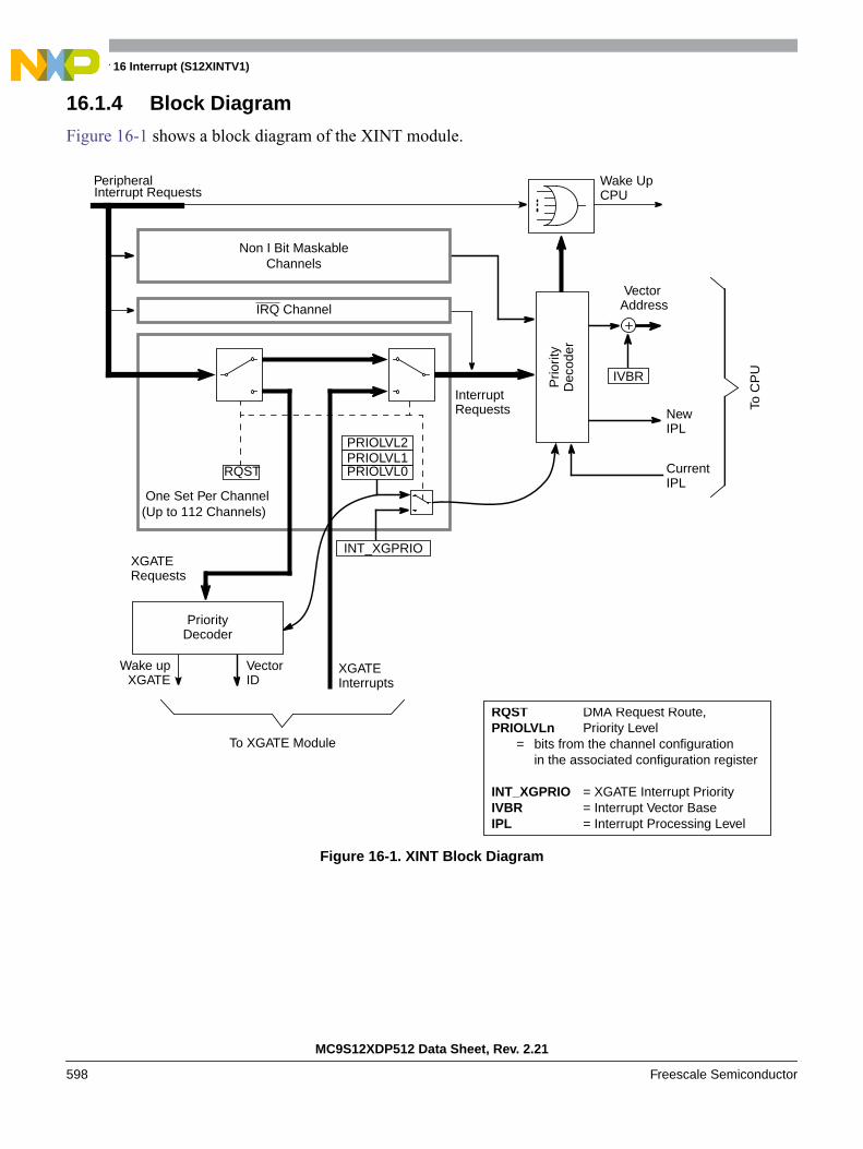
Chapter 16 Interrupt (S12XINTV1)
MC9S12XDP512 Data Sheet, Rev. 2.21
598 Freescale Semiconductor
16.1.4 Block Diagram
Figure 16-1 shows a block diagram of the XINT module.
Figure 16-1. XINT Block Diagram
Wake Up
CurrentRQST
IVBR
One Set Per Channel
XGATEInterrupts
XGATERequests
InterruptRequests
Interrupt Requests CPU
VectorAddress
NewIPL
IPL
(Up to 112 Channels)
RQST DMA Request Route,PRIOLVLn Priority Level
= bits from the channel configurationin the associated configuration register
INT_XGPRIO = XGATE Interrupt PriorityIVBR = Interrupt Vector BaseIPL = Interrupt Processing Level
PRIOLVL0PRIOLVL1PRIOLVL2
INT_XGPRIO
Peripheral
VectorID
To XGATE Module
PriorityDecoder
To C
PU
Prio
rity
Dec
oder
Non I Bit MaskableChannels
Wake upXGATE
IRQ Channel
Chapter 16 Interrupt (S12XINTV1)
MC9S12XDP512 Data Sheet, Rev. 2.21
Freescale Semiconductor 599
16.2 External Signal DescriptionThe XINT module has no external signals.
16.3 Memory Map and Register DefinitionThis section provides a detailed description of all registers accessible in the XINT.
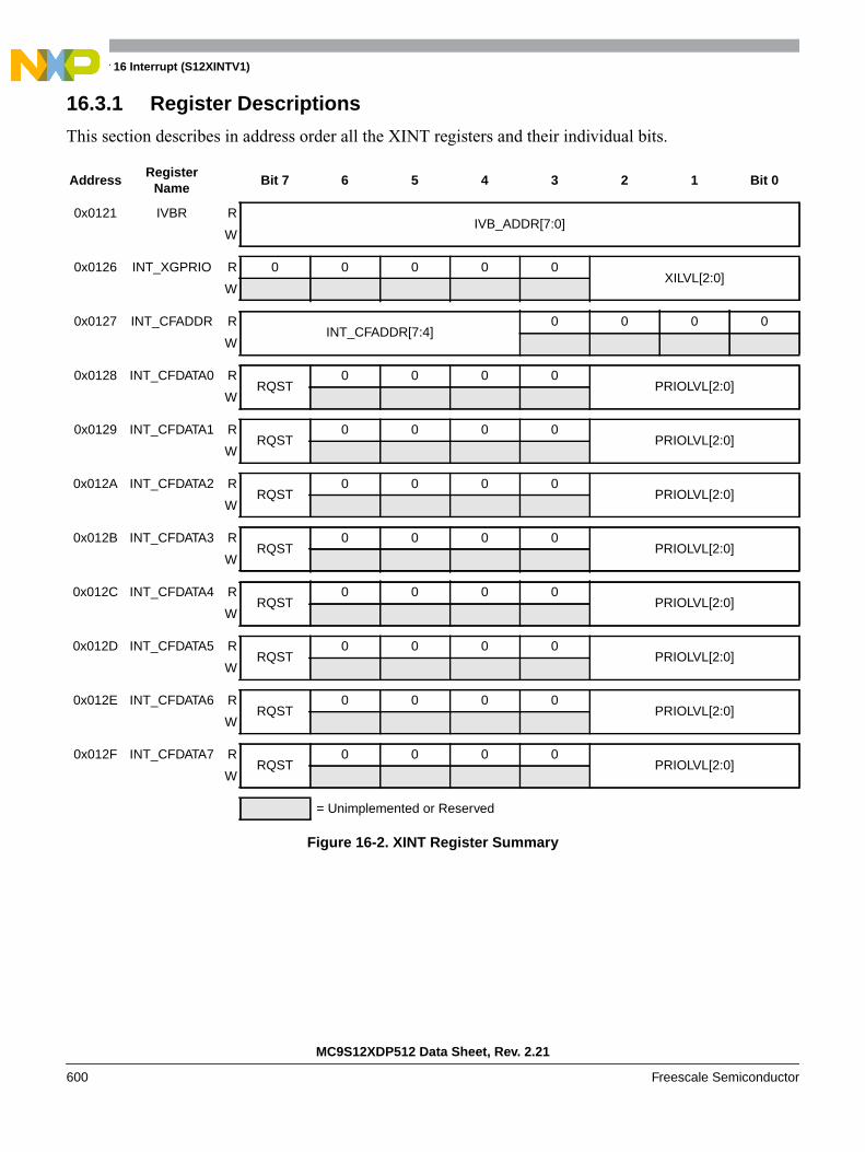
Chapter 16 Interrupt (S12XINTV1)
MC9S12XDP512 Data Sheet, Rev. 2.21
600 Freescale Semiconductor
16.3.1 Register Descriptions
This section describes in address order all the XINT registers and their individual bits.
AddressRegister
NameBit 7 6 5 4 3 2 1 Bit 0
0x0121 IVBR RIVB_ADDR[7:0]
W
0x0126 INT_XGPRIO R 0 0 0 0 0XILVL[2:0]
W
0x0127 INT_CFADDR RINT_CFADDR[7:4]
0 0 0 0
W
0x0128 INT_CFDATA0 RRQST
0 0 0 0PRIOLVL[2:0]
W
0x0129 INT_CFDATA1 RRQST
0 0 0 0PRIOLVL[2:0]
W
0x012A INT_CFDATA2 RRQST
0 0 0 0PRIOLVL[2:0]
W
0x012B INT_CFDATA3 RRQST
0 0 0 0PRIOLVL[2:0]
W
0x012C INT_CFDATA4 RRQST
0 0 0 0PRIOLVL[2:0]
W
0x012D INT_CFDATA5 RRQST
0 0 0 0PRIOLVL[2:0]
W
0x012E INT_CFDATA6 RRQST
0 0 0 0PRIOLVL[2:0]
W
0x012F INT_CFDATA7 RRQST
0 0 0 0PRIOLVL[2:0]
W
= Unimplemented or Reserved
Figure 16-2. XINT Register Summary
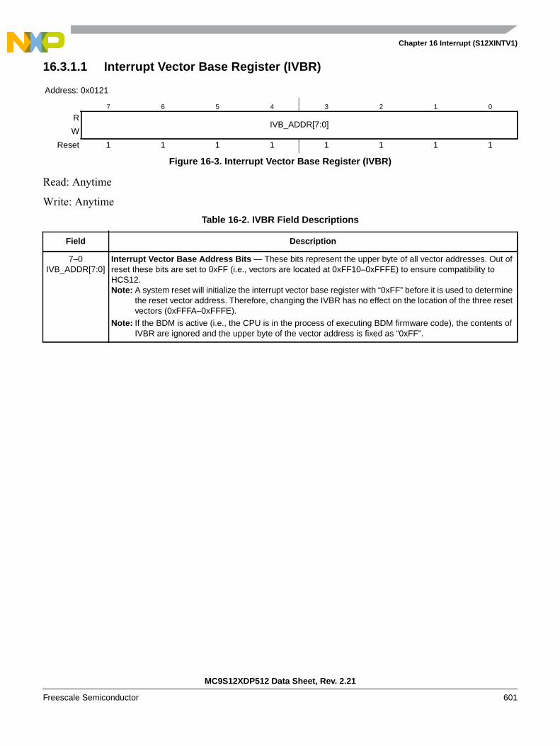
Chapter 16 Interrupt (S12XINTV1)
MC9S12XDP512 Data Sheet, Rev. 2.21
Freescale Semiconductor 601
16.3.1.1 Interrupt Vector Base Register (IVBR)
Read: Anytime
Write: Anytime
Address: 0x0121
7 6 5 4 3 2 1 0
RIVB_ADDR[7:0]
W
Reset 1 1 1 1 1 1 1 1
Figure 16-3. Interrupt Vector Base Register (IVBR)
Table 16-2. IVBR Field Descriptions
Field Description
7–0IVB_ADDR[7:0]
Interrupt Vector Base Address Bits — These bits represent the upper byte of all vector addresses. Out ofreset these bits are set to 0xFF (i.e., vectors are located at 0xFF10–0xFFFE) to ensure compatibility toHCS12.Note: A system reset will initialize the interrupt vector base register with “0xFF” before it is used to determine
the reset vector address. Therefore, changing the IVBR has no effect on the location of the three resetvectors (0xFFFA–0xFFFE).
Note: If the BDM is active (i.e., the CPU is in the process of executing BDM firmware code), the contents ofIVBR are ignored and the upper byte of the vector address is fixed as “0xFF”.

Chapter 16 Interrupt (S12XINTV1)
MC9S12XDP512 Data Sheet, Rev. 2.21
602 Freescale Semiconductor
16.3.1.2 XGATE Interrupt Priority Configuration Register (INT_XGPRIO)
Read: Anytime
Write: Anytime
Address: 0x0126
7 6 5 4 3 2 1 0
R 0 0 0 0 0XILVL[2:0]
W
Reset 0 0 0 0 0 0 0 1
= Unimplemented or Reserved
Figure 16-4. XGATE Interrupt Priority Configuration Register (INT_XGPRIO)
Table 16-3. INT_XGPRIO Field Descriptions
Field Description
2–0XILVL[2:0]
XGATE Interrupt Priority Level — The XILVL[2:0] bits configure the shared interrupt level of the DMA interruptscoming from the XGATE module. Out of reset the priority is set to the lowest active level (“1”).
Table 16-4. XGATE Interrupt Priority Levels
Priority XILVL2 XILVL1 XILVL0 Meaning
0 0 0 Interrupt request is disabled
low 0 0 1 Priority level 1
0 1 0 Priority level 2
0 1 1 Priority level 3
1 0 0 Priority level 4
1 0 1 Priority level 5
1 1 0 Priority level 6
high 1 1 1 Priority level 7

Chapter 16 Interrupt (S12XINTV1)
MC9S12XDP512 Data Sheet, Rev. 2.21
Freescale Semiconductor 603
16.3.1.3 Interrupt Request Configuration Address Register (INT_CFADDR)
Read: Anytime
Write: Anytime
Address: 0x0127
7 6 5 4 3 2 1 0
RINT_CFADDR[7:4]
0 0 0 0
W
Reset 0 0 0 1 0 0 0 0
= Unimplemented or Reserved
Figure 16-5. Interrupt Configuration Address Register (INT_CFADDR)
Table 16-5. INT_CFADDR Field Descriptions
Field Description
7–4INT_CFADDR[7:4]
Interrupt Request Configuration Data Register Select Bits — These bits determine which of the 128configuration data registers are accessible in the 8 register window at INT_CFDATA0–7. The hexadecimalvalue written to this register corresponds to the upper nibble of the lower byte of the interrupt vector, i.e.,writing 0xE0 to this register selects the configuration data register block for the 8 interrupt vector requestsstarting with vector (vector base + 0x00E0) to be accessible as INT_CFDATA0–7.Note: Writing all 0s selects non-existing configuration registers. In this case write accesses to
INT_CFDATA0–7 will be ignored and read accesses will return all 0.

Chapter 16 Interrupt (S12XINTV1)
MC9S12XDP512 Data Sheet, Rev. 2.21
604 Freescale Semiconductor
16.3.1.4 Interrupt Request Configuration Data Registers (INT_CFDATA0–7)
The eight register window visible at addresses INT_CFDATA0–7 contains the configuration data for theblock of eight interrupt requests (out of 128) selected by the interrupt configuration address register(INT_CFADDR) in ascending order. INT_CFDATA0 represents the interrupt configuration data registerof the vector with the lowest address in this block, while INT_CFDATA7 represents the interruptconfiguration data register of the vector with the highest address, respectively.
Address: 0x0128
7 6 5 4 3 2 1 0
RRQST
0 0 0 0PRIOLVL[2:0]
W
Reset 0 0 0 0 0 0 0 11
1 Please refer to the notes following the PRIOLVL[2:0] description below.
= Unimplemented or Reserved
Figure 16-6. Interrupt Request Configuration Data Register 0 (INT_CFDATA0)
Address: 0x0129
7 6 5 4 3 2 1 0
RRQST
0 0 0 0PRIOLVL[2:0]
W
Reset 0 0 0 0 0 0 0 11
1 Please refer to the notes following the PRIOLVL[2:0] description below.
= Unimplemented or Reserved
Figure 16-7. Interrupt Request Configuration Data Register 1 (INT_CFDATA1)
Address: 0x012A
7 6 5 4 3 2 1 0
RRQST
0 0 0 0PRIOLVL[2:0]
W
Reset 0 0 0 0 0 0 0 11
1 Please refer to the notes following the PRIOLVL[2:0] description below.
= Unimplemented or Reserved
Figure 16-8. Interrupt Request Configuration Data Register 2 (INT_CFDATA2)
Address: 0x012B
7 6 5 4 3 2 1 0
RRQST
0 0 0 0PRIOLVL[2:0]
W
Reset 0 0 0 0 0 0 0 11
1 Please refer to the notes following the PRIOLVL[2:0] description below.
= Unimplemented or Reserved
Figure 16-9. Interrupt Request Configuration Data Register 3 (INT_CFDATA3)

Chapter 16 Interrupt (S12XINTV1)
MC9S12XDP512 Data Sheet, Rev. 2.21
Freescale Semiconductor 605
Read: Anytime
Write: Anytime
Address: 0x012C
7 6 5 4 3 2 1 0
RRQST
0 0 0 0PRIOLVL[2:0]
W
Reset 0 0 0 0 0 0 0 11
1 Please refer to the notes following the PRIOLVL[2:0] description below.
= Unimplemented or Reserved
Figure 16-10. Interrupt Request Configuration Data Register 4 (INT_CFDATA4)
Address: 0x012D
7 6 5 4 3 2 1 0
RRQST
0 0 0 0PRIOLVL[2:0]
W
Reset 0 0 0 0 0 0 0 11
1 Please refer to the notes following the PRIOLVL[2:0] description below.
= Unimplemented or Reserved
Figure 16-11. Interrupt Request Configuration Data Register 5 (INT_CFDATA5)
Address: 0x012E
7 6 5 4 3 2 1 0
RRQST
0 0 0 0PRIOLVL[2:0]
W
Reset 0 0 0 0 0 0 0 11
1 Please refer to the notes following the PRIOLVL[2:0] description below.
= Unimplemented or Reserved
Figure 16-12. Interrupt Request Configuration Data Register 6 (INT_CFDATA6)
Address: 0x012F
7 6 5 4 3 2 1 0
RRQST
0 0 0 0PRIOLVL[2:0]
W
Reset 0 0 0 0 0 0 0 11
1 Please refer to the notes following the PRIOLVL[2:0] description below.
= Unimplemented or Reserved
Figure 16-13. Interrupt Request Configuration Data Register 7 (INT_CFDATA7)
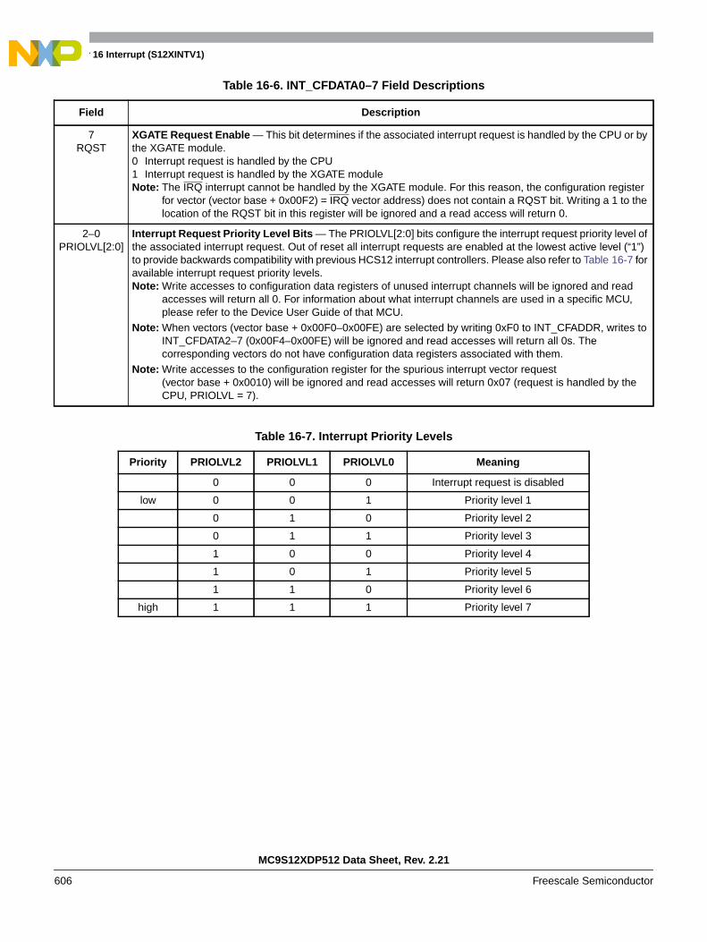
Chapter 16 Interrupt (S12XINTV1)
MC9S12XDP512 Data Sheet, Rev. 2.21
606 Freescale Semiconductor
Table 16-6. INT_CFDATA0–7 Field Descriptions
Field Description
7RQST
XGATE Request Enable — This bit determines if the associated interrupt request is handled by the CPU or bythe XGATE module.0 Interrupt request is handled by the CPU1 Interrupt request is handled by the XGATE moduleNote: The IRQ interrupt cannot be handled by the XGATE module. For this reason, the configuration register
for vector (vector base + 0x00F2) = IRQ vector address) does not contain a RQST bit. Writing a 1 to thelocation of the RQST bit in this register will be ignored and a read access will return 0.
2–0PRIOLVL[2:0]
Interrupt Request Priority Level Bits — The PRIOLVL[2:0] bits configure the interrupt request priority level ofthe associated interrupt request. Out of reset all interrupt requests are enabled at the lowest active level (“1”)to provide backwards compatibility with previous HCS12 interrupt controllers. Please also refer to Table 16-7 foravailable interrupt request priority levels.Note: Write accesses to configuration data registers of unused interrupt channels will be ignored and read
accesses will return all 0. For information about what interrupt channels are used in a specific MCU,please refer to the Device User Guide of that MCU.
Note: When vectors (vector base + 0x00F0–0x00FE) are selected by writing 0xF0 to INT_CFADDR, writes toINT_CFDATA2–7 (0x00F4–0x00FE) will be ignored and read accesses will return all 0s. Thecorresponding vectors do not have configuration data registers associated with them.
Note: Write accesses to the configuration register for the spurious interrupt vector request(vector base + 0x0010) will be ignored and read accesses will return 0x07 (request is handled by theCPU, PRIOLVL = 7).
Table 16-7. Interrupt Priority Levels
Priority PRIOLVL2 PRIOLVL1 PRIOLVL0 Meaning
0 0 0 Interrupt request is disabled
low 0 0 1 Priority level 1
0 1 0 Priority level 2
0 1 1 Priority level 3
1 0 0 Priority level 4
1 0 1 Priority level 5
1 1 0 Priority level 6
high 1 1 1 Priority level 7
Chapter 16 Interrupt (S12XINTV1)
MC9S12XDP512 Data Sheet, Rev. 2.21
Freescale Semiconductor 607
16.4 Functional DescriptionThe XINT module processes all exception requests to be serviced by the CPU module. These exceptionsinclude interrupt vector requests and reset vector requests. Each of these exception types and their overallpriority level is discussed in the subsections below.
16.4.1 S12X Exception Requests
The CPU handles both reset requests and interrupt requests. The XINT contains registers to configure thepriority level of each I bit maskable interrupt request which can be used to implement an interrupt priorityscheme. This also includes the possibility to nest interrupt requests. A priority decoder is used to evaluatethe priority of a pending interrupt request.
16.4.2 Interrupt Prioritization
After system reset all interrupt requests with a vector address lower than or equal to (vector base + 0x00F2)are enabled, are set up to be handled by the CPU and have a pre-configured priority level of 1. Theexception to this rule is the spurious interrupt vector request at (vector base + 0x0010) which cannot bedisabled, is always handled by the CPU and has a fixed priority level of 7. A priority level of 0 effectivelydisables the associated interrupt request.
If more than one interrupt request is configured to the same interrupt priority level the interrupt requestwith the higher vector address wins the prioritization.
The following conditions must be met for an I bit maskable interrupt request to be processed.
1. The local interrupt enabled bit in the peripheral module must be set.
2. The setup in the configuration register associated with the interrupt request channel must meet thefollowing conditions:
a) The XGATE request enable bit must be 0 to have the CPU handle the interrupt request.
b) The priority level must be set to non zero.
c) The priority level must be greater than the current interrupt processing level in the conditioncode register (CCR) of the CPU (PRIOLVL[2:0] > IPL[2:0]).
3. The I bit in the condition code register (CCR) of the CPU must be cleared.
4. There is no SWI, TRAP, or XIRQ request pending.
NOTEAll non I bit maskable interrupt requests always have higher priority thanI bit maskable interrupt requests. If an I bit maskable interrupt request isinterrupted by a non I bit maskable interrupt request, the currently activeinterrupt processing level (IPL) remains unaffected. It is possible to nestnon I bit maskable interrupt requests, e.g., by nesting SWI or TRAP calls.
Chapter 16 Interrupt (S12XINTV1)
MC9S12XDP512 Data Sheet, Rev. 2.21
608 Freescale Semiconductor
16.4.2.1 Interrupt Priority Stack
The current interrupt processing level (IPL) is stored in the condition code register (CCR) of the CPU. Thisway the current IPL is automatically pushed to the stack by the standard interrupt stacking procedure. Thenew IPL is copied to the CCR from the priority level of the highest priority active interrupt request channelwhich is configured to be handled by the CPU. The copying takes place when the interrupt vector isfetched. The previous IPL is automatically restored by executing the RTI instruction.
16.4.3 XGATE Requests
The XINT module processes all exception requests to be serviced by the XGATE module. The overallpriority level of those exceptions is discussed in the subsections below.
16.4.3.1 XGATE Request Prioritization
An interrupt request channel is configured to be handled by the XGATE module, if the RQST bit of theassociated configuration register is set to 1 (please refer to Section 16.3.1.4, “Interrupt RequestConfiguration Data Registers (INT_CFDATA0–7)”). The priority level setting (PRIOLVL) for this channelbecomes the DMA priority which will be used to determine the highest priority DMA request to beserviced next by the XGATE module. Additionally, DMA interrupts may be raised by the XGATE moduleby setting one or more of the XGATE channel interrupt flags (using the SIF instruction). This will resultin an CPU interrupt with vector address vector base + (2 * channel ID number), where the channel IDnumber corresponds to the highest set channel interrupt flag, if the XGIE and channel RQST bits are set.
The shared interrupt priority for the DMA interrupt requests is taken from the XGATE interrupt priorityconfiguration register (please refer to Section 16.3.1.2, “XGATE Interrupt Priority Configuration Register(INT_XGPRIO)”). If more than one DMA interrupt request channel becomes active at the same time, thechannel with the highest vector address wins the prioritization.
16.4.4 Priority Decoders
The XINT module contains priority decoders to determine the priority for all interrupt requests pendingfor the respective target.
There are two priority decoders, one for each interrupt request target (CPU, XGATE module). The functionof both priority decoders is basically the same with one exception: the priority decoder for the XGATEmodule does not take the current interrupt processing level into account because XGATE requests cannotbe nested.
Because the vector is not supplied until the CPU requests it, it is possible that a higher priority interruptrequest could override the original exception that caused the CPU to request the vector. In this case, theCPU will receive the highest priority vector and the system will process this exception instead of theoriginal request.
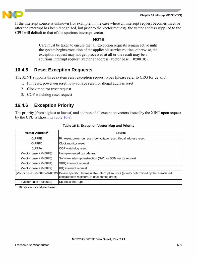
Chapter 16 Interrupt (S12XINTV1)
MC9S12XDP512 Data Sheet, Rev. 2.21
Freescale Semiconductor 609
If the interrupt source is unknown (for example, in the case where an interrupt request becomes inactiveafter the interrupt has been recognized, but prior to the vector request), the vector address supplied to theCPU will default to that of the spurious interrupt vector.
NOTECare must be taken to ensure that all exception requests remain active untilthe system begins execution of the applicable service routine; otherwise, theexception request may not get processed at all or the result may be aspurious interrupt request (vector at address (vector base + 0x0010)).
16.4.5 Reset Exception Requests
The XINT supports three system reset exception request types (please refer to CRG for details):
1. Pin reset, power-on reset, low-voltage reset, or illegal address reset
2. Clock monitor reset request
3. COP watchdog reset request
16.4.6 Exception Priority
The priority (from highest to lowest) and address of all exception vectors issued by the XINT upon requestby the CPU is shown in Table 16-8.
Table 16-8. Exception Vector Map and Priority
Vector Address1
1 16 bits vector address based
Source
0xFFFE Pin reset, power-on reset, low-voltage reset, illegal address reset
0xFFFC Clock monitor reset
0xFFFA COP watchdog reset
(Vector base + 0x00F8) Unimplemented opcode trap
(Vector base + 0x00F6) Software interrupt instruction (SWI) or BDM vector request
(Vector base + 0x00F4) XIRQ interrupt request
(Vector base + 0x00F2) IRQ interrupt request
(Vector base + 0x00F0–0x0012) Device specific I bit maskable interrupt sources (priority determined by the associatedconfiguration registers, in descending order)
(Vector base + 0x0010) Spurious interrupt
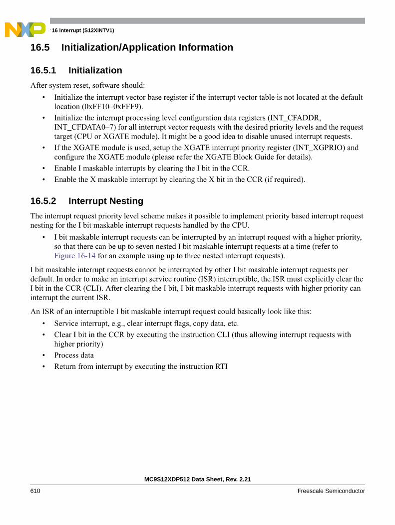
Chapter 16 Interrupt (S12XINTV1)
MC9S12XDP512 Data Sheet, Rev. 2.21
610 Freescale Semiconductor
16.5 Initialization/Application Information
16.5.1 Initialization
After system reset, software should:
• Initialize the interrupt vector base register if the interrupt vector table is not located at the defaultlocation (0xFF10–0xFFF9).
• Initialize the interrupt processing level configuration data registers (INT_CFADDR,INT_CFDATA0–7) for all interrupt vector requests with the desired priority levels and the requesttarget (CPU or XGATE module). It might be a good idea to disable unused interrupt requests.
• If the XGATE module is used, setup the XGATE interrupt priority register (INT_XGPRIO) andconfigure the XGATE module (please refer the XGATE Block Guide for details).
• Enable I maskable interrupts by clearing the I bit in the CCR.
• Enable the X maskable interrupt by clearing the X bit in the CCR (if required).
16.5.2 Interrupt Nesting
The interrupt request priority level scheme makes it possible to implement priority based interrupt requestnesting for the I bit maskable interrupt requests handled by the CPU.
• I bit maskable interrupt requests can be interrupted by an interrupt request with a higher priority,so that there can be up to seven nested I bit maskable interrupt requests at a time (refer toFigure 16-14 for an example using up to three nested interrupt requests).
I bit maskable interrupt requests cannot be interrupted by other I bit maskable interrupt requests perdefault. In order to make an interrupt service routine (ISR) interruptible, the ISR must explicitly clear theI bit in the CCR (CLI). After clearing the I bit, I bit maskable interrupt requests with higher priority caninterrupt the current ISR.
An ISR of an interruptible I bit maskable interrupt request could basically look like this:
• Service interrupt, e.g., clear interrupt flags, copy data, etc.
• Clear I bit in the CCR by executing the instruction CLI (thus allowing interrupt requests withhigher priority)
• Process data
• Return from interrupt by executing the instruction RTI
Chapter 16 Interrupt (S12XINTV1)
MC9S12XDP512 Data Sheet, Rev. 2.21
Freescale Semiconductor 611
Figure 16-14. Interrupt Processing Example
16.5.3 Wake Up from Stop or Wait Mode
16.5.3.1 CPU Wake Up from Stop or Wait Mode
Every I bit maskable interrupt request which is configured to be handled by the CPU is capable of wakingthe MCU from stop or wait mode. To determine whether an I bit maskable interrupts is qualified to wakeup the CPU or not, the same settings as in normal run mode are applied during stop or wait mode:
• If the I bit in the CCR is set, all I bit maskable interrupts are masked from waking up the MCU.
• An I bit maskable interrupt is ignored if it is configured to a priority level below or equal to thecurrent IPL in CCR.
• I bit maskable interrupt requests which are configured to be handled by the XGATE are not capableof waking up the CPU.
An XIRQ request can wake up the MCU from stop or wait mode at anytime, even if the X bit in CCR is set.
16.5.3.2 XGATE Wake Up from Stop or Wait Mode
Interrupt request channels which are configured to be handled by the XGATE are capable of waking up theXGATE. Interrupt request channels handled by the XGATE do not affect the state of the CPU.
0
Reset
4
0
7
6
5
4
3
2
1
0
L4
7
0
4
L1 (Pending)
L7
L3 (Pending)
RTI
4
0
3
0
RTI
RTI
1
0
0
RTI
Stacked IPL
Processing Levels
IPL in CCR

Chapter 16 Interrupt (S12XINTV1)
MC9S12XDP512 Data Sheet, Rev. 2.21
612 Freescale Semiconductor

MC9S12XDP512 Data Sheet, Rev. 2.21
Freescale Semiconductor 613
Chapter 17Memory Mapping Control (S12XMMCV2)
17.1 IntroductionThis section describes the functionality of the module mapping control (MMC) sub-block of the S12Xplatform. The block diagram of the MMC is shown in Figure 1-1.
The MMC module controls the multi-master priority accesses, the selection of internal resources andexternal space. Internal buses including internal memories and peripherals are controlled in this module.The local address space for each master is translated to a global memory space.
17.1.1 Features
The main features of this block are:
• Paging capability to support a global 8 Mbytes memory address space
• Bus arbitration between the masters CPU, BDM, and XGATE
• Simultaneous accesses to different resources1 (internal, external, and peripherals) (see Figure 1-1)
• Resolution of target bus access collision
• Access restriction control from masters to some targets (e.g., RAM write access protection for userspecified areas)
• MCU operation mode control
• MCU security control
• Separate memory map schemes for each master CPU, BDM, and XGATE
• ROM control bits to enable the on-chip FLASH or ROM selection
• Port replacement registers access control
• Generation of system reset when CPU accesses an unimplemented address (i.e., an address whichdoes not belong to any of the on-chip modules) in single-chip modes
17.1.2 Modes of Operation
This subsection lists and briefly describes all operating modes supported by the MMC.
17.1.2.1 Power Saving Modes
• Run mode
MMC is functional during normal run mode.
1. Resources are also called targets.

Chapter 17 Memory Mapping Control (S12XMMCV2)
MC9S12XDP512 Data Sheet, Rev. 2.21
614 Freescale Semiconductor
• Wait mode
MMC is functional during wait mode.
• Stop mode
MMC is inactive during stop mode.
17.1.2.2 Functional Modes
• Single chip modes
In normal and special single chip mode the internal memory is used. External bus is not active.
• Expanded modes
Address, data, and control signals are activated in normal expanded and special test modes whenaccessing the external bus.
• Emulation modes
External bus is active to emulate via an external tool the normal expanded or the normal single chipmode.
17.1.3 Block Diagram
Figure 1-1 shows a block diagram of the MMC.
Figure 17-1. MMC Block Diagram
17.2 External Signal DescriptionThe user is advised to refer to the SoC Guide for port configuration and location of external bus signals.Some pins may not be bonded out in all implementations.
Peripherals
FLASH
XGATECPUBDM
Target Bus Controller
DBG
EEPROM
EBIMMC
Address Decoder & Priority
RAM
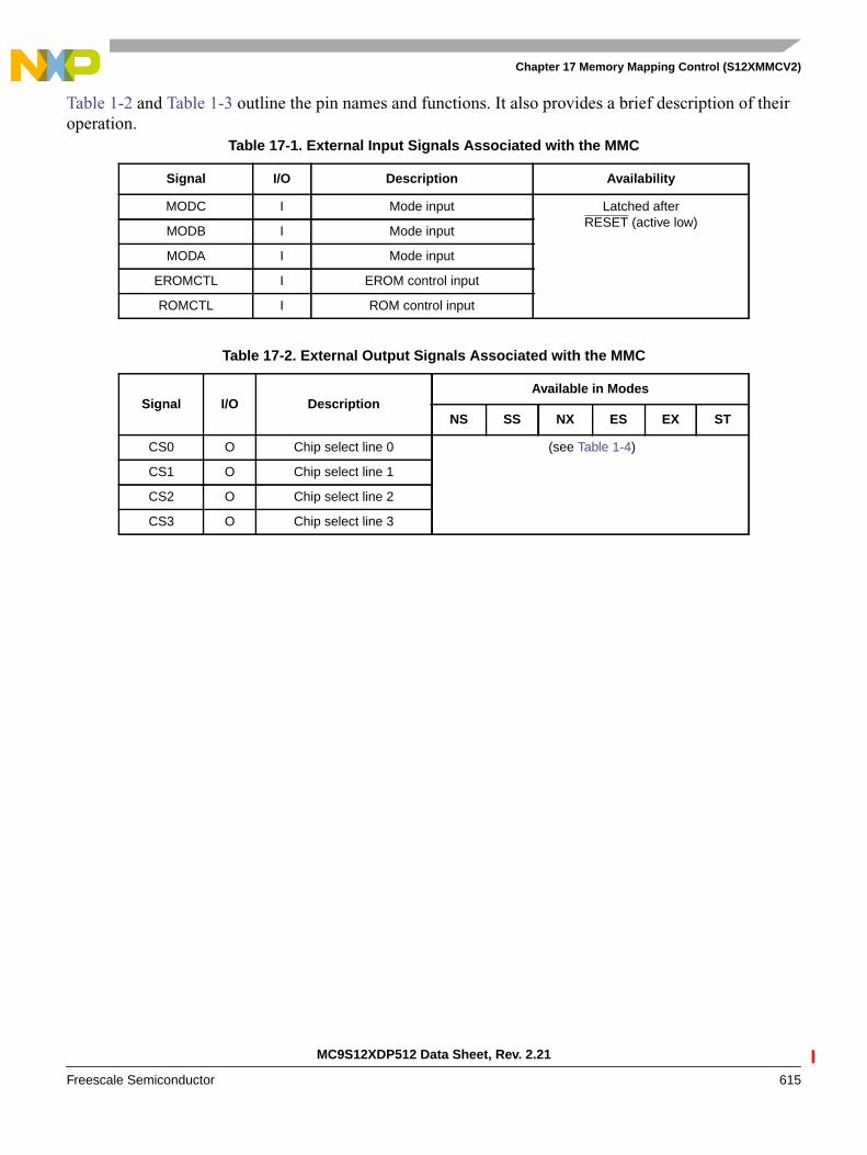
Chapter 17 Memory Mapping Control (S12XMMCV2)
MC9S12XDP512 Data Sheet, Rev. 2.21
Freescale Semiconductor 615
Table 1-2 and Table 1-3 outline the pin names and functions. It also provides a brief description of theiroperation.
Table 17-1. External Input Signals Associated with the MMC
Signal I/O Description Availability
MODC I Mode input Latched afterRESET (active low)
MODB I Mode input
MODA I Mode input
EROMCTL I EROM control input
ROMCTL I ROM control input
Table 17-2. External Output Signals Associated with the MMC
Signal I/O DescriptionAvailable in Modes
NS SS NX ES EX ST
CS0 O Chip select line 0 (see Table 1-4)
CS1 O Chip select line 1
CS2 O Chip select line 2
CS3 O Chip select line 3
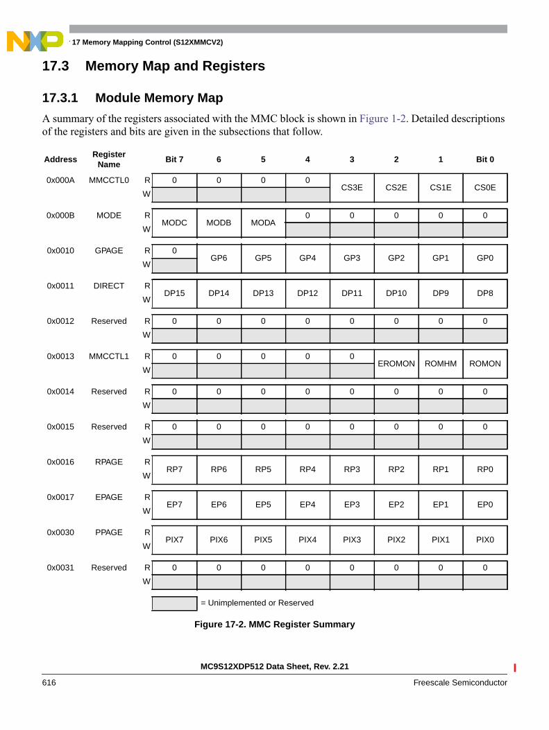
Chapter 17 Memory Mapping Control (S12XMMCV2)
MC9S12XDP512 Data Sheet, Rev. 2.21
616 Freescale Semiconductor
17.3 Memory Map and Registers
17.3.1 Module Memory Map
A summary of the registers associated with the MMC block is shown in Figure 1-2. Detailed descriptionsof the registers and bits are given in the subsections that follow.
AddressRegister
NameBit 7 6 5 4 3 2 1 Bit 0
0x000A MMCCTL0 R 0 0 0 0CS3E CS2E CS1E CS0E
W
0x000B MODE RMODC MODB MODA
0 0 0 0 0
W
0x0010 GPAGE R 0GP6 GP5 GP4 GP3 GP2 GP1 GP0
W
0x0011 DIRECT RDP15 DP14 DP13 DP12 DP11 DP10 DP9 DP8
W
0x0012 Reserved R 0 0 0 0 0 0 0 0
W
0x0013 MMCCTL1 R 0 0 0 0 0EROMON ROMHM ROMON
W
0x0014 Reserved R 0 0 0 0 0 0 0 0
W
0x0015 Reserved R 0 0 0 0 0 0 0 0
W
0x0016 RPAGE RRP7 RP6 RP5 RP4 RP3 RP2 RP1 RP0
W
0x0017 EPAGE REP7 EP6 EP5 EP4 EP3 EP2 EP1 EP0
W
0x0030 PPAGE RPIX7 PIX6 PIX5 PIX4 PIX3 PIX2 PIX1 PIX0
W
0x0031 Reserved R 0 0 0 0 0 0 0 0
W
= Unimplemented or Reserved
Figure 17-2. MMC Register Summary

Chapter 17 Memory Mapping Control (S12XMMCV2)
MC9S12XDP512 Data Sheet, Rev. 2.21
Freescale Semiconductor 617
17.3.2 Register Descriptions
17.3.2.1 MMC Control Register (MMCCTL0)
Read: Anytime. In emulation modes read operations will return the data from the external bus. In all othermodes the data is read from this register.
Write: Anytime. In emulation modes write operations will also be directed to the external bus.
0x011C RAMWPC RRPWE
0 0 0 0 0AVIE AVIF
W
0x011D RAMXGU R 1XGU6 XGU5 XGU4 XGU3 XGU2 XGU1 XGU0
W
0x011E RAMSHL R 1SHL6 SHL5 SHL4 SHL3 SHL2 SHL1 SHL0
W
0x011F RAMSHU R 1SHU6 SHU5 SHU4 SHU3 SHU2 SHU1 SHU0
W
Address: 0x000A PRR
7 6 5 4 3 2 1 0
R 0 0 0 0CS3E CS2E CS1E CS0E
W
Reset 0 0 0 0 0 0 0 ROMON1
1. ROMON is bit[0] of the register MMCTL1 (see Figure 1-10)
= Unimplemented or Reserved
Figure 17-3. MMC Control Register (MMCCTL0)
Table 17-3. Chip Selects Function Activity
Register BitChip Modes
NS SS NX ES EX ST
CS3E, CS2E, CS1E, CS0E Disabled1
1 Disabled: feature always inactive.
Disabled Enabled2
2 Enabled: activity is controlled by the appropriate register bit value.
Disabled Enabled Enabled
AddressRegister
NameBit 7 6 5 4 3 2 1 Bit 0
= Unimplemented or Reserved
Figure 17-2. MMC Register Summary

Chapter 17 Memory Mapping Control (S12XMMCV2)
MC9S12XDP512 Data Sheet, Rev. 2.21
618 Freescale Semiconductor
The MMCCTL0 register is used to control external bus functions, i.e., availability of chip selects.
CAUTIONXGATE write access to this register during an CPU access which makes useof this register could lead to unexpected results.
Table 17-4. MMCCTL0 Field Descriptions
Field Description
3–0CS[3:0]E
Chip Select Enables — Each of these bits enables one of the external chip selects CS3, CS2, CS1, and CS0outputs which are asserted during accesses to specific external addresses. The associated global addressranges are shown in Table 1-6 and Table 1-21 and Figure 1-23.Chip selects are only active if enabled in normal expanded mode, Emulation expanded mode and special testmode. The function disabled in all other operating modes.0 Chip select is disabled1 Chip select is enabled
Table 17-5. Chip Select Signals
Global Address Range Asserted Signal
0x00_0800–0x0F_FFFF CS3
0x10_0000–0x1F_FFFF CS2
0x20_0000–0x3F_FFFF CS1
0x40_0000–0x7F_FFFF CS01
1 When the internal NVM is enabled (see ROMON in Section 1.3.2.5, “MMC ControlRegister (MMCCTL1)”) the CS0 is not asserted in the space occupied by this on-chipmemory block.

Chapter 17 Memory Mapping Control (S12XMMCV2)
MC9S12XDP512 Data Sheet, Rev. 2.21
Freescale Semiconductor 619
17.3.2.2 Mode Register (MODE)
Read: Anytime. In emulation modes read operations will return the data read from the external bus. In allother modes the data are read from this register.
Write: Only if a transition is allowed (see Figure 1-5). In emulation modes write operations will be alsodirected to the external bus.
The MODE bits of the MODE register are used to establish the MCU operating mode.
CAUTIONXGATE write access to this register during an CPU access which makes useof this register could lead to unexpected results.
Address: 0x000B PRR
7 6 5 4 3 2 1 0
RMODC MODB MODA
0 0 0 0 0
W
Reset MODC1 MODB1 MODA1 0 0 0 0 0
1. External signal (see Table 1-2).
= Unimplemented or Reserved
Figure 17-4. Mode Register (MODE)
Table 17-6. MODE Field Descriptions
Field Description
7–5MODC,MODB,MODA
Mode Select Bits — These bits control the current operating mode during RESET high (inactive). The externalmode pins MODC, MODB, and MODA determine the operating mode during RESET low (active). The state ofthe pins is latched into the respective register bits after the RESET signal goes inactive (see Figure 1-5).
Write restrictions exist to disallow transitions between certain modes. Figure 1-5 illustrates all allowed modechanges. Attempting non authorized transitions will not change the MODE bits, but it will block further writes tothese register bits except in special modes.
Both transitions from normal single-chip mode to normal expanded mode and from emulation single-chip toemulation expanded mode are only executed by writing a value of 0b101 (write once). Writing any other valuewill not change the MODE bits, but will block further writes to these register bits.
Changes of operating modes are not allowed when the device is secured, but it will block further writes to theseregister bits except in special modes.
In emulation modes reading this address returns data from the external bus which has to be driven by theemulator. It is therefore responsibility of the emulator hardware to provide the expected value (i.e. a valuecorresponding to normal single chip mode while the device is in emulation single-chip mode or a valuecorresponding to normal expanded mode while the device is in emulation expanded mode).

Chapter 17 Memory Mapping Control (S12XMMCV2)
MC9S12XDP512 Data Sheet, Rev. 2.21
620 Freescale Semiconductor
Figure 17-5. Mode Transition Diagram when MCU is Unsecured
NormalSingle-Chip
100
NormalExpanded
101
EmulationExpanded
011
EmulationSingle-Chip
001
SpecialTest
010
SpecialSingle-Chip
000
101
101
011
011
101
000010
100
001
001
100
101
RESET
(SS)
110111
000
RESET
RESET
RESET
RESET
RESET
010
101
011001
100
(EX)
(NX)(NS)
(ES)
(ST)
RESET
Transition done by external pins (MODC, MODB, MODA)
Transition done by write access to the MODE register
110111
Illegal (MODC, MODB, MODA) pin values.
Do not use. (Reserved for future use).
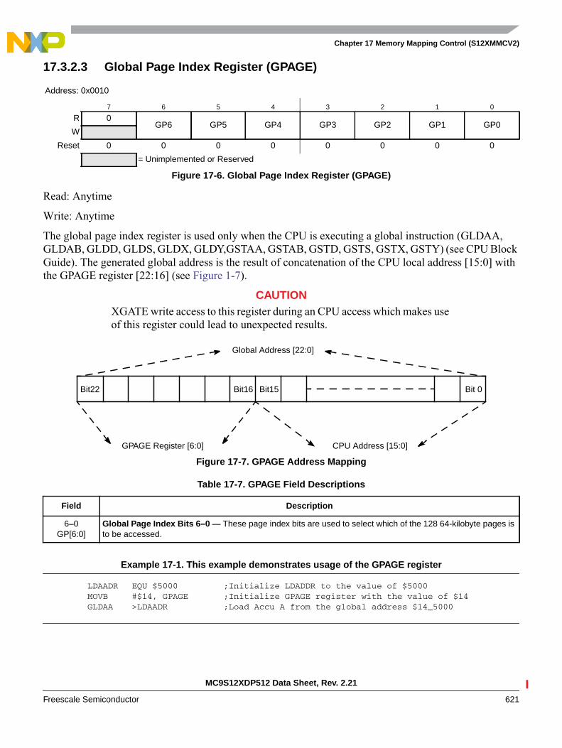
Chapter 17 Memory Mapping Control (S12XMMCV2)
MC9S12XDP512 Data Sheet, Rev. 2.21
Freescale Semiconductor 621
17.3.2.3 Global Page Index Register (GPAGE)
Read: Anytime
Write: Anytime
The global page index register is used only when the CPU is executing a global instruction (GLDAA,GLDAB, GLDD, GLDS, GLDX, GLDY,GSTAA, GSTAB, GSTD, GSTS, GSTX, GSTY) (see CPU BlockGuide). The generated global address is the result of concatenation of the CPU local address [15:0] withthe GPAGE register [22:16] (see Figure 1-7).
CAUTIONXGATE write access to this register during an CPU access which makes useof this register could lead to unexpected results.
Figure 17-7. GPAGE Address Mapping
Example 17-1. This example demonstrates usage of the GPAGE register
LDAADR EQU $5000 ;Initialize LDADDR to the value of $5000MOVB #$14, GPAGE ;Initialize GPAGE register with the value of $14GLDAA >LDAADR ;Load Accu A from the global address $14_5000
Address: 0x0010
7 6 5 4 3 2 1 0
R 0GP6 GP5 GP4 GP3 GP2 GP1 GP0
W
Reset 0 0 0 0 0 0 0 0
= Unimplemented or Reserved
Figure 17-6. Global Page Index Register (GPAGE)
Table 17-7. GPAGE Field Descriptions
Field Description
6–0GP[6:0]
Global Page Index Bits 6–0 — These page index bits are used to select which of the 128 64-kilobyte pages isto be accessed.
Bit16 Bit 0Bit15Bit22
CPU Address [15:0]GPAGE Register [6:0]
Global Address [22:0]
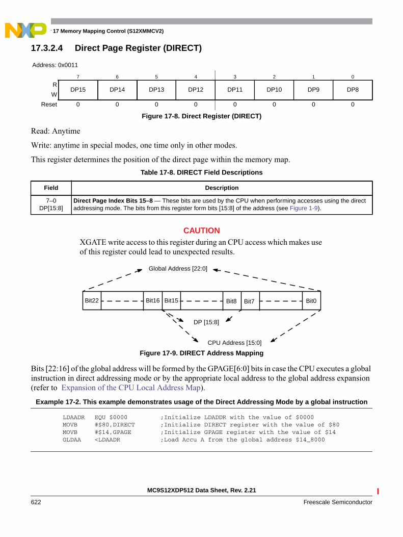
Chapter 17 Memory Mapping Control (S12XMMCV2)
MC9S12XDP512 Data Sheet, Rev. 2.21
622 Freescale Semiconductor
17.3.2.4 Direct Page Register (DIRECT)
Read: Anytime
Write: anytime in special modes, one time only in other modes.
This register determines the position of the direct page within the memory map.
CAUTIONXGATE write access to this register during an CPU access which makes useof this register could lead to unexpected results.
Figure 17-9. DIRECT Address Mapping
Bits [22:16] of the global address will be formed by the GPAGE[6:0] bits in case the CPU executes a globalinstruction in direct addressing mode or by the appropriate local address to the global address expansion(refer to Expansion of the CPU Local Address Map).
Example 17-2. This example demonstrates usage of the Direct Addressing Mode by a global instruction
LDAADR EQU $0000 ;Initialize LDADDR with the value of $0000MOVB #$80,DIRECT ;Initialize DIRECT register with the value of $80MOVB #$14,GPAGE ;Initialize GPAGE register with the value of $14GLDAA <LDAADR ;Load Accu A from the global address $14_8000
Address: 0x0011
7 6 5 4 3 2 1 0
RDP15 DP14 DP13 DP12 DP11 DP10 DP9 DP8
W
Reset 0 0 0 0 0 0 0 0
Figure 17-8. Direct Register (DIRECT)
Table 17-8. DIRECT Field Descriptions
Field Description
7–0DP[15:8]
Direct Page Index Bits 15–8 — These bits are used by the CPU when performing accesses using the directaddressing mode. The bits from this register form bits [15:8] of the address (see Figure 1-9).
Bit15 Bit0Bit7Bit22
CPU Address [15:0]
Global Address [22:0]
Bit8Bit16
DP [15:8]
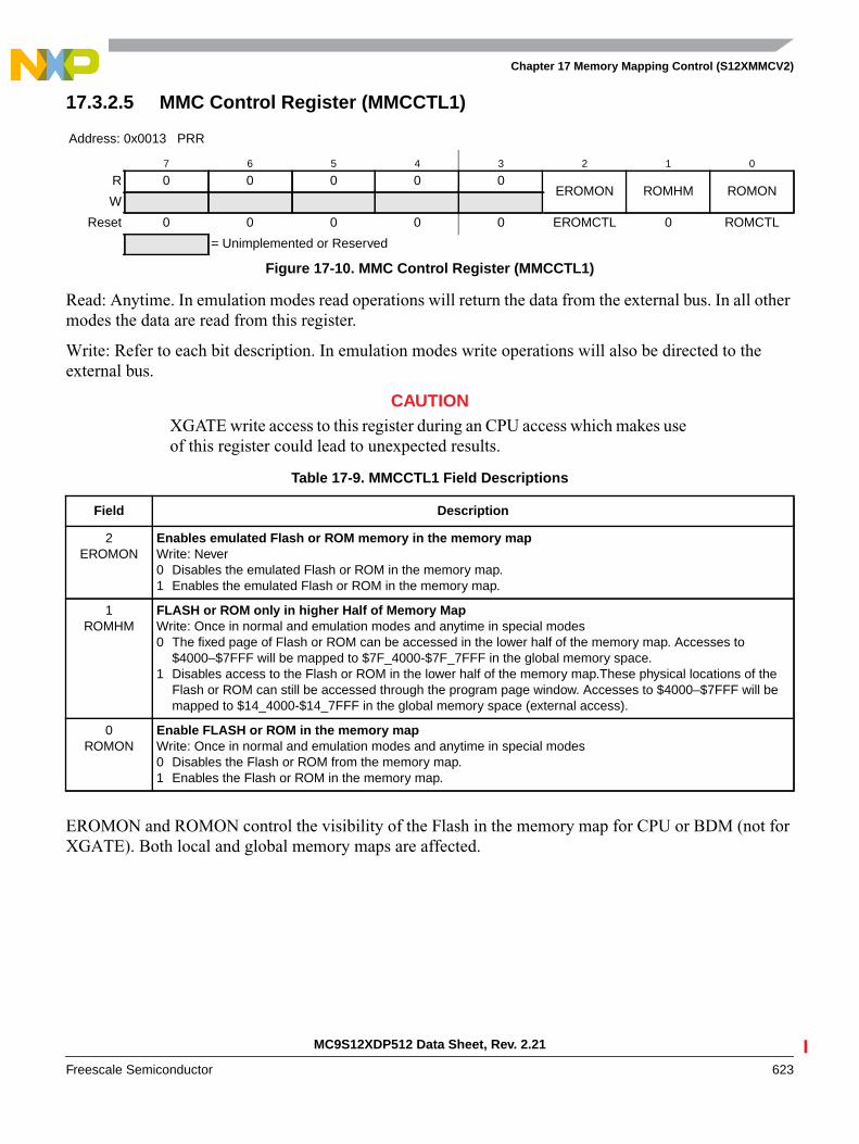
Chapter 17 Memory Mapping Control (S12XMMCV2)
MC9S12XDP512 Data Sheet, Rev. 2.21
Freescale Semiconductor 623
17.3.2.5 MMC Control Register (MMCCTL1)
Read: Anytime. In emulation modes read operations will return the data from the external bus. In all othermodes the data are read from this register.
Write: Refer to each bit description. In emulation modes write operations will also be directed to theexternal bus.
CAUTIONXGATE write access to this register during an CPU access which makes useof this register could lead to unexpected results.
EROMON and ROMON control the visibility of the Flash in the memory map for CPU or BDM (not forXGATE). Both local and global memory maps are affected.
Address: 0x0013 PRR
7 6 5 4 3 2 1 0
R 0 0 0 0 0EROMON ROMHM ROMON
W
Reset 0 0 0 0 0 EROMCTL 0 ROMCTL
= Unimplemented or Reserved
Figure 17-10. MMC Control Register (MMCCTL1)
Table 17-9. MMCCTL1 Field Descriptions
Field Description
2EROMON
Enables emulated Flash or ROM memory in the memory mapWrite: Never0 Disables the emulated Flash or ROM in the memory map.1 Enables the emulated Flash or ROM in the memory map.
1ROMHM
FLASH or ROM only in higher Half of Memory MapWrite: Once in normal and emulation modes and anytime in special modes0 The fixed page of Flash or ROM can be accessed in the lower half of the memory map. Accesses to
$4000–$7FFF will be mapped to $7F_4000-$7F_7FFF in the global memory space.1 Disables access to the Flash or ROM in the lower half of the memory map.These physical locations of the
Flash or ROM can still be accessed through the program page window. Accesses to $4000–$7FFF will bemapped to $14_4000-$14_7FFF in the global memory space (external access).
0ROMON
Enable FLASH or ROM in the memory mapWrite: Once in normal and emulation modes and anytime in special modes0 Disables the Flash or ROM from the memory map.1 Enables the Flash or ROM in the memory map.

Chapter 17 Memory Mapping Control (S12XMMCV2)
MC9S12XDP512 Data Sheet, Rev. 2.21
624 Freescale Semiconductor
17.3.2.6 RAM Page Index Register (RPAGE)
Read: Anytime
Write: Anytime
The RAM page index register allows accessing up to (1M minus 2K) bytes of RAM in the global memorymap by using the eight page index bits to page 4 Kbyte blocks into the RAM page window located in theCPU local memory map from address $1000 to address $1FFF (see Figure 1-12).
CAUTIONXGATE write access to this register during an CPU access which makes useof this register could lead to unexpected results.
Table 17-10. Data Sources when CPU or BDM is Accessing Flash Area
Chip Modes ROMON EROMON DATA SOURCE1
1 Internal means resources inside the MCU are read/written.Internal Flash means Flash resources inside the MCU are read/written.Emulation memory means resources inside the emulator are read/written (PRU registers, flashreplacement, RAM, EEPROM and register space are always considered internal).External application means resources residing outside the MCU are read/written.
Stretch2
2 The external access stretch mechanism is part of the EBI module (refer to EBI Block Guide for details).
Normal Single Chip X X Internal N
Special Single Chip
Emulation Single Chip X 0 Emulation Memory N
X 1 Internal Flash
Normal Expanded 0 X External Application Y
1 X Internal Flash N
Emulation Expanded 0 X External Application Y
1 0 Emulation Memory N
1 1 Internal Flash
Special Test 0 X External Application N
1 X Internal Flash
Address: 0x0016
7 6 5 4 3 2 1 0
RRP7 RP6 RP5 RP4 RP3 RP2 RP1 RP0
W
Reset 1 1 1 1 1 1 0 1
Figure 17-11. RAM Page Index Register (RPAGE)
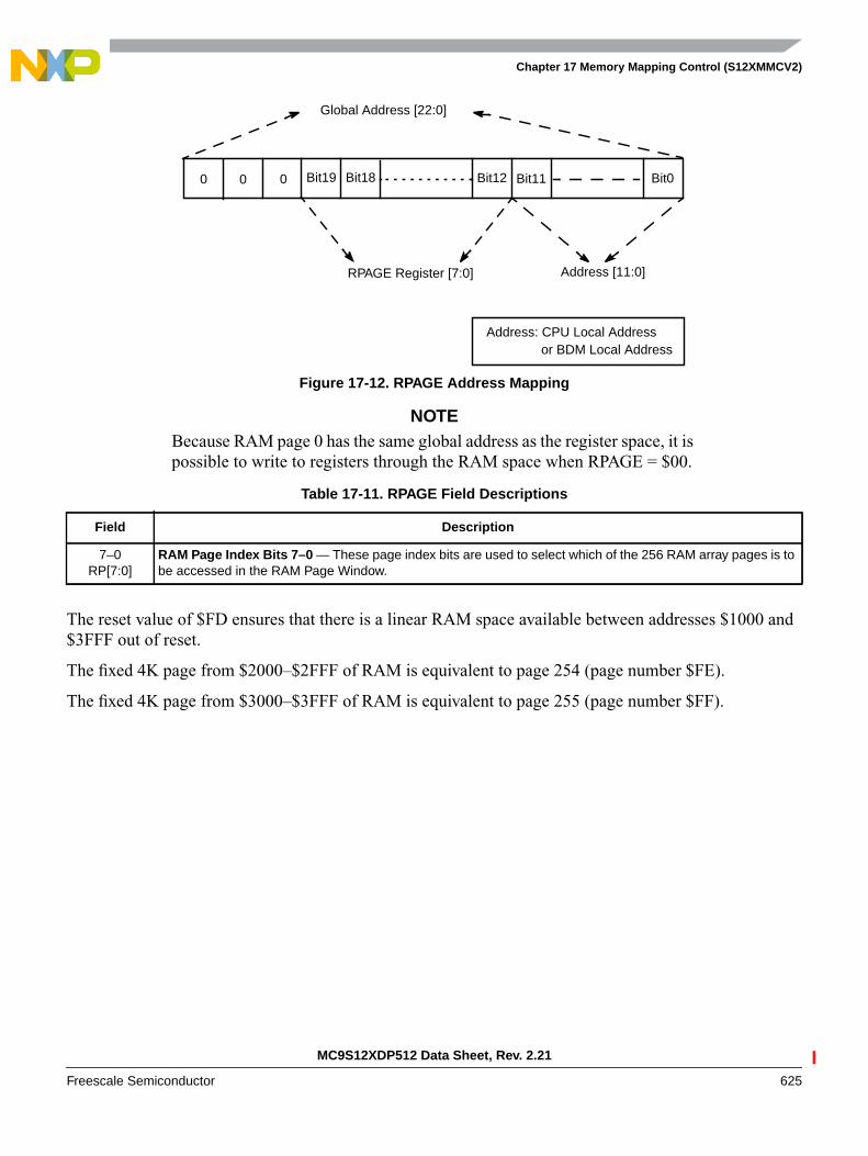
Chapter 17 Memory Mapping Control (S12XMMCV2)
MC9S12XDP512 Data Sheet, Rev. 2.21
Freescale Semiconductor 625
Figure 17-12. RPAGE Address Mapping
NOTEBecause RAM page 0 has the same global address as the register space, it ispossible to write to registers through the RAM space when RPAGE = $00.
The reset value of $FD ensures that there is a linear RAM space available between addresses $1000 and$3FFF out of reset.
The fixed 4K page from $2000–$2FFF of RAM is equivalent to page 254 (page number $FE).
The fixed 4K page from $3000–$3FFF of RAM is equivalent to page 255 (page number $FF).
Table 17-11. RPAGE Field Descriptions
Field Description
7–0RP[7:0]
RAM Page Index Bits 7–0 — These page index bits are used to select which of the 256 RAM array pages is tobe accessed in the RAM Page Window.
Bit18 Bit0Bit110
Address [11:0]RPAGE Register [7:0]
Global Address [22:0]
Bit12Bit190
Address: CPU Local Addressor BDM Local Address
0

Chapter 17 Memory Mapping Control (S12XMMCV2)
MC9S12XDP512 Data Sheet, Rev. 2.21
626 Freescale Semiconductor
17.3.2.7 EEPROM Page Index Register (EPAGE)
Read: Anytime
Write: Anytime
The EEPROM page index register allows accessing up to 256 Kbyte of EEPROM in the global memorymap by using the eight page index bits to page 1 Kbyte blocks into the EEPROM page window located inthe local CPU memory map from address $0800 to address $0BFF (see Figure 1-14).
CAUTIONXGATE write access to this register during an CPU access which makes useof this register could lead to unexpected results.
Figure 17-14. EPAGE Address Mapping
The reset value of $FE ensures that there is a linear EEPROM space available between addresses $0800and $0FFF out of reset.
The fixed 1K page $0C00–$0FFF of EEPROM is equivalent to page 255 (page number $FF).
Address: 0x0017
7 6 5 4 3 2 1 0
REP7 EP6 EP5 EP4 EP3 EP2 EP1 EP0
W
Reset 1 1 1 1 1 1 1 0
Figure 17-13. EEPROM Page Index Register (EPAGE)
Table 17-12. EPAGE Field Descriptions
Field Description
7–0EP[7:0]
EEPROM Page Index Bits 7–0 — These page index bits are used to select which of the 256 EEPROM arraypages is to be accessed in the EEPROM Page Window.
Bit16 Bit0Bit9
Address [9:0]EPAGE Register [7:0]
Global Address [22:0]
Bit10Bit1700 10 0
Address: CPU Local Addressor BDM Local Address
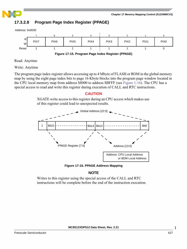
Chapter 17 Memory Mapping Control (S12XMMCV2)
MC9S12XDP512 Data Sheet, Rev. 2.21
Freescale Semiconductor 627
17.3.2.8 Program Page Index Register (PPAGE)
Read: Anytime
Write: Anytime
The program page index register allows accessing up to 4 Mbyte of FLASH or ROM in the global memorymap by using the eight page index bits to page 16 Kbyte blocks into the program page window located inthe CPU local memory map from address $8000 to address $BFFF (see Figure 1-16). The CPU has aspecial access to read and write this register during execution of CALL and RTC instructions.
CAUTIONXGATE write access to this register during an CPU access which makes useof this register could lead to unexpected results.
Figure 17-16. PPAGE Address Mapping
NOTEWrites to this register using the special access of the CALL and RTCinstructions will be complete before the end of the instruction execution.
Address: 0x0030
7 6 5 4 3 2 1 0
RPIX7 PIX6 PIX5 PIX4 PIX3 PIX2 PIX1 PIX0
W
Reset 1 1 1 1 1 1 1 0
Figure 17-15. Program Page Index Register (PPAGE)
Bit14 Bit01
Address [13:0]PPAGE Register [7:0]
Global Address [22:0]
Bit13Bit21
Address: CPU Local Addressor BDM Local Address
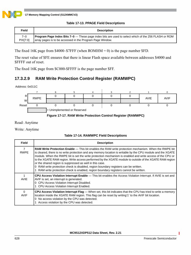
Chapter 17 Memory Mapping Control (S12XMMCV2)
MC9S12XDP512 Data Sheet, Rev. 2.21
628 Freescale Semiconductor
The fixed 16K page from $4000–$7FFF (when ROMHM = 0) is the page number $FD.
The reset value of $FE ensures that there is linear Flash space available between addresses $4000 and$FFFF out of reset.
The fixed 16K page from $C000-$FFFF is the page number $FF.
17.3.2.9 RAM Write Protection Control Register (RAMWPC)
Read: Anytime
Write: Anytime
Table 17-13. PPAGE Field Descriptions
Field Description
7–0PIX[7:0]
Program Page Index Bits 7–0 — These page index bits are used to select which of the 256 FLASH or ROMarray pages is to be accessed in the Program Page Window.
Address: 0x011C
7 6 5 4 3 2 1 0
RRWPE
0 0 0 0 0AVIE AVIF
W
Reset 0 0 0 0 0 0 0 0
= Unimplemented or Reserved
Figure 17-17. RAM Write Protection Control Register (RAMWPC)
Table 17-14. RAMWPC Field Descriptions
Field Description
7RWPE
RAM Write Protection Enable — This bit enables the RAM write protection mechanism. When the RWPE bitis cleared, there is no write protection and any memory location is writable by the CPU module and the XGATEmodule. When the RWPE bit is set the write protection mechanism is enabled and write access of the CPU orto the XGATE RAM region. Write access performed by the XGATE module to outside of the XGATE RAM regionor the shared region is suppressed as well in this case.0 RAM write protection check is disabled, region boundary registers can be written.1 RAM write protection check is enabled, region boundary registers cannot be written.
1AVIE
CPU Access Violation Interrupt Enable — This bit enables the Access Violation Interrupt. If AVIE is set andAVIF is set, an interrupt is generated.0 CPU Access Violation Interrupt Disabled.1 CPU Access Violation Interrupt Enabled.
0AVIF
CPU Access Violation Interrupt Flag — When set, this bit indicates that the CPU has tried to write a memorylocation inside the XGATE RAM region. This flag can be reset by writing’1’ to the AVIF bit location.0 No access violation by the CPU was detected.1 Access violation by the CPU was detected.

Chapter 17 Memory Mapping Control (S12XMMCV2)
MC9S12XDP512 Data Sheet, Rev. 2.21
Freescale Semiconductor 629
17.3.2.10 RAM XGATE Upper Boundary Register (RAMXGU)
Read: Anytime
Write: Anytime when RWPE = 0
17.3.2.11 RAM Shared Region Lower Boundary Register (RAMSHL)
Read: Anytime
Write: Anytime when RWPE = 0
Address: 0x011D
7 6 5 4 3 2 1 0
R 1XGU6 XGU5 XGU4 XGU3 XGU2 XGU1 XGU0
W
Reset 1 1 1 1 1 1 1 1
= Unimplemented or Reserved
Figure 17-18. RAM XGATE Upper Boundary Register (RAMXGU)
Table 17-15. RAMXGU Field Descriptions
Field Description
6–0XGU[6:0]
XGATE Region Upper Boundary Bits 6-0 — These bits define the upper boundary of the RAM region allocatedto the XGATE module in multiples of 256 bytes. The 256 byte block selected by this register is included in theregion. See Figure 1-25 for details.
Address: 0x011E
7 6 5 4 3 2 1 0
R 1SHL6 SHL5 SHL4 SHL3 SHL2 SHL1 SHL0
W
Reset 1 1 1 1 1 1 1 1
= Unimplemented or Reserved
Figure 17-19. RAM Shared Region Lower Boundary Register (RAMSHL)
Table 17-16. RAMSHL Field Descriptions
Field Description
6–0SHL[6:0]
RAM Shared Region Lower Boundary Bits 6–0 — These bits define the lower boundary of the shared memoryregion in multiples of 256 bytes. The block selected by this register is included in the region. See Figure 1-25 fordetails.

Chapter 17 Memory Mapping Control (S12XMMCV2)
MC9S12XDP512 Data Sheet, Rev. 2.21
630 Freescale Semiconductor
17.3.2.12 RAM Shared Region Upper Boundary Register (RAMSHU)
Read: Anytime
Write: Anytime when RWPE = 0
17.4 Functional DescriptionThe MMC block performs several basic functions of the S12X sub-system operation: MCU operationmodes, priority control, address mapping, select signal generation and access limitations for the system.Each aspect is described in the following subsections.
17.4.1 MCU Operating Mode• Normal single-chip mode
There is no external bus in this mode. The MCU program is executed from the internal memoryand no external accesses are allowed.
• Special single-chip mode
This mode is generally used for debugging single-chip operation, boot-strapping or security relatedoperations. The active background debug mode is in control of the CPU code execution and theBDM firmware is waiting for serial commands sent through the BKGD pin. There is no externalbus in this mode.
• Emulation single-chip mode
Tool vendors use this mode for emulation systems in which the user’s target application is normalsingle-chip mode. Code is executed from external or internal memory depending on the set-up ofthe EROMON bit (see Section 1.3.2.5, “MMC Control Register (MMCCTL1)”). The external busis active in both cases to allow observation of internal operations (internal visibility).
Address: 0x011F
7 6 5 4 3 2 1 0
R 1SHU6 SHU5 SHU4 SHU3 SHU2 SHU1 SHU0
W
Reset 1 1 1 1 1 1 1 1
= Unimplemented or Reserved
Figure 17-20. RAM Shared Region Upper Boundary Register (RAMSHU)
Table 17-17. RAMSHU Field Descriptions
Field Description
6–0SHU[6:0]
RAM Shared Region Upper Boundary Bits 6–0 — These bits define the upper boundary of the sharedmemory in multiples of 256 bytes. The block selected by this register is included in the region. See Figure 1-25for details.

Chapter 17 Memory Mapping Control (S12XMMCV2)
MC9S12XDP512 Data Sheet, Rev. 2.21
Freescale Semiconductor 631
• Normal expanded mode
The external bus interface is configured as an up to 23-bit address bus, 8 or 16-bit data bus withdedicated bus control and status signals. This mode allows 8 or 16-bit external memory andperipheral devices to be interfaced to the system. The fastest external bus rate is half of the internalbus rate. An external signal can be used in this mode to cause the external bus to wait as desired bythe external logic.
• Emulation expanded mode
Tool vendors use this mode for emulation systems in which the user’s target application is normalexpanded mode.
• Special test mode
This mode is an expanded mode for factory test.
17.4.2 Memory Map Scheme
17.4.2.1 CPU and BDM Memory Map Scheme
The BDM firmware lookup tables and BDM register memory locations share addresses with othermodules; however they are not visible in the memory map during user’s code execution. The BDMmemory resources are enabled only during the READ_BD and WRITE_BD access cycles to distinguishbetween accesses to the BDM memory area and accesses to the other modules. (Refer to BDM BlockGuide for further details).
When MCU enters active BDM mode the BDM firmware lookup tables and the BDM registers becomevisible in the local memory map between addresses $FF00 and $FFFF and the CPU begins execution offirmware commands or the BDM begins execution of hardware commands. The resources which sharememory space with the BDM module will not be visible in the memory map during active BDM mode.
Please note that after the MCU enters active BDM mode the BDM firmware lookup tables and the BDMregisters will also be visible between addresses $BF00 and $BFFF if the PPAGE register contains value of$FF.
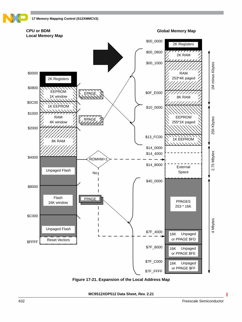
Chapter 17 Memory Mapping Control (S12XMMCV2)
MC9S12XDP512 Data Sheet, Rev. 2.21
632 Freescale Semiconductor
Figure 17-21. Expansion of the Local Address Map
$7F_FFFF
$00_0000
$7F_C000
$14_0000
$13_FC00
$10_0000
$FFFF Reset Vectors
$C000
$8000
Unpaged Flash
$4000
$1000
$0000
2K Registers
8K RAM
$0F_E000
1K EEPROM
255*1K pagedEEPROM
1M m
inus
Kby
tes
256
Kby
tes
Unpaged16K
253 * 16KPPAGES
4 M
byte
s
Unpaged Flash
16K window
$7F_8000
$7F_4000
$0C00
1K window
$2000
4K windowRAM
EEPROM$0800
1K EEPROM
8K RAM
253*4K pagedRAM
2K Registers
$00_0800
$00_1000
ExternalSpace
2.75
Mby
tes
EPAGE
RPAGE
PPAGEFlash
$40_0000
2K RAM
or PPAGE $FF
Unpaged16Kor PPAGE $FE
ROMHM=1
CPU or BDMLocal Memory Map
Global Memory Map
Unpaged16Kor PPAGE $FD
No
$14_4000
$14_8000
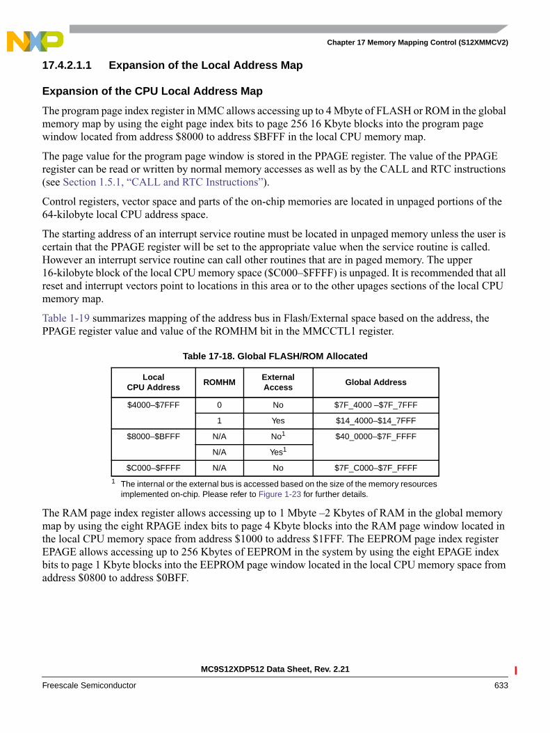
Chapter 17 Memory Mapping Control (S12XMMCV2)
MC9S12XDP512 Data Sheet, Rev. 2.21
Freescale Semiconductor 633
17.4.2.1.1 Expansion of the Local Address Map
Expansion of the CPU Local Address Map
The program page index register in MMC allows accessing up to 4 Mbyte of FLASH or ROM in the globalmemory map by using the eight page index bits to page 256 16 Kbyte blocks into the program pagewindow located from address $8000 to address $BFFF in the local CPU memory map.
The page value for the program page window is stored in the PPAGE register. The value of the PPAGEregister can be read or written by normal memory accesses as well as by the CALL and RTC instructions(see Section 1.5.1, “CALL and RTC Instructions”).
Control registers, vector space and parts of the on-chip memories are located in unpaged portions of the64-kilobyte local CPU address space.
The starting address of an interrupt service routine must be located in unpaged memory unless the user iscertain that the PPAGE register will be set to the appropriate value when the service routine is called.However an interrupt service routine can call other routines that are in paged memory. The upper16-kilobyte block of the local CPU memory space ($C000–$FFFF) is unpaged. It is recommended that allreset and interrupt vectors point to locations in this area or to the other upages sections of the local CPUmemory map.
Table 1-19 summarizes mapping of the address bus in Flash/External space based on the address, thePPAGE register value and value of the ROMHM bit in the MMCCTL1 register.
The RAM page index register allows accessing up to 1 Mbyte –2 Kbytes of RAM in the global memorymap by using the eight RPAGE index bits to page 4 Kbyte blocks into the RAM page window located inthe local CPU memory space from address $1000 to address $1FFF. The EEPROM page index registerEPAGE allows accessing up to 256 Kbytes of EEPROM in the system by using the eight EPAGE indexbits to page 1 Kbyte blocks into the EEPROM page window located in the local CPU memory space fromaddress $0800 to address $0BFF.
Table 17-18. Global FLASH/ROM Allocated
LocalCPU Address
ROMHMExternalAccess
Global Address
$4000–$7FFF 0 No $7F_4000 –$7F_7FFF
1 Yes $14_4000–$14_7FFF
$8000–$BFFF N/A No1
1 The internal or the external bus is accessed based on the size of the memory resourcesimplemented on-chip. Please refer to Figure 1-23 for further details.
$40_0000–$7F_FFFF
N/A Yes1
$C000–$FFFF N/A No $7F_C000–$7F_FFFF

Chapter 17 Memory Mapping Control (S12XMMCV2)
MC9S12XDP512 Data Sheet, Rev. 2.21
634 Freescale Semiconductor
Expansion of the BDM Local Address Map
PPAGE, RPAGE, and EPAGE registers are also used for the expansion of the BDM local address to theglobal address. These registers can be read and written by the BDM.
The BDM expansion scheme is the same as the CPU expansion scheme.
17.4.2.2 Global Addresses Based on the Global Page
CPU Global Addresses Based on the Global Page
The seven global page index bits allow access to the full 8 Mbyte address map that can be accessed with23 address bits. This provides an alternative way to access all of the various pages of FLASH, RAM andEEPROM as well as additional external memory.
The GPAGE Register is used only when the CPU is executing a global instruction (see Section 1.3.2.3,“Global Page Index Register (GPAGE)”). The generated global address is the result of concatenation ofthe CPU local address [15:0] with the GPAGE register [22:16] (see Figure 1-7).
BDM Global Addresses Based on the Global Page
The seven BDMGPR Global Page index bits allow access to the full 8 Mbyte address map that can beaccessed with 23 address bits. This provides an alternative way to access all of the various pages ofFLASH, RAM and EEPROM as well as additional external memory.
The BDM global page index register (BDMGPR) is used only in the case the CPU is executing a firmwarecommand which uses a global instruction (like GLDD, GSTD) or by a BDM hardware command (likeWRITE_W, WRITE_BYTE, READ_W, READ_BYTE). See the BDM Block Guide for further details.
The generated global address is a result of concatenation of the BDM local address with the BDMGPRregister [22:16] in the case of a hardware command or concatenation of the CPU local address and theBDMGPR register [22:16] in the case of a firmware command (see Figure 1-22).
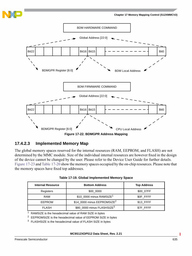
Chapter 17 Memory Mapping Control (S12XMMCV2)
MC9S12XDP512 Data Sheet, Rev. 2.21
Freescale Semiconductor 635
Figure 17-22. BDMGPR Address Mapping
17.4.2.3 Implemented Memory Map
The global memory spaces reserved for the internal resources (RAM, EEPROM, and FLASH) are notdetermined by the MMC module. Size of the individual internal resources are however fixed in the designof the device cannot be changed by the user. Please refer to the Device User Guide for further details.Figure 17-23 and Table 17-20 show the memory spaces occupied by the on-chip resources. Please note thatthe memory spaces have fixed top addresses.
Table 17-19. Global Implemented Memory Space
Internal Resource Bottom Address Top Address
Registers $00_0000 $00_07FF
RAM $10_0000 minus RAMSIZE1
1 RAMSIZE is the hexadecimal value of RAM SIZE in bytes
$0F_FFFF
EEPROM $14_0000 minus EEPROMSIZE2
2 EEPROMSIZE is the hexadecimal value of EEPROM SIZE in bytes
$13_FFFF
FLASH $80_0000 minus FLASHSIZE3
3 FLASHSIZE is the hexadecimal value of FLASH SIZE in bytes
$7F_FFFF
Bit16 Bit0Bit15Bit22
BDM Local AddressBDMGPR Register [6:0]
Global Address [22:0]
Bit16 Bit0Bit15Bit22
CPU Local AddressBDMGPR Register [6:0]
Global Address [22:0]
BDM HARDWARE COMMAND
BDM FIRMWARE COMMAND

Chapter 17 Memory Mapping Control (S12XMMCV2)
MC9S12XDP512 Data Sheet, Rev. 2.21
636 Freescale Semiconductor
When the device is operating in expanded modes except emulation single-chip mode, accesses to theglobal addresses which are not occupied by the on-chip resources (unimplemented areas or external space)result in accesses to the external bus (see Figure 17-23).
In emulation single-chip mode, accesses to the global addresses which are not occupied by the on-chipresources (unimplemented areas) result in accesses to the external bus. CPU accesses to the globaladdresses which are occupied by the external space result in an illegal access reset (system reset). TheBDM accesses to the external space are performed but the data is undefined.
In single-chip modes an access to any of the unimplemented areas (see Figure 17-23) by the CPU (exceptfirmware commands) results in an illegal access reset (system reset). The BDM accesses to theunimplemented areas are performed but the data is undefined.
Misaligned word accesses to the last location (Top address) of any of the on-chip resource blocks (exceptRAM) by the CPU is performed in expanded modes. In single-chip modes these accesses (except Flash)result in an illegal access reset (except firmware commands).
Misaligned word accesses to the last location (top address) of the on-chip RAM by the CPU is ignored inexpanded modes (read of undefined data). In single-chip modes these accesses result in an illegal accessreset (except firmware commands).
No misaligned word access from the BDM module will occur. These accesses are blocked in the BDM(Refer to BDM Block Guide).
Misaligned word accesses to the last location of any global page (64 Kbyte) by using global instructions,is performed by accessing the last byte of the page and the first byte of the same page, considering theabove mentioned misaligned access cases.
The non internal resources (unimplemented areas or external space) are used to generate the chip selects(CS0,CS1,CS2 and CS3) (see Figure 17-23), which are only active in normal expanded mode, emulationexpanded mode, and special test mode (see Section 1.3.2.1, “MMC Control Register (MMCCTL0)”).
Table 1-21 shows the address boundaries of each chip select and the relationship with the implementedresources (internal) parameters.
Table 17-20. Global Chip Selects Memory Space
Chip Selects Bottom Address Top Address
CS3 $00_0800 $0F_FFFF minus RAMSIZE1
1 External RPAGE accesses in (NX, EX and ST)
CS2 $10_0000 $13_FFFF minus EEPROMSIZE2
2 External EPAGE accesses in (NX, EX and ST)
CS23
3 When ROMHM is set (see ROMHM in Table 1-19) the CS2 is asserted in the space occupied by this on-chipmemory block.
$14_0000 $1F_FFFF
CS1 $20_0000 $3F_FFFF
CS04
4 When the internal NVM is enabled (see ROMON in Section 1.3.2.5, “MMC Control Register (MMCCTL1)”)the CS0 is not asserted in the space occupied by this on-chip memory block.
$40_0000 $7F_FFFF minus FLASHSIZE5
5 External PPAGE accesses in (NX, EX and ST)

Chapter 17 Memory Mapping Control (S12XMMCV2)
MC9S12XDP512 Data Sheet, Rev. 2.21
Freescale Semiconductor 637
Figure 17-23. Local to Implemented Global Address Mapping (Without GPAGE)
$7F_FFFF
$00_0000
$13_FFFF
$0F_FFFF
$FFFF Reset Vectors
$C000
$8000
Unpaged Flash
$4000
$1000
$0000
2K Registers
8K RAM
1K EEPROM
Unpaged Flash
16K window
$0C00
1K window
$2000
4K windowRAM
EEPROM$0800
EEPROM
RAM
2K Registers
$00_0800
ExternalSpace
EPAGE
RPAGE
PPAGEFlash
$40_0000
CPU and BDMLocal Memory Map
Global Memory Map
FLASH
FLA
SH
SIZ
EE
EP
RO
MS
IZE
RA
MS
IZE
UnimplementedEEPROM
UnimplementedFLASH
UnimplementedRAM C
S3
CS
2C
S1
CS
0
$1F_FFFF CS
2

Chapter 17 Memory Mapping Control (S12XMMCV2)
MC9S12XDP512 Data Sheet, Rev. 2.21
638 Freescale Semiconductor
17.4.2.4 XGATE Memory Map Scheme
17.4.2.4.1 Expansion of the XGATE Local Address Map
The XGATE 64 Kbyte memory space allows access to internal resources only (Registers, RAM, andFLASH). The 2 Kilobyte register address range is the same register address range as for the CPU and theBDM module . XGATE can access the FLASH in single chip modes, even when the MCU is secured. Inexpanded modes, XGATE can not access the FLASH when MCU is secured.
The local address of the XGATE RAM access is translated to the global RAM address range. The XGATEshares the RAM resource with the CPU and the BDM module. The local address of the XGATE FLASHaccess is translated to the global address as shown in Figure 17-24. For the implemented memory spacesand addresses please refer to Table 1-4 and Table 1-5.
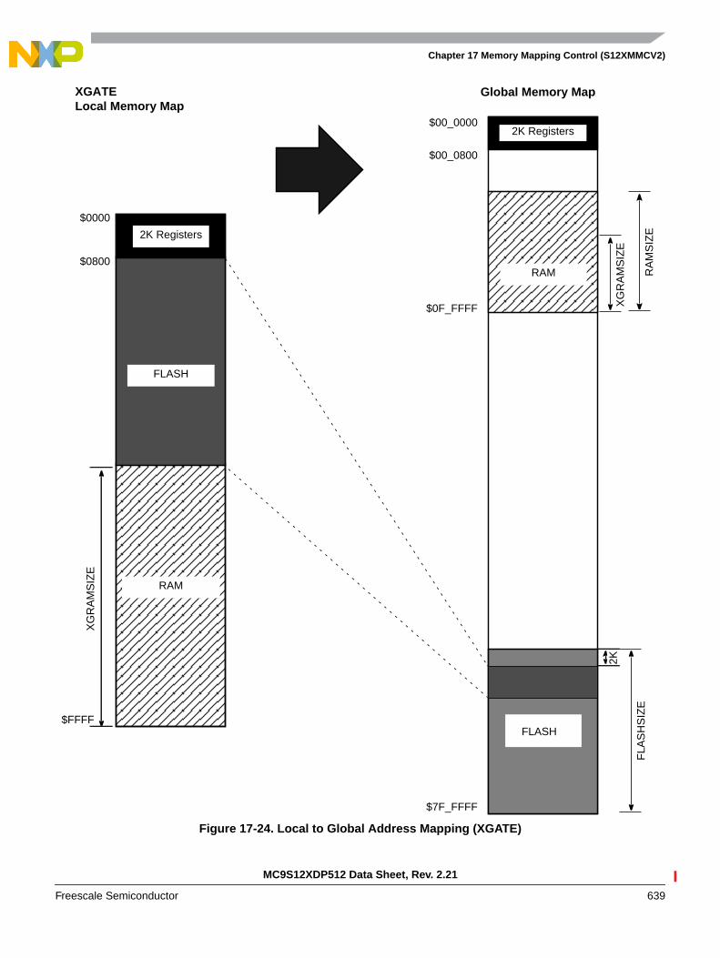
Chapter 17 Memory Mapping Control (S12XMMCV2)
MC9S12XDP512 Data Sheet, Rev. 2.21
Freescale Semiconductor 639
Figure 17-24. Local to Global Address Mapping (XGATE)
$7F_FFFF
$00_0000
$0F_FFFF
$FFFF
$0000
2K Registers
FLASH
RAM
$0800RAM
2K Registers
$00_0800
XGATELocal Memory Map
Global Memory Map
FLASH
FLA
SH
SIZ
E
XG
RA
MS
IZE
XG
RA
MS
IZE
2K
RA
MS
IZE
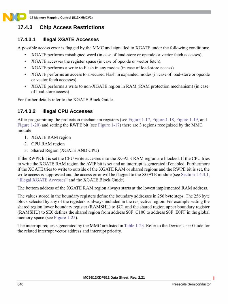
Chapter 17 Memory Mapping Control (S12XMMCV2)
MC9S12XDP512 Data Sheet, Rev. 2.21
640 Freescale Semiconductor
17.4.3 Chip Access Restrictions
17.4.3.1 Illegal XGATE Accesses
A possible access error is flagged by the MMC and signalled to XGATE under the following conditions:
• XGATE performs misaligned word (in case of load-store or opcode or vector fetch accesses).
• XGATE accesses the register space (in case of opcode or vector fetch).
• XGATE performs a write to Flash in any modes (in case of load-store access).
• XGATE performs an access to a secured Flash in expanded modes (in case of load-store or opcodeor vector fetch accesses).
• XGATE performs a write to non-XGATE region in RAM (RAM protection mechanism) (in caseof load-store access).
For further details refer to the XGATE Block Guide.
17.4.3.2 Illegal CPU Accesses
After programming the protection mechanism registers (see Figure 1-17, Figure 1-18, Figure 1-19, andFigure 1-20) and setting the RWPE bit (see Figure 1-17) there are 3 regions recognized by the MMCmodule:
1. XGATE RAM region
2. CPU RAM region
3. Shared Region (XGATE AND CPU)
If the RWPE bit is set the CPU write accesses into the XGATE RAM region are blocked. If the CPU triesto write the XGATE RAM region the AVIF bit is set and an interrupt is generated if enabled. Furthermoreif the XGATE tries to write to outside of the XGATE RAM or shared regions and the RWPE bit is set, thewrite access is suppressed and the access error will be flagged to the XGATE module (see Section 1.4.3.1,“Illegal XGATE Accesses” and the XGATE Block Guide).
The bottom address of the XGATE RAM region always starts at the lowest implemented RAM address.
The values stored in the boundary registers define the boundary addresses in 256 byte steps. The 256 byteblock selected by any of the registers is always included in the respective region. For example setting theshared region lower boundary register (RAMSHL) to $C1 and the shared region upper boundary register(RAMSHU) to $E0 defines the shared region from address $0F_C100 to address $0F_E0FF in the globalmemory space (see Figure 1-25).
The interrupt requests generated by the MMC are listed in Table 1-23. Refer to the Device User Guide forthe related interrupt vector address and interrupt priority.

Chapter 17 Memory Mapping Control (S12XMMCV2)
MC9S12XDP512 Data Sheet, Rev. 2.21
Freescale Semiconductor 641
The following conditions must be satisfied to ensure correct operation of the RAM protection mechanism:
• Value stored in RAMXGU must be lower than the value stored in RAMSHL.
• Value stored RAMSHL must be lower or equal than the value stored in RAMSHU.
Figure 17-25. RAM Write Protection Scheme
Table 17-21. RAM Write Protection Interrupt Vectors
Interrupt Source CCR Mask Local Enable
CPU access violation I Bit AVIE in RAMWPC
$0F_FFFF
$00_0000
Shared Region
XGATE RAMRegion
$0F_RAMSHU_FF
$0F_RAMSHL_00
$0F_RAMXGU_FF
Only XGATE is allowed to write
CPU and XGATE are allowed to write
Only CPU is allowed to write
Unimplemented
Only CPU is allowed to write
RA
MS
IZE
$00_0800
2K Registers
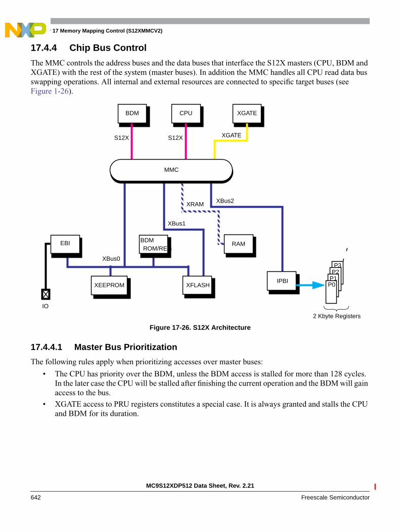
Chapter 17 Memory Mapping Control (S12XMMCV2)
MC9S12XDP512 Data Sheet, Rev. 2.21
642 Freescale Semiconductor
17.4.4 Chip Bus Control
The MMC controls the address buses and the data buses that interface the S12X masters (CPU, BDM andXGATE) with the rest of the system (master buses). In addition the MMC handles all CPU read data busswapping operations. All internal and external resources are connected to specific target buses (seeFigure 1-26).
Figure 17-26. S12X Architecture
17.4.4.1 Master Bus Prioritization
The following rules apply when prioritizing accesses over master buses:
• The CPU has priority over the BDM, unless the BDM access is stalled for more than 128 cycles.In the later case the CPU will be stalled after finishing the current operation and the BDM will gainaccess to the bus.
• XGATE access to PRU registers constitutes a special case. It is always granted and stalls the CPUand BDM for its duration.
XBus2
CPU
P0P1P2P3
XFLASHXEEPROMIPBI
EBI
XBus0
ROM/REGBDM
IO
XBus1
RAM
XRAM
2 Kbyte Registers
S12X S12X XGATE
MMC
BDM XGATE
Chapter 17 Memory Mapping Control (S12XMMCV2)
MC9S12XDP512 Data Sheet, Rev. 2.21
Freescale Semiconductor 643
17.4.4.2 Access Conflicts on Target Buses
The arbitration scheme allows only one master to be connected to a target at any given time. The followingrules apply when prioritizing accesses from different masters to the same target bus:
• CPU always has priority over XGATE.
• BDM access has priority over XGATE.
• XGATE access to PRU registers constitutes a special case. It is always granted and stalls the CPUand BDM for its duration.
• In emulation modes all internal accesses are visible on the external bus as well.
• During access to the PRU registers, the external bus is reserved.
17.4.5 Interrupts
17.4.5.1 Outgoing Interrupt Requests
The following interrupt requests can be triggered by the MMC module:
CPU access violation: The CPU access violation signals to the CPU detection of an error condition in theCPU application code which is resulted in write access to the protected XGATE RAM area (seeSection 1.4.3.2, “Illegal CPU Accesses”).
17.5 Initialization/Application Information
17.5.1 CALL and RTC Instructions
CALL and RTC instructions are uninterruptable CPU instructions that automate page switching in theprogram page window. The CALL instruction is similar to the JSR instruction, but the subroutine that iscalled can be located anywhere in the local address space or in any Flash or ROM page visible through theprogram page window. The CALL instruction calculates and stacks a return address, stacks the currentPPAGE value and writes a new instruction-supplied value to the PPAGE register. The PPAGE valuecontrols which of the 256 possible pages is visible through the 16 Kbyte program page window in the64 Kbyte local CPU memory map. Execution then begins at the address of the called subroutine.
During the execution of the CALL instruction, the CPU performs the following steps:
1. Writes the current PPAGE value into an internal temporary register and writes the newinstruction-supplied PPAGE value into the PPAGE register
2. Calculates the address of the next instruction after the CALL instruction (the return address) andpushes this 16-bit value onto the stack
3. Pushes the temporarily stored PPAGE value onto the stack
4. Calculates the effective address of the subroutine, refills the queue and begins execution at the newaddress
Chapter 17 Memory Mapping Control (S12XMMCV2)
MC9S12XDP512 Data Sheet, Rev. 2.21
644 Freescale Semiconductor
This sequence is uninterruptable. There is no need to inhibit interrupts during the CALL instructionexecution. A CALL instruction can be performed from any address to any other address in the local CPUmemory space.
The PPAGE value supplied by the instruction is part of the effective address of the CPU. For all addressingmode variations (except indexed-indirect modes) the new page value is provided by an immediate operandin the instruction. In indexed-indirect variations of the CALL instruction a pointer specifies memorylocations where the new page value and the address of the called subroutine are stored. Using indirectaddressing for both the new page value and the address within the page allows usage of values calculatedat run time rather than immediate values that must be known at the time of assembly.
The RTC instruction terminates subroutines invoked by a CALL instruction. The RTC instruction unstacksthe PPAGE value and the return address and refills the queue. Execution resumes with the next instructionafter the CALL instruction.
During the execution of an RTC instruction the CPU performs the following steps:
1. Pulls the previously stored PPAGE value from the stack
2. Pulls the 16-bit return address from the stack and loads it into the PC
3. Writes the PPAGE value into the PPAGE register
4. Refills the queue and resumes execution at the return address
This sequence is uninterruptable. The RTC can be executed from anywhere in the local CPU memoryspace.
The CALL and RTC instructions behave like JSR and RTS instruction, they however require moreexecution cycles. Usage of JSR/RTS instructions is therefore recommended when possible andCALL/RTC instructions should only be used when needed. The JSR and RTS instructions can be used toaccess subroutines that are already present in the local CPU memory map (i.e. in the same page in theprogram memory page window for example). However calling a function located in a different pagerequires usage of the CALL instruction. The function must be terminated by the RTC instruction. Becausethe RTC instruction restores contents of the PPAGE register from the stack, functions terminated with theRTC instruction must be called using the CALL instruction even when the correct page is already presentin the memory map. This is to make sure that the correct PPAGE value will be present on stack at the timeof the RTC instruction execution.
17.5.2 Port Replacement Registers (PRRs)
Registers used for emulation purposes must be rebuilt by the in-circuit emulator hardware to achieve fullemulation of single chip mode operation. These registers are called port replacement registers (PRRs) (seeTable 1-25). PRRs are accessible from all masters using different access types (word aligned,word-misaligned and byte). Each access to PRRs will be extended to 2 bus cycles for write or read accessesindependent of the operating mode. In emulation modes all write operations result in writing into theinternal registers (peripheral access) and into the emulated registers (external access) located in the PRUin the emulator at the same time. All read operations are performed from external registers (externalaccess) in emulation modes. In all other modes the read operations are performed from the internalregisters (peripheral access).
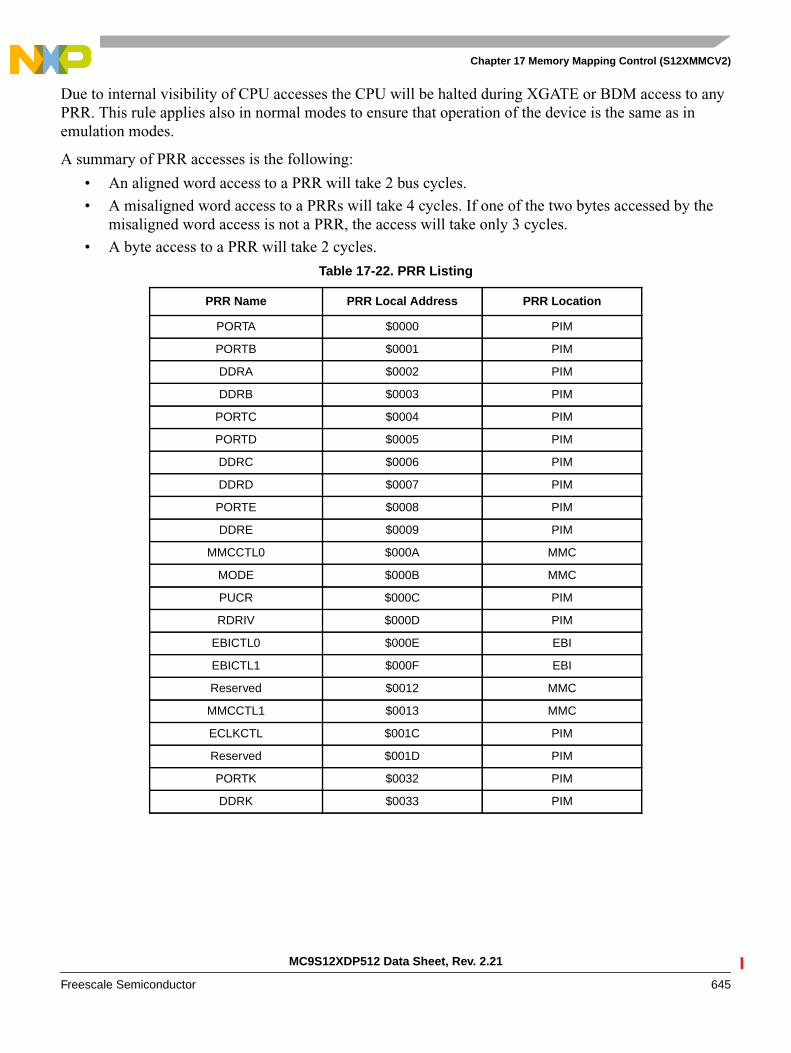
Chapter 17 Memory Mapping Control (S12XMMCV2)
MC9S12XDP512 Data Sheet, Rev. 2.21
Freescale Semiconductor 645
Due to internal visibility of CPU accesses the CPU will be halted during XGATE or BDM access to anyPRR. This rule applies also in normal modes to ensure that operation of the device is the same as inemulation modes.
A summary of PRR accesses is the following:
• An aligned word access to a PRR will take 2 bus cycles.
• A misaligned word access to a PRRs will take 4 cycles. If one of the two bytes accessed by themisaligned word access is not a PRR, the access will take only 3 cycles.
• A byte access to a PRR will take 2 cycles.
Table 17-22. PRR Listing
PRR Name PRR Local Address PRR Location
PORTA $0000 PIM
PORTB $0001 PIM
DDRA $0002 PIM
DDRB $0003 PIM
PORTC $0004 PIM
PORTD $0005 PIM
DDRC $0006 PIM
DDRD $0007 PIM
PORTE $0008 PIM
DDRE $0009 PIM
MMCCTL0 $000A MMC
MODE $000B MMC
PUCR $000C PIM
RDRIV $000D PIM
EBICTL0 $000E EBI
EBICTL1 $000F EBI
Reserved $0012 MMC
MMCCTL1 $0013 MMC
ECLKCTL $001C PIM
Reserved $001D PIM
PORTK $0032 PIM
DDRK $0033 PIM

Chapter 17 Memory Mapping Control (S12XMMCV2)
MC9S12XDP512 Data Sheet, Rev. 2.21
646 Freescale Semiconductor
17.5.3 On-Chip ROM Control
The MCU offers two modes to support emulation. In the first mode (called generator) the emulatorprovides the data instead of the internal FLASH and traces the CPU actions. In the other mode (calledobserver) the internal FLASH provides the data and all internal actions are made visible to the emulator.
17.5.3.1 ROM Control in Single-Chip Modes
In single-chip modes the MCU has no external bus. All memory accesses and program fetches are internal(see Figure 1-27).
Figure 17-27. ROM in Single Chip Modes
17.5.3.2 ROM Control in Emulation Single-Chip Mode
In emulation single-chip mode the external bus is connected to the emulator. If the EROMON bit is set,the internal FLASH provides the data and the emulator can observe all internal CPU actions on the externalbus. If the EROMON bit is cleared, the emulator provides the data (generator) and traces the all CPUactions (see Figure 1-28).
Figure 17-28. ROM in Emulation Single-Chip Mode
MCU
Flash
No External Bus
EROMON = 1
Emulator
MCU
EROMON = 0
Emulator
Flash
MCU
Flash
Observer
Generator
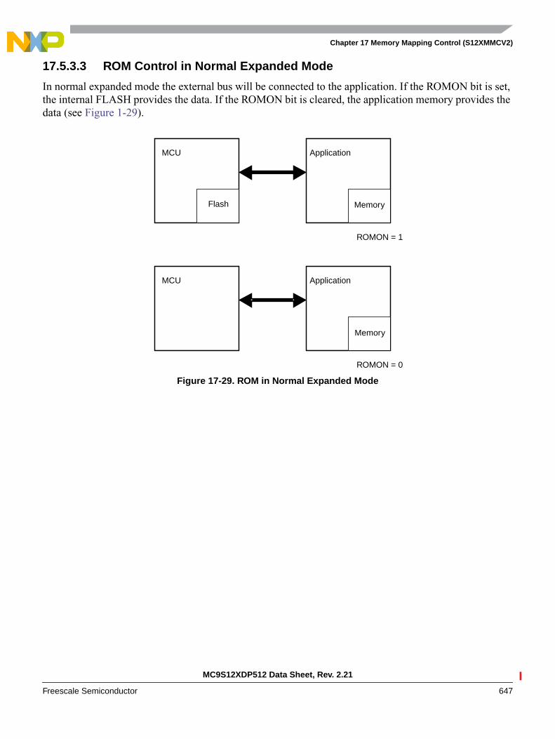
Chapter 17 Memory Mapping Control (S12XMMCV2)
MC9S12XDP512 Data Sheet, Rev. 2.21
Freescale Semiconductor 647
17.5.3.3 ROM Control in Normal Expanded Mode
In normal expanded mode the external bus will be connected to the application. If the ROMON bit is set,the internal FLASH provides the data. If the ROMON bit is cleared, the application memory provides thedata (see Figure 1-29).
Figure 17-29. ROM in Normal Expanded Mode
ROMON = 1
Application
MCU
ROMON = 0
Application
MCU
Flash Memory
Memory
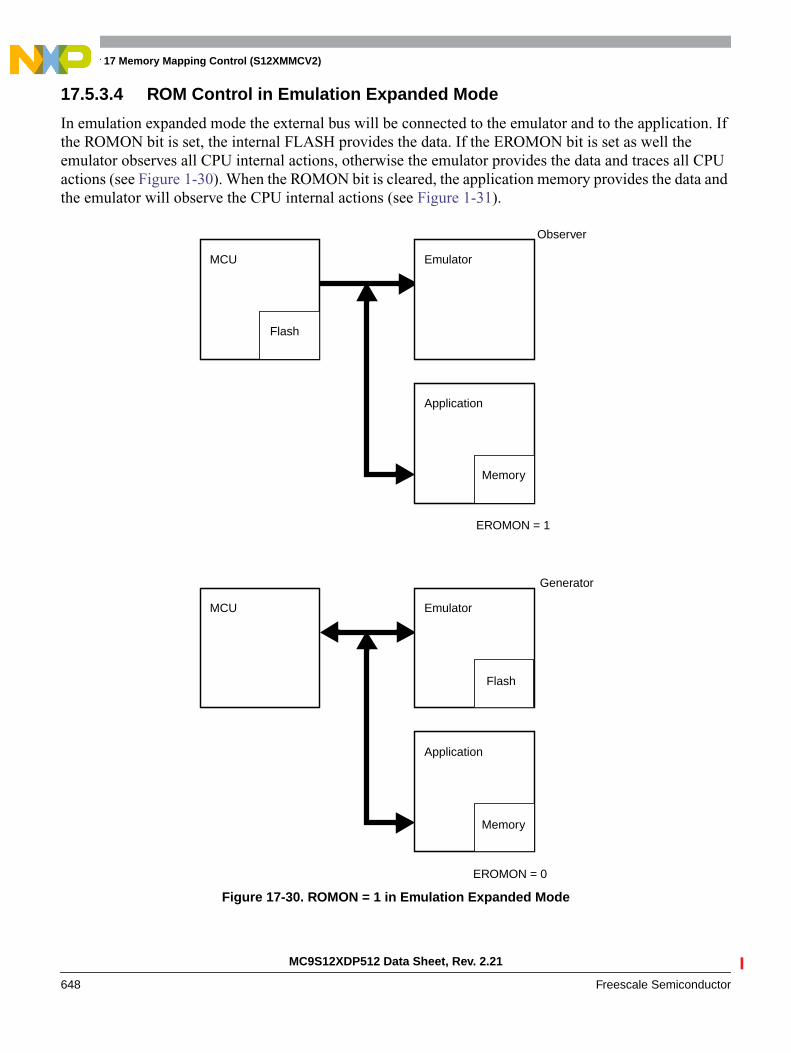
Chapter 17 Memory Mapping Control (S12XMMCV2)
MC9S12XDP512 Data Sheet, Rev. 2.21
648 Freescale Semiconductor
17.5.3.4 ROM Control in Emulation Expanded Mode
In emulation expanded mode the external bus will be connected to the emulator and to the application. Ifthe ROMON bit is set, the internal FLASH provides the data. If the EROMON bit is set as well theemulator observes all CPU internal actions, otherwise the emulator provides the data and traces all CPUactions (see Figure 1-30). When the ROMON bit is cleared, the application memory provides the data andthe emulator will observe the CPU internal actions (see Figure 1-31).
Figure 17-30. ROMON = 1 in Emulation Expanded Mode
EROMON = 1
Application
MCU
Flash
Memory
Emulator
EROMON = 0
Application
MCU
Memory
Emulator
Flash
Generator
Observer
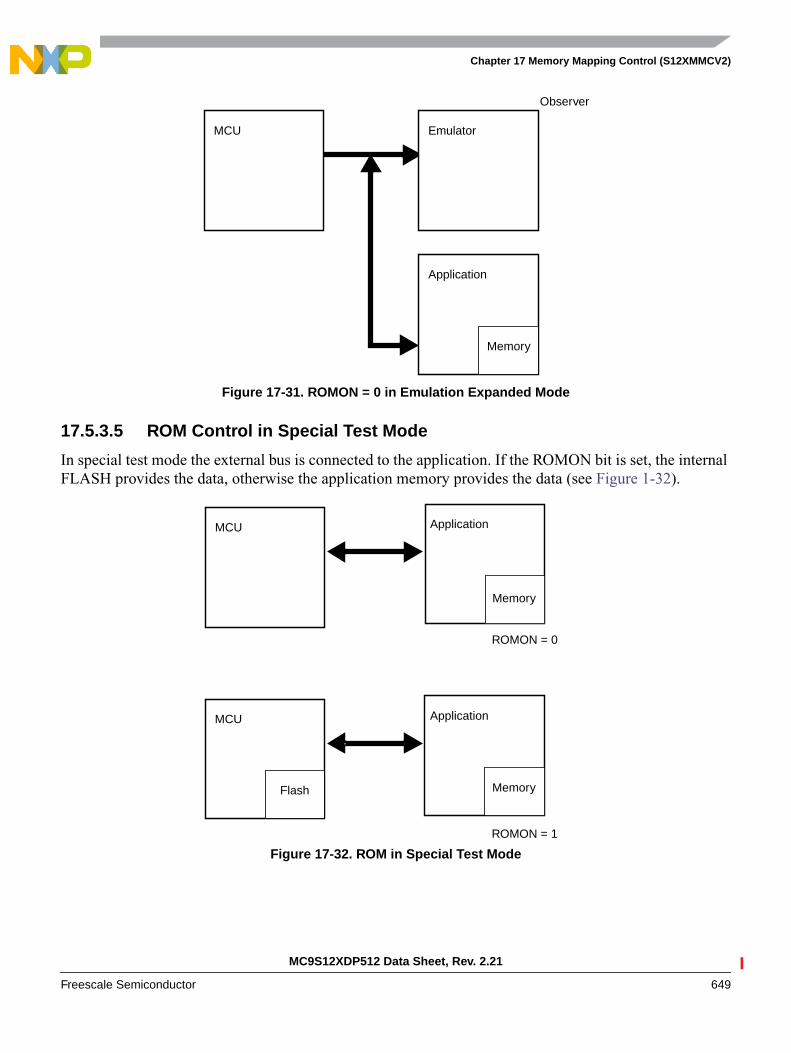
Chapter 17 Memory Mapping Control (S12XMMCV2)
MC9S12XDP512 Data Sheet, Rev. 2.21
Freescale Semiconductor 649
Figure 17-31. ROMON = 0 in Emulation Expanded Mode
17.5.3.5 ROM Control in Special Test Mode
In special test mode the external bus is connected to the application. If the ROMON bit is set, the internalFLASH provides the data, otherwise the application memory provides the data (see Figure 1-32).
Figure 17-32. ROM in Special Test Mode
Application
MCU
Memory
Emulator
Observer
ApplicationMCU
Memory
ROMON = 0
ApplicationMCU
Memory
ROMON = 1
Flash

Chapter 17 Memory Mapping Control (S12XMMCV2)
MC9S12XDP512 Data Sheet, Rev. 2.21
650 Freescale Semiconductor
MC9S12XDP512 Data Sheet, Rev. 2.21
Freescale Semiconductor 651
Chapter 18Memory Mapping Control (S12XMMCV3)
18.1 IntroductionThis section describes the functionality of the module mapping control (MMC) sub-block of the S12Xplatform. The block diagram of the MMC is shown in Figure 18-1.
The MMC module controls the multi-master priority accesses, the selection of internal resources andexternal space. Internal buses, including internal memories and peripherals, are controlled in this module.The local address space for each master is translated to a global memory space.
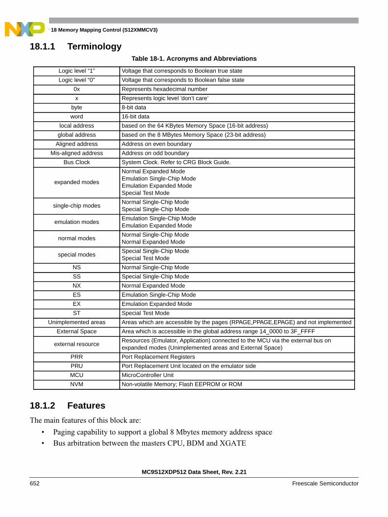
Chapter 18 Memory Mapping Control (S12XMMCV3)
MC9S12XDP512 Data Sheet, Rev. 2.21
652 Freescale Semiconductor
18.1.1 Terminology
18.1.2 Features
The main features of this block are:
• Paging capability to support a global 8 Mbytes memory address space
• Bus arbitration between the masters CPU, BDM and XGATE
Table 18-1. Acronyms and Abbreviations
Logic level “1” Voltage that corresponds to Boolean true state
Logic level “0” Voltage that corresponds to Boolean false state
0x Represents hexadecimal number
x Represents logic level ’don’t care’
byte 8-bit data
word 16-bit data
local address based on the 64 KBytes Memory Space (16-bit address)
global address based on the 8 MBytes Memory Space (23-bit address)
Aligned address Address on even boundary
Mis-aligned address Address on odd boundary
Bus Clock System Clock. Refer to CRG Block Guide.
expanded modes
Normal Expanded ModeEmulation Single-Chip ModeEmulation Expanded ModeSpecial Test Mode
single-chip modesNormal Single-Chip ModeSpecial Single-Chip Mode
emulation modesEmulation Single-Chip ModeEmulation Expanded Mode
normal modesNormal Single-Chip ModeNormal Expanded Mode
special modesSpecial Single-Chip ModeSpecial Test Mode
NS Normal Single-Chip Mode
SS Special Single-Chip Mode
NX Normal Expanded Mode
ES Emulation Single-Chip Mode
EX Emulation Expanded Mode
ST Special Test Mode
Unimplemented areas Areas which are accessible by the pages (RPAGE,PPAGE,EPAGE) and not implemented
External Space Area which is accessible in the global address range 14_0000 to 3F_FFFF
external resourceResources (Emulator, Application) connected to the MCU via the external bus onexpanded modes (Unimplemented areas and External Space)
PRR Port Replacement Registers
PRU Port Replacement Unit located on the emulator side
MCU MicroController Unit
NVM Non-volatile Memory; Flash EEPROM or ROM

Chapter 18 Memory Mapping Control (S12XMMCV3)
MC9S12XDP512 Data Sheet, Rev. 2.21
Freescale Semiconductor 653
• Simultaneous accesses to different resources1 (internal, external, and peripherals) (see )
• Resolution of target bus access collision
• Access restriction control from masters to some targets (e.g., RAM write access protection for userspecified areas)
• MCU operation mode control
• MCU security control
• Separate memory map schemes for each master CPU, BDM and XGATE
• ROM control bits to enable the on-chip FLASH or ROM selection
• Port replacement registers access control
• Generation of system reset when CPU accesses an unimplemented address (i.e., an address whichdoes not belong to any of the on-chip modules) in single-chip modes
18.1.3 S12X Memory Mapping
The S12X architecture implements a number of memory mapping schemes including
• a CPU 8 MByte global map, defined using a global page (GPAGE) register and dedicated 23-bitaddress load/store instructions.
• a BDM 8 MByte global map, defined using a global page (BDMGPR) register and dedicated 23-bitaddress load/store instructions.
• a (CPU or BDM) 64 KByte local map, defined using specific resource page (RPAGE, EPAGE andPPAGE) registers and the default instruction set. The 64 KBytes visible at any instant can beconsidered as the local map accessed by the 16-bit (CPU or BDM) address.
• The XGATE 64 Kbyte local map.
The MMC module performs translation of the different memory mapping schemes to the specific global(physical) memory implementation.
18.1.4 Modes of Operation
This subsection lists and briefly describes all operating modes supported by the MMC.
18.1.4.1 Power Saving Modes
• Run mode
MMC is functional during normal run mode.
• Wait mode
MMC is functional during wait mode.
• Stop mode
MMC is inactive during stop mode.
1. Resources are also called targets.

Chapter 18 Memory Mapping Control (S12XMMCV3)
MC9S12XDP512 Data Sheet, Rev. 2.21
654 Freescale Semiconductor
18.1.4.2 Functional Modes
• Single chip modes
In normal and special single chip mode the internal memory is used. External bus is not active.
• Expanded modes
Address, data, and control signals are activated in normal expanded and special test modes whenaccessing the external bus. Access to internal resources will not cause activity on the external bus.
• Emulation modes
External bus is active to emulate, via an external tool, the normal expanded or the normal singlechip mode.
18.1.5 Block Diagram
Figure 18-11 shows a block diagram of the MMC.
Figure 18-1. MMC Block Diagram
18.2 External Signal DescriptionThe user is advised to refer to the SoC Guide for port configuration and location of external bus signals.Some pins may not be bonded out in all implementations.
Table 18-2 and Table 18-3 outline the pin names and functions. It also provides a brief description of theiroperation.
1. Doted blocks and lines are optional. Please refer to the Device User Guide for their availlibilities.
Peripherals
FLASH
XGATECPUBDM
Target Bus Controller
DBG
EEPROM
EBI
MMC
Address Decoder & Priority
RAM
FLEXRAY

Chapter 18 Memory Mapping Control (S12XMMCV3)
MC9S12XDP512 Data Sheet, Rev. 2.21
Freescale Semiconductor 655
Table 18-2. External Input Signals Associated with the MMC
Signal I/O Description Availability
MODC I Mode input Latched afterRESET (active low)
MODB I Mode input Latched afterRESET (active low)
MODA I Mode input Latched afterRESET (active low)
EROMCTL I EROM control input Latched afterRESET (active low)
ROMCTL I ROM control input Latched afterRESET (active low)
Table 18-3. External Output Signals Associated with the MMC
Signal I/O DescriptionAvailable in Modes
NS SS NX ES EX ST
CS0 O Chip select line 0 (see Table 18-4)
CS1 O Chip select line 1
CS2 O Chip select line 2
CS3 O Chip select line 3

Chapter 18 Memory Mapping Control (S12XMMCV3)
MC9S12XDP512 Data Sheet, Rev. 2.21
656 Freescale Semiconductor
18.3 Memory Map and Registers
18.3.1 Module Memory Map
A summary of the registers associated with the MMC block is shown in Figure 18-2. Detailed descriptionsof the registers and bits are given in the subsections that follow.
AddressRegister
NameBit 7 6 5 4 3 2 1 Bit 0
0x000A MMCCTL0 R 0 0 0 0CS3E CS2E CS1E CS0E
W
0x000B MODE RMODC MODB MODA
0 0 0 0 0
W
0x0010 GPAGE R 0GP6 GP5 GP4 GP3 GP2 GP1 GP0
W
0x0011 DIRECT RDP15 DP14 DP13 DP12 DP11 DP10 DP9 DP8
W
0x0012 Reserved R 0 0 0 0 0 0 0 0
W
0x0013 MMCCTL1 R 0 0 0 0 0EROMON ROMHM ROMON
W
0x0014 Reserved R 0 0 0 0 0 0 0 0
W
0x0015 Reserved R 0 0 0 0 0 0 0 0
W
0x0016 RPAGE RRP7 RP6 RP5 RP4 RP3 RP2 RP1 RP0
W
0x0017 EPAGE REP7 EP6 EP5 EP4 EP3 EP2 EP1 EP0
W
0x0030 PPAGE RPIX7 PIX6 PIX5 PIX4 PIX3 PIX2 PIX1 PIX0
W
0x0031 Reserved R 0 0 0 0 0 0 0 0
W
= Unimplemented or Reserved
Figure 18-2. MMC Register Summary
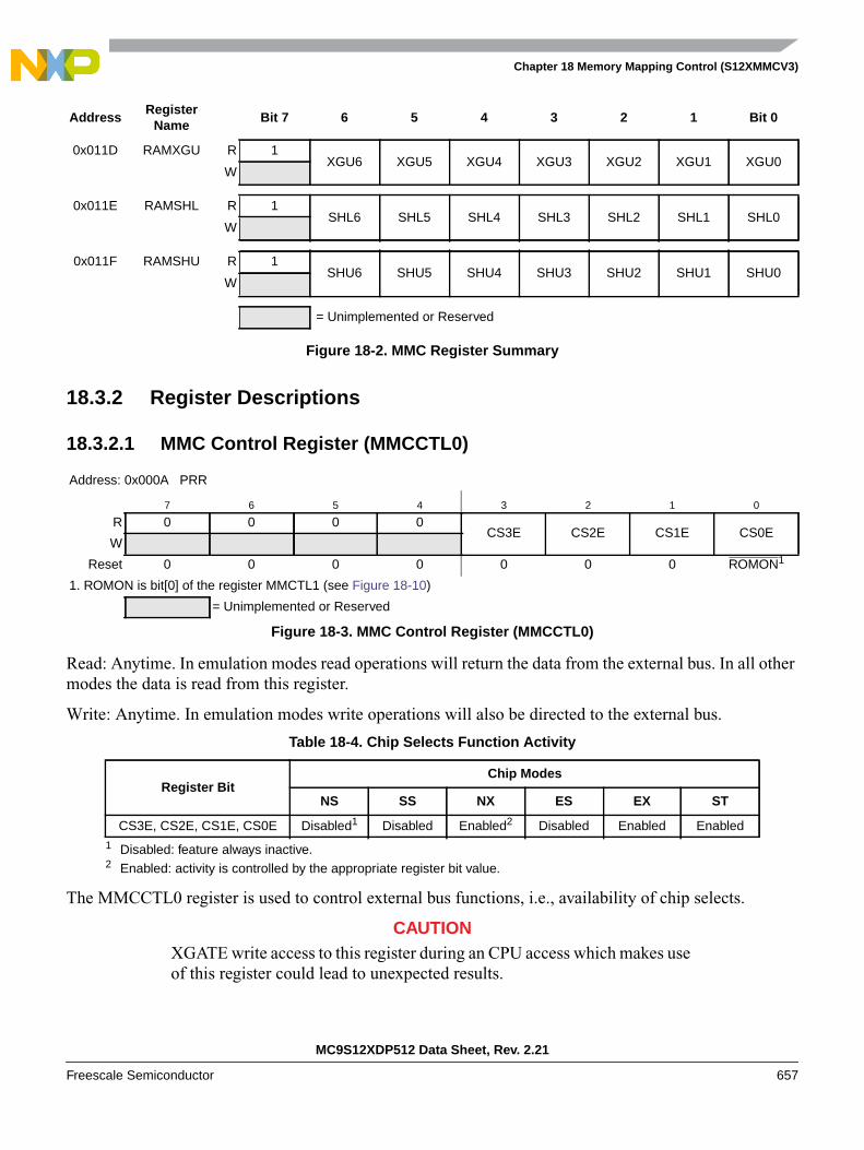
Chapter 18 Memory Mapping Control (S12XMMCV3)
MC9S12XDP512 Data Sheet, Rev. 2.21
Freescale Semiconductor 657
18.3.2 Register Descriptions
18.3.2.1 MMC Control Register (MMCCTL0)
Read: Anytime. In emulation modes read operations will return the data from the external bus. In all othermodes the data is read from this register.
Write: Anytime. In emulation modes write operations will also be directed to the external bus.
The MMCCTL0 register is used to control external bus functions, i.e., availability of chip selects.
CAUTIONXGATE write access to this register during an CPU access which makes useof this register could lead to unexpected results.
0x011D RAMXGU R 1XGU6 XGU5 XGU4 XGU3 XGU2 XGU1 XGU0
W
0x011E RAMSHL R 1SHL6 SHL5 SHL4 SHL3 SHL2 SHL1 SHL0
W
0x011F RAMSHU R 1SHU6 SHU5 SHU4 SHU3 SHU2 SHU1 SHU0
W
Address: 0x000A PRR
7 6 5 4 3 2 1 0
R 0 0 0 0CS3E CS2E CS1E CS0E
W
Reset 0 0 0 0 0 0 0 ROMON1
1. ROMON is bit[0] of the register MMCTL1 (see Figure 18-10)
= Unimplemented or Reserved
Figure 18-3. MMC Control Register (MMCCTL0)
Table 18-4. Chip Selects Function Activity
Register BitChip Modes
NS SS NX ES EX ST
CS3E, CS2E, CS1E, CS0E Disabled1
1 Disabled: feature always inactive.
Disabled Enabled2
2 Enabled: activity is controlled by the appropriate register bit value.
Disabled Enabled Enabled
AddressRegister
NameBit 7 6 5 4 3 2 1 Bit 0
= Unimplemented or Reserved
Figure 18-2. MMC Register Summary
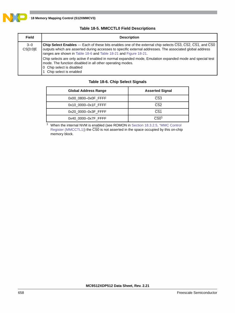
Chapter 18 Memory Mapping Control (S12XMMCV3)
MC9S12XDP512 Data Sheet, Rev. 2.21
658 Freescale Semiconductor
Table 18-5. MMCCTL0 Field Descriptions
Field Description
3–0CS[3:0]E
Chip Select Enables — Each of these bits enables one of the external chip selects CS3, CS2, CS1, and CS0outputs which are asserted during accesses to specific external addresses. The associated global addressranges are shown in Table 18-6 and Table 18-21 and Figure 18-21.Chip selects are only active if enabled in normal expanded mode, Emulation expanded mode and special testmode. The function disabled in all other operating modes.0 Chip select is disabled1 Chip select is enabled
Table 18-6. Chip Select Signals
Global Address Range Asserted Signal
0x00_0800–0x0F_FFFF CS3
0x10_0000–0x1F_FFFF CS2
0x20_0000–0x3F_FFFF CS1
0x40_0000–0x7F_FFFF CS01
1 When the internal NVM is enabled (see ROMON in Section 18.3.2.5, “MMC ControlRegister (MMCCTL1)) the CS0 is not asserted in the space occupied by this on-chipmemory block.

Chapter 18 Memory Mapping Control (S12XMMCV3)
MC9S12XDP512 Data Sheet, Rev. 2.21
Freescale Semiconductor 659
18.3.2.2 Mode Register (MODE)
Read: Anytime. In emulation modes read operations will return the data read from the external bus. In allother modes the data are read from this register.
Write: Only if a transition is allowed (see Figure 18-5). In emulation modes write operations will be alsodirected to the external bus.
The MODE bits of the MODE register are used to establish the MCU operating mode.
CAUTIONXGATE write access to this register during an CPU access which makes useof this register could lead to unexpected results.
Address: 0x000B PRR
7 6 5 4 3 2 1 0
RMODC MODB MODA
0 0 0 0 0
W
Reset MODC1 MODB1 MODA1 0 0 0 0 0
1. External signal (see Table 18-2).
= Unimplemented or Reserved
Figure 18-4. Mode Register (MODE)
Table 18-7. MODE Field Descriptions
Field Description
7–5MODC,MODB,MODA
Mode Select Bits — These bits control the current operating mode during RESET high (inactive). The externalmode pins MODC, MODB, and MODA determine the operating mode during RESET low (active). The state ofthe pins is latched into the respective register bits after the RESET signal goes inactive (see Figure 18-5).
Write restrictions exist to disallow transitions between certain modes. Figure 18-5 illustrates all allowed modechanges. Attempting non authorized transitions will not change the MODE bits, but it will block further writes tothese register bits except in special modes.
Both transitions from normal single-chip mode to normal expanded mode and from emulation single-chip toemulation expanded mode are only executed by writing a value of 3’b101 (write once). Writing any other valuewill not change the MODE bits, but will block further writes to these register bits.
Changes of operating modes are not allowed when the device is secured, but it will block further writes to theseregister bits except in special modes.
In emulation modes reading this address returns data from the external bus which has to be driven by theemulator. It is therefore responsibility of the emulator hardware to provide the expected value (i.e. a valuecorresponding to normal single chip mode while the device is in emulation single-chip mode or a valuecorresponding to normal expanded mode while the device is in emulation expanded mode).
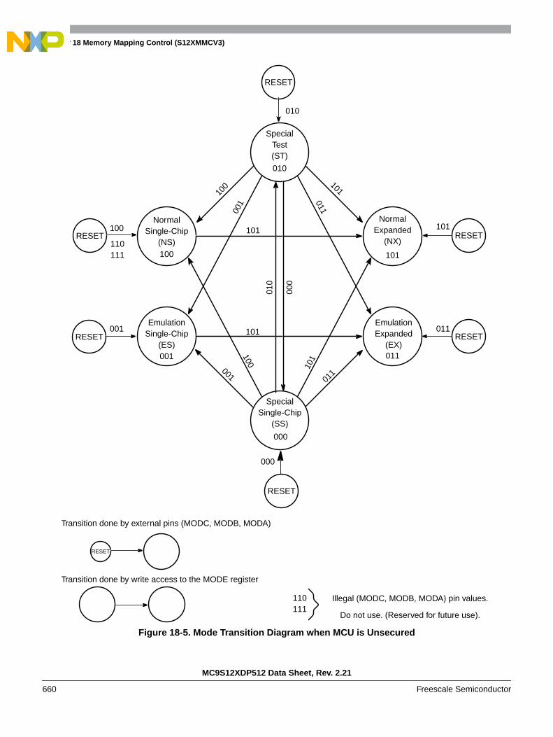
Chapter 18 Memory Mapping Control (S12XMMCV3)
MC9S12XDP512 Data Sheet, Rev. 2.21
660 Freescale Semiconductor
Figure 18-5. Mode Transition Diagram when MCU is Unsecured
NormalSingle-Chip
100
NormalExpanded
101
EmulationExpanded
011
EmulationSingle-Chip
001
SpecialTest
010
SpecialSingle-Chip
000
101
101
011
011
101
000010
100
001
001
100
101
RESET
(SS)
110111
000
RESET
RESET
RESET
RESET
RESET
010
101
011001
100
(EX)
(NX)(NS)
(ES)
(ST)
RESET
Transition done by external pins (MODC, MODB, MODA)
Transition done by write access to the MODE register
110111
Illegal (MODC, MODB, MODA) pin values.
Do not use. (Reserved for future use).

Chapter 18 Memory Mapping Control (S12XMMCV3)
MC9S12XDP512 Data Sheet, Rev. 2.21
Freescale Semiconductor 661
18.3.2.3 Global Page Index Register (GPAGE)
Read: Anytime
Write: Anytime
The global page index register is used to construct a 23 bit address in the global map format. It is only usedwhen the CPU is executing a global instruction (GLDAA, GLDAB, GLDD, GLDS, GLDX,GLDY,GSTAA, GSTAB, GSTD, GSTS, GSTX, GSTY) (see CPU Block Guide). The generated globaladdress is the result of concatenation of the CPU local address [15:0] with the GPAGE register [22:16] (seeFigure 18-7).
CAUTIONXGATE write access to this register during an CPU access which makes useof this register could lead to unexpected results.
Figure 18-7. GPAGE Address Mapping
Example 18-1. This example demonstrates usage of the GPAGE register
LDX #0x5000 ;Set GPAGE offset to the value of 0x5000MOVB #0x14, GPAGE ;Initialize GPAGE register with the value of 0x14GLDAA X ;Load Accu A from the global address 0x14_5000
Address: 0x0010
7 6 5 4 3 2 1 0
R 0GP6 GP5 GP4 GP3 GP2 GP1 GP0
W
Reset 0 0 0 0 0 0 0 0
= Unimplemented or Reserved
Figure 18-6. Global Page Index Register (GPAGE)
Table 18-8. GPAGE Field Descriptions
Field Description
6–0GP[6:0]
Global Page Index Bits 6–0 — These page index bits are used to select which of the 128 64-kilobyte pages isto be accessed.
Bit16 Bit 0Bit15Bit22
CPU Address [15:0]GPAGE Register [6:0]
Global Address [22:0]

Chapter 18 Memory Mapping Control (S12XMMCV3)
MC9S12XDP512 Data Sheet, Rev. 2.21
662 Freescale Semiconductor
18.3.2.4 Direct Page Register (DIRECT)
Read: Anytime
Write: anytime in special modes, one time only in other modes.
This register determines the position of the 256 Byte direct page within the memory map.It is valid for bothglobal and local mapping scheme.
CAUTIONXGATE write access to this register during an CPU access which makes useof this register could lead to unexpected results.
Figure 18-9. DIRECT Address Mapping
Bits [22:16] of the global address will be formed by the GPAGE[6:0] bits in case the CPU executes a globalinstruction in direct addressing mode or by the appropriate local address to the global address expansion(refer to Section 18.4.2.1.1, “Expansion of the Local Address Map).
Example 18-2. This example demonstrates usage of the Direct Addressing Mode
MOVB #0x80,DIRECT ;Set DIRECT register to 0x80. Write once only.;Global data accesses to the range 0xXX_80XX can be direct.;Logical data accesses to the range 0x80XX are direct.
LDY <00 ;Load the Y index register from 0x8000 (direct access).;< operator forces direct access on some assemblers but in;many cases assemblers are “direct page aware” and can
Address: 0x0011
7 6 5 4 3 2 1 0
RDP15 DP14 DP13 DP12 DP11 DP10 DP9 DP8
W
Reset 0 0 0 0 0 0 0 0
Figure 18-8. Direct Register (DIRECT)
Table 18-9. DIRECT Field Descriptions
Field Description
7–0DP[15:8]
Direct Page Index Bits 15–8 — These bits are used by the CPU when performing accesses using the directaddressing mode. The bits from this register form bits [15:8] of the address (see Figure 18-9).
Bit15 Bit0Bit7Bit22
CPU Address [15:0]
Global Address [22:0]
Bit8Bit16
DP [15:8]
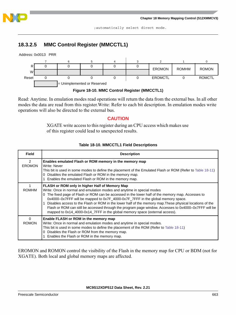
Chapter 18 Memory Mapping Control (S12XMMCV3)
MC9S12XDP512 Data Sheet, Rev. 2.21
Freescale Semiconductor 663
;automatically select direct mode.
18.3.2.5 MMC Control Register (MMCCTL1)
Read: Anytime. In emulation modes read operations will return the data from the external bus. In all othermodes the data are read from this register.Write: Refer to each bit description. In emulation modes writeoperations will also be directed to the external bus.
CAUTIONXGATE write access to this register during an CPU access which makes useof this register could lead to unexpected results.
EROMON and ROMON control the visibility of the Flash in the memory map for CPU or BDM (not forXGATE). Both local and global memory maps are affected.
Address: 0x0013 PRR
7 6 5 4 3 2 1 0
R 0 0 0 0 0EROMON ROMHM ROMON
W
Reset 0 0 0 0 0 EROMCTL 0 ROMCTL
= Unimplemented or Reserved
Figure 18-10. MMC Control Register (MMCCTL1)
Table 18-10. MMCCTL1 Field Descriptions
Field Description
2EROMON
Enables emulated Flash or ROM memory in the memory mapWrite: NeverThis bit is used in some modes to define the placement of the Emulated Flash or ROM (Refer to Table 18-11)0 Disables the emulated Flash or ROM in the memory map.1 Enables the emulated Flash or ROM in the memory map.
1ROMHM
FLASH or ROM only in higher Half of Memory MapWrite: Once in normal and emulation modes and anytime in special modes0 The fixed page of Flash or ROM can be accessed in the lower half of the memory map. Accesses to
0x4000–0x7FFF will be mapped to 0x7F_4000-0x7F_7FFF in the global memory space.1 Disables access to the Flash or ROM in the lower half of the memory map.These physical locations of the
Flash or ROM can still be accessed through the program page window. Accesses to 0x4000–0x7FFF will bemapped to 0x14_4000-0x14_7FFF in the global memory space (external access).
0ROMON
Enable FLASH or ROM in the memory mapWrite: Once in normal and emulation modes and anytime in special modes.This bit is used in some modes to define the placement of the ROM (Refer to Table 18-11)0 Disables the Flash or ROM from the memory map.1 Enables the Flash or ROM in the memory map.
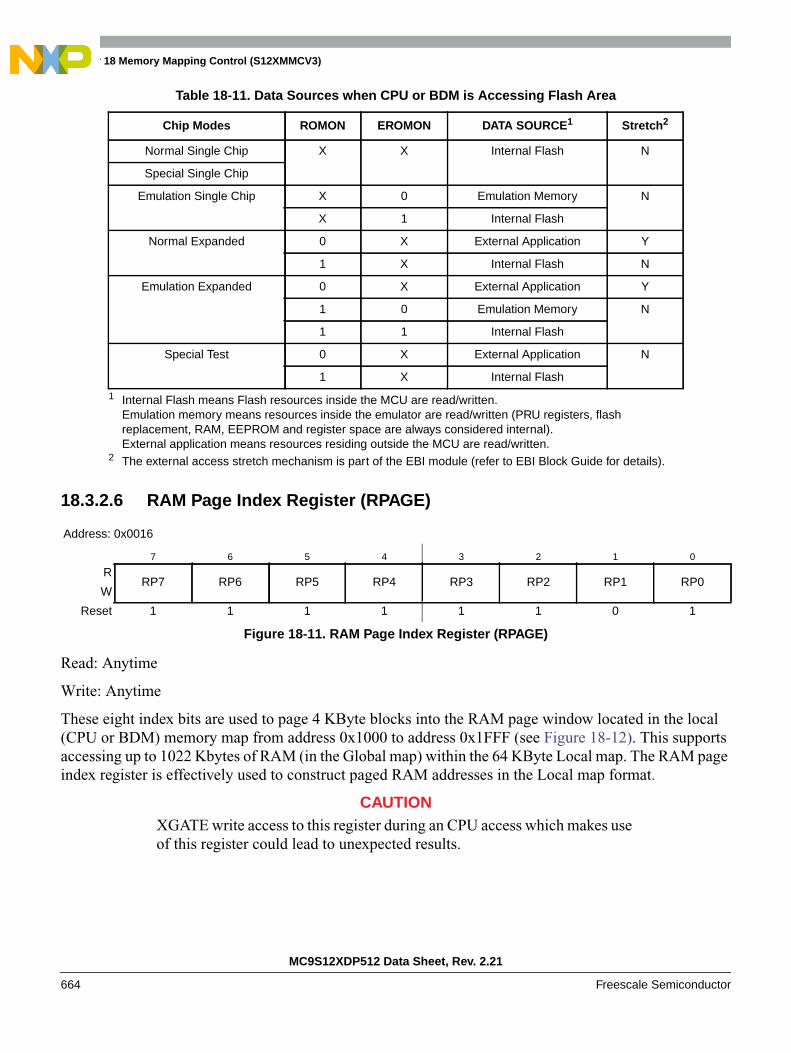
Chapter 18 Memory Mapping Control (S12XMMCV3)
MC9S12XDP512 Data Sheet, Rev. 2.21
664 Freescale Semiconductor
18.3.2.6 RAM Page Index Register (RPAGE)
Read: Anytime
Write: Anytime
These eight index bits are used to page 4 KByte blocks into the RAM page window located in the local(CPU or BDM) memory map from address 0x1000 to address 0x1FFF (see Figure 18-12). This supportsaccessing up to 1022 Kbytes of RAM (in the Global map) within the 64 KByte Local map. The RAM pageindex register is effectively used to construct paged RAM addresses in the Local map format.
CAUTIONXGATE write access to this register during an CPU access which makes useof this register could lead to unexpected results.
Table 18-11. Data Sources when CPU or BDM is Accessing Flash Area
Chip Modes ROMON EROMON DATA SOURCE1
1 Internal Flash means Flash resources inside the MCU are read/written.Emulation memory means resources inside the emulator are read/written (PRU registers, flashreplacement, RAM, EEPROM and register space are always considered internal).External application means resources residing outside the MCU are read/written.
Stretch2
2 The external access stretch mechanism is part of the EBI module (refer to EBI Block Guide for details).
Normal Single Chip X X Internal Flash N
Special Single Chip
Emulation Single Chip X 0 Emulation Memory N
X 1 Internal Flash
Normal Expanded 0 X External Application Y
1 X Internal Flash N
Emulation Expanded 0 X External Application Y
1 0 Emulation Memory N
1 1 Internal Flash
Special Test 0 X External Application N
1 X Internal Flash
Address: 0x0016
7 6 5 4 3 2 1 0
RRP7 RP6 RP5 RP4 RP3 RP2 RP1 RP0
W
Reset 1 1 1 1 1 1 0 1
Figure 18-11. RAM Page Index Register (RPAGE)

Chapter 18 Memory Mapping Control (S12XMMCV3)
MC9S12XDP512 Data Sheet, Rev. 2.21
Freescale Semiconductor 665
Figure 18-12. RPAGE Address Mapping
NOTEBecause RAM page 0 has the same global address as the register space, it ispossible to write to registers through the RAM space when RPAGE = 0x00.
The reset value of 0xFD ensures that there is a linear RAM space available between addresses 0x1000 and0x3FFF out of reset.
The fixed 4K page from 0x2000–0x2FFF of RAM is equivalent to page 254 (page number 0xFE).
The fixed 4K page from 0x3000–0x3FFF of RAM is equivalent to page 255 (page number 0xFF).
Table 18-12. RPAGE Field Descriptions
Field Description
7–0RP[7:0]
RAM Page Index Bits 7–0 — These page index bits are used to select which of the 256 RAM array pages is tobe accessed in the RAM Page Window.
Bit18 Bit0Bit110
Address [11:0]RPAGE Register [7:0]
Global Address [22:0]
Bit12Bit190
Address: CPU Local Addressor BDM Local Address
0

Chapter 18 Memory Mapping Control (S12XMMCV3)
MC9S12XDP512 Data Sheet, Rev. 2.21
666 Freescale Semiconductor
18.3.2.7 EEPROM Page Index Register (EPAGE)
Read: Anytime
Write: Anytime
These eight index bits are used to page 1 KByte blocks into the EEPROM page window located in the local(CPU or BDM) memory map from address 0x0800 to address 0x0BFF (see Figure 18-14). This supportsaccessing up to 256 Kbytes of EEPROM (in the Global map) within the 64 KByte Local map. TheEEPROM page index register is effectively used to construct paged EEPROM addresses in the Local mapformat.
CAUTIONXGATE write access to this register during an CPU access which makes useof this register could lead to unexpected results.
Figure 18-14. EPAGE Address Mapping
The reset value of 0xFE ensures that there is a linear EEPROM space available between addresses 0x0800and 0x0FFF out of reset.
The fixed 1K page 0x0C00–0x0FFF of EEPROM is equivalent to page 255 (page number 0xFF).
Address: 0x0017
7 6 5 4 3 2 1 0
REP7 EP6 EP5 EP4 EP3 EP2 EP1 EP0
W
Reset 1 1 1 1 1 1 1 0
Figure 18-13. EEPROM Page Index Register (EPAGE)
Table 18-13. EPAGE Field Descriptions
Field Description
7–0EP[7:0]
EEPROM Page Index Bits 7–0 — These page index bits are used to select which of the 256 EEPROM arraypages is to be accessed in the EEPROM Page Window.
Bit16 Bit0Bit9
Address [9:0]EPAGE Register [7:0]
Global Address [22:0]
Bit10Bit1700 10 0
Address: CPU Local Addressor BDM Local Address
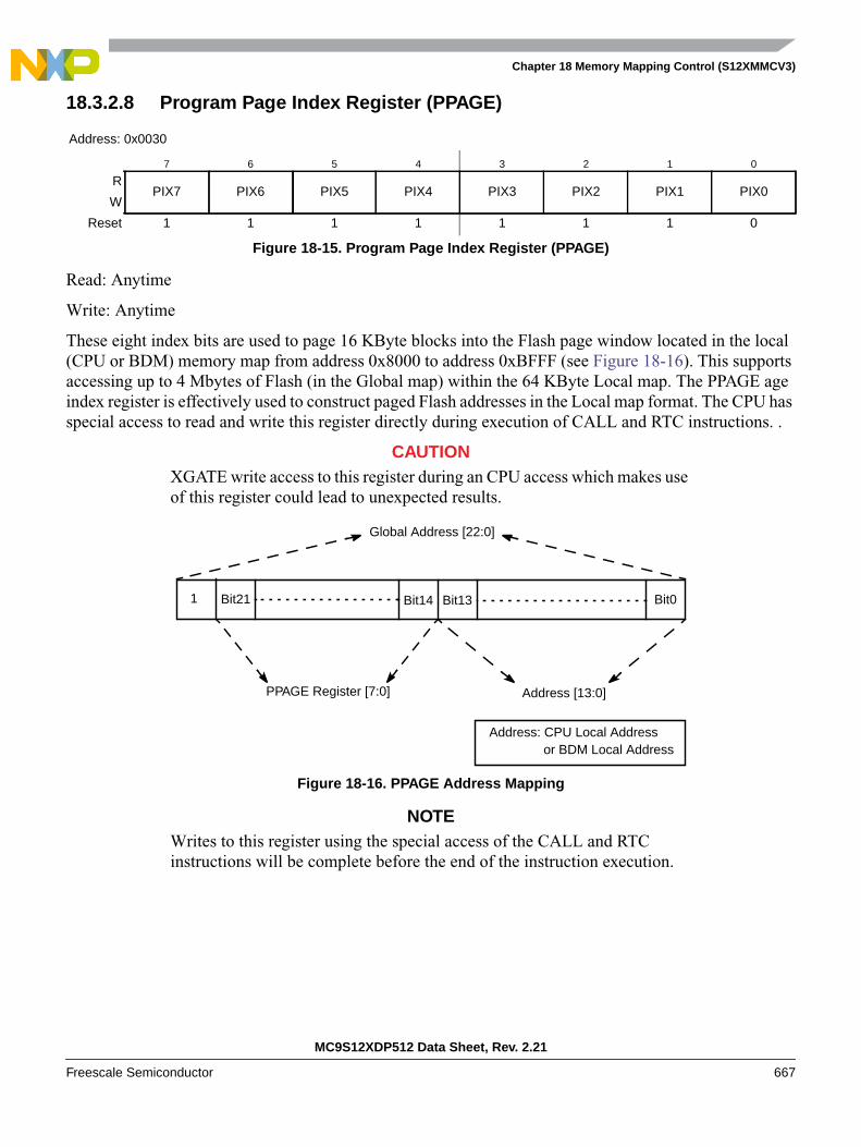
Chapter 18 Memory Mapping Control (S12XMMCV3)
MC9S12XDP512 Data Sheet, Rev. 2.21
Freescale Semiconductor 667
18.3.2.8 Program Page Index Register (PPAGE)
Read: Anytime
Write: Anytime
These eight index bits are used to page 16 KByte blocks into the Flash page window located in the local(CPU or BDM) memory map from address 0x8000 to address 0xBFFF (see Figure 18-16). This supportsaccessing up to 4 Mbytes of Flash (in the Global map) within the 64 KByte Local map. The PPAGE ageindex register is effectively used to construct paged Flash addresses in the Local map format. The CPU hasspecial access to read and write this register directly during execution of CALL and RTC instructions. .
CAUTIONXGATE write access to this register during an CPU access which makes useof this register could lead to unexpected results.
Figure 18-16. PPAGE Address Mapping
NOTEWrites to this register using the special access of the CALL and RTCinstructions will be complete before the end of the instruction execution.
Address: 0x0030
7 6 5 4 3 2 1 0
RPIX7 PIX6 PIX5 PIX4 PIX3 PIX2 PIX1 PIX0
W
Reset 1 1 1 1 1 1 1 0
Figure 18-15. Program Page Index Register (PPAGE)
Bit14 Bit01
Address [13:0]PPAGE Register [7:0]
Global Address [22:0]
Bit13Bit21
Address: CPU Local Addressor BDM Local Address
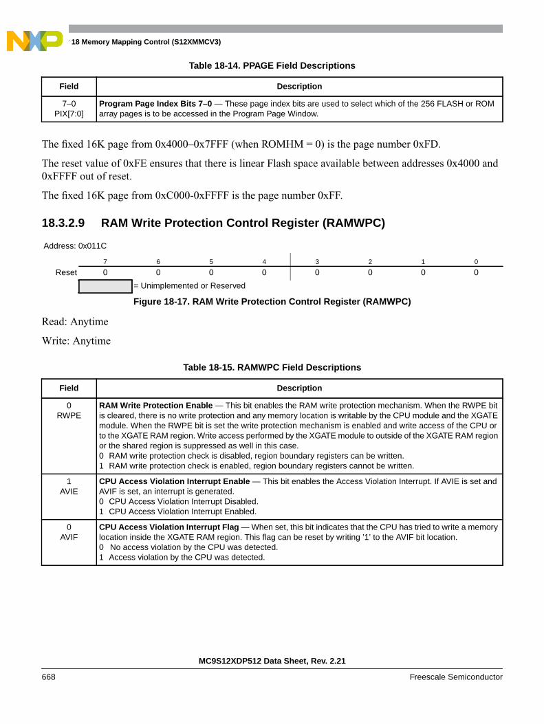
Chapter 18 Memory Mapping Control (S12XMMCV3)
MC9S12XDP512 Data Sheet, Rev. 2.21
668 Freescale Semiconductor
The fixed 16K page from 0x4000–0x7FFF (when ROMHM = 0) is the page number 0xFD.
The reset value of 0xFE ensures that there is linear Flash space available between addresses 0x4000 and0xFFFF out of reset.
The fixed 16K page from 0xC000-0xFFFF is the page number 0xFF.
18.3.2.9 RAM Write Protection Control Register (RAMWPC)
Read: Anytime
Write: Anytime
Table 18-14. PPAGE Field Descriptions
Field Description
7–0PIX[7:0]
Program Page Index Bits 7–0 — These page index bits are used to select which of the 256 FLASH or ROMarray pages is to be accessed in the Program Page Window.
Address: 0x011C
7 6 5 4 3 2 1 0
Reset 0 0 0 0 0 0 0 0
= Unimplemented or Reserved
Figure 18-17. RAM Write Protection Control Register (RAMWPC)
Table 18-15. RAMWPC Field Descriptions
Field Description
0RWPE
RAM Write Protection Enable — This bit enables the RAM write protection mechanism. When the RWPE bitis cleared, there is no write protection and any memory location is writable by the CPU module and the XGATEmodule. When the RWPE bit is set the write protection mechanism is enabled and write access of the CPU orto the XGATE RAM region. Write access performed by the XGATE module to outside of the XGATE RAM regionor the shared region is suppressed as well in this case.0 RAM write protection check is disabled, region boundary registers can be written.1 RAM write protection check is enabled, region boundary registers cannot be written.
1AVIE
CPU Access Violation Interrupt Enable — This bit enables the Access Violation Interrupt. If AVIE is set andAVIF is set, an interrupt is generated.0 CPU Access Violation Interrupt Disabled.1 CPU Access Violation Interrupt Enabled.
0AVIF
CPU Access Violation Interrupt Flag — When set, this bit indicates that the CPU has tried to write a memorylocation inside the XGATE RAM region. This flag can be reset by writing ’1’ to the AVIF bit location.0 No access violation by the CPU was detected.1 Access violation by the CPU was detected.

Chapter 18 Memory Mapping Control (S12XMMCV3)
MC9S12XDP512 Data Sheet, Rev. 2.21
Freescale Semiconductor 669
18.3.2.10 RAM XGATE Upper Boundary Register (RAMXGU)
Read: Anytime
Write: Anytime when RWPE = 0
18.3.2.11 RAM Shared Region Lower Boundary Register (RAMSHL)
Read: Anytime
Write: Anytime when RWPE = 0
Address: 0x011D
7 6 5 4 3 2 1 0
R 1XGU6 XGU5 XGU4 XGU3 XGU2 XGU1 XGU0
W
Reset 1 1 1 1 1 1 1 1
= Unimplemented or Reserved
Figure 18-18. RAM XGATE Upper Boundary Register (RAMXGU)
Table 18-16. RAMXGU Field Descriptions
Field Description
6–0XGU[6:0]
XGATE Region Upper Boundary Bits 6-0 — These bits define the upper boundary of the RAM region allocatedto the XGATE module in multiples of 256 bytes. The 256 byte block selected by this register is included in theregion. See Figure 18-25 for details.
Address: 0x011E
7 6 5 4 3 2 1 0
R 1SHL6 SHL5 SHL4 SHL3 SHL2 SHL1 SHL0
W
Reset 1 1 1 1 1 1 1 1
= Unimplemented or Reserved
Figure 18-19. RAM Shared Region Lower Boundary Register (RAMSHL)
Table 18-17. RAMSHL Field Descriptions
Field Description
6–0SHL[6:0]
RAM Shared Region Lower Boundary Bits 6–0 — These bits define the lower boundary of the shared memoryregion in multiples of 256 bytes. The block selected by this register is included in the region. See Figure 18-25for details.
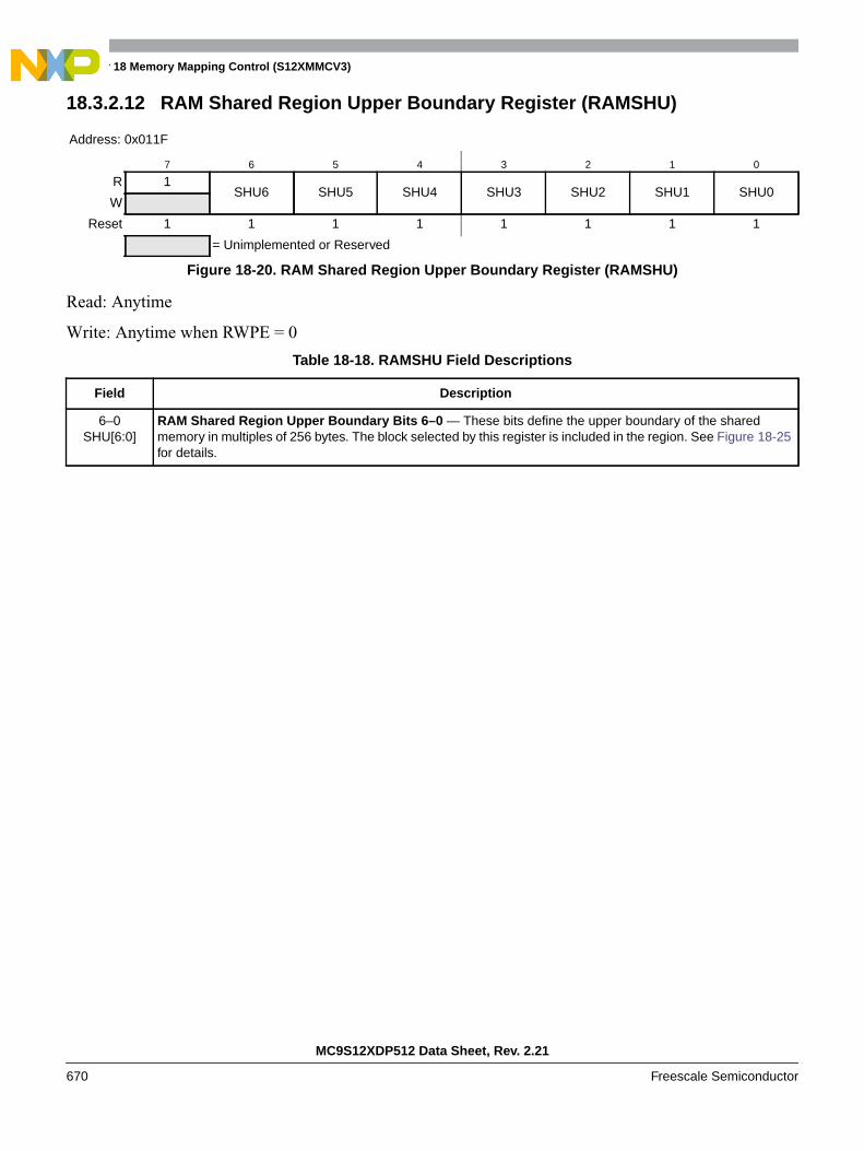
Chapter 18 Memory Mapping Control (S12XMMCV3)
MC9S12XDP512 Data Sheet, Rev. 2.21
670 Freescale Semiconductor
18.3.2.12 RAM Shared Region Upper Boundary Register (RAMSHU)
Read: Anytime
Write: Anytime when RWPE = 0
Address: 0x011F
7 6 5 4 3 2 1 0
R 1SHU6 SHU5 SHU4 SHU3 SHU2 SHU1 SHU0
W
Reset 1 1 1 1 1 1 1 1
= Unimplemented or Reserved
Figure 18-20. RAM Shared Region Upper Boundary Register (RAMSHU)
Table 18-18. RAMSHU Field Descriptions
Field Description
6–0SHU[6:0]
RAM Shared Region Upper Boundary Bits 6–0 — These bits define the upper boundary of the sharedmemory in multiples of 256 bytes. The block selected by this register is included in the region. See Figure 18-25for details.
Chapter 18 Memory Mapping Control (S12XMMCV3)
MC9S12XDP512 Data Sheet, Rev. 2.21
Freescale Semiconductor 671
18.4 Functional DescriptionThe MMC block performs several basic functions of the S12X sub-system operation: MCU operationmodes, priority control, address mapping, select signal generation and access limitations for the system.Each aspect is described in the following subsections.
18.4.1 MCU Operating Mode• Normal single-chip mode
There is no external bus in this mode. The MCU program is executed from the internal memoryand no external accesses are allowed.
• Special single-chip mode
This mode is generally used for debugging single-chip operation, boot-strapping or security relatedoperations. The active background debug mode is in control of the CPU code execution and theBDM firmware is waiting for serial commands sent through the BKGD pin. There is no externalbus in this mode.
• Emulation single-chip mode
Tool vendors use this mode for emulation systems in which the user’s target application is normalsingle-chip mode. Code is executed from external or internal memory depending on the set-up ofthe EROMON bit (see Section 18.3.2.5, “MMC Control Register (MMCCTL1)). The external busis active in both cases to allow observation of internal operations (internal visibility).
Chapter 18 Memory Mapping Control (S12XMMCV3)
MC9S12XDP512 Data Sheet, Rev. 2.21
672 Freescale Semiconductor
• Normal expanded mode
The external bus interface is configured as an up to 23-bit address bus, 8 or 16-bit data bus withdedicated bus control and status signals. This mode allows 8 or 16-bit external memory andperipheral devices to be interfaced to the system. The fastest external bus rate is half of the internalbus rate. An external signal can be used in this mode to cause the external bus to wait as desired bythe external logic.
• Emulation expanded mode
Tool vendors use this mode for emulation systems in which the user’s target application is normalexpanded mode.
• Special test mode
This mode is an expanded mode for factory test.
18.4.2 Memory Map Scheme
18.4.2.1 CPU and BDM Memory Map Scheme
The BDM firmware lookup tables and BDM register memory locations share addresses with othermodules; however they are not visible in the memory map during user’s code execution. The BDMmemory resources are enabled only during the READ_BD and WRITE_BD access cycles to distinguishbetween accesses to the BDM memory area and accesses to the other modules. (Refer to BDM BlockGuide for further details).
When the MCU enters active BDM mode, the BDM firmware lookup tables and the BDM registersbecome visible in the local memory map in the range 0xFF00-0xFFFF (global address 0x7F_FF00 -0x7F_FFFF) and the CPU begins execution of firmware commands or the BDM begins execution ofhardware commands. The resources which share memory space with the BDM module will not be visiblein the memory map during active BDM mode.
Please note that after the MCU enters active BDM mode the BDM firmware lookup tables and the BDMregisters will also be visible between addresses 0xBF00 and 0xBFFF if the PPAGE register contains valueof 0xFF.
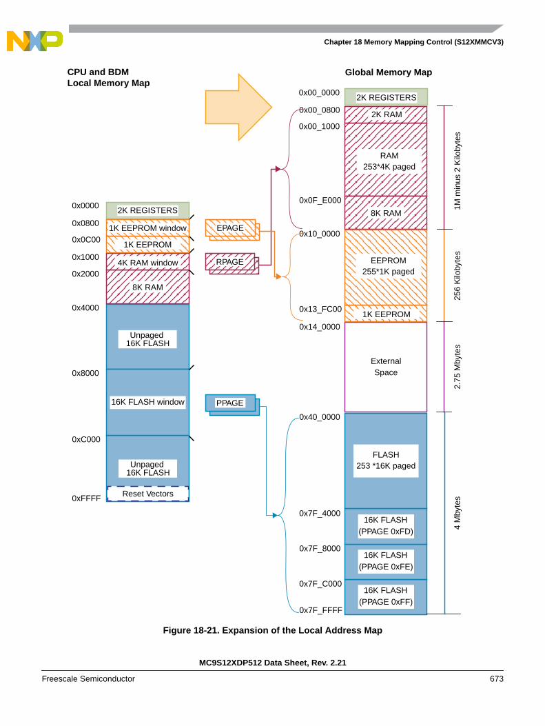
Chapter 18 Memory Mapping Control (S12XMMCV3)
MC9S12XDP512 Data Sheet, Rev. 2.21
Freescale Semiconductor 673
Figure 18-21. Expansion of the Local Address Map
0x7F_FFFF
0x00_0000
0x14_0000
0x10_0000
0x00_0800
EPAGE
RPAGE
PPAGE
CPU and BDMLocal Memory Map
Global Memory Map
0xFFFF Reset Vectors
0xC000
0x8000
Unpaged
0x4000
0x1000
0x0000
16K FLASH window
0x0C00
0x2000
0x0800
8K RAM
4K RAM window
1K EEPROM
2K REGISTERS
1K EEPROM window
16K FLASH
Unpaged16K FLASH
2K REGISTERS
2K RAM
253*4K pagedRAM
1K EEPROM
255*1K pagedEEPROM
253 *16K pagedFLASH
16K FLASH(PPAGE 0xFD)
8K RAM
ExternalSpace
16K FLASH(PPAGE 0xFE)
16K FLASH(PPAGE 0xFF)
0x00_1000
0x0F_E000
0x13_FC00
0x40_0000
0x7F_4000
0x7F_8000
0x7F_C000
1M m
inus
2 K
iloby
tes
256
Kilo
byte
s4
Mby
tes
2.75
Mby
tes

Chapter 18 Memory Mapping Control (S12XMMCV3)
MC9S12XDP512 Data Sheet, Rev. 2.21
674 Freescale Semiconductor
18.4.2.1.1 Expansion of the Local Address Map
Expansion of the CPU Local Address Map
The program page index register in MMC allows accessing up to 4 Mbyte of FLASH or ROM in the globalmemory map by using the eight page index bits to page 256 16 Kbyte blocks into the program pagewindow located from address 0x8000 to address 0xBFFF in the local CPU memory map.
The page value for the program page window is stored in the PPAGE register. The value of the PPAGEregister can be read or written by normal memory accesses as well as by the CALL and RTC instructions(see Section 18.5.1, “CALL and RTC Instructions).
Control registers, vector space and parts of the on-chip memories are located in unpaged portions of the64-kilobyte local CPU address space.
The starting address of an interrupt service routine must be located in unpaged memory unless the user iscertain that the PPAGE register will be set to the appropriate value when the service routine is called.However an interrupt service routine can call other routines that are in paged memory. The upper16-kilobyte block of the local CPU memory space (0xC000–0xFFFF) is unpaged. It is recommended thatall reset and interrupt vectors point to locations in this area or to the other unpaged sections of the localCPU memory map.
Table 18-19 Table 18-12 summarizes mapping of the address bus in Flash/External space based on theaddress, the PPAGE register value and value of the ROMHM bit in the MMCCTL1 register.
The RAM page index register allows accessing up to 1 Mbyte –2 Kbytes of RAM in the global memorymap by using the eight RPAGE index bits to page 4 Kbyte blocks into the RAM page window located inthe local CPU memory space from address 0x1000 to address 0x1FFF. The EEPROM page index registerEPAGE allows accessing up to 256 Kbytes of EEPROM in the system by using the eight EPAGE indexbits to page 1 Kbyte blocks into the EEPROM page window located in the local CPU memory space fromaddress 0x0800 to address 0x0BFF.
Table 18-19. Global FLASH/ROM Allocated
LocalCPU Address
ROMHMExternalAccess
Global Address
0x4000–0x7FFF 0 No 0x7F_4000 –0x7F_7FFF
1 Yes 0x14_4000–0x14_7FFF
0x8000–0xBFFF N/A No1
1 The internal or the external bus is accessed based on the size of the memory resourcesimplemented on-chip. Please refer to Figure 1-23 for further details.
0x40_0000–0x7F_FFFF
N/A Yes1
0xC000–0xFFFF N/A No 0x7F_C000–0x7F_FFFF

Chapter 18 Memory Mapping Control (S12XMMCV3)
MC9S12XDP512 Data Sheet, Rev. 2.21
Freescale Semiconductor 675
Expansion of the BDM Local Address Map
PPAGE, RPAGE, and EPAGE registers are also used for the expansion of the BDM local address to theglobal address. These registers can be read and written by the BDM.
The BDM expansion scheme is the same as the CPU expansion scheme.
18.4.2.2 Global Addresses Based on the Global Page
CPU Global Addresses Based on the Global Page
The seven global page index bits allow access to the full 8 Mbyte address map that can be accessed with23 address bits. This provides an alternative way to access all of the various pages of FLASH, RAM andEEPROM as well as additional external memory.
The GPAGE Register is used only when the CPU is executing a global instruction (see Section 18.3.2.3,“Global Page Index Register (GPAGE)). The generated global address is the result of concatenation of theCPU local address [15:0] with the GPAGE register [22:16] (see Figure 18-7).
BDM Global Addresses Based on the Global Page
The seven BDMGPR Global Page index bits allow access to the full 8 Mbyte address map that can beaccessed with 23 address bits. This provides an alternative way to access all of the various pages ofFLASH, RAM and EEPROM as well as additional external memory.
The BDM global page index register (BDMGPR) is used only in the case the CPU is executing a firmwarecommand which uses a global instruction (like GLDD, GSTD) or by a BDM hardware command (likeWRITE_W, WRITE_BYTE, READ_W, READ_BYTE). See the BDM Block Guide for further details.
The generated global address is a result of concatenation of the BDM local address with the BDMGPRregister [22:16] in the case of a hardware command or concatenation of the CPU local address and theBDMGPR register [22:16] in the case of a firmware command (see Figure 18-22).
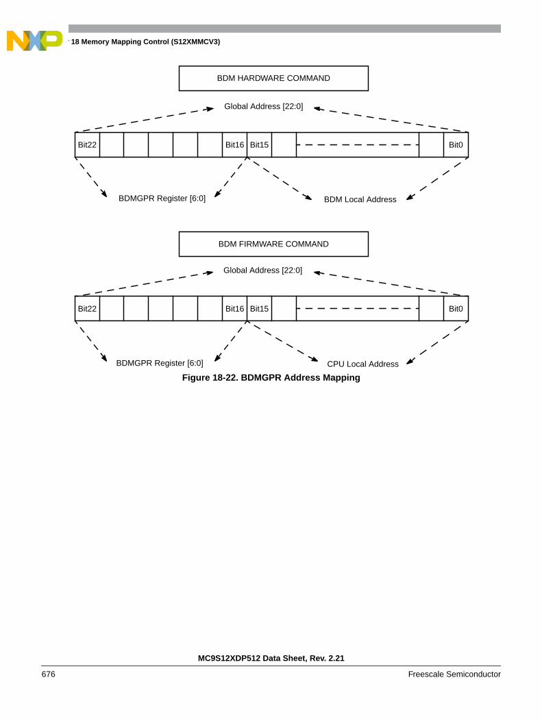
Chapter 18 Memory Mapping Control (S12XMMCV3)
MC9S12XDP512 Data Sheet, Rev. 2.21
676 Freescale Semiconductor
Figure 18-22. BDMGPR Address Mapping
Bit16 Bit0Bit15Bit22
BDM Local AddressBDMGPR Register [6:0]
Global Address [22:0]
Bit16 Bit0Bit15Bit22
CPU Local AddressBDMGPR Register [6:0]
Global Address [22:0]
BDM HARDWARE COMMAND
BDM FIRMWARE COMMAND
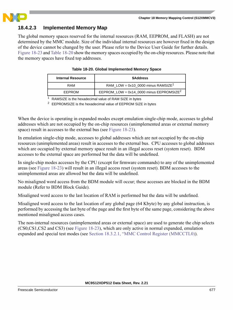
Chapter 18 Memory Mapping Control (S12XMMCV3)
MC9S12XDP512 Data Sheet, Rev. 2.21
Freescale Semiconductor 677
18.4.2.3 Implemented Memory Map
The global memory spaces reserved for the internal resources (RAM, EEPROM, and FLASH) are notdetermined by the MMC module. Size of the individual internal resources are however fixed in the designof the device cannot be changed by the user. Please refer to the Device User Guide for further details.Figure 18-23 and Table 18-20 show the memory spaces occupied by the on-chip resources. Please note thatthe memory spaces have fixed top addresses.
When the device is operating in expanded modes except emulation single-chip mode, accesses to globaladdresses which are not occupied by the on-chip resources (unimplemented areas or external memoryspace) result in accesses to the external bus (see Figure 18-23).
In emulation single-chip mode, accesses to global addresses which are not occupied by the on-chipresources (unimplemented areas) result in accesses to the external bus. CPU accesses to global addresseswhich are occupied by external memory space result in an illegal access reset (system reset). BDMaccesses to the external space are performed but the data will be undefined.
In single-chip modes accesses by the CPU (except for firmware commands) to any of the unimplementedareas (see Figure 18-23) will result in an illegal access reset (system reset). BDM accesses to theunimplemented areas are allowed but the data will be undefined.
No misaligned word access from the BDM module will occur; these accesses are blocked in the BDMmodule (Refer to BDM Block Guide).
Misaligned word access to the last location of RAM is performed but the data will be undefined.
Misaligned word access to the last location of any global page (64 Kbyte) by any global instruction, isperformed by accessing the last byte of the page and the first byte of the same page, considering the abovementioned misaligned access cases.
The non-internal resources (unimplemented areas or external space) are used to generate the chip selects(CS0,CS1,CS2 and CS3) (see Figure 18-23), which are only active in normal expanded, emulationexpanded and special test modes (see Section 18.3.2.1, “MMC Control Register (MMCCTL0)).
Table 18-20. Global Implemented Memory Space
Internal Resource $Address
RAM RAM_LOW = 0x10_0000 minus RAMSIZE1
1 RAMSIZE is the hexadecimal value of RAM SIZE in bytes
EEPROM EEPROM_LOW = 0x14_0000 minus EEPROMSIZE2
2 EEPROMSIZE is the hexadecimal value of EEPROM SIZE in bytes
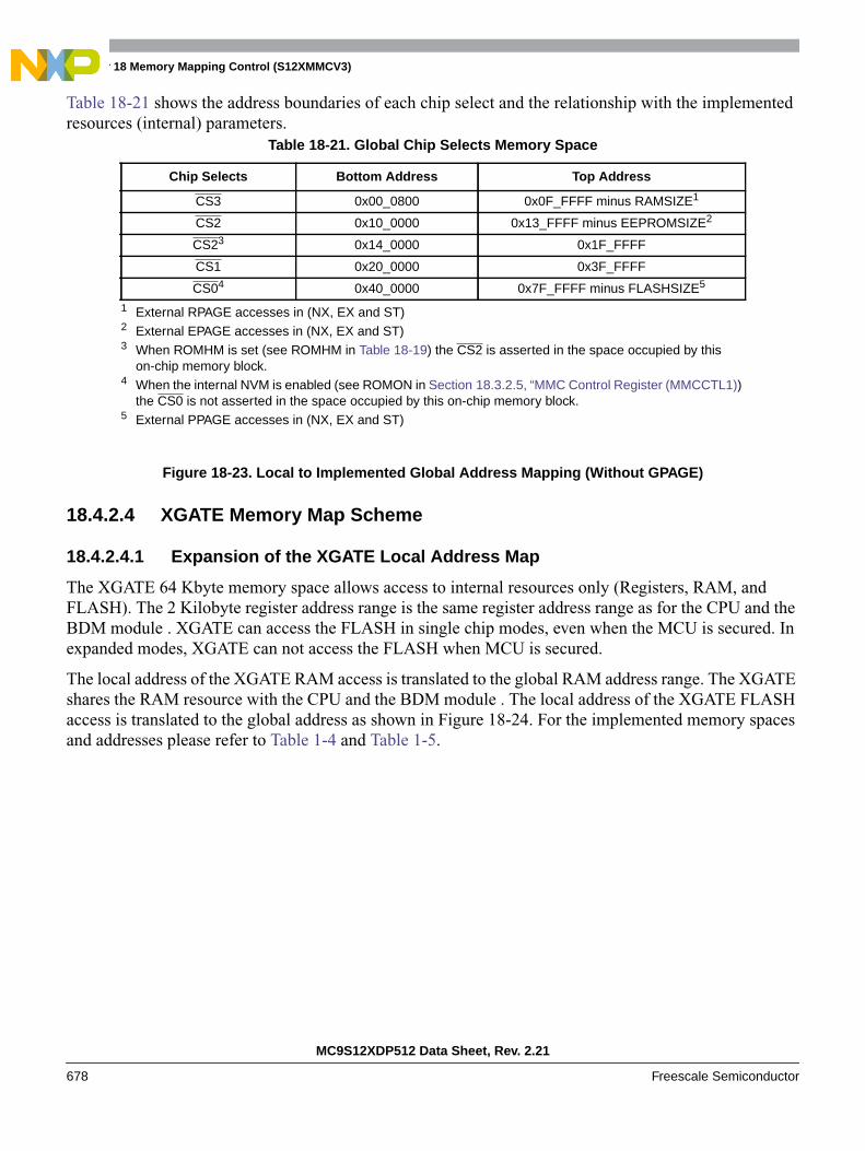
Chapter 18 Memory Mapping Control (S12XMMCV3)
MC9S12XDP512 Data Sheet, Rev. 2.21
678 Freescale Semiconductor
Table 18-21 shows the address boundaries of each chip select and the relationship with the implementedresources (internal) parameters.
Figure 18-23. Local to Implemented Global Address Mapping (Without GPAGE)
18.4.2.4 XGATE Memory Map Scheme
18.4.2.4.1 Expansion of the XGATE Local Address Map
The XGATE 64 Kbyte memory space allows access to internal resources only (Registers, RAM, andFLASH). The 2 Kilobyte register address range is the same register address range as for the CPU and theBDM module . XGATE can access the FLASH in single chip modes, even when the MCU is secured. Inexpanded modes, XGATE can not access the FLASH when MCU is secured.
The local address of the XGATE RAM access is translated to the global RAM address range. The XGATEshares the RAM resource with the CPU and the BDM module . The local address of the XGATE FLASHaccess is translated to the global address as shown in Figure 18-24. For the implemented memory spacesand addresses please refer to Table 1-4 and Table 1-5.
Table 18-21. Global Chip Selects Memory Space
Chip Selects Bottom Address Top Address
CS3 0x00_0800 0x0F_FFFF minus RAMSIZE1
1 External RPAGE accesses in (NX, EX and ST)
CS2 0x10_0000 0x13_FFFF minus EEPROMSIZE2
2 External EPAGE accesses in (NX, EX and ST)
CS23
3 When ROMHM is set (see ROMHM in Table 18-19) the CS2 is asserted in the space occupied by thison-chip memory block.
0x14_0000 0x1F_FFFF
CS1 0x20_0000 0x3F_FFFF
CS04
4 When the internal NVM is enabled (see ROMON in Section 18.3.2.5, “MMC Control Register (MMCCTL1))the CS0 is not asserted in the space occupied by this on-chip memory block.
0x40_0000 0x7F_FFFF minus FLASHSIZE5
5 External PPAGE accesses in (NX, EX and ST)

Chapter 18 Memory Mapping Control (S12XMMCV3)
MC9S12XDP512 Data Sheet, Rev. 2.21
Freescale Semiconductor 679
Figure 18-24. XGATE Global Address Mapping
0x7F_FFFF
0x00_0000
0x0F_FFFF
0xFFFF
0x0000
Registers
FLASH
RAM
0x0800
Registers0x00_07FF
XGATELocal Memory Map
Global Memory Map
XG
FLA
SH
SIZ
E
XG
RA
MS
IZE
RA
MS
IZE
0x78_0800FLASH
RAM
XGRAM_LOW
XGFLASH_HIGH

Chapter 18 Memory Mapping Control (S12XMMCV3)
MC9S12XDP512 Data Sheet, Rev. 2.21
680 Freescale Semiconductor
18.4.3 Chip Access Restrictions
18.4.3.1 Illegal XGATE Accesses
A possible access error is flagged by the MMC and signalled to XGATE under the following conditions:
• XGATE performs misaligned word (in case of load-store or opcode or vector fetch accesses).
• XGATE accesses the register space (in case of opcode or vector fetch).
• XGATE performs a write to Flash in any modes (in case of load-store access).
• XGATE performs an access to a secured Flash in expanded modes (in case of load-store or opcodeor vector fetch accesses).
• XGATE performs an access to an unimplemented area (in case of load-store or opcode or vectorfetch accesses).
• XGATE performs a write to non-XGATE region in RAM (RAM protection mechanism) (in caseof load-store access).
For further details refer to the XGATE Block Guide.
18.4.3.2 Illegal CPU Accesses
After programming the protection mechanism registers (see Figure 18-17, Figure 18-18, Figure 18-19,and Figure 18-20) and setting the RWPE bit (see Figure 18-17) there are 3 regions recognized by the MMCmodule:
1. XGATE RAM region
2. CPU RAM region
3. Shared Region (XGATE AND CPU)
If the RWPE bit is set the CPU write accesses into the XGATE RAM region are blocked. If the CPU triesto write the XGATE RAM region the AVIF bit is set and an interrupt is generated if enabled. Furthermoreif the XGATE tries to write to outside of the XGATE RAM or shared regions and the RWPE bit is set, thewrite access is suppressed and the access error will be flagged to the XGATE module (see Section 18.4.3.1,“Illegal XGATE Accesses and the XGATE Block Guide).
The bottom address of the XGATE RAM region always starts at the lowest implemented RAM address.
The values stored in the boundary registers define the boundary addresses in 256 byte steps. The 256 byteblock selected by any of the registers is always included in the respective region. For example setting theshared region lower boundary register (RAMSHL) to 0xC1 and the shared region upper boundary register(RAMSHU) to 0xE0 defines the shared region from address 0x0F_C100 to address 0x0F_E0FF in theglobal memory space (see Figure 18-20).
The interrupt requests generated by the MMC are listed in Table 18-22. Refer to the Device User Guidefor the related interrupt vector address and interrupt priority.
The following conditions must be satisfied to ensure correct operation of the RAM protection mechanism:
• Value stored in RAMXGU must be lower than the value stored in RAMSHL.
• Value stored RAMSHL must be lower or equal than the value stored in RAMSHU.

Chapter 18 Memory Mapping Control (S12XMMCV3)
MC9S12XDP512 Data Sheet, Rev. 2.21
Freescale Semiconductor 681
Figure 18-25. RAM write protection scheme
Table 18-22. RAM Write Protection Interrupt Vectors
Interrupt Source CCR Mask Local Enable
CPU access violation I Bit AVIE in RAMWPC
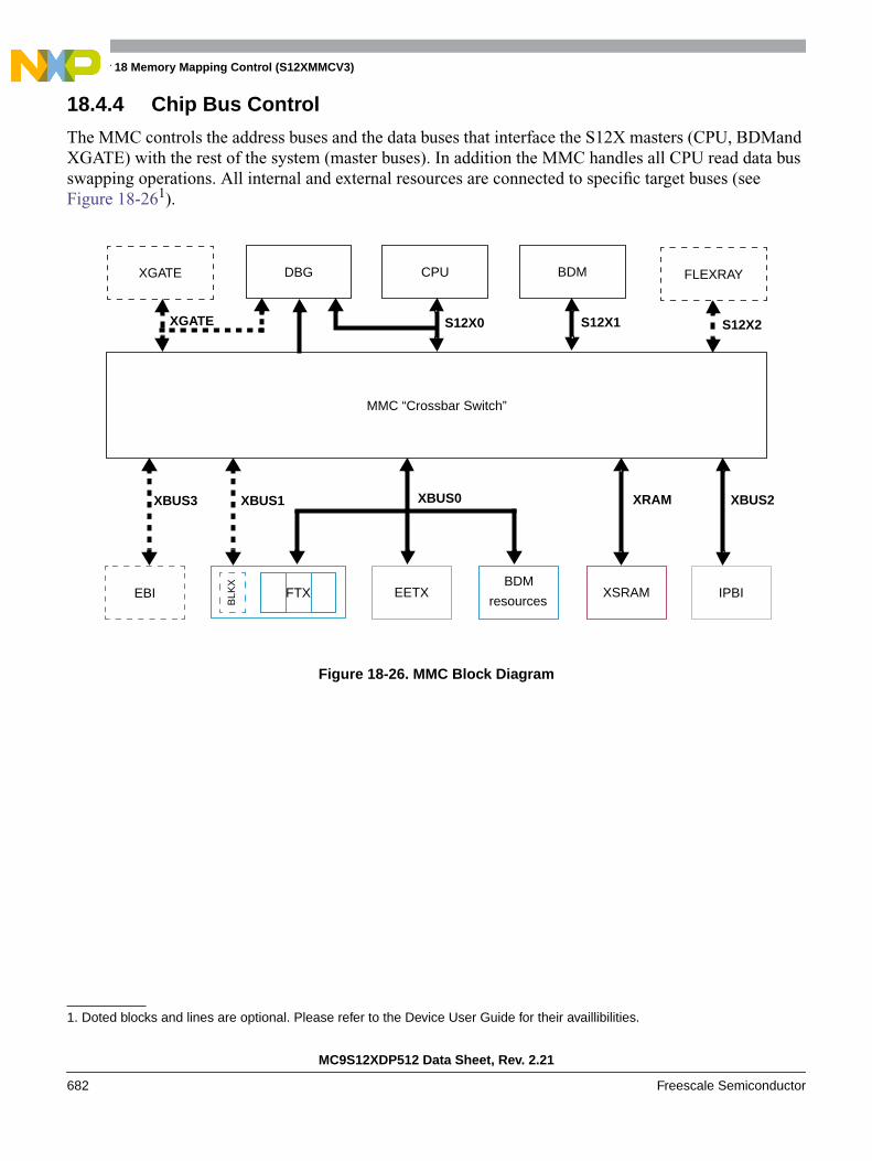
Chapter 18 Memory Mapping Control (S12XMMCV3)
MC9S12XDP512 Data Sheet, Rev. 2.21
682 Freescale Semiconductor
18.4.4 Chip Bus Control
The MMC controls the address buses and the data buses that interface the S12X masters (CPU, BDMandXGATE) with the rest of the system (master buses). In addition the MMC handles all CPU read data busswapping operations. All internal and external resources are connected to specific target buses (seeFigure 18-261).
Figure 18-26. MMC Block Diagram
1. Doted blocks and lines are optional. Please refer to the Device User Guide for their availlibilities.
CPU BDM
MMC “Crossbar Switch”
XGATE
S12X1S12X0XGATE
XBUS3 XBUS0XBUS1 XRAM XBUS2
DBG FLEXRAY
S12X2
IPBIFLASH EETXEBI XSRAMBDM
FTX
BLK
X
resources
Chapter 18 Memory Mapping Control (S12XMMCV3)
MC9S12XDP512 Data Sheet, Rev. 2.21
Freescale Semiconductor 683
18.4.4.1 Master Bus Prioritization regarding Access Conflicts on Target Buses
The arbitration scheme allows only one master to be connected to a target at any given time. The followingrules apply when prioritizing accesses from different masters to the same target bus:
• CPU always has priority over BDM and XGATE.
• XGATE access to PRU registers constitutes a special case. It is always granted and stalls the CPUfor its duration.
• XGATE has priority over BDM.
• BDM has priority over CPU and XGATE when its access is stalled for more than 128 cycles. In thelater case the suspect master will be stalled after finishing the current operation and the BDM willgain access to the bus.
• In emulation modes all internal accesses are visible on the external bus as well and the external busis used during access to the PRU registers.
18.4.5 Interrupts
18.4.5.1 Outgoing Interrupt Requests
The following interrupt requests can be triggered by the MMC module:
CPU access violation: The CPU access violation signals to the CPU detection of an error condition in theCPU application code which is resulted in write access to the protected XGATE RAM area (seeSection 18.4.3.2, “Illegal CPU Accesses).
18.5 Initialization/Application Information
18.5.1 CALL and RTC Instructions
CALL and RTC instructions are uninterruptable CPU instructions that automate page switching in theprogram page window. The CALL instruction is similar to the JSR instruction, but the subroutine that iscalled can be located anywhere in the local address space or in any Flash or ROM page visible through theprogram page window. The CALL instruction calculates and stacks a return address, stacks the currentPPAGE value and writes a new instruction-supplied value to the PPAGE register. The PPAGE valuecontrols which of the 256 possible pages is visible through the 16 Kbyte program page window in the64 Kbyte local CPU memory map. Execution then begins at the address of the called subroutine.
During the execution of the CALL instruction, the CPU performs the following steps:
1. Writes the current PPAGE value into an internal temporary register and writes the newinstruction-supplied PPAGE value into the PPAGE register
2. Calculates the address of the next instruction after the CALL instruction (the return address) andpushes this 16-bit value onto the stack
3. Pushes the temporarily stored PPAGE value onto the stack
4. Calculates the effective address of the subroutine, refills the queue and begins execution at the newaddress
Chapter 18 Memory Mapping Control (S12XMMCV3)
MC9S12XDP512 Data Sheet, Rev. 2.21
684 Freescale Semiconductor
This sequence is uninterruptable. There is no need to inhibit interrupts during the CALL instructionexecution. A CALL instruction can be performed from any address to any other address in the local CPUmemory space.
The PPAGE value supplied by the instruction is part of the effective address of the CPU. For all addressingmode variations (except indexed-indirect modes) the new page value is provided by an immediate operandin the instruction. In indexed-indirect variations of the CALL instruction a pointer specifies memorylocations where the new page value and the address of the called subroutine are stored. Using indirectaddressing for both the new page value and the address within the page allows usage of values calculatedat run time rather than immediate values that must be known at the time of assembly.
The RTC instruction terminates subroutines invoked by a CALL instruction. The RTC instruction unstacksthe PPAGE value and the return address and refills the queue. Execution resumes with the next instructionafter the CALL instruction.
During the execution of an RTC instruction the CPU performs the following steps:
1. Pulls the previously stored PPAGE value from the stack
2. Pulls the 16-bit return address from the stack and loads it into the PC
3. Writes the PPAGE value into the PPAGE register
4. Refills the queue and resumes execution at the return address
This sequence is uninterruptable. The RTC can be executed from anywhere in the local CPU memoryspace.
The CALL and RTC instructions behave like JSR and RTS instruction, they however require moreexecution cycles. Usage of JSR/RTS instructions is therefore recommended when possible andCALL/RTC instructions should only be used when needed. The JSR and RTS instructions can be used toaccess subroutines that are already present in the local CPU memory map (i.e. in the same page in theprogram memory page window for example). However calling a function located in a different pagerequires usage of the CALL instruction. The function must be terminated by the RTC instruction. Becausethe RTC instruction restores contents of the PPAGE register from the stack, functions terminated with theRTC instruction must be called using the CALL instruction even when the correct page is already presentin the memory map. This is to make sure that the correct PPAGE value will be present on stack at the timeof the RTC instruction execution.
18.5.2 Port Replacement Registers (PRRs)
Registers used for emulation purposes must be rebuilt by the in-circuit emulator hardware to achieve fullemulation of single chip mode operation. These registers are called port replacement registers (PRRs) (seeTable 1-25). PRRs are accessible from CPU, BDM and XGATE using different access types (wordaligned, word-misaligned and byte).
Each access to PRRs will be extended to 2 bus cycles for write or read accesses independent of theoperating mode. In emulation modes all write operations result in simultaneous writing to the internalregisters (peripheral access) and to the emulated registers (external access) located in the PRU in theemulator. All read operations are performed from external registers (external access) in emulation modes.In all other modes the read operations are performed from the internal registers (peripheral access).
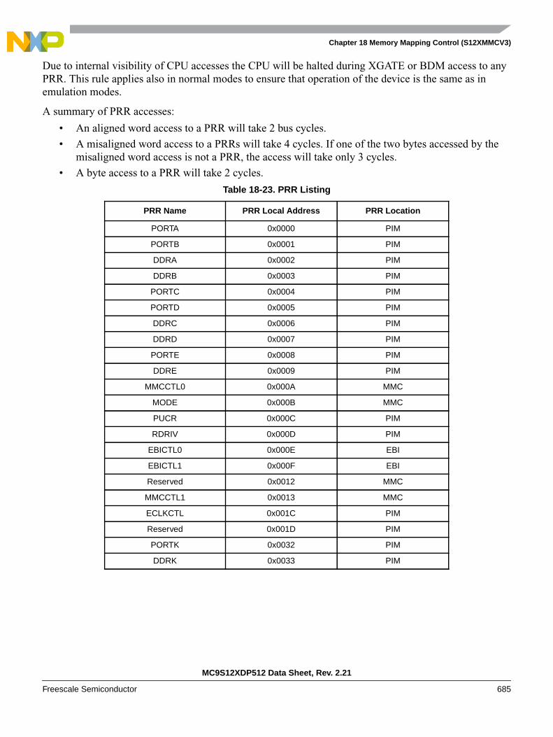
Chapter 18 Memory Mapping Control (S12XMMCV3)
MC9S12XDP512 Data Sheet, Rev. 2.21
Freescale Semiconductor 685
Due to internal visibility of CPU accesses the CPU will be halted during XGATE or BDM access to anyPRR. This rule applies also in normal modes to ensure that operation of the device is the same as inemulation modes.
A summary of PRR accesses:
• An aligned word access to a PRR will take 2 bus cycles.
• A misaligned word access to a PRRs will take 4 cycles. If one of the two bytes accessed by themisaligned word access is not a PRR, the access will take only 3 cycles.
• A byte access to a PRR will take 2 cycles.
Table 18-23. PRR Listing
PRR Name PRR Local Address PRR Location
PORTA 0x0000 PIM
PORTB 0x0001 PIM
DDRA 0x0002 PIM
DDRB 0x0003 PIM
PORTC 0x0004 PIM
PORTD 0x0005 PIM
DDRC 0x0006 PIM
DDRD 0x0007 PIM
PORTE 0x0008 PIM
DDRE 0x0009 PIM
MMCCTL0 0x000A MMC
MODE 0x000B MMC
PUCR 0x000C PIM
RDRIV 0x000D PIM
EBICTL0 0x000E EBI
EBICTL1 0x000F EBI
Reserved 0x0012 MMC
MMCCTL1 0x0013 MMC
ECLKCTL 0x001C PIM
Reserved 0x001D PIM
PORTK 0x0032 PIM
DDRK 0x0033 PIM
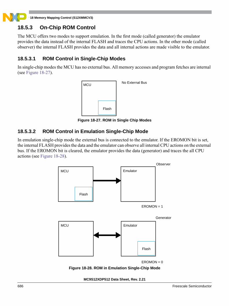
Chapter 18 Memory Mapping Control (S12XMMCV3)
MC9S12XDP512 Data Sheet, Rev. 2.21
686 Freescale Semiconductor
18.5.3 On-Chip ROM Control
The MCU offers two modes to support emulation. In the first mode (called generator) the emulatorprovides the data instead of the internal FLASH and traces the CPU actions. In the other mode (calledobserver) the internal FLASH provides the data and all internal actions are made visible to the emulator.
18.5.3.1 ROM Control in Single-Chip Modes
In single-chip modes the MCU has no external bus. All memory accesses and program fetches are internal(see Figure 18-27).
Figure 18-27. ROM in Single Chip Modes
18.5.3.2 ROM Control in Emulation Single-Chip Mode
In emulation single-chip mode the external bus is connected to the emulator. If the EROMON bit is set,the internal FLASH provides the data and the emulator can observe all internal CPU actions on the externalbus. If the EROMON bit is cleared, the emulator provides the data (generator) and traces the all CPUactions (see Figure 18-28).
Figure 18-28. ROM in Emulation Single-Chip Mode
MCU
Flash
No External Bus
EROMON = 1
Emulator
MCU
EROMON = 0
Emulator
Flash
MCU
Flash
Observer
Generator
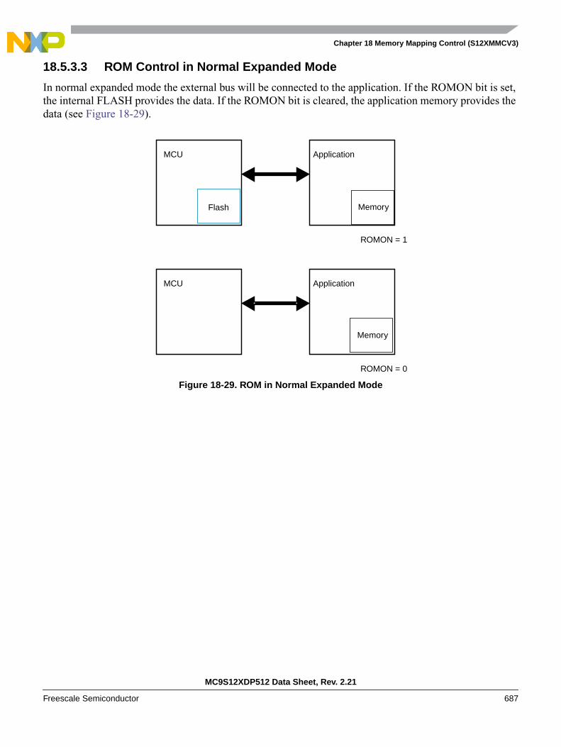
Chapter 18 Memory Mapping Control (S12XMMCV3)
MC9S12XDP512 Data Sheet, Rev. 2.21
Freescale Semiconductor 687
18.5.3.3 ROM Control in Normal Expanded Mode
In normal expanded mode the external bus will be connected to the application. If the ROMON bit is set,the internal FLASH provides the data. If the ROMON bit is cleared, the application memory provides thedata (see Figure 18-29).
Figure 18-29. ROM in Normal Expanded Mode
ROMON = 1
Application
MCU
ROMON = 0
Application
MCU
Flash Memory
Memory
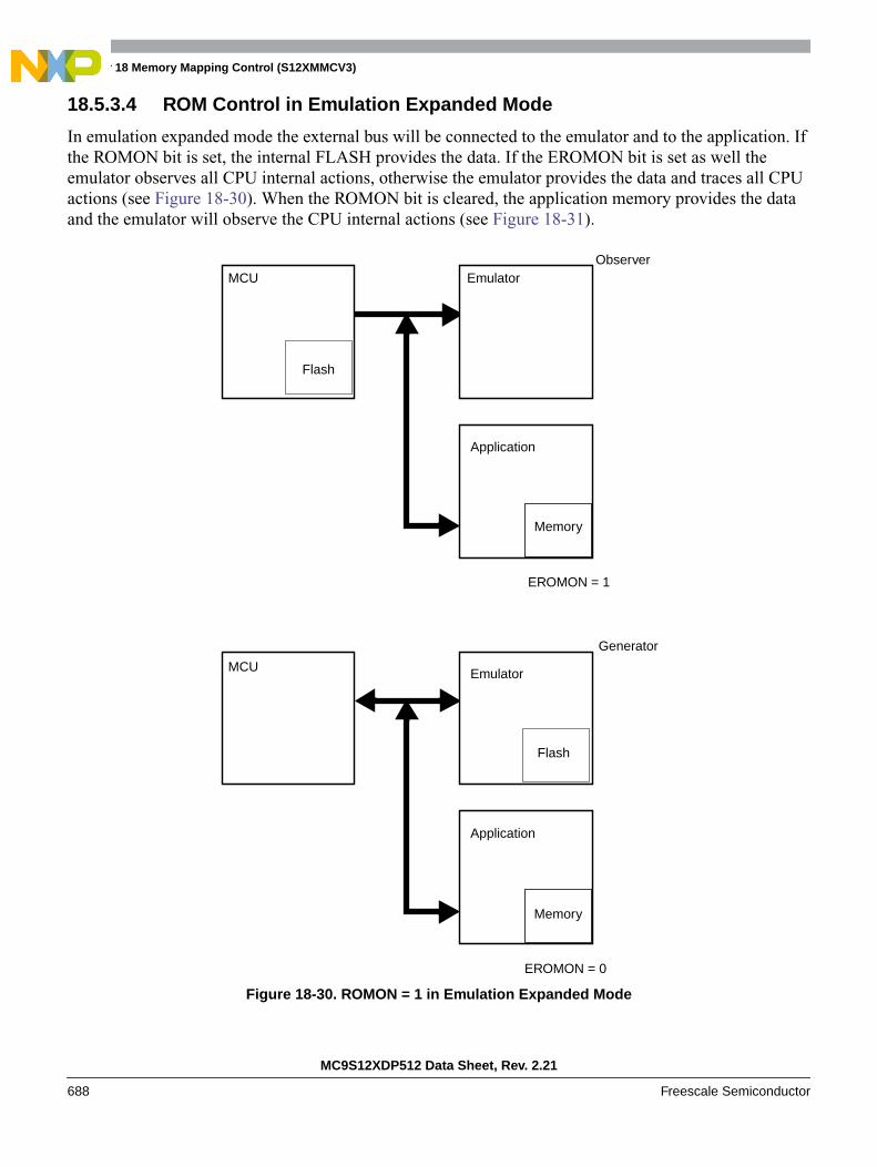
Chapter 18 Memory Mapping Control (S12XMMCV3)
MC9S12XDP512 Data Sheet, Rev. 2.21
688 Freescale Semiconductor
18.5.3.4 ROM Control in Emulation Expanded Mode
In emulation expanded mode the external bus will be connected to the emulator and to the application. Ifthe ROMON bit is set, the internal FLASH provides the data. If the EROMON bit is set as well theemulator observes all CPU internal actions, otherwise the emulator provides the data and traces all CPUactions (see Figure 18-30). When the ROMON bit is cleared, the application memory provides the dataand the emulator will observe the CPU internal actions (see Figure 18-31).
Figure 18-30. ROMON = 1 in Emulation Expanded Mode
EROMON = 1
Application
MCU
Flash
Memory
Emulator
EROMON = 0
Application
MCU
Memory
Emulator
Flash
Generator
Observer
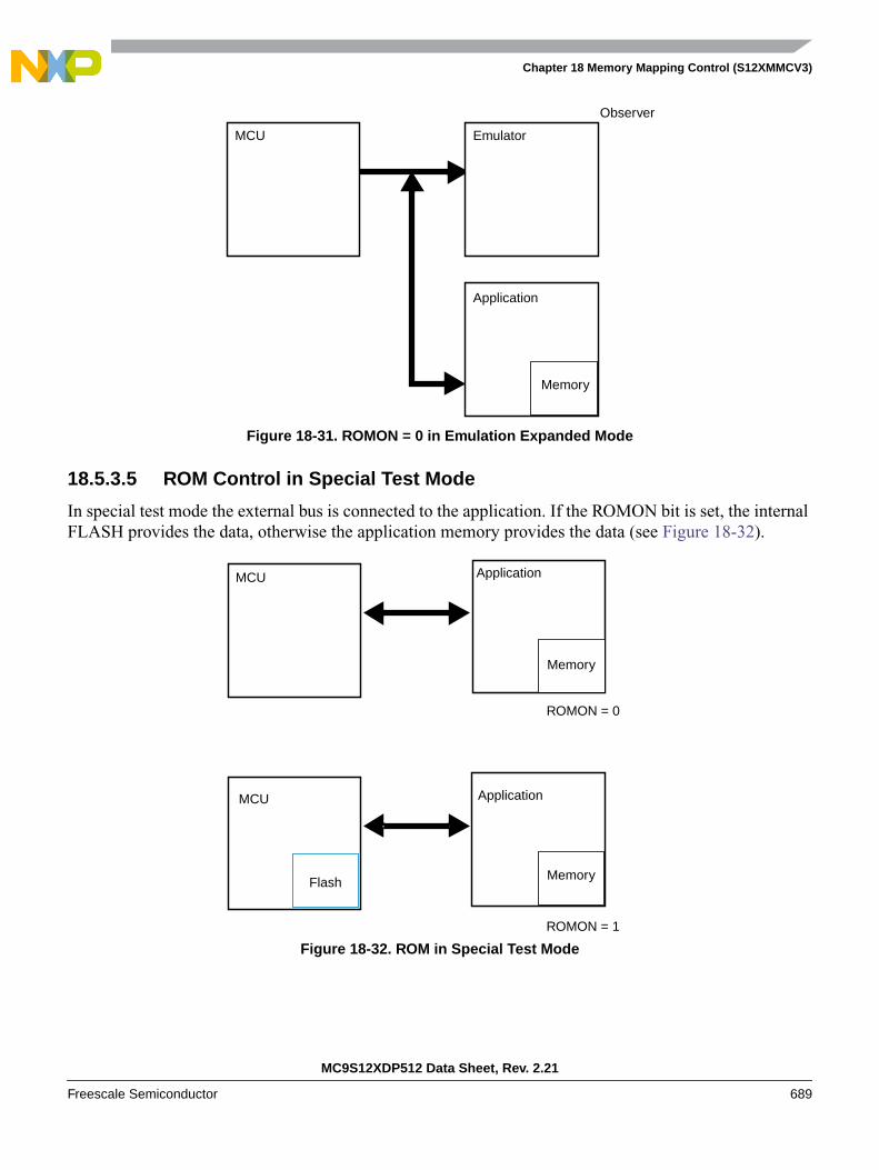
Chapter 18 Memory Mapping Control (S12XMMCV3)
MC9S12XDP512 Data Sheet, Rev. 2.21
Freescale Semiconductor 689
Figure 18-31. ROMON = 0 in Emulation Expanded Mode
18.5.3.5 ROM Control in Special Test Mode
In special test mode the external bus is connected to the application. If the ROMON bit is set, the internalFLASH provides the data, otherwise the application memory provides the data (see Figure 18-32).
Figure 18-32. ROM in Special Test Mode
Application
MCU
Memory
Emulator
Observer
ApplicationMCU
Memory
ROMON = 0
ApplicationMCU
Memory
ROMON = 1
Flash

Chapter 18 Memory Mapping Control (S12XMMCV3)
MC9S12XDP512 Data Sheet, Rev. 2.21
690 Freescale Semiconductor

MC9S12XDP512 Data Sheet, Rev. 2.21
Freescale Semiconductor 693
Chapter 19S12X Debug (S12XDBGV2) Module
19.1 IntroductionThe DBG module provides an on-chip trace buffer with flexible triggering capability to allow non-intrusivedebug of application software. The DBG module is optimized for the HCS12X 16-bit architecture andallows debugging of both CPU and XGATE module operations.
Typically the DBG module is used in conjunction with the BDM module, whereby the user configures theDBG module for a debugging session over the BDM interface. Once configured the DBG module is armedand the device leaves BDM mode returning control to the user program, which is then monitored by theDBG module. Alternatively, the DBG module can be configured over a serial interface using SWI routines.
Comparators monitor the bus activity of the CPU and XGATE modules. When a match occurs, the controllogic can trigger the state sequencer to a new state or tag an opcode. A tag hit, which occurs when thetagged opcode reaches the execution stage of the instruction queue, can also cause a state transition.
On a transition to the final state, bus tracing is triggered and/or a breakpoint can be generated. Independentof comparator matches, a transition to final state with associated tracing and breakpoint can be triggeredby the external TAGHI and TAGLO signals. This is done by an XGATE module S/W breakpoint requestor by writing to the TRIG control bit.
The trace buffer is visible through a 2-byte window in the register address map and can be read out usingstandard 16-bit word reads. Tracing is disabled when the MCU system is secured.
19.1.1 Glossary of Terms
COF: Change Of Flow. Change in the program flow due to a conditional branch, indexed jump or interrupt.
BDM : Background Debug Mode
DUG: Device User Guide, describing the features of the device into which the DBG is integrated.
WORD: 16 bit data entity
Data Line : 64 bit data entity
XGATE : S12X family programmable Direct Memory Access Module
CPU : S12X_CPU module
Tag : Tags can be attached to XGATE or CPU opcodes as they enter the instruction pipe. If the taggedopcode reaches the execution stage a tag hit occurs.

Chapter 19 S12X Debug (S12XDBGV2) Module
MC9S12XDP512 Data Sheet, Rev. 2.21
694 Freescale Semiconductor
19.1.2 Features• Four comparators (A, B, C, and D):
— Comparators A and C compare the full address and the full 16-bit data bus
— Comparators A and C feature a data bus mask register
— Comparators B and D compare the full address bus only
— Each comparator can be configured to monitor either CPU or XGATE busses
— Each comparator features control of R/W and byte/word access cycles
— Comparisons can be used as triggers for the state sequencer
• Three comparator modes:
— Simple address/data comparator match mode
— Inside address range mode, Addmin ≤ Address ≤ Addmax
— Outside address range match mode, Address < Addmin or Address > Addmax
• Two types of triggers:
— Tagged: triggers just before a specific instruction begins execution
— Force: triggers on the first instruction boundary after a match occurs.
• Three types of breakpoints:
— CPU breakpoint entering BDM on breakpoint (BDM)
— CPU breakpoint executing SWI on breakpoint (SWI)
— XGATE breakpoint
• Three trigger modes independent of comparators:
— External instruction tagging (associated with CPU instructions only)
— XGATE S/W breakpoint request
— TRIG bit immediate software trigger
• Three trace modes:
— Normal: change of flow (COF) bus information is stored (see Section 19.4.5.2.1, “NormalMode”) for change of flow definition.
— Loop1: same as normal but inhibits consecutive duplicate source address entries
— Detail: address and data for all cycles except free cycles and opcode fetches are stored
• 4-stage state sequencer for trace buffer control:
— Tracing session trigger linked to final state of state sequencer
— Begin, end, and mid alignment of tracing to trigger
19.1.3 Modes of Operation
The DBG module can be used in all MCU functional modes.
During BDM hardware accesses and when the BDM module is active, CPU monitoring is disabled. Thusbreakpoints, comparators and bus tracing mapped to the CPU are disabled but accessing the DBG registers,including comparator registers, is still possible. While in active BDM or during hardware BDM accesses,
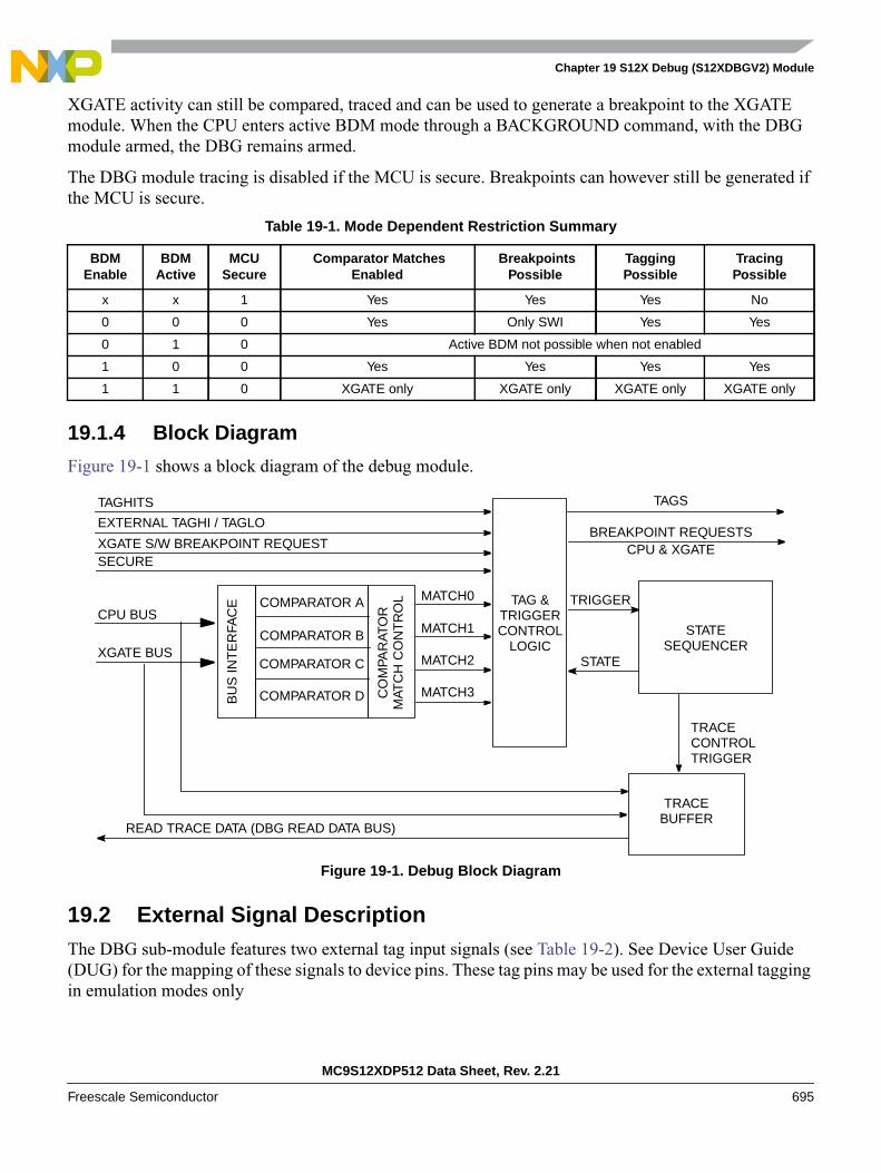
Chapter 19 S12X Debug (S12XDBGV2) Module
MC9S12XDP512 Data Sheet, Rev. 2.21
Freescale Semiconductor 695
XGATE activity can still be compared, traced and can be used to generate a breakpoint to the XGATEmodule. When the CPU enters active BDM mode through a BACKGROUND command, with the DBGmodule armed, the DBG remains armed.
The DBG module tracing is disabled if the MCU is secure. Breakpoints can however still be generated ifthe MCU is secure.
19.1.4 Block Diagram
Figure 19-1 shows a block diagram of the debug module.
Figure 19-1. Debug Block Diagram
19.2 External Signal DescriptionThe DBG sub-module features two external tag input signals (see Table 19-2). See Device User Guide(DUG) for the mapping of these signals to device pins. These tag pins may be used for the external taggingin emulation modes only
Table 19-1. Mode Dependent Restriction Summary
BDMEnable
BDMActive
MCUSecure
Comparator MatchesEnabled
BreakpointsPossible
TaggingPossible
TracingPossible
x x 1 Yes Yes Yes No
0 0 0 Yes Only SWI Yes Yes
0 1 0 Active BDM not possible when not enabled
1 0 0 Yes Yes Yes Yes
1 1 0 XGATE only XGATE only XGATE only XGATE only
CPU BUS
BU
S IN
TE
RFA
CE TRIGGER
EXTERNAL TAGHI / TAGLO
MATCH0
XGATE BUSCOMPARATOR B
COMPARATOR C
COMPARATOR D
COMPARATOR A
MATCH1
MATCH2
MATCH3
READ TRACE DATA (DBG READ DATA BUS)
SECURE
BREAKPOINT REQUESTSXGATE S/W BREAKPOINT REQUEST
TAGSTAGHITS
STATE
CPU & XGATE
CO
MPA
RAT
OR
MAT
CH
CO
NT
RO
L TAG &TRIGGERCONTROL
LOGICSTATE
SEQUENCER
TRACEBUFFER
TRACECONTROLTRIGGER

Chapter 19 S12X Debug (S12XDBGV2) Module
MC9S12XDP512 Data Sheet, Rev. 2.21
696 Freescale Semiconductor
.
Table 19-2. External System Pins Associated With DBG
Pin Name Pin Functions Description
TAGHI(See DUG)
TAGHI When instruction tagging is on, tags the high half of the instruction word being readinto the instruction queue.
TAGLO(See DUG)
TAGLO When instruction tagging is on, tags the low half of the instruction word being readinto the instruction queue.
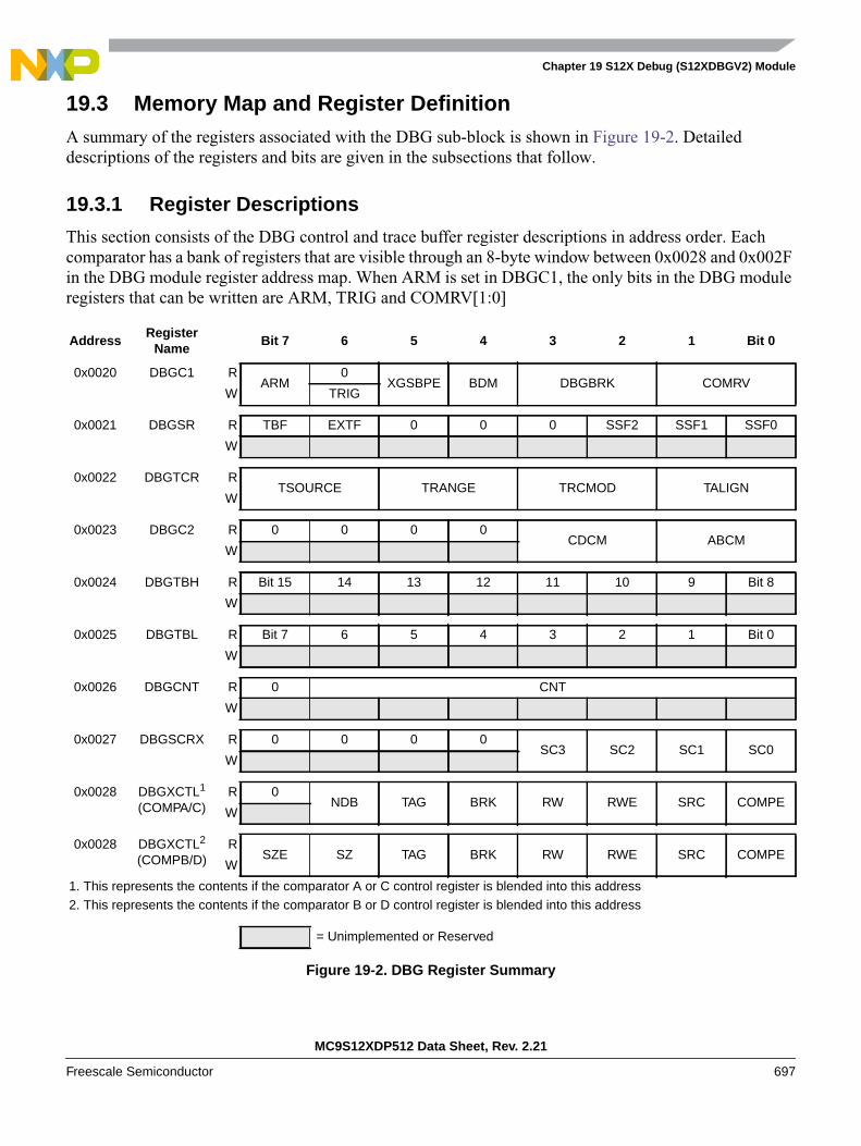
Chapter 19 S12X Debug (S12XDBGV2) Module
MC9S12XDP512 Data Sheet, Rev. 2.21
Freescale Semiconductor 697
19.3 Memory Map and Register DefinitionA summary of the registers associated with the DBG sub-block is shown in Figure 19-2. Detaileddescriptions of the registers and bits are given in the subsections that follow.
19.3.1 Register Descriptions
This section consists of the DBG control and trace buffer register descriptions in address order. Eachcomparator has a bank of registers that are visible through an 8-byte window between 0x0028 and 0x002Fin the DBG module register address map. When ARM is set in DBGC1, the only bits in the DBG moduleregisters that can be written are ARM, TRIG and COMRV[1:0]
AddressRegister
NameBit 7 6 5 4 3 2 1 Bit 0
0x0020 DBGC1 RARM
0XGSBPE BDM DBGBRK COMRV
W TRIG
0x0021 DBGSR R TBF EXTF 0 0 0 SSF2 SSF1 SSF0
W
0x0022 DBGTCR RTSOURCE TRANGE TRCMOD TALIGN
W
0x0023 DBGC2 R 0 0 0 0CDCM ABCM
W
0x0024 DBGTBH R Bit 15 14 13 12 11 10 9 Bit 8
W
0x0025 DBGTBL R Bit 7 6 5 4 3 2 1 Bit 0
W
0x0026 DBGCNT R 0 CNT
W
0x0027 DBGSCRX R 0 0 0 0SC3 SC2 SC1 SC0
W
0x0028 DBGXCTL1
(COMPA/C)R 0
NDB TAG BRK RW RWE SRC COMPEW
0x0028 DBGXCTL2
(COMPB/D)R
SZE SZ TAG BRK RW RWE SRC COMPEW
1. This represents the contents if the comparator A or C control register is blended into this address2. This represents the contents if the comparator B or D control register is blended into this address
= Unimplemented or Reserved
Figure 19-2. DBG Register Summary

Chapter 19 S12X Debug (S12XDBGV2) Module
MC9S12XDP512 Data Sheet, Rev. 2.21
698 Freescale Semiconductor
19.3.1.1 Debug Control Register 1 (DBGC1)
Read: Anytime
Write: Bits 7,1,0 anytime, Bit 6 can be written anytime but always reads back as 0.Bits 5:2 anytime DBG is not armed.
NOTEWhen disarming the DBG by clearing ARM with software, the contents ofbits[5:2] are not affected by the write, since up until the write operation,ARM=1 preventing these bits from being written. These bits must be clearedusing a second write if required.
0x0029 DBGXAH R 0Bit 22 21 20 19 18 17 Bit 16
W
0x002A DBGXAM RBit 15 14 13 12 11 10 9 Bit 8
W
0x002B DBGXAL RBit 7 6 5 4 3 2 1 Bit 0
W
0x002C DBGXDH RBit 15 14 13 12 11 10 9 Bit 8
W
0x002D DBGXDL RBit 7 6 5 4 3 2 1 Bit 0
W
0x002E DBGXDHM RBit 15 14 13 12 11 10 9 Bit 8
W
0x002F DBGXDLM RBit 7 6 5 4 3 2 1 Bit 0
W
0x0020
7 6 5 4 3 2 1 0
RARM
0XGSBPE BDM DBGBRK COMRV
W TRIG
Reset 0 0 0 0 0 0 0 0
Figure 19-3. Debug Control Register (DBGC1)
AddressRegister
NameBit 7 6 5 4 3 2 1 Bit 0
= Unimplemented or Reserved
Figure 19-2. DBG Register Summary (continued)
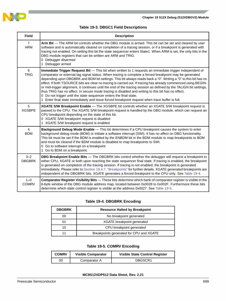
Chapter 19 S12X Debug (S12XDBGV2) Module
MC9S12XDP512 Data Sheet, Rev. 2.21
Freescale Semiconductor 699
Table 19-3. DBGC1 Field Descriptions
Field Description
7ARM
Arm Bit — The ARM bit controls whether the DBG module is armed. This bit can be set and cleared by usersoftware and is automatically cleared on completion of a tracing session, or if a breakpoint is generated withtracing not enabled. On setting this bit the state sequencer enters State1. When ARM is set, the only bits in theDBG module registers that can be written are ARM and TRIG.0 Debugger disarmed1 Debugger armed
6TRIG
Immediate Trigger Request Bit — This bit when written to 1 requests an immediate trigger independent ofcomparator or external tag signal status. When tracing is complete a forced breakpoint may be generateddepending upon DBGBRK and BDM bit settings. This bit always reads back a “0”. Writing a “0” to this bit has noeffect. If both TSOURCE bits are clear no tracing is carried out. If tracing has already commenced using BEGIN-or mid-trigger alignment, it continues until the end of the tracing session as defined by the TALIGN bit settings,thus TRIG has no affect. In secure mode tracing is disabled and writing to this bit has no effect.0 Do not trigger until the state sequencer enters the final state.1 Enter final state immediately and issue forced breakpoint request when trace buffer is full.
5XGSBPE
XGATE S/W Breakpoint Enable — The XGSBPE bit controls whether an XGATE S/W breakpoint request ispassed to the CPU. The XGATE S/W breakpoint request is handled by the DBG module, which can request anCPU breakpoint depending on the state of this bit.0 XGATE S/W breakpoint request is disabled1 XGATE S/W breakpoint request is enabled
4BDM
Background Debug Mode Enable — This bit determines if a CPU breakpoint causes the system to enterbackground debug mode (BDM) or initiate a software interrupt (SWI). It has no affect on DBG functionality.This bit must be set if the BDM is enabled by the ENBDM bit in the BDM module to map breakpoints to BDMand must be cleared if the BDM module is disabled to map breakpoints to SWI.0 Go to software interrupt on a breakpoint1 Go to BDM on a breakpoint.
3–2DBGBRK
DBG Breakpoint Enable Bits — The DBGBRK bits control whether the debugger will request a breakpoint toeither CPU, XGATE or both upon reaching the state sequencer final state. If tracing is enabled, the breakpointis generated on completion of the tracing session. If tracing is not enabled, the breakpoint is generatedimmediately. Please refer to Section 19.4.7, “Breakpoints” for further details. XGATE generated breakpoints areindependent of the DBGBRK bits. XGATE generates a forced breakpoint to the CPU only. See Table 19-4.
1–0COMRV
Comparator Register Visibility Bits — These bits determine which bank of comparator register is visible in the8-byte window of the DBG module address map, located between 0x0028 to 0x002F. Furthermore these bitsdetermine which state control register is visible at the address 0x0027. See Table 19-5.
Table 19-4. DBGBRK Encoding
DBGBRK Resource Halted by Breakpoint
00 No breakpoint generated
01 XGATE breakpoint generated
10 CPU breakpoint generated
11 Breakpoints generated for CPU and XGATE
Table 19-5. COMRV Encoding
COMRV Visible Comparator Visible State Control Register
00 Comparator A DBGSCR1

Chapter 19 S12X Debug (S12XDBGV2) Module
MC9S12XDP512 Data Sheet, Rev. 2.21
700 Freescale Semiconductor
19.3.1.2 Debug Status Register (DBGSR)
Read: Anytime
Write: Never
01 Comparator B DBGSCR2
10 Comparator C DBGSCR3
11 Comparator D DBGSCR3
0x0021
7 6 5 4 3 2 1 0
R TBF EXTF 0 0 0 SSF2 SSF1 SSF0
W
Reset — 0 0 0 0 0 0 0
POR 0 0 0 0 0 0 0 0
Unimplemented or Reserved
Figure 19-4. Debug Status Register (DBGSR)
Table 19-6. DBGSR Field Descriptions
Field Description
7TBF
Trace Buffer Full — The TBF bit indicates that the trace buffer has stored 64 or more lines of data since it waslast armed. If this bit is set, then all 64 lines will be valid data, regardless of the value of DBGCNT bits CNT[6:0].The TBF bit is cleared when ARM in DBGC1 is written to a 1. The TBF is cleared by the power on resetinitialization. Other system generated resets have no affect on this bit
6EXTF
External Tag Hit Flag — The EXTF bit indicates if a tag hit condition from an external TAGHI/TAGLO tag wasmet since arming. This bit is cleared when ARM in DBGC1 is written to a 1.0 External tag hit has not occurred1 External tag hit has occurred
2–0SSF[2:0
State Sequencer Flag Bits — The SSF bits indicate in which state the state sequencer is currently in. Duringa debug session on each transition to a new state these bits are updated. If the debug session is ended bysoftware clearing the ARM bit, then these bits retain their value to reflect the last state of the state sequencerbefore disarming. If a debug session is ended by a breakpoint, then the state sequencer returns to state0 andthese bits are cleared to indicate that state0 was entered during the session. On arming the module the statesequencer enters state1 and these bits are forced to SSF[2:0] = 001. See Table 19-7.
Table 19-7. SSF[2:0] — State Sequence Flag Bit Encoding
SSF[2:0] Current State
000 State0 (disarmed)
001 State1
010 State2
011 State3
100 Final State
101,110,111 Reserved
Table 19-5. COMRV Encoding
COMRV Visible Comparator Visible State Control Register
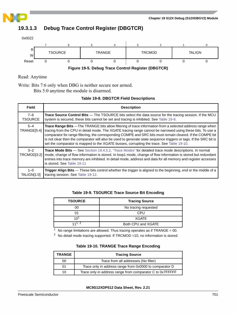
Chapter 19 S12X Debug (S12XDBGV2) Module
MC9S12XDP512 Data Sheet, Rev. 2.21
Freescale Semiconductor 701
19.3.1.3 Debug Trace Control Register (DBGTCR)
Read: Anytime
Write: Bits 7:6 only when DBG is neither secure nor armed.Bits 5:0 anytime the module is disarmed.
0x0022
7 6 5 4 3 2 1 0
RTSOURCE TRANGE TRCMOD TALIGN
W
Reset 0 0 0 0 0 0 0 0
Figure 19-5. Debug Trace Control Register (DBGTCR)
Table 19-8. DBGTCR Field Descriptions
Field Description
7–6TSOURCE
Trace Source Control Bits — The TSOURCE bits select the data source for the tracing session. If the MCUsystem is secured, these bits cannot be set and tracing is inhibited. See Table 19-9.
5–4TRANGE[5:4]
Trace Range Bits —The TRANGE bits allow filtering of trace information from a selected address range whentracing from the CPU in detail mode. The XGATE tracing range cannot be narrowed using these bits. To use acomparator for range filtering, the corresponding COMPE and SRC bits must remain cleared. If the COMPE bitis not clear then the comparator will also be used to generate state sequence triggers or tags. If the SRC bit isset the comparator is mapped to the XGATE busses, corrupting the trace. See Table 19-10.
3–2TRCMOD[3:2]
Trace Mode Bits — See Section 19.4.5.2, “Trace Modes“ for detailed trace mode descriptions. In normalmode, change of flow information is stored. In loop1 mode, change of flow information is stored but redundantentries into trace memory are inhibited. In detail mode, address and data for all memory and register accessesis stored. See Table 19-11
1–0TALIGN[1:0]
Trigger Align Bits — These bits control whether the trigger is aligned to the beginning, end or the middle of atracing session. See Table 19-12.
Table 19-9. TSOURCE Trace Source Bit Encoding
TSOURCE Tracing Source
00 No tracing requested
01 CPU
101
1 No range limitations are allowed. Thus tracing operates as if TRANGE = 00.
XGATE
111, 2
2 No detail mode tracing supported. If TRCMOD =10, no information is stored.
Both CPU and XGATE
Table 19-10. TRANGE Trace Range Encoding
TRANGE Tracing Source
00 Trace from all addresses (No filter)
01 Trace only in address range from 0x0000 to comparator D
10 Trace only in address range from comparator C to 0x7FFFFF
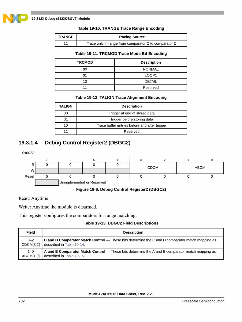
Chapter 19 S12X Debug (S12XDBGV2) Module
MC9S12XDP512 Data Sheet, Rev. 2.21
702 Freescale Semiconductor
19.3.1.4 Debug Control Register2 (DBGC2)
Read: Anytime
Write: Anytime the module is disarmed.
This register configures the comparators for range matching.
11 Trace only in range from comparator C to comparator D
Table 19-11. TRCMOD Trace Mode Bit Encoding
TRCMOD Description
00 NORMAL
01 LOOP1
10 DETAIL
11 Reserved
Table 19-12. TALIGN Trace Alignment Encoding
TALIGN Description
00 Trigger at end of stored data
01 Trigger before storing data
10 Trace buffer entries before and after trigger
11 Reserved
0x0023
7 6 5 4 3 2 1 0
R 0 0 0 0CDCM ABCM
W
Reset 0 0 0 0 0 0 0 0
Unimplemented or Reserved
Figure 19-6. Debug Control Register2 (DBGC2)
Table 19-13. DBGC2 Field Descriptions
Field Description
3–2CDCM[3:2]
C and D Comparator Match Control — These bits determine the C and D comparator match mapping asdescribed in Table 19-14.
1–0ABCM[1:0]
A and B Comparator Match Control — These bits determine the A and B comparator match mapping asdescribed in Table 19-15.
Table 19-10. TRANGE Trace Range Encoding
TRANGE Tracing Source

Chapter 19 S12X Debug (S12XDBGV2) Module
MC9S12XDP512 Data Sheet, Rev. 2.21
Freescale Semiconductor 703
19.3.1.5 Debug Trace Buffer Register (DBGTBH:DBGTBL)
Read: Anytime when unlocked and not secured and not armed.
Write: Aligned word writes when disarmed unlock the trace buffer for reading but do not affect trace buffercontents
Table 19-14. CDCM Encoding
CDCM Description
00 Match2 mapped to comparator C match....... Match3 mapped to comparator D match.
01 Match2 mapped to comparator C/D inside range....... Match3 disabled.
10 Match2 mapped to comparator C/D outside range....... Match3 disabled.
11 Reserved
Table 19-15. ABCM Encoding
ABCM Description
00 Match0 mapped to comparator A match....... Match1 mapped to comparator B match.
01 Match 0 mapped to comparator A/B inside range....... Match1 disabled.
10 Match 0 mapped to comparator A/B outside range....... Match1 disabled.
11 Reserved
0x0024
15 14 13 12 11 10 9 8
RBit 15 14 13 12 11 10 9 Bit 8
W
Reset X X X X X X X X
Figure 19-7. Debug Trace Buffer Register (DBGTBH)
0x0025
7 6 5 4 3 2 1 0
RBit 7 6 5 4 3 2 1 Bit 0
W
Reset X X X X X X X X
Figure 19-8. Debug Trace Buffer Register (DBGTBL)
Table 19-16. DBGTB Field Descriptions
Field Description
15–0Bit[15:0]
Trace Buffer Data Bits — The trace buffer register is a window through which the 64-bit wide data lines of thetrace buffer may be read 16 bits at a time. Each valid read of DBGTB increments an internal trace buffer pointerwhich points to the next address to be read. When the ARM bit is written to 1 the trace buffer is locked to preventreading. The trace buffer can only be unlocked for reading by writing to DBGTB with an aligned word write whenthe module is disarmed. The DBGTB register can be read only as an aligned word, any byte reads or misalignedaccess of these registers will return 0 and will not cause the trace buffer pointer to increment to the next tracebuffer address. The same is true for word reads while the debugger is armed. System resets do not affect thetrace buffer contents. The POR state is undefined.
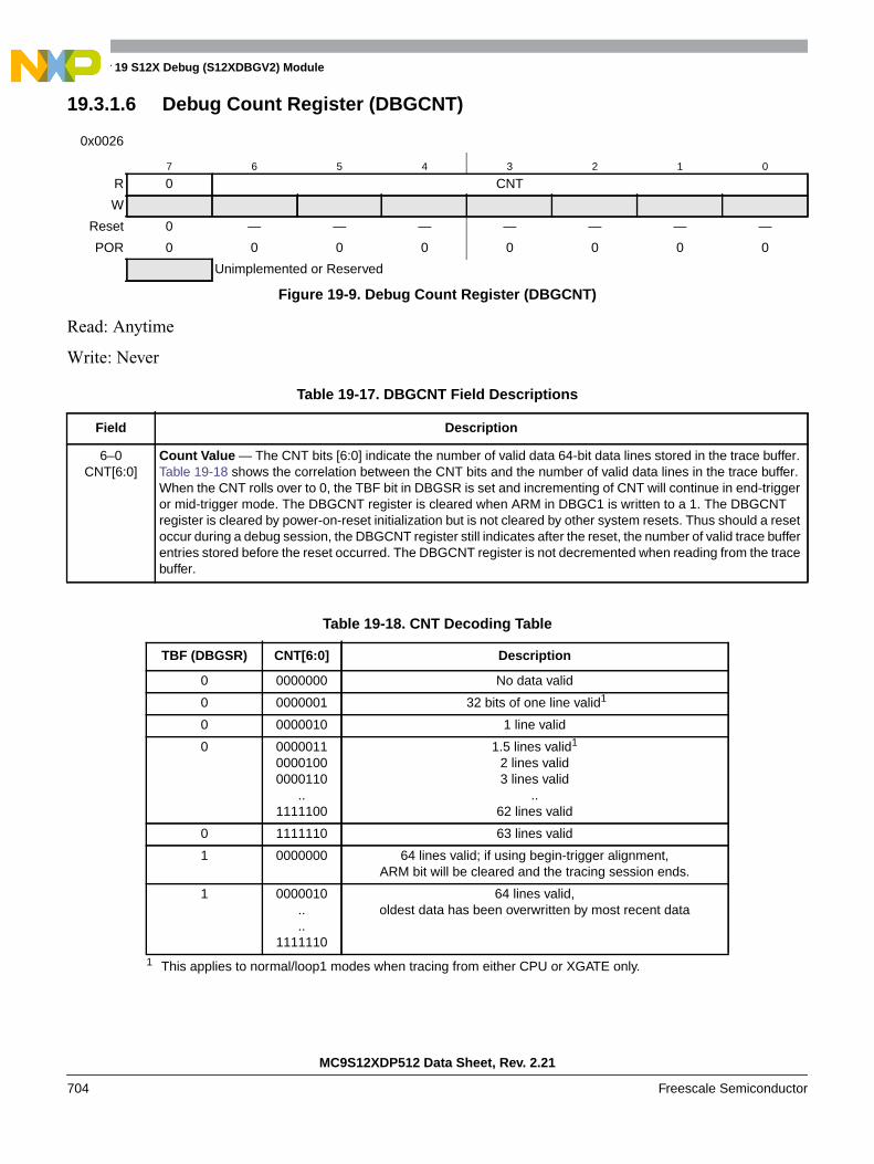
Chapter 19 S12X Debug (S12XDBGV2) Module
MC9S12XDP512 Data Sheet, Rev. 2.21
704 Freescale Semiconductor
19.3.1.6 Debug Count Register (DBGCNT)
Read: Anytime
Write: Never
0x0026
7 6 5 4 3 2 1 0
R 0 CNT
W
Reset 0 — — — — — — —
POR 0 0 0 0 0 0 0 0
Unimplemented or Reserved
Figure 19-9. Debug Count Register (DBGCNT)
Table 19-17. DBGCNT Field Descriptions
Field Description
6–0CNT[6:0]
Count Value — The CNT bits [6:0] indicate the number of valid data 64-bit data lines stored in the trace buffer.Table 19-18 shows the correlation between the CNT bits and the number of valid data lines in the trace buffer.When the CNT rolls over to 0, the TBF bit in DBGSR is set and incrementing of CNT will continue in end-triggeror mid-trigger mode. The DBGCNT register is cleared when ARM in DBGC1 is written to a 1. The DBGCNTregister is cleared by power-on-reset initialization but is not cleared by other system resets. Thus should a resetoccur during a debug session, the DBGCNT register still indicates after the reset, the number of valid trace bufferentries stored before the reset occurred. The DBGCNT register is not decremented when reading from the tracebuffer.
Table 19-18. CNT Decoding Table
TBF (DBGSR) CNT[6:0] Description
0 0000000 No data valid
0 0000001 32 bits of one line valid1
1 This applies to normal/loop1 modes when tracing from either CPU or XGATE only.
0 0000010 1 line valid
0 000001100001000000110
..1111100
1.5 lines valid1
2 lines valid3 lines valid
..62 lines valid
0 1111110 63 lines valid
1 0000000 64 lines valid; if using begin-trigger alignment,ARM bit will be cleared and the tracing session ends.
1 0000010....
1111110
64 lines valid,oldest data has been overwritten by most recent data
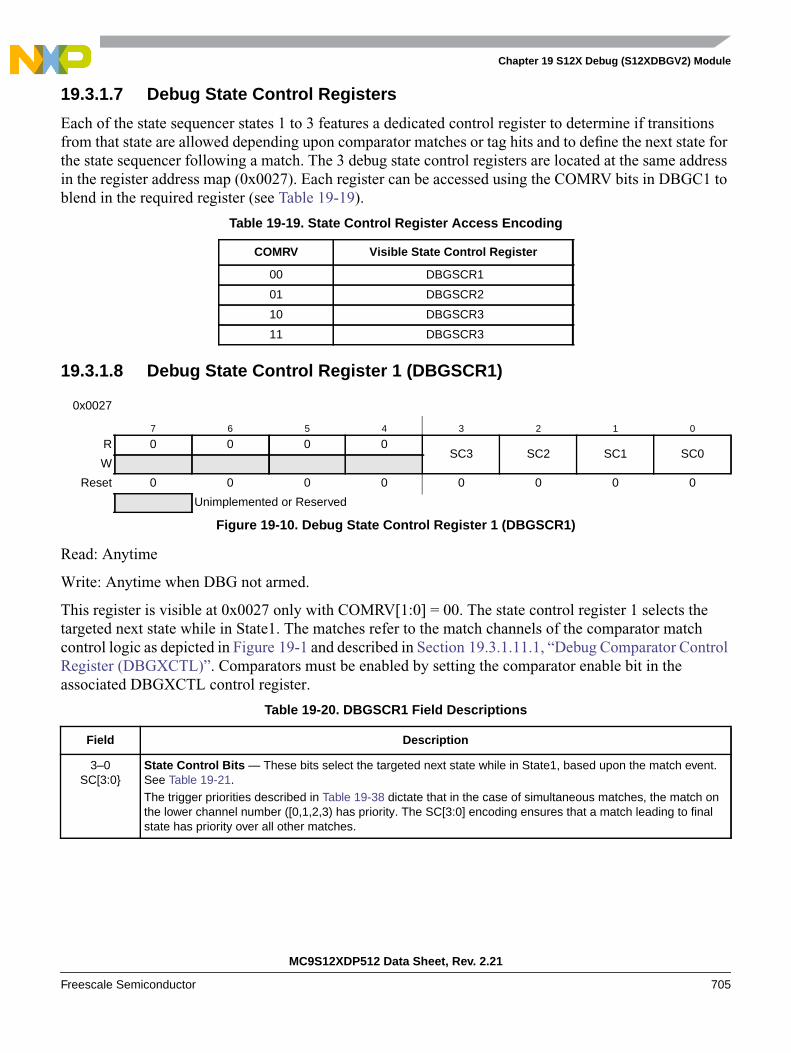
Chapter 19 S12X Debug (S12XDBGV2) Module
MC9S12XDP512 Data Sheet, Rev. 2.21
Freescale Semiconductor 705
19.3.1.7 Debug State Control Registers
Each of the state sequencer states 1 to 3 features a dedicated control register to determine if transitionsfrom that state are allowed depending upon comparator matches or tag hits and to define the next state forthe state sequencer following a match. The 3 debug state control registers are located at the same addressin the register address map (0x0027). Each register can be accessed using the COMRV bits in DBGC1 toblend in the required register (see Table 19-19).
19.3.1.8 Debug State Control Register 1 (DBGSCR1)
Read: Anytime
Write: Anytime when DBG not armed.
This register is visible at 0x0027 only with COMRV[1:0] = 00. The state control register 1 selects thetargeted next state while in State1. The matches refer to the match channels of the comparator matchcontrol logic as depicted in Figure 19-1 and described in Section 19.3.1.11.1, “Debug Comparator ControlRegister (DBGXCTL)”. Comparators must be enabled by setting the comparator enable bit in theassociated DBGXCTL control register.
Table 19-19. State Control Register Access Encoding
COMRV Visible State Control Register
00 DBGSCR1
01 DBGSCR2
10 DBGSCR3
11 DBGSCR3
0x0027
7 6 5 4 3 2 1 0
R 0 0 0 0SC3 SC2 SC1 SC0
W
Reset 0 0 0 0 0 0 0 0
Unimplemented or Reserved
Figure 19-10. Debug State Control Register 1 (DBGSCR1)
Table 19-20. DBGSCR1 Field Descriptions
Field Description
3–0SC[3:0
State Control Bits — These bits select the targeted next state while in State1, based upon the match event.See Table 19-21.The trigger priorities described in Table 19-38 dictate that in the case of simultaneous matches, the match onthe lower channel number ([0,1,2,3) has priority. The SC[3:0] encoding ensures that a match leading to finalstate has priority over all other matches.
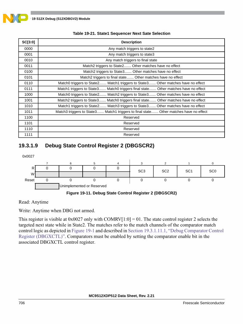
Chapter 19 S12X Debug (S12XDBGV2) Module
MC9S12XDP512 Data Sheet, Rev. 2.21
706 Freescale Semiconductor
19.3.1.9 Debug State Control Register 2 (DBGSCR2)
Read: Anytime
Write: Anytime when DBG not armed.
This register is visible at 0x0027 only with COMRV[1:0] = 01. The state control register 2 selects thetargeted next state while in State2. The matches refer to the match channels of the comparator matchcontrol logic as depicted in Figure 19-1 and described in Section 19.3.1.11.1, “Debug Comparator ControlRegister (DBGXCTL)”. Comparators must be enabled by setting the comparator enable bit in theassociated DBGXCTL control register.
Table 19-21. State1 Sequencer Next Sate Selection
SC[3:0] Description
0000 Any match triggers to state2
0001 Any match triggers to state3
0010 Any match triggers to final state
0011 Match2 triggers to State2....... Other matches have no effect
0100 Match2 triggers to State3....... Other matches have no effect
0101 Match2 triggers to final state....... Other matches have no effect
0110 Match0 triggers to State2....... Match1 triggers to State3....... Other matches have no effect
0111 Match1 triggers to State3....... Match0 triggers final state....... Other matches have no effect
1000 Match0 triggers to State2....... Match2 triggers to State3....... Other matches have no effect
1001 Match2 triggers to State3....... Match0 triggers final state....... Other matches have no effect
1010 Match1 triggers to State2....... Match3 triggers to State3....... Other matches have no effect
1011 Match3 triggers to State3....... Match1 triggers to final state....... Other matches have no effect
1100 Reserved
1101 Reserved
1110 Reserved
1111 Reserved
0x0027
7 6 5 4 3 2 1 0
R 0 0 0 0SC3 SC2 SC1 SC0
W
Reset 0 0 0 0 0 0 0 0
Unimplemented or Reserved
Figure 19-11. Debug State Control Register 2 (DBGSCR2)
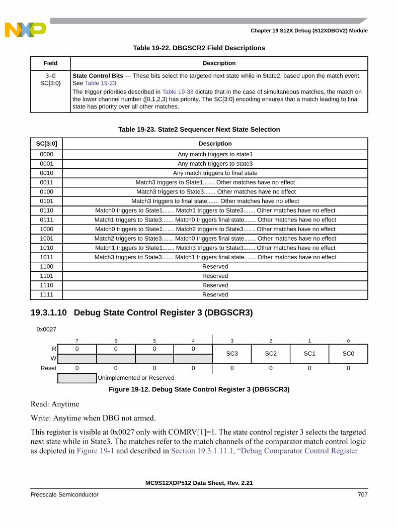
Chapter 19 S12X Debug (S12XDBGV2) Module
MC9S12XDP512 Data Sheet, Rev. 2.21
Freescale Semiconductor 707
19.3.1.10 Debug State Control Register 3 (DBGSCR3)
Read: Anytime
Write: Anytime when DBG not armed.
This register is visible at 0x0027 only with COMRV[1]=1. The state control register 3 selects the targetednext state while in State3. The matches refer to the match channels of the comparator match control logicas depicted in Figure 19-1 and described in Section 19.3.1.11.1, “Debug Comparator Control Register
Table 19-22. DBGSCR2 Field Descriptions
Field Description
3–0SC[3:0
State Control Bits — These bits select the targeted next state while in State2, based upon the match event.See Table 19-23.The trigger priorities described in Table 19-38 dictate that in the case of simultaneous matches, the match onthe lower channel number ([0,1,2,3) has priority. The SC[3:0] encoding ensures that a match leading to finalstate has priority over all other matches.
Table 19-23. State2 Sequencer Next State Selection
SC[3:0] Description
0000 Any match triggers to state1
0001 Any match triggers to state3
0010 Any match triggers to final state
0011 Match3 triggers to State1....... Other matches have no effect
0100 Match3 triggers to State3....... Other matches have no effect
0101 Match3 triggers to final state....... Other matches have no effect
0110 Match0 triggers to State1....... Match1 triggers to State3....... Other matches have no effect
0111 Match1 triggers to State3....... Match0 triggers final state....... Other matches have no effect
1000 Match0 triggers to State1....... Match2 triggers to State3....... Other matches have no effect
1001 Match2 triggers to State3....... Match0 triggers final state....... Other matches have no effect
1010 Match1 triggers to State1....... Match3 triggers to State3....... Other matches have no effect
1011 Match3 triggers to State3....... Match1 triggers final state....... Other matches have no effect
1100 Reserved
1101 Reserved
1110 Reserved
1111 Reserved
0x0027
7 6 5 4 3 2 1 0
R 0 0 0 0SC3 SC2 SC1 SC0
W
Reset 0 0 0 0 0 0 0 0
Unimplemented or Reserved
Figure 19-12. Debug State Control Register 3 (DBGSCR3)
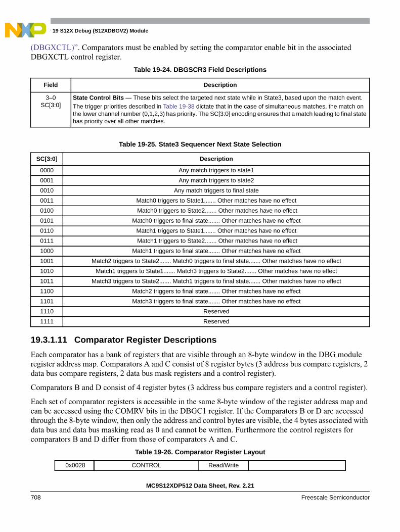
Chapter 19 S12X Debug (S12XDBGV2) Module
MC9S12XDP512 Data Sheet, Rev. 2.21
708 Freescale Semiconductor
(DBGXCTL)”. Comparators must be enabled by setting the comparator enable bit in the associatedDBGXCTL control register.
19.3.1.11 Comparator Register Descriptions
Each comparator has a bank of registers that are visible through an 8-byte window in the DBG moduleregister address map. Comparators A and C consist of 8 register bytes (3 address bus compare registers, 2data bus compare registers, 2 data bus mask registers and a control register).
Comparators B and D consist of 4 register bytes (3 address bus compare registers and a control register).
Each set of comparator registers is accessible in the same 8-byte window of the register address map andcan be accessed using the COMRV bits in the DBGC1 register. If the Comparators B or D are accessedthrough the 8-byte window, then only the address and control bytes are visible, the 4 bytes associated withdata bus and data bus masking read as 0 and cannot be written. Furthermore the control registers forcomparators B and D differ from those of comparators A and C.
Table 19-24. DBGSCR3 Field Descriptions
Field Description
3–0SC[3:0]
State Control Bits — These bits select the targeted next state while in State3, based upon the match event.The trigger priorities described in Table 19-38 dictate that in the case of simultaneous matches, the match onthe lower channel number (0,1,2,3) has priority. The SC[3:0] encoding ensures that a match leading to final statehas priority over all other matches.
Table 19-25. State3 Sequencer Next State Selection
SC[3:0] Description
0000 Any match triggers to state1
0001 Any match triggers to state2
0010 Any match triggers to final state
0011 Match0 triggers to State1....... Other matches have no effect
0100 Match0 triggers to State2....... Other matches have no effect
0101 Match0 triggers to final state....... Other matches have no effect
0110 Match1 triggers to State1....... Other matches have no effect
0111 Match1 triggers to State2....... Other matches have no effect
1000 Match1 triggers to final state....... Other matches have no effect
1001 Match2 triggers to State2....... Match0 triggers to final state....... Other matches have no effect
1010 Match1 triggers to State1....... Match3 triggers to State2....... Other matches have no effect
1011 Match3 triggers to State2....... Match1 triggers to final state....... Other matches have no effect
1100 Match2 triggers to final state....... Other matches have no effect
1101 Match3 triggers to final state....... Other matches have no effect
1110 Reserved
1111 Reserved
Table 19-26. Comparator Register Layout
0x0028 CONTROL Read/Write
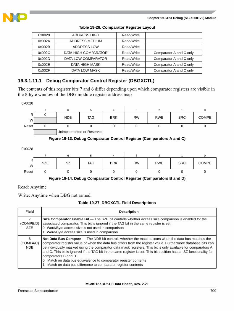
Chapter 19 S12X Debug (S12XDBGV2) Module
MC9S12XDP512 Data Sheet, Rev. 2.21
Freescale Semiconductor 709
19.3.1.11.1 Debug Comparator Control Register (DBGXCTL)
The contents of this register bits 7 and 6 differ depending upon which comparator registers are visible inthe 8-byte window of the DBG module register address map
Read: Anytime
Write: Anytime when DBG not armed.
0x0029 ADDRESS HIGH Read/Write
0x002A ADDRESS MEDIUM Read/Write
0x002B ADDRESS LOW Read/Write
0x002C DATA HIGH COMPARATOR Read/Write Comparator A and C only
0x002D DATA LOW COMPARATOR Read/Write Comparator A and C only
0x002E DATA HIGH MASK Read/Write Comparator A and C only
0x002F DATA LOW MASK Read/Write Comparator A and C only
0x0028
7 6 5 4 3 2 1 0
R 0NDB TAG BRK RW RWE SRC COMPE
W
Reset 0 0 0 0 0 0 0 0
Unimplemented or Reserved
Figure 19-13. Debug Comparator Control Register (Comparators A and C)
0x0028
7 6 5 4 3 2 1 0
RSZE SZ TAG BRK RW RWE SRC COMPE
W
Reset 0 0 0 0 0 0 0 0
Figure 19-14. Debug Comparator Control Register (Comparators B and D)
Table 19-27. DBGXCTL Field Descriptions
Field Description
7(COMPB/D)
SZE
Size Comparator Enable Bit — The SZE bit controls whether access size comparison is enabled for theassociated comparator. This bit is ignored if the TAG bit in the same register is set.0 Word/Byte access size is not used in comparison1 Word/Byte access size is used in comparison
6(COMPA/C)
NDB
Not Data Bus Compare — The NDB bit controls whether the match occurs when the data bus matches thecomparator register value or when the data bus differs from the register value. Furthermore database bits canbe individually masked using the comparator data mask registers. This bit is only available for comparators Aand C. This bit is ignored if the TAG bit in the same register is set. This bit position has an SZ functionality forcomparators B and D.0 Match on data bus equivalence to comparator register contents1 Match on data bus difference to comparator register contents
Table 19-26. Comparator Register Layout

Chapter 19 S12X Debug (S12XDBGV2) Module
MC9S12XDP512 Data Sheet, Rev. 2.21
710 Freescale Semiconductor
Table 19-28 shows the effect for RWE and RW on the comparison conditions. These bits are not useful fortagged operations since the trigger occurs based on the tagged opcode reaching the execution stage of theinstruction queue. Thus, these bits are ignored if tagged triggering is selected.
6(COMP B/D)
SZ
Size Comparator Value Bit — The SZ bit selects either word or byte access size in comparison for theassociated comparator. This bit is ignored if the SZE bit is cleared or if the TAG bit in the same register is set.This bit position has NDB functionality for comparators A and C0 Word access size will be compared1 Byte access size will be compared
5TAG
Tag Select — This bit controls whether the comparator match will cause a trigger or tag the opcode at thematched address. Tagged opcodes trigger only if they reach the execution stage of the instruction queue.0 Trigger immediately on match1 On match, tag the opcode. If the opcode is about to be executed a trigger is generated
4BRK
Break — This bit controls whether a comparator match can cause an immediate breakpoint independent of statesequencer state. The module breakpoints must be enabled using the DBGC1 bits DBGBRK[1:0].0 Breakpoints may only be generated from this channel when the state machine reaches final state.1 A match on this channel generates an immediate breakpoint, tracing, if active, is terminated and the module
disarmed.
3RW
Read/Write Comparator Value Bit — The RW bit controls whether read or write is used in compare for theassociated comparator. The RW bit is not used if RWE = 0.0 Write cycle will be matched1 Read cycle will be matched
2RWE
Read/Write Enable Bit — The RWE bit controls whether read or write comparison is enabled for the associatedcomparator. This bit is not useful for tagged operations.1 Read/Write is used in comparison0 Read/Write is not used in comparison
1SRC
SRC — Determines mapping of comparator to CPU or XGATE0 The comparator is mapped to CPU busses1 The comparator is mapped to XGATE address and data busses
0COMPE
Comparator Enable Bit— Determines if comparator is enabled0 The comparator is not enabled1 The comparator is enabled for state sequence triggers or tag generation
Table 19-28. Read or Write Comparison Logic Table
RWE Bit RW Bit RW Signal Comment
0 x 0 RW not used in comparison
0 x 1 RW not used in comparison
1 0 0 Write data bus
1 0 1 No match
1 1 0 No match
1 1 1 Read data bus
Table 19-27. DBGXCTL Field Descriptions (continued)
Field Description
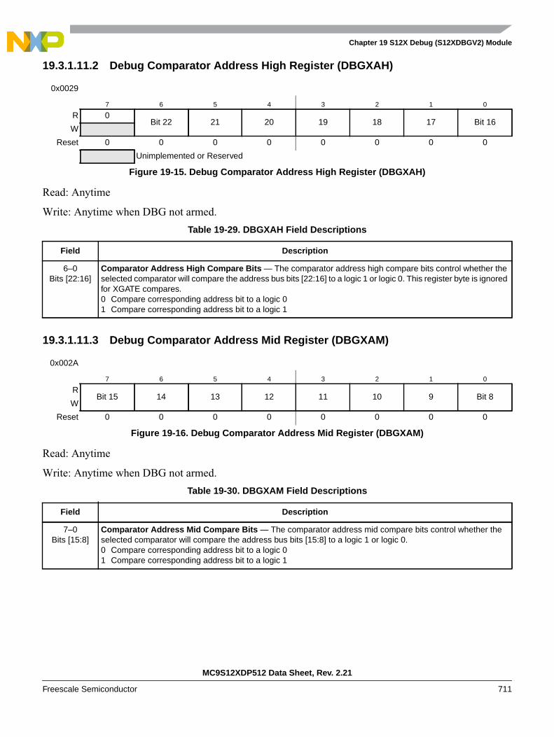
Chapter 19 S12X Debug (S12XDBGV2) Module
MC9S12XDP512 Data Sheet, Rev. 2.21
Freescale Semiconductor 711
19.3.1.11.2 Debug Comparator Address High Register (DBGXAH)
Read: Anytime
Write: Anytime when DBG not armed.
19.3.1.11.3 Debug Comparator Address Mid Register (DBGXAM)
Read: Anytime
Write: Anytime when DBG not armed.
0x0029
7 6 5 4 3 2 1 0
R 0Bit 22 21 20 19 18 17 Bit 16
W
Reset 0 0 0 0 0 0 0 0
Unimplemented or Reserved
Figure 19-15. Debug Comparator Address High Register (DBGXAH)
Table 19-29. DBGXAH Field Descriptions
Field Description
6–0Bits [22:16]
Comparator Address High Compare Bits — The comparator address high compare bits control whether theselected comparator will compare the address bus bits [22:16] to a logic 1 or logic 0. This register byte is ignoredfor XGATE compares.0 Compare corresponding address bit to a logic 01 Compare corresponding address bit to a logic 1
0x002A
7 6 5 4 3 2 1 0
RBit 15 14 13 12 11 10 9 Bit 8
W
Reset 0 0 0 0 0 0 0 0
Figure 19-16. Debug Comparator Address Mid Register (DBGXAM)
Table 19-30. DBGXAM Field Descriptions
Field Description
7–0Bits [15:8]
Comparator Address Mid Compare Bits — The comparator address mid compare bits control whether theselected comparator will compare the address bus bits [15:8] to a logic 1 or logic 0.0 Compare corresponding address bit to a logic 01 Compare corresponding address bit to a logic 1
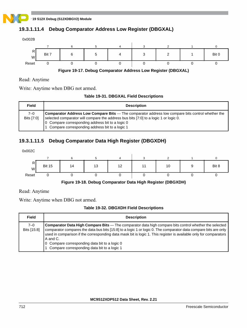
Chapter 19 S12X Debug (S12XDBGV2) Module
MC9S12XDP512 Data Sheet, Rev. 2.21
712 Freescale Semiconductor
19.3.1.11.4 Debug Comparator Address Low Register (DBGXAL)
Read: Anytime
Write: Anytime when DBG not armed.
19.3.1.11.5 Debug Comparator Data High Register (DBGXDH)
Read: Anytime
Write: Anytime when DBG not armed.
0x002B
7 6 5 4 3 2 1 0
RBit 7 6 5 4 3 2 1 Bit 0
W
Reset 0 0 0 0 0 0 0 0
Figure 19-17. Debug Comparator Address Low Register (DBGXAL)
Table 19-31. DBGXAL Field Descriptions
Field Description
7–0Bits [7:0]
Comparator Address Low Compare Bits — The comparator address low compare bits control whether theselected comparator will compare the address bus bits [7:0] to a logic 1 or logic 0.0 Compare corresponding address bit to a logic 01 Compare corresponding address bit to a logic 1
0x002C
7 6 5 4 3 2 1 0
RBit 15 14 13 12 11 10 9 Bit 8
W
Reset 0 0 0 0 0 0 0 0
Figure 19-18. Debug Comparator Data High Register (DBGXDH)
Table 19-32. DBGXDH Field Descriptions
Field Description
7–0Bits [15:8]
Comparator Data High Compare Bits — The comparator data high compare bits control whether the selectedcomparator compares the data bus bits [15:8] to a logic 1 or logic 0. The comparator data compare bits are onlyused in comparison if the corresponding data mask bit is logic 1. This register is available only for comparatorsA and C.0 Compare corresponding data bit to a logic 01 Compare corresponding data bit to a logic 1
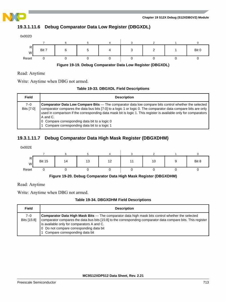
Chapter 19 S12X Debug (S12XDBGV2) Module
MC9S12XDP512 Data Sheet, Rev. 2.21
Freescale Semiconductor 713
19.3.1.11.6 Debug Comparator Data Low Register (DBGXDL)
Read: Anytime
Write: Anytime when DBG not armed.
19.3.1.11.7 Debug Comparator Data High Mask Register (DBGXDHM)
Read: Anytime
Write: Anytime when DBG not armed.
0x002D
7 6 5 4 3 2 1 0
RBit 7 6 5 4 3 2 1 Bit 0
W
Reset 0 0 0 0 0 0 0 0
Figure 19-19. Debug Comparator Data Low Register (DBGXDL)
Table 19-33. DBGXDL Field Descriptions
Field Description
7–0Bits [7:0]
Comparator Data Low Compare Bits — The comparator data low compare bits control whether the selectedcomparator compares the data bus bits [7:0] to a logic 1 or logic 0. The comparator data compare bits are onlyused in comparison if the corresponding data mask bit is logic 1. This register is available only for comparatorsA and C.0 Compare corresponding data bit to a logic 01 Compare corresponding data bit to a logic 1
0x002E
7 6 5 4 3 2 1 0
RBit 15 14 13 12 11 10 9 Bit 8
W
Reset 0 0 0 0 0 0 0 0
Figure 19-20. Debug Comparator Data High Mask Register (DBGXDHM)
Table 19-34. DBGXDHM Field Descriptions
Field Description
7–0Bits [15:8]
Comparator Data High Mask Bits — The comparator data high mask bits control whether the selectedcomparator compares the data bus bits [15:8] to the corresponding comparator data compare bits. This registeris available only for comparators A and C.0 Do not compare corresponding data bit1 Compare corresponding data bit

Chapter 19 S12X Debug (S12XDBGV2) Module
MC9S12XDP512 Data Sheet, Rev. 2.21
714 Freescale Semiconductor
19.3.1.11.8 Debug Comparator Data Low Mask Register (DBGXDLM)
Read: Anytime
Write: Anytime when DBG not armed.
19.4 Functional DescriptionThis section provides a complete functional description of the DBG module. If the part is in secure mode,the DBG module can generate breakpoints but tracing is not possible.
19.4.1 DBG Operation
Arming the DBG module by setting ARM in DBGC1 allows triggering, and storing of data in the tracebuffer and can be used to cause breakpoints to the CPU or the XGATE module. The DBG module is madeup of 4 main blocks, the comparators, control logic, the state sequencer and the trace buffer.
The comparators monitor the bus activity of the CPU and XGATE modules. Comparators can beconfigured to monitor address and databus. Comparators can also be configured to mask out individualdata bus bits during a compare and to use R/W and word/byte access qualification in the comparison. Whena match with a comparator register value occurs the associated control logic can trigger the state sequencerto another state (Figure 19-23). Either forced or tagged triggers are possible. Using a forced trigger, thetrigger is generated immediately on a comparator match. Using a tagged trigger, at a comparator match,the instruction opcode is tagged and only if the instruction reaches the execution stage of the instructionqueue is a trigger generated. In the case of a transition to final state, bus tracing is triggered and/or abreakpoint can be generated. Tracing of both CPU and/or XGATE bus activity is possible.
Independent of the state sequencer, a breakpoint can be triggered by the external TAGHI / TAGLO signals,by an XGATE S/W breakpoint request or by writing to the TRIG bit in the DBGC1 control register.
The trace buffer is visible through a 2-byte window in the register address map and can be read out usingstandard 16-bit word reads.
0x002F
7 6 5 4 3 2 1 0
RBit 7 6 5 4 3 2 1 Bit 0
W
Reset 0 0 0 0 0 0 0 0
Figure 19-21. Debug Comparator Data Low Mask Register (DBGXDLM)
Table 19-35. DBGXDLM Field Descriptions
Field Description
7–0Bits [7:0]
Comparator Data Low Mask Bits — The comparator data low mask bits control whether the selectedcomparator compares the data bus bits [7:0] to the corresponding comparator data compare bits. This registeris available only for comparators A and C.0 Do not compare corresponding data bit1 Compare corresponding data bit
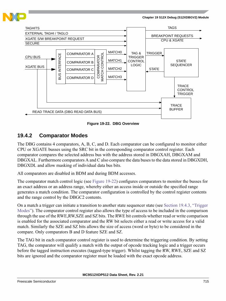
Chapter 19 S12X Debug (S12XDBGV2) Module
MC9S12XDP512 Data Sheet, Rev. 2.21
Freescale Semiconductor 715
Figure 19-22. DBG Overview
19.4.2 Comparator Modes
The DBG contains 4 comparators, A, B, C, and D. Each comparator can be configured to monitor eitherCPU or XGATE busses using the SRC bit in the corresponding comparator control register. Eachcomparator compares the selected address bus with the address stored in DBGXAH, DBGXAM andDBGXAL. Furthermore comparators A and C also compare the data buses to the data stored in DBGXDH,DBGXDL and allow masking of individual data bus bits.
All comparators are disabled in BDM and during BDM accesses.
The comparator match control logic (see Figure 19-22) configures comparators to monitor the busses foran exact address or an address range, whereby either an access inside or outside the specified rangegenerates a match condition. The comparator configuration is controlled by the control register contentsand the range control by the DBGC2 contents.
On a match a trigger can initiate a transition to another state sequencer state (see Section 19.4.3, “TriggerModes”). The comparator control register also allows the type of access to be included in the comparisonthrough the use of the RWE,RW,SZE and SZ bits. The RWE bit controls whether read or write comparisonis enabled for the associated comparator and the RW bit selects either a read or write access for a validmatch. Similarly the SZE and SZ bits allows the size of access (word or byte) to be considered in thecompare. Only comparators B and D feature SZE and SZ.
The TAG bit in each comparator control register is used to determine the triggering condition. By settingTAG, the comparator will qualify a match with the output of opcode tracking logic and a trigger occursbefore the tagged instruction executes (tagged-type trigger). Whilst tagging the RW, RWE, SZE and SZbits are ignored and the comparator register must be loaded with the exact opcode address.
CPU BUSB
US
INT
ER
FAC
E TRIGGER
EXTERNAL TAGHI / TAGLO
MATCH0
XGATE BUSCOMPARATOR B
COMPARATOR C
COMPARATOR D
COMPARATOR A
MATCH1
MATCH2
MATCH3
READ TRACE DATA (DBG READ DATA BUS)
SECURE
BREAKPOINT REQUESTSXGATE S/W BREAKPOINT REQUEST
TAGSTAGHITS
STATE
CPU & XGATE
CO
MPA
RAT
OR
MAT
CH
CO
NT
RO
L TAG &TRIGGERCONTROL
LOGICSTATE
SEQUENCER
TRACEBUFFER
TRACECONTROLTRIGGER
Chapter 19 S12X Debug (S12XDBGV2) Module
MC9S12XDP512 Data Sheet, Rev. 2.21
716 Freescale Semiconductor
If the TAG bit is clear (forced type trigger) a comparator match is generated when the selected addressappears on the system address bus. If the selected address is an opcode address, the match is generatedwhen the opcode is fetched from the memory. This precedes the instruction execution by an indefinitenumber of cycles due to instruction pipe lining. For a comparator match of an opcode at an odd addresswhen TAG = 0, the corresponding even address must be contained in the comparator register. Thus for anopcode at odd address (n), the comparator register must contain address (n – 1).
Once a successful comparator match has occurred, the condition that caused the original match is notverified again on subsequent matches. Thus if a particular data value is verified at a given address, thisaddress may not still contain that data value when a subsequent match occurs.
Comparators C and D can also be used to select an address range to trace from. This is determined by theTRANGE bits in the DBGTCR register. The TRANGE encoding is shown in Table 19-10. If the TRANGEbits select a range definition using comparator D, then comparator D is configured for trace rangedefinition and cannot be used for address bus comparisons. Similarly if the TRANGE bits select a rangedefinition using comparator C, then comparator C is configured for trace range definition and cannot beused for address bus comparisons.
Match[0,1,2,3] map directly to comparators [A,B,C,D] respectively, except in range modes (seeSection 19.3.1.4, “Debug Control Register2 (DBGC2)”). Comparator priority rules are described in thetrigger priority (see Section 19.4.3.6, “Trigger Priorities”).
19.4.2.1 Exact Address Comparator Match (Comparators A and C)
With range comparisons disabled, the match condition is an exact equivalence of address/data bus with thevalue stored in the comparator address/data registers. Further qualification of the type of access (R/W,word/byte) is possible.
Comparators A and C do not feature SZE or SZ control bits, thus the access size is not compared. The exactaddress is compared, thus with the comparator address register loaded with address (n) a misaligned wordaccess of address (n-1) also accesses (n) but does not cause a match Table 19-37 lists access considerationswithout data bus compare. Table 19-36 lists access considerations with data bus comparison. To comparebyte accesses DBGXDH must be loaded with the data byte. The low byte must be masked out using theDBGXDLM mask register. On word accesses data byte of the lower address is mapped to DBGXDH.
Comparators A and C feature an NDB control bit to determine if a match occurs when the data bus differsto comparator register contents or when the data bus is equivalent to the comparator register contents.
Table 19-36. Comparator A and C Data Bus Considerations
Access Address DBGxDH DBGxDL DBGxDHM DBGxDLM Example Valid Match
Word ADDR[n] Data[n] Data[n+1] 0x_FF 0x_FF MOVW #$WORD ADDR[n]
Byte ADDR[n] Data[n] x 0x_FF 0x_00 MOVB #$BYTE ADDR[n]
Word ADDR[n] Data[n] x 0x_FF 0x_00 MOVW #$WORD ADDR[n]
Word ADDR[n] x Data[n+1] 0x_00 0x_FF MOVW #$WORD ADDR[n]

Chapter 19 S12X Debug (S12XDBGV2) Module
MC9S12XDP512 Data Sheet, Rev. 2.21
Freescale Semiconductor 717
19.4.2.2 Exact Address Comparator Match (Comparators B and D)
Comparators B and D feature SZ and SZE control bits. If SZE is clear, then the comparator address matchqualification functions the same as for comparators A and C.
If the SZE bit is set the access size (word or byte) is compared with the SZ bit value such that only thespecified type of access causes a match. Thus, if configured for a byte access of a particular address, a wordaccess covering the same address does not lead to match.
19.4.2.3 Range Comparisons
When using the AB comparator pair for a range comparison, the data bus can also be used for qualificationby using the comparator A data and data mask registers. Furthermore the DBGACTL RW and RWE bitscan be used to qualify the range comparison on either a read or a write access. The correspondingDBGBCTL bits are ignored. Similarly when using the CD comparator pair for a range comparison, thedata bus can also be used for qualification by using the comparator C data and data mask registers.Furthermore the DBGCCTL RW and RWE bits can be used to qualify the range comparison on either aread or a write access if tagging is not selected. The corresponding DBGDCTL bits are ignored. The SZEand SZ control bits are ignored in range mode. The comparator A and C TAG bits are used to tag rangecomparisons for the AB and CD ranges respectively. The comparator B and D TAG bits are ignored inrange modes. In order for a range comparison using comparators A and B, both COMPEA and COMPEBmust be set; to disable range comparisons both must be cleared. Similarly for a range CD comparison, bothCOMPEC and COMPED must be set. If a range mode is selected SRCA and SRCB must select the samesource (S12X or XGATE). Similarly SRCC and SRCD must select the same source. When configured forrange comparisons and tagging, the ranges are accurate only to word boundaries.
19.4.2.3.1 Inside Range (CompAC_Addr ≤ Address ≤ CompBD_Addr)
In the inside range comparator mode, either comparator pair A and B or comparator pair C and D can beconfigured for range comparisons. This configuration depends upon the control register (DBGC2). Thematch condition requires that a valid match for both comparators happens on the same bus cycle. A matchcondition on only one comparator is not valid. An aligned word access which straddles the range boundarywill cause a trigger only if the aligned address is inside the range.
Table 19-37. Comparator Access Size Considerations
Comparator Address SZE SZ8 Condition For Valid Match
ComparatorsA and C
ADDR[n] - - Word and byte accesses of ADDR[n]1
MOVB #$BYTE ADDR[n]MOVW #$WORD ADDR[n]
1 A word access of ADDR[n-1] also accesses ADDR[n] but does not generate a match.The comparator address register must contain the exact address used in the code.
ComparatorsB and D
ADDR[n] 0 X Word and byte accesses of ADDR[n]1
MOVB #$BYTE ADDR[n]MOVW #$WORD ADDR[n]
ComparatorsB and D
ADDR[n] 1 0 Word accesses of ADDR[n]1
MOVW #$WORD ADDR[n]
ComparatorsB and D
ADDR[n] 1 1 Byte accesses of ADDR[n]MOVB #$BYTE ADDR[n]
Chapter 19 S12X Debug (S12XDBGV2) Module
MC9S12XDP512 Data Sheet, Rev. 2.21
718 Freescale Semiconductor
19.4.2.3.2 Outside Range (Address < CompAC_Addr or Address > CompBD_Addr)
In the outside range comparator mode, either comparator pair A and B or comparator pair C and D can beconfigured for range comparisons. A single match condition on either of the comparators is recognized asvalid. An aligned word access which straddles the range boundary will cause a trigger only if the alignedaddress is outside the range.
Outside range mode in combination with tagged triggers can be used to detect if the opcode fetches arefrom an unexpected range. In forced trigger modes the outside range trigger would typically be activatedat any interrupt vector fetch or register access. This can be avoided by setting the upper range limit to0x7FFFFF or lower range limit to 0x000000 respectively.
When comparing the XGATE address bus in outside range mode, the initial vector fetch as determined bythe vector contained in the XGATE XGVBR register should be taken into consideration. The XGVBRregister and hence vector address can be modified.
19.4.3 Trigger Modes
Trigger modes are used as qualifiers for a state sequencer change of state. The control logic determines thetrigger mode and provides a trigger to the state sequencer. The individual trigger modes are described inthe following sections.
19.4.3.1 Trigger On Comparator Match
If a comparator match occurs, a trigger occurs to initiate a transition to another state sequencer state andthe corresponding flags in DBGSR are set. For a comparator match to trigger firstly the comparator mustbe enabled by setting the COMPE bit in the corresponding comparator control register. Secondly the statecontrol register for the current state must enable the match for that state. The state control registers allowfor different matches to be enabled in each of the states 1 to 3.
19.4.3.2 Trigger On Comparator Related Taghit
If either a CPU or XGATE taghit occurs a transition to another state sequencer state is initiated and thecorresponding DBGSR flags are set. For a comparator related taghit to occur, the DBG must first generatetags based on comparator matches. When the tagged instruction reaches the execution stage of theinstruction queue a taghit is generated by the CPU/XGATE.
19.4.3.3 External Tag Trigger
In external tagging trigger mode, the TAGLO and TAGHI pins (mapped to device pins) are used to tag aninstruction. This function can be used as another breakpoint source. When the tagged opcode reaches theexecution stage of the instruction queue a transition to the disarmed state0 occurs, ending the debug sessionand generating a breakpoint, if breakpoints are enabled. External tagging is only possible in deviceemulation modes.
Chapter 19 S12X Debug (S12XDBGV2) Module
MC9S12XDP512 Data Sheet, Rev. 2.21
Freescale Semiconductor 719
19.4.3.4 Trigger On XGATE S/W Breakpoint Request
The XGATE S/W breakpoint request issues a forced breakpoint request to the CPU immediatelyindependent of DBG settings. If the debug module is armed triggers the state sequencer into the disarmedstate. Active tracing sessions are terminated immediately, thus if tracing has not yet begun using begin-trigger, no trace information is stored. XGATE generated breakpoints are independent of the DBGBRKbits. The XGSBPE bit in DBGC1 determines if the XGATE S/W breakpoint function is enabled. The BDMbit in DBGC1 determines if the XGATE requested breakpoint causes the system to enter BDM mode orinitiate a software interrupt (SWI).
19.4.3.5 Immediate Trigger
At any time independent of comparator matches or external tag signals it is possible to initiate a tracingsession and/or breakpoint by writing to the TRIG bit in DBGC1. This triggers the state sequencer into thefinal state and issues a forced breakpoint request to both CPU and XGATE.
19.4.3.6 Trigger Priorities
In case of simultaneous triggers, the priority is resolved according to Table 19-38. The lower prioritytrigger is suppressed. It is thus possible to miss a lower priority trigger if it occurs simultaneously with atrigger of a higher priority. The trigger priorities described in Table 19-38 dictate that in the case ofsimultaneous matches, the match on the lower channel number ([0,1,2,3) has priority. The SC[3:0]encoding ensures that a match leading to final state has priority over all other matches independent ofcurrent state sequencer state. When configured for range modes a simultaneous match of comparators Aand C generates an active match0 while match2 is suppressed.
Table 19-38. Trigger Priorities
Priority Source Action
Highest XGATE Immediate forced breakpoint......(Tracing terminated immediately).
TRIG Enter final state
External TAGHI/TAGLO Enter State0
Match0 (force or tag hit) Trigger to next state as defined by state control registers
Match1 (force or tag hit) Trigger to next state as defined by state control registers
Match2 (force or tag hit) Trigger to next state as defined by state control registers
Lowest Match3 (force or tag hit) Trigger to next state as defined by state control registers

Chapter 19 S12X Debug (S12XDBGV2) Module
MC9S12XDP512 Data Sheet, Rev. 2.21
720 Freescale Semiconductor
19.4.4 State Sequence Control
Figure 19-23. State Sequencer Diagram
The state sequence control allows a defined sequence of events to provide a trigger point for tracing of datain the trace buffer. Once the DBG module has been armed by setting the ARM bit in the DBGC1 register,then State1 of the state sequencer is entered. Further transitions between the states are then controlled bythe state control registers and depend upon a selected trigger mode condition being met. From final statethe only permitted transition is back to the disarmed state0. Transition between any of the states 1 to 3 isnot restricted. Each transition updates the SSF[2:0] flags in DBGSR accordingly to indicate the currentstate.
Alternatively writing to the TRIG bit in DBGSC1, the final state is entered and tracing starts immediatelyif the TSOURCE bits are configured for tracing.
A tag hit through TAGHI/TAGLO causes a breakpoint, if breakpoints are enabled, and ends tracingimmediately independent of the trigger alignment bits TALIGN[1:0].
Furthermore, each comparator channel can be individually configured to generate an immediatebreakpoint when a match occurs through the use of the BRK bits in the DBGxCTL registers independentof the state sequencer state. Thus it is possible to generate an immediate breakpoint on selected channels,while a state sequencer transition can be initiated by a match on other channels.
An XGATE S/W breakpoint request, if enabled causes a transition to the final state and generates abreakpoint request to the CPU immediately.
If neither tracing nor breakpoints are enabled then, when a forced match triggers to final state, it can onlybe returned to the disarmed state0 by clearing the ARM bit by software. This also applies to the case thatBDM breakpoints are enabled, but the BDM is disabled. Furthermore if neither tracing nor breakpoints areenabled, forced triggers on channels with BRK set cause a transition to the state determined by the statesequencer as if the BRK bit were not being used.
If neither tracing nor breakpoints are enabled then when a tagged match triggers to final state, the statesequencer returns to the disarmed state0.
State1
Final State State3
ARM = 1
Session complete
(disarm)
State2State 0
(Disarmed)ARM = 0
ARM=0
ARM = 0
Chapter 19 S12X Debug (S12XDBGV2) Module
MC9S12XDP512 Data Sheet, Rev. 2.21
Freescale Semiconductor 721
19.4.4.1 Final State
On entering final state a trigger may be issued to the trace buffer according to the trace position control asdefined by the TALIGN field (see Section 19.3.1.3, “Debug Trace Control Register (DBGTCR)”). If theTSOURCE bits in the trace control register DBGTCR are cleared then the trace buffer is disabled and thetransition to final state can only generate a breakpoint request. In this case or upon completion of a tracingsession when tracing is enabled, the ARM bit in the DBGC1 register is cleared, returning the module tothe disarmed state0. If tracing is enabled a breakpoint request can occur at the end of the tracing session.
19.4.5 Trace Buffer Operation
The trace buffer is a 64 lines deep by 64-bits wide RAM array. The DBG module stores trace informationin the RAM array in a circular buffer format. The CPU accesses the RAM array through a register window(DBGTBH:DBGTBL) using 16-bit wide word accesses. After each complete 64-bit trace buffer line isread via the CPU, an internal pointer into the RAM is incremented so that the next read will receive freshinformation. Data is stored in the format shown in Table 19-39. After each store the counter register bitsDBGCNT[6:0] are incremented. Tracing of CPU activity is disabled when the BDM is active but tracingof XGATE activity is still possible. Reading the trace buffer while the BDM is active returns invalid dataand the trace buffer pointer is not incremented.
19.4.5.1 Trace Trigger Alignment
Using the TALIGN bits (see Section 19.3.1.3, “Debug Trace Control Register (DBGTCR)”) it is possibleto align the trigger with the end, the middle or the beginning of a tracing session.
If end or mid tracing is selected, tracing begins when the ARM bit in DBGC1 is set and State1 is entered.The transition to final state if end is selected signals the end of the tracing session. The transition to finalstate if mid is selected signals that another 32 lines will be traced before ending the tracing session. Tracingwith begin-trigger starts at the opcode of the trigger.
19.4.5.1.1 Storing with Begin-Trigger
Storing with begin-trigger, data is not stored in the trace buffer until the final state is entered. Once thetrigger condition is met the DBG module will remain armed until 64 lines are stored in the trace buffer. Ifthe trigger is at the address of the change-of-flow instruction the change of flow associated with the triggerwill be stored in the trace buffer. Using begin-trigger together with tagging, if the tagged instruction isabout to be executed then the trace is started. Upon completion of the tracing session the breakpoint isgenerated, thus the breakpoint does not occur at the tagged instruction boundary.
19.4.5.1.2 Storing with Mid-Trigger
Storing with mid-trigger, data is stored in the trace buffer as soon as the DBG module is armed. When thetrigger condition is met, another 32 lines will be traced before ending the tracing session, irrespective ofthe number of lines stored before the trigger occurred, then the DBG module is disarmed and no more datais stored. If the trigger is at the address of a change of flow instruction the trigger event is not stored in thetrace buffer. Using mid-trigger with tagging, if the tagged instruction is about to be executed then the trace
Chapter 19 S12X Debug (S12XDBGV2) Module
MC9S12XDP512 Data Sheet, Rev. 2.21
722 Freescale Semiconductor
is continued for another 32 lines. Upon tracing completion the breakpoint is generated, thus the breakpointdoes not occur at the tagged instruction boundary.
19.4.5.1.3 Storing with End-Trigger
Storing with end-trigger, data is stored in the trace buffer until the final state is entered, at which point theDBG module will become disarmed and no more data will be stored. If the trigger is at the address of achange of flow instruction the trigger event will not be stored in the trace buffer.
19.4.5.2 Trace Modes
The DBG module can operate in three trace modes. The mode is selected using the TRCMOD bits in theDBGTCR register. In each mode tracing of XGATE or CPU information is possible. The source for thetrace is selected using the TSOURCE bits in the DBGTCR register. The modes are described in thefollowing subsections. The trace buffer organization is shown in Table 19-39.
19.4.5.2.1 Normal Mode
In normal mode, change of flow (COF) addresses will be stored.
COF addresses are defined as follows for the CPU:
• Source address of taken conditional branches (long, short, bit-conditional, and loop primitives)
• Destination address of indexed JMP, JSR and CALL instruction.
• Destination address of RTI, RTS and RTC instructions
• Vector address of interrupts, except for SWI and BDM vectors
LBRA, BRA, BSR, BGND as well as non-indexed JMP, JSR, and CALL instructions are not classified aschange of flow and are not stored in the trace buffer.
COF addresses are defined as follows for the XGATE:
• Source address of taken conditional branches
• Destination address of indexed JAL instructions.
• First XGATE code address, determined by the vector contained in the XGATE XGVBR register
Change-of-flow addresses stored include the full 23-bit address bus in the case of CPU, the 16-bit addressbus for the XGATE module and an information byte, which contains a source/destination bit to indicatewhether the stored address was a source address or destination address.
19.4.5.2.2 Loop1 Mode
Loop1 mode, similarly to normal mode also stores only COF address information to the trace buffer, ithowever allows the filtering out of redundant information.
The intent of loop1 mode is to prevent the trace buffer from being filled entirely with duplicate informationfrom a looping construct such as delays using the DBNE instruction or polling loops usingBRSET/BRCLR instructions. Immediately after address information is placed in the trace buffer, the DBGmodule writes this value into a background register. This prevents consecutive duplicate address entries inthe trace buffer resulting from repeated branches.
Chapter 19 S12X Debug (S12XDBGV2) Module
MC9S12XDP512 Data Sheet, Rev. 2.21
Freescale Semiconductor 723
Loop1 mode only inhibits consecutive duplicate source address entries that would typically be stored inmost tight looping constructs. It does not inhibit repeated entries of destination addresses or vectoraddresses, since repeated entries of these would most likely indicate a bug in the user’s code that the DBGmodule is designed to help find.
NOTEIn certain very tight loops, the source address will have already been fetchedagain before the background comparator is updated. This results in thesource address being stored twice before further duplicate entries aresuppressed. This condition occurs with branch-on-bit instructions when thebranch is fetched by the first P-cycle of the branch or with loop-constructinstructions in which the branch is fetched with the first or second P cycle.See examples below:
LOOP INX ;1-byte instruction fetched by 1st P-cycle of BRCLRBRCLR CMPTMP,#$0c,LOOP ;the BRCLR instruction also will be fetched by 1st P-cycle
;of BRCLR
LOOP2 BRN* ; 2-byte instruction fetched by 1st P-cycle of DBNENOP ; 1-byte instruction fetched by 2nd P-cycle of DBNEDBNE A,LOOP2 ; this instruction also fetched by 2nd P-cycle of DBNE
19.4.5.2.3 Detail Mode
In detail mode, address and data for all memory and register accesses is stored in the trace buffer. In thecase of XGATE tracing this means that initialization of the R1 register during a vector fetch is not traced.This mode is intended to supply additional information on indexed, indirect addressing modes wherestoring only the destination address would not provide all information required for a user to determinewhere the code is in error. This mode also features information byte storage to the trace buffer, for eachaddress byte storage. The information byte indicates the size of access (word or byte), the type of access(read or write).
When tracing CPU activity in detail mode, all cycles are traced except those when the CPU is either in afree or opcode fetch cycle. In this mode the XGATE program counter is also traced to provide a snapshotof the XGATE activity. CXINF information byte bits indicate the type of XGATE activity occurring at thetime of the trace buffer entry. When tracing CPU activity alone in detail mode, the address range can belimited to a range specified by the TRANGE bits in DBGTCR. This function uses comparators C and Dto define an address range inside which CPU activity should be traced (see Table 19-10). Thus, the tracedCPU activity can be restricted to register range accesses.
When tracing XGATE activity in detail mode, all cycles apart from opcode fetch and free cycles are storedto the trace buffer. Additionally the CPU program counter is stored at the time of the XGATE trace bufferentry to provide a snapshot of CPU activity.
19.4.5.3 Trace Buffer Organization
The buffer can be used to trace either from CPU, from XGATE or from both sources. An “X” prefixdenotes information from the XGATE module, a “C” prefix denotes information from the CPU.ADRH,ADRM,ADRL denote address high, middle and low byte respectively. INF bytes contain control
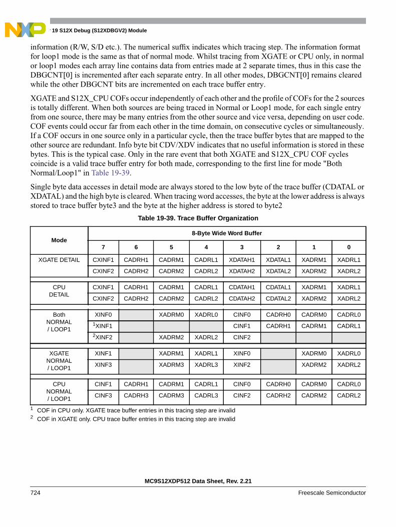
Chapter 19 S12X Debug (S12XDBGV2) Module
MC9S12XDP512 Data Sheet, Rev. 2.21
724 Freescale Semiconductor
information (R/W, S/D etc.). The numerical suffix indicates which tracing step. The information formatfor loop1 mode is the same as that of normal mode. Whilst tracing from XGATE or CPU only, in normalor loop1 modes each array line contains data from entries made at 2 separate times, thus in this case theDBGCNT[0] is incremented after each separate entry. In all other modes, DBGCNT[0] remains clearedwhile the other DBGCNT bits are incremented on each trace buffer entry.
XGATE and S12X_CPU COFs occur independently of each other and the profile of COFs for the 2 sourcesis totally different. When both sources are being traced in Normal or Loop1 mode, for each single entryfrom one source, there may be many entries from the other source and vice versa, depending on user code.COF events could occur far from each other in the time domain, on consecutive cycles or simultaneously.If a COF occurs in one source only in a particular cycle, then the trace buffer bytes that are mapped to theother source are redundant. Info byte bit CDV/XDV indicates that no useful information is stored in thesebytes. This is the typical case. Only in the rare event that both XGATE and S12X_CPU COF cyclescoincide is a valid trace buffer entry for both made, corresponding to the first line for mode "BothNormal/Loop1" in Table 19-39.
Single byte data accesses in detail mode are always stored to the low byte of the trace buffer (CDATAL orXDATAL) and the high byte is cleared. When tracing word accesses, the byte at the lower address is alwaysstored to trace buffer byte3 and the byte at the higher address is stored to byte2
Table 19-39. Trace Buffer Organization
Mode8-Byte Wide Word Buffer
7 6 5 4 3 2 1 0
XGATE DETAIL CXINF1 CADRH1 CADRM1 CADRL1 XDATAH1 XDATAL1 XADRM1 XADRL1
CXINF2 CADRH2 CADRM2 CADRL2 XDATAH2 XDATAL2 XADRM2 XADRL2
CPUDETAIL
CXINF1 CADRH1 CADRM1 CADRL1 CDATAH1 CDATAL1 XADRM1 XADRL1
CXINF2 CADRH2 CADRM2 CADRL2 CDATAH2 CDATAL2 XADRM2 XADRL2
BothNORMAL/ LOOP1
XINF0 XADRM0 XADRL0 CINF0 CADRH0 CADRM0 CADRL0
1XINF1
1 COF in CPU only. XGATE trace buffer entries in this tracing step are invalid
CINF1 CADRH1 CADRM1 CADRL1
2XINF2
2 COF in XGATE only. CPU trace buffer entries in this tracing step are invalid
XADRM2 XADRL2 CINF2
XGATENORMAL/ LOOP1
XINF1 XADRM1 XADRL1 XINF0 XADRM0 XADRL0
XINF3 XADRM3 XADRL3 XINF2 XADRM2 XADRL2
CPUNORMAL/ LOOP1
CINF1 CADRH1 CADRM1 CADRL1 CINF0 CADRH0 CADRM0 CADRL0
CINF3 CADRH3 CADRM3 CADRL3 CINF2 CADRH2 CADRM2 CADRL2
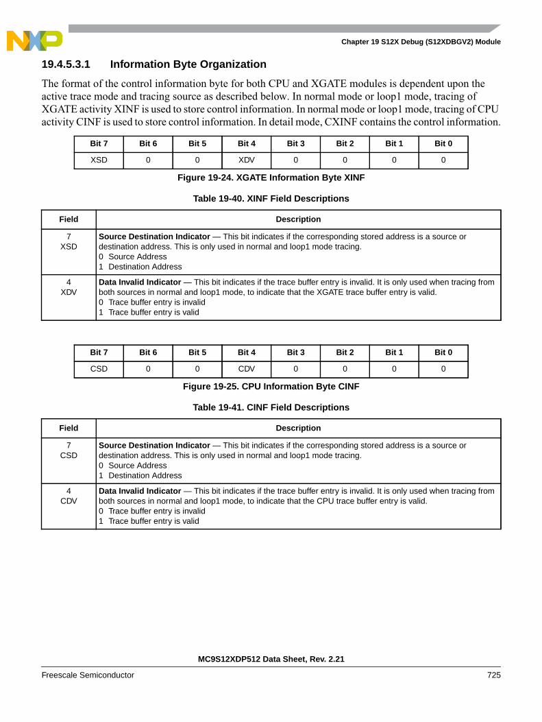
Chapter 19 S12X Debug (S12XDBGV2) Module
MC9S12XDP512 Data Sheet, Rev. 2.21
Freescale Semiconductor 725
19.4.5.3.1 Information Byte Organization
The format of the control information byte for both CPU and XGATE modules is dependent upon theactive trace mode and tracing source as described below. In normal mode or loop1 mode, tracing ofXGATE activity XINF is used to store control information. In normal mode or loop1 mode, tracing of CPUactivity CINF is used to store control information. In detail mode, CXINF contains the control information.
Bit 7 Bit 6 Bit 5 Bit 4 Bit 3 Bit 2 Bit 1 Bit 0
XSD 0 0 XDV 0 0 0 0
Figure 19-24. XGATE Information Byte XINF
Table 19-40. XINF Field Descriptions
Field Description
7XSD
Source Destination Indicator — This bit indicates if the corresponding stored address is a source ordestination address. This is only used in normal and loop1 mode tracing.0 Source Address1 Destination Address
4XDV
Data Invalid Indicator — This bit indicates if the trace buffer entry is invalid. It is only used when tracing fromboth sources in normal and loop1 mode, to indicate that the XGATE trace buffer entry is valid.0 Trace buffer entry is invalid1 Trace buffer entry is valid
Bit 7 Bit 6 Bit 5 Bit 4 Bit 3 Bit 2 Bit 1 Bit 0
CSD 0 0 CDV 0 0 0 0
Figure 19-25. CPU Information Byte CINF
Table 19-41. CINF Field Descriptions
Field Description
7CSD
Source Destination Indicator — This bit indicates if the corresponding stored address is a source ordestination address. This is only used in normal and loop1 mode tracing.0 Source Address1 Destination Address
4CDV
Data Invalid Indicator — This bit indicates if the trace buffer entry is invalid. It is only used when tracing fromboth sources in normal and loop1 mode, to indicate that the CPU trace buffer entry is valid.0 Trace buffer entry is invalid1 Trace buffer entry is valid
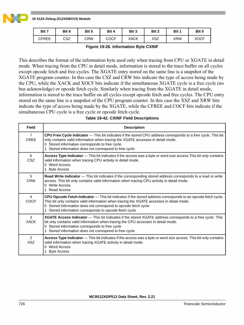
Chapter 19 S12X Debug (S12XDBGV2) Module
MC9S12XDP512 Data Sheet, Rev. 2.21
726 Freescale Semiconductor
This describes the format of the information byte used only when tracing from CPU or XGATE in detailmode. When tracing from the CPU in detail mode, information is stored to the trace buffer on all cyclesexcept opcode fetch and free cycles. The XGATE entry stored on the same line is a snapshot of theXGATE program counter. In this case the CSZ and CRW bits indicate the type of access being made bythe CPU, while the XACK and XOCF bits indicate if the simultaneous XGATE cycle is a free cycle (nobus acknowledge) or opcode fetch cycle. Similarly when tracing from the XGATE in detail mode,information is stored to the trace buffer on all cycles except opcode fetch and free cycles. The CPU entrystored on the same line is a snapshot of the CPU program counter. In this case the XSZ and XRW bitsindicate the type of access being made by the XGATE, while the CFREE and COCF bits indicate if thesimultaneous CPU cycle is a free cycle or opcode fetch cycle.
Bit 7 Bit 6 Bit 5 Bit 4 Bit 3 Bit 2 Bit 1 Bit 0
CFREE CSZ CRW COCF XACK XSZ XRW XOCF
Figure 19-26. Information Byte CXINF
Table 19-42. CXINF Field Descriptions
Field Description
7CREE
CPU Free Cycle Indicator — This bit indicates if the stored CPU address corresponds to a free cycle. This bitonly contains valid information when tracing the XGATE accesses in detail mode.0 Stored information corresponds to free cycle1 Stored information does not correspond to free cycle
6CSZ
Access Type Indicator — This bit indicates if the access was a byte or word size access.This bit only containsvalid information when tracing CPU activity in detail mode.0 Word Access1 Byte Access
5CRW
Read Write Indicator — This bit indicates if the corresponding stored address corresponds to a read or writeaccess. This bit only contains valid information when tracing CPU activity in detail mode.0 Write Access1 Read Access
4COCF
CPU Opcode Fetch Indicator — This bit indicates if the stored address corresponds to an opcode fetch cycle.This bit only contains valid information when tracing the XGATE accesses in detail mode.0 Stored information does not correspond to opcode fetch cycle1 Stored information corresponds to opcode fetch cycle
3XACK
XGATE Access Indicator — This bit indicates if the stored XGATE address corresponds to a free cycle. Thisbit only contains valid information when tracing the CPU accesses in detail mode.0 Stored information corresponds to free cycle1 Stored information does not correspond to free cycle
2XSZ
Access Type Indicator — This bit indicates if the access was a byte or word size access. This bit only containsvalid information when tracing XGATE activity in detail mode.0 Word Access1 Byte Access
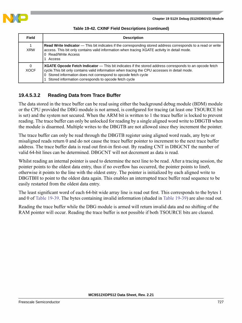
Chapter 19 S12X Debug (S12XDBGV2) Module
MC9S12XDP512 Data Sheet, Rev. 2.21
Freescale Semiconductor 727
19.4.5.3.2 Reading Data from Trace Buffer
The data stored in the trace buffer can be read using either the background debug module (BDM) moduleor the CPU provided the DBG module is not armed, is configured for tracing (at least one TSOURCE bitis set) and the system not secured. When the ARM bit is written to 1 the trace buffer is locked to preventreading. The trace buffer can only be unlocked for reading by a single aligned word write to DBGTB whenthe module is disarmed. Multiple writes to the DBGTB are not allowed since they increment the pointer.
The trace buffer can only be read through the DBGTB register using aligned word reads, any byte ormisaligned reads return 0 and do not cause the trace buffer pointer to increment to the next trace bufferaddress. The trace buffer data is read out first-in first-out. By reading CNT in DBGCNT the number ofvalid 64-bit lines can be determined. DBGCNT will not decrement as data is read.
Whilst reading an internal pointer is used to determine the next line to be read. After a tracing session, thepointer points to the oldest data entry, thus if no overflow has occurred, the pointer points to line0,otherwise it points to the line with the oldest entry. The pointer is initialized by each aligned write toDBGTBH to point to the oldest data again. This enables an interrupted trace buffer read sequence to beeasily restarted from the oldest data entry.
The least significant word of each 64-bit wide array line is read out first. This corresponds to the bytes 1and 0 of Table 19-39. The bytes containing invalid information (shaded in Table 19-39) are also read out.
Reading the trace buffer while the DBG module is armed will return invalid data and no shifting of theRAM pointer will occur. Reading the trace buffer is not possible if both TSOURCE bits are cleared.
1XRW
Read Write Indicator — This bit indicates if the corresponding stored address corresponds to a read or writeaccess. This bit only contains valid information when tracing XGATE activity in detail mode.0 Read/Write Access1 Access
0XOCF
XGATE Opcode Fetch Indicator — This bit indicates if the stored address corresponds to an opcode fetchcycle.This bit only contains valid information when tracing the CPU accesses in detail mode.0 Stored information does not correspond to opcode fetch cycle1 Stored information corresponds to opcode fetch cycle
Table 19-42. CXINF Field Descriptions (continued)
Field Description
Chapter 19 S12X Debug (S12XDBGV2) Module
MC9S12XDP512 Data Sheet, Rev. 2.21
728 Freescale Semiconductor
19.4.5.3.3 Trace Buffer Reset State
The trace buffer contents are not initialized by a system reset. Thus should a system reset occur, the tracesession information from immediately before the reset occurred can be read out. The DBGCNT bits arenot cleared by a system reset. Thus should a reset occur, the number of valid lines in the trace buffer isindicated by DBGCNT. The internal pointer to the current trace buffer address is initialized by unlockingthe trace buffer thus points to the oldest valid data even if a reset occurred during the tracing session.Generally debugging occurrences of system resets is best handled using mid or end-trigger alignment sincethe reset may occur before the trace trigger, which in the begin-trigger alignment case means noinformation would be stored in the trace buffer.
19.4.6 Tagging
A tag follows program information as it advances through the instruction queue. When a tagged instructionreaches the head of the queue a tag hit occurs and triggers the state sequencer.
Each comparator control register features a TAG bit, which controls whether the comparator match willcause a trigger immediately or tag the opcode at the matched address. If a comparator is enabled for taggedcomparisons, the address stored in the comparator match address registers must be an opcode address forthe trigger to occur.
Both CPU and XGATE opcodes can be tagged with the comparator register TAG bits.
Using a begin-aligned trigger together with tagging, if the tagged instruction is about to be executed thenthe transition to the next state sequencer state occurs. If the transition is to the final state, tracing is started.Only upon completion of the tracing session can a breakpoint be generated. Similarly using a mid-alignedtrigger with tagging, if the tagged instruction is about to be executed then the trace is continued for another32 lines. Upon tracing completion the breakpoint is generated. Using an end-aligned trigger, when thetagged instruction is about to be executed and the next transition is to final state then a breakpoint isgenerated immediately, before the tagged instruction is carried out.
R/W monitoring is not useful for tagged operations since the trigger occurs based on the tagged opcodereaching the execution stage of the instruction queue. Similarly access size (SZ) monitoring and data busmonitoring is not useful if tagged triggering is selected, since the tag is attached to the opcode at thematched address and is not dependent on the data bus nor on the size of access. Thus these bits are ignoredif tagged triggering is selected.
When configured for range comparisons and tagging, the ranges are accurate only to word boundaries.
CPU tagging is disabled when the BDM becomes active. Conversely, BDM firmware commands are notprocessed while tagging is active. XGATE tagging is possible when the BDM is active.
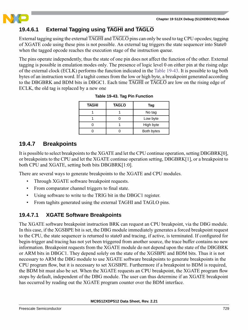
Chapter 19 S12X Debug (S12XDBGV2) Module
MC9S12XDP512 Data Sheet, Rev. 2.21
Freescale Semiconductor 729
19.4.6.1 External Tagging using TAGHI and TAGLO
External tagging using the external TAGHI and TAGLO pins can only be used to tag CPU opcodes; taggingof XGATE code using these pins is not possible. An external tag triggers the state sequencer into State0when the tagged opcode reaches the execution stage of the instruction queue.
The pins operate independently, thus the state of one pin does not affect the function of the other. Externaltagging is possible in emulation modes only. The presence of logic level 0 on either pin at the rising edgeof the external clock (ECLK) performs the function indicated in the Table 19-43. It is possible to tag bothbytes of an instruction word. If a taghit comes from the low or high byte, a breakpoint generated accordingto the DBGBRK and BDM bits in DBGC1. Each time TAGHI or TAGLO are low on the rising edge ofECLK, the old tag is replaced by a new one
19.4.7 Breakpoints
It is possible to select breakpoints to the XGATE and let the CPU continue operation, setting DBGBRK[0],or breakpoints to the CPU and let the XGATE continue operation setting, DBGBRK[1], or a breakpoint toboth CPU and XGATE, setting both bits DBGBRK[1:0].
There are several ways to generate breakpoints to the XGATE and CPU modules.
• Through XGATE software breakpoint requests.
• From comparator channel triggers to final state.
• Using software to write to the TRIG bit in the DBGC1 register.
• From taghits generated using the external TAGHI and TAGLO pins.
19.4.7.1 XGATE Software Breakpoints
The XGATE software breakpoint instruction BRK can request an CPU breakpoint, via the DBG module.In this case, if the XGSBPE bit is set, the DBG module immediately generates a forced breakpoint requestto the CPU, the state sequencer is returned to state0 and tracing, if active, is terminated. If configured forbegin-trigger and tracing has not yet been triggered from another source, the trace buffer contains no newinformation. Breakpoint requests from the XGATE module do not depend upon the state of the DBGBRKor ARM bits in DBGC1. They depend solely on the state of the XGSBPE and BDM bits. Thus it is notnecessary to ARM the DBG module to use XGATE software breakpoints to generate breakpoints in theCPU program flow, but it is necessary to set XGSBPE. Furthermore if a breakpoint to BDM is required,the BDM bit must also be set. When the XGATE requests an CPU breakpoint, the XGATE program flowstops by default, independent of the DBG module. The user can thus determine if an XGATE breakpointhas occurred by reading out the XGATE program counter over the BDM interface.
Table 19-43. Tag Pin Function
TAGHI TAGLO Tag
1 1 No tag
1 0 Low byte
0 1 High byte
0 0 Both bytes

Chapter 19 S12X Debug (S12XDBGV2) Module
MC9S12XDP512 Data Sheet, Rev. 2.21
730 Freescale Semiconductor
19.4.7.2 Breakpoints From Internal Comparator Channel Final State Triggers
Breakpoints can be generated when internal comparator channels trigger the state sequencer to the finalstate. If configured for tagging, then the breakpoint is generated when the tagged opcode reaches theexecution stage of the instruction queue. If an end aligned trigger is selected or no tracing is enabled,breakpoints can be generated immediately, depending on the state of the DBGBRK[n] bits.
If a begin or mid aligned tracing session is selected by the TSOURCE bits, breakpoints are requested whenthe tracing session has completed, thus the breakpoint is requested only on completion of the subsequenttrace (see Table 19-44). If the BRK bit is set on the triggering channel, then the breakpoint is generatedimmediately independent of tracing trigger alignment.
19.4.7.3 Breakpoints Generated Via The TRIG Bit
If a TRIG triggers occur, the final state is entered. Tracing trigger alignment is defined by the TALIGNbits. If a tracing session is selected by the TSOURCE bits, breakpoints are requested when the tracingsession has completed, thus if begin or mid aligned triggering is selected, the breakpoint is requested onlyon completion of the subsequent trace. If no tracing session is selected, breakpoints are requestedimmediately. TRIG breakpoints are possible even if the DBG module is disarmed. TRIG bit breakpointsare enabled by setting DBGBRK[n].
19.4.7.4 Breakpoints via TAGHI Or TAGLO Pin Taghits
Tagging using the external TAGHI/TAGLO pins always ends the session immediately at the tag hit. It isalways end aligned, independent of internal channel trigger alignment configuration. External tagbreakpoints are always mapped to the CPU, are only possible in emulation modes and can be enabled bysetting DBGBRK[1].
Table 19-44. Setup for Both XGATE and CPU Breakpoints
BRK TALIGN DBGBRK[n] Type of Debug Session
0 00 0 Fill trace buffer until trigger(no breakpoints — keep running)
0 00 1 Fill trace buffer until trigger, then a breakpoint request occurs
0 01 0 Start trace buffer at trigger(no breakpoints — keep running)
0 01 1 Start trace buffer at triggerA breakpoint request occurs when trace buffer is full
0 10 0 Start trace buffer at triggerEnd tracing 32 line entries after trigger
(no breakpoints — keep running)
0 10 1 Start trace buffer at triggerEnd tracing 32 line entries after trigger
Request breakpoint after the 32 further trace buffer entries
1 00,01,10 0 Terminate tracing immediately on trigger without breakpoint
1 00,01,10 1 Terminate tracing and generate breakpoint immediately on trigger
x 11 x Reserved
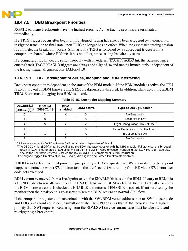
Chapter 19 S12X Debug (S12XDBGV2) Module
MC9S12XDP512 Data Sheet, Rev. 2.21
Freescale Semiconductor 731
19.4.7.5 DBG Breakpoint Priorities
XGATE software breakpoints have the highest priority. Active tracing sessions are terminatedimmediately.
If a TRIG triggers occur after begin or mid aligned tracing has already been triggered by a comparatorinstigated transition to final state, then TRIG no longer has an effect. When the associated tracing sessionis complete, the breakpoint occurs. Similarly if a TRIG is followed by a subsequent trigger from acomparator channel whose BRK=0, it has no effect, since tracing has already started.
If a comparator tag hit occurs simultaneously with an external TAGHI/TAGLO hit, the state sequencerenters State0. TAGHI/TAGLO triggers are always end aligned, to end tracing immediately, independent ofthe tracing trigger alignment bits TALIGN[1:0].
19.4.7.5.1 DBG Breakpoint priorities, mapping and BDM interfacing
Breakpoint operation is dependent on the state of the BDM module. If the BDM module is active, the CPUis executing out of BDM firmware and S12X breakpoints are disabled. In addition, while executing a BDMTRACE command, tagging into BDM is disabled.
If BDM is not active, the breakpoint will give priority to BDM requests over SWI requests if the breakpointhappens to coincide with a SWI instruction in the user’s code. On returning from BDM, the SWI from usercode gets executed.
BDM cannot be entered from a breakpoint unless the ENABLE bit is set in the BDM. If entry to BDM viaa BGND instruction is attempted and the ENABLE bit in the BDM is cleared, the CPU actually executesthe BDM firmware code. It checks the ENABLE and returns if ENABLE is not set. If not serviced by themonitor then the breakpoint is re-asserted when the BDM returns to normal CPU flow.
If the comparator register contents coincide with the SWI/BDM vector address then an SWI in user codeand DBG breakpoint could occur simultaneously. The CPU ensures that BDM requests have a higherpriority than SWI requests. Returning from the BDM/SWI service routine care must be taken to avoidre-triggering a breakpoint.
Table 19-45. Breakpoint Mapping Summary
DBGBRK[1]
(DBGC1[3])1
1 All sources except XGATE software BKP, which are independent of this bit.
BDM bit(DBGC1[4])
BDMenabled BDM active Type of Debug Session
0 X X X No Breakpoint
1 0 0 0 Breakpoint to SWI
1 0 1 X Illegal Configuration. Do Not Use.2
2The DBGC1[4] bit (BDM) must be set if using the BDM interface together with the DBG module. Failure to set this bit couldresult in XGATE generated breakpoints to SWI during BDM firmware execution corrupting the S12X PC return address,should the user have entered BDM via the BACKGROUND command or BGND instruction.
1 1 0 0 Illegal Configuration. Do Not Use. 3
3End aligned tagged Breakpoint to SWI. Begin, Mid aligned and Forced Breakpoints disabled
1 1 1 0 Breakpoint to BDM
1 1 1 1 No Breakpoint

Chapter 19 S12X Debug (S12XDBGV2) Module
MC9S12XDP512 Data Sheet, Rev. 2.21
732 Freescale Semiconductor
When program control returns from a tagged breakpoint using an RTI or BDM GO command withoutprogram counter modification it will return to the instruction whose tag generated the breakpoint. Thuscare must be taken to avoid re triggering a breakpoint at the same location. This can be done byreconfiguring the DBG module in the SWI routine, (SWI configuration), or by executing a TRACEcommand before the GO (BDM configuration) to increment the program flow past the tagged instruction.
Comparators should not be configured for the vector address range while tagging, since these addressesare not opcode addresses

Chapter 19 S12X Debug (S12XDBGV2) Module
MC9S12XDP512 Data Sheet, Rev. 2.21
Freescale Semiconductor 733

Chapter 19 S12X Debug (S12XDBGV2) Module
MC9S12XDP512 Data Sheet, Rev. 2.21
734 Freescale Semiconductor

Chapter 19 S12X Debug (S12XDBGV2) Module
MC9S12XDP512 Data Sheet, Rev. 2.21
Freescale Semiconductor 735

Chapter 19 S12X Debug (S12XDBGV2) Module
MC9S12XDP512 Data Sheet, Rev. 2.21
736 Freescale Semiconductor

Chapter 19 S12X Debug (S12XDBGV2) Module
MC9S12XDP512 Data Sheet, Rev. 2.21
Freescale Semiconductor 737

Chapter 19 S12X Debug (S12XDBGV2) Module
MC9S12XDP512 Data Sheet, Rev. 2.21
738 Freescale Semiconductor

Chapter 19 S12X Debug (S12XDBGV2) Module
MC9S12XDP512 Data Sheet, Rev. 2.21
Freescale Semiconductor 739

Chapter 19 S12X Debug (S12XDBGV2) Module
MC9S12XDP512 Data Sheet, Rev. 2.21
740 Freescale Semiconductor

Chapter 19 S12X Debug (S12XDBGV2) Module
MC9S12XDP512 Data Sheet, Rev. 2.21
Freescale Semiconductor 741

Chapter 19 S12X Debug (S12XDBGV2) Module
MC9S12XDP512 Data Sheet, Rev. 2.21
742 Freescale Semiconductor

Chapter 19 S12X Debug (S12XDBGV2) Module
MC9S12XDP512 Data Sheet, Rev. 2.21
Freescale Semiconductor 743

Chapter 19 S12X Debug (S12XDBGV2) Module
MC9S12XDP512 Data Sheet, Rev. 2.21
744 Freescale Semiconductor

MC9S12XDP512 Data Sheet, Rev. 2.21
Freescale Semiconductor 745
Chapter 20S12X Debug (S12XDBGV3) Module
20.1 IntroductionThe S12XDBG module provides an on-chip trace buffer with flexible triggering capability to allownon-intrusive debug of application software. The S12XDBG module is optimized for the HCS12X 16-bitarchitecture and allows debugging of both S12XCPU and XGATE module operations.
Typically the S12XDBG module is used in conjunction with the S12XBDM module, whereby the userconfigures the S12XDBG module for a debugging session over the BDM interface. Once configured theS12XDBG module is armed and the device leaves BDM Mode returning control to the user program,which is then monitored by the S12XDBG module. Alternatively the S12XDBG module can be configuredover a serial interface using SWI routines.
20.1.1 Glossary Of Terms
COF: Change Of Flow. Change in the program flow due to a conditional branch, indexed jump or interrupt.
BDM : Background Debug Mode
DUG: Device User Guide, describing the features of the device into which the DBG is integrated.
WORD: 16 bit data entity
Data Line : 64 bit data entity
XGATE : S12X family programmable Direct Memory Access Module
CPU : S12X_CPU module
Tag : Tags can be attached to XGATE or CPU opcodes as they enter the instruction pipe. If the taggedopcode reaches the execution stage a tag hit occurs.
20.1.2 Overview
The comparators monitor the bus activity of the S12XCPU and XGATE modules. When a match occursthe control logic can trigger the state sequencer to a new state. On a transition to the Final State, bus tracingis triggered and/or a breakpoint can be generated.
Independent of comparator matches a transition to Final State with associated tracing and breakpoint canbe triggered by the external TAGHI and TAGLO signals, by an XGATE module S/W breakpoint requestor an immediate trigger, instigated by writing to the TRIG control bit.

Chapter 20 S12X Debug (S12XDBGV3) Module
MC9S12XDP512 Data Sheet, Rev. 2.21
746 Freescale Semiconductor
The trace buffer is visible through a 2-byte window in the register address map and can be read out usingstandard 16-bit word reads. Tracing is disabled when the MCU system is secured.
20.1.3 Features• Four comparators (A, B, C, and D)
— Comparators A and C compare the full address bus and full 16-bit data bus— Comparators A and C feature a data bus mask register— Comparators B and D compare the full address bus only— Each comparator can be configured to monitor either S12XCPU or XGATE buses— Each comparator features control of R/W and byte/word access cycles— Comparisons can be used as triggers for the state sequencer
• Three comparator modes— Simple address/data comparator match mode— Inside address range mode, Addmin ≤ Address ≤ Addmax— Outside address range match mode, Address < Addmin or Address > Addmax
• Two types of triggers— Tagged — This triggers just before a specific instruction begins execution— Force — This triggers on the first instruction boundary after a match occurs.
• Three types of breakpoints— S12XCPU breakpoint entering BDM on breakpoint (BDM)— S12XCPU breakpoint executing SWI on breakpoint (SWI)— XGATE breakpoint
• Three trigger modes independent of comparators— External instruction tagging (associated with S12XCPU instructions only)— XGATE S/W breakpoint request— TRIG Immediate software trigger
• Four trace modes— Normal: change of flow (COF) PC information is stored (see Section 20.4.5.2.1) for change of
flow definition.— Loop1: same as Normal but inhibits consecutive duplicate source address entries— Detail: address and data for all cycles except free cycles and opcode fetches are stored— Pure PC: All program counter addresses are stored.
• 4-stage state sequencer for trace buffer control— Tracing session trigger linked to Final State of state sequencer— Begin, End, and Mid alignment of tracing to trigger
20.1.4 Modes of Operation
The S12XDBG module can be used in all MCU functional modes.

Chapter 20 S12X Debug (S12XDBGV3) Module
MC9S12XDP512 Data Sheet, Rev. 2.21
Freescale Semiconductor 747
During BDM hardware accesses and whilst the BDM module is active, S12XCPU monitoring is disabled.Thus breakpoints, comparators, and bus tracing mapped to the S12XCPU are disabled but XGATE busmonitoring accessing the S12XDBG registers, including comparator registers, is still possible. While inactive BDM or during hardware BDM accesses, XGATE activity can still be compared, traced and can beused to generate a breakpoint to the XGATE module. When the S12XCPU enters active BDM Modethrough a BACKGROUND command, with the S12XDBG module armed, the S12XDBG remains armed.
The S12XDBG module tracing is disabled if the MCU is secure. However, breakpoints can still begenerated if the MCU is secure.
20.1.5 Block Diagram
Figure 20-1. Debug Module Block Diagram
20.2 External Signal DescriptionThe S12XDBG sub-module features two external tag input signals. See Device User Guide (DUG) for themapping of these signals to device pins. These tag pins may be used for the external tagging in emulationmodes only.
Table 20-1. Mode Dependent Restriction Summary
BDMEnable
BDMActive
MCUSecure
ComparatorMatches Enabled
BreakpointsPossible
TaggingPossible
TracingPossible
x x 1 Yes Yes Yes No
0 0 0 Yes Only SWI Yes Yes
0 1 0 Active BDM not possible when not enabled
1 0 0 Yes Yes Yes Yes
1 1 0 XGATE only XGATE only XGATE only XGATE only
S12XCPU BUS
TRACE BUFFER
BU
S IN
TE
RFA
CE
TRIGGER
EXTERNAL TAGHI / TAGLO
MATCH0
STATE
XGATE BUS
COMPARATOR B
COMPARATOR C
COMPARATOR D
COMPARATOR A
STATE SEQUENCERMATCH1
MATCH2
MATCH3
TRACE
READ TRACE DATA (DBG READ DATA BUS)
CONTROL
SECURE
BREAKPOINT REQUESTS
CO
MPA
RAT
OR
MAT
CH
CO
NT
RO
L
XGATE S/W BREAKPOINT REQUEST
TRIGGER
TAG &TRIGGERCONTROL
LOGIC
TAGSTAGHITS
STATE
S12XCPU & XGATE
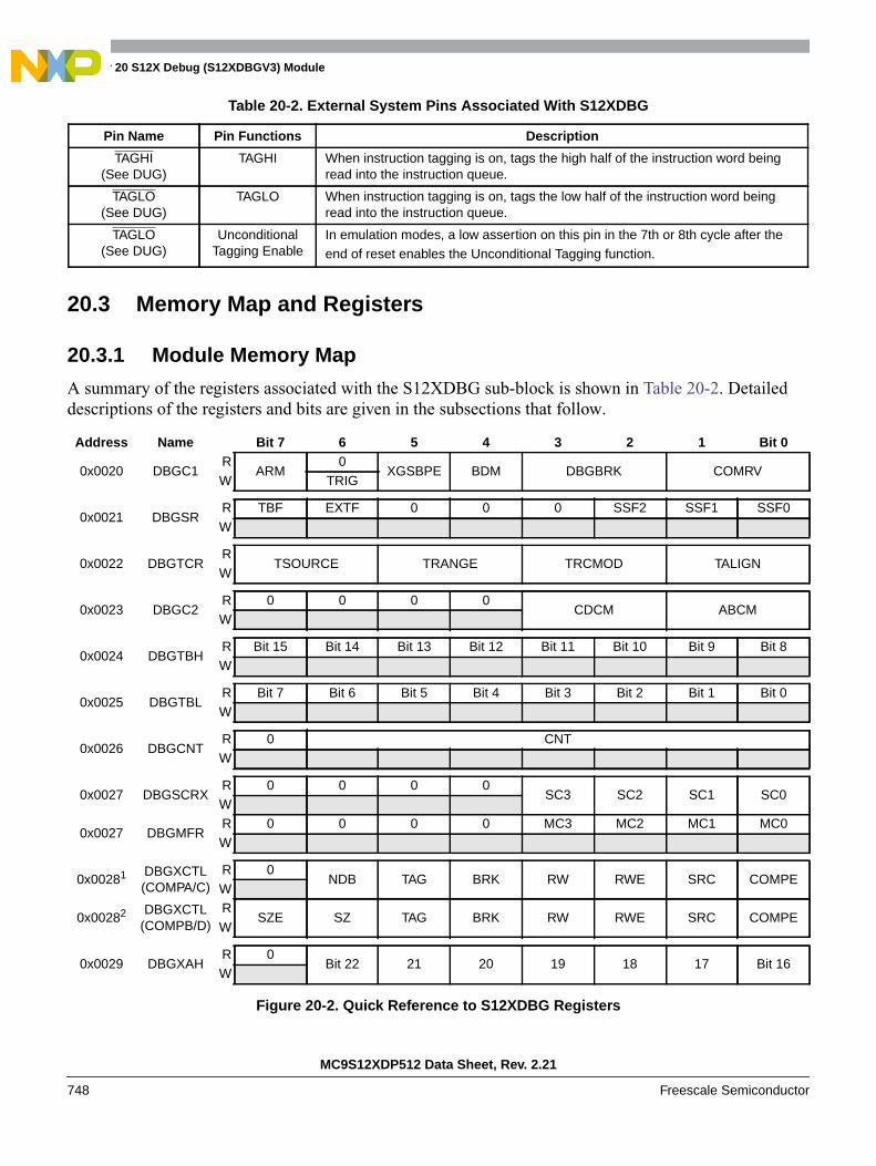
Chapter 20 S12X Debug (S12XDBGV3) Module
MC9S12XDP512 Data Sheet, Rev. 2.21
748 Freescale Semiconductor
20.3 Memory Map and Registers
20.3.1 Module Memory Map
A summary of the registers associated with the S12XDBG sub-block is shown in Table 20-2. Detaileddescriptions of the registers and bits are given in the subsections that follow.
Table 20-2. External System Pins Associated With S12XDBG
Pin Name Pin Functions Description
TAGHI(See DUG)
TAGHI When instruction tagging is on, tags the high half of the instruction word beingread into the instruction queue.
TAGLO(See DUG)
TAGLO When instruction tagging is on, tags the low half of the instruction word beingread into the instruction queue.
TAGLO(See DUG)
UnconditionalTagging Enable
In emulation modes, a low assertion on this pin in the 7th or 8th cycle after theend of reset enables the Unconditional Tagging function.
Address Name Bit 7 6 5 4 3 2 1 Bit 0
0x0020 DBGC1R
ARM0
XGSBPE BDM DBGBRK COMRVW TRIG
0x0021 DBGSRR TBF EXTF 0 0 0 SSF2 SSF1 SSF0W
0x0022 DBGTCRR
TSOURCE TRANGE TRCMOD TALIGNW
0x0023 DBGC2R 0 0 0 0
CDCM ABCMW
0x0024 DBGTBHR Bit 15 Bit 14 Bit 13 Bit 12 Bit 11 Bit 10 Bit 9 Bit 8W
0x0025 DBGTBLR Bit 7 Bit 6 Bit 5 Bit 4 Bit 3 Bit 2 Bit 1 Bit 0W
0x0026 DBGCNTR 0 CNTW
0x0027 DBGSCRXR 0 0 0 0
SC3 SC2 SC1 SC0W
0x0027 DBGMFRR 0 0 0 0 MC3 MC2 MC1 MC0W
0x00281 DBGXCTL(COMPA/C)
R 0NDB TAG BRK RW RWE SRC COMPE
W
0x00282 DBGXCTL(COMPB/D)
RSZE SZ TAG BRK RW RWE SRC COMPE
W
0x0029 DBGXAHR 0
Bit 22 21 20 19 18 17 Bit 16W
Figure 20-2. Quick Reference to S12XDBG Registers
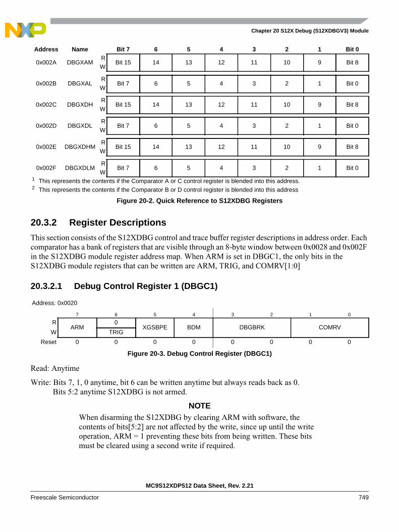
Chapter 20 S12X Debug (S12XDBGV3) Module
MC9S12XDP512 Data Sheet, Rev. 2.21
Freescale Semiconductor 749
20.3.2 Register Descriptions
This section consists of the S12XDBG control and trace buffer register descriptions in address order. Eachcomparator has a bank of registers that are visible through an 8-byte window between 0x0028 and 0x002Fin the S12XDBG module register address map. When ARM is set in DBGC1, the only bits in theS12XDBG module registers that can be written are ARM, TRIG, and COMRV[1:0]
20.3.2.1 Debug Control Register 1 (DBGC1)
Read: Anytime
Write: Bits 7, 1, 0 anytime, bit 6 can be written anytime but always reads back as 0.Bits 5:2 anytime S12XDBG is not armed.
NOTEWhen disarming the S12XDBG by clearing ARM with software, thecontents of bits[5:2] are not affected by the write, since up until the writeoperation, ARM = 1 preventing these bits from being written. These bitsmust be cleared using a second write if required.
0x002A DBGXAMR
Bit 15 14 13 12 11 10 9 Bit 8W
0x002B DBGXALR
Bit 7 6 5 4 3 2 1 Bit 0W
0x002C DBGXDHR
Bit 15 14 13 12 11 10 9 Bit 8W
0x002D DBGXDLR
Bit 7 6 5 4 3 2 1 Bit 0W
0x002E DBGXDHMR
Bit 15 14 13 12 11 10 9 Bit 8W
0x002F DBGXDLMR
Bit 7 6 5 4 3 2 1 Bit 0W
1 This represents the contents if the Comparator A or C control register is blended into this address.2 This represents the contents if the Comparator B or D control register is blended into this address
Address: 0x0020
7 6 5 4 3 2 1 0
RARM
0XGSBPE BDM DBGBRK COMRV
W TRIG
Reset 0 0 0 0 0 0 0 0
Figure 20-3. Debug Control Register (DBGC1)
Address Name Bit 7 6 5 4 3 2 1 Bit 0
Figure 20-2. Quick Reference to S12XDBG Registers

Chapter 20 S12X Debug (S12XDBGV3) Module
MC9S12XDP512 Data Sheet, Rev. 2.21
750 Freescale Semiconductor
Table 20-3. DBGC1 Field Descriptions
Field Description
7ARM
Arm Bit — The ARM bit controls whether the S12XDBG module is armed. This bit can be set and cleared byuser software and is automatically cleared on completion of a tracing session, or if a breakpoint is generated withtracing not enabled. On setting this bit the state sequencer enters State1. When ARM is set, the only bits in theS12XDBG module registers that can be written are ARM and TRIG.0 Debugger disarmed1 Debugger armed
6TRIG
Immediate Trigger Request Bit — This bit when written to 1 requests an immediate trigger independent ofcomparator or external tag signal status. When tracing is complete a forced breakpoint may be generateddepending upon DBGBRK and BDM bit settings. This bit always reads back a 0. Writing a 0 to this bit has noeffect. If both TSOURCE bits are clear no tracing is carried out. If tracing has already commenced using BEGIN-or MID trigger alignment, it continues until the end of the tracing session as defined by the TALIGN bit settings,thus TRIG has no affect. In secure mode tracing is disabled and writing to this bit has no effect.0 Do not trigger until the state sequencer enters the Final State.1 Enter Final State immediately and issue forced breakpoint request when trace buffer is full.
5XGSBPE
XGATE S/W Breakpoint Enable — The XGSBPE bit controls whether an XGATE S/W breakpoint request ispassed to the S12XCPU. The XGATE S/W breakpoint request is handled by the S12XDBG module, which canrequest an S12XCPU breakpoint depending on the state of this bit.0 XGATE S/W breakpoint request is disabled1 XGATE S/W breakpoint request is enabled
4BDM
Background Debug Mode Enable — This bit determines if a S12X breakpoint causes the system to enterBackground Debug Mode (BDM) or initiate a Software Interrupt (SWI). It has no affect on S12XDBG functionality.If this bit is set but the BDM is not enabled by the ENBDM bit in the BDM module, then breakpoints default to SWI.0 Breakpoint to Software Interrupt if BDM inactive. Otherwise no breakpoint.1 Breakpoint to BDM, if BDM enabled. Otherwise breakpoint to SWI
3–2DBGBRK
S12XDBG Breakpoint Enable Bits — The DBGBRK bits control whether the debugger will request a breakpointto either S12XCPU or XGATE or both upon reaching the state sequencer Final State. If tracing is enabled, thebreakpoint is generated on completion of the tracing session. If tracing is not enabled, the breakpoint isgenerated immediately. Please refer to Section 20.4.7 for further details. XGATE software breakpoints areindependent of the DBGBRK bits. XGATE software breakpoints force a breakpoint to the S12XCPU independentof the DBGBRK bit field configuration. See Table 20-4.
1–0COMRV
Comparator Register Visibility Bits — These bits determine which bank of comparator register is visible in the8-byte window of the S12XDBG module address map, located between 0x0028 to 0x002F. Furthermore thesebits determine which register is visible at the address 0x0027. See Table 20-5.
Table 20-4. DBGBRK Encoding
DBGBRK Resource Halted by Breakpoint
00 No breakpoint generated
01 XGATE breakpoint generated
10 S12XCPU breakpoint generated
11 Breakpoints generated for S12XCPU and XGATE
Table 20-5. COMRV Encoding
COMRV Visible Comparator Visible Register at 0x0027
00 Comparator A DBGSCR1
01 Comparator B DBGSCR2

Chapter 20 S12X Debug (S12XDBGV3) Module
MC9S12XDP512 Data Sheet, Rev. 2.21
Freescale Semiconductor 751
10 Comparator C DBGSCR3
11 Comparator D DBGMFR
Table 20-5. COMRV Encoding
COMRV Visible Comparator Visible Register at 0x0027
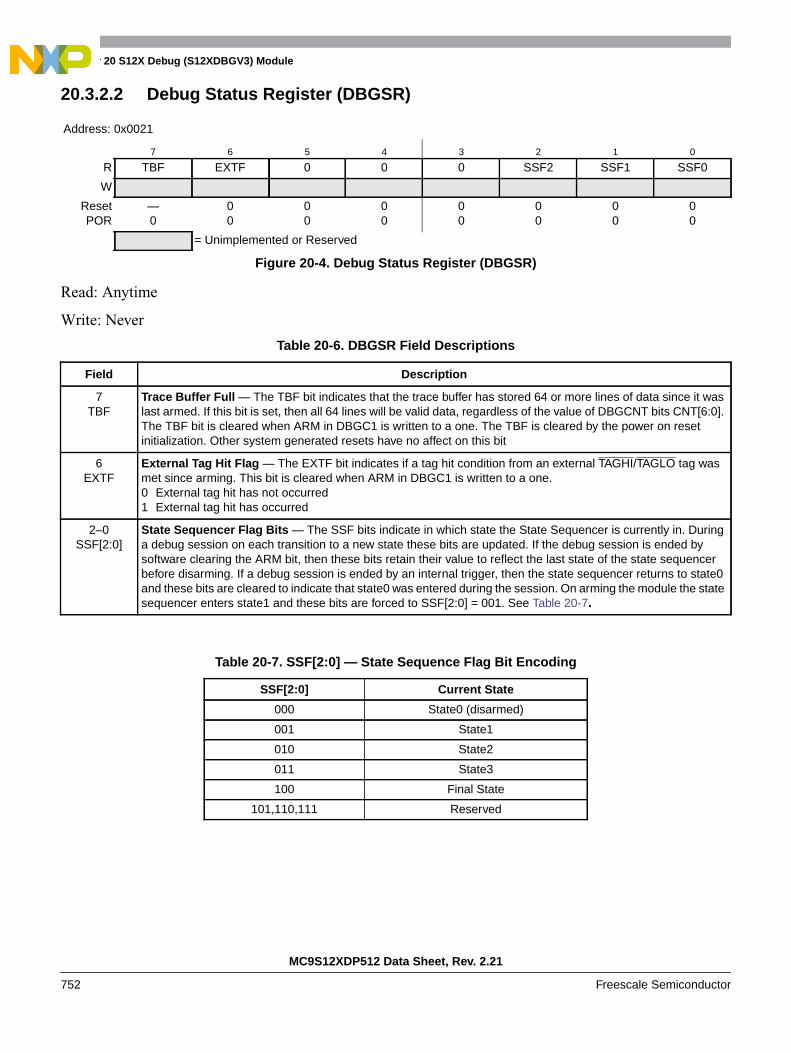
Chapter 20 S12X Debug (S12XDBGV3) Module
MC9S12XDP512 Data Sheet, Rev. 2.21
752 Freescale Semiconductor
20.3.2.2 Debug Status Register (DBGSR)
Read: Anytime
Write: Never
Address: 0x0021
7 6 5 4 3 2 1 0
R TBF EXTF 0 0 0 SSF2 SSF1 SSF0
W
ResetPOR
—0
00
00
00
00
00
00
00
= Unimplemented or Reserved
Figure 20-4. Debug Status Register (DBGSR)
Table 20-6. DBGSR Field Descriptions
Field Description
7TBF
Trace Buffer Full — The TBF bit indicates that the trace buffer has stored 64 or more lines of data since it waslast armed. If this bit is set, then all 64 lines will be valid data, regardless of the value of DBGCNT bits CNT[6:0].The TBF bit is cleared when ARM in DBGC1 is written to a one. The TBF is cleared by the power on resetinitialization. Other system generated resets have no affect on this bit
6EXTF
External Tag Hit Flag — The EXTF bit indicates if a tag hit condition from an external TAGHI/TAGLO tag wasmet since arming. This bit is cleared when ARM in DBGC1 is written to a one.0 External tag hit has not occurred1 External tag hit has occurred
2–0SSF[2:0]
State Sequencer Flag Bits — The SSF bits indicate in which state the State Sequencer is currently in. Duringa debug session on each transition to a new state these bits are updated. If the debug session is ended bysoftware clearing the ARM bit, then these bits retain their value to reflect the last state of the state sequencerbefore disarming. If a debug session is ended by an internal trigger, then the state sequencer returns to state0and these bits are cleared to indicate that state0 was entered during the session. On arming the module the statesequencer enters state1 and these bits are forced to SSF[2:0] = 001. See Table 20-7.
Table 20-7. SSF[2:0] — State Sequence Flag Bit Encoding
SSF[2:0] Current State
000 State0 (disarmed)
001 State1
010 State2
011 State3
100 Final State
101,110,111 Reserved
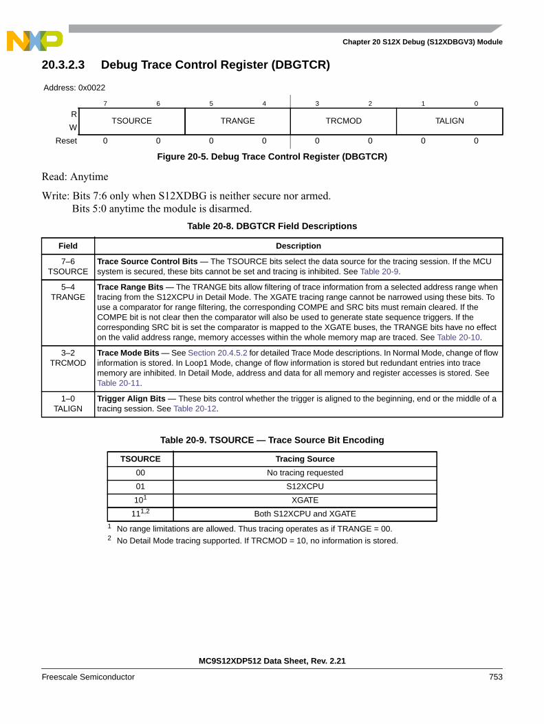
Chapter 20 S12X Debug (S12XDBGV3) Module
MC9S12XDP512 Data Sheet, Rev. 2.21
Freescale Semiconductor 753
20.3.2.3 Debug Trace Control Register (DBGTCR)
Read: Anytime
Write: Bits 7:6 only when S12XDBG is neither secure nor armed.Bits 5:0 anytime the module is disarmed.
Address: 0x0022
7 6 5 4 3 2 1 0
RTSOURCE TRANGE TRCMOD TALIGN
W
Reset 0 0 0 0 0 0 0 0
Figure 20-5. Debug Trace Control Register (DBGTCR)
Table 20-8. DBGTCR Field Descriptions
Field Description
7–6TSOURCE
Trace Source Control Bits — The TSOURCE bits select the data source for the tracing session. If the MCUsystem is secured, these bits cannot be set and tracing is inhibited. See Table 20-9.
5–4TRANGE
Trace Range Bits — The TRANGE bits allow filtering of trace information from a selected address range whentracing from the S12XCPU in Detail Mode. The XGATE tracing range cannot be narrowed using these bits. Touse a comparator for range filtering, the corresponding COMPE and SRC bits must remain cleared. If theCOMPE bit is not clear then the comparator will also be used to generate state sequence triggers. If thecorresponding SRC bit is set the comparator is mapped to the XGATE buses, the TRANGE bits have no effecton the valid address range, memory accesses within the whole memory map are traced. See Table 20-10.
3–2TRCMOD
Trace Mode Bits — See Section 20.4.5.2 for detailed Trace Mode descriptions. In Normal Mode, change of flowinformation is stored. In Loop1 Mode, change of flow information is stored but redundant entries into tracememory are inhibited. In Detail Mode, address and data for all memory and register accesses is stored. SeeTable 20-11.
1–0TALIGN
Trigger Align Bits — These bits control whether the trigger is aligned to the beginning, end or the middle of atracing session. See Table 20-12.
Table 20-9. TSOURCE — Trace Source Bit Encoding
TSOURCE Tracing Source
00 No tracing requested
01 S12XCPU
101
1 No range limitations are allowed. Thus tracing operates as if TRANGE = 00.
XGATE
111,2
2 No Detail Mode tracing supported. If TRCMOD = 10, no information is stored.
Both S12XCPU and XGATE
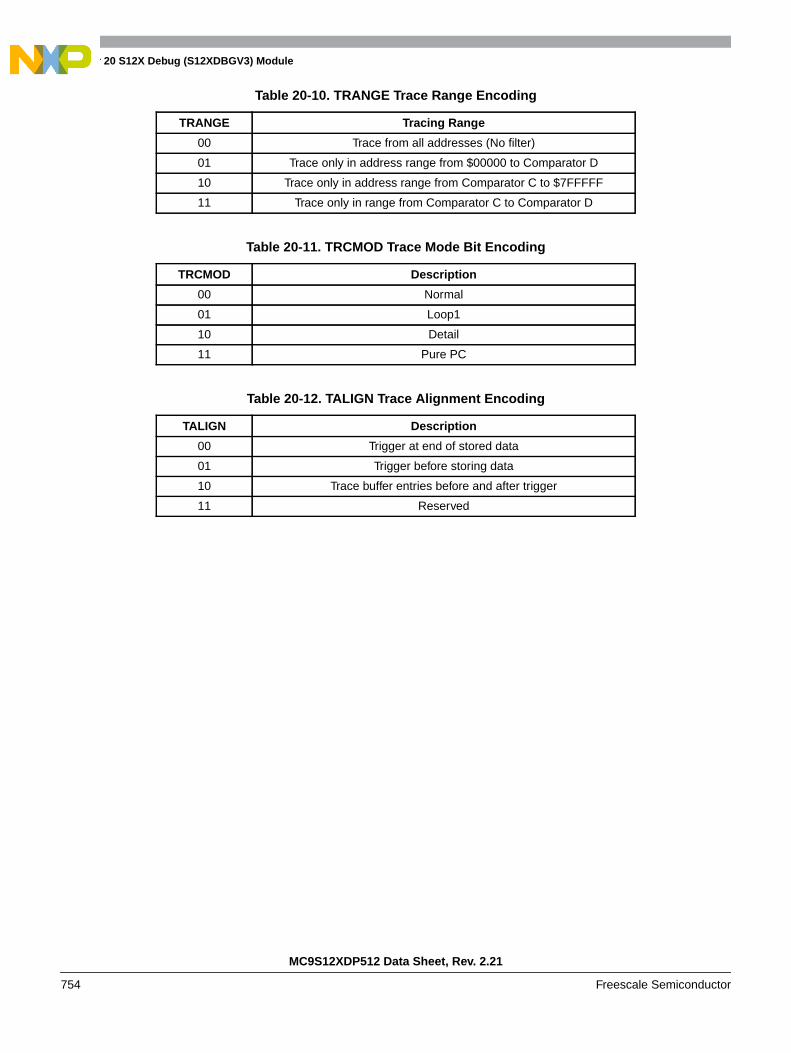
Chapter 20 S12X Debug (S12XDBGV3) Module
MC9S12XDP512 Data Sheet, Rev. 2.21
754 Freescale Semiconductor
Table 20-10. TRANGE Trace Range Encoding
TRANGE Tracing Range
00 Trace from all addresses (No filter)
01 Trace only in address range from $00000 to Comparator D
10 Trace only in address range from Comparator C to $7FFFFF
11 Trace only in range from Comparator C to Comparator D
Table 20-11. TRCMOD Trace Mode Bit Encoding
TRCMOD Description
00 Normal
01 Loop1
10 Detail
11 Pure PC
Table 20-12. TALIGN Trace Alignment Encoding
TALIGN Description
00 Trigger at end of stored data
01 Trigger before storing data
10 Trace buffer entries before and after trigger
11 Reserved

Chapter 20 S12X Debug (S12XDBGV3) Module
MC9S12XDP512 Data Sheet, Rev. 2.21
Freescale Semiconductor 755
20.3.2.4 Debug Control Register2 (DBGC2)
Read: Anytime
Write: Anytime the module is disarmed.
This register configures the comparators for range matching.
Address: 0x0023
7 6 5 4 3 2 1 0
R 0 0 0 0CDCM ABCM
W
Reset 0 0 0 0 0 0 0 0
= Unimplemented or Reserved
Figure 20-6. Debug Control Register2 (DBGC2)
Table 20-13. DBGC2 Field Descriptions
Field Description
3–2CDCM[1:0]
C and D Comparator Match Control — These bits determine the C and D comparator match mapping asdescribed in Table 20-14.
1–0ABCM[1:0]
A and B Comparator Match Control — These bits determine the A and B comparator match mapping asdescribed in Table 20-15.
Table 20-14. CDCM Encoding
CDCM Description
00 Match2 mapped to comparator C match....... Match3 mapped to comparator D match.
01 Match2 mapped to comparator C/D inside range....... Match3 disabled.
10 Match2 mapped to comparator C/D outside range....... Match3 disabled.
11 Reserved
Table 20-15. ABCM Encoding
ABCM Description
00 Match0 mapped to comparator A match....... Match1 mapped to comparator B match.
01 Match 0 mapped to comparator A/B inside range....... Match1 disabled.
10 Match 0 mapped to comparator A/B outside range....... Match1 disabled.
11 Reserved
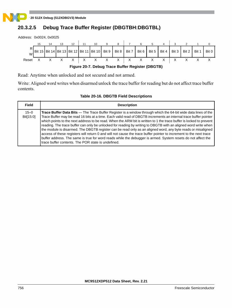
Chapter 20 S12X Debug (S12XDBGV3) Module
MC9S12XDP512 Data Sheet, Rev. 2.21
756 Freescale Semiconductor
20.3.2.5 Debug Trace Buffer Register (DBGTBH:DBGTBL)
Read: Anytime when unlocked and not secured and not armed.
Write: Aligned word writes when disarmed unlock the trace buffer for reading but do not affect trace buffercontents.
Address: 0x0024, 0x0025
15 14 13 12 11 10 9 8 7 6 5 4 3 2 1 0
RBit 15 Bit 14 Bit 13 Bit 12 Bit 11 Bit 10 Bit 9 Bit 8 Bit 7 Bit 6 Bit 5 Bit 4 Bit 3 Bit 2 Bit 1 Bit 0
W
Reset X X X X X X X X X X X X X X X X
Figure 20-7. Debug Trace Buffer Register (DBGTB)
Table 20-16. DBGTB Field Descriptions
Field Description
15–0Bit[15:0]
Trace Buffer Data Bits — The Trace Buffer Register is a window through which the 64-bit wide data lines of theTrace Buffer may be read 16 bits at a time. Each valid read of DBGTB increments an internal trace buffer pointerwhich points to the next address to be read. When the ARM bit is written to 1 the trace buffer is locked to preventreading. The trace buffer can only be unlocked for reading by writing to DBGTB with an aligned word write whenthe module is disarmed. The DBGTB register can be read only as an aligned word, any byte reads or misalignedaccess of these registers will return 0 and will not cause the trace buffer pointer to increment to the next tracebuffer address. The same is true for word reads while the debugger is armed. System resets do not affect thetrace buffer contents. The POR state is undefined.
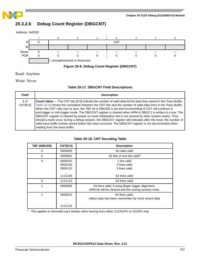
Chapter 20 S12X Debug (S12XDBGV3) Module
MC9S12XDP512 Data Sheet, Rev. 2.21
Freescale Semiconductor 757
20.3.2.6 Debug Count Register (DBGCNT)
Read: Anytime
Write: Never
Address: 0x0026
7 6 5 4 3 2 1 0
R 0 CNT
W
ResetPOR
00
—0
—0
—0
—0
—0
—0
—0
= Unimplemented or Reserved
Figure 20-8. Debug Count Register (DBGCNT)
Table 20-17. DBGCNT Field Descriptions
Field Description
6–0CNT[6:0]
Count Value — The CNT bits [6:0] indicate the number of valid data 64-bit data lines stored in the Trace Buffer.Table 20-18 shows the correlation between the CNT bits and the number of valid data lines in the Trace Buffer.When the CNT rolls over to zero, the TBF bit in DBGSR is set and incrementing of CNT will continue inend-trigger or mid-trigger mode. The DBGCNT register is cleared when ARM in DBGC1 is written to a one. TheDBGCNT register is cleared by power-on-reset initialization but is not cleared by other system resets. Thusshould a reset occur during a debug session, the DBGCNT register still indicates after the reset, the number ofvalid trace buffer entries stored before the reset occurred. The DBGCNT register is not decremented whenreading from the trace buffer.
Table 20-18. CNT Decoding Table
TBF (DBGSR) CNT[6:0] Description
0 0000000 No data valid
0 0000001 32 bits of one line valid1
1 This applies to Normal/Loop1 Modes when tracing from either S12XCPU or XGATE only.
0 000001000001000000110
..1111100
1 line valid2 lines valid3 lines valid
..62 lines valid
0 1111110 63 lines valid
1 0000000 64 lines valid; if using Begin trigger alignment,ARM bit will be cleared and the tracing session ends.
1 0000010....
1111110
64 lines valid,oldest data has been overwritten by most recent data

Chapter 20 S12X Debug (S12XDBGV3) Module
MC9S12XDP512 Data Sheet, Rev. 2.21
758 Freescale Semiconductor
20.3.2.7 Debug State Control Registers
There is a dedicated control register for each of the state sequencer states 1 to 3 that determines iftransitions from that state are allowed, depending upon comparator matches or tag hits, and defines thenext state for the state sequencer following a match. The three debug state control registers are located atthe same address in the register address map (0x0027). Each register can be accessed using the COMRVbits in DBGC1 to blend in the required register. The COMRV = 11 value blends in the match flag register(DBGMFR).
Table 20-19. State Control Register Access Encoding
COMRV Visible State Control Register
00 DBGSCR1
01 DBGSCR2
10 DBGSCR3
11 DBGMFR
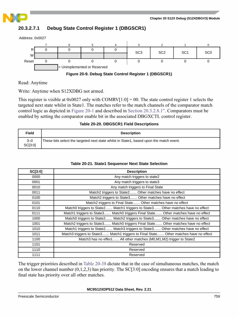
Chapter 20 S12X Debug (S12XDBGV3) Module
MC9S12XDP512 Data Sheet, Rev. 2.21
Freescale Semiconductor 759
20.3.2.7.1 Debug State Control Register 1 (DBGSCR1)
Read: Anytime
Write: Anytime when S12XDBG not armed.
This register is visible at 0x0027 only with COMRV[1:0] = 00. The state control register 1 selects thetargeted next state whilst in State1. The matches refer to the match channels of the comparator matchcontrol logic as depicted in Figure 20-1 and described in Section 20.3.2.8.1”. Comparators must beenabled by setting the comparator enable bit in the associated DBGXCTL control register.
The trigger priorities described in Table 20-38 dictate that in the case of simultaneous matches, the matchon the lower channel number (0,1,2,3) has priority. The SC[3:0] encoding ensures that a match leading tofinal state has priority over all other matches.
Address: 0x0027
7 6 5 4 3 2 1 0
R 0 0 0 0SC3 SC2 SC1 SC0
W
Reset 0 0 0 0 0 0 0 0
= Unimplemented or Reserved
Figure 20-9. Debug State Control Register 1 (DBGSCR1)
Table 20-20. DBGSCR1 Field Descriptions
Field Description
3–0SC[3:0]
These bits select the targeted next state whilst in State1, based upon the match event.
Table 20-21. State1 Sequencer Next State Selection
SC[3:0] Description0000 Any match triggers to state20001 Any match triggers to state30010 Any match triggers to Final State0011 Match2 triggers to State2....... Other matches have no effect0100 Match2 triggers to State3....... Other matches have no effect0101 Match2 triggers to Final State....... Other matches have no effect0110 Match0 triggers to State2....... Match1 triggers to State3....... Other matches have no effect0111 Match1 triggers to State3....... Match0 triggers Final State....... Other matches have no effect1000 Match0 triggers to State2....... Match2 triggers to State3....... Other matches have no effect1001 Match2 triggers to State3....... Match0 triggers Final State....... Other matches have no effect1010 Match1 triggers to State2....... Match3 triggers to State3....... Other matches have no effect1011 Match3 triggers to State3....... Match1 triggers to Final State....... Other matches have no effect1100 Match3 has no effect....... All other matches (M0,M1,M2) trigger to State21101 Reserved1110 Reserved1111 Reserved

Chapter 20 S12X Debug (S12XDBGV3) Module
MC9S12XDP512 Data Sheet, Rev. 2.21
760 Freescale Semiconductor
20.3.2.7.2 Debug State Control Register 2 (DBGSCR2)
Read: Anytime
Write: Anytime when S12XDBG not armed.
This register is visible at 0x0027 only with COMRV[1:0] = 01. The state control register 2 selects thetargeted next state whilst in State2. The matches refer to the match channels of the comparator matchcontrol logic as depicted in Figure 20-1 and described in Section 20.3.2.8.1”. Comparators must beenabled by setting the comparator enable bit in the associated DBGXCTL control register.
The trigger priorities described in Table 20-38 dictate that in the case of simultaneous matches, the matchon the lower channel number (0,1,2,3) has priority. The SC[3:0] encoding ensures that a match leading tofinal state has priority over all other matches.
Address: 0x0027
7 6 5 4 3 2 1 0
R 0 0 0 0SC3 SC2 SC1 SC0
W
Reset 0 0 0 0 0 0 0 0
= Unimplemented or Reserved
Figure 20-10. Debug State Control Register 2 (DBGSCR2)
Table 20-22. DBGSCR2 Field Descriptions
Field Description
3–0SC[3:0]
These bits select the targeted next state whilst in State2, based upon the match event.
Table 20-23. State2 —Sequencer Next State Selection
SC[3:0] Description0000 Any match triggers to state10001 Any match triggers to state30010 Any match triggers to Final State0011 Match3 triggers to State1....... Other matches have no effect0100 Match3 triggers to State3....... Other matches have no effect0101 Match3 triggers to Final State....... Other matches have no effect0110 Match0 triggers to State1....... Match1 triggers to State3....... Other matches have no effect0111 Match1 triggers to State3....... Match0 triggers Final State....... Other matches have no effect1000 Match0 triggers to State1....... Match2 triggers to State3....... Other matches have no effect1001 Match2 triggers to State3....... Match0 triggers Final State....... Other matches have no effect1010 Match1 triggers to State1....... Match3 triggers to State3....... Other matches have no effect1011 Match3 triggers to State3....... Match1 triggers Final State....... Other matches have no effect1100 Match2 triggers to State1..... Match3 trigger to Final State1101 Match2 has no affect, all other matches (M0,M1,M3) trigger to Final State1110 Reserved1111 Reserved
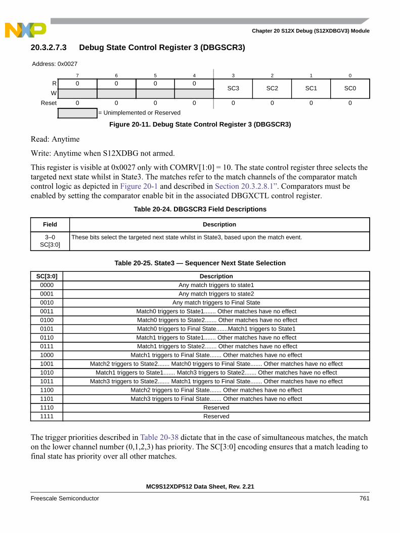
Chapter 20 S12X Debug (S12XDBGV3) Module
MC9S12XDP512 Data Sheet, Rev. 2.21
Freescale Semiconductor 761
20.3.2.7.3 Debug State Control Register 3 (DBGSCR3)
Read: Anytime
Write: Anytime when S12XDBG not armed.
This register is visible at 0x0027 only with COMRV[1:0] = 10. The state control register three selects thetargeted next state whilst in State3. The matches refer to the match channels of the comparator matchcontrol logic as depicted in Figure 20-1 and described in Section 20.3.2.8.1”. Comparators must beenabled by setting the comparator enable bit in the associated DBGXCTL control register.
The trigger priorities described in Table 20-38 dictate that in the case of simultaneous matches, the matchon the lower channel number (0,1,2,3) has priority. The SC[3:0] encoding ensures that a match leading tofinal state has priority over all other matches.
Address: 0x0027
7 6 5 4 3 2 1 0
R 0 0 0 0SC3 SC2 SC1 SC0
W
Reset 0 0 0 0 0 0 0 0
= Unimplemented or Reserved
Figure 20-11. Debug State Control Register 3 (DBGSCR3)
Table 20-24. DBGSCR3 Field Descriptions
Field Description
3–0SC[3:0]
These bits select the targeted next state whilst in State3, based upon the match event.
Table 20-25. State3 — Sequencer Next State Selection
SC[3:0] Description0000 Any match triggers to state10001 Any match triggers to state20010 Any match triggers to Final State0011 Match0 triggers to State1....... Other matches have no effect0100 Match0 triggers to State2....... Other matches have no effect0101 Match0 triggers to Final State.......Match1 triggers to State10110 Match1 triggers to State1....... Other matches have no effect0111 Match1 triggers to State2....... Other matches have no effect1000 Match1 triggers to Final State....... Other matches have no effect1001 Match2 triggers to State2....... Match0 triggers to Final State....... Other matches have no effect1010 Match1 triggers to State1....... Match3 triggers to State2....... Other matches have no effect1011 Match3 triggers to State2....... Match1 triggers to Final State....... Other matches have no effect1100 Match2 triggers to Final State....... Other matches have no effect1101 Match3 triggers to Final State....... Other matches have no effect1110 Reserved1111 Reserved
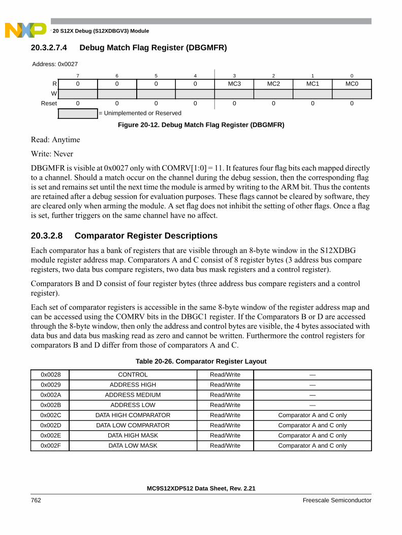
Chapter 20 S12X Debug (S12XDBGV3) Module
MC9S12XDP512 Data Sheet, Rev. 2.21
762 Freescale Semiconductor
20.3.2.7.4 Debug Match Flag Register (DBGMFR)
Read: Anytime
Write: Never
DBGMFR is visible at 0x0027 only with COMRV[1:0] = 11. It features four flag bits each mapped directlyto a channel. Should a match occur on the channel during the debug session, then the corresponding flagis set and remains set until the next time the module is armed by writing to the ARM bit. Thus the contentsare retained after a debug session for evaluation purposes. These flags cannot be cleared by software, theyare cleared only when arming the module. A set flag does not inhibit the setting of other flags. Once a flagis set, further triggers on the same channel have no affect.
20.3.2.8 Comparator Register Descriptions
Each comparator has a bank of registers that are visible through an 8-byte window in the S12XDBGmodule register address map. Comparators A and C consist of 8 register bytes (3 address bus compareregisters, two data bus compare registers, two data bus mask registers and a control register).
Comparators B and D consist of four register bytes (three address bus compare registers and a controlregister).
Each set of comparator registers is accessible in the same 8-byte window of the register address map andcan be accessed using the COMRV bits in the DBGC1 register. If the Comparators B or D are accessedthrough the 8-byte window, then only the address and control bytes are visible, the 4 bytes associated withdata bus and data bus masking read as zero and cannot be written. Furthermore the control registers forcomparators B and D differ from those of comparators A and C.
Address: 0x0027
7 6 5 4 3 2 1 0
R 0 0 0 0 MC3 MC2 MC1 MC0
W
Reset 0 0 0 0 0 0 0 0
= Unimplemented or Reserved
Figure 20-12. Debug Match Flag Register (DBGMFR)
Table 20-26. Comparator Register Layout
0x0028 CONTROL Read/Write —
0x0029 ADDRESS HIGH Read/Write —
0x002A ADDRESS MEDIUM Read/Write —
0x002B ADDRESS LOW Read/Write —
0x002C DATA HIGH COMPARATOR Read/Write Comparator A and C only
0x002D DATA LOW COMPARATOR Read/Write Comparator A and C only
0x002E DATA HIGH MASK Read/Write Comparator A and C only
0x002F DATA LOW MASK Read/Write Comparator A and C only

Chapter 20 S12X Debug (S12XDBGV3) Module
MC9S12XDP512 Data Sheet, Rev. 2.21
Freescale Semiconductor 763
20.3.2.8.1 Debug Comparator Control Register (DBGXCTL)
The contents of this register bits 7 and 6 differ depending upon which comparator registers are visible inthe 8-byte window of the DBG module register address map.
Read: Anytime
Write: Anytime when S12XDBG not armed.
Address: 0x0028
7 6 5 4 3 2 1 0
R 0NDB TAG BRK RW RWE SRC COMPE
W
Reset 0 0 0 0 0 0 0 0
= Unimplemented or Reserved
Figure 20-13. Debug Comparator Control Register (Comparators A and C)
Address: 0x0028
7 6 5 4 3 2 1 0
RSZE SZ TAG BRK RW RWE SRC COMPE
W
Reset 0 0 0 0 0 0 0 0
Figure 20-14. Debug Comparator Control Register (Comparators B and D)
Table 20-27. DBGXCTL Field Descriptions
Field Description
7SZE
(ComparatorsB nd D)
Size Comparator Enable Bit — The SZE bit controls whether access size comparison is enabled for theassociated comparator. This bit is ignored if the TAG bit in the same register is set.0 Word/Byte access size is not used in comparison1 Word/Byte access size is used in comparison
6NDB
(ComparatorsA and C
Not Data Bus Compare — The NDB bit controls whether the match occurs when the data bus matches thecomparator register value or when the data bus differs from the register value. Furthermore data bus bits canbe individually masked using the comparator data mask registers. This bit is only available for comparatorsA and C. This bit is ignored if the TAG bit in the same register is set. This bit position has an SZ functionalityfor comparators B and D.0 Match on data bus equivalence to comparator register contents1 Match on data bus difference to comparator register contents
6SZ
(ComparatorsB and D)
Size Comparator Value Bit — The SZ bit selects either word or byte access size in comparison for theassociated comparator. This bit is ignored if the SZE bit is cleared or if the TAG bit in the same register is set.This bit position has NDB functionality for comparators A and C0 Word access size will be compared1 Byte access size will be compared
5TAG
Tag Select — This bit controls whether the comparator match will cause a trigger or tag the opcode at thematched address. Tagged opcodes trigger only if they reach the execution stage of the instruction queue.0 Trigger immediately on match1 On match, tag the opcode. If the opcode is about to be executed a trigger is generated

Chapter 20 S12X Debug (S12XDBGV3) Module
MC9S12XDP512 Data Sheet, Rev. 2.21
764 Freescale Semiconductor
Table 20-28 shows the effect for RWE and RW on the comparison conditions. These bits are not useful fortagged operations since the trigger occurs based on the tagged opcode reaching the execution stage of theinstruction queue. Thus these bits are ignored if tagged triggering is selected.
4BRK
Break — This bit controls whether a comparator match terminates a debug session immediately,independent of state sequencer state. To generate an immediate breakpoint the module breakpoints must beenabled using the DBGC1 bits DBGBRK[1:0].0 The debug session termination is dependent upon the state sequencer and trigger conditions.1 A match on this channel terminates the debug session immediately; breakpoints if active are generated,
tracing, if active, is terminated and the module disarmed.
3RW
Read/Write Comparator Value Bit — The RW bit controls whether read or write is used in compare for theassociated comparator. The RW bit is not used if RWE = 0.0 Write cycle will be matched1 Read cycle will be matched
2RWE
Read/Write Enable Bit — The RWE bit controls whether read or write comparison is enabled for theassociated comparator. This bit is not useful for tagged operations.0 Read/Write is not used in comparison1 Read/Write is used in comparison
1SRC
Determines mapping of comparator to S12XCPU or XGATE0 The comparator is mapped to S12XCPU buses1 The comparator is mapped to XGATE address and data buses
0COMPE
Determines if comparator is enabled0 The comparator is not enabled1 The comparator is enabled for state sequence triggers or tag generation
Table 20-28. Read or Write Comparison Logic Table
RWE Bit RW Bit RW Signal Comment
0 x 0 RW not used in comparison
0 x 1 RW not used in comparison
1 0 0 Write data bus
1 0 1 No match
1 1 0 No match
1 1 1 Read data bus
Table 20-27. DBGXCTL Field Descriptions (continued)
Field Description

Chapter 20 S12X Debug (S12XDBGV3) Module
MC9S12XDP512 Data Sheet, Rev. 2.21
Freescale Semiconductor 765
20.3.2.8.2 Debug Comparator Address High Register (DBGXAH)
Read: Anytime
Write: Anytime when S12XDBG not armed.
20.3.2.8.3 Debug Comparator Address Mid Register (DBGXAM)
Read: Anytime
Write: Anytime when S12XDBG not armed.
Address: 0x0029
7 6 5 4 3 2 1 0
R 0Bit 22 Bit 21 Bit 20 Bit 19 Bit 18 Bit 17 Bit 16
W
Reset 0 0 0 0 0 0 0 0
= Unimplemented or Reserved
Figure 20-15. Debug Comparator Address High Register (DBGXAH)
Table 20-29. DBGXAH Field Descriptions
Field Description
6–0Bit[22:16]
Comparator Address High Compare Bits — The Comparator address high compare bits control whether theselected comparator will compare the address bus bits [22:16] to a logic one or logic zero. This register byte isignored for XGATE compares.0 Compare corresponding address bit to a logic zero1 Compare corresponding address bit to a logic one
Address: 0x002A
7 6 5 4 3 2 1 0
RBit 15 Bit 14 Bit 13 Bit 12 Bit 11 Bit 10 Bit 9 Bit 8
W
Reset 0 0 0 0 0 0 0 0
Figure 20-16. Debug Comparator Address Mid Register (DBGXAM)
Table 20-30. DBGXAM Field Descriptions
Field Description
7–0Bit[15:8]
Comparator Address Mid Compare Bits — The Comparator address mid compare bits control whether theselected comparator will compare the address bus bits [15:8] to a logic one or logic zero.0 Compare corresponding address bit to a logic zero1 Compare corresponding address bit to a logic one
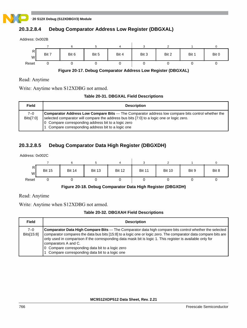
Chapter 20 S12X Debug (S12XDBGV3) Module
MC9S12XDP512 Data Sheet, Rev. 2.21
766 Freescale Semiconductor
20.3.2.8.4 Debug Comparator Address Low Register (DBGXAL)
Read: Anytime
Write: Anytime when S12XDBG not armed.
20.3.2.8.5 Debug Comparator Data High Register (DBGXDH)
Read: Anytime
Write: Anytime when S12XDBG not armed.
Address: 0x002B
7 6 5 4 3 2 1 0
RBit 7 Bit 6 Bit 5 Bit 4 Bit 3 Bit 2 Bit 1 Bit 0
W
Reset 0 0 0 0 0 0 0 0
Figure 20-17. Debug Comparator Address Low Register (DBGXAL)
Table 20-31. DBGXAL Field Descriptions
Field Description
7–0Bits[7:0]
Comparator Address Low Compare Bits — The Comparator address low compare bits control whether theselected comparator will compare the address bus bits [7:0] to a logic one or logic zero.0 Compare corresponding address bit to a logic zero1 Compare corresponding address bit to a logic one
Address: 0x002C
7 6 5 4 3 2 1 0
RBit 15 Bit 14 Bit 13 Bit 12 Bit 11 Bit 10 Bit 9 Bit 8
W
Reset 0 0 0 0 0 0 0 0
Figure 20-18. Debug Comparator Data High Register (DBGXDH)
Table 20-32. DBGXAH Field Descriptions
Field Description
7–0Bits[15:8]
Comparator Data High Compare Bits — The Comparator data high compare bits control whether the selectedcomparator compares the data bus bits [15:8] to a logic one or logic zero. The comparator data compare bits areonly used in comparison if the corresponding data mask bit is logic 1. This register is available only forcomparators A and C.0 Compare corresponding data bit to a logic zero1 Compare corresponding data bit to a logic one
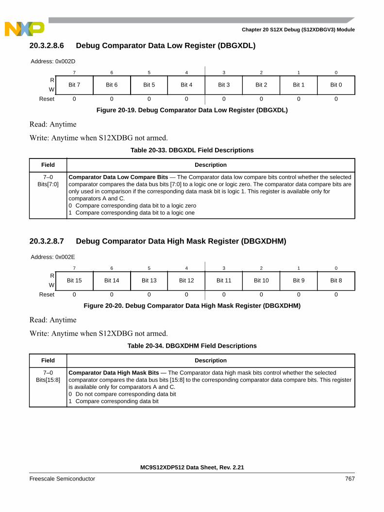
Chapter 20 S12X Debug (S12XDBGV3) Module
MC9S12XDP512 Data Sheet, Rev. 2.21
Freescale Semiconductor 767
20.3.2.8.6 Debug Comparator Data Low Register (DBGXDL)
Read: Anytime
Write: Anytime when S12XDBG not armed.
20.3.2.8.7 Debug Comparator Data High Mask Register (DBGXDHM)
Read: Anytime
Write: Anytime when S12XDBG not armed.
Address: 0x002D
7 6 5 4 3 2 1 0
RBit 7 Bit 6 Bit 5 Bit 4 Bit 3 Bit 2 Bit 1 Bit 0
W
Reset 0 0 0 0 0 0 0 0
Figure 20-19. Debug Comparator Data Low Register (DBGXDL)
Table 20-33. DBGXDL Field Descriptions
Field Description
7–0Bits[7:0]
Comparator Data Low Compare Bits — The Comparator data low compare bits control whether the selectedcomparator compares the data bus bits [7:0] to a logic one or logic zero. The comparator data compare bits areonly used in comparison if the corresponding data mask bit is logic 1. This register is available only forcomparators A and C.0 Compare corresponding data bit to a logic zero1 Compare corresponding data bit to a logic one
Address: 0x002E
7 6 5 4 3 2 1 0
RBit 15 Bit 14 Bit 13 Bit 12 Bit 11 Bit 10 Bit 9 Bit 8
W
Reset 0 0 0 0 0 0 0 0
Figure 20-20. Debug Comparator Data High Mask Register (DBGXDHM)
Table 20-34. DBGXDHM Field Descriptions
Field Description
7–0Bits[15:8]
Comparator Data High Mask Bits — The Comparator data high mask bits control whether the selectedcomparator compares the data bus bits [15:8] to the corresponding comparator data compare bits. This registeris available only for comparators A and C.0 Do not compare corresponding data bit1 Compare corresponding data bit

Chapter 20 S12X Debug (S12XDBGV3) Module
MC9S12XDP512 Data Sheet, Rev. 2.21
768 Freescale Semiconductor
20.3.2.8.8 Debug Comparator Data Low Mask Register (DBGXDLM)
Read: Anytime
Write: Anytime when S12XDBG not armed.
20.4 Functional DescriptionThis section provides a complete functional description of the S12XDBG module. If the part is in securemode, the S12XDBG module can generate breakpoints but tracing is not possible.
20.4.1 S12XDBG Operation
Arming the S12XDBG module by setting ARM in DBGC1 allows triggering, and storing of data in thetrace buffer and can be used to cause breakpoints to the S12XCPU or the XGATE module. The DBGmodule is made up of four main blocks, the comparators, control logic, the state sequencer, and the tracebuffer.
The comparators monitor the bus activity of the S12XCPU and XGATE modules. Comparators can beconfigured to monitor address and databus. Comparators can also be configured to mask out individualdata bus bits during a compare and to use R/W and word/byte access qualification in the comparison. Whena match with a comparator register value occurs the associated control logic can trigger the state sequencerto another state (see Figure 20-23). Either forced or tagged triggers are possible. Using a forced trigger,the trigger is generated immediately on a comparator match. Using a tagged trigger, at a comparator match,the instruction opcode is tagged and only if the instruction reaches the execution stage of the instructionqueue is a trigger generated. In the case of a transition to Final State, bus tracing is triggered and/or abreakpoint can be generated. Tracing of both S12XCPU and/or XGATE bus activity is possible.
Independent of the state sequencer, a breakpoint can be triggered by the external TAGHI / TAGLO signals,by an XGATE S/W breakpoint request or by writing to the TRIG bit in the DBGC1 control register.
Address: 0x002F
7 6 5 4 3 2 1 0
RBit 7 Bit 6 Bit 5 Bit 4 Bit 3 Bit 2 Bit 1 Bit 0
W
Reset 0 0 0 0 0 0 0 0
Figure 20-21. Debug Comparator Data Low Mask Register (DBGXDLM)
Table 20-35. DBGXDLM Field Descriptions
Field Description
7–0Bits[7:0]
Comparator Data Low Mask Bits — The Comparator data low mask bits control whether the selectedcomparator compares the data bus bits [7:0] to the corresponding comparator data compare bits. This registeris available only for comparators A and C.0 Do not compare corresponding data bit1 Compare corresponding data bit

Chapter 20 S12X Debug (S12XDBGV3) Module
MC9S12XDP512 Data Sheet, Rev. 2.21
Freescale Semiconductor 769
The trace buffer is visible through a 2-byte window in the register address map and can be read out usingstandard 16-bit word reads.
Figure 20-22. S12XDBG Overview
20.4.2 Comparator Modes
The S12XDBG contains four comparators, A, B, C, and D. Each comparator can be configured to monitoreither S12XCPU or XGATE buses using the SRC bit in the corresponding comparator control register.Each comparator compares the selected address bus with the address stored in DBGXAH, DBGXAM, andDBGXAL. Furthermore, comparators A and C also compare the data buses to the data stored in DBGXDH,DBGXDL and allow masking of individual data bus bits.
All comparators are disabled in BDM and during BDM accesses.
The comparator match control logic (see Figure 20-22) configures comparators to monitor the buses foran exact address or an address range, whereby either an access inside or outside the specified rangegenerates a match condition. The comparator configuration is controlled by the control register contentsand the range control by the DBGC2 contents.
On a match a trigger can initiate a transition to another state sequencer state (see Section 20.4.3”). Thecomparator control register also allows the type of access to be included in the comparison through the useof the RWE, RW, SZE, and SZ bits. The RWE bit controls whether read or write comparison is enabledfor the associated comparator and the RW bit selects either a read or write access for a valid match.Similarly the SZE and SZ bits allows the size of access (word or byte) to be considered in the compare.Only comparators B and D feature SZE and SZ.
The TAG bit in each comparator control register is used to determine the triggering condition. By settingTAG, the comparator will qualify a match with the output of opcode tracking logic and a trigger occurs
S12XCPU BUS
TRACE BUFFER
BU
S IN
TE
RFA
CE
TRIGGER
EXTERNAL TAGHI / TAGLO
MATCH0
STATE
XGATE BUS
COMPARATOR B
COMPARATOR C
COMPARATOR D
COMPARATOR A
STATE SEQUENCERMATCH1
MATCH2
MATCH3
TRACE
READ TRACE DATA (DBG READ DATA BUS)
CONTROL
SECURE
BREAKPOINT REQUESTS
CO
MPA
RAT
OR
MAT
CH
CO
NT
RO
L
XGATE S/W BREAKPOINT REQUEST
TRIGGER
TAG &TRIGGERCONTROL
LOGIC
TAGSTAGHITS
STATE
S12XCPU & XGATE

Chapter 20 S12X Debug (S12XDBGV3) Module
MC9S12XDP512 Data Sheet, Rev. 2.21
770 Freescale Semiconductor
before the tagged instruction executes (tagged-type trigger). Whilst tagging the RW, RWE, SZE, and SZbits are ignored and the comparator register must be loaded with the exact opcode address.
If the TAG bit is clear (forced type trigger) a comparator match is generated when the selected addressappears on the system address bus. If the selected address is an opcode address, the match is generatedwhen the opcode is fetched from the memory. This precedes the instruction execution by an indefinitenumber of cycles due to instruction pipe lining. For a comparator match of an opcode at an odd addresswhen TAG = 0, the corresponding even address must be contained in the comparator register. Thus for anopcode at odd address (n), the comparator register must contain address (n–1).
Once a successful comparator match has occurred, the condition that caused the original match is notverified again on subsequent matches. Thus if a particular data value is verified at a given address, thisaddress may not still contain that data value when a subsequent match occurs.
Comparators C and D can also be used to select an address range to trace from. This is determined by theTRANGE bits in the DBGTCR register. The TRANGE encoding is shown in Table 20-10. If the TRANGEbits select a range definition using comparator D, then comparator D is configured for trace rangedefinition and cannot be used for address bus comparisons. Similarly if the TRANGE bits select a rangedefinition using comparator C, then comparator C is configured for trace range definition and cannot beused for address bus comparisons.
Match[0, 1, 2, 3] map directly to Comparators[A, B, C, D] respectively, except in range modes (seeSection 20.3.2.4”). Comparator priority rules are described in the trigger priority section(Section 20.4.3.6”).
20.4.2.1 Exact Address Comparator Match (Comparators A and C)
With range comparisons disabled, the match condition is an exact equivalence of address/data bus with thevalue stored in the comparator address/data registers. Further qualification of the type of access (R/W,word/byte) is possible.
Comparators A and C do not feature SZE or SZ control bits, thus the access size is not compared. The exactaddress is compared, thus with the comparator address register loaded with address (n) a misaligned wordaccess of address (n–1) also accesses (n) but does not cause a match. Table 20-37 lists accessconsiderations without data bus compare. Table 20-36 lists access considerations with data buscomparison. To compare byte accesses DBGXDH must be loaded with the data byte. The low byte mustbe masked out using the DBGXDLM mask register. On word accesses the data byte of the lower addressis mapped to DBGXDH.
Table 20-36. Comparator A and C Data Bus Considerations
Access Address DBGxDH DBGxDL DBGxDHM DBGxDLM Example Valid Match
Word ADDR[n] Data[n] Data[n+1] $FF $FF MOVW #$WORD ADDR[n]
Byte ADDR[n] Data[n] x $FF $00 MOVB #$BYTE ADDR[n]
Word ADDR[n] Data[n] x $FF $00 MOVW #$WORD ADDR[n]
Word ADDR[n] x Data[n+1] $00 $FF MOVW #$WORD ADDR[n]
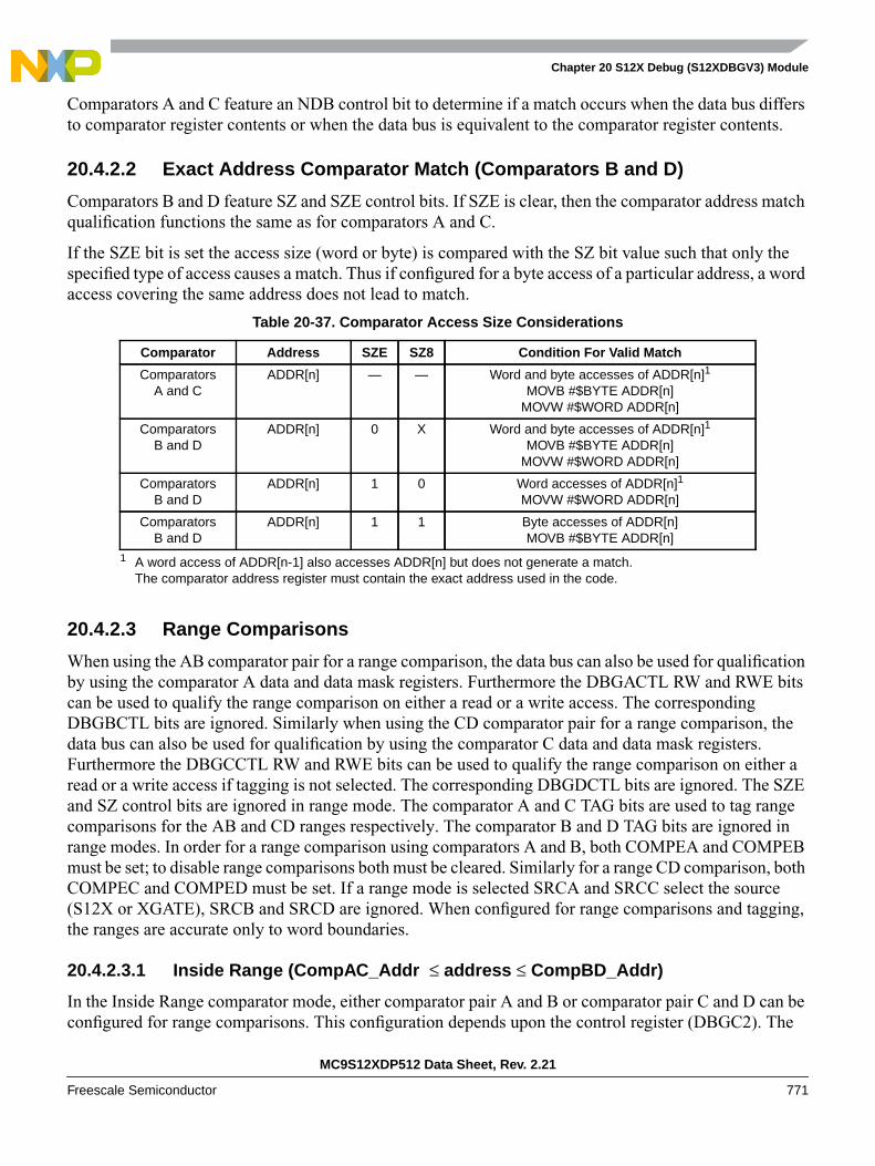
Chapter 20 S12X Debug (S12XDBGV3) Module
MC9S12XDP512 Data Sheet, Rev. 2.21
Freescale Semiconductor 771
Comparators A and C feature an NDB control bit to determine if a match occurs when the data bus differsto comparator register contents or when the data bus is equivalent to the comparator register contents.
20.4.2.2 Exact Address Comparator Match (Comparators B and D)
Comparators B and D feature SZ and SZE control bits. If SZE is clear, then the comparator address matchqualification functions the same as for comparators A and C.
If the SZE bit is set the access size (word or byte) is compared with the SZ bit value such that only thespecified type of access causes a match. Thus if configured for a byte access of a particular address, a wordaccess covering the same address does not lead to match.
20.4.2.3 Range Comparisons
When using the AB comparator pair for a range comparison, the data bus can also be used for qualificationby using the comparator A data and data mask registers. Furthermore the DBGACTL RW and RWE bitscan be used to qualify the range comparison on either a read or a write access. The correspondingDBGBCTL bits are ignored. Similarly when using the CD comparator pair for a range comparison, thedata bus can also be used for qualification by using the comparator C data and data mask registers.Furthermore the DBGCCTL RW and RWE bits can be used to qualify the range comparison on either aread or a write access if tagging is not selected. The corresponding DBGDCTL bits are ignored. The SZEand SZ control bits are ignored in range mode. The comparator A and C TAG bits are used to tag rangecomparisons for the AB and CD ranges respectively. The comparator B and D TAG bits are ignored inrange modes. In order for a range comparison using comparators A and B, both COMPEA and COMPEBmust be set; to disable range comparisons both must be cleared. Similarly for a range CD comparison, bothCOMPEC and COMPED must be set. If a range mode is selected SRCA and SRCC select the source(S12X or XGATE), SRCB and SRCD are ignored. When configured for range comparisons and tagging,the ranges are accurate only to word boundaries.
20.4.2.3.1 Inside Range (CompAC_Addr ≤ address ≤ CompBD_Addr)
In the Inside Range comparator mode, either comparator pair A and B or comparator pair C and D can beconfigured for range comparisons. This configuration depends upon the control register (DBGC2). The
Table 20-37. Comparator Access Size Considerations
Comparator Address SZE SZ8 Condition For Valid Match
ComparatorsA and C
ADDR[n] — — Word and byte accesses of ADDR[n]1
MOVB #$BYTE ADDR[n]MOVW #$WORD ADDR[n]
1 A word access of ADDR[n-1] also accesses ADDR[n] but does not generate a match.The comparator address register must contain the exact address used in the code.
ComparatorsB and D
ADDR[n] 0 X Word and byte accesses of ADDR[n]1
MOVB #$BYTE ADDR[n]MOVW #$WORD ADDR[n]
ComparatorsB and D
ADDR[n] 1 0 Word accesses of ADDR[n]1
MOVW #$WORD ADDR[n]
ComparatorsB and D
ADDR[n] 1 1 Byte accesses of ADDR[n]MOVB #$BYTE ADDR[n]

Chapter 20 S12X Debug (S12XDBGV3) Module
MC9S12XDP512 Data Sheet, Rev. 2.21
772 Freescale Semiconductor
match condition requires that a valid match for both comparators happens on the same bus cycle. A matchcondition on only one comparator is not valid. An aligned word access which straddles the range boundarywill cause a trigger only if the aligned address is inside the range.
20.4.2.3.2 Outside Range (address < CompAC_Addr or address > CompBD_Addr)
In the Outside Range comparator mode, either comparator pair A and B or comparator pair C and D canbe configured for range comparisons. A single match condition on either of the comparators is recognizedas valid. An aligned word access which straddles the range boundary will cause a trigger only if the alignedaddress is outside the range.
Outside range mode in combination with tagged triggers can be used to detect if the opcode fetches arefrom an unexpected range. In forced trigger modes the outside range trigger would typically be activatedat any interrupt vector fetch or register access. This can be avoided by setting the upper range limit to$7FFFFF or lower range limit to $000000 respectively.
When comparing the XGATE address bus in outside range mode, the initial vector fetch as determined bythe vector contained in the XGATE XGVBR register should be taken into consideration. The XGVBRregister and hence vector address can be modified.
20.4.3 Trigger Modes
Trigger modes are used as qualifiers for a state sequencer change of state. The control logic determines thetrigger mode and provides a trigger to the state sequencer. The individual trigger modes are described inthe following sections.
20.4.3.1 Forced Trigger On Comparator Match
If a forced trigger comparator match occurs, the trigger immediately initiates a transition to the next statesequencer state whereby the corresponding flags in DBGSR are set. The state control register for thecurrent state determines the next state for each trigger. Forced triggers are generated as soon as thematching address appears on the address bus, which in the case of opcode fetches occurs several cyclesbefore the opcode execution. For this reason a forced trigger of an opcode address precedes a tagged triggerat the same address by several cycles.
20.4.3.2 Trigger On Comparator Related Taghit
If either a S12XCPU or XGATE taghit occurs a transition to another state sequencer state is initiated andthe corresponding DBGSR flags are set. For a comparator related taghit to occur, the S12XDBG must firstgenerate tags based on comparator matches. When the tagged instruction reaches the execution stage ofthe instruction queue a taghit is generated by the S12XCPU/XGATE. The state control register for thecurrent state determines the next state for each trigger.
20.4.3.3 External Tagging Trigger
In external tagging trigger mode, the TAGLO and TAGHI pins (mapped to device pins) are used to tag aninstruction. This function can be used as another breakpoint source. When the tagged opcode reaches the
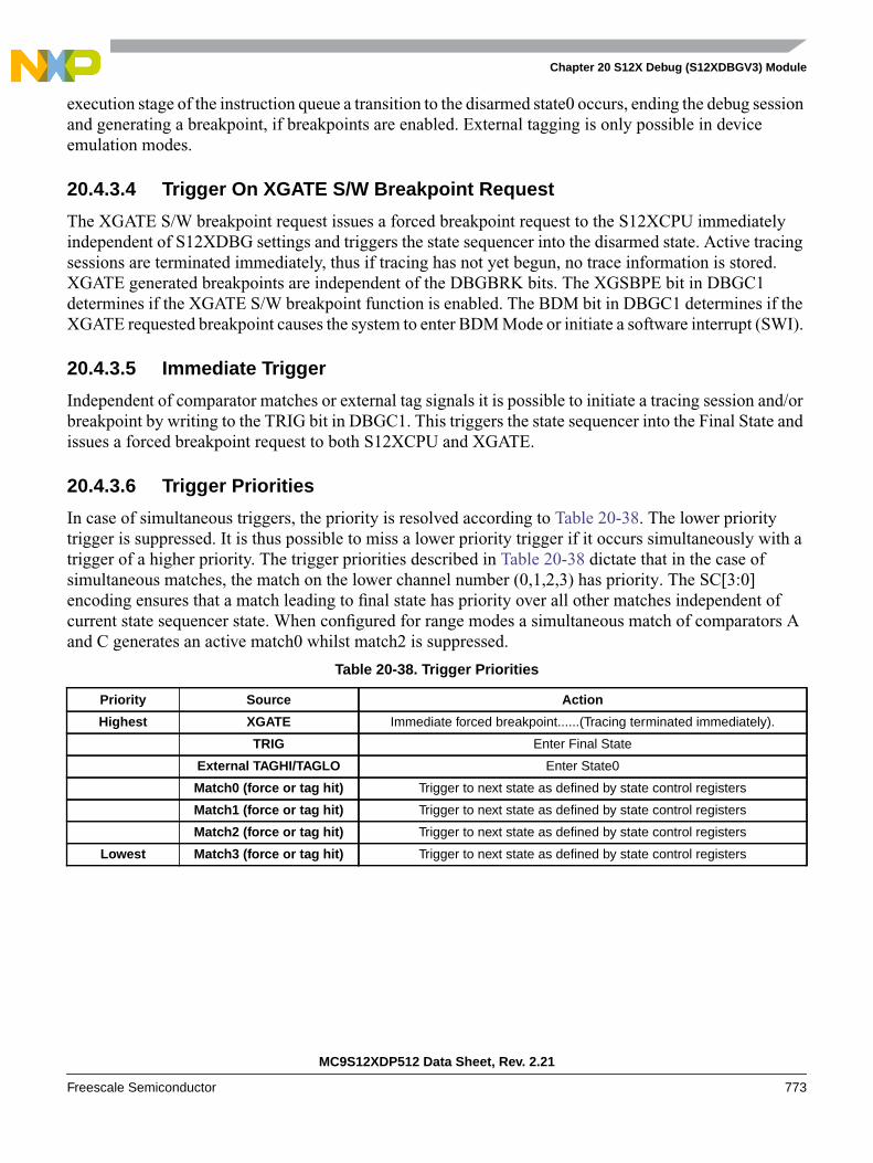
Chapter 20 S12X Debug (S12XDBGV3) Module
MC9S12XDP512 Data Sheet, Rev. 2.21
Freescale Semiconductor 773
execution stage of the instruction queue a transition to the disarmed state0 occurs, ending the debug sessionand generating a breakpoint, if breakpoints are enabled. External tagging is only possible in deviceemulation modes.
20.4.3.4 Trigger On XGATE S/W Breakpoint Request
The XGATE S/W breakpoint request issues a forced breakpoint request to the S12XCPU immediatelyindependent of S12XDBG settings and triggers the state sequencer into the disarmed state. Active tracingsessions are terminated immediately, thus if tracing has not yet begun, no trace information is stored.XGATE generated breakpoints are independent of the DBGBRK bits. The XGSBPE bit in DBGC1determines if the XGATE S/W breakpoint function is enabled. The BDM bit in DBGC1 determines if theXGATE requested breakpoint causes the system to enter BDM Mode or initiate a software interrupt (SWI).
20.4.3.5 Immediate Trigger
Independent of comparator matches or external tag signals it is possible to initiate a tracing session and/orbreakpoint by writing to the TRIG bit in DBGC1. This triggers the state sequencer into the Final State andissues a forced breakpoint request to both S12XCPU and XGATE.
20.4.3.6 Trigger Priorities
In case of simultaneous triggers, the priority is resolved according to Table 20-38. The lower prioritytrigger is suppressed. It is thus possible to miss a lower priority trigger if it occurs simultaneously with atrigger of a higher priority. The trigger priorities described in Table 20-38 dictate that in the case ofsimultaneous matches, the match on the lower channel number (0,1,2,3) has priority. The SC[3:0]encoding ensures that a match leading to final state has priority over all other matches independent ofcurrent state sequencer state. When configured for range modes a simultaneous match of comparators Aand C generates an active match0 whilst match2 is suppressed.
Table 20-38. Trigger Priorities
Priority Source Action
Highest XGATE Immediate forced breakpoint......(Tracing terminated immediately).
TRIG Enter Final State
External TAGHI/TAGLO Enter State0
Match0 (force or tag hit) Trigger to next state as defined by state control registers
Match1 (force or tag hit) Trigger to next state as defined by state control registers
Match2 (force or tag hit) Trigger to next state as defined by state control registers
Lowest Match3 (force or tag hit) Trigger to next state as defined by state control registers
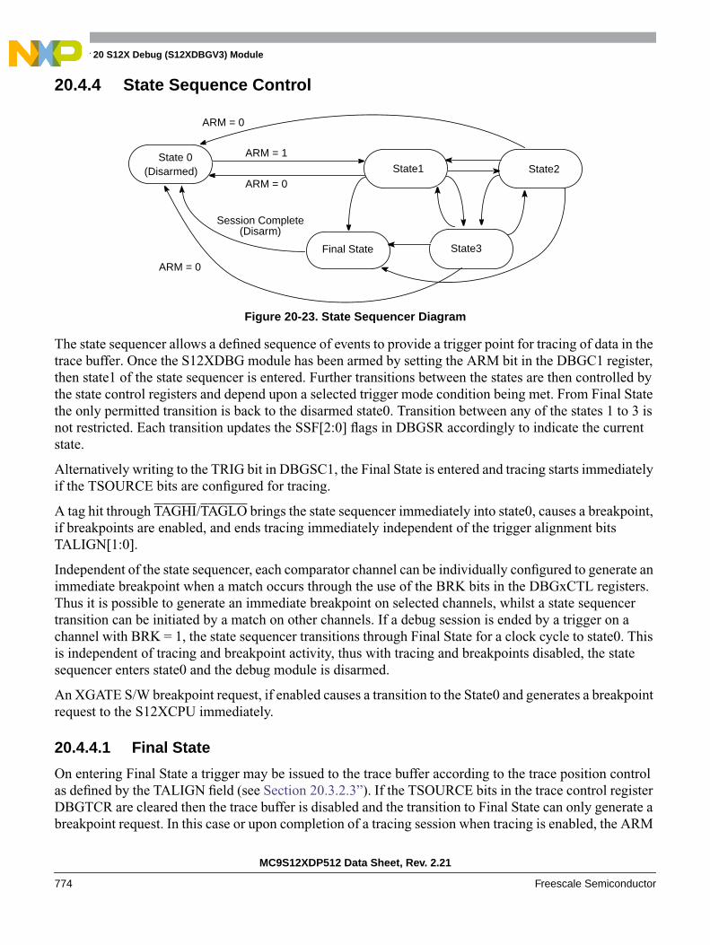
Chapter 20 S12X Debug (S12XDBGV3) Module
MC9S12XDP512 Data Sheet, Rev. 2.21
774 Freescale Semiconductor
20.4.4 State Sequence Control
Figure 20-23. State Sequencer Diagram
The state sequencer allows a defined sequence of events to provide a trigger point for tracing of data in thetrace buffer. Once the S12XDBG module has been armed by setting the ARM bit in the DBGC1 register,then state1 of the state sequencer is entered. Further transitions between the states are then controlled bythe state control registers and depend upon a selected trigger mode condition being met. From Final Statethe only permitted transition is back to the disarmed state0. Transition between any of the states 1 to 3 isnot restricted. Each transition updates the SSF[2:0] flags in DBGSR accordingly to indicate the currentstate.
Alternatively writing to the TRIG bit in DBGSC1, the Final State is entered and tracing starts immediatelyif the TSOURCE bits are configured for tracing.
A tag hit through TAGHI/TAGLO brings the state sequencer immediately into state0, causes a breakpoint,if breakpoints are enabled, and ends tracing immediately independent of the trigger alignment bitsTALIGN[1:0].
Independent of the state sequencer, each comparator channel can be individually configured to generate animmediate breakpoint when a match occurs through the use of the BRK bits in the DBGxCTL registers.Thus it is possible to generate an immediate breakpoint on selected channels, whilst a state sequencertransition can be initiated by a match on other channels. If a debug session is ended by a trigger on achannel with BRK = 1, the state sequencer transitions through Final State for a clock cycle to state0. Thisis independent of tracing and breakpoint activity, thus with tracing and breakpoints disabled, the statesequencer enters state0 and the debug module is disarmed.
An XGATE S/W breakpoint request, if enabled causes a transition to the State0 and generates a breakpointrequest to the S12XCPU immediately.
20.4.4.1 Final State
On entering Final State a trigger may be issued to the trace buffer according to the trace position controlas defined by the TALIGN field (see Section 20.3.2.3”). If the TSOURCE bits in the trace control registerDBGTCR are cleared then the trace buffer is disabled and the transition to Final State can only generate abreakpoint request. In this case or upon completion of a tracing session when tracing is enabled, the ARM
State1
Final State State3
ARM = 1
Session Complete(Disarm)
State2 State 0
(Disarmed)ARM = 0
ARM = 0
ARM = 0

Chapter 20 S12X Debug (S12XDBGV3) Module
MC9S12XDP512 Data Sheet, Rev. 2.21
Freescale Semiconductor 775
bit in the DBGC1 register is cleared, returning the module to the disarmed state0. If tracing is enabled abreakpoint request can occur at the end of the tracing session. If neither tracing nor breakpoints are enabledthen when the final state is reached it returns automatically to state0 and the debug module is disarmed.
20.4.5 Trace Buffer Operation
The trace buffer is a 64 lines deep by 64-bits wide RAM array. The S12XDBG module stores traceinformation in the RAM array in a circular buffer format. The S12XCPU accesses the RAM array througha register window (DBGTBH:DBGTBL) using 16-bit wide word accesses. After each complete 64-bittrace buffer line is read via the S12XCPU, an internal pointer into the RAM is incremented so that the nextread will receive fresh information. Data is stored in the format shown in Table 20-39. After each store thecounter register bits DBGCNT[6:0] are incremented. Tracing of S12XCPU activity is disabled when theBDM is active but tracing of XGATE activity is still possible. Reading the trace buffer whilst the BDM isactive returns invalid data and the trace buffer pointer is not incremented.
20.4.5.1 Trace Trigger Alignment
Using the TALIGN bits (see Section 20.3.2.3”) it is possible to align the trigger with the end, the middle,or the beginning of a tracing session.
If End or Mid tracing is selected, tracing begins when the ARM bit in DBGC1 is set and State1 is entered.The transition to Final State if End is selected signals the end of the tracing session. The transition to FinalState if Mid is selected signals that another 32 lines will be traced before ending the tracing session.Tracing with Begin-Trigger starts at the opcode of the trigger. Using End or Mid-Trigger or when thetracing is initiated by writing to the TRIG bit whilst configured for Begin-Trigger, tracing starts at thesecond opcode after writing to DBGC1 if written in the CPU thread, .
20.4.5.1.1 Storing with Begin-Trigger
Storing with Begin-Trigger, data is not stored in the Trace Buffer until the Final State is entered. Once thetrigger condition is met the S12XDBG module will remain armed until 64 lines are stored in the TraceBuffer. If the trigger is at the address of the change-of-flow instruction the change of flow associated withthe trigger will be stored in the Trace Buffer. Using Begin-trigger together with tagging, if the taggedinstruction is about to be executed then the trace is started. Upon completion of the tracing session thebreakpoint is generated, thus the breakpoint does not occur at the tagged instruction boundary.
20.4.5.1.2 Storing with Mid-Trigger
Storing with Mid-Trigger, data is stored in the Trace Buffer as soon as the S12XDBG module is armed.When the trigger condition is met, another 32 lines will be traced before ending the tracing session,irrespective of the number of lines stored before the trigger occurred, then the S12XDBG module isdisarmed and no more data is stored. If the trigger is at the address of a change of flow instruction thetrigger event is not stored in the Trace Buffer. Using Mid-trigger with tagging, if the tagged instruction isabout to be executed then the trace is continued for another 32 lines. Upon tracing completion thebreakpoint is generated, thus the breakpoint does not occur at the tagged instruction boundary.

Chapter 20 S12X Debug (S12XDBGV3) Module
MC9S12XDP512 Data Sheet, Rev. 2.21
776 Freescale Semiconductor
20.4.5.1.3 Storing with End-Trigger
Storing with End-Trigger, data is stored in the Trace Buffer until the Final State is entered, at which pointthe S12XDBG module will become disarmed and no more data will be stored. If the trigger is at theaddress of a change of flow instruction the trigger event will not be stored in the Trace Buffer.
20.4.5.2 Trace Modes
The S12XDBG module can operate in four trace modes. The mode is selected using the TRCMOD bits inthe DBGTCR register. In each mode tracing of XGATE or S12XCPU information is possible. The sourcefor the trace is selected using the TSOURCE bits in the DBGTCR register. The modes are described in thefollowing subsections. The trace buffer organization is shown in Table 20-39.
20.4.5.2.1 Normal Mode
In Normal Mode, change of flow (COF) program counter (PC) addresses will be stored.
COF addresses are defined as follows for the S12XCPU:
• Source address of taken conditional branches (long, short, bit-conditional, and loop primitives)
• Destination address of indexed JMP, JSR, and CALL instruction.
• Destination address of RTI, RTS, and RTC instructions
• Vector address of interrupts, except for SWI and BDM vectors
LBRA, BRA, BSR, BGND as well as non-indexed JMP, JSR, and CALL instructions are not classified aschange of flow and are not stored in the trace buffer.
COF addresses are defined as follows for the XGATE:
• Source address of taken conditional branches
• Destination address of indexed JAL instructions.
• First XGATE code address in a thread
Change-of-flow addresses stored include the full 23-bit address bus in the case of S12XCPU, the 16-bitaddress bus for the XGATE module and an information byte, which contains a source/destination bit toindicate whether the stored address was a source address or destination address.
20.4.5.2.2 Loop1 Mode
Loop1 Mode, similarly to Normal Mode also stores only COF address information to the trace buffer, ithowever allows the filtering out of redundant information.
The intent of Loop1 Mode is to prevent the Trace Buffer from being filled entirely with duplicateinformation from a looping construct such as delays using the DBNE instruction or polling loops usingBRSET/BRCLR instructions. Immediately after address information is placed in the Trace Buffer, theS12XDBG module writes this value into a background register. This prevents consecutive duplicateaddress entries in the Trace Buffer resulting from repeated branches.
Chapter 20 S12X Debug (S12XDBGV3) Module
MC9S12XDP512 Data Sheet, Rev. 2.21
Freescale Semiconductor 777
Loop1 Mode only inhibits consecutive duplicate source address entries that would typically be stored inmost tight looping constructs. It does not inhibit repeated entries of destination addresses or vectoraddresses, since repeated entries of these would most likely indicate a bug in the user’s code that theS12XDBG module is designed to help find.
NOTEIn certain very tight loops, the source address will have already been fetchedagain before the background comparator is updated. This results in thesource address being stored twice before further duplicate entries aresuppressed. This condition occurs with branch-on-bit instructions when thebranch is fetched by the first P-cycle of the branch or with loop-constructinstructions in which the branch is fetched with the first or second P cycle.See examples below:
LOOP INX ; 1-byte instruction fetched by 1st P-cycle of BRCLRBRCLR CMPTMP,#$0c, LOOP ; the BRCLR instruction also will be fetched by 1st
; P-cycle of BRCLR
LOOP2 BRN * ; 2-byte instruction fetched by 1st P-cycle of DBNENOP ; 1-byte instruction fetched by 2nd P-cycle of DBNEDBNE A,LOOP2 ; this instruction also fetched by 2nd P-cycle of DBNE
20.4.5.2.3 Detail Mode
In Detail Mode, address and data for all memory and register accesses is stored in the trace buffer. In thecase of XGATE tracing this means that initialization of the R1 register during a vector fetch is not traced.This mode is intended to supply additional information on indexed, indirect addressing modes wherestoring only the destination address would not provide all information required for a user to determinewhere the code is in error. This mode also features information byte storage to the trace buffer, for eachaddress byte storage. The information byte indicates the size of access (word or byte), the type of access(read or write).
When tracing S12XCPU activity in Detail Mode, all cycles are traced except those when the S12XCPU iseither in a free or opcode fetch cycle. In this mode the XGATE program counter is also traced to providea snapshot of the XGATE activity. CXINF information byte bits indicate the type of XGATE activityoccurring at the time of the trace buffer entry. When tracing S12XCPU activity alone in Detail Mode, theaddress range can be limited to a range specified by the TRANGE bits in DBGTCR. This function usescomparators C and D to define an address range inside which S12XCPU activity should be traced (seeTable 20-39). Thus the traced S12XCPU activity can be restricted to register range accesses.
When tracing XGATE activity in Detail Mode, all load and store cycles are traced. Additionally theS12XCPU program counter is stored at the time of the XGATE trace buffer entry to provide a snapshot ofS12XCPU activity.
20.4.5.2.4 Pure PC Mode
In Pure PC Mode, tracing from the CPU the PC addresses of all executed opcodes are stored with theexception of WAI and STOP instructions.
In Pure PC Mode, tracing from the XGATE the PC addresses of all executed opcodes are stored.
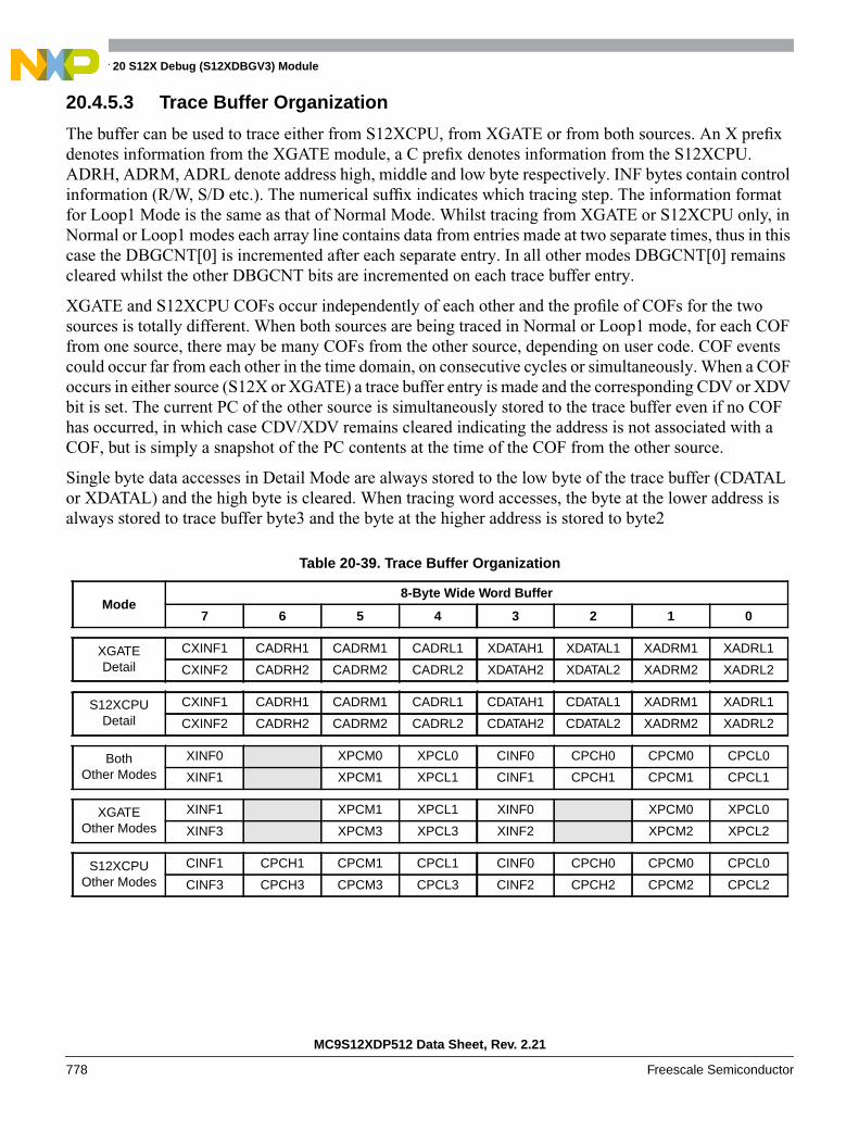
Chapter 20 S12X Debug (S12XDBGV3) Module
MC9S12XDP512 Data Sheet, Rev. 2.21
778 Freescale Semiconductor
20.4.5.3 Trace Buffer Organization
The buffer can be used to trace either from S12XCPU, from XGATE or from both sources. An X prefixdenotes information from the XGATE module, a C prefix denotes information from the S12XCPU.ADRH, ADRM, ADRL denote address high, middle and low byte respectively. INF bytes contain controlinformation (R/W, S/D etc.). The numerical suffix indicates which tracing step. The information formatfor Loop1 Mode is the same as that of Normal Mode. Whilst tracing from XGATE or S12XCPU only, inNormal or Loop1 modes each array line contains data from entries made at two separate times, thus in thiscase the DBGCNT[0] is incremented after each separate entry. In all other modes DBGCNT[0] remainscleared whilst the other DBGCNT bits are incremented on each trace buffer entry.
XGATE and S12XCPU COFs occur independently of each other and the profile of COFs for the twosources is totally different. When both sources are being traced in Normal or Loop1 mode, for each COFfrom one source, there may be many COFs from the other source, depending on user code. COF eventscould occur far from each other in the time domain, on consecutive cycles or simultaneously. When a COFoccurs in either source (S12X or XGATE) a trace buffer entry is made and the corresponding CDV or XDVbit is set. The current PC of the other source is simultaneously stored to the trace buffer even if no COFhas occurred, in which case CDV/XDV remains cleared indicating the address is not associated with aCOF, but is simply a snapshot of the PC contents at the time of the COF from the other source.
Single byte data accesses in Detail Mode are always stored to the low byte of the trace buffer (CDATALor XDATAL) and the high byte is cleared. When tracing word accesses, the byte at the lower address isalways stored to trace buffer byte3 and the byte at the higher address is stored to byte2
Table 20-39. Trace Buffer Organization
Mode8-Byte Wide Word Buffer
7 6 5 4 3 2 1 0
XGATEDetail
CXINF1 CADRH1 CADRM1 CADRL1 XDATAH1 XDATAL1 XADRM1 XADRL1
CXINF2 CADRH2 CADRM2 CADRL2 XDATAH2 XDATAL2 XADRM2 XADRL2
S12XCPUDetail
CXINF1 CADRH1 CADRM1 CADRL1 CDATAH1 CDATAL1 XADRM1 XADRL1
CXINF2 CADRH2 CADRM2 CADRL2 CDATAH2 CDATAL2 XADRM2 XADRL2
BothOther Modes
XINF0 XPCM0 XPCL0 CINF0 CPCH0 CPCM0 CPCL0
XINF1 XPCM1 XPCL1 CINF1 CPCH1 CPCM1 CPCL1
XGATEOther Modes
XINF1 XPCM1 XPCL1 XINF0 XPCM0 XPCL0
XINF3 XPCM3 XPCL3 XINF2 XPCM2 XPCL2
S12XCPUOther Modes
CINF1 CPCH1 CPCM1 CPCL1 CINF0 CPCH0 CPCM0 CPCL0
CINF3 CPCH3 CPCM3 CPCL3 CINF2 CPCH2 CPCM2 CPCL2

Chapter 20 S12X Debug (S12XDBGV3) Module
MC9S12XDP512 Data Sheet, Rev. 2.21
Freescale Semiconductor 779
20.4.5.3.1 Information Byte Organization
The format of the control information byte for both S12XCPU and XGATE modules is dependent uponthe active trace mode and tracing source as described below. In Normal, Loop1, or Pure PC modes tracingof XGATE activity, XINF is used to store control information. In Normal, Loop1, or Pure PC modestracing of S12XCPU activity, CINF is used to store control information. In Detail Mode, CXINF containsthe control information
XGATE Information Byte
X12X_CPU Information Byte
Bit 7 Bit 6 Bit 5 Bit 4 Bit 3 Bit 2 Bit 1 Bit 0
XSD XSOT XCOT XDV 0 0 0 0
Figure 20-24. XGATE Information Byte XINF
Table 20-40. XINF Field Descriptions
Field Description
7XSD
Source Destination Indicator — This bit indicates if the corresponding stored address is a source or destinationaddress. This is only used in Normal and Loop1 mode tracing.0 Source Address1 Destination Address or Start of Thread or Continuation of Thread
6XSOT
Source Of Thread Indicator — This bit indicates that the corresponding stored address is a start of threadaddress. This is only used in Normal and Loop1 mode tracing.NOTE. This bit only has effect on devices where the XGATE module supports multiple interrupt levels.0 Stored address not from a start of thread1 Stored address from a start of thread
5XCOT
Continuation Of Thread Indicator — This bit indicates that the corresponding stored address is the firstaddress following a return from a higher priority thread. This is only used in Normal and Loop1 mode tracing.NOTE. This bit only has effect on devices where the XGATE module supports multiple interrupt levels.0 Stored address not from a continuation of thread1 Stored address from a continuation of thread
4XDV
Data Invalid Indicator — This bit indicates if the trace buffer entry is invalid. It is only used when tracing fromboth sources in Normal, Loop1 and Pure PC modes, to indicate that the XGATE trace buffer entry is valid.0 Trace buffer entry is invalid1 Trace buffer entry is valid
Bit 7 Bit 6 Bit 5 Bit 4 Bit 3 Bit 2 Bit 1 Bit 0
CSD CVA 0 CDV 0 0 0 0
Figure 20-25. S12XCPU Information Byte CINF

Chapter 20 S12X Debug (S12XDBGV3) Module
MC9S12XDP512 Data Sheet, Rev. 2.21
780 Freescale Semiconductor
CXINF Information Byte
This describes the format of the information byte used only when tracing from S12XCPU or XGATE inDetail Mode. When tracing from the S12XCPU in Detail Mode, information is stored to the trace bufferon all cycles except opcode fetch and free cycles. The XGATE entry stored on the same line is a snapshotof the XGATE program counter. In this case the CSZ and CRW bits indicate the type of access being madeby the S12XCPU, whilst the XACK and XOCF bits indicate if the simultaneous XGATE cycle is a freecycle (no bus acknowledge) or opcode fetch cycle. Similarly when tracing from the XGATE in DetailMode, information is stored to the trace buffer on all cycles except opcode fetch and free cycles. TheS12XCPU entry stored on the same line is a snapshot of the S12XCPU program counter. In this case theXSZ and XRW bits indicate the type of access being made by the XGATE, whilst the CFREE and COCFbits indicate if the simultaneous S12XCPU cycle is a free cycle or opcode fetch cycle.
Table 20-41. CINF Field Descriptions
Field Description
7CSD
Source Destination Indicator — This bit indicates if the corresponding stored address is a source or destinationaddress. This is only used in Normal and Loop1 mode tracing.0 Source Address1 Destination Address
6CVA
Vector Indicator — This bit indicates if the corresponding stored address is a vector address.. This is only usedin Normal and Loop1 mode tracing.0 Source Address1 Destination Address
4CDV
Data Invalid Indicator — This bit indicates if the trace buffer entry is invalid. It is only used when tracing fromboth sources in Normal, Loop1 and Pure PC modes, to indicate that the S12XCPU trace buffer entry is valid.0 Trace buffer entry is invalid1 Trace buffer entry is valid
Bit 7 Bit 6 Bit 5 Bit 4 Bit 3 Bit 2 Bit 1 Bit 0
CFREE CSZ CRW COCF XACK XSZ XRW XOCF
Figure 20-26. Information Byte CXINF
Table 20-42. CXINF Field Descriptions
Field Description
7CFREE
S12XCPU Free Cycle Indicator — This bit indicates if the stored S12XCPU address corresponds to a free cycle.This bit only contains valid information when tracing the XGATE accesses in Detail Mode.0 Stored information corresponds to free cycle1 Stored information does not correspond to free cycle
6CSZ
Access Type Indicator — This bit indicates if the access was a byte or word size access.This bit only containsvalid information when tracing S12XCPU activity in Detail Mode.0 Word Access1 Byte Access
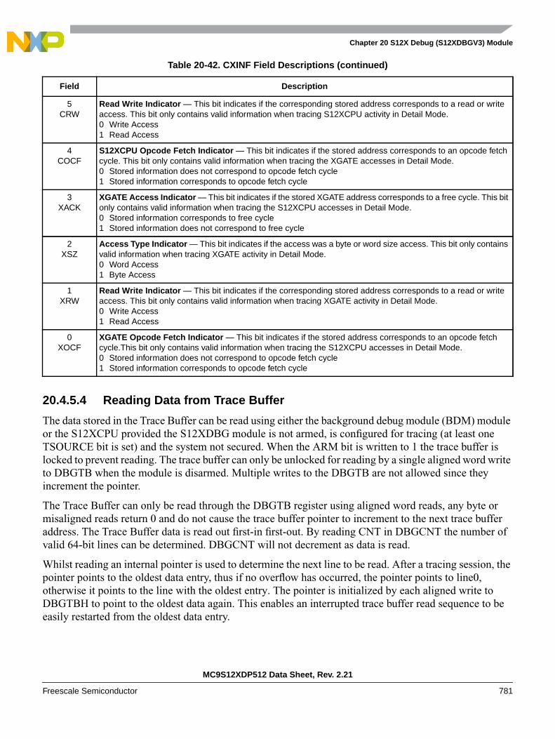
Chapter 20 S12X Debug (S12XDBGV3) Module
MC9S12XDP512 Data Sheet, Rev. 2.21
Freescale Semiconductor 781
20.4.5.4 Reading Data from Trace Buffer
The data stored in the Trace Buffer can be read using either the background debug module (BDM) moduleor the S12XCPU provided the S12XDBG module is not armed, is configured for tracing (at least oneTSOURCE bit is set) and the system not secured. When the ARM bit is written to 1 the trace buffer islocked to prevent reading. The trace buffer can only be unlocked for reading by a single aligned word writeto DBGTB when the module is disarmed. Multiple writes to the DBGTB are not allowed since theyincrement the pointer.
The Trace Buffer can only be read through the DBGTB register using aligned word reads, any byte ormisaligned reads return 0 and do not cause the trace buffer pointer to increment to the next trace bufferaddress. The Trace Buffer data is read out first-in first-out. By reading CNT in DBGCNT the number ofvalid 64-bit lines can be determined. DBGCNT will not decrement as data is read.
Whilst reading an internal pointer is used to determine the next line to be read. After a tracing session, thepointer points to the oldest data entry, thus if no overflow has occurred, the pointer points to line0,otherwise it points to the line with the oldest entry. The pointer is initialized by each aligned write toDBGTBH to point to the oldest data again. This enables an interrupted trace buffer read sequence to beeasily restarted from the oldest data entry.
5CRW
Read Write Indicator — This bit indicates if the corresponding stored address corresponds to a read or writeaccess. This bit only contains valid information when tracing S12XCPU activity in Detail Mode.0 Write Access1 Read Access
4COCF
S12XCPU Opcode Fetch Indicator — This bit indicates if the stored address corresponds to an opcode fetchcycle. This bit only contains valid information when tracing the XGATE accesses in Detail Mode.0 Stored information does not correspond to opcode fetch cycle1 Stored information corresponds to opcode fetch cycle
3XACK
XGATE Access Indicator — This bit indicates if the stored XGATE address corresponds to a free cycle. This bitonly contains valid information when tracing the S12XCPU accesses in Detail Mode.0 Stored information corresponds to free cycle1 Stored information does not correspond to free cycle
2XSZ
Access Type Indicator — This bit indicates if the access was a byte or word size access. This bit only containsvalid information when tracing XGATE activity in Detail Mode.0 Word Access1 Byte Access
1XRW
Read Write Indicator — This bit indicates if the corresponding stored address corresponds to a read or writeaccess. This bit only contains valid information when tracing XGATE activity in Detail Mode.0 Write Access1 Read Access
0XOCF
XGATE Opcode Fetch Indicator — This bit indicates if the stored address corresponds to an opcode fetchcycle.This bit only contains valid information when tracing the S12XCPU accesses in Detail Mode.0 Stored information does not correspond to opcode fetch cycle1 Stored information corresponds to opcode fetch cycle
Table 20-42. CXINF Field Descriptions (continued)
Field Description

Chapter 20 S12X Debug (S12XDBGV3) Module
MC9S12XDP512 Data Sheet, Rev. 2.21
782 Freescale Semiconductor
The least significant word of each 64-bit wide array line is read out first. This corresponds to the bytes 1and 0 of Table 20-39. The bytes containing invalid information (shaded in Table 20-39) are also read out.
Reading the Trace Buffer while the S12XDBG module is armed will return invalid data and no shifting ofthe RAM pointer will occur. Reading the trace buffer is not possible if both TSOURCE bits are cleared.
20.4.5.5 Trace Buffer Reset State
The Trace Buffer contents are not initialized by a system reset. Thus should a system reset occur, the tracesession information from immediately before the reset occurred can be read out. The DBGCNT bits arenot cleared by a system reset. Thus should a reset occur, the number of valid lines in the trace buffer isindicated by DBGCNT. The internal pointer to the current trace buffer address is initialized by unlockingthe trace buffer thus points to the oldest valid data even if a reset occurred during the tracing session.Generally debugging occurrences of system resets is best handled using mid or end trigger alignment sincethe reset may occur before the trace trigger, which in the begin trigger alignment case means noinformation would be stored in the trace buffer.
20.4.6 Tagging
A tag follows program information as it advances through the instruction queue. When a tagged instructionreaches the head of the queue a tag hit occurs and triggers the state sequencer.
Each comparator control register features a TAG bit, which controls whether the comparator match willcause a trigger immediately or tag the opcode at the matched address. If a comparator is enabled for taggedcomparisons, the address stored in the comparator match address registers must be an opcode address forthe trigger to occur.
Both S12XCPU and XGATE opcodes can be tagged with the comparator register TAG bits.
Using Begin trigger together with tagging, if the tagged instruction is about to be executed then thetransition to the next state sequencer state occurs. If the transition is to the Final State, tracing is started.Only upon completion of the tracing session can a breakpoint be generated. Similarly using Mid triggerwith tagging, if the tagged instruction is about to be executed then the trace is continued for another 32lines. Upon tracing completion the breakpoint is generated. Using End trigger, when the tagged instructionis about to be executed and the next transition is to Final State then a breakpoint is generated immediately,before the tagged instruction is carried out.
R/W monitoring is not useful for tagged operations since the trigger occurs based on the tagged opcodereaching the execution stage of the instruction queue. Similarly access size (SZ) monitoring and data busmonitoring is not useful if tagged triggering is selected, since the tag is attached to the opcode at thematched address and is not dependent on the data bus nor on the size of access. Thus these bits are ignoredif tagged triggering is selected.
When configured for range comparisons and tagging, the ranges are accurate only to word boundaries.
S12X tagging is disabled when the BDM becomes active. Conversely BDM firmware commands are notprocessed while tagging is active. XGATE tagging is possible when the BDM is active.
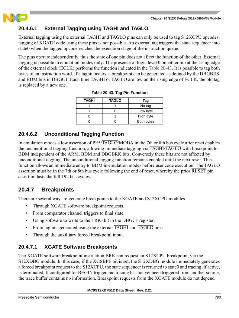
Chapter 20 S12X Debug (S12XDBGV3) Module
MC9S12XDP512 Data Sheet, Rev. 2.21
Freescale Semiconductor 783
20.4.6.1 External Tagging using TAGHI and TAGLO
External tagging using the external TAGHI and TAGLO pins can only be used to tag S12XCPU opcodes;tagging of XGATE code using these pins is not possible. An external tag triggers the state sequencer intostate0 when the tagged opcode reaches the execution stage of the instruction queue.
The pins operate independently, thus the state of one pin does not affect the function of the other. Externaltagging is possible in emulation modes only. The presence of logic level 0 on either pin at the rising edgeof the external clock (ECLK) performs the function indicated in the Table 20-43. It is possible to tag bothbytes of an instruction word. If a taghit occurs, a breakpoint can be generated as defined by the DBGBRKand BDM bits in DBGC1. Each time TAGHI or TAGLO are low on the rising edge of ECLK, the old tagis replaced by a new one.
20.4.6.2 Unconditional Tagging Function
In emulation modes a low assertion of PE5/TAGLO/MODA in the 7th or 8th bus cycle after reset enablesthe unconditional tagging function, allowing immediate tagging via TAGHI/TAGLO with breakpoint toBDM independent of the ARM, BDM and DBGBRK bits. Conversely these bits are not affected byunconditional tagging. The unconditional tagging function remains enabled until the next reset. Thisfunction allows an immediate entry to BDM in emulation modes before user code execution. The TAGLOassertion must be in the 7th or 8th bus cycle following the end of reset, whereby the prior RESET pinassertion lasts the full 192 bus cycles.
20.4.7 Breakpoints
There are several ways to generate breakpoints to the XGATE and S12XCPU modules
• Through XGATE software breakpoint requests.
• From comparator channel triggers to final state.
• Using software to write to the TRIG bit in the DBGC1 register.
• From taghits generated using the external TAGHI and TAGLO pins.
• Through the auxilliary forced breakpoint input.
20.4.7.1 XGATE Software Breakpoints
The XGATE software breakpoint instruction BRK can request an S12XCPU breakpoint, via theS12XDBG module. In this case, if the XGSBPE bit is set, the S12XDBG module immediately generatesa forced breakpoint request to the S12XCPU, the state sequencer is returned to state0 and tracing, if active,is terminated. If configured for BEGIN trigger and tracing has not yet been triggered from another source,the trace buffer contains no information. Breakpoint requests from the XGATE module do not depend
Table 20-43. Tag Pin Function
TAGHI TAGLO Tag1 1 No tag1 0 Low byte0 1 High byte0 0 Both bytes
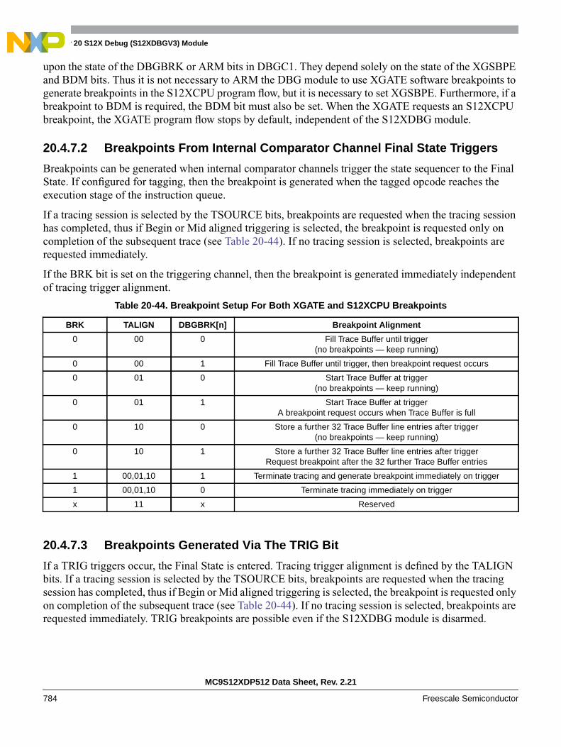
Chapter 20 S12X Debug (S12XDBGV3) Module
MC9S12XDP512 Data Sheet, Rev. 2.21
784 Freescale Semiconductor
upon the state of the DBGBRK or ARM bits in DBGC1. They depend solely on the state of the XGSBPEand BDM bits. Thus it is not necessary to ARM the DBG module to use XGATE software breakpoints togenerate breakpoints in the S12XCPU program flow, but it is necessary to set XGSBPE. Furthermore, if abreakpoint to BDM is required, the BDM bit must also be set. When the XGATE requests an S12XCPUbreakpoint, the XGATE program flow stops by default, independent of the S12XDBG module.
20.4.7.2 Breakpoints From Internal Comparator Channel Final State Triggers
Breakpoints can be generated when internal comparator channels trigger the state sequencer to the FinalState. If configured for tagging, then the breakpoint is generated when the tagged opcode reaches theexecution stage of the instruction queue.
If a tracing session is selected by the TSOURCE bits, breakpoints are requested when the tracing sessionhas completed, thus if Begin or Mid aligned triggering is selected, the breakpoint is requested only oncompletion of the subsequent trace (see Table 20-44). If no tracing session is selected, breakpoints arerequested immediately.
If the BRK bit is set on the triggering channel, then the breakpoint is generated immediately independentof tracing trigger alignment.
20.4.7.3 Breakpoints Generated Via The TRIG Bit
If a TRIG triggers occur, the Final State is entered. Tracing trigger alignment is defined by the TALIGNbits. If a tracing session is selected by the TSOURCE bits, breakpoints are requested when the tracingsession has completed, thus if Begin or Mid aligned triggering is selected, the breakpoint is requested onlyon completion of the subsequent trace (see Table 20-44). If no tracing session is selected, breakpoints arerequested immediately. TRIG breakpoints are possible even if the S12XDBG module is disarmed.
Table 20-44. Breakpoint Setup For Both XGATE and S12XCPU Breakpoints
BRK TALIGN DBGBRK[n] Breakpoint Alignment
0 00 0 Fill Trace Buffer until trigger(no breakpoints — keep running)
0 00 1 Fill Trace Buffer until trigger, then breakpoint request occurs
0 01 0 Start Trace Buffer at trigger(no breakpoints — keep running)
0 01 1 Start Trace Buffer at triggerA breakpoint request occurs when Trace Buffer is full
0 10 0 Store a further 32 Trace Buffer line entries after trigger(no breakpoints — keep running)
0 10 1 Store a further 32 Trace Buffer line entries after triggerRequest breakpoint after the 32 further Trace Buffer entries
1 00,01,10 1 Terminate tracing and generate breakpoint immediately on trigger
1 00,01,10 0 Terminate tracing immediately on trigger
x 11 x Reserved
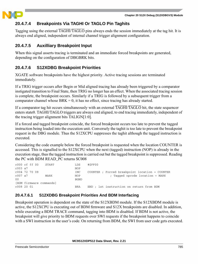
Chapter 20 S12X Debug (S12XDBGV3) Module
MC9S12XDP512 Data Sheet, Rev. 2.21
Freescale Semiconductor 785
20.4.7.4 Breakpoints Via TAGHI Or TAGLO Pin Taghits
Tagging using the external TAGHI/TAGLO pins always ends the session immediately at the tag hit. It isalways end aligned, independent of internal channel trigger alignment configuration.
20.4.7.5 Auxilliary Breakpoint Input
When this signal asserts tracing is terminated and an immediate forced breakpoints are generated,depending on the configuration of DBGBRK bits.
20.4.7.6 S12XDBG Breakpoint Priorities
XGATE software breakpoints have the highest priority. Active tracing sessions are terminatedimmediately.
If a TRIG trigger occurs after Begin or Mid aligned tracing has already been triggered by a comparatorinstigated transition to Final State, then TRIG no longer has an effect. When the associated tracing sessionis complete, the breakpoint occurs. Similarly if a TRIG is followed by a subsequent trigger from acomparator channel whose BRK = 0, it has no effect, since tracing has already started.
If a comparator tag hit occurs simultaneously with an external TAGHI/TAGLO hit, the state sequencerenters state0. TAGHI/TAGLO triggers are always end aligned, to end tracing immediately, independent ofthe tracing trigger alignment bits TALIGN[1:0].
If a forced and tagged breakpoint coincide, the forced breakpoint occurs too late to prevent the taggedinstruction being loaded into the execution unit. Conversely the taghit is too late to prevent the breakpointrequest in the DBG module. Thus the S12XCPU suppresses the taghit although the tagged instruction isexecuted.
Considering the code example below the forced breakpoint is requested when the location COUNTER isaccessed. This is signalled to the S12XCPU when the next (tagged) instruction (NOP) is already in theexecution stage, thus the tagged instruction is carried out but the tagged breakpoint is suppressed. Readingthe PC with BDM READ_PC returns $C008c000 cf ff 00 START LDS #$FF00c003 a7 NOPc004 72 70 08 INC COUNTER ; Forced breakpoint location = COUNTERc007 a7 MARK NOP ; Tagged opcode location = MARK00 BGND[BDM firmware commands]c008 20 01 BRA END ; 1st instruction on return from BDM
20.4.7.6.1 S12XDBG Breakpoint Priorities And BDM Interfacing
Breakpoint operation is dependent on the state of the S12XBDM module. If the S12XBDM module isactive, the S12XCPU is executing out of BDM firmware and S12X breakpoints are disabled. In addition,while executing a BDM TRACE command, tagging into BDM is disabled. If BDM is not active, thebreakpoint will give priority to BDM requests over SWI requests if the breakpoint happens to coincidewith a SWI instruction in the user’s code. On returning from BDM, the SWI from user code gets executed.

Chapter 20 S12X Debug (S12XDBGV3) Module
MC9S12XDP512 Data Sheet, Rev. 2.21
786 Freescale Semiconductor
BDM cannot be entered from a breakpoint unless the ENABLE bit is set in the BDM. If entry to BDM viaa BGND instruction is attempted and the ENABLE bit in the BDM is cleared, the S12XCPU actuallyexecutes the BDM firmware code. It checks the ENABLE and returns if ENABLE is not set. If not servicedby the monitor then the breakpoint is re-asserted when the BDM returns to normal S12XCPU flow.
If the comparator register contents coincide with the SWI/BDM vector address then an SWI in user codeand DBG breakpoint could occur simultaneously. The S12XCPU ensures that BDM requests have a higherpriority than SWI requests. Returning from the BDM/SWI service routine care must be taken to avoid retriggering a breakpoint.
NOTEWhen program control returns from a tagged breakpoint using an RTI orBDM GO command without program counter modification it will return tothe instruction whose tag generated the breakpoint. To avoid re triggering abreakpoint at the same location reconfigure the S12XDBG module in theSWI routine, if configured for an SWI breakpoint, or over the BDMinterface by executing a TRACE command before the GO to increment theprogram flow past the tagged instruction.
An XGATE software breakpoint is forced immediately, the tracing sessionterminated and the XGATE module execution stops. The user can thusdetermine if an XGATE breakpoint has occurred by reading out the XGATEprogram counter over the BDM interface.
Table 20-45. Breakpoint Mapping Summary
DBGBRK[1](DBGC1[3])
BDM Bit(DBGC1[4])
BDMEnabled
BDMActive
S12X BreakpointMapping
0 X X X No Breakpoint
1 0 X 0 Breakpoint to SWI
1 0 X 1 No Breakpoint
1 1 0 X Breakpoint to SWI
1 1 1 0 Breakpoint to BDM
1 1 1 1 No Breakpoint

MC9S12XDP512 Data Sheet, Rev. 2.21
Freescale Semiconductor 787
Chapter 21External Bus Interface (S12XEBIV2)
21.1 IntroductionThis document describes the functionality of the XEBI block controlling the external bus interface.
The XEBI controls the functionality of a non-multiplexed external bus (a.k.a. ‘expansion bus’) inrelationship with the chip operation modes. Dependent on the mode, the external bus can be used for dataexchange with external memory, peripherals or PRU, and provide visibility to the internal bus externallyin combination with an emulator.
21.1.1 Features
The XEBI includes the following features:
• Output of up to 23-bit address bus and control signals to be used with a non-muxed external bus
• Bidirectional 16-bit external data bus with option to disable upper half
• Visibility of internal bus activity
21.1.2 Modes of Operation• Single-chip modes
The external bus interface is not available in these modes.
• Expanded modes
Address, data, and control signals are activated on the external bus in normal expanded mode andspecial test mode.
• Emulation modes
The external bus is activated to interface to an external tool for emulation of normal expanded modeor normal single-chip mode applications.
Refer to the S12X_MMC section for a detailed description of the MCU operating modes.

Chapter 21 External Bus Interface (S12XEBIV2)
MC9S12XDP512 Data Sheet, Rev. 2.21
788 Freescale Semiconductor
21.1.3 Block Diagram
Figure 21-1 is a block diagram of the XEBI with all related I/O signals.
Figure 21-1. XEBI Block Diagram
21.2 External Signal DescriptionThe user is advised to refer to the SoC section for port configuration and location of external bus signals.
NOTEThe following external bus related signals are described in other sections:
CS2, CS1, CS0 (chip selects) — S12X_MMC sectionECLK, ECLKX2 (free-running clocks) — PIM sectionTAGHI, TAGLO (tag inputs) — PIM section, S12X_DBG section
Table 21-1 outlines the pin names and gives a brief description of their function. Refer to the SoC sectionand PIM section for reset states of these pins and associated pull-ups or pull-downs.
XEBI
ADDR[22:0]DATA[15:0]
LSTRBR/W
UDSLDSREWE
EWAIT
ACC[2:0]IQSTAT[3:0]
IVD[15:0]
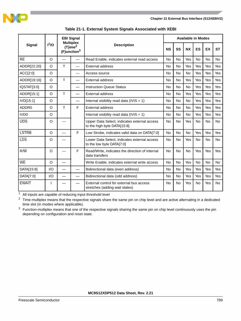
Chapter 21 External Bus Interface (S12XEBIV2)
MC9S12XDP512 Data Sheet, Rev. 2.21
Freescale Semiconductor 789
Table 21-1. External System Signals Associated with XEBI
Signal I1/O
1 All inputs are capable of reducing input threshold level
EBI SignalMultiplex(T)ime2
(F)unction3
2 Time-multiplex means that the respective signals share the same pin on chip level and are active alternating in a dedicatedtime slot (in modes where applicable).
3 Function-multiplex means that one of the respective signals sharing the same pin on chip level continuously uses the pindepending on configuration and reset state.
Description
Available in Modes
NS SS NX ES EX ST
RE O — — Read Enable, indicates external read access No No Yes No No No
ADDR[22:20] O T — External address No No Yes Yes Yes Yes
ACC[2:0] O — Access source No No No Yes Yes Yes
ADDR[19:16] O T — External address No No Yes Yes Yes Yes
IQSTAT[3:0] O — Instruction Queue Status No No No Yes Yes Yes
ADDR[15:1] O T — External address No No Yes Yes Yes Yes
IVD[15:1] O — Internal visibility read data (IVIS = 1) No No No Yes Yes Yes
ADDR0 O T F External address No No No Yes Yes Yes
IVD0 O Internal visibility read data (IVIS = 1) No No No Yes Yes Yes
UDS O — Upper Data Select, indicates external accessto the high byte DATA[15:8]
No No Yes No No No
LSTRB O — F Low Strobe, indicates valid data on DATA[7:0] No No No Yes Yes Yes
LDS O — Lower Data Select, indicates external accessto the low byte DATA[7:0]
No No Yes No No No
R/W O — F Read/Write, indicates the direction of internaldata transfers
No No No Yes Yes Yes
WE O — Write Enable, indicates external write access No No Yes No No No
DATA[15:8] I/O — — Bidirectional data (even address) No No Yes Yes Yes Yes
DATA[7:0] I/O — — Bidirectional data (odd address) No No Yes Yes Yes Yes
EWAIT I — — External control for external bus accessstretches (adding wait states)
No No Yes No Yes No
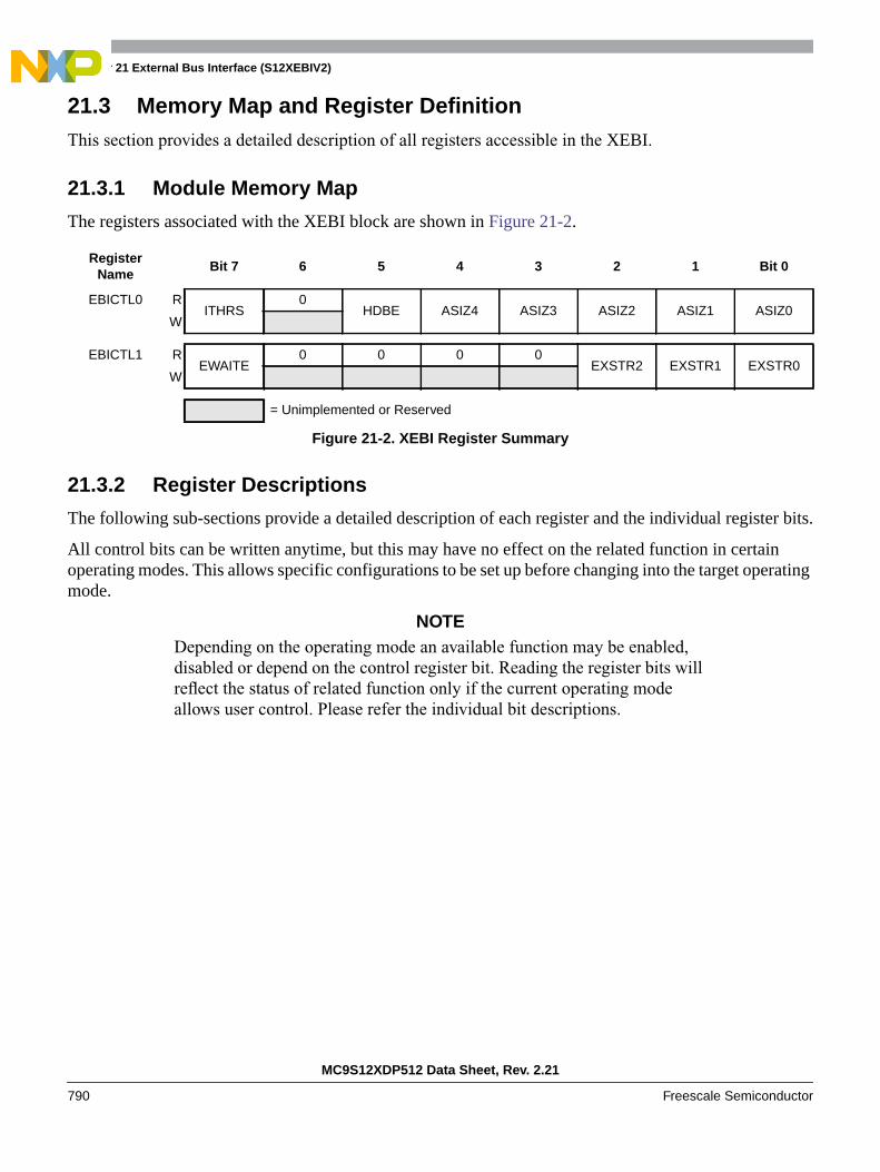
Chapter 21 External Bus Interface (S12XEBIV2)
MC9S12XDP512 Data Sheet, Rev. 2.21
790 Freescale Semiconductor
21.3 Memory Map and Register DefinitionThis section provides a detailed description of all registers accessible in the XEBI.
21.3.1 Module Memory Map
The registers associated with the XEBI block are shown in Figure 21-2.
21.3.2 Register Descriptions
The following sub-sections provide a detailed description of each register and the individual register bits.
All control bits can be written anytime, but this may have no effect on the related function in certainoperating modes. This allows specific configurations to be set up before changing into the target operatingmode.
NOTEDepending on the operating mode an available function may be enabled,disabled or depend on the control register bit. Reading the register bits willreflect the status of related function only if the current operating modeallows user control. Please refer the individual bit descriptions.
RegisterName
Bit 7 6 5 4 3 2 1 Bit 0
EBICTL0 RITHRS
0HDBE ASIZ4 ASIZ3 ASIZ2 ASIZ1 ASIZ0
W
EBICTL1 REWAITE
0 0 0 0EXSTR2 EXSTR1 EXSTR0
W
= Unimplemented or Reserved
Figure 21-2. XEBI Register Summary
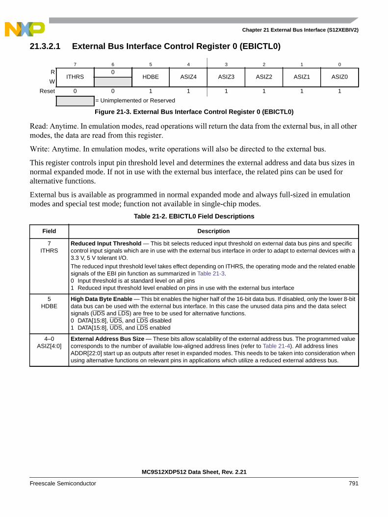
Chapter 21 External Bus Interface (S12XEBIV2)
MC9S12XDP512 Data Sheet, Rev. 2.21
Freescale Semiconductor 791
21.3.2.1 External Bus Interface Control Register 0 (EBICTL0)
Read: Anytime. In emulation modes, read operations will return the data from the external bus, in all othermodes, the data are read from this register.
Write: Anytime. In emulation modes, write operations will also be directed to the external bus.
This register controls input pin threshold level and determines the external address and data bus sizes innormal expanded mode. If not in use with the external bus interface, the related pins can be used foralternative functions.
External bus is available as programmed in normal expanded mode and always full-sized in emulationmodes and special test mode; function not available in single-chip modes.
7 6 5 4 3 2 1 0
RITHRS
0HDBE ASIZ4 ASIZ3 ASIZ2 ASIZ1 ASIZ0
W
Reset 0 0 1 1 1 1 1 1
= Unimplemented or Reserved
Figure 21-3. External Bus Interface Control Register 0 (EBICTL0)
Table 21-2. EBICTL0 Field Descriptions
Field Description
7ITHRS
Reduced Input Threshold — This bit selects reduced input threshold on external data bus pins and specificcontrol input signals which are in use with the external bus interface in order to adapt to external devices with a3.3 V, 5 V tolerant I/O.The reduced input threshold level takes effect depending on ITHRS, the operating mode and the related enablesignals of the EBI pin function as summarized in Table 21-3.0 Input threshold is at standard level on all pins1 Reduced input threshold level enabled on pins in use with the external bus interface
5HDBE
High Data Byte Enable — This bit enables the higher half of the 16-bit data bus. If disabled, only the lower 8-bitdata bus can be used with the external bus interface. In this case the unused data pins and the data selectsignals (UDS and LDS) are free to be used for alternative functions.0 DATA[15:8], UDS, and LDS disabled1 DATA[15:8], UDS, and LDS enabled
4–0ASIZ[4:0]
External Address Bus Size — These bits allow scalability of the external address bus. The programmed valuecorresponds to the number of available low-aligned address lines (refer to Table 21-4). All address linesADDR[22:0] start up as outputs after reset in expanded modes. This needs to be taken into consideration whenusing alternative functions on relevant pins in applications which utilize a reduced external address bus.
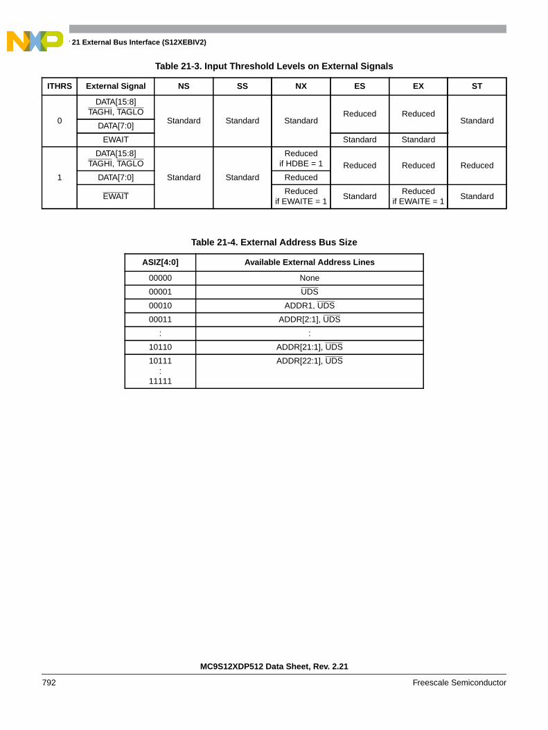
Chapter 21 External Bus Interface (S12XEBIV2)
MC9S12XDP512 Data Sheet, Rev. 2.21
792 Freescale Semiconductor
Table 21-3. Input Threshold Levels on External Signals
ITHRS External Signal NS SS NX ES EX ST
0
DATA[15:8]TAGHI, TAGLO
Standard Standard StandardReduced Reduced
StandardDATA[7:0]
EWAIT Standard Standard
1
DATA[15:8]TAGHI, TAGLO
Standard Standard
Reducedif HDBE = 1 Reduced Reduced Reduced
DATA[7:0] Reduced
EWAITReduced
if EWAITE = 1Standard
Reducedif EWAITE = 1
Standard
Table 21-4. External Address Bus Size
ASIZ[4:0] Available External Address Lines
00000 None
00001 UDS
00010 ADDR1, UDS
00011 ADDR[2:1], UDS
: :
10110 ADDR[21:1], UDS
10111:
11111
ADDR[22:1], UDS
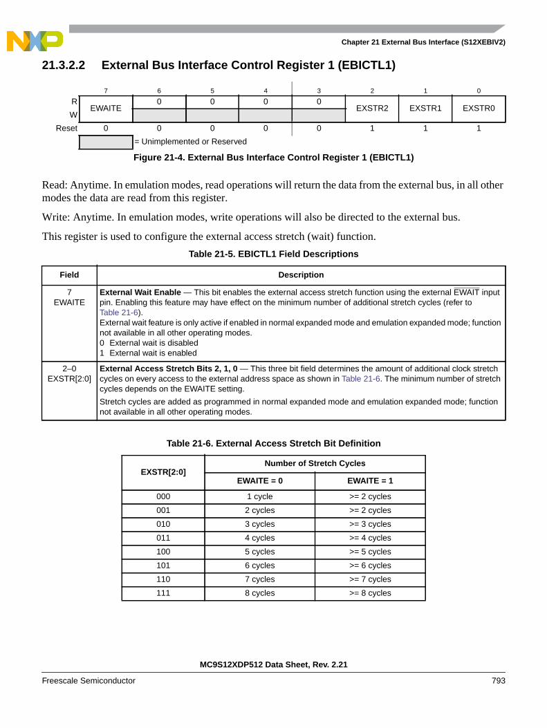
Chapter 21 External Bus Interface (S12XEBIV2)
MC9S12XDP512 Data Sheet, Rev. 2.21
Freescale Semiconductor 793
21.3.2.2 External Bus Interface Control Register 1 (EBICTL1)
Read: Anytime. In emulation modes, read operations will return the data from the external bus, in all othermodes the data are read from this register.
Write: Anytime. In emulation modes, write operations will also be directed to the external bus.
This register is used to configure the external access stretch (wait) function.
7 6 5 4 3 2 1 0
REWAITE
0 0 0 0EXSTR2 EXSTR1 EXSTR0
W
Reset 0 0 0 0 0 1 1 1
= Unimplemented or Reserved
Figure 21-4. External Bus Interface Control Register 1 (EBICTL1)
Table 21-5. EBICTL1 Field Descriptions
Field Description
7EWAITE
External Wait Enable — This bit enables the external access stretch function using the external EWAIT inputpin. Enabling this feature may have effect on the minimum number of additional stretch cycles (refer toTable 21-6).External wait feature is only active if enabled in normal expanded mode and emulation expanded mode; functionnot available in all other operating modes.0 External wait is disabled1 External wait is enabled
2–0EXSTR[2:0]
External Access Stretch Bits 2, 1, 0 — This three bit field determines the amount of additional clock stretchcycles on every access to the external address space as shown in Table 21-6. The minimum number of stretchcycles depends on the EWAITE setting.
Stretch cycles are added as programmed in normal expanded mode and emulation expanded mode; functionnot available in all other operating modes.
Table 21-6. External Access Stretch Bit Definition
EXSTR[2:0]Number of Stretch Cycles
EWAITE = 0 EWAITE = 1
000 1 cycle >= 2 cycles
001 2 cycles >= 2 cycles
010 3 cycles >= 3 cycles
011 4 cycles >= 4 cycles
100 5 cycles >= 5 cycles
101 6 cycles >= 6 cycles
110 7 cycles >= 7 cycles
111 8 cycles >= 8 cycles

Chapter 21 External Bus Interface (S12XEBIV2)
MC9S12XDP512 Data Sheet, Rev. 2.21
794 Freescale Semiconductor
21.4 Functional DescriptionThis section describes the functions of the external bus interface. The availability of external signals andfunctions in relation to the operating mode is initially summarized and described in more detail in separatesub-sections.
21.4.1 Operating Modes and External Bus Properties
A summary of the external bus interface functions for each operating mode is shown in Table 21-7.
Table 21-7. Summary of Functions
Properties(if Enabled)
Single-Chip Modes Expanded Modes
NormalSingle-Chip
SpecialSingle-Chip
NormalExpanded
EmulationSingle-Chip
EmulationExpanded
SpecialTest
Timing Properties
PRR access1
1 Incl. S12X_EBI registers
2 cyclesread internalwrite internal
2 cyclesread internalwrite internal
2 cyclesread internalwrite internal
2 cyclesread externalwrite int & ext
2 cyclesread externalwrite int & ext
2 cyclesread internalwrite internal
Internal accessvisible externally
— ——
1 cycle 1 cycle 1 cycle
Externaladdress access
andunimplemented area
access2
2 Refer to S12X_MMC section.
— — Max. of 2 to 9programmed
cyclesor n cycles of
ext. wait3
3 If EWAITE = 1, the minimum number of external bus cycles is 3.
1 cycle Max. of 2 to 9programmed
cyclesor n cycles of
ext. wait3
1 cycle
Flash areaaddress access4
4 Available only if configured appropriately by ROMON and EROMON (refer to S12X_MMC section).
— — — 1 cycle 1 cycle 1 cycle
Signal Properties
Bus signals — — ADDR[22:1]DATA[15:0]
ADDR[22:20]/ACC[2:0]
ADDR[19:16]/IQSTAT[3:0]ADDR[15:0]/
IVD[15:0]DATA[15:0]
ADDR[22:20]/ACC[2:0]
ADDR[19:16]/IQSTAT[3:0]ADDR[15:0]/
IVD[15:0]DATA[15:0]
ADDR[22:0]DATA[15:0]
Data select signals(if 16-bit data bus)
— — UDSLDS
ADDR0LSTRB
ADDR0LSTRB
ADDR0LSTRB
Data direction signals — — REWE
R/W R/W R/W
External waitfeature
— — EWAIT — EWAIT —
Reduced inputthreshold enabled on
— — Refer toTable 21-3
DATA[15:0]EWAIT
DATA[15:0]EWAIT
Refer toTable 21-3
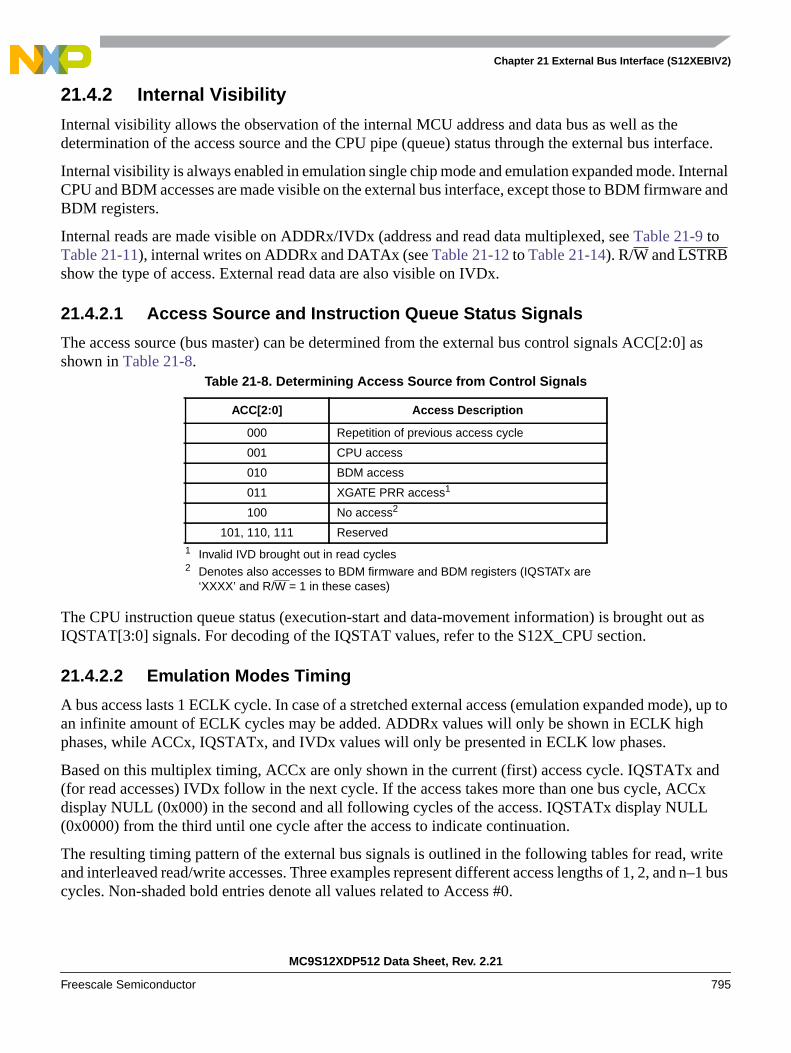
Chapter 21 External Bus Interface (S12XEBIV2)
MC9S12XDP512 Data Sheet, Rev. 2.21
Freescale Semiconductor 795
21.4.2 Internal Visibility
Internal visibility allows the observation of the internal MCU address and data bus as well as thedetermination of the access source and the CPU pipe (queue) status through the external bus interface.
Internal visibility is always enabled in emulation single chip mode and emulation expanded mode. InternalCPU and BDM accesses are made visible on the external bus interface, except those to BDM firmware andBDM registers.
Internal reads are made visible on ADDRx/IVDx (address and read data multiplexed, see Table 21-9 toTable 21-11), internal writes on ADDRx and DATAx (see Table 21-12 to Table 21-14). R/W and LSTRBshow the type of access. External read data are also visible on IVDx.
21.4.2.1 Access Source and Instruction Queue Status Signals
The access source (bus master) can be determined from the external bus control signals ACC[2:0] asshown in Table 21-8.
The CPU instruction queue status (execution-start and data-movement information) is brought out asIQSTAT[3:0] signals. For decoding of the IQSTAT values, refer to the S12X_CPU section.
21.4.2.2 Emulation Modes Timing
A bus access lasts 1 ECLK cycle. In case of a stretched external access (emulation expanded mode), up toan infinite amount of ECLK cycles may be added. ADDRx values will only be shown in ECLK highphases, while ACCx, IQSTATx, and IVDx values will only be presented in ECLK low phases.
Based on this multiplex timing, ACCx are only shown in the current (first) access cycle. IQSTATx and(for read accesses) IVDx follow in the next cycle. If the access takes more than one bus cycle, ACCxdisplay NULL (0x000) in the second and all following cycles of the access. IQSTATx display NULL(0x0000) from the third until one cycle after the access to indicate continuation.
The resulting timing pattern of the external bus signals is outlined in the following tables for read, writeand interleaved read/write accesses. Three examples represent different access lengths of 1, 2, and n–1 buscycles. Non-shaded bold entries denote all values related to Access #0.
Table 21-8. Determining Access Source from Control Signals
ACC[2:0] Access Description
000 Repetition of previous access cycle
001 CPU access
010 BDM access
011 XGATE PRR access1
1 Invalid IVD brought out in read cycles
100 No access2
2 Denotes also accesses to BDM firmware and BDM registers (IQSTATx are‘XXXX’ and R/W = 1 in these cases)
101, 110, 111 Reserved
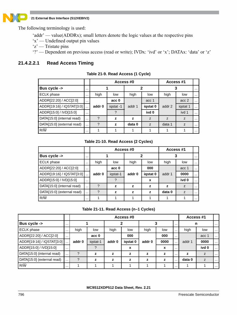
Chapter 21 External Bus Interface (S12XEBIV2)
MC9S12XDP512 Data Sheet, Rev. 2.21
796 Freescale Semiconductor
The following terminology is used:
‘addr’ — value(ADDRx); small letters denote the logic values at the respective pins‘x’ — Undefined output pin values‘z’ — Tristate pins‘?’ — Dependent on previous access (read or write); IVDx: ‘ivd’ or ‘x’; DATAx: ‘data’ or ‘z’
21.4.2.2.1 Read Access Timing
Table 21-9. Read Access (1 Cycle)
Access #0 Access #1
Bus cycle -> ... 1 2 3 ...
ECLK phase ... high low high low high low ...
ADDR[22:20] / ACC[2:0] ...
addr 0
acc 0
addr 1
acc 1
addr 2
acc 2 ...
ADDR[19:16] / IQSTAT[3:0] ... iqstat -1 iqstat 0 iqstat 1 ...
ADDR[15:0] / IVD[15:0] ... ? ivd 0 ivd 1 ...
DATA[15:0] (internal read) ... ? z z z z z ...
DATA[15:0] (external read) ... ? z data 0 z data 1 z ...
R/W ... 1 1 1 1 1 1 ...
Table 21-10. Read Access (2 Cycles)
Access #0 Access #1
Bus cycle -> ... 1 2 3 ...
ECLK phase ... high low high low high low ...
ADDR[22:20] / ACC[2:0] ...
addr 0
acc 0
addr 0
000
addr 1
acc 1 ...
ADDR[19:16] / IQSTAT[3:0] ... iqstat-1 iqstat 0 0000 ...
ADDR[15:0] / IVD[15:0] ... ? x ivd 0 ...
DATA[15:0] (internal read) ... ? z z z z z ...
DATA[15:0] (external read) ... ? z z z data 0 z ...
R/W ... 1 1 1 1 1 1 ...
Table 21-11. Read Access (n–1 Cycles)
Access #0 Access #1
Bus cycle -> ... 1 2 3 ... n ...
ECLK phase ... high low high low high low ... high low ...
ADDR[22:20] / ACC[2:0] ...
addr 0
acc 0
addr 0
000
addr 0
000 ...
addr 1
acc 1 ...
ADDR[19:16] / IQSTAT[3:0] ... iqstat-1 iqstat 0 0000 ... 0000 ...
ADDR[15:0] / IVD[15:0] ... ? x x ... ivd 0 ...
DATA[15:0] (internal read) ... ? z z z z z ... z z ...
DATA[15:0] (external read) ... ? z z z z z ... data 0 z ...
R/W ... 1 1 1 1 1 1 ... 1 1 ...
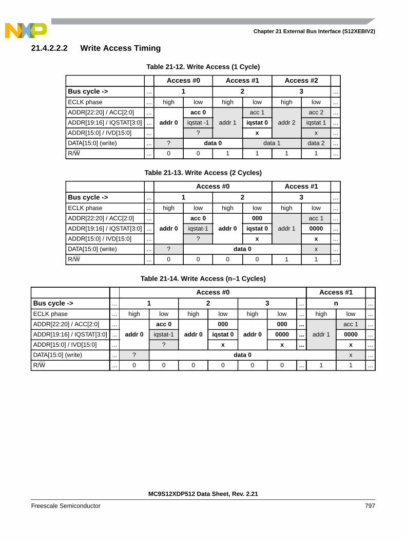
Chapter 21 External Bus Interface (S12XEBIV2)
MC9S12XDP512 Data Sheet, Rev. 2.21
Freescale Semiconductor 797
21.4.2.2.2 Write Access Timing
Table 21-12. Write Access (1 Cycle)
Access #0 Access #1 Access #2
Bus cycle -> ... 1 2 3 ...
ECLK phase ... high low high low high low ...
ADDR[22:20] / ACC[2:0] ...
addr 0
acc 0
addr 1
acc 1
addr 2
acc 2 ...
ADDR[19:16] / IQSTAT[3:0] ... iqstat -1 iqstat 0 iqstat 1 ...
ADDR[15:0] / IVD[15:0] ... ? x x ...
DATA[15:0] (write) ... ? data 0 data 1 data 2 ...
R/W ... 0 0 1 1 1 1 ...
Table 21-13. Write Access (2 Cycles)
Access #0 Access #1
Bus cycle -> ... 1 2 3 ...
ECLK phase ... high low high low high low ...
ADDR[22:20] / ACC[2:0] ...
addr 0
acc 0
addr 0
000
addr 1
acc 1 ...
ADDR[19:16] / IQSTAT[3:0] ... iqstat-1 iqstat 0 0000 ...
ADDR[15:0] / IVD[15:0] ... ? x x ...
DATA[15:0] (write) ... ? data 0 x ...
R/W ... 0 0 0 0 1 1 ...
Table 21-14. Write Access (n–1 Cycles)
Access #0 Access #1
Bus cycle -> ... 1 2 3 ... n ...
ECLK phase ... high low high low high low ... high low ...
ADDR[22:20] / ACC[2:0] ...
addr 0
acc 0
addr 0
000
addr 0
000 ...
addr 1
acc 1 ...
ADDR[19:16] / IQSTAT[3:0] ... iqstat-1 iqstat 0 0000 ... 0000 ...
ADDR[15:0] / IVD[15:0] ... ? x x ... x ...
DATA[15:0] (write) ... ? data 0 x ...
R/W ... 0 0 0 0 0 0 ... 1 1 ...

Chapter 21 External Bus Interface (S12XEBIV2)
MC9S12XDP512 Data Sheet, Rev. 2.21
798 Freescale Semiconductor
21.4.2.2.3 Read-Write-Read Access Timing
21.4.2.3 Internal Visibility Data
Depending on the access size and alignment, either a word of read data is made visible on the address linesor only the related data byte will be presented in the ECLK low phase. For details refer to Table 21-16.
21.4.3 Accesses to Port Replacement Registers
All read and write accesses to PRR addresses take two bus clock cycles independent of the operating mode.If writing to these addresses in emulation modes, the access is directed to both, the internal register andthe external resource while reads will be treated external.
The XEBI control registers also belong to this category.
21.4.4 Stretched External Bus Accesses
In order to allow fast internal bus cycles to coexist in a system with slower external resources, the XEBIsupports stretched external bus accesses (wait states).
This feature is available in normal expanded mode and emulation expanded mode for accesses to allexternal addresses except emulation memory and PRR. In these cases the fixed access times are 1 or 2cycles, respectively.
Table 21-15. Interleaved Read-Write-Read Accesses (1 Cycle)
Access #0 Access #1 Access #2
Bus cycle -> ... 1 2 3 ...
ECLK phase ... high low high low high low ...
ADDR[22:20] / ACC[2:0] ...
addr 0
acc 0
addr 1
acc 1
addr 2
acc 2 ...
ADDR[19:16] / IQSTAT[3:0] ... iqstat -1 iqstat 0 iqstat 1 ...
ADDR[15:0] / IVD[15:0] ... ? ivd 0 x ...
DATA[15:0] (internal read) ... ? z z (write) data 1 z ...
DATA[15:0] (external read) ... ? z data 0 (write) data 1 z ...
R/W ... 1 1 0 0 1 1 ...
Table 21-16. IVD Read Data Output
Access IVD[15:8] IVD[7:0]
Word read of data at an even and even+1 address ivd(even) ivd(even+1)
Word read of data at an odd and odd+1 internal RAM address (misaligned) ivd(odd+1) ivd(odd)
Byte read of data at an even address ivd(even) addr[7:0] (rep.)
Byte read of data at an odd address addr[15:8] (rep.) ivd(odd)
Chapter 21 External Bus Interface (S12XEBIV2)
MC9S12XDP512 Data Sheet, Rev. 2.21
Freescale Semiconductor 799
Stretched accesses are controlled by:
1. EXSTR[2:0] bits in the EBICTL1 register configuring fixed amount of stretch cycles
2. Activation of the external wait feature by EWAITE in EBICTL1 register
3. Assertion of the external EWAIT signal when EWAITE = 1
The EXSTR[2:0] control bits can be programmed for generation of a fixed number of 1 to 8 stretch cycles.If the external wait feature is enabled, the minimum number of additional stretch cycles is 2. An arbitraryamount of stretch cycles can be added using the EWAIT input.
EWAIT needs to be asserted at least for a minimal specified time window within an external access cyclefor the internal logic to detect it and add a cycle (refer to electrical characteristics). Holding it for additionalcycles will cause the external bus access to be stretched accordingly.
Write accesses are stretched by holding the initiator in its current state for additional cycles as programmedand controlled by external wait after the data have been driven out on the external bus. This results in anextension of time the bus signals and the related control signals are valid externally.
Read data are not captured by the system in normal expanded mode until the specified setup time beforethe RE rising edge.
Read data are not captured in emulation expanded mode until the specified setup time before the fallingedge of ECLK.
In emulation expanded mode, accesses to the internal flash or the emulation memory (determined byEROMON and ROMON bits; see S12X_MMC section for details) always take 1 cycle and stretching isnot supported. In case the internal flash is taken out of the map in user applications, accesses are stretchedas programmed and controlled by external wait.
21.4.5 Data Select and Data Direction Signals
The S12X_EBI supports byte and word accesses at any valid external address. The big endian system ofthe MCU is extended to the external bus; however, word accesses are restricted to even aligned addresses.The only exception is the visibility of misaligned word accesses to addresses in the internal RAM as thismodule exclusively supports these kind of accesses in a single cycle.
With the above restriction, a fixed relationship is implied between the address parity and the dedicated bushalves where the data are accessed: DATA[15:8] is related to even addresses and DATA[7:0] is related toodd addresses.
In expanded modes the data access type is externally determined by a set of control signals, i.e., data selectand data direction signals, as described below. The data select signals are not available if using the externalbus interface with an 8-bit data bus.
21.4.5.1 Normal Expanded Mode
In normal expanded mode, the external signals RE, WE, UDS, LDS indicate the access type (read/write),data size and alignment of an external bus access (Table 21-17).
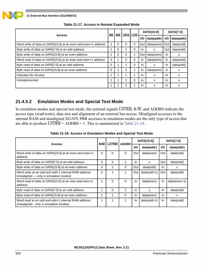
Chapter 21 External Bus Interface (S12XEBIV2)
MC9S12XDP512 Data Sheet, Rev. 2.21
800 Freescale Semiconductor
21.4.5.2 Emulation Modes and Special Test Mode
In emulation modes and special test mode, the external signals LSTRB, R/W, and ADDR0 indicate theaccess type (read/write), data size and alignment of an external bus access. Misaligned accesses to theinternal RAM and misaligned XGATE PRR accesses in emulation modes are the only type of access thatare able to produce LSTRB = ADDR0 = 1. This is summarized in Table 21-18.
Table 21-17. Access in Normal Expanded Mode
Access RE WE UDS LDSDATA[15:8] DATA[7:0]
I/O data(addr) I/O data(addr)
Word write of data on DATA[15:0] at an even and even+1 address 1 0 0 0 Out data(even) Out data(odd)
Byte write of data on DATA[7:0] at an odd address 1 0 1 0 In x Out data(odd)
Byte write of data on DATA[15:8] at an even address 1 0 0 1 Out data(even) In x
Word read of data on DATA[15:0] at an even and even+1 address 0 1 0 0 In data(even) In data(odd)
Byte read of data on DATA[7:0] at an odd address 0 1 1 0 In x In data(odd)
Byte read of data on DATA[15:8] at an even address 0 1 0 1 In data(even) In x
Indicates No Access 1 1 1 1 In x In x
Unimplemented 1 1 1 0 In x In x
1 1 0 1 In x In x
Table 21-18. Access in Emulation Modes and Special Test Mode
Access R/W LSTRB ADDR0DATA[15:8] DATA[7:0]
I/O data(addr) I/O data(addr)
Word write of data on DATA[15:0] at an even and even+1address
0 0 0 Out data(even) Out data(odd)
Byte write of data on DATA[7:0] at an odd address 0 0 1 In x Out data(odd)
Byte write of data on DATA[15:8] at an even address 0 1 0 Out data(odd) In x
Word write at an odd and odd+1 internal RAM address(misaligned — only in emulation modes)
0 1 1 Out data(odd+1) Out data(odd)
Word read of data on DATA[15:0] at an even and even+1address
1 0 0 In data(even) In data(even+1)
Byte read of data on DATA[7:0] at an odd address 1 0 1 In x In data(odd)
Byte read of data on DATA[15:8] at an even address 1 1 0 In data(even) In x
Word read at an odd and odd+1 internal RAM address(misaligned - only in emulation modes)
1 1 1 In data(odd+1) In data(odd)

Chapter 21 External Bus Interface (S12XEBIV2)
MC9S12XDP512 Data Sheet, Rev. 2.21
Freescale Semiconductor 801
21.4.6 Low-Power Options
The XEBI does not support any user-controlled options for reducing power consumption.
21.4.6.1 Run Mode
The XEBI does not support any options for reducing power in run mode.
Power consumption is reduced in single-chip modes due to the absence of the external bus interface.Operation in expanded modes results in a higher power consumption, however any unnecessary togglingof external bus signals is reduced to the lowest indispensable activity by holding the previous statesbetween external accesses.
21.4.6.2 Wait Mode
The XEBI does not support any options for reducing power in wait mode.
21.4.6.3 Stop Mode
The XEBI will cease to function in stop mode.
21.5 Initialization/Application InformationThis section describes the external bus interface usage and timing. Typical customer operating modes arenormal expanded mode and emulation modes, specifically to be used in emulator applications. Taking theavailability of the external wait feature into account the use cases are divided into four scenarios:
• Normal expanded mode
— External wait feature disabled
– External wait feature enabled
• Emulation modes
– Emulation single-chip mode (without wait states)
– Emulation expanded mode (with optional access stretching)
Normal single-chip mode and special single-chip mode do not have an external bus. Special test mode isused for factory test only. Therefore, these modes are omitted here.
All timing diagrams referred to throughout this section are available in the Electrical Characteristicsappendix of the SoC section.
Chapter 21 External Bus Interface (S12XEBIV2)
MC9S12XDP512 Data Sheet, Rev. 2.21
802 Freescale Semiconductor
21.5.1 Normal Expanded Mode
This mode allows interfacing to external memories or peripherals which are available in the commercialmarket. In these applications the normal bus operation requires a minimum of 1 cycle stretch for eachexternal access.
21.5.1.1 Example 1a: External Wait Feature Disabled
The first example of bus timing of an external read and write access with the external wait feature disabledis shown in
• Figure ‘Example 1a: Normal Expanded Mode — Read Followed by Write’
The associated supply voltage dependent timing are numbers given in
• Table ‘Example 1a: Normal Expanded Mode Timing VDD5 = 5.0 V (EWAITE = 0)’
• Table ‘Example 1a: Normal Expanded Mode Timing VDD5 = 3.0 V (EWAITE = 0)’
Systems designed this way rely on the internal programmable access stretching. These systems havepredictable external memory access times. The additional stretch time can be programmed up to 8 cyclesto provide longer access times.
21.5.1.2 Example 1b: External Wait Feature Enabled
The external wait operation is shown in this example. It can be used to exceed the amount of stretch cyclesover the programmed number in EXSTR[2:0]. The feature must be enabled by writing EWAITE = 1.
If the EWAIT signal is not asserted, the number of stretch cycles is forced to a minimum of 2 cycles. IfEWAIT is asserted within the predefined time window during the access it will be strobed active andanother stretch cycle is added. If strobed inactive, the next cycle will be the last cycle before the access isfinished. EWAIT can be held asserted as long as desired to stretch the access.
An access with 1 cycle stretch by EWAIT assertion is shown in
• Figure ‘Example 1b: Normal Expanded Mode — Stretched Read Access’
• Figure ‘Example 1b: Normal Expanded Mode — Stretched Write Access’
The associated timing numbers for both operations are given in
• Table ‘Example 1b: Normal Expanded Mode Timing VDD5 = 5.0 V (EWAITE = 1)’
• Table ‘Example 1b: Normal Expanded Mode Timing VDD5 = 3.0 V (EWAITE = 1)’
It is recommended to use the free-running clock (ECLK) at the fastest rate (bus clock rate) to synchronizethe EWAIT input signal.

Chapter 21 External Bus Interface (S12XEBIV2)
MC9S12XDP512 Data Sheet, Rev. 2.21
Freescale Semiconductor 803
21.5.2 Emulation Modes
In emulation mode applications, the development systems use a custom PRU device to rebuild thesingle-chip or expanded bus functions which are lost due to the use of the external bus with an emulator.
Accesses to a set of registers controlling the related ports in normal modes (refer to SoC section) aredirected to the external bus in emulation modes which are substituted by PRR as part of the PRU. Accessesto these registers take a constant time of 2 cycles.
Depending on the setting of ROMON and EROMON (refer to S12X_MMC section), the program codecan be executed from internal memory or an optional external emulation memory (EMULMEM). No waitstate operation (stretching) of the external bus access is done in emulation modes when accessing internalmemory or emulation memory addresses.
In both modes observation of the internal operation is supported through the external bus (internalvisibility).
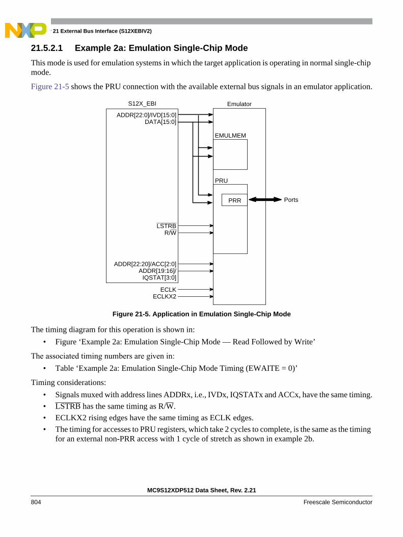
Chapter 21 External Bus Interface (S12XEBIV2)
MC9S12XDP512 Data Sheet, Rev. 2.21
804 Freescale Semiconductor
21.5.2.1 Example 2a: Emulation Single-Chip Mode
This mode is used for emulation systems in which the target application is operating in normal single-chipmode.
Figure 21-5 shows the PRU connection with the available external bus signals in an emulator application.
Figure 21-5. Application in Emulation Single-Chip Mode
The timing diagram for this operation is shown in:
• Figure ‘Example 2a: Emulation Single-Chip Mode — Read Followed by Write’
The associated timing numbers are given in:
• Table ‘Example 2a: Emulation Single-Chip Mode Timing (EWAITE = 0)’
Timing considerations:
• Signals muxed with address lines ADDRx, i.e., IVDx, IQSTATx and ACCx, have the same timing.
• LSTRB has the same timing as R/W.
• ECLKX2 rising edges have the same timing as ECLK edges.
• The timing for accesses to PRU registers, which take 2 cycles to complete, is the same as the timingfor an external non-PRR access with 1 cycle of stretch as shown in example 2b.
S12X_EBI
ADDR[22:0]/IVD[15:0]DATA[15:0]
ECLKECLKX2
LSTRBR/W
ADDR[22:20]/ACC[2:0]ADDR[19:16]/
PRR Ports
PRU
IQSTAT[3:0]
EMULMEM
Emulator

Chapter 21 External Bus Interface (S12XEBIV2)
MC9S12XDP512 Data Sheet, Rev. 2.21
Freescale Semiconductor 805
21.5.2.2 Example 2b: Emulation Expanded Mode
This mode is used for emulation systems in which the target application is operating in normal expandedmode.
If the external bus is used with a PRU, the external device rebuilds the data select and data direction signalsUDS, LDS, RE, and WE from the ADDR0, LSTRB, and R/W signals.
Figure 21-6 shows the PRU connection with the available external bus signals in an emulator application.
Figure 21-6. Application in Emulation Expanded Mode
The timings of accesses with 1 stretch cycle are shown in
• Figure ‘Example 2b: Emulation Expanded Mode — Read with 1 Stretch Cycle’
• Figure ‘Example 2b: Emulation Expanded Mode — Write with 1 Stretch Cycle’
The associated timing numbers are given in
• Table ‘Example 2b: Emulation Expanded Mode Timing VDD5 = 5.0 V (EWAITE = 0)’ (this alsoincludes examples for alternative settings of 2 and 3 additional stretch cycles)
Timing considerations:
• If no stretch cycle is added, the timing is the same as in Emulation Single-Chip Mode.
S12X_EBI
ADDR[22:0]/IVD[15:0]DATA[15:0]
ECLKECLKX2
LSTRBR/W
UDSLDSREWE
ADDR[22:20]/ACC[2:0]ADDR[19:16]/
CS[2:0]
PRR Ports
PRU
IQSTAT[3:0]
EMULMEM
Emulator
EWAIT

Chapter 21 External Bus Interface (S12XEBIV2)
MC9S12XDP512 Data Sheet, Rev. 2.21
806 Freescale Semiconductor
MC9S12XDP512 Data Sheet, Rev. 2.21
Freescale Semiconductor 807
Chapter 22DP512 Port Integration Module (S12XDP512PIMV2)
22.1 IntroductionThe S12XD family port integration module (below referred to as PIM) establishes the interface betweenthe peripheral modules including the non-multiplexed external bus interface module (S12X_EBI) and theI/O pins for all ports. It controls the electrical pin properties as well as the signal prioritization andmultiplexing on shared pins.
This document covers the description of:
• Port A, B used as address output of the S12X_EBI
• Port C, D used as data I/O of the S12X_EBI
• Port E associated with the S12X_EBI control signals and the IRQ, XIRQ interrupt inputs
• Port K associated with address output and control signals of the S12X_EBI
• Port T connected to the Enhanced Capture Timer (ECT) module
• Port S associated with 2 SCI and 1 SPI modules
• Port M associated with 4 MSCAN modules and 1 SCI module
• Port P connected to the PWM and 2 SPI modules — inputs can be used as an external interruptsource
• Port H associated with 2 SCI modules — inputs can be used as an external interrupt source
• Port J associated with 1 MSCAN, 1 SCI, and 2 IIC modules — inputs can be used as an externalinterrupt source
• Port AD0 and AD1 associated with one 8-channel and one 16-channel ATD module
Most I/O pins can be configured by register bits to select data direction and drive strength, to enable andselect pull-up or pull-down devices. Interrupts can be enabled on specific pins resulting in status flags.
The I/O’s of 2 MSCAN and all 3 SPI modules can be routed from their default location to alternative portpins.
NOTEThe implementation of the PIM is device dependent. Therefore somefunctions are not available on certain derivatives or 112-pin and 80-pinpackage options.

Chapter 22 DP512 Port Integration Module (S12XDP512PIMV2)
MC9S12XDP512 Data Sheet, Rev. 2.21
808 Freescale Semiconductor
22.1.1 Features
A full-featured PIM module includes these distinctive registers:
• Data and data direction registers for Ports A, B, C, D, E, K, T, S, M, P, H, J, AD0, and AD1 whenused as general-purpose I/O
• Control registers to enable/disable pull-device and select pull-ups/pull-downs on Ports T, S, M, P,H, and J on per-pin basis
• Control registers to enable/disable pull-up devices on Ports AD0, and AD1 on per-pin basis
• Single control register to enable/disable pull-ups on Ports A, B, C, D, E, and K on per-port basisand on BKGD pin
• Control registers to enable/disable reduced output drive on Ports T, S, M, P, H, J, AD0, and AD1on per-pin basis
• Single control register to enable/disable reduced output drive on Ports A, B, C, D, E, and K onper-port basis
• Control registers to enable/disable open-drain (wired-OR) mode on Ports S and M
• Control registers to enable/disable pin interrupts on Ports P, H, and J
• Interrupt flag register for pin interrupts on Ports P, H, and J
• Control register to configure IRQ pin operation
• Free-running clock outputs
A standard port pin has the following minimum features:
• Input/output selection
• 5V output drive with two selectable drive strengths
• 5V digital and analog input
• Input with selectable pull-up or pull-down device
Optional features:
• Open drain for wired-OR connections
• Interrupt inputs with glitch filtering
• Reduced input threshold to support low voltage applications
22.1.2 Block Diagram
Figure 22-1 is a block diagram of the PIM.
• Signals shown in Bold are not available in 80-pin packages.
• Signals shown in Bold-Italics are neither available in 112-pin nor in 80-pin packages.
• Shaded labels denote alternative module routing ports.

Chapter 22 DP512 Port Integration Module (S12XDP512PIMV2)
MC9S12XDP512 Data Sheet, Rev. 2.21
Freescale Semiconductor 809
Figure 22-1. PIM Block Diagram
Por
t T
PT0PT1PT2PT3PT4PT5PT6PT7
EC
T
IOC0IOC1IOC2IOC3IOC4IOC5IOC6IOC7
Por
t PPP0PP1PP2PP3PP4PP5PP6PP7
PW
M
PWM0PWM1PWM2PWM3PWM4PWM5PWM6PWM7
Por
t S
PS0PS1PS2PS3PS4PS5PS6PS7
RXDTXDRXDTXD
MISOMOSISCK
SS
SCI0
SCI1
SPI0
Port H
PH0PH1PH2PH3PH4PH5PH6PH7
Port J
PJ0PJ1
PJ6
PJ7
Port M
PM0PM1PM2PM3PM4PM5PM6PM7 SCI3TXD
RXD
CAN1TXCANRXCAN
CAN2TXCANRXCAN
CAN0TXCANRXCAN
IIC0SCLSDA
Port Integration Module
CAN4TXCANRXCAN
MISOMOSISCK
SSSPI1In
terr
upt L
ogic
MISOMOSI
SCKSS
SPI2
Port B
PB0PB1PB2PB3PB4PB5PB6PB7
Port A
PA0PA1PA2PA3PA4PA5PA6PA7
Por
t E
PE0PE1PE2PE3PE4PE5PE6PE7
Por
t K
PK0PK1PK2PK3
PK7
PK4PK5
ADDR8ADDR9ADDR10ADDR11ADDR12ADDR13ADDR14ADDR15
ADDR0/UDSADDR1ADDR2ADDR3ADDR4ADDR5ADDR6ADDR7
XIRQIRQ
WE/R/WLDS/LSTRB
ECLKTAGLO/RE/MODA
ECLKX2/XCLKSTAGHI/MODB
ADDR17ADDR18ADDR19
EWAIT/ROMCTL
ADRR20ADDR21
S12X_EBI
ADDR16
BKGD/MODC BKGD
CA
N0
Port C
PC0PC1PC2PC3PC4PC5PC6PC7
Port D
PD0PD1PD2PD3PD4PD5PD6PD7
DATA0DATA1DATA2DATA3DATA4DATA5DATA6DATA7
DATA8DATA9DATA10DATA11DATA12DATA13DATA14DATA15
NOACC/ADDR22 PK6
PJ4PJ5
PJ2
IIC1SCLSDA
RXDTXDRXDTXD
SCI4
SCI5
Interrupt LogicP
ort A
D0
PAD00PAD01PAD02PAD03PAD04PAD05PAD06PAD07
ATD
0
AN0AN1AN2AN3AN4AN5AN6AN7
Por
t AD
1
PAD08PAD10PAD12PAD14PAD16PAD18PAD20PAD22
ATD
1
AN1,0AN3,2AN5,4AN7,6AN9,8
AN11,10AN13,12AN15,14
SP
I1 S
PI2
SP
I0
PAD09PAD11PAD13PAD15PAD17PAD19PAD21PAD23
SCI2TXDRXD
CAN3TXCANRXCAN
S12X_BDMS12X_DBGS12X_INT
Inte
rrup
t Lo
gic
CA
N0
CA
N0
CA
N4
CA
N4
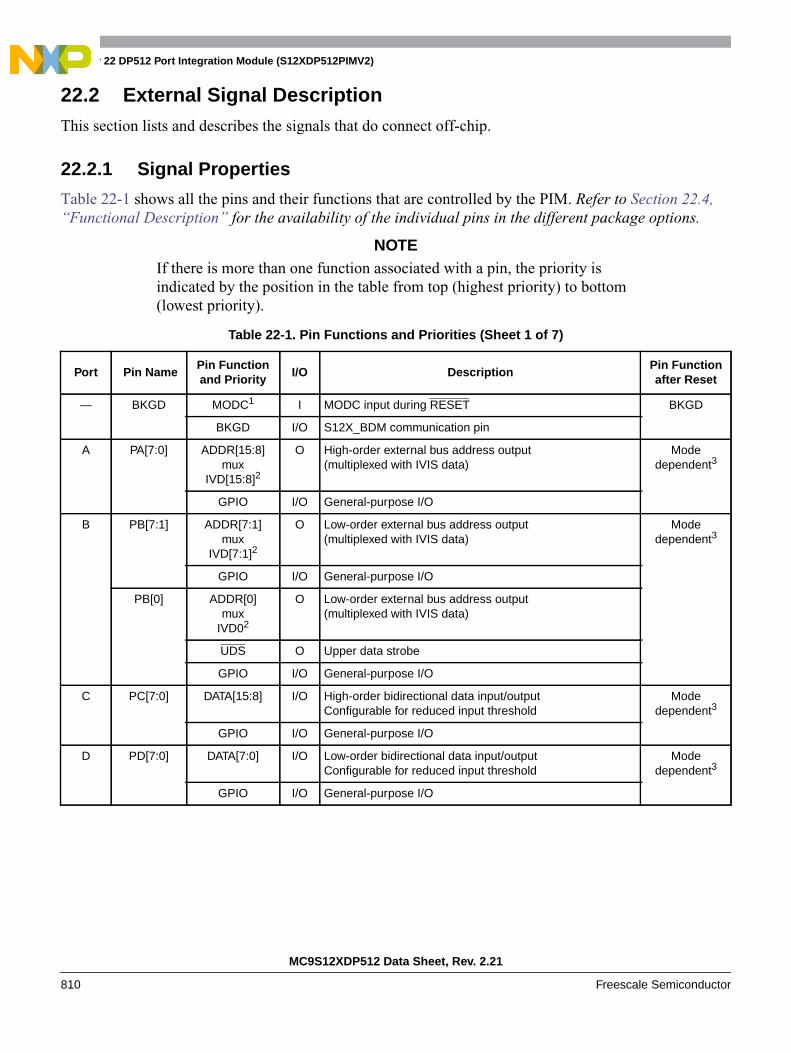
Chapter 22 DP512 Port Integration Module (S12XDP512PIMV2)
MC9S12XDP512 Data Sheet, Rev. 2.21
810 Freescale Semiconductor
22.2 External Signal DescriptionThis section lists and describes the signals that do connect off-chip.
22.2.1 Signal Properties
Table 22-1 shows all the pins and their functions that are controlled by the PIM. Refer to Section 22.4,“Functional Description” for the availability of the individual pins in the different package options.
NOTEIf there is more than one function associated with a pin, the priority isindicated by the position in the table from top (highest priority) to bottom(lowest priority).
Table 22-1. Pin Functions and Priorities (Sheet 1 of 7)
Port Pin NamePin Functionand Priority
I/O DescriptionPin Functionafter Reset
— BKGD MODC1 I MODC input during RESET BKGD
BKGD I/O S12X_BDM communication pin
A PA[7:0] ADDR[15:8]mux
IVD[15:8]2
O High-order external bus address output(multiplexed with IVIS data)
Modedependent3
GPIO I/O General-purpose I/O
B PB[7:1] ADDR[7:1]mux
IVD[7:1]2
O Low-order external bus address output(multiplexed with IVIS data)
Modedependent3
GPIO I/O General-purpose I/O
PB[0] ADDR[0]mux
IVD02
O Low-order external bus address output(multiplexed with IVIS data)
UDS O Upper data strobe
GPIO I/O General-purpose I/O
C PC[7:0] DATA[15:8] I/O High-order bidirectional data input/outputConfigurable for reduced input threshold
Modedependent3
GPIO I/O General-purpose I/O
D PD[7:0] DATA[7:0] I/O Low-order bidirectional data input/outputConfigurable for reduced input threshold
Modedependent3
GPIO I/O General-purpose I/O
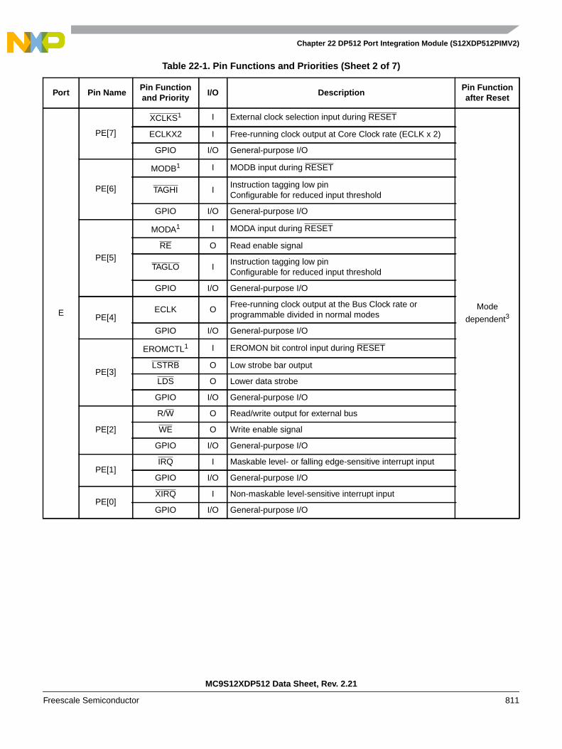
Chapter 22 DP512 Port Integration Module (S12XDP512PIMV2)
MC9S12XDP512 Data Sheet, Rev. 2.21
Freescale Semiconductor 811
E
PE[7]
XCLKS1 I External clock selection input during RESET
Mode
dependent3
ECLKX2 I Free-running clock output at Core Clock rate (ECLK x 2)
GPIO I/O General-purpose I/O
PE[6]
MODB1 I MODB input during RESET
TAGHI IInstruction tagging low pinConfigurable for reduced input threshold
GPIO I/O General-purpose I/O
PE[5]
MODA1 I MODA input during RESET
RE O Read enable signal
TAGLO IInstruction tagging low pinConfigurable for reduced input threshold
GPIO I/O General-purpose I/O
PE[4]ECLK O
Free-running clock output at the Bus Clock rate orprogrammable divided in normal modes
GPIO I/O General-purpose I/O
PE[3]
EROMCTL1 I EROMON bit control input during RESET
LSTRB O Low strobe bar output
LDS O Lower data strobe
GPIO I/O General-purpose I/O
PE[2]
R/W O Read/write output for external bus
WE O Write enable signal
GPIO I/O General-purpose I/O
PE[1]IRQ I Maskable level- or falling edge-sensitive interrupt input
GPIO I/O General-purpose I/O
PE[0]XIRQ I Non-maskable level-sensitive interrupt input
GPIO I/O General-purpose I/O
Table 22-1. Pin Functions and Priorities (Sheet 2 of 7)
Port Pin NamePin Functionand Priority
I/O DescriptionPin Functionafter Reset
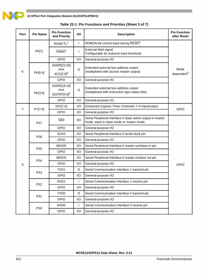
Chapter 22 DP512 Port Integration Module (S12XDP512PIMV2)
MC9S12XDP512 Data Sheet, Rev. 2.21
812 Freescale Semiconductor
K
PK[7]
ROMCTL1 I ROMON bit control input during RESET
Mode
dependent3
EWAIT IExternal Wait signalConfigurable for reduced input threshold
GPIO I/O General-purpose I/O
PK[6:4]
ADDR[22:20]mux
ACC[2:0]2O
Extended external bus address output(multiplexed with access master output)
GPIO I/O General-purpose I/O
PK[3:0]
ADDR[19:16]mux
IQSTAT[3:0]2O
Extended external bus address output(multiplexed with instruction pipe status bits)
GPIO I/O General-purpose I/O
T PT[7:0]IOC[7:0] I/O Enhanced Capture Timer Channels 7–0 input/output
GPIOGPIO I/O General-purpose I/O
S
PS7SS0 I/O
Serial Peripheral Interface 0 slave select output in mastermode, input in slave mode or master mode.
GPIO
GPIO I/O General-purpose I/O
PS6SCK0 I/O Serial Peripheral Interface 0 serial clock pin
GPIO I/O General-purpose I/O
PS5MOSI0 I/O Serial Peripheral Interface 0 master out/slave in pin
GPIO I/O General-purpose I/O
PS4MISO0 I/O Serial Peripheral Interface 0 master in/slave out pin
GPIO I/O General-purpose I/O
PS3TXD1 O Serial Communication Interface 1 transmit pin
GPIO I/O General-purpose I/O
PS2RXD1 I Serial Communication Interface 1 receive pin
GPIO I/O General-purpose I/O
PS1TXD0 O Serial Communication Interface 0 transmit pin
GPIO I/O General-purpose I/O
PS0RXD0 I Serial Communication Interface 0 receive pin
GPIO I/O General-purpose I/O
Table 22-1. Pin Functions and Priorities (Sheet 3 of 7)
Port Pin NamePin Functionand Priority
I/O DescriptionPin Functionafter Reset
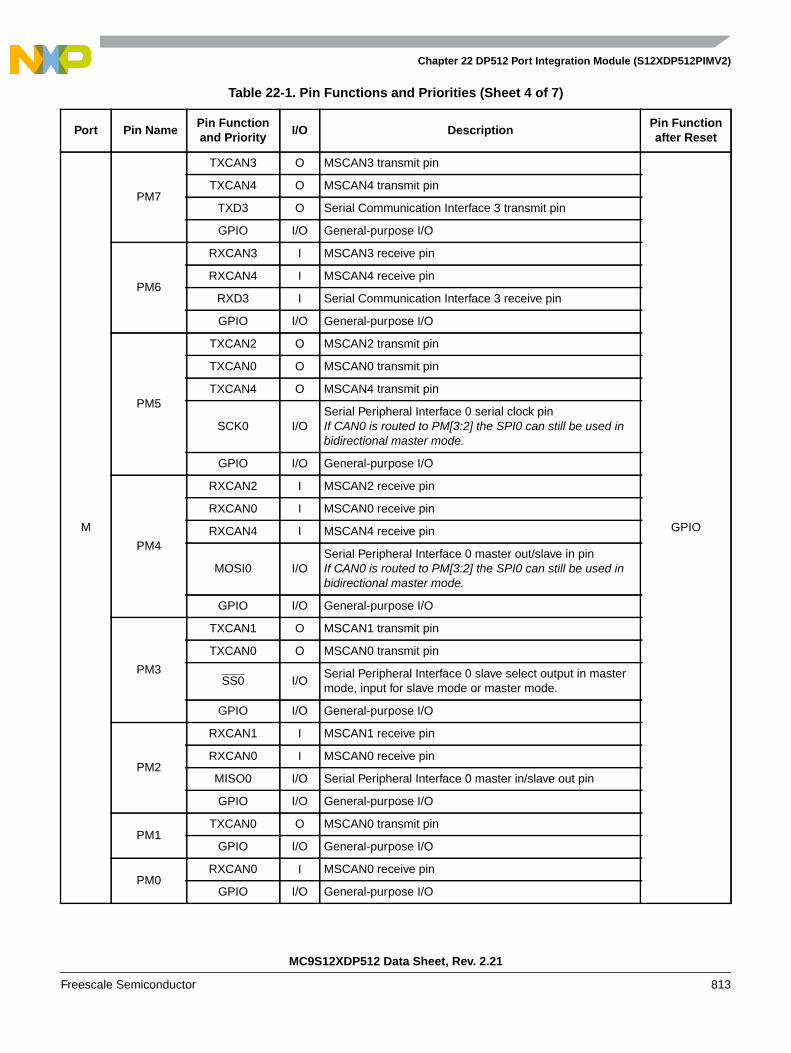
Chapter 22 DP512 Port Integration Module (S12XDP512PIMV2)
MC9S12XDP512 Data Sheet, Rev. 2.21
Freescale Semiconductor 813
M
PM7
TXCAN3 O MSCAN3 transmit pin
GPIO
TXCAN4 O MSCAN4 transmit pin
TXD3 O Serial Communication Interface 3 transmit pin
GPIO I/O General-purpose I/O
PM6
RXCAN3 I MSCAN3 receive pin
RXCAN4 I MSCAN4 receive pin
RXD3 I Serial Communication Interface 3 receive pin
GPIO I/O General-purpose I/O
PM5
TXCAN2 O MSCAN2 transmit pin
TXCAN0 O MSCAN0 transmit pin
TXCAN4 O MSCAN4 transmit pin
SCK0 I/OSerial Peripheral Interface 0 serial clock pinIf CAN0 is routed to PM[3:2] the SPI0 can still be used inbidirectional master mode.
GPIO I/O General-purpose I/O
PM4
RXCAN2 I MSCAN2 receive pin
RXCAN0 I MSCAN0 receive pin
RXCAN4 I MSCAN4 receive pin
MOSI0 I/OSerial Peripheral Interface 0 master out/slave in pinIf CAN0 is routed to PM[3:2] the SPI0 can still be used inbidirectional master mode.
GPIO I/O General-purpose I/O
PM3
TXCAN1 O MSCAN1 transmit pin
TXCAN0 O MSCAN0 transmit pin
SS0 I/OSerial Peripheral Interface 0 slave select output in mastermode, input for slave mode or master mode.
GPIO I/O General-purpose I/O
PM2
RXCAN1 I MSCAN1 receive pin
RXCAN0 I MSCAN0 receive pin
MISO0 I/O Serial Peripheral Interface 0 master in/slave out pin
GPIO I/O General-purpose I/O
PM1TXCAN0 O MSCAN0 transmit pin
GPIO I/O General-purpose I/O
PM0RXCAN0 I MSCAN0 receive pin
GPIO I/O General-purpose I/O
Table 22-1. Pin Functions and Priorities (Sheet 4 of 7)
Port Pin NamePin Functionand Priority
I/O DescriptionPin Functionafter Reset
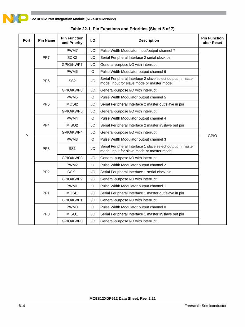
Chapter 22 DP512 Port Integration Module (S12XDP512PIMV2)
MC9S12XDP512 Data Sheet, Rev. 2.21
814 Freescale Semiconductor
P
PP7
PWM7 I/O Pulse Width Modulator input/output channel 7
GPIO
SCK2 I/O Serial Peripheral Interface 2 serial clock pin
GPIO/KWP7 I/O General-purpose I/O with interrupt
PP6
PWM6 O Pulse Width Modulator output channel 6
SS2 I/OSerial Peripheral Interface 2 slave select output in mastermode, input for slave mode or master mode.
GPIO/KWP6 I/O General-purpose I/O with interrupt
PP5
PWM5 O Pulse Width Modulator output channel 5
MOSI2 I/O Serial Peripheral Interface 2 master out/slave in pin
GPIO/KWP5 I/O General-purpose I/O with interrupt
PP4
PWM4 O Pulse Width Modulator output channel 4
MISO2 I/O Serial Peripheral Interface 2 master in/slave out pin
GPIO/KWP4 I/O General-purpose I/O with interrupt
PP3
PWM3 O Pulse Width Modulator output channel 3
SS1 I/OSerial Peripheral Interface 1 slave select output in mastermode, input for slave mode or master mode.
GPIO/KWP3 I/O General-purpose I/O with interrupt
PP2
PWM2 O Pulse Width Modulator output channel 2
SCK1 I/O Serial Peripheral Interface 1 serial clock pin
GPIO/KWP2 I/O General-purpose I/O with interrupt
PP1
PWM1 O Pulse Width Modulator output channel 1
MOSI1 I/O Serial Peripheral Interface 1 master out/slave in pin
GPIO/KWP1 I/O General-purpose I/O with interrupt
PP0
PWM0 O Pulse Width Modulator output channel 0
MISO1 I/O Serial Peripheral Interface 1 master in/slave out pin
GPIO/KWP0 I/O General-purpose I/O with interrupt
Table 22-1. Pin Functions and Priorities (Sheet 5 of 7)
Port Pin NamePin Functionand Priority
I/O DescriptionPin Functionafter Reset
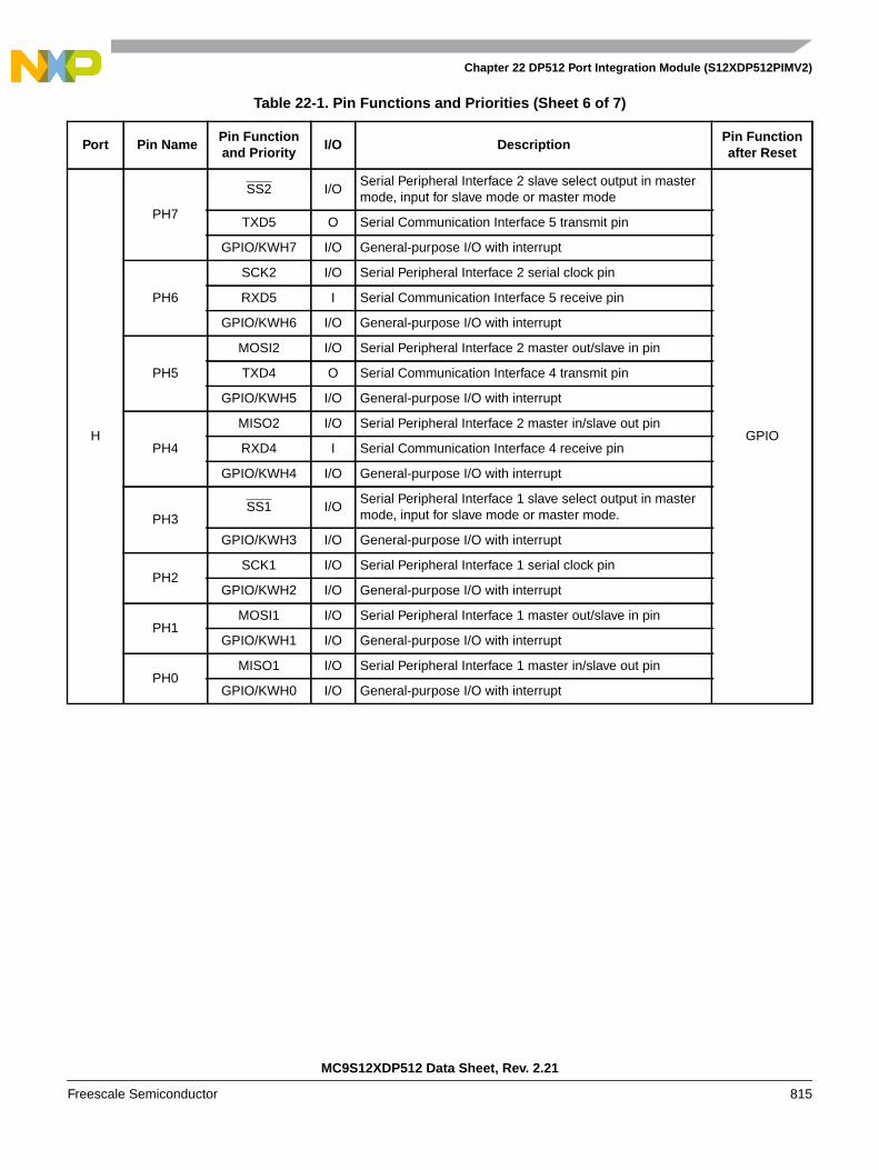
Chapter 22 DP512 Port Integration Module (S12XDP512PIMV2)
MC9S12XDP512 Data Sheet, Rev. 2.21
Freescale Semiconductor 815
H
PH7
SS2 I/OSerial Peripheral Interface 2 slave select output in mastermode, input for slave mode or master mode
GPIO
TXD5 O Serial Communication Interface 5 transmit pin
GPIO/KWH7 I/O General-purpose I/O with interrupt
PH6
SCK2 I/O Serial Peripheral Interface 2 serial clock pin
RXD5 I Serial Communication Interface 5 receive pin
GPIO/KWH6 I/O General-purpose I/O with interrupt
PH5
MOSI2 I/O Serial Peripheral Interface 2 master out/slave in pin
TXD4 O Serial Communication Interface 4 transmit pin
GPIO/KWH5 I/O General-purpose I/O with interrupt
PH4
MISO2 I/O Serial Peripheral Interface 2 master in/slave out pin
RXD4 I Serial Communication Interface 4 receive pin
GPIO/KWH4 I/O General-purpose I/O with interrupt
PH3SS1 I/O
Serial Peripheral Interface 1 slave select output in mastermode, input for slave mode or master mode.
GPIO/KWH3 I/O General-purpose I/O with interrupt
PH2SCK1 I/O Serial Peripheral Interface 1 serial clock pin
GPIO/KWH2 I/O General-purpose I/O with interrupt
PH1MOSI1 I/O Serial Peripheral Interface 1 master out/slave in pin
GPIO/KWH1 I/O General-purpose I/O with interrupt
PH0MISO1 I/O Serial Peripheral Interface 1 master in/slave out pin
GPIO/KWH0 I/O General-purpose I/O with interrupt
Table 22-1. Pin Functions and Priorities (Sheet 6 of 7)
Port Pin NamePin Functionand Priority
I/O DescriptionPin Functionafter Reset
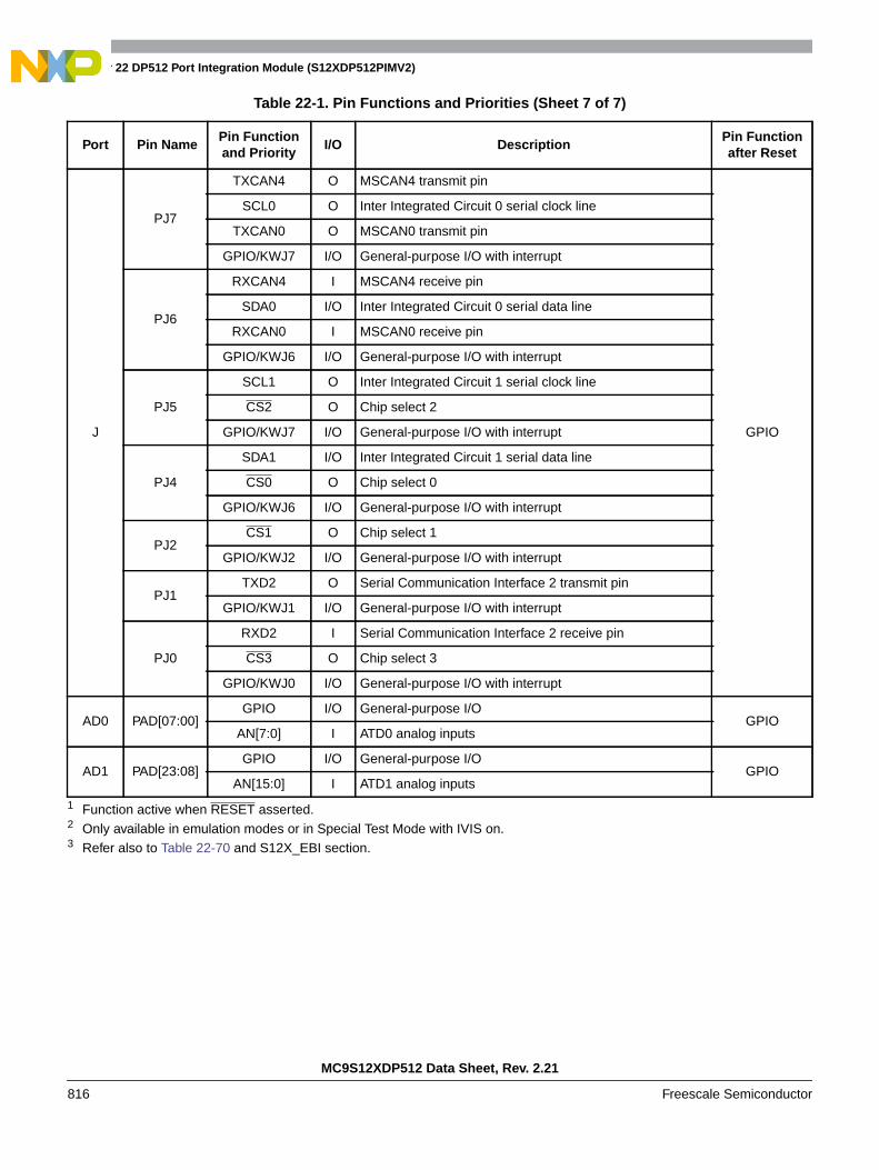
Chapter 22 DP512 Port Integration Module (S12XDP512PIMV2)
MC9S12XDP512 Data Sheet, Rev. 2.21
816 Freescale Semiconductor
J
PJ7
TXCAN4 O MSCAN4 transmit pin
GPIO
SCL0 O Inter Integrated Circuit 0 serial clock line
TXCAN0 O MSCAN0 transmit pin
GPIO/KWJ7 I/O General-purpose I/O with interrupt
PJ6
RXCAN4 I MSCAN4 receive pin
SDA0 I/O Inter Integrated Circuit 0 serial data line
RXCAN0 I MSCAN0 receive pin
GPIO/KWJ6 I/O General-purpose I/O with interrupt
PJ5
SCL1 O Inter Integrated Circuit 1 serial clock line
CS2 O Chip select 2
GPIO/KWJ7 I/O General-purpose I/O with interrupt
PJ4
SDA1 I/O Inter Integrated Circuit 1 serial data line
CS0 O Chip select 0
GPIO/KWJ6 I/O General-purpose I/O with interrupt
PJ2CS1 O Chip select 1
GPIO/KWJ2 I/O General-purpose I/O with interrupt
PJ1TXD2 O Serial Communication Interface 2 transmit pin
GPIO/KWJ1 I/O General-purpose I/O with interrupt
PJ0
RXD2 I Serial Communication Interface 2 receive pin
CS3 O Chip select 3
GPIO/KWJ0 I/O General-purpose I/O with interrupt
AD0 PAD[07:00]GPIO I/O General-purpose I/O
GPIOAN[7:0] I ATD0 analog inputs
AD1 PAD[23:08]GPIO I/O General-purpose I/O
GPIOAN[15:0] I ATD1 analog inputs
1 Function active when RESET asserted.2 Only available in emulation modes or in Special Test Mode with IVIS on.3 Refer also to Table 22-70 and S12X_EBI section.
Table 22-1. Pin Functions and Priorities (Sheet 7 of 7)
Port Pin NamePin Functionand Priority
I/O DescriptionPin Functionafter Reset
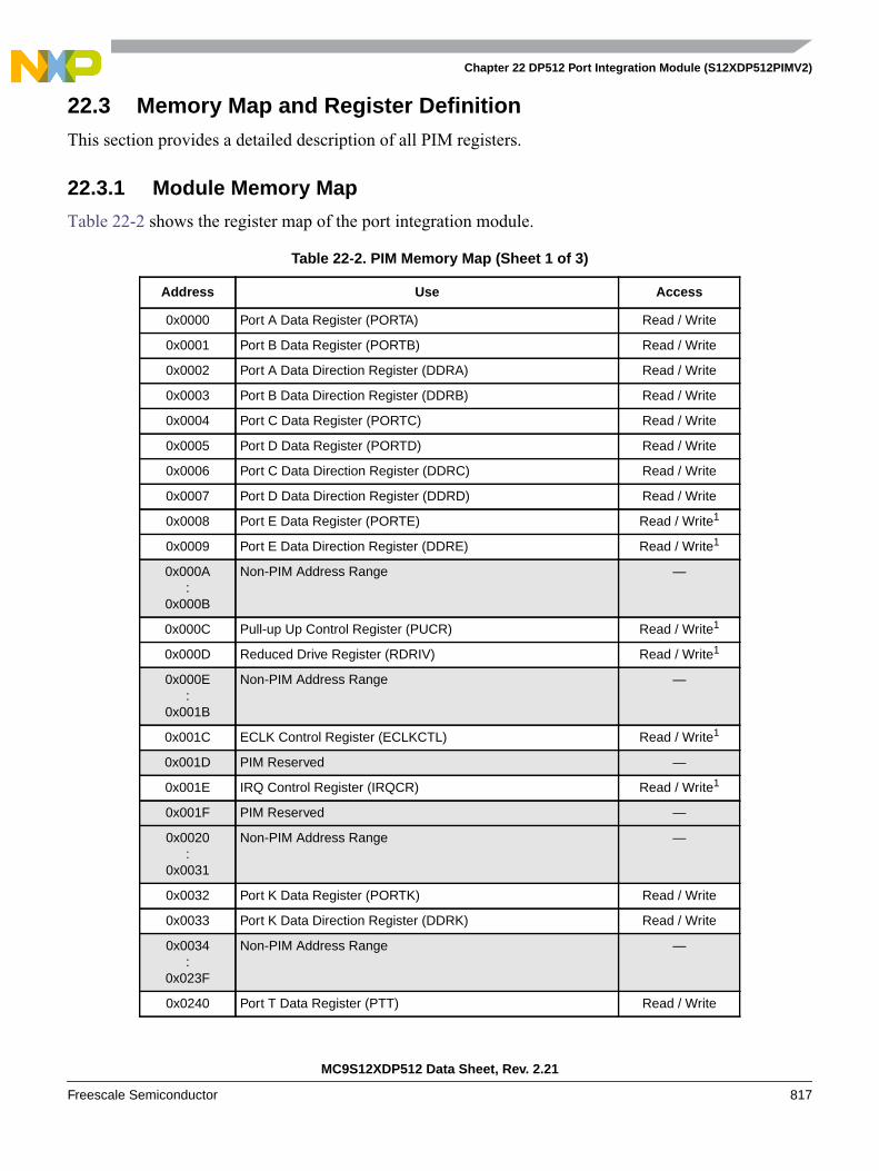
Chapter 22 DP512 Port Integration Module (S12XDP512PIMV2)
MC9S12XDP512 Data Sheet, Rev. 2.21
Freescale Semiconductor 817
22.3 Memory Map and Register DefinitionThis section provides a detailed description of all PIM registers.
22.3.1 Module Memory Map
Table 22-2 shows the register map of the port integration module.
Table 22-2. PIM Memory Map (Sheet 1 of 3)
Address Use Access
0x0000 Port A Data Register (PORTA) Read / Write
0x0001 Port B Data Register (PORTB) Read / Write
0x0002 Port A Data Direction Register (DDRA) Read / Write
0x0003 Port B Data Direction Register (DDRB) Read / Write
0x0004 Port C Data Register (PORTC) Read / Write
0x0005 Port D Data Register (PORTD) Read / Write
0x0006 Port C Data Direction Register (DDRC) Read / Write
0x0007 Port D Data Direction Register (DDRD) Read / Write
0x0008 Port E Data Register (PORTE) Read / Write1
0x0009 Port E Data Direction Register (DDRE) Read / Write1
0x000A:
0x000B
Non-PIM Address Range —
0x000C Pull-up Up Control Register (PUCR) Read / Write1
0x000D Reduced Drive Register (RDRIV) Read / Write1
0x000E:
0x001B
Non-PIM Address Range —
0x001C ECLK Control Register (ECLKCTL) Read / Write1
0x001D PIM Reserved —
0x001E IRQ Control Register (IRQCR) Read / Write1
0x001F PIM Reserved —
0x0020:
0x0031
Non-PIM Address Range —
0x0032 Port K Data Register (PORTK) Read / Write
0x0033 Port K Data Direction Register (DDRK) Read / Write
0x0034:
0x023F
Non-PIM Address Range —
0x0240 Port T Data Register (PTT) Read / Write

Chapter 22 DP512 Port Integration Module (S12XDP512PIMV2)
MC9S12XDP512 Data Sheet, Rev. 2.21
818 Freescale Semiconductor
0x0241 Port T Input Register (PTIT) Read
0x0242 Port T Data Direction Register (DDRT) Read / Write
0x0243 Port T Reduced Drive Register (RDRT) Read / Write
0x0244 Port T Pull Device Enable Register (PERT) Read / Write
0x0245 Port T Polarity Select Register (PPST) Read / Write
0x0246 Reserved —
0x0247 Reserved —
0x0248 Port S Data Register (PTS) Read / Write
0x0249 Port S Input Register (PTIS) Read
0x024A Port S Data Direction Register (DDRS) Read / Write
0x024B Port S Reduced Drive Register (RDRS) Read / Write
0x024C Port S Pull Device Enable Register (PERS) Read / Write
0x024D Port S Polarity Select Register (PPSS) Read / Write
0x024E Port S Wired-OR Mode Register (WOMS) Read / Write
0x024F Reserved —
0x0250 Port M Data Register (PTM) Read / Write
0x0251 Port M Input Register (PTIM) Read
0x0252 Port M Data Direction Register (DDRM) Read / Write
0x0253 Port M Reduced Drive Register (RDRM) Read / Write
0x0254 Port M Pull Device Enable Register (PERM) Read / Write
0x0255 Port M Polarity Select Register (PPSM) Read / Write
0x0256 Port M Wired-OR Mode Register (WOMM) Read / Write
0x0257 Module Routing Register (MODRR) Read / Write
0x0258 Port P Data Register (PTP) Read / Write
0x0259 Port P Input Register (PTIP) Read
0x025A Port P Data Direction Register (DDRP) Read / Write
0x025B Port P Reduced Drive Register (RDRP) Read / Write
0x025C Port P Pull Device Enable Register (PERP) Read / Write
0x025D Port P Polarity Select Register (PPSP) Read / Write
0x025E Port P Interrupt Enable Register (PIEP) Read / Write
0x025F Port P Interrupt Flag Register (PIFP) Read / Write
0x0260 Port H Data Register (PTH) Read / Write
0x0261 Port H Input Register (PTIH) Read
0x0262 Port H Data Direction Register (DDRH) Read / Write
0x0263 Port H Reduced Drive Register (RDRH) Read / Write
Table 22-2. PIM Memory Map (Sheet 2 of 3)
Address Use Access
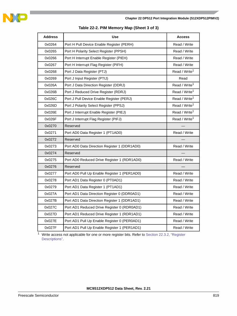
Chapter 22 DP512 Port Integration Module (S12XDP512PIMV2)
MC9S12XDP512 Data Sheet, Rev. 2.21
Freescale Semiconductor 819
0x0264 Port H Pull Device Enable Register (PERH) Read / Write
0x0265 Port H Polarity Select Register (PPSH) Read / Write
0x0266 Port H Interrupt Enable Register (PIEH) Read / Write
0x0267 Port H Interrupt Flag Register (PIFH) Read / Write
0x0268 Port J Data Register (PTJ) Read / Write1
0x0269 Port J Input Register (PTIJ) Read
0x026A Port J Data Direction Register (DDRJ) Read / Write1
0x026B Port J Reduced Drive Register (RDRJ) Read / Write1
0x026C Port J Pull Device Enable Register (PERJ) Read / Write1
0x026D Port J Polarity Select Register (PPSJ) Read / Write1
0x026E Port J Interrupt Enable Register (PIEJ) Read / Write1
0x026F Port J Interrupt Flag Register (PIFJ) Read / Write1
0x0270 Reserved —
0x0271 Port AD0 Data Register 1 (PT1AD0) Read / Write
0x0272 Reserved —
0x0273 Port AD0 Data Direction Register 1 (DDR1AD0) Read / Write
0x0274 Reserved —
0x0275 Port AD0 Reduced Drive Register 1 (RDR1AD0) Read / Write
0x0276 Reserved —
0x0277 Port AD0 Pull Up Enable Register 1 (PER1AD0) Read / Write
0x0278 Port AD1 Data Register 0 (PT0AD1) Read / Write
0x0279 Port AD1 Data Register 1 (PT1AD1) Read / Write
0x027A Port AD1 Data Direction Register 0 (DDR0AD1) Read / Write
0x027B Port AD1 Data Direction Register 1 (DDR1AD1) Read / Write
0x027C Port AD1 Reduced Drive Register 0 (RDR0AD1) Read / Write
0x027D Port AD1 Reduced Drive Register 1 (RDR1AD1) Read / Write
0x027E Port AD1 Pull Up Enable Register 0 (PER0AD1) Read / Write
0x027F Port AD1 Pull Up Enable Register 1 (PER1AD1) Read / Write
1 Write access not applicable for one or more register bits. Refer to Section 22.3.2, “RegisterDescriptions”.
Table 22-2. PIM Memory Map (Sheet 3 of 3)
Address Use Access
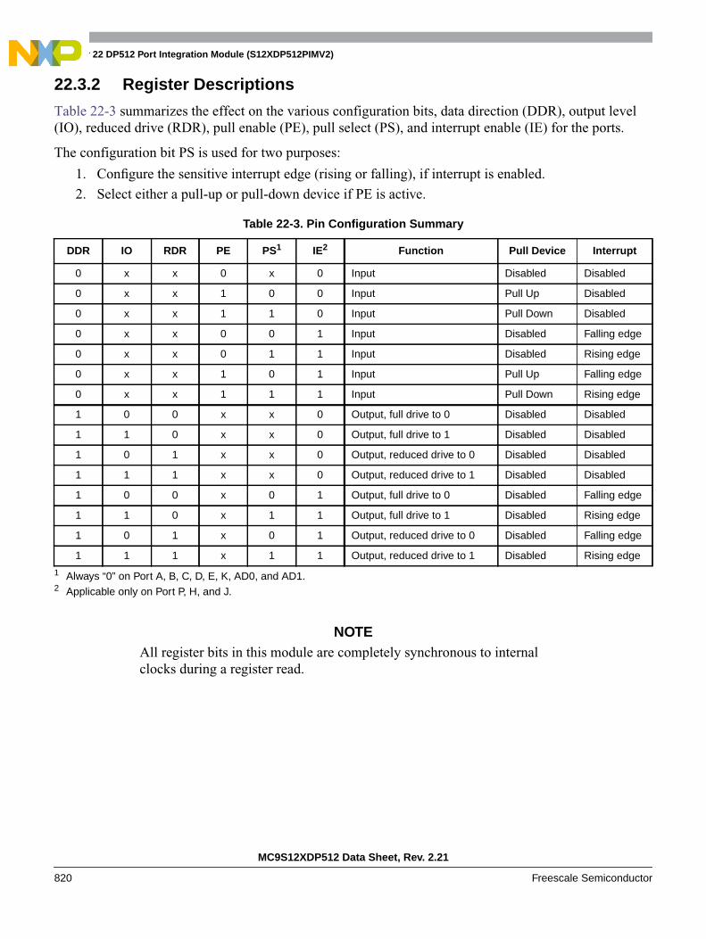
Chapter 22 DP512 Port Integration Module (S12XDP512PIMV2)
MC9S12XDP512 Data Sheet, Rev. 2.21
820 Freescale Semiconductor
22.3.2 Register Descriptions
Table 22-3 summarizes the effect on the various configuration bits, data direction (DDR), output level(IO), reduced drive (RDR), pull enable (PE), pull select (PS), and interrupt enable (IE) for the ports.
The configuration bit PS is used for two purposes:
1. Configure the sensitive interrupt edge (rising or falling), if interrupt is enabled.
2. Select either a pull-up or pull-down device if PE is active.
NOTEAll register bits in this module are completely synchronous to internalclocks during a register read.
Table 22-3. Pin Configuration Summary
DDR IO RDR PE PS1
1 Always “0” on Port A, B, C, D, E, K, AD0, and AD1.
IE2
2 Applicable only on Port P, H, and J.
Function Pull Device Interrupt
0 x x 0 x 0 Input Disabled Disabled
0 x x 1 0 0 Input Pull Up Disabled
0 x x 1 1 0 Input Pull Down Disabled
0 x x 0 0 1 Input Disabled Falling edge
0 x x 0 1 1 Input Disabled Rising edge
0 x x 1 0 1 Input Pull Up Falling edge
0 x x 1 1 1 Input Pull Down Rising edge
1 0 0 x x 0 Output, full drive to 0 Disabled Disabled
1 1 0 x x 0 Output, full drive to 1 Disabled Disabled
1 0 1 x x 0 Output, reduced drive to 0 Disabled Disabled
1 1 1 x x 0 Output, reduced drive to 1 Disabled Disabled
1 0 0 x 0 1 Output, full drive to 0 Disabled Falling edge
1 1 0 x 1 1 Output, full drive to 1 Disabled Rising edge
1 0 1 x 0 1 Output, reduced drive to 0 Disabled Falling edge
1 1 1 x 1 1 Output, reduced drive to 1 Disabled Rising edge
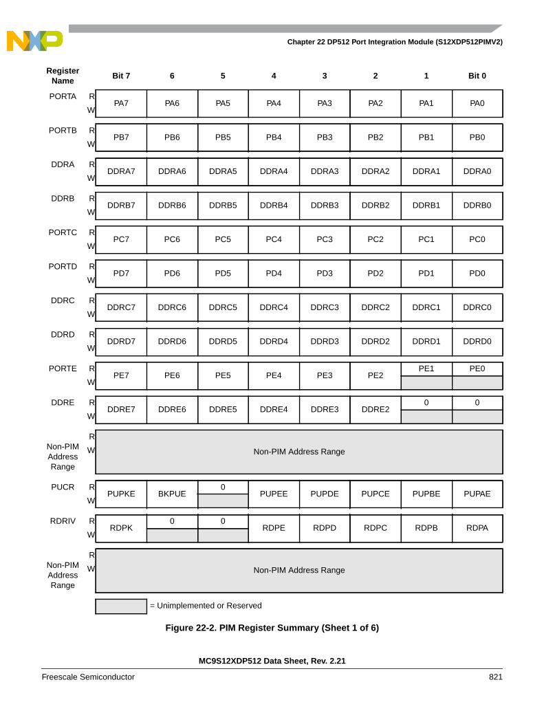
Chapter 22 DP512 Port Integration Module (S12XDP512PIMV2)
MC9S12XDP512 Data Sheet, Rev. 2.21
Freescale Semiconductor 821
RegisterName
Bit 7 6 5 4 3 2 1 Bit 0
PORTA RPA7 PA6 PA5 PA4 PA3 PA2 PA1 PA0
W
PORTB RPB7 PB6 PB5 PB4 PB3 PB2 PB1 PB0
W
DDRA RDDRA7 DDRA6 DDRA5 DDRA4 DDRA3 DDRA2 DDRA1 DDRA0
W
DDRB RDDRB7 DDRB6 DDRB5 DDRB4 DDRB3 DDRB2 DDRB1 DDRB0
W
PORTC RPC7 PC6 PC5 PC4 PC3 PC2 PC1 PC0
W
PORTD RPD7 PD6 PD5 PD4 PD3 PD2 PD1 PD0
W
DDRC RDDRC7 DDRC6 DDRC5 DDRC4 DDRC3 DDRC2 DDRC1 DDRC0
W
DDRD RDDRD7 DDRD6 DDRD5 DDRD4 DDRD3 DDRD2 DDRD1 DDRD0
W
PORTE RPE7 PE6 PE5 PE4 PE3 PE2
PE1 PE0
W
DDRE RDDRE7 DDRE6 DDRE5 DDRE4 DDRE3 DDRE2
0 0
W
Non-PIMAddressRange
R
Non-PIM Address RangeW
PUCR RPUPKE BKPUE
0PUPEE PUPDE PUPCE PUPBE PUPAE
W
RDRIV RRDPK
0 0RDPE RDPD RDPC RDPB RDPA
W
Non-PIMAddressRange
R
Non-PIM Address RangeW
= Unimplemented or Reserved
Figure 22-2. PIM Register Summary (Sheet 1 of 6)
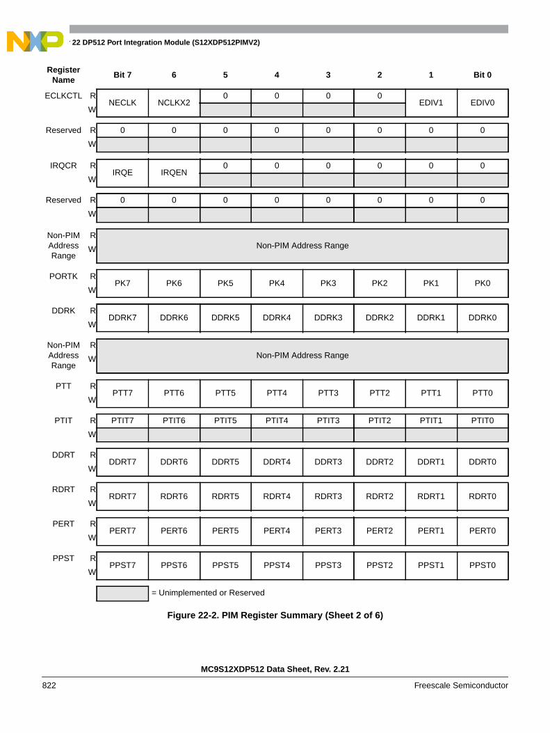
Chapter 22 DP512 Port Integration Module (S12XDP512PIMV2)
MC9S12XDP512 Data Sheet, Rev. 2.21
822 Freescale Semiconductor
ECLKCTL RNECLK NCLKX2
0 0 0 0EDIV1 EDIV0
W
Reserved R 0 0 0 0 0 0 0 0
W
IRQCR RIRQE IRQEN
0 0 0 0 0 0
W
Reserved R 0 0 0 0 0 0 0 0
W
Non-PIMAddressRange
RNon-PIM Address RangeW
PORTK RPK7 PK6 PK5 PK4 PK3 PK2 PK1 PK0
W
DDRK RDDRK7 DDRK6 DDRK5 DDRK4 DDRK3 DDRK2 DDRK1 DDRK0
W
Non-PIMAddressRange
RNon-PIM Address RangeW
PTT RPTT7 PTT6 PTT5 PTT4 PTT3 PTT2 PTT1 PTT0
W
PTIT R PTIT7 PTIT6 PTIT5 PTIT4 PTIT3 PTIT2 PTIT1 PTIT0
W
DDRT RDDRT7 DDRT6 DDRT5 DDRT4 DDRT3 DDRT2 DDRT1 DDRT0
W
RDRT RRDRT7 RDRT6 RDRT5 RDRT4 RDRT3 RDRT2 RDRT1 RDRT0
W
PERT RPERT7 PERT6 PERT5 PERT4 PERT3 PERT2 PERT1 PERT0
W
PPST RPPST7 PPST6 PPST5 PPST4 PPST3 PPST2 PPST1 PPST0
W
RegisterName
Bit 7 6 5 4 3 2 1 Bit 0
= Unimplemented or Reserved
Figure 22-2. PIM Register Summary (Sheet 2 of 6)

Chapter 22 DP512 Port Integration Module (S12XDP512PIMV2)
MC9S12XDP512 Data Sheet, Rev. 2.21
Freescale Semiconductor 823
Reserved R 0 0 0 0 0 0 0 0
W
Reserved R 0 0 0 0 0 0 0 0
W
PTS RPTS7 PTS6 PTS5 PTS4 PTS3 PTS2 PTS1 PTS0
W
PTIS R PTIS7 PTIS6 PTIS5 PTIS4 PTIS3 PTIS2 PTIS1 PTIS0
W
DDRS RDDRS7 DDRS6 DDRS5 DDRS4 DDRS3 DDRS2 DDRS1 DDRS0
W
RDRS RRDRS7 RDRS6 RDRS5 RDRS4 RDRS3 RDRS2 RDRS1 RDRS0
W
PERS RPERS7 PERS6 PERS5 PERS4 PERS3 PERS2 PERS1 PERS0
W
PPSS RPPSS7 PPSS6 PPSS5 PPSS4 PPSS3 PPSS2 PPSS1 PPSS0
W
WOMS RWOMS7 WOMS6 WOMS5 WOMS4 WOMS3 WOMS2 WOMS1 WOMS0
W
Reserved R 0 0 0 0 0 0 0 0
W
PTM RPTM7 PTM6 PTM5 PTM4 PTM3 PTM2 PTM1 PTM0
W
PTIM R PTIM7 PTIM6 PTIM5 PTIM4 PTIM3 PTIM2 PTIM1 PTIM0
W
DDRM RDDRM7 DDRM6 DDRM5 DDRM4 DDRM3 DDRM2 DDRM1 DDRM0
W
RDRM RRDRM7 RDRM6 RDRM5 RDRM4 RDRM3 RDRM2 RDRM1 RDRM0
W
PERM RPERM7 PERM6 PERM5 PERM4 PERM3 PERM2 PERM1 PERM0
W
RegisterName
Bit 7 6 5 4 3 2 1 Bit 0
= Unimplemented or Reserved
Figure 22-2. PIM Register Summary (Sheet 3 of 6)
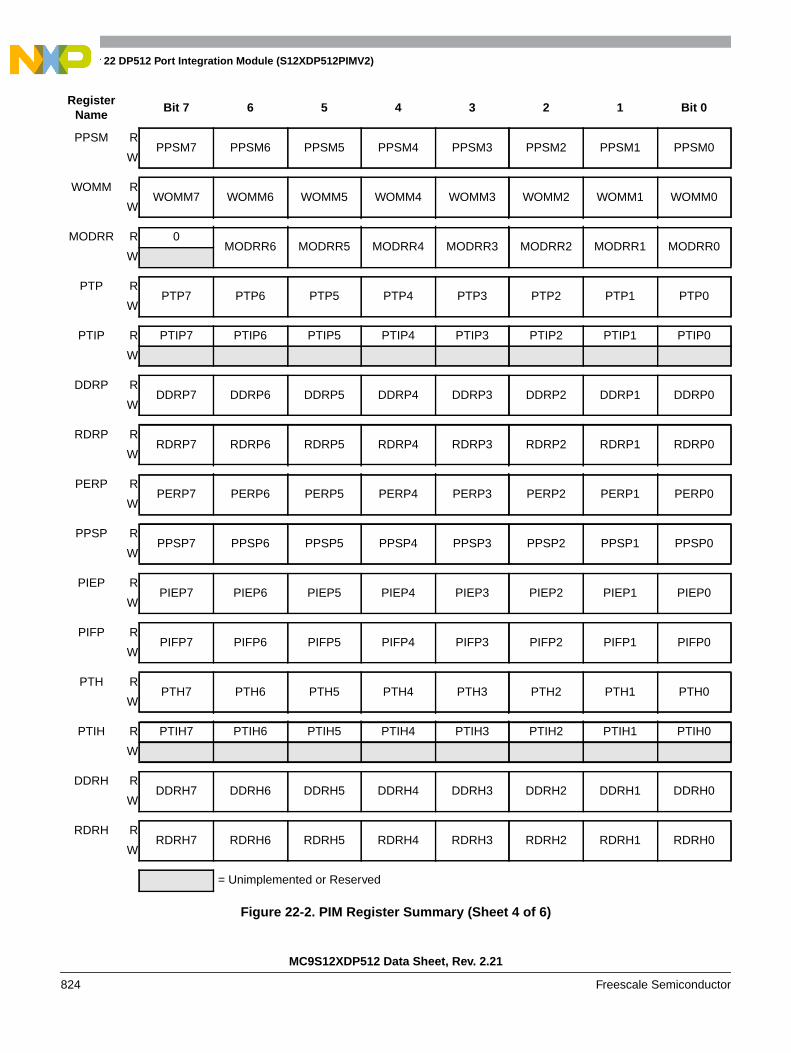
Chapter 22 DP512 Port Integration Module (S12XDP512PIMV2)
MC9S12XDP512 Data Sheet, Rev. 2.21
824 Freescale Semiconductor
PPSM RPPSM7 PPSM6 PPSM5 PPSM4 PPSM3 PPSM2 PPSM1 PPSM0
W
WOMM RWOMM7 WOMM6 WOMM5 WOMM4 WOMM3 WOMM2 WOMM1 WOMM0
W
MODRR R 0MODRR6 MODRR5 MODRR4 MODRR3 MODRR2 MODRR1 MODRR0
W
PTP RPTP7 PTP6 PTP5 PTP4 PTP3 PTP2 PTP1 PTP0
W
PTIP R PTIP7 PTIP6 PTIP5 PTIP4 PTIP3 PTIP2 PTIP1 PTIP0
W
DDRP RDDRP7 DDRP6 DDRP5 DDRP4 DDRP3 DDRP2 DDRP1 DDRP0
W
RDRP RRDRP7 RDRP6 RDRP5 RDRP4 RDRP3 RDRP2 RDRP1 RDRP0
W
PERP RPERP7 PERP6 PERP5 PERP4 PERP3 PERP2 PERP1 PERP0
W
PPSP RPPSP7 PPSP6 PPSP5 PPSP4 PPSP3 PPSP2 PPSP1 PPSP0
W
PIEP RPIEP7 PIEP6 PIEP5 PIEP4 PIEP3 PIEP2 PIEP1 PIEP0
W
PIFP RPIFP7 PIFP6 PIFP5 PIFP4 PIFP3 PIFP2 PIFP1 PIFP0
W
PTH RPTH7 PTH6 PTH5 PTH4 PTH3 PTH2 PTH1 PTH0
W
PTIH R PTIH7 PTIH6 PTIH5 PTIH4 PTIH3 PTIH2 PTIH1 PTIH0
W
DDRH RDDRH7 DDRH6 DDRH5 DDRH4 DDRH3 DDRH2 DDRH1 DDRH0
W
RDRH RRDRH7 RDRH6 RDRH5 RDRH4 RDRH3 RDRH2 RDRH1 RDRH0
W
RegisterName
Bit 7 6 5 4 3 2 1 Bit 0
= Unimplemented or Reserved
Figure 22-2. PIM Register Summary (Sheet 4 of 6)

Chapter 22 DP512 Port Integration Module (S12XDP512PIMV2)
MC9S12XDP512 Data Sheet, Rev. 2.21
Freescale Semiconductor 825
PERH RPERH7 PERH6 PERH5 PERH4 PERH3 PERH2 PERH1 PERH0
W
PPSH RPPSH7 PPSH6 PPSH5 PPSH4 PPSH3 PPSH2 PPSH1 PPSH0
W
PIEH RPIEH7 PIEH6 PIEH5 PIEH4 PIEH3 PIEH2 PIEH1 PIEH0
W
PIFH RPIFH7 PIFH6 PIFH5 PIFH4 PIFH3 PIFH2 PIFH1 PIFH0
W
PTJ RPTJ7 PTJ6 PTJ5 PTJ4
0PTJ2 PTJ1 PTJ0
W
PTIJ R PTIJ7 PTIJ6 PTIJ5 PTIJ4 0 PTIJ2 PTIJ1 PTIJ0
W
DDRJ RDDRJ7 DDRJ6 DDRJ5 DDRJ4
0DDRJ2 DDRJ1 DDRJ0
W
RDRJ RRDRJ7 RDRJ6 RDRJ5 RDRJ4
0RDRJ2 RDRJ1 RDRJ0
W
PERJ RPERJ7 PERJ6 PERJ5 PERJ4
0PERJ2 PERJ1 PERJ0
W
PPSJ RPPSJ7 PPSJ6 PPSJ5 PPSJ4
0PPSJ2 PPSJ1 PPSJ0
W
PIEJ RPIEJ7 PIEJ6 PIEJ5 PIEJ4
0PIEJ2 PIEJ1 PIEJ0
W
PIFJ RPPSJ7 PPSJ6 PPSJ5 PPSJ4
0PPSJ2 PPSJ1 PPSJ0
W
Reserved R 0 0 0 0 0 0 0 0
W
PT1AD0 RPT1AD07 PT1AD06 PT1AD05 PT1AD04 PT1AD03 PT1AD02 PT1AD01 PT1AD00
W
Reserved R 0 0 0 0 0 0 0 0
W
RegisterName
Bit 7 6 5 4 3 2 1 Bit 0
= Unimplemented or Reserved
Figure 22-2. PIM Register Summary (Sheet 5 of 6)

Chapter 22 DP512 Port Integration Module (S12XDP512PIMV2)
MC9S12XDP512 Data Sheet, Rev. 2.21
826 Freescale Semiconductor
Name RDDR1AD07 DDR1AD06 DDR1AD05 DDR1AD04 DDR1AD03 DDR1AD02 DDR1AD01 DDR1AD00
W
Reserved R 0 0 0 0 0 0 0 0
W
RDR1AD0 RRDR1AD07 RDR1AD06 RDR1AD05 RDR1AD04 RDR1AD03 RDR1AD02 RDR1AD01 RDR1AD00
W
Reserved R 0 0 0 0 0 0 0 0
W
PER1AD0 RPER1AD07 PER1AD06 PER1AD05 PER1AD04 PER1AD03 PER1AD02 PER1AD01 PER1AD00
W
PT0AD1 RPT0AD123 PT0AD122 PT0AD121 PT0AD120 PT0AD119 PT0AD118 PT0AD117 PT0AD116
W
PT1AD1 RPT1AD115 PT1AD114 PT1AD113 PT1AD112 PT1AD111 PT1AD110 PT1AD19 PT1AD18
W
DDR0AD1 RDDR0AD123 DDR0AD122 DDR0AD121 DDR0AD120 DDR0AD119 DDR0AD118 DDR0AD117 DDR0AD116
W
DDR1AD1 RDDR1AD115 DDR1AD114 DDR1AD113 DDR1AD112 DDR1AD111 DDR1AD110 DDR1AD19 DDR1AD18
W
RDR0AD1 RRDR0AD123 RDR0AD122 RDR0AD121 RDR0AD120 RDR0AD119 RDR0AD118 RDR0AD117 RDR0AD116
W
RDR1AD1 RRDR1AD115 RDR1AD114 RDR1AD113 RDR1AD112 RDR1AD111 RDR1AD110 RDR1AD19 RDR1AD18
W
PER0AD1 RPER0AD123 PER0AD122 PER0AD121 PER0AD120 PER0AD119 PER0AD118 PER0AD117 PER0AD116
W
PER1AD1 RPER1AD115 PER1AD114 PER1AD113 PER1AD112 PER1AD111 PER1AD110 PER1AD19 PER1AD18
W
RegisterName
Bit 7 6 5 4 3 2 1 Bit 0
= Unimplemented or Reserved
Figure 22-2. PIM Register Summary (Sheet 6 of 6)

Chapter 22 DP512 Port Integration Module (S12XDP512PIMV2)
MC9S12XDP512 Data Sheet, Rev. 2.21
Freescale Semiconductor 827
22.3.2.1 Port A Data Register (PORTA)
Read: Anytime. In emulation modes, read operations will return the data from the external bus, in all othermodes the data source is depending on the data direction value.
Write: Anytime. In emulation modes, write operations will also be directed to the external bus.
22.3.2.2 Port B Data Register (PORTB)
Read: Anytime. In emulation modes, read operations will return the data from the external bus, in all othermodes the data source is depending on the data direction value.
7 6 5 4 3 2 1 0
RPA7 PA6 PA5 PA4 PA3 PA2 PA1 PA0
W
Alt.Function
ADDR15mux
IVD15
ADDR14mux
IVD14
ADDR13mux
IVD13
ADDR12mux
IVD12
ADDR11mux
IVD11
ADDR10mux
IVD10
ADDR9muxIVD9
ADDR8muxIVD8
Reset 0 0 0 0 0 0 0 0
Figure 22-3. Port A Data Register (PORTA)
Table 22-4. PORTA Field Descriptions
Field Description
7–0PA[7:0]
Port A — Port A pins 7–0 are associated with address outputs ADDR15 through ADDR8 respectively inexpanded modes. When this port is not used for external addresses, these pins can be used as general purposeI/O. If the data direction bits of the associated I/O pins are set to logic level “1”, a read returns the value of theport register, otherwise the buffered pin input state is read.
7 6 5 4 3 2 1 0
RPB7 PB6 PB5 PB4 PB3 PB2 PB1 PB0
W
Alt.Function ADDR7
muxIVD7
ADDR6muxIVD6
ADDR5muxIVD5
ADDR4muxIVD4
ADDR3muxIVD3
ADDR2muxIVD2
ADDR1muxIVD1
ADDR0muxIVD0
orUDS
Reset 0 0 0 0 0 0 0 0
Figure 22-4. Port B Data Register (PORTB)

Chapter 22 DP512 Port Integration Module (S12XDP512PIMV2)
MC9S12XDP512 Data Sheet, Rev. 2.21
828 Freescale Semiconductor
Write: Anytime. In emulation modes, write operations will also be directed to the external bus.Table 22-5. PORTB Field Descriptions
Field Description
7–0PB[7:0]
Port B — Port B pins 7–0 are associated with address outputs ADDR7 through ADDR1 respectively in expandedmodes. Pin 0 is associated with output ADDR0 in emulation modes and special test mode and with Upper DataSelect (UDS) in normal expanded mode. When this port is not used for external addresses, these pins can beused as general purpose I/O. If the data direction bits of the associated I/O pins are set to logic level “1”, a readreturns the value of the port register, otherwise the buffered pin input state is read.
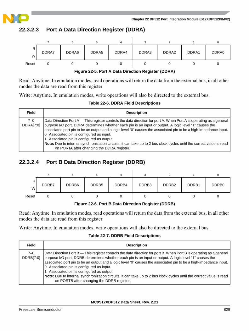
Chapter 22 DP512 Port Integration Module (S12XDP512PIMV2)
MC9S12XDP512 Data Sheet, Rev. 2.21
Freescale Semiconductor 829
22.3.2.3 Port A Data Direction Register (DDRA)
Read: Anytime. In emulation modes, read operations will return the data from the external bus, in all othermodes the data are read from this register.
Write: Anytime. In emulation modes, write operations will also be directed to the external bus.
22.3.2.4 Port B Data Direction Register (DDRB)
Read: Anytime. In emulation modes, read operations will return the data from the external bus, in all othermodes the data are read from this register.
Write: Anytime. In emulation modes, write operations will also be directed to the external bus.
7 6 5 4 3 2 1 0
RDDRA7 DDRA6 DDRA5 DDRA4 DDRA3 DDRA2 DDRA1 DDRA0
W
Reset 0 0 0 0 0 0 0 0
Figure 22-5. Port A Data Direction Register (DDRA)
Table 22-6. DDRA Field Descriptions
Field Description
7–0DDRA[7:0]
Data Direction Port A — This register controls the data direction for port A. When Port A is operating as a generalpurpose I/O port, DDRA determines whether each pin is an input or output. A logic level “1” causes theassociated port pin to be an output and a logic level “0” causes the associated pin to be a high-impedance input.0 Associated pin is configured as input.1 Associated pin is configured as output.Note: Due to internal synchronization circuits, it can take up to 2 bus clock cycles until the correct value is read
on PORTA after changing the DDRA register.
7 6 5 4 3 2 1 0
RDDRB7 DDRB6 DDRB5 DDRB4 DDRB3 DDRB2 DDRB1 DDRB0
W
Reset 0 0 0 0 0 0 0 0
Figure 22-6. Port B Data Direction Register (DDRB)
Table 22-7. DDRB Field Descriptions
Field Description
7–0DDRB[7:0]
Data Direction Port B — This register controls the data direction for port B. When Port B is operating as a generalpurpose I/O port, DDRB determines whether each pin is an input or output. A logic level “1” causes theassociated port pin to be an output and a logic level “0” causes the associated pin to be a high-impedance input.0 Associated pin is configured as input.1 Associated pin is configured as output.Note: Due to internal synchronization circuits, it can take up to 2 bus clock cycles until the correct value is read
on PORTB after changing the DDRB register.

Chapter 22 DP512 Port Integration Module (S12XDP512PIMV2)
MC9S12XDP512 Data Sheet, Rev. 2.21
830 Freescale Semiconductor
22.3.2.5 Port C Data Register (PORTC)
Read: Anytime. In emulation modes, read operations will return the data from the external bus, in all othermodes the data source is depending on the data direction value.
Write: Anytime. In emulation modes, write operations will also be directed to the external bus.
22.3.2.6 Port D Data Register (PORTD)
Read: Anytime. In emulation modes, read operations will return the data from the external bus, in all othermodes the data source is depending on the data direction value.
Write: Anytime. In emulation modes, write operations will also be directed to the external bus.
7 6 5 4 3 2 1 0
RPC7 PC6 PC5 PC4 PC3 PC2 PC1 PC0
W
Exp.: DATA15 DATA14 DATA13 DATA12 DATA11 DATA10 DATA9 DATA8
Reset 0 0 0 0 0 0 0 0
Figure 22-7. Port C Data Register (PORTC)
Table 22-8. PORTC Field Descriptions
Field Description
7–0PC[7:0]
Port C — Port C pins 7–0 are associated with data I/O lines DATA15 through DATA8 respectively in expandedmodes. When this port is not used for external data, these pins can be used as general purpose I/O. If the datadirection bits of the associated I/O pins are set to logic level “1”, a read returns the value of the port register,otherwise the buffered pin input state is read.
7 6 5 4 3 2 1 0
RPD7 PD6 PD5 PD4 PD3 PD2 PD1 PD0
W
Exp.: DATA7 DATA6 DATA5 DATA4 DATA3 DATA2 DATA1 DATA0
Reset 0 0 0 0 0 0 0 0
Figure 22-8. Port D Data Register (PORTD)
Table 22-9. PORTD Field Descriptions
Field Description
7–0PD[7:0]
Port D — Port D pins 7–0 are associated with data I/O lines DATA7 through DATA0 respectively in expandedmodes. When this port is not used for external data, these pins can be used as general purpose I/O. — If thedata direction bits of the associated I/O pins are set to logic level “1”, a read returns the value of the port register,otherwise the buffered pin input state is read.

Chapter 22 DP512 Port Integration Module (S12XDP512PIMV2)
MC9S12XDP512 Data Sheet, Rev. 2.21
Freescale Semiconductor 831
22.3.2.7 Port C Data Direction Register (DDRC)
Read: Anytime. In emulation modes, read operations will return the data from the external bus, in all othermodes the data are read from this register.
Write: Anytime. In emulation modes, write operations will also be directed to the external bus.
22.3.2.8 Port D Data Direction Register (DDRD)
Read: Anytime. In emulation modes, read operations will return the data from the external bus, in all othermodes the data are read from this register.
Write: Anytime. In emulation modes, write operations will also be directed to the external bus.
7 6 5 4 3 2 1 0
RDDRC7 DDRC6 DDRC5 DDRC4 DDRC3 DDRC2 DDRC1 DDRC0
W
Reset 0 0 0 0 0 0 0 0
Figure 22-9. Port C Data Direction Register (DDRC)
Table 22-10. DDRC Field Descriptions
Field Description
7–0DDRC[7:0]
Data Direction Port C — This register controls the data direction for port C. When Port C is operating as a generalpurpose I/O port, DDRC determines whether each pin is an input or output. A logic level “1” causes theassociated port pin to be an output and a logic level “0” causes the associated pin to be a high-impedance input.0 Associated pin is configured as input.1 Associated pin is configured as output.Note: Due to internal synchronization circuits, it can take up to 2 bus clock cycles until the correct value is read
on PORTC after changing the DDRC register.
7 6 5 4 3 2 1 0
RDDRD7 DDRD6 DDRD5 DDRD4 DDRD3 DDRD2 DDRD1 DDRD0
W
Reset 0 0 0 0 0 0 0 0
Figure 22-10. Port D Data Direction Register (DDRD)
Table 22-11. DDRD Field Descriptions
Field Description
7–0DDRD[7:0]
Data Direction Port D — This register controls the data direction for port D. When Port D is operating as a generalpurpose I/O port, DDRD determines whether each pin is an input or output. A logic level “1” causes theassociated port pin to be an output and a logic level “0” causes the associated pin to be a high-impedance input.0 Associated pin is configured as input.1 Associated pin is configured as output.Note: Due to internal synchronization circuits, it can take up to 2 bus clock cycles until the correct value is read
on PORTD after changing the DDRD register.
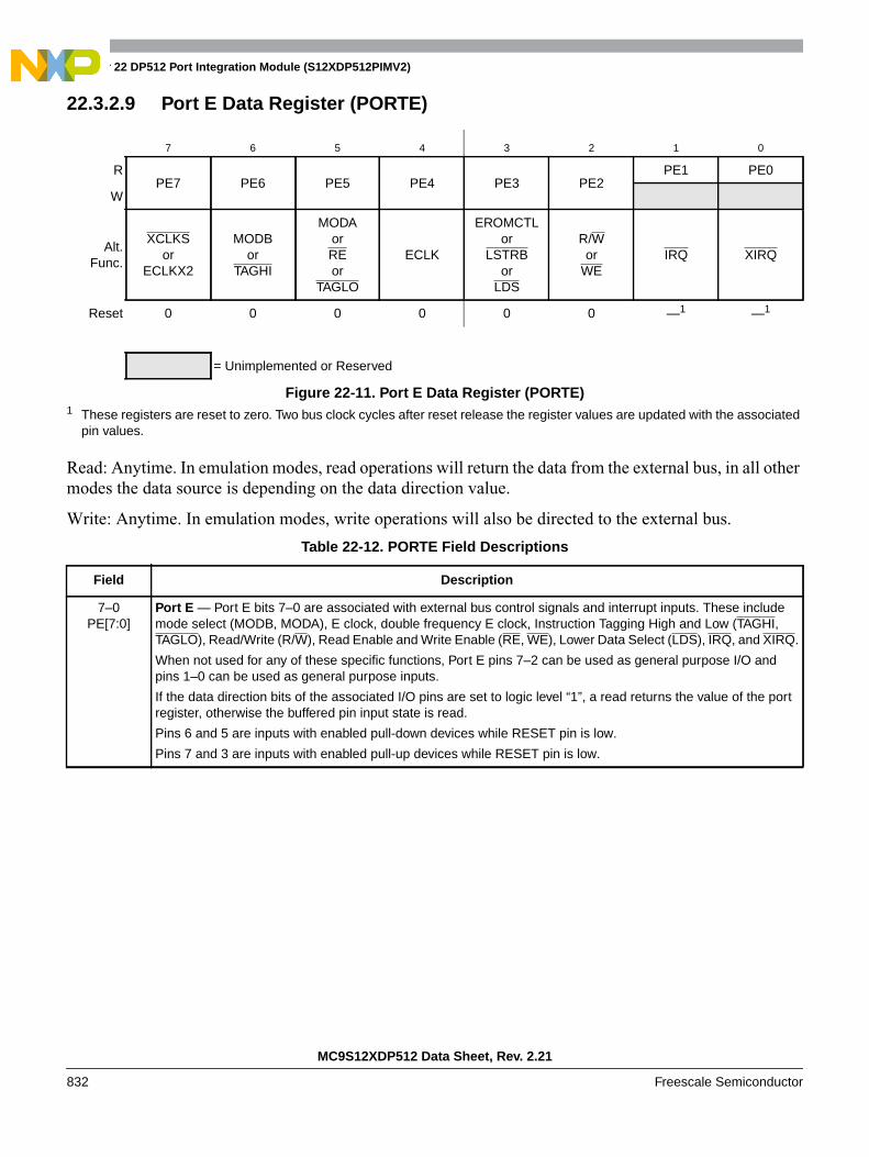
Chapter 22 DP512 Port Integration Module (S12XDP512PIMV2)
MC9S12XDP512 Data Sheet, Rev. 2.21
832 Freescale Semiconductor
22.3.2.9 Port E Data Register (PORTE)
Read: Anytime. In emulation modes, read operations will return the data from the external bus, in all othermodes the data source is depending on the data direction value.
Write: Anytime. In emulation modes, write operations will also be directed to the external bus.
7 6 5 4 3 2 1 0
RPE7 PE6 PE5 PE4 PE3 PE2
PE1 PE0
W
Alt.Func.
XCLKSor
ECLKX2
MODBor
TAGHI
MODAorREor
TAGLO
ECLK
EROMCTLor
LSTRBor
LDS
R/Wor
WEIRQ XIRQ
Reset 0 0 0 0 0 0 —1
1 These registers are reset to zero. Two bus clock cycles after reset release the register values are updated with the associatedpin values.
—1
= Unimplemented or Reserved
Figure 22-11. Port E Data Register (PORTE)
Table 22-12. PORTE Field Descriptions
Field Description
7–0PE[7:0]
Port E — Port E bits 7–0 are associated with external bus control signals and interrupt inputs. These includemode select (MODB, MODA), E clock, double frequency E clock, Instruction Tagging High and Low (TAGHI,TAGLO), Read/Write (R/W), Read Enable and Write Enable (RE, WE), Lower Data Select (LDS), IRQ, and XIRQ.
When not used for any of these specific functions, Port E pins 7–2 can be used as general purpose I/O andpins 1–0 can be used as general purpose inputs.
If the data direction bits of the associated I/O pins are set to logic level “1”, a read returns the value of the portregister, otherwise the buffered pin input state is read.
Pins 6 and 5 are inputs with enabled pull-down devices while RESET pin is low.
Pins 7 and 3 are inputs with enabled pull-up devices while RESET pin is low.
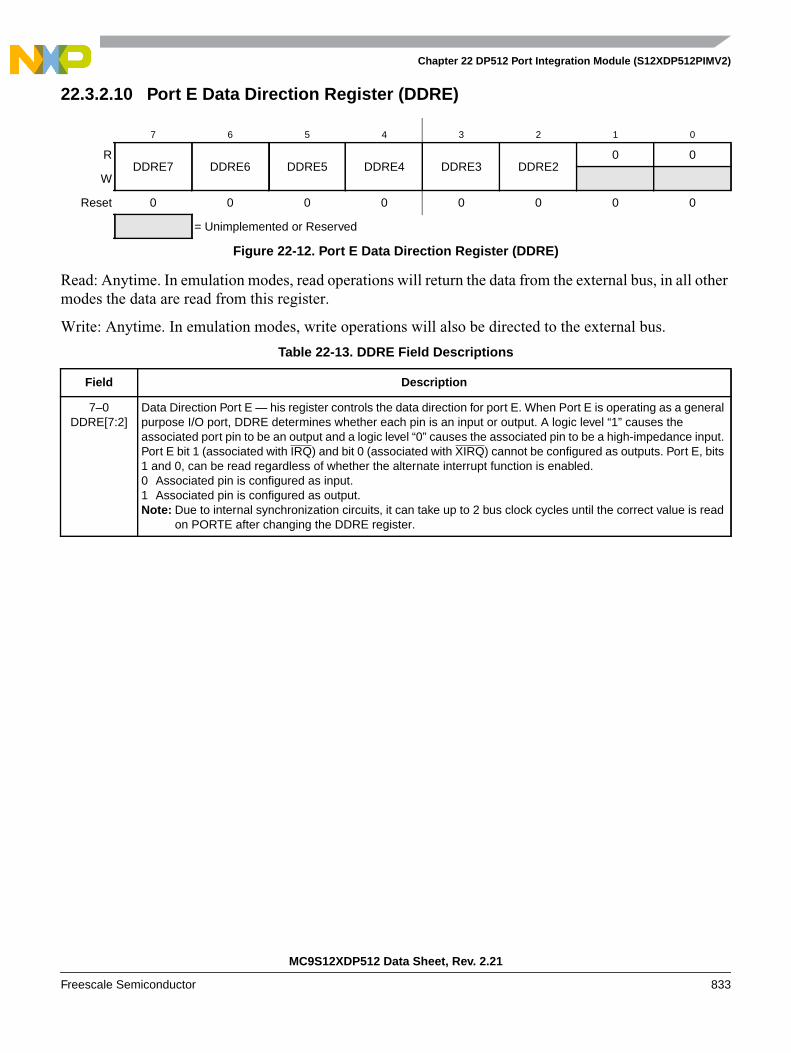
Chapter 22 DP512 Port Integration Module (S12XDP512PIMV2)
MC9S12XDP512 Data Sheet, Rev. 2.21
Freescale Semiconductor 833
22.3.2.10 Port E Data Direction Register (DDRE)
Read: Anytime. In emulation modes, read operations will return the data from the external bus, in all othermodes the data are read from this register.
Write: Anytime. In emulation modes, write operations will also be directed to the external bus.
7 6 5 4 3 2 1 0
RDDRE7 DDRE6 DDRE5 DDRE4 DDRE3 DDRE2
0 0
W
Reset 0 0 0 0 0 0 0 0
= Unimplemented or Reserved
Figure 22-12. Port E Data Direction Register (DDRE)
Table 22-13. DDRE Field Descriptions
Field Description
7–0DDRE[7:2]
Data Direction Port E — his register controls the data direction for port E. When Port E is operating as a generalpurpose I/O port, DDRE determines whether each pin is an input or output. A logic level “1” causes theassociated port pin to be an output and a logic level “0” causes the associated pin to be a high-impedance input.Port E bit 1 (associated with IRQ) and bit 0 (associated with XIRQ) cannot be configured as outputs. Port E, bits1 and 0, can be read regardless of whether the alternate interrupt function is enabled.0 Associated pin is configured as input.1 Associated pin is configured as output.Note: Due to internal synchronization circuits, it can take up to 2 bus clock cycles until the correct value is read
on PORTE after changing the DDRE register.

Chapter 22 DP512 Port Integration Module (S12XDP512PIMV2)
MC9S12XDP512 Data Sheet, Rev. 2.21
834 Freescale Semiconductor
22.3.2.11 S12X_EBI Ports, BKGD, VREGEN Pin Pull-up Control Register (PUCR)
Read: Anytime in single-chip modes.
Write: Anytime, except BKPUE which is writable in special test mode only.
This register is used to enable pull-up devices for the associated ports A, B, C, D, E, and K. Pull-up devicesare assigned on a per-port basis and apply to any pin in the corresponding port that is currently configuredas an input.
7 6 5 4 3 2 1 0
RPUPKE BKPUE
0PUPEE PUPDE PUPCE PUPBE PUPAE
W
Reset 1 1 0 1 0 0 0 0
= Unimplemented or Reserved
Figure 22-13. S12X_EBI Ports, BKGD, VREGEN Pin Pull-up Control Register (PUCR)
Table 22-14. PUCR Field Descriptions
Field Description
7PUPKE
Pull-up Port K Enable0 Port K pull-up devices are disabled.1 Enable pull-up devices for Port K input pins.
6BKPUE
BKGD and VREGEN Pin Pull-up Enable0 BKGD and VREGEN pull-up devices are disabled.1 Enable pull-up devices on BKGD and VREGEN pins.
4PUPEE
Pull-up Port E Enable0 Port E pull-up devices on bit 7, 4–0 are disabled.1 Enable pull-up devices for Port E input pins bits 7, 4–0.Note: Bits 5 and 6 of Port E have pull-down devices which are only enabled during reset. This bit has no effect
on these pins.
3PUPDE
Pull-up Port D Enable0 Port D pull-up devices are disabled.1 Enable pull-up devices for all Port D input pins.
2PUPCE
Pull-up Port C Enable0 Port C pull-up devices are disabled.1 Enable pull-up devices for all Port C input pins.
1PUPBE
Pull-up Port B Enable0 Port B pull-up devices are disabled.1 Enable pull-up devices for all Port B input pins.
0PUPAE
Pull-up Port A Enable0 Port A pull-up devices are disabled.1 Enable pull-up devices for all Port A input pins.

Chapter 22 DP512 Port Integration Module (S12XDP512PIMV2)
MC9S12XDP512 Data Sheet, Rev. 2.21
Freescale Semiconductor 835
22.3.2.12 S12X_EBI Ports Reduced Drive Register (RDRIV)
Read: Anytime. In emulation modes, read operations will return the data from the external bus, in all othermodes the data are read from this register.
Write: Anytime. In emulation modes, write operations will also be directed to the external bus.
This register is used to select reduced drive for the pins associated with the S12X_EBI ports A, B, C, D,E, and K. If enabled, the pins drive at about 1/6 of the full drive strength. The reduced drive function isindependent of which function is being used on a particular pin.
The reduced drive functionality does not take effect on the pins in emulation modes.
7 6 5 4 3 2 1 0
RRDPK
0 0RDPE RDPD RDPC RDPB RDPA
W
Reset 0 0 0 0 0 0 0 0
= Unimplemented or Reserved
Figure 22-14. S12X_EBI Ports Reduced Drive Register (RDRIV)
Table 22-15. RDRIV Field Descriptions
Field Description
7RDPK
Reduced Drive of Port K0 All port K output pins have full drive enabled.1 All port K output pins have reduced drive enabled.
4RDPE
Reduced Drive of Port E0 All port E output pins have full drive enabled.1 All port E output pins have reduced drive enabled.
3RDPD
Reduced Drive of Port D0 All port D output pins have full drive enabled.1 All port D output pins have reduced drive enabled.
2RDPC
Reduced Drive of Port C0 All port C output pins have full drive enabled.1 All port C output pins have reduced drive enabled.
1RDPB
Reduced Drive of Port B0 All port B output pins have full drive enabled.1 All port B output pins have reduced drive enabled.
0RDPA
Reduced Drive of Ports A0 All Port A output pins have full drive enabled.1 All port A output pins have reduced drive enabled.
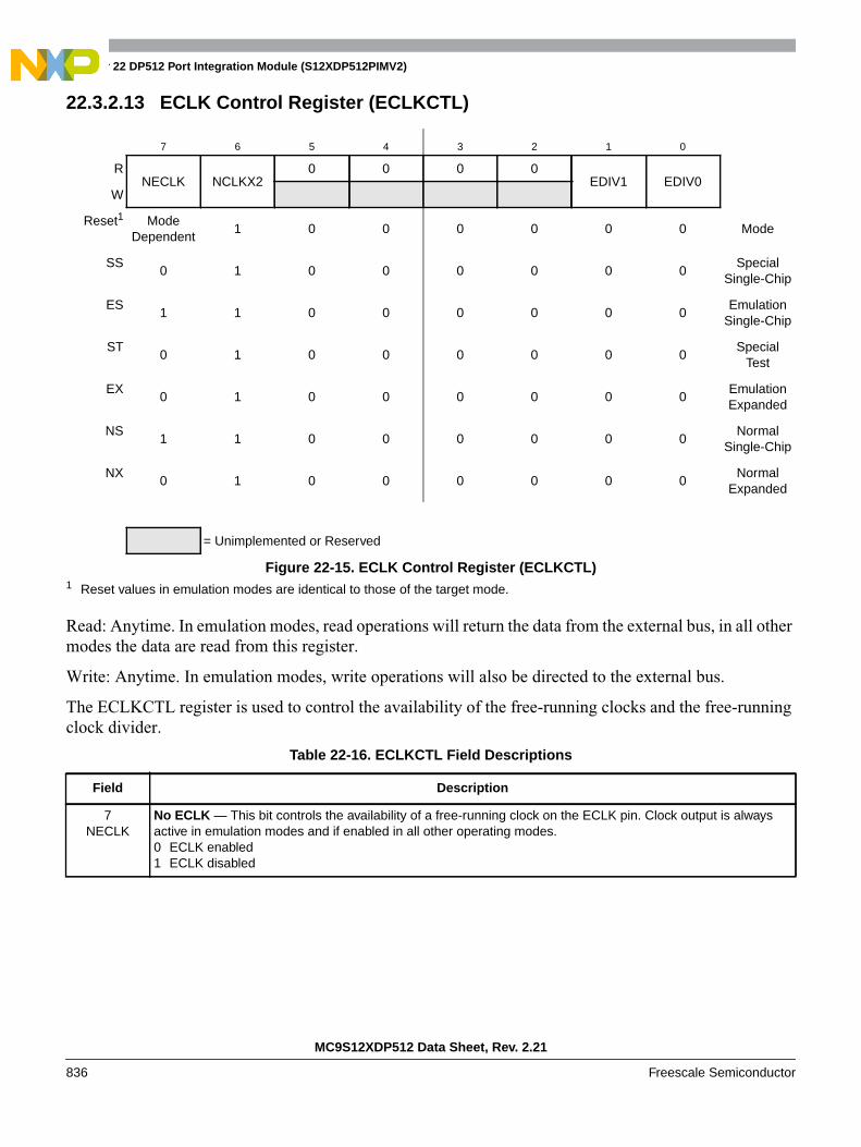
Chapter 22 DP512 Port Integration Module (S12XDP512PIMV2)
MC9S12XDP512 Data Sheet, Rev. 2.21
836 Freescale Semiconductor
22.3.2.13 ECLK Control Register (ECLKCTL)
Read: Anytime. In emulation modes, read operations will return the data from the external bus, in all othermodes the data are read from this register.
Write: Anytime. In emulation modes, write operations will also be directed to the external bus.
The ECLKCTL register is used to control the availability of the free-running clocks and the free-runningclock divider.
7 6 5 4 3 2 1 0
RNECLK NCLKX2
0 0 0 0EDIV1 EDIV0
W
Reset1
1 Reset values in emulation modes are identical to those of the target mode.
ModeDependent
1 0 0 0 0 0 0 Mode
SS0 1 0 0 0 0 0 0
SpecialSingle-Chip
ES1 1 0 0 0 0 0 0
EmulationSingle-Chip
ST0 1 0 0 0 0 0 0
SpecialTest
EX0 1 0 0 0 0 0 0
EmulationExpanded
NS1 1 0 0 0 0 0 0
NormalSingle-Chip
NX0 1 0 0 0 0 0 0
NormalExpanded
= Unimplemented or Reserved
Figure 22-15. ECLK Control Register (ECLKCTL)
Table 22-16. ECLKCTL Field Descriptions
Field Description
7NECLK
No ECLK — This bit controls the availability of a free-running clock on the ECLK pin. Clock output is alwaysactive in emulation modes and if enabled in all other operating modes.0 ECLK enabled1 ECLK disabled

Chapter 22 DP512 Port Integration Module (S12XDP512PIMV2)
MC9S12XDP512 Data Sheet, Rev. 2.21
Freescale Semiconductor 837
22.3.2.14 IRQ Control Register (IRQCR)
Read: See individual bit descriptions below.
Write: See individual bit descriptions below.
6NCLKX2
No ECLKX2 — This bit controls the availability of a free-running clock on the ECLKX2 pin. This clock has a fixedrate of twice the internal bus clock. Clock output is always active in emulation modes and if enabled in all otheroperating modes.0 ECLKX2 is enabled1 ECLKX2 is disabled
1–0EDIV[1:0]
Free-Running ECLK Divider — These bits determine the rate of the free-running clock on the ECLK pin. Theusage of the bits is shown in Table 22-17. Divider is always disabled in emulation modes and active asprogrammed in all other operating modes.
Table 22-17. Free-Running ECLK Clock Rate
EDIV[1:0] Rate of Free-Running ECLK
00 ECLK = Bus clock rate
01 ECLK = Bus clock rate divided by 2
10 ECLK = Bus clock rate divided by 3
11 ECLK = Bus clock rate divided by 4
7 6 5 4 3 2 1 0
RIRQE IRQEN
0 0 0 0 0 0
W
Reset 0 1 0 0 0 0 0 0
= Unimplemented or Reserved
Figure 22-16. IRQ Control Register (IRQCR)
Table 22-18. IRQCR Field Descriptions
Field Description
7IRQE
IRQ Select Edge Sensitive OnlySpecial modes: Read or write anytime.Normal and emulation modes: Read anytime, write once.0 IRQ configured for low level recognition.1 IRQ configured to respond only to falling edges. Falling edges on the IRQ pin will be detected anytime
IRQE = 1 and will be cleared only upon a reset or the servicing of the IRQ interrupt.
6IRQEN
External IRQ EnableRead or write anytime.0 External IRQ pin is disconnected from interrupt logic.1 External IRQ pin is connected to interrupt logic.
Table 22-16. ECLKCTL Field Descriptions (continued)
Field Description

Chapter 22 DP512 Port Integration Module (S12XDP512PIMV2)
MC9S12XDP512 Data Sheet, Rev. 2.21
838 Freescale Semiconductor
22.3.2.15 Port K Data Register (PORTK)
Read: Anytime. In emulation modes, read operations will return the data from the external bus, in all othermodes the data source is depending on the data direction value.
Write: Anytime. In emulation modes, write operations will also be directed to the external bus.
22.3.2.16 Port K Data Direction Register (DDRK)
Read: Anytime. In emulation modes, read operations will return the data from the external bus, in all othermodes the data are read from this register.
Write: Anytime. In emulation modes, write operations will also be directed to the external bus.
This register controls the data direction for port K. When Port K is operating as a general purpose I/O port,DDRK determines whether each pin is an input or output. A logic level “1” causes the associated port pinto be an output and a logic level “0” causes the associated pin to be a high-impedance input.
7 6 5 4 3 2 1 0
RPK7 PK6 PK5 PK4 PK3 PK2 PK1 PK0
W
Alt.Func.
ROMCTLor
EWAIT
ADDR22mux
NOACCADDR21 ADDR20
ADDR19mux
IQSTAT3
ADDR18mux
IQSTAT2
ADDR17mux
IQSTAT1
ADDR16mux
IQSTAT0
Reset 0 0 0 0 0 0 0 0
Figure 22-17. Port K Data Register (PORTK)
Table 22-19. PORTK Field Descriptions
Field Description
7–0PK[7:0]
Port K — Port K pins 7–0 are associated with external bus control signals and internal memory expansionemulation pins. These include ADDR22-ADDR16, No-Access (NOACC), External Wait (EWAIT) and instructionpipe signals IQSTAT3-IQSTAT0. Bits 6-0 carry the external addresses in all expanded modes. In emulation orspecial test mode with internal visibility enabled the address is multiplexed with the alternate functions NOACCand IQSTAT on the respective pins. In single-chip modes the port pins can be used as general-purpose I/O. Ifthe data direction bits of the associated I/O pins are set to logic level “1”, a read returns the value of the portregister, otherwise the buffered pin input state is read.
7 6 5 4 3 2 1 0
RDDRK7 DDRK6 DDRK5 DDRK4 DDRK3 DDRK2 DDRK1 DDRK0
W
Reset 0 0 0 0 0 0 0 0
Figure 22-18. Port K Data Direction Register (DDRK)

Chapter 22 DP512 Port Integration Module (S12XDP512PIMV2)
MC9S12XDP512 Data Sheet, Rev. 2.21
Freescale Semiconductor 839
Table 22-20. DDRK Field Descriptions
Field Description
7–0DDRK[7:0]
Data Direction Port K0 Associated pin is configured as input.1 Associated pin is configured as output.Note: Due to internal synchronization circuits, it can take up to 2 bus clock cycles until the correct value is read
on PORTK after changing the DDRK register.
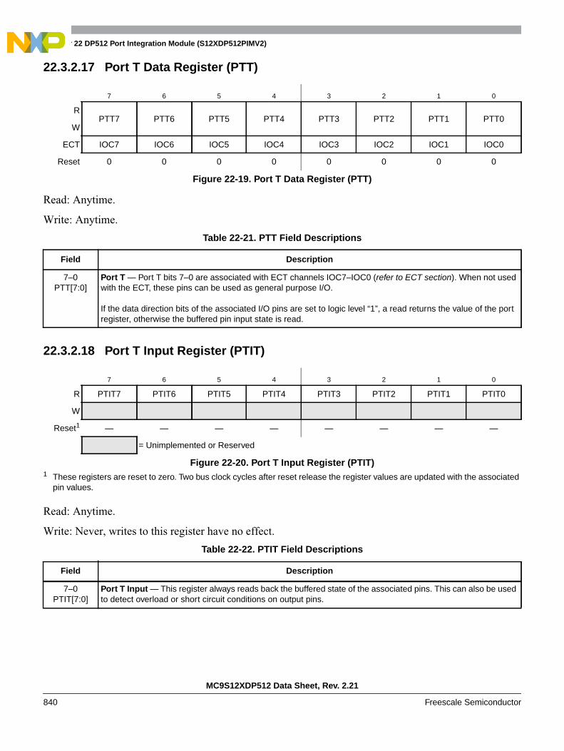
Chapter 22 DP512 Port Integration Module (S12XDP512PIMV2)
MC9S12XDP512 Data Sheet, Rev. 2.21
840 Freescale Semiconductor
22.3.2.17 Port T Data Register (PTT)
Read: Anytime.
Write: Anytime.
22.3.2.18 Port T Input Register (PTIT)
Read: Anytime.
Write: Never, writes to this register have no effect.
7 6 5 4 3 2 1 0
RPTT7 PTT6 PTT5 PTT4 PTT3 PTT2 PTT1 PTT0
W
ECT IOC7 IOC6 IOC5 IOC4 IOC3 IOC2 IOC1 IOC0
Reset 0 0 0 0 0 0 0 0
Figure 22-19. Port T Data Register (PTT)
Table 22-21. PTT Field Descriptions
Field Description
7–0PTT[7:0]
Port T — Port T bits 7–0 are associated with ECT channels IOC7–IOC0 (refer to ECT section). When not usedwith the ECT, these pins can be used as general purpose I/O.
If the data direction bits of the associated I/O pins are set to logic level “1”, a read returns the value of the portregister, otherwise the buffered pin input state is read.
7 6 5 4 3 2 1 0
R PTIT7 PTIT6 PTIT5 PTIT4 PTIT3 PTIT2 PTIT1 PTIT0
W
Reset1
1 These registers are reset to zero. Two bus clock cycles after reset release the register values are updated with the associatedpin values.
— — — — — — — —
= Unimplemented or Reserved
Figure 22-20. Port T Input Register (PTIT)
Table 22-22. PTIT Field Descriptions
Field Description
7–0PTIT[7:0]
Port T Input — This register always reads back the buffered state of the associated pins. This can also be usedto detect overload or short circuit conditions on output pins.

Chapter 22 DP512 Port Integration Module (S12XDP512PIMV2)
MC9S12XDP512 Data Sheet, Rev. 2.21
Freescale Semiconductor 841
22.3.2.19 Port T Data Direction Register (DDRT)
Read: Anytime.
Write: Anytime.
This register configures each port T pin as either input or output.
The ECT forces the I/O state to be an output for each timer port associated with an enabled output compare.In this case the data direction bits will not change.
The DDRT bits revert to controlling the I/O direction of a pin when the associated timer output compareis disabled.
The timer input capture always monitors the state of the pin.
7 6 5 4 3 2 1 0
RDDRT7 DDRT6 DDRT5 DDRT4 DDRT3 DDRT2 DDRT1 DDRT0
W
Reset 0 0 0 0 0 0 0 0
Figure 22-21. Port T Data Direction Register (DDRT)
Table 22-23. DDRT Field Descriptions
Field Description
7–0DDRT[7:0]
Data Direction Port T0 Associated pin is configured as input.1 Associated pin is configured as output.Note: Due to internal synchronization circuits, it can take up to 2 bus clock cycles until the correct value is read
on PTT or PTIT registers, when changing the DDRT register.

Chapter 22 DP512 Port Integration Module (S12XDP512PIMV2)
MC9S12XDP512 Data Sheet, Rev. 2.21
842 Freescale Semiconductor
22.3.2.20 Port T Reduced Drive Register (RDRT)
Read: Anytime.
Write: Anytime.
This register configures the drive strength of each port T output pin as either full or reduced. If the port isused as input this bit is ignored.
22.3.2.21 Port T Pull Device Enable Register (PERT)
Read: Anytime.
Write: Anytime.
This register configures whether a pull-up or a pull-down device is activated, if the port is used as input.This bit has no effect if the port is used as output. Out of reset no pull device is enabled.
7 6 5 4 3 2 1 0
RRDRT7 RDRT6 RDRT5 RDRT4 RDRT3 RDRT2 RDRT1 RDRT0
W
Reset 0 0 0 0 0 0 0 0
Figure 22-22. Port T Reduced Drive Register (RDRT)
Table 22-24. RDRT Field Descriptions
Field Description
7–0RDRT[7:0]
Reduced Drive Port T0 Full drive strength at output.1 Associated pin drives at about 1/6 of the full drive strength.
7 6 5 4 3 2 1 0
RPERT7 PERT6 PERT5 PERT4 PERT3 PERT2 PERT1 PERT0
W
Reset 0 0 0 0 0 0 0 0
Figure 22-23. Port T Pull Device Enable Register (PERT)
Table 22-25. PERT Field Descriptions
Field Description
7–0PERT[7:0]
Pull Device Enable Port T0 Pull-up or pull-down device is disabled.1 Either a pull-up or pull-down device is enabled.

Chapter 22 DP512 Port Integration Module (S12XDP512PIMV2)
MC9S12XDP512 Data Sheet, Rev. 2.21
Freescale Semiconductor 843
22.3.2.22 Port T Polarity Select Register (PPST)
Read: Anytime.
Write: Anytime.
This register selects whether a pull-down or a pull-up device is connected to the pin.
22.3.2.23 Port S Data Register (PTS)
Read: Anytime.
Write: Anytime.
Port S pins 7–4 are associated with the SPI0. The SPI0 pin configuration is determined by several statusbits in the SPI0 module. Refer to SPI section for details. When not used with the SPI0, these pins can beused as general purpose I/O.
Port S bits 3–0 are associated with the SCI1 and SCI0. The SCI ports associated with transmit pins 3 and1 are configured as outputs if the transmitter is enabled. The SCI ports associated with receive pins 2 and0 are configured as inputs if the receiver is enabled. Refer to SCI section for details. When not used withthe SCI, these pins can be used as general purpose I/O.
If the data direction bits of the associated I/O pins are set to logic level “1”, a read returns the value of theport register, otherwise the buffered pin input state is read.
7 6 5 4 3 2 1 0
RPPST7 PPST6 PPST5 PPST4 PPST3 PPST2 PPST1 PPST0
W
Reset 0 0 0 0 0 0 0 0
Figure 22-24. Port T Polarity Select Register (PPST)
Table 22-26. PPST Field Descriptions
Field Description
7–0PPST[7:0]
Pull Select Port T0 A pull-up device is connected to the associated port T pin, if enabled by the associated bit in register PERT
and if the port is used as input.1 A pull-down device is connected to the associated port T pin, if enabled by the associated bit in register PERT
and if the port is used as input.
7 6 5 4 3 2 1 0
RPTS7 PTS6 PTS5 PTS4 PTS3 PTS2 PTS1 PTS0
W
SCI/SPI SS0 SCK0 MOSI0 MISO0 TXD1 RXD1 TXD0 RXD0
Reset 0 0 0 0 0 0 0 0
Figure 22-25. Port S Data Register (PTS)

Chapter 22 DP512 Port Integration Module (S12XDP512PIMV2)
MC9S12XDP512 Data Sheet, Rev. 2.21
844 Freescale Semiconductor
22.3.2.24 Port S Input Register (PTIS)
Read: Anytime.
Write: Never, writes to this register have no effect.
This register always reads back the buffered state of the associated pins. This also can be used to detectoverload or short circuit conditions on output pins.
7 6 5 4 3 2 1 0
R PTIS7 PTIS6 PTIS5 PTIS4 PTIS3 PTIS2 PTIS1 PTIS0
W
Reset1
1 These registers are reset to zero. Two bus clock cycles after reset release the register values are updated with the associatedpin values.
— — — — — — — —
= Unimplemented or Reserved
Figure 22-26. Port S Input Register (PTIS)
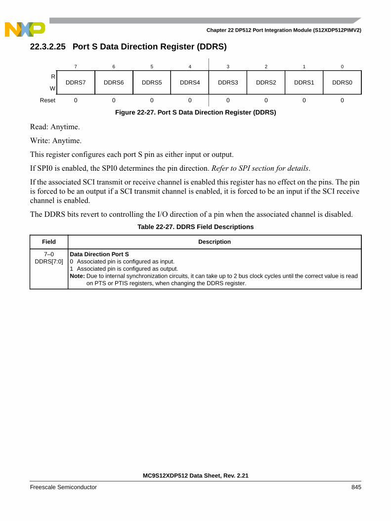
Chapter 22 DP512 Port Integration Module (S12XDP512PIMV2)
MC9S12XDP512 Data Sheet, Rev. 2.21
Freescale Semiconductor 845
22.3.2.25 Port S Data Direction Register (DDRS)
Read: Anytime.
Write: Anytime.
This register configures each port S pin as either input or output.
If SPI0 is enabled, the SPI0 determines the pin direction. Refer to SPI section for details.
If the associated SCI transmit or receive channel is enabled this register has no effect on the pins. The pinis forced to be an output if a SCI transmit channel is enabled, it is forced to be an input if the SCI receivechannel is enabled.
The DDRS bits revert to controlling the I/O direction of a pin when the associated channel is disabled.
7 6 5 4 3 2 1 0
RDDRS7 DDRS6 DDRS5 DDRS4 DDRS3 DDRS2 DDRS1 DDRS0
W
Reset 0 0 0 0 0 0 0 0
Figure 22-27. Port S Data Direction Register (DDRS)
Table 22-27. DDRS Field Descriptions
Field Description
7–0DDRS[7:0]
Data Direction Port S0 Associated pin is configured as input.1 Associated pin is configured as output.Note: Due to internal synchronization circuits, it can take up to 2 bus clock cycles until the correct value is read
on PTS or PTIS registers, when changing the DDRS register.

Chapter 22 DP512 Port Integration Module (S12XDP512PIMV2)
MC9S12XDP512 Data Sheet, Rev. 2.21
846 Freescale Semiconductor
22.3.2.26 Port S Reduced Drive Register (RDRS)
Read: Anytime.
Write: Anytime.
This register configures the drive strength of each port S output pin as either full or reduced. If the port isused as input this bit is ignored.
22.3.2.27 Port S Pull Device Enable Register (PERS)
Read: Anytime.
Write: Anytime.
This register configures whether a pull-up or a pull-down device is activated, if the port is used as input oras output in wired-OR (open drain) mode. This bit has no effect if the port is used as push-pull output. Outof reset a pull-up device is enabled.
7 6 5 4 3 2 1 0
RRDRS7 RDRS6 RDRS5 RDRS4 RDRS3 RDRS2 RDRS1 RDRS0
W
Reset 0 0 0 0 0 0 0 0
Figure 22-28. Port S Reduced Drive Register (RDRS)
Table 22-28. RDRS Field Descriptions
Field Description
7–0RDRS[7:0]
Reduced Drive Port S0 Full drive strength at output.1 Associated pin drives at about 1/6 of the full drive strength.
7 6 5 4 3 2 1 0
RPERS7 PERS6 PERS5 PERS4 PERS3 PERS2 PERS1 PERS0
W
Reset 1 1 1 1 1 1 1 1
Figure 22-29. Port S Pull Device Enable Register (PERS)
Table 22-29. PERS Field Descriptions
Field Description
7–0PERS[7:0]
Pull Device Enable Port S0 Pull-up or pull-down device is disabled.1 Either a pull-up or pull-down device is enabled.

Chapter 22 DP512 Port Integration Module (S12XDP512PIMV2)
MC9S12XDP512 Data Sheet, Rev. 2.21
Freescale Semiconductor 847
22.3.2.28 Port S Polarity Select Register (PPSS)
Read: Anytime.
Write: Anytime.
This register selects whether a pull-down or a pull-up device is connected to the pin.
22.3.2.29 Port S Wired-OR Mode Register (WOMS)
Read: Anytime.
Write: Anytime.
This register configures the output pins as wired-OR. If enabled the output is driven active low only(open-drain). A logic level of “1” is not driven. It applies also to the SPI and SCI outputs and allows amultipoint connection of several serial modules. These bits have no influence on pins used as inputs.
7 6 5 4 3 2 1 0
RPPSS7 PPSS6 PPSS5 PPSS4 PPSS3 PPSS2 PPSS1 PPSS0
W
Reset 0 0 0 0 0 0 0 0
Figure 22-30. Port S Polarity Select Register (PPSS)
Table 22-30. PPSS Field Descriptions
Field Description
7–0PPSS[7:0]
Pull Select Port S0 A pull-up device is connected to the associated port S pin, if enabled by the associated bit in register PERS
and if the port is used as input or as wired-OR output.1 A pull-down device is connected to the associated port S pin, if enabled by the associated bit in register PERS
and if the port is used as input.
7 6 5 4 3 2 1 0
RWOMS7 WOMS6 WOMS5 WOMS4 WOMS3 WOMS2 WOMS1 WOMS0
W
Reset 0 0 0 0 0 0 0 0
Figure 22-31. Port S Wired-OR Mode Register (WOMS)
Table 22-31. WOMS Field Descriptions
Field Description
7–0WOMS[7:0]
Wired-OR Mode Port S0 Output buffers operate as push-pull outputs.1 Output buffers operate as open-drain outputs.
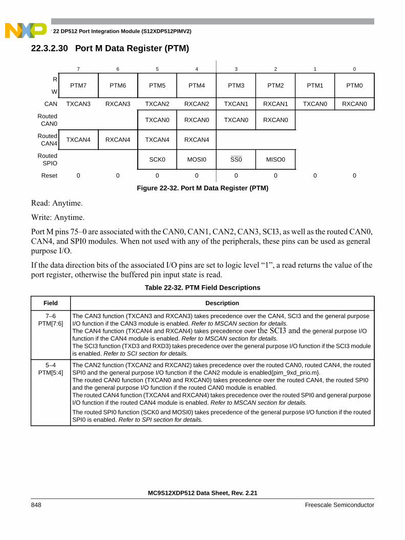
Chapter 22 DP512 Port Integration Module (S12XDP512PIMV2)
MC9S12XDP512 Data Sheet, Rev. 2.21
848 Freescale Semiconductor
22.3.2.30 Port M Data Register (PTM)
Read: Anytime.
Write: Anytime.
Port M pins 75–0 are associated with the CAN0, CAN1, CAN2, CAN3, SCI3, as well as the routed CAN0,CAN4, and SPI0 modules. When not used with any of the peripherals, these pins can be used as generalpurpose I/O.
If the data direction bits of the associated I/O pins are set to logic level “1”, a read returns the value of theport register, otherwise the buffered pin input state is read.
7 6 5 4 3 2 1 0
RPTM7 PTM6 PTM5 PTM4 PTM3 PTM2 PTM1 PTM0
W
CAN TXCAN3 RXCAN3 TXCAN2 RXCAN2 TXCAN1 RXCAN1 TXCAN0 RXCAN0
RoutedCAN0
TXCAN0 RXCAN0 TXCAN0 RXCAN0
RoutedCAN4
TXCAN4 RXCAN4 TXCAN4 RXCAN4
RoutedSPIO
SCK0 MOSI0 SS0 MISO0
Reset 0 0 0 0 0 0 0 0
Figure 22-32. Port M Data Register (PTM)
Table 22-32. PTM Field Descriptions
Field Description
7–6PTM[7:6]
The CAN3 function (TXCAN3 and RXCAN3) takes precedence over the CAN4, SCI3 and the general purposeI/O function if the CAN3 module is enabled. Refer to MSCAN section for details.The CAN4 function (TXCAN4 and RXCAN4) takes precedence over the SCI3 and the general purpose I/Ofunction if the CAN4 module is enabled. Refer to MSCAN section for details.The SCI3 function (TXD3 and RXD3) takes precedence over the general purpose I/O function if the SCI3 moduleis enabled. Refer to SCI section for details.
5–4PTM[5:4]
The CAN2 function (TXCAN2 and RXCAN2) takes precedence over the routed CAN0, routed CAN4, the routedSPI0 and the general purpose I/O function if the CAN2 module is enabledpim_9xd_prio.m.The routed CAN0 function (TXCAN0 and RXCAN0) takes precedence over the routed CAN4, the routed SPI0and the general purpose I/O function if the routed CAN0 module is enabled.The routed CAN4 function (TXCAN4 and RXCAN4) takes precedence over the routed SPI0 and general purposeI/O function if the routed CAN4 module is enabled. Refer to MSCAN section for details.
The routed SPI0 function (SCK0 and MOSI0) takes precedence of the general purpose I/O function if the routedSPI0 is enabled. Refer to SPI section for details.

Chapter 22 DP512 Port Integration Module (S12XDP512PIMV2)
MC9S12XDP512 Data Sheet, Rev. 2.21
Freescale Semiconductor 849
3–2PTM[3:2]
The CAN1 function (TXCAN1 and RXCAN1) takes precedence over the routed CAN0, the routed SPI0 and thegeneral purpose I/O function if the CAN1 module is enabled.
The routed CAN0 function (TXCAN0 and RXCAN0) takes precedence over the routed SPI0 and the generalpurpose I/O function if the routed CAN0 module is enabled. Refer to MSCAN section for details.
The routed SPI0 function (SS0 and MISO0) takes precedence of the general purpose I/O function if the routedSPI0 is enabled and not in bidirectional mode. Refer to SPI section for details.
1–0PTM[1:0]
The CAN0 function (TXCAN0 and RXCAN0) takes precedence over the general purpose I/O function if the CAN0module is enabled. Refer to MSCAN section for details.
Table 22-32. PTM Field Descriptions (continued)
Field Description

Chapter 22 DP512 Port Integration Module (S12XDP512PIMV2)
MC9S12XDP512 Data Sheet, Rev. 2.21
850 Freescale Semiconductor
22.3.2.31 Port M Input Register (PTIM)
Read: Anytime.
Write: Never, writes to this register have no effect.
This register always reads back the buffered state of the associated pins. This can also be used to detectoverload or short circuit conditions on output pins.
7 6 5 4 3 2 1 0
R PTIM7 PTIM6 PTIM5 PTIM4 PTIM3 PTIM2 PTIM1 PTIM0
W
Reset1
1 These registers are reset to zero. Two bus clock cycles after reset release the register values are updated with the associatedpin values.
— — — — — — — —
= Unimplemented or Reserved
Figure 22-33. Port M Input Register (PTIM)

Chapter 22 DP512 Port Integration Module (S12XDP512PIMV2)
MC9S12XDP512 Data Sheet, Rev. 2.21
Freescale Semiconductor 851
22.3.2.32 Port M Data Direction Register (DDRM)
Read: Anytime.
Write: Anytime.
This register configures each port M pin as either input or output.
The CAN/SCI3 forces the I/O state to be an output for each port line associated with an enabled output(TXCAN[3:0], TXD3). TheyAlso forces the I/O state to be an input for each port line associated with anenabled input (RXCAN[3:0], RXD3). In those cases the data direction bits will not change.
The DDRM bits revert to controlling the I/O direction of a pin when the associated peripheral module isdisabled.
7 6 5 4 3 2 1 0
RDDRM7 DDRM6 DDRM5 DDRM4 DDRM3 DDRM2 DDRM1 DDRM0
W
Reset 0 0 0 0 0 0 0 0
Figure 22-34. Port M Data Direction Register (DDRM)
Table 22-33. DDRM Field Descriptions
Field Description
7–0DDRM[7:0]
Data Direction Port M0 Associated pin is configured as input.1 Associated pin is configured as output.Note: Due to internal synchronization circuits, it can take up to 2 bus clock cycles until the correct value is read
on PTM or PTIM registers, when changing the DDRM register.

Chapter 22 DP512 Port Integration Module (S12XDP512PIMV2)
MC9S12XDP512 Data Sheet, Rev. 2.21
852 Freescale Semiconductor
22.3.2.33 Port M Reduced Drive Register (RDRM)
Read: Anytime.
Write: Anytime.
This register configures the drive strength of each Port M output pin as either full or reduced. If the portis used as input this bit is ignored.
22.3.2.34 Port M Pull Device Enable Register (PERM)
Read: Anytime.
Write: Anytime.
This register configures whether a pull-up or a pull-down device is activated, if the port is used as input orwired-OR output. This bit has no effect if the port is used as push-pull output. Out of reset no pull deviceis enabled.
7 6 5 4 3 2 1 0
RRDRM7 RDRM6 RDRM5 RDRM4 RDRM3 RDRM2 RDRM1 RDRM0
W
Reset 0 0 0 0 0 0 0 0
Figure 22-35. Port M Reduced Drive Register (RDRM)
Table 22-34. RDRM Field Descriptions
Field Description
7–0RDRM[7:0]
Reduced Drive Port M0 Full drive strength at output.1 Associated pin drives at about 1/6 of the full drive strength.
7 6 5 4 3 2 1 0
RPERM7 PERM6 PERM5 PERM4 PERM3 PERM2 PERM1 PERM0
W
Reset 0 0 0 0 0 0 0 0
Figure 22-36. Port M Pull Device Enable Register (PERM)
Table 22-35. PERM Field Descriptions
Field Description
7–0PERM[7:0]
Pull Device Enable Port M0 Pull-up or pull-down device is disabled.1 Either a pull-up or pull-down device is enabled.

Chapter 22 DP512 Port Integration Module (S12XDP512PIMV2)
MC9S12XDP512 Data Sheet, Rev. 2.21
Freescale Semiconductor 853
22.3.2.35 Port M Polarity Select Register (PPSM)
Read: Anytime.
Write: Anytime.
This register selects whether a pull-down or a pull-up device is connected to the pin. If CAN is active apull-up device can be activated on the RXCAN[3:0] inputs, but not a pull-down.
22.3.2.36 Port M Wired-OR Mode Register (WOMM)
Read: Anytime.
Write: Anytime.
This register configures the output pins as wired-OR. If enabled the output is driven active low only(open-drain). A logic level of “1” is not driven. It applies also to the CAN outputs and allows a multipointconnection of several serial modules. This bit has no influence on pins used as inputs.
7 6 5 4 3 2 1 0
RPPSM7 PPSM6 PPSM5 PPSM4 PPSM3 PPSM2 PPSM1 PPSM0
W
Reset 0 0 0 0 0 0 0 0
Figure 22-37. Port M Polarity Select Register (PPSM)
Table 22-36. PPSM Field Descriptions
Field Description
7–0PPSM[7:0]
Pull Select Port M0 A pull-up device is connected to the associated port M pin, if enabled by the associated bit in register PERM
and if the port is used as general purpose or RXCAN input.1 A pull-down device is connected to the associated port M pin, if enabled by the associated bit in register PERM
and if the port is used as a general purpose but not as RXCAN.
7 6 5 4 3 2 1 0
RWOMM7 WOMM6 WOMM5 WOMM4 WOMM3 WOMM2 WOMM1 WOMM0
W
Reset 0 0 0 0 0 0 0 0
Figure 22-38. Port M Wired-OR Mode Register (WOMM)
Table 22-37. WOMM Field Descriptions
Field Description
7–0WOMM[7:0]
Wired-OR Mode Port M0 Output buffers operate as push-pull outputs.1 Output buffers operate as open-drain outputs.
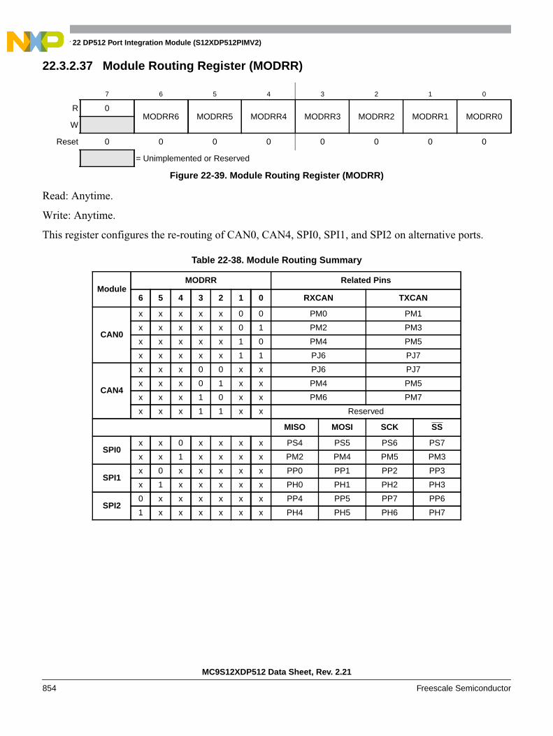
Chapter 22 DP512 Port Integration Module (S12XDP512PIMV2)
MC9S12XDP512 Data Sheet, Rev. 2.21
854 Freescale Semiconductor
22.3.2.37 Module Routing Register (MODRR)
Read: Anytime.
Write: Anytime.
This register configures the re-routing of CAN0, CAN4, SPI0, SPI1, and SPI2 on alternative ports.
7 6 5 4 3 2 1 0
R 0MODRR6 MODRR5 MODRR4 MODRR3 MODRR2 MODRR1 MODRR0
W
Reset 0 0 0 0 0 0 0 0
= Unimplemented or Reserved
Figure 22-39. Module Routing Register (MODRR)
Table 22-38. Module Routing Summary
ModuleMODRR Related Pins
6 5 4 3 2 1 0 RXCAN TXCAN
CAN0
x x x x x 0 0 PM0 PM1
x x x x x 0 1 PM2 PM3
x x x x x 1 0 PM4 PM5
x x x x x 1 1 PJ6 PJ7
CAN4
x x x 0 0 x x PJ6 PJ7
x x x 0 1 x x PM4 PM5
x x x 1 0 x x PM6 PM7
x x x 1 1 x x Reserved
MISO MOSI SCK SS
SPI0x x 0 x x x x PS4 PS5 PS6 PS7
x x 1 x x x x PM2 PM4 PM5 PM3
SPI1x 0 x x x x x PP0 PP1 PP2 PP3
x 1 x x x x x PH0 PH1 PH2 PH3
SPI20 x x x x x x PP4 PP5 PP7 PP6
1 x x x x x x PH4 PH5 PH6 PH7

Chapter 22 DP512 Port Integration Module (S12XDP512PIMV2)
MC9S12XDP512 Data Sheet, Rev. 2.21
Freescale Semiconductor 855
22.3.2.38 Port P Data Register (PTP)
Read: Anytime.
Write: Anytime.
Port P pins 7, and 5–0 are associated with the PWM as well as the SPI1 and SPI2 modules. These pins canbe used as general purpose I/O when not used with any of the peripherals.
If the data direction bits of the associated I/O pins are set to logic level “1”, a read returns the value of theport register, otherwise the buffered pin input state is read.
The PWM function takes precedence over the general purpose I/O and the SPI2 or SPI1 function if theassociated PWM channel is enabled. While channels 6 and 5-0 are output only if the respective channel isenabled, channel 7 can be PWM output or input if the shutdown feature is enabled. Refer to PWM sectionfor details.
The SPI2 function takes precedence over the general purpose I/O function if enabled. Refer to SPI sectionfor details.
The SPI1 function takes precedence over the general purpose I/O function if enabled. Refer to SPI sectionfor details.
7 6 5 4 3 2 1 0
RPTP7 PTP6 PTP5 PTP4 PTP3 PTP2 PTP1 PTP0
W
PWM PWM7 PWM6 PWM5 PWM4 PWM3 PWM2 PWM1 PWM0
SPI SCK2 SS2 MOSI2 MISO2 SS1 SCK1 MOSI1 MISO1
Reset 0 0 0 0 0 0 0 0
Figure 22-40. Port P Data Register (PTP)

Chapter 22 DP512 Port Integration Module (S12XDP512PIMV2)
MC9S12XDP512 Data Sheet, Rev. 2.21
856 Freescale Semiconductor
22.3.2.39 Port P Input Register (PTIP)
Read: Anytime.
Write: Never, writes to this register have no effect.
This register always reads back the buffered state of the associated pins. This can also be used to detectoverload or short circuit conditions on output pins.
7 6 5 4 3 2 1 0
R PTIP7 PTIP6 PTIP5 PTIP4 PTIP3 PTIP2 PTIP1 PTIP0
W
Reset1
1 These registers are reset to zero. Two bus clock cycles after reset release the register values are updated with the associatedpin values.
— — — — — — — —
= Unimplemented or Reserved
Figure 22-41. Port P Input Register (PTIP)

Chapter 22 DP512 Port Integration Module (S12XDP512PIMV2)
MC9S12XDP512 Data Sheet, Rev. 2.21
Freescale Semiconductor 857
22.3.2.40 Port P Data Direction Register (DDRP)
Read: Anytime.
Write: Anytime.
This register configures each port P pin as either input or output.
If the associated PWM channel or SPI module is enabled this register has no effect on the pins.
The PWM forces the I/O state to be an output for each port line associated with an enabled PWM7–0channel. Channel 7 can force the pin to input if the shutdown feature is enabled. Refer to PWM section fordetails.
If a SPI module is enabled, the SPI determines the pin direction. Refer to SPI section for details.
The DDRP bits revert to controlling the I/O direction of a pin when the associated peripherals are disabled.
7 6 5 4 3 2 1 0
RDDRP7 DDRP6 DDRP5 DDRP4 DDRP3 DDRP2 DDRP1 DDRP0
W
Reset 0 0 0 0 0 0 0 0
Figure 22-42. Port P Data Direction Register (DDRP)
Table 22-39. DDRP Field Descriptions
Field Description
7–0DDRP[7:0]
Data Direction Port P0 Associated pin is configured as input.1 Associated pin is configured as output.Note: Due to internal synchronization circuits, it can take up to 2 bus clock cycles until the correct value is read
on PTP or PTIP registers, when changing the DDRP register.

Chapter 22 DP512 Port Integration Module (S12XDP512PIMV2)
MC9S12XDP512 Data Sheet, Rev. 2.21
858 Freescale Semiconductor
22.3.2.41 Port P Reduced Drive Register (RDRP)
Read: Anytime.
Write: Anytime.
This register configures the drive strength of each port P output pin as either full or reduced. If the port isused as input this bit is ignored.
22.3.2.42 Port P Pull Device Enable Register (PERP)
Read: Anytime.
Write: Anytime.
This register configures whether a pull-up or a pull-down device is activated, if the port is used as input.This bit has no effect if the port is used as output. Out of reset no pull device is enabled.
7 6 5 4 3 2 1 0
RRDRP7 RDRP6 RDRP5 RDRP4 RDRP3 RDRP2 RDRP1 RDRP0
W
Reset 0 0 0 0 0 0 0 0
Figure 22-43. Port P Reduced Drive Register (RDRP)
Table 22-40. RDRP Field Descriptions
Field Description
7–0RDRP[7:0]
Reduced Drive Port P0 Full drive strength at output.1 Associated pin drives at about 1/6 of the full drive strength.
7 6 5 4 3 2 1 0
RPERP7 PERP6 PERP5 PERP4 PERP3 PERP2 PERP1 PERP0
W
Reset 0 0 0 0 0 0 0 0
Figure 22-44. Port P Pull Device Enable Register (PERP)
Table 22-41. PERP Field Descriptions
Field Description
7–0PERP[7:0]
Pull Device Enable Port P0 Pull-up or pull-down device is disabled.1 Either a pull-up or pull-down device is enabled.

Chapter 22 DP512 Port Integration Module (S12XDP512PIMV2)
MC9S12XDP512 Data Sheet, Rev. 2.21
Freescale Semiconductor 859
22.3.2.43 Port P Polarity Select Register (PPSP)
Read: Anytime.
Write: Anytime.
This register serves a dual purpose by selecting the polarity of the active interrupt edge as well as selectinga pull-up or pull-down device if enabled.
22.3.2.44 Port P Interrupt Enable Register (PIEP)
Read: Anytime.
Write: Anytime.
This register disables or enables on a per-pin basis the edge sensitive external interrupt associated withPort P.
7 6 5 4 3 2 1 0
RPPSP7 PPSP6 PPSP5 PPSP4 PPSP3 PPSP2 PPSP1 PPSP0
W
Reset 0 0 0 0 0 0 0 0
Figure 22-45. Port P Polarity Select Register (PPSP)
Table 22-42. PPSP Field Descriptions
Field Description
7–0PPSP[7:0]
Polarity Select Port P0 Falling edge on the associated port P pin sets the associated flag bit in the PIFP register.A pull-up device is
connected to the associated port P pin, if enabled by the associated bit in register PERP and if the port is usedas input.
1 Rising edge on the associated port P pin sets the associated flag bit in the PIFP register.A pull-down deviceis connected to the associated port P pin, if enabled by the associated bit in register PERP and if the port isused as input.
7 6 5 4 3 2 1 0
RPIEP7 PIEP6 PIEP5 PIEP4 PIEP3 PIEP2 PIEP1 PIEP0
W
Reset 0 0 0 0 0 0 0 0
Figure 22-46. Port P Interrupt Enable Register (PIEP)
Table 22-43. PIEP Field Descriptions
Field Description
7–0PIEP[7:0]
Interrupt Enable Port P0 Interrupt is disabled (interrupt flag masked).1 Interrupt is enabled.

Chapter 22 DP512 Port Integration Module (S12XDP512PIMV2)
MC9S12XDP512 Data Sheet, Rev. 2.21
860 Freescale Semiconductor
22.3.2.45 Port P Interrupt Flag Register (PIFP)
Read: Anytime.
Write: Anytime.
Each flag is set by an active edge on the associated input pin. This could be a rising or a falling edge basedon the state of the PPSP register. To clear this flag, write logic level “1” to the corresponding bit in thePIFP register. Writing a “0” has no effect.
7 6 5 4 3 2 1 0
RPIFP7 PIFP6 PIFP5 PIFP4 PIFP3 PIFP2 PIFP1 PIFP0
W
Reset 0 0 0 0 0 0 0 0
Figure 22-47. Port P Interrupt Flag Register (PIFP)
Table 22-44. PIFP Field Descriptions
Field Description
7–0PIFP[7:0]
Interrupt Flags Port P0 No active edge pending. Writing a “0” has no effect.1 Active edge on the associated bit has occurred (an interrupt will occur if the associated enable bit is set).
Writing a logic level “1” clears the associated flag.

Chapter 22 DP512 Port Integration Module (S12XDP512PIMV2)
MC9S12XDP512 Data Sheet, Rev. 2.21
Freescale Semiconductor 861
22.3.2.46 Port H Data Register (PTH)
Read: Anytime.
Write: Anytime.
Port H pins 7–0 are associated with the SCI4 and SCI5 as well as the routed SPI1 and SPI2 modules.
These pins can be used as general purpose I/O when not used with any of the peripherals.
If the data direction bits of the associated I/O pins are set to logic level “1”, a read returns the value of theport register, otherwise the buffered pin input state is read.
The routed SPI2 function takes precedence over the SCI4 and SCI5 and the general purpose I/O functionif the routed SPI2 module is enabled. Refer to SPI section for details.
The routed SPI1 function takes precedence over the general purpose I/O function if the routed SPI1 isenabled. Refer to SPI section for details.
The SCI4 and SCI5 function takes precedence over the general purpose I/O function if the SCI4 or SCI5is enabled. Refer to SCI section for details.
7 6 5 4 3 2 1 0
RPTH7 PTH6 PTH5 PTH4 PTH3 PTH2 PTH1 PTH0
W
RoutedSPI
SS2 SCK2 MOSI2 MISO2 SS1 SCK1 MOSI1 MISO1
Reset 0 0 0 0 0 0 0 0
Figure 22-48. Port H Data Register (PTH)

Chapter 22 DP512 Port Integration Module (S12XDP512PIMV2)
MC9S12XDP512 Data Sheet, Rev. 2.21
862 Freescale Semiconductor
22.3.2.47 Port H Input Register (PTIH)
Read: Anytime.
Write: Never, writes to this register have no effect.
This register always reads back the buffered state of the associated pins. This can also be used to detectoverload or short circuit conditions on output pins.
7 6 5 4 3 2 1 0
R PTIH7 PTIH6 PTIH5 PTIH4 PTIH3 PTIH2 PTIH1 PTIH0
W
Reset1
1 These registers are reset to zero. Two bus clock cycles after reset release the register values are updated with the associatedpin values.
— — — — — — — —
= Unimplemented or Reserved
Figure 22-49. Port H Input Register (PTIH)
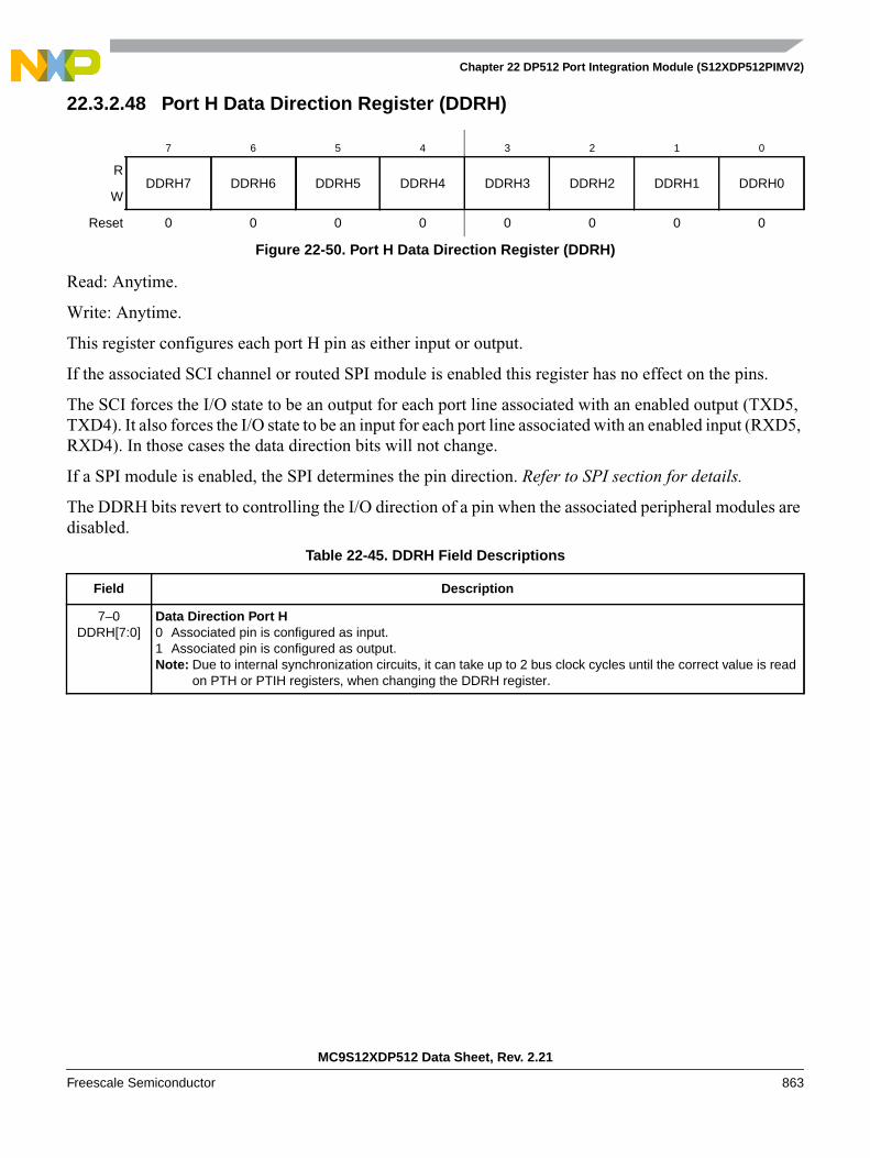
Chapter 22 DP512 Port Integration Module (S12XDP512PIMV2)
MC9S12XDP512 Data Sheet, Rev. 2.21
Freescale Semiconductor 863
22.3.2.48 Port H Data Direction Register (DDRH)
Read: Anytime.
Write: Anytime.
This register configures each port H pin as either input or output.
If the associated SCI channel or routed SPI module is enabled this register has no effect on the pins.
The SCI forces the I/O state to be an output for each port line associated with an enabled output (TXD5,TXD4). It also forces the I/O state to be an input for each port line associated with an enabled input (RXD5,RXD4). In those cases the data direction bits will not change.
If a SPI module is enabled, the SPI determines the pin direction. Refer to SPI section for details.
The DDRH bits revert to controlling the I/O direction of a pin when the associated peripheral modules aredisabled.
7 6 5 4 3 2 1 0
RDDRH7 DDRH6 DDRH5 DDRH4 DDRH3 DDRH2 DDRH1 DDRH0
W
Reset 0 0 0 0 0 0 0 0
Figure 22-50. Port H Data Direction Register (DDRH)
Table 22-45. DDRH Field Descriptions
Field Description
7–0DDRH[7:0]
Data Direction Port H0 Associated pin is configured as input.1 Associated pin is configured as output.Note: Due to internal synchronization circuits, it can take up to 2 bus clock cycles until the correct value is read
on PTH or PTIH registers, when changing the DDRH register.

Chapter 22 DP512 Port Integration Module (S12XDP512PIMV2)
MC9S12XDP512 Data Sheet, Rev. 2.21
864 Freescale Semiconductor
22.3.2.49 Port H Reduced Drive Register (RDRH)
Read: Anytime.
Write: Anytime.
This register configures the drive strength of each Port H output pin as either full or reduced. If the port isused as input this bit is ignored.
22.3.2.50 Port H Pull Device Enable Register (PERH)
Read: Anytime.
Write: Anytime.
This register configures whether a pull-up or a pull-down device is activated, if the port is used as input.This bit has no effect if the port is used as output. Out of reset no pull device is enabled.
7 6 5 4 3 2 1 0
RRDRH7 RDRH6 RDRH5 RDRH4 RDRH3 RDRH2 RDRH1 RDRH0
W
Reset 0 0 0 0 0 0 0 0
Figure 22-51. Port H Reduced Drive Register (RDRH)
Table 22-46. RDRH Field Descriptions
Field Description
7–0RDRH[7:0]
Reduced Drive Port H0 Full drive strength at output.1 Associated pin drives at about 1/6 of the full drive strength.
7 6 5 4 3 2 1 0
RPERH7 PERH6 PERH5 PERH4 PERH3 PERH2 PERH1 PERH0
W
Reset 0 0 0 0 0 0 0 0
Figure 22-52. Port H Pull Device Enable Register (PERH)
Table 22-47. PERH Field Descriptions
Field Description
7–0PERH[7:0]
Pull Device Enable Port H0 Pull-up or pull-down device is disabled.1 Either a pull-up or pull-down device is enabled.

Chapter 22 DP512 Port Integration Module (S12XDP512PIMV2)
MC9S12XDP512 Data Sheet, Rev. 2.21
Freescale Semiconductor 865
22.3.2.51 Port H Polarity Select Register (PPSH)
Read: Anytime.
Write: Anytime.
This register serves a dual purpose by selecting the polarity of the active interrupt edge as well as selectinga pull-up or pull-down device if enabled.
22.3.2.52 Port H Interrupt Enable Register (PIEH)
Read: Anytime.
Write: Anytime.
This register disables or enables on a per-pin basis the edge sensitive external interrupt associated withPort H.
7 6 5 4 3 2 1 0
RPPSH7 PPSH6 PPSH5 PPSH4 PPSH3 PPSH2 PPSH1 PPSH0
W
Reset 0 0 0 0 0 0 0 0
Figure 22-53. Port H Polarity Select Register (PPSH)
Table 22-48. PPSH Field Descriptions
Field Description
7–0PPSH[7:0]
Polarity Select Port H0 Falling edge on the associated port H pin sets the associated flag bit in the PIFH register.
A pull-up device is connected to the associated port H pin, if enabled by the associated bit in register PERHand if the port is used as input.
1 Rising edge on the associated port H pin sets the associated flag bit in the PIFH register.A pull-down device is connected to the associated port H pin, if enabled by the associated bit in register PERHand if the port is used as input.
7 6 5 4 3 2 1 0
RPIEH7 PIEH6 PIEH5 PIEH4 PIEH3 PIEH2 PIEH1 PIEH0
W
Reset 0 0 0 0 0 0 0 0
Figure 22-54. Port H Interrupt Enable Register (PIEH)
Table 22-49. PIEH Field Descriptions
Field Description
7–0PIEH[7:0]
Interrupt Enable Port H0 Interrupt is disabled (interrupt flag masked).1 Interrupt is enabled.

Chapter 22 DP512 Port Integration Module (S12XDP512PIMV2)
MC9S12XDP512 Data Sheet, Rev. 2.21
866 Freescale Semiconductor
22.3.2.53 Port H Interrupt Flag Register (PIFH)
Read: Anytime.
Write: Anytime.
Each flag is set by an active edge on the associated input pin. This could be a rising or a falling edge basedon the state of the PPSH register. To clear this flag, write logic level “1” to the corresponding bit in thePIFH register. Writing a “0” has no effect.
7 6 5 4 3 2 1 0
RPIFH7 PIFH6 PIFH5 PIFH4 PIFH3 PIFH2 PIFH1 PIFH0
W
Reset 0 0 0 0 0 0 0 0
Figure 22-55. Port H Interrupt Flag Register (PIFH)
Table 22-50. PIFH Field Descriptions
Field Description
7–0PIFH[7:0]
Interrupt Flags Port H0 No active edge pending. Writing a “0” has no effect.1 Active edge on the associated bit has occurred (an interrupt will occur if the associated enable bit is set).
Writing a logic level “1” clears the associated flag.
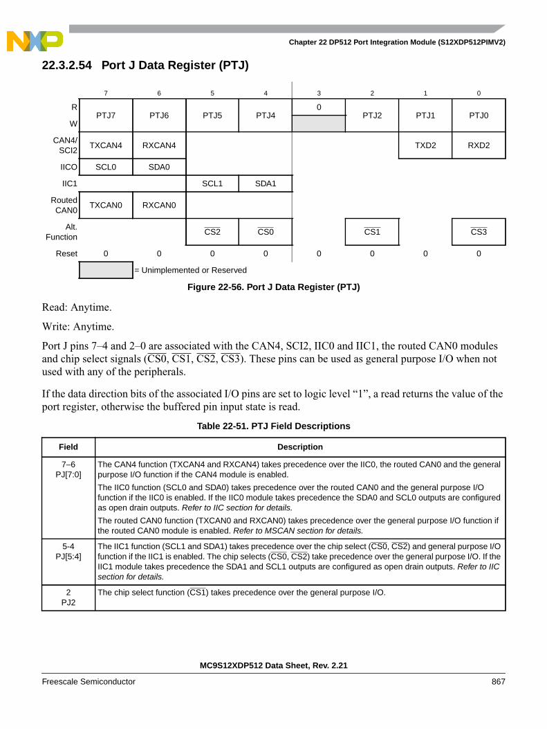
Chapter 22 DP512 Port Integration Module (S12XDP512PIMV2)
MC9S12XDP512 Data Sheet, Rev. 2.21
Freescale Semiconductor 867
22.3.2.54 Port J Data Register (PTJ)
Read: Anytime.
Write: Anytime.
Port J pins 7–4 and 2–0 are associated with the CAN4, SCI2, IIC0 and IIC1, the routed CAN0 modulesand chip select signals (CS0, CS1, CS2, CS3). These pins can be used as general purpose I/O when notused with any of the peripherals.
If the data direction bits of the associated I/O pins are set to logic level “1”, a read returns the value of theport register, otherwise the buffered pin input state is read.
7 6 5 4 3 2 1 0
RPTJ7 PTJ6 PTJ5 PTJ4
0PTJ2 PTJ1 PTJ0
W
CAN4/SCI2
TXCAN4 RXCAN4 TXD2 RXD2
IICO SCL0 SDA0
IIC1 SCL1 SDA1
RoutedCAN0
TXCAN0 RXCAN0
Alt.Function
CS2 CS0 CS1 CS3
Reset 0 0 0 0 0 0 0 0
= Unimplemented or Reserved
Figure 22-56. Port J Data Register (PTJ)
Table 22-51. PTJ Field Descriptions
Field Description
7–6PJ[7:0]
The CAN4 function (TXCAN4 and RXCAN4) takes precedence over the IIC0, the routed CAN0 and the generalpurpose I/O function if the CAN4 module is enabled.
The IIC0 function (SCL0 and SDA0) takes precedence over the routed CAN0 and the general purpose I/Ofunction if the IIC0 is enabled. If the IIC0 module takes precedence the SDA0 and SCL0 outputs are configuredas open drain outputs. Refer to IIC section for details.
The routed CAN0 function (TXCAN0 and RXCAN0) takes precedence over the general purpose I/O function ifthe routed CAN0 module is enabled. Refer to MSCAN section for details.
5-4PJ[5:4]
The IIC1 function (SCL1 and SDA1) takes precedence over the chip select (CS0, CS2) and general purpose I/Ofunction if the IIC1 is enabled. The chip selects (CS0, CS2) take precedence over the general purpose I/O. If theIIC1 module takes precedence the SDA1 and SCL1 outputs are configured as open drain outputs. Refer to IICsection for details.
2PJ2
The chip select function (CS1) takes precedence over the general purpose I/O.

Chapter 22 DP512 Port Integration Module (S12XDP512PIMV2)
MC9S12XDP512 Data Sheet, Rev. 2.21
868 Freescale Semiconductor
1PJ1
The SCI2 function takes precedence over the general purpose I/O function if the SCI2 module is enabled. Referto SCI section for details.
0PJ0
The SCI2 function takes precedence over the chip select (CS3) and the general purpose I/O function if the SCI2module is enabled. The chip select (CS3) takes precedence over the general purpose I/O function. Refer to SCIsection for details.
Table 22-51. PTJ Field Descriptions (continued)
Field Description

Chapter 22 DP512 Port Integration Module (S12XDP512PIMV2)
MC9S12XDP512 Data Sheet, Rev. 2.21
Freescale Semiconductor 869
22.3.2.55 Port J Input Register (PTIJ)
Read: Anytime.
Write: Never, writes to this register have no effect.
This register always reads back the buffered state of the associated pins. This can be used to detectoverload or short circuit conditions on output pins.
7 6 5 4 3 2 1 0
R PTIJ7 PTIJ6 PTIJ5 PTIJ4 0 PTIJ2 PTIJ1 PTIJ0
W
Reset1
1 These registers are reset to zero. Two bus clock cycles after reset release the register values are updated with the associatedpin values.
0 0 0 0 0 0 0 0
= Unimplemented or Reserved
Figure 22-57. Port J Input Register (PTIJ)
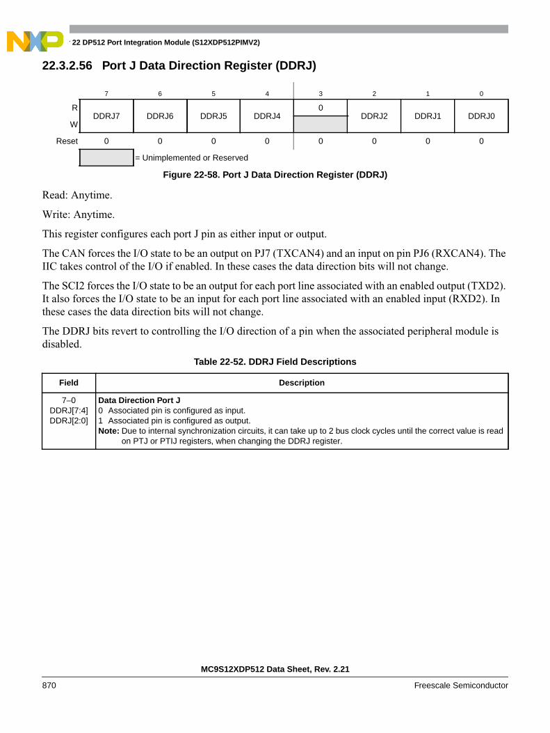
Chapter 22 DP512 Port Integration Module (S12XDP512PIMV2)
MC9S12XDP512 Data Sheet, Rev. 2.21
870 Freescale Semiconductor
22.3.2.56 Port J Data Direction Register (DDRJ)
Read: Anytime.
Write: Anytime.
This register configures each port J pin as either input or output.
The CAN forces the I/O state to be an output on PJ7 (TXCAN4) and an input on pin PJ6 (RXCAN4). TheIIC takes control of the I/O if enabled. In these cases the data direction bits will not change.
The SCI2 forces the I/O state to be an output for each port line associated with an enabled output (TXD2).It also forces the I/O state to be an input for each port line associated with an enabled input (RXD2). Inthese cases the data direction bits will not change.
The DDRJ bits revert to controlling the I/O direction of a pin when the associated peripheral module isdisabled.
7 6 5 4 3 2 1 0
RDDRJ7 DDRJ6 DDRJ5 DDRJ4
0DDRJ2 DDRJ1 DDRJ0
W
Reset 0 0 0 0 0 0 0 0
= Unimplemented or Reserved
Figure 22-58. Port J Data Direction Register (DDRJ)
Table 22-52. DDRJ Field Descriptions
Field Description
7–0DDRJ[7:4]DDRJ[2:0]
Data Direction Port J0 Associated pin is configured as input.1 Associated pin is configured as output.Note: Due to internal synchronization circuits, it can take up to 2 bus clock cycles until the correct value is read
on PTJ or PTIJ registers, when changing the DDRJ register.
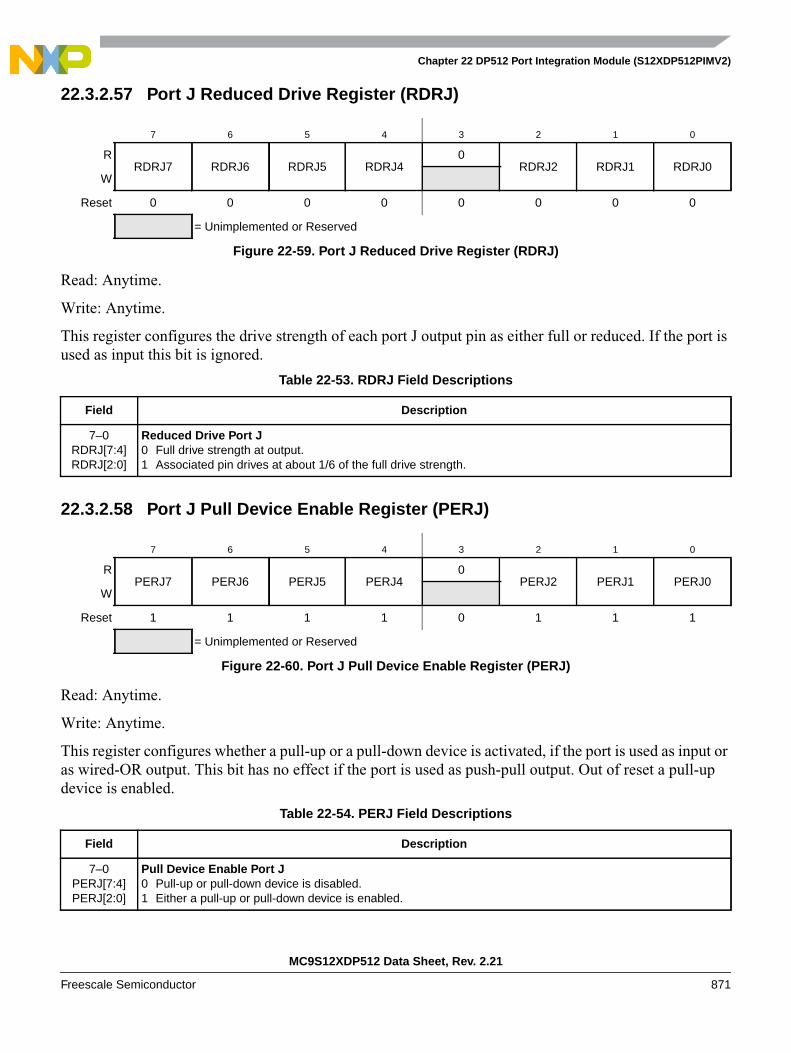
Chapter 22 DP512 Port Integration Module (S12XDP512PIMV2)
MC9S12XDP512 Data Sheet, Rev. 2.21
Freescale Semiconductor 871
22.3.2.57 Port J Reduced Drive Register (RDRJ)
Read: Anytime.
Write: Anytime.
This register configures the drive strength of each port J output pin as either full or reduced. If the port isused as input this bit is ignored.
22.3.2.58 Port J Pull Device Enable Register (PERJ)
Read: Anytime.
Write: Anytime.
This register configures whether a pull-up or a pull-down device is activated, if the port is used as input oras wired-OR output. This bit has no effect if the port is used as push-pull output. Out of reset a pull-updevice is enabled.
7 6 5 4 3 2 1 0
RRDRJ7 RDRJ6 RDRJ5 RDRJ4
0RDRJ2 RDRJ1 RDRJ0
W
Reset 0 0 0 0 0 0 0 0
= Unimplemented or Reserved
Figure 22-59. Port J Reduced Drive Register (RDRJ)
Table 22-53. RDRJ Field Descriptions
Field Description
7–0RDRJ[7:4]RDRJ[2:0]
Reduced Drive Port J0 Full drive strength at output.1 Associated pin drives at about 1/6 of the full drive strength.
7 6 5 4 3 2 1 0
RPERJ7 PERJ6 PERJ5 PERJ4
0PERJ2 PERJ1 PERJ0
W
Reset 1 1 1 1 0 1 1 1
= Unimplemented or Reserved
Figure 22-60. Port J Pull Device Enable Register (PERJ)
Table 22-54. PERJ Field Descriptions
Field Description
7–0PERJ[7:4]PERJ[2:0]
Pull Device Enable Port J0 Pull-up or pull-down device is disabled.1 Either a pull-up or pull-down device is enabled.

Chapter 22 DP512 Port Integration Module (S12XDP512PIMV2)
MC9S12XDP512 Data Sheet, Rev. 2.21
872 Freescale Semiconductor
22.3.2.59 Port J Polarity Select Register (PPSJ)
Read: Anytime.
Write: Anytime.
This register serves a dual purpose by selecting the polarity of the active interrupt edge as well as selectinga pull-up or pull-down device if enabled.
22.3.2.60 Port J Interrupt Enable Register (PIEJ)
This register disables or enables on a per-pin basis the edge sensitive external interrupt associated withPort J.
7 6 5 4 3 2 1 0
RPPSJ7 PPSJ6 PPSJ5 PPSJ4
0PPSJ2 PPSJ1 PPSJ0
W
Reset 0 0 0 0 0 0 0 0
= Unimplemented or Reserved
Figure 22-61. Port J Polarity Select Register (PPSJ)
Table 22-55. PPSJ Field Descriptions
Field Description
7–0PPSJ[7:4]PPSJ[2:0]
Polarity Select Port J0 Falling edge on the associated port J pin sets the associated flag bit in the PIFJ register.
A pull-up device is connected to the associated port J pin, if enabled by the associated bit in register PERJand if the port is used as general purpose input or as IIC port.
1 Rising edge on the associated port J pin sets the associated flag bit in the PIFJ register.A pull-down device is connected to the associated port J pin, if enabled by the associated bit in register PERJand if the port is used as input.
7 6 5 4 3 2 1 0
RPIEJ7 PIEJ6 PIEJ5 PIEJ4
0PIEJ2 PIEJ1 PIEJ0
W
Reset 0 0 0 0 0 0 0 0
= Unimplemented or Reserved
Figure 22-62. Port J Interrupt Enable Register (PIEJ)
Table 22-56. PIEJ Field Descriptions
Field Description
7–0PIEJ[7:4]PIEJ[2:0]
Interrupt Enable Port J0 Interrupt is disabled (interrupt flag masked).1 Interrupt is enabled.
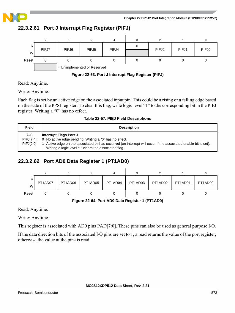
Chapter 22 DP512 Port Integration Module (S12XDP512PIMV2)
MC9S12XDP512 Data Sheet, Rev. 2.21
Freescale Semiconductor 873
22.3.2.61 Port J Interrupt Flag Register (PIFJ)
Read: Anytime.
Write: Anytime.
Each flag is set by an active edge on the associated input pin. This could be a rising or a falling edge basedon the state of the PPSJ register. To clear this flag, write logic level “1” to the corresponding bit in the PIFJregister. Writing a “0” has no effect.
22.3.2.62 Port AD0 Data Register 1 (PT1AD0)
Read: Anytime.
Write: Anytime.
This register is associated with AD0 pins PAD[7:0]. These pins can also be used as general purpose I/O.
If the data direction bits of the associated I/O pins are set to 1, a read returns the value of the port register,otherwise the value at the pins is read.
7 6 5 4 3 2 1 0
RPIFJ7 PIFJ6 PIFJ5 PIFJ4
0PIFJ2 PIFJ1 PIFJ0
W
Reset 0 0 0 0 0 0 0 0
= Unimplemented or Reserved
Figure 22-63. Port J Interrupt Flag Register (PIFJ)
Table 22-57. PIEJ Field Descriptions
Field Description
7–0PIFJ[7:4]PIFJ[2:0]
Interrupt Flags Port J0 No active edge pending. Writing a “0” has no effect.1 Active edge on the associated bit has occurred (an interrupt will occur if the associated enable bit is set).
Writing a logic level “1” clears the associated flag.
7 6 5 4 3 2 1 0
RPT1AD07 PT1AD06 PT1AD05 PT1AD04 PT1AD03 PT1AD02 PT1AD01 PT1AD00
W
Reset 0 0 0 0 0 0 0 0
Figure 22-64. Port AD0 Data Register 1 (PT1AD0)
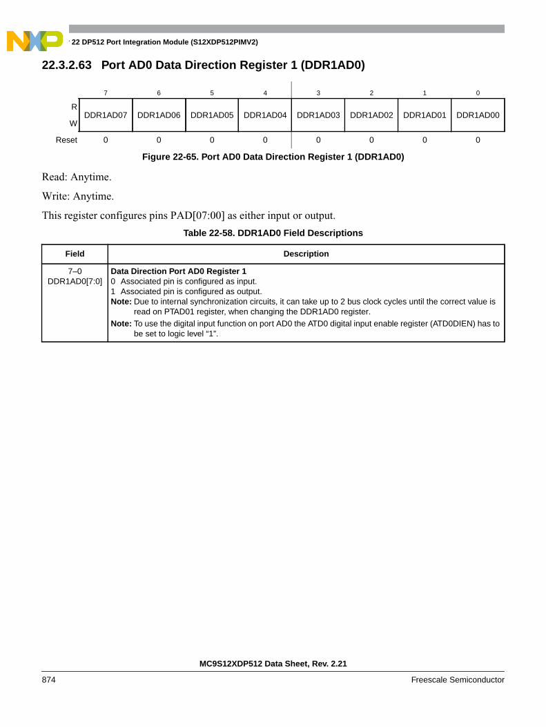
Chapter 22 DP512 Port Integration Module (S12XDP512PIMV2)
MC9S12XDP512 Data Sheet, Rev. 2.21
874 Freescale Semiconductor
22.3.2.63 Port AD0 Data Direction Register 1 (DDR1AD0)
Read: Anytime.
Write: Anytime.
This register configures pins PAD[07:00] as either input or output.
7 6 5 4 3 2 1 0
RDDR1AD07 DDR1AD06 DDR1AD05 DDR1AD04 DDR1AD03 DDR1AD02 DDR1AD01 DDR1AD00
W
Reset 0 0 0 0 0 0 0 0
Figure 22-65. Port AD0 Data Direction Register 1 (DDR1AD0)
Table 22-58. DDR1AD0 Field Descriptions
Field Description
7–0DDR1AD0[7:0]
Data Direction Port AD0 Register 10 Associated pin is configured as input.1 Associated pin is configured as output.Note: Due to internal synchronization circuits, it can take up to 2 bus clock cycles until the correct value is
read on PTAD01 register, when changing the DDR1AD0 register.Note: To use the digital input function on port AD0 the ATD0 digital input enable register (ATD0DIEN) has to
be set to logic level “1”.
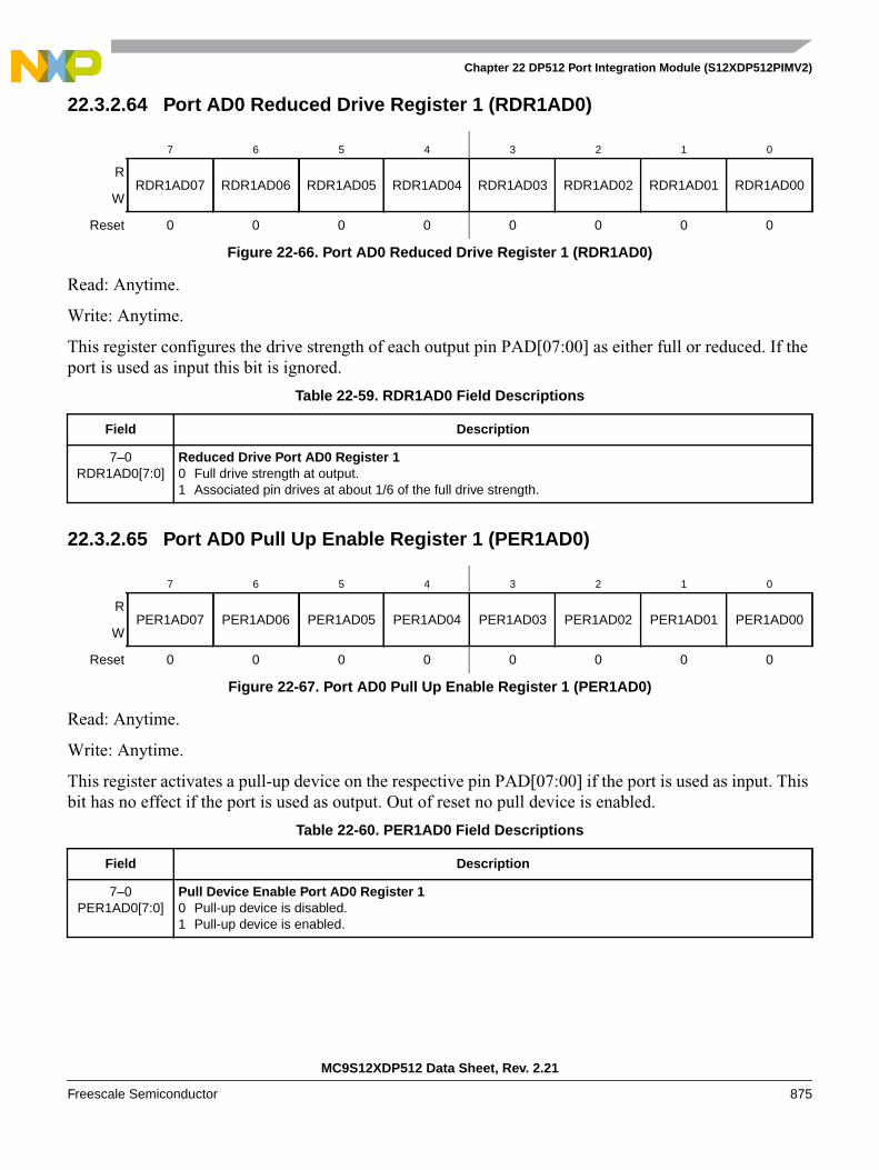
Chapter 22 DP512 Port Integration Module (S12XDP512PIMV2)
MC9S12XDP512 Data Sheet, Rev. 2.21
Freescale Semiconductor 875
22.3.2.64 Port AD0 Reduced Drive Register 1 (RDR1AD0)
Read: Anytime.
Write: Anytime.
This register configures the drive strength of each output pin PAD[07:00] as either full or reduced. If theport is used as input this bit is ignored.
22.3.2.65 Port AD0 Pull Up Enable Register 1 (PER1AD0)
Read: Anytime.
Write: Anytime.
This register activates a pull-up device on the respective pin PAD[07:00] if the port is used as input. Thisbit has no effect if the port is used as output. Out of reset no pull device is enabled.
7 6 5 4 3 2 1 0
RRDR1AD07 RDR1AD06 RDR1AD05 RDR1AD04 RDR1AD03 RDR1AD02 RDR1AD01 RDR1AD00
W
Reset 0 0 0 0 0 0 0 0
Figure 22-66. Port AD0 Reduced Drive Register 1 (RDR1AD0)
Table 22-59. RDR1AD0 Field Descriptions
Field Description
7–0RDR1AD0[7:0]
Reduced Drive Port AD0 Register 10 Full drive strength at output.1 Associated pin drives at about 1/6 of the full drive strength.
7 6 5 4 3 2 1 0
RPER1AD07 PER1AD06 PER1AD05 PER1AD04 PER1AD03 PER1AD02 PER1AD01 PER1AD00
W
Reset 0 0 0 0 0 0 0 0
Figure 22-67. Port AD0 Pull Up Enable Register 1 (PER1AD0)
Table 22-60. PER1AD0 Field Descriptions
Field Description
7–0PER1AD0[7:0]
Pull Device Enable Port AD0 Register 10 Pull-up device is disabled.1 Pull-up device is enabled.

Chapter 22 DP512 Port Integration Module (S12XDP512PIMV2)
MC9S12XDP512 Data Sheet, Rev. 2.21
876 Freescale Semiconductor
22.3.2.66 Port AD1 Data Register 0 (PT0AD1)
Read: Anytime.
Write: Anytime.
This register is associated with AD1 pins PAD[23:16]. These pins can also be used as general purpose I/O.
If the data direction bits of the associated I/O pins are set to 1, a read returns the value of the port register,otherwise the value at the pins is read.
22.3.2.67 Port AD1 Data Register 1 (PT1AD1)
Read: Anytime.
Write: Anytime.
This register is associated with AD1 pins PAD[15:08]. These pins can also be used as general purpose I/O.
If the data direction bits of the associated I/O pins are set to 1, a read returns the value of the port register,otherwise the value at the pins is read.
7 6 5 4 3 2 1 0
RPT0AD123 PT0AD122 PT0AD121 PT0AD120 PT0AD119 PT0AD118 PT0AD117 PT0AD116
W
Reset 0 0 0 0 0 0 0 0
Figure 22-68. Port AD1 Data Register 0 (PT0AD1)
7 6 5 4 3 2 1 0
RPT1AD115 PT1AD114 PT1AD113 PT1AD112 PT1AD111 PT1AD110 PT1AD19 PT1AD18
W
Reset 0 0 0 0 0 0 0 0
Figure 22-69. Port AD1 Data Register 1 (PT1AD1)

Chapter 22 DP512 Port Integration Module (S12XDP512PIMV2)
MC9S12XDP512 Data Sheet, Rev. 2.21
Freescale Semiconductor 877
22.3.2.68 Port AD1 Data Direction Register 0 (DDR0AD1)
Read: Anytime.
Write: Anytime.
This register configures pin PAD[23:16] as either input or output.
7 6 5 4 3 2 1 0
RDDR0AD123 DDR0AD122 DDR0AD121 DDR0AD120 DDR0AD119 DDR0AD118 DDR0AD117 DDR0AD116
W
Reset 0 0 0 0 0 0 0 0
Figure 22-70. Port AD1 Data Direction Register 0 (DDR0AD1)
Table 22-61. DDR0AD1 Field Descriptions
Field Description
7–0DDR0AD1[23:16]
Data Direction Port AD1 Register 00 Associated pin is configured as input.1 Associated pin is configured as output.Note: Due to internal synchronization circuits, it can take up to 2 bus clock cycles until the correct value is
read on PTAD10 register, when changing the DDR0AD1 register.Note: To use the digital input function on Port AD1 the ATD1 digital input enable register (ATD1DIEN0) has
to be set to logic level “1”.

Chapter 22 DP512 Port Integration Module (S12XDP512PIMV2)
MC9S12XDP512 Data Sheet, Rev. 2.21
878 Freescale Semiconductor
22.3.2.69 Port AD1 Data Direction Register 1 (DDR1AD1)
Read: Anytime.
Write: Anytime.
This register configures pins PAD[15:08] as either input or output.
7 6 5 4 3 2 1 0
RDDR1AD115 DDR1AD114 DDR1AD113 DDR1AD112 DDR1AD111 DDR1AD110 DDR1AD19 DDR1AD18
W
Reset 0 0 0 0 0 0 0 0
Figure 22-71. Port AD1 Data Direction Register 1 (DDR1AD1)
Table 22-62. DDR1AD1 Field Descriptions
Field Description
7–0DDR1AD1[15:8]
Data Direction Port AD1 Register 10 Associated pin is configured as input.1 Associated pin is configured as output.Note: Due to internal synchronization circuits, it can take up to 2 bus clock cycles until the correct value is
read on PTAD11 register, when changing the DDR1AD1 register.Note: To use the digital input function on port AD1 the ATD1 digital input enable register (ATD1DIEN1) has
to be set to logic level “1”.

Chapter 22 DP512 Port Integration Module (S12XDP512PIMV2)
MC9S12XDP512 Data Sheet, Rev. 2.21
Freescale Semiconductor 879
22.3.2.70 Port AD1 Reduced Drive Register 0 (RDR0AD1)
Read: Anytime.
Write: Anytime.
This register configures the drive strength of each PAD[23:16] output pin as either full or reduced. If theport is used as input this bit is ignored.
22.3.2.71 Port AD1 Reduced Drive Register 1 (RDR1AD1)
Read: Anytime.
Write: Anytime.
This register configures the drive strength of each PAD[15:08] output pin as either full or reduced. If theport is used as input this bit is ignored.
7 6 5 4 3 2 1 0
RRDR0AD123 RDR0AD122 RDR0AD121 RDR0AD120 RDR0AD119 RDR0AD118 RDR0AD117 RDR0AD116
W
Reset 0 0 0 0 0 0 0 0
Figure 22-72. Port AD1 Reduced Drive Register 0 (RDR0AD1)
Table 22-63. RDR0AD1 Field Descriptions
Field Description
7–0RDR0AD1[23:16]
Reduced Drive Port AD1 Register 00 Full drive strength at output.1 Associated pin drives at about 1/6 of the full drive strength.
7 6 5 4 3 2 1 0
RRDR1AD115 RDR1AD114 RDR1AD113 RDR1AD112 RDR1AD111 RDR1AD110 RDR1AD19 RDR1AD18
W
Reset 0 0 0 0 0 0 0 0
Figure 22-73. Port AD1 Reduced Drive Register 1 (RDR1AD1)
Table 22-64. RDR1AD1 Field Descriptions
Field Description
7–0RDR1AD1[15:8]
Reduced Drive Port AD1 Register 10 Full drive strength at output.1 Associated pin drives at about 1/6 of the full drive strength.

Chapter 22 DP512 Port Integration Module (S12XDP512PIMV2)
MC9S12XDP512 Data Sheet, Rev. 2.21
880 Freescale Semiconductor
22.3.2.72 Port AD1 Pull Up Enable Register 0 (PER0AD1)
Read: Anytime.
Write: Anytime.
This register activates a pull-up device on the respective PAD[23:16] pin if the port is used as input. Thisbit has no effect if the port is used as output. Out of reset no pull-up device is enabled.
22.3.2.73 Port AD1 Pull Up Enable Register 1 (PER1AD1)
Read: Anytime.
Write: Anytime.
This register activates a pull-up device on the respective PAD[15:08] pin if the port is used as input. Thisbit has no effect if the port is used as output. Out of reset no pull-up device is enabled.
7 6 5 4 3 2 1 0
RPER0AD123 PER0AD122 PER0AD121 PER0AD120 PER0AD119 PER0AD118 PER0AD117 PER0AD116
W
Reset 0 0 0 0 0 0 0 0
Figure 22-74. Port AD1 Pull Up Enable Register 0 (PER0AD1)
Table 22-65. PER0AD1 Field Descriptions
Field Description
7–0PER0AD1[23:16]
Pull Device Enable Port AD1 Register 00 Pull-up device is disabled.1 Pull-up device is enabled.
7 6 5 4 3 2 1 0
RPER1AD115 PER1AD114 PER1AD113 PER1AD112 PER1AD111 PER1AD110 PER1AD19 PER1AD18
W
Reset 0 0 0 0 0 0 0 0
Figure 22-75. Port AD1 Pull Up Enable Register 1 (PER1AD1)
Table 22-66. PER1AD1 Field Descriptions
Field Description
7–0PER1AD1[15:8]
Pull Device Enable Port AD1 Register 10 Pull-up device is disabled.1 Pull-up device is enabled.
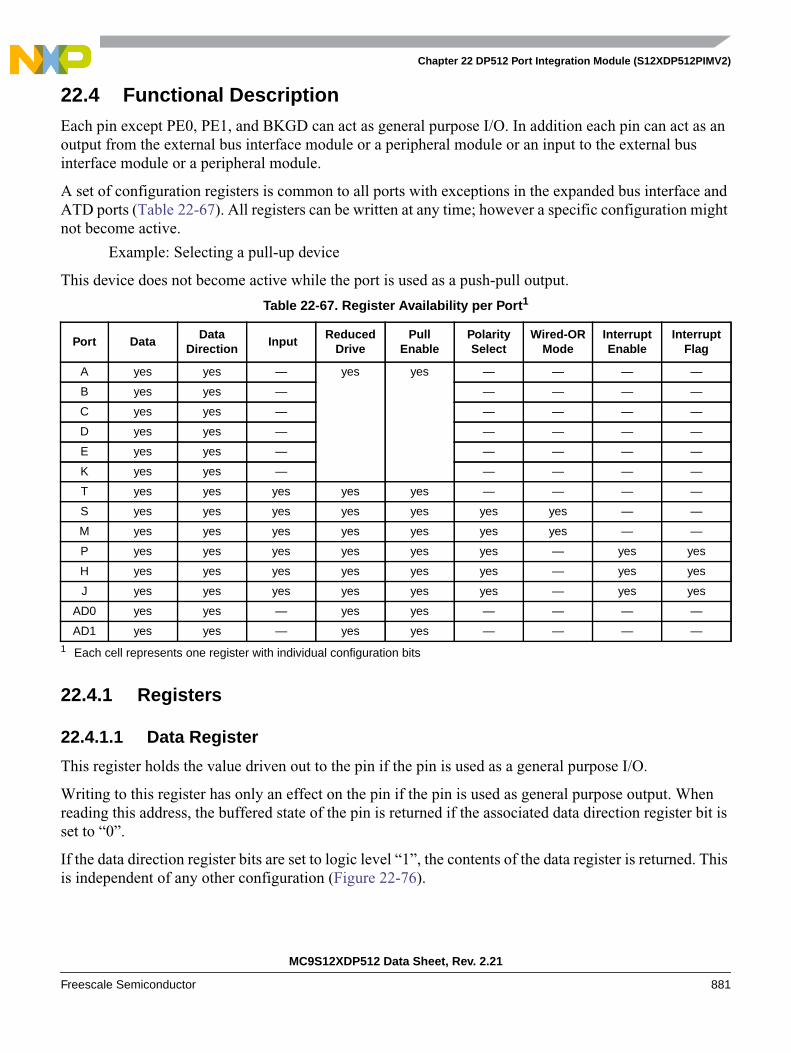
Chapter 22 DP512 Port Integration Module (S12XDP512PIMV2)
MC9S12XDP512 Data Sheet, Rev. 2.21
Freescale Semiconductor 881
22.4 Functional DescriptionEach pin except PE0, PE1, and BKGD can act as general purpose I/O. In addition each pin can act as anoutput from the external bus interface module or a peripheral module or an input to the external businterface module or a peripheral module.
A set of configuration registers is common to all ports with exceptions in the expanded bus interface andATD ports (Table 22-67). All registers can be written at any time; however a specific configuration mightnot become active.
Example: Selecting a pull-up device
This device does not become active while the port is used as a push-pull output.
22.4.1 Registers
22.4.1.1 Data Register
This register holds the value driven out to the pin if the pin is used as a general purpose I/O.
Writing to this register has only an effect on the pin if the pin is used as general purpose output. Whenreading this address, the buffered state of the pin is returned if the associated data direction register bit isset to “0”.
If the data direction register bits are set to logic level “1”, the contents of the data register is returned. Thisis independent of any other configuration (Figure 22-76).
Table 22-67. Register Availability per Port1
1 Each cell represents one register with individual configuration bits
Port DataData
Direction Input
ReducedDrive
PullEnable
PolaritySelect
Wired-ORMode
InterruptEnable
InterruptFlag
A yes yes — yes yes — — — —
B yes yes — — — — —
C yes yes — — — — —
D yes yes — — — — —
E yes yes — — — — —
K yes yes — — — — —
T yes yes yes yes yes — — — —
S yes yes yes yes yes yes yes — —
M yes yes yes yes yes yes yes — —
P yes yes yes yes yes yes — yes yes
H yes yes yes yes yes yes — yes yes
J yes yes yes yes yes yes — yes yes
AD0 yes yes — yes yes — — — —
AD1 yes yes — yes yes — — — —

Chapter 22 DP512 Port Integration Module (S12XDP512PIMV2)
MC9S12XDP512 Data Sheet, Rev. 2.21
882 Freescale Semiconductor
22.4.1.2 Input Register
This is a read-only register and always returns the buffered state of the pin (Figure 22-76).
22.4.1.3 Data Direction Register
This register defines whether the pin is used as an input or an output.
If a peripheral module controls the pin the contents of the data direction register is ignored (Figure 22-76).
Figure 22-76. Illustration of I/O Pin Functionality
22.4.1.4 Reduced Drive Register
If the pin is used as an output this register allows the configuration of the drive strength.
22.4.1.5 Pull Device Enable Register
This register turns on a pull-up or pull-down device. It becomes active only if the pin is used as an inputor as a wired-OR output.
22.4.1.6 Polarity Select Register
This register selects either a pull-up or pull-down device if enabled. It becomes active only if the pin isused as an input. A pull-up device can be activated if the pin is used as a wired-OR output. If the pin isused as an interrupt input this register selects the active interrupt edge.
22.4.1.7 Wired-OR Mode Register
If the pin is used as an output this register turns off the active high drive. This allows wired-OR typeconnections of outputs.
PT
DDR
output enable
module enable
1
0
1
1
0
0
PIN
PTI
data outModule
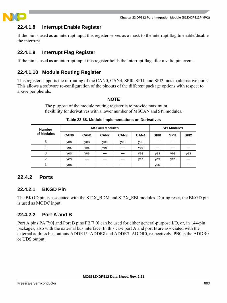
Chapter 22 DP512 Port Integration Module (S12XDP512PIMV2)
MC9S12XDP512 Data Sheet, Rev. 2.21
Freescale Semiconductor 883
22.4.1.8 Interrupt Enable Register
If the pin is used as an interrupt input this register serves as a mask to the interrupt flag to enable/disablethe interrupt.
22.4.1.9 Interrupt Flag Register
If the pin is used as an interrupt input this register holds the interrupt flag after a valid pin event.
22.4.1.10 Module Routing Register
This register supports the re-routing of the CAN0, CAN4, SPI0, SPI1, and SPI2 pins to alternative ports.This allows a software re-configuration of the pinouts of the different package options with respect toabove peripherals.
NOTEThe purpose of the module routing register is to provide maximumflexibility for derivatives with a lower number of MSCAN and SPI modules.
22.4.2 Ports
22.4.2.1 BKGD Pin
The BKGD pin is associated with the S12X_BDM and S12X_EBI modules. During reset, the BKGD pinis used as MODC input.
22.4.2.2 Port A and B
Port A pins PA[7:0] and Port B pins PB[7:0] can be used for either general-purpose I/O, or, in 144-pinpackages, also with the external bus interface. In this case port A and port B are associated with theexternal address bus outputs ADDR15–ADDR8 and ADDR7–ADDR0, respectively. PB0 is the ADDR0or UDS output.
Table 22-68. Module Implementations on Derivatives
Numberof Modules
MSCAN Modules SPI Modules
CAN0 CAN1 CAN2 CAN3 CAN4 SPI0 SPI1 SPI2
5 yes yes yes yes yes — — —
4 yes yes yes — yes — — —
3 yes yes — — yes yes yes yes
2 yes — — — yes yes yes —
1 yes — — — — yes — —

Chapter 22 DP512 Port Integration Module (S12XDP512PIMV2)
MC9S12XDP512 Data Sheet, Rev. 2.21
884 Freescale Semiconductor
22.4.2.3 Port C and D
Port C pins PC[7:0] and port D pins PD[7:0] can be used for either general-purpose I/O, or, in 144-pinpackages, also with the external bus interface. In this case port C and port D are associated with theexternal data bus inputs/outputs DATA15–DATA8 and DATA7–DATA0, respectively.
These pins are configured for reduced input threshold in certain operating modes (refer to S12X_EBIsection).
NOTEPort C and D are neither available in 112-pin nor in 80-pin packages.
22.4.2.4 Port E
Port E is associated with the external bus control outputs R/W, LSTRB, LDS and RE, the free-runningclock outputs ECLK and ECLK2X, as well as with the TAGHI, TAGLO, MODA and MODB andinterrupt inputs IRQ and XIRQ.
Port E pins PE[7:2] can be used for either general-purpose I/O or with the alternative functions.
Port E pin PE[7] an be used for either general-purpose I/O or as the free-running clock ECLKX2 outputrunning at the core clock rate. The clock output is always enabled in emulation modes.
Port E pin PE[4] an be used for either general-purpose I/O or as the free-running clock ECLK outputrunning at the bus clock rate or at the programmed divided clock rate. The clock output is always enabledin emulation modes.
Port E pin PE[1] can be used for either general-purpose input or as the level- or falling edge-sensitive IRQinterrupt input. IRQ will be enabled by setting the IRQEN configuration bit (Section 22.3.2.14, “IRQControl Register (IRQCR)”) and clearing the I-bit in the CPU’s condition code register. It is inhibited atreset so this pin is initially configured as a simple input with a pull-up.
Port E pin PE[0] can be used for either general-purpose input or as the level-sensitive XIRQ interruptinput. XIRQ can be enabled by clearing the X-bit in the CPU’s condition code register. It is inhibited atreset so this pin is initially configured as a high-impedance input with a pull-up.
Port E pins PE[5] and PE[6] are configured for reduced input threshold in certain modes (refer toS12X_EBI section).
22.4.2.5 Port K
Port K pins PK[7:0] can be used for either general-purpose I/O, or, in 144-pin packages, also with theexternal bus interface. In this case port K pins PK[6:0] are associated with the external address bus outputsADDR22–ADDR16 and PK7 is associated to the EWAIT input.
Port K pin PE[7] is configured for reduced input threshold in certain modes (refer to S12X_EBI section).
NOTEPort K is not available in 80-pin packages. PK[6] is not available in 112-pinpackages.

Chapter 22 DP512 Port Integration Module (S12XDP512PIMV2)
MC9S12XDP512 Data Sheet, Rev. 2.21
Freescale Semiconductor 885
22.4.2.6 Port T
This port is associated with the ECT module. Port T pins PT[7:0] can be used for either general-purposeI/O, or with the channels of the enhanced capture timer.
22.4.2.7 Port S
This port is associated with SCI0, SCI1 and SPI0. Port S pins PS[7:0] can be used either for general-purpose I/O, or with the SCI and SPI subsystems.
The SPI0 pins can be re-routed. Refer to Section 22.3.2.37, “Module Routing Register (MODRR)”.
NOTEPS[7:4] are not available in 80-pin packages.
22.4.2.8 Port M
This port is associated with the SCI3, CAN4–0 and SPI0. Port M pins PM[7:0] can be used for eithergeneral purpose I/O, or with the CAN, SCI and SPI subsystems.
The CAN0, CAN4 and SPI0 pins can be re-routed. Refer to Section 22.3.2.37, “Module Routing Register(MODRR)”.
NOTEPM[7:6] are not available in 80-pin packages.
22.4.2.9 Port P
This port is associated with the PWM, SPI1 and SPI2. Port P pins PP[7:0] can be used for either generalpurpose I/O, or with the PWM and SPI subsystems.
The pins are shared between the PWM channels and the SPI1 and SPI2 modules. If the PWM is enabledthe pins become PWM output channels with the exception of pin 7 which can be PWM input or output. IfSPI1 or SPI2 are enabled and PWM is disabled, the respective pin configuration is determined by statusbits in the SPI modules.
The SPI1 and SPI2 pins can be re-routed. Refer to Section 22.3.2.37, “Module Routing Register(MODRR)”.
Port P offers 8 I/O pins with edge triggered interrupt capability in wired-OR fashion (Section 22.4.3, “PinInterrupts”).
NOTEPP[6] is not available in 80-pin packages.
Chapter 22 DP512 Port Integration Module (S12XDP512PIMV2)
MC9S12XDP512 Data Sheet, Rev. 2.21
886 Freescale Semiconductor
22.4.2.10 Port H
This port is associated with the SPI1, SPI2, SCI4, and SCI5. Port H pins PH[7:0] can be used for eithergeneral purpose I/O, or with the SPI and SCI subsystems. Port H pins can be used with the routed SPI1and SPI2 modules. Refer to Section 22.3.2.37, “Module Routing Register (MODRR)”.
Port H offers 8 I/O pins with edge triggered interrupt capability (Section 22.4.3, “Pin Interrupts”).
NOTEPort H is not available in 80-pin packages.
22.4.2.11 Port J
This port is associated with the chip selects CS0, CS1, CS2 and CS3 as well as with CAN4, CAN0, IIC1,IIC0, and SCI2. Port J pins PJ[7:4] and PJ[2:0] can be used for either general purpose I/O, or with theCAN, IIC, or SCI subsystems. If IIC takes precedence the associated pins become IIC open-drain outputpins. The CAN4 pins can be re-routed. Refer to Section 22.3.2.37, “Module Routing Register (MODRR)”.
Port J pins can be used with the routed CAN0 modules. Refer to Section 22.3.2.37, “Module RoutingRegister (MODRR)”.
Port J offers 7 I/O pins with edge triggered interrupt capability (Section 22.4.3, “Pin Interrupts”).
NOTEPJ[5,4,2] are not available in 112-pin packages. PJ[5,4,2,1,0] are notavailable in 80-pin packages.
22.4.2.12 Port AD0
This port is associated with the ATD0. Port AD0 pins PAD07–PAD00 can be used for either generalpurpose I/O, or with the ATD0 subsystem.
22.4.2.13 Port AD1
This port is associated with the ATD1. Port AD1 pins PAD23–PAD08 can be used for either generalpurpose I/O, or with the ATD1 subsystem.
NOTEPAD[23:16] are not available in 112-pin packages. PAD[23:08] are notavailable in 80-pin packages.
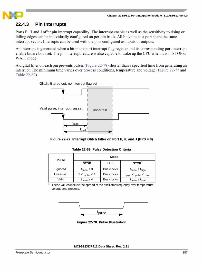
Chapter 22 DP512 Port Integration Module (S12XDP512PIMV2)
MC9S12XDP512 Data Sheet, Rev. 2.21
Freescale Semiconductor 887
22.4.3 Pin Interrupts
Ports P, H and J offer pin interrupt capability. The interrupt enable as well as the sensitivity to rising orfalling edges can be individually configured on per-pin basis. All bits/pins in a port share the sameinterrupt vector. Interrupts can be used with the pins configured as inputs or outputs.
An interrupt is generated when a bit in the port interrupt flag register and its corresponding port interruptenable bit are both set. The pin interrupt feature is also capable to wake up the CPU when it is in STOP orWAIT mode.
A digital filter on each pin prevents pulses (Figure 22-78) shorter than a specified time from generating aninterrupt. The minimum time varies over process conditions, temperature and voltage (Figure 22-77 andTable 22-69).
Figure 22-77. Interrupt Glitch Filter on Port P, H, and J (PPS = 0)
Figure 22-78. Pulse Illustration
Table 22-69. Pulse Detection Criteria
PulseMode
STOP Unit STOP1
1 These values include the spread of the oscillator frequency over temperature,voltage and process.
Ignored tpulse ≤ 3 Bus clocks tpulse ≤ tpign
Uncertain 3 < tpulse < 4 Bus clocks tpign < tpulse < tpval
Valid tpulse ≥ 4 Bus clocks tpulse ≥ tpval
Glitch, filtered out, no interrupt flag set
Valid pulse, interrupt flag set
tpign
tpval
uncertain
tpulse
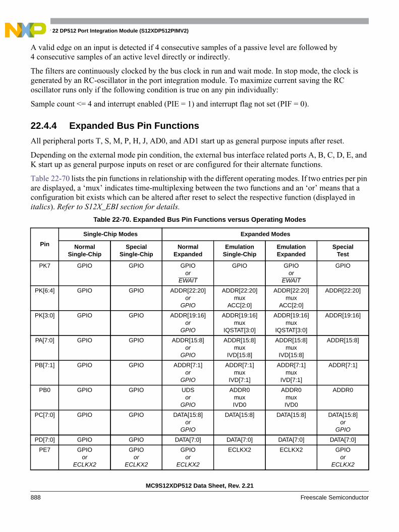
Chapter 22 DP512 Port Integration Module (S12XDP512PIMV2)
MC9S12XDP512 Data Sheet, Rev. 2.21
888 Freescale Semiconductor
A valid edge on an input is detected if 4 consecutive samples of a passive level are followed by4 consecutive samples of an active level directly or indirectly.
The filters are continuously clocked by the bus clock in run and wait mode. In stop mode, the clock isgenerated by an RC-oscillator in the port integration module. To maximize current saving the RCoscillator runs only if the following condition is true on any pin individually:
Sample count <= 4 and interrupt enabled (PIE = 1) and interrupt flag not set (PIF = 0).
22.4.4 Expanded Bus Pin Functions
All peripheral ports T, S, M, P, H, J, AD0, and AD1 start up as general purpose inputs after reset.
Depending on the external mode pin condition, the external bus interface related ports A, B, C, D, E, andK start up as general purpose inputs on reset or are configured for their alternate functions.
Table 22-70 lists the pin functions in relationship with the different operating modes. If two entries per pinare displayed, a ‘mux’ indicates time-multiplexing between the two functions and an ‘or’ means that aconfiguration bit exists which can be altered after reset to select the respective function (displayed initalics). Refer to S12X_EBI section for details.
Table 22-70. Expanded Bus Pin Functions versus Operating Modes
Pin
Single-Chip Modes Expanded Modes
NormalSingle-Chip
SpecialSingle-Chip
NormalExpanded
EmulationSingle-Chip
EmulationExpanded
SpecialTest
PK7 GPIO GPIO GPIOor
EWAIT
GPIO GPIOor
EWAIT
GPIO
PK[6:4] GPIO GPIO ADDR[22:20]or
GPIO
ADDR[22:20]mux
ACC[2:0]
ADDR[22:20]mux
ACC[2:0]
ADDR[22:20]
PK[3:0] GPIO GPIO ADDR[19:16]or
GPIO
ADDR[19:16]mux
IQSTAT[3:0]
ADDR[19:16]mux
IQSTAT[3:0]
ADDR[19:16]
PA[7:0] GPIO GPIO ADDR[15:8]or
GPIO
ADDR[15:8]mux
IVD[15:8]
ADDR[15:8]mux
IVD[15:8]
ADDR[15:8]
PB[7:1] GPIO GPIO ADDR[7:1]or
GPIO
ADDR[7:1]mux
IVD[7:1]
ADDR[7:1]mux
IVD[7:1]
ADDR[7:1]
PB0 GPIO GPIO UDSor
GPIO
ADDR0muxIVD0
ADDR0muxIVD0
ADDR0
PC[7:0] GPIO GPIO DATA[15:8]or
GPIO
DATA[15:8] DATA[15:8] DATA[15:8]or
GPIO
PD[7:0] GPIO GPIO DATA[7:0] DATA[7:0] DATA[7:0] DATA[7:0]
PE7 GPIOor
ECLKX2
GPIOor
ECLKX2
GPIOor
ECLKX2
ECLKX2 ECLKX2 GPIOor
ECLKX2
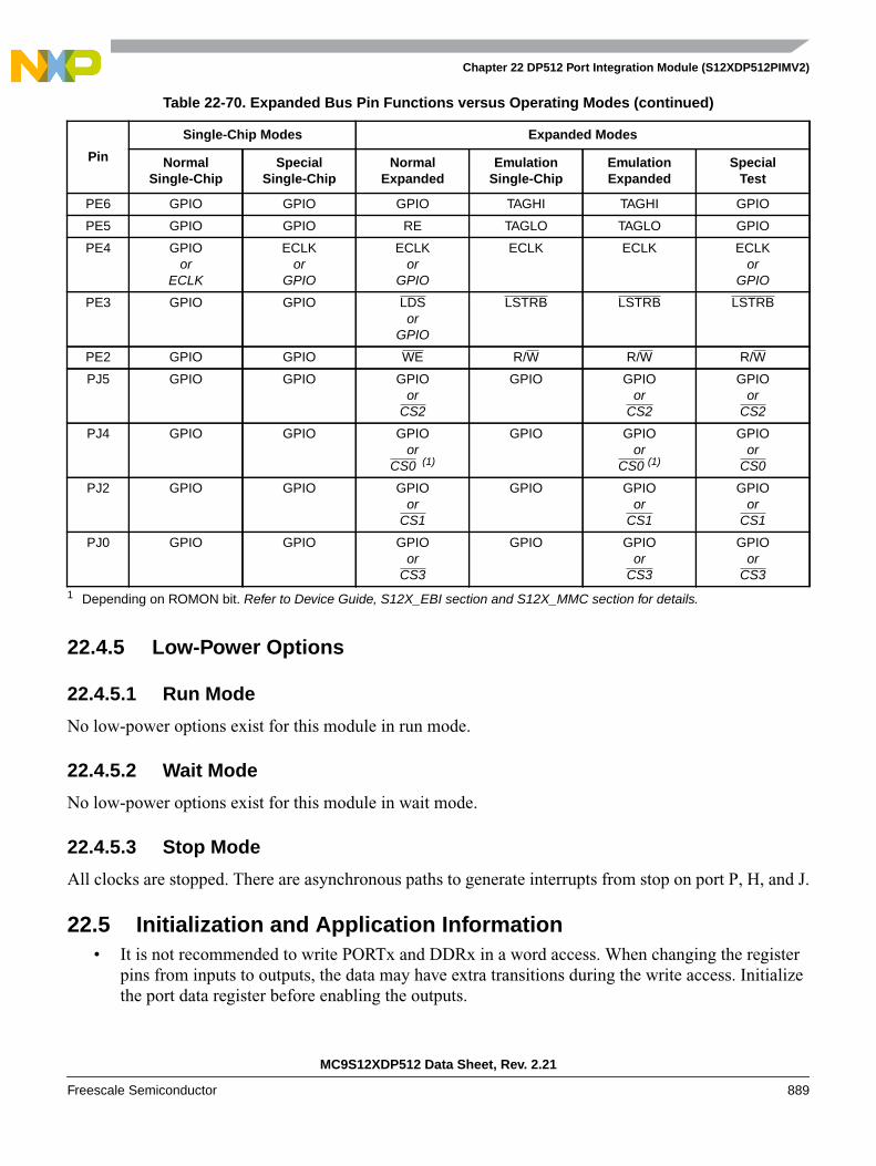
Chapter 22 DP512 Port Integration Module (S12XDP512PIMV2)
MC9S12XDP512 Data Sheet, Rev. 2.21
Freescale Semiconductor 889
22.4.5 Low-Power Options
22.4.5.1 Run Mode
No low-power options exist for this module in run mode.
22.4.5.2 Wait Mode
No low-power options exist for this module in wait mode.
22.4.5.3 Stop Mode
All clocks are stopped. There are asynchronous paths to generate interrupts from stop on port P, H, and J.
22.5 Initialization and Application Information• It is not recommended to write PORTx and DDRx in a word access. When changing the register
pins from inputs to outputs, the data may have extra transitions during the write access. Initializethe port data register before enabling the outputs.
PE6 GPIO GPIO GPIO TAGHI TAGHI GPIO
PE5 GPIO GPIO RE TAGLO TAGLO GPIO
PE4 GPIOor
ECLK
ECLKor
GPIO
ECLKor
GPIO
ECLK ECLK ECLKor
GPIO
PE3 GPIO GPIO LDSor
GPIO
LSTRB LSTRB LSTRB
PE2 GPIO GPIO WE R/W R/W R/W
PJ5 GPIO GPIO GPIOor
CS2
GPIO GPIOor
CS2
GPIOor
CS2
PJ4 GPIO GPIO GPIOor
CS0 (1)
GPIO GPIOor
CS0 (1)
GPIOor
CS0
PJ2 GPIO GPIO GPIOor
CS1
GPIO GPIOor
CS1
GPIOor
CS1
PJ0 GPIO GPIO GPIOor
CS3
GPIO GPIOor
CS3
GPIOor
CS31 Depending on ROMON bit. Refer to Device Guide, S12X_EBI section and S12X_MMC section for details.
Table 22-70. Expanded Bus Pin Functions versus Operating Modes (continued)
Pin
Single-Chip Modes Expanded Modes
NormalSingle-Chip
SpecialSingle-Chip
NormalExpanded
EmulationSingle-Chip
EmulationExpanded
SpecialTest

Chapter 22 DP512 Port Integration Module (S12XDP512PIMV2)
MC9S12XDP512 Data Sheet, Rev. 2.21
890 Freescale Semiconductor
• Power consumption will increase the more the voltages on general purpose input pins deviate fromthe supply voltages towards mid-range because the digital input buffers operate in the linear region.

Chapter 22 DP512 Port Integration Module (S12XDP512PIMV2)
MC9S12XDP512 Data Sheet, Rev. 2.21
Freescale Semiconductor 891

Chapter 22 DP512 Port Integration Module (S12XDP512PIMV2)
MC9S12XDP512 Data Sheet, Rev. 2.21
892 Freescale Semiconductor

Chapter 22 DP512 Port Integration Module (S12XDP512PIMV2)
MC9S12XDP512 Data Sheet, Rev. 2.21
Freescale Semiconductor 893

Chapter 22 DP512 Port Integration Module (S12XDP512PIMV2)
MC9S12XDP512 Data Sheet, Rev. 2.21
894 Freescale Semiconductor

Chapter 22 DP512 Port Integration Module (S12XDP512PIMV2)
MC9S12XDP512 Data Sheet, Rev. 2.21
Freescale Semiconductor 895

Chapter 22 DP512 Port Integration Module (S12XDP512PIMV2)
MC9S12XDP512 Data Sheet, Rev. 2.21
896 Freescale Semiconductor

Chapter 22 DP512 Port Integration Module (S12XDP512PIMV2)
MC9S12XDP512 Data Sheet, Rev. 2.21
Freescale Semiconductor 897

Chapter 22 DP512 Port Integration Module (S12XDP512PIMV2)
MC9S12XDP512 Data Sheet, Rev. 2.21
898 Freescale Semiconductor

Chapter 22 DP512 Port Integration Module (S12XDP512PIMV2)
MC9S12XDP512 Data Sheet, Rev. 2.21
Freescale Semiconductor 899

Chapter 22 DP512 Port Integration Module (S12XDP512PIMV2)
MC9S12XDP512 Data Sheet, Rev. 2.21
900 Freescale Semiconductor

MC9S12XDP512 Data Sheet, Rev. 2.21Freescale Semiconductor 901
Chapter 23DQ256 Port Integration Module (S12XDQ256PIMV2)
Introduction
The S12XD family port integration module (below referred to as PIM) establishes the interface betweenthe peripheral modules including the non-multiplexed external bus interface module (S12X_EBI) and theI/O pins for all ports. It controls the electrical pin properties as well as the signal prioritization andmultiplexing on shared pins.
This document covers the description of:
• Port A, B used as address output of the S12X_EBI and Port C, D used as data I/O of the S12X_EBI
• Port E associated with the S12X_EBI control signals and the IRQ, XIRQ interrupt inputs
• Port K associated with address output and control signals of the S12X_EBI
• Port T connected to the Enhanced Capture Timer (ECT) module
• Port S associated with 2 SCI and 1 SPI modules
• Port M associated with 3 MSCAN modules
• Port P connected to the PWM and 2 SPI modules — inputs can be used as an external interruptsource
• Port H associated with 1 SCI module — inputs can be used as an external interrupt source
• Port J associated with 1 MSCAN, 1 SCI, and 1 IIC module — inputs can be used as an externalinterrupt source
• Port AD0 and AD1 associated with one 8-channel andone 16-channel ATD module
Most I/O pins can be configured by register bits to select data direction and drive strength, to enable andselect pull-up or pull-down devices. Interrupts can be enabled on specific pins resulting in status flags.
The I/O’s of 2 MSCAN and 3 SPI modules can be routed from their default location to alternative portpins.
NOTEThe implementation of the PIM is device dependent. Therefore somefunctions are not available on certain derivatives or 112-pin and 80-pinpackage options.
23.0.1 Features
A full-featured PIM module includes these distinctive registers:
• Data and data direction registers for Ports A, B, C, D, E, K, T, S, M, P, H, J, AD0, and AD1 whenused as general-purpose I/O

Chapter 23 DQ256 Port Integration Module (S12XDQ256PIMV2)
MC9S12XDP512 Data Sheet, Rev. 2.21902 Freescale Semiconductor
• Control registers to enable/disable pull-device and select pull-ups/pull-downs on Ports T, S, M, P,H, and J on per-pin basis
• Control registers to enable/disable pull-up devices on Ports AD0, and AD1 on per-pin basis
• Single control register to enable/disable pull-ups on Ports A, B, C, D, E, and K on per-port basisand on BKGD pin
• Control registers to enable/disable reduced output drive on Ports T, S, M, P, H, J, AD0, and AD1on per-pin basis
• Single control register to enable/disable reduced output drive on Ports A, B, C, D, E, and K on per-port basis
• Control registers to enable/disable open-drain (wired-OR) mode on Ports S and M
• Control registers to enable/disable pin interrupts on Ports P, H, and J
• Interrupt flag register for pin interrupts on Ports P, H, and J
• Control register to configure IRQ pin operation
• Free-running clock outputs
A standard port pin has the following minimum features:
• Input/output selection
• 5V output drive with two selectable drive strengths
• 5V digital and analog input
• Input with selectable pull-up or pull-down device
Optional features:
• Open drain for wired-OR connections
• Interrupt inputs with glitch filtering
• Reduced input threshold to support low voltage applications
23.0.2 Block Diagram
Figure 23-1 is a block diagram of the PIM.
• Signals shown in Bold are not available in 80-pin packages.
• Signals shown in Bold-Italics are neither available in 112-pin nor in 80-pin packages.
• Shaded labels denote alternative module routing ports.
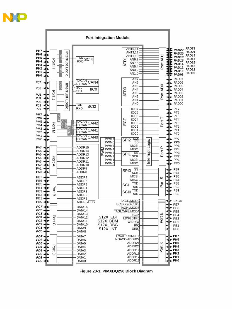
Figure 23-1. PIMXDQ256 Block Diagram
Por
t T
PT0PT1PT2PT3PT4PT5PT6PT7
EC
T
IOC0IOC1IOC2IOC3IOC4IOC5IOC6IOC7
Por
t PPP0PP1PP2PP3PP4PP5PP6PP7
PW
M
PWM0PWM1PWM2PWM3PWM4PWM5PWM6PWM7
Por
t S
PS0PS1PS2PS3PS4PS5PS6PS7
RXDTXDRXDTXD
MISOMOSISCK
SS
SCI0
SCI1
SPI0
Port H
PH0PH1PH2PH3PH4PH5PH6PH7
Port J
PJ0PJ1
PJ6
PJ7
Port M
PM0PM1PM2PM3PM4PM5PM6PM7
CAN1TXCANRXCAN
CAN2TXCANRXCAN
CAN0TXCANRXCAN
IIC0SCLSDA
Port Integration Module
CAN4TXCANRXCAN
MISOMOSISCK
SSSPI1In
terr
upt L
ogic
MISOMOSI
SCKSS
SPI2
Port B
PB0PB1PB2PB3PB4PB5PB6PB7
Port A
PA0PA1PA2PA3PA4PA5PA6PA7
Por
t E
PE0PE1PE2PE3PE4PE5PE6PE7
Por
t K
PK0PK1PK2PK3
PK7
PK4PK5
ADDR8ADDR9ADDR10ADDR11ADDR12ADDR13ADDR14ADDR15
ADDR0/UDSADDR1ADDR2ADDR3ADDR4ADDR5ADDR6ADDR7
XIRQIRQ
WE/R/WLDS/LSTRB
ECLKTAGLO/RE/MODA
ECLKX2/XCLKSTAGHI/MODB
ADDR17ADDR18ADDR19
EWAIT/ROMCTL
ADRR20ADDR21
S12X_EBI
ADDR16
BKGD/MODC BKGD
CA
N0
Port C
PC0PC1PC2PC3PC4PC5PC6PC7
Port D
PD0PD1PD2PD3PD4PD5PD6PD7
DATA0DATA1DATA2DATA3DATA4DATA5DATA6DATA7
DATA8DATA9DATA10DATA11DATA12DATA13DATA14DATA15
NOACC/ADDR22 PK6
PJ4PJ5
PJ2
RXDTXD SCI4
Interrupt LogicP
ort A
D0
PAD00PAD01PAD02PAD03PAD04PAD05PAD06PAD07
ATD
0
AN0AN1AN2AN3AN4AN5AN6AN7
Por
t AD
1
PAD08PAD10PAD12PAD14PAD16PAD18PAD20PAD22
ATD
1
AN1,0AN3,2AN5,4AN7,6AN9,8
AN11,10AN13,12AN15,14
SP
I1 S
PI2
SP
I0
PAD09PAD11PAD13PAD15PAD17PAD19PAD21PAD23
SCI2TXDRXD
S12X_BDMS12X_DBGS12X_INT
Inte
rrup
t Lo
gic
CA
N0
CA
N0
CA
N4
CA
N4
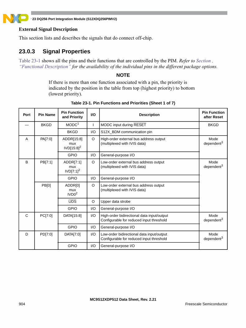
Chapter 23 DQ256 Port Integration Module (S12XDQ256PIMV2)
MC9S12XDP512 Data Sheet, Rev. 2.21904 Freescale Semiconductor
External Signal Description
This section lists and describes the signals that do connect off-chip.
23.0.3 Signal Properties
Table 23-1 shows all the pins and their functions that are controlled by the PIM. Refer to Section ,“Functional Description” for the availability of the individual pins in the different package options.
NOTEIf there is more than one function associated with a pin, the priority isindicated by the position in the table from top (highest priority) to bottom(lowest priority).
Table 23-1. Pin Functions and Priorities (Sheet 1 of 7)
Port Pin NamePin Functionand Priority
I/O DescriptionPin Functionafter Reset
— BKGD MODC1 I MODC input during RESET BKGD
BKGD I/O S12X_BDM communication pin
A PA[7:0] ADDR[15:8]mux
IVD[15:8]2
O High-order external bus address output(multiplexed with IVIS data)
Modedependent3
GPIO I/O General-purpose I/O
B PB[7:1] ADDR[7:1]mux
IVD[7:1]2
O Low-order external bus address output(multiplexed with IVIS data)
Modedependent3
GPIO I/O General-purpose I/O
PB[0] ADDR[0]mux
IVD02
O Low-order external bus address output(multiplexed with IVIS data)
UDS O Upper data strobe
GPIO I/O General-purpose I/O
C PC[7:0] DATA[15:8] I/O High-order bidirectional data input/outputConfigurable for reduced input threshold
Modedependent3
GPIO I/O General-purpose I/O
D PD[7:0] DATA[7:0] I/O Low-order bidirectional data input/outputConfigurable for reduced input threshold
Modedependent3
GPIO I/O General-purpose I/O

E
PE[7]
XCLKS1 I External clock selection input during RESET
Mode
dependent3
ECLKX2 I Free-running clock output at Core Clock rate (ECLK x 2)
GPIO I/O General-purpose I/O
PE[6]
MODB1 I MODB input during RESET
TAGHI IInstruction tagging low pinConfigurable for reduced input threshold
GPIO I/O General-purpose I/O
PE[5]
MODA1 I MODA input during RESET
RE O Read enable signal
TAGLO IInstruction tagging low pinConfigurable for reduced input threshold
GPIO I/O General-purpose I/O
PE[4]ECLK O
Free-running clock output at the Bus Clock rate orprogrammable divided in normal modes
GPIO I/O General-purpose I/O
PE[3]
EROMCTL1 I EROMON bit control input during RESET
LSTRB O Low strobe bar output
LDS O Lower data strobe
GPIO I/O General-purpose I/O
PE[2]
R/W O Read/write output for external bus
WE O Write enable signal
GPIO I/O General-purpose I/O
PE[1]IRQ I Maskable level- or falling edge-sensitive interrupt input
GPIO I/O General-purpose I/O
PE[0]XIRQ I Non-maskable level-sensitive interrupt input
GPIO I/O General-purpose I/O
Table 23-1. Pin Functions and Priorities (Sheet 2 of 7)
Port Pin NamePin Functionand Priority
I/O DescriptionPin Functionafter Reset
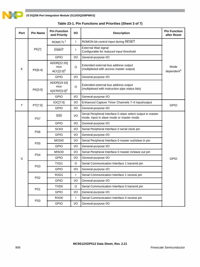
Chapter 23 DQ256 Port Integration Module (S12XDQ256PIMV2)
MC9S12XDP512 Data Sheet, Rev. 2.21906 Freescale Semiconductor
K
PK[7]
ROMCTL1 I ROMON bit control input during RESET
Mode
dependent3
EWAIT IExternal Wait signalConfigurable for reduced input threshold
GPIO I/O General-purpose I/O
PK[6:4]
ADDR[22:20]mux
ACC[2:0]2O
Extended external bus address output(multiplexed with access master output)
GPIO I/O General-purpose I/O
PK[3:0]
ADDR[19:16]mux
IQSTAT[3:0]2O
Extended external bus address output(multiplexed with instruction pipe status bits)
GPIO I/O General-purpose I/O
T PT[7:0]IOC[7:0] I/O Enhanced Capture Timer Channels 7–0 input/output
GPIOGPIO I/O General-purpose I/O
S
PS7SS0 I/O
Serial Peripheral Interface 0 slave select output in mastermode, input in slave mode or master mode.
GPIO
GPIO I/O General-purpose I/O
PS6SCK0 I/O Serial Peripheral Interface 0 serial clock pin
GPIO I/O General-purpose I/O
PS5MOSI0 I/O Serial Peripheral Interface 0 master out/slave in pin
GPIO I/O General-purpose I/O
PS4MISO0 I/O Serial Peripheral Interface 0 master in/slave out pin
GPIO I/O General-purpose I/O
PS3TXD1 O Serial Communication Interface 1 transmit pin
GPIO I/O General-purpose I/O
PS2RXD1 I Serial Communication Interface 1 receive pin
GPIO I/O General-purpose I/O
PS1TXD0 O Serial Communication Interface 0 transmit pin
GPIO I/O General-purpose I/O
PS0RXD0 I Serial Communication Interface 0 receive pin
GPIO I/O General-purpose I/O
Table 23-1. Pin Functions and Priorities (Sheet 3 of 7)
Port Pin NamePin Functionand Priority
I/O DescriptionPin Functionafter Reset
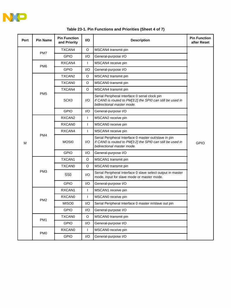
M
PM7TXCAN4 O MSCAN4 transmit pin
GPIO
GPIO I/O General-purpose I/O
PM6RXCAN4 I MSCAN4 receive pin
GPIO I/O General-purpose I/O
PM5
TXCAN2 O MSCAN2 transmit pin
TXCAN0 O MSCAN0 transmit pin
TXCAN4 O MSCAN4 transmit pin
SCK0 I/OSerial Peripheral Interface 0 serial clock pinIf CAN0 is routed to PM[3:2] the SPI0 can still be used inbidirectional master mode.
GPIO I/O General-purpose I/O
PM4
RXCAN2 I MSCAN2 receive pin
RXCAN0 I MSCAN0 receive pin
RXCAN4 I MSCAN4 receive pin
MOSI0 I/OSerial Peripheral Interface 0 master out/slave in pinIf CAN0 is routed to PM[3:2] the SPI0 can still be used inbidirectional master mode.
GPIO I/O General-purpose I/O
PM3
TXCAN1 O MSCAN1 transmit pin
TXCAN0 O MSCAN0 transmit pin
SS0 I/OSerial Peripheral Interface 0 slave select output in mastermode, input for slave mode or master mode.
GPIO I/O General-purpose I/O
PM2
RXCAN1 I MSCAN1 receive pin
RXCAN0 I MSCAN0 receive pin
MISO0 I/O Serial Peripheral Interface 0 master in/slave out pin
GPIO I/O General-purpose I/O
PM1TXCAN0 O MSCAN0 transmit pin
GPIO I/O General-purpose I/O
PM0RXCAN0 I MSCAN0 receive pin
GPIO I/O General-purpose I/O
Table 23-1. Pin Functions and Priorities (Sheet 4 of 7)
Port Pin NamePin Functionand Priority
I/O DescriptionPin Functionafter Reset
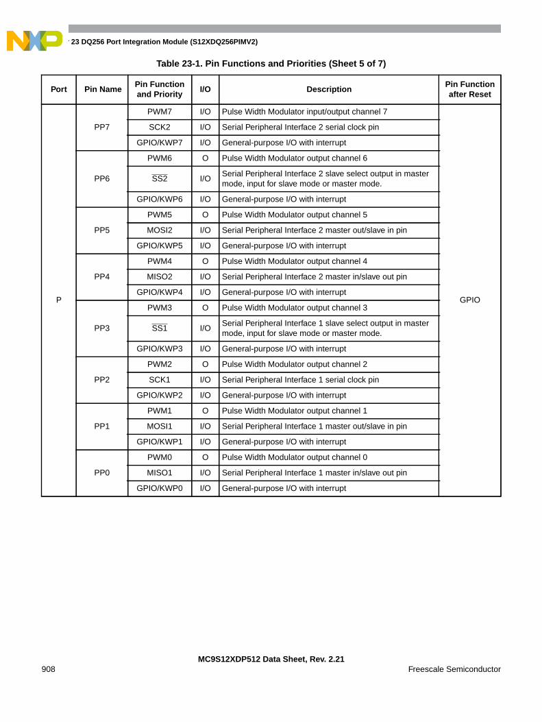
Chapter 23 DQ256 Port Integration Module (S12XDQ256PIMV2)
MC9S12XDP512 Data Sheet, Rev. 2.21908 Freescale Semiconductor
P
PP7
PWM7 I/O Pulse Width Modulator input/output channel 7
GPIO
SCK2 I/O Serial Peripheral Interface 2 serial clock pin
GPIO/KWP7 I/O General-purpose I/O with interrupt
PP6
PWM6 O Pulse Width Modulator output channel 6
SS2 I/OSerial Peripheral Interface 2 slave select output in mastermode, input for slave mode or master mode.
GPIO/KWP6 I/O General-purpose I/O with interrupt
PP5
PWM5 O Pulse Width Modulator output channel 5
MOSI2 I/O Serial Peripheral Interface 2 master out/slave in pin
GPIO/KWP5 I/O General-purpose I/O with interrupt
PP4
PWM4 O Pulse Width Modulator output channel 4
MISO2 I/O Serial Peripheral Interface 2 master in/slave out pin
GPIO/KWP4 I/O General-purpose I/O with interrupt
PP3
PWM3 O Pulse Width Modulator output channel 3
SS1 I/OSerial Peripheral Interface 1 slave select output in mastermode, input for slave mode or master mode.
GPIO/KWP3 I/O General-purpose I/O with interrupt
PP2
PWM2 O Pulse Width Modulator output channel 2
SCK1 I/O Serial Peripheral Interface 1 serial clock pin
GPIO/KWP2 I/O General-purpose I/O with interrupt
PP1
PWM1 O Pulse Width Modulator output channel 1
MOSI1 I/O Serial Peripheral Interface 1 master out/slave in pin
GPIO/KWP1 I/O General-purpose I/O with interrupt
PP0
PWM0 O Pulse Width Modulator output channel 0
MISO1 I/O Serial Peripheral Interface 1 master in/slave out pin
GPIO/KWP0 I/O General-purpose I/O with interrupt
Table 23-1. Pin Functions and Priorities (Sheet 5 of 7)
Port Pin NamePin Functionand Priority
I/O DescriptionPin Functionafter Reset
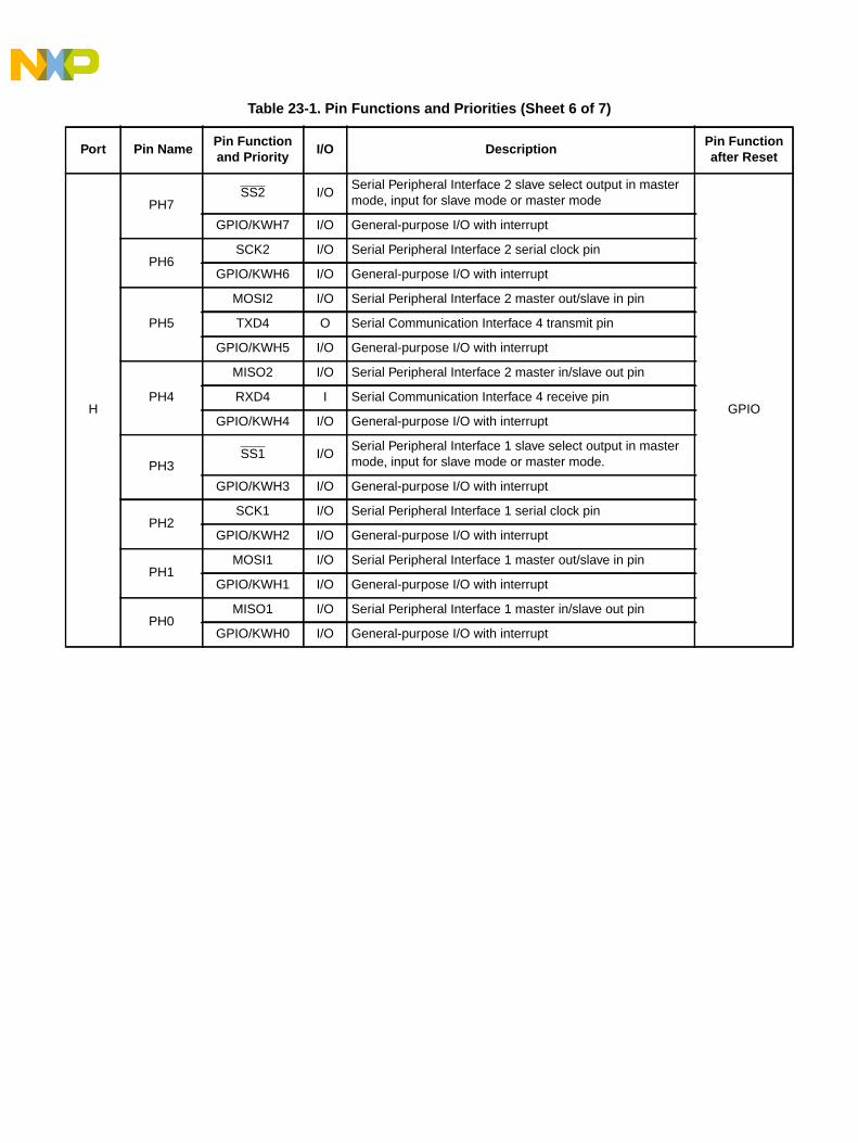
H
PH7SS2 I/O
Serial Peripheral Interface 2 slave select output in mastermode, input for slave mode or master mode
GPIO
GPIO/KWH7 I/O General-purpose I/O with interrupt
PH6SCK2 I/O Serial Peripheral Interface 2 serial clock pin
GPIO/KWH6 I/O General-purpose I/O with interrupt
PH5
MOSI2 I/O Serial Peripheral Interface 2 master out/slave in pin
TXD4 O Serial Communication Interface 4 transmit pin
GPIO/KWH5 I/O General-purpose I/O with interrupt
PH4
MISO2 I/O Serial Peripheral Interface 2 master in/slave out pin
RXD4 I Serial Communication Interface 4 receive pin
GPIO/KWH4 I/O General-purpose I/O with interrupt
PH3SS1 I/O
Serial Peripheral Interface 1 slave select output in mastermode, input for slave mode or master mode.
GPIO/KWH3 I/O General-purpose I/O with interrupt
PH2SCK1 I/O Serial Peripheral Interface 1 serial clock pin
GPIO/KWH2 I/O General-purpose I/O with interrupt
PH1MOSI1 I/O Serial Peripheral Interface 1 master out/slave in pin
GPIO/KWH1 I/O General-purpose I/O with interrupt
PH0MISO1 I/O Serial Peripheral Interface 1 master in/slave out pin
GPIO/KWH0 I/O General-purpose I/O with interrupt
Table 23-1. Pin Functions and Priorities (Sheet 6 of 7)
Port Pin NamePin Functionand Priority
I/O DescriptionPin Functionafter Reset
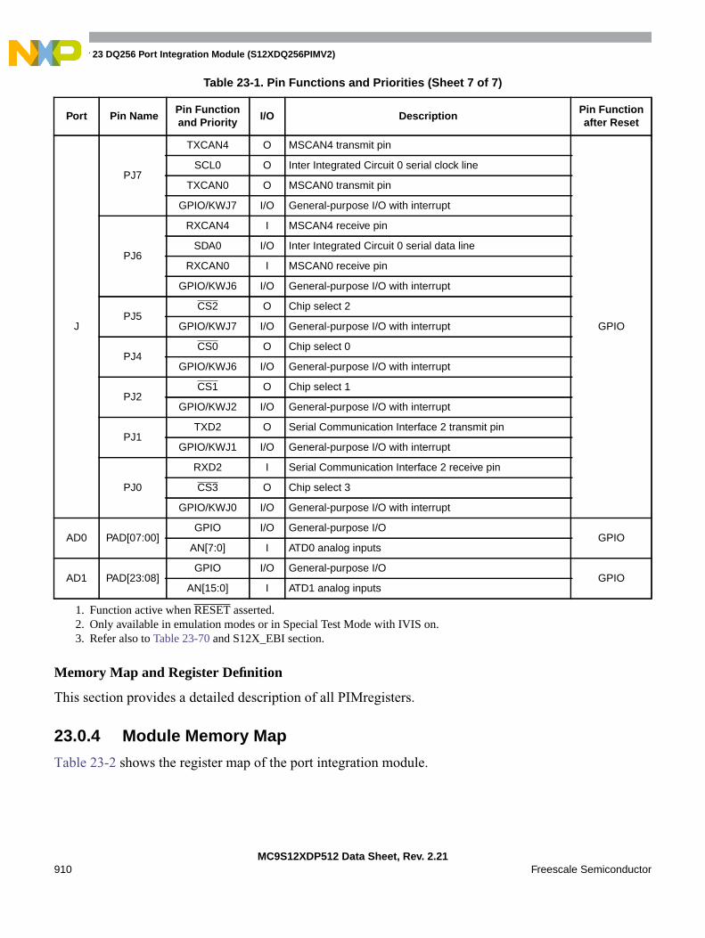
Chapter 23 DQ256 Port Integration Module (S12XDQ256PIMV2)
MC9S12XDP512 Data Sheet, Rev. 2.21910 Freescale Semiconductor
Memory Map and Register Definition
This section provides a detailed description of all PIMregisters.
23.0.4 Module Memory Map
Table 23-2 shows the register map of the port integration module.
J
PJ7
TXCAN4 O MSCAN4 transmit pin
GPIO
SCL0 O Inter Integrated Circuit 0 serial clock line
TXCAN0 O MSCAN0 transmit pin
GPIO/KWJ7 I/O General-purpose I/O with interrupt
PJ6
RXCAN4 I MSCAN4 receive pin
SDA0 I/O Inter Integrated Circuit 0 serial data line
RXCAN0 I MSCAN0 receive pin
GPIO/KWJ6 I/O General-purpose I/O with interrupt
PJ5CS2 O Chip select 2
GPIO/KWJ7 I/O General-purpose I/O with interrupt
PJ4CS0 O Chip select 0
GPIO/KWJ6 I/O General-purpose I/O with interrupt
PJ2CS1 O Chip select 1
GPIO/KWJ2 I/O General-purpose I/O with interrupt
PJ1TXD2 O Serial Communication Interface 2 transmit pin
GPIO/KWJ1 I/O General-purpose I/O with interrupt
PJ0
RXD2 I Serial Communication Interface 2 receive pin
CS3 O Chip select 3
GPIO/KWJ0 I/O General-purpose I/O with interrupt
AD0 PAD[07:00]GPIO I/O General-purpose I/O
GPIOAN[7:0] I ATD0 analog inputs
AD1 PAD[23:08]GPIO I/O General-purpose I/O
GPIOAN[15:0] I ATD1 analog inputs
1. Function active when RESET asserted.2. Only available in emulation modes or in Special Test Mode with IVIS on.3. Refer also to Table 23-70 and S12X_EBI section.
Table 23-1. Pin Functions and Priorities (Sheet 7 of 7)
Port Pin NamePin Functionand Priority
I/O DescriptionPin Functionafter Reset

Table 23-2. PIM Memory Map (Sheet 1 of 3)
Address Use Access
0x0000 Port A Data Register (PORTA) Read / Write
0x0001 Port B Data Register (PORTB) Read / Write
0x0002 Port A Data Direction Register (DDRA) Read / Write
0x0003 Port B Data Direction Register (DDRB) Read / Write
0x0004 Port C Data Register (PORTC) Read / Write
0x0005 Port D Data Register (PORTD) Read / Write
0x0006 Port C Data Direction Register (DDRC) Read / Write
0x0007 Port D Data Direction Register (DDRD) Read / Write
0x0008 Port E Data Register (PORTE) Read / Write1
0x0009 Port E Data Direction Register (DDRE) Read / Write1
0x000A:
0x000B
Non-PIM Address Range —
0x000C Pull-up Up Control Register (PUCR) Read / Write1
0x000D Reduced Drive Register (RDRIV) Read / Write1
0x000E:
0x001B
Non-PIM Address Range —
0x001C ECLK Control Register (ECLKCTL) Read / Write1
0x001D PIM Reserved —
0x001E IRQ Control Register (IRQCR) Read / Write1
0x001F PIM Reserved —
0x0020:
0x0031
Non-PIM Address Range —
0x0032 Port K Data Register (PORTK) Read / Write
0x0033 Port K Data Direction Register (DDRK) Read / Write
0x0034:
0x023F
Non-PIM Address Range —
0x0240 Port T Data Register (PTT) Read / Write
0x0241 Port T Input Register (PTIT) Read
0x0242 Port T Data Direction Register (DDRT) Read / Write
0x0243 Port T Reduced Drive Register (RDRT) Read / Write
0x0244 Port T Pull Device Enable Register (PERT) Read / Write
0x0245 Port T Polarity Select Register (PPST) Read / Write
0x0246 PIM Reserved —
0x0247 PIM Reserved —

Chapter 23 DQ256 Port Integration Module (S12XDQ256PIMV2)
MC9S12XDP512 Data Sheet, Rev. 2.21912 Freescale Semiconductor
0x0248 Port S Data Register (PTS) Read / Write
0x0249 Port S Input Register (PTIS) Read
0x024A Port S Data Direction Register (DDRS) Read / Write
0x024B Port S Reduced Drive Register (RDRS) Read / Write
0x024C Port S Pull Device Enable Register (PERS) Read / Write
0x024D Port S Polarity Select Register (PPSS) Read / Write
0x024E Port S Wired-OR Mode Register (WOMS) Read / Write
0x024F PIM Reserved —
0x0250 Port M Data Register (PTM) Read / Write
0x0251 Port M Input Register (PTIM) Read
0x0252 Port M Data Direction Register (DDRM) Read / Write
0x0253 Port M Reduced Drive Register (RDRM) Read / Write
0x0254 Port M Pull Device Enable Register (PERM) Read / Write
0x0255 Port M Polarity Select Register (PPSM) Read / Write
0x0256 Port M Wired-OR Mode Register (WOMM) Read / Write
0x0257 Module Routing Register (MODRR) Read / Write
0x0258 Port P Data Register (PTP) Read / Write
0x0259 Port P Input Register (PTIP) Read
0x025A Port P Data Direction Register (DDRP) Read / Write
0x025B Port P Reduced Drive Register (RDRP) Read / Write
0x025C Port P Pull Device Enable Register (PERP) Read / Write
0x025D Port P Polarity Select Register (PPSP) Read / Write
0x025E Port P Interrupt Enable Register (PIEP) Read / Write
0x025F Port P Interrupt Flag Register (PIFP) Read / Write
0x0260 Port H Data Register (PTH) Read / Write
0x0261 Port H Input Register (PTIH) Read
0x0262 Port H Data Direction Register (DDRH) Read / Write
0x0263 Port H Reduced Drive Register (RDRH) Read / Write
0x0264 Port H Pull Device Enable Register (PERH) Read / Write
0x0265 Port H Polarity Select Register (PPSH) Read / Write
0x0266 Port H Interrupt Enable Register (PIEH) Read / Write
0x0267 Port H Interrupt Flag Register (PIFH) Read / Write
0x0268 Port J Data Register (PTJ) Read / Write1
0x0269 Port J Input Register (PTIJ) Read
0x026A Port J Data Direction Register (DDRJ) Read / Write1
Table 23-2. PIM Memory Map (Sheet 2 of 3)
Address Use Access
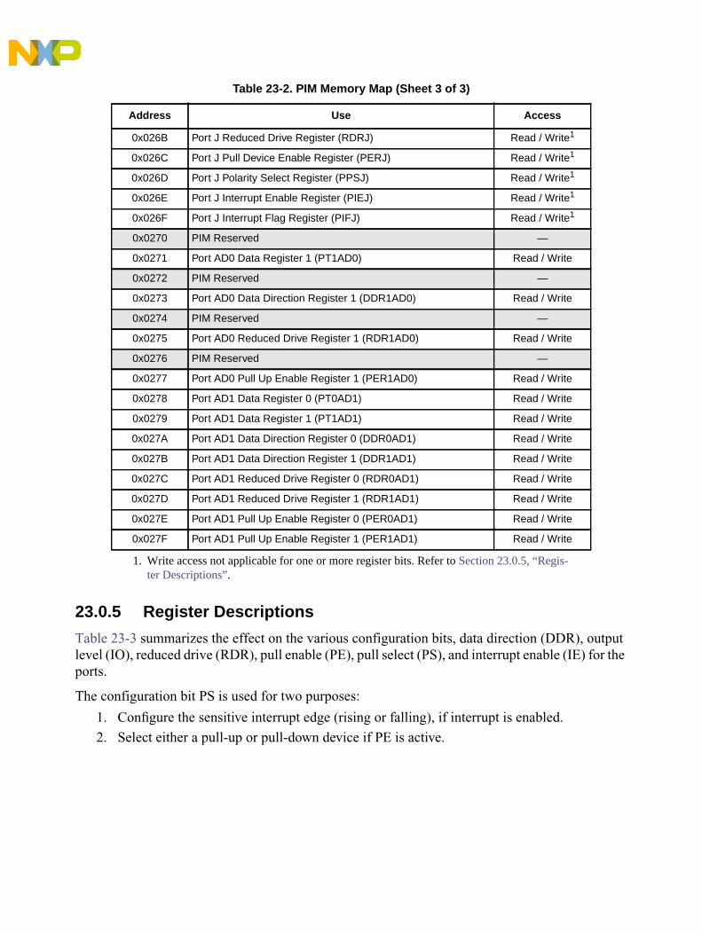
23.0.5 Register Descriptions
Table 23-3 summarizes the effect on the various configuration bits, data direction (DDR), outputlevel (IO), reduced drive (RDR), pull enable (PE), pull select (PS), and interrupt enable (IE) for theports.
The configuration bit PS is used for two purposes:
1. Configure the sensitive interrupt edge (rising or falling), if interrupt is enabled.
2. Select either a pull-up or pull-down device if PE is active.
0x026B Port J Reduced Drive Register (RDRJ) Read / Write1
0x026C Port J Pull Device Enable Register (PERJ) Read / Write1
0x026D Port J Polarity Select Register (PPSJ) Read / Write1
0x026E Port J Interrupt Enable Register (PIEJ) Read / Write1
0x026F Port J Interrupt Flag Register (PIFJ) Read / Write1
0x0270 PIM Reserved —
0x0271 Port AD0 Data Register 1 (PT1AD0) Read / Write
0x0272 PIM Reserved —
0x0273 Port AD0 Data Direction Register 1 (DDR1AD0) Read / Write
0x0274 PIM Reserved —
0x0275 Port AD0 Reduced Drive Register 1 (RDR1AD0) Read / Write
0x0276 PIM Reserved —
0x0277 Port AD0 Pull Up Enable Register 1 (PER1AD0) Read / Write
0x0278 Port AD1 Data Register 0 (PT0AD1) Read / Write
0x0279 Port AD1 Data Register 1 (PT1AD1) Read / Write
0x027A Port AD1 Data Direction Register 0 (DDR0AD1) Read / Write
0x027B Port AD1 Data Direction Register 1 (DDR1AD1) Read / Write
0x027C Port AD1 Reduced Drive Register 0 (RDR0AD1) Read / Write
0x027D Port AD1 Reduced Drive Register 1 (RDR1AD1) Read / Write
0x027E Port AD1 Pull Up Enable Register 0 (PER0AD1) Read / Write
0x027F Port AD1 Pull Up Enable Register 1 (PER1AD1) Read / Write
1. Write access not applicable for one or more register bits. Refer to Section 23.0.5, “Regis-ter Descriptions”.
Table 23-2. PIM Memory Map (Sheet 3 of 3)
Address Use Access

Chapter 23 DQ256 Port Integration Module (S12XDQ256PIMV2)
MC9S12XDP512 Data Sheet, Rev. 2.21914 Freescale Semiconductor
NOTEAll register bits in this module are completely synchronous to internalclocks during a register read.
Table 23-3. Pin Configuration Summary
DDR IO RDR PE PS1
1. Always “0” on Port A, B, C, D, E, K, AD0, and AD1.
IE2
2. Applicable only on Port P, H, and J.
Function Pull Device Interrupt
0 x x 0 x 0 Input Disabled Disabled
0 x x 1 0 0 Input Pull Up Disabled
0 x x 1 1 0 Input Pull Down Disabled
0 x x 0 0 1 Input Disabled Falling edge
0 x x 0 1 1 Input Disabled Rising edge
0 x x 1 0 1 Input Pull Up Falling edge
0 x x 1 1 1 Input Pull Down Rising edge
1 0 0 x x 0 Output, full drive to 0 Disabled Disabled
1 1 0 x x 0 Output, full drive to 1 Disabled Disabled
1 0 1 x x 0 Output, reduced drive to 0 Disabled Disabled
1 1 1 x x 0 Output, reduced drive to 1 Disabled Disabled
1 0 0 x 0 1 Output, full drive to 0 Disabled Falling edge
1 1 0 x 1 1 Output, full drive to 1 Disabled Rising edge
1 0 1 x 0 1 Output, reduced drive to 0 Disabled Falling edge
1 1 1 x 1 1 Output, reduced drive to 1 Disabled Rising edge
RegisterName
Bit 7 6 5 4 3 2 1 Bit 0
PORTA RPA7 PA6 PA5 PA4 PA3 PA2 PA1 PA0
W
PORTB RPB7 PB6 PB5 PB4 PB3 PB2 PB1 PB0
W
DDRA RDDRA7 DDRA6 DDRA5 DDRA4 DDRA3 DDRA2 DDRA1 DDRA0
W
DDRB RDDRB7 DDRB6 DDRB5 DDRB4 DDRB3 DDRB2 DDRB1 DDRB0
W
= Unimplemented or Reserved
Figure 23-2. PIM Register Summary (Sheet 1 of 7)

PORTC RPC7 PC6 PC5 PC4 PC3 PC2 PC1 PC0
W
PORTD RPD7 PD6 PD5 PD4 PD3 PD2 PD1 PD0
W
DDRC RDDRC7 DDRC6 DDRC5 DDRC4 DDRC3 DDRC2 DDRC1 DDRC0
W
DDRD RDDRD7 DDRD6 DDRD5 DDRD4 DDRD3 DDRD2 DDRD1 DDRD0
W
PORTE RPE7 PE6 PE5 PE4 PE3 PE2
PE1 PE0
W
DDRE RDDRE7 DDRE6 DDRE5 DDRE4 DDRE3 DDRE2
0 0
W
Non-PIMAddressRange
R
Non-PIM Address RangeW
PUCR RPUPKE BKPUE
0PUPEE PUPDE PUPCE PUPBE PUPAE
W
RDRIV RRDPK
0 0RDPE RDPD RDPC RDPB RDPA
W
Non-PIMAddressRange
R
Non-PIM Address RangeW
ECLKCTL RNECLK NCLKX2
0 0 0 0EDIV1 EDIV0
W
Reserved R 0 0 0 0 0 0 0 0
W
IRQCR RIRQE IRQEN
0 0 0 0 0 0
W
Reserved R 0 0 0 0 0 0 0 0
W
RegisterName
Bit 7 6 5 4 3 2 1 Bit 0
= Unimplemented or Reserved
Figure 23-2. PIM Register Summary (Sheet 2 of 7)
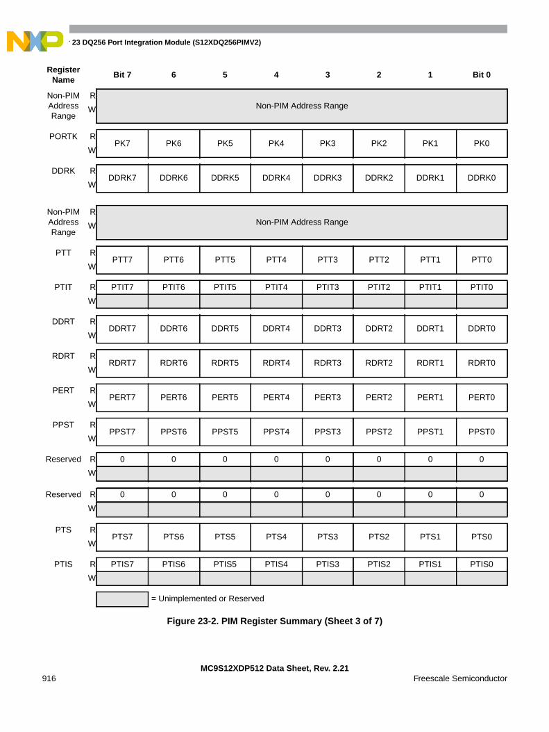
Chapter 23 DQ256 Port Integration Module (S12XDQ256PIMV2)
MC9S12XDP512 Data Sheet, Rev. 2.21916 Freescale Semiconductor
Non-PIMAddressRange
RNon-PIM Address RangeW
PORTK RPK7 PK6 PK5 PK4 PK3 PK2 PK1 PK0
W
DDRK RDDRK7 DDRK6 DDRK5 DDRK4 DDRK3 DDRK2 DDRK1 DDRK0
W
Non-PIMAddressRange
RNon-PIM Address RangeW
PTT RPTT7 PTT6 PTT5 PTT4 PTT3 PTT2 PTT1 PTT0
W
PTIT R PTIT7 PTIT6 PTIT5 PTIT4 PTIT3 PTIT2 PTIT1 PTIT0
W
DDRT RDDRT7 DDRT6 DDRT5 DDRT4 DDRT3 DDRT2 DDRT1 DDRT0
W
RDRT RRDRT7 RDRT6 RDRT5 RDRT4 RDRT3 RDRT2 RDRT1 RDRT0
W
PERT RPERT7 PERT6 PERT5 PERT4 PERT3 PERT2 PERT1 PERT0
W
PPST RPPST7 PPST6 PPST5 PPST4 PPST3 PPST2 PPST1 PPST0
W
Reserved R 0 0 0 0 0 0 0 0
W
Reserved R 0 0 0 0 0 0 0 0
W
PTS RPTS7 PTS6 PTS5 PTS4 PTS3 PTS2 PTS1 PTS0
W
PTIS R PTIS7 PTIS6 PTIS5 PTIS4 PTIS3 PTIS2 PTIS1 PTIS0
W
RegisterName
Bit 7 6 5 4 3 2 1 Bit 0
= Unimplemented or Reserved
Figure 23-2. PIM Register Summary (Sheet 3 of 7)

DDRS RDDRS7 DDRS6 DDRS5 DDRS4 DDRS3 DDRS2 DDRS1 DDRS0
W
RDRS RRDRS7 RDRS6 RDRS5 RDRS4 RDRS3 RDRS2 RDRS1 RDRS0
W
PERS RPERS7 PERS6 PERS5 PERS4 PERS3 PERS2 PERS1 PERS0
W
PPSS RPPSS7 PPSS6 PPSS5 PPSS4 PPSS3 PPSS2 PPSS1 PPSS0
W
WOMS RWOMS7 WOMS6 WOMS5 WOMS4 WOMS3 WOMS2 WOMS1 WOMS0
W
Reserved R 0 0 0 0 0 0 0 0
W
PTM RPTM7 PTM6 PTM5 PTM4 PTM3 PTM2 PTM1 PTM0
W
PTIM R PTIM7 PTIM6 PTIM5 PTIM4 PTIM3 PTIM2 PTIM1 PTIM0
W
DDRM RDDRM7 DDRM6 DDRM5 DDRM4 DDRM3 DDRM2 DDRM1 DDRM0
W
RDRM RRDRM7 RDRM6 RDRM5 RDRM4 RDRM3 RDRM2 RDRM1 RDRM0
W
PERM RPERM7 PERM6 PERM5 PERM4 PERM3 PERM2 PERM1 PERM0
W
PPSM RPPSM7 PPSM6 PPSM5 PPSM4 PPSM3 PPSM2 PPSM1 PPSM0
W
WOMM RWOMM7 WOMM6 WOMM5 WOMM4 WOMM3 WOMM2 WOMM1 WOMM0
W
MODRR R 0MODRR6 MODRR5 MODRR4 MODRR3 MODRR2 MODRR1 MODRR0
W
PTP RPTP7 PTP6 PTP5 PTP4 PTP3 PTP2 PTP1 PTP0
W
RegisterName
Bit 7 6 5 4 3 2 1 Bit 0
= Unimplemented or Reserved
Figure 23-2. PIM Register Summary (Sheet 4 of 7)
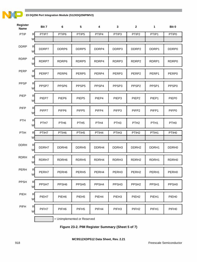
Chapter 23 DQ256 Port Integration Module (S12XDQ256PIMV2)
MC9S12XDP512 Data Sheet, Rev. 2.21918 Freescale Semiconductor
PTIP R PTIP7 PTIP6 PTIP5 PTIP4 PTIP3 PTIP2 PTIP1 PTIP0
W
DDRP RDDRP7 DDRP6 DDRP5 DDRP4 DDRP3 DDRP2 DDRP1 DDRP0
W
RDRP RRDRP7 RDRP6 RDRP5 RDRP4 RDRP3 RDRP2 RDRP1 RDRP0
W
PERP RPERP7 PERP6 PERP5 PERP4 PERP3 PERP2 PERP1 PERP0
W
PPSP RPPSP7 PPSP6 PPSP5 PPSP4 PPSP3 PPSP2 PPSP1 PPSP0
W
PIEP RPIEP7 PIEP6 PIEP5 PIEP4 PIEP3 PIEP2 PIEP1 PIEP0
W
PIFP RPIFP7 PIFP6 PIFP5 PIFP4 PIFP3 PIFP2 PIFP1 PIFP0
W
PTH RPTH7 PTH6 PTH5 PTH4 PTH3 PTH2 PTH1 PTH0
W
PTIH R PTIH7 PTIH6 PTIH5 PTIH4 PTIH3 PTIH2 PTIH1 PTIH0
W
DDRH RDDRH7 DDRH6 DDRH5 DDRH4 DDRH3 DDRH2 DDRH1 DDRH0
W
RDRH RRDRH7 RDRH6 RDRH5 RDRH4 RDRH3 RDRH2 RDRH1 RDRH0
W
PERH RPERH7 PERH6 PERH5 PERH4 PERH3 PERH2 PERH1 PERH0
W
PPSH RPPSH7 PPSH6 PPSH5 PPSH4 PPSH3 PPSH2 PPSH1 PPSH0
W
PIEH RPIEH7 PIEH6 PIEH5 PIEH4 PIEH3 PIEH2 PIEH1 PIEH0
W
PIFH RPIFH7 PIFH6 PIFH5 PIFH4 PIFH3 PIFH2 PIFH1 PIFH0
W
RegisterName
Bit 7 6 5 4 3 2 1 Bit 0
= Unimplemented or Reserved
Figure 23-2. PIM Register Summary (Sheet 5 of 7)

PTJ RPTJ7 PTJ6 PTJ5 PTJ4
0PTJ2 PTJ1 PTJ0
W
PTIJ R PTIJ7 PTIJ6 PTIJ5 PTIJ4 0 PTIJ2 PTIJ1 PTIJ0
W
DDRJ RDDRJ7 DDRJ6 DDRJ5 DDRJ4
0DDRJ2 DDRJ1 DDRJ0
W
RDRJ RRDRJ7 RDRJ6 RDRJ5 RDRJ4
0RDRJ2 RDRJ1 RDRJ0
W
PERJ RPERJ7 PERJ6 PERJ5 PERJ4
0PERJ2 PERJ1 PERJ0
W
PPSJ RPPSJ7 PPSJ6 PPSJ5 PPSJ4
0PPSJ2 PPSJ1 PPSJ0
W
PIEJ RPIEJ7 PIEJ6 PIEJ5 PIEJ4
0PIEJ2 PIEJ1 PIEJ0
W
PIFJ RPPSJ7 PPSJ6 PPSJ5 PPSJ4
0PPSJ2 PPSJ1 PPSJ0
W
Reserved R 0 0 0 0 0 0 0 0
W
PT1AD0 RPT1AD07 PT1AD06 PT1AD05 PT1AD04 PT1AD03 PT1AD02 PT1AD01 PT1AD00
W
Reserved R 0 0 0 0 0 0 0 0
W
DDR1AD0 RDDR1AD07 DDR1AD06 DDR1AD05 DDR1AD04 DDR1AD03 DDR1AD02 DDR1AD01 DDR1AD00
W
Reserved R 0 0 0 0 0 0 0 0
W
RDR1AD0 RRDR1AD07 RDR1AD06 RDR1AD05 RDR1AD04 RDR1AD03 RDR1AD02 RDR1AD01 RDR1AD00
W
Reserved R 0 0 0 0 0 0 0 0
W
RegisterName
Bit 7 6 5 4 3 2 1 Bit 0
= Unimplemented or Reserved
Figure 23-2. PIM Register Summary (Sheet 6 of 7)
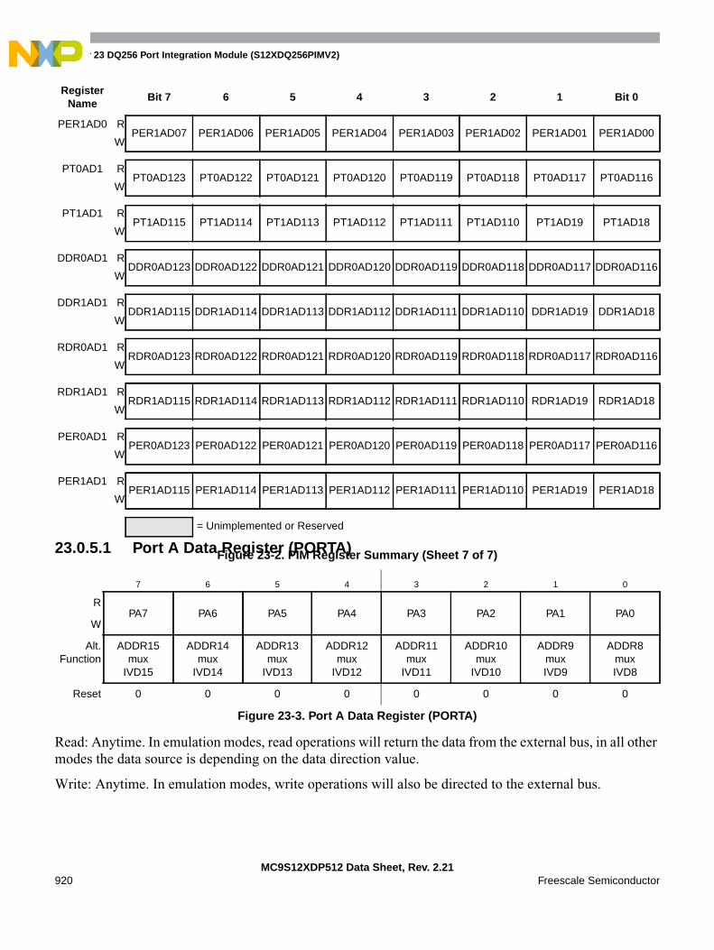
Chapter 23 DQ256 Port Integration Module (S12XDQ256PIMV2)
MC9S12XDP512 Data Sheet, Rev. 2.21920 Freescale Semiconductor
23.0.5.1 Port A Data Register (PORTA)
Read: Anytime. In emulation modes, read operations will return the data from the external bus, in all othermodes the data source is depending on the data direction value.
Write: Anytime. In emulation modes, write operations will also be directed to the external bus.
PER1AD0 RPER1AD07 PER1AD06 PER1AD05 PER1AD04 PER1AD03 PER1AD02 PER1AD01 PER1AD00
W
PT0AD1 RPT0AD123 PT0AD122 PT0AD121 PT0AD120 PT0AD119 PT0AD118 PT0AD117 PT0AD116
W
PT1AD1 RPT1AD115 PT1AD114 PT1AD113 PT1AD112 PT1AD111 PT1AD110 PT1AD19 PT1AD18
W
DDR0AD1 RDDR0AD123 DDR0AD122 DDR0AD121 DDR0AD120 DDR0AD119 DDR0AD118 DDR0AD117 DDR0AD116
W
DDR1AD1 RDDR1AD115 DDR1AD114 DDR1AD113 DDR1AD112 DDR1AD111 DDR1AD110 DDR1AD19 DDR1AD18
W
RDR0AD1 RRDR0AD123 RDR0AD122 RDR0AD121 RDR0AD120 RDR0AD119 RDR0AD118 RDR0AD117 RDR0AD116
W
RDR1AD1 RRDR1AD115 RDR1AD114 RDR1AD113 RDR1AD112 RDR1AD111 RDR1AD110 RDR1AD19 RDR1AD18
W
PER0AD1 RPER0AD123 PER0AD122 PER0AD121 PER0AD120 PER0AD119 PER0AD118 PER0AD117 PER0AD116
W
PER1AD1 RPER1AD115 PER1AD114 PER1AD113 PER1AD112 PER1AD111 PER1AD110 PER1AD19 PER1AD18
W
7 6 5 4 3 2 1 0
RPA7 PA6 PA5 PA4 PA3 PA2 PA1 PA0
W
Alt.Function
ADDR15mux
IVD15
ADDR14mux
IVD14
ADDR13mux
IVD13
ADDR12mux
IVD12
ADDR11mux
IVD11
ADDR10mux
IVD10
ADDR9muxIVD9
ADDR8muxIVD8
Reset 0 0 0 0 0 0 0 0
Figure 23-3. Port A Data Register (PORTA)
RegisterName
Bit 7 6 5 4 3 2 1 Bit 0
= Unimplemented or Reserved
Figure 23-2. PIM Register Summary (Sheet 7 of 7)
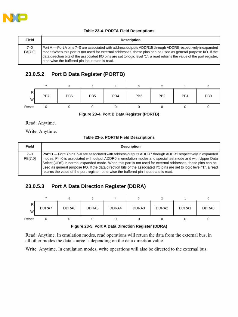
23.0.5.2 Port B Data Register (PORTB)
Read: Anytime.
Write: Anytime.
23.0.5.3 Port A Data Direction Register (DDRA)
Read: Anytime. In emulation modes, read operations will return the data from the external bus, inall other modes the data source is depending on the data direction value.
Write: Anytime. In emulation modes, write operations will also be directed to the external bus.
Table 23-4. PORTA Field Descriptions
Field Description
7–0PA[7:0]
Port A — Port A pins 7–0 are associated with address outputs ADDR15 through ADDR8 respectively inexpandedmodesWhen this port is not used for external addresses, these pins can be used as general purpose I/O. If thedata direction bits of the associated I/O pins are set to logic level “1”, a read returns the value of the port register,otherwise the buffered pin input state is read.
7 6 5 4 3 2 1 0
RPB7 PB6 PB5 PB4 PB3 PB2 PB1 PB0
W
Reset 0 0 0 0 0 0 0 0
Figure 23-4. Port B Data Register (PORTB)
Table 23-5. PORTB Field Descriptions
Field Description
7–0PB[7:0]
Port B — Port B pins 7–0 are associated with address outputs ADDR7 through ADDR1 respectively in expandedmodes. Pin 0 is associated with output ADDR0 in emulation modes and special test mode and with Upper DataSelect (UDS) in normal expanded mode. When this port is not used for external addresses, these pins can beused as general purpose I/O. If the data direction bits of the associated I/O pins are set to logic level “1”, a readreturns the value of the port register, otherwise the buffered pin input state is read.
7 6 5 4 3 2 1 0
RDDRA7 DDRA6 DDRA5 DDRA4 DDRA3 DDRA2 DDRA1 DDRA0
W
Reset 0 0 0 0 0 0 0 0
Figure 23-5. Port A Data Direction Register (DDRA)

Chapter 23 DQ256 Port Integration Module (S12XDQ256PIMV2)
MC9S12XDP512 Data Sheet, Rev. 2.21922 Freescale Semiconductor
23.0.5.4 Port B Data Direction Register (DDRB)
Read: Anytime. In emulation modes, read operations will return the data from the external bus, in all othermodes the data source is depending on the data direction value.
Write: Anytime. In emulation modes, write operations will also be directed to the external bus.
23.0.5.5 Port C Data Register (PORTC)
Read: Anytime. In emulation modes, read operations will return the data from the external bus, in all othermodes the data source is depending on the data direction value.
Write: Anytime. In emulation modes, write operations will also be directed to the external bus.
Table 23-6. DDRA Field Descriptions
Field Description
7–0DDRA[7:0]
Data Direction Port A — This register controls the data direction for port A. When Port A is operating as a generalpurpose I/O port, DDRA determines whether each pin is an input or output. A logic level “1” causes theassociated port pin to be an output and a logic level “0” causes the associated pin to be a high-impedance input.0 Associated pin is configured as input.1 Associated pin is configured as output.Note: Due to internal synchronization circuits, it can take up to 2 bus clock cycles until the correct value is read
on PORTA after changing the DDRA register.
7 6 5 4 3 2 1 0
RDDRB7 DDRB6 DDRB5 DDRB4 DDRB3 DDRB2 DDRB1 DDRB0
W
Reset 0 0 0 0 0 0 0 0
Figure 23-6. Port B Data Direction Register (DDRB)
Table 23-7. DDRB Field Descriptions
Field Description
7–0DDRB[7:0]
Data Direction Port B — This register controls the data direction for port B. When Port B is operating as a generalpurpose I/O port, DDRB determines whether each pin is an input or output. A logic level “1” causes theassociated port pin to be an output and a logic level “0” causes the associated pin to be a high-impedance input.0 Associated pin is configured as input.1 Associated pin is configured as output.Note: Due to internal synchronization circuits, it can take up to 2 bus clock cycles until the correct value is read
on PORTB after changing the DDRB register.
7 6 5 4 3 2 1 0
RPC7 PC6 PC5 PC4 PC3 PC2 PC1 PC0
W
Reset 0 0 0 0 0 0 0 0
Figure 23-7. Port C Data Register (PORTC)
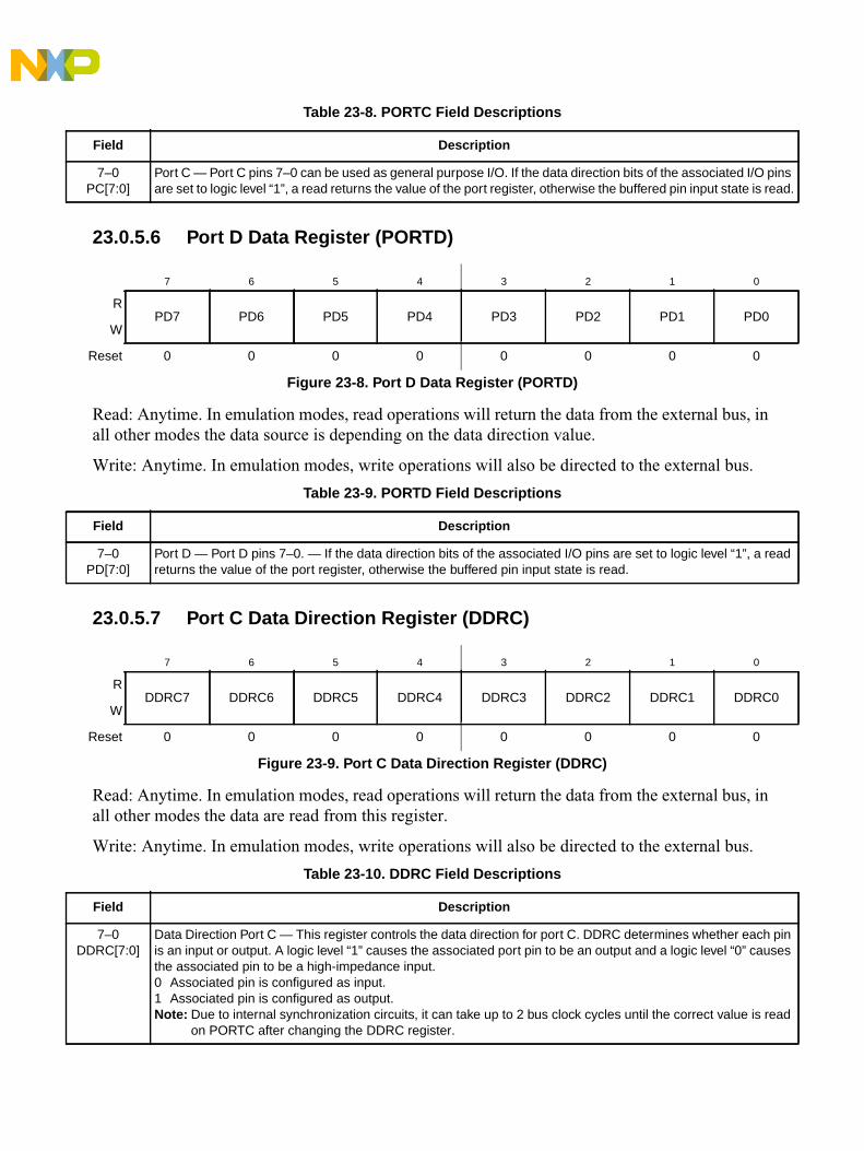
23.0.5.6 Port D Data Register (PORTD)
Read: Anytime. In emulation modes, read operations will return the data from the external bus, inall other modes the data source is depending on the data direction value.
Write: Anytime. In emulation modes, write operations will also be directed to the external bus.
23.0.5.7 Port C Data Direction Register (DDRC)
Read: Anytime. In emulation modes, read operations will return the data from the external bus, inall other modes the data are read from this register.
Write: Anytime. In emulation modes, write operations will also be directed to the external bus.
Table 23-8. PORTC Field Descriptions
Field Description
7–0PC[7:0]
Port C — Port C pins 7–0 can be used as general purpose I/O. If the data direction bits of the associated I/O pinsare set to logic level “1”, a read returns the value of the port register, otherwise the buffered pin input state is read.
7 6 5 4 3 2 1 0
RPD7 PD6 PD5 PD4 PD3 PD2 PD1 PD0
W
Reset 0 0 0 0 0 0 0 0
Figure 23-8. Port D Data Register (PORTD)
Table 23-9. PORTD Field Descriptions
Field Description
7–0PD[7:0]
Port D — Port D pins 7–0. — If the data direction bits of the associated I/O pins are set to logic level “1”, a readreturns the value of the port register, otherwise the buffered pin input state is read.
7 6 5 4 3 2 1 0
RDDRC7 DDRC6 DDRC5 DDRC4 DDRC3 DDRC2 DDRC1 DDRC0
W
Reset 0 0 0 0 0 0 0 0
Figure 23-9. Port C Data Direction Register (DDRC)
Table 23-10. DDRC Field Descriptions
Field Description
7–0DDRC[7:0]
Data Direction Port C — This register controls the data direction for port C. DDRC determines whether each pinis an input or output. A logic level “1” causes the associated port pin to be an output and a logic level “0” causesthe associated pin to be a high-impedance input.0 Associated pin is configured as input.1 Associated pin is configured as output.Note: Due to internal synchronization circuits, it can take up to 2 bus clock cycles until the correct value is read
on PORTC after changing the DDRC register.

Chapter 23 DQ256 Port Integration Module (S12XDQ256PIMV2)
MC9S12XDP512 Data Sheet, Rev. 2.21924 Freescale Semiconductor
23.0.5.8 Port D Data Direction Register (DDRD)
Read: Anytime. In emulation modes, read operations will return the data from the external bus, in all othermodes the data are read from this register.
Write: Anytime. In emulation modes, write operations will also be directed to the external bus.
23.0.5.9 Port E Data Register (PORTE)
Read: Anytime. In emulation modes, read operations will return the data from the external bus, in all othermodes the data source is depending on the data direction value.
Write: Anytime. In emulation modes, write operations will also be directed to the external bus.
7 6 5 4 3 2 1 0
RDDRD7 DDRD6 DDRD5 DDRD4 DDRD3 DDRD2 DDRD1 DDRD0
W
Reset 0 0 0 0 0 0 0 0
Figure 23-10. Port D Data Direction Register (DDRD)
Table 23-11. DDRD Field Descriptions
Field Description
7–0DDRD[7:0]
Data Direction Port D — This register controls the data direction for port D. DDRD determines whether each pinis an input or output. A logic level “1” causes the associated port pin to be an output and a logic level “0” causesthe associated pin to be a high-impedance input.0 Associated pin is configured as input.1 Associated pin is configured as output.Note: Due to internal synchronization circuits, it can take up to 2 bus clock cycles until the correct value is read
on PORTD after changing the DDRD register.
7 6 5 4 3 2 1 0
RPE7 PE6 PE5 PE4 PE3 PE2
PE1 PE0
W
Alt.Func.
XCLKSor
ECLKX2
MODBor
TAGHI
MODAorREor
TAGLO
ECLK
EROMCTLor
LSTRBor
LDS
R/Wor
WEIRQ XIRQ
Reset 0 0 0 0 0 0 —1
1. These registers are reset to zero. Two bus clock cycles after reset release the register values are updated with theassociated pin values.
—1
= Unimplemented or Reserved
Figure 23-11. Port E Data Register (PORTE)
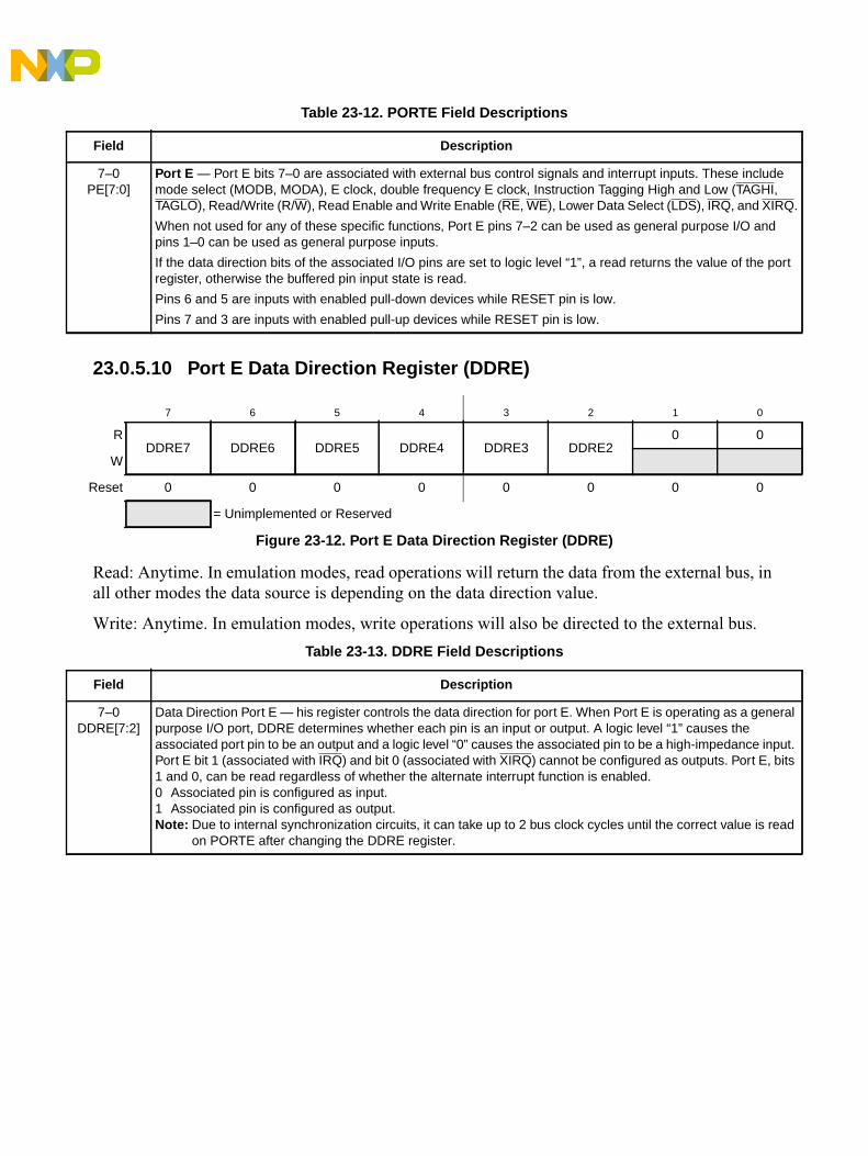
23.0.5.10 Port E Data Direction Register (DDRE)
Read: Anytime. In emulation modes, read operations will return the data from the external bus, inall other modes the data source is depending on the data direction value.
Write: Anytime. In emulation modes, write operations will also be directed to the external bus.
Table 23-12. PORTE Field Descriptions
Field Description
7–0PE[7:0]
Port E — Port E bits 7–0 are associated with external bus control signals and interrupt inputs. These includemode select (MODB, MODA), E clock, double frequency E clock, Instruction Tagging High and Low (TAGHI,TAGLO), Read/Write (R/W), Read Enable and Write Enable (RE, WE), Lower Data Select (LDS), IRQ, and XIRQ.
When not used for any of these specific functions, Port E pins 7–2 can be used as general purpose I/O andpins 1–0 can be used as general purpose inputs.
If the data direction bits of the associated I/O pins are set to logic level “1”, a read returns the value of the portregister, otherwise the buffered pin input state is read.
Pins 6 and 5 are inputs with enabled pull-down devices while RESET pin is low.
Pins 7 and 3 are inputs with enabled pull-up devices while RESET pin is low.
7 6 5 4 3 2 1 0
RDDRE7 DDRE6 DDRE5 DDRE4 DDRE3 DDRE2
0 0
W
Reset 0 0 0 0 0 0 0 0
= Unimplemented or Reserved
Figure 23-12. Port E Data Direction Register (DDRE)
Table 23-13. DDRE Field Descriptions
Field Description
7–0DDRE[7:2]
Data Direction Port E — his register controls the data direction for port E. When Port E is operating as a generalpurpose I/O port, DDRE determines whether each pin is an input or output. A logic level “1” causes theassociated port pin to be an output and a logic level “0” causes the associated pin to be a high-impedance input.Port E bit 1 (associated with IRQ) and bit 0 (associated with XIRQ) cannot be configured as outputs. Port E, bits1 and 0, can be read regardless of whether the alternate interrupt function is enabled.0 Associated pin is configured as input.1 Associated pin is configured as output.Note: Due to internal synchronization circuits, it can take up to 2 bus clock cycles until the correct value is read
on PORTE after changing the DDRE register.

Chapter 23 DQ256 Port Integration Module (S12XDQ256PIMV2)
MC9S12XDP512 Data Sheet, Rev. 2.21926 Freescale Semiconductor
23.0.5.11 S12X_EBI Ports, BKGD, VREGEN Pin Pull-up Control Register (PUCR)
Read: Anytime in single-chip modes.
Write: Anytime, except BKPUE which is writable in special test mode only.
This register is used to enable pull-up devices for the associated ports A, B, C, D, E, and K. Pull-up devicesare assigned on a per-port basis and apply to any pin in the corresponding port currently configured as aninput.
7 6 5 4 3 2 1 0
RPUPKE BKPUE
0PUPEE PUPDE PUPCE PUPBE PUPAE
W
Reset 1 1 0 1 0 0 0 0
= Unimplemented or Reserved
Figure 23-13. S12X_EBI Ports, BKGD, VREGEN Pin Pull-up Control Register (PUCR)
Table 23-14. PUCR Field Descriptions
Field Description
7PUPKE
Pull-up Port K Enable0 Port K pull-up devices are disabled.1 Enable pull-up devices for Port K input pins.
6BKPUE
BKGD and VREGEN Pin Pull-up Enable0 BKGD and VREGEN pull-up devices are disabled.1 Enable pull-up devices on BKGD and VREGEN pins.
4PUPEE
Pull-up Port E Enable0 Port E pull-up devices on bit 7, 4–0 are disabled.1 Enable pull-up devices for Port E input pins bits 7, 4–0.Note: Bits 5 and 6 of Port E have pull-down devices which are only enabled during reset. This bit has no effect
on these pins.
3PUPDE
Pull-up Port D Enable0 Port D pull-up devices are disabled.1 Enable pull-up devices for all Port D input pins.
2PUPCE
Pull-up Port C Enable0 Port C pull-up devices are disabled.1 Enable pull-up devices for all Port C input pins.
1PUPBE
Pull-up Port B Enable0 Port B pull-up devices are disabled.1 Enable pull-up devices for all Port B input pins.
0PUPAE
Pull-up Port A Enable0 Port A pull-up devices are disabled.1 Enable pull-up devices for all Port A input pins.

23.0.5.12 S12X_EBI Ports Reduced Drive Register (RDRIV)
Read: Anytime. In emulation modes, read operations will return the data from the external bus, inall other modes the data source is depending on the data direction value.
Write: Anytime. In emulation modes, write operations will also be directed to the external bus.
This register is used to select reduced drive for the pins associated with ports A, B, E, and K. Ifenabled, the pins drive at about 1/6 of the full drive strength. The reduced drive function isindependent of which function is being used on a particular pin.
The reduced drive functionality does not take effect on the pins in emulation modes.
7 6 5 4 3 2 1 0
RRDPK
0 0RDPE RDPD RDPC RDPB RDPA
W
Reset 0 0 0 0 0 0 0 0
= Unimplemented or Reserved
Figure 23-14. S12X_EBI Ports Reduced Drive Register (RDRIV)
Table 23-15. RDRIV Field Descriptions
Field Description
7RDPK
Reduced Drive of Port K0 All port K output pins have full drive enabled.1 All port K output pins have reduced drive enabled.
4RDPE
Reduced Drive of Port E0 All port E output pins have full drive enabled.1 All port E output pins have reduced drive enabled.
3RDPD
Reduced Drive of Port D0 All port D output pins have full drive enabled.1 All port D output pins have reduced drive enabled.
2RDPC
Reduced Drive of Port C0 All port C output pins have full drive enabled.1 All port C output pins have reduced drive enabled.
1RDPB
Reduced Drive of Port B0 All port B output pins have full drive enabled.1 All port B output pins have reduced drive enabled.
0RDPA
Reduced Drive of Ports A0 All Port A output pins have full drive enabled.1 All port A output pins have reduced drive enabled.
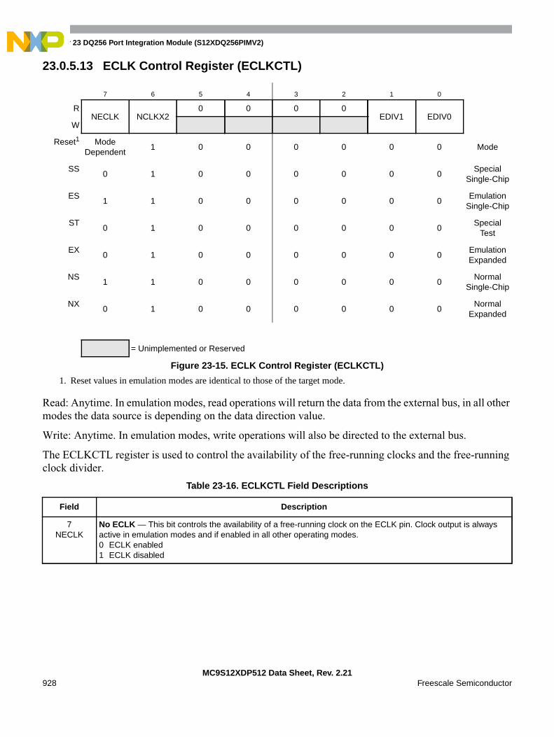
Chapter 23 DQ256 Port Integration Module (S12XDQ256PIMV2)
MC9S12XDP512 Data Sheet, Rev. 2.21928 Freescale Semiconductor
23.0.5.13 ECLK Control Register (ECLKCTL)
Read: Anytime. In emulation modes, read operations will return the data from the external bus, in all othermodes the data source is depending on the data direction value.
Write: Anytime. In emulation modes, write operations will also be directed to the external bus.
The ECLKCTL register is used to control the availability of the free-running clocks and the free-runningclock divider.
7 6 5 4 3 2 1 0
RNECLK NCLKX2
0 0 0 0EDIV1 EDIV0
W
Reset1
1. Reset values in emulation modes are identical to those of the target mode.
ModeDependent
1 0 0 0 0 0 0 Mode
SS0 1 0 0 0 0 0 0
SpecialSingle-Chip
ES1 1 0 0 0 0 0 0
EmulationSingle-Chip
ST0 1 0 0 0 0 0 0
SpecialTest
EX0 1 0 0 0 0 0 0
EmulationExpanded
NS1 1 0 0 0 0 0 0
NormalSingle-Chip
NX0 1 0 0 0 0 0 0
NormalExpanded
= Unimplemented or Reserved
Figure 23-15. ECLK Control Register (ECLKCTL)
Table 23-16. ECLKCTL Field Descriptions
Field Description
7NECLK
No ECLK — This bit controls the availability of a free-running clock on the ECLK pin. Clock output is alwaysactive in emulation modes and if enabled in all other operating modes.0 ECLK enabled1 ECLK disabled
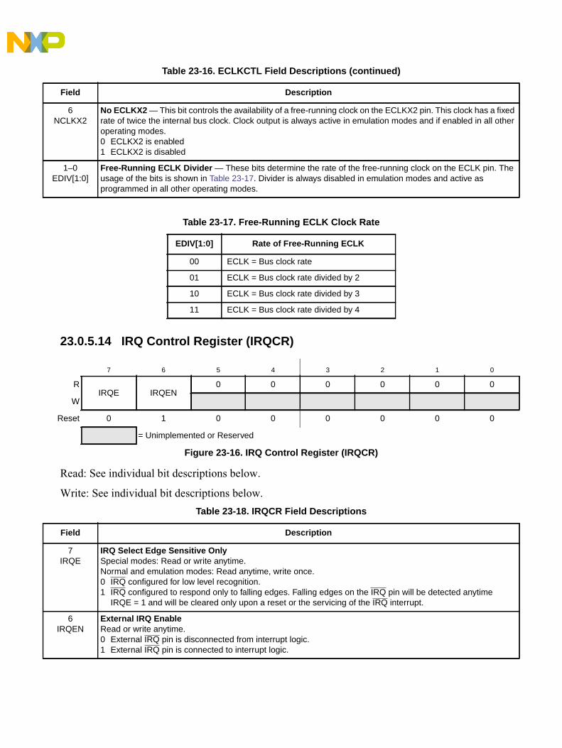
23.0.5.14 IRQ Control Register (IRQCR)
Read: See individual bit descriptions below.
Write: See individual bit descriptions below.
6NCLKX2
No ECLKX2 — This bit controls the availability of a free-running clock on the ECLKX2 pin. This clock has a fixedrate of twice the internal bus clock. Clock output is always active in emulation modes and if enabled in all otheroperating modes.0 ECLKX2 is enabled1 ECLKX2 is disabled
1–0EDIV[1:0]
Free-Running ECLK Divider — These bits determine the rate of the free-running clock on the ECLK pin. Theusage of the bits is shown in Table 23-17. Divider is always disabled in emulation modes and active asprogrammed in all other operating modes.
Table 23-17. Free-Running ECLK Clock Rate
EDIV[1:0] Rate of Free-Running ECLK
00 ECLK = Bus clock rate
01 ECLK = Bus clock rate divided by 2
10 ECLK = Bus clock rate divided by 3
11 ECLK = Bus clock rate divided by 4
7 6 5 4 3 2 1 0
RIRQE IRQEN
0 0 0 0 0 0
W
Reset 0 1 0 0 0 0 0 0
= Unimplemented or Reserved
Figure 23-16. IRQ Control Register (IRQCR)
Table 23-18. IRQCR Field Descriptions
Field Description
7IRQE
IRQ Select Edge Sensitive OnlySpecial modes: Read or write anytime.Normal and emulation modes: Read anytime, write once.0 IRQ configured for low level recognition.1 IRQ configured to respond only to falling edges. Falling edges on the IRQ pin will be detected anytime
IRQE = 1 and will be cleared only upon a reset or the servicing of the IRQ interrupt.
6IRQEN
External IRQ EnableRead or write anytime.0 External IRQ pin is disconnected from interrupt logic.1 External IRQ pin is connected to interrupt logic.
Table 23-16. ECLKCTL Field Descriptions (continued)
Field Description
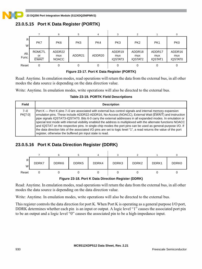
Chapter 23 DQ256 Port Integration Module (S12XDQ256PIMV2)
MC9S12XDP512 Data Sheet, Rev. 2.21930 Freescale Semiconductor
23.0.5.15 Port K Data Register (PORTK)
Read: Anytime. In emulation modes, read operations will return the data from the external bus, in all othermodes the data source is depending on the data direction value.
Write: Anytime. In emulation modes, write operations will also be directed to the external bus.
23.0.5.16 Port K Data Direction Register (DDRK)
Read: Anytime. In emulation modes, read operations will return the data from the external bus, in all othermodes the data source is depending on the data direction value.
Write: Anytime. In emulation modes, write operations will also be directed to the external bus.
This register controls the data direction for port K. When Port K is operating as a general purpose I/O port,DDRK determines whether each pin is an input or output. A logic level “1” causes the associated port pinto be an output and a logic level “0” causes the associated pin to be a high-impedance input.
7 6 5 4 3 2 1 0
RPK7 PK6 PK5 PK4 PK3 PK2 PK1 PK0
W
Alt.Func.
ROMCTLor
EWAIT
ADDR22mux
NOACCADDR21 ADDR20
ADDR19mux
IQSTAT3
ADDR18mux
IQSTAT2
ADDR17mux
IQSTAT1
ADDR16mux
IQSTAT0
Reset 0 0 0 0 0 0 0 0
Figure 23-17. Port K Data Register (PORTK)
Table 23-19. PORTK Field Descriptions
Field Description
7–0PK[7:0]
Port K — Port K pins 7–0 are associated with external bus control signals and internal memory expansionemulation pins. These include ADDR22-ADDR16, No-Access (NOACC), External Wait (EWAIT) and instructionpipe signals IQSTAT3-IQSTAT0. Bits 6-0 carry the external addresses in all expanded modes. In emulation orspecial test mode with internal visibility enabled the address is multiplexed with the alternate functions NOACCand IQSTAT on the respective pins. In single-chip modes the port pins can be used as general-purpose I/O. Ifthe data direction bits of the associated I/O pins are set to logic level “1”, a read returns the value of the portregister, otherwise the buffered pin input state is read.
7 6 5 4 3 2 1 0
RDDRK7 DDRK6 DDRK5 DDRK4 DDRK3 DDRK2 DDRK1 DDRK0
W
Reset 0 0 0 0 0 0 0 0
Figure 23-18. Port K Data Direction Register (DDRK)

23.0.5.17 Port T Data Register (PTT)
Read: Anytime.
Write: Anytime.
23.0.5.18 Port T Input Register (PTIT)
Read: Anytime.
Write: Never, writes to this register have no effect.
Table 23-20. DDRK Field Descriptions
Field Description
7–0DDRK[7:0]
Data Direction Port K0 Associated pin is configured as input.1 Associated pin is configured as output.Note: Due to internal synchronization circuits, it can take up to 2 bus clock cycles until the correct value is read
on PORTK after changing the DDRK register.
7 6 5 4 3 2 1 0
RPTT7 PTT6 PTT5 PTT4 PTT3 PTT2 PTT1 PTT0
W
ECT IOC7 IOC6 IOC5 IOC4 IOC3 IOC2 IOC1 IOC0
Reset 0 0 0 0 0 0 0 0
Figure 23-19. Port T Data Register (PTT)
Table 23-21. PTT Field Descriptions
Field Description
7–0PTT[7:0]
Port T — Port T bits 7–0 are associated with ECT channels IOC7–IOC0 (refer to ECT section). When not usedwith the ECT, these pins can be used as general purpose I/O.
If the data direction bits of the associated I/O pins are set to logic level “1”, a read returns the value of the portregister, otherwise the buffered pin input state is read.
7 6 5 4 3 2 1 0
R PTIT7 PTIT6 PTIT5 PTIT4 PTIT3 PTIT2 PTIT1 PTIT0
W
Reset1
1. These registers are reset to zero. Two bus clock cycles after reset release the register values are updated with theassociated pin values.
— — — — — — — —
= Unimplemented or Reserved
Figure 23-20. Port T Input Register (PTIT)
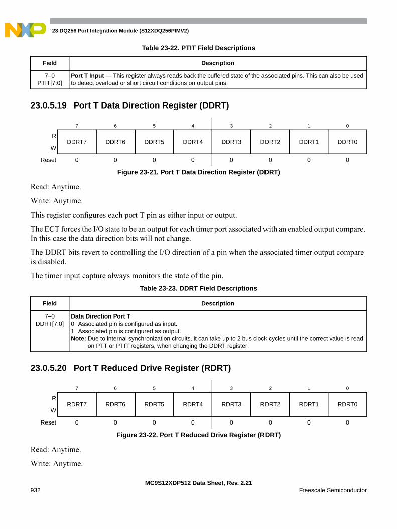
Chapter 23 DQ256 Port Integration Module (S12XDQ256PIMV2)
MC9S12XDP512 Data Sheet, Rev. 2.21932 Freescale Semiconductor
23.0.5.19 Port T Data Direction Register (DDRT)
Read: Anytime.
Write: Anytime.
This register configures each port T pin as either input or output.
The ECT forces the I/O state to be an output for each timer port associated with an enabled output compare.In this case the data direction bits will not change.
The DDRT bits revert to controlling the I/O direction of a pin when the associated timer output compareis disabled.
The timer input capture always monitors the state of the pin.
23.0.5.20 Port T Reduced Drive Register (RDRT)
Read: Anytime.
Write: Anytime.
Table 23-22. PTIT Field Descriptions
Field Description
7–0PTIT[7:0]
Port T Input — This register always reads back the buffered state of the associated pins. This can also be usedto detect overload or short circuit conditions on output pins.
7 6 5 4 3 2 1 0
RDDRT7 DDRT6 DDRT5 DDRT4 DDRT3 DDRT2 DDRT1 DDRT0
W
Reset 0 0 0 0 0 0 0 0
Figure 23-21. Port T Data Direction Register (DDRT)
Table 23-23. DDRT Field Descriptions
Field Description
7–0DDRT[7:0]
Data Direction Port T0 Associated pin is configured as input.1 Associated pin is configured as output.Note: Due to internal synchronization circuits, it can take up to 2 bus clock cycles until the correct value is read
on PTT or PTIT registers, when changing the DDRT register.
7 6 5 4 3 2 1 0
RRDRT7 RDRT6 RDRT5 RDRT4 RDRT3 RDRT2 RDRT1 RDRT0
W
Reset 0 0 0 0 0 0 0 0
Figure 23-22. Port T Reduced Drive Register (RDRT)
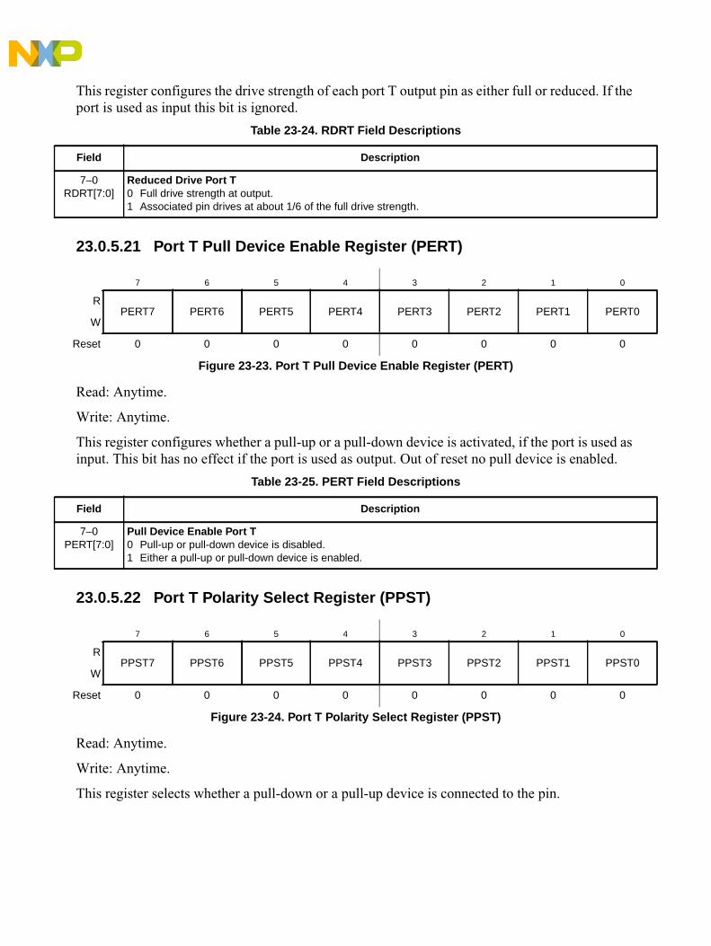
This register configures the drive strength of each port T output pin as either full or reduced. If theport is used as input this bit is ignored.
23.0.5.21 Port T Pull Device Enable Register (PERT)
Read: Anytime.
Write: Anytime.
This register configures whether a pull-up or a pull-down device is activated, if the port is used asinput. This bit has no effect if the port is used as output. Out of reset no pull device is enabled.
23.0.5.22 Port T Polarity Select Register (PPST)
Read: Anytime.
Write: Anytime.
This register selects whether a pull-down or a pull-up device is connected to the pin.
Table 23-24. RDRT Field Descriptions
Field Description
7–0RDRT[7:0]
Reduced Drive Port T0 Full drive strength at output.1 Associated pin drives at about 1/6 of the full drive strength.
7 6 5 4 3 2 1 0
RPERT7 PERT6 PERT5 PERT4 PERT3 PERT2 PERT1 PERT0
W
Reset 0 0 0 0 0 0 0 0
Figure 23-23. Port T Pull Device Enable Register (PERT)
Table 23-25. PERT Field Descriptions
Field Description
7–0PERT[7:0]
Pull Device Enable Port T0 Pull-up or pull-down device is disabled.1 Either a pull-up or pull-down device is enabled.
7 6 5 4 3 2 1 0
RPPST7 PPST6 PPST5 PPST4 PPST3 PPST2 PPST1 PPST0
W
Reset 0 0 0 0 0 0 0 0
Figure 23-24. Port T Polarity Select Register (PPST)
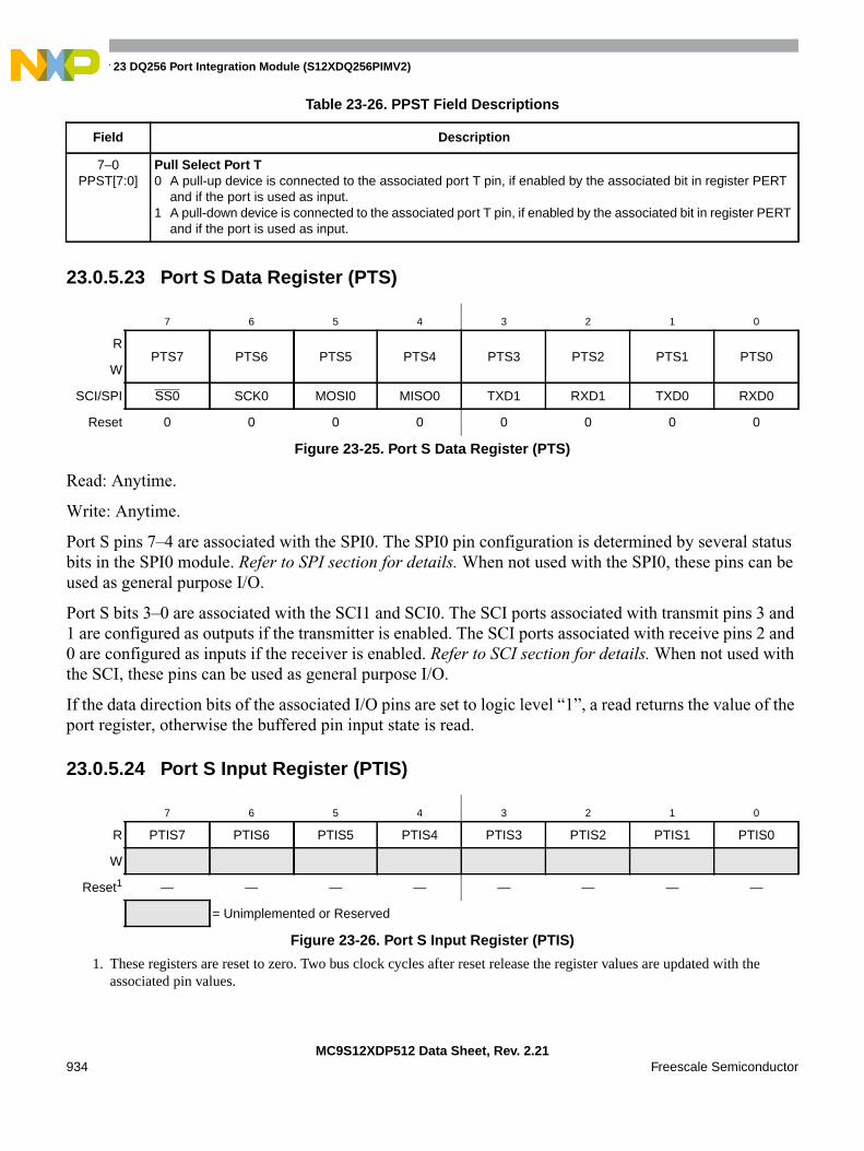
Chapter 23 DQ256 Port Integration Module (S12XDQ256PIMV2)
MC9S12XDP512 Data Sheet, Rev. 2.21934 Freescale Semiconductor
23.0.5.23 Port S Data Register (PTS)
Read: Anytime.
Write: Anytime.
Port S pins 7–4 are associated with the SPI0. The SPI0 pin configuration is determined by several statusbits in the SPI0 module. Refer to SPI section for details. When not used with the SPI0, these pins can beused as general purpose I/O.
Port S bits 3–0 are associated with the SCI1 and SCI0. The SCI ports associated with transmit pins 3 and1 are configured as outputs if the transmitter is enabled. The SCI ports associated with receive pins 2 and0 are configured as inputs if the receiver is enabled. Refer to SCI section for details. When not used withthe SCI, these pins can be used as general purpose I/O.
If the data direction bits of the associated I/O pins are set to logic level “1”, a read returns the value of theport register, otherwise the buffered pin input state is read.
23.0.5.24 Port S Input Register (PTIS)
Table 23-26. PPST Field Descriptions
Field Description
7–0PPST[7:0]
Pull Select Port T0 A pull-up device is connected to the associated port T pin, if enabled by the associated bit in register PERT
and if the port is used as input.1 A pull-down device is connected to the associated port T pin, if enabled by the associated bit in register PERT
and if the port is used as input.
7 6 5 4 3 2 1 0
RPTS7 PTS6 PTS5 PTS4 PTS3 PTS2 PTS1 PTS0
W
SCI/SPI SS0 SCK0 MOSI0 MISO0 TXD1 RXD1 TXD0 RXD0
Reset 0 0 0 0 0 0 0 0
Figure 23-25. Port S Data Register (PTS)
7 6 5 4 3 2 1 0
R PTIS7 PTIS6 PTIS5 PTIS4 PTIS3 PTIS2 PTIS1 PTIS0
W
Reset1
1. These registers are reset to zero. Two bus clock cycles after reset release the register values are updated with theassociated pin values.
— — — — — — — —
= Unimplemented or Reserved
Figure 23-26. Port S Input Register (PTIS)
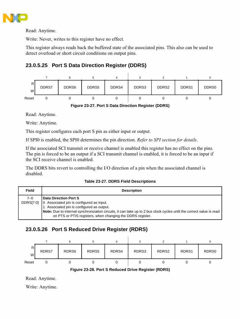
Read: Anytime.
Write: Never, writes to this register have no effect.
This register always reads back the buffered state of the associated pins. This also can be used todetect overload or short circuit conditions on output pins.
23.0.5.25 Port S Data Direction Register (DDRS)
Read: Anytime.
Write: Anytime.
This register configures each port S pin as either input or output.
If SPI0 is enabled, the SPI0 determines the pin direction. Refer to SPI section for details.
If the associated SCI transmit or receive channel is enabled this register has no effect on the pins.The pin is forced to be an output if a SCI transmit channel is enabled, it is forced to be an input ifthe SCI receive channel is enabled.
The DDRS bits revert to controlling the I/O direction of a pin when the associated channel isdisabled.
23.0.5.26 Port S Reduced Drive Register (RDRS)
Read: Anytime.
Write: Anytime.
7 6 5 4 3 2 1 0
RDDRS7 DDRS6 DDRS5 DDRS4 DDRS3 DDRS2 DDRS1 DDRS0
W
Reset 0 0 0 0 0 0 0 0
Figure 23-27. Port S Data Direction Register (DDRS)
Table 23-27. DDRS Field Descriptions
Field Description
7–0DDRS[7:0]
Data Direction Port S0 Associated pin is configured as input.1 Associated pin is configured as output.Note: Due to internal synchronization circuits, it can take up to 2 bus clock cycles until the correct value is read
on PTS or PTIS registers, when changing the DDRS register.
7 6 5 4 3 2 1 0
RRDRS7 RDRS6 RDRS5 RDRS4 RDRS3 RDRS2 RDRS1 RDRS0
W
Reset 0 0 0 0 0 0 0 0
Figure 23-28. Port S Reduced Drive Register (RDRS)

Chapter 23 DQ256 Port Integration Module (S12XDQ256PIMV2)
MC9S12XDP512 Data Sheet, Rev. 2.21936 Freescale Semiconductor
This register configures the drive strength of each port S output pin as either full or reduced. If the port isused as input this bit is ignored.
23.0.5.27 Port S Pull Device Enable Register (PERS)
Read: Anytime.
Write: Anytime.
This register configures whether a pull-up or a pull-down device is activated, if the port is used as input oras output in wired-OR (open drain) mode. This bit has no effect if the port is used as push-pull output. Outof reset a pull-up device is enabled.
23.0.5.28 Port S Polarity Select Register (PPSS)
Read: Anytime.
Write: Anytime.
This register selects whether a pull-down or a pull-up device is connected to the pin.
Table 23-28. RDRS Field Descriptions
Field Description
7–0RDRS[7:0]
Reduced Drive Port S0 Full drive strength at output.1 Associated pin drives at about 1/6 of the full drive strength.
7 6 5 4 3 2 1 0
RPERS7 PERS6 PERS5 PERS4 PERS3 PERS2 PERS1 PERS0
W
Reset 1 1 1 1 1 1 1 1
Figure 23-29. Port S Pull Device Enable Register (PERS)
Table 23-29. PERS Field Descriptions
Field Description
7–0PERS[7:0]
Pull Device Enable Port S0 Pull-up or pull-down device is disabled.1 Either a pull-up or pull-down device is enabled.
7 6 5 4 3 2 1 0
RPPSS7 PPSS6 PPSS5 PPSS4 PPSS3 PPSS2 PPSS1 PPSS0
W
Reset 0 0 0 0 0 0 0 0
Figure 23-30. Port S Polarity Select Register (PPSS)

23.0.5.29 Port S Wired-OR Mode Register (WOMS)
Read: Anytime.
Write: Anytime.
This register configures the output pins as wired-OR. If enabled the output is driven active low only(open-drain). A logic level of “1” is not driven. It applies also to the SPI and SCI outputs and allowsa multipoint connection of several serial modules. These bits have no influence on pins used asinputs.
Table 23-30. PPSS Field Descriptions
Field Description
7–0PPSS[7:0]
Pull Select Port S0 A pull-up device is connected to the associated port S pin, if enabled by the associated bit in register PERS
and if the port is used as input or as wired-OR output.1 A pull-down device is connected to the associated port S pin, if enabled by the associated bit in register PERS
and if the port is used as input.
7 6 5 4 3 2 1 0
RWOMS7 WOMS6 WOMS5 WOMS4 WOMS3 WOMS2 WOMS1 WOMS0
W
Reset 0 0 0 0 0 0 0 0
Figure 23-31. Port S Wired-OR Mode Register (WOMS)
Table 23-31. WOMS Field Descriptions
Field Description
7–0WOMS[7:0]
Wired-OR Mode Port S0 Output buffers operate as push-pull outputs.1 Output buffers operate as open-drain outputs.
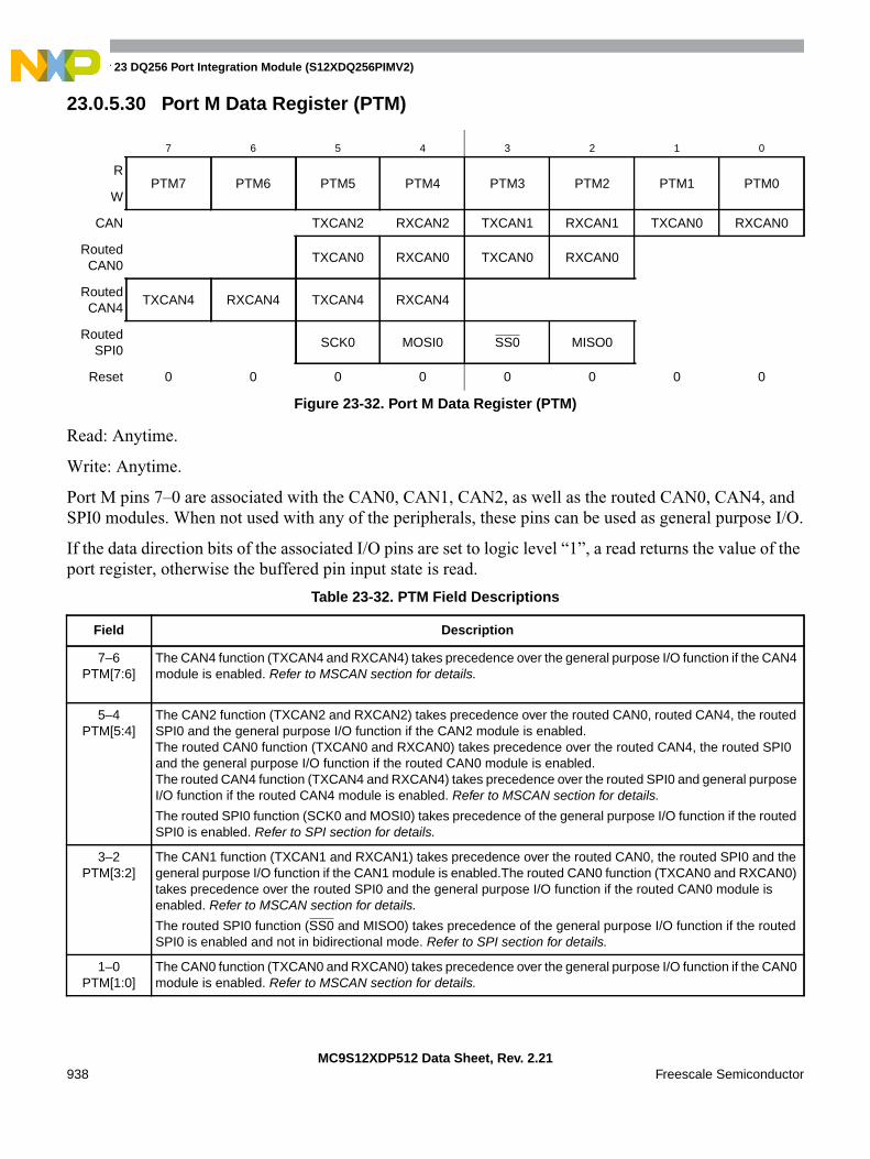
Chapter 23 DQ256 Port Integration Module (S12XDQ256PIMV2)
MC9S12XDP512 Data Sheet, Rev. 2.21938 Freescale Semiconductor
23.0.5.30 Port M Data Register (PTM)
Read: Anytime.
Write: Anytime.
Port M pins 7–0 are associated with the CAN0, CAN1, CAN2, as well as the routed CAN0, CAN4, andSPI0 modules. When not used with any of the peripherals, these pins can be used as general purpose I/O.
If the data direction bits of the associated I/O pins are set to logic level “1”, a read returns the value of theport register, otherwise the buffered pin input state is read.
7 6 5 4 3 2 1 0
RPTM7 PTM6 PTM5 PTM4 PTM3 PTM2 PTM1 PTM0
W
CAN TXCAN2 RXCAN2 TXCAN1 RXCAN1 TXCAN0 RXCAN0
RoutedCAN0
TXCAN0 RXCAN0 TXCAN0 RXCAN0
RoutedCAN4
TXCAN4 RXCAN4 TXCAN4 RXCAN4
RoutedSPI0
SCK0 MOSI0 SS0 MISO0
Reset 0 0 0 0 0 0 0 0
Figure 23-32. Port M Data Register (PTM)
Table 23-32. PTM Field Descriptions
Field Description
7–6PTM[7:6]
The CAN4 function (TXCAN4 and RXCAN4) takes precedence over the general purpose I/O function if the CAN4module is enabled. Refer to MSCAN section for details.
5–4PTM[5:4]
The CAN2 function (TXCAN2 and RXCAN2) takes precedence over the routed CAN0, routed CAN4, the routedSPI0 and the general purpose I/O function if the CAN2 module is enabled.The routed CAN0 function (TXCAN0 and RXCAN0) takes precedence over the routed CAN4, the routed SPI0and the general purpose I/O function if the routed CAN0 module is enabled.The routed CAN4 function (TXCAN4 and RXCAN4) takes precedence over the routed SPI0 and general purposeI/O function if the routed CAN4 module is enabled. Refer to MSCAN section for details.
The routed SPI0 function (SCK0 and MOSI0) takes precedence of the general purpose I/O function if the routedSPI0 is enabled. Refer to SPI section for details.
3–2PTM[3:2]
The CAN1 function (TXCAN1 and RXCAN1) takes precedence over the routed CAN0, the routed SPI0 and thegeneral purpose I/O function if the CAN1 module is enabled.The routed CAN0 function (TXCAN0 and RXCAN0)takes precedence over the routed SPI0 and the general purpose I/O function if the routed CAN0 module isenabled. Refer to MSCAN section for details.
The routed SPI0 function (SS0 and MISO0) takes precedence of the general purpose I/O function if the routedSPI0 is enabled and not in bidirectional mode. Refer to SPI section for details.
1–0PTM[1:0]
The CAN0 function (TXCAN0 and RXCAN0) takes precedence over the general purpose I/O function if the CAN0module is enabled. Refer to MSCAN section for details.

23.0.5.31 Port M Input Register (PTIM)
Read: Anytime.
Write: Never, writes to this register have no effect.
This register always reads back the buffered state of the associated pins. This can also be used todetect overload or short circuit conditions on output pins.
23.0.5.32 Port M Data Direction Register (DDRM)
Read: Anytime.
Write: Anytime.
This register configures each port M pin as either input or output.
The CAN forces the I/O state to be an output for each port line associated with an enabled output(TXCAN). also forces the I/O state to be an input for each port line associated with an enabledinput (RXCAN). In those cases the data direction bits will not change.
The DDRM bits revert to controlling the I/O direction of a pin when the associated peripheralmodule is disabled.
7 6 5 4 3 2 1 0
R PTIM7 PTIM6 PTIM5 PTIM4 PTIM3 PTIM2 PTIM1 PTIM0
W
Reset1
1. These registers are reset to zero. Two bus clock cycles after reset release the register values are updated with theassociated pin values.
— — — — — — — —
= Unimplemented or Reserved
Figure 23-33. Port M Input Register (PTIM)
7 6 5 4 3 2 1 0
RDDRM7 DDRM6 DDRM5 DDRM4 DDRM3 DDRM2 DDRM1 DDRM0
W
Reset 0 0 0 0 0 0 0 0
Figure 23-34. Port M Data Direction Register (DDRM)
Table 23-33. DDRM Field Descriptions
Field Description
7–0DDRM[7:0]
Data Direction Port M0 Associated pin is configured as input.1 Associated pin is configured as output.Note: Due to internal synchronization circuits, it can take up to 2 bus clock cycles until the correct value is read
on PTM or PTIM registers, when changing the DDRM register.

Chapter 23 DQ256 Port Integration Module (S12XDQ256PIMV2)
MC9S12XDP512 Data Sheet, Rev. 2.21940 Freescale Semiconductor
23.0.5.33 Port M Reduced Drive Register (RDRM)
Read: Anytime.
Write: Anytime.
This register configures the drive strength of each Port M output pin as either full or reduced. If the portis used as input this bit is ignored.
23.0.5.34 Port M Pull Device Enable Register (PERM)
Read: Anytime.
Write: Anytime.
This register configures whether a pull-up or a pull-down device is activated, if the port is used as input orwired-OR output. This bit has no effect if the port is used as push-pull output. Out of reset no pull deviceis enabled.
7 6 5 4 3 2 1 0
RRDRM7 RDRM6 RDRM5 RDRM4 RDRM3 RDRM2 RDRM1 RDRM0
W
Reset 0 0 0 0 0 0 0 0
Figure 23-35. Port M Reduced Drive Register (RDRM)
Table 23-34. RDRM Field Descriptions
Field Description
7–0RDRM[7:0]
Reduced Drive Port M0 Full drive strength at output.1 Associated pin drives at about 1/6 of the full drive strength.
7 6 5 4 3 2 1 0
RPERM7 PERM6 PERM5 PERM4 PERM3 PERM2 PERM1 PERM0
W
Reset 0 0 0 0 0 0 0 0
Figure 23-36. Port M Pull Device Enable Register (PERM)
Table 23-35. PERM Field Descriptions
Field Description
7–0PERM[7:0]
Pull Device Enable Port M0 Pull-up or pull-down device is disabled.1 Either a pull-up or pull-down device is enabled.

23.0.5.35 Port M Polarity Select Register (PPSM)
Read: Anytime.
Write: Anytime.
This register selects whether a pull-down or a pull-up device is connected to the pin. If CAN isactive, a pull-up device can be activated on the related RXCAN inputs, but not a pull-down.
23.0.5.36 Port M Wired-OR Mode Register (WOMM)
Read: Anytime.
Write: Anytime.
This register configures the output pins as wired-OR. If enabled the output is driven active low only(open-drain). A logic level of “1” is not driven. It applies also to the CAN outputs and allows amultipoint connection of several serial modules. This bit has no influence on pins used as inputs.
7 6 5 4 3 2 1 0
RPPSM7 PPSM6 PPSM5 PPSM4 PPSM3 PPSM2 PPSM1 PPSM0
W
Reset 0 0 0 0 0 0 0 0
Figure 23-37. Port M Polarity Select Register (PPSM)
Table 23-36. PPSM Field Descriptions
Field Description
7–0PPSM[7:0]
Pull Select Port M0 A pull-up device is connected to the associated port M pin, if enabled by the associated bit in register PERM
and if the port is used as general purpose or RXCAN input.1 A pull-down device is connected to the associated port M pin, if enabled by the associated bit in register PERM
and if the port is used as a general purpose but not as RXCAN.
7 6 5 4 3 2 1 0
RWOMM7 WOMM6 WOMM5 WOMM4 WOMM3 WOMM2 WOMM1 WOMM0
W
Reset 0 0 0 0 0 0 0 0
Figure 23-38. Port M Wired-OR Mode Register (WOMM)
Table 23-37. WOMM Field Descriptions
Field Description
7–0WOMM[7:0]
Wired-OR Mode Port M0 Output buffers operate as push-pull outputs.1 Output buffers operate as open-drain outputs.

Chapter 23 DQ256 Port Integration Module (S12XDQ256PIMV2)
MC9S12XDP512 Data Sheet, Rev. 2.21942 Freescale Semiconductor
23.0.5.37 Module Routing Register (MODRR)
Read: Anytime.
Write: Anytime.
This register configures the re-routing of CAN0, CAN4, SPI0, SPI1, and SPI2 on alternative ports.
7 6 5 4 3 2 1 0
R 0MODRR6 MODRR5 MODRR4 MODRR3 MODRR2 MODRR1 MODRR0
W
Reset 0 0 0 0 0 0 0 0
= Unimplemented or Reserved
Figure 23-39. Module Routing Register (MODRR)
Table 23-38. Module Routing Summary
ModuleMODRR Related Pins
6 5 4 3 2 1 0 RXCAN TXCAN
CAN0
x x x x x 0 0 PM0 PM1
x x x x x 0 1 PM2 PM3
x x x x x 1 0 PM4 PM5
x x x x x 1 1 PJ6 PJ7
CAN4
x x x 0 0 x x PJ6 PJ7
x x x 0 1 x x PM4 PM5
x x x 1 0 x x PM6 PM7
x x x 1 1 x x Reserved
MISO MOSI SCK SS
SPI0x x 0 x x x x PS4 PS5 PS6 PS7
x x 1 x x x x PM2 PM4 PM5 PM3
SPI1x 0 x x x x x PP0 PP1 PP2 PP3
x 1 x x x x x PH0 PH1 PH2 PH3
SPI20 x x x x x x PP4 PP5 PP7 PP6
1 x x x x x x PH4 PH5 PH6 PH7

23.0.5.38 Port P Data Register (PTP)
Read: Anytime.
Write: Anytime.
Port P pins 7–0 are associated with the PWM as well as the SPI1 and SPI2. These pins can be usedas general purpose I/O when not used with any of the peripherals.
If the data direction bits of the associated I/O pins are set to logic level “1”, a read returns the valueof the port register, otherwise the buffered pin input state is read.
The PWM function takes precedence over the general purpose I/O and the SPI2 or SPI1 functionif the associated PWM channel is enabled. While channels 6-0 are output only if the respectivechannel is enabled, channel 7 can be PWM output or input if the shutdown feature is enabled. Referto PWM section for details.
The SPI2 function takes precedence over the general purpose I/O function if enabled. Refer to SPIsection for details. The SPI1 function takes precedence over the general purpose I/O function ifenabled. Refer to SPI section for details.
23.0.5.39 Port P Input Register (PTIP)
Read: Anytime.
Write: Never, writes to this register have no effect.
This register always reads back the buffered state of the associated pins. This can also be used todetect overload or short circuit conditions on output pins.
7 6 5 4 3 2 1 0
RPTP7 PTP6 PTP5 PTP4 PTP3 PTP2 PTP1 PTP0
W
PWM PWM7 PWM6 PWM5 PWM4 PWM3 PWM2 PWM1 PWM0
SPI SCK2 SS2 MOSI2 MISO2 SS1 SCK1 MOSI1 MISO1
Reset 0 0 0 0 0 0 0 0
Figure 23-40. Port P Data Register (PTP)
7 6 5 4 3 2 1 0
R PTIP7 PTIP6 PTIP5 PTIP4 PTIP3 PTIP2 PTIP1 PTIP0
W
Reset1
1. These registers are reset to zero. Two bus clock cycles after reset release the register values are updated with theassociated pin values.
— — — — — — — —
= Unimplemented or Reserved
Figure 23-41. Port P Input Register (PTIP)

Chapter 23 DQ256 Port Integration Module (S12XDQ256PIMV2)
MC9S12XDP512 Data Sheet, Rev. 2.21944 Freescale Semiconductor
23.0.5.40 Port P Data Direction Register (DDRP)
Read: Anytime.
Write: Anytime.
This register configures each port P pin as either input or output.
If the associated PWM channel or SPI module is enabled this register has no effect on the pins.
The PWM forces the I/O state to be an output for each port line associated with an enabled PWM7–0channel. Channel 7 can force the pin to input if the shutdown feature is enabled. Refer to PWM section fordetails.
If SPI is enabled, the SPI determines the pin direction. Refer to SPI section for details.
The DDRP bits revert to controlling the I/O direction of a pin when the associated peripherals are disabled.
23.0.5.41 Port P Reduced Drive Register (RDRP)
Read: Anytime.
Write: Anytime.
This register configures the drive strength of each port P output pin as either full or reduced. If the port isused as input this bit is ignored.
7 6 5 4 3 2 1 0
RDDRP7 DDRP6 DDRP5 DDRP4 DDRP3 DDRP2 DDRP1 DDRP0
W
Reset 0 0 0 0 0 0 0 0
Figure 23-42. Port P Data Direction Register (DDRP)
Table 23-39. DDRP Field Descriptions
Field Description
7–0DDRP[7:0]
Data Direction Port P0 Associated pin is configured as input.1 Associated pin is configured as output.Note: Due to internal synchronization circuits, it can take up to 2 bus clock cycles until the correct value is read
on PTP or PTIP registers, when changing the DDRP register.
7 6 5 4 3 2 1 0
RRDRP7 RDRP6 RDRP5 RDRP4 RDRP3 RDRP2 RDRP1 RDRP0
W
Reset 0 0 0 0 0 0 0 0
Figure 23-43. Port P Reduced Drive Register (RDRP)

23.0.5.42 Port P Pull Device Enable Register (PERP)
Read: Anytime.
Write: Anytime.
This register configures whether a pull-up or a pull-down device is activated, if the port is used asinput. This bit has no effect if the port is used as output. Out of reset no pull device is enabled.
23.0.5.43 Port P Polarity Select Register (PPSP)
Read: Anytime.
Write: Anytime.
This register serves a dual purpose by selecting the polarity of the active interrupt edge as well asselecting a pull-up or pull-down device if enabled.
Table 23-40. RDRP Field Descriptions
Field Description
7–0RDRP[7:0]
Reduced Drive Port P0 Full drive strength at output.1 Associated pin drives at about 1/6 of the full drive strength.
7 6 5 4 3 2 1 0
RPERP7 PERP6 PERP5 PERP4 PERP3 PERP2 PERP1 PERP0
W
Reset 0 0 0 0 0 0 0 0
Figure 23-44. Port P Pull Device Enable Register (PERP)
Table 23-41. PERP Field Descriptions
Field Description
7–0PERP[7:0]
Pull Device Enable Port P0 Pull-up or pull-down device is disabled.1 Either a pull-up or pull-down device is enabled.
7 6 5 4 3 2 1 0
RPPSP7 PPSP6 PPSP5 PPSP4 PPSP3 PPSP2 PPSP1 PPSP0
W
Reset 0 0 0 0 0 0 0 0
Figure 23-45. Port P Polarity Select Register (PPSP)
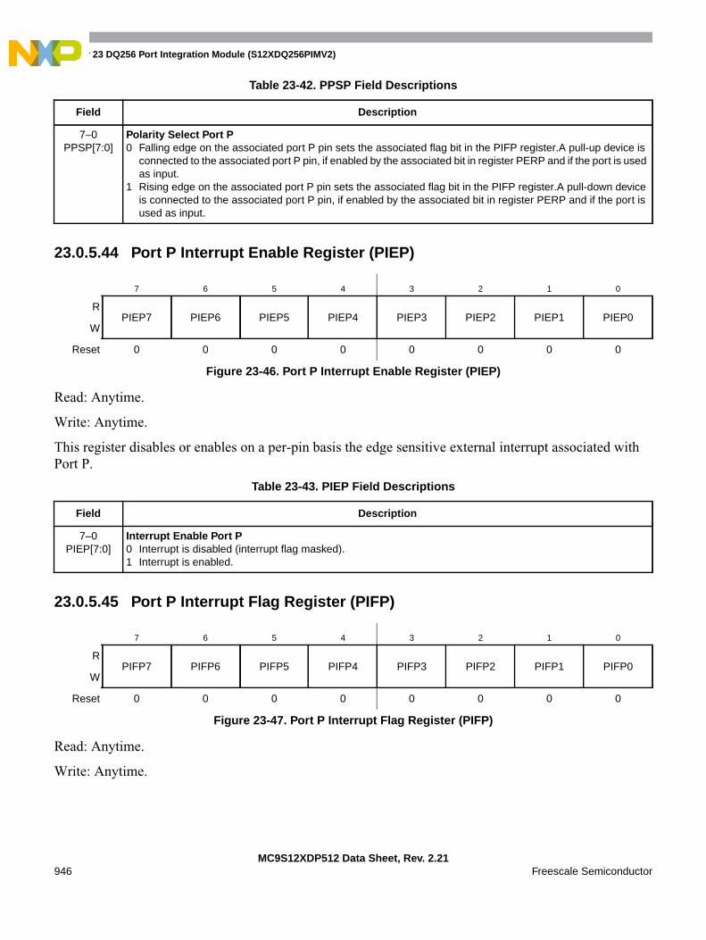
Chapter 23 DQ256 Port Integration Module (S12XDQ256PIMV2)
MC9S12XDP512 Data Sheet, Rev. 2.21946 Freescale Semiconductor
23.0.5.44 Port P Interrupt Enable Register (PIEP)
Read: Anytime.
Write: Anytime.
This register disables or enables on a per-pin basis the edge sensitive external interrupt associated withPort P.
23.0.5.45 Port P Interrupt Flag Register (PIFP)
Read: Anytime.
Write: Anytime.
Table 23-42. PPSP Field Descriptions
Field Description
7–0PPSP[7:0]
Polarity Select Port P0 Falling edge on the associated port P pin sets the associated flag bit in the PIFP register.A pull-up device is
connected to the associated port P pin, if enabled by the associated bit in register PERP and if the port is usedas input.
1 Rising edge on the associated port P pin sets the associated flag bit in the PIFP register.A pull-down deviceis connected to the associated port P pin, if enabled by the associated bit in register PERP and if the port isused as input.
7 6 5 4 3 2 1 0
RPIEP7 PIEP6 PIEP5 PIEP4 PIEP3 PIEP2 PIEP1 PIEP0
W
Reset 0 0 0 0 0 0 0 0
Figure 23-46. Port P Interrupt Enable Register (PIEP)
Table 23-43. PIEP Field Descriptions
Field Description
7–0PIEP[7:0]
Interrupt Enable Port P0 Interrupt is disabled (interrupt flag masked).1 Interrupt is enabled.
7 6 5 4 3 2 1 0
RPIFP7 PIFP6 PIFP5 PIFP4 PIFP3 PIFP2 PIFP1 PIFP0
W
Reset 0 0 0 0 0 0 0 0
Figure 23-47. Port P Interrupt Flag Register (PIFP)
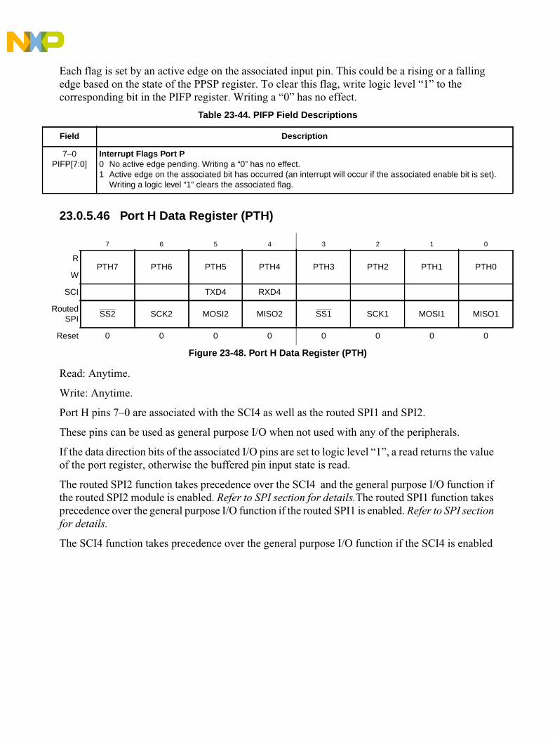
Each flag is set by an active edge on the associated input pin. This could be a rising or a fallingedge based on the state of the PPSP register. To clear this flag, write logic level “1” to thecorresponding bit in the PIFP register. Writing a “0” has no effect.
23.0.5.46 Port H Data Register (PTH)
Read: Anytime.
Write: Anytime.
Port H pins 7–0 are associated with the SCI4 as well as the routed SPI1 and SPI2.
These pins can be used as general purpose I/O when not used with any of the peripherals.
If the data direction bits of the associated I/O pins are set to logic level “1”, a read returns the valueof the port register, otherwise the buffered pin input state is read.
The routed SPI2 function takes precedence over the SCI4 and the general purpose I/O function ifthe routed SPI2 module is enabled. Refer to SPI section for details.The routed SPI1 function takesprecedence over the general purpose I/O function if the routed SPI1 is enabled. Refer to SPI sectionfor details.
The SCI4 function takes precedence over the general purpose I/O function if the SCI4 is enabled
Table 23-44. PIFP Field Descriptions
Field Description
7–0PIFP[7:0]
Interrupt Flags Port P0 No active edge pending. Writing a “0” has no effect.1 Active edge on the associated bit has occurred (an interrupt will occur if the associated enable bit is set).
Writing a logic level “1” clears the associated flag.
7 6 5 4 3 2 1 0
RPTH7 PTH6 PTH5 PTH4 PTH3 PTH2 PTH1 PTH0
W
SCI TXD4 RXD4
RoutedSPI
SS2 SCK2 MOSI2 MISO2 SS1 SCK1 MOSI1 MISO1
Reset 0 0 0 0 0 0 0 0
Figure 23-48. Port H Data Register (PTH)
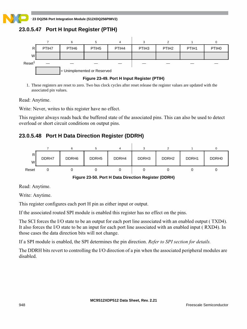
Chapter 23 DQ256 Port Integration Module (S12XDQ256PIMV2)
MC9S12XDP512 Data Sheet, Rev. 2.21948 Freescale Semiconductor
23.0.5.47 Port H Input Register (PTIH)
Read: Anytime.
Write: Never, writes to this register have no effect.
This register always reads back the buffered state of the associated pins. This can also be used to detectoverload or short circuit conditions on output pins.
23.0.5.48 Port H Data Direction Register (DDRH)
Read: Anytime.
Write: Anytime.
This register configures each port H pin as either input or output.
If the associated routed SPI module is enabled this register has no effect on the pins.
The SCI forces the I/O state to be an output for each port line associated with an enabled output ( TXD4).It also forces the I/O state to be an input for each port line associated with an enabled input ( RXD4). Inthose cases the data direction bits will not change.
If a SPI module is enabled, the SPI determines the pin direction. Refer to SPI section for details.
The DDRH bits revert to controlling the I/O direction of a pin when the associated peripheral modules aredisabled.
7 6 5 4 3 2 1 0
R PTIH7 PTIH6 PTIH5 PTIH4 PTIH3 PTIH2 PTIH1 PTIH0
W
Reset1
1. These registers are reset to zero. Two bus clock cycles after reset release the register values are updated with theassociated pin values.
— — — — — — — —
= Unimplemented or Reserved
Figure 23-49. Port H Input Register (PTIH)
7 6 5 4 3 2 1 0
RDDRH7 DDRH6 DDRH5 DDRH4 DDRH3 DDRH2 DDRH1 DDRH0
W
Reset 0 0 0 0 0 0 0 0
Figure 23-50. Port H Data Direction Register (DDRH)

23.0.5.49 Port H Reduced Drive Register (RDRH)
Read: Anytime.
Write: Anytime.
This register configures the drive strength of each Port H output pin as either full or reduced. If theport is used as input this bit is ignored.
23.0.5.50 Port H Pull Device Enable Register (PERH)
Read: Anytime.
Write: Anytime.
This register configures whether a pull-up or a pull-down device is activated, if the port is used asinput. This bit has no effect if the port is used as output. Out of reset no pull device is enabled.
Table 23-45. DDRH Field Descriptions
Field Description
7–0DDRH[7:0]
Data Direction Port H0 Associated pin is configured as input.1 Associated pin is configured as output.Note: Due to internal synchronization circuits, it can take up to 2 bus clock cycles until the correct value is read
on PTH or PTIH registers, when changing the DDRH register.
7 6 5 4 3 2 1 0
RRDRH7 RDRH6 RDRH5 RDRH4 RDRH3 RDRH2 RDRH1 RDRH0
W
Reset 0 0 0 0 0 0 0 0
Figure 23-51. Port H Reduced Drive Register (RDRH)
Table 23-46. RDRH Field Descriptions
Field Description
7–0RDRH[7:0]
Reduced Drive Port H0 Full drive strength at output.1 Associated pin drives at about 1/6 of the full drive strength.
7 6 5 4 3 2 1 0
RPERH7 PERH6 PERH5 PERH4 PERH3 PERH2 PERH1 PERH0
W
Reset 0 0 0 0 0 0 0 0
Figure 23-52. Port H Pull Device Enable Register (PERH)
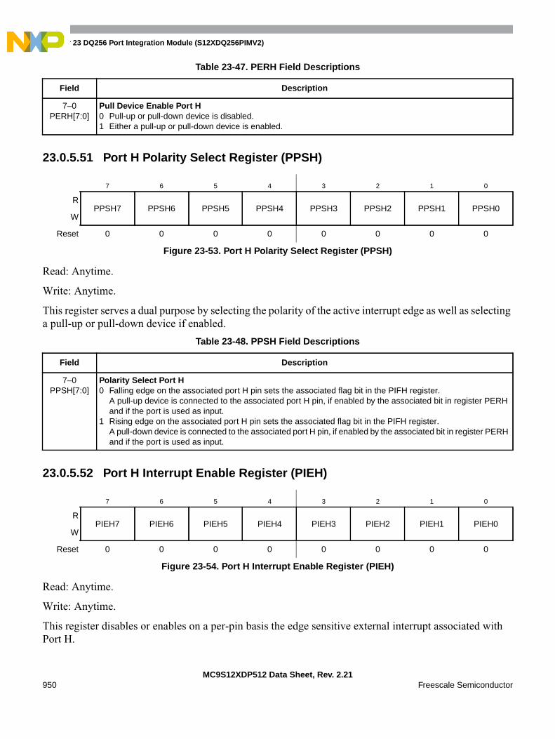
Chapter 23 DQ256 Port Integration Module (S12XDQ256PIMV2)
MC9S12XDP512 Data Sheet, Rev. 2.21950 Freescale Semiconductor
23.0.5.51 Port H Polarity Select Register (PPSH)
Read: Anytime.
Write: Anytime.
This register serves a dual purpose by selecting the polarity of the active interrupt edge as well as selectinga pull-up or pull-down device if enabled.
23.0.5.52 Port H Interrupt Enable Register (PIEH)
Read: Anytime.
Write: Anytime.
This register disables or enables on a per-pin basis the edge sensitive external interrupt associated withPort H.
Table 23-47. PERH Field Descriptions
Field Description
7–0PERH[7:0]
Pull Device Enable Port H0 Pull-up or pull-down device is disabled.1 Either a pull-up or pull-down device is enabled.
7 6 5 4 3 2 1 0
RPPSH7 PPSH6 PPSH5 PPSH4 PPSH3 PPSH2 PPSH1 PPSH0
W
Reset 0 0 0 0 0 0 0 0
Figure 23-53. Port H Polarity Select Register (PPSH)
Table 23-48. PPSH Field Descriptions
Field Description
7–0PPSH[7:0]
Polarity Select Port H0 Falling edge on the associated port H pin sets the associated flag bit in the PIFH register.
A pull-up device is connected to the associated port H pin, if enabled by the associated bit in register PERHand if the port is used as input.
1 Rising edge on the associated port H pin sets the associated flag bit in the PIFH register.A pull-down device is connected to the associated port H pin, if enabled by the associated bit in register PERHand if the port is used as input.
7 6 5 4 3 2 1 0
RPIEH7 PIEH6 PIEH5 PIEH4 PIEH3 PIEH2 PIEH1 PIEH0
W
Reset 0 0 0 0 0 0 0 0
Figure 23-54. Port H Interrupt Enable Register (PIEH)

23.0.5.53 Port H Interrupt Flag Register (PIFH)
Read: Anytime.
Write: Anytime.
Each flag is set by an active edge on the associated input pin. This could be a rising or a fallingedge based on the state of the PPSH register. To clear this flag, write logic level “1” to thecorresponding bit in the PIFH register. Writing a “0” has no effect.
Table 23-49. PIEH Field Descriptions
Field Description
7–0PIEH[7:0]
Interrupt Enable Port H0 Interrupt is disabled (interrupt flag masked).1 Interrupt is enabled.
7 6 5 4 3 2 1 0
RPIFH7 PIFH6 PIFH5 PIFH4 PIFH3 PIFH2 PIFH1 PIFH0
W
Reset 0 0 0 0 0 0 0 0
Figure 23-55. Port H Interrupt Flag Register (PIFH)
Table 23-50. PIFH Field Descriptions
Field Description
7–0PIFH[7:0]
Interrupt Flags Port H0 No active edge pending. Writing a “0” has no effect.1 Active edge on the associated bit has occurred (an interrupt will occur if the associated enable bit is set).
Writing a logic level “1” clears the associated flag.
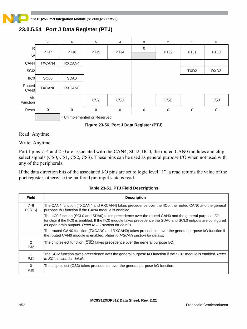
Chapter 23 DQ256 Port Integration Module (S12XDQ256PIMV2)
MC9S12XDP512 Data Sheet, Rev. 2.21952 Freescale Semiconductor
23.0.5.54 Port J Data Register (PTJ)
Read: Anytime.
Write: Anytime.
Port J pins 7–4 and 2–0 are associated with the CAN4, SCI2, IIC0, the routed CAN0 modules and chipselect signals (CS0, CS1, CS2, CS3). These pins can be used as general purpose I/O when not used withany of the peripherals.
If the data direction bits of the associated I/O pins are set to logic level “1”, a read returns the value of theport register, otherwise the buffered pin input state is read.
7 6 5 4 3 2 1 0
RPTJ7 PTJ6 PTJ5 PTJ4
0PTJ2 PTJ1 PTJ0
W
CAN4 TXCAN4 RXCAN4
SCI2 TXD2 RXD2
IIC0 SCL0 SDA0
RoutedCAN0
TXCAN0 RXCAN0
Alt.Function
CS2 CS0 CS1 CS3
Reset 0 0 0 0 0 0 0 0
= Unimplemented or Reserved
Figure 23-56. Port J Data Register (PTJ)
Table 23-51. PTJ Field Descriptions
Field Description
7–6PJ[7:6]
The CAN4 function (TXCAN4 and RXCAN4) takes precedence over the IIC0, the routed CAN0 and the generalpurpose I/O function if the CAN4 module is enabled.
The IIC0 function (SCL0 and SDA0) takes precedence over the routed CAN0 and the general purpose I/Ofunction if the IIC0 is enabled. If the IIC0 module takes precedence the SDA0 and SCL0 outputs are configuredas open drain outputs. Refer to IIC section for details.
The routed CAN0 function (TXCAN0 and RXCAN0) takes precedence over the general purpose I/O function ifthe routed CAN0 module is enabled. Refer to MSCAN section for details.
2PJ2
The chip select function (CS1) takes precedence over the general purpose I/O.
1PJ1
The SCI2 function takes precedence over the general purpose I/O function if the SCI2 module is enabled. Referto SCI section for details.
0PJ0
The chip select (CS3) takes precedence over the general purpose I/O function.
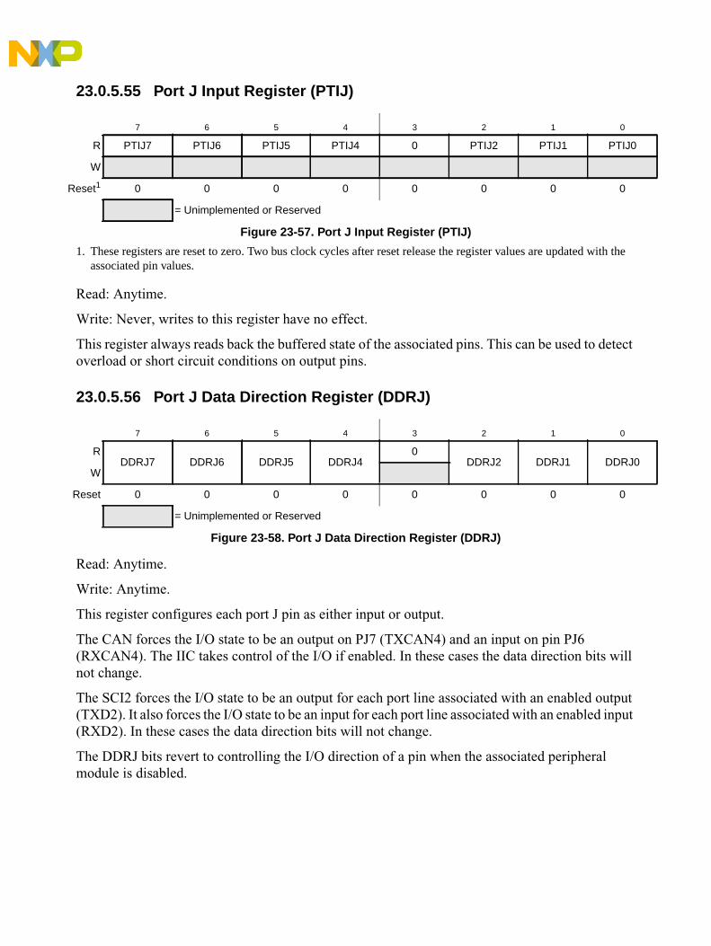
23.0.5.55 Port J Input Register (PTIJ)
Read: Anytime.
Write: Never, writes to this register have no effect.
This register always reads back the buffered state of the associated pins. This can be used to detectoverload or short circuit conditions on output pins.
23.0.5.56 Port J Data Direction Register (DDRJ)
Read: Anytime.
Write: Anytime.
This register configures each port J pin as either input or output.
The CAN forces the I/O state to be an output on PJ7 (TXCAN4) and an input on pin PJ6(RXCAN4). The IIC takes control of the I/O if enabled. In these cases the data direction bits willnot change.
The SCI2 forces the I/O state to be an output for each port line associated with an enabled output(TXD2). It also forces the I/O state to be an input for each port line associated with an enabled input(RXD2). In these cases the data direction bits will not change.
The DDRJ bits revert to controlling the I/O direction of a pin when the associated peripheralmodule is disabled.
7 6 5 4 3 2 1 0
R PTIJ7 PTIJ6 PTIJ5 PTIJ4 0 PTIJ2 PTIJ1 PTIJ0
W
Reset1
1. These registers are reset to zero. Two bus clock cycles after reset release the register values are updated with theassociated pin values.
0 0 0 0 0 0 0 0
= Unimplemented or Reserved
Figure 23-57. Port J Input Register (PTIJ)
7 6 5 4 3 2 1 0
RDDRJ7 DDRJ6 DDRJ5 DDRJ4
0DDRJ2 DDRJ1 DDRJ0
W
Reset 0 0 0 0 0 0 0 0
= Unimplemented or Reserved
Figure 23-58. Port J Data Direction Register (DDRJ)
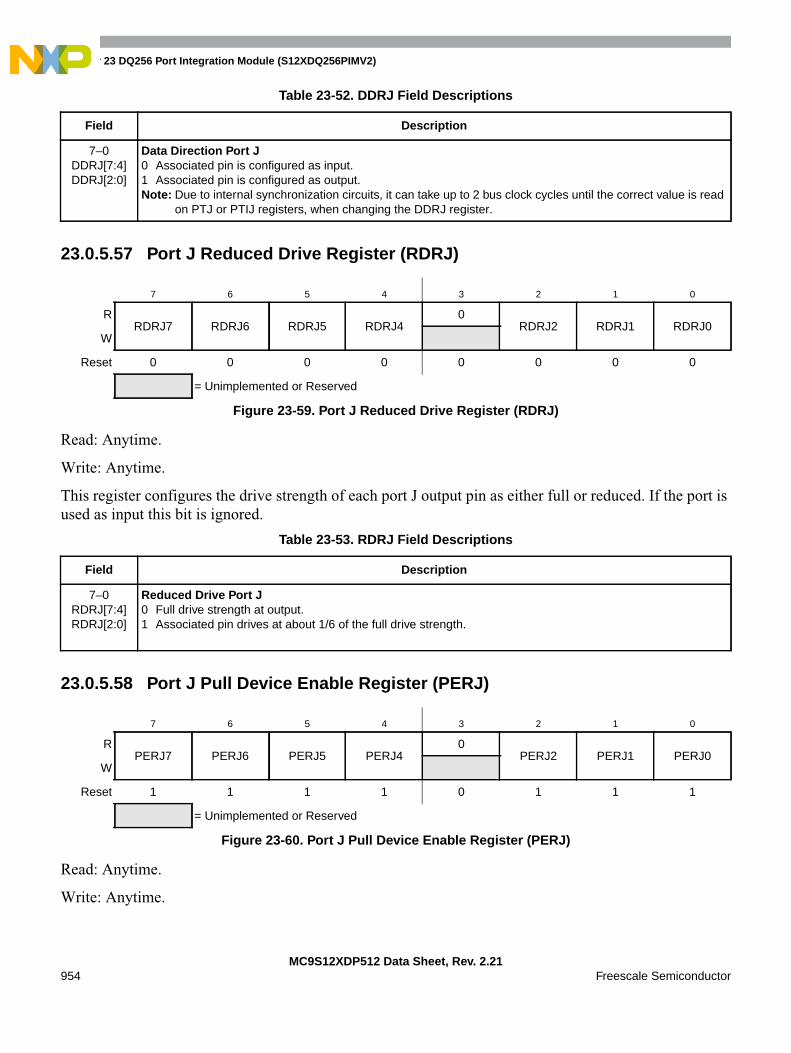
Chapter 23 DQ256 Port Integration Module (S12XDQ256PIMV2)
MC9S12XDP512 Data Sheet, Rev. 2.21954 Freescale Semiconductor
23.0.5.57 Port J Reduced Drive Register (RDRJ)
Read: Anytime.
Write: Anytime.
This register configures the drive strength of each port J output pin as either full or reduced. If the port isused as input this bit is ignored.
23.0.5.58 Port J Pull Device Enable Register (PERJ)
Read: Anytime.
Write: Anytime.
Table 23-52. DDRJ Field Descriptions
Field Description
7–0DDRJ[7:4]DDRJ[2:0]
Data Direction Port J0 Associated pin is configured as input.1 Associated pin is configured as output.Note: Due to internal synchronization circuits, it can take up to 2 bus clock cycles until the correct value is read
on PTJ or PTIJ registers, when changing the DDRJ register.
7 6 5 4 3 2 1 0
RRDRJ7 RDRJ6 RDRJ5 RDRJ4
0RDRJ2 RDRJ1 RDRJ0
W
Reset 0 0 0 0 0 0 0 0
= Unimplemented or Reserved
Figure 23-59. Port J Reduced Drive Register (RDRJ)
Table 23-53. RDRJ Field Descriptions
Field Description
7–0RDRJ[7:4]RDRJ[2:0]
Reduced Drive Port J0 Full drive strength at output.1 Associated pin drives at about 1/6 of the full drive strength.
7 6 5 4 3 2 1 0
RPERJ7 PERJ6 PERJ5 PERJ4
0PERJ2 PERJ1 PERJ0
W
Reset 1 1 1 1 0 1 1 1
= Unimplemented or Reserved
Figure 23-60. Port J Pull Device Enable Register (PERJ)
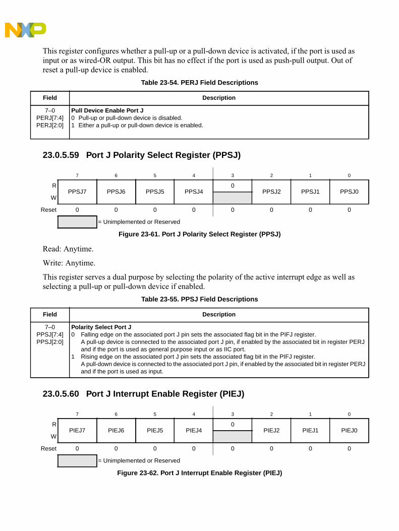
This register configures whether a pull-up or a pull-down device is activated, if the port is used asinput or as wired-OR output. This bit has no effect if the port is used as push-pull output. Out ofreset a pull-up device is enabled.
23.0.5.59 Port J Polarity Select Register (PPSJ)
Read: Anytime.
Write: Anytime.
This register serves a dual purpose by selecting the polarity of the active interrupt edge as well asselecting a pull-up or pull-down device if enabled.
23.0.5.60 Port J Interrupt Enable Register (PIEJ)
Table 23-54. PERJ Field Descriptions
Field Description
7–0PERJ[7:4]PERJ[2:0]
Pull Device Enable Port J0 Pull-up or pull-down device is disabled.1 Either a pull-up or pull-down device is enabled.
7 6 5 4 3 2 1 0
RPPSJ7 PPSJ6 PPSJ5 PPSJ4
0PPSJ2 PPSJ1 PPSJ0
W
Reset 0 0 0 0 0 0 0 0
= Unimplemented or Reserved
Figure 23-61. Port J Polarity Select Register (PPSJ)
Table 23-55. PPSJ Field Descriptions
Field Description
7–0PPSJ[7:4]PPSJ[2:0]
Polarity Select Port J0 Falling edge on the associated port J pin sets the associated flag bit in the PIFJ register.
A pull-up device is connected to the associated port J pin, if enabled by the associated bit in register PERJand if the port is used as general purpose input or as IIC port.
1 Rising edge on the associated port J pin sets the associated flag bit in the PIFJ register.A pull-down device is connected to the associated port J pin, if enabled by the associated bit in register PERJand if the port is used as input.
7 6 5 4 3 2 1 0
RPIEJ7 PIEJ6 PIEJ5 PIEJ4
0PIEJ2 PIEJ1 PIEJ0
W
Reset 0 0 0 0 0 0 0 0
= Unimplemented or Reserved
Figure 23-62. Port J Interrupt Enable Register (PIEJ)

Chapter 23 DQ256 Port Integration Module (S12XDQ256PIMV2)
MC9S12XDP512 Data Sheet, Rev. 2.21956 Freescale Semiconductor
This register disables or enables on a per-pin basis the edge sensitive external interrupt associated withPort J.
23.0.5.61 Port J Interrupt Flag Register (PIFJ)
Read: Anytime.
Write: Anytime.
Each flag is set by an active edge on the associated input pin. This could be a rising or a falling edge basedon the state of the PPSJ register. To clear this flag, write logic level “1” to the corresponding bit in the PIFJregister. Writing a “0” has no effect.
23.0.5.62 Port AD0 Data Register 1 (PT1AD0)
Read: Anytime.
Write: Anytime.
Table 23-56. PIEJ Field Descriptions
Field Description
7–0PIEJ[7:4]PIEJ[2:0]
Interrupt Enable Port J0 Interrupt is disabled (interrupt flag masked).1 Interrupt is enabled.
7 6 5 4 3 2 1 0
RPIFJ7 PIFJ6 PIFJ5 PIFJ4
0PIFJ2 PIFJ1 PIFJ0
W
Reset 0 0 0 0 0 0 0 0
= Unimplemented or Reserved
Figure 23-63. Port J Interrupt Flag Register (PIFJ)
Table 23-57. PIEJ Field Descriptions
Field Description
7–0PIFJ[7:4]PIFJ[2:0]
Interrupt Flags Port J0 No active edge pending. Writing a “0” has no effect.1 Active edge on the associated bit has occurred (an interrupt will occur if the associated enable bit is set).
Writing a logic level “1” clears the associated flag.
7 6 5 4 3 2 1 0
RPT1AD07 PT1AD06 PT1AD05 PT1AD04 PT1AD03 PT1AD02 PT1AD01 PT1AD00
W
Reset 0 0 0 0 0 0 0 0
Figure 23-64. Port AD0 Data Register 1 (PT1AD0)
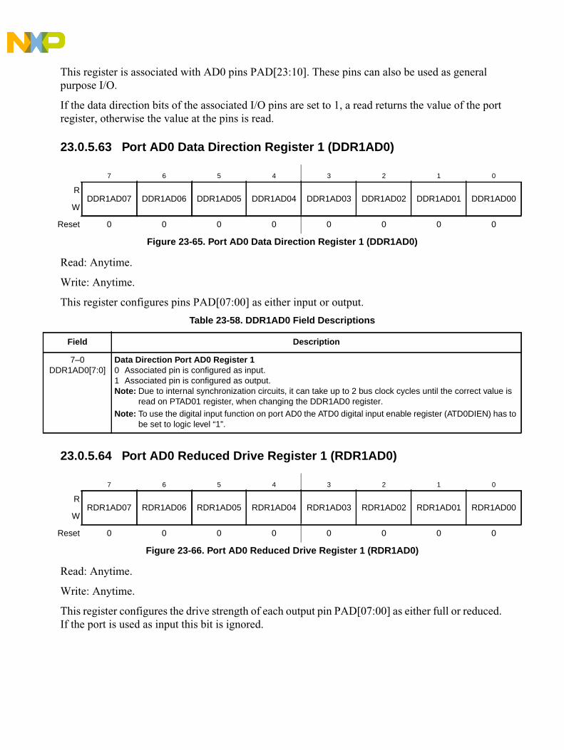
This register is associated with AD0 pins PAD[23:10]. These pins can also be used as generalpurpose I/O.
If the data direction bits of the associated I/O pins are set to 1, a read returns the value of the portregister, otherwise the value at the pins is read.
23.0.5.63 Port AD0 Data Direction Register 1 (DDR1AD0)
Read: Anytime.
Write: Anytime.
This register configures pins PAD[07:00] as either input or output.
23.0.5.64 Port AD0 Reduced Drive Register 1 (RDR1AD0)
Read: Anytime.
Write: Anytime.
This register configures the drive strength of each output pin PAD[07:00] as either full or reduced.If the port is used as input this bit is ignored.
7 6 5 4 3 2 1 0
RDDR1AD07 DDR1AD06 DDR1AD05 DDR1AD04 DDR1AD03 DDR1AD02 DDR1AD01 DDR1AD00
W
Reset 0 0 0 0 0 0 0 0
Figure 23-65. Port AD0 Data Direction Register 1 (DDR1AD0)
Table 23-58. DDR1AD0 Field Descriptions
Field Description
7–0DDR1AD0[7:0]
Data Direction Port AD0 Register 10 Associated pin is configured as input.1 Associated pin is configured as output.Note: Due to internal synchronization circuits, it can take up to 2 bus clock cycles until the correct value is
read on PTAD01 register, when changing the DDR1AD0 register.Note: To use the digital input function on port AD0 the ATD0 digital input enable register (ATD0DIEN) has to
be set to logic level “1”.
7 6 5 4 3 2 1 0
RRDR1AD07 RDR1AD06 RDR1AD05 RDR1AD04 RDR1AD03 RDR1AD02 RDR1AD01 RDR1AD00
W
Reset 0 0 0 0 0 0 0 0
Figure 23-66. Port AD0 Reduced Drive Register 1 (RDR1AD0)
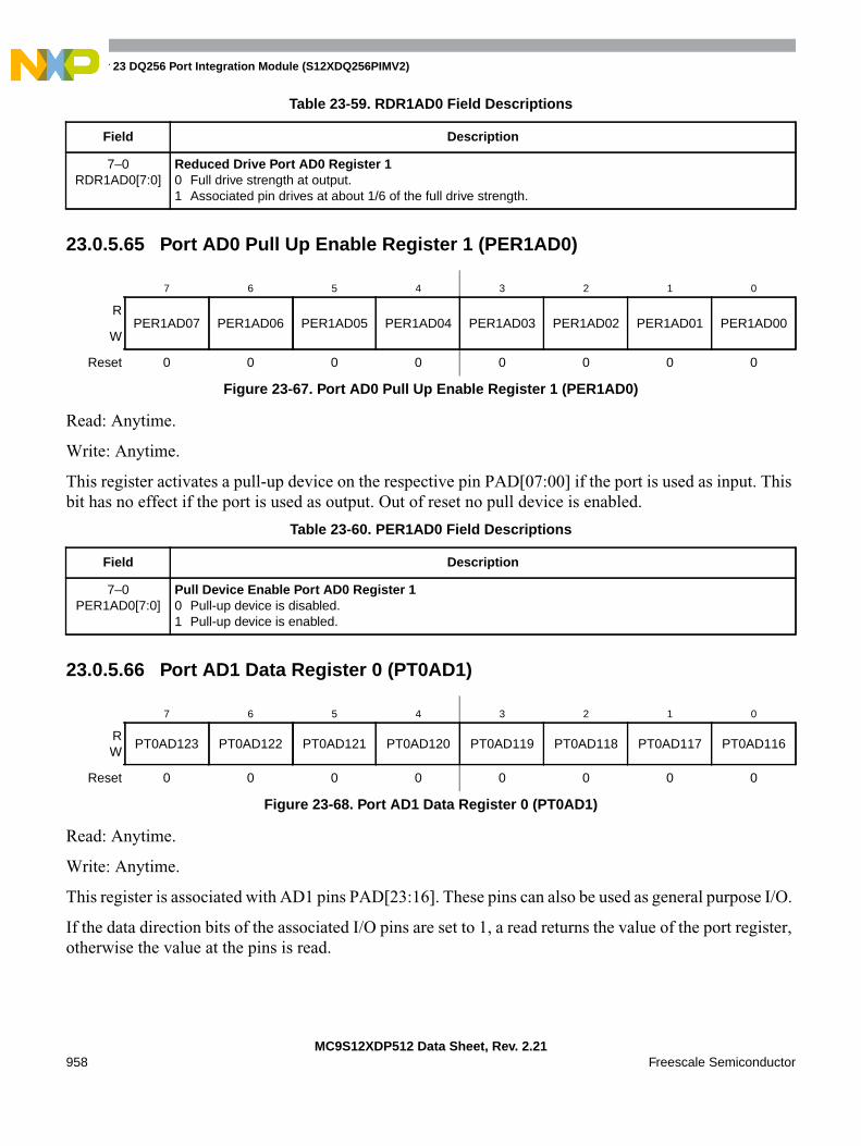
Chapter 23 DQ256 Port Integration Module (S12XDQ256PIMV2)
MC9S12XDP512 Data Sheet, Rev. 2.21958 Freescale Semiconductor
23.0.5.65 Port AD0 Pull Up Enable Register 1 (PER1AD0)
Read: Anytime.
Write: Anytime.
This register activates a pull-up device on the respective pin PAD[07:00] if the port is used as input. Thisbit has no effect if the port is used as output. Out of reset no pull device is enabled.
23.0.5.66 Port AD1 Data Register 0 (PT0AD1)
Read: Anytime.
Write: Anytime.
This register is associated with AD1 pins PAD[23:16]. These pins can also be used as general purpose I/O.
If the data direction bits of the associated I/O pins are set to 1, a read returns the value of the port register,otherwise the value at the pins is read.
Table 23-59. RDR1AD0 Field Descriptions
Field Description
7–0RDR1AD0[7:0]
Reduced Drive Port AD0 Register 10 Full drive strength at output.1 Associated pin drives at about 1/6 of the full drive strength.
7 6 5 4 3 2 1 0
RPER1AD07 PER1AD06 PER1AD05 PER1AD04 PER1AD03 PER1AD02 PER1AD01 PER1AD00
W
Reset 0 0 0 0 0 0 0 0
Figure 23-67. Port AD0 Pull Up Enable Register 1 (PER1AD0)
Table 23-60. PER1AD0 Field Descriptions
Field Description
7–0PER1AD0[7:0]
Pull Device Enable Port AD0 Register 10 Pull-up device is disabled.1 Pull-up device is enabled.
7 6 5 4 3 2 1 0
RW
PT0AD123 PT0AD122 PT0AD121 PT0AD120 PT0AD119 PT0AD118 PT0AD117 PT0AD116
Reset 0 0 0 0 0 0 0 0
Figure 23-68. Port AD1 Data Register 0 (PT0AD1)
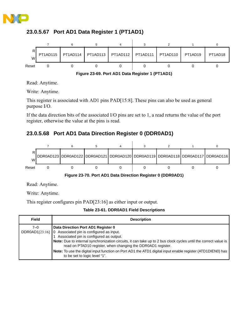
23.0.5.67 Port AD1 Data Register 1 (PT1AD1)
Read: Anytime.
Write: Anytime.
This register is associated with AD1 pins PAD[15:8]. These pins can also be used as generalpurpose I/O.
If the data direction bits of the associated I/O pins are set to 1, a read returns the value of the portregister, otherwise the value at the pins is read.
23.0.5.68 Port AD1 Data Direction Register 0 (DDR0AD1)
Read: Anytime.
Write: Anytime.
This register configures pin PAD[23:16] as either input or output.
7 6 5 4 3 2 1 0
RPT1AD115 PT1AD114 PT1AD113 PT1AD112 PT1AD111 PT1AD110 PT1AD19 PT1AD18
W
Reset 0 0 0 0 0 0 0 0
Figure 23-69. Port AD1 Data Register 1 (PT1AD1)
7 6 5 4 3 2 1 0
RDDR0AD123 DDR0AD122 DDR0AD121 DDR0AD120 DDR0AD119 DDR0AD118 DDR0AD117 DDR0AD116
W
Reset 0 0 0 0 0 0 0 0
Figure 23-70. Port AD1 Data Direction Register 0 (DDR0AD1)
Table 23-61. DDR0AD1 Field Descriptions
Field Description
7–0DDR0AD1[23:16]
Data Direction Port AD1 Register 00 Associated pin is configured as input.1 Associated pin is configured as output.Note: Due to internal synchronization circuits, it can take up to 2 bus clock cycles until the correct value is
read on PTAD10 register, when changing the DDR0AD1 register.Note: To use the digital input function on Port AD1 the ATD1 digital input enable register (ATD1DIEN0) has
to be set to logic level “1”.
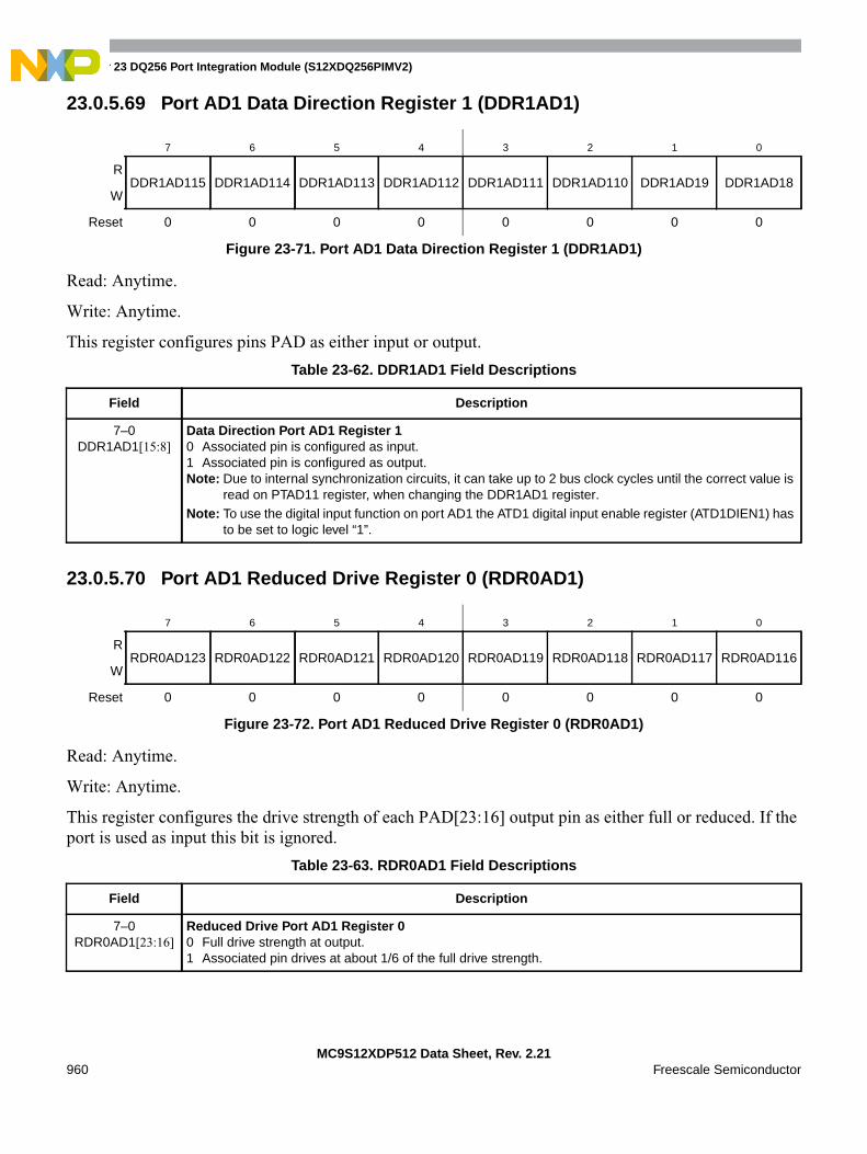
Chapter 23 DQ256 Port Integration Module (S12XDQ256PIMV2)
MC9S12XDP512 Data Sheet, Rev. 2.21960 Freescale Semiconductor
23.0.5.69 Port AD1 Data Direction Register 1 (DDR1AD1)
Read: Anytime.
Write: Anytime.
This register configures pins PAD as either input or output.
23.0.5.70 Port AD1 Reduced Drive Register 0 (RDR0AD1)
Read: Anytime.
Write: Anytime.
This register configures the drive strength of each PAD[23:16] output pin as either full or reduced. If theport is used as input this bit is ignored.
7 6 5 4 3 2 1 0
RDDR1AD115 DDR1AD114 DDR1AD113 DDR1AD112 DDR1AD111 DDR1AD110 DDR1AD19 DDR1AD18
W
Reset 0 0 0 0 0 0 0 0
Figure 23-71. Port AD1 Data Direction Register 1 (DDR1AD1)
Table 23-62. DDR1AD1 Field Descriptions
Field Description
7–0DDR1AD1[15:8]
Data Direction Port AD1 Register 10 Associated pin is configured as input.1 Associated pin is configured as output.Note: Due to internal synchronization circuits, it can take up to 2 bus clock cycles until the correct value is
read on PTAD11 register, when changing the DDR1AD1 register.Note: To use the digital input function on port AD1 the ATD1 digital input enable register (ATD1DIEN1) has
to be set to logic level “1”.
7 6 5 4 3 2 1 0
RRDR0AD123 RDR0AD122 RDR0AD121 RDR0AD120 RDR0AD119 RDR0AD118 RDR0AD117 RDR0AD116
W
Reset 0 0 0 0 0 0 0 0
Figure 23-72. Port AD1 Reduced Drive Register 0 (RDR0AD1)
Table 23-63. RDR0AD1 Field Descriptions
Field Description
7–0RDR0AD1[23:16]
Reduced Drive Port AD1 Register 00 Full drive strength at output.1 Associated pin drives at about 1/6 of the full drive strength.

23.0.5.71 Port AD1 Reduced Drive Register 1 (RDR1AD1)
Read: Anytime.
Write: Anytime.
This register configures the drive strength of each PAD[15:8] output pin as either full or reduced.If the port is used as input this bit is ignored.
23.0.5.72 Port AD1 Pull Up Enable Register 0 (PER0AD1)
Read: Anytime.
Write: Anytime.
This register activates a pull-up device on the respective PAD[23:16] pin if the port is used as input.This bit has no effect if the port is used as output. Out of reset no pull-up device is enabled.
7 6 5 4 3 2 1 0
RRDR1AD115 RDR1AD114 RDR1AD113 RDR1AD112 RDR1AD111 RDR1AD110 RDR1AD19 RDR1AD18
W
Reset 0 0 0 0 0 0 0 0
Figure 23-73. Port AD1 Reduced Drive Register 1 (RDR1AD1)
Table 23-64. RDR1AD1 Field Descriptions
Field Description
7–0RDR1AD1[15:8]
Reduced Drive Port AD1 Register 10 Full drive strength at output.1 Associated pin drives at about 1/6 of the full drive strength.
7 6 5 4 3 2 1 0
RPER0AD123 PER0AD122 PER0AD121 PER0AD120 PER0AD119 PER0AD118 PER0AD117 PER0AD116
W
Reset 0 0 0 0 0 0 0 0
Figure 23-74. Port AD1 Pull Up Enable Register 0 (PER0AD1)
Table 23-65. PER0AD1 Field Descriptions
Field Description
7–0PER0AD1[23:16]
Pull Device Enable Port AD1 Register 00 Pull-up device is disabled.1 Pull-up device is enabled.
Chapter 23 DQ256 Port Integration Module (S12XDQ256PIMV2)
MC9S12XDP512 Data Sheet, Rev. 2.21962 Freescale Semiconductor
23.0.5.73 Port AD1 Pull Up Enable Register 1 (PER1AD1)
Read: Anytime.
Write: Anytime.
This register activates a pull-up device on the respective PAD[15:8] pin if the port is used as input. Thisbit has no effect if the port is used as output. Out of reset no pull-up device is enabled.
Functional Description
Each pin except PE0, PE1, and BKGD can act as general purpose I/O. In addition each pin can act as anoutput from the external bus interface module or a peripheral module or an input to the external businterface module or a peripheral module.
A set of configuration registers is common to all ports with exceptions in the expanded bus interface andATD ports (Table 23-67). All registers can be written at any time; however a specific configuration mightnot become active.
Example: Selecting a pull-up device
This device does not become active while the port is used as a push-pull output.
7 6 5 4 3 2 1 0
RPER1AD115 PER1AD114 PER1AD113 PER1AD112 PER1AD111 PER1AD110 PER1AD19 PER1AD18
W
Reset 0 0 0 0 0 0 0 0
Figure 23-75. Port AD1 Pull Up Enable Register 1 (PER1AD1)
Table 23-66. PER1AD1 Field Descriptions
Field Description
7–0PER1AD1[15:8]
Pull Device Enable Port AD1 Register 10 Pull-up device is disabled.1 Pull-up device is enabled.
Table 23-67. Register Availability per Port1
Port DataData
Direction Input
ReducedDrive
PullEnable
PolaritySelect
Wired-ORMode
InterruptEnable
InterruptFlag
A yes yes — yes yes — — — —
B yes yes — — — — —
C yes yes — — — — —
D yes yes — — — — —
E yes yes — — — — —
K yes yes — — — — —
T yes yes yes yes yes — — — —
S yes yes yes yes yes yes yes — —
M yes yes yes yes yes yes yes — —

23.0.6 Registers
23.0.6.1 Data Register
This register holds the value driven out to the pin if the pin is used as a general purpose I/O.
Writing to this register has only an effect on the pin if the pin is used as general purpose output.When reading this address, the buffered state of the pin is returned if the associated data directionregister bit is set to “0”.
If the data direction register bits are set to logic level “1”, the contents of the data register isreturned. This is independent of any other configuration (Figure 23-76).
23.0.6.2 Input Register
This is a read-only register and always returns the buffered state of the pin (Figure 23-76).
23.0.6.3 Data Direction Register
This register defines whether the pin is used as an input or an output.
If a peripheral module controls the pin the contents of the data direction register is ignored(Figure 23-76).
P yes yes yes yes yes yes — yes yes
H yes yes yes yes yes yes — yes yes
J yes yes yes yes yes yes — yes yes
AD0 yes yes — yes yes — — — —
AD1 yes yes — yes yes — — — —
1. Each cell represents one register with individual configuration bits
Table 23-67. Register Availability per Port1
Port DataData
Direction Input
ReducedDrive
PullEnable
PolaritySelect
Wired-ORMode
InterruptEnable
InterruptFlag
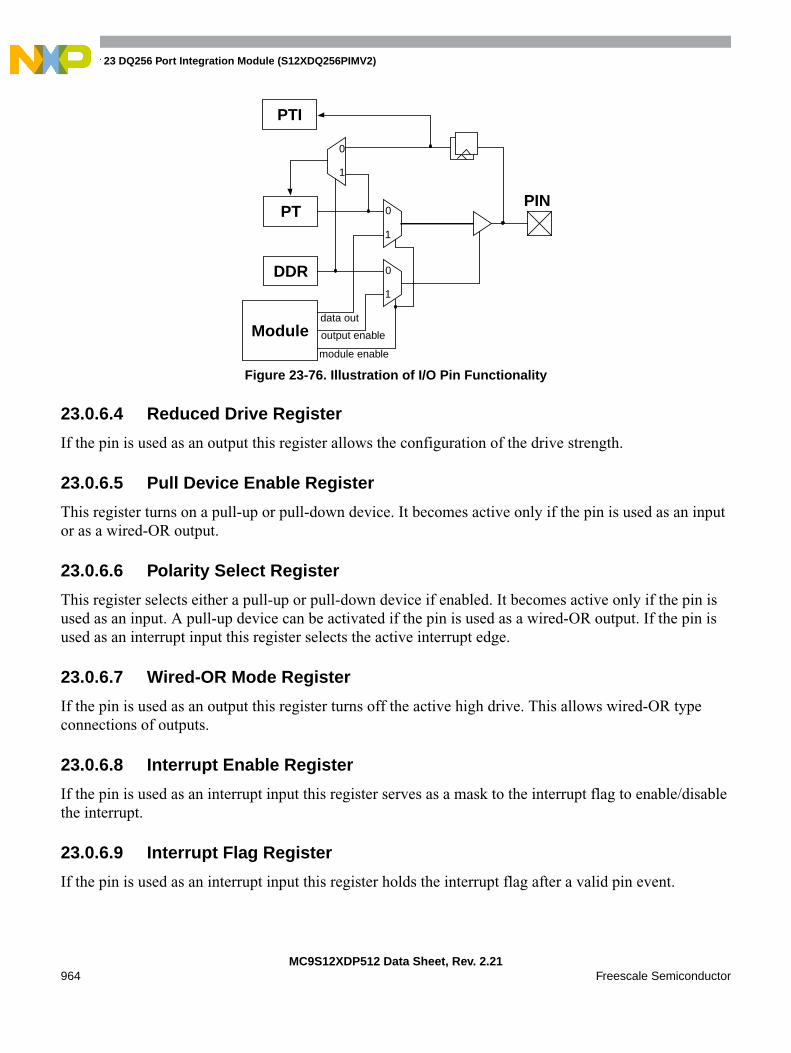
Chapter 23 DQ256 Port Integration Module (S12XDQ256PIMV2)
MC9S12XDP512 Data Sheet, Rev. 2.21964 Freescale Semiconductor
Figure 23-76. Illustration of I/O Pin Functionality
23.0.6.4 Reduced Drive Register
If the pin is used as an output this register allows the configuration of the drive strength.
23.0.6.5 Pull Device Enable Register
This register turns on a pull-up or pull-down device. It becomes active only if the pin is used as an inputor as a wired-OR output.
23.0.6.6 Polarity Select Register
This register selects either a pull-up or pull-down device if enabled. It becomes active only if the pin isused as an input. A pull-up device can be activated if the pin is used as a wired-OR output. If the pin isused as an interrupt input this register selects the active interrupt edge.
23.0.6.7 Wired-OR Mode Register
If the pin is used as an output this register turns off the active high drive. This allows wired-OR typeconnections of outputs.
23.0.6.8 Interrupt Enable Register
If the pin is used as an interrupt input this register serves as a mask to the interrupt flag to enable/disablethe interrupt.
23.0.6.9 Interrupt Flag Register
If the pin is used as an interrupt input this register holds the interrupt flag after a valid pin event.
PT
DDR
output enable
module enable
1
0
1
1
0
0
PIN
PTI
data outModule

23.0.6.10 Module Routing Register
This register supports the re-routing of the CAN0, CAN4, SPI0, SPI1, and SPI2 pins to alternativeports. This allows a software re-configuration of the pinouts of the different package options withrespect to above peripherals.
NOTEThe purpose of the module routing register is to provide maximumflexibility for derivatives with a lower number of MSCAN and SPImodules.
23.0.7 Ports
23.0.7.1 BKGD Pin
The BKGD pin is associated with the S12X_BDM and S12X_EBI modules. During reset, theBKGD pin is used as MODC input.
23.0.7.2 Port A and B
Port A pins PA[7:0] and Port B pins PB[7:0] can be used for either general-purpose I/O, or, in 144-pin packages, also with the external bus interface. In this case port A and port B are associated withthe external address bus outputs ADDR15–ADDR8 and ADDR7–ADDR0, respectively. PB0 is theADDR0 or UDS output.
23.0.7.3 Port C and D
Port C pins PC[7:0] and port D pins PD[7:0] can be used for either general-purpose I/O, or, in 144-pin packages, also with the external bus interface. In this case port C and port D are associated withthe external data bus inputs/outputs DATA15–DATA8 and DATA7–DATA0, respectively.
These pins are configured for reduced input threshold in certain operating modes (refer toS12X_EBI section).
NOTEPort C and D are neither available in 112-pin nor in 80-pin packages.
Table 23-68. Module Implementations on Derivatives
Numberof Modules
MSCAN Modules SPI Modules
CAN0 CAN1 CAN2 CAN3 CAN4 SPI0 SPI1 SPI2
5 yes yes yes yes yes — — —
4 yes yes yes — yes — — —
3 yes yes — — yes yes yes yes
2 yes — — — yes yes yes —
1 yes — — — — yes — —

Chapter 23 DQ256 Port Integration Module (S12XDQ256PIMV2)
MC9S12XDP512 Data Sheet, Rev. 2.21966 Freescale Semiconductor
23.0.7.4 Port E
Port E is associated with the external bus control outputs R/W, LSTRB, LDS and RE, the free-runningclock outputs ECLK and ECLK2X, as well as with the TAGHI, TAGLO, MODA and MODB andinterrupt inputs IRQ and XIRQ.
Port E pins PE[7:2] can be used for either general-purpose I/O or with the alternative functions.
Port E pin PE[7] an be used for either general-purpose I/O or as the free-running clock ECLKX2 outputrunning at the core clock rate. The clock output is always enabled in emulation modes.
Port E pin PE[4] an be used for either general-purpose I/O or as the free-running clock ECLK outputrunning at the bus clock rate or at the programmed divided clock rate. The clock output is always enabledin emulation modes.
Port E pin PE[1] can be used for either general-purpose input or as the level- or falling edge-sensitive IRQinterrupt input. IRQ will be enabled by setting the IRQEN configuration bit (Section 23.0.5.14, “IRQControl Register (IRQCR)”) and clearing the I-bit in the CPU’s condition code register. It is inhibited atreset so this pin is initially configured as a simple input with a pull-up.
Port E pin PE[0] can be used for either general-purpose input or as the level-sensitive XIRQ interruptinput. XIRQ can be enabled by clearing the X-bit in the CPU’s condition code register. It is inhibited atreset so this pin is initially configured as a high-impedance input with a pull-up.
Port E pins PE[5] and PE[6] are configured for reduced input threshold in certain modes (refer toS12X_EBI section).
23.0.7.5 Port K
Port K pins PK[7:0] can be used for either general-purpose I/O, or, in 144-pin packages, also with theexternal bus interface. In this case port K pins PK[6:0] are associated with the external address bus outputsADDR22–ADDR16 and PK7 is associated to the EWAIT input.
Port K pin PE[7] is configured for reduced input threshold in certain modes (refer to S12X_EBI section).
NOTEPort K is not available in 80-pin packages. PK[6] is not available in 112-pinpackages.
23.0.7.6 Port T
This port is associated with the ECT module. Port T pins PT[7:0] can be used for either general-purposeI/O, or with the channels of the enhanced capture timer.
23.0.7.7 Port S
This port is associated with SCI0, SCI1 and SPI0. Port S pins PS[7:0] can be used either for general-purpose I/O, or with the SCI and SPI subsystems.
The SPI0 pins can be re-routed. Refer to Section 23.0.5.37, “Module Routing Register (MODRR)”.
NOTEPS[7:4] are not available in 80-pin packages.
23.0.7.8 Port M
This port is associated with the CAN40 and SPI0. Port M pins PM[7:0] can be used for eithergeneral purpose I/O, or with the CAN, SCI and SPI subsystems.
The CAN0, CAN4 and SPI0 pins can be re-routed. Refer to Section 23.0.5.37, “Module RoutingRegister (MODRR)”.
NOTEPM[7:6] are not available in 80-pin packages.
23.0.7.9 Port P
This port is associated with the PWM, SPI1 and SPI2. Port P pins PP[7:0] can be used for eithergeneral purpose I/O, or with the PWM and SPI subsystems.
The pins are shared between the PWM channels and the SPI1 and SPI2. If the PWM is enabled thepins become PWM output channels with the exception of pin 7 which can be PWM input or output.If SPI1 or SPI2 are enabled and PWM is disabled, the respective pin configuration is determinedby status bits in the SPI.
The SPI1 and SPI2 pins can be re-routed. Refer to Section 23.0.5.37, “Module Routing Register(MODRR)”.
Port P offers 8 I/O pins with edge triggered interrupt capability in wired-OR fashion(Section 23.0.8, “Pin Interrupts”).
NOTEPP[6] is not available in 80-pin packages.
23.0.7.10 Port H
This port is associated with the SPI1, SPI2, SCI4. Port H pins PH[7:0] can be used for eithergeneral purpose I/O, or with the SPI and SCI subsystems. Port H pins can be used with the routedSPI1 and SPI2. Refer to Section 23.0.5.37, “Module Routing Register (MODRR)”.
Port H offers 8 I/O pins with edge triggered interrupt capability (Section 23.0.8, “Pin Interrupts”).
NOTEPort H is not available in 80-pin packages.
23.0.7.11 Port J
This port is associated with the chip selects CS0, CS1, CS2 and CS3 as well as with CAN4, CAN0,IIC1, IIC0, and SCI2. Port J pins PJ[7:4] and PJ[2:0] can be used for either general purpose I/O, orwith the CAN, IIC, or SCI subsystems. If IIC takes precedence the associated pins become IIC
Chapter 23 DQ256 Port Integration Module (S12XDQ256PIMV2)
MC9S12XDP512 Data Sheet, Rev. 2.21968 Freescale Semiconductor
open-drain output pins. The CAN4 pins can be re-routed. Refer to Section 23.0.5.37, “Module RoutingRegister (MODRR)”.
Port J pins can be used with the routed CAN0 modules. Refer to Section 23.0.5.37, “Module RoutingRegister (MODRR)”.
Port J offers 7 I/O pins with edge triggered interrupt capability (Section 23.0.8, “Pin Interrupts”).
NOTEPJ[5,4,2] are not available in 112-pin packages. PJ[5,4,2,1,0] are notavailable in 80-pin packages.
23.0.7.12 Port AD0
This port is associated with the ATD0. Port AD0 pins PAD07–PAD00 can be used for either generalpurpose I/O, or with the ATD0 subsystem.
23.0.7.13 Port AD1
This port is associated with the ATD1. Port AD1 pins PAD23–PAD8 can be used for either generalpurpose I/O, or with the ATD1 subsystem.
NOTEPAD[23:16] are not available in 112-pin packages. PAD[23:8] are notavailable in 80-pin packages.
23.0.8 Pin Interrupts
Ports P, H and J offer pin interrupt capability. The interrupt enable as well as the sensitivity to rising orfalling edges can be individually configured on per-pin basis. All bits/pins in a port share the sameinterrupt vector. Interrupts can be used with the pins configured as inputs or outputs.
An interrupt is generated when a bit in the port interrupt flag register and its corresponding port interruptenable bit are both set. The pin interrupt feature is also capable to wake up the CPU when it is in STOP orWAIT mode.
A digital filter on each pin prevents pulses (Figure 23-78) shorter than a specified time from generating aninterrupt. The minimum time varies over process conditions, temperature and voltage (Figure 23-77 andTable 23-69).

Figure 23-77. Interrupt Glitch Filter on Port P, H, and J (PPS = 0)
Figure 23-78. Pulse Illustration
A valid edge on an input is detected if 4 consecutive samples of a passive level are followed by4 consecutive samples of an active level directly or indirectly.
The filters are continuously clocked by the bus clock in run and wait mode. In stop mode, the clockis generated by an RC-oscillator in the port integration module. To maximize current saving theRC oscillator runs only if the following condition is true on any pin individually:
Sample count <= 4 and interrupt enabled (PIE = 1) and interrupt flag not set (PIF = 0).
23.0.9 Expanded Bus Pin Functions
All peripheral ports T, S, M, P, H, J, AD0, and AD1 start up as general purpose inputs after reset.
Depending on the external mode pin condition, the external bus interface related ports A, B, C, D,E, and K start up as general purpose inputs on reset or are configured for their alternate functions.
Table 23-69. Pulse Detection Criteria
PulseMode
STOP Unit STOP1
1. These values include the spread of the oscillator frequency overtemperature, voltage and process.
Ignored tpulse ≤ 3 Bus clocks tpulse ≤ tpign
Uncertain 3 < tpulse < 4 Bus clocks tpign < tpulse < tpval
Valid tpulse ≥ 4 Bus clocks tpulse ≥ tpval
Glitch, filtered out, no interrupt flag set
Valid pulse, interrupt flag set
tpign
tpval
uncertain
tpulse
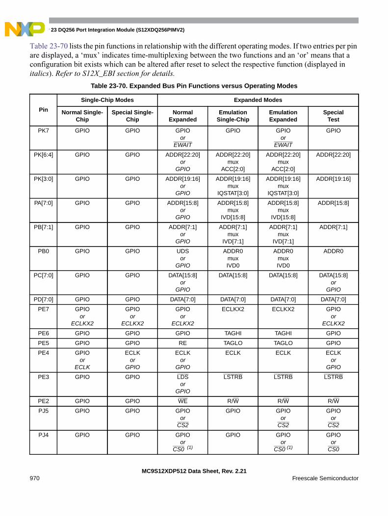
Chapter 23 DQ256 Port Integration Module (S12XDQ256PIMV2)
MC9S12XDP512 Data Sheet, Rev. 2.21970 Freescale Semiconductor
Table 23-70 lists the pin functions in relationship with the different operating modes. If two entries per pinare displayed, a ‘mux’ indicates time-multiplexing between the two functions and an ‘or’ means that aconfiguration bit exists which can be altered after reset to select the respective function (displayed initalics). Refer to S12X_EBI section for details.
Table 23-70. Expanded Bus Pin Functions versus Operating Modes
Pin
Single-Chip Modes Expanded Modes
Normal Single-Chip
Special Single-Chip
NormalExpanded
EmulationSingle-Chip
EmulationExpanded
SpecialTest
PK7 GPIO GPIO GPIOor
EWAIT
GPIO GPIOor
EWAIT
GPIO
PK[6:4] GPIO GPIO ADDR[22:20]or
GPIO
ADDR[22:20]mux
ACC[2:0]
ADDR[22:20]mux
ACC[2:0]
ADDR[22:20]
PK[3:0] GPIO GPIO ADDR[19:16]or
GPIO
ADDR[19:16]mux
IQSTAT[3:0]
ADDR[19:16]mux
IQSTAT[3:0]
ADDR[19:16]
PA[7:0] GPIO GPIO ADDR[15:8]or
GPIO
ADDR[15:8]mux
IVD[15:8]
ADDR[15:8]mux
IVD[15:8]
ADDR[15:8]
PB[7:1] GPIO GPIO ADDR[7:1]or
GPIO
ADDR[7:1]mux
IVD[7:1]
ADDR[7:1]mux
IVD[7:1]
ADDR[7:1]
PB0 GPIO GPIO UDSor
GPIO
ADDR0muxIVD0
ADDR0muxIVD0
ADDR0
PC[7:0] GPIO GPIO DATA[15:8]or
GPIO
DATA[15:8] DATA[15:8] DATA[15:8]or
GPIO
PD[7:0] GPIO GPIO DATA[7:0] DATA[7:0] DATA[7:0] DATA[7:0]
PE7 GPIOor
ECLKX2
GPIOor
ECLKX2
GPIOor
ECLKX2
ECLKX2 ECLKX2 GPIOor
ECLKX2
PE6 GPIO GPIO GPIO TAGHI TAGHI GPIO
PE5 GPIO GPIO RE TAGLO TAGLO GPIO
PE4 GPIOor
ECLK
ECLKor
GPIO
ECLKor
GPIO
ECLK ECLK ECLKor
GPIO
PE3 GPIO GPIO LDSor
GPIO
LSTRB LSTRB LSTRB
PE2 GPIO GPIO WE R/W R/W R/W
PJ5 GPIO GPIO GPIOor
CS2
GPIO GPIOor
CS2
GPIOor
CS2
PJ4 GPIO GPIO GPIOor
CS0 (1)
GPIO GPIOor
CS0 (1)
GPIOor
CS0

23.0.10 Low-Power Options
23.0.10.1 Run Mode
No low-power options exist for this module in run mode.
23.0.10.2 Wait Mode
No low-power options exist for this module in wait mode.
23.0.10.3 Stop Mode
All clocks are stopped. There are asynchronous paths to generate interrupts from stop on port P, H,and J.
Initialization and Application Information• It is not recommended to write PORTx and DDRx in a word access. When changing the
register pins from inputs to outputs, the data may have extra transitions during the writeaccess. Initialize the port data register before enabling the outputs.
• Power consumption will increase the more the voltages on general purpose input pinsdeviate from the supply voltages towards mid-range because the digital input buffersoperate in the linear region.
PJ2 GPIO GPIO GPIOor
CS1
GPIO GPIOor
CS1
GPIOor
CS1
PJ0 GPIO GPIO GPIOor
CS3
GPIO GPIOor
CS3
GPIOor
CS3
1. Depending on ROMON bit. Refer to Device Guide, S12X_EBI section and S12X_MMC section for details.
Table 23-70. Expanded Bus Pin Functions versus Operating Modes (continued)
Pin
Single-Chip Modes Expanded Modes
Normal Single-Chip
Special Single-Chip
NormalExpanded
EmulationSingle-Chip
EmulationExpanded
SpecialTest

Chapter 23 DQ256 Port Integration Module (S12XDQ256PIMV2)
MC9S12XDP512 Data Sheet, Rev. 2.21972 Freescale Semiconductor


Chapter 23 DQ256 Port Integration Module (S12XDQ256PIMV2)
MC9S12XDP512 Data Sheet, Rev. 2.21974 Freescale Semiconductor

MC9S12XDP512 Data Sheet, Rev. 2.21Freescale Semiconductor 975
Chapter 24DG128 Port Integration Module (S12XDG128PIMV2)
Introduction
The S12XD family port integration module (below referred to as PIM) establishes the interface betweenthe peripheral modules including the non-multiplexed external bus interface module (S12X_EBI) and theI/O pins for all ports. It controls the electrical pin properties as well as the signal prioritization andmultiplexing on shared pins.
This document covers the description of:
• Port A, B
• Port E associated with the IRQ, XIRQ interrupt inputs
• Port K
• Port T connected to the Enhanced Capture Timer (ECT) module
• Port S associated with 2 SCI and 1 SPI modules
• Port M associated with 2 MSCAN modules and 1 SCI module
• Port P connected to the PWM and 1 SPI module — inputs can be used as an external interruptsource
• Port H associated with 2 SCI modules — inputs can be used as an external interrupt source
• Port J associated with 1 MSCAN, 1 SCI, and 1 IIC module — inputs can be used as an externalinterrupt source
• Port AD1 associated with one 16-channel ATD module
Most I/O pins can be configured by register bits to select data direction and drive strength, to enable andselect pull-up or pull-down devices. Interrupts can be enabled on specific pins resulting in status flags.
The I/O’s of 2 MSCAN and 2 SPI modules can be routed from their default location to alternative portpins.
NOTEThe implementation of the PIM is device dependent. Therefore somefunctions are not available on certain derivatives or80-pin package options.
24.0.1 Features
A full-featured PIM module includes these distinctive registers:

Chapter 24 DG128 Port Integration Module (S12XDG128PIMV2)
MC9S12XDP512 Data Sheet, Rev. 2.21976 Freescale Semiconductor
• Data and data direction registers for Ports A, B, E, K, T, S, M, P, H, J, and AD1 when used asgeneral-purpose I/O
• Control registers to enable/disable pull-device and select pull-ups/pull-downs on Ports T, S, M, P,H, and J on per-pin basis
• Control registers to enable/disable pull-up devices on Port AD1 on per-pin basis
• Single control register to enable/disable pull-ups on Ports A, B, E, and K on per-port basis and onBKGD pin
• Control registers to enable/disable reduced output drive on Ports T, S, M, P, H, J, and AD1 on per-pin basis
• Single control register to enable/disable reduced output drive on Ports A, B, E, and K on per-portbasis
• Control registers to enable/disable open-drain (wired-OR) mode on Ports S and M
• Control registers to enable/disable pin interrupts on Ports P, H, and J
• Interrupt flag register for pin interrupts on Ports P, H, and J
• Control register to configure IRQ pin operation
• Free-running clock outputs
A standard port pin has the following minimum features:
• Input/output selection
• 5V output drive with two selectable drive strengths
• 5V digital and analog input
• Input with selectable pull-up or pull-down device
Optional features:
• Open drain for wired-OR connections
• Interrupt inputs with glitch filtering
• Reduced input threshold to support low voltage applications
24.0.2 Block Diagram
Figure 24-1 is a block diagram of the PIM.
• Signals shown in Bold are not available in 80-pin packages.
• Shaded labels denote alternative module routing ports.

Figure 24-1. PIM_9XDG128 Block Diagram
Por
t T
PT0PT1PT2PT3PT4PT5PT6PT7
EC
T
IOC0IOC1IOC2IOC3IOC4IOC5IOC6IOC7
Por
t PPP0PP1PP2PP3PP4PP5PP6PP7
PW
M
PWM0PWM1PWM2PWM3PWM4PWM5PWM6PWM7
Por
t S
PS0PS1PS2PS3PS4PS5PS6PS7
RXDTXDRXDTXD
MISOMOSISCK
SS
SCI0
SCI1
SPI0
Port H
PH0PH1PH2PH3PH4PH5PH6PH7
Port J
PJ0PJ1
PJ6
PJ7
Port M
PM0PM1PM2PM3PM4PM5PM6PM7
CAN0TXCANRXCAN
IIC0SCLSDA
Port Integration Module
CAN4TXCANRXCAN
MISOMOSISCK
SSSPI1In
terr
upt L
ogic
Port B
PB0PB1PB2PB3PB4PB5PB6PB7
Port A
PA0PA1PA2PA3PA4PA5PA6PA7
Por
t E
PE0PE1PE2PE3PE4PE5PE6PE7
Por
t K
PK0PK1PK2PK3
PK7
PK4PK5
XIRQIRQ
ECLK
XCLKS
ROMCTL
BKGD/MODC BKGD
CA
N0
Interrupt Logic
PAD00PAD01PAD02PAD03PAD04PAD05PAD06PAD07
AN0AN1AN2AN3AN4AN5AN6AN7
Por
t AD
1
PAD08PAD09PAD10PAD11PAD12PAD13PAD14PAD15
ATD
1
AN8AN9
AN10AN11AN12AN13AN14AN15
SP
I1 S
PI2
SP
I0
S12X_BDMS12X_INT
Inte
rrup
t Lo
gic
CA
N0
CA
N0
CA
N4
CA
N4
S12X_MMC
ECLKX2
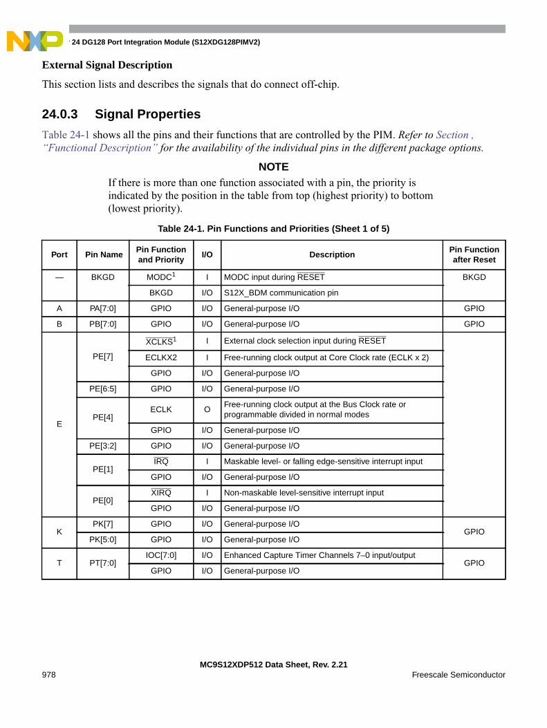
Chapter 24 DG128 Port Integration Module (S12XDG128PIMV2)
MC9S12XDP512 Data Sheet, Rev. 2.21978 Freescale Semiconductor
External Signal Description
This section lists and describes the signals that do connect off-chip.
24.0.3 Signal Properties
Table 24-1 shows all the pins and their functions that are controlled by the PIM. Refer to Section ,“Functional Description” for the availability of the individual pins in the different package options.
NOTEIf there is more than one function associated with a pin, the priority isindicated by the position in the table from top (highest priority) to bottom(lowest priority).
Table 24-1. Pin Functions and Priorities (Sheet 1 of 5)
Port Pin NamePin Functionand Priority
I/O DescriptionPin Functionafter Reset
— BKGD MODC1 I MODC input during RESET BKGD
BKGD I/O S12X_BDM communication pin
A PA[7:0] GPIO I/O General-purpose I/O GPIO
B PB[7:0] GPIO I/O General-purpose I/O GPIO
E
PE[7]
XCLKS1 I External clock selection input during RESET
ECLKX2 I Free-running clock output at Core Clock rate (ECLK x 2)
GPIO I/O General-purpose I/O
PE[6:5] GPIO I/O General-purpose I/O
PE[4]ECLK O
Free-running clock output at the Bus Clock rate orprogrammable divided in normal modes
GPIO I/O General-purpose I/O
PE[3:2] GPIO I/O General-purpose I/O
PE[1]IRQ I Maskable level- or falling edge-sensitive interrupt input
GPIO I/O General-purpose I/O
PE[0]XIRQ I Non-maskable level-sensitive interrupt input
GPIO I/O General-purpose I/O
KPK[7] GPIO I/O General-purpose I/O
GPIOPK[5:0] GPIO I/O General-purpose I/O
T PT[7:0]IOC[7:0] I/O Enhanced Capture Timer Channels 7–0 input/output
GPIOGPIO I/O General-purpose I/O
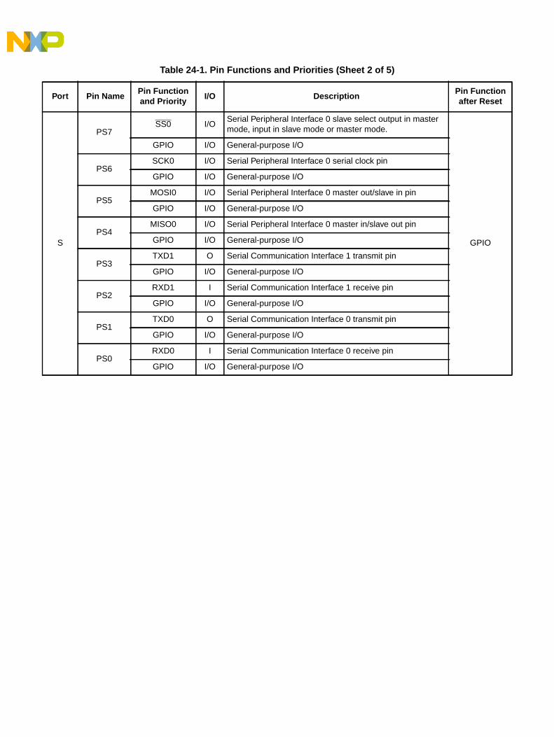
S
PS7SS0 I/O
Serial Peripheral Interface 0 slave select output in mastermode, input in slave mode or master mode.
GPIO
GPIO I/O General-purpose I/O
PS6SCK0 I/O Serial Peripheral Interface 0 serial clock pin
GPIO I/O General-purpose I/O
PS5MOSI0 I/O Serial Peripheral Interface 0 master out/slave in pin
GPIO I/O General-purpose I/O
PS4MISO0 I/O Serial Peripheral Interface 0 master in/slave out pin
GPIO I/O General-purpose I/O
PS3TXD1 O Serial Communication Interface 1 transmit pin
GPIO I/O General-purpose I/O
PS2RXD1 I Serial Communication Interface 1 receive pin
GPIO I/O General-purpose I/O
PS1TXD0 O Serial Communication Interface 0 transmit pin
GPIO I/O General-purpose I/O
PS0RXD0 I Serial Communication Interface 0 receive pin
GPIO I/O General-purpose I/O
Table 24-1. Pin Functions and Priorities (Sheet 2 of 5)
Port Pin NamePin Functionand Priority
I/O DescriptionPin Functionafter Reset
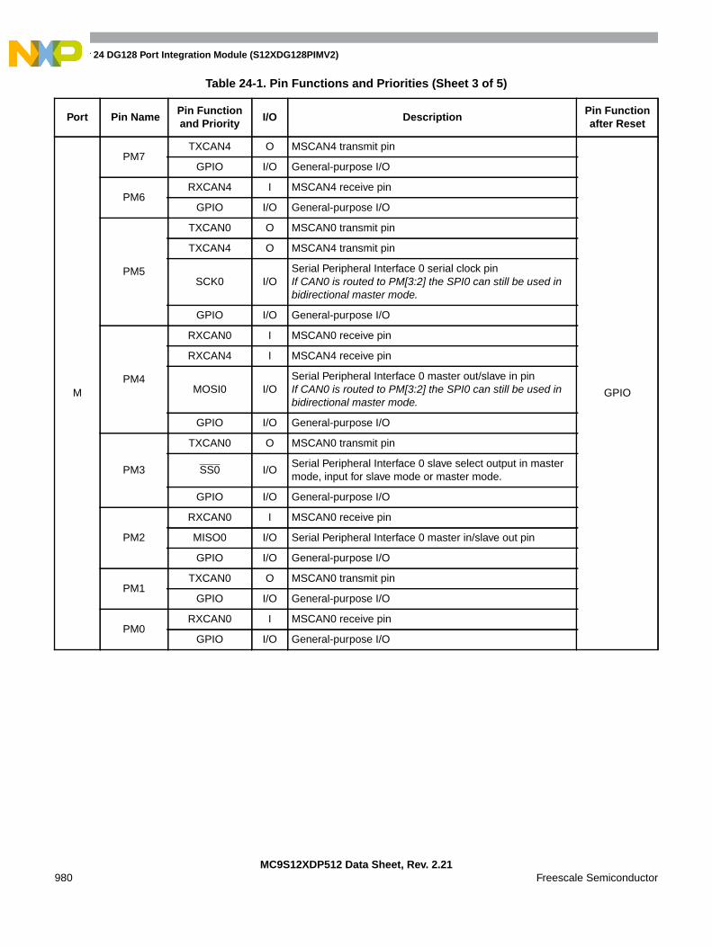
Chapter 24 DG128 Port Integration Module (S12XDG128PIMV2)
MC9S12XDP512 Data Sheet, Rev. 2.21980 Freescale Semiconductor
M
PM7TXCAN4 O MSCAN4 transmit pin
GPIO
GPIO I/O General-purpose I/O
PM6RXCAN4 I MSCAN4 receive pin
GPIO I/O General-purpose I/O
PM5
TXCAN0 O MSCAN0 transmit pin
TXCAN4 O MSCAN4 transmit pin
SCK0 I/OSerial Peripheral Interface 0 serial clock pinIf CAN0 is routed to PM[3:2] the SPI0 can still be used inbidirectional master mode.
GPIO I/O General-purpose I/O
PM4
RXCAN0 I MSCAN0 receive pin
RXCAN4 I MSCAN4 receive pin
MOSI0 I/OSerial Peripheral Interface 0 master out/slave in pinIf CAN0 is routed to PM[3:2] the SPI0 can still be used inbidirectional master mode.
GPIO I/O General-purpose I/O
PM3
TXCAN0 O MSCAN0 transmit pin
SS0 I/OSerial Peripheral Interface 0 slave select output in mastermode, input for slave mode or master mode.
GPIO I/O General-purpose I/O
PM2
RXCAN0 I MSCAN0 receive pin
MISO0 I/O Serial Peripheral Interface 0 master in/slave out pin
GPIO I/O General-purpose I/O
PM1TXCAN0 O MSCAN0 transmit pin
GPIO I/O General-purpose I/O
PM0RXCAN0 I MSCAN0 receive pin
GPIO I/O General-purpose I/O
Table 24-1. Pin Functions and Priorities (Sheet 3 of 5)
Port Pin NamePin Functionand Priority
I/O DescriptionPin Functionafter Reset

P
PP7PWM7 I/O Pulse Width Modulator input/output channel 7
GPIO
GPIO/KWP7 I/O General-purpose I/O with interrupt
PP6PWM6 O Pulse Width Modulator output channel 6
GPIO/KWP6 I/O General-purpose I/O with interrupt
PP5PWM5 O Pulse Width Modulator output channel 5
GPIO/KWP5 I/O General-purpose I/O with interrupt
PP4PWM4 O Pulse Width Modulator output channel 4
GPIO/KWP4 I/O General-purpose I/O with interrupt
PP3
PWM3 O Pulse Width Modulator output channel 3
SS1 I/OSerial Peripheral Interface 1 slave select output in mastermode, input for slave mode or master mode.
GPIO/KWP3 I/O General-purpose I/O with interrupt
PP2
PWM2 O Pulse Width Modulator output channel 2
SCK1 I/O Serial Peripheral Interface 1 serial clock pin
GPIO/KWP2 I/O General-purpose I/O with interrupt
PP1
PWM1 O Pulse Width Modulator output channel 1
MOSI1 I/O Serial Peripheral Interface 1 master out/slave in pin
GPIO/KWP1 I/O General-purpose I/O with interrupt
PP0
PWM0 O Pulse Width Modulator output channel 0
MISO1 I/O Serial Peripheral Interface 1 master in/slave out pin
GPIO/KWP0 I/O General-purpose I/O with interrupt
Table 24-1. Pin Functions and Priorities (Sheet 4 of 5)
Port Pin NamePin Functionand Priority
I/O DescriptionPin Functionafter Reset

Chapter 24 DG128 Port Integration Module (S12XDG128PIMV2)
MC9S12XDP512 Data Sheet, Rev. 2.21982 Freescale Semiconductor
H
PH7
SS2 I/OSerial Peripheral Interface 2 slave select output in mastermode, input for slave mode or master mode
GPIO
TXD5 O Serial Communication Interface 5 transmit pin
GPIO/KWH7 I/O General-purpose I/O with interrupt
PH6
SCK2 I/O Serial Peripheral Interface 2 serial clock pin
RXD5 I Serial Communication Interface 5 receive pin
GPIO/KWH6 I/O General-purpose I/O with interrupt
PH5
MOSI2 I/O Serial Peripheral Interface 2 master out/slave in pin
TXD4 O Serial Communication Interface 4 transmit pin
GPIO/KWH5 I/O General-purpose I/O with interrupt
PH4
MISO2 I/O Serial Peripheral Interface 2 master in/slave out pin
RXD4 I Serial Communication Interface 4 receive pin
GPIO/KWH4 I/O General-purpose I/O with interrupt
PH3SS1 I/O
Serial Peripheral Interface 1 slave select output in mastermode, input for slave mode or master mode.
GPIO/KWH3 I/O General-purpose I/O with interrupt
PH2SCK1 I/O Serial Peripheral Interface 1 serial clock pin
GPIO/KWH2 I/O General-purpose I/O with interrupt
PH1MOSI1 I/O Serial Peripheral Interface 1 master out/slave in pin
GPIO/KWH1 I/O General-purpose I/O with interrupt
PH0MISO1 I/O Serial Peripheral Interface 1 master in/slave out pin
GPIO/KWH0 I/O General-purpose I/O with interrupt
J
PJ7
TXCAN4 O MSCAN4 transmit pin
GPIO
SCL0 O Inter Integrated Circuit 0 serial clock line
TXCAN0 O MSCAN0 transmit pin
GPIO/KWJ7 I/O General-purpose I/O with interrupt
PJ6
RXCAN4 I MSCAN4 receive pin
SDA0 I/O Inter Integrated Circuit 0 serial data line
RXCAN0 I MSCAN0 receive pin
GPIO/KWJ6 I/O General-purpose I/O with interrupt
PJ1 GPIO/KWJ1 I/O General-purpose I/O with interrupt
PJ0 GPIO/KWJ0 I/O General-purpose I/O with interrupt
AD1 PAD[15:00]GPIO I/O General-purpose I/O
GPIOAN[15:0] I ATD1 analog inputs
1. Function active when RESET asserted.
Table 24-1. Pin Functions and Priorities (Sheet 5 of 5)
Port Pin NamePin Functionand Priority
I/O DescriptionPin Functionafter Reset

Memory Map and Register Definition
This section provides a detailed description of all PIM registers.
24.0.4 Module Memory Map
Table 24-2 shows the register map of the port integration module.
Table 24-2. PIM Memory Map (Sheet 1 of 3)
Address Use Access
0x0000 Port A Data Register (PORTA) Read / Write
0x0001 Port B Data Register (PORTB) Read / Write
0x0002 Port A Data Direction Register (DDRA) Read / Write
0x0003 Port B Data Direction Register (DDRB) Read / Write
0x0004:
0x0007
PIM Reserved —
0x0008 Port E Data Register (PORTE) Read / Write1
0x0009 Port E Data Direction Register (DDRE) Read / Write1
0x000A:
0x000B
Non-PIM Address Range —
0x000C Pull-up Up Control Register (PUCR) Read / Write1
0x000D Reduced Drive Register (RDRIV) Read / Write1
0x000E:
0x001B
Non-PIM Address Range —
0x001C ECLK Control Register (ECLKCTL) Read / Write1
0x001D PIM Reserved —
0x001E IRQ Control Register (IRQCR) Read / Write1
0x001F PIM Reserved —
0x0020:
0x0031
Non-PIM Address Range —
0x0032 Port K Data Register (PORTK) Read / Write
0x0033 Port K Data Direction Register (DDRK) Read / Write
0x0034:
0x023F
Non-PIM Address Range —
0x0240 Port T Data Register (PTT) Read / Write
0x0241 Port T Input Register (PTIT) Read
0x0242 Port T Data Direction Register (DDRT) Read / Write
0x0243 Port T Reduced Drive Register (RDRT) Read / Write

Chapter 24 DG128 Port Integration Module (S12XDG128PIMV2)
MC9S12XDP512 Data Sheet, Rev. 2.21984 Freescale Semiconductor
0x0244 Port T Pull Device Enable Register (PERT) Read / Write
0x0245 Port T Polarity Select Register (PPST) Read / Write
0x0246 PIM Reserved —
0x0247 PIM Reserved —
0x0248 Port S Data Register (PTS) Read / Write
0x0249 Port S Input Register (PTIS) Read
0x024A Port S Data Direction Register (DDRS) Read / Write
0x024B Port S Reduced Drive Register (RDRS) Read / Write
0x024C Port S Pull Device Enable Register (PERS) Read / Write
0x024D Port S Polarity Select Register (PPSS) Read / Write
0x024E Port S Wired-OR Mode Register (WOMS) Read / Write
0x024F PIM Reserved —
0x0250 Port M Data Register (PTM) Read / Write
0x0251 Port M Input Register (PTIM) Read
0x0252 Port M Data Direction Register (DDRM) Read / Write
0x0253 Port M Reduced Drive Register (RDRM) Read / Write
0x0254 Port M Pull Device Enable Register (PERM) Read / Write
0x0255 Port M Polarity Select Register (PPSM) Read / Write
0x0256 Port M Wired-OR Mode Register (WOMM) Read / Write
0x0257 Module Routing Register (MODRR) Read / Write
0x0258 Port P Data Register (PTP) Read / Write
0x0259 Port P Input Register (PTIP) Read
0x025A Port P Data Direction Register (DDRP) Read / Write
0x025B Port P Reduced Drive Register (RDRP) Read / Write
0x025C Port P Pull Device Enable Register (PERP) Read / Write
0x025D Port P Polarity Select Register (PPSP) Read / Write
0x025E Port P Interrupt Enable Register (PIEP) Read / Write
0x025F Port P Interrupt Flag Register (PIFP) Read / Write
0x0260 Port H Data Register (PTH) Read / Write
0x0261 Port H Input Register (PTIH) Read
0x0262 Port H Data Direction Register (DDRH) Read / Write
0x0263 Port H Reduced Drive Register (RDRH) Read / Write
0x0264 Port H Pull Device Enable Register (PERH) Read / Write
0x0265 Port H Polarity Select Register (PPSH) Read / Write
0x0266 Port H Interrupt Enable Register (PIEH) Read / Write
Table 24-2. PIM Memory Map (Sheet 2 of 3)
Address Use Access
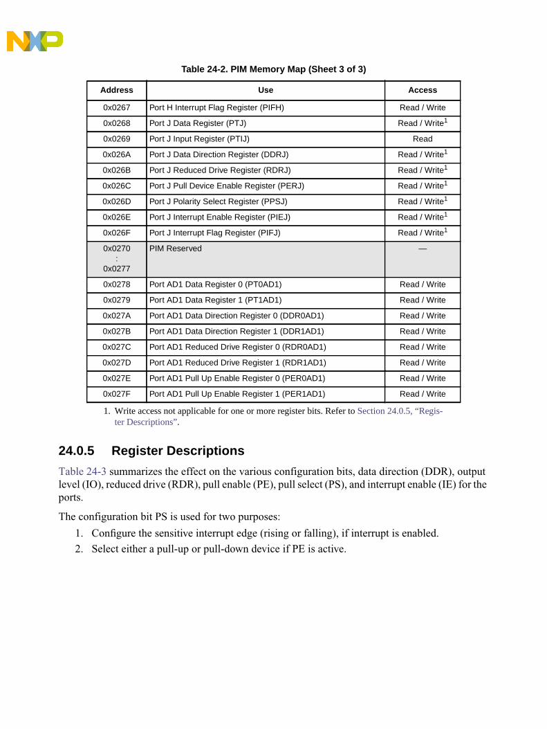
24.0.5 Register Descriptions
Table 24-3 summarizes the effect on the various configuration bits, data direction (DDR), outputlevel (IO), reduced drive (RDR), pull enable (PE), pull select (PS), and interrupt enable (IE) for theports.
The configuration bit PS is used for two purposes:
1. Configure the sensitive interrupt edge (rising or falling), if interrupt is enabled.
2. Select either a pull-up or pull-down device if PE is active.
0x0267 Port H Interrupt Flag Register (PIFH) Read / Write
0x0268 Port J Data Register (PTJ) Read / Write1
0x0269 Port J Input Register (PTIJ) Read
0x026A Port J Data Direction Register (DDRJ) Read / Write1
0x026B Port J Reduced Drive Register (RDRJ) Read / Write1
0x026C Port J Pull Device Enable Register (PERJ) Read / Write1
0x026D Port J Polarity Select Register (PPSJ) Read / Write1
0x026E Port J Interrupt Enable Register (PIEJ) Read / Write1
0x026F Port J Interrupt Flag Register (PIFJ) Read / Write1
0x0270:
0x0277
PIM Reserved —
0x0278 Port AD1 Data Register 0 (PT0AD1) Read / Write
0x0279 Port AD1 Data Register 1 (PT1AD1) Read / Write
0x027A Port AD1 Data Direction Register 0 (DDR0AD1) Read / Write
0x027B Port AD1 Data Direction Register 1 (DDR1AD1) Read / Write
0x027C Port AD1 Reduced Drive Register 0 (RDR0AD1) Read / Write
0x027D Port AD1 Reduced Drive Register 1 (RDR1AD1) Read / Write
0x027E Port AD1 Pull Up Enable Register 0 (PER0AD1) Read / Write
0x027F Port AD1 Pull Up Enable Register 1 (PER1AD1) Read / Write
1. Write access not applicable for one or more register bits. Refer to Section 24.0.5, “Regis-ter Descriptions”.
Table 24-2. PIM Memory Map (Sheet 3 of 3)
Address Use Access
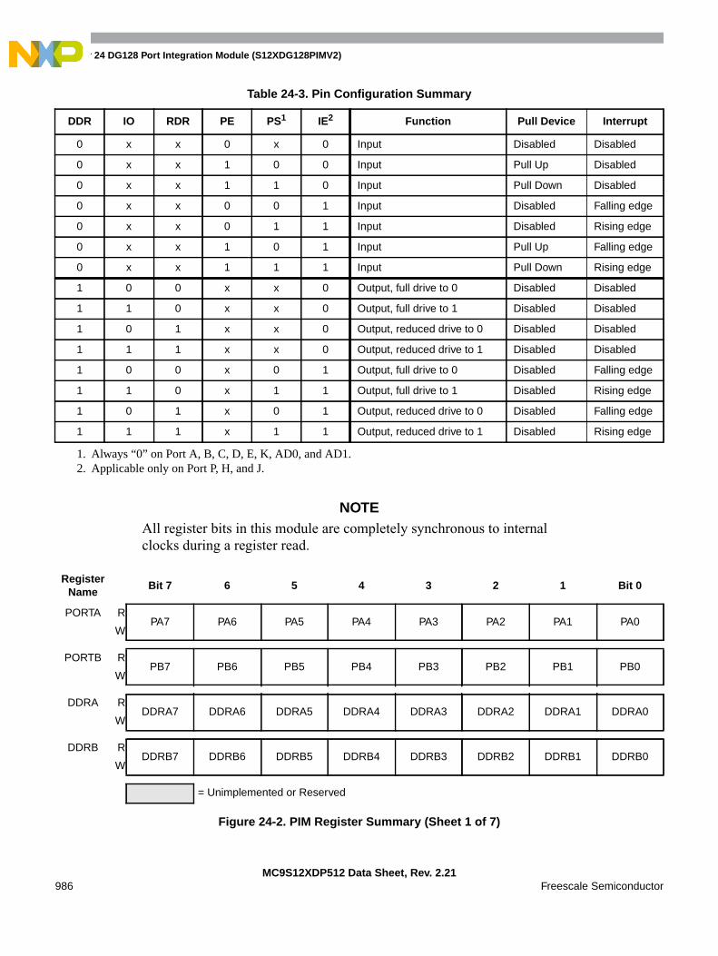
Chapter 24 DG128 Port Integration Module (S12XDG128PIMV2)
MC9S12XDP512 Data Sheet, Rev. 2.21986 Freescale Semiconductor
NOTEAll register bits in this module are completely synchronous to internalclocks during a register read.
Table 24-3. Pin Configuration Summary
DDR IO RDR PE PS1
1. Always “0” on Port A, B, C, D, E, K, AD0, and AD1.
IE2
2. Applicable only on Port P, H, and J.
Function Pull Device Interrupt
0 x x 0 x 0 Input Disabled Disabled
0 x x 1 0 0 Input Pull Up Disabled
0 x x 1 1 0 Input Pull Down Disabled
0 x x 0 0 1 Input Disabled Falling edge
0 x x 0 1 1 Input Disabled Rising edge
0 x x 1 0 1 Input Pull Up Falling edge
0 x x 1 1 1 Input Pull Down Rising edge
1 0 0 x x 0 Output, full drive to 0 Disabled Disabled
1 1 0 x x 0 Output, full drive to 1 Disabled Disabled
1 0 1 x x 0 Output, reduced drive to 0 Disabled Disabled
1 1 1 x x 0 Output, reduced drive to 1 Disabled Disabled
1 0 0 x 0 1 Output, full drive to 0 Disabled Falling edge
1 1 0 x 1 1 Output, full drive to 1 Disabled Rising edge
1 0 1 x 0 1 Output, reduced drive to 0 Disabled Falling edge
1 1 1 x 1 1 Output, reduced drive to 1 Disabled Rising edge
RegisterName
Bit 7 6 5 4 3 2 1 Bit 0
PORTA RPA7 PA6 PA5 PA4 PA3 PA2 PA1 PA0
W
PORTB RPB7 PB6 PB5 PB4 PB3 PB2 PB1 PB0
W
DDRA RDDRA7 DDRA6 DDRA5 DDRA4 DDRA3 DDRA2 DDRA1 DDRA0
W
DDRB RDDRB7 DDRB6 DDRB5 DDRB4 DDRB3 DDRB2 DDRB1 DDRB0
W
= Unimplemented or Reserved
Figure 24-2. PIM Register Summary (Sheet 1 of 7)
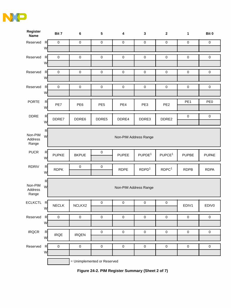
Reserved R 0 0 0 0 0 0 0 0
W
Reserved R 0 0 0 0 0 0 0 0
W
Reserved R 0 0 0 0 0 0 0 0
W
Reserved R 0 0 0 0 0 0 0 0
W
PORTE RPE7 PE6 PE5 PE4 PE3 PE2
PE1 PE0
W
DDRE RDDRE7 DDRE6 DDRE5 DDRE4 DDRE3 DDRE2
0 0
W
Non-PIMAddressRange
R
Non-PIM Address RangeW
PUCR RPUPKE BKPUE
0PUPEE PUPDE1 PUPCE1 PUPBE PUPAE
W
RDRIV RRDPK
0 0RDPE RDPD1 RDPC1 RDPB RDPA
W
Non-PIMAddressRange
R
Non-PIM Address RangeW
ECLKCTL RNECLK NCLKX2
0 0 0 0EDIV1 EDIV0
W
Reserved R 0 0 0 0 0 0 0 0
W
IRQCR RIRQE IRQEN
0 0 0 0 0 0
W
Reserved R 0 0 0 0 0 0 0 0
W
RegisterName
Bit 7 6 5 4 3 2 1 Bit 0
= Unimplemented or Reserved
Figure 24-2. PIM Register Summary (Sheet 2 of 7)
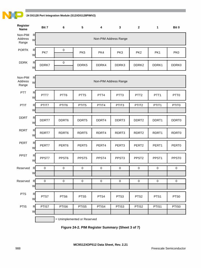
Chapter 24 DG128 Port Integration Module (S12XDG128PIMV2)
MC9S12XDP512 Data Sheet, Rev. 2.21988 Freescale Semiconductor
Non-PIMAddressRange
RNon-PIM Address RangeW
PORTK RPK7
0PK5 PK4 PK3 PK2 PK1 PK0
W
DDRK RDDRK7
0DDRK5 DDRK4 DDRK3 DDRK2 DDRK1 DDRK0
W
Non-PIMAddressRange
RNon-PIM Address RangeW
PTT RPTT7 PTT6 PTT5 PTT4 PTT3 PTT2 PTT1 PTT0
W
PTIT R PTIT7 PTIT6 PTIT5 PTIT4 PTIT3 PTIT2 PTIT1 PTIT0
W
DDRT RDDRT7 DDRT6 DDRT5 DDRT4 DDRT3 DDRT2 DDRT1 DDRT0
W
RDRT RRDRT7 RDRT6 RDRT5 RDRT4 RDRT3 RDRT2 RDRT1 RDRT0
W
PERT RPERT7 PERT6 PERT5 PERT4 PERT3 PERT2 PERT1 PERT0
W
PPST RPPST7 PPST6 PPST5 PPST4 PPST3 PPST2 PPST1 PPST0
W
Reserved R 0 0 0 0 0 0 0 0
W
Reserved R 0 0 0 0 0 0 0 0
W
PTS RPTS7 PTS6 PTS5 PTS4 PTS3 PTS2 PTS1 PTS0
W
PTIS R PTIS7 PTIS6 PTIS5 PTIS4 PTIS3 PTIS2 PTIS1 PTIS0
W
RegisterName
Bit 7 6 5 4 3 2 1 Bit 0
= Unimplemented or Reserved
Figure 24-2. PIM Register Summary (Sheet 3 of 7)
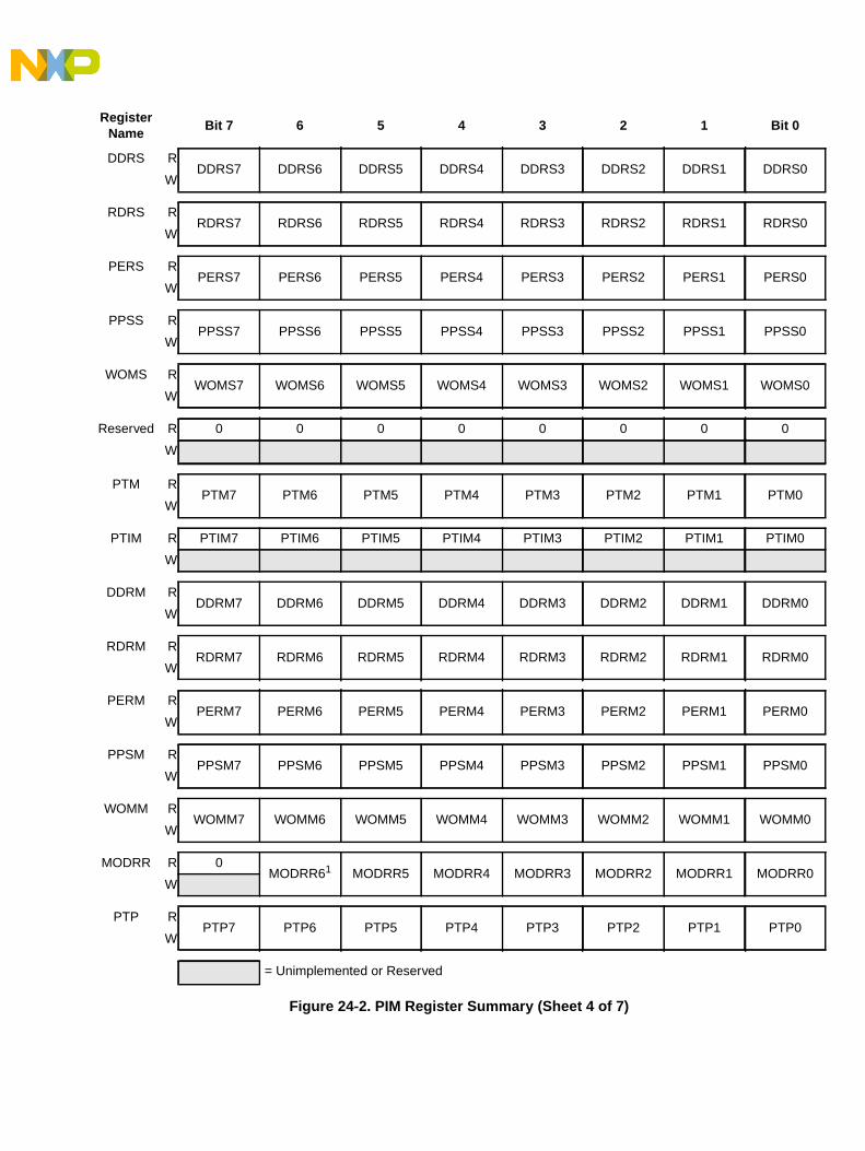
DDRS RDDRS7 DDRS6 DDRS5 DDRS4 DDRS3 DDRS2 DDRS1 DDRS0
W
RDRS RRDRS7 RDRS6 RDRS5 RDRS4 RDRS3 RDRS2 RDRS1 RDRS0
W
PERS RPERS7 PERS6 PERS5 PERS4 PERS3 PERS2 PERS1 PERS0
W
PPSS RPPSS7 PPSS6 PPSS5 PPSS4 PPSS3 PPSS2 PPSS1 PPSS0
W
WOMS RWOMS7 WOMS6 WOMS5 WOMS4 WOMS3 WOMS2 WOMS1 WOMS0
W
Reserved R 0 0 0 0 0 0 0 0
W
PTM RPTM7 PTM6 PTM5 PTM4 PTM3 PTM2 PTM1 PTM0
W
PTIM R PTIM7 PTIM6 PTIM5 PTIM4 PTIM3 PTIM2 PTIM1 PTIM0
W
DDRM RDDRM7 DDRM6 DDRM5 DDRM4 DDRM3 DDRM2 DDRM1 DDRM0
W
RDRM RRDRM7 RDRM6 RDRM5 RDRM4 RDRM3 RDRM2 RDRM1 RDRM0
W
PERM RPERM7 PERM6 PERM5 PERM4 PERM3 PERM2 PERM1 PERM0
W
PPSM RPPSM7 PPSM6 PPSM5 PPSM4 PPSM3 PPSM2 PPSM1 PPSM0
W
WOMM RWOMM7 WOMM6 WOMM5 WOMM4 WOMM3 WOMM2 WOMM1 WOMM0
W
MODRR R 0MODRR61 MODRR5 MODRR4 MODRR3 MODRR2 MODRR1 MODRR0
W
PTP RPTP7 PTP6 PTP5 PTP4 PTP3 PTP2 PTP1 PTP0
W
RegisterName
Bit 7 6 5 4 3 2 1 Bit 0
= Unimplemented or Reserved
Figure 24-2. PIM Register Summary (Sheet 4 of 7)

Chapter 24 DG128 Port Integration Module (S12XDG128PIMV2)
MC9S12XDP512 Data Sheet, Rev. 2.21990 Freescale Semiconductor
PTIP R PTIP7 PTIP6 PTIP5 PTIP4 PTIP3 PTIP2 PTIP1 PTIP0
W
DDRP RDDRP7 DDRP6 DDRP5 DDRP4 DDRP3 DDRP2 DDRP1 DDRP0
W
RDRP RRDRP7 RDRP6 RDRP5 RDRP4 RDRP3 RDRP2 RDRP1 RDRP0
W
PERP RPERP7 PERP6 PERP5 PERP4 PERP3 PERP2 PERP1 PERP0
W
PPSP RPPSP7 PPSP6 PPSP5 PPSP4 PPSP3 PPSP2 PPSP1 PPSP0
W
PIEP RPIEP7 PIEP6 PIEP5 PIEP4 PIEP3 PIEP2 PIEP1 PIEP0
W
PIFP RPIFP7 PIFP6 PIFP5 PIFP4 PIFP3 PIFP2 PIFP1 PIFP0
W
PTH RPTH7 PTH6 PTH5 PTH4 PTH3 PTH2 PTH1 PTH0
W
PTIH R PTIH7 PTIH6 PTIH5 PTIH4 PTIH3 PTIH2 PTIH1 PTIH0
W
DDRH RDDRH7 DDRH6 DDRH5 DDRH4 DDRH3 DDRH2 DDRH1 DDRH0
W
RDRH RRDRH7 RDRH6 RDRH5 RDRH4 RDRH3 RDRH2 RDRH1 RDRH0
W
PERH RPERH7 PERH6 PERH5 PERH4 PERH3 PERH2 PERH1 PERH0
W
PPSH RPPSH7 PPSH6 PPSH5 PPSH4 PPSH3 PPSH2 PPSH1 PPSH0
W
PIEH RPIEH7 PIEH6 PIEH5 PIEH4 PIEH3 PIEH2 PIEH1 PIEH0
W
PIFH RPIFH7 PIFH6 PIFH5 PIFH4 PIFH3 PIFH2 PIFH1 PIFH0
W
RegisterName
Bit 7 6 5 4 3 2 1 Bit 0
= Unimplemented or Reserved
Figure 24-2. PIM Register Summary (Sheet 5 of 7)

PTJ RPTJ7 PTJ6
0 0 0 0PTJ1 PTJ0
W
PTIJ R PTIJ7 PTIJ6 0 0 0 0 PTIJ1 PTIJ0
W
DDRJ RDDRJ7 DDRJ6
0 0 0 0DDRJ1 DDRJ0
W
RDRJ RRDRJ7 RDRJ6
0 0 0 0RDRJ1 RDRJ0
W
PERJ RPERJ7 PERJ6
0 0 0 0PERJ1 PERJ0
W
PPSJ RPPSJ7 PPSJ6
0 0 0 0PPSJ1 PPSJ0
W
PIEJ RPIEJ7 PIEJ6
0 0 0 0PIEJ1 PIEJ0
W
PIFJ RPPSJ7 PPSJ6
0 0 0 0PPSJ1 PPSJ0
W
Reserved R 0 0 0 0 0 0 0 0
W
Reserved R 0 0 0 0 0 0 0 0
W
Reserved R 0 0 0 0 0 0 0 0
W
Reserved R 0 0 0 0 0 0 0 0
W
Reserved R 0 0 0 0 0 0 0 0
W
Reserved R 0 0 0 0 0 0 0 0
W
Reserved R 0 0 0 0 0 0 0 0
W
RegisterName
Bit 7 6 5 4 3 2 1 Bit 0
= Unimplemented or Reserved
Figure 24-2. PIM Register Summary (Sheet 6 of 7)

Chapter 24 DG128 Port Integration Module (S12XDG128PIMV2)
MC9S12XDP512 Data Sheet, Rev. 2.21992 Freescale Semiconductor
24.0.5.1 Port A Data Register (PORTA)
Read: Anytime.
Write: Anytime.
Reserved R 0 0 0 0 0 0 0 0
W
PT0AD1 RPT1AD115 PT1AD114 PT1AD113 PT1AD112 PT1AD111 PT1AD110 PT1AD19 PT1AD18
W
PT1AD1 RPT1AD17 PT1AD16 PT1AD15 PT1AD14 PT1AD13 PT1AD12 PT1AD11 PT1AD10
W
DDR0AD1 RDDR1AD115 DDR1AD114 DDR1AD113 DDR1AD112 DDR1AD111 DDR1AD110 DDR1AD19 DDR1AD18
W
DDR1AD1 RDDR1AD17 DDR1AD16 DDR1AD15 DDR1AD14 DDR1AD13 DDR1AD12 DDR1AD11 DDR1AD10
W
RDR0AD1 RRDR1AD115 RDR1AD114 RDR1AD113 RDR1AD112 RDR1AD111 RDR1AD110 RDR1AD19 RDR1AD18
W
RDR1AD1 RRDR1AD17 RDR1AD16 RDR1AD15 RDR1AD14 RDR1AD13 RDR1AD12 RDR1AD11 RDR1AD10
W
PER0AD1 RPER1AD115 PER1AD114 PER1AD113 PER1AD112 PER1AD111 PER1AD110 PER1AD19 PER1AD18
W
PER1AD1 RPER1AD17 PER1AD16 PER1AD15 PER1AD14 PER1AD13 PER1AD12 PER1AD11 PER1AD10
W
1. Register implemented, function disabled: Written values can be read back.
7 6 5 4 3 2 1 0
RPA7 PA6 PA5 PA4 PA3 PA2 PA1 PA0
W
Reset 0 0 0 0 0 0 0 0
Figure 24-3. Port A Data Register (PORTA)
RegisterName
Bit 7 6 5 4 3 2 1 Bit 0
= Unimplemented or Reserved
Figure 24-2. PIM Register Summary (Sheet 7 of 7)
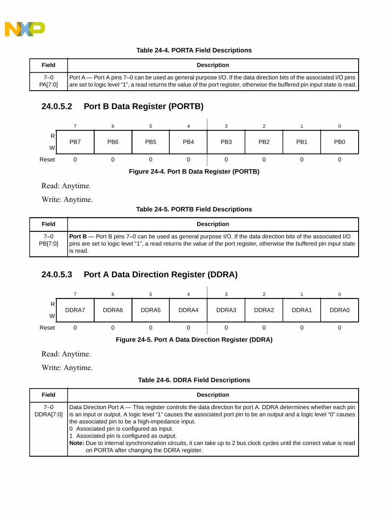
24.0.5.2 Port B Data Register (PORTB)
Read: Anytime.
Write: Anytime.
24.0.5.3 Port A Data Direction Register (DDRA)
Read: Anytime.
Write: Anytime.
Table 24-4. PORTA Field Descriptions
Field Description
7–0PA[7:0]
Port A — Port A pins 7–0 can be used as general purpose I/O. If the data direction bits of the associated I/O pinsare set to logic level “1”, a read returns the value of the port register, otherwise the buffered pin input state is read.
7 6 5 4 3 2 1 0
RPB7 PB6 PB5 PB4 PB3 PB2 PB1 PB0
W
Reset 0 0 0 0 0 0 0 0
Figure 24-4. Port B Data Register (PORTB)
Table 24-5. PORTB Field Descriptions
Field Description
7–0PB[7:0]
Port B — Port B pins 7–0 can be used as general purpose I/O. If the data direction bits of the associated I/Opins are set to logic level “1”, a read returns the value of the port register, otherwise the buffered pin input stateis read.
7 6 5 4 3 2 1 0
RDDRA7 DDRA6 DDRA5 DDRA4 DDRA3 DDRA2 DDRA1 DDRA0
W
Reset 0 0 0 0 0 0 0 0
Figure 24-5. Port A Data Direction Register (DDRA)
Table 24-6. DDRA Field Descriptions
Field Description
7–0DDRA[7:0]
Data Direction Port A — This register controls the data direction for port A. DDRA determines whether each pinis an input or output. A logic level “1” causes the associated port pin to be an output and a logic level “0” causesthe associated pin to be a high-impedance input.0 Associated pin is configured as input.1 Associated pin is configured as output.Note: Due to internal synchronization circuits, it can take up to 2 bus clock cycles until the correct value is read
on PORTA after changing the DDRA register.

Chapter 24 DG128 Port Integration Module (S12XDG128PIMV2)
MC9S12XDP512 Data Sheet, Rev. 2.21994 Freescale Semiconductor
24.0.5.4 Port B Data Direction Register (DDRB)
Read: Anytime.
Write: Anytime.
24.0.5.5 Port E Data Register (PORTE)
Read: Anytime.
Write: Anytime.
7 6 5 4 3 2 1 0
RDDRB7 DDRB6 DDRB5 DDRB4 DDRB3 DDRB2 DDRB1 DDRB0
W
Reset 0 0 0 0 0 0 0 0
Figure 24-6. Port B Data Direction Register (DDRB)
Table 24-7. DDRB Field Descriptions
Field Description
7–0DDRB[7:0]
Data Direction Port B — This register controls the data direction for port B. DDRB determines whether each pinis an input or output. A logic level “1” causes the associated port pin to be an output and a logic level “0” causesthe associated pin to be a high-impedance input.0 Associated pin is configured as input.1 Associated pin is configured as output.Note: Due to internal synchronization circuits, it can take up to 2 bus clock cycles until the correct value is read
on PORTB after changing the DDRB register.
7 6 5 4 3 2 1 0
RPE7 PE6 PE5 PE4 PE3 PE2
PE1 PE0
W
Alt.Func.
XCLKSor
ECLKX2MODB MODA ECLK EROMCTL IRQ XIRQ
Reset 0 0 0 0 0 0 —1
1. These registers are reset to zero. Two bus clock cycles after reset release the register values are updated with theassociated pin values.
—1
= Unimplemented or Reserved
Figure 24-7. Port E Data Register (PORTE)

24.0.5.6 Port E Data Direction Register (DDRE)
Read: Anytime.
Write: Anytime.
Table 24-8. PORTE Field Descriptions
Field Description
7–0PE[7:0]
Port E — Port E bits 7–0 are associated with external bus control signals and interrupt inputs. These includemode select (MODB, MODA), E clock, double frequency E clock, IRQ, and XIRQ.
When not used for any of these specific functions, Port E pins 7–2 can be used as general purpose I/O andpins 1–0 can be used as general purpose inputs.
If the data direction bits of the associated I/O pins are set to logic level “1”, a read returns the value of the portregister, otherwise the buffered pin input state is read.
Pins 6 and 5 are inputs with enabled pull-down devices while RESET pin is low.
Pins 7 and 3 are inputs with enabled pull-up devices while RESET pin is low.
7 6 5 4 3 2 1 0
RDDRE7 DDRE6 DDRE5 DDRE4 DDRE3 DDRE2
0 0
W
Reset 0 0 0 0 0 0 0 0
= Unimplemented or Reserved
Figure 24-8. Port E Data Direction Register (DDRE)
Table 24-9. DDRE Field Descriptions
Field Description
7–0DDRE[7:2]
Data Direction Port E — his register controls the data direction for port E. DDRE determines whether each pinis an input or output. A logic level “1” causes the associated port pin to be an output and a logic level “0” causesthe associated pin to be a high-impedance input.Port E bit 1 (associated with IRQ) and bit 0 (associated with XIRQ) cannot be configured as outputs. Port E, bits1 and 0, can be read regardless of whether the alternate interrupt function is enabled.0 Associated pin is configured as input.1 Associated pin is configured as output.Note: Due to internal synchronization circuits, it can take up to 2 bus clock cycles until the correct value is read
on PORTE after changing the DDRE register.

Chapter 24 DG128 Port Integration Module (S12XDG128PIMV2)
MC9S12XDP512 Data Sheet, Rev. 2.21996 Freescale Semiconductor
24.0.5.7 S12X_EBI Ports, BKGD, VREGEN Pin Pull-up Control Register (PUCR)
Read: Anytime in single-chip modes.
Write: Anytime, except BKPUE which is writable in special test mode only.
This register is used to enable pull-up devices for the associated ports A, B E, and K. Pull-up devices areassigned on a per-port basis and apply to any pin in the corresponding port currently configured as aninput.
7 6 5 4 3 2 1 0
RPUPKE BKPUE
0PUPEE PUPDE1
1. Register implemented, function disabled: Written values can be read back.
PUPCE1 PUPBE PUPAEW
Reset 1 1 0 1 0 0 0 0
= Unimplemented or Reserved
Figure 24-9. S12X_EBI Ports, BKGD, VREGEN Pin Pull-up Control Register (PUCR)
Table 24-10. PUCR Field Descriptions
Field Description
7PUPKE
Pull-up Port K Enable0 Port K pull-up devices are disabled.1 Enable pull-up devices for Port K input pins.
6BKPUE
BKGD and VREGEN Pin Pull-up Enable0 BKGD and VREGEN pull-up devices are disabled.1 Enable pull-up devices on BKGD and VREGEN pins.
4PUPEE
Pull-up Port E Enable0 Port E pull-up devices on bit 7, 4–0 are disabled.1 Enable pull-up devices for Port E input pins bits 7, 4–0.Note: Bits 5 and 6 of Port E have pull-down devices which are only enabled during reset. This bit has no effect
on these pins.
1PUPBE
Pull-up Port B Enable0 Port B pull-up devices are disabled.1 Enable pull-up devices for all Port B input pins.
0PUPAE
Pull-up Port A Enable0 Port A pull-up devices are disabled.1 Enable pull-up devices for all Port A input pins.

24.0.5.8 S12X_EBI Ports Reduced Drive Register (RDRIV)
Read: Anytime.
Write: Anytime.
This register is used to select reduced drive for the pins associated with ports A, B, E, and K. Ifenabled, the pins drive at about 1/6 of the full drive strength. The reduced drive function isindependent of which function is being used on a particular pin.
The reduced drive functionality does not take effect on the pins in emulation modes.
7 6 5 4 3 2 1 0
RRDPK
0 0RDPE RDPD1
1. Register implemented, function disabled: Written values can be read back.
RDPC1 RDPB RDPAW
Reset 0 0 0 0 0 0 0 0
= Unimplemented or Reserved
Figure 24-10. S12X_EBI Ports Reduced Drive Register (RDRIV)
Table 24-11. RDRIV Field Descriptions
Field Description
7RDPK
Reduced Drive of Port K0 All port K output pins have full drive enabled.1 All port K output pins have reduced drive enabled.
4RDPE
Reduced Drive of Port E0 All port E output pins have full drive enabled.1 All port E output pins have reduced drive enabled.
1RDPB
Reduced Drive of Port B0 All port B output pins have full drive enabled.1 All port B output pins have reduced drive enabled.
0RDPA
Reduced Drive of Ports A0 All Port A output pins have full drive enabled.1 All port A output pins have reduced drive enabled.

Chapter 24 DG128 Port Integration Module (S12XDG128PIMV2)
MC9S12XDP512 Data Sheet, Rev. 2.21998 Freescale Semiconductor
24.0.5.9 ECLK Control Register (ECLKCTL)
Read: Anytime.
Write: Anytime.
The ECLKCTL register is used to control the availability of the free-running clocks and the free-runningclock divider.
7 6 5 4 3 2 1 0
RNECLK NCLKX2
0 0 0 0EDIV1 EDIV0
W
Reset1
1. Reset values in emulation modes are identical to those of the target mode.
ModeDependent
1 0 0 0 0 0 0 Mode
SS0 1 0 0 0 0 0 0
SpecialSingle-Chip
ES1 1 0 0 0 0 0 0
EmulationSingle-Chip
ST0 1 0 0 0 0 0 0
SpecialTest
EX0 1 0 0 0 0 0 0
EmulationExpanded
NS1 1 0 0 0 0 0 0
NormalSingle-Chip
NX0 1 0 0 0 0 0 0
NormalExpanded
= Unimplemented or Reserved
Figure 24-11. ECLK Control Register (ECLKCTL)
Table 24-12. ECLKCTL Field Descriptions
Field Description
7NECLK
No ECLK — This bit controls the availability of a free-running clock on the ECLK pin. Clock output is alwaysactive in emulation modes and if enabled in all other operating modes.0 ECLK enabled1 ECLK disabled
6NCLKX2
No ECLKX2 — This bit controls the availability of a free-running clock on the ECLKX2 pin. This clock has a fixedrate of twice the internal bus clock. Clock output is always active in emulation modes and if enabled in all otheroperating modes.0 ECLKX2 is enabled1 ECLKX2 is disabled
1–0EDIV[1:0]
Free-Running ECLK Divider — These bits determine the rate of the free-running clock on the ECLK pin. Theusage of the bits is shown in Table 24-13. Divider is always disabled in emulation modes and active asprogrammed in all other operating modes.
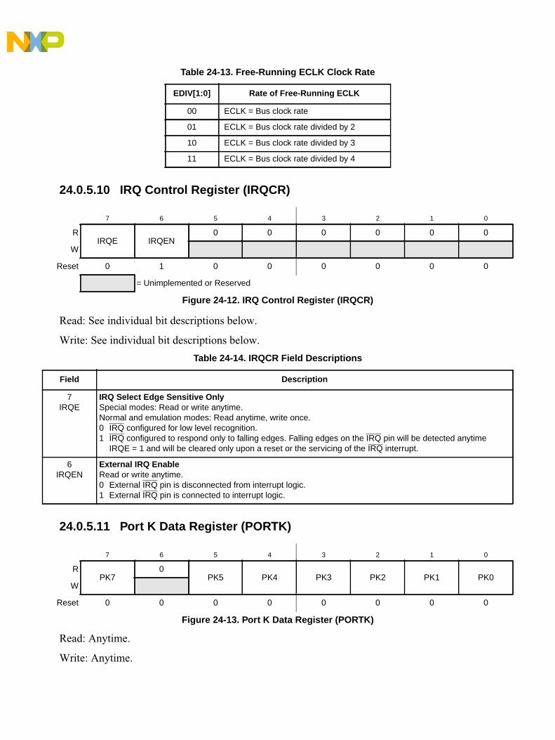
24.0.5.10 IRQ Control Register (IRQCR)
Read: See individual bit descriptions below.
Write: See individual bit descriptions below.
24.0.5.11 Port K Data Register (PORTK)
Read: Anytime.
Write: Anytime.
Table 24-13. Free-Running ECLK Clock Rate
EDIV[1:0] Rate of Free-Running ECLK
00 ECLK = Bus clock rate
01 ECLK = Bus clock rate divided by 2
10 ECLK = Bus clock rate divided by 3
11 ECLK = Bus clock rate divided by 4
7 6 5 4 3 2 1 0
RIRQE IRQEN
0 0 0 0 0 0
W
Reset 0 1 0 0 0 0 0 0
= Unimplemented or Reserved
Figure 24-12. IRQ Control Register (IRQCR)
Table 24-14. IRQCR Field Descriptions
Field Description
7IRQE
IRQ Select Edge Sensitive OnlySpecial modes: Read or write anytime.Normal and emulation modes: Read anytime, write once.0 IRQ configured for low level recognition.1 IRQ configured to respond only to falling edges. Falling edges on the IRQ pin will be detected anytime
IRQE = 1 and will be cleared only upon a reset or the servicing of the IRQ interrupt.
6IRQEN
External IRQ EnableRead or write anytime.0 External IRQ pin is disconnected from interrupt logic.1 External IRQ pin is connected to interrupt logic.
7 6 5 4 3 2 1 0
RPK7
0PK5 PK4 PK3 PK2 PK1 PK0
W
Reset 0 0 0 0 0 0 0 0
Figure 24-13. Port K Data Register (PORTK)

Chapter 24 DG128 Port Integration Module (S12XDG128PIMV2)
MC9S12XDP512 Data Sheet, Rev. 2.211000 Freescale Semiconductor
24.0.5.12 Port K Data Direction Register (DDRK)
Read: Anytime.
Write: Anytime.
This register controls the data direction for port K. DDRK determines whether each pin (except PK6) isan input or output. A logic level “1” causes the associated port pin to be an output and a logic level “0”causes the associated pin to be a high-impedance input.
24.0.5.13 Port T Data Register (PTT)
Read: Anytime.
Write: Anytime.
Table 24-15. PORTK Field Descriptions
Field Description
7–0PK[7,5:0]
Port K — Port K pins 7–0 can be used as general-purpose I/O. If the data direction bits of the associated I/O pinsare set to logic level “1”, a read returns the value of the port register, otherwise the buffered pin input state is readexcept for bit 6 which reads “0”.
7 6 5 4 3 2 1 0
RDDRK7
0DDRK5 DDRK4 DDRK3 DDRK2 DDRK1 DDRK0
W
Reset 0 0 0 0 0 0 0 0
Figure 24-14. Port K Data Direction Register (DDRK)
Table 24-16. DDRK Field Descriptions
Field Description
7–0DDRK[7,5:0]
Data Direction Port K0 Associated pin is configured as input.1 Associated pin is configured as output.Note: Due to internal synchronization circuits, it can take up to 2 bus clock cycles until the correct value is read
on PORTK after changing the DDRK register.
7 6 5 4 3 2 1 0
RPTT7 PTT6 PTT5 PTT4 PTT3 PTT2 PTT1 PTT0
W
ECT IOC7 IOC6 IOC5 IOC4 IOC3 IOC2 IOC1 IOC0
Reset 0 0 0 0 0 0 0 0
Figure 24-15. Port T Data Register (PTT)
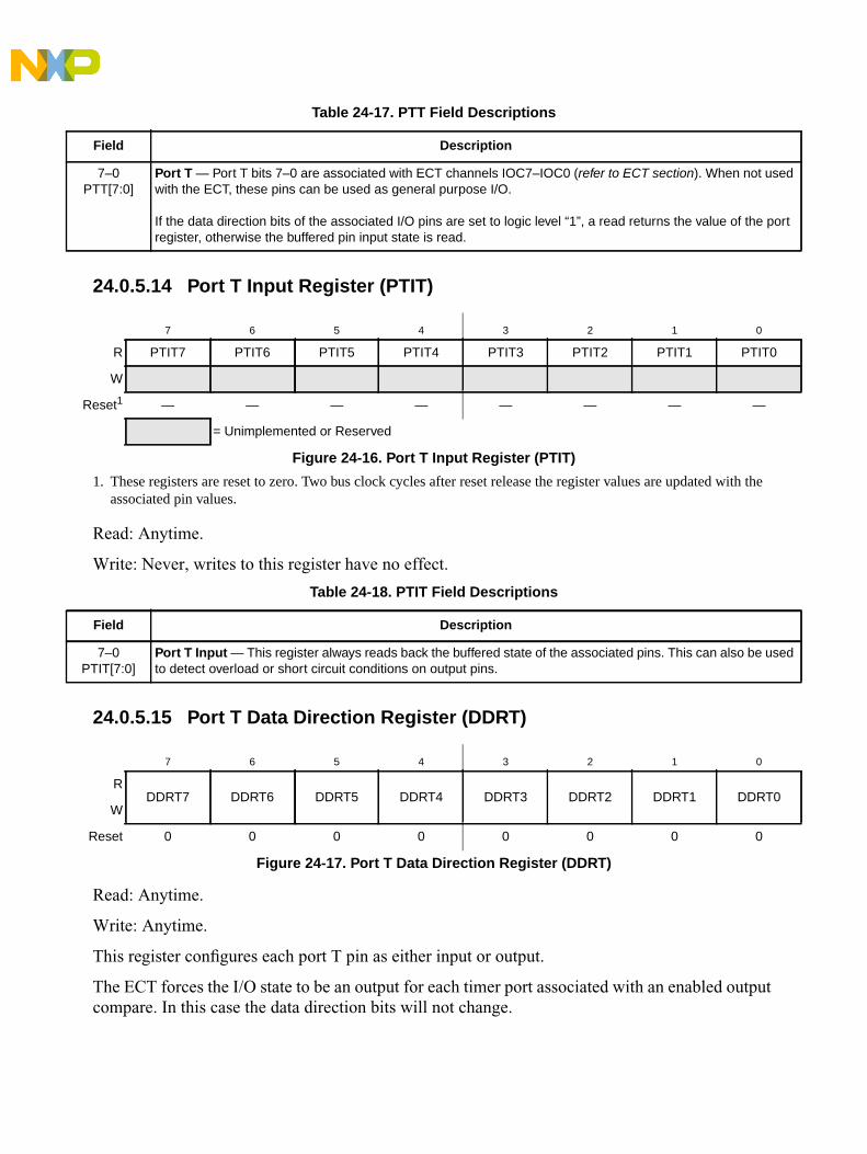
24.0.5.14 Port T Input Register (PTIT)
Read: Anytime.
Write: Never, writes to this register have no effect.
24.0.5.15 Port T Data Direction Register (DDRT)
Read: Anytime.
Write: Anytime.
This register configures each port T pin as either input or output.
The ECT forces the I/O state to be an output for each timer port associated with an enabled outputcompare. In this case the data direction bits will not change.
Table 24-17. PTT Field Descriptions
Field Description
7–0PTT[7:0]
Port T — Port T bits 7–0 are associated with ECT channels IOC7–IOC0 (refer to ECT section). When not usedwith the ECT, these pins can be used as general purpose I/O.
If the data direction bits of the associated I/O pins are set to logic level “1”, a read returns the value of the portregister, otherwise the buffered pin input state is read.
7 6 5 4 3 2 1 0
R PTIT7 PTIT6 PTIT5 PTIT4 PTIT3 PTIT2 PTIT1 PTIT0
W
Reset1
1. These registers are reset to zero. Two bus clock cycles after reset release the register values are updated with theassociated pin values.
— — — — — — — —
= Unimplemented or Reserved
Figure 24-16. Port T Input Register (PTIT)
Table 24-18. PTIT Field Descriptions
Field Description
7–0PTIT[7:0]
Port T Input — This register always reads back the buffered state of the associated pins. This can also be usedto detect overload or short circuit conditions on output pins.
7 6 5 4 3 2 1 0
RDDRT7 DDRT6 DDRT5 DDRT4 DDRT3 DDRT2 DDRT1 DDRT0
W
Reset 0 0 0 0 0 0 0 0
Figure 24-17. Port T Data Direction Register (DDRT)

Chapter 24 DG128 Port Integration Module (S12XDG128PIMV2)
MC9S12XDP512 Data Sheet, Rev. 2.211002 Freescale Semiconductor
The DDRT bits revert to controlling the I/O direction of a pin when the associated timer output compareis disabled.
The timer input capture always monitors the state of the pin.
24.0.5.16 Port T Reduced Drive Register (RDRT)
Read: Anytime.
Write: Anytime.
This register configures the drive strength of each port T output pin as either full or reduced. If the port isused as input this bit is ignored.
24.0.5.17 Port T Pull Device Enable Register (PERT)
Read: Anytime.
Write: Anytime.
Table 24-19. DDRT Field Descriptions
Field Description
7–0DDRT[7:0]
Data Direction Port T0 Associated pin is configured as input.1 Associated pin is configured as output.Note: Due to internal synchronization circuits, it can take up to 2 bus clock cycles until the correct value is read
on PTT or PTIT registers, when changing the DDRT register.
7 6 5 4 3 2 1 0
RRDRT7 RDRT6 RDRT5 RDRT4 RDRT3 RDRT2 RDRT1 RDRT0
W
Reset 0 0 0 0 0 0 0 0
Figure 24-18. Port T Reduced Drive Register (RDRT)
Table 24-20. RDRT Field Descriptions
Field Description
7–0RDRT[7:0]
Reduced Drive Port T0 Full drive strength at output.1 Associated pin drives at about 1/6 of the full drive strength.
7 6 5 4 3 2 1 0
RPERT7 PERT6 PERT5 PERT4 PERT3 PERT2 PERT1 PERT0
W
Reset 0 0 0 0 0 0 0 0
Figure 24-19. Port T Pull Device Enable Register (PERT)

This register configures whether a pull-up or a pull-down device is activated, if the port is used asinput. This bit has no effect if the port is used as output. Out of reset no pull device is enabled.
24.0.5.18 Port T Polarity Select Register (PPST)
Read: Anytime.
Write: Anytime.
This register selects whether a pull-down or a pull-up device is connected to the pin.
24.0.5.19 Port S Data Register (PTS)
Read: Anytime.
Write: Anytime.
Table 24-21. PERT Field Descriptions
Field Description
7–0PERT[7:0]
Pull Device Enable Port T0 Pull-up or pull-down device is disabled.1 Either a pull-up or pull-down device is enabled.
7 6 5 4 3 2 1 0
RPPST7 PPST6 PPST5 PPST4 PPST3 PPST2 PPST1 PPST0
W
Reset 0 0 0 0 0 0 0 0
Figure 24-20. Port T Polarity Select Register (PPST)
Table 24-22. PPST Field Descriptions
Field Description
7–0PPST[7:0]
Pull Select Port T0 A pull-up device is connected to the associated port T pin, if enabled by the associated bit in register PERT
and if the port is used as input.1 A pull-down device is connected to the associated port T pin, if enabled by the associated bit in register PERT
and if the port is used as input.
7 6 5 4 3 2 1 0
RPTS7 PTS6 PTS5 PTS4 PTS3 PTS2 PTS1 PTS0
W
SCI/SPI SS0 SCK0 MOSI0 MISO0 TXD1 RXD1 TXD0 RXD0
Reset 0 0 0 0 0 0 0 0
Figure 24-21. Port S Data Register (PTS)

Chapter 24 DG128 Port Integration Module (S12XDG128PIMV2)
MC9S12XDP512 Data Sheet, Rev. 2.211004 Freescale Semiconductor
Port S pins 7–4 are associated with the SPI0. The SPI0 pin configuration is determined by several statusbits in the SPI0 module. Refer to SPI section for details. When not used with the SPI0, these pins can beused as general purpose I/O.
Port S bits 3–0 are associated with the SCI1 and SCI0. The SCI ports associated with transmit pins 3 and1 are configured as outputs if the transmitter is enabled. The SCI ports associated with receive pins 2 and0 are configured as inputs if the receiver is enabled. Refer to SCI section for details. When not used withthe SCI, these pins can be used as general purpose I/O.
If the data direction bits of the associated I/O pins are set to logic level “1”, a read returns the value of theport register, otherwise the buffered pin input state is read.
24.0.5.20 Port S Input Register (PTIS)
Read: Anytime.
Write: Never, writes to this register have no effect.
This register always reads back the buffered state of the associated pins. This also can be used to detectoverload or short circuit conditions on output pins.
24.0.5.21 Port S Data Direction Register (DDRS)
Read: Anytime.
Write: Anytime.
This register configures each port S pin as either input or output.
If SPI0 is enabled, the SPI0 determines the pin direction. Refer to SPI section for details.
7 6 5 4 3 2 1 0
R PTIS7 PTIS6 PTIS5 PTIS4 PTIS3 PTIS2 PTIS1 PTIS0
W
Reset1
1. These registers are reset to zero. Two bus clock cycles after reset release the register values are updated with theassociated pin values.
— — — — — — — —
= Unimplemented or Reserved
Figure 24-22. Port S Input Register (PTIS)
7 6 5 4 3 2 1 0
RDDRS7 DDRS6 DDRS5 DDRS4 DDRS3 DDRS2 DDRS1 DDRS0
W
Reset 0 0 0 0 0 0 0 0
Figure 24-23. Port S Data Direction Register (DDRS)

If the associated SCI transmit or receive channel is enabled this register has no effect on the pins.The pin is forced to be an output if a SCI transmit channel is enabled, it is forced to be an input ifthe SCI receive channel is enabled.
The DDRS bits revert to controlling the I/O direction of a pin when the associated channel isdisabled.
24.0.5.22 Port S Reduced Drive Register (RDRS)
Read: Anytime.
Write: Anytime.
This register configures the drive strength of each port S output pin as either full or reduced. If theport is used as input this bit is ignored.
24.0.5.23 Port S Pull Device Enable Register (PERS)
Read: Anytime.
Table 24-23. DDRS Field Descriptions
Field Description
7–0DDRS[7:0]
Data Direction Port S0 Associated pin is configured as input.1 Associated pin is configured as output.Note: Due to internal synchronization circuits, it can take up to 2 bus clock cycles until the correct value is read
on PTS or PTIS registers, when changing the DDRS register.
7 6 5 4 3 2 1 0
RRDRS7 RDRS6 RDRS5 RDRS4 RDRS3 RDRS2 RDRS1 RDRS0
W
Reset 0 0 0 0 0 0 0 0
Figure 24-24. Port S Reduced Drive Register (RDRS)
Table 24-24. RDRS Field Descriptions
Field Description
7–0RDRS[7:0]
Reduced Drive Port S0 Full drive strength at output.1 Associated pin drives at about 1/6 of the full drive strength.
7 6 5 4 3 2 1 0
RPERS7 PERS6 PERS5 PERS4 PERS3 PERS2 PERS1 PERS0
W
Reset 1 1 1 1 1 1 1 1
Figure 24-25. Port S Pull Device Enable Register (PERS)
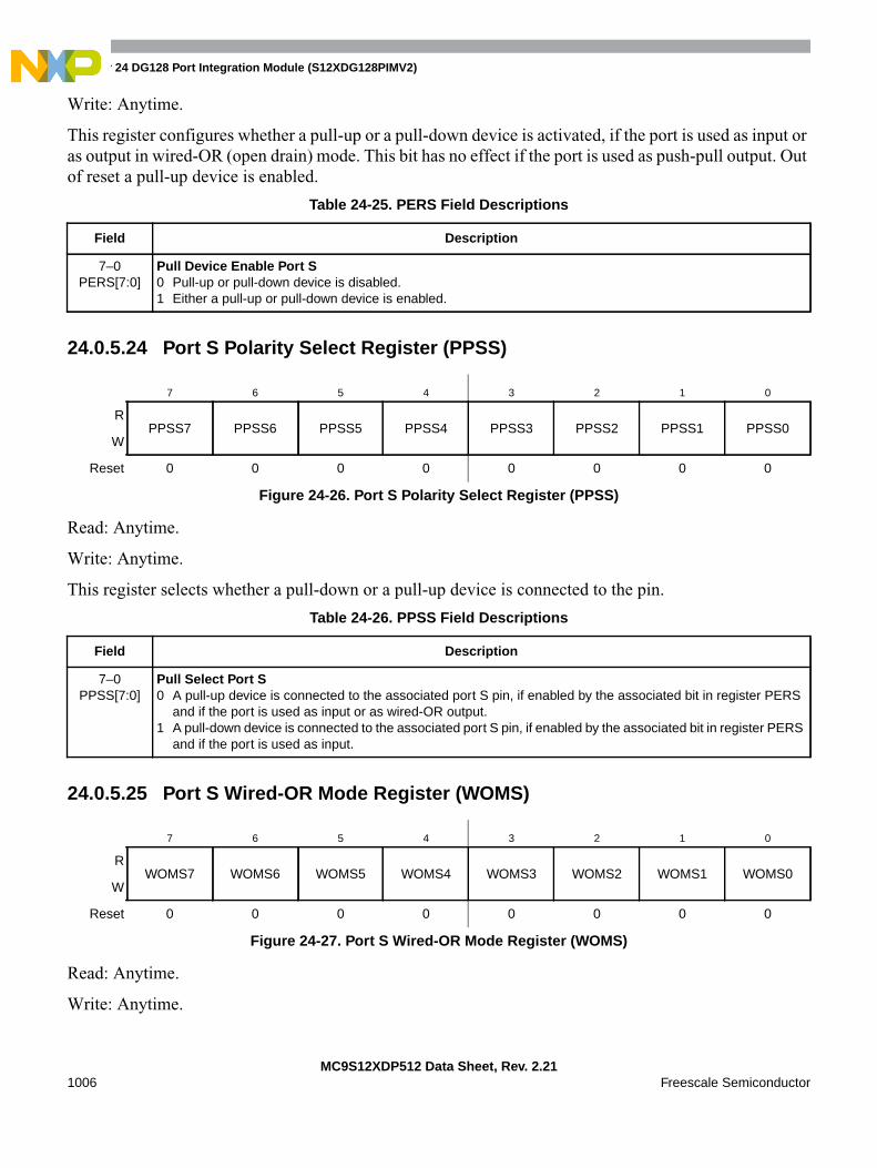
Chapter 24 DG128 Port Integration Module (S12XDG128PIMV2)
MC9S12XDP512 Data Sheet, Rev. 2.211006 Freescale Semiconductor
Write: Anytime.
This register configures whether a pull-up or a pull-down device is activated, if the port is used as input oras output in wired-OR (open drain) mode. This bit has no effect if the port is used as push-pull output. Outof reset a pull-up device is enabled.
24.0.5.24 Port S Polarity Select Register (PPSS)
Read: Anytime.
Write: Anytime.
This register selects whether a pull-down or a pull-up device is connected to the pin.
24.0.5.25 Port S Wired-OR Mode Register (WOMS)
Read: Anytime.
Write: Anytime.
Table 24-25. PERS Field Descriptions
Field Description
7–0PERS[7:0]
Pull Device Enable Port S0 Pull-up or pull-down device is disabled.1 Either a pull-up or pull-down device is enabled.
7 6 5 4 3 2 1 0
RPPSS7 PPSS6 PPSS5 PPSS4 PPSS3 PPSS2 PPSS1 PPSS0
W
Reset 0 0 0 0 0 0 0 0
Figure 24-26. Port S Polarity Select Register (PPSS)
Table 24-26. PPSS Field Descriptions
Field Description
7–0PPSS[7:0]
Pull Select Port S0 A pull-up device is connected to the associated port S pin, if enabled by the associated bit in register PERS
and if the port is used as input or as wired-OR output.1 A pull-down device is connected to the associated port S pin, if enabled by the associated bit in register PERS
and if the port is used as input.
7 6 5 4 3 2 1 0
RWOMS7 WOMS6 WOMS5 WOMS4 WOMS3 WOMS2 WOMS1 WOMS0
W
Reset 0 0 0 0 0 0 0 0
Figure 24-27. Port S Wired-OR Mode Register (WOMS)

This register configures the output pins as wired-OR. If enabled the output is driven active low only(open-drain). A logic level of “1” is not driven. It applies also to the SPI and SCI outputs and allowsa multipoint connection of several serial modules. These bits have no influence on pins used asinputs.
24.0.5.26 Port M Data Register (PTM)
Read: Anytime.
Write: Anytime.
Port M pins 7–0 are associated with the CAN0, as well as the routed CAN0, CAN4, and SPI0modules. When not used with any of the peripherals, these pins can be used as general purpose I/O.
If the data direction bits of the associated I/O pins are set to logic level “1”, a read returns the valueof the port register, otherwise the buffered pin input state is read.
Table 24-27. WOMS Field Descriptions
Field Description
7–0WOMS[7:0]
Wired-OR Mode Port S0 Output buffers operate as push-pull outputs.1 Output buffers operate as open-drain outputs.
7 6 5 4 3 2 1 0
RPTM7 PTM6 PTM5 PTM4 PTM3 PTM2 PTM1 PTM0
W
CAN TXCAN0 RXCAN0
RoutedCAN0
TXCAN0 RXCAN0 TXCAN0 RXCAN0
RoutedCAN4
TXCAN4 RXCAN4 TXCAN4 RXCAN4
RoutedSPI0
SCK0 MOSI0 SS0 MISO0
Reset 0 0 0 0 0 0 0 0
Figure 24-28. Port M Data Register (PTM)
Table 24-28. PTM Field Descriptions
Field Description
7–6PTM[7:6]
The CAN4 function (TXCAN4 and RXCAN4) takes precedence over the general purpose I/O function if the CAN4module is enabled. Refer to MSCAN section for details.
5–4PTM[5:4]
The routed CAN0 function (TXCAN0 and RXCAN0) takes precedence over the routed CAN4, the routed SPI0and the general purpose I/O function if the routed CAN0 module is enabled.The routed CAN4 function (TXCAN4 and RXCAN4) takes precedence over the routed SPI0 and general purposeI/O function if the routed CAN4 module is enabled. Refer to MSCAN section for details.
The routed SPI0 function (SCK0 and MOSI0) takes precedence of the general purpose I/O function if the routedSPI0 is enabled. Refer to SPI section for details.
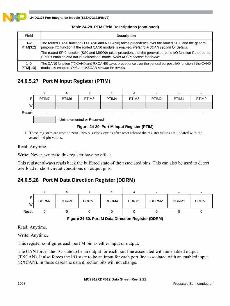
Chapter 24 DG128 Port Integration Module (S12XDG128PIMV2)
MC9S12XDP512 Data Sheet, Rev. 2.211008 Freescale Semiconductor
24.0.5.27 Port M Input Register (PTIM)
Read: Anytime.
Write: Never, writes to this register have no effect.
This register always reads back the buffered state of the associated pins. This can also be used to detectoverload or short circuit conditions on output pins.
24.0.5.28 Port M Data Direction Register (DDRM)
Read: Anytime.
Write: Anytime.
This register configures each port M pin as either input or output.
The CAN forces the I/O state to be an output for each port line associated with an enabled output(TXCAN). It also forces the I/O state to be an input for each port line associated with an enabled input(RXCAN). In those cases the data direction bits will not change.
3–2PTM[3:2]
The routed CAN0 function (TXCAN0 and RXCAN0) takes precedence over the routed SPI0 and the generalpurpose I/O function if the routed CAN0 module is enabled. Refer to MSCAN section for details.
The routed SPI0 function (SS0 and MISO0) takes precedence of the general purpose I/O function if the routedSPI0 is enabled and not in bidirectional mode. Refer to SPI section for details.
1–0PTM[1:0]
The CAN0 function (TXCAN0 and RXCAN0) takes precedence over the general purpose I/O function if the CAN0module is enabled. Refer to MSCAN section for details.
7 6 5 4 3 2 1 0
R PTIM7 PTIM6 PTIM5 PTIM4 PTIM3 PTIM2 PTIM1 PTIM0
W
Reset1
1. These registers are reset to zero. Two bus clock cycles after reset release the register values are updated with theassociated pin values.
— — — — — — — —
= Unimplemented or Reserved
Figure 24-29. Port M Input Register (PTIM)
7 6 5 4 3 2 1 0
RDDRM7 DDRM6 DDRM5 DDRM4 DDRM3 DDRM2 DDRM1 DDRM0
W
Reset 0 0 0 0 0 0 0 0
Figure 24-30. Port M Data Direction Register (DDRM)
Table 24-28. PTM Field Descriptions (continued)
Field Description
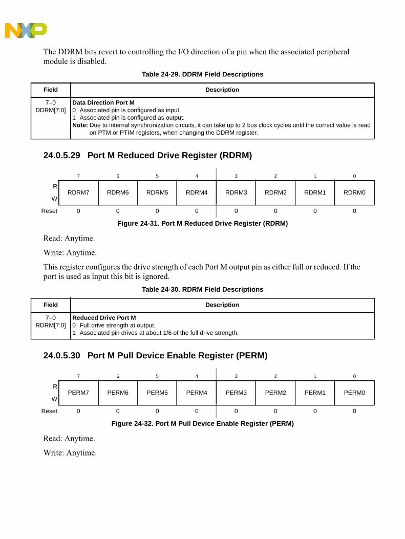
The DDRM bits revert to controlling the I/O direction of a pin when the associated peripheralmodule is disabled.
24.0.5.29 Port M Reduced Drive Register (RDRM)
Read: Anytime.
Write: Anytime.
This register configures the drive strength of each Port M output pin as either full or reduced. If theport is used as input this bit is ignored.
24.0.5.30 Port M Pull Device Enable Register (PERM)
Read: Anytime.
Write: Anytime.
Table 24-29. DDRM Field Descriptions
Field Description
7–0DDRM[7:0]
Data Direction Port M0 Associated pin is configured as input.1 Associated pin is configured as output.Note: Due to internal synchronization circuits, it can take up to 2 bus clock cycles until the correct value is read
on PTM or PTIM registers, when changing the DDRM register.
7 6 5 4 3 2 1 0
RRDRM7 RDRM6 RDRM5 RDRM4 RDRM3 RDRM2 RDRM1 RDRM0
W
Reset 0 0 0 0 0 0 0 0
Figure 24-31. Port M Reduced Drive Register (RDRM)
Table 24-30. RDRM Field Descriptions
Field Description
7–0RDRM[7:0]
Reduced Drive Port M0 Full drive strength at output.1 Associated pin drives at about 1/6 of the full drive strength.
7 6 5 4 3 2 1 0
RPERM7 PERM6 PERM5 PERM4 PERM3 PERM2 PERM1 PERM0
W
Reset 0 0 0 0 0 0 0 0
Figure 24-32. Port M Pull Device Enable Register (PERM)

Chapter 24 DG128 Port Integration Module (S12XDG128PIMV2)
MC9S12XDP512 Data Sheet, Rev. 2.211010 Freescale Semiconductor
This register configures whether a pull-up or a pull-down device is activated, if the port is used as input orwired-OR output. This bit has no effect if the port is used as push-pull output. Out of reset no pull deviceis enabled.
24.0.5.31 Port M Polarity Select Register (PPSM)
Read: Anytime.
Write: Anytime.
This register selects whether a pull-down or a pull-up device is connected to the pin. If CAN is active, apull-up device can be activated on the related RXCAN inputs, but not a pull-down.
24.0.5.32 Port M Wired-OR Mode Register (WOMM)
Read: Anytime.
Write: Anytime.
Table 24-31. PERM Field Descriptions
Field Description
7–0PERM[7:0]
Pull Device Enable Port M0 Pull-up or pull-down device is disabled.1 Either a pull-up or pull-down device is enabled.
7 6 5 4 3 2 1 0
RPPSM7 PPSM6 PPSM5 PPSM4 PPSM3 PPSM2 PPSM1 PPSM0
W
Reset 0 0 0 0 0 0 0 0
Figure 24-33. Port M Polarity Select Register (PPSM)
Table 24-32. PPSM Field Descriptions
Field Description
7–0PPSM[7:0]
Pull Select Port M0 A pull-up device is connected to the associated port M pin, if enabled by the associated bit in register PERM
and if the port is used as general purpose or RXCAN input.1 A pull-down device is connected to the associated port M pin, if enabled by the associated bit in register PERM
and if the port is used as a general purpose but not as RXCAN.
7 6 5 4 3 2 1 0
RWOMM7 WOMM6 WOMM5 WOMM4 WOMM3 WOMM2 WOMM1 WOMM0
W
Reset 0 0 0 0 0 0 0 0
Figure 24-34. Port M Wired-OR Mode Register (WOMM)

This register configures the output pins as wired-OR. If enabled the output is driven active low only(open-drain). A logic level of “1” is not driven. It applies also to the CAN outputs and allows amultipoint connection of several serial modules. This bit has no influence on pins used as inputs.
24.0.5.33 Module Routing Register (MODRR)
Read: Anytime.
Write: Anytime.
This register configures the re-routing of CAN0, CAN4, SPI0, SPI1 on alternative ports.
Table 24-33. WOMM Field Descriptions
Field Description
7–0WOMM[7:0]
Wired-OR Mode Port M0 Output buffers operate as push-pull outputs.1 Output buffers operate as open-drain outputs.
7 6 5 4 3 2 1 0
R 0MODRR61
1. Register implemented, function disabled: Written values can be read back.
MODRR5 MODRR4 MODRR3 MODRR2 MODRR1 MODRR0W
Reset 0 0 0 0 0 0 0 0
= Unimplemented or Reserved
Figure 24-35. Module Routing Register (MODRR)
Table 24-34. Module Routing Summary
ModuleMODRR Related Pins
6 5 4 3 2 1 0 RXCAN TXCAN
CAN0
x x x x x 0 0 PM0 PM1
x x x x x 0 1 PM2 PM3
x x x x x 1 0 PM4 PM5
x x x x x 1 1 PJ6 PJ7
CAN4
x x x 0 0 x x PJ6 PJ7
x x x 0 1 x x PM4 PM5
x x x 1 0 x x PM6 PM7
x x x 1 1 x x Reserved
MISO MOSI SCK SS
SPI0x x 0 x x x x PS4 PS5 PS6 PS7
x x 1 x x x x PM2 PM4 PM5 PM3
SPI1x 0 x x x x x PP0 PP1 PP2 PP3
x 1 x x x x x PH0 PH1 PH2 PH3

Chapter 24 DG128 Port Integration Module (S12XDG128PIMV2)
MC9S12XDP512 Data Sheet, Rev. 2.211012 Freescale Semiconductor
24.0.5.34 Port P Data Register (PTP)
Read: Anytime.
Write: Anytime.
Port P pins 7–0 are associated with the PWM as well as the SPI1. These pins can be used as generalpurpose I/O when not used with any of the peripherals.
If the data direction bits of the associated I/O pins are set to logic level “1”, a read returns the value of theport register, otherwise the buffered pin input state is read.
The PWM function takes precedence over the general purpose I/O and the SPI1 function if the associatedPWM channel is enabled. While channels 6-0 are output only if the respective channel is enabled, channel7 can be PWM output or input if the shutdown feature is enabled. Refer to PWM section for details.
The SPI1 function takes precedence over the general purpose I/O function if enabled. Refer to SPI sectionfor details.
24.0.5.35 Port P Input Register (PTIP)
Read: Anytime.
Write: Never, writes to this register have no effect.
This register always reads back the buffered state of the associated pins. This can also be used to detectoverload or short circuit conditions on output pins.
7 6 5 4 3 2 1 0
RPTP7 PTP6 PTP5 PTP4 PTP3 PTP2 PTP1 PTP0
W
PWM PWM7 PWM6 PWM5 PWM4 PWM3 PWM2 PWM1 PWM0
SPI SS1 SCK1 MOSI1 MISO1
Reset 0 0 0 0 0 0 0 0
Figure 24-36. Port P Data Register (PTP)
7 6 5 4 3 2 1 0
R PTIP7 PTIP6 PTIP5 PTIP4 PTIP3 PTIP2 PTIP1 PTIP0
W
Reset1
1. These registers are reset to zero. Two bus clock cycles after reset release the register values are updated with theassociated pin values.
— — — — — — — —
= Unimplemented or Reserved
Figure 24-37. Port P Input Register (PTIP)

24.0.5.36 Port P Data Direction Register (DDRP)
Read: Anytime.
Write: Anytime.
This register configures each port P pin as either input or output.
If the associated PWM channel or SPI module is enabled this register has no effect on the pins.
The PWM forces the I/O state to be an output for each port line associated with an enabled PWM7–0 channel. Channel 7 can force the pin to input if the shutdown feature is enabled. Refer to PWMsection for details.
If SPI is enabled, the SPI determines the pin direction. Refer to SPI section for details.
The DDRP bits revert to controlling the I/O direction of a pin when the associated peripherals aredisabled.
24.0.5.37 Port P Reduced Drive Register (RDRP)
Read: Anytime.
Write: Anytime.
This register configures the drive strength of each port P output pin as either full or reduced. If theport is used as input this bit is ignored.
7 6 5 4 3 2 1 0
RDDRP7 DDRP6 DDRP5 DDRP4 DDRP3 DDRP2 DDRP1 DDRP0
W
Reset 0 0 0 0 0 0 0 0
Figure 24-38. Port P Data Direction Register (DDRP)
Table 24-35. DDRP Field Descriptions
Field Description
7–0DDRP[7:0]
Data Direction Port P0 Associated pin is configured as input.1 Associated pin is configured as output.Note: Due to internal synchronization circuits, it can take up to 2 bus clock cycles until the correct value is read
on PTP or PTIP registers, when changing the DDRP register.
7 6 5 4 3 2 1 0
RRDRP7 RDRP6 RDRP5 RDRP4 RDRP3 RDRP2 RDRP1 RDRP0
W
Reset 0 0 0 0 0 0 0 0
Figure 24-39. Port P Reduced Drive Register (RDRP)

Chapter 24 DG128 Port Integration Module (S12XDG128PIMV2)
MC9S12XDP512 Data Sheet, Rev. 2.211014 Freescale Semiconductor
24.0.5.38 Port P Pull Device Enable Register (PERP)
Read: Anytime.
Write: Anytime.
This register configures whether a pull-up or a pull-down device is activated, if the port is used as input.This bit has no effect if the port is used as output. Out of reset no pull device is enabled.
24.0.5.39 Port P Polarity Select Register (PPSP)
Read: Anytime.
Write: Anytime.
This register serves a dual purpose by selecting the polarity of the active interrupt edge as well as selectinga pull-up or pull-down device if enabled.
Table 24-36. RDRP Field Descriptions
Field Description
7–0RDRP[7:0]
Reduced Drive Port P0 Full drive strength at output.1 Associated pin drives at about 1/6 of the full drive strength.
7 6 5 4 3 2 1 0
RPERP7 PERP6 PERP5 PERP4 PERP3 PERP2 PERP1 PERP0
W
Reset 0 0 0 0 0 0 0 0
Figure 24-40. Port P Pull Device Enable Register (PERP)
Table 24-37. PERP Field Descriptions
Field Description
7–0PERP[7:0]
Pull Device Enable Port P0 Pull-up or pull-down device is disabled.1 Either a pull-up or pull-down device is enabled.
7 6 5 4 3 2 1 0
RPPSP7 PPSP6 PPSP5 PPSP4 PPSP3 PPSP2 PPSP1 PPSP0
W
Reset 0 0 0 0 0 0 0 0
Figure 24-41. Port P Polarity Select Register (PPSP)

24.0.5.40 Port P Interrupt Enable Register (PIEP)
Read: Anytime.
Write: Anytime.
This register disables or enables on a per-pin basis the edge sensitive external interrupt associatedwith Port P.
24.0.5.41 Port P Interrupt Flag Register (PIFP)
Read: Anytime.
Write: Anytime.
Each flag is set by an active edge on the associated input pin. This could be a rising or a fallingedge based on the state of the PPSP register. To clear this flag, write logic level “1” to thecorresponding bit in the PIFP register. Writing a “0” has no effect.
Table 24-38. PPSP Field Descriptions
Field Description
7–0PPSP[7:0]
Polarity Select Port P0 Falling edge on the associated port P pin sets the associated flag bit in the PIFP register.A pull-up device is
connected to the associated port P pin, if enabled by the associated bit in register PERP and if the port is usedas input.
1 Rising edge on the associated port P pin sets the associated flag bit in the PIFP register.A pull-down deviceis connected to the associated port P pin, if enabled by the associated bit in register PERP and if the port isused as input.
7 6 5 4 3 2 1 0
RPIEP7 PIEP6 PIEP5 PIEP4 PIEP3 PIEP2 PIEP1 PIEP0
W
Reset 0 0 0 0 0 0 0 0
Figure 24-42. Port P Interrupt Enable Register (PIEP)
Table 24-39. PIEP Field Descriptions
Field Description
7–0PIEP[7:0]
Interrupt Enable Port P0 Interrupt is disabled (interrupt flag masked).1 Interrupt is enabled.
7 6 5 4 3 2 1 0
RPIFP7 PIFP6 PIFP5 PIFP4 PIFP3 PIFP2 PIFP1 PIFP0
W
Reset 0 0 0 0 0 0 0 0
Figure 24-43. Port P Interrupt Flag Register (PIFP)
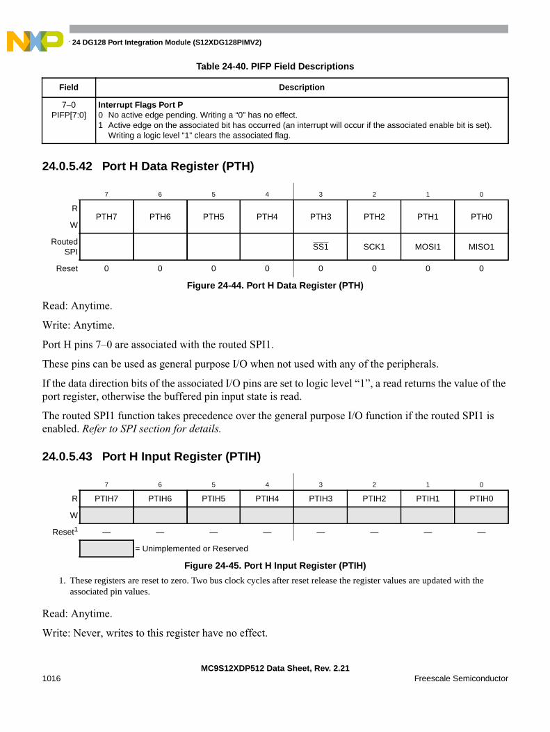
Chapter 24 DG128 Port Integration Module (S12XDG128PIMV2)
MC9S12XDP512 Data Sheet, Rev. 2.211016 Freescale Semiconductor
24.0.5.42 Port H Data Register (PTH)
Read: Anytime.
Write: Anytime.
Port H pins 7–0 are associated with the routed SPI1.
These pins can be used as general purpose I/O when not used with any of the peripherals.
If the data direction bits of the associated I/O pins are set to logic level “1”, a read returns the value of theport register, otherwise the buffered pin input state is read.
The routed SPI1 function takes precedence over the general purpose I/O function if the routed SPI1 isenabled. Refer to SPI section for details.
24.0.5.43 Port H Input Register (PTIH)
Read: Anytime.
Write: Never, writes to this register have no effect.
Table 24-40. PIFP Field Descriptions
Field Description
7–0PIFP[7:0]
Interrupt Flags Port P0 No active edge pending. Writing a “0” has no effect.1 Active edge on the associated bit has occurred (an interrupt will occur if the associated enable bit is set).
Writing a logic level “1” clears the associated flag.
7 6 5 4 3 2 1 0
RPTH7 PTH6 PTH5 PTH4 PTH3 PTH2 PTH1 PTH0
W
RoutedSPI
SS1 SCK1 MOSI1 MISO1
Reset 0 0 0 0 0 0 0 0
Figure 24-44. Port H Data Register (PTH)
7 6 5 4 3 2 1 0
R PTIH7 PTIH6 PTIH5 PTIH4 PTIH3 PTIH2 PTIH1 PTIH0
W
Reset1
1. These registers are reset to zero. Two bus clock cycles after reset release the register values are updated with theassociated pin values.
— — — — — — — —
= Unimplemented or Reserved
Figure 24-45. Port H Input Register (PTIH)

This register always reads back the buffered state of the associated pins. This can also be used todetect overload or short circuit conditions on output pins.
24.0.5.44 Port H Data Direction Register (DDRH)
Read: Anytime.
Write: Anytime.
This register configures each port H pin as either input or output.
If the associated routed SPI module is enabled this register has no effect on the pins.
If a SPI module is enabled, the SPI determines the pin direction. Refer to SPI section for details.
The DDRH bits revert to controlling the I/O direction of a pin when the associated peripheralmodules are disabled.
24.0.5.45 Port H Reduced Drive Register (RDRH)
Read: Anytime.
Write: Anytime.
This register configures the drive strength of each Port H output pin as either full or reduced. If theport is used as input this bit is ignored.
7 6 5 4 3 2 1 0
RDDRH7 DDRH6 DDRH5 DDRH4 DDRH3 DDRH2 DDRH1 DDRH0
W
Reset 0 0 0 0 0 0 0 0
Figure 24-46. Port H Data Direction Register (DDRH)
Table 24-41. DDRH Field Descriptions
Field Description
7–0DDRH[7:0]
Data Direction Port H0 Associated pin is configured as input.1 Associated pin is configured as output.Note: Due to internal synchronization circuits, it can take up to 2 bus clock cycles until the correct value is read
on PTH or PTIH registers, when changing the DDRH register.
7 6 5 4 3 2 1 0
RRDRH7 RDRH6 RDRH5 RDRH4 RDRH3 RDRH2 RDRH1 RDRH0
W
Reset 0 0 0 0 0 0 0 0
Figure 24-47. Port H Reduced Drive Register (RDRH)

Chapter 24 DG128 Port Integration Module (S12XDG128PIMV2)
MC9S12XDP512 Data Sheet, Rev. 2.211018 Freescale Semiconductor
24.0.5.46 Port H Pull Device Enable Register (PERH)
Read: Anytime.
Write: Anytime.
This register configures whether a pull-up or a pull-down device is activated, if the port is used as input.This bit has no effect if the port is used as output. Out of reset no pull device is enabled.
24.0.5.47 Port H Polarity Select Register (PPSH)
Read: Anytime.
Write: Anytime.
This register serves a dual purpose by selecting the polarity of the active interrupt edge as well as selectinga pull-up or pull-down device if enabled.
Table 24-42. RDRH Field Descriptions
Field Description
7–0RDRH[7:0]
Reduced Drive Port H0 Full drive strength at output.1 Associated pin drives at about 1/6 of the full drive strength.
7 6 5 4 3 2 1 0
RPERH7 PERH6 PERH5 PERH4 PERH3 PERH2 PERH1 PERH0
W
Reset 0 0 0 0 0 0 0 0
Figure 24-48. Port H Pull Device Enable Register (PERH)
Table 24-43. PERH Field Descriptions
Field Description
7–0PERH[7:0]
Pull Device Enable Port H0 Pull-up or pull-down device is disabled.1 Either a pull-up or pull-down device is enabled.
7 6 5 4 3 2 1 0
RPPSH7 PPSH6 PPSH5 PPSH4 PPSH3 PPSH2 PPSH1 PPSH0
W
Reset 0 0 0 0 0 0 0 0
Figure 24-49. Port H Polarity Select Register (PPSH)

24.0.5.48 Port H Interrupt Enable Register (PIEH)
Read: Anytime.
Write: Anytime.
This register disables or enables on a per-pin basis the edge sensitive external interrupt associatedwith Port H.
24.0.5.49 Port H Interrupt Flag Register (PIFH)
Read: Anytime.
Write: Anytime.
Each flag is set by an active edge on the associated input pin. This could be a rising or a fallingedge based on the state of the PPSH register. To clear this flag, write logic level “1” to thecorresponding bit in the PIFH register. Writing a “0” has no effect.
Table 24-44. PPSH Field Descriptions
Field Description
7–0PPSH[7:0]
Polarity Select Port H0 Falling edge on the associated port H pin sets the associated flag bit in the PIFH register.
A pull-up device is connected to the associated port H pin, if enabled by the associated bit in register PERHand if the port is used as input.
1 Rising edge on the associated port H pin sets the associated flag bit in the PIFH register.A pull-down device is connected to the associated port H pin, if enabled by the associated bit in register PERHand if the port is used as input.
7 6 5 4 3 2 1 0
RPIEH7 PIEH6 PIEH5 PIEH4 PIEH3 PIEH2 PIEH1 PIEH0
W
Reset 0 0 0 0 0 0 0 0
Figure 24-50. Port H Interrupt Enable Register (PIEH)
Table 24-45. PIEH Field Descriptions
Field Description
7–0PIEH[7:0]
Interrupt Enable Port H0 Interrupt is disabled (interrupt flag masked).1 Interrupt is enabled.
7 6 5 4 3 2 1 0
RPIFH7 PIFH6 PIFH5 PIFH4 PIFH3 PIFH2 PIFH1 PIFH0
W
Reset 0 0 0 0 0 0 0 0
Figure 24-51. Port H Interrupt Flag Register (PIFH)
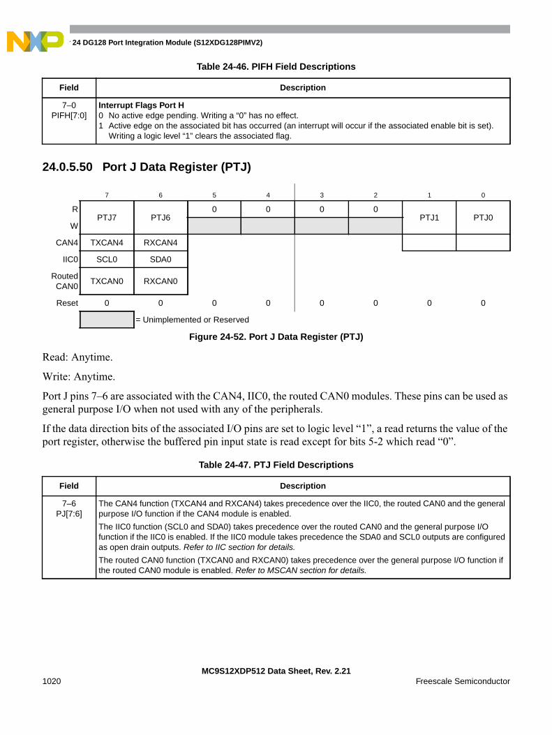
Chapter 24 DG128 Port Integration Module (S12XDG128PIMV2)
MC9S12XDP512 Data Sheet, Rev. 2.211020 Freescale Semiconductor
24.0.5.50 Port J Data Register (PTJ)
Read: Anytime.
Write: Anytime.
Port J pins 7–6 are associated with the CAN4, IIC0, the routed CAN0 modules. These pins can be used asgeneral purpose I/O when not used with any of the peripherals.
If the data direction bits of the associated I/O pins are set to logic level “1”, a read returns the value of theport register, otherwise the buffered pin input state is read except for bits 5-2 which read “0”.
Table 24-46. PIFH Field Descriptions
Field Description
7–0PIFH[7:0]
Interrupt Flags Port H0 No active edge pending. Writing a “0” has no effect.1 Active edge on the associated bit has occurred (an interrupt will occur if the associated enable bit is set).
Writing a logic level “1” clears the associated flag.
7 6 5 4 3 2 1 0
RPTJ7 PTJ6
0 0 0 0PTJ1 PTJ0
W
CAN4 TXCAN4 RXCAN4
IIC0 SCL0 SDA0
RoutedCAN0
TXCAN0 RXCAN0
Reset 0 0 0 0 0 0 0 0
= Unimplemented or Reserved
Figure 24-52. Port J Data Register (PTJ)
Table 24-47. PTJ Field Descriptions
Field Description
7–6PJ[7:6]
The CAN4 function (TXCAN4 and RXCAN4) takes precedence over the IIC0, the routed CAN0 and the generalpurpose I/O function if the CAN4 module is enabled.
The IIC0 function (SCL0 and SDA0) takes precedence over the routed CAN0 and the general purpose I/Ofunction if the IIC0 is enabled. If the IIC0 module takes precedence the SDA0 and SCL0 outputs are configuredas open drain outputs. Refer to IIC section for details.
The routed CAN0 function (TXCAN0 and RXCAN0) takes precedence over the general purpose I/O function ifthe routed CAN0 module is enabled. Refer to MSCAN section for details.
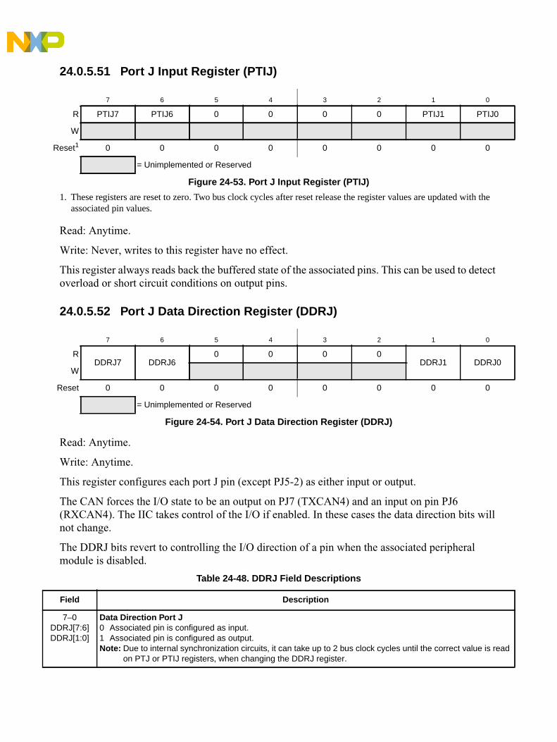
24.0.5.51 Port J Input Register (PTIJ)
Read: Anytime.
Write: Never, writes to this register have no effect.
This register always reads back the buffered state of the associated pins. This can be used to detectoverload or short circuit conditions on output pins.
24.0.5.52 Port J Data Direction Register (DDRJ)
Read: Anytime.
Write: Anytime.
This register configures each port J pin (except PJ5-2) as either input or output.
The CAN forces the I/O state to be an output on PJ7 (TXCAN4) and an input on pin PJ6(RXCAN4). The IIC takes control of the I/O if enabled. In these cases the data direction bits willnot change.
The DDRJ bits revert to controlling the I/O direction of a pin when the associated peripheralmodule is disabled.
7 6 5 4 3 2 1 0
R PTIJ7 PTIJ6 0 0 0 0 PTIJ1 PTIJ0
W
Reset1
1. These registers are reset to zero. Two bus clock cycles after reset release the register values are updated with theassociated pin values.
0 0 0 0 0 0 0 0
= Unimplemented or Reserved
Figure 24-53. Port J Input Register (PTIJ)
7 6 5 4 3 2 1 0
RDDRJ7 DDRJ6
0 0 0 0DDRJ1 DDRJ0
W
Reset 0 0 0 0 0 0 0 0
= Unimplemented or Reserved
Figure 24-54. Port J Data Direction Register (DDRJ)
Table 24-48. DDRJ Field Descriptions
Field Description
7–0DDRJ[7:6]DDRJ[1:0]
Data Direction Port J0 Associated pin is configured as input.1 Associated pin is configured as output.Note: Due to internal synchronization circuits, it can take up to 2 bus clock cycles until the correct value is read
on PTJ or PTIJ registers, when changing the DDRJ register.
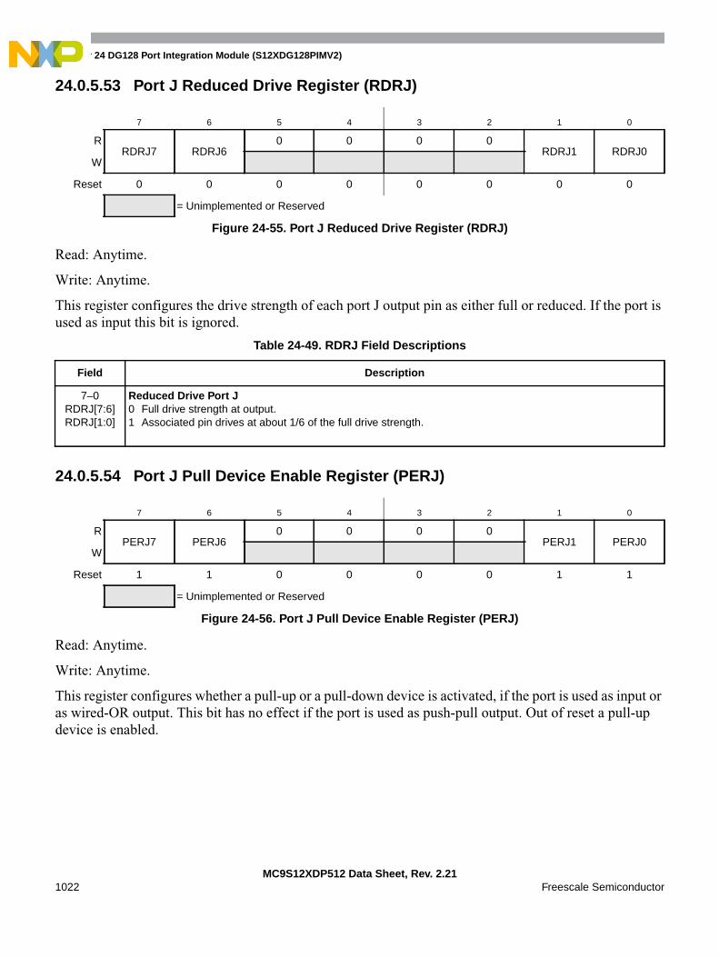
Chapter 24 DG128 Port Integration Module (S12XDG128PIMV2)
MC9S12XDP512 Data Sheet, Rev. 2.211022 Freescale Semiconductor
24.0.5.53 Port J Reduced Drive Register (RDRJ)
Read: Anytime.
Write: Anytime.
This register configures the drive strength of each port J output pin as either full or reduced. If the port isused as input this bit is ignored.
24.0.5.54 Port J Pull Device Enable Register (PERJ)
Read: Anytime.
Write: Anytime.
This register configures whether a pull-up or a pull-down device is activated, if the port is used as input oras wired-OR output. This bit has no effect if the port is used as push-pull output. Out of reset a pull-updevice is enabled.
7 6 5 4 3 2 1 0
RRDRJ7 RDRJ6
0 0 0 0RDRJ1 RDRJ0
W
Reset 0 0 0 0 0 0 0 0
= Unimplemented or Reserved
Figure 24-55. Port J Reduced Drive Register (RDRJ)
Table 24-49. RDRJ Field Descriptions
Field Description
7–0RDRJ[7:6]RDRJ[1:0]
Reduced Drive Port J0 Full drive strength at output.1 Associated pin drives at about 1/6 of the full drive strength.
7 6 5 4 3 2 1 0
RPERJ7 PERJ6
0 0 0 0PERJ1 PERJ0
W
Reset 1 1 0 0 0 0 1 1
= Unimplemented or Reserved
Figure 24-56. Port J Pull Device Enable Register (PERJ)

24.0.5.55 Port J Polarity Select Register (PPSJ)
Read: Anytime.
Write: Anytime.
This register serves a dual purpose by selecting the polarity of the active interrupt edge as well asselecting a pull-up or pull-down device if enabled.
24.0.5.56 Port J Interrupt Enable Register (PIEJ)
This register disables or enables on a per-pin basis the edge sensitive external interrupt associatedwith Port J.
Table 24-50. PERJ Field Descriptions
Field Description
7–0PERJ[7:6]PERJ[1:0]
Pull Device Enable Port J0 Pull-up or pull-down device is disabled.1 Either a pull-up or pull-down device is enabled.
7 6 5 4 3 2 1 0
RPPSJ7 PPSJ6
0 0 0 0PPSJ1 PPSJ0
W
Reset 0 0 0 0 0 0 0 0
= Unimplemented or Reserved
Figure 24-57. Port J Polarity Select Register (PPSJ)
Table 24-51. PPSJ Field Descriptions
Field Description
7–0PPSJ[7:6]PPSJ[1:0]
Polarity Select Port J0 Falling edge on the associated port J pin sets the associated flag bit in the PIFJ register.
A pull-up device is connected to the associated port J pin, if enabled by the associated bit in register PERJand if the port is used as general purpose input or as IIC port.
1 Rising edge on the associated port J pin sets the associated flag bit in the PIFJ register.A pull-down device is connected to the associated port J pin, if enabled by the associated bit in register PERJand if the port is used as input.
7 6 5 4 3 2 1 0
RPIEJ7 PIEJ6
0 0 0 0PIEJ1 PIEJ0
W
Reset 0 0 0 0 0 0 0 0
= Unimplemented or Reserved
Figure 24-58. Port J Interrupt Enable Register (PIEJ)

Chapter 24 DG128 Port Integration Module (S12XDG128PIMV2)
MC9S12XDP512 Data Sheet, Rev. 2.211024 Freescale Semiconductor
24.0.5.57 Port J Interrupt Flag Register (PIFJ)
Read: Anytime.
Write: Anytime.
Each flag is set by an active edge on the associated input pin. This could be a rising or a falling edge basedon the state of the PPSJ register. To clear this flag, write logic level “1” to the corresponding bit in the PIFJregister. Writing a “0” has no effect.
24.0.5.58 Port AD1 Data Register 0 (PT0AD1)
Read: Anytime.
Write: Anytime.
This register is associated with AD1 pins PAD[15:8]. These pins can also be used as general purpose I/O.
Table 24-52. PIEJ Field Descriptions
Field Description
7–0PIEJ[7:6]PIEJ[1:0]
Interrupt Enable Port J0 Interrupt is disabled (interrupt flag masked).1 Interrupt is enabled.
7 6 5 4 3 2 1 0
RPIFJ7 PIFJ6
0 0 0 0PIFJ1 PIFJ0
W
Reset 0 0 0 0 0 0 0 0
= Unimplemented or Reserved
Figure 24-59. Port J Interrupt Flag Register (PIFJ)
Table 24-53. PIEJ Field Descriptions
Field Description
7–0PIFJ[7:6]PIFJ[1:0]
Interrupt Flags Port J0 No active edge pending. Writing a “0” has no effect.1 Active edge on the associated bit has occurred (an interrupt will occur if the associated enable bit is set).
Writing a logic level “1” clears the associated flag.
7 6 5 4 3 2 1 0
RPT0AD115 PT0AD114 PT0AD113 PT0AD112 PT0AD111 PT0AD110 PT0AD19 PT0AD18
W
Reset 0 0 0 0 0 0 0 0
Figure 24-60. Port AD1 Data Register 0 (PT0AD1)

If the data direction bits of the associated I/O pins are set to 1, a read returns the value of the portregister, otherwise the value at the pins is read.
24.0.5.59 Port AD1 Data Register 1 (PT1AD1)
Read: Anytime.
Write: Anytime.
This register is associated with AD1 pins PAD[7:0]. These pins can also be used as general purposeI/O.
If the data direction bits of the associated I/O pins are set to 1, a read returns the value of the portregister, otherwise the value at the pins is read.
24.0.5.60 Port AD1 Data Direction Register 0 (DDR0AD1)
Read: Anytime.
Write: Anytime.
This register configures pin PAD[15:8] as either input or output.
7 6 5 4 3 2 1 0
RPT1AD17 PT1AD16 PT1AD15 PT1AD14 PT1AD13 PT1AD12 PT1AD11 PT1AD10
W
Reset 0 0 0 0 0 0 0 0
Figure 24-61. Port AD1 Data Register 1 (PT1AD1)
7 6 5 4 3 2 1 0
RDDR0AD115 DDR0AD114 DDR0AD113 DDR0AD112 DDR0AD111 DDR0AD110 DDR0AD19 DDR0AD18
W
Reset 0 0 0 0 0 0 0 0
Figure 24-62. Port AD1 Data Direction Register 0 (DDR0AD1)
Table 24-54. DDR0AD1 Field Descriptions
Field Description
7–0DDR0AD1[15:8]
Data Direction Port AD1 Register 00 Associated pin is configured as input.1 Associated pin is configured as output.Note: Due to internal synchronization circuits, it can take up to 2 bus clock cycles until the correct value is
read on PTAD10 register, when changing the DDR0AD1 register.Note: To use the digital input function on Port AD1 the ATD1 digital input enable register (ATD1DIEN0) has
to be set to logic level “1”.
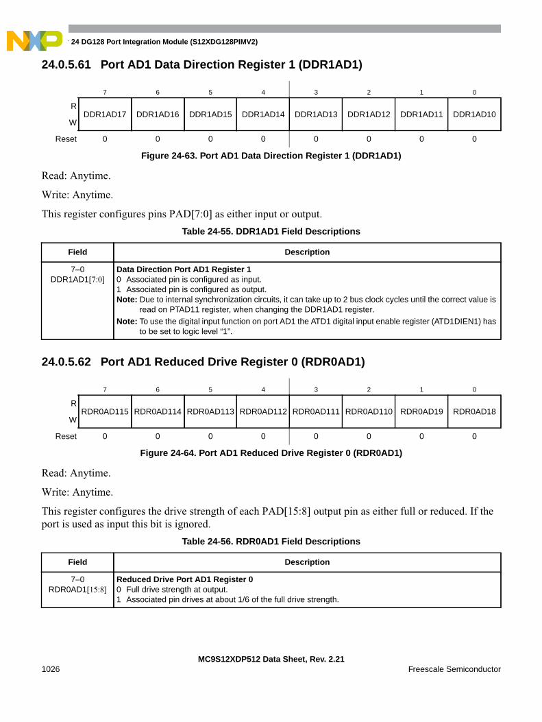
Chapter 24 DG128 Port Integration Module (S12XDG128PIMV2)
MC9S12XDP512 Data Sheet, Rev. 2.211026 Freescale Semiconductor
24.0.5.61 Port AD1 Data Direction Register 1 (DDR1AD1)
Read: Anytime.
Write: Anytime.
This register configures pins PAD[7:0] as either input or output.
24.0.5.62 Port AD1 Reduced Drive Register 0 (RDR0AD1)
Read: Anytime.
Write: Anytime.
This register configures the drive strength of each PAD[15:8] output pin as either full or reduced. If theport is used as input this bit is ignored.
7 6 5 4 3 2 1 0
RDDR1AD17 DDR1AD16 DDR1AD15 DDR1AD14 DDR1AD13 DDR1AD12 DDR1AD11 DDR1AD10
W
Reset 0 0 0 0 0 0 0 0
Figure 24-63. Port AD1 Data Direction Register 1 (DDR1AD1)
Table 24-55. DDR1AD1 Field Descriptions
Field Description
7–0DDR1AD1[7:0]
Data Direction Port AD1 Register 10 Associated pin is configured as input.1 Associated pin is configured as output.Note: Due to internal synchronization circuits, it can take up to 2 bus clock cycles until the correct value is
read on PTAD11 register, when changing the DDR1AD1 register.Note: To use the digital input function on port AD1 the ATD1 digital input enable register (ATD1DIEN1) has
to be set to logic level “1”.
7 6 5 4 3 2 1 0
RRDR0AD115 RDR0AD114 RDR0AD113 RDR0AD112 RDR0AD111 RDR0AD110 RDR0AD19 RDR0AD18
W
Reset 0 0 0 0 0 0 0 0
Figure 24-64. Port AD1 Reduced Drive Register 0 (RDR0AD1)
Table 24-56. RDR0AD1 Field Descriptions
Field Description
7–0RDR0AD1[15:8]
Reduced Drive Port AD1 Register 00 Full drive strength at output.1 Associated pin drives at about 1/6 of the full drive strength.

24.0.5.63 Port AD1 Reduced Drive Register 1 (RDR1AD1)
Read: Anytime.
Write: Anytime.
This register configures the drive strength of each PAD[7:0] output pin as either full or reduced. Ifthe port is used as input this bit is ignored.
24.0.5.64 Port AD1 Pull Up Enable Register 0 (PER0AD1)
Read: Anytime.
Write: Anytime.
This register activates a pull-up device on the respective PAD[15:8] pin if the port is used as input.This bit has no effect if the port is used as output. Out of reset no pull-up device is enabled.
7 6 5 4 3 2 1 0
RRDR1AD17 RDR1AD16 RDR1AD15 RDR1AD14 RDR1AD13 RDR1AD12 RDR1AD11 RDR1AD10
W
Reset 0 0 0 0 0 0 0 0
Figure 24-65. Port AD1 Reduced Drive Register 1 (RDR1AD1)
Table 24-57. RDR1AD1 Field Descriptions
Field Description
7–0RDR1AD1[7:0]
Reduced Drive Port AD1 Register 10 Full drive strength at output.1 Associated pin drives at about 1/6 of the full drive strength.
7 6 5 4 3 2 1 0
RPER0AD115 PER0AD114 PER0AD113 PER0AD112 PER0AD111 PER0AD110 PER0AD19 PER0AD18
W
Reset 0 0 0 0 0 0 0 0
Figure 24-66. Port AD1 Pull Up Enable Register 0 (PER0AD1)
Table 24-58. PER0AD1 Field Descriptions
Field Description
7–0PER0AD1[15:8]
Pull Device Enable Port AD1 Register 00 Pull-up device is disabled.1 Pull-up device is enabled.

Chapter 24 DG128 Port Integration Module (S12XDG128PIMV2)
MC9S12XDP512 Data Sheet, Rev. 2.211028 Freescale Semiconductor
24.0.5.65 Port AD1 Pull Up Enable Register 1 (PER1AD1)
Read: Anytime.
Write: Anytime.
This register activates a pull-up device on the respective PAD[7:0] pin if the port is used as input. This bithas no effect if the port is used as output. Out of reset no pull-up device is enabled.
Functional Description
Each pin except PE0, PE1, and BKGD can act as general purpose I/O. In addition each pin can act as anoutput from the external bus interface module or a peripheral module or an input to the external businterface module or a peripheral module.
A set of configuration registers is common to all ports with exceptions in the expanded bus interface andATD ports (Table 24-60). All registers can be written at any time; however a specific configuration mightnot become active.
Example: Selecting a pull-up device
This device does not become active while the port is used as a push-pull output.
7 6 5 4 3 2 1 0
RPER1AD17 PER1AD16 PER1AD15 PER1AD14 PER1AD13 PER1AD12 PER1AD11 PER1AD10
W
Reset 0 0 0 0 0 0 0 0
Figure 24-67. Port AD1 Pull Up Enable Register 1 (PER1AD1)
Table 24-59. PER1AD1 Field Descriptions
Field Description
7–0PER1AD1[7:0]
Pull Device Enable Port AD1 Register 10 Pull-up device is disabled.1 Pull-up device is enabled.
Table 24-60. Register Availability per Port1
Port DataData
Direction Input
ReducedDrive
PullEnable
PolaritySelect
Wired-ORMode
InterruptEnable
InterruptFlag
A yes yes — yes yes — — — —
B yes yes — — — — —
E yes yes — — — — —
K yes yes — — — — —
T yes yes yes yes yes — — — —
S yes yes yes yes yes yes yes — —
M yes yes yes yes yes yes yes — —
P yes yes yes yes yes yes — yes yes
H yes yes yes yes yes yes — yes yes
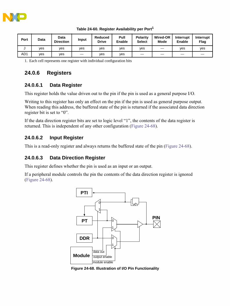
24.0.6 Registers
24.0.6.1 Data Register
This register holds the value driven out to the pin if the pin is used as a general purpose I/O.
Writing to this register has only an effect on the pin if the pin is used as general purpose output.When reading this address, the buffered state of the pin is returned if the associated data directionregister bit is set to “0”.
If the data direction register bits are set to logic level “1”, the contents of the data register isreturned. This is independent of any other configuration (Figure 24-68).
24.0.6.2 Input Register
This is a read-only register and always returns the buffered state of the pin (Figure 24-68).
24.0.6.3 Data Direction Register
This register defines whether the pin is used as an input or an output.
If a peripheral module controls the pin the contents of the data direction register is ignored(Figure 24-68).
Figure 24-68. Illustration of I/O Pin Functionality
J yes yes yes yes yes yes — yes yes
AD1 yes yes — yes yes — — — —
1. Each cell represents one register with individual configuration bits
Table 24-60. Register Availability per Port1
Port DataData
Direction Input
ReducedDrive
PullEnable
PolaritySelect
Wired-ORMode
InterruptEnable
InterruptFlag
PT
DDR
output enable
module enable
1
0
1
1
0
0
PIN
PTI
data outModule

Chapter 24 DG128 Port Integration Module (S12XDG128PIMV2)
MC9S12XDP512 Data Sheet, Rev. 2.211030 Freescale Semiconductor
24.0.6.4 Reduced Drive Register
If the pin is used as an output this register allows the configuration of the drive strength.
24.0.6.5 Pull Device Enable Register
This register turns on a pull-up or pull-down device. It becomes active only if the pin is used as an inputor as a wired-OR output.
24.0.6.6 Polarity Select Register
This register selects either a pull-up or pull-down device if enabled. It becomes active only if the pin isused as an input. A pull-up device can be activated if the pin is used as a wired-OR output. If the pin isused as an interrupt input this register selects the active interrupt edge.
24.0.6.7 Wired-OR Mode Register
If the pin is used as an output this register turns off the active high drive. This allows wired-OR typeconnections of outputs.
24.0.6.8 Interrupt Enable Register
If the pin is used as an interrupt input this register serves as a mask to the interrupt flag to enable/disablethe interrupt.
24.0.6.9 Interrupt Flag Register
If the pin is used as an interrupt input this register holds the interrupt flag after a valid pin event.
24.0.6.10 Module Routing Register
This register supports the re-routing of the CAN0, CAN4, SPI0, SPI1, and SPI2 pins to alternative ports.This allows a software re-configuration of the pinouts of the different package options with respect toabove peripherals.
NOTEThe purpose of the module routing register is to provide maximumflexibility for derivatives with a lower number of MSCAN and SPI modules.

24.0.7 Ports
24.0.7.1 BKGD Pin
The BKGD pin is associated with the S12X_BDM and S12X_EBI modules. During reset, theBKGD pin is used as MODC input.
24.0.7.2 Port A and B
Port A pins PA[7:0] and Port B pins PB[7:0] can be used for either general-purpose I/O.
24.0.7.3 Port E
Port E pins PE[7:2] can be used for either general-purpose I/O or with the alternative functions.
Port E pin PE[7] an be used for either general-purpose I/O or as the free-running clock ECLKX2output running at the core clock rate. The clock output is always enabled in emulation modes.
Port E pin PE[4] an be used for either general-purpose I/O or as the free-running clock ECLKoutput running at the bus clock rate or at the programmed divided clock rate. The clock output isalways enabled in emulation modes.
Port E pin PE[1] can be used for either general-purpose input or as the level- or falling edge-sensitive IRQ interrupt input. IRQ will be enabled by setting the IRQEN configuration bit(Section 24.0.5.10, “IRQ Control Register (IRQCR)”) and clearing the I-bit in the CPU’s conditioncode register. It is inhibited at reset so this pin is initially configured as a simple input with a pull-up.
Port E pin PE[0] can be used for either general-purpose input or as the level-sensitive XIRQinterrupt input. XIRQ can be enabled by clearing the X-bit in the CPU’s condition code register. Itis inhibited at reset so this pin is initially configured as a high-impedance input with a pull-up.
24.0.7.4 Port K
Port K pins PK[7:0] can be used for either general-purpose I/O.
Table 24-61. Module Implementations on Derivatives
Numberof Modules
MSCAN Modules SPI Modules
CAN0 CAN1 CAN2 CAN3 CAN4 SPI0 SPI1 SPI2
5 yes yes yes yes yes — — —
4 yes yes yes — yes — — —
3 yes yes — — yes yes yes yes
2 yes — — — yes yes yes —
1 yes — — — — yes — —

Chapter 24 DG128 Port Integration Module (S12XDG128PIMV2)
MC9S12XDP512 Data Sheet, Rev. 2.211032 Freescale Semiconductor
Port K pin PE[7] is configured for reduced input threshold in certain modes (refer to S12X_EBI section).
NOTEPort K is not available in 80-pin packages.
24.0.7.5 Port T
This port is associated with the ECT module. Port T pins PT[7:0] can be used for either general-purposeI/O, or with the channels of the enhanced capture timer.
24.0.7.6 Port S
This port is associated with SCI0, SCI1 and SPI0. Port S pins PS[7:0] can be used either for general-purpose I/O, or with the SCI and SPI subsystems.
The SPI0 pins can be re-routed. Refer to Section 24.0.5.33, “Module Routing Register (MODRR)”.
NOTEPS[7:4] are not available in 80-pin packages.
24.0.7.7 Port M
This port is associated with the CAN4 and 0 and SPI0. Port M pins PM[7:0] can be used for either generalpurpose I/O, or with the CAN, SCI and SPI subsystems.
The CAN0, CAN4 and SPI0 pins can be re-routed. Refer to Section 24.0.5.33, “Module Routing Register(MODRR)”.
NOTEPM[7:6] are not available in 80-pin packages.
24.0.7.8 Port P
This port is associated with the PWM, SPI1. Port P pins PP[7:0] can be used for either general purpose I/O, or with the PWM and SPI subsystems.
The pins are shared between the PWM channels and the SPI1. If the PWM is enabled the pins becomePWM output channels with the exception of pin 7 which can be PWM input or output. If SPI1is enabledand PWM is disabled, the respective pin configuration is determined by status bits in the SPI.
The SPI1 pins can be re-routed. Refer to Section 24.0.5.33, “Module Routing Register (MODRR)”.
Port P offers 8 I/O pins with edge triggered interrupt capability in wired-OR fashion (Section 24.0.8, “PinInterrupts”).
NOTEPP[6] is not available in 80-pin packages.

24.0.7.9 Port H
This port is associated with the SPI1, . Port H pins PH[7:0] can be used for either general purposeI/O, or with the SPI and SCI subsystems. Port H pins can be used with the routed SPI1. Refer toSection 24.0.5.33, “Module Routing Register (MODRR)”.
Port H offers 8 I/O pins with edge triggered interrupt capability (Section 24.0.8, “Pin Interrupts”).
NOTEPort H is not available in 80-pin packages.
24.0.7.10 Port J
This port is associated with CAN4, CAN0, IIC0. Port J pins PJ[7:4] and PJ[2:0] can be used foreither general purpose I/O, or with the CAN, IIC, or SCI subsystems. If IIC takes precedence theassociated pins become IIC open-drain output pins. The CAN4 pins can be re-routed. Refer toSection 24.0.5.33, “Module Routing Register (MODRR)”.
Port J pins can be used with the routed CAN0 modules. Refer to Section 24.0.5.33, “ModuleRouting Register (MODRR)”.
Port J offers 7 I/O pins with edge triggered interrupt capability (Section 24.0.8, “Pin Interrupts”).
NOTEPJ[5,4,2,1,0] are not available in 80-pin packages.
24.0.7.11 Port AD1
This port is associated with the ATD1. Port AD1 pins PAD15–PAD0 can be used for either generalpurpose I/O, or with the ATD1 subsystem.
NOTEPAD[15:8] are not available in 80-pin packages.
24.0.8 Pin Interrupts
Ports P, H and J offer pin interrupt capability. The interrupt enable as well as the sensitivity torising or falling edges can be individually configured on per-pin basis. All bits/pins in a port sharethe same interrupt vector. Interrupts can be used with the pins configured as inputs or outputs.
An interrupt is generated when a bit in the port interrupt flag register and its corresponding portinterrupt enable bit are both set. The pin interrupt feature is also capable to wake up the CPU whenit is in STOP or WAIT mode.
A digital filter on each pin prevents pulses (Figure 24-70) shorter than a specified time fromgenerating an interrupt. The minimum time varies over process conditions, temperature andvoltage (Figure 24-69 and Table 24-62).

Chapter 24 DG128 Port Integration Module (S12XDG128PIMV2)
MC9S12XDP512 Data Sheet, Rev. 2.211034 Freescale Semiconductor
Figure 24-69. Interrupt Glitch Filter on Port P, H, and J (PPS = 0)
Figure 24-70. Pulse Illustration
A valid edge on an input is detected if 4 consecutive samples of a passive level are followed by4 consecutive samples of an active level directly or indirectly.
The filters are continuously clocked by the bus clock in run and wait mode. In stop mode, the clock isgenerated by an RC-oscillator in the port integration module. To maximize current saving the RCoscillator runs only if the following condition is true on any pin individually:
Sample count <= 4 and interrupt enabled (PIE = 1) and interrupt flag not set (PIF = 0).
24.0.9 Low-Power Options
24.0.9.1 Run Mode
No low-power options exist for this module in run mode.
Table 24-62. Pulse Detection Criteria
PulseMode
STOP Unit STOP1
1. These values include the spread of the oscillator frequency overtemperature, voltage and process.
Ignored tpulse ≤ 3 Bus clocks tpulse ≤ tpign
Uncertain 3 < tpulse < 4 Bus clocks tpign < tpulse < tpval
Valid tpulse ≥ 4 Bus clocks tpulse ≥ tpval
Glitch, filtered out, no interrupt flag set
Valid pulse, interrupt flag set
tpign
tpval
uncertain
tpulse

24.0.9.2 Wait Mode
No low-power options exist for this module in wait mode.
24.0.9.3 Stop Mode
All clocks are stopped. There are asynchronous paths to generate interrupts from stop on port P, H,and J.
Initialization and Application Information• It is not recommended to write PORTx and DDRx in a word access. When changing the
register pins from inputs to outputs, the data may have extra transitions during the writeaccess. Initialize the port data register before enabling the outputs.
• Power consumption will increase the more the voltages on general purpose input pinsdeviate from the supply voltages towards mid-range because the digital input buffersoperate in the linear region.

Chapter 24 DG128 Port Integration Module (S12XDG128PIMV2)
MC9S12XDP512 Data Sheet, Rev. 2.211036 Freescale Semiconductor


Chapter 24 DG128 Port Integration Module (S12XDG128PIMV2)
MC9S12XDP512 Data Sheet, Rev. 2.211038 Freescale Semiconductor
MC9S12XDP512 Data Sheet, Rev. 2.21
Freescale Semiconductor 1039
Chapter 252 Kbyte EEPROM Module (S12XEETX2KV1)
25.1 IntroductionThis document describes the EETX2K module which includes a 2Kbyte EEPROM (nonvolatile) memory.The EEPROM memory may be read as either bytes, aligned words, or misaligned words. Read access timeis one bus cycle for bytes and aligned words, and two bus cycles for misaligned words.
The EEPROM memory is ideal for data storage for single-supply applications allowing for fieldreprogramming without requiring external voltage sources for program or erase. Program and erasefunctions are controlled by a command driven interface. The EEPROM module supports both block erase(all memory bytes) and sector erase (4 memory bytes). An erased bit reads 1 and a programmed bit reads0. The high voltage required to program and erase the EEPROM memory is generated internally. It is notpossible to read from the EEPROM block while it is being erased or programmed.
CAUTIONAn EEPROM word (2 bytes) must be in the erased state before beingprogrammed. Cumulative programming of bits within a word is not allowed.
25.1.1 Glossary
Command Write Sequence — A three-step MCU instruction sequence to execute built-in algorithms(including program and erase) on the EEPROM memory.
25.1.2 Features• 2 Kbytes of EEPROM memory divided into 512 sectors of 4 bytes
• Automated program and erase algorithm
• Interrupts on EEPROM command completion and command buffer empty
• Fast sector erase and word program operation
• 2-stage command pipeline
• Sector erase abort feature for critical interrupt response
• Flexible protection scheme to prevent accidental program or erase
• Single power supply for all EEPROM operations including program and erase
25.1.3 Modes of Operation
Program, erase and erase verify operations (please refer to Section 25.4.1, “EEPROM CommandOperations” for details).

Chapter 25 2 Kbyte EEPROM Module (S12XEETX2KV1)
MC9S12XDP512 Data Sheet, Rev. 2.21
1040 Freescale Semiconductor
25.1.4 Block Diagram
A block diagram of the EEPROM module is shown in Figure 25-1.
Figure 25-1. EETX2K Block Diagram
25.2 External Signal DescriptionThe EEPROM module contains no signals that connect off-chip.
25.3 Memory Map and Register DefinitionThis section describes the memory map and registers for the EEPROM module.
25.3.1 Module Memory Map
The EEPROM memory map is shown in Figure 25-2. The HCS12X architecture places the EEPROMmemory addresses between global addresses 0x13_F800 and 0x13_FFFF. The EPROT register, describedin Section 25.3.2.5, “EEPROM Protection Register (EPROT)”, can be set to protect the upper region in theEEPROM memory from accidental program or erase. The EEPROM addresses covered by this protectable
EETX2K
EEPROM
1K * 16 Bits
sector 0sector 1
sector 511
OscillatorClockDivider
Clock
CommandInterruptRequest
EECLK
Protection
Command Pipeline
cmd2addr2data2
cmd1addr1data1
Registers
EEPROMInterface
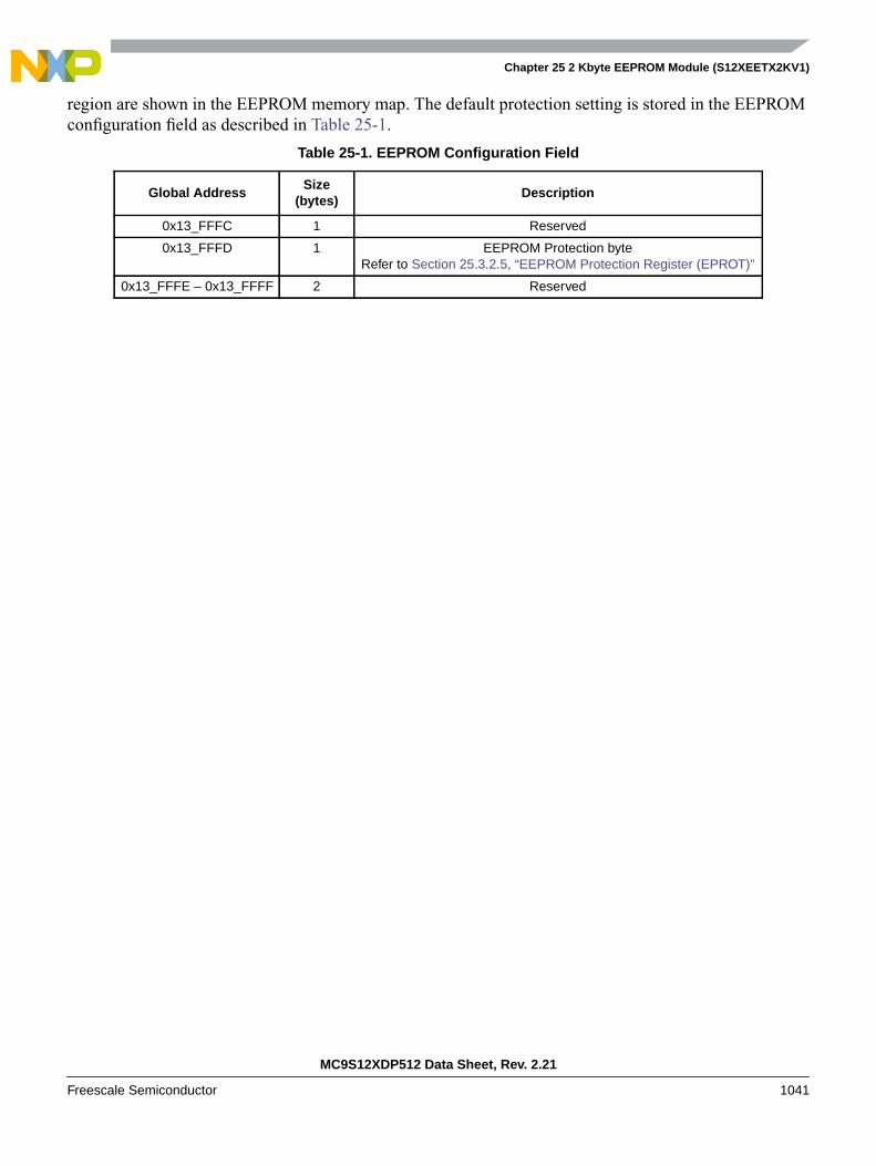
Chapter 25 2 Kbyte EEPROM Module (S12XEETX2KV1)
MC9S12XDP512 Data Sheet, Rev. 2.21
Freescale Semiconductor 1041
region are shown in the EEPROM memory map. The default protection setting is stored in the EEPROMconfiguration field as described in Table 25-1.
Table 25-1. EEPROM Configuration Field
Global AddressSize
(bytes)Description
0x13_FFFC 1 Reserved
0x13_FFFD 1 EEPROM Protection byteRefer to Section 25.3.2.5, “EEPROM Protection Register (EPROT)”
0x13_FFFE – 0x13_FFFF 2 Reserved
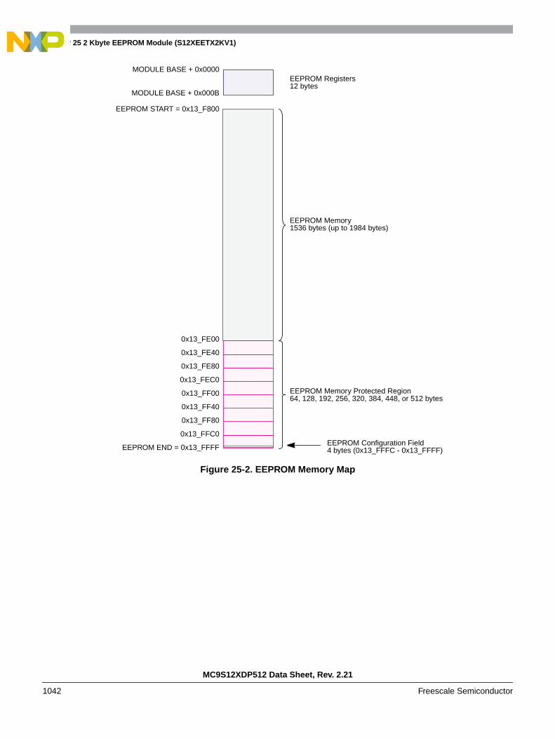
Chapter 25 2 Kbyte EEPROM Module (S12XEETX2KV1)
MC9S12XDP512 Data Sheet, Rev. 2.21
1042 Freescale Semiconductor
Figure 25-2. EEPROM Memory Map
EEPROM RegistersMODULE BASE + 0x0000
EEPROM Configuration Field
MODULE BASE + 0x000B
EEPROM START = 0x13_F800
EEPROM END = 0x13_FFFF
0x13_FFC0
0x13_FF80
EEPROM Memory Protected Region64, 128, 192, 256, 320, 384, 448, or 512 bytes
EEPROM Memory1536 bytes (up to 1984 bytes)
12 bytes
4 bytes (0x13_FFFC - 0x13_FFFF)
0x13_FF40
0x13_FF00
0x13_FEC0
0x13_FE80
0x13_FE40
0x13_FE00
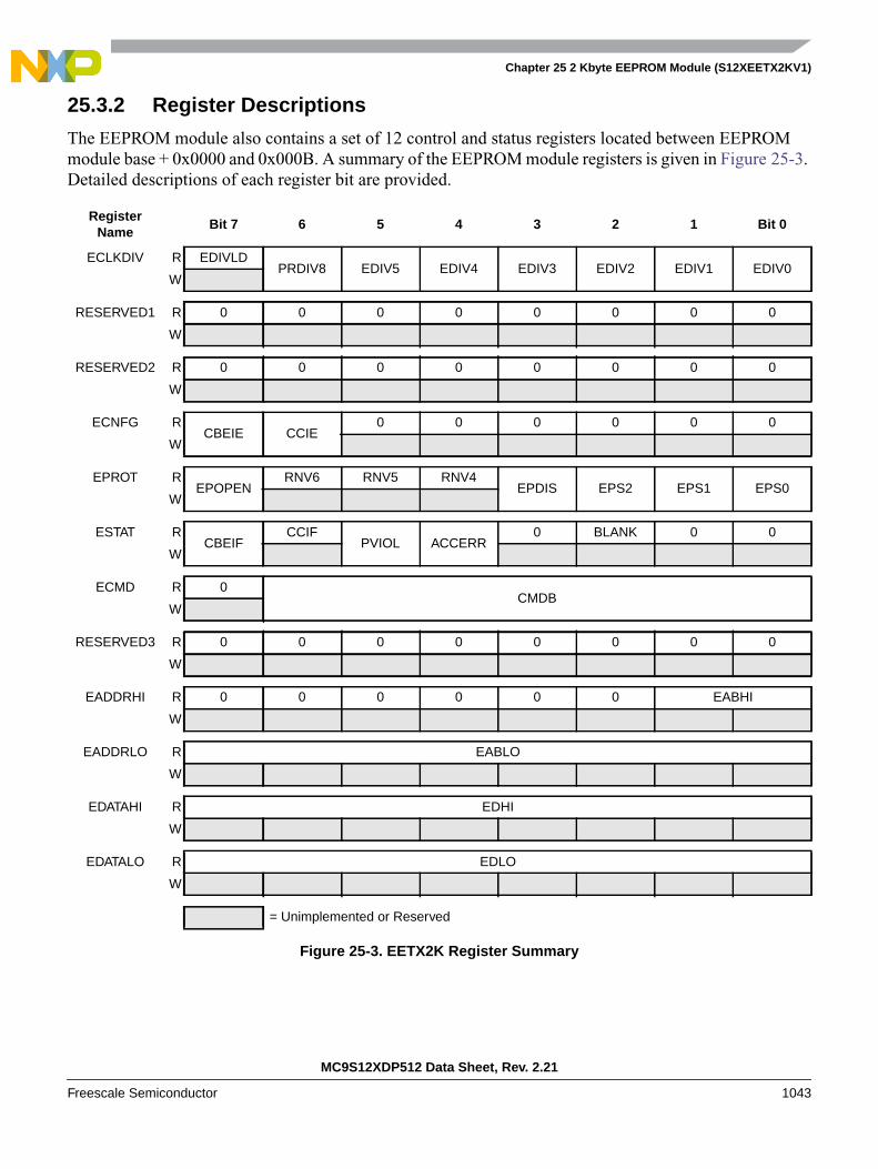
Chapter 25 2 Kbyte EEPROM Module (S12XEETX2KV1)
MC9S12XDP512 Data Sheet, Rev. 2.21
Freescale Semiconductor 1043
25.3.2 Register Descriptions
The EEPROM module also contains a set of 12 control and status registers located between EEPROMmodule base + 0x0000 and 0x000B. A summary of the EEPROM module registers is given in Figure 25-3.Detailed descriptions of each register bit are provided.
RegisterName
Bit 7 6 5 4 3 2 1 Bit 0
ECLKDIV R EDIVLDPRDIV8 EDIV5 EDIV4 EDIV3 EDIV2 EDIV1 EDIV0
W
RESERVED1 R 0 0 0 0 0 0 0 0
W
RESERVED2 R 0 0 0 0 0 0 0 0
W
ECNFG RCBEIE CCIE
0 0 0 0 0 0
W
EPROT REPOPEN
RNV6 RNV5 RNV4EPDIS EPS2 EPS1 EPS0
W
ESTAT RCBEIF
CCIFPVIOL ACCERR
0 BLANK 0 0
W
ECMD R 0CMDB
W
RESERVED3 R 0 0 0 0 0 0 0 0
W
EADDRHI R 0 0 0 0 0 0 EABHI
W
EADDRLO R EABLO
W
EDATAHI R EDHI
W
EDATALO R EDLO
W
= Unimplemented or Reserved
Figure 25-3. EETX2K Register Summary
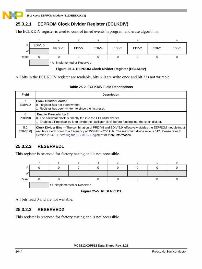
Chapter 25 2 Kbyte EEPROM Module (S12XEETX2KV1)
MC9S12XDP512 Data Sheet, Rev. 2.21
1044 Freescale Semiconductor
25.3.2.1 EEPROM Clock Divider Register (ECLKDIV)
The ECLKDIV register is used to control timed events in program and erase algorithms.
All bits in the ECLKDIV register are readable, bits 6–0 are write once and bit 7 is not writable.
25.3.2.2 RESERVED1
This register is reserved for factory testing and is not accessible.
All bits read 0 and are not writable.
25.3.2.3 RESERVED2
This register is reserved for factory testing and is not accessible.
7 6 5 4 3 2 1 0
R EDIVLDPRDIV8 EDIV5 EDIV4 EDIV3 EDIV2 EDIV1 EDIV0
W
Reset 0 0 0 0 0 0 0 0
= Unimplemented or Reserved
Figure 25-4. EEPROM Clock Divider Register (ECLKDIV)
Table 25-2. ECLKDIV Field Descriptions
Field Description
7EDIVLD
Clock Divider Loaded0 Register has not been written.1 Register has been written to since the last reset.
6PRDIV8
Enable Prescalar by 80 The oscillator clock is directly fed into the ECLKDIV divider.1 Enables a Prescalar by 8, to divide the oscillator clock before feeding into the clock divider.
5:0EDIV[5:0]
Clock Divider Bits — The combination of PRDIV8 and EDIV[5:0] effectively divides the EEPROM module inputoscillator clock down to a frequency of 150 kHz – 200 kHz. The maximum divide ratio is 512. Please refer toSection 25.4.1.1, “Writing the ECLKDIV Register” for more information.
7 6 5 4 3 2 1 0
R 0 0 0 0 0 0 0 0
W
Reset 0 0 0 0 0 0 0 0
= Unimplemented or Reserved
Figure 25-5. RESERVED1

Chapter 25 2 Kbyte EEPROM Module (S12XEETX2KV1)
MC9S12XDP512 Data Sheet, Rev. 2.21
Freescale Semiconductor 1045
All bits read 0 and are not writable.
25.3.2.4 EEPROM Configuration Register (ECNFG)
The ECNFG register enables the EEPROM interrupts.
CBEIE and CCIE bits are readable and writable while all remaining bits read 0 and are not writable.
7 6 5 4 3 2 1 0
R 0 0 0 0 0 0 0 0
W
Reset 0 0 0 0 0 0 0 0
= Unimplemented or Reserved
Figure 25-6. RESERVED2
7 6 5 4 3 2 1 0
RCBEIE CCIE
0 0 0 0 0 0
W
Reset 0 0 0 0 0 0 0 0
= Unimplemented or Reserved
Figure 25-7. EEPROM Configuration Register (ECNFG)
Table 25-3. ECNFG Field Descriptions
Field Description
7CBEIE
Command Buffer Empty Interrupt Enable — The CBEIE bit enables an interrupt in case of an empty commandbuffer in the EEPROM module.0 Command Buffer Empty interrupt disabled.1 An interrupt will be requested whenever the CBEIF flag (see Section 25.3.2.6, “EEPROM Status Register
(ESTAT)”) is set.
6CCIE
Command Complete Interrupt Enable — The CCIE bit enables an interrupt in case all commands have beencompleted in the EEPROM module.0 Command Complete interrupt disabled.1 An interrupt will be requested whenever the CCIF flag (see Section 25.3.2.6, “EEPROM Status Register
(ESTAT)”) is set.
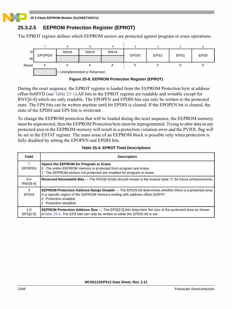
Chapter 25 2 Kbyte EEPROM Module (S12XEETX2KV1)
MC9S12XDP512 Data Sheet, Rev. 2.21
1046 Freescale Semiconductor
25.3.2.5 EEPROM Protection Register (EPROT)
The EPROT register defines which EEPROM sectors are protected against program or erase operations.
During the reset sequence, the EPROT register is loaded from the EEPROM Protection byte at addressoffset 0x0FFD (see Table 25-1).All bits in the EPROT register are readable and writable except forRNV[6:4] which are only readable. The EPOPEN and EPDIS bits can only be written to the protectedstate. The EPS bits can be written anytime until bit EPDIS is cleared. If the EPOPEN bit is cleared, thestate of the EPDIS and EPS bits is irrelevant.
To change the EEPROM protection that will be loaded during the reset sequence, the EEPROM memorymust be unprotected, then the EEPROM Protection byte must be reprogrammed. Trying to alter data in anyprotected area in the EEPROM memory will result in a protection violation error and the PVIOL flag willbe set in the ESTAT register. The mass erase of an EEPROM block is possible only when protection isfully disabled by setting the EPOPEN and EPDIS bits.
7 6 5 4 3 2 1 0
REPOPEN
RNV6 RNV5 RNV4EPDIS EPS2 EPS1 EPS0
W
Reset F F F F F F F F
= Unimplemented or Reserved
Figure 25-8. EEPROM Protection Register (EPROT)
Table 25-4. EPROT Field Descriptions
Field Description
7EPOPEN
Opens the EEPROM for Program or Erase0 The entire EEPROM memory is protected from program and erase.1 The EEPROM sectors not protected are enabled for program or erase.
6:4RNV[6:4]
Reserved Nonvolatile Bits — The RNV[6:4] bits should remain in the erased state “1” for future enhancements.
3EPDIS
EEPROM Protection Address Range Disable — The EPDIS bit determines whether there is a protected areain a specific region of the EEPROM memory ending with address offset 0x0FFF.0 Protection enabled.1 Protection disabled.
2:0EPS[2:0]
EEPROM Protection Address Size — The EPS[2:0] bits determine the size of the protected area as showninTable 25-5. The EPS bits can only be written to while the EPDIS bit is set.
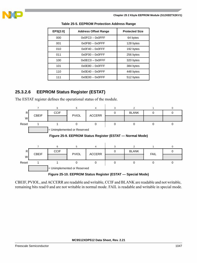
Chapter 25 2 Kbyte EEPROM Module (S12XEETX2KV1)
MC9S12XDP512 Data Sheet, Rev. 2.21
Freescale Semiconductor 1047
25.3.2.6 EEPROM Status Register (ESTAT)
The ESTAT register defines the operational status of the module.
CBEIF, PVIOL, and ACCERR are readable and writable, CCIF and BLANK are readable and not writable,remaining bits read 0 and are not writable in normal mode. FAIL is readable and writable in special mode.
Table 25-5. EEPROM Protection Address Range
EPS[2:0] Address Offset Range Protected Size
000 0x0FC0 – 0x0FFF 64 bytes
001 0x0F80 – 0x0FFF 128 bytes
010 0x0F40 – 0x0FFF 192 bytes
011 0x0F00 – 0x0FFF 256 bytes
100 0x0EC0 – 0x0FFF 320 bytes
101 0x0E80 – 0x0FFF 384 bytes
110 0x0E40 – 0x0FFF 448 bytes
111 0x0E00 – 0x0FFF 512 bytes
7 6 5 4 3 2 1 0
RCBEIF
CCIFPVIOL ACCERR
0 BLANK 0 0
W
Reset 1 1 0 0 0 0 0 0
= Unimplemented or Reserved
Figure 25-9. EEPROM Status Register (ESTAT — Normal Mode)
7 6 5 4 3 2 1 0
RCBEIF
CCIFPVIOL ACCERR
0 BLANKFAIL
0
W
Reset 1 1 0 0 0 0 0 0
= Unimplemented or Reserved
Figure 25-10. EEPROM Status Register (ESTAT — Special Mode)

Chapter 25 2 Kbyte EEPROM Module (S12XEETX2KV1)
MC9S12XDP512 Data Sheet, Rev. 2.21
1048 Freescale Semiconductor
Table 25-6. ESTAT Field Descriptions
Field Description
7CBEIF
Command Buffer Empty Interrupt Flag — The CBEIF flag indicates that the address, data, and commandbuffers are empty so that a new command write sequence can be started. The CBEIF flag is cleared by writinga 1 to CBEIF. Writing a 0 to the CBEIF flag has no effect on CBEIF. Writing a 0 to CBEIF after writing an alignedword to the EEPROM address space but before CBEIF is cleared will abort a command write sequence andcause the ACCERR flag to be set. Writing a 0 to CBEIF outside of a command write sequence will not set theACCERR flag. The CBEIF flag is used together with the CBEIE bit in the ECNFG register to generate an interruptrequest (see Figure 25-24).0 Buffers are full.1 Buffers are ready to accept a new command.
6CCIF
Command Complete Interrupt Flag — The CCIF flag indicates that there are no more commands pending. TheCCIF flag is cleared when CBEIF is clear and sets automatically upon completion of all active and pendingcommands. The CCIF flag does not set when an active commands completes and a pending command isfetched from the command buffer. Writing to the CCIF flag has no effect on CCIF. The CCIF flag is used togetherwith the CCIE bit in the ECNFG register to generate an interrupt request (see Figure 25-24).0 Command in progress.1 All commands are completed.
5PVIOL
Protection Violation Flag — The PVIOL flag indicates an attempt was made to program or erase an addressin a protected area of the EEPROM memory during a command write sequence. The PVIOL flag is cleared bywriting a 1 to PVIOL. Writing a 0 to the PVIOL flag has no effect on PVIOL. While PVIOL is set, it is not possibleto launch a command or start a command write sequence.0 No failure.1 A protection violation has occurred.
4ACCERR
Access Error Flag — The ACCERR flag indicates an illegal access has occurred to the EEPROM memorycaused by either a violation of the command write sequence (see Section 25.4.1.2, “Command WriteSequence”), issuing an illegal EEPROM command (see Table 25-8), launching the sector erase abort commandterminating a sector erase operation early (see Section 25.4.2.5, “Sector Erase Abort Command”) or theexecution of a CPU STOP instruction while a command is executing (CCIF = 0). The ACCERR flag is cleared bywriting a 1 to ACCERR. Writing a 0 to the ACCERR flag has no effect on ACCERR. While ACCERR is set, it isnot possible to launch a command or start a command write sequence. If ACCERR is set by an erase verifyoperation, any buffered command will not launch.0 No access error detected.1 Access error has occurred.
2BLANK
Flag Indicating the Erase Verify Operation Status — When the CCIF flag is set after completion of an eraseverify command, the BLANK flag indicates the result of the erase verify operation. The BLANK flag is cleared bythe EEPROM module when CBEIF is cleared as part of a new valid command write sequence. Writing to theBLANK flag has no effect on BLANK.0 EEPROM block verified as not erased.1 EEPROM block verified as erased.
1FAIL
Flag Indicating a Failed EEPROM Operation — The FAIL flag will set if the erase verify operation fails(EEPROM block verified as not erased). The FAIL flag is cleared by writing a 1 to FAIL. Writing a 0 to the FAILflag has no effect on FAIL.0 EEPROM operation completed without error.1 EEPROM operation failed.
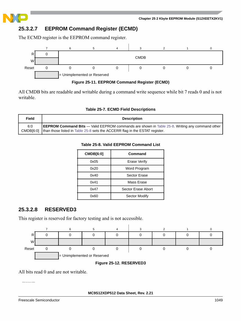
Chapter 25 2 Kbyte EEPROM Module (S12XEETX2KV1)
MC9S12XDP512 Data Sheet, Rev. 2.21
Freescale Semiconductor 1049
25.3.2.7 EEPROM Command Register (ECMD)
The ECMD register is the EEPROM command register.
All CMDB bits are readable and writable during a command write sequence while bit 7 reads 0 and is notwritable.
25.3.2.8 RESERVED3
This register is reserved for factory testing and is not accessible.
All bits read 0 and are not writable.
EEPROM Address Registers (EADDR)
7 6 5 4 3 2 1 0
R 0CMDB
W
Reset 0 0 0 0 0 0 0 0
= Unimplemented or Reserved
Figure 25-11. EEPROM Command Register (ECMD)
Table 25-7. ECMD Field Descriptions
Field Description
6:0CMDB[6:0]
EEPROM Command Bits — Valid EEPROM commands are shown in Table 25-8. Writing any command otherthan those listed in Table 25-8 sets the ACCERR flag in the ESTAT register.
Table 25-8. Valid EEPROM Command List
CMDB[6:0] Command
0x05 Erase Verify
0x20 Word Program
0x40 Sector Erase
0x41 Mass Erase
0x47 Sector Erase Abort
0x60 Sector Modify
7 6 5 4 3 2 1 0
R 0 0 0 0 0 0 0 0
W
Reset 0 0 0 0 0 0 0 0
= Unimplemented or Reserved
Figure 25-12. RESERVED3
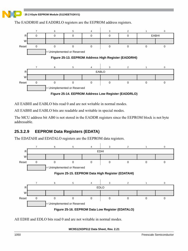
Chapter 25 2 Kbyte EEPROM Module (S12XEETX2KV1)
MC9S12XDP512 Data Sheet, Rev. 2.21
1050 Freescale Semiconductor
The EADDRHI and EADDRLO registers are the EEPROM address registers.
All EABHI and EABLO bits read 0 and are not writable in normal modes.
All EABHI and EABLO bits are readable and writable in special modes.
The MCU address bit AB0 is not stored in the EADDR registers since the EEPROM block is not byteaddressable.
25.3.2.9 EEPROM Data Registers (EDATA)
The EDATAHI and EDATALO registers are the EEPROM data registers.
All EDHI and EDLO bits read 0 and are not writable in normal modes.
7 6 5 4 3 2 1 0
R 0 0 0 0 0 0 EABHI
W
Reset 0 0 0 0 0 0 0 0
= Unimplemented or Reserved
Figure 25-13. EEPROM Address High Register (EADDRHI)
7 6 5 4 3 2 1 0
R EABLO
W
Reset 0 0 0 0 0 0 0 0
= Unimplemented or Reserved
Figure 25-14. EEPROM Address Low Register (EADDRLO)
7 6 5 4 3 2 1 0
R EDHI
W
Reset 0 0 0 0 0 0 0 0
= Unimplemented or Reserved
Figure 25-15. EEPROM Data High Register (EDATAHI)
7 6 5 4 3 2 1 0
R EDLO
W
Reset 0 0 0 0 0 0 0 0
= Unimplemented or Reserved
Figure 25-16. EEPROM Data Low Register (EDATALO)

Chapter 25 2 Kbyte EEPROM Module (S12XEETX2KV1)
MC9S12XDP512 Data Sheet, Rev. 2.21
Freescale Semiconductor 1051
All EDHI and EDLO bits are readable and writable in special modes.
25.4 Functional Description
25.4.1 EEPROM Command Operations
Write operations are used to execute program, erase, erase verify, sector erase abort, and sector modifyalgorithms described in this section. The program, erase, and sector modify algorithms are controlled bya state machine whose timebase, EECLK, is derived from the oscillator clock via a programmable divider.The command register as well as the associated address and data registers operate as a buffer and a register(2-stage FIFO) so that a second command along with the necessary data and address can be stored to thebuffer while the first command is still in progress. Buffer empty as well as command completion aresignalled by flags in the EEPROM status register with interrupts generated, if enabled.
The next sections describe:
1. How to write the ECLKDIV register
2. Command write sequences to program, erase, erase verify, sector erase abort, and sector modifyoperations on the EEPROM memory
3. Valid EEPROM commands
4. Effects resulting from illegal EEPROM command write sequences or aborting EEPROMoperations
25.4.1.1 Writing the ECLKDIV Register
Prior to issuing any EEPROM command after a reset, the user is required to write the ECLKDIV registerto divide the oscillator clock down to within the 150 kHz to 200 kHz range. Since the program and erasetimings are also a function of the bus clock, the ECLKDIV determination must take this information intoaccount.
If we define:
• ECLK as the clock of the EEPROM timing control block
• Tbus as the period of the bus clock
• INT(x) as taking the integer part of x (e.g., INT(4.323)=4)
then ECLKDIV register bits PRDIV8 and EDIV[5:0] are to be set as described in Figure 25-17.
For example, if the oscillator clock frequency is 950 kHz and the bus clock frequency is 10 MHz,ECLKDIV bits EDIV[5:0] should be set to 0x04 (000100) and bit PRDIV8 set to 0. The resulting EECLKfrequency is then 190 kHz. As a result, the EEPROM program and erase algorithm timings are increasedover the optimum target by:
If the oscillator clock frequency is 16 MHz and the bus clock frequency is 40 MHz, ECLKDIV bitsEDIV[5:0] should be set to 0x0A (001010) and bit PRDIV8 set to 1. The resulting EECLK frequency is
200 190–( ) 200⁄ 100× 5%=

Chapter 25 2 Kbyte EEPROM Module (S12XEETX2KV1)
MC9S12XDP512 Data Sheet, Rev. 2.21
1052 Freescale Semiconductor
then 182 kHz. In this case, the EEPROM program and erase algorithm timings are increased over theoptimum target by:
CAUTIONProgram and erase command execution time will increase proportionallywith the period of EECLK. Because of the impact of clock synchronizationon the accuracy of the functional timings, programming or erasing theEEPROM memory cannot be performed if the bus clock runs at less than 1MHz. Programming or erasing the EEPROM memory with EECLK < 150kHz should be avoided. Setting ECLKDIV to a value such that EECLK <150 kHz can destroy the EEPROM memory due to overstress. SettingECLKDIV to a value such that (1/EECLK+Tbus) < 5 µs can result inincomplete programming or erasure of the EEPROM memory cells.
If the ECLKDIV register is written, the EDIVLD bit is set automatically. If the EDIVLD bit is 0, theECLKDIV register has not been written since the last reset. If the ECLKDIV register has not been writtento, the EEPROM command loaded during a command write sequence will not execute and the ACCERRflag in the ESTAT register will set.
200 182–( ) 200⁄ 100× 9%=
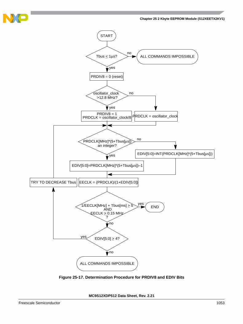
Chapter 25 2 Kbyte EEPROM Module (S12XEETX2KV1)
MC9S12XDP512 Data Sheet, Rev. 2.21
Freescale Semiconductor 1053
Figure 25-17. Determination Procedure for PRDIV8 and EDIV Bits
PRDIV8 = 1
yes
no
PRDIV8 = 0 (reset)
>12.8 MHz?
EECLK = (PRDCLK)/(1+EDIV[5:0])
PRDCLK = oscillator_clockPRDCLK = oscillator_clock/8
PRDCLK[MHz]*(5+Tbus[µs])no
EDIV[5:0]=PRDCLK[MHz]*(5+Tbus[µs])–1
yes
START
Tbus < 1µs?
an integer?
EDIV[5:0]=INT(PRDCLK[MHz]*(5+Tbus[µs]))
1/EECLK[MHz] + Tbus[ms] > 5AND
EECLK > 0.15 MHz?
ENDyes
no
EDIV[5:0] > 4?
ALL COMMANDS IMPOSSIBLE
yes
no
ALL COMMANDS IMPOSSIBLE
no
TRY TO DECREASE Tbus
yes
oscillator_clock

Chapter 25 2 Kbyte EEPROM Module (S12XEETX2KV1)
MC9S12XDP512 Data Sheet, Rev. 2.21
1054 Freescale Semiconductor
25.4.1.2 Command Write Sequence
The EEPROM command controller is used to supervise the command write sequence to execute program,erase, erase verify, sector erase abort, and sector modify algorithms.
Before starting a command write sequence, the ACCERR and PVIOL flags in the ESTAT register must beclear (see Section 25.3.2.6, “EEPROM Status Register (ESTAT)”) and the CBEIF flag should be tested todetermine the state of the address, data and command buffers. If the CBEIF flag is set, indicating thebuffers are empty, a new command write sequence can be started. If the CBEIF flag is clear, indicating thebuffers are not available, a new command write sequence will overwrite the contents of the address, dataand command buffers.
A command write sequence consists of three steps which must be strictly adhered to with writes to theEEPROM module not permitted between the steps. However, EEPROM register and array reads areallowed during a command write sequence. The basic command write sequence is as follows:
1. Write to one address in the EEPROM memory.
2. Write a valid command to the ECMD register.
3. Clear the CBEIF flag in the ESTAT register by writing a 1 to CBEIF to launch the command.
The address written in step 1 will be stored in the EADDR registers and the data will be stored in theEDATA registers. If the CBEIF flag in the ESTAT register is clear when the first EEPROM array writeoccurs, the contents of the address and data buffers will be overwritten and the CBEIF flag will be set.When the CBEIF flag is cleared, the CCIF flag is cleared on the same bus cycle by the EEPROM commandcontroller indicating that the command was successfully launched. For all command write sequencesexcept sector erase abort, the CBEIF flag will set four bus cycles after the CCIF flag is cleared indicatingthat the address, data, and command buffers are ready for a new command write sequence to begin. Forsector erase abort operations, the CBEIF flag will remain clear until the operation completes. Except forthe sector erase abort command, a buffered command will wait for the active operation to be completedbefore being launched. The sector erase abort command is launched when the CBEIF flag is cleared as partof a sector erase abort command write sequence. Once a command is launched, the completion of thecommand operation is indicated by the setting of the CCIF flag in the ESTAT register. The CCIF flag willset upon completion of all active and buffered commands.
25.4.2 EEPROM Commands
Table 25-9 summarizes the valid EEPROM commands along with the effects of the commands on theEEPROM block.
Table 25-9. EEPROM Command Description
ECMDB Command Function on EEPROM Memory
0x05 EraseVerify
Verify all memory bytes in the EEPROM block are erased. If the EEPROM block is erased, theBLANK flag in the ESTAT register will set upon command completion.
0x20 Program Program a word (two bytes) in the EEPROM block.
0x40 SectorErase
Erase all four memory bytes in a sector of the EEPROM block.

Chapter 25 2 Kbyte EEPROM Module (S12XEETX2KV1)
MC9S12XDP512 Data Sheet, Rev. 2.21
Freescale Semiconductor 1055
CAUTIONAn EEPROM word (2 bytes) must be in the erased state before beingprogrammed. Cumulative programming of bits within a word is not allowed.
0x41 MassErase
Erase all memory bytes in the EEPROM block. A mass erase of the full EEPROM block is onlypossible when EPOPEN and EPDIS bits in the EPROT register are set prior to launching thecommand.
0x47 Sector EraseAbort
Abort the sector erase operation. The sector erase operation will terminate according to a setprocedure. The EEPROM sector should not be considered erased if the ACCERR flag is setupon command completion.
0x60 SectorModify
Erase all four memory bytes in a sector of the EEPROM block and reprogram the addressedword.
Table 25-9. EEPROM Command Description
ECMDB Command Function on EEPROM Memory
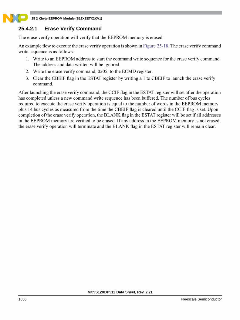
Chapter 25 2 Kbyte EEPROM Module (S12XEETX2KV1)
MC9S12XDP512 Data Sheet, Rev. 2.21
1056 Freescale Semiconductor
25.4.2.1 Erase Verify Command
The erase verify operation will verify that the EEPROM memory is erased.
An example flow to execute the erase verify operation is shown in Figure 25-18. The erase verify commandwrite sequence is as follows:
1. Write to an EEPROM address to start the command write sequence for the erase verify command.The address and data written will be ignored.
2. Write the erase verify command, 0x05, to the ECMD register.
3. Clear the CBEIF flag in the ESTAT register by writing a 1 to CBEIF to launch the erase verifycommand.
After launching the erase verify command, the CCIF flag in the ESTAT register will set after the operationhas completed unless a new command write sequence has been buffered. The number of bus cyclesrequired to execute the erase verify operation is equal to the number of words in the EEPROM memoryplus 14 bus cycles as measured from the time the CBEIF flag is cleared until the CCIF flag is set. Uponcompletion of the erase verify operation, the BLANK flag in the ESTAT register will be set if all addressesin the EEPROM memory are verified to be erased. If any address in the EEPROM memory is not erased,the erase verify operation will terminate and the BLANK flag in the ESTAT register will remain clear.
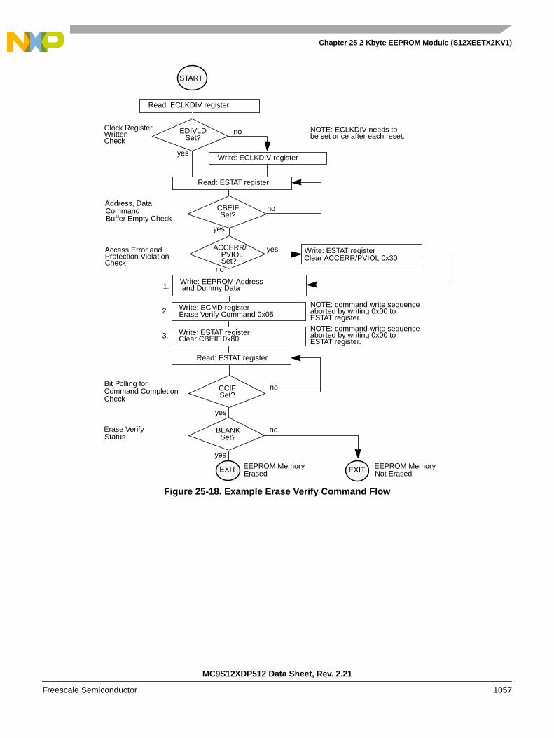
Chapter 25 2 Kbyte EEPROM Module (S12XEETX2KV1)
MC9S12XDP512 Data Sheet, Rev. 2.21
Freescale Semiconductor 1057
Figure 25-18. Example Erase Verify Command Flow
Write: EEPROM Address
Write: ECMD registerErase Verify Command 0x05
Write: ESTAT registerClear CBEIF 0x80
1.
2.
3.
Clear ACCERR/PVIOL 0x30Write: ESTAT registeryes
no
Access Error andProtection Violation
no
and Dummy Data
Bit Polling forCommand CompletionCheck
Read: ESTAT register
yes
NOTE: command write sequenceaborted by writing 0x00 toESTAT register.
NOTE: command write sequenceaborted by writing 0x00 toESTAT register.
Read: ESTAT register
no
START
yes
Check
CBEIFSet?
Address, Data,CommandBuffer Empty Check
CCIFSet?
ACCERR/PVIOLSet?
noErase VerifyStatus
yes
EXIT EEPROM MemoryNot ErasedEXIT EEPROM Memory
Erased
BLANKSet?
Write: ECLKDIV register
Read: ECLKDIV register
yes
noClock RegisterWrittenCheck
EDIVLDSet?
NOTE: ECLKDIV needs tobe set once after each reset.

Chapter 25 2 Kbyte EEPROM Module (S12XEETX2KV1)
MC9S12XDP512 Data Sheet, Rev. 2.21
1058 Freescale Semiconductor
25.4.2.2 Program Command
The program operation will program a previously erased word in the EEPROM memory using anembedded algorithm.
An example flow to execute the program operation is shown in Figure 25-19. The program command writesequence is as follows:
1. Write to an EEPROM block address to start the command write sequence for the programcommand. The data written will be programmed to the address written.
2. Write the program command, 0x20, to the ECMD register.
3. Clear the CBEIF flag in the ESTAT register by writing a 1 to CBEIF to launch the programcommand.
If a word to be programmed is in a protected area of the EEPROM memory, the PVIOL flag in the ESTATregister will set and the program command will not launch. Once the program command has successfullylaunched, the CCIF flag in the ESTAT register will set after the program operation has completed unless anew command write sequence has been buffered.
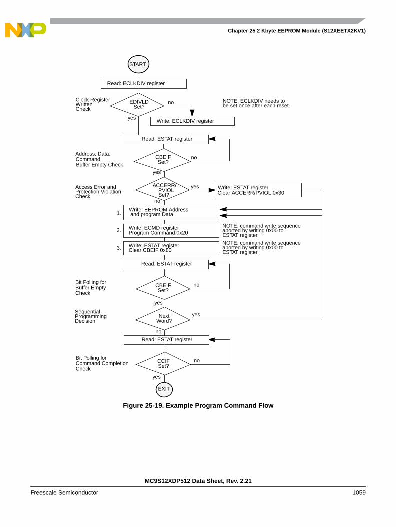
Chapter 25 2 Kbyte EEPROM Module (S12XEETX2KV1)
MC9S12XDP512 Data Sheet, Rev. 2.21
Freescale Semiconductor 1059
Figure 25-19. Example Program Command Flow
Write: EEPROM Address
Write: ECMD registerProgram Command 0x20
Write: ESTAT registerClear CBEIF 0x80
1.
2.
3.
Clear ACCERR/PVIOL 0x30Write: ESTAT registeryes
no
Access Error andProtection Violation
no
and program Data
Bit Polling forBuffer EmptyCheck
Read: ESTAT register
yes
NOTE: command write sequenceaborted by writing 0x00 toESTAT register.
NOTE: command write sequenceaborted by writing 0x00 toESTAT register.
Read: ESTAT register
no
START
yes
Check
CBEIFSet?
Address, Data,CommandBuffer Empty Check
CBEIFSet?
ACCERR/PVIOLSet?
EXIT
Write: ECLKDIV register
Read: ECLKDIV register
yes
noClock RegisterWrittenCheck
EDIVLDSet?
NOTE: ECLKDIV needs tobe set once after each reset.
no
yesSequentialProgrammingDecision
NextWord?
noBit Polling forCommand CompletionCheck
Read: ESTAT register
yes
CCIFSet?

Chapter 25 2 Kbyte EEPROM Module (S12XEETX2KV1)
MC9S12XDP512 Data Sheet, Rev. 2.21
1060 Freescale Semiconductor
25.4.2.3 Sector Erase Command
The sector erase operation will erase both words in a sector of EEPROM memory using an embeddedalgorithm.
An example flow to execute the sector erase operation is shown in Figure 25-20. The sector erasecommand write sequence is as follows:
1. Write to an EEPROM memory address to start the command write sequence for the sector erasecommand. The EEPROM address written determines the sector to be erased while global addressbits [1:0] and the data written are ignored.
2. Write the sector erase command, 0x40, to the ECMD register.
3. Clear the CBEIF flag in the ESTAT register by writing a 1 to CBEIF to launch the sector erasecommand.
If an EEPROM sector to be erased is in a protected area of the EEPROM memory, the PVIOL flag in theESTAT register will set and the sector erase command will not launch. Once the sector erase command hassuccessfully launched, the CCIF flag in the ESTAT register will set after the sector erase operation hascompleted unless a new command write sequence has been buffered.
Chapter 25 2 Kbyte EEPROM Module (S12XEETX2KV1)
MC9S12XDP512 Data Sheet, Rev. 2.21
Freescale Semiconductor 1061
Figure 25-20. Example Sector Erase Command Flow
Write: EEPROM Sector Address
Write: ECMD registerSector Erase Command 0x40
Write: ESTAT registerClear CBEIF 0x80
1.
2.
3.
Clear ACCERR/PVIOL 0x30Write: ESTAT registeryes
no
Access Error andProtection Violation
and Dummy Data
Read: ESTAT register
NOTE: command write sequenceaborted by writing 0x00 toESTAT register.
NOTE: command write sequenceaborted by writing 0x00 toESTAT register.
Read: ESTAT register
no
START
yes
Check
CBEIFSet?
Address, Data,CommandBuffer Empty Check
ACCERR/PVIOLSet?
EXIT
Write: ECLKDIV register
Read: ECLKDIV register
yes
noClock RegisterWrittenCheck
EDIVLDSet?
NOTE: ECLKDIV needs tobe set once after each reset.
noBit Polling forCommand CompletionCheck
yes
CCIFSet?

Chapter 25 2 Kbyte EEPROM Module (S12XEETX2KV1)
MC9S12XDP512 Data Sheet, Rev. 2.21
1062 Freescale Semiconductor
25.4.2.4 Mass Erase Command
The mass erase operation will erase all addresses in an EEPROM block using an embedded algorithm.
An example flow to execute the mass erase operation is shown in Figure 25-21. The mass erase commandwrite sequence is as follows:
1. Write to an EEPROM memory address to start the command write sequence for the mass erasecommand. The address and data written will be ignored.
2. Write the mass erase command, 0x41, to the ECMD register.
3. Clear the CBEIF flag in the ESTAT register by writing a 1 to CBEIF to launch the mass erasecommand.
If the EEPROM memory to be erased contains any protected area, the PVIOL flag in the ESTAT registerwill set and the mass erase command will not launch. Once the mass erase command has successfullylaunched, the CCIF flag in the ESTAT register will set after the mass erase operation has completed unlessa new command write sequence has been buffered.

Chapter 25 2 Kbyte EEPROM Module (S12XEETX2KV1)
MC9S12XDP512 Data Sheet, Rev. 2.21
Freescale Semiconductor 1063
Figure 25-21. Example Mass Erase Command Flow
Write: EEPROM Address
Write: ECMD registerMass Erase Command 0x41
Write: ESTAT registerClear CBEIF 0x80
1.
2.
3.
Clear ACCERR/PVIOL 0x30Write: ESTAT registeryes
no
Access Error andProtection Violation
and Dummy Data
Read: ESTAT register
NOTE: command write sequenceaborted by writing 0x00 toESTAT register.
NOTE: command write sequenceaborted by writing 0x00 toESTAT register.
Read: ESTAT register
no
START
yes
Check
CBEIFSet?
Address, Data,CommandBuffer Empty Check
ACCERR/PVIOLSet?
EXIT
Write: ECLKDIV register
Read: ECLKDIV register
yes
noClock RegisterWrittenCheck
EDIVLDSet?
NOTE: ECLKDIV needs tobe set once after each reset.
noBit Polling forCommand CompletionCheck
yes
CCIFSet?
Chapter 25 2 Kbyte EEPROM Module (S12XEETX2KV1)
MC9S12XDP512 Data Sheet, Rev. 2.21
1064 Freescale Semiconductor
25.4.2.5 Sector Erase Abort Command
The sector erase abort operation will terminate the active sector erase or sector modify operation so thatother sectors in an EEPROM block are available for read and program operations without waiting for thesector erase or sector modify operation to complete.
An example flow to execute the sector erase abort operation is shown in Figure 25-22. The sector eraseabort command write sequence is as follows:
1. Write to any EEPROM memory address to start the command write sequence for the sector eraseabort command. The address and data written are ignored.
2. Write the sector erase abort command, 0x47, to the ECMD register.
3. Clear the CBEIF flag in the ESTAT register by writing a 1 to CBEIF to launch the sector erase abortcommand.
If the sector erase abort command is launched resulting in the early termination of an active sector eraseor sector modify operation, the ACCERR flag will set once the operation completes as indicated by theCCIF flag being set. The ACCERR flag sets to inform the user that the EEPROM sector may not be fullyerased and a new sector erase or sector modify command must be launched before programming anylocation in that specific sector. If the sector erase abort command is launched but the active sector erase orsector modify operation completes normally, the ACCERR flag will not set upon completion of theoperation as indicated by the CCIF flag being set. If the sector erase abort command is launched after thesector modify operation has completed the sector erase step, the program step will be allowed to complete.The maximum number of cycles required to abort a sector erase or sector modify operation is equal to fourEECLK periods (see Section 25.4.1.1, “Writing the ECLKDIV Register”) plus five bus cycles as measuredfrom the time the CBEIF flag is cleared until the CCIF flag is set.
NOTESince the ACCERR bit in the ESTAT register may be set at the completionof the sector erase abort operation, a command write sequence is notallowed to be buffered behind a sector erase abort command write sequence.The CBEIF flag will not set after launching the sector erase abort commandto indicate that a command should not be buffered behind it. If an attempt ismade to start a new command write sequence with a sector erase abortoperation active, the ACCERR flag in the ESTAT register will be set. A newcommand write sequence may be started after clearing the ACCERR flag, ifset.
NOTEThe sector erase abort command should be used sparingly since a sectorerase operation that is aborted counts as a complete program/erase cycle.

Chapter 25 2 Kbyte EEPROM Module (S12XEETX2KV1)
MC9S12XDP512 Data Sheet, Rev. 2.21
Freescale Semiconductor 1065
Figure 25-22. Example Sector Erase Abort Command Flow
Write: Dummy EEPROM Address
Write: ECMD registerSector Erase Abort Cmd 0x47
Write: ESTAT registerClear CBEIF 0x80
1.
2.
3.
Read: ESTAT register
and Dummy Data
Bit Polling forCommandCompletion Check
yes
NOTE: command write sequenceaborted by writing 0x00 toESTAT register.
NOTE: command write sequenceaborted by writing 0x00 toESTAT register.
CCIFSet?
Execute Sector Erase/Modify Command Flow
noBit Polling forCommandCompletion Check
Read: ESTAT register
yes
CCIFSet?
no
yes
AbortNeeded?
Erase
Clear ACCERR 0x10Write: ESTAT registeryes
no
AccessError Check
ACCERRSet?
Sector Eraseor Modify
Sector Eraseor Modify
no
EXIT EXIT
Sector EraseCompleted EXIT
Completed Aborted

Chapter 25 2 Kbyte EEPROM Module (S12XEETX2KV1)
MC9S12XDP512 Data Sheet, Rev. 2.21
1066 Freescale Semiconductor
25.4.2.6 Sector Modify Command
The sector modify operation will erase both words in a sector of EEPROM memory followed by areprogram of the addressed word using an embedded algorithm.
An example flow to execute the sector modify operation is shown in Figure 25-23. The sector modifycommand write sequence is as follows:
1. Write to an EEPROM memory address to start the command write sequence for the sector modifycommand. The EEPROM address written determines the sector to be erased and word to bereprogrammed while byte address bit 0 is ignored.
2. Write the sector modify command, 0x60, to the ECMD register.
3. Clear the CBEIF flag in the ESTAT register by writing a 1 to CBEIF to launch the sector erasecommand.
If an EEPROM sector to be modified is in a protected area of the EEPROM memory, the PVIOL flag inthe ESTAT register will set and the sector modify command will not launch. Once the sector modifycommand has successfully launched, the CCIF flag in the ESTAT register will set after the sector modifyoperation has completed unless a new command write sequence has been buffered.

Chapter 25 2 Kbyte EEPROM Module (S12XEETX2KV1)
MC9S12XDP512 Data Sheet, Rev. 2.21
Freescale Semiconductor 1067
Figure 25-23. Example Sector Modify Command Flow
Write: EEPROM Word Address
Write: ECMD registerSector Modify Command 0x60
Write: ESTAT registerClear CBEIF 0x80
1.
2.
3.
Clear ACCERR/PVIOL 0x30Write: ESTAT registeryes
no
Access Error andProtection Violation
and program Data
Read: ESTAT register
NOTE: command write sequenceaborted by writing 0x00 toESTAT register.
NOTE: command write sequenceaborted by writing 0x00 toESTAT register.
Read: ESTAT register
no
START
yes
Check
CBEIFSet?
Address, Data,CommandBuffer Empty Check
ACCERR/PVIOLSet?
EXIT
Write: ECLKDIV register
Read: ECLKDIV register
yes
noClock RegisterWrittenCheck
EDIVLDSet?
NOTE: ECLKDIV needs tobe set once after each reset.
noBit Polling forCommand CompletionCheck
yes
CCIFSet?

Chapter 25 2 Kbyte EEPROM Module (S12XEETX2KV1)
MC9S12XDP512 Data Sheet, Rev. 2.21
1068 Freescale Semiconductor
25.4.3 Illegal EEPROM Operations
The ACCERR flag will be set during the command write sequence if any of the following illegal steps areperformed, causing the command write sequence to immediately abort:
1. Writing to an EEPROM address before initializing the ECLKDIV register.
2. Writing a byte or misaligned word to a valid EEPROM address.
3. Starting a command write sequence while a sector erase abort operation is active.
4. Writing to any EEPROM register other than ECMD after writing to an EEPROM address.
5. Writing a second command to the ECMD register in the same command write sequence.
6. Writing an invalid command to the ECMD register.
7. Writing to an EEPROM address after writing to the ECMD register.
8. Writing to any EEPROM register other than ESTAT (to clear CBEIF) after writing to the ECMDregister.
9. Writing a 0 to the CBEIF flag in the ESTAT register to abort a command write sequence.
The ACCERR flag will not be set if any EEPROM register is read during a valid command write sequence.
The ACCERR flag will also be set if any of the following events occur:
1. Launching the sector erase abort command while a sector erase or sector modify operation is activewhich results in the early termination of the sector erase or sector modify operation (seeSection 25.4.2.5, “Sector Erase Abort Command”).
2. The MCU enters stop mode and a command operation is in progress. The operation is abortedimmediately and any pending command is purged (see Section 25.5.2, “Stop Mode”).
If the EEPROM memory is read during execution of an algorithm (CCIF = 0), the read operation willreturn invalid data and the ACCERR flag will not be set.
If the ACCERR flag is set in the ESTAT register, the user must clear the ACCERR flag before startinganother command write sequence (see Section 25.3.2.6, “EEPROM Status Register (ESTAT)”).
The PVIOL flag will be set after the command is written to the ECMD register during a command writesequence if any of the following illegal operations are attempted, causing the command write sequence toimmediately abort:
1. Writing the program command if the address written in the command write sequence was in aprotected area of the EEPROM memory.
2. Writing the sector erase command if the address written in the command write sequence was in aprotected area of the EEPROM memory.
3. Writing the mass erase command to the EEPROM memory while any EEPROM protection isenabled.
4. Writing the sector modify command if the address written in the command write sequence was ina protected area of the EEPROM memory.
If the PVIOL flag is set in the ESTAT register, the user must clear the PVIOL flag before starting anothercommand write sequence (see Section 25.3.2.6, “EEPROM Status Register (ESTAT)”).
Chapter 25 2 Kbyte EEPROM Module (S12XEETX2KV1)
MC9S12XDP512 Data Sheet, Rev. 2.21
Freescale Semiconductor 1069
25.5 Operating Modes
25.5.1 Wait Mode
If a command is active (CCIF = 0) when the MCU enters the wait mode, the active command and anybuffered command will be completed.
The EEPROM module can recover the MCU from wait mode if the CBEIF and CCIF interrupts are enabled(see Section 25.8, “Interrupts”).
25.5.2 Stop Mode
If a command is active (CCIF = 0) when the MCU enters the stop mode, the operation will be aborted and,if the operation is program, sector erase, mass erase, or sector modify, the EEPROM array data beingprogrammed or erased may be corrupted and the CCIF and ACCERR flags will be set. If active, the highvoltage circuitry to the EEPROM memory will immediately be switched off when entering stop mode.Upon exit from stop mode, the CBEIF flag is set and any buffered command will not be launched. TheACCERR flag must be cleared before starting a command write sequence (see Section 25.4.1.2,“Command Write Sequence”).
NOTEAs active commands are immediately aborted when the MCU enters stopmode, it is strongly recommended that the user does not use the STOPinstruction during program, sector erase, mass erase, or sector modifyoperations.
25.5.3 Background Debug Mode
In background debug mode (BDM), the EPROT register is writable. If the MCU is unsecured, then allEEPROM commands listed in Table 25-9 can be executed. If the MCU is secured and is in special singlechip mode, the only command available to execute is mass erase.
25.6 EEPROM Module SecurityThe EEPROM module does not provide any security information to the MCU. After each reset, thesecurity state of the MCU is a function of information provided by the Flash module (see the specific FTXBlock Guide).

Chapter 25 2 Kbyte EEPROM Module (S12XEETX2KV1)
MC9S12XDP512 Data Sheet, Rev. 2.21
1070 Freescale Semiconductor
25.6.1 Unsecuring the MCU in Special Single Chip Mode using BDM
Before the MCU can be unsecured in special single chip mode, the EEPROM memory must be erasedusing the following method :
• Reset the MCU into special single chip mode, delay while the erase test is performed by the BDMsecure ROM, send BDM commands to disable protection in the EEPROM module, and execute amass erase command write sequence to erase the EEPROM memory.
After the CCIF flag sets to indicate that the EEPROM mass operation has completed and assuming that theFlash memory has also been erased, reset the MCU into special single chip mode. The BDM secure ROMwill verify that the Flash and EEPROM memory are erased and will assert the UNSEC bit in the BDMstatus register. This BDM action will cause the MCU to override the Flash security state and the MCU willbe unsecured. Once the MCU is unsecured, BDM commands will be enabled and the Flash security bytemay be programmed to the unsecure state.
25.7 Resets
25.7.1 EEPROM Reset Sequence
On each reset, the EEPROM module executes a reset sequence to hold CPU activity while loading theEPROT register from the EEPROM memory according to Table 25-1.
25.7.2 Reset While EEPROM Command Active
If a reset occurs while any EEPROM command is in progress, that command will be immediately aborted.The state of a word being programmed or the sector / block being erased is not guaranteed.
25.8 InterruptsThe EEPROM module can generate an interrupt when all EEPROM command operations have completed,when the EEPROM address, data, and command buffers are empty.
NOTEVector addresses and their relative interrupt priority are determined at theMCU level.
Table 25-10. EEPROM Interrupt Sources
Interrupt Source Interrupt Flag Local Enable Global (CCR) Mask
EEPROM address, data, and command buffers empty CBEIF(ESTAT register)
CBEIE(ECNFG register)
I Bit
All EEPROM commands completed CCIF(ESTAT register)
CCIE(ECNFG register)
I Bit
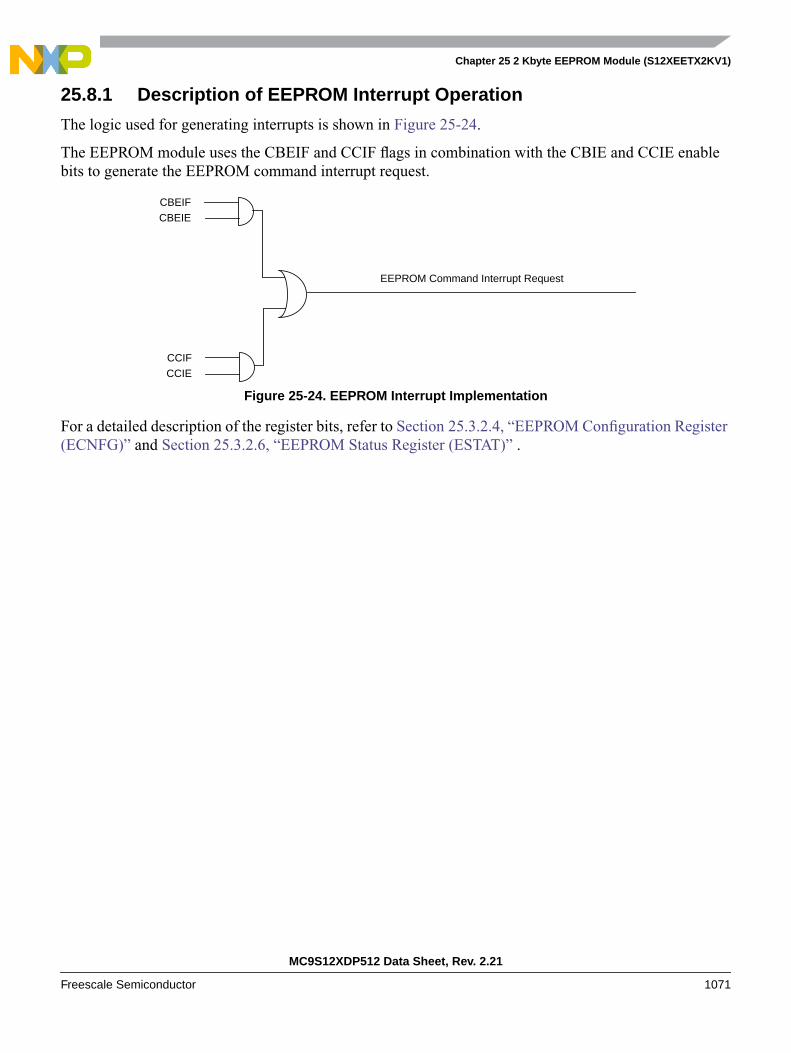
Chapter 25 2 Kbyte EEPROM Module (S12XEETX2KV1)
MC9S12XDP512 Data Sheet, Rev. 2.21
Freescale Semiconductor 1071
25.8.1 Description of EEPROM Interrupt Operation
The logic used for generating interrupts is shown in Figure 25-24.
The EEPROM module uses the CBEIF and CCIF flags in combination with the CBIE and CCIE enablebits to generate the EEPROM command interrupt request.
Figure 25-24. EEPROM Interrupt Implementation
For a detailed description of the register bits, refer to Section 25.3.2.4, “EEPROM Configuration Register(ECNFG)” and Section 25.3.2.6, “EEPROM Status Register (ESTAT)” .
EEPROM Command Interrupt Request
CBEIE
CBEIF
CCIE
CCIF

Chapter 25 2 Kbyte EEPROM Module (S12XEETX2KV1)
MC9S12XDP512 Data Sheet, Rev. 2.21
1072 Freescale Semiconductor

MC9S12XDP512 Data Sheet, Rev. 2.21
Freescale Semiconductor 1073
Chapter 264 Kbyte EEPROM Module (S12XEETX4KV2)
26.1 IntroductionThis document describes the EETX4K module which includes a 4 Kbyte EEPROM (nonvolatile) memory.The EEPROM memory may be read as either bytes, aligned words, or misaligned words. Read access timeis one bus cycle for bytes and aligned words, and two bus cycles for misaligned words.
The EEPROM memory is ideal for data storage for single-supply applications allowing for fieldreprogramming without requiring external voltage sources for program or erase. Program and erasefunctions are controlled by a command driven interface. The EEPROM module supports both block erase(all memory bytes) and sector erase (4 memory bytes). An erased bit reads 1 and a programmed bit reads0. The high voltage required to program and erase the EEPROM memory is generated internally. It is notpossible to read from the EEPROM block while it is being erased or programmed.
CAUTIONAn EEPROM word (2 bytes) must be in the erased state before beingprogrammed. Cumulative programming of bits within a word is not allowed.
26.1.1 Glossary
Command Write Sequence — A three-step MCU instruction sequence to execute built-in algorithms(including program and erase) on the EEPROM memory.
26.1.2 Features• 4 Kbytes of EEPROM memory divided into 1024 sectors of 4 bytes
• Automated program and erase algorithm
• Interrupts on EEPROM command completion and command buffer empty
• Fast sector erase and word program operation
• 2-stage command pipeline
• Sector erase abort feature for critical interrupt response
• Flexible protection scheme to prevent accidental program or erase
• Single power supply for all EEPROM operations including program and erase
26.1.3 Modes of Operation
Program, erase and erase verify operations (please refer to Section 26.4.1, “EEPROM CommandOperations” for details).

Chapter 26 4 Kbyte EEPROM Module (S12XEETX4KV2)
MC9S12XDP512 Data Sheet, Rev. 2.21
1074 Freescale Semiconductor
26.1.4 Block Diagram
A block diagram of the EEPROM module is shown in Figure 26-1.
Figure 26-1. EETX4K Block Diagram
26.2 External Signal DescriptionThe EEPROM module contains no signals that connect off-chip.
26.3 Memory Map and Register DefinitionThis section describes the memory map and registers for the EEPROM module.
26.3.1 Module Memory Map
The EEPROM memory map is shown in Figure 26-2. The HCS12X architecture places the EEPROMmemory addresses between global addresses 0x13_F000 and 0x13_FFFF. The EPROT register, describedin Section 26.3.2.5, “EEPROM Protection Register (EPROT)”, can be set to protect the upper region in theEEPROM memory from accidental program or erase. The EEPROM addresses covered by this protectable
EETX4K
EEPROM
2K * 16 Bits
sector 0sector 1
sector 1023
OscillatorClockDivider
Clock
CommandInterruptRequest
EECLK
Protection
Command Pipeline
cmd2addr2data2
cmd1addr1data1
Registers
EEPROMInterface

Chapter 26 4 Kbyte EEPROM Module (S12XEETX4KV2)
MC9S12XDP512 Data Sheet, Rev. 2.21
Freescale Semiconductor 1075
region are shown in the EEPROM memory map. The default protection setting is stored in the EEPROMconfiguration field as described in Table 26-1.
Table 26-1. EEPROM Configuration Field
Global AddressSize
(bytes)Description
0x13_FFFC 1 Reserved
0x13_FFFD 1 EEPROM Protection byteRefer to Section 26.3.2.5, “EEPROM Protection Register (EPROT)”
0x13_FFFE – 0x13_FFFF 2 Reserved
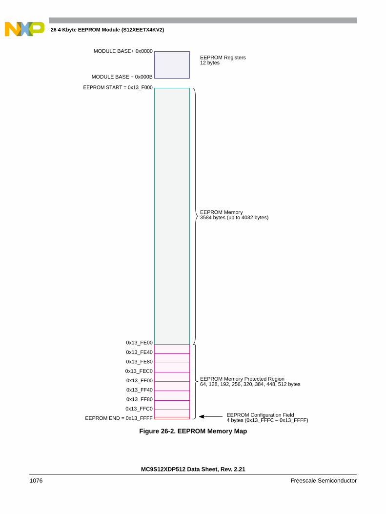
Chapter 26 4 Kbyte EEPROM Module (S12XEETX4KV2)
MC9S12XDP512 Data Sheet, Rev. 2.21
1076 Freescale Semiconductor
Figure 26-2. EEPROM Memory Map
EEPROM RegistersMODULE BASE+ 0x0000
EEPROM Configuration Field
MODULE BASE + 0x000B
EEPROM START = 0x13_F000
EEPROM END = 0x13_FFFF
0x13_FFC0
0x13_FF80
EEPROM Memory Protected Region64, 128, 192, 256, 320, 384, 448, 512 bytes
EEPROM Memory3584 bytes (up to 4032 bytes)
12 bytes
4 bytes (0x13_FFFC – 0x13_FFFF)
0x13_FF40
0x13_FF00
0x13_FEC0
0x13_FE80
0x13_FE40
0x13_FE00

Chapter 26 4 Kbyte EEPROM Module (S12XEETX4KV2)
MC9S12XDP512 Data Sheet, Rev. 2.21
Freescale Semiconductor 1077
The EEPROM module also contains a set of 12 control and status registers located between EEPROMmodule base + 0x0000 and 0x000B. A summary of the EEPROM module registers is given in Table 26-2while their accessibility is detailed in Section 26.3.2, “Register Descriptions”.
Table 26-2. EEPROM Register Map
ModuleBase +
Register NameNormal Mode
Access
0x0000 EEPROM Clock Divider Register (ECLKDIV) R/W
0x0001 RESERVED11
1 Intended for factory test purposes only.
R
0x0002 RESERVED21 R
0x0003 EEPROM Configuration Register (ECNFG) R/W
0x0004 EEPROM Protection Register (EPROT) R/W
0x0005 EEPROM Status Register (ESTAT) R/W
0x0006 EEPROM Command Register (ECMD) R/W
0x0007 RESERVED31 R
0x0008 EEPROM High Address Register (EADDRHI)1 R
0x0009 EEPROM Low Address Register (EADDRLO)1 R
0x000A EEPROM High Data Register (EDATAHI)1 R
0x000B EEPROM Low Data Register (EDATALO)1 R

Chapter 26 4 Kbyte EEPROM Module (S12XEETX4KV2)
MC9S12XDP512 Data Sheet, Rev. 2.21
1078 Freescale Semiconductor
26.3.2 Register Descriptions
26.3.2.1 EEPROM Clock Divider Register (ECLKDIV)
The ECLKDIV register is used to control timed events in program and erase algorithms.
RegisterName
Bit 7 6 5 4 3 2 1 Bit 0
ECLKDIV R EDIVLDPRDIV8 EDIV5 EDIV4 EDIV3 EDIV2 EDIV1 EDIV0
W
RESERVED1 R 0 0 0 0 0 0 0 0
W
RESERVED2 R 0 0 0 0 0 0 0 0
W
ECNFG RCBEIE CCIE
0 0 0 0 0 0
W
EPROT REPOPEN
RNV6 RNV5 RNV4EPDIS EPS2 EPS1 EPS0
W
ESTAT RCBEIF
CCIFPVIOL ACCERR
0 BLANK 0 0
W
ECMD R 0CMDB
W
RESERVED3 R 0 0 0 0 0 0 0 0
W
EADDRHI R 0 0 0 0 0 EABHI
W
EADDRLO R EABLO
W
EDATAHI R EDHI
W
EDATALO R EDLO
W
= Unimplemented or Reserved
Figure 26-3. EETX4K Register Summary
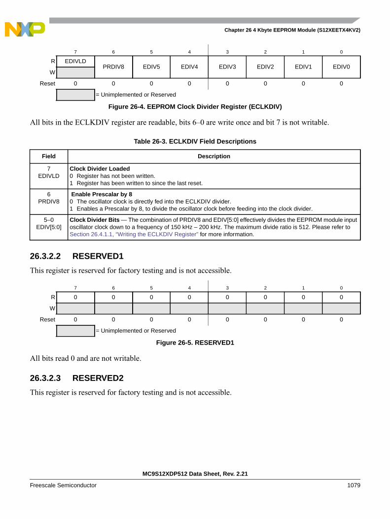
Chapter 26 4 Kbyte EEPROM Module (S12XEETX4KV2)
MC9S12XDP512 Data Sheet, Rev. 2.21
Freescale Semiconductor 1079
All bits in the ECLKDIV register are readable, bits 6–0 are write once and bit 7 is not writable.
26.3.2.2 RESERVED1
This register is reserved for factory testing and is not accessible.
All bits read 0 and are not writable.
26.3.2.3 RESERVED2
This register is reserved for factory testing and is not accessible.
7 6 5 4 3 2 1 0
R EDIVLDPRDIV8 EDIV5 EDIV4 EDIV3 EDIV2 EDIV1 EDIV0
W
Reset 0 0 0 0 0 0 0 0
= Unimplemented or Reserved
Figure 26-4. EEPROM Clock Divider Register (ECLKDIV)
Table 26-3. ECLKDIV Field Descriptions
Field Description
7EDIVLD
Clock Divider Loaded0 Register has not been written.1 Register has been written to since the last reset.
6PRDIV8
Enable Prescalar by 80 The oscillator clock is directly fed into the ECLKDIV divider.1 Enables a Prescalar by 8, to divide the oscillator clock before feeding into the clock divider.
5–0EDIV[5:0]
Clock Divider Bits — The combination of PRDIV8 and EDIV[5:0] effectively divides the EEPROM module inputoscillator clock down to a frequency of 150 kHz – 200 kHz. The maximum divide ratio is 512. Please refer toSection 26.4.1.1, “Writing the ECLKDIV Register” for more information.
7 6 5 4 3 2 1 0
R 0 0 0 0 0 0 0 0
W
Reset 0 0 0 0 0 0 0 0
= Unimplemented or Reserved
Figure 26-5. RESERVED1
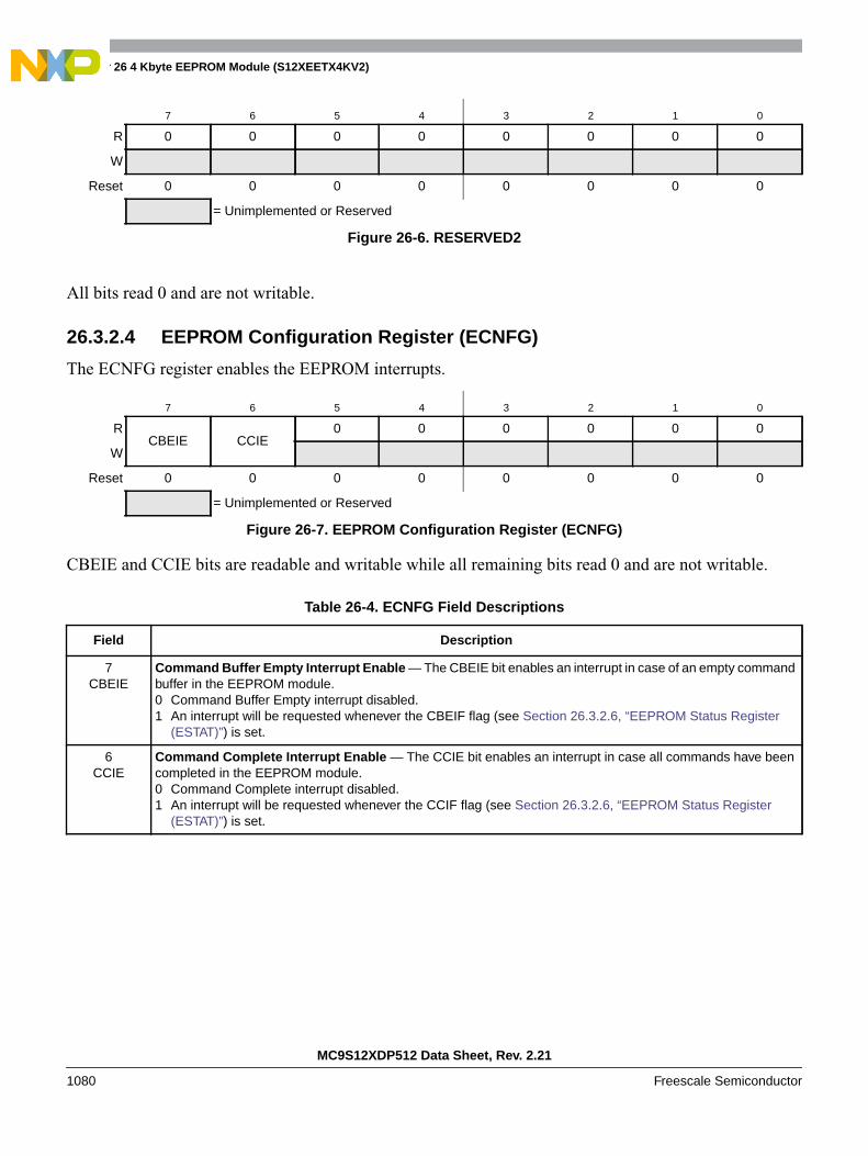
Chapter 26 4 Kbyte EEPROM Module (S12XEETX4KV2)
MC9S12XDP512 Data Sheet, Rev. 2.21
1080 Freescale Semiconductor
All bits read 0 and are not writable.
26.3.2.4 EEPROM Configuration Register (ECNFG)
The ECNFG register enables the EEPROM interrupts.
CBEIE and CCIE bits are readable and writable while all remaining bits read 0 and are not writable.
7 6 5 4 3 2 1 0
R 0 0 0 0 0 0 0 0
W
Reset 0 0 0 0 0 0 0 0
= Unimplemented or Reserved
Figure 26-6. RESERVED2
7 6 5 4 3 2 1 0
RCBEIE CCIE
0 0 0 0 0 0
W
Reset 0 0 0 0 0 0 0 0
= Unimplemented or Reserved
Figure 26-7. EEPROM Configuration Register (ECNFG)
Table 26-4. ECNFG Field Descriptions
Field Description
7CBEIE
Command Buffer Empty Interrupt Enable — The CBEIE bit enables an interrupt in case of an empty commandbuffer in the EEPROM module.0 Command Buffer Empty interrupt disabled.1 An interrupt will be requested whenever the CBEIF flag (see Section 26.3.2.6, “EEPROM Status Register
(ESTAT)”) is set.
6CCIE
Command Complete Interrupt Enable — The CCIE bit enables an interrupt in case all commands have beencompleted in the EEPROM module.0 Command Complete interrupt disabled.1 An interrupt will be requested whenever the CCIF flag (see Section 26.3.2.6, “EEPROM Status Register
(ESTAT)”) is set.
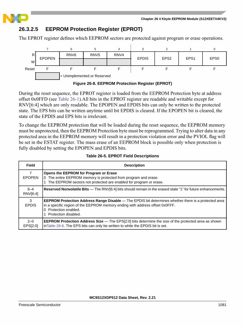
Chapter 26 4 Kbyte EEPROM Module (S12XEETX4KV2)
MC9S12XDP512 Data Sheet, Rev. 2.21
Freescale Semiconductor 1081
26.3.2.5 EEPROM Protection Register (EPROT)
The EPROT register defines which EEPROM sectors are protected against program or erase operations.
During the reset sequence, the EPROT register is loaded from the EEPROM Protection byte at addressoffset 0x0FFD (see Table 26-1).All bits in the EPROT register are readable and writable except forRNV[6:4] which are only readable. The EPOPEN and EPDIS bits can only be written to the protectedstate. The EPS bits can be written anytime until bit EPDIS is cleared. If the EPOPEN bit is cleared, thestate of the EPDIS and EPS bits is irrelevant.
To change the EEPROM protection that will be loaded during the reset sequence, the EEPROM memorymust be unprotected, then the EEPROM Protection byte must be reprogrammed. Trying to alter data in anyprotected area in the EEPROM memory will result in a protection violation error and the PVIOL flag willbe set in the ESTAT register. The mass erase of an EEPROM block is possible only when protection isfully disabled by setting the EPOPEN and EPDIS bits.
7 6 5 4 3 2 1 0
REPOPEN
RNV6 RNV5 RNV4EPDIS EPS2 EPS1 EPS0
W
Reset F F F F F F F F
= Unimplemented or Reserved
Figure 26-8. EEPROM Protection Register (EPROT)
Table 26-5. EPROT Field Descriptions
Field Description
7EPOPEN
Opens the EEPROM for Program or Erase0 The entire EEPROM memory is protected from program and erase.1 The EEPROM sectors not protected are enabled for program or erase.
6–4RNV[6:4]
Reserved Nonvolatile Bits — The RNV[6:4] bits should remain in the erased state “1” for future enhancements.
3EPDIS
EEPROM Protection Address Range Disable — The EPDIS bit determines whether there is a protected areain a specific region of the EEPROM memory ending with address offset 0x0FFF.0 Protection enabled.1 Protection disabled.
2–0EPS[2:0]
EEPROM Protection Address Size — The EPS[2:0] bits determine the size of the protected area as showninTable 26-6. The EPS bits can only be written to while the EPDIS bit is set.
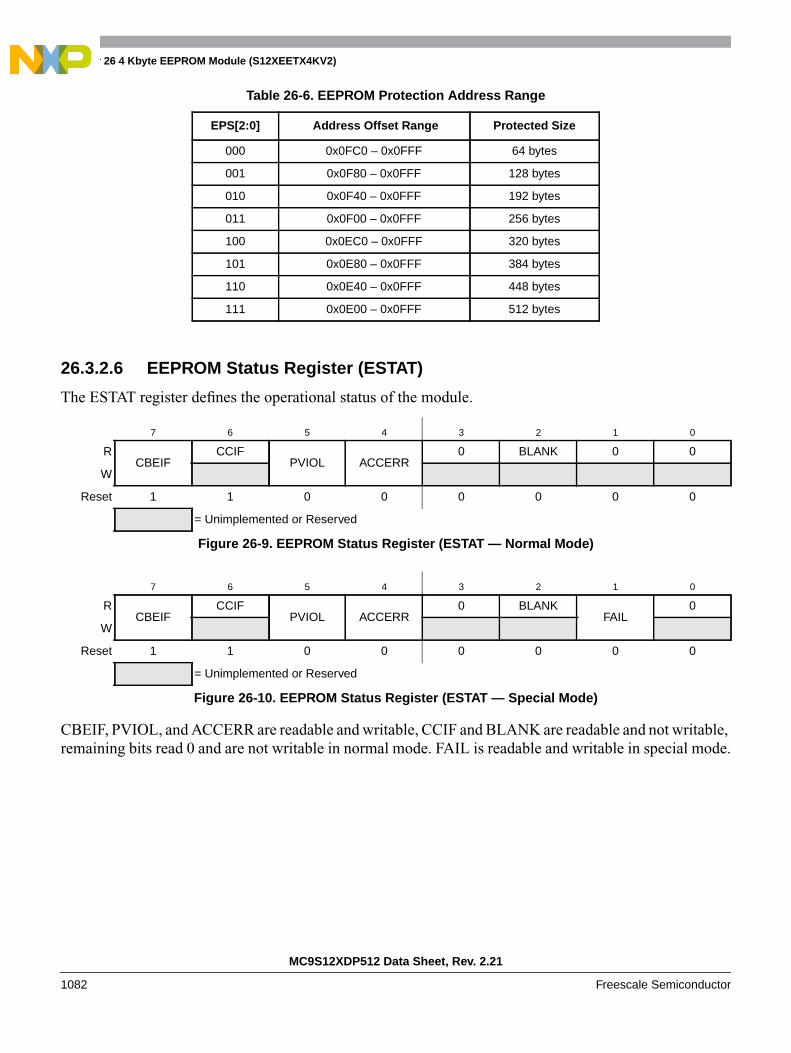
Chapter 26 4 Kbyte EEPROM Module (S12XEETX4KV2)
MC9S12XDP512 Data Sheet, Rev. 2.21
1082 Freescale Semiconductor
26.3.2.6 EEPROM Status Register (ESTAT)
The ESTAT register defines the operational status of the module.
CBEIF, PVIOL, and ACCERR are readable and writable, CCIF and BLANK are readable and not writable,remaining bits read 0 and are not writable in normal mode. FAIL is readable and writable in special mode.
Table 26-6. EEPROM Protection Address Range
EPS[2:0] Address Offset Range Protected Size
000 0x0FC0 – 0x0FFF 64 bytes
001 0x0F80 – 0x0FFF 128 bytes
010 0x0F40 – 0x0FFF 192 bytes
011 0x0F00 – 0x0FFF 256 bytes
100 0x0EC0 – 0x0FFF 320 bytes
101 0x0E80 – 0x0FFF 384 bytes
110 0x0E40 – 0x0FFF 448 bytes
111 0x0E00 – 0x0FFF 512 bytes
7 6 5 4 3 2 1 0
RCBEIF
CCIFPVIOL ACCERR
0 BLANK 0 0
W
Reset 1 1 0 0 0 0 0 0
= Unimplemented or Reserved
Figure 26-9. EEPROM Status Register (ESTAT — Normal Mode)
7 6 5 4 3 2 1 0
RCBEIF
CCIFPVIOL ACCERR
0 BLANKFAIL
0
W
Reset 1 1 0 0 0 0 0 0
= Unimplemented or Reserved
Figure 26-10. EEPROM Status Register (ESTAT — Special Mode)

Chapter 26 4 Kbyte EEPROM Module (S12XEETX4KV2)
MC9S12XDP512 Data Sheet, Rev. 2.21
Freescale Semiconductor 1083
Table 26-7. ESTAT Field Descriptions
Field Description
7CBEIF
Command Buffer Empty Interrupt Flag — The CBEIF flag indicates that the address, data, and commandbuffers are empty so that a new command write sequence can be started. The CBEIF flag is cleared by writinga 1 to CBEIF. Writing a 0 to the CBEIF flag has no effect on CBEIF. Writing a 0 to CBEIF after writing an alignedword to the EEPROM address space but before CBEIF is cleared will abort a command write sequence andcause the ACCERR flag to be set. Writing a 0 to CBEIF outside of a command write sequence will not set theACCERR flag. The CBEIF flag is used together with the CBEIE bit in the ECNFG register to generate an interruptrequest (see Figure 26-24).0 Buffers are full.1 Buffers are ready to accept a new command.
6CCIF
Command Complete Interrupt Flag — The CCIF flag indicates that there are no more commands pending. TheCCIF flag is cleared when CBEIF is clear and sets automatically upon completion of all active and pendingcommands. The CCIF flag does not set when an active commands completes and a pending command isfetched from the command buffer. Writing to the CCIF flag has no effect on CCIF. The CCIF flag is used togetherwith the CCIE bit in the ECNFG register to generate an interrupt request (see Figure 26-24).0 Command in progress.1 All commands are completed.
5PVIOL
Protection Violation Flag — The PVIOL flag indicates an attempt was made to program or erase an addressin a protected area of the EEPROM memory during a command write sequence. The PVIOL flag is cleared bywriting a 1 to PVIOL. Writing a 0 to the PVIOL flag has no effect on PVIOL. While PVIOL is set, it is not possibleto launch a command or start a command write sequence.0 No failure.1 A protection violation has occurred.
4ACCERR
Access Error Flag — The ACCERR flag indicates an illegal access has occurred to the EEPROM memorycaused by either a violation of the command write sequence (see Section 26.4.1.2, “Command WriteSequence”), issuing an illegal EEPROM command (see Table 26-9), launching the sector erase abort commandterminating a sector erase operation early (see Section 26.4.2.5, “Sector Erase Abort Command”) or theexecution of a CPU STOP instruction while a command is executing (CCIF = 0). The ACCERR flag is cleared bywriting a 1 to ACCERR. Writing a 0 to the ACCERR flag has no effect on ACCERR. While ACCERR is set, it isnot possible to launch a command or start a command write sequence. If ACCERR is set by an erase verifyoperation, any buffered command will not launch.0 No access error detected.1 Access error has occurred.
2BLANK
Flag Indicating the Erase Verify Operation Status — When the CCIF flag is set after completion of an eraseverify command, the BLANK flag indicates the result of the erase verify operation. The BLANK flag is cleared bythe EEPROM module when CBEIF is cleared as part of a new valid command write sequence. Writing to theBLANK flag has no effect on BLANK.0 EEPROM block verified as not erased.1 EEPROM block verified as erased.
1FAIL
Flag Indicating a Failed EEPROM Operation — The FAIL flag will set if the erase verify operation fails(EEPROM block verified as not erased). The FAIL flag is cleared by writing a 1 to FAIL. Writing a 0 to the FAILflag has no effect on FAIL.0 EEPROM operation completed without error.1 EEPROM operation failed.

Chapter 26 4 Kbyte EEPROM Module (S12XEETX4KV2)
MC9S12XDP512 Data Sheet, Rev. 2.21
1084 Freescale Semiconductor
26.3.2.7 EEPROM Command Register (ECMD)
The ECMD register is the EEPROM command register.
All CMDB bits are readable and writable during a command write sequence while bit 7 reads 0 and is notwritable.
26.3.2.8 RESERVED3
This register is reserved for factory testing and is not accessible.
All bits read 0 and are not writable.
EEPROM Address Registers (EADDR)
7 6 5 4 3 2 1 0
R 0CMDB
W
Reset 0 0 0 0 0 0 0 0
= Unimplemented or Reserved
Figure 26-11. EEPROM Command Register (ECMD)
Table 26-8. ECMD Field Descriptions
Field Description
6–0CMDB[6:0]
EEPROM Command Bits — Valid EEPROM commands are shown in Table 26-9. Writing any command otherthan those listed in Table 26-9 sets the ACCERR flag in the ESTAT register.
Table 26-9. Valid EEPROM Command List
CMDB[6:0] Command
0x05 Erase Verify
0x20 Word Program
0x40 Sector Erase
0x41 Mass Erase
0x47 Sector Erase Abort
0x60 Sector Modify
7 6 5 4 3 2 1 0
R 0 0 0 0 0 0 0 0
W
Reset 0 0 0 0 0 0 0 0
= Unimplemented or Reserved
Figure 26-12. RESERVED3
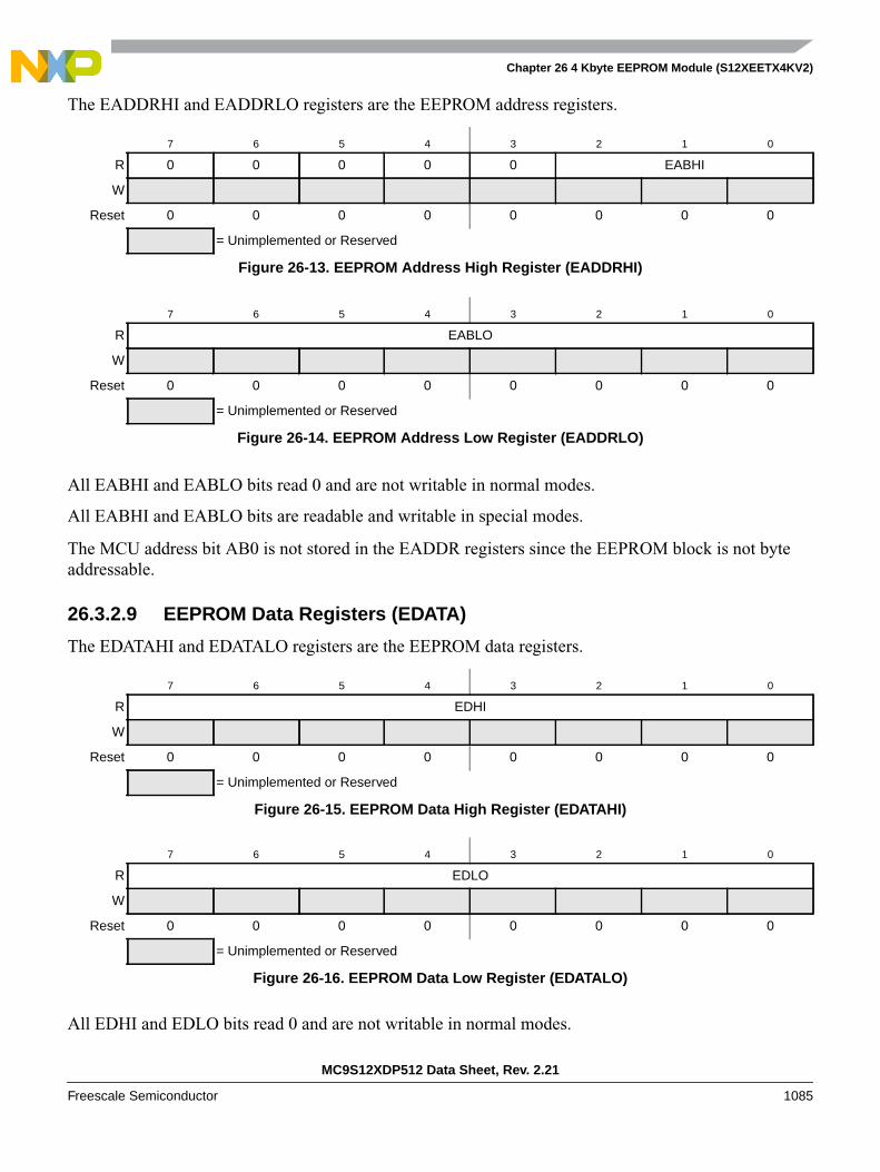
Chapter 26 4 Kbyte EEPROM Module (S12XEETX4KV2)
MC9S12XDP512 Data Sheet, Rev. 2.21
Freescale Semiconductor 1085
The EADDRHI and EADDRLO registers are the EEPROM address registers.
All EABHI and EABLO bits read 0 and are not writable in normal modes.
All EABHI and EABLO bits are readable and writable in special modes.
The MCU address bit AB0 is not stored in the EADDR registers since the EEPROM block is not byteaddressable.
26.3.2.9 EEPROM Data Registers (EDATA)
The EDATAHI and EDATALO registers are the EEPROM data registers.
All EDHI and EDLO bits read 0 and are not writable in normal modes.
7 6 5 4 3 2 1 0
R 0 0 0 0 0 EABHI
W
Reset 0 0 0 0 0 0 0 0
= Unimplemented or Reserved
Figure 26-13. EEPROM Address High Register (EADDRHI)
7 6 5 4 3 2 1 0
R EABLO
W
Reset 0 0 0 0 0 0 0 0
= Unimplemented or Reserved
Figure 26-14. EEPROM Address Low Register (EADDRLO)
7 6 5 4 3 2 1 0
R EDHI
W
Reset 0 0 0 0 0 0 0 0
= Unimplemented or Reserved
Figure 26-15. EEPROM Data High Register (EDATAHI)
7 6 5 4 3 2 1 0
R EDLO
W
Reset 0 0 0 0 0 0 0 0
= Unimplemented or Reserved
Figure 26-16. EEPROM Data Low Register (EDATALO)

Chapter 26 4 Kbyte EEPROM Module (S12XEETX4KV2)
MC9S12XDP512 Data Sheet, Rev. 2.21
1086 Freescale Semiconductor
All EDHI and EDLO bits are readable and writable in special modes.
26.4 Functional Description
26.4.1 EEPROM Command Operations
Write operations are used to execute program, erase, erase verify, sector erase abort, and sector modifyalgorithms described in this section. The program, erase, and sector modify algorithms are controlled bya state machine whose timebase, EECLK, is derived from the oscillator clock via a programmable divider.The command register as well as the associated address and data registers operate as a buffer and a register(2-stage FIFO) so that a second command along with the necessary data and address can be stored to thebuffer while the first command is still in progress. Buffer empty as well as command completion aresignalled by flags in the EEPROM status register with interrupts generated, if enabled.
The next sections describe:
1. How to write the ECLKDIV register
2. Command write sequences to program, erase, erase verify, sector erase abort, and sector modifyoperations on the EEPROM memory
3. Valid EEPROM commands
4. Effects resulting from illegal EEPROM command write sequences or aborting EEPROMoperations
26.4.1.1 Writing the ECLKDIV Register
Prior to issuing any EEPROM command after a reset, the user is required to write the ECLKDIV registerto divide the oscillator clock down to within the 150 kHz to 200 kHz range. Since the program and erasetimings are also a function of the bus clock, the ECLKDIV determination must take this information intoaccount.
If we define:
• ECLK as the clock of the EEPROM timing control block
• Tbus as the period of the bus clock
• INT(x) as taking the integer part of x (e.g., INT(4.323)=4)
then ECLKDIV register bits PRDIV8 and EDIV[5:0] are to be set as described in Figure 26-17.
For example, if the oscillator clock frequency is 950 kHz and the bus clock frequency is 10 MHz,ECLKDIV bits EDIV[5:0] should be set to 0x04 (000100) and bit PRDIV8 set to 0. The resulting EECLKfrequency is then 190 kHz. As a result, the EEPROM program and erase algorithm timings are increasedover the optimum target by:
If the oscillator clock frequency is 16 MHz and the bus clock frequency is 40 MHz, ECLKDIV bitsEDIV[5:0] should be set to 0x0A (001010) and bit PRDIV8 set to 1. The resulting EECLK frequency is
200 190–( ) 200⁄ 100× 5%=
Chapter 26 4 Kbyte EEPROM Module (S12XEETX4KV2)
MC9S12XDP512 Data Sheet, Rev. 2.21
Freescale Semiconductor 1087
then 182 kHz. In this case, the EEPROM program and erase algorithm timings are increased over theoptimum target by:
CAUTIONProgram and erase command execution time will increase proportionallywith the period of EECLK. Because of the impact of clock synchronizationon the accuracy of the functional timings, programming or erasing theEEPROM memory cannot be performed if the bus clock runs at less than 1MHz. Programming or erasing the EEPROM memory with EECLK < 150kHz should be avoided. Setting ECLKDIV to a value such that EECLK <150 kHz can destroy the EEPROM memory due to overstress. SettingECLKDIV to a value such that (1/EECLK+Tbus) < 5 µs can result inincomplete programming or erasure of the EEPROM memory cells.
If the ECLKDIV register is written, the EDIVLD bit is set automatically. If the EDIVLD bit is 0, theECLKDIV register has not been written since the last reset. If the ECLKDIV register has not been writtento, the EEPROM command loaded during a command write sequence will not execute and the ACCERRflag in the ESTAT register will set.
200 182–( ) 200⁄ 100× 9%=

Chapter 26 4 Kbyte EEPROM Module (S12XEETX4KV2)
MC9S12XDP512 Data Sheet, Rev. 2.21
1088 Freescale Semiconductor
Figure 26-17. Determination Procedure for PRDIV8 and EDIV Bits
PRDIV8 = 1
yes
no
PRDIV8 = 0 (reset)
>12.8 MHz?
EECLK = (PRDCLK)/(1+EDIV[5:0])
PRDCLK = oscillator_clockPRDCLK = oscillator_clock/8
PRDCLK[MHz]*(5+Tbus[µs])no
EDIV[5:0]=PRDCLK[MHz]*(5+Tbus[µs])–1
yes
START
Tbus < 1µs?
an integer?
EDIV[5:0]=INT(PRDCLK[MHz]*(5+Tbus[µs]))
1/EECLK[MHz] + Tbus[ms] > 5AND
EECLK > 0.15 MHz?
ENDyes
no
EDIV[5:0] > 4?
ALL COMMANDS IMPOSSIBLE
yes
no
ALL COMMANDS IMPOSSIBLE
no
TRY TO DECREASE Tbus
yes
oscillator_clock

Chapter 26 4 Kbyte EEPROM Module (S12XEETX4KV2)
MC9S12XDP512 Data Sheet, Rev. 2.21
Freescale Semiconductor 1089
26.4.1.2 Command Write Sequence
The EEPROM command controller is used to supervise the command write sequence to execute program,erase, erase verify, sector erase abort, and sector modify algorithms.
Before starting a command write sequence, the ACCERR and PVIOL flags in the ESTAT register must beclear (see Section 26.3.2.6, “EEPROM Status Register (ESTAT)”) and the CBEIF flag should be tested todetermine the state of the address, data and command buffers. If the CBEIF flag is set, indicating thebuffers are empty, a new command write sequence can be started. If the CBEIF flag is clear, indicating thebuffers are not available, a new command write sequence will overwrite the contents of the address, dataand command buffers.
A command write sequence consists of three steps which must be strictly adhered to with writes to theEEPROM module not permitted between the steps. However, EEPROM register and array reads areallowed during a command write sequence. The basic command write sequence is as follows:
1. Write to one address in the EEPROM memory.
2. Write a valid command to the ECMD register.
3. Clear the CBEIF flag in the ESTAT register by writing a 1 to CBEIF to launch the command.
The address written in step 1 will be stored in the EADDR registers and the data will be stored in theEDATA registers. If the CBEIF flag in the ESTAT register is clear when the first EEPROM array writeoccurs, the contents of the address and data buffers will be overwritten and the CBEIF flag will be set.When the CBEIF flag is cleared, the CCIF flag is cleared on the same bus cycle by the EEPROM commandcontroller indicating that the command was successfully launched. For all command write sequencesexcept sector erase abort, the CBEIF flag will set four bus cycles after the CCIF flag is cleared indicatingthat the address, data, and command buffers are ready for a new command write sequence to begin. Forsector erase abort operations, the CBEIF flag will remain clear until the operation completes. Except forthe sector erase abort command, a buffered command will wait for the active operation to be completedbefore being launched. The sector erase abort command is launched when the CBEIF flag is cleared as partof a sector erase abort command write sequence. Once a command is launched, the completion of thecommand operation is indicated by the setting of the CCIF flag in the ESTAT register. The CCIF flag willset upon completion of all active and buffered commands.
26.4.2 EEPROM Commands
Table 26-10 summarizes the valid EEPROM commands along with the effects of the commands on theEEPROM block.
Table 26-10. EEPROM Command Description
ECMDB Command Function on EEPROM Memory
0x05 EraseVerify
Verify all memory bytes in the EEPROM block are erased. If the EEPROM block is erased, theBLANK flag in the ESTAT register will set upon command completion.
0x20 Program Program a word (two bytes) in the EEPROM block.
0x40 SectorErase
Erase all four memory bytes in a sector of the EEPROM block.

Chapter 26 4 Kbyte EEPROM Module (S12XEETX4KV2)
MC9S12XDP512 Data Sheet, Rev. 2.21
1090 Freescale Semiconductor
CAUTIONAn EEPROM word (2 bytes) must be in the erased state before beingprogrammed. Cumulative programming of bits within a word is not allowed.
0x41 MassErase
Erase all memory bytes in the EEPROM block. A mass erase of the full EEPROM block is onlypossible when EPOPEN and EPDIS bits in the EPROT register are set prior to launching thecommand.
0x47 Sector EraseAbort
Abort the sector erase operation. The sector erase operation will terminate according to a setprocedure. The EEPROM sector should not be considered erased if the ACCERR flag is setupon command completion.
0x60 SectorModify
Erase all four memory bytes in a sector of the EEPROM block and reprogram the addressedword.
Table 26-10. EEPROM Command Description
ECMDB Command Function on EEPROM Memory

Chapter 26 4 Kbyte EEPROM Module (S12XEETX4KV2)
MC9S12XDP512 Data Sheet, Rev. 2.21
Freescale Semiconductor 1091
26.4.2.1 Erase Verify Command
The erase verify operation will verify that the EEPROM memory is erased.
An example flow to execute the erase verify operation is shown in Figure 26-18. The erase verify commandwrite sequence is as follows:
1. Write to an EEPROM address to start the command write sequence for the erase verify command.The address and data written will be ignored.
2. Write the erase verify command, 0x05, to the ECMD register.
3. Clear the CBEIF flag in the ESTAT register by writing a 1 to CBEIF to launch the erase verifycommand.
After launching the erase verify command, the CCIF flag in the ESTAT register will set after the operationhas completed unless a new command write sequence has been buffered. The number of bus cyclesrequired to execute the erase verify operation is equal to the number of words in the EEPROM memoryplus 14 bus cycles as measured from the time the CBEIF flag is cleared until the CCIF flag is set. Uponcompletion of the erase verify operation, the BLANK flag in the ESTAT register will be set if all addressesin the EEPROM memory are verified to be erased. If any address in the EEPROM memory is not erased,the erase verify operation will terminate and the BLANK flag in the ESTAT register will remain clear.
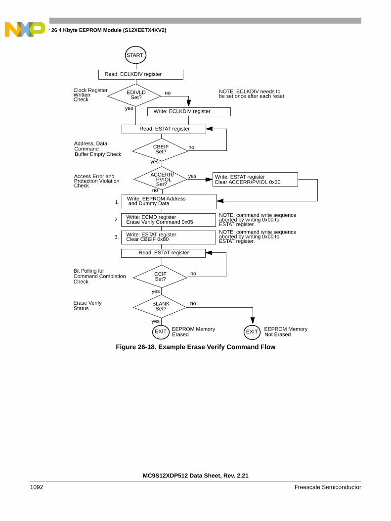
Chapter 26 4 Kbyte EEPROM Module (S12XEETX4KV2)
MC9S12XDP512 Data Sheet, Rev. 2.21
1092 Freescale Semiconductor
Figure 26-18. Example Erase Verify Command Flow
Write: EEPROM Address
Write: ECMD registerErase Verify Command 0x05
Write: ESTAT registerClear CBEIF 0x80
1.
2.
3.
Clear ACCERR/PVIOL 0x30Write: ESTAT registeryes
no
Access Error andProtection Violation
no
and Dummy Data
Bit Polling forCommand CompletionCheck
Read: ESTAT register
yes
NOTE: command write sequenceaborted by writing 0x00 toESTAT register.
NOTE: command write sequenceaborted by writing 0x00 toESTAT register.
Read: ESTAT register
no
START
yes
Check
CBEIFSet?
Address, Data,CommandBuffer Empty Check
CCIFSet?
ACCERR/PVIOLSet?
noErase VerifyStatus
yes
EXIT EEPROM MemoryNot ErasedEXIT EEPROM Memory
Erased
BLANKSet?
Write: ECLKDIV register
Read: ECLKDIV register
yes
noClock RegisterWrittenCheck
EDIVLDSet?
NOTE: ECLKDIV needs tobe set once after each reset.
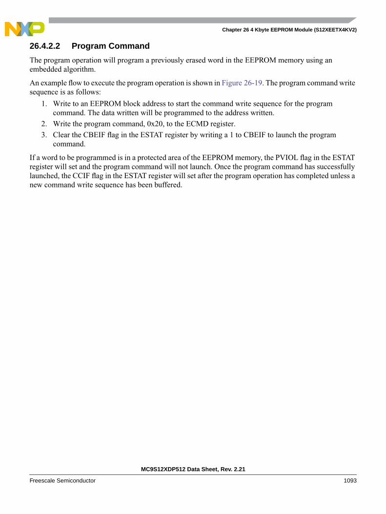
Chapter 26 4 Kbyte EEPROM Module (S12XEETX4KV2)
MC9S12XDP512 Data Sheet, Rev. 2.21
Freescale Semiconductor 1093
26.4.2.2 Program Command
The program operation will program a previously erased word in the EEPROM memory using anembedded algorithm.
An example flow to execute the program operation is shown in Figure 26-19. The program command writesequence is as follows:
1. Write to an EEPROM block address to start the command write sequence for the programcommand. The data written will be programmed to the address written.
2. Write the program command, 0x20, to the ECMD register.
3. Clear the CBEIF flag in the ESTAT register by writing a 1 to CBEIF to launch the programcommand.
If a word to be programmed is in a protected area of the EEPROM memory, the PVIOL flag in the ESTATregister will set and the program command will not launch. Once the program command has successfullylaunched, the CCIF flag in the ESTAT register will set after the program operation has completed unless anew command write sequence has been buffered.
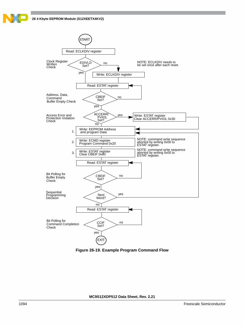
Chapter 26 4 Kbyte EEPROM Module (S12XEETX4KV2)
MC9S12XDP512 Data Sheet, Rev. 2.21
1094 Freescale Semiconductor
Figure 26-19. Example Program Command Flow
Write: EEPROM Address
Write: ECMD registerProgram Command 0x20
Write: ESTAT registerClear CBEIF 0x80
1.
2.
3.
Clear ACCERR/PVIOL 0x30Write: ESTAT registeryes
no
Access Error andProtection Violation
no
and program Data
Bit Polling forBuffer EmptyCheck
Read: ESTAT register
yes
NOTE: command write sequenceaborted by writing 0x00 toESTAT register.
NOTE: command write sequenceaborted by writing 0x00 toESTAT register.
Read: ESTAT register
no
START
yes
Check
CBEIFSet?
Address, Data,CommandBuffer Empty Check
CBEIFSet?
ACCERR/PVIOLSet?
EXIT
Write: ECLKDIV register
Read: ECLKDIV register
yes
noClock RegisterWrittenCheck
EDIVLDSet?
NOTE: ECLKDIV needs tobe set once after each reset.
no
yesSequentialProgrammingDecision
NextWord?
noBit Polling forCommand CompletionCheck
Read: ESTAT register
yes
CCIFSet?

Chapter 26 4 Kbyte EEPROM Module (S12XEETX4KV2)
MC9S12XDP512 Data Sheet, Rev. 2.21
Freescale Semiconductor 1095
26.4.2.3 Sector Erase Command
The sector erase operation will erase both words in a sector of EEPROM memory using an embeddedalgorithm.
An example flow to execute the sector erase operation is shown in Figure 26-20. The sector erasecommand write sequence is as follows:
1. Write to an EEPROM memory address to start the command write sequence for the sector erasecommand. The EEPROM address written determines the sector to be erased while global addressbits [1:0] and the data written are ignored.
2. Write the sector erase command, 0x40, to the ECMD register.
3. Clear the CBEIF flag in the ESTAT register by writing a 1 to CBEIF to launch the sector erasecommand.
If an EEPROM sector to be erased is in a protected area of the EEPROM memory, the PVIOL flag in theESTAT register will set and the sector erase command will not launch. Once the sector erase command hassuccessfully launched, the CCIF flag in the ESTAT register will set after the sector erase operation hascompleted unless a new command write sequence has been buffered.
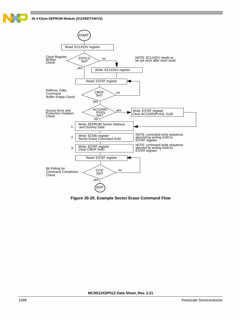
Chapter 26 4 Kbyte EEPROM Module (S12XEETX4KV2)
MC9S12XDP512 Data Sheet, Rev. 2.21
1096 Freescale Semiconductor
Figure 26-20. Example Sector Erase Command Flow
Write: EEPROM Sector Address
Write: ECMD registerSector Erase Command 0x40
Write: ESTAT registerClear CBEIF 0x80
1.
2.
3.
Clear ACCERR/PVIOL 0x30Write: ESTAT registeryes
no
Access Error andProtection Violation
and Dummy Data
Read: ESTAT register
NOTE: command write sequenceaborted by writing 0x00 toESTAT register.
NOTE: command write sequenceaborted by writing 0x00 toESTAT register.
Read: ESTAT register
no
START
yes
Check
CBEIFSet?
Address, Data,CommandBuffer Empty Check
ACCERR/PVIOLSet?
EXIT
Write: ECLKDIV register
Read: ECLKDIV register
yes
noClock RegisterWrittenCheck
EDIVLDSet?
NOTE: ECLKDIV needs tobe set once after each reset.
noBit Polling forCommand CompletionCheck
yes
CCIFSet?
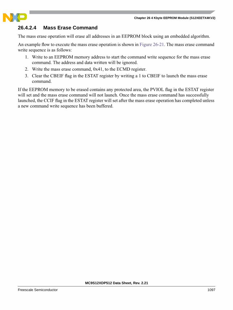
Chapter 26 4 Kbyte EEPROM Module (S12XEETX4KV2)
MC9S12XDP512 Data Sheet, Rev. 2.21
Freescale Semiconductor 1097
26.4.2.4 Mass Erase Command
The mass erase operation will erase all addresses in an EEPROM block using an embedded algorithm.
An example flow to execute the mass erase operation is shown in Figure 26-21. The mass erase commandwrite sequence is as follows:
1. Write to an EEPROM memory address to start the command write sequence for the mass erasecommand. The address and data written will be ignored.
2. Write the mass erase command, 0x41, to the ECMD register.
3. Clear the CBEIF flag in the ESTAT register by writing a 1 to CBEIF to launch the mass erasecommand.
If the EEPROM memory to be erased contains any protected area, the PVIOL flag in the ESTAT registerwill set and the mass erase command will not launch. Once the mass erase command has successfullylaunched, the CCIF flag in the ESTAT register will set after the mass erase operation has completed unlessa new command write sequence has been buffered.
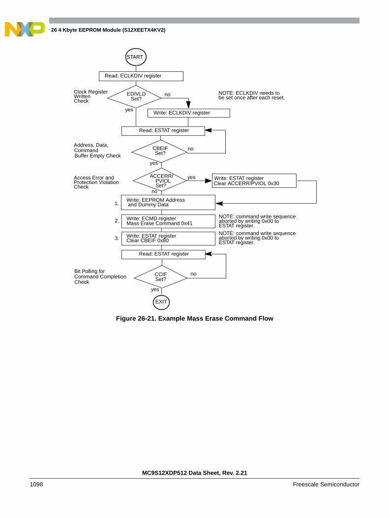
Chapter 26 4 Kbyte EEPROM Module (S12XEETX4KV2)
MC9S12XDP512 Data Sheet, Rev. 2.21
1098 Freescale Semiconductor
Figure 26-21. Example Mass Erase Command Flow
Write: EEPROM Address
Write: ECMD registerMass Erase Command 0x41
Write: ESTAT registerClear CBEIF 0x80
1.
2.
3.
Clear ACCERR/PVIOL 0x30Write: ESTAT registeryes
no
Access Error andProtection Violation
and Dummy Data
Read: ESTAT register
NOTE: command write sequenceaborted by writing 0x00 toESTAT register.
NOTE: command write sequenceaborted by writing 0x00 toESTAT register.
Read: ESTAT register
no
START
yes
Check
CBEIFSet?
Address, Data,CommandBuffer Empty Check
ACCERR/PVIOLSet?
EXIT
Write: ECLKDIV register
Read: ECLKDIV register
yes
noClock RegisterWrittenCheck
EDIVLDSet?
NOTE: ECLKDIV needs tobe set once after each reset.
noBit Polling forCommand CompletionCheck
yes
CCIFSet?
Chapter 26 4 Kbyte EEPROM Module (S12XEETX4KV2)
MC9S12XDP512 Data Sheet, Rev. 2.21
Freescale Semiconductor 1099
26.4.2.5 Sector Erase Abort Command
The sector erase abort operation will terminate the active sector erase or sector modify operation so thatother sectors in an EEPROM block are available for read and program operations without waiting for thesector erase or sector modify operation to complete.
An example flow to execute the sector erase abort operation is shown in Figure 26-22. The sector eraseabort command write sequence is as follows:
1. Write to any EEPROM memory address to start the command write sequence for the sector eraseabort command. The address and data written are ignored.
2. Write the sector erase abort command, 0x47, to the ECMD register.
3. Clear the CBEIF flag in the ESTAT register by writing a 1 to CBEIF to launch the sector erase abortcommand.
If the sector erase abort command is launched resulting in the early termination of an active sector eraseor sector modify operation, the ACCERR flag will set once the operation completes as indicated by theCCIF flag being set. The ACCERR flag sets to inform the user that the EEPROM sector may not be fullyerased and a new sector erase or sector modify command must be launched before programming anylocation in that specific sector. If the sector erase abort command is launched but the active sector erase orsector modify operation completes normally, the ACCERR flag will not set upon completion of theoperation as indicated by the CCIF flag being set. If the sector erase abort command is launched after thesector modify operation has completed the sector erase step, the program step will be allowed to complete.The maximum number of cycles required to abort a sector erase or sector modify operation is equal to fourEECLK periods (see Section 26.4.1.1, “Writing the ECLKDIV Register”) plus five bus cycles as measuredfrom the time the CBEIF flag is cleared until the CCIF flag is set.
NOTESince the ACCERR bit in the ESTAT register may be set at the completionof the sector erase abort operation, a command write sequence is notallowed to be buffered behind a sector erase abort command write sequence.The CBEIF flag will not set after launching the sector erase abort commandto indicate that a command should not be buffered behind it. If an attempt ismade to start a new command write sequence with a sector erase abortoperation active, the ACCERR flag in the ESTAT register will be set. A newcommand write sequence may be started after clearing the ACCERR flag, ifset.
NOTEThe sector erase abort command should be used sparingly since a sectorerase operation that is aborted counts as a complete program/erase cycle.
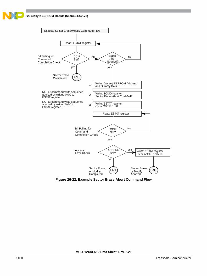
Chapter 26 4 Kbyte EEPROM Module (S12XEETX4KV2)
MC9S12XDP512 Data Sheet, Rev. 2.21
1100 Freescale Semiconductor
Figure 26-22. Example Sector Erase Abort Command Flow
Write: Dummy EEPROM Address
Write: ECMD registerSector Erase Abort Cmd 0x47
Write: ESTAT registerClear CBEIF 0x80
1.
2.
3.
Read: ESTAT register
and Dummy Data
Bit Polling forCommandCompletion Check
yes
NOTE: command write sequenceaborted by writing 0x00 toESTAT register.
NOTE: command write sequenceaborted by writing 0x00 toESTAT register.
CCIFSet?
Execute Sector Erase/Modify Command Flow
noBit Polling forCommandCompletion Check
Read: ESTAT register
yes
CCIFSet?
no
yes
AbortNeeded?
Erase
Clear ACCERR 0x10Write: ESTAT registeryes
no
AccessError Check
ACCERRSet?
Sector Eraseor Modify
Sector Eraseor Modify
no
EXIT EXIT
Sector EraseCompleted EXIT
Completed Aborted

Chapter 26 4 Kbyte EEPROM Module (S12XEETX4KV2)
MC9S12XDP512 Data Sheet, Rev. 2.21
Freescale Semiconductor 1101
26.4.2.6 Sector Modify Command
The sector modify operation will erase both words in a sector of EEPROM memory followed by areprogram of the addressed word using an embedded algorithm.
An example flow to execute the sector modify operation is shown in Figure 26-23. The sector modifycommand write sequence is as follows:
1. Write to an EEPROM memory address to start the command write sequence for the sector modifycommand. The EEPROM address written determines the sector to be erased and word to bereprogrammed while byte address bit 0 is ignored.
2. Write the sector modify command, 0x60, to the ECMD register.
3. Clear the CBEIF flag in the ESTAT register by writing a 1 to CBEIF to launch the sector erasecommand.
If an EEPROM sector to be modified is in a protected area of the EEPROM memory, the PVIOL flag inthe ESTAT register will set and the sector modify command will not launch. Once the sector modifycommand has successfully launched, the CCIF flag in the ESTAT register will set after the sector modifyoperation has completed unless a new command write sequence has been buffered.

Chapter 26 4 Kbyte EEPROM Module (S12XEETX4KV2)
MC9S12XDP512 Data Sheet, Rev. 2.21
1102 Freescale Semiconductor
Figure 26-23. Example Sector Modify Command Flow
Write: EEPROM Word Address
Write: ECMD registerSector Modify Command 0x60
Write: ESTAT registerClear CBEIF 0x80
1.
2.
3.
Clear ACCERR/PVIOL 0x30Write: ESTAT registeryes
no
Access Error andProtection Violation
and program Data
Read: ESTAT register
NOTE: command write sequenceaborted by writing 0x00 toESTAT register.
NOTE: command write sequenceaborted by writing 0x00 toESTAT register.
Read: ESTAT register
no
START
yes
Check
CBEIFSet?
Address, Data,CommandBuffer Empty Check
ACCERR/PVIOLSet?
EXIT
Write: ECLKDIV register
Read: ECLKDIV register
yes
noClock RegisterWrittenCheck
EDIVLDSet?
NOTE: ECLKDIV needs tobe set once after each reset.
noBit Polling forCommand CompletionCheck
yes
CCIFSet?
Chapter 26 4 Kbyte EEPROM Module (S12XEETX4KV2)
MC9S12XDP512 Data Sheet, Rev. 2.21
Freescale Semiconductor 1103
26.4.3 Illegal EEPROM Operations
The ACCERR flag will be set during the command write sequence if any of the following illegal steps areperformed, causing the command write sequence to immediately abort:
1. Writing to an EEPROM address before initializing the ECLKDIV register.
2. Writing a byte or misaligned word to a valid EEPROM address.
3. Starting a command write sequence while a sector erase abort operation is active.
4. Writing to any EEPROM register other than ECMD after writing to an EEPROM address.
5. Writing a second command to the ECMD register in the same command write sequence.
6. Writing an invalid command to the ECMD register.
7. Writing to an EEPROM address after writing to the ECMD register.
8. Writing to any EEPROM register other than ESTAT (to clear CBEIF) after writing to the ECMDregister.
9. Writing a 0 to the CBEIF flag in the ESTAT register to abort a command write sequence.
The ACCERR flag will not be set if any EEPROM register is read during a valid command write sequence.
The ACCERR flag will also be set if any of the following events occur:
1. Launching the sector erase abort command while a sector erase or sector modify operation is activewhich results in the early termination of the sector erase or sector modify operation (seeSection 26.4.2.5, “Sector Erase Abort Command”).
2. The MCU enters stop mode and a command operation is in progress. The operation is abortedimmediately and any pending command is purged (see Section 26.5.2, “Stop Mode”).
If the EEPROM memory is read during execution of an algorithm (CCIF = 0), the read operation willreturn invalid data and the ACCERR flag will not be set.
If the ACCERR flag is set in the ESTAT register, the user must clear the ACCERR flag before startinganother command write sequence (see Section 26.3.2.6, “EEPROM Status Register (ESTAT)”).
The PVIOL flag will be set after the command is written to the ECMD register during a command writesequence if any of the following illegal operations are attempted, causing the command write sequence toimmediately abort:
1. Writing the program command if the address written in the command write sequence was in aprotected area of the EEPROM memory.
2. Writing the sector erase command if the address written in the command write sequence was in aprotected area of the EEPROM memory.
3. Writing the mass erase command to the EEPROM memory while any EEPROM protection isenabled.
4. Writing the sector modify command if the address written in the command write sequence was ina protected area of the EEPROM memory.
If the PVIOL flag is set in the ESTAT register, the user must clear the PVIOL flag before starting anothercommand write sequence (see Section 26.3.2.6, “EEPROM Status Register (ESTAT)”).
Chapter 26 4 Kbyte EEPROM Module (S12XEETX4KV2)
MC9S12XDP512 Data Sheet, Rev. 2.21
1104 Freescale Semiconductor
26.5 Operating Modes
26.5.1 Wait Mode
If a command is active (CCIF = 0) when the MCU enters the wait mode, the active command and anybuffered command will be completed.
The EEPROM module can recover the MCU from wait mode if the CBEIF and CCIF interrupts are enabled(see Section 26.8, “Interrupts”).
26.5.2 Stop Mode
If a command is active (CCIF = 0) when the MCU enters the stop mode, the operation will be aborted and,if the operation is program, sector erase, mass erase, or sector modify, the EEPROM array data beingprogrammed or erased may be corrupted and the CCIF and ACCERR flags will be set. If active, the highvoltage circuitry to the EEPROM memory will immediately be switched off when entering stop mode.Upon exit from stop mode, the CBEIF flag is set and any buffered command will not be launched. TheACCERR flag must be cleared before starting a command write sequence (see Section 26.4.1.2,“Command Write Sequence”).
NOTEAs active commands are immediately aborted when the MCU enters stopmode, it is strongly recommended that the user does not use the STOPinstruction during program, sector erase, mass erase, or sector modifyoperations.
26.5.3 Background Debug Mode
In background debug mode (BDM), the EPROT register is writable. If the MCU is unsecured, then allEEPROM commands listed in Table 26-10 can be executed. If the MCU is secured and is in special singlechip mode, the only command available to execute is mass erase.
26.6 EEPROM Module SecurityThe EEPROM module does not provide any security information to the MCU. After each reset, thesecurity state of the MCU is a function of information provided by the Flash module (see the specific FTXBlock Guide).
Chapter 26 4 Kbyte EEPROM Module (S12XEETX4KV2)
MC9S12XDP512 Data Sheet, Rev. 2.21
Freescale Semiconductor 1105
26.6.1 Unsecuring the MCU in Special Single Chip Mode using BDM
Before the MCU can be unsecured in special single chip mode, the EEPROM memory must be erasedusing the following method :
• Reset the MCU into special single chip mode, delay while the erase test is performed by the BDMsecure ROM, send BDM commands to disable protection in the EEPROM module, and execute amass erase command write sequence to erase the EEPROM memory.
After the CCIF flag sets to indicate that the EEPROM mass operation has completed and assuming that theFlash memory has also been erased, reset the MCU into special single chip mode. The BDM secure ROMwill verify that the Flash and EEPROM memory are erased and will assert the UNSEC bit in the BDMstatus register. This BDM action will cause the MCU to override the Flash security state and the MCU willbe unsecured. Once the MCU is unsecured, BDM commands will be enabled and the Flash security bytemay be programmed to the unsecure state.
26.7 Resets
26.7.1 EEPROM Reset Sequence
On each reset, the EEPROM module executes a reset sequence to hold CPU activity while loading theEPROT register from the EEPROM memory according to Table 26-1.
26.7.2 Reset While EEPROM Command Active
If a reset occurs while any EEPROM command is in progress, that command will be immediately aborted.The state of a word being programmed or the sector / block being erased is not guaranteed.
26.8 InterruptsThe EEPROM module can generate an interrupt when all EEPROM command operations have completed,when the EEPROM address, data, and command buffers are empty.
NOTEVector addresses and their relative interrupt priority are determined at theMCU level.
Table 26-11. EEPROM Interrupt Sources
Interrupt Source Interrupt Flag Local Enable Global (CCR) Mask
EEPROM address, data, and command buffers empty CBEIF(ESTAT register)
CBEIE(ECNFG register)
I Bit
All EEPROM commands completed CCIF(ESTAT register)
CCIE(ECNFG register)
I Bit
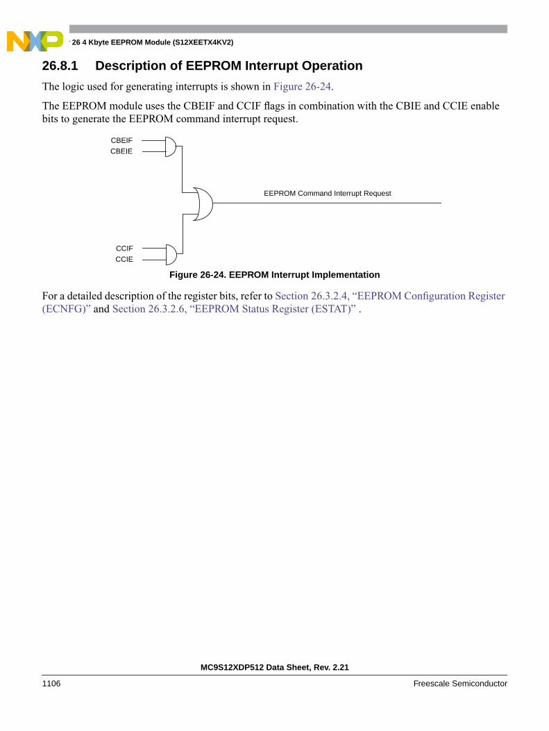
Chapter 26 4 Kbyte EEPROM Module (S12XEETX4KV2)
MC9S12XDP512 Data Sheet, Rev. 2.21
1106 Freescale Semiconductor
26.8.1 Description of EEPROM Interrupt Operation
The logic used for generating interrupts is shown in Figure 26-24.
The EEPROM module uses the CBEIF and CCIF flags in combination with the CBIE and CCIE enablebits to generate the EEPROM command interrupt request.
Figure 26-24. EEPROM Interrupt Implementation
For a detailed description of the register bits, refer to Section 26.3.2.4, “EEPROM Configuration Register(ECNFG)” and Section 26.3.2.6, “EEPROM Status Register (ESTAT)” .
EEPROM Command Interrupt Request
CBEIE
CBEIF
CCIE
CCIF
MC9S12XDP512 Data Sheet, Rev. 2.21
Freescale Semiconductor 1107
Chapter 27512 Kbyte Flash Module (S12XFTX512K4V2)
27.1 IntroductionThis document describes the FTX512K4 module that includes a 512K Kbyte Flash (nonvolatile) memory.The Flash memory may be read as either bytes, aligned words or misaligned words. Read access time isone bus cycle for bytes and aligned words, and two bus cycles for misaligned words.
The Flash memory is ideal for program and data storage for single-supply applications allowing for fieldreprogramming without requiring external voltage sources for program or erase. Program and erasefunctions are controlled by a command driven interface. The Flash module supports both block erase andsector erase. An erased bit reads 1 and a programmed bit reads 0. The high voltage required to programand erase the Flash memory is generated internally. It is not possible to read from a Flash block while it isbeing erased or programmed.
CAUTIONA Flash word must be in the erased state before being programmed.Cumulative programming of bits within a Flash word is not allowed.
27.1.1 Glossary
Command Write Sequence — A three-step MCU instruction sequence to execute built-in algorithms(including program and erase) on the Flash memory.
Multiple-Input Signature Register (MISR) — A Multiple-Input Signature Register is an outputresponse analyzer implemented using a linear feedback shift-register (LFSR). A 16-bit MISR is used tocompress data and generate a signature that is particular to the data read from a Flash block.
27.1.2 Features• 512 Kbytes of Flash memory comprised of four 128 Kbyte blocks with each block divided into
128 sectors of 1024 bytes
• Automated program and erase algorithm
• Interrupts on Flash command completion, command buffer empty
• Fast sector erase and word program operation
• 2-stage command pipeline for faster multi-word program times
• Sector erase abort feature for critical interrupt response
• Flexible protection scheme to prevent accidental program or erase
• Single power supply for all Flash operations including program and erase

Chapter 27 512 Kbyte Flash Module (S12XFTX512K4V2)
MC9S12XDP512 Data Sheet, Rev. 2.21
1108 Freescale Semiconductor
• Security feature to prevent unauthorized access to the Flash memory
• Code integrity check using built-in data compression
27.1.3 Modes of Operation
Program, erase, erase verify, and data compress operations (please refer to Section 27.4.1, “FlashCommand Operations” for details).
27.1.4 Block Diagram
A block diagram of the Flash module is shown in Figure 27-1.

Chapter 27 512 Kbyte Flash Module (S12XFTX512K4V2)
MC9S12XDP512 Data Sheet, Rev. 2.21
Freescale Semiconductor 1109
Figure 27-1. FTX512K4 Block Diagram
27.2 External Signal DescriptionThe Flash module contains no signals that connect off-chip.
FTX512K4 Flash Block 064K * 16 Bits
Flash Block 164K * 16 Bits
Flash Block 264K * 16 Bits
64K * 16 BitsFlash Block 3
sector 0sector 1
sector 127
sector 0sector 1
sector 127
sector 0sector 1
sector 127
sector 0sector 1
sector 127
OscillatorClockDivider
Clock
CommandInterruptRequest
FCLK
Protection
Security
Command Pipeline
cmd2addr2data2_0
cmd1addr1data1_0
Registers
data2_1 data1_1data2_2 data1_2data2_3 data1_3
FlashInterface
Chapter 27 512 Kbyte Flash Module (S12XFTX512K4V2)
MC9S12XDP512 Data Sheet, Rev. 2.21
1110 Freescale Semiconductor
27.3 Memory Map and Register DefinitionThis section describes the memory map and registers for the Flash module.
27.3.1 Module Memory Map
The Flash memory map is shown in Figure 27-2. The HCS12X architecture places the Flash memoryaddresses between global addresses 0x78_0000 and 0x7F_FFFF. The FPROT register, described inSection 27.3.2.5, “Flash Protection Register (FPROT)”, can be set to protect regions in the Flash memoryfrom accidental program or erase. Three separate memory regions, one growing upward from globaladdress 0x7F_8000 in the Flash memory (called the lower region), one growing downward from globaladdress 0x7F_FFFF in the Flash memory (called the higher region), and the remaining addresses in theFlash memory, can be activated for protection. The Flash memory addresses covered by these protectableregions are shown in the Flash memory map. The higher address region is mainly targeted to hold the bootloader code since it covers the vector space. The lower address region can be used for EEPROM emulationin an MCU without an EEPROM module since it can be left unprotected while the remaining addressesare protected from program or erase. Default protection settings as well as security information that allowsthe MCU to restrict access to the Flash module are stored in the Flash configuration field as described inTable 27-1.
Table 27-1. Flash Configuration Field
Global AddressSize
(Bytes)Description
0x7F_FF00 – 0x7F_FF07 8 Backdoor Comparison KeyRefer to Section 27.6.1, “Unsecuring the MCU using Backdoor Key Access”
0x7F_FF08 – 0x7F_FF0C 5 Reserved
0x7F_FF0D 1 Flash Protection byteRefer to Section 27.3.2.5, “Flash Protection Register (FPROT)”
0x7F_FF0E 1 Flash Nonvolatile byteRefer to Section 27.3.2.8, “Flash Control Register (FCTL)”
0x7F_FF0F 1 Flash Security byteRefer to Section 27.3.2.2, “Flash Security Register (FSEC)”

Chapter 27 512 Kbyte Flash Module (S12XFTX512K4V2)
MC9S12XDP512 Data Sheet, Rev. 2.21
Freescale Semiconductor 1111
Figure 27-2. Flash Memory Map
Flash Registers
Flash Configuration Field
0x7F_C000
Flash Protected/Unprotected Lower Region1, 2, 4, 8 Kbytes
0x7F_8000
0x7F_9000
0x7F_84000x7F_8800
0x7F_A000
FLASH END = 0x7F_FFFF
0x7F_F800
0x7F_F000
0x7F_E000 Flash Protected/Unprotected Higher Region2, 4, 8, 16 Kbytes
Flash Protected/Unprotected Region8 Kbytes (up to 29 Kbytes)
16 bytes
16 bytes (0x7F_FF00 - 0x7F_FF0F)
Flash Protected/Unprotected Region480 Kbytes
FLASH START = 0x78_0000
MODULE BASE + 0x0000
MODULE BASE + 0x000F
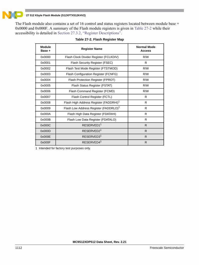
Chapter 27 512 Kbyte Flash Module (S12XFTX512K4V2)
MC9S12XDP512 Data Sheet, Rev. 2.21
1112 Freescale Semiconductor
The Flash module also contains a set of 16 control and status registers located between module base +0x0000 and 0x000F. A summary of the Flash module registers is given in Table 27-2 while theiraccessibility is detailed in Section 27.3.2, “Register Descriptions”.
Table 27-2. Flash Register Map
ModuleBase +
Register NameNormal Mode
Access
0x0000 Flash Clock Divider Register (FCLKDIV) R/W
0x0001 Flash Security Register (FSEC) R
0x0002 Flash Test Mode Register (FTSTMOD) R/W
0x0003 Flash Configuration Register (FCNFG) R/W
0x0004 Flash Protection Register (FPROT) R/W
0x0005 Flash Status Register (FSTAT) R/W
0x0006 Flash Command Register (FCMD) R/W
0x0007 Flash Control Register (FCTL) R
0x0008 Flash High Address Register (FADDRHI)1 R
0x0009 Flash Low Address Register (FADDRLO)1 R
0x000A Flash High Data Register (FDATAHI) R
0x000B Flash Low Data Register (FDATALO) R
0x000C RESERVED11 R
0x000D RESERVED21 R
0x000E RESERVED31 R
0x000F RESERVED41
1 Intended for factory test purposes only.
R
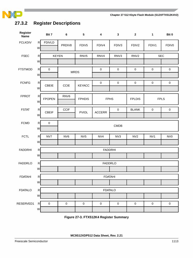
Chapter 27 512 Kbyte Flash Module (S12XFTX512K4V2)
MC9S12XDP512 Data Sheet, Rev. 2.21
Freescale Semiconductor 1113
27.3.2 Register Descriptions
RegisterName
Bit 7 6 5 4 3 2 1 Bit 0
FCLKDIV R FDIVLDPRDIV8 FDIV5 FDIV4 FDIV3 FDIV2 FDIV1 FDIV0
W
FSEC R KEYEN RNV5 RNV4 RNV3 RNV2 SEC
W
FTSTMOD R 0MRDS
0 0 0 0 0
W
FCNFG RCBEIE CCIE KEYACC
0 0 0 0 0
W
FPROT RFPOPEN
RNV6FPHDIS FPHS FPLDIS FPLS
W
FSTAT RCBEIF
CCIFPVIOL ACCERR
0 BLANK 0 0
W
FCMD R 0CMDB
W
FCTL R NV7 NV6 NV5 NV4 NV3 NV2 NV1 NV0
W
FADDRHI R FADDRHI
W
FADDRLO R FADDRLO
W
FDATAHI R FDATAHI
W
FDATALO R FDATALO
W
RESERVED1 R 0 0 0 0 0 0 0 0
W
Figure 27-3. FTX512K4 Register Summary
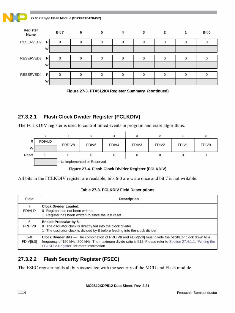
Chapter 27 512 Kbyte Flash Module (S12XFTX512K4V2)
MC9S12XDP512 Data Sheet, Rev. 2.21
1114 Freescale Semiconductor
27.3.2.1 Flash Clock Divider Register (FCLKDIV)
The FCLKDIV register is used to control timed events in program and erase algorithms.
All bits in the FCLKDIV register are readable, bits 6-0 are write once and bit 7 is not writable.
27.3.2.2 Flash Security Register (FSEC)
The FSEC register holds all bits associated with the security of the MCU and Flash module.
RESERVED2 R 0 0 0 0 0 0 0 0
W
RESERVED3 R 0 0 0 0 0 0 0 0
W
RESERVED4 R 0 0 0 0 0 0 0 0
W
7 6 5 4 3 2 1 0
R FDIVLDPRDIV8 FDIV5 FDIV4 FDIV3 FDIV2 FDIV1 FDIV0
W
Reset 0 0 0 0 0 0 0 0
= Unimplemented or Reserved
Figure 27-4. Flash Clock Divider Register (FCLKDIV)
Table 27-3. FCLKDIV Field Descriptions
Field Description
7FDIVLD
Clock Divider Loaded.0 Register has not been written.1 Register has been written to since the last reset.
6PRDIV8
Enable Prescalar by 8.0 The oscillator clock is directly fed into the clock divider.1 The oscillator clock is divided by 8 before feeding into the clock divider.
5-0FDIV[5:0]
Clock Divider Bits — The combination of PRDIV8 and FDIV[5:0] must divide the oscillator clock down to afrequency of 150 kHz–200 kHz. The maximum divide ratio is 512. Please refer to Section 27.4.1.1, “Writing theFCLKDIV Register” for more information.
RegisterName
Bit 7 6 5 4 3 2 1 Bit 0
Figure 27-3. FTX512K4 Register Summary (continued)
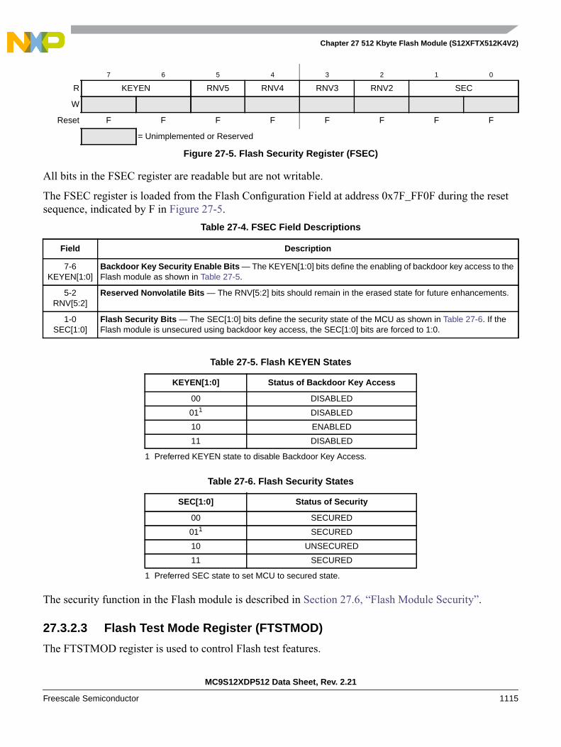
Chapter 27 512 Kbyte Flash Module (S12XFTX512K4V2)
MC9S12XDP512 Data Sheet, Rev. 2.21
Freescale Semiconductor 1115
All bits in the FSEC register are readable but are not writable.
The FSEC register is loaded from the Flash Configuration Field at address 0x7F_FF0F during the resetsequence, indicated by F in Figure 27-5.
The security function in the Flash module is described in Section 27.6, “Flash Module Security”.
27.3.2.3 Flash Test Mode Register (FTSTMOD)
The FTSTMOD register is used to control Flash test features.
7 6 5 4 3 2 1 0
R KEYEN RNV5 RNV4 RNV3 RNV2 SEC
W
Reset F F F F F F F F
= Unimplemented or Reserved
Figure 27-5. Flash Security Register (FSEC)
Table 27-4. FSEC Field Descriptions
Field Description
7-6KEYEN[1:0]
Backdoor Key Security Enable Bits — The KEYEN[1:0] bits define the enabling of backdoor key access to theFlash module as shown in Table 27-5.
5-2RNV[5:2]
Reserved Nonvolatile Bits — The RNV[5:2] bits should remain in the erased state for future enhancements.
1-0SEC[1:0]
Flash Security Bits — The SEC[1:0] bits define the security state of the MCU as shown in Table 27-6. If theFlash module is unsecured using backdoor key access, the SEC[1:0] bits are forced to 1:0.
Table 27-5. Flash KEYEN States
KEYEN[1:0] Status of Backdoor Key Access
00 DISABLED
011
1 Preferred KEYEN state to disable Backdoor Key Access.
DISABLED
10 ENABLED
11 DISABLED
Table 27-6. Flash Security States
SEC[1:0] Status of Security
00 SECURED
011
1 Preferred SEC state to set MCU to secured state.
SECURED
10 UNSECURED
11 SECURED
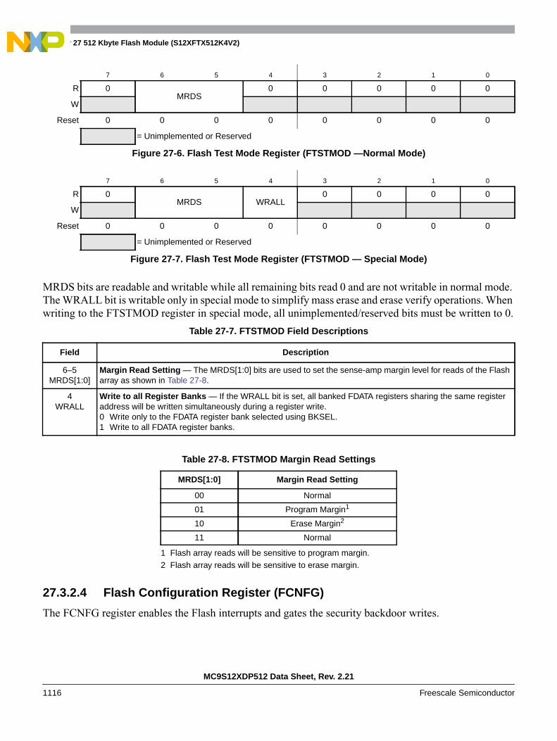
Chapter 27 512 Kbyte Flash Module (S12XFTX512K4V2)
MC9S12XDP512 Data Sheet, Rev. 2.21
1116 Freescale Semiconductor
MRDS bits are readable and writable while all remaining bits read 0 and are not writable in normal mode.The WRALL bit is writable only in special mode to simplify mass erase and erase verify operations. Whenwriting to the FTSTMOD register in special mode, all unimplemented/reserved bits must be written to 0.
27.3.2.4 Flash Configuration Register (FCNFG)
The FCNFG register enables the Flash interrupts and gates the security backdoor writes.
7 6 5 4 3 2 1 0
R 0MRDS
0 0 0 0 0
W
Reset 0 0 0 0 0 0 0 0
= Unimplemented or Reserved
Figure 27-6. Flash Test Mode Register (FTSTMOD —Normal Mode)
7 6 5 4 3 2 1 0
R 0MRDS WRALL
0 0 0 0
W
Reset 0 0 0 0 0 0 0 0
= Unimplemented or Reserved
Figure 27-7. Flash Test Mode Register (FTSTMOD — Special Mode)
Table 27-7. FTSTMOD Field Descriptions
Field Description
6–5MRDS[1:0]
Margin Read Setting — The MRDS[1:0] bits are used to set the sense-amp margin level for reads of the Flasharray as shown in Table 27-8.
4WRALL
Write to all Register Banks — If the WRALL bit is set, all banked FDATA registers sharing the same registeraddress will be written simultaneously during a register write.0 Write only to the FDATA register bank selected using BKSEL.1 Write to all FDATA register banks.
Table 27-8. FTSTMOD Margin Read Settings
MRDS[1:0] Margin Read Setting
00 Normal
01 Program Margin1
1 Flash array reads will be sensitive to program margin.
10 Erase Margin2
2 Flash array reads will be sensitive to erase margin.
11 Normal

Chapter 27 512 Kbyte Flash Module (S12XFTX512K4V2)
MC9S12XDP512 Data Sheet, Rev. 2.21
Freescale Semiconductor 1117
CBEIE, CCIE and KEYACC bits are readable and writable while all remaining bits read 0 and are notwritable in normal mode. KEYACC is only writable if KEYEN (see Section 27.3.2.2, “Flash SecurityRegister (FSEC)” is set to the enabled state. BKSEL is readable and writable in special mode to simplifymass erase and erase verify operations. When writing to the FCNFG register in special mode, allunimplemented/ reserved bits must be written to 0.
7 6 5 4 3 2 1 0
RCBEIE CCIE KEYACC
0 0 0 0 0
W
Reset 0 0 0 0 0 0 0 0
= Unimplemented or Reserved
Figure 27-8. Flash Configuration Register (FCNFG — Normal Mode)
7 6 5 4 3 2 1 0
RCBEIE CCIE KEYACC
Undefined 0 0BKSEL
W
Reset 0 0 0 Undefined 0 0 0 0
= Unimplemented or Reserved
Figure 27-9. Flash Configuration Register (FCNFG — Special Mode)
Table 27-9. FCNFG Field Descriptions
Field Description
7CBEIE
Command Buffer Empty Interrupt Enable — The CBEIE bit enables an interrupt in case of an empty commandbuffer in the Flash module.0 Command buffer empty interrupt disabled.1 An interrupt will be requested whenever the CBEIF flag (see Section 27.3.2.6, “Flash Status Register
(FSTAT)”) is set.
6CCIE
Command Complete Interrupt Enable — The CCIE bit enables an interrupt in case all commands have beencompleted in the Flash module.0 Command complete interrupt disabled.1 An interrupt will be requested whenever the CCIF flag (see Section 27.3.2.6, “Flash Status Register (FSTAT)”)
is set.
5KEYACC
Enable Security Key Writing0 Flash writes are interpreted as the start of a command write sequence.1 Writes to Flash array are interpreted as keys to open the backdoor. Reads of the Flash array return invalid
data.
1–0BKSEL[1:0]
Block Select — The BKSEL[1:0] bits indicates which register bank is active according to Table 27-10.
Table 27-10. Flash Register Bank Selects
BKSEL[1:0] Selected Block
00 Flash Block 0
01 Flash Block 1
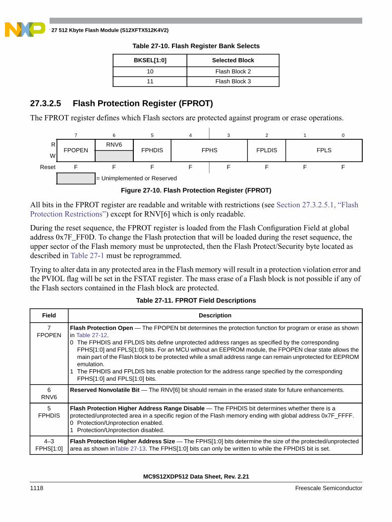
Chapter 27 512 Kbyte Flash Module (S12XFTX512K4V2)
MC9S12XDP512 Data Sheet, Rev. 2.21
1118 Freescale Semiconductor
27.3.2.5 Flash Protection Register (FPROT)
The FPROT register defines which Flash sectors are protected against program or erase operations.
All bits in the FPROT register are readable and writable with restrictions (see Section 27.3.2.5.1, “FlashProtection Restrictions”) except for RNV[6] which is only readable.
During the reset sequence, the FPROT register is loaded from the Flash Configuration Field at globaladdress 0x7F_FF0D. To change the Flash protection that will be loaded during the reset sequence, theupper sector of the Flash memory must be unprotected, then the Flash Protect/Security byte located asdescribed in Table 27-1 must be reprogrammed.
Trying to alter data in any protected area in the Flash memory will result in a protection violation error andthe PVIOL flag will be set in the FSTAT register. The mass erase of a Flash block is not possible if any ofthe Flash sectors contained in the Flash block are protected.
10 Flash Block 2
11 Flash Block 3
7 6 5 4 3 2 1 0
RFPOPEN
RNV6FPHDIS FPHS FPLDIS FPLS
W
Reset F F F F F F F F
= Unimplemented or Reserved
Figure 27-10. Flash Protection Register (FPROT)
Table 27-11. FPROT Field Descriptions
Field Description
7FPOPEN
Flash Protection Open — The FPOPEN bit determines the protection function for program or erase as shownin Table 27-12.0 The FPHDIS and FPLDIS bits define unprotected address ranges as specified by the corresponding
FPHS[1:0] and FPLS[1:0] bits. For an MCU without an EEPROM module, the FPOPEN clear state allows themain part of the Flash block to be protected while a small address range can remain unprotected for EEPROMemulation.
1 The FPHDIS and FPLDIS bits enable protection for the address range specified by the correspondingFPHS[1:0] and FPLS[1:0] bits.
6RNV6
Reserved Nonvolatile Bit — The RNV[6] bit should remain in the erased state for future enhancements.
5FPHDIS
Flash Protection Higher Address Range Disable — The FPHDIS bit determines whether there is aprotected/unprotected area in a specific region of the Flash memory ending with global address 0x7F_FFFF.0 Protection/Unprotection enabled.1 Protection/Unprotection disabled.
4–3FPHS[1:0]
Flash Protection Higher Address Size — The FPHS[1:0] bits determine the size of the protected/unprotectedarea as shown inTable 27-13. The FPHS[1:0] bits can only be written to while the FPHDIS bit is set.
Table 27-10. Flash Register Bank Selects
BKSEL[1:0] Selected Block
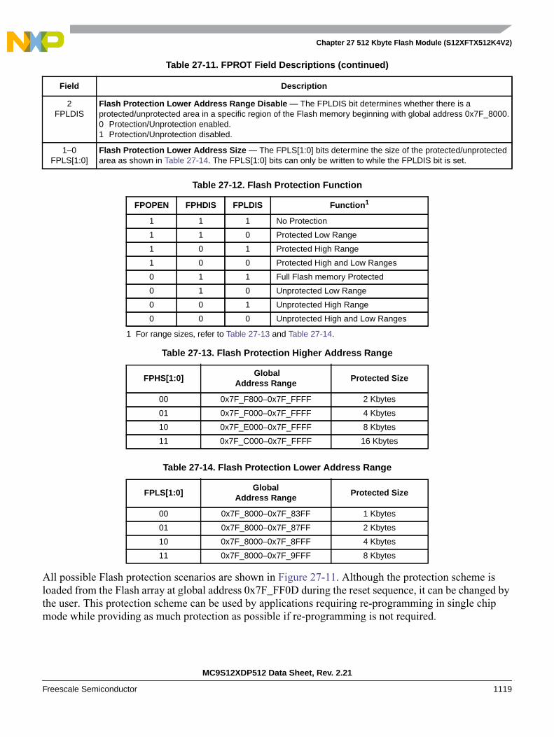
Chapter 27 512 Kbyte Flash Module (S12XFTX512K4V2)
MC9S12XDP512 Data Sheet, Rev. 2.21
Freescale Semiconductor 1119
All possible Flash protection scenarios are shown in Figure 27-11. Although the protection scheme isloaded from the Flash array at global address 0x7F_FF0D during the reset sequence, it can be changed bythe user. This protection scheme can be used by applications requiring re-programming in single chipmode while providing as much protection as possible if re-programming is not required.
2FPLDIS
Flash Protection Lower Address Range Disable — The FPLDIS bit determines whether there is aprotected/unprotected area in a specific region of the Flash memory beginning with global address 0x7F_8000.0 Protection/Unprotection enabled.1 Protection/Unprotection disabled.
1–0FPLS[1:0]
Flash Protection Lower Address Size — The FPLS[1:0] bits determine the size of the protected/unprotectedarea as shown in Table 27-14. The FPLS[1:0] bits can only be written to while the FPLDIS bit is set.
Table 27-12. Flash Protection Function
FPOPEN FPHDIS FPLDIS Function1
1 For range sizes, refer to Table 27-13 and Table 27-14.
1 1 1 No Protection
1 1 0 Protected Low Range
1 0 1 Protected High Range
1 0 0 Protected High and Low Ranges
0 1 1 Full Flash memory Protected
0 1 0 Unprotected Low Range
0 0 1 Unprotected High Range
0 0 0 Unprotected High and Low Ranges
Table 27-13. Flash Protection Higher Address Range
FPHS[1:0] Global
Address RangeProtected Size
00 0x7F_F800–0x7F_FFFF 2 Kbytes
01 0x7F_F000–0x7F_FFFF 4 Kbytes
10 0x7F_E000–0x7F_FFFF 8 Kbytes
11 0x7F_C000–0x7F_FFFF 16 Kbytes
Table 27-14. Flash Protection Lower Address Range
FPLS[1:0]Global
Address RangeProtected Size
00 0x7F_8000–0x7F_83FF 1 Kbytes
01 0x7F_8000–0x7F_87FF 2 Kbytes
10 0x7F_8000–0x7F_8FFF 4 Kbytes
11 0x7F_8000–0x7F_9FFF 8 Kbytes
Table 27-11. FPROT Field Descriptions (continued)
Field Description

Chapter 27 512 Kbyte Flash Module (S12XFTX512K4V2)
MC9S12XDP512 Data Sheet, Rev. 2.21
1120 Freescale Semiconductor
Figure 27-11. Flash Protection Scenarios
7 6 5 4
3 2 1 0
FPHDIS=1FPLDIS=1
FPHDIS=1FPLDIS=0
FPHDIS=0FPLDIS=1
FPHDIS=0FPLDIS=0
Scenario
Scenario
Unprotected region Protected region with size
Protected region Protected region with size
defined by FPLS
defined by FPHSnot defined by FPLS, FPHS
0x7F_8000
0x7F_FFFF
0x7F_8000
0x7F_FFFF
0x78_0000
0x78_0000
FPHS[1:0]
FPLS[1:0]
FPOPEN=1
FPHS[1:0]
FPLS[1:0]
FPOPEN=0

Chapter 27 512 Kbyte Flash Module (S12XFTX512K4V2)
MC9S12XDP512 Data Sheet, Rev. 2.21
Freescale Semiconductor 1121
27.3.2.5.1 Flash Protection Restrictions
The general guideline is that Flash protection can only be added and not removed. Table 27-15 specifiesall valid transitions between Flash protection scenarios. Any attempt to write an invalid scenario to theFPROT register will be ignored and the FPROT register will remain unchanged. The contents of theFPROT register reflect the active protection scenario. See the FPHS and FPLS descriptions for additionalrestrictions.
27.3.2.6 Flash Status Register (FSTAT)
The FSTAT register defines the operational status of the module.
Table 27-15. Flash Protection Scenario Transitions
FromProtection Scenario
To Protection Scenario1
1 Allowed transitions marked with X.
0 1 2 3 4 5 6 7
0 X X X X
1 X X
2 X X
3 X
4 X X
5 X X X X
6 X X X X
7 X X X X X X X X
7 6 5 4 3 2 1 0
RCBEIF
CCIFPVIOL ACCERR
0 BLANK 0 0
W
Reset 1 1 0 0 0 0 0 0
= Unimplemented or Reserved
Figure 27-12. Flash Status Register (FSTAT — Normal Mode)
7 6 5 4 3 2 1 0
RCBEIF
CCIFPVIOL ACCERR
0 BLANKFAIL
0
W
Reset 1 1 0 0 0 0 0 0
= Unimplemented or Reserved
Figure 27-13. Flash Status Register (FSTAT — Special Mode)

Chapter 27 512 Kbyte Flash Module (S12XFTX512K4V2)
MC9S12XDP512 Data Sheet, Rev. 2.21
1122 Freescale Semiconductor
CBEIF, PVIOL, and ACCERR are readable and writable, CCIF and BLANK are readable and not writable,remaining bits read 0 and are not writable in normal mode. FAIL is readable and writable in special mode.FAIL must be clear in special mode when starting a command write sequence.
Table 27-16. FSTAT Field Descriptions
Field Description
7CBEIF
Command Buffer Empty Interrupt Flag — The CBEIF flag indicates that the address, data and commandbuffers are empty so that a new command write sequence can be started. Writing a 0 to the CBEIF flag has noeffect on CBEIF. Writing a 0 to CBEIF after writing an aligned word to the Flash address space, but before CBEIFis cleared, will abort a command write sequence and cause the ACCERR flag to be set. Writing a 0 to CBEIFoutside of a command write sequence will not set the ACCERR flag. The CBEIF flag is cleared by writing a 1 toCBEIF. The CBEIF flag is used together with the CBEIE bit in the FCNFG register to generate an interruptrequest (see Figure 27-32).0 Command buffers are full.1 Command buffers are ready to accept a new command.
6CCIF
Command Complete Interrupt Flag — The CCIF flag indicates that there are no more commands pending. TheCCIF flag is cleared when CBEIF is cleared and sets automatically upon completion of all active and pendingcommands. The CCIF flag does not set when an active commands completes and a pending command isfetched from the command buffer. Writing to the CCIF flag has no effect on CCIF. The CCIF flag is used togetherwith the CCIE bit in the FCNFG register to generate an interrupt request (see Figure 27-32).0 Command in progress.1 All commands are completed.
5PVIOL
Protection Violation Flag —The PVIOL flag indicates an attempt was made to program or erase an address ina protected area of the Flash memory during a command write sequence. Writing a 0 to the PVIOL flag has noeffect on PVIOL. The PVIOL flag is cleared by writing a 1 to PVIOL. While PVIOL is set, it is not possible to launcha command or start a command write sequence.0 No protection violation detected.1 Protection violation has occurred.
4ACCERR
Access Error Flag — The ACCERR flag indicates an illegal access has occurred to the Flash memory causedby either a violation of the command write sequence (see Section 27.4.1.2, “Command Write Sequence”),issuing an illegal Flash command (see Table 27-18), launching the sector erase abort command terminating asector erase operation early (see Section 27.4.2.6, “Sector Erase Abort Command”) or the execution of a CPUSTOP instruction while a command is executing (CCIF = 0). Writing a 0 to the ACCERR flag has no effect onACCERR. The ACCERR flag is cleared by writing a 1 to ACCERR.While ACCERR is set, it is not possible tolaunch a command or start a command write sequence. If ACCERR is set by an erase verify operation or a datacompress operation, any buffered command will not launch.0 No access error detected.1 Access error has occurred.
2BLANK
Flag Indicating the Erase Verify Operation Status — When the CCIF flag is set after completion of an eraseverify command, the BLANK flag indicates the result of the erase verify operation. The BLANK flag is cleared bythe Flash module when CBEIF is cleared as part of a new valid command write sequence. Writing to the BLANKflag has no effect on BLANK.0 Flash block verified as not erased.1 Flash block verified as erased.
1FAIL
Flag Indicating a Failed Flash Operation — The FAIL flag will set if the erase verify operation fails (selectedFlash block verified as not erased). Writing a 0 to the FAIL flag has no effect on FAIL. The FAIL flag is cleared bywriting a 1 to FAIL.0 Flash operation completed without error.1 Flash operation failed.
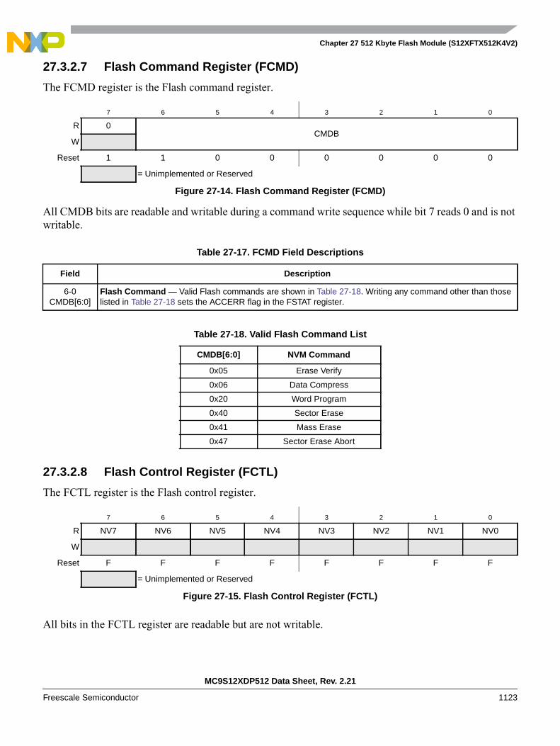
Chapter 27 512 Kbyte Flash Module (S12XFTX512K4V2)
MC9S12XDP512 Data Sheet, Rev. 2.21
Freescale Semiconductor 1123
27.3.2.7 Flash Command Register (FCMD)
The FCMD register is the Flash command register.
All CMDB bits are readable and writable during a command write sequence while bit 7 reads 0 and is notwritable.
27.3.2.8 Flash Control Register (FCTL)
The FCTL register is the Flash control register.
All bits in the FCTL register are readable but are not writable.
7 6 5 4 3 2 1 0
R 0CMDB
W
Reset 1 1 0 0 0 0 0 0
= Unimplemented or Reserved
Figure 27-14. Flash Command Register (FCMD)
Table 27-17. FCMD Field Descriptions
Field Description
6-0CMDB[6:0]
Flash Command — Valid Flash commands are shown in Table 27-18. Writing any command other than thoselisted in Table 27-18 sets the ACCERR flag in the FSTAT register.
Table 27-18. Valid Flash Command List
CMDB[6:0] NVM Command
0x05 Erase Verify
0x06 Data Compress
0x20 Word Program
0x40 Sector Erase
0x41 Mass Erase
0x47 Sector Erase Abort
7 6 5 4 3 2 1 0
R NV7 NV6 NV5 NV4 NV3 NV2 NV1 NV0
W
Reset F F F F F F F F
= Unimplemented or Reserved
Figure 27-15. Flash Control Register (FCTL)
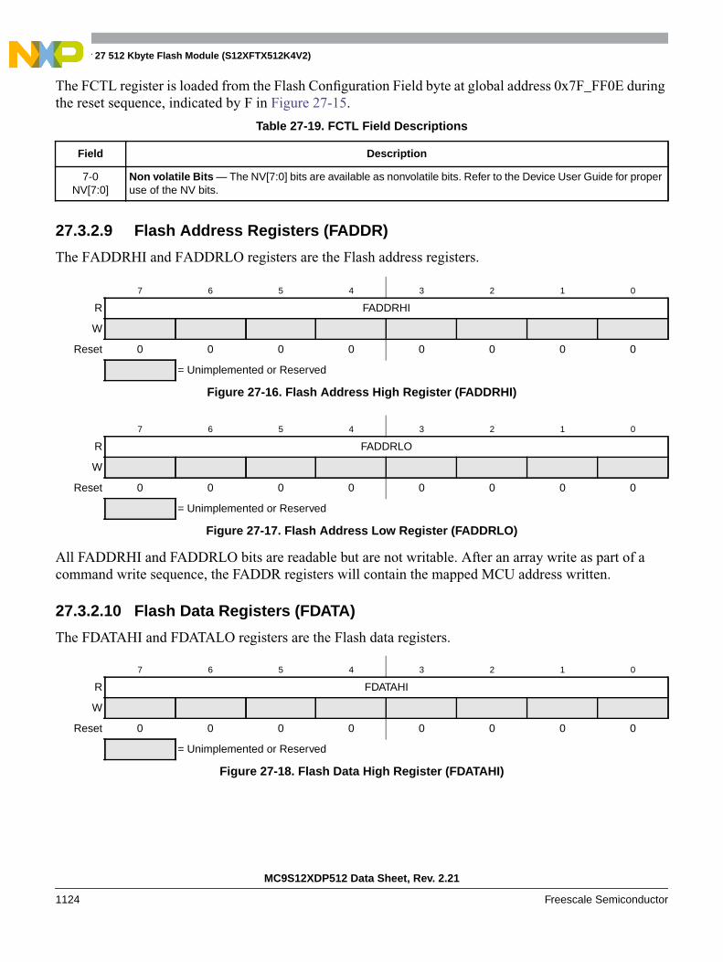
Chapter 27 512 Kbyte Flash Module (S12XFTX512K4V2)
MC9S12XDP512 Data Sheet, Rev. 2.21
1124 Freescale Semiconductor
The FCTL register is loaded from the Flash Configuration Field byte at global address 0x7F_FF0E duringthe reset sequence, indicated by F in Figure 27-15.
27.3.2.9 Flash Address Registers (FADDR)
The FADDRHI and FADDRLO registers are the Flash address registers.
All FADDRHI and FADDRLO bits are readable but are not writable. After an array write as part of acommand write sequence, the FADDR registers will contain the mapped MCU address written.
27.3.2.10 Flash Data Registers (FDATA)
The FDATAHI and FDATALO registers are the Flash data registers.
Table 27-19. FCTL Field Descriptions
Field Description
7-0NV[7:0]
Non volatile Bits — The NV[7:0] bits are available as nonvolatile bits. Refer to the Device User Guide for properuse of the NV bits.
7 6 5 4 3 2 1 0
R FADDRHI
W
Reset 0 0 0 0 0 0 0 0
= Unimplemented or Reserved
Figure 27-16. Flash Address High Register (FADDRHI)
7 6 5 4 3 2 1 0
R FADDRLO
W
Reset 0 0 0 0 0 0 0 0
= Unimplemented or Reserved
Figure 27-17. Flash Address Low Register (FADDRLO)
7 6 5 4 3 2 1 0
R FDATAHI
W
Reset 0 0 0 0 0 0 0 0
= Unimplemented or Reserved
Figure 27-18. Flash Data High Register (FDATAHI)

Chapter 27 512 Kbyte Flash Module (S12XFTX512K4V2)
MC9S12XDP512 Data Sheet, Rev. 2.21
Freescale Semiconductor 1125
All FDATAHI and FDATALO bits are readable but are not writable. At the completion of a data compressoperation, the resulting 16-bit signature is stored in the FDATA registers. The data compression signatureis readable in the FDATA registers until a new command write sequence is started.
27.3.2.11 RESERVED1
This register is reserved for factory testing and is not accessible.
All bits read 0 and are not writable.
27.3.2.12 RESERVED2
This register is reserved for factory testing and is not accessible.
All bits read 0 and are not writable.
27.3.2.13 RESERVED3
This register is reserved for factory testing and is not accessible.
7 6 5 4 3 2 1 0
R FDATALO
W
Reset 0 0 0 0 0 0 0 0
= Unimplemented or Reserved
Figure 27-19. Flash Data Low Register (FDATALO)
7 6 5 4 3 2 1 0
R 0 0 0 0 0 0 0 0
W
Reset 0 0 0 0 0 0 0 0
= Unimplemented or Reserved
Figure 27-20. RESERVED1
7 6 5 4 3 2 1 0
R 0 0 0 0 0 0 0 0
W
Reset 0 0 0 0 0 0 0 0
= Unimplemented or Reserved
Figure 27-21. RESERVED2

Chapter 27 512 Kbyte Flash Module (S12XFTX512K4V2)
MC9S12XDP512 Data Sheet, Rev. 2.21
1126 Freescale Semiconductor
All bits read 0 and are not writable.
27.3.2.14 RESERVED4
This register is reserved for factory testing and is not accessible.
All bits read 0 and are not writable.
27.4 Functional Description
27.4.1 Flash Command Operations
Write operations are used to execute program, erase, erase verify, erase abort, and data compressalgorithms described in this section. The program and erase algorithms are controlled by a state machinewhose timebase, FCLK, is derived from the oscillator clock via a programmable divider. The commandregister, as well as the associated address and data registers, operate as a buffer and a register (2-stageFIFO) so that a second command along with the necessary data and address can be stored to the bufferwhile the first command is still in progress. This pipelined operation allows a time optimization whenprogramming more than one word on a specific row in the Flash block as the high voltage generation canbe kept active in between two programming commands. The pipelined operation also allows asimplification of command launching. Buffer empty as well as command completion are signalled by flagsin the Flash status register with corresponding interrupts generated, if enabled.
The next sections describe:
1. How to write the FCLKDIV register
2. Command write sequences to program, erase, erase verify, erase abort, and data compressoperations on the Flash memory
3. Valid Flash commands
4. Effects resulting from illegal Flash command write sequences or aborting Flash operations
7 6 5 4 3 2 1 0
R 0 0 0 0 0 0 0 0
W
Reset 0 0 0 0 0 0 0 0
= Unimplemented or Reserved
Figure 27-22. RESERVED3
7 6 5 4 3 2 1 0
R 0 0 0 0 0 0 0 0
W
Reset 0 0 0 0 0 0 0 0
= Unimplemented or Reserved
Figure 27-23. RESERVED4
Chapter 27 512 Kbyte Flash Module (S12XFTX512K4V2)
MC9S12XDP512 Data Sheet, Rev. 2.21
Freescale Semiconductor 1127
27.4.1.1 Writing the FCLKDIV Register
Prior to issuing any Flash command after a reset, the user is required to write the FCLKDIV register todivide the oscillator clock down to within the 150 kHz to 200 kHz range. Since the program and erasetimings are also a function of the bus clock, the FCLKDIV determination must take this information intoaccount.
If we define:
• FCLK as the clock of the Flash timing control block
• Tbus as the period of the bus clock
• INT(x) as taking the integer part of x (e.g. INT(4.323) = 4)
then FCLKDIV register bits PRDIV8 and FDIV[5:0] are to be set as described in Figure 27-24.
For example, if the oscillator clock frequency is 950kHz and the bus clock frequency is 10MHz,FCLKDIV bits FDIV[5:0] should be set to 0x04 (000100) and bit PRDIV8 set to 0. The resulting FCLKfrequency is then 190kHz. As a result, the Flash program and erase algorithm timings are increased overthe optimum target by:
If the oscillator clock frequency is 16MHz and the bus clock frequency is 40MHz, FCLKDIV bitsFDIV[5:0] should be set to 0x0A (001010) and bit PRDIV8 set to 1. The resulting FCLK frequency is then182kHz. In this case, the Flash program and erase algorithm timings are increased over the optimum targetby:
CAUTIONProgram and erase command execution time will increase proportionallywith the period of FCLK. Because of the impact of clock synchronizationon the accuracy of the functional timings, programming or erasing the Flashmemory cannot be performed if the bus clock runs at less than 1 MHz.Programming or erasing the Flash memory with FCLK < 150 kHz shouldbe avoided. Setting FCLKDIV to a value such that FCLK < 150 kHz candestroy the Flash memory due to overstress. Setting FCLKDIV to a valuesuch that (1/FCLK+Tbus) < 5µs can result in incomplete programming orerasure of the Flash memory cells.
If the FCLKDIV register is written, the FDIVLD bit is set automatically. If the FDIVLD bit is 0, theFCLKDIV register has not been written since the last reset. If the FCLKDIV register has not been writtento, the Flash command loaded during a command write sequence will not execute and the ACCERR flagin the FSTAT register will set.
200 190–( ) 200⁄ 100× 5%=
200 182–( ) 200⁄ 100× 9%=
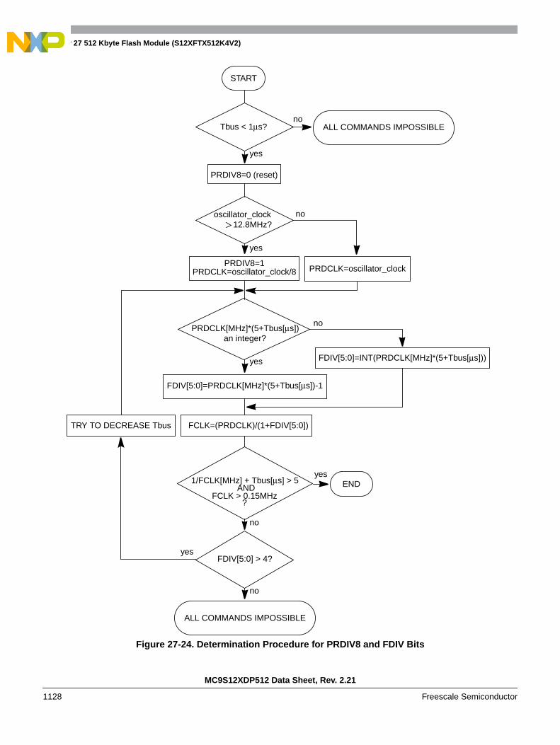
Chapter 27 512 Kbyte Flash Module (S12XFTX512K4V2)
MC9S12XDP512 Data Sheet, Rev. 2.21
1128 Freescale Semiconductor
Figure 27-24. Determination Procedure for PRDIV8 and FDIV Bits
PRDIV8=1
yes
no
PRDIV8=0 (reset)
12.8MHz?
FCLK=(PRDCLK)/(1+FDIV[5:0])
PRDCLK=oscillator_clockPRDCLK=oscillator_clock/8
PRDCLK[MHz]*(5+Tbus[µs])no
FDIV[5:0]=PRDCLK[MHz]*(5+Tbus[µs])-1
yes
START
Tbus < 1µs?
an integer?
FDIV[5:0]=INT(PRDCLK[MHz]*(5+Tbus[µs]))
1/FCLK[MHz] + Tbus[µs] > 5AND
FCLK > 0.15MHz?
ENDyes
no
FDIV[5:0] > 4?
ALL COMMANDS IMPOSSIBLE
yes
no
ALL COMMANDS IMPOSSIBLE
no
TRY TO DECREASE Tbus
yes
oscillator_clock

Chapter 27 512 Kbyte Flash Module (S12XFTX512K4V2)
MC9S12XDP512 Data Sheet, Rev. 2.21
Freescale Semiconductor 1129
27.4.1.2 Command Write Sequence
The Flash command controller is used to supervise the command write sequence to execute program,erase, erase verify, erase abort, and data compress algorithms.
Before starting a command write sequence, the ACCERR and PVIOL flags in the FSTAT register must beclear (see Section 27.3.2.6, “Flash Status Register (FSTAT)”) and the CBEIF flag should be tested todetermine the state of the address, data and command buffers. If the CBEIF flag is set, indicating thebuffers are empty, a new command write sequence can be started. If the CBEIF flag is clear, indicating thebuffers are not available, a new command write sequence will overwrite the contents of the address, dataand command buffers.
A command write sequence consists of three steps which must be strictly adhered to with writes to theFlash module not permitted between the steps. However, Flash register and array reads are allowed duringa command write sequence. The basic command write sequence is as follows:
1. Write to a valid address in the Flash memory. Addresses in multiple Flash blocks can be written toas long as the location is at the same relative address in each available Flash block. Multipleaddresses must be written in Flash block order starting with the lower Flash block.
2. Write a valid command to the FCMD register.
3. Clear the CBEIF flag in the FSTAT register by writing a 1 to CBEIF to launch the command.
The address written in step 1 will be stored in the FADDR registers and the data will be stored in theFDATA registers. If the CBEIF flag in the FSTAT register is clear when the first Flash array write occurs,the contents of the address and data buffers will be overwritten and the CBEIF flag will be set. When theCBEIF flag is cleared, the CCIF flag is cleared on the same bus cycle by the Flash command controllerindicating that the command was successfully launched. For all command write sequences except datacompress and sector erase abort, the CBEIF flag will set four bus cycles after the CCIF flag is clearedindicating that the address, data, and command buffers are ready for a new command write sequence tobegin. For data compress and sector erase abort operations, the CBEIF flag will remain clear until theoperation completes. Except for the sector erase abort command, a buffered command will wait for theactive operation to be completed before being launched. The sector erase abort command is launched whenthe CBEIF flag is cleared as part of a sector erase abort command write sequence. Once a command islaunched, the completion of the command operation is indicated by the setting of the CCIF flag in theFSTAT register. The CCIF flag will set upon completion of all active and buffered commands.
27.4.2 Flash Commands
Table 27-20 summarizes the valid Flash commands along with the effects of the commands on the Flashblock.
Table 27-20. Flash Command Description
FCMDBNVM
CommandFunction on Flash Memory
0x05 EraseVerify
Verify all memory bytes in the Flash block are erased.If the Flash block is erased, the BLANK flag in the FSTAT register will set upon commandcompletion.

Chapter 27 512 Kbyte Flash Module (S12XFTX512K4V2)
MC9S12XDP512 Data Sheet, Rev. 2.21
1130 Freescale Semiconductor
CAUTIONA Flash word must be in the erased state before being programmed.Cumulative programming of bits within a Flash word is not allowed.
0x06 DataCompress
Compress data from a selected portion of the Flash block.The resulting signature is stored in the FDATA register.
0x20 Program Program a word (two bytes) in the Flash block.
0x40 SectorErase
Erase all memory bytes in a sector of the Flash block.
0x41 MassErase
Erase all memory bytes in the Flash block.A mass erase of the full Flash block is only possible when FPLDIS, FPHDIS andFPOPEN bits in the FPROT register are set prior to launching the command.
0x47 SectorEraseAbort
Abort the sector erase operation.The sector erase operation will terminate according to a set procedure. The Flash sectorshould not be considered erased if the ACCERR flag is set upon command completion.
Table 27-20. Flash Command Description
FCMDBNVM
CommandFunction on Flash Memory

Chapter 27 512 Kbyte Flash Module (S12XFTX512K4V2)
MC9S12XDP512 Data Sheet, Rev. 2.21
Freescale Semiconductor 1131
27.4.2.1 Erase Verify Command
The erase verify operation will verify that a Flash block is erased.
An example flow to execute the erase verify operation is shown in Figure 27-25. The erase verify commandwrite sequence is as follows:
1. Write to a Flash block address to start the command write sequence for the erase verify command.The address and data written will be ignored. Multiple Flash blocks can be simultaneously eraseverified by writing to the same relative address in each Flash block.
2. Write the erase verify command, 0x05, to the FCMD register.
3. Clear the CBEIF flag in the FSTAT register by writing a 1 to CBEIF to launch the erase verifycommand.
After launching the erase verify command, the CCIF flag in the FSTAT register will set after the operationhas completed unless a new command write sequence has been buffered. The number of bus cyclesrequired to execute the erase verify operation is equal to the number of addresses in a Flash block plus 14bus cycles as measured from the time the CBEIF flag is cleared until the CCIF flag is set. Upon completionof the erase verify operation, the BLANK flag in the FSTAT register will be set if all addresses in theselected Flash blocks are verified to be erased. If any address in a selected Flash block is not erased, theerase verify operation will terminate and the BLANK flag in the FSTAT register will remain clear. TheMRDS bits in the FTSTMOD register will determine the sense-amp margin setting during the erase verifyoperation.
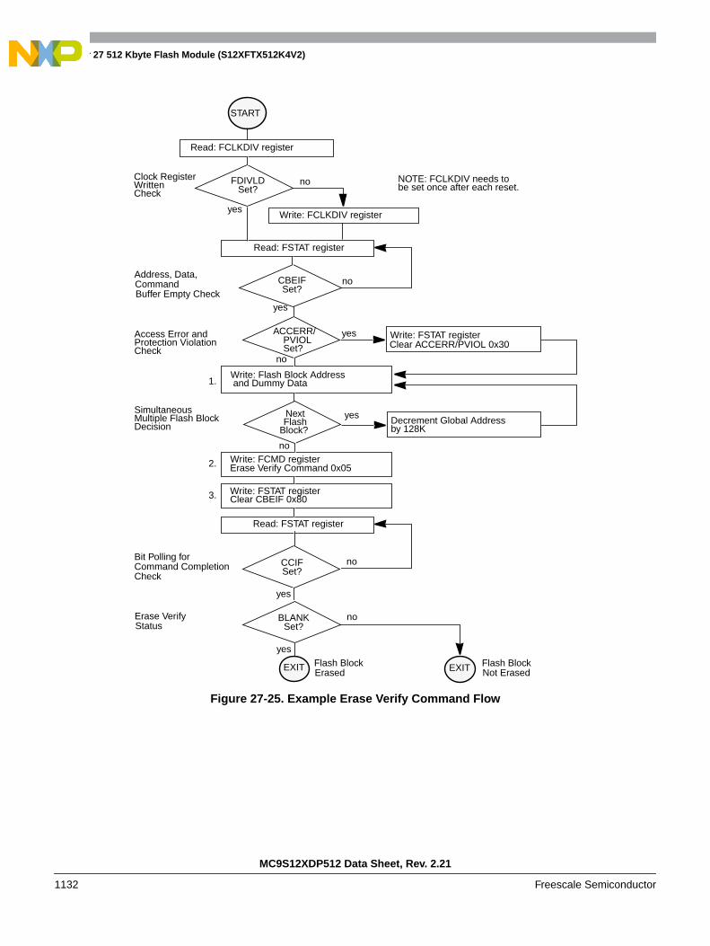
Chapter 27 512 Kbyte Flash Module (S12XFTX512K4V2)
MC9S12XDP512 Data Sheet, Rev. 2.21
1132 Freescale Semiconductor
Figure 27-25. Example Erase Verify Command Flow
Write: Flash Block Address
Write: FCMD registerErase Verify Command 0x05
Write: FSTAT registerClear CBEIF 0x80
1.
2.
3.
Clear ACCERR/PVIOL 0x30Write: FSTAT registeryes
no
Access Error andProtection Violation
no
and Dummy Data
Bit Polling forCommand CompletionCheck
Read: FSTAT register
yes
Read: FSTAT register
no
START
yes
Check
CBEIFSet?
Next
no
yes
Address, Data,CommandBuffer Empty Check
FlashBlock?
CCIFSet?
ACCERR/PVIOLSet?
noErase VerifyStatus
yes
EXIT Flash BlockNot ErasedEXIT Flash Block
Erased
BLANKSet?
Decrement Global Address
Write: FCLKDIV register
Read: FCLKDIV register
yes
noClock RegisterWrittenCheck
FDIVLDSet?
NOTE: FCLKDIV needs tobe set once after each reset.
SimultaneousMultiple Flash BlockDecision by 128K

Chapter 27 512 Kbyte Flash Module (S12XFTX512K4V2)
MC9S12XDP512 Data Sheet, Rev. 2.21
Freescale Semiconductor 1133
27.4.2.2 Data Compress Command
The data compress operation will check Flash code integrity by compressing data from a selected portionof the Flash memory into a signature analyzer.
An example flow to execute the data compress operation is shown in Figure 27-26. The data compresscommand write sequence is as follows:
1. Write to a Flash block address to start the command write sequence for the data compresscommand. The address written determines the starting address for the data compress operation andthe data written determines the number of consecutive words to compress. If the data value writtenis 0x0000, 64K addresses or 128 Kbytes will be compressed. Multiple Flash blocks can besimultaneously compressed by writing to the same relative address in each Flash block. If morethan one Flash block is written to in this step, the first data written will determine the number ofconsecutive words to compress in each selected Flash block.
2. Write the data compress command, 0x06, to the FCMD register.
3. Clear the CBEIF flag in the FSTAT register by writing a 1 to CBEIF to launch the data compresscommand.
After launching the data compress command, the CCIF flag in the FSTAT register will set after the datacompress operation has completed. The number of bus cycles required to execute the data compressoperation is equal to two times the number of consecutive words to compress plus the number of Flashblocks simultaneously compressed plus 18 bus cycles as measured from the time the CBEIF flag is cleareduntil the CCIF flag is set. Once the CCIF flag is set, the signature generated by the data compress operationis available in the FDATA registers. The signature in the FDATA registers can be compared to the expectedsignature to determine the integrity of the selected data stored in the selected Flash memory. If the lastaddress of a Flash block is reached during the data compress operation, data compression will continuewith the starting address of the same Flash block. The MRDS bits in the FTSTMOD register will determinethe sense-amp margin setting during the data compress operation.
NOTESince the FDATA registers (or data buffer) are written to as part of the datacompress operation, a command write sequence is not allowed to bebuffered behind a data compress command write sequence. The CBEIF flagwill not set after launching the data compress command to indicate that acommand should not be buffered behind it. If an attempt is made to start anew command write sequence with a data compress operation active, theACCERR flag in the FSTAT register will be set. A new command writesequence should only be started after reading the signature stored in theFDATA registers.
In order to take corrective action, it is recommended that the data compress command be executed on aFlash sector or subset of a Flash sector. If the data compress operation on a Flash sector returns an invalidsignature, the Flash sector should be erased using the sector erase command and then reprogrammed usingthe program command.
The data compress command can be used to verify that a sector or sequential set of sectors are erased.

Chapter 27 512 Kbyte Flash Module (S12XFTX512K4V2)
MC9S12XDP512 Data Sheet, Rev. 2.21
1134 Freescale Semiconductor
Figure 27-26. Example Data Compress Command Flow
Write: Flash Address to start
Write: FCMD registerData Compress Command 0x06
Write: FSTAT registerClear CBEIF 0x80
1.
2.
3.
Clear ACCERR/PVIOL 0x30Write: FSTAT registeryes
no
Access Error andProtection Violation
no
compression and number of word
Bit Polling forCommand CompletionCheck
Read: FSTAT register
yes
Read: FSTAT register
no
START
yes
Check
CBEIFSet?
Next
no
yes
Address, Data,CommandBuffer Empty Check
FlashBlock?
CCIFSet?
ACCERR/PVIOLSet?
EXIT
Erase and Reprogram
by 128KDecrement Global Address
Write: FCLKDIV register
Read: FCLKDIV register
yes
noClock RegisterWrittenCheck
FDIVLDSet?
NOTE: FCLKDIV needs tobe set once after each reset.
SimultaneousMultiple Flash BlockDecision
Flash Sector(s) Compressed
Data Compress Signature Read: FDATA registers
no
yes
SignatureValid?
addresses to compressNOTE: address used to selectFlash block; data ignored.

Chapter 27 512 Kbyte Flash Module (S12XFTX512K4V2)
MC9S12XDP512 Data Sheet, Rev. 2.21
Freescale Semiconductor 1135
27.4.2.2.1 Data Compress Operation
The Flash module contains a 16-bit multiple-input signature register (MISR) for each Flash block togenerate a 16-bit signature based on selected Flash array data. If multiple Flash blocks are selected forsimultaneous compression, then the signature from each Flash block is further compressed to generate asingle 16-bit signature. The final 16-bit signature, found in the FDATA registers after the data compressoperation has completed, is based on the following logic equation which is executed on every datacompression cycle during the operation:
MISR[15:0] = MISR[14:0], ^MISR[15,4,2,1] ^ DATA[15:0] Eqn. 27-1
where MISR is the content of the internal signature register associated with each Flash block and DATAis the data to be compressed as shown in Figure 27-27.
Figure 27-27. 16-Bit MISR Diagram
During the data compress operation, the following steps are executed:
1. MISR for each Flash block is reset to 0xFFFF.
2. Initialized DATA equal to 0xFFFF is compressed into the MISR for each selected Flash blockwhich results in the MISR containing 0x0001.
3. DATA equal to the selected Flash array data range is read and compressed into the MISR for eachselected Flash block with addresses incrementing.
4. DATA equal to the selected Flash array data range is read and compressed into the MISR for eachselected Flash block with addresses decrementing.
5. If Flash block 0 is selected for compression, DATA equal to the contents of the MISR for Flashblock 0 is compressed into the MISR for Flash block 0. If data in Flash block 0 was not selectedfor compression, the MISR for Flash block 0 contains 0xFFFF.
6. If Flash block 1 is selected for compression, DATA equal to the contents of the MISR for Flashblock 1 is compressed into the MISR for Flash block 0.
7. If Flash block 2 is selected for compression, DATA equal to the contents of the MISR for Flashblock 2 is compressed into the MISR for Flash block 0.
8. If Flash block 3 is selected for compression, DATA equal to the contents of the MISR for Flashblock 3 is compressed into the MISR for Flash block 0.
9. The contents of the MISR for Flash block 0 are written to the FDATA registers.
D Q
>
+
+
= Exclusive-OR
DATA[0]
M0
D Q
>
+
DATA[1]
M1
D Q
>
+
DATA[2]
M2
D Q
>
+
DATA[3]
M3
D Q
>
+
DATA[4]
M4
D Q
>
+
DATA[5]
M5
D Q
>
+
DATA[15]
M15
...
+ +
+
MISR[15:0] = Q[15:0]

Chapter 27 512 Kbyte Flash Module (S12XFTX512K4V2)
MC9S12XDP512 Data Sheet, Rev. 2.21
1136 Freescale Semiconductor
27.4.2.3 Program Command
The program operation will program a previously erased word in the Flash memory using an embeddedalgorithm.
An example flow to execute the program operation is shown in Figure 27-28. The program command writesequence is as follows:
1. Write to a Flash block address to start the command write sequence for the program command. Thedata written will be programmed to the address written. Multiple Flash blocks can besimultaneously programmed by writing to the same relative address in each Flash block.
2. Write the program command, 0x20, to the FCMD register.
3. Clear the CBEIF flag in the FSTAT register by writing a 1 to CBEIF to launch the programcommand.
If a word to be programmed is in a protected area of the Flash block, the PVIOL flag in the FSTAT registerwill set and the program command will not launch. Once the program command has successfully launched,the CCIF flag in the FSTAT register will set after the program operation has completed unless a newcommand write sequence has been buffered. By executing a new program command write sequence onsequential words after the CBEIF flag in the FSTAT register has been set, up to 55% faster programmingtime per word can be effectively achieved than by waiting for the CCIF flag to set after each programoperation.
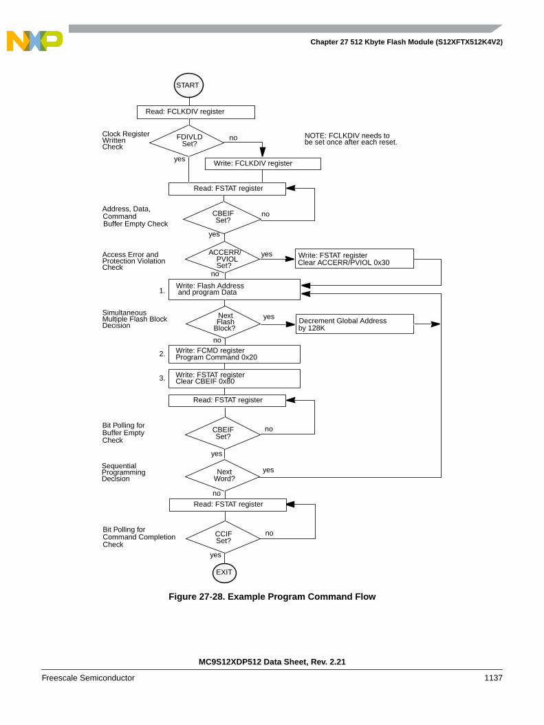
Chapter 27 512 Kbyte Flash Module (S12XFTX512K4V2)
MC9S12XDP512 Data Sheet, Rev. 2.21
Freescale Semiconductor 1137
Figure 27-28. Example Program Command Flow
Write: Flash Address
Write: FCMD registerProgram Command 0x20
Write: FSTAT registerClear CBEIF 0x80
1.
2.
3.
Clear ACCERR/PVIOL 0x30Write: FSTAT registeryes
no
Access Error andProtection Violation
no
and program Data
Bit Polling forBuffer EmptyCheck
Read: FSTAT register
yes
Read: FSTAT register
no
START
yes
Check
CBEIFSet?
Next
no
yes
Address, Data,CommandBuffer Empty Check
FlashBlock?
CBEIFSet?
ACCERR/PVIOLSet?
EXIT
by 128KDecrement Global Address
Write: FCLKDIV register
Read: FCLKDIV register
yes
noClock RegisterWrittenCheck
FDIVLDSet?
NOTE: FCLKDIV needs tobe set once after each reset.
SimultaneousMultiple Flash BlockDecision
no
yesSequentialProgrammingDecision
NextWord?
noBit Polling forCommand CompletionCheck
Read: FSTAT register
yes
CCIFSet?

Chapter 27 512 Kbyte Flash Module (S12XFTX512K4V2)
MC9S12XDP512 Data Sheet, Rev. 2.21
1138 Freescale Semiconductor
27.4.2.4 Sector Erase Command
The sector erase operation will erase all addresses in a 1 Kbyte sector of Flash memory using an embeddedalgorithm.
An example flow to execute the sector erase operation is shown in Figure 27-29. The sector erasecommand write sequence is as follows:
1. Write to a Flash block address to start the command write sequence for the sector erase command.The Flash address written determines the sector to be erased while global address bits [9:0] and thedata written are ignored. Multiple Flash sectors can be simultaneously erased by writing to thesame relative address in each Flash block.
2. Write the sector erase command, 0x40, to the FCMD register.
3. Clear the CBEIF flag in the FSTAT register by writing a 1 to CBEIF to launch the sector erasecommand.
If a Flash sector to be erased is in a protected area of the Flash block, the PVIOL flag in the FSTAT registerwill set and the sector erase command will not launch. Once the sector erase command has successfullylaunched, the CCIF flag in the FSTAT register will set after the sector erase operation has completed unlessa new command write sequence has been buffered.

Chapter 27 512 Kbyte Flash Module (S12XFTX512K4V2)
MC9S12XDP512 Data Sheet, Rev. 2.21
Freescale Semiconductor 1139
Figure 27-29. Example Sector Erase Command Flow
Write: Flash Sector Address
Write: FCMD registerSector Erase Command 0x40
Write: FSTAT registerClear CBEIF 0x80
1.
2.
3.
Clear ACCERR/PVIOL 0x30Write: FSTAT registeryes
no
Access Error andProtection Violation
and Dummy Data
Read: FSTAT register
Read: FSTAT register
no
START
yes
Check
CBEIFSet?
Next
no
yes
Address, Data,CommandBuffer Empty Check
FlashBlock?
ACCERR/PVIOLSet?
EXIT
by 128KDecrement Global Address
Write: FCLKDIV register
Read: FCLKDIV register
yes
noClock RegisterWrittenCheck
FDIVLDSet?
NOTE: FCLKDIV needs tobe set once after each reset.
SimultaneousMultiple Flash BlockDecision
noBit Polling forCommand CompletionCheck
yes
CCIFSet?

Chapter 27 512 Kbyte Flash Module (S12XFTX512K4V2)
MC9S12XDP512 Data Sheet, Rev. 2.21
1140 Freescale Semiconductor
27.4.2.5 Mass Erase Command
The mass erase operation will erase all addresses in a Flash block using an embedded algorithm.
An example flow to execute the mass erase operation is shown in Figure 27-30. The mass erase commandwrite sequence is as follows:
1. Write to a Flash block address to start the command write sequence for the mass erase command.The address and data written will be ignored. Multiple Flash blocks can be simultaneously masserased by writing to the same relative address in each Flash block.
2. Write the mass erase command, 0x41, to the FCMD register.
3. Clear the CBEIF flag in the FSTAT register by writing a 1 to CBEIF to launch the mass erasecommand.
If a Flash block to be erased contains any protected area, the PVIOL flag in the FSTAT register will set andthe mass erase command will not launch. Once the mass erase command has successfully launched, theCCIF flag in the FSTAT register will set after the mass erase operation has completed unless a newcommand write sequence has been buffered.
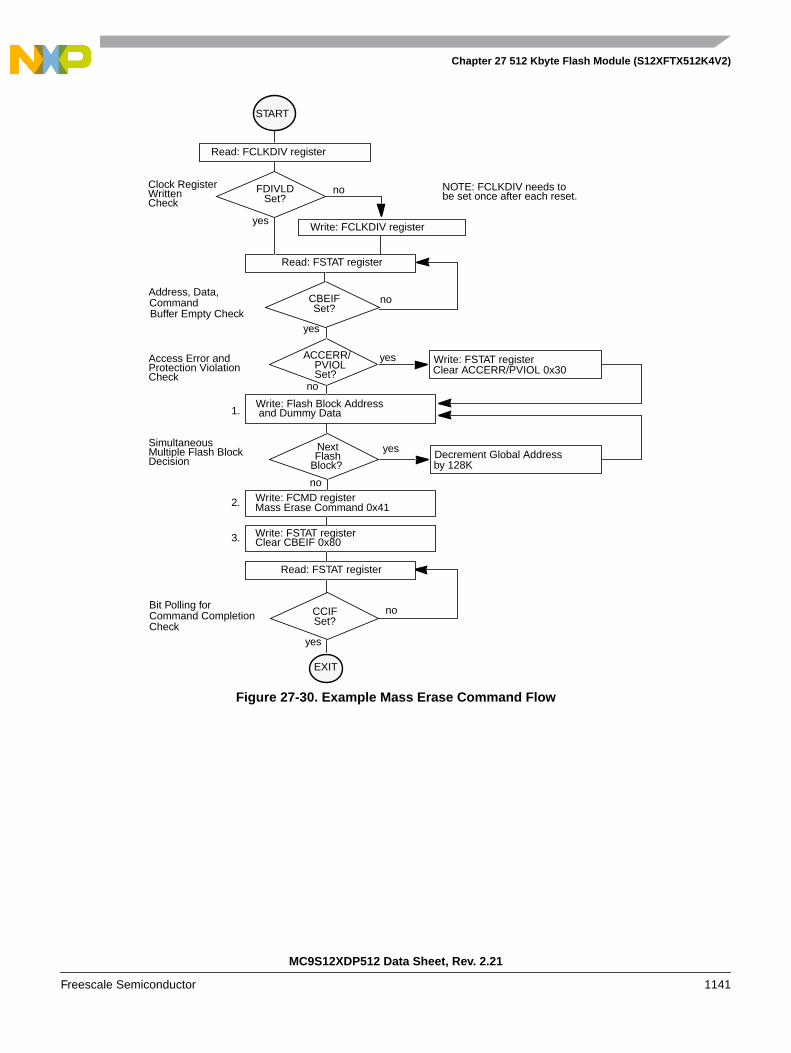
Chapter 27 512 Kbyte Flash Module (S12XFTX512K4V2)
MC9S12XDP512 Data Sheet, Rev. 2.21
Freescale Semiconductor 1141
Figure 27-30. Example Mass Erase Command Flow
Write: Flash Block Address
Write: FCMD registerMass Erase Command 0x41
Write: FSTAT registerClear CBEIF 0x80
1.
2.
3.
Clear ACCERR/PVIOL 0x30Write: FSTAT registeryes
no
Access Error andProtection Violation
and Dummy Data
Read: FSTAT register
Read: FSTAT register
no
START
yes
Check
CBEIFSet?
Next
no
yes
Address, Data,CommandBuffer Empty Check
FlashBlock?
ACCERR/PVIOLSet?
EXIT
by 128KDecrement Global Address
Write: FCLKDIV register
Read: FCLKDIV register
yes
noClock RegisterWrittenCheck
FDIVLDSet?
NOTE: FCLKDIV needs tobe set once after each reset.
SimultaneousMultiple Flash BlockDecision
noBit Polling forCommand CompletionCheck
yes
CCIFSet?

Chapter 27 512 Kbyte Flash Module (S12XFTX512K4V2)
MC9S12XDP512 Data Sheet, Rev. 2.21
1142 Freescale Semiconductor
27.4.2.6 Sector Erase Abort Command
The sector erase abort operation will terminate the active sector erase operation so that other sectors in aFlash block are available for read and program operations without waiting for the sector erase operation tocomplete.
An example flow to execute the sector erase abort operation is shown in Figure 27-31. The sector eraseabort command write sequence is as follows:
1. Write to any Flash block address to start the command write sequence for the sector erase abortcommand. The address and data written are ignored.
2. Write the sector erase abort command, 0x47, to the FCMD register.
3. Clear the CBEIF flag in the FSTAT register by writing a 1 to CBEIF to launch the sector erase abortcommand.
If the sector erase abort command is launched resulting in the early termination of an active sector eraseoperation, the ACCERR flag will set once the operation completes as indicated by the CCIF flag being set.The ACCERR flag sets to inform the user that the Flash sector may not be fully erased and a new sectorerase command must be launched before programming any location in that specific sector. If the sectorerase abort command is launched but the active sector erase operation completes normally, the ACCERRflag will not set upon completion of the operation as indicated by the CCIF flag being set. Therefore, if theACCERR flag is not set after the sector erase abort command has completed, a Flash sector being erasedwhen the abort command was launched will be fully erased. The maximum number of cycles required toabort a sector erase operation is equal to four FCLK periods (see Section 27.4.1.1, “Writing the FCLKDIVRegister”) plus five bus cycles as measured from the time the CBEIF flag is cleared until the CCIF flag isset. If sectors in multiple Flash blocks are being simultaneously erased, the sector erase abort operationwill be applied to all active Flash blocks without writing to each Flash block in the sector erase abortcommand write sequence.
NOTESince the ACCERR bit in the FSTAT register may be set at the completionof the sector erase abort operation, a command write sequence is notallowed to be buffered behind a sector erase abort command write sequence.The CBEIF flag will not set after launching the sector erase abort commandto indicate that a command should not be buffered behind it. If an attempt ismade to start a new command write sequence with a sector erase abortoperation active, the ACCERR flag in the FSTAT register will be set. A newcommand write sequence may be started after clearing the ACCERR flag, ifset.
NOTEThe sector erase abort command should be used sparingly since a sectorerase operation that is aborted counts as a complete program/erase cycle.

Chapter 27 512 Kbyte Flash Module (S12XFTX512K4V2)
MC9S12XDP512 Data Sheet, Rev. 2.21
Freescale Semiconductor 1143
Figure 27-31. Example Sector Erase Abort Command Flow
Write: Dummy Flash Address
Write: FCMD registerSector Erase Abort Cmd 0x47
Write: FSTAT registerClear CBEIF 0x80
1.
2.
3.
Read: FSTAT register
and Dummy Data
Bit Polling forCommandCompletion Check
yes
CCIFSet?
Execute Sector Erase Command Flow
noBit Polling forCommandCompletion Check
Read: FSTAT register
yes
CCIFSet?
no
yes
AbortNeeded?
Erase
Clear ACCERR 0x10Write: FSTAT registeryes
no
AccessError Check
ACCERRSet?
Sector EraseCompleted
Sector EraseAborted
no
EXIT EXIT
Sector EraseCompleted EXIT

Chapter 27 512 Kbyte Flash Module (S12XFTX512K4V2)
MC9S12XDP512 Data Sheet, Rev. 2.21
1144 Freescale Semiconductor
27.4.3 Illegal Flash Operations
The ACCERR flag will be set during the command write sequence if any of the following illegal steps areperformed, causing the command write sequence to immediately abort:
1. Writing to a Flash address before initializing the FCLKDIV register.
2. Writing a byte or misaligned word to a valid Flash address.
3. Starting a command write sequence while a data compress operation is active.
4. Starting a command write sequence while a sector erase abort operation is active.
5. Writing a Flash address in step 1 of a command write sequence that is not the same relative addressas the first one written in the same command write sequence.
6. Writing to any Flash register other than FCMD after writing to a Flash address.
7. Writing a second command to the FCMD register in the same command write sequence.
8. Writing an invalid command to the FCMD register.
9. When security is enabled, writing a command other than mass erase to the FCMD register whenthe write originates from a non-secure memory location or from the Background Debug Mode.
10. Writing to a Flash address after writing to the FCMD register.
11. Writing to any Flash register other than FSTAT (to clear CBEIF) after writing to the FCMDregister.
12. Writing a 0 to the CBEIF flag in the FSTAT register to abort a command write sequence.
The ACCERR flag will not be set if any Flash register is read during a valid command write sequence.
The ACCERR flag will also be set if any of the following events occur:
1. Launching the sector erase abort command while a sector erase operation is active which results inthe early termination of the sector erase operation (see Section 27.4.2.6, “Sector Erase AbortCommand”).
2. The MCU enters stop mode and a program or erase operation is in progress. The operation isaborted immediately and any pending command is purged (see Section 27.5.2, “Stop Mode”).
If the Flash memory is read during execution of an algorithm (CCIF = 0), the read operation will returninvalid data and the ACCERR flag will not be set.
If the ACCERR flag is set in the FSTAT register, the user must clear the ACCERR flag before startinganother command write sequence (see Section 27.3.2.6, “Flash Status Register (FSTAT)”).
The PVIOL flag will be set after the command is written to the FCMD register during a command writesequence if any of the following illegal operations are attempted, causing the command write sequence toimmediately abort:
1. Writing the program command if an address written in the command write sequence was in aprotected area of the Flash memory
2. Writing the sector erase command if an address written in the command write sequence was in aprotected area of the Flash memory
3. Writing the mass erase command to a Flash block while any Flash protection is enabled in theblock

Chapter 27 512 Kbyte Flash Module (S12XFTX512K4V2)
MC9S12XDP512 Data Sheet, Rev. 2.21
Freescale Semiconductor 1145
If the PVIOL flag is set in the FSTAT register, the user must clear the PVIOL flag before starting anothercommand write sequence (see Section 27.3.2.6, “Flash Status Register (FSTAT)”).
27.5 Operating Modes
27.5.1 Wait Mode
If a command is active (CCIF = 0) when the MCU enters wait mode, the active command and any bufferedcommand will be completed.
The Flash module can recover the MCU from wait mode if the CBEIF and CCIF interrupts are enabled(see Section 27.8, “Interrupts”).
27.5.2 Stop Mode
If a command is active (CCIF = 0) when the MCU enters stop mode, the operation will be aborted and, ifthe operation is program or erase, the Flash array data being programmed or erased may be corrupted andthe CCIF and ACCERR flags will be set. If active, the high voltage circuitry to the Flash memory willimmediately be switched off when entering stop mode. Upon exit from stop mode, the CBEIF flag is setand any buffered command will not be launched. The ACCERR flag must be cleared before starting acommand write sequence (see Section 27.4.1.2, “Command Write Sequence”).
NOTEAs active commands are immediately aborted when the MCU enters stopmode, it is strongly recommended that the user does not use the STOPinstruction during program or erase operations.
27.5.3 Background Debug Mode
In background debug mode (BDM), the FPROT register is writable. If the MCU is unsecured, then allFlash commands listed in Table 27-20 can be executed. If the MCU is secured and is in special single chipmode, only mass erase can be executed.
27.6 Flash Module SecurityThe Flash module provides the necessary security information to the MCU. After each reset, the Flashmodule determines the security state of the MCU as defined in Section 27.3.2.2, “Flash Security Register(FSEC)”.
The contents of the Flash security byte at 0x7F_FF0F in the Flash Configuration Field must be changeddirectly by programming 0x7F_FF0F when the MCU is unsecured and the higher address sector isunprotected. If the Flash security byte is left in a secured state, any reset will cause the MCU to initializeto a secure operating mode.
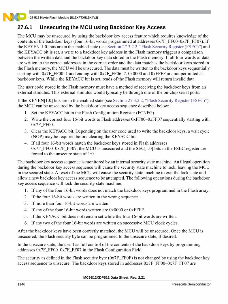
Chapter 27 512 Kbyte Flash Module (S12XFTX512K4V2)
MC9S12XDP512 Data Sheet, Rev. 2.21
1146 Freescale Semiconductor
27.6.1 Unsecuring the MCU using Backdoor Key Access
The MCU may be unsecured by using the backdoor key access feature which requires knowledge of thecontents of the backdoor keys (four 16-bit words programmed at addresses 0x7F_FF00–0x7F_FF07). Ifthe KEYEN[1:0] bits are in the enabled state (see Section 27.3.2.2, “Flash Security Register (FSEC)”) andthe KEYACC bit is set, a write to a backdoor key address in the Flash memory triggers a comparisonbetween the written data and the backdoor key data stored in the Flash memory. If all four words of dataare written to the correct addresses in the correct order and the data matches the backdoor keys stored inthe Flash memory, the MCU will be unsecured. The data must be written to the backdoor keys sequentiallystarting with 0x7F_FF00–1 and ending with 0x7F_FF06–7. 0x0000 and 0xFFFF are not permitted asbackdoor keys. While the KEYACC bit is set, reads of the Flash memory will return invalid data.
The user code stored in the Flash memory must have a method of receiving the backdoor keys from anexternal stimulus. This external stimulus would typically be through one of the on-chip serial ports.
If the KEYEN[1:0] bits are in the enabled state (see Section 27.3.2.2, “Flash Security Register (FSEC)”),the MCU can be unsecured by the backdoor key access sequence described below:
1. Set the KEYACC bit in the Flash Configuration Register (FCNFG).
2. Write the correct four 16-bit words to Flash addresses 0xFF00–0xFF07 sequentially starting with0x7F_FF00.
3. Clear the KEYACC bit. Depending on the user code used to write the backdoor keys, a wait cycle(NOP) may be required before clearing the KEYACC bit.
4. If all four 16-bit words match the backdoor keys stored in Flash addresses0x7F_FF00–0x7F_FF07, the MCU is unsecured and the SEC[1:0] bits in the FSEC register areforced to the unsecure state of 1:0.
The backdoor key access sequence is monitored by an internal security state machine. An illegal operationduring the backdoor key access sequence will cause the security state machine to lock, leaving the MCUin the secured state. A reset of the MCU will cause the security state machine to exit the lock state andallow a new backdoor key access sequence to be attempted. The following operations during the backdoorkey access sequence will lock the security state machine:
1. If any of the four 16-bit words does not match the backdoor keys programmed in the Flash array.
2. If the four 16-bit words are written in the wrong sequence.
3. If more than four 16-bit words are written.
4. If any of the four 16-bit words written are 0x0000 or 0xFFFF.
5. If the KEYACC bit does not remain set while the four 16-bit words are written.
6. If any two of the four 16-bit words are written on successive MCU clock cycles.
After the backdoor keys have been correctly matched, the MCU will be unsecured. Once the MCU isunsecured, the Flash security byte can be programmed to the unsecure state, if desired.
In the unsecure state, the user has full control of the contents of the backdoor keys by programmingaddresses 0x7F_FF00–0x7F_FF07 in the Flash Configuration Field.
The security as defined in the Flash security byte (0x7F_FF0F) is not changed by using the backdoor keyaccess sequence to unsecure. The backdoor keys stored in addresses 0x7F_FF00–0x7F_FF07 are

Chapter 27 512 Kbyte Flash Module (S12XFTX512K4V2)
MC9S12XDP512 Data Sheet, Rev. 2.21
Freescale Semiconductor 1147
unaffected by the backdoor key access sequence. After the next reset of the MCU, the security state of theFlash module is determined by the Flash security byte (0x7F_FF0F). The backdoor key access sequencehas no effect on the program and erase protections defined in the Flash protection register.
It is not possible to unsecure the MCU in special single chip mode by using the backdoor key accesssequence in background debug mode (BDM).
27.6.2 Unsecuring the MCU in Special Single Chip Mode using BDM
The MCU can be unsecured in special single chip mode by erasing the Flash module by the followingmethod:
• Reset the MCU into special single chip mode, delay while the erase test is performed by the BDMsecure ROM, send BDM commands to disable protection in the Flash module, and execute a masserase command write sequence to erase the Flash memory.
After the CCIF flag sets to indicate that the mass operation has completed, reset the MCU into specialsingle chip mode. The BDM secure ROM will verify that the Flash memory is erased and will assert theUNSEC bit in the BDM status register. This BDM action will cause the MCU to override the Flash securitystate and the MCU will be unsecured. All BDM commands will be enabled and the Flash security bytemay be programmed to the unsecure state by the following method:
• Send BDM commands to execute a word program sequence to program the Flash security byte tothe unsecured state and reset the MCU.
27.7 Resets
27.7.1 Flash Reset Sequence
On each reset, the Flash module executes a reset sequence to hold CPU activity while loading the followingregisters from the Flash memory according to Table 27-1:
• FPROT — Flash Protection Register (see Section 27.3.2.5).
• FCTL - Flash Control Register (see Section 27.3.2.8).
• FSEC — Flash Security Register (see Section 27.3.2.2).
27.7.2 Reset While Flash Command Active
If a reset occurs while any Flash command is in progress, that command will be immediately aborted. Thestate of the word being programmed or the sector/block being erased is not guaranteed.
27.8 InterruptsThe Flash module can generate an interrupt when all Flash command operations have completed, when theFlash address, data and command buffers are empty.
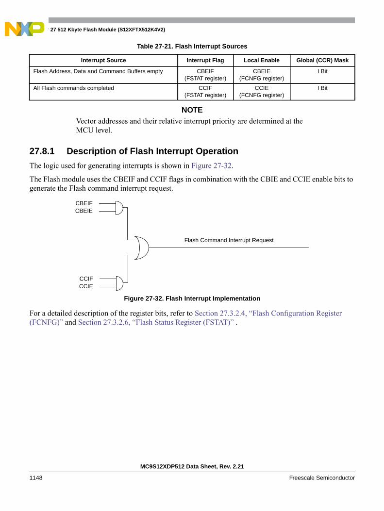
Chapter 27 512 Kbyte Flash Module (S12XFTX512K4V2)
MC9S12XDP512 Data Sheet, Rev. 2.21
1148 Freescale Semiconductor
NOTEVector addresses and their relative interrupt priority are determined at theMCU level.
27.8.1 Description of Flash Interrupt Operation
The logic used for generating interrupts is shown in Figure 27-32.
The Flash module uses the CBEIF and CCIF flags in combination with the CBIE and CCIE enable bits togenerate the Flash command interrupt request.
Figure 27-32. Flash Interrupt Implementation
For a detailed description of the register bits, refer to Section 27.3.2.4, “Flash Configuration Register(FCNFG)” and Section 27.3.2.6, “Flash Status Register (FSTAT)” .
Table 27-21. Flash Interrupt Sources
Interrupt Source Interrupt Flag Local Enable Global (CCR) Mask
Flash Address, Data and Command Buffers empty CBEIF(FSTAT register)
CBEIE(FCNFG register)
I Bit
All Flash commands completed CCIF(FSTAT register)
CCIE(FCNFG register)
I Bit
Flash Command Interrupt Request
CBEIECBEIF
CCIECCIF
MC9S12XDP512 Data Sheet, Rev. 2.21
Freescale Semiconductor 1149
Chapter 28256 Kbyte Flash Module (S12XFTX256K2V1)
28.1 IntroductionThis document describes the FTX256K2 module that includes a 256 Kbyte Flash (nonvolatile) memory.The Flash memory may be read as either bytes, aligned words or misaligned words. Read access time isone bus cycle for bytes and aligned words, and two bus cycles for misaligned words.
The Flash memory is ideal for program and data storage for single-supply applications allowing for fieldreprogramming without requiring external voltage sources for program or erase. Program and erasefunctions are controlled by a command driven interface. The Flash module supports both block erase andsector erase. An erased bit reads 1 and a programmed bit reads 0. The high voltage required to programand erase the Flash memory is generated internally. It is not possible to read from a Flash block while it isbeing erased or programmed.
CAUTIONA Flash word must be in the erased state before being programmed.Cumulative programming of bits within a Flash word is not allowed.
28.1.1 Glossary
Command Write Sequence — A three-step MCU instruction sequence to execute built-in algorithms(including program and erase) on the Flash memory.
Multiple-Input Signature Register (MISR) — A Multiple-Input Signature Register is an outputresponse analyzer implemented using a linear feedback shift-register (LFSR). A 16-bit MISR is used tocompress data and generate a signature that is particular to the data read from a Flash block.
28.1.2 Features• 256 Kbytes of Flash memory comprised of two 128 Kbyte blocks with each block divided into 128
sectors of 1024 bytes
• Automated program and erase algorithm
• Interrupts on Flash command completion, command buffer empty
• Fast sector erase and word program operation
• 2-stage command pipeline for faster multi-word program times
• Sector erase abort feature for critical interrupt response
• Flexible protection scheme to prevent accidental program or erase
• Single power supply for all Flash operations including program and erase
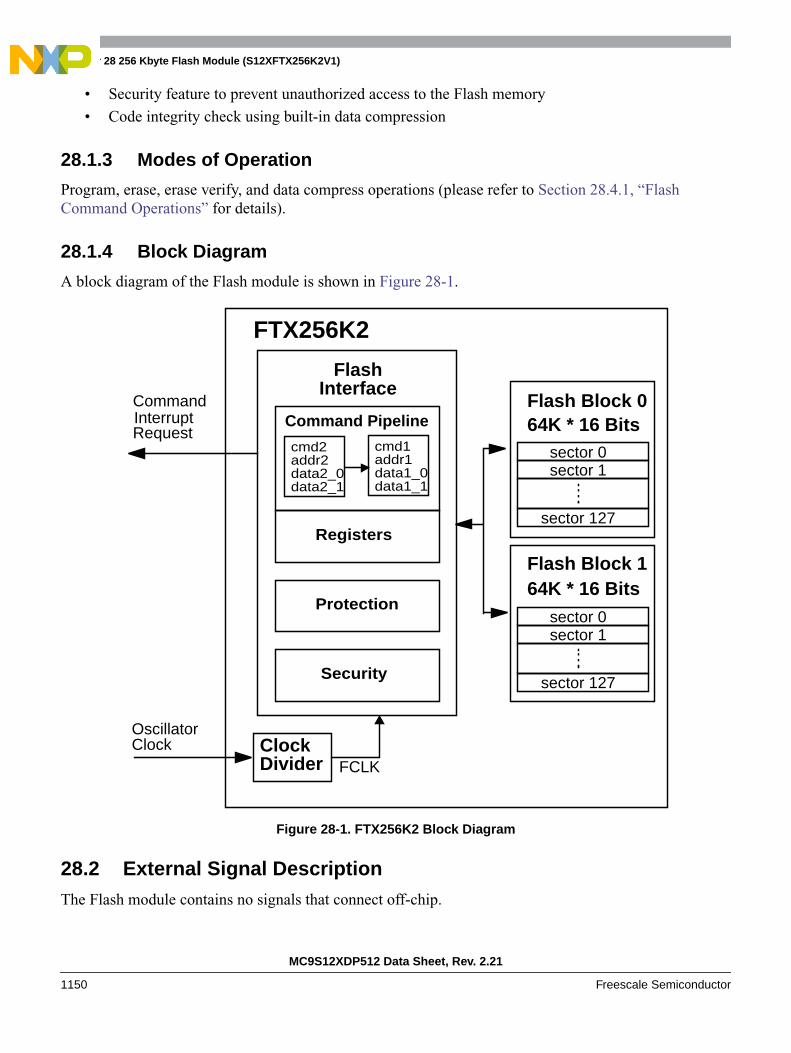
Chapter 28 256 Kbyte Flash Module (S12XFTX256K2V1)
MC9S12XDP512 Data Sheet, Rev. 2.21
1150 Freescale Semiconductor
• Security feature to prevent unauthorized access to the Flash memory
• Code integrity check using built-in data compression
28.1.3 Modes of Operation
Program, erase, erase verify, and data compress operations (please refer to Section 28.4.1, “FlashCommand Operations” for details).
28.1.4 Block Diagram
A block diagram of the Flash module is shown in Figure 28-1.
Figure 28-1. FTX256K2 Block Diagram
28.2 External Signal DescriptionThe Flash module contains no signals that connect off-chip.
FTX256K2
Flash Block 064K * 16 Bits
Flash Block 164K * 16 Bits
sector 0sector 1
sector 127
sector 0sector 1
sector 127
OscillatorClockDivider
Clock
CommandInterruptRequest
FCLK
Protection
Security
Command Pipeline
cmd2addr2data2_0
cmd1addr1data1_0
Registers
data2_1 data1_1
FlashInterface

Chapter 28 256 Kbyte Flash Module (S12XFTX256K2V1)
MC9S12XDP512 Data Sheet, Rev. 2.21
Freescale Semiconductor 1151
28.3 Memory Map and Register DefinitionThis section describes the memory map and registers for the Flash module.
28.3.1 Module Memory Map
The Flash memory map is shown in Figure 28-2. The HCS12X architecture places the Flash memoryaddresses between global addresses 0x78_0000 and 0x7F_FFFF. The FPROT register, described inSection 28.3.2.5, “Flash Protection Register (FPROT)”, can be set to protect regions in the Flash memoryfrom accidental program or erase. Three separate memory regions, one growing upward from globaladdress 0x7F_8000 in the Flash memory (called the lower region), one growing downward from globaladdress 0x7F_FFFF in the Flash memory (called the higher region), and the remaining addresses in theFlash memory, can be activated for protection. The Flash memory addresses covered by these protectableregions are shown in the Flash memory map. The higher address region is mainly targeted to hold the bootloader code since it covers the vector space. The lower address region can be used for EEPROM emulationin an MCU without an EEPROM module since it can be left unprotected while the remaining addressesare protected from program or erase. Default protection settings as well as security information that allowsthe MCU to restrict access to the Flash module are stored in the Flash configuration field as described inTable 28-1.
Table 28-1. Flash Configuration Field
Global AddressSize
(Bytes)Description
0x7F_FF00 – 0x7F_FF07 8 Backdoor Comparison KeyRefer to Section 28.6.1, “Unsecuring the MCU using Backdoor Key Access”
0x7F_FF08 – 0x7F_FF0C 5 Reserved
0x7F_FF0D 1 Flash Protection byteRefer to Section 28.3.2.5, “Flash Protection Register (FPROT)”
0x7F_FF0E 1 Flash Nonvolatile byteRefer to Section 28.3.2.8, “Flash Control Register (FCTL)”
0x7F_FF0F 1 Flash Security byteRefer to Section 28.3.2.2, “Flash Security Register (FSEC)”
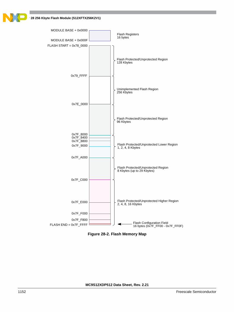
Chapter 28 256 Kbyte Flash Module (S12XFTX256K2V1)
MC9S12XDP512 Data Sheet, Rev. 2.21
1152 Freescale Semiconductor
Figure 28-2. Flash Memory Map
Flash Registers
Flash Configuration Field
0x7F_C000
Flash Protected/Unprotected Lower Region1, 2, 4, 8 Kbytes
0x7F_8000
0x7F_9000
0x7F_84000x7F_8800
0x7F_A000
FLASH END = 0x7F_FFFF
0x7F_F800
0x7F_F000
0x7F_E000 Flash Protected/Unprotected Higher Region2, 4, 8, 16 Kbytes
Flash Protected/Unprotected Region8 Kbytes (up to 29 Kbytes)
16 bytes
16 bytes (0x7F_FF00 - 0x7F_FF0F)
FLASH START = 0x78_0000
MODULE BASE + 0x0000
MODULE BASE + 0x000F
Flash Protected/Unprotected Region96 Kbytes
0x7E_0000
0x79_FFFF
Flash Protected/Unprotected Region128 Kbytes
Unimplemented Flash Region256 Kbytes
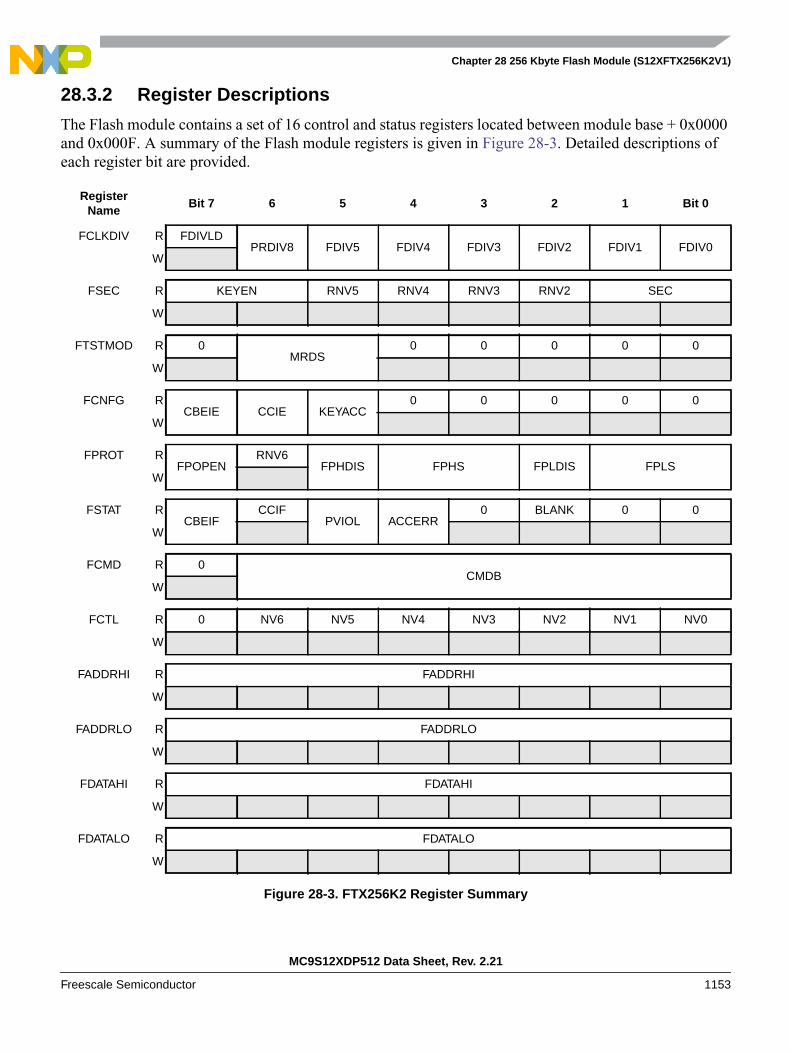
Chapter 28 256 Kbyte Flash Module (S12XFTX256K2V1)
MC9S12XDP512 Data Sheet, Rev. 2.21
Freescale Semiconductor 1153
28.3.2 Register Descriptions
The Flash module contains a set of 16 control and status registers located between module base + 0x0000and 0x000F. A summary of the Flash module registers is given in Figure 28-3. Detailed descriptions ofeach register bit are provided.
RegisterName
Bit 7 6 5 4 3 2 1 Bit 0
FCLKDIV R FDIVLDPRDIV8 FDIV5 FDIV4 FDIV3 FDIV2 FDIV1 FDIV0
W
FSEC R KEYEN RNV5 RNV4 RNV3 RNV2 SEC
W
FTSTMOD R 0MRDS
0 0 0 0 0
W
FCNFG RCBEIE CCIE KEYACC
0 0 0 0 0
W
FPROT RFPOPEN
RNV6FPHDIS FPHS FPLDIS FPLS
W
FSTAT RCBEIF
CCIFPVIOL ACCERR
0 BLANK 0 0
W
FCMD R 0CMDB
W
FCTL R 0 NV6 NV5 NV4 NV3 NV2 NV1 NV0
W
FADDRHI R FADDRHI
W
FADDRLO R FADDRLO
W
FDATAHI R FDATAHI
W
FDATALO R FDATALO
W
Figure 28-3. FTX256K2 Register Summary

Chapter 28 256 Kbyte Flash Module (S12XFTX256K2V1)
MC9S12XDP512 Data Sheet, Rev. 2.21
1154 Freescale Semiconductor
28.3.2.1 Flash Clock Divider Register (FCLKDIV)
The FCLKDIV register is used to control timed events in program and erase algorithms.
All bits in the FCLKDIV register are readable, bits 6-0 are write once and bit 7 is not writable.
28.3.2.2 Flash Security Register (FSEC)
The FSEC register holds all bits associated with the security of the MCU and Flash module.
RESERVED1 R 0 0 0 0 0 0 0 0
W
RESERVED2 R 0 0 0 0 0 0 0 0
W
RESERVED3 R 0 0 0 0 0 0 0 0
W
RESERVED4 R 0 0 0 0 0 0 0 0
W
7 6 5 4 3 2 1 0
R FDIVLDPRDIV8 FDIV5 FDIV4 FDIV3 FDIV2 FDIV1 FDIV0
W
Reset 0 0 0 0 0 0 0 0
= Unimplemented or Reserved
Figure 28-4. Flash Clock Divider Register (FCLKDIV)
Table 28-2. FCLKDIV Field Descriptions
Field Description
7FDIVLD
Clock Divider Loaded.0 Register has not been written.1 Register has been written to since the last reset.
6PRDIV8
Enable Prescalar by 8.0 The oscillator clock is directly fed into the clock divider.1 The oscillator clock is divided by 8 before feeding into the clock divider.
5:0FDIV[5:0]
Clock Divider Bits — The combination of PRDIV8 and FDIV[5:0] must divide the oscillator clock down to afrequency of 150 kHz–200 kHz. The maximum divide ratio is 512. Please refer to Section 28.4.1.1, “Writing theFCLKDIV Register” for more information.
RegisterName
Bit 7 6 5 4 3 2 1 Bit 0
Figure 28-3. FTX256K2 Register Summary (continued)
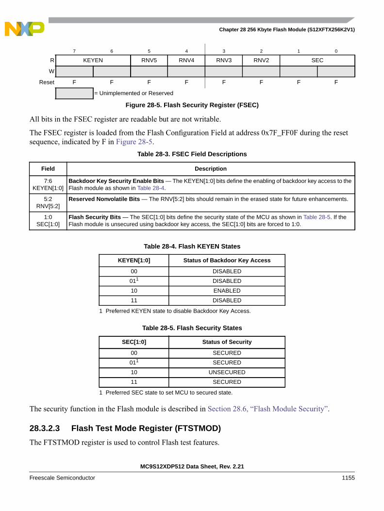
Chapter 28 256 Kbyte Flash Module (S12XFTX256K2V1)
MC9S12XDP512 Data Sheet, Rev. 2.21
Freescale Semiconductor 1155
All bits in the FSEC register are readable but are not writable.
The FSEC register is loaded from the Flash Configuration Field at address 0x7F_FF0F during the resetsequence, indicated by F in Figure 28-5.
The security function in the Flash module is described in Section 28.6, “Flash Module Security”.
28.3.2.3 Flash Test Mode Register (FTSTMOD)
The FTSTMOD register is used to control Flash test features.
7 6 5 4 3 2 1 0
R KEYEN RNV5 RNV4 RNV3 RNV2 SEC
W
Reset F F F F F F F F
= Unimplemented or Reserved
Figure 28-5. Flash Security Register (FSEC)
Table 28-3. FSEC Field Descriptions
Field Description
7:6KEYEN[1:0]
Backdoor Key Security Enable Bits — The KEYEN[1:0] bits define the enabling of backdoor key access to theFlash module as shown in Table 28-4.
5:2RNV[5:2]
Reserved Nonvolatile Bits — The RNV[5:2] bits should remain in the erased state for future enhancements.
1:0SEC[1:0]
Flash Security Bits — The SEC[1:0] bits define the security state of the MCU as shown in Table 28-5. If theFlash module is unsecured using backdoor key access, the SEC[1:0] bits are forced to 1:0.
Table 28-4. Flash KEYEN States
KEYEN[1:0] Status of Backdoor Key Access
00 DISABLED
011
1 Preferred KEYEN state to disable Backdoor Key Access.
DISABLED
10 ENABLED
11 DISABLED
Table 28-5. Flash Security States
SEC[1:0] Status of Security
00 SECURED
011
1 Preferred SEC state to set MCU to secured state.
SECURED
10 UNSECURED
11 SECURED
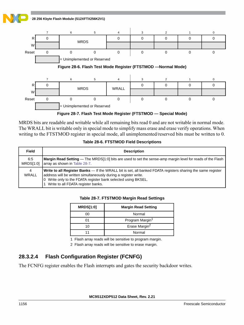
Chapter 28 256 Kbyte Flash Module (S12XFTX256K2V1)
MC9S12XDP512 Data Sheet, Rev. 2.21
1156 Freescale Semiconductor
MRDS bits are readable and writable while all remaining bits read 0 and are not writable in normal mode.The WRALL bit is writable only in special mode to simplify mass erase and erase verify operations. Whenwriting to the FTSTMOD register in special mode, all unimplemented/reserved bits must be written to 0.
28.3.2.4 Flash Configuration Register (FCNFG)
The FCNFG register enables the Flash interrupts and gates the security backdoor writes.
7 6 5 4 3 2 1 0
R 0MRDS
0 0 0 0 0
W
Reset 0 0 0 0 0 0 0 0
= Unimplemented or Reserved
Figure 28-6. Flash Test Mode Register (FTSTMOD —Normal Mode)
7 6 5 4 3 2 1 0
R 0MRDS WRALL
0 0 0 0
W
Reset 0 0 0 0 0 0 0 0
= Unimplemented or Reserved
Figure 28-7. Flash Test Mode Register (FTSTMOD — Special Mode)
Table 28-6. FTSTMOD Field Descriptions
Field Description
6:5MRDS[1:0]
Margin Read Setting — The MRDS[1:0] bits are used to set the sense-amp margin level for reads of the Flasharray as shown in Table 28-7.
4WRALL
Write to all Register Banks — If the WRALL bit is set, all banked FDATA registers sharing the same registeraddress will be written simultaneously during a register write.0 Write only to the FDATA register bank selected using BKSEL.1 Write to all FDATA register banks.
Table 28-7. FTSTMOD Margin Read Settings
MRDS[1:0] Margin Read Setting
00 Normal
01 Program Margin1
1 Flash array reads will be sensitive to program margin.
10 Erase Margin2
2 Flash array reads will be sensitive to erase margin.
11 Normal
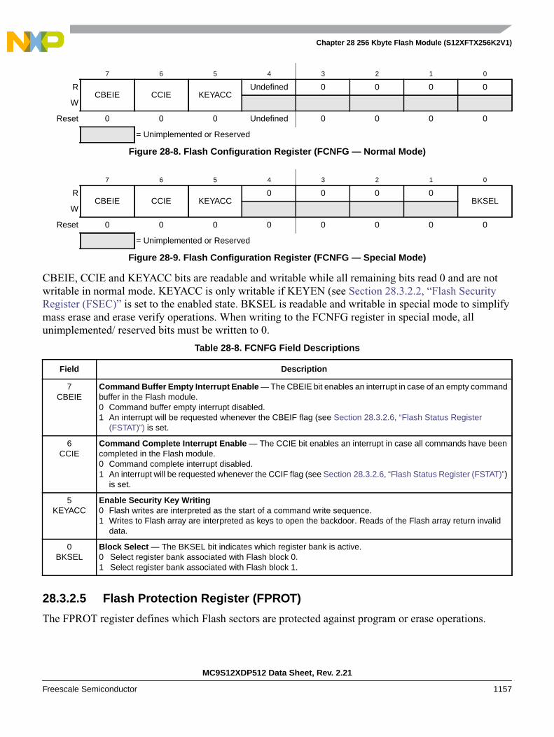
Chapter 28 256 Kbyte Flash Module (S12XFTX256K2V1)
MC9S12XDP512 Data Sheet, Rev. 2.21
Freescale Semiconductor 1157
CBEIE, CCIE and KEYACC bits are readable and writable while all remaining bits read 0 and are notwritable in normal mode. KEYACC is only writable if KEYEN (see Section 28.3.2.2, “Flash SecurityRegister (FSEC)” is set to the enabled state. BKSEL is readable and writable in special mode to simplifymass erase and erase verify operations. When writing to the FCNFG register in special mode, allunimplemented/ reserved bits must be written to 0.
28.3.2.5 Flash Protection Register (FPROT)
The FPROT register defines which Flash sectors are protected against program or erase operations.
7 6 5 4 3 2 1 0
RCBEIE CCIE KEYACC
Undefined 0 0 0 0
W
Reset 0 0 0 Undefined 0 0 0 0
= Unimplemented or Reserved
Figure 28-8. Flash Configuration Register (FCNFG — Normal Mode)
7 6 5 4 3 2 1 0
RCBEIE CCIE KEYACC
0 0 0 0BKSEL
W
Reset 0 0 0 0 0 0 0 0
= Unimplemented or Reserved
Figure 28-9. Flash Configuration Register (FCNFG — Special Mode)
Table 28-8. FCNFG Field Descriptions
Field Description
7CBEIE
Command Buffer Empty Interrupt Enable — The CBEIE bit enables an interrupt in case of an empty commandbuffer in the Flash module.0 Command buffer empty interrupt disabled.1 An interrupt will be requested whenever the CBEIF flag (see Section 28.3.2.6, “Flash Status Register
(FSTAT)”) is set.
6CCIE
Command Complete Interrupt Enable — The CCIE bit enables an interrupt in case all commands have beencompleted in the Flash module.0 Command complete interrupt disabled.1 An interrupt will be requested whenever the CCIF flag (see Section 28.3.2.6, “Flash Status Register (FSTAT)”)
is set.
5KEYACC
Enable Security Key Writing0 Flash writes are interpreted as the start of a command write sequence.1 Writes to Flash array are interpreted as keys to open the backdoor. Reads of the Flash array return invalid
data.
0BKSEL
Block Select — The BKSEL bit indicates which register bank is active.0 Select register bank associated with Flash block 0.1 Select register bank associated with Flash block 1.

Chapter 28 256 Kbyte Flash Module (S12XFTX256K2V1)
MC9S12XDP512 Data Sheet, Rev. 2.21
1158 Freescale Semiconductor
All bits in the FPROT register are readable and writable with restrictions (see Section 28.3.2.5.1, “FlashProtection Restrictions”) except for RNV[6] which is only readable.
During the reset sequence, the FPROT register is loaded from the Flash Configuration Field at globaladdress 0x7F_FF0D. To change the Flash protection that will be loaded during the reset sequence, theupper sector of the Flash memory must be unprotected, then the Flash Protect/Security byte located asdescribed in Table 28-1 must be reprogrammed.
Trying to alter data in any protected area in the Flash memory will result in a protection violation error andthe PVIOL flag will be set in the FSTAT register. The mass erase of a Flash block is not possible if any ofthe Flash sectors contained in the Flash block are protected.
7 6 5 4 3 2 1 0
RFPOPEN
RNV6FPHDIS FPHS FPLDIS FPLS
W
Reset F F F F F F F F
= Unimplemented or Reserved
Figure 28-10. Flash Protection Register (FPROT)
Table 28-9. FPROT Field Descriptions
Field Description
7FPOPEN
Flash Protection Open — The FPOPEN bit determines the protection function for program or erase as shownin Table 28-10.0 The FPHDIS and FPLDIS bits define unprotected address ranges as specified by the corresponding
FPHS[1:0] and FPLS[1:0] bits. For an MCU without an EEPROM module, the FPOPEN clear state allows themain part of the Flash block to be protected while a small address range can remain unprotected for EEPROMemulation.
1 The FPHDIS and FPLDIS bits enable protection for the address range specified by the correspondingFPHS[1:0] and FPLS[1:0] bits.
6RNV6
Reserved Nonvolatile Bit — The RNV[6] bit should remain in the erased state for future enhancements.
5FPHDIS
Flash Protection Higher Address Range Disable — The FPHDIS bit determines whether there is aprotected/unprotected area in a specific region of the Flash memory ending with global address 0x7F_FFFF.0 Protection/Unprotection enabled.1 Protection/Unprotection disabled.
4:3FPHS[1:0]
Flash Protection Higher Address Size — The FPHS[1:0] bits determine the size of the protected/unprotectedarea as shown inTable 28-11. The FPHS[1:0] bits can only be written to while the FPHDIS bit is set.
2FPLDIS
Flash Protection Lower Address Range Disable — The FPLDIS bit determines whether there is aprotected/unprotected area in a specific region of the Flash memory beginning with global address 0x7F_8000.0 Protection/Unprotection enabled.1 Protection/Unprotection disabled.
1:0FPLS[1:0]
Flash Protection Lower Address Size — The FPLS[1:0] bits determine the size of the protected/unprotectedarea as shown in Table 28-12. The FPLS[1:0] bits can only be written to while the FPLDIS bit is set.
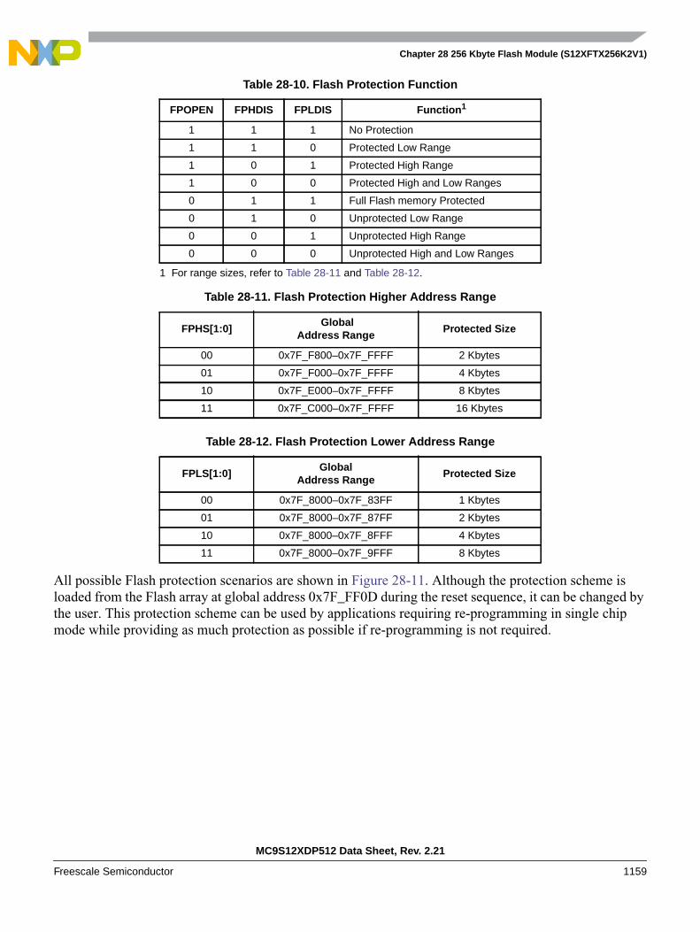
Chapter 28 256 Kbyte Flash Module (S12XFTX256K2V1)
MC9S12XDP512 Data Sheet, Rev. 2.21
Freescale Semiconductor 1159
All possible Flash protection scenarios are shown in Figure 28-11. Although the protection scheme isloaded from the Flash array at global address 0x7F_FF0D during the reset sequence, it can be changed bythe user. This protection scheme can be used by applications requiring re-programming in single chipmode while providing as much protection as possible if re-programming is not required.
Table 28-10. Flash Protection Function
FPOPEN FPHDIS FPLDIS Function1
1 For range sizes, refer to Table 28-11 and Table 28-12.
1 1 1 No Protection
1 1 0 Protected Low Range
1 0 1 Protected High Range
1 0 0 Protected High and Low Ranges
0 1 1 Full Flash memory Protected
0 1 0 Unprotected Low Range
0 0 1 Unprotected High Range
0 0 0 Unprotected High and Low Ranges
Table 28-11. Flash Protection Higher Address Range
FPHS[1:0] Global
Address RangeProtected Size
00 0x7F_F800–0x7F_FFFF 2 Kbytes
01 0x7F_F000–0x7F_FFFF 4 Kbytes
10 0x7F_E000–0x7F_FFFF 8 Kbytes
11 0x7F_C000–0x7F_FFFF 16 Kbytes
Table 28-12. Flash Protection Lower Address Range
FPLS[1:0]Global
Address RangeProtected Size
00 0x7F_8000–0x7F_83FF 1 Kbytes
01 0x7F_8000–0x7F_87FF 2 Kbytes
10 0x7F_8000–0x7F_8FFF 4 Kbytes
11 0x7F_8000–0x7F_9FFF 8 Kbytes
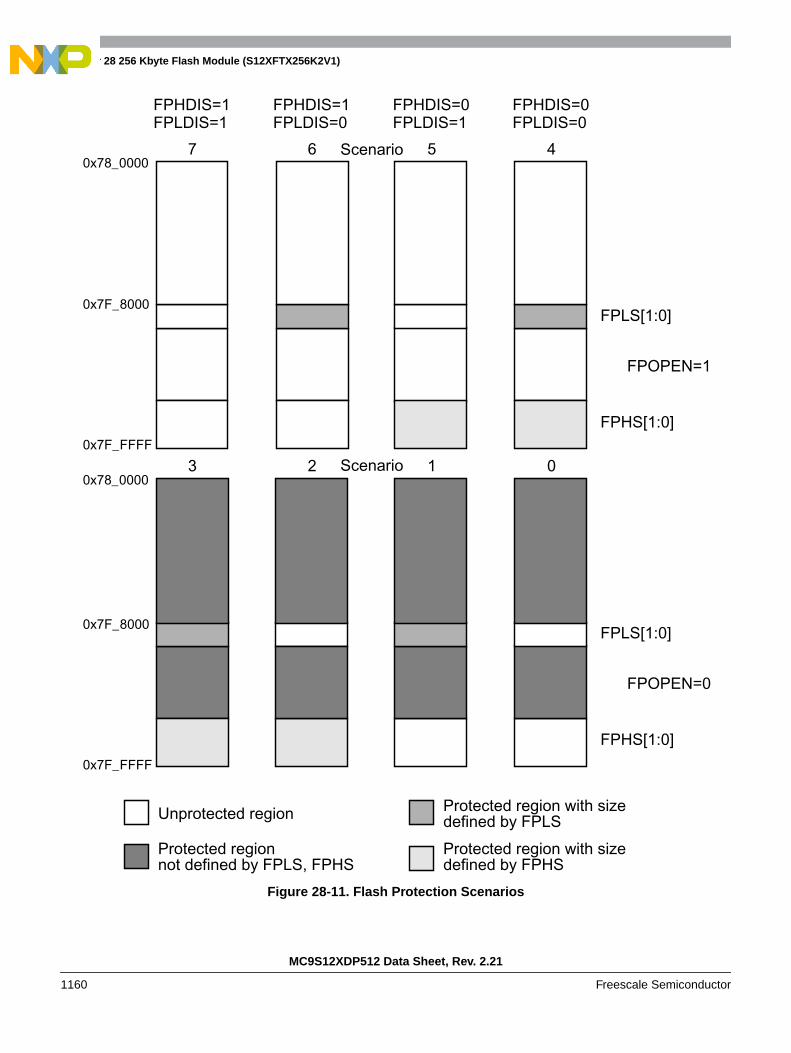
Chapter 28 256 Kbyte Flash Module (S12XFTX256K2V1)
MC9S12XDP512 Data Sheet, Rev. 2.21
1160 Freescale Semiconductor
Figure 28-11. Flash Protection Scenarios
7 6 5 4
3 2 1 0
FPHDIS=1FPLDIS=1
FPHDIS=1FPLDIS=0
FPHDIS=0FPLDIS=1
FPHDIS=0FPLDIS=0
Scenario
Scenario
Unprotected region Protected region with size
Protected region Protected region with size
defined by FPLS
defined by FPHSnot defined by FPLS, FPHS
0x7F_8000
0x7F_FFFF
0x7F_8000
0x7F_FFFF
0x78_0000
0x78_0000
FPHS[1:0]
FPLS[1:0]
FPOPEN=1
FPHS[1:0]
FPLS[1:0]
FPOPEN=0
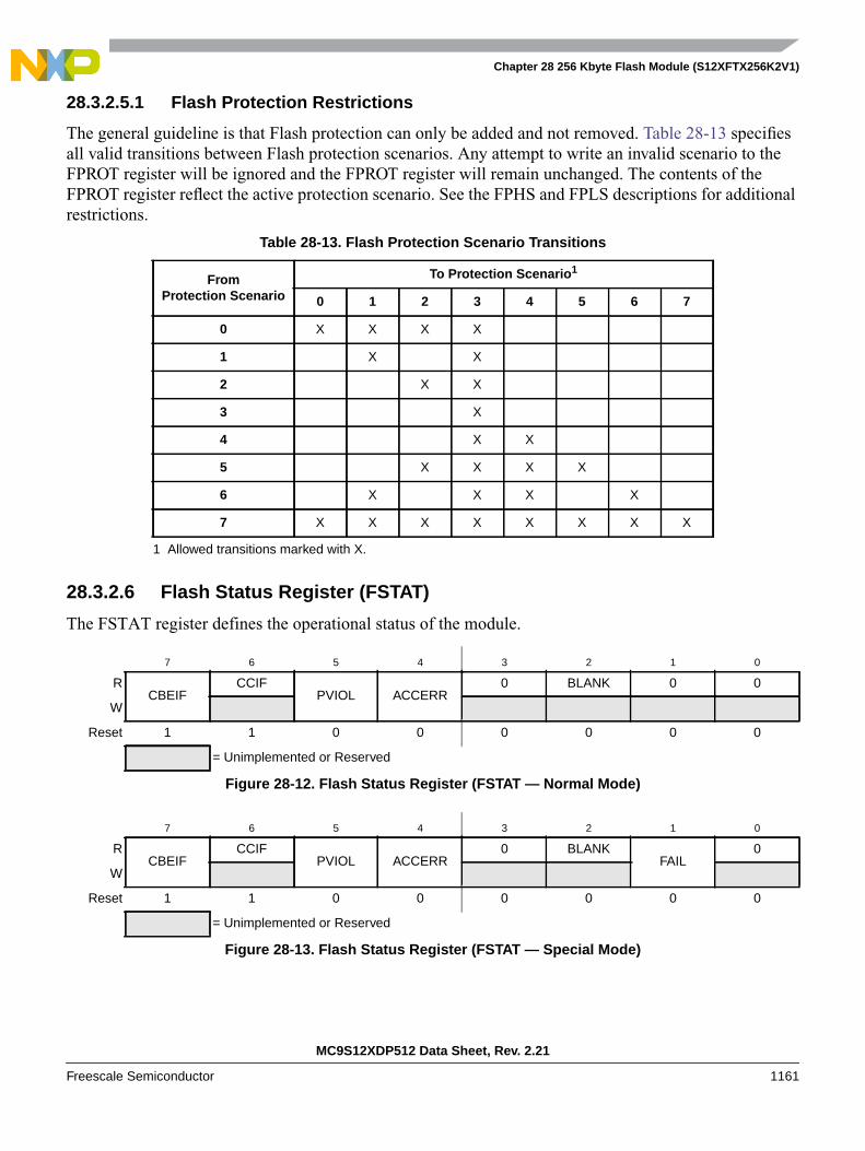
Chapter 28 256 Kbyte Flash Module (S12XFTX256K2V1)
MC9S12XDP512 Data Sheet, Rev. 2.21
Freescale Semiconductor 1161
28.3.2.5.1 Flash Protection Restrictions
The general guideline is that Flash protection can only be added and not removed. Table 28-13 specifiesall valid transitions between Flash protection scenarios. Any attempt to write an invalid scenario to theFPROT register will be ignored and the FPROT register will remain unchanged. The contents of theFPROT register reflect the active protection scenario. See the FPHS and FPLS descriptions for additionalrestrictions.
28.3.2.6 Flash Status Register (FSTAT)
The FSTAT register defines the operational status of the module.
Table 28-13. Flash Protection Scenario Transitions
FromProtection Scenario
To Protection Scenario1
1 Allowed transitions marked with X.
0 1 2 3 4 5 6 7
0 X X X X
1 X X
2 X X
3 X
4 X X
5 X X X X
6 X X X X
7 X X X X X X X X
7 6 5 4 3 2 1 0
RCBEIF
CCIFPVIOL ACCERR
0 BLANK 0 0
W
Reset 1 1 0 0 0 0 0 0
= Unimplemented or Reserved
Figure 28-12. Flash Status Register (FSTAT — Normal Mode)
7 6 5 4 3 2 1 0
RCBEIF
CCIFPVIOL ACCERR
0 BLANKFAIL
0
W
Reset 1 1 0 0 0 0 0 0
= Unimplemented or Reserved
Figure 28-13. Flash Status Register (FSTAT — Special Mode)

Chapter 28 256 Kbyte Flash Module (S12XFTX256K2V1)
MC9S12XDP512 Data Sheet, Rev. 2.21
1162 Freescale Semiconductor
CBEIF, PVIOL, and ACCERR are readable and writable, CCIF and BLANK are readable and not writable,remaining bits read 0 and are not writable in normal mode. FAIL is readable and writable in special mode.FAIL must be clear in special mode when starting a command write sequence.
Table 28-14. FSTAT Field Descriptions
Field Description
7CBEIF
Command Buffer Empty Interrupt Flag — The CBEIF flag indicates that the address, data and commandbuffers are empty so that a new command write sequence can be started. Writing a 0 to the CBEIF flag has noeffect on CBEIF. Writing a 0 to CBEIF after writing an aligned word to the Flash address space, but before CBEIFis cleared, will abort a command write sequence and cause the ACCERR flag to be set. Writing a 0 to CBEIFoutside of a command write sequence will not set the ACCERR flag. The CBEIF flag is cleared by writing a 1 toCBEIF. The CBEIF flag is used together with the CBEIE bit in the FCNFG register to generate an interruptrequest (see Figure 28-32).0 Command buffers are full.1 Command buffers are ready to accept a new command.
6CCIF
Command Complete Interrupt Flag — The CCIF flag indicates that there are no more commands pending. TheCCIF flag is cleared when CBEIF is cleared and sets automatically upon completion of all active and pendingcommands. The CCIF flag does not set when an active commands completes and a pending command isfetched from the command buffer. Writing to the CCIF flag has no effect on CCIF. The CCIF flag is used togetherwith the CCIE bit in the FCNFG register to generate an interrupt request (see Figure 28-32).0 Command in progress.1 All commands are completed.
5PVIOL
Protection Violation Flag —The PVIOL flag indicates an attempt was made to program or erase an address ina protected area of the Flash memory during a command write sequence. Writing a 0 to the PVIOL flag has noeffect on PVIOL. The PVIOL flag is cleared by writing a 1 to PVIOL. While PVIOL is set, it is not possible to launcha command or start a command write sequence.0 No protection violation detected.1 Protection violation has occurred.
4ACCERR
Access Error Flag — The ACCERR flag indicates an illegal access has occurred to the Flash memory causedby either a violation of the command write sequence (see Section 28.4.1.2, “Command Write Sequence”),issuing an illegal Flash command (see Table 28-16), launching the sector erase abort command terminating asector erase operation early (see Section 28.4.2.6, “Sector Erase Abort Command”) or the execution of a CPUSTOP instruction while a command is executing (CCIF = 0). Writing a 0 to the ACCERR flag has no effect onACCERR. The ACCERR flag is cleared by writing a 1 to ACCERR.While ACCERR is set, it is not possible tolaunch a command or start a command write sequence. If ACCERR is set by an erase verify operation or a datacompress operation, any buffered command will not launch.0 No access error detected.1 Access error has occurred.
2BLANK
Flag Indicating the Erase Verify Operation Status — When the CCIF flag is set after completion of an eraseverify command, the BLANK flag indicates the result of the erase verify operation. The BLANK flag is cleared bythe Flash module when CBEIF is cleared as part of a new valid command write sequence. Writing to the BLANKflag has no effect on BLANK.0 Flash block verified as not erased.1 Flash block verified as erased.
1FAIL
Flag Indicating a Failed Flash Operation — The FAIL flag will set if the erase verify operation fails (selectedFlash block verified as not erased). Writing a 0 to the FAIL flag has no effect on FAIL. The FAIL flag is cleared bywriting a 1 to FAIL.0 Flash operation completed without error.1 Flash operation failed.
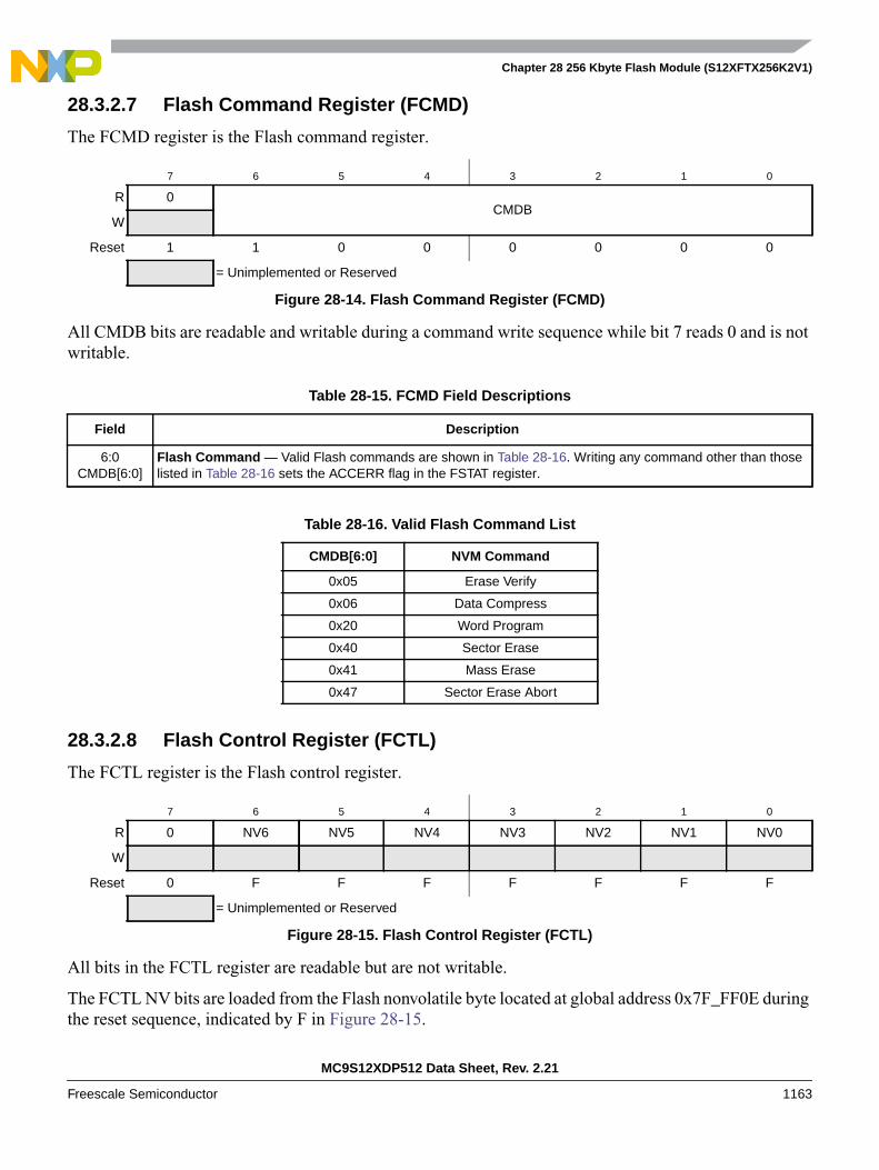
Chapter 28 256 Kbyte Flash Module (S12XFTX256K2V1)
MC9S12XDP512 Data Sheet, Rev. 2.21
Freescale Semiconductor 1163
28.3.2.7 Flash Command Register (FCMD)
The FCMD register is the Flash command register.
All CMDB bits are readable and writable during a command write sequence while bit 7 reads 0 and is notwritable.
28.3.2.8 Flash Control Register (FCTL)
The FCTL register is the Flash control register.
All bits in the FCTL register are readable but are not writable.
The FCTL NV bits are loaded from the Flash nonvolatile byte located at global address 0x7F_FF0E duringthe reset sequence, indicated by F in Figure 28-15.
7 6 5 4 3 2 1 0
R 0CMDB
W
Reset 1 1 0 0 0 0 0 0
= Unimplemented or Reserved
Figure 28-14. Flash Command Register (FCMD)
Table 28-15. FCMD Field Descriptions
Field Description
6:0CMDB[6:0]
Flash Command — Valid Flash commands are shown in Table 28-16. Writing any command other than thoselisted in Table 28-16 sets the ACCERR flag in the FSTAT register.
Table 28-16. Valid Flash Command List
CMDB[6:0] NVM Command
0x05 Erase Verify
0x06 Data Compress
0x20 Word Program
0x40 Sector Erase
0x41 Mass Erase
0x47 Sector Erase Abort
7 6 5 4 3 2 1 0
R 0 NV6 NV5 NV4 NV3 NV2 NV1 NV0
W
Reset 0 F F F F F F F
= Unimplemented or Reserved
Figure 28-15. Flash Control Register (FCTL)