Embed Size (px)
Citation preview
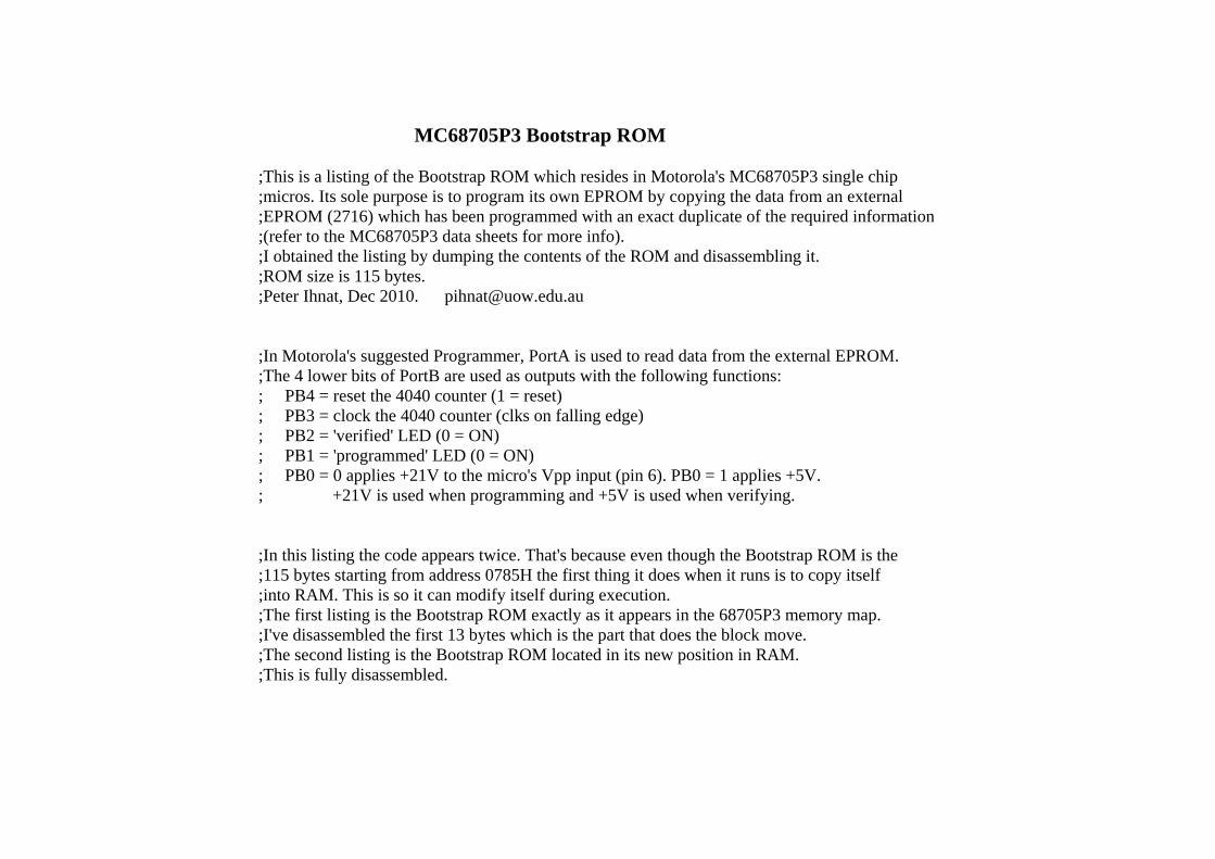
MC68705P3 Bootstrap ROM ;This is a listing of the Bootstrap ROM which resides in Motorola's MC68705P3 single chip ;micros. Its sole purpose is to program its own EPROM by copying the data from an external ;EPROM (2716) which has been programmed with an exact duplicate of the required information ;(refer to the MC68705P3 data sheets for more info). ;I obtained the listing by dumping the contents of the ROM and disassembling it. ;ROM size is 115 bytes. ;Peter Ihnat, Dec 2010. [email protected]
;In Motorola's suggested Programmer, PortA is used to read data from the external EPROM. ;The 4 lower bits of PortB are used as outputs with the following functions: ; PB4 = reset the 4040 counter (1 = reset) ; PB3 = clock the 4040 counter (clks on falling edge) ; PB2 = 'verified' LED (0 = ON) ; PB1 = 'programmed' LED (0 = ON) ; PB0 = 0 applies +21V to the micro's Vpp input (pin 6). PB0 = 1 applies +5V. ; +21V is used when programming and +5V is used when verifying.
;In this listing the code appears twice. That's because even though the Bootstrap ROM is the ;115 bytes starting from address 0785H the first thing it does when it runs is to copy itself ;into RAM. This is so it can modify itself during execution. ;The first listing is the Bootstrap ROM exactly as it appears in the 68705P3 memory map. ;I've disassembled the first 13 bytes which is the part that does the block move. ;The second listing is the Bootstrap ROM located in its new position in RAM. ;This is fully disassembled.
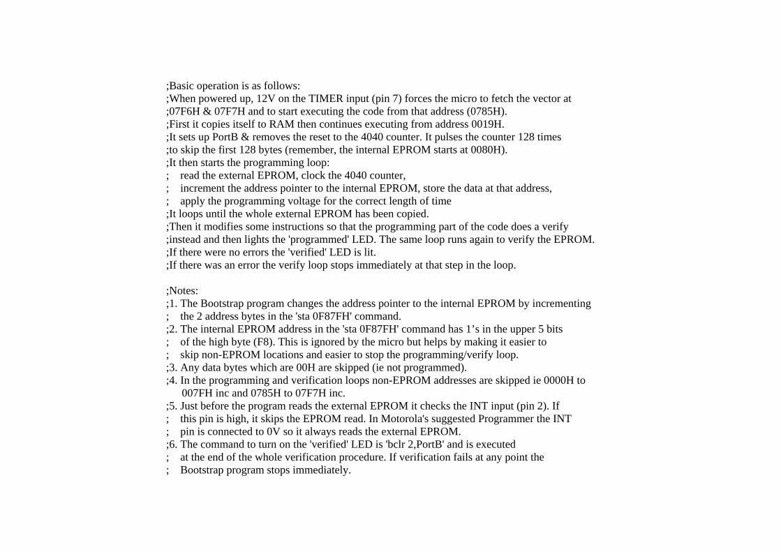
;Basic operation is as follows: ;When powered up, 12V on the TIMER input (pin 7) forces the micro to fetch the vector at ;07F6H & 07F7H and to start executing the code from that address (0785H). ;First it copies itself to RAM then continues executing from address 0019H. ;It sets up PortB & removes the reset to the 4040 counter. It pulses the counter 128 times ;to skip the first 128 bytes (remember, the internal EPROM starts at 0080H). ;It then starts the programming loop: ; read the external EPROM, clock the 4040 counter, ; increment the address pointer to the internal EPROM, store the data at that address, ; apply the programming voltage for the correct length of time ;It loops until the whole external EPROM has been copied. ;Then it modifies some instructions so that the programming part of the code does a verify ;instead and then lights the 'programmed' LED. The same loop runs again to verify the EPROM. ;If there were no errors the 'verified' LED is lit. ;If there was an error the verify loop stops immediately at that step in the loop.
;Notes: ;1. The Bootstrap program changes the address pointer to the internal EPROM by incrementing ; the 2 address bytes in the 'sta 0F87FH' command. ;2. The internal EPROM address in the 'sta 0F87FH' command has 1’s in the upper 5 bits ; of the high byte (F8). This is ignored by the micro but helps by making it easier to ; skip non-EPROM locations and easier to stop the programming/verify loop. ;3. Any data bytes which are 00H are skipped (ie not programmed). ;4. In the programming and verification loops non-EPROM addresses are skipped ie 0000H to
007FH inc and 0785H to 07F7H inc. ;5. Just before the program reads the external EPROM it checks the INT input (pin 2). If ; this pin is high, it skips the EPROM read. In Motorola's suggested Programmer the INT ; pin is connected to 0V so it always reads the external EPROM. ;6. The command to turn on the 'verified' LED is 'bclr 2,PortB' and is executed ; at the end of the whole verification procedure. If verification fails at any point the ; Bootstrap program stops immediately.
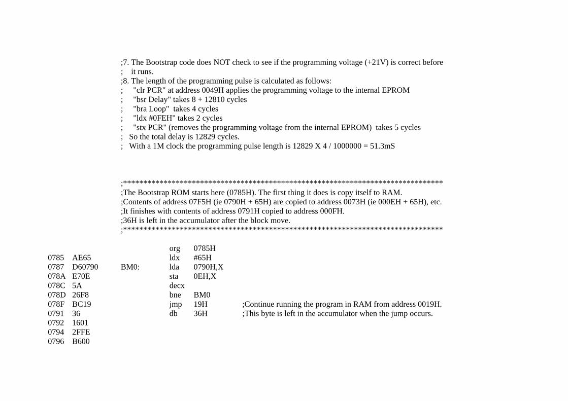
;7. The Bootstrap code does NOT check to see if the programming voltage (+21V) is correct before ; it runs. ;8. The length of the programming pulse is calculated as follows: ; "clr PCR" at address 0049H applies the programming voltage to the internal EPROM ; "bsr Delay" takes 8 + 12810 cycles ; "bra Loop" takes 4 cycles ; "ldx #0FEH" takes 2 cycles ; "stx PCR" (removes the programming voltage from the internal EPROM) takes 5 cycles ; So the total delay is 12829 cycles. ; With a 1M clock the programming pulse length is 12829 X 4 / 1000000 = 51.3mS
;******************************************************************************* ;The Bootstrap ROM starts here (0785H). The first thing it does is copy itself to RAM.
;Contents of address 07F5H (ie 0790H + 65H) are copied to address 0073H (ie 000EH + 65H), etc. ;It finishes with contents of address 0791H copied to address 000FH. ;36H is left in the accumulator after the block move. ;*******************************************************************************
org 0785H
0785 AE65 ldx #65H 0787 D60790 BM0: lda 0790H,X 078A E70E sta 0EH,X 078C 5A decx 078D 26F8 bne BM0 078F BC19 jmp 19H ;Continue running the program in RAM from address 0019H. 0791 36 db 36H ;This byte is left in the accumulator when the jump occurs. 0792 1601 0794 2FFE 0796 B600

0798 1701 079A 81 079B B701 079D A63F 079F B705 07A1 1901 07A3 ADED 07A5 5C 07A6 2AFB 07A8 AEFE 07AA BF0B 07AC 3C46 07AE 2604 07B0 3C45 07B2 271D 07B4 ADDC 07B6 BE45 07B8 A3FF 07BA 260A 07BC BE46 07BE A385 07C0 2504 07C2 A3F8 07C4 25E2 07C6 C7F87F 07C9 2704 07CB 3F0B 07CD AD1E 07CF 20D7 07D1 03010D 07D4 5F
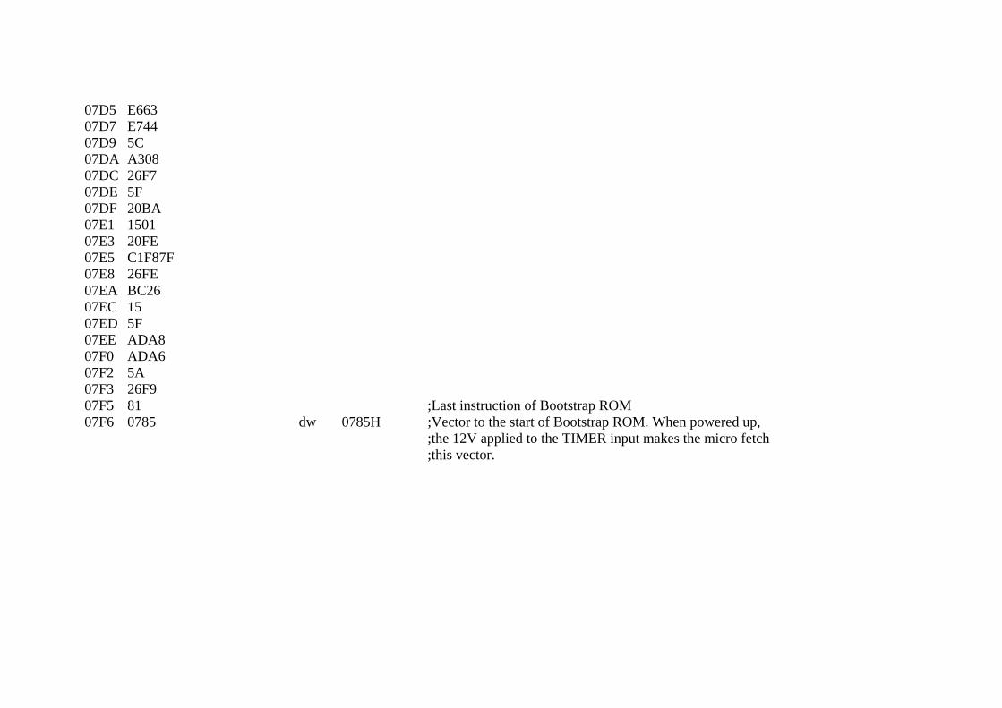
07D5 E663 07D7 E744 07D9 5C 07DA A308 07DC 26F7 07DE 5F 07DF 20BA 07E1 1501 07E3 20FE 07E5 C1F87F 07E8 26FE 07EA BC26 07EC 15 07ED 5F 07EE ADA8 07F0 ADA6 07F2 5A 07F3 26F9 07F5 81 ;Last instruction of Bootstrap ROM 07F6 0785 dw 0785H ;Vector to the start of Bootstrap ROM. When powered up,
;the 12V applied to the TIMER input makes the micro fetch ;this vector.
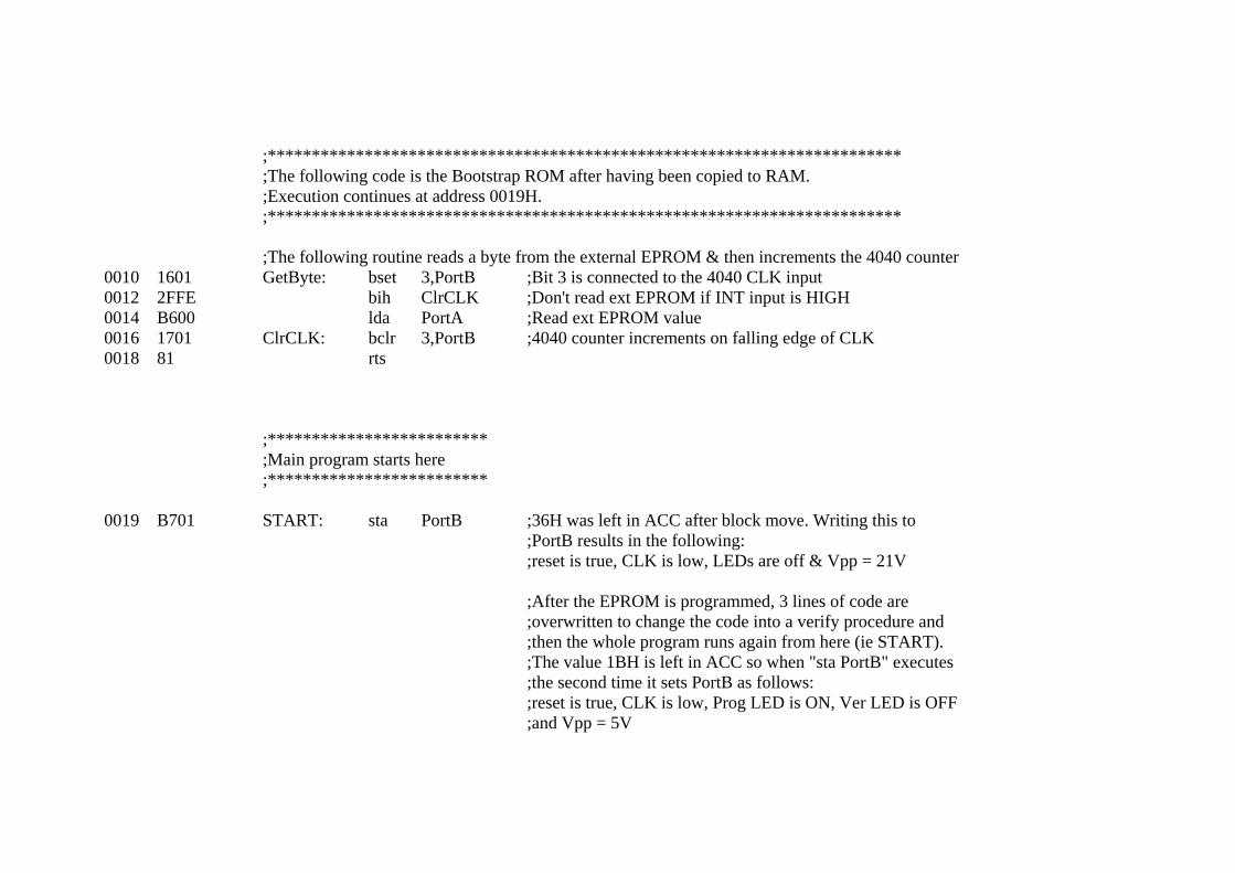
;************************************************************************ ;The following code is the Bootstrap ROM after having been copied to RAM. ;Execution continues at address 0019H. ;************************************************************************
;The following routine reads a byte from the external EPROM & then increments the 4040 counter
0010 1601 GetByte: bset 3,PortB ;Bit 3 is connected to the 4040 CLK input 0012 2FFE bih ClrCLK ;Don't read ext EPROM if INT input is HIGH 0014 B600 lda PortA ;Read ext EPROM value 0016 1701 ClrCLK: bclr 3,PortB ;4040 counter increments on falling edge of CLK 0018 81 rts
;************************* ;Main program starts here ;*************************
0019 B701 START: sta PortB ;36H was left in ACC after block move. Writing this to
;PortB results in the following: ;reset is true, CLK is low, LEDs are off & Vpp = 21V
;After the EPROM is programmed, 3 lines of code are ;overwritten to change the code into a verify procedure and ;then the whole program runs again from here (ie START). ;The value 1BH is left in ACC so when "sta PortB" executes ;the second time it sets PortB as follows: ;reset is true, CLK is low, Prog LED is ON, Ver LED is OFF ;and Vpp = 5V
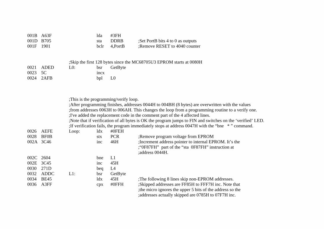
001B A63F lda #3FH 001D B705 sta DDRB ;Set PortB bits 4 to 0 as outputs 001F 1901 bclr 4,PortB ;Remove RESET to 4040 counter
;Skip the first 128 bytes since the MC68705U3 EPROM starts at 0080H 0021 ADED L0: bsr GetByte 0023 5C incx 0024 2AFB bpl L0
;This is the programming/verify loop. ;After programming finishes, addresses 0044H to 004BH (8 bytes) are overwritten with the values ;from addresses 0063H to 006AH. This changes the loop from a programming routine to a verify one. ;I've added the replacement code in the comment part of the 4 affected lines. ;Note that if verification of all bytes is OK the program jumps to FIN and switches on the ‘verified’ LED. ;If verification fails, the program immediately stops at address 0047H with the “bne * ” command.
0026 AEFE Loop: ldx #0FEH 0028 BF0B stx PCR ;Remove program voltage from EPROM 002A 3C46 inc 46H ;Increment address pointer to internal EPROM. It’s the ;“0F87FH” part of the “sta 0F87FH” instruction at ;address 0044H. 002C 2604 bne L1 002E 3C45 inc 45H 0030 271D beq L4 0032 ADDC L1: bsr GetByte 0034 BE45 ldx 45H ;The following 8 lines skip non-EPROM addresses. 0036 A3FF cpx #0FFH ;Skipped addresses are FF85H to FFF7H inc. Note that ;the micro ignores the upper 5 bits of the address so the ;addresses actually skipped are 0785H to 07F7H inc.
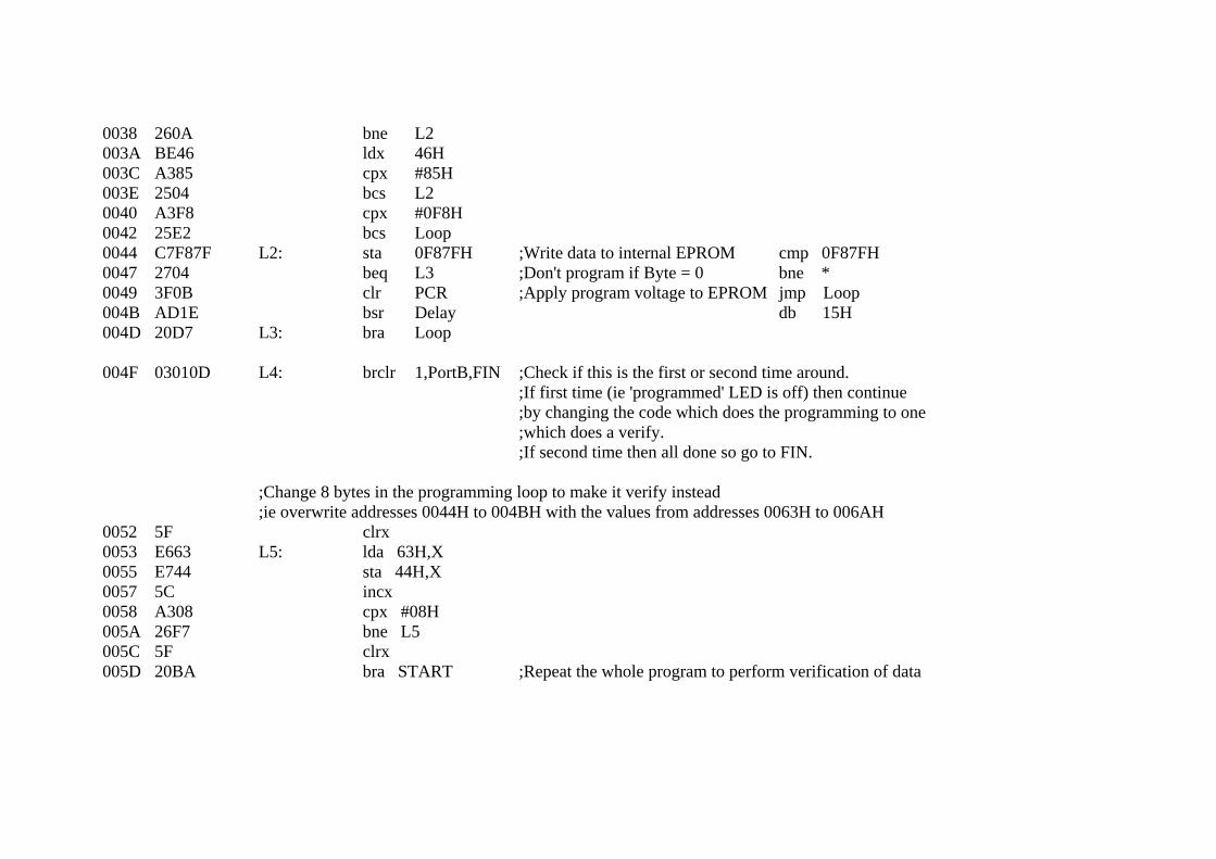
0038 260A bne L2 003A BE46 ldx 46H 003C A385 cpx #85H 003E 2504 bcs L2 0040 A3F8 cpx #0F8H 0042 25E2 bcs Loop 0044 C7F87F L2: sta 0F87FH ;Write data to internal EPROM cmp 0F87FH 0047 2704 beq L3 ;Don't program if Byte = 0 bne * 0049 3F0B clr PCR ;Apply program voltage to EPROM jmp Loop 004B AD1E bsr Delay db 15H 004D 20D7 L3: bra Loop 004F 03010D L4: brclr 1,PortB,FIN ;Check if this is the first or second time around.
;If first time (ie 'programmed' LED is off) then continue ;by changing the code which does the programming to one ;which does a verify. ;If second time then all done so go to FIN.
;Change 8 bytes in the programming loop to make it verify instead ;ie overwrite addresses 0044H to 004BH with the values from addresses 0063H to 006AH
0052 5F clrx 0053 E663 L5: lda 63H,X 0055 E744 sta 44H,X 0057 5C incx 0058 A308 cpx #08H 005A 26F7 bne L5 005C 5F clrx 005D 20BA bra START ;Repeat the whole program to perform verification of data
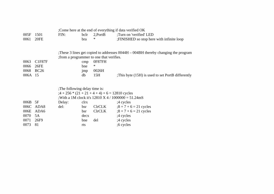
;Come here at the end of everything if data verified OK 005F 1501 FIN: bclr 2,PortB ;Turn on 'verified' LED 0061 20FE bra * ;FINISHED so stop here with infinite loop
;These 3 lines get copied to addresses 0044H – 004BH thereby changing the program ;from a programmer to one that verifies.
0063 C1F87F cmp 0F87FH 0066 26FE bne * 0068 BC26 jmp 0026H 006A 15 db 15H ;This byte (15H) is used to set PortB differently
;The following delay time is: ;4 + 256 * (21 + 21 + 4 + 4) + 6 = 12810 cycles ;With a 1M clock it's 12810 X 4 / 1000000 = 51.24mS
006B 5F Delay: clrx ;4 cycles 006C ADA8 del: bsr ClrCLK ;8 + 7 + 6 = 21 cycles 006E ADA6 bsr ClrCLK ;8 + 7 + 6 = 21 cycles 0070 5A decx ;4 cycles 0071 26F9 bne del ;4 cycles 0073 81 rts ;6 cycles


![[BOOK] [Bootstrap] [Awesome] Bootstrap-Programming-Cookbook](https://img.pdfslide.us/doc/110x75/577ca6bf1a28abea748c023f/book-bootstrap-awesome-bootstrap-programming-cookbook.jpg)