Embed Size (px)
Citation preview
ASH WARE, Inc.
by
Version 2.60
8/24/2018
(C) 2012 ASH WARE, Inc.
MC33816 Assembler
John Diener and Andy Klumpp
Reference Manual

MC33816 Assembler, page 3 (C) 2012 ASH WARE, Inc. ASH WARE, Inc.
MC33816 Assembler
Table of Contents
ASH WARE, Inc. Friday, August 24, 2018
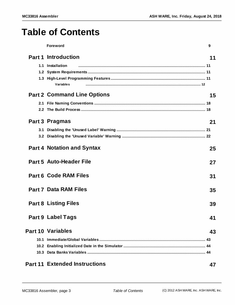
Table of Contents
Foreword 9
Part 1 Introduction 11
.............................................................................................................. 111.1 Installation
.............................................................................................................. 111.2 System Requirements
.............................................................................................................. 111.3 High-Level Programming Features
..................................................................................................................................... 12Variables
Part 2 Command Line Options 15
.............................................................................................................. 182.1 File Naming Conventions
.............................................................................................................. 182.2 The Build Process
Part 3 Pragmas 21
.............................................................................................................. 213.1 Disabling the 'Unused Label' Warning
.............................................................................................................. 223.2 Disabling the 'Unused Variable' Warning
Part 4 Notation and Syntax 25
Part 5 Auto-Header File 27
Part 6 Code RAM Files 31
Part 7 Data RAM Files 35
Part 8 Listing Files 39
Part 9 Label Tags 41
Part 10 Variables 43
.............................................................................................................. 4310.1 Immediate/Global Variables
.............................................................................................................. 4410.2 Enabling Initialized Date in the Simulator
.............................................................................................................. 4410.3 Data Banks Variables
Part 11 Extended Instructions 47
MC33816 Assembler, page 4 (C) 2012 ASH WARE, Inc. ASH WARE, Inc.
MC33816 Assembler
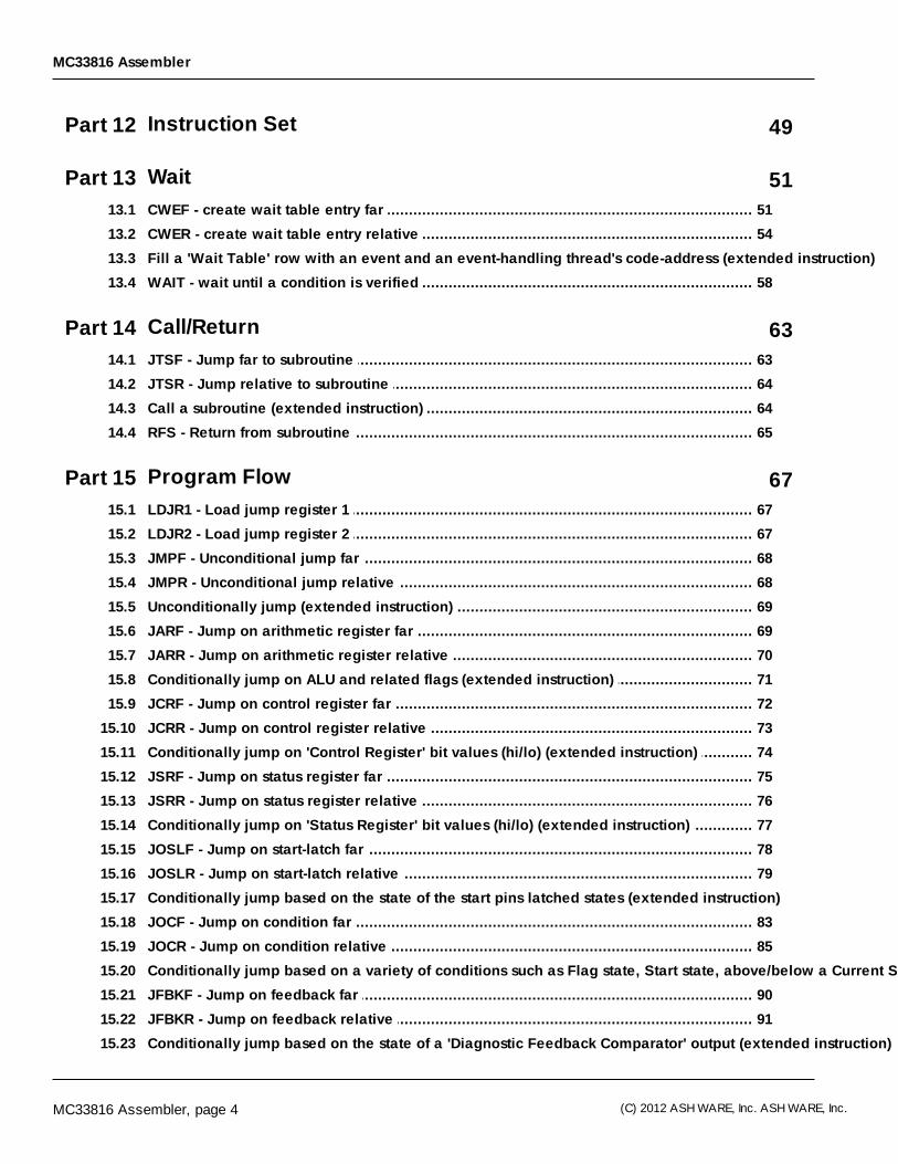
Part 12 Instruction Set 49
Part 13 Wait 51
.............................................................................................................. 5113.1 CWEF - create wait table entry far
.............................................................................................................. 5413.2 CWER - create wait table entry relative
.............................................................................................................. 5613.3 Fill a 'Wait Table' row with an event and an event-handling thread's code-address (extended instruction)
.............................................................................................................. 5813.4 WAIT - wait until a condition is verified
Part 14 Call/Return 63
.............................................................................................................. 6314.1 JTSF - Jump far to subroutine
.............................................................................................................. 6414.2 JTSR - Jump relative to subroutine
.............................................................................................................. 6414.3 Call a subroutine (extended instruction)
.............................................................................................................. 6514.4 RFS - Return from subroutine
Part 15 Program Flow 67
.............................................................................................................. 6715.1 LDJR1 - Load jump register 1
.............................................................................................................. 6715.2 LDJR2 - Load jump register 2
.............................................................................................................. 6815.3 JMPF - Unconditional jump far
.............................................................................................................. 6815.4 JMPR - Unconditional jump relative
.............................................................................................................. 6915.5 Unconditionally jump (extended instruction)
.............................................................................................................. 6915.6 JARF - Jump on arithmetic register far
.............................................................................................................. 7015.7 JARR - Jump on arithmetic register relative
.............................................................................................................. 7115.8 Conditionally jump on ALU and related flags (extended instruction)
.............................................................................................................. 7215.9 JCRF - Jump on control register far
.............................................................................................................. 7315.10 JCRR - Jump on control register relative
.............................................................................................................. 7415.11 Conditionally jump on 'Control Register' bit values (hi/lo) (extended instruction)
.............................................................................................................. 7515.12 JSRF - Jump on status register far
.............................................................................................................. 7615.13 JSRR - Jump on status register relative
.............................................................................................................. 7715.14 Conditionally jump on 'Status Register' bit values (hi/lo) (extended instruction)
.............................................................................................................. 7815.15 JOSLF - Jump on start-latch far
.............................................................................................................. 7915.16 JOSLR - Jump on start-latch relative
.............................................................................................................. 8115.17 Conditionally jump based on the state of the start pins latched states (extended instruction)
.............................................................................................................. 8315.18 JOCF - Jump on condition far
.............................................................................................................. 8515.19 JOCR - Jump on condition relative
.............................................................................................................. 8815.20 Conditionally jump based on a variety of conditions such as Flag state, Start state, above/below a Current Sense Threshold, ... (extended instruction)
.............................................................................................................. 9015.21 JFBKF - Jump on feedback far
.............................................................................................................. 9115.22 JFBKR - Jump on feedback relative
.............................................................................................................. 9215.23 Conditionally jump based on the state of a 'Diagnostic Feedback Comparator' output (extended instruction)
MC33816 Assembler, page 5 (C) 2012 ASH WARE, Inc. ASH WARE, Inc.
MC33816 Assembler
Table of Contents
ASH WARE, Inc. Friday, August 24, 2018
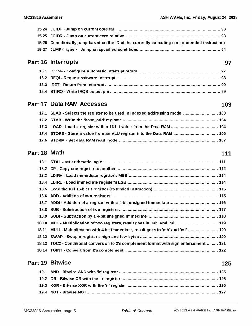
.............................................................................................................. 9315.24 JOIDF - Jump on current core far
.............................................................................................................. 9315.25 JOIDR - Jump on current core relative
.............................................................................................................. 9415.26 Conditionally jump based on the ID of the currently-executing core (extended instruction)
.............................................................................................................. 9415.27 JUMP<_type> - Jump on specified conditions
Part 16 Interrupts 97
.............................................................................................................. 9716.1 ICONF - Configure automatic interrupt return
.............................................................................................................. 9816.2 REQI - Request software interrupt
.............................................................................................................. 9916.3 IRET - Return from interrupt
.............................................................................................................. 9916.4 STIRQ - Write IRQB output pin
Part 17 Data RAM Accesses 103
.............................................................................................................. 10317.1 SLAB - Selects the register to be used in Indexed addressing mode
.............................................................................................................. 10417.2 STAB - Write the 'base_add' register
.............................................................................................................. 10417.3 LOAD - Load a register with a 16-bit value from the Data RAM
.............................................................................................................. 10617.4 STORE - Store a value from an ALU register into the Data RAM
.............................................................................................................. 10717.5 STDRM - Set data RAM read mode
Part 18 Math 111
.............................................................................................................. 11118.1 STAL - set arithmetic logic
.............................................................................................................. 11218.2 CP - Copy one register to another
.............................................................................................................. 11418.3 LDIRH - Load immediate register's MSB
.............................................................................................................. 11418.4 LDIRL - Load immediate register's LSB
.............................................................................................................. 11518.5 Load the full 16-bit IR register (extended instruction)
.............................................................................................................. 11518.6 ADD - Addition of two registers
.............................................................................................................. 11618.7 ADDI - Addition of a register with a 4-bit unsigned immediate
.............................................................................................................. 11718.8 SUB - Substraction of two registers
.............................................................................................................. 11818.9 SUBI - Subtraction by a 4-bit unsigned immediate
.............................................................................................................. 11918.10 MUL - Multiplication of two registers, result goes in 'mh' and 'ml'
.............................................................................................................. 12018.11 MULI - Multiplication with 4-bit immediate, result goes in 'mh' and 'ml'
.............................................................................................................. 12018.12 SWAP - Swap a register's high and low bytes
.............................................................................................................. 12118.13 TOC2 - Conditional conversion to 2's complement format with sign enforcement
.............................................................................................................. 12218.14 TOINT - Convert from 2's complement
Part 19 Bitwise 125
.............................................................................................................. 12519.1 AND - Bitwise AND with 'ir' register
.............................................................................................................. 12619.2 OR - Bitwise OR with the 'ir' register
.............................................................................................................. 12619.3 XOR - Bitwise XOR with the 'ir' register
.............................................................................................................. 12719.4 NOT - Bitwise NOT
MC33816 Assembler, page 6 (C) 2012 ASH WARE, Inc. ASH WARE, Inc.
MC33816 Assembler
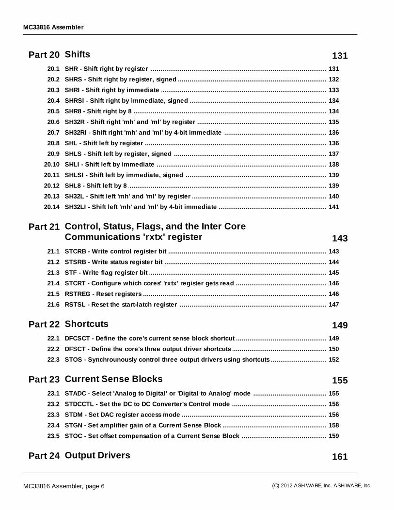
Part 20 Shifts 131
.............................................................................................................. 13120.1 SHR - Shift right by register
.............................................................................................................. 13220.2 SHRS - Shift right by register, signed
.............................................................................................................. 13320.3 SHRI - Shift right by immediate
.............................................................................................................. 13420.4 SHRSI - Shift right by immediate, signed
.............................................................................................................. 13420.5 SHR8 - Shift right by 8
.............................................................................................................. 13520.6 SH32R - Shift right 'mh' and 'ml' by register
.............................................................................................................. 13620.7 SH32RI - Shift right 'mh' and 'ml' by 4-bit immediate
.............................................................................................................. 13620.8 SHL - Shift left by register
.............................................................................................................. 13720.9 SHLS - Shift left by register, signed
.............................................................................................................. 13820.10 SHLI - Shift left by immediate
.............................................................................................................. 13920.11 SHLSI - Shift left by immediate, signed
.............................................................................................................. 13920.12 SHL8 - Shift left by 8
.............................................................................................................. 14020.13 SH32L - Shift left 'mh' and 'ml' by register
.............................................................................................................. 14120.14 SH32LI - Shift left 'mh' and 'ml' by 4-bit immediate
Part 21 Control, Status, Flags, and the Inter CoreCommunications 'rxtx' register 143
.............................................................................................................. 14321.1 STCRB - Write control register bit
.............................................................................................................. 14421.2 STSRB - Write status register bit
.............................................................................................................. 14521.3 STF - Write flag register bit
.............................................................................................................. 14621.4 STCRT - Configure which cores' 'rxtx' register gets read
.............................................................................................................. 14621.5 RSTREG - Reset registers
.............................................................................................................. 14721.6 RSTSL - Reset the start-latch register
Part 22 Shortcuts 149
.............................................................................................................. 14922.1 DFCSCT - Define the core's current sense block shortcut
.............................................................................................................. 15022.2 DFSCT - Define the core's three output driver shortcuts
.............................................................................................................. 15222.3 STOS - Synchrounously control three output drivers using shortcuts
Part 23 Current Sense Blocks 155
.............................................................................................................. 15523.1 STADC - Select 'Analog to Digital' or 'Digital to Analog' mode
.............................................................................................................. 15623.2 STDCCTL - Set the DC to DC Converter's Control mode
.............................................................................................................. 15623.3 STDM - Set DAC register access mode
.............................................................................................................. 15823.4 STGN - Set amplifier gain of a Current Sense Block
.............................................................................................................. 15923.5 STOC - Set offset compensation of a Current Sense Block
Part 24 Output Drivers 161
MC33816 Assembler, page 7 (C) 2012 ASH WARE, Inc. ASH WARE, Inc.
MC33816 Assembler
Table of Contents
ASH WARE, Inc. Friday, August 24, 2018
.............................................................................................................. 16124.1 BIAS - Set load current bias
.............................................................................................................. 16224.2 STEOA - Set end of actuation mode
.............................................................................................................. 16324.3 STFW - Set freewheeling mode between a pair of output drivers
.............................................................................................................. 16424.4 STO - Set one output driver
.............................................................................................................. 16424.5 STSLEW - Set output drivers' slew rates
Part 25 Diagnostics 167
.............................................................................................................. 16725.1 CHTH - Change diagnostic comparator's threshold
.............................................................................................................. 16825.2 ENDIAG - Enable or disable output driver diagnostics, ONE
.............................................................................................................. 16925.3 ENDIAGA - Enable or disable output driver diagnostics, ALL
.............................................................................................................. 17025.4 ENDIAGS - Enable or disable output driver diagnostics, SHORTCUTS
.............................................................................................................. 17125.5 SLFBK - Select the power source to monitor for Vds Diagnostics
Part 26 Timers 173
.............................................................................................................. 17326.1 LDCA - Load a counter's 'Terminal Count' from a register and write two output drivers
.............................................................................................................. 17426.2 LDCD - Load a counter's 'Terminal Count' from data RAM and write two output Drivers
Part 27 SPI Backdoor 179
.............................................................................................................. 17927.1 SLSA - SPI backdoor set address register
.............................................................................................................. 18027.2 RDSPI - SPI backdoor read
.............................................................................................................. 18027.3 WRSPI - SPI Backdoor write

MC33816 Assembler, page 9 (C) 2012 ASH WARE, Inc. ASH WARE, Inc.MC33816 Assembler, page 9
MC33816 Assembler

MC33816 Assembler, page 10 (C) 2012 ASH WARE, Inc. ASH WARE, Inc.
Introduction
Part
I
MC33816 Assembler, page 11 (C) 2012 ASH WARE, Inc. ASH WARE, Inc.
1. Introduction
ASH WARE, Inc. 8/24/2018
1Introduction
The ASH WARE MC33816 Assembler supports NXP's MC33816 device. The MC33816 Assembler is acommand line tool so it can be invoked from a Windows console window. The MC33816 Assembler isalso designed to support integrated builds from within DevTool as well as being called as part of DevTool'sintegrated graphical state machine.
1.1 Installation
The MC33816 assembler is installed as an integrated part of DevTool. The environment variable shownbelow can be used to locate the last-installed version.
DEV_TOOL_MC33816_BIN
In the following example the assembler 'help' is envoked.
%DEV_TOOL_MC33816_BIN%asm816.exe -h
1.2 System Requirements
The MC33816 assembler is a command line tool that runs under in any Windows operating system such asWindows XP, Windows 7, or Windows 8.
1.3 High-Level Programming Features
The ASH WARE %PRODUCT%> has several features above and beyond the basic assemblerfunctionality that ease the development process.
auto-generation of a header file for inclusion in the host processor code, that simplifies initialization andinteraction with the MC33816.
variable declarations that provide enhanced address space checking at build-time, and a better debugexperience at run-time. Additionally the variables are auto-located at ideal addresses with all locationinformation output into the auto-generated header file.
MC33816 Assembler, page 12 (C) 2012 ASH WARE, Inc. ASH WARE, Inc.
1. Introduction
High-Level Programming Features
instruction extensions provide a concise method of building a series of instruction that, in many cases,can be more efficiently generated by the assembler. For instance, a function call extension can be usedin which the assembler chooses either a far, or the more effecient relative jump instruction based on theactual distance from the caller to the called function.
1.3.1 Variables
Symbolic variables can be used to allocate and specify data locations in the MC33816 Data RAM. Thesymbolic declarations allow the assembler to auto-locate data items and output their location information inthe auto-header for proper host/simulator access. Using the variable symbols in the load/store/ldcdinstructions in user assembly make the code more readable and ensure that the proper address space isaccessed by the instruction. The MC33816 architecture supports two address space types : immediate/global space, and indexed/banked space. Multiple "data banks" can declared and used via indexedaddressing, as the base address of this space can be changed on the fly.
See the Immediate/Global Variables section for a description on how to declare and use global variables.
See the Auto-Header section for an example of the macros that are output for data addresses for use inhost code and simulator scripts. Note that due to the auto-locating capabilities of assembler, if usingvariables then all data locations should be declared using variables as otherwise there is the possibility ofconflict between auto-located data and user-located data. The auto-locating algorithm is described in the Data Banks section.
MC33816 Assembler, page 13 (C) 2012 ASH WARE, Inc. ASH WARE, Inc.
Command Line Options
Part
II

MC33816 Assembler, page 15 (C) 2012 ASH WARE, Inc. ASH WARE, Inc.
2. Command Line Options
ASH WARE, Inc. 8/24/2018
2Command Line Options
Type the executable name with the -h command line parameter to generate a list of the available options.
Asm816.exe –h
The assembler is called Asm816.exe, and it has the following format:
Asm816.exe <options> <AssemblyFile>
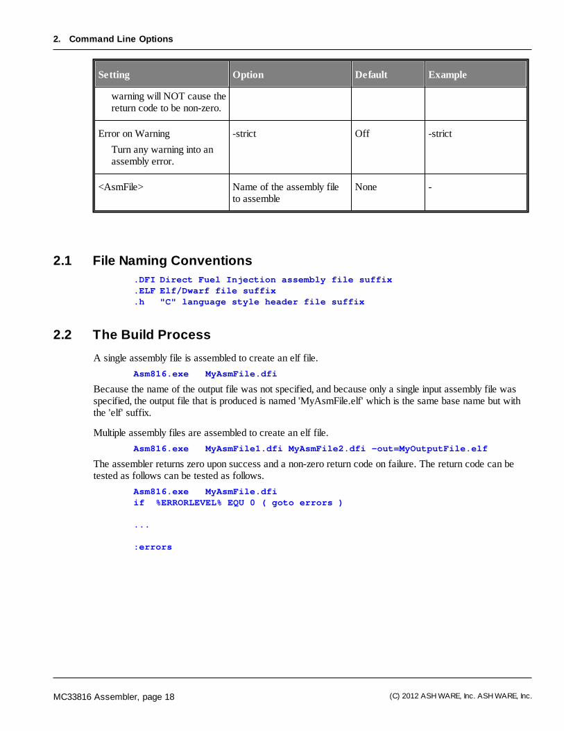
The following table is a complete listing of all supported command line options.
Setting Option Default Example
Display Help
This option overrides allothers and when it exists noassembly is actually done.
-h Off -h
Open Manual
Opens the electronicversion of this AssemblerReference Manual.
-man Off -man
Display Version
Displays the tool name andversion number and exitswith a non-zero exit codewithout assembling.
-version Off -version
Console Message Verbosity
Control the verbosity of themessage output.
-verb=<N>
where N can be in the rangeof 0 (no console output) to 9(verbose message output).
5 -verb=9
MC33816 Assembler, page 16 (C) 2012 ASH WARE, Inc. ASH WARE, Inc.
2. Command Line Options
Setting Option Default Example
Cipher File
Controls which file is usedto generate the cipheredbinary file.
-key=<FileName>
Filename is the name of thecipher file.
none -key=CipherDir\Key4.key
Global Mnemonic
The specified mnemonicgets pre-pended to allnames in the auto-generatedheader file and executableimage array C file. This isuseful when multiple imagesare to be used at host loadtime, thereby avoidingnaming conflicts.
-GM=<Text> -GM=_FS_
Source File Search Paths
Specifies any directories,after the current one, to besearched for included files. Multiple paths can bespecified and they aresearched in the order oftheir appearance in thecommand line.
-I=<PATH>
where PATH is a text stringrepresenting either a relativeor absolute directory path. The entire option must be inquotes if the path containsspaces.
None
-I=..\Include
Disable a specific warning -warnDis=<ID> where IDis the warning'sidentification number.
Off -WarnDis=41065
Console Message Suppression
Suppress console messagesby their type/class. Multipletypes can be specified withmultiple –verbSuppressoptions.
-verbSuppress=<TYPE>
where TYPE can be:
BANNER : the ETECversion & copyrightbanner.
SUMMARY : thesuccess/failure warning/error count summary line
WARNING : all warningmessages
INFO: all info messages
ERROR : all error
Off -verbSuppress=SUMMARY
MC33816 Assembler, page 17 (C) 2012 ASH WARE, Inc. ASH WARE, Inc.
2. Command Line Options
ASH WARE, Inc. 8/24/2018
Setting Option Default Example
messages (does notaffect the tool exit code)
Console Message Style
Controls the style of theerror/warning outputmessages, primarily forintegration with IDEs
-msgStyle=<STYLE>
where STYLE can be:
- ETEC : default ETECmessage style.
- GNU : output messages inGNU-style. This allowsthe default error parsersof tools such as Eclipse toparse ETEC output andallow users to click on anerror message and go tothe offending source line.
- DIAB : output messagesin the style used by Diab(WindRiver) compilers.
- MSDV : output inMicrosoft DeveloperStudio format so thatwhen using the DevStudioIDE errors/warnings canbe clicked on to bringfocus to the problemsource code line.
ETEC -msgStyle=MSDV
Console Message Path Style
Controls how the path andfilename are displayed onany warning/error messagesthat contain filenameinformation.
-msgPath=<STYLE>
where STYLE can be:
- ASIS : output the filenameas it is input on thecommand line (or foundvia #include or search).
- ABS : output the filenamewith its full absolute path.
ASIS -msgPath=ABS
Warning Disable
Disable a specific assemblywarning via its numericalidentifier. Note that if awarning is disabled and the-strict option is set, then the
-warnDis=<WARNID> Off (allwarningsenabled)
-warnDis=33243
MC33816 Assembler, page 18 (C) 2012 ASH WARE, Inc. ASH WARE, Inc.
2. Command Line Options
Setting Option Default Example
warning will NOT cause thereturn code to be non-zero.
Error on Warning
Turn any warning into anassembly error.
-strict Off -strict
<AsmFile> Name of the assembly fileto assemble
None -
2.1 File Naming Conventions
.DFI Direct Fuel Injection assembly file suffix
.ELF Elf/Dwarf file suffix
.h "C" language style header file suffix
2.2 The Build Process
A single assembly file is assembled to create an elf file.
Asm816.exe MyAsmFile.dfi
Because the name of the output file was not specified, and because only a single input assembly file wasspecified, the output file that is produced is named 'MyAsmFile.elf' which is the same base name but withthe 'elf' suffix.
Multiple assembly files are assembled to create an elf file.
Asm816.exe MyAsmFile1.dfi MyAsmFile2.dfi -out=MyOutputFile.elf
The assembler returns zero upon success and a non-zero return code on failure. The return code can betested as follows can be tested as follows.
Asm816.exe MyAsmFile.dfiif %ERRORLEVEL% EQU 0 ( goto errors )
...
:errors

MC33816 Assembler, page 19 (C) 2012 ASH WARE, Inc. ASH WARE, Inc.
Pragmas
Part
III

MC33816 Assembler, page 21 (C) 2012 ASH WARE, Inc. ASH WARE, Inc.
3. Pragmas
ASH WARE, Inc. 8/24/2018
3Pragmas
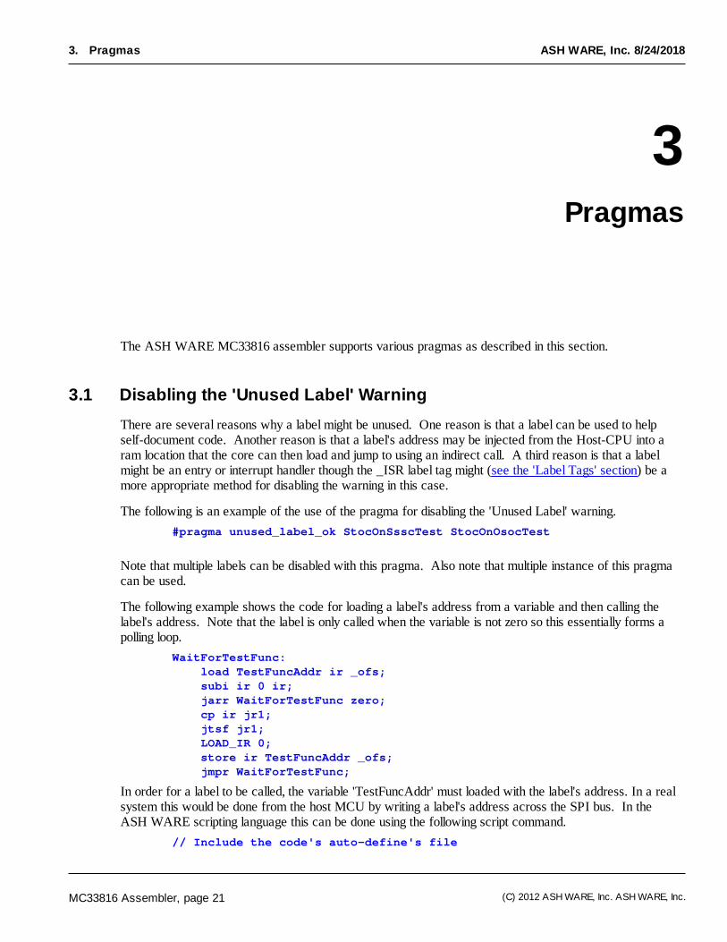
The ASH WARE MC33816 assembler supports various pragmas as described in this section.
3.1 Disabling the 'Unused Label' Warning
There are several reasons why a label might be unused. One reason is that a label can be used to helpself-document code. Another reason is that a label's address may be injected from the Host-CPU into aram location that the core can then load and jump to using an indirect call. A third reason is that a labelmight be an entry or interrupt handler though the _ISR label tag might (see the 'Label Tags' section) be amore appropriate method for disabling the warning in this case.
The following is an example of the use of the pragma for disabling the 'Unused Label' warning.
#pragma unused_label_ok StocOnSsscTest StocOnOsocTest
Note that multiple labels can be disabled with this pragma. Also note that multiple instance of this pragmacan be used.
The following example shows the code for loading a label's address from a variable and then calling thelabel's address. Note that the label is only called when the variable is not zero so this essentially forms apolling loop.
WaitForTestFunc: load TestFuncAddr ir _ofs; subi ir 0 ir; jarr WaitForTestFunc zero; cp ir jr1; jtsf jr1; LOAD_IR 0; store ir TestFuncAddr _ofs; jmpr WaitForTestFunc;
In order for a label to be called, the variable 'TestFuncAddr' must loaded with the label's address. In a realsystem this would be done from the host MCU by writing a label's address across the SPI bus. In theASH WARE scripting language this can be done using the following script command.
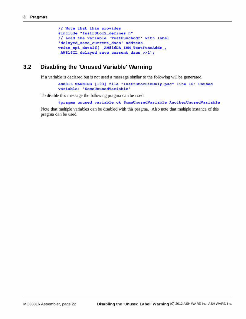
// Include the code's auto-define's file
MC33816 Assembler, page 22 (C) 2012 ASH WARE, Inc. ASH WARE, Inc.
3. Pragmas
Disabling the 'Unused Label' Warning
// Note that this provides #include "InstrStoc2_defines.h"// Load the variable 'TestFuncAddr' with label'delayed_save_current_dacs' address.write_spi_data16( _AW816DA_IMM_TestFuncAddr_,_AW816CL_delayed_save_current_dacs_>>1);
3.2 Disabling the 'Unused Variable' Warning
If a variable is declared but is not used a message similar to the following will be generated.
Asm816 WARNING [193] file "InstrStocSimOnly.psc" line 10: Unusedvariable: 'SomeUnusedVariable'
To disable this message the following pragma can be used.
#pragma unused_variable_ok SomeUnusedVariable AnotherUnusedVariable
Note that multiple variables can be disabled with this pragma. Also note that multiple instance of thispragma can be used.
MC33816 Assembler, page 23 (C) 2012 ASH WARE, Inc. ASH WARE, Inc.
Notation and Syntax
Part
IV

MC33816 Assembler, page 25 (C) 2012 ASH WARE, Inc. ASH WARE, Inc.
4. Notation and Syntax
ASH WARE, Inc. 8/24/2018
4Notation and Syntax
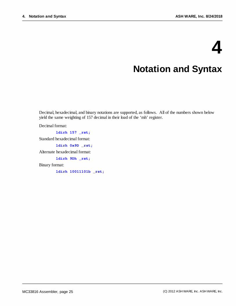
Decimal, hexadecimal, and binary notations are supported, as follows. All of the numbers shown belowyield the same weighting of 157 decimal in their load of the ‘mh’ register.
Decimal format:
ldirh 157 _rst;
Standard hexadecimal format:
ldirh 0x9D _rst;
Alternate hexadecimal format:
ldirh 9Dh _rst;
Binary format:
ldirh 10011101b _rst;

MC33816 Assembler, page 26 (C) 2012 ASH WARE, Inc. ASH WARE, Inc.
Auto-Header File
Part
V
MC33816 Assembler, page 27 (C) 2012 ASH WARE, Inc. ASH WARE, Inc.
5. Auto-Header File
ASH WARE, Inc. 8/24/2018
5Auto-Header File
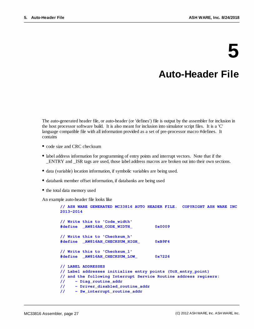
The auto-generated header file, or auto-header (or 'defines') file is output by the assembler for inclusion inthe host processor software build. It is also meant for inclusion into simulator script files. It is a 'C'language compatible file with all information provided as a set of pre-processor macro #defines. Itcontains
code size and CRC checksum
label address information for programming of entry points and interrupt vectors. Note that if the_ENTRY and _ISR tags are used, those label address macros are broken out into their own sections.
data (variable) location information, if symbolic variables are being used.
databank member offset information, if databanks are being used
the total data memory used
An example auto-header file looks like
// ASH WARE GENERATED MC33816 AUTO HEADER FILE. COPYRIGHT ASH WARE INC2013-2014
// Write this to 'Code_width'#define _AW816AH_CODE_WIDTH_ 0x0009
// Write this to 'Checksum_h'#define _AW816AH_CHECKSUM_HIGH_ 0xB9F4
// Write this to 'Checksum_l'#define _AW816AH_CHECKSUM_LOW_ 0x7226
// LABEL ADDRESSES// Label addresses initialize entry points (UcX_entry_point)// and the following Interrupt Service Routine address regisers:// - Diag_routine_addr// - Driver_disabled_routine_addr// - Sw_interrupt_routine_addr
MC33816 Assembler, page 28 (C) 2012 ASH WARE, Inc. ASH WARE, Inc.
5. Auto-Header File
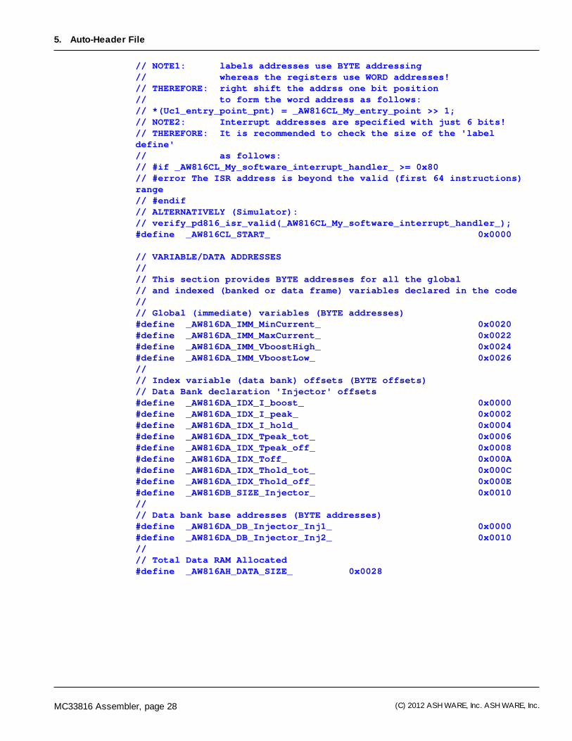
// NOTE1: labels addresses use BYTE addressing// whereas the registers use WORD addresses!// THEREFORE: right shift the addrss one bit position// to form the word address as follows:// *(Uc1_entry_point_pnt) = _AW816CL_My_entry_point >> 1;// NOTE2: Interrupt addresses are specified with just 6 bits!// THEREFORE: It is recommended to check the size of the 'labeldefine'// as follows:// #if _AW816CL_My_software_interrupt_handler_ >= 0x80// #error The ISR address is beyond the valid (first 64 instructions)range// #endif// ALTERNATIVELY (Simulator):// verify_pd816_isr_valid(_AW816CL_My_software_interrupt_handler_);#define _AW816CL_START_ 0x0000
// VARIABLE/DATA ADDRESSES//// This section provides BYTE addresses for all the global// and indexed (banked or data frame) variables declared in the code//// Global (immediate) variables (BYTE addresses)#define _AW816DA_IMM_MinCurrent_ 0x0020#define _AW816DA_IMM_MaxCurrent_ 0x0022#define _AW816DA_IMM_VboostHigh_ 0x0024#define _AW816DA_IMM_VboostLow_ 0x0026//// Index variable (data bank) offsets (BYTE offsets)// Data Bank declaration 'Injector' offsets#define _AW816DA_IDX_I_boost_ 0x0000#define _AW816DA_IDX_I_peak_ 0x0002#define _AW816DA_IDX_I_hold_ 0x0004#define _AW816DA_IDX_Tpeak_tot_ 0x0006#define _AW816DA_IDX_Tpeak_off_ 0x0008#define _AW816DA_IDX_Toff_ 0x000A#define _AW816DA_IDX_Thold_tot_ 0x000C#define _AW816DA_IDX_Thold_off_ 0x000E#define _AW816DB_SIZE_Injector_ 0x0010//// Data bank base addresses (BYTE addresses)#define _AW816DA_DB_Injector_Inj1_ 0x0000#define _AW816DA_DB_Injector_Inj2_ 0x0010//// Total Data RAM Allocated#define _AW816AH_DATA_SIZE_ 0x0028

MC33816 Assembler, page 29 (C) 2012 ASH WARE, Inc. ASH WARE, Inc.
Code RAM Files
Part
VI

MC33816 Assembler, page 31 (C) 2012 ASH WARE, Inc. ASH WARE, Inc.
6. Code RAM Files
ASH WARE, Inc. 8/24/2018
6Code RAM Files
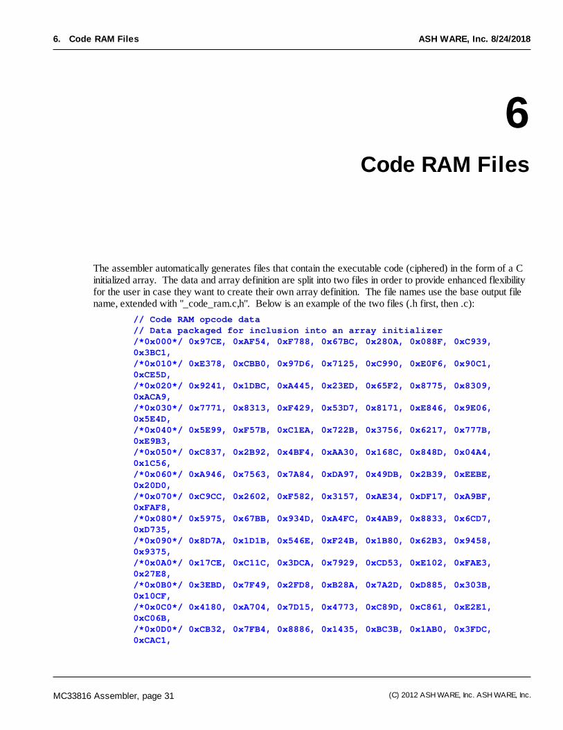
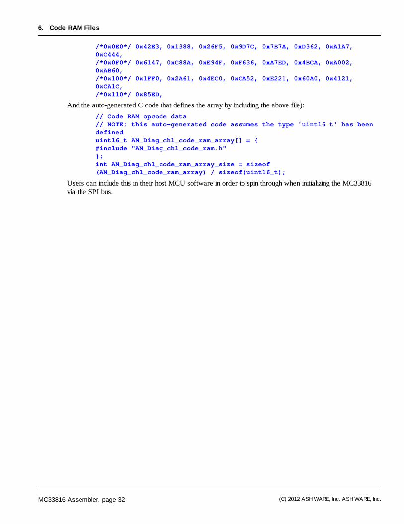
The assembler automatically generates files that contain the executable code (ciphered) in the form of a Cinitialized array. The data and array definition are split into two files in order to provide enhanced flexibilityfor the user in case they want to create their own array definition. The file names use the base output filename, extended with "_code_ram.c,h". Below is an example of the two files (.h first, then .c):
// Code RAM opcode data// Data packaged for inclusion into an array initializer/*0x000*/ 0x97CE, 0xAF54, 0xF788, 0x67BC, 0x280A, 0x088F, 0xC939,0x3BC1, /*0x010*/ 0xE378, 0xCBB0, 0x97D6, 0x7125, 0xC990, 0xE0F6, 0x90C1,0xCE5D, /*0x020*/ 0x9241, 0x1DBC, 0xA445, 0x23ED, 0x65F2, 0x8775, 0x8309,0xACA9, /*0x030*/ 0x7771, 0x8313, 0xF429, 0x53D7, 0x8171, 0xE846, 0x9E06,0x5E4D, /*0x040*/ 0x5E99, 0xF57B, 0xC1EA, 0x722B, 0x3756, 0x6217, 0x777B,0xE9B3, /*0x050*/ 0xC837, 0x2B92, 0x4BF4, 0xAA30, 0x168C, 0x848D, 0x04A4,0x1C56, /*0x060*/ 0xA946, 0x7563, 0x7A84, 0xDA97, 0x49DB, 0x2B39, 0xEEBE,0x20D0, /*0x070*/ 0xC9CC, 0x2602, 0xF582, 0x3157, 0xAE34, 0xDF17, 0xA9BF,0xFAF8, /*0x080*/ 0x5975, 0x67BB, 0x934D, 0xA4FC, 0x4AB9, 0x8833, 0x6CD7,0xD735, /*0x090*/ 0x8D7A, 0x1D1B, 0x546E, 0xF24B, 0x1B80, 0x62B3, 0x9458,0x9375, /*0x0A0*/ 0x17CE, 0xC11C, 0x3DCA, 0x7929, 0xCD53, 0xE102, 0xFAE3,0x27E8, /*0x0B0*/ 0x3EBD, 0x7F49, 0x2FD8, 0xB28A, 0x7A2D, 0xD885, 0x303B,0x10CF, /*0x0C0*/ 0x4180, 0xA704, 0x7D15, 0x4773, 0xC89D, 0xC861, 0xE2E1,0xC06B, /*0x0D0*/ 0xCB32, 0x7FB4, 0x8886, 0x1435, 0xBC3B, 0x1AB0, 0x3FDC,0xCAC1,
MC33816 Assembler, page 32 (C) 2012 ASH WARE, Inc. ASH WARE, Inc.
6. Code RAM Files
/*0x0E0*/ 0x42E3, 0x1388, 0x26F5, 0x9D7C, 0x7B7A, 0xD362, 0xA1A7,0xC444, /*0x0F0*/ 0x6147, 0xC88A, 0xE94F, 0xF636, 0xA7ED, 0x4BCA, 0xA002,0xAB60, /*0x100*/ 0x1FF0, 0x2A61, 0x4EC0, 0xCA52, 0xE221, 0x60A0, 0x4121,0xCA1C, /*0x110*/ 0x85ED,
And the auto-generated C code that defines the array by including the above file):
// Code RAM opcode data// NOTE: this auto-generated code assumes the type 'uint16_t' has beendefineduint16_t AN_Diag_ch1_code_ram_array[] = {#include "AN_Diag_ch1_code_ram.h"};int AN_Diag_ch1_code_ram_array_size = sizeof(AN_Diag_ch1_code_ram_array) / sizeof(uint16_t);
Users can include this in their host MCU software in order to spin through when initializing the MC33816via the SPI bus.

MC33816 Assembler, page 33 (C) 2012 ASH WARE, Inc. ASH WARE, Inc.
Data RAM Files
Part
VII

MC33816 Assembler, page 35 (C) 2012 ASH WARE, Inc. ASH WARE, Inc.
7. Data RAM Files
ASH WARE, Inc. 8/24/2018
7Data RAM Files
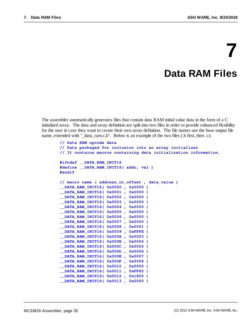
The assembler automatically generates files that contain data RAM initial value data in the form of a Cinitialized array. The data and array definition are split into two files in order to provide enhanced flexibilityfor the user in case they want to create their own array definition. The file names use the base output filename, extended with "_data_ram.c,h". Below is an example of the two files (.h first, then .c):
// Data RAM opcode data// Data packaged for inclusion into an array initializer// It contains macros containing data initialization information.
#ifndef __DATA_RAM_INIT16#define __DATA_RAM_INIT16( addr, val )#endif
// macro name ( address_or_offset , data_value )__DATA_RAM_INIT16( 0x0000 , 0x0000 )__DATA_RAM_INIT16( 0x0001 , 0x0000 )__DATA_RAM_INIT16( 0x0002 , 0x0000 )__DATA_RAM_INIT16( 0x0003 , 0x0000 )__DATA_RAM_INIT16( 0x0004 , 0x0000 )__DATA_RAM_INIT16( 0x0005 , 0x0000 )__DATA_RAM_INIT16( 0x0006 , 0x0000 )__DATA_RAM_INIT16( 0x0007 , 0x0000 )__DATA_RAM_INIT16( 0x0008 , 0x0001 )__DATA_RAM_INIT16( 0x0009 , 0xFFFE )__DATA_RAM_INIT16( 0x000A , 0x0003 )__DATA_RAM_INIT16( 0x000B , 0x0004 )__DATA_RAM_INIT16( 0x000C , 0x0005 )__DATA_RAM_INIT16( 0x000D , 0x0006 )__DATA_RAM_INIT16( 0x000E , 0x0007 )__DATA_RAM_INIT16( 0x000F , 0x0008 )__DATA_RAM_INIT16( 0x0010 , 0x0000 )__DATA_RAM_INIT16( 0x0011 , 0xFF85 )__DATA_RAM_INIT16( 0x0012 , 0x1800 )__DATA_RAM_INIT16( 0x0013 , 0x0000 )
MC33816 Assembler, page 36 (C) 2012 ASH WARE, Inc. ASH WARE, Inc.
7. Data RAM Files
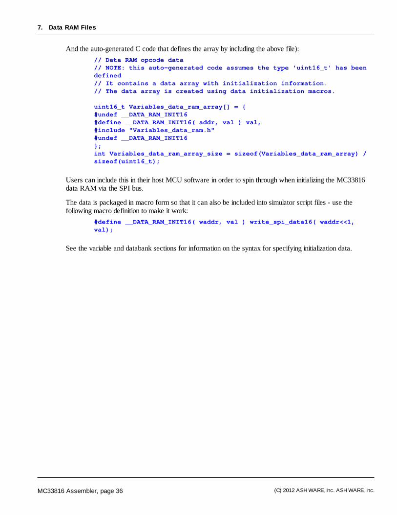
And the auto-generated C code that defines the array by including the above file):
// Data RAM opcode data// NOTE: this auto-generated code assumes the type 'uint16_t' has beendefined// It contains a data array with initialization information.// The data array is created using data initialization macros.
uint16_t Variables_data_ram_array[] = {#undef __DATA_RAM_INIT16#define __DATA_RAM_INIT16( addr, val ) val,#include "Variables_data_ram.h"#undef __DATA_RAM_INIT16};int Variables_data_ram_array_size = sizeof(Variables_data_ram_array) /sizeof(uint16_t);
Users can include this in their host MCU software in order to spin through when initializing the MC33816data RAM via the SPI bus.
The data is packaged in macro form so that it can also be included into simulator script files - use thefollowing macro definition to make it work:
#define __DATA_RAM_INIT16( waddr, val ) write_spi_data16( waddr<<1,val);
See the variable and databank sections for information on the syntax for specifying initialization data.

MC33816 Assembler, page 37 (C) 2012 ASH WARE, Inc. ASH WARE, Inc.
Listing Files
Part
VIII

MC33816 Assembler, page 39 (C) 2012 ASH WARE, Inc. ASH WARE, Inc.
8. Listing Files
ASH WARE, Inc. 8/24/2018
8Listing Files
The assembler generates a listing file for each source file that contains opcodes. The name of each listingfile is the base name of the original source file, with "_listing.dfi" added. The extension "dfi" is used toindicate the file is uses original NXP assembler format (and can thus be assembled by those tools). Theoutput listing files are created as read-only as they should not be edited.

MC33816 Assembler, page 40 (C) 2012 ASH WARE, Inc. ASH WARE, Inc.
Label Tags
Part
IX
MC33816 Assembler, page 41 (C) 2012 ASH WARE, Inc. ASH WARE, Inc.
9. Label Tags
ASH WARE, Inc. 8/24/2018
9Label Tags
Labels can be marked with the "_ISR" tag to alert the assembler that the label represents an interruptservice routine entry point. This serves the following purposes. First, it allows the assembler to perform acheck on the label address to make sure it is within the valid range (first 64 opcode addresses). Second, itautomatically disables the "unused label" warning as it is unlikely this label is the destination of any codejumps. Third, the label address it output into a special section of the defines file that makes it easy to find.
_ISR ch0_auto_diag_isr:stos off off off; // disable all drivers// ...
Similar to the "_ISR" tag is the "_ENTRY" tag - used to denote a label that will get used as a microcoreentry point. The main purpose for this tag is to prevent the "unused label" warning, as typically these labelswill not have a jump to them from anywhere in the code. They are also broken out into their own area ofthe auto-defines file.
_ENTRY entry_uc1:
MC33816 Assembler, page 42 (C) 2012 ASH WARE, Inc. ASH WARE, Inc.
Variables
Part
X
MC33816 Assembler, page 43 (C) 2012 ASH WARE, Inc. ASH WARE, Inc.
10. Variables
ASH WARE, Inc. 8/24/2018
10Variables
Variables can be used to bring some structure to the assembly language.
10.1 Immediate/Global Variables
Declaration syntax for immediate (global) variables is
<type> <variableName>;
All data in the MC33816 is 16-bit. Two types are currently supported - 'sint16' and 'uint16' - the former asigned 16-bit integer and the latter an unsigned 16-bit integer. The type does not affect the assemblyprocess, and is only used when working with the variable in the simulator debug environment. Variablenames must conform to 'C' naming conventions - '_' and alphanumeric characters, must not start with adigit.
// current threshold parametersuint16 I_boost;uint16 I_peak;sint16 I_hold;
Although the address space, immediate vs. indexed, is built into the variable declaration, when variables arereferenced in load/store/ldcd instructions the offset field still needs to be specified, and will be cross-checked against the variable's address space.
BOOST: load I_boost dac_sssc _ofs;
The immediate and global variable locations are exported into an auto-header file which is appropriate foruse by the host processor.
Initial values for the variables can be specified with C-like initializers - the values specified are output intothe auto-generated _data_ram,.[c,h] files.
// current threshold parametersuint16 I_boost = 0x1234;uint16 I_peak = 536;sint16 I_hold = -67;
MC33816 Assembler, page 44 (C) 2012 ASH WARE, Inc. ASH WARE, Inc.
10. Variables
Enabling Initialized Date in the Simulator
10.2 Enabling Initialized Date in the Simulator
In the host CPU files <BaseFileName>_data.h and <BaseFileName>_data.c generate a data array thatgets copied across the SPI bus to perform the global and databank initialization.
The mechanism used in the simulator is to include the .h version of the initialized data files after defining themacro that initializes these values. The code below can be copied into your script command file to performthis initialization. Note that the following code works when the .elf file's name is 'MyCode.elf'.
#define __DATA_RAM_INIT16( addr, val ) *((MC33816_SPI_SPACE U16 *)(addr<<1)) = val;#include "MyCode_data_ram.h"
10.3 Data Banks Variables
Indexed variables are declared in a two step process. First, a data bank structure is declared, followed bydefining one or more instances of the data bank. A data bank structure is used to define a cohesive set ofindexed data, and has a syntax similar to a C struct declaration.
// Declare a databankdatabank Injector {
uint16 I_peak;uint16 I_hold;
};
Once a databank has been declared, instances of it can be created. These instance symbols can then beused in the code to set the index base address.
// Allocate two databanks of type 'Injector'databank Injector _injector1; databank Injector _injector2;// ...// set the index base address to the _injector1 databank addressstab _injector1; // ...// From the active databank (currently '_injector1') // load variable 'I_peak' into register 'r0'load I_peak r0 ofs;
Note that immediate/global variables and databank instances must be defined before being referenced incode.
The auto-locating algorithm is straightforward. Globals/immediates and databank instances get located inthe order they are traversed in the source code.
The data bank locations and member variable offsets within the databank are exported into an auto-headerfile which is appropriate for use by the host processor.
Initial values for the databank instances can be specified with C-like initializers - the values specified areoutput into the auto-generated _data_ram,.[c,h] files. The number of initializers must match the number ofdatabank members.
// Allocate two databanks of type 'Injector'
MC33816 Assembler, page 45 (C) 2012 ASH WARE, Inc. ASH WARE, Inc.
10. Variables
Data Banks Variables
ASH WARE, Inc. 8/24/2018
databank Injector _injector1 = { 0x440, 123 }; databank Injector _injector2 = { 500, 0x230, };
The address of the databank can be loaded into the IR register as follows:
LOAD_IR @_injector1;
Be sure to set the set the IR register as the index register before accessing databank variables.
stab ir; // Set the 'ir' register as the index registerload I_peak r0 ofs;
The address of a databank variable can also be loaded directly. When accessing databank variables, do sodirectly with the address set to zero.
LOAD_IR @_injector1.I_hold;load 0 r0 ofs; // Load the I_hold parameter into register 'r0'
MC33816 Assembler, page 46 (C) 2012 ASH WARE, Inc. ASH WARE, Inc.
Extended Instructions
Part
XI
MC33816 Assembler, page 47 (C) 2012 ASH WARE, Inc. ASH WARE, Inc.
11. Extended Instructions
ASH WARE, Inc. 8/24/2018
11Extended Instructions
Extended instructions have been provided in cases where the assembler can generally choose betteropcodes than a human. Consider the case of a jump. The are are two versions; 'far' and 'near'. Depending on the situation, one of these is always going to be optimal over the other. However, it isdifficult for humans to track (as code is added/subtracted from a design and as coders arrive/leave on aproject) which opcode choice is optimal. So this choice is best left to the assembler and the use ofextended instructions provides a mechanism for doing so.
The following extended instructions are supported. Note that these are documented alongside their nativeinstructions.
CALL
CREATE_WAIT_ENTRY
LOAD_IR
JUMP
JUMP_ARITHMETIC
JUMP_CONDITION
JUMP_CONTROL
JUMP_CORE_ID
JUMP_FEEDBACK
JUMP_START
JUMP_STATUS

MC33816 Assembler, page 48 (C) 2012 ASH WARE, Inc. ASH WARE, Inc.
Instruction Set
Part
XII
MC33816 Assembler, page 49 (C) 2012 ASH WARE, Inc. ASH WARE, Inc.
12. Instruction Set
ASH WARE, Inc. 8/24/2018
12Instruction Set
This section covers the MC33816 Instruction Set.

MC33816 Assembler, page 50 (C) 2012 ASH WARE, Inc. ASH WARE, Inc.
Wait
Part
XIII
MC33816 Assembler, page 51 (C) 2012 ASH WARE, Inc. ASH WARE, Inc.
13. Wait
ASH WARE, Inc. 8/24/2018
13Wait
The MC33816 is an event/response machine. An event occurs and then code executes that handles thatevent.
The wait instructions are the key to this behavior. The core waits at a 'wait' instruction for an event tooccur.
Although there are many possible event sources, such as sense current to reach a threshold or a timer toreach its terminal count, the core can only be waiting for up to five different events to occur at any onewait instruction.
These pending events are configured as rows in a five-row wait table. Each of the five rows the the waittable must be configured with the 'cwef' and 'cwer' instructions.
Once a row is configured with the 'cwef' or 'cwer' instruction the row is 'sticky' in that it will not changeuntil re-configured with a future 'cwef' or 'cwer' instruction.
13.1 CWEF - create wait table entry far
Initializes or changes one of the five rows in the wait table used by the 'wait' instruction.
The address of the code that will execute in response to the row's event is is in either the 'jr1' or jr2'register as specified by the 'JrSel' parameter.
The event type is specified by the 'Cond' parameter.
Note that once the wait table row is stickky such that once the jump register's address is loaded into thewait table, the jump register is free to be used for other purposes.
Syntax
cwef JrSel Cond Entry;
Example
// Set the wait table's row 2 event// to be the VBoost voltage reaching t's thresholdcwer vboost_hit_threshold vb row2;
MC33816 Assembler, page 52 (C) 2012 ASH WARE, Inc. ASH WARE, Inc.
13. Wait
CWEF - create wait table entry far
// Set the wait table's row 3 event// to be when the core's own current sense threshold is reached// Note that if the destination is over 16 opcodes away// then this 2-instruction 'far' opcode pair is requiredldjr1 own_current_hit_threshold;cwef jr1 ocur row3;// Set the wait table's row 5 event// to be the counter 1 reaching it's terminal count// NOTE: This is the extended instruction that// automatically selects the more optimal// of either cwer or cwefCREATE_WAIT_ENTRY counter3_terminal jr1 tc3 row5;//Cease execution until row 2's, 3's, or 5's event occurswait row235;vboost_hit_threshold:// ... More code here ...own_current_hit_threshold:// ... More code here ...counter3_terminal:// ... More code here ...
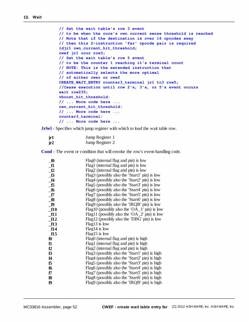
JrSel - Specifies which jump register with which to load the wait table row.
jr1 Jump Register 1jr2 Jump Register 2
Cond - The event or condition that will envoke the row's event-handling code.
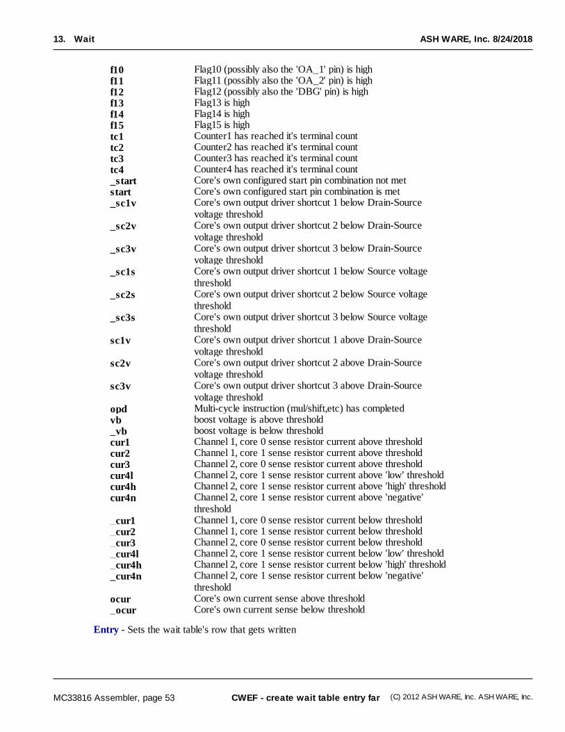
_f0 Flag0 (internal flag and pin) is low_f1 Flag1 (internal flag and pin) is low_f2 Flag2 (internal flag and pin) is low_f3 Flag3 (possibly also the 'Start1' pin) is low_f4 Flag4 (possibly also the 'Start2' pin) is low_f5 Flag5 (possibly also the 'Start3' pin) is low_f6 Flag6 (possibly also the 'Start4' pin) is low_f7 Flag7 (possibly also the 'Start5' pin) is low_f8 Flag8 (possibly also the 'Start6' pin) is low_f9 Flag9 (possibly also the 'IRQB' pin) is low_f10 Flag10 (possibly also the 'OA_1' pin) is low_f11 Flag11 (possibly also the 'OA_2' pin) is low_f12 Flag12 (possibly also the 'DBG' pin) is low_f13 Flag13 is low_f14 Flag14 is low_f15 Flag15 is lowf0 Flag0 (internal flag and pin) is highf1 Flag1 (internal flag and pin) is highf2 Flag2 (internal flag and pin) is highf3 Flag3 (possibly also the 'Start1' pin) is highf4 Flag4 (possibly also the 'Start2' pin) is highf5 Flag5 (possibly also the 'Start3' pin) is highf6 Flag6 (possibly also the 'Start4' pin) is highf7 Flag7 (possibly also the 'Start5' pin) is highf8 Flag8 (possibly also the 'Start6' pin) is highf9 Flag9 (possibly also the 'IRQB' pin) is high
MC33816 Assembler, page 53 (C) 2012 ASH WARE, Inc. ASH WARE, Inc.
13. Wait
CWEF - create wait table entry far
ASH WARE, Inc. 8/24/2018
f10 Flag10 (possibly also the 'OA_1' pin) is highf11 Flag11 (possibly also the 'OA_2' pin) is highf12 Flag12 (possibly also the 'DBG' pin) is highf13 Flag13 is highf14 Flag14 is highf15 Flag15 is hightc1 Counter1 has reached it's terminal counttc2 Counter2 has reached it's terminal counttc3 Counter3 has reached it's terminal counttc4 Counter4 has reached it's terminal count_start Core's own configured start pin combination not metstart Core's own configured start pin combination is met_sc1v Core's own output driver shortcut 1 below Drain-Source
voltage threshold_sc2v Core's own output driver shortcut 2 below Drain-Source
voltage threshold_sc3v Core's own output driver shortcut 3 below Drain-Source
voltage threshold_sc1s Core's own output driver shortcut 1 below Source voltage
threshold_sc2s Core's own output driver shortcut 2 below Source voltage
threshold_sc3s Core's own output driver shortcut 3 below Source voltage
thresholdsc1v Core's own output driver shortcut 1 above Drain-Source
voltage thresholdsc2v Core's own output driver shortcut 2 above Drain-Source
voltage thresholdsc3v Core's own output driver shortcut 3 above Drain-Source
voltage thresholdopd Multi-cycle instruction (mul/shift,etc) has completedvb boost voltage is above threshold_vb boost voltage is below thresholdcur1 Channel 1, core 0 sense resistor current above thresholdcur2 Channel 1, core 1 sense resistor current above thresholdcur3 Channel 2, core 0 sense resistor current above thresholdcur4l Channel 2, core 1 sense resistor current above 'low' thresholdcur4h Channel 2, core 1 sense resistor current above 'high' thresholdcur4n Channel 2, core 1 sense resistor current above 'negative'
threshold_cur1 Channel 1, core 0 sense resistor current below threshold_cur2 Channel 1, core 1 sense resistor current below threshold_cur3 Channel 2, core 0 sense resistor current below threshold_cur4l Channel 2, core 1 sense resistor current below 'low' threshold_cur4h Channel 2, core 1 sense resistor current below 'high' threshold_cur4n Channel 2, core 1 sense resistor current below 'negative'
thresholdocur Core's own current sense above threshold_ocur Core's own current sense below threshold
Entry - Sets the wait table's row that gets written
MC33816 Assembler, page 54 (C) 2012 ASH WARE, Inc. ASH WARE, Inc.
13. Wait
CWEF - create wait table entry far
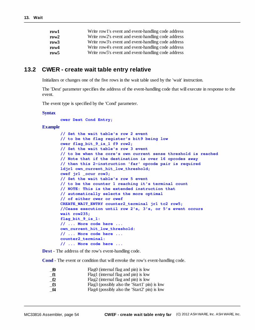
row1 Write row1's event and event-handling code addressrow2 Write row2's event and event-handling code addressrow3 Write row3's event and event-handling code addressrow4 Write row4's event and event-handling code addressrow5 Write row5's event and event-handling code address
13.2 CWER - create wait table entry relative
Initializes or changes one of the five rows in the wait table used by the 'wait' instruction.
The 'Dest' parameter specifies the address of the event-handling code that will execute in response to theevent.
The event type is specified by the 'Cond' parameter.
Syntax
cwer Dest Cond Entry;
Example
// Set the wait table's row 2 event// to be the flag register's bit9 being lowcwer flag_bit_9_is_1 f9 row2;// Set the wait table's row 3 event// to be when the core's own current sense threshold is reached// Note that if the destination is over 16 opcodes away// then this 2-instruction 'far' opcode pair is requiredldjr1 own_current_hit_low_threshold;cwef jr1 _ocur row3;// Set the wait table's row 5 event// to be the counter 1 reaching it's terminal count// NOTE: This is the extended instruction that// automatically selects the more optimal// of either cwer or cwefCREATE_WAIT_ENTRY counter2_terminal jr1 tc2 row5;//Cease execution until row 2's, 3's, or 5's event occurswait row235;flag_bit_9_is_1:// ... More code here ...own_current_hit_low_threshold:// ... More code here ...counter2_terminal:// ... More code here ...
Dest - The address of the row's event-handling code.
Cond - The event or condition that will envoke the row's event-handling code.
_f0 Flag0 (internal flag and pin) is low_f1 Flag1 (internal flag and pin) is low_f2 Flag2 (internal flag and pin) is low_f3 Flag3 (possibly also the 'Start1' pin) is low_f4 Flag4 (possibly also the 'Start2' pin) is low
MC33816 Assembler, page 55 (C) 2012 ASH WARE, Inc. ASH WARE, Inc.
13. Wait
CWER - create wait table entry relative
ASH WARE, Inc. 8/24/2018
_f5 Flag5 (possibly also the 'Start3' pin) is low_f6 Flag6 (possibly also the 'Start4' pin) is low_f7 Flag7 (possibly also the 'Start5' pin) is low_f8 Flag8 (possibly also the 'Start6' pin) is low_f9 Flag9 (possibly also the 'IRQB' pin) is low_f10 Flag10 (possibly also the 'OA_1' pin) is low_f11 Flag11 (possibly also the 'OA_2' pin) is low_f12 Flag12 (possibly also the 'DBG' pin) is low_f13 Flag13 is low_f14 Flag14 is low_f15 Flag15 is lowf0 Flag0 (internal flag and pin) is highf1 Flag1 (internal flag and pin) is highf2 Flag2 (internal flag and pin) is highf3 Flag3 (possibly also the 'Start1' pin) is highf4 Flag4 (possibly also the 'Start2' pin) is highf5 Flag5 (possibly also the 'Start3' pin) is highf6 Flag6 (possibly also the 'Start4' pin) is highf7 Flag7 (possibly also the 'Start5' pin) is highf8 Flag8 (possibly also the 'Start6' pin) is highf9 Flag9 (possibly also the 'IRQB' pin) is highf10 Flag10 (possibly also the 'OA_1' pin) is highf11 Flag11 (possibly also the 'OA_2' pin) is highf12 Flag12 (possibly also the 'DBG' pin) is highf13 Flag13 is highf14 Flag14 is highf15 Flag15 is hightc1 Counter1 has reached it's terminal counttc2 Counter2 has reached it's terminal counttc3 Counter3 has reached it's terminal counttc4 Counter4 has reached it's terminal count_start Core's own configured start pin combination not metstart Core's own configured start pin combination is met_sc1v Core's own output driver shortcut 1 below Drain-Source
voltage threshold_sc2v Core's own output driver shortcut 2 below Drain-Source
voltage threshold_sc3v Core's own output driver shortcut 3 below Drain-Source
voltage threshold_sc1s Core's own output driver shortcut 1 below Source voltage
threshold_sc2s Core's own output driver shortcut 2 below Source voltage
threshold_sc3s Core's own output driver shortcut 3 below Source voltage
thresholdsc1v Core's own output driver shortcut 1 above Drain-Source
voltage thresholdsc2v Core's own output driver shortcut 2 above Drain-Source
voltage thresholdsc3v Core's own output driver shortcut 3 above Drain-Source
voltage thresholdopd Multi-cycle instruction (mul/shift,etc) has completed
MC33816 Assembler, page 56 (C) 2012 ASH WARE, Inc. ASH WARE, Inc.
13. Wait
CWER - create wait table entry relative
vb boost voltage is above threshold_vb boost voltage is below thresholdcur1 Channel 1, core 0 sense resistor current above thresholdcur2 Channel 1, core 1 sense resistor current above thresholdcur3 Channel 2, core 0 sense resistor current above thresholdcur4l Channel 2, core 1 sense resistor current above 'low' thresholdcur4h Channel 2, core 1 sense resistor current above 'high' thresholdcur4n Channel 2, core 1 sense resistor current above 'negative'
threshold_cur1 Channel 1, core 0 sense resistor current below threshold_cur2 Channel 1, core 1 sense resistor current below threshold_cur3 Channel 2, core 0 sense resistor current below threshold_cur4l Channel 2, core 1 sense resistor current below 'low' threshold_cur4h Channel 2, core 1 sense resistor current below 'high' threshold_cur4n Channel 2, core 1 sense resistor current below 'negative'
thresholdocur Core's own current sense above threshold_ocur Core's own current sense below threshold
Entry - Specifies which wait table row gets written
row1 Write row1's event and event-handling code addressrow2 Write row2's event and event-handling code addressrow3 Write row3's event and event-handling code addressrow4 Write row4's event and event-handling code addressrow5 Write row5's event and event-handling code address
13.3 Fill a 'Wait Table' row with an event and an event-handling thread'scode-address (extended instruction)
Call to the label, loading/using the specified jump register only if a far jump is required.
Syntax
CREATE_WAIT_ENTRY Dest JrSel Cond Entry;
Example
// Set the wait table's row 2 event// to be the flag register's bit 13 being low// NOTE: This is the extended instruction that// automatically selects the more optimal// of either cwer or cwefCREATE_WAIT_ENTRY flag_reg_bit_13_low jr1 _f13 row2;// Set the wait table's row 5 event// to be the counter 1 reaching it's terminal countCREATE_WAIT_ENTRY counter1_terminal jr1 tc1 row5;//Cease execution until row 2's, 3's, or 5's event occurswait row25;flag_reg_bit_13_low:// ... More code here ...counter1_terminal:// ... More code here ...
MC33816 Assembler, page 57 (C) 2012 ASH WARE, Inc. ASH WARE, Inc.
13. Wait
Fill a 'Wait Table' row with an event and an event-handling thread's code-address (extended instruction)
ASH WARE, Inc. 8/24/2018
Dest - The destination label of the wait entry.
JrSel - Specifies which jump register to use if a far address load is required.
jr1 Jump Register 1jr2 Jump Register 2
Cond - The event or condition that will envoke the row's event-handling code.
_f0 Flag0 (internal flag and pin) is low_f1 Flag1 (internal flag and pin) is low_f2 Flag2 (internal flag and pin) is low_f3 Flag3 (possibly also the 'Start1' pin) is low_f4 Flag4 (possibly also the 'Start2' pin) is low_f5 Flag5 (possibly also the 'Start3' pin) is low_f6 Flag6 (possibly also the 'Start4' pin) is low_f7 Flag7 (possibly also the 'Start5' pin) is low_f8 Flag8 (possibly also the 'Start6' pin) is low_f9 Flag9 (possibly also the 'IRQB' pin) is low_f10 Flag10 (possibly also the 'OA_1' pin) is low_f11 Flag11 (possibly also the 'OA_2' pin) is low_f12 Flag12 (possibly also the 'DBG' pin) is low_f13 Flag13 is low_f14 Flag14 is low_f15 Flag15 is lowf0 Flag0 (internal flag and pin) is highf1 Flag1 (internal flag and pin) is highf2 Flag2 (internal flag and pin) is highf3 Flag3 (possibly also the 'Start1' pin) is highf4 Flag4 (possibly also the 'Start2' pin) is highf5 Flag5 (possibly also the 'Start3' pin) is highf6 Flag6 (possibly also the 'Start4' pin) is highf7 Flag7 (possibly also the 'Start5' pin) is highf8 Flag8 (possibly also the 'Start6' pin) is highf9 Flag9 (possibly also the 'IRQB' pin) is highf10 Flag10 (possibly also the 'OA_1' pin) is highf11 Flag11 (possibly also the 'OA_2' pin) is highf12 Flag12 (possibly also the 'DBG' pin) is highf13 Flag13 is highf14 Flag14 is highf15 Flag15 is hightc1 Counter1 has reached it's terminal counttc2 Counter2 has reached it's terminal counttc3 Counter3 has reached it's terminal counttc4 Counter4 has reached it's terminal count_start Core's own configured start pin combination not metstart Core's own configured start pin combination is met_sc1v Core's own output driver shortcut 1 below Drain-Source
voltage threshold_sc2v Core's own output driver shortcut 2 below Drain-Source
voltage threshold_sc3v Core's own output driver shortcut 3 below Drain-Source
voltage threshold
MC33816 Assembler, page 58 (C) 2012 ASH WARE, Inc. ASH WARE, Inc.
13. Wait
Fill a 'Wait Table' row with an event and an event-handling thread's code-address (extended instruction)
_sc1s Core's own output driver shortcut 1 below Source voltagethreshold
_sc2s Core's own output driver shortcut 2 below Source voltagethreshold
_sc3s Core's own output driver shortcut 3 below Source voltagethreshold
sc1v Core's own output driver shortcut 1 above Drain-Sourcevoltage threshold
sc2v Core's own output driver shortcut 2 above Drain-Sourcevoltage threshold
sc3v Core's own output driver shortcut 3 above Drain-Sourcevoltage threshold
opd Multi-cycle instruction (mul/shift,etc) has completedvb boost voltage is above threshold_vb boost voltage is below thresholdcur1 Channel 1, core 0 sense resistor current above thresholdcur2 Channel 1, core 1 sense resistor current above thresholdcur3 Channel 2, core 0 sense resistor current above thresholdcur4l Channel 2, core 1 sense resistor current above 'low' thresholdcur4h Channel 2, core 1 sense resistor current above 'high' thresholdcur4n Channel 2, core 1 sense resistor current above 'negative'
threshold_cur1 Channel 1, core 0 sense resistor current below threshold_cur2 Channel 1, core 1 sense resistor current below threshold_cur3 Channel 2, core 0 sense resistor current below threshold_cur4l Channel 2, core 1 sense resistor current below 'low' threshold_cur4h Channel 2, core 1 sense resistor current below 'high' threshold_cur4n Channel 2, core 1 sense resistor current below 'negative'
thresholdocur Core's own current sense above threshold_ocur Core's own current sense below threshold
Entry - Specifies which wait table row gets written
row1 Write row1's event and event-handling code addressrow2 Write row2's event and event-handling code addressrow3 Write row3's event and event-handling code addressrow4 Write row4's event and event-handling code addressrow5 Write row5's event and event-handling code address
13.4 WAIT - wait until a condition is verified
stop the program counter and wait until at least one of the enabled wait conditions is met; when one of theconditions is met, the program counter is moved to the corresponding destination
the possible wait conditions, along with the corresponding destinations, are stored in the wait table (pleaserefer to the cwer and cwef instructions for further details)
not all wait table rows are enabled during a wait
- waitmask is a 5-bit mask; each bit identifies a row in the wait table; if the bit is set to 1 then the
MC33816 Assembler, page 59 (C) 2012 ASH WARE, Inc. ASH WARE, Inc.
13. Wait
WAIT - wait until a condition is verified
ASH WARE, Inc. 8/24/2018
correspondent condition is tested during the wait
Syntax
wait WaitMask;
Example
// Map the wait table's row1// to the HOLD_OFF thread// when the core's Own Current Sense comparator// becomes high (occur)cwer HOLD_OFF ocur row1;//// Map the wait table's row3// to the IDLE thread// on Terminal Count 2 (TC2)cwer IDLE tc2 row3;//// Enable rows 1 and 3, disable the others.// Cease core's execution until the// event in either 1 or 3 are truewait row13;//// Thread: IDLEIDLE:// ... (more code here) ...//// Thread: HOLD_OFFHOLD_OFF:// ... (more code here) ...
WaitMask
always MISSING DESCRIPTION STRINGrow1 MISSING DESCRIPTION STRINGrow2 MISSING DESCRIPTION STRINGrow12 MISSING DESCRIPTION STRINGrow3 MISSING DESCRIPTION STRINGrow13 MISSING DESCRIPTION STRINGrow23 MISSING DESCRIPTION STRINGrow123 MISSING DESCRIPTION STRINGrow4 MISSING DESCRIPTION STRINGrow14 MISSING DESCRIPTION STRINGrow24 MISSING DESCRIPTION STRINGrow124 MISSING DESCRIPTION STRINGrow34 MISSING DESCRIPTION STRINGrow134 MISSING DESCRIPTION STRINGrow234 MISSING DESCRIPTION STRINGrow1234 MISSING DESCRIPTION STRINGrow5 MISSING DESCRIPTION STRINGrow15 MISSING DESCRIPTION STRINGrow25 MISSING DESCRIPTION STRINGrow125 MISSING DESCRIPTION STRINGrow35 MISSING DESCRIPTION STRING
MC33816 Assembler, page 60 (C) 2012 ASH WARE, Inc. ASH WARE, Inc.
13. Wait
WAIT - wait until a condition is verified
row135 MISSING DESCRIPTION STRINGrow235 MISSING DESCRIPTION STRINGrow1235 MISSING DESCRIPTION STRINGrow45 MISSING DESCRIPTION STRINGrow145 MISSING DESCRIPTION STRINGrow245 MISSING DESCRIPTION STRINGrow1245 MISSING DESCRIPTION STRINGrow345 MISSING DESCRIPTION STRINGrow1345 MISSING DESCRIPTION STRINGrow2345 MISSING DESCRIPTION STRINGrow12345 MISSING DESCRIPTION STRING

MC33816 Assembler, page 61 (C) 2012 ASH WARE, Inc. ASH WARE, Inc.
Call/Return
Part
XIV

MC33816 Assembler, page 63 (C) 2012 ASH WARE, Inc. ASH WARE, Inc.
14. Call/Return
ASH WARE, Inc. 8/24/2018
14Call/Return
This section covers the instructions that support calling and returning from subroutines.
14.1 JTSF - Jump far to subroutine
Jump to the subroutine specified by one of the jump registers, 'jr1' or 'jr2' as specified by the 'JrSel'parameter. The subroutine's address must have been previously loaded into either 'jr1' or 'jr2'.
The return address is loaded into the auxiliary register (aux.)
Following subroutine execution the return from subroutine instruction 'rfs' is used to return to the point atwhich the subroutine was called.
Syntax
jtsf JrSel;
Example
// Load the subroutine address// into jump register 1 'jr1' and call itldjr1 my_far_subroutine;jtsf jr1;// ... (more code here) ...// Start of subroutinemy_far_subroutine:// ... (more code here) ...// Return from subroutingrfs;//// SUGGESTION: use this equivalent extended instruction instead:CALL my_far_subroutine jr1;
JrSel - The subroutine's start address
jr1 Jump Register 1jr2 Jump Register 2
MC33816 Assembler, page 64 (C) 2012 ASH WARE, Inc. ASH WARE, Inc.
14. Call/Return
JTSF - Jump far to subroutine
14.2 JTSR - Jump relative to subroutine
Jump to a subroutine. The subroutine must be within -16 to +15 instructions of the address of the jumpinstruction.
The return address is loaded into the auxiliary register (aux.)
Following subroutine execution the return from subroutine instruction 'rfs' is used to return to the point atwhich the subroutine was called.
Syntax
jtsr Dest;
Example
// call subroutine 'my_near_subroutine'jtsr my_near_subroutine;// ... (more code here) ...// Start of subroutinemy_near_subroutine:// ... (more code here) ...// Return from subroutingrfs;//// SUGGESTION: use this equivalent extended instruction instead:CALL my_near_subroutine jr1;
Dest - The jump destination code address.
14.3 Call a subroutine (extended instruction)
Call to the label, loading/using the specified jump register only if a far jump is required.
Syntax
CALL Dest JrSel;
Example
// Call destination label 'my_subroutine', using jr1 if necessaryCALL my_subroutine jr1;// ... (more code here) ...// Start of subroutinemy_subroutine:// ... (more code here) ...// Return from subroutingrfs;
Dest - The call destination label.
JrSel - Specifies which jump register to use if a far call is required.
MC33816 Assembler, page 65 (C) 2012 ASH WARE, Inc. ASH WARE, Inc.
14. Call/Return
Call a subroutine (extended instruction)
ASH WARE, Inc. 8/24/2018
jr1 Jump Register 1jr2 Jump Register 2
14.4 RFS - Return from subroutine
Ends a subroutine. The program counter (pc) is loaded with the value from the auxiliary register (aux). The'aux' register should have been loaded with the calling address using either the 'jtsf' or 'jtsr' instruction.
Syntax
rfs;
Example
// Save the address of the caller// and call a two-deep subroutineone_deep_subroutine:cp aux r1;ldjr1 two_deep_subroutine;jtsf jr1;// ... (more code here) ...// Restore the original caller's address// and returncp r1 aux;rfs;//two_deep_subroutine:// ... (more code here) ...// return from subroutinerfs;

MC33816 Assembler, page 66 (C) 2012 ASH WARE, Inc. ASH WARE, Inc.
Program Flow
Part
XV
MC33816 Assembler, page 67 (C) 2012 ASH WARE, Inc. ASH WARE, Inc.
15. Program Flow
ASH WARE, Inc. 8/24/2018
15Program Flow
This section covers conditional and unconditional jumps as well as loading the jump registers which isrequired for 'far' jumps.
15.1 LDJR1 - Load jump register 1
Loads a code address into jump register 1 (jr1.)
Syntax
ldjr1 DestValue;
Example
ldjr1 clear_results_subroutine;jtsf jr1;// ...clear_results_subroutine:
DestValue - The code address.
15.2 LDJR2 - Load jump register 2
Loads a code address into jump register 2 (jr2.)
Syntax
ldjr2 DestValue;
Example
ldjr2 my_sub_routine;jtsf jr2;// ...my_sub_routine:
MC33816 Assembler, page 68 (C) 2012 ASH WARE, Inc. ASH WARE, Inc.
15. Program Flow
LDJR2 - Load jump register 2
DestValue - The code address.
15.3 JMPF - Unconditional jump far
Jump to the code address specified by one of the jump registers, 'jr1' or 'jr2' as specified by the 'JrSel'parameter. The destination code address must have been previously loaded into either 'jr1' or 'jr2'.
Syntax
jmpf JrSel;
Example
// Jump to label 'far_dest_label'ldjr1 far_dest_label;jmpf jr1;// ... (more code here) ...far_dest_label://// SUGGESTION: use this equivalent extended instruction instead:JUMP far_dest_label jr1;
JrSel - Specifies which jump register contains the jump destination.
jr1 Jump Register 1jr2 Jump Register 2
15.4 JMPR - Unconditional jump relative
Jump to a code address. The destination must be within -16 to +15 instructions of the address of the jumpinstruction.
Syntax
jmpr Dest;
Example
// Jump to label 'jump_dest_label'jmpr near_jump_dest_label;// ... (more code here) ...near_jump_dest_label://// SUGGESTION: use this equivalent extended instruction instead:JUMP near_jump_dest_label jr1;
Dest - The jump destination code address.
MC33816 Assembler, page 69 (C) 2012 ASH WARE, Inc. ASH WARE, Inc.
15. Program Flow
Unconditionally jump (extended instruction)
ASH WARE, Inc. 8/24/2018
15.5 Unconditionally jump (extended instruction)
Jump to the label, loading/using the specified jump register only if a far jump is required.
Syntax
JUMP Dest JrSel;
Example
// Unconditionally jump to 'DEST_LABEL0'// using jr1 if necessaryJUMP DEST_LABEL0 jr1;// ... (more code here) ...DEST_LABEL0:
Dest - The jump destination label.
JrSel - Specifies which jump register to use if a far jump is required.
jr1 Jump Register 1jr2 Jump Register 2
15.6 JARF - Jump on arithmetic register far
If the condition being tested is true, jump to the code address specified by one of the jump registers, 'jr1' or'jr2' as specified by the 'JrSel' parameter. The code address must have been previously loaded into either'jr1' or 'jr2'.
Syntax
jarf JrSel BitSel;
Example
// If register 'r0' contains a '7'// then goto label 'result_is_zero'subi r0 7 r1;ldjr1 result_is_zero;jarf jr1 sgn;// ... (more code here) ...result_is_zero://// SUGGESTION: use this equivalent extended instruction instead:JUMP_ARITHMETIC result_is_zero jr1 sgn;
JrSel - Specifies which jump register contains the jump destination.
jr1 Jump Register 1jr2 Jump Register 2
BitSel - The condition being tested.
opd OD - Multi-cycle instruction (mul/shift,etc) has completedovs SO - Overflow with signed operandsuns SU - Underflow with signed operandsovu UO - Overflow with unsigned operands
MC33816 Assembler, page 70 (C) 2012 ASH WARE, Inc. ASH WARE, Inc.
15. Program Flow
JARF - Jump on arithmetic register far
unu UU - Underflow with unsigned operandssgn CS - Sign of resultzero RZ - Result is zeromloss ML - Multiply precision lossmover MO - Multiply overflowall1 MM - Result of mask operation is 0xFFFFall0 MN - Result of mask operation is 0x0000aritl A0 - Arithmetic Logic Mode bit 0arith A1 - Arithmetic Logic Mode bit 1carry C - Carryconv CS - Conversion signcsh SB - Carry on shift operation
15.7 JARR - Jump on arithmetic register relative
If the condition being tested is true, jump to the specified code address. The destination must be within -16to +15 instructions of the address of the jump instruction.
Syntax
jarr Dest BitSel;
Example
// If register 'r0' contains a '7'// then goto label 'r0_is_7'subi r0 7 r1;jarr r0_is_7 sgn;// ... (more code here) ...r0_is_7://// SUGGESTION: use this equivalent extended instruction instead:JUMP_ARITHMETIC result_is_zero jr1 sgn;
Dest - The jump destination code address.
BitSel - Specifies which bit to test.
opd OD - Multi-cycle instruction (mul/shift,etc) has completedovs SO - Overflow with signed operandsuns SU - Underflow with signed operandsovu UO - Overflow with unsigned operandsunu UU - Underflow with unsigned operandssgn CS - Sign of resultzero RZ - Result is zeromloss ML - Multiply precision lossmover MO - Multiply overflowall1 MM - Result of mask operation is 0xFFFFall0 MN - Result of mask operation is 0x0000aritl A0 - Arithmetic Logic Mode bit 0arith A1 - Arithmetic Logic Mode bit 1carry C - Carry
MC33816 Assembler, page 71 (C) 2012 ASH WARE, Inc. ASH WARE, Inc.
15. Program Flow
JARR - Jump on arithmetic register relative
ASH WARE, Inc. 8/24/2018
conv CS - Conversion signcsh SB - Carry on shift operation
15.8 Conditionally jump on ALU and related flags (extended instruction)
Jump to the label if tested condition is true, loading/using the specified jump register only if a far jump isrequired.
Syntax
JUMP_ARITHMETIC Dest JrSel BitSel;
Example
// Test bits 3-7 of register 'r0'.// If all set, jump to label 'bits_3_to_7_set'LOAD_IR 0x00F8;and r0;JUMP_ARITHMETIC bits_3_to_7_set jr1 all1;// ... (more code here) ...bits_3_to_7_set:
Dest - The jump destination label.
JrSel - Specifies which jump register to use if a far jump is required.
jr1 Jump Register 1jr2 Jump Register 2
BitSel - The condition being tested.
opd OD - Multi-cycle instruction (mul/shift,etc) has completedovs SO - Overflow with signed operandsuns SU - Underflow with signed operandsovu UO - Overflow with unsigned operandsunu UU - Underflow with unsigned operandssgn CS - Sign of resultzero RZ - Result is zeromloss ML - Multiply precision lossmover MO - Multiply overflowall1 MM - Result of mask operation is 0xFFFFall0 MN - Result of mask operation is 0x0000aritl A0 - Arithmetic Logic Mode bit 0arith A1 - Arithmetic Logic Mode bit 1carry C - Carryconv CS - Conversion signcsh SB - Carry on shift operation
MC33816 Assembler, page 72 (C) 2012 ASH WARE, Inc. ASH WARE, Inc.
15. Program Flow
JCRF - Jump on control register far
15.9 JCRF - Jump on control register far
Conditionally jump on a control register bit. The destination code address is specified by one of the jumpregisters, 'jr1' or 'jr2' as specified by the 'JrSel' parameter. The code address must have been previouslyloaded into either 'jr1' or 'jr2'.
The jump can occur when the control bit is set, or when the control bit is cleared which is specified by the'Pol' parameter.
Note that each core has its own control register so the control register that is tested is that core's owncontrol register.
Syntax
jcrf JrSel BitSel Pol;
Example
// Jump to label 'Dest3'// if Control Register's bit 12 is a '0'ldjr1 Dest3;jcrf jr1 b12 high;// ... (more code here) ...Dest3://// SUGGESTION: use this equivalent extended instruction instead:JUMP_CONTROL Dest3 jr1 b12 high;
JrSel - Specifies which jump register contains the jump destination.
jr1 Jump Register 1jr2 Jump Register 2
BitSel - Specifies which bit to test.
b0 Control register bit 0b1 Control register bit 1b2 Control register bit 2b3 Control register bit 3b4 Control register bit 4b5 Control register bit 5b6 Control register bit 6b7 Control register bit 7b8 Control register bit 8b9 Control register bit 9b10 Control register bit 10b11 Control register bit 11b12 Control register bit 12b13 Control register bit 13b14 Control register bit 14b15 Control register bit 15
Pol - Specifies jump on bit low or on bit high.
MC33816 Assembler, page 73 (C) 2012 ASH WARE, Inc. ASH WARE, Inc.
15. Program Flow
JCRF - Jump on control register far
ASH WARE, Inc. 8/24/2018
low Jump on control bit lowhigh Jump on control bit high
15.10 JCRR - Jump on control register relative
Conditionally jump on a control register bit. The destination must be within -16 to +15 instructions of theaddress of the jump instruction.
The jump can occur when the control bit is set, or when the control bit is cleared which is specified by the'Pol' parameter.
Note that each core has its own control register so the control register that is tested is that core's owncontrol register.
Syntax
jcrr Dest BitSel Pol;
Example
// Jump to 'Dest2'// if Control Register's bit 5 is a '1'jcrr Dest2 b5 high;// ... (more code here) ...Dest2://// SUGGESTION: use this equivalent extended instruction instead:JUMP_CONTROL Dest2 jr1 b5 high;
Dest - The jump destination code address.
BitSel - Specifies which control bit to test.
b0 Control register bit 0b1 Control register bit 1b2 Control register bit 2b3 Control register bit 3b4 Control register bit 4b5 Control register bit 5b6 Control register bit 6b7 Control register bit 7b8 Control register bit 8b9 Control register bit 9b10 Control register bit 10b11 Control register bit 11b12 Control register bit 12b13 Control register bit 13b14 Control register bit 14b15 Control register bit 15
Pol - Specifies jump on bit low or on bit high.
MC33816 Assembler, page 74 (C) 2012 ASH WARE, Inc. ASH WARE, Inc.
15. Program Flow
JCRR - Jump on control register relative
low Jump on control bit lowhigh Jump on control bit high
15.11 Conditionally jump on 'Control Register' bit values (hi/lo) (extendedinstruction)
Jump to the label if tested condition is true, loading/using the specified jump register only if a far jump isrequired.
Syntax
JUMP_CONTROL Dest JrSel BitSel Pol;
Example
// Jump to 'DEST_LABEL1'// if control register bit 11 is a '1'// using jr1 if necessaryJUMP_CONTROL DEST_LABEL1 jr1 b11 high;// ... (more code here) ...DEST_LABEL1:
Dest - The jump destination label.
JrSel - Specifies which jump register to use if a far jump is required.
jr1 Jump Register 1jr2 Jump Register 2
BitSel - Specifies which bit to test.
b0 Control register bit 0b1 Control register bit 1b2 Control register bit 2b3 Control register bit 3b4 Control register bit 4b5 Control register bit 5b6 Control register bit 6b7 Control register bit 7b8 Control register bit 8b9 Control register bit 9b10 Control register bit 10b11 Control register bit 11b12 Control register bit 12b13 Control register bit 13b14 Control register bit 14b15 Control register bit 15
Pol - Specifies jump on bit low or on bit high.
low Jump on control bit lowhigh Jump on control bit high
MC33816 Assembler, page 75 (C) 2012 ASH WARE, Inc. ASH WARE, Inc.
15. Program Flow
JSRF - Jump on status register far
ASH WARE, Inc. 8/24/2018
15.12 JSRF - Jump on status register far
Conditionally jump on a status register bit. The destination code address is specified by one of the jumpregisters, 'jr1' or 'jr2' as specified by the 'JrSel' parameter. The code address must have been previouslyloaded into either 'jr1' or 'jr2'.
The jump can occur when the status bit is set, or when the status bit is cleared which is specified by the'Pol' parameter.
Note that each core has its own status register so the status register that is tested is that core's own controlregister.
Syntax
jsrf JrSel BitSel Pol;
Example
// Jump to label 'bit_12_is_low'// if Status Register's bit 12 is a '0'ldjr1 bit_12_is_low;jsrf jr1 b12 low;//// SUGGESTION: use this equivalent extended instruction instead:JUMP_STATUS bit_12_is_low jr1 b12 low;
JrSel - Specifies which jump register contains the jump destination.
jr1 Jump Register 1jr2 Jump Register 2
BitSel - Specifies which bit to test.
b0 Status register bit 0b1 Status register bit 1b2 Status register bit 2b3 Status register bit 3b4 Status register bit 4b5 Status register bit 5b6 Status register bit 6b7 Status register bit 7b8 Status register bit 8b9 Status register bit 9b10 Status register bit 10b11 Status register bit 11b12 Status register bit 12b13 Status register bit 13b14 Status register bit 14b15 Status register bit 15
Pol - Specifies jump on bit low or on bit high.
low Jump on status bit lowhigh Jump on status bit high
MC33816 Assembler, page 76 (C) 2012 ASH WARE, Inc. ASH WARE, Inc.
15. Program Flow
JSRF - Jump on status register far
15.13 JSRR - Jump on status register relative
Conditionally jump on a status register bit. The destination code address must be within -16 to +15instructions of the address of the jump instruction.
The jump can occur when the status bit is set, or when the status bit is cleared which is specified by the'Pol' parameter.
Note that each core has its own status register so the status register that is tested is that core's own controlregister.
Syntax
jsrr Dest BitSel Pol;
Example
// Jump to label 'bit_12_is_low'// if Status Register’s bit 12 is a '0'jsrr bit_12_is_low b12 low;// ... (more code here) ...bit_12_is_low://// SUGGESTION: use this equivalent extended instruction instead:JUMP_STATUS bit_12_is_low jr1 b12 low;
Dest - The jump destination code address.
BitSel - Specifies which bit to test.
b0 Status register bit 0b1 Status register bit 1b2 Status register bit 2b3 Status register bit 3b4 Status register bit 4b5 Status register bit 5b6 Status register bit 6b7 Status register bit 7b8 Status register bit 8b9 Status register bit 9b10 Status register bit 10b11 Status register bit 11b12 Status register bit 12b13 Status register bit 13b14 Status register bit 14b15 Status register bit 15
Pol - Specifies jump on bit low or on bit high.
low Jump on status bit lowhigh Jump on status bit high
MC33816 Assembler, page 77 (C) 2012 ASH WARE, Inc. ASH WARE, Inc.
15. Program Flow
Conditionally jump on 'Status Register' bit values (hi/lo) (extended instruction)
ASH WARE, Inc. 8/24/2018
15.14 Conditionally jump on 'Status Register' bit values (hi/lo) (extendedinstruction)
Jump to the label if tested condition is true, loading/using the specified jump register only if a far jump isrequired.
Syntax
JUMP_STATUS Dest JrSel BitSel Pol;
Example
// Jump to 'DEST_LABEL2'// if bit 7 of the status register is low// using jr2 if necessaryJUMP_STATUS DEST_LABEL2 jr2 b7 low;// ... (more code here) ...DEST_LABEL2:
Dest - The jump destination label.
JrSel - Specifies which jump register to use if a far jump is required.
jr1 Jump Register 1jr2 Jump Register 2
BitSel - Specifies which bit to test.
b0 Status register bit 0b1 Status register bit 1b2 Status register bit 2b3 Status register bit 3b4 Status register bit 4b5 Status register bit 5b6 Status register bit 6b7 Status register bit 7b8 Status register bit 8b9 Status register bit 9b10 Status register bit 10b11 Status register bit 11b12 Status register bit 12b13 Status register bit 13b14 Status register bit 14b15 Status register bit 15
Pol - Specifies jump on bit low or on bit high.
low Jump on status bit lowhigh Jump on status bit high
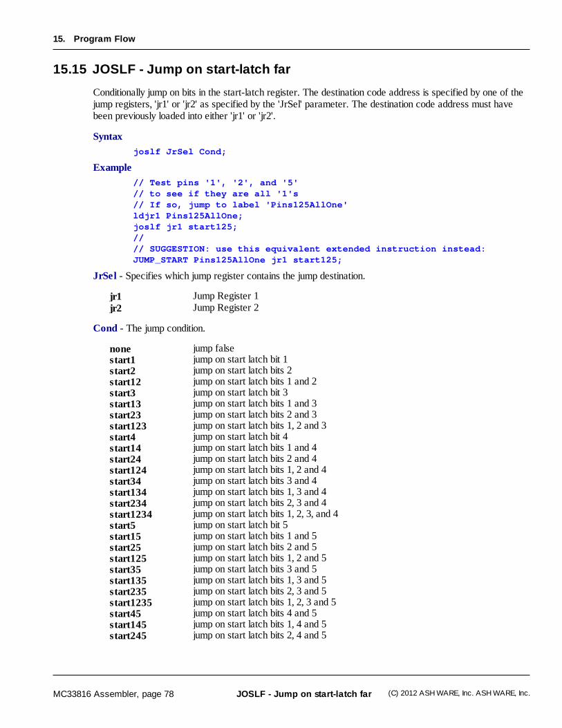
MC33816 Assembler, page 78 (C) 2012 ASH WARE, Inc. ASH WARE, Inc.
15. Program Flow
JOSLF - Jump on start-latch far
15.15 JOSLF - Jump on start-latch far
Conditionally jump on bits in the start-latch register. The destination code address is specified by one of thejump registers, 'jr1' or 'jr2' as specified by the 'JrSel' parameter. The destination code address must havebeen previously loaded into either 'jr1' or 'jr2'.
Syntax
joslf JrSel Cond;
Example
// Test pins '1', '2', and '5'// to see if they are all '1's// If so, jump to label 'Pins125AllOne'ldjr1 Pins125AllOne;joslf jr1 start125;//// SUGGESTION: use this equivalent extended instruction instead:JUMP_START Pins125AllOne jr1 start125;
JrSel - Specifies which jump register contains the jump destination.
jr1 Jump Register 1jr2 Jump Register 2
Cond - The jump condition.
none jump falsestart1 jump on start latch bit 1start2 jump on start latch bits 2start12 jump on start latch bits 1 and 2start3 jump on start latch bit 3start13 jump on start latch bits 1 and 3start23 jump on start latch bits 2 and 3start123 jump on start latch bits 1, 2 and 3start4 jump on start latch bit 4start14 jump on start latch bits 1 and 4start24 jump on start latch bits 2 and 4start124 jump on start latch bits 1, 2 and 4start34 jump on start latch bits 3 and 4start134 jump on start latch bits 1, 3 and 4start234 jump on start latch bits 2, 3 and 4start1234 jump on start latch bits 1, 2, 3, and 4start5 jump on start latch bit 5start15 jump on start latch bits 1 and 5start25 jump on start latch bits 2 and 5start125 jump on start latch bits 1, 2 and 5start35 jump on start latch bits 3 and 5start135 jump on start latch bits 1, 3 and 5start235 jump on start latch bits 2, 3 and 5start1235 jump on start latch bits 1, 2, 3 and 5start45 jump on start latch bits 4 and 5start145 jump on start latch bits 1, 4 and 5start245 jump on start latch bits 2, 4 and 5
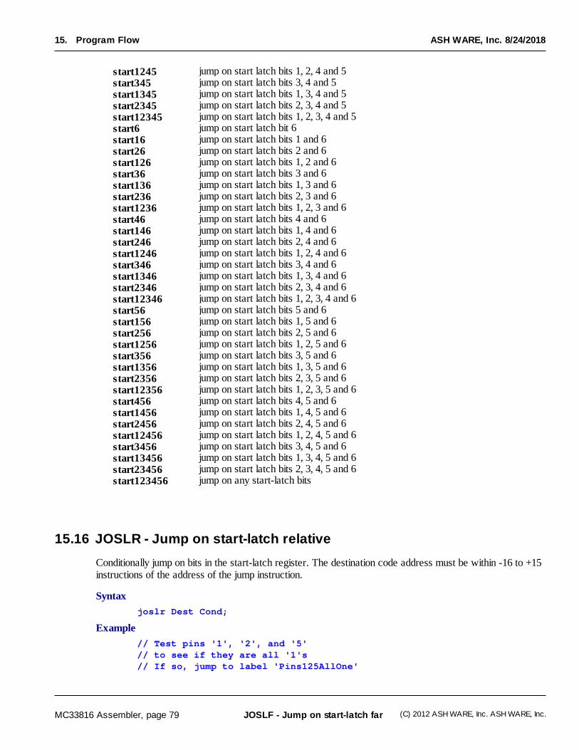
MC33816 Assembler, page 79 (C) 2012 ASH WARE, Inc. ASH WARE, Inc.
15. Program Flow
JOSLF - Jump on start-latch far
ASH WARE, Inc. 8/24/2018
start1245 jump on start latch bits 1, 2, 4 and 5start345 jump on start latch bits 3, 4 and 5start1345 jump on start latch bits 1, 3, 4 and 5start2345 jump on start latch bits 2, 3, 4 and 5start12345 jump on start latch bits 1, 2, 3, 4 and 5start6 jump on start latch bit 6start16 jump on start latch bits 1 and 6start26 jump on start latch bits 2 and 6start126 jump on start latch bits 1, 2 and 6start36 jump on start latch bits 3 and 6start136 jump on start latch bits 1, 3 and 6start236 jump on start latch bits 2, 3 and 6start1236 jump on start latch bits 1, 2, 3 and 6start46 jump on start latch bits 4 and 6start146 jump on start latch bits 1, 4 and 6start246 jump on start latch bits 2, 4 and 6start1246 jump on start latch bits 1, 2, 4 and 6start346 jump on start latch bits 3, 4 and 6start1346 jump on start latch bits 1, 3, 4 and 6start2346 jump on start latch bits 2, 3, 4 and 6start12346 jump on start latch bits 1, 2, 3, 4 and 6start56 jump on start latch bits 5 and 6start156 jump on start latch bits 1, 5 and 6start256 jump on start latch bits 2, 5 and 6start1256 jump on start latch bits 1, 2, 5 and 6start356 jump on start latch bits 3, 5 and 6start1356 jump on start latch bits 1, 3, 5 and 6start2356 jump on start latch bits 2, 3, 5 and 6start12356 jump on start latch bits 1, 2, 3, 5 and 6start456 jump on start latch bits 4, 5 and 6start1456 jump on start latch bits 1, 4, 5 and 6start2456 jump on start latch bits 2, 4, 5 and 6start12456 jump on start latch bits 1, 2, 4, 5 and 6start3456 jump on start latch bits 3, 4, 5 and 6start13456 jump on start latch bits 1, 3, 4, 5 and 6start23456 jump on start latch bits 2, 3, 4, 5 and 6start123456 jump on any start-latch bits
15.16 JOSLR - Jump on start-latch relative
Conditionally jump on bits in the start-latch register. The destination code address must be within -16 to +15instructions of the address of the jump instruction.
Syntax
joslr Dest Cond;
Example
// Test pins '1', '2', and '5'// to see if they are all '1's// If so, jump to label 'Pins125AllOne'
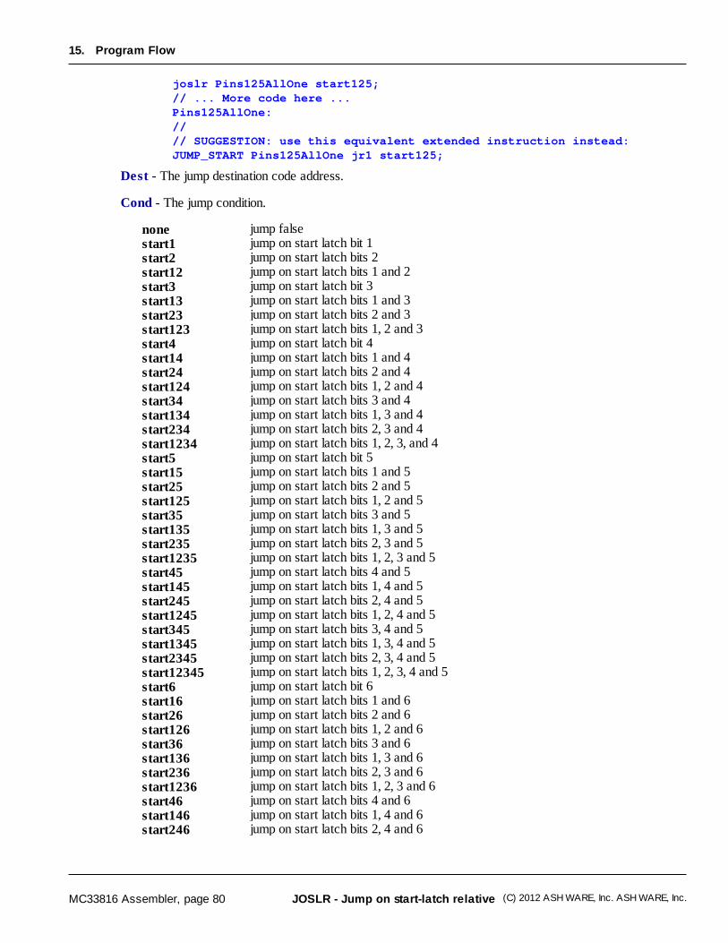
MC33816 Assembler, page 80 (C) 2012 ASH WARE, Inc. ASH WARE, Inc.
15. Program Flow
JOSLR - Jump on start-latch relative
joslr Pins125AllOne start125;// ... More code here ...Pins125AllOne://// SUGGESTION: use this equivalent extended instruction instead:JUMP_START Pins125AllOne jr1 start125;
Dest - The jump destination code address.
Cond - The jump condition.
none jump falsestart1 jump on start latch bit 1start2 jump on start latch bits 2start12 jump on start latch bits 1 and 2start3 jump on start latch bit 3start13 jump on start latch bits 1 and 3start23 jump on start latch bits 2 and 3start123 jump on start latch bits 1, 2 and 3start4 jump on start latch bit 4start14 jump on start latch bits 1 and 4start24 jump on start latch bits 2 and 4start124 jump on start latch bits 1, 2 and 4start34 jump on start latch bits 3 and 4start134 jump on start latch bits 1, 3 and 4start234 jump on start latch bits 2, 3 and 4start1234 jump on start latch bits 1, 2, 3, and 4start5 jump on start latch bit 5start15 jump on start latch bits 1 and 5start25 jump on start latch bits 2 and 5start125 jump on start latch bits 1, 2 and 5start35 jump on start latch bits 3 and 5start135 jump on start latch bits 1, 3 and 5start235 jump on start latch bits 2, 3 and 5start1235 jump on start latch bits 1, 2, 3 and 5start45 jump on start latch bits 4 and 5start145 jump on start latch bits 1, 4 and 5start245 jump on start latch bits 2, 4 and 5start1245 jump on start latch bits 1, 2, 4 and 5start345 jump on start latch bits 3, 4 and 5start1345 jump on start latch bits 1, 3, 4 and 5start2345 jump on start latch bits 2, 3, 4 and 5start12345 jump on start latch bits 1, 2, 3, 4 and 5start6 jump on start latch bit 6start16 jump on start latch bits 1 and 6start26 jump on start latch bits 2 and 6start126 jump on start latch bits 1, 2 and 6start36 jump on start latch bits 3 and 6start136 jump on start latch bits 1, 3 and 6start236 jump on start latch bits 2, 3 and 6start1236 jump on start latch bits 1, 2, 3 and 6start46 jump on start latch bits 4 and 6start146 jump on start latch bits 1, 4 and 6start246 jump on start latch bits 2, 4 and 6
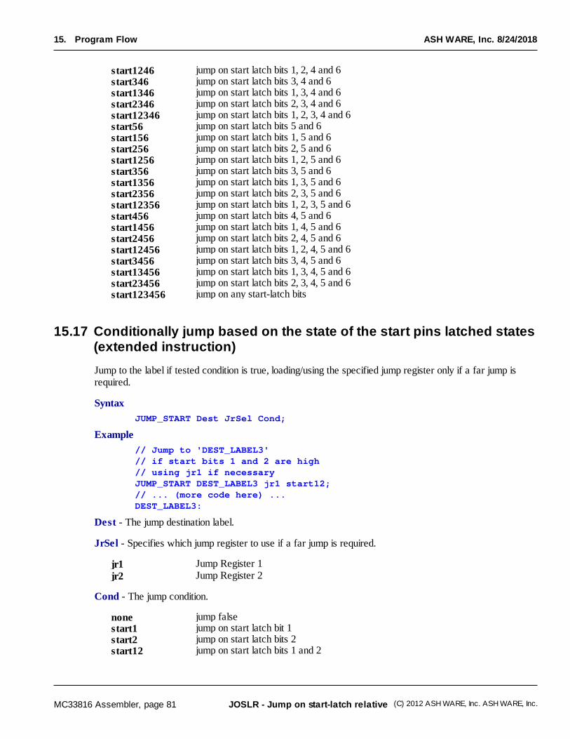
MC33816 Assembler, page 81 (C) 2012 ASH WARE, Inc. ASH WARE, Inc.
15. Program Flow
JOSLR - Jump on start-latch relative
ASH WARE, Inc. 8/24/2018
start1246 jump on start latch bits 1, 2, 4 and 6start346 jump on start latch bits 3, 4 and 6start1346 jump on start latch bits 1, 3, 4 and 6start2346 jump on start latch bits 2, 3, 4 and 6start12346 jump on start latch bits 1, 2, 3, 4 and 6start56 jump on start latch bits 5 and 6start156 jump on start latch bits 1, 5 and 6start256 jump on start latch bits 2, 5 and 6start1256 jump on start latch bits 1, 2, 5 and 6start356 jump on start latch bits 3, 5 and 6start1356 jump on start latch bits 1, 3, 5 and 6start2356 jump on start latch bits 2, 3, 5 and 6start12356 jump on start latch bits 1, 2, 3, 5 and 6start456 jump on start latch bits 4, 5 and 6start1456 jump on start latch bits 1, 4, 5 and 6start2456 jump on start latch bits 2, 4, 5 and 6start12456 jump on start latch bits 1, 2, 4, 5 and 6start3456 jump on start latch bits 3, 4, 5 and 6start13456 jump on start latch bits 1, 3, 4, 5 and 6start23456 jump on start latch bits 2, 3, 4, 5 and 6start123456 jump on any start-latch bits
15.17 Conditionally jump based on the state of the start pins latched states(extended instruction)
Jump to the label if tested condition is true, loading/using the specified jump register only if a far jump isrequired.
Syntax
JUMP_START Dest JrSel Cond;
Example
// Jump to 'DEST_LABEL3'// if start bits 1 and 2 are high// using jr1 if necessaryJUMP_START DEST_LABEL3 jr1 start12;// ... (more code here) ...DEST_LABEL3:
Dest - The jump destination label.
JrSel - Specifies which jump register to use if a far jump is required.
jr1 Jump Register 1jr2 Jump Register 2
Cond - The jump condition.
none jump falsestart1 jump on start latch bit 1start2 jump on start latch bits 2start12 jump on start latch bits 1 and 2
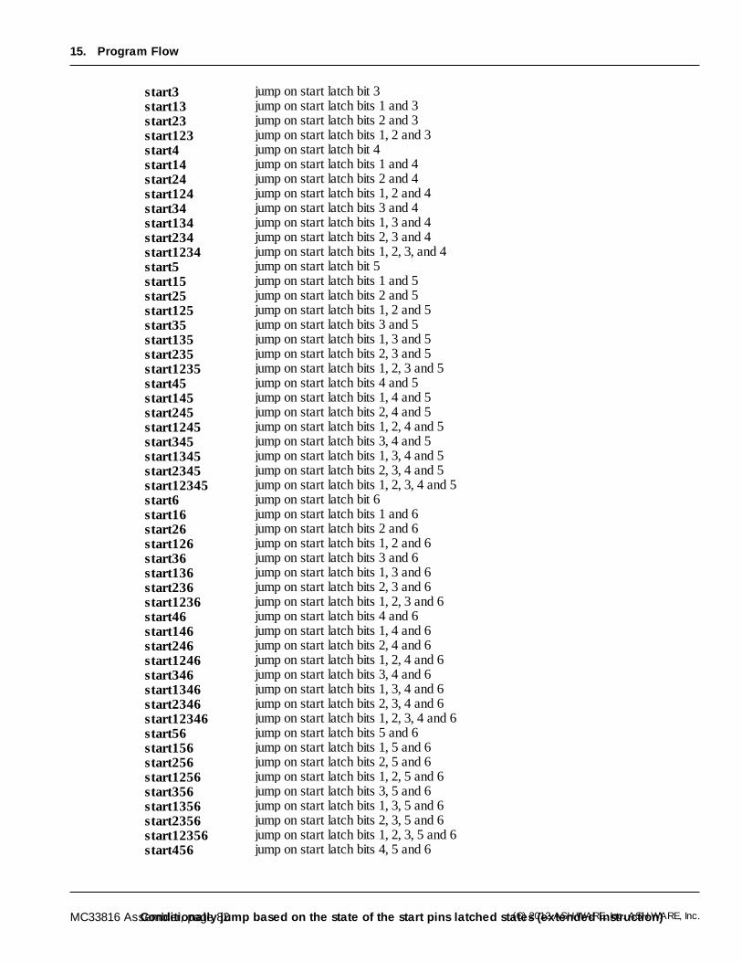
MC33816 Assembler, page 82 (C) 2012 ASH WARE, Inc. ASH WARE, Inc.
15. Program Flow
Conditionally jump based on the state of the start pins latched states (extended instruction)
start3 jump on start latch bit 3start13 jump on start latch bits 1 and 3start23 jump on start latch bits 2 and 3start123 jump on start latch bits 1, 2 and 3start4 jump on start latch bit 4start14 jump on start latch bits 1 and 4start24 jump on start latch bits 2 and 4start124 jump on start latch bits 1, 2 and 4start34 jump on start latch bits 3 and 4start134 jump on start latch bits 1, 3 and 4start234 jump on start latch bits 2, 3 and 4start1234 jump on start latch bits 1, 2, 3, and 4start5 jump on start latch bit 5start15 jump on start latch bits 1 and 5start25 jump on start latch bits 2 and 5start125 jump on start latch bits 1, 2 and 5start35 jump on start latch bits 3 and 5start135 jump on start latch bits 1, 3 and 5start235 jump on start latch bits 2, 3 and 5start1235 jump on start latch bits 1, 2, 3 and 5start45 jump on start latch bits 4 and 5start145 jump on start latch bits 1, 4 and 5start245 jump on start latch bits 2, 4 and 5start1245 jump on start latch bits 1, 2, 4 and 5start345 jump on start latch bits 3, 4 and 5start1345 jump on start latch bits 1, 3, 4 and 5start2345 jump on start latch bits 2, 3, 4 and 5start12345 jump on start latch bits 1, 2, 3, 4 and 5start6 jump on start latch bit 6start16 jump on start latch bits 1 and 6start26 jump on start latch bits 2 and 6start126 jump on start latch bits 1, 2 and 6start36 jump on start latch bits 3 and 6start136 jump on start latch bits 1, 3 and 6start236 jump on start latch bits 2, 3 and 6start1236 jump on start latch bits 1, 2, 3 and 6start46 jump on start latch bits 4 and 6start146 jump on start latch bits 1, 4 and 6start246 jump on start latch bits 2, 4 and 6start1246 jump on start latch bits 1, 2, 4 and 6start346 jump on start latch bits 3, 4 and 6start1346 jump on start latch bits 1, 3, 4 and 6start2346 jump on start latch bits 2, 3, 4 and 6start12346 jump on start latch bits 1, 2, 3, 4 and 6start56 jump on start latch bits 5 and 6start156 jump on start latch bits 1, 5 and 6start256 jump on start latch bits 2, 5 and 6start1256 jump on start latch bits 1, 2, 5 and 6start356 jump on start latch bits 3, 5 and 6start1356 jump on start latch bits 1, 3, 5 and 6start2356 jump on start latch bits 2, 3, 5 and 6start12356 jump on start latch bits 1, 2, 3, 5 and 6start456 jump on start latch bits 4, 5 and 6
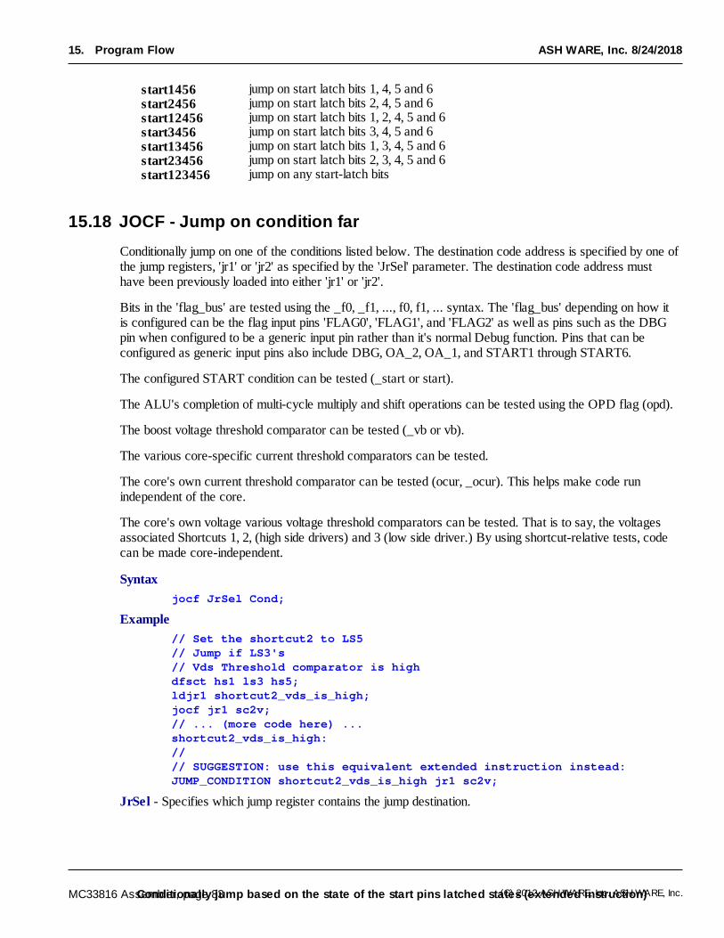
MC33816 Assembler, page 83 (C) 2012 ASH WARE, Inc. ASH WARE, Inc.
15. Program Flow
Conditionally jump based on the state of the start pins latched states (extended instruction)
ASH WARE, Inc. 8/24/2018
start1456 jump on start latch bits 1, 4, 5 and 6start2456 jump on start latch bits 2, 4, 5 and 6start12456 jump on start latch bits 1, 2, 4, 5 and 6start3456 jump on start latch bits 3, 4, 5 and 6start13456 jump on start latch bits 1, 3, 4, 5 and 6start23456 jump on start latch bits 2, 3, 4, 5 and 6start123456 jump on any start-latch bits
15.18 JOCF - Jump on condition far
Conditionally jump on one of the conditions listed below. The destination code address is specified by one ofthe jump registers, 'jr1' or 'jr2' as specified by the 'JrSel' parameter. The destination code address musthave been previously loaded into either 'jr1' or 'jr2'.
Bits in the 'flag_bus' are tested using the _f0, _f1, ..., f0, f1, ... syntax. The 'flag_bus' depending on how itis configured can be the flag input pins 'FLAG0', 'FLAG1', and 'FLAG2' as well as pins such as the DBGpin when configured to be a generic input pin rather than it's normal Debug function. Pins that can beconfigured as generic input pins also include DBG, OA_2, OA_1, and START1 through START6.
The configured START condition can be tested (_start or start).
The ALU's completion of multi-cycle multiply and shift operations can be tested using the OPD flag (opd).
The boost voltage threshold comparator can be tested (_vb or vb).
The various core-specific current threshold comparators can be tested.
The core's own current threshold comparator can be tested (ocur, _ocur). This helps make code runindependent of the core.
The core's own voltage various voltage threshold comparators can be tested. That is to say, the voltagesassociated Shortcuts 1, 2, (high side drivers) and 3 (low side driver.) By using shortcut-relative tests, codecan be made core-independent.
Syntax
jocf JrSel Cond;
Example
// Set the shortcut2 to LS5// Jump if LS3's// Vds Threshold comparator is highdfsct hs1 ls3 hs5;ldjr1 shortcut2_vds_is_high;jocf jr1 sc2v;// ... (more code here) ...shortcut2_vds_is_high://// SUGGESTION: use this equivalent extended instruction instead:JUMP_CONDITION shortcut2_vds_is_high jr1 sc2v;
JrSel - Specifies which jump register contains the jump destination.
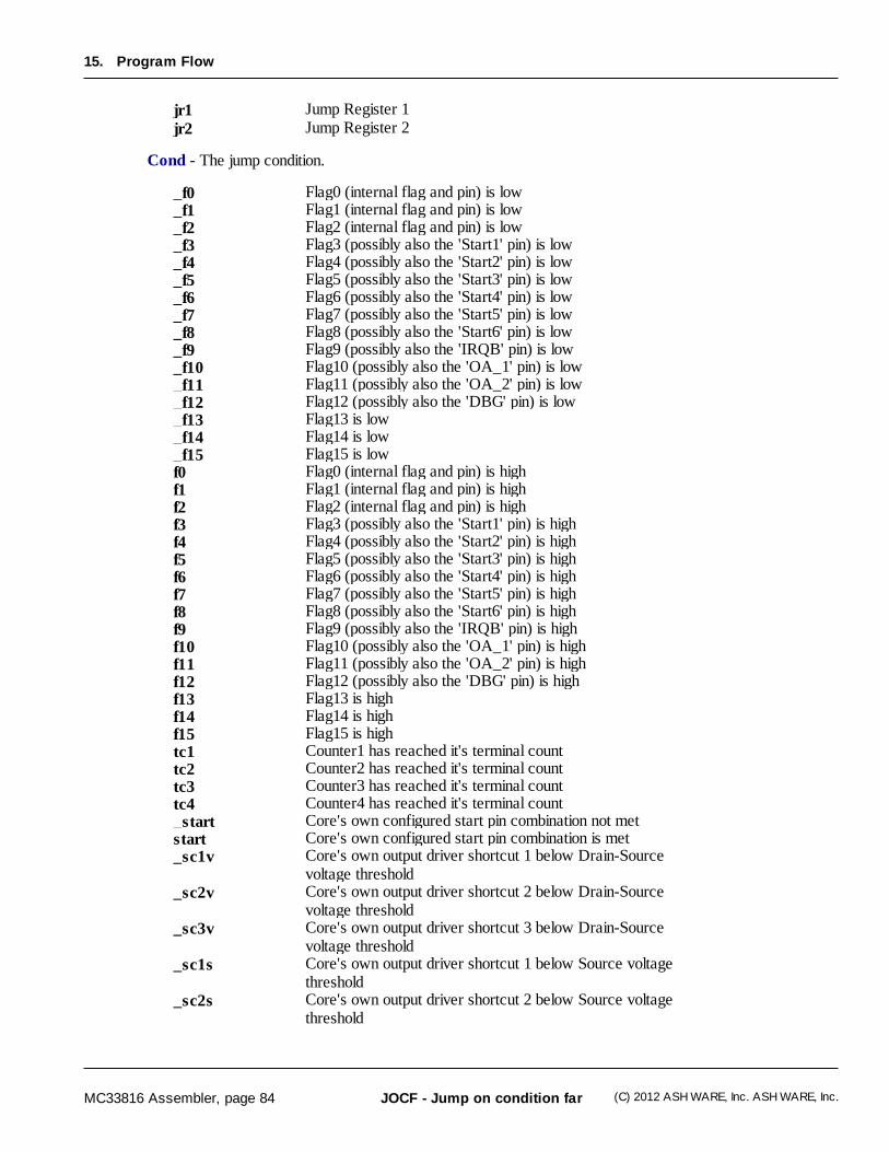
MC33816 Assembler, page 84 (C) 2012 ASH WARE, Inc. ASH WARE, Inc.
15. Program Flow
JOCF - Jump on condition far
jr1 Jump Register 1jr2 Jump Register 2
Cond - The jump condition.
_f0 Flag0 (internal flag and pin) is low_f1 Flag1 (internal flag and pin) is low_f2 Flag2 (internal flag and pin) is low_f3 Flag3 (possibly also the 'Start1' pin) is low_f4 Flag4 (possibly also the 'Start2' pin) is low_f5 Flag5 (possibly also the 'Start3' pin) is low_f6 Flag6 (possibly also the 'Start4' pin) is low_f7 Flag7 (possibly also the 'Start5' pin) is low_f8 Flag8 (possibly also the 'Start6' pin) is low_f9 Flag9 (possibly also the 'IRQB' pin) is low_f10 Flag10 (possibly also the 'OA_1' pin) is low_f11 Flag11 (possibly also the 'OA_2' pin) is low_f12 Flag12 (possibly also the 'DBG' pin) is low_f13 Flag13 is low_f14 Flag14 is low_f15 Flag15 is lowf0 Flag0 (internal flag and pin) is highf1 Flag1 (internal flag and pin) is highf2 Flag2 (internal flag and pin) is highf3 Flag3 (possibly also the 'Start1' pin) is highf4 Flag4 (possibly also the 'Start2' pin) is highf5 Flag5 (possibly also the 'Start3' pin) is highf6 Flag6 (possibly also the 'Start4' pin) is highf7 Flag7 (possibly also the 'Start5' pin) is highf8 Flag8 (possibly also the 'Start6' pin) is highf9 Flag9 (possibly also the 'IRQB' pin) is highf10 Flag10 (possibly also the 'OA_1' pin) is highf11 Flag11 (possibly also the 'OA_2' pin) is highf12 Flag12 (possibly also the 'DBG' pin) is highf13 Flag13 is highf14 Flag14 is highf15 Flag15 is hightc1 Counter1 has reached it's terminal counttc2 Counter2 has reached it's terminal counttc3 Counter3 has reached it's terminal counttc4 Counter4 has reached it's terminal count_start Core's own configured start pin combination not metstart Core's own configured start pin combination is met_sc1v Core's own output driver shortcut 1 below Drain-Source
voltage threshold_sc2v Core's own output driver shortcut 2 below Drain-Source
voltage threshold_sc3v Core's own output driver shortcut 3 below Drain-Source
voltage threshold_sc1s Core's own output driver shortcut 1 below Source voltage
threshold_sc2s Core's own output driver shortcut 2 below Source voltage
threshold
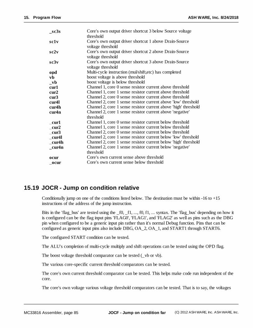
MC33816 Assembler, page 85 (C) 2012 ASH WARE, Inc. ASH WARE, Inc.
15. Program Flow
JOCF - Jump on condition far
ASH WARE, Inc. 8/24/2018
_sc3s Core's own output driver shortcut 3 below Source voltagethreshold
sc1v Core's own output driver shortcut 1 above Drain-Sourcevoltage threshold
sc2v Core's own output driver shortcut 2 above Drain-Sourcevoltage threshold
sc3v Core's own output driver shortcut 3 above Drain-Sourcevoltage threshold
opd Multi-cycle instruction (mul/shift,etc) has completedvb boost voltage is above threshold_vb boost voltage is below thresholdcur1 Channel 1, core 0 sense resistor current above thresholdcur2 Channel 1, core 1 sense resistor current above thresholdcur3 Channel 2, core 0 sense resistor current above thresholdcur4l Channel 2, core 1 sense resistor current above 'low' thresholdcur4h Channel 2, core 1 sense resistor current above 'high' thresholdcur4n Channel 2, core 1 sense resistor current above 'negative'
threshold_cur1 Channel 1, core 0 sense resistor current below threshold_cur2 Channel 1, core 1 sense resistor current below threshold_cur3 Channel 2, core 0 sense resistor current below threshold_cur4l Channel 2, core 1 sense resistor current below 'low' threshold_cur4h Channel 2, core 1 sense resistor current below 'high' threshold_cur4n Channel 2, core 1 sense resistor current below 'negative'
thresholdocur Core's own current sense above threshold_ocur Core's own current sense below threshold
15.19 JOCR - Jump on condition relative
Conditionally jump on one of the conditions listed below. The destination must be within -16 to +15instructions of the address of the jump instruction.
Bits in the 'flag_bus' are tested using the _f0, _f1, ..., f0, f1, ... syntax. The 'flag_bus' depending on how itis configured can be the flag input pins 'FLAG0', 'FLAG1', and 'FLAG2' as well as pins such as the DBGpin when configured to be a generic input pin rather than it's normal Debug function. Pins that can beconfigured as generic input pins also include DBG, OA_2, OA_1, and START1 through START6.
The configured START condition can be tested.
The ALU's completion of multi-cycle multiply and shift operations can be tested using the OPD flag.
The boost voltage threshold comparator can be tested (_vb or vb).
The various core-specific current threshold comparators can be tested.
The core's own current threshold comparator can be tested. This helps make code run independent of thecore.
The core's own voltage various voltage threshold comparators can be tested. That is to say, the voltages
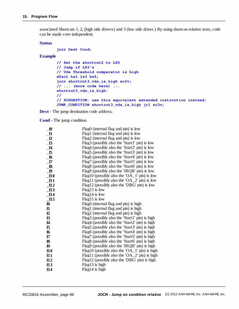
MC33816 Assembler, page 86 (C) 2012 ASH WARE, Inc. ASH WARE, Inc.
15. Program Flow
JOCR - Jump on condition relative
associated Shortcuts 1, 2, (high side drivers) and 3 (low side driver.) By using shortcut-relative tests, codecan be made core-independent.
Syntax
jocr Dest Cond;
Example
// Set the shortcut2 to LS5// Jump if LS3's// Vds Threshold comparator is highdfsct hs1 ls3 hs5;jocr shortcut3_vds_is_high sc3v;// ... (more code here) ...shortcut3_vds_is_high://// SUGGESTION: use this equivalent extended instruction instead:JUMP_CONDITION shortcut3_vds_is_high jr1 sc3v;
Dest - The jump destination code address.
Cond - The jump condition.
_f0 Flag0 (internal flag and pin) is low_f1 Flag1 (internal flag and pin) is low_f2 Flag2 (internal flag and pin) is low_f3 Flag3 (possibly also the 'Start1' pin) is low_f4 Flag4 (possibly also the 'Start2' pin) is low_f5 Flag5 (possibly also the 'Start3' pin) is low_f6 Flag6 (possibly also the 'Start4' pin) is low_f7 Flag7 (possibly also the 'Start5' pin) is low_f8 Flag8 (possibly also the 'Start6' pin) is low_f9 Flag9 (possibly also the 'IRQB' pin) is low_f10 Flag10 (possibly also the 'OA_1' pin) is low_f11 Flag11 (possibly also the 'OA_2' pin) is low_f12 Flag12 (possibly also the 'DBG' pin) is low_f13 Flag13 is low_f14 Flag14 is low_f15 Flag15 is lowf0 Flag0 (internal flag and pin) is highf1 Flag1 (internal flag and pin) is highf2 Flag2 (internal flag and pin) is highf3 Flag3 (possibly also the 'Start1' pin) is highf4 Flag4 (possibly also the 'Start2' pin) is highf5 Flag5 (possibly also the 'Start3' pin) is highf6 Flag6 (possibly also the 'Start4' pin) is highf7 Flag7 (possibly also the 'Start5' pin) is highf8 Flag8 (possibly also the 'Start6' pin) is highf9 Flag9 (possibly also the 'IRQB' pin) is highf10 Flag10 (possibly also the 'OA_1' pin) is highf11 Flag11 (possibly also the 'OA_2' pin) is highf12 Flag12 (possibly also the 'DBG' pin) is highf13 Flag13 is highf14 Flag14 is high
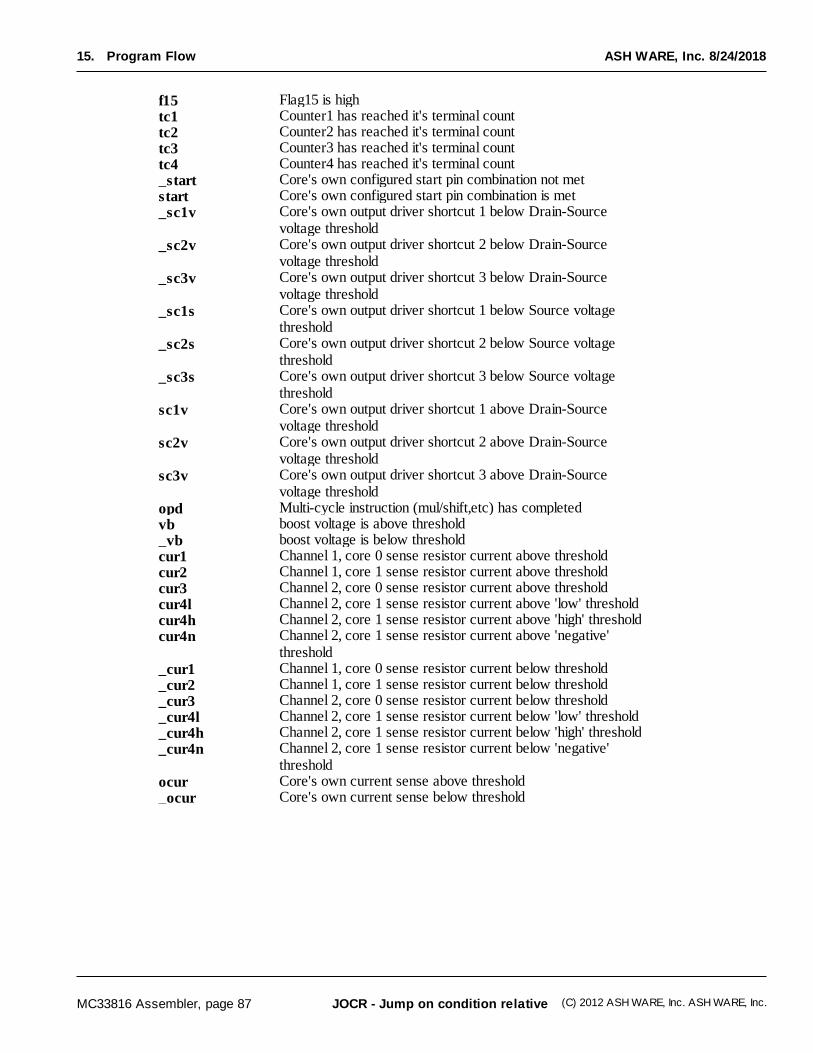
MC33816 Assembler, page 87 (C) 2012 ASH WARE, Inc. ASH WARE, Inc.
15. Program Flow
JOCR - Jump on condition relative
ASH WARE, Inc. 8/24/2018
f15 Flag15 is hightc1 Counter1 has reached it's terminal counttc2 Counter2 has reached it's terminal counttc3 Counter3 has reached it's terminal counttc4 Counter4 has reached it's terminal count_start Core's own configured start pin combination not metstart Core's own configured start pin combination is met_sc1v Core's own output driver shortcut 1 below Drain-Source
voltage threshold_sc2v Core's own output driver shortcut 2 below Drain-Source
voltage threshold_sc3v Core's own output driver shortcut 3 below Drain-Source
voltage threshold_sc1s Core's own output driver shortcut 1 below Source voltage
threshold_sc2s Core's own output driver shortcut 2 below Source voltage
threshold_sc3s Core's own output driver shortcut 3 below Source voltage
thresholdsc1v Core's own output driver shortcut 1 above Drain-Source
voltage thresholdsc2v Core's own output driver shortcut 2 above Drain-Source
voltage thresholdsc3v Core's own output driver shortcut 3 above Drain-Source
voltage thresholdopd Multi-cycle instruction (mul/shift,etc) has completedvb boost voltage is above threshold_vb boost voltage is below thresholdcur1 Channel 1, core 0 sense resistor current above thresholdcur2 Channel 1, core 1 sense resistor current above thresholdcur3 Channel 2, core 0 sense resistor current above thresholdcur4l Channel 2, core 1 sense resistor current above 'low' thresholdcur4h Channel 2, core 1 sense resistor current above 'high' thresholdcur4n Channel 2, core 1 sense resistor current above 'negative'
threshold_cur1 Channel 1, core 0 sense resistor current below threshold_cur2 Channel 1, core 1 sense resistor current below threshold_cur3 Channel 2, core 0 sense resistor current below threshold_cur4l Channel 2, core 1 sense resistor current below 'low' threshold_cur4h Channel 2, core 1 sense resistor current below 'high' threshold_cur4n Channel 2, core 1 sense resistor current below 'negative'
thresholdocur Core's own current sense above threshold_ocur Core's own current sense below threshold
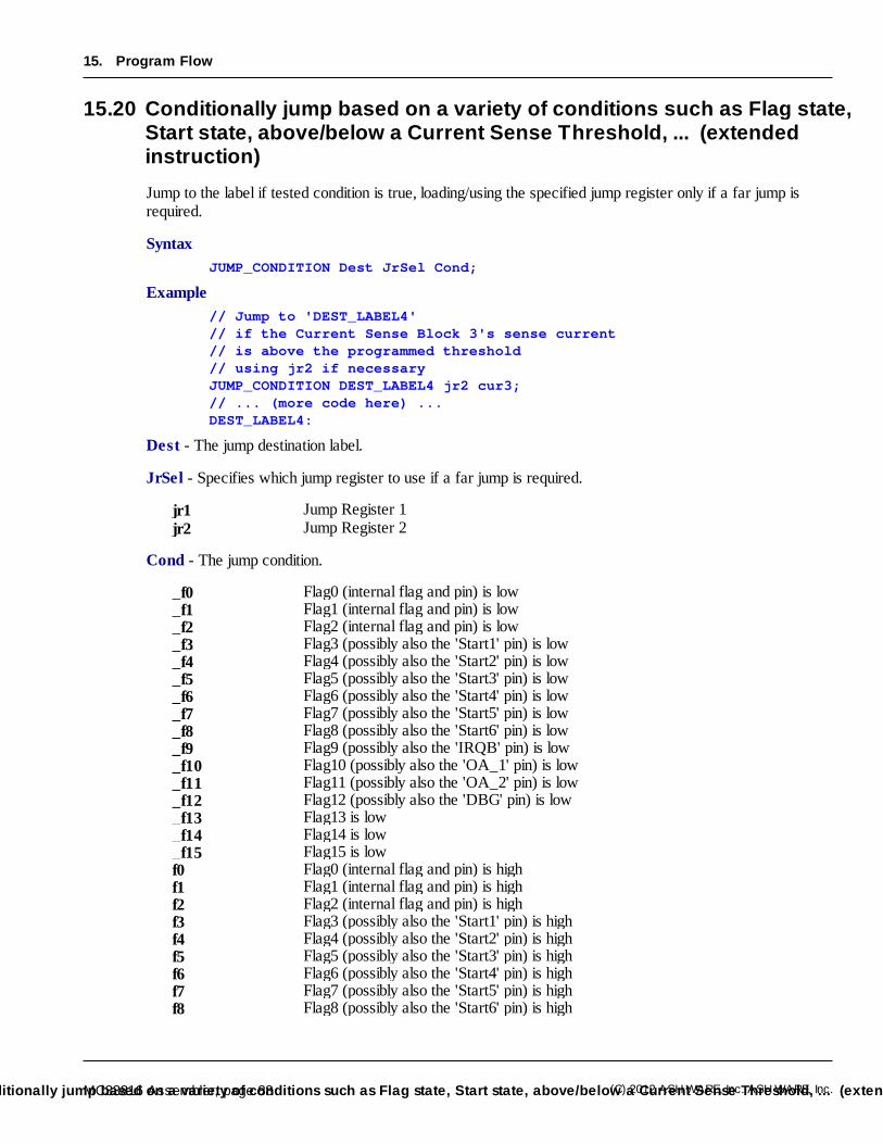
MC33816 Assembler, page 88 (C) 2012 ASH WARE, Inc. ASH WARE, Inc.
15. Program Flow
Conditionally jump based on a variety of conditions such as Flag state, Start state, above/below a Current Sense Threshold, ... (extended instruction)
15.20 Conditionally jump based on a variety of conditions such as Flag state,Start state, above/below a Current Sense Threshold, ... (extendedinstruction)
Jump to the label if tested condition is true, loading/using the specified jump register only if a far jump isrequired.
Syntax
JUMP_CONDITION Dest JrSel Cond;
Example
// Jump to 'DEST_LABEL4'// if the Current Sense Block 3's sense current// is above the programmed threshold// using jr2 if necessaryJUMP_CONDITION DEST_LABEL4 jr2 cur3;// ... (more code here) ...DEST_LABEL4:
Dest - The jump destination label.
JrSel - Specifies which jump register to use if a far jump is required.
jr1 Jump Register 1jr2 Jump Register 2
Cond - The jump condition.
_f0 Flag0 (internal flag and pin) is low_f1 Flag1 (internal flag and pin) is low_f2 Flag2 (internal flag and pin) is low_f3 Flag3 (possibly also the 'Start1' pin) is low_f4 Flag4 (possibly also the 'Start2' pin) is low_f5 Flag5 (possibly also the 'Start3' pin) is low_f6 Flag6 (possibly also the 'Start4' pin) is low_f7 Flag7 (possibly also the 'Start5' pin) is low_f8 Flag8 (possibly also the 'Start6' pin) is low_f9 Flag9 (possibly also the 'IRQB' pin) is low_f10 Flag10 (possibly also the 'OA_1' pin) is low_f11 Flag11 (possibly also the 'OA_2' pin) is low_f12 Flag12 (possibly also the 'DBG' pin) is low_f13 Flag13 is low_f14 Flag14 is low_f15 Flag15 is lowf0 Flag0 (internal flag and pin) is highf1 Flag1 (internal flag and pin) is highf2 Flag2 (internal flag and pin) is highf3 Flag3 (possibly also the 'Start1' pin) is highf4 Flag4 (possibly also the 'Start2' pin) is highf5 Flag5 (possibly also the 'Start3' pin) is highf6 Flag6 (possibly also the 'Start4' pin) is highf7 Flag7 (possibly also the 'Start5' pin) is highf8 Flag8 (possibly also the 'Start6' pin) is high
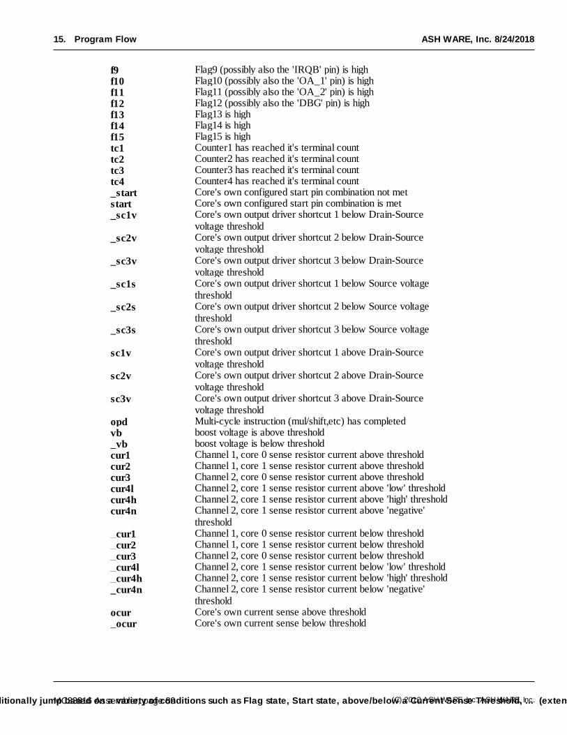
MC33816 Assembler, page 89 (C) 2012 ASH WARE, Inc. ASH WARE, Inc.
15. Program Flow
Conditionally jump based on a variety of conditions such as Flag state, Start state, above/below a Current Sense Threshold, ... (extended instruction)
ASH WARE, Inc. 8/24/2018
f9 Flag9 (possibly also the 'IRQB' pin) is highf10 Flag10 (possibly also the 'OA_1' pin) is highf11 Flag11 (possibly also the 'OA_2' pin) is highf12 Flag12 (possibly also the 'DBG' pin) is highf13 Flag13 is highf14 Flag14 is highf15 Flag15 is hightc1 Counter1 has reached it's terminal counttc2 Counter2 has reached it's terminal counttc3 Counter3 has reached it's terminal counttc4 Counter4 has reached it's terminal count_start Core's own configured start pin combination not metstart Core's own configured start pin combination is met_sc1v Core's own output driver shortcut 1 below Drain-Source
voltage threshold_sc2v Core's own output driver shortcut 2 below Drain-Source
voltage threshold_sc3v Core's own output driver shortcut 3 below Drain-Source
voltage threshold_sc1s Core's own output driver shortcut 1 below Source voltage
threshold_sc2s Core's own output driver shortcut 2 below Source voltage
threshold_sc3s Core's own output driver shortcut 3 below Source voltage
thresholdsc1v Core's own output driver shortcut 1 above Drain-Source
voltage thresholdsc2v Core's own output driver shortcut 2 above Drain-Source
voltage thresholdsc3v Core's own output driver shortcut 3 above Drain-Source
voltage thresholdopd Multi-cycle instruction (mul/shift,etc) has completedvb boost voltage is above threshold_vb boost voltage is below thresholdcur1 Channel 1, core 0 sense resistor current above thresholdcur2 Channel 1, core 1 sense resistor current above thresholdcur3 Channel 2, core 0 sense resistor current above thresholdcur4l Channel 2, core 1 sense resistor current above 'low' thresholdcur4h Channel 2, core 1 sense resistor current above 'high' thresholdcur4n Channel 2, core 1 sense resistor current above 'negative'
threshold_cur1 Channel 1, core 0 sense resistor current below threshold_cur2 Channel 1, core 1 sense resistor current below threshold_cur3 Channel 2, core 0 sense resistor current below threshold_cur4l Channel 2, core 1 sense resistor current below 'low' threshold_cur4h Channel 2, core 1 sense resistor current below 'high' threshold_cur4n Channel 2, core 1 sense resistor current below 'negative'
thresholdocur Core's own current sense above threshold_ocur Core's own current sense below threshold
MC33816 Assembler, page 90 (C) 2012 ASH WARE, Inc. ASH WARE, Inc.
15. Program Flow
JFBKF - Jump on feedback far
15.21 JFBKF - Jump on feedback far
Tests diagnostic voltage feedback to see if the selected diagnostic node is above or below a threshold.
The destination code address is specified by one of the jump registers, 'jr1' or 'jr2', as specified by the'JrSel' parameter. The destination code address must have been previously loaded into either 'jr1' or 'jr2'.
Parameter 'Pol' determines if the jump is taken when the voltage is below or above the threshold.
Syntax
jfbkf JrSel SelFbk Pol;
Example
// Jump if HS3's// Vsrc Threshold comparator is lowldjr1 hs3_vsrc_is_low;jfbkf jr1 hs3s low;// ... (more code here) ...hs3_vsrc_is_low://// SUGGESTION: use this equivalent extended instruction instead:JUMP_FEEDBACK hs3_vsrc_is_low jr1 hs3s low;
JrSel - Specifies which jump register contains the jump destination.
jr1 Jump Register 1jr2 Jump Register 2
SelFbk - Feedback threshold.
hs1v High side pre-driver 1 VDS feedback above thresholdhs1s High side pre-driver 1 VSRC feedback above thresholdhs2v High side pre-driver 2 VDS feedback above thresholdhs2s High side pre-driver 2 VSRC feedback above thresholdhs3v High side pre-driver 3 VDS feedback above thresholdhs3s High side pre-driver 3 VSRC feedback above thresholdhs4v High side pre-driver 4 VDS feedback above thresholdhs4s High side pre-driver 4 VSRC feedback above thresholdhs5v High side pre-driver 5 VDS feedback above thresholdhs5s High side pre-driver 5 VSRC feedback above thresholdls1v Low side pre-driver 1 VDS feedback above thresholdls2v Low side pre-driver 2 VDS feedback above thresholdls3v Low side pre-driver 3 VDS feedback above thresholdls4v Low side pre-driver 4 VDS feedback above thresholdls5v Low side pre-driver 5 VDS feedback above thresholdls6v Low side pre-driver 6 VDS feedback above threshold
Pol - Specifies jump on feedback low or on feedbakc high.
low Jump on feedback lowhigh Jump on feedback high
MC33816 Assembler, page 91 (C) 2012 ASH WARE, Inc. ASH WARE, Inc.
15. Program Flow
JFBKR - Jump on feedback relative
ASH WARE, Inc. 8/24/2018
15.22 JFBKR - Jump on feedback relative
Tests diagnostic voltage feedback to see if the selected diagnostic node is above or below a threshold.
The destination must be within -16 to +15 instructions of the address of the jump instruction.
Parameter 'Pol' determines if the jump is taken when the voltage is below or above the threshold.
Syntax
jfbkr Dest SelFbk Pol;
Example
// Jump if HS4's// Vsrc Threshold comparator is lowjfbkr hs4_vsrc_is_low hs4s low;// ... (more code here) ...hs4_vsrc_is_low://// SUGGESTION: use this equivalent extended instruction instead:JUMP_FEEDBACK hs4_vsrc_is_low jr1 hs4s low;
Dest - The jump destination code address.
SelFbk
hs1v High side pre-driver 1 VDS feedback above thresholdhs1s High side pre-driver 1 VSRC feedback above thresholdhs2v High side pre-driver 2 VDS feedback above thresholdhs2s High side pre-driver 2 VSRC feedback above thresholdhs3v High side pre-driver 3 VDS feedback above thresholdhs3s High side pre-driver 3 VSRC feedback above thresholdhs4v High side pre-driver 4 VDS feedback above thresholdhs4s High side pre-driver 4 VSRC feedback above thresholdhs5v High side pre-driver 5 VDS feedback above thresholdhs5s High side pre-driver 5 VSRC feedback above thresholdls1v Low side pre-driver 1 VDS feedback above thresholdls2v Low side pre-driver 2 VDS feedback above thresholdls3v Low side pre-driver 3 VDS feedback above thresholdls4v Low side pre-driver 4 VDS feedback above thresholdls5v Low side pre-driver 5 VDS feedback above thresholdls6v Low side pre-driver 6 VDS feedback above threshold
Pol - Specifies jump on feedback low or on feedback high.
low Jump on feedback lowhigh Jump on feedback high
MC33816 Assembler, page 92 (C) 2012 ASH WARE, Inc. ASH WARE, Inc.
15. Program Flow
Conditionally jump based on the state of a 'Diagnostic Feedback Comparator' output (extended instruction)
15.23 Conditionally jump based on the state of a 'Diagnostic FeedbackComparator' output (extended instruction)
Jump to the label if tested condition is true, loading/using the specified jump register only if a far jump isrequired.
Syntax
JUMP_FEEDBACK Dest JrSel SelFbk Pol;
Example
// Jump to 'DEST_LABEL5'// if HS2's Vsrc Threshold comparator is low// using jr1 if necessaryJUMP_FEEDBACK DEST_LABEL5 jr1 hs2v low;// ... (more code here) ...DEST_LABEL5:
Dest - The jump destination label.
JrSel - Specifies which jump register to use if a far jump is required.
jr1 Jump Register 1jr2 Jump Register 2
SelFbk - Feedback threshold.
hs1v High side pre-driver 1 VDS feedback above thresholdhs1s High side pre-driver 1 VSRC feedback above thresholdhs2v High side pre-driver 2 VDS feedback above thresholdhs2s High side pre-driver 2 VSRC feedback above thresholdhs3v High side pre-driver 3 VDS feedback above thresholdhs3s High side pre-driver 3 VSRC feedback above thresholdhs4v High side pre-driver 4 VDS feedback above thresholdhs4s High side pre-driver 4 VSRC feedback above thresholdhs5v High side pre-driver 5 VDS feedback above thresholdhs5s High side pre-driver 5 VSRC feedback above thresholdls1v Low side pre-driver 1 VDS feedback above thresholdls2v Low side pre-driver 2 VDS feedback above thresholdls3v Low side pre-driver 3 VDS feedback above thresholdls4v Low side pre-driver 4 VDS feedback above thresholdls5v Low side pre-driver 5 VDS feedback above thresholdls6v Low side pre-driver 6 VDS feedback above threshold
Pol - Specifies jump on feedback low or on feedbakc high.
low Jump on feedback lowhigh Jump on feedback high
MC33816 Assembler, page 93 (C) 2012 ASH WARE, Inc. ASH WARE, Inc.
15. Program Flow
JOIDF - Jump on current core far
ASH WARE, Inc. 8/24/2018
15.24 JOIDF - Jump on current core far
Determines which of the two cores within a channel are executing. The destination code address isspecified by one of the jump registers, 'jr1' or 'jr2' as specified by the 'JrSel' parameter. The code addressmust have been previously loaded into either 'jr1' or 'jr2'.
Syntax
joidf JrSel Cond;
Example
// Jump to label 'is_core_0'// if the core executing this instruction// is core0ldjr1 is_core_0;joidf jr1 seq0;// ... (more code here) ...is_core_0://// SUGGESTION: use this equivalent extended instruction instead:JUMP_CORE_ID is_core_0 jr1 seq0;
JrSel - Specifies which jump register contains the jump destination.
jr1 Jump Register 1jr2 Jump Register 2
Cond - The core to test for
seq0 The current core is Core 0seq1 The current core is Core 1
15.25 JOIDR - Jump on current core relative
Determines which of the two cores within a channel are executing. The destination code address must bewithin -16 to +15 instructions of the address of the jump instruction.
Syntax
joidr Dest Cond;
Example
// Jump to label 'is_core_1'// if the core executing this instruction// is core1joidr is_core_1 seq1;// ... (more code here) ...is_core_1://// SUGGESTION: use this equivalent extended instruction instead:JUMP_CORE_ID is_core_1 jr1 seq0;
Dest - The jump destination code address.
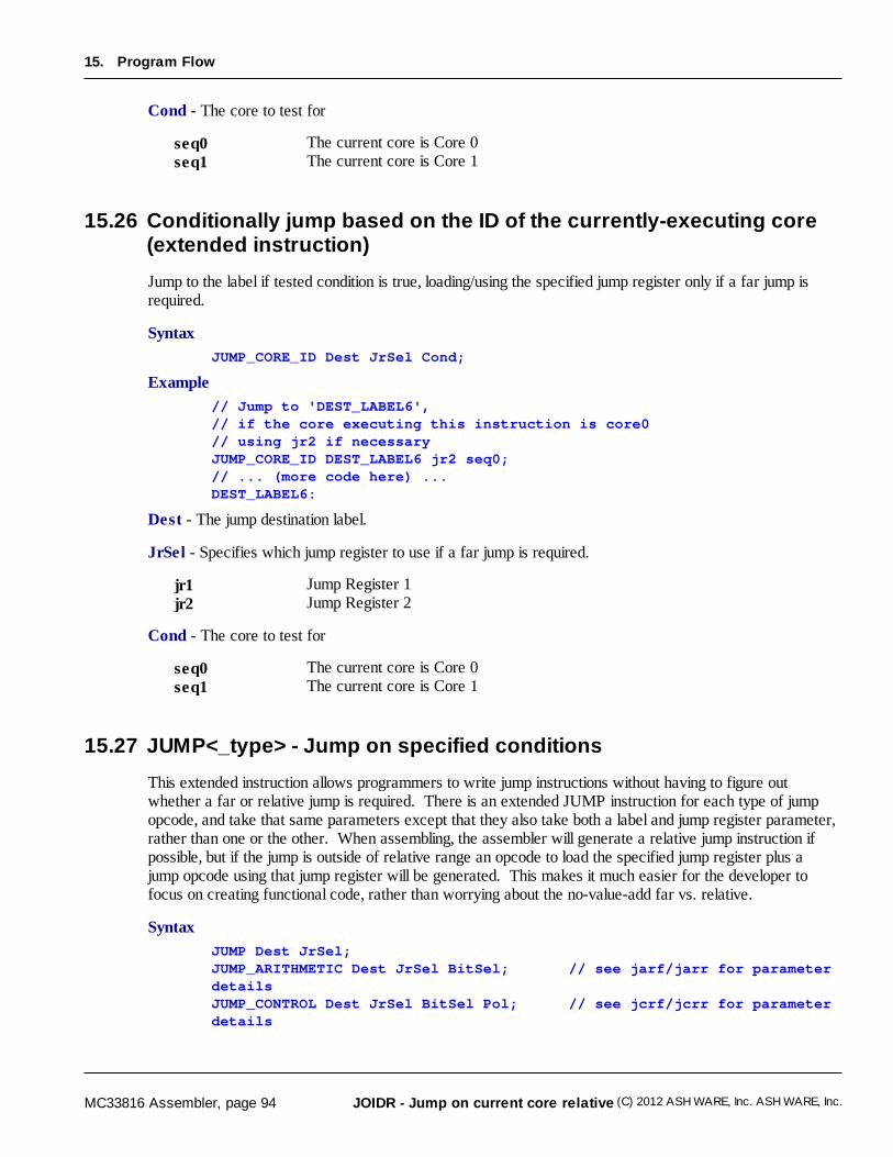
MC33816 Assembler, page 94 (C) 2012 ASH WARE, Inc. ASH WARE, Inc.
15. Program Flow
JOIDR - Jump on current core relative
Cond - The core to test for
seq0 The current core is Core 0seq1 The current core is Core 1
15.26 Conditionally jump based on the ID of the currently-executing core(extended instruction)
Jump to the label if tested condition is true, loading/using the specified jump register only if a far jump isrequired.
Syntax
JUMP_CORE_ID Dest JrSel Cond;
Example
// Jump to 'DEST_LABEL6',// if the core executing this instruction is core0// using jr2 if necessaryJUMP_CORE_ID DEST_LABEL6 jr2 seq0;// ... (more code here) ...DEST_LABEL6:
Dest - The jump destination label.
JrSel - Specifies which jump register to use if a far jump is required.
jr1 Jump Register 1jr2 Jump Register 2
Cond - The core to test for
seq0 The current core is Core 0seq1 The current core is Core 1
15.27 JUMP<_type> - Jump on specified conditions
This extended instruction allows programmers to write jump instructions without having to figure outwhether a far or relative jump is required. There is an extended JUMP instruction for each type of jumpopcode, and take that same parameters except that they also take both a label and jump register parameter,rather than one or the other. When assembling, the assembler will generate a relative jump instruction ifpossible, but if the jump is outside of relative range an opcode to load the specified jump register plus ajump opcode using that jump register will be generated. This makes it much easier for the developer tofocus on creating functional code, rather than worrying about the no-value-add far vs. relative.
Syntax
JUMP Dest JrSel;JUMP_ARITHMETIC Dest JrSel BitSel; // see jarf/jarr for parameterdetailsJUMP_CONTROL Dest JrSel BitSel Pol; // see jcrf/jcrr for parameterdetails
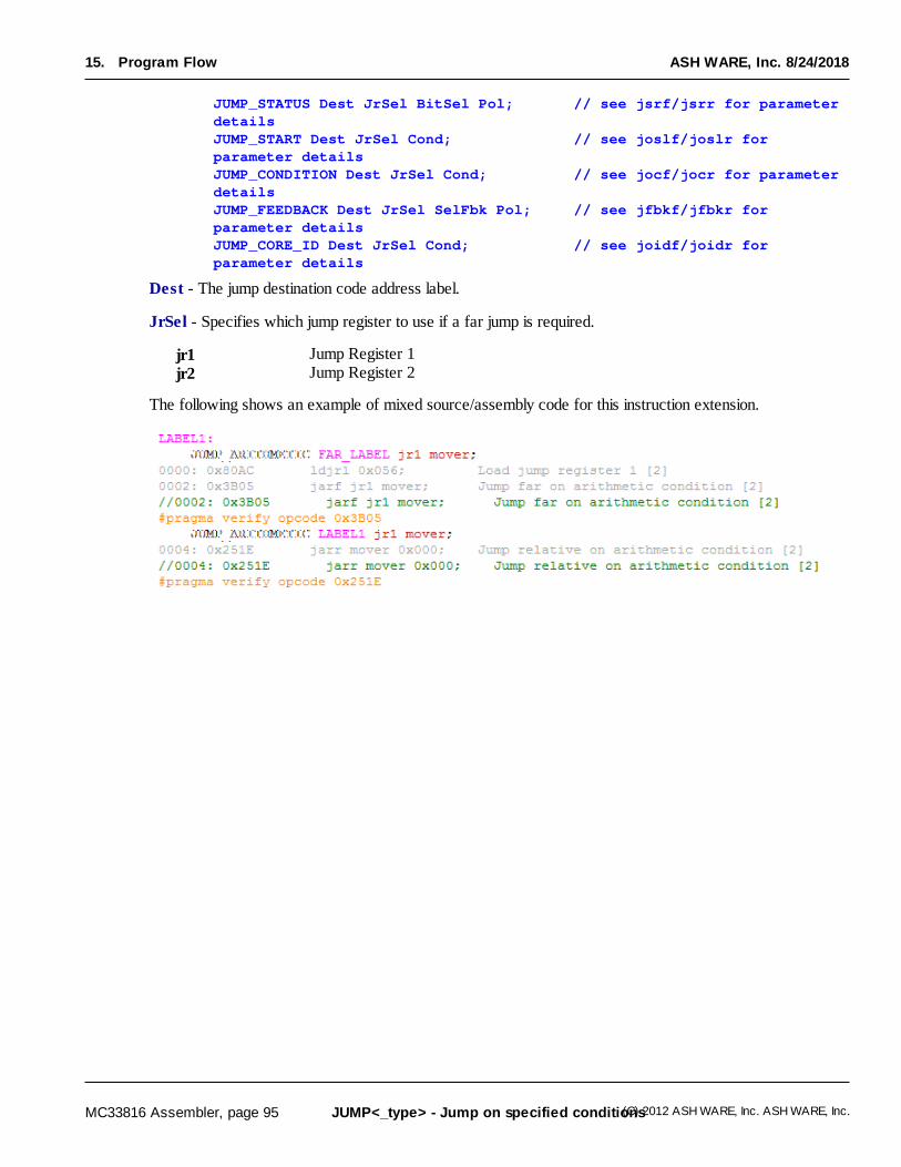
MC33816 Assembler, page 95 (C) 2012 ASH WARE, Inc. ASH WARE, Inc.
15. Program Flow
JUMP<_type> - Jump on specified conditions
ASH WARE, Inc. 8/24/2018
JUMP_STATUS Dest JrSel BitSel Pol; // see jsrf/jsrr for parameterdetailsJUMP_START Dest JrSel Cond; // see joslf/joslr forparameter detailsJUMP_CONDITION Dest JrSel Cond; // see jocf/jocr for parameterdetailsJUMP_FEEDBACK Dest JrSel SelFbk Pol; // see jfbkf/jfbkr forparameter detailsJUMP_CORE_ID Dest JrSel Cond; // see joidf/joidr forparameter details
Dest - The jump destination code address label.
JrSel - Specifies which jump register to use if a far jump is required.
jr1 Jump Register 1jr2 Jump Register 2
The following shows an example of mixed source/assembly code for this instruction extension.

MC33816 Assembler, page 96 (C) 2012 ASH WARE, Inc. ASH WARE, Inc.
Interrupts
Part
XVI
MC33816 Assembler, page 97 (C) 2012 ASH WARE, Inc. ASH WARE, Inc.
16. Interrupts
ASH WARE, Inc. 8/24/2018
16Interrupts
This section covers interrupts within the MC33816 device.
There are a number of possible interrupt sources including diagnostic interrupts, start interrupts, andsoftware interrupts. A software interrupt is envoked by the 'reqi' instruction.
Most devices will only return from interrupt when an interrupt return instruction is executed. TheMC33816 supports this industry-standard behavior with it's 'iret' behavior. However, the mc33816 alsohas an 'automatic interrupt return' mode in which a core's interrupt service routine automatically terminateswhen the interrupting source goes away. This mode allows a very quick response time to the resolution ofcondition that caused the interrupt. Picture being released from jail by a catapult.
When most devices return from an interrupt they go back to the location where the interrupt occurredthereby allowing the core to pickup doing what it was doing when the original interrupt occurred. However,, the MC33816 as a special interrupt return mode in which the return from interrupt behavior is toresume execution at the location pointed to by the reset vector. This allows the interrupt return behavior tomimic the reset behavior. This is like getting in trouble in fourth grade and going to the principals office andthe principal gives you a big lecture and then, instead of you going back to fourth grade, makes you startschool over and by going back to kindergarten instead.
Interestingly, this curious interrupt return behavior is available both when the interrupt return is caused bythe normal 'iret' instruction, and also when in 'automatic interrupt return' mode and the interrupting sourcegoes away.
Note that interrupts are one-deep such that an interrupt service routine will not be interrupted by anotherinterrupt source, even if the other interrupt source is at a higher priority level.
16.1 ICONF - Configure automatic interrupt return
Determines the behavior of the core when the interrupting source goes away.
This setting is 'sticky' such that once configured it retains its setting until changed by a future 'iconf'instruction.
MC33816 Assembler, page 98 (C) 2012 ASH WARE, Inc. ASH WARE, Inc.
16. Interrupts
ICONF - Configure automatic interrupt return
The default behavior is 'none' which means that 'automatic interrupt return' is disabled. This is similar to thethe behavior for similar controllers in that there is no automatic interrupt return. Instead, the 'interruptreturn' (iret) instruction must be executed in order to return from an interrupt.
However, this instruction can be used to configure the core to immediately return to the point in code thatwas interrupted. Alternatively, the core interrupt return behavior can be configured to return through thereset vector.
Syntax
iconf Conf;
Example
// Handle interrupt recovery// similarly to coming out of reseticonf restart;
Conf - Interrupt return behavior
none disable 'Automatic Return From Interrupt' for the coreNA N/Acontinue continue code execution at the point where execution was
interruptedrestart determined by the 'Ucx_entry_point' register … the location
where the execution begins coming out of reset
16.2 REQI - Request software interrupt
This instruction requests a software interrupt.
Two deep interrupts are not supported. In other words, an interrupt routine cannot itself be interrupted.Therefore, this 'reqi' instruction is ignored if it is executed within an interrupt service routine.
The effects of this software interrupt is similar to that of other interrupting source (such as a diagnostic orstart interrupt) in that the return address is loaded with the next address after the 'reqi' instruction.However, unlike other interrupt sources, there is no way for an 'automatic interrupt return' to occur forsoftware interrupts so a software interrupt must be terminated by the 'iret' instruction.
This instruction provides an 'id' which can be used within the interrupt service routine. The core can readit's irq register which contains a field named 'irq_source.' This 'irq_source' field contains the id of theinterrupting source.
Interestingly, all four cores' 'irq' registers can be read by the host MCU across the SPI bus by reading thefour 'irq_status' registers. This provides the host MCU with the ability to determine the software interruptsources.
Syntax
reqi Id;
Example
// Force a software interrupt within the corereqi 2;
MC33816 Assembler, page 99 (C) 2012 ASH WARE, Inc. ASH WARE, Inc.
16. Interrupts
REQI - Request software interrupt
ASH WARE, Inc. 8/24/2018
Id - The interrupt source ID
16.3 IRET - Return from interrupt
Ends the the interrupt service routine (isr) and clears the sequencer interrupt status register.
Execution normally continues at the address in the irq register's 'iret_address' field. This behavior isspecified by selecting 'continue' in the 'Type' parameter as show below. The 'iret_address' field getswritten when the interrupt occurred and contains the appropriate return address. For instance, if aninterrupt occurred while waiting at a 'wait' instruction, execution continues at the 'wait' instruction.However, if the interrupting source was a software interrupt ('iret' instruction) then execution resumes atthe instruction following the 'iret' instruction.
Alternatively, instruction execution will resume at the address specified by the reset vector by selecting'restart' in the 'Type' parameter as shown below. This allows interrupt return behavior to be identical to thereset behavior.
The 'Rst' parameter allows any pending interrupt sources to be cleared from the interrupt queue followingexecution of this interrupt instruction.
Syntax
iret Type Rst;
Example
// Standard interrupt termination// using the 'iret' instruction.// retain pending interrupts.iret continue _rst;
Type
continue Resume program execution at the address specifed in the irqregister's 'iret_address' field which contains the address thatwas active when the originating interrupt occured
restart Resume program execution a address specified by the core'sreset vector thereby mimicing the core's reset behavior
Rst
_rst The pending interrupt queue is not clearedrst Clear the pending interrupt queue
16.4 STIRQ - Write IRQB output pin
Write the IRQB output pin. This pin is normally connected to the host MCU's interrupt input pin therebyallowing the MC33816 to interrupt the MCU.
The pin's logic level is determined by the 'Value' parameter.
Syntax
stirq Value;
MC33816 Assembler, page 100 (C) 2012 ASH WARE, Inc. ASH WARE, Inc.
16. Interrupts
STIRQ - Write IRQB output pin
Example
// Interrupt the MCU// by putting the IRQB pin lowstirq low;
Value - The IRQB output pin's logic level
low Write the IRQB ouput pin to a low logic levelhigh Write the IRQB ouput pin to a high logic level

MC33816 Assembler, page 101 (C) 2012 ASH WARE, Inc. ASH WARE, Inc.
Data RAM Accesses
Part
XVII

MC33816 Assembler, page 103 (C) 2012 ASH WARE, Inc. ASH WARE, Inc.
17. Data RAM Accesses
ASH WARE, Inc. 8/24/2018
17Data RAM Accesses
The Data RAM access instructions are used to load and store data memory. These instructions also setthe access mode which can be set to either 'Immediate' mode or 'Indexed' mode. 'Indexed' mode is whenan offset from the Base Address register is applied to the access's address.
17.1 SLAB - Selects the register to be used in Indexed addressing mode
Selects which register ('base_add' or 'ir') is to be used when accessing data RAM in 'Indexed' addressingmode (XM).
This setting is 'sticky' in that once programmed it remains until changed by a future 'slab' instruction.
The reset value of SelBase is reg.
Note that when using databanks, register 'base_add' must be the active index register when any databankmember variables are accessed.
Syntax
slab Sel;
Example
// Use indexed addressing// and the 'ir' register// to store 0xCC to address 0x20slab ir;ldirl CCh rst;cp ir r0;ldirl 20h rst;store r0 My_Count _ofs;
Sel - Specifies which register is to be used for future 'Indexed' data memory accesses.
reg Use the 'base_add' register for 'Indexed' data memoryaccesses
ir Use the 'ir' register for 'Indexed' data memory accesses
MC33816 Assembler, page 104 (C) 2012 ASH WARE, Inc. ASH WARE, Inc.
17. Data RAM Accesses
STAB - Write the 'base_add' register
17.2 STAB - Write the 'base_add' register
This instruction writes the address in the 6-bit 'base_add' register.
The 'base_add' register is used in 'Indexed' addressing mode, but only if it is configured to be the BaseAddress register by a previously-executed 'slab' instruction.
Note that the 'ir' register can (alternatively) be used as the Base Address for indexed addresses.
See the 'slab' instruction which configures either the 'base_add' register or the 'ir' register to be used forindexed addresses.
Note that the 'base_add' register can be written but not read.
This instruction is also used to set the active databank and in fact must be used prior to accessing anydatabank member variables. See the example below.
Syntax
stab AddrBase;
Example
// Declare a databankdatabank Injector {uint16 I_peak;uint16 I_hold;};// ...// Allocate two databanks of type 'Injector'databank Injector _injector1;databank Injector _injector2;// ...// set the index base address to the _injector1 databank addressstab _injector1;// ...// From the active databank (currently '_injector1')// load variable 'I_peak' into register 'r0'load I_peak r0 ofs;
AddrBase - Sets the data RAM address
17.3 LOAD - Load a register with a 16-bit value from the Data RAM
Load an ALU register with a 16-bit value from the Data RAM.
The DRAM address from which the register is loaded is defined by 'AddSrc' which is a 6-bit Data RAMaddress. Optionally, a base address can be applied to form a fully qualified address.
Note that the read value can be affected by the 'Set Data RAM Read Mode ' instruction (stdrm) whichsupports swapping the bytes, reading just the upper byte, and reading just the lower byte.
'Ofs' determines whether the 'Base Address' register is applied.
Syntax
MC33816 Assembler, page 105 (C) 2012 ASH WARE, Inc. ASH WARE, Inc.
17. Data RAM Accesses
LOAD - Load a register with a 16-bit value from the Data RAM
ASH WARE, Inc. 8/24/2018
load AddrSrc RegDest Offset;
Example
// Declare a 16-bit variable named 'engine_speed3'sint16 engine_speed3;// ...// Load global variable 'engine_speed3' into register 'r0'load engine_speed3 r0 _ofs;// ...// Load a value from hard-coded address 55 (yuck)// into register 'r1'load 55 r1 _ofs;
AddrSrc - Sets the data RAM address
RegDest - The destination register
r0 ALU General Purpose Register 0r1 ALU General Purpose Register 1r2 ALU General Purpose Register 2r3 ALU General Purpose Register 3r4 ALU General Purpose Register 4ir ALU Immediate Registermh ALU MSB Multiplication Result Registerml ALU LSB Multiplication Result Registerar The 'arith_reg' (ar) is read-only. ALU condition register (Z,
C, N, V, etc.) WARNING: the arith_reg is read-only. NOTE:The 'ar' register is often refered to as the 'arith_reg
aux Auxiliary Register - Following a 'call', contains the returnaddress
jr1 Register 'Jump Destination 1'jr2 Register 'Jump Destination 2'cnt1 Counter 1's 'count' registercnt2 Counter 2's 'count' registercnt3 Counter 3's 'count' registercnt4 Counter 4's 'count' registereoc1 Counter 1's 'Terminal Count' registereoc2 Counter 2's 'Terminal Count' registereoc3 Counter 3's 'Terminal Count' registereoc4 Counter 4's 'Terminal Count' registerflag Flag output from the microcorecr Control inputs from the controlling MCUsr Status register for the controlling MCUspi_data The SPI Bus's DATA Registerdac_sssc 'Same Core Same Channel' current sense threshold DAC
Registerdac_ossc 'Other Core, Same Channel' current sense threshold DAC
Registerdac_ssoc 'Same Core Other Channel' current sense threshold DAC
Registerdac_osoc 'Other Core, Other Channel' current sense threshold DAC
Registerdac4h4n Accesses either core 4's second current sense threshold
DAC register (used for DC/DC Control,) or the core 4's
MC33816 Assembler, page 106 (C) 2012 ASH WARE, Inc. ASH WARE, Inc.
17. Data RAM Accesses
LOAD - Load a register with a 16-bit value from the Data RAM
negative current sense DAC register, or the VBoost DACregister depending on the DAC access mode. See instruction'stdm' for setting the DAC access mode.
spi_add The SPI bus's ADDRESS Registerirq Interrupt status registerrxtx Inter core communication register
Offset - Sets the addressing mode.
_ofs Immediate addressing, address = AddSrcofs Indexed addressing, address = AddSrc + Base Address
register
17.4 STORE - Store a value from an ALU register into the Data RAM
Store a 16-bit value from an ALU register into the Data RAM.
The DRAM address where the value stored is defined by 'AddSrc' which is a 6-bit Data RAM address.Optionally, a base address can be applied to form a fully qualified address.
'Ofs' determines whether the 'Base Address' register is applied.
Syntax
store RegSrc AddrDest Offset;
Example
// Declare a 16-bit variable named 'engine_speed4'sint16 engine_speed4;// ...// Load the 'ir' register with 0x1234// and store into variable 'engine_speed4;LOAD_IR 0x1234;store ir engine_speed4 _ofs;// ...// Store a value from register 'r2'// Into the hard-coded data ram address 23 (yuck)store r2 23 _ofs;
RegSrc - The source register
r0 ALU General Purpose Register 0r1 ALU General Purpose Register 1r2 ALU General Purpose Register 2r3 ALU General Purpose Register 3r4 ALU General Purpose Register 4ir ALU Immediate Registermh ALU MSB Multiplication Result Registerml ALU LSB Multiplication Result Registerar The 'arith_reg' (ar) is read-only. ALU condition register (Z,
C, N, V, etc.) WARNING: the arith_reg is read-only. NOTE:The 'ar' register is often refered to as the 'arith_reg
MC33816 Assembler, page 107 (C) 2012 ASH WARE, Inc. ASH WARE, Inc.
17. Data RAM Accesses
STORE - Store a value from an ALU register into the Data RAM
ASH WARE, Inc. 8/24/2018
aux Auxiliary Register - Following a 'call', contains the returnaddress
jr1 Register 'Jump Destination 1'jr2 Register 'Jump Destination 2'cnt1 Counter 1's 'count' registercnt2 Counter 2's 'count' registercnt3 Counter 3's 'count' registercnt4 Counter 4's 'count' registereoc1 Counter 1's 'Terminal Count' registereoc2 Counter 2's 'Terminal Count' registereoc3 Counter 3's 'Terminal Count' registereoc4 Counter 4's 'Terminal Count' registerflag Flag output from the microcorecr Control inputs from the controlling MCUsr Status register for the controlling MCUspi_data The SPI Bus's DATA Registerdac_sssc 'Same Core Same Channel' current sense threshold DAC
Registerdac_ossc 'Other Core, Same Channel' current sense threshold DAC
Registerdac_ssoc 'Same Core Other Channel' current sense threshold DAC
Registerdac_osoc 'Other Core, Other Channel' current sense threshold DAC
Registerdac4h4n Accesses either core 4's second current sense threshold
DAC register (used for DC/DC Control,) or the core 4'snegative current sense DAC register, or the VBoost DACregister depending on the DAC access mode. See instruction'stdm' for setting the DAC access mode.
spi_add The SPI bus's ADDRESS Registerirq Interrupt status registerrxtx Inter core communication register
AddrDest - Sets the data RAM address
Offset - Sets the addressing mode.
_ofs Immediate addressing, address = AddSrcofs Indexed addressing, address = AddSrc + Base Address
register
17.5 STDRM - Set data RAM read mode
This instruction sets the data RAM read mode.
The default is to read all 16 bytes.
In 'low' mode the lower byte is read and the upper byte is zero.
In 'high' mode the upper byte is read into the lower byte. The upper byte is zero.
MC33816 Assembler, page 108 (C) 2012 ASH WARE, Inc. ASH WARE, Inc.
17. Data RAM Accesses
STDRM - Set data RAM read mode
In 'swap' mode the upper and lower bytes are swapped.
This setting is sticky, such that once set it does not change until a future 'stdrm' instruction.
Syntax
stdrm Mode;
Example
// Set the data RAM read mode// to read JUST the high bytes// but into the low byte// of the destination registers.stdrm high;
Mode - Specifies the mode.
word Read the full word normally (default)low Read just the low byte, upper byte is zerohigh Read just the uppper byte, but shift into lower byteswap Swap the upper and lower bytes in read

MC33816 Assembler, page 109 (C) 2012 ASH WARE, Inc. ASH WARE, Inc.
Math
Part
XVIII

MC33816 Assembler, page 111 (C) 2012 ASH WARE, Inc. ASH WARE, Inc.
18. Math
ASH WARE, Inc. 8/24/2018
18Math
The following section covers the math operations including flag configuration, adds, subtracts, andmultiplies, etc.
18.1 STAL - set arithmetic logic
This instruction configures the behavior of addition and subtraction instructions only. All other instructions(multiply, shift, bitwise, etc) are not affected by this instruction.
The addition and subtract results are affected only if one the 'saturation' modes is selected. If 'saturation' isnot selected then the results are not affected.
With 'saturation' enabled the result is bounded by the natural limits of the 16 bit register. The maximumsigned integer is 0x7FFF. When in signed saturation mode (al2) and two positive numbers are added thatwould exceed 0x7FFF, then the operation is said to 'saturate' in that the result is 0x7FFF.
The 'A1' and 'A0' bits of the ALU Condition Register 'arith_reg' are written with this instruction.
This instruction is 'sticky' in that once written, the setting does not change until written again with a future'stal' instruction.
Syntax
stal Mode;
Example
// Set mode to 'signed saturation' (al2)// This causes add/sub results that would// otherwise overflow// to limit to the max/min values instead// In this example the register will get a 0x7FFF,// (the maximum signed value).stal al2;LOAD_IR 0x7FFD;addi ir 15 r0;
MC33816 Assembler, page 112 (C) 2012 ASH WARE, Inc. ASH WARE, Inc.
18. Math
STAL - set arithmetic logic
Mode
al1 Signed number without overflow saturational2 Signed number with overflow saturational3 Unsigned number without overflow saturational4 Unsigned number with overflow saturation
18.2 CP - Copy one register to another
Copy the value from one register to another.
Syntax
cp RegSrc RegDest;
Example
// Copy the contents// of register 'r3'// into the core's DACcp r3 dac_sssc;
RegSrc - The source register.
r0 ALU General Purpose Register 0r1 ALU General Purpose Register 1r2 ALU General Purpose Register 2r3 ALU General Purpose Register 3r4 ALU General Purpose Register 4ir ALU Immediate Registermh ALU MSB Multiplication Result Registerml ALU LSB Multiplication Result Registerar The 'arith_reg' (ar) is read-only. ALU condition register (Z,
C, N, V, etc.) WARNING: the arith_reg is read-only. NOTE:The 'ar' register is often refered to as the 'arith_reg
aux Auxiliary Register - Following a 'call', contains the returnaddress
jr1 Register 'Jump Destination 1'jr2 Register 'Jump Destination 2'cnt1 Counter 1's 'count' registercnt2 Counter 2's 'count' registercnt3 Counter 3's 'count' registercnt4 Counter 4's 'count' registereoc1 Counter 1's 'Terminal Count' registereoc2 Counter 2's 'Terminal Count' registereoc3 Counter 3's 'Terminal Count' registereoc4 Counter 4's 'Terminal Count' registerflag Flag output from the microcorecr Control inputs from the controlling MCUsr Status register for the controlling MCUspi_data The SPI Bus's DATA Registerdac_sssc 'Same Core Same Channel' current sense threshold DAC
Registerdac_ossc 'Other Core, Same Channel' current sense threshold DAC
MC33816 Assembler, page 113 (C) 2012 ASH WARE, Inc. ASH WARE, Inc.
18. Math
CP - Copy one register to another
ASH WARE, Inc. 8/24/2018
Registerdac_ssoc 'Same Core Other Channel' current sense threshold DAC
Registerdac_osoc 'Other Core, Other Channel' current sense threshold DAC
Registerdac4h4n Accesses either core 4's second current sense threshold
DAC register (used for DC/DC Control,) or the core 4'snegative current sense DAC register, or the VBoost DACregister depending on the DAC access mode. See instruction'stdm' for setting the DAC access mode.
spi_add The SPI bus's ADDRESS Registerirq Interrupt status registerrxtx Inter core communication register
RegDest - The destination register.
r0 ALU General Purpose Register 0r1 ALU General Purpose Register 1r2 ALU General Purpose Register 2r3 ALU General Purpose Register 3r4 ALU General Purpose Register 4ir ALU Immediate Registermh ALU MSB Multiplication Result Registerml ALU LSB Multiplication Result Registerar The 'arith_reg' (ar) is read-only. ALU condition register (Z,
C, N, V, etc.) WARNING: the arith_reg is read-only. NOTE:The 'ar' register is often refered to as the 'arith_reg
aux Auxiliary Register - Following a 'call', contains the returnaddress
jr1 Register 'Jump Destination 1'jr2 Register 'Jump Destination 2'cnt1 Counter 1's 'count' registercnt2 Counter 2's 'count' registercnt3 Counter 3's 'count' registercnt4 Counter 4's 'count' registereoc1 Counter 1's 'Terminal Count' registereoc2 Counter 2's 'Terminal Count' registereoc3 Counter 3's 'Terminal Count' registereoc4 Counter 4's 'Terminal Count' registerflag Flag output from the microcorecr Control inputs from the controlling MCUsr Status register for the controlling MCUspi_data The SPI Bus's DATA Registerdac_sssc 'Same Core Same Channel' current sense threshold DAC
Registerdac_ossc 'Other Core, Same Channel' current sense threshold DAC
Registerdac_ssoc 'Same Core Other Channel' current sense threshold DAC
Registerdac_osoc 'Other Core, Other Channel' current sense threshold DAC
Registerdac4h4n Accesses either core 4's second current sense threshold
MC33816 Assembler, page 114 (C) 2012 ASH WARE, Inc. ASH WARE, Inc.
18. Math
CP - Copy one register to another
DAC register (used for DC/DC Control,) or the core 4'snegative current sense DAC register, or the VBoost DACregister depending on the DAC access mode. See instruction'stdm' for setting the DAC access mode.
spi_add The SPI bus's ADDRESS Registerirq Interrupt status registerrxtx Inter core communication register
18.3 LDIRH - Load immediate register's MSB
Load an immediate value into the most significant byte (MSB) of the 'ir' register.
The least significant byte (LSB) can be either reset to zero or left unchanged.
NOTE: If the intent is to update the entire 'ir' register, it is recommended the extended
instruction 'LOAD_IR' be used instead.
Syntax
ldirh Value rstL;
Example
// Setup the counter to detect a timeout error at 200 countsLOAD_IR 200;ldca rst keep keep ir c1;//// Load '0x7C' into the upper byte of the IR register// leaving the lower byte unchanged.ldirh 0xAB _rst;
Value - 8-bit immediate value
rstL - Reset the LSB to zero?
_rst Do not change the 'ir' register's LSBrst Reset 'ir' register's LSB to zero
18.4 LDIRL - Load immediate register's LSB
Load an immediate value into the least significant byte (LSB) of the 'ir' register.
The most significant byte (MSB) can be either reset to zero or left unchanged.
NOTE: If the intent is to update the entire 'ir' register, it is recommended the extended
instruction 'LOAD_IR' be used instead.
Syntax
MC33816 Assembler, page 115 (C) 2012 ASH WARE, Inc. ASH WARE, Inc.
18. Math
LDIRL - Load immediate register's LSB
ASH WARE, Inc. 8/24/2018
ldirl Value rstH;
Example
// Setup the counter to detect a timeout error at 200 countsLOAD_IR 200;ldca rst keep keep ir c1;//// Load '0xAB' into the lower byte of the IR register// leaving the upper byte unchanged.ldirl 0xAB _rst;
Value - 8-bit immediate value
rstH - Reset the MSB to zero?
_rst Do not change the 'ir' register's MSBrst Reset 'ir' register's MSB to zero
18.5 Load the full 16-bit IR register (extended instruction)
Load an immediate value into the 'ir' register. The assembler optimally does the load based upon theimmediate value.
Syntax
LOAD_IR Value;
Example
// Declare a 16-bit variable named 'engine_speed1'sint16 engine_speed1;// ...// Load the 'ir' register with 0x1234// and store into variable 'engine_speed1;LOAD_IR 0x1234;store ir engine_speed1 _ofs;
Value - 16-bit immediate value
18.6 ADD - Addition of two registers
Add the value in one register with the value in a second register and place the result in a third register.
This instruction is affected by the Arithmetic Logic Mode which is set by the 'stal' instruction.
Syntax
add Add1 Add2 Res;
Example
// Add ir and r1,// place results in r2add ir r1 r2;
MC33816 Assembler, page 116 (C) 2012 ASH WARE, Inc. ASH WARE, Inc.
18. Math
ADD - Addition of two registers
Add1 - The first register to be added
r0 ALU General Purpose Register 0r1 ALU General Purpose Register 1r2 ALU General Purpose Register 2r3 ALU General Purpose Register 3r4 ALU General Purpose Register 4ir ALU Immediate Registermh ALU MSB Multiplication Result Registerml ALU LSB Multiplication Result Register
Add2 - The second register to be added
r0 ALU General Purpose Register 0r1 ALU General Purpose Register 1r2 ALU General Purpose Register 2r3 ALU General Purpose Register 3r4 ALU General Purpose Register 4ir ALU Immediate Registermh ALU MSB Multiplication Result Registerml ALU LSB Multiplication Result Register
Res - The register where the result goes
r0 ALU General Purpose Register 0r1 ALU General Purpose Register 1r2 ALU General Purpose Register 2r3 ALU General Purpose Register 3r4 ALU General Purpose Register 4ir ALU Immediate Registermh ALU MSB Multiplication Result Registerml ALU LSB Multiplication Result Register
18.7 ADDI - Addition of a register with a 4-bit unsigned immediate
Adds a register to a 4-bit unsigned immediate and places the result in a register.
This instruction is affected by the Arithmetic Logic Mode which is set by the 'stal' instruction.
Syntax
addi Add Imm Res;
Example
// Add five to the value in the 'r0' register// and place the result in the 'r1' registeraddi r0 5 r1;
Add - The ALU register with the value to be added.
MC33816 Assembler, page 117 (C) 2012 ASH WARE, Inc. ASH WARE, Inc.
18. Math
ADDI - Addition of a register with a 4-bit unsigned immediate
ASH WARE, Inc. 8/24/2018
r0 ALU General Purpose Register 0r1 ALU General Purpose Register 1r2 ALU General Purpose Register 2r3 ALU General Purpose Register 3r4 ALU General Purpose Register 4ir ALU Immediate Registermh ALU MSB Multiplication Result Registerml ALU LSB Multiplication Result Register
Imm - The 4-bit unsigned immediate value that gets added.
Res - The ALU register that will cantain the result of the addition.
r0 ALU General Purpose Register 0r1 ALU General Purpose Register 1r2 ALU General Purpose Register 2r3 ALU General Purpose Register 3r4 ALU General Purpose Register 4ir ALU Immediate Registermh ALU MSB Multiplication Result Registerml ALU LSB Multiplication Result Register
18.8 SUB - Substraction of two registers
Subtracts a register from a register and places the results in a third register.
This instruction is affected by the Arithmetic Logic Mode which is set by the 'stal' instruction.
Res = Sub1 - Sub2
Syntax
sub Sub1 Sub2 Res;
Example
// Subtract the value in the 'ir' register// from the value in the 'r1' register// and place results in 'r2' registeradd r1 ir r2;
Sub1 - The minuend
r0 ALU General Purpose Register 0r1 ALU General Purpose Register 1r2 ALU General Purpose Register 2r3 ALU General Purpose Register 3r4 ALU General Purpose Register 4ir ALU Immediate Registermh ALU MSB Multiplication Result Registerml ALU LSB Multiplication Result Register
Sub2 - The subtrahend
MC33816 Assembler, page 118 (C) 2012 ASH WARE, Inc. ASH WARE, Inc.
18. Math
SUB - Substraction of two registers
r0 ALU General Purpose Register 0r1 ALU General Purpose Register 1r2 ALU General Purpose Register 2r3 ALU General Purpose Register 3r4 ALU General Purpose Register 4ir ALU Immediate Registermh ALU MSB Multiplication Result Registerml ALU LSB Multiplication Result Register
Res - The result
r0 ALU General Purpose Register 0r1 ALU General Purpose Register 1r2 ALU General Purpose Register 2r3 ALU General Purpose Register 3r4 ALU General Purpose Register 4ir ALU Immediate Registermh ALU MSB Multiplication Result Registerml ALU LSB Multiplication Result Register
18.9 SUBI - Subtraction by a 4-bit unsigned immediate
Subtracts an unsigned 4-bit immediate from a register and places the results in second register.
This instruction is affected by the Arithmetic Logic Mode which is set by the 'stal' instruction.
Res = Sub - Imm
Syntax
subi Sub Imm Res;
Example
// Subtract 0xE from register 'r2'// and put the result into register 'r3'subi r2 0xE r3;
Sub - The minuend
r0 ALU General Purpose Register 0r1 ALU General Purpose Register 1r2 ALU General Purpose Register 2r3 ALU General Purpose Register 3r4 ALU General Purpose Register 4ir ALU Immediate Registermh ALU MSB Multiplication Result Registerml ALU LSB Multiplication Result Register
Imm - The 4-bit immediate subtrahend
Res - The result
MC33816 Assembler, page 119 (C) 2012 ASH WARE, Inc. ASH WARE, Inc.
18. Math
SUBI - Subtraction by a 4-bit unsigned immediate
ASH WARE, Inc. 8/24/2018
r0 ALU General Purpose Register 0r1 ALU General Purpose Register 1r2 ALU General Purpose Register 2r3 ALU General Purpose Register 3r4 ALU General Purpose Register 4ir ALU Immediate Registermh ALU MSB Multiplication Result Registerml ALU LSB Multiplication Result Register
18.10 MUL - Multiplication of two registers, result goes in 'mh' and 'ml'
Multiply register Fact1 with register Fact2 and put the resulting 32-bit number's MSB in the 'mh' registerand LSB in the 'ml' register.
The multiply takes 17 clock cycles.
A series of shift's and add's of the 'mh' and 'ml' register is used such that the 'mh' and 'ml' register shouldbe neither read nor written while the multiply is underway. However, registers 'r0' through 'r4' and 'ir' areavailable for parallel execution.
To determine when the multiply is complete, the arith_reg's OD bit, which goes from zero to one, can betested as shown in the example below.
Syntax
mul Fact1 Fact2;
Example
mul r0 r1;wait_loop6:jarr done6 opd;jmpr wait_loop6;done6:store mh MyMsbVar _ofs;store ml MyLsbVar _ofs;
Fact1 - The first register to be multiplied
r0 ALU General Purpose Register 0r1 ALU General Purpose Register 1r2 ALU General Purpose Register 2r3 ALU General Purpose Register 3r4 ALU General Purpose Register 4ir ALU Immediate Register
Fact2 - The second register to be multiplied
r0 ALU General Purpose Register 0r1 ALU General Purpose Register 1r2 ALU General Purpose Register 2r3 ALU General Purpose Register 3r4 ALU General Purpose Register 4ir ALU Immediate Register
MC33816 Assembler, page 120 (C) 2012 ASH WARE, Inc. ASH WARE, Inc.
18. Math
MULI - Multiplication with 4-bit immediate, result goes in 'mh' and 'ml'
18.11 MULI - Multiplication with 4-bit immediate, result goes in 'mh' and 'ml'
Multiply register Fact with the 4-bit immediate and put the resulting 32-bit number's MSB in the 'mh'register and LSB in the 'ml' register.
The multiply takes 17 clock cycles.
A series of shift's and add's of the 'mh' and 'ml' register is used such that the 'mh' and 'ml' register shouldbe neither read nor written while the multiply is underway. However, registers 'r0' through 'r4' and 'ir' areavailable for parallel execution.
To determine when the multiply is complete, the arith_reg's OD bit, which goes from zero to one, can betested as shown in the example below.
Syntax
muli Fact Imm;
Example
muli r0 9;wait_loop1:jarr done1 opd;jmpr wait_loop1;done1:store mh MyMsbVar _ofs;store ml MyLsbVar _ofs;
Fact - The register to be multiplied
r0 ALU General Purpose Register 0r1 ALU General Purpose Register 1r2 ALU General Purpose Register 2r3 ALU General Purpose Register 3r4 ALU General Purpose Register 4ir ALU Immediate Register
Imm - The four-bit immediate to be multiplied
18.12 SWAP - Swap a register's high and low bytes
The high byte becomes the low byte and the low byte becomes the high byte.
Syntax
swap Reg;
Example
// Swap the upper and lower bytes// within register 'r1'swap r1;
Reg
MC33816 Assembler, page 121 (C) 2012 ASH WARE, Inc. ASH WARE, Inc.
18. Math
SWAP - Swap a register's high and low bytes
ASH WARE, Inc. 8/24/2018
r0 ALU General Purpose Register 0r1 ALU General Purpose Register 1r2 ALU General Purpose Register 2r3 ALU General Purpose Register 3r4 ALU General Purpose Register 4ir ALU Immediate Registermh ALU MSB Multiplication Result Registerml ALU LSB Multiplication Result Register
18.13 TOC2 - Conditional conversion to 2's complement format with signenforcement
Conditionally converts a number to 2's complement format.
If the conversion bit 'CS' of the ALU Condition Register 'arith_reg' is zero then only the most significant bitis to zero and no other bits are changed.
However, if 'CS' is one, then a two's complement is taken (bitwise inversion, then add one) and the mostsignificant bit is set to one.
Syntax
toc2 Reg;
Example
// Conditionally convert a number// to 2's complement format.// If the conversion bit 'CS'// of the ALU Condition Register 'arith_reg' is zero// then only the most significant bit is to zero and// no other bits are changed.// However, if 'CS' is one,// then a two's complement is taken// (bitwise inversion, then add one)// and the most significant bit is set to onetoc2 ir;
Reg -
r0 ALU General Purpose Register 0r1 ALU General Purpose Register 1r2 ALU General Purpose Register 2r3 ALU General Purpose Register 3r4 ALU General Purpose Register 4ir ALU Immediate Registermh ALU MSB Multiplication Result Registerml ALU LSB Multiplication Result Register
MC33816 Assembler, page 122 (C) 2012 ASH WARE, Inc. ASH WARE, Inc.
18. Math
TOINT - Convert from 2's complement
18.14 TOINT - Convert from 2's complement
Convert the 2-complement value to integer format.
If the operand's most significant bit is zero then the original value is retained.
If the operand's most significant bit is a one then a two's complement is performed (invert all bits and addone) and the most significant bit is cleared.
The resulting value of the conversion bit 'CS' of the ALU Condition Register 'arith_reg' is affected by theRst parameter.
If the Rst parameter is a zero then the CS bit gets 'OR'd with the operands most significant bit.
If the Rst parameter is a one then the CS bit is set to the operand's most significant bit.
Syntax
toint Reg Rst;
Example
// Convert from 2's complement.// The Rst parameter is a one// so set the CS bit// to the operand's most significant bittoint ir rst;
Reg
r0 ALU General Purpose Register 0r1 ALU General Purpose Register 1r2 ALU General Purpose Register 2r3 ALU General Purpose Register 3r4 ALU General Purpose Register 4ir ALU Immediate Registermh ALU MSB Multiplication Result Registerml ALU LSB Multiplication Result Register
Rst - CS bit behavior
_rst The existing conversion bit CS is XORed with the operand'smost significant bit
rst The existing conversion bit CS is set according to theoperand's most significant bit

MC33816 Assembler, page 123 (C) 2012 ASH WARE, Inc. ASH WARE, Inc.
Bitwise
Part
XIX

MC33816 Assembler, page 125 (C) 2012 ASH WARE, Inc. ASH WARE, Inc.
19. Bitwise
ASH WARE, Inc. 8/24/2018
19Bitwise
This section covers the 'bitwise' operations, 'and', 'or', 'xor', and 'not'.
19.1 AND - Bitwise AND with 'ir' register
Performs a bitwise 'AND' of the selected register with the 'ir' register and places the results back into the(same) selected register.
The ALU Condition Register 'arith_reg' 'MN' and 'MZ' bits get written.
Note that the 'MN' flag indicating all one's gets tested by the 'jarr' and 'jarf' instructions using the 'all1'syntax. Similarly, the 'MZ' flag indicating all zeroes gets tested by the 'all0' flag.
Syntax
and Reg;
Example
// AND the 'ir' register with the 'r0' register.// Result goes in the 'r0' register.// If the result is '0' then jump to the 'handle_all_zeroes_' codelabel.and r0;jarr handle_all_zeroes_ all0;// ... (more code here) ...handle_all_zeroes_:
Reg - The register for both the operation's operand and result.
MC33816 Assembler, page 126 (C) 2012 ASH WARE, Inc. ASH WARE, Inc.
19. Bitwise
AND - Bitwise AND with 'ir' register
r0 ALU General Purpose Register 0r1 ALU General Purpose Register 1r2 ALU General Purpose Register 2r3 ALU General Purpose Register 3r4 ALU General Purpose Register 4ir ALU Immediate Registermh ALU MSB Multiplication Result Registerml ALU LSB Multiplication Result Register
19.2 OR - Bitwise OR with the 'ir' register
Performs a bitwise 'OR' of the selected register with the 'ir' register and places the results back into the(same) selected register.
The ALU Condition Register 'arith_reg' 'MN' and 'MZ' bits get written.
Note that the 'MN' flag indicating all one's gets tested by the 'jarr' and 'jarf' instructions using the 'all1'syntax. Similarly, the 'MZ' flag indicating all zeroes gets tested by the 'all0' flag.
Syntax
or Reg;
Example
// Bitwise OR the 'ir' register with the 'r0' register.// Result goes in the 'r0' register.// If the result is '0xFFFF' then jump to the 'handle_all_ones_' codelabel.or r0;jarr handle_all_ones_ all1;// ... (more code here) ...handle_all_ones_:
Reg - The register for both the operation's operand and result.
r0 ALU General Purpose Register 0r1 ALU General Purpose Register 1r2 ALU General Purpose Register 2r3 ALU General Purpose Register 3r4 ALU General Purpose Register 4ir ALU Immediate Registermh ALU MSB Multiplication Result Registerml ALU LSB Multiplication Result Register
19.3 XOR - Bitwise XOR with the 'ir' register
Performs a bitwise 'XOR' of the selected register with the 'ir' register and places the results back into the(same) selected register.
The ALU Condition Register 'arith_reg' 'MN' and 'MZ' bits get written.
MC33816 Assembler, page 127 (C) 2012 ASH WARE, Inc. ASH WARE, Inc.
19. Bitwise
XOR - Bitwise XOR with the 'ir' register
ASH WARE, Inc. 8/24/2018
Note that the 'MN' flag indicating all one's gets tested by the 'jarr' and 'jarf' instructions using the 'all1'syntax. Similarly, the 'MZ' flag indicating all zeroes gets tested by the 'all0' flag.
Syntax
xor Reg;
Example
// Bitwise XOR the 'ir' register with the 'r0' register.// Result goes in the 'r0' register.// If the result is '0xFFFF' then jump to the 'handle_all_ones' codelabel.xor r0;jarr handle_all_ones all1;// ... (more code here) ...handle_all_ones:
Reg - The register for both the operation's operand and result.
r0 ALU General Purpose Register 0r1 ALU General Purpose Register 1r2 ALU General Purpose Register 2r3 ALU General Purpose Register 3r4 ALU General Purpose Register 4ir ALU Immediate Registermh ALU MSB Multiplication Result Registerml ALU LSB Multiplication Result Register
19.4 NOT - Bitwise NOT
Inverts the bits of the selected register and puts the result into the same register.
The ALU Condition Register 'arith_reg' 'MN' and 'MZ' bits get written.
Note that the 'MN' flag indicating all one's gets tested by the 'jarr' and 'jarf' instructions using the 'all1'syntax. Similarly, the 'MZ' flag indicating all zeroes gets tested by the 'all0' flag.
Syntax
not Reg;
Example
// Bitwise invert the 'r0' register.// Result goes in the 'r0' register.// If the result is '0' then jump to the 'handle_all_zeroes' codelabel.not r0;jarr handle_all_zeroes all0;// ... (more code here) ...handle_all_zeroes:
Reg - The register for both the operation's operand and result.
MC33816 Assembler, page 128 (C) 2012 ASH WARE, Inc. ASH WARE, Inc.
19. Bitwise
NOT - Bitwise NOT
r0 ALU General Purpose Register 0r1 ALU General Purpose Register 1r2 ALU General Purpose Register 2r3 ALU General Purpose Register 3r4 ALU General Purpose Register 4ir ALU Immediate Registermh ALU MSB Multiplication Result Registerml ALU LSB Multiplication Result Register

MC33816 Assembler, page 129 (C) 2012 ASH WARE, Inc. ASH WARE, Inc.
Shifts
Part
XX

MC33816 Assembler, page 131 (C) 2012 ASH WARE, Inc. ASH WARE, Inc.
20. Shifts
ASH WARE, Inc. 8/24/2018
20Shifts
This section covers the shift instructions. Shifts include 'shift left' and 'shift right', 'shift by register' and'shift immediate', 'normal shift' and 'signed shift' in which the most significant bit does not change, and 32-bit shifts in which the 'mh' and 'ml' registers are treated as a single 32-bit register in which the 'mh'register's lsb connects with the 'ml's registers msb.
Shifts normally take one instruction cycle per shifted bit and the 'arith_reg' register's 'OD' bit can be testedto determine when the shift is completed. So an 11-bit shift would normally take 11 clock cycles toexecute. However, there is a special 8-bit shift which takes just a single clock cycle so shifts by constantsgreater than 8 bit positions can be sped up by combining the 8-bit shift with the immediate shift.
20.1 SHR - Shift right by register
Shift right register 'RegData' the number of bits set by the value in register 'RegPos'.
This operation takes a variable number of clocks to execute. Specifically, it takes one clock per bit positionshifted.
To determine when the operation is complete, the arith_reg's 'Operation Done' bit (opd), which goes fromzero to one upon completion, should be tested as shown in the example below.
Syntax
shr RegData RegPos;
Example
shr r3 r2;wait_loop9:jarr done9 opd;jmpr wait_loop9;done9:
RegData - The register that gets shifted
MC33816 Assembler, page 132 (C) 2012 ASH WARE, Inc. ASH WARE, Inc.
20. Shifts
SHR - Shift right by register
r0 ALU General Purpose Register 0r1 ALU General Purpose Register 1r2 ALU General Purpose Register 2r3 ALU General Purpose Register 3r4 ALU General Purpose Register 4ir ALU Immediate Registermh ALU MSB Multiplication Result Registerml ALU LSB Multiplication Result Register
RegPos - This register sets the number of bits to shift
r0 ALU General Purpose Register 0r1 ALU General Purpose Register 1r2 ALU General Purpose Register 2r3 ALU General Purpose Register 3r4 ALU General Purpose Register 4ir ALU Immediate Registermh ALU MSB Multiplication Result Registerml ALU LSB Multiplication Result Register
20.2 SHRS - Shift right by register, signed
Shift right register 'RegData' the number of bits set by the value in register 'RegPos'.
The sign of the resulting number does not change in that the sign bit (msb) retains its original value.
This operation takes a variable number of clocks to execute. Specifically, it takes one clock per bit positionshifted.
To determine when the operation is complete, the arith_reg's 'Operation Done' bit (opd), which goes fromzero to one upon completion, should be tested as shown in the example below.
Syntax
shrs RegData RegPos;
Example
shrs r3 r2;wait_loop10:jarr done10 opd;jmpr wait_loop10;done10:
RegData - The register that gets shifted
MC33816 Assembler, page 133 (C) 2012 ASH WARE, Inc. ASH WARE, Inc.
20. Shifts
SHRS - Shift right by register, signed
ASH WARE, Inc. 8/24/2018
r0 ALU General Purpose Register 0r1 ALU General Purpose Register 1r2 ALU General Purpose Register 2r3 ALU General Purpose Register 3r4 ALU General Purpose Register 4ir ALU Immediate Registermh ALU MSB Multiplication Result Registerml ALU LSB Multiplication Result Register
RegPos - This register sets the number of bits to shift
r0 ALU General Purpose Register 0r1 ALU General Purpose Register 1r2 ALU General Purpose Register 2r3 ALU General Purpose Register 3r4 ALU General Purpose Register 4ir ALU Immediate Registermh ALU MSB Multiplication Result Registerml ALU LSB Multiplication Result Register
20.3 SHRI - Shift right by immediate
Shift right register 'Reg' the number of bits set by an immediate value.
This operation takes a variable number of clocks to execute. Specifically, it takes one clock per bit positionshifted.
To determine when the shift is complete, the arith_reg's OD bit, which goes from zero to one uponcompletion, can be tested as shown in the example below.
Syntax
shri Reg Imm;
Example
shri r3 7;wait_loop4:jarr done4 opd;jmpr wait_loop4;done4:
Reg - The register that gets shifted
r0 ALU General Purpose Register 0r1 ALU General Purpose Register 1r2 ALU General Purpose Register 2r3 ALU General Purpose Register 3r4 ALU General Purpose Register 4ir ALU Immediate Registermh ALU MSB Multiplication Result Registerml ALU LSB Multiplication Result Register
MC33816 Assembler, page 134 (C) 2012 ASH WARE, Inc. ASH WARE, Inc.
20. Shifts
SHRI - Shift right by immediate
Imm - The number of bits to shift
20.4 SHRSI - Shift right by immediate, signed
Shift right register 'Reg' the number of bits set by the immediate value.
The sign of the resulting number does not change in that the sign bit (msb) retains its original value.
This operation takes a variable number of clocks to execute. Specifically, it takes one clock per bit positionshifted.
To determine when the operation is complete, the arith_reg's 'Operation Done' bit (opd), which goes fromzero to one upon completion, should be tested as shown in the example below.
Syntax
shrsi Reg Imm;
Example
shrsi r3 7;wait_loop5:jarr done5 opd;jmpr wait_loop5;done5:
Reg - The register that gets shifted
r0 ALU General Purpose Register 0r1 ALU General Purpose Register 1r2 ALU General Purpose Register 2r3 ALU General Purpose Register 3r4 ALU General Purpose Register 4ir ALU Immediate Registermh ALU MSB Multiplication Result Registerml ALU LSB Multiplication Result Register
Imm - The number of bits to shift
20.5 SHR8 - Shift right by 8
Shift right register 'Reg' eight bits.
This operation one clock.
Syntax
shr8 Reg;
Example
// Shift the r3 register right by 11 bits// in two steps that take 4 clocksshr8 r3;shri r3 3;
MC33816 Assembler, page 135 (C) 2012 ASH WARE, Inc. ASH WARE, Inc.
20. Shifts
SHR8 - Shift right by 8
ASH WARE, Inc. 8/24/2018
cp ir ir; // NOPcp ir ir; // NOP
Reg - The register that gets shifted
r0 ALU General Purpose Register 0r1 ALU General Purpose Register 1r2 ALU General Purpose Register 2r3 ALU General Purpose Register 3r4 ALU General Purpose Register 4ir ALU Immediate Registermh ALU MSB Multiplication Result Registerml ALU LSB Multiplication Result Register
20.6 SH32R - Shift right 'mh' and 'ml' by register
Shift right registers 'mh' and 'ml' the number of bits set by the value in register 'RegPos'. Note that the 'mh'and 'ml' registers are considered to be a single 32-bit register where the lsb from 'mh' shifts into the msb of'ml'.
This operation takes a variable number of clocks to execute. Specifically, it takes one clock per bit positionshifted.
To determine when the operation is complete, the arith_reg's 'Operation Done' bit (opd), which goes fromzero to one upon completion, should be tested as shown in the example below.
Syntax
sh32r RegPos;
Example
sh32r r2;wait_loop14:jarr done14 opd;jmpr wait_loop14;done14:
RegPos - This register sets the number of bits to shift
r0 ALU General Purpose Register 0r1 ALU General Purpose Register 1r2 ALU General Purpose Register 2r3 ALU General Purpose Register 3r4 ALU General Purpose Register 4ir ALU Immediate Registermh ALU MSB Multiplication Result Registerml ALU LSB Multiplication Result Register
MC33816 Assembler, page 136 (C) 2012 ASH WARE, Inc. ASH WARE, Inc.
20. Shifts
SH32RI - Shift right 'mh' and 'ml' by 4-bit immediate
20.7 SH32RI - Shift right 'mh' and 'ml' by 4-bit immediate
Shift right registers 'mh' and 'ml' the number of bits set by the immediate value. Note that the 'mh' and 'ml'registers are considered to be a single 32-bit register where the lsb from 'mh' shifts into the msb of 'ml'.
This operation takes a variable number of clocks to execute. Specifically, it takes one clock per bit positionshifted.
To determine when the operation is complete, the arith_reg's 'Operation Done' bit (opd), which goes fromzero to one upon completion, can be tested as shown in the example below.
Syntax
sh32ri Imm;
Example
sh32ri 7;wait_loop12:jarr done12 opd;jmpr wait_loop12;done12:
Imm - The number of bits to shift
20.8 SHL - Shift left by register
Shift left register 'RegData' the number of bits set by the value in register 'RegPos'.
This operation takes a variable number of clocks to execute. Specifically, it takes one clock per bit positionshifted.
To determine when the operation is complete, the arith_reg's 'Operation Done' bit (opd), which goes fromzero to one upon completion, should be tested as shown in the example below.
Syntax
shl RegData RegPos;
Example
shl r3 r2;wait_loop7:jarr done7 opd;jmpr wait_loop7;done7:
RegData - The register that gets shifted
MC33816 Assembler, page 137 (C) 2012 ASH WARE, Inc. ASH WARE, Inc.
20. Shifts
SHL - Shift left by register
ASH WARE, Inc. 8/24/2018
r0 ALU General Purpose Register 0r1 ALU General Purpose Register 1r2 ALU General Purpose Register 2r3 ALU General Purpose Register 3r4 ALU General Purpose Register 4ir ALU Immediate Registermh ALU MSB Multiplication Result Registerml ALU LSB Multiplication Result Register
RegPos - This register sets the number of bits to shift
r0 ALU General Purpose Register 0r1 ALU General Purpose Register 1r2 ALU General Purpose Register 2r3 ALU General Purpose Register 3r4 ALU General Purpose Register 4ir ALU Immediate Registermh ALU MSB Multiplication Result Registerml ALU LSB Multiplication Result Register
20.9 SHLS - Shift left by register, signed
Shift left register 'RegData' the number of bits set by the value in register 'RegPos'.
The sign of the resulting number does not change in that the sign bit (msb) retains its original value.
This operation takes a variable number of clocks to execute. Specifically, it takes one clock per bit positionshifted.
To determine when the operation is complete, the arith_reg's 'Operation Done' bit (opd), which goes fromzero to one upon completion, should be tested as shown in the example below.
Syntax
shls RegData RegPos;
Example
shls r3 r2;wait_loop8:jarr done8 opd;jmpr wait_loop8;done8:
RegData - The register that gets shifted
MC33816 Assembler, page 138 (C) 2012 ASH WARE, Inc. ASH WARE, Inc.
20. Shifts
SHLS - Shift left by register, signed
r0 ALU General Purpose Register 0r1 ALU General Purpose Register 1r2 ALU General Purpose Register 2r3 ALU General Purpose Register 3r4 ALU General Purpose Register 4ir ALU Immediate Registermh ALU MSB Multiplication Result Registerml ALU LSB Multiplication Result Register
RegPos - This register sets the number of bits to shift
r0 ALU General Purpose Register 0r1 ALU General Purpose Register 1r2 ALU General Purpose Register 2r3 ALU General Purpose Register 3r4 ALU General Purpose Register 4ir ALU Immediate Registermh ALU MSB Multiplication Result Registerml ALU LSB Multiplication Result Register
20.10 SHLI - Shift left by immediate
Shift left register 'Reg' the number of bits set by an immediate value.
This operation takes a variable number of clocks to execute. Specifically, it takes one clock per bit positionshifted.
To determine when the shift is complete, the arith_reg's OD bit, which goes from zero to one uponcompletion, can be tested as shown in the example below.
Syntax
shli Reg Imm;
Example
shli r3 7;wait_loop2:jarr done2 opd;jmpr wait_loop2;done2:
Reg - The register that gets shifted
r0 ALU General Purpose Register 0r1 ALU General Purpose Register 1r2 ALU General Purpose Register 2r3 ALU General Purpose Register 3r4 ALU General Purpose Register 4ir ALU Immediate Registermh ALU MSB Multiplication Result Registerml ALU LSB Multiplication Result Register
MC33816 Assembler, page 139 (C) 2012 ASH WARE, Inc. ASH WARE, Inc.
20. Shifts
SHLI - Shift left by immediate
ASH WARE, Inc. 8/24/2018
Imm - The number of bits to shift
20.11 SHLSI - Shift left by immediate, signed
Shift left register 'Reg' the number of bits set by the immediate value.
The sign of the resulting number does not change in that the sign bit (msb) retains its original value.
This operation takes a variable number of clocks to execute. Specifically, it takes one clock per bit positionshifted.
To determine when the operation is complete, the arith_reg's 'Operation Done' bit (opd), which goes fromzero to one upon completion, should be tested as shown in the example below.
Syntax
shlsi Reg Imm;
Example
shlsi r3 7;wait_loop3:jarr done3 opd;jmpr wait_loop3;done3:
Reg - The register that gets shifted
r0 ALU General Purpose Register 0r1 ALU General Purpose Register 1r2 ALU General Purpose Register 2r3 ALU General Purpose Register 3r4 ALU General Purpose Register 4ir ALU Immediate Registermh ALU MSB Multiplication Result Registerml ALU LSB Multiplication Result Register
Imm - The number of bits to shift
20.12 SHL8 - Shift left by 8
Shift left register 'Reg' eight bits.
This operation one clock.
Syntax
shl8 Reg;
Example
// Shift the r3 register left by 11 bits// in two steps that take 4 clocksshl8 r3;shli r3 3;
MC33816 Assembler, page 140 (C) 2012 ASH WARE, Inc. ASH WARE, Inc.
20. Shifts
SHL8 - Shift left by 8
cp ir ir; // NOPcp ir ir; // NOP
Reg - The register that gets shifted
r0 ALU General Purpose Register 0r1 ALU General Purpose Register 1r2 ALU General Purpose Register 2r3 ALU General Purpose Register 3r4 ALU General Purpose Register 4ir ALU Immediate Registermh ALU MSB Multiplication Result Registerml ALU LSB Multiplication Result Register
20.13 SH32L - Shift left 'mh' and 'ml' by register
Shift left registers 'mh' and 'ml' the number of bits set by the value in register 'RegPos'. Note that the 'mh'and 'ml' registers are considered to be a single 32-bit register where the msb from 'ml' shifts into the lsb of'mh'.
This operation takes a variable number of clocks to execute. Specifically, it takes one clock per bit positionshifted.
To determine when the operation is complete, the arith_reg's 'Operation Done' bit (opd), which goes fromzero to one upon completion, should be tested as shown in the example below.
Syntax
sh32l RegPos;
Example
sh32l r2;wait_loop13:jarr done13 opd;jmpr wait_loop13;done13:
RegPos - This register sets the number of bits to shift
r0 ALU General Purpose Register 0r1 ALU General Purpose Register 1r2 ALU General Purpose Register 2r3 ALU General Purpose Register 3r4 ALU General Purpose Register 4ir ALU Immediate Registermh ALU MSB Multiplication Result Registerml ALU LSB Multiplication Result Register
MC33816 Assembler, page 141 (C) 2012 ASH WARE, Inc. ASH WARE, Inc.
20. Shifts
SH32LI - Shift left 'mh' and 'ml' by 4-bit immediate
ASH WARE, Inc. 8/24/2018
20.14 SH32LI - Shift left 'mh' and 'ml' by 4-bit immediate
Shift left registers 'mh' and 'ml' the number of bits set by an immediate value. Note that the 'mh' and 'ml'registers are considered to be a single 32-bit register where the msb from 'ml' shifts into the lsb of 'mh'.
This operation takes a variable number of clocks to execute. Specifically, it takes one clock per bit positionshifted.
To determine when the operation is complete, the arith_reg's 'Operation Done' bit (opd), which goes fromzero to one upon completion, should be tested as shown in the example below.
Syntax
sh32li Imm;
Example
sh32li 7;wait_loop11:jarr done11 opd;jmpr wait_loop11;done11:
Imm - The number of bits to shift
MC33816 Assembler, page 142 (C) 2012 ASH WARE, Inc. ASH WARE, Inc.
Control, Status, Flags, and the Inter CoreCommunications 'rxtx' register
Part
XXI
MC33816 Assembler, page 143 (C) 2012 ASH WARE, Inc. ASH WARE, Inc.
21. Control, Status, Flags, and the Inter Core Communications 'rxtx' register
ASH WARE, Inc. 8/24/2018
21Control, Status, Flags, and the Inter
Core Communications 'rxtx' register
This section covers the instructions that handle the control register, the status register and the flags register.Note that each of the four cores has it's own control and status register but the four course share the flagregister.
The flags register has many purposes. The devices's input pins can be read through the (single) flagsregister (if configured appropriately.) Output pins (if configured appropriately) can be controlled through theflags register. The flags register can also by the 'wait' instruction such that a state value can cause asection of code to execute.
The inter-core communication register 'rxtx' provides a mechanism to share data between cores. Eachcore writes its own 'rxtx' register. However, any core can read any other core's 'rxtx' register byconfiguring appropriately using the 'stcrt' instruction.
21.1 STCRB - Write control register bit
Writes individual bits in the control register ('cr') to either '1' or '0'.
Note that only the upper byte (bits 8 through 15) can be written as the lower bits are read-only.
Note also that the entire upper byte can be written at once using the copy ('cp') instruction.
Syntax
stcrb Value BitSel;
Example
// Set bit 8 of the core's control register,stcrb high b8;
Value - Value ('1' or '0') of the write.
low Write the bit to '0'high Write the bit to '1'
MC33816 Assembler, page 144 (C) 2012 ASH WARE, Inc. ASH WARE, Inc.
21. Control, Status, Flags, and the Inter Core Communications 'rxtx' register
STCRB - Write control register bit
BitSel - Specifies which control bit to set.
b8 Write bit 8b9 Write bit 9b10 Write bit 10b11 Write bit 11b12 Write bit 12b13 Write bit 13b14 Write bit 14b15 Write bit 15
21.2 STSRB - Write status register bit
Writes individual bits in the status register ('sr') to either '1' or '0'.
Note that the entire register can be written at once using the copy ('cp') instruction.
Syntax
stsrb Value BitSel;
Example
// Write a '1' to bit 10 in the 'Flag' register.stsrb high b10;
Value
low Write the bit to '0'high Write the bit to '1'
BitSel - Specifies which bit to test.
b0 Status register bit 0b1 Status register bit 1b2 Status register bit 2b3 Status register bit 3b4 Status register bit 4b5 Status register bit 5b6 Status register bit 6b7 Status register bit 7b8 Status register bit 8b9 Status register bit 9b10 Status register bit 10b11 Status register bit 11b12 Status register bit 12b13 Status register bit 13b14 Status register bit 14b15 Status register bit 15
MC33816 Assembler, page 145 (C) 2012 ASH WARE, Inc. ASH WARE, Inc.
21. Control, Status, Flags, and the Inter Core Communications 'rxtx' register
STF - Write flag register bit
ASH WARE, Inc. 8/24/2018
21.3 STF - Write flag register bit
This 'std' instruction writes a bit in the channel's flag register. Since the two cores share a channel flagregister if both cores write to the same channel bit, the bit goes to the last-written value.
The chip has a chip-wide channel register that is derived from the two channel flag registers. Each bit inthe chip-wide register is the ANDed value of the two respective bits from the two channel flag registers.
But wait there is more. Each bit in the chip-wide flag register can ALSO come from the chips I/O pinswhen these pins are configured to be generic input pins. This the flags_source register and theflags_direction register determine (on a bit by bit basis) whether these chip-wide flags register comes fromthe pins or the ANDing of the two channel_flag registers.
The chip-wide flags register can be used to set the output pin values. Pins configured as generic outputs getthe values set in chip-wide flag register. Curiously (since both '1' and '0' values can be driven on all flagbits) the output pins can be inverted relative to the flag pins by writing the respective bits in the'flags_polarity' register.
The DBG, OA_1 - OA_2, IRQB, Start1 – Start6, and Flag0-Flag2 pins can be individually configured asgeneric input pins and be read by reading the chip-wide flags register. When configured suchly (by writingthe flags_source and the flags_direction registers appropriately) the values written by this 'stf' instructionare ignored and instead the input pin value becomes the flag value.
These flag values can be tested using the 'jump on condition' instructions, 'jocf' and 'jocr'.
These flag values can also be conditions that cause threads to execute in the 'wait' instruction.
Syntax
stf Value BitSel;
Example
// Set 'flag6' high.stf high b6;
Value - Specifies which flag register bit to set.
low Write the bit to '0'high Write the bit to '1'
BitSel - Specifies which bit to set
b0 Flag bit 0 (and the 'Flag0' generic output pin if configuredsuchly)
b1 Flag bit 1 (and the 'Flag1' generic output pin if configuredsuchly)
b2 Flag bit 2 (and the 'Flag2' generic output pin if configuredsuchly)
b3 Flag bit 3 (and the 'Start1' generic output pin if configuredsuchly)
b4 Flag bit 4 (and the 'Start2' generic output pin if configuredsuchly)
b5 Flag bit 5 (and the 'Start3' generic output pin if configuredsuchly)
b6 Flag bit 6 (and the 'Start4' generic output pin if configured
MC33816 Assembler, page 146 (C) 2012 ASH WARE, Inc. ASH WARE, Inc.
21. Control, Status, Flags, and the Inter Core Communications 'rxtx' register
STF - Write flag register bit
suchly)b7 Flag bit 7 (and the 'Start5' generic output pin if configured
suchly)b8 Flag bit 8 (and the 'Start6' generic output pin if configured
suchly)b9 Flag bit 9 (and the 'IRQB' generic output pin if configured
suchly)b10 Flag bit 10 (and the 'OA_1' generic output pin if configured
suchly)b11 Flag bit 11 (and the 'OA_2' generic output pin if configured
suchly)b12 Flag bit 12 (and the 'DBG' generic output pin if configured
suchly)b13 Flag bit 13b14 Flag bit 14b15 Flag bit 15
21.4 STCRT - Configure which cores' 'rxtx' register gets read
The 'rxtx' register is used for iner-core communications. Each core has its own 'rxtx' register that only itcan write. However a core can read any of the four cores' 'rxtx' register. This instruction sets which cores''rxtx' register gets read when a core reads an 'rxtx' registers.
Note that this setting is 'sticky' such that, once set, it will not change until changed by a future execution ofthis 'stcrt' instruction.
Syntax
stcrt SeqId;
Example
// Sets 'rxtx' register that gets read// to be from the other core in the other channel.stcrt osoc;
SeqId - Specifies the core.
sssc Same Core Same Channelossc Other Core Same Channelssoc Same Core other Channelosoc Other Core other Channel
21.5 RSTREG - Reset registers
Resets one or more of the following the core's status register, the core's control register, the core'sautomatic diagnostics register. Also can re-enable the diagnostics interrupt.
Syntax
rstreg TargetReg;
Example
MC33816 Assembler, page 147 (C) 2012 ASH WARE, Inc. ASH WARE, Inc.
21. Control, Status, Flags, and the Inter Core Communications 'rxtx' register
RSTREG - Reset registers
ASH WARE, Inc. 8/24/2018
// Reset both the Status and Control Registersrstreg sr_cr;
TargetReg - Specifies the registers and to reset and whether to re-enable diagnostics interrupt.
sr The core's status registercr The core's control registersr_diag_halt The core's status register, automatic diagnostics register, and
re-enables diagnostics interruptsall The core's status and control registers, automatic diagnostics
register, and re-enables diagnostics interruptsdiag_halt The automatic diagnostics register, and re-enables diagnostics
interruptssr_cr The core's status and control registerssr_halt The core's status register and re-enables diagnostics
interruptshalt Re-enables diagnostics interrrupts
21.6 RSTSL - Reset the start-latch register
Reset the Start_latch_ucx register.
This instruction is active only if the Smart Latch Mode is enabled. The smart mode register can beactivated by setting the bits smart_start_uc0 and smart_start_uc1 of the Start_config_reg registers (0x104,0x124).
Syntax
rstsl;
Example
// Reset the latched start bitsrstsl;

MC33816 Assembler, page 148 (C) 2012 ASH WARE, Inc. ASH WARE, Inc.
Shortcuts
Part
XXII
MC33816 Assembler, page 149 (C) 2012 ASH WARE, Inc. ASH WARE, Inc.
22. Shortcuts
ASH WARE, Inc. 8/24/2018
22Shortcuts
Shortcuts are used to connect a core to the hardware. There are two types of shortcuts; 'output driver'shortcuts and 'current sense block' shortcuts.
Output driver shortcuts allow a core to modify the states of up to three outputs at once. By modifying allthree output in a single instruction, fully synchronized driver changes can occur in a single instruction. Thisprevents (say) an interrupt from causing a delay between output driver changes.
Each core has one current sense block shortcut. The current sense block shortcut connects the core toone of the four current senses blocks. This shortcut is used primarily for testing the 'own current' currentthreshold (see the 'ocur' field value of the 'jocf' and 'jocr' instructions) or waiting for the 'own current'threshold to be reached (see the 'wait' instruction's 'ocur' field value.)
Another benefit of shortcuts is the ability to write core-independent code. This allows (say) the exact samecode to operate on different sets of output drivers and current sense blocks without having to make driver-specific conditional jumps.
22.1 DFCSCT - Define the core's current sense block shortcut
Each core connects to one Current Sense Block through a shortcut connection.
The shortcut is used only to read the Current Sense Block's current-threshold comparator.
This comparator indicates if current flowing through the sense resistor is above or below the thresholdprogrammed into the Current Sense Block's DAC.
Using the shortcut, the comparator's output is determined using the 'wait' instruction's 'Own Current' (ocur,_ocur) parameters
The Jump On Condition (jocr/jocf) instructions can also us the 'ocur' and '_ocur' parameters to determinethe comparator's output state.
Syntax
dfcsct ShrtCur;
MC33816 Assembler, page 150 (C) 2012 ASH WARE, Inc. ASH WARE, Inc.
22. Shortcuts
DFCSCT - Define the core's current sense block shortcut
Example
// Configure core's own// current threshold shortcut for Ch2.Uc0// Test the 'own current' (occur) threshold// and jump to label 'current_above_threshold'// if the current is above the thresholddfcsct dac3;jocr current_above_threshold ocur;// ... (more code here) ...current_above_threshold:
ShrtCur
dac1 The Current Sense Block normally belonging to Channel 1,Core 0
dac2 The Current Sense Block normally belonging to Channel 1,Core 1
dac3 The Current Sense Block normally belonging to Channel 2,Core 0
dac4l The Current Sense Block normally belonging to Channel 2,Core 1
22.2 DFSCT - Define the core's three output driver shortcuts
Each core controls three output drivers using 'shortcuts'.
This instruction determines which of the high side drivers and low side drivers each of the three shortcutscontrols.
This setting is 'sticky' in that once programmed, the shortcuts stay the same until changed by a future 'dfsct'instruction.
Each shortcut can connect to any of the high side or low side drivers.
Syntax
dfsct Shrt1 Shrt2 Shrt3;
Example
// Set the currently-executing core's shortcuts// to control output drivers// High Side Driver #3 with shortcut #1// High Side Driver #4 with shortcut #2// Low Side Driver #6 with shortcut #3dfsct hs3 hs4 ls6;// Synchronously turn off HS3,// turn on HS4,// and turn on LS6stos off on on;
Shrt1 - Shortcut #1
hs1 High Side Driver 1
MC33816 Assembler, page 151 (C) 2012 ASH WARE, Inc. ASH WARE, Inc.
22. Shortcuts
DFSCT - Define the core's three output driver shortcuts
ASH WARE, Inc. 8/24/2018
hs2 High Side Driver 2hs3 High Side Driver 3hs4 High Side Driver 4hs5 High Side Driver 5ls1 Low Side Driver 1ls2 Low Side Driver 2ls3 Low Side Driver 3ls4 Low Side Driver 4ls5 Low Side Driver 5ls6 Low Side Driver 6ls7 Low Side Driver 7undef Undefined
Shrt2 - Shortcut #2
hs1 High Side Driver 1hs2 High Side Driver 2hs3 High Side Driver 3hs4 High Side Driver 4hs5 High Side Driver 5ls1 Low Side Driver 1ls2 Low Side Driver 2ls3 Low Side Driver 3ls4 Low Side Driver 4ls5 Low Side Driver 5ls6 Low Side Driver 6ls7 Low Side Driver 7undef Undefined
Shrt3 - Shortcut #3
hs1 High Side Driver 1hs2 High Side Driver 2hs3 High Side Driver 3hs4 High Side Driver 4hs5 High Side Driver 5ls1 Low Side Driver 1ls2 Low Side Driver 2ls3 Low Side Driver 3ls4 Low Side Driver 4ls5 Low Side Driver 5ls6 Low Side Driver 6ls7 Low Side Driver 7undef Undefined
MC33816 Assembler, page 152 (C) 2012 ASH WARE, Inc. ASH WARE, Inc.
22. Shortcuts
STOS - Synchrounously control three output drivers using shortcuts
22.3 STOS - Synchrounously control three output drivers using shortcuts
Each core controls three output drivers using 'shortcuts'.
This instruction provides an atomic method for synchronously changing all three output drivers. If the outputdrivers were to be changed sequentially using (say) the 'sto' instruction then an intervening interrupt couldpossibly cause a large delay between when the multiple output drivers get modified.
The three shortcuts can be any of the high side or low side drivers and these are configured with the 'dfsct'instruction.
Each output driver can be independently set high, set low, toggled, or kept the same.
Syntax
stos Out1 Out2 Out3;
Example
// Configure cores' three// output driver shortcuts// to control HS3, HS4, and LS2dfsct hs3 hs4 ls2;//// Synchronously// - Turn ON HS3// - Leave HS4 unchanged// - Toggle LS2// (if ON turn OFF, if OFF turn ON)stos on keep toggle;
Out1 - Forces the state of the output driver controlled by the core's first output driver shortcut
keep No change, keep the previous settingoff Turn the output driver offon Turn the output driver ontoggle Toggle the output driver; if it was on turn it off, if it was off
turn it on.
Out2 - Forces the state of the output driver controlled by the core's second output driver shortcut
keep No change, keep the previous settingoff Turn the output driver offon Turn the output driver ontoggle Toggle the output driver; if it was on turn it off, if it was off
turn it on.
Out3 - Forces the state of the output driver controlled by the core's third output driver shortcut
keep No change, keep the previous settingoff Turn the output driver offon Turn the output driver ontoggle Toggle the output driver; if it was on turn it off, if it was off
turn it on.
MC33816 Assembler, page 153 (C) 2012 ASH WARE, Inc. ASH WARE, Inc.
Current Sense Blocks
Part
XXIII

MC33816 Assembler, page 155 (C) 2012 ASH WARE, Inc. ASH WARE, Inc.
23. Current Sense Blocks
ASH WARE, Inc. 8/24/2018
23Current Sense Blocks
The instructions described in this section are used to configure the current sense blocks. However, there isone related instruction that is missing form this section. Instructions 'dfsct,' which connects the core to acurrent sense block using a shortcut, is described in the 'Shortcuts' section.
23.1 STADC - Select 'Analog to Digital' or 'Digital to Analog' mode
Selects the Current Sense Block to operate either in 'Analog to Digital' mode or 'Digital to Analog' mode.
In the normal 'Digital to Analog' mode the DAC is used to generate a threshold voltage. This voltagethreshold is compared against the an amplification of the voltage across the current sense resistor. Theoutput of the Current Sense comparator indicates if the current through the sense resistor is above or belowthis programmed threshold.
In the 'Analog to Digital' mode the DAC will contain the output of the A to D conversion 11 clock cyclesafter the conversion is initiated. Note that sharing of the OAx multiplexer prevents concurrent conversionson Current Sense Blocks 1 and 3. For the same reason, concurrent conversions on Current Sense Blocks 2and 4 is also not possible.
The instruction is successful only if the core has the right to access the effected Current Sense Block. Seeregisters Cur_block_access_1 and Cur_block_access_2 Register (0x188 and 0x189.)
Syntax
stadc adcMode Target;
Example
// Set the core's D/A Converter// to work in D/A mode instead.stadc on sssc;
adcMode - Selects 'Analog to Digital' or 'Digital to Analog' mode
MC33816 Assembler, page 156 (C) 2012 ASH WARE, Inc. ASH WARE, Inc.
23. Current Sense Blocks
STADC - Select 'Analog to Digital' or 'Digital to Analog' mode
off The Current Sense Block compares the current flowingthrough the sense resistor to the threshold programmed in theDAC (default)
on The Current Sense Block performs and Analog to Digitalconversion (ADC) of the voltage across the current senseresistor and places the results in the DAC
Target - Specifies the core.
sssc Same Core Same Channelossc Other Core Same Channelssoc Same Core other Channelosoc Other Core other Channel
23.2 STDCCTL - Set the DC to DC Converter's Control mode
This instruction enables or disable a special mode intended for DC to DC conversion using Current SenseBlock 4 and the Low Side Output Driver 7 (LS7.)
When enabled by executing this 'stdcctl' instruction with the Mode parameter set to 'async' dedicatedhardware switches, the 'ls7' output driver is automatically switched on when the current drops below theminimum threshold programmed by the DAC4L and is automatically switched off when the current risesabove the upper threshold programmed into the DAC 4H. This is fully automatic with no additionalsoftware control required.
When disabled by executing this 'stdcctl' instruction with the Mode parameter set to 'sync' the Ls7 outputdriver is controlled by the cores.
Syntax
stdcctl Mode;
Example
// Begin hardware control of LS7// based on Current Sense Block 4's// lower and upper (4L and 4H) current sense thresholdsstdcctl async;
Mode - Ls7 controlled by hardware or by the core
sync The Ls7 output driver is controlled by the coreasync The Ls7 output driver is controlled by hardware using the
current maximum and minimum thresholds programmed inDAC4H and DAC4L of Current Sense Block 4
23.3 STDM - Set DAC register access mode
The DAC registers are bit sliced in that the actual register that is accessed depends on the access modewhich is configured with this instruction.
The four primary DAC registers (dac_sssc, dac_ossc, dac_ssoc, dac_osoc) and the dac4h4n register are
MC33816 Assembler, page 157 (C) 2012 ASH WARE, Inc. ASH WARE, Inc.
23. Current Sense Blocks
STDM - Set DAC register access mode
ASH WARE, Inc. 8/24/2018
multi-purpose registers. Depending on how they are configured with this 'stdm' instruction, they can beused to access the four Current Sense Blocks' actual DAC values, the four current sense blocksCOMPENSATION values, the fourth Current Sense Block's 4H DAC value, the fourth Current SenseBlock's 4neg DAC value, or the LS7's VBoost DAC value.
These registers can be read and written using the copy ('cp'), the load ('load') and the store ('store')instructions.
To access a Current Sense Block's primary DAC register, use the 'stdm dac' mode. The 8-bit DAC valueis accessed in bits 0 to 7 of the respective dac_sssc, dac_ossc, dac_ssoc, or dac_osoc registers.
To access a Current Sense Block's 'DAC Compensation' register use the 'stdm offset' mode. The 6-bitDAC-Compensation value is accessed in bits 8-13 of the respective dac_sssc, dac_ossc, dac_ssoc, ordac_osoc registers.
The 'stdm full' mode is used to access a Current Sense Block's the DAC value and DAC compensation ina single instruction. The 8-bit DAC value is accessed in bits 0 to 7 and The 6-bit DAC-Compensation valueis accessed in bits 8-13 of the respective dac_sssc, dac_ossc, dac_ssoc, or dac_osoc registers.
To access the fourth Current Sense Block's 4H DAC's value use the 'stdm dac' mode. The 8-bit 4H DACvalue is accessed in bits 0 to 7 of the 'DAC4H4N' register.
To access the fourth Current Sense Block's 4Neg DAC's value use the 'stdm offset' mode. The 4-bit 4NegDAC value is accessed in bits 8 to 11 of the 'DAC4H4N' register.
To access the fourth Current Sense Block's 4H and 4Neg DAC values together, use the 'stdm full' mode.The 8-bit 4Neg DAC value is accessed in bits 0 to 7 and the 4-bit 4Neg DAC value is accessed in bits 8 to11 of the 'DAC4H4N' register.
To access the VBoost DAC value use the 'stdm null' mode. The 8-bit VBoost DAC value is accessed inbits 0-7 of the 'DAC4H4N' register.
This mode is 'sticky' such that once configured it retains its setting until changed by a future 'stdm'instruction.
The default mode is 'DAC' such that the Current Sense Blocks' DAC values are accessed in theirrespective dac_sssc, dac_ossc, dac_ssoc, or dac_osoc registers and the 8-bit 4H DAC value is accessedin the DAC4h4n register.
Syntax
stdm Mode;
Example
// Read the 'VBoost DAC' into register 'r4'stdm null;cp dac4h4n r4;//// Write a '0xC' into the fourth Current Sense Block's 4-bit DAC4Neg.// Note that the DAC4Neg is accessed in the upper byte ... bits 8-11.'stdm offset;ldirh 0xC rst;cp ir dac4h4n;//
MC33816 Assembler, page 158 (C) 2012 ASH WARE, Inc. ASH WARE, Inc.
23. Current Sense Blocks
STDM - Set DAC register access mode
// Write the third Current Sense Block's DAC Value and DACcompensation.// The DAC value is written with '0x98' and the DAC compensation iswritten with '0x13'// Note1: It is assumed that this is executing in Channel 1 Core 0// such that 'OSSC' accesses DAC4.// Note2: the 8-bit DAC Value is accessed in the lower byte ... bits 0-7.// Note3: The 6-bit DAC Compensation is accessed in the upper byte ...bits 8-13.ldirl 0x98 _rst;ldirh 0x13 _rst;stdm full;cp ir dac_ossc;
Mode - The DAC Access mode
null Writes to the four DAC_xSxC registers have no affect andreads return zero. Reads and writes to the DAC4H4Nregister access the VBoost DAC.
dac Reads and writes to the four DAC_xSxC registers access thefour Current Sense Blocks' DAC registers. Reads and writesto the DAC4H4N register access the fourth Current SenseBlock's 4H Dac.
offset Reads and writes to the four DAC_xSxC registers access thefour Current Sense Blocks' DAC-Compensation registers inbits 8-13. Reads and writes to the DAC4H4N register accessthe fourth Current Sense Block's 4N DAC at bits 8-11.
full Reads and writes to the four DAC_xSxC registers access thefour Current Sense Blocks' DAC values at bits 0-7 and theDAC-Compensation values in bits 8-13. Reads and writes tothe DAC4H4N register access the fourth Current SenseBlock's 4H DAC at bits 0-7 and the 4N DAC at bits 8-11.
23.4 STGN - Set amplifier gain of a Current Sense Block
Set the gain of the Current Sense Block's Amplifier. This amplifies the voltage across the current senseresistor by the gain specified by this instruction
The instruction is successful only if the core has the right to access the effected Current Sense Block. Seeregisters Cur_block_access_1 and Cur_block_access_2 Register (0x188 and 0x189.)
Syntax
stgn Value OaTarget;
Example
// Set the gain// of the executing core's// current sense amplifier// to 12.6 Volts/voltstgn gain12.6 sssc;
MC33816 Assembler, page 159 (C) 2012 ASH WARE, Inc. ASH WARE, Inc.
23. Current Sense Blocks
STGN - Set amplifier gain of a Current Sense Block
ASH WARE, Inc. 8/24/2018
Value - The amplifier's gain
gain5.8 Set gain to 5.8gain12.6 Set gain to 12.3gain19.3 Set gain to 19.3gain8.7 Set gain to 8.7
OaTarget - Specifies the core.
sssc Same Core Same Channelossc Other Core Same Channelssoc Same Core other Channelosoc Other Core other Channel
23.5 STOC - Set offset compensation of a Current Sense Block
Enables or disables offset compensation on the specified current measurement block.
'Zero Compensation' is a small offset added to the input of the Current Sense Block's amplifier that reducesthe amplifier's zero current offset error.
When enabling, a 62-microsecond auto-calibration cycle is initiated in which the compensation value iscalculated by the hardware.
The instruction is successful only if the core has the right to access the effected Current Sense Block. Seeregisters Cur_block_access_1 and Cur_block_access_2 Register (0x188 and 0x189.)
Note that '0x1A' should be written to the Current Sense Block's DAC prior to initiating the auto-calibrationcycle.
Note also that the auto-calibration cycle should only be initiated when no current is flowing through theCurrent Sense Block's sense resistor.
Syntax
stoc Ctrl DacTarget;
Example
// Start an auto-compensation cycle// on the core's own DACstoc on sssc;
Ctrl - Enable or Disable zero calibration
off Disable zero compensationon Enable zero compensation and begin an auto-calibration cycle
DacTarget - Specifies the core.
sssc Same Core Same Channelossc Other Core Same Channelssoc Same Core other Channelosoc Other Core other Channel

MC33816 Assembler, page 160 (C) 2012 ASH WARE, Inc. ASH WARE, Inc.
Output Drivers
Part
XXIV
MC33816 Assembler, page 161 (C) 2012 ASH WARE, Inc. ASH WARE, Inc.
24. Output Drivers
ASH WARE, Inc. 8/24/2018
24Output Drivers
The instructions described in this section are used to control the Output Drivers.
24.1 BIAS - Set load current bias
Enable or disable load's current bias at the load for the specified diver.
The instruction is successful only if the core had the right to modify the specified output driver. See the fouroutput access registers, 'Out_acc_uc0_ch1', 'Out_acc_uc1_ch1', 'Out_acc_uc0_ch2', and'Out_acc_uc1_ch2' (0x184, 0x185, 0x186, and 0x187.)
Syntax
bias BiasTarget Ctrl;
Example
// Turn on bias's for all high and low side drivers.bias all on;// Turn off HS2's 'strong' and 'normal' bias'sbias hs2s off;bias hs2 off;
BiasTarget - Output driver(s) selection
hs1 High Side Driver 1hs2 High Side Driver 2hs3 High Side Driver 3hs4 High Side Driver 4hs5 High Side Driver 5ls1 Low Side Driver 1ls2 Low Side Driver 2ls3 Low Side Driver 3ls4 Low Side Driver 4ls5 Low Side Driver 5ls6 Low Side Driver 6hs2s Low Side Driver 2, strong
MC33816 Assembler, page 162 (C) 2012 ASH WARE, Inc. ASH WARE, Inc.
24. Output Drivers
BIAS - Set load current bias
hs4s Low Side Driver 4, strongall Select all high side and low side pre-driver bias structures
including strong bias structureshs Select all high side pre-driver bias structures including strong
bias structuresls Select all low side pre-driver bias structures
Ctrl - Enable or disable
off Turn the selected bias structure(s) offon Turn the selected bias structure(s) on
24.2 STEOA - Set end of actuation mode
Enable or disable the end of actuation mode for all the high side output driver(s) that the core right tomodify.
The Vsrc threshold monitoring of the affected output driver(s) is disabled by setting the 'mask' parameter.
The default 'mask' value is 'nomask'.
The default 'Switch' value is 'bsoff'.
This instruction affects only the output drivers which the core has the right to modify. See the four outputaccess registers, 'Out_acc_uc0_ch1', 'Out_acc_uc1_ch1', 'Out_acc_uc0_ch2', and'Out_acc_uc1_ch2' (0x184, 0x185, 0x186, and 0x187.)
Syntax
steoa mask switch;
Example
// Set the end of actuation modesteoa mask bsoff;
mask - Mask Vsrc threshold monitoring
nomask Vsrc threshold monitoring of the selected HS is unchangedmask Vsrc threshold monitoring of the selected HS is masked to
zero
switch - Select end of actuation mode
keep No change, keep the previous settingbson Bootstrap switch can be enabled even if no low side pre-
driver is switched onbsneutral Bootstrap control is not affectedbsoff Bootstrap switch is forced off
MC33816 Assembler, page 163 (C) 2012 ASH WARE, Inc. ASH WARE, Inc.
24. Output Drivers
STFW - Set freewheeling mode between a pair of output drivers
ASH WARE, Inc. 8/24/2018
24.3 STFW - Set freewheeling mode between a pair of output drivers
This instruction enables or disables freewheeling mode between a pair of output drivers. In 'freewheeling'mode the output driver pair has a 'master/slave' relationship in which, when the master is turned 'on', theslave is automatically turned 'off', and when the master is turned 'off' the slave is automatically turned 'on'.
Because at any given time one driver is always 'off' when the other is 'on' this is typically used to switch aload between power and ground. Using this freewheeling mode, two sets of output drivers (four outputdrivers total) can be used in an h-bridge configuration.
The selection of the master driver for the freewheeling mode is set by the core's output driver shortcut 1.See the 'dfsct' instruction. Only specific pairs are allowed, see below.
If shortcut1 is hs1, then ls5 is affected
If shortcut1 is hs2, then ls6 is affected
If shortcut1 is hs3, then ls7 is affected
If shortcut1 is hs4, then hs5 is affected
If shortcut1 is hs5, then ls4 is affected
The instruction is successful only if the core has the right to modify the output driver selected by shortcut 1.See the four output access registers, 'Out_acc_uc0_ch1', 'Out_acc_uc1_ch1', 'Out_acc_uc0_ch2', and'Out_acc_uc1_ch2' (0x184, 0x185, 0x186, and 0x187.)
The freewheeling state can be seen in register Fw_ext_req (0x16A.)
A programmable 'dead time' prevents both drivers from being on at the same time. See theHsx_output_config Registers (0x155, 0x158, 0x15B, 0x15E, 0x161.)
Syntax
stfw FwMod;
Example
// Configure Shortcut #1 to be HS1dfsct hs1 hs4 ls6;//// Enable freewheeling mode// between HS1 and LS5stfw auto;
FwMod - Specify the freewheeling mode
manual Disableauto Enable
MC33816 Assembler, page 164 (C) 2012 ASH WARE, Inc. ASH WARE, Inc.
24. Output Drivers
STO - Set one output driver
24.4 STO - Set one output driver
Turns an ouput driver on, off, or toggle. When 'toogle' is specified and the output driver is 'on', it turns 'off'and if it is 'off' it turns 'on'.
The instruction is successful only if the core had the right to modify the specified output driver. See the fouroutput access registers, 'Out_acc_uc0_ch1', 'Out_acc_uc1_ch1', 'Out_acc_uc0_ch2', and'Out_acc_uc1_ch2' (0x184, 0x185, 0x186, and 0x187.)
Syntax
sto OutSel Out;
Example
// Turn HS3 on, LS6 off, and toggle LS1.sto hs3 on;sto ls6 off;sto ls1 toggle;
OutSel - Select output driver
hs1 High Side Driver 1hs2 High Side Driver 2hs3 High Side Driver 3hs4 High Side Driver 4hs5 High Side Driver 5ls1 Low Side Driver 1ls2 Low Side Driver 2ls3 Low Side Driver 3ls4 Low Side Driver 4ls5 Low Side Driver 5ls6 Low Side Driver 6ls7 Low Side Driver 7undef Undefined
Out - Specify output driver state
keep No change, keep the previous settingoff Turn the output driver offon Turn the output driver ontoggle Toggle the output driver; if it was on turn it off, if it was off
turn it on.
24.5 STSLEW - Set output drivers' slew rates
This instruction sets the output drivers' slew rates.
The slew rates can be set to the fastest possible by setting parameter 'Mode' to 'fast.'
The slew rates can returned back to their normal by setting paramter 'Mode' to 'fast.'. Each output driverhas its own 'normal' slew rate which is specified in registers hs_slewrate and ls_slewrate registers (0x18E,0x18F.)
MC33816 Assembler, page 165 (C) 2012 ASH WARE, Inc. ASH WARE, Inc.
24. Output Drivers
STSLEW - Set output drivers' slew rates
ASH WARE, Inc. 8/24/2018
The instruction affects only those output drivers which the core has the right to modify. See the four outputaccess registers, 'Out_acc_uc0_ch1', 'Out_acc_uc1_ch1', 'Out_acc_uc0_ch2', and'Out_acc_uc1_ch2' (0x184, 0x185, 0x186, and 0x187.)
Syntax
stslew Mode;
Example
// Sets the slewrates of all the output drivers// that the core has access to to the 'fast' slewrate.stslew fast;
Mode - Slew rate selection
normal Normal slew rate as specified for each driver in registersHs_slewrate and Ls_slewrate (0x18E, 0x18F)
fast Fast slew rate

MC33816 Assembler, page 166 (C) 2012 ASH WARE, Inc. ASH WARE, Inc.
Diagnostics
Part
XXV
MC33816 Assembler, page 167 (C) 2012 ASH WARE, Inc. ASH WARE, Inc.
25. Diagnostics
ASH WARE, Inc. 8/24/2018
25Diagnostics
The automatic diagnostic capabilities described in this section provide a method for detecting if a variety oferror conditions including open load, load shorted to ground, load shorted to the battery, shorted driver, etc.
Diagnostic faults result in execution of an ISR. However, fault isolation generally requires additionalcomputation.
25.1 CHTH - Change diagnostic comparator's threshold
Change the thresholds for the selected VDS and VSRC diagnostic feedback comparator.
These are the same values as in registers Vds_threshold_hs (0x18A), Vsrc_threshold_hs (0x18B),Vds_threshold_ls_1 (0x18C), and Vds_threshold_ls_2 (0x18D).
The instruction is successful only if the core had the right to modify the specified output driver. See the fouroutput access registers, 'Out_acc_uc0_ch1', 'Out_acc_uc1_ch1', 'Out_acc_uc0_ch2', and'Out_acc_uc1_ch2' (0x184, 0x185, 0x186, and 0x187.)
The configuration of the high side pre-driver Vsrc thresholds is also impacted by the bootstrap initializationmode.
changes the thresholds for the selected feedback comparator.
For Vds on HS2 and HS4 the choice of the power source to be used as the 'drain' comparator comparatorcan be switched between VBoost and VBat using the 'slfbk' instruction.
Syntax
chth SelFbk ThLevel;
Example
// Turn on driver HS2 and change the Vds threshold 'level 8' (VBoost-3.5V.)sto hs2 on;chth hs2v lv8;
SelFbk - The diagnostic comparator's threshold to modify
MC33816 Assembler, page 168 (C) 2012 ASH WARE, Inc. ASH WARE, Inc.
25. Diagnostics
CHTH - Change diagnostic comparator's threshold
hs1v High side pre-driver 1 VDS feedback above thresholdhs1s High side pre-driver 1 VSRC feedback above thresholdhs2v High side pre-driver 2 VDS feedback above thresholdhs2s High side pre-driver 2 VSRC feedback above thresholdhs3v High side pre-driver 3 VDS feedback above thresholdhs3s High side pre-driver 3 VSRC feedback above thresholdhs4v High side pre-driver 4 VDS feedback above thresholdhs4s High side pre-driver 4 VSRC feedback above thresholdhs5v High side pre-driver 5 VDS feedback above thresholdhs5s High side pre-driver 5 VSRC feedback above thresholdls1v Low side pre-driver 1 VDS feedback above thresholdls2v Low side pre-driver 2 VDS feedback above thresholdls3v Low side pre-driver 3 VDS feedback above thresholdls4v Low side pre-driver 4 VDS feedback above thresholdls5v Low side pre-driver 5 VDS feedback above thresholdls6v Low side pre-driver 6 VDS feedback above threshold
ThLevel - The voltage threshold
lv1 0.0 Voltslv2 0.5 Voltslv3 1.0 Voltslv4 1.5 Voltslv5 2.0 Voltslv6 2.5 Volts (Note: the HS Vds is 2.45 Volts)lv7 3.0 Volts (Note: the HS Vds is 2.95 Volts)lv8 3.5 Volts (Note: the HS Vds is 3.45 Volts)
25.2 ENDIAG - Enable or disable output driver diagnostics, ONE
Enables or disables the automatic diagnostics for one output driver.
Note that the automatic diagnostics can result in an error-handling interrupt.
The instruction is successful only if the core had the right to modify the specified output driver. See the fouroutput access registers, 'Out_acc_uc0_ch1', 'Out_acc_uc1_ch1', 'Out_acc_uc0_ch2', and'Out_acc_uc1_ch2' (0x184, 0x185, 0x186, and 0x187.)
Syntax
endiag Sel Diag;
Example
// Enable High Side Driver #4's// Vds Diagnostic Interruptendiag hs5v diagon;
Sel - Feedback threshold.
hs1v High side pre-driver 1 VDS feedback diagnosticshs1s High side pre-driver 1 VSRC feedback diagnosticshs2v High side pre-driver 2 VDS feedback diagnosticshs2s High side pre-driver 2 VSRC feedback diagnostics
MC33816 Assembler, page 169 (C) 2012 ASH WARE, Inc. ASH WARE, Inc.
25. Diagnostics
ENDIAG - Enable or disable output driver diagnostics, ONE
ASH WARE, Inc. 8/24/2018
hs3v High side pre-driver 3 VDS feedback diagnosticshs3s High side pre-driver 3 VSRC feedback diagnosticshs4v High side pre-driver 4 VDS feedback diagnosticshs4s High side pre-driver 4 VSRC feedback diagnosticshs5v High side pre-driver 5 VDS feedback diagnosticshs5s High side pre-driver 5 VSRC feedback diagnosticsls1v Low side pre-driver 1 VDS feedback diagnosticsls2v Low side pre-driver 2 VDS feedback diagnosticsls3v Low side pre-driver 3 VDS feedback diagnosticsls4v Low side pre-driver 4 VDS feedback diagnosticsls5v Low side pre-driver 5 VDS feedback diagnosticsls6v Low side pre-driver 6 VDS feedback diagnostics
Diag - Enable or disable diagnostics
diagoff Disable automatic diagnosticsdiagon Enable automatic diagnostics
25.3 ENDIAGA - Enable or disable output driver diagnostics, ALL
Enables or disables the automatic diagnostics for all output drivers all at once.
The operation is only for those output drivers which the the core has the right to modify. So by configuringthe Output Access registers appropriately, this instruction can be an effective way to enable just thoseoutput drivers appropriate for to the core.
However, using the 'endiags' instruction is another approach to accomplishing a similar effect.
Note that the automatic diagnostics can result in an error-handling interrupt.
See the four output access registers, 'Out_acc_uc0_ch1', 'Out_acc_uc1_ch1', 'Out_acc_uc0_ch2', and'Out_acc_uc1_ch2' (0x184, 0x185, 0x186, and 0x187.)
Syntax
endiaga Diag;
Example
// Turn ON all diagnostic interrupts// that the core executing this instruction// has a right to control// per the core's output access enable// register (see 0x185-0x189)endiaga diagon;
Diag - Enable or disable diagnostics
diagoff Disable automatic diagnosticsdiagon Enable automatic diagnostics
MC33816 Assembler, page 170 (C) 2012 ASH WARE, Inc. ASH WARE, Inc.
25. Diagnostics
ENDIAGS - Enable or disable output driver diagnostics, SHORTCUTS
25.4 ENDIAGS - Enable or disable output driver diagnostics, SHORTCUTS
Enables or disables the automatic diagnostics for the three output drivers which the core is connected to viaits output driver shortcuts.
Note that the core's output driver shortcuts can be changed with the 'dfsct' instruction.
Note also that the automatic diagnostics can result in an error-handling interrupt.
The instruction is successful only on the output drivers which the core has the right to modify. See the fouroutput access registers, 'Out_acc_uc0_ch1', 'Out_acc_uc1_ch1', 'Out_acc_uc0_ch2', and'Out_acc_uc1_ch2' (0x184, 0x185, 0x186, and 0x187.)
Syntax
endiags Diag_sh1_vds Diag_sh1_src Diag_sh2_vds Diag_sh3_vds;
Example
// CONFIGURE// HS4 on shortcut #1// HS2 on shortcut #2// LS3 on shortcut #3// THEN// Disable HS4's Vds interrupt// Enable HS4's Vsrc interrupt// Keep unchanged HS2's Vds interrupt// Enable LS3's Vds interruptdfsct hs4 hs2 ls3;endiags off on keep on;
Diag_sh1_vds - Select core's output driver shortcut #1's Vds setting
keep No change, keep the previous settingNA Not allowedoff Disable automatic diagnosticson Enable automatic diagnostics
Diag_sh1_src - Select core's output driver shortcut #1's Vsrc setting
keep No change, keep the previous settingNA Not allowedoff Disable automatic diagnosticson Enable automatic diagnostics
Diag_sh2_vds - Select core's output driver shortcut #2's Vds setting
keep No change, keep the previous settingNA Not allowedoff Disable automatic diagnosticson Enable automatic diagnostics
Diag_sh3_vds - Select core's output driver shortcut #3's Vds setting
MC33816 Assembler, page 171 (C) 2012 ASH WARE, Inc. ASH WARE, Inc.
25. Diagnostics
ENDIAGS - Enable or disable output driver diagnostics, SHORTCUTS
ASH WARE, Inc. 8/24/2018
keep No change, keep the previous settingNA Not allowedoff Disable automatic diagnosticson Enable automatic diagnostics
25.5 SLFBK - Select the power source to monitor for Vds Diagnostics
Selects the power source to monitor for Vds Diagnostics. The drain voltage reference for the diagnosticsthreshold comparator can either by the VBoost or the Battery pins.
This instruction can also enable, disable or not change automatic diagnosics for hs2 and hs4.
Note that this instruction applies only to High Side Driver 2 and High Side Driver 4 (hs2 and hs4.)
Syntax
slfbk Sel Diag;
Example
// Set HS2's and HS4's VDS Comparator// to the VBoost supply// and enable diagnosticsslfbk boost on;
Sel - Power source
boost The Vds diagnostic feedback comparator uses the VBoost(VBOOST pin)
bat The Vds diagnostic feedback comparator uses the Battery(VBATT pin)
Diag - Enable, Disable, or keep the same
keep No change, keep the previous settingNA This field is invalid. Not Applicableoff Automatic diagnosis disabledon Automatic diagnosis enabled

MC33816 Assembler, page 172 (C) 2012 ASH WARE, Inc. ASH WARE, Inc.
Timers
Part
XXVI
MC33816 Assembler, page 173 (C) 2012 ASH WARE, Inc. ASH WARE, Inc.
26. Timers
ASH WARE, Inc. 8/24/2018
26Timers
These instructions write the counter's terminal count.
26.1 LDCA - Load a counter's 'Terminal Count' from a register and write twooutput drivers
Loads one of the four counter's 'Terminal Count' registers with a value stored in an ALU register and andwrites two of the output drivers from output driver shortcuts one and two. Note that the output driverassociated with the core's third output driver shortcut is left unchanged.
The counter can either be left unchanged or reset to zero. In either case it continues to increment until itreached it's 'Terminal Count.'
Syntax
ldca Rst Sh1 Sh2 RegSrc Counter;
Example
// Load counter's terminal count with 100 microsecods (6mhz core)// Reset and run the core// and also turns on shortcut 1's and 2's output driverLOAD_IR 6 * 100;ldca rst on on ir c1;
Rst - select if the counter gets reset.
_rst The counter value is not changed (only its 'Terminal Count'gets written)
rst The counter is reset to zero and immediately resumescounting
Sh1 - Sets the shortcut 1 (high side) output driver.
MC33816 Assembler, page 174 (C) 2012 ASH WARE, Inc. ASH WARE, Inc.
26. Timers
LDCA - Load a counter's 'Terminal Count' from a register and write two output drivers
keep No change, keep the previous settingoff Turn the output driver offon Turn the output driver ontoggle Toggle the output driver; if it was on turn it off, if it was off
turn it on.
Sh2 - Sets the shortcut 2 (high side) output driver.
keep No change, keep the previous settingoff Turn the output driver offon Turn the output driver ontoggle Toggle the output driver; if it was on turn it off, if it was off
turn it on.
RegSrc - The register from which the counter's 'Terminal Count' gets loaded.
r0 ALU General Purpose Register 0r1 ALU General Purpose Register 1r2 ALU General Purpose Register 2r3 ALU General Purpose Register 3r4 ALU General Purpose Register 4ir ALU Immediate Registermh ALU MSB Multiplication Result Registerml ALU LSB Multiplication Result Register
Counter - Sets which counter's Terminal Count (eoc) gets written.
c1 Counter 1c2 Counter 2c3 Counter 3c4 Counter 4
26.2 LDCD - Load a counter's 'Terminal Count' from data RAM and write twooutput Drivers
Loads one of the four counter's 'Terminal Count' registers with a value stored in DRAM and and writestwo of the output drivers from output driver shortcuts one and two. Note that the output driver associatedwith the core's third output driver shortcut is left unchanged.
The counter can either be left unchanged or reset to zero. In either case it continues to increment until itreached it's 'Terminal Count.'
The DRAM address from which the counter's 'Terminal Count' is loaded is defined by 'AddSrc' which is a6-bit Data RAM address. Optionally, a base address can be applied to form a fully qualified address.
'Ofs' determines whether the 'Base Address' register is applied.
If 'Base Address' is used it can be either the 'ip' register or the 'add_base' register which is configured bythe 'slab' instruction.
MC33816 Assembler, page 175 (C) 2012 ASH WARE, Inc. ASH WARE, Inc.
26. Timers
LDCD - Load a counter's 'Terminal Count' from data RAM and write two output Drivers
ASH WARE, Inc. 8/24/2018
Note that the read value can be affected by the 'Set Data RAM Read Mode ' instruction (stdrm) whichsupports swapping the bytes, reading just the upper byte, and reading just the lower byte.
Instead of using a hardcoded address, a variable can be used instead - the address mode of the variablemust match the address mode specified by the Offset field.
Syntax
ldcd Rst Offset Sh1 Sh2 AddrSrc Counter;
Example
// Declare a 16-bit variable named 'engine_speed2'sint16 engine_speed2;// ...// Reset Timer 1's counter// and load it's Terminal Count from variable 'engine_speed2'// turn on the output driver pointed to by 'shortcut 1'// turn off the output driver pointed to by 'shortcut 2'ldcd rst _ofs on off engine_speed2 c1;
Rst - select if the counter gets reset.
_rst The counter value is not changed (only its 'Terminal Count'gets written)
rst The counter is reset to zero and immediately resumescounting
Offset - Sets the addressing mode.
_ofs Immediate addressing, address = AddSrcofs Indexed addressing, address = AddSrc + Base Address
register
Sh1 - Sets the shortcut 1 (high side) output driver.
keep No change, keep the previous settingoff Turn the output driver offon Turn the output driver ontoggle Toggle the output driver; if it was on turn it off, if it was off
turn it on.
Sh2 - Sets the shortcut 2 (high side) output driver.
keep No change, keep the previous settingoff Turn the output driver offon Turn the output driver ontoggle Toggle the output driver; if it was on turn it off, if it was off
turn it on.
AddrSrc - Sets the data RAM address.
Counter - Sets which counter's Terminal Count (eoc) gets written.
MC33816 Assembler, page 176 (C) 2012 ASH WARE, Inc. ASH WARE, Inc.
26. Timers
LDCD - Load a counter's 'Terminal Count' from data RAM and write two output Drivers
c1 Counter 1c2 Counter 2c3 Counter 3c4 Counter 4

MC33816 Assembler, page 177 (C) 2012 ASH WARE, Inc. ASH WARE, Inc.
SPI Backdoor
Part
XXVII

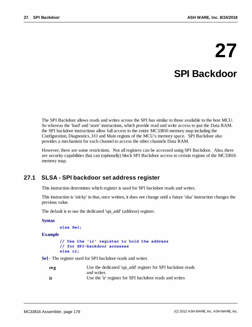
MC33816 Assembler, page 179 (C) 2012 ASH WARE, Inc. ASH WARE, Inc.
27. SPI Backdoor
ASH WARE, Inc. 8/24/2018
27SPI Backdoor
The SPI Backdoor allows reads and writes across the SPI bus similar to those available to the host MCU. So whereas the 'load' and 'store' instructions, which provide read and write access to just the Data RAM.the SPI backdoor instructions allow full access to the entire MC33816 memory map including theConfiguration, Diagnostics, I/O and Main regions of the MCU's memory space. SPI Backdoor alsoprovides a mechanism for each channel to access the other channels Data RAM.
However, there are some restrictions. Not all registers can be accessed using SPI Backdoor. Also, thereare security capabilities that can (optionally) block SPI Backdoor access to certain regions of the MC33816memory map.
27.1 SLSA - SPI backdoor set address register
This instruction determines which register is used for SPI backdoor reads and writes.
This instruction is 'sticky' in that, once written, it does not change until a future 'slsa' instruction changes theprevious value.
The default is to use the dedicated 'spi_add' (address) register.
Syntax
slsa Sel;
Example
// Use the 'ir' register to hold the address// for SPI-backdoor accessesslsa ir;
Sel - The register used for SPI backdoor reads and writes
reg Use the dedicated 'spi_add' register for SPI backdoor readsand writes
ir Use the 'ir' register for SPI backdoor reads and writes
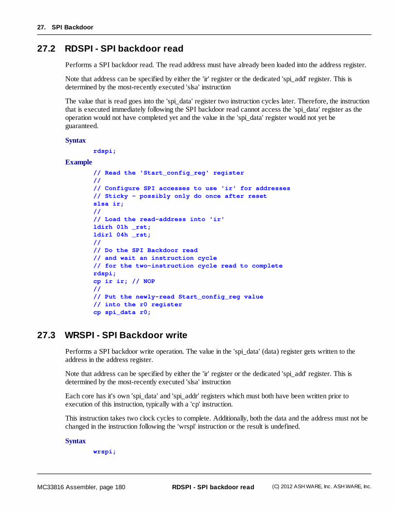
MC33816 Assembler, page 180 (C) 2012 ASH WARE, Inc. ASH WARE, Inc.
27. SPI Backdoor
RDSPI - SPI backdoor read
27.2 RDSPI - SPI backdoor read
Performs a SPI backdoor read. The read address must have already been loaded into the address register.
Note that address can be specified by either the 'ir' register or the dedicated 'spi_add' register. This isdetermined by the most-recently executed 'slsa' instruction
The value that is read goes into the 'spi_data' register two instruction cycles later. Therefore, the instructionthat is executed immediately following the SPI backdoor read cannot access the 'spi_data' register as theoperation would not have completed yet and the value in the 'spi_data' register would not yet beguaranteed.
Syntax
rdspi;
Example
// Read the 'Start_config_reg' register//// Configure SPI accesses to use 'ir' for addresses// Sticky - possibly only do once after resetslsa ir;//// Load the read-address into 'ir'ldirh 01h _rst;ldirl 04h _rst;//// Do the SPI Backdoor read// and wait an instruction cycle// for the two-instruction cycle read to completerdspi;cp ir ir; // NOP//// Put the newly-read Start_config_reg value// into the r0 registercp spi_data r0;
27.3 WRSPI - SPI Backdoor write
Performs a SPI backdoor write operation. The value in the 'spi_data' (data) register gets written to theaddress in the address register.
Note that address can be specified by either the 'ir' register or the dedicated 'spi_add' register. This isdetermined by the most-recently executed 'slsa' instruction
Each core has it's own 'spi_data' and 'spi_addr' registers which must both have been written prior toexecution of this instruction, typically with a 'cp' instruction.
This instruction takes two clock cycles to complete. Additionally, both the data and the address must not bechanged in the instruction following the 'wrspi' instruction or the result is undefined.
Syntax
wrspi;
MC33816 Assembler, page 181 (C) 2012 ASH WARE, Inc. ASH WARE, Inc.
27. SPI Backdoor
WRSPI - SPI Backdoor write
ASH WARE, Inc. 8/24/2018
Example
// Write the 'Start_config_reg' register//// Configure SPI accesses to use 'ir' for addresses// Sticky - possibly only do once after resetslsa ir;//// Load the read-address into 'ir'ldirh 01h _rst;ldirl 04h _rst;//// Load the value to be written into 'spi_data'ldirh 01h _rst;ldirl 01h _rst;cp ir spi_data;//// Do the SPI Backdoor writewrspi;

MC33816 Assembler, page 182 (C) 2012 ASH WARE, Inc. ASH WARE, Inc.