Embed Size (px)
Citation preview
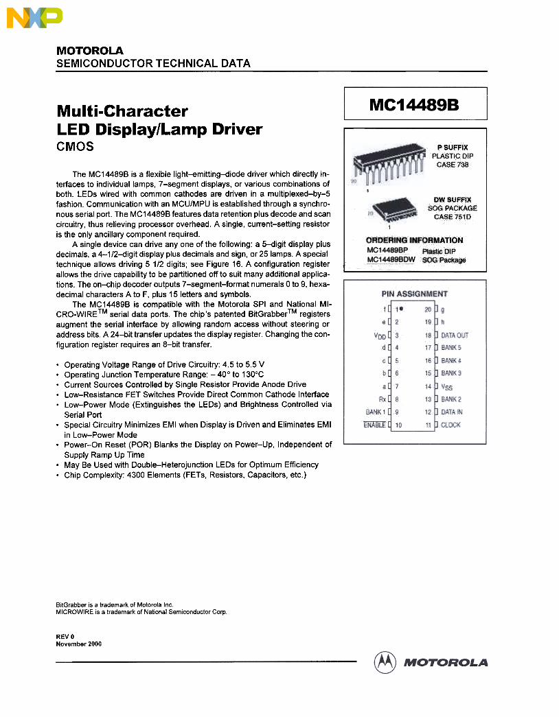
MOTOROLA
SEMICONDUCTOR TECHNICAL DATA
MC14489BM u Iti-Character
lED Display/lamp Driver
CMOS p SVFFiXPLASTICOIP
CASE73$
PW SUFF,~SOOPACKAGE "
CASE 7510
..ORDERING INFQRMATJON
MC14489BP PlaSticDtP
MC14489BDW SOOP~gec
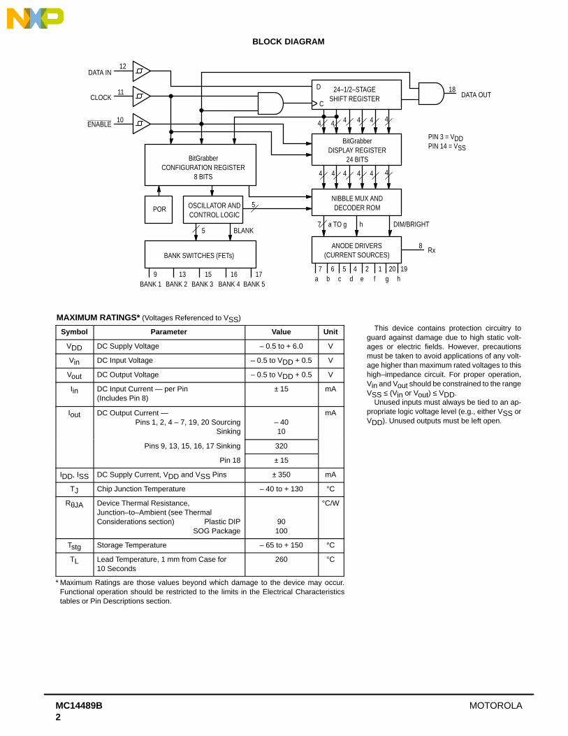
The MC144898 is a flexible light-emitting-diode driver which directly in-terfaces to individual lamps, 7-segment displays, or various combinations ofboth. LEOs wired with common cathodes are driven in a multiplexed-by-5fashion. Communication with an MCUIMPU is established through a synchro-nous serial port. The MC 144898 features data retention plus decode and scancircuitry, thus relieving processor overhead. A single, current-setting resistoris the only ancillary component required.
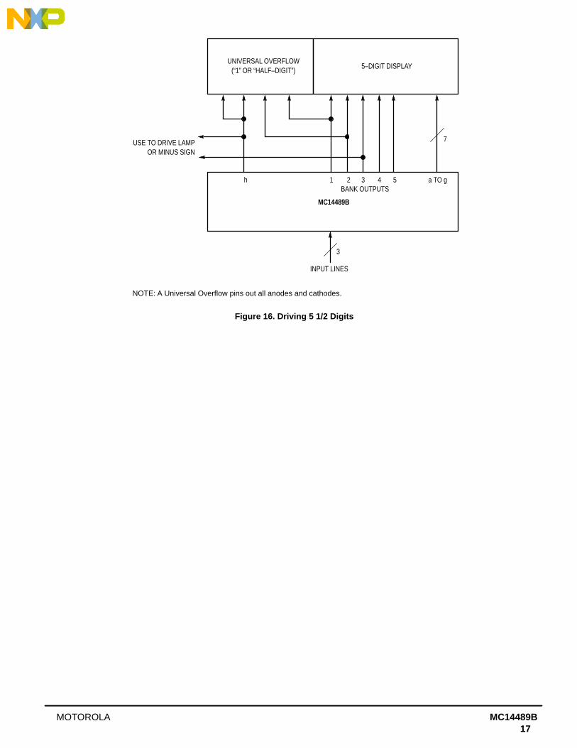
A single device can drive anyone of the following: a 5-digit display plusdecimals, a 4-112-digit display plus decimals and sign, or 25 lamps. A specialtechnique allows driving 5 112 digits; see Figure 16. A configuration registerallows the drive capability to be partitioned off to suit many additional applica-tions. The on-chip decoder outputs 7-segment-format numerals O to 9, hexa-decimal characters A to F, plus 151etters and symbols.
The MC144898 is compatible with the Motorola SPI and National MI-CRO-WIRETM serial data ports. The chip's patented 8itGrabberTM registersaugment the serial interface by allowing random access without steering oraddress bits. A 24-bit transfer updates the display register. Changing the con-figuration register requires an 8-bit transfer.
.Operating Voltage Range of Drive Circuitry: 4.5 to 5.5 V
.Operating Junction Temperature Range: -40° to 130°C
.Current Sources Controlled by Single Resistor Provide Anode Drive
.Low-Resistance FET Switches Provide Direct Common Cathode Interface
.Low-Power Mode (Extinguishes the LEDs) and Brightness Controlled viaSerial Port
.Special Circuitry Minimizes EMI when Display is Driven and Eliminates EMIin Low-Power Mode
.Power-On Reset (POR) Blanks the Display on Power-Up, Independent ofSupply Ramp Up Time
.May Be Used with Double-Heterojunction LEDs for Optimum Efficiency
.Chip Complexity: 4300 Elements (FETs, Resistors, Capacitors, etc.)
BitGrabber is a trademark of Motorola Inc.MICROWIRE is a trademark of National Semiconductor Corp.
REVO
November 2000
MC14489B MOTOROLA2
BLOCK DIAGRAM
1
BitGrabberCONFIGURATION REGISTER
8 BITS
Rx
DATA OUT
8
2 20
12
BitGrabberDISPLAY REGISTER
24 BITS
NIBBLE MUX ANDDECODER ROM
ANODE DRIVERS(CURRENT SOURCES)BANK SWITCHES (FETs)
194567a b
DATA IN
c d e f g h
24–1/2–STAGESHIFT REGISTER
11
10
7
444444
444444
18
POR
9 13 15 16 17
5
5
CLOCK
ENABLE
OSCILLATOR ANDCONTROL LOGIC
BANK 1 BANK 2 BANK 3 BANK 4 BANK 5
PIN 3 = VDDPIN 14 = VSS
h DIM/BRIGHTBLANK
a TO g
D
C
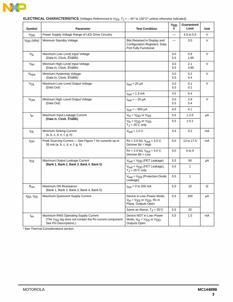
MAXIMUM RATINGS* (Voltages Referenced to VSS)ÁÁÁÁÁÁÁÁ
SymbolÁÁÁÁÁÁÁÁÁÁÁÁÁÁÁÁÁÁÁÁÁÁÁÁ
ParameterÁÁÁÁÁÁÁÁÁÁÁÁ
ValueÁÁÁÁÁÁ
UnitÁÁÁÁÁÁÁÁ
VDDÁÁÁÁÁÁÁÁÁÁÁÁÁÁÁÁÁÁÁÁÁÁÁÁ
DC Supply VoltageÁÁÁÁÁÁÁÁÁÁÁÁ
– 0.5 to + 6.0ÁÁÁÁÁÁ
VÁÁÁÁÁÁÁÁ
VinÁÁÁÁÁÁÁÁÁÁÁÁÁÁÁÁÁÁÁÁÁÁÁÁ
DC Input VoltageÁÁÁÁÁÁÁÁÁÁÁÁ
– 0.5 to VDD + 0.5ÁÁÁÁÁÁ
VÁÁÁÁÁÁÁÁ
VoutÁÁÁÁÁÁÁÁÁÁÁÁÁÁÁÁÁÁÁÁÁÁÁÁ
DC Output VoltageÁÁÁÁÁÁÁÁÁÁÁÁ
– 0.5 to VDD + 0.5ÁÁÁÁÁÁ
VÁÁÁÁÁÁÁÁÁÁÁÁ
IinÁÁÁÁÁÁÁÁÁÁÁÁÁÁÁÁÁÁÁÁÁÁÁÁÁÁÁÁÁÁÁÁÁÁÁÁ
DC Input Current — per Pin(Includes Pin 8)
ÁÁÁÁÁÁÁÁÁÁÁÁÁÁÁÁÁÁ
± 15ÁÁÁÁÁÁÁÁÁ
mA
ÁÁÁÁÁÁÁÁÁÁÁÁ
Iout ÁÁÁÁÁÁÁÁÁÁÁÁÁÁÁÁÁÁÁÁÁÁÁÁÁÁÁÁÁÁÁÁÁÁÁÁ
DC Output Current — Pins 1, 2, 4 – 7, 19, 20 Sourcing
Sinking
ÁÁÁÁÁÁÁÁÁÁÁÁÁÁÁÁÁÁ
– 4010
ÁÁÁÁÁÁÁÁÁ
mA
ÁÁÁÁÁÁÁÁ
ÁÁÁÁÁÁÁÁÁÁÁÁÁÁÁÁÁÁÁÁÁÁÁÁ
Pins 9, 13, 15, 16, 17 SinkingÁÁÁÁÁÁÁÁÁÁÁÁ
320ÁÁÁÁÁÁÁÁÁÁ
ÁÁÁÁÁÁÁÁÁÁÁÁÁÁÁÁÁÁÁÁÁÁÁÁÁÁÁÁ
Pin 18ÁÁÁÁÁÁÁÁÁÁÁÁ
± 15ÁÁÁÁÁÁÁÁÁÁ
ÁÁÁÁIDD, ISSÁÁÁÁÁÁÁÁÁÁÁÁÁÁÁÁÁÁÁÁÁÁÁÁ
DC Supply Current, VDD and VSS PinsÁÁÁÁÁÁÁÁÁÁÁÁ
± 350ÁÁÁÁÁÁ
mAÁÁÁÁÁÁÁÁ
TJÁÁÁÁÁÁÁÁÁÁÁÁÁÁÁÁÁÁÁÁÁÁÁÁ
Chip Junction TemperatureÁÁÁÁÁÁÁÁÁÁÁÁ
– 40 to + 130ÁÁÁÁÁÁ
°CÁÁÁÁÁÁÁÁÁÁÁÁÁÁÁÁ
RθJAÁÁÁÁÁÁÁÁÁÁÁÁÁÁÁÁÁÁÁÁÁÁÁÁÁÁÁÁÁÁÁÁÁÁÁÁÁÁÁÁÁÁÁÁÁÁÁÁ
Device Thermal Resistance,Junction–to–Ambient (see ThermalConsiderations section) Plastic DIP
SOG Package
ÁÁÁÁÁÁÁÁÁÁÁÁÁÁÁÁÁÁÁÁÁÁÁÁ
90100
ÁÁÁÁÁÁÁÁÁÁÁÁ
°C/W
ÁÁÁÁÁÁÁÁ
TstgÁÁÁÁÁÁÁÁÁÁÁÁÁÁÁÁÁÁÁÁÁÁÁÁ
Storage TemperatureÁÁÁÁÁÁÁÁÁÁÁÁ
– 65 to + 150ÁÁÁÁÁÁ
°CÁÁÁÁÁÁÁÁÁÁÁÁ
TLÁÁÁÁÁÁÁÁÁÁÁÁÁÁÁÁÁÁÁÁÁÁÁÁÁÁÁÁÁÁÁÁÁÁÁÁ
Lead Temperature, 1 mm from Case for10 Seconds
ÁÁÁÁÁÁÁÁÁÁÁÁÁÁÁÁÁÁ
260ÁÁÁÁÁÁÁÁÁ
°C
* Maximum Ratings are those values beyond which damage to the device may occur.Functional operation should be restricted to the limits in the Electrical Characteristicstables or Pin Descriptions section.
This device contains protection circuitry toguard against damage due to high static volt-ages or electric fields. However, precautionsmust be taken to avoid applications of any volt-age higher than maximum rated voltages to thishigh–impedance circuit. For proper operation,Vin and Vout should be constrained to the rangeVSS ≤ (Vin or Vout) ≤ VDD.
Unused inputs must always be tied to an ap-propriate logic voltage level (e.g., either VSS orVDD). Unused outputs must be left open.
MC14489BMOTOROLA3
ELECTRICAL CHARACTERISTICS (Voltages Referenced to VSS, TJ = – 40° to 130°C* unless otherwise indicated)
Symbol Parameter Test ConditionVDD
VGuaranteed
Limit Unit
VDD Power Supply Voltage Range of LED Drive Circuitry — 4.5 to 5.5 V
VDD (stby) Minimum Standby Voltage Bits Retained in Display andConfiguration Registers, DataPort Fully Functional
— 3.0 V
VIL Maximum Low–Level Input Voltage(Data In, Clock, Enable)
3.05.5
0.91.65
V
VIH Minimum High–Level Input Voltage(Data In, Clock, Enable)
3.05.5
2.13.85
V
VHys Minimum Hysteresis Voltage(Data In, Clock, Enable)
3.05.5
0.20.4
V
VOL Maximum Low–Level Output Voltage(Data Out)
Iout = 20 µA 3.05.5
0.10.1
V
Iout = 1.3 mA 4.5 0.4
VOH Minimum High–Level Output Voltage(Data Out)
Iout = – 20 µA 3.05.5
2.95.4
V
Iout = – 800 µA 4.5 4.1
Iin Maximum Input Leakage Current(Data In Clock Enable)
Vin = VDD or VSS 5.5 ± 2.0 µA(Data In, Clock, Enable)
Vin = VDD or VSS,TJ = 25°C only
5.5 ± 0.1
iOL Minimum Sinking Current(a, b, c, d, e, f, g, h)
Vout = 1.0 V 4.5 0.2 mA
iOH Peak Sourcing Current — See Figure 7 for currents up to35 mA (a, b, c, d, e, f, g, h)
Rx = 2.0 kΩ, Vout = 3.0 V,Dimmer Bit = High
5.0 13 to 17.5 mA
Rx = 2.0 kΩ, Vout = 3.0 V,Dimmer Bit = Low
5.0 6 to 9
IOZ Maximum Output Leakage Current(Bank 1 Bank 2 Bank 3 Bank 4 Bank 5)
Vout = VDD (FET Leakage) 5.5 50 µA(Bank 1, Bank 2, Bank 3, Bank 4, Bank 5)
Vout = VDD (FET Leakage),TJ = 25°C only
5.5 1
Vout = VSS (Protection DiodeLeakage)
5.5 1
Ron Maximum ON Resistance(Bank 1, Bank 2, Bank 3, Bank 4, Bank 5)
Iout = 0 to 200 mA 5.0 10 Ω
IDD, ISS Maximum Quiescent Supply Current Device in Low–Power Mode,Vin = VSS or VDD, Rx inPlace, Outputs Open
5.5 100 µA
Same as Above, TJ = 25°C 5.5 20
Iss Maximum RMS Operating Supply Current(The VSS leg does not contain the Rx current component.See Pin Descriptions.)
Device NOT in Low–PowerMode, Vin = VSS or VDD,Outputs Open
5.5 1.5 mA
* See Thermal Considerations section.
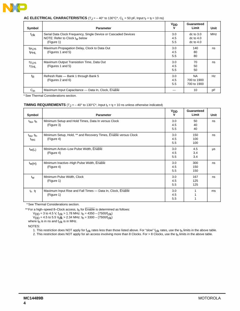
MC14489B MOTOROLA4
AC ELECTRICAL CHARACTERISTICS (TJ = – 40° to 130°C*, CL = 50 pF, Input tr = tf = 10 ns)
Symbol ParameterVDD
VGuaranteed
Limit Unit
fclk Serial Data Clock Frequency, Single Device or Cascaded DevicesNOTE: Refer to Clock tw below
(Figure 1)
3.04.55.5
dc to 3.0dc to 4.0dc to 4.0
MHz
tPLH,tPHL
Maximum Propagation Delay, Clock to Data Out(Figures 1 and 5)
3.04.55.5
1408080
ns
tTLH,tTHL
Maximum Output Transistion Time, Data Out(Figures 1 and 5)
3.04.55.5
705050
ns
fR Refresh Rate — Bank 1 through Bank 5(Figures 2 and 6)
3.04.55.5
NA700 to 1900700 to 1900
Hz
Cin Maximum Input Capacitance — Data In, Clock, Enable — 10 pF
* See Thermal Considerations section.
TIMING REQUIREMENTS (TJ = – 40° to 130°C*, Input tr = tf = 10 ns unless otherwise indicated)
Symbol ParameterVDD
VGuaranteed
Limit Unit
tsu, th Minimum Setup and Hold Times, Data In versus Clock(Figure 3)
3.04.55.5
504040
ns
tsu, th,trec
Minimum Setup, Hold, ** and Recovery Times, Enable versus Clock(Figure 4)
3.04.55.5
150100100
ns
tw(L) Minimum Active–Low Pulse Width, Enable(Figure 4)
3.04.55.5
4.53.43.4
µs
tw(H) Minimum Inactive–High Pulse Width, Enable(Figure 4)
3.04.55.5
300150150
ns
tw Minimum Pulse Width, Clock(Figure 1)
3.04.55.5
167125125
ns
tr, tf Maximum Input Rise and Fall Times — Data In, Clock, Enable (Figure 1)
3.04.55.5
111
ms
* See Thermal Considerations section.
** For a high–speed 8–Clock access, th for Enable is determined as follows:VDD = 3 to 4.5 V, fclk > 1.78 MHz: th = 4350 – (7500/fclk)VDD = 4.5 to 5.5 V, fclk > 2.34 MHz: th = 3300 – (7500/fclk)
where th is in ns and fclk is in MHz.
NOTES:1. This restriction does NOT apply for fclk rates less than those listed above. For “slow” fclk rates, use the th limits in the above table.2. This restriction does NOT apply for an access involving more than 8 Clocks. For > 8 Clocks, use the th limits in the above table.
MC14489BMOTOROLA5
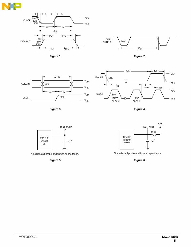
Figure 1 . Figure 2.
10%
VDD
1/fclk
DATA OUT
CLOCK
90%50%
90%50%10%
tPLH tPHL
tTLH tTHL
twtw
tf tr
BANKOUTPUT 50%
1/fR
VSS
Figure 3 . Figure 4.
DATA IN
CLOCK
50%
VALID
50%
tsu thVDD
VDD
CLOCK
ENABLE
50%
tsu th
FIRSTCLOCK
LASTCLOCK
trec
50%
VDD
VDDtw(H)tw(L)
VSS
VSS
VSS
VSS
Figure 5 . Figure 6.
TEST POINT
DEVICEUNDERTEST
CL*
*Includes all probe and fixture capacitance.
TEST POINT
DEVICEUNDERTEST
CL*
*Includes all probe and fixture capacitance.
VDD
56 Ω
MC14489B MOTOROLA6
PIN DESCRIPTIONS
DIGITAL INTERFACE
Data In (Pin 12)
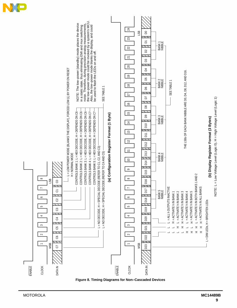
Serial Data Input. The bit stream begins with the MSB andis shifted in on the low–to–high transition of Clock. When thedevice is not cascaded, the bit pattern is either 1 byte (8 bits)long to change the configuration register or 3 bytes (24 bits)long to update the display register. For two chips cascaded,the pattern is either 4 or 6 bytes, respectively. The displaydoes not change during shifting (until Enable makes a low–to–high transition) which allows slow serial data rates, if de-sired.
The bit stream needs neither address nor steering bits dueto the innovative BitGrabber registers. Therefore, all bits inthe stream are available to be data for the two registers. Ran-dom access of either register is provided. That is, the regis-ters may be accessed in any sequence. Data is retained inthe registers over a supply range of 3 to 5.5 V. Formats areshown in Figures 8 through 14 and summarized in Table 2.Information on the segment decoder is given in Table 1.
Data In typically switches near 50% of VDD and has aSchmitt–triggered input buffer. These features combine tomaximize noise immunity for use in harsh environments andbus applications. This input can be directly interfaced toCMOS devices with outputs guaranteed to switch near rail–to–rail. When interfacing to NMOS or TTL devices, either alevel shifter (MC14504B, MC74HCT04A) or pullup resistor of1 kΩ to 10 kΩ must be used. Parameters to be consideredwhen sizing the resistor are the worst–case IOL of the drivingdevice, maximum tolerable power consumption, and maxi-mum data rate.
Clock (Pin 11)
Serial Data Clock Input. Low–to–high transitions on Clockshift bits available at Data In, while high–to–low transitionsshift bits from Data Out. The chip’s 24–1/2–stage shift regis-ter is static, allowing clock rates down to dc in a continuous orintermittent mode. The Clock input does not need to be syn-chronous with the on–chip clock oscillator which drives themultiplexing circuit.
Eight clock cycles are required to access the configurationregister, while 24 are needed for the display register when theMC14489B is not cascaded. See Figures 8 and 9.
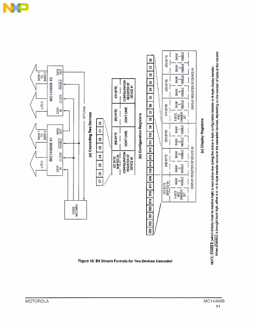
As shown in Figure 10, two devices may be cascaded. Inthis case, 32 clock cycles access the configuration registerand 48 access the display register, as depicted in Figure 10.
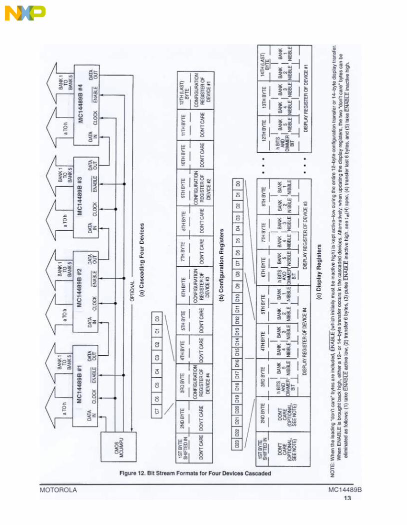
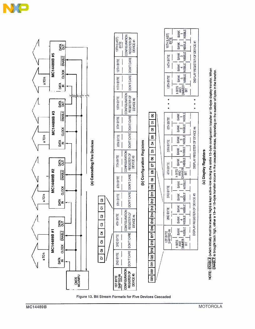
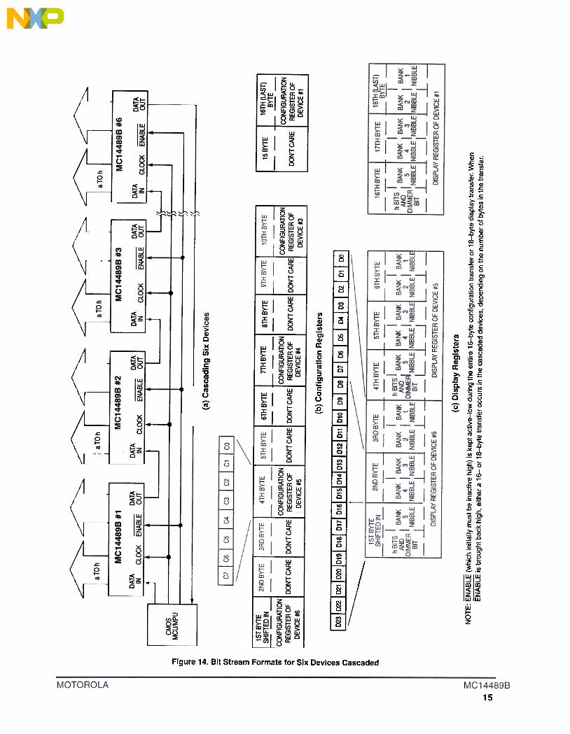
Cascading of 3, 4, 5, and 6 devices is shown in Figures 11,12, 13, and 14, respectively. Also, reference Table 2.
Clock typically switches near 50% of VDD and has aSchmitt–triggered input buffer. Slow Clock rise and fall timesare tolerated. See the last paragraph of Data In for more in-formation.
NOTETo guarantee proper operation of the power–onreset (POR) circuit, the Clock pin must NOT befloated or toggled during power–up. That is, theClock pin must be stabl e until the VDD pinreaches at least 3 V.If control of the Clock pin during power–up is notpractical, then the MC14489B must be reset via bitC0 in the C register. To accomplish this, C0 is re-set low, then set high.
Enable (Pin 10)
Active–Low Enable Input. This pin allows the MC14489B tobe used on a serial bus, sharing Data In and Clock with otherperipherals. When Enable is in an inactive high state, DataOut is forced to a known (low) state, shifting is inhibited, andthe port is held in the initialized state. To transfer data to thedevice, Enable (which initially must be inactive high) is takenlow, a serial transfer is made via Data In and Clock, andEnable is taken high. The low–to–high transition on Enabletransfers data to either the configuration or display register,depending on the data stream length.
Every rising edge on Enable initiates a blanking intervalwhile data is loaded. Thus, continually loading the device withthe same data may cause the LEDs on some banks to appeardimmer than others.
NOTE
Transitions on Enable must not be attemptedwhile Clock is high. This puts the device out ofsynchronization with the microcontroller. Resyn-chronization occurs when Enable is high andClock is low.
This input is also Schmitt–triggered and switches near 50%of VDD, thereby minimizing the chance of loading erroneousdata in the registers. See the last paragraph of Data In formore information.
Data Out (Pin 18)
Serial Data Output. Data is transferred out of the shift regis-ter through Data Out on the high–to–low transition of Clock.This output is a no connect, unless used in one of the man-ners discussed below.
When cascading MC14489B’s, Data Out feeds Data In of thenext device per Figures 10, 11, 12, 13, and 14.
Data Out could be fed back to an MCU/MPU to perform awrap–around test of serial data. This could be part of a sys-tem check conducted at power–up to test the integrity of thesystem’s processor, pc board traces, solder joints, etc.
The pin could be monitored at an in–line Q.A. test duringboard manufacturing.
Finally, Data Out facilitates troubleshooting a system.
DISPLAY INTERFACE
Rx (Pin 8)
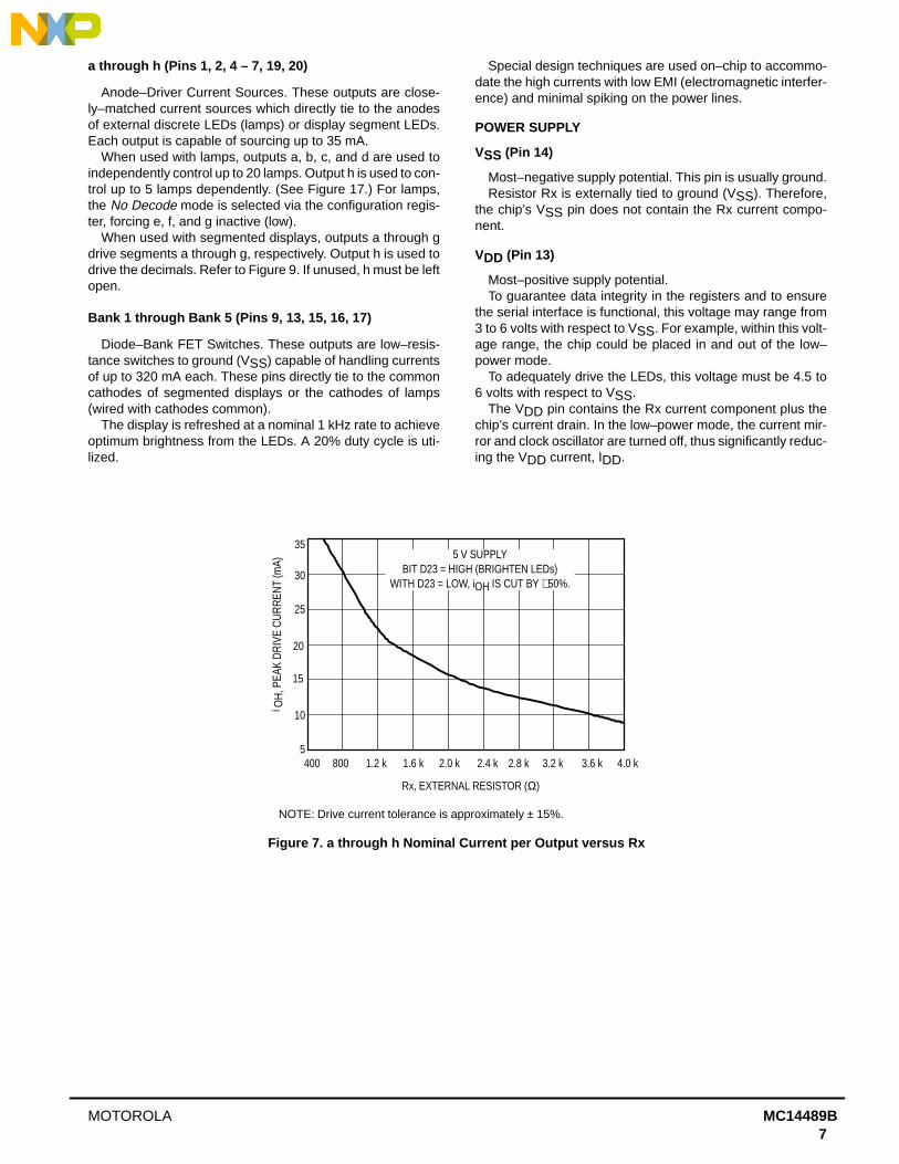
External Current–Setting Resistor. A resistor tied betweenthis pin and ground (VSS) determines the peak segment drivecurrent delivered at pins a through h. Pin 8’s resistor ties intoa current mirror with an approximate current gain of 10 whenbit D23 = high (brighten). With D23 = low, the peak current isreduced about 50%. Values for Rx range from 700 Ω to infin-ity. When Rx = ∞ (open circuit), the display is extinguished.For proper current control, resistors having ± 1% toleranceshould be used. See Figure 7.
CAUTION
Small Rx values may cause the chip to overheatif precautions are not observed. See ThermalConsiderations.
MC14489BMOTOROLA7
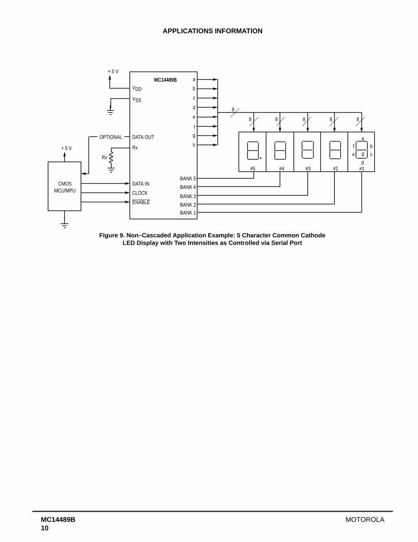
a through h (Pins 1, 2, 4 – 7, 19, 20)
Anode–Driver Current Sources. These outputs are close-ly–matched current sources which directly tie to the anodesof external discrete LEDs (lamps) or display segment LEDs.Each output is capable of sourcing up to 35 mA.
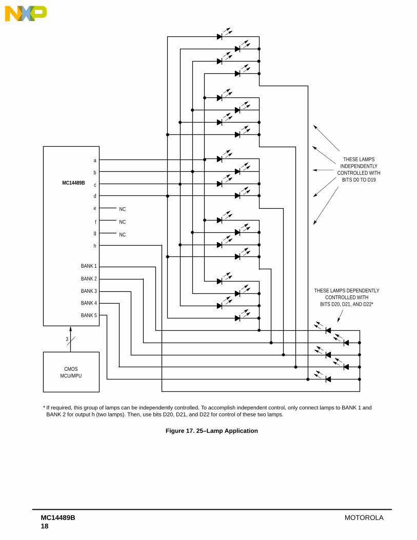
When used with lamps, outputs a, b, c, and d are used toindependently control up to 20 lamps. Output h is used to con-trol up to 5 lamps dependently. (See Figure 17.) For lamps,the No Decode mode is selected via the configuration regis-ter, forcing e, f, and g inactive (low).
When used with segmented displays, outputs a through gdrive segments a through g, respectively. Output h is used todrive the decimals. Refer to Figure 9. If unused, h must be leftopen.
Bank 1 through Bank 5 (Pins 9, 13, 15, 16, 17)
Diode–Bank FET Switches. These outputs are low–resis-tance switches to ground (VSS) capable of handling currentsof up to 320 mA each. These pins directly tie to the commoncathodes of segmented displays or the cathodes of lamps(wired with cathodes common).
The display is refreshed at a nominal 1 kHz rate to achieveoptimum brightness from the LEDs. A 20% duty cycle is uti-lized.
Special design techniques are used on–chip to accommo-date the high currents with low EMI (electromagnetic interfer-ence) and minimal spiking on the power lines.
POWER SUPPLY
VSS (Pin 14)
Most–negative supply potential. This pin is usually ground.Resistor Rx is externally tied to ground (VSS). Therefore,
the chip’s VSS pin does not contain the Rx current compo-nent.
VDD (Pin 13)
Most–positive supply potential.To guarantee data integrity in the registers and to ensure
the serial interface is functional, this voltage may range from3 to 6 volts with respect to VSS. For example, within this volt-age range, the chip could be placed in and out of the low–power mode.
To adequately drive the LEDs, this voltage must be 4.5 to6 volts with respect to VSS.
The VDD pin contains the Rx current component plus thechip’s current drain. In the low–power mode, the current mir-ror and clock oscillator are turned off, thus significantly reduc-ing the VDD current, IDD.
Figure 7. a through h Nominal Current per Output versus Rx
35
30
25
20
15
10
5400 800 1.2 k 2.0 k 2.4 k 2.8 k 3.2 k 3.6 k 4.0 k1.6 k
i OH
, PEA
K D
RIV
E C
UR
REN
T (m
A)
5 V SUPPLYBIT D23 = HIGH (BRIGHTEN LEDs)
WITH D23 = LOW, iOH IS CUT BY ∼50%.
Rx, EXTERNAL RESISTOR (Ω)
NOTE: Drive current tolerance is approximately ± 15%.
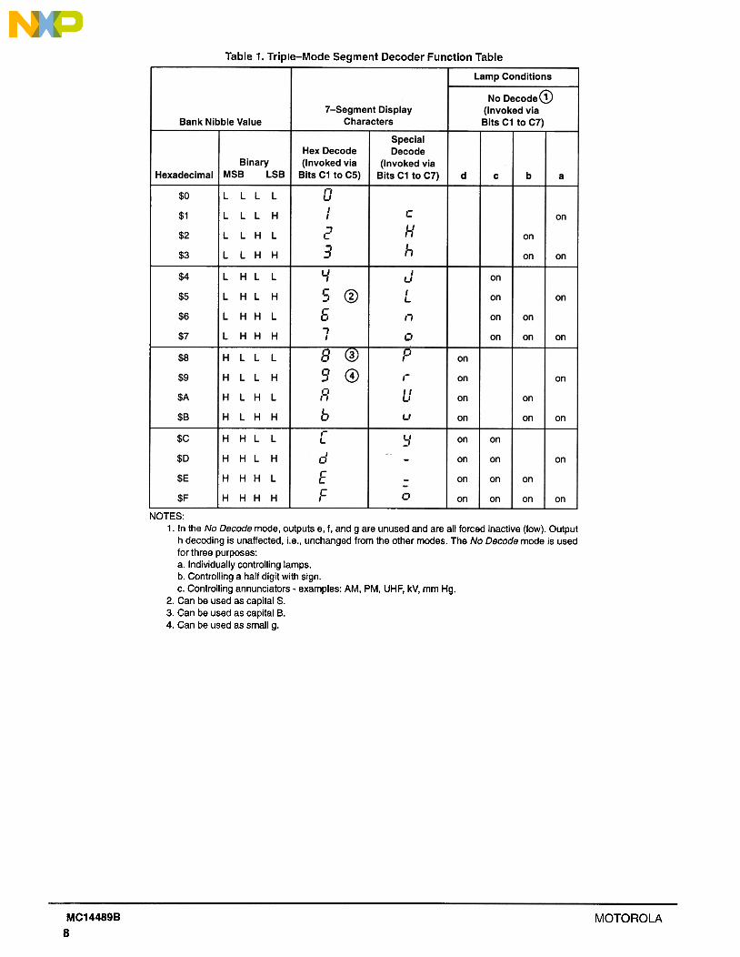
Table 1. Triple-Mode Segment Decoder Function Table
Lamp Conditions
No DecodeG)(Invoked viaBits C1 to C7)
7-Segment DisplayCharactersBank Nibble Value
SpecialDecode
(Invoked viaBits C1 to C7)
Hex Decode(Invoked via
Bits C1 to C5)Binary
MSB LSBHexadecimal d bc a
"u
II
2
3
$0
$1
$2
$3
L L L
L L H
L H L
L H H
c
,','
,'I
on
on
on on
l./
s
G,,
8
9'-I,-,
'c,
~
$4
$5
$6
$7
H L L
H L H
H H L
H H H
on
on on
on on
on on on
$8
$9
$A
$B
I H L L L
H L L H
H L H L
H L H H
on
,-
u
LI
on on
on on
on on on
,-L
,c'
E
F
$C
$0
$E
$F
~H
H
H
H
on on
on on on
on on on
0 on on on on
NOTES:1. In the No Decode mode, outputs e, f, and g are unused and are all forced inactive (low). Output
h decoding is unaffected, i.e., unchanged from the other modes. The No Decode mode is used
for three purposes:a. Individually controlling lamps.b. Controlling a half digit with sign.c. Controlling annunciators. examples: AM, PM, UHF, kV, mm Hg.
2. Can be used as capital S.3. Can be used as capital B.4. Can be used as small g.
MC14489B
8
MOTOROLA
@
~
@
,u
IL
"
OO,
H
H
H
H r
L
H
L
H
MC14489BMOTOROLA9
ÇÇÇÇÇÇÇÇÇÇÇÇÇÇÇÇÇÇÇÇÇÇÇÇÇÇÇÇÇÇÇÇÇÇÇÇÇÇÇÇÇÇÇÇÇÇÇÇÇÇÇÇÇÇ
Figure 8. Timing Diagrams for Non–Cascaded Devices
ÇÇÇ
ÇÇÇÇÇÇD2
2
ÇÇÇ
D21
ÇÇÇ
D20
ÇÇÇ
D19
ÇÇÇ
D18
ÇÇÇÇÇÇ
D17
ÇÇÇ
D16
ÇÇÇÇÇÇD1
5
ÇÇÇ
D14
ÇÇÇÇÇÇD1
3ÇÇÇ
D12
ÇÇÇ
D11
ÇÇÇ
D10
ÇÇÇ
D9
ÇÇÇÇÇÇD8
ÇÇÇ
D7
ÇÇÇÇÇÇD6
ÇÇÇ
D5
ÇÇÇÇÇÇD4
ÇÇÇ
D3
ÇÇÇ
D2
ÇÇÇ
D1
ÇÇÇÇÇÇÇÇÇ
D0
ÇÇÇÇÇÇÇÇÇÇÇÇ
D23
23
45
67
89
1011
1213
1415
1617
1819
2021
2223
241
MSB
LSB
L =
DIM
LED
s, H
= B
RIG
HTE
N L
EDs
THE
LSBs
OF
EAC
H B
ANK
NIB
BLE
ARE
D0,
D4,
D8,
D12
, AN
D D
16.
BAN
K 5
NO
TE
: The
low
–pow
er (
stan
dby)
mod
e pl
aces
the
devi
ce
C6
C5
C4
C3
C2
C1
C7
23
45
67
81
MSB
ENAB
LE
CLO
CK
DAT
A IN
in a
sta
tic s
tate
, thu
s el
imin
atin
g E
MI a
nd m
ux s
witc
hing
nois
e. T
here
fore
, dur
ing
prec
isio
n an
alog
mea
sure
men
ts,
the
low
–pow
er m
ode
coul
d be
invo
ked
by a
sys
tem
’s M
CU
.A
lso,
the
low
–pow
er m
ode
blan
ks th
e di
spla
y, a
nd c
ould
be
use
d to
flas
h th
e LE
Ds
on a
nd o
ff.
C0
L =
LOW
PO
WER
MO
DE
(BLA
NKS
TH
E D
ISPL
AY),
FOR
CED
LO
W (L
) BY
POW
ER O
N R
ESET
H =
NO
RM
AL M
OD
E
CO
NTR
OLS
BAN
K 1:
CO
NTR
OLS
BAN
K 2:
L =
HEX
DEC
OD
E, H
= D
EPEN
DS
ON
C6
CO
NTR
OLS
BAN
K 3:
L =
HEX
DEC
OD
E, H
= D
EPEN
DS
ON
C6
CO
NTR
OLS
BAN
K 4:
L =
HEX
DEC
OD
E, H
= D
EPEN
DS
ON
C7
CO
NTR
OLS
BAN
K 5:
L =
HEX
DEC
OD
E, H
= D
EPEN
DS
ON
C7
SEE
TABL
E 1
L =
NO
DEC
OD
E, H
= S
PEC
IAL
DEC
OD
E (R
EFER
TO
C1,
C2,
AN
D C
3)L
= N
O D
ECO
DE,
H =
SPE
CIA
L D
ECO
DE
(REF
ER T
O C
4 AN
D C
5)
L L L L H H H H
L L H H L L H H
L H L H L H L H
= AL
L h
OU
TPU
TS IN
ACTI
VE
= AC
TIVA
TE h
IN B
ANK
1=
ACTI
VATE
h IN
BAN
K 2
= AC
TIVA
TE h
IN B
ANK
3=
ACTI
VATE
h IN
BAN
K 4
= AC
TIVA
TE h
IN B
ANK
5
= AC
TIVA
TE h
IN B
OTH
BAN
KS 1
AN
D 2
= AC
TIVA
TE h
IN A
LL B
ANKS
NIB
BLE
BAN
K 4
NIB
BLE
BAN
K 3
NIB
BLE
BAN
K 2
NIB
BLE
BAN
K 1
NIB
BLE
SEE
TABL
E 1
ENAB
LE
CLC
OK
DAT
A IN
LSB (a)
Con
figur
atio
n R
egis
ter
For
mat
(1
Byt
e)
(b)
Dis
play
Reg
iste
r F
orm
at (
3 B
ytes
)
NO
TE
: L =
Low
Vol
tage
Lev
el (
Logi
c 0)
, H =
Hig
h V
olta
ge L
evel
(Lo
gic
1)
L =
HEX
DEC
OD
E, H
= D
EPEN
DS
ON
C6
MC14489B MOTOROLA10
APPLICATIONS INFORMATION
Figure 9. Non–Cascaded Application Example: 5 Character Common CathodeLED Display with Two Intensities as Controlled via Serial Port
#5 #4 #3 #2 #1
8
8 8 8 8 8
d
ab
ce
fg
BANK 5
BANK 4
BANK 3
BANK 2
BANK 1
d
a
b
c
e
fg
hOPTIONAL
CMOSMCU/MPU
+ 5 V
Rx
VDD
VSS
DATA OUT
Rx
DATA IN
CLOCK
ENABLE
+ 5 V
MC14489B
•
h
Lt)
~o~zt-z~ ~
II)
~o~z~z<~<00 tO
Figure 10. Bit Stream Formats for Two Devices Cascaded
au.~ ~O~
~~ I ~~~~- --~
';!?rn ~ffio
Sa:
I w
~ I ~ID 1-C 2:II: I o(0) C
~i:;Q-
~I ~~~
aJ (!)U)-
--Gj
~I ~~Q
("I
~ I ~
IDI ~D Z
~
I
cn...wow
.51w
a:
co
;IV...~CI
;0=C0
(J--
8.
~Q)-U)
.51Q)a:>-m
iiU)c
u-
"~I/)c
~Q)
" .cQ) --cI/) .-c I/)
~~>..c"'-
'Q.°I/) ~.-Q)"C.cQ) E>. ~
cb ;.c
O ~~ 0
~ 01I/) CC .-." "C~ C-Q)C Q.
.0 Q)~ "C~ .~ I/)
.g' .~C >0 Q)U "CQ) "C
!~~ ~
'"" Q)C .cQ) -Q) C.c .--I/)OI~C ~
.c U
~ 8"C ~
~~.Q I/)
J, ~> -u Q)." >.-.c
g-.b-" ~I/) 0
~J.QI .".c ~Q) Q)> :5U .a;"' .C .c
.-01Q) .-
.c.C--"I/) U~ jgE ->..c= 01"' ~
'"" 0:5 .5.c .!a
1 ~li « c
z Q)
UJ.C..s:
UJ
~
-'<
Q In1- GI~ .~
>I GI
I ~
i .!DlC
=6~1,)In~
(J
:§:
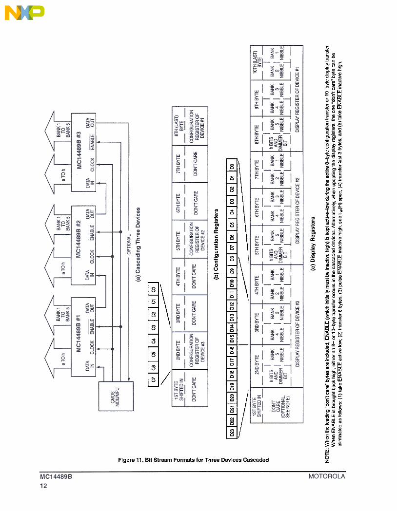
Figure 11. Bit Stream Formats for Three Devices Cascaded
1/1..Q)...1/1
.51Q)
11:
c.2~..~C)
;;:cO
u
B
In...41"cn'6141a:>-la"5.Inc
:§:
..:
'*c: Q)(\1.0~ c: .
>-B.C:~ .2'c.Q).c..~ >. Q)"c .0 .~Q). u>.~(\1-9 B .5O ... ~W .-c:-1
~oaJO"cc(~. Z
2.Q)WU) c:
c:°Q)
(\IQ)~~ -(\I
---
c:-~° .Il)
.-~ ~
"§1!."C U) c:
:J .-(\I.2' &JI .
'E~U)o>-Q)U(\1>.
Q)Q..O>. .~ C')
~ "ccn
Q) (\I
.c.-Q) -~
.= 01 2.-c:U)C::QC:Q) (\I e
Q)"C-.c.c.~-:J-.r
0Ic:~c:
Q) ..c: U:J.C.Q)
"c~C. U)~ ~~-~OQ)J:
->~J, "' ~> (\I -
:;: E Q)
UQ)Q)(\I .-U)
-< -c. .c:Q) .CJ~ U) .-
Q).C..~ .!J Q)~».c: Q) .-
OI"cU.-"c (\I.c: Q) .5
~"c ~UJ U~-1
(\I (\I [D
.5 U ~
Q)Q)w.O=Q)-c:0)~ .-3E ~ c.
>-:J~-HC')~o-:...~ U)C: Q) Q)
.-->.
.c.0).oU c:
.-(\I co
.c. "'~ -~
~Q)2.~ UJ >. 0)
-1-9C:
aJoec(.-:::.z~C\IWO~
"I:i.b~Q) -
"Cc:Q).2 (\I >U ~ .-
c:Q)U.-.c: (\I~ ... ~UJ (\IQ)-1
U).r:aJQ) .2' c(
>..c:Z.O~W, U Q)
~~~
B-s .c.~...01.-C::J~O O ..
"C ~ ~, .0 ~
OIU)Oc: .-=.-" .O"C~-(\I-1U)Q)aJ(\1
-a;c("C.c:ZQ)-W- (\Ic:c:C:Q) Q) .-
.c:.c:E
~~~
Uj
bz
"'~o~2 1- 2< <00 00
"'~o~z t- z< <00 00
"'
:.:=0:.:Z I- Z
< <
00 00
.c
9"'
.c~...
.c~"'
.c
~"'
"'
~o~ZI-Z~ ~
~~00
~I ~~0) ~,
~ W"'""'" ~
U 8~ ;1
N*
m0>
~qo,..U~
Lt):11:
m0>~vv.-u~
M
=11=
ID
0)
~
~
~
,-
U
~
~z~-0
~<.>
~z<-1"
~~
~o
w
ffi
~"I
§u
<~~i'"' i
~~~o
I~
I~~UJI
8-'0
~z<-n
~~~o
::J<n a.
o~~::J
uu~
InQ)u
">Q)
0Q)>~CIC
:gUIn
-' IU
~ (,)0 ---IU1- --~0
~
I gJ.!..
OLL
~0",
W~ I ~0:.. ~fi3 5~~
mt;: -->I-- I ZLL(!)W cn:c 8 wo ~cn 0:
c:Q) "'.c: Q)$:'(iJc:"' ~Q) '"'
'(iJ;C:.c:~ -~ c:>- .-
~ I/)-Q)
~>-.-.Q"0-Q) 0
>-'"'
;b~.-:3'"' c0 Q)'"'.C:Q)-
'(iJ CC 0~ CI-CC .-
0"0.-C-Q)~ a.:. Q)CI"0IC -C U>
8 .~Q) >
III ~>- ~
.."0Q) Q)-.-"0~ Q) BCI .= I/)Q) -~
~ ~ u
>Q)Q)ca £:5
-c:c. CI .-
.! .E ~c :.:3"0 u
u ~8"-' 0'"'
1~> c:
~ ~U '"'~ -
-Q)a.>.
~;b
:c-'"'ClO
:c~Q) .->~ ~U '"'"' Q).E £Q) .a;
.Q .-.c:U> CI:. .-
E.C:~>-u
= ~.~ .Q,.. -c: .c:
.-CI
.c: ~U 0
:c.c~ I/)
~.-
lili
~z
(/)Qj-u;'610)~co;cu..~Dl
-=C0
U
§:
"'~o~ZLZ<~<CD CD
"'~ ~zgz< <CD CD
II)
~o~ZI-Z
~ ~
"'~o~Z I- Z~ ~
.c~m
.c
~...
.c~"'
.c~...
('II=11:
m0)~~~?-
u
~
M'#:
m01~q-q-~U~
ID=!I:
ID0)CO~~~()~
~5~o
,..I w :11: -J
m ~0) zrD w~q- ~
c:; 8~ 5
.<~~"1
8-'(.)
~z<-a
~!;~o
w-'[0<zw
8d
<'<~0
~I:;
~o
UJ-'00
~III
I~
~
§u
~z<-n
~5~o
=>
Inll.o~~=>
l>~
UIQ)U'>Q)C><
inDlC=6
~III
--' IV< Uz O IV
1-CI.O
I g~-Ou.
F;°~~~
I ~ ~ ~>=~ (.!)cn-
aJtL: [!:a[;jf--1 ~wc cn:l: Olr
~cn (,)
I ~ 11.
~ ~~~IIJ 115!7j~
~ I~~~
zau.1=" ~a-
~~ '
1 ~ ~ ~;;:aJ ~a(t;
10 8 wc -11:!
~ I
~ ~
~
zOu.-0."'< ..
a:a:w::J~U<.?CI)--->u.<.?wZwc
Sa:
z
~~'"'
~a:-
::I1:!~(!)00--->LL(!)W
8~o
Figure 14. Bit Stream Formats tor Six Devices Cascaded
wa:<(.)1-Z
8
~~~z8
wIr
~
~wIr<u
~
8
w
~1-
~wa:51-Z
8
~<u1-Z~
UI...Q)
~
'51Q)
a:
co
;:la...~CI
;;:CO
(J
e:
cw ~
~.; c~ as
.p!.;.(/) Q!C.cas -;. c>. .-
as (/)-w
.~~-0-Q! 0
l~,.. :....c0 Q!
cW-
in CC 0
~ CJ-CC .-0 -0
.-C
"§ ~:. WCJ-0
10= .C (/)
8 .~w Q!
cn ~-0..I -0GI(OW-,..-0~ Q! ~
CI~~GI c ~
a: W>- Q!~ca .c-
--cc. CJ .-
~ .2 ~0 :.:.
-0 u~ >uCJ ~ 0
0...
1.;> C
-:: ~U -(1J Q!
c.>.
~~.-,..:2"...CJO:2~W ,..>-:: (1JU ...(1J Q!
.E :5w .a;
.c .-.c"' CJ:. .-
E.C~>.u
= as
~.c.2 :E-CJ
.c :.u 0
.c.c~ (/)~.-
I~ I~
~IDZ<wffi
w
bz
15
MC14489B MOTOROLA16
Table 2. Register Access for Two or More Cascaded Devices
C i i *
Configuratio n Register Access Display Register Access
Criteria* Total Number of BytesNumber of Leading“Don’t Care” Bytes Total Number of Bytes
Number of Leading“Don’t Care” Bytes
If 3N is a Multiple of 4 3N 2 3N + 2 2
If 3N – 1 is a Multiple of 4 3N – 1 1 3N + 1 1
If 3N – 2 is a Multiple of 4 3N – 2 0 3N 0
If 3N – 3 is a Multiple of 4 3N – 2 0 3N 0
* N = number of devices that are cascaded. For example, to drive 10 digits, 2 devices are cascaded; therefore, N = 2. To drive 35 digits, sevendevices are cascaded; therefore N = 7.
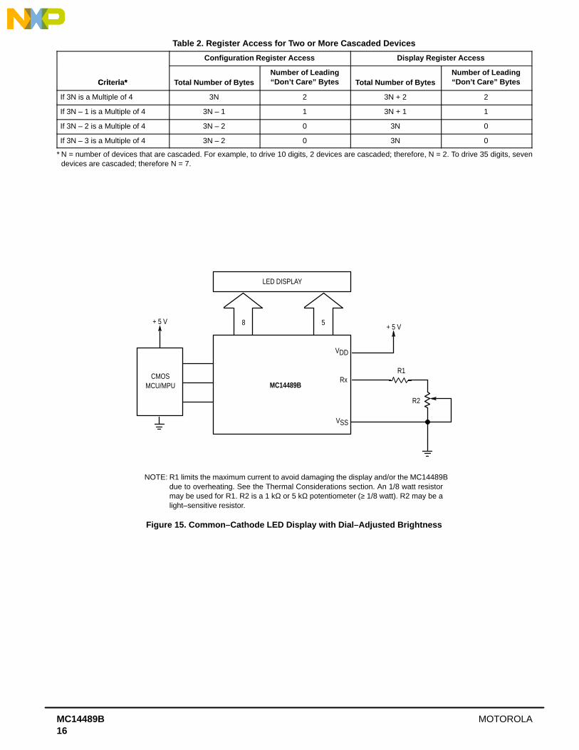
Figure 15. Common–Cathode LED Display with Dial–Adjusted Brightness
VSS
CMOSMCU/MPU
Rx
LED DISPLAY
MC14489B
8 5+ 5 V
R1
R2
VDD
+ 5 V
NOTE: R1 limits the maximum current to avoid damaging the display and/or the MC14489Bdue to overheating. See the Thermal Considerations section. An 1/8 watt resistormay be used for R1. R2 is a 1 kΩ or 5 kΩ potentiometer (≥ 1/8 watt). R2 may be alight–sensitive resistor.
MC14489BMOTOROLA17
Figure 16. Driving 5 1/2 Digits
4
UNIVERSAL OVERFLOW(“1” OR “HALF–DIGIT”)
MC14489B
5h
3
a TO g321BANK OUTPUTS
7USE TO DRIVE LAMPOR MINUS SIGN
5–DIGIT DISPLAY
INPUT LINES
NOTE: A Universal Overflow pins out all anodes and cathodes.
MC14489B MOTOROLA18
Figure 17. 25–Lamp Application
3
BANK 5
BANK 4
BANK 3
BANK 2
BANK 1
d
a
b
c
e
f
g
h
CMOSMCU/MPU
NC
NC
NC
MC14489B
THESE LAMPS DEPENDENTLYCONTROLLED WITH
BITS D20, D21, AND D22*
THESE LAMPSINDEPENDENTLY
CONTROLLED WITHBITS D0 TO D19
* If required, this group of lamps can be independently controlled. To accomplish independent control, only connect lamps to BANK 1 andBANK 2 for output h (two lamps). Then, use bits D20, D21, and D22 for control of these two lamps.
MC14489BMOTOROLA19
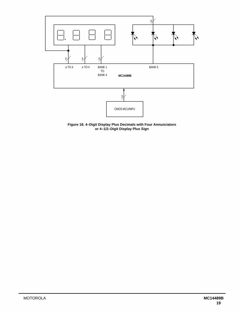
Figure 18. 4–Digit Display Plus Decimals with Four Annunciatorsor 4–1/2–Digit Display Plus Sign
4
CMOS MCU/MPU
a TO d BANK 1TO
BANK 4
BANK 5
MC14489B
4 4
e TO h
3
4
•
Figure 19. Compact Display System with Three Components
INPUT LINES
3
8
14
MC14489B
MUXED 5–DIGIT MONOLITHIC DISPLAY (CLUSTER)HEWLETT–PACKARD 5082–7415 OR EQUIVALENT
12 3 6 2 10 8 5 1 13 4 9 7
6 5 4 2 1 20 19 17 16 15 13 97
MC14489B MOTOROLA20
THERMAL CONSIDERATIONS
The MC14489B is designed to operate with a chip–junctiontemperature (TJ) ranging from – 40 to 130°C, as indicated inthe electrical characteristics tables. The ambient operatingtemperature range (TA) is dependent on RθJA, the internalchip current, how many anode drivers are used, the numberof bank drivers used, the drive current, and how the packageis cooled. The maximum ratings table gives the thermal resis-tance, junction–to–ambient, of the MC14489B mounted on apc board using natural convection to be 90°C per watt for theplastic DIP. The SOG thermal resistance is 100°C per watt.
The following general equation (1) is used to determine thepower dissipated by the MC14489B.
PT = PD + PI (1)where
PT = Total power dissipation of the MC14489BPD = Power dissipated in the driver circuitry (mW)PI = Power dissipated by the internal chip
circuitry (mW)
The equations for the two terms of the general equationare:
PD = (iOH) (N)(VDD – VLED)(B/5) (2)
(3)PI = (1.5 mA)(VDD) + IRx(VDD – IRxRx)
whereiOH = Peak anode driver current (mA)IRx = iOH /10, with iOH = the peak anode driver current
(mA) when the dimmer bit is highN = Number of anode drivers usedB = Number of bank drivers used
Rx = External resistor value (kΩ)VDD = Maximum supply voltage, referenced to VSS
(volts)VLED = Minimum anticipated voltage drop across the
LED1.5 mA = Operating supply current of the MC14489B
The following two examples show how to calculate themaximum allowable ambient temperature.
Worst–Case Analysis Example 1:
5–digit display with decimals (5 banks and 8 anode drivers)DIP without heat sink on PC board
iOH = 20 mA maxVLED = 1.8 V minVDD = 5.25 max
PD = (20)(8)(5.25 – 1.8)(5/5) = 552 mW Ref. (2)
PI = (1.5)(5.25) + 2[5.25 – 2(2)] = 10 mW Ref. (3)
Therefore, PT = 552 + 10 = 562 mW Ref. (1)
and ∆Tchip = RθJAPT = (90°C/W)(0.562) = 51°C
Finally, the maximum allowableTA = TJmax – ∆Tchip = 130 – 51 = 79°C
That is, if TA = 79°C, the maximum junction temperature is130°C. The chip’s average temperature for this example islower than 130°C because all segments are usually not illumi-nated simultaneously for an indefinite period.
Worst–Case Analysis Example 2:
16 lamps (4 banks and 4 anode drivers)SOG without heat sink on PC board
iOH = 30 mA maxVLED = 1.8 V minVDD = 5.5 max
PD = (30)(4)(5.5 – 1.8)(4/5) = 355 mW Ref. (2)
PI = (1.5)(5.5) + 3[5.5 – 3(1.0)] = 16 mW Ref. (3)
Therefore, PT = 355 + 16 = 371 mW Ref. (1)
and ∆Tchip = RθJAPT = (100°C/W)(0.371) = 37°C
Finally, the maximum allowableTA = TJmax – ∆Tchip = 130 – 37 = 93°C
To extend the allowable ambient temperature range or toreduce TJ, which extends chip life, a heat sink such as shownin Figure 20 can be used in high–current applications. Alter-natively, heat–spreader techniques can be used on the PCboard, such as running a wide trace under the MC14489B andusing thermal paste. Wide, radial traces from the MC14489Bleads also act as heat spreaders.
AAVID #5804 or equivalent(Tel. 603/524–4443, FAX 603/528–1478)Motorola cannot recommend one supplier over another andin no way suggests that this is the only heat sink supplier.
Figure 20. Heat Sink
Table 3. LED Lamp and Common–Cathode DisplayManufacturers
Supplier
QT Optoelectronics
Hewlett–Packard (HP), Components Group
Industrial Electronic Engineers (IEE), Component Products Div.
Purdy Electronics Corp., AND Product Line
NOTE: Motorola cannot recommend one supplier over anotherand in no way suggests that this is a complete listing ofLED suppliers.
MC14489BMOTOROLA21
PACKAG E DIMENSIONS
P SUFFIXPLASTIC DIPCASE 738–03
1.0700.2600.1800.022
0.070
0.0150.140
15° 0.040
1.0100.2400.1500.015
0.050
0.0080.110
0° 0.020
25.666.103.810.39
1.27
0.212.80
0° 0.51
27.176.604.570.55
1.77
0.383.55
15°1.01
0.050 BSC
0.100 BSC
0.300 BSC
1.27 BSC
2.54 BSC
7.62 BSC
MIN MINMAX MAXINCHES MILLIMETERS
DIMABCDEFGJKLMN
NOTES:1. DIMENSIONING AND TOLERANCING PER ANSI
Y14.5M, 1982.2. CONTROLLING DIMENSION: INCH.3. DIMENSION L TO CENTER OF LEAD WHEN
FORMED PARALLEL.4. DIMENSION B DOES NOT INCLUDE MOLD
FLASH.
-A-
C
K
NE
G F
D 20 PL
J 20 PL
L
M
-T-SEATINGPLANE
1 10
1120
0.25 (0.010) T AM M
0.25 (0.010) T BM M
B
DW SUFFIXSOG PACKAGECASE 751D–04
NOTES:1. DIMENSIONING AND TOLERANCING PER
ANSI Y14.5M, 1982.2. CONTROLLING DIMENSION: MILLIMETER.3. DIMENSIONS A AND B DO NOT INCLUDE
MOLD PROTRUSION.4. MAXIMUM MOLD PROTRUSION 0.150
(0.006) PER SIDE.5. DIMENSION D DOES NOT INCLUDE
DAMBAR PROTRUSION. ALLOWABLEDAMBAR PROTRUSION SHALL BE 0.13(0.005) TOTAL IN EXCESS OF D DIMENSIONAT MAXIMUM MATERIAL CONDITION.
–A–
–B–
20
1
11
10
SAM0.010 (0.25) B ST
D20X
MBM0.010 (0.25)P10X
J
F
G18X K
C
–T– SEATINGPLANE
M
R X 45
DIM MIN MAX MIN MAXINCHESMILLIMETERS
A 12.65 12.95 0.499 0.510B 7.40 7.60 0.292 0.299C 2.35 2.65 0.093 0.104D 0.35 0.49 0.014 0.019F 0.50 0.90 0.020 0.035G 1.27 BSC 0.050 BSCJ 0.25 0.32 0.010 0.012K 0.10 0.25 0.004 0.009M 0 7 0 7 P 10.05 10.55 0.395 0.415R 0.25 0.75 0.010 0.029
MC14489 A22
Motorola reserves the right to make changes without further notice to any products herein. Motorola makes no warranty, representation or guarantee regardingthe suitability of its products for any particular purpose, nor does Motorola assume any liability arising out of the application or use of any product or circuit, andspecifically disclaims any and all liability, including without limitation consequential or incidental damages. “Typical” parameters which may be provided in Motoroladata sheets and/or specifications can and do vary in different applications and actual performance may vary over time. All operating parameters, including “Typicals”must be validated for each customer application by customer’s technical experts. Motorola does not convey any license under its patent rights nor the rights ofothers. Motorola products are not designed, intended, or authorized for use as components in systems intended for surgical implant into the body, or otherapplications intended to support or sustain life, or for any other application in which the failure of the Motorola product could create a situation where personal injuryor death may occur. Should Buyer purchase or use Motorola products for any such unintended or unauthorized application, Buyer shall indemnify and hold Motorolaand its officers, employees, subsidiaries, affiliates, and distributors harmless against all claims, costs, damages, and expenses, and reasonable attorney feesarising out of, directly or indirectly, any claim of personal injury or death associated with such unintended or unauthorized use, even if such claim alleges thatMotorola was negligent regarding the design or manufacture of the part. Motorola and are registered trademarks of Motorola, Inc. Motorola, Inc. is an EqualOpportunity/Affirmative Action Employer.
Mfax is a trademark of Motorola, Inc.How to reach us:USA /EUROPE/Locations Not Listed : Motorola Literature Distribution; JAPAN: Nippon Motorola Ltd.; SPD, Strategic Planning Office, 141,P.O. Box 5405, Denver, Colorado 80217. 1–303–675–2140 or 1–800–441–2447 4–32–1 Nishi–Gotanda, Shinagawa–ku, Tokyo, Japan. 81–3–5487–8488
Customer Focus Center: 1–800–521–6274
Mfax : [email protected] – TOUCHTONE 1–602–244–6609 ASIA /PACIFIC: Motorola Semiconductors H.K. Ltd.; Silicon Harbor Center,Motorola Fax Back System – US & Canada ONLY 1–800–774–1848 2 Dai King Street, Tai Po, N.T., Hong Kong. fax: 852–26666123
– http://sps.motorola.com/mfax/HOME PAGE: http://mot-sps.com/
MC14489B