Embed Size (px)
Citation preview
Revised 18/4/12
MB86298 ‘Ruby’PCI Express Graphics Controller
Hardware ManualFujitsu Semiconductor Europe GmbH
Version: 1.22
April 18, 2012
Fujitsu Semiconductor Europe GmbH
Revised 18/4/12
Preface
Intention and Target Audience of this Document
This document describes and gives you detailed insight to the stated Fujitsu semiconductor product. The MB86298 'Ruby' device is the successor of Fujitsu’s MB86297A ‘Carmine’ and contains both im-provements and many new features.
This target audience of this document is engineers developing products which will use the MB86298 'Ruby' device. It describes the function and operation of the device. Please read this document care-fully.
Trademarks
ARM is a registered trademark of ARM Limited in UK, USA and Taiwan.
ARM is a trademark of ARM Limited in Japan and Korea.
ARM Powered logo is a registered trademark of ARM Limited in Japan, UK, USA, and Taiwan.
ARM Powered logo is a trademark of ARM Limited in Korea.
ARM926EJ-S and ETM9 are trademarks of ARM Limited.
System names and the product names which appear in this document are the trademarks of the re-spective company or organization.
Licenses
Under the conditions of Philips corporation I2C patent, the license is valid where the device is used in an I2C system which conforms to the I2C standard specification by Philips Corporation.
The purchase of Fujitsu I2C components conveys a license under the Philips I2C Patent Rights to use these components in an I2C system, provided that the system conforms to the I2C Standard Specifi-cation as defined by Philips.
Fujitsu Semiconductor Europe GmbH
Revised 18/4/12
Notes
The contents of this document are subject to change without notice. Customers are advised to consult with FUJITSU sales representatives before ordering.
Any information in this document, including functional descriptions and schematic diagrams, shall not be construed as license of the use or the exercising of any intellectual property rights, such as patent rights or copyright or any other right of FUJITSU or any third party or does FUJITSU warrant non-in-fringement of any third-party’s intellectual property right or other right by using such information. FU-JITSU assumes no liability for any infringement of the intellectual property rights or other rights of third parties which would result from the use of information contained herein.
The products described in this document are designed, developed and manufactured for general use, including unrestricted ordinary industrial use, general office use, personal use, and household use but are not designed, developed and manufactured for use accompanying fatal risks or dangers that, un-less extremely high safety levels are ensured, could have a serious effect to the public and could lead directly to death, personal injury, severe physical damage or other loss (i.e., nuclear reaction control in nuclear facility, aircraft flight control, air traffic control, mass transport control, medical life support sys-tem, missile launch control in weapon systems), or (2) for use requiring extremely high reliability (i.e., submarine or satellite technology). Please note that FUJITSU will not be liable against you and/or any third party for any claims or damages arising in connection with above-mentioned uses of the products.
If any products described in this document represent goods or technologies subject to certain restric-tions on export under the Foreign Exchange and Foreign Trade Law of Japan, the prior authorization by the Japanese government will be required for export of those products from Japan.
All rights reserved and Copyright © FUJITSU Semiconductor Europe GmbH 2010
Fujitsu Semiconductor Europe GmbH

Revised 18/4/12
Fujitsu Semiconductor Europe GmbH
MB86298 ‘Ruby’ - Table of Contents Revised 18/4/12
Table of Contents
Chapter 1: Overview ................................................................................................... 1-1
1.1 Key Features ......................................................................................................................................1-1
1.2 System Overview...............................................................................................................................1-3
1.3 Architecture Overview ......................................................................................................................1-4
1.4 Package ..............................................................................................................................................1-5
1.5 Functional Overview of Pins ............................................................................................................1-51.5.1 Pin Functions....................................................................................................................................1-61.5.1.1 System related pins .......................................................................................................................1-71.5.1.2 I2C related pins .............................................................................................................................1-71.5.1.3 SPI related pins .............................................................................................................................1-81.5.1.4 GPIO related pins ..........................................................................................................................1-81.5.1.5 JTAG/Test related pins..................................................................................................................1-81.5.1.6 DDR2 related pins .........................................................................................................................1-91.5.1.7 Display related pins .....................................................................................................................1-101.5.1.8 Video capture related pins...........................................................................................................1-111.5.1.9 PCIE related pins.........................................................................................................................1-111.5.1.10 Power supply related pins .........................................................................................................1-11
1.6 Pinning .............................................................................................................................................1-121.6.1 Pin Assignment...............................................................................................................................1-121.6.2 Pin Assignment Table.....................................................................................................................1-141.6.3 Pin Multiplexing ..............................................................................................................................1-231.6.4 Unused Pins ...................................................................................................................................1-23
1.7 Address Map ....................................................................................................................................1-24
1.8 Common Topics ..............................................................................................................................1-261.8.1 Register Access Error Responses..................................................................................................1-261.8.2 Register Access to modules in power-down...................................................................................1-261.8.3 Reconfiguration of modules............................................................................................................1-261.8.4 PCIE reset ......................................................................................................................................1-261.8.5 PCIE link lost ..................................................................................................................................1-261.8.6 Using ARGES Display lists in a Command list ...............................................................................1-261.8.7 Memory data coherency .................................................................................................................1-26
1.9 Chip Interconnect ............................................................................................................................1-271.9.1 Bus System ....................................................................................................................................1-271.9.2 Other Connections..........................................................................................................................1-271.9.2.1 GPIO connections .......................................................................................................................1-271.9.2.2 Video connections .......................................................................................................................1-28
1.10 Clocks.............................................................................................................................................1-301.10.1 Clock Domains .............................................................................................................................1-301.10.2 Clock Generation Configuration (Frequency Settings) .................................................................1-311.10.3 Clock Enable ................................................................................................................................1-31
Fujitsu Semiconductor Europe GmbH 1
MB86298 ‘Ruby’ - Table of Contents Revised 18/4/12
1.11 Reset...............................................................................................................................................1-311.11.1 Interrupts ......................................................................................................................................1-31
Chapter 2: Electrical Characteristics ........................................................................ 2-1
2.1 Absolute Maximum Ratings .............................................................................................................2-1
2.2 Recommended Operating Conditions .............................................................................................2-2
2.3 Electrical Characteristics..................................................................................................................2-22.3.1 PCIE Interface IO .............................................................................................................................2-2
2.4 Typical Power Consumption Ratings ..............................................................................................2-3
2.5 DC Characteristics ............................................................................................................................2-32.5.1 3.3V Standard CMOS I/O .................................................................................................................2-32.5.1.1 3.3V Standard CMOS I/O V-I Characteristic (Driving Capability 2) ...............................................2-42.5.1.2 3.3V Standard CMOS I/O V-I Characteristics (Driving Capability 3) .............................................2-42.5.2 DDR2 SDRAM Interface I/O (SSTL_18)...........................................................................................2-52.5.3 I2C Bus Fast Mode I/O .....................................................................................................................2-62.5.4 I2C IO V-1 Characteristic Figure ......................................................................................................2-7
2.6 AC Characteristics ............................................................................................................................2-82.6.1 PCIE Interface Signal Timing ...........................................................................................................2-82.6.1.1 PCIe Transmitter Characteristics...................................................................................................2-82.6.1.2 PCIe Receiver Characteristics.......................................................................................................2-92.6.1.3 PCIe PLL Characteristics ..............................................................................................................2-92.6.2 DDR2 SDRAM Interface Signal Timing ..........................................................................................2-102.6.2.1 DDR2SDRAM IF Timing Diagram ...............................................................................................2-112.6.3 GPIO Interface Signal Timing.........................................................................................................2-142.6.4 Display Interface Signal Timing ......................................................................................................2-152.6.4.1 Clocks..........................................................................................................................................2-152.6.4.2 Input Signals................................................................................................................................2-152.6.4.3 Output Signals .............................................................................................................................2-162.6.5 Video Capture Signal Timing..........................................................................................................2-172.6.5.1 Clocks..........................................................................................................................................2-172.6.5.2 Input Signals................................................................................................................................2-182.6.6 I2C Interface Signal Timing ............................................................................................................2-20
2.7 Precautions at Power On ................................................................................................................2-232.7.1 Recommended Power On/Off Sequence .......................................................................................2-232.7.2 Power-On Reset .............................................................................................................................2-24
2.8 PCIe Power-On/Reset Sequence....................................................................................................2-252.8.1 PCIe Symbol Lock ..........................................................................................................................2-26
Chapter 3: Global Control (GC) ................................................................................. 3-1
3.1 Position of the GC Block in the GDC...............................................................................................3-1
3.2 Feature List ........................................................................................................................................3-23.2.1 Chip ID..............................................................................................................................................3-23.2.2 PLL control .......................................................................................................................................3-2
2 Fujitsu Semiconductor Europe GmbH
MB86298 ‘Ruby’ - Table of Contents Revised 18/4/12
3.2.3 Spread Spectrum Clock Generation.................................................................................................3-23.2.4 Reset Generation .............................................................................................................................3-33.2.5 Clock generation and enable............................................................................................................3-3
3.3 General Restrictions .........................................................................................................................3-4
3.4 Processing Mode...............................................................................................................................3-43.4.1 Spread Spectrum Clock Generation.................................................................................................3-4
3.5 Control Flow.......................................................................................................................................3-53.5.1 Spread Spectrum Clock Generation Setup ......................................................................................3-53.5.1.1 Operation.......................................................................................................................................3-53.5.1.2 Measurement.................................................................................................................................3-53.5.1.3 Programming sequences...............................................................................................................3-83.5.1.4 Programming examples ................................................................................................................3-93.5.1.5 Operation sequence ....................................................................................................................3-103.5.1.6 Power down/up sequence ...........................................................................................................3-11
3.6 Software Interface ...........................................................................................................................3-123.6.1 Register Summary..........................................................................................................................3-12
3.7 Global Control Register Description .............................................................................................3-14
Chapter 4: Spread Spectrum Generator ................................................................... 4-1
4.1 Introduction........................................................................................................................................4-1
4.2 Position of Block in whole LSI .........................................................................................................4-1
4.3 Features..............................................................................................................................................4-24.3.1 Functional .........................................................................................................................................4-24.3.2 Measurement....................................................................................................................................4-24.3.3 Limitations ........................................................................................................................................4-24.3.3.1 Switch on/off SSCG Modulation ....................................................................................................4-3
4.4 Processing Mode...............................................................................................................................4-44.4.1 Processing Flow ...............................................................................................................................4-44.4.2 Processing Algorithm........................................................................................................................4-44.4.2.1 Parameter calculation (refer to the section 'Software Interface') ...................................................4-44.4.2.2 Parameter setting for 1.6GHz PLL clock ......................................................................................4-7
4.5 Control Flow.......................................................................................................................................4-8
Chapter 5: PCI Express Interface .............................................................................. 5-1
5.1 Position of Block in whole LSI .........................................................................................................5-1
5.2 Feature List ........................................................................................................................................5-1
5.3 Processing Mode...............................................................................................................................5-25.3.1 Processing Flow ...............................................................................................................................5-25.3.1.1 Block diagram................................................................................................................................5-25.3.1.2 Address Map .................................................................................................................................5-2
Fujitsu Semiconductor Europe GmbH 3
MB86298 ‘Ruby’ - Table of Contents Revised 18/4/12
5.4 Processing Algorithm .......................................................................................................................5-25.4.1 Configuration Space Registers.........................................................................................................5-25.4.2 Completer .........................................................................................................................................5-35.4.3 Requesters .......................................................................................................................................5-35.4.4 MSI (Message Signalling Interrupt) ..................................................................................................5-45.4.5 Completer Interface Address Translation .........................................................................................5-55.4.5.1 BAR0 Address Translation ............................................................................................................5-55.4.5.2 BAR2 Address Translation ............................................................................................................5-55.4.5.3 BAR4 Address Translation ............................................................................................................5-55.4.5.4 Endianess Correction ....................................................................................................................5-55.4.5.5 BYTE Swap ...................................................................................................................................5-65.4.5.6 WORD Swap .................................................................................................................................5-65.4.5.7 DWORD Swap...............................................................................................................................5-6
5.5 Control Flow.......................................................................................................................................5-75.5.1 Setup Completer Interface................................................................................................................5-75.5.2 Setup Requester Interface (Direct Master).......................................................................................5-75.5.3 Setup Interrupt (MSI) I/F...................................................................................................................5-7
5.6 Software Interface .............................................................................................................................5-8
5.7 PCIe Host Interface Register Summary...........................................................................................5-8
5.8 PCIe Host Interface Register Description .......................................................................................5-8
5.9 PCIe Host Configuration Register Summary ................................................................................5-17
5.10 PCIe Host Configuration Register Description...........................................................................5-19
Chapter 6: Interconnect Bus...................................................................................... 6-1
6.1 Position of Block in whole LSI .........................................................................................................6-1
6.2 Feature List ........................................................................................................................................6-16.2.1 AXI-Master Ports ..............................................................................................................................6-16.2.2 AXI Interconnect Matrix ....................................................................................................................6-16.2.2.1 Layer select function......................................................................................................................6-16.2.3 Configurable arbitration scheme.......................................................................................................6-16.2.4 Lock option .......................................................................................................................................6-1
6.3 Software Interface .............................................................................................................................6-2
6.4 Register Summary.............................................................................................................................6-2
6.5 Register Description .........................................................................................................................6-2
6.6 Processing Mode...............................................................................................................................6-56.6.1 Processing Flow ...............................................................................................................................6-56.6.1.1 Overview........................................................................................................................................6-56.6.1.2 Interconnect A (AXI Interconnect Matrix).......................................................................................6-66.6.1.2.1 Overview ....................................................................................................................................6-66.6.1.2.4 Interconnect B & C (Register Space 1) ....................................................................................6-86.6.2 Processing Algorithm........................................................................................................................6-9
4 Fujitsu Semiconductor Europe GmbH
MB86298 ‘Ruby’ - Table of Contents Revised 18/4/12
6.6.2.1 AXI Interconnect Matrix .................................................................................................................6-96.6.2.2 Arbiter ............................................................................................................................................6-9
Chapter 7: DDR2 Memory Interface........................................................................... 7-1
7.1 Memory Packer ..................................................................................................................................7-17.1.1 Location of the Memory Packer in the Device ..................................................................................7-17.1.2 Feature List.......................................................................................................................................7-27.1.3 Limitations ........................................................................................................................................7-2
7.2 DRAM Interface Controller................................................................................................................7-27.2.1 Position of the DRAM Interface Controller in the device ..................................................................7-27.2.2 Feature List.......................................................................................................................................7-37.2.3 DRAM Interface Controller Performance..........................................................................................7-47.2.4 External Memory Configurations ......................................................................................................7-47.2.5 Recommended Timing Parameters for DDR2 Devices ....................................................................7-47.2.6 On-Die Termination (ODT) ...............................................................................................................7-57.2.7 Operating Modes ..............................................................................................................................7-57.2.8 Off-Chip Driver Calibration (OCD) ....................................................................................................7-57.2.9 DDR2 Initialization Procedure ..........................................................................................................7-67.2.9.1 DDR2 Lock-up Procedure .............................................................................................................7-77.2.9.2 DDR2 Initialization Command Issue Procedure ............................................................................7-8
7.3 Software Interface ...........................................................................................................................7-107.3.1 Register Summary..........................................................................................................................7-107.3.2 Register Description ......................................................................................................................7-12
7.4 Processing Mode ............................................................................................................................7-327.4.1 Processing Flow .............................................................................................................................7-327.4.2 Processing Algorithm......................................................................................................................7-347.4.2.1 Arbitration Scheme ......................................................................................................................7-347.4.2.2 Least Recently Used Algorithm ...................................................................................................7-35
7.5 Control Flow.....................................................................................................................................7-357.5.1 Setup DRAM Interface Controller ...................................................................................................7-357.5.2 Setup Cache Controller ..................................................................................................................7-367.5.3 Write-back of Cache Data ..............................................................................................................7-367.5.3.1 Software Flush (SW-flush) controlled ..........................................................................................7-367.5.3.2 LRU (least recently used) controlled ...........................................................................................7-367.5.3.3 Timer controlled...........................................................................................................................7-367.5.4 Flushing Cache Buffers ..................................................................................................................7-37
7.6 Application Notes - Accessing Memory ........................................................................................7-387.6.1 Overview.........................................................................................................................................7-387.6.1.1 Port Mapping ...............................................................................................................................7-397.6.1.2 Arbitration of AXI layers...............................................................................................................7-39
7.7 Buffer management.........................................................................................................................7-407.7.1 Default Routing...............................................................................................................................7-407.7.2 Capture to Texture Buffer ...............................................................................................................7-417.7.3 Capture to Display Buffer ...............................................................................................................7-417.7.4 Clear / Fill Buffer.............................................................................................................................7-427.7.5 Rendering and Blitting to a Frame Buffer .......................................................................................7-42
Fujitsu Semiconductor Europe GmbH 5
MB86298 ‘Ruby’ - Table of Contents Revised 18/4/12
7.7.6 Filtering and Mipmap Generation ...................................................................................................7-437.7.7 Host does Memory Access.............................................................................................................7-437.7.7.1 Writing Data.................................................................................................................................7-437.7.7.2 Reading Data...............................................................................................................................7-44
7.8 Software Implementation Guidelines ............................................................................................7-447.8.1 Host Interface (PCI Express)..........................................................................................................7-447.8.1.1 Write Access................................................................................................................................7-457.8.2 Rendering .......................................................................................................................................7-467.8.3 Pixel Blitter Operations ...................................................................................................................7-477.8.4 Command List Examples................................................................................................................7-487.8.5 Miscellaneous.................................................................................................................................7-48
Chapter 8: Display Controller .................................................................................... 8-1
8.1 Position of Block in whole LSI .........................................................................................................8-1
8.2 Feature List ........................................................................................................................................8-18.2.1 Display Layers ..................................................................................................................................8-18.2.1.1 Video Layers..................................................................................................................................8-18.2.2 Dual screen mode ............................................................................................................................8-28.2.3 Chroma Key......................................................................................................................................8-28.2.4 Display Output Mode ........................................................................................................................8-28.2.5 Alpha Layer ......................................................................................................................................8-28.2.6 Video Timing Generator ...................................................................................................................8-38.2.7 Palette RAM .....................................................................................................................................8-38.2.8 Cursor...............................................................................................................................................8-38.2.9 Gamma Correction ...........................................................................................................................8-38.2.10 Dithering .........................................................................................................................................8-38.2.11 Blending..........................................................................................................................................8-38.2.12 Dual View .......................................................................................................................................8-38.2.13 Programmable display output ports................................................................................................8-48.2.14 Interrupt ..........................................................................................................................................8-48.2.15 External Synchronization (ESY) .....................................................................................................8-48.2.16 Read Skip .......................................................................................................................................8-58.2.17 Wrap around processing ................................................................................................................8-5
8.3 Limitations .........................................................................................................................................8-5
8.4 External Interfaces ............................................................................................................................8-58.4.1 Communication Protocols (Timing Diagrams) ..................................................................................8-58.4.1.1 Video Output Timing......................................................................................................................8-58.4.2 Input Data Format.............................................................................................................................8-78.4.2.1 Indirect Color (8 bit/pixel)...............................................................................................................8-78.4.2.2 Direct Color (16 bit/pixel) ...............................................................................................................8-78.4.2.3 Direct Color (32 bit/pixel) ...............................................................................................................8-78.4.2.4 YCbCr Color (16 bit/pixel)..............................................................................................................8-88.4.2.5 Alpha Value (8 bit/pixel).................................................................................................................8-88.4.2.6 Layer Dependency ........................................................................................................................8-88.4.3 Output Data Format..........................................................................................................................8-88.4.3.1 RGB 888 (24 bit)............................................................................................................................8-88.4.3.2 RGB 777 (21 bit)............................................................................................................................8-88.4.3.3 RGB 666 (18 bit)............................................................................................................................8-9
6 Fujitsu Semiconductor Europe GmbH
MB86298 ‘Ruby’ - Table of Contents Revised 18/4/12
8.4.3.4 RGB 565 (16 bit)............................................................................................................................8-9
8.5 Processing Mode.............................................................................................................................8-108.5.1 Data Processing Flow.....................................................................................................................8-108.5.2 Processing algorithm ......................................................................................................................8-128.5.2.1 Alpha blending modes .................................................................................................................8-128.5.2.2 Transparent color processing ......................................................................................................8-138.5.2.3 YCbCr to RGB color matrix .........................................................................................................8-138.5.2.4 Color Look-up Table (CLUT) processing.....................................................................................8-138.5.2.5 Dither processing.........................................................................................................................8-148.5.2.6 Dual view processing...................................................................................................................8-14
8.6 Control Flow.....................................................................................................................................8-148.6.1 General Control Flow......................................................................................................................8-148.6.2 Configure Display Clock .................................................................................................................8-158.6.2.1 Setting the correct reference clock and divider ratio ...................................................................8-178.6.3 Display Timing Configuration..........................................................................................................8-188.6.4 Display Output Parameter Configuration.......................................................................................8-218.6.4.1 Output Mode Configuration .........................................................................................................8-218.6.4.2 Configure dual screen mode .......................................................................................................8-228.6.4.3 Dual view mode ...........................................................................................................................8-258.6.4.4 Csync output................................................................................................................................8-258.6.4.5 Chroma keying ............................................................................................................................8-258.6.4.6 Color Lookup Table (Gamma Correction) ...................................................................................8-258.6.4.7 Dither Unit Configuration .............................................................................................................8-268.6.5 Background Color Configuration ....................................................................................................8-268.6.6 Enable/Disable Display Controller ..................................................................................................8-268.6.7 Configure Layer Specific Settings ..................................................................................................8-268.6.7.1 Color mode ..................................................................................................................................8-278.6.7.2 Origin address, display address and display position..................................................................8-288.6.7.3 Set window position and size ......................................................................................................8-308.6.7.4 Read skip mode (for standard layer) ...........................................................................................8-308.6.7.5 De-interlacing and upscaling (for video layers) ...........................................................................8-318.6.7.6 Layer position and order..............................................................................................................8-318.6.7.7 Blending mode and transparent processing ................................................................................8-328.6.7.8 Cursor configuration ....................................................................................................................8-338.6.8 Register Update Modes..................................................................................................................8-348.6.9 Processing on interrupts.................................................................................................................8-35
8.7 Software Interface ...........................................................................................................................8-368.7.1 Register Summary..........................................................................................................................8-36
8.8 Register Description ......................................................................................................................8-42
Chapter 9: Write Back Processor .............................................................................. 9-1
9.1 Position of Block in whole LSI .........................................................................................................9-1
9.2 Feature List ........................................................................................................................................9-29.2.1 Write Back Mode ..............................................................................................................................9-29.2.2 Source Selection ..............................................................................................................................9-29.2.3 Field Selection ..................................................................................................................................9-29.2.4 Interrupt ............................................................................................................................................9-2
Fujitsu Semiconductor Europe GmbH 7
MB86298 ‘Ruby’ - Table of Contents Revised 18/4/12
9.2.5 Data Formats....................................................................................................................................9-39.2.5.1 Input data Formats ........................................................................................................................9-39.2.5.2 Output Data Format.......................................................................................................................9-3
9.3 Processing Mode...............................................................................................................................9-49.3.1 Processing Flow ...............................................................................................................................9-49.3.2 Processing Algorithm........................................................................................................................9-49.3.2.1 Cropping ........................................................................................................................................9-49.3.2.2 Field Modes ...................................................................................................................................9-5
9.4 Control Flow.......................................................................................................................................9-69.4.1 Setup of Write Back..........................................................................................................................9-69.4.2 Operation..........................................................................................................................................9-69.4.2.1 Single Shot ....................................................................................................................................9-69.4.2.2 Continous Mode ............................................................................................................................9-6
9.5 Software Interface .............................................................................................................................9-89.5.1 Register Summary............................................................................................................................9-8
9.6 Writeback Register Description ......................................................................................................9-89.6.1 WritebackSoftwareReset .................................................................................................................9-89.6.2 WritebackFlowControl .....................................................................................................................9-99.6.3 WritebackStatus ..............................................................................................................................9-99.6.4 WritebackMode ..............................................................................................................................9-109.6.5 WritebackOriginAddress0 ..............................................................................................................9-109.6.6 WritebackOriginAddress1 ..............................................................................................................9-109.6.7 WritebackStart ...............................................................................................................................9-119.6.8 WritebackEnd ................................................................................................................................9-119.6.9 WritebackVstrEnd ..........................................................................................................................9-11
Chapter 10: Video Capture....................................................................................... 10-1
10.1 Position of Block in whole LSI .....................................................................................................10-1
10.2 Feature List ...................................................................................................................................10-210.2.1 Video standards............................................................................................................................10-210.2.2 Video interfaces............................................................................................................................10-210.2.3 Deinterlacing.................................................................................................................................10-210.2.4 Color conversion...........................................................................................................................10-310.2.5 Scaling..........................................................................................................................................10-310.2.6 Cropping .......................................................................................................................................10-3
10.3 Interface Data Formats..................................................................................................................10-410.3.1 Input Data Format.........................................................................................................................10-410.3.1.1 External Video Signal Input .......................................................................................................10-410.3.1.2 ITU-R BT656 YUV422 input format ..........................................................................................10-410.3.2 Output Data Format....................................................................................................................10-1810.3.2.1 Video Data Format ..................................................................................................................10-1810.3.2.2 Synchronisation Control ..........................................................................................................10-2010.3.2.3 Memory Allocation ...................................................................................................................10-2010.3.2.4 Window Display .......................................................................................................................10-2110.3.2.5 Interlace Display ......................................................................................................................10-21
8 Fujitsu Semiconductor Europe GmbH
MB86298 ‘Ruby’ - Table of Contents Revised 18/4/12
10.4 Processing Mode.........................................................................................................................10-2110.4.1 Processing Flow .........................................................................................................................10-2110.4.1.1 Video Input Selection...............................................................................................................10-2110.4.1.2 De-Interlacing ..........................................................................................................................10-2510.4.1.3 Downscaling Function ............................................................................................................10-2610.4.1.4 Cropping ................................................................................................................................10-2910.4.1.5 Low Pass Filter ........................................................................................................................10-3010.4.2 Processing Algorithm..................................................................................................................10-3010.4.2.1 De-interlacing ..........................................................................................................................10-3010.4.2.2 Scaling.....................................................................................................................................10-31
10.5 Control Flow.................................................................................................................................10-3210.5.1 Programming the Capture Unit...................................................................................................10-3210.5.1.1 Programming the YUV / ITU-BT.656 mode .............................................................................10-3310.5.1.2 RGB Video Input Parameter Setting Chart.............................................................................10-3310.5.1.3 Programming the Still Detection ..............................................................................................10-3410.5.1.4 Programming the High Definition Mode...................................................................................10-3610.5.2 Interrupts ....................................................................................................................................10-3810.5.2.1 Overview..................................................................................................................................10-3810.5.2.2 Interrupt Status ........................................................................................................................10-3810.5.2.3 Error Detection ........................................................................................................................10-3810.5.2.4 Capture VSYNC Interrupt ........................................................................................................10-3810.5.2.5 Direct Interrupt.........................................................................................................................10-3910.5.2.6 Interrupt Waveform..................................................................................................................10-40
10.6 Software Interface .......................................................................................................................10-41
10.7 Register Summary.......................................................................................................................10-41
10.8 Register Description ...................................................................................................................10-45
Chapter 11: Graphics Core (ARGES) ...................................................................... 11-1
11.1 Graphics Core (ARGES)................................................................................................................11-1
11.2 Position of ARGES ........................................................................................................................11-3
11.3 Function .........................................................................................................................................11-411.3.1 Register access ............................................................................................................................11-411.3.2 Save/Restore register...................................................................................................................11-411.3.3 Display list and vertex arrays........................................................................................................11-411.3.4 Drawing features ..........................................................................................................................11-411.3.5 Pixel format...................................................................................................................................11-4
11.4 Software Interface and Commands .............................................................................................11-511.4.1 Global address .............................................................................................................................11-511.4.2 Register summary ........................................................................................................................11-6
11.5 Register Descriptions ...................................................................................................................11-7
11.6 Display lists..................................................................................................................................11-1311.6.1 Overview.....................................................................................................................................11-1311.6.1.1 Direct DL Display list transfer mode ........................................................................................11-13
Fujitsu Semiconductor Europe GmbH 9
MB86298 ‘Ruby’ - Table of Contents Revised 18/4/12
11.6.1.2 Index Display list transfer mode ..............................................................................................11-1311.6.2 Header Format ...........................................................................................................................11-1411.6.3 Parameter Format ......................................................................................................................11-1411.6.3.1 FP32 .......................................................................................................................................11-1411.6.3.2 Fixed........................................................................................................................................11-1411.6.4 Command List ............................................................................................................................11-1511.6.5 Detailled explanation of all display list commands .....................................................................11-16
11.7 Processing Flow..........................................................................................................................11-6811.7.1 Processing Algorithm..................................................................................................................11-68
11.8 Control Flow (Usage) ..................................................................................................................11-6911.8.1 Hardware Initialization Procedure...............................................................................................11-6911.8.1.1 Hardware reset ........................................................................................................................11-6911.8.1.2 Software reset .........................................................................................................................11-6911.8.1.3 Register access .......................................................................................................................11-6911.8.2 Display list input..........................................................................................................................11-6911.8.3 FrameBuffer................................................................................................................................11-7111.8.3.1 FrameBuffer Setup ..................................................................................................................11-7111.8.3.2 Memory data format 32bpp color.............................................................................................11-7211.8.3.3 Memory data format 16bpp color.............................................................................................11-7211.8.3.4 Memory data format 8bpp color...............................................................................................11-73
11.9 Programmable Shader Setup .....................................................................................................11-7411.9.1 Loading the shader program ......................................................................................................11-7411.9.2 Loading uniform variables (uniforms) .........................................................................................11-7511.9.3 Setting the precision of attributes and varying variables (varyings) ...........................................11-7511.9.4 Attribute memory data format .....................................................................................................11-7611.9.5 Static attribute settings ...............................................................................................................11-77
11.10 View volume clipping ................................................................................................................11-79
11.11 Scissor test ................................................................................................................................11-80
11.12 Culling ........................................................................................................................................11-81
11.13 Viewport transformation ...........................................................................................................11-83
11.14 Basic procedure for drawing graphics....................................................................................11-8411.14.1 Basic structure of a display list for drawing ..............................................................................11-8411.14.2 Attribute reading .......................................................................................................................11-8411.14.3 Programmable vertex shader ...................................................................................................11-8711.14.4 Projective transformation..........................................................................................................11-8811.14.5 Programmable fragment shader...............................................................................................11-8811.14.6 Texture mapping.......................................................................................................................11-8811.14.7 Texture co-ordinates.................................................................................................................11-8811.14.8 Registering textures..................................................................................................................11-9011.14.8.1 Memory address....................................................................................................................11-9011.14.8.2 Texture size ...........................................................................................................................11-9011.14.8.3 Texture format .......................................................................................................................11-9011.14.8.4 Texture wrapping...................................................................................................................11-9411.14.8.5 Texture filtering......................................................................................................................11-9511.14.9 Alpha blending..........................................................................................................................11-9911.14.9.1 Blend equation.......................................................................................................................11-99
10 Fujitsu Semiconductor Europe GmbH
MB86298 ‘Ruby’ - Table of Contents Revised 18/4/12
11.14.9.2 Blend function......................................................................................................................11-10011.14.10 Depth test .............................................................................................................................11-10111.14.10.1 Z buffer Configuration........................................................................................................11-10111.14.10.2 Memory data format ..........................................................................................................11-10111.14.10.3 Setting of depth test...........................................................................................................11-10211.14.11 Stencil Test...........................................................................................................................11-10311.14.12 PolygonOffset .......................................................................................................................11-10511.14.13 BitBlt (Bit Block Transfer) .....................................................................................................11-10611.14.13.1 Alpha map .........................................................................................................................11-11011.14.13.2 Compressed data copy......................................................................................................11-11011.14.13.3 Bit pattern drawing.............................................................................................................11-11011.14.14 Drawing Effect of Straight Line .............................................................................................11-11111.14.14.1 Antialiasing ........................................................................................................................11-11111.14.14.2 Thick line ...........................................................................................................................11-11111.14.15 Detection of end of drawing..................................................................................................11-11311.14.16 Debug function .....................................................................................................................11-114
Chapter 12: PixBlt Unit ............................................................................................. 12-1
12.1 Position of Block in whole LSI .....................................................................................................12-1
12.2 Feature List ....................................................................................................................................12-212.2.1 Constant Fill..................................................................................................................................12-212.2.2 Copy .............................................................................................................................................12-212.2.3 Anti-Aliasing (FSAA).....................................................................................................................12-212.2.4 Simple Scaling..............................................................................................................................12-212.2.5 Support for generic Pixel Formats ................................................................................................12-212.2.6 Blending........................................................................................................................................12-212.2.7 Dithering .......................................................................................................................................12-312.2.8 Flip Operations .............................................................................................................................12-312.2.9 Logic Operations (ROP3) .............................................................................................................12-312.2.10 3X3 filtering.................................................................................................................................12-312.2.11 Shader support ...........................................................................................................................12-312.2.12 General Restrictions ...................................................................................................................12-3
12.3 External Interfaces ........................................................................................................................12-412.3.1 Data Formats................................................................................................................................12-412.3.1.1 Coordinates ...............................................................................................................................12-412.3.1.2 Input Data Format......................................................................................................................12-512.3.1.3 Output Data Format...................................................................................................................12-5
12.4 Processing Mode...........................................................................................................................12-612.4.1 Processing Flow ...........................................................................................................................12-612.4.2 Processing Algorithm....................................................................................................................12-612.4.2.1 Copy Mode ................................................................................................................................12-612.4.2.2 Fill Mode ....................................................................................................................................12-612.4.2.3 Raster Operation Mode .............................................................................................................12-712.4.2.4 2X2 and 3X3 Filter Modes .........................................................................................................12-712.4.2.5 Blending Mode...........................................................................................................................12-712.4.2.6 Shader Modes ...........................................................................................................................12-712.4.2.7 Neutral Mode .............................................................................................................................12-8
12.5 Control Flow...................................................................................................................................12-8
Fujitsu Semiconductor Europe GmbH 11
MB86298 ‘Ruby’ - Table of Contents Revised 18/4/12
12.6 Software Interface .......................................................................................................................12-1712.6.1 Register Summary......................................................................................................................12-17
12.7 PixBlt Register Description ........................................................................................................12-19
Chapter 13: I2C Interface.......................................................................................... 13-1
13.1 Overview.........................................................................................................................................13-1
13.2 Features..........................................................................................................................................13-1
13.3 Block Diagram ...............................................................................................................................13-2
13.4 Description of Block Functions ...................................................................................................13-3
13.5 Operation Description...................................................................................................................13-513.5.1 Start Condition..............................................................................................................................13-513.5.2 Stop Condition .............................................................................................................................13-513.5.3 Addressing....................................................................................................................................13-613.5.3.1 Slave address map....................................................................................................................13-713.5.4 Arbitration of SCL Synchronization..............................................................................................13-813.5.5 Arbitration .....................................................................................................................................13-913.5.6 Acknowledge/Negative Acknowledge.........................................................................................13-1013.5.7 Bus Error ....................................................................................................................................13-1113.5.8 Initialization.................................................................................................................................13-1113.5.9 1-byte Transfer from Master to Slave .........................................................................................13-1213.5.10 1-byte Transfer from Slave to Master .......................................................................................13-1313.5.11 Return after I2C Bus Error........................................................................................................13-1413.5.12 Interrupt Processing and Wait Request to the Master Device..................................................13-14
13.6 Warnings ......................................................................................................................................13-1513.6.1 10-bit Slave Address ..................................................................................................................13-1513.6.2 Conflict among SCC, MSS and INT Bits ....................................................................................13-1513.6.3 Setting of Serial Transfer Clock..................................................................................................13-1513.6.4 Restrictions on Multimaster Usage.............................................................................................13-15
13.7 Additional Notes ..........................................................................................................................13-1513.7.1 Serial Transfer Clock Setting (CSR)...........................................................................................13-1513.7.2 Bus Clock Frequency Setting (FSR)...........................................................................................13-17
13.8 Software Interface .......................................................................................................................13-1813.8.1 Register Summary......................................................................................................................13-18
13.9 Register Description ..................................................................................................................13-19
Chapter 14: GPIO ...................................................................................................... 14-1
14.1 Position of Block in whole LSI .....................................................................................................14-1
14.2 Feature List ....................................................................................................................................14-114.2.1 GPIO Ports ...................................................................................................................................14-114.2.2 Peripheral Mode ...........................................................................................................................14-114.2.3 General Restrictions .....................................................................................................................14-1
12 Fujitsu Semiconductor Europe GmbH
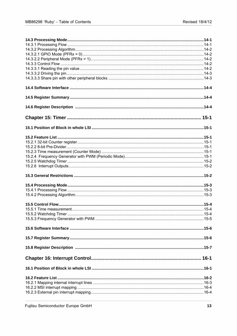
MB86298 ‘Ruby’ - Table of Contents Revised 18/4/12
14.3 Processing Mode...........................................................................................................................14-114.3.1 Processing Flow ...........................................................................................................................14-114.3.2 Processing Algorithm....................................................................................................................14-214.3.2.1 GPIO Mode (PFRx = 0) .............................................................................................................14-214.3.2.2 Peripheral Mode (PFRx = 1)......................................................................................................14-214.3.3 Control Flow .................................................................................................................................14-214.3.3.1 Reading the pin value................................................................................................................14-214.3.3.2 Driving the pin............................................................................................................................14-314.3.3.3 Share pin with other peripheral blocks ......................................................................................14-3
14.4 Software Interface .........................................................................................................................14-4
14.5 Register Summary.........................................................................................................................14-4
14.6 Register Description ....................................................................................................................14-4
Chapter 15: Timer ..................................................................................................... 15-1
15.1 Position of Block in whole LSI .....................................................................................................15-1
15.2 Feature List ....................................................................................................................................15-115.2.1 32-bit Counter register..................................................................................................................15-115.2.2 8-bit Pre-Divider............................................................................................................................15-115.2.3 Time measurement (Counter Mode) ............................................................................................15-115.2.4 Frequency Generator with PWM (Periodic Mode).......................................................................15-115.2.5 Watchdog Timer ...........................................................................................................................15-215.2.6 Interrupt Outputs..........................................................................................................................15-2
15.3 General Restrictions .....................................................................................................................15-2
15.4 Processing Mode...........................................................................................................................15-315.4.1 Processing Flow ...........................................................................................................................15-315.4.2 Processing Algorithm....................................................................................................................15-3
15.5 Control Flow...................................................................................................................................15-415.5.1 Time measurement.......................................................................................................................15-415.5.2 Watchdog Timer ...........................................................................................................................15-415.5.3 Frequency Generator with PWM ..................................................................................................15-5
15.6 Software Interface .........................................................................................................................15-6
15.7 Register Summary.........................................................................................................................15-6
15.8 Register Description ....................................................................................................................15-7
Chapter 16: Interrupt Control................................................................................... 16-1
16.1 Position of Block in whole LSI .....................................................................................................16-1
16.2 Feature List ....................................................................................................................................16-216.2.1 Mapping internal interrupt lines ....................................................................................................16-316.2.2 MSI interrupt mapping ..................................................................................................................16-416.2.3 External pin interrupt mapping......................................................................................................16-4
Fujitsu Semiconductor Europe GmbH 13

MB86298 ‘Ruby’ - Table of Contents Revised 18/4/12
16.3 Known Limitations ........................................................................................................................16-5
16.4 Processing Mode...........................................................................................................................16-516.4.1 Processing Flow ...........................................................................................................................16-5
16.5 Control Flow...................................................................................................................................16-5
16.6 Software Interface .........................................................................................................................16-7
16.7 Register Summary.........................................................................................................................16-7
16.8 Register Description ....................................................................................................................16-7
Chapter 17: Command Sequencer .......................................................................... 17-1
17.1 Position of Block in whole LSI .....................................................................................................17-1
17.2 Feature List ....................................................................................................................................17-1
17.3 Processing Mode...........................................................................................................................17-217.3.1 Processing Flow ...........................................................................................................................17-217.3.2 Processing Algorithm....................................................................................................................17-217.3.2.1 System Status Register .............................................................................................................17-317.3.2.2 Watchdog ..................................................................................................................................17-317.3.2.3 Command FIFO.........................................................................................................................17-317.3.2.4 Undefined Instructions...............................................................................................................17-417.3.3 Instruction Set...............................................................................................................................17-417.3.3.1 NOP – No Operation ................................................................................................................17-417.3.3.2 CALL – Call to a command list .................................................................................................17-517.3.3.3 RET – Return from command list .............................................................................................17-517.3.3.4 WRITE – Write data to buffer ...................................................................................................17-617.3.3.5 COPY – Copy Buffer ................................................................................................................17-717.3.3.6 SAVE – Save register values ...................................................................................................17-817.3.3.7 RESTORE – Restore register values from memory .................................................................17-917.3.3.8 SYNC ......................................................................................................................................17-1017.3.3.9 WDR – Watchdog reset ..........................................................................................................17-1117.3.3.10 RSVD – Reserved ................................................................................................................17-11
17.4 Control Flow.................................................................................................................................17-1117.4.1 Command Buffer ........................................................................................................................17-1117.4.2 Setup watchdog..........................................................................................................................17-1217.4.3 SAVE and RESTORE.................................................................................................................17-1217.4.4 Operation Mode..........................................................................................................................17-1217.4.5 Restart after detecting an illegal instruction................................................................................17-13
17.5 Software Interface .......................................................................................................................17-14
17.6 Register Summary.......................................................................................................................17-14
17.7 Register Description ..................................................................................................................17-15
14 Fujitsu Semiconductor Europe GmbH
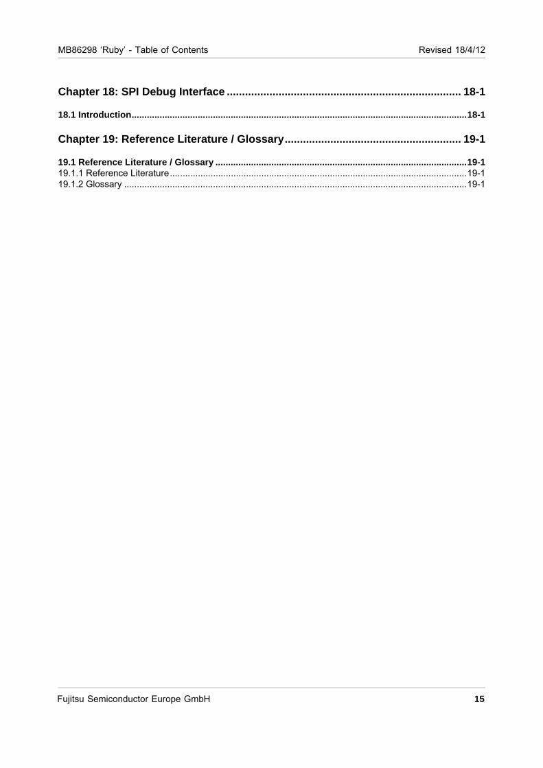
MB86298 ‘Ruby’ - Table of Contents Revised 18/4/12
Chapter 18: SPI Debug Interface ............................................................................. 18-1
18.1 Introduction....................................................................................................................................18-1
Chapter 19: Reference Literature / Glossary.......................................................... 19-1
19.1 Reference Literature / Glossary ...................................................................................................19-119.1.1 Reference Literature.....................................................................................................................19-119.1.2 Glossary .......................................................................................................................................19-1
Fujitsu Semiconductor Europe GmbH 15

MB86298 ‘Ruby’ - Table of Contents Revised 18/4/12
16 Fujitsu Semiconductor Europe GmbH
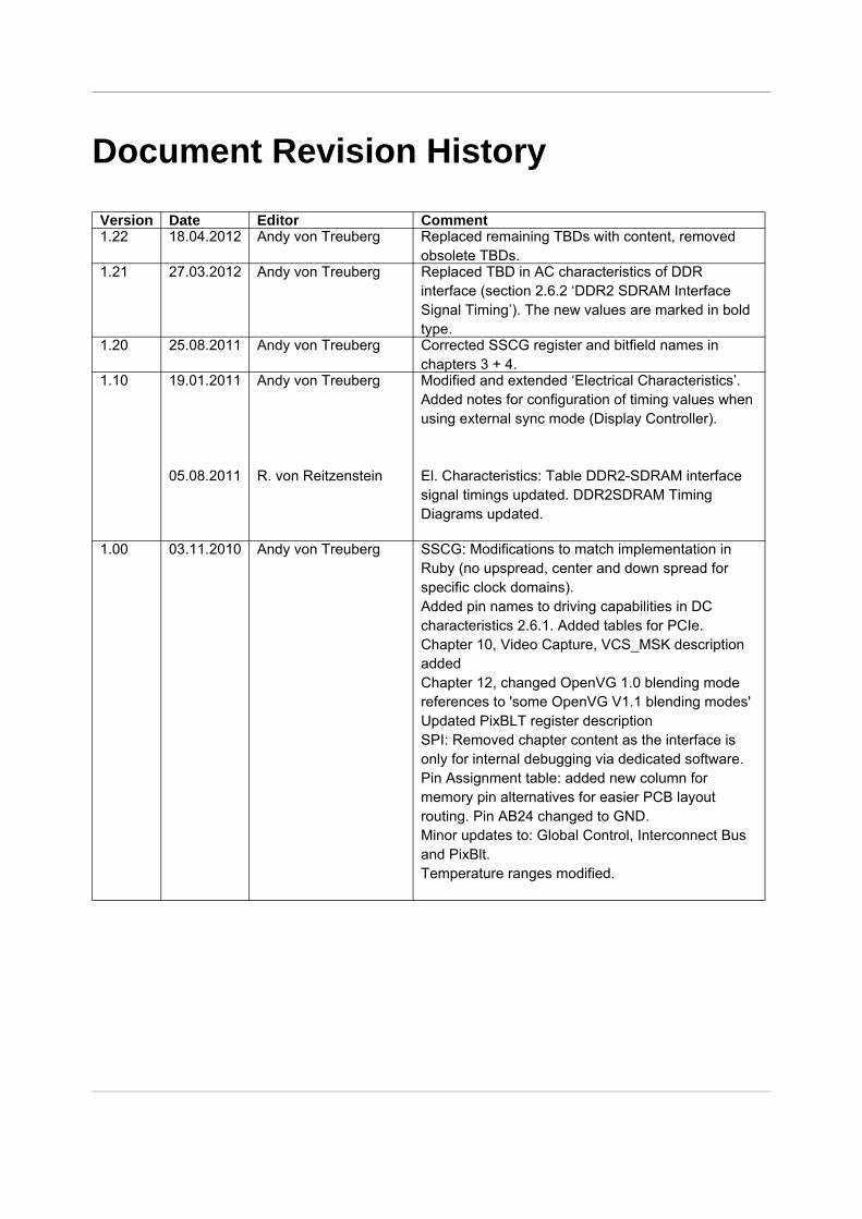
Document Revision History
Version Date Editor Comment1.22 18.04.2012 Andy von Treuberg Replaced remaining TBDs with content, removed
obsolete TBDs.1.21 27.03.2012 Andy von Treuberg Replaced TBD in AC characteristics of DDR
interface (section 2.6.2 ‘DDR2 SDRAM Interface Signal Timing’). The new values are marked in bold type.
1.20 25.08.2011 Andy von Treuberg Corrected SSCG register and bitfield names in chapters 3 + 4.
1.10 19.01.2011
05.08.2011
Andy von Treuberg
R. von Reitzenstein
Modified and extended ‘Electrical Characteristics’.Added notes for configuration of timing values when using external sync mode (Display Controller).
El. Characteristics: Table DDR2-SDRAM interface signal timings updated. DDR2SDRAM Timing Diagrams updated.
1.00 03.11.2010 Andy von Treuberg SSCG: Modifications to match implementation in Ruby (no upspread, center and down spread for specific clock domains). Added pin names to driving capabilities in DC characteristics 2.6.1. Added tables for PCIe.Chapter 10, Video Capture, VCS_MSK description addedChapter 12, changed OpenVG 1.0 blending mode references to 'some OpenVG V1.1 blending modes'Updated PixBLT register descriptionSPI: Removed chapter content as the interface is only for internal debugging via dedicated software.Pin Assignment table: added new column for memory pin alternatives for easier PCB layout routing. Pin AB24 changed to GND.Minor updates to: Global Control, Interconnect Bus and PixBlt.Temperature ranges modified.
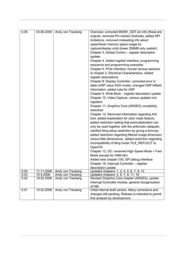
0.05 03.06.2009 Andy von Treuberg Overview: corrected M0/M1_ODT pin info (these are outputs, removed PU resistor footnote), added SPI limitations, removed misleading info about upper/lower memory space usage by capture/display units (lower 256MB only usable!)Chapter 3, Global Control – register description update:Chapter 4, Added register interface, programming sequence and programming examplesChapter 5, PCIe Interface: moved various sections to chapter 2, Electrical Characteristics. Added register descriptionsChapter 8: Display Controller, corrected error in table (HSP value XGA mode), changed HSP bitfield information, added note for HSPChapter 9, Write Back – register description updateChapter 10, Video Capture, various updates incl. registersChapter 11, Graphics Core (ARGES) completely reworkedChapter 12, Removed information regarding AXI lock, added explanation for color mask feature, added restriction stating that premultiplication can only be used together with the arithmetic datapath, clarified tiling setup restriction by giving a formula, added restriction regarding filtered image dimension versus filter dimensions, added restriction regarding incompatibility of tiling mode TILE_REFLECT to OpenVGChapter 13, I2C: renamed High Speed Mode > Fast Mode (except for HSM bit!)Added new chapter (18): SPI debug interfaceChapter 16, Interrupt Controller – register description update
0.04 11.11.2008 Andy von Treuberg Updated chapters: 1, 2, 4, 5, 6, 7, 9, 130.03 10.4.2008 Andy von Treuberg Updated chapters: 4, 6, 7, 9, 11, 160.02 18.02.2008 Andy von Treuberg Revised Graphics Core chapter (ARGES), update
Interrupt Controller module, general reorganization of HM
0.01 15.02.2008 Andy von Treuberg Initial internal draft version. Many corrections and changes still pending. Release is intended to permit first analysis by development.

Revised 18/4/12
Register Descriptions, Global Addresses
Format of Register DescriptionThe register descriptions in this manual use the format shown below to describe each bit field of a register.
Meaning of items and sign
Register address
Register address shows the address (Offset address) of the register.
Bit number
Bit number shows bit position of the register.
Field name
Field name shows bit name of the register.
R/W
R/W shows the read/write attribute of each bit field:
R: Read
W: Write
W1C: Writing a value of "1" clears the register.
Reset value
Reset value indicates the value of each bit field immediately after reset.
0:Initial value is "0".
1:Initial value is "1".
X:Undefined.
Unused register fields are marked with a solid grey background.
Bit vectors are unsigned integers, if nothing else specified.
Please note, that access to an address with no register results in an error response.
Global AddressFor module base addresses refer to the global address map.
Register address OffsetBit number 31 30 29 28 27 26 25 24 23 22 21 20 19 18 17 16 15 14 13 12 11 10 9 8 7 6 5 4 3 2 1 0
Field name
R/W
Reset value
Fujitsu Semiconductor Europe GmbH 3 - 1

Revised 18/4/12
3 - 2 Fujitsu Semiconductor Europe GmbH

Overview Revised 18/4/12
Chapter 1: Overview
This documentation describes the hardware features of the MB86298 'Ruby' Graphics Display Con-troller (GDC) device which is a fourth generation, high end device, which incorporates many im-provements over the MB86297A ‘Carmine’ device.
MB86298 'Ruby' is a performance optimized 90nm CMOS device, developed for embedded sys-tems, especially for automotive requirements and targets graphic applications in the high end sector for CID (Central Information Display) units including navigation systems, as well as rear seat enter-tainment and dashboard (cluster) applications.
MB86298 'Ruby' provides high performance 3D-rendering functions in combination with enhanced video capturing. OpenGL ES 2.0 (http://www.khronos.org/opengles/) conformity is attained using a programmable unified shader architecture as opposed to a fixed function hardware design. State-of-the-art-interfaces to host and graphic memory provide the necessary bandwidth for the data throughput requirements of future high end graphic applications.
Hardware support for some functions of the OpenVG 1.1 standard API (for hardware-accelerated 2D vector graphics) is also included.
1.1 Key Features
Technology
CMOS 90nm technology (CS101)
Power supply voltage: (IO: 3.3 ± 0.3V and core: 1.2 ± 0.1V and DDR2: 1.8 ± 0.1V)
Power consumption: < 4W
Package
Package: TEBGA-543
Ambient temperature range: -40 … +85°C
.
Fujitsu Semiconductor Europe GmbH 1 - 1
Revised 18/4/12 Overview
Functions
New 2D/3D graphics engine with a general purpose, programmable Unified Shader unit providing support for the OpenGL shading language via a shading language compiler (SL Compiler)
Full Scene Anti-Aliasing (FSAA) and high-performance copy and blend blit operations by a separate dedicated hardware unit (PixBlt unit)
Full hardware support of ROP2 and ROP3 raster operations
Two display controllers with display resolutions up to e.g. 1280x1024 or 1600x600 (for details see chapter Display Controller), dual display signal output and combined output for dual view displays
8 overlay layers per display controller, 4 alpha planes, constant alpha value or alpha from pixel data available for blending on each layer
Dithering and Color Look-Up-Table for gamma correction
Four independent digital video capture channels supporting specific input combinations of 3x ITU-R BT.656 and 1x ITU-R BT.656 or DRGB888, DRGB666 - with adaptive de-interlacing (still image detection) and up-/downscaling
Supported video input resolutions: ITU-R BT 601/656, DRGB 888 (up to 1280 pixel horizontal resolution) and SMTPE 296M (1280x720/60p, 1280x720/59.94p, 1280x720/50p)
Frame-rate conversion
Video texturing (e.g. for warping applications)
Write-back of display output to video memory
Brightness, Contrast, Saturation control for video
Built-in chroma-keying
PCI Express Host Interface (1 lane TX/RX) – requester and completer functionality
Big/Little endian swapping
External Interrupt output
32/64 bit external DDR2 SDRAM interface (up to DDR2-800)
I2C Master functionality
GPIO: 8 pins with edge detection interrupts
Spread-Spectrum Clock Generation
IEEE 1149.1 compliant JTAG interface for boundary scan test
1 - 2 Fujitsu Semiconductor Europe GmbH

Overview Revised 18/4/12
1.2 System Overview
Figure 1-1: System Overview
Fujitsu Semiconductor Europe GmbH 1 - 3
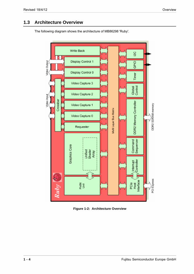
Revised 18/4/12 Overview
1.3 Architecture Overview
The following diagram shows the architecture of MB86298 'Ruby'.
Figure 1-2: Architecture Overview
1 - 4 Fujitsu Semiconductor Europe GmbH
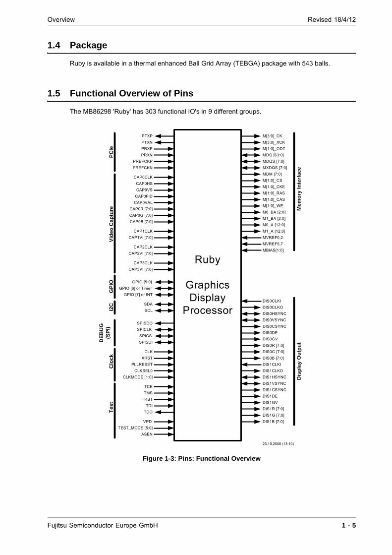
Overview Revised 18/4/12
1.4 Package
Ruby is available in a thermal enhanced Ball Grid Array (TEBGA) package with 543 balls.
1.5 Functional Overview of Pins
The MB86298 'Ruby' has 303 functional IO's in 9 different groups.
Figure 1-3: Pins: Functional Overview
Ruby
GraphicsDisplay
Processor
PTXN
PRXP
PREFCKP
CAP0HS
MDQ [63:0]
CAP0FID
CAP0R [7:0]
CAP0VS
CAP0CLK
MDQS [7:0]
M[1:0]_RAS
CAP0G [7:0]
CAP0B [7:0]
CAP1VI [7:0]
CAP1CLK
CAP2VI [7:0]
CAP2CLK
CAP3VI [7:0]
CAP3CLK
M[3:0]_XCK
MDM [7:0]
M[1:0]_CAS
M[1:0]_CS
M[1:0]_CKE
M[1:0]_WE
M0_BA [2:0]
M0_A [12:0]
MBIAS[1:0]
MVREF5,7
DIS0CLKI
DIS0CLKO
DIS0DE
DIS0HSYNC
DIS0GV
DIS0VSYNC
DIS0CSYNC
DIS0R [7:0]
DIS0G [7:0]
DIS0B [7:0]
DIS1CLKI
DIS1CLKO
DIS1DE
DIS1HSYNC
DIS1GV
DIS1VSYNC
DIS1CSYNC
DIS1R [7:0]
DIS1G [7:0]
DIS1B [7:0]
TMS
TDI
TDO
TRST
TCK
VPD
TEST_MODE [5:0]
ASEN
SCL
SDA
CLK
GPIO [5:0]
PLLRESET
CLKSEL0
XRST
GPIO [7] or INT
GPIO [6] or Timer
Tes
tC
lock
I2C
GP
IOV
ideo
Cap
ture
PC
Ie
Mem
ory
In
terf
ace
Dis
pla
y O
utp
ut
MXDQS [7:0]
M[1:0]_ODT
CAP0VAL
M[3:0]_CK
M1_BA [2:0]
M1_A [12:0]
MVREF0,2
PTXP
PRXN
PREFCKN
SPICLK
SPISDI
SPICS
DE
BU
G
(SP
I)
CLKMODE [1:0]
23.10.2008 (13:10)
SPISDO
Fujitsu Semiconductor Europe GmbH 1 - 5
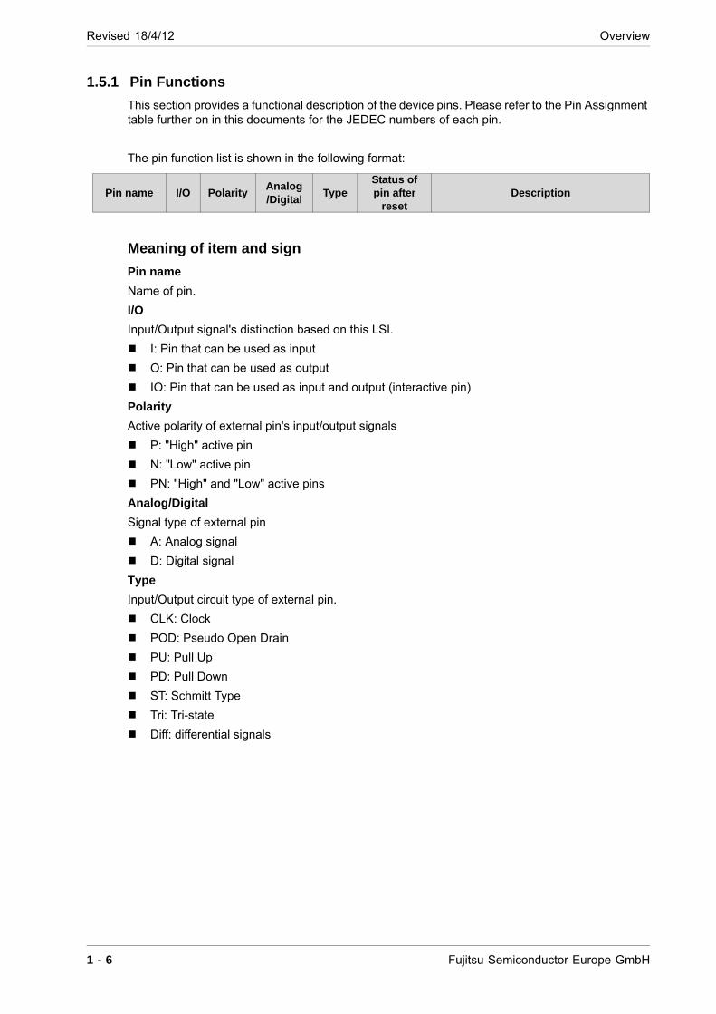
Revised 18/4/12 Overview
1.5.1 Pin Functions
This section provides a functional description of the device pins. Please refer to the Pin Assignment table further on in this documents for the JEDEC numbers of each pin.
The pin function list is shown in the following format:
Meaning of item and sign
Pin name
Name of pin.
I/O
Input/Output signal's distinction based on this LSI.
I: Pin that can be used as input
O: Pin that can be used as output
IO: Pin that can be used as input and output (interactive pin)
Polarity
Active polarity of external pin's input/output signals
P: "High" active pin
N: "Low" active pin
PN: "High" and "Low" active pins
Analog/Digital
Signal type of external pin
A: Analog signal
D: Digital signal
Type
Input/Output circuit type of external pin.
CLK: Clock
POD: Pseudo Open Drain
PU: Pull Up
PD: Pull Down
ST: Schmitt Type
Tri: Tri-state
Diff: differential signals
Pin name I/O PolarityAnalog/Digital
TypeStatus of pin after
resetDescription
1 - 6 Fujitsu Semiconductor Europe GmbH
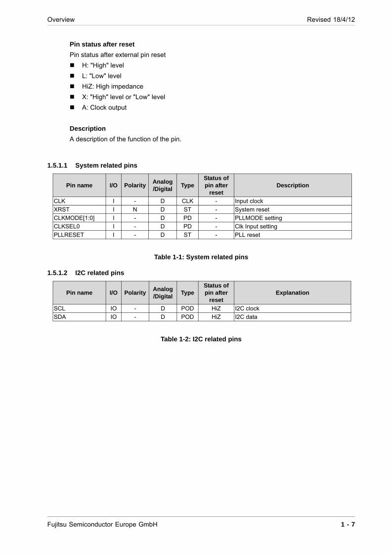
Overview Revised 18/4/12
Pin status after reset
Pin status after external pin reset
H: "High" level
L: "Low" level
HiZ: High impedance
X: "High" level or "Low" level
A: Clock output
Description
A description of the function of the pin.
1.5.1.1 System related pins
Table 1-1: System related pins
1.5.1.2 I2C related pins
Table 1-2: I2C related pins
Pin name I/O PolarityAnalog/Digital
TypeStatus of pin after
resetDescription
CLK I - D CLK - Input clock
XRST I N D ST - System reset
CLKMODE[1:0] I - D PD - PLLMODE setting
CLKSEL0 I - D PD - Clk Input setting
PLLRESET I - D ST - PLL reset
Pin name I/O PolarityAnalog/Digital
TypeStatus of pin after
resetExplanation
SCL IO - D POD HiZ I2C clock
SDA IO - D POD HiZ I2C data
Fujitsu Semiconductor Europe GmbH 1 - 7
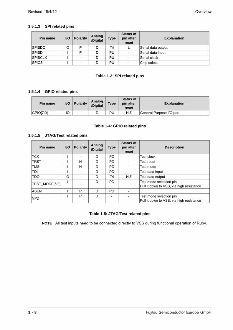
Revised 18/4/12 Overview
1.5.1.3 SPI related pins
Table 1-3: SPI related pins
1.5.1.4 GPIO related pins
Table 1-4: GPIO related pins
1.5.1.5 JTAG/Test related pins
Table 1-5: JTAG/Test related pins
NOTE All test inputs need to be connected directly to VSS during functional operation of Ruby.
Pin name I/O PolarityAnalog/Digital
TypeStatus of pin after
resetExplanation
SPISDO O P D Tri L Serial data output
SPISDI I P D PU - Serial data input
SPISCLK I - D PU - Serial clock
SPICS I - D PU - Chip select
Pin name I/O PolarityAnalog/Digital
TypeStatus of pin after
resetExplanation
GPIO[7:0] IO - D PU HiZ General Purpose I/O port
Pin name I/O PolarityAnalog/Digital
TypeStatus of pin after
resetDescription
TCK I - D PD - Test clock
TRST I N D PD - Test reset
TMS I N D PD - Test mode
TDI I - D PD - Test data input
TDO O - D Tri HiZ Test data output
TEST_MODE[5:0]I - D PD - Test mode selection pin
Pull it down to VSS, via high resistance
ASEN I P D PD -
VPDI P D - - Test mode selection pin
Pull it down to VSS, via high resistance
1 - 8 Fujitsu Semiconductor Europe GmbH
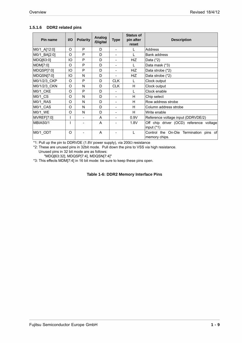
Overview Revised 18/4/12
1.5.1.6 DDR2 related pins
Table 1-6: DDR2 Memory Interface Pins
Pin name I/O PolarityAnalog/Digital
TypeStatus of pin after
resetDescription
M0/1_A[12:0] O P D - L Address
M0/1_BA[2:0] O P D - L Bank address
MDQ[63:0] IO P D - HiZ Data (*2)
MDM[7:0] O P D - L Data mask (*3)
MDQSP[7:0] IO P D - HiZ Data strobe (*2)
MDQSN[7:0] IO N D - HiZ Data strobe (*2)
M0/1/2/3_CKP O P D CLK L Clock output
M0/1/2/3_CKN O N D CLK H Clock output
M0/1_CKE O P D - L Clock enable
M0/1_CS O N D - H Chip select
M0/1_RAS O N D - H Row address strobe
M0/1_CAS O N D - H Column address strobe
M0/1_WE O N D - H Write enable
MVREF[7:0] I - A - 0.9V Reference voltage input (DDRVDE/2)
MBIAS0/1 I - A - 1.8V Off chip driver (OCD) reference voltage input (*1)
M0/1_ODT O - A - L Control the On-Die Termination pins of memory chips.
*1: Pull up the pin to DDRVDE (1.8V power supply), via 200 resistance*2: These are unused pins in 32bit mode. Pull down the pins to VSS via high resistance.
Unused pins in 32 bit mode are as follows:"MDQ[63:32], MDQSP[7:4], MDQSN[7:4]"
*3: This effects MDM[7:4] in 16 bit mode: be sure to keep these pins open.
Fujitsu Semiconductor Europe GmbH 1 - 9

Revised 18/4/12 Overview
1.5.1.7 Display related pins
Table 1-7: Display related pins
NOTE The sync signals are not immediately switched to an input state after a reset (there is a delay because the internal Display Controllers extend the reset procedure within the GDC for technical reasons). During the reset and after it, the status of the pins is undetermined.
Pin name I/O PolarityAnalog/Digital
TypeStatus of pin after
resetExplanation
DIS0HSYNC IO - D - HiZ Video output interface horizontal sync output Horizontal sync input in external sync mode
DIS0VSYNC IO - D - HiZ Video output interface vertical sync outputVertical sync input in external sync mode
DIS0CSYNC O - D - HiZ Video output composite sync
DIS0GV O - D - HiZ Video output interface graphics/video switch
DIS0CLKI I - D CLK - Video output interface dot clock input
DIS0CLKO O - D CLK HiZ Video output interface dot clock output
DIS0DE O - D - HiZ Video output data enable
DIS0R[7:0] O - D - HiZ Digital RGB output0
DIS0G[7:0] O - D - HiZ Digital RGB output0
DIS0B[7:0] O - D - HiZ Digital RGB output0
DIS1HSYNC IO - D - HiZ Video output interface horizontal sync outputHorizontal sync input in external sync mode
DIS1VSYNC IO - D - HiZ Video output interface vertical sync outputVertical sync input in external sync mode
DIS1CSYNC HiZ Video output composite sync
DIS1GV O - D - HiZ Video output interface graphics/video switch
DIS1CLKI I - D CLK - Video output interface dot clock input
DIS1CLKO O - D CLK HiZ Video output interface dot clock output
DIS1DE O - D - HiZ Video output data enable
DIS1R[7:0] O - D - HiZ Digital RGB output1
DIS1G[7:0] O - D - HiZ Digital RGB output1
DIS1B[7:0] O - D - HiZ Digital RGB output1
1 - 10 Fujitsu Semiconductor Europe GmbH
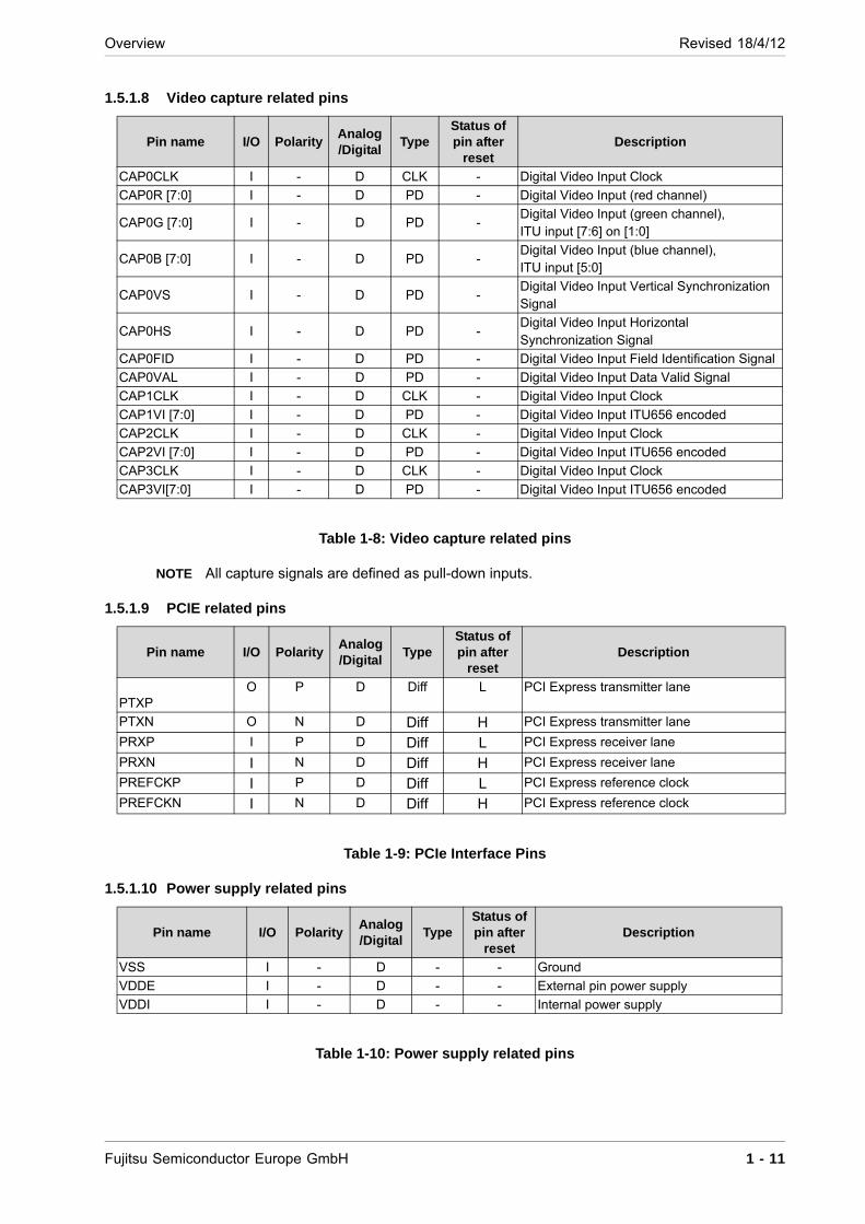
Overview Revised 18/4/12
1.5.1.8 Video capture related pins
Table 1-8: Video capture related pins
NOTE All capture signals are defined as pull-down inputs.
1.5.1.9 PCIE related pins
Table 1-9: PCIe Interface Pins
1.5.1.10 Power supply related pins
Table 1-10: Power supply related pins
Pin name I/O PolarityAnalog/Digital
TypeStatus of pin after
resetDescription
CAP0CLK I - D CLK - Digital Video Input Clock
CAP0R [7:0] I - D PD - Digital Video Input (red channel)
CAP0G [7:0] I - D PD -Digital Video Input (green channel),ITU input [7:6] on [1:0]
CAP0B [7:0] I - D PD -Digital Video Input (blue channel),ITU input [5:0]
CAP0VS I - D PD -Digital Video Input Vertical Synchronization Signal
CAP0HS I - D PD -Digital Video Input Horizontal Synchronization Signal
CAP0FID I - D PD - Digital Video Input Field Identification Signal
CAP0VAL I - D PD - Digital Video Input Data Valid Signal
CAP1CLK I - D CLK - Digital Video Input Clock
CAP1VI [7:0] I - D PD - Digital Video Input ITU656 encoded
CAP2CLK I - D CLK - Digital Video Input Clock
CAP2VI [7:0] I - D PD - Digital Video Input ITU656 encoded
CAP3CLK I - D CLK - Digital Video Input Clock
CAP3VI[7:0] I - D PD - Digital Video Input ITU656 encoded
Pin name I/O PolarityAnalog/Digital
TypeStatus of pin after
resetDescription
PTXPO P D Diff L PCI Express transmitter lane
PTXN O N D Diff H PCI Express transmitter lane
PRXP I P D Diff L PCI Express receiver lane
PRXN I N D Diff H PCI Express receiver lane
PREFCKP I P D Diff L PCI Express reference clock
PREFCKN I N D Diff H PCI Express reference clock
Pin name I/O PolarityAnalog/Digital
TypeStatus of pin after
resetDescription
VSS I - D - - Ground
VDDE I - D - - External pin power supply
VDDI I - D - - Internal power supply
Fujitsu Semiconductor Europe GmbH 1 - 11
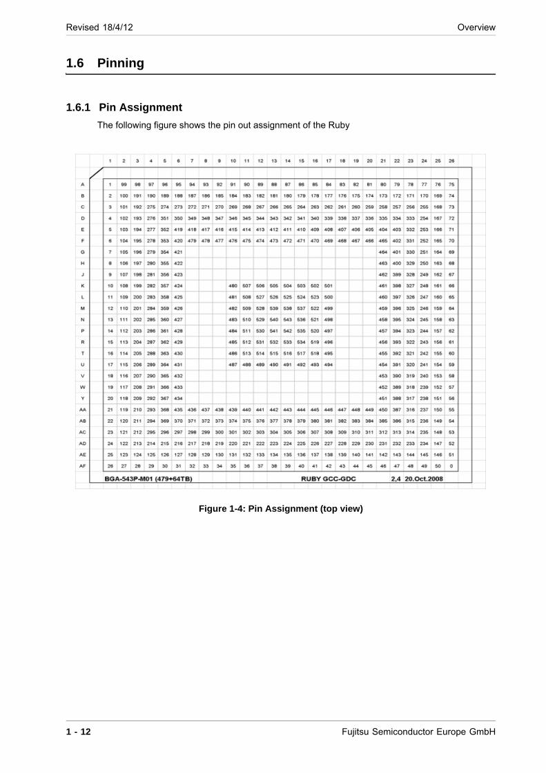
Revised 18/4/12 Overview
1.6 Pinning
1.6.1 Pin Assignment
The following figure shows the pin out assignment of the Ruby
Figure 1-4: Pin Assignment (top view)
1 - 12 Fujitsu Semiconductor Europe GmbH
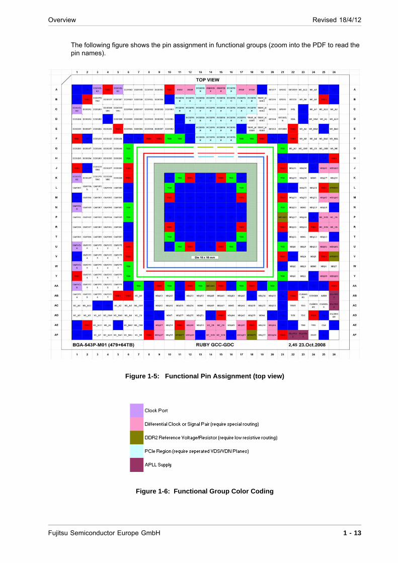
Overview Revised 18/4/12
The following figure shows the pin assignment in functional groups (zoom into the PDF to read the pin names).
Figure 1-5: Functional Pin Assignment (top view)
Figure 1-6: Functional Group Color Coding
Fujitsu Semiconductor Europe GmbH 1 - 13
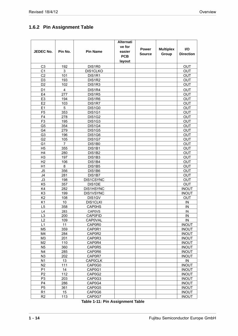
Revised 18/4/12 Overview
1.6.2 Pin Assignment Table
JEDEC No. Pin No. Pin Name
Alternative for easier PCB
layout
Power Source
MultiplexGroup
I/O Direction
C3 192 DIS1R0 OUTC1 3 DIS1CLKO OUTC2 101 DIS1R1 OUTD3 193 DIS1R2 OUTD2 102 DIS1R3 OUT
D1 4 DIS1R4 OUTE4 277 DIS1R5 OUTE3 194 DIS1R6 OUTE2 103 DIS1R7 OUTE1 5 DIS1G0 OUTF5 353 DIS1G1 OUTF4 278 DIS1G2 OUTF3 195 DIS1G3 OUTG5 354 DIS1G4 OUTG4 279 DIS1G5 OUTG3 196 DIS1G6 OUTG2 105 DIS1G7 OUTG1 7 DIS1B0 OUTH5 355 DIS1B1 OUTH4 280 DIS1B2 OUTH3 197 DIS1B3 OUTH2 106 DIS1B4 OUTH1 8 DIS1B5 OUTJ5 356 DIS1B6 OUTJ4 281 DIS1B7 OUTJ3 198 DIS1CSYNC OUTK5 357 DIS1DE OUTK4 282 DIS1HSYNC INOUTK3 199 DIS1VSYNC INOUTK2 108 DIS1GV OUTK1 10 DIS1CLKI INL5 358 CAP0HS INL4 283 CAP0VS INL3 200 CAP0FID INL2 109 CAP0VAL INL1 11 CAP0R0 INOUTM5 359 CAP0R1 INOUTM4 284 CAP0R2 INOUTM3 201 CAP0R3 INOUTM2 110 CAP0R4 INOUTN5 360 CAP0R5 INOUTN4 285 CAP0R6 INOUTN3 202 CAP0R7 INOUTN1 13 CAP0CLK INN2 111 CAP0G0 INOUTP1 14 CAP0G1 INOUTP2 112 CAP0G2 INOUTP3 203 CAP0G3 INOUTP4 286 CAP0G4 INOUTP5 361 CAP0G5 INOUTR1 15 CAP0G6 INOUTR2 113 CAP0G7 INOUT
Table 1-11: Pin Assignment Table
1 - 14 Fujitsu Semiconductor Europe GmbH
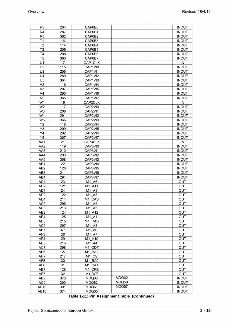
Overview Revised 18/4/12
R3 204 CAP0B0 INOUTR4 287 CAP0B1 INOUTR5 362 CAP0B2 INOUTT1 16 CAP0B3 INOUTT2 114 CAP0B4 INOUTT3 205 CAP0B5 INOUTT4 288 CAP0B6 INOUTT5 363 CAP0B7 INOUTU1 17 CAP1CLK INU2 115 CAP1VI0 INOUTU3 206 CAP1VI1 INOUTU4 289 CAP1VI2 INOUTU5 364 CAP1VI3 INOUTV2 116 CAP1VI4 INOUTV3 207 CAP1VI5 INOUTV4 290 CAP1VI6 INOUTV5 365 CAP1VI7 INOUTW1 19 CAP2CLK INW2 117 CAP2VI0 INOUTW3 208 CAP2VI1 INOUTW4 291 CAP2VI2 INOUTW5 366 CAP2VI3 INOUTY2 118 CAP2VI4 INOUTY3 209 CAP2VI5 INOUTY4 292 CAP2VI6 INOUTY5 367 CAP2VI7 INOUT
AA1 21 CAP3CLK INAA2 119 CAP3VI0 INOUTAA3 210 CAP3VI1 INOUTAA4 293 CAP3VI2 INOUTAA5 368 CAP3VI3 INOUTAB1 22 CAP3VI4 INOUTAB2 120 CAP3VI5 INOUTAB3 211 CAP3VI6 INOUTAB4 294 CAP3VI7 INOUTAC1 23 M1_A6 OUTAC2 121 M1_A11 OUTAD1 24 M1_A9 OUTAD2 122 M1_A5 OUTAD4 214 M1_CAS OUTAC5 296 M1_A2 OUTAD3 213 M1_A3 OUTAE3 124 M1_A12 OUTAE4 125 M1_A1 OUTAD5 215 M1_RAS OUTAC6 297 M1_A8 OUTAB7 371 M1_A0 OUTAF3 28 M1_A7 OUTAF4 29 M1_A10 OUTAD6 216 M1_A4 OUTAC7 298 M1_ODT OUTAE6 127 M1_BA2 OUTAD7 217 M1_CS OUTAF5 30 M1_BA0 OUTAF6 31 M1_BA1 OUTAE7 128 M1_CKE OUTAF7 32 M1_WE OUTAB9 373 MDQ63 MDQ62 INOUTAC9 300 MDQ62 MDQ59 INOUT
AC10 301 MDQ61 MDQ57 INOUTAB10 374 MDQ60 INOUT
Table 1-11: Pin Assignment Table (Continued)
Fujitsu Semiconductor Europe GmbH 1 - 15
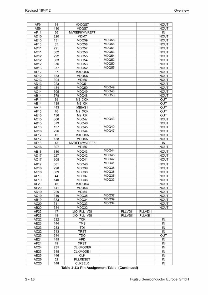
Revised 18/4/12 Overview
AF9 34 MXDQS7 INOUTAE9 130 MDQS7 INOUTAF11 36 MVREF6/MVREF7 INAD10 220 MDM7 INOUTAE10 131 MDQ59 MDQ58 INOUTAF10 35 MDQ58 MDQ56 INOUTAD11 221 MDQ57 MDQ61 INOUTAC11 302 MDQ56 MDQ63 INOUTAD12 222 MDQ55 MDQ54 INOUTAC12 303 MDQ54 MDQ52 INOUTAB12 376 MDQ53 MDQ50 INOUTAB13 377 MDQ52 MDQ55 INOUTAF12 37 MXDQS6 INOUTAE12 133 MDQS6 INOUTAC13 304 MDM6 INOUTAD13 223 MDQ51 INOUTAE13 134 MDQ50 MDQ49 INOUTAC14 305 MDQ49 MDQ48 INOUTAB14 378 MDQ48 MDQ53 INOUTAF14 39 M3_XCK OUTAE14 135 M3_CK OUTAA14 443 MBIAS1 OUTAF15 40 M2_XCK OUTAE15 136 M2_CK OUTAC15 306 MDQ47 MDQ43 INOUTAB15 379 MDQ46 INOUTAE16 137 MDQ45 MDQ40 INOUTAD16 226 MDQ44 MDQ47 INOUTAF17 42 MXDQS5 INOUTAE17 138 MDQS5 INOUTAF18 43 MVREF4/MVREF5 INAC16 307 MDM5 INOUT
AB16 380 MDQ43 MDQ44 INOUTAD17 227 MDQ42 MDQ45 INOUTAC17 308 MDQ41 MDQ42 INOUT
AB17 381 MDQ40 MDQ41 INOUTAD18 228 MDQ39 MDQ38 INOUTAC18 309 MDQ38 MDQ36 INOUTAF19 44 MDQ37 MDQ35 INOUTAE19 140 MDQ36 MDQ33 INOUTAF20 45 MXDQS4 INOUTAE20 141 MDQS4 INOUTAD19 229 MDM4 INOUTAC19 310 MDQ35 MDQ37 INOUTAB19 383 MDQ34 MDQ39 INOUTAC20 311 MDQ33 MDQ34 INOUTAB20 384 MDQ32 INOUTAF22 47 #IO_PLL_VDI PLLVDI1 PLLVDI1AF23 48 #IO_PLL_VSI PLLVSI1 PLLVSI1AD22 232 TCK INAE23 144 TMS INAD23 233 TDI INAC22 313 TRST INAC23 314 TDO OUTAE24 145 VPD INAF24 49 XRST INAC24 235 CLKMODE0 INAB23 315 CLKMODE1 INAE25 146 CLK INAD26 52 PLLRESET INAC25 148 CLKSEL0 IN
Table 1-11: Pin Assignment Table (Continued)
1 - 16 Fujitsu Semiconductor Europe GmbH
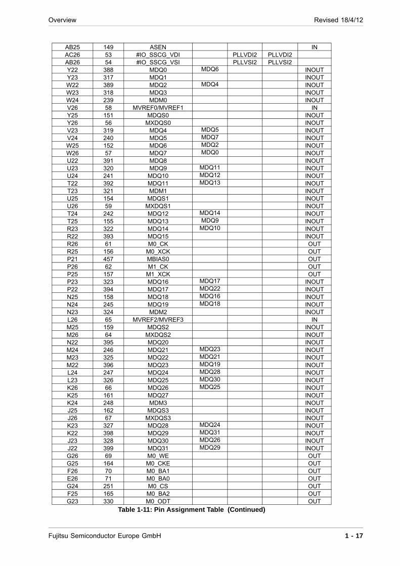
Overview Revised 18/4/12
AB25 149 ASEN INAC26 53 #IO_SSCG_VDI PLLVDI2 PLLVDI2AB26 54 #IO_SSCG_VSI PLLVSI2 PLLVSI2Y22 388 MDQ0 MDQ6 INOUTY23 317 MDQ1 INOUTW22 389 MDQ2 MDQ4 INOUTW23 318 MDQ3 INOUTW24 239 MDM0 INOUTV26 58 MVREF0/MVREF1 INY25 151 MDQS0 INOUTY26 56 MXDQS0 INOUTV23 319 MDQ4 MDQ5 INOUTV24 240 MDQ5 MDQ7 INOUTW25 152 MDQ6 MDQ2 INOUTW26 57 MDQ7 MDQ0 INOUTU22 391 MDQ8 INOUTU23 320 MDQ9 MDQ11 INOUTU24 241 MDQ10 MDQ12 INOUTT22 392 MDQ11 MDQ13 INOUTT23 321 MDM1 INOUTU25 154 MDQS1 INOUTU26 59 MXDQS1 INOUTT24 242 MDQ12 MDQ14 INOUTT25 155 MDQ13 MDQ9 INOUTR23 322 MDQ14 MDQ10 INOUTR22 393 MDQ15 INOUTR26 61 M0_CK OUTR25 156 M0_XCK OUTP21 457 MBIAS0 OUTP26 62 M1_CK OUTP25 157 M1_XCK OUTP23 323 MDQ16 MDQ17 INOUTP22 394 MDQ17 MDQ22 INOUTN25 158 MDQ18 MDQ16 INOUTN24 245 MDQ19 MDQ18 INOUTN23 324 MDM2 INOUTL26 65 MVREF2/MVREF3 INM25 159 MDQS2 INOUTM26 64 MXDQS2 INOUTN22 395 MDQ20 INOUTM24 246 MDQ21 MDQ23 INOUTM23 325 MDQ22 MDQ21 INOUTM22 396 MDQ23 MDQ19 INOUTL24 247 MDQ24 MDQ28 INOUTL23 326 MDQ25 MDQ30 INOUTK26 66 MDQ26 MDQ25 INOUTK25 161 MDQ27 INOUTK24 248 MDM3 INOUTJ25 162 MDQS3 INOUTJ26 67 MXDQS3 INOUTK23 327 MDQ28 MDQ24 INOUTK22 398 MDQ29 MDQ31 INOUTJ23 328 MDQ30 MDQ26 INOUTJ22 399 MDQ31 MDQ29 INOUTG26 69 M0_WE OUTG25 164 M0_CKE OUTF26 70 M0_BA1 OUTE26 71 M0_BA0 OUTG24 251 M0_CS OUTF25 165 M0_BA2 OUTG23 330 M0_ODT OUT
Table 1-11: Pin Assignment Table (Continued)
Fujitsu Semiconductor Europe GmbH 1 - 17

Revised 18/4/12 Overview
F24 252 M0_A4 OUTD26 72 M0_A10 OUTC24 255 M0_A7 OUTG22 401 M0_A0 OUTF23 331 M0_A8 OUTE24 253 M0_RAS OUTD25 167 M0_A1 OUTC25 168 M0_A12 OUTC26 73 M0_A3 OUTE23 332 M0_A2 OUTD24 254 M0_CAS OUTB24 170 M0_A5 OUTA24 77 M0_A9 OUTA23 78 M0_A11 OUTB23 171 M0_A6 OUTD22 334 SDA INOUTC22 257 SCL INOUTB22 172 SPICS INA22 79 SPISDO OUTE21 404 SPISDI IND21 335 SPISCLK INC21 258 GPIO0 INOUTB21 173 GPIO1 INOUTA21 80 GPIO2 INOUTE20 405 GPIO3 INOUTD20 336 GPIO4 INOUTC20 259 GPIO5 INOUTB20 174 GPIO6 INOUTA20 81 GPIO7 INOUTE19 406 TEST_MODE0 IND19 337 TEST_MODE1 INC19 260 TEST_MODE2 INB19 175 TEST_MODE3 INE18 407 TEST_MODE4 IND18 338 TEST_MODE5 INA18 83 PTXN OUTA17 84 PTXP OUTA15 86 PREFCKN INA14 87 PREFCKP INA12 89 PRXN INA11 90 PRXP INC10 269 DIS0R0 OUTD10 346 DIS0R1 OUTE10 415 DIS0R2 OUTA9 92 DIS0R3 OUTB9 185 DIS0R4 OUTC9 270 DIS0R5 OUTD9 347 DIS0R6 OUTE9 416 DIS0R7 OUTA8 93 DIS0G0 OUTB8 186 DIS0G1 OUTC8 271 DIS0G2 OUTD8 348 DIS0G3 OUTE8 417 DIS0G4 OUT
A7 94 DIS0G5 OUTB7 187 DIS0G6 OUTC7 272 DIS0G7 OUTD7 349 DIS0B0 OUTE7 418 DIS0B1 OUTA6 95 DIS0B2 OUTB6 188 DIS0B3 OUT
Table 1-11: Pin Assignment Table (Continued)
1 - 18 Fujitsu Semiconductor Europe GmbH
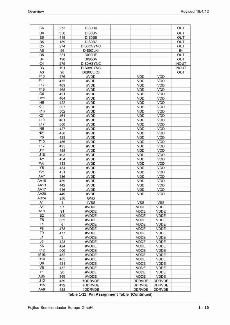
Overview Revised 18/4/12
C6 273 DIS0B4 OUT
D6 350 DIS0B5 OUTE6 419 DIS0B6 OUTB5 189 DIS0B7 OUTC5 274 DIS0CSYNC OUTA5 96 DIS0CLKI IND5 351 DIS0DE OUTB4 190 DIS0GV OUTC4 275 DIS0HSYNC INOUTB3 191 DIS0VSYNC INOUTA3 98 DIS0CLKO OUTF10 476 #VDD VDD VDDF11 475 #VDD VDD VDDF17 469 #VDD VDD VDDF18 468 #VDD VDD VDDG6 421 #VDD VDD VDD
G21 464 #VDD VDD VDDH6 422 #VDD VDD VDDK11 507 #VDD VDD VDDK16 502 #VDD VDD VDDK21 461 #VDD VDD VDDL10 481 #VDD VDD VDDL17 500 #VDD VDD VDDN6 427 #VDD VDD VDD
N21 458 #VDD VDD VDDP6 428 #VDD VDD VDDT10 486 #VDD VDD VDDT17 495 #VDD VDD VDDU11 488 #VDD VDD VDDU16 493 #VDD VDD VDDU21 454 #VDD VDD VDDW6 433 #VDD VDD VDDY6 434 #VDD VDD VDD
Y21 451 #VDD VDD VDDAA7 436 #VDD VDD VDDAA10 439 #VDD VDD VDDAA13 442 #VDD VDD VDDAA17 446 #VDD VDD VDDAA20 449 #VDD VDD VDDAB24 236 GND
A1 1 #VSS VSS VSSA4 97 #VDDE VDDE VDDE
A10 91 #VDDE VDDE VDDEB2 100 #VDDE VDDE VDDEE5 352 #VDDE VDDE VDDEF1 6 #VDDE VDDE VDDEF8 478 #VDDE VDDE VDDEF9 477 #VDDE VDDE VDDEJ1 9 #VDDE VDDE VDDEJ6 423 #VDDE VDDE VDDEK6 424 #VDDE VDDE VDDE
K12 506 #VDDE VDDE VDDEM10 482 #VDDE VDDE VDDER10 485 #VDDE VDDE VDDEU6 431 #VDDE VDDE VDDEV6 432 #VDDE VDDE VDDEY1 20 #VDDE VDDE VDDE
AB5 369 #VDDE VDDE VDDEU12 489 #DDRVDE DDRVDE DDRVDEU15 492 #DDRVDE DDRVDE DDRVDEAA9 438 #DDRVDE DDRVDE DDRVDE
Table 1-11: Pin Assignment Table (Continued)
Fujitsu Semiconductor Europe GmbH 1 - 19
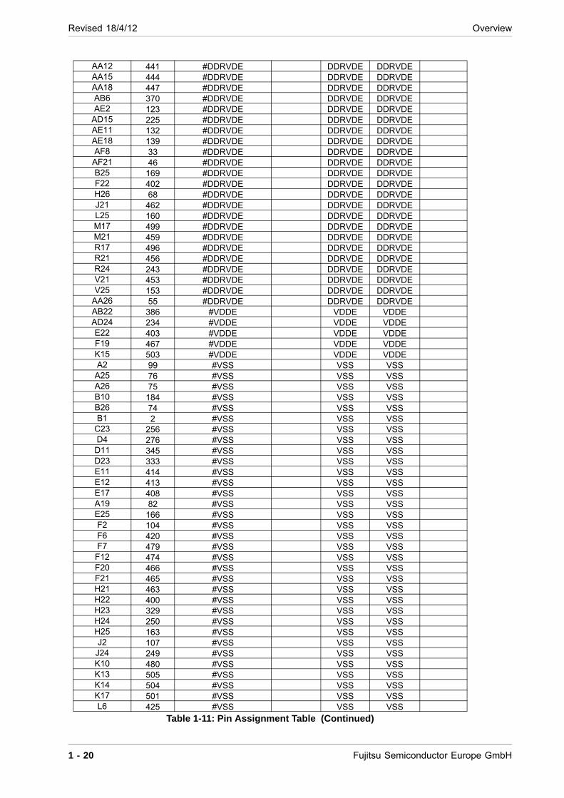
Revised 18/4/12 Overview
AA12 441 #DDRVDE DDRVDE DDRVDEAA15 444 #DDRVDE DDRVDE DDRVDEAA18 447 #DDRVDE DDRVDE DDRVDEAB6 370 #DDRVDE DDRVDE DDRVDEAE2 123 #DDRVDE DDRVDE DDRVDE
AD15 225 #DDRVDE DDRVDE DDRVDEAE11 132 #DDRVDE DDRVDE DDRVDEAE18 139 #DDRVDE DDRVDE DDRVDEAF8 33 #DDRVDE DDRVDE DDRVDEAF21 46 #DDRVDE DDRVDE DDRVDEB25 169 #DDRVDE DDRVDE DDRVDEF22 402 #DDRVDE DDRVDE DDRVDEH26 68 #DDRVDE DDRVDE DDRVDEJ21 462 #DDRVDE DDRVDE DDRVDEL25 160 #DDRVDE DDRVDE DDRVDEM17 499 #DDRVDE DDRVDE DDRVDEM21 459 #DDRVDE DDRVDE DDRVDER17 496 #DDRVDE DDRVDE DDRVDER21 456 #DDRVDE DDRVDE DDRVDER24 243 #DDRVDE DDRVDE DDRVDEV21 453 #DDRVDE DDRVDE DDRVDEV25 153 #DDRVDE DDRVDE DDRVDE
AA26 55 #DDRVDE DDRVDE DDRVDEAB22 386 #VDDE VDDE VDDEAD24 234 #VDDE VDDE VDDEE22 403 #VDDE VDDE VDDEF19 467 #VDDE VDDE VDDEK15 503 #VDDE VDDE VDDEA2 99 #VSS VSS VSS
A25 76 #VSS VSS VSSA26 75 #VSS VSS VSSB10 184 #VSS VSS VSSB26 74 #VSS VSS VSSB1 2 #VSS VSS VSS
C23 256 #VSS VSS VSSD4 276 #VSS VSS VSS
D11 345 #VSS VSS VSSD23 333 #VSS VSS VSSE11 414 #VSS VSS VSSE12 413 #VSS VSS VSSE17 408 #VSS VSS VSSA19 82 #VSS VSS VSSE25 166 #VSS VSS VSSF2 104 #VSS VSS VSSF6 420 #VSS VSS VSSF7 479 #VSS VSS VSSF12 474 #VSS VSS VSSF20 466 #VSS VSS VSSF21 465 #VSS VSS VSSH21 463 #VSS VSS VSSH22 400 #VSS VSS VSSH23 329 #VSS VSS VSSH24 250 #VSS VSS VSSH25 163 #VSS VSS VSSJ2 107 #VSS VSS VSS
J24 249 #VSS VSS VSSK10 480 #VSS VSS VSSK13 505 #VSS VSS VSSK14 504 #VSS VSS VSSK17 501 #VSS VSS VSSL6 425 #VSS VSS VSS
Table 1-11: Pin Assignment Table (Continued)
1 - 20 Fujitsu Semiconductor Europe GmbH
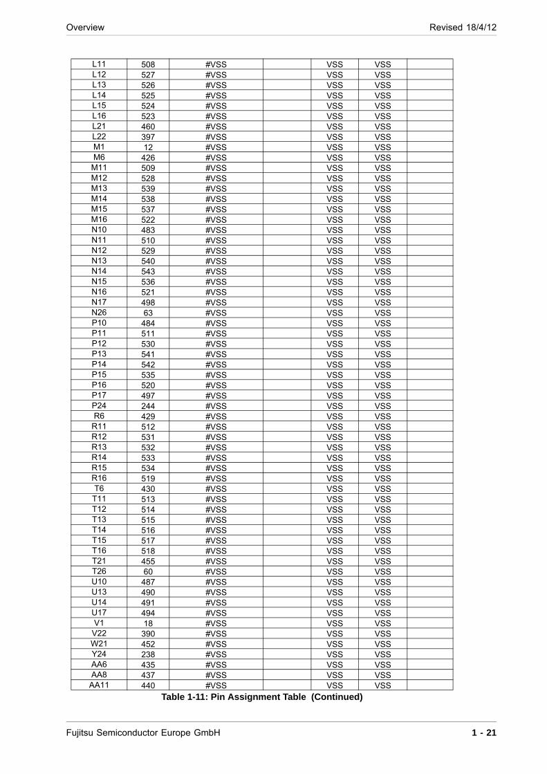
Overview Revised 18/4/12
L11 508 #VSS VSS VSSL12 527 #VSS VSS VSSL13 526 #VSS VSS VSSL14 525 #VSS VSS VSSL15 524 #VSS VSS VSSL16 523 #VSS VSS VSSL21 460 #VSS VSS VSSL22 397 #VSS VSS VSSM1 12 #VSS VSS VSSM6 426 #VSS VSS VSS
M11 509 #VSS VSS VSSM12 528 #VSS VSS VSSM13 539 #VSS VSS VSSM14 538 #VSS VSS VSSM15 537 #VSS VSS VSSM16 522 #VSS VSS VSSN10 483 #VSS VSS VSSN11 510 #VSS VSS VSSN12 529 #VSS VSS VSSN13 540 #VSS VSS VSSN14 543 #VSS VSS VSSN15 536 #VSS VSS VSSN16 521 #VSS VSS VSSN17 498 #VSS VSS VSSN26 63 #VSS VSS VSSP10 484 #VSS VSS VSSP11 511 #VSS VSS VSSP12 530 #VSS VSS VSSP13 541 #VSS VSS VSSP14 542 #VSS VSS VSSP15 535 #VSS VSS VSSP16 520 #VSS VSS VSSP17 497 #VSS VSS VSSP24 244 #VSS VSS VSSR6 429 #VSS VSS VSS
R11 512 #VSS VSS VSSR12 531 #VSS VSS VSSR13 532 #VSS VSS VSSR14 533 #VSS VSS VSSR15 534 #VSS VSS VSSR16 519 #VSS VSS VSST6 430 #VSS VSS VSST11 513 #VSS VSS VSST12 514 #VSS VSS VSST13 515 #VSS VSS VSST14 516 #VSS VSS VSST15 517 #VSS VSS VSST16 518 #VSS VSS VSST21 455 #VSS VSS VSST26 60 #VSS VSS VSSU10 487 #VSS VSS VSSU13 490 #VSS VSS VSSU14 491 #VSS VSS VSSU17 494 #VSS VSS VSSV1 18 #VSS VSS VSS
V22 390 #VSS VSS VSSW21 452 #VSS VSS VSSY24 238 #VSS VSS VSSAA6 435 #VSS VSS VSSAA8 437 #VSS VSS VSSAA11 440 #VSS VSS VSS
Table 1-11: Pin Assignment Table (Continued)
Fujitsu Semiconductor Europe GmbH 1 - 21
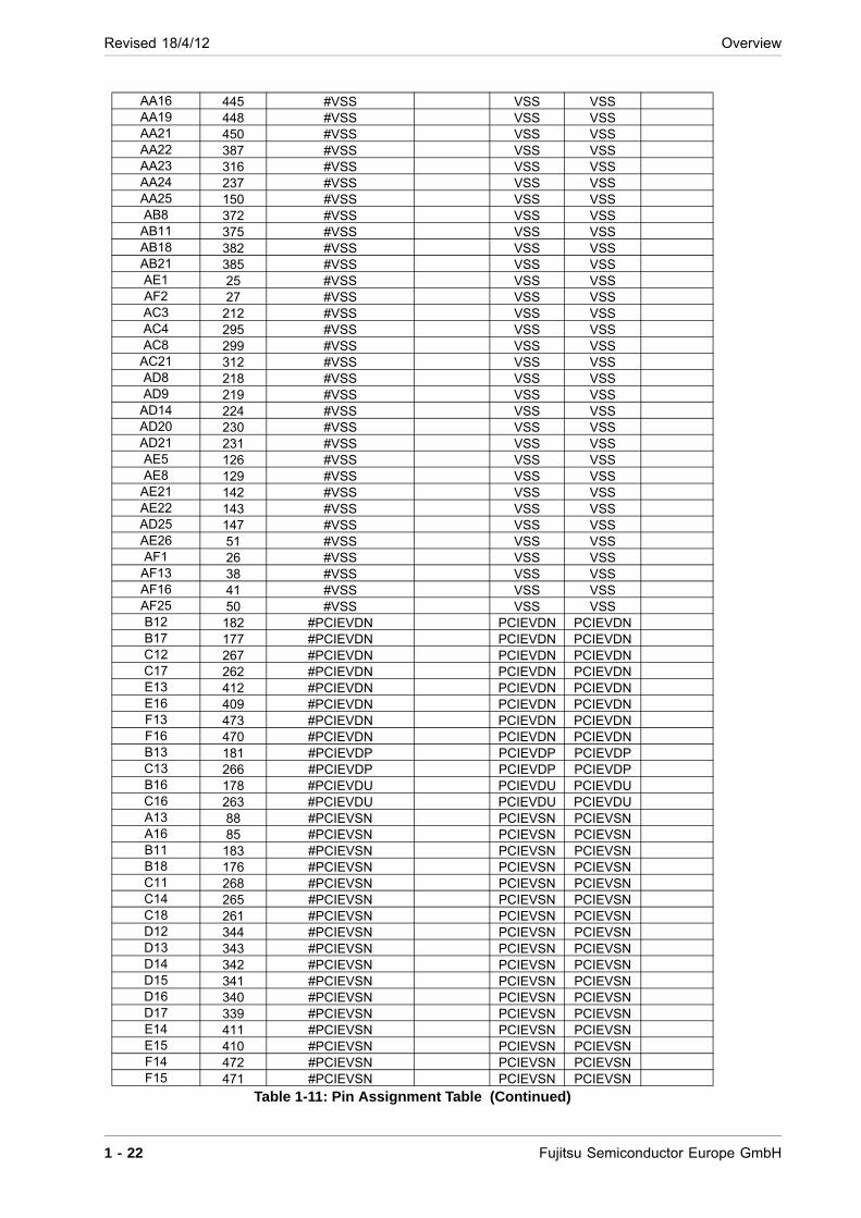
Revised 18/4/12 Overview
AA16 445 #VSS VSS VSSAA19 448 #VSS VSS VSSAA21 450 #VSS VSS VSSAA22 387 #VSS VSS VSSAA23 316 #VSS VSS VSSAA24 237 #VSS VSS VSSAA25 150 #VSS VSS VSSAB8 372 #VSS VSS VSSAB11 375 #VSS VSS VSSAB18 382 #VSS VSS VSSAB21 385 #VSS VSS VSSAE1 25 #VSS VSS VSSAF2 27 #VSS VSS VSSAC3 212 #VSS VSS VSSAC4 295 #VSS VSS VSSAC8 299 #VSS VSS VSS
AC21 312 #VSS VSS VSSAD8 218 #VSS VSS VSSAD9 219 #VSS VSS VSS
AD14 224 #VSS VSS VSSAD20 230 #VSS VSS VSSAD21 231 #VSS VSS VSSAE5 126 #VSS VSS VSSAE8 129 #VSS VSS VSSAE21 142 #VSS VSS VSSAE22 143 #VSS VSS VSSAD25 147 #VSS VSS VSSAE26 51 #VSS VSS VSSAF1 26 #VSS VSS VSSAF13 38 #VSS VSS VSSAF16 41 #VSS VSS VSSAF25 50 #VSS VSS VSSB12 182 #PCIEVDN PCIEVDN PCIEVDNB17 177 #PCIEVDN PCIEVDN PCIEVDNC12 267 #PCIEVDN PCIEVDN PCIEVDNC17 262 #PCIEVDN PCIEVDN PCIEVDNE13 412 #PCIEVDN PCIEVDN PCIEVDNE16 409 #PCIEVDN PCIEVDN PCIEVDNF13 473 #PCIEVDN PCIEVDN PCIEVDNF16 470 #PCIEVDN PCIEVDN PCIEVDNB13 181 #PCIEVDP PCIEVDP PCIEVDPC13 266 #PCIEVDP PCIEVDP PCIEVDPB16 178 #PCIEVDU PCIEVDU PCIEVDUC16 263 #PCIEVDU PCIEVDU PCIEVDUA13 88 #PCIEVSN PCIEVSN PCIEVSNA16 85 #PCIEVSN PCIEVSN PCIEVSNB11 183 #PCIEVSN PCIEVSN PCIEVSNB18 176 #PCIEVSN PCIEVSN PCIEVSNC11 268 #PCIEVSN PCIEVSN PCIEVSNC14 265 #PCIEVSN PCIEVSN PCIEVSNC18 261 #PCIEVSN PCIEVSN PCIEVSND12 344 #PCIEVSN PCIEVSN PCIEVSND13 343 #PCIEVSN PCIEVSN PCIEVSND14 342 #PCIEVSN PCIEVSN PCIEVSND15 341 #PCIEVSN PCIEVSN PCIEVSND16 340 #PCIEVSN PCIEVSN PCIEVSND17 339 #PCIEVSN PCIEVSN PCIEVSNE14 411 #PCIEVSN PCIEVSN PCIEVSNE15 410 #PCIEVSN PCIEVSN PCIEVSNF14 472 #PCIEVSN PCIEVSN PCIEVSNF15 471 #PCIEVSN PCIEVSN PCIEVSN
Table 1-11: Pin Assignment Table (Continued)
1 - 22 Fujitsu Semiconductor Europe GmbH

Overview Revised 18/4/12
1.6.3 Pin Multiplexing
Ruby uses pin multiplexing in order to achieve a minimal pin count despite maximum hardware func-tionality. This means that in a specific pin multiplex mode, certain package pins are internally re-routed (shared between different units) so that their external functionality is changed. Package pins are categorized into different groups, represented by various pin multiplex modes.
NOTE You should only change the pin multiplex mode when the pins effected by the mode switch are not in use. PFR = Port Function Register, Section 14.6.4.
1.6.4 Unused Pins
This section is intended for PCB designers and describes the way in which pins, whose functionality is not required (used) should be connected (pulled up, pulled down or left open/'floating') in the lay-out.
A 'high resistance' as referred to in the table is typically: 4k7Ohms
The term n/a stands for 'not applicable' and refers to some pins whose functionality is required for the use of the chip (i.e. they can not be unused). Power and ground pins are not described as these must be connected to the corresponding signal.
Unused pins should be handled according to their properties described in section Section 1.5.1.
C15 264 #PCIEVSN PCIEVSN PCIEVSNB14 180 #PCIEVSU PCIEVSU PCIEVSUB15 179 #PCIEVSU PCIEVSU PCIEVSU
GPIO Mode(PFR[7] = 0x0)
Interrupt Mode(PFR[7] = 0x1)
GPIO[7] INT (output)
Table 1-12: Pin Multiplexing Modes 1
GPIO Mode(PFR[6] = 0x0)
Timer Mode(PFR[6] = 0x1)
GPIO[6]Compare (output)Retrigger (input)
Table 1-13: Pin Multiplexing Modes 2
Table 1-11: Pin Assignment Table (Continued)
Fujitsu Semiconductor Europe GmbH 1 - 23
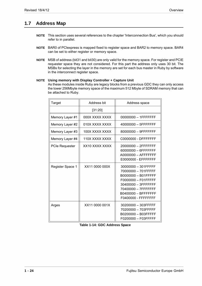
Revised 18/4/12 Overview
1.7 Address Map
NOTE This section uses several references to the chapter 'Interconnection Bus', which you should refer to in parallel.
NOTE BAR0 of PCIexpress is mapped fixed to register space and BAR2 to memory space. BAR4 can be set to either register or memory space.
NOTE MSB of address (bit31 and bit30) are only valid for the memory space. For register and PCIE requester space they are not considered. For this part the address only uses 30 bit. The MSBs for selecting the layer in the memory are set for each bus master in Ruby by software in the interconnect register space.
NOTE Using memory with Display Controller + Capture UnitAs these modules inside Ruby are legacy blocks from a previous GDC they can only access the lower 256Mbyte memory space of the maximum 512 Mbyte of SDRAM memory that can be attached to Ruby.
Target Address bit Address space
[31:20]
Memory Layer #1 000X XXXX XXXX 00000000 – 1FFFFFFF
Memory Layer #2 010X XXXX XXXX 40000000 – 5FFFFFFF
Memory Layer #3 100X XXXX XXXX 80000000 – 9FFFFFFF
Memory Layer #4 110X XXXX XXXX C0000000 - DFFFFFFF
PCIe Requester XX10 XXXX XXXX 20000000 – 2FFFFFFF60000000 – 6FFFFFFFA0000000 – AFFFFFFFE0000000 - EFFFFFFF
Register Space 1 XX11 0000 000X 30000000 – 301FFFFF70000000 – 701FFFFFB0000000 – B01FFFFFF0000000 – F01FFFFF30400000 – 3FFFFFFF70400000 – 7FFFFFFFB0400000 – BFFFFFFFF0400000 - FFFFFFFF
Arges XX11 0000 001X 30200000 – 303FFFFF70200000 – 703FFFFFB0200000 – B03FFFFFF0200000 – F03FFFFF
Table 1-14: GDC Address Space
1 - 24 Fujitsu Semiconductor Europe GmbH
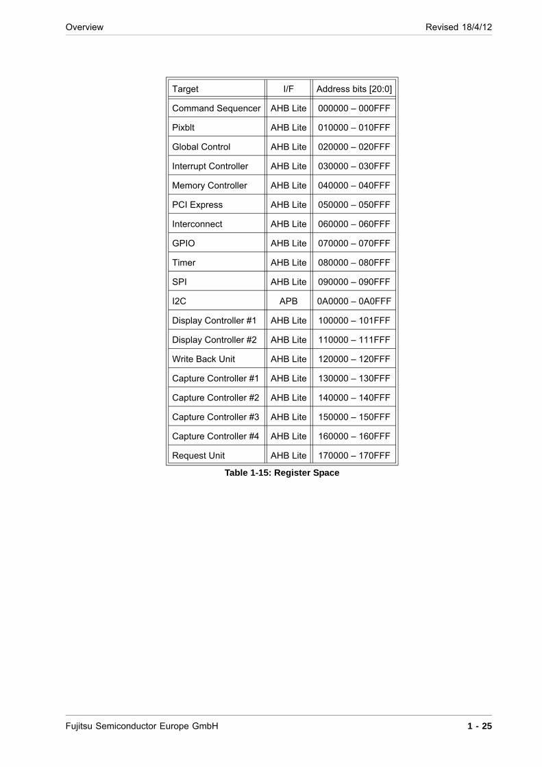
Overview Revised 18/4/12
Target I/F Address bits [20:0]
Command Sequencer AHB Lite 000000 – 000FFF
Pixblt AHB Lite 010000 – 010FFF
Global Control AHB Lite 020000 – 020FFF
Interrupt Controller AHB Lite 030000 – 030FFF
Memory Controller AHB Lite 040000 – 040FFF
PCI Express AHB Lite 050000 – 050FFF
Interconnect AHB Lite 060000 – 060FFF
GPIO AHB Lite 070000 – 070FFF
Timer AHB Lite 080000 – 080FFF
SPI AHB Lite 090000 – 090FFF
I2C APB 0A0000 – 0A0FFF
Display Controller #1 AHB Lite 100000 – 101FFF
Display Controller #2 AHB Lite 110000 – 111FFF
Write Back Unit AHB Lite 120000 – 120FFF
Capture Controller #1 AHB Lite 130000 – 130FFF
Capture Controller #2 AHB Lite 140000 – 140FFF
Capture Controller #3 AHB Lite 150000 – 150FFF
Capture Controller #4 AHB Lite 160000 – 160FFF
Request Unit AHB Lite 170000 – 170FFF
Table 1-15: Register Space
Fujitsu Semiconductor Europe GmbH 1 - 25
Revised 18/4/12 Overview
1.8 Common Topics
1.8.1 Register Access Error Responses
An error response from the AHB slaves is generated for register access if ...
there is no register assigned to the respective address
a READ is executed to a register with Write Only bit fields
a WRITE is executed to a register with Read Only bit fields
1.8.2 Register Access to modules in power-down
NOTE Do not access any modules that are in power down, i.e. the clock to the module is disabled in the Global Control module. The internal bus system will otherwise hang up and can only be recovered via a global external reset.
1.8.3 Reconfiguration of modules
NOTE Modules in the internal bus system such as the memory controller, the interconnect bus or the PCIE host interface are not re-configured dynamically during operation of the chip. If you want to reconfigure, make sure that there is no ongoing traffic over the bus in any direction (except for the access to the register that needs to be changed)
1.8.4 PCIE reset
NOTE The Ruby hardware reset is connected to the PERST# reset signal of the PCIE bus system that Ruby is connected to. This guarantees that both - root complex and endpoint (Ruby) - remain in the same state.
1.8.5 PCIE link lost
NOTE If the PCIE link is lost, the chip has to be subjected to a hardware reset because the state of the PCIE link macro will otherwise become unpredictable.
1.8.6 Using ARGES Display lists in a Command list
NOTE If you use an ARGES display list inside a Command Sequencer command list and it ends with a SYNC command for the ARGES idle state, then you must put an ARGES flush command at the end of the ARGES display list (i.e. before the SYNC command)
1.8.7 Memory data coherency
NOTE In order to make sure that data is consistent in memory when accessed simultaneously by two bus masters of the Ruby system, the following two rules must be followed:
1. Route both masters to the same port of the memory controller (see port configuration registers in the chapter 'Interconnect Bus')
2. If 1. is not possible, execute a flush of the cache in the Memory Controller after a write operation is completed before reading the data with the second master
1 - 26 Fujitsu Semiconductor Europe GmbH

Overview Revised 18/4/12
1.9 Chip Interconnect
1.9.1 Bus System
Please refer to the chapter 'Interconnect Bus' for AXI and AHB interconnect and bus connections.
1.9.2 Other Connections
1.9.2.1 GPIO connections
The picture below shows the system connectivity of the GPIO module.
Figure 1-7: GPIO Connections
Details
PFO[7] is connected to ‘ext_int_n’ pin of the interrupt controller.
PFO[6] is connected to ‘compare_out’ pin of the timer.
PFI[7:0] are connected to ‘int[39:32]’ pins of the interrupt controller.
PFI[7:0] are connected to ‘sysstatus[23:16]’ pins of the command sequencer.
PFI[6] is connected to ‘retrigger_in’ pin of the timer.
Fujitsu Semiconductor Europe GmbH 1 - 27

Revised 18/4/12 Overview
1.9.2.2 Video connections
The following picture shows the system connectivity between the video capture and display units.
These connections are needed for the upscale processing of video streams. The processing flow is as follows:
Display controller reads video data from memory
Display controller sends it to one capture unit for upscaling (depends on the layer used in Display controller)
Display controller gets the scaled data back from capture unit
Video data is sent to the LCD screen
NOTE In this mode one capture unit can be connected only with one of the two display controllers. The setting is done in Capture register VCM by the DSEL field.
1 - 28 Fujitsu Semiconductor Europe GmbH
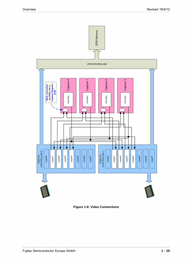
Overview Revised 18/4/12
Figure 1-8: Video Connections
Fujitsu Semiconductor Europe GmbH 1 - 29
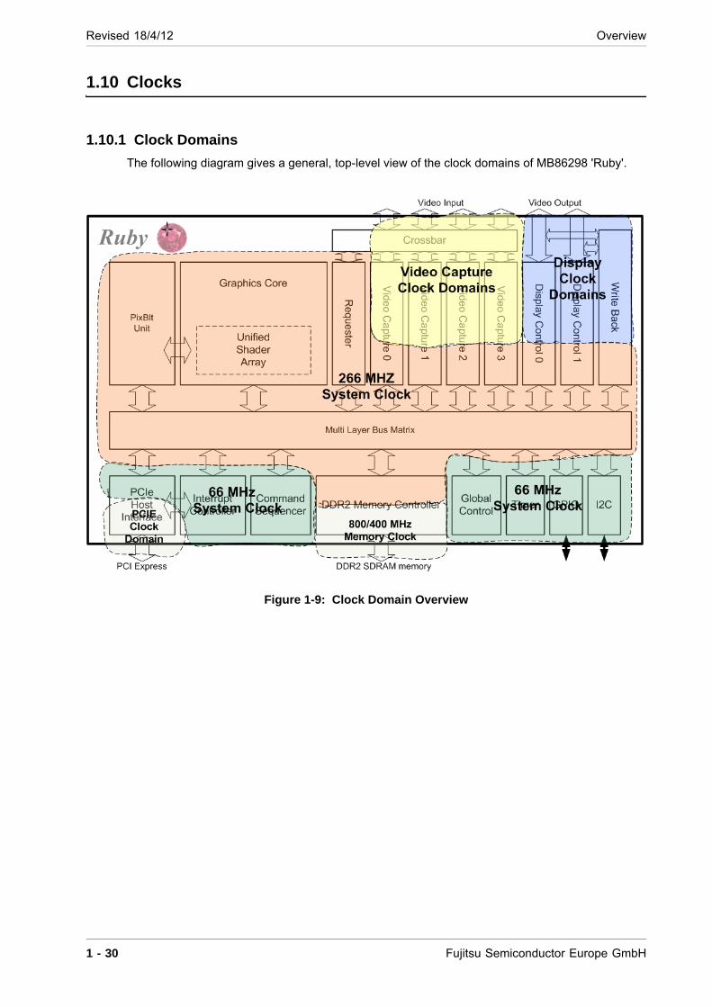
Revised 18/4/12 Overview
1.10 Clocks
1.10.1 Clock Domains
The following diagram gives a general, top-level view of the clock domains of MB86298 'Ruby'.
Figure 1-9: Clock Domain Overview
1 - 30 Fujitsu Semiconductor Europe GmbH
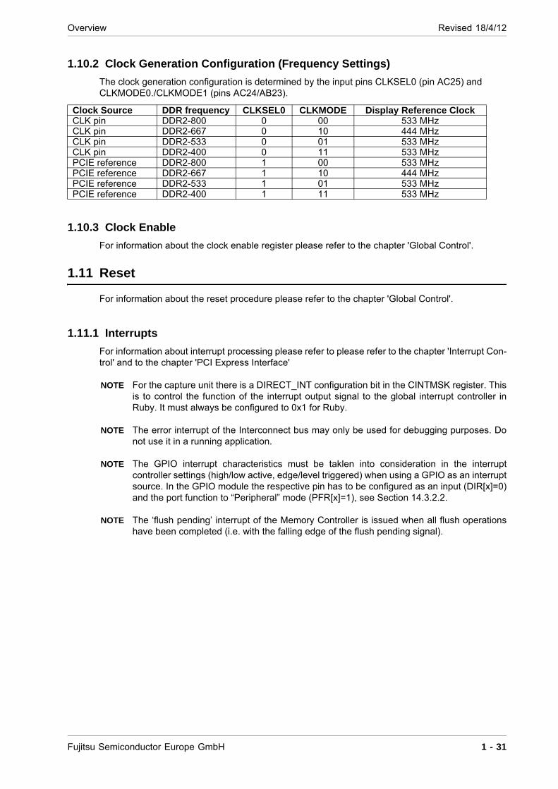
Overview Revised 18/4/12
1.10.2 Clock Generation Configuration (Frequency Settings)
The clock generation configuration is determined by the input pins CLKSEL0 (pin AC25) and CLKMODE0./CLKMODE1 (pins AC24/AB23).
1.10.3 Clock Enable
For information about the clock enable register please refer to the chapter 'Global Control'.
1.11 Reset
For information about the reset procedure please refer to the chapter 'Global Control'.
1.11.1 Interrupts
For information about interrupt processing please refer to please refer to the chapter 'Interrupt Con-trol' and to the chapter 'PCI Express Interface'
NOTE For the capture unit there is a DIRECT_INT configuration bit in the CINTMSK register. This is to control the function of the interrupt output signal to the global interrupt controller in Ruby. It must always be configured to 0x1 for Ruby.
NOTE The error interrupt of the Interconnect bus may only be used for debugging purposes. Do not use it in a running application.
NOTE The GPIO interrupt characteristics must be taklen into consideration in the interrupt controller settings (high/low active, edge/level triggered) when using a GPIO as an interrupt source. In the GPIO module the respective pin has to be configured as an input (DIR[x]=0) and the port function to “Peripheral” mode (PFR[x]=1), see Section 14.3.2.2.
NOTE The ‘flush pending’ interrupt of the Memory Controller is issued when all flush operations have been completed (i.e. with the falling edge of the flush pending signal).
Clock Source DDR frequency CLKSEL0 CLKMODE Display Reference ClockCLK pin DDR2-800 0 00 533 MHzCLK pin DDR2-667 0 10 444 MHzCLK pin DDR2-533 0 01 533 MHzCLK pin DDR2-400 0 11 533 MHzPCIE reference DDR2-800 1 00 533 MHzPCIE reference DDR2-667 1 10 444 MHzPCIE reference DDR2-533 1 01 533 MHzPCIE reference DDR2-400 1 11 533 MHz
Fujitsu Semiconductor Europe GmbH 1 - 31

Revised 18/4/12 Overview
1 - 32 Fujitsu Semiconductor Europe GmbH
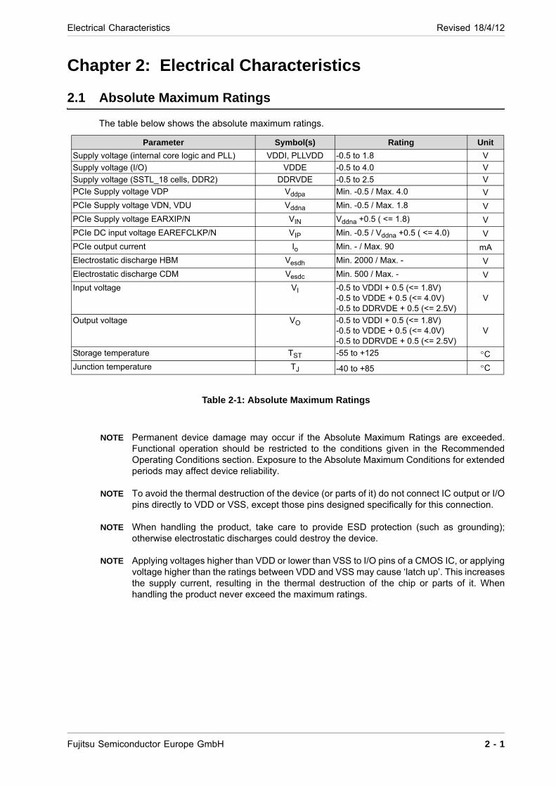
Electrical Characteristics Revised 18/4/12
Chapter 2: Electrical Characteristics
2.1 Absolute Maximum Ratings
The table below shows the absolute maximum ratings.
Table 2-1: Absolute Maximum Ratings
NOTE Permanent device damage may occur if the Absolute Maximum Ratings are exceeded. Functional operation should be restricted to the conditions given in the Recommended Operating Conditions section. Exposure to the Absolute Maximum Conditions for extended periods may affect device reliability.
NOTE To avoid the thermal destruction of the device (or parts of it) do not connect IC output or I/O pins directly to VDD or VSS, except those pins designed specifically for this connection.
NOTE When handling the product, take care to provide ESD protection (such as grounding); otherwise electrostatic discharges could destroy the device.
NOTE Applying voltages higher than VDD or lower than VSS to I/O pins of a CMOS IC, or applying voltage higher than the ratings between VDD and VSS may cause ‘latch up’. This increases the supply current, resulting in the thermal destruction of the chip or parts of it. When handling the product never exceed the maximum ratings.
Parameter Symbol(s) Rating Unit
Supply voltage (internal core logic and PLL) VDDI, PLLVDD -0.5 to 1.8 V
Supply voltage (I/O) VDDE -0.5 to 4.0 V
Supply voltage (SSTL_18 cells, DDR2) DDRVDE -0.5 to 2.5 V
PCIe Supply voltage VDP Vddpa Min. -0.5 / Max. 4.0 V
PCIe Supply voltage VDN, VDU Vddna Min. -0.5 / Max. 1.8 V
PCIe Supply voltage EARXIP/N VIN Vddna +0.5 ( <= 1.8) V
PCIe DC input voltage EAREFCLKP/N VIP Min. -0.5 / Vddna +0.5 ( <= 4.0) V
PCIe output current Io Min. - / Max. 90 mA
Electrostatic discharge HBM Vesdh Min. 2000 / Max. - V
Electrostatic discharge CDM Vesdc Min. 500 / Max. - V
Input voltage VI -0.5 to VDDI + 0.5 (<= 1.8V)-0.5 to VDDE + 0.5 (<= 4.0V)-0.5 to DDRVDE + 0.5 (<= 2.5V)
V
Output voltage VO -0.5 to VDDI + 0.5 (<= 1.8V)-0.5 to VDDE + 0.5 (<= 4.0V)-0.5 to DDRVDE + 0.5 (<= 2.5V)
V
Storage temperature TST -55 to +125 CJunction temperature TJ -40 to +85 C
Fujitsu Semiconductor Europe GmbH 2 - 1
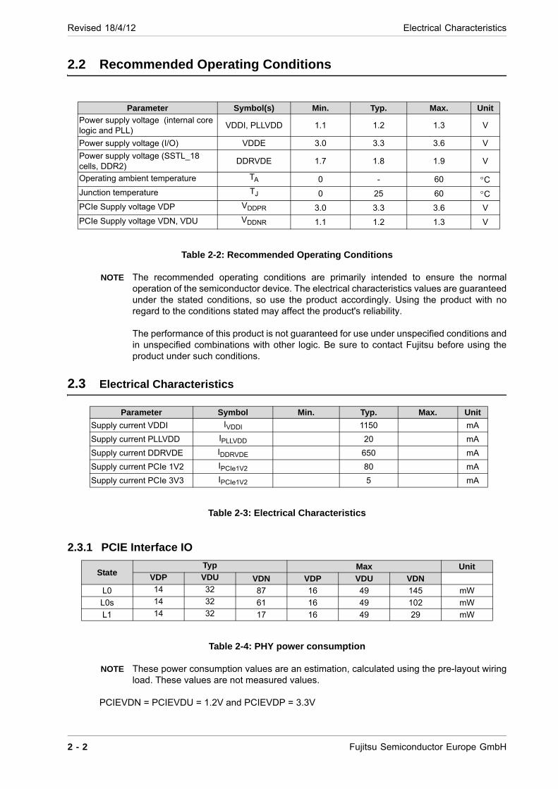
Revised 18/4/12 Electrical Characteristics
2.2 Recommended Operating Conditions
Table 2-2: Recommended Operating Conditions
NOTE The recommended operating conditions are primarily intended to ensure the normal operation of the semiconductor device. The electrical characteristics values are guaranteed under the stated conditions, so use the product accordingly. Using the product with no regard to the conditions stated may affect the product's reliability. The performance of this product is not guaranteed for use under unspecified conditions and in unspecified combinations with other logic. Be sure to contact Fujitsu before using the product under such conditions.
2.3 Electrical Characteristics
Table 2-3: Electrical Characteristics
2.3.1 PCIE Interface IO
Table 2-4: PHY power consumption
NOTE These power consumption values are an estimation, calculated using the pre-layout wiring load. These values are not measured values.
PCIEVDN = PCIEVDU = 1.2V and PCIEVDP = 3.3V
Parameter Symbol(s) Min. Typ. Max. Unit
Power supply voltage (internal core logic and PLL)
VDDI, PLLVDD 1.1 1.2 1.3 V
Power supply voltage (I/O) VDDE 3.0 3.3 3.6 V
Power supply voltage (SSTL_18 cells, DDR2)
DDRVDE 1.7 1.8 1.9 V
Operating ambient temperature TA 0 - 60 CJunction temperature TJ 0 25 60 CPCIe Supply voltage VDP VDDPR 3.0 3.3 3.6 V
PCIe Supply voltage VDN, VDU VDDNR 1.1 1.2 1.3 V
Parameter Symbol Min. Typ. Max. Unit
Supply current VDDI IVDDI 1150 mA
Supply current PLLVDD IPLLVDD 20 mA
Supply current DDRVDE IDDRVDE 650 mA
Supply current PCIe 1V2 IPCIe1V2 80 mA
Supply current PCIe 3V3 IPCIe1V2 5 mA
StateTyp Max Unit
VDP VDU VDN VDP VDU VDN
L0 14 32 87 16 49 145 mW
L0s 14 32 61 16 49 102 mW
L1 14 32 17 16 49 29 mW
2 - 2 Fujitsu Semiconductor Europe GmbH
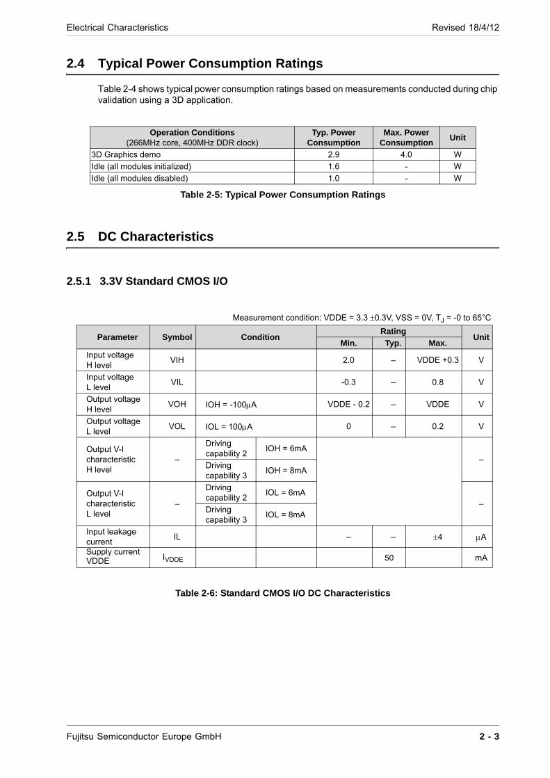
Electrical Characteristics Revised 18/4/12
2.4 Typical Power Consumption Ratings
Table 2-4 shows typical power consumption ratings based on measurements conducted during chip validation using a 3D application.
Table 2-5: Typical Power Consumption Ratings
2.5 DC Characteristics
2.5.1 3.3V Standard CMOS I/O
Table 2-6: Standard CMOS I/O DC Characteristics
Operation Conditions(266MHz core, 400MHz DDR clock)
Typ. Power Consumption
Max. Power Consumption
Unit
3D Graphics demo 2.9 4.0 W
Idle (all modules initialized) 1.6 - W
Idle (all modules disabled) 1.0 - W
Measurement condition: VDDE = 3.3 0.3V, VSS = 0V, TJ = -0 to 65°C
Parameter Symbol ConditionRating
UnitMin. Typ. Max.
Input voltage H level
VIH 2.0 – VDDE +0.3 V
Input voltage L level
VIL -0.3 – 0.8 V
Output voltage H level
VOH IOH = -100A VDDE - 0.2 – VDDE V
Output voltage L level
VOL IOL = 100A 0 – 0.2 V
Output V-I characteristicH level
–
Driving capability 2
IOH = 6mA–
Driving capability 3
IOH = 8mA
Output V-I characteristicL level
–
Driving capability 2
IOL = 6mA–
Driving capability 3
IOL = 8mA
Input leakage current
IL – – 4 A
Supply current VDDE IVDDE 50 mA
Fujitsu Semiconductor Europe GmbH 2 - 3
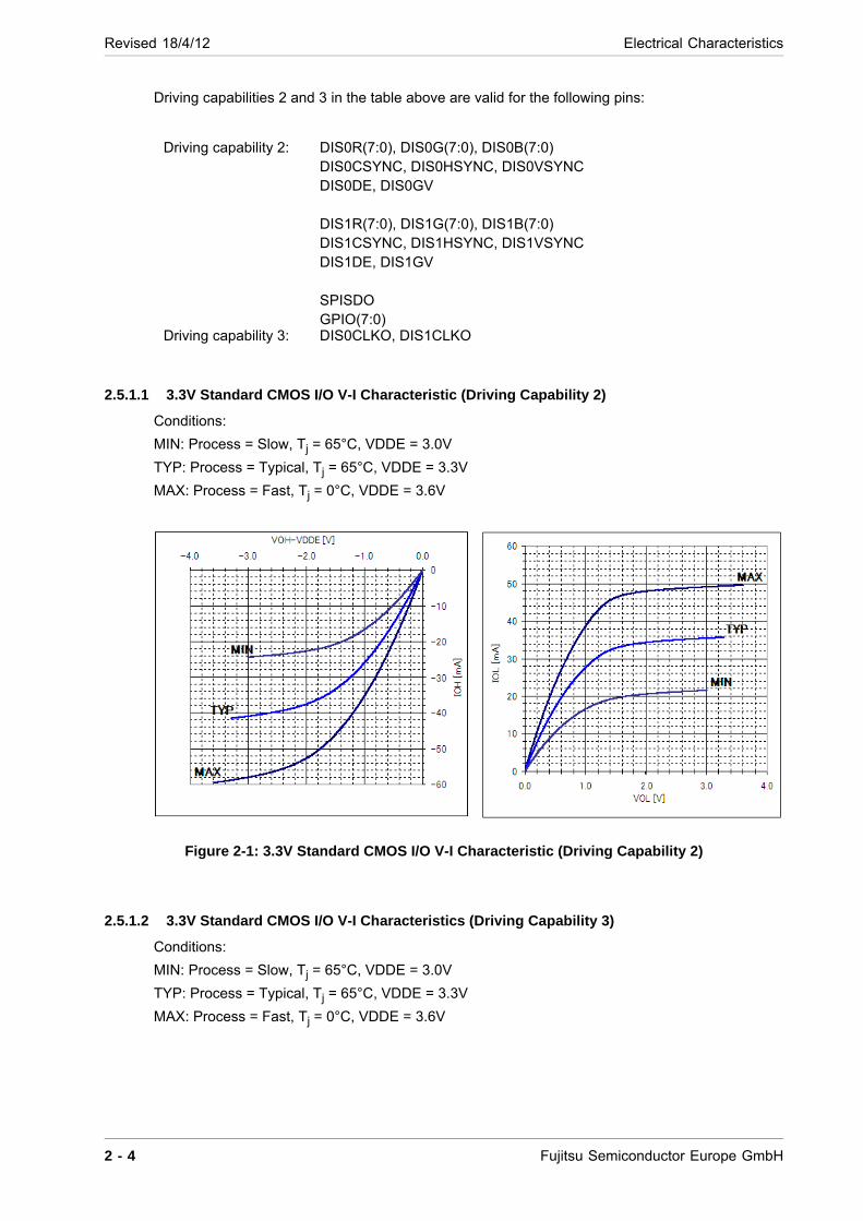
Revised 18/4/12 Electrical Characteristics
Driving capabilities 2 and 3 in the table above are valid for the following pins:
2.5.1.1 3.3V Standard CMOS I/O V-I Characteristic (Driving Capability 2)
Conditions:
MIN: Process = Slow, Tj = 65°C, VDDE = 3.0V
TYP: Process = Typical, Tj = 65°C, VDDE = 3.3V
MAX: Process = Fast, Tj = 0°C, VDDE = 3.6V
Figure 2-1: 3.3V Standard CMOS I/O V-I Characteristic (Driving Capability 2)
2.5.1.2 3.3V Standard CMOS I/O V-I Characteristics (Driving Capability 3)
Conditions:
MIN: Process = Slow, Tj = 65°C, VDDE = 3.0V
TYP: Process = Typical, Tj = 65°C, VDDE = 3.3V
MAX: Process = Fast, Tj = 0°C, VDDE = 3.6V
Driving capability 2: DIS0R(7:0), DIS0G(7:0), DIS0B(7:0)DIS0CSYNC, DIS0HSYNC, DIS0VSYNCDIS0DE, DIS0GV
DIS1R(7:0), DIS1G(7:0), DIS1B(7:0)DIS1CSYNC, DIS1HSYNC, DIS1VSYNCDIS1DE, DIS1GV
SPISDOGPIO(7:0)
Driving capability 3: DIS0CLKO, DIS1CLKO
2 - 4 Fujitsu Semiconductor Europe GmbH
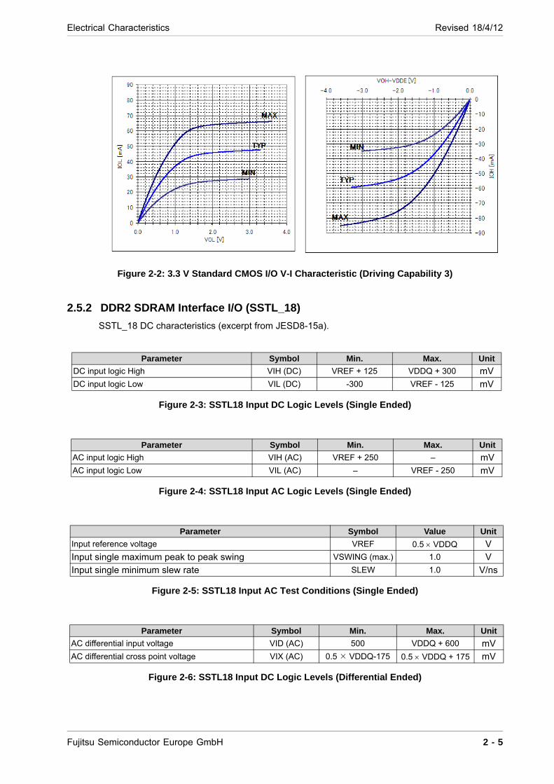
Electrical Characteristics Revised 18/4/12
Figure 2-2: 3.3 V Standard CMOS I/O V-I Characteristic (Driving Capability 3)
2.5.2 DDR2 SDRAM Interface I/O (SSTL_18)
SSTL_18 DC characteristics (excerpt from JESD8-15a).
Figure 2-3: SSTL18 Input DC Logic Levels (Single Ended)
Figure 2-4: SSTL18 Input AC Logic Levels (Single Ended)
Figure 2-5: SSTL18 Input AC Test Conditions (Single Ended)
Figure 2-6: SSTL18 Input DC Logic Levels (Differential Ended)
Parameter Symbol Min. Max. Unit
DC input logic High VIH (DC) VREF + 125 VDDQ + 300 mVDC input logic Low VIL (DC) -300 VREF - 125 mV
Parameter Symbol Min. Max. Unit
AC input logic High VIH (AC) VREF + 250 – mVAC input logic Low VIL (AC) – VREF - 250 mV
Parameter Symbol Value Unit
Input reference voltage VREF 0.5 VDDQ V
Input single maximum peak to peak swing VSWING (max.) 1.0 V
Input single minimum slew rate SLEW 1.0 V/ns
Parameter Symbol Min. Max. Unit
AC differential input voltage VID (AC) 500 VDDQ + 600 mVAC differential cross point voltage VIX (AC) 0.5 VDDQ-175 0.5 VDDQ + 175 mV
Fujitsu Semiconductor Europe GmbH 2 - 5
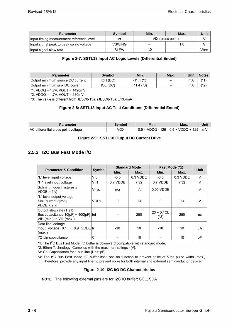
Revised 18/4/12 Electrical Characteristics
Figure 2-7: SSTL18 Input AC Logic Levels (Differential Ended)
Figure 2-8: SSTL18 Input AC Test Conditions (Differential Ended)
Figure 2-9: SSTL18 Output DC Current Drive
2.5.3 I2C Bus Fast Mode I/O
Figure 2-10: I2C I/O DC Characteristics
NOTE The following external pins are for I2C IO buffer: SCL, SDA
Parameter Symbol Min. Max. Unit
Input timing measurement reference level Vr VIX (cross point) VInput signal peak to peak swing voltage VSWING – 1.0 VInput signal slew rate SLEW 1.0 – V/ns
Parameter Symbol Min. Max. Unit Notes
Output minimum source DC current IOH (DC) -11.4 (*3) – mA (*1)
Output minimum sink DC current IOL (DC) 11.4 (*3) – mA (*2)
*1: VDDQ = 1.7V, VOUT = 1420mV*2: VDDQ = 1.7V, VOUT = 280mV*3: The value is different from JESD8-15a. (JESD8-15a: 13.4mA)
Parameter Symbol Min. Max. Unit
AC differential cross point voltage VOX 0.5 × VDDQ - 125 0.5 × VDDQ + 125 mV
Parameter & Condition SymbolStandard Mode Fast Mode (*1)
UnitMin. Max. Min. Max.
"L" level input voltage VIL -0.5 0.3 VDDE -0.5 0.3 VDDE V
"H" level input voltage VIH 0.7 VDDE (*2) 0.7 VDDE (*2) V
Schmitt trigger hysteresisVDDE > 2[v]
Vhys n/a n/a 0.05 VDDE – V
"L" level output voltageSink current 3[mA]VDDE > 2[v]
VOL1 0 0.4 0 0.4 V
Output slew rate (Tfall)Bus capacitance 10[pF] ~ 400[pF]VIH (min.) to VIL (max.)
tof – 25020 + 0.1Cb
(*3)250 ns
Data line leakageInput voltage 0.1 ~ 0.9 VDDE (max.)
Ii -10 10 -10 10 A
I/O pin capacitance Ci – 10 – 10 pF
*1: The I2C Bus Fast Mode I/O buffer is downward compatible with standard mode.*2: 90nm Technology: Complies with the maximum ratings 4[V]. *3: Cb: Capacitance for 1 bus line (Unit: pF).
*4: The I2C Bus Fast Mode I/O buffer itself has no function to prevent spike of 50ns pulse width (max.). Therefore, provide any input filter to prevent spike for both internal and external semiconductor device.
2 - 6 Fujitsu Semiconductor Europe GmbH
Electrical Characteristics Revised 18/4/12
2.5.4 I2C IO V-1 Characteristic Figure
Figure 2-11: I2C V-I Characteristic Figure
Voltage (V)
Cur
rent
(A
)
Fujitsu Semiconductor Europe GmbH 2 - 7
Revised 18/4/12 Electrical Characteristics
2.6 AC Characteristics
In this chapter, the signal timing of external ports is described.
2.6.1 PCIE Interface Signal Timing
2.6.1.1 PCIe Transmitter Characteristics
Table 2-7: PCIe Transmitter Characteristics
Characteristic Symbol MIN TYP MAX Unit NotesUnit interval Ttxd 399.88 400 400.12 ps +-300ppm (*1)SSCTx output rise/fall time
Trf 0.125 - - UI
Tx eye width Teyetx 0.75 - - UIMax. time between the jitter median and max. deviation from the median
Tmedtx - - 0.125 UI
Transition to electrical idle time
Tidle - - 6 UI
Transition to valid output time after electrical idle
Tact - - 20 UI
Tx DC common mode voltage
Vcmdctx - - 1.3 V
RMS AC peak common mode output voltage
Vcmacptx - - 20 mVVcmacptx=RMS(Vcmactx-Vcmdctx)Vcmactx=(EXTXOP+EXTXON)/2Vcmdctx=DC of (EXTXOP+EXTXON)/2
Absolute Delta of DC Commonmode voltage During L0 andElectircal Idle
Vcmeitx 0 - 100 mV (Vcmdctx-Vcm[electrical idle]) ?100mV
Absolute Delta of DC Commonmode voltage between EXTXOPand EXTXON
Vcmdcline 0 - 25 mV(Vcmdctxop-Vcmdctxon) ?25mVVcmdctxop= DC of EXTXOPVcmdctxon= DC of EXTXON
Electrical Idle Differential PeakOutput voltage
Vcmdiff 0 - 20 mV (Vidletxop-Vidletxon) ?20mV
Differential Peak to Peakoutput voltage
Vdifftx 800 - 1200 mV Vdifftx=2*(EXTXOP-EXTXON)
Pre-emphasized differentialoutput voltage (Ratio)
Vratiotx -4.0 -3.5 -3.0 dB
Tx DC differential outputimpedance
Zdifftx 80 100 120 ohm
Lane to lane output skew
Tskwtx - - 500+2UI psStatic skew between any two transmitter lanes within a single link
Transmission latency
Ttxlate - - 37 UIFrom 16 bits parallel data loading to output of first bit
Rx detection initial data set time
Trdsetei 100 - - ns
Rx detection data set time
Trdset 10 - 11µs
Rx detection status strobe
Tgetst 100 - - ns
The amount of voltage change at Rxdetection
Vrxdet - - 600 mV
Differential return loss
Rldifftx 10 - - dB
Common mode return loss
RLcmtx 6 - - dB
Tx short circuit current limit
Itxshort - - 90 mAThe total current the transmitter can provide when shorted to its ground
AC coupling capacitor
Ctx 75 - 200 nF
2 - 8 Fujitsu Semiconductor Europe GmbH
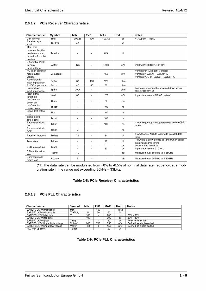
Electrical Characteristics Revised 18/4/12
2.6.1.2 PCIe Receiver Characteristics
(*1) The data rate can be modulated from +0% to -0.5% of nominal data rate frequency, at a mod-ulation rate in the range not exceeding 30kHz – 33kHz.
Table 2-8: PCIe Receiver Characteristics
2.6.1.3 PCIe PLL Characteristics
Table 2-9: PCIe PLL Characteristics
Characteristic Symbol MIN TYP MAX Unit NotesUnit interval Trxd 399.88 400 400.12 ps +-300ppm (*1)SSCReceiver eye width
Trx-eye 0.4 - - UI
Max. time between the jitter median and max. deviation from the median
Tmedrx - - 0.3 UI
Differential Peak to PeakInput voltage
Vdiffrx 175 - 1200 mV Vdiffrx=2*(EXTXIP-EXTXIN)
AC peak common mode output voltage
Vcmacprx - - 150 mVVcmacprx= (Vcmacrx-Vcmdcrx)Vcmacrx=(EXTXIP+EXTXIN)/2Vcmdcrx=DC of (EXTXIP+EXTXIN)/2
Rx differential input impedance
Zdiffrx 80 100 120 ohm
Rx DC impedance Zdcrx 40 50 60 ohmPower down DC input impedance
Zpdrx 200k - - ohmLosdetector should be powered down when RXLOSDETPD=1
Input signal threshold
Vrsd 65 - 175 mV Input data stream '8B10B pattern'
LosDetector power on
Tbcon - - 20 µs
LosDetector power down
Tbcoff - - 100 ns
Signal lost detect time
Tlos - - 100 ns
Signal exists detect time
Texist - - 100 ns
Recovered clock ON
Tckon - - 100 nsClock frequency is not guaranteed before CDR lockup
Recovered clock OFF
Tckoff 0 - - ns
Receiver latecncy Trxlate 19 - 34 UIFrom the first 16 bits loading to parallel data input
Total skew Tskwrx - - 16 UITskwrx is a skew across all lanes when serial data input same timing
CDR lockup time Trlock--
--
120
µsµs
Lockup time from L0sInput data stream '01010...'
Differential return loss
Rldiffrx 10 - - dB Measured over 50 MHz to 1.25GHz
Common mode return loss
RLcmrx 6 - - dB Measured over 50 MHz to 1.25GHz
Characteristic Symbol MIN TYP MAX Unit NotesEAREFCLKP/N frequency fref 100 MHzEAREFCLKP/N duty cycle Trefduty 40 50 60 %EAREFCLKP/N rise time Tr 100 - 700 ps 20% - 80%EAREFCLKP/N fall time Tf 100 - 700 ps 20% - 80%EAREFCLKP/N jitter Tjrefp - - 40 ps Peak to Peak jitterEAREFCLKP/N input high voltage Vohref 660 710 850 mV Defined as single-endedEAREFCLKP/N input low voltage Volref -150 0 150 mV Defined as single-endedPLL lock up time Tplock - - 20 µs
Fujitsu Semiconductor Europe GmbH 2 - 9
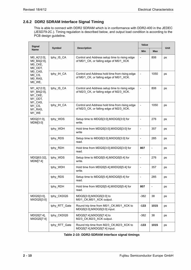
Revised 18/4/12 Electrical Characteristics
2.6.2 DDR2 SDRAM Interface Signal Timing
This is able to connect with DDR2 SDRAM which is in conformance with DDR2-400 in the JEDEC (JESD79-2C.). Timing regulation is described below, and output load condition is according to the PCB design guideline.
Signal Name
Symbol DescriptionValue
UnitMin Max
M0_A[12:0],M0_BA[2:0],M0_CKE,M0_ODT,M0_CAS,M0_CS,M0_RAS,M0_WE,
tphy_IS_CA Control and Address setup time to rising edge of M0/1_CK, or falling edge of M0/1_XCK
- 806 ps
tphy_IH_CA Control and Address hold time from rising edge of M0/1_CK, or falling edge of M0/1_XCK.
- 1050 ps
M1_A[12:0],M1_BA[2:0],M1_CKE,M1_ODT,M1_CAS,M1_CS,M1_RAS,M1_WE
tphy_IS_CA Control and Address setup time to rising edge of M2/3_CK, or falling edge of M2/3_XCK.
- 806 ps
tphy_IH_CA Control and Address hold time from rising edge of M2/3_CK, or falling edge of M2/3_XCK.
- 1050 ps
MDQ[31:0],MDM[3:0]
tphy_WDS Setup time to MDQS[3:0],MXDQS[3:0] for write.
- 276 ps
tphy_WDH Hold time from MDQS[3:0],MXDQS[3:0] for write
- 357 ps
tphy_RDS Setup time to MDQS[3:0],MXDQS[3:0] for read.
- 285 ps
tphy_RDH Hold time from MDQS[3:0],MXDQS[3:0] for read.
807 - ps
MDQ[63:32],MDM[7:4]
tphy_WDS Setup time to MDQS[5:4],MXDQS[5:4] for write.
- 276 ps
tphy_WDH Hold time from MDQS[5:4],MXDQS[5:4] for write.
- 357 ps
tphy_RDS Setup time to MDQS[5:4],MXDQS[5:4] for read.
- 285 ps
tphy_RDH Hold time from MDQS[5:4],MXDQS[5:4] for read.
807 - ps
MDQS[3:0],MXDQS[3:0]
tphy_CKDQS MDQS[3:0],MXDQS[3:0] to M0/1_CK,M0/1_XCK output.
-382 38 ps
tphy_RTT_Gate Round trip time from M0/1_CK,M0/1_XCK to MDQS[3:0],MXDQS[3:0] input.
-133 1015 ps
MDQS[7:4],MXDQS[7:4]
tphy_CKDQS MDQS[7:4],MXDQS[7:4] to M2/3_CK,M2/3_XCK output.
-382 38 ps
tphy_RTT_Gate Round trip time from M2/3_CK,M2/3_XCK to MDQS[7:4],MXDQS[7:4] input.
-133 1015 ps
Table 2-10: DDR2-SDRAM Interface signal timings
2 - 10 Fujitsu Semiconductor Europe GmbH
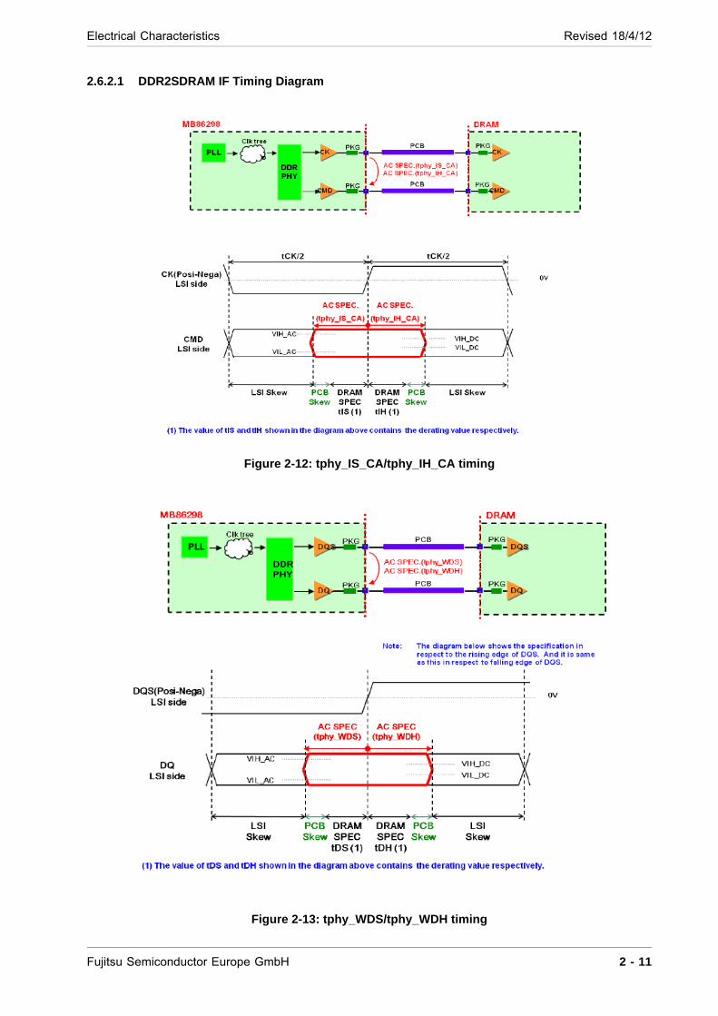
Electrical Characteristics Revised 18/4/12
2.6.2.1 DDR2SDRAM IF Timing Diagram
Figure 2-12: tphy_IS_CA/tphy_IH_CA timing
Figure 2-13: tphy_WDS/tphy_WDH timing
Fujitsu Semiconductor Europe GmbH 2 - 11
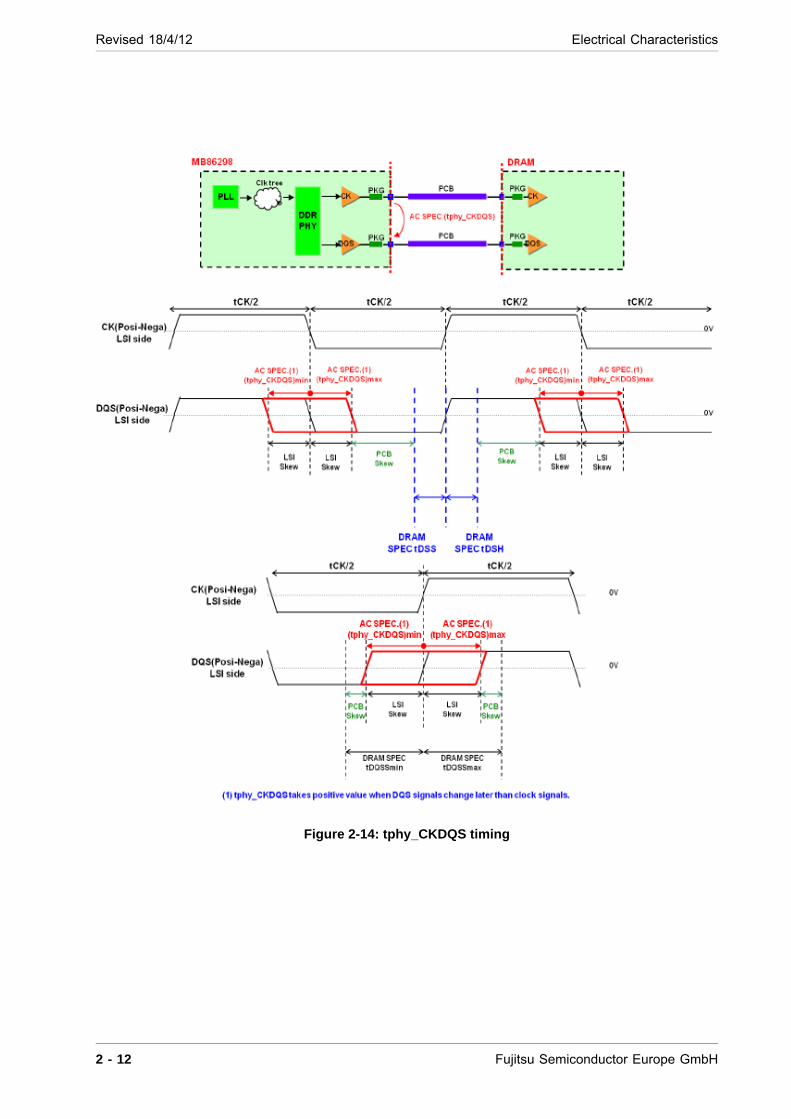
Revised 18/4/12 Electrical Characteristics
Figure 2-14: tphy_CKDQS timing
2 - 12 Fujitsu Semiconductor Europe GmbH
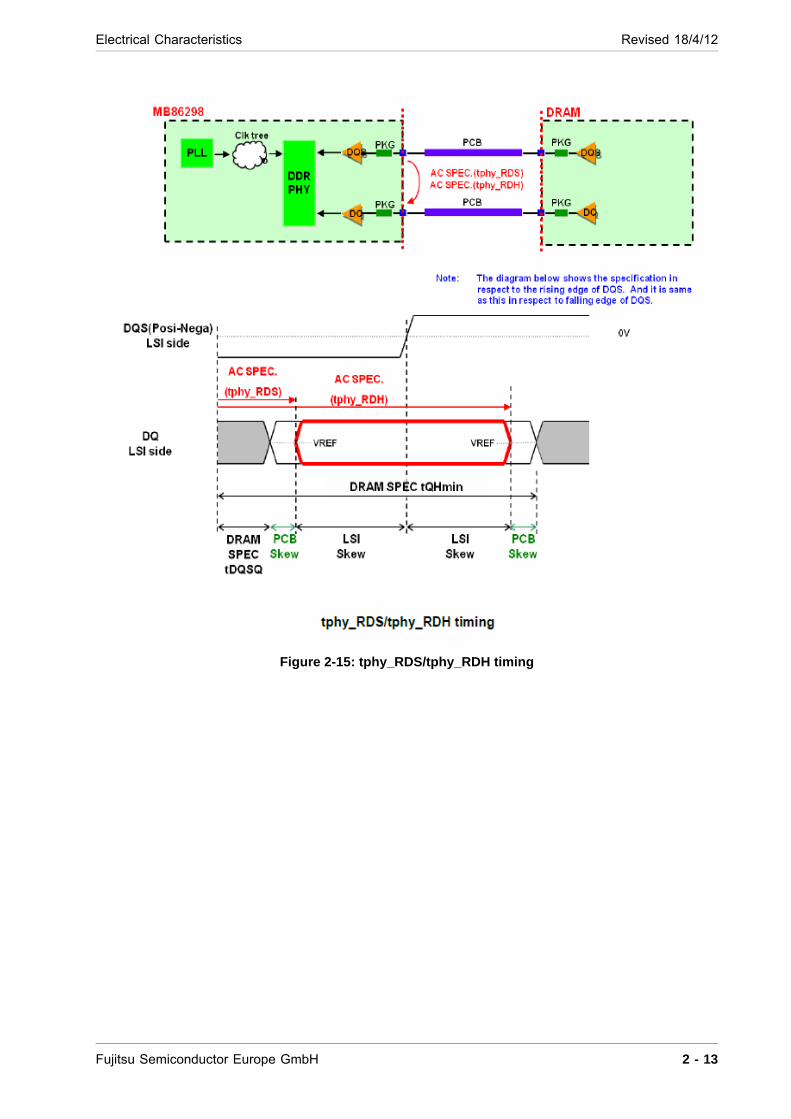
Electrical Characteristics Revised 18/4/12
Figure 2-15: tphy_RDS/tphy_RDH timing
Fujitsu Semiconductor Europe GmbH 2 - 13
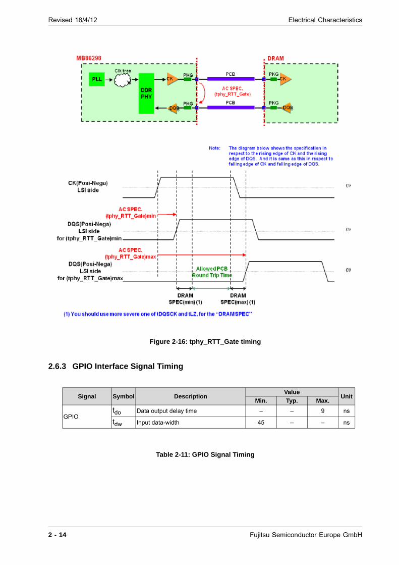
Revised 18/4/12 Electrical Characteristics
Figure 2-16: tphy_RTT_Gate timing
2.6.3 GPIO Interface Signal Timing
Table 2-11: GPIO Signal Timing
Signal Symbol DescriptionValue
UnitMin. Typ. Max.
GPIOtdo Data output delay time – – 9 ns
tdw Input data-width 45 – – ns
2 - 14 Fujitsu Semiconductor Europe GmbH
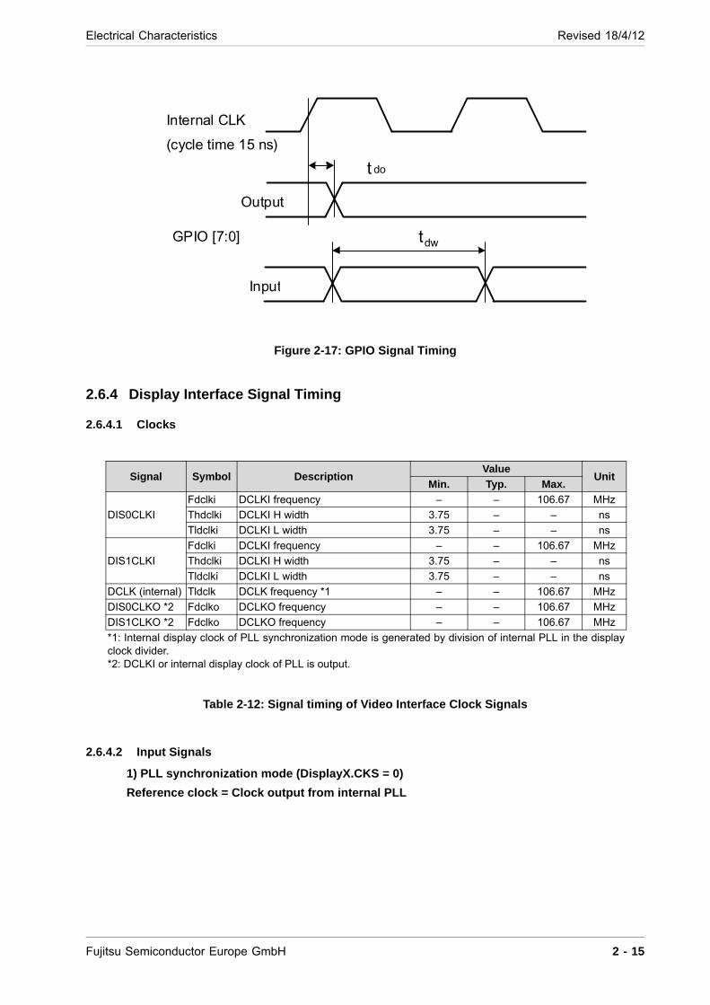
Electrical Characteristics Revised 18/4/12
Figure 2-17: GPIO Signal Timing
2.6.4 Display Interface Signal Timing
2.6.4.1 Clocks
Table 2-12: Signal timing of Video Interface Clock Signals
2.6.4.2 Input Signals
1) PLL synchronization mode (DisplayX.CKS = 0)
Reference clock = Clock output from internal PLL
Signal Symbol DescriptionValue
UnitMin. Typ. Max.
DIS0CLKI
Fdclki DCLKI frequency – – 106.67 MHz
Thdclki DCLKI H width 3.75 – – ns
Tldclki DCLKI L width 3.75 – – ns
DIS1CLKI
Fdclki DCLKI frequency – – 106.67 MHz
Thdclki DCLKI H width 3.75 – – ns
Tldclki DCLKI L width 3.75 – – ns
DCLK (internal) Tldclk DCLK frequency *1 – – 106.67 MHz
DIS0CLKO *2 Fdclko DCLKO frequency – – 106.67 MHz
DIS1CLKO *2 Fdclko DCLKO frequency – – 106.67 MHz
*1: Internal display clock of PLL synchronization mode is generated by division of internal PLL in the display clock divider.*2: DCLKI or internal display clock of PLL is output.
GPIO [7:0]
Input
t do
tdw
Output
Internal CLK (cycle time 15 ns)
Fujitsu Semiconductor Europe GmbH 2 - 15

Revised 18/4/12 Electrical Characteristics
Figure 2-18: Signal Timing of Video Interface Input Signal (1)
2) DCLKI synchronization mode (DisplayX.CKS = 1)
Reference clock = DCLKI
Table 2-13: Display Input Signal Timing
Figure 2-19: Display Input Signal Timing
2.6.4.3 Output Signals
Signal Symbol DescriptionValue
UnitMin. Typ. Max.
DIS0HSYNC Twhsync HSYNC input pulse width 3 – – Clock
DIS1HSYNC Twhsync HSYNC input pulse width 3 – – Clock
DIS0VSYNC Twvsync VSYNC input pulse width 1 – – HSYNC
DIS1VSYNC Twvsync VSYNC input pulse width 1 – – HSYNC
Signal Symbol DescriptionValue
UnitMin. Typ. Max.
DIS0HSYNC
Twhsync HSYNC input pulse width 3 – – Clock
Tshsync HSYNC Input setup time 5.0 – – ns
Thhsync HSYNC Input hold time 0.5 – – ns
DIS1HSYNC
Twhsync HSYNC input pulse width 3.0 – – Clock
Tshsync HSYNC Input setup time 5.0 – – ns
Thhsync HSYNC Input hold time 0.5 – – ns
DIS0VSYNC Twvsync VSYNC input pulse width 1 – – HSYNC
DIS1VSYNC Twvsync VSYNC input pulse width 1 – – HSYNC
Signal Symbol DescriptionValue
UnitMin. Typ. Max.
DIS0R/G/B[7:0] Tdrgb RGB output delay time 1 – 6 ns
Twvsync
DISxCLK
DISxHSYNC
Tshsync Thhsync
Thdclki Tldclki 1/Fdclki
DISxVSYNC
Tsvsync Thvsync
Twhsync
2 - 16 Fujitsu Semiconductor Europe GmbH

Electrical Characteristics Revised 18/4/12
Table 2-14: Signal Timing of Video Interface Output Signal
Figure 2-20: Display Output Signal Timing
2.6.5 Video Capture Signal Timing
2.6.5.1 Clocks
DIS1R/G/B[7:0] Tdrgb RGB output delay time 1 – 6 ns
DIS0HSYNC Tdhsync HSYNC output delay time 1 – 6 ns
DIS1HSYNC Tdhsync HSYNC output delay time 1 – 6 ns
DIS0VSYNC Tdvsync VSYNC output delay time 1 – 6 ns
DIS1VSYNC Tdvsync VSYNC output delay time 1 – 6 ns
DIS0CSYNC Tdcsync CSYNC output delay time 1 – 6 ns
DIS1CSYNC Tdcsync CSYNC output delay time 1 – 6 ns
DIS0DE Tdde DE output delay time 1 – 6 ns
DIS1DE Tdde DE output delay time 1 – 6 ns
DIS0GV Tdgv GV output delay time 1 – 6 ns
DIS1GV Tdgv GV output delay time 1 – 6 ns
Note: If hold time is insufficient inverting or shifting of DCLKO clock is recommended.
Signal Symbol DescriptionValue
UnitMin. Typ. Max.
DISxCLKO (inverted)
DISxCLKO
DISxHSYNC
1/Fdclko
DISxVSYNC
DISxR/G/B
Tdrgb
DISxCSYNC
DISxDE
Tdhsync
Tdvsync
Tdcsync
Tdde
Tdgv
DISxGV
Fujitsu Semiconductor Europe GmbH 2 - 17
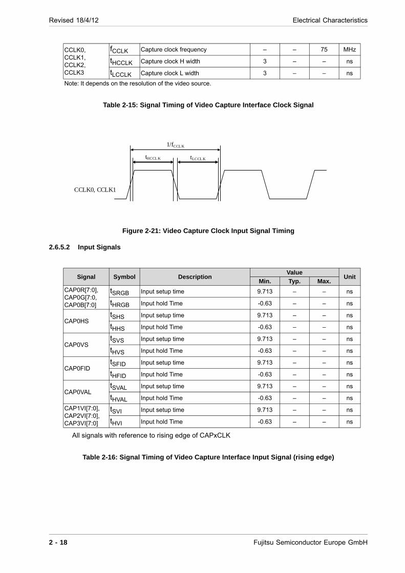
Revised 18/4/12 Electrical Characteristics
Table 2-15: Signal Timing of Video Capture Interface Clock Signal
Figure 2-21: Video Capture Clock Input Signal Timing
2.6.5.2 Input Signals
All signals with reference to rising edge of CAPxCLK
Table 2-16: Signal Timing of Video Capture Interface Input Signal (rising edge)
CCLK0,CCLK1,CCLK2,CCLK3
fCCLK Capture clock frequency – – 75 MHz
tHCCLK Capture clock H width 3 – – ns
tLCCLK Capture clock L width 3 – – ns
Note: It depends on the resolution of the video source.
Signal Symbol DescriptionValue
UnitMin. Typ. Max.
CAP0R[7:0],CAP0G[7:0,CAP0B[7:0]
tSRGB Input setup time 9.713 – – ns
tHRGB Input hold Time -0.63 – – ns
CAP0HStSHS Input setup time 9.713 – – ns
tHHS Input hold Time -0.63 – – ns
CAP0VStSVS Input setup time 9.713 – – ns
tHVS Input hold Time -0.63 – – ns
CAP0FIDtSFID Input setup time 9.713 – – ns
tHFID Input hold Time -0.63 – – ns
CAP0VALtSVAL Input setup time 9.713 – – ns
tHVAL Input hold Time -0.63 – – ns
CAP1VI[7:0],CAP2VI[7:0],CAP3VI[7:0]
tSVI Input setup time 9.713 – – ns
tHVI Input hold Time -0.63 – – ns
1/fCCL K
tLCCL K tHCCL K
CCLK0, CCLK1
2 - 18 Fujitsu Semiconductor Europe GmbH
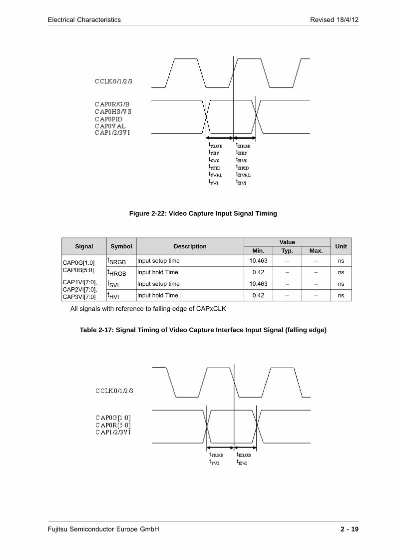
Electrical Characteristics Revised 18/4/12
Figure 2-22: Video Capture Input Signal Timing
All signals with reference to falling edge of CAPxCLK
Table 2-17: Signal Timing of Video Capture Interface Input Signal (falling edge)
Signal Symbol DescriptionValue
UnitMin. Typ. Max.
CAP0G[1:0]CAP0B[5:0]
tSRGB Input setup time 10.463 – – ns
tHRGB Input hold Time 0.42 – – ns
CAP1VI[7:0],CAP2VI[7:0],CAP3VI[7:0]
tSVI Input setup time 10.463 – – ns
tHVI Input hold Time 0.42 – – ns
Fujitsu Semiconductor Europe GmbH 2 - 19

Revised 18/4/12 Electrical Characteristics
2.6.6 I2C Interface Signal Timing
Table 2-18: Signal timing of I2C signal
Signal Symbol DescriptionValue
UnitMin. Typ. Max.
I2C_SDA0I2C_SDA1
TS2SDAISDAI setup time
Normal mode 250 (*1) – – ns
High-speed mode 100 (*1) – – ns
TH2SDAISDAI hold time
Normal mode 0.0 (*1) – – ns
High-speed mode 0.0 (*1) – – ns
TWBFI BUS free timeNormal mode 4.7 (*1) – – µs
High-speed mode 1.3 (*1) – – µs
I2C_SCL0I2C_SCL1
TCSCLISCLI cycle time
Normal mode 1.0 (*1) – – µs
High-speed mode 2.5 (*1) – – µs
TWHSCLI
SCLI H widthNormal mode 4.0 (*1) – – µs
High-speed mode 0.6 (*1) – – µs
TWLSCLI SCLI L widthNormal mode 4.7 (*1) – – µs
High-speed mode 1.3 (*1) – – µs
TCSCLOSCLO cycle time
Normal mode 2*m + 2 (*2) – – PCLK (*3)
High-speed mode Int (1.5*m) + 2 (*2) – – PCLK (*3)
TWHSCLO
SCLO H widthNormal mode m + 2 (*2) – – PCLK (*3)
High-speed mode Int (0.5*m) + 2 (*2) – – PCLK (*3)
TWLSCLO
SCLO L widthNormal mode m (*2) – – PCLK (*3)
High-speed mode m (*2) – – PCLK (*3)
TS2SCLISCLI setup time
Normal mode 4.0 (*2) – – µs
High-speed mode 0.6 (*2) – – µs
TH2SCLI SCLI hold timeNormal mode 4.7 (*2) – – µs
High-speed mode 1.3 (*2) – – µs
*1: I2C bus specification value
*2: See I2C bus interface's clock control register (I2CxCCR) of the MB86298 LSI product specifications for the "m" value*3: PCLK = 66 MHz
2 - 20 Fujitsu Semiconductor Europe GmbH

Electrical Characteristics Revised 18/4/12
Figure 2-23: I2C Access Timing
Fujitsu Semiconductor Europe GmbH 2 - 21

Revised 18/4/12 Electrical Characteristics
Figure 2-24: I2C Stop/Start/Restart Timing
2 - 22 Fujitsu Semiconductor Europe GmbH
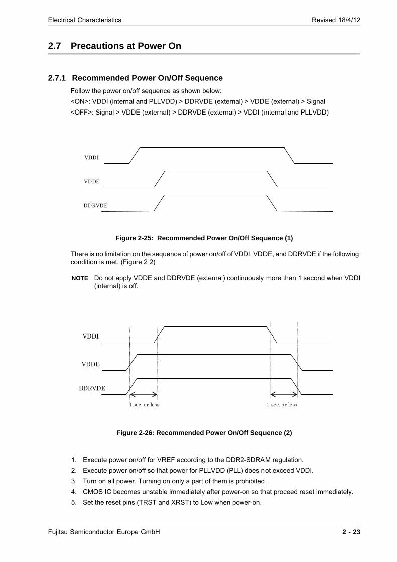
Electrical Characteristics Revised 18/4/12
2.7 Precautions at Power On
2.7.1 Recommended Power On/Off Sequence
Follow the power on/off sequence as shown below:
<ON>: VDDI (internal and PLLVDD) > DDRVDE (external) > VDDE (external) > Signal
<OFF>: Signal > VDDE (external) > DDRVDE (external) > VDDI (internal and PLLVDD)
Figure 2-25: Recommended Power On/Off Sequence (1)
There is no limitation on the sequence of power on/off of VDDI, VDDE, and DDRVDE if the following condition is met. (Figure 2 2)
NOTE Do not apply VDDE and DDRVDE (external) continuously more than 1 second when VDDI (internal) is off.
Figure 2-26: Recommended Power On/Off Sequence (2)
1. Execute power on/off for VREF according to the DDR2-SDRAM regulation.
2. Execute power on/off so that power for PLLVDD (PLL) does not exceed VDDI.
3. Turn on all power. Turning on only a part of them is prohibited.
4. CMOS IC becomes unstable immediately after power-on so that proceed reset immediately.
5. Set the reset pins (TRST and XRST) to Low when power-on.
VDDI
VDDE
DDRVDE
VDDE
1 sec. or less
VDDI
1 sec. or less
DDRVDE
Fujitsu Semiconductor Europe GmbH 2 - 23
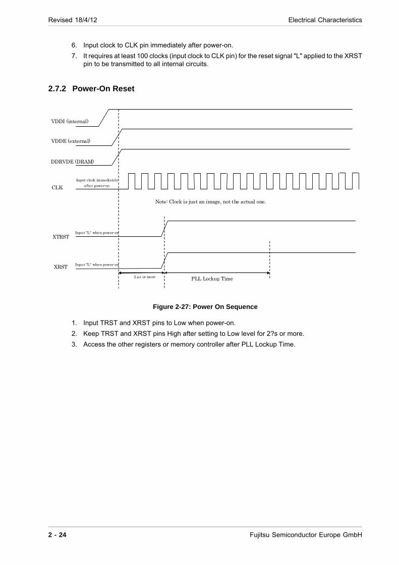
Revised 18/4/12 Electrical Characteristics
6. Input clock to CLK pin immediately after power-on.
7. It requires at least 100 clocks (input clock to CLK pin) for the reset signal "L" applied to the XRST pin to be transmitted to all internal circuits.
2.7.2 Power-On Reset
Figure 2-27: Power On Sequence
1. Input TRST and XRST pins to Low when power-on.
2. Keep TRST and XRST pins High after setting to Low level for 2?s or more.
3. Access the other registers or memory controller after PLL Lockup Time.
VDDE (external)
DDRVDE (DRAM)
XRST
XTRST
Note: Clock is just an image, not the actual one.
CLK
Input "L" when power-on
Input clock immediatelyafter power-on
PLL Lockup Time
VDDI (internal)
Input "L" when power-on
2 s or more
2 - 24 Fujitsu Semiconductor Europe GmbH
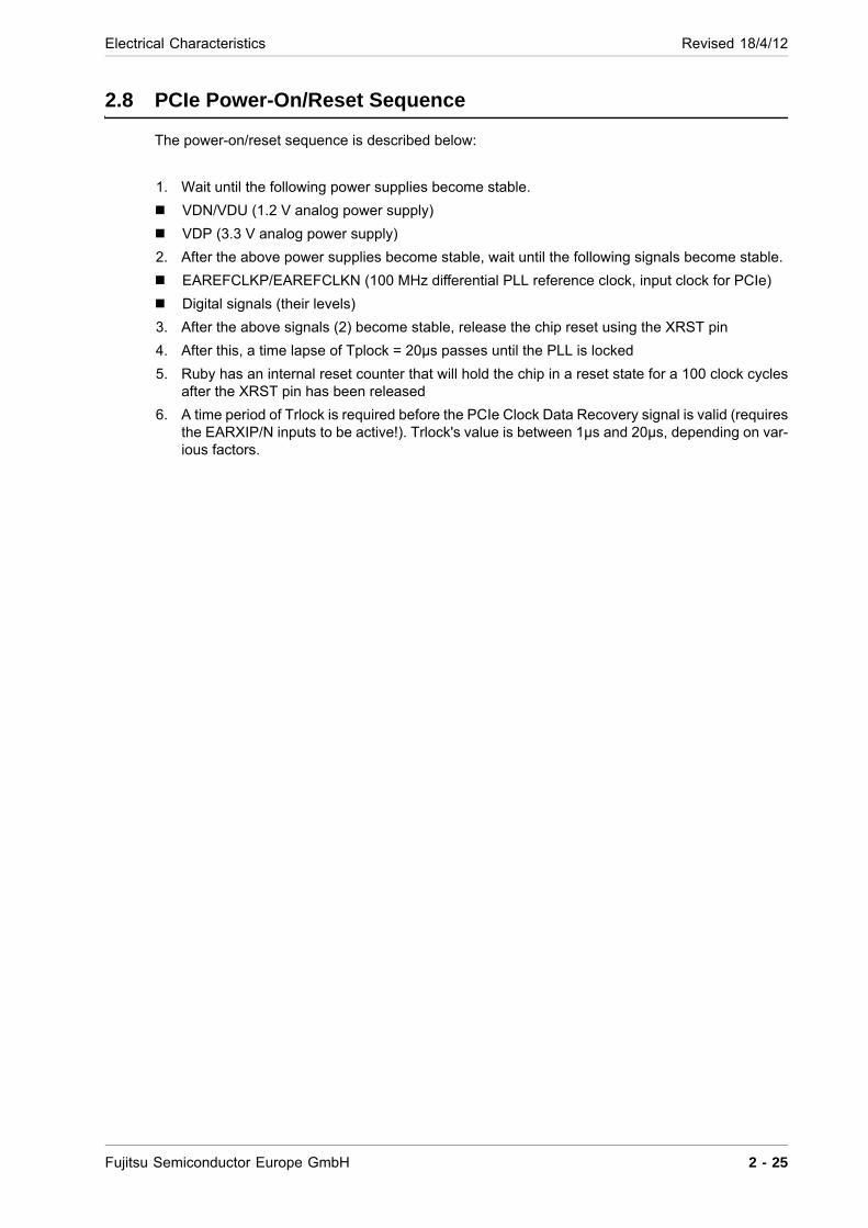
Electrical Characteristics Revised 18/4/12
2.8 PCIe Power-On/Reset Sequence
The power-on/reset sequence is described below:
1. Wait until the following power supplies become stable.
VDN/VDU (1.2 V analog power supply)
VDP (3.3 V analog power supply)
2. After the above power supplies become stable, wait until the following signals become stable.
EAREFCLKP/EAREFCLKN (100 MHz differential PLL reference clock, input clock for PCIe)
Digital signals (their levels)
3. After the above signals (2) become stable, release the chip reset using the XRST pin
4. After this, a time lapse of Tplock = 20µs passes until the PLL is locked
5. Ruby has an internal reset counter that will hold the chip in a reset state for a 100 clock cycles after the XRST pin has been released
6. A time period of Trlock is required before the PCIe Clock Data Recovery signal is valid (requires the EARXIP/N inputs to be active!). Trlock's value is between 1µs and 20µs, depending on var-ious factors.
Fujitsu Semiconductor Europe GmbH 2 - 25
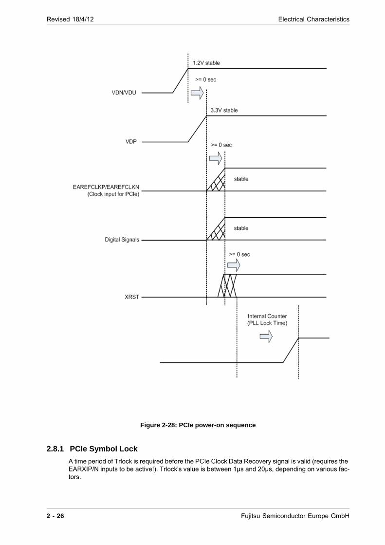
Revised 18/4/12 Electrical Characteristics
Figure 2-28: PCIe power-on sequence
2.8.1 PCIe Symbol Lock
A time period of Trlock is required before the PCIe Clock Data Recovery signal is valid (requires the EARXIP/N inputs to be active!). Trlock's value is between 1µs and 20µs, depending on various fac-tors.
2 - 26 Fujitsu Semiconductor Europe GmbH
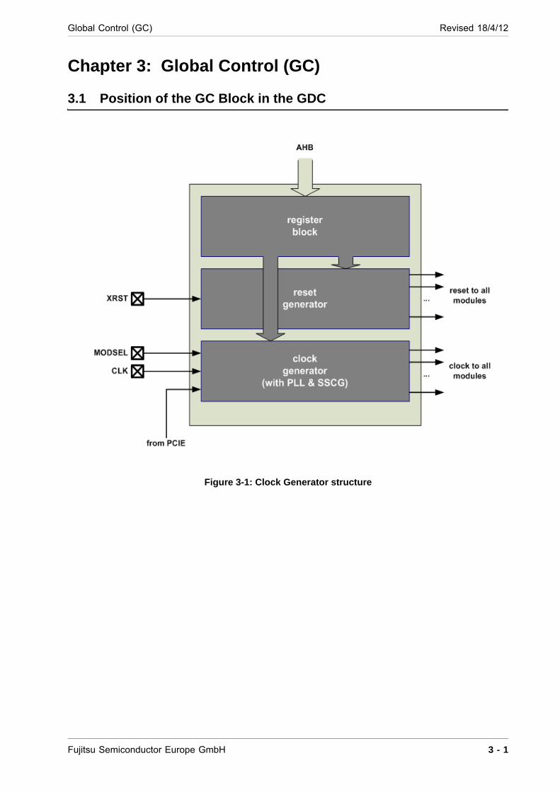
Global Control (GC) Revised 18/4/12
Chapter 3: Global Control (GC)
3.1 Position of the GC Block in the GDC
Figure 3-1: Clock Generator structure
Fujitsu Semiconductor Europe GmbH 3 - 1

Revised 18/4/12 Global Control (GC)
3.2 Feature List
The Global Control/Clock Generation unit has the following features:
Stores the chip ID
Controls the PLL
Controls the Spread Spectrum Clock Generation (SSCG) unit including the independent SSCG enable for different output clocks (see the separate 'SSCG' chapter)
Controls the reset signal for all modules including chip reset expansion
Controls the clock enable for all modules
Supplies the clock and reset to all other modules
Controls the pin multiplexing of the GPIO[7]/INT pin
3.2.1 Chip ID
The Global Control unit supplies the chip version information via a read-only register.
This register contains the following information:
CHIP VERSION (currently 0x1)
CHIP ID: The identification tag of the chip
CHIP part number: (0x86298 for MB86298 is default).
3.2.2 PLL control
The Global Control can modify the PLL multiplication factor (for debug purposes only).
NOTE The (even only!) value must be between 6 and 64. The output frequency of the PLL may not exceed 1600 MHz (Note: this debug feature is currently not supported).
3.2.3 Spread Spectrum Clock Generation
Spread Spectrum Clock Generation can be controlled for:
Modulation frequency
Modulation depth
Downspread or centerspread
The SSCG unit can be enabled/disabled independently for both display clock outputs, the 266 MHz system clock and the memory clock. The modulation scheme is set globally for all clocks. Please refer to the SSCG chapter for details.
3 - 2 Fujitsu Semiconductor Europe GmbH
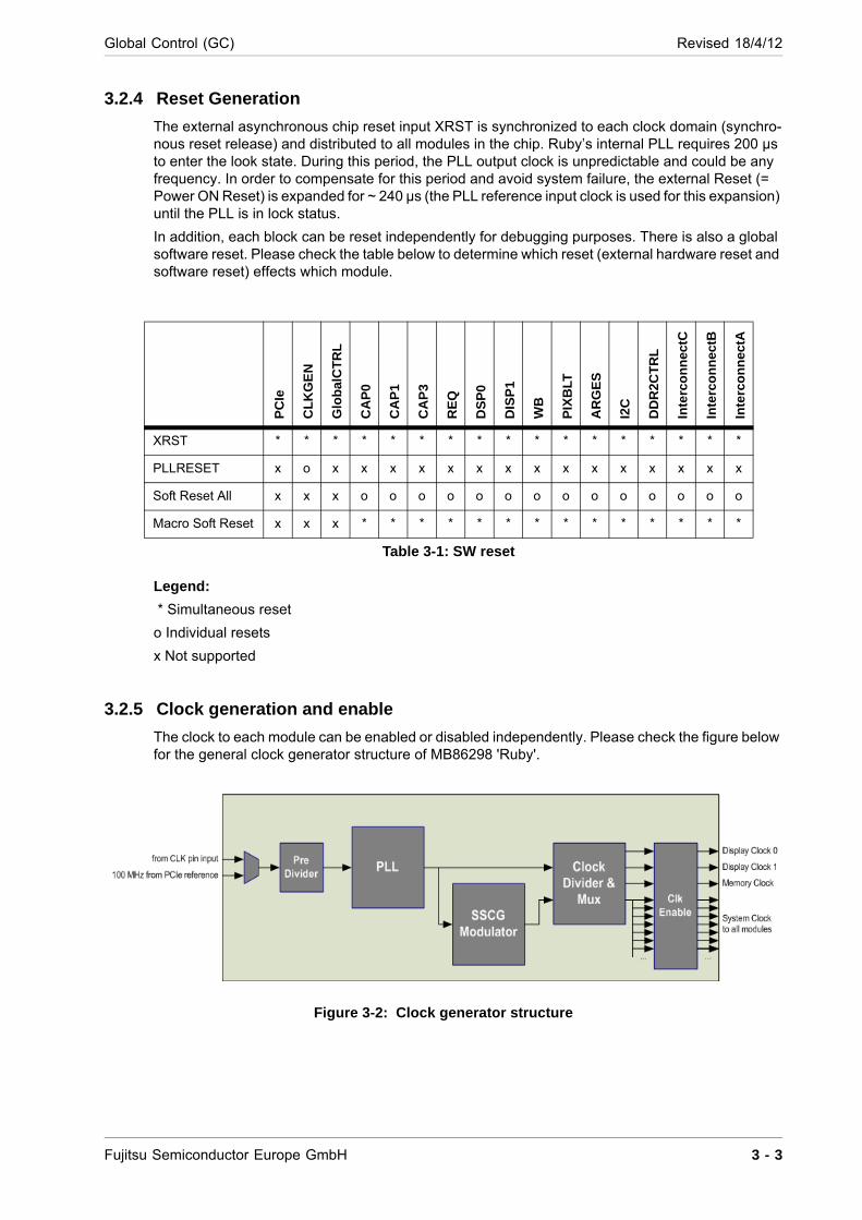
Global Control (GC) Revised 18/4/12
3.2.4 Reset Generation
The external asynchronous chip reset input XRST is synchronized to each clock domain (synchro-nous reset release) and distributed to all modules in the chip. Ruby’s internal PLL requires 200 µs to enter the look state. During this period, the PLL output clock is unpredictable and could be any frequency. In order to compensate for this period and avoid system failure, the external Reset (= Power ON Reset) is expanded for ~ 240 µs (the PLL reference input clock is used for this expansion) until the PLL is in lock status.
In addition, each block can be reset independently for debugging purposes. There is also a global software reset. Please check the table below to determine which reset (external hardware reset and software reset) effects which module.
Legend:
* Simultaneous reset
o Individual resets
x Not supported
3.2.5 Clock generation and enable
The clock to each module can be enabled or disabled independently. Please check the figure below for the general clock generator structure of MB86298 'Ruby'.
Figure 3-2: Clock generator structure
PC
Ie
CL
KG
EN
Glo
bal
CT
RL
CA
P0
CA
P1
CA
P3
RE
Q
DS
P0
DIS
P1
WB
PIX
BLT
AR
GE
S
I2C
DD
R2C
TR
L
Inte
rco
nn
ectC
Inte
rco
nn
ectB
Inte
rco
nn
ectA
XRST * * * * * * * * * * * * * * * * *
PLLRESET x o x x x x x x x x x x x x x x x
Soft Reset All x x x o o o o o o o o o o o o o o
Macro Soft Reset x x x * * * * * * * * * * * * * *
Table 3-1: SW reset
Fujitsu Semiconductor Europe GmbH 3 - 3
Revised 18/4/12 Global Control (GC)
The different clock frequencies are:
3.3 General Restrictions
System and memory clock SSCG modulation: only downspread is possible. Please take this into account when calculating the required display frequency and display timing settings when using the SSCG unit for an external display clock signal and for the internal system or memory clock.
If the SSCG unit is enabled or disabled via the SSCG_ENABLE register, then all clock multiplexers for display, memory and system clocks must be switched to the non-modulated clock using the SSCG_CLKEN register.
3.4 Processing Mode
3.4.1 Spread Spectrum Clock Generation
Please refer to “Processing Mode” in the SSCG chapter.
System Clock 266 MHz
Memory Clock 800/667/533/400 MHz depending on DDR2 memory configuration
Display Reference Clock 444 MHz/533 MHz for each display output (depending on the CLKMODE0 and CLKMODE1 pins.
3 - 4 Fujitsu Semiconductor Europe GmbH
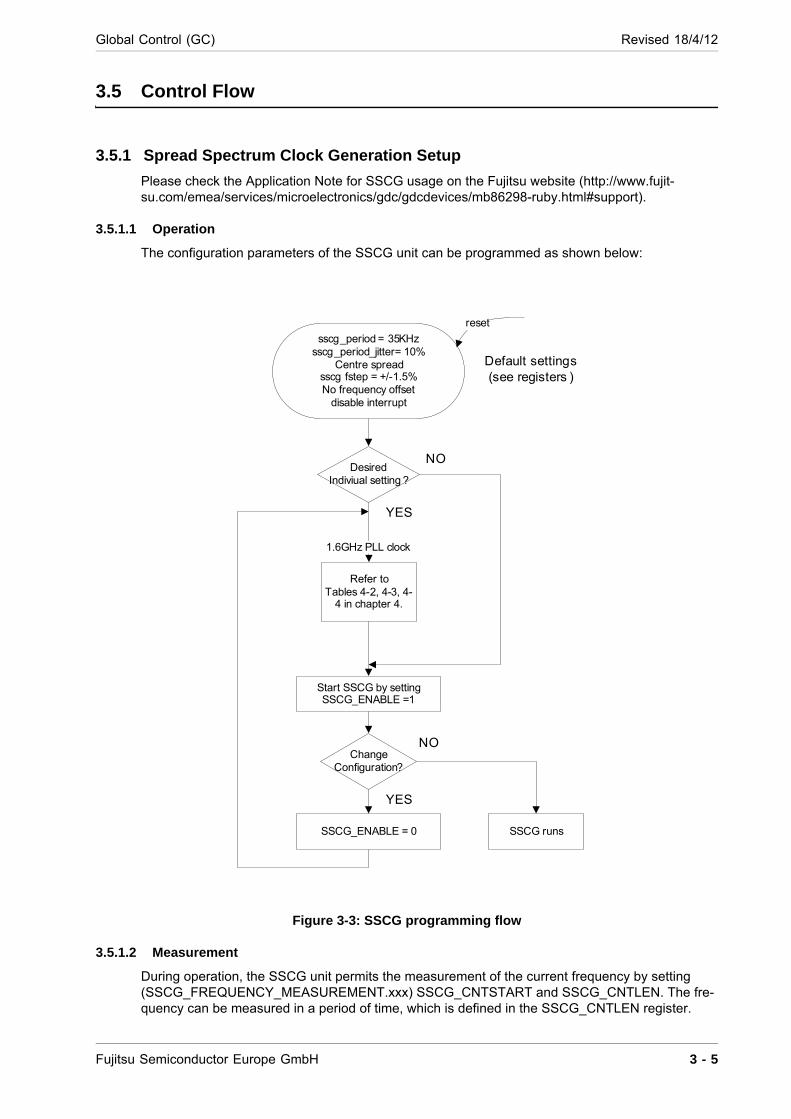
Global Control (GC) Revised 18/4/12
3.5 Control Flow
3.5.1 Spread Spectrum Clock Generation Setup
Please check the Application Note for SSCG usage on the Fujitsu website (http://www.fujit-su.com/emea/services/microelectronics/gdc/gdcdevices/mb86298-ruby.html#support).
3.5.1.1 Operation
The configuration parameters of the SSCG unit can be programmed as shown below:
Figure 3-3: SSCG programming flow
3.5.1.2 Measurement
During operation, the SSCG unit permits the measurement of the current frequency by setting (SSCG_FREQUENCY_MEASUREMENT.xxx) SSCG_CNTSTART and SSCG_CNTLEN. The fre-quency can be measured in a period of time, which is defined in the SSCG_CNTLEN register.
sscg_period = 35KHzsscg_period_jitter= 10%
Centre spreadsscg fstep = +/-1.5%No frequency offset
disable interrupt
Default settings(see registers )
Desired Indiviual setting ?
Refer to Tables 4-2, 4-3, 4-
4 in chapter 4.
Start SSCG by setting SSCG_ENABLE =1
ChangeConfiguration?
SSCG_ENABLE = 0
reset
SSCG runs
NO
YES
NO
YES
1.6GHz PLL clock
Fujitsu Semiconductor Europe GmbH 3 - 5

Revised 18/4/12 Global Control (GC)
The maximum operating frequency also can be derived by setting
SSCG_CNTSTART = 0 and SSCG_CNTLEN = SSCG_PERIOD/2 ,
SSCG_FOFFSET = 0 and SSCG_STEP /= 0
The max./min. operational frequency can be calculated as shown below:
3 - 6 Fujitsu Semiconductor Europe GmbH

Global Control (GC) Revised 18/4/12
Figure 3-4: Measurement flow
SSCG_CNTSTART = 0SSCG_CNTLEN = SSCG_PERIOD/2One measurement
Customsettings?
SSCG_CNTSTARTSSCG_CNTLEN
SSCG_COUNT_REPEAT
SSCG_COUNT_TRIG = 1
ChangeConfiguration?
SSCG_COUNT_TRIG = 0
reset
Result=SSCG_CNTOUTFREQ
NO
YES
NO
YES
SSCG_PERIOD_JITTER = 0
SSCG_PERIOD_JITTER = 0
SSCG_COUNT_REPEAT= 1
Result = Max(SSCG_CNTOUTFREQ)
NO
YES
Default setting
NO
YES
Fujitsu Semiconductor Europe GmbH 3 - 7
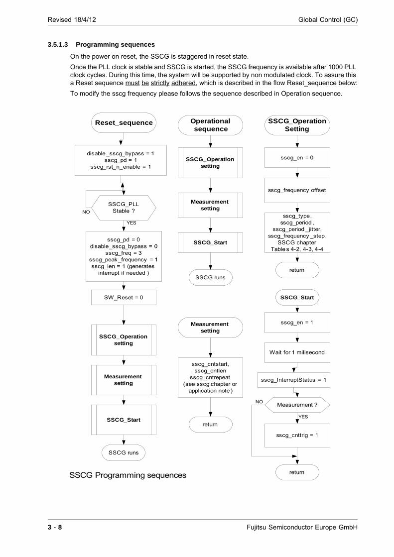
Revised 18/4/12 Global Control (GC)
3.5.1.3 Programming sequences
On the power on reset, the SSCG is staggered in reset state.
Once the PLL clock is stable and SSCG is started, the SSCG frequency is available after 1000 PLL clock cycles. During this time, the system will be supported by non modulated clock. To assure this a Reset sequence must be strictly adhered, which is described in the flow Reset_sequence below:
To modify the sscg frequency please follows the sequence described in Operation sequence.
Reset_sequence
disable_sscg_bypass = 1sscg_pd = 1
sscg_rst_n_enable = 1
SSCG_Operationsetting
sscg_pd = 0disable_sscg_bypass = 0
sscg_freq = 3sscg_peak_frequency = 1sscg_ien = 1 (generates
interrupt if needed )
SSCG_Start
SSCG_OperationSetting
SSCG_PLLStable ?
SSCG runs
sscg_frequency offset
sscg_type,sscg_period ,
sscg_period_jitter,sscg_frequency _step,
SSCG chapterTable s 4-2, 4-3, 4-4
sscg_en = 0
return
SSCG_Start
sscg_en = 1
Wait for 1 milisecond
sscg_InterruptStatus = 1
return
Operationalsequence
SSCG_Operationsetting
SSCG_Start
SSCG runs
SSCG Programming sequences
Measurementsetting
sscg_cntstart,sscg_cntlen
sscg_cntrepeat(see sscg chapter or
application note )
return
Measurement setting
Measurement ?
sscg_cnttrig = 1
NO
YES
NO
YES
SW_Reset = 0
Measurement setting
3 - 8 Fujitsu Semiconductor Europe GmbH
Global Control (GC) Revised 18/4/12
3.5.1.4 Programming examples
(Modulation Period= 35kHz with 10% Jitter, center spead of +/-1.0%)
Reset sequence
SSCG_CTRL = 0x80010133; PowerDown = 1, Bypass=1, peak_frequency,
operational frequency 1.6 GHz, center spread
activate SW_Reset
SSCG_CLKEN = 0x00000000; SSCG_RST_N_ENABLE bit [2]
Wait for PLL stable (is already stable under normal condition)
SSCG_CTRL =0x00000133; PowerDown = 0, Bypass=0, peak_frequency,
operational frequency 1.6 GHz, center spread
SSCG_IEN =0x00000001;Interrupt enable
deactivate SW_Reset
SSCG_CLKEN = 0x00000004;release reset
Wait 1000 pll cycles (can be compensated by operation setting)
(operation setting)
SSCG_EN = 0x00000000; disable sscg function
SSCG_PERIOD = 0x000000b4; 35kHz of modulation period
SSCG_PERIOD_JITTER = 0x00000090; 10% period Jitter
SSCG_FSTEP =0x000069ea; 1.0% modulation peak
SSCG_FOFFSET=0x00000000; no frequency offset
SSCG_InterruptStatus = 0x00000001; reset interrupt status
(measurement setting)
SSCG_FREQUENCY_MEASUREMENT = 0x005a0000;sscg_cntlen = 0x5a, sscg_cntstart = 0
SSCG_COUNT_REPEAT = 0x00000001; continuous measurement
(sscg_start)
SSCG_CLKEN = 0x0000000f; enable sscg function and DISP0, DISP1
SSCG_EN = 0x00000001; enable sscg function
Wait for 1 milliseconds
Fujitsu Semiconductor Europe GmbH 3 - 9
Revised 18/4/12 Global Control (GC)
SSCG_InterruptStatus = 0x00000001; reset interrupt status
SSCG_COUNT_TRIG= 0x00000001; activate measurement function
Return
3.5.1.5 Operation sequence
(operation setting)
SSCG_EN = 0x00000000; disable sscg function
SSCG_PERIOD = 0x000000b4; 35kHz of modulation period
SSCG_PERIOD_JITTER = 0x00000090; 10% period Jitter
SSCG_FSTEP =0x000069ea; 1.0% modulation peak
SSCG_FOFFSET=0x00000000; no frequency offset
SSCG_InterruptStatus = 0x00000001; reset interrupt status
(measurement setting)
SSCG_FREQUENCY_MEASUREMENT= 0x005a0000;sscg_cntlen = 0x5a, sscg_cntstart = 0
SSCG_COUNT_REPEAT = 0x00000001; continuous measurement
(sscg_start)
SSCG_CLKEN = 0x0000000f; enable sscg function
SSCG_EN= 0x00000001; enable sscg function
Wait for 1 millisecond
SSCG_InterruptStatus = 0x00000001; reset interrupt status
SSCG_COUNT_TRIG= 0x00000001; activate measurement function
return
3 - 10 Fujitsu Semiconductor Europe GmbH

Global Control (GC) Revised 18/4/12
3.5.1.6 Power down/up sequence
(SSCG is already configured)
Power down
SSCG_EN= 0x00000000; disable sscg function
SSCG_CLKEN = 0x00000000; select non SSCG clock
SSCG_CTRL= 0x80010133; PowerDown = 1, Bypass=1, peak_frequency,
operational frequency 1.6 GHz, center spread
return
Power up
SSCG_CLKEN = 0x00000000; SW_Reset bit [2]
SSCG_CTRL=0x00000133; PowerDown = 0, Bypass=0, peak_frequency,
operational frequency 1.6 GHz, center spread
Wait for 1000 pll cycles
SSCG_CLKEN = 0x0000000f; enable sscg function
SSCG_EN = 0x00000001; enable sscg function
Wait for 1 milliseconds
SSCG_InterruptStatus = 0x00000001; reset interrupt status
SSCG_COUNT_TRIG= 0x00000001; activate measurement function
return
Fujitsu Semiconductor Europe GmbH 3 - 11
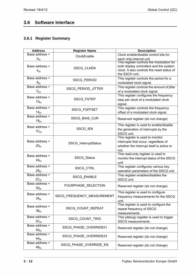
Revised 18/4/12 Global Control (GC)
3.6 Software Interface
3.6.1 Register Summary
Address Register Name DescriptionBase address +
0H ClockEnable Clock enable/disable control bits for
each chip-internal unit
Base address + 4H
SSCG_CLKEN
This register controls the modulation for both display controllers and the system clock. It also controls the reset status of the SSCH unit.
Base address + 8H
SSCG_PERIOD This register controls the period for a modulated clock signal.
Base address + CH
SSCG_PERIOD_JITTER This register controls the amount of jitter of a modulated clock signal.
Base address + 10H
SSCG_FSTEP This register configures the frequency step per clock of a modulated clock signal.
Base address + 14H
SSCG_FOFFSET This register controls the frequency offset of a modulated clock signal.
Base address + 18H
SSCG_BIAS_CUR Reserved register (do not change)
Base address + 1CH
SSCG_IEN This register is used to enable/disable the generation of interrupts by the SSCG unit.
Base address + 20H
SSCG_InterruptStatus
This register is used to monitor interrupts that occur, regardless of whether the interrupt itself is active or not.
Base address + 24H
SSCG_Status This read-only register is used to monitor the interrupt status of the SSCG unit
Base address + 28H
SSCG_CTRL This register configures various key operation parameters of the SSCG unit.
Base address + 2CH
SSCG_ENABLE This register enables/disables the SSCG unit.
Base address + 30H
FOURPHASE_SELECTION Reserved register (do not change)
Base address + 34H
SSCG_FREQUENCY_MEASUREMENT This register is used to configure frequency measurements for the SSCG unit.
Base address + 38H
SSCG_COUNT_REPEAT This register is used to configure the repeat frequency of SSCG measurements.
Base address + 3CH
SSCG_COUNT_TRIG This (debug) register is used to trigger SSCG measurements.
Base address + 40H
SSCG_PHASE_OVERRIDE01 Reserved register (do not change)
Base address + 44H
SSCG_PHASE_OVERRIDE23 Reserved register (do not change)
Base address + 48H
SSCG_PHASE_OVERRIDE_EN Reserved register (do not change)
3 - 12 Fujitsu Semiconductor Europe GmbH

Global Control (GC) Revised 18/4/12
Base address + 4CH
SSCG_CNTOUTFREQ This (debug) register is used to read the measured output clock count
Base address + 50H
CHIPINFO This register can be read in order to obtain information about the version, chip ID and part number of this GDC.
Base address + 54H
SW_RESET
This (debug) register provides a common soft reset for specific internal units (NOTE: An application should not use this register).
Base address + 58H
MACRO_RESET
This (debug) register provides a soft reset control for individual internal units (NOTE: An application should not use this register).
Fujitsu Semiconductor Europe GmbH 3 - 13
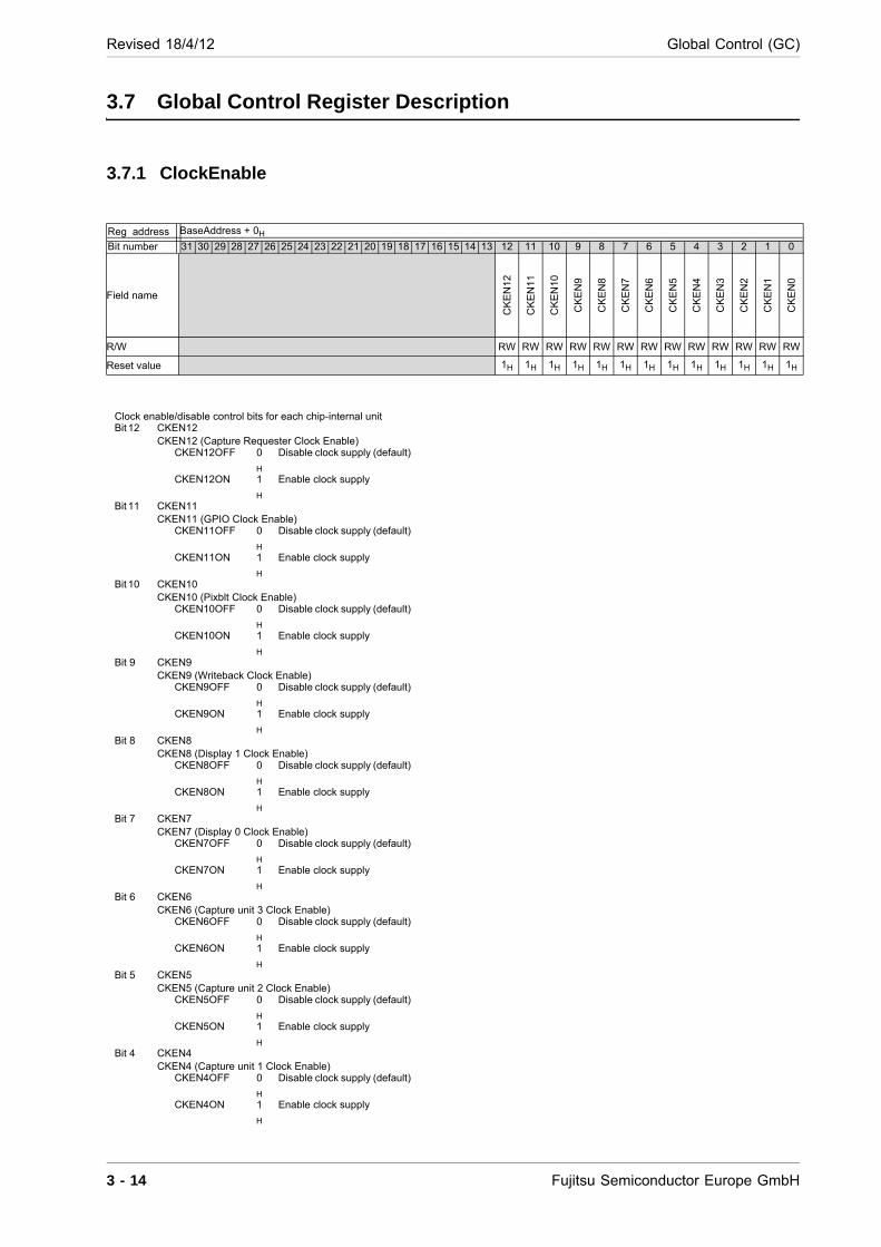
Revised 18/4/12 Global Control (GC)
3.7 Global Control Register Description
3.7.1 ClockEnable
Reg address BaseAddress + 0H
Bit number 31 30 29 28 27 26 25 24 23 22 21 20 19 18 17 16 15 14 13 12 11 10 9 8 7 6 5 4 3 2 1 0
Field name
CK
EN
12
CK
EN
11
CK
EN
10
CK
EN
9
CK
EN
8
CK
EN
7
CK
EN
6
CK
EN
5
CK
EN
4
CK
EN
3
CK
EN
2
CK
EN
1
CK
EN
0
R/W RW RW RW RW RW RW RW RW RW RW RW RW RW
Reset value 1H 1H 1H 1H 1H 1H 1H 1H 1H 1H 1H 1H 1H
Clock enable/disable control bits for each chip-internal unit Bit 12 CKEN12
CKEN12 (Capture Requester Clock Enable) CKEN12OFF 0
H
Disable clock supply (default)
CKEN12ON 1
H
Enable clock supply
Bit 11 CKEN11 CKEN11 (GPIO Clock Enable)
CKEN11OFF 0
H
Disable clock supply (default)
CKEN11ON 1
H
Enable clock supply
Bit 10 CKEN10 CKEN10 (Pixblt Clock Enable)
CKEN10OFF 0
H
Disable clock supply (default)
CKEN10ON 1
H
Enable clock supply
Bit 9 CKEN9 CKEN9 (Writeback Clock Enable)
CKEN9OFF 0
H
Disable clock supply (default)
CKEN9ON 1
H
Enable clock supply
Bit 8 CKEN8 CKEN8 (Display 1 Clock Enable)
CKEN8OFF 0
H
Disable clock supply (default)
CKEN8ON 1
H
Enable clock supply
Bit 7 CKEN7 CKEN7 (Display 0 Clock Enable)
CKEN7OFF 0
H
Disable clock supply (default)
CKEN7ON 1
H
Enable clock supply
Bit 6 CKEN6 CKEN6 (Capture unit 3 Clock Enable)
CKEN6OFF 0
H
Disable clock supply (default)
CKEN6ON 1
H
Enable clock supply
Bit 5 CKEN5 CKEN5 (Capture unit 2 Clock Enable)
CKEN5OFF 0
H
Disable clock supply (default)
CKEN5ON 1
H
Enable clock supply
Bit 4 CKEN4 CKEN4 (Capture unit 1 Clock Enable)
CKEN4OFF 0
H
Disable clock supply (default)
CKEN4ON 1
H
Enable clock supply
3 - 14 Fujitsu Semiconductor Europe GmbH
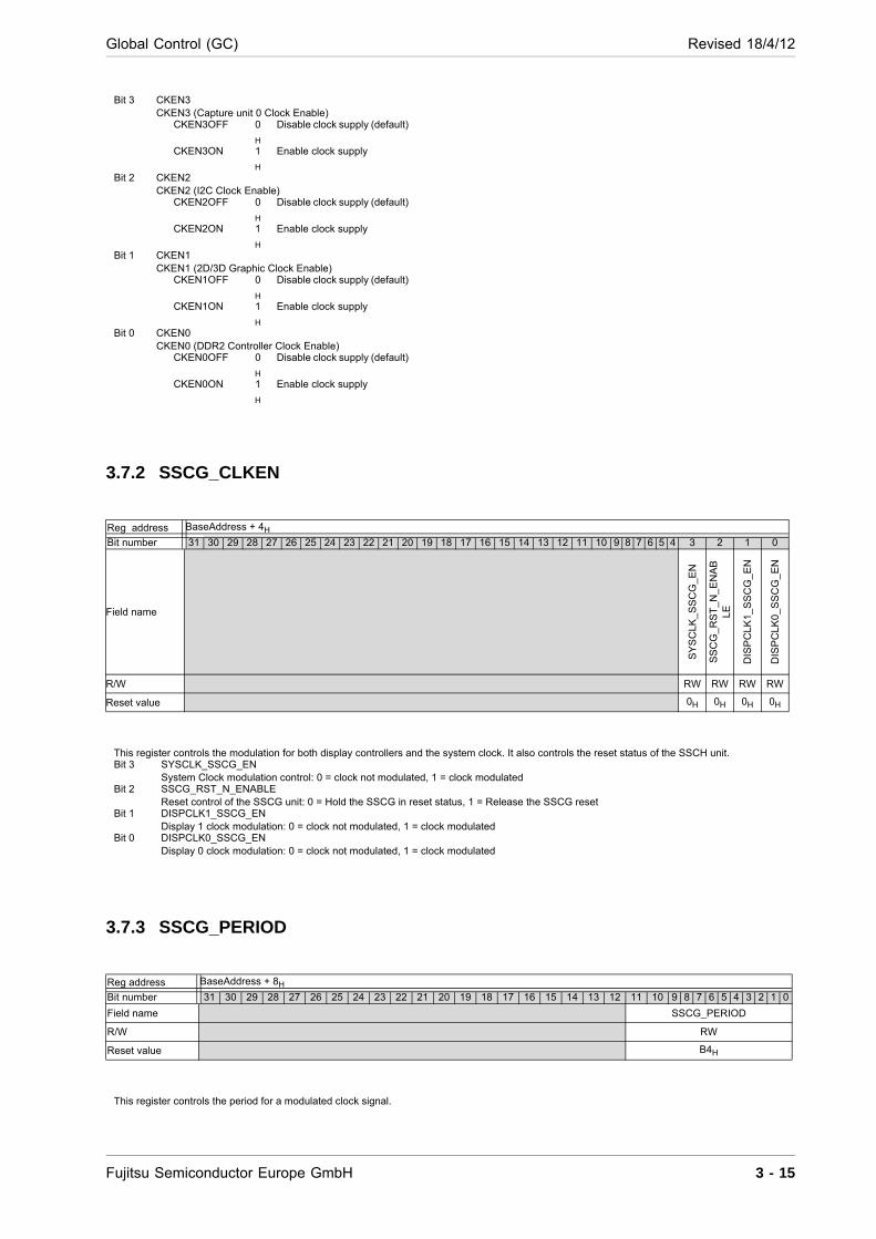
Global Control (GC) Revised 18/4/12
3.7.2 SSCG_CLKEN
3.7.3 SSCG_PERIOD
Bit 3 CKEN3 CKEN3 (Capture unit 0 Clock Enable)
CKEN3OFF 0
H
Disable clock supply (default)
CKEN3ON 1
H
Enable clock supply
Bit 2 CKEN2 CKEN2 (I2C Clock Enable)
CKEN2OFF 0
H
Disable clock supply (default)
CKEN2ON 1
H
Enable clock supply
Bit 1 CKEN1 CKEN1 (2D/3D Graphic Clock Enable)
CKEN1OFF 0
H
Disable clock supply (default)
CKEN1ON 1
H
Enable clock supply
Bit 0 CKEN0 CKEN0 (DDR2 Controller Clock Enable)
CKEN0OFF 0
H
Disable clock supply (default)
CKEN0ON 1
H
Enable clock supply
Reg address BaseAddress + 4H
Bit number 31 30 29 28 27 26 25 24 23 22 21 20 19 18 17 16 15 14 13 12 11 10 9 8 7 6 5 4 3 2 1 0
Field name
SY
SC
LK_
SS
CG
_E
N
SS
CG
_R
ST
_N_
EN
AB
LE
DIS
PC
LK1
_S
SC
G_
EN
DIS
PC
LK0
_S
SC
G_
EN
R/W RW RW RW RW
Reset value 0H 0H 0H 0H
This register controls the modulation for both display controllers and the system clock. It also controls the reset status of the SSCH unit. Bit 3 SYSCLK_SSCG_EN
System Clock modulation control: 0 = clock not modulated, 1 = clock modulated Bit 2 SSCG_RST_N_ENABLE
Reset control of the SSCG unit: 0 = Hold the SSCG in reset status, 1 = Release the SSCG reset Bit 1 DISPCLK1_SSCG_EN
Display 1 clock modulation: 0 = clock not modulated, 1 = clock modulated Bit 0 DISPCLK0_SSCG_EN
Display 0 clock modulation: 0 = clock not modulated, 1 = clock modulated
Reg address BaseAddress + 8H
Bit number 31 30 29 28 27 26 25 24 23 22 21 20 19 18 17 16 15 14 13 12 11 10 9 8 7 6 5 4 3 2 1 0
Field name SSCG_PERIOD
R/W RW
Reset value B4H
This register controls the period for a modulated clock signal.
Fujitsu Semiconductor Europe GmbH 3 - 15
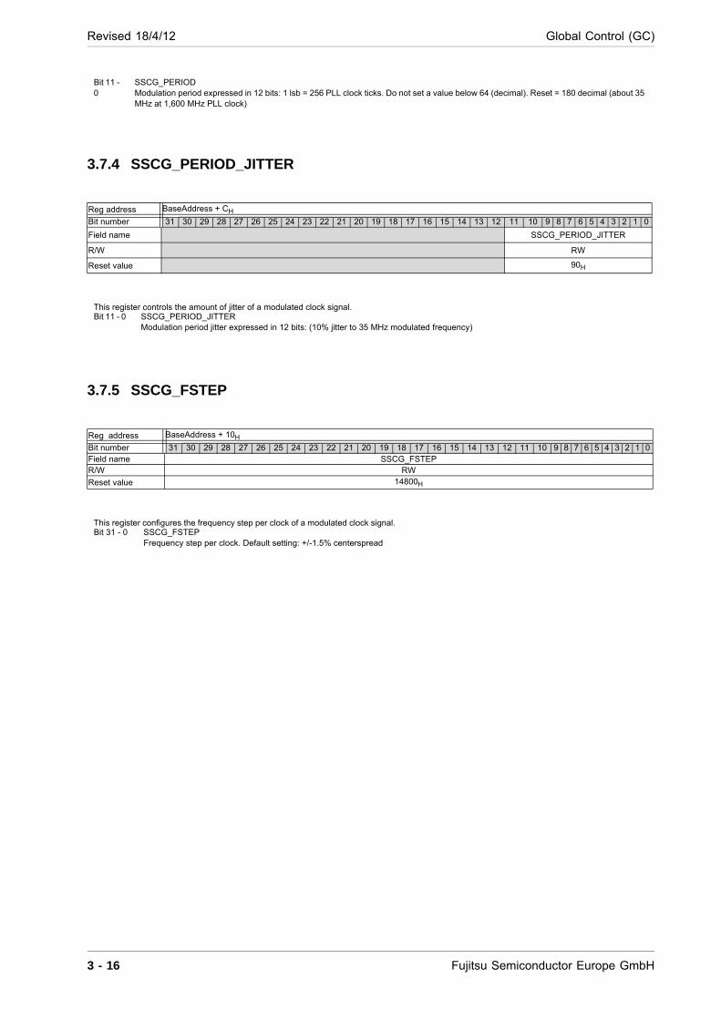
Revised 18/4/12 Global Control (GC)
3.7.4 SSCG_PERIOD_JITTER
3.7.5 SSCG_FSTEP
Bit 11 - 0
SSCG_PERIOD Modulation period expressed in 12 bits: 1 lsb = 256 PLL clock ticks. Do not set a value below 64 (decimal). Reset = 180 decimal (about 35 MHz at 1,600 MHz PLL clock)
Reg address BaseAddress + CH
Bit number 31 30 29 28 27 26 25 24 23 22 21 20 19 18 17 16 15 14 13 12 11 10 9 8 7 6 5 4 3 2 1 0
Field name SSCG_PERIOD_JITTER
R/W RW
Reset value 90H
This register controls the amount of jitter of a modulated clock signal. Bit 11 - 0 SSCG_PERIOD_JITTER
Modulation period jitter expressed in 12 bits: (10% jitter to 35 MHz modulated frequency)
Reg address BaseAddress + 10H
Bit number 31 30 29 28 27 26 25 24 23 22 21 20 19 18 17 16 15 14 13 12 11 10 9 8 7 6 5 4 3 2 1 0Field name SSCG_FSTEP R/W RW
Reset value 14800H
This register configures the frequency step per clock of a modulated clock signal. Bit 31 - 0 SSCG_FSTEP
Frequency step per clock. Default setting: +/-1.5% centerspread
3 - 16 Fujitsu Semiconductor Europe GmbH
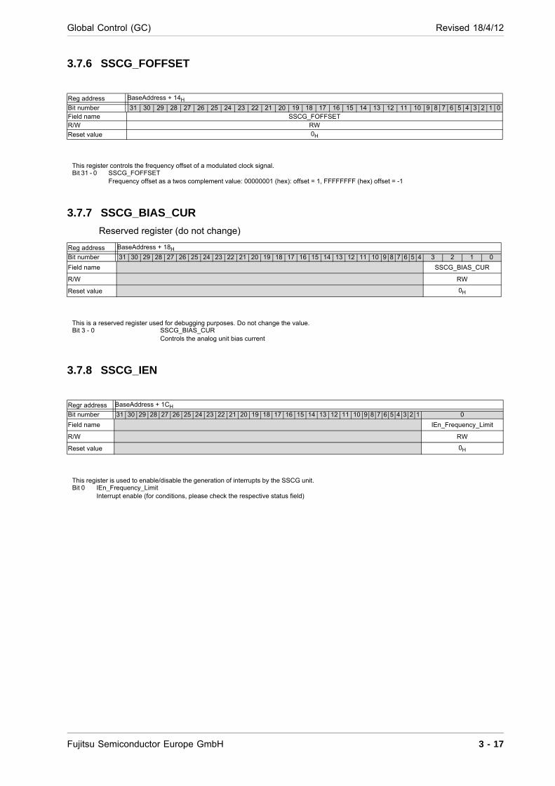
Global Control (GC) Revised 18/4/12
3.7.6 SSCG_FOFFSET
3.7.7 SSCG_BIAS_CUR
Reserved register (do not change)
3.7.8 SSCG_IEN
Reg address BaseAddress + 14H
Bit number 31 30 29 28 27 26 25 24 23 22 21 20 19 18 17 16 15 14 13 12 11 10 9 8 7 6 5 4 3 2 1 0Field name SSCG_FOFFSET R/W RW
Reset value 0H
This register controls the frequency offset of a modulated clock signal. Bit 31 - 0 SSCG_FOFFSET
Frequency offset as a twos complement value: 00000001 (hex): offset = 1, FFFFFFFF (hex) offset = -1
Reg address BaseAddress + 18H
Bit number 31 30 29 28 27 26 25 24 23 22 21 20 19 18 17 16 15 14 13 12 11 10 9 8 7 6 5 4 3 2 1 0
Field name SSCG_BIAS_CUR
R/W RW
Reset value 0H
This is a reserved register used for debugging purposes. Do not change the value.Bit 3 - 0 SSCG_BIAS_CUR
Controls the analog unit bias current
Regr address BaseAddress + 1CH
Bit number 31 30 29 28 27 26 25 24 23 22 21 20 19 18 17 16 15 14 13 12 11 10 9 8 7 6 5 4 3 2 1 0
Field name IEn_Frequency_Limit
R/W RW
Reset value 0H
This register is used to enable/disable the generation of interrupts by the SSCG unit. Bit 0 IEn_Frequency_Limit
Interrupt enable (for conditions, please check the respective status field)
Fujitsu Semiconductor Europe GmbH 3 - 17
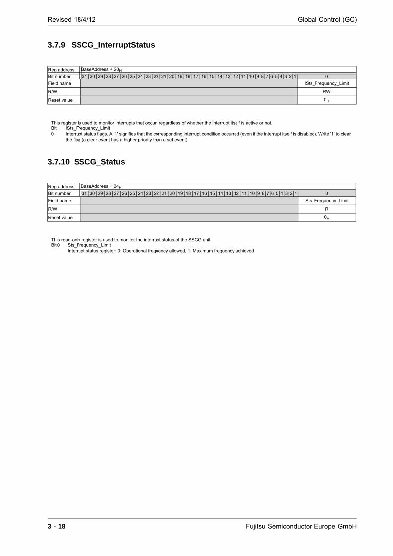
Revised 18/4/12 Global Control (GC)
3.7.9 SSCG_InterruptStatus
3.7.10 SSCG_Status
Reg address BaseAddress + 20H
Bit number 31 30 29 28 27 26 25 24 23 22 21 20 19 18 17 16 15 14 13 12 11 10 9 8 7 6 5 4 3 2 1 0
Field name ISts_Frequency_Limit
R/W RW
Reset value 0H
This register is used to monitor interrupts that occur, regardless of whether the interrupt itself is active or not. Bit 0
ISts_Frequency_Limit Interrupt status flags. A '1' signifies that the corresponding interrupt condition occurred (even if the interrupt itself is disabled). Write '1' to clear the flag (a clear event has a higher priority than a set event)
Reg address BaseAddress + 24H
Bit number 31 30 29 28 27 26 25 24 23 22 21 20 19 18 17 16 15 14 13 12 11 10 9 8 7 6 5 4 3 2 1 0
Field name Sts_Frequency_Limit
R/W R
Reset value 0H
This read-only register is used to monitor the interrupt status of the SSCG unit Bit 0 Sts_Frequency_Limit
Interrupt status register: 0: Operational frequency allowed, 1: Maximum frequency achieved
3 - 18 Fujitsu Semiconductor Europe GmbH
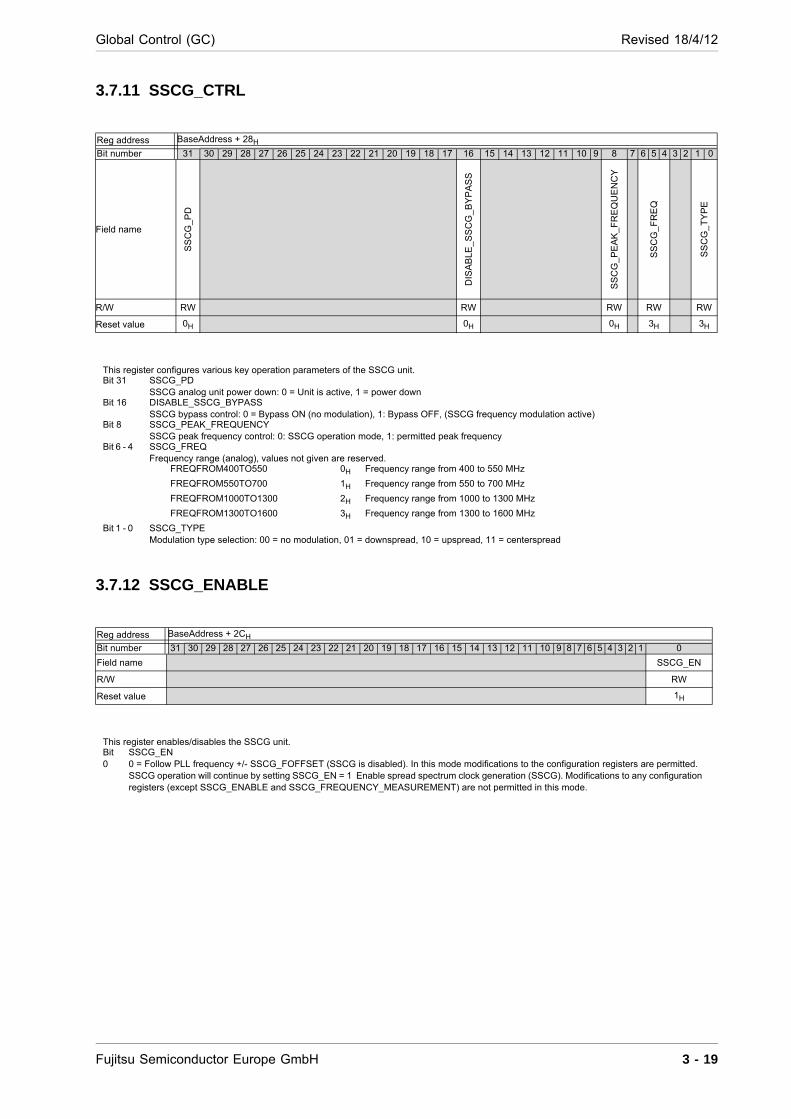
Global Control (GC) Revised 18/4/12
3.7.11 SSCG_CTRL
3.7.12 SSCG_ENABLE
Reg address BaseAddress + 28H
Bit number 31 30 29 28 27 26 25 24 23 22 21 20 19 18 17 16 15 14 13 12 11 10 9 8 7 6 5 4 3 2 1 0
Field name
SS
CG
_PD
DIS
AB
LE_
SS
CG
_B
YP
AS
S
SS
CG
_P
EA
K_F
RE
QU
EN
CY
SS
CG
_F
RE
Q
SS
CG
_T
YP
E
R/W RW RW RW RW RW
Reset value 0H 0H 0H 3H 3H
This register configures various key operation parameters of the SSCG unit. Bit 31 SSCG_PD
SSCG analog unit power down: 0 = Unit is active, 1 = power down Bit 16 DISABLE_SSCG_BYPASS
SSCG bypass control: 0 = Bypass ON (no modulation), 1: Bypass OFF, (SSCG frequency modulation active) Bit 8 SSCG_PEAK_FREQUENCY
SSCG peak frequency control: 0: SSCG operation mode, 1: permitted peak frequency Bit 6 - 4 SSCG_FREQ
Frequency range (analog), values not given are reserved. FREQFROM400TO550 0H Frequency range from 400 to 550 MHz
FREQFROM550TO700 1H Frequency range from 550 to 700 MHz
FREQFROM1000TO1300 2H Frequency range from 1000 to 1300 MHz
FREQFROM1300TO1600 3H Frequency range from 1300 to 1600 MHz
Bit 1 - 0 SSCG_TYPE Modulation type selection: 00 = no modulation, 01 = downspread, 10 = upspread, 11 = centerspread
Reg address BaseAddress + 2CH
Bit number 31 30 29 28 27 26 25 24 23 22 21 20 19 18 17 16 15 14 13 12 11 10 9 8 7 6 5 4 3 2 1 0
Field name SSCG_EN
R/W RW
Reset value 1H
This register enables/disables the SSCG unit. Bit 0
SSCG_EN 0 = Follow PLL frequency +/- SSCG_FOFFSET (SSCG is disabled). In this mode modifications to the configuration registers are permitted. SSCG operation will continue by setting SSCG_EN = 1 Enable spread spectrum clock generation (SSCG). Modifications to any configuration registers (except SSCG_ENABLE and SSCG_FREQUENCY_MEASUREMENT) are not permitted in this mode.
Fujitsu Semiconductor Europe GmbH 3 - 19

Revised 18/4/12 Global Control (GC)
3.7.13 FOURPHASE_SELECTION
Reserved register (do not change)
3.7.14 SSCG_FREQUENCY_MEASUREMENT
3.7.15 SSCG_COUNT_REPEAT
Reg address BaseAddress + 30H
Bit number 31 30 29 28 27 26 25 24 23 22 21 20 19 18 17 16 15 14 13 12 11 10 9 8 7 6 5 4 3 2 1 0
Field name SSCG_FOURPHEXT
R/W RW
Reset value 0H
This is a reserved register used for debugging purposes. Do not change the value.Bit 0 SSCG_FOURPHEXT
0: Internal four phase, 1: External four phase
Reg address BaseAddress + 34H
Bit number 31 30 29 28 27 26 25 24 23 22 21 20 19 18 17 16 15 14 13 12 11 10 9 8 7 6 5 4 3 2 1 0
Field name SSCG_CNTLEN SSCG_CNTSTART
R/W RW RW
Reset value 5AH 0H
This register is used to configure frequency measurements for the SSCG unit. Bit 27 - 16
SSCG_CNTLEN This bitfield is used to measure the output frequency over 'n' clocks after counting has been triggered (1 lsb = 256 PLL clock ticks, condition: SSCG_CNTSTART + SSCG_CNTLEN in the SSCG_FREQUENCY_MEASUREMENT register is less than SSCG_PERIOD)
Bit 11 - 0
SSCG_CNTSTART This bitfield configures the delay from the start of the modulation period to the start of the SSCG frequency measurement (1 lsb = 256 PLL clock ticks)
Reg address BaseAddress + 38H
Bit number 31 30 29 28 27 26 25 24 23 22 21 20 19 18 17 16 15 14 13 12 11 10 9 8 7 6 5 4 3 2 1 0
Field name SSCG_CNTREPEAT
R/W RW
Reset value 0H
This register is used to configure the repeat frequency of SSCG measurements. Bit 0 SSCG_CNTREPEAT
Frequency of measurements: 0 = one measurement only, 1 = continuous measurement
3 - 20 Fujitsu Semiconductor Europe GmbH
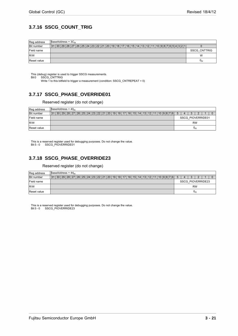
Global Control (GC) Revised 18/4/12
3.7.16 SSCG_COUNT_TRIG
3.7.17 SSCG_PHASE_OVERRIDE01
Reserved register (do not change)
3.7.18 SSCG_PHASE_OVERRIDE23
Reserved register (do not change)
Reg address BaseAddress + 3CH
Bit number 31 30 29 28 27 26 25 24 23 22 21 20 19 18 17 16 15 14 13 12 11 10 9 8 7 6 5 4 3 2 1 0
Field name SSCG_CNTTRIG
R/W W
Reset value 0H
This (debug) register is used to trigger SSCG measurements. Bit 0 SSCG_CNTTRIG
Write 1 to this bitfield to trigger a measurement (condition: SSCG_CNTREPEAT = 0)
Reg address BaseAddress + 40H
Bit number 31 30 29 28 27 26 25 24 23 22 21 20 19 18 17 16 15 14 13 12 11 10 9 8 7 6 5 4 3 2 1 0
Field name SSCG_PIOVERRIDE01
R/W RW
Reset value 0H
This is a reserved register used for debugging purposes. Do not change the value.Bit 5 - 0 SSCG_PIOVERRIDE01
Reg address BaseAddress + 44H
Bit number 31 30 29 28 27 26 25 24 23 22 21 20 19 18 17 16 15 14 13 12 11 10 9 8 7 6 5 4 3 2 1 0
Field name SSCG_PIOVERRIDE23
R/W RW
Reset value 0H
This is a reserved register used for debugging purposes. Do not change the value.Bit 5 - 0 SSCG_PIOVERRIDE23
Fujitsu Semiconductor Europe GmbH 3 - 21
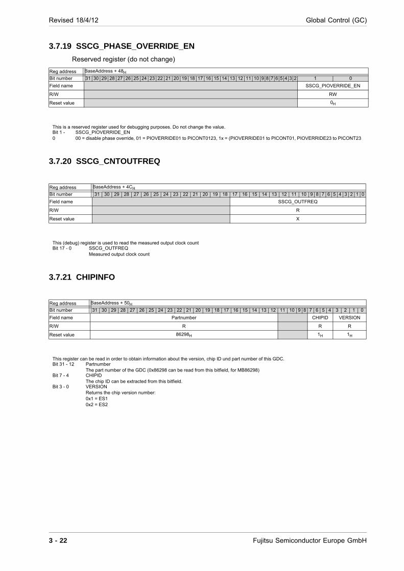
Revised 18/4/12 Global Control (GC)
3.7.19 SSCG_PHASE_OVERRIDE_EN
Reserved register (do not change)
3.7.20 SSCG_CNTOUTFREQ
3.7.21 CHIPINFO
Reg address BaseAddress + 48H
Bit number 31 30 29 28 27 26 25 24 23 22 21 20 19 18 17 16 15 14 13 12 11 10 9 8 7 6 5 4 3 2 1 0
Field name SSCG_PIOVERRIDE_EN
R/W RW
Reset value 0H
This is a reserved register used for debugging purposes. Do not change the value.Bit 1 - 0
SSCG_PIOVERRIDE_EN 00 = disable phase override, 01 = PIOVERRIDE01 to PICONT0123, 1x = (PIOVERRIDE01 to PICONT01, PIOVERRIDE23 to PICONT23
Reg address BaseAddress + 4CH
Bit number 31 30 29 28 27 26 25 24 23 22 21 20 19 18 17 16 15 14 13 12 11 10 9 8 7 6 5 4 3 2 1 0
Field name SSCG_OUTFREQ
R/W R
Reset value X
This (debug) register is used to read the measured output clock count Bit 17 - 0 SSCG_OUTFREQ
Measured output clock count
Reg address BaseAddress + 50H
Bit number 31 30 29 28 27 26 25 24 23 22 21 20 19 18 17 16 15 14 13 12 11 10 9 8 7 6 5 4 3 2 1 0
Field name Partnumber CHIPID VERSION
R/W R R R
Reset value 86298H 1H 1H
This register can be read in order to obtain information about the version, chip ID und part number of this GDC. Bit 31 - 12 Partnumber
The part number of the GDC (0x86298 can be read from this bitfield, for MB86298) Bit 7 - 4 CHIPID
The chip ID can be extracted from this bitfield. Bit 3 - 0 VERSION
Returns the chip version number:0x1 = ES10x2 = ES2
3 - 22 Fujitsu Semiconductor Europe GmbH
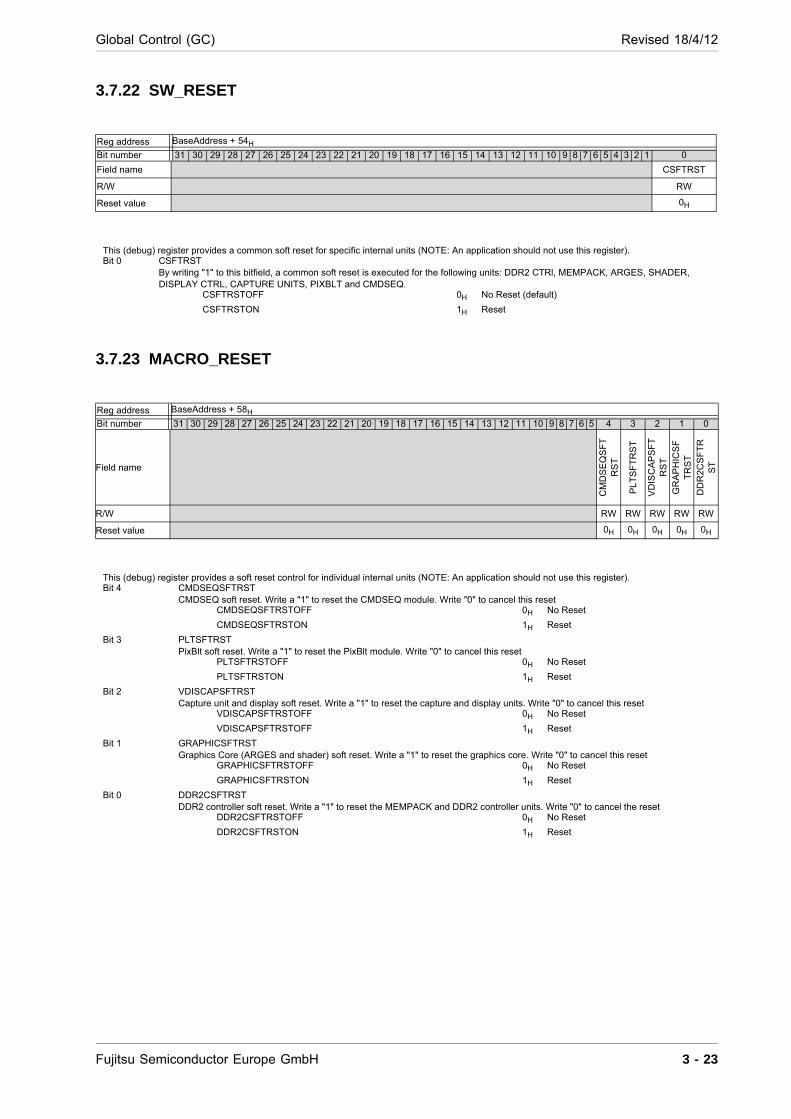
Global Control (GC) Revised 18/4/12
3.7.22 SW_RESET
3.7.23 MACRO_RESET
Reg address BaseAddress + 54H
Bit number 31 30 29 28 27 26 25 24 23 22 21 20 19 18 17 16 15 14 13 12 11 10 9 8 7 6 5 4 3 2 1 0
Field name CSFTRST
R/W RW
Reset value 0H
This (debug) register provides a common soft reset for specific internal units (NOTE: An application should not use this register). Bit 0 CSFTRST
By writing "1" to this bitfield, a common soft reset is executed for the following units: DDR2 CTRl, MEMPACK, ARGES, SHADER, DISPLAY CTRL, CAPTURE UNITS, PIXBLT and CMDSEQ.
CSFTRSTOFF 0H No Reset (default)
CSFTRSTON 1H Reset
Reg address BaseAddress + 58H
Bit number 31 30 29 28 27 26 25 24 23 22 21 20 19 18 17 16 15 14 13 12 11 10 9 8 7 6 5 4 3 2 1 0
Field name
CM
DS
EQ
SF
TR
ST
PL
TS
FT
RS
T
VD
ISC
AP
SF
TR
ST
G
RA
PH
ICS
FT
RS
T
DD
R2
CS
FT
RS
T
R/W RW RW RW RW RW
Reset value 0H 0H 0H 0H 0H
This (debug) register provides a soft reset control for individual internal units (NOTE: An application should not use this register). Bit 4 CMDSEQSFTRST
CMDSEQ soft reset. Write a "1" to reset the CMDSEQ module. Write "0" to cancel this reset CMDSEQSFTRSTOFF 0H No Reset
CMDSEQSFTRSTON 1H Reset
Bit 3 PLTSFTRST PixBlt soft reset. Write a "1" to reset the PixBlt module. Write "0" to cancel this reset
PLTSFTRSTOFF 0H No Reset
PLTSFTRSTON 1H Reset
Bit 2 VDISCAPSFTRST Capture unit and display soft reset. Write a "1" to reset the capture and display units. Write "0" to cancel this reset
VDISCAPSFTRSTOFF 0H No Reset
VDISCAPSFTRSTOFF 1H Reset
Bit 1 GRAPHICSFTRST Graphics Core (ARGES and shader) soft reset. Write a "1" to reset the graphics core. Write "0" to cancel this reset
GRAPHICSFTRSTOFF 0H No Reset
GRAPHICSFTRSTON 1H Reset
Bit 0 DDR2CSFTRST DDR2 controller soft reset. Write a "1" to reset the MEMPACK and DDR2 controller units. Write "0" to cancel the reset
DDR2CSFTRSTOFF 0H No Reset
DDR2CSFTRSTON 1H Reset
Fujitsu Semiconductor Europe GmbH 3 - 23

Revised 18/4/12 Global Control (GC)
3 - 24 Fujitsu Semiconductor Europe GmbH
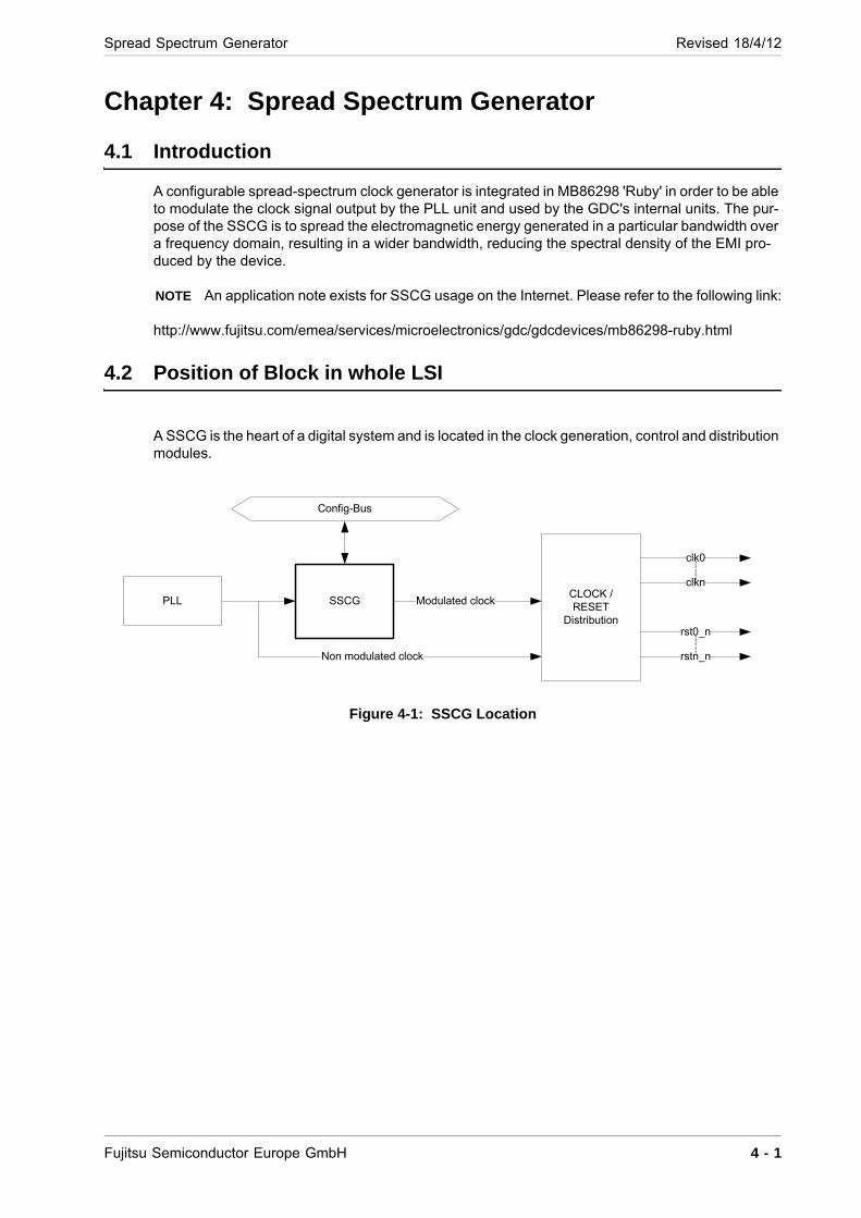
Spread Spectrum Generator Revised 18/4/12
Chapter 4: Spread Spectrum Generator
4.1 Introduction
A configurable spread-spectrum clock generator is integrated in MB86298 'Ruby' in order to be able to modulate the clock signal output by the PLL unit and used by the GDC's internal units. The pur-pose of the SSCG is to spread the electromagnetic energy generated in a particular bandwidth over a frequency domain, resulting in a wider bandwidth, reducing the spectral density of the EMI pro-duced by the device.
NOTE An application note exists for SSCG usage on the Internet. Please refer to the following link:
http://www.fujitsu.com/emea/services/microelectronics/gdc/gdcdevices/mb86298-ruby.html
4.2 Position of Block in whole LSI
A SSCG is the heart of a digital system and is located in the clock generation, control and distribution modules.
Figure 4-1: SSCG Location
CLOCK /RESET
Distribution
SSCG
Non modulated clock
Modulated clock
clk0
clkn
rstn_n
rst0_n
PLL
Config-Bus
Fujitsu Semiconductor Europe GmbH 4 - 1
Revised 18/4/12 Spread Spectrum Generator
4.3 Features
4.3.1 Functional
Input frequency range:The switchable frequency range of the SSCG unit itself is 1.0 GHz – 1.6 GHz.
Modulation Period: Variable from 1/1,048,320 to 1/256 of the PLL clock
Modulation Period Jitter (Delta)Continuously from 0 to 12.5% of the modulation period
Modulation types available for use:Non-modulatedDownspread,Center spread (default)
Modulation peak:Default ±1.0%Center spread:-1.56% to +1.56%Downspread: 0 to -1.56%
Modulation shapes: Triangle, Dual Triangle
Frequency offset-1.56% to +1.56%, default 0
Maskable Interrupt generation:Generate an interrupt on an illegal configuration setting
4.3.2 Measurement
Max./min. operation frequency
4.3.3 Limitations
Do not modify any SSCG registers during operation of the SSCG unit
Please stop the SSCG by setting SSCG_EN =0 if you need to modify the SSCG registers
If SSCG_PEAK_FREQUENCY is set to 1, the modulation peak value will be doubled. In order to maintain the same modulation peak, the values of SSCG_FOFFSET and SSCG_FSTEP must therefore be divided by 2.
If using a mixed setting of SSCG_FSTEP and SSCG_FOFFSET (both values are not zero), SSCG_PEAK_FREQUENCY must be set to 1. The SSCG will generate an interrupt in the first 32 SSCG periods. These interrupts can be ignored and must be reset afterwards. An illegal configuration setting will periodically generate an interrupt in SSCG_period cycles.
At high modulation frequencies, picture disturbances on a display are possible. During validation it was noted that under very specific conditions (DVI port, specific monitor) display was unstable for SSCG rates > 20kHz at +/- 0.5 % modulation peak. This was not a problem
4 - 2 Fujitsu Semiconductor Europe GmbH
Spread Spectrum Generator Revised 18/4/12
caused by the MB86298 'Ruby' chip, but an incompatibility of the DVI receiver to compensate for SSCG-induced jitter during clock recovery. If picture disturbances are visible, use a lower modulation frequency.
The additional measurement of offset (SSCG_CNT_START) and duration (SSCG_CNT_LEN) must be less than a SSCG period (SSCG_CNT_START + SSCG_CNT_LEN <= 0.95 * SSCG-Period)
Please note that the use of the maximum values (e.g. Modulation Peak) may be limited, depending on the use of other interfaces in the chip (e.g. UART)
4.3.3.1 Switch on/off SSCG Modulation
The following scheme is recommended to switch on/off the SSCG modulation in order to avoid caus-ing a spike on the clock signal of the effected clock domains:
SSCG Power down
1. Disable the SSCG
2. Set the SSCG to Bypass mode
3. Switch the internal clock domains to the non-SSCG modulated clock domain
4. Switch the display clock domains to the non-SSCG modulated clock domain
5. Set the SSCG to Bypass mode and power down the SSCG
6. Reset the SSCG
SSCG operation
1. Switch the internal clock domains to the non-SSCG modulated clock domain, reset the SSCG and switch the display clocks to the non-SSCG modulated clock domain
2. Set the SSCG to Bypass mode and power down the SSCG
3. Power up the SSCG and set to Bypass mode
4. Configure the SSCG and wait for 1000 clock cycles before starting the SSCG
5. Disable the Bypass mode (enabling the SSCG unit):
6. Release the SSCG reset (digital part) using global control and switch the internal clock domains to the SSCG modulated clock domain
7. Switch the display clock domains to the SSCG modulated clock domain
8. Enable the SSCG
9. Wait for 1 millisecond
10. Reset the 'Frequency Limit' Interrupt
11. Check that SSCG_STATUS.STS_FREQUENCY_LIMIT = 0
Fujitsu Semiconductor Europe GmbH 4 - 3
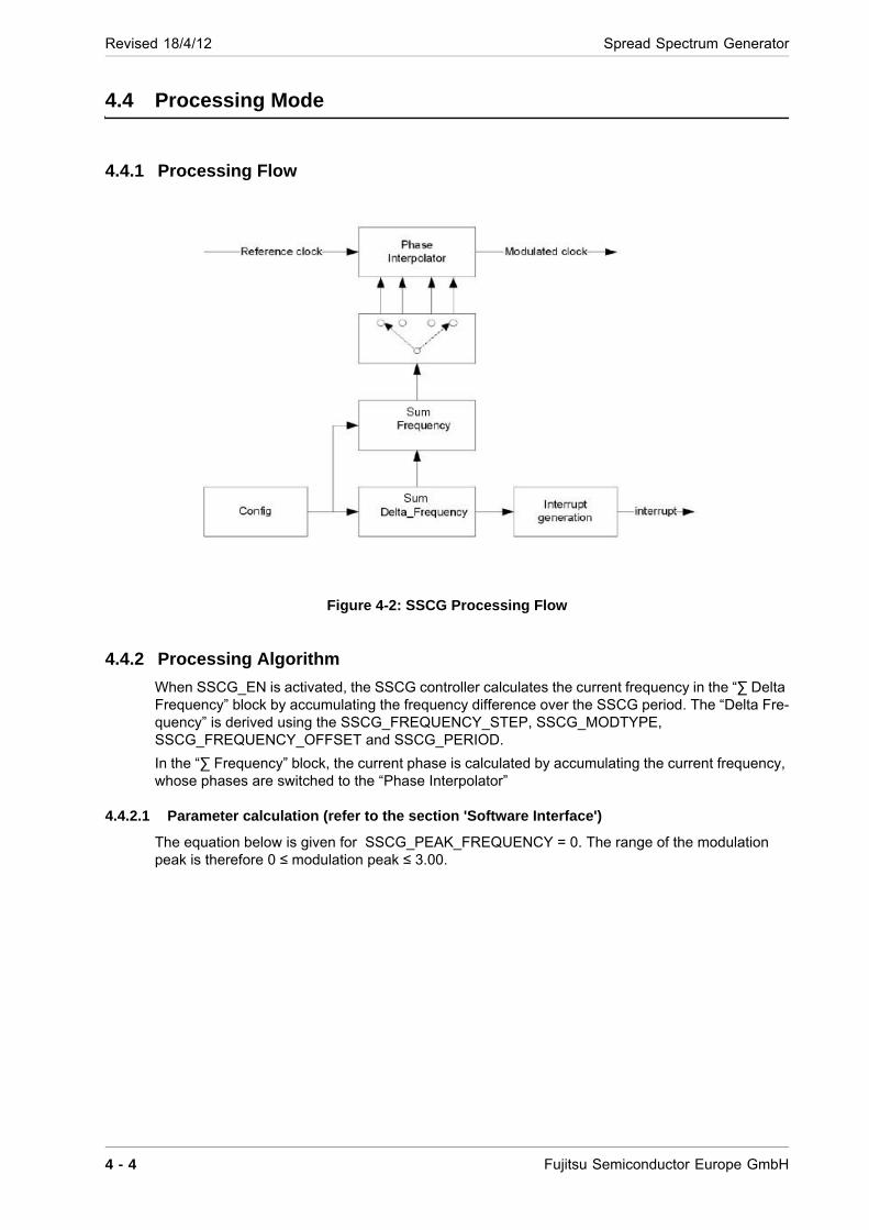
Revised 18/4/12 Spread Spectrum Generator
4.4 Processing Mode
4.4.1 Processing Flow
Figure 4-2: SSCG Processing Flow
4.4.2 Processing Algorithm
When SSCG_EN is activated, the SSCG controller calculates the current frequency in the “∑ Delta Frequency” block by accumulating the frequency difference over the SSCG period. The “Delta Fre-quency” is derived using the SSCG_FREQUENCY_STEP, SSCG_MODTYPE, SSCG_FREQUENCY_OFFSET and SSCG_PERIOD.
In the “∑ Frequency” block, the current phase is calculated by accumulating the current frequency, whose phases are switched to the “Phase Interpolator”
4.4.2.1 Parameter calculation (refer to the section 'Software Interface')
The equation below is given for SSCG_PEAK_FREQUENCY = 0. The range of the modulation peak is therefore 0 ≤ modulation peak ≤ 3.00.
4 - 4 Fujitsu Semiconductor Europe GmbH
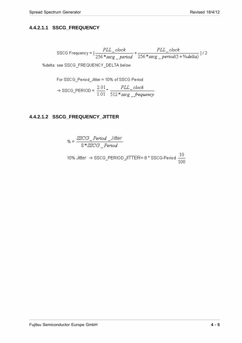
Spread Spectrum Generator Revised 18/4/12
4.4.2.1.1 SSCG_FREQUENCY
4.4.2.1.2 SSCG_FREQUENCY_JITTER
Fujitsu Semiconductor Europe GmbH 4 - 5
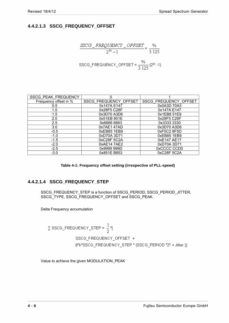
Revised 18/4/12 Spread Spectrum Generator
4.4.2.1.3 SSCG_FREQUENCY_OFFSET
Table 4-1: Frequency offset setting (irrespective of PLL-speed)
4.4.2.1.4 SSCG_FREQUENCY_STEP
SSCG_FREQUENCY_STEP is a function of SSCG_PERIOD, SSCG_PERIOD_JITTER, SSCG_TYPE, SSCG_FREQUENCY_OFFSET and SSCG_PEAK.
Delta Frequency accumulation
Value to achieve the given MODULATION_PEAK
SSCG_PEAK_FREQUENCY 0 1Frequency offset in % SSCG_FREQUENCY_OFFSET SSCG_FREQUENCY_OFFSET
0.5 0x147A E147 0x0A3D 70A31.0 0x28F5 C28F 0x147A E1471.5 0x3D70 A3D6 0x1EB8 51E92.0 0x51EB 851E 0x28F5 C28F2.5 0x6666 6663 0x3333 33303.0 0x7AE1 47AD 0x3D70 A3D6-0.5 0xEB85 1EB9 0xF5C2 8F5D-1.0 0xD70A 3D71 0xEB85 1EB9-1.5 0xC28F 5C2A 0xE147 AE17-2.0 0xAE14 7AE2 0xD70A 3D71-2.5 0x9999 999D 0xCCCC CCD0-3.0 0x851E B853 0xC28F 5C2A
4 - 6 Fujitsu Semiconductor Europe GmbH
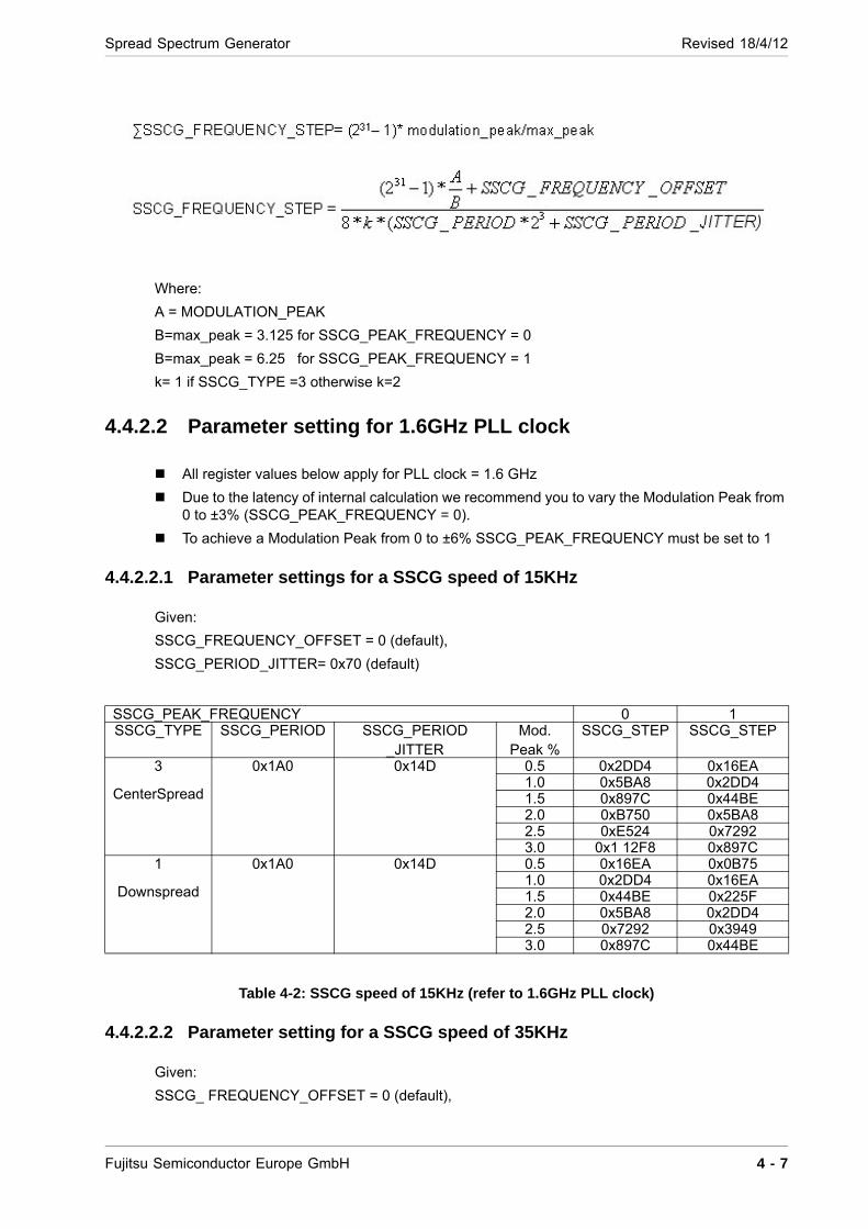
Spread Spectrum Generator Revised 18/4/12
Where:
A = MODULATION_PEAK
B=max_peak = 3.125 for SSCG_PEAK_FREQUENCY = 0
B=max_peak = 6.25 for SSCG_PEAK_FREQUENCY = 1
k= 1 if SSCG_TYPE =3 otherwise k=2
4.4.2.2 Parameter setting for 1.6GHz PLL clock
All register values below apply for PLL clock = 1.6 GHz
Due to the latency of internal calculation we recommend you to vary the Modulation Peak from 0 to ±3% (SSCG_PEAK_FREQUENCY = 0).
To achieve a Modulation Peak from 0 to ±6% SSCG_PEAK_FREQUENCY must be set to 1
4.4.2.2.1 Parameter settings for a SSCG speed of 15KHz
Given:
SSCG_FREQUENCY_OFFSET = 0 (default),
SSCG_PERIOD_JITTER= 0x70 (default)
Table 4-2: SSCG speed of 15KHz (refer to 1.6GHz PLL clock)
4.4.2.2.2 Parameter setting for a SSCG speed of 35KHz
Given:
SSCG_ FREQUENCY_OFFSET = 0 (default),
SSCG_PEAK_FREQUENCY 0 1SSCG_TYPE SSCG_PERIOD SSCG_PERIOD
_JITTERMod.
Peak %SSCG_STEP SSCG_STEP
3
CenterSpread
0x1A0 0x14D 0.5 0x2DD4 0x16EA1.0 0x5BA8 0x2DD41.5 0x897C 0x44BE2.0 0xB750 0x5BA82.5 0xE524 0x72923.0 0x1 12F8 0x897C
1
Downspread
0x1A0 0x14D 0.5 0x16EA 0x0B751.0 0x2DD4 0x16EA1.5 0x44BE 0x225F2.0 0x5BA8 0x2DD42.5 0x7292 0x39493.0 0x897C 0x44BE
Fujitsu Semiconductor Europe GmbH 4 - 7
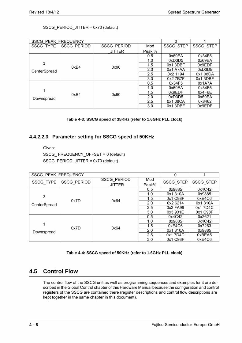
Revised 18/4/12 Spread Spectrum Generator
SSCG_PERIOD_JITTER = 0x70 (default)
Table 4-3: SSCG speed of 35KHz (refer to 1.6GHz PLL clock)
4.4.2.2.3 Parameter setting for SSCG speed of 50KHz
Given:
SSCG_ FREQUENCY_OFFSET = 0 (default)
SSCG_PERIOD_JITTER = 0x70 (default)
Table 4-4: SSCG speed of 50KHz (refer to 1.6GHz PLL clock)
4.5 Control Flow
The control flow of the SSCG unit as well as programming sequences and examples for it are de-scribed in the Global Control chapter of this Hardware Manual because the configuration and control registers of the SSCG are contained there (register descriptions and control flow descriptions are kept together in the same chapter in this document).
SSCG_PEAK_FREQUENCY 0 1SSCG_TYPE SSCG_PERIOD SSCG_PERIOD
_JITTERMod
Peak %SSCG_STEP SSCG_STEP
3
CenterSpread0xB4 0x90
0.5 0x69EA 0x34F51.0 0xD3D5 0x69EA1.5 0x1 3DBF 0x9EDF2.0 0x1 A7AA 0xD3D52.5 0x2 1194 0x1 08CA3.0 0x2 7B7F 0x1 3DBF
1
Downspread0xB4 0x90
0.5 0x34F5 0x1A7A1.0 0x69EA 0x34F51.5 0x9EDF 0x4F6E2.0 0xD3D5 0x69EA2.5 0x1 08CA 0x84623.0 0x1 3DBF 0x9EDF
SSCG_PEAK_FREQUENCY 0 1
SSCG_TYPE SSCG_PERIODSSCG_PERIOD
_JITTERMod
Peak%SSCG_STEP SSCG_STEP
3
CenterSpread0x7D 0x64
0.5 0x9885 0x4C421.0 0x1 310A 0x98851.5 0x1 C98F 0xE4C62.0 0x2 6214 0x1 310A2.5 0x2 FA99 0x1 7D4C3.0 0x3 931E 0x1 C98F
1
Downspread0x7D 0x64
0.5 0x4C42 0x26211.0 0x9885 0x4C421.5 0xE4C6 0x72632.0 0x1 310A 0x98852.5 0x1 7D4C 0xBEA53.0 0x1 C98F 0xE4C6
4 - 8 Fujitsu Semiconductor Europe GmbH

PCI Express Interface Revised 18/4/12
Chapter 5: PCI Express Interface
5.1 Position of Block in whole LSI
The PCI Express interface handles the communication between the GDC and the host CPU. It is mainly used for register setup and data exchange.
Figure 5-1: Location of the PCIe functional block in Ruby
5.2 Feature List
The PCI Express module has the following features:
Single link (dual-simplex communications channel)
PCIe Standard Revision 1.1 compliant
PCIe Express Endpoint device (non-legacy)
Power management (support for L0s, L1, L3 modes) with native Active State Power Management (ASPM)
Integrated termination
Transmitter de-emphasis, receiver equalization
Link speed (signaling rate): 2.5Gbps in each direction
Throughput
> 160MBps continuous data stream from host to MB86298
> 40MBps continuous data stream from MB86298 to host
1 Virtual Channel (VC0)
Master capability (GDC core is requester)
Configurable payload size for read requests
Up to 4 different address spaces with autonomous address translation
Endianess correction configurable for each address space
Slave capability (GDC core is completer)
Address translation for each PCIe address space
Configurable endianess correction for each PCIe address space
Message Signal Interrupts (MSI) from GDC core (up to 32 messages)
Transaction Layer end-to-end 32-bit CRC (ECRC) support
CPURoot
Complex
Host MB86298 “Ruby”
End Point
GDCCore
PHY
Fujitsu Semiconductor Europe GmbH 5 - 1
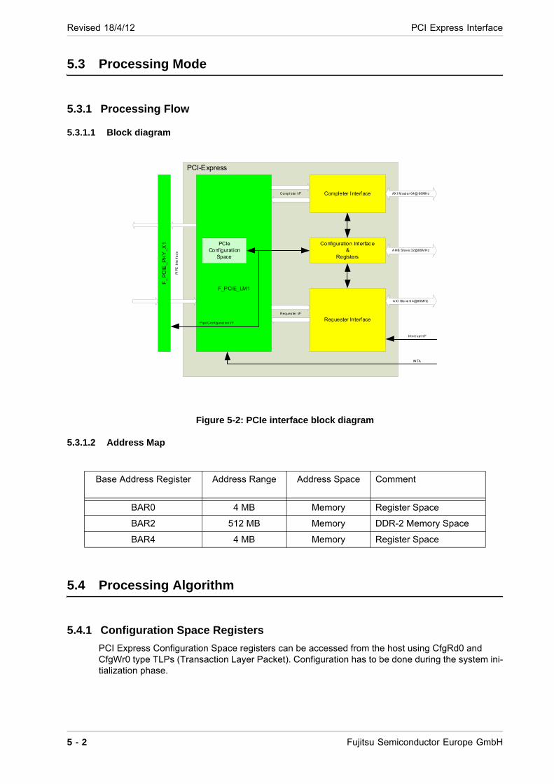
Revised 18/4/12 PCI Express Interface
5.3 Processing Mode
5.3.1 Processing Flow
5.3.1.1 Block diagram
Figure 5-2: PCIe interface block diagram
5.3.1.2 Address Map
5.4 Processing Algorithm
5.4.1 Configuration Space Registers
PCI Express Configuration Space registers can be accessed from the host using CfgRd0 and CfgWr0 type TLPs (Transaction Layer Packet). Configuration has to be done during the system ini-tialization phase.
Base Address Register Address Range Address Space Comment
BAR0 4 MB Memory Register Space
BAR2 512 MB Memory DDR-2 Memory Space
BAR4 4 MB Memory Register Space
F
_P
CIE
_PH
Y_X
1
F_PCIE_LM1
PCIeConf igurat ion
Space
Configurat ion Interface&
Registers
Requester Interface
Completer Interface AX I M aster 64@ 66MHz
AHB S lave 32@66M Hz
AXI Sla ve 6 4@66M Hz
Compl eter I /F
Requester I/F
Interrupt I/F
PCI-Express
INTA
Pipe Conf igurat ion I/F
PIP
E I
nte
rfa
ce
5 - 2 Fujitsu Semiconductor Europe GmbH
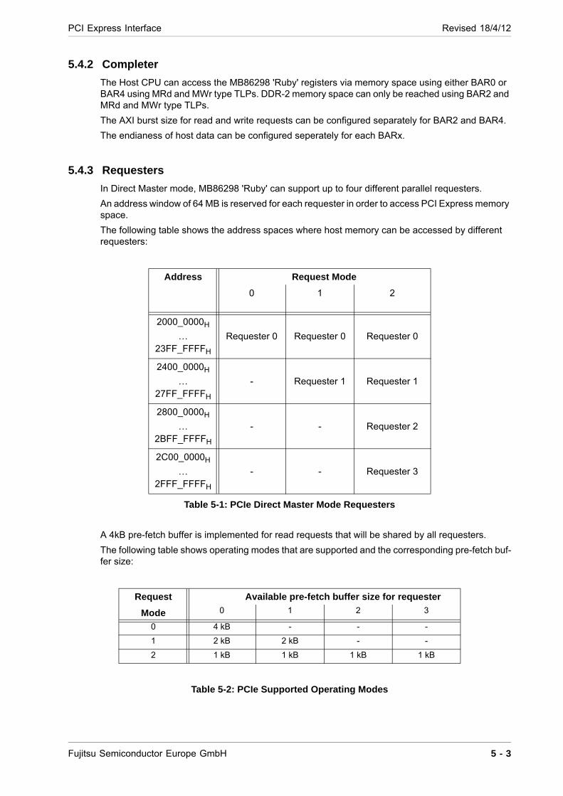
PCI Express Interface Revised 18/4/12
5.4.2 Completer
The Host CPU can access the MB86298 'Ruby' registers via memory space using either BAR0 or BAR4 using MRd and MWr type TLPs. DDR-2 memory space can only be reached using BAR2 and MRd and MWr type TLPs.
The AXI burst size for read and write requests can be configured separately for BAR2 and BAR4.
The endianess of host data can be configured seperately for each BARx.
5.4.3 Requesters
In Direct Master mode, MB86298 'Ruby' can support up to four different parallel requesters.
An address window of 64 MB is reserved for each requester in order to access PCI Express memory space.
The following table shows the address spaces where host memory can be accessed by different requesters:
Table 5-1: PCIe Direct Master Mode Requesters
A 4kB pre-fetch buffer is implemented for read requests that will be shared by all requesters.
The following table shows operating modes that are supported and the corresponding pre-fetch buf-fer size:
Table 5-2: PCIe Supported Operating Modes
Address Request Mode
0 1 2
2000_0000H
…23FF_FFFFH
Requester 0 Requester 0 Requester 0
2400_0000H
…27FF_FFFFH
- Requester 1 Requester 1
2800_0000H
…2BFF_FFFFH
- - Requester 2
2C00_0000H
…2FFF_FFFFH
- - Requester 3
Request Available pre-fetch buffer size for requester
Mode 0 1 2 3
0 4 kB - - -
1 2 kB 2 kB - -
2 1 kB 1 kB 1 kB 1 kB
Fujitsu Semiconductor Europe GmbH 5 - 3
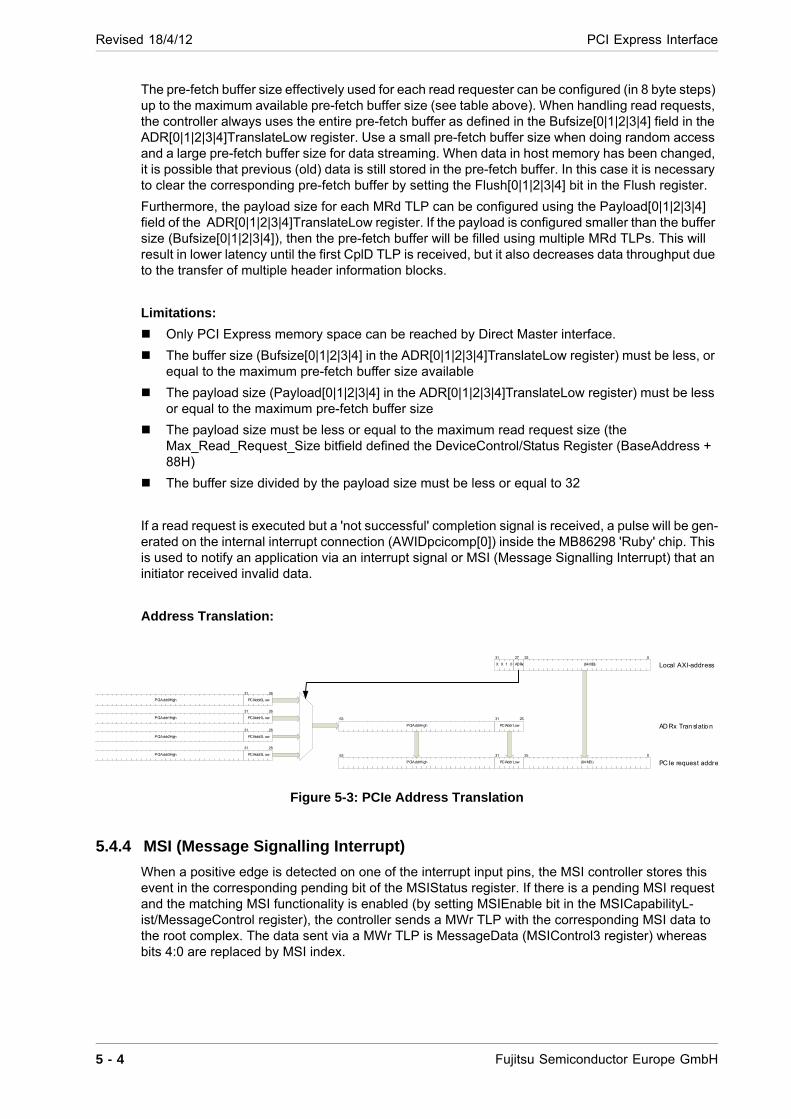
Revised 18/4/12 PCI Express Interface
The pre-fetch buffer size effectively used for each read requester can be configured (in 8 byte steps) up to the maximum available pre-fetch buffer size (see table above). When handling read requests, the controller always uses the entire pre-fetch buffer as defined in the Bufsize[0|1|2|3|4] field in the ADR[0|1|2|3|4]TranslateLow register. Use a small pre-fetch buffer size when doing random access and a large pre-fetch buffer size for data streaming. When data in host memory has been changed, it is possible that previous (old) data is still stored in the pre-fetch buffer. In this case it is necessary to clear the corresponding pre-fetch buffer by setting the Flush[0|1|2|3|4] bit in the Flush register.
Furthermore, the payload size for each MRd TLP can be configured using the Payload[0|1|2|3|4] field of the ADR[0|1|2|3|4]TranslateLow register. If the payload is configured smaller than the buffer size (Bufsize[0|1|2|3|4]), then the pre-fetch buffer will be filled using multiple MRd TLPs. This will result in lower latency until the first CplD TLP is received, but it also decreases data throughput due to the transfer of multiple header information blocks.
Limitations:
Only PCI Express memory space can be reached by Direct Master interface.
The buffer size (Bufsize[0|1|2|3|4] in the ADR[0|1|2|3|4]TranslateLow register) must be less, or equal to the maximum pre-fetch buffer size available
The payload size (Payload[0|1|2|3|4] in the ADR[0|1|2|3|4]TranslateLow register) must be less or equal to the maximum pre-fetch buffer size
The payload size must be less or equal to the maximum read request size (the Max_Read_Request_Size bitfield defined the DeviceControl/Status Register (BaseAddress + 88H)
The buffer size divided by the payload size must be less or equal to 32
If a read request is executed but a 'not successful' completion signal is received, a pulse will be gen-erated on the internal interrupt connection (AWIDpcicomp[0]) inside the MB86298 'Ruby' chip. This is used to notify an application via an interrupt signal or MSI (Message Signalling Interrupt) that an initiator received invalid data.
Address Translation:
Figure 5-3: PCIe Address Translation
5.4.4 MSI (Message Signalling Interrupt)
When a positive edge is detected on one of the interrupt input pins, the MSI controller stores this event in the corresponding pending bit of the MSIStatus register. If there is a pending MSI request and the matching MSI functionality is enabled (by setting MSIEnable bit in the MSICapabilityL-ist/MessageControl register), the controller sends a MWr TLP with the corresponding MSI data to the root complex. The data sent via a MWr TLP is MessageData (MSIControl3 register) whereas bits 4:0 are replaced by MSI index.
Local AXI-address
PCIe request addre
031
03163
2527
ADRxX X 1 0
25
PCIAddr LowPCIAddrHigh
(64 MB)
(64 MB)
3163 26
PCIAddr LowPCIAddrHigh ADRx Tran slatio n
31 26
PCIAddr0L owPCIAddr0High
31 26
PCIAddr1L owPCIAddr1High
31 26
PCIAddr2L owPCIAddr2High
31 26
PCIAddr3L owPCIAddr3High
5 - 4 Fujitsu Semiconductor Europe GmbH
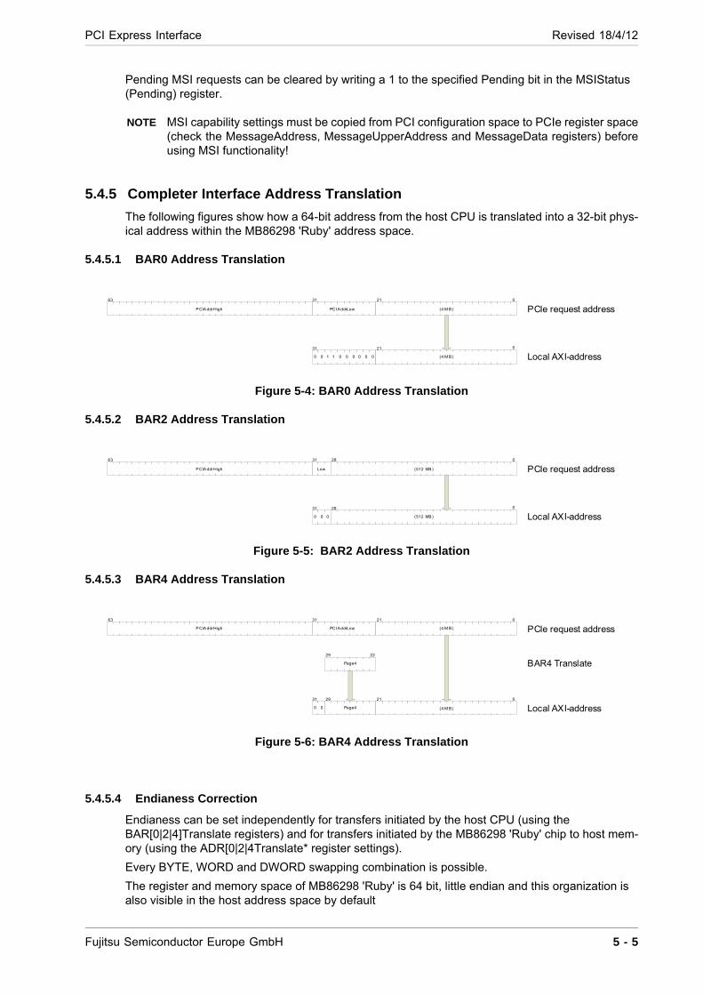
PCI Express Interface Revised 18/4/12
Pending MSI requests can be cleared by writing a 1 to the specified Pending bit in the MSIStatus (Pending) register.
NOTE MSI capability settings must be copied from PCI configuration space to PCIe register space (check the MessageAddress, MessageUpperAddress and MessageData registers) before using MSI functionality!
5.4.5 Completer Interface Address Translation
The following figures show how a 64-bit address from the host CPU is translated into a 32-bit phys-ical address within the MB86298 'Ruby' address space.
5.4.5.1 BAR0 Address Translation
Figure 5-4: BAR0 Address Translation
5.4.5.2 BAR2 Address Translation
Figure 5-5: BAR2 Address Translation
5.4.5.3 BAR4 Address Translation
Figure 5-6: BAR4 Address Translation
5.4.5.4 Endianess Correction
Endianess can be set independently for transfers initiated by the host CPU (using the BAR[0|2|4]Translate registers) and for transfers initiated by the MB86298 'Ruby' chip to host mem-ory (using the ADR[0|2|4Translate* register settings).
Every BYTE, WORD and DWORD swapping combination is possible.
The register and memory space of MB86298 'Ruby' is 64 bit, little endian and this organization is also visible in the host address space by default
Local AXI-address
PCIe request address
031
03163
21
21
PCIAddrLowPCIA ddrHigh
(4 M B )
(4 M B )
0 1 0 0 0 0 0 010
Local AXI-address
PCIe request address
031
03163
28
28
LowPCIA ddrHigh
(512 MB)
(512 MB)
0 00
Local AXI-address
PCIe request address
031
03163
21
21
PCIAddrLowPCIA ddrHigh
(4 M B )
(4 M B )
00
BAR4 Translate
29
Page4
2229
Page4
Fujitsu Semiconductor Europe GmbH 5 - 5
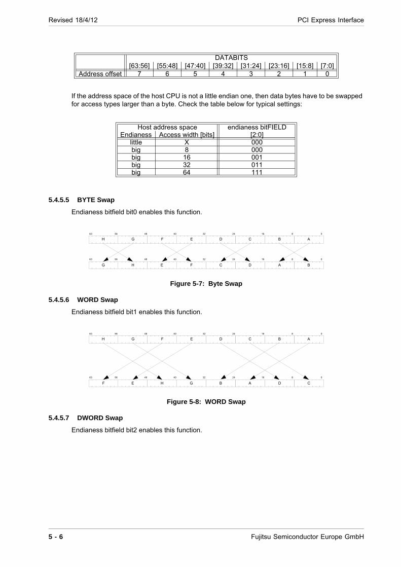
Revised 18/4/12 PCI Express Interface
If the address space of the host CPU is not a little endian one, then data bytes have to be swapped for access types larger than a byte. Check the table below for typical settings:
5.4.5.5 BYTE Swap
Endianess bitfield bit0 enables this function.
Figure 5-7: Byte Swap
5.4.5.6 WORD Swap
Endianess bitfield bit1 enables this function.
Figure 5-8: WORD Swap
5.4.5.7 DWORD Swap
Endianess bitfield bit2 enables this function.
DATABITS[63:56] [55:48] [47:40] [39:32] [31:24] [23:16] [15:8] [7:0]
Address offset 7 6 5 4 3 2 1 0
Host address space endianess bitFIELDEndianess Access width [bits] [2:0]
little X 000big 8 000big 16 001big 32 011big 64 111
0
A
8
B
16
C
24
D
32
E
40
F
48
G
5663
H
BADCFEHG
0816243240485663
0
A
8
B
16
C
24
D
32
E
40
F
48
G
5663
H
CDABGHEF
0816243240485663
5 - 6 Fujitsu Semiconductor Europe GmbH
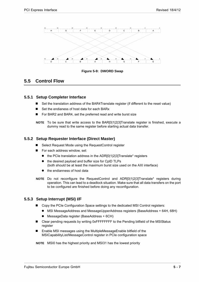
PCI Express Interface Revised 18/4/12
Figure 5-9: DWORD Swap
5.5 Control Flow
5.5.1 Setup Completer Interface
Set the translation address of the BAR4Translate register (if different to the reset value)
Set the endianess of host data for each BARx
For BAR2 and BAR4, set the preferred read and write burst size
NOTE To be sure that write access to the BAR[0|1|2|3]Translate register is finished, execute a dummy read to the same register before starting actual data transfer.
5.5.2 Setup Requester Interface (Direct Master)
Select Request Mode using the RequestControl register
For each address window, set:
the PCIe translation address in the ADR[0|1|2|3]Translate* registers
the desired payload and buffer size for CplD TLPs(both should be at least the maximum burst size used on the AXI interface)
the endianness of host data
NOTE Do not reconfigure the RequestControl and ADR[0|1|2|3]Translate* registers during operation. This can lead to a deadlock situation. Make sure that all data transfers on the port to be configured are finished before doing any reconfiguration.
5.5.3 Setup Interrupt (MSI) I/F
Copy the PCIe Configuration Space settings to the dedicated MSI Control registers:
MSI MessageAddress and MessageUpperAddress registers (BaseAddress + 64H, 68H)
MessageData register (BaseAddress + 6CH)
Clear pending requests by writing 0xFFFFFFFF to the Pending bitfield of the MSIStatus register
Enable MSI messages using the MultipleMessageEnable bitfield of the MSICapabilityList/MessageControl register in PCIe configuration space
NOTE MSI0 has the highest priority and MSI31 has the lowest priority
0
A
8
B
16
C
24
D
32
E
40
F
48
G
5663
H
EFGHABCD
0816243240485663
Fujitsu Semiconductor Europe GmbH 5 - 7
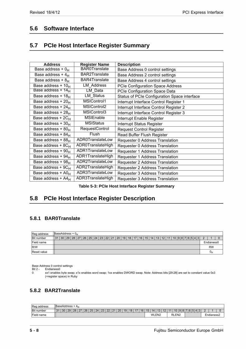
Revised 18/4/12 PCI Express Interface
5.6 Software Interface
5.7 PCIe Host Interface Register Summary
Table 5-3: PCIe Host Interface Register Summary
5.8 PCIe Host Interface Register Description
5.8.1 BAR0Translate
5.8.2 BAR2Translate
Address Register Name DescriptionBase address + 0H BAR0Translate Base Address 0 control settings Base address + 4H BAR2Translate Base Address 2 control settings Base address + 8H BAR4Translate Base Address 4 control settings
Base address + 10H LM_Address PCIe Configuration Space Address Base address + 14H LM_Data PCIe Configuration Space Data Base address + 18H LM_Status Status of PCIe Configuration Space interface Base address + 20H MSIControl1 Interrupt Interface Control Register 1 Base address + 24H MSIControl2 Interrupt Interface Control Register 2 Base address + 28H MSIControl3 Interrupt Interface Control Register 3 Base address + 2CH MSIEnable Interrupt Enable Register Base address + 30H MSIStatus Interrupt Status Register Base address + 80H RequestControl Request Control Register Base address + 84H Flush Read Buffer Flush Register Base address + 88H ADR0TranslateLow Requester 0 Address Translation Base address + 8CH ADR0TranslateHigh Requester 0 Address Translation Base address + 90H ADR1TranslateLow Requester 1 Address Translation Base address + 94H ADR1TranslateHigh Requester 1 Address Translation Base address + 98H ADR2TranslateLow Requester 2 Address Translation Base address + 9CH ADR2TranslateHigh Requester 2 Address Translation Base address + A0H ADR3TranslateLow Requester 3 Address Translation Base address + A4H ADR3TranslateHigh Requester 3 Address Translation
Reg address BaseAddress + 0H
Bit number 31 30 29 28 27 26 25 24 23 22 21 20 19 18 17 16 15 14 13 12 11 10 9 8 7 6 5 4 3 2 1 0
Field name Endianess0
R/W RW
Reset value 0H
Base Address 0 control settings Bit 2 - 0
Endianess0 xx1 enables byte swap; x1x enables word swap; 1xx enables DWORD swap. Note: Address bits [29:28] are set to constant value 0x3 (=register space) in Ruby
Reg address BaseAddress + 4H
Bit number 31 30 29 28 27 26 25 24 23 22 21 20 19 18 17 16 15 14 13 12 11 10 9 8 7 6 5 4 3 2 1 0
Field name WLEN2 RLEN2 Endianess2
5 - 8 Fujitsu Semiconductor Europe GmbH
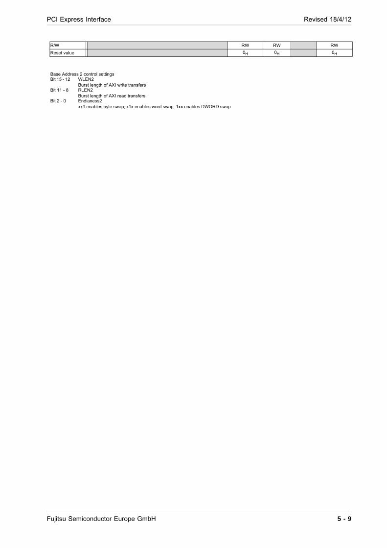
PCI Express Interface Revised 18/4/12
R/W RW RW RW
Reset value 0H 0H 0H
Base Address 2 control settings Bit 15 - 12 WLEN2
Burst length of AXI write transfers Bit 11 - 8 RLEN2
Burst length of AXI read transfers Bit 2 - 0 Endianess2
xx1 enables byte swap; x1x enables word swap; 1xx enables DWORD swap
Fujitsu Semiconductor Europe GmbH 5 - 9
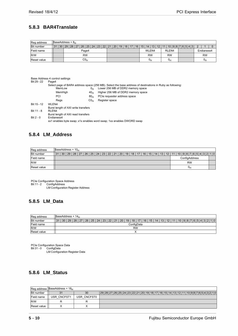
Revised 18/4/12 PCI Express Interface
5.8.3 BAR4Translate
5.8.4 LM_Address
5.8.5 LM_Data
5.8.6 LM_Status
Reg address BaseAddress + 8H
Bit number 31 30 29 28 27 26 25 24 23 22 21 20 19 18 17 16 15 14 13 12 11 10 9 8 7 6 5 4 3 2 1 0
Field name Page4 WLEN4 RLEN4 Endianess4
R/W RW RW RW RW
Reset value C0H 0H 0H 0H
Base Address 4 control settings Bit 29 - 22 Page4
Select page of BAR4 address space (256 MB). Select the base address of destinations in Ruby as following: MemLow 0H Lower 256 MB of DDR2 memory space
MemHigh 40H Higher 256 MB of DDR2 memory space
PCI 80H PCIe requester address space
Regs C0H Register space
Bit 15 - 12 WLEN4 Burst length of AXI write transfers
Bit 11 - 8 RLEN4 Burst length of AXI read transfers
Bit 2 - 0 Endianess4 xx1 enables byte swap; x1x enables word swap; 1xx enables DWORD swap
Reg address BaseAddress + 10H
Bit number 31 30 29 28 27 26 25 24 23 22 21 20 19 18 17 16 15 14 13 12 11 10 9 8 7 6 5 4 3 2 1 0
Field name ConfigAddress
R/W RW
Reset value 0H
PCIe Configuration Space Address Bit 11 - 2 ConfigAddress
LM Configuration Register Address
Reg address BaseAddress + 14H
Bit number 31 30 29 28 27 26 25 24 23 22 21 20 19 18 17 16 15 14 13 12 11 10 9 8 7 6 5 4 3 2 1 0Field name ConfigData R/W RW Reset value X
PCIe Configuration Space Data Bit 31 - 0 ConfigData
LM Configuration Register Data
Reg address BaseAddress + 18H
Bit number 31 30 29 28 27 26 25 24 23 22 21 20 19 18 17 16 15 14 13 12 11 10 9 8 7 6 5 4 3 2 1 0
Field name USR_CNCFST1 USR_CNCFST0
R/W R R
Reset value X X
5 - 10 Fujitsu Semiconductor Europe GmbH
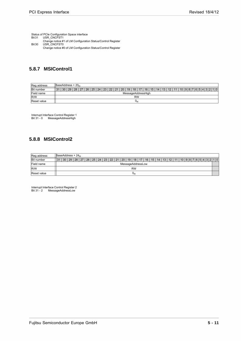
PCI Express Interface Revised 18/4/12
5.8.7 MSIControl1
5.8.8 MSIControl2
Status of PCIe Configuration Space interface Bit 31 USR_CNCFST1
Change notice #1 of LM Configuration Status/Control Register Bit 30 USR_CNCFST0
Change notice #0 of LM Configuration Status/Control Register
Reg address BaseAddress + 20H
Bit number 31 30 29 28 27 26 25 24 23 22 21 20 19 18 17 16 15 14 13 12 11 10 9 8 7 6 5 4 3 2 1 0Field name MessageAddressHigh R/W RW
Reset value 0H
Interrupt Interface Control Register 1 Bit 31 - 0 MessageAddressHigh
Reg address BaseAddress + 24H
Bit number 31 30 29 28 27 26 25 24 23 22 21 20 19 18 17 16 15 14 13 12 11 10 9 8 7 6 5 4 3 2 1 0
Field name MessageAddressLow
R/W RW
Reset value 0H
Interrupt Interface Control Register 2 Bit 31 - 2 MessageAddressLow
Fujitsu Semiconductor Europe GmbH 5 - 11
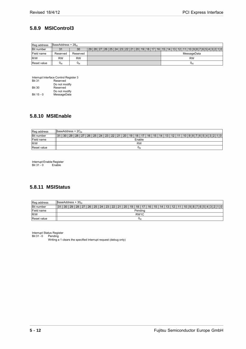
Revised 18/4/12 PCI Express Interface
5.8.9 MSIControl3
5.8.10 MSIEnable
5.8.11 MSIStatus
Reg address BaseAddress + 28H
Bit number 31 30 29 28 27 26 25 24 23 22 21 20 19 18 17 16 15 14 13 12 11 10 9 8 7 6 5 4 3 2 1 0
Field name Reserved Reserved MessageData
R/W RW RW RW
Reset value 0H 0H 0H
Interrupt Interface Control Register 3 Bit 31 Reserved
Do not modify Bit 30 Reserved
Do not modify Bit 15 - 0 MessageData
Reg address BaseAddress + 2CH
Bit number 31 30 29 28 27 26 25 24 23 22 21 20 19 18 17 16 15 14 13 12 11 10 9 8 7 6 5 4 3 2 1 0Field name Enable R/W RW
Reset value 0H
Interrupt Enable Register Bit 31 - 0 Enable
Reg address BaseAddress + 30H
Bit number 31 30 29 28 27 26 25 24 23 22 21 20 19 18 17 16 15 14 13 12 11 10 9 8 7 6 5 4 3 2 1 0Field name Pending R/W RW1C
Reset value 0H
Interrupt Status Register Bit 31 - 0 Pending
Writing a 1 clears the specified interrupt request (debug only)
5 - 12 Fujitsu Semiconductor Europe GmbH
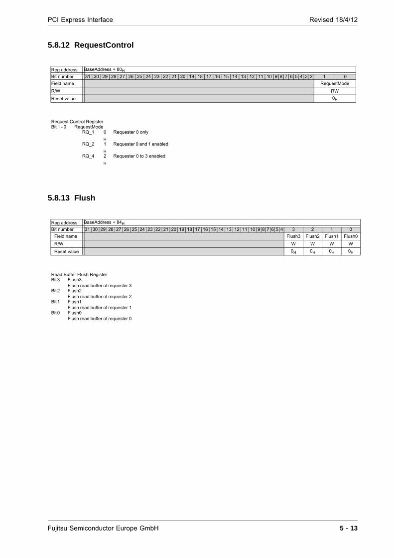
PCI Express Interface Revised 18/4/12
5.8.12 RequestControl
5.8.13 Flush
Reg address BaseAddress + 80H
Bit number 31 30 29 28 27 26 25 24 23 22 21 20 19 18 17 16 15 14 13 12 11 10 9 8 7 6 5 4 3 2 1 0
Field name RequestMode
R/W RW
Reset value 0H
Request Control Register Bit 1 - 0 RequestMode
RQ_1 0
H
Requester 0 only
RQ_2 1
H
Requester 0 and 1 enabled
RQ_4 2
H
Requester 0 to 3 enabled
Reg address BaseAddress + 84H
Bit number 31 30 29 28 27 26 25 24 23 22 21 20 19 18 17 16 15 14 13 12 11 10 9 8 7 6 5 4 3 2 1 0
Field name Flush3 Flush2 Flush1 Flush0
R/W W W W W
Reset value 0H 0H 0H 0H
Read Buffer Flush Register Bit 3 Flush3
Flush read buffer of requester 3 Bit 2 Flush2
Flush read buffer of requester 2 Bit 1 Flush1
Flush read buffer of requester 1 Bit 0 Flush0
Flush read buffer of requester 0
Fujitsu Semiconductor Europe GmbH 5 - 13
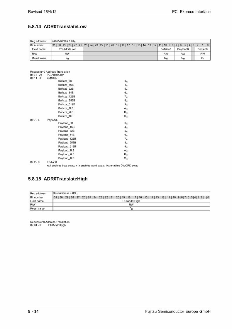
Revised 18/4/12 PCI Express Interface
5.8.14 ADR0TranslateLow
5.8.15 ADR0TranslateHigh
Reg address BaseAddress + 88H
Bit number 31 30 29 28 27 26 25 24 23 22 21 20 19 18 17 16 15 14 13 12 11 10 9 8 7 6 5 4 3 2 1 0
Field name PCIAddr0Low Bufsize0 Payload0 Endian0
R/W RW RW RW RW
Reset value 0H CH CH 0H
Requester 0 Address Translation Bit 31 - 26 PCIAddr0Low Bit 11 - 8 Bufsize0
Bufsize_8B 3H
Bufsize_16B 4H
Bufsize_32B 5H
Bufsize_64B 6H
Bufsize_128B 7H
Bufsize_256B 8H
Bufsize_512B 9H
Bufsize_1kB AH
Bufsize_2kB BH
Bufsize_4kB CH
Bit 7 - 4 Payload0 Payload_8B 3H
Payload_16B 4H
Payload_32B 5H
Payload_64B 6H
Payload_128B 7H
Payload_256B 8H
Payload_512B 9H
Payload_1kB AH
Payload_2kB BH
Payload_4kB CH
Bit 2 - 0 Endian0 xx1 enables byte swap; x1x enables word swap; 1xx enables DWORD swap
Reg address BaseAddress + 8CH
Bit number 31 30 29 28 27 26 25 24 23 22 21 20 19 18 17 16 15 14 13 12 11 10 9 8 7 6 5 4 3 2 1 0Field name PCIAddr0High R/W RW
Reset value 0H
Requester 0 Address Translation Bit 31 - 0 PCIAddr0High
5 - 14 Fujitsu Semiconductor Europe GmbH
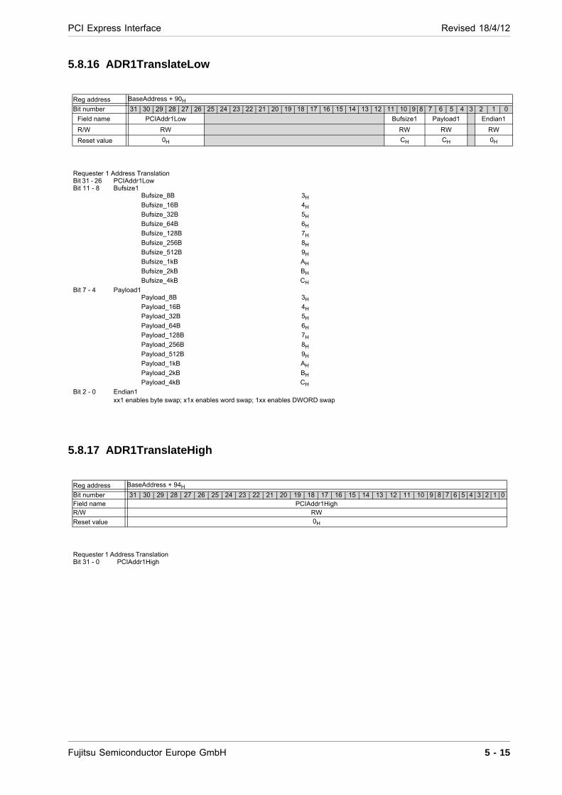
PCI Express Interface Revised 18/4/12
5.8.16 ADR1TranslateLow
5.8.17 ADR1TranslateHigh
Reg address BaseAddress + 90H
Bit number 31 30 29 28 27 26 25 24 23 22 21 20 19 18 17 16 15 14 13 12 11 10 9 8 7 6 5 4 3 2 1 0
Field name PCIAddr1Low Bufsize1 Payload1 Endian1
R/W RW RW RW RW
Reset value 0H CH CH 0H
Requester 1 Address Translation Bit 31 - 26 PCIAddr1Low Bit 11 - 8 Bufsize1
Bufsize_8B 3H
Bufsize_16B 4H
Bufsize_32B 5H
Bufsize_64B 6H
Bufsize_128B 7H
Bufsize_256B 8H
Bufsize_512B 9H
Bufsize_1kB AH
Bufsize_2kB BH
Bufsize_4kB CH
Bit 7 - 4 Payload1 Payload_8B 3H
Payload_16B 4H
Payload_32B 5H
Payload_64B 6H
Payload_128B 7H
Payload_256B 8H
Payload_512B 9H
Payload_1kB AH
Payload_2kB BH
Payload_4kB CH
Bit 2 - 0 Endian1 xx1 enables byte swap; x1x enables word swap; 1xx enables DWORD swap
Reg address BaseAddress + 94H
Bit number 31 30 29 28 27 26 25 24 23 22 21 20 19 18 17 16 15 14 13 12 11 10 9 8 7 6 5 4 3 2 1 0Field name PCIAddr1High R/W RW
Reset value 0H
Requester 1 Address Translation Bit 31 - 0 PCIAddr1High
Fujitsu Semiconductor Europe GmbH 5 - 15
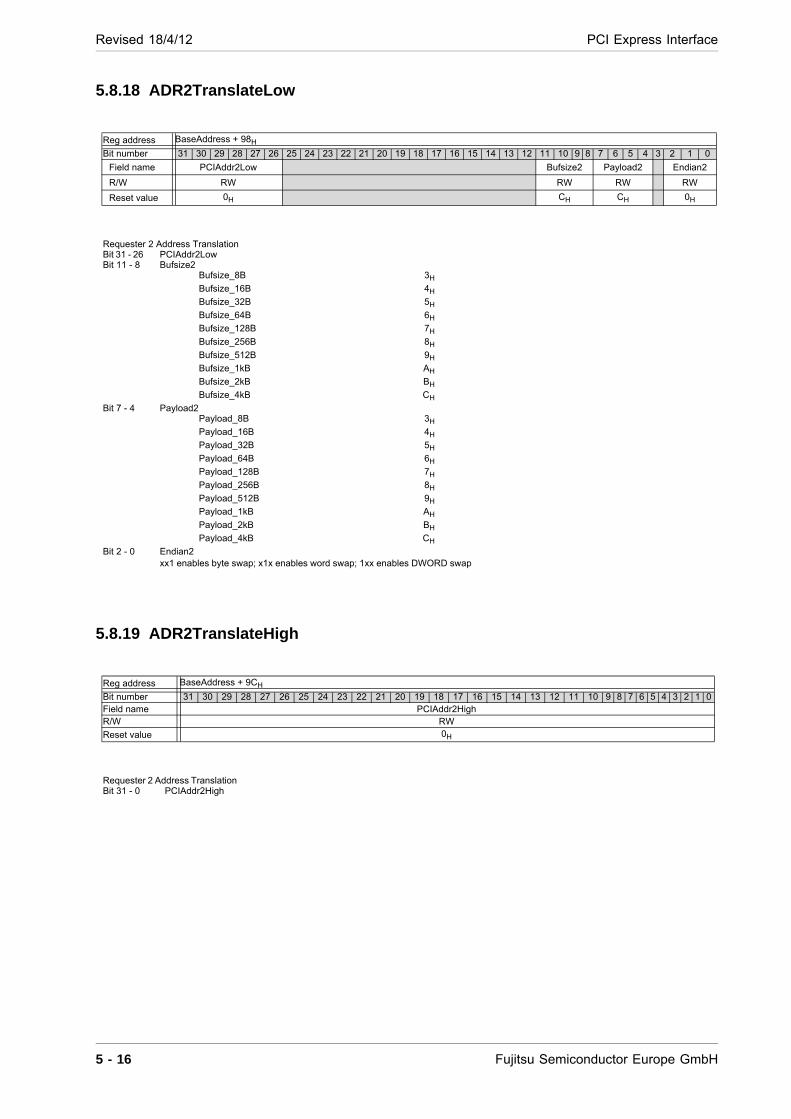
Revised 18/4/12 PCI Express Interface
5.8.18 ADR2TranslateLow
5.8.19 ADR2TranslateHigh
Reg address BaseAddress + 98H
Bit number 31 30 29 28 27 26 25 24 23 22 21 20 19 18 17 16 15 14 13 12 11 10 9 8 7 6 5 4 3 2 1 0
Field name PCIAddr2Low Bufsize2 Payload2 Endian2
R/W RW RW RW RW
Reset value 0H CH CH 0H
Requester 2 Address Translation Bit 31 - 26 PCIAddr2Low Bit 11 - 8 Bufsize2
Bufsize_8B 3H
Bufsize_16B 4H
Bufsize_32B 5H
Bufsize_64B 6H
Bufsize_128B 7H
Bufsize_256B 8H
Bufsize_512B 9H
Bufsize_1kB AH
Bufsize_2kB BH
Bufsize_4kB CH
Bit 7 - 4 Payload2 Payload_8B 3H
Payload_16B 4H
Payload_32B 5H
Payload_64B 6H
Payload_128B 7H
Payload_256B 8H
Payload_512B 9H
Payload_1kB AH
Payload_2kB BH
Payload_4kB CH
Bit 2 - 0 Endian2 xx1 enables byte swap; x1x enables word swap; 1xx enables DWORD swap
Reg address BaseAddress + 9CH
Bit number 31 30 29 28 27 26 25 24 23 22 21 20 19 18 17 16 15 14 13 12 11 10 9 8 7 6 5 4 3 2 1 0Field name PCIAddr2High R/W RW
Reset value 0H
Requester 2 Address Translation Bit 31 - 0 PCIAddr2High
5 - 16 Fujitsu Semiconductor Europe GmbH
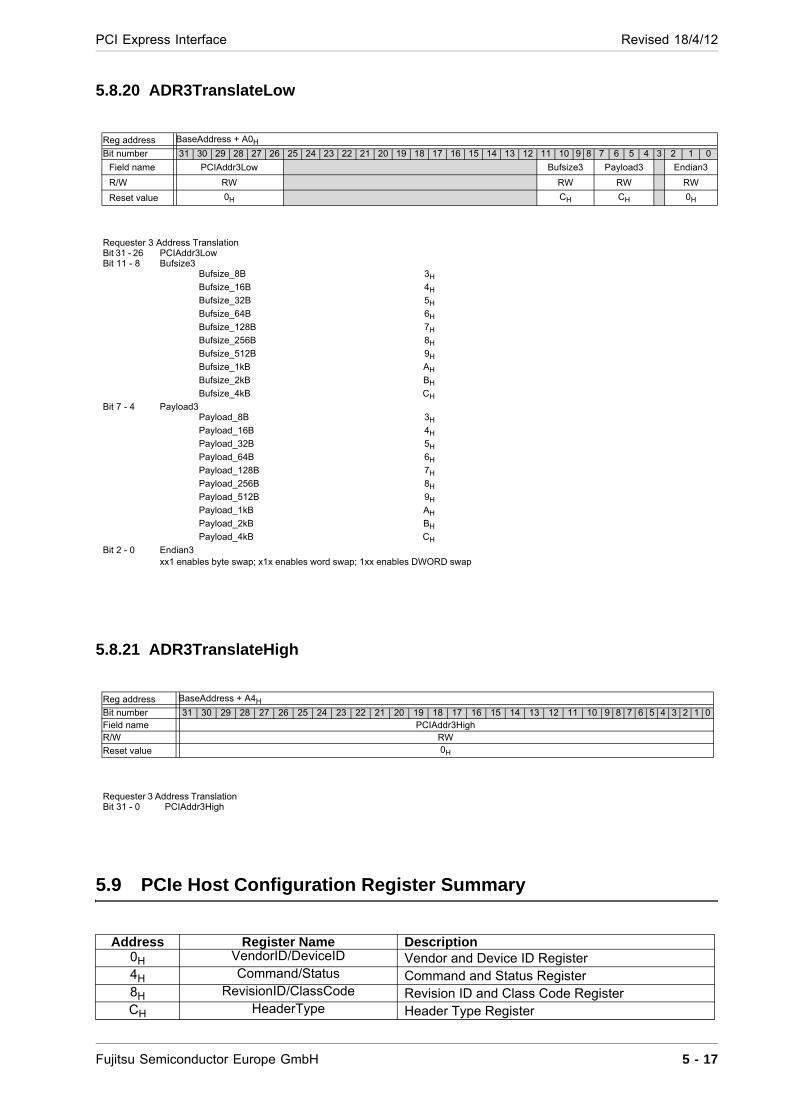
PCI Express Interface Revised 18/4/12
5.8.20 ADR3TranslateLow
5.8.21 ADR3TranslateHigh
5.9 PCIe Host Configuration Register Summary
Reg address BaseAddress + A0H
Bit number 31 30 29 28 27 26 25 24 23 22 21 20 19 18 17 16 15 14 13 12 11 10 9 8 7 6 5 4 3 2 1 0
Field name PCIAddr3Low Bufsize3 Payload3 Endian3
R/W RW RW RW RW
Reset value 0H CH CH 0H
Requester 3 Address Translation Bit 31 - 26 PCIAddr3Low Bit 11 - 8 Bufsize3
Bufsize_8B 3H
Bufsize_16B 4H
Bufsize_32B 5H
Bufsize_64B 6H
Bufsize_128B 7H
Bufsize_256B 8H
Bufsize_512B 9H
Bufsize_1kB AH
Bufsize_2kB BH
Bufsize_4kB CH
Bit 7 - 4 Payload3 Payload_8B 3H
Payload_16B 4H
Payload_32B 5H
Payload_64B 6H
Payload_128B 7H
Payload_256B 8H
Payload_512B 9H
Payload_1kB AH
Payload_2kB BH
Payload_4kB CH
Bit 2 - 0 Endian3 xx1 enables byte swap; x1x enables word swap; 1xx enables DWORD swap
Reg address BaseAddress + A4H
Bit number 31 30 29 28 27 26 25 24 23 22 21 20 19 18 17 16 15 14 13 12 11 10 9 8 7 6 5 4 3 2 1 0Field name PCIAddr3High R/W RW
Reset value 0H
Requester 3 Address Translation Bit 31 - 0 PCIAddr3High
Address Register Name Description0H VendorID/DeviceID Vendor and Device ID Register 4H Command/Status Command and Status Register 8H RevisionID/ClassCode Revision ID and Class Code Register CH HeaderType Header Type Register
Fujitsu Semiconductor Europe GmbH 5 - 17
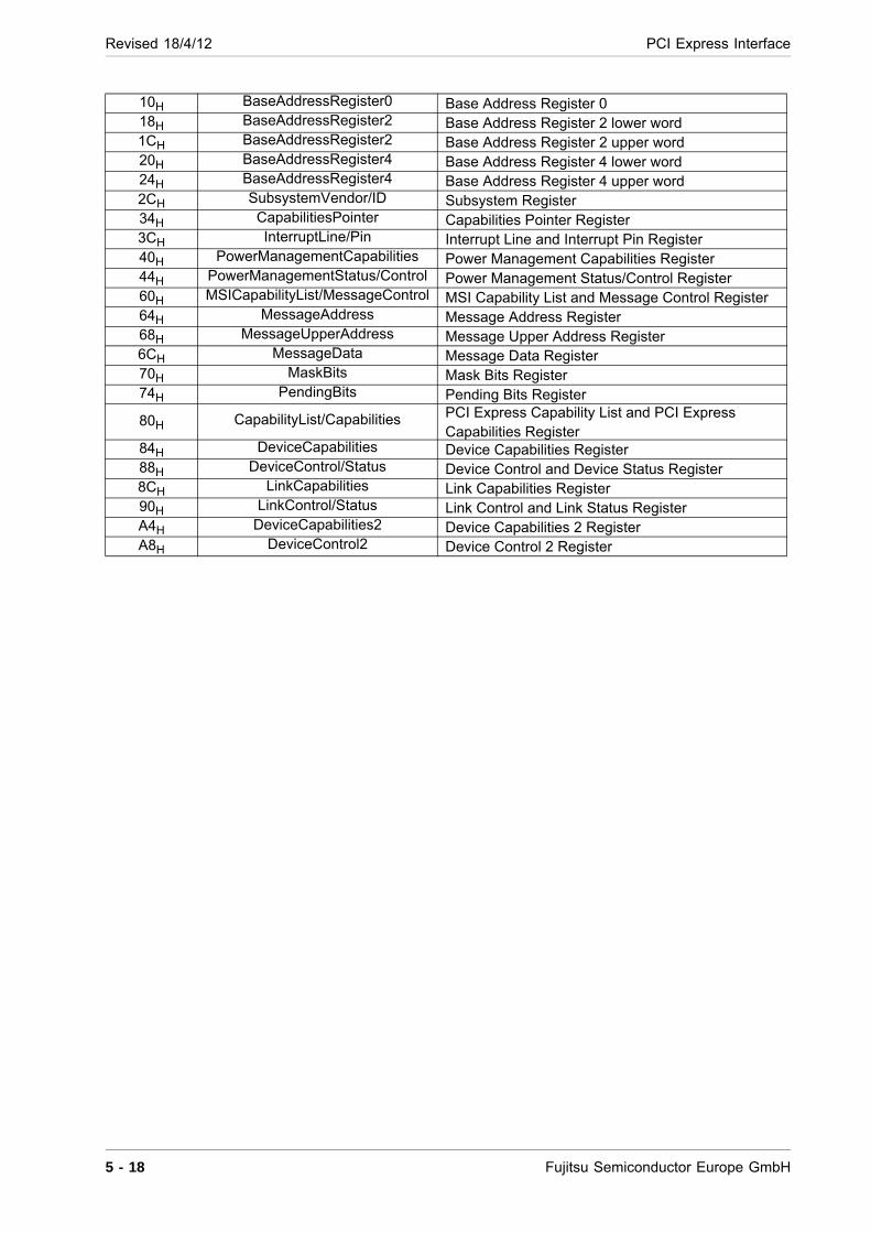
Revised 18/4/12 PCI Express Interface
10H BaseAddressRegister0 Base Address Register 0 18H BaseAddressRegister2 Base Address Register 2 lower word 1CH BaseAddressRegister2 Base Address Register 2 upper word 20H BaseAddressRegister4 Base Address Register 4 lower word 24H BaseAddressRegister4 Base Address Register 4 upper word 2CH SubsystemVendor/ID Subsystem Register 34H CapabilitiesPointer Capabilities Pointer Register 3CH InterruptLine/Pin Interrupt Line and Interrupt Pin Register 40H PowerManagementCapabilities Power Management Capabilities Register 44H PowerManagementStatus/Control Power Management Status/Control Register 60H MSICapabilityList/MessageControl MSI Capability List and Message Control Register 64H MessageAddress Message Address Register 68H MessageUpperAddress Message Upper Address Register 6CH MessageData Message Data Register 70H MaskBits Mask Bits Register 74H PendingBits Pending Bits Register
80H CapabilityList/Capabilities PCI Express Capability List and PCI Express Capabilities Register
84H DeviceCapabilities Device Capabilities Register 88H DeviceControl/Status Device Control and Device Status Register 8CH LinkCapabilities Link Capabilities Register 90H LinkControl/Status Link Control and Link Status Register A4H DeviceCapabilities2 Device Capabilities 2 Register A8H DeviceControl2 Device Control 2 Register
5 - 18 Fujitsu Semiconductor Europe GmbH
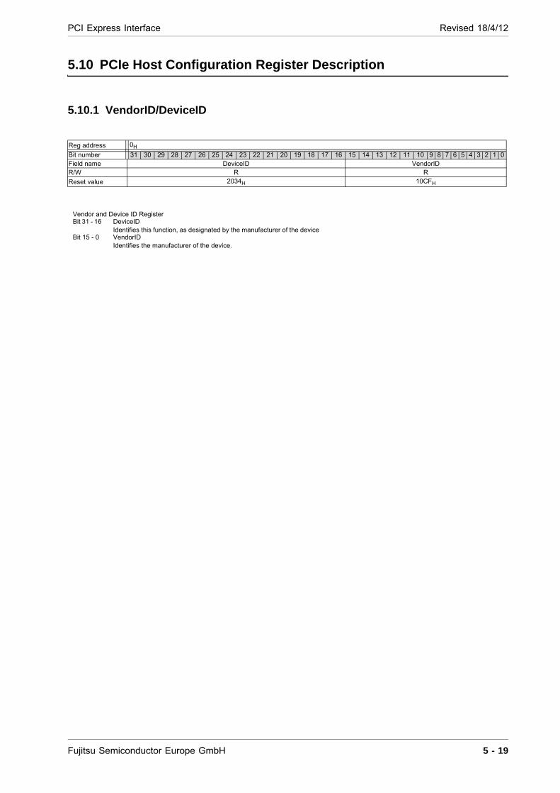
PCI Express Interface Revised 18/4/12
5.10 PCIe Host Configuration Register Description
5.10.1 VendorID/DeviceID
Reg address 0H
Bit number 31 30 29 28 27 26 25 24 23 22 21 20 19 18 17 16 15 14 13 12 11 10 9 8 7 6 5 4 3 2 1 0Field name DeviceID VendorID R/W R R
Reset value 2034H 10CFH
Vendor and Device ID Register Bit 31 - 16 DeviceID
Identifies this function, as designated by the manufacturer of the device Bit 15 - 0 VendorID
Identifies the manufacturer of the device.
Fujitsu Semiconductor Europe GmbH 5 - 19
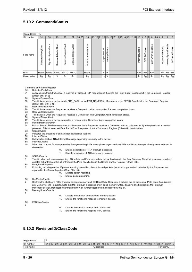
Revised 18/4/12 PCI Express Interface
5.10.2 Command/Status
5.10.3 RevisionID/ClassCode
Reg address 4H
Bit number 31 30 29 28 27 26 25 24 23 22 21 20 19 18 17 16 15 14 13 12 11 10 9 8 7 6 5 4 3 2 1 0
Field name
De
tect
edP
arit
yErr
or
Sig
nale
dS
yste
mE
rro
r
Rec
eive
dM
aste
rAbo
rt
Re
ceiv
ed
Ta
rge
tAb
ort
Sig
nale
dT
arg
etA
bor
t
Ma
ster
Da
taP
arit
yErr
or
Ca
pa
bilit
yLis
t
Inte
rru
ptS
tatu
s
Inte
rru
ptD
isa
ble
SE
RR
#En
abl
e
Pa
rityE
rro
rRes
pon
se
Bus
Mas
terE
na
ble
Me
mor
ySp
ace
En
ab
le
I/O
Sp
ace
Ena
ble
R/W RW1C RW1C RW1C RW1C RW1C RW1C R R RW RW RW RW RW RW
Reset value 0H 0H X 0H 0H 0H 1H X 0H 0H 0H 0H 0H 0H
Command and Status Register Bit 31
DetectedParityError A device sets this bit whenever it receives a Poisoned TLP, regardless of the state the Parity Error Response bit in the Command Register (Offset 04h: bit 6).
Bit 30
SignaledSystemError This bit is set when a device sends ERR_FATAL or an ERR_NONFATAL Message and the SERR# Enable bit in the Command Register (Offset 04h: bit8) is 1b.
Bit 29
ReceivedMasterAbort This bit is set when the Requester receives a Completion with Unsupported Request completion status.
Bit 28
ReceivedTargetAbort This bit is set when the Requester receives a Completion with Completer Abort completion status.
Bit 27
SignaledTargetAbort This bit is set when a device completes a request using Completer Abort completion status.
Bit 24
MasterDataParityError Poison Report. The Requester sets this bit either 1) the Requester receives a Comletion marked poisoned, or 2) a Request itself is marked poisoned. This bit never set if the Parity Error Response bit in the Command Register (Offset 04h: bit 6) is clear.
Bit 20
CapabilityList Indicates the presence of an extended capabilities list item.
Bit 19
InterruptStatus 0b Indicates that an INTA Interrupt Message is pending internally to the device.
Bit 10
InterruptDisable When this bit is set, function prevented from generating INTx interrupt messages, and any INTx emulation interrupts already asserted must be deasserted.
0H Enable generation of INTA interrupt messages.
1H Disable generation of INTA interrupt messages.
Bit 8
SERR#Enable This bit, when set, enables reporting of Non-fatal and Fatal errors detected by the device to the Root Complex. Note that errors are reported if enabled either through this bit or through the PCIe specific bits in the Device Control Register (Offset: 88h).
Bit 6
ParityErrorResponse Poisoning reporting control. If poison reporting is enabled, then poisoned packets (received or generated) detected by the Requester are reported in the Status Register (Offset 06h: bit8)
0H Disable poison reporting.
1H Enable poison reporting.
Bit 2
BusMasterEnable Controls the ability of a PCIe Endpoint to issue Memory and I/O Read/Write Requests. Disabling this bit prevents a PCIe agent from issuing any Memory or I/O Requests. Note that MSI interrupt messages are in-band memory writes, disabling this bit disables MSI interrupt messages as well. Requests other than Memory or I/O Requests are not controlled by this bit.
Bit 1
MemorySpaceEnable
0H Disable the function to respond to memory access.
1H Enable the function to respond to memory access.
Bit 0
I/OSpaceEnable
0H Disable the function to respond to I/O access.
1H Enable the function to respond to I/O access.
Reg address 8H
Bit number 31 30 29 28 27 26 25 24 23 22 21 20 19 18 17 16 15 14 13 12 11 10 9 8 7 6 5 4 3 2 1 0Field name ClassCode RevisionID
5 - 20 Fujitsu Semiconductor Europe GmbH
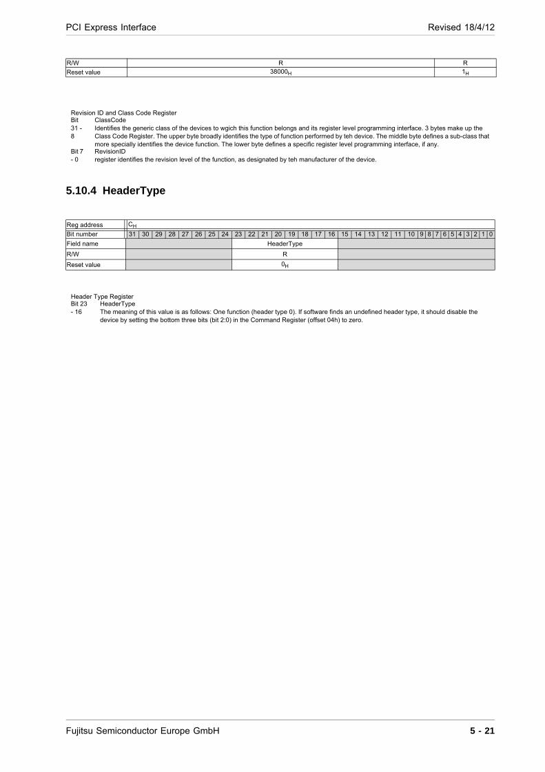
PCI Express Interface Revised 18/4/12
5.10.4 HeaderType
R/W R R
Reset value 38000H 1H
Revision ID and Class Code Register Bit 31 - 8
ClassCode Identifies the generic class of the devices to wgich this function belongs and its register level programming interface. 3 bytes make up the Class Code Register. The upper byte broadly identifies the type of function performed by teh device. The middle byte defines a sub-class that more specially identifies the device function. The lower byte defines a specific register level programming interface, if any.
Bit 7 - 0
RevisionID register identifies the revision level of the function, as designated by teh manufacturer of the device.
Reg address CH
Bit number 31 30 29 28 27 26 25 24 23 22 21 20 19 18 17 16 15 14 13 12 11 10 9 8 7 6 5 4 3 2 1 0
Field name HeaderType
R/W R
Reset value 0H
Header Type Register Bit 23 - 16
HeaderType The meaning of this value is as follows: One function (header type 0). If software finds an undefined header type, it should disable the device by setting the bottom three bits (bit 2:0) in the Command Register (offset 04h) to zero.
Fujitsu Semiconductor Europe GmbH 5 - 21
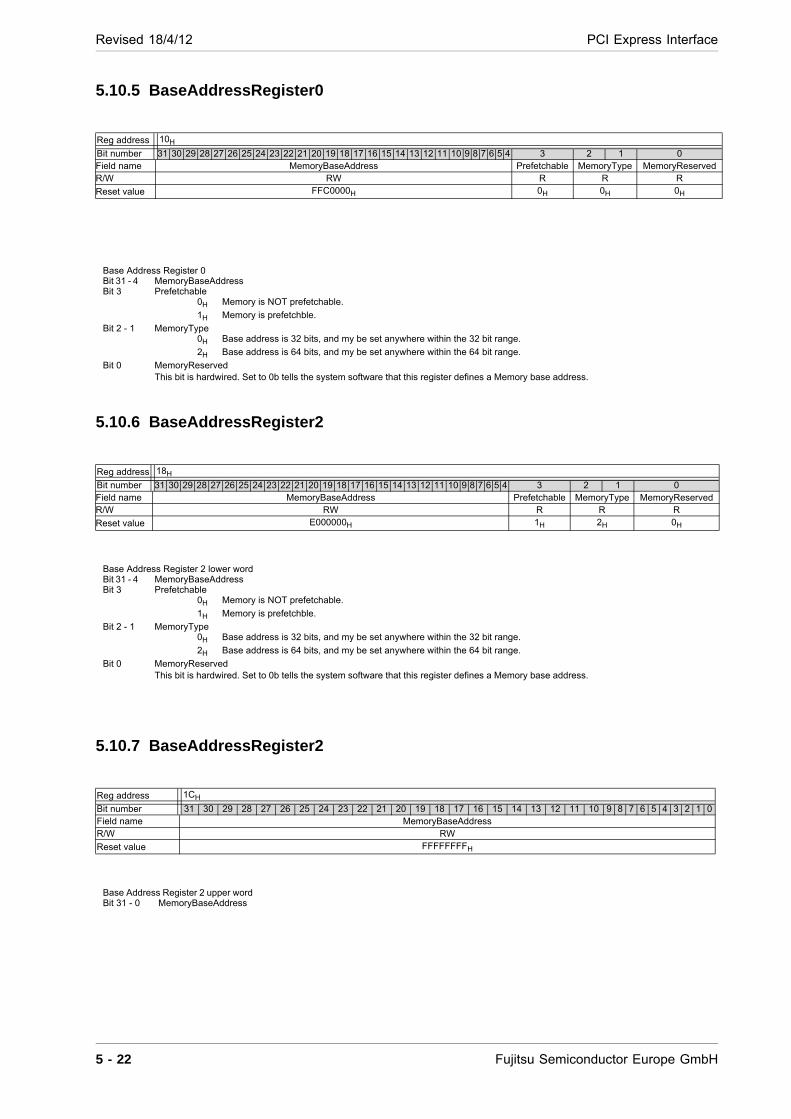
Revised 18/4/12 PCI Express Interface
5.10.5 BaseAddressRegister0
5.10.6 BaseAddressRegister2
5.10.7 BaseAddressRegister2
Reg address 10H
Bit number 31 30 29 28 27 26 25 24 23 22 21 20 19 18 17 16 15 14 13 12 11 10 9 8 7 6 5 4 3 2 1 0Field name MemoryBaseAddress Prefetchable MemoryType MemoryReserved R/W RW R R R
Reset value FFC0000H 0H 0H 0H
Base Address Register 0 Bit 31 - 4 MemoryBaseAddress Bit 3 Prefetchable
0H Memory is NOT prefetchable.
1H Memory is prefetchble.
Bit 2 - 1 MemoryType 0H Base address is 32 bits, and my be set anywhere within the 32 bit range.
2H Base address is 64 bits, and my be set anywhere within the 64 bit range.
Bit 0 MemoryReserved This bit is hardwired. Set to 0b tells the system software that this register defines a Memory base address.
Reg address 18H
Bit number 31 30 29 28 27 26 25 24 23 22 21 20 19 18 17 16 15 14 13 12 11 10 9 8 7 6 5 4 3 2 1 0Field name MemoryBaseAddress Prefetchable MemoryType MemoryReserved R/W RW R R R
Reset value E000000H 1H 2H 0H
Base Address Register 2 lower word Bit 31 - 4 MemoryBaseAddress Bit 3 Prefetchable
0H Memory is NOT prefetchable.
1H Memory is prefetchble.
Bit 2 - 1 MemoryType 0H Base address is 32 bits, and my be set anywhere within the 32 bit range.
2H Base address is 64 bits, and my be set anywhere within the 64 bit range.
Bit 0 MemoryReserved This bit is hardwired. Set to 0b tells the system software that this register defines a Memory base address.
Reg address 1CH
Bit number 31 30 29 28 27 26 25 24 23 22 21 20 19 18 17 16 15 14 13 12 11 10 9 8 7 6 5 4 3 2 1 0Field name MemoryBaseAddress R/W RW
Reset value FFFFFFFFH
Base Address Register 2 upper word Bit 31 - 0 MemoryBaseAddress
5 - 22 Fujitsu Semiconductor Europe GmbH
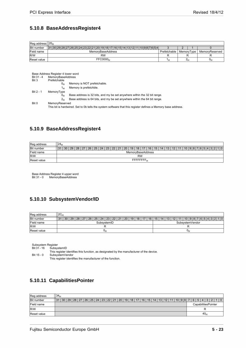
PCI Express Interface Revised 18/4/12
5.10.8 BaseAddressRegister4
5.10.9 BaseAddressRegister4
5.10.10 SubsystemVendor/ID
5.10.11 CapabilitiesPointer
Reg address 20H
Bit number 31 30 29 28 27 26 25 24 23 22 21 20 19 18 17 16 15 14 13 12 11 10 9 8 7 6 5 4 3 2 1 0Field name MemoryBaseAddress Prefetchable MemoryType MemoryReserved R/W RW R R R
Reset value FFC0000H 1H 2H 0H
Base Address Register 4 lower word Bit 31 - 4 MemoryBaseAddress Bit 3 Prefetchable
0H Memory is NOT prefetchable.
1H Memory is prefetchble.
Bit 2 - 1 MemoryType 0H Base address is 32 bits, and my be set anywhere within the 32 bit range.
2H Base address is 64 bits, and my be set anywhere within the 64 bit range.
Bit 0 MemoryReserved This bit is hardwired. Set to 0b tells the system software that this register defines a Memory base address.
Reg address 24H
Bit number 31 30 29 28 27 26 25 24 23 22 21 20 19 18 17 16 15 14 13 12 11 10 9 8 7 6 5 4 3 2 1 0Field name MemoryBaseAddress R/W RW
Reset value FFFFFFFFH
Base Address Register 4 upper word Bit 31 - 0 MemoryBaseAddress
Reg address 2CH
Bit number 31 30 29 28 27 26 25 24 23 22 21 20 19 18 17 16 15 14 13 12 11 10 9 8 7 6 5 4 3 2 1 0Field name SubsystemID SubsystemVendor R/W R R
Reset value 0H 0H
Subsystem Register Bit 31 - 16 SubsystemID
This register identifies this function, as designated by the manufacturer of the device. Bit 15 - 0 SubsystemVendor
This register identifies the manufacturer of the function.
Reg address 34H
Bit number 31 30 29 28 27 26 25 24 23 22 21 20 19 18 17 16 15 14 13 12 11 10 9 8 7 6 5 4 3 2 1 0
Field name CapabilitiesPointer
R/W R
Reset value 40H
Fujitsu Semiconductor Europe GmbH 5 - 23
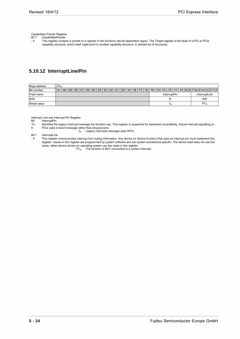
Revised 18/4/12 PCI Express Interface
5.10.12 InterruptLine/Pin
Capabilities Pointer Register Bit 7 - 0
CapabilitiesPointer This register contains a pointer to a register in the functions device dependent region. The Target register is the head of a PCI or PCIe capability structure, which itself might point to another capability structure, in alinked list of structures.
Regi address 3CH
Bit number 31 30 29 28 27 26 25 24 23 22 21 20 19 18 17 16 15 14 13 12 11 10 9 8 7 6 5 4 3 2 1 0
Field name InterruptPin InterruptLine
R/W R RW
Reset value 1H FFH
Interrupt Line and Interrupt Pin Register Bit 15 - 8
InterruptPin Identifies the legacy interrupt message the function use. This register is supported for backward compatibility. Actual interrupt signalling on PCIe uses in-band message rather than physical pins.
1H Legacy interrupts message uses INTA.
Bit 7 - 0
InterruptLine This register communicates interrupt line routing information. Any device (or device function) that uses an interrupt pin must implement this register. Values in this register are programmed by system software and are system architecture specific. The device itself does not use this value; rather device drivers an operating system use the value in this register.
FFH The function is NOT connected to a system interrupt.
5 - 24 Fujitsu Semiconductor Europe GmbH
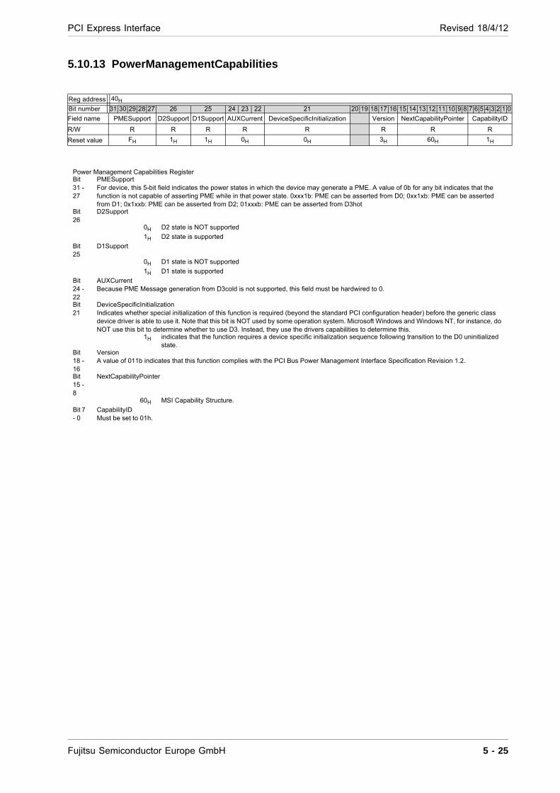
PCI Express Interface Revised 18/4/12
5.10.13 PowerManagementCapabilities
Reg address 40H
Bit number 31 30 29 28 27 26 25 24 23 22 21 20 19 18 17 16 15 14 13 12 11 10 9 8 7 6 5 4 3 2 1 0
Field name PMESupport D2Support D1Support AUXCurrent DeviceSpecificInitialization Version NextCapabilityPointer CapabilityID
R/W R R R R R R R R
Reset value FH 1H 1H 0H 0H 3H 60H 1H
Power Management Capabilities Register Bit 31 - 27
PMESupport For device, this 5-bit field indicates the power states in which the device may generate a PME. A value of 0b for any bit indicates that the function is not capable of asserting PME while in that power state. 0xxx1b: PME can be asserted from D0; 0xx1xb: PME can be asserted from D1; 0x1xxb: PME can be asserted from D2; 01xxxb: PME can be asserted from D3hot
Bit 26
D2Support
0H D2 state is NOT supported
1H D2 state is supported
Bit 25
D1Support
0H D1 state is NOT supported
1H D1 state is supported
Bit 24 - 22
AUXCurrent Because PME Message generation from D3cold is not supported, this field must be hardwired to 0.
Bit 21
DeviceSpecificInitialization Indicates whether special initialization of this function is required (beyond the standard PCI configuration header) before the generic class device driver is able to use it. Note that this bit is NOT used by some operation system. Microsoft Windows and Windows NT, for instance, do NOT use this bit to determine whether to use D3. Instead, they use the drivers capabilities to determine this.
1H indicates that the function requires a device specific initialization sequence following transition to the D0 uninitialized state.
Bit 18 - 16
Version A value of 011b indicates that this function complies with the PCI Bus Power Management Interface Specification Revision 1.2.
Bit 15 - 8
NextCapabilityPointer
60H MSI Capability Structure.
Bit 7 - 0
CapabilityID Must be set to 01h.
Fujitsu Semiconductor Europe GmbH 5 - 25

Revised 18/4/12 PCI Express Interface
5.10.14 PowerManagementStatus/Control
Reg address 44H
Bit number 31 30 29 28 27 26 25 24 23 22 21 20 19 18 17 16 15 14 13 12 11 10 9 8 7 6 5 4 3 2 1 0
Field name PMEStatus PMEEnable No_Soft_Reset PowerState
R/W RW1C RW R RW
Reset value 0H 0H 1H 0H
Power Management Status/Control Register Bit 15 PMEStatus
This bit is set when the function would normally assert PME independent of the state of the PME Enable bit (bit 8). Writing 1b to this bit will clear it and cause the function to stop asserting PME.
Bit 8 PMEEnable 1b enables the function to assert PME. When 0b, PME assertion is disabled.
Bit 3 No_Soft_Reset When set (1b), this bit indicates that devices transitioning from D3hot to D0 because of PowerState commands do not perform an internal reset. Configuration context is preserved. Upon transition the D3hot to the D0 Initialized state, no additional operating system intervention is required to preserve Configuration context beyond writing the PowerState bits.
Bit 1 - 0
PowerState This 2-bit field is used both to determine the current power state of a function and to set the function into a new power state. If software attemps to write unsupported, optional state to this field, the write operation must complete normally; however, the data is discarded and no state change occurs.
0H D0
1H D1
2H D2
3H D3hot
5 - 26 Fujitsu Semiconductor Europe GmbH
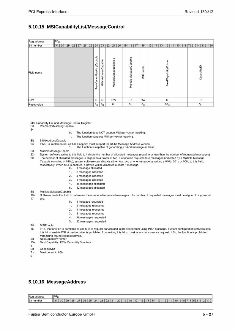
PCI Express Interface Revised 18/4/12
5.10.15 MSICapabilityList/MessageControl
5.10.16 MessageAddress
Reg address 60H
Bit number 31 30 29 28 27 26 25 24 23 22 21 20 19 18 17 16 15 14 13 12 11 10 9 8 7 6 5 4 3 2 1 0
Field name
Pe
r-V
ect
orM
ask
ing
Ca
pab
le
64b
itAd
dre
ssC
apa
ble
Mu
ltip
leM
essa
geE
nab
le
Mu
ltipl
eM
ess
ag
eC
apa
ble
MS
IEn
ab
le
Nex
tCa
pab
ility
Po
inte
r
Cap
ab
ility
ID
R/W R R RW R RW R R
Reset value 1H 1H 0H 5H 0H 80H 5H
MSI Capability List and Message Control Register Bit 24
Per-VectorMaskingCapable
0H The function does NOT support MSI per-vector masking.
1H The function supports MSI per-vector masking.
Bit 23
64bitAddressCapable If MSI is implemented, a PCIe Endpoint must support the 64-bit Message Address version.
1H The function is capable of generating a 64-bit message address.
Bit 22 - 20
MultipleMessageEnable System software writes to this field to indicate the number of allocated messages (equal to or less than the number of requested messages). The number of allocated messages is aligned to a power of two. If a function requests four messages (indicated by a Multiple Message Capable encoding of 010b), system software can allocate either four, two or one message by writing a 010b, 001b or 000b to this field, respectively. When MSI is enabled, a device will be allocated at least 1 message.
0H 1 message allocated
1H 2 messages allocated
2H 4 messages allocated
3H 8 messages allocated
4H 16 messages allocated
5H 32 messages allocated
Bit 19 - 17
MultipleMessageCapable Software reads this field to determine the number of requested messages. The number of requested messages must be aligned to a power of two.
0H 1 message requested
1H 2 messages requested
2H 4 messages requested
3H 8 messages requested
4H 16 messages requested
5H 32 messages requested
Bit 16
MSIEnable If 1b, the function is permitted to use MSI to request service and is prohibited from using INTA Message. System configuration software sets this bit to enable MSI. A device driver is prohibited from writing this bit to mask a functions service request. If 0b, the function is prohibited from using MSI to request service.
Bit 15 - 8
NextCapabilityPointer Next Capability: PCIe Capability Structure
Bit 7 - 0
CapabilityID Must be set to 05h.
Reg address 64H
Bit number 31 30 29 28 27 26 25 24 23 22 21 20 19 18 17 16 15 14 13 12 11 10 9 8 7 6 5 4 3 2 1 0
Fujitsu Semiconductor Europe GmbH 5 - 27
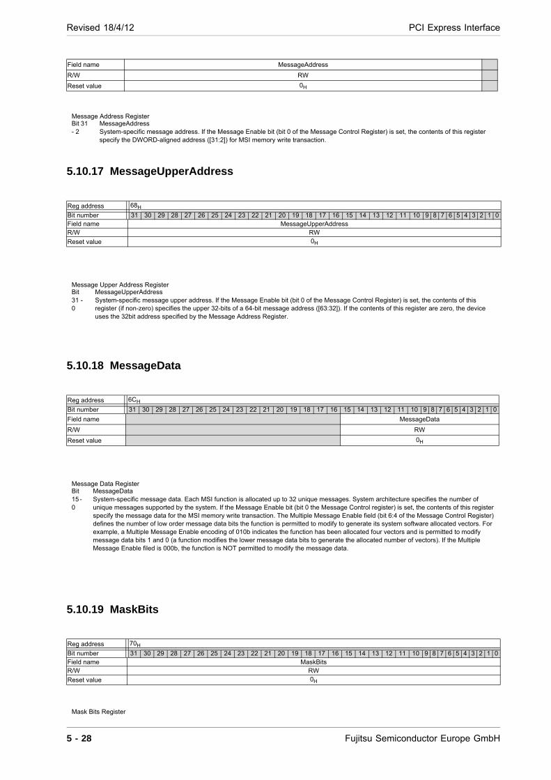
Revised 18/4/12 PCI Express Interface
5.10.17 MessageUpperAddress
5.10.18 MessageData
5.10.19 MaskBits
Field name MessageAddress
R/W RW
Reset value 0H
Message Address Register Bit 31 - 2
MessageAddress System-specific message address. If the Message Enable bit (bit 0 of the Message Control Register) is set, the contents of this register specify the DWORD-aligned address ([31:2]) for MSI memory write transaction.
Reg address 68H
Bit number 31 30 29 28 27 26 25 24 23 22 21 20 19 18 17 16 15 14 13 12 11 10 9 8 7 6 5 4 3 2 1 0Field name MessageUpperAddress R/W RW
Reset value 0H
Message Upper Address Register Bit 31 - 0
MessageUpperAddress System-specific message upper address. If the Message Enable bit (bit 0 of the Message Control Register) is set, the contents of this register (if non-zero) specifies the upper 32-bits of a 64-bit message address ([63:32]). If the contents of this register are zero, the device uses the 32bit address specified by the Message Address Register.
Reg address 6CH
Bit number 31 30 29 28 27 26 25 24 23 22 21 20 19 18 17 16 15 14 13 12 11 10 9 8 7 6 5 4 3 2 1 0
Field name MessageData
R/W RW
Reset value 0H
Message Data Register Bit 15 - 0
MessageData System-specific message data. Each MSI function is allocated up to 32 unique messages. System architecture specifies the number of unique messages supported by the system. If the Message Enable bit (bit 0 the Message Control register) is set, the contents of this register specify the message data for the MSI memory write transaction. The Multiple Message Enable field (bit 6:4 of the Message Control Register) defines the number of low order message data bits the function is permitted to modify to generate its system software allocated vectors. For example, a Multiple Message Enable encoding of 010b indicates the function has been allocated four vectors and is permitted to modify message data bits 1 and 0 (a function modifies the lower message data bits to generate the allocated number of vectors). If the Multiple Message Enable filed is 000b, the function is NOT permitted to modify the message data.
Reg address 70H
Bit number 31 30 29 28 27 26 25 24 23 22 21 20 19 18 17 16 15 14 13 12 11 10 9 8 7 6 5 4 3 2 1 0Field name MaskBits R/W RW
Reset value 0H
Mask Bits Register
5 - 28 Fujitsu Semiconductor Europe GmbH
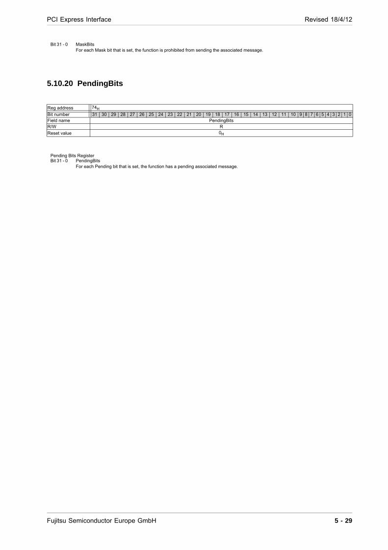
PCI Express Interface Revised 18/4/12
5.10.20 PendingBits
Bit 31 - 0 MaskBits For each Mask bit that is set, the function is prohibited from sending the associated message.
Reg address 74H
Bit number 31 30 29 28 27 26 25 24 23 22 21 20 19 18 17 16 15 14 13 12 11 10 9 8 7 6 5 4 3 2 1 0Field name PendingBits R/W R
Reset value 0H
Pending Bits Register Bit 31 - 0 PendingBits
For each Pending bit that is set, the function has a pending associated message.
Fujitsu Semiconductor Europe GmbH 5 - 29
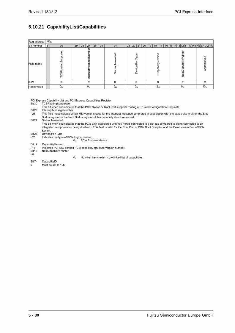
Revised 18/4/12 PCI Express Interface
5.10.21 CapabilityList/Capabilities
Reg address 80H
Bit number 31 30 29 28 27 26 25 24 23 22 21 20 19 18 17 16 15 14 13 12 11 10 9 8 7 6 5 4 3 2 1 0
Field nameT
CS
Ro
utin
gS
upp
ort
ed
Inte
rru
ptM
ess
age
Nu
mbe
r
Slo
tIm
ple
me
nte
d
De
vice
/Po
rtT
ype
Ca
pab
ility
Ver
sio
n
Ne
xtC
ap
abi
lityP
oin
ter
Ca
pab
ility
ID
R/W R R R R R R R
Reset value 0H 0H 0H 0H 2H 0H 10H
PCI Express Capability List and PCI Express Capabilities Register Bit 30 TCSRoutingSupported
This bit when set indicates that the PCIe Switch or Root Port supports routing of Trusted Configuration Requests. Bit 29 - 25
InterruptMessageNumber This field must indicate which MSI vector is used for the interrupt message generated in association with the status bits in either the Slot Status register or the Root Status register of this capability structure are set.
Bit 24 SlotImplemented This bit when set indicates that the PCIe Link associated with this Port is connected to a slot (as compared to being connected to an integrated component or being disabled). This field is valid for the Root Port of PCIe Root Complex and the Downstream Port of PCIe Switch.
Bit 23 - 20
Device/PortType Indicates the type of PCIe logical device.
0H PCIe Endpoint device
Bit 19 - 16
CapabilityVersion Indicates PCI-SIG defined PCIe capability structure version number.
Bit 15 - 8
NextCapabilityPointer
0H No other items exist in the linked list of capabilities.
Bit 7 - 0
CapabilityID Must be set to 10h.
5 - 30 Fujitsu Semiconductor Europe GmbH
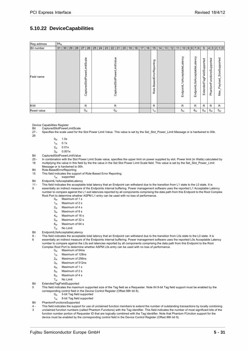
PCI Express Interface Revised 18/4/12
5.10.22 DeviceCapabilities
Reg address 84H
Bit number 31 30 29 28 27 26 25 24 23 22 21 20 19 18 17 16 15 14 13 12 11 10 9 8 7 6 5 4 3 2 1 0
Field name
Ca
ptu
red
Slo
tPo
we
rLim
itSca
le
Ca
ptur
ed
Slo
tPo
we
rLim
itVa
lue
Ro
le-B
ase
dE
rro
rRe
port
ing
En
dp
oin
tL1
sAcc
ep
tab
leL
ate
ncy
En
dp
oin
tL0
sAcc
ep
tab
leL
ate
ncy
Ext
en
de
dTa
gF
ield
Su
ppo
rte
d
Ph
anto
mF
unct
ion
sSu
ppo
rte
d
Ma
x_P
ayl
oad
_S
izeS
upp
ort
ed
R/W R R R R R R R R
Reset value 0H 0H 1H 5H 6H 0H 0H 5H
Device Capabilities Register Bit 27 - 26
CapturedSlotPowerLimitScale Specifies the scale used for the Slot Power Limit Value. This value is set by the Set_Slot_Power_Limit Message or is hardwired to 00b.
0H 1.0x
1H 0.1x
2H 0.01x
3H 0.001x
Bit 25 - 18
CapturedSlotPowerLimitValue In combination with the Slot Power Limit Scale value, specifies the upper limit on power supplied by slot. Power limit (in Watts) calculated by multiplying the value in this field by the the value in the Set Slot Power Limit Scale field. This value is set by the Set_Slot_Power_Limit Message or is hardwired to 00h.
Bit 15
Role-BasedErrorReporting This field indicates the support of Role-Based Error Reporting.
1H supported
Bit 11 - 9
EndpointL1sAcceptableLatency This field indicates the acceptable total latency that an Endpoint can withstand due to the transition from L1 state to the L0 state. It is essentially an indirect measure of the Endpoints internal buffering. Power management software uses the reported L1 Acceptable Latency number to compare against the L1 exit latencies reported by all components comprising the data path from this Endpoint to the Root Complex Root Port to determine whether ASPM L1 entry can be used with no loss of performance.
0H Maximum of 1 s
1H Maximum of 2 s
2H Maximum of 4 s
3H Maximum of 8 s
4H Maximum of 16 s
5H Maximum of 32 s
6H Maximum of 64 s
7H No Limit
Bit 8 - 6
EndpointL0sAcceptableLatency This field indicates the acceptable total latency that an Endpoint can withstand due to the transition from L0s state to the L0 state. It is essentially an indirect measure of the Endpoints internal buffering. Power management software uses the reported L0s Acceptable Latency number to compare against the L0s exit latencies reported by all components comprising the data path from this Endpoint to the Root Complex Root Port to determine whether ASPM L0s entry can be used with no loss of performance.
0H Maximum of 64ns
1H Maximum of 128ns
2H Maximum of 256ns
3H Maximum of 512ns
4H Maximum of 1 s
5H Maximum of 2 s
6H Maximum of 4 s
7H No Limit
Bit 5
ExtendedTagFieldSupported This field indicates the maximum supported size of the Tag field as a Requester. Note tht 8-bit Tag field support must be enabled by the corresponding control field in the Device Control Register (Offset 88h bit 8).
0H 5-bit Tag field supported
1H 8-bit Tag field supported
Bit 4 - 3
PhantomFunctionsSupported This field indicates the support for use of unclaimed function members to extend the number of outstanding transactions by locally combining unclaimed function numbers (called Phantom Functions) with the Tag identifier. This field indicates the number of most significant bits of the function number portion of Requester ID that are logically combined with the Tag identifier. Note that Phantom FUnction support for the device must be enabled by the corresponding control field in the Device Control Register (Offset 88h bit 9).
Fujitsu Semiconductor Europe GmbH 5 - 31

Revised 18/4/12 PCI Express Interface
0H No function number bits used for Phantom Functions; device may implement all numbers.
1H First most significant bit of function number in Requester ID used for Phantom Functions; devive may implement functions 0-3. Functions 0, 1, 2, and 3 may claim functions 4, 5, 6, and 7 as Phantom functions respectively.
2H First two most significant bits of function number in Requester ID used for Phantom Functions; device may implement functions 0-1. Function 0 may claim functions 2, 4, and 6 as Phantom Functions; function 1 may claim functions 3,5, and 7 as Phantom Functions.
3H All three bits of function number in Requester ID used for Phantom Functions; device must be a single function 0 device that may claim all other functions as Phantom Functions.
Bit 2 - 0
Max_Payload_SizeSupported This field indicates the maximum payload size that the device can support for TLPs.
0H 128 Bytes max payload size
1H 256 Bytes max payload size
2H 512 Bytes max payload size
3H 1024 Bytes max payload size
4H 2048 Bytes max payload size
5H 4096 Bytes max payload size
5 - 32 Fujitsu Semiconductor Europe GmbH
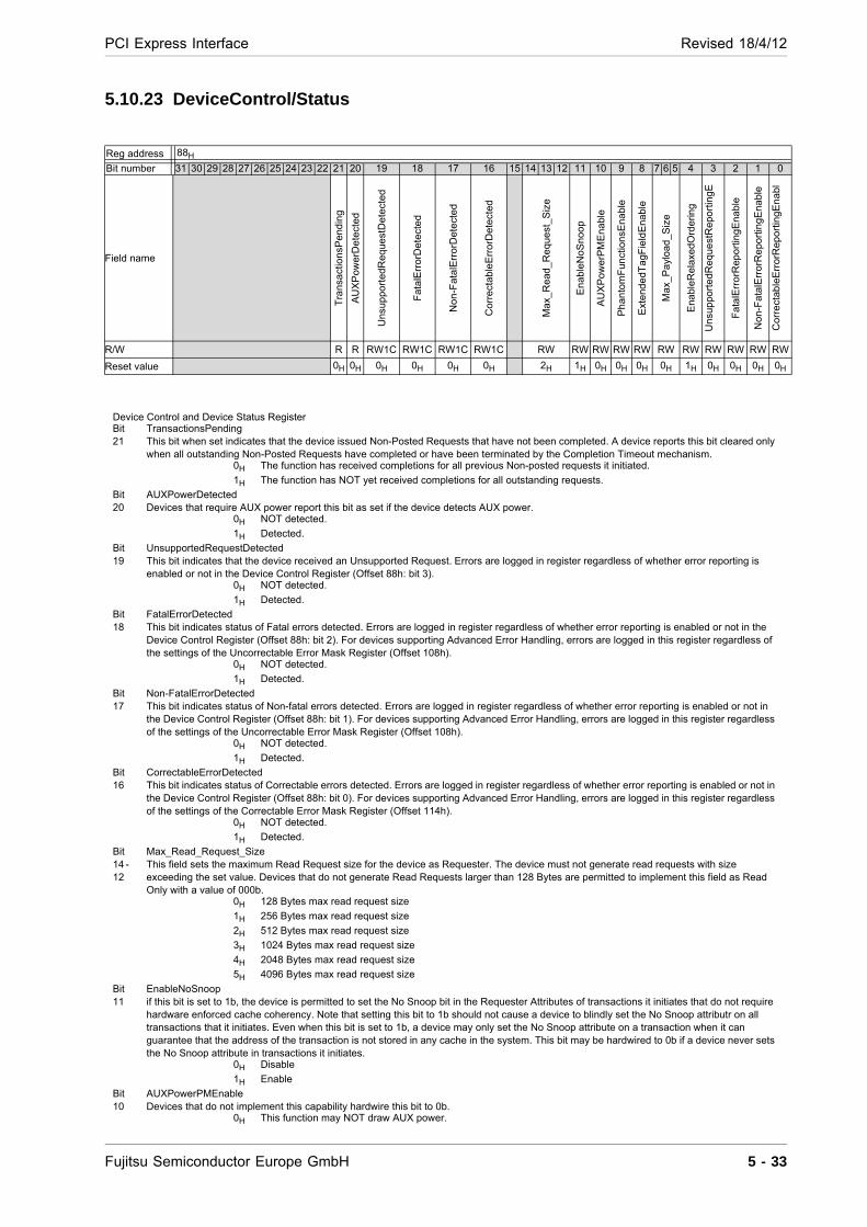
PCI Express Interface Revised 18/4/12
5.10.23 DeviceControl/Status
Reg address 88H
Bit number 31 30 29 28 27 26 25 24 23 22 21 20 19 18 17 16 15 14 13 12 11 10 9 8 7 6 5 4 3 2 1 0
Field name
Tra
nsa
ctio
nsP
end
ing
AU
XP
ow
erD
ete
cte
d
Un
sup
por
ted
Re
que
stD
ete
cte
d
Fat
alE
rro
rDe
tect
ed
No
n-F
ata
lErr
orD
ete
cte
d
Co
rre
cta
ble
Err
orD
ete
cte
d
Ma
x_R
ead
_R
eq
uest
_Siz
e
En
abl
eN
oS
noo
p
AU
XP
ow
erP
ME
na
ble
Ph
an
tom
Fu
nct
ion
sEn
ab
le
Ext
end
ed
Ta
gFie
ldE
nab
le
Ma
x_P
aylo
ad
_Siz
e
Ena
ble
Re
laxe
dO
rde
ring
Un
sup
port
ed
Re
que
stR
epo
rtin
gE
Fa
talE
rro
rRep
ort
ing
En
ab
le
No
n-F
ata
lErr
orR
epo
rtin
gE
na
ble
Co
rre
ctab
leE
rro
rRep
ort
ingE
na
bl
R/W R R RW1C RW1C RW1C RW1C RW RW RW RW RW RW RW RW RW RW RW
Reset value 0H 0H 0H 0H 0H 0H 2H 1H 0H 0H 0H 0H 1H 0H 0H 0H 0H
Device Control and Device Status Register Bit 21
TransactionsPending This bit when set indicates that the device issued Non-Posted Requests that have not been completed. A device reports this bit cleared only when all outstanding Non-Posted Requests have completed or have been terminated by the Completion Timeout mechanism.
0H The function has received completions for all previous Non-posted requests it initiated.
1H The function has NOT yet received completions for all outstanding requests.
Bit 20
AUXPowerDetected Devices that require AUX power report this bit as set if the device detects AUX power.
0H NOT detected.
1H Detected.
Bit 19
UnsupportedRequestDetected This bit indicates that the device received an Unsupported Request. Errors are logged in register regardless of whether error reporting is enabled or not in the Device Control Register (Offset 88h: bit 3).
0H NOT detected.
1H Detected.
Bit 18
FatalErrorDetected This bit indicates status of Fatal errors detected. Errors are logged in register regardless of whether error reporting is enabled or not in the Device Control Register (Offset 88h: bit 2). For devices supporting Advanced Error Handling, errors are logged in this register regardless of the settings of the Uncorrectable Error Mask Register (Offset 108h).
0H NOT detected.
1H Detected.
Bit 17
Non-FatalErrorDetected This bit indicates status of Non-fatal errors detected. Errors are logged in register regardless of whether error reporting is enabled or not in the Device Control Register (Offset 88h: bit 1). For devices supporting Advanced Error Handling, errors are logged in this register regardless of the settings of the Uncorrectable Error Mask Register (Offset 108h).
0H NOT detected.
1H Detected.
Bit 16
CorrectableErrorDetected This bit indicates status of Correctable errors detected. Errors are logged in register regardless of whether error reporting is enabled or not in the Device Control Register (Offset 88h: bit 0). For devices supporting Advanced Error Handling, errors are logged in this register regardless of the settings of the Correctable Error Mask Register (Offset 114h).
0H NOT detected.
1H Detected.
Bit 14 - 12
Max_Read_Request_Size This field sets the maximum Read Request size for the device as Requester. The device must not generate read requests with size exceeding the set value. Devices that do not generate Read Requests larger than 128 Bytes are permitted to implement this field as Read Only with a value of 000b.
0H 128 Bytes max read request size
1H 256 Bytes max read request size
2H 512 Bytes max read request size
3H 1024 Bytes max read request size
4H 2048 Bytes max read request size
5H 4096 Bytes max read request size
Bit 11
EnableNoSnoop if this bit is set to 1b, the device is permitted to set the No Snoop bit in the Requester Attributes of transactions it initiates that do not require hardware enforced cache coherency. Note that setting this bit to 1b should not cause a device to blindly set the No Snoop attributr on all transactions that it initiates. Even when this bit is set to 1b, a device may only set the No Snoop attribute on a transaction when it can guarantee that the address of the transaction is not stored in any cache in the system. This bit may be hardwired to 0b if a device never sets the No Snoop attribute in transactions it initiates.
0H Disable
1H Enable
Bit 10
AUXPowerPMEnable Devices that do not implement this capability hardwire this bit to 0b.
0H This function may NOT draw AUX power.
Fujitsu Semiconductor Europe GmbH 5 - 33
Revised 18/4/12 PCI Express Interface
1H This function is allowed to draw AUX power.
Bit 9
PhantomFunctionsEnable When set, this bit enables a device to use unclaimedd functions as phantom functions to extend the number of outstanding transaction identifiers. If this bit is cleared, the device is not allowed to use Phantom Functions. Devices that do not implement this capability hardwire this bit to 0b.
0H This function may NOT use phantom functions.
1H This function is allowed to use phantom functions.
Bit 8
ExtendedTagFieldEnable When set, this bit enables a device to use an 8-bit Tag-field as a requester. If the bit is cleared, the device is restricted to a 5-bit Tag field. Devices that do not implement this capability hardwie this bit to 0b.
0H This function must use a 5-bit Tag field.
1H This function must use a 8-bit Tag field.
Bit 7 - 5
Max_Payload_Size This field sets maximum TLP payload size for the device. As a Receiver, the device must handle TLPs as large as the set value; as Transmitter, the device must not generate TLPs exceeding the set value. The Max_Payload_Size Supported in the Device Capabilities Register (Offset 84h: bit 2:0) indicates permissible values that can be programmed.
0H 128 Bytes max payload size
1H 256 Bytes max payload size
2H 512 Bytes max payload size
3H 1024 Bytes max payload size
4H 2048 Bytes max payload size
5H 4096 Bytes max payload size
Bit 4
EnableRelaxedOrdering If this bit is set, the device is permitted to set the relaxed Ordering bit in the Attributes field of transactions it initiates that do not require strong write ordering.
0H Disable
1H Enable
Bit 3
UnsupportedRequestReportingEnable This bit in conjunction with other bits controls the signalling of Unsupported requests by sending Error Messages.
Bit 2
FatalErrorReportingEnable This bit in conjunction with other bits controls sending ERR_FATAL Messages.
Bit 1
Non-FatalErrorReportingEnable This bit in conjunction with other bits controls sending ERR_NONFATAL Messages.
Bit 0
CorrectableErrorReportingEnable This bit in conjunction with other bits controls sending ERR_COR Messages.
5 - 34 Fujitsu Semiconductor Europe GmbH
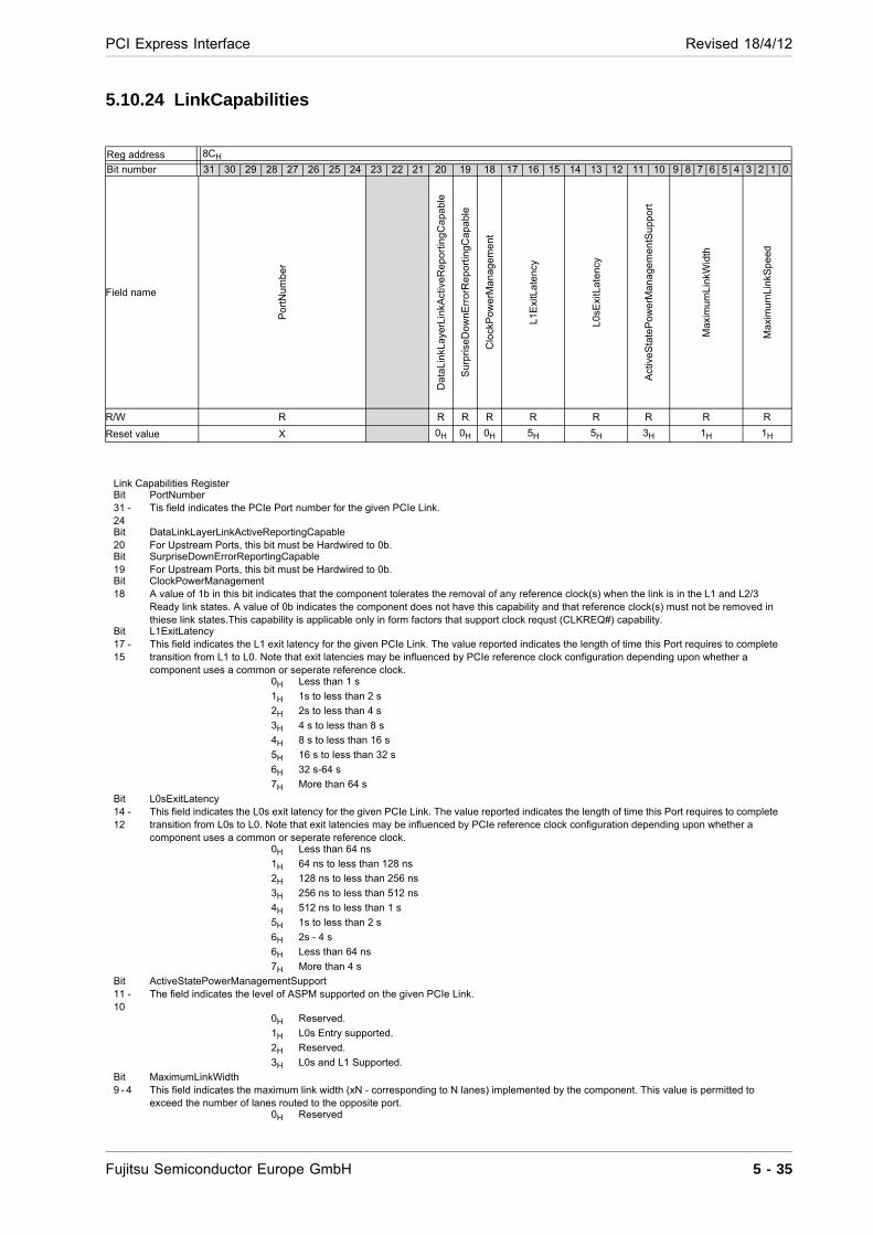
PCI Express Interface Revised 18/4/12
5.10.24 LinkCapabilities
Reg address 8CH
Bit number 31 30 29 28 27 26 25 24 23 22 21 20 19 18 17 16 15 14 13 12 11 10 9 8 7 6 5 4 3 2 1 0
Field nameP
ort
Nu
mb
er
Da
taL
inkL
ayer
Lin
kAct
ive
Re
por
ting
Ca
pab
le
Su
rpri
seD
ow
nErr
orR
ep
ort
ing
Ca
pa
ble
Clo
ckP
ow
erM
an
age
me
nt
L1E
xitL
ate
ncy
L0sE
xitL
aten
cy
Act
ive
Sta
teP
ow
erM
an
age
me
ntS
upp
ort
Max
imu
mL
inkW
idth
Ma
xim
um
Lin
kSp
eed
R/W R R R R R R R R R
Reset value X 0H 0H 0H 5H 5H 3H 1H 1H
Link Capabilities Register Bit 31 - 24
PortNumber Tis field indicates the PCIe Port number for the given PCIe Link.
Bit 20
DataLinkLayerLinkActiveReportingCapable For Upstream Ports, this bit must be Hardwired to 0b.
Bit 19
SurpriseDownErrorReportingCapable For Upstream Ports, this bit must be Hardwired to 0b.
Bit 18
ClockPowerManagement A value of 1b in this bit indicates that the component tolerates the removal of any reference clock(s) when the link is in the L1 and L2/3 Ready link states. A value of 0b indicates the component does not have this capability and that reference clock(s) must not be removed in thiese link states.This capability is applicable only in form factors that support clock requst (CLKREQ#) capability.
Bit 17 - 15
L1ExitLatency This field indicates the L1 exit latency for the given PCIe Link. The value reported indicates the length of time this Port requires to complete transition from L1 to L0. Note that exit latencies may be influenced by PCIe reference clock configuration depending upon whether a component uses a common or seperate reference clock.
0H Less than 1 s
1H 1s to less than 2 s
2H 2s to less than 4 s
3H 4 s to less than 8 s
4H 8 s to less than 16 s
5H 16 s to less than 32 s
6H 32 s-64 s
7H More than 64 s
Bit 14 - 12
L0sExitLatency This field indicates the L0s exit latency for the given PCIe Link. The value reported indicates the length of time this Port requires to complete transition from L0s to L0. Note that exit latencies may be influenced by PCIe reference clock configuration depending upon whether a component uses a common or seperate reference clock.
0H Less than 64 ns
1H 64 ns to less than 128 ns
2H 128 ns to less than 256 ns
3H 256 ns to less than 512 ns
4H 512 ns to less than 1 s
5H 1s to less than 2 s
6H 2s - 4 s
6H Less than 64 ns
7H More than 4 s
Bit 11 - 10
ActiveStatePowerManagementSupport The field indicates the level of ASPM supported on the given PCIe Link.
0H Reserved.
1H L0s Entry supported.
2H Reserved.
3H L0s and L1 Supported.
Bit 9 - 4
MaximumLinkWidth This field indicates the maximum link width (xN - corresponding to N lanes) implemented by the component. This value is permitted to exceed the number of lanes routed to the opposite port.
0H Reserved
Fujitsu Semiconductor Europe GmbH 5 - 35

Revised 18/4/12 PCI Express Interface
1H x1
2H x2
3H x4
Bit 3 - 0
MaximumLinkSpeed This field indicates the maximum Link speed of the given PCIe Link.
1H 2.5Gbps link. All other encodings are reserved
5 - 36 Fujitsu Semiconductor Europe GmbH
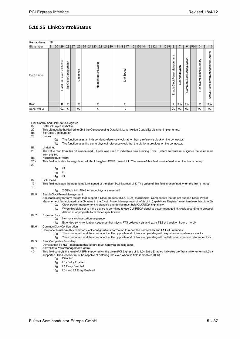
PCI Express Interface Revised 18/4/12
5.10.25 LinkControl/Status
Reg address 90H
Bit number 31 30 29 28 27 26 25 24 23 22 21 20 19 18 17 16 15 14 13 12 11 10 9 8 7 6 5 4 3 2 1 0
Field name
Dat
aLi
nkL
aye
rLin
kAct
ive
Slo
tClo
ckC
on
figur
atio
n
Un
def
ine
d
Ne
go
tiate
dLin
kWid
th
Lin
kSpe
ed
En
ab
leC
lock
Po
we
rMan
ag
eme
nt
Ext
end
ed
Syn
ch
Co
mm
on
Clo
ckC
on
figur
atio
n
Rea
dC
om
ple
tion
Bou
nd
ary
Act
iveS
tate
Po
we
rMan
ag
eme
ntC
on
tro
l
R/W R R R R R R RW RW R RW
Reset value 0H X 0H X 1H 0H 0H 0H 0H 0H
Link Control and Link Status Register Bit 29
DataLinkLayerLinkActive This bit must be hardwired to 0b if the Corresponding Data Link Layer Active Capability bit is not implemented.
Bit 28
SlotClockConfiguration (none)
0H The function uses an independent reference clock rather than a reference clock on the connector.
1H The function uses the same physical reference clock that the platform provides on the connector.
Bit 26
Undefined The value read from this bit is undefined. This bit was used to indicate a Link Training Error. System software must ignore the value read from this bit.
Bit 25 - 20
NegotiatedLinkWidth This field indicates the negotiated width of the given PCI Express Link. The value of this field is undefined when the link is not up.
1H x1
2H x2
4H x4
Bit 19 - 16
LinkSpeed This field indicates the negotiated Link speed of the given PCI Express Link. The value of this field is undefined when the link is not up.
1H 2.5Gbps link. All other encodings are reserved
Bit 8 EnableClockPowerManagement Applicable only for form factors that support a Clock Request (CLKREQ#) mechanism. Components that do not support Clock Power Management (as indicated by a 0b value in the Clock Power Management bit of th Link Capabilities Register) must hardwire this bit to 0b.
0H Clock power management is disabled and device must hold CLKREQ# signal low.
1H When this bit is set to 1 the device is permitted to use CLKREQ# signal to power manage link clock according to protocol defined in appropriate form factor specification.
Bit 7 ExtendedSynch 0H Normal synchronization sequence.
1H Extended synchronization sequence that injects FTS ordered sets and extra TS2 at transition from L1 to L0.
Bit 6 CommonClockConfiguration Components utilizise this common clock configuration information to report the correct L0s and L1 Exit Latencies.
0H This component and the component at the opposite end of link are operating with asynchronous reference clocks.
1H This component and the component at the opposite end of link are operating with a distributed common reference clock.
Bit 3 ReadCompletionBoundary Devices that do NOT implement this feature must hardwire the field ot 0b.
Bit 1 - 0
ActiveStatePowerManagementControl This field controls the level of ASPM supported on the given PCI Express Link. L0s Entry Enabled indicates the Transmitter entering L0s is supported. The Receiver must be capable of entering L0s even when tis field is disabled (00b).
0H Disabled
1H L0s Entry Enabled
2H L1 Entry Enabled
3H L0s and L1 Entry Enabled
Fujitsu Semiconductor Europe GmbH 5 - 37

Revised 18/4/12 PCI Express Interface
5.10.26 DeviceCapabilities2
Reg address
A4H
Bit number
31 30 29 28 27 26 25 24 23 22 21 20 19 18 17 16 15 14 13 12 11 10 9 8 7 6 5 4 3 2 1 0
Field name
CompletionTimeoutDisableSupported
CompletionTimeoutRangesSupported
R/W R R Reset value
0H X
Device Capabilities 2 Register Bit 4
CompletionTimeoutDisableSupported A value of 1b indicates support for the Completion Timeout Disable mechanism.
Bit 3 - 0
CompletionTimeoutRangesSupported This field indicates device support for the optional Completion Timeout programmability mechanism. This mechanism allows system software to modify the Completion Timeout value. Four time ranges are defined: Range A is 50us to 10ms; Range B is 10ms to 250ms; Range C is 250ms to 4s; Range D is 4s to 64s. Bits are set according to the table below to show timeout value ranges supported. It is strongly recommended that the Completion Timeout mechanism not expire in less than 10 ms.
0H Completion Timeout programming not supported. The device must implement a timeout value in the range 50us to 50ms.
1H Range A
2H Range B
3H Range A and B
6H Range B and C
7H Range A, B and C
EH Range B, C and D
FH Range A, B, C and D
5 - 38 Fujitsu Semiconductor Europe GmbH

PCI Express Interface Revised 18/4/12
5.10.27 DeviceControl2
Reg address A8H
Bit number 31 30 29 28 27 26 25 24 23 22 21 20 19 18 17 16 15 14 13 12 11 10 9 8 7 6 5 4 3 2 1 0
Field nameCompletion
TimeoutDisable Completion
TimeoutValue
R/W RW RW
Reset value 0H 0H
Device Control 2 Register Bit 4
CompletionTimeoutDisable When set to 1b, this bit disables the Completion Timeout mechanism. Software is permitted to set or clear this bit at any time. When set, the Completion Timeout detection mechanism is disabled. If there are outstanding requests when the bit is cleared, it is permitted but not required for hardware to apply the completion timeout mechanism to the outstanding requests. If this is done, it is permitted to base the start time for each request on either the time this bit was cleared or the time each request was issued.
Bit 3 - 0
CompletionTimeoutValue In Devices that support Completion Timeout programmability, this field allows system software to modify the Completion Timeout value. Devices that support Completion Timeout programmability must support the values given below corresponding to the Programmability ranges indicated in the Completion Timeout Values Supported field. It is strongly recommended that the Completion Timeout mechanism not expire in less than 10ms. Software is permitted to change the value in this field at any time. For requests already pending when Completion Timeout Value is changed, hardware is permitted to use either the new or the old value for the outstanding requests, and is permitted to base the start time for each request either on when this value was changed or on when each request was issued.
0H Default range: 50us to 50ms
1H 5us to 100us
2H 1ms to 10ms
5H 16ms to 55ms
6H 65ms to 210ms
9H 260ms to 900ms
AH 1s to 3.5s
DH 4s to 13s
EH 17s to 64s
Fujitsu Semiconductor Europe GmbH 5 - 39

Revised 18/4/12 PCI Express Interface
5 - 40 Fujitsu Semiconductor Europe GmbH
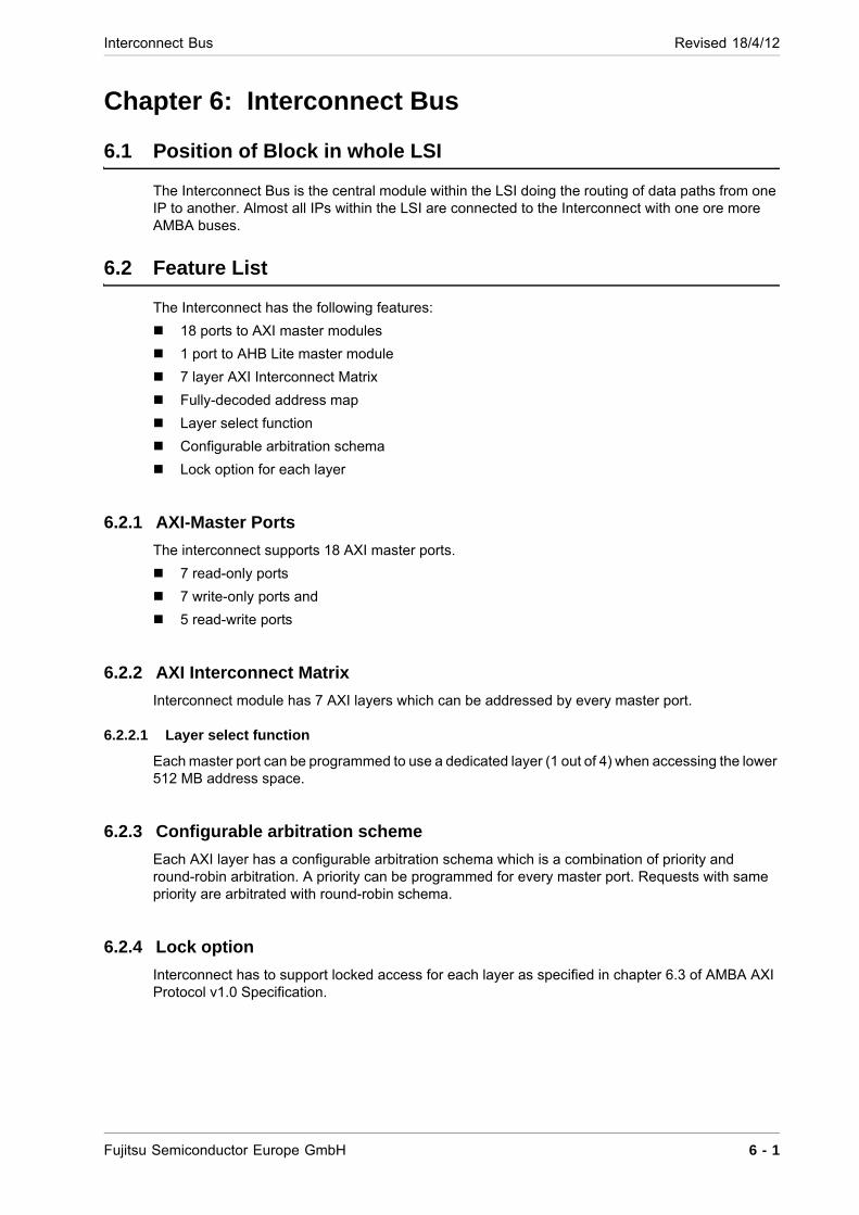
Interconnect Bus Revised 18/4/12
Chapter 6: Interconnect Bus
6.1 Position of Block in whole LSI
The Interconnect Bus is the central module within the LSI doing the routing of data paths from one IP to another. Almost all IPs within the LSI are connected to the Interconnect with one ore more AMBA buses.
6.2 Feature List
The Interconnect has the following features:
18 ports to AXI master modules
1 port to AHB Lite master module
7 layer AXI Interconnect Matrix
Fully-decoded address map
Layer select function
Configurable arbitration schema
Lock option for each layer
6.2.1 AXI-Master Ports
The interconnect supports 18 AXI master ports.
7 read-only ports
7 write-only ports and
5 read-write ports
6.2.2 AXI Interconnect Matrix
Interconnect module has 7 AXI layers which can be addressed by every master port.
6.2.2.1 Layer select function
Each master port can be programmed to use a dedicated layer (1 out of 4) when accessing the lower 512 MB address space.
6.2.3 Configurable arbitration scheme
Each AXI layer has a configurable arbitration schema which is a combination of priority and round-robin arbitration. A priority can be programmed for every master port. Requests with same priority are arbitrated with round-robin schema.
6.2.4 Lock option
Interconnect has to support locked access for each layer as specified in chapter 6.3 of AMBA AXI Protocol v1.0 Specification.
Fujitsu Semiconductor Europe GmbH 6 - 1
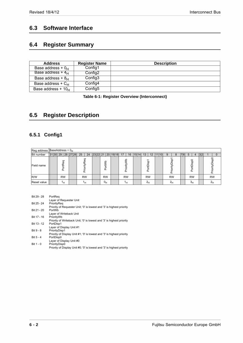
Revised 18/4/12 Interconnect Bus
6.3 Software Interface
6.4 Register Summary
Table 6-1: Register Overview (Interconnect)
6.5 Register Description
6.5.1 Config1
Address Register Name DescriptionBase address + 0H Config1 Base address + 4H Config2 Base address + 8H Config3 Base address + CH Config4 Base address + 10H Config5
Reg address BaseAddress + 0H
Bit number 31 30 29 28 27 26 25 24 23 22 21 20 19 18 17 16 15 14 13 12 11 10 9 8 7 6 5 4 3 2 1 0
Field name
Po
rtR
eq
Prio
rity
Re
q
Por
tWb
Pri
orit
yWb
Po
rtD
isp
1
Prio
rity
Dis
p1
Po
rtD
isp
0
Prio
rity
Dis
p0
R/W RW RW RW RW RW RW RW RW
Reset value 1H 1H 0H 1H 2H 2H 3H 2H
Bit 29 - 28 PortReq Layer of Requester Unit
Bit 25 - 24 PriorityReq Priority of Requester Unit; '0' is lowest and '3' is highest priority
Bit 21 - 20 PortWb Layer of Writeback Unit
Bit 17 - 16 PriorityWb Priority of Writeback Unit; '0' is lowest and '3' is highest priority
Bit 13 - 12 PortDisp1 Layer of Display Unit #1
Bit 9 - 8 PriorityDisp1 Priority of Display Unit #1; '0' is lowest and '3' is highest priority
Bit 5 - 4 PortDisp0 Layer of Display Unit #0
Bit 1 - 0 PriorityDisp0 Priority of Display Unit #0; '0' is lowest and '3' is highest priority
6 - 2 Fujitsu Semiconductor Europe GmbH

Interconnect Bus Revised 18/4/12
6.5.2 Config2
6.5.3 Config3
6.5.4 Config4
Reg address BaseAddress + 4H
Bit number 31 30 29 28 27 26 25 24 23 22 21 20 19 18 17 16 15 14 13 12 11 10 9 8 7 6 5 4 3 2 1 0
Field name
Po
rtC
ap
3
Pri
ority
Cap
3
Po
rtC
ap
2
Pri
ority
Cap
2
Po
rtC
ap
1
Pri
ority
Cap
1
Po
rtC
ap
0
Pri
ority
Cap
0
R/W RW RW RW RW RW RW RW RW
Reset value 2H 2H 2H 2H 3H 2H 3H 2H
Bit 29 - 28 PortCap3 Layer of Capture Unit #3
Bit 25 - 24 PriorityCap3 Priority of Capture Unit #3; '0' is lowest and '3' is highest priority
Bit 21 - 20 PortCap2 Layer ofCapture Unit #2
Bit 17 - 16 PriorityCap2 Priority of Capture Unit #2; '0' is lowest and '3' is highest priority
Bit 13 - 12 PortCap1 Layer of Capture Unit #1
Bit 9 - 8 PriorityCap1 Priority of Capture Unit #1; '0' is lowest and '3' is highest priority
Bit 5 - 4 PortCap0 Layer of Capture Unit #0
Bit 1 - 0 PriorityCap0 Priority of Capture Unit #0; '0' is lowest and '3' is highest priority
Reg address BaseAddress + 8H
Bit number 31 30 29 28 27 26 25 24 23 22 21 20 19 18 17 16 15 14 13 12 11 10 9 8 7 6 5 4 3 2 1 0
Field name
Por
tPix
w
Pri
ority
Pix
w
Por
tPix
r3
Pri
orit
yPix
r3
Por
tPix
r2
Pri
orit
yPix
r2
Por
tPix
r1
Pri
orit
yPix
r1
R/W RW RW RW RW RW RW RW RW
Reset value 1H 0H 0H 0H 2H 0H 1H 0H
Bit 29 - 28 PortPixw Layer of Pixblt Destination
Bit 25 - 24 PriorityPixw Priority of Pixblt Destination; '0' is lowest and '3' is highest priority
Bit 21 - 20 PortPixr3 Layer of Pixblt Source #3
Bit 17 - 16 PriorityPixr3 Priority of Pixblt Source #3; '0' is lowest and '3' is highest priority
Bit 13 - 12 PortPixr2 Layer of Pixblt Source #2
Bit 9 - 8 PriorityPixr2 Priority of Pixblt Source #2; '0' is lowest and '3' is highest priority
Bit 5 - 4 PortPixr1 Layer of Pixblt Source #1
Bit 1 - 0 PriorityPixr1 Priority of Pixblt Source #1; '0' is lowest and '3' is highest priority
Reg address
BaseAddress + CH
Fujitsu Semiconductor Europe GmbH 6 - 3
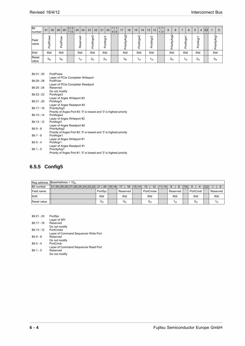
Revised 18/4/12 Interconnect Bus
6.5.5 Config5
Bit number
31 30 29 2827
26
25 24 23 22 21 2019
18
17 16 15 14 13 1211
10
9 8 7 6 5 4 3 2 1 0
Field name
Po
rtP
ciew
Po
rtP
cie
r
Res
erve
d
Po
rtA
rgw
3
Po
rtA
rgr3
Prio
rity
Arg
3
Po
rtA
rgw
2
Po
rtA
rgr2
Prio
rity
Arg
2
Po
rtA
rgw
1
Po
rtA
rgr1
Prio
rity
Arg
1
R/W RW RW RW RW RW RW RW RW RW RW RW RW
Reset value
0H 0H 1H 2H 2H 0H 1H 1H 0H 1H 0H 0H
Bit 31 - 30 PortPciew Layer of PCIe Completer Writeport
Bit 29 - 28 PortPcier Layer of PCIe Completer Readport
Bit 25 - 24 ReservedDo not modify
Bit 23 - 22 PortArgw3 Layer of Arges Writeport #3
Bit 21 - 20 PortArgr3 Layer of Arges Readport #3
Bit 17 - 16 PriorityArg3 Priority of Arges Port #3; '0' is lowest and '3' is highest priority
Bit 15 - 14 PortArgw2 Layer of Arges Writeport #2
Bit 13 - 12 PortArgr2 Layer of Arges Readport #2
Bit 9 - 8 PriorityArg2 Priority of Arges Port #2; '0' is lowest and '3' is highest priority
Bit 7 - 6 PortArgw1 Layer of Arges Writeport #1
Bit 5 - 4 PortArgr1 Layer of Arges Readport #1
Bit 1 - 0 PriorityArg1 Priority of Arges Port #1; '0' is lowest and '3' is highest priority
Reg address BaseAddress + 10H
Bit number 31 30 29 28 27 26 25 24 23 22 21 20 19 18 17 16 15 14 13 12 11 10 9 8 7 6 5 4 3 2 1 0
Field name PortSpi Reserved PortCmdw Reserved PortCmdr Reserved
R/W RW RW RW RW RW RW
Reset value 0H 0H 0H 1H 0H 1H
Bit 21 - 20 PortSpi Layer of SPI
Bit 17 - 16 ReservedDo not modify
Bit 13 - 12 PortCmdw Layer of Command Sequencer Write Port
Bit 9 - 8 ReservedDo not modify
Bit 5 - 4 PortCmdr Layer of Command Sequencer Read Port
Bit 1 - 0 ReservedDo not modify
6 - 4 Fujitsu Semiconductor Europe GmbH

Interconnect Bus Revised 18/4/12
6.6 Processing Mode
6.6.1 Processing Flow
6.6.1.1 Overview
Figure 6-1: Interconnect: Processing Flow
Arbiter
MonitorConfigurationRegisters
Interconnect B & C
Interconnect A
Slave Ports
Master Ports
Interconnect
Fujitsu Semiconductor Europe GmbH 6 - 5

Revised 18/4/12 Interconnect Bus
6.6.1.2 Interconnect A (AXI Interconnect Matrix)
6.6.1.2.1 Overview
Figure 6-2: Interconnect A: Overview
PCIeAXI-Slave
64@66 MHz
Register Space 1AXI-Slave
32@266 MHz
...
AX
I In
terc
on
ne
ct M
atr
ix
Memory #4AXI-Slave
64@266 MHz
Memory #3AXI-Slave
64@266 MHz
Memory #2AXI-Slave
64@266 MHz
Memory #1AXI-Slave
64@266 MHz
Synch bridgeDownsizer
AXI-Master #164@266 MHz
Routing
AXI-Master #1564@266 MHz
Routing
Cmd ReadAXI-Master
32@266 MHz
Routing
Cmd WriteAXI-Master #1732@266 MHz
Routing
PCIeAXI-Master #18
64@66 MHz
Routing
SPIAHB Lite Master
32@66 MHz
Routing
AXI Layer #1 64@266 MHz
AXI Layer #2 64@266 MHz
AXI Layer #3 64@266 MHz
AXI Layer #5 64@266 MHz
AXI Layer #4 64@266 MHz
AXI Layer #6 64@266 MHz
AXI Layer #7 64@266 MHz
Synch bridge
AHB - AXI
Synch bridge
...
Arges HIFAXI-Slave
64@266 MHz
UpsizerUpsizer Upsizer
6 - 6 Fujitsu Semiconductor Europe GmbH
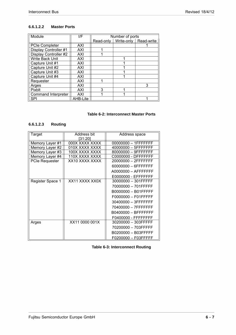
Interconnect Bus Revised 18/4/12
6.6.1.2.2 Master Ports
Table 6-2: Interconnect Master Ports
6.6.1.2.3 Routing
Table 6-3: Interconnect Routing
Module I/F Number of portsRead-only Write-only Read-write
PCIe Completer AXI 1Display Controller #1 AXI 1Display Controller #2 AXI 1Write Back Unit AXI 1Capture Unit #1 AXI 1Capture Unit #2 AXI 1Capture Unit #3 AXI 1Capture Unit #4 AXI 1Requester AXI 1Arges AXI 3Pixblt AXI 3 1Command Interpreter AXI 1 1SPI AHB-Lite 1
Target Address bit Address space[31:20]
Memory Layer #1 000X XXXX XXXX 00000000 – 1FFFFFFFMemory Layer #2 010X XXXX XXXX 40000000 – 5FFFFFFFMemory Layer #3 100X XXXX XXXX 80000000 – 9FFFFFFFMemory Layer #4 110X XXXX XXXX C0000000 - DFFFFFFFPCIe Requester XX10 XXXX XXXX 20000000 – 2FFFFFFF
60000000 – 6FFFFFFFA0000000 – AFFFFFFFE0000000 - EFFFFFFF
Register Space 1 XX11 XXXX XX0X 30000000 – 301FFFFF70000000 – 701FFFFFB0000000 – B01FFFFFF0000000 – F01FFFFF30400000 – 3FFFFFFF70400000 – 7FFFFFFFB0400000 – BFFFFFFFF0400000 - FFFFFFFF
Arges XX11 0000 001X 30200000 – 303FFFFF70200000 – 703FFFFFB0200000 – B03FFFFFF0200000 – F03FFFFF
Fujitsu Semiconductor Europe GmbH 6 - 7
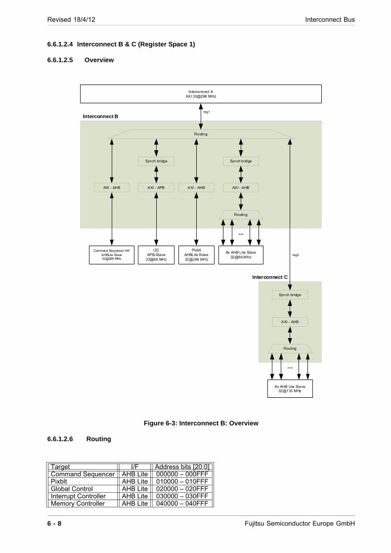
Revised 18/4/12 Interconnect Bus
6.6.1.2.4 Interconnect B & C (Register Space 1)
6.6.1.2.5 Overview
Figure 6-3: Interconnect B: Overview
6.6.1.2.6 Routing
Target I/F Address bits [20:0]Command Sequencer AHB Lite 000000 – 000FFFPixblt AHB Lite 010000 – 010FFFGlobal Control AHB Lite 020000 – 020FFFInterrupt Controller AHB Lite 030000 – 030FFFMemory Controller AHB Lite 040000 – 040FFF
Interconnect AAXI 32@266 MHz
Routing
AXI - AHB
Synch bridge
AXI - AHBAXI - APB
I2CAPB-Slave
32@66 MHz
Routing
...
8x AHB Lite Slave32@66 MHz
Interconnect B
Synch bridge
PixbltAHBLite Slave 32@266 MHz
AXI - AHB
Synch bridge
Routing
...
Interconnect C
8x AHB Lite Slave32@133 MHz
Command Sequencer HIFAHBLite Slave32@266 MHz
AXI - AHB
reg2
reg1
6 - 8 Fujitsu Semiconductor Europe GmbH
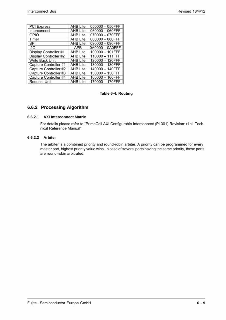
Interconnect Bus Revised 18/4/12
Table 6-4: Routing
6.6.2 Processing Algorithm
6.6.2.1 AXI Interconnect Matrix
For details please refer to “PrimeCell AXI Configurable Interconnect (PL301) Revision: r1p1 Tech-nical Reference Manual”.
6.6.2.2 Arbiter
The arbiter is a combined priority and round-robin arbiter. A priority can be programmed for every master port, highest priority value wins. In case of several ports having the same priority, these ports are round-robin arbitrated.
PCI Express AHB Lite 050000 – 050FFFInterconnect AHB Lite 060000 – 060FFFGPIO AHB Lite 070000 – 070FFFTimer AHB Lite 080000 – 080FFFSPI AHB Lite 090000 – 090FFFI2C APB 0A0000 – 0A0FFFDisplay Controller #1 AHB Lite 100000 – 101FFFDisplay Controller #2 AHB Lite 110000 – 111FFFWrite Back Unit AHB Lite 120000 – 120FFFCapture Controller #1 AHB Lite 130000 – 130FFFCapture Controller #2 AHB Lite 140000 – 140FFFCapture Controller #3 AHB Lite 150000 – 150FFFCapture Controller #4 AHB Lite 160000 – 160FFFRequest Unit AHB Lite 170000 – 170FFF
Fujitsu Semiconductor Europe GmbH 6 - 9

Revised 18/4/12 Interconnect Bus
6 - 10 Fujitsu Semiconductor Europe GmbH
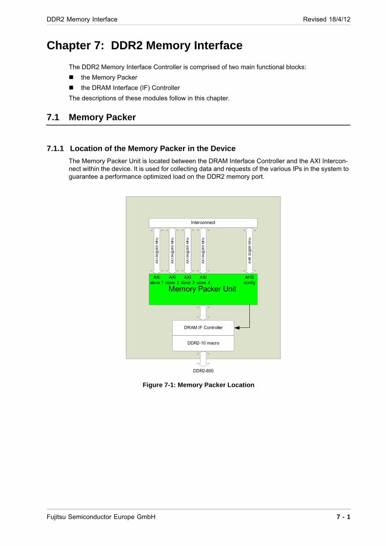
DDR2 Memory Interface Revised 18/4/12
Chapter 7: DDR2 Memory Interface
The DDR2 Memory Interface Controller is comprised of two main functional blocks:
the Memory Packer
the DRAM Interface (IF) Controller
The descriptions of these modules follow in this chapter.
7.1 Memory Packer
7.1.1 Location of the Memory Packer in the Device
The Memory Packer Unit is located between the DRAM Interface Controller and the AXI Intercon-nect within the device. It is used for collecting data and requests of the various IPs in the system to guarantee a performance optimized load on the DDR2 memory port.
Figure 7-1: Memory Packer Location
DDR2-800
AX
I 64
@26
6 M
Hz
AX
I 64
@26
6 M
Hz
AX
I 64
@26
6 M
Hz
AX
I 64
@26
6 M
Hz
AH
B 3
2@
66 M
Hz
Memory Packer Unit
DRAM IF Controller
DDR2-10 macro
Interconnect
AXI slave 1
AXI slave 2
AXI slave 3
AXI slave 4
AHB config
Fujitsu Semiconductor Europe GmbH 7 - 1

Revised 18/4/12 DDR2 Memory Interface
7.1.2 Feature List
The Memory Packer module has the following features:
4 AXI slave interfaces provide required bandwidth to operate with 64 bit DDR2-800 memories
Synchronization of read and write requests for each AXI port
Configurable arbitration schema of AXI ports
Cache with 16 R/W buffers for each AXI port (AXI slave 1 corresponds to Cache 1, AXI slave 2 to Cache 2 and so on)
256 Byte buffer size per cache-line, configurable to 256, 128, 64 and 32 byte width
LeastRecentlyUsed (LRU) buffer select schema
Configurable write-back functionality
LRU counter value
Timer
SW-flush
Configurable read buffer invalidation
7.1.3 Limitations
Data integrity between any two of the four AXI interfaces is not guaranteed.
If a software flush is triggered and the associated AXI interfaces do still receive traffic, traffic ongoing during the flush is partially affected by the flush as well
An Area Flush always flushes a complete cache line. So the smallest granularity to flush is the configured cache line width.
Flush initiated by Timer does not set flushpending status registers or status signals
7.2 DRAM Interface Controller
7.2.1 Position of the DRAM Interface Controller in the device
The DRAM Interface Controller is located between the Memory Packer and the DDR2 memory port within the device. The DRAM Interface Controller was built using 90nm technology and supports op-eration frequencies between 200MHz-400MHz i.e. the following devices: DDR2-800, DDR2-667, DDR2-533, DDR2-400 which comply to the JEDEC standard 'JESD79-2E', see http://www.jedec.org/download/search/JESD79-2E.pdf.
7 - 2 Fujitsu Semiconductor Europe GmbH
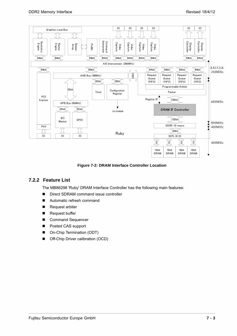
DDR2 Memory Interface Revised 18/4/12
LK Hz
Hz
HzHz
Hz
Figure 7-2: DRAM Interface Controller Location
7.2.2 Feature List
The MB86298 'Ruby' DRAM Interface Controller has the following main features:
Direct SDRAM command issue controller
Automatic refresh command
Request arbiter
Request buffer
Command Sequencer
Posted CAS support
On-Chip Termination (ODT)
Off-Chip Driver calibration (OCD)
AXI C266M
400M
400M800M
400M
DRAM IF Controller
DDR2-10 macro
16bitDRAM
16bitDRAM
16bitDRAM
16bitDRAM
16bit
SSTL18 IO
Packer
64bit
16bit
16bit
16bit
128bit
128bit
Programmable Arbiter
RequestQueue(FIFO)
RequestQueue(FIFO)
RequestQueue(FIFO)
RequestQueue(FIFO)
64bit 64bit 64bit64bit
AXI Interconnect (266MHz)
AHB Bus (66MHz)
ConfigurationRegister
64bit
32bit
to module
Timer
32bit
APB Bus (66MHz)
GPIO
32bit
32bit
I2CMaster
32bit
64bit
PCIExpress
64bit
Disp
layC
ontro
ller
64bit
Disp
layC
ontro
ller
64bit
Video
Cap
ture
64bit
Video
Cap
ture
64bit
Video
Cap
ture
64bit
Video
Cap
ture
64bit
Com
man
dInterpreter
PixB
lt
64bit
Shad
er A
rray
Graphics Local Bus
Raster
Engine
64bit
Geom
etryE
ngine
64bit
IO IO
PHY
IO
IOIOIOIOIOIO
Ruby32b
it
Register IF
Fujitsu Semiconductor Europe GmbH 7 - 3
Revised 18/4/12 DDR2 Memory Interface
7.2.3 DRAM Interface Controller Performance
Table 7-1: Data Transfer Speed
Table 7-2: DRAM Controller Read Latency
7.2.4 External Memory Configurations
The following external memory device configurations are possible with MB86298 'Ruby':
7.2.5 Recommended Timing Parameters for DDR2 Devices
64bit SDRAM at 800Mbps (6400[Mbyte/s])
Continuous 8 byte read access (page mistake hit) 130[Mbyte/s]
Continuous 8 byte read access (page hit) 1550[Mbyte/s]
Continuous 128 bytes read access (page mistake hit) 2150[Mbyte/s]
Continuous 128 byte read access (page hit) 6200[Mbyte/s]
Continuous 8 byte write access (page mistake hit) 130[Mbyte/s]
Continuous 8 byte write access (page hit) 1550[Mbyte/s]
Continuous 128 bytes write access (page mistake hit) 1800[Mbyte/s]
Continuous 128 byte write access (page hit) 6200[Mbyte/s]
64bit SDRAM of 800Mbps
Read access (page mistake hit) min. 29 cycles
Read access (page hit) min. 19 cycles
Type Data Organization Bus Width Chip Count Total Capacity
DDR2SDRAM 512Mbit 32M x16 32 bit 2 128MB
DDR2SDRAM 1Gbit 64M x16 32 bit 2 256MB
DDR2SDRAM 256Mbit 16M x16 64 bit 4 128MB
DDR2SDRAM 512Mbit 32M x16 64 bit 4 256MB
DDR2SDRAM 1Gbit 64M x16 64 bit 4 512MB
Symbol Register DDR2-800E DDR2-800D DDR2-667D DDR2-533C DDR2-400C
CL SMR_CL[2:0] 6 5 5 4 3
AL SEMR1[2:0] 4 4 4 3 3
tREFI SRC_TREFI[15:0] 3120 3120 2600 2080 1560
tRFC STP1_TRFC[7:0] 51 51 43 34 26
7 - 4 Fujitsu Semiconductor Europe GmbH
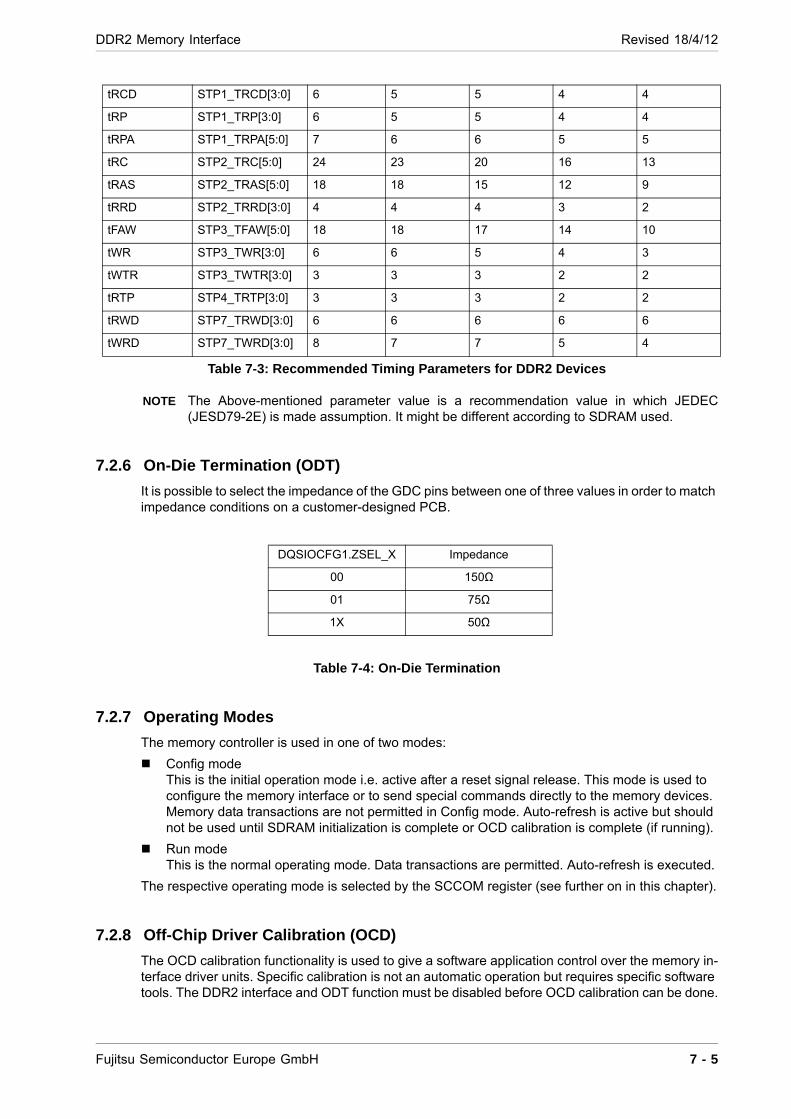
DDR2 Memory Interface Revised 18/4/12
Table 7-3: Recommended Timing Parameters for DDR2 Devices
NOTE The Above-mentioned parameter value is a recommendation value in which JEDEC (JESD79-2E) is made assumption. It might be different according to SDRAM used.
7.2.6 On-Die Termination (ODT)
It is possible to select the impedance of the GDC pins between one of three values in order to match impedance conditions on a customer-designed PCB.
Table 7-4: On-Die Termination
7.2.7 Operating Modes
The memory controller is used in one of two modes:
Config modeThis is the initial operation mode i.e. active after a reset signal release. This mode is used to configure the memory interface or to send special commands directly to the memory devices. Memory data transactions are not permitted in Config mode. Auto-refresh is active but should not be used until SDRAM initialization is complete or OCD calibration is complete (if running).
Run modeThis is the normal operating mode. Data transactions are permitted. Auto-refresh is executed.
The respective operating mode is selected by the SCCOM register (see further on in this chapter).
7.2.8 Off-Chip Driver Calibration (OCD)
The OCD calibration functionality is used to give a software application control over the memory in-terface driver units. Specific calibration is not an automatic operation but requires specific software tools. The DDR2 interface and ODT function must be disabled before OCD calibration can be done.
tRCD STP1_TRCD[3:0] 6 5 5 4 4
tRP STP1_TRP[3:0] 6 5 5 4 4
tRPA STP1_TRPA[5:0] 7 6 6 5 5
tRC STP2_TRC[5:0] 24 23 20 16 13
tRAS STP2_TRAS[5:0] 18 18 15 12 9
tRRD STP2_TRRD[3:0] 4 4 4 3 2
tFAW STP3_TFAW[5:0] 18 18 17 14 10
tWR STP3_TWR[3:0] 6 6 5 4 3
tWTR STP3_TWTR[3:0] 3 3 3 2 2
tRTP STP4_TRTP[3:0] 3 3 3 2 2
tRWD STP7_TRWD[3:0] 6 6 6 6 6
tWRD STP7_TWRD[3:0] 8 7 7 5 4
DQSIOCFG1.ZSEL_X Impedance
00 150Ω
01 75Ω
1X 50Ω
Fujitsu Semiconductor Europe GmbH 7 - 5

Revised 18/4/12 DDR2 Memory Interface
7.2.9 DDR2 Initialization Procedure
Figure 7-3: DDR2 Initialization Procedure
7 - 6 Fujitsu Semiconductor Europe GmbH
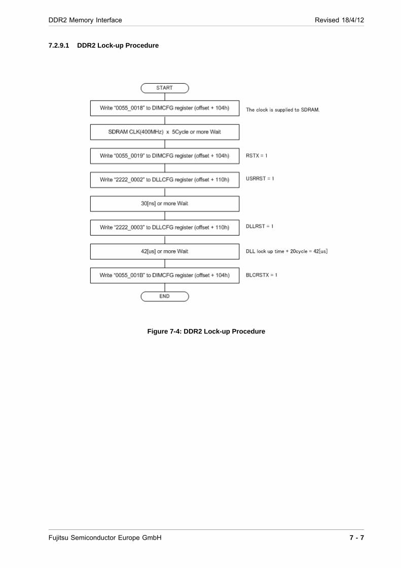
DDR2 Memory Interface Revised 18/4/12
7.2.9.1 DDR2 Lock-up Procedure
Figure 7-4: DDR2 Lock-up Procedure
Fujitsu Semiconductor Europe GmbH 7 - 7
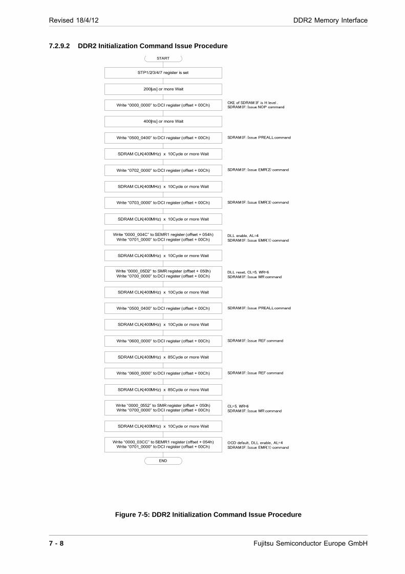
Revised 18/4/12 DDR2 Memory Interface
7.2.9.2 DDR2 Initialization Command Issue Procedure
Figure 7-5: DDR2 Initialization Command Issue Procedure
START
200[us] or more Wait
Write “0000_0000” to DCI register (offset + 00Ch)CKE of SDRAM IF is H level . SDRAM IF: Issue NOP command
STP1/2/3/4/7 register is set
Write “0500_0400” to DCI register (offset + 00Ch) SDRAM IF: Issue PREALL command
Write “0000_004C” to SEMR1 register (offset + 054h)Write “0701_0000” to DCI register (offset + 00Ch)
DLL enable, AL=4SDRAM IF: Issue EMR(1) command
Write “0000_05D2” to SMR register (offset + 050h)Write “0700_0000” to DCI register (offset + 00Ch)
DLL reset, CL=5, WR=6SDRAM IF: Issue MR command
Write “0500_0400” to DCI register (offset + 00Ch) SDRAM IF: Issue PREALL command
400[ns] or more Wait
SDRAM CLK(400MHz) x 10Cycle or more Wait
SDRAM CLK(400MHz) x 10Cycle or more Wait
SDRAM CLK(400MHz) x 10Cycle or more Wait
SDRAM CLK(400MHz) x 10Cycle or more Wait
Write “0600_0000” to DCI register (offset + 00Ch) SDRAM IF: Issue REF command
SDRAM CLK(400MHz) x 85Cycle or more Wait
Write “0600_0000” to DCI register (offset + 00Ch) SDRAM IF: Issue REF command
SDRAM CLK(400MHz) x 85Cycle or more Wait
Write “0000_0552” to SMR register (offset + 050h)Write “0700_0000” to DCI register (offset + 00Ch)
CL=5, WR=6SDRAM IF: Issue MR command
SDRAM CLK(400MHz) x 10Cycle or more Wait
Write “0000_03CC” to SEMR1 register (offset + 054h)Write “0701_0000” to DCI register (offset + 00Ch)
OCD default , DLL enable, AL=4SDRAM IF: Issue EMR(1) command
END
Write “0702_0000” to DCI register (offset + 00Ch) SDRAM IF: Issue EMR(2) command
Write “0703_0000” to DCI register (offset + 00Ch) SDRAM IF: Issue EMR(3) command
SDRAM CLK(400MHz) x 10Cycle or more Wait
SDRAM CLK(400MHz) x 10Cycle or more Wait
7 - 8 Fujitsu Semiconductor Europe GmbH

DDR2 Memory Interface Revised 18/4/12
Fujitsu Semiconductor Europe GmbH 7 - 9
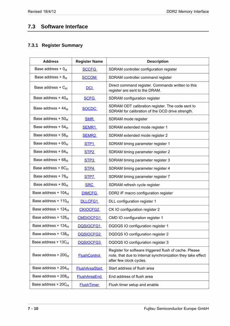
Revised 18/4/12 DDR2 Memory Interface
7.3 Software Interface
7.3.1 Register Summary
Address Register Name Description
Base address + 0H SCCFG SDRAM controller configuration register
Base address + 8H SCCOM SDRAM controller command register
Base address + CH DCI Direct command register. Commands written to this register are sent to the DRAM.
Base address + 40H SCFG SDRAM configuration register
Base address + 44H SOCDC SDRAM ODT calibration register. The code sent to SDRAM for calibration of the OCD drive strength.
Base address + 50H SMR SDRAM mode register
Base address + 54H SEMR1 SDRAM extended mode register 1
Base address + 58H SEMR2 SDRAM extended mode register 2
Base address + 60H STP1 SDRAM timing parameter register 1
Base address + 64H STP2 SDRAM timing parameter register 2
Base address + 68H STP3 SDRAM timing parameter register 3
Base address + 6CH STP4 SDRAM timing parameter register 4
Base address + 78H STP7 SDRAM timing parameter register 7
Base address + 80H SRC SDRAM refresh cycle register
Base address + 104H DIMCFG DDR2 IF macro configuration register
Base address + 110H DLLCFG1 DLL configuration register 1
Base address + 124H CKIOCFG2 CK IO configuration register 2
Base address + 128H CMDIOCFG1 CMD IO configuration register 1
Base address + 134H DQSIOCFG1 DQDQS IO configuration register 1
Base address + 138H DQSIOCFG2 DQDQS IO configuration register 2
Base address + 13CH DQSIOCFG3 DQDQS IO configuration register 3
Base address + 200H FlushControl Register for software triggered flush of cache. Please note, that due to internal synchronization they take effect after few clock cycles.
Base address + 204H FlushAreaStart Start address of flush area
Base address + 208H FlushAreaEnd End address of flush area
Base address + 20CH FlushTimer Flush timer setup and enable
7 - 10 Fujitsu Semiconductor Europe GmbH

DDR2 Memory Interface Revised 18/4/12
Base address + 210H CacheControl Cache control register, setup of line width and writeback value. Do not change this during operation.
Base address + 214H ArbiterControl Arbiter control register, priority setup. Do not change this during operation.
Fujitsu Semiconductor Europe GmbH 7 - 11
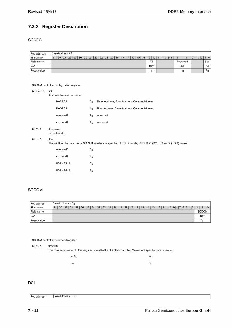
Revised 18/4/12 DDR2 Memory Interface
7.3.2 Register Description
SCCFG
SCCOM
DCI
Reg address BaseAddress + 0H
Bit number 31 30 29 28 27 26 25 24 23 22 21 20 19 18 17 16 15 14 13 12 11 10 9 8 7 6 5 4 3 2 1 0
Field name AT Reserved BW
R/W RW RW RW
Reset value 0H 0H 3H
SDRAM controller configuration register
Bit 13 - 12 AT Address Translation mode
BARACA 0H Bank Address, Row Address, Column Address
RABACA 1H Row Address, Bank Address, Column Address
reserved2 2H reserved
reserved3 3H reserved
Bit 7 - 6 ReservedDo not modify
Bit 1 - 0 BW The width of the data bus of SDRAM Interface is specified. In 32 bit mode, SSTL18IO (DQ 31:0 an DQS 3:0) is used.
reserved0 0H
reserved1 1H
Width 32 bit 2H
Width 64 bit 3H
Reg address BaseAddress + 8H
Bit number 31 30 29 28 27 26 25 24 23 22 21 20 19 18 17 16 15 14 13 12 11 10 9 8 7 6 5 4 3 2 1 0
Field name SCCOM
R/W RW
Reset value 0H
SDRAM controller command register
Bit 2 - 0 SCCOM The command written to this register is sent to the SDRAM controller. Values not specified are reserved.
config 0H
run 3H
Reg address BaseAddress + CH
7 - 12 Fujitsu Semiconductor Europe GmbH

DDR2 Memory Interface Revised 18/4/12
SCFG
SOCDC
Bit number 31 30 29 28 27 26 25 24 23 22 21 20 19 18 17 16 15 14 13 12 11 10 9 8 7 6 5 4 3 2 1 0
Field name COM BA ADDR
R/W RW RW RW
Reset value 0H 0H 0H
Direct command register. Commands written to this register are sent to the DRAM.
Bit 26 - 24 COM Command to be executed. Values not specified are reserved.
NOP 0H
PREALL 5H
AREF 6H
MRS 7H
Bit 18 - 16 BA Bank Address the command is executed on
Bit 12 - 0 ADDR Address the command is executed on, do not use byte write access on this register
Reg address BaseAddress + 40H
Bit number 31 30 29 28 27 26 25 24 23 22 21 20 19 18 17 16 15 14 13 12 11 10 9 8 7 6 5 4 3 2 1 0
Field name ODT1 ODT0 BAN RAN CAN
R/W RW RW RW RW RW
Reset value 0H 0H 3H DH AH
SDRAM configuration register
Bit 31 ODT1 On Die Termination for DQ[63:32]
disable 0H
enable 1H
Bit 30 ODT0 On Die Termination for DQ[31:0]
disable 0H
enable 1H
Bit 10 - 9 BAN Bank Address Bit Width: legal values are 2 and 3, others are reserved
Bit 8 - 4 RAN Row Address Bit Width, 13 is the only legal number, all others are reserved
Bit 3 - 0 CAN Column Address Bit Width, legal values are 9 and 10, others are reserved
Reg address BaseAddress + 44H
Bit number 31 30 29 28 27 26 25 24 23 22 21 20 19 18 17 16 15 14 13 12 11 10 9 8 7 6 5 4 3 2 1 0
Field name OCDCODE_3 OCDCODE_2 OCDCODE_1 OCDCODE_0
R/W RW RW RW RW
Fujitsu Semiconductor Europe GmbH 7 - 13
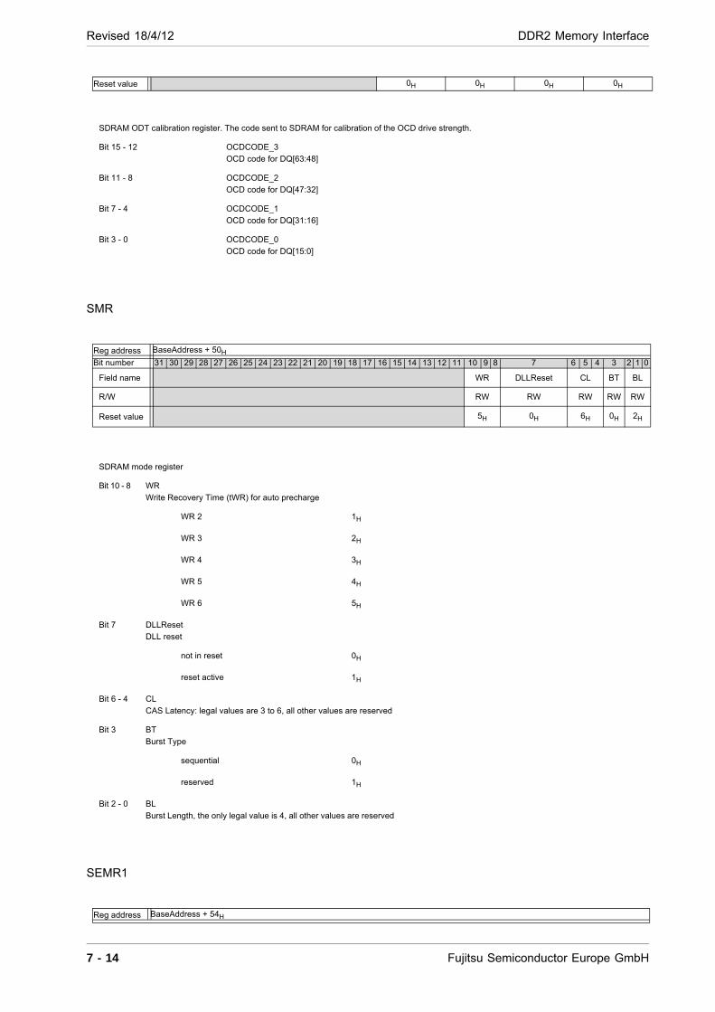
Revised 18/4/12 DDR2 Memory Interface
SMR
SEMR1
Reset value 0H 0H 0H 0H
SDRAM ODT calibration register. The code sent to SDRAM for calibration of the OCD drive strength.
Bit 15 - 12 OCDCODE_3 OCD code for DQ[63:48]
Bit 11 - 8 OCDCODE_2 OCD code for DQ[47:32]
Bit 7 - 4 OCDCODE_1 OCD code for DQ[31:16]
Bit 3 - 0 OCDCODE_0 OCD code for DQ[15:0]
Reg address BaseAddress + 50H
Bit number 31 30 29 28 27 26 25 24 23 22 21 20 19 18 17 16 15 14 13 12 11 10 9 8 7 6 5 4 3 2 1 0
Field name WR DLLReset CL BT BL
R/W RW RW RW RW RW
Reset value 5H 0H 6H 0H 2H
SDRAM mode register
Bit 10 - 8 WR Write Recovery Time (tWR) for auto precharge
WR 2 1H
WR 3 2H
WR 4 3H
WR 5 4H
WR 6 5H
Bit 7 DLLReset DLL reset
not in reset 0H
reset active 1H
Bit 6 - 4 CL CAS Latency: legal values are 3 to 6, all other values are reserved
Bit 3 BT Burst Type
sequential 0H
reserved 1H
Bit 2 - 0 BL Burst Length, the only legal value is 4, all other values are reserved
Reg address BaseAddress + 54H
7 - 14 Fujitsu Semiconductor Europe GmbH
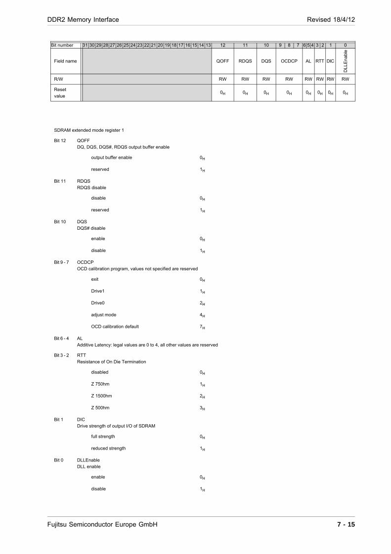
DDR2 Memory Interface Revised 18/4/12
Bit number 31 30 29 28 27 26 25 24 23 22 21 20 19 18 17 16 15 14 13 12 11 10 9 8 7 6 5 4 3 2 1 0
Field name QOFF RDQS DQS OCDCP AL RTT DIC
DLL
En
able
R/W RW RW RW RW RW RW RW RW
Reset
value0H 0H 0H 0H 0H 0H 0H 0H
SDRAM extended mode register 1
Bit 12 QOFF DQ, DQS, DQS#, RDQS output buffer enable
output buffer enable 0H
reserved 1H
Bit 11 RDQS RDQS disable
disable 0H
reserved 1H
Bit 10 DQS DQS# disable
enable 0H
disable 1H
Bit 9 - 7 OCDCP OCD calibration program, values not specified are reserved
exit 0H
Drive1 1H
Drive0 2H
adjust mode 4H
OCD calibration default 7H
Bit 6 - 4 AL Additive Latency: legal values are 0 to 4, all other values are reserved
Bit 3 - 2 RTT Resistance of On Die Termination
disabled 0H
Z 750hm 1H
Z 1500hm 2H
Z 500hm 3H
Bit 1 DIC Drive strength of output I/O of SDRAM
full strength 0H
reduced strength 1H
Bit 0 DLLEnable DLL enable
enable 0H
disable 1H
Fujitsu Semiconductor Europe GmbH 7 - 15
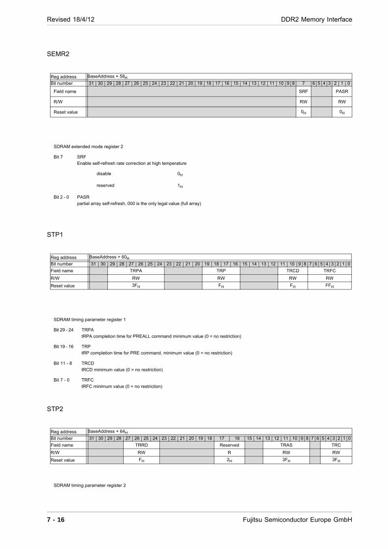
Revised 18/4/12 DDR2 Memory Interface
SEMR2
STP1
STP2
Reg address BaseAddress + 58H
Bit number 31 30 29 28 27 26 25 24 23 22 21 20 19 18 17 16 15 14 13 12 11 10 9 8 7 6 5 4 3 2 1 0
Field name SRF PASR
R/W RW RW
Reset value 0H 0H
SDRAM extended mode register 2
Bit 7 SRF Enable self-refresh rate correction at high temperature
disable 0H
reserved 1H
Bit 2 - 0 PASR partial array self-refresh, 000 is the only legal value (full array)
Reg address BaseAddress + 60H
Bit number 31 30 29 28 27 26 25 24 23 22 21 20 19 18 17 16 15 14 13 12 11 10 9 8 7 6 5 4 3 2 1 0
Field name TRPA TRP TRCD TRFC
R/W RW RW RW RW
Reset value 3FH FH FH FFH
SDRAM timing parameter register 1
Bit 29 - 24 TRPA tRPA completion time for PREALL command minimum value (0 = no restriction)
Bit 19 - 16 TRP tRP completion time for PRE command, minimum value (0 = no restriction)
Bit 11 - 8 TRCD tRCD minimum value (0 = no restriction)
Bit 7 - 0 TRFC tRFC minimum value (0 = no restriction)
Reg address BaseAddress + 64H
Bit number 31 30 29 28 27 26 25 24 23 22 21 20 19 18 17 16 15 14 13 12 11 10 9 8 7 6 5 4 3 2 1 0
Field name TRRD Reserved TRAS TRC
R/W RW R RW RW
Reset value FH 2H 3FH 3FH
SDRAM timing parameter register 2
7 - 16 Fujitsu Semiconductor Europe GmbH
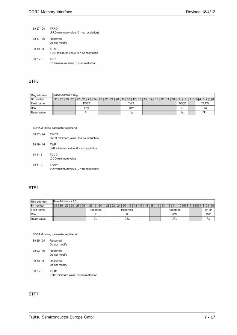
DDR2 Memory Interface Revised 18/4/12
STP3
STP4
STP7
Bit 27 - 24 TRRD tRRD minimum value (0 = no restriction)
Bit 17 - 16 ReservedDo not modify
Bit 13 - 8 TRAS tRAS minimum value, 0 = no restriction
Bit 5 - 0 TRC tRC minimum value, 0 = no restriction
Reg address BaseAddress + 68H
Bit number 31 30 29 28 27 26 25 24 23 22 21 20 19 18 17 16 15 14 13 12 11 10 9 8 7 6 5 4 3 2 1 0
Field name TWTR TWR TCCD TFAW
R/W RW RW R RW
Reset value FH FH 2H 3FH
SDRAM timing parameter register 3
Bit 27 - 24 TWTR tWTR minimum value, 0 = no restriction
Bit 19 - 16 TWR tWR minimum value, 0 = no restriction
Bit 9 - 8 TCCD tCCD minimum value
Bit 5 - 0 TFAW tFAW minimum value (0 = no restriction)
Reg address BaseAddress + 6CH
Bit number 31 30 29 28 27 26 25 24 23 22 21 20 19 18 17 16 15 14 13 12 11 10 9 8 7 6 5 4 3 2 1 0
Field name Reserved Reserved Reserved TRTP
R/W R R RW RW
Reset value 2H C8H 3FH FH
SDRAM timing parameter register 4
Bit 25 - 24 ReservedDo not modify
Bit 23 - 16 ReservedDo not modify
Bit 13 - 8 ReservedDo not modify
Bit 3 - 0 TRTP tRTP minimum value, 0 = no restriction
Fujitsu Semiconductor Europe GmbH 7 - 17
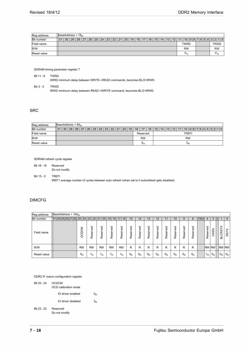
Revised 18/4/12 DDR2 Memory Interface
RS
TX
H
SRC
DIMCFG
Reg address BaseAddress + 78H
Bit number 31 30 29 28 27 26 25 24 23 22 21 20 19 18 17 16 15 14 13 12 11 10 9 8 7 6 5 4 3 2 1 0
Field name TWRD TRWD
R/W RW RW
Reset value FH FH
SDRAM timing parameter register 7
Bit 11 - 8 TWRD tWRD minimum delay between WRITE->READ commands, becomes BL/2+tRWD
Bit 3 - 0 TRWD tRWD minimum delay between READ->WRITE command, becomes BL/2+tRWD
Reg address BaseAddress + 80H
Bit number 31 30 29 28 27 26 25 24 23 22 21 20 19 18 17 16 15 14 13 12 11 10 9 8 7 6 5 4 3 2 1 0
Field name Reserved TREFI
R/W RW RW
Reset value 0H 0H
SDRAM refresh cycle register
Bit 18 - 16 ReservedDo not modify
Bit 15 - 0 TREFI tREF1 average number of cycles between auto refresh (when set to 0 autorefresh gets disabled)
Reg address BaseAddress + 104H
Bit number 31 30 29 28 27 26 25 24 23 22 21 20 19 18 17 16 15 14 13 12 11 10 9 8 7 6 5 4 3 2 1 0
Field name
OC
DC
M
Res
erve
d
Res
erve
d
Res
erve
d
Res
erve
d
Res
erve
d
Res
erve
d
Res
erve
d
Res
erve
d
Res
erve
d
Res
erve
d
Res
erve
d
Res
erve
d
Res
erve
d
CK
EN
BL
CR
ST
X
R/W RW RW RW RW RW R R R R R R R R RW RW RW RW
Reset value 0H 1H 1H 1H 1H 0H 0H 0H 0H 0H 0H 0H 0H 1H 0H 0H 0
DDR2 IF macro configuration register
Bit 25 - 24 OCDCM OCD calibration mode
IO driver enabled 0H
IO driver disabled 3H
Bit 23 - 22 ReservedDo not modify
7 - 18 Fujitsu Semiconductor Europe GmbH
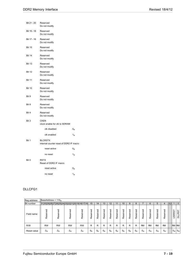
DDR2 Memory Interface Revised 18/4/12
0
DL
LR
ST
RW
0H
DLLCFG1
Bit 21 - 20 ReservedDo not modify
Bit 19 - 18 ReservedDo not modify
Bit 17 - 16 ReservedDo not modify
Bit 15 ReservedDo not modify
Bit 14 ReservedDo not modify
Bit 13 ReservedDo not modify
Bit 12 ReservedDo not modify
Bit 11 ReservedDo not modify
Bit 10 ReservedDo not modify
Bit 9 ReservedDo not modify
Bit 8 ReservedDo not modify
Bit 4 ReservedDo not modify
Bit 3 CKEN clock enable for clk to SDRAM
clk disabled 0H
clk enabled 1H
Bit 1 BLCRSTX internal counter reset of DDR2 IF macro
reset active 0H
no reset 1H
Bit 0 RSTX Reset of DDR2 IF macro
reset active 0H
no reset 1H
Reg address BaseAddress + 110H
Bit number 31 30 29 28 27 26 25 24 23 22 21 20 19 18 17 16 15 14 13 12 11 10 9 8 7 6 5 4 3 2 1
Field name
Re
serv
ed
Re
serv
ed
Re
serv
ed
Re
serv
ed
Re
serv
ed
Re
serv
ed
Re
serv
ed
Re
serv
ed
Re
serv
ed
Re
serv
ed
Re
serv
ed
Re
serv
ed
Re
serv
ed
Re
serv
ed
Re
serv
ed
Re
serv
ed
US
RR
ST
R/W RW RW RW RW R R R R R R R R RW RW RW RW RW
Reset value 2H 2H 2H 2H 0H 0H 0H 0H 0H 0H 0H 0H 0H 0H 0H 0H 0H
Fujitsu Semiconductor Europe GmbH 7 - 19

Revised 18/4/12 DDR2 Memory Interface
CKIOCFG2
DLL configuration register 1
Bit 31 - 28 ReservedDo not modify
Bit 27 - 24 ReservedDo not modify
Bit 23 - 20 ReservedDo not modify
Bit 19 - 16 ReservedDo not modify
Bit 15 ReservedDo not modify
Bit 14 ReservedDo not modify
Bit 13 ReservedDo not modify
Bit 12 ReservedDo not modify
Bit 11 ReservedDo not modify
Bit 10 ReservedDo not modify
Bit 9 ReservedDo not modify
Bit 8 ReservedDo not modify
Bit 7 ReservedDo not modify
Bit 6 ReservedDo not modify
Bit 5 ReservedDo not modify
Bit 4 ReservedDo not modify
Bit 1 USRRST DLL reset
reset active 0
H
no reset 1
H
Bit 0 DLLRST DLL reset
reset active 0
H
no reset 1
H
Reg address BaseAddress + 124H
Bit number 31 30 29 28 27 26 25 24 23 22 21 20 19 18 17 16 15 14 13 12 11 10 9 8 7 6 5 4 3 2 1 0Field name CK_DRVN_3 CK_DRVN_2 CK_DRVN_1 CK_DRVN_0 CK_DRVP_3 CK_DRVP_2 CK_DRVP_1 CK_DRVP_0
7 - 20 Fujitsu Semiconductor Europe GmbH
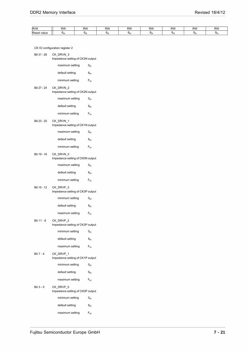
DDR2 Memory Interface Revised 18/4/12
R/W RW RW RW RW RW RW RW RW
Reset value 6H 6H 6H 6H 9H 9H 9H 9H
CK IO configuration register 2
Bit 31 - 28 CK_DRVN_3 Impedance setting of CK3N output
maximum setting 0H
default setting 6H
minimum setting FH
Bit 27 - 24 CK_DRVN_2 Impedance setting of CK2N output
maximum setting 0H
default setting 6H
minimum setting FH
Bit 23 - 20 CK_DRVN_1 Impedance setting of CK1N output
maximum setting 0H
default setting 6H
minimum setting FH
Bit 19 - 16 CK_DRVN_0 Impedance setting of CK0N output
maximum setting 0H
default setting 6H
minimum setting FH
Bit 15 - 12 CK_DRVP_3 Impedance setting of CK3P output
minimum setting 0H
default setting 9H
maximum setting FH
Bit 11 - 8 CK_DRVP_2 Impedance setting of CK2P output
minimum setting 0H
default setting 9H
maximum setting FH
Bit 7 - 4 CK_DRVP_1 Impedance setting of CK1P output
minimum setting 0H
default setting 9H
maximum setting FH
Bit 3 - 0 CK_DRVP_0 Impedance setting of CK0P output
minimum setting 0H
default setting 9H
maximum setting FH
Fujitsu Semiconductor Europe GmbH 7 - 21

Revised 18/4/12 DDR2 Memory Interface
CMDIOCFG1
Reg address BaseAddress + 128H
Bit number 31 30 29 28 27 26 25 24 23 22 21 20 19 18 17 16 15 14 13 12 11 10 9 8 7 6 5 4 3 2 1 0
Field name
CM
D_
DR
VN
_
1
CM
D_
DR
VN
_0
CM
D_
DR
VP
_1
CM
D_
DR
VP
_0
CM
D_
SP
FU
NC
_
1
CM
D_
SP
FU
NC
_
0
Re
serv
ed
Re
serv
ed
R/W RW RW RW RW RW RW RW RW
Reset value 6H 6H 9H 9H 0H 0H 0H 0H
CMD IO configuration register 1
Bit 31 - 28 CMD_DRVN_1 Impedance setting of CMD1 outputs, legal values 0 (max) to 15 (min)
maximum setting 0H
default setting 6H
minimum setting FH
Bit 27 - 24 CMD_DRVN_0 Impedance setting of CMD0 outputs, legal values 0 (max) to 15 (min)
maximum setting 0H
default setting 6H
minimum setting FH
Bit 23 - 20 CMD_DRVP_1 Impedance setting of CMD1 outputs, legal values 0 (min) to 15 (max)
minimum setting 0H
default setting 9H
maximum setting FH
Bit 19 - 16 CMD_DRVP_0 Impedance setting of CMD0 outputs, legal values 0 (min) to 15 (max)
minimum setting 0H
default setting 9H
maximum setting FH
Bit 3 CMD_SPFUNC_1 control of buffer mode for CMD1 outputs, don't change
default 0H
Bit 2 CMD_SPFUNC_0 control of buffer mode for CMD0 outputs, don't change
default 0H
Bit 1 ReservedDo not modify
Bit 0 ReservedDo not modify
7 - 22 Fujitsu Semiconductor Europe GmbH

DDR2 Memory Interface Revised 18/4/12
DQSIOCFG1
Reg address BaseAddress + 134H
Bit number 31 30 29 28 27 26 25 24 23 22 21 20 19 18 17 16 15 14 13 12 11 10 9 8 7 6 5 4 3 2 1 0
Field name
Res
erve
d
Res
erve
d
Res
erve
d
Res
erve
d
DQ
_O
DT
ON
_3
DQ
_O
DT
ON
_2
DQ
_O
DT
ON
_1
DQ
_O
DT
ON
_0
Res
erve
d
Res
erve
d
Res
erve
d
Res
erve
d
Res
erve
d
Res
erve
d
Res
erve
d
Res
erve
d
Res
erve
d
Res
erve
d
Res
erve
d
Res
erve
d
Res
erve
d
Res
erve
d
Res
erve
d
Res
erve
d
R/W RW RW RW RW RW RW RW RW RW RW RW RW RW RW RW RW RW RW RW RW RW RW RW RW
Reset value 2H 2H 2H 2H 0H 0H 0H 0H 1H 1H 1H 1H 0H 0H 0H 0H 0H 0H 0H 0H 0H 0H 0H 0H
DQDQS IO configuration register 1
Bit 31 - 30 ReservedDo not modify
Bit 29 - 28 ReservedDo not modify
Bit 27 - 26 ReservedDo not modify
Bit 25 - 24 ReservedDo not modify
Bit 19 DQ_ODTON_3 ODT control for DQ63:48 and DQ7:6
OFF 0H
ON 1H
Bit 18 DQ_ODTON_2 ODT control for DQ47:32 and DQ5:4
OFF 0H
ON 1H
Bit 17 DQ_ODTON_1 ODT control for DQ31:16 and DQ3:2
OFF 0H
ON 1H
Bit 16 DQ_ODTON_0 ODT control for DQ15:0 and DQ1:0
OFF 0H
ON 1H
Bit 15 ReservedDo not modify
Bit 14 ReservedDo not modify
Bit 13 ReservedDo not modify
Bit 12 ReservedDo not modify
Bit 11 ReservedDo not modify
Fujitsu Semiconductor Europe GmbH 7 - 23
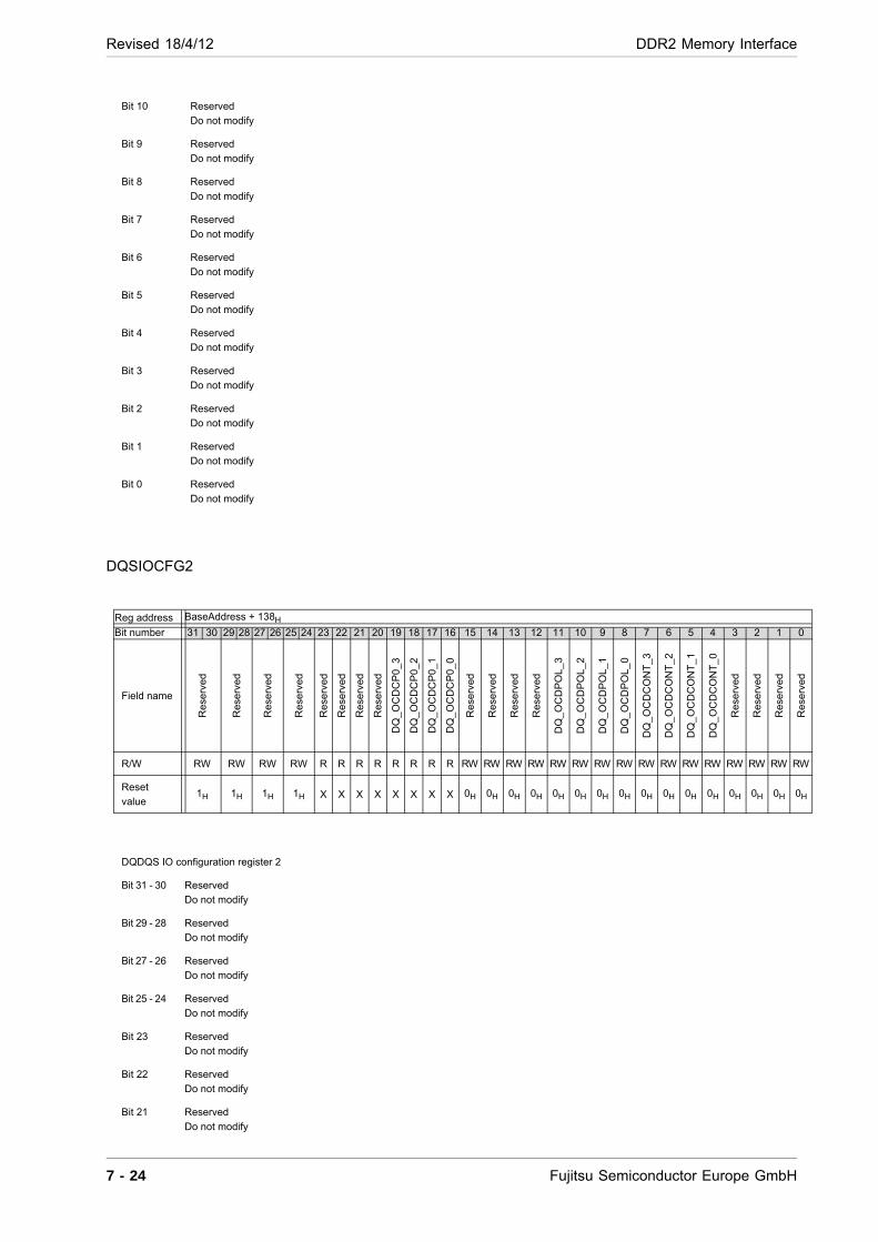
Revised 18/4/12 DDR2 Memory Interface
DQSIOCFG2
Bit 10 ReservedDo not modify
Bit 9 ReservedDo not modify
Bit 8 ReservedDo not modify
Bit 7 ReservedDo not modify
Bit 6 ReservedDo not modify
Bit 5 ReservedDo not modify
Bit 4 ReservedDo not modify
Bit 3 ReservedDo not modify
Bit 2 ReservedDo not modify
Bit 1 ReservedDo not modify
Bit 0 ReservedDo not modify
Reg address BaseAddress + 138H
Bit number 31 30 29 28 27 26 25 24 23 22 21 20 19 18 17 16 15 14 13 12 11 10 9 8 7 6 5 4 3 2 1 0
Field name
Res
erve
d
Res
erve
d
Res
erve
d
Res
erve
d
Res
erve
d
Res
erve
d
Res
erve
d
Res
erve
d
DQ
_O
CD
CP
0_3
DQ
_O
CD
CP
0_2
DQ
_O
CD
CP
0_1
DQ
_O
CD
CP
0_0
Res
erve
d
Res
erve
d
Res
erve
d
Res
erve
d
DQ
_O
CD
PO
L_
3
DQ
_O
CD
PO
L_
2
DQ
_O
CD
PO
L_
1
DQ
_O
CD
PO
L_
0
DQ
_OC
DC
ON
T_
3
DQ
_OC
DC
ON
T_
2
DQ
_OC
DC
ON
T_
1
DQ
_OC
DC
ON
T_
0
Res
erve
d
Res
erve
d
Res
erve
d
Res
erve
d
R/W RW RW RW RW R R R R R R R R RW RW RW RW RW RW RW RW RW RW RW RW RW RW RW RW
Reset
value1H 1H 1H 1H X X X X X X X X 0H 0H 0H 0H 0H 0H 0H 0H 0H 0H 0H 0H 0H 0H 0H 0H
DQDQS IO configuration register 2
Bit 31 - 30 ReservedDo not modify
Bit 29 - 28 ReservedDo not modify
Bit 27 - 26 ReservedDo not modify
Bit 25 - 24 ReservedDo not modify
Bit 23 ReservedDo not modify
Bit 22 ReservedDo not modify
Bit 21 ReservedDo not modify
7 - 24 Fujitsu Semiconductor Europe GmbH
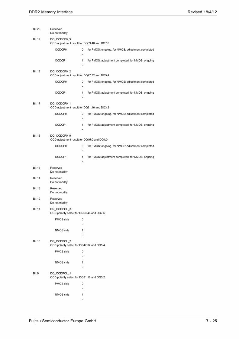
DDR2 Memory Interface Revised 18/4/12
Bit 20 ReservedDo not modify
Bit 19 DQ_OCDCP0_3 OCD adjustment result for DQ63:48 and DQ7:6
OCDCP0 0
H
for PMOS: ongoing, for NMOS: adjustment completed
OCDCP1 1
H
for PMOS: adjustment completed, for NMOS: ongoing
Bit 18 DQ_OCDCP0_2 OCD adjustment result for DQ47:32 and DQ5:4
OCDCP0 0
H
for PMOS: ongoing, for NMOS: adjustment completed
OCDCP1 1
H
for PMOS: adjustment completed, for NMOS: ongoing
Bit 17 DQ_OCDCP0_1 OCD adjustment result for DQ31:16 and DQ3:2
OCDCP0 0
H
for PMOS: ongoing, for NMOS: adjustment completed
OCDCP1 1
H
for PMOS: adjustment completed, for NMOS: ongoing
Bit 16 DQ_OCDCP0_0 OCD adjustment result for DQ15:0 and DQ1:0
OCDCP0 0
H
for PMOS: ongoing, for NMOS: adjustment completed
OCDCP1 1
H
for PMOS: adjustment completed, for NMOS: ongoing
Bit 15 ReservedDo not modify
Bit 14 ReservedDo not modify
Bit 13 ReservedDo not modify
Bit 12 ReservedDo not modify
Bit 11 DQ_OCDPOL_3 OCD polarity select for DQ63:48 and DQ7:6
PMOS side 0
H
NMOS side 1
H
Bit 10 DQ_OCDPOL_2 OCD polarity select for DQ47:32 and DQ5:4
PMOS side 0
H
NMOS side 1
H
Bit 9 DQ_OCDPOL_1 OCD polarity select for DQ31:16 and DQ3:2
PMOS side 0
H
NMOS side 1
H
Fujitsu Semiconductor Europe GmbH 7 - 25
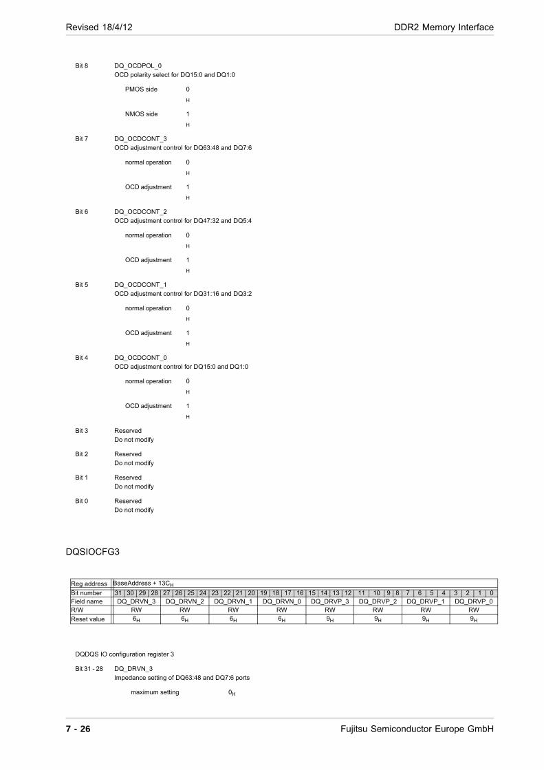
Revised 18/4/12 DDR2 Memory Interface
DQSIOCFG3
Bit 8 DQ_OCDPOL_0 OCD polarity select for DQ15:0 and DQ1:0
PMOS side 0
H
NMOS side 1
H
Bit 7 DQ_OCDCONT_3 OCD adjustment control for DQ63:48 and DQ7:6
normal operation 0
H
OCD adjustment 1
H
Bit 6 DQ_OCDCONT_2 OCD adjustment control for DQ47:32 and DQ5:4
normal operation 0
H
OCD adjustment 1
H
Bit 5 DQ_OCDCONT_1 OCD adjustment control for DQ31:16 and DQ3:2
normal operation 0
H
OCD adjustment 1
H
Bit 4 DQ_OCDCONT_0 OCD adjustment control for DQ15:0 and DQ1:0
normal operation 0
H
OCD adjustment 1
H
Bit 3 ReservedDo not modify
Bit 2 ReservedDo not modify
Bit 1 ReservedDo not modify
Bit 0 ReservedDo not modify
Reg address BaseAddress + 13CH
Bit number 31 30 29 28 27 26 25 24 23 22 21 20 19 18 17 16 15 14 13 12 11 10 9 8 7 6 5 4 3 2 1 0Field name DQ_DRVN_3 DQ_DRVN_2 DQ_DRVN_1 DQ_DRVN_0 DQ_DRVP_3 DQ_DRVP_2 DQ_DRVP_1 DQ_DRVP_0 R/W RW RW RW RW RW RW RW RW
Reset value 6H 6H 6H 6H 9H 9H 9H 9H
DQDQS IO configuration register 3
Bit 31 - 28 DQ_DRVN_3 Impedance setting of DQ63:48 and DQ7:6 ports
maximum setting 0H
7 - 26 Fujitsu Semiconductor Europe GmbH

DDR2 Memory Interface Revised 18/4/12
FlushControl
default setting 6H
minimum setting FH
Bit 27 - 24 DQ_DRVN_2 Impedance setting of DQ47:32 and DQ5:4 ports
maximum setting 0H
default setting 6H
minimum setting FH
Bit 23 - 20 DQ_DRVN_1 Impedance setting of DQ31:16 and DQ3:2 ports
maximum setting 0H
default setting 6H
minimum setting FH
Bit 19 - 16 DQ_DRVN_0 Impedance setting of DQ31:16 and DQ3:2 ports)
maximum setting 0H
default setting 6H
minimum setting FH
Bit 15 - 12 DQ_DRVP_3 Impedance setting of DQ63:48 and DQ7:6 ports
minimum setting 0H
default setting 9H
maximum setting FH
Bit 11 - 8 DQ_DRVP_2 Impedance setting of DQ47:32 and DQ5:4 ports
minimum setting 0H
default setting 9H
maximum setting FH
Bit 7 - 4 DQ_DRVP_1 Impedance setting of DQ31:16 and DQ3:2 ports
minimum setting 0H
default setting 9H
maximum setting FH
Bit 3 - 0 DQ_DRVP_0 Impedance setting of DQ15:0 and DQ1:0 ports
minimum setting 0H
default setting 9H
maximum setting FH
Reg address BaseAddress + 200H
Bit number 31 30 29 28 27 26 25 24 23 22 21 20 19 18 17 16 15 14 13 12 11 10 9 8 7 6 5 4 3 2 1 0
Fujitsu Semiconductor Europe GmbH 7 - 27
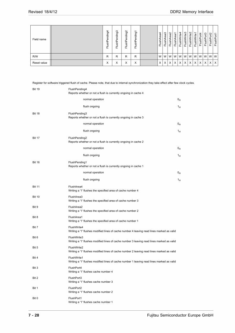
Revised 18/4/12 DDR2 Memory Interface
Field name
Flu
shP
endi
ng4
Flu
shP
endi
ng3
Flu
shP
endi
ng2
Flu
shP
endi
ng1
Flu
shA
rea
4
Flu
shA
rea
3
Flu
shA
rea
2
Flu
shA
rea
1
Flu
shW
rite
4
Flu
shW
rite
3
Flu
shW
rite
2
Flu
shW
rite
1
Flu
shP
ort
4
Flu
shP
ort
3
Flu
shP
ort
2
Flu
shP
ort
1
R/W R R R R W W W W W W W W W W W W
Reset value X X X X X X X X X X X X X X X X
Register for software triggered flush of cache. Please note, that due to internal synchronization they take effect after few clock cycles.
Bit 19 FlushPending4 Reports whether or not a flush is currently ongoing in cache 4
normal operation 0H
flush ongoing 1H
Bit 18 FlushPending3 Reports whether or not a flush is currently ongoing in cache 3
normal operation 0H
flush ongoing 1H
Bit 17 FlushPending2 Reports whether or not a flush is currently ongoing in cache 2
normal operation 0H
flush ongoing 1H
Bit 16 FlushPending1 Reports whether or not a flush is currently ongoing in cache 1
normal operation 0H
flush ongoing 1H
Bit 11 FlushArea4 Writing a '1' flushes the specified area of cache number 4
Bit 10 FlushArea3 Writing a '1' flushes the specified area of cache number 3
Bit 9 FlushArea2 Writing a '1' flushes the specified area of cache number 2
Bit 8 FlushArea1 Writing a '1' flushes the specified area of cache number 1
Bit 7 FlushWrite4 Writing a '1' flushes modified lines of cache number 4 leaving read lines marked as valid
Bit 6 FlushWrite3 Writing a '1' flushes modified lines of cache number 3 leaving read lines marked as valid
Bit 5 FlushWrite2 Writing a '1' flushes modified lines of cache number 2 leaving read lines marked as valid
Bit 4 FlushWrite1 Writing a '1' flushes modified lines of cache number 1 leaving read lines marked as valid
Bit 3 FlushPort4 Writing a '1' flushes cache number 4
Bit 2 FlushPort3 Writing a '1' flushes cache number 3
Bit 1 FlushPort2 Writing a '1' flushes cache number 2
Bit 0 FlushPort1 Writing a '1' flushes cache number 1
7 - 28 Fujitsu Semiconductor Europe GmbH
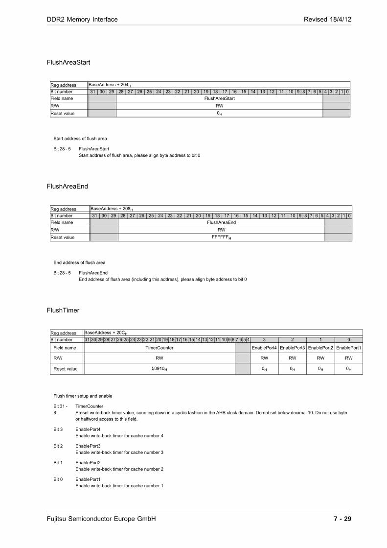
DDR2 Memory Interface Revised 18/4/12
t1
FlushAreaStart
FlushAreaEnd
FlushTimer
Reg address BaseAddress + 204H
Bit number 31 30 29 28 27 26 25 24 23 22 21 20 19 18 17 16 15 14 13 12 11 10 9 8 7 6 5 4 3 2 1 0
Field name FlushAreaStart
R/W RW
Reset value 0H
Start address of flush area
Bit 28 - 5 FlushAreaStart Start address of flush area, please align byte address to bit 0
Reg address BaseAddress + 208H
Bit number 31 30 29 28 27 26 25 24 23 22 21 20 19 18 17 16 15 14 13 12 11 10 9 8 7 6 5 4 3 2 1 0
Field name FlushAreaEnd
R/W RW
Reset value FFFFFFH
End address of flush area
Bit 28 - 5 FlushAreaEnd End address of flush area (including this address), please align byte address to bit 0
Reg address BaseAddress + 20CH
Bit number 31 30 29 28 27 26 25 24 23 22 21 20 19 18 17 16 15 14 13 12 11 10 9 8 7 6 5 4 3 2 1 0
Field name TimerCounter EnablePort4 EnablePort3 EnablePort2 EnablePor
R/W RW RW RW RW RW
Reset value 50910H 0H 0H 0H 0H
Flush timer setup and enable
Bit 31 -
8
TimerCounter Preset write-back timer value, counting down in a cyclic fashion in the AHB clock domain. Do not set below decimal 10. Do not use byte
or halfword access to this field.
Bit 3 EnablePort4 Enable write-back timer for cache number 4
Bit 2 EnablePort3 Enable write-back timer for cache number 3
Bit 1 EnablePort2 Enable write-back timer for cache number 2
Bit 0 EnablePort1 Enable write-back timer for cache number 1
Fujitsu Semiconductor Europe GmbH 7 - 29
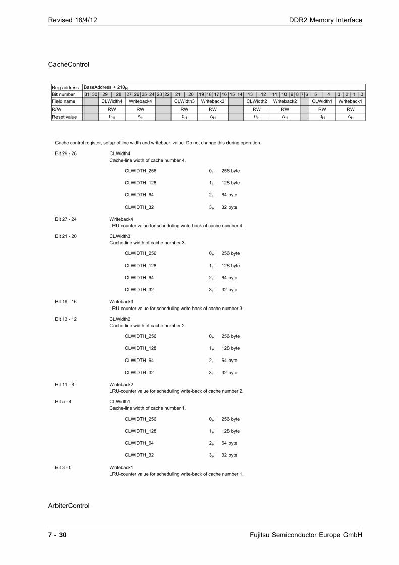
Revised 18/4/12 DDR2 Memory Interface
CacheControl
ArbiterControl
Reg address BaseAddress + 210H
Bit number 31 30 29 28 27 26 25 24 23 22 21 20 19 18 17 16 15 14 13 12 11 10 9 8 7 6 5 4 3 2 1 0
Field name CLWidth4 Writeback4 CLWidth3 Writeback3 CLWidth2 Writeback2 CLWidth1 Writeback1
R/W RW RW RW RW RW RW RW RW
Reset value 0H AH 0H AH 0H AH 0H AH
Cache control register, setup of line width and writeback value. Do not change this during operation.
Bit 29 - 28 CLWidth4 Cache-line width of cache number 4.
CLWIDTH_256 0H 256 byte
CLWIDTH_128 1H 128 byte
CLWIDTH_64 2H 64 byte
CLWIDTH_32 3H 32 byte
Bit 27 - 24 Writeback4 LRU-counter value for scheduling write-back of cache number 4.
Bit 21 - 20 CLWidth3 Cache-line width of cache number 3.
CLWIDTH_256 0H 256 byte
CLWIDTH_128 1H 128 byte
CLWIDTH_64 2H 64 byte
CLWIDTH_32 3H 32 byte
Bit 19 - 16 Writeback3 LRU-counter value for scheduling write-back of cache number 3.
Bit 13 - 12 CLWidth2 Cache-line width of cache number 2.
CLWIDTH_256 0H 256 byte
CLWIDTH_128 1H 128 byte
CLWIDTH_64 2H 64 byte
CLWIDTH_32 3H 32 byte
Bit 11 - 8 Writeback2 LRU-counter value for scheduling write-back of cache number 2.
Bit 5 - 4 CLWidth1 Cache-line width of cache number 1.
CLWIDTH_256 0H 256 byte
CLWIDTH_128 1H 128 byte
CLWIDTH_64 2H 64 byte
CLWIDTH_32 3H 32 byte
Bit 3 - 0 Writeback1 LRU-counter value for scheduling write-back of cache number 1.
7 - 30 Fujitsu Semiconductor Europe GmbH
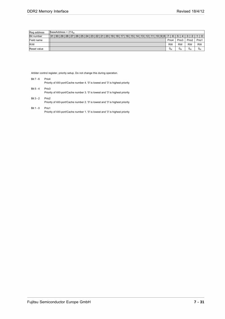
DDR2 Memory Interface Revised 18/4/12
Reg address BaseAddress + 214H
Bit number 31 30 29 28 27 26 25 24 23 22 21 20 19 18 17 16 15 14 13 12 11 10 9 8 7 6 5 4 3 2 1 0
Field name Prio4 Prio3 Prio2 Prio1
R/W RW RW RW RW
Reset value 0H 0H 0H 0H
Arbiter control register, priority setup. Do not change this during operation.
Bit 7 - 6 Prio4 Priority of AXI-port/Cache number 4. '0' is lowest and '3' is highest priority
Bit 5 - 4 Prio3 Priority of AXI-port/Cache number 3. '0' is lowest and '3' is highest priority
Bit 3 - 2 Prio2 Priority of AXI-port/Cache number 2. '0' is lowest and '3' is highest priority
Bit 1 - 0 Prio1 Priority of AXI-port/Cache number 1. '0' is lowest and '3' is highest priority
Fujitsu Semiconductor Europe GmbH 7 - 31
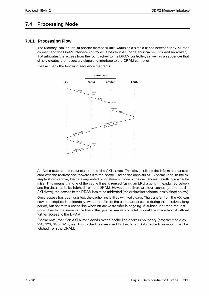
Revised 18/4/12 DDR2 Memory Interface
7.4 Processing Mode
7.4.1 Processing Flow
The Memory Packer unit, or shorter mempack unit, works as a simple cache between the AXI inter-connect and the DRAM interface controller. It has four AXI ports, four cache units and an arbiter, that arbitrates the access from the four caches to the DRAM controller, as well as a sequencer that simply creates the necessary signals to interface to the DRAM controller.
Please check the following sequence diagrams:
An AXI master sends requests to one of the AXI slaves. This slave collects the information associ-ated with the request and forwards it to the cache. The cache consists of 16 cache lines. In the ex-ample shown above, the data requested is not already in one of the cache lines, resulting in a cache miss. This means that one of the cache lines is reused (using an LRU algorithm, explained below) and the data has to be fetched from the DRAM. However, as there are four caches (one for each AXI slave), the access to the DRAM has to be arbitrated (the arbitration scheme is explained below).
Once access has been granted, the cache line is filled with valid data. The transfer from the AXI can now be completed. Incidentally, write transfers to the cache are possible during this relatively long period, but not to this cache line when an active transfer is ongoing. A subsequent read request would then hit the same cache line in the given example and a fetch would be made from it without further access to the DRAM.
Please note, that if an AXI burst extends over a cache line address boundary (programmable as 256, 128, 64 or 32 bytes), two cache lines are used for that burst. Both cache lines would then be fetched from the DRAM.
AXI Cache Arbiter DRAM
mempack
Readcache miss
Readqueued
arbitrated
Read
Data Transfer
Data Transfer
Readcache
hit
Data Transfer
(whole cacheline)
7 - 32 Fujitsu Semiconductor Europe GmbH

DDR2 Memory Interface Revised 18/4/12
The example above shows write transfers. The first write transfer results in a cache miss, which means that one of the cache lines is reused in the previously described LRU manner and the write data is written to that reused cache line. However, this time, as the trigger was a write, no transfer is necessary to or from the DRAM yet. More write requests arrive and hit the same cache line (their data being written there) or miss and reuse more cache lines. Every time a cache line is used, the LRU value is updated according to the LRU algorithm and once the LRU value hits a specific thresh-old (specified in the register interface as the ‘writeback value’), the content of the cache line is scheduled for transfer to the DRAM. Once the access has been granted, the modified portions of the cache line are written to the DRAM.
Please note, that besides the LRU value hitting the writeback value, there are two more possible triggers to initiate a write back operation: Flush via the software interface or via a timer_counter. Please read the section ‘Control Flow’ for details.
AXI Cache Arbiter DRAM
mempack
Write cache miss line 0
Writequeued
arbitrated
Write
Write
line 0 lru hits writeback
value
Write cache hit
line 0
Write cache missline 1
Write cache missline 2
(modified bytes of line 0)
cache hit
line 1
Fujitsu Semiconductor Europe GmbH 7 - 33
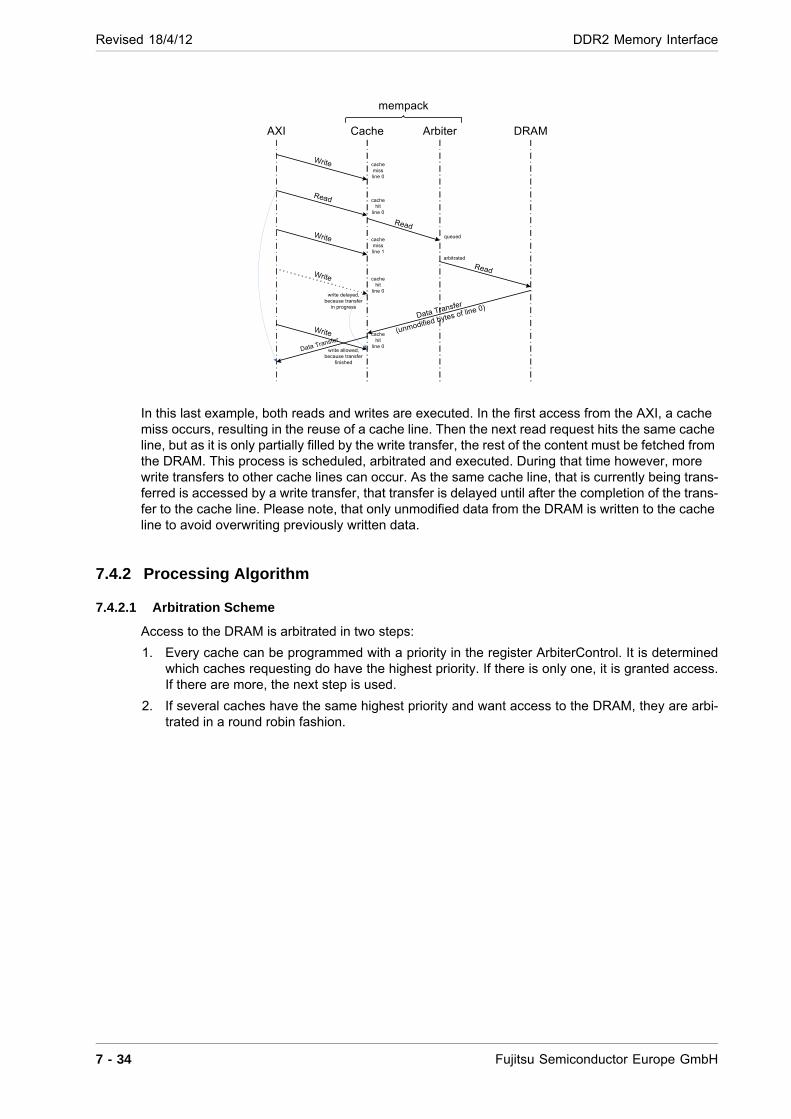
Revised 18/4/12 DDR2 Memory Interface
In this last example, both reads and writes are executed. In the first access from the AXI, a cache miss occurs, resulting in the reuse of a cache line. Then the next read request hits the same cache line, but as it is only partially filled by the write transfer, the rest of the content must be fetched from the DRAM. This process is scheduled, arbitrated and executed. During that time however, more write transfers to other cache lines can occur. As the same cache line, that is currently being trans-ferred is accessed by a write transfer, that transfer is delayed until after the completion of the trans-fer to the cache line. Please note, that only unmodified data from the DRAM is written to the cache line to avoid overwriting previously written data.
7.4.2 Processing Algorithm
7.4.2.1 Arbitration Scheme
Access to the DRAM is arbitrated in two steps:
1. Every cache can be programmed with a priority in the register ArbiterControl. It is determined which caches requesting do have the highest priority. If there is only one, it is granted access. If there are more, the next step is used.
2. If several caches have the same highest priority and want access to the DRAM, they are arbi-trated in a round robin fashion.
AXI Cache Arbiter DRAM
mempack
Write cache miss line 0
Readqueued
arbitrated
Read
Write
write delayed, because transfer
in progress
Read cache hit
line 0
Write cache missline 1
Write cache hit
line 0
(unmodified bytes of line 0)
cache hit
line 0
Data Transfer
write allowed, because transfer
finished
Data Transfer
7 - 34 Fujitsu Semiconductor Europe GmbH
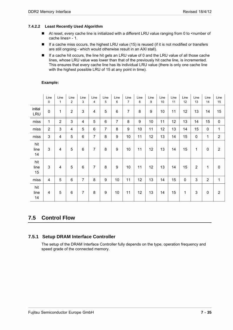
DDR2 Memory Interface Revised 18/4/12
Line 15
15
0
1
2
2
0
1
2
7.4.2.2 Least Recently Used Algorithm
At reset, every cache line is initialized with a different LRU value ranging from 0 to <number of cache lines> - 1.
If a cache miss occurs, the highest LRU value (15) is reused (if it is not modified or transfers are still ongoing - which would otherwise result in an AXI stall).
If a cache hit occurs, the line hit gets an LRU value of 0 and the LRU value of all those cache lines, whose LRU value was lower than that of the previously hit cache line, is incremented. This ensures that every cache line has its individual LRU value (there is only one cache line with the highest possible LRU of 15 at any point in time).
Example:
7.5 Control Flow
7.5.1 Setup DRAM Interface Controller
The setup of the DRAM Interface Controller fully depends on the type, operation frequency and speed grade of the connected memory.
Line 0
Line 1
Line 2
Line 3
Line 4
Line 5
Line 6
Line 7
Line 8
Line 9
Line 10
Line 11
Line 12
Line 13
Line 14
initial LRU
0 1 2 3 4 5 6 7 8 9 10 11 12 13 14
miss 1 2 3 4 5 6 7 8 9 10 11 12 13 14 15
miss 2 3 4 5 6 7 8 9 10 11 12 13 14 15 0
miss 3 4 5 6 7 8 9 10 11 12 13 14 15 0 1
hit line 14
3 4 5 6 7 8 9 10 11 12 13 14 15 1 0
hit line 15
3 4 5 6 7 8 9 10 11 12 13 14 15 2 1
miss 4 5 6 7 8 9 10 11 12 13 14 15 0 3 2
hit line 14
4 5 6 7 8 9 10 11 12 13 14 15 1 3 0
Fujitsu Semiconductor Europe GmbH 7 - 35
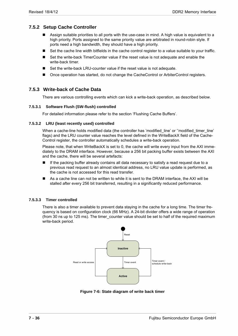
Revised 18/4/12 DDR2 Memory Interface
7.5.2 Setup Cache Controller
Assign suitable priorities to all ports with the use-case in mind. A high value is equivalent to a high priority. Ports assigned to the same priority value are arbitrated in round-robin style. If ports need a high bandwidth, they should have a high priority.
Set the cache line width bitfields in the cache control register to a value suitable to your traffic.
Set the write-back TimerCounter value if the reset value is not adequate and enable the write-back timer.
Set the write-back LRU-counter value if the reset value is not adequate.
Once operation has started, do not change the CacheControl or ArbiterControl registers.
7.5.3 Write-back of Cache Data
There are various controlling events which can kick a write-back operation, as described below.
7.5.3.1 Software Flush (SW-flush) controlled
For detailed information please refer to the section ‘Flushing Cache Buffers’.
7.5.3.2 LRU (least recently used) controlled
When a cache-line holds modified data (the controller has ’modified_line’ or ‘’modified_timer_line’ flags) and the LRU counter value reaches the level defined in the WriteBackX field of the Cache-Control register, the controller automatically schedules a write-back operation.
Please note, that when WriteBackX is set to 0, the cache will write every input from the AXI imme-diately to the DRAM interface. However, because a 256 bit packing buffer exists between the AXI and the cache, there will be several artefacts:
If the packing buffer already contains all data necessary to satisfy a read request due to a previous read request to an almost identical address, no LRU value update is performed, as the cache is not accessed for this read transfer.
As a cache line can not be written to while it is sent to the DRAM interface, the AXI will be stalled after every 256 bit transferred, resulting in a significantly reduced performance.
7.5.3.3 Timer controlled
There is also a timer available to prevent data staying in the cache for a long time. The timer fre-quency is based on configuration clock (66 MHz). A 24-bit divider offers a wide range of operation (from 30 ns up to 125 ms). The timer_counter value should be set to half of the required maximum write-back period.
Figure 7-6: State diagram of write back timer
Inactive
Reset
Active
Timer eventTimer event / schedule write-back
Read or write access
7 - 36 Fujitsu Semiconductor Europe GmbH
DDR2 Memory Interface Revised 18/4/12
7.5.4 Flushing Cache Buffers
There are three possible software triggered flushes:
Port Flush
Write Flush
Area Flush
When doing a Port Flush operation, cache lines containing read data will be cleared (the controller removes the ‘all_valid_line’ flags). Cache lines that have write data (the controller has ‘’modified_line’ or ‘modified_timer_line’ flags) must do write-back operation before clearing the buf-fer. Each cache module can be flushed individually by writing a ‘1’ to the corresponding Flush-PortX-bit in the FlushControl register.
A Write Flush does the same, except is does not invalidate read data (it does not remove the ‘all_valid_line’ flags). It only starts a write_back operation for all modified data.
It is also possible to flush only cache-lines storing data of specified memory area. Define the desired area be setting FlushAreaStart and FlushAreaEnd field. Execution will be started when writing a ‘1’ to the individual FlushArea-bits in the FlushControl register. This operation will then be executed on all cache modules selected for the specified areas. Area Flush will also invalidate read data (re-moves all_valid_line flags).
Fujitsu Semiconductor Europe GmbH 7 - 37
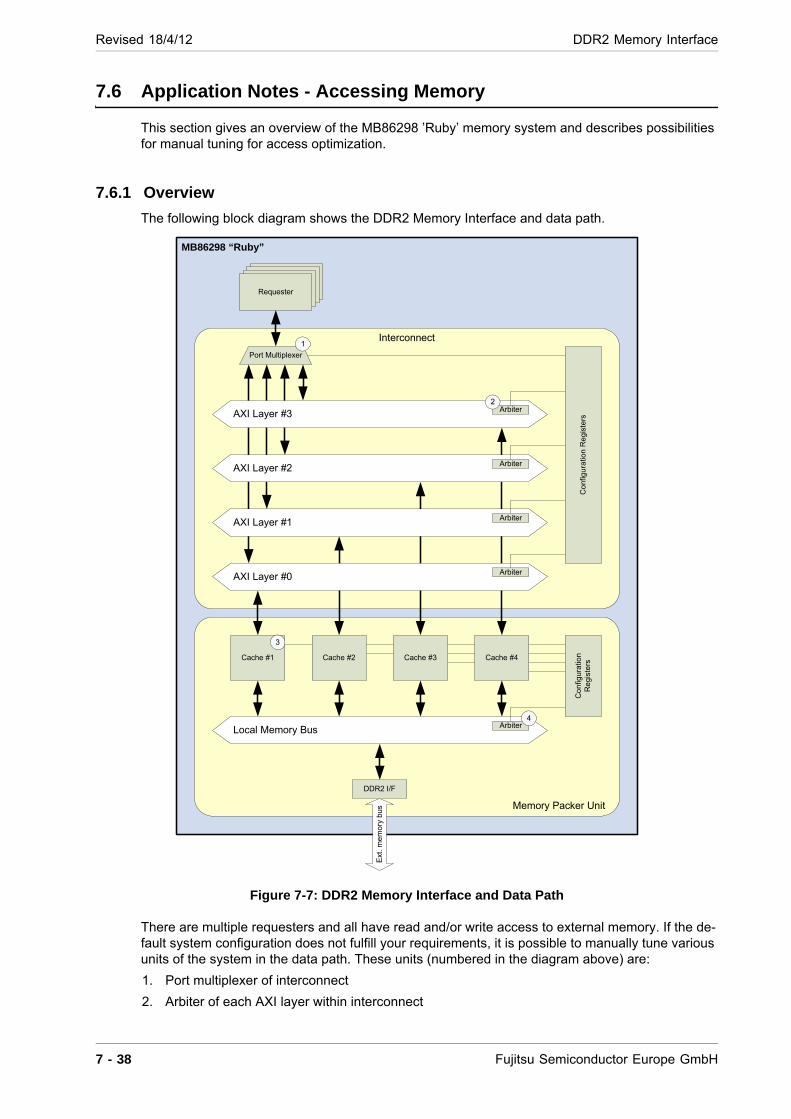
Revised 18/4/12 DDR2 Memory Interface
7.6 Application Notes - Accessing Memory
This section gives an overview of the MB86298 ’Ruby’ memory system and describes possibilities for manual tuning for access optimization.
7.6.1 Overview
The following block diagram shows the DDR2 Memory Interface and data path.
Figure 7-7: DDR2 Memory Interface and Data Path
There are multiple requesters and all have read and/or write access to external memory. If the de-fault system configuration does not fulfill your requirements, it is possible to manually tune various units of the system in the data path. These units (numbered in the diagram above) are:
1. Port multiplexer of interconnect
2. Arbiter of each AXI layer within interconnect
Port Multiplexer
AXI Layer #3 Arbiter
Cache #1
AXI Layer #2 Arbiter
AXI Layer #1 Arbiter
AXI Layer #0 Arbiter
<Module><Module><Module>Requester
Cache #2 Cache #3 Cache #4
Local Memory Bus Arbiter
DDR2 I/F
Ext
. m
em
ory
bus
Co
nfig
urat
ion
Re
gist
ers
Co
nfig
urat
ion
Reg
iste
rs
Interconnect
Memory Packer Unit
MB86298 “Ruby”
1
2
3
4
7 - 38 Fujitsu Semiconductor Europe GmbH
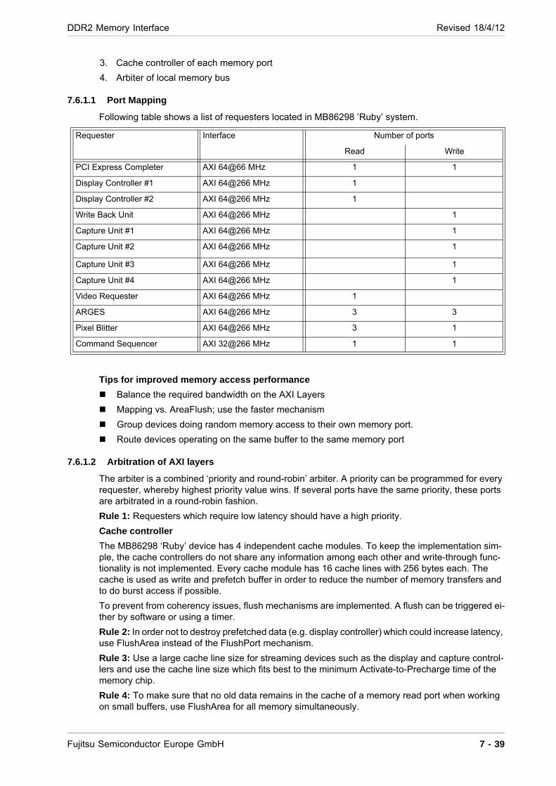
DDR2 Memory Interface Revised 18/4/12
3. Cache controller of each memory port
4. Arbiter of local memory bus
7.6.1.1 Port Mapping
Following table shows a list of requesters located in MB86298 ’Ruby’ system.
Tips for improved memory access performance
Balance the required bandwidth on the AXI Layers
Mapping vs. AreaFlush; use the faster mechanism
Group devices doing random memory access to their own memory port.
Route devices operating on the same buffer to the same memory port
7.6.1.2 Arbitration of AXI layers
The arbiter is a combined ‘priority and round-robin’ arbiter. A priority can be programmed for every requester, whereby highest priority value wins. If several ports have the same priority, these ports are arbitrated in a round-robin fashion.
Rule 1: Requesters which require low latency should have a high priority.
Cache controller
The MB86298 ‘Ruby’ device has 4 independent cache modules. To keep the implementation sim-ple, the cache controllers do not share any information among each other and write-through func-tionality is not implemented. Every cache module has 16 cache lines with 256 bytes each. The cache is used as write and prefetch buffer in order to reduce the number of memory transfers and to do burst access if possible.
To prevent from coherency issues, flush mechanisms are implemented. A flush can be triggered ei-ther by software or using a timer.
Rule 2: In order not to destroy prefetched data (e.g. display controller) which could increase latency, use FlushArea instead of the FlushPort mechanism.
Rule 3: Use a large cache line size for streaming devices such as the display and capture control-lers and use the cache line size which fits best to the minimum Activate-to-Precharge time of the memory chip.
Rule 4: To make sure that no old data remains in the cache of a memory read port when working on small buffers, use FlushArea for all memory simultaneously.
Requester Interface Number of ports
Read Write
PCI Express Completer AXI 64@66 MHz 1 1
Display Controller #1 AXI 64@266 MHz 1
Display Controller #2 AXI 64@266 MHz 1
Write Back Unit AXI 64@266 MHz 1
Capture Unit #1 AXI 64@266 MHz 1
Capture Unit #2 AXI 64@266 MHz 1
Capture Unit #3 AXI 64@266 MHz 1
Capture Unit #4 AXI 64@266 MHz 1
Video Requester AXI 64@266 MHz 1
ARGES AXI 64@266 MHz 3 3
Pixel Blitter AXI 64@266 MHz 3 1
Command Sequencer AXI 32@266 MHz 1 1
Fujitsu Semiconductor Europe GmbH 7 - 39
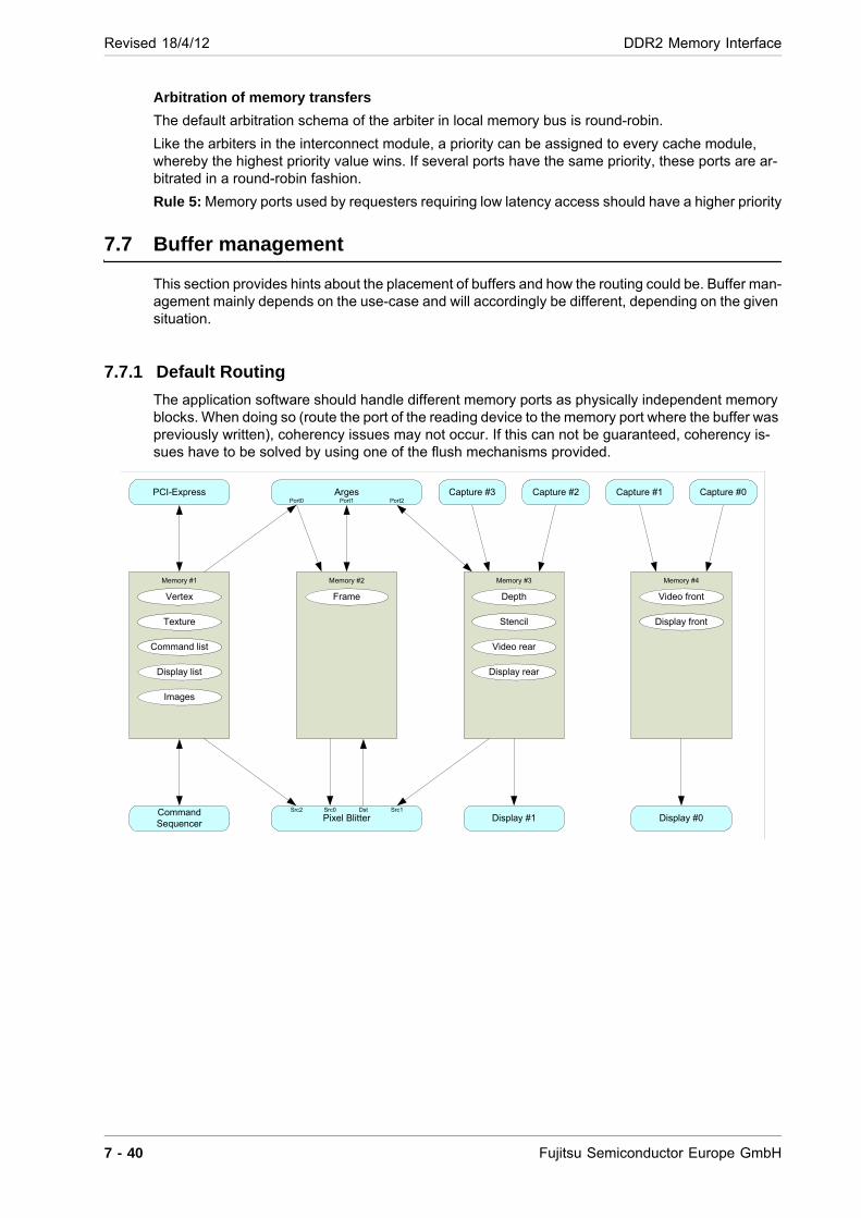
Revised 18/4/12 DDR2 Memory Interface
Arbitration of memory transfers
The default arbitration schema of the arbiter in local memory bus is round-robin.
Like the arbiters in the interconnect module, a priority can be assigned to every cache module, whereby the highest priority value wins. If several ports have the same priority, these ports are ar-bitrated in a round-robin fashion.
Rule 5: Memory ports used by requesters requiring low latency access should have a higher priority
7.7 Buffer management
This section provides hints about the placement of buffers and how the routing could be. Buffer man-agement mainly depends on the use-case and will accordingly be different, depending on the given situation.
7.7.1 Default Routing
The application software should handle different memory ports as physically independent memory blocks. When doing so (route the port of the reading device to the memory port where the buffer was previously written), coherency issues may not occur. If this can not be guaranteed, coherency is-sues have to be solved by using one of the flush mechanisms provided.
Memory #1
Vertex
Texture
Command list
Display list
Images
Memory #2
Frame
Memory #3
Depth
Stencil
Video rear
Display rear
Memory #4
Video front
Display front
Display #0Display #1Command Sequencer
PCI-Express Capture #0Capture #1Capture #2Capture #3Arges
Pixel Blitter
Port0 Port1 Port2
Src2 Src0 Dst Src1
7 - 40 Fujitsu Semiconductor Europe GmbH
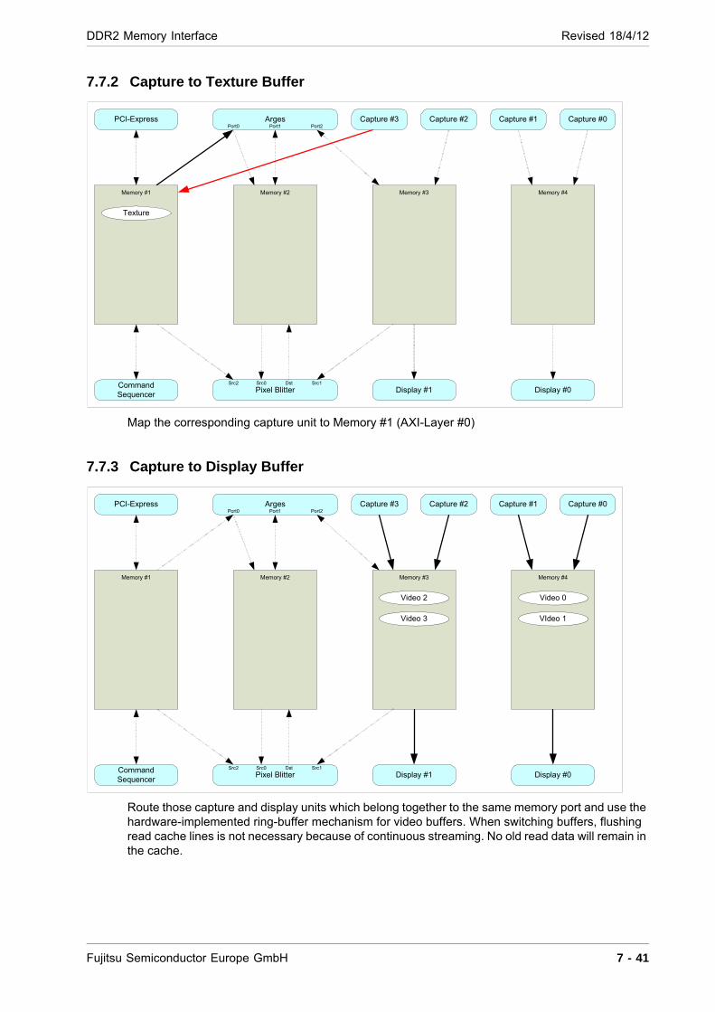
DDR2 Memory Interface Revised 18/4/12
7.7.2 Capture to Texture Buffer
Map the corresponding capture unit to Memory #1 (AXI-Layer #0)
7.7.3 Capture to Display Buffer
Route those capture and display units which belong together to the same memory port and use the hardware-implemented ring-buffer mechanism for video buffers. When switching buffers, flushing read cache lines is not necessary because of continuous streaming. No old read data will remain in the cache.
Memory #1
Texture
Memory #2 Memory #3 Memory #4
Display #0Display #1Command Sequencer
PCI-Express Capture #0Capture #1Capture #2Capture #3Arges
Pixel Blitter
Port0 Port1 Port2
Src2 Src0 Dst Src1
Memory #1 Memory #2 Memory #3
Video 2
Video 3
Memory #4
Video 0
VIdeo 1
Display #0Display #1Command Sequencer
PCI-Express Capture #0Capture #1Capture #2Capture #3Arges
Pixel Blitter
Port0 Port1 Port2
Src2 Src0 Dst Src1
Fujitsu Semiconductor Europe GmbH 7 - 41
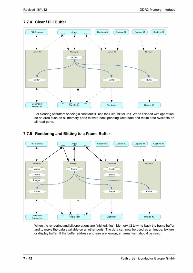
Revised 18/4/12 DDR2 Memory Interface
7.7.4 Clear / Fill Buffer
For clearing of buffers or doing a constant fill, use the Pixel Blitter unit. When finished with operation, do an area flush on all memory ports to write-back pending write data and make data available on all read ports.
7.7.5 Rendering and Blitting to a Frame Buffer
When the rendering and blit operations are finished, flush Memory #2 to write-back the frame buffer and to make the data available on all other ports. The data can now be used as an image, texture or display buffer. If the buffer address and size are known, an area flush should be used.
Memory #1 Memory #2
Buffer
Memory #3 Memory #4
Display #0Display #1Command Sequencer
PCI-Express Capture #0Capture #1Capture #2Capture #3Arges
Pixel Blitter
Port0 Port1 Port2
Src2 Src0 Dst Src1
Buffer BufferBuffer
Memory #1
Vertex
Texture
Images
Memory #2
Frame
Memory #3
Depth
Stencil
Memory #4
Display #0Display #1Command Sequencer
PCI-Express Capture #0Capture #1Capture #2Capture #3Arges
Pixel Blitter
Port0 Port1 Port2
Src2 Src0 Dst Src1
Frame FrameFrame
7 - 42 Fujitsu Semiconductor Europe GmbH

DDR2 Memory Interface Revised 18/4/12
7.7.6 Filtering and Mipmap Generation
When a filtering operation is finished, flush Memory #2 to write-back the frame buffer and to make the data available on all other ports. The data can now be used as an image, texture or display buf-fer. If the buffer address and size are known, an area flush should be used.
7.7.7 Host does Memory Access
The host interface (PCI Express) routing should not be changed, otherwise blocking and synchro-nization mechanisms are required if a multithreading environment exists.
A flush is not required if the host is accessing vertex, texture, command lists or image data on the same memory port where the target buffer is located.
7.7.7.1 Writing Data
Memory #1
Source
Memory #2
Source
Memory #3
Source
Memory #4
Display #0Display #1Command Sequencer
PCI-Express Capture #0Capture #1Capture #2Capture #3Arges
Pixel Blitter
Port0 Port1 Port2
Src2 Src0 Dst Src1
Frame
Frame FrameFrame
Memory #1
Buffer
Memory #2 Memory #3 Memory #4
Display #0Display #1Command Sequencer
PCI-Express Capture #0Capture #1Capture #2Capture #3Arges
Pixel Blitter
Port0 Port1 Port2
Src2 Src0 Dst Src1
Buffer Buffer Buffer
Fujitsu Semiconductor Europe GmbH 7 - 43
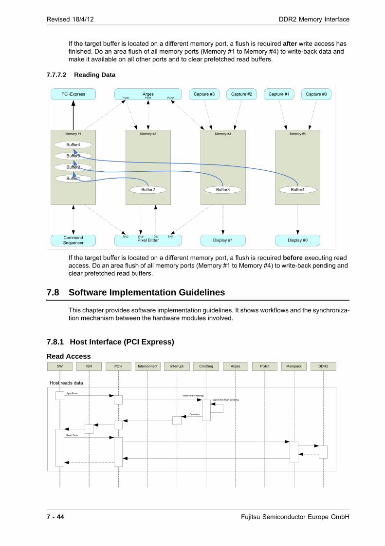
Revised 18/4/12 DDR2 Memory Interface
If the target buffer is located on a different memory port, a flush is required after write access has finished. Do an area flush of all memory ports (Memory #1 to Memory #4) to write-back data and make it available on all other ports and to clear prefetched read buffers.
7.7.7.2 Reading Data
If the target buffer is located on a different memory port, a flush is required before executing read access. Do an area flush of all memory ports (Memory #1 to Memory #4) to write-back pending and clear prefetched read buffers.
7.8 Software Implementation Guidelines
This chapter provides software implementation guidelines. It shows workflows and the synchroniza-tion mechanism between the hardware modules involved.
7.8.1 Host Interface (PCI Express)
Read Access
Memory #1
Buffer1
Memory #2 Memory #3 Memory #4
Display #0Display #1Command Sequencer
PCI-Express Capture #0Capture #1Capture #2Capture #3Arges
Pixel Blitter
Port0 Port1 Port2
Src2 Src0 Dst Src1
Buffer2 Buffer3 Buffer4
Buffer3
Buffer2
Buffer4
SW ISR PCIe Interrupt CmdSeq Arges PixBlt Mempack DDR2Interconnect
SyncFlush
Wait while flush pending
Complete
Read Data
Host reads data
WaitWhileFlushing()
7 - 44 Fujitsu Semiconductor Europe GmbH
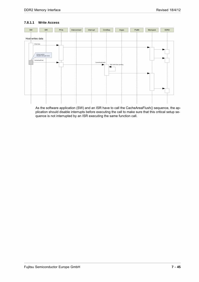
DDR2 Memory Interface Revised 18/4/12
7.8.1.1 Write Access
As the software application (SW) and an ISR have to call the CacheAreaFlush() sequence, the ap-plication should disable interrupts before executing the call to make sure that this critical setup se-quence is not interrupted by an ISR executing the same function call.
SW ISR PCIe Interrupt CmdSeq Arges PixBlt Mempack DDR2Interconnect
Write Data
CacheAreaFlush
Critical section (Disable interrupts here)
Host writes data
Wait while flush pending
CacheAreaFlush()
Fujitsu Semiconductor Europe GmbH 7 - 45
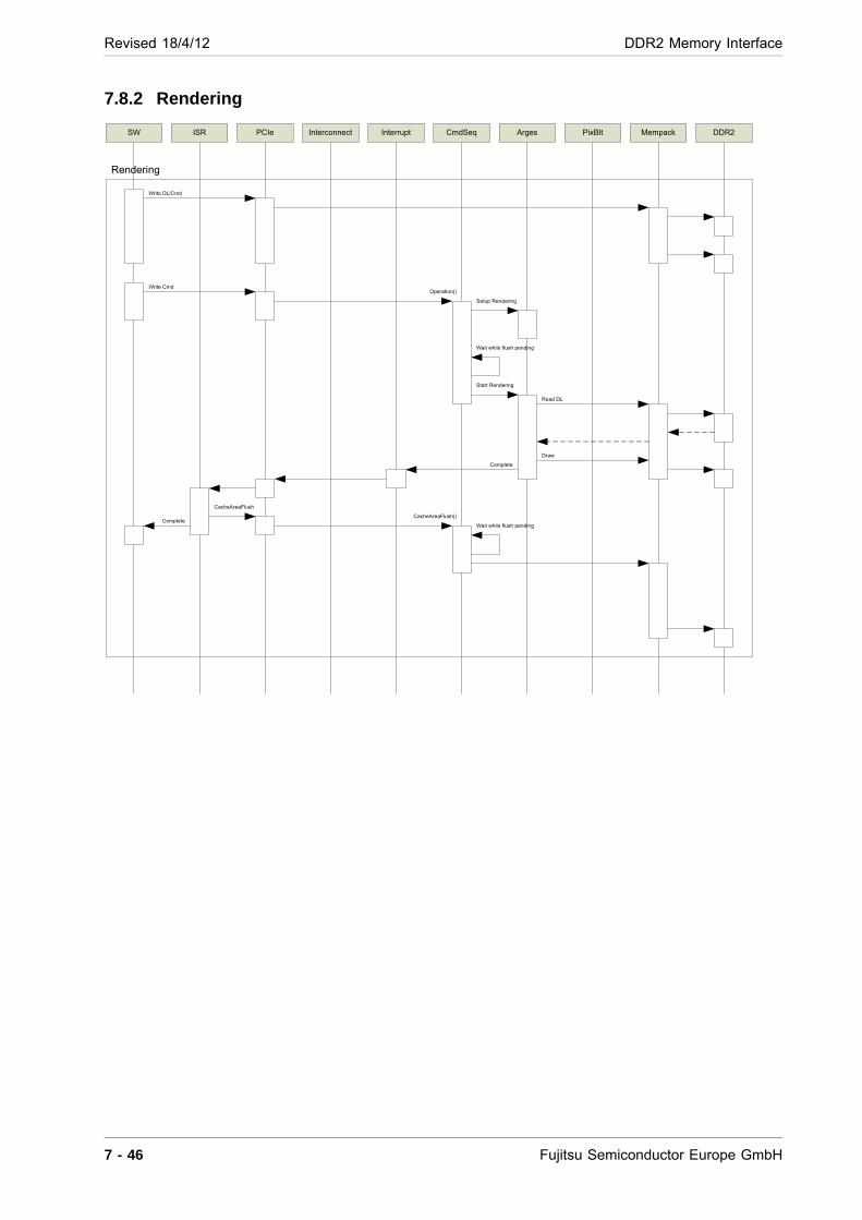
Revised 18/4/12 DDR2 Memory Interface
7.8.2 Rendering
SW ISR PCIe Interrupt CmdSeq Arges PixBlt Mempack DDR2Interconnect
Write DL/Cmd
Write Cmd
Setup Rendering
Wait while flush pending
Start Rendering
Read DL
Draw
Complete
CacheAreaFlush
Complete
Rendering
Wait while flush pending
CacheAreaFlush()
Operation()
7 - 46 Fujitsu Semiconductor Europe GmbH

DDR2 Memory Interface Revised 18/4/12
7.8.3 Pixel Blitter Operations
SW ISR PCIe Interrupt CmdSeq Arges PixBlt Mempack DDR2Interconnect
Write Cmd
Setup PixBlt
Wait while flush pending
Start Operation
Read
Write
Complete
CacheAreaFlush
Complete
Fill, blit or filter
Wait while flush pending
CacheAreaFlush()
Operation()
Fujitsu Semiconductor Europe GmbH 7 - 47
Revised 18/4/12 DDR2 Memory Interface
7.8.4 Command List Examples
7.8.5 Miscellaneous
Rule 6: Do not access the ARGES command FIFO directly; use the Command Sequencer to write display list commands to ARGES.
// Examples of command list snippetsOperation:
// begin of operation setup
[insert operation setup here]
// end of operation setup
// wait while flush is pending
SYNC 8
// begin start of operation sequence
[insert start of operation sequence here]
// end start of operation sequence
RETCacheAreaFlush:
// wait while flush is pending
7 - 48 Fujitsu Semiconductor Europe GmbH
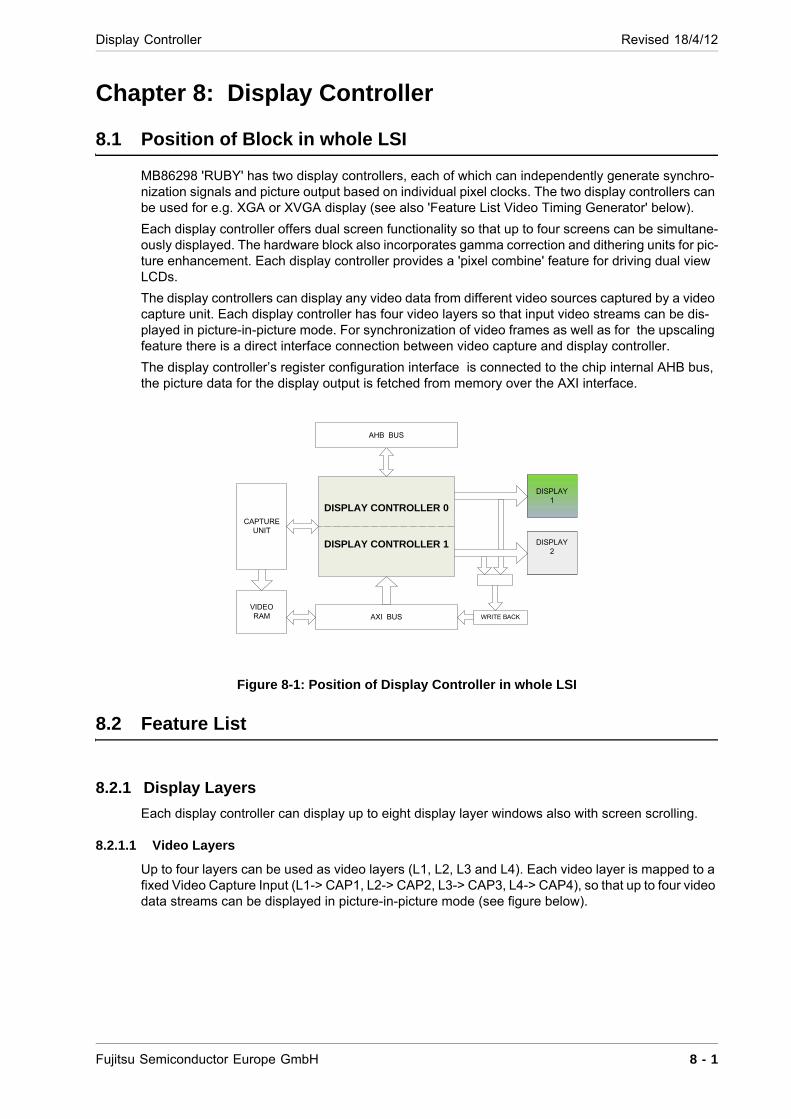
Display Controller Revised 18/4/12
Chapter 8: Display Controller
8.1 Position of Block in whole LSI
MB86298 'RUBY' has two display controllers, each of which can independently generate synchro-nization signals and picture output based on individual pixel clocks. The two display controllers can be used for e.g. XGA or XVGA display (see also 'Feature List Video Timing Generator' below).
Each display controller offers dual screen functionality so that up to four screens can be simultane-ously displayed. The hardware block also incorporates gamma correction and dithering units for pic-ture enhancement. Each display controller provides a 'pixel combine' feature for driving dual view LCDs.
The display controllers can display any video data from different video sources captured by a video capture unit. Each display controller has four video layers so that input video streams can be dis-played in picture-in-picture mode. For synchronization of video frames as well as for the upscaling feature there is a direct interface connection between video capture and display controller.
The display controller’s register configuration interface is connected to the chip internal AHB bus, the picture data for the display output is fetched from memory over the AXI interface.
Figure 8-1: Position of Display Controller in whole LSI
8.2 Feature List
8.2.1 Display Layers
Each display controller can display up to eight display layer windows also with screen scrolling.
8.2.1.1 Video Layers
Up to four layers can be used as video layers (L1, L2, L3 and L4). Each video layer is mapped to a fixed Video Capture Input (L1-> CAP1, L2-> CAP2, L3-> CAP3, L4-> CAP4), so that up to four video data streams can be displayed in picture-in-picture mode (see figure below).
DISPLAY CONTROLLER 0
DISPLAY CONTROLLER 1
CAPTUREUNIT
DISPLAY1
DISPLAY2
VIDEORAM AXI BUS
AHB BUS
WRITE BACK
Fujitsu Semiconductor Europe GmbH 8 - 1
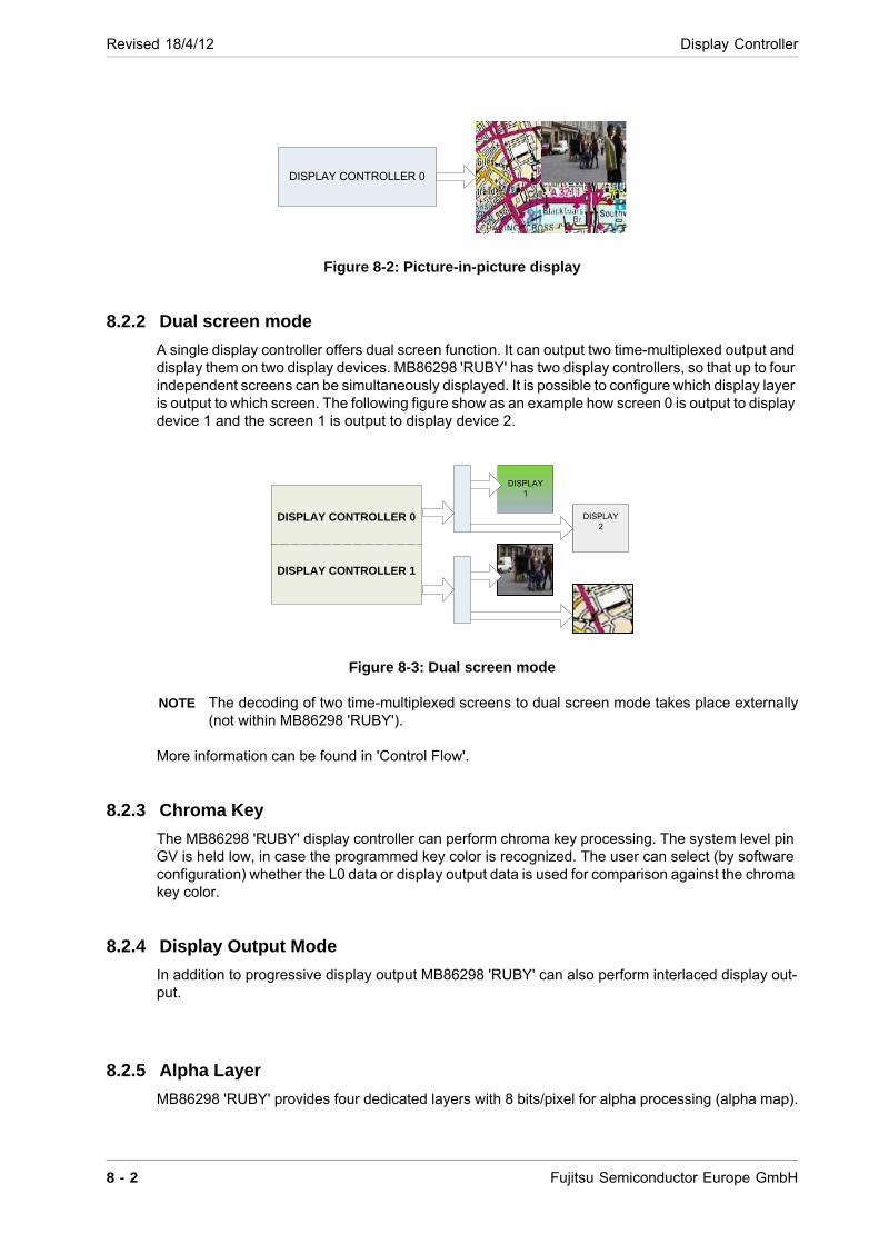
Revised 18/4/12 Display Controller
Figure 8-2: Picture-in-picture display
8.2.2 Dual screen mode
A single display controller offers dual screen function. It can output two time-multiplexed output and display them on two display devices. MB86298 'RUBY' has two display controllers, so that up to four independent screens can be simultaneously displayed. It is possible to configure which display layer is output to which screen. The following figure show as an example how screen 0 is output to display device 1 and the screen 1 is output to display device 2.
Figure 8-3: Dual screen mode
NOTE The decoding of two time-multiplexed screens to dual screen mode takes place externally (not within MB86298 'RUBY').
More information can be found in 'Control Flow'.
8.2.3 Chroma Key
The MB86298 'RUBY' display controller can perform chroma key processing. The system level pin GV is held low, in case the programmed key color is recognized. The user can select (by software configuration) whether the L0 data or display output data is used for comparison against the chroma key color.
8.2.4 Display Output Mode
In addition to progressive display output MB86298 'RUBY' can also perform interlaced display out-put.
8.2.5 Alpha Layer
MB86298 'RUBY' provides four dedicated layers with 8 bits/pixel for alpha processing (alpha map).
DISPLAY CONTROLLER 0
DISPLAY CONTROLLER 0
DISPLAY CONTROLLER 1
DISPLAY1
DISPLAY2
8 - 2 Fujitsu Semiconductor Europe GmbH
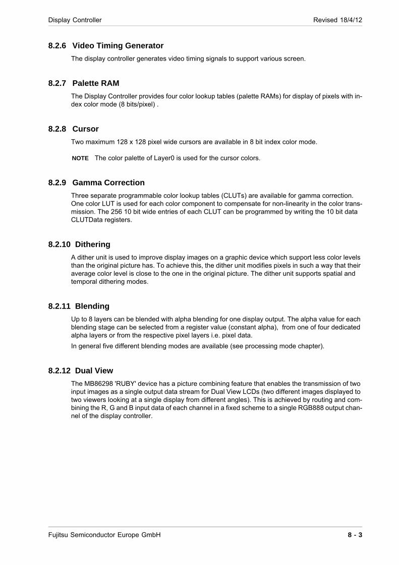
Display Controller Revised 18/4/12
8.2.6 Video Timing Generator
The display controller generates video timing signals to support various screen.
8.2.7 Palette RAM
The Display Controller provides four color lookup tables (palette RAMs) for display of pixels with in-dex color mode (8 bits/pixel) .
8.2.8 Cursor
Two maximum 128 x 128 pixel wide cursors are available in 8 bit index color mode.
NOTE The color palette of Layer0 is used for the cursor colors.
8.2.9 Gamma Correction
Three separate programmable color lookup tables (CLUTs) are available for gamma correction. One color LUT is used for each color component to compensate for non-linearity in the color trans-mission. The 256 10 bit wide entries of each CLUT can be programmed by writing the 10 bit data CLUTData registers.
8.2.10 Dithering
A dither unit is used to improve display images on a graphic device which support less color levels than the original picture has. To achieve this, the dither unit modifies pixels in such a way that their average color level is close to the one in the original picture. The dither unit supports spatial and temporal dithering modes.
8.2.11 Blending
Up to 8 layers can be blended with alpha blending for one display output. The alpha value for each blending stage can be selected from a register value (constant alpha), from one of four dedicated alpha layers or from the respective pixel layers i.e. pixel data.
In general five different blending modes are available (see processing mode chapter).
8.2.12 Dual View
The MB86298 'RUBY' device has a picture combining feature that enables the transmission of two input images as a single output data stream for Dual View LCDs (two different images displayed to two viewers looking at a single display from different angles). This is achieved by routing and com-bining the R, G and B input data of each channel in a fixed scheme to a single RGB888 output chan-nel of the display controller.
Fujitsu Semiconductor Europe GmbH 8 - 3
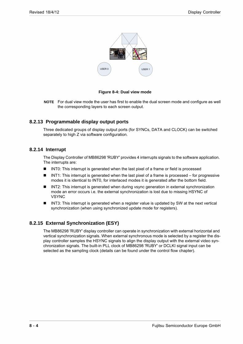
Revised 18/4/12 Display Controller
Figure 8-4: Dual view mode
NOTE For dual view mode the user has first to enable the dual screen mode and configure as well the corresponding layers to each screen output.
8.2.13 Programmable display output ports
Three dedicated groups of display output ports (for SYNCs, DATA and CLOCK) can be switched separately to high Z via software configuration.
8.2.14 Interrupt
The Display Controller of MB86298 'RUBY' provides 4 interrupts signals to the software application. The interrupts are:
INT0: This interrupt is generated when the last pixel of a frame or field is processed
INT1: This interrupt is generated when the last pixel of a frame is processed – for progressive modes it is identical to INT0, for interlaced modes it is generated after the bottom field.
INT2: This interrupt is generated when during vsync generation in external synchronization mode an error occurs i.e. the external synchronization is lost due to missing HSYNC of VSYNC
INT3: This interrupt is generated when a register value is updated by SW at the next vertical synchronization (when using synchronized update mode for registers).
8.2.15 External Synchronization (ESY)
The MB86298 'RUBY' display controller can operate in synchronization with external horizontal and vertical synchronization signals. When external synchronous mode is selected by a register the dis-play controller samples the HSYNC signals to align the display output with the external video syn-chronization signals. The built-in PLL clock of MB86298 'RUBY' or DCLKI signal input can be selected as the sampling clock (details can be found under the control flow chapter).
USER 0 USER 1
8 - 4 Fujitsu Semiconductor Europe GmbH
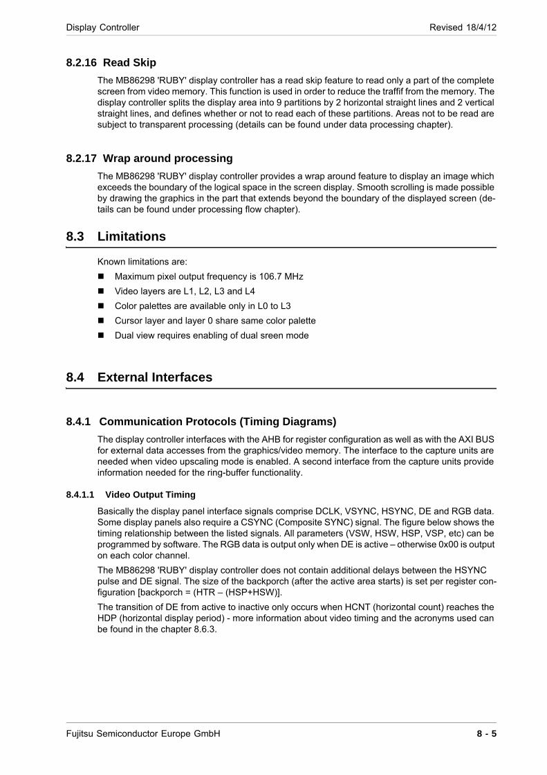
Display Controller Revised 18/4/12
8.2.16 Read Skip
The MB86298 'RUBY' display controller has a read skip feature to read only a part of the complete screen from video memory. This function is used in order to reduce the traffif from the memory. The display controller splits the display area into 9 partitions by 2 horizontal straight lines and 2 vertical straight lines, and defines whether or not to read each of these partitions. Areas not to be read are subject to transparent processing (details can be found under data processing chapter).
8.2.17 Wrap around processing
The MB86298 'RUBY' display controller provides a wrap around feature to display an image which exceeds the boundary of the logical space in the screen display. Smooth scrolling is made possible by drawing the graphics in the part that extends beyond the boundary of the displayed screen (de-tails can be found under processing flow chapter).
8.3 Limitations
Known limitations are:
Maximum pixel output frequency is 106.7 MHz
Video layers are L1, L2, L3 and L4
Color palettes are available only in L0 to L3
Cursor layer and layer 0 share same color palette
Dual view requires enabling of dual sreen mode
8.4 External Interfaces
8.4.1 Communication Protocols (Timing Diagrams)
The display controller interfaces with the AHB for register configuration as well as with the AXI BUS for external data accesses from the graphics/video memory. The interface to the capture units are needed when video upscaling mode is enabled. A second interface from the capture units provide information needed for the ring-buffer functionality.
8.4.1.1 Video Output Timing
Basically the display panel interface signals comprise DCLK, VSYNC, HSYNC, DE and RGB data. Some display panels also require a CSYNC (Composite SYNC) signal. The figure below shows the timing relationship between the listed signals. All parameters (VSW, HSW, HSP, VSP, etc) can be programmed by software. The RGB data is output only when DE is active – otherwise 0x00 is output on each color channel.
The MB86298 'RUBY' display controller does not contain additional delays between the HSYNC pulse and DE signal. The size of the backporch (after the active area starts) is set per register con-figuration [backporch = (HTR – (HSP+HSW)].
The transition of DE from active to inactive only occurs when HCNT (horizontal count) reaches the HDP (horizontal display period) - more information about video timing and the acronyms used can be found in the chapter 8.6.3.
Fujitsu Semiconductor Europe GmbH 8 - 5
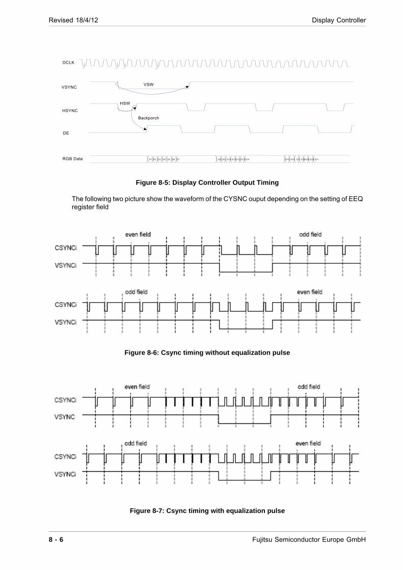
Revised 18/4/12 Display Controller
Figure 8-5: Display Controller Output Timing
The following two picture show the waveform of the CYSNC ouput depending on the setting of EEQ register field
Figure 8-6: Csync timing without equalization pulse
Figure 8-7: Csync timing with equalization pulse
DCLK
VSYNC
HSYNC
DE
VSW
D8 D9 D10 D11D12 D13 D14 D15 D16 D17 D18D19 D20 D21 D1 D2 D3 D4 D5 D6 D7RGB Data
HSW
Backporch
8 - 6 Fujitsu Semiconductor Europe GmbH
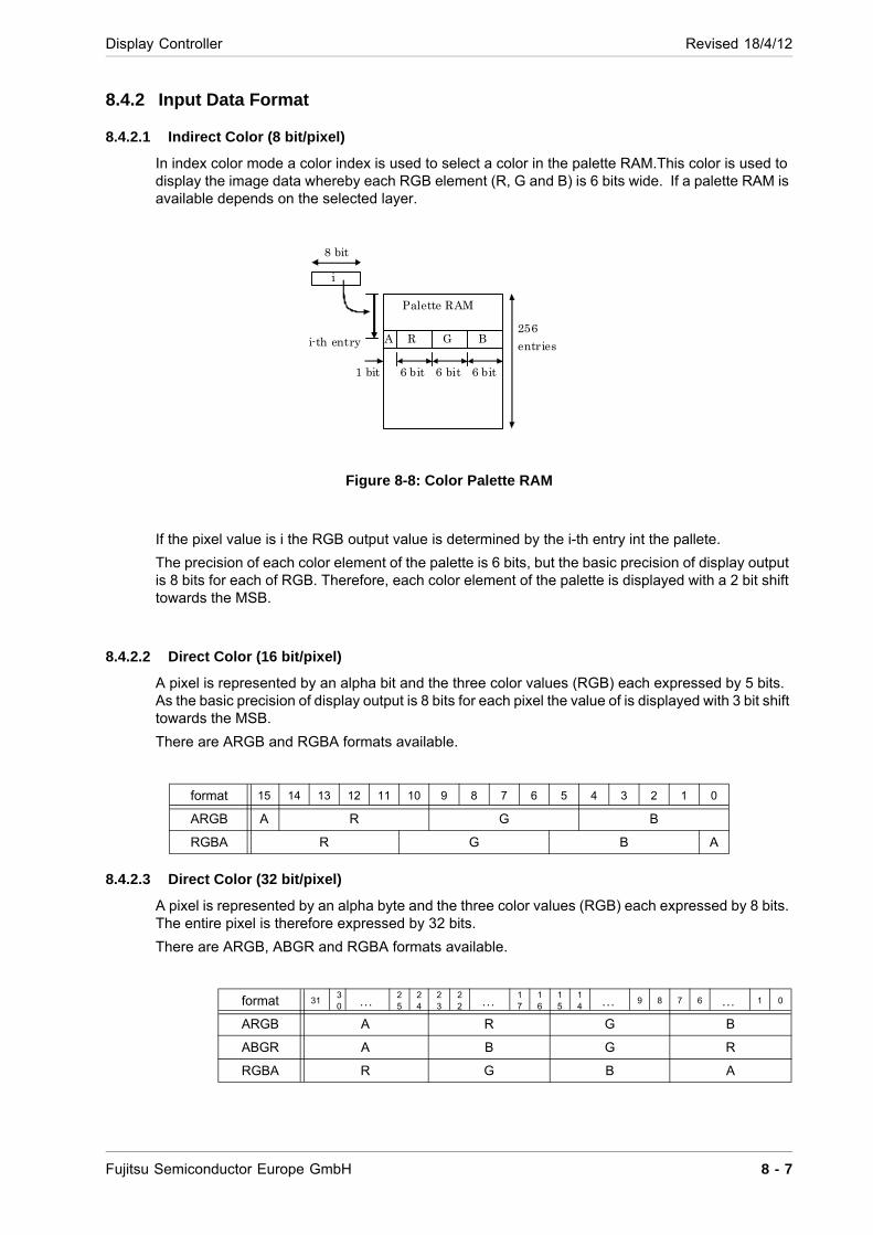
Display Controller Revised 18/4/12
8.4.2 Input Data Format
8.4.2.1 Indirect Color (8 bit/pixel)
In index color mode a color index is used to select a color in the palette RAM.This color is used to display the image data whereby each RGB element (R, G and B) is 6 bits wide. If a palette RAM is available depends on the selected layer.
Figure 8-8: Color Palette RAM
If the pixel value is i the RGB output value is determined by the i-th entry int the pallete.
The precision of each color element of the palette is 6 bits, but the basic precision of display output is 8 bits for each of RGB. Therefore, each color element of the palette is displayed with a 2 bit shift towards the MSB.
8.4.2.2 Direct Color (16 bit/pixel)
A pixel is represented by an alpha bit and the three color values (RGB) each expressed by 5 bits. As the basic precision of display output is 8 bits for each pixel the value of is displayed with 3 bit shift towards the MSB.
There are ARGB and RGBA formats available.
8.4.2.3 Direct Color (32 bit/pixel)
A pixel is represented by an alpha byte and the three color values (RGB) each expressed by 8 bits. The entire pixel is therefore expressed by 32 bits.
There are ARGB, ABGR and RGBA formats available.
format 15 14 13 12 11 10 9 8 7 6 5 4 3 2 1 0
ARGB A R G B
RGBA R G B A
format 3130 2
524
23
22 1
716
15
14 9 8 7 6 1 0
ARGB A R G B
ABGR A B G R
RGBA R G B A
A
8 bit
R G Bi-th entry
i
1 bit 6 bit 6 bit 6 bit
Palette RAM
256
entries
Fujitsu Semiconductor Europe GmbH 8 - 7
Revised 18/4/12 Display Controller
8.4.2.4 YCbCr Color (16 bit/pixel)
Image data is represented in “YCbCr = 4:2:2” format. This image data is displayed after conversion by a color matrix as display image data whereby each color value is 8 bit wide. Two pixels are then converted each to 32 bits.
8.4.2.5 Alpha Value (8 bit/pixel)
The factor for display blending. If the value is t, t/256 is expressed as a binary decimal.
8.4.2.6 Layer Dependency
The display colors that can be used for each layer are shown below.
8.4.3 Output Data Format
The output data of the display controller (depending on the dither mode) can be one of the following formats.
8.4.3.1 RGB 888 (24 bit)
8.4.3.2 RGB 777 (21 bit)
format 31
30 2
524
23
22 1
716
15
14 9 8 7 6 1 0
YCbCr Y Cr Y Cb
Layer Layer modes Palette RAMs
L0 Direct (16,32), indirect (P0), alphaPalette 0(P0): is used an L0 palette or cursor palette
L1Direct (16,32), indirect (P1), YCbCr, alpha
Palette 1(P1): is used as a L1 palette. .
L2Direct (16,32), indirect (P2), YCbCr, alpha
Palette 2(P2): is used as L2 palette. .
L3Direct (16,32), indirect (P3), YCbCr, alpha
Palette 3(P3): is used as L3 palette
L4 Direct (16,32), YCbCr, alpha
L5 Direct (16,32), alpha
L6 Direct (16,32), alpha
L7 Direct (16,32), alpha
LA0 Alpha
LA1 Alpha
LA2 Alpha
LA3 Alpha
dither mode 23 22 21 20 19 18 17 16 15 14 13 12 11 10 9 8 7 6 5 4 3 2 1 0
00 R G B
dither mode 23 22 21 20 19 18 17 16 15 14 13 12 11 10 9 8 7 6 5 4 3 2 1 0
01 R G B
8 - 8 Fujitsu Semiconductor Europe GmbH

Display Controller Revised 18/4/12
8.4.3.3 RGB 666 (18 bit)
8.4.3.4 RGB 565 (16 bit)
dither mode 23 22 21 20 19 18 17 16 15 14 13 12 11 10 9 8 7 6 5 4 3 2 1 0
10 R G B
dither mode 23 22 21 20 19 18 17 16 15 14 13 12 11 10 9 8 7 6 5 4 3 2 1 0
11 R G B
Fujitsu Semiconductor Europe GmbH 8 - 9
Revised 18/4/12 Display Controller
8.5 Processing Mode
8.5.1 Data Processing Flow
Figure 8-9: Processing Flow of Display Controller (Part 1)
Capture 1
Downscaler
Upscaler
Capture 2
Downscaler
Upscaler
Capture 3
Downscaler
Upscaler
Capture 4
Downscaler
Upscaler
FIFO
Display Controller 1
Note: Display ctrl common Selector
AXI
FIFO
FIFO
FIFO
DATA to CAPTURE
MUXVmag DATA
MUX
AXI
L0
L1
L2
L3
L4
L5
L6
L7
CapTo
Disp.Ctrl
AXI
8 - 10 Fujitsu Semiconductor Europe GmbH
Display Controller Revised 18/4/12
Figure 8-10: Data Processing Flow of Display Controller (Part 2)
The basic data processing flow is:
Graphic Memory à Video FIFO (Capture Units) > Color Palette (or YVU/RGB) > Layer Selector > Blending > Gamma Correction > Dithering > Pixel Combine (if required)
Pallete
YVU/RGB
Pallete
Pallete
YVU/RGB
Pallete
YVU/RGB
Alp
ha
dat
aB
len
d
RBG data
Gam
m c
orr
ecti
on
an
d d
ith
erin
g
Pix
el
com
bin
e (
Du
al V
iew
)
La
yer
Se
lec
tor
Cursor 0
Cursor 1
Layer 0
Layer 1
Layer 2
Layer 3
Layer 4
Layer 5
Layer 6
Layer 7
LA0
LA1
LA2
YVU/RGB
Fujitsu Semiconductor Europe GmbH 8 - 11
Revised 18/4/12 Display Controller
The video/graphics memory is used to store the video (image) data from different sources (e.g.video capture or graphics processing). The display controller fetches the data and puts it in the video FIFO. The display controller can use four layers (L1, L2, L3 and L4) as video layers. The display controller then fetches the video data from video/graphics memory and sends it to one dedicated video capture unit if the register of Vmag (upscaling) is enabled. So the display controller can output video data from any of four video sources (with or without video upscaling) to these four specific vid-eo layers simultaneously. When using L1, L2, L3 and L4 as video layers and the video data is stored in the YUV format data must be converted to RGB data format before blending operations. L0, L5, L6 and L7 are no video layers with specific functions for upscaling, YUV conversion, etc. However they can be used to display video that has been captured as RGB. Buffer handling then has to be controlled by SW.
Color palettes are used to convert indirect 8-bit color data to RGB format.L0 shares the palette with the cursor layers. Therefore the L0 layer and the cursors are designed to be overlayed before blend operations of Layer0 are performed. L1, L2 and L3 each also comprise a color palette to convert an 8-bit indirect color to the RGB format.
In the Layer Selector layers can be selected in any order for blending. The blending unit executes blending using a blend factor which can be selected from the pixel data, a constant value (defined by SW configuration) or from the four dedicated Alpha layers.
MB86298 'RUBY' has three Color Lookup Tables (CLUTs) for gamma correction of each color chan-nel (R,G,B). A dithering unit is added to enhance the image quality on display devices with low pre-cision interfaces (6 or 7 bits/color).
A pixel combining feature is implemented in order to enable the transmission of two input images as a single output data stream for Dual View LCDs.
8.5.2 Processing algorithm
8.5.2.1 Alpha blending modes
Basically MB86298 'RUBY' supports five blending modes. The modes are:
1) standard alpha blending
2) standard alpha blending with pre-multiplied RGB source
8 - 12 Fujitsu Semiconductor Europe GmbH
Display Controller Revised 18/4/12
3) constant alpha only
4) simultaneous alpha
5) simultaneous alpha with pre-multiplied RGB source
Whereby:
Csource = actual layer color
Cprev = color of previous layer
alphaconst = constant alpha value (per layer), range 0 to 256
alphapix = per-pixel alpha (selected by per-pixel alpha source register), range 0 to 255
By setting a flag in the Layer Blend register alphapix can be incremented by 1 if the value of alphapix is greater than 0.
8.5.2.2 Transparent color processing
When transparent color processing is enabled and the color of the pixel matches the color value configured in the transparent color (TC) register field of the respective layer the pixel is not displayed on the screen. Instead the color of the pixel of the layer below or the background color is shown (depending on layer position of the respective layer).
8.5.2.3 YCbCr to RGB color matrix
YCbCr color formats are transformed to RGB using a programmable color conversion matrix:
The reset values already of the color matrix already define a suitable conversion function from YCb-Cr to RGB.
8.5.2.4 Color Look-up Table (CLUT) processing
The CLUT use the color value of each color channel as index value for a RAM. The 10-bit output value stored at this position of the RAM is then transferred to the dither unit.
The CLUT can for instance be used to program a gamma correction curve to compensate for LCD panel irregularites.
(a11 a12 a13
) * (Y
) + (b1
) = (R
)a21 a22 a23 Cb-128 b2 Ga31 a32 a33 Cr-128 b3 B
Fujitsu Semiconductor Europe GmbH 8 - 13
Revised 18/4/12 Display Controller
8.5.2.5 Dither processing
Dither is an intentionally applied form of noise, used to randomize quantization error, thereby pre-venting large-scale patterns such as contouring that are more objectionable than uncorrelated noise.
During dither processing the number of bits per pixel is lowered from the original value, e.g. RGB888 to RGB666. To avoid visual artefacts the lower bits are not just cut away but the values are randomly round up or down based on location of the pixel in the frame (spatial dithering) or a random vector is generated to address the dither matrix (temporal dithering).
8.5.2.6 Dual view processing
For dual view panels the pixels of two screens with identical resolution are combined into one pixel stream to the display. Depending on position of the pixel on the screen either R and B value from screen 0 and G value from screen 1 or R and B value from screen 1 and G value from screen 0 are transmitted as a new formed pixel. The two combinations are sent alternately in the stream to the display. Depending on the selected pattern (DVPATTERN bit) the the two combinations are alter-nated as well at the start of each line (pattern = checkerboard) or kept for each line (pattern = stripes)– please see tables below for details. By using the screen swap bit DVDTSW screen 0 and screen 1 can be exchanged in the pattern.
whereby R0G0B0 is a pixel from screen 0 and R1G1B1 a pixel from screen 1.
NOTE There is only one output picture generated with the configured resolution.
8.6 Control Flow
8.6.1 General Control Flow
The next figure shows the general configuration flow for display control. Each step is described in more detail in the following chapters.
DVPATTERN = stripesDVDTSW = 1 DVDTSW = 0line 0: R0G1B0, R1G0B1, R0G1B0, R1G0B1, …line 1: R0G1B0, R1G0B1, R0G1B0, R1G0B1, ……
line 0: R1G0B1, R0G1B0, R1G0B1, R0G1B0, …line 1: R1G0B1, R0G1B0, R1G0B1, R0G1B0, ……
DVPATTERN = checkerboardDVDTSW = 1 DVDTSW = 0line 0: R0G1B0, R1G0B1, R0G1B0, R1G0B1, …line 1: R1G0B1, R0G1B0, R1G0B1, R0G1B0, ……
line 0: R1G0B1, R0G1B0, R1G0B1, R0G1B0, …line 1: R0G1B0, R1G0B1, R0G1B0, R1G0B1, ……
8 - 14 Fujitsu Semiconductor Europe GmbH
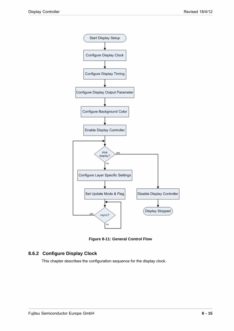
Display Controller Revised 18/4/12
Figure 8-11: General Control Flow
8.6.2 Configure Display Clock
This chapter describes the configuration sequence for the display clock.
Fujitsu Semiconductor Europe GmbH 8 - 15
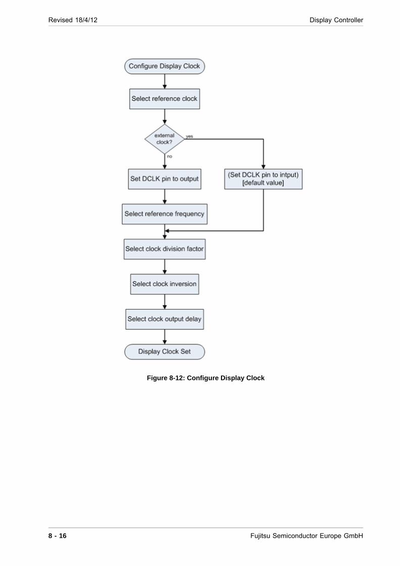
Revised 18/4/12 Display Controller
Figure 8-12: Configure Display Clock
8 - 16 Fujitsu Semiconductor Europe GmbH
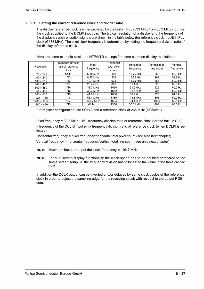
Display Controller Revised 18/4/12
8.6.2.1 Setting the correct reference clock and divider ratio
The display reference clock is either provided by the built-in PLL (533 MHz from 33.3 MHz input) or the clock supplied to the DCLKI input pin. The typical resolution of a display and the frequency of the display’s synchronization signals are shown in the table below (for reference clock = built-in PLL clock of 533 MHz). The pixel clock frequency is determined by setting the frequency division ratio of the display reference clock
Here are some example clock and HTP/VTR settings for some common display resolutions:
1 in register configuration use SC=42 and a reference clock of 266 MHz (DCSel=1)
Pixel frequency = 33.3 MHz ´ 16 ´ frequency division ratio of reference clock (for the built-in PLL)
= frequency of the DCLKI input pin x frequency division ratio of reference clock (when DCLKI is se-lected)
Horizontal frequency = pixel frequency/horizontal total pixel count (see also next chapter)
Vertical frequency = horizontal frequency/vertical total line count (see also next chapter)
NOTE Maximum input or output dot clock frequency is 106.7 MHz.
NOTE For dual-screen display functionality the clock speed has to be doubled compared to the single screen setup i.e. the frequency division has to be set to the value in the table divided by 2.
In addition the DCLK output can be inverted and/or delayed by some clock cycles of the reference clock in order to adjust the sampling edge for the receiving circuit with respect to the output RGB data.
ResolutionFrequency division ratio of reference
clock
Pixel frequency
Horizontal total pixel
count
Horizontal frequency
Vertical total line count
Vertical frequency
320 240 1/841 6.35 MHz 403 15.75 kHz 263 59.9 Hz400 240 1/63 8.47 MHz 538 15.73 kHz 263 59.8 Hz480 240 1/53 10.1 MHz 638 15.76 kHz 263 60.0 Hz640 480 1/21 25.4 MHz 800 31.4 kHz 525 60.5 Hz800 480 1/16 33.3 MHz 1060 31.5 kHz 525 60.0 Hz854 480 1/16 33.3 MHz 1062 31.7 kHz 525 59.8 Hz800 600 1/13 41.0 MHz 1060 38.7 kHz 628 61.6 Hz
1024 768 1/8 66.7 MHz 1380 48.3 kHz 806 59.9 Hz1280 1024 1/5 106.7 MHz 1664 64.1 kHz 1066 60.1 Hz1280 480 1/13 41 MHz 1366 30.01 kHz 494 60.8 Hz
Fujitsu Semiconductor Europe GmbH 8 - 17

Revised 18/4/12 Display Controller
8.6.3 Display Timing Configuration
The flow for setting the display timing is shown below.
Figure 8-13: Display Timing Configuration
A display area is defined using the parameters shown below. Each parameter is set as a register value.
8 - 18 Fujitsu Semiconductor Europe GmbH
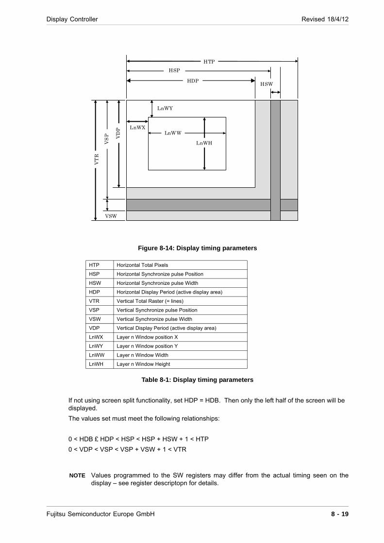
Display Controller Revised 18/4/12
Figure 8-14: Display timing parameters
Table 8-1: Display timing parameters
If not using screen split functionality, set HDP = HDB. Then only the left half of the screen will be displayed.
The values set must meet the following relationships:
0 < HDB £ HDP < HSP < HSP + HSW + 1 < HTP
0 < VDP < VSP < VSP + VSW + 1 < VTR
NOTE Values programmed to the SW registers may differ from the actual timing seen on the display – see register descriptopn for details.
HTP Horizontal Total Pixels
HSP Horizontal Synchronize pulse Position
HSW Horizontal Synchronize pulse Width
HDP Horizontal Display Period (active display area)
VTR Vertical Total Raster (= lines)
VSP Vertical Synchronize pulse Position
VSW Vertical Synchronize pulse Width
VDP Vertical Display Period (active display area)
LnWX Layer n Window position X
LnWY Layer n Window position Y
LnWW Layer n Window Width
LnWH Layer n Window Height
HTP
HSP
HDP
LnWY
LnWX LnWW
LnWH
VD
P
VS
P
VT
R
VSW
HSW
Fujitsu Semiconductor Europe GmbH 8 - 19
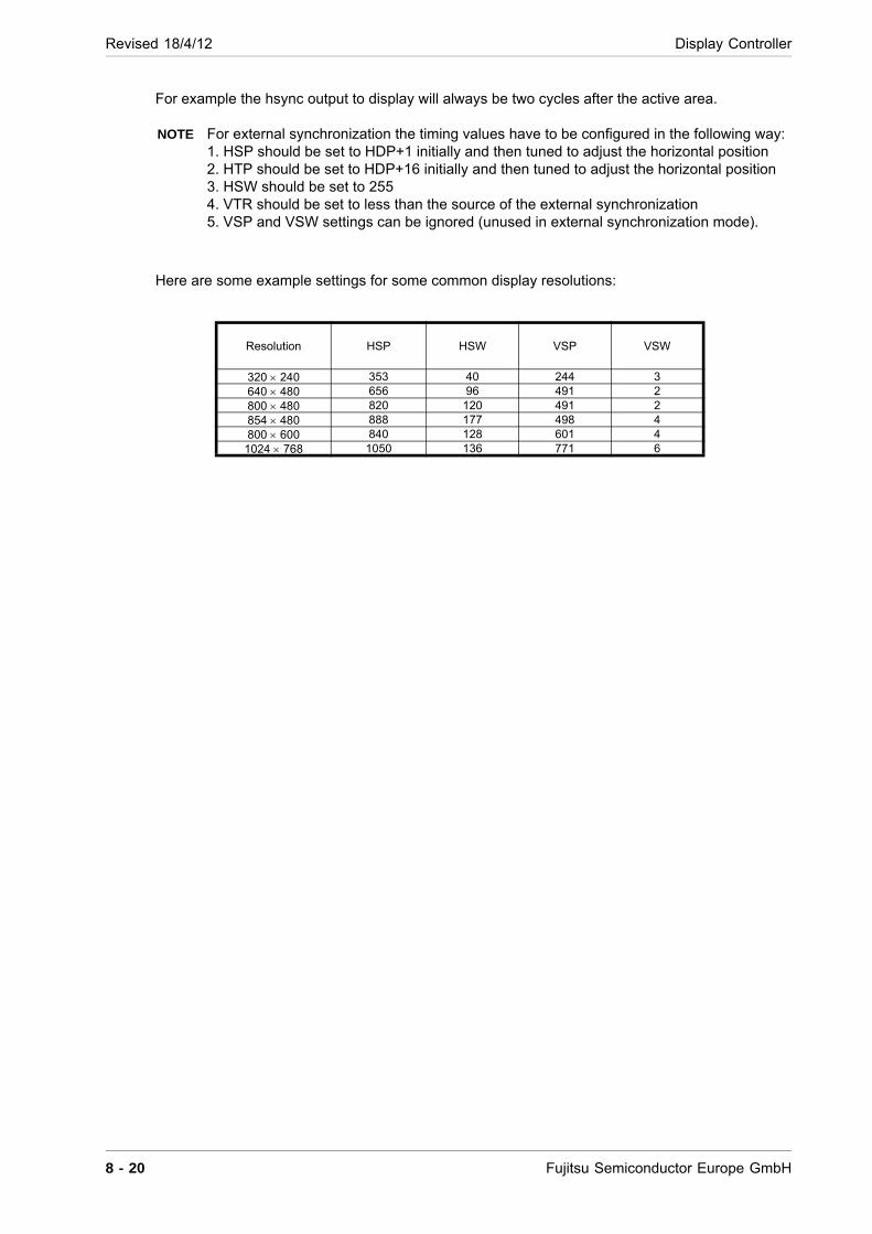
Revised 18/4/12 Display Controller
For example the hsync output to display will always be two cycles after the active area.
NOTE For external synchronization the timing values have to be configured in the following way:1. HSP should be set to HDP+1 initially and then tuned to adjust the horizontal position2. HTP should be set to HDP+16 initially and then tuned to adjust the horizontal position3. HSW should be set to 2554. VTR should be set to less than the source of the external synchronization5. VSP and VSW settings can be ignored (unused in external synchronization mode).
Here are some example settings for some common display resolutions:
Resolution HSP HSW VSP VSW
320 240 353 40 244 3640 480 656 96 491 2800 480 820 120 491 2854 480 888 177 498 4800 600 840 128 601 4
1024 768 1050 136 771 6
8 - 20 Fujitsu Semiconductor Europe GmbH
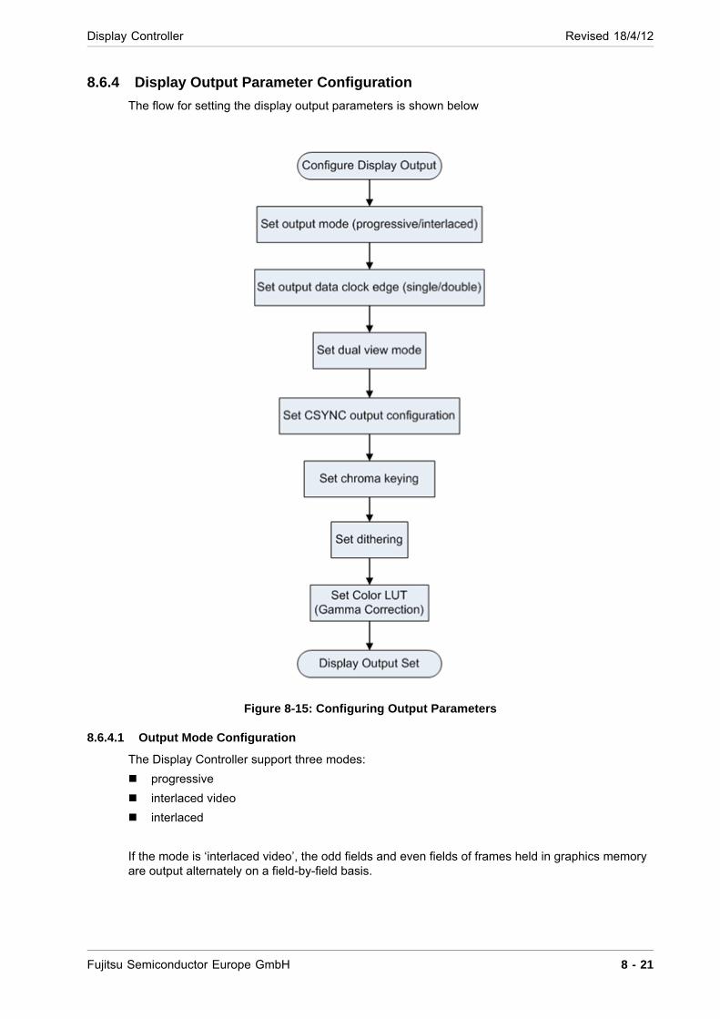
Display Controller Revised 18/4/12
8.6.4 Display Output Parameter Configuration
The flow for setting the display output parameters is shown below
Figure 8-15: Configuring Output Parameters
8.6.4.1 Output Mode Configuration
The Display Controller support three modes:
progressive
interlaced video
interlaced
If the mode is ‘interlaced video’, the odd fields and even fields of frames held in graphics memory are output alternately on a field-by-field basis.
Fujitsu Semiconductor Europe GmbH 8 - 21

Revised 18/4/12 Display Controller
If the mode is set to ‘interlaced’, the same image data is output to an odd field and then to an even field.However, in contradiction to progressive mode odd and even fields are distinguished here from each other by the phase relationship between the horizontal synchronization signal and the vertical synchronization signal.
Figure 8-16: Display Output Modes
8.6.4.2 Configure dual screen mode
Display controller has dual screen functionality. This function can output two multiplexed screens in order to display them on two separate display devices. If MB86298 'RUBY' comprises in total two display controllers, by using this functionality up to 4 independent screens can be simultaneously displayed (two of them respectively need to share the same display timing). It is possible to route layers to individual screens. The following example assumes that screen 0 is output to display de-vice 0 and screen 1 is output to display device 1.
Figure 8-17: Dual screen display by single display controller
To enable this mode: first of all multi display mode has to be enabled. In addition each display layer can be sent to only one or both of the two screens (see multi-display control register).
There are two dual screen output modes:
parallel mode and
multiplexing mode
However, MB86298 'RUBY' uses only multiplexing mode, i.e. two screens are time multiplexed and output to the same RGB output pins.
Odd
Even
Noninterlace Interlace Video Interlace
Screen “1”
Screen “0”display device “0”
display device “1”
display controller
8 - 22 Fujitsu Semiconductor Europe GmbH
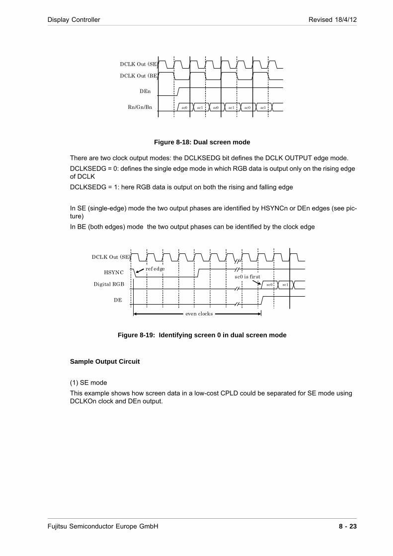
Display Controller Revised 18/4/12
Figure 8-18: Dual screen mode
There are two clock output modes: the DCLKSEDG bit defines the DCLK OUTPUT edge mode.
DCLKSEDG = 0: defines the single edge mode in which RGB data is output only on the rising edge of DCLK
DCLKSEDG = 1: here RGB data is output on both the rising and falling edge
In SE (single-edge) mode the two output phases are identified by HSYNCn or DEn edges (see pic-ture)
In BE (both edges) mode the two output phases can be identified by the clock edge
Figure 8-19: Identifying screen 0 in dual screen mode
Sample Output Circuit
(1) SE mode
This example shows how screen data in a low-cost CPLD could be separated for SE mode using DCLKOn clock and DEn output.
sc1 sc0 sc1 sc0 sc1sc0Rn/Gn/Bn
DCLK Out (BE)
DCLK Out (SE)
DEn
sc0 sc1 Digital RGB
DCLK Out (SE)
HSYNC
even clocks
DE
ref edge
sc0 is first
Fujitsu Semiconductor Europe GmbH 8 - 23
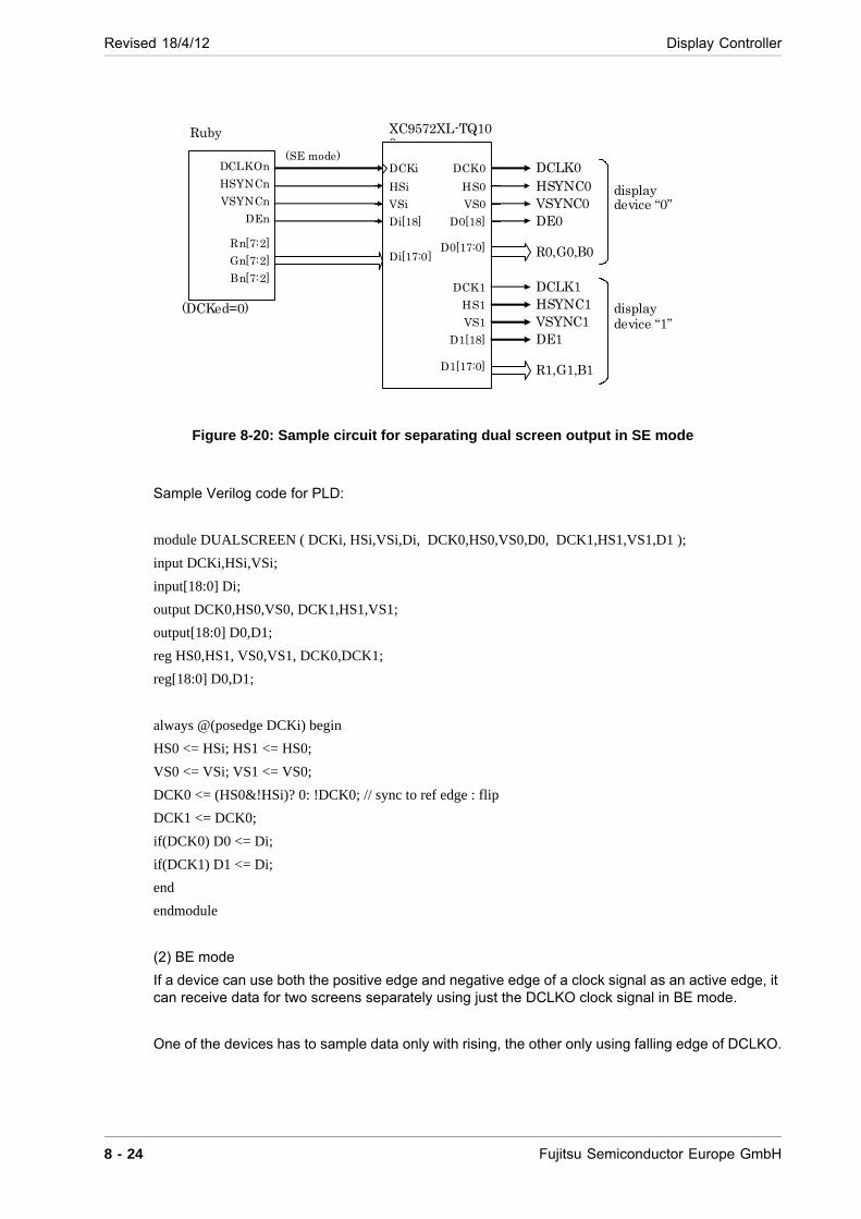
Revised 18/4/12 Display Controller
Figure 8-20: Sample circuit for separating dual screen output in SE mode
Sample Verilog code for PLD:
module DUALSCREEN ( DCKi, HSi,VSi,Di, DCK0,HS0,VS0,D0, DCK1,HS1,VS1,D1 );
input DCKi,HSi,VSi;
input[18:0] Di;
output DCK0,HS0,VS0, DCK1,HS1,VS1;
output[18:0] D0,D1;
reg HS0,HS1, VS0,VS1, DCK0,DCK1;
reg[18:0] D0,D1;
always @(posedge DCKi) begin
HS0 <= HSi; HS1 <= HS0;
VS0 <= VSi; VS1 <= VS0;
DCK0 <= (HS0&!HSi)? 0: !DCK0; // sync to ref edge : flip
DCK1 <= DCK0;
if(DCK0) D0 <= Di;
if(DCK1) D1 <= Di;
end
endmodule
(2) BE mode
If a device can use both the positive edge and negative edge of a clock signal as an active edge, it can receive data for two screens separately using just the DCLKO clock signal in BE mode.
One of the devices has to sample data only with rising, the other only using falling edge of DCLKO.
DCKi
VSi
HSi
Di[18]
DCK0
VS0
HS0
D0[18]
D0[17:0]Di[17:0]
Rn[7:2]
Gn[7:2]
Bn[7:2]
DCLKOn
HSYNCn
VSYNCn
DEn
XC9572XL-TQ100
R0,G0,B0
DCLK0HSYNC0VSYNC0DE0
R1,G1,B1
DCLK1HSYNC1VSYNC1DE1
(SE mode)
Ruby
display device “0”
display device “1”
D1[17:0]
DCK1
VS1
HS1
D1[18]
(DCKed=0)
8 - 24 Fujitsu Semiconductor Europe GmbH
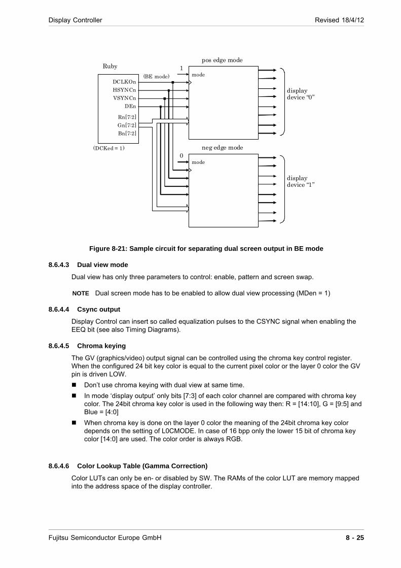
Display Controller Revised 18/4/12
Figure 8-21: Sample circuit for separating dual screen output in BE mode
8.6.4.3 Dual view mode
Dual view has only three parameters to control: enable, pattern and screen swap.
NOTE Dual screen mode has to be enabled to allow dual view processing (MDen = 1)
8.6.4.4 Csync output
Display Control can insert so called equalization pulses to the CSYNC signal when enabling the EEQ bit (see also Timing Diagrams).
8.6.4.5 Chroma keying
The GV (graphics/video) output signal can be controlled using the chroma key control register. When the configured 24 bit key color is equal to the current pixel color or the layer 0 color the GV pin is driven LOW.
Don’t use chroma keying with dual view at same time.
In mode ‘display output’ only bits [7:3] of each color channel are compared with chroma key color. The 24bit chroma key color is used in the following way then: R = [14:10], G = [9:5] and Blue = [4:0]
When chroma key is done on the layer 0 color the meaning of the 24bit chroma key color depends on the setting of L0CMODE. In case of 16 bpp only the lower 15 bit of chroma key color [14:0] are used. The color order is always RGB.
8.6.4.6 Color Lookup Table (Gamma Correction)
Color LUTs can only be en- or disabled by SW. The RAMs of the color LUT are memory mapped into the address space of the display controller.
0
1pos edge mode
(BE mode) mode
display device “0”
display device “1”
(DCKed = 1) neg edge mode
mode
Ruby
Rn[7:2]
Gn[7:2]
Bn[7:2]
DCLKOn
HSYNCn
VSYNCn
DEn
Fujitsu Semiconductor Europe GmbH 8 - 25
Revised 18/4/12 Display Controller
8.6.4.7 Dither Unit Configuration
The dither unit can be setup in different ways: one configuration register bit (DITHEN) switches the dithering unit on/off.The DITHFS bitfield adapts the resolution of output pixels (888, 777, 666 or 565). The DITHRS bitfield aligns the output data to the upper or lower byte edge The DITHMS bit-field selects the dithering mode – spatial or temporal.
8.6.5 Background Color Configuration
There is one 24bit register to set the background color for display controller.
NOTE Keep background color enable field always set to 1.
8.6.6 Enable/Disable Display Controller
Display Control has a global enable and SW reset register.
8.6.7 Configure Layer Specific Settings
For each display layer and the cursor layer some specific settings have to be made. In principle this also depends on the layer’s capabilities. There are several possibilities:
standard display layer: L5, L6, L7
standard display layer in combination with cursor and color palette: L0
display layer with video ring buffer function (together with capture units) + color palettes: L1, L2, L3
display layer with video ring buffer function (together with capture units): L4
Please see the principle setup flow for display layers (exclunding cursors) below.
8 - 26 Fujitsu Semiconductor Europe GmbH
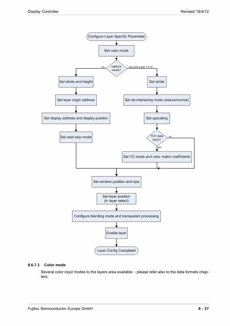
Display Controller Revised 18/4/12
8.6.7.1 Color mode
Several color input modes to the layers area available - please refer also to the data formats chap-ters.
Fujitsu Semiconductor Europe GmbH 8 - 27
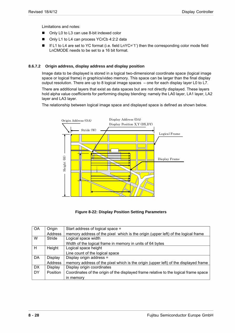
Revised 18/4/12 Display Controller
Limitations and notes:
Only L0 to L3 can use 8-bit indexed color
Only L1 to L4 can process YCrCb 4:2:2 data
If L1 to L4 are set to YC format (i.e. field LnYC=’1’) then the corresponding color mode field LnCMODE needs to be set to a 16 bit format.
8.6.7.2 Origin address, display address and display position
Image data to be displayed is stored in a logical two-dimensional coordinate space (logical image space or logical frame) in graphics/video memory. This space can be larger than the final display output resolution. There are up to 8 logical image spaces – one for each display layer L0 to L7.
There are additional layers that exist as data spaces but are not directly displayed. These layers hold alpha value coefficients for performing display blending: namely the LA0 layer, LA1 layer, LA2 layer and LA3 layer.
The relationship between logical image space and displayed space is defined as shown below.
Figure 8-22: Display Position Setting Parameters
OA Origin Address
Start address of logical space =memory address of the pixel which is the origin (upper left) of the logical frame
W Stride Logical space widthWidth of the logical frame in memory in units of 64 bytes
H Height Logical space heightLine count of the logical space
DA Display Address
Display origin address =memory address of the pixel which is the origin (upper left) of the displayed frame
DXDY
Display Position
Display origin coordinatesCoordinates of the origin of the displayed frame relative to the logical frame space in memory
Origin Address (OA) Display Address (DA)
Display Position X,Y (DX,DY)
Stride (W)
Hei
ght
(H)
Logical Frame
Display Frame
8 - 28 Fujitsu Semiconductor Europe GmbH
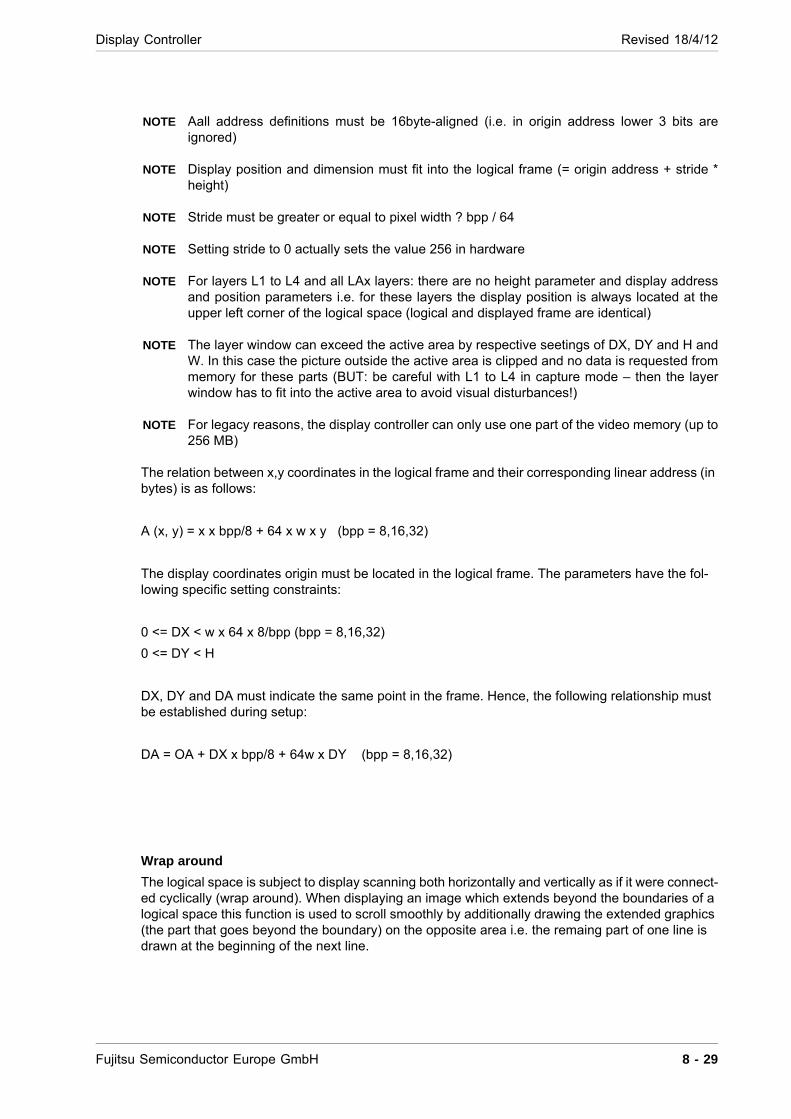
Display Controller Revised 18/4/12
NOTE Aall address definitions must be 16byte-aligned (i.e. in origin address lower 3 bits are ignored)
NOTE Display position and dimension must fit into the logical frame (= origin address + stride * height)
NOTE Stride must be greater or equal to pixel width ? bpp / 64
NOTE Setting stride to 0 actually sets the value 256 in hardware
NOTE For layers L1 to L4 and all LAx layers: there are no height parameter and display address and position parameters i.e. for these layers the display position is always located at the upper left corner of the logical space (logical and displayed frame are identical)
NOTE The layer window can exceed the active area by respective seetings of DX, DY and H and W. In this case the picture outside the active area is clipped and no data is requested from memory for these parts (BUT: be careful with L1 to L4 in capture mode – then the layer window has to fit into the active area to avoid visual disturbances!)
NOTE For legacy reasons, the display controller can only use one part of the video memory (up to 256 MB)
The relation between x,y coordinates in the logical frame and their corresponding linear address (in bytes) is as follows:
A (x, y) = x x bpp/8 + 64 x w x y (bpp = 8,16,32)
The display coordinates origin must be located in the logical frame. The parameters have the fol-lowing specific setting constraints:
0 <= DX < w x 64 x 8/bpp (bpp = 8,16,32)
0 <= DY < H
DX, DY and DA must indicate the same point in the frame. Hence, the following relationship must be established during setup:
DA = OA + DX x bpp/8 + 64w x DY (bpp = 8,16,32)
Wrap around
The logical space is subject to display scanning both horizontally and vertically as if it were connect-ed cyclically (wrap around). When displaying an image which extends beyond the boundaries of a logical space this function is used to scroll smoothly by additionally drawing the extended graphics (the part that goes beyond the boundary) on the opposite area i.e. the remaing part of one line is drawn at the beginning of the next line.
Fujitsu Semiconductor Europe GmbH 8 - 29
Revised 18/4/12 Display Controller
Figure 8-23: Display wraparound processing
NOTE Layer L1, L2, L3 and L4 as well as LA0 to LA3 layers have no wrap around function. L0, L5, L6, L7 have a wraparound function, but alpha dedicated layers LA0 to LA3 have no wraparound function.
8.6.7.3 Set window position and size
For displaying one layer on the screen two more parameters have to be configured: window position and window size. Window position defines the position of the upper-left pixel of the respective dis-play layer in relation to the origin of the visible screen for example if programmed to (0,0) the layer is positioned in the upper left corner of the screen. The window width and height define the visible part of each layer.
8.6.7.4 Read skip mode (for standard layer)
Data reads of an area hidden completely by an another layer can be prevented in order to the reduce the bandwidth requirements for the memory. For example when a top layer image is enabled such as a user menu located in a specific area of the screen it is possible to prevent the data reads for this area in the lower layers
Therefore it is possible to split the display area into 9 partitions using two straight horizontal lines and two straight vertical lines. For each parition it can be specified separately whether data is read or not. Areas that should not be read are regarded as transparent.
The control over a partition read (enable or disable for each partition) is set using the LnPR bitfield. In the LnPR bitfield each bit corresponds to one of the partitions. When the corresponding bit is set to a value of 0 data is not read for this partition.
64w
L
Logical Frame Origin
Additionally
drawn area New display origin
Previos display origin
8 - 30 Fujitsu Semiconductor Europe GmbH
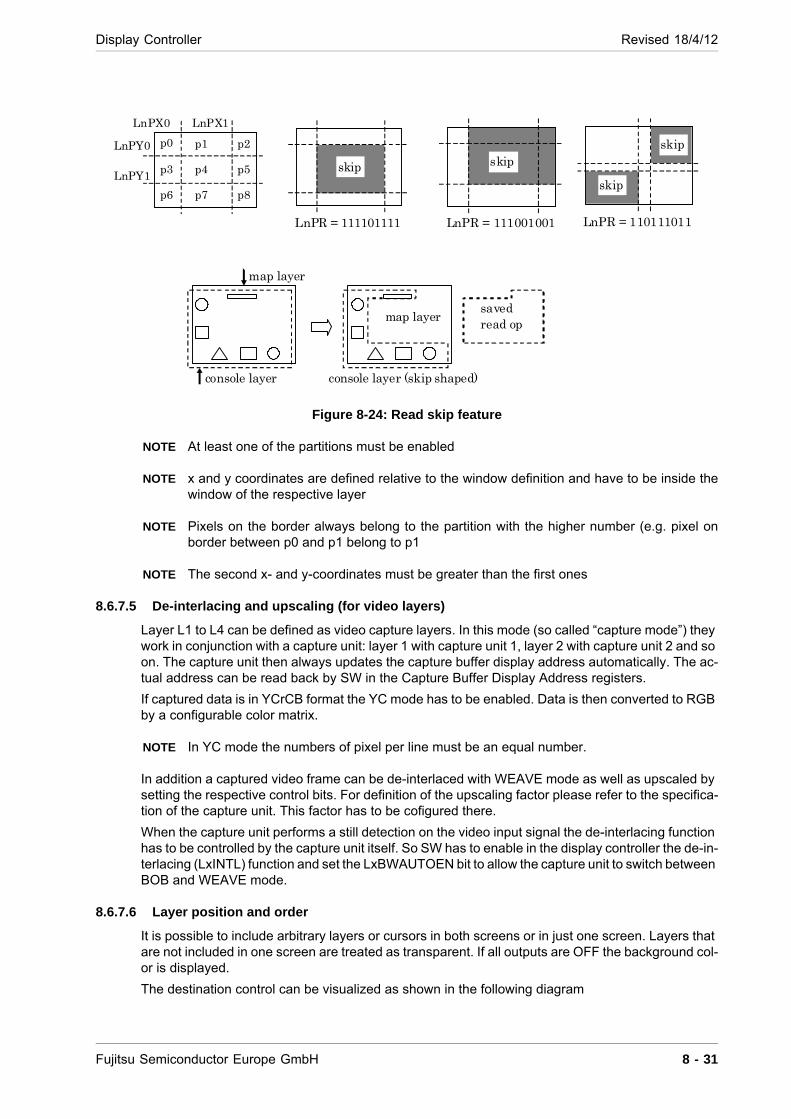
Display Controller Revised 18/4/12
Figure 8-24: Read skip feature
NOTE At least one of the partitions must be enabled
NOTE x and y coordinates are defined relative to the window definition and have to be inside the window of the respective layer
NOTE Pixels on the border always belong to the partition with the higher number (e.g. pixel on border between p0 and p1 belong to p1
NOTE The second x- and y-coordinates must be greater than the first ones
8.6.7.5 De-interlacing and upscaling (for video layers)
Layer L1 to L4 can be defined as video capture layers. In this mode (so called “capture mode”) they work in conjunction with a capture unit: layer 1 with capture unit 1, layer 2 with capture unit 2 and so on. The capture unit then always updates the capture buffer display address automatically. The ac-tual address can be read back by SW in the Capture Buffer Display Address registers.
If captured data is in YCrCB format the YC mode has to be enabled. Data is then converted to RGB by a configurable color matrix.
NOTE In YC mode the numbers of pixel per line must be an equal number.
In addition a captured video frame can be de-interlaced with WEAVE mode as well as upscaled by setting the respective control bits. For definition of the upscaling factor please refer to the specifica-tion of the capture unit. This factor has to be cofigured there.
When the capture unit performs a still detection on the video input signal the de-interlacing function has to be controlled by the capture unit itself. So SW has to enable in the display controller the de-in-terlacing (LxINTL) function and set the LxBWAUTOEN bit to allow the capture unit to switch between BOB and WEAVE mode.
8.6.7.6 Layer position and order
It is possible to include arbitrary layers or cursors in both screens or in just one screen. Layers that are not included in one screen are treated as transparent. If all outputs are OFF the background col-or is displayed.
The destination control can be visualized as shown in the following diagram
LnPY0
LnPX0
p0
LnPX1
LnPY1
p1 p2
p3 p4 p5
p6 p7 p8
skip
LnPR = 111101111
skip
LnPR = 111001001
skip
skip
LnPR = 110111011
map layer
console layer
map layer
console layer (skip shaped)
saved read op
Fujitsu Semiconductor Europe GmbH 8 - 31
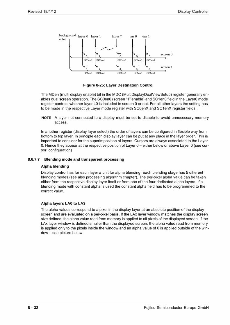
Revised 18/4/12 Display Controller
Figure 8-25: Layer Destination Control
The MDen (multi display enable) bit in the MDC (MultiDisplayDualViewSetup) register generally en-ables dual screen operation. The SC0en0 (screen “1” enable) and SC1en0 field in the Layer0 mode register controls whether layer L0 is included in screen 0 or not. For all other layers the setting has to be made in the respective Layer mode register with SC0enX and SC1enX register fields .
NOTE A layer not connected to a display must be set to disable to avoid unnecessary memory access.
In another register (display layer select) the order of layers can be configured in flexible way from bottom to top layer. In principle each display layer can be put at any place in the layer order. This is important to consider for the superimposition of layers. Cursors are always associated to the Layer 0. Hence they appear at the respective position of Layer 0 – either below or above Layer 0 (see cur-sor configuration)
8.6.7.7 Blending mode and transparent processing
Alpha blending
Display control has for each layer a unit for alpha blending. Each blending stage has 5 different blending modes (see also processing algorithm chapter). The per-pixel alpha value can be taken either from the respective display layer itself or from one of the four dedicated alpha layers. If a blending mode with constant alpha is used the constant alpha field has to be programmed to the correct value.
Alpha layers LA0 to LA3
The alpha values correspond to a pixel in the display layer at an absolute position of the display screen and are evaluated on a per-pixel basis. If the LAx layer window matches the display screen size defined, the alpha value read from memory is applied to all pixels of the displayed screen. If the LAx layer window is defined smaller than the displayed screen, the alpha value read from memory is applied only to the pixels inside the window and an alpha value of 0 is applied outside of the win-dow – see picture below.
SC0en6
SC1en6
SC0en7
SC1en7
SC0en5
SC1en5
SC0en1
SC1en1
SC0en0
SC1en0
screen 0
layer 0
screen 1
background color
layer 1 layer 7 cur 0 cur 1
8 - 32 Fujitsu Semiconductor Europe GmbH
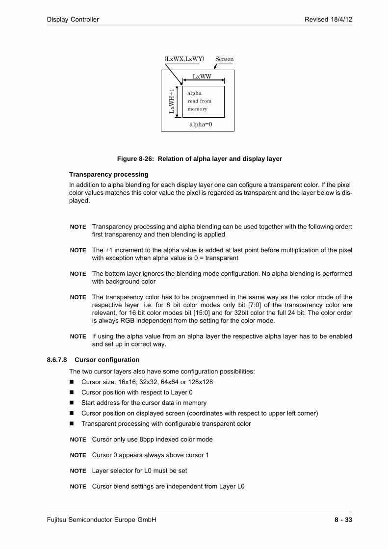
Display Controller Revised 18/4/12
Figure 8-26: Relation of alpha layer and display layer
Transparency processing
In addition to alpha blending for each display layer one can cofigure a transparent color. If the pixel color values matches this color value the pixel is regarded as transparent and the layer below is dis-played.
NOTE Transparency processing and alpha blending can be used together with the following order: first transparency and then blending is applied
NOTE The +1 increment to the alpha value is added at last point before multiplication of the pixel with exception when alpha value is 0 = transparent
NOTE The bottom layer ignores the blending mode configuration. No alpha blending is performed with background color
NOTE The transparency color has to be programmed in the same way as the color mode of the respective layer, i.e. for 8 bit color modes only bit [7:0] of the transparency color are relevant, for 16 bit color modes bit [15:0] and for 32bit color the full 24 bit. The color order is always RGB independent from the setting for the color mode.
NOTE If using the alpha value from an alpha layer the respective alpha layer has to be enabled and set up in correct way.
8.6.7.8 Cursor configuration
The two cursor layers also have some configuration possibilities:
Cursor size: 16x16, 32x32, 64x64 or 128x128
Cursor position with respect to Layer 0
Start address for the cursor data in memory
Cursor position on displayed screen (coordinates with respect to upper left corner)
Transparent processing with configurable transparent color
NOTE Cursor only use 8bpp indexed color mode
NOTE Cursor 0 appears always above cursor 1
NOTE Layer selector for L0 must be set
NOTE Cursor blend settings are independent from Layer L0
LxWW
LxW
H+
1
(LxWX,LxWY)
alpha=0
alpha
read from
memory
Screen
Fujitsu Semiconductor Europe GmbH 8 - 33
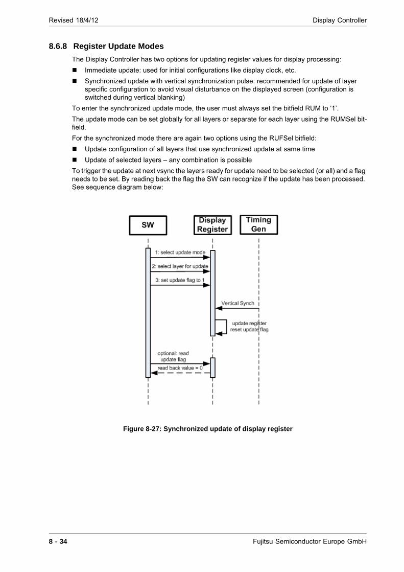
Revised 18/4/12 Display Controller
8.6.8 Register Update Modes
The Display Controller has two options for updating register values for display processing:
Immediate update: used for initial configurations like display clock, etc.
Synchronized update with vertical synchronization pulse: recommended for update of layer specific configuration to avoid visual disturbance on the displayed screen (configuration is switched during vertical blanking)
To enter the synchronized update mode, the user must always set the bitfield RUM to ‘1’.
The update mode can be set globally for all layers or separate for each layer using the RUMSel bit-field.
For the synchronized mode there are again two options using the RUFSel bitfield:
Update configuration of all layers that use synchronized update at same time
Update of selected layers – any combination is possible
To trigger the update at next vsync the layers ready for update need to be selected (or all) and a flag needs to be set. By reading back the flag the SW can recognize if the update has been processed. See sequence diagram below:
Figure 8-27: Synchronized update of display register
8 - 34 Fujitsu Semiconductor Europe GmbH
Display Controller Revised 18/4/12
The following register or register fields are subject of synchronized update:
All settings that influence the memory address and stride of the respective layer
All settings that influence the window size and position of the respective layer
All settings that influence the color mode and de-interlacing of the respective layer
Not included are the settings for blending and transparent processing and the read skip mode.
NOTE The layer enable fields LnE or LAnE as well as the enable for the cursor layer CENn are always synchronized to the vertical synchronization – independent of the configured register update mode.
8.6.9 Processing on interrupts
The Display Controller has four different interrupts to signal to the SW a certain state of the HW. These are for information purposes only and SW has not to take any action upon receiving one of the interrupts. The interrupts can be used to synchronize actions in SW application or driver (e.g. VSYNC interrupt).
Fujitsu Semiconductor Europe GmbH 8 - 35
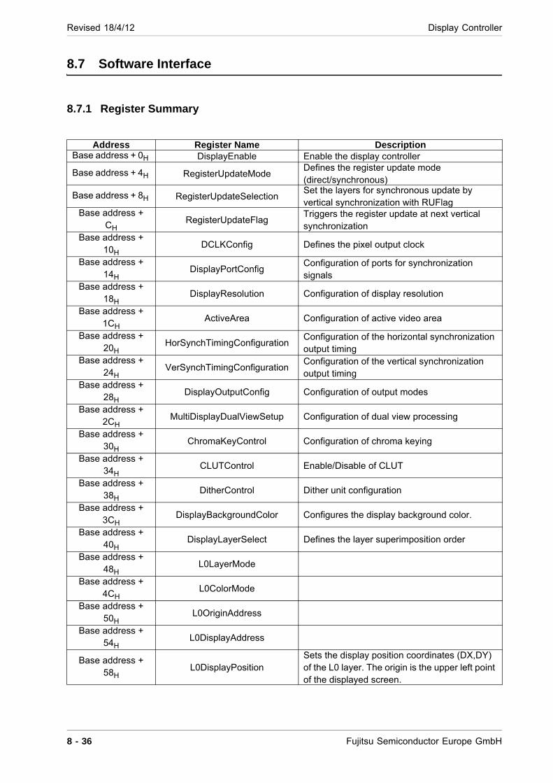
Revised 18/4/12 Display Controller
8.7 Software Interface
8.7.1 Register Summary
Address Register Name DescriptionBase address + 0H DisplayEnable Enable the display controller
Base address + 4H RegisterUpdateMode Defines the register update mode (direct/synchronous)
Base address + 8H RegisterUpdateSelection Set the layers for synchronous update by vertical synchronization with RUFlag
Base address + CH
RegisterUpdateFlag Triggers the register update at next vertical synchronization
Base address + 10H
DCLKConfig Defines the pixel output clock
Base address + 14H
DisplayPortConfig Configuration of ports for synchronization signals
Base address + 18H
DisplayResolution Configuration of display resolution
Base address + 1CH
ActiveArea Configuration of active video area
Base address + 20H HorSynchTimingConfiguration
Configuration of the horizontal synchronization output timing
Base address + 24H VerSynchTimingConfiguration
Configuration of the vertical synchronization output timing
Base address + 28H DisplayOutputConfig Configuration of output modes
Base address + 2CH MultiDisplayDualViewSetup Configuration of dual view processing
Base address + 30H ChromaKeyControl Configuration of chroma keying
Base address + 34H CLUTControl Enable/Disable of CLUT
Base address + 38H DitherControl Dither unit configuration
Base address + 3CH
DisplayBackgroundColor Configures the display background color.
Base address + 40H
DisplayLayerSelect Defines the layer superimposition order
Base address + 48H
L0LayerMode
Base address + 4CH
L0ColorMode
Base address + 50H
L0OriginAddress
Base address + 54H L0DisplayAddress
Base address + 58H L0DisplayPosition
Sets the display position coordinates (DX,DY) of the L0 layer. The origin is the upper left point of the displayed screen.
8 - 36 Fujitsu Semiconductor Europe GmbH
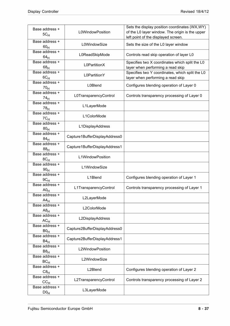
Display Controller Revised 18/4/12
Base address + 5CH L0WindowPosition
Sets the display position coordinates (WX,WY) of the L0 layer window. The origin is the upper left point of the displayed screen.
Base address + 60H
L0WindowSize Sets the size of the L0 layer window
Base address + 64H
L0ReadSkipMode Controls read skip operation of layer L0
Base address + 68H
L0PartitionX Specifies two X coordinates which split the L0 layer when performing a read skip
Base address + 6CH
L0PartitionY Specifies two Y coordinates, which split the L0 layer when performing a read skip
Base address + 70H
L0Blend Configures blending operation of Layer 0
Base address + 74H L0TransparencyControl Controls transparency processing of Layer 0
Base address + 78H L1LayerMode
Base address + 7CH L1ColorMode
Base address + 80H L1DisplayAddress
Base address + 84H Capture1BufferDisplayAddress0
Base address + 88H Capture1BufferDisplayAddress1
Base address + 8CH L1WindowPosition
Base address + 90H
L1WindowSize
Base address + 9CH
L1Blend Configures blending operation of Layer 1
Base address + A0H
L1TransparencyControl Controls transparency processing of Layer 1
Base address + A4H
L2LayerMode
Base address + A8H
L2ColorMode
Base address + ACH L2DisplayAddress
Base address + B0H Capture2BufferDisplayAddress0
Base address + B4H Capture2BufferDisplayAddress1
Base address + B8H L2WindowPosition
Base address + BCH L2WindowSize
Base address + C8H L2Blend Configures blending operation of Layer 2
Base address + CCH L2TransparencyControl Controls transparency processing of Layer 2
Base address + D0H
L3LayerMode
Fujitsu Semiconductor Europe GmbH 8 - 37
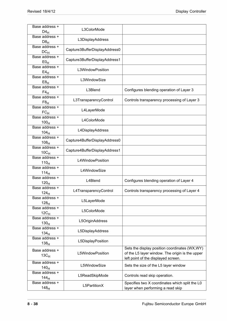
Revised 18/4/12 Display Controller
Base address + D4H
L3ColorMode
Base address + D8H
L3DisplayAddress
Base address + DCH
Capture3BufferDisplayAddress0
Base address + E0H Capture3BufferDisplayAddress1
Base address + E4H L3WindowPosition
Base address + E8H L3WindowSize
Base address + F4H L3Blend Configures blending operation of Layer 3
Base address + F8H L3TransparencyControl Controls transparency processing of Layer 3
Base address + FCH L4LayerMode
Base address + 100H L4ColorMode
Base address + 104H
L4DisplayAddress
Base address + 108H
Capture4BufferDisplayAddress0
Base address + 10CH
Capture4BufferDisplayAddress1
Base address + 110H
L4WindowPosition
Base address + 114H
L4WindowSize
Base address + 120H L4Blend Configures blending operation of Layer 4
Base address + 124H L4TransparencyControl Controls transparency processing of Layer 4
Base address + 128H L5LayerMode
Base address + 12CH L5ColorMode
Base address + 130H L5OriginAddress
Base address + 134H L5DisplayAddress
Base address + 138H L5DisplayPosition
Base address + 13CH L5WindowPosition
Sets the display position coordinates (WX,WY) of the L5 layer window. The origin is the upper left point of the displayed screen.
Base address + 140H L5WindowSize Sets the size of the L5 layer window
Base address + 144H L5ReadSkipMode Controls read skip operation.
Base address + 148H
L5PartitionX Specifies two X coordinates which split the L0 layer when performing a read skip
8 - 38 Fujitsu Semiconductor Europe GmbH
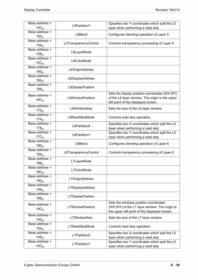
Display Controller Revised 18/4/12
Base address + 14CH
L5PartitionY Specifies two Y coordinates which split the L0 layer when performing a read skip
Base address + 150H
L5Blend Configures blending operation of Layer 5
Base address + 154H
L5TransparencyControl Controls transparency processing of Layer 5
Base address + 158H L6LayerMode
Base address + 15CH L6ColorMode
Base address + 160H L6OriginAddress
Base address + 164H L6DisplayAddress
Base address + 168H L6DisplayPosition
Base address + 16CH
L6WindowPosition Sets the display position coordinates (WX,WY) of the L6 layer window. The origin is the upper left point of the displayed screen.
Base address + 170H L6WindowSize Sets the size of the L6 layer window
Base address + 174H L6ReadSkipMode Controls read skip operation.
Base address + 178H L6PartitionX
Specifies two X coordinates which split the L0 layer when performing a read skip
Base address + 17CH L6PartitionY
Specifies two Y coordinates which split the L0 layer when performing a read skip
Base address + 180H
L6Blend Configures blending operation of Layer 6
Base address + 184H
L6TransparencyControl Controls transparency processing of Layer 6
Base address + 188H
L7LayerMode
Base address + 18CH
L7ColorMode
Base address + 190H
L7OriginAddress
Base address + 194H L7DisplayAddress
Base address + 198H L7DisplayPosition
Base address + 19CH
L7WindowPosition Sets the windows position coordinates (WX,WY) of the L7 layer window. The origin is the upper left point of the displayed screen.
Base address + 1A0H L7WindowSize Sets the size of the L7 layer window
Base address + 1A4H L7ReadSkipMode Controls read skip operation.
Base address + 1A8H L7PartitionX
Specifies two X coordinates which split the L0 layer when performing a read skip
Base address + 1ACH L7PartitionY
Specifies two Y coordinates which split the L0 layer when performing a read skip
Fujitsu Semiconductor Europe GmbH 8 - 39
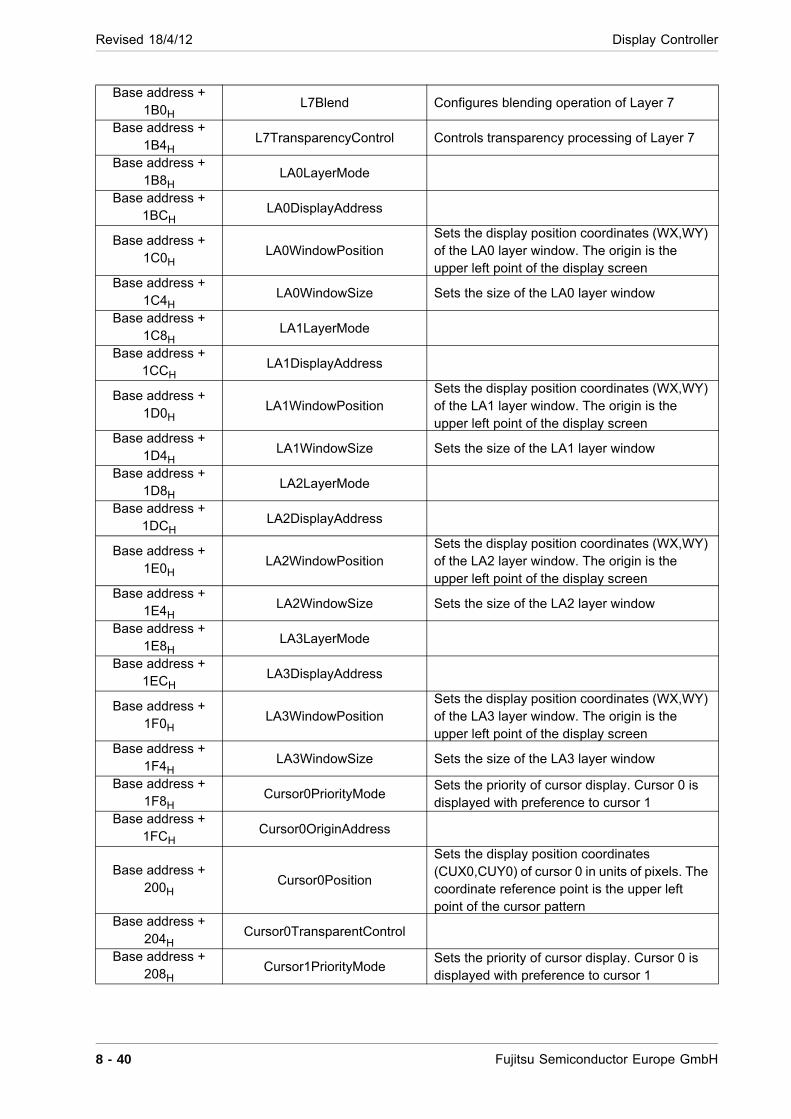
Revised 18/4/12 Display Controller
Base address + 1B0H
L7Blend Configures blending operation of Layer 7
Base address + 1B4H
L7TransparencyControl Controls transparency processing of Layer 7
Base address + 1B8H
LA0LayerMode
Base address + 1BCH LA0DisplayAddress
Base address + 1C0H LA0WindowPosition
Sets the display position coordinates (WX,WY) of the LA0 layer window. The origin is the upper left point of the display screen
Base address + 1C4H
LA0WindowSize Sets the size of the LA0 layer window
Base address + 1C8H LA1LayerMode
Base address + 1CCH LA1DisplayAddress
Base address + 1D0H
LA1WindowPosition Sets the display position coordinates (WX,WY) of the LA1 layer window. The origin is the upper left point of the display screen
Base address + 1D4H LA1WindowSize Sets the size of the LA1 layer window
Base address + 1D8H LA2LayerMode
Base address + 1DCH LA2DisplayAddress
Base address + 1E0H
LA2WindowPosition Sets the display position coordinates (WX,WY) of the LA2 layer window. The origin is the upper left point of the display screen
Base address + 1E4H LA2WindowSize Sets the size of the LA2 layer window
Base address + 1E8H LA3LayerMode
Base address + 1ECH LA3DisplayAddress
Base address + 1F0H
LA3WindowPosition Sets the display position coordinates (WX,WY) of the LA3 layer window. The origin is the upper left point of the display screen
Base address + 1F4H LA3WindowSize Sets the size of the LA3 layer window
Base address + 1F8H Cursor0PriorityMode
Sets the priority of cursor display. Cursor 0 is displayed with preference to cursor 1
Base address + 1FCH Cursor0OriginAddress
Base address + 200H
Cursor0Position
Sets the display position coordinates (CUX0,CUY0) of cursor 0 in units of pixels. The coordinate reference point is the upper left point of the cursor pattern
Base address + 204H
Cursor0TransparentControl
Base address + 208H Cursor1PriorityMode
Sets the priority of cursor display. Cursor 0 is displayed with preference to cursor 1
8 - 40 Fujitsu Semiconductor Europe GmbH
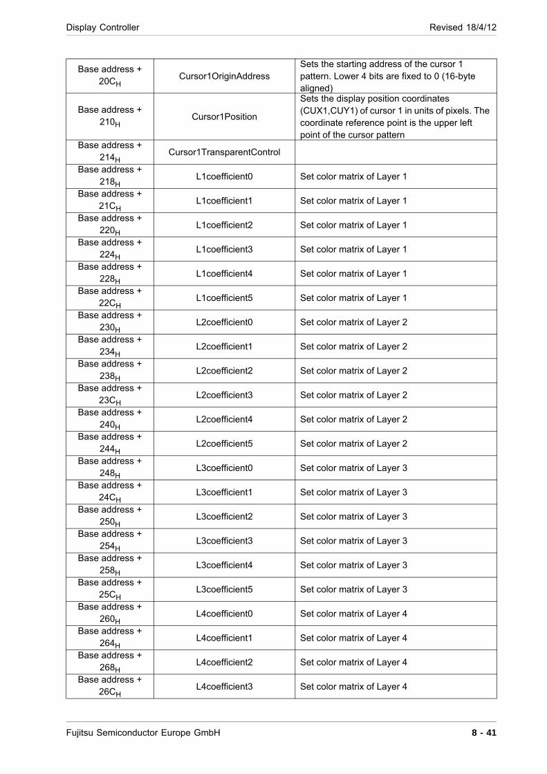
Display Controller Revised 18/4/12
Base address + 20CH Cursor1OriginAddress
Sets the starting address of the cursor 1 pattern. Lower 4 bits are fixed to 0 (16-byte aligned)
Base address + 210H
Cursor1Position
Sets the display position coordinates (CUX1,CUY1) of cursor 1 in units of pixels. The coordinate reference point is the upper left point of the cursor pattern
Base address + 214H
Cursor1TransparentControl
Base address + 218H L1coefficient0 Set color matrix of Layer 1
Base address + 21CH L1coefficient1 Set color matrix of Layer 1
Base address + 220H L1coefficient2 Set color matrix of Layer 1
Base address + 224H L1coefficient3 Set color matrix of Layer 1
Base address + 228H L1coefficient4 Set color matrix of Layer 1
Base address + 22CH L1coefficient5 Set color matrix of Layer 1
Base address + 230H L2coefficient0 Set color matrix of Layer 2
Base address + 234H
L2coefficient1 Set color matrix of Layer 2
Base address + 238H
L2coefficient2 Set color matrix of Layer 2
Base address + 23CH
L2coefficient3 Set color matrix of Layer 2
Base address + 240H
L2coefficient4 Set color matrix of Layer 2
Base address + 244H
L2coefficient5 Set color matrix of Layer 2
Base address + 248H L3coefficient0 Set color matrix of Layer 3
Base address + 24CH L3coefficient1 Set color matrix of Layer 3
Base address + 250H L3coefficient2 Set color matrix of Layer 3
Base address + 254H L3coefficient3 Set color matrix of Layer 3
Base address + 258H L3coefficient4 Set color matrix of Layer 3
Base address + 25CH L3coefficient5 Set color matrix of Layer 3
Base address + 260H L4coefficient0 Set color matrix of Layer 4
Base address + 264H
L4coefficient1 Set color matrix of Layer 4
Base address + 268H
L4coefficient2 Set color matrix of Layer 4
Base address + 26CH
L4coefficient3 Set color matrix of Layer 4
Fujitsu Semiconductor Europe GmbH 8 - 41
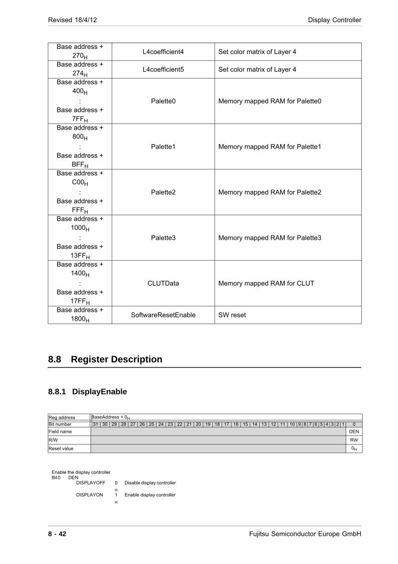
Revised 18/4/12 Display Controller
8.8 Register Description
8.8.1 DisplayEnable
Base address + 270H
L4coefficient4 Set color matrix of Layer 4
Base address + 274H
L4coefficient5 Set color matrix of Layer 4
Base address + 400H
:Base address +
7FFH
Palette0 Memory mapped RAM for Palette0
Base address + 800H
:Base address +
BFFH
Palette1 Memory mapped RAM for Palette1
Base address + C00H
:Base address +
FFFH
Palette2 Memory mapped RAM for Palette2
Base address + 1000H
:Base address +
13FFH
Palette3 Memory mapped RAM for Palette3
Base address + 1400H
:Base address +
17FFH
CLUTData Memory mapped RAM for CLUT
Base address + 1800H SoftwareResetEnable SW reset
Reg address BaseAddress + 0H
Bit number 31 30 29 28 27 26 25 24 23 22 21 20 19 18 17 16 15 14 13 12 11 10 9 8 7 6 5 4 3 2 1 0
Field name DEN
R/W RW
Reset value 0H
Enable the display controller Bit 0 DEN
DISPLAYOFF 0
H
Disable display controller
DISPLAYON 1
H
Enable display controller
8 - 42 Fujitsu Semiconductor Europe GmbH
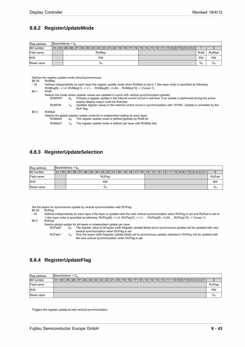
Display Controller Revised 18/4/12
8.8.2 RegisterUpdateMode
8.8.3 RegisterUpdateSelection
8.8.4 RegisterUpdateFlag
Reg address BaseAddress + 4H
Bit number 31 30 29 28 27 26 25 24 23 22 21 20 19 18 17 16 15 14 13 12 11 10 9 8 7 6 5 4 3 2 1 0
Field name RUMlay RUM RUMsel
R/W RW RW RW
Reset value 0H 0H 0H
Defines the register update mode (direct/synchronous) Bit 29 - 16
RUMlay Defines independently for each layer the register update mode when RUMsel is set to 1 (the layer order is specified as following: RUMlay[0] --> L0, RUMlay[1] --> L1, ... RUMlay[8] -->LA0,... RUMlay[13] --> Cursor 1)
Bit 1 RUM Selects the mode where register values are updated in synch with vertical synchronization globally
RUMOFF 0H Process a register update in the internal control circuit in real time. If an update is performed during the active display display output could be distorted
RUMON 1H Updates register values to the internal control circuit in synchronization with VSYNC. Update is controlled by the RUF flag
Bit 0 RUMsel Selects the global register update mode bit or independent setting for each layer
RUMsel0 0H The register update mode is defined globally by RUM bit
RUMsel1 1H The register update mode is defined per layer with RUMlay bits
Reg address BaseAddress + 8H
Bit number 31 30 29 28 27 26 25 24 23 22 21 20 19 18 17 16 15 14 13 12 11 10 9 8 7 6 5 4 3 2 1 0
Field name RUFlay RUFsel
R/W RW RW
Reset value 0H 0H
Set the layers for synchronous update by vertical synchronization with RUFlag Bit 29 - 16
RUFlay Defines independently for each layer if the layer is updated with the next vertical synchronization when RUFlag is set and RUFsel is set to 1 (the layer order is specified as following: RUFlay[0] --> L0, RUFlay[1] --> L1, ... RUFlay[8] -->LA0,... RUFlay[13] --> Cursor 1)
Bit 0 RUFsel Selects global update for all layers or independent update per layer
RUFsel0 0H The register value of all layers (with Register Update Mode set to synchronous update) will be updated with next vertical synchronization when RUFlag is set
RUFsel1 1H Only the layers (with Register Update Mode set to synchronous update) selected in RUFlay will be updated with the next vertical synchronization when RUFlag is set
Reg address BaseAddress + CH
Bit number 31 30 29 28 27 26 25 24 23 22 21 20 19 18 17 16 15 14 13 12 11 10 9 8 7 6 5 4 3 2 1 0
Field name RUFlag
R/W RW
Reset value 0H
Triggers the register update at next vertical synchronization
Fujitsu Semiconductor Europe GmbH 8 - 43
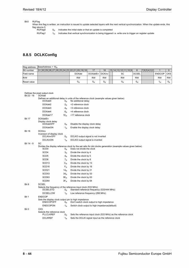
Revised 18/4/12 Display Controller
8.8.5 DCLKConfig
Bit 0 RUFlag When this flag is written, an instruction is issued to update selected layers with the next vertical synchronization. When the update ends, this flag returns 0.
RUFlag0 0H Indicates the initial state or that an update is completed
RUFlag1 1H Indicates that vertical synchronization is being triggered i.e. write one to trigger an register update
Reg address BaseAddress + 10H
Bit number 31 30 29 28 27 26 25 24 23 22 21 20 19 18 17 16 15 14 13 12 11 10 9 8 7 6 5 4 3 2 1 0
Field name DCKdel DCKdelEn DCKinv SC DCSEL ENDCOP CKS
R/W RW RW RW RW RW RW RW
Reset value 0H 0H 0H 0H 0H 1H 0H
Defines the pixel output clock Bit 22 - 18 DCKdel
Defines an additional delay in units of the reference clock (example values given below) DCKdel0 0H No additional delay
DCKdel2 2H +2 reference clock
DCKdel3 4H +3 reference clock
DCKdel4 6H +4 reference clock
DCKdel17 1EH +17 reference clock
Bit 17 DCKdelEn Display clock delay
DCKdelOFF 0H Disable the display clock delay
DCKdelON 1H Enable the display clock delay
Bit 16 DCKinv Inversion of display clock
DCLKinvOFF 0H DCLKO output signal is not inverted
DCLKinON 1H DCLKO output signal is inverted
Bit 14 - 9 SC Divides the display reference clock by the set ratio for dot clocks generation (example values given below)
SCD0 0H Does not divide the clock
SCD4 3H Divide the clock by 4
SCD5 4H Divide the clock by 5
SCD8 7H Divide the clock by 8
SCD13 CH Divide the clock by 13
SCD16 FH Divide the clock by 16
SCD21 14H Divide the clock by 21
SCD53 34H Divide the clock by 53
SCD63 3EH Divide the clock by 63
SCD64 3FH Divide the clock by 64
Bit 8 DCSEL Selects the frequency of the reference input clock (533 MHz)
DCSELSTD 0H Standard reference frequency (533/444 MHz)
DCSELLOW 1H Low reference frequency (266 MHz)
Bit 1 ENDCOP Sets the display clock output pin to high impedance
ENDCOPOFF 0H Don't switch clock output to high impedance
ENDCOPON 1H Switch clock output to high impedance(default)
Bit 0 CKS Selects the reference clock
PLLCLKREF 0H Sets the reference input clock (533 MHz) as the reference clock
DCLKREF 1H Sets the DCLKI signal input as the reference clock
8 - 44 Fujitsu Semiconductor Europe GmbH
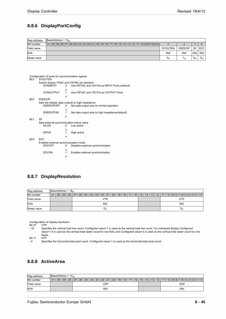
Display Controller Revised 18/4/12
8.8.6 DisplayPortConfig
8.8.7 DisplayResolution
8.8.8 ActiveArea
Reg address BaseAddress + 14H
Bit number 31 30 29 28 27 26 25 24 23 22 21 20 19 18 17 16 15 14 13 12 11 10 9 8 7 6 5 4 3 2 1 0
Field name SYOUTEN ENDDOP SF ESY
R/W RW RW RW RW
Reset value 0H 1H 0H 0H
Configuration of ports for synchronization signals Bit 3 SYOUTEN
Switch display YSNC and VSYNC pin direction SYNINPUT 0
H
Use HSYNC and VSYCN as INPUT Ports (default)
SYNOUTPUT 1
H
Use HSYNC and VSYCN as OUTPUT Ports
Bit 2 ENDDOP Sets the display data outputs to high impedance
ENDDOPOFF 0
H
Set data output pins to normal operation
ENDDOPON 1
H
Set data output pins to high impedance(default)
Bit 1 SF Sets external synchronization active value
NLOG 0
H
Low active
NPOS 1
H
High active
Bit 0 ESY Enables external synchronization mode
ESYOFF 0
H
Disables external synchronization
ESYON 1
H
Enables external synchronization
Reg address BaseAddress + 18H
Bit number 31 30 29 28 27 26 25 24 23 22 21 20 19 18 17 16 15 14 13 12 11 10 9 8 7 6 5 4 3 2 1 0
Field name VTR HTP
R/W RW RW
Reset value 0H 0H
Configuration of display resolution Bit 27 - 16
VTR Specifies the vertical total line count. Configured value+1 is used as the vertical total line count. For interlaced display Configured value+1.5 is used as the vertical total raster count for one field, and Configured value+3 is used as the vertical total raster count for one frame.
Bit 11 - 0
HTP Specifies the horizontal total pixel count. Configured value+1 is used as the horizontal total pixel count
Reg address BaseAddress + 1CH
Bit number 31 30 29 28 27 26 25 24 23 22 21 20 19 18 17 16 15 14 13 12 11 10 9 8 7 6 5 4 3 2 1 0
Field name VDP HDP
R/W RW RW
Fujitsu Semiconductor Europe GmbH 8 - 45
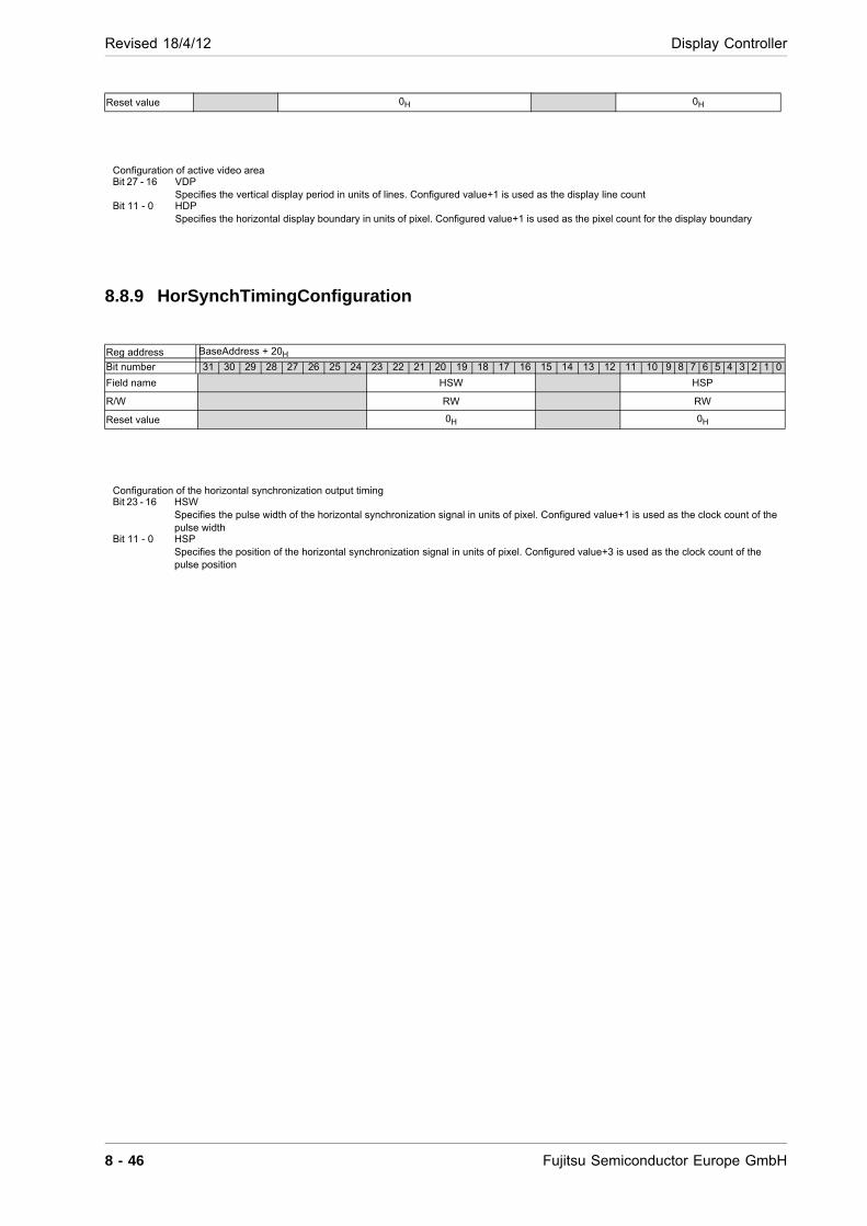
Revised 18/4/12 Display Controller
8.8.9 HorSynchTimingConfiguration
Reset value 0H 0H
Configuration of active video area Bit 27 - 16 VDP
Specifies the vertical display period in units of lines. Configured value+1 is used as the display line count Bit 11 - 0 HDP
Specifies the horizontal display boundary in units of pixel. Configured value+1 is used as the pixel count for the display boundary
Reg address BaseAddress + 20H
Bit number 31 30 29 28 27 26 25 24 23 22 21 20 19 18 17 16 15 14 13 12 11 10 9 8 7 6 5 4 3 2 1 0
Field name HSW HSP
R/W RW RW
Reset value 0H 0H
Configuration of the horizontal synchronization output timing Bit 23 - 16 HSW
Specifies the pulse width of the horizontal synchronization signal in units of pixel. Configured value+1 is used as the clock count of the pulse width
Bit 11 - 0 HSP Specifies the position of the horizontal synchronization signal in units of pixel. Configured value+3 is used as the clock count of the pulse position
8 - 46 Fujitsu Semiconductor Europe GmbH
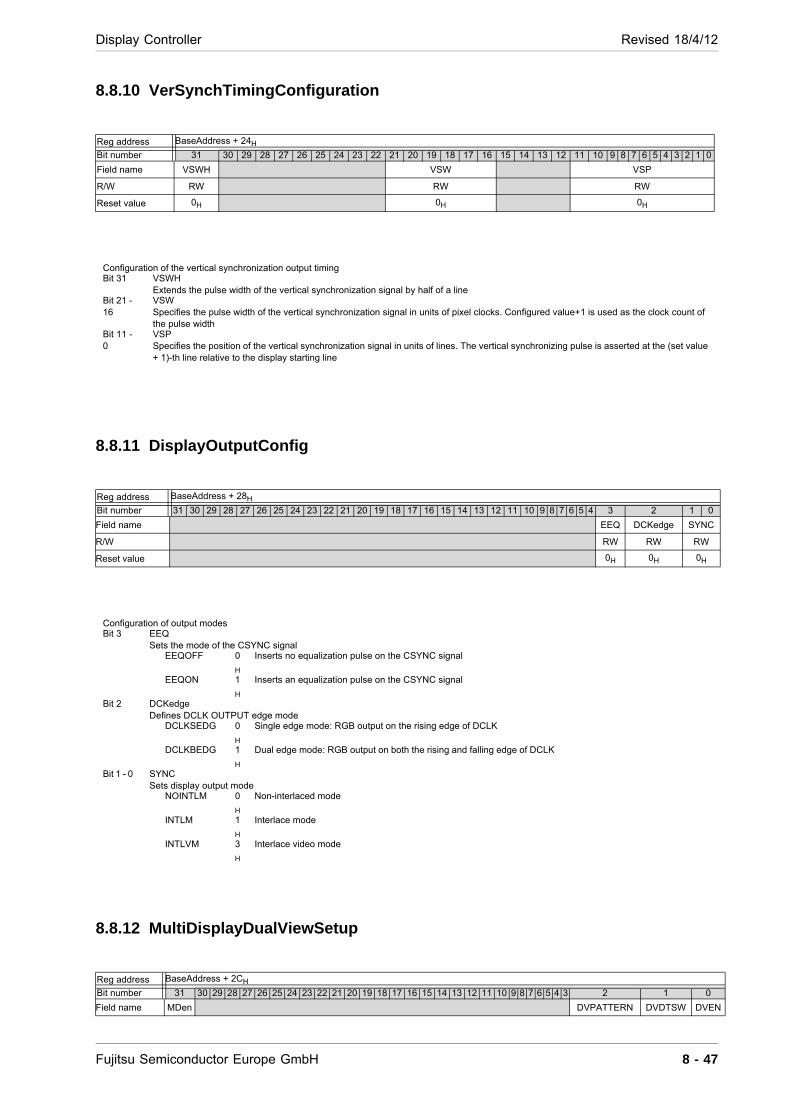
Display Controller Revised 18/4/12
8.8.10 VerSynchTimingConfiguration
8.8.11 DisplayOutputConfig
8.8.12 MultiDisplayDualViewSetup
Reg address BaseAddress + 24H
Bit number 31 30 29 28 27 26 25 24 23 22 21 20 19 18 17 16 15 14 13 12 11 10 9 8 7 6 5 4 3 2 1 0
Field name VSWH VSW VSP
R/W RW RW RW
Reset value 0H 0H 0H
Configuration of the vertical synchronization output timing Bit 31 VSWH
Extends the pulse width of the vertical synchronization signal by half of a line Bit 21 - 16
VSW Specifies the pulse width of the vertical synchronization signal in units of pixel clocks. Configured value+1 is used as the clock count of the pulse width
Bit 11 - 0
VSP Specifies the position of the vertical synchronization signal in units of lines. The vertical synchronizing pulse is asserted at the (set value + 1)-th line relative to the display starting line
Reg address BaseAddress + 28H
Bit number 31 30 29 28 27 26 25 24 23 22 21 20 19 18 17 16 15 14 13 12 11 10 9 8 7 6 5 4 3 2 1 0
Field name EEQ DCKedge SYNC
R/W RW RW RW
Reset value 0H 0H 0H
Configuration of output modes Bit 3 EEQ
Sets the mode of the CSYNC signal EEQOFF 0
H
Inserts no equalization pulse on the CSYNC signal
EEQON 1
H
Inserts an equalization pulse on the CSYNC signal
Bit 2 DCKedge Defines DCLK OUTPUT edge mode
DCLKSEDG 0
H
Single edge mode: RGB output on the rising edge of DCLK
DCLKBEDG 1
H
Dual edge mode: RGB output on both the rising and falling edge of DCLK
Bit 1 - 0 SYNC Sets display output mode
NOINTLM 0
H
Non-interlaced mode
INTLM 1
H
Interlace mode
INTLVM 3
H
Interlace video mode
Reg address BaseAddress + 2CH
Bit number 31 30 29 28 27 26 25 24 23 22 21 20 19 18 17 16 15 14 13 12 11 10 9 8 7 6 5 4 3 2 1 0
Field name MDen DVPATTERN DVDTSW DVEN
Fujitsu Semiconductor Europe GmbH 8 - 47
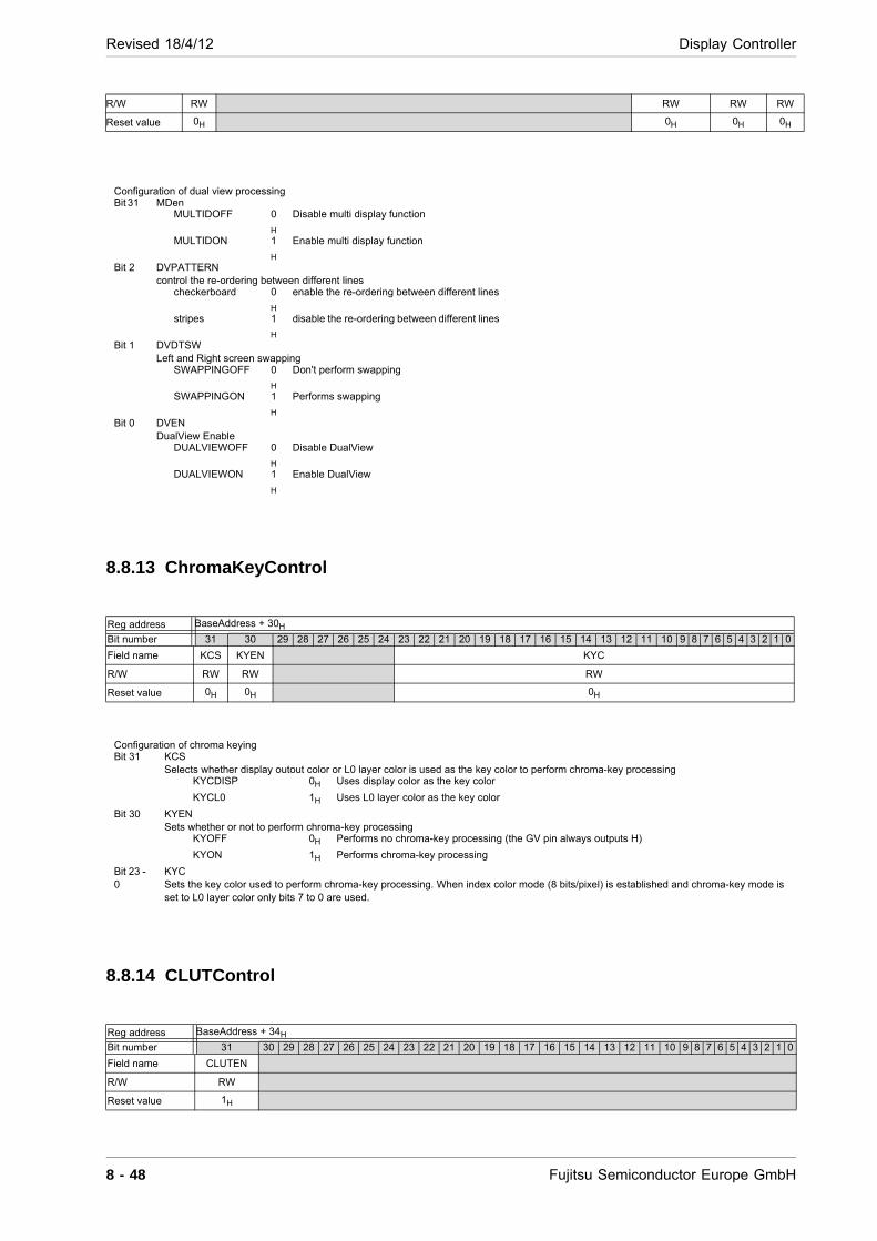
Revised 18/4/12 Display Controller
8.8.13 ChromaKeyControl
8.8.14 CLUTControl
R/W RW RW RW RW
Reset value 0H 0H 0H 0H
Configuration of dual view processing Bit 31 MDen
MULTIDOFF 0
H
Disable multi display function
MULTIDON 1
H
Enable multi display function
Bit 2 DVPATTERN control the re-ordering between different lines
checkerboard 0
H
enable the re-ordering between different lines
stripes 1
H
disable the re-ordering between different lines
Bit 1 DVDTSW Left and Right screen swapping
SWAPPINGOFF 0
H
Don't perform swapping
SWAPPINGON 1
H
Performs swapping
Bit 0 DVEN DualView Enable
DUALVIEWOFF 0
H
Disable DualView
DUALVIEWON 1
H
Enable DualView
Reg address BaseAddress + 30H
Bit number 31 30 29 28 27 26 25 24 23 22 21 20 19 18 17 16 15 14 13 12 11 10 9 8 7 6 5 4 3 2 1 0
Field name KCS KYEN KYC
R/W RW RW RW
Reset value 0H 0H 0H
Configuration of chroma keying Bit 31 KCS
Selects whether display outout color or L0 layer color is used as the key color to perform chroma-key processing KYCDISP 0H Uses display color as the key color
KYCL0 1H Uses L0 layer color as the key color
Bit 30 KYEN Sets whether or not to perform chroma-key processing
KYOFF 0H Performs no chroma-key processing (the GV pin always outputs H)
KYON 1H Performs chroma-key processing
Bit 23 - 0
KYC Sets the key color used to perform chroma-key processing. When index color mode (8 bits/pixel) is established and chroma-key mode is set to L0 layer color only bits 7 to 0 are used.
Reg address BaseAddress + 34H
Bit number 31 30 29 28 27 26 25 24 23 22 21 20 19 18 17 16 15 14 13 12 11 10 9 8 7 6 5 4 3 2 1 0
Field name CLUTEN
R/W RW
Reset value 1H
8 - 48 Fujitsu Semiconductor Europe GmbH
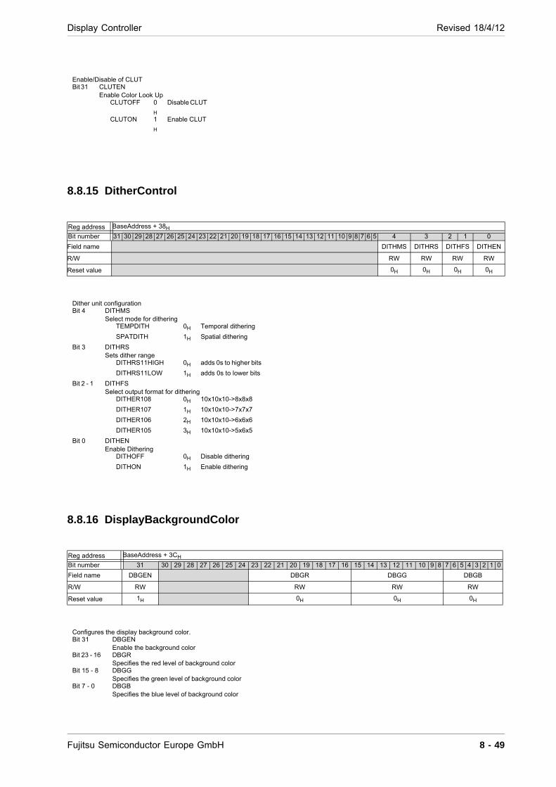
Display Controller Revised 18/4/12
8.8.15 DitherControl
8.8.16 DisplayBackgroundColor
Enable/Disable of CLUT Bit 31 CLUTEN
Enable Color Look Up CLUTOFF 0
H
Disable CLUT
CLUTON 1
H
Enable CLUT
Reg address BaseAddress + 38H
Bit number 31 30 29 28 27 26 25 24 23 22 21 20 19 18 17 16 15 14 13 12 11 10 9 8 7 6 5 4 3 2 1 0
Field name DITHMS DITHRS DITHFS DITHEN
R/W RW RW RW RW
Reset value 0H 0H 0H 0H
Dither unit configuration Bit 4 DITHMS
Select mode for dithering TEMPDITH 0H Temporal dithering
SPATDITH 1H Spatial dithering
Bit 3 DITHRS Sets dither range
DITHRS11HIGH 0H adds 0s to higher bits
DITHRS11LOW 1H adds 0s to lower bits
Bit 2 - 1 DITHFS Select output format for dithering
DITHER108 0H 10x10x10->8x8x8
DITHER107 1H 10x10x10->7x7x7
DITHER106 2H 10x10x10->6x6x6
DITHER105 3H 10x10x10->5x6x5
Bit 0 DITHEN Enable Dithering
DITHOFF 0H Disable dithering
DITHON 1H Enable dithering
Reg address BaseAddress + 3CH
Bit number 31 30 29 28 27 26 25 24 23 22 21 20 19 18 17 16 15 14 13 12 11 10 9 8 7 6 5 4 3 2 1 0
Field name DBGEN DBGR DBGG DBGB
R/W RW RW RW RW
Reset value 1H 0H 0H 0H
Configures the display background color.Bit 31 DBGEN
Enable the background color Bit 23 - 16 DBGR
Specifies the red level of background color Bit 15 - 8 DBGG
Specifies the green level of background color Bit 7 - 0 DBGB
Specifies the blue level of background color
Fujitsu Semiconductor Europe GmbH 8 - 49
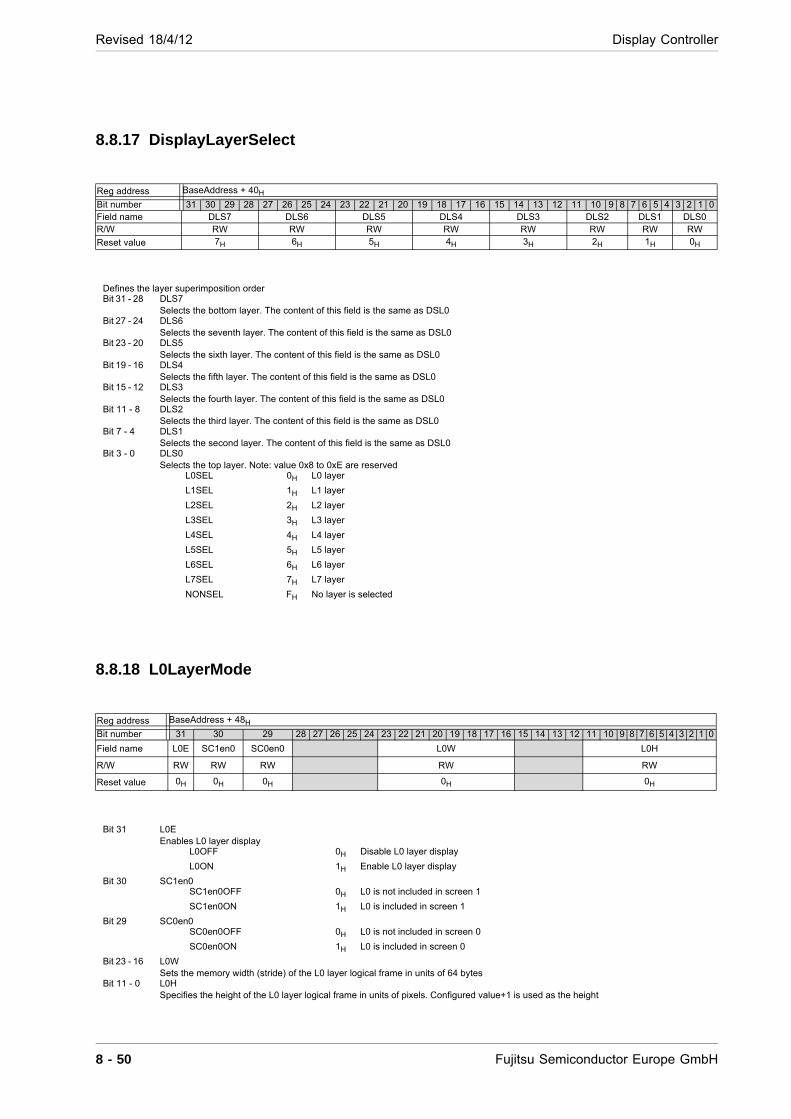
Revised 18/4/12 Display Controller
8.8.17 DisplayLayerSelect
8.8.18 L0LayerMode
Reg address BaseAddress + 40H
Bit number 31 30 29 28 27 26 25 24 23 22 21 20 19 18 17 16 15 14 13 12 11 10 9 8 7 6 5 4 3 2 1 0Field name DLS7 DLS6 DLS5 DLS4 DLS3 DLS2 DLS1 DLS0 R/W RW RW RW RW RW RW RW RW
Reset value 7H 6H 5H 4H 3H 2H 1H 0H
Defines the layer superimposition order Bit 31 - 28 DLS7
Selects the bottom layer. The content of this field is the same as DSL0 Bit 27 - 24 DLS6
Selects the seventh layer. The content of this field is the same as DSL0 Bit 23 - 20 DLS5
Selects the sixth layer. The content of this field is the same as DSL0 Bit 19 - 16 DLS4
Selects the fifth layer. The content of this field is the same as DSL0 Bit 15 - 12 DLS3
Selects the fourth layer. The content of this field is the same as DSL0 Bit 11 - 8 DLS2
Selects the third layer. The content of this field is the same as DSL0 Bit 7 - 4 DLS1
Selects the second layer. The content of this field is the same as DSL0 Bit 3 - 0 DLS0
Selects the top layer. Note: value 0x8 to 0xE are reserved L0SEL 0H L0 layer
L1SEL 1H L1 layer
L2SEL 2H L2 layer
L3SEL 3H L3 layer
L4SEL 4H L4 layer
L5SEL 5H L5 layer
L6SEL 6H L6 layer
L7SEL 7H L7 layer
NONSEL FH No layer is selected
Reg address BaseAddress + 48H
Bit number 31 30 29 28 27 26 25 24 23 22 21 20 19 18 17 16 15 14 13 12 11 10 9 8 7 6 5 4 3 2 1 0
Field name L0E SC1en0 SC0en0 L0W L0H
R/W RW RW RW RW RW
Reset value 0H 0H 0H 0H 0H
Bit 31 L0E Enables L0 layer display
L0OFF 0H Disable L0 layer display
L0ON 1H Enable L0 layer display
Bit 30 SC1en0 SC1en0OFF 0H L0 is not included in screen 1
SC1en0ON 1H L0 is included in screen 1
Bit 29 SC0en0 SC0en0OFF 0H L0 is not included in screen 0
SC0en0ON 1H L0 is included in screen 0
Bit 23 - 16 L0W Sets the memory width (stride) of the L0 layer logical frame in units of 64 bytes
Bit 11 - 0 L0H Specifies the height of the L0 layer logical frame in units of pixels. Configured value+1 is used as the height
8 - 50 Fujitsu Semiconductor Europe GmbH
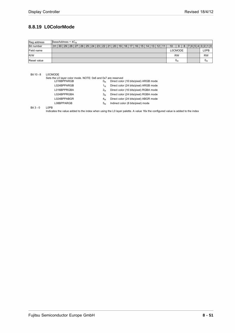
Display Controller Revised 18/4/12
8.8.19 L0ColorMode
Reg address BaseAddress + 4CH
Bit number 31 30 29 28 27 26 25 24 23 22 21 20 19 18 17 16 15 14 13 12 11 10 9 8 7 6 5 4 3 2 1 0
Field name L0CMODE L0PB
R/W RW RW
Reset value 0H 0H
Bit 10 - 8 L0CMODE Sets the L0 layer color mode. NOTE: 0x6 and 0x7 are reserved
L016BPPARGB 0H Direct color (16 bits/pixel) ARGB mode
L024BPPARGB 1H Direct color (24 bits/pixel) ARGB mode
L016BPPRGBA 2H Direct color (16 bits/pixel) RGBA mode
L024BPPRGBA 3H Direct color (24 bits/pixel) RGBA mode
L024BPPABGR 4H Direct color (24 bits/pixel) ABGR mode
L08BPPARGB 5H Indirect color (8 bits/pixel) mode
Bit 3 - 0 L0PB Indicates the value added to the index when using the L0 layer palette. A value 16x the configured value is added to the index
Fujitsu Semiconductor Europe GmbH 8 - 51

Revised 18/4/12 Display Controller
8.8.20 L0OriginAddress
8.8.21 L0DisplayAddress
8.8.22 L0DisplayPosition
Reg address BaseAddress + 50H
Bit number 31 30 29 28 27 26 25 24 23 22 21 20 19 18 17 16 15 14 13 12 11 10 9 8 7 6 5 4 3 2 1 0
Field name L0OA0
R/W RW
Reset value 0H
Bit 27 - 0 L0OA0 Sets the logical frame origin address of the L0 layer. The lower 4 bits are fixed to 0 (16-byte aligned)
Reg address BaseAddress + 54H
Bit number 31 30 29 28 27 26 25 24 23 22 21 20 19 18 17 16 15 14 13 12 11 10 9 8 7 6 5 4 3 2 1 0
Field name L0DA0
R/W RW
Reset value 0H
Bit 27 - 0 L0DA0 Sets the display window origin address of the L0 layer. Address has to be 16-byte aligned
Reg address BaseAddress + 58H
Bit number 31 30 29 28 27 26 25 24 23 22 21 20 19 18 17 16 15 14 13 12 11 10 9 8 7 6 5 4 3 2 1 0
Field name L0DY L0DX
R/W RW RW
Reset value 0H 0H
Sets the display position coordinates (DX,DY) of the L0 layer. The origin is the upper left point of the displayed screen. Bit 27 - 16 L0DY
Specifies the DY coordinate Bit 11 - 0 L0DX
Specifies the DX coordinate
8 - 52 Fujitsu Semiconductor Europe GmbH
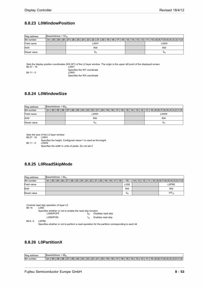
Display Controller Revised 18/4/12
8.8.23 L0WindowPosition
8.8.24 L0WindowSize
8.8.25 L0ReadSkipMode
8.8.26 L0PartitionX
Reg address BaseAddress + 5CH
Bit number 31 30 29 28 27 26 25 24 23 22 21 20 19 18 17 16 15 14 13 12 11 10 9 8 7 6 5 4 3 2 1 0
Field name L0WY L0WX
R/W RW RW
Reset value 0H 0H
Sets the display position coordinates (WX,WY) of the L0 layer window. The origin is the upper left point of the displayed screen. Bit 27 - 16 L0WY
Specifies the WY coordinate Bit 11 - 0 L0WX
Specifies the WX coordinate
Reg address BaseAddress + 60H
Bit number 31 30 29 28 27 26 25 24 23 22 21 20 19 18 17 16 15 14 13 12 11 10 9 8 7 6 5 4 3 2 1 0
Field name L0WH L0WW
R/W RW RW
Reset value 0H 0H
Sets the size of the L0 layer window Bit 27 - 16 L0WH
Specifies the height. Configured value+1 is used as the height. Bit 11 - 0 L0WW
Specifies the width in units of pixels. Do not set 0
Reg address BaseAddress + 64H
Bit number 31 30 29 28 27 26 25 24 23 22 21 20 19 18 17 16 15 14 13 12 11 10 9 8 7 6 5 4 3 2 1 0
Field name L0SE L0PRE
R/W RW RW
Reset value 0H 1FFH
Controls read skip operation of layer L0 Bit 15 L0SE
Specifies whether or not to enable the read skip function L0SKIPOFF 0H Disables read skip
L0SKIPON 1H Enables read skip
Bit 8 - 0 L0PRE Specifies whether or not to perform a read operation for the partition corresponding to each bit
Reg address BaseAddress + 68H
Bit number 31 30 29 28 27 26 25 24 23 22 21 20 19 18 17 16 15 14 13 12 11 10 9 8 7 6 5 4 3 2 1 0
Fujitsu Semiconductor Europe GmbH 8 - 53
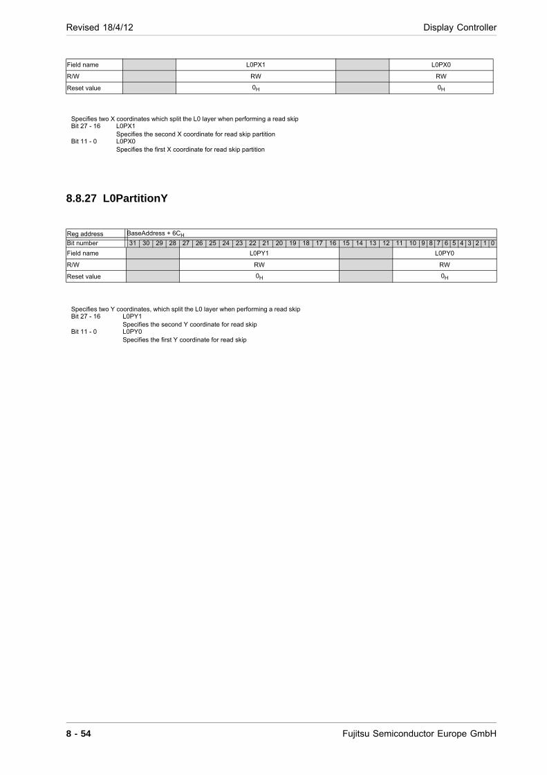
Revised 18/4/12 Display Controller
8.8.27 L0PartitionY
Field name L0PX1 L0PX0
R/W RW RW
Reset value 0H 0H
Specifies two X coordinates which split the L0 layer when performing a read skip Bit 27 - 16 L0PX1
Specifies the second X coordinate for read skip partition Bit 11 - 0 L0PX0
Specifies the first X coordinate for read skip partition
Reg address BaseAddress + 6CH
Bit number 31 30 29 28 27 26 25 24 23 22 21 20 19 18 17 16 15 14 13 12 11 10 9 8 7 6 5 4 3 2 1 0
Field name L0PY1 L0PY0
R/W RW RW
Reset value 0H 0H
Specifies two Y coordinates, which split the L0 layer when performing a read skip Bit 27 - 16 L0PY1
Specifies the second Y coordinate for read skip Bit 11 - 0 L0PY0
Specifies the first Y coordinate for read skip
8 - 54 Fujitsu Semiconductor Europe GmbH
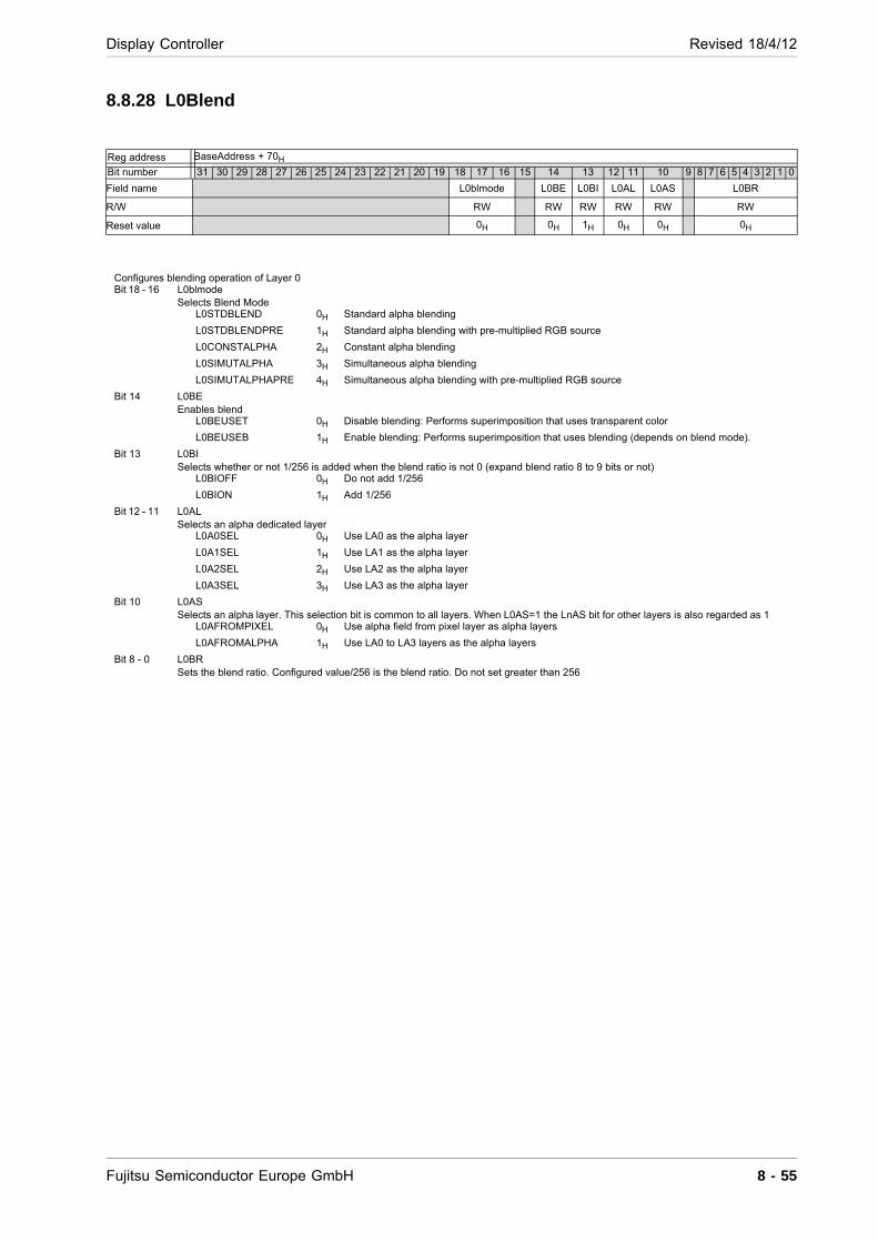
Display Controller Revised 18/4/12
8.8.28 L0Blend
Reg address BaseAddress + 70H
Bit number 31 30 29 28 27 26 25 24 23 22 21 20 19 18 17 16 15 14 13 12 11 10 9 8 7 6 5 4 3 2 1 0
Field name L0blmode L0BE L0BI L0AL L0AS L0BR
R/W RW RW RW RW RW RW
Reset value 0H 0H 1H 0H 0H 0H
Configures blending operation of Layer 0 Bit 18 - 16 L0blmode
Selects Blend Mode L0STDBLEND 0H Standard alpha blending
L0STDBLENDPRE 1H Standard alpha blending with pre-multiplied RGB source
L0CONSTALPHA 2H Constant alpha blending
L0SIMUTALPHA 3H Simultaneous alpha blending
L0SIMUTALPHAPRE 4H Simultaneous alpha blending with pre-multiplied RGB source
Bit 14 L0BE Enables blend
L0BEUSET 0H Disable blending: Performs superimposition that uses transparent color
L0BEUSEB 1H Enable blending: Performs superimposition that uses blending (depends on blend mode).
Bit 13 L0BI Selects whether or not 1/256 is added when the blend ratio is not 0 (expand blend ratio 8 to 9 bits or not)
L0BIOFF 0H Do not add 1/256
L0BION 1H Add 1/256
Bit 12 - 11 L0AL Selects an alpha dedicated layer
L0A0SEL 0H Use LA0 as the alpha layer
L0A1SEL 1H Use LA1 as the alpha layer
L0A2SEL 2H Use LA2 as the alpha layer
L0A3SEL 3H Use LA3 as the alpha layer
Bit 10 L0AS Selects an alpha layer. This selection bit is common to all layers. When L0AS=1 the LnAS bit for other layers is also regarded as 1
L0AFROMPIXEL 0H Use alpha field from pixel layer as alpha layers
L0AFROMALPHA 1H Use LA0 to LA3 layers as the alpha layers
Bit 8 - 0 L0BR Sets the blend ratio. Configured value/256 is the blend ratio. Do not set greater than 256
Fujitsu Semiconductor Europe GmbH 8 - 55
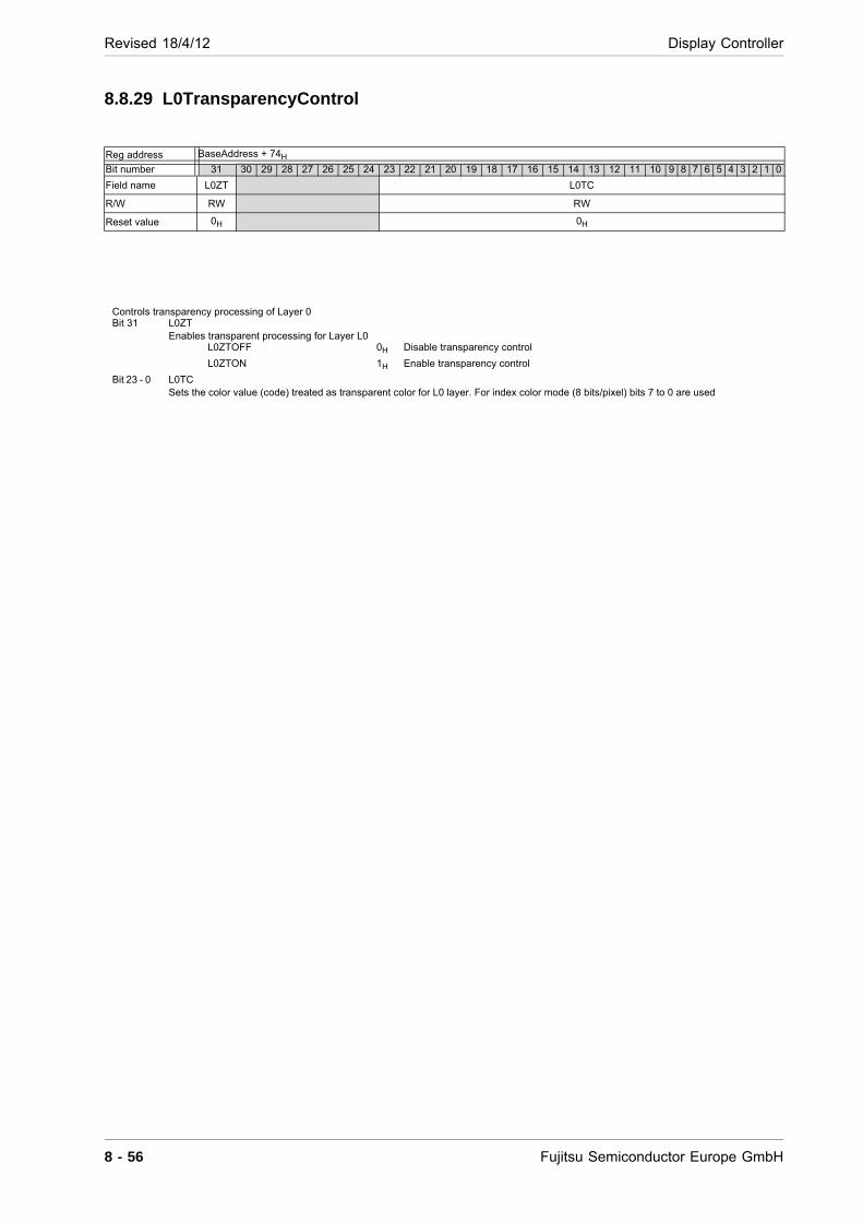
Revised 18/4/12 Display Controller
8.8.29 L0TransparencyControl
Reg address BaseAddress + 74H
Bit number 31 30 29 28 27 26 25 24 23 22 21 20 19 18 17 16 15 14 13 12 11 10 9 8 7 6 5 4 3 2 1 0
Field name L0ZT L0TC
R/W RW RW
Reset value 0H 0H
Controls transparency processing of Layer 0 Bit 31 L0ZT
Enables transparent processing for Layer L0 L0ZTOFF 0H Disable transparency control
L0ZTON 1H Enable transparency control
Bit 23 - 0 L0TC Sets the color value (code) treated as transparent color for L0 layer. For index color mode (8 bits/pixel) bits 7 to 0 are used
8 - 56 Fujitsu Semiconductor Europe GmbH

Display Controller Revised 18/4/12
8.8.30 L1LayerMode
8.8.31 L1ColorMode
Reg address BaseAddress + 78H
Bit number 31 30 29 28 27 26 25 24 23 22 21 20 19 18 17 16 15 14 13 12 11 10 9 8 7 6 5 4 3 2 1 0
Field name L1E SC1en1 SC0en1 L1ENBWAUTO L1YC L1CS L1INTL L1VMAG L1W
R/W RW RW RW RW RW RW RW RW RW
Reset value 0H 0H 0H 0H 0H 0H 0H 0H 0H
Bit 31
L1E Enables L1 layer display
L1OFF 0
H
Disable L1 layer display
L1ON 1
H
Enable L1 layer display
Bit 30
SC1en1
SC1en1OFF 0
H
L1 is not included in screen 1
SC1en1ON 1
H
L1 is included in screen 1
Bit 29
SC0en1
SC0en1OFF 0
H
L1 is not included in screen 0
SC0en1ON 1
H
L1 is included in screen 0
Bit 20
L1ENBWAUTO set a automatic video capture operation mode when L1CS is in capture mode
L1ENBWAUTOOFF 0
H
No automatic mode. video capture operation mode depends on the L1INTL field only
L1ENBWAUTOON 1
H
Automatic Buffer managment in BOB or WAEVE mode
Bit 19
L1YC Sets the L1 layer color format
L1RGBMODE 0
H
RGB mode
L1YCMODE 1
H
YC mode
Bit 18
L1CS Sets whether to use the L1 layer as a normal display layer or as a video capture layer
L1VCOFF 0
H
Normal mode
L1VCON 1
H
Video Capture mode
Bit 17
L1INTL Sets a video capture operation mode when L1CS is in capture mode
L1INTLOFF 0
H
Normal mode
L1INTLON 1
H
For non-interlaced display, displays in WEAVE mode. For interlaced display and interlaced video display, handles buffer management in units of frames (a frame consists of a pair of odd and even fields)
Bit 16
L1VMAG Enables/disables capture image upscaling
L1UPSCOFF 0
H
Disable upscaling
L1UPSCON 1
H
Enable upscaling
Bit 7 - 0
L1W Sets the memory width (stride) of the L1 layer logical frame in units of 64 bytes
Reg address BaseAddress + 7CH
Bit number 31 30 29 28 27 26 25 24 23 22 21 20 19 18 17 16 15 14 13 12 11 10 9 8 7 6 5 4 3 2 1 0
Field name L1CMODE L1PB
R/W RW RW
Reset value 0H 0H
Fujitsu Semiconductor Europe GmbH 8 - 57

Revised 18/4/12 Display Controller
8.8.32 L1DisplayAddress
8.8.33 Capture1BufferDisplayAddress0
8.8.34 Capture1BufferDisplayAddress1
Bit 10 - 8 L1CMODE Sets the L1 layer color mode. NOTE: 0x6 .. 0x7 are reserved
L116BPPARGB 0H Direct color (16 bits/pixel) ARGB mode
L124BPPARGB 1H Direct color (24 bits/pixel) ARGB mode
L116BPPRGBA 2H Direct color (16 bits/pixel) RGBA mode
L124BPPRGBA 3H Direct color (24 bits/pixel) RGBA mode
L124BPPABGR 4H Direct color (24 bits/pixel) ABGR mode
L18BPPARGB 5H Indirect color (8 bits/pixel) mode
Bit 3 - 0 L1PB Indicates the value to be added to the index when drawing the L1 layer palette. A value 16 times the configured value is added to the index
Reg address BaseAddress + 80H
Bit number 31 30 29 28 27 26 25 24 23 22 21 20 19 18 17 16 15 14 13 12 11 10 9 8 7 6 5 4 3 2 1 0
Field name L1DA
R/W RW
Reset value 0H
Bit 27 - 0 L1DA Sets the display window origin address of the L1 layer. Address has to be 16-byte aligned
Reg address BaseAddress + 84H
Bit number 31 30 29 28 27 26 25 24 23 22 21 20 19 18 17 16 15 14 13 12 11 10 9 8 7 6 5 4 3 2 1 0
Field name L1CBDA0
R/W R
Reset value X
Bit 27 - 0
L1CBDA0 This register is a read-only register which can be accessed when the L1M register L1CS bit is 1. This register indicates the starting address of the displayed capture image. When the L1CS bit is 1 and the L1IM bit is also 1, this register indicates the starting address of an odd field of the capture screen.
Reg address BaseAddress + 88H
Bit number 31 30 29 28 27 26 25 24 23 22 21 20 19 18 17 16 15 14 13 12 11 10 9 8 7 6 5 4 3 2 1 0
Field name L1CBDA1
R/W R
Reset value X
Bit 27 - 0
L1CBDA1 This register is a read-only register which is only enabled when the L1CS bit is 1 and the L1IM bit is also 1. This register indicates the starting address of an even field of the capture screen.
8 - 58 Fujitsu Semiconductor Europe GmbH

Display Controller Revised 18/4/12
8.8.35 L1WindowPosition
8.8.36 L1WindowSize
8.8.37 L1Blend
Reg address BaseAddress + 8CH
Bit number 31 30 29 28 27 26 25 24 23 22 21 20 19 18 17 16 15 14 13 12 11 10 9 8 7 6 5 4 3 2 1 0
Field name L1WY L1WX
R/W RW RW
Reset value 0H 0H
Bit 27 - 16 L1WY Sets the display position coordinates (WY) of the L1 layer window. The origin is the upper left point of the display screen
Bit 11 - 0 L1WX Sets the display position coordinates (WX) of the L1 layer window. The origin is the upper left point of the display screen
Reg address BaseAddress + 90H
Bit number 31 30 29 28 27 26 25 24 23 22 21 20 19 18 17 16 15 14 13 12 11 10 9 8 7 6 5 4 3 2 1 0
Field name L1WH L1WW
R/W RW RW
Reset value 0H 0H
Bit 27 - 16 L1WH Sets the size of the L1 layer window. Specifies the height. Configured value+1 is used as the height.
Bit 11 - 0 L1WW Sets the size of the L1 layer window. Specifies the width in units of pixels. Do not set 0
Reg address BaseAddress + 9CH
Bit number 31 30 29 28 27 26 25 24 23 22 21 20 19 18 17 16 15 14 13 12 11 10 9 8 7 6 5 4 3 2 1 0
Field name L1blmode L1BE L1BI L1AL L1AS L1BR
R/W RW RW RW RW RW RW
Reset value 0H 0H 1H 0H 0H 0H
Configures blending operation of Layer 1 Bit 18 - 16 L1blmode
Selects Blend Mode L1STDBLEND 0H Standard alpha blending
L1STDBLENDPRE 1H Standard alpha blending with pre-multiplied RGB source
L1CONSTALPHA 2H Constant alpha blending
L1SIMUTALPHA 3H Simultaneous alpha blending
L1SIMUTALPHAPRE 4H Simultaneous alpha blending with pre-multiplied RGB source
Bit 14 L1BE Enables blend
L1BEUSET 0H Disable blending: Performs superimposition that uses transparent color
L1BEUSEB 1H Enable blending: Performs superimposition that uses blending (depends on blend mode).
Bit 13 L1BI Selects whether or not 1/256 is added when the blend ratio is not 0 (expand blend ratio 8 to 9 bits or not)
Fujitsu Semiconductor Europe GmbH 8 - 59
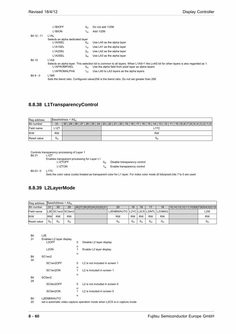
Revised 18/4/12 Display Controller
8.8.38 L1TransparencyControl
8.8.39 L2LayerMode
L1BIOFF 0H Do not add 1/256
L1BION 1H Add 1/256
Bit 12 - 11 L1AL Selects an alpha dedicated layer
L1A0SEL 0H Use LA0 as the alpha layer
L1A1SEL 1H Use LA1 as the alpha layer
L1A2SEL 2H Use LA2 as the alpha layer
L1A3SEL 3H Use LA3 as the alpha layer
Bit 10 L1AS Selects an alpha layer. This selection bit is common to all layers. When L1AS=1 the LnAS bit for other layers is also regarded as 1.
L1AFROMPIXEL 0H Use the alpha field from pixel layer as alpha layers
L1AFROMALPHA 1H Use LA0 to LA3 layers as the alpha layers
Bit 8 - 0 L1BR Sets the blend ratio. Configured value/256 is the blend ratio. Do not set greater than 256
Reg address BaseAddress + A0H
Bit number 31 30 29 28 27 26 25 24 23 22 21 20 19 18 17 16 15 14 13 12 11 10 9 8 7 6 5 4 3 2 1 0
Field name L1ZT L1TC
R/W RW RW
Reset value 0H 0H
Controls transparency processing of Layer 1 Bit 31 L1ZT
Enables transparent processing for Layer L1 L1ZTOFF 0H Disable transparency control
L1ZTON 1H Enable transparency control
Bit 23 - 0 L1TC Sets the color value (code) treated as transparent color for L1 layer. For index color mode (8 bits/pixel) bits 7 to 0 are used
Reg address BaseAddress + A4H
Bit number 31 30 29 28 27 26 25 24 23 22 21 20 19 18 17 16 15 14 13 12 11 10 9 8 7 6 5 4 3 2 1 0
Field name L2E SC1en2 SC0en2 L2ENBWAUTO L2YC L2CS L2INTL L2VMAG L2W
R/W RW RW RW RW RW RW RW RW RW
Reset value 0H 0H 0H 0H 0H 0H 0H 0H 0H
Bit 31
L2E Enables L2 layer display
L2OFF 0
H
Disable L2 layer display
L2ON 1
H
Enable L2 layer display.
Bit 30
SC1en2
SC1en2OFF 0
H
L2 is not included in screen 1
SC1en2ON 1
H
L2 is included in screen 1
Bit 29
SC0en2
SC0en2OFF 0
H
L2 is not included in screen 0
SC0en2ON 1
H
L2 is included in screen 0
Bit 20
L2ENBWAUTO set a automatic video capture operation mode when L2CS is in capture mode
8 - 60 Fujitsu Semiconductor Europe GmbH
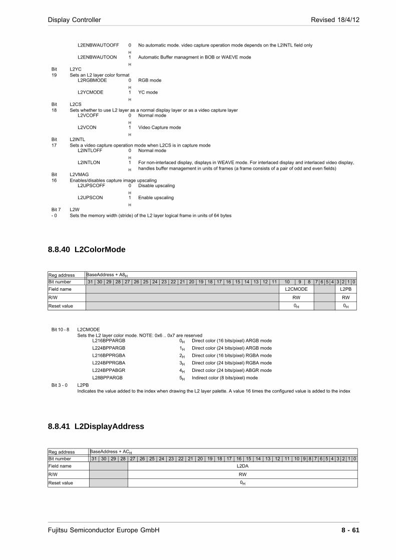
Display Controller Revised 18/4/12
8.8.40 L2ColorMode
8.8.41 L2DisplayAddress
L2ENBWAUTOOFF 0
H
No automatic mode. video capture operation mode depends on the L2INTL field only
L2ENBWAUTOON 1
H
Automatic Buffer managment in BOB or WAEVE mode
Bit 19
L2YC Sets an L2 layer color format
L2RGBMODE 0
H
RGB mode
L2YCMODE 1
H
YC mode
Bit 18
L2CS Sets whether to use L2 layer as a normal display layer or as a video capture layer
L2VCOFF 0
H
Normal mode
L2VCON 1
H
Video Capture mode
Bit 17
L2INTL Sets a video capture operation mode when L2CS is in capture mode
L2INTLOFF 0
H
Normal mode
L2INTLON 1
H
For non-interlaced display, displays in WEAVE mode. For interlaced display and interlaced video display, handles buffer management in units of frames (a frame consists of a pair of odd and even fields)
Bit 16
L2VMAG Enables/disables capture image upscaling
L2UPSCOFF 0
H
Disable upscaling
L2UPSCON 1
H
Enable upscaling
Bit 7 - 0
L2W Sets the memory width (stride) of the L2 layer logical frame in units of 64 bytes
Reg address BaseAddress + A8H
Bit number 31 30 29 28 27 26 25 24 23 22 21 20 19 18 17 16 15 14 13 12 11 10 9 8 7 6 5 4 3 2 1 0
Field name L2CMODE L2PB
R/W RW RW
Reset value 0H 0H
Bit 10 - 8 L2CMODE Sets the L2 layer color mode. NOTE: 0x6 .. 0x7 are reserved
L216BPPARGB 0H Direct color (16 bits/pixel) ARGB mode
L224BPPARGB 1H Direct color (24 bits/pixel) ARGB mode
L216BPPRGBA 2H Direct color (16 bits/pixel) RGBA mode
L224BPPRGBA 3H Direct color (24 bits/pixel) RGBA mode
L224BPPABGR 4H Direct color (24 bits/pixel) ABGR mode
L28BPPARGB 5H Indirect color (8 bits/pixel) mode
Bit 3 - 0 L2PB Indicates the value added to the index when drawing the L2 layer palette. A value 16 times the configured value is added to the index
Reg address BaseAddress + ACH
Bit number 31 30 29 28 27 26 25 24 23 22 21 20 19 18 17 16 15 14 13 12 11 10 9 8 7 6 5 4 3 2 1 0
Field name L2DA
R/W RW
Reset value 0H
Fujitsu Semiconductor Europe GmbH 8 - 61

Revised 18/4/12 Display Controller
8.8.42 Capture2BufferDisplayAddress0
8.8.43 Capture2BufferDisplayAddress1
8.8.44 L2WindowPosition
Bit 27 - 0 L2DA Sets the display window origin address of the L2 layer. Address has to be 16-byte aligned
Reg address BaseAddress + B0H
Bit number 31 30 29 28 27 26 25 24 23 22 21 20 19 18 17 16 15 14 13 12 11 10 9 8 7 6 5 4 3 2 1 0
Field name L2CBDA0
R/W R
Reset value X
Bit 27 - 0
L2CBDA0 This register is a read-only register which can be accessed when the L2M register L2CS bit is 1. This register indicates the starting address of the displayed capture image. When the L2CS bit is 1 and the L2IM bit is also 1, this register indicates the starting address of an odd field of the capture screen.
Reg address BaseAddress + B4H
Bit number 31 30 29 28 27 26 25 24 23 22 21 20 19 18 17 16 15 14 13 12 11 10 9 8 7 6 5 4 3 2 1 0
Field name L2CBDA1
R/W R
Reset value X
Bit 27 - 0
L2CBDA1 This register is a read-only register which is only enabled when the L2CS bit is 1 and the L2IM bit is also 1. This register indicates the starting address of an even field of the capture screen.
Reg address BaseAddress + B8H
Bit number 31 30 29 28 27 26 25 24 23 22 21 20 19 18 17 16 15 14 13 12 11 10 9 8 7 6 5 4 3 2 1 0
Field name L2WY L2WX
R/W RW RW
Reset value 0H 0H
Bit 27 - 16 L2WY Sets the display position coordinates (WY) of the L2 layer window. The origin is the upper left point of the display screen
Bit 11 - 0 L2WX Sets the display position coordinates (WX) of the L2 layer window. The origin is the upper left point of the display screen
8 - 62 Fujitsu Semiconductor Europe GmbH

Display Controller Revised 18/4/12
8.8.45 L2WindowSize
Reg address BaseAddress + BCH
Bit number 31 30 29 28 27 26 25 24 23 22 21 20 19 18 17 16 15 14 13 12 11 10 9 8 7 6 5 4 3 2 1 0
Field name L2WH L2WW
R/W RW RW
Reset value 0H 0H
Bit 27 - 16 L2WH Sets the size of the L2 layer window. Specifies the height. Configured value+1 is used as the height.
Bit 11 - 0 L2WW Sets the size of the L2 layer window. Specifies the width in units of pixels. Do not set 0
Fujitsu Semiconductor Europe GmbH 8 - 63
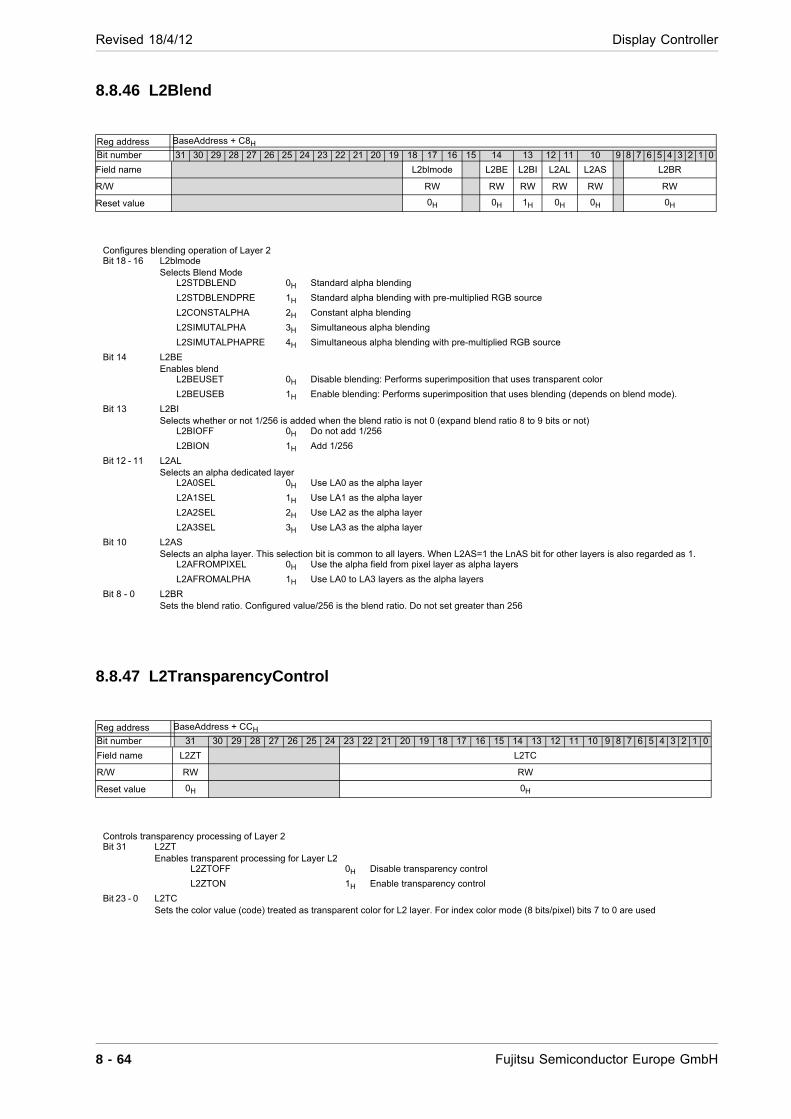
Revised 18/4/12 Display Controller
8.8.46 L2Blend
8.8.47 L2TransparencyControl
Reg address BaseAddress + C8H
Bit number 31 30 29 28 27 26 25 24 23 22 21 20 19 18 17 16 15 14 13 12 11 10 9 8 7 6 5 4 3 2 1 0
Field name L2blmode L2BE L2BI L2AL L2AS L2BR
R/W RW RW RW RW RW RW
Reset value 0H 0H 1H 0H 0H 0H
Configures blending operation of Layer 2 Bit 18 - 16 L2blmode
Selects Blend Mode L2STDBLEND 0H Standard alpha blending
L2STDBLENDPRE 1H Standard alpha blending with pre-multiplied RGB source
L2CONSTALPHA 2H Constant alpha blending
L2SIMUTALPHA 3H Simultaneous alpha blending
L2SIMUTALPHAPRE 4H Simultaneous alpha blending with pre-multiplied RGB source
Bit 14 L2BE Enables blend
L2BEUSET 0H Disable blending: Performs superimposition that uses transparent color
L2BEUSEB 1H Enable blending: Performs superimposition that uses blending (depends on blend mode).
Bit 13 L2BI Selects whether or not 1/256 is added when the blend ratio is not 0 (expand blend ratio 8 to 9 bits or not)
L2BIOFF 0H Do not add 1/256
L2BION 1H Add 1/256
Bit 12 - 11 L2AL Selects an alpha dedicated layer
L2A0SEL 0H Use LA0 as the alpha layer
L2A1SEL 1H Use LA1 as the alpha layer
L2A2SEL 2H Use LA2 as the alpha layer
L2A3SEL 3H Use LA3 as the alpha layer
Bit 10 L2AS Selects an alpha layer. This selection bit is common to all layers. When L2AS=1 the LnAS bit for other layers is also regarded as 1.
L2AFROMPIXEL 0H Use the alpha field from pixel layer as alpha layers
L2AFROMALPHA 1H Use LA0 to LA3 layers as the alpha layers
Bit 8 - 0 L2BR Sets the blend ratio. Configured value/256 is the blend ratio. Do not set greater than 256
Reg address BaseAddress + CCH
Bit number 31 30 29 28 27 26 25 24 23 22 21 20 19 18 17 16 15 14 13 12 11 10 9 8 7 6 5 4 3 2 1 0
Field name L2ZT L2TC
R/W RW RW
Reset value 0H 0H
Controls transparency processing of Layer 2 Bit 31 L2ZT
Enables transparent processing for Layer L2 L2ZTOFF 0H Disable transparency control
L2ZTON 1H Enable transparency control
Bit 23 - 0 L2TC Sets the color value (code) treated as transparent color for L2 layer. For index color mode (8 bits/pixel) bits 7 to 0 are used
8 - 64 Fujitsu Semiconductor Europe GmbH

Display Controller Revised 18/4/12
8.8.48 L3LayerMode
8.8.49 L3ColorMode
Reg address BaseAddress + D0H
Bit number 31 30 29 28 27 26 25 24 23 22 21 20 19 18 17 16 15 14 13 12 11 10 9 8 7 6 5 4 3 2 1 0
Field name L3E SC1en3 SC0en3 L3ENBWAUTO L3YC L3CS L3INTL L3VMAG L3W
R/W RW RW RW RW RW RW RW RW RW
Reset value 0H 0H 0H 0H 0H 0H 0H 0H 0H
Bit 31
L3E Enables L3 layer display
L3OFF 0
H
Disable L3 layer display
L3ON 1
H
Enable L3 layer display
Bit 30
SC1en3
SC1en3OFF 0
H
L3 is not included in screen 1
SC1en3ON 1
H
L3 is included in screen 1
Bit 29
SC0en3
SC0en3OFF 0
H
L3 is not included in screen 0
SC0en3ON 1
H
L3 is included in screen 0
Bit 20
L3ENBWAUTO set a automatic video capture operation mode when L3CS is in capture mode
L3ENBWAUTOOFF 0
H
No automatic mode. video capture operation mode depends on the L3INTL field only
L3ENBWAUTOON 1
H
Automatic Buffer managment in BOB or WAEVE mode
Bit 19
L3YC Sets an L3 layer color format
L3RGBMODE 0
H
RGB mode
L3YCMODE 1
H
YC mode
Bit 18
L3CS Sets whether to use L3 layer as a normal display layer or as a video capture layer
L3VCOFF 0
H
Normal mode
L3VCON 1
H
Video Capture mode
Bit 17
L3INTL Sets a video capture operation mode when L3CS is in capture mode
L3INTLOFF 0
H
Normal mode
L3INTLON 1
H
For non-interlaced display, displays in WEAVE mode. For interlaced display and interlaced video display, handles buffer management in units of frames (a frame consists of a pair of odd and even fields)
Bit 16
L3VMAG Enables/disables capture image upscaling
L3UPSCOFF 0
H
Disable upscaling
L3UPSCON 1
H
Enable upscaling
Bit 7 - 0
L3W Sets the memory width (stride) of the L3 layer logical frame in units of 64 bytes
Reg address BaseAddress + D4H
Bit number 31 30 29 28 27 26 25 24 23 22 21 20 19 18 17 16 15 14 13 12 11 10 9 8 7 6 5 4 3 2 1 0
Field name L3CMODE L3PB
R/W RW RW
Reset value 0H 0H
Fujitsu Semiconductor Europe GmbH 8 - 65
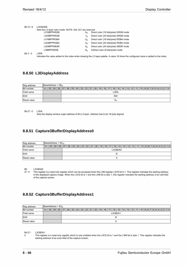
Revised 18/4/12 Display Controller
8.8.50 L3DisplayAddress
8.8.51 Capture3BufferDisplayAddress0
8.8.52 Capture3BufferDisplayAddress1
Bit 10 - 8 L3CMODE Sets the L3 layer color mode. NOTE: 0x6..0x7 are reserved
L316BPPARGB 0H Direct color (16 bits/pixel) ARGB mode
L324BPPARGB 1H Direct color (24 bits/pixel) ARGB mode
L316BPPRGBA 2H Direct color (16 bits/pixel) RGBA mode
L324BPPRGBA 3H Direct color (24 bits/pixel) RGBA mode
L324BPPABGR 4H Direct color (24 bits/pixel) ABGR mode
L38BPPARGB 5H Indirect color (8 bits/pixel) mode
Bit 3 - 0 L3PB Indicates the value added to the index when drawing the L3 layer palette. A value 16 times the configured value is added to the index
Reg address BaseAddress + D8H
Bit number 31 30 29 28 27 26 25 24 23 22 21 20 19 18 17 16 15 14 13 12 11 10 9 8 7 6 5 4 3 2 1 0
Field name L3DA
R/W RW
Reset value 0H
Bit 27 - 0 L3DA Sets the display window origin address of the L3 layer. Address has to be 16-byte aligned
Reg address BaseAddress + DCH
Bit number 31 30 29 28 27 26 25 24 23 22 21 20 19 18 17 16 15 14 13 12 11 10 9 8 7 6 5 4 3 2 1 0
Field name L3CBDA0
R/W R
Reset value X
Bit 27 - 0
L3CBDA0 This register is a read-only register which can be accessed when the L3M register L3CS bit is 1. This register indicates the starting address of the displayed capture image. When the L3CS bit is 1 and the L3IM bit is also 1, this register indicates the starting address of an odd field of the capture screen.
Reg address BaseAddress + E0H
Bit number 31 30 29 28 27 26 25 24 23 22 21 20 19 18 17 16 15 14 13 12 11 10 9 8 7 6 5 4 3 2 1 0
Field name L3CBDA1
R/W R
Reset value X
Bit 27 - 0
L3CBDA1 This register is a read-only register which is only enabled when the L3CS bit is 1 and the L3IM bit is also 1. This register indicates the starting address of an even field of the capture screen.
8 - 66 Fujitsu Semiconductor Europe GmbH
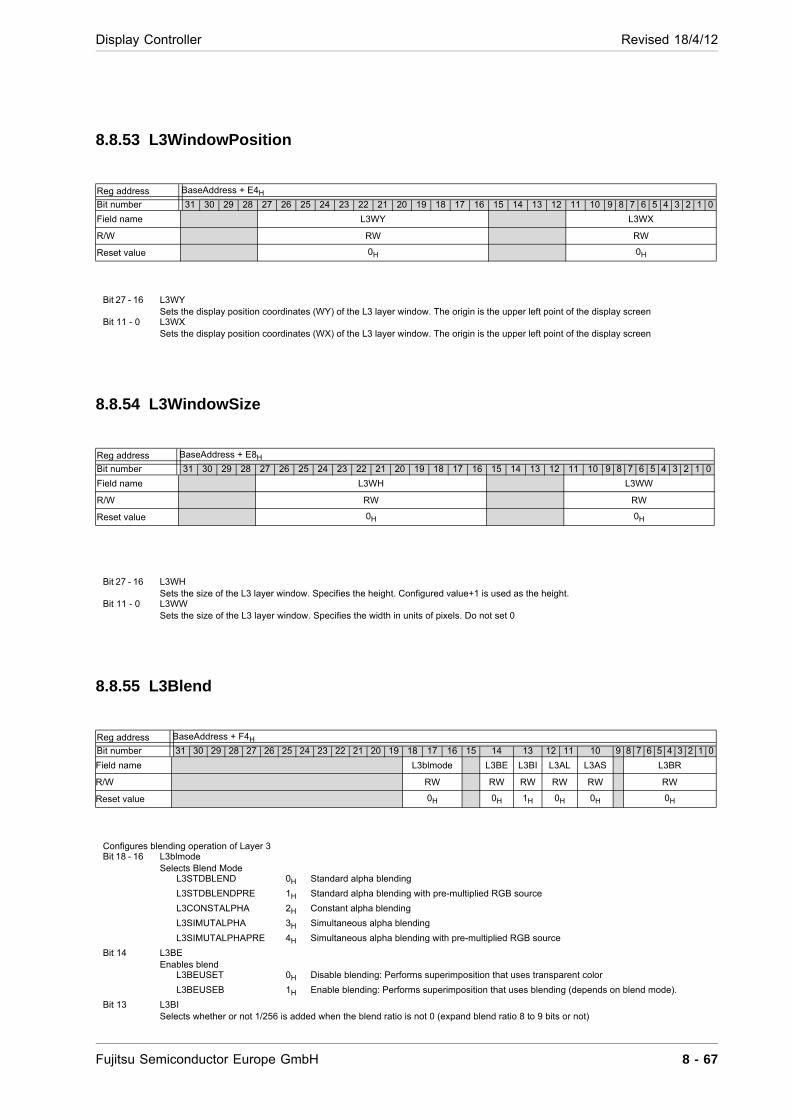
Display Controller Revised 18/4/12
8.8.53 L3WindowPosition
8.8.54 L3WindowSize
8.8.55 L3Blend
Reg address BaseAddress + E4H
Bit number 31 30 29 28 27 26 25 24 23 22 21 20 19 18 17 16 15 14 13 12 11 10 9 8 7 6 5 4 3 2 1 0
Field name L3WY L3WX
R/W RW RW
Reset value 0H 0H
Bit 27 - 16 L3WY Sets the display position coordinates (WY) of the L3 layer window. The origin is the upper left point of the display screen
Bit 11 - 0 L3WX Sets the display position coordinates (WX) of the L3 layer window. The origin is the upper left point of the display screen
Reg address BaseAddress + E8H
Bit number 31 30 29 28 27 26 25 24 23 22 21 20 19 18 17 16 15 14 13 12 11 10 9 8 7 6 5 4 3 2 1 0
Field name L3WH L3WW
R/W RW RW
Reset value 0H 0H
Bit 27 - 16 L3WH Sets the size of the L3 layer window. Specifies the height. Configured value+1 is used as the height.
Bit 11 - 0 L3WW Sets the size of the L3 layer window. Specifies the width in units of pixels. Do not set 0
Reg address BaseAddress + F4H
Bit number 31 30 29 28 27 26 25 24 23 22 21 20 19 18 17 16 15 14 13 12 11 10 9 8 7 6 5 4 3 2 1 0
Field name L3blmode L3BE L3BI L3AL L3AS L3BR
R/W RW RW RW RW RW RW
Reset value 0H 0H 1H 0H 0H 0H
Configures blending operation of Layer 3 Bit 18 - 16 L3blmode
Selects Blend Mode L3STDBLEND 0H Standard alpha blending
L3STDBLENDPRE 1H Standard alpha blending with pre-multiplied RGB source
L3CONSTALPHA 2H Constant alpha blending
L3SIMUTALPHA 3H Simultaneous alpha blending
L3SIMUTALPHAPRE 4H Simultaneous alpha blending with pre-multiplied RGB source
Bit 14 L3BE Enables blend
L3BEUSET 0H Disable blending: Performs superimposition that uses transparent color
L3BEUSEB 1H Enable blending: Performs superimposition that uses blending (depends on blend mode).
Bit 13 L3BI Selects whether or not 1/256 is added when the blend ratio is not 0 (expand blend ratio 8 to 9 bits or not)
Fujitsu Semiconductor Europe GmbH 8 - 67
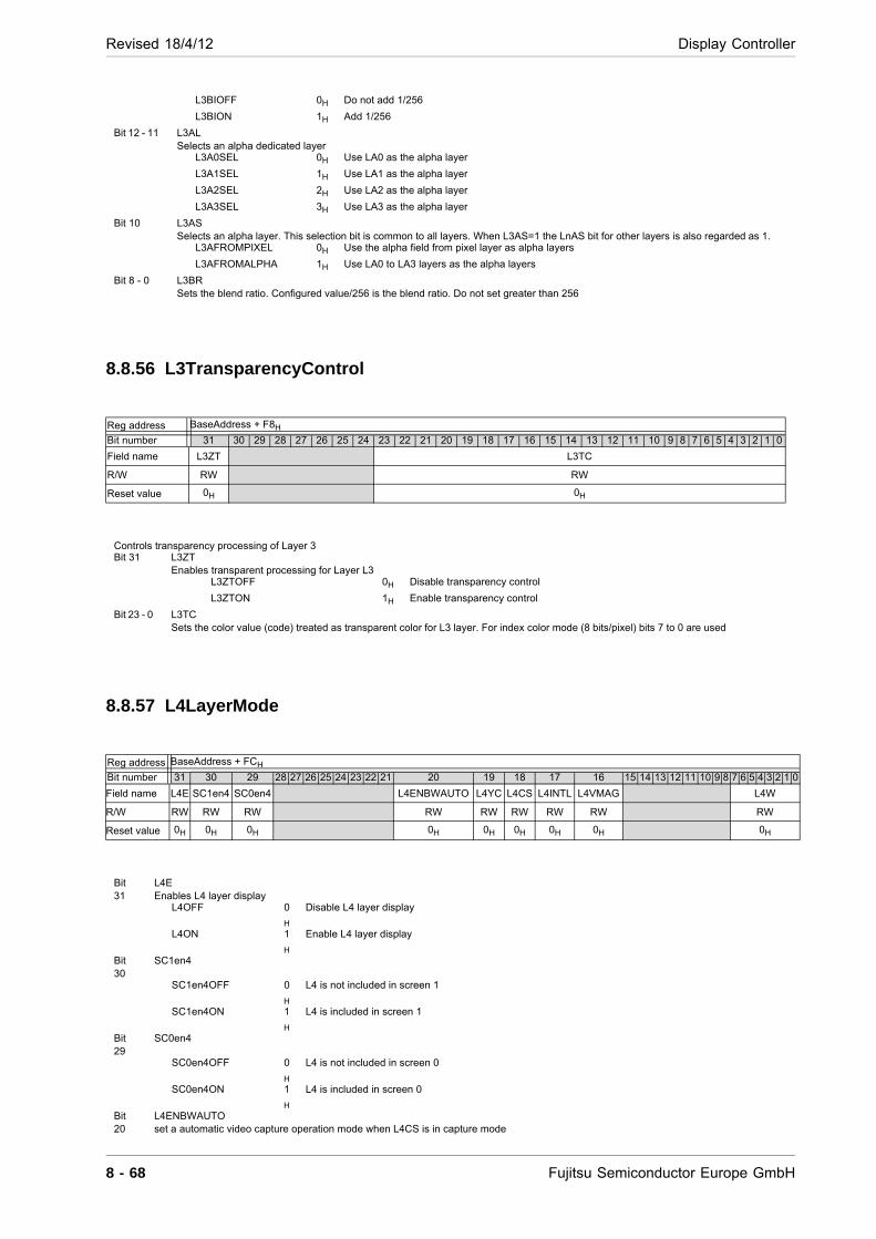
Revised 18/4/12 Display Controller
8.8.56 L3TransparencyControl
8.8.57 L4LayerMode
L3BIOFF 0H Do not add 1/256
L3BION 1H Add 1/256
Bit 12 - 11 L3AL Selects an alpha dedicated layer
L3A0SEL 0H Use LA0 as the alpha layer
L3A1SEL 1H Use LA1 as the alpha layer
L3A2SEL 2H Use LA2 as the alpha layer
L3A3SEL 3H Use LA3 as the alpha layer
Bit 10 L3AS Selects an alpha layer. This selection bit is common to all layers. When L3AS=1 the LnAS bit for other layers is also regarded as 1.
L3AFROMPIXEL 0H Use the alpha field from pixel layer as alpha layers
L3AFROMALPHA 1H Use LA0 to LA3 layers as the alpha layers
Bit 8 - 0 L3BR Sets the blend ratio. Configured value/256 is the blend ratio. Do not set greater than 256
Reg address BaseAddress + F8H
Bit number 31 30 29 28 27 26 25 24 23 22 21 20 19 18 17 16 15 14 13 12 11 10 9 8 7 6 5 4 3 2 1 0
Field name L3ZT L3TC
R/W RW RW
Reset value 0H 0H
Controls transparency processing of Layer 3 Bit 31 L3ZT
Enables transparent processing for Layer L3 L3ZTOFF 0H Disable transparency control
L3ZTON 1H Enable transparency control
Bit 23 - 0 L3TC Sets the color value (code) treated as transparent color for L3 layer. For index color mode (8 bits/pixel) bits 7 to 0 are used
Reg address BaseAddress + FCH
Bit number 31 30 29 28 27 26 25 24 23 22 21 20 19 18 17 16 15 14 13 12 11 10 9 8 7 6 5 4 3 2 1 0
Field name L4E SC1en4 SC0en4 L4ENBWAUTO L4YC L4CS L4INTL L4VMAG L4W
R/W RW RW RW RW RW RW RW RW RW
Reset value 0H 0H 0H 0H 0H 0H 0H 0H 0H
Bit 31
L4E Enables L4 layer display
L4OFF 0
H
Disable L4 layer display
L4ON 1
H
Enable L4 layer display
Bit 30
SC1en4
SC1en4OFF 0
H
L4 is not included in screen 1
SC1en4ON 1
H
L4 is included in screen 1
Bit 29
SC0en4
SC0en4OFF 0
H
L4 is not included in screen 0
SC0en4ON 1
H
L4 is included in screen 0
Bit 20
L4ENBWAUTO set a automatic video capture operation mode when L4CS is in capture mode
8 - 68 Fujitsu Semiconductor Europe GmbH
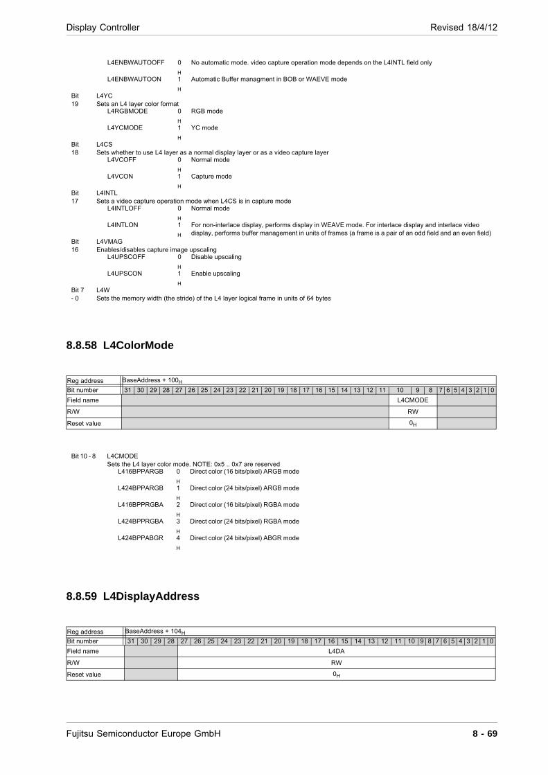
Display Controller Revised 18/4/12
8.8.58 L4ColorMode
8.8.59 L4DisplayAddress
L4ENBWAUTOOFF 0
H
No automatic mode. video capture operation mode depends on the L4INTL field only
L4ENBWAUTOON 1
H
Automatic Buffer managment in BOB or WAEVE mode
Bit 19
L4YC Sets an L4 layer color format
L4RGBMODE 0
H
RGB mode
L4YCMODE 1
H
YC mode
Bit 18
L4CS Sets whether to use L4 layer as a normal display layer or as a video capture layer
L4VCOFF 0
H
Normal mode
L4VCON 1
H
Capture mode
Bit 17
L4INTL Sets a video capture operation mode when L4CS is in capture mode
L4INTLOFF 0
H
Normal mode
L4INTLON 1
H
For non-interlace display, performs display in WEAVE mode. For interlace display and interlace video display, performs buffer management in units of frames (a frame is a pair of an odd field and an even field)
Bit 16
L4VMAG Enables/disables capture image upscaling
L4UPSCOFF 0
H
Disable upscaling
L4UPSCON 1
H
Enable upscaling
Bit 7 - 0
L4W Sets the memory width (the stride) of the L4 layer logical frame in units of 64 bytes
Reg address BaseAddress + 100H
Bit number 31 30 29 28 27 26 25 24 23 22 21 20 19 18 17 16 15 14 13 12 11 10 9 8 7 6 5 4 3 2 1 0
Field name L4CMODE
R/W RW
Reset value 0H
Bit 10 - 8 L4CMODE Sets the L4 layer color mode. NOTE: 0x5 .. 0x7 are reserved
L416BPPARGB 0
H
Direct color (16 bits/pixel) ARGB mode
L424BPPARGB 1
H
Direct color (24 bits/pixel) ARGB mode
L416BPPRGBA 2
H
Direct color (16 bits/pixel) RGBA mode
L424BPPRGBA 3
H
Direct color (24 bits/pixel) RGBA mode
L424BPPABGR 4
H
Direct color (24 bits/pixel) ABGR mode
Reg address BaseAddress + 104H
Bit number 31 30 29 28 27 26 25 24 23 22 21 20 19 18 17 16 15 14 13 12 11 10 9 8 7 6 5 4 3 2 1 0
Field name L4DA
R/W RW
Reset value 0H
Fujitsu Semiconductor Europe GmbH 8 - 69
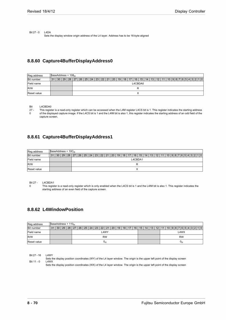
Revised 18/4/12 Display Controller
8.8.60 Capture4BufferDisplayAddress0
8.8.61 Capture4BufferDisplayAddress1
8.8.62 L4WindowPosition
Bit 27 - 0 L4DA Sets the display window origin address of the L4 layer. Address has to be 16-byte aligned
Reg address BaseAddress + 108H
Bit number 31 30 29 28 27 26 25 24 23 22 21 20 19 18 17 16 15 14 13 12 11 10 9 8 7 6 5 4 3 2 1 0
Field name L4CBDA0
R/W R
Reset value X
Bit 27 - 0
L4CBDA0 This register is a read-only register which can be accessed when the L4M register L4CS bit is 1. This register indicates the starting address of the displayed capture image. If the L4CS bit is 1 and the L4IM bit is also 1, this register indicates the starting address of an odd field of the capture screen.
Reg address BaseAddress + 10CH
Bit number 31 30 29 28 27 26 25 24 23 22 21 20 19 18 17 16 15 14 13 12 11 10 9 8 7 6 5 4 3 2 1 0
Field name L4CBDA1
R/W R
Reset value X
Bit 27 - 0
L4CBDA1 This register is a read-only register which is only enabled when the L4CS bit is 1 and the L4IM bit is also 1. This register indicates the starting address of an even field of the capture screen.
Reg address BaseAddress + 110H
Bit number 31 30 29 28 27 26 25 24 23 22 21 20 19 18 17 16 15 14 13 12 11 10 9 8 7 6 5 4 3 2 1 0
Field name L4WY L4WX
R/W RW RW
Reset value 0H 0H
Bit 27 - 16 L4WY Sets the display position coordinates (WY) of the L4 layer window. The origin is the upper left point of the display screen
Bit 11 - 0 L4WX Sets the display position coordinates (WX) of the L4 layer window. The origin is the upper left point of the display screen
8 - 70 Fujitsu Semiconductor Europe GmbH

Display Controller Revised 18/4/12
8.8.63 L4WindowSize
Reg address BaseAddress + 114H
Bit number 31 30 29 28 27 26 25 24 23 22 21 20 19 18 17 16 15 14 13 12 11 10 9 8 7 6 5 4 3 2 1 0
Field name L4WH L4WW
R/W RW RW
Reset value 0H 0H
Bit 27 - 16 L4WH Sets the size of the L4 layer window. Specifies the height. Configured value+1 is used as the height.
Bit 11 - 0 L4WW Sets the size of the L4 layer window. Specifies the width in units of pixels. Do not set 0
Fujitsu Semiconductor Europe GmbH 8 - 71

Revised 18/4/12 Display Controller
8.8.64 L4Blend
8.8.65 L4TransparencyControl
Reg address BaseAddress + 120H
Bit number 31 30 29 28 27 26 25 24 23 22 21 20 19 18 17 16 15 14 13 12 11 10 9 8 7 6 5 4 3 2 1 0
Field name L4blmode L4BE L4BI L4AL L4AS L4BR
R/W RW RW RW RW RW RW
Reset value 0H 0H 1H 0H 0H 0H
Configures blending operation of Layer 4 Bit 18 - 16 L4blmode
Selects Blend Mode L4STDBLEND 0H Standard alpha blending
L4STDBLENDPRE 1H Standard alpha blending with pre-multiplied RGB source
L4CONSTALPHA 2H Constant alpha blending
L4SIMUTALPHA 3H Simultaneous alpha blending
L4SIMUTALPHAPRE 4H Simultaneous alpha blending with pre-multiplied RGB source
Bit 14 L4BE Enables blend
L4BEUSET 0H Disable blending: Performs superimposition that uses transparent color
L4BEUSEB 1H Enable blending: Performs superimposition that uses blending (depends on blend mode).
Bit 13 L4BI Selects whether or not 1/256 is added when the blend ratio is not 0 (expand blend ratio 8 to 9 bits or not)
L4BIOFF 0H Do not add 1/256
L4BION 1H Add 1/256
Bit 12 - 11 L4AL Selects an alpha dedicated layer
L4A0SEL 0H Use LA0 as the alpha layer
L4A1SEL 1H Use LA1 as the alpha layer
L4A2SEL 2H Use LA2 as the alpha layer
L4A3SEL 3H Use LA3 as the alpha layer
Bit 10 L4AS Selects an alpha layer. This selection bit is common to all layers. When L4AS=1 the LnAS bit for other layers is also regarded as 1.
L4AFROMPIXEL 0H Use the alpha field from pixel layer as alpha layers
L4AFROMALPHA 1H Use LA0 to LA3 layers as the alpha layers
Bit 8 - 0 L4BR Sets the blend ratio. Configured value/256 is the blend ratio. Do not set greater than 256
Reg address BaseAddress + 124H
Bit number 31 30 29 28 27 26 25 24 23 22 21 20 19 18 17 16 15 14 13 12 11 10 9 8 7 6 5 4 3 2 1 0
Field name L4ZT L4TC
R/W RW RW
Reset value 0H 0H
Controls transparency processing of Layer 4 Bit 31 L4ZT
Enables transparent processing for Layer L4 L4ZTOFF 0H Disable transparency control
L4ZTON 1H Enable transparency control
Bit 23 - 0 L4TC Sets the color value (code) treated as transparent color for L4 layer. For index color mode (8 bits/pixel) bits 7 to 0 are used
8 - 72 Fujitsu Semiconductor Europe GmbH
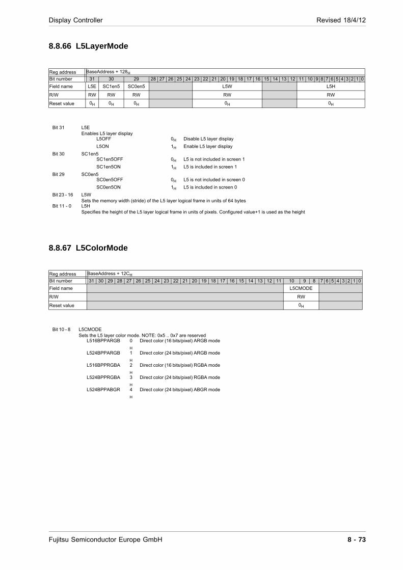
Display Controller Revised 18/4/12
8.8.66 L5LayerMode
8.8.67 L5ColorMode
Reg address BaseAddress + 128H
Bit number 31 30 29 28 27 26 25 24 23 22 21 20 19 18 17 16 15 14 13 12 11 10 9 8 7 6 5 4 3 2 1 0
Field name L5E SC1en5 SC0en5 L5W L5H
R/W RW RW RW RW RW
Reset value 0H 0H 0H 0H 0H
Bit 31 L5E Enables L5 layer display
L5OFF 0H Disable L5 layer display
L5ON 1H Enable L5 layer display
Bit 30 SC1en5 SC1en5OFF 0H L5 is not included in screen 1
SC1en5ON 1H L5 is included in screen 1
Bit 29 SC0en5 SC0en5OFF 0H L5 is not included in screen 0
SC0en5ON 1H L5 is included in screen 0
Bit 23 - 16 L5W Sets the memory width (stride) of the L5 layer logical frame in units of 64 bytes
Bit 11 - 0 L5H Specifies the height of the L5 layer logical frame in units of pixels. Configured value+1 is used as the height
Reg address BaseAddress + 12CH
Bit number 31 30 29 28 27 26 25 24 23 22 21 20 19 18 17 16 15 14 13 12 11 10 9 8 7 6 5 4 3 2 1 0
Field name L5CMODE
R/W RW
Reset value 0H
Bit 10 - 8 L5CMODE Sets the L5 layer color mode. NOTE: 0x5 .. 0x7 are reserved
L516BPPARGB 0
H
Direct color (16 bits/pixel) ARGB mode
L524BPPARGB 1
H
Direct color (24 bits/pixel) ARGB mode
L516BPPRGBA 2
H
Direct color (16 bits/pixel) RGBA mode
L524BPPRGBA 3
H
Direct color (24 bits/pixel) RGBA mode
L524BPPABGR 4
H
Direct color (24 bits/pixel) ABGR mode
Fujitsu Semiconductor Europe GmbH 8 - 73
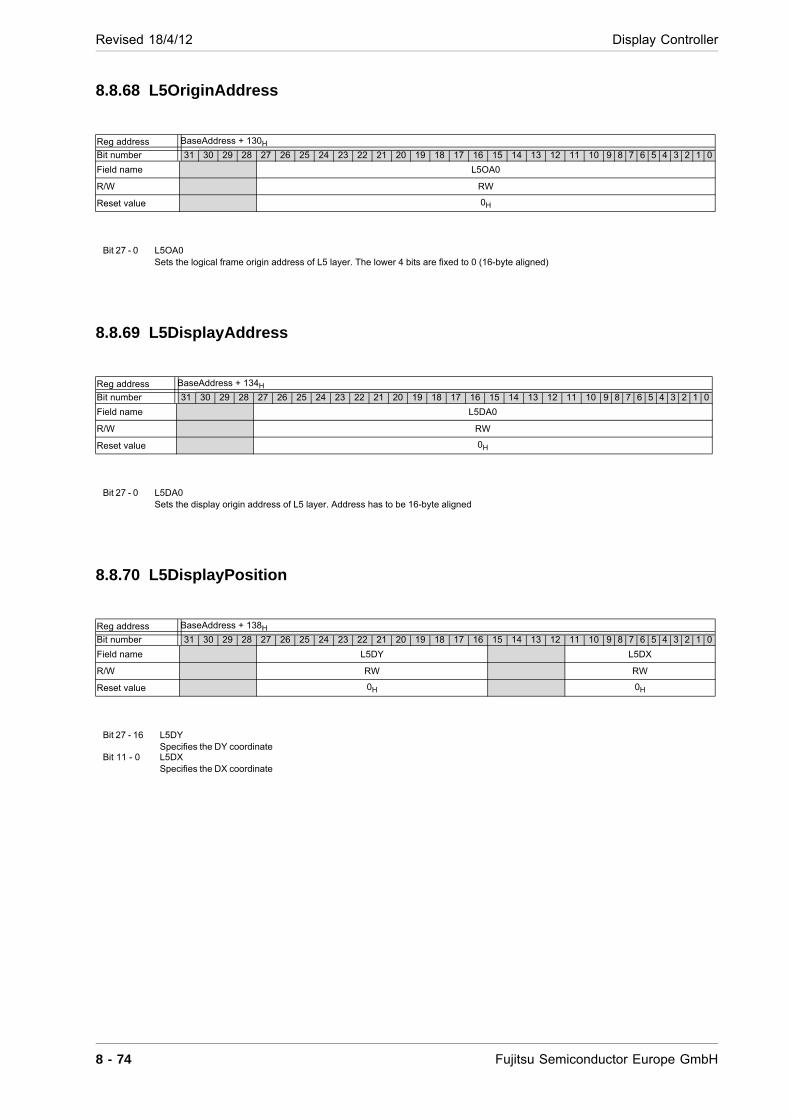
Revised 18/4/12 Display Controller
8.8.68 L5OriginAddress
8.8.69 L5DisplayAddress
8.8.70 L5DisplayPosition
Reg address BaseAddress + 130H
Bit number 31 30 29 28 27 26 25 24 23 22 21 20 19 18 17 16 15 14 13 12 11 10 9 8 7 6 5 4 3 2 1 0
Field name L5OA0
R/W RW
Reset value 0H
Bit 27 - 0 L5OA0 Sets the logical frame origin address of L5 layer. The lower 4 bits are fixed to 0 (16-byte aligned)
Reg address BaseAddress + 134H
Bit number 31 30 29 28 27 26 25 24 23 22 21 20 19 18 17 16 15 14 13 12 11 10 9 8 7 6 5 4 3 2 1 0
Field name L5DA0
R/W RW
Reset value 0H
Bit 27 - 0 L5DA0 Sets the display origin address of L5 layer. Address has to be 16-byte aligned
Reg address BaseAddress + 138H
Bit number 31 30 29 28 27 26 25 24 23 22 21 20 19 18 17 16 15 14 13 12 11 10 9 8 7 6 5 4 3 2 1 0
Field name L5DY L5DX
R/W RW RW
Reset value 0H 0H
Bit 27 - 16 L5DY Specifies the DY coordinate
Bit 11 - 0 L5DX Specifies the DX coordinate
8 - 74 Fujitsu Semiconductor Europe GmbH
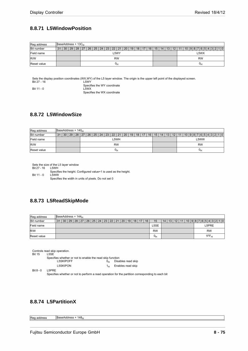
Display Controller Revised 18/4/12
8.8.71 L5WindowPosition
8.8.72 L5WindowSize
8.8.73 L5ReadSkipMode
8.8.74 L5PartitionX
Reg address BaseAddress + 13CH
Bit number 31 30 29 28 27 26 25 24 23 22 21 20 19 18 17 16 15 14 13 12 11 10 9 8 7 6 5 4 3 2 1 0
Field name L5WY L5WX
R/W RW RW
Reset value 0H 0H
Sets the display position coordinates (WX,WY) of the L5 layer window. The origin is the upper left point of the displayed screen. Bit 27 - 16 L5WY
Specifies the WY coordinate Bit 11 - 0 L5WX
Specifies the WX coordinate
Reg address BaseAddress + 140H
Bit number 31 30 29 28 27 26 25 24 23 22 21 20 19 18 17 16 15 14 13 12 11 10 9 8 7 6 5 4 3 2 1 0
Field name L5WH L5WW
R/W RW RW
Reset value 0H 0H
Sets the size of the L5 layer window Bit 27 - 16 L5WH
Specifies the height. Configured value+1 is used as the height. Bit 11 - 0 L5WW
Specifies the width in units of pixels. Do not set 0
Reg address BaseAddress + 144H
Bit number 31 30 29 28 27 26 25 24 23 22 21 20 19 18 17 16 15 14 13 12 11 10 9 8 7 6 5 4 3 2 1 0
Field name L5SE L5PRE
R/W RW RW
Reset value 0H 1FFH
Controls read skip operation. Bit 15 L5SE
Specifies whether or not to enable the read skip function L5SKIPOFF 0H Disables read skip
L5SKIPON 1H Enables read skip
Bit 8 - 0 L5PRE Specifies whether or not to perform a read operation for the partition corresponding to each bit
Reg address BaseAddress + 148H
Fujitsu Semiconductor Europe GmbH 8 - 75
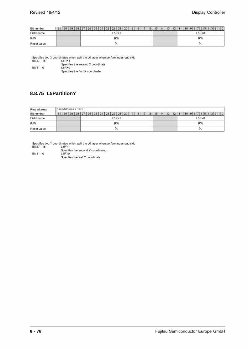
Revised 18/4/12 Display Controller
8.8.75 L5PartitionY
Bit number 31 30 29 28 27 26 25 24 23 22 21 20 19 18 17 16 15 14 13 12 11 10 9 8 7 6 5 4 3 2 1 0
Field name L5PX1 L5PX0
R/W RW RW
Reset value 0H 0H
Specifies two X coordinates which split the L0 layer when performing a read skip Bit 27 - 16 L5PX1
Specifies the second X coordinate Bit 11 - 0 L5PX0
Specifies the first X coordinate
Reg address BaseAddress + 14CH
Bit number 31 30 29 28 27 26 25 24 23 22 21 20 19 18 17 16 15 14 13 12 11 10 9 8 7 6 5 4 3 2 1 0
Field name L5PY1 L5PY0
R/W RW RW
Reset value 0H 0H
Specifies two Y coordinates which split the L0 layer when performing a read skip Bit 27 - 16 L5PY1
Specifies the second Y coordinate. Bit 11 - 0 L5PY0
Specifies the first Y coordinate
8 - 76 Fujitsu Semiconductor Europe GmbH
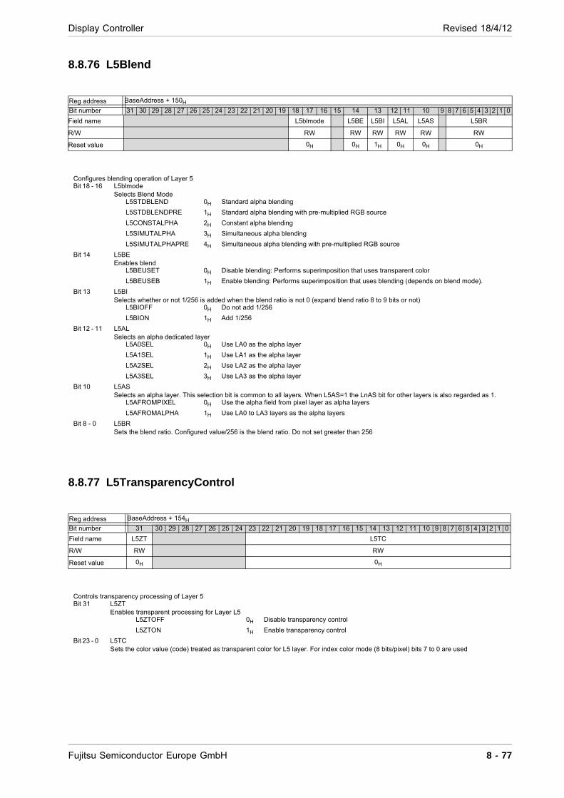
Display Controller Revised 18/4/12
8.8.76 L5Blend
8.8.77 L5TransparencyControl
Reg address BaseAddress + 150H
Bit number 31 30 29 28 27 26 25 24 23 22 21 20 19 18 17 16 15 14 13 12 11 10 9 8 7 6 5 4 3 2 1 0
Field name L5blmode L5BE L5BI L5AL L5AS L5BR
R/W RW RW RW RW RW RW
Reset value 0H 0H 1H 0H 0H 0H
Configures blending operation of Layer 5 Bit 18 - 16 L5blmode
Selects Blend Mode L5STDBLEND 0H Standard alpha blending
L5STDBLENDPRE 1H Standard alpha blending with pre-multiplied RGB source
L5CONSTALPHA 2H Constant alpha blending
L5SIMUTALPHA 3H Simultaneous alpha blending
L5SIMUTALPHAPRE 4H Simultaneous alpha blending with pre-multiplied RGB source
Bit 14 L5BE Enables blend
L5BEUSET 0H Disable blending: Performs superimposition that uses transparent color
L5BEUSEB 1H Enable blending: Performs superimposition that uses blending (depends on blend mode).
Bit 13 L5BI Selects whether or not 1/256 is added when the blend ratio is not 0 (expand blend ratio 8 to 9 bits or not)
L5BIOFF 0H Do not add 1/256
L5BION 1H Add 1/256
Bit 12 - 11 L5AL Selects an alpha dedicated layer
L5A0SEL 0H Use LA0 as the alpha layer
L5A1SEL 1H Use LA1 as the alpha layer
L5A2SEL 2H Use LA2 as the alpha layer
L5A3SEL 3H Use LA3 as the alpha layer
Bit 10 L5AS Selects an alpha layer. This selection bit is common to all layers. When L5AS=1 the LnAS bit for other layers is also regarded as 1.
L5AFROMPIXEL 0H Use the alpha field from pixel layer as alpha layers
L5AFROMALPHA 1H Use LA0 to LA3 layers as the alpha layers
Bit 8 - 0 L5BR Sets the blend ratio. Configured value/256 is the blend ratio. Do not set greater than 256
Reg address BaseAddress + 154H
Bit number 31 30 29 28 27 26 25 24 23 22 21 20 19 18 17 16 15 14 13 12 11 10 9 8 7 6 5 4 3 2 1 0
Field name L5ZT L5TC
R/W RW RW
Reset value 0H 0H
Controls transparency processing of Layer 5 Bit 31 L5ZT
Enables transparent processing for Layer L5 L5ZTOFF 0H Disable transparency control
L5ZTON 1H Enable transparency control
Bit 23 - 0 L5TC Sets the color value (code) treated as transparent color for L5 layer. For index color mode (8 bits/pixel) bits 7 to 0 are used
Fujitsu Semiconductor Europe GmbH 8 - 77
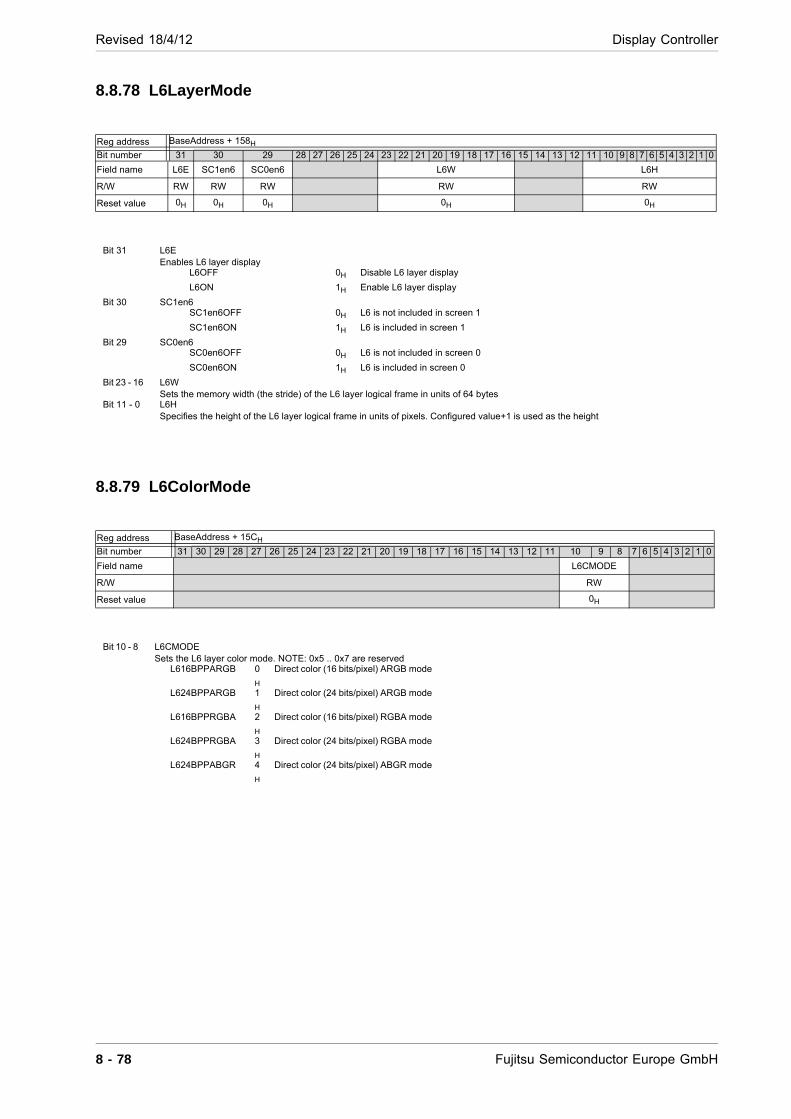
Revised 18/4/12 Display Controller
8.8.78 L6LayerMode
8.8.79 L6ColorMode
Reg address BaseAddress + 158H
Bit number 31 30 29 28 27 26 25 24 23 22 21 20 19 18 17 16 15 14 13 12 11 10 9 8 7 6 5 4 3 2 1 0
Field name L6E SC1en6 SC0en6 L6W L6H
R/W RW RW RW RW RW
Reset value 0H 0H 0H 0H 0H
Bit 31 L6E Enables L6 layer display
L6OFF 0H Disable L6 layer display
L6ON 1H Enable L6 layer display
Bit 30 SC1en6 SC1en6OFF 0H L6 is not included in screen 1
SC1en6ON 1H L6 is included in screen 1
Bit 29 SC0en6 SC0en6OFF 0H L6 is not included in screen 0
SC0en6ON 1H L6 is included in screen 0
Bit 23 - 16 L6W Sets the memory width (the stride) of the L6 layer logical frame in units of 64 bytes
Bit 11 - 0 L6H Specifies the height of the L6 layer logical frame in units of pixels. Configured value+1 is used as the height
Reg address BaseAddress + 15CH
Bit number 31 30 29 28 27 26 25 24 23 22 21 20 19 18 17 16 15 14 13 12 11 10 9 8 7 6 5 4 3 2 1 0
Field name L6CMODE
R/W RW
Reset value 0H
Bit 10 - 8 L6CMODE Sets the L6 layer color mode. NOTE: 0x5 .. 0x7 are reserved
L616BPPARGB 0
H
Direct color (16 bits/pixel) ARGB mode
L624BPPARGB 1
H
Direct color (24 bits/pixel) ARGB mode
L616BPPRGBA 2
H
Direct color (16 bits/pixel) RGBA mode
L624BPPRGBA 3
H
Direct color (24 bits/pixel) RGBA mode
L624BPPABGR 4
H
Direct color (24 bits/pixel) ABGR mode
8 - 78 Fujitsu Semiconductor Europe GmbH
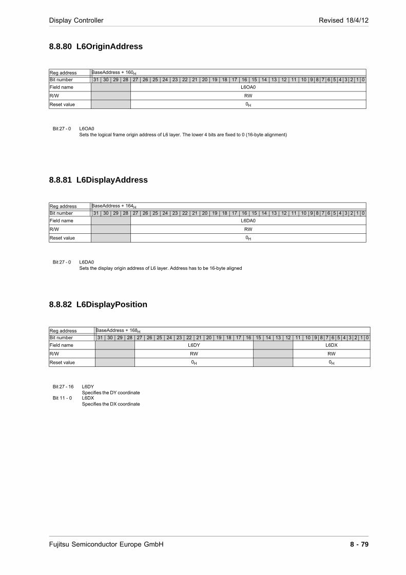
Display Controller Revised 18/4/12
8.8.80 L6OriginAddress
8.8.81 L6DisplayAddress
8.8.82 L6DisplayPosition
Reg address BaseAddress + 160H
Bit number 31 30 29 28 27 26 25 24 23 22 21 20 19 18 17 16 15 14 13 12 11 10 9 8 7 6 5 4 3 2 1 0
Field name L6OA0
R/W RW
Reset value 0H
Bit 27 - 0 L6OA0 Sets the logical frame origin address of L6 layer. The lower 4 bits are fixed to 0 (16-byte alignment)
Reg address BaseAddress + 164H
Bit number 31 30 29 28 27 26 25 24 23 22 21 20 19 18 17 16 15 14 13 12 11 10 9 8 7 6 5 4 3 2 1 0
Field name L6DA0
R/W RW
Reset value 0H
Bit 27 - 0 L6DA0 Sets the display origin address of L6 layer. Address has to be 16-byte aligned
Reg address BaseAddress + 168H
Bit number 31 30 29 28 27 26 25 24 23 22 21 20 19 18 17 16 15 14 13 12 11 10 9 8 7 6 5 4 3 2 1 0
Field name L6DY L6DX
R/W RW RW
Reset value 0H 0H
Bit 27 - 16 L6DY Specifies the DY coordinate
Bit 11 - 0 L6DX Specifies the DX coordinate
Fujitsu Semiconductor Europe GmbH 8 - 79
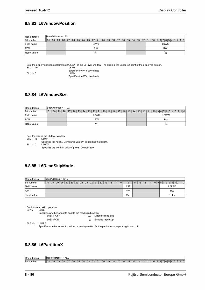
Revised 18/4/12 Display Controller
8.8.83 L6WindowPosition
8.8.84 L6WindowSize
8.8.85 L6ReadSkipMode
8.8.86 L6PartitionX
Reg address BaseAddress + 16CH
Bit number 31 30 29 28 27 26 25 24 23 22 21 20 19 18 17 16 15 14 13 12 11 10 9 8 7 6 5 4 3 2 1 0
Field name L6WY L6WX
R/W RW RW
Reset value 0H 0H
Sets the display position coordinates (WX,WY) of the L6 layer window. The origin is the upper left point of the displayed screen. Bit 27 - 16 L6WY
Specifies the WY coordinate Bit 11 - 0 L6WX
Specifies the WX coordinate
Reg address BaseAddress + 170H
Bit number 31 30 29 28 27 26 25 24 23 22 21 20 19 18 17 16 15 14 13 12 11 10 9 8 7 6 5 4 3 2 1 0
Field name L6WH L6WW
R/W RW RW
Reset value 0H 0H
Sets the size of the L6 layer window Bit 27 - 16 L6WH
Specifies the height. Configured value+1 is used as the height. Bit 11 - 0 L6WW
Specifies the width in units of pixels. Do not set 0
Reg address BaseAddress + 174H
Bit number 31 30 29 28 27 26 25 24 23 22 21 20 19 18 17 16 15 14 13 12 11 10 9 8 7 6 5 4 3 2 1 0
Field name L6SE L6PRE
R/W RW RW
Reset value 0H 1FFH
Controls read skip operation. Bit 15 L6SE
Specifies whether or not to enable the read skip function L6SKIPOFF 0H Disables read skip
L6SKIPON 1H Enables read skip
Bit 8 - 0 L6PRE Specifies whether or not to perform a read operation for the partition corresponding to each bit
Reg address BaseAddress + 178H
Bit number 31 30 29 28 27 26 25 24 23 22 21 20 19 18 17 16 15 14 13 12 11 10 9 8 7 6 5 4 3 2 1 0
8 - 80 Fujitsu Semiconductor Europe GmbH

Display Controller Revised 18/4/12
8.8.87 L6PartitionY
Field name L6PX1 L6PX0
R/W RW RW
Reset value 0H 0H
Specifies two X coordinates which split the L0 layer when performing a read skip Bit 27 - 16 L6PX1
Specifies the second X coordinate Bit 11 - 0 L6PX0
Specifies the first X coordinate
Reg address BaseAddress + 17CH
Bit number 31 30 29 28 27 26 25 24 23 22 21 20 19 18 17 16 15 14 13 12 11 10 9 8 7 6 5 4 3 2 1 0
Field name L6PY1 L6PY0
R/W RW RW
Reset value 0H 0H
Specifies two Y coordinates which split the L0 layer when performing a read skip Bit 27 - 16 L6PY1
Specifies the second Y coordinate. Bit 11 - 0 L6PY0
Specifies the first Y coordinate
Fujitsu Semiconductor Europe GmbH 8 - 81
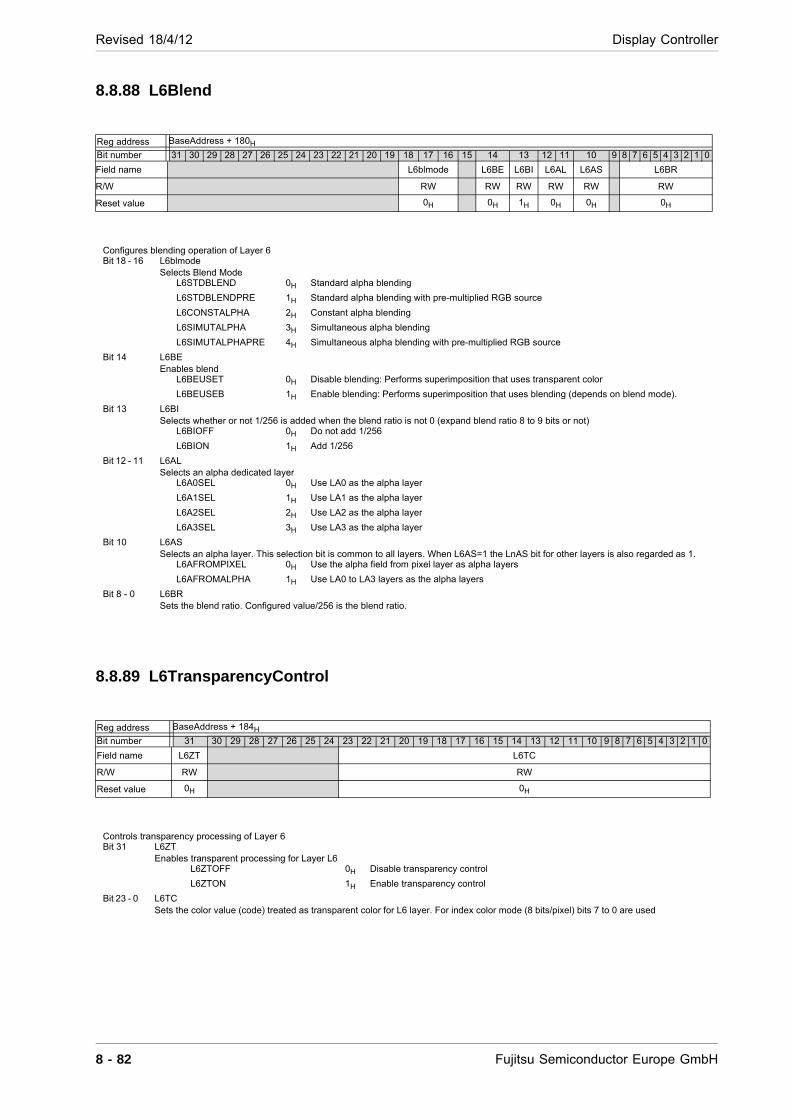
Revised 18/4/12 Display Controller
8.8.88 L6Blend
8.8.89 L6TransparencyControl
Reg address BaseAddress + 180H
Bit number 31 30 29 28 27 26 25 24 23 22 21 20 19 18 17 16 15 14 13 12 11 10 9 8 7 6 5 4 3 2 1 0
Field name L6blmode L6BE L6BI L6AL L6AS L6BR
R/W RW RW RW RW RW RW
Reset value 0H 0H 1H 0H 0H 0H
Configures blending operation of Layer 6 Bit 18 - 16 L6blmode
Selects Blend Mode L6STDBLEND 0H Standard alpha blending
L6STDBLENDPRE 1H Standard alpha blending with pre-multiplied RGB source
L6CONSTALPHA 2H Constant alpha blending
L6SIMUTALPHA 3H Simultaneous alpha blending
L6SIMUTALPHAPRE 4H Simultaneous alpha blending with pre-multiplied RGB source
Bit 14 L6BE Enables blend
L6BEUSET 0H Disable blending: Performs superimposition that uses transparent color
L6BEUSEB 1H Enable blending: Performs superimposition that uses blending (depends on blend mode).
Bit 13 L6BI Selects whether or not 1/256 is added when the blend ratio is not 0 (expand blend ratio 8 to 9 bits or not)
L6BIOFF 0H Do not add 1/256
L6BION 1H Add 1/256
Bit 12 - 11 L6AL Selects an alpha dedicated layer
L6A0SEL 0H Use LA0 as the alpha layer
L6A1SEL 1H Use LA1 as the alpha layer
L6A2SEL 2H Use LA2 as the alpha layer
L6A3SEL 3H Use LA3 as the alpha layer
Bit 10 L6AS Selects an alpha layer. This selection bit is common to all layers. When L6AS=1 the LnAS bit for other layers is also regarded as 1.
L6AFROMPIXEL 0H Use the alpha field from pixel layer as alpha layers
L6AFROMALPHA 1H Use LA0 to LA3 layers as the alpha layers
Bit 8 - 0 L6BR Sets the blend ratio. Configured value/256 is the blend ratio.
Reg address BaseAddress + 184H
Bit number 31 30 29 28 27 26 25 24 23 22 21 20 19 18 17 16 15 14 13 12 11 10 9 8 7 6 5 4 3 2 1 0
Field name L6ZT L6TC
R/W RW RW
Reset value 0H 0H
Controls transparency processing of Layer 6 Bit 31 L6ZT
Enables transparent processing for Layer L6 L6ZTOFF 0H Disable transparency control
L6ZTON 1H Enable transparency control
Bit 23 - 0 L6TC Sets the color value (code) treated as transparent color for L6 layer. For index color mode (8 bits/pixel) bits 7 to 0 are used
8 - 82 Fujitsu Semiconductor Europe GmbH

Display Controller Revised 18/4/12
8.8.90 L7LayerMode
8.8.91 L7ColorMode
Reg address BaseAddress + 188H
Bit number 31 30 29 28 27 26 25 24 23 22 21 20 19 18 17 16 15 14 13 12 11 10 9 8 7 6 5 4 3 2 1 0
Field name L7E SC1en7 SC0en7 L7W L7H
R/W RW RW RW RW RW
Reset value 0H 0H 0H 0H 0H
Bit 31 L7E Enables L7 layer display
L7OFF 0H Disable L7 layer display
L7ON 1H Enable L7 layer display
Bit 30 SC1en7 SC1en7OFF 0H L7 is not included in screen 1
SC1en7ON 1H L7 is included in screen 1
Bit 29 SC0en7 SC0en7OFF 0H L7 is not included in screen 0
SC0en7ON 1H L7 is included in screen 0
Bit 23 - 16 L7W Sets the memory width (the stride) of the L7 layer logical frame in units of 64 bytes
Bit 11 - 0 L7H Specifies the height of the L7 layer logical frame in units of pixels. Configured value+1 is used as the height
Reg address BaseAddress + 18CH
Bit number 31 30 29 28 27 26 25 24 23 22 21 20 19 18 17 16 15 14 13 12 11 10 9 8 7 6 5 4 3 2 1 0
Field name L7CMODE
R/W RW
Reset value 0H
Bit 10 - 8 L7CMODE Sets the L7 layer color mode. NOTE: 0x5 .. 0x7 are reserved
L716BPPARGB 0
H
Direct color (16 bits/pixel) ARGB mode
L724BPPARGB 1
H
Direct color (24 bits/pixel) ARGB mode
L716BPPRGBA 2
H
Direct color (16 bits/pixel) RGBA mode
L724BPPRGBA 3
H
Direct color (24 bits/pixel) RGBA mode
L724BPPABGR 4
H
Direct color (24 bits/pixel) ABGR mode
Fujitsu Semiconductor Europe GmbH 8 - 83
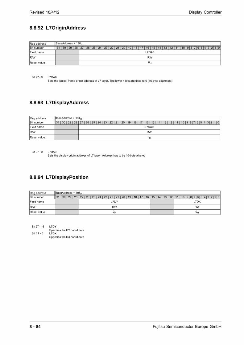
Revised 18/4/12 Display Controller
8.8.92 L7OriginAddress
8.8.93 L7DisplayAddress
8.8.94 L7DisplayPosition
Reg address BaseAddress + 190H
Bit number 31 30 29 28 27 26 25 24 23 22 21 20 19 18 17 16 15 14 13 12 11 10 9 8 7 6 5 4 3 2 1 0
Field name L7OA0
R/W RW
Reset value 0H
Bit 27 - 0 L7OA0 Sets the logical frame origin address of L7 layer. The lower 4 bits are fixed to 0 (16-byte alignment)
Reg address BaseAddress + 194H
Bit number 31 30 29 28 27 26 25 24 23 22 21 20 19 18 17 16 15 14 13 12 11 10 9 8 7 6 5 4 3 2 1 0
Field name L7DA0
R/W RW
Reset value 0H
Bit 27 - 0 L7DA0 Sets the display origin address of L7 layer. Address has to be 16-byte aligned
Reg address BaseAddress + 198H
Bit number 31 30 29 28 27 26 25 24 23 22 21 20 19 18 17 16 15 14 13 12 11 10 9 8 7 6 5 4 3 2 1 0
Field name L7DY L7DX
R/W RW RW
Reset value 0H 0H
Bit 27 - 16 L7DY Specifies the DY coordinate
Bit 11 - 0 L7DX Specifies the DX coordinate
8 - 84 Fujitsu Semiconductor Europe GmbH
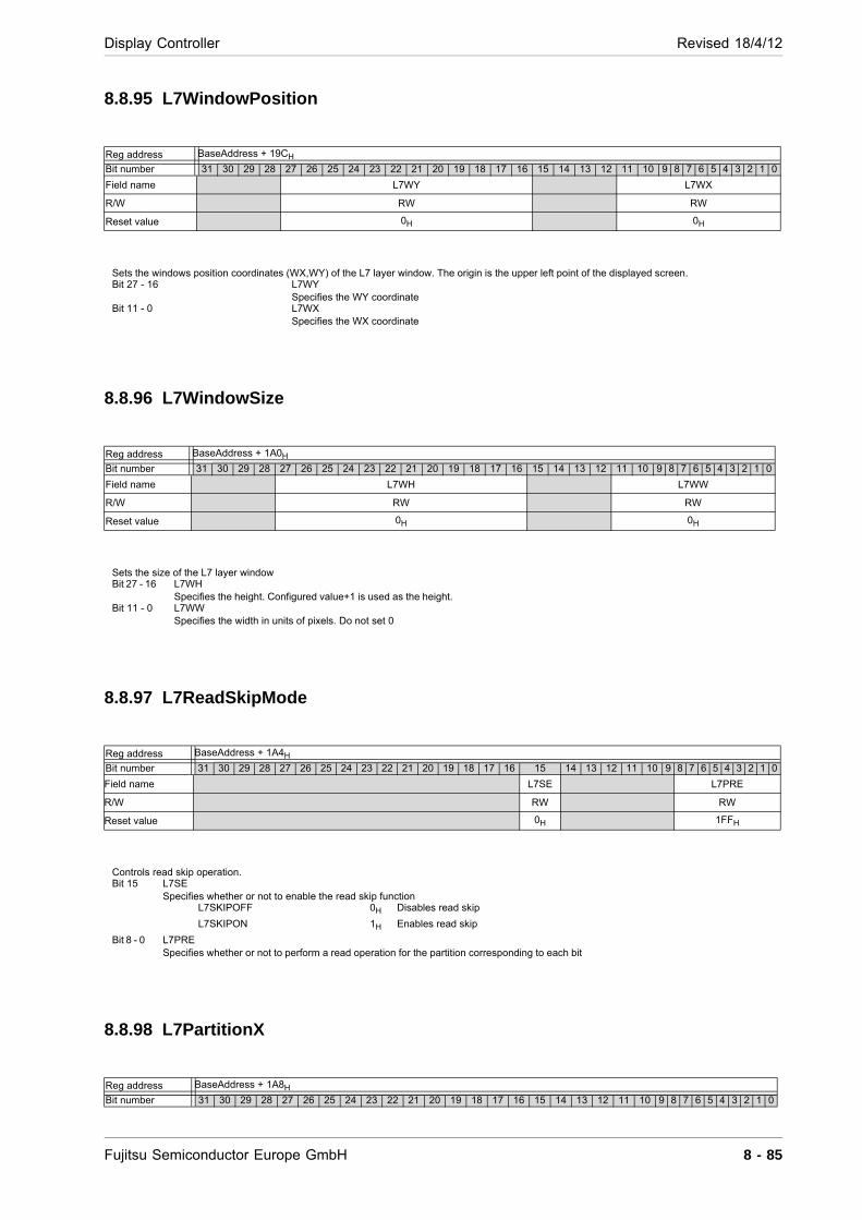
Display Controller Revised 18/4/12
8.8.95 L7WindowPosition
8.8.96 L7WindowSize
8.8.97 L7ReadSkipMode
8.8.98 L7PartitionX
Reg address BaseAddress + 19CH
Bit number 31 30 29 28 27 26 25 24 23 22 21 20 19 18 17 16 15 14 13 12 11 10 9 8 7 6 5 4 3 2 1 0
Field name L7WY L7WX
R/W RW RW
Reset value 0H 0H
Sets the windows position coordinates (WX,WY) of the L7 layer window. The origin is the upper left point of the displayed screen. Bit 27 - 16 L7WY
Specifies the WY coordinate Bit 11 - 0 L7WX
Specifies the WX coordinate
Reg address BaseAddress + 1A0H
Bit number 31 30 29 28 27 26 25 24 23 22 21 20 19 18 17 16 15 14 13 12 11 10 9 8 7 6 5 4 3 2 1 0
Field name L7WH L7WW
R/W RW RW
Reset value 0H 0H
Sets the size of the L7 layer window Bit 27 - 16 L7WH
Specifies the height. Configured value+1 is used as the height. Bit 11 - 0 L7WW
Specifies the width in units of pixels. Do not set 0
Reg address BaseAddress + 1A4H
Bit number 31 30 29 28 27 26 25 24 23 22 21 20 19 18 17 16 15 14 13 12 11 10 9 8 7 6 5 4 3 2 1 0
Field name L7SE L7PRE
R/W RW RW
Reset value 0H 1FFH
Controls read skip operation. Bit 15 L7SE
Specifies whether or not to enable the read skip function L7SKIPOFF 0H Disables read skip
L7SKIPON 1H Enables read skip
Bit 8 - 0 L7PRE Specifies whether or not to perform a read operation for the partition corresponding to each bit
Reg address BaseAddress + 1A8H
Bit number 31 30 29 28 27 26 25 24 23 22 21 20 19 18 17 16 15 14 13 12 11 10 9 8 7 6 5 4 3 2 1 0
Fujitsu Semiconductor Europe GmbH 8 - 85

Revised 18/4/12 Display Controller
8.8.99 L7PartitionY
Field name L7PX1 L7PX0
R/W RW RW
Reset value 0H 0H
Specifies two X coordinates which split the L0 layer when performing a read skip Bit 27 - 16 L7PX1
Specifies the second X coordinate Bit 11 - 0 L7PX0
Specifies the first X coordinate
Reg address BaseAddress + 1ACH
Bit number 31 30 29 28 27 26 25 24 23 22 21 20 19 18 17 16 15 14 13 12 11 10 9 8 7 6 5 4 3 2 1 0
Field name L7PY1 L7PY0
R/W RW RW
Reset value 0H 0H
Specifies two Y coordinates which split the L0 layer when performing a read skip Bit 27 - 16 L7PY1
Specifies the second Y coordinate. Bit 11 - 0 L7PY0
Specifies the first Y coordinate
8 - 86 Fujitsu Semiconductor Europe GmbH
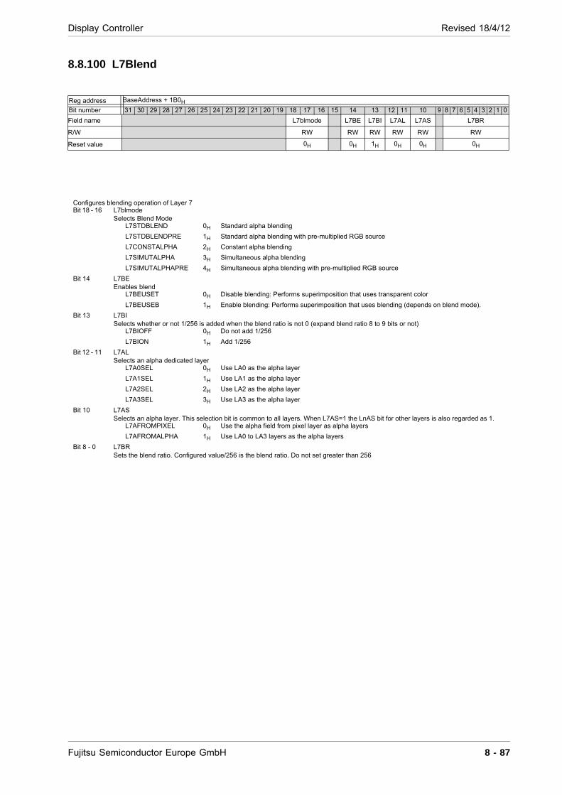
Display Controller Revised 18/4/12
8.8.100 L7Blend
Reg address BaseAddress + 1B0H
Bit number 31 30 29 28 27 26 25 24 23 22 21 20 19 18 17 16 15 14 13 12 11 10 9 8 7 6 5 4 3 2 1 0
Field name L7blmode L7BE L7BI L7AL L7AS L7BR
R/W RW RW RW RW RW RW
Reset value 0H 0H 1H 0H 0H 0H
Configures blending operation of Layer 7 Bit 18 - 16 L7blmode
Selects Blend Mode L7STDBLEND 0H Standard alpha blending
L7STDBLENDPRE 1H Standard alpha blending with pre-multiplied RGB source
L7CONSTALPHA 2H Constant alpha blending
L7SIMUTALPHA 3H Simultaneous alpha blending
L7SIMUTALPHAPRE 4H Simultaneous alpha blending with pre-multiplied RGB source
Bit 14 L7BE Enables blend
L7BEUSET 0H Disable blending: Performs superimposition that uses transparent color
L7BEUSEB 1H Enable blending: Performs superimposition that uses blending (depends on blend mode).
Bit 13 L7BI Selects whether or not 1/256 is added when the blend ratio is not 0 (expand blend ratio 8 to 9 bits or not)
L7BIOFF 0H Do not add 1/256
L7BION 1H Add 1/256
Bit 12 - 11 L7AL Selects an alpha dedicated layer
L7A0SEL 0H Use LA0 as the alpha layer
L7A1SEL 1H Use LA1 as the alpha layer
L7A2SEL 2H Use LA2 as the alpha layer
L7A3SEL 3H Use LA3 as the alpha layer
Bit 10 L7AS Selects an alpha layer. This selection bit is common to all layers. When L7AS=1 the LnAS bit for other layers is also regarded as 1.
L7AFROMPIXEL 0H Use the alpha field from pixel layer as alpha layers
L7AFROMALPHA 1H Use LA0 to LA3 layers as the alpha layers
Bit 8 - 0 L7BR Sets the blend ratio. Configured value/256 is the blend ratio. Do not set greater than 256
Fujitsu Semiconductor Europe GmbH 8 - 87
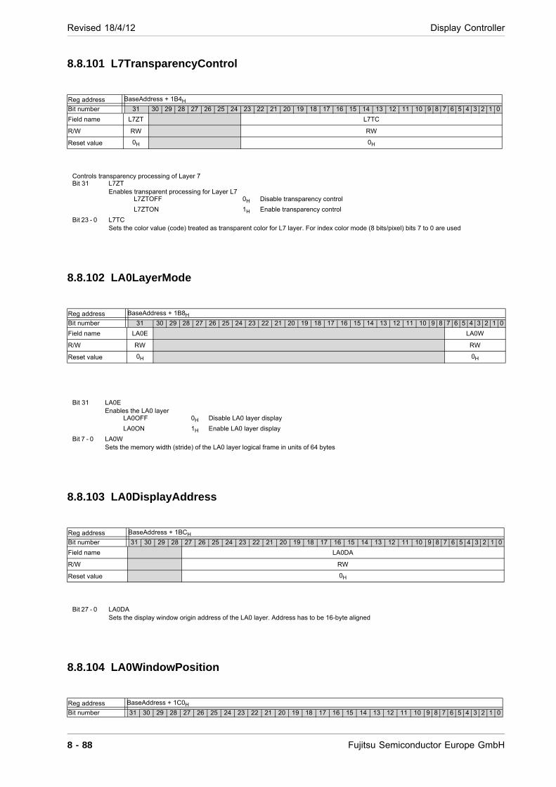
Revised 18/4/12 Display Controller
8.8.101 L7TransparencyControl
8.8.102 LA0LayerMode
8.8.103 LA0DisplayAddress
8.8.104 LA0WindowPosition
Reg address BaseAddress + 1B4H
Bit number 31 30 29 28 27 26 25 24 23 22 21 20 19 18 17 16 15 14 13 12 11 10 9 8 7 6 5 4 3 2 1 0
Field name L7ZT L7TC
R/W RW RW
Reset value 0H 0H
Controls transparency processing of Layer 7 Bit 31 L7ZT
Enables transparent processing for Layer L7 L7ZTOFF 0H Disable transparency control
L7ZTON 1H Enable transparency control
Bit 23 - 0 L7TC Sets the color value (code) treated as transparent color for L7 layer. For index color mode (8 bits/pixel) bits 7 to 0 are used
Reg address BaseAddress + 1B8H
Bit number 31 30 29 28 27 26 25 24 23 22 21 20 19 18 17 16 15 14 13 12 11 10 9 8 7 6 5 4 3 2 1 0
Field name LA0E LA0W
R/W RW RW
Reset value 0H 0H
Bit 31 LA0E Enables the LA0 layer
LA0OFF 0H Disable LA0 layer display
LA0ON 1H Enable LA0 layer display
Bit 7 - 0 LA0W Sets the memory width (stride) of the LA0 layer logical frame in units of 64 bytes
Reg address BaseAddress + 1BCH
Bit number 31 30 29 28 27 26 25 24 23 22 21 20 19 18 17 16 15 14 13 12 11 10 9 8 7 6 5 4 3 2 1 0
Field name LA0DA
R/W RW
Reset value 0H
Bit 27 - 0 LA0DA Sets the display window origin address of the LA0 layer. Address has to be 16-byte aligned
Reg address BaseAddress + 1C0H
Bit number 31 30 29 28 27 26 25 24 23 22 21 20 19 18 17 16 15 14 13 12 11 10 9 8 7 6 5 4 3 2 1 0
8 - 88 Fujitsu Semiconductor Europe GmbH
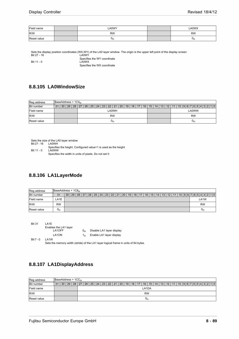
Display Controller Revised 18/4/12
8.8.105 LA0WindowSize
8.8.106 LA1LayerMode
8.8.107 LA1DisplayAddress
Field name LA0WY LA0WX
R/W RW RW
Reset value 0H 0H
Sets the display position coordinates (WX,WY) of the LA0 layer window. The origin is the upper left point of the display screen Bit 27 - 16 LA0WY
Specifies the WY coordinate Bit 11 - 0 LA0WX
Specifies the WX coordinate
Reg address BaseAddress + 1C4H
Bit number 31 30 29 28 27 26 25 24 23 22 21 20 19 18 17 16 15 14 13 12 11 10 9 8 7 6 5 4 3 2 1 0
Field name LA0WH LA0WW
R/W RW RW
Reset value 0H 0H
Sets the size of the LA0 layer window Bit 27 - 16 LA0WH
Specifies the height. Configured value+1 is used as the height Bit 11 - 0 LA0WW
Specifies the width in units of pixels. Do not set 0
Reg address BaseAddress + 1C8H
Bit number 31 30 29 28 27 26 25 24 23 22 21 20 19 18 17 16 15 14 13 12 11 10 9 8 7 6 5 4 3 2 1 0
Field name LA1E LA1W
R/W RW RW
Reset value 0H 0H
Bit 31 LA1E Enables the LA1 layer
LA1OFF 0H Disable LA1 layer display
LA1ON 1H Enable LA1 layer display
Bit 7 - 0 LA1W Sets the memory width (stride) of the LA1 layer logical frame in units of 64 bytes.
Reg address BaseAddress + 1CCH
Bit number 31 30 29 28 27 26 25 24 23 22 21 20 19 18 17 16 15 14 13 12 11 10 9 8 7 6 5 4 3 2 1 0
Field name LA1DA
R/W RW
Reset value 0H
Fujitsu Semiconductor Europe GmbH 8 - 89
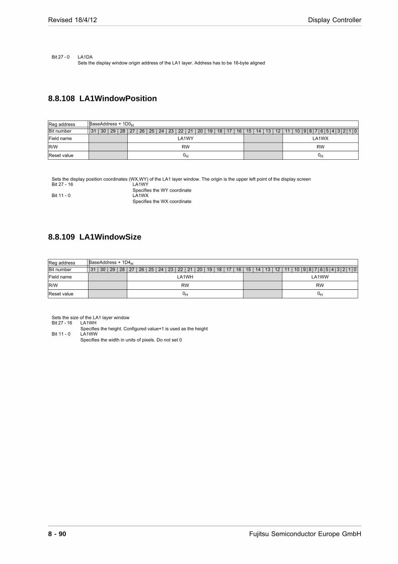
Revised 18/4/12 Display Controller
8.8.108 LA1WindowPosition
8.8.109 LA1WindowSize
Bit 27 - 0 LA1DA Sets the display window origin address of the LA1 layer. Address has to be 16-byte aligned
Reg address BaseAddress + 1D0H
Bit number 31 30 29 28 27 26 25 24 23 22 21 20 19 18 17 16 15 14 13 12 11 10 9 8 7 6 5 4 3 2 1 0
Field name LA1WY LA1WX
R/W RW RW
Reset value 0H 0H
Sets the display position coordinates (WX,WY) of the LA1 layer window. The origin is the upper left point of the display screen Bit 27 - 16 LA1WY
Specifies the WY coordinate Bit 11 - 0 LA1WX
Specifies the WX coordinate
Reg address BaseAddress + 1D4H
Bit number 31 30 29 28 27 26 25 24 23 22 21 20 19 18 17 16 15 14 13 12 11 10 9 8 7 6 5 4 3 2 1 0
Field name LA1WH LA1WW
R/W RW RW
Reset value 0H 0H
Sets the size of the LA1 layer window Bit 27 - 16 LA1WH
Specifies the height. Configured value+1 is used as the height Bit 11 - 0 LA1WW
Specifies the width in units of pixels. Do not set 0
8 - 90 Fujitsu Semiconductor Europe GmbH
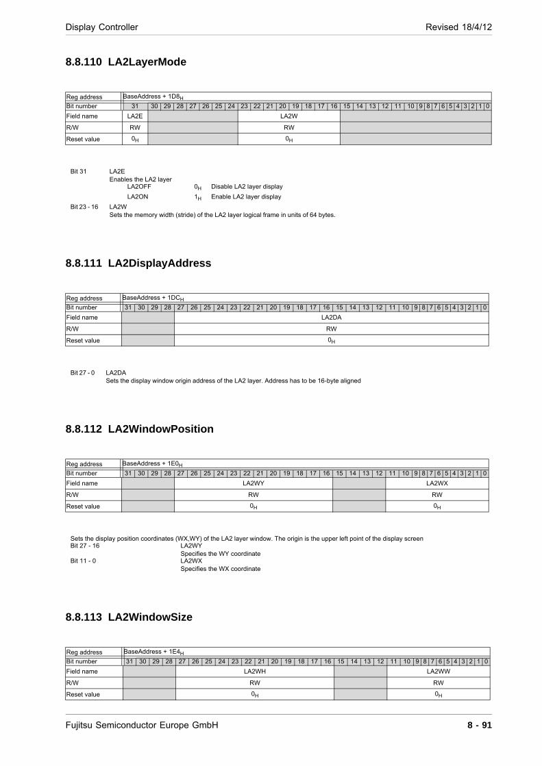
Display Controller Revised 18/4/12
8.8.110 LA2LayerMode
8.8.111 LA2DisplayAddress
8.8.112 LA2WindowPosition
8.8.113 LA2WindowSize
Reg address BaseAddress + 1D8H
Bit number 31 30 29 28 27 26 25 24 23 22 21 20 19 18 17 16 15 14 13 12 11 10 9 8 7 6 5 4 3 2 1 0
Field name LA2E LA2W
R/W RW RW
Reset value 0H 0H
Bit 31 LA2E Enables the LA2 layer
LA2OFF 0H Disable LA2 layer display
LA2ON 1H Enable LA2 layer display
Bit 23 - 16 LA2W Sets the memory width (stride) of the LA2 layer logical frame in units of 64 bytes.
Reg address BaseAddress + 1DCH
Bit number 31 30 29 28 27 26 25 24 23 22 21 20 19 18 17 16 15 14 13 12 11 10 9 8 7 6 5 4 3 2 1 0
Field name LA2DA
R/W RW
Reset value 0H
Bit 27 - 0 LA2DA Sets the display window origin address of the LA2 layer. Address has to be 16-byte aligned
Reg address BaseAddress + 1E0H
Bit number 31 30 29 28 27 26 25 24 23 22 21 20 19 18 17 16 15 14 13 12 11 10 9 8 7 6 5 4 3 2 1 0
Field name LA2WY LA2WX
R/W RW RW
Reset value 0H 0H
Sets the display position coordinates (WX,WY) of the LA2 layer window. The origin is the upper left point of the display screen Bit 27 - 16 LA2WY
Specifies the WY coordinate Bit 11 - 0 LA2WX
Specifies the WX coordinate
Reg address BaseAddress + 1E4H
Bit number 31 30 29 28 27 26 25 24 23 22 21 20 19 18 17 16 15 14 13 12 11 10 9 8 7 6 5 4 3 2 1 0
Field name LA2WH LA2WW
R/W RW RW
Reset value 0H 0H
Fujitsu Semiconductor Europe GmbH 8 - 91
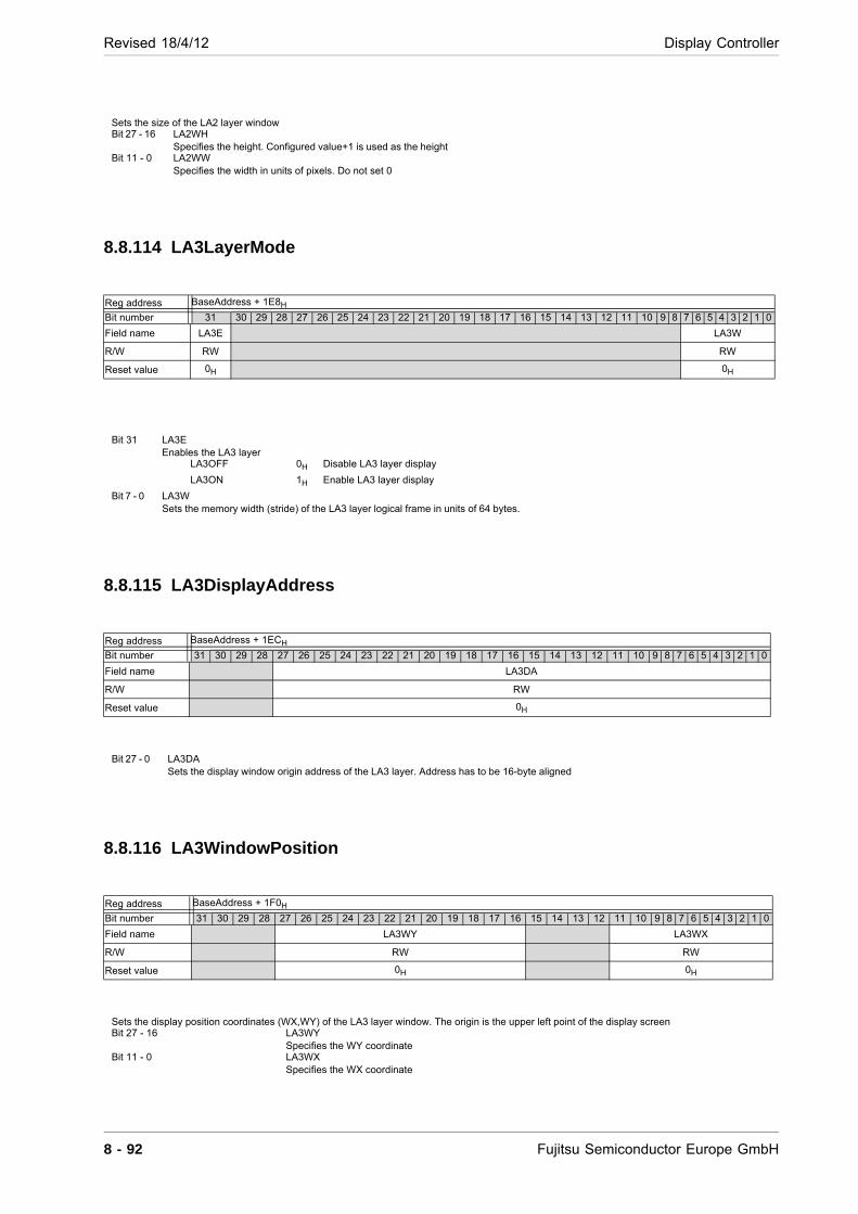
Revised 18/4/12 Display Controller
8.8.114 LA3LayerMode
8.8.115 LA3DisplayAddress
8.8.116 LA3WindowPosition
Sets the size of the LA2 layer window Bit 27 - 16 LA2WH
Specifies the height. Configured value+1 is used as the height Bit 11 - 0 LA2WW
Specifies the width in units of pixels. Do not set 0
Reg address BaseAddress + 1E8H
Bit number 31 30 29 28 27 26 25 24 23 22 21 20 19 18 17 16 15 14 13 12 11 10 9 8 7 6 5 4 3 2 1 0
Field name LA3E LA3W
R/W RW RW
Reset value 0H 0H
Bit 31 LA3E Enables the LA3 layer
LA3OFF 0H Disable LA3 layer display
LA3ON 1H Enable LA3 layer display
Bit 7 - 0 LA3W Sets the memory width (stride) of the LA3 layer logical frame in units of 64 bytes.
Reg address BaseAddress + 1ECH
Bit number 31 30 29 28 27 26 25 24 23 22 21 20 19 18 17 16 15 14 13 12 11 10 9 8 7 6 5 4 3 2 1 0
Field name LA3DA
R/W RW
Reset value 0H
Bit 27 - 0 LA3DA Sets the display window origin address of the LA3 layer. Address has to be 16-byte aligned
Reg address BaseAddress + 1F0H
Bit number 31 30 29 28 27 26 25 24 23 22 21 20 19 18 17 16 15 14 13 12 11 10 9 8 7 6 5 4 3 2 1 0
Field name LA3WY LA3WX
R/W RW RW
Reset value 0H 0H
Sets the display position coordinates (WX,WY) of the LA3 layer window. The origin is the upper left point of the display screen Bit 27 - 16 LA3WY
Specifies the WY coordinate Bit 11 - 0 LA3WX
Specifies the WX coordinate
8 - 92 Fujitsu Semiconductor Europe GmbH
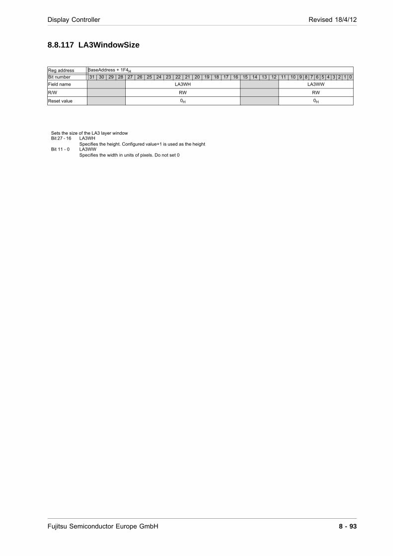
Display Controller Revised 18/4/12
8.8.117 LA3WindowSize
Reg address BaseAddress + 1F4H
Bit number 31 30 29 28 27 26 25 24 23 22 21 20 19 18 17 16 15 14 13 12 11 10 9 8 7 6 5 4 3 2 1 0
Field name LA3WH LA3WW
R/W RW RW
Reset value 0H 0H
Sets the size of the LA3 layer window Bit 27 - 16 LA3WH
Specifies the height. Configured value+1 is used as the height Bit 11 - 0 LA3WW
Specifies the width in units of pixels. Do not set 0
Fujitsu Semiconductor Europe GmbH 8 - 93
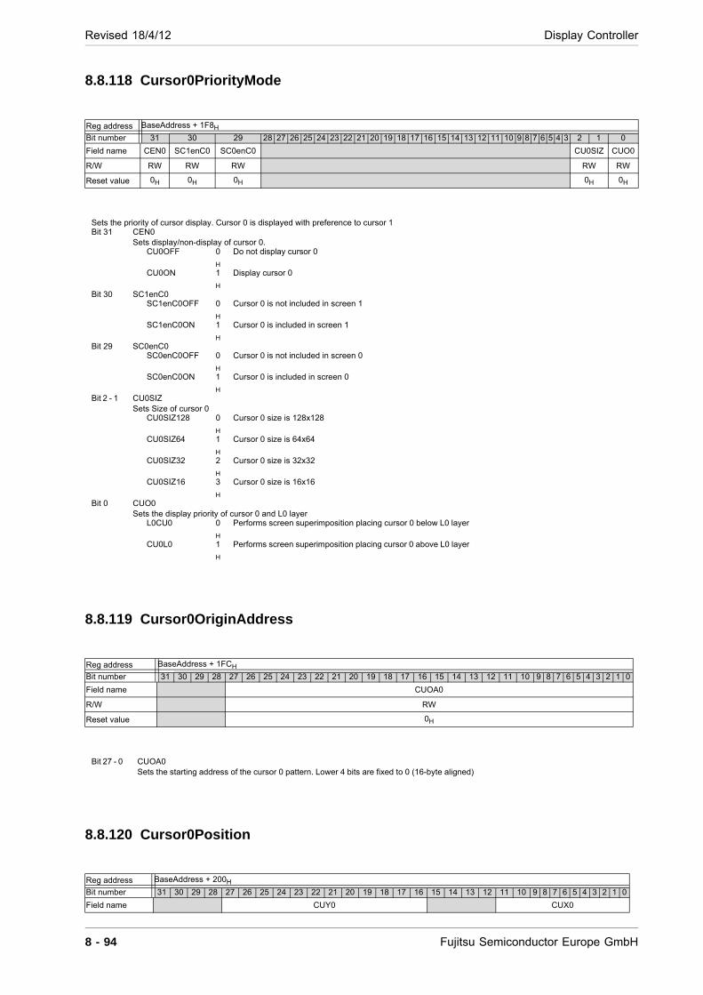
Revised 18/4/12 Display Controller
8.8.118 Cursor0PriorityMode
8.8.119 Cursor0OriginAddress
8.8.120 Cursor0Position
Reg address BaseAddress + 1F8H
Bit number 31 30 29 28 27 26 25 24 23 22 21 20 19 18 17 16 15 14 13 12 11 10 9 8 7 6 5 4 3 2 1 0
Field name CEN0 SC1enC0 SC0enC0 CU0SIZ CUO0
R/W RW RW RW RW RW
Reset value 0H 0H 0H 0H 0H
Sets the priority of cursor display. Cursor 0 is displayed with preference to cursor 1 Bit 31 CEN0
Sets display/non-display of cursor 0. CU0OFF 0
H
Do not display cursor 0
CU0ON 1
H
Display cursor 0
Bit 30 SC1enC0 SC1enC0OFF 0
H
Cursor 0 is not included in screen 1
SC1enC0ON 1
H
Cursor 0 is included in screen 1
Bit 29 SC0enC0 SC0enC0OFF 0
H
Cursor 0 is not included in screen 0
SC0enC0ON 1
H
Cursor 0 is included in screen 0
Bit 2 - 1 CU0SIZ Sets Size of cursor 0
CU0SIZ128 0
H
Cursor 0 size is 128x128
CU0SIZ64 1
H
Cursor 0 size is 64x64
CU0SIZ32 2
H
Cursor 0 size is 32x32
CU0SIZ16 3
H
Cursor 0 size is 16x16
Bit 0 CUO0 Sets the display priority of cursor 0 and L0 layer
L0CU0 0
H
Performs screen superimposition placing cursor 0 below L0 layer
CU0L0 1
H
Performs screen superimposition placing cursor 0 above L0 layer
Reg address BaseAddress + 1FCH
Bit number 31 30 29 28 27 26 25 24 23 22 21 20 19 18 17 16 15 14 13 12 11 10 9 8 7 6 5 4 3 2 1 0
Field name CUOA0
R/W RW
Reset value 0H
Bit 27 - 0 CUOA0 Sets the starting address of the cursor 0 pattern. Lower 4 bits are fixed to 0 (16-byte aligned)
Reg address BaseAddress + 200H
Bit number 31 30 29 28 27 26 25 24 23 22 21 20 19 18 17 16 15 14 13 12 11 10 9 8 7 6 5 4 3 2 1 0
Field name CUY0 CUX0
8 - 94 Fujitsu Semiconductor Europe GmbH
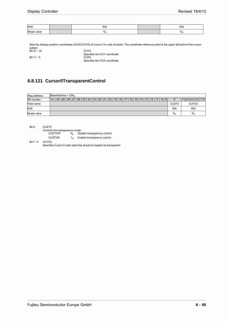
Display Controller Revised 18/4/12
8.8.121 Cursor0TransparentControl
R/W RW RW
Reset value 0H 0H
Sets the display position coordinates (CUX0,CUY0) of cursor 0 in units of pixels. The coordinate reference point is the upper left point of the cursor pattern Bit 27 - 16 CUY0
Specifies the CUY coordinate Bit 11 - 0 CUX0
Specifies the CUX coordinate.
Reg address BaseAddress + 204H
Bit number 31 30 29 28 27 26 25 24 23 22 21 20 19 18 17 16 15 14 13 12 11 10 9 8 7 6 5 4 3 2 1 0
Field name CUZT0 CUTC0
R/W RW RW
Reset value 0H 0H
Bit 8 CUZT0 Controls the transparency mode
CUZTOFF 0H Disable transparency control
CUZTON 1H Enable transparency control
Bit 7 - 0 CUTC0 Specifies Cursor 0 color data that shoub be treated as transparent
Fujitsu Semiconductor Europe GmbH 8 - 95
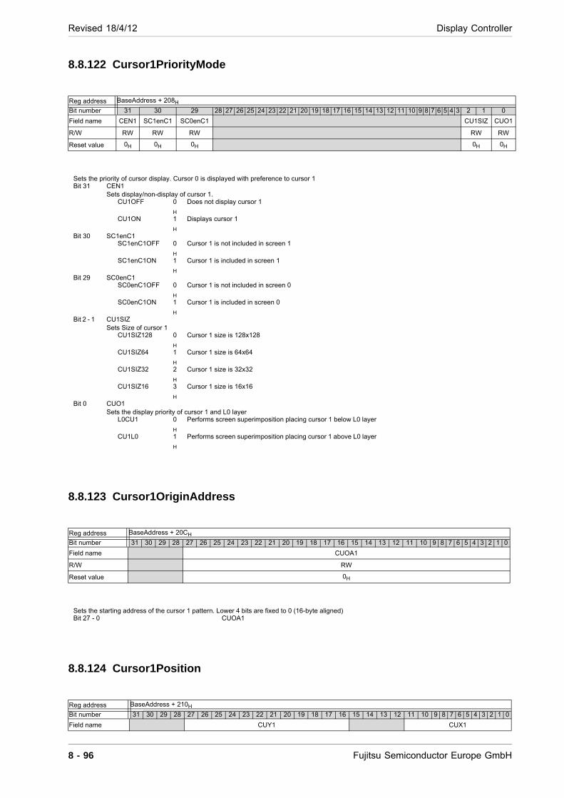
Revised 18/4/12 Display Controller
8.8.122 Cursor1PriorityMode
8.8.123 Cursor1OriginAddress
8.8.124 Cursor1Position
Reg address BaseAddress + 208H
Bit number 31 30 29 28 27 26 25 24 23 22 21 20 19 18 17 16 15 14 13 12 11 10 9 8 7 6 5 4 3 2 1 0
Field name CEN1 SC1enC1 SC0enC1 CU1SIZ CUO1
R/W RW RW RW RW RW
Reset value 0H 0H 0H 0H 0H
Sets the priority of cursor display. Cursor 0 is displayed with preference to cursor 1 Bit 31 CEN1
Sets display/non-display of cursor 1. CU1OFF 0
H
Does not display cursor 1
CU1ON 1
H
Displays cursor 1
Bit 30 SC1enC1 SC1enC1OFF 0
H
Cursor 1 is not included in screen 1
SC1enC1ON 1
H
Cursor 1 is included in screen 1
Bit 29 SC0enC1 SC0enC1OFF 0
H
Cursor 1 is not included in screen 0
SC0enC1ON 1
H
Cursor 1 is included in screen 0
Bit 2 - 1 CU1SIZ Sets Size of cursor 1
CU1SIZ128 0
H
Cursor 1 size is 128x128
CU1SIZ64 1
H
Cursor 1 size is 64x64
CU1SIZ32 2
H
Cursor 1 size is 32x32
CU1SIZ16 3
H
Cursor 1 size is 16x16
Bit 0 CUO1 Sets the display priority of cursor 1 and L0 layer
L0CU1 0
H
Performs screen superimposition placing cursor 1 below L0 layer
CU1L0 1
H
Performs screen superimposition placing cursor 1 above L0 layer
Reg address BaseAddress + 20CH
Bit number 31 30 29 28 27 26 25 24 23 22 21 20 19 18 17 16 15 14 13 12 11 10 9 8 7 6 5 4 3 2 1 0
Field name CUOA1
R/W RW
Reset value 0H
Sets the starting address of the cursor 1 pattern. Lower 4 bits are fixed to 0 (16-byte aligned) Bit 27 - 0 CUOA1
Reg address BaseAddress + 210H
Bit number 31 30 29 28 27 26 25 24 23 22 21 20 19 18 17 16 15 14 13 12 11 10 9 8 7 6 5 4 3 2 1 0
Field name CUY1 CUX1
8 - 96 Fujitsu Semiconductor Europe GmbH

Display Controller Revised 18/4/12
8.8.125 Cursor1TransparentControl
8.8.126 L1coefficient0
8.8.127 L1coefficient1
R/W RW RW
Reset value 0H 0H
Sets the display position coordinates (CUX1,CUY1) of cursor 1 in units of pixels. The coordinate reference point is the upper left point of the cursor pattern Bit 27 - 16 CUY1
Specifies the CUY coordinate Bit 11 - 0 CUX1
Specifies the CUX coordinate
Reg address BaseAddress + 214H
Bit number 31 30 29 28 27 26 25 24 23 22 21 20 19 18 17 16 15 14 13 12 11 10 9 8 7 6 5 4 3 2 1 0
Field name CUZT1 CUTC1
R/W RW RW
Reset value 0H 0H
Bit 8 CUZT1 Controls the transparency mode
CUZTOFF 0H Disable transparency control
CUZTON 1H Enable transparency control
Bit 7 - 0 CUTC1 Specifies Cursor 1 color data that should be treated as transparent
Reg address BaseAddress + 218H
Bit number 31 30 29 28 27 26 25 24 23 22 21 20 19 18 17 16 15 14 13 12 11 10 9 8 7 6 5 4 3 2 1 0
Field name L1a12 L1a11
R/W RW RW
Reset value 0H 12CH
Set color matrix of Layer 1 Bit 26 - 16 L1a12
11-bit signed fixed-point value. The lower 8 bits of the value are placed after the decimal point. The value is a two's complement representation
Bit 10 - 0 L1a11 11-bit signed fixed-point value. The lower 8 bits of the value are placed after the decimal point. The value is a two's complement representation
Reg address BaseAddress + 21CH
Bit number 31 30 29 28 27 26 25 24 23 22 21 20 19 18 17 16 15 14 13 12 11 10 9 8 7 6 5 4 3 2 1 0
Field name L1b1 L1a13
R/W RW RW
Reset value 1F0H 19AH
Fujitsu Semiconductor Europe GmbH 8 - 97
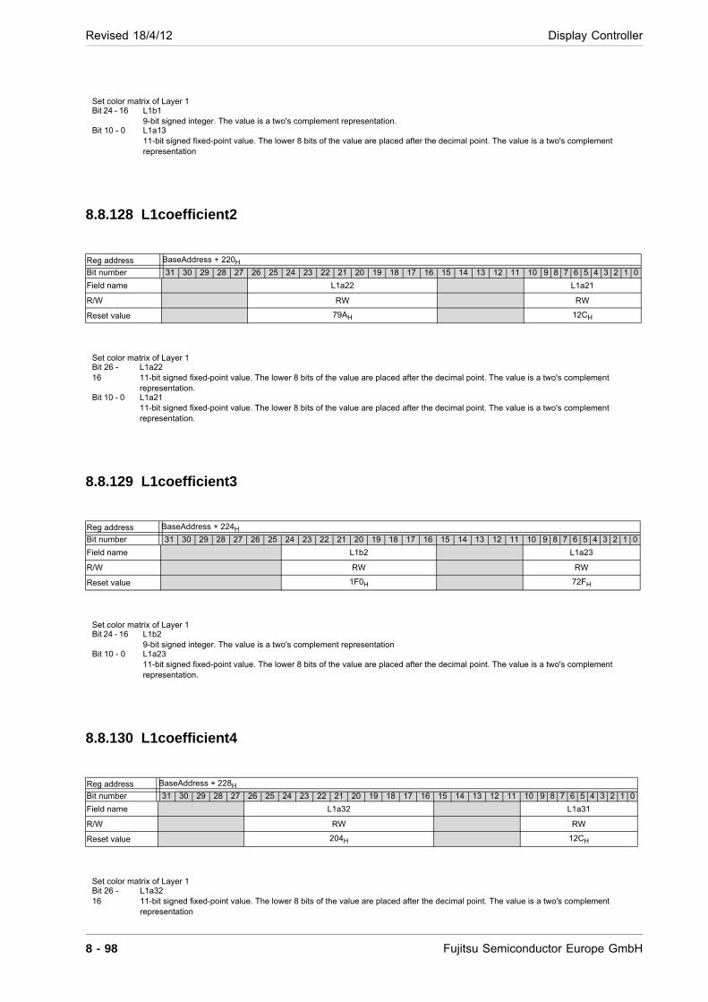
Revised 18/4/12 Display Controller
8.8.128 L1coefficient2
8.8.129 L1coefficient3
8.8.130 L1coefficient4
Set color matrix of Layer 1 Bit 24 - 16 L1b1
9-bit signed integer. The value is a two's complement representation. Bit 10 - 0 L1a13
11-bit signed fixed-point value. The lower 8 bits of the value are placed after the decimal point. The value is a two's complement representation
Reg address BaseAddress + 220H
Bit number 31 30 29 28 27 26 25 24 23 22 21 20 19 18 17 16 15 14 13 12 11 10 9 8 7 6 5 4 3 2 1 0
Field name L1a22 L1a21
R/W RW RW
Reset value 79AH 12CH
Set color matrix of Layer 1 Bit 26 - 16
L1a22 11-bit signed fixed-point value. The lower 8 bits of the value are placed after the decimal point. The value is a two's complement representation.
Bit 10 - 0 L1a21 11-bit signed fixed-point value. The lower 8 bits of the value are placed after the decimal point. The value is a two's complement representation.
Reg address BaseAddress + 224H
Bit number 31 30 29 28 27 26 25 24 23 22 21 20 19 18 17 16 15 14 13 12 11 10 9 8 7 6 5 4 3 2 1 0
Field name L1b2 L1a23
R/W RW RW
Reset value 1F0H 72FH
Set color matrix of Layer 1 Bit 24 - 16 L1b2
9-bit signed integer. The value is a two's complement representation Bit 10 - 0 L1a23
11-bit signed fixed-point value. The lower 8 bits of the value are placed after the decimal point. The value is a two's complement representation.
Reg address BaseAddress + 228H
Bit number 31 30 29 28 27 26 25 24 23 22 21 20 19 18 17 16 15 14 13 12 11 10 9 8 7 6 5 4 3 2 1 0
Field name L1a32 L1a31
R/W RW RW
Reset value 204H 12CH
Set color matrix of Layer 1 Bit 26 - 16
L1a32 11-bit signed fixed-point value. The lower 8 bits of the value are placed after the decimal point. The value is a two's complement representation
8 - 98 Fujitsu Semiconductor Europe GmbH

Display Controller Revised 18/4/12
8.8.131 L1coefficient5
8.8.132 L2coefficient0
8.8.133 L2coefficient1
Bit 10 - 0 L1a31 11-bit signed fixed-point value. The lower 8 bits of the value are placed after the decimal point. The value is a two's complement representation
Reg address BaseAddress + 22CH
Bit number 31 30 29 28 27 26 25 24 23 22 21 20 19 18 17 16 15 14 13 12 11 10 9 8 7 6 5 4 3 2 1 0
Field name L1b3 L1a33
R/W RW RW
Reset value 1F0H 0H
Set color matrix of Layer 1 Bit 24 - 16 L1b3
9-bit signed integer. The value is a two's complement representation Bit 10 - 0 L1a33
11-bit signed fixed-point value. The lower 8 bits of the value are placed after the decimal point. The value is a two's complement representation
Reg address BaseAddress + 230H
Bit number 31 30 29 28 27 26 25 24 23 22 21 20 19 18 17 16 15 14 13 12 11 10 9 8 7 6 5 4 3 2 1 0
Field name L2a12 L2a11
R/W RW RW
Reset value 0H 12CH
Set color matrix of Layer 2 Bit 26 - 16 L2a12
11-bit signed fixed-point value. The lower 8 bits of the value are placed after the decimal point. The value is a two's complement representation
Bit 10 - 0 L2a11 11-bit signed fixed-point value. The lower 8 bits of the value are placed after the decimal point. The value is a two's complement representation
Reg address BaseAddress + 234H
Bit number 31 30 29 28 27 26 25 24 23 22 21 20 19 18 17 16 15 14 13 12 11 10 9 8 7 6 5 4 3 2 1 0
Field name L2b1 L2a13
R/W RW RW
Reset value 1F0H 19AH
Set color matrix of Layer 2 Bit 24 - 16 L2b1
9-bit signed integer. The value is a two's complement representation. Bit 10 - 0 L2a13
11-bit signed fixed-point value. The lower 8 bits of the value are placed after the decimal point. The value is a two's complement representation
Fujitsu Semiconductor Europe GmbH 8 - 99
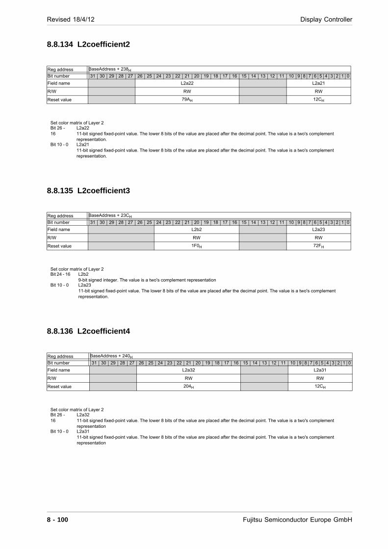
Revised 18/4/12 Display Controller
8.8.134 L2coefficient2
8.8.135 L2coefficient3
8.8.136 L2coefficient4
Reg address BaseAddress + 238H
Bit number 31 30 29 28 27 26 25 24 23 22 21 20 19 18 17 16 15 14 13 12 11 10 9 8 7 6 5 4 3 2 1 0
Field name L2a22 L2a21
R/W RW RW
Reset value 79AH 12CH
Set color matrix of Layer 2 Bit 26 - 16
L2a22 11-bit signed fixed-point value. The lower 8 bits of the value are placed after the decimal point. The value is a two's complement representation.
Bit 10 - 0 L2a21 11-bit signed fixed-point value. The lower 8 bits of the value are placed after the decimal point. The value is a two's complement representation.
Reg address BaseAddress + 23CH
Bit number 31 30 29 28 27 26 25 24 23 22 21 20 19 18 17 16 15 14 13 12 11 10 9 8 7 6 5 4 3 2 1 0
Field name L2b2 L2a23
R/W RW RW
Reset value 1F0H 72FH
Set color matrix of Layer 2 Bit 24 - 16 L2b2
9-bit signed integer. The value is a two's complement representation Bit 10 - 0 L2a23
11-bit signed fixed-point value. The lower 8 bits of the value are placed after the decimal point. The value is a two's complement representation.
Reg address BaseAddress + 240H
Bit number 31 30 29 28 27 26 25 24 23 22 21 20 19 18 17 16 15 14 13 12 11 10 9 8 7 6 5 4 3 2 1 0
Field name L2a32 L2a31
R/W RW RW
Reset value 204H 12CH
Set color matrix of Layer 2 Bit 26 - 16
L2a32 11-bit signed fixed-point value. The lower 8 bits of the value are placed after the decimal point. The value is a two's complement representation
Bit 10 - 0 L2a31 11-bit signed fixed-point value. The lower 8 bits of the value are placed after the decimal point. The value is a two's complement representation
8 - 100 Fujitsu Semiconductor Europe GmbH
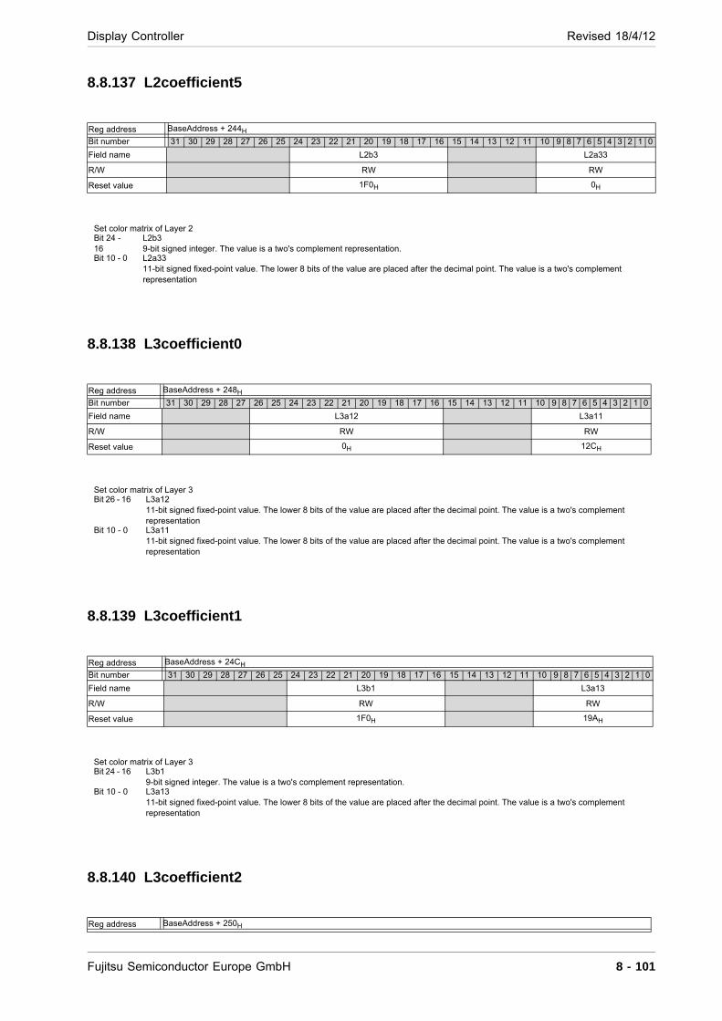
Display Controller Revised 18/4/12
8.8.137 L2coefficient5
8.8.138 L3coefficient0
8.8.139 L3coefficient1
8.8.140 L3coefficient2
Reg address BaseAddress + 244H
Bit number 31 30 29 28 27 26 25 24 23 22 21 20 19 18 17 16 15 14 13 12 11 10 9 8 7 6 5 4 3 2 1 0
Field name L2b3 L2a33
R/W RW RW
Reset value 1F0H 0H
Set color matrix of Layer 2 Bit 24 - 16
L2b3 9-bit signed integer. The value is a two's complement representation.
Bit 10 - 0 L2a33 11-bit signed fixed-point value. The lower 8 bits of the value are placed after the decimal point. The value is a two's complement representation
Reg address BaseAddress + 248H
Bit number 31 30 29 28 27 26 25 24 23 22 21 20 19 18 17 16 15 14 13 12 11 10 9 8 7 6 5 4 3 2 1 0
Field name L3a12 L3a11
R/W RW RW
Reset value 0H 12CH
Set color matrix of Layer 3 Bit 26 - 16 L3a12
11-bit signed fixed-point value. The lower 8 bits of the value are placed after the decimal point. The value is a two's complement representation
Bit 10 - 0 L3a11 11-bit signed fixed-point value. The lower 8 bits of the value are placed after the decimal point. The value is a two's complement representation
Reg address BaseAddress + 24CH
Bit number 31 30 29 28 27 26 25 24 23 22 21 20 19 18 17 16 15 14 13 12 11 10 9 8 7 6 5 4 3 2 1 0
Field name L3b1 L3a13
R/W RW RW
Reset value 1F0H 19AH
Set color matrix of Layer 3 Bit 24 - 16 L3b1
9-bit signed integer. The value is a two's complement representation. Bit 10 - 0 L3a13
11-bit signed fixed-point value. The lower 8 bits of the value are placed after the decimal point. The value is a two's complement representation
Reg address BaseAddress + 250H
Fujitsu Semiconductor Europe GmbH 8 - 101
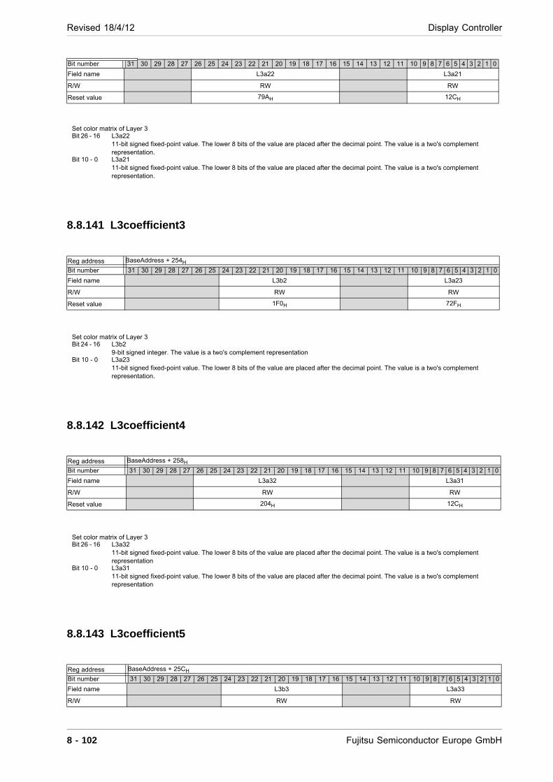
Revised 18/4/12 Display Controller
8.8.141 L3coefficient3
8.8.142 L3coefficient4
8.8.143 L3coefficient5
Bit number 31 30 29 28 27 26 25 24 23 22 21 20 19 18 17 16 15 14 13 12 11 10 9 8 7 6 5 4 3 2 1 0
Field name L3a22 L3a21
R/W RW RW
Reset value 79AH 12CH
Set color matrix of Layer 3 Bit 26 - 16 L3a22
11-bit signed fixed-point value. The lower 8 bits of the value are placed after the decimal point. The value is a two's complement representation.
Bit 10 - 0 L3a21 11-bit signed fixed-point value. The lower 8 bits of the value are placed after the decimal point. The value is a two's complement representation.
Reg address BaseAddress + 254H
Bit number 31 30 29 28 27 26 25 24 23 22 21 20 19 18 17 16 15 14 13 12 11 10 9 8 7 6 5 4 3 2 1 0
Field name L3b2 L3a23
R/W RW RW
Reset value 1F0H 72FH
Set color matrix of Layer 3 Bit 24 - 16 L3b2
9-bit signed integer. The value is a two's complement representation Bit 10 - 0 L3a23
11-bit signed fixed-point value. The lower 8 bits of the value are placed after the decimal point. The value is a two's complement representation.
Reg address BaseAddress + 258H
Bit number 31 30 29 28 27 26 25 24 23 22 21 20 19 18 17 16 15 14 13 12 11 10 9 8 7 6 5 4 3 2 1 0
Field name L3a32 L3a31
R/W RW RW
Reset value 204H 12CH
Set color matrix of Layer 3 Bit 26 - 16 L3a32
11-bit signed fixed-point value. The lower 8 bits of the value are placed after the decimal point. The value is a two's complement representation
Bit 10 - 0 L3a31 11-bit signed fixed-point value. The lower 8 bits of the value are placed after the decimal point. The value is a two's complement representation
Reg address BaseAddress + 25CH
Bit number 31 30 29 28 27 26 25 24 23 22 21 20 19 18 17 16 15 14 13 12 11 10 9 8 7 6 5 4 3 2 1 0
Field name L3b3 L3a33
R/W RW RW
8 - 102 Fujitsu Semiconductor Europe GmbH
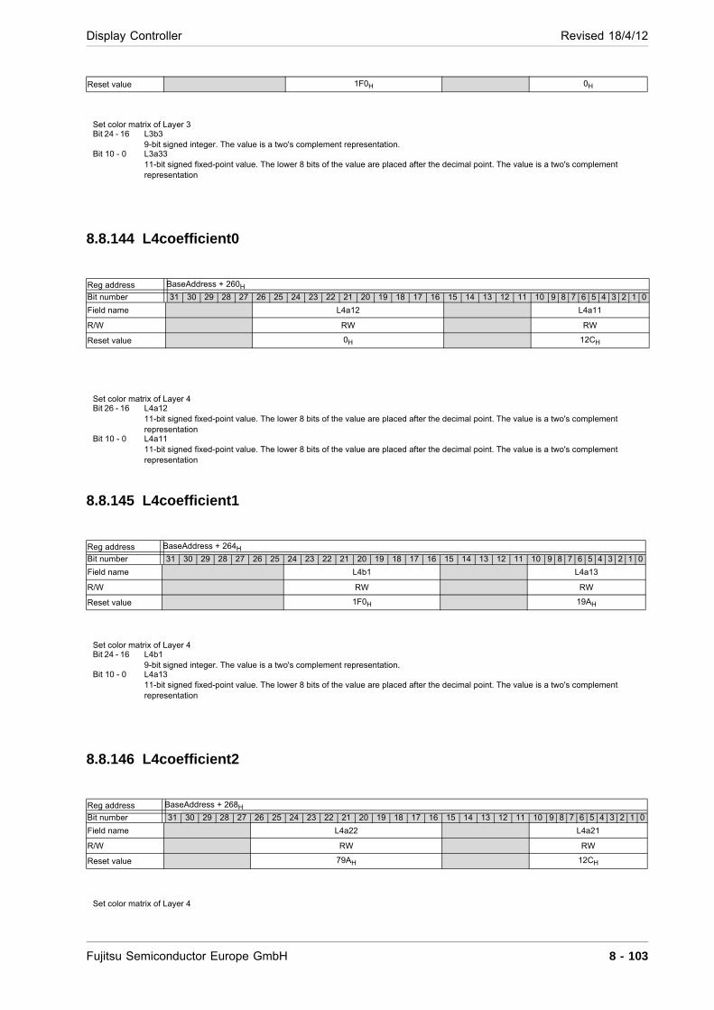
Display Controller Revised 18/4/12
8.8.144 L4coefficient0
8.8.145 L4coefficient1
8.8.146 L4coefficient2
Reset value 1F0H 0H
Set color matrix of Layer 3 Bit 24 - 16 L3b3
9-bit signed integer. The value is a two's complement representation. Bit 10 - 0 L3a33
11-bit signed fixed-point value. The lower 8 bits of the value are placed after the decimal point. The value is a two's complement representation
Reg address BaseAddress + 260H
Bit number 31 30 29 28 27 26 25 24 23 22 21 20 19 18 17 16 15 14 13 12 11 10 9 8 7 6 5 4 3 2 1 0
Field name L4a12 L4a11
R/W RW RW
Reset value 0H 12CH
Set color matrix of Layer 4 Bit 26 - 16 L4a12
11-bit signed fixed-point value. The lower 8 bits of the value are placed after the decimal point. The value is a two's complement representation
Bit 10 - 0 L4a11 11-bit signed fixed-point value. The lower 8 bits of the value are placed after the decimal point. The value is a two's complement representation
Reg address BaseAddress + 264H
Bit number 31 30 29 28 27 26 25 24 23 22 21 20 19 18 17 16 15 14 13 12 11 10 9 8 7 6 5 4 3 2 1 0
Field name L4b1 L4a13
R/W RW RW
Reset value 1F0H 19AH
Set color matrix of Layer 4 Bit 24 - 16 L4b1
9-bit signed integer. The value is a two's complement representation. Bit 10 - 0 L4a13
11-bit signed fixed-point value. The lower 8 bits of the value are placed after the decimal point. The value is a two's complement representation
Reg address BaseAddress + 268H
Bit number 31 30 29 28 27 26 25 24 23 22 21 20 19 18 17 16 15 14 13 12 11 10 9 8 7 6 5 4 3 2 1 0
Field name L4a22 L4a21
R/W RW RW
Reset value 79AH 12CH
Set color matrix of Layer 4
Fujitsu Semiconductor Europe GmbH 8 - 103
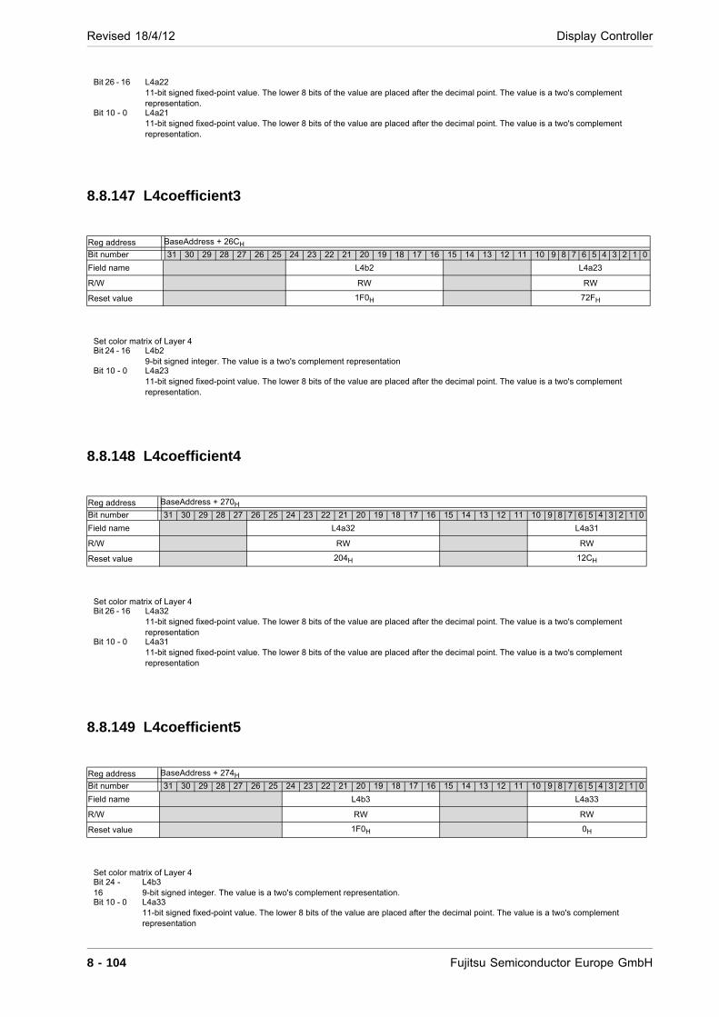
Revised 18/4/12 Display Controller
8.8.147 L4coefficient3
8.8.148 L4coefficient4
8.8.149 L4coefficient5
Bit 26 - 16 L4a22 11-bit signed fixed-point value. The lower 8 bits of the value are placed after the decimal point. The value is a two's complement representation.
Bit 10 - 0 L4a21 11-bit signed fixed-point value. The lower 8 bits of the value are placed after the decimal point. The value is a two's complement representation.
Reg address BaseAddress + 26CH
Bit number 31 30 29 28 27 26 25 24 23 22 21 20 19 18 17 16 15 14 13 12 11 10 9 8 7 6 5 4 3 2 1 0
Field name L4b2 L4a23
R/W RW RW
Reset value 1F0H 72FH
Set color matrix of Layer 4 Bit 24 - 16 L4b2
9-bit signed integer. The value is a two's complement representation Bit 10 - 0 L4a23
11-bit signed fixed-point value. The lower 8 bits of the value are placed after the decimal point. The value is a two's complement representation.
Reg address BaseAddress + 270H
Bit number 31 30 29 28 27 26 25 24 23 22 21 20 19 18 17 16 15 14 13 12 11 10 9 8 7 6 5 4 3 2 1 0
Field name L4a32 L4a31
R/W RW RW
Reset value 204H 12CH
Set color matrix of Layer 4 Bit 26 - 16 L4a32
11-bit signed fixed-point value. The lower 8 bits of the value are placed after the decimal point. The value is a two's complement representation
Bit 10 - 0 L4a31 11-bit signed fixed-point value. The lower 8 bits of the value are placed after the decimal point. The value is a two's complement representation
Reg address BaseAddress + 274H
Bit number 31 30 29 28 27 26 25 24 23 22 21 20 19 18 17 16 15 14 13 12 11 10 9 8 7 6 5 4 3 2 1 0
Field name L4b3 L4a33
R/W RW RW
Reset value 1F0H 0H
Set color matrix of Layer 4 Bit 24 - 16
L4b3 9-bit signed integer. The value is a two's complement representation.
Bit 10 - 0 L4a33 11-bit signed fixed-point value. The lower 8 bits of the value are placed after the decimal point. The value is a two's complement representation
8 - 104 Fujitsu Semiconductor Europe GmbH

Display Controller Revised 18/4/12
Fujitsu Semiconductor Europe GmbH 8 - 105
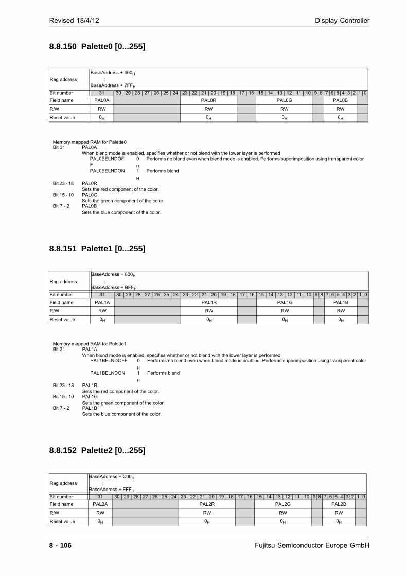
Revised 18/4/12 Display Controller
8.8.150 Palette0 [0...255]
8.8.151 Palette1 [0...255]
8.8.152 Palette2 [0...255]
Reg address
BaseAddress + 400H :BaseAddress + 7FFH
Bit number 31 30 29 28 27 26 25 24 23 22 21 20 19 18 17 16 15 14 13 12 11 10 9 8 7 6 5 4 3 2 1 0
Field name PAL0A PAL0R PAL0G PAL0B
R/W RW RW RW RW
Reset value 0H 0H 0H 0H
Memory mapped RAM for Palette0 Bit 31 PAL0A
When blend mode is enabled, specifies whether or not blend with the lower layer is performed PAL0BELNDOFF
0
H
Performs no blend even when blend mode is enabled. Performs superimposition using transparent color
PAL0BELNDON 1
H
Performs blend
Bit 23 - 18 PAL0R Sets the red component of the color.
Bit 15 - 10 PAL0G Sets the green component of the color.
Bit 7 - 2 PAL0B Sets the blue component of the color.
Reg address
BaseAddress + 800H :BaseAddress + BFFH
Bit number 31 30 29 28 27 26 25 24 23 22 21 20 19 18 17 16 15 14 13 12 11 10 9 8 7 6 5 4 3 2 1 0
Field name PAL1A PAL1R PAL1G PAL1B
R/W RW RW RW RW
Reset value 0H 0H 0H 0H
Memory mapped RAM for Palette1 Bit 31 PAL1A
When blend mode is enabled, specifies whether or not blend with the lower layer is performed PAL1BELNDOFF 0
H
Performs no blend even when blend mode is enabled. Performs superimposition using transparent color
PAL1BELNDON 1
H
Performs blend
Bit 23 - 18 PAL1R Sets the red component of the color.
Bit 15 - 10 PAL1G Sets the green component of the color.
Bit 7 - 2 PAL1B Sets the blue component of the color.
Reg address
BaseAddress + C00H :BaseAddress + FFFH
Bit number 31 30 29 28 27 26 25 24 23 22 21 20 19 18 17 16 15 14 13 12 11 10 9 8 7 6 5 4 3 2 1 0
Field name PAL2A PAL2R PAL2G PAL2B
R/W RW RW RW RW
Reset value 0H 0H 0H 0H
8 - 106 Fujitsu Semiconductor Europe GmbH
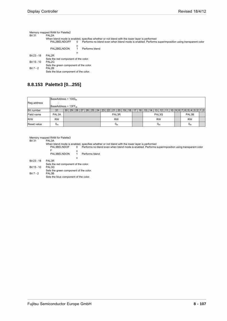
Display Controller Revised 18/4/12
8.8.153 Palette3 [0...255]
Memory mapped RAM for Palette2 Bit 31 PAL2A
When blend mode is enabled, specifies whether or not blend with the lower layer is performed PAL2BELNDOFF 0
H
Performs no blend even when blend mode is enabled. Performs superimposition using transparent color
PAL2BELNDON 1
H
Performs blend
Bit 23 - 18 PAL2R Sets the red component of the color.
Bit 15 - 10 PAL2G Sets the green component of the color.
Bit 7 - 2 PAL2B Sets the blue component of the color.
Reg address
BaseAddress + 1000H :BaseAddress + 13FFH
Bit number 31 30 29 28 27 26 25 24 23 22 21 20 19 18 17 16 15 14 13 12 11 10 9 8 7 6 5 4 3 2 1 0
Field name PAL3A PAL3R PAL3G PAL3B
R/W RW RW RW RW
Reset value 0H 0H 0H 0H
Memory mapped RAM for Palette3 Bit 31 PAL3A
When blend mode is enabled, specifies whether or not blend with the lower layer is performed PAL3BELNDOFF
0
H
Performs no blend even when blend mode is enabled. Performs superimposition using transparent color
PAL3BELNDON 1
H
Performs blend
Bit 23 - 18 PAL3R Sets the red component of the color.
Bit 15 - 10 PAL3G Sets the green component of the color.
Bit 7 - 2 PAL3B Sets the blue component of the color.
Fujitsu Semiconductor Europe GmbH 8 - 107
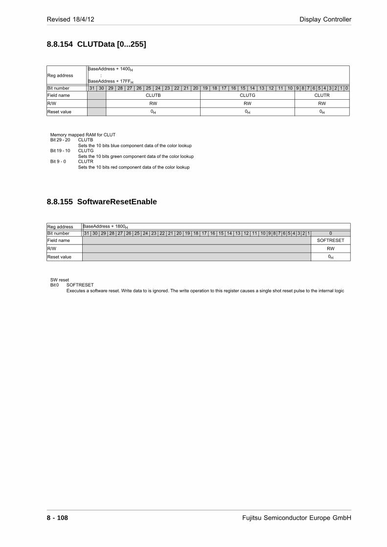
Revised 18/4/12 Display Controller
8.8.154 CLUTData [0...255]
8.8.155 SoftwareResetEnable
Reg address
BaseAddress + 1400H :BaseAddress + 17FFH
Bit number 31 30 29 28 27 26 25 24 23 22 21 20 19 18 17 16 15 14 13 12 11 10 9 8 7 6 5 4 3 2 1 0
Field name CLUTB CLUTG CLUTR
R/W RW RW RW
Reset value 0H 0H 0H
Memory mapped RAM for CLUT Bit 29 - 20 CLUTB
Sets the 10 bits blue component data of the color lookup Bit 19 - 10 CLUTG
Sets the 10 bits green component data of the color lookup Bit 9 - 0 CLUTR
Sets the 10 bits red component data of the color lookup
Reg address BaseAddress + 1800H
Bit number 31 30 29 28 27 26 25 24 23 22 21 20 19 18 17 16 15 14 13 12 11 10 9 8 7 6 5 4 3 2 1 0
Field name SOFTRESET
R/W RW
Reset value 0H
SW reset Bit 0 SOFTRESET
Executes a software reset. Write data to is ignored. The write operation to this register causes a single shot reset pulse to the internal logic
8 - 108 Fujitsu Semiconductor Europe GmbH
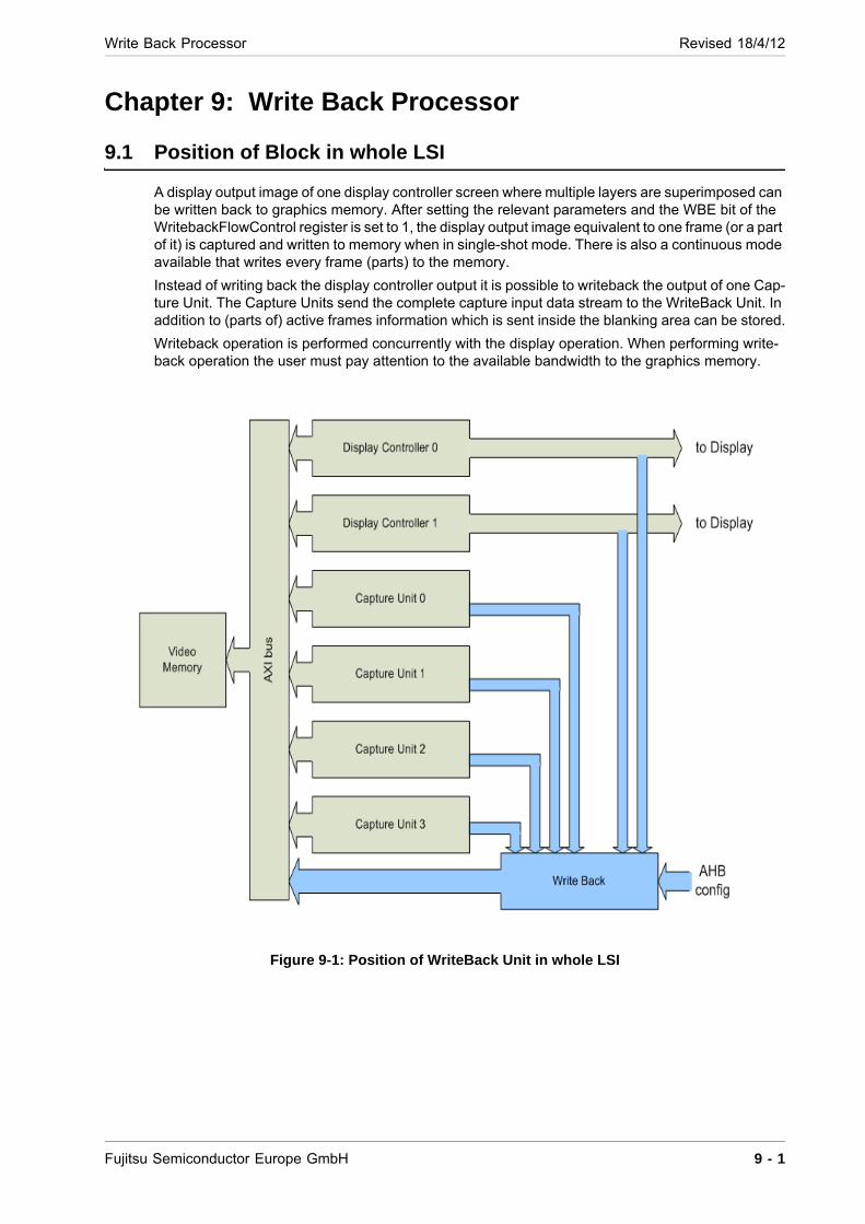
Write Back Processor Revised 18/4/12
Chapter 9: Write Back Processor
9.1 Position of Block in whole LSI
A display output image of one display controller screen where multiple layers are superimposed can be written back to graphics memory. After setting the relevant parameters and the WBE bit of the WritebackFlowControl register is set to 1, the display output image equivalent to one frame (or a part of it) is captured and written to memory when in single-shot mode. There is also a continuous mode available that writes every frame (parts) to the memory.
Instead of writing back the display controller output it is possible to writeback the output of one Cap-ture Unit. The Capture Units send the complete capture input data stream to the WriteBack Unit. In addition to (parts of) active frames information which is sent inside the blanking area can be stored.
Writeback operation is performed concurrently with the display operation. When performing write-back operation the user must pay attention to the available bandwidth to the graphics memory.
Figure 9-1: Position of WriteBack Unit in whole LSI
Fujitsu Semiconductor Europe GmbH 9 - 1
Revised 18/4/12 Write Back Processor
9.2 Feature List
9.2.1 Write Back Mode
The WriteBack Unit can operate in single-shot or continuous mode:
Single shot – only one frame is captured after setting a trigger by SW
Continuous – every frame is captured
NOTE When using continuous mode please respect the bandwidth conditions in the whole system to avoid unnecessary distortion of after operation or distorted write back image. Use only for small windows (e.g. one line)
9.2.2 Source Selection
The WriteBack Unit can select data from different sources – Display Controllers and Capture Units.
The table below shows the different possibilities that can be selected.
Table 9-1: Source selection
For the details of single and dual screen mode please see the display controller specification.
In the Display Controller pixel data is used from the pipeline stage before the Color LUT + Dithering.
The Capture Units supply raw ITU656 8-bit (after decoding of the ITU656 sync word) to the Write-Back Unit.
9.2.3 Field Selection
The fields for interlaced writeback operation can be selected according to the specified mode.
001: Odd field mode or non-interlace [default]
010: Even field mode
011: Both fields mode
111: Both fields mode (no field discrimination is performed)
9.2.4 Interrupt
The WriteBack Unit issues an interrupt after completion of the operation. (i.e. after two fields in “both fields” mode – see above).
If the Continuous mode is enabled the interrupt is issued after each frame (part).
The WB_INT port is a registered output which sends one pulse synchron to HCLK input.
Vsel Source
000 Display Controller 0 (single screen or dual screen 0)010 Display Controller 0 (dual screen 1)001 Display Controller 1 (single screen or dual screen 0)
011 Display Controller 1 (dual screen 1)100 Capture 0101 Capture 1 110 Capture 2111 Capture 3
9 - 2 Fujitsu Semiconductor Europe GmbH
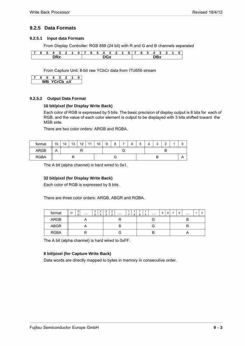
Write Back Processor Revised 18/4/12
9.2.5 Data Formats
9.2.5.1 Input data Formats
From Display Controller: RGB 888 (24 bit) with R and G and B channels separated
From Capture Unit: 8-bit raw YCbCr data from ITU656 stream
9.2.5.2 Output Data Format
16 bit/pixel (for Display Write Back)
Each color of RGB is expressed by 5 bits. The basic precision of display output is 8 bits for each of RGB, and the value of each color element is output to be displayed with 3 bits shifted toward the MSB side.
There are two color orders: ARGB and RGBA.
The A bit (alpha channel) is hard wired to 0x1.
32 bit/pixel (for Display Write Back)
Each color of RGB is expressed by 8 bits.
There are three color orders: ARGB, ABGR and RGBA.
The A bit (alpha channel) is hard wired to 0xFF.
8 bit/pixel (for Capture Write Back)
Data words are directly mapped to bytes in memory in consecutive order.
7 6 5 4 3 2 1 0 7 6 5 4 3 2 1 0 7 6 5 4 3 2 1 0DRx DGx DBx
7 6 5 4 3 2 1 0WB_YCrCb_cX
format 15 14 13 12 11 10 9 8 7 6 5 4 3 2 1 0
ARGB A R G B
RGBA R G B A
format 3130 2
524
23
22 1
716
15
14 9 8 7 6 1 0
ARGB A R G B
ABGR A B G R
RGBA R G B A
Fujitsu Semiconductor Europe GmbH 9 - 3

Revised 18/4/12 Write Back Processor
9.3 Processing Mode
9.3.1 Processing Flow
The write-back data processing is very simple and straightforward. The WriteBack Unit selects the data from a dedicated video source and calculates the corresponding memory address for data stor-age. An internal FIFO is used to convert the pixel data stream to 64 bit words for the memory access.
Figure 9-2: Data Processing Flow of Writeback Processor
9.3.2 Processing Algorithm
9.3.2.1 Cropping
A clip frame can be specified with the following register fields WIHSTR, WIVSTR, WIHEND, WIVEND. Only the area inside the clip frame is used for write-back operation.
9 - 4 Fujitsu Semiconductor Europe GmbH

Write Back Processor Revised 18/4/12
Figure 9-3: Writeback Processor: Clip frame
With the fields of register WritebackVstrEnd a different vertical start and end address can be spec-ified for the writeback operation of even fields. (WBVSRES instead of WIVSTR and WBVERES in-stead of WIVEND)
NOTE Always set WIHSTR < WIHEND and WIVSTR < WIVEND
NOTE The (0,0) position is different if output from capture or display is used in WriteBack:Display -> (0,0) is pixel when data enable switches to HIGH the first time after VSYNCCapture -> (0,0) is first data word after first HSYNC after VSYNC (do not set to start values to 0,0 though)
9.3.2.2 Field Modes
For interlaced input from Display Controller there are several modes (fied mode FM) available for writing the data to memory.
The starting address of the transfer destination of an image is defined as shown below.
WBOA0: odd field (or non-interlaced sources)
WBOA1: even field
However, for FM = 111 odd fields and even fields are not distinguished from each other, and first field is written to the area beginning at WBOA0 and second field is written after the first field.
Figure 9-4: Writeback Processor: Frame Modes
(0, 0)
(WIHSTR, WIVSTR)
(WIHEND, WIVEND)
Fujitsu Semiconductor Europe GmbH 9 - 5
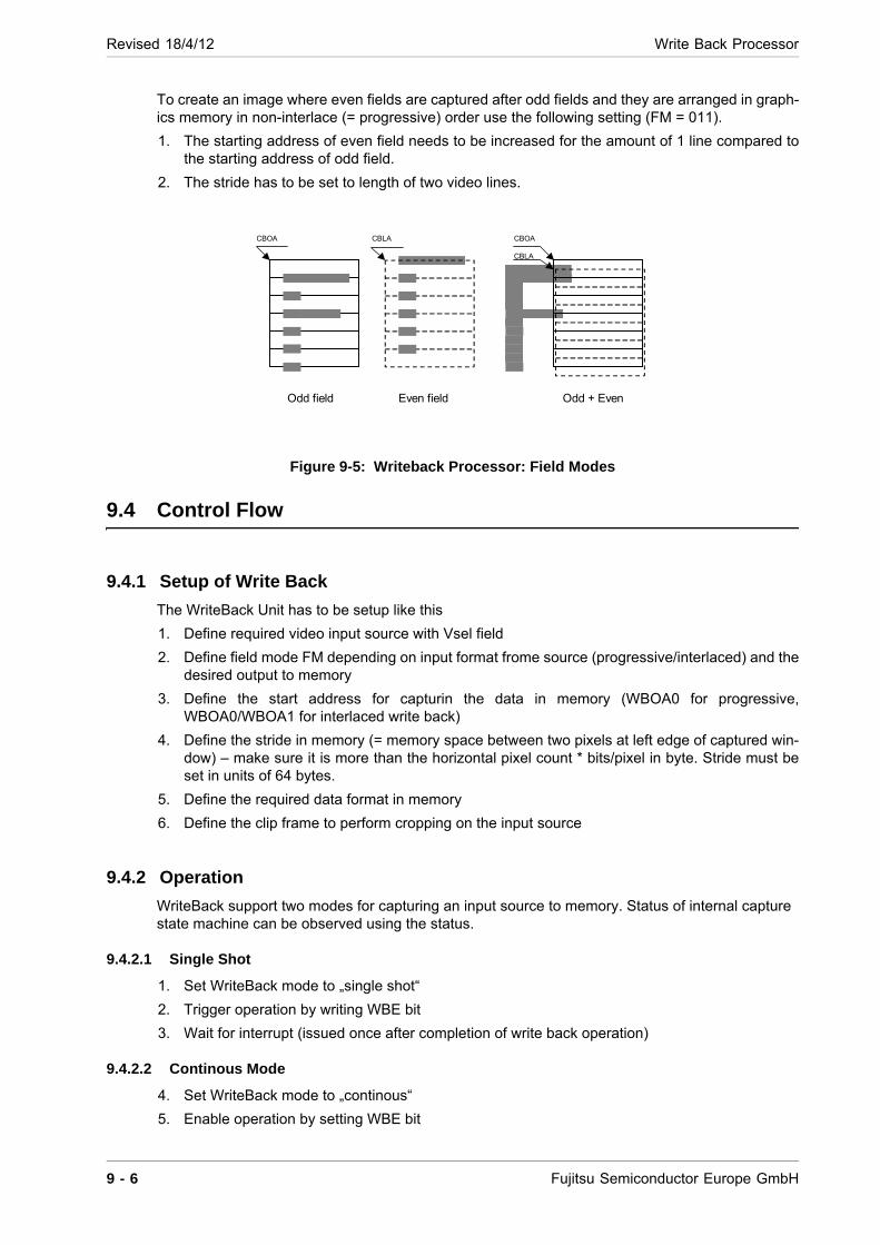
Revised 18/4/12 Write Back Processor
To create an image where even fields are captured after odd fields and they are arranged in graph-ics memory in non-interlace (= progressive) order use the following setting (FM = 011).
1. The starting address of even field needs to be increased for the amount of 1 line compared to the starting address of odd field.
2. The stride has to be set to length of two video lines.
Figure 9-5: Writeback Processor: Field Modes
9.4 Control Flow
9.4.1 Setup of Write Back
The WriteBack Unit has to be setup like this
1. Define required video input source with Vsel field
2. Define field mode FM depending on input format frome source (progressive/interlaced) and the desired output to memory
3. Define the start address for capturin the data in memory (WBOA0 for progressive, WBOA0/WBOA1 for interlaced write back)
4. Define the stride in memory (= memory space between two pixels at left edge of captured win-dow) – make sure it is more than the horizontal pixel count * bits/pixel in byte. Stride must be set in units of 64 bytes.
5. Define the required data format in memory
6. Define the clip frame to perform cropping on the input source
9.4.2 Operation
WriteBack support two modes for capturing an input source to memory. Status of internal capture state machine can be observed using the status.
9.4.2.1 Single Shot
1. Set WriteBack mode to „single shot“
2. Trigger operation by writing WBE bit
3. Wait for interrupt (issued once after completion of write back operation)
9.4.2.2 Continous Mode
4. Set WriteBack mode to „continous“
5. Enable operation by setting WBE bit
CBLA
CBOA CBOA CBLA
Odd field Even field Odd + Even
9 - 6 Fujitsu Semiconductor Europe GmbH

Write Back Processor Revised 18/4/12
6. Wait for interrupt (issued after each captured frame)
NOTE Be sure that enough bandwidth to memory is available when triggering a write back operation. Otherwise operation of the rest of system can be disturbed or the captured image can be corrupted.
Fujitsu Semiconductor Europe GmbH 9 - 7

Revised 18/4/12 Write Back Processor
9.5 Software Interface
9.5.1 Register Summary
Table 9-2: Register Overview
9.6 Writeback Register Description
9.6.1 WritebackSoftwareReset
Address Register Name Description
Base address + 0H WritebackSoftwareReset This register executes a software reset. Write data is ignored. Write operation sends a single shot reset pulse to the internal logic.
Base address + 4H WritebackFlowControl This register is used to configure and enable/disable the WriteBack unit.
Base address + 8H WritebackStatus Shows the current internal status of the WriteBack unit
Base address + CH WritebackMode This register is used to configure the video source and video data format for the WriteBack unit.
Base address + 10H WritebackOriginAddress0 This register specifies the address in memory for area 0
Base address + 14H WritebackOriginAddress1 This register specifies the address in memory for area 1
Base address + 18H WritebackStart Start co-ordinates of the writeback frame Base address + 1CH WritebackEnd End co-ordinates of the writeback frame Base address + 24H WritebackVstrEnd
Regr address BaseAddress + 0H
Bit number 31 30 29 28 27 26 25 24 23 22 21 20 19 18 17 16 15 14 13 12 11 10 9 8 7 6 5 4 3 2 1 0
Field name SOFTRESET
R/W RW
Reset value 0H
This register executes a software reset. Write data is ignored. Write operation sends a single shot reset pulse to the internal logic. Bit 0 SOFTRESET
Write: Software Reset
9 - 8 Fujitsu Semiconductor Europe GmbH
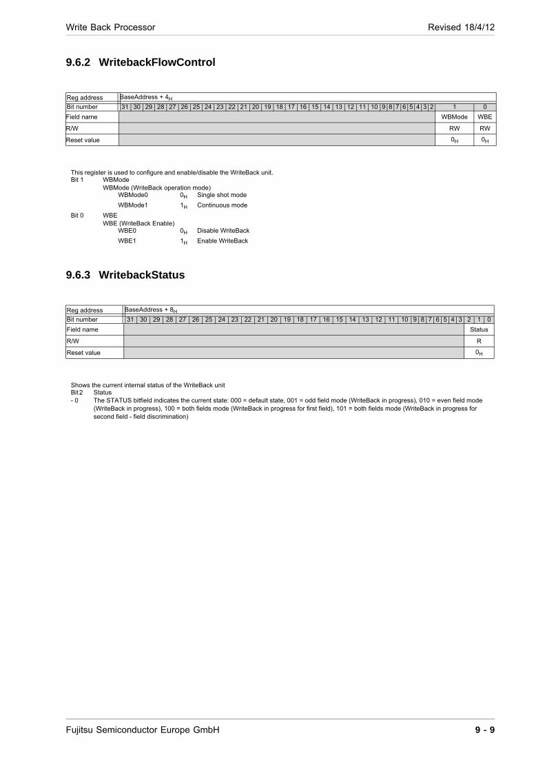
Write Back Processor Revised 18/4/12
9.6.2 WritebackFlowControl
9.6.3 WritebackStatus
Reg address BaseAddress + 4H
Bit number 31 30 29 28 27 26 25 24 23 22 21 20 19 18 17 16 15 14 13 12 11 10 9 8 7 6 5 4 3 2 1 0
Field name WBMode WBE
R/W RW RW
Reset value 0H 0H
This register is used to configure and enable/disable the WriteBack unit. Bit 1 WBMode
WBMode (WriteBack operation mode) WBMode0 0H Single shot mode
WBMode1 1H Continuous mode
Bit 0 WBE WBE (WriteBack Enable)
WBE0 0H Disable WriteBack
WBE1 1H Enable WriteBack
Reg address BaseAddress + 8H
Bit number 31 30 29 28 27 26 25 24 23 22 21 20 19 18 17 16 15 14 13 12 11 10 9 8 7 6 5 4 3 2 1 0
Field name Status
R/W R
Reset value 0H
Shows the current internal status of the WriteBack unit Bit 2 - 0
Status The STATUS bitfield indicates the current state: 000 = default state, 001 = odd field mode (WriteBack in progress), 010 = even field mode (WriteBack in progress), 100 = both fields mode (WriteBack in progress for first field), 101 = both fields mode (WriteBack in progress for second field - field discrimination)
Fujitsu Semiconductor Europe GmbH 9 - 9
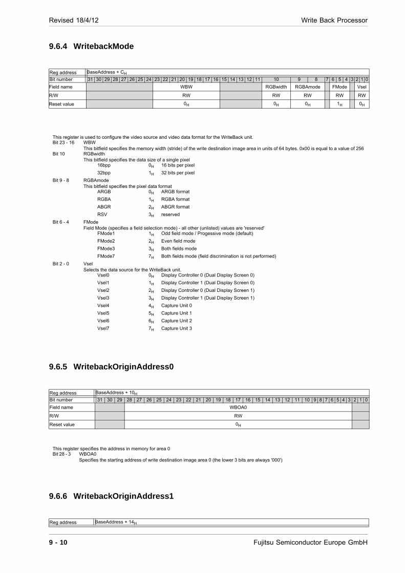
Revised 18/4/12 Write Back Processor
9.6.4 WritebackMode
9.6.5 WritebackOriginAddress0
9.6.6 WritebackOriginAddress1
Reg address BaseAddress + CH
Bit number 31 30 29 28 27 26 25 24 23 22 21 20 19 18 17 16 15 14 13 12 11 10 9 8 7 6 5 4 3 2 1 0
Field name WBW RGBwidth RGBAmode FMode Vsel
R/W RW RW RW RW RW
Reset value 0H 0H 0H 1H 0H
This register is used to configure the video source and video data format for the WriteBack unit. Bit 23 - 16 WBW
This bitfield specifies the memory width (stride) of the write destination image area in units of 64 bytes. 0x00 is equal to a value of 256 Bit 10 RGBwidth
This bitfield specifies the data size of a single pixel 16bpp 0H 16 bits per pixel
32bpp 1H 32 bits per pixel
Bit 9 - 8 RGBAmode This bitfield specifies the pixel data format
ARGB 0H ARGB format
RGBA 1H RGBA format
ABGR 2H ABGR format
RSV 3H reserved
Bit 6 - 4 FMode Field Mode (specifies a field selection mode) - all other (unlisted) values are 'reserved'
FMode1 1H Odd field mode / Progessive mode (default)
FMode2 2H Even field mode
FMode3 3H Both fields mode
FMode7 7H Both fields mode (field discrimination is not performed)
Bit 2 - 0 Vsel Selects the data source for the WriteBack unit.
Vsel0 0H Display Controller 0 (Dual Display Screen 0)
Vsel1 1H Display Controller 1 (Dual Display Screen 0)
Vsel2 2H Display Controller 0 (Dual Display Screen 1)
Vsel3 3H Display Controller 1 (Dual Display Screen 1)
Vsel4 4H Capture Unit 0
Vsel5 5H Capture Unit 1
Vsel6 6H Capture Unit 2
Vsel7 7H Capture Unit 3
Reg address BaseAddress + 10H
Bit number 31 30 29 28 27 26 25 24 23 22 21 20 19 18 17 16 15 14 13 12 11 10 9 8 7 6 5 4 3 2 1 0
Field name WBOA0
R/W RW
Reset value 0H
This register specifies the address in memory for area 0 Bit 28 - 3 WBOA0
Specifies the starting address of write destination image area 0 (the lower 3 bits are always '000')
Reg address BaseAddress + 14H
9 - 10 Fujitsu Semiconductor Europe GmbH
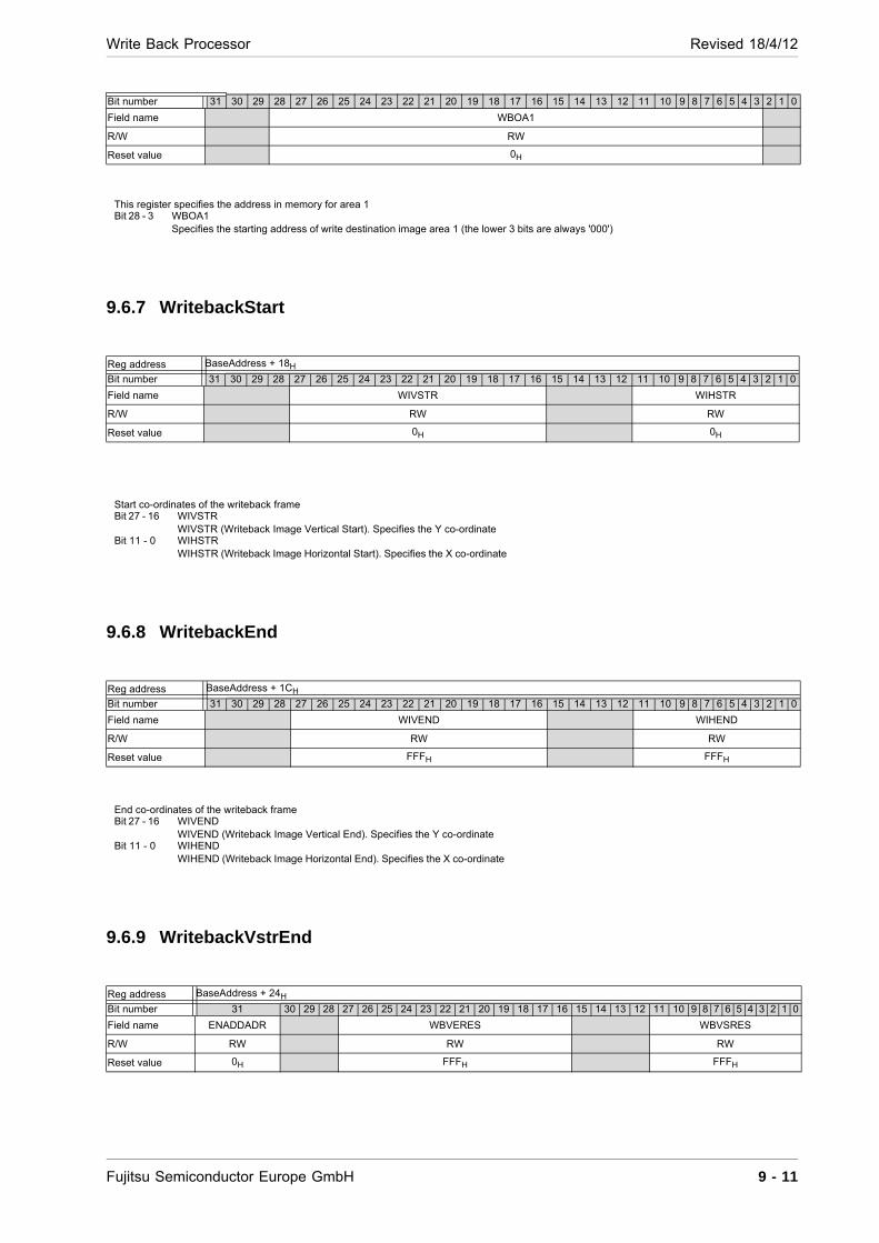
Write Back Processor Revised 18/4/12
9.6.7 WritebackStart
9.6.8 WritebackEnd
9.6.9 WritebackVstrEnd
Bit number 31 30 29 28 27 26 25 24 23 22 21 20 19 18 17 16 15 14 13 12 11 10 9 8 7 6 5 4 3 2 1 0
Field name WBOA1
R/W RW
Reset value 0H
This register specifies the address in memory for area 1 Bit 28 - 3 WBOA1
Specifies the starting address of write destination image area 1 (the lower 3 bits are always '000')
Reg address BaseAddress + 18H
Bit number 31 30 29 28 27 26 25 24 23 22 21 20 19 18 17 16 15 14 13 12 11 10 9 8 7 6 5 4 3 2 1 0
Field name WIVSTR WIHSTR
R/W RW RW
Reset value 0H 0H
Start co-ordinates of the writeback frame Bit 27 - 16 WIVSTR
WIVSTR (Writeback Image Vertical Start). Specifies the Y co-ordinate Bit 11 - 0 WIHSTR
WIHSTR (Writeback Image Horizontal Start). Specifies the X co-ordinate
Reg address BaseAddress + 1CH
Bit number 31 30 29 28 27 26 25 24 23 22 21 20 19 18 17 16 15 14 13 12 11 10 9 8 7 6 5 4 3 2 1 0
Field name WIVEND WIHEND
R/W RW RW
Reset value FFFH FFFH
End co-ordinates of the writeback frame Bit 27 - 16 WIVEND
WIVEND (Writeback Image Vertical End). Specifies the Y co-ordinate Bit 11 - 0 WIHEND
WIHEND (Writeback Image Horizontal End). Specifies the X co-ordinate
Reg address BaseAddress + 24H
Bit number 31 30 29 28 27 26 25 24 23 22 21 20 19 18 17 16 15 14 13 12 11 10 9 8 7 6 5 4 3 2 1 0
Field name ENADDADR WBVERES WBVSRES
R/W RW RW RW
Reset value 0H FFFH FFFH
Fujitsu Semiconductor Europe GmbH 9 - 11
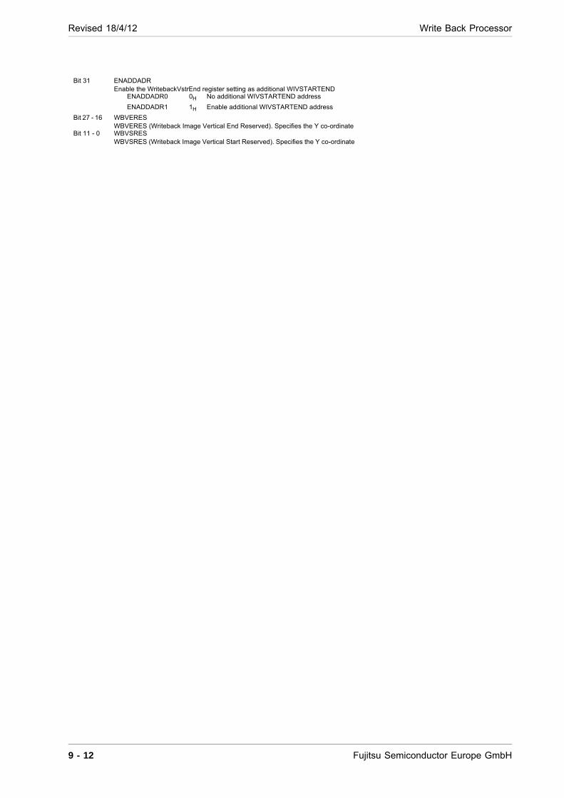
Revised 18/4/12 Write Back Processor
Bit 31 ENADDADR Enable the WritebackVstrEnd register setting as additional WIVSTARTEND
ENADDADR0 0H No additional WIVSTARTEND address
ENADDADR1 1H Enable additional WIVSTARTEND address
Bit 27 - 16 WBVERES WBVERES (Writeback Image Vertical End Reserved). Specifies the Y co-ordinate
Bit 11 - 0 WBVSRES WBVSRES (Writeback Image Vertical Start Reserved). Specifies the Y co-ordinate
9 - 12 Fujitsu Semiconductor Europe GmbH

Video Capture Revised 18/4/12
Chapter 10: Video Capture
10.1 Position of Block in whole LSI
The MB86298 'RUBY' has four capture inputs (CAP0 ... CAP3):
Capture unit CAP0 supports three 8-bit wide video inputs for RGB, dedicated sync signals and a clock.
Capture units CAP1, CAP2, CAP3 have one 8-bit video input plus a clock (intended for HD and SD video modes with embedded syncs)
The video inputs can be routed to the four internal video capture units using an internal crossbar switch (see diagram below). After processing, the video data is written to the frame buffer memory. The video capture unit generates interrupt signals, which are transmitted to the interrupt controller. The unit also has a connection to (and from) the display controller unit for upscaling, because the scaling hardware of the display controller is used for this operation.
The four internal capture units are identical. Using the flexible crossbar switch, each capture unit can capture the supported video standards from each input port.
The register addresses of the capture units are described in the Interconnect chapter of this docu-ment.
Figure 10-1: Video Capture: Block Diagram
Video Capture 1
Video Capture 2
Video Capture 3
crossbar
switchco
ntro
l bu
s
bus
to fr
ame
mem
ory
Video Capture 0
CAP3
CCLK3
CAP2
CCLK2
CAP1
CCLK1
CAP0
CCLK0
Display Controller
int
Fujitsu Semiconductor Europe GmbH 10 - 1

Revised 18/4/12 Video Capture
10.2 Feature List
The video capture unit has the following support features:
Video standards
HD video input 720p progressive format according to the SMPTE 296M standard (50 and 60 Hz frame rates)
SD video input with embedded syncs according to the ITU-R BT.656 standard, PAL and NTSC resolutions and frame rates
DRGB888 type video input with dedicated sync signals
Video interfaces
16-bit wide, single-data-rate (SDR), YCrCb 4:2:2, with embedded syncs, for HD standards
8-bit wide, double-data-rate (DDR), YCrCb 4:2:2, with embedded syncs, for HD standards
8-bit wide, single-data-rate (SDR), YCrCb 4:2:2, with embedded syncs, for SD standards
RGB video interface with dedicated sync signals
Deinterlacing of interlaced video sources, support of field combining (WEAVE) and field doubling (BOB) deinterlacing algorithms. Still image detection and automatic switching to field combining (WEAVE) for interlaced video input.
Color conversion matrices for RGB to YCrCb as well as YCrCb to RGB color space transformation
Scaling
Horizontal low-pass filtering
Vertical low-pass filtering
Downscaling (down to 1/32)
Upscaling in the display controller when reading from the frame buffer
10.2.1 Video standards
The capture unit supports HD video input in 720p format for both 50 and 60Hz frame rates, with em-bedded syncs, according to the SMPTE 296M standard. 720p is a progressive format with an active image area of 1280 by 720 pixels. The pixel clock is 74.25 MHz.
The capture unit supports SD video input with embedded syncs according to the ITU-R BT.656standard. PAL and NTSC resolutions and frame rates are supported.
The capture unit supports RGB888 video input, 24-bit (8-bit R, 8-bit G, 8-bit B), with dedicated sync signals.
10.2.2 Video interfaces
For HD standard 720p, YCrCb 4:2:2 with embedded syncs, a 16-bit wide (8-bit Y, 8-bit CrCb) a sin-gle-data-rate (SDR) interface is supported. Furthermore an 8-bit double-data-rate (DDR) interface is supported for this standard.
For SD standards with embedded sync (YCrCb 4:2:2), an 8-bit interface is supported.
For RGB input a 24 bit interface (8-bit R, 8-bit G, 8-bit B) with dedicated sync signals is supported.
10.2.3 Deinterlacing
Deinterlacing of interlaced video sources is supported, which includes support of field combining (WEAVE) and field doubling (BOB) deinterlacing algorithms. Furthermore still image detection and automatic switch to field combining (WEAVE) for interlaced video input is included.
10 - 2 Fujitsu Semiconductor Europe GmbH

Video Capture Revised 18/4/12
10.2.4 Color conversion
The capture unit supports color conversion from RGB to YCrCb and from YCrCb to RGB color for-mat.
10.2.5 Scaling
Horizontal and vertical low pass filtering is supported. The video image can be downscaled down to 1/32 or upscaled in the display controller when reading from the frame buffer.
10.2.6 Cropping
Frame cropping is supported by the capture unit, i.e. a rectangular area of the incoming frame can be cut out and used.
Fujitsu Semiconductor Europe GmbH 10 - 3
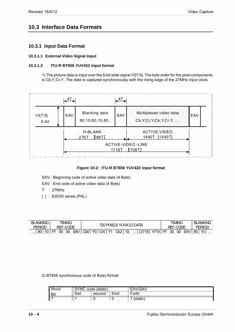
Revised 18/4/12 Video Capture
10.3 Interface Data Formats
10.3.1 Input Data Format
10.3.1.1 External Video Signal Input
10.3.1.2 ITU-R BT656 YUV422 input format
1) The picture data is input over the 8-bit wide signal VI[7:0]. The byte order for the pixel components is Cb,Y,Cr,Y. The data is captured synchronously with the rising edge of the 27MHz input clock.
Figure 10-2: ITU-R BT656 YUV422 input format
SAV : Beginning code of active video data (4 Byte)
EAV : End code of active video data (4 Byte)
T : 27MHz
[ ] : 625/50 series (PAL)
2) BT656 synchronous code (4 Byte) format
WordBit
SYNC code (static) EAV/SAVfirst second third Forth
7 1 0 0 1 (static)
SAVEAV Multiplexed video data
Cb,Y,Cr,Y,Cb,Y,Cr,Y,….. 8 bit
VI[7:0]
4T
H-BLANK 276T 288T
ACTIVE-VIDEO 1440T [1440T]
EAV
4T
Blanking data
80,10,80,10,80,.
ACTIVE-VIDEO -LINE 1716T 1728T
BLANKING PERIOD
TIMING REF-CODE
720 PIXELS YUV4:2:2 DATA TIMING
REF-CODE BLANKINGPERIOD
… 80 10 FF 00 00 SAV Cb0 Y0 Cr0 Y1 Cb2 Y2 … Cr718 Y719 FF 00 00 EAV 80 10 …
10 - 4 Fujitsu Semiconductor Europe GmbH
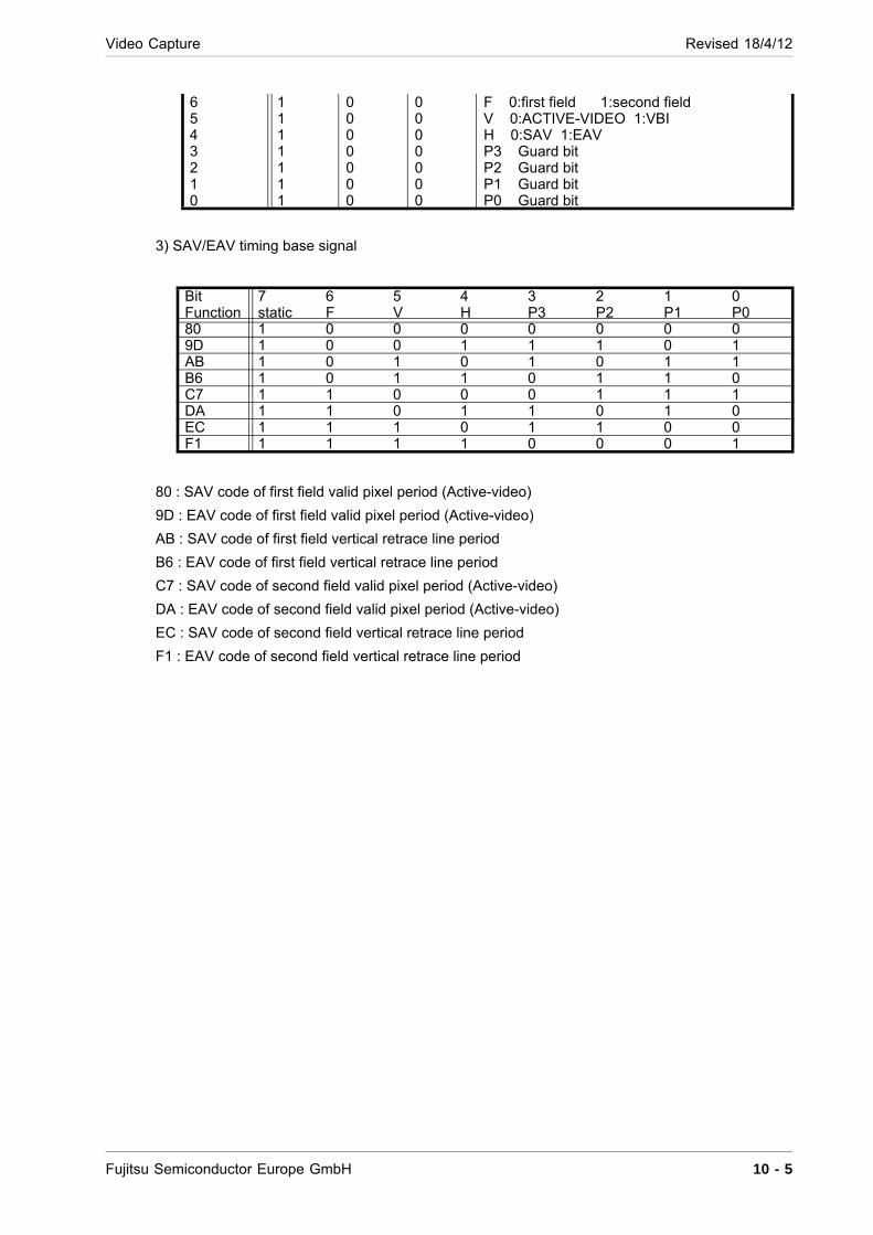
Video Capture Revised 18/4/12
3) SAV/EAV timing base signal
80 : SAV code of first field valid pixel period (Active-video)
9D : EAV code of first field valid pixel period (Active-video)
AB : SAV code of first field vertical retrace line period
B6 : EAV code of first field vertical retrace line period
C7 : SAV code of second field valid pixel period (Active-video)
DA : EAV code of second field valid pixel period (Active-video)
EC : SAV code of second field vertical retrace line period
F1 : EAV code of second field vertical retrace line period
6 1 0 0 F 0:first field 1:second field5 1 0 0 V 0:ACTIVE-VIDEO 1:VBI4 1 0 0 H 0:SAV 1:EAV3 1 0 0 P3 Guard bit2 1 0 0 P2 Guard bit1 1 0 0 P1 Guard bit0 1 0 0 P0 Guard bit
Bit 7 6 5 4 3 2 1 0Function static F V H P3 P2 P1 P080 1 0 0 0 0 0 0 09D 1 0 0 1 1 1 0 1AB 1 0 1 0 1 0 1 1B6 1 0 1 1 0 1 1 0C7 1 1 0 0 0 1 1 1DA 1 1 0 1 1 0 1 0EC 1 1 1 0 1 1 0 0F1 1 1 1 1 0 0 0 1
Fujitsu Semiconductor Europe GmbH 10 - 5

Revised 18/4/12 Video Capture
4) BT656 synchronous code (EAV) timing (525/60 series)
522 523 524 525 1 2 3 4 5 6 7 8 9 LINE-No,
1st_field ACTIVE-VIDEO Cut pulse Vertical synchronous Cut pulse EAV DA DA DA DA F1 F1 F1 B6 B6 B6 B6 B6 B6
F 1 1 1 1 1 1 1 0 0 0 0 0 0 V 0 0 0 0 1 1 1 1 1 1 1 1 1
260 261 262 263 264 265 266 267 268 269 270 271 272 LINE-No, 2nd_field ACTIVE-VIDEO Cut pulse Vertical synchronous Cut pulse
EAV 9D 9D 9D 9D B6 B6 F1 F1 F1 F1 F1 F1 F1 F 0 0 0 0 0 0 1 1 1 1 1 1 1 V 0 0 0 0 1 1 1 1 1 1 1 1 1
10 11 12 13 14 15 16 17 18 19 20 21 22 23 LINE-No,
1st_field VBI-lines 1st_field Act-video EAV B6 B6 B6 B6 B6 B6 B6 B6 B6 B6 9D 9D 9D 9D
F 0 0 0 0 0 0 0 0 0 0 0 0 0 0 V 1 1 1 1 1 1 1 1 1 1 0 0 0 0
273 274 275 276 277 278 279 280 281 282 283 284 285 286 LINE-No, 2nd_field VBI-lines 2nd_field Act-video
EAV F1 F1 F1 F1 F1 F1 F1 F1 F1 F1 DA DA DA DA F 1 1 1 1 1 1 1 1 1 1 1 1 1 1 V 1 1 1 1 1 1 1 1 1 1 0 0 0 0
10 - 6 Fujitsu Semiconductor Europe GmbH
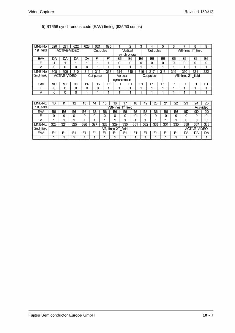
Video Capture Revised 18/4/12
5) BT656 synchronous code (EAV) timing (625/50 series)
620 621 622 623 624 625 1 2 3 4 5 6 7 8 9 LINE-No,
1st_field ACTIVE-VIDEO Cut pulse Vertical synchronous
Cut pulse VBI-lines 1st_field
EAV DA DA DA DA F1 F1 B6 B6 B6 B6 B6 B6 B6 B6 B6 F 1 1 1 1 1 1 0 0 0 0 0 0 0 0 0 V 0 0 0 0 1 1 1 1 1 1 1 1 1 1 1
308 309 310 311 312 313 314 315 316 317 318 319 320 321 322LINE-No, 2nd_field ACTIVE-VIDEO Cut pulse Vertical
synchronous Cut pulse VBI-lines 2nd_field
EAV 9D 9D 9D B6 B6 F1 F1 F1 F1 F1 F1 F1 F1 F1 F1 F 0 0 0 0 0 1 1 1 1 1 1 1 1 1 1 V 0 0 0 1 1 1 1 1 1 1 1 1 1 1 1
10 11 12 13 14 15 16 17 18 19 20 21 22 23 24 25 LINE-No, 1st_field VBI-lines 1st_field Act-video
EAV B6 B6 B6 B6 B6 B6 B6 B6 B6 B6 B6 B6 B6 9D 9D 9D F 0 0 0 0 0 0 0 0 0 0 0 0 0 0 0 0 V 1 1 1 1 1 1 1 1 1 1 1 1 1 0 0 0
323 324 325 326 327 328 329 330 331 332 333 334 335 336 337 338LINE-No, 2nd_field VBI-lines 2
nd_field ACTIVE-VIDEO
EAV F1 F1 F1 F1 F1 F1 F1 F1 F1 F1 F1 F1 F1 DA DA DAF 1 1 1 1 1 1 1 1 1 1 1 1 1 1 1 1
Fujitsu Semiconductor Europe GmbH 10 - 7
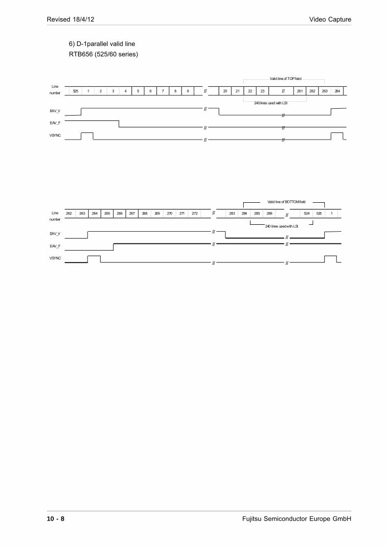
Revised 18/4/12 Video Capture
6) D-1parallel valid line
RTB656 (525/60 series)
525 1 2 3 4 5 6 7 8 9 20 21 22 23 261 262 263 264
262 263 264 265 266 267 268 269 270 271 272 283 284 285 286 524 525 1
VSYNC
Line
number
VSYNC
EAV_V
EAV_V
EAV_F
Line
number
EAV_F
240 lines used with LSI
Valid line of BOTTOM field
240 lines used with LSI
Valid line of TOP f ield
10 - 8 Fujitsu Semiconductor Europe GmbH
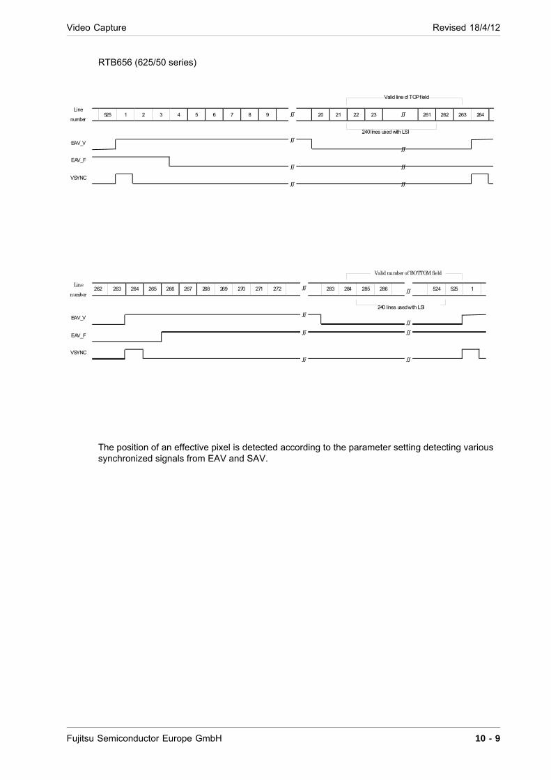
Video Capture Revised 18/4/12
RTB656 (625/50 series)
The position of an effective pixel is detected according to the parameter setting detecting various synchronized signals from EAV and SAV.
525 1 2 3 4 5 6 7 8 9 20 21 22 23 261 262 263 264
262 263 264 265 266 267 268 269 270 271 272 283 284 285 286 524 525 1
VSYNC
Line
number
VSYNC
EAV_V
EAV_V
EAV_F
Line
number
EAV_F
240 lines used with LSI
Valid number of BOTTOM field
240 lines used with LSI
Valid line of TOP f ield
Fujitsu Semiconductor Europe GmbH 10 - 9
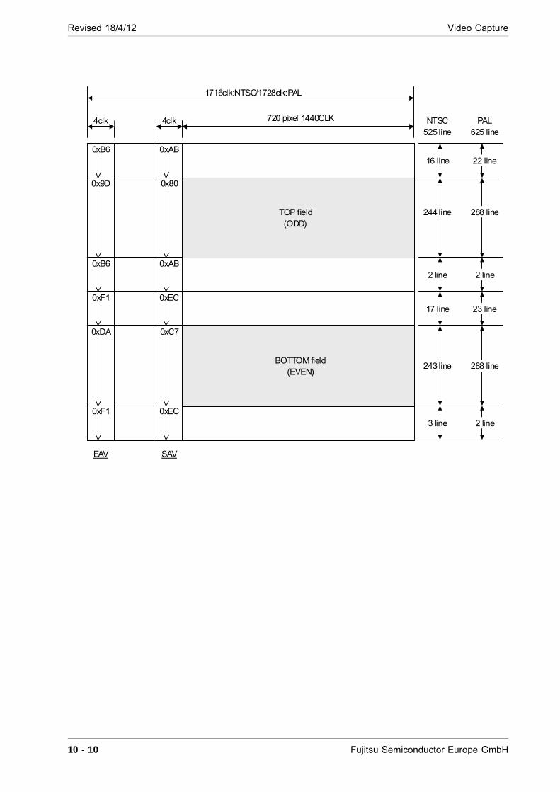
Revised 18/4/12 Video Capture
TOP field (ODD)
BOTTOM field (EVEN)
720 pixel 1440CLK
SAV EAV
1716clk:NTSC/1728clk:PAL
4clk
0xF1
0xB6
4clk
0xF1
0xB6
0xAB
0xAB
0xEC
0xEC
0x80 0x9D
0xC7 0xDA
16 line 22 line
244 line 288 line
2 line
17 line
243 line
3 line
2 line
23 line
288 line
2 line
525 line 625 lineNTSC PAL
10 - 10 Fujitsu Semiconductor Europe GmbH
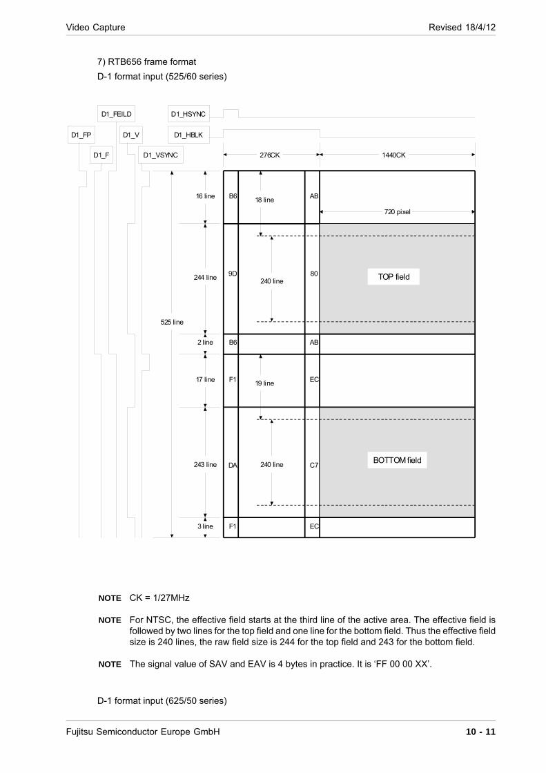
Video Capture Revised 18/4/12
7) RTB656 frame format
D-1 format input (525/60 series)
NOTE CK = 1/27MHz
NOTE For NTSC, the effective field starts at the third line of the active area. The effective field is followed by two lines for the top field and one line for the bottom field. Thus the effective field size is 240 lines, the raw field size is 244 for the top field and 243 for the bottom field.
NOTE The signal value of SAV and EAV is 4 bytes in practice. It is ‘FF 00 00 XX’.
D-1 format input (625/50 series)
276CK
D1_HBLK D1_FP
D1_VSYNC
D1_FEILD
1440CK
B6 AB
720 pixel
TOP field
BOTTOM field
16 line 18 line
244 line
525 line
243 line
3 line
17 line
F1 EC
F1 EC
B6 AB2 line
240 line
240 line
D1_HSYNC
D1_F
D1_V
19 line
9D 80
DA C7
Fujitsu Semiconductor Europe GmbH 10 - 11
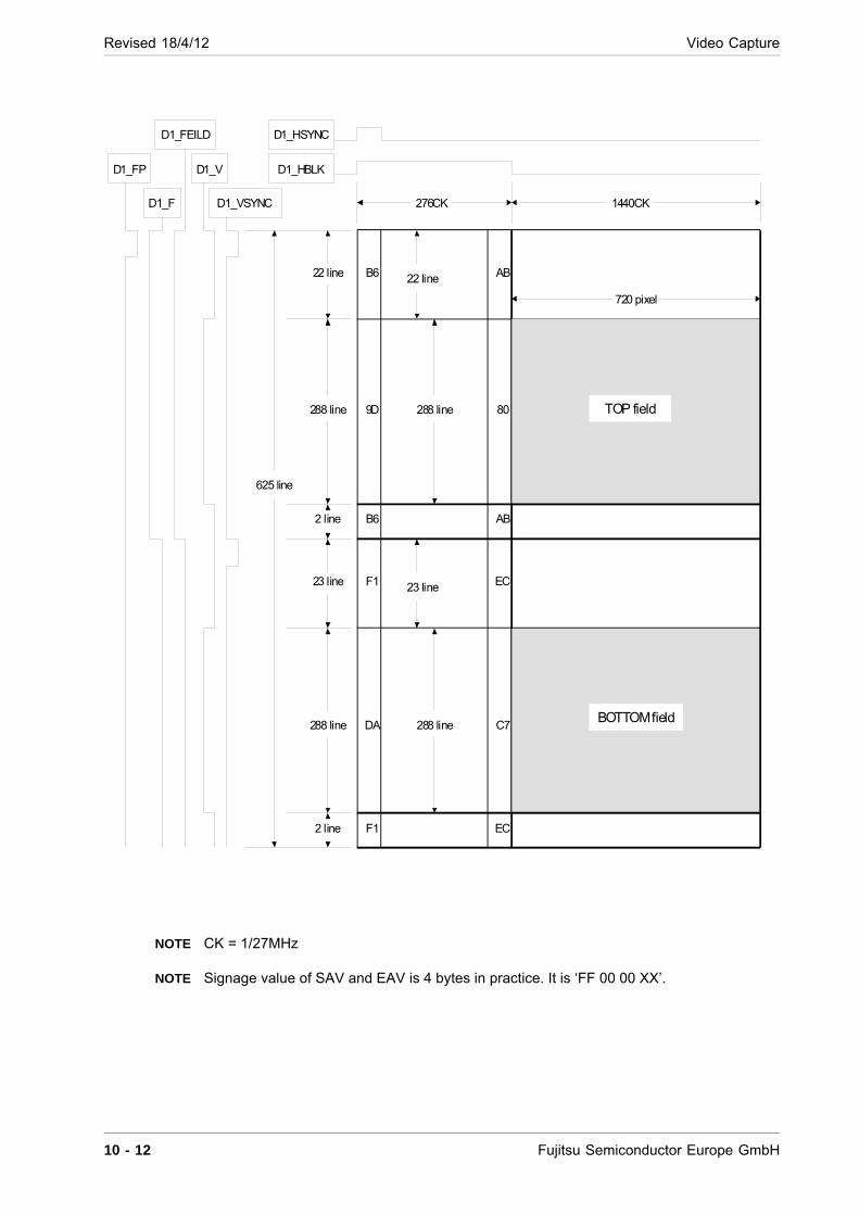
Revised 18/4/12 Video Capture
NOTE CK = 1/27MHz
NOTE Signage value of SAV and EAV is 4 bytes in practice. It is ‘FF 00 00 XX’.
276CK
D1_HBLK D1_FP
D1_VSYNC
D1_FEILD
1440CK
B6 AB
720 pixel
TOP field
BOTTOM field
22 line 22 line
288 line
625 line
288 line
2 line
23 line
F1 EC
F1 EC
B6 AB2 line
288 line
288 line
D1_HSYNC
D1_F
D1_V
23 line
9D 80
DA C7
10 - 12 Fujitsu Semiconductor Europe GmbH
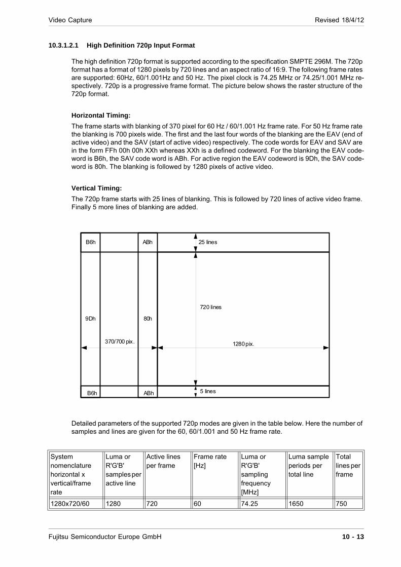
Video Capture Revised 18/4/12
10.3.1.2.1 High Definition 720p Input Format
The high definition 720p format is supported according to the specification SMPTE 296M. The 720p format has a format of 1280 pixels by 720 lines and an aspect ratio of 16:9. The following frame rates are supported: 60Hz, 60/1.001Hz and 50 Hz. The pixel clock is 74.25 MHz or 74.25/1.001 MHz re-spectively. 720p is a progressive frame format. The picture below shows the raster structure of the 720p format.
Horizontal Timing:
The frame starts with blanking of 370 pixel for 60 Hz / 60/1.001 Hz frame rate. For 50 Hz frame rate the blanking is 700 pixels wide. The first and the last four words of the blanking are the EAV (end of active video) and the SAV (start of active video) respectively. The code words for EAV and SAV are in the form FFh 00h 00h XXh whereas XXh is a defined codeword. For the blanking the EAV code-word is B6h, the SAV code word is ABh. For active region the EAV codeword is 9Dh, the SAV code-word is 80h. The blanking is followed by 1280 pixels of active video.
Vertical Timing:
The 720p frame starts with 25 lines of blanking. This is followed by 720 lines of active video frame. Finally 5 more lines of blanking are added.
Detailed parameters of the supported 720p modes are given in the table below. Here the number of samples and lines are given for the 60, 60/1.001 and 50 Hz frame rate.
System nomenclaturehorizontal x vertical/frame rate
Luma or R'G'B' samples per active line
Active lines per frame
Frame rate [Hz]
Luma or R'G'B' sampling frequency [MHz]
Luma sample periods per total line
Total lines per frame
1280x720/60 1280 720 60 74.25 1650 750
25 lines
720 lines
5 lines
1280 pix.370/700 pix.
B6h ABh
9Dh 80h
B6h ABh
Fujitsu Semiconductor Europe GmbH 10 - 13
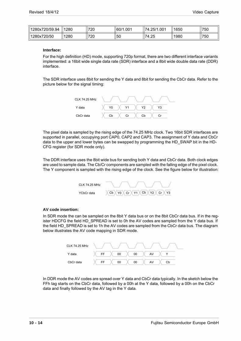
Revised 18/4/12 Video Capture
Interface:
For the high definition (HD) mode, supporting 720p format, there are two different interface variants implemented: a 16bit wide single data rate (SDR) interface and a 8bit wide double data rate (DDR) interface.
The SDR interface uses 8bit for sending the Y data and 8bit for sending the CbCr data. Refer to the picture below for the signal timing:
The pixel data is sampled by the rising edge of the 74.25 MHz clock. Two 16bit SDR interfaces are supported in parallel, occupying port CAP0, CAP2 and CAP3. The assignment of Y data and CbCr data to the upper and lower bytes can be swapped by programming the HD_SWAP bit in the HD-CFG register (for SDR mode only).
The DDR interface uses the 8bit wide bus for sending both Y data and CbCr data. Both clock edges are used to sample data. The Cb/Cr components are sampled with the falling edge of the pixel clock. The Y component is sampled with the rising edge of the clock. See the figure below for illustration:
AV code insertion:
In SDR mode the can be sampled on the 8bit Y data bus or on the 8bit CbCr data bus. If in the reg-ister HDCFG the field HD_SPREAD is set to 0h the AV codes are sampled from the Y data bus. If the field HD_SPREAD is set to 1h the AV codes are sampled from the CbCr data bus. The diagram below illustrates the AV code mapping in SDR mode.
In DDR mode the AV codes are spread over Y data and CbCr data typically. In the sketch below the FFh tag starts on the CbCr data, followed by a 00h at the Y data, followed by a 00h on the CbCr data and finally followed by the AV tag in the Y data.
1280x720/59.94 1280 720 60/1.001 74.25/1.001 1650 750
1280x720/50 1280 720 50 74.25 1980 750
Y0 Y1 Y2 Y3
Cb Cr Cb Cr
CLK 74.25 MHz
Y data
CbCr data
Cb Y0 Cr Y1 Cb Y2 Cr Y3
CLK 74.25 MHz
YCbCr data
FF 00 00 AV
FF 00 00 AV
CLK 74.25 MHz
Y data
CbCr data
Y
Cb
10 - 14 Fujitsu Semiconductor Europe GmbH
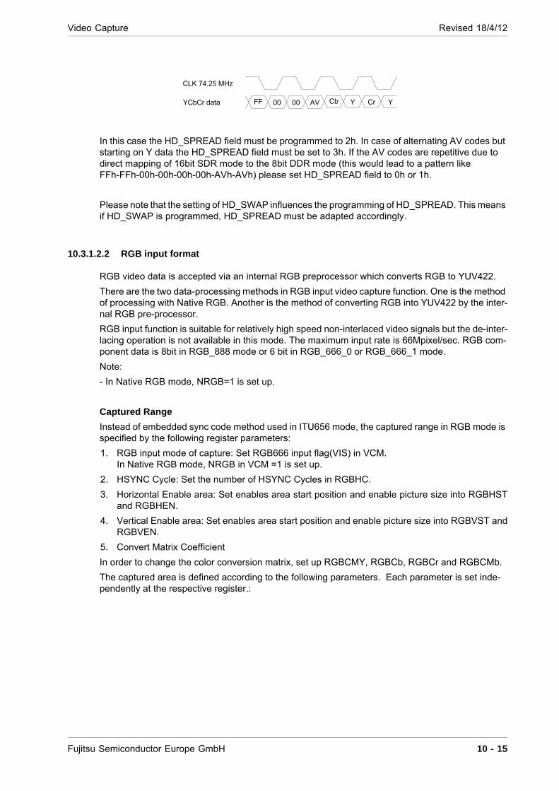
Video Capture Revised 18/4/12
In this case the HD_SPREAD field must be programmed to 2h. In case of alternating AV codes but starting on Y data the HD_SPREAD field must be set to 3h. If the AV codes are repetitive due to direct mapping of 16bit SDR mode to the 8bit DDR mode (this would lead to a pattern like FFh-FFh-00h-00h-00h-00h-AVh-AVh) please set HD_SPREAD field to 0h or 1h.
Please note that the setting of HD_SWAP influences the programming of HD_SPREAD. This means if HD_SWAP is programmed, HD_SPREAD must be adapted accordingly.
10.3.1.2.2 RGB input format
RGB video data is accepted via an internal RGB preprocessor which converts RGB to YUV422.
There are the two data-processing methods in RGB input video capture function. One is the method of processing with Native RGB. Another is the method of converting RGB into YUV422 by the inter-nal RGB pre-processor.
RGB input function is suitable for relatively high speed non-interlaced video signals but the de-inter-lacing operation is not available in this mode. The maximum input rate is 66Mpixel/sec. RGB com-ponent data is 8bit in RGB_888 mode or 6 bit in RGB_666_0 or RGB_666_1 mode.
Note:
- In Native RGB mode, NRGB=1 is set up.
Captured Range
Instead of embedded sync code method used in ITU656 mode, the captured range in RGB mode is specified by the following register parameters:
1. RGB input mode of capture: Set RGB666 input flag(VIS) in VCM.In Native RGB mode, NRGB in VCM =1 is set up.
2. HSYNC Cycle: Set the number of HSYNC Cycles in RGBHC.
3. Horizontal Enable area: Set enables area start position and enable picture size into RGBHST and RGBHEN.
4. Vertical Enable area: Set enables area start position and enable picture size into RGBVST and RGBVEN.
5. Convert Matrix Coefficient
In order to change the color conversion matrix, set up RGBCMY, RGBCb, RGBCr and RGBCMb.
The captured area is defined according to the following parameters. Each parameter is set inde-pendently at the respective register.:
FF 00 00 AV Cb Y Cr Y
CLK 74.25 MHz
YCbCr data
Fujitsu Semiconductor Europe GmbH 10 - 15
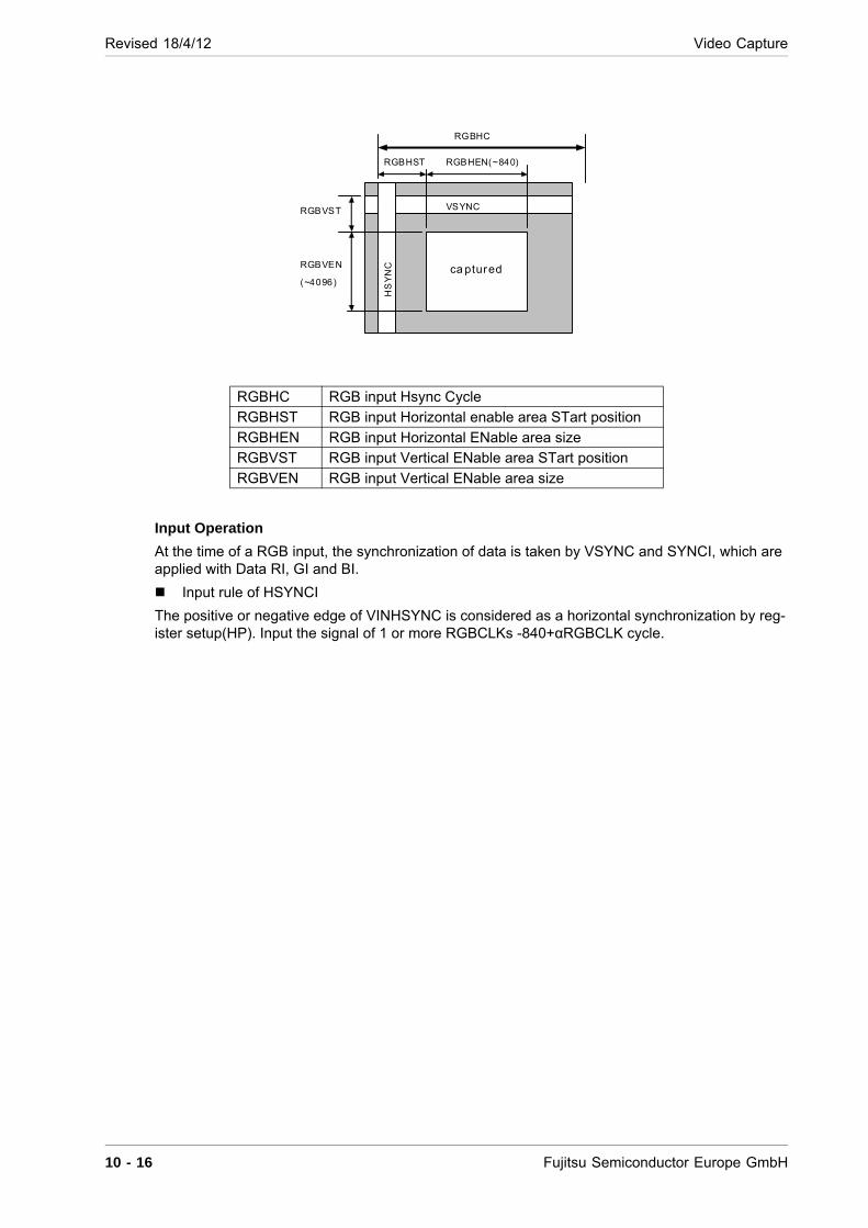
Revised 18/4/12 Video Capture
Input Operation
At the time of a RGB input, the synchronization of data is taken by VSYNC and SYNCI, which are applied with Data RI, GI and BI.
Input rule of HSYNCI
The positive or negative edge of VINHSYNC is considered as a horizontal synchronization by reg-ister setup(HP). Input the signal of 1 or more RGBCLKs -840+αRGBCLK cycle.
RGBHC RGB input Hsync Cycle
RGBHST RGB input Horizontal enable area STart position
RGBHEN RGB input Horizontal ENable area size
RGBVST RGB input Vertical ENable area STart position
RGBVEN RGB input Vertical ENable area size
VSYNC
HS
YN
C
RGBHST
RGBVST
RGBHEN(~840)
RGBVEN
(~4096) ca ptured
RGBHC
10 - 16 Fujitsu Semiconductor Europe GmbH
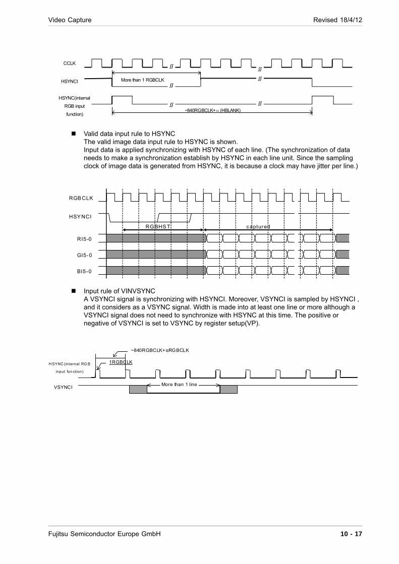
Video Capture Revised 18/4/12
Valid data input rule to HSYNCThe valid image data input rule to HSYNC is shown.Input data is applied synchronizing with HSYNC of each line. (The synchronization of data needs to make a synchronization establish by HSYNC in each line unit. Since the sampling clock of image data is generated from HSYNC, it is because a clock may have jitter per line.)
Input rule of VINVSYNCA VSYNCI signal is synchronizing with HSYNCI. Moreover, VSYNCI is sampled by HSYNCI , and it considers as a VSYNC signal. Width is made into at least one line or more although a VSYNCI signal does not need to synchronize with HSYNC at this time. The positive or negative of VSYNCI is set to VSYNC by register setup(VP).
CCLK
HSYNCI
~840RGBCLK+α(HBLANK)
More than 1 RGBCLK
HSYNC(internal
RGB input
function)
RGB CLK
HSY NCI
RI5-0
GI5-0
BI5-0
RGBHS T captured
More than 1 line
1RGBCLK H SYNC (internal RG B
input fun ct ion)
VSYNCI
~840RGBCLK+αRGBCLK
Fujitsu Semiconductor Europe GmbH 10 - 17
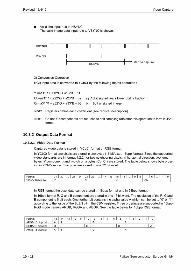
Revised 18/4/12 Video Capture
Valid line input rule to HSYNCThe valid image data input rule to VSYNC is shown.
3) Conversion Operation
RGB input data is converted to YCbCr by the following matrix operation :
Y =a11*R + a12*G + a13*B + b1
Cb=a21*R + a22*G + a23*B + b2 aij :10bit signed real ( lower 8bit is fraction )
Cr= a31*R + a32*G + a33*B + b3 bi: 8bit unsigned integer
NOTE Registers define each coefficient (see register description).
NOTE Cb and Cr components are reduced to half sampling rate after this operation to form in 4:2:2 format.
10.3.2 Output Data Format
10.3.2.1 Video Data Format
Captured video data is stored in YCbCr format or RGB format.
In YCbCr format two pixels are stored in two bytes (16 bit/pixel, 16bpp format). Since the supported video standards are in format 4:2:2, for two neighboring pixels, in horizontal direction, two luma bytes (Y component) and two chroma bytes (Cb, Cr) are stored. The table below shows byte order-ing in YCbCr mode. Two pixel are stored in one 32 bit word.
In RGB format the pixel data can be stored in 16bpp format and in 24bpp format.
In 16bpp format R, G and B component are stored in one 16 bit word. The resolution of the R, G and B component is 5 bit each. One further bit contains the alpha value A which can be set to “0” or “1” according to the value of the BLEN bit in the CBM register. Three orderings are supported in 16bpp RGB mode namely ARGB, RGBA and ABGR. See the table below for 16bpp RGB format.
Format 31 30 ... 25 24 23 22 ... 17 16 15 14 ... 9 8 7 6 ... 1 0
YCbCr 16 bit/pixel Y Cr Y Cb
Format 15 14 13 12 11 10 9 8 7 6 5 4 3 2 1 0
ARGB 16 bit/pixel A R G B
RGBA 16 bit/pixel R G B A
ARGB 16 bit/pixel A B G R
VSYNCI
HSYNCI
start to capture RGBVST
10 - 18 Fujitsu Semiconductor Europe GmbH

Video Capture Revised 18/4/12
In 24bpp format R, G and B component are stored in one 32 bit word. The resolution of the R, G and B component is 8 bit each. One further byte contains the alpha value A which can be set to 00h or FFh according to the value of the BLEN bit in the CBM register. Three orderings are supported in 24bpp RGB mode namely ARGB, RGBA and ABGR. See the table below for 24bpp RGB format.
The relation between the video data formats and the register control bits as shown in the table be-low:
The “X” in the rightmost column of the above table indicates that enlarged display of capture data is supported.
The NRGB bit is in VCM register, CRGB, C24 and RGBA bits are in CBM register.
The Selection of video data format dependent on the programming of the above mentioned register bits is shown in the below picture:
For the ARGB, RGBA or ABGR formats, whether to set the blend bit to 1 (ffh resp.) or 0 at pixel write time can be selected using the BLEN bit of the CBM register.
Format 31 30 ... 25 24 23 22 ... 17 16 15 14 ... 9 8 7 6 ... 1 0
ARGB 24 bit/pixel A R G B
RGBA 24 bit/pixel R G B A
ABGR 24 bit/pixel A B G R
NRGB CRGB C24 RGBA[1:0] Capture Data FormatsEnlarged Display
0 0 0 00 YCbCr 16bits/pixel X
0 0 0 01 Unused
0 0 1 XX Unused
0 1 0 00 ARGB 16 bits/pixel (YCbCr -> RGB conversion)
0 1 0 01 RGBA 16 bits/pixel (YCbCr -> RGB conversion)
0 1 0 10 ABGR 16 bits/pixel (YCbCr -> RGB conversion)
0 1 1 00 ARGB 24 bits/pixel (YCbCr -> RGB conversion)
0 1 1 01 RGBA 24 bits/pixel (YCbCr -> RGB conversion)
0 1 1 10 ABGR 24 bits/pixel (YCbCr -> RGB conversion)
1 0 0 00 ARGB 16 bits/pixel X
1 0 0 01 RGBA 16 bits/pixel
1 0 0 10 ARGB 16 bits/pixel
1 0 1 00 ARGB 24 bits/pixel X
1 0 1 01 RGBA 24 bits/pixel
1 0 1 10 ABGR 24 bits/pixel
1 1 X XX Unused
YCbCrto RGBRGB to
YCbCr
RGB24 to 16
ARGBto RGBA or ABGR
VI input
VIS bit
RI/GI/BI input
CRGB bit
C24 bit RGBA bitsNRGB bit
YCbCr-16bppARGB-16bppRGBA-16bppABGR-16bppARGB-24bppRGBA-24bppABGR-24bpp
Fujitsu Semiconductor Europe GmbH 10 - 19
Revised 18/4/12 Video Capture
10.3.2.2 Synchronisation Control
Write of video image data to graphics memory and scan to display the data are performed indepen-dently. Graphics memory for video capture is controlled using the ring buffer mode, and when image data equivalent to 1 frame is prepared in memory, the frame is displayed.
When the frame rate of video capture and that of display are different, frame dropping or continuous display of the same frame occurs.
10.3.2.3 Memory Allocation
For the video buffer a memory area must be reserved. The register CBOA (Capture Buffer Origin Address) points to the beginning of the video buffer. The register CBLA (Capture Buffer Limit Ad-dress) points to the end of the video buffer. Below paragraph describes how the values for CBOA and CBLA register are calculated.
First, calculate the stride size: s = ceil( w * b / 64); whereas
w – width of frame in pixel
b – bytes per pixel, (YCBCR: b = 2, RGB16: b = 2, RGB24: b = 4)
Second, calculate the memory size needed to store one frame: f = s * 64 * h; whereas
s – stride size
h – height of frame to store (number of lines of frame)
Third, calculate the final size of the ring buffer: It is recommended to use at least n = 2.2 frames for the video buffer. When still detection is used, the size of the video buffer must be doubled.
if no still detection is used : CBLA = CBOA + n * f
if still detection is used:CBLA = CBOA + n * f * 2
In single buffer mode no ring buffer is supported. In this mode the programmer must take additional effort in order to support a of double buffering. (n = 1).
CBLA = CBOA is the start address of the single buffer by definition.
CBLA=CBOA and is the start address of the single buffer by definition
if no still detection is used: CBLA + f = CBOA + f; this is the end address of the single buffer
if stil detection is used: CBLA + 2 * f = CBOA + 2 * f; this is the end address of the single buffer
Example: PAL video input, 720x576 pixels, YCrCb, no scaling, no cropping, still detection enabled, CBOA = 0x100000, n = 3, ring buffer mode
Stride size s = ceil (720 * 2 bpp / 64) = 23.
Frame size f = s * 64 * h = 23 * 64 * 576 = 0xcf000
10 - 20 Fujitsu Semiconductor Europe GmbH
Video Capture Revised 18/4/12
CBLA = CBOA + n * f * 2 = 0x100000 + 3 * 0xcf000 * 2 = 0x5da000
NOTE CBOA and CBLA must point to 64bit aligned addresses.
NOTE If fixed start addresses of the video buffer are required (e.g. single buffer mode), the video buffer should be chosen n - times the frame size f. Usually equals 1 when using single buffer mode.
NOTE Please be aware, that the address the CBLA register points to is not the end address of the video buffer, but two lines are written beyond this address.
NOTE The video buffer must be disposed below the address border of 256MByte.
NOTE CBLA must be greater than CBOA
NOTE When frame size is reduced by scaling and/or cropping the buffer size corresponds to the size of the reduced frame.
NOTE If the horizontal line length in bytes is not a multiple of the unit size of stride (unit size is equal to 64 byte), dummy data will be written to the memory until stride size is reached. The size of the displayed window must be setup accordingly in the display controller.
10.3.2.4 Window Display
Captured video images are displayed using selected layer in the display unit. The whole or a part of a captured image can be displayed as the whole or a window of a screen.
When performing capture display, set video layer in capture synchronizing mode (LnCS = 1). In this mode, video layer displays the most recent frame that is in the video capture buffer. The display ad-dress used in normal mode is ignored.
The stride of video layer must match that of the video capture buffer.
Make the display size of video layer the same as the reduced video capture image size. When the display size of video layer is made greater than the reduced video capture image size, invalid data will be displayed.
For video layer, the user can select between RGB display and YCbCr display, but when performing video capture, select the YCbCr format (LnYC = 1).
10.3.2.5 Interlace Display
It is possible to perform interlace display for images captured into the video capture buffer in WEAVE mode. To perform the interlace display, enable WEAVE mode and select interlace & video display for display scan.
However, when display scan is asynchronous, flicker can occur in motion scenes. To prevent flicker, set the OO (Odd Only) bit of the CBM (Capture Buffer Mode) register to 1. Furthermore still detection mode is supported. In still detection mode, the appropriate de-interlacing method is chosen depend-ed on amount of motion in the scene.
10.4 Processing Mode
10.4.1 Processing Flow
10.4.1.1 Video Input Selection
The four capture interfaces CAP0, CAP1, CAP2, CAP3 are connected to the four capture units C0, C1, C2, C3 by a cross bar switch. This allows a flexible connection of the interfaces to the corre-sponding capture unit. See the picture below for an overview.
Fujitsu Semiconductor Europe GmbH 10 - 21

Revised 18/4/12 Video Capture
Figure 10-3: Video Capture: Input Selection
Basically each capture unit can process all supported video modes. All combinations of input video modes are possible as long as the needed input package pins are not blocked by another used video unit.
Examples:
one RGB_888 signal could be combined with three specific ITU_656 inputs (not ITU_656_0!)
two parallel RGB666 inputs can be input, but then all pins are used, therefore other signals can not be captured
Bearing the pin usage in mind, you can use the tables shown below to determine which combina-tions are possible and which pin connections are used for these.
Capture Unit C0
RGB
SD
HD-S/D
HD-S
Capture Unit C1
Capture Unit C2
Capture Unit C3
RGB
SD
HD-S/D
HD-S
RGB
SD
HD-S/D
HD-S
RGB
SD
HD-S/D
HD-S
CAP0R
CAP0G
CAP0B
CAP1V
CAP2V
CAP3V
bus
to
fra
me
buf
fer
cont
rol b
us
bus
to fr
am
e b
uffe
r
10 - 22 Fujitsu Semiconductor Europe GmbH
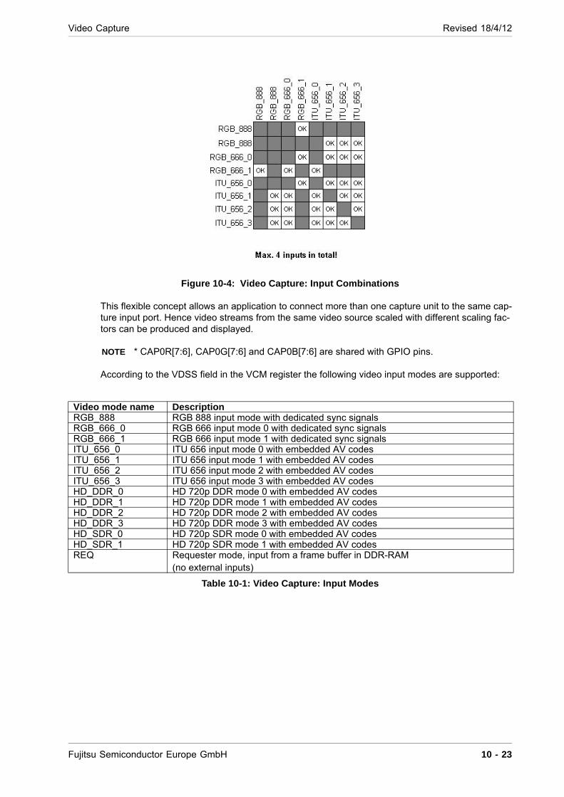
Video Capture Revised 18/4/12
Figure 10-4: Video Capture: Input Combinations
This flexible concept allows an application to connect more than one capture unit to the same cap-ture input port. Hence video streams from the same video source scaled with different scaling fac-tors can be produced and displayed.
NOTE * CAP0R[7:6], CAP0G[7:6] and CAP0B[7:6] are shared with GPIO pins.
According to the VDSS field in the VCM register the following video input modes are supported:
Table 10-1: Video Capture: Input Modes
Video mode name DescriptionRGB_888 RGB 888 input mode with dedicated sync signalsRGB_666_0 RGB 666 input mode 0 with dedicated sync signalsRGB_666_1 RGB 666 input mode 1 with dedicated sync signalsITU_656_0 ITU 656 input mode 0 with embedded AV codesITU_656_1 ITU 656 input mode 1 with embedded AV codesITU_656_2 ITU 656 input mode 2 with embedded AV codesITU_656_3 ITU 656 input mode 3 with embedded AV codesHD_DDR_0 HD 720p DDR mode 0 with embedded AV codesHD_DDR_1 HD 720p DDR mode 1 with embedded AV codesHD_DDR_2 HD 720p DDR mode 2 with embedded AV codesHD_DDR_3 HD 720p DDR mode 3 with embedded AV codesHD_SDR_0 HD 720p SDR mode 0 with embedded AV codesHD_SDR_1 HD 720p SDR mode 1 with embedded AV codesREQ Requester mode, input from a frame buffer in DDR-RAM
(no external inputs)
Fujitsu Semiconductor Europe GmbH 10 - 23

Revised 18/4/12 Video Capture
The following tables describe the input ports for the various video modes:
RGB_888
RGB_666_0
RGB_666_1
ITU_656_0
ITU_656_1
ITU_656_2
ITU_656_3
The leftmost column shows the video input pins of the chip. The upper row lists the video modes. The table body therefore shows the exact mapping of each video signal component to a package pin on the left.
Table 10-2: Video Capture: Input Ports for Modes (1)
The table below defines the input ports for the video modes HD_DDR_0 to HD_DDR_3, HD_SDR_0 and HD_SDR_1.
10 - 24 Fujitsu Semiconductor Europe GmbH
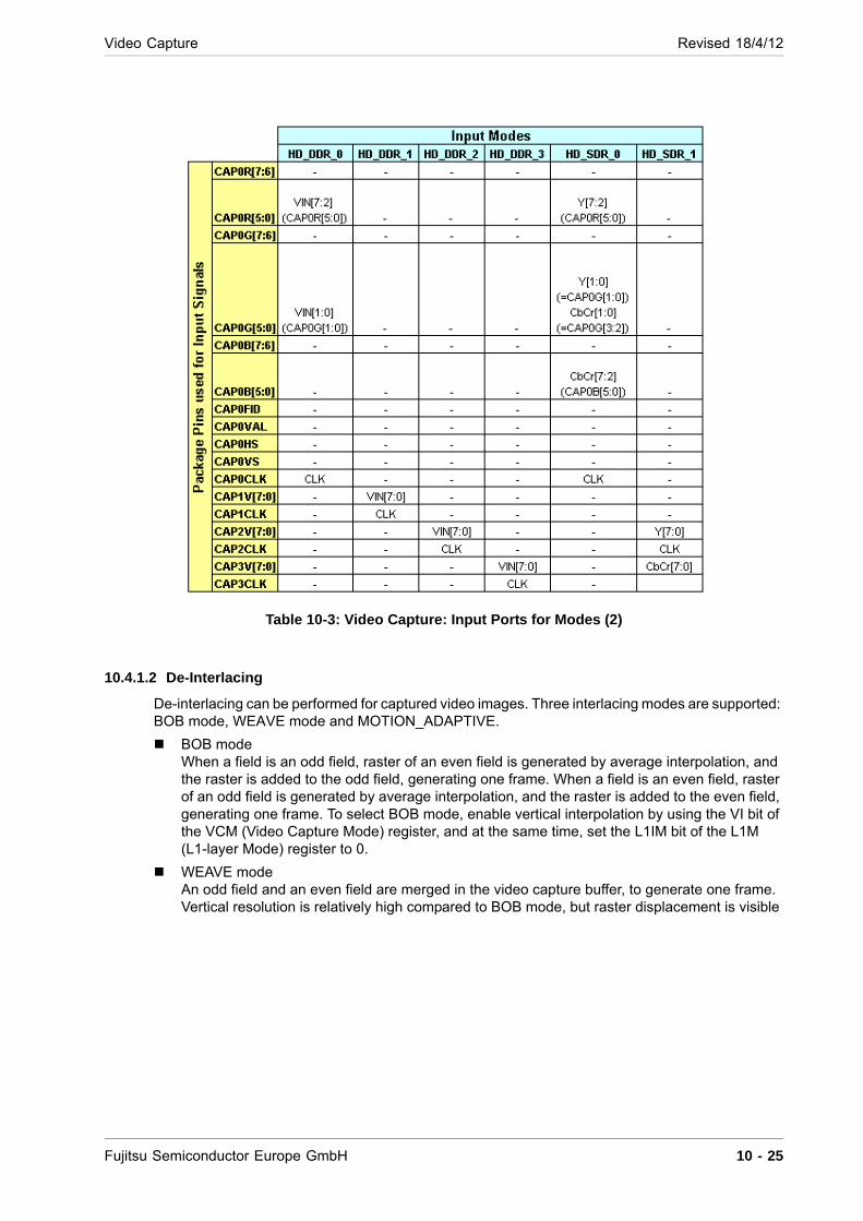
Video Capture Revised 18/4/12
Table 10-3: Video Capture: Input Ports for Modes (2)
10.4.1.2 De-Interlacing
De-interlacing can be performed for captured video images. Three interlacing modes are supported: BOB mode, WEAVE mode and MOTION_ADAPTIVE.
BOB modeWhen a field is an odd field, raster of an even field is generated by average interpolation, and the raster is added to the odd field, generating one frame. When a field is an even field, raster of an odd field is generated by average interpolation, and the raster is added to the even field, generating one frame. To select BOB mode, enable vertical interpolation by using the VI bit of the VCM (Video Capture Mode) register, and at the same time, set the L1IM bit of the L1M (L1-layer Mode) register to 0.
WEAVE modeAn odd field and an even field are merged in the video capture buffer, to generate one frame. Vertical resolution is relatively high compared to BOB mode, but raster displacement is visible
Fujitsu Semiconductor Europe GmbH 10 - 25

Revised 18/4/12 Video Capture
in motion scenes. To select WEAVE mode, disable vertical interpolation by using the VI bit of the VCM (Video Capture Mode) register, and at the same time, set the L1IM bit of the L1M (L1-layer Mode) register to 1.
MOTION_ADAPTIVE modeIn motion adaptive de-interlacing mode the motion detection is performed. Depending on the video characteristics either BOB or WEAVE de-interlacing scheme is chosen automatically.
10.4.1.3 Downscaling Function
When the CM bits of the video capture mode register (VCM) are 11, the scaler reduces the video screen size. The reduction can be set independently in the vertical and horizontal size. The reduc-tion is set per line in the vertical direction and in 2-pixel units in the horizontal direction. The scale setting value is defined by an input/output value. It is a 16-bit fixed fraction where the integer is rep-resented by 5 bits and the fraction is represented by 11 bits. Valid setting values are from 0800H to FFFFH. Set the vertical direction at bit 31 to bit 16 of the capture scale register (CSC) and the hor-izontal direction at bits 15 to bit 00. The initial value for this register is 08000800H (once). An ex-ample of the expressions for setting a reduction in the vertical and horizontal directions is shown below.
Reduction in vertical direction 576 -> 490 lines 576/490 = 1.176
1.176?2048=2408 -> 0968H
Reduction in horizontal direction 720 -> 648 pixels 720/648 = 1.111
. 1.111?2048=2275 -> 08E3H
Therefore, 096808E3H is set in CSC.
The capture horizontal pixel register (CHP) is used to limit the number of pixels processed during scaling. It is not used to set scaling values. Clamp processing is performed on the video streaming data outside the values set in CHP. Usually, the defaults for these registers are used.
10.4.1.3.1 Flow of image processing
As for the capture image displayed the selected layer window, image processing is performed by the following flow.
10 - 26 Fujitsu Semiconductor Europe GmbH

Video Capture Revised 18/4/12
Non-interlace interpolation processingWhen VI of a video capture mode register (VCM) is 0, an interlace screen is interpolated vertically using the data in the same field. A screen is doubled vertically. When VI is 1, it is not interpolated vertically.
Horizontal low-pass filter processingAs a preprocessing when scaling down a picture horizontally, a low-pass filter can be covered horizontally. Regardless of scaling up and scaling down of a picture, ON/OFF is possible for a level low path filter (LPF).
The horizontal low-pass filter consists of FIR (Finite Impulse Response) filters of five taps. A coeffi-cient is specified in the following register.
The coefficient is specified by the coefficient code in two bits independently by luminance (Y) signal and chrominance (Cb and Cr) signals. The coefficient is a symmetric coefficient.
CHLPF_Y Horizontal LPF Luminance element and RGB element coefficient code
CHLPF_C Horizontal LPF chrominance element coefficient code
CJLPF_X K0 K1 K2 K3 K400 0 0 1 0 001 0 1/4 2/4 1/4 010 0 3/16 10/16 3/16 011 3/32 8/32 10/32 10/32 3/32
Scaler
Horizontal LP Filtering
Horizontal down Scaling
Vertical LP Filtering
Colour Conversion
Matrix
Non-interlace Interpolation
Vid
eo
Buf
fer
RGB
HD
601/656
Vertical Up Scaling
Horizontal Up Scaling
Display Controller
VideoInput
VideoOutput
Vertical down Scaling
Still Detection
Cap
ture
Bu
s In
terfa
ce
Fujitsu Semiconductor Europe GmbH 10 - 27
Revised 18/4/12 Video Capture
Horizontal LPF becomes turning off (through) because of the setting of the coefficient code "00".
NOTE In the case of Native RGB mode (NRGB=1), only a setup of CHLPF_Y code becomes effective.
Down and Up scaling processing of horizontal directionPlease set bit 15-00 of capture scale register (CSC) to do the down and up scaling processing of horizontal direction.Horizontal direction is scaled down before writing in VRAM. Horizontal direction is scaled up after reading from VRAM.The interpolation filter processing of luminance (Y) signal is done by cubic interpolation (Cubic Interpolate) method. The interpolation filter processing of chrominance (Cb and Cr) signal is done by BiLinear interpolation (BiLinear Interpolate) method. The interpolation filter processing of Native-RGB signal is done by cubic interpolation method.
Vertical low-pass filter processingThe low-pass filter can be put on the vertical direction as a preprocessing when the image is scaled down to the vertical direction. Vertical low-pass filter (LPF) can be set to turning on regardless of the scaling up or down of the vertical direction.A vertical low-pass filter is composed of the FIR filter of three taps. The coefficient is specified by the following register.
The coefficient is specified by the coefficient code in two bits independently by luminance (Y) signal and chrominance (Cb and Cr) signals. The coefficient is a symmetric coefficient.
Vertical LPF becomes turning off (through) because of the setting of the coefficient code "00".
NOTE In the case of Native RGB mode (NRGB=1), only a setup of CVLPF_Y code becomes effective.
Down and up scaling processing in vertical directionPlease set bit 31-16 of capture scale register (CSC) to do the down and up scaling processing in the vertical direction.The vertical direction is scaled down before writing in VRAM. The vertical direction is scaled up after reading from VRAM.The interpolation filter processing of luminance (Y) signal is done by cubic interpolation (Cubic
CVLPF_Y Vertical LPF Luminance element coefficient codeCVLPF_C Vertical LPF chrominance element coefficient code
CVLPF_X K0 K1 K200 0 1 001 1/4 2/4 1/410 3/16 10/16 3/1611 Setting
is disabled
10 - 28 Fujitsu Semiconductor Europe GmbH
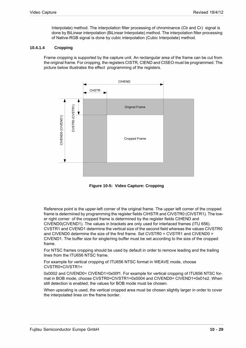
Video Capture Revised 18/4/12
Interpolate) method. The interpolation filter processing of chrominance (Cb and Cr) signal is done by BiLinear interpolation (BiLinear Interpolate) method. The interpolation filter processing of Native-RGB signal is done by cubic interpolation (Cubic Interpolate) method.
10.4.1.4 Cropping
Frame cropping is supported by the capture unit. An rectangular area of the frame can be cut from the original frame. For cropping, the registers CISTR, CIEND and CISEO must be programmed. The picture below illustrates the effect programming of the registers.
Figure 10-5: Video Capture: Cropping
Reference point is the upper-left corner of the original frame. The upper left corner of the cropped frame is determined by programming the register fields CIHSTR and CIVSTR0 (CIVSTR1). The low-er right corner of the cropped frame is determined by the register fields CIHEND and CIVEND0(CIVEND1). The values in brackets are only used for interlaced frames (ITU 656). CVSTR1 and CVEND1 determine the vertical size of the second field whereas the values CIVSTR0 and CIVEND0 determine the size of the first frame. Set CVSTR0 = CVSTR1 and CIVEND0 = CIVEND1. The buffer size for single/ring buffer must be set according to the size of the cropped frame.
For NTSC frames cropping should be used by default in order to remove leading and the trailing lines from the ITU656 NTSC frame.
For example for vertical cropping of ITU656 NTSC format in WEAVE mode, choose CVSTR0=CIVSTR1=
0x0002 and CIVEND0= CIVEND1=0x00f1. For example for vertical cropping of ITU656 NTSC for-mat in BOB mode, choose CVSTR0=CIVSTR1=0x0004 and CIVEND0= CIVEND1=0x01e2. When still detection is enabled, the values for BOB mode must be chosen.
When upscaling is used, the vertical cropped area must be chosen slightly larger in order to cover the interpolated lines on the frame border.
Original Frame
Cropped Frame
CIV
EN
D0
(CIV
EN
D1
)
CV
ST
R0
(CV
ST
R1)
CHSTR
CIHEND
Fujitsu Semiconductor Europe GmbH 10 - 29

Revised 18/4/12 Video Capture
10.4.1.5 Low Pass Filter
Low pass filtering is provided by the capture unit. The vertical low pass filter is a 3 tap FIR filter. The horizontal low pass filter is a 5 tap filter. The filter can be programmed by a two bit coefficient. The coefficient can be set independently for the Y (luminance) and CrCb (chrominance) components.
Use the CLPF (Capture Low Pass Filter) register to program the filter. See the table below for de-tailed description of the single coefficients. Please note that writing 0x0 to the coefficient field, the filter is bypassed.
10.4.2 Processing Algorithm
10.4.2.1 De-interlacing
The de-interlacing algorithms BOB and WEAVE are supported.
Using the BOB algorithm, every line of a frame is doubled. This is useful during motion in the inter-laced video since it reduces artifacts on the edges of moving objects during de-interlacing. Disad-vantage is the reduced resolution of the de-interlaced video.
Using the WEAVE algorithm, the odd and even field is combined during de-interlacing. This assures highest quality of the video, but moving objects can show artifacts.
Furthermore there is a still detection algorithm implemented. This mode allows switching to WEAVE mode when no motion is detected in the video. When motion appears, the BOB de-interlacing algo-rithm is used. Thus the still detection algorithm adapts the de-interlacing to still video scenes.
Bit [17:16] CHLPF_C (Capture Horizontal LPF coefficient C)
CHLPF_C K0 K1 K2 K3 K4
00 0 0 1 0 0
01 0 1/4 2/4 1/4 0
10 0 3/16 10/16 3/16 0
11 3/32 8/32 10/32 10/32 3/32
Bit [19:18] CHLPF_Y (Capture Horizontal LPF coefficient Y)
CHLPF_Y K0 K1 K2 K3 K4
00 0 0 1 0 0
01 0 1/4 2/4 1/4 0
10 0 3/16 10/16 3/16 0
11 3/32 8/32 10/32 10/32 3/32
Bit [25:24] CVLPF_C (Capture Vertical LPF coefficient C)
CVLPF_C K0 K1 K2
00 0 1 0
01 1/4 2/4 1/4
10 3/16 10/16 3/16
11 Reserved
Bit [27:26] CVLPF_Y (Capture Vertical LPF coefficient Y)
CVLPF_Y K0 K1 K2
00 0 1 0
01 1/4 2/4 1/4
10 3/16 10/16 3/16
11 Reserved
10 - 30 Fujitsu Semiconductor Europe GmbH

Video Capture Revised 18/4/12
10.4.2.2 Scaling
The interpolation filter processing of luminance (Y) signal is done by cubic interpolation (Cubic In-terpolate) method. The interpolation filter processing of chrominance (Cb and Cr) signal is done by bilinear interpolation (bilinear interpolate) method. The interpolation filter processing of native RGB signal is done by cubic interpolation (cubic interpolate) method.
Fujitsu Semiconductor Europe GmbH 10 - 31

Revised 18/4/12 Video Capture
10.5 Control Flow
10.5.1 Programming the Capture Unit
The flow chart below shows the necessary steps for programming the capture unit:
Figure 10-6: Programming the Capture Unit
10 - 32 Fujitsu Semiconductor Europe GmbH
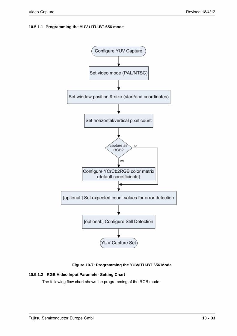
Video Capture Revised 18/4/12
10.5.1.1 Programming the YUV / ITU-BT.656 mode
Figure 10-7: Programming the YUV/ITU-BT.656 Mode
10.5.1.2 RGB Video Input Parameter Setting Chart
The following flow chart shows the programming of the RGB mode:
Fujitsu Semiconductor Europe GmbH 10 - 33
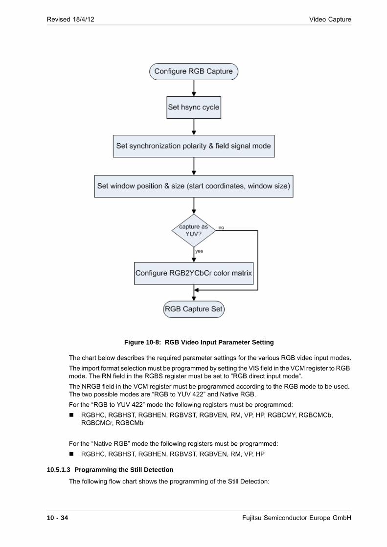
Revised 18/4/12 Video Capture
Figure 10-8: RGB Video Input Parameter Setting
The chart below describes the required parameter settings for the various RGB video input modes.
The import format selection must be programmed by setting the VIS field in the VCM register to RGB mode. The RN field in the RGBS register must be set to “RGB direct input mode“.
The NRGB field in the VCM register must be programmed according to the RGB mode to be used. The two possible modes are “RGB to YUV 422” and Native RGB.
For the “RGB to YUV 422” mode the following registers must be programmed:
RGBHC, RGBHST, RGBHEN, RGBVST, RGBVEN, RM, VP, HP, RGBCMY, RGBCMCb, RGBCMCr, RGBCMb
For the “Native RGB” mode the following registers must be programmed:
RGBHC, RGBHST, RGBHEN, RGBVST, RGBVEN, RM, VP, HP
10.5.1.3 Programming the Still Detection
The following flow chart shows the programming of the Still Detection:
10 - 34 Fujitsu Semiconductor Europe GmbH
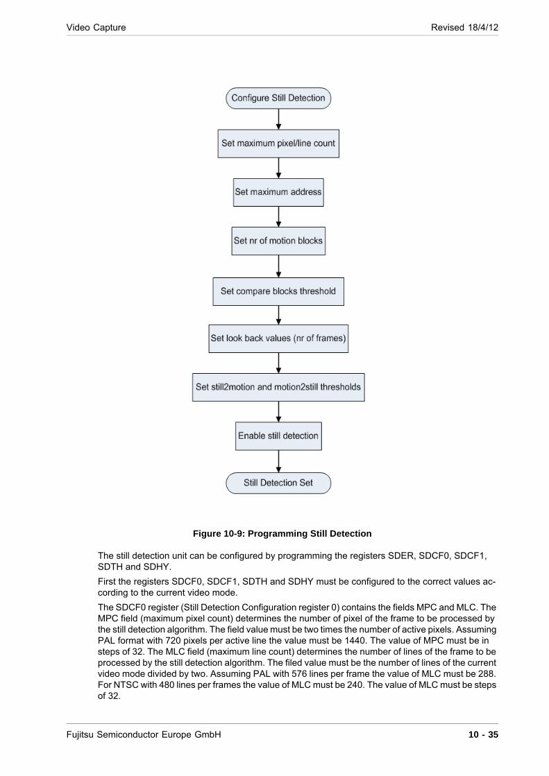
Video Capture Revised 18/4/12
Figure 10-9: Programming Still Detection
The still detection unit can be configured by programming the registers SDER, SDCF0, SDCF1, SDTH and SDHY.
First the registers SDCF0, SDCF1, SDTH and SDHY must be configured to the correct values ac-cording to the current video mode.
The SDCF0 register (Still Detection Configuration register 0) contains the fields MPC and MLC. The MPC field (maximum pixel count) determines the number of pixel of the frame to be processed by the still detection algorithm. The field value must be two times the number of active pixels. Assuming PAL format with 720 pixels per active line the value must be 1440. The value of MPC must be in steps of 32. The MLC field (maximum line count) determines the number of lines of the frame to be processed by the still detection algorithm. The filed value must be the number of lines of the current video mode divided by two. Assuming PAL with 576 lines per frame the value of MLC must be 288. For NTSC with 480 lines per frames the value of MLC must be 240. The value of MLC must be steps of 32.
Fujitsu Semiconductor Europe GmbH 10 - 35

Revised 18/4/12 Video Capture
The SDCF1 (Still Detection Configuration register 1) register contains the fields MA and MB. The MA field (maximum address) determines the maximum address of the reduced frame memory. MA depends on the chosen video mode and can be calculated from the values of MPC and MLC using the following formula:
MA = (MPC / 32) * (MLP / 8).
Assuming a PAL resolution of 720x576 the value of MA is 1620. For a NTSC resolution of 720x480 the value of MA is 1350.
The MB field (motion blocks) can be in the range of 1 to MA. The value MB determines how many values out of value MA must have the attribute “motion” that the frame is considered a motion frame. A reasonable value for MB should be between 50 and 500. If the value of MB is increased, more areas of the frame n must differ compared to frame n-1 that frame n is considered different to frame n-1, means frame n is a motion frame. If the value of MB is decreased less areas of the frame n must differ compared to frame n-1
The SDTH register (Still Detection Threshold register) contains the field CBTH (Compare Blocks Threshold value). The value of CBTH determines the difference between a reduced block of frame n and frame n-1 to be considered as different. If the value of CBTH is increased, the still detection algorithm is less sensitive to motion detection, if the value of CBTH is decreased; the still detection algorithm is more sensitive to motion detection.
The SDTH register (Still Detection Threshold register) contains the fields ST2MO, MO2ST, MLB and SLB.
The field MLB (Motion look back) determines how many past frames are considered for Still to Mo-tion state change. The value of MLB can be between 1 and 64.
The field SLB (Still look back) determines how many past frames are considered for Motion to Still state change. The value of SLB can be between 1 and 64.
The field ST2MO determines how many motion frames must be within the Motion Look Back range to switch the still detection to motion state. ST2MO must be equal or smaller than MLB. Assuming MLB is 6 and ST2MO is 4.That means that 4 out of the last 6 frames must be detected motion frames that the still detection changes from still to motion state. The ordering of the frames is not taken into account.
The field MO2ST determines how many motion frames must be within the Still Look Back range to switch the still detection to still state. MO2ST must be equal or smaller than SLB. Assuming SLB is 8 and ST2MO is 6.That means that 6 out of the last 8 frames must be detected still frames that the still detection changes from motion to still state. The ordering of the frames is not taken into account.
The SDTH register controls a hysteresis mechanism for the still detection algorithm to avoid a per-manent switching between motion and still state and therefore avoids flickering. To obtain a still de-tection behavior, the value of MO2ST must be greater than the value for ST2MO (assuming MLB = SLB. Remark: This must not be necessarily the case). This means the state goes to still after a rel-atively high number of still frames but goes quickly to motion state after only a few frames are de-tected as motion frames.
Finally after configuring the still detection, setting the SDEN bit in the STER register (Still Detection Enable Register) to 1 the still detection starts processing. The setting of SDEN overrides setting of VI bit in the VCM register. When SDEN is “1”, VI is “don’t care”.
10.5.1.4 Programming the High Definition Mode
The following flow chart shows how the programming of the HD mode:
10 - 36 Fujitsu Semiconductor Europe GmbH
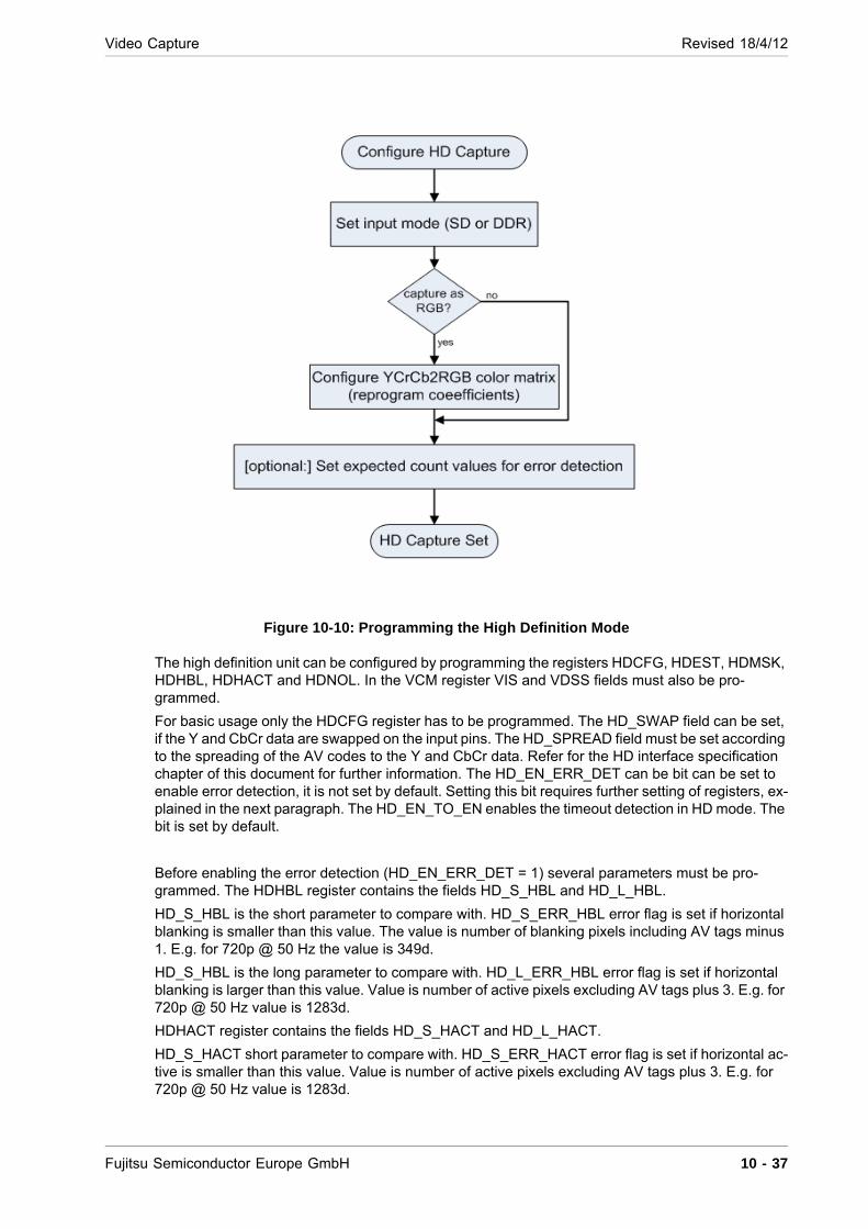
Video Capture Revised 18/4/12
Figure 10-10: Programming the High Definition Mode
The high definition unit can be configured by programming the registers HDCFG, HDEST, HDMSK, HDHBL, HDHACT and HDNOL. In the VCM register VIS and VDSS fields must also be pro-grammed.
For basic usage only the HDCFG register has to be programmed. The HD_SWAP field can be set, if the Y and CbCr data are swapped on the input pins. The HD_SPREAD field must be set according to the spreading of the AV codes to the Y and CbCr data. Refer for the HD interface specification chapter of this document for further information. The HD_EN_ERR_DET can be bit can be set to enable error detection, it is not set by default. Setting this bit requires further setting of registers, ex-plained in the next paragraph. The HD_EN_TO_EN enables the timeout detection in HD mode. The bit is set by default.
Before enabling the error detection (HD_EN_ERR_DET = 1) several parameters must be pro-grammed. The HDHBL register contains the fields HD_S_HBL and HD_L_HBL.
HD_S_HBL is the short parameter to compare with. HD_S_ERR_HBL error flag is set if horizontal blanking is smaller than this value. The value is number of blanking pixels including AV tags minus 1. E.g. for 720p @ 50 Hz the value is 349d.
HD_S_HBL is the long parameter to compare with. HD_L_ERR_HBL error flag is set if horizontal blanking is larger than this value. Value is number of active pixels excluding AV tags plus 3. E.g. for 720p @ 50 Hz value is 1283d.
HDHACT register contains the fields HD_S_HACT and HD_L_HACT.
HD_S_HACT short parameter to compare with. HD_S_ERR_HACT error flag is set if horizontal ac-tive is smaller than this value. Value is number of active pixels excluding AV tags plus 3. E.g. for 720p @ 50 Hz value is 1283d.
Fujitsu Semiconductor Europe GmbH 10 - 37
Revised 18/4/12 Video Capture
HD_L_HACT long parameter to compare with. HD_L_ERR_HACT error flag is set if horizontal ac-tive is larger than this value. Value is number of active pixels excluding AV tags plus 3. E.g. for 720p @ 50 Hz value is 1283d.
HDNOL register contains the fields HD_S_NOL and HD_L_NOL.
HD_S_NOL short parameter to compare with. HD_S_ERR_NOL error flag is set if number of active lines is smaller than this value. Value is number of active lines minus 1. E.g. for 720p value is 719d.
HD_L_NOL long parameter to compare with. HD_L_ERR_NOL error flag is set if number of active lines is larger than this value. Value is number of active lines minus 1. E.g. for 720p value is 719d.
The error mask register HDMSK is used to mask error cases if error detection in HD mode is en-abled. When masking out an error case (set the corresponding mask bit to 0), interrupt generation is suppressed for this error case. The status flags will still be set.
In the VCM register the VIS field must be set to 1h to enable the HD mode. Furthermore the VDSS field must be programmed for section of the video input, either SD mode or DDR mode.
10.5.2 Interrupts
10.5.2.1 Overview
There are two sources of interrupt in the capture unit:
1. Capture Error This interrupt occurs due to video input error.
2. Capture VSYNCThis interrupt occurs in synchronization with the video input Vsync signal.
10.5.2.2 Interrupt Status
Several events can trigger an interrupt in the capture unit. Each interrupt event can be masked out using the interrupt mask register. The single events are ored together and connected to the interrupt controller. In the interrupt controller single capture units can be masked out.
When detecting events by polling, turn off interrupt propagation by the mask settings and read the status flag in the capture controller directly. The flag value can be read without being affected by the mask setting.
10.5.2.3 Error Detection
An error occurs when an expected control code or synchronization signal cannot be detected in the input video data. The status register in the corresponding capture controller is the SYNC_err reg-ister.
10.5.2.4 Capture VSYNC Interrupt
This interrupt notifies about the VSYNC timing of capture. The status register in the corresponding capture controller is the CINT register.
The following uses cases are assumed for this interrupt:
1. Detection of valid image input
2. Frame management by host CPU
The single buffer mode is used when the host CPU manages frame. The CBOA and CBLA registers that specify the starting address of the buffer can be rewritten when the VSYNC interrupt occurs.
The frame immediately after the interrupt has occurred is written to the address in effect before the update is performed. A new address becomes effective from the next frame. In other words, the cap-tured image at the previous address can be used as a still image.
The following shows the state in which writing is being performed to area0. The starting address of area0 is held by the CBOA register.
10 - 38 Fujitsu Semiconductor Europe GmbH
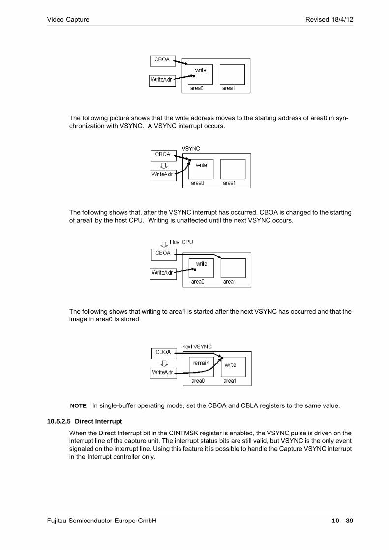
Video Capture Revised 18/4/12
The following picture shows that the write address moves to the starting address of area0 in syn-chronization with VSYNC. A VSYNC interrupt occurs.
The following shows that, after the VSYNC interrupt has occurred, CBOA is changed to the starting of area1 by the host CPU. Writing is unaffected until the next VSYNC occurs.
The following shows that writing to area1 is started after the next VSYNC has occurred and that the image in area0 is stored.
NOTE In single-buffer operating mode, set the CBOA and CBLA registers to the same value.
10.5.2.5 Direct Interrupt
When the Direct Interrupt bit in the CINTMSK register is enabled, the VSYNC pulse is driven on the interrupt line of the capture unit. The interrupt status bits are still valid, but VSYNC is the only event signaled on the interrupt line. Using this feature it is possible to handle the Capture VSYNC interrupt in the Interrupt controller only.
Fujitsu Semiconductor Europe GmbH 10 - 39

Revised 18/4/12 Video Capture
10.5.2.6 Interrupt Waveform
Basically the capture interrupt signal is high active. For DIRECT_INT=1 the waveform of the capture interrupt is pulse shaped. It is generated with every VSYNC. For DIRECT_INT=0 the capture inter-rupt signal is set to active by the VSYNC signal. It stays active until it is reset to inactive low by writ-ing the corresponding CINT register bit with ‘0’.
10 - 40 Fujitsu Semiconductor Europe GmbH
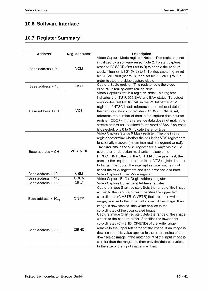
Video Capture Revised 18/4/12
10.6 Software Interface
10.7 Register Summary
Address Register Name Description
Base address + 0H VCM
Video Capture Mode register. Note 1: This register is not initialized by a software reset. Note 2: To start capture, reset bit 28 (VICE) first (set to 0) to enable the capture clock. Then set bit 31 (VIE) to 1. To stop capturing, reset bit 31 (VIE) first (set to 0), then set bit 28 (VICE) to 1 in order to stop the video capture clock.
Base address + 4H CSC Capture Scale register. This register sets the video capture upscaling/downscaling ratio.
Base address + 8H VCS
Video Capture Status 0 register. Note: This register indicates the ITU-R 656 SAV and EAV status. To detect error codes, set NTSC/PAL in the VS bit of the VCM register. If NTSC is set, reference the number of data in the capture data count register (CDCN). If PAL is set, reference the number of data in the capture data counter register (CDCP). If the reference data does not match the stream data or an undefined fourth word of SAV/EAV code is detected, bits 6 to 0 indicate the error type.
Base address + CH VCS_MSK
Video Capture Status 0 Mask register. The bits in this register determine whether the bits in the VCS register are functionally masked (i.e. an interrupt is triggered or not). The error bits in the VCS register are always visible. To use the error detection mechanism, disable the DIRECT_INT bitfield in the CINTMASK register first, then unmask the required error bits in the VCS register in order to trigger interrupts. The interrupt service routine must check the VCS register to see if an error has occurred.
Base address + 10H CBM Video Capture Buffer Mode register Base address + 14H CBOA Video Capture Buffer Origin Address register Base address + 18H CBLA Video Capture Buffer Limit Address register
Base address + 1CH CISTR
Capture Image Start register. Sets the range of the image written to the capture buffer. Specifies the upper left co-ordinates (CIHSTR, CIVSTR) that are in the write range, relative to the upper left corner of the image. If an image is downscaled, this value applies to the co-ordinates of the downscaled image.
Base address + 20H CIEND
Capture Image Start register. Sets the range of the image written to the capture buffer. Specifies the lower right co-ordinates (CIHEND, CIVEND) of the write range, relative to the upper left corner of the image. If an image is downscaled, this value applies to the co-ordinates of the downscaled image. If the raster count of the input image is smaller than the range set, then only the data equivalent to the size of the input image is written.
Fujitsu Semiconductor Europe GmbH 10 - 41
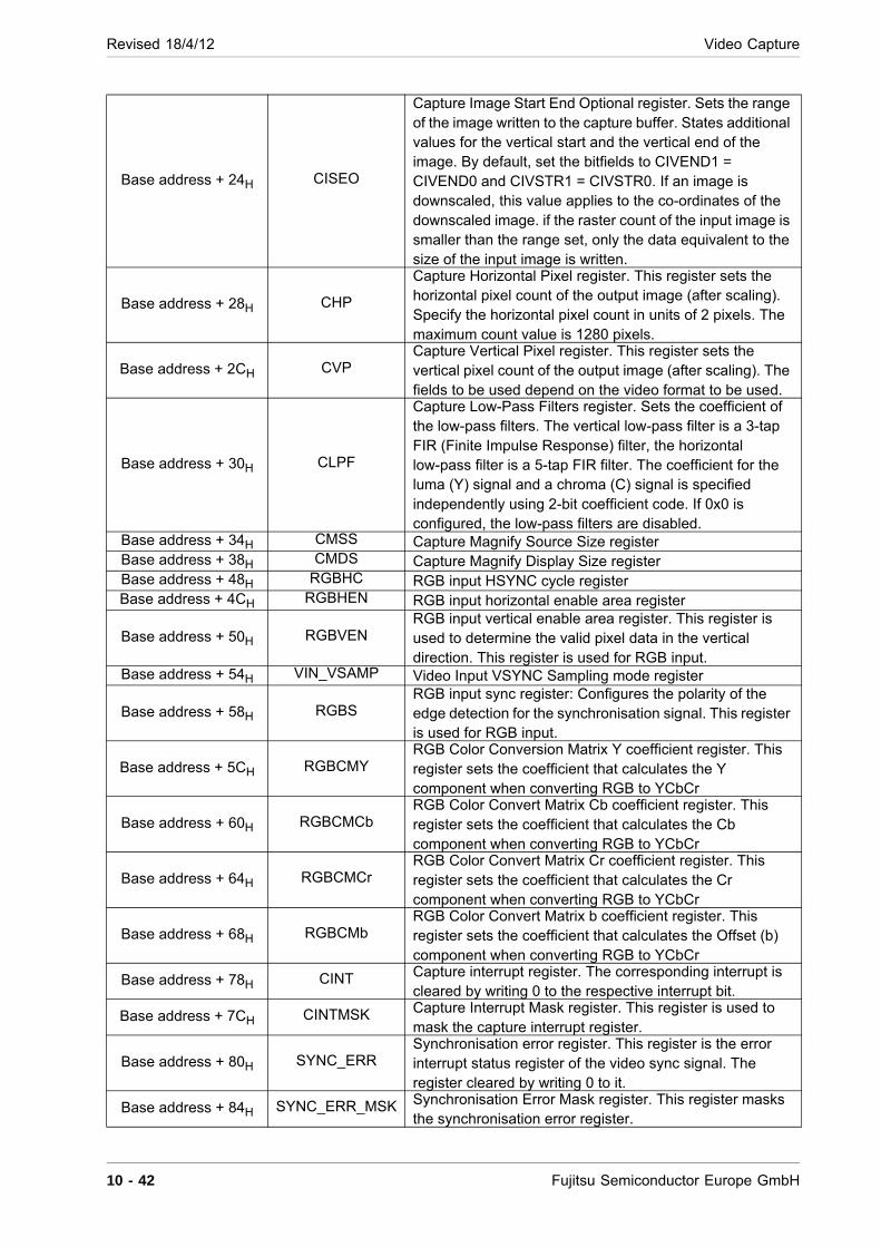
Revised 18/4/12 Video Capture
Base address + 24H CISEO
Capture Image Start End Optional register. Sets the range of the image written to the capture buffer. States additional values for the vertical start and the vertical end of the image. By default, set the bitfields to CIVEND1 = CIVEND0 and CIVSTR1 = CIVSTR0. If an image is downscaled, this value applies to the co-ordinates of the downscaled image. if the raster count of the input image is smaller than the range set, only the data equivalent to the size of the input image is written.
Base address + 28H CHP
Capture Horizontal Pixel register. This register sets the horizontal pixel count of the output image (after scaling). Specify the horizontal pixel count in units of 2 pixels. The maximum count value is 1280 pixels.
Base address + 2CH CVP Capture Vertical Pixel register. This register sets the vertical pixel count of the output image (after scaling). The fields to be used depend on the video format to be used.
Base address + 30H CLPF
Capture Low-Pass Filters register. Sets the coefficient of the low-pass filters. The vertical low-pass filter is a 3-tap FIR (Finite Impulse Response) filter, the horizontal low-pass filter is a 5-tap FIR filter. The coefficient for the luma (Y) signal and a chroma (C) signal is specified independently using 2-bit coefficient code. If 0x0 is configured, the low-pass filters are disabled.
Base address + 34H CMSS Capture Magnify Source Size register Base address + 38H CMDS Capture Magnify Display Size register Base address + 48H RGBHC RGB input HSYNC cycle register Base address + 4CH RGBHEN RGB input horizontal enable area register
Base address + 50H RGBVEN RGB input vertical enable area register. This register is used to determine the valid pixel data in the vertical direction. This register is used for RGB input.
Base address + 54H VIN_VSAMP Video Input VSYNC Sampling mode register
Base address + 58H RGBS RGB input sync register: Configures the polarity of the edge detection for the synchronisation signal. This register is used for RGB input.
Base address + 5CH RGBCMY RGB Color Conversion Matrix Y coefficient register. This register sets the coefficient that calculates the Y component when converting RGB to YCbCr
Base address + 60H RGBCMCb RGB Color Convert Matrix Cb coefficient register. This register sets the coefficient that calculates the Cb component when converting RGB to YCbCr
Base address + 64H RGBCMCr RGB Color Convert Matrix Cr coefficient register. This register sets the coefficient that calculates the Cr component when converting RGB to YCbCr
Base address + 68H RGBCMb RGB Color Convert Matrix b coefficient register. This register sets the coefficient that calculates the Offset (b) component when converting RGB to YCbCr
Base address + 78H CINT Capture interrupt register. The corresponding interrupt is cleared by writing 0 to the respective interrupt bit.
Base address + 7CH CINTMSK Capture Interrupt Mask register. This register is used to mask the capture interrupt register.
Base address + 80H SYNC_ERR Synchronisation error register. This register is the error interrupt status register of the video sync signal. The register cleared by writing 0 to it.
Base address + 84H SYNC_ERR_MSK Synchronisation Error Mask register. This register masks the synchronisation error register.
10 - 42 Fujitsu Semiconductor Europe GmbH
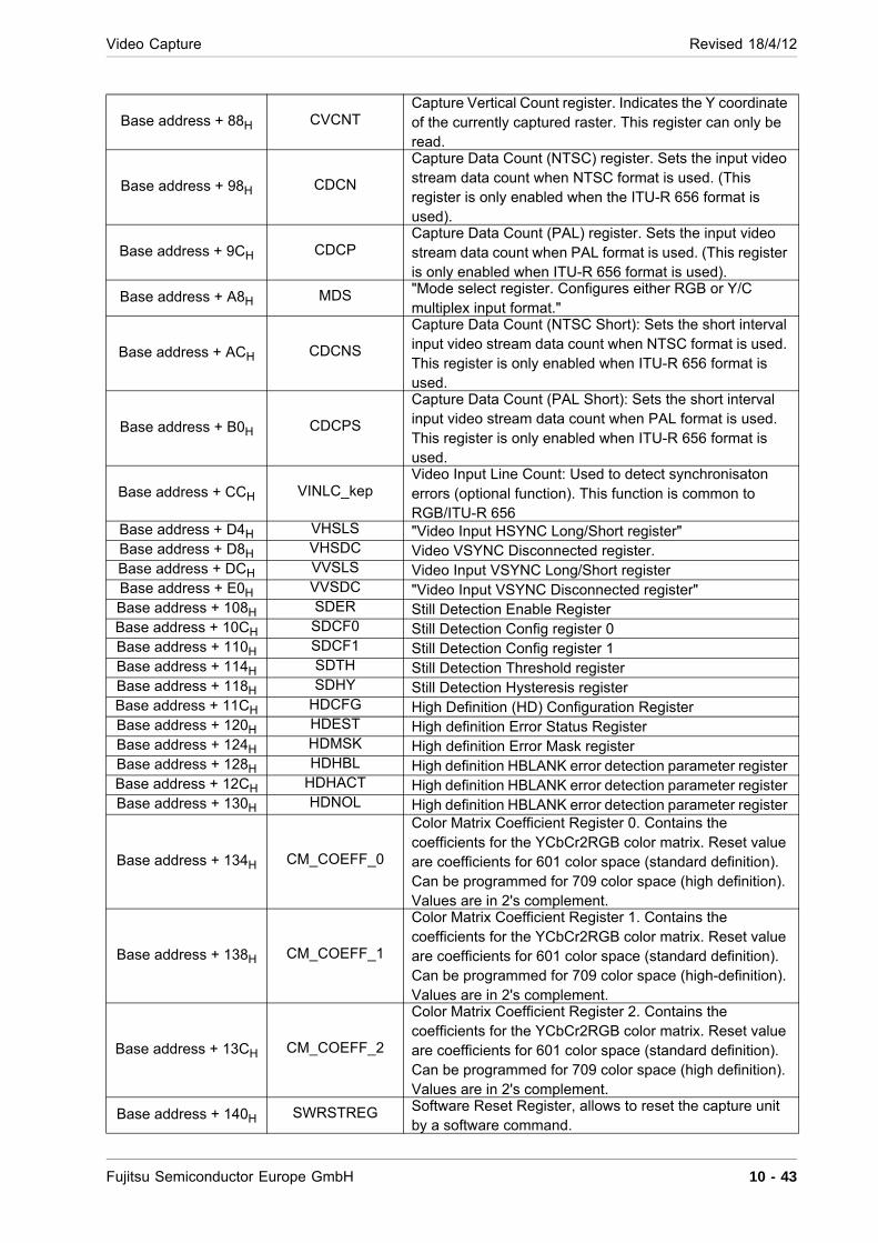
Video Capture Revised 18/4/12
Base address + 88H CVCNT Capture Vertical Count register. Indicates the Y coordinate of the currently captured raster. This register can only be read.
Base address + 98H CDCN
Capture Data Count (NTSC) register. Sets the input video stream data count when NTSC format is used. (This register is only enabled when the ITU-R 656 format is used).
Base address + 9CH CDCP Capture Data Count (PAL) register. Sets the input video stream data count when PAL format is used. (This register is only enabled when ITU-R 656 format is used).
Base address + A8H MDS "Mode select register. Configures either RGB or Y/C multiplex input format."
Base address + ACH CDCNS
Capture Data Count (NTSC Short): Sets the short interval input video stream data count when NTSC format is used. This register is only enabled when ITU-R 656 format is used.
Base address + B0H CDCPS
Capture Data Count (PAL Short): Sets the short interval input video stream data count when PAL format is used. This register is only enabled when ITU-R 656 format is used.
Base address + CCH VINLC_kep Video Input Line Count: Used to detect synchronisaton errors (optional function). This function is common to RGB/ITU-R 656
Base address + D4H VHSLS "Video Input HSYNC Long/Short register" Base address + D8H VHSDC Video VSYNC Disconnected register. Base address + DCH VVSLS Video Input VSYNC Long/Short register Base address + E0H VVSDC "Video Input VSYNC Disconnected register" Base address + 108H SDER Still Detection Enable Register Base address + 10CH SDCF0 Still Detection Config register 0 Base address + 110H SDCF1 Still Detection Config register 1 Base address + 114H SDTH Still Detection Threshold register Base address + 118H SDHY Still Detection Hysteresis register Base address + 11CH HDCFG High Definition (HD) Configuration Register Base address + 120H HDEST High definition Error Status Register Base address + 124H HDMSK High definition Error Mask register Base address + 128H HDHBL High definition HBLANK error detection parameter register Base address + 12CH HDHACT High definition HBLANK error detection parameter register Base address + 130H HDNOL High definition HBLANK error detection parameter register
Base address + 134H CM_COEFF_0
Color Matrix Coefficient Register 0. Contains the coefficients for the YCbCr2RGB color matrix. Reset value are coefficients for 601 color space (standard definition). Can be programmed for 709 color space (high definition). Values are in 2's complement.
Base address + 138H CM_COEFF_1
Color Matrix Coefficient Register 1. Contains the coefficients for the YCbCr2RGB color matrix. Reset value are coefficients for 601 color space (standard definition). Can be programmed for 709 color space (high-definition). Values are in 2's complement.
Base address + 13CH CM_COEFF_2
Color Matrix Coefficient Register 2. Contains the coefficients for the YCbCr2RGB color matrix. Reset value are coefficients for 601 color space (standard definition). Can be programmed for 709 color space (high definition). Values are in 2's complement.
Base address + 140H SWRSTREG Software Reset Register, allows to reset the capture unit by a software command.
Fujitsu Semiconductor Europe GmbH 10 - 43

Revised 18/4/12 Video Capture
Table 10-4: Video Capture Register Summary
10 - 44 Fujitsu Semiconductor Europe GmbH
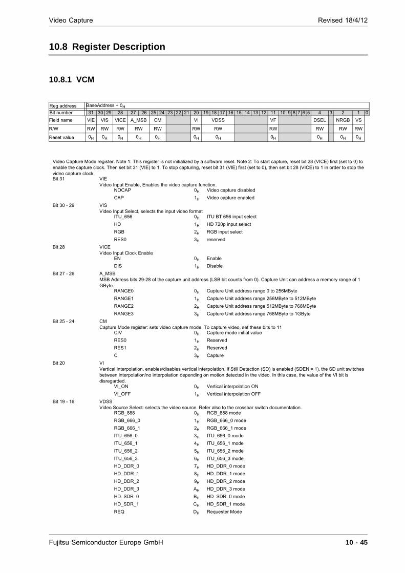
Video Capture Revised 18/4/12
10.8 Register Description
10.8.1 VCM
Reg address BaseAddress + 0H
Bit number 31 30 29 28 27 26 25 24 23 22 21 20 19 18 17 16 15 14 13 12 11 10 9 8 7 6 5 4 3 2 1 0
Field name VIE VIS VICE A_MSB CM VI VDSS VF DSEL NRGB VS
R/W RW RW RW RW RW RW RW RW RW RW RW
Reset value 0H 0H 0H 0H 0H 0H 0H 0H 0H 0H 0H
Video Capture Mode register. Note 1: This register is not initialized by a software reset. Note 2: To start capture, reset bit 28 (VICE) first (set to 0) to enable the capture clock. Then set bit 31 (VIE) to 1. To stop capturing, reset bit 31 (VIE) first (set to 0), then set bit 28 (VICE) to 1 in order to stop the video capture clock. Bit 31 VIE
Video Input Enable, Enables the video capture function. NOCAP 0H Video capture disabled
CAP 1H Video capture enabled
Bit 30 - 29 VIS Video Input Select, selects the input video format
ITU_656 0H ITU BT 656 input select
HD 1H HD 720p input select
RGB 2H RGB input select
RES0 3H reserved
Bit 28 VICE Video Input Clock Enable
EN 0H Enable
DIS 1H Disable
Bit 27 - 26 A_MSB MSB Address bits 29-28 of the capture unit address (LSB bit counts from 0). Capture Unit can address a memory range of 1 GByte.
RANGE0 0H Capture Unit address range 0 to 256MByte
RANGE1 1H Capture Unit address range 256MByte to 512MByte
RANGE2 2H Capture Unit address range 512MByte to 768MByte
RANGE3 3H Capture Unit address range 768MByte to 1GByte
Bit 25 - 24 CM Capture Mode register: sets video capture mode. To capture video, set these bits to 11
CIV 0H Capture mode initial value
RES0 1H Reserved
RES1 2H Reserved
C 3H Capture
Bit 20 VI Vertical Interpolation, enables/disables vertical interpolation. If Still Detection (SD) is enabled (SDEN = 1), the SD unit switches between interpolation/no interpolation depending on motion detected in the video. In this case, the value of the VI bit is disregarded.
VI_ON 0H Vertical interpolation ON
VI_OFF 1H Vertical interpolation OFF
Bit 19 - 16 VDSS Video Source Select: selects the video source. Refer also to the crossbar switch documentation.
RGB_888 0H RGB_888 mode
RGB_666_0 1H RGB_666_0 mode
RGB_666_1 2H RGB_666_1 mode
ITU_656_0 3H ITU_656_0 mode
ITU_656_1 4H ITU_656_1 mode
ITU_656_2 5H ITU_656_2 mode
ITU_656_3 6H ITU_656_3 mode
HD_DDR_0 7H HD_DDR_0 mode
HD_DDR_1 8H HD_DDR_1 mode
HD_DDR_2 9H HD_DDR_2 mode
HD_DDR_3 AH HD_DDR_3 mode
HD_SDR_0 BH HD_SDR_0 mode
HD_SDR_1 CH HD_SDR_1 mode
REQ DH Requester Mode
Fujitsu Semiconductor Europe GmbH 10 - 45
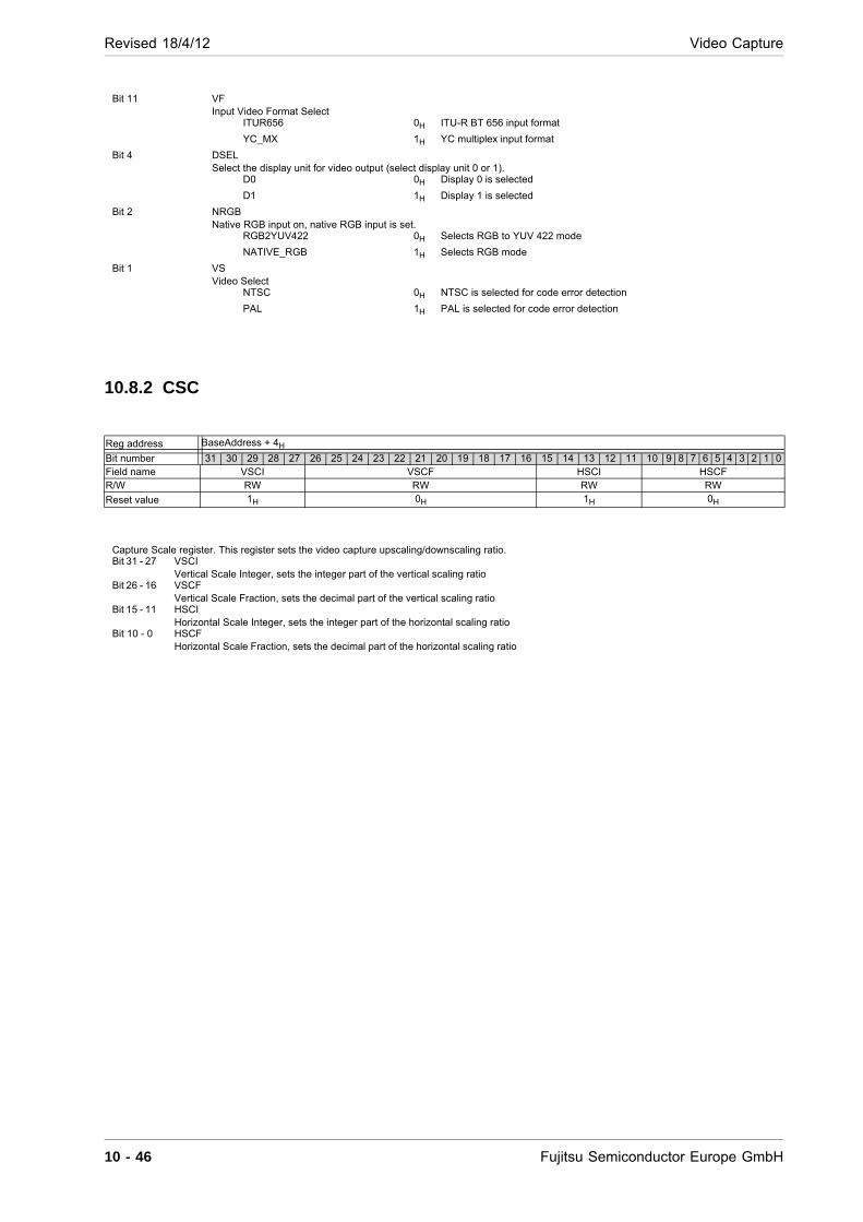
Revised 18/4/12 Video Capture
10.8.2 CSC
Bit 11 VF Input Video Format Select
ITUR656 0H ITU-R BT 656 input format
YC_MX 1H YC multiplex input format
Bit 4 DSEL Select the display unit for video output (select display unit 0 or 1).
D0 0H Display 0 is selected
D1 1H Display 1 is selected
Bit 2 NRGB Native RGB input on, native RGB input is set.
RGB2YUV422 0H Selects RGB to YUV 422 mode
NATIVE_RGB 1H Selects RGB mode
Bit 1 VS Video Select
NTSC 0H NTSC is selected for code error detection
PAL 1H PAL is selected for code error detection
Reg address BaseAddress + 4H
Bit number 31 30 29 28 27 26 25 24 23 22 21 20 19 18 17 16 15 14 13 12 11 10 9 8 7 6 5 4 3 2 1 0Field name VSCI VSCF HSCI HSCF R/W RW RW RW RW
Reset value 1H 0H 1H 0H
Capture Scale register. This register sets the video capture upscaling/downscaling ratio. Bit 31 - 27 VSCI
Vertical Scale Integer, sets the integer part of the vertical scaling ratio Bit 26 - 16 VSCF
Vertical Scale Fraction, sets the decimal part of the vertical scaling ratio Bit 15 - 11 HSCI
Horizontal Scale Integer, sets the integer part of the horizontal scaling ratio Bit 10 - 0 HSCF
Horizontal Scale Fraction, sets the decimal part of the horizontal scaling ratio
10 - 46 Fujitsu Semiconductor Europe GmbH
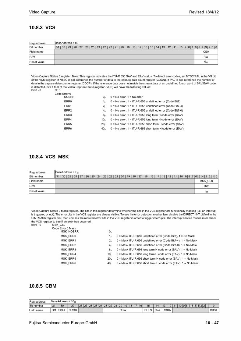
Video Capture Revised 18/4/12
10.8.3 VCS
10.8.4 VCS_MSK
10.8.5 CBM
Reg address BaseAddress + 8H
Bit number 31 30 29 28 27 26 25 24 23 22 21 20 19 18 17 16 15 14 13 12 11 10 9 8 7 6 5 4 3 2 1 0
Field name CE0
R/W RW
Reset value 0H
Video Capture Status 0 register. Note: This register indicates the ITU-R 656 SAV and EAV status. To detect error codes, set NTSC/PAL in the VS bit of the VCM register. If NTSC is set, reference the number of data in the capture data count register (CDCN). If PAL is set, reference the number of data in the capture data counter register (CDCP). If the reference data does not match the stream data or an undefined fourth word of SAV/EAV code is detected, bits 4 to 0 of the Video Capture Status register (VCS) will have the following values: Bit 6 - 0 CE0
Code Error 0 NOERR 0H 0 = No error, 1 = No error
ERR0 1H 0 = No error, 1 = ITU-R 656 undefined error (Code Bit7)
ERR1 2H 0 = No error, 1 = ITU-R 656 undefined error (Code Bit7-4)
ERR2 4H 0 = No error, 1 = ITU-R 656 undefined error (Code Bit7-0)
ERR3 8H 0 = No error, 1 = ITU-R 656 long term H code error (SAV)
ERR4 10H 0 = No error, 1 = ITU-R 656 long term H code error (EAV)
ERR5 20H 0 = No error, 1 = ITU-R 656 short term H code error (SAV)
ERR6 40H 0 = No error, 1 = ITU-R 656 short term H code error (EAV)
Reg address BaseAddress + CH
Bit number 31 30 29 28 27 26 25 24 23 22 21 20 19 18 17 16 15 14 13 12 11 10 9 8 7 6 5 4 3 2 1 0
Field name MSK_CE0
R/W RW
Reset value 0H
Video Capture Status 0 Mask register. The bits in this register determine whether the bits in the VCS register are functionally masked (i.e. an interrupt is triggered or not). The error bits in the VCS register are always visible. To use the error detection mechanism, disable the DIRECT_INT bitfield in the CINTMASK register first, then unmask the required error bits in the VCS register in order to trigger interrupts. The interrupt service routine must check the VCS register to see if an error has occurred.Bit 6 - 0 MSK_CE0
Code Error 0 Mask MSK_NOERR 0H
MSK_ERR0 1H 0 = Mask ITU-R 656 undefined error (Code Bit7), 1 = No Mask
MSK_ERR1 2H 0 = Mask ITU-R 656 undefined error (Code Bit7-4), 1 = No Mask
MSK_ERR2 4H 0 = Mask ITU-R 656 undefined error (Code Bit7-0), 1 = No Mask
MSK_ERR3 8H 0 = Mask ITU-R 656 long term H code error (SAV), 1 = No Mask
MSK_ERR4 10H 0 = Mask ITU-R 656 long term H code error (EAV), 1 = No Mask
MSK_ERR5 20H 0 = Mask ITU-R 656 short term H code error (SAV), 1 = No Mask
MSK_ERR6 40H 0 = Mask ITU-R 656 short term H code error (EAV), 1 = No Mask
Reg address BaseAddress + 10H
Bit number 31 30 29 28 27 26 25 24 23 22 21 20 19 18 17 16 15 14 13 12 11 10 9 8 7 6 5 4 3 2 1 0
Field name OO SBUF CRGB CBW BLEN C24 RGBA CBST
Fujitsu Semiconductor Europe GmbH 10 - 47
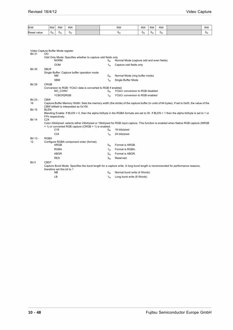
Revised 18/4/12 Video Capture
R/W RW RW RW RW RW RW RW RW
Reset value 0H 0H 0H 0H 0H 0H 0H 0H
Video Capture Buffer Mode register Bit 31 OO
Odd Only Mode: Specifies whether to capture odd fields only NORM 0H Normal Mode (capture odd and even fields)
OOM 1H Capture odd fields only
Bit 30 SBUF Single Buffer: Capture buffer operation mode
NM 0H Normal Mode (ring buffer mode)
SBM 1H Single Buffer Mode
Bit 29 CRGB Conversion to RGB: YCbCr data is converted to RGB if enabled.
NO_CONV 0H YCbCr conversion to RGB disabled
YCBCR2RGB 1H YCbCr conversion to RGB enabled
Bit 23 - 16
CBW Capture Buffer Memory Width: Sets the memory width (the stride) of the capture buffer (in units of 64 bytes). If set to 0x00, the value of the CBW bitfield is interpreted as 0x100.
Bit 15 BLEN Blending Enable: If BLEN = 0, then the alpha bit/byte in the RGBA formats are set to 0h. If BLEN = 1 then the alpha bit/byte is set to 1 or FFh respectively.
Bit 14 C24 Color 24bit/pixel: selects either 24bit/pixel or 16bit/pixel for RGB input capture. This function is enabled when Native RGB capture (NRGB = 1) or converted RGB capture (CRGB = 1) is enabled.
C16 0H 16 bits/pixel
C24 1H 24 bits/pixel
Bit 13 - 12
RGBA Configure RGBA component order (format).
ARGB 0H Format is ARGB.
RGBA 1H Format is RGBA.
ABGR 2H Format is ABGR.
RES 3H Reserved.
Bit 0 CBST Capture Burst Mode. Specifies the burst length for a capture write. A long burst length is recommended for performance reasons, therefore set this bit to 1
NB 0H Normal burst write (4 Words)
LB 1H Long burst write (8 Words)
10 - 48 Fujitsu Semiconductor Europe GmbH
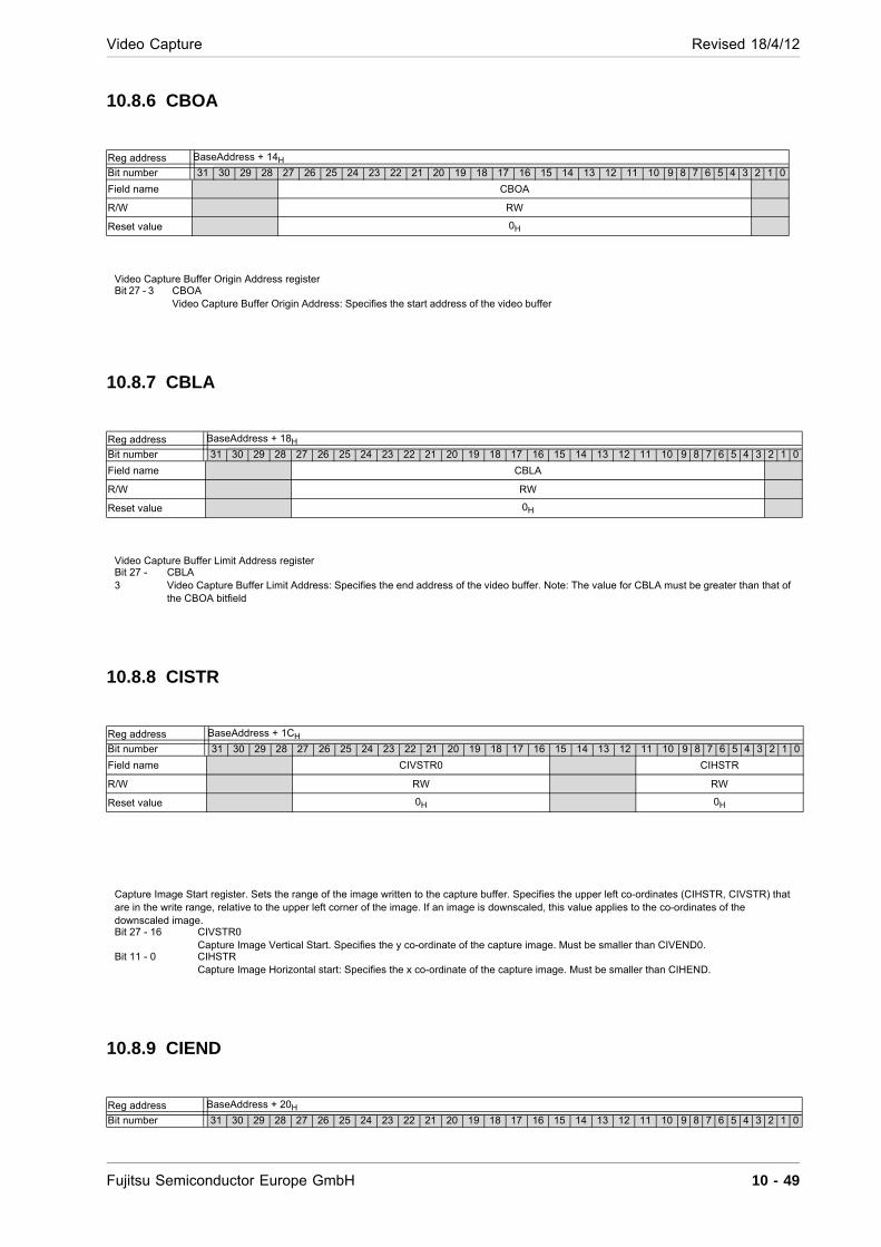
Video Capture Revised 18/4/12
10.8.6 CBOA
10.8.7 CBLA
10.8.8 CISTR
10.8.9 CIEND
Reg address BaseAddress + 14H
Bit number 31 30 29 28 27 26 25 24 23 22 21 20 19 18 17 16 15 14 13 12 11 10 9 8 7 6 5 4 3 2 1 0
Field name CBOA
R/W RW
Reset value 0H
Video Capture Buffer Origin Address register Bit 27 - 3 CBOA
Video Capture Buffer Origin Address: Specifies the start address of the video buffer
Reg address BaseAddress + 18H
Bit number 31 30 29 28 27 26 25 24 23 22 21 20 19 18 17 16 15 14 13 12 11 10 9 8 7 6 5 4 3 2 1 0
Field name CBLA
R/W RW
Reset value 0H
Video Capture Buffer Limit Address register Bit 27 - 3
CBLA Video Capture Buffer Limit Address: Specifies the end address of the video buffer. Note: The value for CBLA must be greater than that of the CBOA bitfield
Reg address BaseAddress + 1CH
Bit number 31 30 29 28 27 26 25 24 23 22 21 20 19 18 17 16 15 14 13 12 11 10 9 8 7 6 5 4 3 2 1 0
Field name CIVSTR0 CIHSTR
R/W RW RW
Reset value 0H 0H
Capture Image Start register. Sets the range of the image written to the capture buffer. Specifies the upper left co-ordinates (CIHSTR, CIVSTR) that are in the write range, relative to the upper left corner of the image. If an image is downscaled, this value applies to the co-ordinates of the downscaled image. Bit 27 - 16 CIVSTR0
Capture Image Vertical Start. Specifies the y co-ordinate of the capture image. Must be smaller than CIVEND0. Bit 11 - 0 CIHSTR
Capture Image Horizontal start: Specifies the x co-ordinate of the capture image. Must be smaller than CIHEND.
Reg address BaseAddress + 20H
Bit number 31 30 29 28 27 26 25 24 23 22 21 20 19 18 17 16 15 14 13 12 11 10 9 8 7 6 5 4 3 2 1 0
Fujitsu Semiconductor Europe GmbH 10 - 49
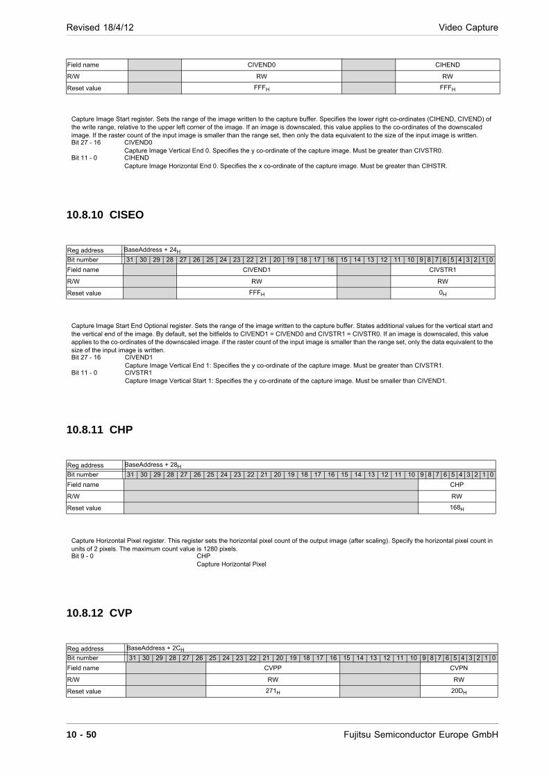
Revised 18/4/12 Video Capture
10.8.10 CISEO
10.8.11 CHP
10.8.12 CVP
Field name CIVEND0 CIHEND
R/W RW RW
Reset value FFFH FFFH
Capture Image Start register. Sets the range of the image written to the capture buffer. Specifies the lower right co-ordinates (CIHEND, CIVEND) of the write range, relative to the upper left corner of the image. If an image is downscaled, this value applies to the co-ordinates of the downscaled image. If the raster count of the input image is smaller than the range set, then only the data equivalent to the size of the input image is written. Bit 27 - 16 CIVEND0
Capture Image Vertical End 0. Specifies the y co-ordinate of the capture image. Must be greater than CIVSTR0. Bit 11 - 0 CIHEND
Capture Image Horizontal End 0. Specifies the x co-ordinate of the capture image. Must be greater than CIHSTR.
Reg address BaseAddress + 24H
Bit number 31 30 29 28 27 26 25 24 23 22 21 20 19 18 17 16 15 14 13 12 11 10 9 8 7 6 5 4 3 2 1 0
Field name CIVEND1 CIVSTR1
R/W RW RW
Reset value FFFH 0H
Capture Image Start End Optional register. Sets the range of the image written to the capture buffer. States additional values for the vertical start and the vertical end of the image. By default, set the bitfields to CIVEND1 = CIVEND0 and CIVSTR1 = CIVSTR0. If an image is downscaled, this value applies to the co-ordinates of the downscaled image. if the raster count of the input image is smaller than the range set, only the data equivalent to the size of the input image is written. Bit 27 - 16 CIVEND1
Capture Image Vertical End 1: Specifies the y co-ordinate of the capture image. Must be greater than CIVSTR1. Bit 11 - 0 CIVSTR1
Capture Image Vertical Start 1: Specifies the y co-ordinate of the capture image. Must be smaller than CIVEND1.
Reg address BaseAddress + 28H
Bit number 31 30 29 28 27 26 25 24 23 22 21 20 19 18 17 16 15 14 13 12 11 10 9 8 7 6 5 4 3 2 1 0
Field name CHP
R/W RW
Reset value 168H
Capture Horizontal Pixel register. This register sets the horizontal pixel count of the output image (after scaling). Specify the horizontal pixel count in units of 2 pixels. The maximum count value is 1280 pixels. Bit 9 - 0 CHP
Capture Horizontal Pixel
Reg address BaseAddress + 2CH
Bit number 31 30 29 28 27 26 25 24 23 22 21 20 19 18 17 16 15 14 13 12 11 10 9 8 7 6 5 4 3 2 1 0
Field name CVPP CVPN
R/W RW RW
Reset value 271H 20DH
10 - 50 Fujitsu Semiconductor Europe GmbH
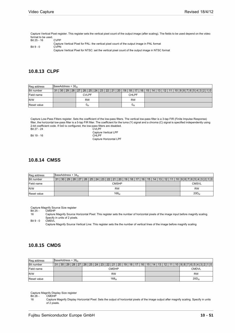
Video Capture Revised 18/4/12
10.8.13 CLPF
10.8.14 CMSS
10.8.15 CMDS
Capture Vertical Pixel register. This register sets the vertical pixel count of the output image (after scaling). The fields to be used depend on the video format to be used. Bit 25 - 16 CVPP
Capture Vertical Pixel for PAL: the vertical pixel count of the output image in PAL format Bit 9 - 0 CVPN
Capture Vertical Pixel for NTSC: set the vertical pixel count of the output image in NTSC format
Reg address BaseAddress + 30H
Bit number 31 30 29 28 27 26 25 24 23 22 21 20 19 18 17 16 15 14 13 12 11 10 9 8 7 6 5 4 3 2 1 0
Field name CVLPF CHLPF
R/W RW RW
Reset value 0H 0H
Capture Low-Pass Filters register. Sets the coefficient of the low-pass filters. The vertical low-pass filter is a 3-tap FIR (Finite Impulse Response) filter, the horizontal low-pass filter is a 5-tap FIR filter. The coefficient for the luma (Y) signal and a chroma (C) signal is specified independently using 2-bit coefficient code. If 0x0 is configured, the low-pass filters are disabled. Bit 27 - 24 CVLPF
Capture Vertical LPF Bit 19 - 16 CHLPF
Capture Horizontal LPF
Reg address BaseAddress + 34H
Bit number 31 30 29 28 27 26 25 24 23 22 21 20 19 18 17 16 15 14 13 12 11 10 9 8 7 6 5 4 3 2 1 0
Field name CMSHP CMSVL
R/W RW RW
Reset value 168H 20DH
Capture Magnify Source Size register Bit 25 - 16
CMSHP Capture Magnify Source Horizontal Pixel: This register sets the number of horizontal pixels of the image input before magnify scaling. Specify in units of 2 pixels.
Bit 9 - 0 CMSVL Capture Magnify Source Vertical Line: This register sets the the number of vertical lines of the image before magnify scaling
Reg address BaseAddress + 38H
Bit number 31 30 29 28 27 26 25 24 23 22 21 20 19 18 17 16 15 14 13 12 11 10 9 8 7 6 5 4 3 2 1 0
Field name CMDHP CMDVL
R/W RW RW
Reset value 168H 20DH
Capture Magnify Display Size register Bit 26 - 16
CMDHP Capture Magnify Display Horizontal Pixel: Sets the output of horizontal pixels of the image output after magnify scaling. Specify in units of 2 pixels.
Fujitsu Semiconductor Europe GmbH 10 - 51
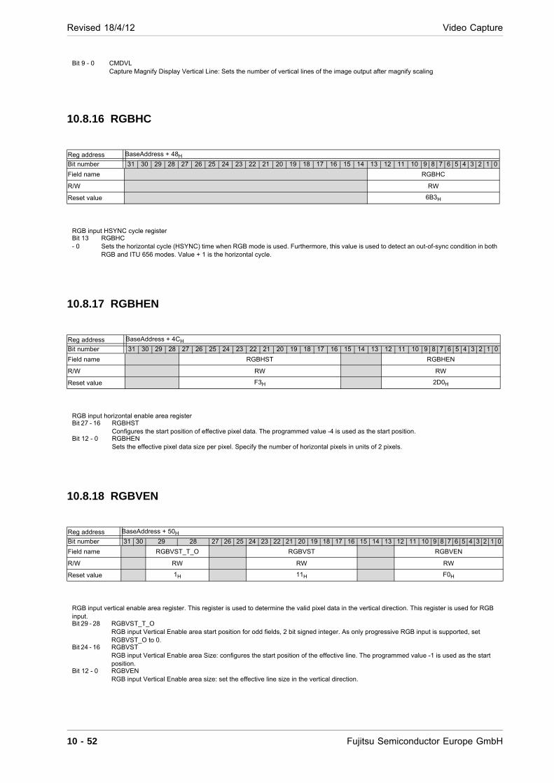
Revised 18/4/12 Video Capture
10.8.16 RGBHC
10.8.17 RGBHEN
10.8.18 RGBVEN
Bit 9 - 0 CMDVL Capture Magnify Display Vertical Line: Sets the number of vertical lines of the image output after magnify scaling
Reg address BaseAddress + 48H
Bit number 31 30 29 28 27 26 25 24 23 22 21 20 19 18 17 16 15 14 13 12 11 10 9 8 7 6 5 4 3 2 1 0
Field name RGBHC
R/W RW
Reset value 6B3H
RGB input HSYNC cycle register Bit 13 - 0
RGBHC Sets the horizontal cycle (HSYNC) time when RGB mode is used. Furthermore, this value is used to detect an out-of-sync condition in both RGB and ITU 656 modes. Value + 1 is the horizontal cycle.
Reg address BaseAddress + 4CH
Bit number 31 30 29 28 27 26 25 24 23 22 21 20 19 18 17 16 15 14 13 12 11 10 9 8 7 6 5 4 3 2 1 0
Field name RGBHST RGBHEN
R/W RW RW
Reset value F3H 2D0H
RGB input horizontal enable area register Bit 27 - 16 RGBHST
Configures the start position of effective pixel data. The programmed value -4 is used as the start position. Bit 12 - 0 RGBHEN
Sets the effective pixel data size per pixel. Specify the number of horizontal pixels in units of 2 pixels.
Reg address BaseAddress + 50H
Bit number 31 30 29 28 27 26 25 24 23 22 21 20 19 18 17 16 15 14 13 12 11 10 9 8 7 6 5 4 3 2 1 0
Field name RGBVST_T_O RGBVST RGBVEN
R/W RW RW RW
Reset value 1H 11H F0H
RGB input vertical enable area register. This register is used to determine the valid pixel data in the vertical direction. This register is used for RGB input. Bit 29 - 28 RGBVST_T_O
RGB input Vertical Enable area start position for odd fields, 2 bit signed integer. As only progressive RGB input is supported, set RGBVST_O to 0.
Bit 24 - 16 RGBVST RGB input Vertical Enable area Size: configures the start position of the effective line. The programmed value -1 is used as the start position.
Bit 12 - 0 RGBVEN RGB input Vertical Enable area size: set the effective line size in the vertical direction.
10 - 52 Fujitsu Semiconductor Europe GmbH
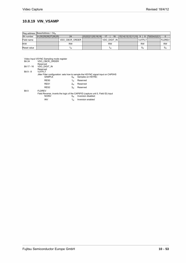
Video Capture Revised 18/4/12
10.8.19 VIN_VSAMP
Reg address BaseAddress + 54H
Bit number 31 30 29 28 27 26 25 24 23 22 21 20 19 18 17 16 15 14 13 12 11 10 9 8 7 6 5 4 3 2 1 0
Field name VDO_CBCR_ORDER VDO_DIGIT_IN VJITFLT FLDREV
R/W RW RW RW RW
Reset value 1H 1H 0H 0H
Video Input VSYNC Sampling mode register Bit 24 VDO_CBCR_ORDER
Reserved Bit 17 - 16 VDO_DIGIT_IN
Reserved Bit 9 - 8 VJITFLT
Jitter Filter configuration: sets how to sample the HSYNC signal input on CAP0HS SAMPLE 0H Samples on HSYNC
RES0 1H Reserved
RES1 2H Reserved
RES2 3H Reserved
Bit 0 FLDREV Field Reverse, inverts the logic of the CAP0FID (capture unit 0, Field ID) input
NOINV 0H Inversion disabled
INV 1H Inversion enabled
Fujitsu Semiconductor Europe GmbH 10 - 53
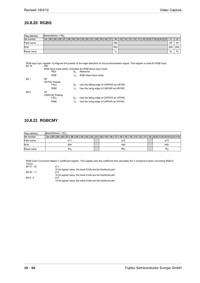
Revised 18/4/12 Video Capture
10.8.20 RGBS
10.8.21 RGBCMY
Reg address BaseAddress + 58H
Bit number 31 30 29 28 27 26 25 24 23 22 21 20 19 18 17 16 15 14 13 12 11 10 9 8 7 6 5 4 3 2 1 0
Field name RM HP VP
R/W RW RW RW
Reset value 1H 0H 0H
RGB input sync register: Configures the polarity of the edge detection for the synchronisation signal. This register is used for RGB input. Bit 16 RM
RGB input mode select: Activates the RGB direct input mode RES 0H Reserved
RGB 1H RGB direct input mode
Bit 1 HP HSYNC Polarity
FALL 0H Use the falling edge of CAP0HS as HSYNC
RISE 1H Use the rising edge of CAP0HS as HSYNC
Bit 0 VP VINSYNC Polarity
FALL 0H Use the falling edge of CAP0VS as VSYNC
RISE 1H Use the rising edge of CAP0VS as VSYNC
Reg address BaseAddress + 5CH
Bit number 31 30 29 28 27 26 25 24 23 22 21 20 19 18 17 16 15 14 13 12 11 10 9 8 7 6 5 4 3 2 1 0
Field name a11 a12 a13
R/W RW RW RW
Reset value 42H 80H 19H
RGB Color Conversion Matrix Y coefficient register. This register sets the coefficient that calculates the Y component when converting RGB to YCbCr Bit 31 - 22 a11
10 bit signed value, the lower 8 bits are the fractional part Bit 20 - 11 a12
10 bit signed value, the lower 8 bits are the fractional part Bit 9 - 0 a13
10 bit signed value, the lower 8 bits are the fractional part
10 - 54 Fujitsu Semiconductor Europe GmbH
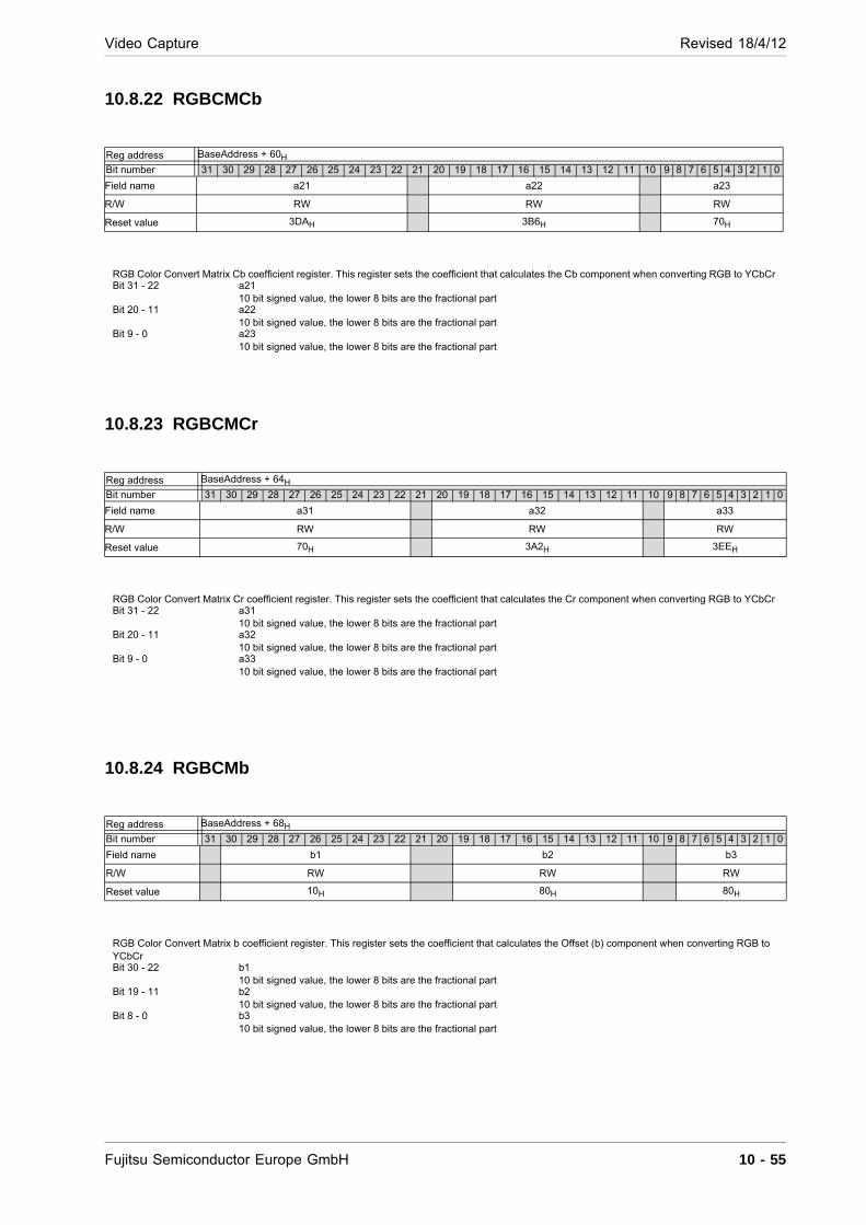
Video Capture Revised 18/4/12
10.8.22 RGBCMCb
10.8.23 RGBCMCr
10.8.24 RGBCMb
Reg address BaseAddress + 60H
Bit number 31 30 29 28 27 26 25 24 23 22 21 20 19 18 17 16 15 14 13 12 11 10 9 8 7 6 5 4 3 2 1 0
Field name a21 a22 a23
R/W RW RW RW
Reset value 3DAH 3B6H 70H
RGB Color Convert Matrix Cb coefficient register. This register sets the coefficient that calculates the Cb component when converting RGB to YCbCr Bit 31 - 22 a21
10 bit signed value, the lower 8 bits are the fractional part Bit 20 - 11 a22
10 bit signed value, the lower 8 bits are the fractional part Bit 9 - 0 a23
10 bit signed value, the lower 8 bits are the fractional part
Reg address BaseAddress + 64H
Bit number 31 30 29 28 27 26 25 24 23 22 21 20 19 18 17 16 15 14 13 12 11 10 9 8 7 6 5 4 3 2 1 0
Field name a31 a32 a33
R/W RW RW RW
Reset value 70H 3A2H 3EEH
RGB Color Convert Matrix Cr coefficient register. This register sets the coefficient that calculates the Cr component when converting RGB to YCbCr Bit 31 - 22 a31
10 bit signed value, the lower 8 bits are the fractional part Bit 20 - 11 a32
10 bit signed value, the lower 8 bits are the fractional part Bit 9 - 0 a33
10 bit signed value, the lower 8 bits are the fractional part
Reg address BaseAddress + 68H
Bit number 31 30 29 28 27 26 25 24 23 22 21 20 19 18 17 16 15 14 13 12 11 10 9 8 7 6 5 4 3 2 1 0
Field name b1 b2 b3
R/W RW RW RW
Reset value 10H 80H 80H
RGB Color Convert Matrix b coefficient register. This register sets the coefficient that calculates the Offset (b) component when converting RGB to YCbCr Bit 30 - 22 b1
10 bit signed value, the lower 8 bits are the fractional part Bit 19 - 11 b2
10 bit signed value, the lower 8 bits are the fractional part Bit 8 - 0 b3
10 bit signed value, the lower 8 bits are the fractional part
Fujitsu Semiconductor Europe GmbH 10 - 55
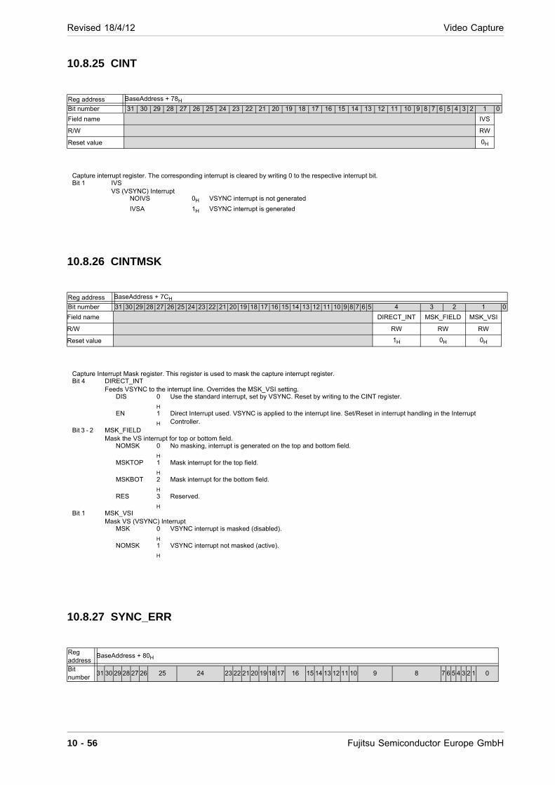
Revised 18/4/12 Video Capture
10.8.25 CINT
10.8.26 CINTMSK
10.8.27 SYNC_ERR
Reg address BaseAddress + 78H
Bit number 31 30 29 28 27 26 25 24 23 22 21 20 19 18 17 16 15 14 13 12 11 10 9 8 7 6 5 4 3 2 1 0
Field name IVS
R/W RW
Reset value 0H
Capture interrupt register. The corresponding interrupt is cleared by writing 0 to the respective interrupt bit. Bit 1 IVS
VS (VSYNC) Interrupt NOIVS 0H VSYNC interrupt is not generated
IVSA 1H VSYNC interrupt is generated
Reg address BaseAddress + 7CH
Bit number 31 30 29 28 27 26 25 24 23 22 21 20 19 18 17 16 15 14 13 12 11 10 9 8 7 6 5 4 3 2 1 0
Field name DIRECT_INT MSK_FIELD MSK_VSI
R/W RW RW RW
Reset value 1H 0H 0H
Capture Interrupt Mask register. This register is used to mask the capture interrupt register. Bit 4 DIRECT_INT
Feeds VSYNC to the interrupt line. Overrides the MSK_VSI setting. DIS 0
H
Use the standard interrupt, set by VSYNC. Reset by writing to the CINT register.
EN 1
H
Direct Interrupt used. VSYNC is applied to the interrupt line. Set/Reset in interrupt handling in the Interrupt Controller.
Bit 3 - 2 MSK_FIELD Mask the VS interrupt for top or bottom field.
NOMSK 0
H
No masking, interrupt is generated on the top and bottom field.
MSKTOP 1
H
Mask interrupt for the top field.
MSKBOT 2
H
Mask interrupt for the bottom field.
RES 3
H
Reserved.
Bit 1 MSK_VSI Mask VS (VSYNC) Interrupt
MSK 0
H
VSYNC interrupt is masked (disabled).
NOMSK 1
H
VSYNC interrupt not masked (active).
Reg address
BaseAddress + 80H
Bit number
31 30 29 28 27 26 25 24 23 22 21 20 19 18 17 16 15 14 13 12 11 10 9 8 7 6 5 4 3 2 1 0
10 - 56 Fujitsu Semiconductor Europe GmbH
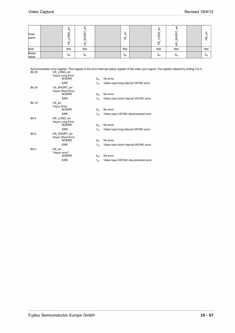
Video Capture Revised 18/4/12
Field name
VS
_L
ON
G_
err
VS
_S
HO
RT
_er
r
VS
_err
HS
_L
ON
G_
err
HS
_SH
OR
T_
err
HS
_er
r
R/W RW RW RW RW RW RW
Reset value
0H 0H 0H 0H 0H 0H
Synchronisation error register. This register is the error interrupt status register of the video sync signal. The register cleared by writing 0 to it. Bit 25 VS_LONG_err
Vsync Long Error NOERR 0H No error.
ERR 1H Video input long interval VSYNC error.
Bit 24 VS_SHORT_err Vsync Short Error
NOERR 0H No error.
ERR 1H Video input short interval VSYNC error.
Bit 16 VS_err Vsync Error
NOERR 0H No error.
ERR 1H Video input VSYNC disconnected error.
Bit 9 HS_LONG_err Hsync Long Error
NOERR 0H No error.
ERR 1H Video input long interval HSYNC error.
Bit 8 HS_SHORT_err Hsync Short Error
NOERR 0H No error.
ERR 1H Video input short interval HSYNC error.
Bit 0 HS_err "Hsync error"
NOERR 0H No error.
ERR 1H Video Input HSYNC disconnected error.
Fujitsu Semiconductor Europe GmbH 10 - 57
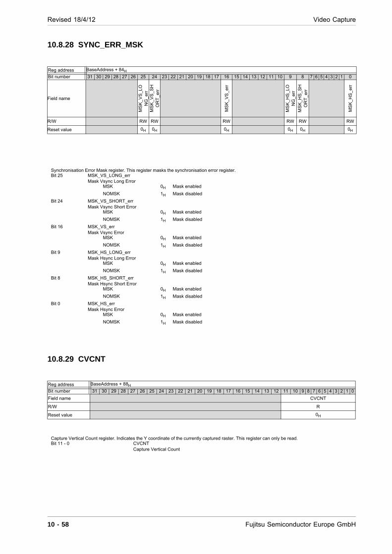
Revised 18/4/12 Video Capture
10.8.28 SYNC_ERR_MSK
10.8.29 CVCNT
Reg address BaseAddress + 84H
Bit number 31 30 29 28 27 26 25 24 23 22 21 20 19 18 17 16 15 14 13 12 11 10 9 8 7 6 5 4 3 2 1 0
Field name
MS
K_
VS
_L
ON
G_
err
MS
K_
VS
_S
HO
RT
_err
MS
K_V
S_
err
MS
K_
HS
_LO
NG
_er
r
MS
K_
HS
_S
HO
RT
_err
MS
K_H
S_
err
R/W RW RW RW RW RW RW
Reset value 0H 0H 0H 0H 0H 0H
Synchronisation Error Mask register. This register masks the synchronisation error register. Bit 25 MSK_VS_LONG_err
Mask Vsync Long Error MSK 0H Mask enabled
NOMSK 1H Mask disabled
Bit 24 MSK_VS_SHORT_err Mask Vsync Short Error
MSK 0H Mask enabled
NOMSK 1H Mask disabled
Bit 16 MSK_VS_err Mask Vsync Error
MSK 0H Mask enabled
NOMSK 1H Mask disabled
Bit 9 MSK_HS_LONG_err Mask Hsync Long Error
MSK 0H Mask enabled
NOMSK 1H Mask disabled
Bit 8 MSK_HS_SHORT_err Mask Hsync Short Error
MSK 0H Mask enabled
NOMSK 1H Mask disabled
Bit 0 MSK_HS_err Mask Hsync Error
MSK 0H Mask enabled
NOMSK 1H Mask disabled
Reg address BaseAddress + 88H
Bit number 31 30 29 28 27 26 25 24 23 22 21 20 19 18 17 16 15 14 13 12 11 10 9 8 7 6 5 4 3 2 1 0
Field name CVCNT
R/W R
Reset value 0H
Capture Vertical Count register. Indicates the Y coordinate of the currently captured raster. This register can only be read. Bit 11 - 0 CVCNT
Capture Vertical Count
10 - 58 Fujitsu Semiconductor Europe GmbH
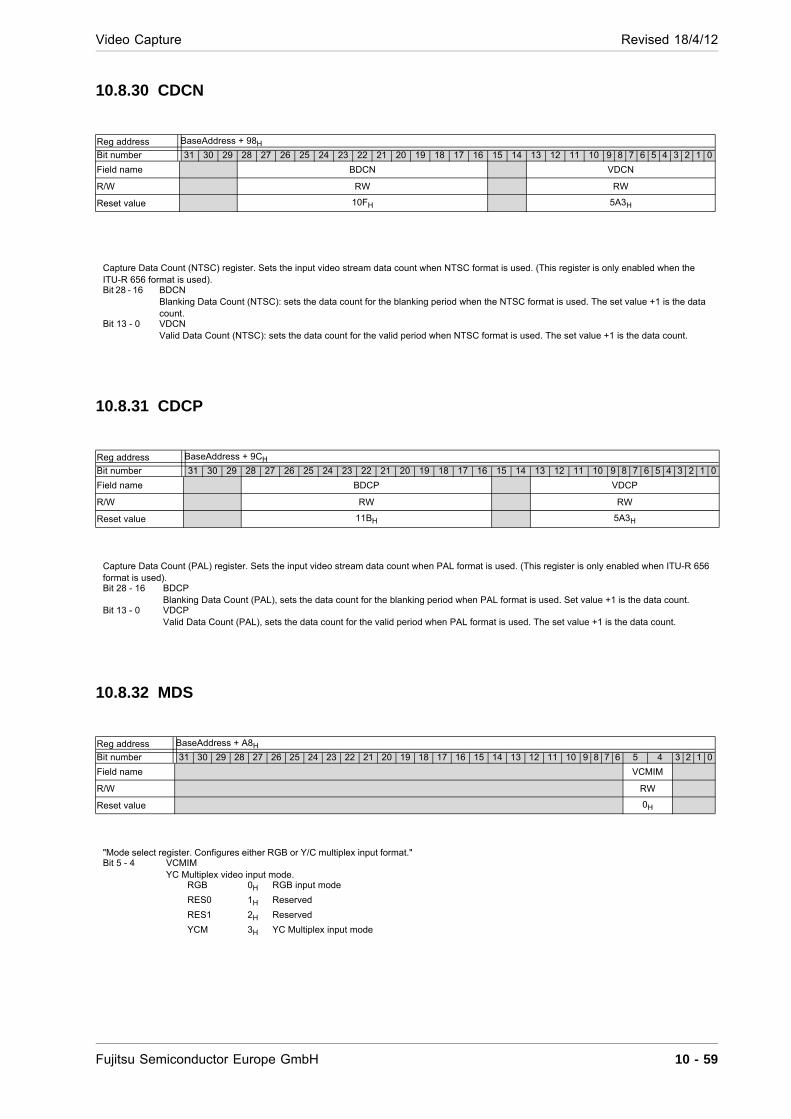
Video Capture Revised 18/4/12
10.8.30 CDCN
10.8.31 CDCP
10.8.32 MDS
Reg address BaseAddress + 98H
Bit number 31 30 29 28 27 26 25 24 23 22 21 20 19 18 17 16 15 14 13 12 11 10 9 8 7 6 5 4 3 2 1 0
Field name BDCN VDCN
R/W RW RW
Reset value 10FH 5A3H
Capture Data Count (NTSC) register. Sets the input video stream data count when NTSC format is used. (This register is only enabled when the ITU-R 656 format is used). Bit 28 - 16 BDCN
Blanking Data Count (NTSC): sets the data count for the blanking period when the NTSC format is used. The set value +1 is the data count.
Bit 13 - 0 VDCN Valid Data Count (NTSC): sets the data count for the valid period when NTSC format is used. The set value +1 is the data count.
Reg address BaseAddress + 9CH
Bit number 31 30 29 28 27 26 25 24 23 22 21 20 19 18 17 16 15 14 13 12 11 10 9 8 7 6 5 4 3 2 1 0
Field name BDCP VDCP
R/W RW RW
Reset value 11BH 5A3H
Capture Data Count (PAL) register. Sets the input video stream data count when PAL format is used. (This register is only enabled when ITU-R 656 format is used). Bit 28 - 16 BDCP
Blanking Data Count (PAL), sets the data count for the blanking period when PAL format is used. Set value +1 is the data count. Bit 13 - 0 VDCP
Valid Data Count (PAL), sets the data count for the valid period when PAL format is used. The set value +1 is the data count.
Reg address BaseAddress + A8H
Bit number 31 30 29 28 27 26 25 24 23 22 21 20 19 18 17 16 15 14 13 12 11 10 9 8 7 6 5 4 3 2 1 0
Field name VCMIM
R/W RW
Reset value 0H
"Mode select register. Configures either RGB or Y/C multiplex input format." Bit 5 - 4 VCMIM
YC Multiplex video input mode. RGB 0H RGB input mode
RES0 1H Reserved
RES1 2H Reserved
YCM 3H YC Multiplex input mode
Fujitsu Semiconductor Europe GmbH 10 - 59

Revised 18/4/12 Video Capture
10.8.33 CDCNS
10.8.34 CDCPS
10.8.35 VINLC_kep
10.8.36 VHSLS
Reg address BaseAddress + ACH
Bit number 31 30 29 28 27 26 25 24 23 22 21 20 19 18 17 16 15 14 13 12 11 10 9 8 7 6 5 4 3 2 1 0
Field name BDCN_S VDCN_S
R/W RW RW
Reset value 10FH 5A3H
Capture Data Count (NTSC Short): Sets the short interval input video stream data count when NTSC format is used. This register is only enabled when ITU-R 656 format is used. Bit 28 - 16 BDCN_S
Blanking Data Count (NTSC Short): Sets the data count for the blanking period when NTSC format is used. The value set +1 is the data count.
Bit 13 - 0 VDCN_S Valid Data Count (NTSC Short): Sets the data count for the valid period when NTSC format is used. The value set +1 is the data count.
Reg address BaseAddress + B0H
Bit number 31 30 29 28 27 26 25 24 23 22 21 20 19 18 17 16 15 14 13 12 11 10 9 8 7 6 5 4 3 2 1 0
Field name BDCP_S VDCP_S
R/W RW RW
Reset value 11BH 5A3H
Capture Data Count (PAL Short): Sets the short interval input video stream data count when PAL format is used. This register is only enabled when ITU-R 656 format is used. Bit 28 - 16 BDCP_S
Blanking Data Count (PAL Short): Sets the data count for the blanking period when PAL format is used. The value set +1 is the data count.
Bit 13 - 0 VDCP_S Valid Data Count (PAL Short): Sets the data count for the valid period when PAL format is used. The value set +1 is the data count.
Reg address BaseAddress + CCH
Bit number 31 30 29 28 27 26 25 24 23 22 21 20 19 18 17 16 15 14 13 12 11 10 9 8 7 6 5 4 3 2 1 0
Field name VIN_LINE_NO_kep
R/W R
Reset value 0H
Video Input Line Count: Used to detect synchronisaton errors (optional function). This function is common to RGB/ITU-R 656 Bit 12 - 0 VIN_LINE_NO_kep
VIN_LINE_NO_kep indicates the line count of one frame (field) including the blanking period. The displayed value +1 is the line count
Reg address BaseAddress + D4H
Bit number 31 30 29 28 27 26 25 24 23 22 21 20 19 18 17 16 15 14 13 12 11 10 9 8 7 6 5 4 3 2 1 0
Field name VIN_HS_LONG VIN_HS_SHORT
10 - 60 Fujitsu Semiconductor Europe GmbH
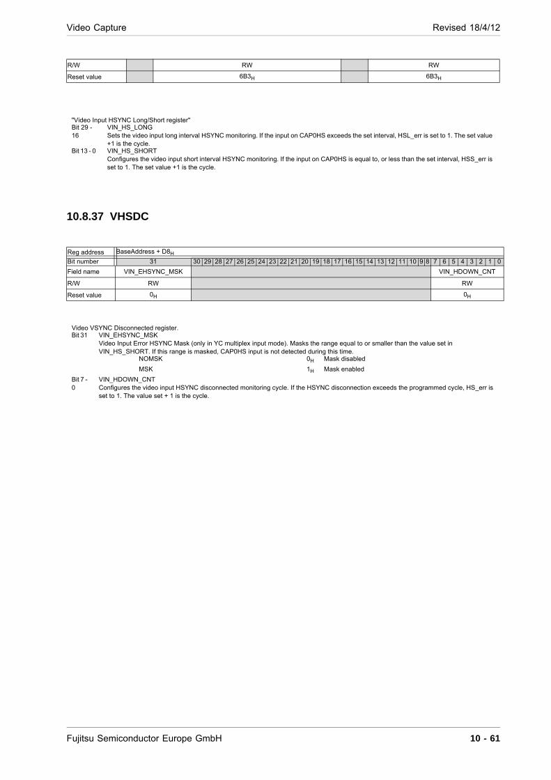
Video Capture Revised 18/4/12
10.8.37 VHSDC
R/W RW RW
Reset value 6B3H 6B3H
"Video Input HSYNC Long/Short register" Bit 29 - 16
VIN_HS_LONG Sets the video input long interval HSYNC monitoring. If the input on CAP0HS exceeds the set interval, HSL_err is set to 1. The set value +1 is the cycle.
Bit 13 - 0 VIN_HS_SHORT Configures the video input short interval HSYNC monitoring. If the input on CAP0HS is equal to, or less than the set interval, HSS_err is set to 1. The set value +1 is the cycle.
Reg address BaseAddress + D8H
Bit number 31 30 29 28 27 26 25 24 23 22 21 20 19 18 17 16 15 14 13 12 11 10 9 8 7 6 5 4 3 2 1 0
Field name VIN_EHSYNC_MSK VIN_HDOWN_CNT
R/W RW RW
Reset value 0H 0H
Video VSYNC Disconnected register. Bit 31 VIN_EHSYNC_MSK
Video Input Error HSYNC Mask (only in YC multiplex input mode). Masks the range equal to or smaller than the value set in VIN_HS_SHORT. If this range is masked, CAP0HS input is not detected during this time.
NOMSK 0H Mask disabled
MSK 1H Mask enabled
Bit 7 - 0
VIN_HDOWN_CNT Configures the video input HSYNC disconnected monitoring cycle. If the HSYNC disconnection exceeds the programmed cycle, HS_err is set to 1. The value set + 1 is the cycle.
Fujitsu Semiconductor Europe GmbH 10 - 61

Revised 18/4/12 Video Capture
10.8.38 VVSLS
10.8.39 VVSDC
Reg address BaseAddress + DCH
Bit number 31 30 29 28 27 26 25 24 23 22 21 20 19 18 17 16 15 14 13 12 11 10 9 8 7 6 5 4 3 2 1 0
Field name VIN_VS_LONG VIN_VS_SHORT
R/W RW RW
Reset value 105H 105H
Video Input VSYNC Long/Short register Bit 28 - 16
VIN_VS_LONG Sets video input long interval VSYNC monitoring. If the input on CAP0VS exceeds the set interval, VSL_err is set to 1. The set value +1 is the cycle.
Bit 12 - 0 VIN_VS_SHORT Configures the video input short interval VSYNC monitoring. If the input on CAPVS is equal to or less then the set interval, VSS_err is set to 1. The value +1 is the cycle.
Reg address BaseAddress + E0H
Bit number 31 30 29 28 27 26 25 24 23 22 21 20 19 18 17 16 15 14 13 12 11 10 9 8 7 6 5 4 3 2 1 0
Field name VIN_EVSYNC_MSK VIN_VDOWN_CNT
R/W RW RW
Reset value 0H 0H
"Video Input VSYNC Disconnected register" Bit 31 VIN_EVSYNC_MSK
Video Input Error VSYNC Mask (only in YC multiplex input mode). Masks the range equal to or smaller than the value set in VIN_VS_SHORT. If this range is masked, CAP0VS input is not detected during this time.
Bit 7 - 0
VIN_VDOWN_CNT Configures the video input VSYNC disconnected monitoring cycle. If the VSYNC disconnection exceeds the programmed cycle, VS_err is set to 1. The value set + 1 is the cycle
10 - 62 Fujitsu Semiconductor Europe GmbH

Video Capture Revised 18/4/12
10.8.40 SDER
10.8.41 SDCF0
10.8.42 SDCF1
Reg address BaseAddress + 108H
Bit number 31 30 29 28 27 26 25 24 23 22 21 20 19 18 17 16 15 14 13 12 11 10 9 8 7 6 5 4 3 2 1 0
Field name SDMOPIX BF SDMON SDMAN SDEN
R/W R R R RW RW
Reset value 0H 0H X 0H 0H
Still Detection Enable Register Bit 26 - 16
SDMOPIX The number of pixels of the reduced frame n which were detected as motion pixels, compared to the reduced frame n-1.
Bit 3 BF Bottom Field. In 656 mode this shows whether the current field is a top or bottom field. Read this value shortly after the VSYNC interrupt (the signal can be assumed to be stable then).
TOP 0H The current field is a top field.
BOTTOM 1H The current field is a bottom field.
Bit 2 SDMON Still Detection Monitor. Read this bit to monitor the status of the still detection function for the current field.
MOTION 0H Mode is motion, interpolation mode enabled.
STILL 1H Mode is still, non-interpolation mode enabled.
Bit 1 SDMAN Still Detection Manual Mode. Set this bit to enable manual mode. The still detection unit calculates reduced frames, but switching between interpolation/non-interpolation can be done by software. Software can read the pixel count of the reduced frame from the SDMOPIX field. Switching between interpolation/non-interpolation is done using the VI bit.
Bit 0 SDEN Still Detection Enable. Set to one to enable the still detection unit. The value of the VI bit in the VCM register is ignored, but not in manual mode (SDMAN=1).
Reg address BaseAddress + 10CH
Bit number 31 30 29 28 27 26 25 24 23 22 21 20 19 18 17 16 15 14 13 12 11 10 9 8 7 6 5 4 3 2 1 0
Field name MLC MPC
R/W RW RW
Reset value 120H 5A0H
Still Detection Config register 0 Bit 24 - 16
MLC Maximum Line Count (MLC). This value determines the maximum number of lines of the frame to be processed by the still detection algorithm. Divide the number of lines per frame by two to calculate the MLC (e.g. for 576 lines choose MLC=288, for 480 lines choose MLC=240). Must be in steps of 8.
Bit 10 - 0
MPC Maximum Pixel Count (MPC). This value determines the maximum number of pixels of the frame to be processed by the still detection algorithm. Multiply the number of pixels by two to calculate the MPC (e.g. for 720 pixels, choose MPC=1440). The value must be in steps of 32.
Reg address BaseAddress + 110H
Bit number 31 30 29 28 27 26 25 24 23 22 21 20 19 18 17 16 15 14 13 12 11 10 9 8 7 6 5 4 3 2 1 0
Field name MB MA
R/W RW RW
Reset value C8H 654H
Fujitsu Semiconductor Europe GmbH 10 - 63
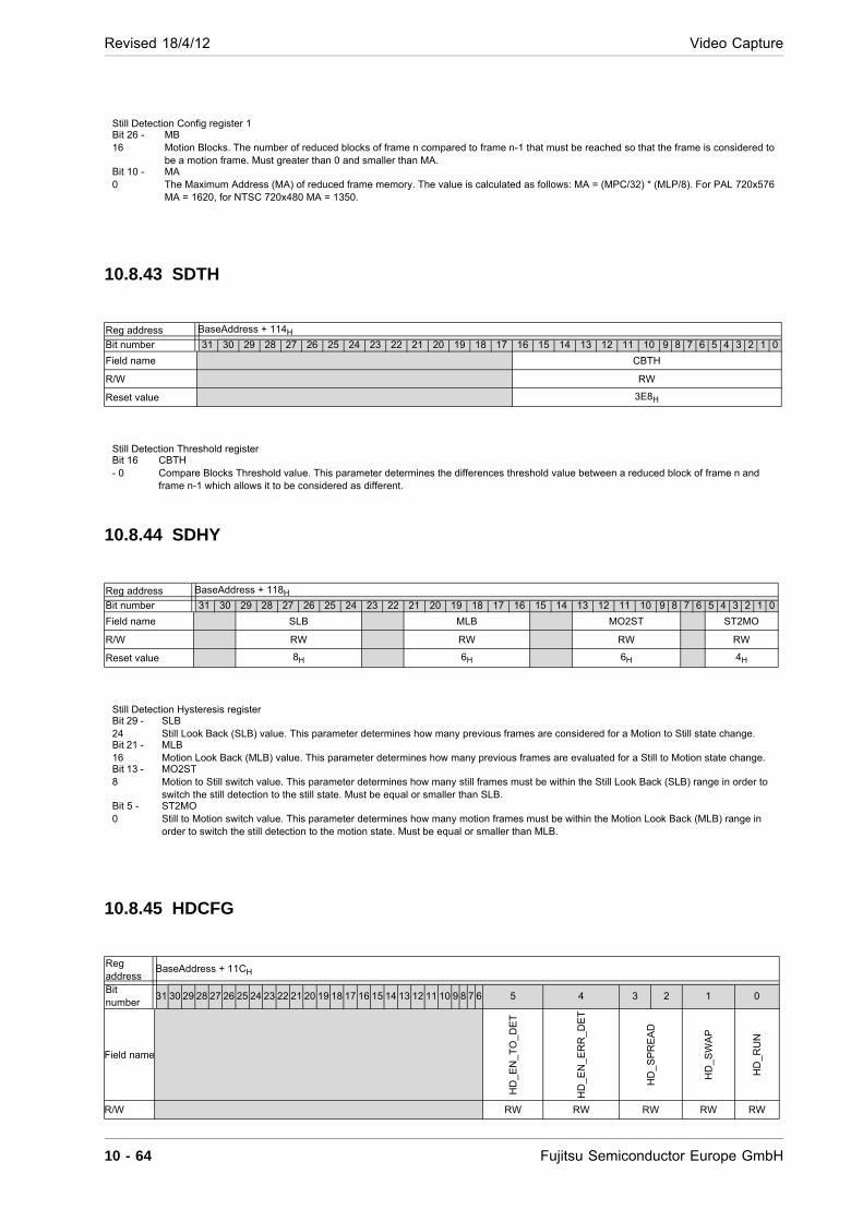
Revised 18/4/12 Video Capture
10.8.43 SDTH
10.8.44 SDHY
10.8.45 HDCFG
Still Detection Config register 1 Bit 26 - 16
MB Motion Blocks. The number of reduced blocks of frame n compared to frame n-1 that must be reached so that the frame is considered to be a motion frame. Must greater than 0 and smaller than MA.
Bit 10 - 0
MA The Maximum Address (MA) of reduced frame memory. The value is calculated as follows: MA = (MPC/32) * (MLP/8). For PAL 720x576 MA = 1620, for NTSC 720x480 MA = 1350.
Reg address BaseAddress + 114H
Bit number 31 30 29 28 27 26 25 24 23 22 21 20 19 18 17 16 15 14 13 12 11 10 9 8 7 6 5 4 3 2 1 0
Field name CBTH
R/W RW
Reset value 3E8H
Still Detection Threshold register Bit 16 - 0
CBTH Compare Blocks Threshold value. This parameter determines the differences threshold value between a reduced block of frame n and frame n-1 which allows it to be considered as different.
Reg address BaseAddress + 118H
Bit number 31 30 29 28 27 26 25 24 23 22 21 20 19 18 17 16 15 14 13 12 11 10 9 8 7 6 5 4 3 2 1 0
Field name SLB MLB MO2ST ST2MO
R/W RW RW RW RW
Reset value 8H 6H 6H 4H
Still Detection Hysteresis register Bit 29 - 24
SLB Still Look Back (SLB) value. This parameter determines how many previous frames are considered for a Motion to Still state change.
Bit 21 - 16
MLB Motion Look Back (MLB) value. This parameter determines how many previous frames are evaluated for a Still to Motion state change.
Bit 13 - 8
MO2ST Motion to Still switch value. This parameter determines how many still frames must be within the Still Look Back (SLB) range in order to switch the still detection to the still state. Must be equal or smaller than SLB.
Bit 5 - 0
ST2MO Still to Motion switch value. This parameter determines how many motion frames must be within the Motion Look Back (MLB) range in order to switch the still detection to the motion state. Must be equal or smaller than MLB.
Reg address
BaseAddress + 11CH
Bit number
31 30 29 28 27 26 25 24 23 22 21 20 19 18 17 16 15 14 13 12 11 10 9 8 7 6 5 4 3 2 1 0
Field name
HD
_EN
_T
O_
DE
T
HD
_EN
_E
RR
_D
ET
HD
_S
PR
EA
D
HD
_S
WA
P
HD
_RU
N
R/W RW RW RW RW RW
10 - 64 Fujitsu Semiconductor Europe GmbH
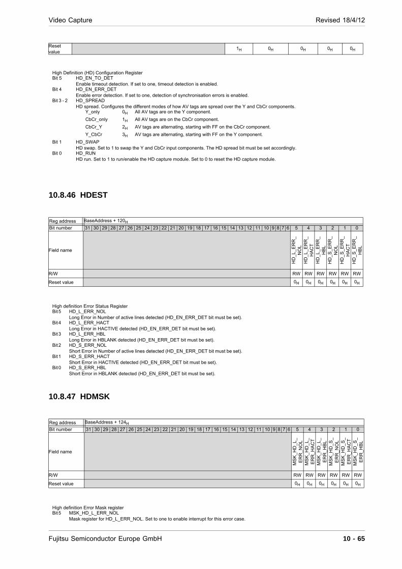
Video Capture Revised 18/4/12
10.8.46 HDEST
10.8.47 HDMSK
Reset value
1H 0H 0H 0H 0H
High Definition (HD) Configuration Register Bit 5 HD_EN_TO_DET
Enable timeout detection. If set to one, timeout detection is enabled. Bit 4 HD_EN_ERR_DET
Enable error detection. If set to one, detection of synchronisation errors is enabled. Bit 3 - 2 HD_SPREAD
HD spread. Configures the different modes of how AV tags are spread over the Y and CbCr components. Y_only 0H All AV tags are on the Y component.
CbCr_only 1H All AV tags are on the CbCr component.
CbCr_Y 2H AV tags are alternating, starting with FF on the CbCr component.
Y_CbCr 3H AV tags are alternating, starting with FF on the Y component.
Bit 1 HD_SWAP HD swap. Set to 1 to swap the Y and CbCr input components. The HD spread bit must be set accordingly.
Bit 0 HD_RUN HD run. Set to 1 to run/enable the HD capture module. Set to 0 to reset the HD capture module.
Reg address BaseAddress + 120H
Bit number 31 30 29 28 27 26 25 24 23 22 21 20 19 18 17 16 15 14 13 12 11 10 9 8 7 6 5 4 3 2 1 0
Field name
HD
_L
_E
RR
_N
OL
HD
_L
_E
RR
_H
AC
T
HD
_L
_E
RR
_H
BL
H
D_
S_
ER
R_
NO
L H
D_
S_
ER
R_
HA
CT
H
D_
S_
ER
R_
HB
L
R/W RW RW RW RW RW RW
Reset value 0H 0H 0H 0H 0H 0H
High definition Error Status Register Bit 5 HD_L_ERR_NOL
Long Error in Number of active lines detected (HD_EN_ERR_DET bit must be set). Bit 4 HD_L_ERR_HACT
Long Error in HACTIVE detected (HD_EN_ERR_DET bit must be set). Bit 3 HD_L_ERR_HBL
Long Error in HBLANK detected (HD_EN_ERR_DET bit must be set). Bit 2 HD_S_ERR_NOL
Short Error in Number of active lines detected (HD_EN_ERR_DET bit must be set). Bit 1 HD_S_ERR_HACT
Short Error in HACTIVE detected (HD_EN_ERR_DET bit must be set). Bit 0 HD_S_ERR_HBL
Short Error in HBLANK detected (HD_EN_ERR_DET bit must be set).
Reg address BaseAddress + 124H
Bit number 31 30 29 28 27 26 25 24 23 22 21 20 19 18 17 16 15 14 13 12 11 10 9 8 7 6 5 4 3 2 1 0
Field name
MS
K_
HD
_L_
ER
R_
NO
L M
SK
_H
D_
L_E
RR
_H
AC
T
MS
K_
HD
_L_
ER
R_H
BL
M
SK
_H
D_
S_
ER
R_
NO
L M
SK
_H
D_
S_
ER
R_
HA
CT
M
SK
_H
D_
S_
ER
R_H
BL
R/W RW RW RW RW RW RW
Reset value 0H 0H 0H 0H 0H 0H
High definition Error Mask register Bit 5 MSK_HD_L_ERR_NOL
Mask register for HD_L_ERR_NOL. Set to one to enable interrupt for this error case.
Fujitsu Semiconductor Europe GmbH 10 - 65
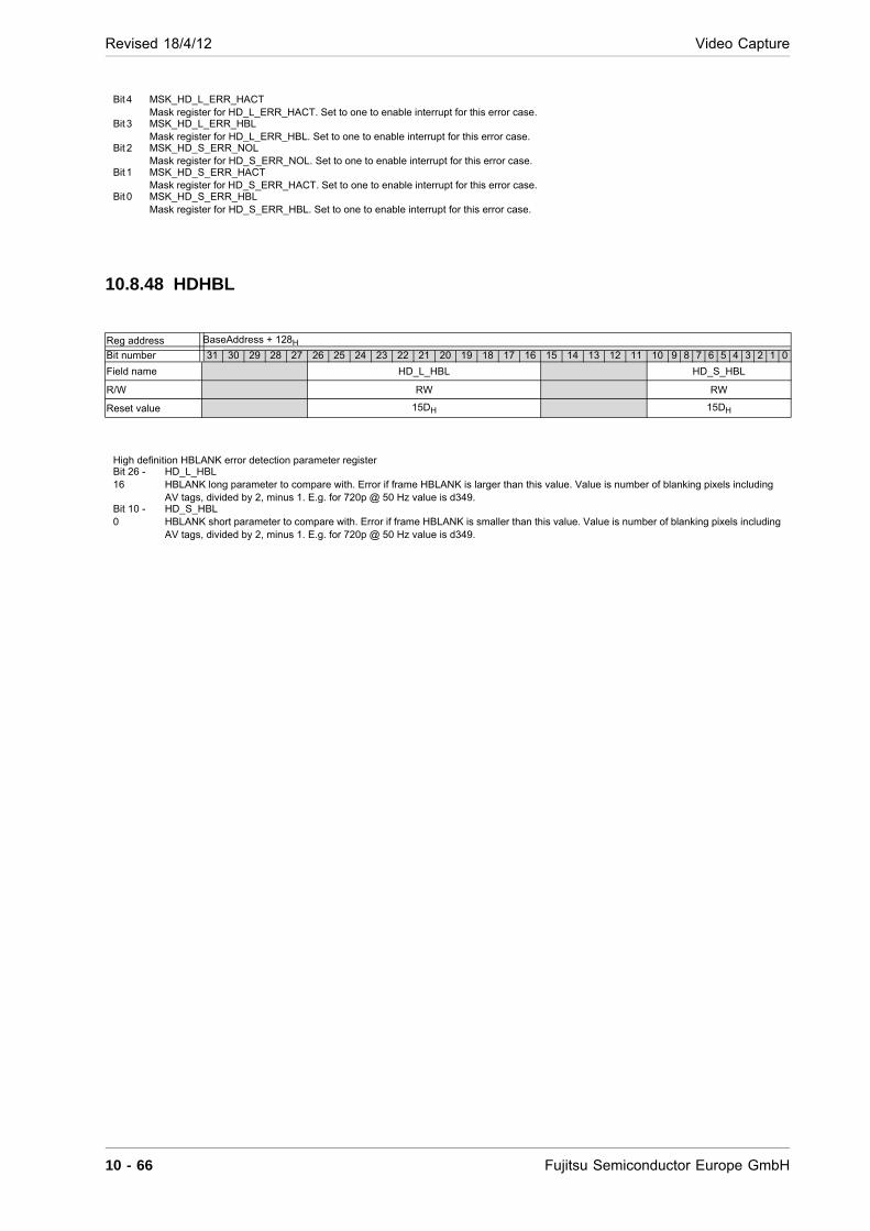
Revised 18/4/12 Video Capture
10.8.48 HDHBL
Bit 4 MSK_HD_L_ERR_HACT Mask register for HD_L_ERR_HACT. Set to one to enable interrupt for this error case.
Bit 3 MSK_HD_L_ERR_HBL Mask register for HD_L_ERR_HBL. Set to one to enable interrupt for this error case.
Bit 2 MSK_HD_S_ERR_NOL Mask register for HD_S_ERR_NOL. Set to one to enable interrupt for this error case.
Bit 1 MSK_HD_S_ERR_HACT Mask register for HD_S_ERR_HACT. Set to one to enable interrupt for this error case.
Bit 0 MSK_HD_S_ERR_HBL Mask register for HD_S_ERR_HBL. Set to one to enable interrupt for this error case.
Reg address BaseAddress + 128H
Bit number 31 30 29 28 27 26 25 24 23 22 21 20 19 18 17 16 15 14 13 12 11 10 9 8 7 6 5 4 3 2 1 0
Field name HD_L_HBL HD_S_HBL
R/W RW RW
Reset value 15DH 15DH
High definition HBLANK error detection parameter register Bit 26 - 16
HD_L_HBL HBLANK long parameter to compare with. Error if frame HBLANK is larger than this value. Value is number of blanking pixels including AV tags, divided by 2, minus 1. E.g. for 720p @ 50 Hz value is d349.
Bit 10 - 0
HD_S_HBL HBLANK short parameter to compare with. Error if frame HBLANK is smaller than this value. Value is number of blanking pixels including AV tags, divided by 2, minus 1. E.g. for 720p @ 50 Hz value is d349.
10 - 66 Fujitsu Semiconductor Europe GmbH
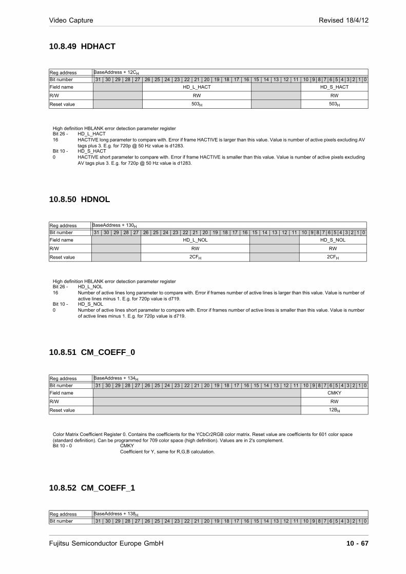
Video Capture Revised 18/4/12
10.8.49 HDHACT
10.8.50 HDNOL
10.8.51 CM_COEFF_0
10.8.52 CM_COEFF_1
Reg address BaseAddress + 12CH
Bit number 31 30 29 28 27 26 25 24 23 22 21 20 19 18 17 16 15 14 13 12 11 10 9 8 7 6 5 4 3 2 1 0
Field name HD_L_HACT HD_S_HACT
R/W RW RW
Reset value 503H 503H
High definition HBLANK error detection parameter register Bit 26 - 16
HD_L_HACT HACTIVE long parameter to compare with. Error if frame HACTIVE is larger than this value. Value is number of active pixels excluding AV tags plus 3. E.g. for 720p @ 50 Hz value is d1283.
Bit 10 - 0
HD_S_HACT HACTIVE short parameter to compare with. Error if frame HACTIVE is smaller than this value. Value is number of active pixels excluding AV tags plus 3. E.g. for 720p @ 50 Hz value is d1283.
Reg address BaseAddress + 130H
Bit number 31 30 29 28 27 26 25 24 23 22 21 20 19 18 17 16 15 14 13 12 11 10 9 8 7 6 5 4 3 2 1 0
Field name HD_L_NOL HD_S_NOL
R/W RW RW
Reset value 2CFH 2CFH
High definition HBLANK error detection parameter register Bit 26 - 16
HD_L_NOL Number of active lines long parameter to compare with. Error if frames number of active lines is larger than this value. Value is number of active lines minus 1. E.g. for 720p value is d719.
Bit 10 - 0
HD_S_NOL Number of active lines short parameter to compare with. Error if frames number of active lines is smaller than this value. Value is number of active lines minus 1. E.g. for 720p value is d719.
Reg address BaseAddress + 134H
Bit number 31 30 29 28 27 26 25 24 23 22 21 20 19 18 17 16 15 14 13 12 11 10 9 8 7 6 5 4 3 2 1 0
Field name CMKY
R/W RW
Reset value 12BH
Color Matrix Coefficient Register 0. Contains the coefficients for the YCbCr2RGB color matrix. Reset value are coefficients for 601 color space (standard definition). Can be programmed for 709 color space (high definition). Values are in 2's complement. Bit 10 - 0 CMKY
Coefficient for Y, same for R,G,B calculation.
Reg address BaseAddress + 138H
Bit number 31 30 29 28 27 26 25 24 23 22 21 20 19 18 17 16 15 14 13 12 11 10 9 8 7 6 5 4 3 2 1 0
Fujitsu Semiconductor Europe GmbH 10 - 67
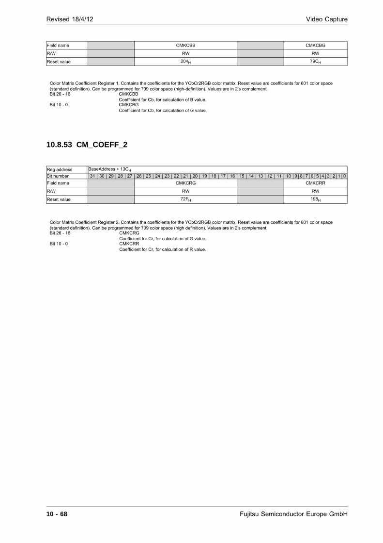
Revised 18/4/12 Video Capture
10.8.53 CM_COEFF_2
Field name CMKCBB CMKCBG
R/W RW RW
Reset value 204H 79CH
Color Matrix Coefficient Register 1. Contains the coefficients for the YCbCr2RGB color matrix. Reset value are coefficients for 601 color space (standard definition). Can be programmed for 709 color space (high-definition). Values are in 2's complement. Bit 26 - 16 CMKCBB
Coefficient for Cb, for calculation of B value. Bit 10 - 0 CMKCBG
Coefficient for Cb, for calculation of G value.
Reg address BaseAddress + 13CH
Bit number 31 30 29 28 27 26 25 24 23 22 21 20 19 18 17 16 15 14 13 12 11 10 9 8 7 6 5 4 3 2 1 0
Field name CMKCRG CMKCRR
R/W RW RW
Reset value 72FH 198H
Color Matrix Coefficient Register 2. Contains the coefficients for the YCbCr2RGB color matrix. Reset value are coefficients for 601 color space (standard definition). Can be programmed for 709 color space (high definition). Values are in 2's complement. Bit 26 - 16 CMKCRG
Coefficient for Cr, for calculation of G value. Bit 10 - 0 CMKCRR
Coefficient for Cr, for calculation of R value.
10 - 68 Fujitsu Semiconductor Europe GmbH
Graphics Core (ARGES) Revised 18/4/12
Chapter 11: Graphics Core (ARGES)
11.1 Graphics Core (ARGES)
ARGES is a graphics drawing core which is integrated in the MB86298 'Ruby' graphics display con-troller.
Technology and Frequency
90nm (CS100A-LL)
266 MHz
Features
OpenGL ES2.0 compliant
Additional functionality: (outside the scope of the OpenGL ES2.0 specification)
Anti-aliased lines
Technology and Frequency
Peak performance
30M vertices/sec of vertex performance.[Number of attributes in performance target]
16 attributes (formats in shader program are FP16). Performance is halved in the case of 32 attributes.
10M triangles or lines /sec of primitive setup performance.[Number of varyings in performance target]8 varyings in FP16 format, performance is halved in the case of 16 varyings.
400M pixels and texels /sec of pixel performance in hitting texture cache (with LINEAR filtering and depth testing)
In the case of LINEAR_MIPMAP_LINEAR, pixel performance is half of LINEAR_MIPMAP_NEAREST. It is 200M pixels and texels /sec in texture cache hits.
470M pixels/sec for flat triangles
Effective performance
2 Million triangles per second under the following conditions:
32 bit RGBA color format (RGBA 8888)
32 bit floating point vertices + normals
Triangle size 20x20 pixel (200 pixels)
3D transformed
Volume clipped
Z and backface culled
lighted (specular + diffuse)
textured (mipmapping)
color/vertex/normal data reside in local GPU memory
[Number of attributes in performance target]
13 attributes (X,Y,Z,W,R,G,B,A,Nx,Ny,Nz,S,T)
[Number of varyings in performance target]
5 varyings (R,G,B,A,S,T)
Fujitsu Semiconductor Europe GmbH 11 - 1

Revised 18/4/12 Graphics Core (ARGES)
*N is a normal vector
[Precision in performance target]
All attributes and varyings are FP16 format.
Bus
ARGES uses 4 AXI buses, one slave AXI and three master AXIs. These are 64bits wide and operate at 266MHz.
11 - 2 Fujitsu Semiconductor Europe GmbH
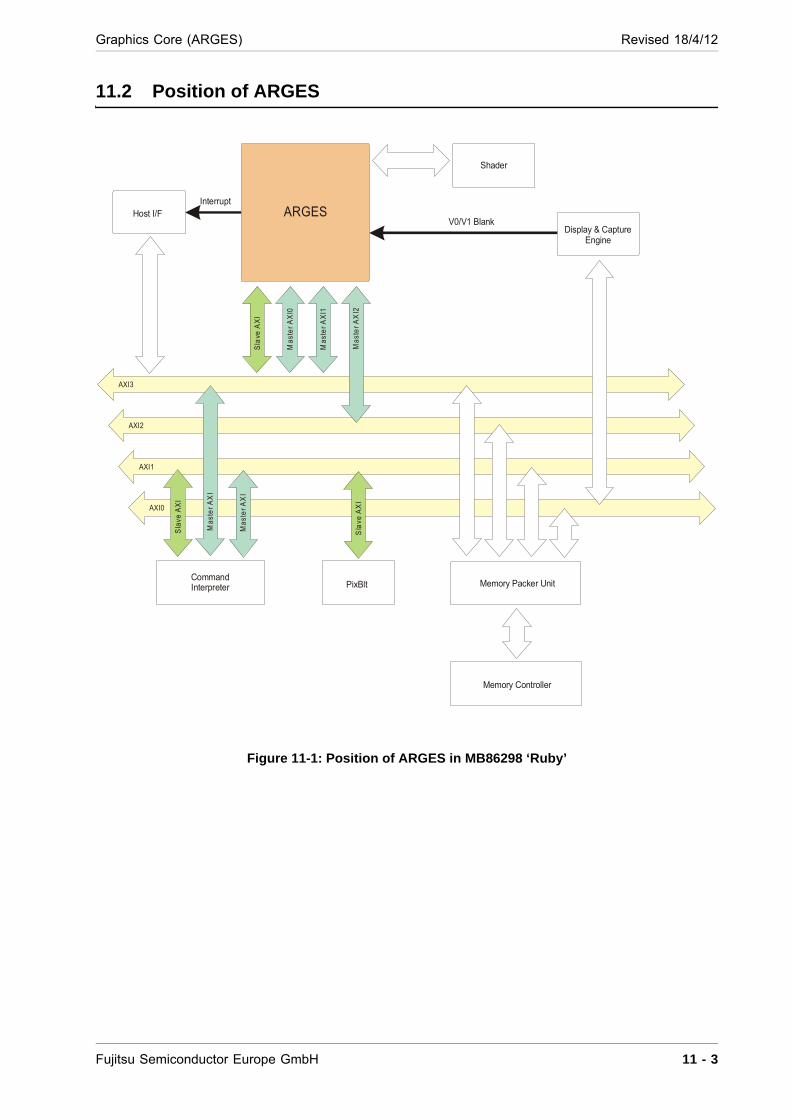
Graphics Core (ARGES) Revised 18/4/12
11.2 Position of ARGES
Figure 11-1: Position of ARGES in MB86298 ‘Ruby’
ARGESHost I/F
PixBlt Memory Packer Unit
Memory Controller
CommandInterpreter
Shader
Display & CaptureEngine
AXI3
AXI2
AXI1
AXI0
Interrupt
V0/V1 Blank
Sla
ve A
XI
Mas
ter A
XI0
Mas
ter A
XI1
Mas
ter A
XI2
Sla
ve A
XI
Mas
ter A
XI
Mas
ter A
XI
Sla
ve A
XI
Fujitsu Semiconductor Europe GmbH 11 - 3
Revised 18/4/12 Graphics Core (ARGES)
11.3 Function
11.3.1 Register access
Status read
Interrupt cause clear
Debug information read
Restrictions
A register's status can be read even during execution.
Interrupt cause can be cleared even during execution.
Debugging information returns after drawing is finished
11.3.2 Save/Restore register
This is a function for task switching.
Save all information which is kept in ARGES to a memory device which is connected to AXI.
Restore all information which was saved.
11.3.3 Display list and vertex arrays
Direct display list mode
Vertex arrays mode
11.3.4 Drawing features
Point
Line
Lines
Line strip
Line loop
Triangle
Triangles
Triangle strip
Triangle fan
Bit Block Transfer (BitBlt)
11.3.5 Pixel format
32bits/pixel color
16bits/pixel color
Restrictions
In addition BLT supports 8bits/pixel (required for stencil buffer clear.)
11 - 4 Fujitsu Semiconductor Europe GmbH

Graphics Core (ARGES) Revised 18/4/12
11.4 Software Interface and Commands
11.4.1 Global address
MB86298 'Ruby' incorporates a single instance of the ARGES core. ARGES decodes only bit20-bit0 of the address space. Register address in the following section means offset from the ARGES reg-ister base address in Ruby. Please refer to the Ruby memory address map for the current base ad-dress.
Fujitsu Semiconductor Europe GmbH 11 - 5

Revised 18/4/12 Graphics Core (ARGES)
11.4.2 Register summary
Address Name Explanation0000_0000h DDLFIFO FIFO for display list input.
All addresses between 0000_0000h ~ 00007Ch are handled as the same FIFO.
…
0000_007Ch
0000_0100h STATUS ARGES status information
0000_0104h SRESET Soft reset
0000_0108h CMDINT Normal interruption cause.
0000_010Ch CMDINTM Mask of normal interruption.
0000_0110h CMDERR Abnormal interruption cause.
0000_0114h CMDERRM Mask of abnormal interruption.
0000_0118h CMDINTR Return value of normal interruption.
0000_011Ch MID Macro identify code
0000_0200h…0000_0210h
- Reserved
0000_0300h ERRORDL First 32 bits of a display list command which generated an error.
0000_0304h DL_CNT Counter of a display list. This stops when error occurs.
0000_0308h ENDCHG Endian setting of DDLFIFO
0000_030Ch…0000_0524h
- Reserved
0000_0528h DBGMODE Debug mode changing
0001_052Ch…0001_0FFFh
- Reserved
0001_0000h…0002_0034h
- Reserved
0002_0038h DepthPassCount This is used by SetQuery (accessable only in debug mode).
0002_003Ch DepthFailCount This is used by SetQuery (accessable only in debug mode).
0002_0040h…0002_FFFFh
- Reserved
11 - 6 Fujitsu Semiconductor Europe GmbH
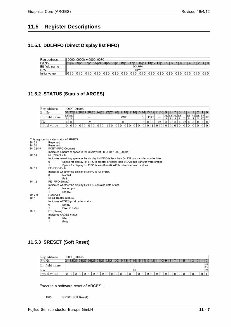
Graphics Core (ARGES) Revised 18/4/12
11.5 Register Descriptions
11.5.1 DDLFIFO (Direct Display list FIFO)
11.5.2 STATUS (Status of ARGES)
11.5.3 SRESET (Soft Reset)
Execute a software reset of ARGES..
Reg address 0000_0000h ~ 0000_007ChBit No. 31 32 29 28 27 26 25 24 23 22 21 20 19 18 17 16 15 14 13 12 11 10 9 8 7 6 5 4 3 2 1 0Bit field name DDLFIFO
R/W R0W
Initial value 0 0 0 0 0 0 0 0 0 0 0 0 0 0 0 0 0 0 0 0 0 0 0 0 0 0 0 0 0 0 0 0
Reg address 0000_0100hBit No. 31 32 29 28 27 26 25 24 23 22 21 20 19 18 17 16 15 14 13 12 11 10 9 8 7 6 5 4 3 2 1 0
Bit field name RES
RES FCNT NF FF FE RE
SRES
RES
RES RE
SRES
RES
BFST ST
RW R R R0 R R R R R0 R R R R R0 R R R R R
Initial value 0 0 0 0 0 0 0 0 0 1 0 0 0 0 0 0 0 0 0 1 0 0 0 0 0 0 0 0 0 0 0 0
This register Indicates status of ARGES.Bit 31 ReservedBit 30 ReservedBit 22-15 FCNT (FIFO Counter)
Indicates amount of space in the display list FIFO. (0~1000_0000b)Bit 14 NF (Near Full)
Indicates remaining space in the display list FIFO is less than 64 AXI bus transfer word entries0 Space for display list FIFO is greater or equal than 64 AXI bus transfer word entries1 Space for display list FIFO is less than 64 AXI bus transfer word entries
Bit 13 FF (FIFO Full) Indicates whether the display list FIFO is full or not.0 Not full.1 Full.
Bit 12 FE (FIFO Empty) Indicates whether the display list FIFO contains data or not.0 Not empty.1 Empty.
Bit 2-9 ReservedBit 1 BFST (Buffer Status)
Indicates ARGES pixel buffer status0 Empty1 Pixel in buffer
Bit 0 ST (Status) Indicates ARGES status.0 Idle1 Busy.
Reg address 0000_0104hBit No. 31 32 29 28 27 26 25 24 23 22 21 20 19 18 17 16 15 14 13 12 11 10 9 8 7 6 5 4 3 2 1 0
Bit field name SRST
RW R0 RW
Initial value 0 0 0 0 0 0 0 0 0 0 0 0 0 0 0 0 0 0 0 0 0 0 0 0 0 0 0 0 0 0 0 1
Bit0 SRST (Soft Reset)
Fujitsu Semiconductor Europe GmbH 11 - 7
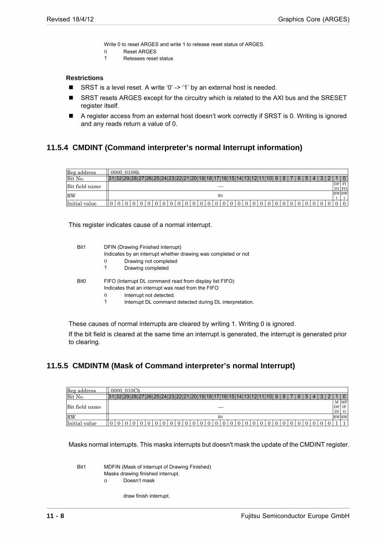
Revised 18/4/12 Graphics Core (ARGES)
Restrictions
SRST is a level reset. A write ‘0’ -> ‘1’ by an external host is needed.
SRST resets ARGES except for the circuitry which is related to the AXI bus and the SRESET register itself.
A register access from an external host doesn’t work correctly if SRST is 0. Writing is ignored and any reads return a value of 0.
11.5.4 CMDINT (Command interpreter’s normal Interrupt information)
This register indicates cause of a normal interrupt.
These causes of normal interrupts are cleared by writing 1. Writing 0 is ignored.
If the bit field is cleared at the same time an interrupt is generated, the interrupt is generated prior to clearing.
11.5.5 CMDINTM (Mask of Command interpreter’s normal Interrupt)
Masks normal interrupts. This masks interrupts but doesn't mask the update of the CMDINT register.
Write 0 to reset ARGES and write 1 to release reset status of ARGES.
0 Reset ARGES1 Releases reset status
Reg address 0000_0108hBit No. 31 32 29 28 27 26 25 24 23 22 21 20 19 18 17 16 15 14 13 12 11 10 9 8 7 6 5 4 3 2 1 0
Bit field name DFIN
FIFO
RW R0 RW1
RW1
Initial value 0 0 0 0 0 0 0 0 0 0 0 0 0 0 0 0 0 0 0 0 0 0 0 0 0 0 0 0 0 0 0 0
Bit1 DFIN (Drawing Finished interrupt) Indicates by an interrupt whether drawing was completed or not
0 Drawing not completed1 Drawing completed
Bit0 FIFO (Interrupt DL command read from display list FIFO) Indicates that an interrupt was read from the FIFO
0 Interrupt not detected.1 Interrupt DL command detected during DL interpretation.
Reg address 0000_010ChBit No. 31 32 29 28 27 26 25 24 23 22 21 20 19 18 17 16 15 14 13 12 11 10 9 8 7 6 5 4 3 2 1 0
Bit field name MDFIN
MFIFO
RW R0 RW RW
Initial value 0 0 0 0 0 0 0 0 0 0 0 0 0 0 0 0 0 0 0 0 0 0 0 0 0 0 0 0 0 0 1 1
Bit1 MDFIN (Mask of interrupt of Drawing Finished) Masks drawing finished interrupt.0 Doesn’t mask
draw finish interrupt.
11 - 8 Fujitsu Semiconductor Europe GmbH
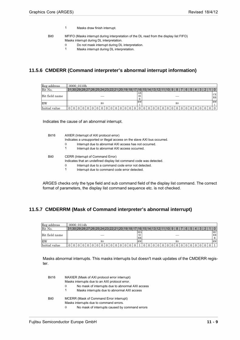
Graphics Core (ARGES) Revised 18/4/12
11.5.6 CMDERR (Command interpreter’s abnormal interrupt information)
Indicates the cause of an abnormal interrupt.
ARGES checks only the type field and sub command field of the display list command. The correct format of parameters, the display list command sequence etc. is not checked.
11.5.7 CMDERRM (Mask of Command interpreter’s abnormal interrupt)
Masks abnormal interrupts. This masks interrupts but doesn't mask updates of the CMDERR regis-ter.
1 Masks draw finish interrupt.
Bit0 MFIFO (Masks interrupt during interpretation of the DL read from the display list FIFO) Masks interrupt during DL interpretation.
0 Do not mask interrupt during DL interpretation.1 Masks interrupt during DL interpretation.
Reg address 0000_0110hBit No. 31 30 29 28 27 26 25 24 23 22 21 20 19 18 17 16 15 14 13 12 11 10 9 8 7 6 5 4 3 2 1 0
Bit field name AXIER
CERR
RW R0 RW1 R0 RW
1
Initial value 0 0 0 0 0 0 0 0 0 0 0 0 0 0 0 0 0 0 0 0 0 0 0 0 0 0 0 0 0 0 0 0
Bit16 AXIER (Interrupt of AXI protocol error) Indicates a unsupported or illegal access on the slave AXI bus occurred.
0 Interrupt due to abnormal AXI access has not occurred.1 Interrupt due to abnormal AXI access occurred.
Bit0 CERR (Interrupt of Command Error) Indicates that an undefined display list command code was detected.
0 Interrupt due to a command code error not detected.1 Interrupt due to command code error detected.
Reg address 0000_0114hBit No. 31 30 29 28 27 26 25 24 23 22 21 20 19 18 17 16 15 14 13 12 11 10 9 8 7 6 5 4 3 2 1 0
Bit field name MAXIER
MCERR
RW R0 RW R0 RW
Initial value 0 0 0 0 0 0 0 0 0 0 0 0 0 0 0 1 0 0 0 0 0 0 0 0 0 0 0 0 0 0 0 1
Bit16 MAXIER (Mask of AXI protocol error interrupt) Masks interrupts due to an AXI protocol error.
0 No mask of interrupts due to abnormal AXI access1 Masks interrupts due to abnormal AXI access
Bit0 MCERR (Mask of Command Error interrupt) Masks interrupts due to command errors.
0 No mask of interrupts caused by command errors
Fujitsu Semiconductor Europe GmbH 11 - 9
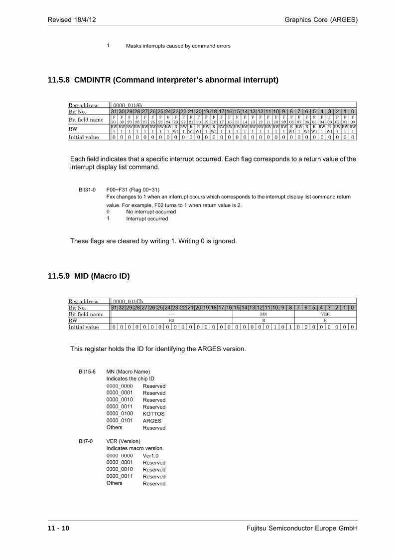
Revised 18/4/12 Graphics Core (ARGES)
11.5.8 CMDINTR (Command interpreter’s abnormal interrupt)
Each field indicates that a specific interrupt occurred. Each flag corresponds to a return value of the interrupt display list command.
These flags are cleared by writing 1. Writing 0 is ignored.
11.5.9 MID (Macro ID)
This register holds the ID for identifying the ARGES version.
1 Masks interrupts caused by command errors
Reg address 0000_0118hBit No. 31 30 29 28 27 26 25 24 23 22 21 20 19 18 17 16 15 14 13 12 11 10 9 8 7 6 5 4 3 2 1 0
Bit field name F31
F30
F29
F28
F27
F26
F25
F24
F23
F22
F21
F20
F19
F18
F17
F16
F15
F14
F13
F12
F11
F10
F09
F08
F07
F06
F05
F04
F03
F02
F01
F00
RW RW1
RW1
RW1
RW1
RW1
RW1
RW1
RW1
RW1
RW1
RW1
RW1
RW1
RW1
RW1
RW1
RW1
RW1
RW1
RW1
RW1
RW1
RW1
RW1
RW1
RW1
RW1
RW1
RW1
RW1
RW1
RW1
Initial value 0 0 0 0 0 0 0 0 0 0 0 0 0 0 0 0 0 0 0 0 0 0 0 0 0 0 0 0 0 0 0 0
Bit31-0 F00~F31 (Flag 00~31) Fxx changes to 1 when an interrupt occurs which corresponds to the interrupt display list command return
value. For example, F02 turns to 1 when return value is 2.0 No interrupt occurred1 Interrupt occurred
Reg address 0000_011ChBit No. 31 32 29 28 27 26 25 24 23 22 21 20 19 18 17 16 15 14 13 12 11 10 9 8 7 6 5 4 3 2 1 0Bit field name MN VER
RW R0 R R
Initial value 0 0 0 0 0 0 0 0 0 0 0 0 0 0 0 0 0 0 0 0 0 1 0 1 0 0 0 0 0 0 0 0
Bit15-8 MN (Macro Name) Indicates the chip ID
0000_0000 Reserved0000_0001 Reserved0000_0010 Reserved0000_0011 Reserved0000_0100 KOTTOS0000_0101 ARGESOthers Reserved
Bit7-0 VER (Version) Indicates macro version.
0000_0000 Ver1.00000_0001 Reserved0000_0010 Reserved0000_0011 ReservedOthers Reserved
11 - 10 Fujitsu Semiconductor Europe GmbH
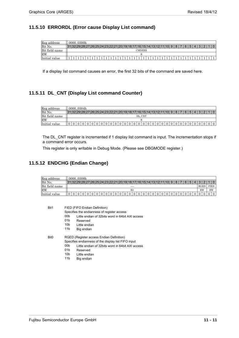
Graphics Core (ARGES) Revised 18/4/12
11.5.10 ERRORDL (Error cause Display List command)
If a display list command causes an error, the first 32 bits of the command are saved here.
11.5.11 DL_CNT (Display List command Counter)
The DL_CNT register is incremented if 1 display list command is input. The incrementation stops if a command error occurs.
This register is only writable in Debug Mode. (Please see DBGMODE register.)
11.5.12 ENDCHG (Endian Change)
Reg address 0000_0300hBit No. 31 32 29 28 27 26 25 24 23 22 21 20 19 18 17 16 15 14 13 12 11 10 9 8 7 6 5 4 3 2 1 0Bit field name CMDERR
RW R
Initial value 1 1 1 1 1 1 1 1 1 1 1 1 1 1 1 1 1 1 1 1 1 1 1 1 1 1 1 1 1 1 1 1
Reg address 0000_0304hBit No. 31 32 29 28 27 26 25 24 23 22 21 20 19 18 17 16 15 14 13 12 11 10 9 8 7 6 5 4 3 2 1 0Bit field name DL_CNT
RW R
Initial value 0 0 0 0 0 0 0 0 0 0 0 0 0 0 0 0 0 0 0 0 0 0 0 0 0 0 0 0 0 0 0 0
Reg address 0000_0308hBit No. 31 32 29 28 27 26 25 24 23 22 21 20 19 18 17 16 15 14 13 12 11 10 9 8 7 6 5 4 3 2 1 0Bit field name RGED FIED
RW R0 RW RW
Initial value 0 0 0 0 0 0 0 0 0 0 0 0 0 0 0 0 0 0 0 0 0 0 0 0 0 0 0 0 0 0 0 0
Bit1 FIED (FIFO Endian Definition) Specifies the endianness of register access00b Little endian of 32bits word in 64bit AXI access01b Reserved10b Little endian11b Big endian
Bit0 RGED (Register access Endian Definition) Specifies endianness of the display list FIFO input00b Little endian of 32bits word in 64bit AXI access01b Reserved10b Little endian11b Big endian
Fujitsu Semiconductor Europe GmbH 11 - 11
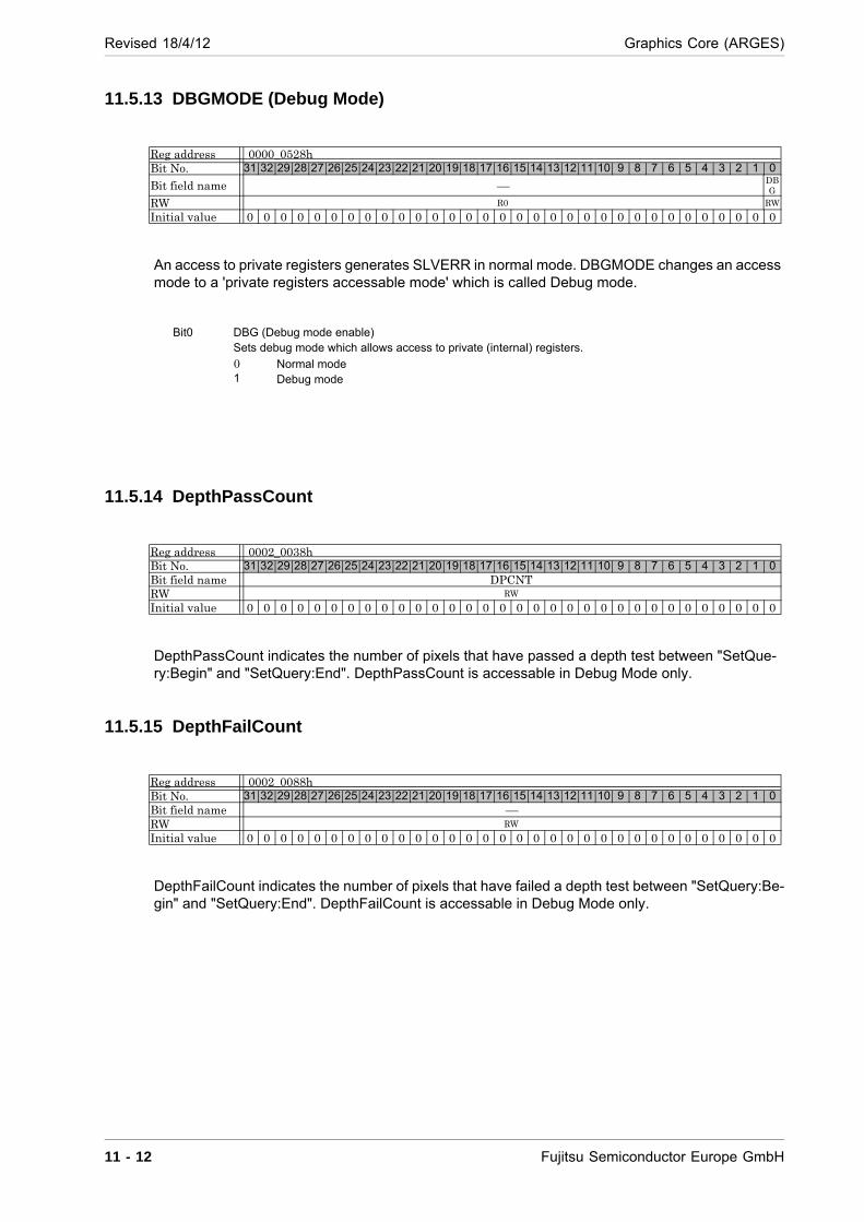
Revised 18/4/12 Graphics Core (ARGES)
11.5.13 DBGMODE (Debug Mode)
An access to private registers generates SLVERR in normal mode. DBGMODE changes an access mode to a 'private registers accessable mode' which is called Debug mode.
11.5.14 DepthPassCount
DepthPassCount indicates the number of pixels that have passed a depth test between "SetQue-ry:Begin" and "SetQuery:End". DepthPassCount is accessable in Debug Mode only.
11.5.15 DepthFailCount
DepthFailCount indicates the number of pixels that have failed a depth test between "SetQuery:Be-gin" and "SetQuery:End". DepthFailCount is accessable in Debug Mode only.
Reg address 0000_0528hBit No. 31 32 29 28 27 26 25 24 23 22 21 20 19 18 17 16 15 14 13 12 11 10 9 8 7 6 5 4 3 2 1 0
Bit field name DBG
RW R0 RW
Initial value 0 0 0 0 0 0 0 0 0 0 0 0 0 0 0 0 0 0 0 0 0 0 0 0 0 0 0 0 0 0 0 0
Bit0 DBG (Debug mode enable) Sets debug mode which allows access to private (internal) registers.
0 Normal mode1 Debug mode
Reg address 0002_0038hBit No. 31 32 29 28 27 26 25 24 23 22 21 20 19 18 17 16 15 14 13 12 11 10 9 8 7 6 5 4 3 2 1 0Bit field name DPCNTRW RW
Initial value 0 0 0 0 0 0 0 0 0 0 0 0 0 0 0 0 0 0 0 0 0 0 0 0 0 0 0 0 0 0 0 0
Reg address 0002_0088hBit No. 31 32 29 28 27 26 25 24 23 22 21 20 19 18 17 16 15 14 13 12 11 10 9 8 7 6 5 4 3 2 1 0Bit field name RW RW
Initial value 0 0 0 0 0 0 0 0 0 0 0 0 0 0 0 0 0 0 0 0 0 0 0 0 0 0 0 0 0 0 0 0
11 - 12 Fujitsu Semiconductor Europe GmbH
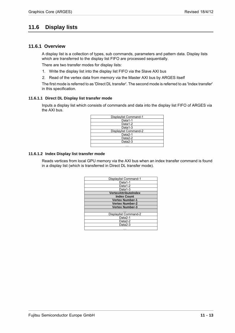
Graphics Core (ARGES) Revised 18/4/12
11.6 Display lists
11.6.1 Overview
A display list is a collection of types, sub commands, parameters and pattern data. Display lists which are transferred to the display list FIFO are processed sequentially.
There are two transfer modes for display lists:
1. Write the display list into the display list FIFO via the Slave AXI bus
2. Read of the vertex data from memory via the Master AXI bus by ARGES itself
The first mode is referred to as 'Direct DL transfer'. The second mode is referred to as 'Index transfer' in this specification.
11.6.1.1 Direct DL Display list transfer mode
Inputs a display list which consists of commands and data into the display list FIFO of ARGES via the AXI bus.
11.6.1.2 Index Display list transfer mode
Reads vertices from local GPU memory via the AXI bus when an index transfer command is found in a display list (which is transferred in Direct DL transfer mode).
Displaylist Command-1Data1-1Data1-2Data1-3
Displaylist Command-2Data2-1Data2-2Data2-3
…
Displaylist Command-1Data1-1Data1-2Data1-3
VertexAttributeIndexIndex Count
Vertex Number-1Vertex Number-2Vertex Number-3
…Displaylist Command-2
Data2-1Data2-2Data2-3
…
Fujitsu Semiconductor Europe GmbH 11 - 13
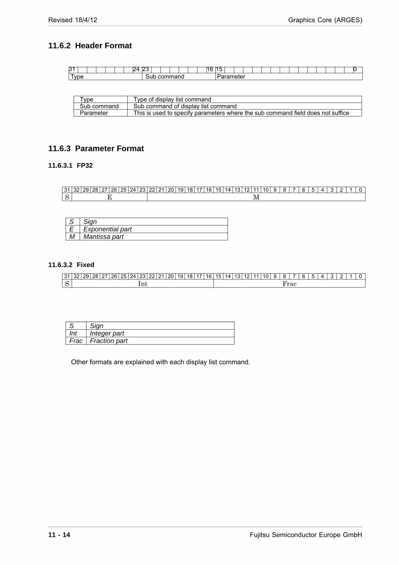
Revised 18/4/12 Graphics Core (ARGES)
11.6.2 Header Format
11.6.3 Parameter Format
11.6.3.1 FP32
11.6.3.2 Fixed
Other formats are explained with each display list command.
31 24 23 16 15 0Type Sub command Parameter
Type Type of display list commandSub command Sub command of display list commandParameter This is used to specify parameters where the sub command field does not suffice
31 32 29 28 27 26 25 24 23 22 21 20 19 18 17 16 15 14 13 12 11 10 9 8 7 6 5 4 3 2 1 0
S E M
S SignE Exponential partM Mantissa part
31 32 29 28 27 26 25 24 23 22 21 20 19 18 17 16 15 14 13 12 11 10 9 8 7 6 5 4 3 2 1 0
S Int Frac
S SignInt Integer partFrac Fraction part
11 - 14 Fujitsu Semiconductor Europe GmbH
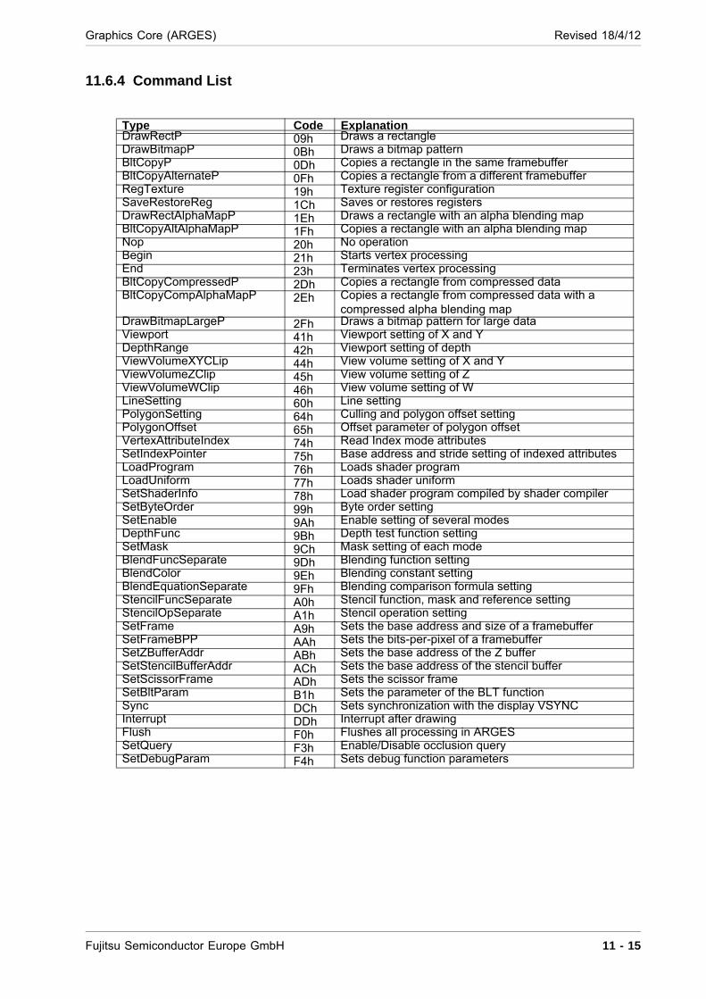
Graphics Core (ARGES) Revised 18/4/12
11.6.4 Command List
Type Code ExplanationDrawRectP 09h Draws a rectangleDrawBitmapP 0Bh Draws a bitmap patternBltCopyP 0Dh Copies a rectangle in the same framebufferBltCopyAlternateP 0Fh Copies a rectangle from a different framebufferRegTexture 19h Texture register configurationSaveRestoreReg 1Ch Saves or restores registersDrawRectAlphaMapP 1Eh Draws a rectangle with an alpha blending mapBltCopyAltAlphaMapP 1Fh Copies a rectangle with an alpha blending mapNop 20h No operationBegin 21h Starts vertex processingEnd 23h Terminates vertex processingBltCopyCompressedP 2Dh Copies a rectangle from compressed dataBltCopyCompAlphaMapP 2Eh Copies a rectangle from compressed data with a
compressed alpha blending mapDrawBitmapLargeP 2Fh Draws a bitmap pattern for large dataViewport 41h Viewport setting of X and YDepthRange 42h Viewport setting of depthViewVolumeXYCLip 44h View volume setting of X and YViewVolumeZClip 45h View volume setting of ZViewVolumeWClip 46h View volume setting of WLineSetting 60h Line settingPolygonSetting 64h Culling and polygon offset settingPolygonOffset 65h Offset parameter of polygon offsetVertexAttributeIndex 74h Read Index mode attributesSetIndexPointer 75h Base address and stride setting of indexed attributesLoadProgram 76h Loads shader programLoadUniform 77h Loads shader uniformSetShaderInfo 78h Load shader program compiled by shader compilerSetByteOrder 99h Byte order settingSetEnable 9Ah Enable setting of several modesDepthFunc 9Bh Depth test function settingSetMask 9Ch Mask setting of each modeBlendFuncSeparate 9Dh Blending function settingBlendColor 9Eh Blending constant settingBlendEquationSeparate 9Fh Blending comparison formula settingStencilFuncSeparate A0h Stencil function, mask and reference settingStencilOpSeparate A1h Stencil operation settingSetFrame A9h Sets the base address and size of a framebufferSetFrameBPP AAh Sets the bits-per-pixel of a framebufferSetZBufferAddr ABh Sets the base address of the Z bufferSetStencilBufferAddr ACh Sets the base address of the stencil bufferSetScissorFrame ADh Sets the scissor frameSetBltParam B1h Sets the parameter of the BLT functionSync DCh Sets synchronization with the display VSYNCInterrupt DDh Interrupt after drawingFlush F0h Flushes all processing in ARGESSetQuery F3h Enable/Disable occlusion querySetDebugParam F4h Sets debug function parameters
Fujitsu Semiconductor Europe GmbH 11 - 15
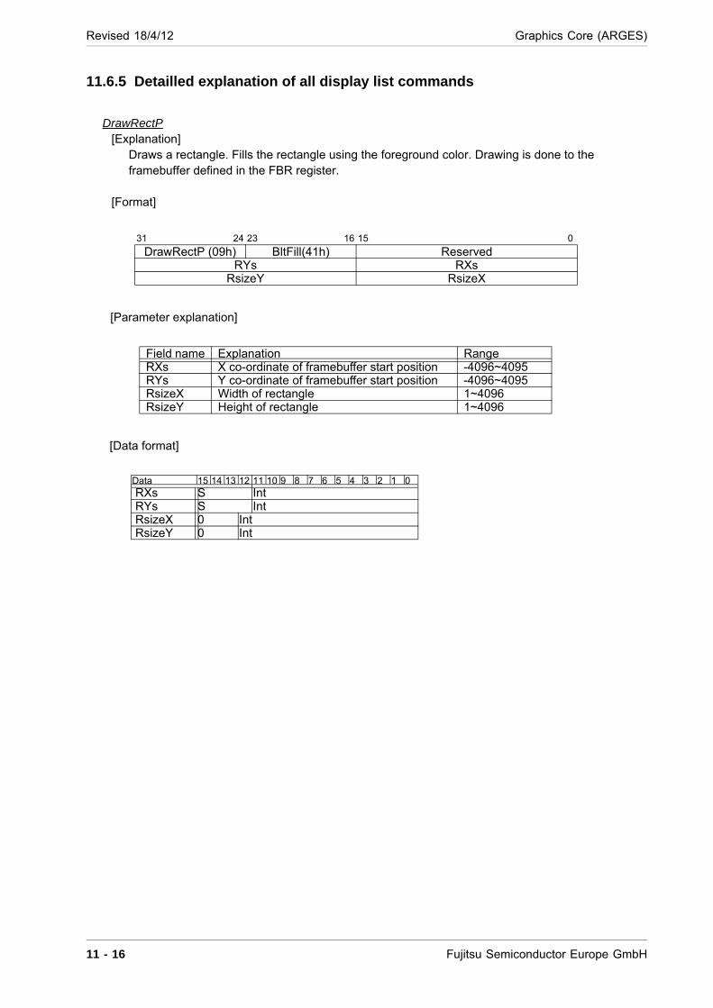
Revised 18/4/12 Graphics Core (ARGES)
11.6.5 Detailled explanation of all display list commands
DrawRectP[Explanation]
Draws a rectangle. Fills the rectangle using the foreground color. Drawing is done to the framebuffer defined in the FBR register.
[Format]
[Parameter explanation]
[Data format]
31 24 23 16 15 0
DrawRectP (09h) BltFill(41h) ReservedRYs RXs
RsizeY RsizeX
Field name Explanation RangeRXs X co-ordinate of framebuffer start position -4096~4095RYs Y co-ordinate of framebuffer start position -4096~4095RsizeX Width of rectangle 1~4096RsizeY Height of rectangle 1~4096
Data 15 14 13 12 11 10 9 8 7 6 5 4 3 2 1 0 RXs S Int RYs S Int RsizeX 0 Int RsizeY 0 Int
11 - 16 Fujitsu Semiconductor Europe GmbH
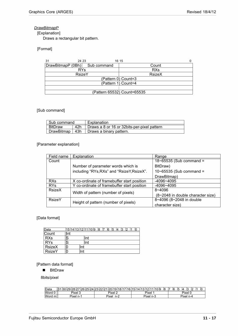
Graphics Core (ARGES) Revised 18/4/12
DrawBitmapP[Explanation]
Draws a rectangular bit pattern.
[Format]
[Sub command]
[Parameter explanation]
[Data format]
[Pattern data format]
BltDraw
8bits/pixel
31 24 23 16 15 0
DrawBitmapP (0Bh) Sub command CountRYs RXs
RsizeY RsizeX(Pattern 0) Count=3(Pattern 1) Count=4
:(Pattern 65532) Count=65535
Sub command ExplanationBltDraw 42h Draws a 8 or 16 or 32bits-per-pixel patternDrawBitmap 43h Draws a binary pattern.
Field name Explanation RangeCount
Number of parameter words which is including “RYs,RXs” and “RsizeY,RsizeX”.
18~65535 (Sub command = BltDraw)10~65535 (Sub command = DrawBitmap)
RXs X co-ordinate of framebuffer start position -4096~4095RYs Y co-ordinate of framebuffer start position -4096~4095RsizeX
Width of pattern (number of pixels)8~4096 (8~2048 in double character size)
RsizeYHeight of pattern (number of pixels)
8~4096 (8~2048 in double character size)
Data 15 14 13 12 11 10 9 8 7 6 5 4 3 2 1 0Count Int RXs S Int RYs S Int RsizeX 0 Int RsizeY 0 Int
Data 31 30 29 28 27 26 25 24 23 22 21 20 19 18 17 16 15 14 13 12 11 10 9 8 7 6 5 4 3 2 1 0Word 0 Pixel 3 Pixel 2 Pixel 1 Pixel 0Word m Pixel n-1 Pixel n-2 Pixel n-3 Pixel n-4
Fujitsu Semiconductor Europe GmbH 11 - 17
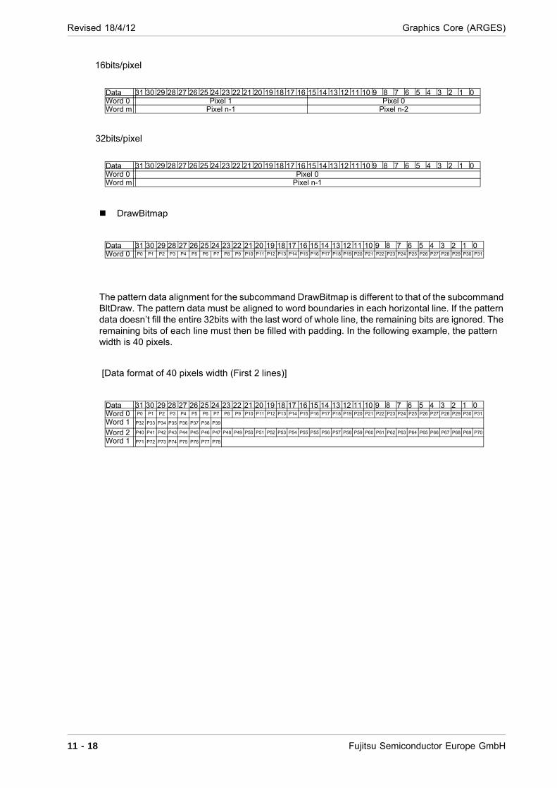
Revised 18/4/12 Graphics Core (ARGES)
16bits/pixel
32bits/pixel
DrawBitmap
The pattern data alignment for the subcommand DrawBitmap is different to that of the subcommand BltDraw. The pattern data must be aligned to word boundaries in each horizontal line. If the pattern data doesn’t fill the entire 32bits with the last word of whole line, the remaining bits are ignored. The remaining bits of each line must then be filled with padding. In the following example, the pattern width is 40 pixels.
[Data format of 40 pixels width (First 2 lines)]
Data 31 30 29 28 27 26 25 24 23 22 21 20 19 18 17 16 15 14 13 12 11 10 9 8 7 6 5 4 3 2 1 0Word 0 Pixel 1 Pixel 0Word m Pixel n-1 Pixel n-2
Data 31 30 29 28 27 26 25 24 23 22 21 20 19 18 17 16 15 14 13 12 11 10 9 8 7 6 5 4 3 2 1 0Word 0 Pixel 0Word m Pixel n-1
Data 31 30 29 28 27 26 25 24 23 22 21 20 19 18 17 16 15 14 13 12 11 10 9 8 7 6 5 4 3 2 1 0Word 0 P0 P1 P2 P3 P4 P5 P6 P7 P8 P9 P10 P11 P12 P13 P14 P15 P16 P17 P18 P19 P20 P21 P22 P23 P24 P25 P26 P27 P28 P29 P30 P31
Data 31 30 29 28 27 26 25 24 23 22 21 20 19 18 17 16 15 14 13 12 11 10 9 8 7 6 5 4 3 2 1 0Word 0 P0 P1 P2 P3 P4 P5 P6 P7 P8 P9 P10 P11 P12 P13 P14 P15 P16 P17 P18 P19 P20 P21 P22 P23 P24 P25 P26 P27 P28 P29 P30 P31
Word 1 P32 P33 P34 P35 P36 P37 P38 P39
Word 2 P40 P41 P42 P43 P44 P45 P46 P47 P48 P49 P50 P51 P52 P53 P54 P55 P55 P56 P57 P58 P59 P60 P61 P62 P63 P64 P65 P66 P67 P68 P69 P70
Word 1 P71 P72 P73 P74 P75 P76 P77 P78
11 - 18 Fujitsu Semiconductor Europe GmbH
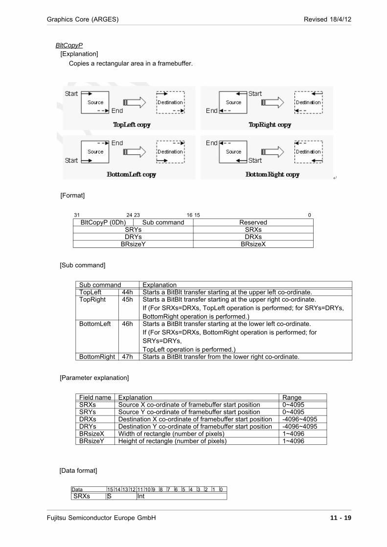
Graphics Core (ARGES) Revised 18/4/12
BltCopyP[Explanation]
Copies a rectangular area in a framebuffer.
[Format]
[Sub command]
[Parameter explanation]
[Data format]
31 24 23 16 15 0
BltCopyP (0Dh) Sub command ReservedSRYs SRXsDRYs DRXs
BRsizeY BRsizeX
Sub command ExplanationTopLeft 44h Starts a BitBlt transfer starting at the upper left co-ordinate.TopRight 45h Starts a BitBlt transfer starting at the upper right co-ordinate.
If (For SRXs=DRXs, TopLeft operation is performed; for SRYs=DRYs,BottomRight operation is performed.)
BottomLeft 46h Starts a BitBlt transfer starting at the lower left co-ordinate.If (For SRXs=DRXs, BottomRight operation is performed; for SRYs=DRYs,TopLeft operation is performed.)
BottomRight 47h Starts a BitBlt transfer from the lower right co-ordinate.
Field name Explanation RangeSRXs Source X co-ordinate of framebuffer start position 0~4095SRYs Source Y co-ordinate of framebuffer start position 0~4095DRXs Destination X co-ordinate of framebuffer start position -4096~4095DRYs Destination Y co-ordinate of framebuffer start position -4096~4095BRsizeX Width of rectangle (number of pixels) 1~4096BRsizeY Height of rectangle (number of pixels) 1~4096
Data 15 14 13 12 11 10 9 8 7 6 5 4 3 2 1 0 SRXs S Int
Fujitsu Semiconductor Europe GmbH 11 - 19
Revised 18/4/12 Graphics Core (ARGES)
SRYs S Int DRXs S Int DRYs S Int BRsizeX 0 Int BRsizeY 0 Int
11 - 20 Fujitsu Semiconductor Europe GmbH
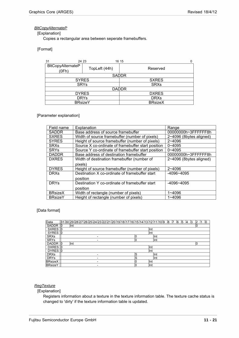
Graphics Core (ARGES) Revised 18/4/12
BltCopyAlternateP[Explanation]
Copies a rectangular area between seperate framebuffers.
[Format]
[Parameter explanation]
[Data format]
RegTexture[Explanation]
Registers information about a texture in the texture information table. The texture cache status is changed to 'dirty' if the texture information table is updated.
31 24 23 16 15 0
BltCopyAlternateP (0Fh)
TopLeft (44h) Reserved
SADDRSYRES SXRESSRYs SRXs
DADDRDYRES DXRESDRYs DRXs
BRsizeY BRsizeX
Field name Explanation RangeSADDR Base address of source framebuffer 00000000h~3FFFFFF8hSXRES Width of source framebuffer (number of pixels) 2~4096 (8bytes aligned)SYRES Height of source framebuffer (number of pixels) 2~4096SRXs Source X co-ordinate of framebuffer start position 0~4095SRYs Source Y co-ordinate of framebuffer start position 0~4095DADDR Base address of destination framebuffer 00000000h~3FFFFFF8hDXRES Width of destination framebuffer (number of
pixels)2~4096 (8bytes aligned)
DYRES Height of source framebuffer (number of pixels) 2~4096DRXs Destination X co-ordinate of framebuffer start
position-4096~4095
DRYs Destination Y co-ordinate of framebuffer start position
-4096~4095
BRsizeX Width of rectangle (number of pixels) 1~4096BRsizeY Height of rectangle (number of pixels) 1~4096
Data 31 30 29 28 27 26 25 24 23 22 21 20 19 18 17 16 15 14 13 12 11 10 9 8 7 6 5 4 3 2 1 0 SADDR 0 Int 0SXRES 0 IntSYRES 0 Int
SRXs - 0 Int SRYs - 0 Int DADDR 0 Int 0DXRES 0 IntDYRES 0 Int
DRXs - S Int DRYs - S IntBRsizeX - 0 IntBRsizeY - 0 Int
Fujitsu Semiconductor Europe GmbH 11 - 21

Revised 18/4/12 Graphics Core (ARGES)
[Format]
[Sub command]
[Parameter explanation]
Each entry which is specified by the TexID parameter has 5 extra entries for cube mapping (each specified by the CubeID parameter). The first cube entry (CubeID=0) has all fields, but the remaining 5 entries have restricted fields. For CubeID = 0, all fields are used, but for CubeID's 1~5, only the fields indicated by the bold font in the figure below are used, the other fields and ‘State’ sub com-mands are ignored. The BPP bitfield has an exception in the case of ALPHA and LUMINANCE_ALPHA: the BPP fileds of all cube surfaces are the same because BPP is fixed for both ALPHA and LUMINANCE_ALPHA. In these cases, the BPP bitfields are not updated except for TexID=0.
31 24 23 16 15 6 4 2 0
RegTexture (19h) Base (00h) Reserved CubeIDReserved
TexID
0 Base Address 00 SizeT 0 SizeS
TSW
Reserved FMT Reserved CMP Reserved BPP
31 24 23 16 15 2 0
RegTexture (19h) State (01h) Reserved TexID
WRAPS WRAPT Reserved
MAGFL
0 MINFL 0
Sub command ExplanationBase
00hRegisters basic information. The maximum number of information entries is 8. It is specified by TexID.
State01h
Registers state information similar to base information.
Field name Explanation RangeTexID Entry No. of texture information table 0~7CubeID Cube surface ID of each texture 0~5
11 - 22 Fujitsu Semiconductor Europe GmbH
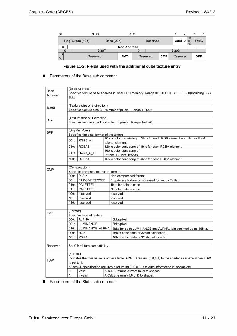
Graphics Core (ARGES) Revised 18/4/12
Figure 11-2: Fields used with the additional cube texture entry
Parameters of the Base sub command
Parameters of the State sub command
31 24 23 16 15 6 4 2 0
RegTexture (19h) Base (00h) Reserved CubeIDReserved
TexID
0 Base Address 00 SizeT 0 SizeS
TSW
Reserved FMT Reserved CMP Reserved BPP
Base Address
(Base Address)Specifies texture base address in local GPU memory. Range 00000000h~3FFFFFF8h(Including LSB 3bits)
SizeS(Texture size of S direction)Specifies texture size S. (Number of pixels) Range 1~4096
SizeT(Texture size of T direction)Specifies texture size T. (Number of pixels) Range 1~4096
BPP(Bits Per Pixel)Specifies the pixel format of the texture.
001: RGB5_A116bits color, consisting of 5bits for each RGB element and 1bit for the A (alpha) element.
010: RGBA8 32bits color consisting of 8bits for each RGBA element.
011: RGB5_6_516bits color consisting ofR:5bits, G:6bits, B:5bits
100: RGBA4 16bits color consisting of 4bits for each RGBA element.
CMP(Compression)Specifies compressed texture format.000: PLAIN Non-compressed format
001: FJ COMPRESSED Proprietary texture compressed format by Fujitsu
010: PALETTE4 4bits for palette code
011: PALETTE8 8bits for palette code.
100: reserved reserved
101: reserved reserved
110: reserved reserved
FMT(Format)Specifies type of texture.000: ALPHA 8bits/pixel.
001: LUMINANCE 8bits/pixel.
010: LUMINANCE_ALPHA 8bits for each LUMINANCE and ALPHA. It is summed up as 16bits.100: RGB 16bits color code or 32bits color code.
101: RGBA 16bits color code or 32bits color code.
Reserved Set 0 for future compatibility.
TSW
(Format)Indicates that this value is not available. ARGES returns (0,0,0,1) to the shader as a texel when TSW is set to 1.*OpenGL specification requires a returning (0,0,0,1) if texture information is incomplete.0: Valid ARGES returns current texel to shader.
1: Invalid ARGES returns (0,0,0,1) to shader.
Fujitsu Semiconductor Europe GmbH 11 - 23
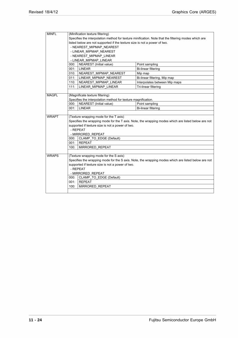
Revised 18/4/12 Graphics Core (ARGES)
MINFL (Minification texture filtering)Specifies the interpolation method for texture minification. Note that the filtering modes which are listed below are not supported if the texture size is not a power of two. - NEAREST_MIPMAP_NEAREST- LINEAR_MIPMAP_NEAREST- NEAREST_MIPMAP_LINEAR- LINEAR_MIPMAP_LINEAR
000: NEAREST (Initial value) Point sampling
001: LINEAR Bi-linear filtering
010: NEAREST_MIPMAP_NEAREST Mip map
011: LINEAR_MIPMAP_NEAREST Bi-linear filtering, Mip map
110: NEAREST_MIPMAP_LINEAR Interpolates between Mip maps
111: LINEAR_MIPMAP_LINEAR Tri-linear filtering
MAGFL (Magnificate texture filtering)Specifies the interpolation method for texture magnification.000: NEAREST (Initial value) Point sampling
001: LINEAR Bi-linear filtering
WRAPT (Texture wrapping mode for the T axis)Specifies the wrapping mode for the T axis. Note, the wrapping modes which are listed below are not supported if texture size is not a power of two.- REPEAT- MIRRORED_REPEAT
000: CLAMP_TO_EDGE (Default)
001: REPEAT
100: MIRRORED_REPEAT
WRAPS (Texture wrapping mode for the S axis)Specifies the wrapping mode for the S axis. Note, the wrapping modes which are listed below are not supported if texture size is not a power of two.- REPEAT- MIRRORED_REPEAT
000: CLAMP_TO_EDGE (Default)
001: REPEAT
100: MIRRORED_REPEAT
11 - 24 Fujitsu Semiconductor Europe GmbH
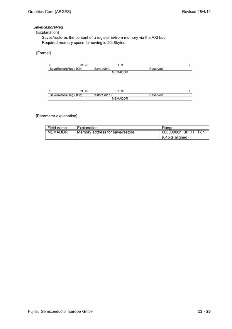
Graphics Core (ARGES) Revised 18/4/12
SaveRestoreReg[Explanation]
Saves/restores the content of a register in/from memory via the AXI bus.Required memory space for saving is 2048bytes.
[Format]
[Parameter explanation]
31 24 23 16 15 0
SaveRestoreReg (1Ch) Save (00h) ReservedMEMADDR
31 24 23 16 15 0
SaveRestoreReg (1Ch) Restore (01h) ReservedMEMADDR
Field name Explanation RangeMEMADDR Memory address for save/restore 00000000h~3FFFFFF8h
(64bits aligned)
Fujitsu Semiconductor Europe GmbH 11 - 25
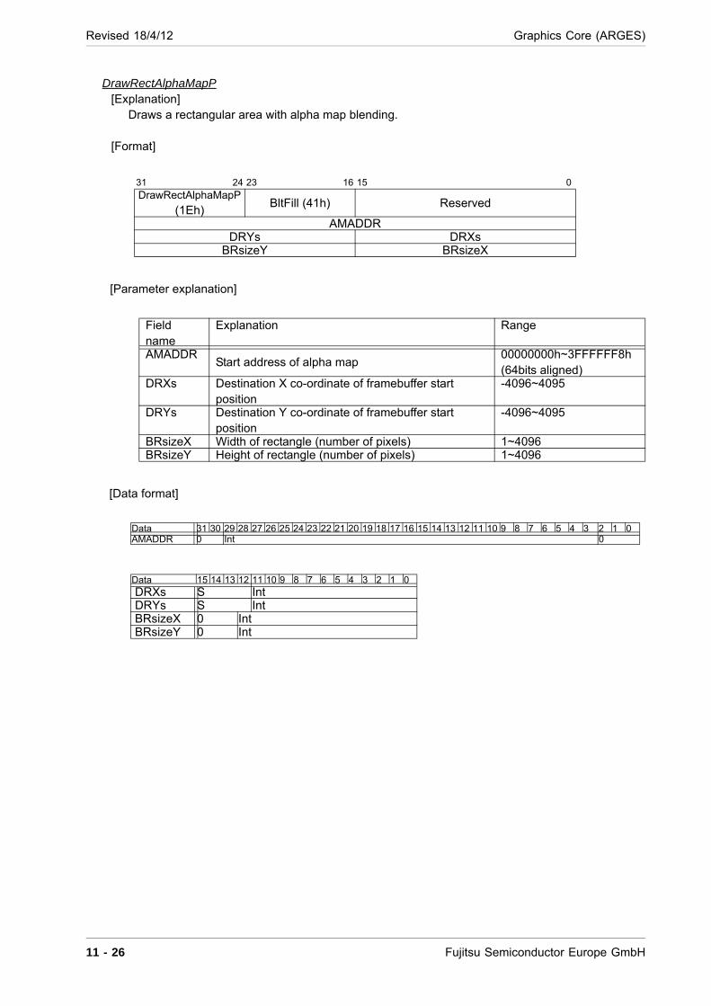
Revised 18/4/12 Graphics Core (ARGES)
DrawRectAlphaMapP[Explanation]
Draws a rectangular area with alpha map blending.
[Format]
[Parameter explanation]
[Data format]
31 24 23 16 15 0DrawRectAlphaMapP
(1Eh)BltFill (41h) Reserved
AMADDRDRYs DRXs
BRsizeY BRsizeX
Field name
Explanation Range
AMADDRStart address of alpha map
00000000h~3FFFFFF8h (64bits aligned)
DRXs Destination X co-ordinate of framebuffer start position
-4096~4095
DRYs Destination Y co-ordinate of framebuffer start position
-4096~4095
BRsizeX Width of rectangle (number of pixels) 1~4096BRsizeY Height of rectangle (number of pixels) 1~4096
Data 31 30 29 28 27 26 25 24 23 22 21 20 19 18 17 16 15 14 13 12 11 10 9 8 7 6 5 4 3 2 1 0AMADDR 0 Int 0
Data 15 14 13 12 11 10 9 8 7 6 5 4 3 2 1 0 DRXs S Int DRYs S Int BRsizeX 0 Int BRsizeY 0 Int
11 - 26 Fujitsu Semiconductor Europe GmbH
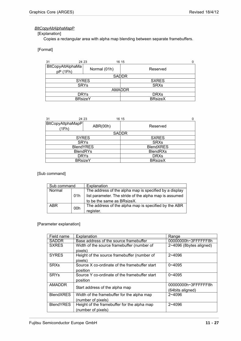
Graphics Core (ARGES) Revised 18/4/12
BltCopyAltAlphaMapP[Explanation]
Copies a rectangular area with alpha map blending between separate framebuffers.
[Format]
[Sub command]
[Parameter explanation]
31 24 23 16 15 0
BltCopyAltAlphaMapP (1Fh)
Normal (01h) Reserved
SADDRSYRES SXRESSRYs SRXs
AMADDRDRYs DRXs
BRsizeY BRsizeX
31 24 23 16 15 0
BltCopyAltphaMapP (1Fh)
ABR(00h) Reserved
SADDRSYRES SXRESSRYs SRXs
BlendYRES BlendXRESBlendRYs BlendRXs
DRYs DRXsBRsizeY BRsizeX
Sub command ExplanationNormal
01hThe address of the alpha map is specified by a display list parameter. The stride of the alpha map is assumed to be the same as BRsizeX.
ABR00h
The address of the alpha map is specified by the ABR register.
Field name Explanation RangeSADDR Base address of the source framebuffer 00000000h~3FFFFFF8hSXRES Width of the source framebuffer (number of
pixels)2~4096 (8bytes aligned)
SYRES Height of the source framebuffer (number of pixels)
2~4096
SRXs Source X co-ordinate of the framebuffer start position
0~4095
SRYs Source Y co-ordinate of the framebuffer start position
0~4095
AMADDRStart address of the alpha map
00000000h~3FFFFFF8h (64bits aligned)
BlendXRES Width of the framebuffer for the alpha map (number of pixels)
2~4096
BlendYRES Height of the framebuffer for the alpha map (number of pixels)
2~4096
Fujitsu Semiconductor Europe GmbH 11 - 27
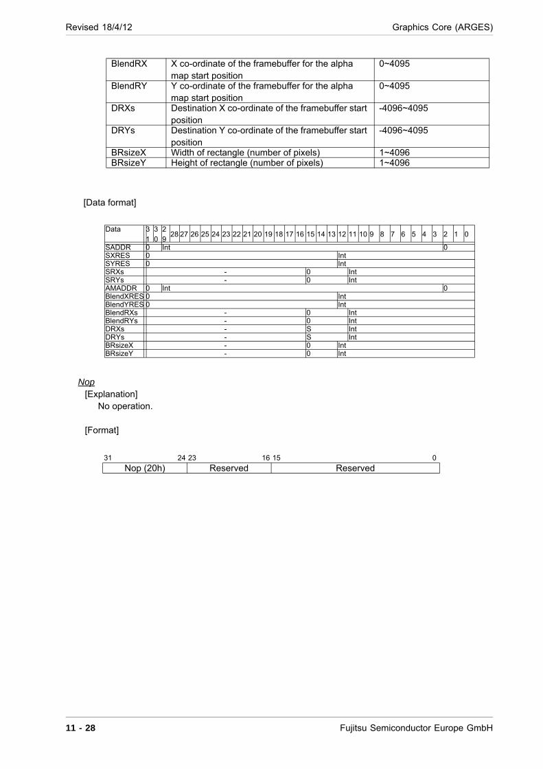
Revised 18/4/12 Graphics Core (ARGES)
[Data format]
Nop[Explanation]
No operation.
[Format]
BlendRX X co-ordinate of the framebuffer for the alpha map start position
0~4095
BlendRY Y co-ordinate of the framebuffer for the alpha map start position
0~4095
DRXs Destination X co-ordinate of the framebuffer start position
-4096~4095
DRYs Destination Y co-ordinate of the framebuffer start position
-4096~4095
BRsizeX Width of rectangle (number of pixels) 1~4096BRsizeY Height of rectangle (number of pixels) 1~4096
Data 31
30
29
28 27 26 25 24 23 22 21 20 19 18 17 16 15 14 13 12 11 10 9 8 7 6 5 4 3 2 1 0
SADDR 0 Int 0SXRES 0 IntSYRES 0 IntSRXs - 0 IntSRYs - 0 IntAMADDR 0 Int 0BlendXRES 0 IntBlendYRES 0 IntBlendRXs - 0 IntBlendRYs - 0 IntDRXs - S IntDRYs - S IntBRsizeX - 0 IntBRsizeY - 0 Int
31 24 23 16 15 0
Nop (20h) Reserved Reserved
11 - 28 Fujitsu Semiconductor Europe GmbH
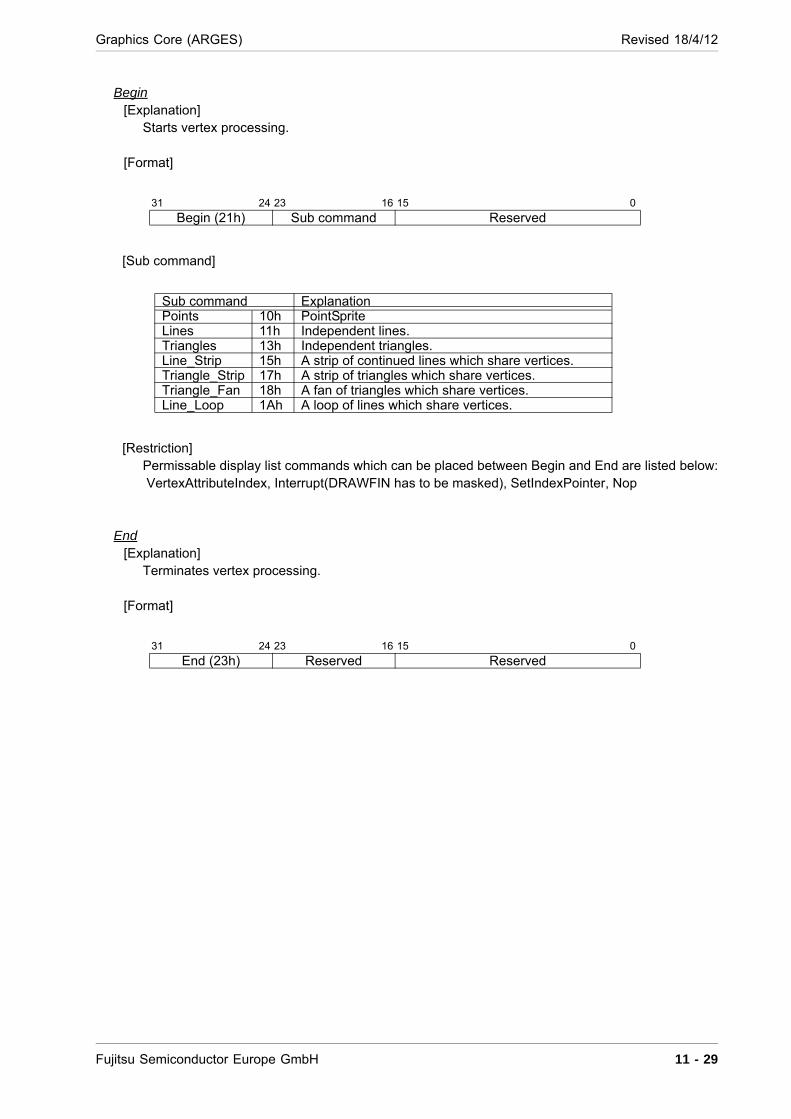
Graphics Core (ARGES) Revised 18/4/12
Begin[Explanation]
Starts vertex processing.
[Format]
[Sub command]
[Restriction]Permissable display list commands which can be placed between Begin and End are listed below: VertexAttributeIndex, Interrupt(DRAWFIN has to be masked), SetIndexPointer, Nop
End[Explanation]
Terminates vertex processing.
[Format]
31 24 23 16 15 0
Begin (21h) Sub command Reserved
Sub command ExplanationPoints 10h PointSpriteLines 11h Independent lines.Triangles 13h Independent triangles.Line_Strip 15h A strip of continued lines which share vertices.Triangle_Strip 17h A strip of triangles which share vertices.Triangle_Fan 18h A fan of triangles which share vertices.Line_Loop 1Ah A loop of lines which share vertices.
31 24 23 16 15 0
End (23h) Reserved Reserved
Fujitsu Semiconductor Europe GmbH 11 - 29

Revised 18/4/12 Graphics Core (ARGES)
BltCopyCompressedP[Explanation]
Decompresses and copies a rectangular block of data in FJ compressed format.
[Format]
[Parameter explanation]
[Data format]
31 24 23 16 15 0
BltCopyCompressedP (2Dh)
TopLeft(44h) Reserved
SADDRDADDR
DYRES DXRESDRYs DRXs
BRsizeY BRsizeX
Field name Explanation RangeSADDR Address of the compressed source data 00000000h~3FFFFFF8hDADDR Base address of the destination framebuffer 00000000h~3FFFFFF8hDXRES Width of the destination framebuffer (number of
pixels)2~4096
DYRES Height of the source framebuffer (number of pixels) 2~4096DRXs Destination X co-ordinate of the framebuffer start
position-4096~4095
DRYs Destination Y co-ordinate of the framebuffer start position
-4096~4095
BRsizeX Width of rectangle (number of pixels) 8~4096 (Multiple of eight)BRsizeY Height of rectangle (number of pixels) 8~4096 (Multiple of eight)
Data 31 30 29 28 27 26 25 24 23 22 21 20 19 18 17 16 15 14 13 12 11 10 9 8 7 6 5 4 3 2 1 0SADDR 0 Int 0DADDR 0 Int 0DXRES 0 IntDYRES 0 IntDRXs - S IntDRYs - S IntBRsizeX - 0 IntBRsizeY - 0 Int
11 - 30 Fujitsu Semiconductor Europe GmbH
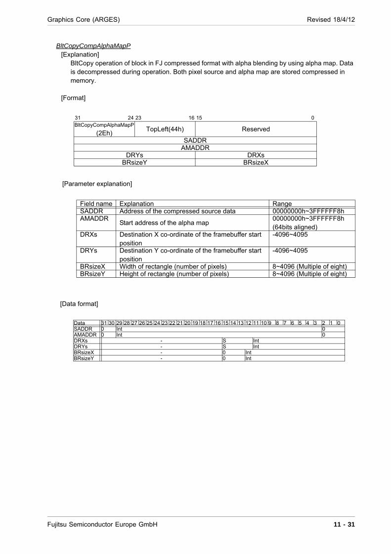
Graphics Core (ARGES) Revised 18/4/12
BltCopyCompAlphaMapP[Explanation]
BltCopy operation of block in FJ compressed format with alpha blending by using alpha map. Data is decompressed during operation. Both pixel source and alpha map are stored compressed in memory.
[Format]
[Parameter explanation]
[Data format]
31 24 23 16 15 0BltCopyCompAlphaMapP
(2Eh)TopLeft(44h) Reserved
SADDRAMADDR
DRYs DRXsBRsizeY BRsizeX
Field name Explanation RangeSADDR Address of the compressed source data 00000000h~3FFFFFF8hAMADDR
Start address of the alpha map00000000h~3FFFFFF8h (64bits aligned)
DRXs Destination X co-ordinate of the framebuffer start position
-4096~4095
DRYs Destination Y co-ordinate of the framebuffer start position
-4096~4095
BRsizeX Width of rectangle (number of pixels) 8~4096 (Multiple of eight)BRsizeY Height of rectangle (number of pixels) 8~4096 (Multiple of eight)
Data 31 30 29 28 27 26 25 24 23 22 21 20 19 18 17 16 15 14 13 12 11 10 9 8 7 6 5 4 3 2 1 0SADDR 0 Int 0AMADDR 0 Int 0DRXs - S IntDRYs - S IntBRsizeX - 0 IntBRsizeY - 0 Int
Fujitsu Semiconductor Europe GmbH 11 - 31
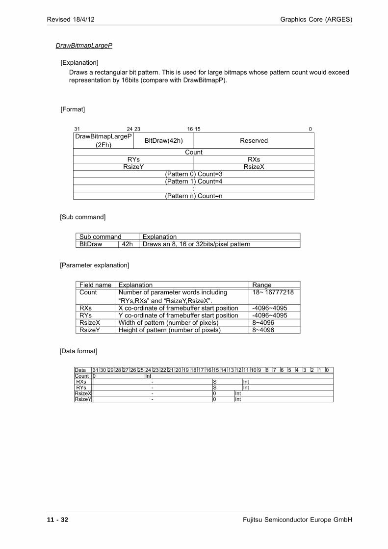
Revised 18/4/12 Graphics Core (ARGES)
DrawBitmapLargeP
[Explanation]
Draws a rectangular bit pattern. This is used for large bitmaps whose pattern count would exceed representation by 16bits (compare with DrawBitmapP).
[Format]
[Sub command]
[Parameter explanation]
[Data format]
31 24 23 16 15 0
DrawBitmapLargeP (2Fh)
BltDraw(42h) Reserved
CountRYs RXs
RsizeY RsizeX(Pattern 0) Count=3(Pattern 1) Count=4
:(Pattern n) Count=n
Sub command ExplanationBltDraw 42h Draws an 8, 16 or 32bits/pixel pattern
Field name Explanation RangeCount Number of parameter words including
“RYs,RXs” and “RsizeY,RsizeX”.18~ 16777218
RXs X co-ordinate of framebuffer start position -4096~4095RYs Y co-ordinate of framebuffer start position -4096~4095RsizeX Width of pattern (number of pixels) 8~4096RsizeY Height of pattern (number of pixels) 8~4096
Data 31 30 29 28 27 26 25 24 23 22 21 20 19 18 17 16 15 14 13 12 11 10 9 8 7 6 5 4 3 2 1 0Count 0 Int RXs - S Int RYs - S IntRsizeX - 0 IntRsizeY - 0 Int
11 - 32 Fujitsu Semiconductor Europe GmbH
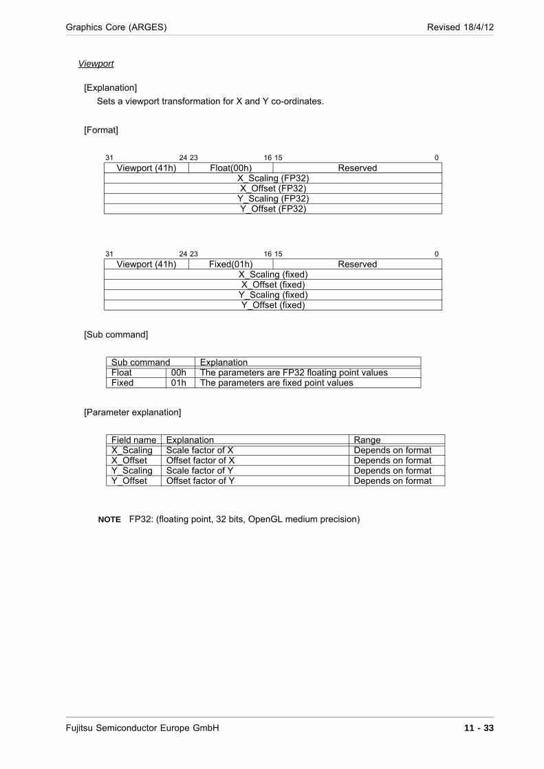
Graphics Core (ARGES) Revised 18/4/12
Viewport
[Explanation]
Sets a viewport transformation for X and Y co-ordinates.
[Format]
[Sub command]
[Parameter explanation]
NOTE FP32: (floating point, 32 bits, OpenGL medium precision)
31 24 23 16 15 0
Viewport (41h) Float(00h) ReservedX_Scaling (FP32)X_Offset (FP32)
Y_Scaling (FP32)Y_Offset (FP32)
31 24 23 16 15 0
Viewport (41h) Fixed(01h) ReservedX_Scaling (fixed)X_Offset (fixed)
Y_Scaling (fixed)Y_Offset (fixed)
Sub command ExplanationFloat 00h The parameters are FP32 floating point valuesFixed 01h The parameters are fixed point values
Field name Explanation RangeX_Scaling Scale factor of X Depends on formatX_Offset Offset factor of X Depends on formatY_Scaling Scale factor of Y Depends on formatY_Offset Offset factor of Y Depends on format
Fujitsu Semiconductor Europe GmbH 11 - 33
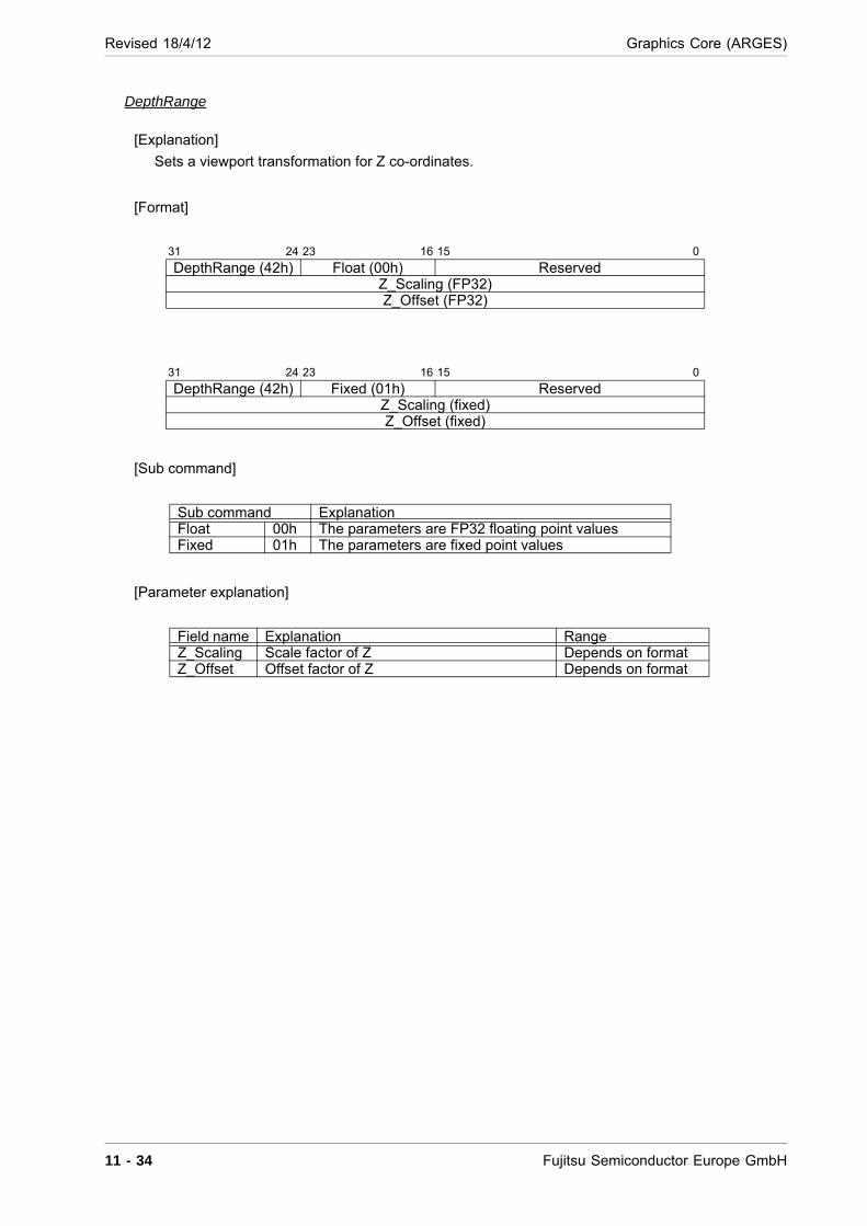
Revised 18/4/12 Graphics Core (ARGES)
DepthRange
[Explanation]
Sets a viewport transformation for Z co-ordinates.
[Format]
[Sub command]
[Parameter explanation]
31 24 23 16 15 0
DepthRange (42h) Float (00h) ReservedZ_Scaling (FP32)Z_Offset (FP32)
31 24 23 16 15 0
DepthRange (42h) Fixed (01h) ReservedZ_Scaling (fixed)Z_Offset (fixed)
Sub command ExplanationFloat 00h The parameters are FP32 floating point valuesFixed 01h The parameters are fixed point values
Field name Explanation RangeZ_Scaling Scale factor of Z Depends on formatZ_Offset Offset factor of Z Depends on format
11 - 34 Fujitsu Semiconductor Europe GmbH

Graphics Core (ARGES) Revised 18/4/12
ViewVolumeXYClip
[Explanation]
Sets a view volume's X and Y co-ordinates.
[Format]
[Sub command]
[Parameter explanation]
31 24 23 16 15 0
ViewVolumeXYClip (44h)
Float(00h) Reserved
XMIN (FP32)XMAX (FP32)YMIN (FP32)YMAX (FP32)
31 24 23 16 15 0
ViewVolumeXYClip (44h)
Fixed(01h) Reserved
XMIN (fixed)XMAX (fixed)YMIN (fixed)YMAX (fixed)
Sub command ExplanationFloat 00h The parameters are FP32 floating point valuesFixed 01h The parameters are fixed point values
Field name Explanation RangeXMIN X minimum of view volume Depends on formatXMAX X maximum of view volume Depends on formatYMIN Y minimum of view volume Depends on formatYMAX Y maximum of view volume Depends on format
Fujitsu Semiconductor Europe GmbH 11 - 35
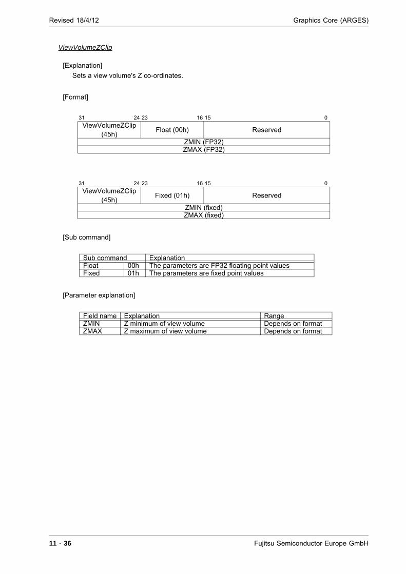
Revised 18/4/12 Graphics Core (ARGES)
ViewVolumeZClip
[Explanation]
Sets a view volume's Z co-ordinates.
[Format]
[Sub command]
[Parameter explanation]
31 24 23 16 15 0
ViewVolumeZClip (45h)
Float (00h) Reserved
ZMIN (FP32)ZMAX (FP32)
31 24 23 16 15 0
ViewVolumeZClip (45h)
Fixed (01h) Reserved
ZMIN (fixed)ZMAX (fixed)
Sub command ExplanationFloat 00h The parameters are FP32 floating point valuesFixed 01h The parameters are fixed point values
Field name Explanation RangeZMIN Z minimum of view volume Depends on formatZMAX Z maximum of view volume Depends on format
11 - 36 Fujitsu Semiconductor Europe GmbH
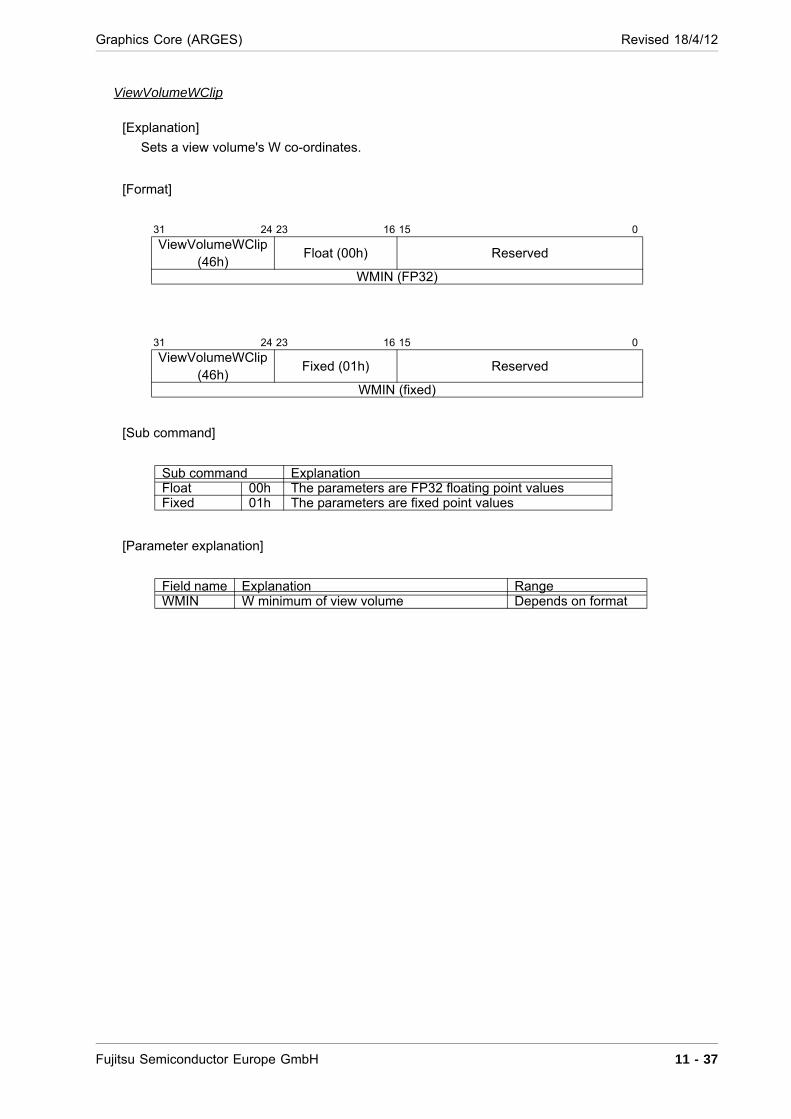
Graphics Core (ARGES) Revised 18/4/12
ViewVolumeWClip
[Explanation]
Sets a view volume's W co-ordinates.
[Format]
[Sub command]
[Parameter explanation]
31 24 23 16 15 0
ViewVolumeWClip (46h)
Float (00h) Reserved
WMIN (FP32)
31 24 23 16 15 0
ViewVolumeWClip (46h)
Fixed (01h) Reserved
WMIN (fixed)
Sub command ExplanationFloat 00h The parameters are FP32 floating point valuesFixed 01h The parameters are fixed point values
Field name Explanation RangeWMIN W minimum of view volume Depends on format
Fujitsu Semiconductor Europe GmbH 11 - 37
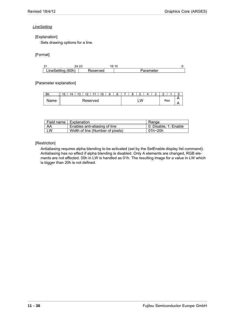
Revised 18/4/12 Graphics Core (ARGES)
LineSetting
[Explanation]
Sets drawing options for a line.
[Format]
[Parameter explanation]
[Restriction]
Antialiasing requires alpha blending to be activated (set by the SetEnable display list command). Antialiasing has no effect if alpha blending is disabled. Only A elements are changed, RGB ele-ments are not effected. 00h in LW is handled as 01h. The resulting image for a value in LW which is bigger than 20h is not defined.
31 24 23 16 15 0
LineSetting (60h) Reserved Parameter
Bit 15 14 13 12 11 10 9 8 7 6 5 4 3 2 1 0
Name Reserved LW ResAA
Field name Explanation RangeAA Enables anti-aliasing of line 0: Disable, 1: EnableLW Width of line (Number of pixels) 01h~20h
11 - 38 Fujitsu Semiconductor Europe GmbH
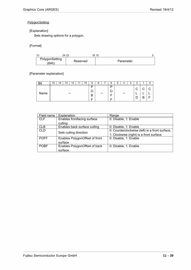
Graphics Core (ARGES) Revised 18/4/12
PolygonSetting
[Explanation]
Sets drawing options for a polygon.
[Format]
[Parameter explanation]
31 24 23 16 15 0
PolygonSetting (64h)
Reserved Parameter
Bit 15 14 13 12 11 10 9 8 7 6 5 4 3 2 1 0
Name -
POBF
-
POFF
-
CLD
CLB
CLF
Field name Explanation RangeCLF Enables frontfacing surface
culling0: Disable, 1: Enable
CLB Enables back surface culling 0: Disable, 1: EnableCLD
Sets culling direction0: Counterclockwise (left) is a front surface,1: Clockwise (right) is a front surface.
POFF Enables PolygonOffset of front surface
0: Disable, 1: Enable
POBF Enables PolygonOffset of back surface
0: Disable, 1: Enable
Fujitsu Semiconductor Europe GmbH 11 - 39
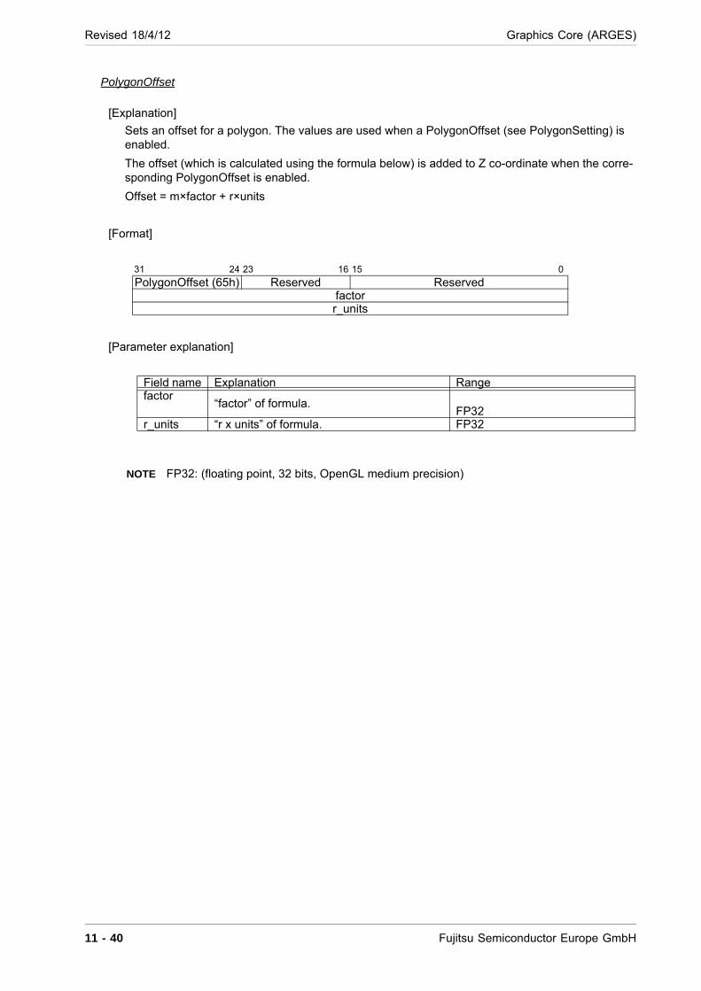
Revised 18/4/12 Graphics Core (ARGES)
PolygonOffset
[Explanation]
Sets an offset for a polygon. The values are used when a PolygonOffset (see PolygonSetting) is enabled.
The offset (which is calculated using the formula below) is added to Z co-ordinate when the corre-sponding PolygonOffset is enabled.
Offset = m×factor + r×units
[Format]
[Parameter explanation]
NOTE FP32: (floating point, 32 bits, OpenGL medium precision)
31 24 23 16 15 0
PolygonOffset (65h) Reserved Reservedfactorr_units
Field name Explanation Rangefactor
“factor” of formula.FP32
r_units “r x units” of formula. FP32
11 - 40 Fujitsu Semiconductor Europe GmbH
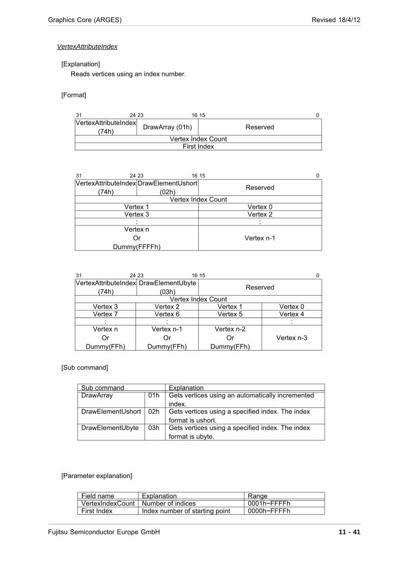
Graphics Core (ARGES) Revised 18/4/12
VertexAttributeIndex
[Explanation]
Reads vertices using an index number.
[Format]
[Sub command]
[Parameter explanation]
31 24 23 16 15 0
VertexAttributeIndex (74h)
DrawArray (01h) Reserved
Vertex Index CountFirst Index
31 24 23 16 15 0
VertexAttributeIndex (74h)
DrawElementUshort (02h)
Reserved
Vertex Index CountVertex 1 Vertex 0Vertex 3 Vertex 2
: :Vertex n
OrDummy(FFFFh)
Vertex n-1
31 24 23 16 15 0
VertexAttributeIndex (74h)
DrawElementUbyte (03h)
Reserved
Vertex Index CountVertex 3 Vertex 2 Vertex 1 Vertex 0Vertex 7 Vertex 6 Vertex 5 Vertex 4
: : : :Vertex n
OrDummy(FFh)
Vertex n-1Or
Dummy(FFh)
Vertex n-2Or
Dummy(FFh)Vertex n-3
Sub command ExplanationDrawArray 01h Gets vertices using an automatically incremented
index.DrawElementUshort 02h Gets vertices using a specified index. The index
format is ushort.DrawElementUbyte 03h Gets vertices using a specified index. The index
format is ubyte.
Field name Explanation RangeVertexIndexCount Number of indices 0001h~FFFFhFirst Index Index number of starting point 0000h~FFFFh
Fujitsu Semiconductor Europe GmbH 11 - 41
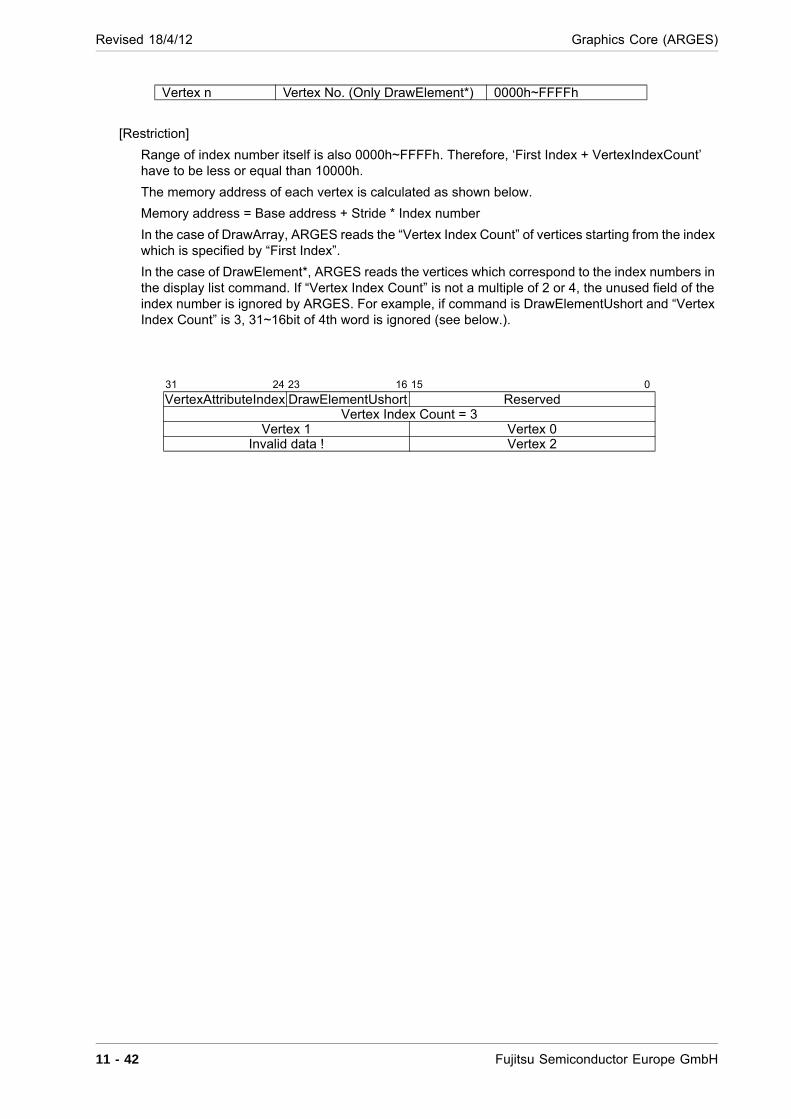
Revised 18/4/12 Graphics Core (ARGES)
[Restriction]
Range of index number itself is also 0000h~FFFFh. Therefore, ‘First Index + VertexIndexCount’ have to be less or equal than 10000h.
The memory address of each vertex is calculated as shown below.
Memory address = Base address + Stride * Index number
In the case of DrawArray, ARGES reads the “Vertex Index Count” of vertices starting from the index which is specified by “First Index”.
In the case of DrawElement*, ARGES reads the vertices which correspond to the index numbers in the display list command. If “Vertex Index Count” is not a multiple of 2 or 4, the unused field of the index number is ignored by ARGES. For example, if command is DrawElementUshort and “Vertex Index Count” is 3, 31~16bit of 4th word is ignored (see below.).
Vertex n Vertex No. (Only DrawElement*) 0000h~FFFFh
31 24 23 16 15 0
VertexAttributeIndex DrawElementUshort ReservedVertex Index Count = 3
Vertex 1 Vertex 0Invalid data ! Vertex 2
11 - 42 Fujitsu Semiconductor Europe GmbH
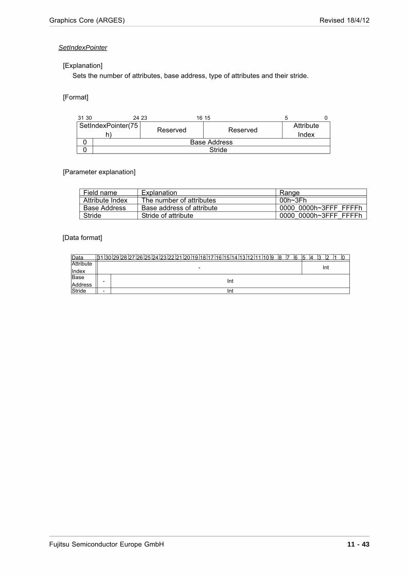
Graphics Core (ARGES) Revised 18/4/12
SetIndexPointer
[Explanation]
Sets the number of attributes, base address, type of attributes and their stride.
[Format]
[Parameter explanation]
[Data format]
31 30 24 23 16 15 5 0
SetIndexPointer(75h)
Reserved ReservedAttribute
Index0 Base Address0 Stride
Field name Explanation RangeAttribute Index The number of attributes 00h~3FhBase Address Base address of attribute 0000_0000h~3FFF_FFFFhStride Stride of attribute 0000_0000h~3FFF_FFFFh
Data 31 30 29 28 27 26 25 24 23 22 21 20 19 18 17 16 15 14 13 12 11 10 9 8 7 6 5 4 3 2 1 0AttributeIndex
- Int
BaseAddress
- Int
Stride - Int
Fujitsu Semiconductor Europe GmbH 11 - 43
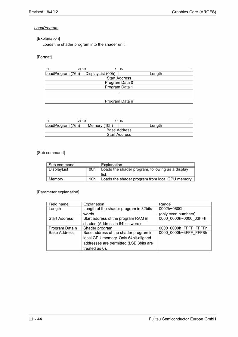
Revised 18/4/12 Graphics Core (ARGES)
LoadProgram
[Explanation]
Loads the shader program into the shader unit.
[Format]
[Sub command]
[Parameter explanation]
31 24 23 16 15 0
LoadProgram (76h) DisplayList (00h) LengthStart Address
Program Data 0Program Data 1
.
.Program Data n
31 24 23 16 15 0
LoadProgram (76h) Memory (10h) LengthBase AddressStart Address
Sub command ExplanationDisplayList 00h Loads the shader program, following as a display
list.Memory 10h Loads the shader program from local GPU memory.
Field name Explanation RangeLength Length of the shader program in 32bits
words.0002h~0800h(only even numbers)
Start Address Start address of the program RAM in shader. (Address in 64bits word)
0000_0000h~0000_03FFh
Program Data n Shader program 0000_0000h~FFFF_FFFFhBase Address Base address of the shader program in
local GPU memory. Only 64bit-aligned addresses are permitted (LSB 3bits are treated as 0).
0000_0000h~3FFF_FFF8h
11 - 44 Fujitsu Semiconductor Europe GmbH
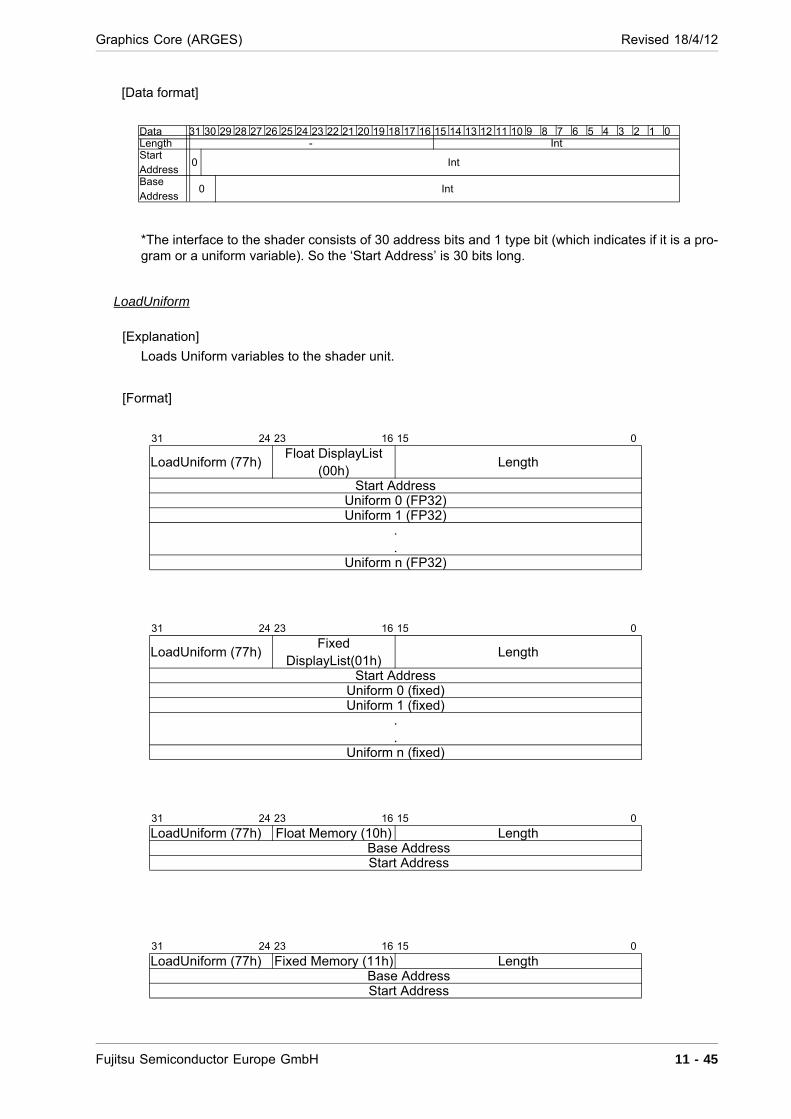
Graphics Core (ARGES) Revised 18/4/12
[Data format]
*The interface to the shader consists of 30 address bits and 1 type bit (which indicates if it is a pro-gram or a uniform variable). So the ‘Start Address’ is 30 bits long.
LoadUniform
[Explanation]
Loads Uniform variables to the shader unit.
[Format]
Data 31 30 29 28 27 26 25 24 23 22 21 20 19 18 17 16 15 14 13 12 11 10 9 8 7 6 5 4 3 2 1 0Length - IntStartAddress
0 Int
BaseAddress
0 Int
31 24 23 16 15 0
LoadUniform (77h)Float DisplayList
(00h)Length
Start AddressUniform 0 (FP32)Uniform 1 (FP32)
.
.Uniform n (FP32)
31 24 23 16 15 0
LoadUniform (77h)Fixed
DisplayList(01h)Length
Start AddressUniform 0 (fixed)Uniform 1 (fixed)
.
.Uniform n (fixed)
31 24 23 16 15 0
LoadUniform (77h) Float Memory (10h) LengthBase AddressStart Address
31 24 23 16 15 0
LoadUniform (77h) Fixed Memory (11h) LengthBase AddressStart Address
Fujitsu Semiconductor Europe GmbH 11 - 45
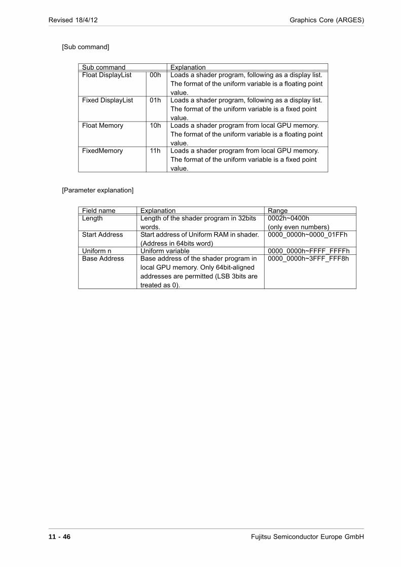
Revised 18/4/12 Graphics Core (ARGES)
[Sub command]
[Parameter explanation]
Sub command ExplanationFloat DisplayList 00h Loads a shader program, following as a display list.
The format of the uniform variable is a floating point value.
Fixed DisplayList 01h Loads a shader program, following as a display list. The format of the uniform variable is a fixed point value.
Float Memory 10h Loads a shader program from local GPU memory. The format of the uniform variable is a floating point value.
FixedMemory 11h Loads a shader program from local GPU memory. The format of the uniform variable is a fixed point value.
Field name Explanation RangeLength Length of the shader program in 32bits
words.0002h~0400h(only even numbers)
Start Address Start address of Uniform RAM in shader. (Address in 64bits word)
0000_0000h~0000_01FFh
Uniform n Uniform variable 0000_0000h~FFFF_FFFFhBase Address Base address of the shader program in
local GPU memory. Only 64bit-aligned addresses are permitted (LSB 3bits are treated as 0).
0000_0000h~3FFF_FFF8h
11 - 46 Fujitsu Semiconductor Europe GmbH

Graphics Core (ARGES) Revised 18/4/12
SetShaderInfo
[Explanation]
Sets registers which are related to the shader units.
[Format]
[Sub command]
[Parameter explanation]
Offset address means an offset from the top register address of SHADER register space. For ex-ample, the SHADER register which is mapped as 004_001Ch is specified as 001Ch in the RegAddr field.
There is no address range check in ARGES. ARGES accesses the SHADER with the specified ad-dress. The behavior of accesses to undefined areas depends on the SHADER.
[Parameter in ‘Data’ word]
Sub command=AttrInf0(00h)
31 24 23 16 15 0
SetShaderInfo (78h) Sub command RegAddrData
Sub command ExplanationAttrInf0 00h Sets the number of attributes.AttrInf1 01h Sets a static attribute return of attribute 0~15.AttrInf2 02h Sets a static attribute return of attribute 16~31.AttrInf3 03h Sets a static attribute return of attribute 32~47.AttrInf4 04h Sets a static attribute return of attribute 48~63.AttrInf5 05h Reserved.AttrInf6 06h Reserved.AttrInf7 07h Reserved.AttrInf8 08h Sets the precision of attributes 0~31.AttrInf9 09h Sets the precision of attributes 32~63.Varying 10h Sets Varying precision and FragCoord transfer
to SHADER.ShaderReg 40h Sets the registers of SHADER. The RegAddr
field is only referred to in the ShaderReg sub command.
Field name Explanation RangeRegAddr Offset address of SHADER register.
Only the ShaderReg sub command refers to RegAddr.
0000h~FFF8h(4bytes aligned)
31 24 23 16 15 7 6 0
ATTRNUM
Field name Explanation RangeATTRNUM The number of attributes of a vertex. 1~64
Fujitsu Semiconductor Europe GmbH 11 - 47
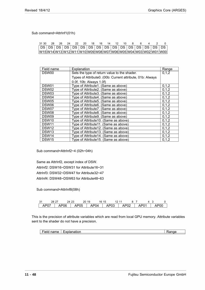
Revised 18/4/12 Graphics Core (ARGES)
Sub command=AttrInf1(01h)
Sub command=AttrInf2~4 (02h~04h)
Same as AttrInf2, except index of DSW.
AttrInf2: DSW16~DSW31 for Attribute16~31
AttrInf3: DSW32~DSW47 for Attribute32~47
AttrInf4: DSW48~DSW63 for Attribute48~63
Sub command=AttrInf8(08h)
This is the precision of attribute variables which are read from local GPU memory. Attribute variables sent to the shader do not have a precision.
31 30 28 26 24 22 20 18 16 14 12 10 8 6 4 2 0
DSW15
DSW14
DSW13
DSW12
DSW11
DSW10
DSW09
DSW08
DSW07
DSW06
DSW05
DSW04
DSW03
DSW02
DSW01
DSW00
Field name Explanation RangeDSW00 Sets the type of return value to the shader.
Types of Attribute0. (00b: Current attribute, 01b: Always 0.0f, 10b: Always 1.0f)
0,1,2
DSW01 Type of Attribute1. (Same as above) 0,1,2DSW02 Type of Attribute2. (Same as above) 0,1,2DSW03 Type of Attribute3. (Same as above) 0,1,2DSW04 Type of Attribute4. (Same as above) 0,1,2DSW05 Type of Attribute5. (Same as above) 0,1,2DSW06 Type of Attribute6. (Same as above) 0,1,2DSW07 Type of Attribute7. (Same as above) 0,1,2DSW08 Type of Attribute8. (Same as above) 0,1,2DSW09 Type of Attribute9. (Same as above) 0,1,2DSW10 Type of Attribute10. (Same as above) 0,1,2DSW11 Type of Attribute11. (Same as above) 0,1,2DSW12 Type of Attribute12. (Same as above) 0,1,2DSW13 Type of Attribute13. (Same as above) 0,1,2DSW14 Type of Attribute14. (Same as above) 0,1,2DSW15 Type of Attribute15. (Same as above) 0,1,2
31 28 27 24 23 20 19 16 15 12 11 8 7 4 3 0
AP07 AP06 AP05 AP04 AP03 AP02 AP01 AP00
Field name Explanation Range
11 - 48 Fujitsu Semiconductor Europe GmbH
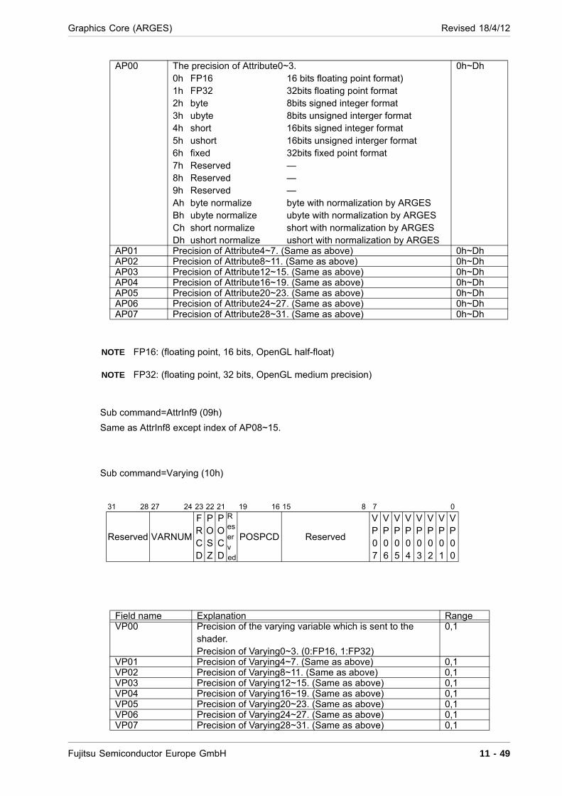
Graphics Core (ARGES) Revised 18/4/12
NOTE FP16: (floating point, 16 bits, OpenGL half-float)
NOTE FP32: (floating point, 32 bits, OpenGL medium precision)
Sub command=AttrInf9 (09h)
Same as AttrInf8 except index of AP08~15.
Sub command=Varying (10h)
AP00 The precision of Attribute0~3.0h FP16 16 bits floating point format)1h FP32 32bits floating point format2h byte 8bits signed integer format3h ubyte 8bits unsigned interger format4h short 16bits signed integer format5h ushort 16bits unsigned interger format6h fixed 32bits fixed point format7h Reserved —8h Reserved —9h Reserved —Ah byte normalize byte with normalization by ARGESBh ubyte normalize ubyte with normalization by ARGESCh short normalize short with normalization by ARGESDh ushort normalize ushort with normalization by ARGES
0h~Dh
AP01 Precision of Attribute4~7. (Same as above) 0h~DhAP02 Precision of Attribute8~11. (Same as above) 0h~DhAP03 Precision of Attribute12~15. (Same as above) 0h~DhAP04 Precision of Attribute16~19. (Same as above) 0h~DhAP05 Precision of Attribute20~23. (Same as above) 0h~DhAP06 Precision of Attribute24~27. (Same as above) 0h~DhAP07 Precision of Attribute28~31. (Same as above) 0h~Dh
31 28 27 24 23 22 21 19 16 15 8 7 0
Reserved VARNUM
FRCD
POSZ
POCD
Reserved
POSPCD Reserved
VP07
VP06
VP05
VP04
VP03
VP02
VP01
VP00
Field name Explanation RangeVP00 Precision of the varying variable which is sent to the
shader.Precision of Varying0~3. (0:FP16, 1:FP32)
0,1
VP01 Precision of Varying4~7. (Same as above) 0,1VP02 Precision of Varying8~11. (Same as above) 0,1VP03 Precision of Varying12~15. (Same as above) 0,1VP04 Precision of Varying16~19. (Same as above) 0,1VP05 Precision of Varying20~23. (Same as above) 0,1VP06 Precision of Varying24~27. (Same as above) 0,1VP07 Precision of Varying28~31. (Same as above) 0,1
Fujitsu Semiconductor Europe GmbH 11 - 49
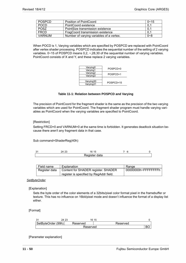
Revised 18/4/12 Graphics Core (ARGES)
When POCD is 1, Varying variables which are specified by POSPCD are replaced with PointCoord after vertex shader processing. POSPCD indicates the sequential number of the setting of 2 varying variables. 0~15 of POSPCD means 0,2, ~,28,30 of the sequential number of varying variables. PointCoord consists of X and Y, and these replace 2 varying variables.
Table 11-1: Relation between POSPCD and Varying
The precision of PointCoord for the fragment shader is the same as the precision of the two varying variables which are used for PointCoord. The fragment shader program must handle varying vari-ables as PointCoord when the varying variables are specified to PointCoord.
[Restriction]
Setting FRCD=0 and VARNUM=0 at the same time is forbidden. It generates deadlock situation be-cause there aren't any fragment data in that case.
Sub command=ShaderReg(40h)
SetByteOrder
[Explanation]
Sets the byte order of the color elements of a 32bits/pixel color format pixel in the framebuffer or texture. This has no influence on 16bit/pixel mode and doesn’t influence the format of a display list either.
[Format]
[Parameter explanation]
POSPCD Position of PointCoord 0~15POCD PointCoord existence 0,1POSZ PointSize transmission existence 0,1FRCD FragCoord transmission existence 0,1VARNUM Number of varying variables of a vertex. 0~8
Varying0 POSPCD=0Varying1Varying2 POSPCD=1Varying3
Varying30 POSPCD=15Varying31
31 24 23 16 15 7 6 0
Register data
Field name Explanation RangeRegister data Content for SHADER register. SHADER
register is specified by RegAddr field.00000000h~FFFFFFFFh
31 24 23 16 15 0
SetByteOrder (99h) Reserved ReservedReserved BO
11 - 50 Fujitsu Semiconductor Europe GmbH
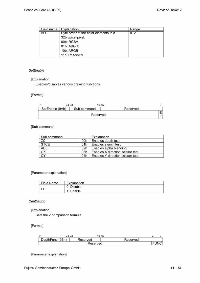
Graphics Core (ARGES) Revised 18/4/12
SetEnable
[Explanation]
Enables/disables various drawing functions.
[Format]
[Sub command]
[Parameter explanation]
DepthFunc
[Explanation]
Sets the Z comparison formula.
[Format]
[Parameter explanation]
Field name Explanation RangeBO Byte order of the color elements in a
32bit/pixel pixel.00b: RGBA01b: ABGR:10b: ARGB11b: Reserved
0~2
31 24 23 16 15 0
SetEnable (9Ah) Sub command Reserved
ReservedEF
Sub command ExplanationZC 00h Enables depth test.STCE 01h Enables stencil test.ABE 02h Enables alpha blending.CX 03h Enables X direction scissor test.CY 04h Enables Y direction scissor test.
Field Name Explanation
EF0: Disable1: Enable
31 24 23 16 15 2 0
DepthFunc (9Bh) Reserved ReservedReserved FUNC
Fujitsu Semiconductor Europe GmbH 11 - 51
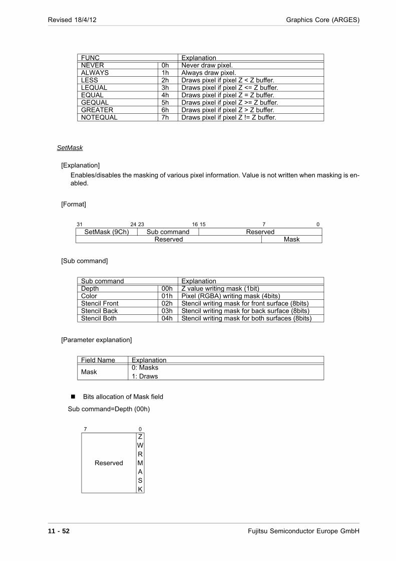
Revised 18/4/12 Graphics Core (ARGES)
SetMask
[Explanation]
Enables/disables the masking of various pixel information. Value is not written when masking is en-abled.
[Format]
[Sub command]
[Parameter explanation]
Bits allocation of Mask field
Sub command=Depth (00h)
FUNC ExplanationNEVER 0h Never draw pixel.ALWAYS 1h Always draw pixel.LESS 2h Draws pixel if pixel Z < Z buffer.LEQUAL 3h Draws pixel if pixel Z <= Z buffer.EQUAL 4h Draws pixel if pixel Z = Z buffer.GEQUAL 5h Draws pixel if pixel Z >= Z buffer.GREATER 6h Draws pixel if pixel Z > Z buffer.NOTEQUAL 7h Draws pixel if pixel Z != Z buffer.
31 24 23 16 15 7 0
SetMask (9Ch) Sub command ReservedReserved Mask
Sub command ExplanationDepth 00h Z value writing mask (1bit)Color 01h Pixel (RGBA) writing mask (4bits)Stencil Front 02h Stencil writing mask for front surface (8bits)Stencil Back 03h Stencil writing mask for back surface (8bits)Stencil Both 04h Stencil writing mask for both surfaces (8bits)
Field Name Explanation
Mask0: Masks1: Draws
7 0
Reserved
ZWRMASK
11 - 52 Fujitsu Semiconductor Europe GmbH
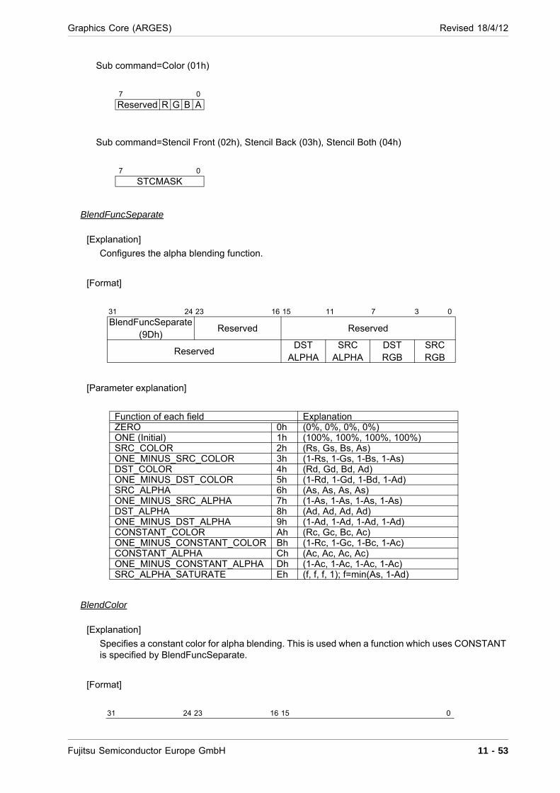
Graphics Core (ARGES) Revised 18/4/12
Sub command=Color (01h)
Sub command=Stencil Front (02h), Stencil Back (03h), Stencil Both (04h)
BlendFuncSeparate
[Explanation]
Configures the alpha blending function.
[Format]
[Parameter explanation]
BlendColor
[Explanation]
Specifies a constant color for alpha blending. This is used when a function which uses CONSTANT is specified by BlendFuncSeparate.
[Format]
7 0
Reserved R G B A
7 0
STCMASK
31 24 23 16 15 11 7 3 0
BlendFuncSeparate (9Dh)
Reserved Reserved
ReservedDST
ALPHASRC
ALPHADSTRGB
SRCRGB
Function of each field ExplanationZERO 0h (0%, 0%, 0%, 0%)ONE (Initial) 1h (100%, 100%, 100%, 100%)SRC_COLOR 2h (Rs, Gs, Bs, As)ONE_MINUS_SRC_COLOR 3h (1-Rs, 1-Gs, 1-Bs, 1-As)DST_COLOR 4h (Rd, Gd, Bd, Ad)ONE_MINUS_DST_COLOR 5h (1-Rd, 1-Gd, 1-Bd, 1-Ad)SRC_ALPHA 6h (As, As, As, As)ONE_MINUS_SRC_ALPHA 7h (1-As, 1-As, 1-As, 1-As)DST_ALPHA 8h (Ad, Ad, Ad, Ad)ONE_MINUS_DST_ALPHA 9h (1-Ad, 1-Ad, 1-Ad, 1-Ad)CONSTANT_COLOR Ah (Rc, Gc, Bc, Ac)ONE_MINUS_CONSTANT_COLOR Bh (1-Rc, 1-Gc, 1-Bc, 1-Ac)CONSTANT_ALPHA Ch (Ac, Ac, Ac, Ac)ONE_MINUS_CONSTANT_ALPHA Dh (1-Ac, 1-Ac, 1-Ac, 1-Ac)SRC_ALPHA_SATURATE Eh (f, f, f, 1); f=min(As, 1-Ad)
31 24 23 16 15 0
Fujitsu Semiconductor Europe GmbH 11 - 53
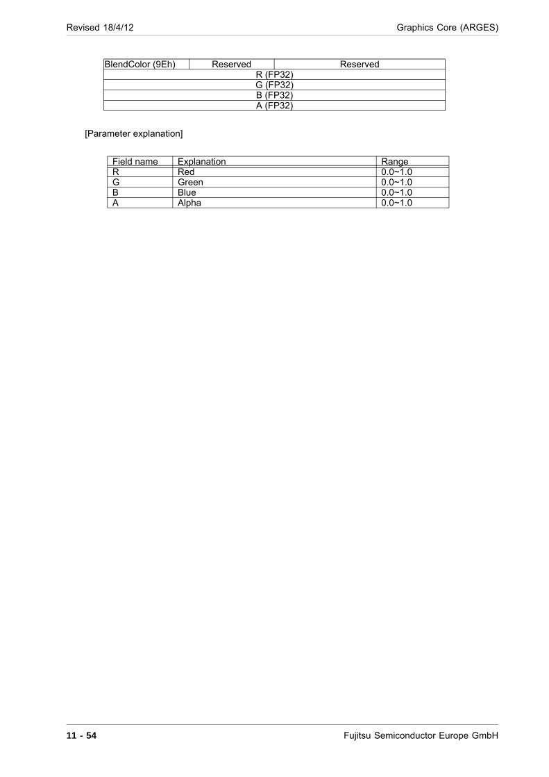
Revised 18/4/12 Graphics Core (ARGES)
[Parameter explanation]
BlendColor (9Eh) Reserved ReservedR (FP32)G (FP32)B (FP32)A (FP32)
Field name Explanation RangeR Red 0.0~1.0G Green 0.0~1.0B Blue 0.0~1.0A Alpha 0.0~1.0
11 - 54 Fujitsu Semiconductor Europe GmbH
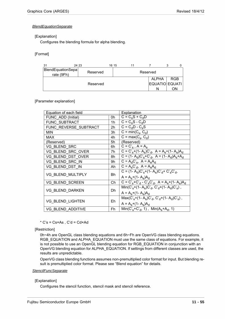
Graphics Core (ARGES) Revised 18/4/12
BlendEquationSeparate
[Explanation]
Configures the blending formula for alpha blending.
[Format]
[Parameter explanation]
* C’s = Cs×As , C’d = Cd×Ad
[Restriction]
0h~4h are OpenGL class blending equations and 6h~Fh are OpenVG class blending equations. RGB_EQUATION and ALPHA_EQUATION must use the same class of equations. For example, it is not possible to use an OpenGL blending equation for RGB_EQUATION in conjunction with an OpenVG blending equation for ALPHA_EQUATION. If settings from different classes are used, the results are unpredictable.
OpenVG class blending functions assumes non-premultiplied color format for input. But blending re-sult is premultiplied color format. Please see “Blend equation” for details.
StencilFuncSeparate
[Explanation]
Configures the stencil function, stencil mask and stencil reference.
31 24 23 16 15 11 7 3 0
BlendEquationSeparate (9Fh)
Reserved Reserved
ReservedALPHA
EQUATION
RGBEQUATI
ON
Equation of each field ExplanationFUNC_ADD (Initial) 0h C = CsS + CdD
FUNC_SUBTRACT 1h C = CsS - CdD
FUNC_REVERSE_SUBTRACT 2h C = CdD - CsS
MIN 3h C = min(Cs, Cd)
MAX 4h C = max(Cs, Cd)(Reserved) 5h (Reserved)VG_BLEND_SRC 6h C = C’s , A = As
VG_BLEND_SRC_OVER 7h C = C’s+(1- As)C’d, A = As+(1- As)Ad
VG_BLEND_DST_OVER 8h C = (1- Ad)C’s+C’d, A = (1- Ad)As+Ad
VG_BLEND_SRC_IN 9h C = AdC’s, A = AsAd
VG_BLEND_DST_IN Ah C = AsC’d, A = AsAd
VG_BLEND_MULTIPLY BhC = (1- Ad)C’s+(1- As)C’d+ C’sC’d,
A = As+(1- As)Ad
VG_BLEND_SCREEN Ch C = C’s+C’d - C’sC’d, A = As+(1- As)Ad
VG_BLEND_DARKEN DhMin(C’s+(1- As)C’d, C’d+(1- Ad)C’s) ,
A = As+(1- As)Ad
VG_BLEND_LIGHTEN EhMax(C’s+(1- As)C’d, C’d+(1- Ad)C’s) ,
A = As+(1- As)Ad
VG_BLEND_ADDITIVE Fh Min(C’s+C’d, 1) , Min(As+Ad, 1)
Fujitsu Semiconductor Europe GmbH 11 - 55
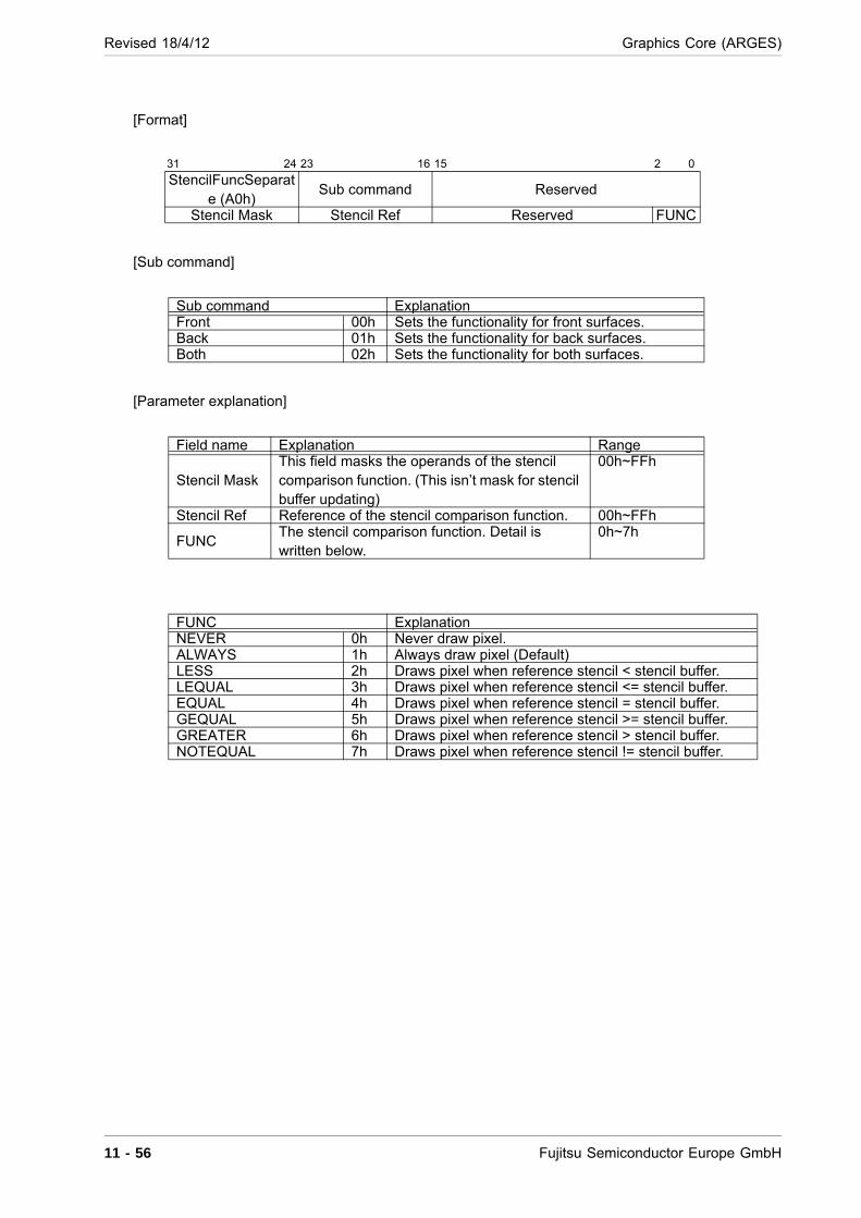
Revised 18/4/12 Graphics Core (ARGES)
[Format]
[Sub command]
[Parameter explanation]
31 24 23 16 15 2 0
StencilFuncSeparate (A0h)
Sub command Reserved
Stencil Mask Stencil Ref Reserved FUNC
Sub command ExplanationFront 00h Sets the functionality for front surfaces.Back 01h Sets the functionality for back surfaces.Both 02h Sets the functionality for both surfaces.
Field name Explanation Range
Stencil MaskThis field masks the operands of the stencil comparison function. (This isn’t mask for stencil buffer updating)
00h~FFh
Stencil Ref Reference of the stencil comparison function. 00h~FFh
FUNCThe stencil comparison function. Detail is written below.
0h~7h
FUNC ExplanationNEVER 0h Never draw pixel.ALWAYS 1h Always draw pixel (Default)LESS 2h Draws pixel when reference stencil < stencil buffer.LEQUAL 3h Draws pixel when reference stencil <= stencil buffer.EQUAL 4h Draws pixel when reference stencil = stencil buffer.GEQUAL 5h Draws pixel when reference stencil >= stencil buffer.GREATER 6h Draws pixel when reference stencil > stencil buffer.NOTEQUAL 7h Draws pixel when reference stencil != stencil buffer.
11 - 56 Fujitsu Semiconductor Europe GmbH

Graphics Core (ARGES) Revised 18/4/12
StencilOpSeparate
[Explanation]
Configures the conditions for stencil buffer updates.
[Format]
[Sub command]
[Parameter explanation]
NOTE Clamping means that in the case of FFh, an increment is ignored and in the case of 00h, a decrement is ignored
31 24 23 16 15 2 0
StencilOpSeparate (A1h)
Sub command Reserved
ReservedDP
PASSDPFAIL SFAIL
Sub command ExplanationFront 00h Sets the functionality for front surfaces.Back 01h Sets the functionality for back surfaces.Both 02h Sets the functionality for both surfaces.
Field name ExplanationSFAIL Specifies functionality when stencil test fails.DPFAIL Specifies functionality when depth test fails.DPPASS Specifies functionality when depth test passes.
Function of each field ExplanationKEEP 0h Doesn’t update stencil buffer.ZERO 1h Writes 0 to stencil buffer.REPLACE 2h Writes a reference stencil to stencil buffer.INCR 3h Increments stencil buffer with clamping.DECR 4h Decrements stencil buffer with clamping.INVERT 5h Inverts bits of stencil buffer.INCR_WRAP 6h Increments stencil buffer without clamping.DECR_WRAP 7h Decrements stencil buffer without clamping.
Fujitsu Semiconductor Europe GmbH 11 - 57
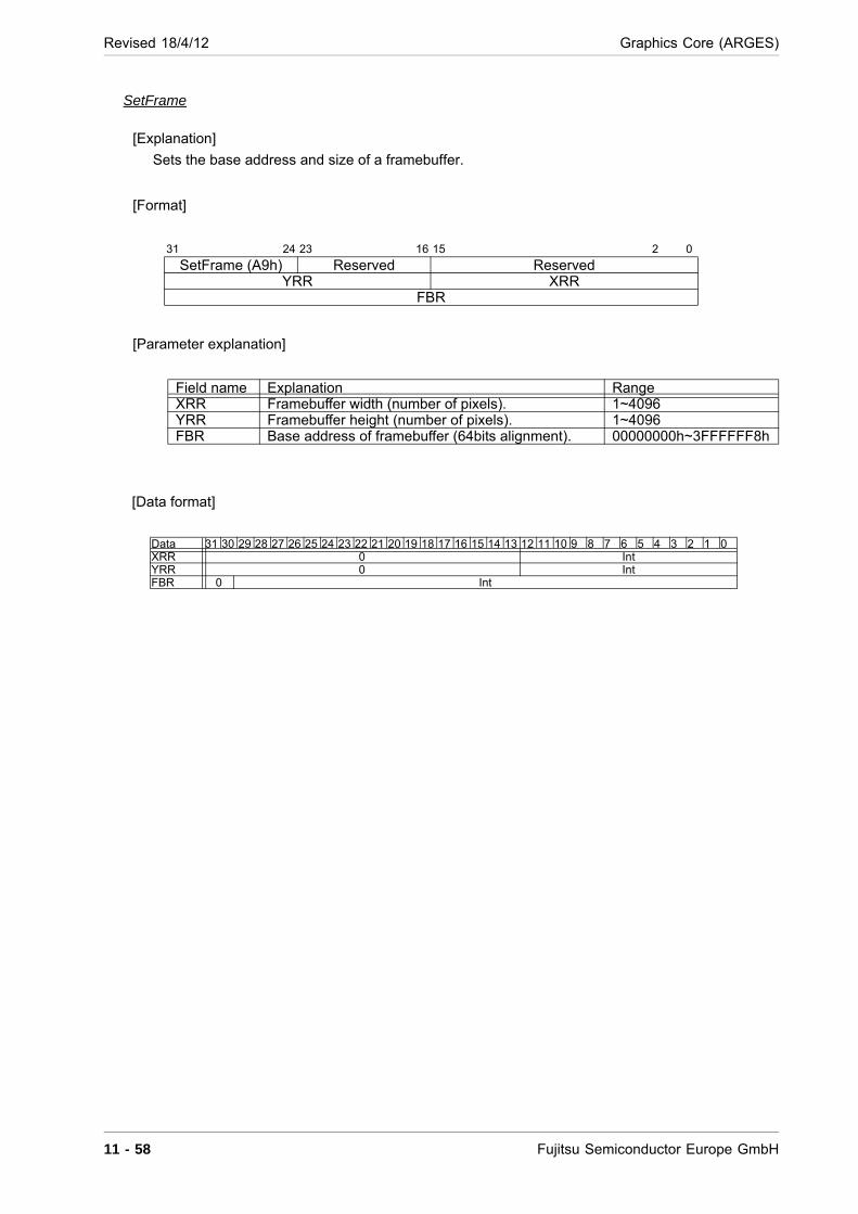
Revised 18/4/12 Graphics Core (ARGES)
SetFrame
[Explanation]
Sets the base address and size of a framebuffer.
[Format]
[Parameter explanation]
[Data format]
31 24 23 16 15 2 0
SetFrame (A9h) Reserved ReservedYRR XRR
FBR
Field name Explanation RangeXRR Framebuffer width (number of pixels). 1~4096YRR Framebuffer height (number of pixels). 1~4096FBR Base address of framebuffer (64bits alignment). 00000000h~3FFFFFF8h
Data 31 30 29 28 27 26 25 24 23 22 21 20 19 18 17 16 15 14 13 12 11 10 9 8 7 6 5 4 3 2 1 0XRR 0 IntYRR 0 IntFBR 0 Int
11 - 58 Fujitsu Semiconductor Europe GmbH

Graphics Core (ARGES) Revised 18/4/12
SetFrameBPP
[Explanation]
Sets the bits/pixel resolution of a framebuffer or a depth buffer.
[Format]
[Sub command]
[Parameter explanation]
SetZBufferAddr
[Explanation]
Sets the base address of the depth buffer.
The width and height of the Z buffer is identical to the settings of the framebuffer.
[Format]
[Parameter explanation]
[Data format]
31 24 23 16 15 1 0
SetFrameBPP(AAh) Sub command ReservedReserved BPP
Sub command ExplanationFrame 00h Setting is for a framebuffer.Depth 01h Setting is for a depth buffer.
Field name Explanation Range
BPP
Bits/pixel.00b: 32bits/pixel01b: 16bits/pixel10b: 8bits/pixel (Required for depth buffer)11b: reserved
0~2
31 24 23 16 15 2 0
SetZbufferAddr (ABh)
Reserved Reserved
ZBR
Field name Explanation RangeZBR Base address of the depth buffer (64bits aligned). 00000000h~3FFFFFF8h
Data 31 30 29 28 27 26 25 24 23 22 21 20 19 18 17 16 15 14 13 12 11 10 9 8 7 6 5 4 3 2 1 0ZBR 0 Int
Fujitsu Semiconductor Europe GmbH 11 - 59
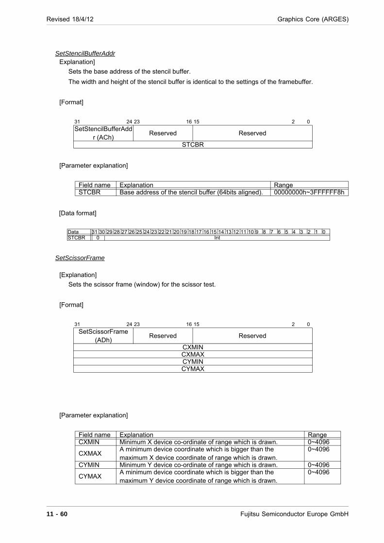
Revised 18/4/12 Graphics Core (ARGES)
SetStencilBufferAddrExplanation]
Sets the base address of the stencil buffer.
The width and height of the stencil buffer is identical to the settings of the framebuffer.
[Format]
[Parameter explanation]
[Data format]
SetScissorFrame
[Explanation]
Sets the scissor frame (window) for the scissor test.
[Format]
[Parameter explanation]
31 24 23 16 15 2 0
SetStencilBufferAddr (ACh)
Reserved Reserved
STCBR
Field name Explanation RangeSTCBR Base address of the stencil buffer (64bits aligned). 00000000h~3FFFFFF8h
Data 31 30 29 28 27 26 25 24 23 22 21 20 19 18 17 16 15 14 13 12 11 10 9 8 7 6 5 4 3 2 1 0STCBR 0 Int
31 24 23 16 15 2 0
SetScissorFrame (ADh)
Reserved Reserved
CXMINCXMAXCYMINCYMAX
Field name Explanation RangeCXMIN Minimum X device co-ordinate of range which is drawn. 0~4096
CXMAXA minimum device coordinate which is bigger than the maximum X device coordinate of range which is drawn.
0~4096
CYMIN Minimum Y device co-ordinate of range which is drawn. 0~4096
CYMAXA minimum device coordinate which is bigger than the maximum Y device coordinate of range which is drawn.
0~4096
11 - 60 Fujitsu Semiconductor Europe GmbH
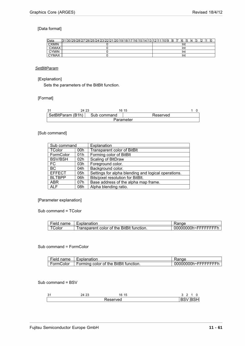
Graphics Core (ARGES) Revised 18/4/12
[Data format]
SetBltParam
[Explanation]
Sets the parameters of the BitBlt function.
[Format]
[Sub command]
[Parameter explanation]
Sub command = TColor
Sub command = FormColor
Sub command = BSV
Data 31 30 29 28 27 26 25 24 23 22 21 20 19 18 17 16 15 14 13 12 11 10 9 8 7 6 5 4 3 2 1 0 CXMIN 0 IntCXMAX 0 IntCYMIN 0 Int
CYMAX 0 Int
31 24 23 16 15 1 0
SetBltParam (B1h) Sub command ReservedParameter
Sub command ExplanationTColor 00h Transparent color of BitBltFormColor 01h Forming color of BitBltBSV/BSH 02h Scaling of BltDrawFC 03h Foreground color.BC 04h Background color.EFFECT 05h Settings for alpha blending and logical operations.BLTBPP 06h Bits/pixel resolution for BitBlt.ABR 07h Base address of the alpha map frame.ALF 08h Alpha blending ratio.
Field name Explanation RangeTColor Transparent color of the BitBlt function. 00000000h~FFFFFFFFh
Field name Explanation RangeFormColor Forming color of the BitBlt function. 00000000h~FFFFFFFFh
31 24 23 16 15 3 2 1 0
Reserved BSV BSH
Fujitsu Semiconductor Europe GmbH 11 - 61
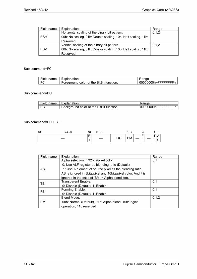
Revised 18/4/12 Graphics Core (ARGES)
Sub command=FC
Sub command=BC
Sub command=EFFECT
Field name Explanation Range
BSHHorizontal scaling of the binary bit pattern.00b: No scaling, 01b: Double scaling, 10b: Half scaling, 11b: Reserved
0,1,2
BSVVertical scaling of the binary bit pattern.00b: No scaling, 01b: Double scaling, 10b: Half scaling, 11b: Reserved
0,1,2
Field name Explanation RangeFC Foreground color of the BitBlt function. 00000000h~FFFFFFFFh
Field name Explanation RangeBC Background color of the BitBlt function. 00000000h~FFFFFFFFh
31 24 23 18 16 15 8 7 4 1 0
BT
LOG BM FE
TE
AS
Field name Explanation Range
AS
Alpha selection in 32bits/pixel color. 0: Use ALF register as blending ratio (Default), 1: Use A element of source pixel as the blending ratio.
AS is ignored in 8bits/pixel and 16bits/pixel color. And it is ignored in the case of 'BM != Alpha blend' too.
0,1
TETransparent Enable. 0: Disable (Default), 1: Enable
0,1
FEForming Enable. 0: Disable (Default), 1: Enable
0,1
BMBlend Mode. 00b: Normal (Default), 01b: Alpha blend, 10b: logical operation, 11b reserved
0,1,2
11 - 62 Fujitsu Semiconductor Europe GmbH
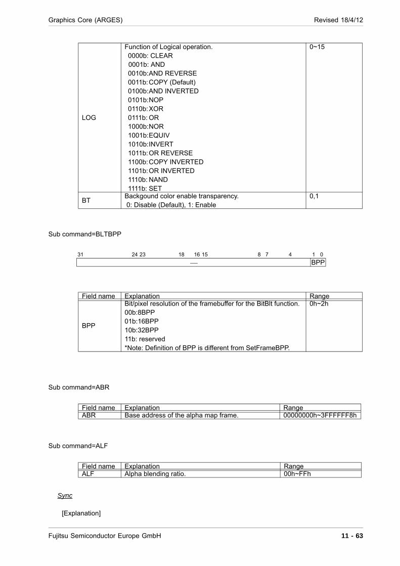
Graphics Core (ARGES) Revised 18/4/12
Sub command=BLTBPP
Sub command=ABR
Sub command=ALF
Sync
[Explanation]
LOG
Function of Logical operation.0000b: CLEAR
0001b: AND0010b:AND REVERSE0011b:COPY (Default)0100b:AND INVERTED0101b:NOP0110b:XOR0111b: OR1000b:NOR1001b:EQUIV1010b:INVERT1011b:OR REVERSE1100b:COPY INVERTED1101b:OR INVERTED1110b: NAND1111b: SET
0~15
BTBackgound color enable transparency. 0: Disable (Default), 1: Enable
0,1
31 24 23 18 16 15 8 7 4 1 0
BPP
Field name Explanation Range
BPP
Bit/pixel resolution of the framebuffer for the BitBlt function.00b:8BPP01b:16BPP10b:32BPP11b: reserved*Note: Definition of BPP is different from SetFrameBPP.
0h~2h
Field name Explanation RangeABR Base address of the alpha map frame. 00000000h~3FFFFFF8h
Field name Explanation RangeALF Alpha blending ratio. 00h~FFh
Fujitsu Semiconductor Europe GmbH 11 - 63
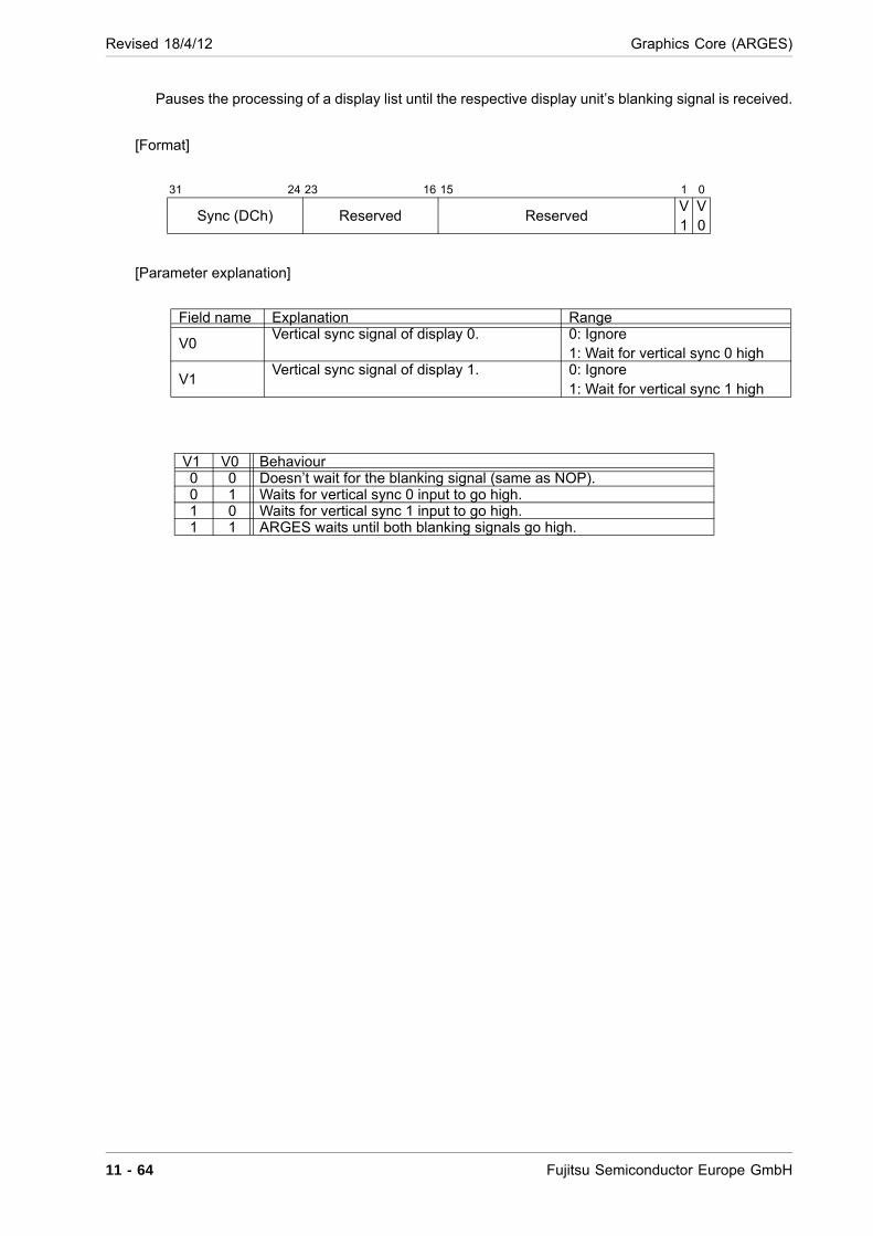
Revised 18/4/12 Graphics Core (ARGES)
Pauses the processing of a display list until the respective display unit’s blanking signal is received.
[Format]
[Parameter explanation]
31 24 23 16 15 1 0
Sync (DCh) Reserved ReservedV1
V0
Field name Explanation Range
V0Vertical sync signal of display 0. 0: Ignore
1: Wait for vertical sync 0 high
V1Vertical sync signal of display 1. 0: Ignore
1: Wait for vertical sync 1 high
V1 V0 Behaviour0 0 Doesn’t wait for the blanking signal (same as NOP).0 1 Waits for vertical sync 0 input to go high.1 0 Waits for vertical sync 1 input to go high.1 1 ARGES waits until both blanking signals go high.
11 - 64 Fujitsu Semiconductor Europe GmbH
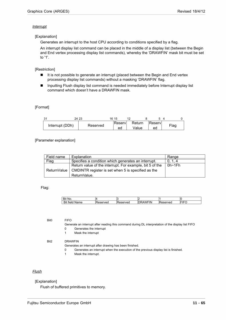
Graphics Core (ARGES) Revised 18/4/12
Interrupt
[Explanation]
Generates an interrupt to the host CPU according to conditions specified by a flag.
An interrupt display list command can be placed in the middle of a display list (between the Begin and End vertex processing display list commands), whereby the ‘DRAWFIN’ mask bit must be set to '1'.
[Restriction]
It is not possible to generate an interrupt (placed between the Begin and End vertex processing display list commands) without a masking ‘DRAWFIN’ flag.
Inputting Flush display list command is needed immediately before Interrupt display list command which doesn’t have a DRAWFIN mask.
[Format]
[Parameter explanation]
Flag:
Flush
[Explanation]
Flush of buffered primitives to memory.
31 24 23 16 15 12 8 5 4 0
Interrupt (DDh) ReservedReserv
edReturnValue
Reserved
Flag
Field name Explanation RangeFlag Specifies a condition which generates an interrupt. 0, 1, 4
ReturnValueReturn value of the interrupt. For example, bit 5 of the CMDINTR register is set when 5 is specified as the ReturnValue.
0h~1Fh
Bit No. 4 3 2 1 0Bit field Name Reserved Reserved DRAWFIN Reserved FIFO
Bit0 FIFOGenerate an interrupt after reading this command during DL interpretation of the display list FIFO
0 Generates the interrupt
1 Mask the interrupt
Bit2 DRAWFINGenerates an interrupt after drawing has been finished.
0 Generates an interrupt when the execution of the previous display list is finished.
1 Mask the interrupt.
Fujitsu Semiconductor Europe GmbH 11 - 65
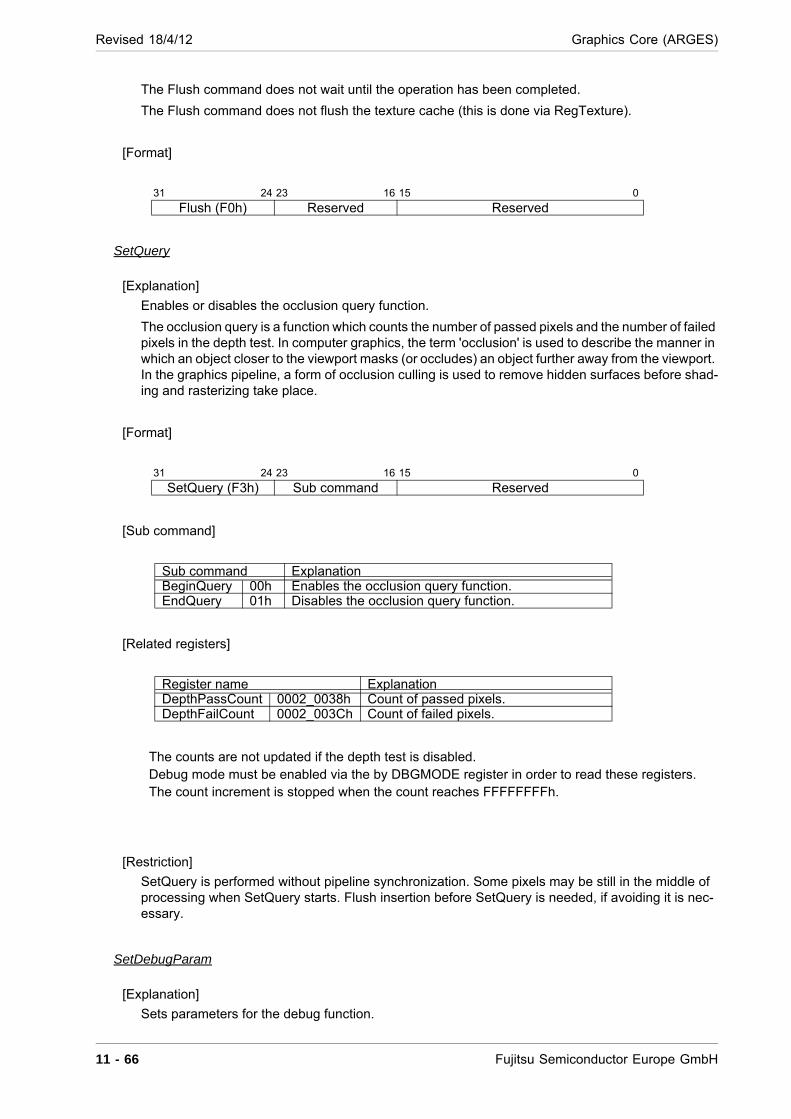
Revised 18/4/12 Graphics Core (ARGES)
The Flush command does not wait until the operation has been completed.
The Flush command does not flush the texture cache (this is done via RegTexture).
[Format]
SetQuery
[Explanation]
Enables or disables the occlusion query function.
The occlusion query is a function which counts the number of passed pixels and the number of failed pixels in the depth test. In computer graphics, the term 'occlusion' is used to describe the manner in which an object closer to the viewport masks (or occludes) an object further away from the viewport. In the graphics pipeline, a form of occlusion culling is used to remove hidden surfaces before shad-ing and rasterizing take place.
[Format]
[Sub command]
[Related registers]
The counts are not updated if the depth test is disabled.Debug mode must be enabled via the by DBGMODE register in order to read these registers.The count increment is stopped when the count reaches FFFFFFFFh.
[Restriction]
SetQuery is performed without pipeline synchronization. Some pixels may be still in the middle of processing when SetQuery starts. Flush insertion before SetQuery is needed, if avoiding it is nec-essary.
SetDebugParam
[Explanation]
Sets parameters for the debug function.
31 24 23 16 15 0
Flush (F0h) Reserved Reserved
31 24 23 16 15 0
SetQuery (F3h) Sub command Reserved
Sub command ExplanationBeginQuery 00h Enables the occlusion query function.EndQuery 01h Disables the occlusion query function.
Register name ExplanationDepthPassCount 0002_0038h Count of passed pixels.DepthFailCount 0002_003Ch Count of failed pixels.
11 - 66 Fujitsu Semiconductor Europe GmbH

Graphics Core (ARGES) Revised 18/4/12
[Format]
[Sub command]
31 24 23 16 15 0
SetDebugParam (F4h)
Sub command Reserved
Param
Sub command ExplanationDL_COUNT 00h Counter for display list
Fujitsu Semiconductor Europe GmbH 11 - 67

Revised 18/4/12 Graphics Core (ARGES)
11.7 Processing Flow
Figure 11-3: Processing flow
11.7.1 Processing Algorithm
Please refer to the functional specification of the different modules.
11 - 68 Fujitsu Semiconductor Europe GmbH

Graphics Core (ARGES) Revised 18/4/12
11.8 Control Flow (Usage)
11.8.1 Hardware Initialization Procedure
11.8.1.1 Hardware reset
A reset is performed when the ARESETn signal is low for 8 or more clock cycles. The condition of all output pins is 'undefined' until a reset has been performed.
11.8.1.2 Software reset
To reset the ARGES core only after startup, write to the SRESET register. This makes it possible to issue a reset to a module other than the slave AXI control circuit within ARGES. Before performing a reset, be sure to input ACLK.
11.8.1.3 Register access
ARGES is controlled by register access from the slave AXI interface. DDLFIFO, which is used for display list input is written like a normal register access.
Accesses to DDLFIFO and another registers must have a corresponding endian setting. The END-CHG register is used to set the corresponding endian type for the accesses.
Figure 11-4: Types of endian Setting
Table 11-2: Endian conversion examples
11.8.2 Display list input
All instructions to the GDC core are contained in a display list which is input to DDLFIFO. The DDL-FIFO has a depth of 128 32-bit words for receiving and holding the display list.
Input Endian mode Result of conversionAddress=0000_0300hData=0123_4567_89AB_CDEFh
Little endian 0300h: 89AB_CDEFh0304h: 0123_4567h
Big endian 0300h: 0123_4567h0304h: 89AB_CDEFh
8bits little endian 0300h: EFCD_AB89h0304h: 6745_2301h
63 31 0
address = xxx0h[31:0]
address = xxx4h[31:0]
63 31 0
address = xxx0h[31:0]
address = xxx4h[31:0]
63 31 0
xxx0h[31:24]
xxx0h[23:16]
xxx0h[15:8]
xxx0h[7:0]
xxx4h[31:24]
xxx4h[23:16]
xxx4h[15:8]
xxx4h[7:0]
Big endian
Little endian
8bits little endian
Fujitsu Semiconductor Europe GmbH 11 - 69
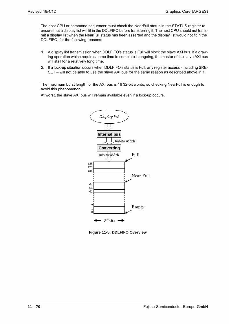
Revised 18/4/12 Graphics Core (ARGES)
The host CPU or command sequencer must check the NearFull status in the STATUS register to ensure that a display list will fit in the DDLFIFO before transferring it. The host CPU should not trans-mit a display list when the NearFull status has been asserted and the display list would not fit in the DDLFIFO, for the following reasons:
1. A display list transmission when DDLFIFO's status is Full will block the slave AXI bus. If a draw-ing operation which requires some time to complete is ongoing, the master of the slave AXI bus will stall for a relatively long time.
2. If a lock-up situation occurs when DDLFIFO's status is Full, any register access - including SRE-SET – will not be able to use the slave AXI bus for the same reason as described above in 1.
The maximum burst length for the AXI bus is 16 32-bit words, so checking NearFull is enough to avoid this phenomenon.
At worst, the slave AXI bus will remain available even if a lock-up occurs.
Figure 11-5: DDLFIFO Overview
126
Empty
Near Full
Full
Internal bus
127128
626364
012
32bits
Display list
Converting
64bits width
32bits width
11 - 70 Fujitsu Semiconductor Europe GmbH
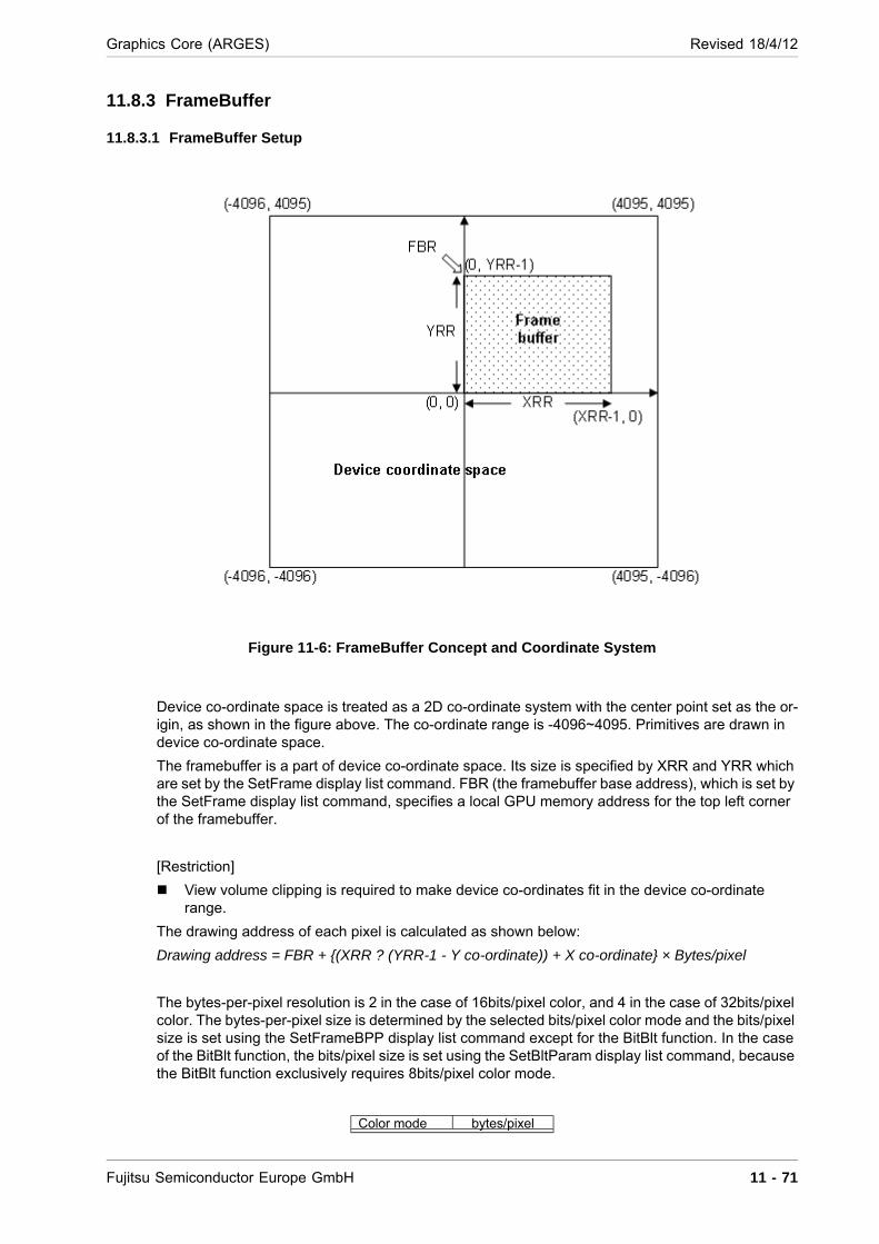
Graphics Core (ARGES) Revised 18/4/12
11.8.3 FrameBuffer
11.8.3.1 FrameBuffer Setup
Figure 11-6: FrameBuffer Concept and Coordinate System
Device co-ordinate space is treated as a 2D co-ordinate system with the center point set as the or-igin, as shown in the figure above. The co-ordinate range is -4096~4095. Primitives are drawn in device co-ordinate space.
The framebuffer is a part of device co-ordinate space. Its size is specified by XRR and YRR which are set by the SetFrame display list command. FBR (the framebuffer base address), which is set by the SetFrame display list command, specifies a local GPU memory address for the top left corner of the framebuffer.
[Restriction]
View volume clipping is required to make device co-ordinates fit in the device co-ordinate range.
The drawing address of each pixel is calculated as shown below:
Drawing address = FBR + (XRR ? (YRR-1 - Y co-ordinate)) + X co-ordinate × Bytes/pixel
The bytes-per-pixel resolution is 2 in the case of 16bits/pixel color, and 4 in the case of 32bits/pixel color. The bytes-per-pixel size is determined by the selected bits/pixel color mode and the bits/pixel size is set using the SetFrameBPP display list command except for the BitBlt function. In the case of the BitBlt function, the bits/pixel size is set using the SetBltParam display list command, because the BitBlt function exclusively requires 8bits/pixel color mode.
Color mode bytes/pixel
Fujitsu Semiconductor Europe GmbH 11 - 71
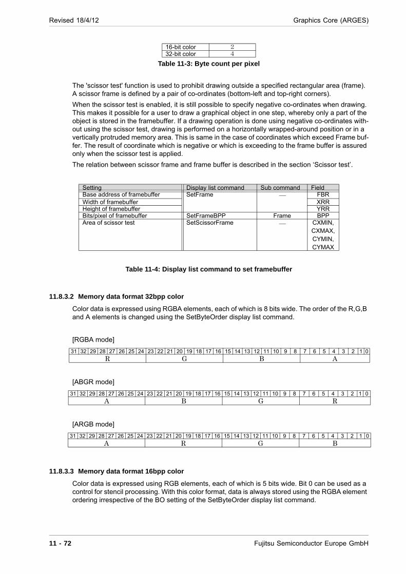
Revised 18/4/12 Graphics Core (ARGES)
Table 11-3: Byte count per pixel
The 'scissor test' function is used to prohibit drawing outside a specified rectangular area (frame). A scissor frame is defined by a pair of co-ordinates (bottom-left and top-right corners).
When the scissor test is enabled, it is still possible to specify negative co-ordinates when drawing. This makes it possible for a user to draw a graphical object in one step, whereby only a part of the object is stored in the framebuffer. If a drawing operation is done using negative co-ordinates with-out using the scissor test, drawing is performed on a horizontally wrapped-around position or in a vertically protruded memory area. This is same in the case of coordinates which exceed Frame buf-fer. The result of coordinate which is negative or which is exceeding to the frame buffer is assured only when the scissor test is applied.
The relation between scissor frame and frame buffer is described in the section ‘Scissor test’.
Table 11-4: Display list command to set framebuffer
11.8.3.2 Memory data format 32bpp color
Color data is expressed using RGBA elements, each of which is 8 bits wide. The order of the R,G,B and A elements is changed using the SetByteOrder display list command.
[RGBA mode]
[ABGR mode]
[ARGB mode]
11.8.3.3 Memory data format 16bpp color
Color data is expressed using RGB elements, each of which is 5 bits wide. Bit 0 can be used as a control for stencil processing. With this color format, data is always stored using the RGBA element ordering irrespective of the BO setting of the SetByteOrder display list command.
16-bit color 232-bit color 4
Setting Display list command Sub command FieldBase address of framebuffer SetFrame FBRWidth of framebuffer XRRHeight of framebuffer YRRBits/pixel of framebuffer SetFrameBPP Frame BPPArea of scissor test SetScissorFrame CXMIN,
CXMAX, CYMIN, CYMAX
31 32 29 28 27 26 25 24 23 22 21 20 19 18 17 16 15 14 13 12 11 10 9 8 7 6 5 4 3 2 1 0
R G B A
31 32 29 28 27 26 25 24 23 22 21 20 19 18 17 16 15 14 13 12 11 10 9 8 7 6 5 4 3 2 1 0
A B G R
31 32 29 28 27 26 25 24 23 22 21 20 19 18 17 16 15 14 13 12 11 10 9 8 7 6 5 4 3 2 1 0
A R G B
11 - 72 Fujitsu Semiconductor Europe GmbH
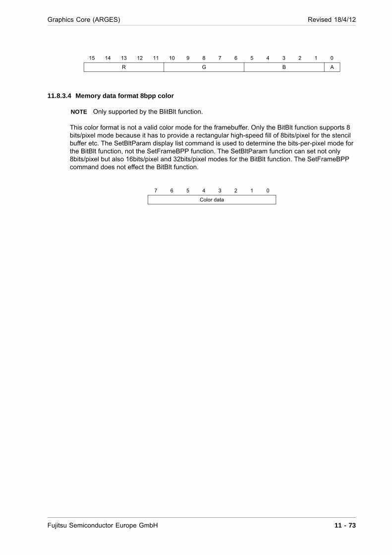
Graphics Core (ARGES) Revised 18/4/12
11.8.3.4 Memory data format 8bpp color
NOTE Only supported by the BlitBlt function.
This color format is not a valid color mode for the framebuffer. Only the BitBlt function supports 8 bits/pixel mode because it has to provide a rectangular high-speed fill of 8bits/pixel for the stencil buffer etc. The SetBltParam display list command is used to determine the bits-per-pixel mode for the BitBlt function, not the SetFrameBPP function. The SetBltParam function can set not only 8bits/pixel but also 16bits/pixel and 32bits/pixel modes for the BitBlt function. The SetFrameBPP command does not effect the BitBlt function.
15 14 13 12 11 10 9 8 7 6 5 4 3 2 1 0
R G B A
7 6 5 4 3 2 1 0
Color data
Fujitsu Semiconductor Europe GmbH 11 - 73
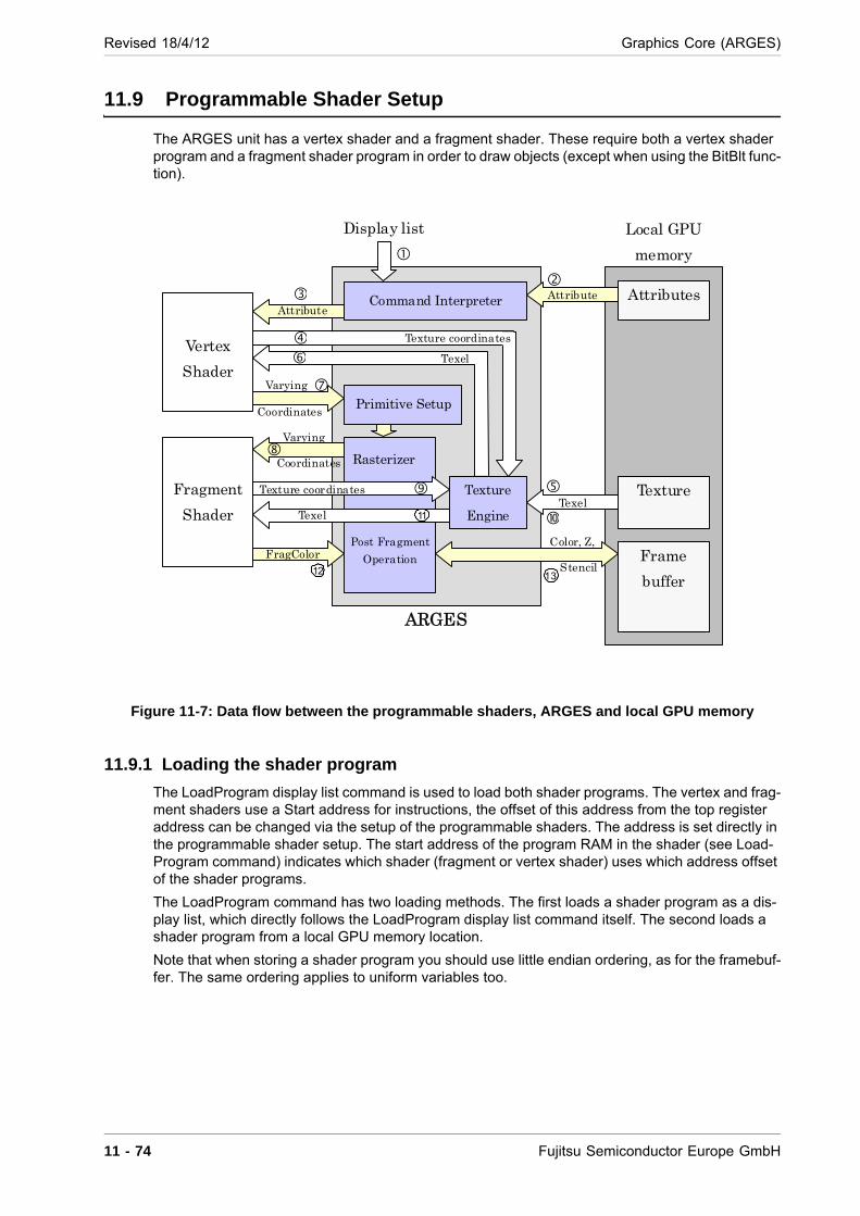
Revised 18/4/12 Graphics Core (ARGES)
11.9 Programmable Shader Setup
The ARGES unit has a vertex shader and a fragment shader. These require both a vertex shader program and a fragment shader program in order to draw objects (except when using the BitBlt func-tion).
Figure 11-7: Data flow between the programmable shaders, ARGES and local GPU memory
11.9.1 Loading the shader program
The LoadProgram display list command is used to load both shader programs. The vertex and frag-ment shaders use a Start address for instructions, the offset of this address from the top register address can be changed via the setup of the programmable shaders. The address is set directly in the programmable shader setup. The start address of the program RAM in the shader (see Load-Program command) indicates which shader (fragment or vertex shader) uses which address offset of the shader programs.
The LoadProgram command has two loading methods. The first loads a shader program as a dis-play list, which directly follows the LoadProgram display list command itself. The second loads a shader program from a local GPU memory location.
Note that when storing a shader program you should use little endian ordering, as for the framebuf-fer. The same ordering applies to uniform variables too.
Fragment
Shader
ARGES
Attributes
Local GPU
memory
Display list
Frame
buffer
Attribute
Varying
Coordinates
Varying
Coordinates
Texel
FragColor
Attribute
Texture Texture coordinatesTexel
Rasterizer
Command Interpreter
Post Fragment
Operation
Color, Z,
Stencil
Vertex
Shader
Texture
Engine
Texture coordinates
Texel
Primitive Setup
12 13
11
11 - 74 Fujitsu Semiconductor Europe GmbH

Graphics Core (ARGES) Revised 18/4/12
Figure 11-8: Storing rule for shader programs / uniform variables
11.9.2 Loading uniform variables (uniforms)
The shader program has general static variables which are called 'uniforms'. These are set up using the LoadUniform display list command.
11.9.3 Setting the precision of attributes and varying variables (varyings)
The input to the vertex shader is an attribute and the input to the fragment shader is a 'varying'. The number of attributes and varyings is set using the SetShaderInfo display list command.
The programmable shader uses two types of precision for both attributes and varyings, namely FP16 (floating point, 16 bits) and FP32. These precisions are also set using the SetShaderInfo dis-play list command.
One attribute precision setting is applied to 4 consecutive attributes. The four attributes whose pre-cision is controlled by this setting must therefore by intention share the same precision. The same applies to varying variables.
0000H
0008H
Word 1 Word 0
Word 3 Word 2
Bit 0
Bit 63
Bit 32
Bit 31
Attribute 0
Attribute 1
Attribute 2
Attribute 3
Attribute 2
Attribute 4
Attribute 5
Attribute 6
Attribute 7
:
Attribute 60
Attribute 61
Attribute 2
Attribute 63
Attribute 62
AP00
AP01
AP15
Varying 0
Varying 1
Attribute 2
Varying 3
Varying 2
Varying 4
Varying 5
Varying 6
Varying 7
:
Varying 28
Varying 29
Attribute 2
Varying 31
Varying 30
VP00
VP01
VP07
Fujitsu Semiconductor Europe GmbH 11 - 75
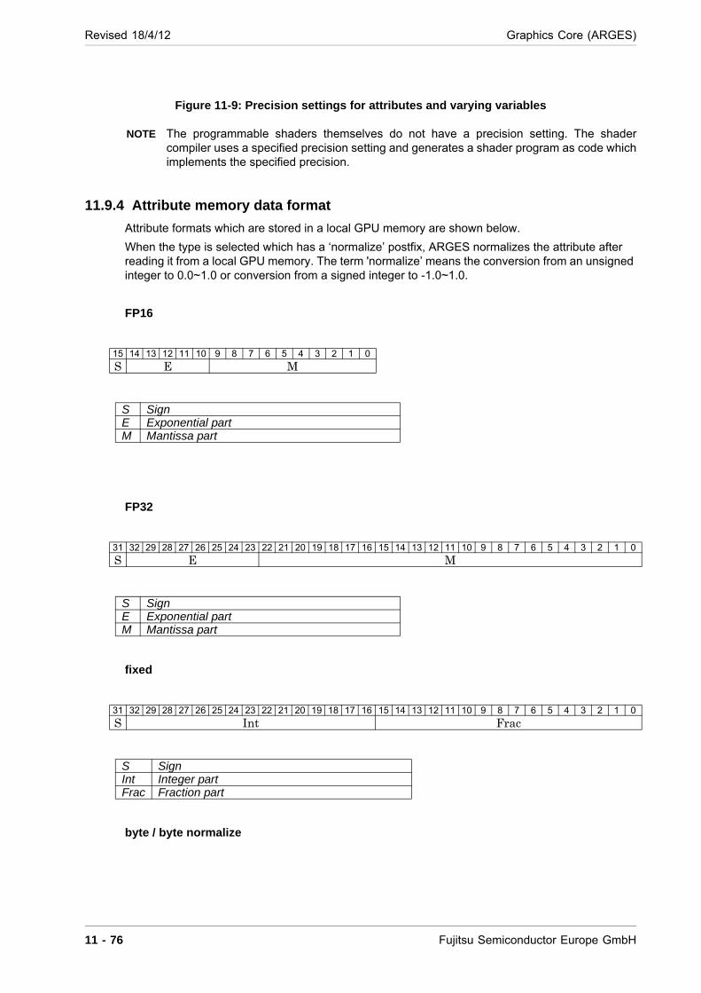
Revised 18/4/12 Graphics Core (ARGES)
Figure 11-9: Precision settings for attributes and varying variables
NOTE The programmable shaders themselves do not have a precision setting. The shader compiler uses a specified precision setting and generates a shader program as code which implements the specified precision.
11.9.4 Attribute memory data format
Attribute formats which are stored in a local GPU memory are shown below.
When the type is selected which has a ‘normalize’ postfix, ARGES normalizes the attribute after reading it from a local GPU memory. The term 'normalize’ means the conversion from an unsigned integer to 0.0~1.0 or conversion from a signed integer to -1.0~1.0.
FP16
FP32
fixed
byte / byte normalize
15 14 13 12 11 10 9 8 7 6 5 4 3 2 1 0
S E M
S SignE Exponential partM Mantissa part
31 32 29 28 27 26 25 24 23 22 21 20 19 18 17 16 15 14 13 12 11 10 9 8 7 6 5 4 3 2 1 0
S E M
S SignE Exponential partM Mantissa part
31 32 29 28 27 26 25 24 23 22 21 20 19 18 17 16 15 14 13 12 11 10 9 8 7 6 5 4 3 2 1 0
S Int Frac
S SignInt Integer partFrac Fraction part
11 - 76 Fujitsu Semiconductor Europe GmbH
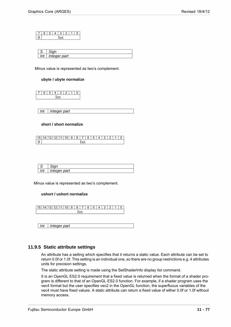
Graphics Core (ARGES) Revised 18/4/12
Minus value is represented as two’s complement.
ubyte / ubyte normalize
short / short normalize
Minus value is represented as two’s complement.
ushort / ushort normalize
11.9.5 Static attribute settings
An attribute has a setting which specifies that it returns a static value. Each attribute can be set to return 0.0f or 1.0f. This setting is an individual one, so there are no group restrictions e.g. 4 attributes units for precision settings.
The static attribute setting is made using the SetShaderInfo display list command.
It is an OpenGL ES2.0 requirement that a fixed value is returned when the format of a shader pro-gram is different to that of an OpenGL ES2.0 function. For example, if a shader program uses the vec4 format but the user specifies vec2 in the OpenGL function, the superfluous variables of the vec4 must have fixed values. A static attribute can return a fixed value of either 0.0f or 1.0f without memory access.
7 6 5 4 3 2 1 0
S Int
S SignInt Integer part
7 6 5 4 3 2 1 0
Int
Int Integer part
15 14 13 12 11 10 9 8 7 6 5 4 3 2 1 0
S Int
S SignInt Integer part
15 14 13 12 11 10 9 8 7 6 5 4 3 2 1 0
Int
Int Integer part
Fujitsu Semiconductor Europe GmbH 11 - 77

Revised 18/4/12 Graphics Core (ARGES)
Table 11-5: Display list command to set attribute and varying variables
Setting Display list command Sub command FieldNumber of attributes SetShaderInfo AttrInf0 ATTRNUMPrecision of attribute AP00~15Static attribute AttrInf1~4 DSW00~63Number of varyings Varying VARNUMPrecision of varying VP00~07
11 - 78 Fujitsu Semiconductor Europe GmbH
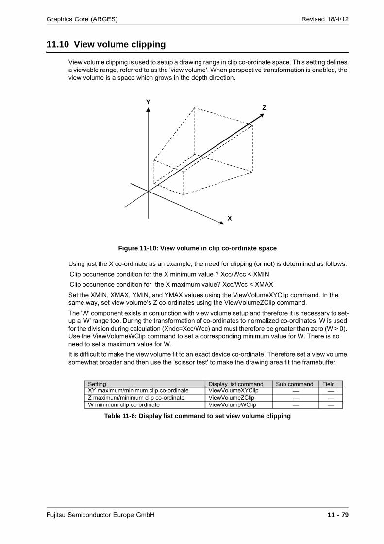
Graphics Core (ARGES) Revised 18/4/12
11.10 View volume clipping
View volume clipping is used to setup a drawing range in clip co-ordinate space. This setting defines a viewable range, referred to as the 'view volume'. When perspective transformation is enabled, the view volume is a space which grows in the depth direction.
Figure 11-10: View volume in clip co-ordinate space
Using just the X co-ordinate as an example, the need for clipping (or not) is determined as follows:
Clip occurrence condition for the X minimum value ? Xcc/Wcc < XMIN
Clip occurrence condition for the X maximum value? Xcc/Wcc < XMAX
Set the XMIN, XMAX, YMIN, and YMAX values using the ViewVolumeXYClip command. In the same way, set view volume's Z co-ordinates using the ViewVolumeZClip command.
The 'W' component exists in conjunction with view volume setup and therefore it is necessary to set-up a 'W' range too. During the transformation of co-ordinates to normalized co-ordinates, W is used for the division during calculation (Xndc=Xcc/Wcc) and must therefore be greater than zero (W > 0). Use the ViewVolumeWClip command to set a corresponding minimum value for W. There is no need to set a maximum value for W.
It is difficult to make the view volume fit to an exact device co-ordinate. Therefore set a view volume somewhat broader and then use the 'scissor test' to make the drawing area fit the framebuffer.
Table 11-6: Display list command to set view volume clipping
Setting Display list command Sub command FieldXY maximum/minimum clip co-ordinate ViewVolumeXYClip Z maximum/minimum clip co-ordinate ViewVolumeZClip W minimum clip co-ordinate ViewVolumeWClip
Z
Y
X
Fujitsu Semiconductor Europe GmbH 11 - 79
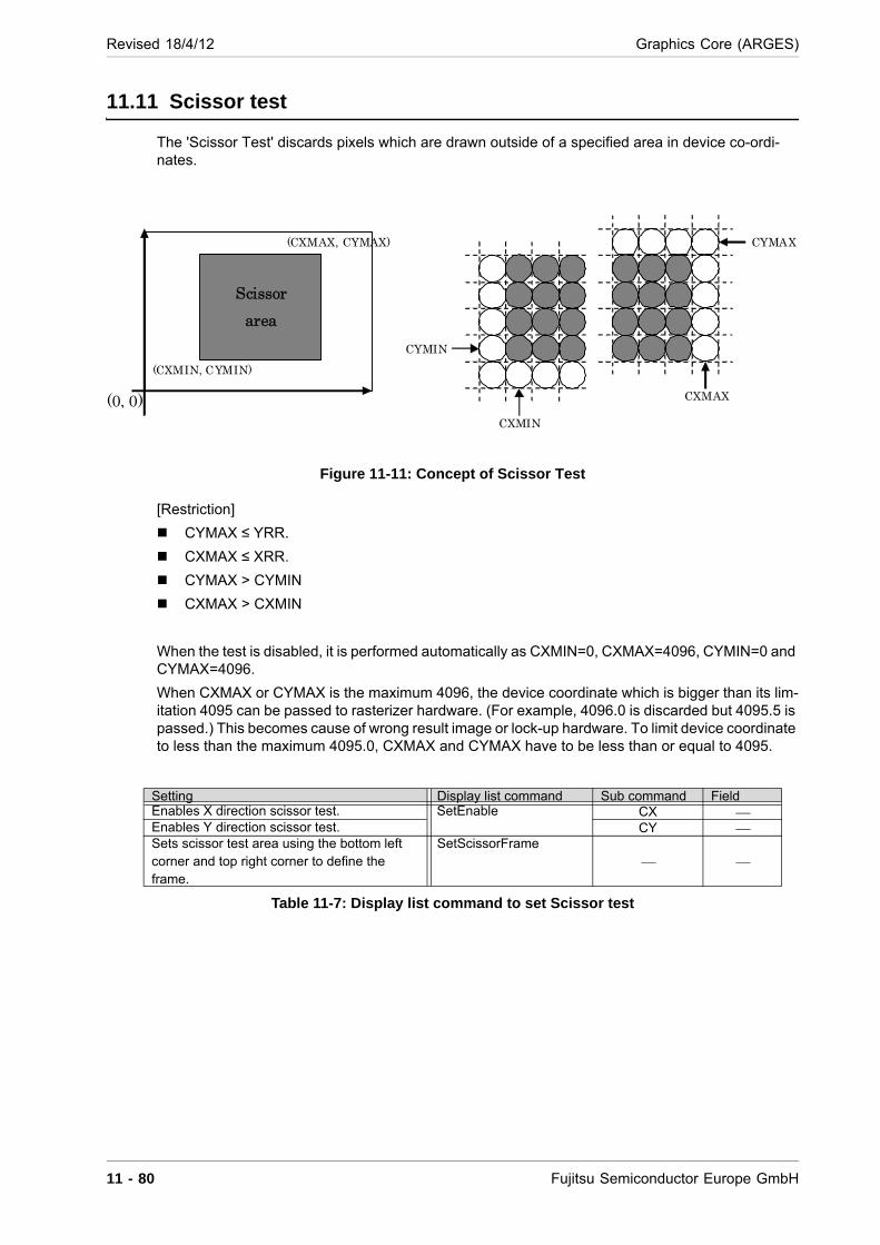
Revised 18/4/12 Graphics Core (ARGES)
11.11 Scissor test
The 'Scissor Test' discards pixels which are drawn outside of a specified area in device co-ordi-nates.
Figure 11-11: Concept of Scissor Test
[Restriction]
CYMAX ≤ YRR.
CXMAX ≤ XRR.
CYMAX > CYMIN
CXMAX > CXMIN
When the test is disabled, it is performed automatically as CXMIN=0, CXMAX=4096, CYMIN=0 and CYMAX=4096.
When CXMAX or CYMAX is the maximum 4096, the device coordinate which is bigger than its lim-itation 4095 can be passed to rasterizer hardware. (For example, 4096.0 is discarded but 4095.5 is passed.) This becomes cause of wrong result image or lock-up hardware. To limit device coordinate to less than the maximum 4095.0, CXMAX and CYMAX have to be less than or equal to 4095.
Table 11-7: Display list command to set Scissor test
Setting Display list command Sub command FieldEnables X direction scissor test. SetEnable CX Enables Y direction scissor test. CY Sets scissor test area using the bottom left corner and top right corner to define the frame.
SetScissorFrame
(CXMAX, CYMAX)
(0, 0)
Scissor
area
(CXMIN, CYMIN)
CXMIN
CYMIN
CXMAX
CYMAX
11 - 80 Fujitsu Semiconductor Europe GmbH
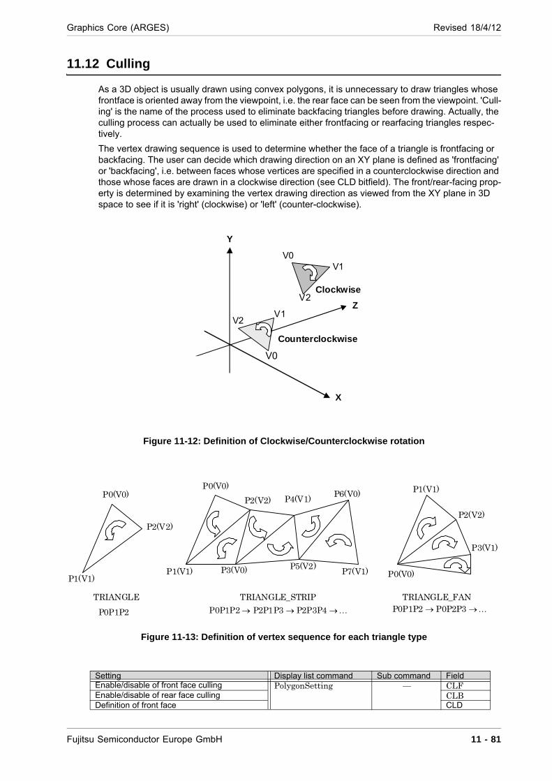
Graphics Core (ARGES) Revised 18/4/12
11.12 Culling
As a 3D object is usually drawn using convex polygons, it is unnecessary to draw triangles whose frontface is oriented away from the viewpoint, i.e. the rear face can be seen from the viewpoint. 'Cull-ing' is the name of the process used to eliminate backfacing triangles before drawing. Actually, the culling process can actually be used to eliminate either frontfacing or rearfacing triangles respec-tively.
The vertex drawing sequence is used to determine whether the face of a triangle is frontfacing or backfacing. The user can decide which drawing direction on an XY plane is defined as 'frontfacing' or 'backfacing', i.e. between faces whose vertices are specified in a counterclockwise direction and those whose faces are drawn in a clockwise direction (see CLD bitfield). The front/rear-facing prop-erty is determined by examining the vertex drawing direction as viewed from the XY plane in 3D space to see if it is 'right' (clockwise) or 'left' (counter-clockwise).
Figure 11-12: Definition of Clockwise/Counterclockwise rotation
Figure 11-13: Definition of vertex sequence for each triangle type
Setting Display list command Sub command FieldEnable/disable of front face culling PolygonSetting CLFEnable/disable of rear face culling CLBDefinition of front face CLD
Z
Y
X
V0V1
V2
V0
V1V2
Clockwise
Counterclockwise
P0(V0)
P1(V1)
P2(V2)
P0(V0)
P1(V1)
P2(V2)
P3(V0)
P4(V1)
P5(V2)
P6(V0)
P7(V1) P0(V0)
P1(V1)
P2(V2)
P3(V1)
TRIANGLE TRIANGLE_STRIP
P0P1P2 P0P1P2 P2P1P3 P2P3P4 P0P1P2 P0P2P3 TRIANGLE_FAN
Fujitsu Semiconductor Europe GmbH 11 - 81

Revised 18/4/12 Graphics Core (ARGES)
11 - 82 Fujitsu Semiconductor Europe GmbH

Graphics Core (ARGES) Revised 18/4/12
11.13 Viewport transformation
The transformation process used to change NDC values (Normalized Device Co-ordinates) into co-ordinates that fit in the framebuffer is referred to as a 'view port transformation'. After the trans-formation, the resulting co-ordinate values are termed 'Device Co-ordinates (DC)'.
Table 11-8: Display list command to set view port transformation
Xdc X_Scaling*Xndc + X_OffsetYdc Y_Scaling*Yndc + Y_OffsetZdc Z_Scaling*Zndc + Z_Offset
Setting Display list command Sub command FieldViewport transformation of XY Viewport Float/Fixed Viewport transformation of Z DepthRange Float/Fixed
Fujitsu Semiconductor Europe GmbH 11 - 83
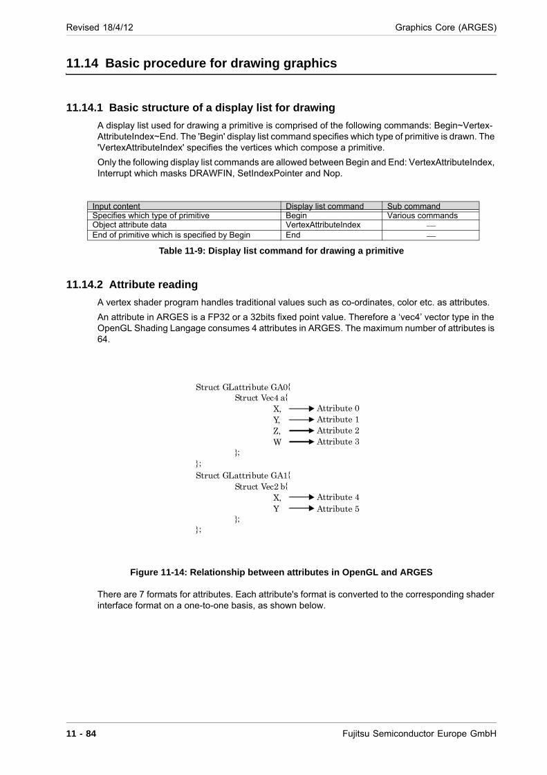
Revised 18/4/12 Graphics Core (ARGES)
11.14 Basic procedure for drawing graphics
11.14.1 Basic structure of a display list for drawing
A display list used for drawing a primitive is comprised of the following commands: Begin~Vertex-AttributeIndex~End. The 'Begin' display list command specifies which type of primitive is drawn. The 'VertexAttributeIndex' specifies the vertices which compose a primitive.
Only the following display list commands are allowed between Begin and End: VertexAttributeIndex, Interrupt which masks DRAWFIN, SetIndexPointer and Nop.
Table 11-9: Display list command for drawing a primitive
11.14.2 Attribute reading
A vertex shader program handles traditional values such as co-ordinates, color etc. as attributes.
An attribute in ARGES is a FP32 or a 32bits fixed point value. Therefore a ‘vec4’ vector type in the OpenGL Shading Langage consumes 4 attributes in ARGES. The maximum number of attributes is 64.
Figure 11-14: Relationship between attributes in OpenGL and ARGES
There are 7 formats for attributes. Each attribute's format is converted to the corresponding shader interface format on a one-to-one basis, as shown below.
Input content Display list command Sub commandSpecifies which type of primitive Begin Various commandsObject attribute data VertexAttributeIndex End of primitive which is specified by Begin End
Struct GLattribute GA0 Struct Vec4 a X, Y, Z, W ; ; Struct GLattribute GA1 Struct Vec2 b X, Y ; ;
Attribute 0 Attribute 1 Attribute 2 Attribute 3
Attribute 4 Attribute 5
11 - 84 Fujitsu Semiconductor Europe GmbH

Graphics Core (ARGES) Revised 18/4/12
Figure 11-15: Precision conversion for attributes
There is a restriction for the precision of attributes, namely that four consecutive attributes must have the same precision. If attributes have different precisions, then you must use a static attribute function to adapt the precision of the respective attributes to the restriction rule.
[Restriction]
There is a restriction for the precision of attributes, namely that four consecutive attributes must have the same precision. If attributes have different precisions, then you must use a static attribute function to adapt the precision of the respective attributes to the restriction rule.
FP16
FP32
FP32
FP16
FP16
FP32
FP16
short
ushort
byte
ubyte ARGES
FP32
Local GPU memoryAttribute in
Shader interface Attribute on
FP32 fixed
Fujitsu Semiconductor Europe GmbH 11 - 85
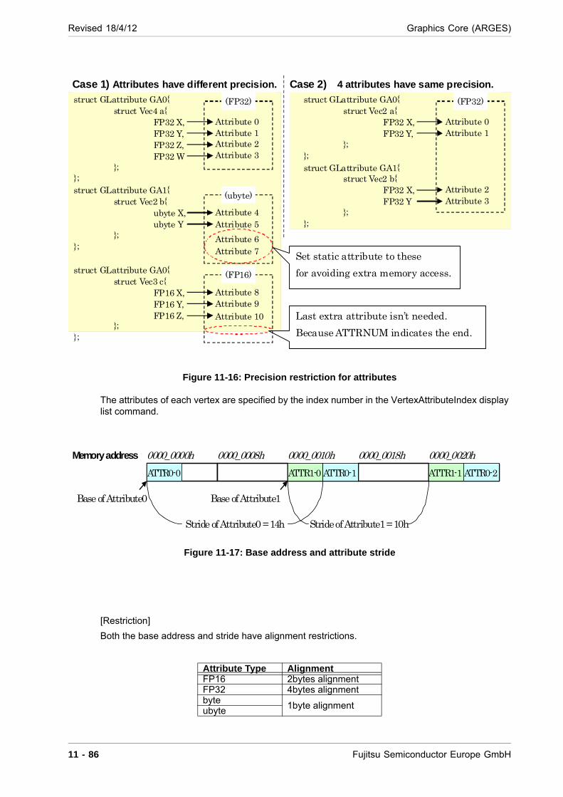
Revised 18/4/12 Graphics Core (ARGES)
Figure 11-16: Precision restriction for attributes
The attributes of each vertex are specified by the index number in the VertexAttributeIndex display list command.
Figure 11-17: Base address and attribute stride
[Restriction]
Both the base address and stride have alignment restrictions.
Attribute Type AlignmentFP16 2bytes alignmentFP32 4bytes alignmentbyte
1byte alignmentubyte
struct GLattribute GA0 struct Vec4 a FP32 X, FP32 Y, FP32 Z, FP32 W ; ; struct GLattribute GA1 struct Vec2 b ubyte X, ubyte Y ; ; struct GLattribute GA0 struct Vec3 c FP16 X, FP16 Y, FP16 Z, ; ;
Attribute 0 Attribute 1 Attribute 2 Attribute 3
Attribute 4 Attribute 5
Attribute 8 Attribute 9 Attribute 10
Attribute 6 Attribute 7
struct GLattribute GA0 struct Vec2 a FP32 X, FP32 Y, ; ; struct GLattribute GA1 struct Vec2 b FP32 X, FP32 Y ; ;
Attribute 0 Attribute 1
Attribute 2 Attribute 3
Set static attribute to these
for avoiding extra memory access.
(ubyte)
Last extra attribute isn’t needed.
Because ATTRNUM indicates the end.
(FP16)
(FP32) (FP32)
Case 1) Attributes have different precision. Case 2) 4 attributes have same precision.
0000_0000h 0000_0008h 0000_0010h 0000_0018h 0000_0020h
Base of Attribute0 Base of Attribute1
ATTR0-0 ATTR1-0 ATTR0-1 ATTR1-1 ATTR0-2
Stride of Attribute0 = 14h Stride of Attribute1 = 10h
Memory address
11 - 86 Fujitsu Semiconductor Europe GmbH
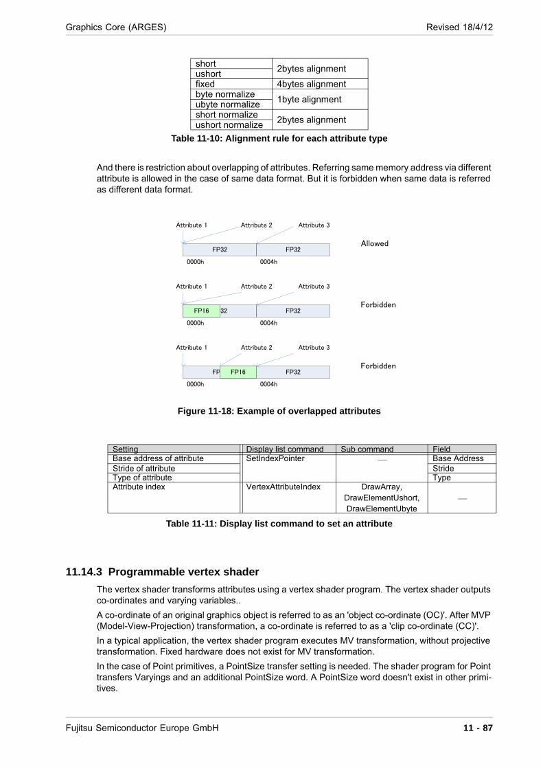
Graphics Core (ARGES) Revised 18/4/12
Table 11-10: Alignment rule for each attribute type
And there is restriction about overlapping of attributes. Referring same memory address via different attribute is allowed in the case of same data format. But it is forbidden when same data is referred as different data format.
Figure 11-18: Example of overlapped attributes
Table 11-11: Display list command to set an attribute
11.14.3 Programmable vertex shader
The vertex shader transforms attributes using a vertex shader program. The vertex shader outputs co-ordinates and varying variables..
A co-ordinate of an original graphics object is referred to as an 'object co-ordinate (OC)'. After MVP (Model-View-Projection) transformation, a co-ordinate is referred to as a 'clip co-ordinate (CC)'.
In a typical application, the vertex shader program executes MV transformation, without projective transformation. Fixed hardware does not exist for MV transformation.
In the case of Point primitives, a PointSize transfer setting is needed. The shader program for Point transfers Varyings and an additional PointSize word. A PointSize word doesn't exist in other primi-tives.
short2bytes alignment
ushortfixed 4bytes alignmentbyte normalize
1byte alignmentubyte normalizeshort normalize
2bytes alignmentushort normalize
Setting Display list command Sub command FieldBase address of attribute SetIndexPointer Base AddressStride of attribute StrideType of attribute TypeAttribute index VertexAttributeIndex DrawArray,
DrawElementUshort, DrawElementUbyte
FP32 FP32
Attribute 1 Attribute 2 Attribute 3
0000h 0004h
FP32 FP32
Attribute 1 Attribute 2 Attribute 3
0000h 0004h
FP16
FP32 FP32
Attribute 1 Attribute 2 Attribute 3
0000h 0004h
FP16
Allowed
Forbidden
Forbidden
Fujitsu Semiconductor Europe GmbH 11 - 87
Revised 18/4/12 Graphics Core (ARGES)
Table 11-12: Display list command to set transmission between vertex shader and ARGES
11.14.4 Projective transformation
For this, the X and Y co-ordinates are divided by the W co-ordinate. The co-ordinates become CC (Clipping CO-ordinates) by perspective division, which is referred to as 'projective transformation'.
In addition, each varying variable is divided by the W co-ordinate. Each varying variable is divided by 1/W after interpolation and before the fragment shader. Dividing by W after the vertex shader and dividing by 1/W before the fragment shader is referred to as 'perspective correction'. Perspective correction is not applied to the Z co-ordinate.
11.14.5 Programmable fragment shader
The fragment shader transforms varyings (varying variables) into pixels using the fragment shader program. The output of the fragment shader is a pixel which has R,G,B and A elements.
If the fragment shader program needs ARGES FragCoord, then FragCoord transmission must be set in ARGES. The FragCoord word from the shader doesn’t exist if this flag is disabled.
Table 11-13: Display list command to set transmission between fragment shader and ARGES
11.14.6 Texture mapping
Texture mapping is a function which reads the texel corresponding to the texture co-ordinate spec-ified for the fragment shader program and then returns it to the fragment shader.
11.14.7 Texture co-ordinates
Texture co-ordinates exist in a 2D co-ordinate system whose horizontal and vertical axes are rep-resented using S and T co-ordinates. The lower left S,T co-ordinate of the texture is (0.0, 0.0), the upper right is (1.0, 1.0).
Patterns of up to 4096 ? 4096 pixels can be used for textures. The RegTexture display list command is used to set a pattern size. If the S,T co-ordinate exceeds the pattern's range, several processing methods can be applied to handle this situation, such as texture pattern repeating (Repeat) and ex-tending the texel at the edge (Clamp to edge). The handling method can be selected.
Setting Display list command Sub command FieldNumber of attributes SetShaderInfo AttrInf0 ATTRNUMPrecision of attribute AttrInf8~9 AP00~15Static attribute AttrInf1~4 DSW00~63Number of varyings set Varying VARNUMPrecision of varying VP00~07PointSize transmission POSZ
Setting Display list command Sub command FieldFragCoord transmission SetShaderInfo Varying FRCDNumber of varyings VARNUM, Precision of varying VP00~07
11 - 88 Fujitsu Semiconductor Europe GmbH
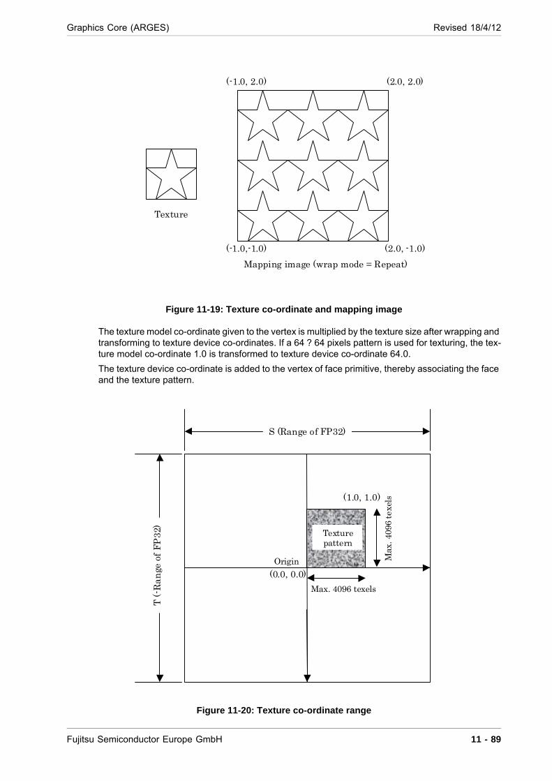
Graphics Core (ARGES) Revised 18/4/12
Figure 11-19: Texture co-ordinate and mapping image
The texture model co-ordinate given to the vertex is multiplied by the texture size after wrapping and transforming to texture device co-ordinates. If a 64 ? 64 pixels pattern is used for texturing, the tex-ture model co-ordinate 1.0 is transformed to texture device co-ordinate 64.0.
The texture device co-ordinate is added to the vertex of face primitive, thereby associating the face and the texture pattern.
Figure 11-20: Texture co-ordinate range
(-1.0, 2.0) (2.0, 2.0)
(-1.0,-1.0) (2.0, -1.0)
Texture
Mapping image (wrap mode = Repeat)
S (Range of FP32)
T (-
Ran
ge o
f F
P32
)
Texture pattern
Origin
Max. 4096 texels
Max
. 409
6 te
xels
(1.0, 1.0)
(0.0, 0.0)
Fujitsu Semiconductor Europe GmbH 11 - 89
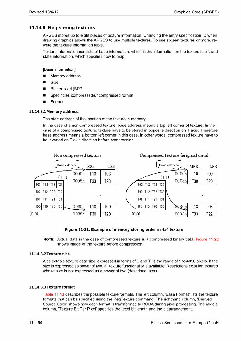
Revised 18/4/12 Graphics Core (ARGES)
11.14.8 Registering textures
ARGES stores up to eight pieces of texture information. Changing the entry specification ID when drawing graphics allows the ARGES to use multiple textures. To use sixteen textures or more, re-write the texture information table.
Texture information consists of base information, which is the information on the texture itself, and state information, which specifies how to map.
[Base information]
Memory address
Size
Bit per pixel (BPP)
Specificies compressed/uncompressed format
Format
11.14.8.1Memory address
The start address of the location of the texture in memory.
In the case of a non-compressed texture, base address means a top left corner of texture. In the case of a compressed texture, texture have to be stored in opposite direction on T axis. Therefore base address means a bottom left corner in this case. In other words, compressed texture have to be inverted on T axis direction before compression.
Figure 11-21: Example of memory storing order in 4x4 texture
NOTE Actual data in the case of compressed texture is a compressed binary data. Figure 11 22shows image of the texture before compression.
11.14.8.2Texture size
A selectable texture data size, expressed in terms of S and T, is the range of 1 to 4096 pixels. If the size is expressed as power of two, all texture functionality is available. Restrictions exist for textures whose size is not expressed as a power of two (described later).
11.14.8.3Texture format
Table 11 13 describes the possible texture formats. The left column, 'Base Format' lists the texture formats that can be specified using the RegTexture command. The righthand column, 'Derived Source Color' shows how each format is transformed to RGBA during pixel processing. The middle column, 'Texture Bit Per Pixel' specifies the texel bit length and the bit arrangement.
T00T10
T20T30
…
T13 T03
T33 T22
MSB LSB
0000h
0008h
(0,0)
(1,1)
Non compressed texture
0000h
0008h
Compressed texture (original data)
T00T10
T20T30
…
T33 T23
T13 T03
MSB LSB
T00 T10 T20 T30
T01 T11 T21 T31
T02 T12 T22 T32
T03 T13 T23 T33
(0,0)
(1,1)
T00 T10 T20 T30
T01 T11 T21 T31
T02 T12 T22 T32
T03 T13 T23 T33
0030h
0038h
0030h
0038h
Base address Base address
11 - 90 Fujitsu Semiconductor Europe GmbH

Graphics Core (ARGES) Revised 18/4/12
Note: In the case of the RGBA8 and LUMINANCE_ALPHA formats, the order of the R element in local GPU memory can be changed by the SetByteOrder display list command.
A texture stored in FJ compressed format only supports the RGBA byte order regardless of SetBy-teOrder setting. For FJ compressed format textures, convert these in advance to the RGBA format when compressing. Various SetByteOrder settings can work correctly, even if FJ compressed tex-ture is made as RGBA format.
Table 11-14: RegTexture format and settable BPP and assignment to each element
Table 11-15: Relation of texture format parameters
The memory allocation of each format is shown below. ARGES supports little endian ordering and pixels are allocated starting with the LSB in 64-bit units corresponding to the bus width. In addition, ARGES has a modifiable byte order for the RGBA8 format: the byte order can be set using the Set-ByteOrder display list command (also for the framebuffer byte order).
RGBA and LA element order in each ByteOrder mode
[RGBA mode]
Base format(FMT)
Texture Bit Per Pixel(BPP)
Derived Source Color(R, G, B, A)
ALPHA Ignored, always 8BPP (0, 0, 0, A)LUMINANCE Ignored, always 8BPP (L, L, L, 1)LUMINANCE_ALPHA Ignored, always 16BPP (L, L, L, A)RGB RGB5_A1/RGBA8/R5_G6_B5/RGBA4 (R, G, B, 1)RGBA RGB5_A1/RGBA8/R5_G6_B5/RGBA4 (R, G, B, A)
CompressionRegTexture(Base) available format
Bits compositionCMP FMT BPP
Uncompressed format
PLAIN RGB, RGBA RGB5_A1 R5:G5:B5:A1RGBA8 R8:G8:B8:A8R5_G6_B5 R5:G6:B5RGBA4 R4:G4:B4:A4
ALPHA, LUMINANCE 8BPP 8bits dataLUMINANCE_ALPHA 16BPP L8:A8
Palette format PALETTE4 RGB, RGBA RGB5_A1 R5:G5:B5:A1RGBA8 R8:G8:B8:A8R5_G6_B5 R5:G6:B5RGBA4 R4:G4:B4:A4
LUMINANCE_ALPHA 16BPP L8:A8PALETTE8 RGB, RGBA RGB5_A1 R5:G5:B5:A1
RGBA8 R8:G8:B8:A8R5_G6_B5 R5:G6:B5RGBA4 R4:G4:B4:A4
LUMINANCE_ALPHA 16BPP L8:A8Compressed format
FJ_COMPRESSED RGB, RGBA RGB5_A1 R5:G5:B5:A1RGBA8 R8:G8:B8:A8
ALPHA, LUMINANCE 8BPP 8bits dataLUMINANCE_ALPHA 16BPP L8:A8
31 32 29 28 27 26 25 24 23 22 21 20 19 18 17 16 15 14 13 12 11 10 9 8 7 6 5 4 3 2 1 0
R G B A
15 14 13 12 11 10 9 8 7 6 5 4 3 2 1 0
L A
Fujitsu Semiconductor Europe GmbH 11 - 91
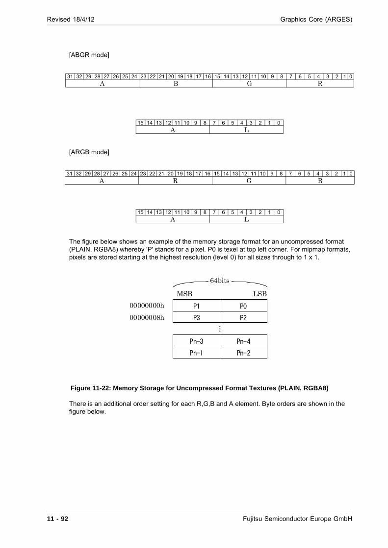
Revised 18/4/12 Graphics Core (ARGES)
[ABGR mode]
[ARGB mode]
The figure below shows an example of the memory storage format for an uncompressed format (PLAIN, RGBA8) whereby 'P' stands for a pixel. P0 is texel at top left corner. For mipmap formats, pixels are stored starting at the highest resolution (level 0) for all sizes through to 1 x 1.
Figure 11-22: Memory Storage for Uncompressed Format Textures (PLAIN, RGBA8)
There is an additional order setting for each R,G,B and A element. Byte orders are shown in the figure below.
31 32 29 28 27 26 25 24 23 22 21 20 19 18 17 16 15 14 13 12 11 10 9 8 7 6 5 4 3 2 1 0
A B G R
15 14 13 12 11 10 9 8 7 6 5 4 3 2 1 0
A L
31 32 29 28 27 26 25 24 23 22 21 20 19 18 17 16 15 14 13 12 11 10 9 8 7 6 5 4 3 2 1 0
A R G B
15 14 13 12 11 10 9 8 7 6 5 4 3 2 1 0
A L
P0 P1
P2 P3
…
Pn-3 Pn-4
Pn-1 Pn-2
MSB LSB
00000000h
00000008h
64bits
11 - 92 Fujitsu Semiconductor Europe GmbH
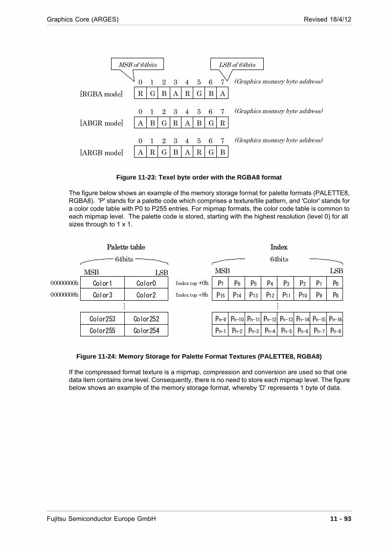
Graphics Core (ARGES) Revised 18/4/12
Figure 11-23: Texel byte order with the RGBA8 format
The figure below shows an example of the memory storage format for palette formats (PALETTE8, RGBA8). 'P' stands for a palette code which comprises a texture/tile pattern, and 'Color' stands for a color code table with P0 to P255 entries. For mipmap formats, the color code table is common to each mipmap level. The palette code is stored, starting with the highest resolution (level 0) for all sizes through to 1 x 1.
Figure 11-24: Memory Storage for Palette Format Textures (PALETTE8, RGBA8)
If the compressed format texture is a mipmap, compression and conversion are used so that one data item contains one level. Consequently, there is no need to store each mipmap level. The figure below shows an example of the memory storage format, whereby 'D' represents 1 byte of data.
R G B A R G B A
0 1 2 3 4 5 6 7 (Graphics memory byte address)
A B G R A B G R
0 1 2 3 4 5 6 7
[RGBA mode]
[ABGR mode]
A R G B A R G B
0 1 2 3 4 5 6 7
[ARGB mode]
(Graphics memory byte address)
(Graphics memory byte address)
MSB of 64bits LSB of 64bits
Color0 Color1
Color2 Color3
Pn-1 Pn-2 Pn-3 Pn-4 Pn-5 Pn-6 Pn-7 Pn-8
Color253 Color252
Color255 Color254
P7 P6 P5 P4 P3 P2 P1 P0
P15 P14 P13 P12 P11 P10 P9 P8
Pn-9 Pn-10 Pn-11 Pn-12 Pn-13 Pn-14 Pn-15 Pn-16
…
MSB LSB00000000h
00000008h
64bits
…
MSB LSB
64bits
Index top +0h
Index top +8h
Palette table Index
Fujitsu Semiconductor Europe GmbH 11 - 93
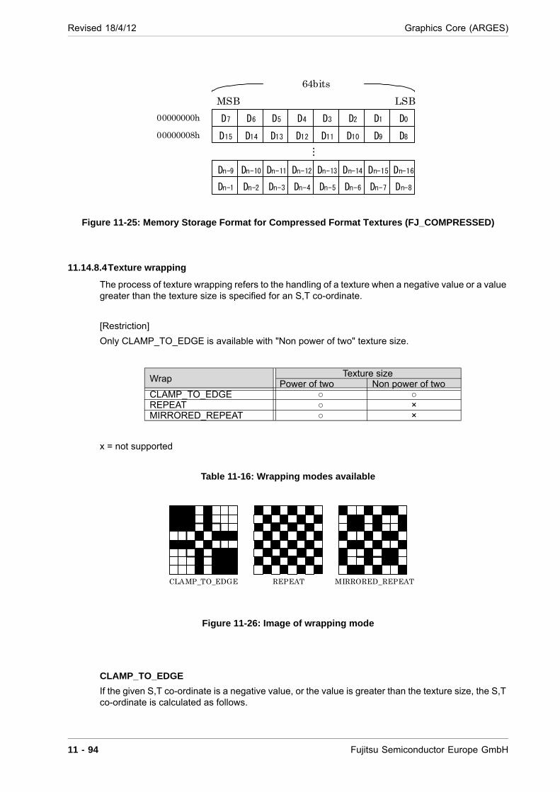
Revised 18/4/12 Graphics Core (ARGES)
Figure 11-25: Memory Storage Format for Compressed Format Textures (FJ_COMPRESSED)
11.14.8.4Texture wrapping
The process of texture wrapping refers to the handling of a texture when a negative value or a value greater than the texture size is specified for an S,T co-ordinate.
[Restriction]
Only CLAMP_TO_EDGE is available with "Non power of two" texture size.
x = not supported
Table 11-16: Wrapping modes available
Figure 11-26: Image of wrapping mode
CLAMP_TO_EDGE
If the given S,T co-ordinate is a negative value, or the value is greater than the texture size, the S,T co-ordinate is calculated as follows.
WrapTexture size
Power of two Non power of twoCLAMP_TO_EDGE REPEAT ×MIRRORED_REPEAT ×
Dn-1 Dn-2 Dn-3 Dn-4 Dn-5 Dn-6 Dn-7 Dn-8
D7 D6 D5 D4 D3 D2 D1 D0
D15 D14 D13 D12 D11 D10 D9 D8
Dn-9 Dn-10 Dn-11 Dn-12 Dn-13 Dn-14 Dn-15 Dn-16
…
MSB LSB
64bits
00000000h
00000008h
REPEAT CLAMP_TO_EDGE MIRRORED_REPEAT
11 - 94 Fujitsu Semiconductor Europe GmbH
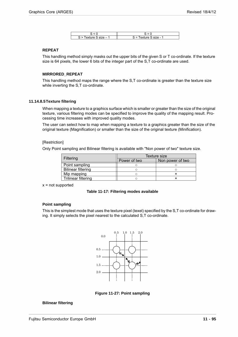
Graphics Core (ARGES) Revised 18/4/12
REPEAT
This handling method simply masks out the upper bits of the given S or T co-ordinate. If the texture size is 64 pixels, the lower 6 bits of the integer part of the S,T co-ordinate are used.
MIRRORED_REPEAT
This handling method maps the range where the S,T co-ordinate is greater than the texture size while inverting the S,T co-ordinate.
11.14.8.5Texture filtering
When mapping a texture to a graphics surface which is smaller or greater than the size of the original texture, various filtering modes can be specified to improve the quality of the mapping result. Pro-cessing time increases with improved quality modes.
The user can select how to map when mapping a texture to a graphics greater than the size of the original texture (Magnification) or smaller than the size of the original texture (Minification).
[Restriction]
Only Point sampling and Bilinear filtering is available with "Non power of two" texture size.
x = not supported
Table 11-17: Filtering modes available
Point sampling
This is the simplest mode that uses the texture pixel (texel) specified by the S,T co-ordinate for draw-ing. It simply selects the pixel nearest to the calculated S,T co-ordinate.
Figure 11-27: Point sampling
Bilinear filtering
S < 0 S = 0S > Texture S size – 1 S = Texture S size - 1
FilteringTexture size
Power of two Non power of twoPoint sampling Bilinear filtering Mip mapping ×Trilinear filtering ×
0.0
0.5 1.0 1.5 2.0
0.5
1.0
1.5
2.0
Fujitsu Semiconductor Europe GmbH 11 - 95
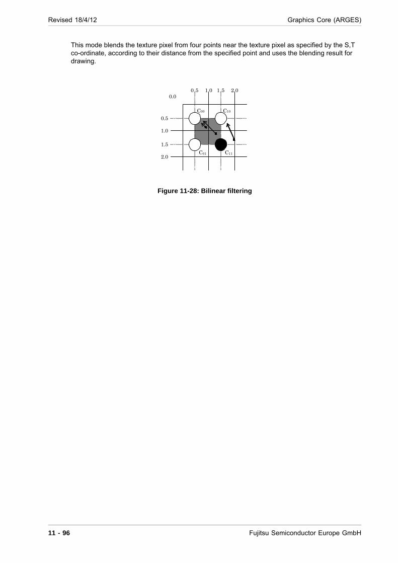
Revised 18/4/12 Graphics Core (ARGES)
This mode blends the texture pixel from four points near the texture pixel as specified by the S,T co-ordinate, according to their distance from the specified point and uses the blending result for drawing.
Figure 11-28: Bilinear filtering
0.0
0.5 1.0 1.5 2.0
0.5
1.0
1.5
2.0
C00 C10
C01 C11
11 - 96 Fujitsu Semiconductor Europe GmbH

Graphics Core (ARGES) Revised 18/4/12
Mip mapping
When mapping a texture, this mode uses the texture at the mipmap level which corresponds to the reduction ratio. This requires different (reduced) versions of the original texture for ready use.
When using mipmap functionality, you must enable perspective correction as described later.
Figure 11-29: Mip map texture
Trilinear filtering
This mode samples texels from the two closest mipmap levels and blends them with weighting fac-tors calculated in the LOD (Level of Detail) calculation. Pixels at the center of the mapping image shown in Figure 11 30 (the dotted line) are situated exactly between mipmap level 1 and level 2, meaning that the two texels are blended at 50% to get the result.
MINFL – see RegTexture description
Table 11-18: Relationship between Filtering and MINFL Setting
LOD bias
When mip mapping is used, ARGES uses a LOD setting to determine which mip map level is used. The LOD is calculated internally according to the minification ratio. A LOD bias is used for minor adjustments to the LOD and is handled differently by a fragment shader and a vertex shader.
For fragment shaders
The LOD is calculated internally by ARGES when textures are accessed by a fragment shader. The shader can state a bias value which will then be added to the internally calculated value.
For vertex shaders
In the case of vertex shaders, an LOD is not calculated internally by ARGES (because the vertex shader does not have a minification scale). In this case the shader must deliver an explicit value for the LOD. A bias does not exist in this case.
The maximum value for the LOD bias is 12.0, so the bias range is from -12.0 to 12.0. A LOD bias which exceeds this range is clamped in ARGES.
Cube mapping
MINFL Bilinear Mipmap TrilinearNEAREST LINEAR NEAREST_MIPMAP_NEAREST NEAREST_MIPMAP_LINEAR LINEAR_MIPMAP_NEAREST LINEAR_MIPMAP_LINEAR
Level 0 Level 1 ……
Level 1 Level 2
..
Mapping image
Fujitsu Semiconductor Europe GmbH 11 - 97
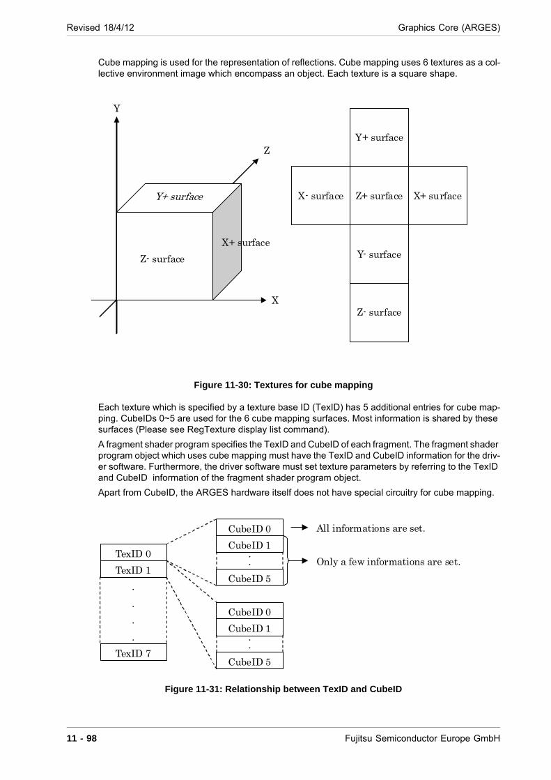
Revised 18/4/12 Graphics Core (ARGES)
Cube mapping is used for the representation of reflections. Cube mapping uses 6 textures as a col-lective environment image which encompass an object. Each texture is a square shape.
Figure 11-30: Textures for cube mapping
Each texture which is specified by a texture base ID (TexID) has 5 additional entries for cube map-ping. CubeIDs 0~5 are used for the 6 cube mapping surfaces. Most information is shared by these surfaces (Please see RegTexture display list command).
A fragment shader program specifies the TexID and CubeID of each fragment. The fragment shader program object which uses cube mapping must have the TexID and CubeID information for the driv-er software. Furthermore, the driver software must set texture parameters by referring to the TexID and CubeID information of the fragment shader program object.
Apart from CubeID, the ARGES hardware itself does not have special circuitry for cube mapping.
Figure 11-31: Relationship between TexID and CubeID
Y+ surface
Z+ surface X+ surfaceX- surface
Y- surface
Z- surface
Y
X
Z
Z- surface
Y+ surface
X+ surface
TexID 0
TexID 1
TexID 7
.
.
CubeID 0
CubeID 1
CubeID 5
.
.
.
.
CubeID 0
CubeID 1
CubeID 5
.
.
All informations are set.
Only a few informations are set.
11 - 98 Fujitsu Semiconductor Europe GmbH
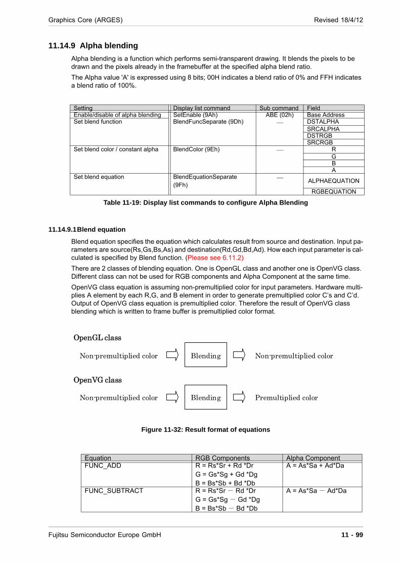
Graphics Core (ARGES) Revised 18/4/12
11.14.9 Alpha blending
Alpha blending is a function which performs semi-transparent drawing. It blends the pixels to be drawn and the pixels already in the framebuffer at the specified alpha blend ratio.
The Alpha value 'A' is expressed using 8 bits; 00H indicates a blend ratio of 0% and FFH indicates a blend ratio of 100%.
Table 11-19: Display list commands to configure Alpha Blending
11.14.9.1Blend equation
Blend equation specifies the equation which calculates result from source and destination. Input pa-rameters are source(Rs,Gs,Bs,As) and destination(Rd,Gd,Bd,Ad). How each input parameter is cal-culated is specified by Blend function. (Please see 6.11.2)
There are 2 classes of blending equation. One is OpenGL class and another one is OpenVG class. Different class can not be used for RGB components and Alpha Component at the same time.
OpenVG class equation is assuming non-premultiplied color for input parameters. Hardware multi-plies A element by each R,G, and B element in order to generate premultiplied color C’s and C’d. Output of OpenVG class equation is premultiplied color. Therefore the result of OpenVG class blending which is written to frame buffer is premultiplied color format.
Figure 11-32: Result format of equations
Setting Display list command Sub command FieldEnable/disable of alpha blending SetEnable (9Ah) ABE (02h) Base AddressSet blend function BlendFuncSeparate (9Dh) DSTALPHA
SRCALPHADSTRGBSRCRGB
Set blend color / constant alpha BlendColor (9Eh) RGBA
Set blend equation BlendEquationSeparate (9Fh)
ALPHAEQUATION
RGBEQUATION
Equation RGB Components Alpha ComponentFUNC_ADD R = Rs*Sr + Rd *Dr
G = Gs*Sg + Gd *DgB = Bs*Sb + Bd *Db
A = As*Sa + Ad*Da
FUNC_SUBTRACT R = Rs*Sr - Rd *DrG = Gs*Sg - Gd *DgB = Bs*Sb - Bd *Db
A = As*Sa - Ad*Da
OpenGL class
Non-premultiplied color Blending Non-premultiplied color
OpenVG class
Non-premultiplied color Blending Premultiplied color
Fujitsu Semiconductor Europe GmbH 11 - 99

Revised 18/4/12 Graphics Core (ARGES)
Table 11-20: Alpha Blending Formula of OpenGL class
* C’s = Cs×As , C’d = Cd×Ad
Table 11-21: Alpha Blending Formulae of OpenVG class
11.14.9.2Blend function
The blend function is used to select how to calculate the alpha blend ratio independently for a source and a destination and only works when alpha blending is enabled. Functions which use the alpha value of a destination pixel can be used only in 32-bit/pixel mode.
FUNC_REVERSE_SUBTRACT R =Rd *Dr - Rs*SrG = Gd *Dg - Gs*SgB = Bd *Db - Bs*Sb
A = Ad*Da - As*Sa
MIN R = min(Rs,Rd)G= min(Gs,Gd)B= min(Bs,Bd)
A= min(As,Ad)
MAX R = max(Rs,Rd)G= max(Gs,Gd)B= max(Bs,Bd)
A= max(As,Ad)
Equation RGB Alpha
VG_BLEND_SRC
VG_BLEND_SRC_OVER
VG_BLEND_DST_OVER
VG_BLEND_SRC_IN
VG_BLEND_DST_IN
VG_BLEND_MULTIPLY
VG_BLEND_SCREEN
VG_BLEND_DARKENmin(
,
)
VG_BLEND_LIGHTENmax(
,
)
VG_BLEND_ADDITIVE min( min(, 1 )
Function Value RGB Blend Factors(Sr, Sg, Sb) or (Dr,Dg,Db)
Alpha Blend FactorSa or Da
ZERO 0 (0, 0, 0) 0ONE 1 (1, 1, 1) 1SRC_COLOR 2 (Rs,Gs,Bs) AsONE_MINUS_SRC_COLOR 3 (1, 1, 1) − (Rs,Gs,Bs) 1 − AsDST_COLOR 4 (Rd,Gd,Bd) Ad
srcC ' src
dstsrcsrc CC ')1(' dstsrcsrc )1(
dstsrcdst CC '')1( srcdstdst )1(
srcdstC ' dstsrc
dstsrcC ' dstsrc
dstsrcdstsrcsrcdst CCCC ''')1(')1( dstsrcsrc )1(
dstsrcdstsrc CCCC '''' dstsrcsrc )1(
dstsrcsrc CC ')1('
srcdstdst CC ')1('
dstsrcsrc )1(
dstsrcsrc CC ')1('
srcdstdst CC ')1('
dstsrcsrc )1(
)1),''( dstsrc CC dstsrc
11 - 100 Fujitsu Semiconductor Europe GmbH
Graphics Core (ARGES) Revised 18/4/12
Table 11-22: Blend Functions
NOTE Values in parentheses refer to the blend ratio of each R, G, B, and A element.*1 SRC ALPHA SATURATE is valid only for source RGB and alpha blending functions.*2 f = min(As, 1 − Ad).
NOTE If the blending result exceeds the maximum value of any R, G, B, and A element, the element is clamped to its maximum value.
11.14.10 Depth test
The depth test is used for 3D drawing to eliminate hidden surfaces using the Z buffer. Always use the Z buffer to compare the depth of surfaces.
11.14.10.1Z buffer Configuration
The dimensions of the Z buffer (its vertical and horizontal pixel counts) are equal to those of the drawing frame. The Z value itself can be either 32 bits/pixel, 16 bits/pixel or 8 bits/pixel. Make sure that you always clear the Z value using DrawRectP before drawing a frame.
The Z values in the Z buffer are floating point number or positive integers. The values which are exceeding the range of current Z format are clamped to either the minimum or the maximum in the range.
Table 11-23: Display list commands to configure the Z Buffer
11.14.10.2Memory data format
The Z value can be held as 32 bits, 16 bits or 8 bits per pixel.
(1) 32-bit floating point data
ONE_MINUS_DST_COLOR 5 (1, 1, 1) − (Rd,Gd,Bd) 1 − A dSRC_ALPHA 6 (As,As,As) AsONE_MINUS_SRC_ALPHA 7 (1, 1, 1) − (As,As,As) 1 − AsDST_ALPHA 8 (Ad,Ad,Ad) AdONE_MINUS_DST_ALPHA 9 (1, 1, 1) − (Ad,Ad,Ad) 1 − AdCONSTANT_COLOR 10 (Rc,Gc,Bc) AcONE_MINUS_CONSTANT_COLOR 11 (1, 1, 1) − (Rc,Gc,Bc) 1 − AcCONSTANT_ALPHA 12 (Ac,Ac,Ac) AcONE MINUS_CONSTANT_ALPHA 13 (1, 1, 1) − (Ac,Ac,Ac) 1 − AcSRC_ALPHA_SATURATE*1 14 (f, f, f)*2 1
Setting Displaylist command Sub commandBase address of Z buffer SetZBufferAddr (ABh)Bpp of Z buffer SetFrameBPP (AAh) 01h
31 0
FP32
Fujitsu Semiconductor Europe GmbH 11 - 101
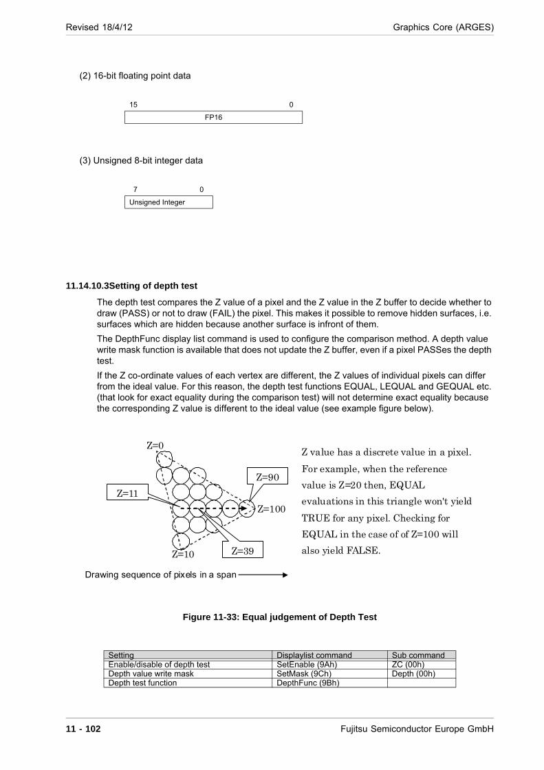
Revised 18/4/12 Graphics Core (ARGES)
(2) 16-bit floating point data
(3) Unsigned 8-bit integer data
11.14.10.3Setting of depth test
The depth test compares the Z value of a pixel and the Z value in the Z buffer to decide whether to draw (PASS) or not to draw (FAIL) the pixel. This makes it possible to remove hidden surfaces, i.e. surfaces which are hidden because another surface is infront of them.
The DepthFunc display list command is used to configure the comparison method. A depth value write mask function is available that does not update the Z buffer, even if a pixel PASSes the depth test.
If the Z co-ordinate values of each vertex are different, the Z values of individual pixels can differ from the ideal value. For this reason, the depth test functions EQUAL, LEQUAL and GEQUAL etc. (that look for exact equality during the comparison test) will not determine exact equality because the corresponding Z value is different to the ideal value (see example figure below).
Figure 11-33: Equal judgement of Depth Test
15 0
FP16
7 0
Unsigned Integer
Setting Displaylist command Sub commandEnable/disable of depth test SetEnable (9Ah) ZC (00h)Depth value write mask SetMask (9Ch) Depth (00h)Depth test function DepthFunc (9Bh)
Z=0
Z=10
Z=100
Drawing sequence of pixels in a span
Z=11
Z=39
Z=90
Z value has a discrete value in a pixel.
For example, when the reference
value is Z=20 then, EQUAL
evaluations in this triangle won't yield
TRUE for any pixel. Checking for
EQUAL in the case of of Z=100 will
also yield FALSE.
11 - 102 Fujitsu Semiconductor Europe GmbH
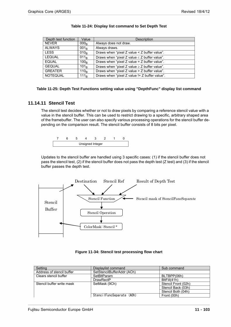
Graphics Core (ARGES) Revised 18/4/12
Table 11-24: Display list command to Set Depth Test
Table 11-25: Depth Test Functions setting value using ”DepthFunc” display list command
11.14.11 Stencil Test
The stencil test decides whether or not to draw pixels by comparing a reference stencil value with a value in the stencil buffer. This can be used to restrict drawing to a specific, arbitrary shaped area of the framebuffer. The user can also specify various processing operations for the stencil buffer de-pending on the comparison result. The stencil buffer consists of 8 bits per pixel.
Updates to the stencil buffer are handled using 3 specific cases: (1) if the stencil buffer does not pass the stencil test, (2) if the stencil buffer does not pass the depth test (Z test) and (3) if the stencil buffer passes the depth test.
Figure 11-34: Stencil test processing flow chart
Depth test function Value DescriptionNEVER 000B Always does not draw.ALWAYS 001B Always draws.LESS 010B Draws when “pixel Z value < Z buffer value”.LEQUAL 011B Draws when “pixel Z value Z buffer value”.EQUAL 100B Draws when “pixel Z value = Z buffer value”.GEQUAL 101B Draws when “pixel Z value Z buffer value”.GREATER 110B Draws when “pixel Z value > Z buffer value”.NOTEQUAL 111B Draws when “pixel Z value != Z buffer value”.
7 6 5 4 3 2 1 0
Unsigned Integer
Setting Displaylist command Sub commandAddress of stencil buffer SetStencilBufferAddr (ACh)Clears stencil buffer SetBltParam BLTBPP(06h)
DrawRectP BltFill(41h)Stencil buffer write mask SetMask (9Ch) Stencil Front (02h)
Stencil Back (03h)Stencil Both (04h)
StencilFuncSeparate (A0h) Front (00h)
Stencil RefDestination
Stencil
Buffer
Stencil Function
ColorMask: Stencil *
Stencil Operation
Result of Depth Test
Stencil mask of StencilFuncSeparate
Fujitsu Semiconductor Europe GmbH 11 - 103

Revised 18/4/12 Graphics Core (ARGES)
Table 11-26: Display list command to configure the Stencil Test
Table 11-27: Display list commands following words to configure the Stencil Test
Table 11-28: Comparison Functions for Stencil Test
Table 11-29: Update Conditions for Stencil Test
Back (01h)Both (02h)
Enable/disable of stencil test SetEnable (9Ah) STCE (01h)Stencil test function StencilFuncSeparate (A0h) Front (00h)
Back (01h)Both (02h)
Specification of stencil buffer update processing
StencilOpSeparate (A1h) Front (00h)
Back (01h)Both (02h)
Setting Preceding Displaylist command FieldReference value when performing stencil test StencilFuncSeparate (A0h) Stencil RefStencil buffer write mask SetMask (9Ch) Mask
StencilFuncSeparate (A0h) Stencil MaskStencil test function StencilFuncSeparate (A0h) FUNCSpecification of stencil buffer update processing StencilOpSeparate (A1h) SFAIL
DPFAILDPPASS
Comparison function for stencil test
Code Condition
NEVER 000 Never draws.ALWAYS 001 Always draws.LESS 010 Draws when “reference stencil value < stencil buffer value”.LEQUAL 011 Draws when “reference stencil value <= stencil buffer value”.EQUAL 100 Draws when “reference stencil value = stencil buffer value”.GEQUAL 101 Draws when “reference stencil value >= stencil buffer value”.GREATER 110 Draws when “reference stencil value > stencil buffer value”.NOTEQUAL 111 Draws when “reference stencil value != stencil buffer value”.
Stencil update condition DescriptionSFAIL When stencil test shows “does not draw”:
* The stencil test and depth test are performed in this order. If the stencil buffer does not pass the stencil test, the depth test is not performed and the result of the depth test is undefined.
DPFAIL When depth test shows “does not draw”:
* Since the depth test has been performed, it means the stencil buffer has passed the stencil test.
DPPASS When depth test shows “draws”:
* Since the depth test has been performed, it means the stencil buffer has passed the stencil test.
11 - 104 Fujitsu Semiconductor Europe GmbH

Graphics Core (ARGES) Revised 18/4/12
Table 11-30: Update Functions for Stencil Test
NOTE When clamping is specified, a decrement from 00H does not change the result, the value is held at 00H.
NOTE When clamping is specified, an increment from FFH does not change the result, the value is held at FFH.
11.14.12 PolygonOffset
PolygonOffset is a function that is used to add an offset to the Z value after co-ordinate transforma-tion has been performed. The expression used to calculate the offset value is shown below.
Offset = m x factor + r x units
The user sets the 'factor' and 'r x units'. 'm' is the inclination after co-ordinate transformation and is calculated automatically by ARGES. Set a separate value for the front and back faces.
The factor parameter is scaler for the Z slope. The units parameter is the minimum unit of depth buf-fer value and the r parameter is scaler for the units.
Table 11-31: Display List command to Configure PolygonOffset
Stencil operation function
Code Condition
SFAIL/
DPFAIL/
DPPASS
KEEP 000 Does not update the stencil buffer.ZERO 001 Writes “0” to the stencil buffer.REPLACE 010 Writes a reference stencil value to the stencil buffer.INCR 011 Increments the stencil buffer value by “1” (with clamping).DECR 100 Decrements the stencil buffer value by “1” (with clamping).INVERT 101 Performs bit inversion for the stencil buffer value.INCR_WRAP 110 Increments the stencil buffer value by “1” (without clamping).DECR_WRAP 111 Decrements the stencil buffer value by “1” (without clamping).
Setting Display list command Sub command Field/ParameterEnable/disable of PolygonOffset for front surface PolygonSetting (64h) POFFEnable/disable of PolygonOffset for back surface PolygonSetting (64h) POBFSetting of “factor” and “r units” PolygonOffset (65h) factor,r_units
Fujitsu Semiconductor Europe GmbH 11 - 105

Revised 18/4/12 Graphics Core (ARGES)
11.14.13 BitBlt (Bit Block Transfer)
The BitBlt function transfers a rectangular area in units of pixels. When using the BitBlt function, the horizontal width (XRR) of the framebuffer must be aligned in units of 8 bytes.
The BitBlt function offers the following types of processing:
Table 11-32: BitBlt Processing Types
The co-ordinates used by the BLT function are relative to the bottom-left corner of an area (note that this is different to the previous KOTTOS graphics core, which used the top-left corner). Despite this, drawing starts from the top unless the BottomRight and BottomLeft sub commands are used.
Figure 11-35: BitBlt co-ordinates system and drawing sequence
Processing type FunctionFILL Fills a rectangular area with the specified color.
DRAW Draws data supplied by the display list, to a rectangular area.
COPY Copies a rectangular area in the same framebuffer.
COPYALT Copies a rectangular area between two different framebuffers. It is possible to copy between framebuffers whose shape and size are different.
COPYCOMP Draws compressed data to the framebuffer while expanding it.
(0, 0)
RsizeY
RsizeX(RXs, RYs)
x
y
Drawing starts from top and
progresses to bottom.
11 - 106 Fujitsu Semiconductor Europe GmbH
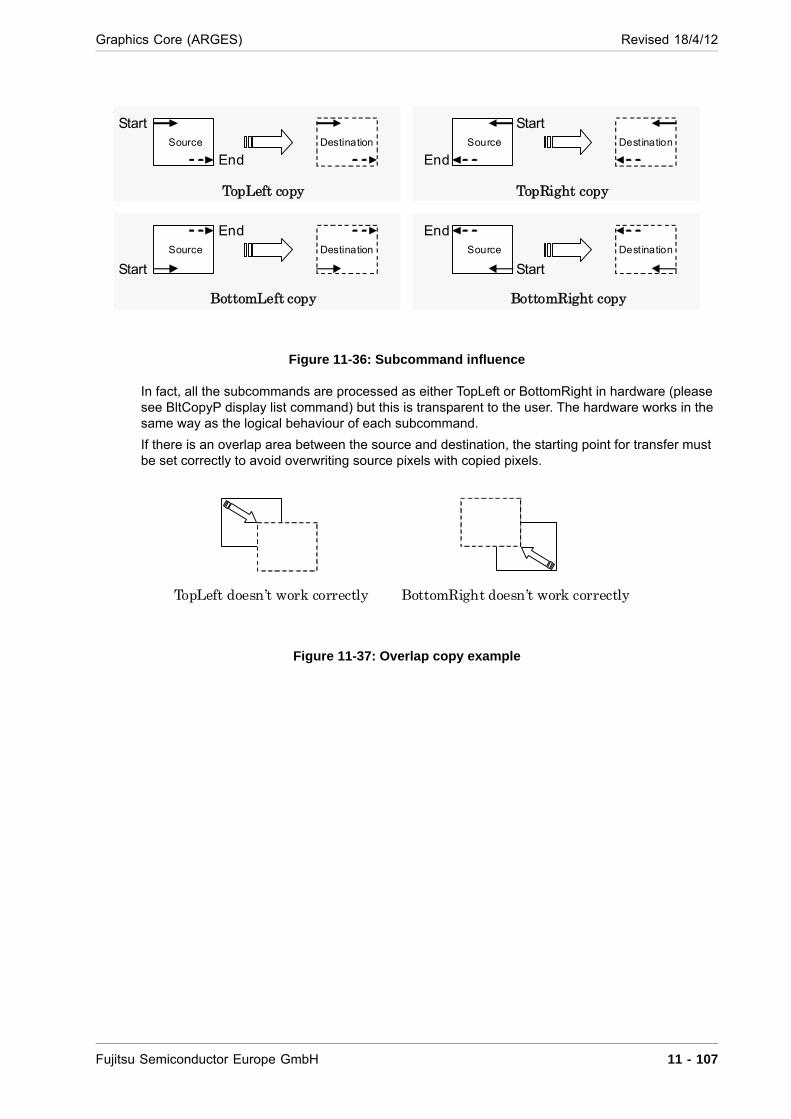
Graphics Core (ARGES) Revised 18/4/12
Figure 11-36: Subcommand influence
In fact, all the subcommands are processed as either TopLeft or BottomRight in hardware (please see BltCopyP display list command) but this is transparent to the user. The hardware works in the same way as the logical behaviour of each subcommand.
If there is an overlap area between the source and destination, the starting point for transfer must be set correctly to avoid overwriting source pixels with copied pixels.
Figure 11-37: Overlap copy example
TopLeft copy
Start
End
TopRight copy
Start
End
BottomLeft copy
Start
End
BottomRight copy
Start
End
Source Destination
Source Destination
Source Destination
Source Destination
TopLeft doesn’t work correctly BottomRight doesn’t work correctly
Fujitsu Semiconductor Europe GmbH 11 - 107
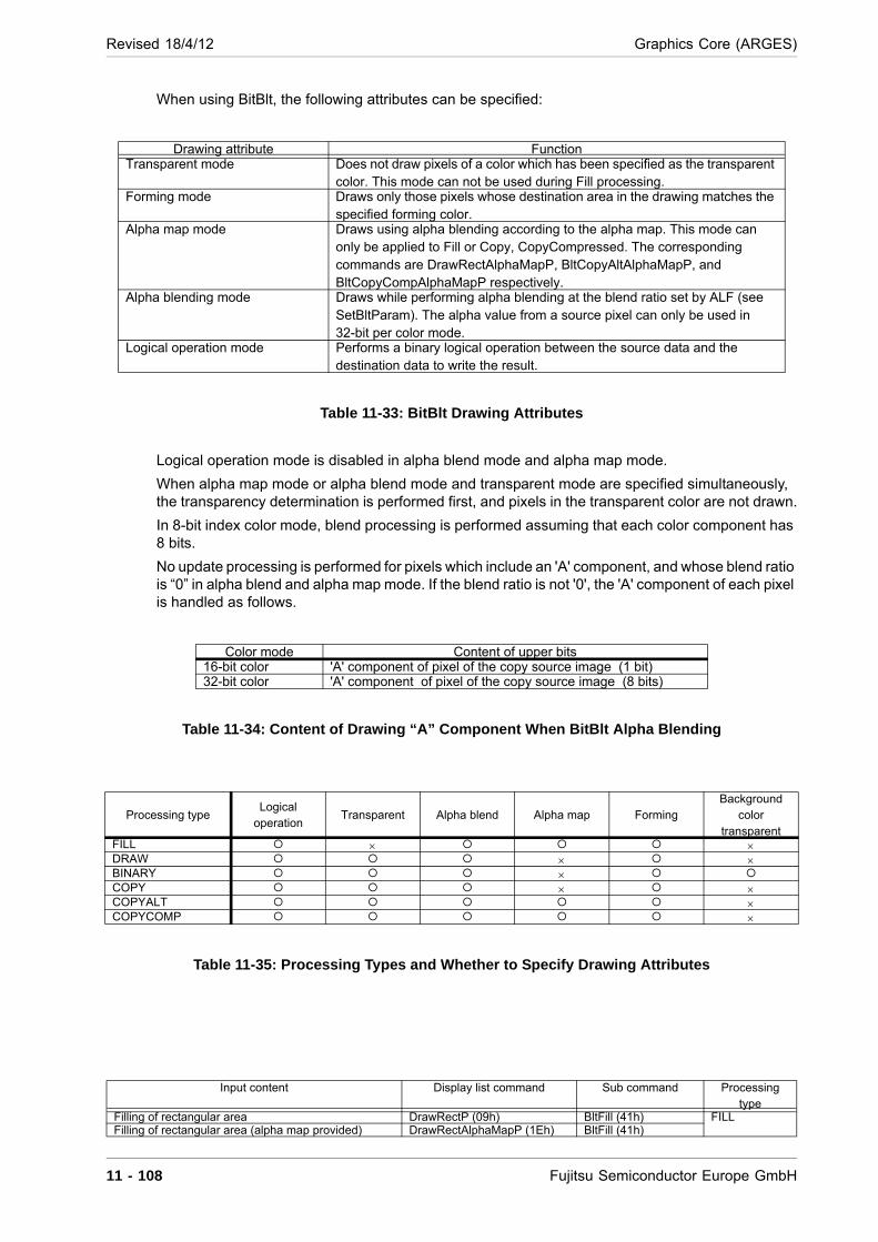
Revised 18/4/12 Graphics Core (ARGES)
When using BitBlt, the following attributes can be specified:
Table 11-33: BitBlt Drawing Attributes
Logical operation mode is disabled in alpha blend mode and alpha map mode.
When alpha map mode or alpha blend mode and transparent mode are specified simultaneously, the transparency determination is performed first, and pixels in the transparent color are not drawn.
In 8-bit index color mode, blend processing is performed assuming that each color component has 8 bits.
No update processing is performed for pixels which include an 'A' component, and whose blend ratio is “0” in alpha blend and alpha map mode. If the blend ratio is not '0', the 'A' component of each pixel is handled as follows.
Table 11-34: Content of Drawing “A” Component When BitBlt Alpha Blending
Table 11-35: Processing Types and Whether to Specify Drawing Attributes
Drawing attribute FunctionTransparent mode Does not draw pixels of a color which has been specified as the transparent
color. This mode can not be used during Fill processing. Forming mode Draws only those pixels whose destination area in the drawing matches the
specified forming color. Alpha map mode Draws using alpha blending according to the alpha map. This mode can
only be applied to Fill or Copy, CopyCompressed. The corresponding commands are DrawRectAlphaMapP, BltCopyAltAlphaMapP, and BltCopyCompAlphaMapP respectively.
Alpha blending mode Draws while performing alpha blending at the blend ratio set by ALF (see SetBltParam). The alpha value from a source pixel can only be used in 32-bit per color mode.
Logical operation mode Performs a binary logical operation between the source data and the destination data to write the result.
Color mode Content of upper bits16-bit color 'A' component of pixel of the copy source image (1 bit)32-bit color 'A' component of pixel of the copy source image (8 bits)
Processing typeLogical
operationTransparent Alpha blend Alpha map Forming
Background color
transparentFILL DRAW BINARY COPY COPYALT COPYCOMP
Input content Display list command Sub command Processing type
Filling of rectangular area DrawRectP (09h) BltFill (41h) FILLFilling of rectangular area (alpha map provided) DrawRectAlphaMapP (1Eh) BltFill (41h)
11 - 108 Fujitsu Semiconductor Europe GmbH

Graphics Core (ARGES) Revised 18/4/12
Table 11-36: Display List command to Use BitBlt
Table 11-37: “SetBltParam” parameters to Set Drawing Effect of BitBlt
Drawing of rectangular pattern DrawBitmapP (0Bh) BltDraw (42h) DRAWDrawing of bit pattern DrawBitmap (43h)Drawing of rectangular pattern (huge data supported) DrawBitmapLargeP (2Fh) BltDraw (42h)Copy of rectangular area (in the same framebuffer) BltCopyP (0Dh) TopLeft (44h) COPY
TopRight (45h)BottomLeft (46h)BottomRight (47h)
Copy of rectangular area (between different framebuffers)
BltCopyAlternateP (0Fh) TopLeft (44h) COPYALT
Copy of rectangular area (alpha map provided) BltCopyAltAlphaMapP (1Fh) Normal (01h)ABR (00h)
Expansion and copy of compressed data BltCopyCompressedP (2Dh) TopLeft (44h) COPYCOMPExpansion and copy of compressed data (alpha map provided)
BltCopyCompAlphaMapP (2Eh)
TopLeft (44h)
Set Blt function parameter SetBltParam (B1h) TColor (00h)FormColor (01h)BSV/HSV (02h)FC (03h)BC (04h)EFFECT (05h)BLTBPP (06h)ABR (07h)ALF (08h)
Setting Command ParameterEnable/disable of logical operation mode EFFECT BMSetting of logical operation function EFFECT LOGEnable/disable of transparent mode EFFECT TESetting of transparent color Tcolor -Enable/disable of forming mode EFFECT FESetting of forming color FormColorEnable/disable of alpha blending mode EFFECT BMSetting of blend ratio of alpha blending ALF -Selection of pixel alpha mode EFFECT ASEnable/disable of background color transparent EFFECT BTSetting of foreground color FCSetting of background color BC -Setting of Bit/pixel of framebuffer in BitBlt function BLTBPP BPP
Fujitsu Semiconductor Europe GmbH 11 - 109
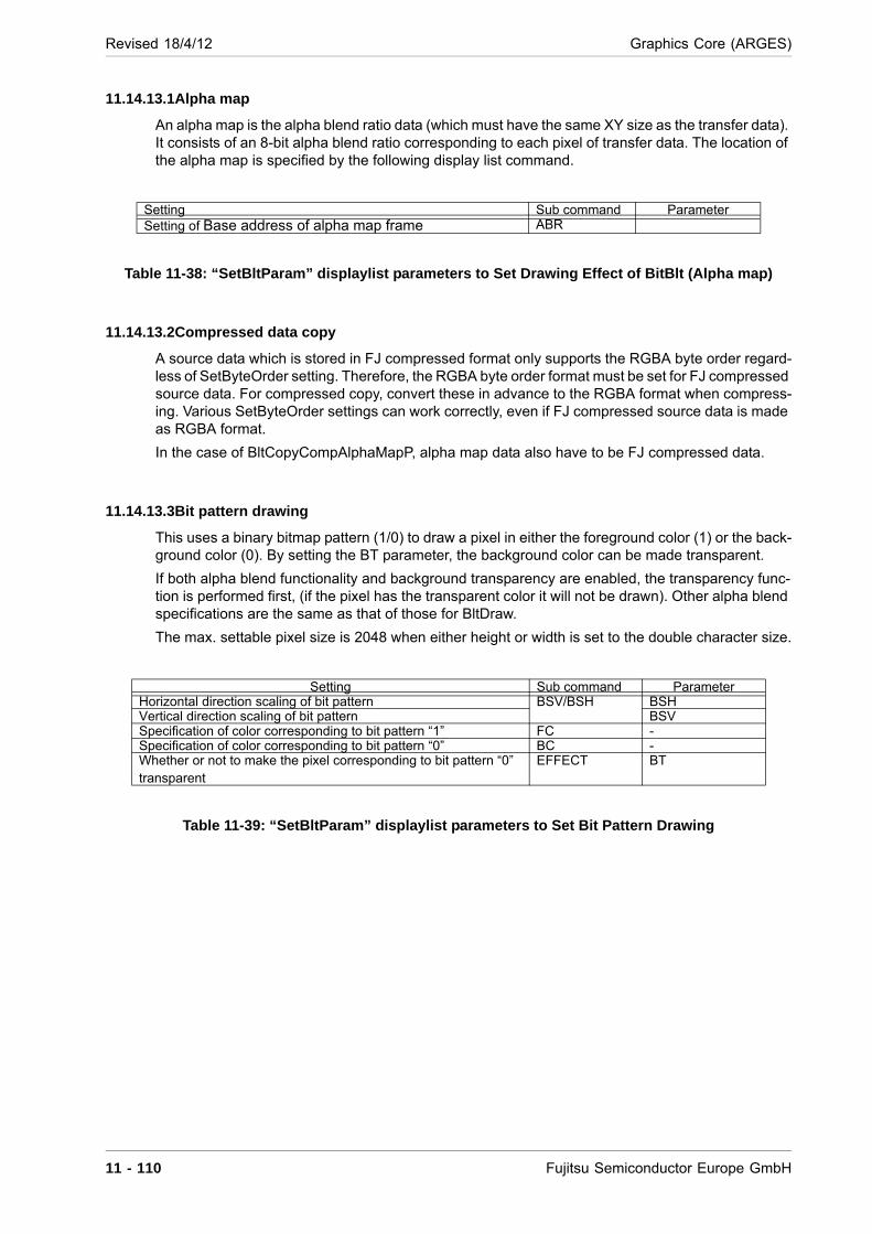
Revised 18/4/12 Graphics Core (ARGES)
11.14.13.1Alpha map
An alpha map is the alpha blend ratio data (which must have the same XY size as the transfer data). It consists of an 8-bit alpha blend ratio corresponding to each pixel of transfer data. The location of the alpha map is specified by the following display list command.
Table 11-38: “SetBltParam” displaylist parameters to Set Drawing Effect of BitBlt (Alpha map)
11.14.13.2Compressed data copy
A source data which is stored in FJ compressed format only supports the RGBA byte order regard-less of SetByteOrder setting. Therefore, the RGBA byte order format must be set for FJ compressed source data. For compressed copy, convert these in advance to the RGBA format when compress-ing. Various SetByteOrder settings can work correctly, even if FJ compressed source data is made as RGBA format.
In the case of BltCopyCompAlphaMapP, alpha map data also have to be FJ compressed data.
11.14.13.3Bit pattern drawing
This uses a binary bitmap pattern (1/0) to draw a pixel in either the foreground color (1) or the back-ground color (0). By setting the BT parameter, the background color can be made transparent.
If both alpha blend functionality and background transparency are enabled, the transparency func-tion is performed first, (if the pixel has the transparent color it will not be drawn). Other alpha blend specifications are the same as that of those for BltDraw.
The max. settable pixel size is 2048 when either height or width is set to the double character size.
Table 11-39: “SetBltParam” displaylist parameters to Set Bit Pattern Drawing
Setting Sub command ParameterSetting of Base address of alpha map frame ABR
Setting Sub command ParameterHorizontal direction scaling of bit pattern BSV/BSH BSHVertical direction scaling of bit pattern BSVSpecification of color corresponding to bit pattern “1” FC -Specification of color corresponding to bit pattern “0” BC -Whether or not to make the pixel corresponding to bit pattern “0” transparent
EFFECT BT
11 - 110 Fujitsu Semiconductor Europe GmbH
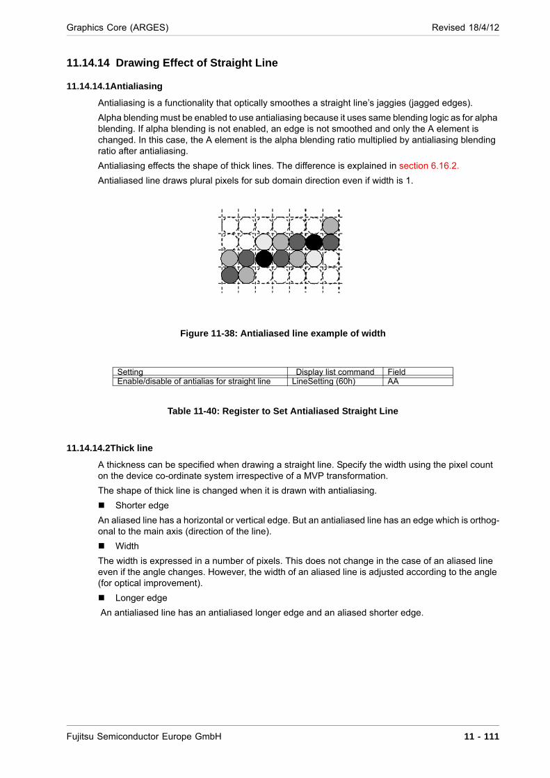
Graphics Core (ARGES) Revised 18/4/12
11.14.14 Drawing Effect of Straight Line
11.14.14.1Antialiasing
Antialiasing is a functionality that optically smoothes a straight line’s jaggies (jagged edges).
Alpha blending must be enabled to use antialiasing because it uses same blending logic as for alpha blending. If alpha blending is not enabled, an edge is not smoothed and only the A element is changed. In this case, the A element is the alpha blending ratio multiplied by antialiasing blending ratio after antialiasing.
Antialiasing effects the shape of thick lines. The difference is explained in section 6.16.2.
Antialiased line draws plural pixels for sub domain direction even if width is 1.
Figure 11-38: Antialiased line example of width
Table 11-40: Register to Set Antialiased Straight Line
11.14.14.2Thick line
A thickness can be specified when drawing a straight line. Specify the width using the pixel count on the device co-ordinate system irrespective of a MVP transformation.
The shape of thick line is changed when it is drawn with antialiasing.
Shorter edge
An aliased line has a horizontal or vertical edge. But an antialiased line has an edge which is orthog-onal to the main axis (direction of the line).
Width
The width is expressed in a number of pixels. This does not change in the case of an aliased line even if the angle changes. However, the width of an aliased line is adjusted according to the angle (for optical improvement).
Longer edge
An antialiased line has an antialiased longer edge and an aliased shorter edge.
Setting Display list command FieldEnable/disable of antialias for straight line LineSetting (60h) AA
Fujitsu Semiconductor Europe GmbH 11 - 111
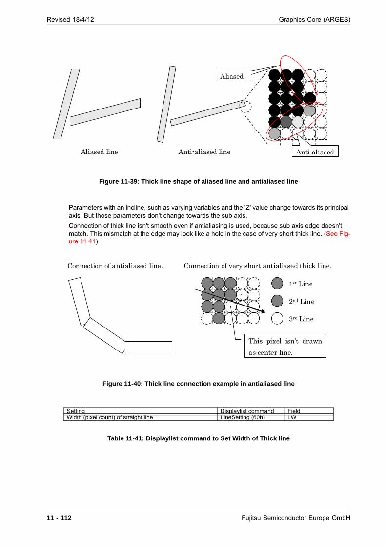
Revised 18/4/12 Graphics Core (ARGES)
Figure 11-39: Thick line shape of aliased line and antialiased line
Parameters with an incline, such as varying variables and the 'Z' value change towards its principal axis. But those parameters don't change towards the sub axis.
Connection of thick line isn't smooth even if antialiasing is used, because sub axis edge doesn't match. This mismatch at the edge may look like a hole in the case of very short thick line. (See Fig-ure 11 41)
Figure 11-40: Thick line connection example in antialiased line
Table 11-41: Displaylist command to Set Width of Thick line
Setting Displaylist command FieldWidth (pixel count) of straight line LineSetting (60h) LW
Aliased line Anti-aliased line Anti aliased
Aliased
1st Line
2nd Line
3rd Line
This pixel isn’t drawn
as center line.
Connection of antialiased line. Connection of very short antialiased thick line.
11 - 112 Fujitsu Semiconductor Europe GmbH

Graphics Core (ARGES) Revised 18/4/12
11.14.15 Detection of end of drawing
An interrupt display list command is provided to detect the end of a drawing operation. The interrupt generates a normal interrupt which is used to notify the user that the drawing operation has ended. The interrupt generation timing can be selected from one of the following two choices:
1. Generate interrupt when interpreting an interrupt command: If the display list is stored in graphics memory, this interrupt indicates that the display list has been executed and the area of memory for this display list can be overwritten. Drawing can con-tinue.
2. Generate interrupt after drawing has ended: This type of interrupt is used to detect that drawing has ended. When a display list is input im-mediately after Interrupt display list command, no interrupt occurs until drawing by this display list also ends.
It is possible to place an interrupt which has a DRAWFIN mask flag between the Begin and End display list commands.
[Restriction]
An interrupt which is located between the Begin and End display list commands and which does not have a DRAWFIN mask is illegal, as this would create a deadlock situation.
Inputting Flush display list command is needed immediately before Interrupt display list command which doesn’t have a DRAWFIN mask. Otherwise a deadlock situation occurs, because pixels remain in internal buffer.
Table 11-42: Display List command to Detect End of Drawing
Input content Display list command Sub command FieldInterrupt generation during interpreting command
Interrupt (DDh) - FIFO
Interrupt generation when drawing ends DRAWFIN
Fujitsu Semiconductor Europe GmbH 11 - 113
Revised 18/4/12 Graphics Core (ARGES)
11.14.16 Debug function
The ARGES unit has a function to detect undefined display list commands. If a command error oc-curs (detection of an undefined display list command), an abnormal interrupt is generated and AR-GES immediately ignores the rest of a display list. Only a software or hardware reset can recover the system from this status.
Use the CMDERR and DL_CNT registers to locate the location where the error occurs,. The DL_CNT register is incremented with each display list command input and stops counting when a command error occurs. The display list command that caused the error is recorded in the ERRORDL register.
Table 11-43: Registers used for the Debug Function
Table 11-44: Display list commands used by Debug Function
Setting Register FieldAbnormal interruption cause CMDERR -Mask of abnormal interruption CMDERRMA display list command which generated an error ERRORDLDisplay list counter DL_CNT -
Setting Displaylist command Sub commandCounter for display list SetDebugParam (F4h) DL_COUNT (00h)
11 - 114 Fujitsu Semiconductor Europe GmbH

PixBlt Unit Revised 18/4/12
Chapter 12: PixBlt Unit
12.1 Position of Block in whole LSI
Figure 12-1: PixBlt Unit Block Diagram
The PixBlt Unit connects to an ARM AXI bus and transfers and processes pixel data from and to memory locations. It also connects to an AHB bus for having its registers filled with parameters for operation and reporting status information. It also has a single pulse interrupt output port without acknowledge.
PixBlt Unit
AHB Interface for registers
AXI Interfaces for access to graphics memory
Inte
rrup
t
Sha
de
rIn
terf
ace
Fujitsu Semiconductor Europe GmbH 12 - 1
Revised 18/4/12 PixBlt Unit
12.2 Feature List
Constant Fill
Copy
Anti-Aliasing (FSAA)
Simple Scaling
Supports generic PixelFormats
Blending
Supports some OpenVG 1.0 blending modes
Supports OpenGL 2.0 blending modes
Dithering
Logic Operations (ROP3)
3X3 filtering with OpenVG 1.1 Tiling Support
Shader support
12.2.1 Constant Fill
The PixBlt Unit can fill rectangles in memory of up to 4096*4096 pixels with up to two pixels per clock cycle.
12.2.2 Copy
The PixBlt Unit can copy rectangles of up to 4096*4096 pixels with up to 32 bit per pixel at a speed of up to 1 pixel per clock cycle. In this operation simple scaling, dithering and a color format conver-sion can be performed without performance loss.
12.2.3 Anti-Aliasing (FSAA)
The PixBlt unit can perform 4to1 FSAA (FullScreenAntiAliasing) in a picture of up to 4096*4096 pix-els at a speed of up to 1 output pixel per two clock cycles. In this operation dithering and color format conversion can be performed without performance loss.
12.2.4 Simple Scaling
The PixBlt Unit can scale a picture by rereading each pixel a specified number of times or skipping a specified number of pixels after each read (nearest). It can also perform linear downscaling for a factor of 2, used for example in FSAA.
12.2.5 Support for generic Pixel Formats
The PixBlt Unit can perform color conversion from any up to 32 bits wide color format into any other color format with up to 8 bits per color during any operation. Additionally, bytes can be masked (not written) in the output pixel format.
12.2.6 Blending
The PixBlt Unit supports a subset of OpenVG 1.1 blending modes and all OpenGL 2.0 blending modes (see the OpenVG and OpenGL specification for further information).
12 - 2 Fujitsu Semiconductor Europe GmbH
PixBlt Unit Revised 18/4/12
12.2.7 Dithering
The PixBlt Unit can perform dithering during color format conversion to enhance image quality dur-ing any operation.
12.2.8 Flip Operations
The PixBlt Unit can fetch image information in negative scan directions, for example from bottom right to top left. This allows it to perform Horizontal and Vertical Flip operations where desired.
12.2.9 Logic Operations (ROP3)
The PixBlt Unit can perform Windows GDI compatible ROP3 raster operations for images up to 4096*4096 pixels at a rate of 1 pixel per cycle.
12.2.10 3X3 filtering
The PixBlt Unit supports up to 3X3 filter kernels with its own arithmetic unit and full OpenVG com-patible filtering with the use of an external shader (see shader support). The maximum performance using its own arithmetic unit is 1 pixel per three clock cycles and up to 1 pixel per clock cycle when using an external shader.
12.2.11 Shader support
The PixBlt unit has an interface to an external data processor (for example a shader). It can send data from its up to three internal sources time multiplexed as 1 pixel per clock cycle before or after using its own data operations and retrieve and store the resulting data on another interface with again up to 1 pixel per clock cycle.
12.2.12 General Restrictions
The PixBlt unit can process images of up to 4096*4096 pixels and process them at a maximum rate of 1 pixel per clock cycle.
It does only support linear scaling with a factor of 2 while filtering, not nearest.
If processing pixel data, that contains color channels 10 bits wide, data loss can not be avoided, because the internal and output color format only contains 8 bit per color.
In filtermode, premultipication can not be performed.
Tiling is only implemented to be used while filtering, so the only valid settings for StartX and StartY are:StartX? >= PicStartX - ( FilterKernelWidth - 1 )StartY? >= PicStartY - ( FilterKernelHeight - 1 )StartX? <= PicEndX - ( RasterWidth + 1 ) + ( FilterKernelWidth - 1 )StartY? <= PicEndY - ( RasterHeight + 1 ) + ( FilterKernelHeight - 1 )
The tiling mode TILE_REFLECT is not fully OpenVG compatible. The implemented tiling operation is:if ( x < PicStartX ) x’ = PicStartX + (PicStartX – x) ;elsif ( x > PicEndX ) x’ = PicEndX – ( x – PicEndX ) ;else x’ = x ;if ( y < PicStartY ) y’ = PicStartY + ( PicStartY – y ) ;elsif ( y > PicEndY ) y’ = PicEndY - ( y – PicEndY ) ;else y’ = y ;
Fujitsu Semiconductor Europe GmbH 12 - 3

Revised 18/4/12 PixBlt Unit
To achieve the same result as a fully compatible OpenVG implementation, for cases in which the filterkernel does not reach outside the picture for more than 1 pixel, TILE_PAD can be used.
The tiling mode TILE_REPEAT does only work correctly, if the tiling rectangle is set to the same rectangle that is to be filtered using the PicStart and PicEnd registerfields, not different (Note that that does not imply that the PicStart coordinates be the same as the Start coordinates, because there is an offset in between them due to the width and height of the filtermatrix itself). Formula:PicEndX = PicStartX + RasterWidth ;PicEndY = PicStartY + RasterHeight ;
For tiling to work correctly, the following restrictions apply:PicEndX >= SubWidth ;PicEndY >= SubHeight ;
If less than 8 bits per color are to be written to memory, the start and endpoints of each line have to be aligned to a byte boundary. Otherwise, a black rectangle will be drawn around the rectangle, that extends the image to the nearest byte boundary.
The AHB must not be reset without the pixblt.
StartX and StartY register fields must only be set to negative values, if tiling is used. Please note that the Pixblt coordinate system refers to the upper left corner of each pixel as its origin and not its center. Like this, hardware can be reduced with minimal effort needed by software for conversion.
Premultiplication can only be used together with the arithmetic datapath (blending or filtering operations). Please note, that only the first and second fetch unit inputs can be premultiplied.
When using SubEnable = 1, either SubWidth or SubHeight have to be set different from 0, otherwise PixBlt may hang. To fetch individual pixels, please set SubEnable to 0. For ShaderMatrix mode with filtersize 0 please use ShaderBlend2 as a workaround.
In all operation modes all (pre and post tiling) coordinates have to be within -4095 to 4095
12.3 External Interfaces
12.3.1 Data Formats
12.3.1.1 Coordinates
The following picture illustrates the coordinates system used by the PixBlt unit.
12 - 4 Fujitsu Semiconductor Europe GmbH
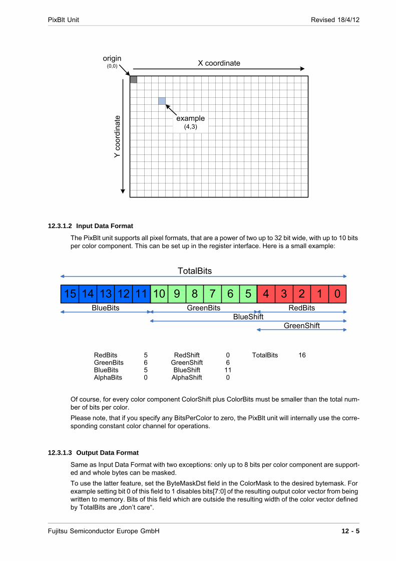
PixBlt Unit Revised 18/4/12
12.3.1.2 Input Data Format
The PixBlt unit supports all pixel formats, that are a power of two up to 32 bit wide, with up to 10 bits per color component. This can be set up in the register interface. Here is a small example:
Of course, for every color component ColorShift plus ColorBits must be smaller than the total num-ber of bits per color.
Please note, that if you specify any BitsPerColor to zero, the PixBlt unit will internally use the corre-sponding constant color channel for operations.
12.3.1.3 Output Data Format
Same as Input Data Format with two exceptions: only up to 8 bits per color component are support-ed and whole bytes can be masked.
To use the latter feature, set the ByteMaskDst field in the ColorMask to the desired bytemask. For example setting bit 0 of this field to 1 disables bits[7:0] of the resulting output color vector from being written to memory. Bits of this field which are outside the resulting width of the color vector defined by TotalBits are „don’t care“.
RedBits 5 RedShift 0 TotalBits 16GreenBits 6 GreenShift 6BlueBits 5 BlueShift 11AlphaBits 0 AlphaShift 0
origin(0,0) X coordinate
Y c
oord
inat
e example(4,3)
15 14 13 12 11 10 9 8 7 6 5 4 3 2 1 0
TotalBits
BlueBits GreenBits RedBitsBlueShift
GreenShift
Fujitsu Semiconductor Europe GmbH 12 - 5

Revised 18/4/12 PixBlt Unit
12.4 Processing Mode
12.4.1 Processing Flow
This is the block diagram for the PixBlt Unit:
The Fetch Units are reading the image data from the AXI bus and the input color conversion units are converting the pixels into the internal RGBA (8888) format. The resulting data is then fed into the arithmetic or logical unit, or sent to the shader. The results are then multiplexed to the output color conversion unit, which can apply dithering if desired, and stored into memory via the AXI bus.
12.4.2 Processing Algorithm
12.4.2.1 Copy Mode
When copying pixel data with the PixBlt unit, only the first Fetch unit is active and a bypasspath not present in the block diagram above is used. As this bypasspath runs through both color conversion units, a loss of accuracy can not be avoided if copying 10bit wide color components, as the output format only supports up to 8 bits per color component. On the other hand, dithering and any color format conversion desired can be performed without loss of performance.
12.4.2.2 Fill Mode
When filling a rectangle in memory with a constant color, that constant color is multiplexed into the output color conversion unit, allowing any color format to be written. If the resulting pixel is 32 bits wide, another mode can be used, where the output color conversion unit produces the pixel twice in a 64 bit vector and the PixBlt unit can thus write 2 pixels per clock in this case.
Register Interface
Store Unit
Mux to Shader
CC
Fetch UnitFetch UnitFetch Unit
From Shader
Mux
to
Ou
tpu
tArithmetic Operation
Logical Operation
CCCCCCA
XI A
XI
AHB
12 - 6 Fujitsu Semiconductor Europe GmbH

PixBlt Unit Revised 18/4/12
12.4.2.3 Raster Operation Mode
The PixBlt Unit is able to automatically detect from the RasterOperationIndex specified which fetch units are not needed and automatically deactivates them, thus saving bus load.
Table 12-1: ROP Mode
The above table shows the result for an operation index of 0x5A. Each color component from each input is used to index the operation index as a lookuptable. The Pattern bit differentiates between the upper and lower 4 bits, the source bit of the upper and lower 2 bits, and the source bit finally selects between the remaining two bits. Like this, the above operation index of 0x5A results in the logical operation Pattern XOR Source.
The PixBlt Unit is able to automatically detect from the RasterOperationIndex specified which fetch units are not needed and automatically deactivates them, thus saving bus load. In the above exam-ple the destination does not have an influence on the result of the operation, so the second fetchunit will automatically be deactivated.
12.4.2.4 2X2 and 3X3 Filter Modes
The 2X2 and 3X3 filter modes reuse the arithmetic data path for calculations. This is achieved by having them calculate the up to 3 columns of the filter matrix from left to right and storing the result in an external register, adding it on to the previous value as necessary.
OpenVG tiling modes are supported for cases when pixels outside the image rectangle are needed (see OpenVG Specification for further information).
12.4.2.5 Blending Mode
The PixBlt unit fully supports OpenVG and OpenGL blending modes with the exception of needing the shader to remove premultiplication from the result. See the OpenVG and OpenGL Specifications for further information.
12.4.2.6 Shader Modes
The modes blending, filtering and ROP can be combined with the shader. The fetched data can be either sent to the shader after passing through the operation, or right after the input color conversion. The result is then returned from the shader into the output color conversion unit and to the fetch unit.
There is an additional shader mode called OP_SHADERSLICEMATRIX that can be used to save interface bandwidth by sending a matrix not row by row to the shader, but column by column instead. The following Figure shows how it works: Instead of transmitting every matrix completely to the shader, we only transmit every column once. The initialization problem is solved by sending the End-ofTransfer signal only if there really is a whole matrix transferred to the shader.
Pattern Destination Source Result0 0 0 00 0 1 10 1 0 00 1 1 11 0 0 11 0 1 01 1 0 11 1 1 0
code 0x5A
Fujitsu Semiconductor Europe GmbH 12 - 7
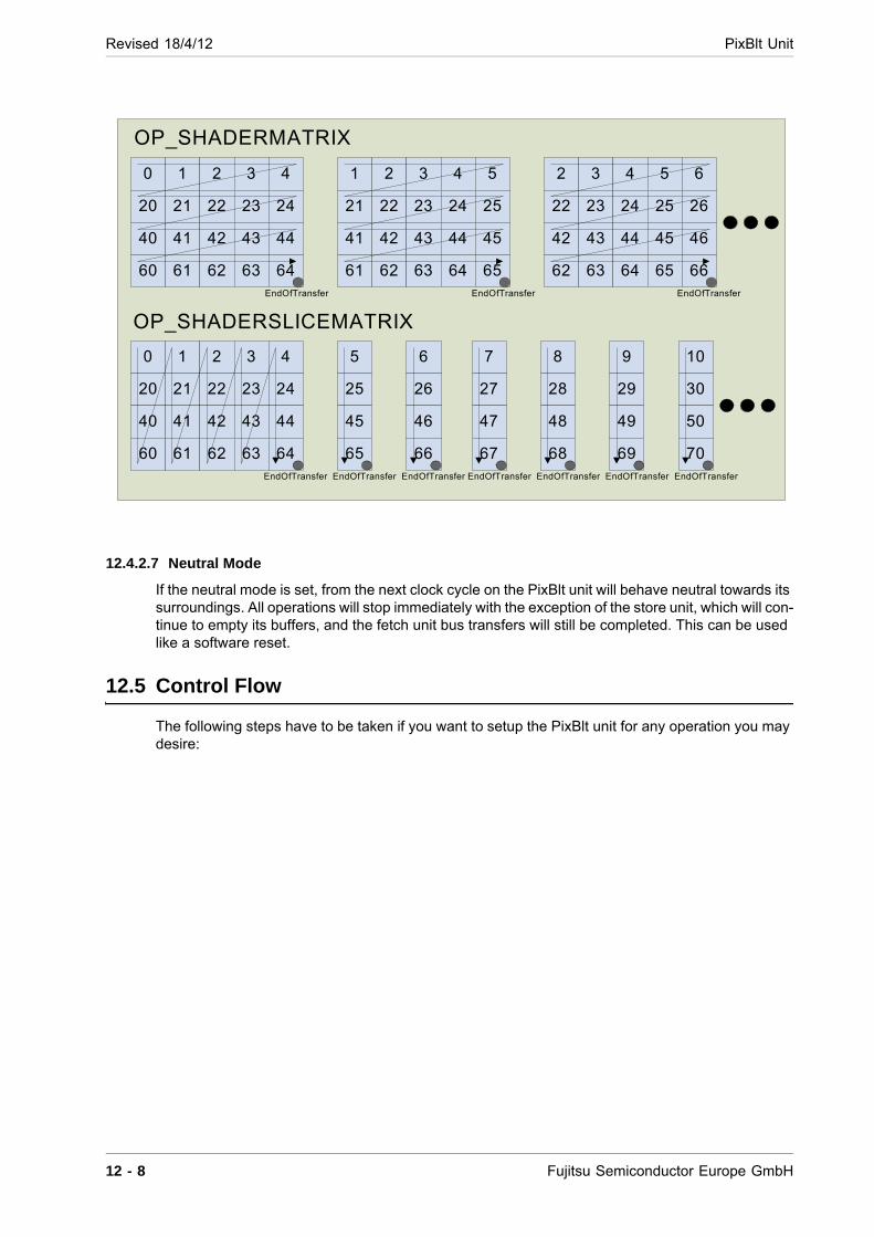
Revised 18/4/12 PixBlt Unit
12.4.2.7 Neutral Mode
If the neutral mode is set, from the next clock cycle on the PixBlt unit will behave neutral towards its surroundings. All operations will stop immediately with the exception of the store unit, which will con-tinue to empty its buffers, and the fetch unit bus transfers will still be completed. This can be used like a software reset.
12.5 Control Flow
The following steps have to be taken if you want to setup the PixBlt unit for any operation you may desire:
0 1 2 3 4
20 21 22 23 24
40 41 42 43 44
60 61 62 63 64
1 2 3 4
21 22 23 24
41 42 43 44
61 62 63 64
5
25
45
65
2 3 4
22 23 24
42 43 44
62 63 64
5
25
45
65
6
26
46
66
0 1 2 3 4
20 21 22 23 24
40 41 42 43 44
60 61 62 63 64
5
25
45
65
6
26
46
66
7
27
47
67
8
28
48
68
9
29
49
69
10
30
50
70
EndOfTransfer EndOfTransfer EndOfTransfer
EndOfTransfer EndOfTransfer EndOfTransfer EndOfTransfer EndOfTransfer EndOfTransfer EndOfTransfer
OP_SHADERMATRIX
OP_SHADERSLICEMATRIX
12 - 8 Fujitsu Semiconductor Europe GmbH
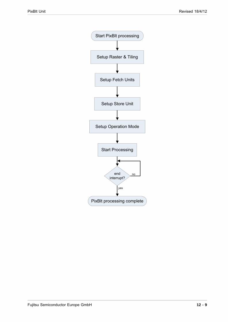
PixBlt Unit Revised 18/4/12
Start PixBlt processing
Setup Store Unit
PixBlt processing complete
Start Processing
Setup Raster & Tiling
Setup Fetch Units
Setup Operation Mode
end interrupt?
no
yes
Fujitsu Semiconductor Europe GmbH 12 - 9

Revised 18/4/12 PixBlt Unit
1) Setup Raster & Tiling
a.Set Raster register
Write to the Raster register the width and height of the rectangle you wish to work on. Both width and height have to be specified minus 1, so as a height of 0 means the rectangle is exactly one pixel high.
Please note for 64 bit fill, that because two 32 bit pixels are written per cycle, the width has to be set to half the width in 32 bit pixels minus one.
b.Set SubRaster register
If you want to use filter modes with or without shader, you will have to remember to set the Sub-Raster Enable bit in the Control register in the last step, and enter the filterwidth and filterheight into the corresponding fields of the SubRaster register. Be aware that filterwidth and filterheight are giv-en minus 1, so as a filterheight of 0 corresponds to a 1 pixel high filterkernel.
If you do not want to use filter modes you will have to set enable bit of the SubRaster mode to a logical 0 later.
c.Setup Tiling
Setup Raster & Tiling
Raster & Tiling configuration completed
Set width & height
Set subraster (filter width & filter height)
Setup tiling(tiling mode & PicStartX, PicStartY, PicEndX, PicEndY coordinates)
filtering? no
yes
tiling needed?
no
yes
12 - 10 Fujitsu Semiconductor Europe GmbH
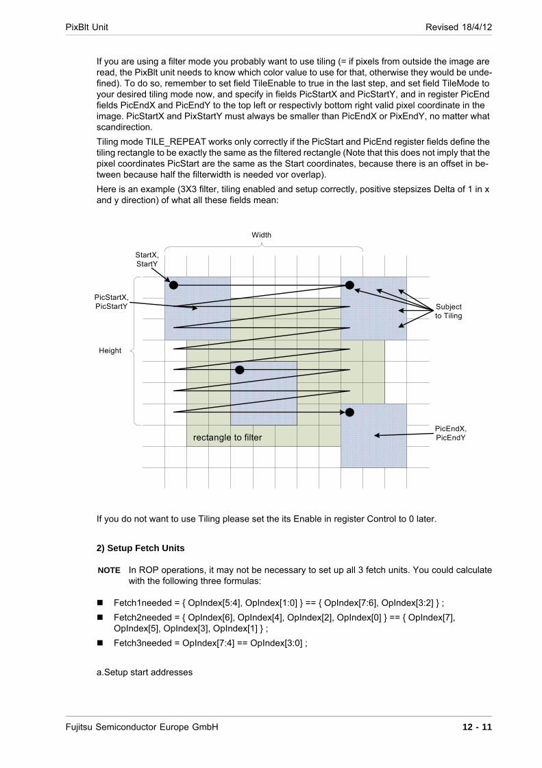
PixBlt Unit Revised 18/4/12
If you are using a filter mode you probably want to use tiling (= if pixels from outside the image are read, the PixBlt unit needs to know which color value to use for that, otherwise they would be unde-fined). To do so, remember to set field TileEnable to true in the last step, and set field TileMode to your desired tiling mode now, and specify in fields PicStartX and PicStartY, and in register PicEnd fields PicEndX and PicEndY to the top left or respectivly bottom right valid pixel coordinate in the image. PicStartX and PixStartY must always be smaller than PicEndX or PixEndY, no matter what scandirection.
Tiling mode TILE_REPEAT works only correctly if the PicStart and PicEnd register fields define the tiling rectangle to be exactly the same as the filtered rectangle (Note that this does not imply that the pixel coordinates PicStart are the same as the Start coordinates, because there is an offset in be-tween because half the filterwidth is needed vor overlap).
Here is an example (3X3 filter, tiling enabled and setup correctly, positive stepsizes Delta of 1 in x and y direction) of what all these fields mean:
If you do not want to use Tiling please set the its Enable in register Control to 0 later.
2) Setup Fetch Units
NOTE In ROP operations, it may not be necessary to set up all 3 fetch units. You could calculate with the following three formulas:
Fetch1needed = OpIndex[5:4], OpIndex[1:0] == OpIndex[7:6], OpIndex[3:2] ;
Fetch2needed = OpIndex[6], OpIndex[4], OpIndex[2], OpIndex[0] == OpIndex[7], OpIndex[5], OpIndex[3], OpIndex[1] ;
Fetch3needed = OpIndex[7:4] == OpIndex[3:0] ;
a.Setup start addresses
Width
Height
StartX,StartY
PicStartX,PicStartY
PicEndX,PicEndY
Subjectto Tiling
rectangle to filter
Fujitsu Semiconductor Europe GmbH 12 - 11
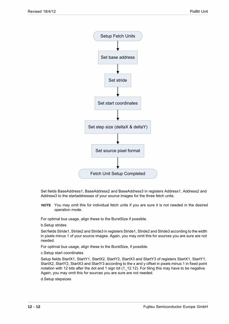
Revised 18/4/12 PixBlt Unit
Set fields BaseAddress1, BaseAddress2 and BaseAddress3 in registers Address1, Address2 and Address3 to the startaddresses of your source images for the three fetch units.
NOTE You may omit this for individual fetch units if you are sure it is not needed in the desired operation mode.
For optimal bus usage, align these to the BurstSize if possible.
b.Setup strides
Set fields Stride1, Stride2 and Stride3 in registers Stride1, Stride2 and Stride3 according to the width in pixels minus 1 of your source images. Again, you may omit this for sources you are sure are not needed.
For optimal bus usage, align these to the BurstSize, if possible.
c.Setup start coordinates
Setup fields StartX1, StartY1, StartX2, StartY2, StartX3 and StartY3 of registers StartX1, StartY1, StartX2, StartY2, StartX3 and StartY3 according to the x and y offset in pixels minus 1 in fixed point notation with 12 bits after the dot and 1 sign bit (1_12.12). For tiling this may have to be negative. Again, you may omit this for sources you are sure are not needed.
d.Setup stepsizes
Setup Fetch Units
Set step size (deltaX & deltaY)
Fetch Unit Setup Completed
Set source pixel format
Set base address
Set stride
Set start coordinates
12 - 12 Fujitsu Semiconductor Europe GmbH

PixBlt Unit Revised 18/4/12
Set fields DeltaX1, DeltaY1, DeltaX2, DeltaY2, DeltaX3 and DeltaY3 of registers DeltaX1, DeltaY1, DeltaX2, DeltaY2, DeltaX3 and DeltaY3 according to the desired stepsize in each individual image. This is in the same format as the start coordinates, and again this may be negative. But be aware that when filtering the stepsizes should be integers only. Again, you may omit this for sources you are sure are not needed.
e.Setup source pixelformats
Next, all fields in the PixelType, ColorBits and ColorShift registers must be set for all sources that are going to be used. This enables the input color conversion unit to convert the pixels correctly into the internal RGBA(8888) format.
Fujitsu Semiconductor Europe GmbH 12 - 13

Revised 18/4/12 PixBlt Unit
3)Setup Store Unit
a.Setup destination address
Now you can begin to setup the store unit: First, start with the BaseAddressDst field in the Address-Dst register. Again, for optimal bus usage, align this to BurstSize.
b.Setup destination stride
Then set the StrideDst field in the StrideDst register to the output image width in pixels minus 1. Again, for optimal bus usage, align this to BurstSize.
Please note for 64 bit fill, that because two 32 bit pixels are written in each cycle, the stride has to be set to half of the 32 bit pixel stride minus one.
c.Setup destination offset
Now, set the StartXDst and StartYDst fields in the StartDst register to the destination rectangle x and y startpoint offset.
d.Setup destination scan direction
Next, set the DeltaXDst and DeltaYDst fields in the DeltaDst register to 1 if the corresponding scan direction is negative.
e.Setup destination pixel format
Set the ColorBitsDst, ColorShiftDst and PixelTypeDst registers according to the destination pixel format you want written to memory.
Setup Store Unit
Set scan direction
Store Unit Setup completed
Set destination pixel format
Set destination address
Set stride
Set offset (StartXDst & StartYDst)
12 - 14 Fujitsu Semiconductor Europe GmbH
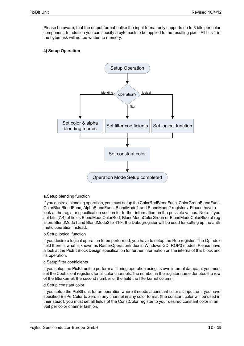
PixBlt Unit Revised 18/4/12
Please be aware, that the output format unlike the input format only supports up to 8 bits per color component. In addition you can specify a bytemask to be applied to the resulting pixel. All bits 1 in the bytemask will not be written to memory.
4) Setup Operation
a.Setup blending function
If you desire a blending operation, you must setup the ColorRedBlendFunc, ColorGreenBlendFunc, ColorBlueBlendFunc, AlphaBlendFunc, BlendMode1 and BlendMode2 registers. Please have a look at the register specification section for further information on the possible values. Note: If you set bits [7:4] of fields BlendModeColorRed, BlendModeColorGreen or BlendModeColorBlue of reg-isters BlendMode1 and BlendMode2 to 4’hF, the Debugregister will be used for setting up the arith-metic operation instead.
b.Setup logical function
If you desire a logical operation to be performed, you have to setup the Rop register. The OpIndex field there is what is known as RasterOperationIndex in Windows GDI ROP3 modes. Please have a look at the PixBlt Block Design specification for further information on the interna of this block and its operation.
c.Setup filter coefficients
If you setup the PixBlt unit to perform a filtering operation using its own internal datapath, you must set the Coefficient registers for all color channels.The number in the register name denotes the row of the filterkernel, the second number of the field the filterkernel column.
d.Setup constant color
If you setup the PixBlt unit for an operation where it needs a constant color as input, or if you have specified BisPerColor to zero in any channel in any color format (the constant color will be used in their stead), you must set all fields of the ConstColor register to your desired constant color in an 8bit per color channel fashion.
Setup Operation
Set constant color
Operation Mode Setup completed
Set filter coefficients
operation?blending
filter
logical
Set color & alphablending modes
Set logical function
Fujitsu Semiconductor Europe GmbH 12 - 15
Revised 18/4/12 PixBlt Unit
5) Start processing and wait for Interrupt
a.Setup OpMode and Enables and Start of Operation
The field MODE of register Control has to be set to your desired operation mode. The individual bits of this field have the following effect:
[10]enables the third fetch unit, not effective if we are using the logical datapath, when it
is automatically decoded if the first fetch unit is needed of not
[9]enables the second fetch unit, same restriction for logical operation as above
[8]enables the first fetch unit, same restriction for logical operation as above
[7]if this is 0, we are going to send data to the shader from before the PixBlt datapath, if
it is 1, from after our datapath
[6]if this is 1, we are going to internally select arithmetic operations as the PixBlt
datapath, else logical operations
[5:4]if this is 2’b00, we are choosing the copy bypass, if 2’b01 the fill color, if 2’b10 the
result from our own datapath and if it is 2’b11 we are choosing the result from the
shader to be stored to memory
[3:2]if this is 2’b00 all glue logic is setup for 2X2 operation, if it is 2’b01 for 3X3 operation,
and if it is 2’b11, for blending operation.
[1:0]if this is 2’b00, there is no data synchronisation between the three fetch units, if it is
2’b01 the first two are synched, if it is 2’b10 all three are synched, and if it is 2’b11 we
are in slicematrixmode and mask the EndOfTransfer signal to the shader accordingly
There should be predefined operation modes available for you for your comfort.
The Enable fields of this register do also have to be set to whether you want the corresponding fea-tures active or not. Please remember that this has to match with the settings you chose for these modes in earlier steps.
To finally start the operation of the PixBlt unit you will have to write the Control register, with a logical 1 to the Start field.
Please take a note that this is the only step that has a fixed place in this sequence of register setups: It has to be at the end. The order of all other steps can be any you like.
b.Wait for Interrupt
The PixBlt unit will produce an interrupt once all of its results is in its output buffer. To be absolutely sure that the store buffer is empty, you can read the Status register field StatusWrite and wait for it to be 0 before setting up the registers for the next operation.
12 - 16 Fujitsu Semiconductor Europe GmbH
PixBlt Unit Revised 18/4/12
12.6 Software Interface
12.6.1 Register Summary
Address Register Name DescriptionBase address + 0H Control PixBlt operation mode Base address + 4H Status Shows status information Base address + 8H Raster Defines operation rectangle Base address + CH SubRaster Defines size of filter matrix Base address + 10H Tiling Base address + 14H PicEnd Picture end coordinates for tiling mode Base address + 18H Address1 Base address + 1CH Stride1 Base address + 20H StartX1 Horizontal offset in pixel of input surface #1 Base address + 24H StartY1 Vertical offset in pixel of input surface #1 Base address + 28H DeltaX1 Horizontal increment in pixel of input surface #1 Base address + 2CH DeltaY1 Vertical increment in pixel of input surface #1 Base address + 30H PixelType1 Base address + 34H ColorBits1 Color component size of input surface #1 Base address + 38H ColorShift1 Color component offset of input surface #1 Base address + 3CH Address2 Base address + 40H Stride2 Base address + 44H StartX2 Horizontal offset in pixel of input surface #2 Base address + 48H StartY2 Vertical offset in pixel of input surface #2 Base address + 4CH DeltaX2 Horizontal increment in pixel of input surface #2 Base address + 50H DeltaY2 Vertical increment in pixel of input surface #2 Base address + 54H PixelType2 Base address + 58H ColorBits2 Color component size of input surface #2 Base address + 5CH ColorShift2 Color component offset of input surface #2 Base address + 60H Address3 Base address + 64H Stride3 Base address + 68H StartX3 Horizontal offset in pixel of input surface #3 Base address + 6CH StartY3 Vertical offset in pixel of input surface #3 Base address + 70H DeltaX3 Horizontal increment in pixel of input surface #3 Base address + 74H DeltaY3 Vertical increment in pixel of input surface #3 Base address + 78H PixelType3 Base address + 7CH ColorBits3 Color component size of input surface #3 Base address + 80H ColorShift3 Color component offset of input surface #3 Base address + 84H AddressDst Base address + 88H StrideDst Base address + 8CH StartXDst Horizontal offset in pixels of output surface Base address + 90H StartYDst Vertical offset in pixels of output surface Base address + 94H DeltaXDst Horizontal scan direction within output surface Base address + 98H DeltaYDst Vertical scan direction within output surface Base address + 9CH PixelTypeDst Base address + A0H ColorBitsDst Color component size of output surface Base address + A4H ColorShiftDst Color component offset of output surface
Base address + A8H ColorMask
Masks bytes of the output pixel, only those bytes within the pixel size specified by field TotalBitsDst are taken into account, 1 = byte masked, 0 = byte gets written
Fujitsu Semiconductor Europe GmbH 12 - 17
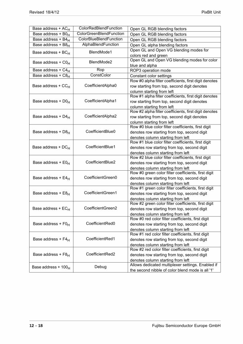
Revised 18/4/12 PixBlt Unit
Base address + ACH ColorRedBlendFunction Open GL RGB blending factors Base address + B0H ColorGreenBlendFunction Open GL RGB blending factors Base address + B4H ColorBlueBlendFunction Open GL RGB blending factors Base address + B8H AlphaBlendFunction Open GL alpha blending factors
Base address + BCH BlendMode1 Open GL and Open VG blending modes for colors red and green
Base address + C0H BlendMode2 Open GL and Open VG blending modes for color blue and alpha
Base address + C4H Rop ROP3 operation mode Base address + C8H ConstColor Constant color settings
Base address + CCH CoefficientAlpha0 Row #0 alpha filter coefficients, first digit denotes row starting from top, second digit denotes column starting from left
Base address + D0H CoefficientAlpha1 Row #1 alpha filter coefficients, first digit denotes row starting from top, second digit denotes column starting from left
Base address + D4H CoefficientAlpha2 Row #2 alpha filter coefficients, first digit denotes row starting from top, second digit denotes column starting from left
Base address + D8H CoefficientBlue0 Row #0 blue color filter coefficients, first digit denotes row starting from top, second digit denotes column starting from left
Base address + DCH CoefficientBlue1 Row #1 blue color filter coefficients, first digit denotes row starting from top, second digit denotes column starting from left
Base address + E0H CoefficientBlue2 Row #2 blue color filter coefficients, first digit denotes row starting from top, second digit denotes column starting from left
Base address + E4H CoefficientGreen0 Row #0 green color filter coefficients, first digit denotes row starting from top, second digit denotes column starting from left
Base address + E8H CoefficientGreen1 Row #1 green color filter coefficients, first digit denotes row starting from top, second digit denotes column starting from left
Base address + ECH CoefficientGreen2 Row #2 green color filter coefficients, first digit denotes row starting from top, second digit denotes column starting from left
Base address + F0H CoefficientRed0 Row #0 red color filter coefficients, first digit denotes row starting from top, second digit denotes column starting from left
Base address + F4H CoefficientRed1 Row #1 red color filter coefficients, first digit denotes row starting from top, second digit denotes column starting from left
Base address + F8H CoefficientRed2 Row #2 red color filter coefficients, first digit denotes row starting from top, second digit denotes column starting from left
Base address + 100H Debug Allows dedicated multiplexer settings. Enabled if the second nibble of color blend mode is all '1'
12 - 18 Fujitsu Semiconductor Europe GmbH
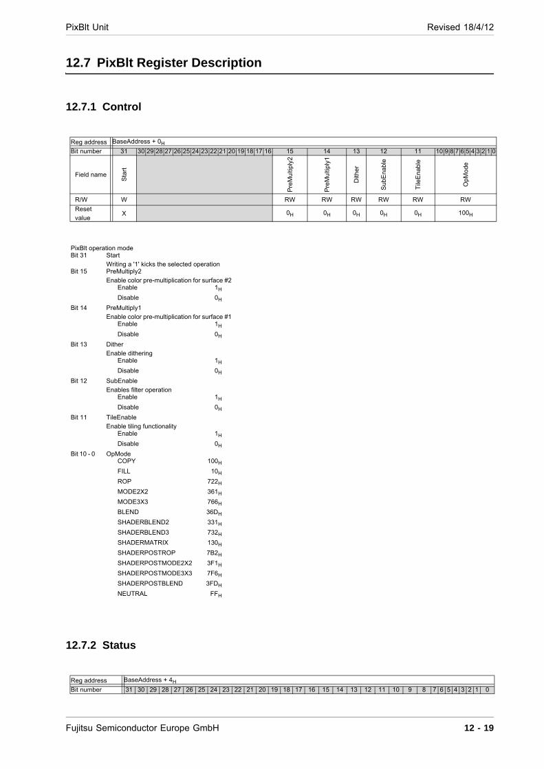
PixBlt Unit Revised 18/4/12
12.7 PixBlt Register Description
12.7.1 Control
12.7.2 Status
Reg address BaseAddress + 0H
Bit number 31 30 29 28 27 26 25 24 23 22 21 20 19 18 17 16 15 14 13 12 11 10 9 8 7 6 5 4 3 2 1 0
Field name
Sta
rt
Pre
Mu
ltipl
y2
Pre
Mu
ltipl
y1
Dith
er
Sub
En
able
Tile
En
abl
e
Op
Mo
de
R/W W RW RW RW RW RW RW
Reset
valueX 0H 0H 0H 0H 0H 100H
PixBlt operation mode Bit 31 Start
Writing a '1' kicks the selected operation Bit 15 PreMultiply2
Enable color pre-multiplication for surface #2 Enable 1H
Disable 0H
Bit 14 PreMultiply1 Enable color pre-multiplication for surface #1
Enable 1H
Disable 0H
Bit 13 Dither Enable dithering
Enable 1H
Disable 0H
Bit 12 SubEnable Enables filter operation
Enable 1H
Disable 0H
Bit 11 TileEnable Enable tiling functionality
Enable 1H
Disable 0H
Bit 10 - 0 OpMode COPY 100H
FILL 10H
ROP 722H
MODE2X2 361H
MODE3X3 766H
BLEND 36DH
SHADERBLEND2 331H
SHADERBLEND3 732H
SHADERMATRIX 130H
SHADERPOSTROP 7B2H
SHADERPOSTMODE2X2 3F1H
SHADERPOSTMODE3X3 7F6H
SHADERPOSTBLEND 3FDH
NEUTRAL FFH
Reg address BaseAddress + 4H
Bit number 31 30 29 28 27 26 25 24 23 22 21 20 19 18 17 16 15 14 13 12 11 10 9 8 7 6 5 4 3 2 1 0
Fujitsu Semiconductor Europe GmbH 12 - 19
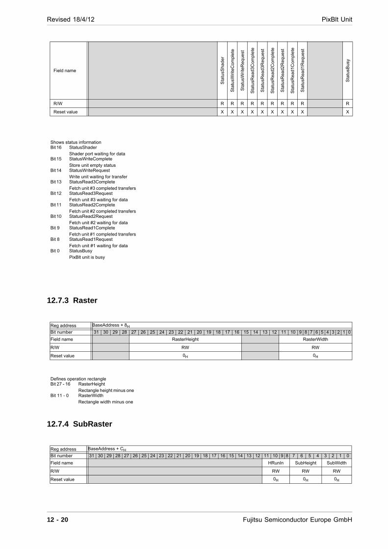
Revised 18/4/12 PixBlt Unit
12.7.3 Raster
12.7.4 SubRaster
Field name
Sta
tusS
ha
der
Sta
tusW
rite
Co
mpl
ete
Sta
tusW
rite
Re
que
st
Sta
tusR
ea
d3C
omp
lete
Sta
tusR
ead
3R
equ
est
Sta
tusR
ea
d2C
omp
lete
Sta
tusR
ead
2R
equ
est
Sta
tusR
ea
d1C
omp
lete
Sta
tusR
ead
1R
equ
est
Sta
tusB
usy
R/W R R R R R R R R R R
Reset value X X X X X X X X X X
Shows status information Bit 16 StatusShader
Shader port waiting for data Bit 15 StatusWriteComplete
Store unit empty status Bit 14 StatusWriteRequest
Write unit waiting for transfer Bit 13 StatusRead3Complete
Fetch unit #3 completed transfers Bit 12 StatusRead3Request
Fetch unit #3 waiting for data Bit 11 StatusRead2Complete
Fetch unit #2 completed transfers Bit 10 StatusRead2Request
Fetch unit #2 waiting for data Bit 9 StatusRead1Complete
Fetch unit #1 completed transfers Bit 8 StatusRead1Request
Fetch unit #1 waiting for data Bit 0 StatusBusy
PixBlt unit is busy
Reg address BaseAddress + 8H
Bit number 31 30 29 28 27 26 25 24 23 22 21 20 19 18 17 16 15 14 13 12 11 10 9 8 7 6 5 4 3 2 1 0
Field name RasterHeight RasterWidth
R/W RW RW
Reset value 0H 0H
Defines operation rectangle Bit 27 - 16 RasterHeight
Rectangle height minus one Bit 11 - 0 RasterWidth
Rectangle width minus one
Reg address BaseAddress + CH
Bit number 31 30 29 28 27 26 25 24 23 22 21 20 19 18 17 16 15 14 13 12 11 10 9 8 7 6 5 4 3 2 1 0
Field name HRunIn SubHeight SubWidth
R/W RW RW RW
Reset value 0H 0H 0H
12 - 20 Fujitsu Semiconductor Europe GmbH
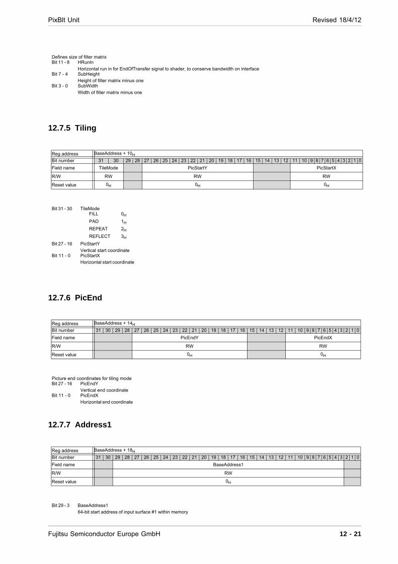
PixBlt Unit Revised 18/4/12
12.7.5 Tiling
12.7.6 PicEnd
12.7.7 Address1
Defines size of filter matrix Bit 11 - 8 HRunIn
Horizontal run in for EndOfTransfer signal to shader, to conserve bandwidth on interface Bit 7 - 4 SubHeight
Height of filter matrix minus one Bit 3 - 0 SubWidth
Width of filter matrix minus one
Reg address BaseAddress + 10H
Bit number 31 30 29 28 27 26 25 24 23 22 21 20 19 18 17 16 15 14 13 12 11 10 9 8 7 6 5 4 3 2 1 0
Field name TileMode PicStartY PicStartX
R/W RW RW RW
Reset value 0H 0H 0H
Bit 31 - 30 TileMode FILL 0H
PAD 1H
REPEAT 2H
REFLECT 3H
Bit 27 - 16 PicStartY Vertical start coordinate
Bit 11 - 0 PicStartX Horizontal start coordinate
Reg address BaseAddress + 14H
Bit number 31 30 29 28 27 26 25 24 23 22 21 20 19 18 17 16 15 14 13 12 11 10 9 8 7 6 5 4 3 2 1 0
Field name PicEndY PicEndX
R/W RW RW
Reset value 0H 0H
Picture end coordinates for tiling mode Bit 27 - 16 PicEndY
Vertical end coordinate Bit 11 - 0 PicEndX
Horizontal end coordinate
Reg address BaseAddress + 18H
Bit number 31 30 29 28 27 26 25 24 23 22 21 20 19 18 17 16 15 14 13 12 11 10 9 8 7 6 5 4 3 2 1 0
Field name BaseAddress1
R/W RW
Reset value 0H
Bit 29 - 3 BaseAddress1 64-bit start address of input surface #1 within memory
Fujitsu Semiconductor Europe GmbH 12 - 21
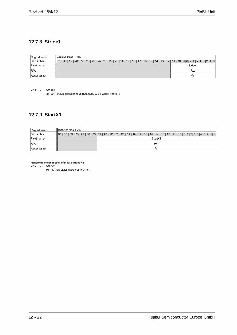
Revised 18/4/12 PixBlt Unit
12.7.8 Stride1
12.7.9 StartX1
Reg address BaseAddress + 1CH
Bit number 31 30 29 28 27 26 25 24 23 22 21 20 19 18 17 16 15 14 13 12 11 10 9 8 7 6 5 4 3 2 1 0
Field name Stride1
R/W RW
Reset value 0H
Bit 11 - 0 Stride1 Stride in pixels minus one of input surface #1 within memory
Reg address BaseAddress + 20H
Bit number 31 30 29 28 27 26 25 24 23 22 21 20 19 18 17 16 15 14 13 12 11 10 9 8 7 6 5 4 3 2 1 0
Field name StartX1
R/W RW
Reset value 0H
Horizontal offset in pixel of input surface #1 Bit 24 - 0 StartX1
Format is s12.12, two's complement
12 - 22 Fujitsu Semiconductor Europe GmbH
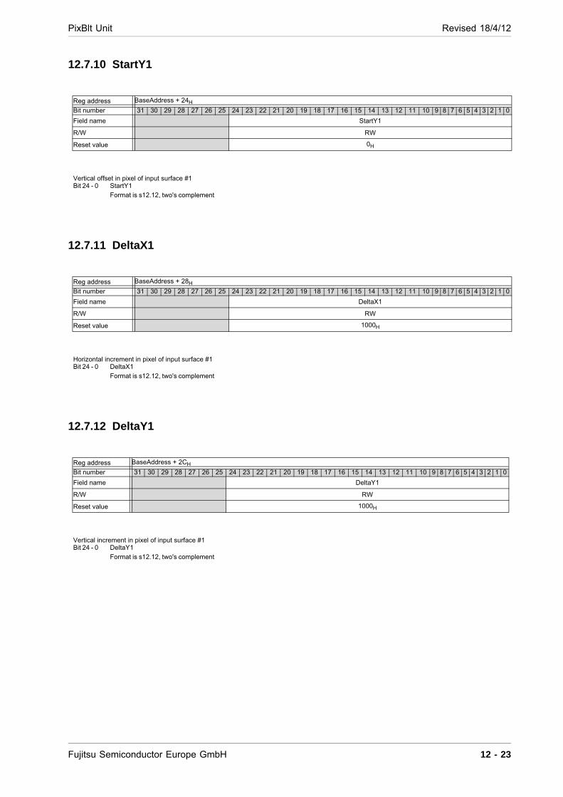
PixBlt Unit Revised 18/4/12
12.7.10 StartY1
12.7.11 DeltaX1
12.7.12 DeltaY1
Reg address BaseAddress + 24H
Bit number 31 30 29 28 27 26 25 24 23 22 21 20 19 18 17 16 15 14 13 12 11 10 9 8 7 6 5 4 3 2 1 0
Field name StartY1
R/W RW
Reset value 0H
Vertical offset in pixel of input surface #1 Bit 24 - 0 StartY1
Format is s12.12, two's complement
Reg address BaseAddress + 28H
Bit number 31 30 29 28 27 26 25 24 23 22 21 20 19 18 17 16 15 14 13 12 11 10 9 8 7 6 5 4 3 2 1 0
Field name DeltaX1
R/W RW
Reset value 1000H
Horizontal increment in pixel of input surface #1 Bit 24 - 0 DeltaX1
Format is s12.12, two's complement
Reg address BaseAddress + 2CH
Bit number 31 30 29 28 27 26 25 24 23 22 21 20 19 18 17 16 15 14 13 12 11 10 9 8 7 6 5 4 3 2 1 0
Field name DeltaY1
R/W RW
Reset value 1000H
Vertical increment in pixel of input surface #1 Bit 24 - 0 DeltaY1
Format is s12.12, two's complement
Fujitsu Semiconductor Europe GmbH 12 - 23
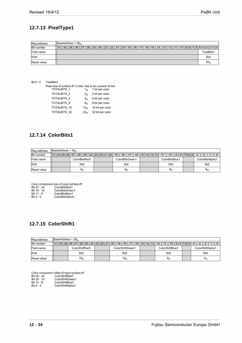
Revised 18/4/12 PixBlt Unit
12.7.13 PixelType1
12.7.14 ColorBits1
12.7.15 ColorShift1
Reg address BaseAddress + 30H
Bit number 31 30 29 28 27 26 25 24 23 22 21 20 19 18 17 16 15 14 13 12 11 10 9 8 7 6 5 4 3 2 1 0
Field name TotalBits1
R/W RW
Reset value 20H
Bit 5 - 0 TotalBits1 Pixel size of surface #1 in bits, has to be a power of two
TOTALBITS_1 1H 1 bit per color
TOTALBITS_2 2H 2 bit per color
TOTALBITS_4 4H 4 bit per color
TOTALBITS_8 8H 8 bit per color
TOTALBITS_16 10H 16 bit per color
TOTALBITS_32 20H 32 bit per color
Reg address BaseAddress + 34H
Bit number 31 30 29 28 27 26 25 24 23 22 21 20 19 18 17 16 15 14 13 12 11 10 9 8 7 6 5 4 3 2 1 0
Field name ColorBitsRed1 ColorBitsGreen1 ColorBitsBlue1 ColorBitsAlpha1
R/W RW RW RW RW
Reset value 8H 8H 8H 8H
Color component size of input surface #1 Bit 27 - 24 ColorBitsRed1 Bit 19 - 16 ColorBitsGreen1 Bit 11 - 8 ColorBitsBlue1 Bit 3 - 0 ColorBitsAlpha1
Reg address BaseAddress + 38H
Bit number 31 30 29 28 27 26 25 24 23 22 21 20 19 18 17 16 15 14 13 12 11 10 9 8 7 6 5 4 3 2 1 0
Field name ColorShiftRed1 ColorShiftGreen1 ColorShiftBlue1 ColorShiftAlpha1
R/W RW RW RW RW
Reset value 18H 10H 8H 0H
Color component offset of input surface #1 Bit 28 - 24 ColorShiftRed1 Bit 20 - 16 ColorShiftGreen1 Bit 12 - 8 ColorShiftBlue1 Bit 4 - 0 ColorShiftAlpha1
12 - 24 Fujitsu Semiconductor Europe GmbH
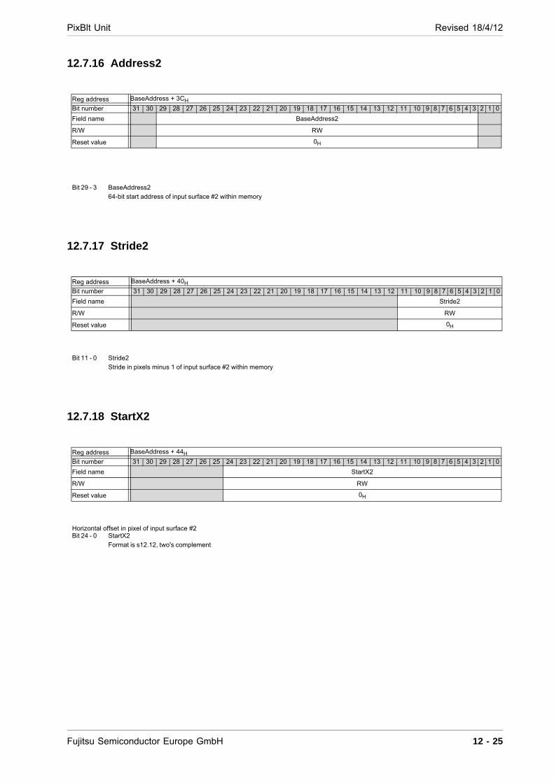
PixBlt Unit Revised 18/4/12
12.7.16 Address2
12.7.17 Stride2
12.7.18 StartX2
Reg address BaseAddress + 3CH
Bit number 31 30 29 28 27 26 25 24 23 22 21 20 19 18 17 16 15 14 13 12 11 10 9 8 7 6 5 4 3 2 1 0
Field name BaseAddress2
R/W RW
Reset value 0H
Bit 29 - 3 BaseAddress2 64-bit start address of input surface #2 within memory
Reg address BaseAddress + 40H
Bit number 31 30 29 28 27 26 25 24 23 22 21 20 19 18 17 16 15 14 13 12 11 10 9 8 7 6 5 4 3 2 1 0
Field name Stride2
R/W RW
Reset value 0H
Bit 11 - 0 Stride2 Stride in pixels minus 1 of input surface #2 within memory
Reg address BaseAddress + 44H
Bit number 31 30 29 28 27 26 25 24 23 22 21 20 19 18 17 16 15 14 13 12 11 10 9 8 7 6 5 4 3 2 1 0
Field name StartX2
R/W RW
Reset value 0H
Horizontal offset in pixel of input surface #2 Bit 24 - 0 StartX2
Format is s12.12, two's complement
Fujitsu Semiconductor Europe GmbH 12 - 25
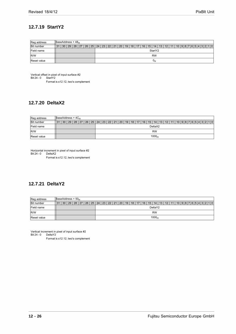
Revised 18/4/12 PixBlt Unit
12.7.19 StartY2
12.7.20 DeltaX2
12.7.21 DeltaY2
Reg address BaseAddress + 48H
Bit number 31 30 29 28 27 26 25 24 23 22 21 20 19 18 17 16 15 14 13 12 11 10 9 8 7 6 5 4 3 2 1 0
Field name StartY2
R/W RW
Reset value 0H
Vertical offset in pixel of input surface #2 Bit 24 - 0 StartY2
Format is s12.12, two's complement
Reg address BaseAddress + 4CH
Bit number 31 30 29 28 27 26 25 24 23 22 21 20 19 18 17 16 15 14 13 12 11 10 9 8 7 6 5 4 3 2 1 0
Field name DeltaX2
R/W RW
Reset value 1000H
Horizontal increment in pixel of input surface #2 Bit 24 - 0 DeltaX2
Format is s12.12, two's complement
Reg address BaseAddress + 50H
Bit number 31 30 29 28 27 26 25 24 23 22 21 20 19 18 17 16 15 14 13 12 11 10 9 8 7 6 5 4 3 2 1 0
Field name DeltaY2
R/W RW
Reset value 1000H
Vertical increment in pixel of input surface #2 Bit 24 - 0 DeltaY2
Format is s12.12, two's complement
12 - 26 Fujitsu Semiconductor Europe GmbH
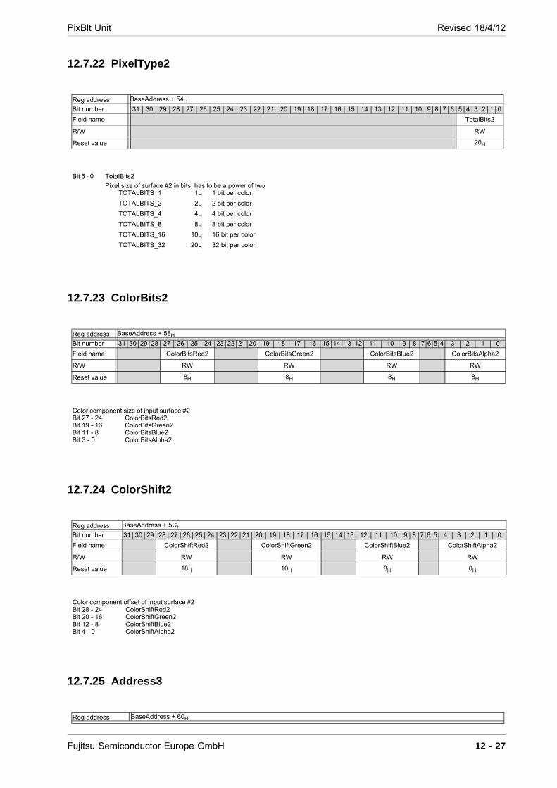
PixBlt Unit Revised 18/4/12
12.7.22 PixelType2
12.7.23 ColorBits2
12.7.24 ColorShift2
12.7.25 Address3
Reg address BaseAddress + 54H
Bit number 31 30 29 28 27 26 25 24 23 22 21 20 19 18 17 16 15 14 13 12 11 10 9 8 7 6 5 4 3 2 1 0
Field name TotalBits2
R/W RW
Reset value 20H
Bit 5 - 0 TotalBits2 Pixel size of surface #2 in bits, has to be a power of two
TOTALBITS_1 1H 1 bit per color
TOTALBITS_2 2H 2 bit per color
TOTALBITS_4 4H 4 bit per color
TOTALBITS_8 8H 8 bit per color
TOTALBITS_16 10H 16 bit per color
TOTALBITS_32 20H 32 bit per color
Reg address BaseAddress + 58H
Bit number 31 30 29 28 27 26 25 24 23 22 21 20 19 18 17 16 15 14 13 12 11 10 9 8 7 6 5 4 3 2 1 0
Field name ColorBitsRed2 ColorBitsGreen2 ColorBitsBlue2 ColorBitsAlpha2
R/W RW RW RW RW
Reset value 8H 8H 8H 8H
Color component size of input surface #2 Bit 27 - 24 ColorBitsRed2 Bit 19 - 16 ColorBitsGreen2 Bit 11 - 8 ColorBitsBlue2 Bit 3 - 0 ColorBitsAlpha2
Reg address BaseAddress + 5CH
Bit number 31 30 29 28 27 26 25 24 23 22 21 20 19 18 17 16 15 14 13 12 11 10 9 8 7 6 5 4 3 2 1 0
Field name ColorShiftRed2 ColorShiftGreen2 ColorShiftBlue2 ColorShiftAlpha2
R/W RW RW RW RW
Reset value 18H 10H 8H 0H
Color component offset of input surface #2 Bit 28 - 24 ColorShiftRed2 Bit 20 - 16 ColorShiftGreen2 Bit 12 - 8 ColorShiftBlue2 Bit 4 - 0 ColorShiftAlpha2
Reg address BaseAddress + 60H
Fujitsu Semiconductor Europe GmbH 12 - 27
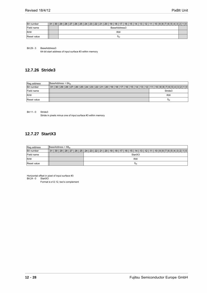
Revised 18/4/12 PixBlt Unit
12.7.26 Stride3
12.7.27 StartX3
Bit number 31 30 29 28 27 26 25 24 23 22 21 20 19 18 17 16 15 14 13 12 11 10 9 8 7 6 5 4 3 2 1 0
Field name BaseAddress3
R/W RW
Reset value 0H
Bit 29 - 3 BaseAddress3 64-bit start address of input surface #3 within memory
Reg address BaseAddress + 64H
Bit number 31 30 29 28 27 26 25 24 23 22 21 20 19 18 17 16 15 14 13 12 11 10 9 8 7 6 5 4 3 2 1 0
Field name Stride3
R/W RW
Reset value 0H
Bit 11 - 0 Stride3 Stride in pixels minus one of input surface #3 within memory
Reg address BaseAddress + 68H
Bit number 31 30 29 28 27 26 25 24 23 22 21 20 19 18 17 16 15 14 13 12 11 10 9 8 7 6 5 4 3 2 1 0
Field name StartX3
R/W RW
Reset value 0H
Horizontal offset in pixel of input surface #3 Bit 24 - 0 StartX3
Format is s12.12, two's complement
12 - 28 Fujitsu Semiconductor Europe GmbH

PixBlt Unit Revised 18/4/12
12.7.28 StartY3
12.7.29 DeltaX3
12.7.30 DeltaY3
Reg address BaseAddress + 6CH
Bit number 31 30 29 28 27 26 25 24 23 22 21 20 19 18 17 16 15 14 13 12 11 10 9 8 7 6 5 4 3 2 1 0
Field name StartY3
R/W RW
Reset value 0H
Vertical offset in pixel of input surface #3 Bit 24 - 0 StartY3
Format is s12.12, two's complement
Reg address BaseAddress + 70H
Bit number 31 30 29 28 27 26 25 24 23 22 21 20 19 18 17 16 15 14 13 12 11 10 9 8 7 6 5 4 3 2 1 0
Field name DeltaX3
R/W RW
Reset value 1000H
Horizontal increment in pixel of input surface #3 Bit 24 - 0 DeltaX3
Format is s12.12, two's complement
Reg address BaseAddress + 74H
Bit number 31 30 29 28 27 26 25 24 23 22 21 20 19 18 17 16 15 14 13 12 11 10 9 8 7 6 5 4 3 2 1 0
Field name DeltaY3
R/W RW
Reset value 1000H
Vertical increment in pixel of input surface #3 Bit 24 - 0 DeltaY3
Format is s12.12, two's complement
Fujitsu Semiconductor Europe GmbH 12 - 29
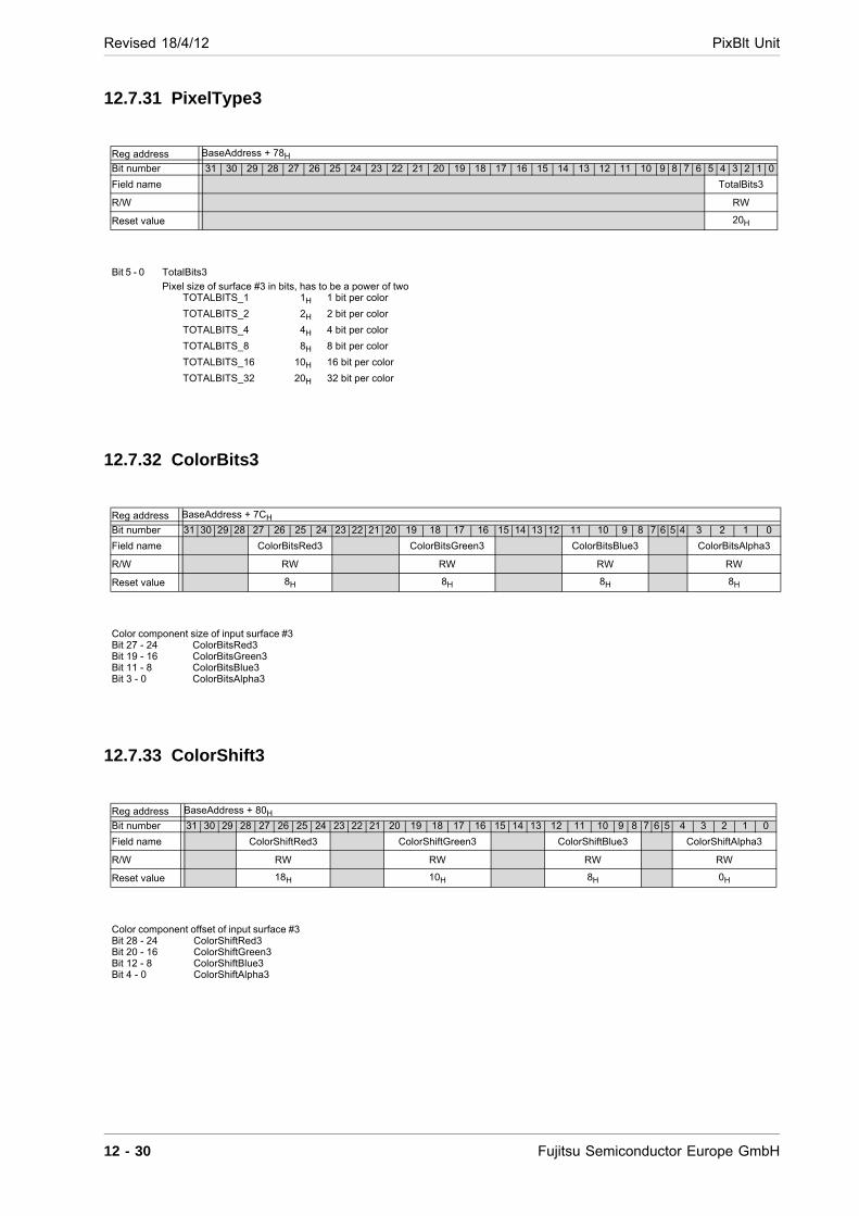
Revised 18/4/12 PixBlt Unit
12.7.31 PixelType3
12.7.32 ColorBits3
12.7.33 ColorShift3
Reg address BaseAddress + 78H
Bit number 31 30 29 28 27 26 25 24 23 22 21 20 19 18 17 16 15 14 13 12 11 10 9 8 7 6 5 4 3 2 1 0
Field name TotalBits3
R/W RW
Reset value 20H
Bit 5 - 0 TotalBits3 Pixel size of surface #3 in bits, has to be a power of two
TOTALBITS_1 1H 1 bit per color
TOTALBITS_2 2H 2 bit per color
TOTALBITS_4 4H 4 bit per color
TOTALBITS_8 8H 8 bit per color
TOTALBITS_16 10H 16 bit per color
TOTALBITS_32 20H 32 bit per color
Reg address BaseAddress + 7CH
Bit number 31 30 29 28 27 26 25 24 23 22 21 20 19 18 17 16 15 14 13 12 11 10 9 8 7 6 5 4 3 2 1 0
Field name ColorBitsRed3 ColorBitsGreen3 ColorBitsBlue3 ColorBitsAlpha3
R/W RW RW RW RW
Reset value 8H 8H 8H 8H
Color component size of input surface #3 Bit 27 - 24 ColorBitsRed3 Bit 19 - 16 ColorBitsGreen3 Bit 11 - 8 ColorBitsBlue3 Bit 3 - 0 ColorBitsAlpha3
Reg address BaseAddress + 80H
Bit number 31 30 29 28 27 26 25 24 23 22 21 20 19 18 17 16 15 14 13 12 11 10 9 8 7 6 5 4 3 2 1 0
Field name ColorShiftRed3 ColorShiftGreen3 ColorShiftBlue3 ColorShiftAlpha3
R/W RW RW RW RW
Reset value 18H 10H 8H 0H
Color component offset of input surface #3 Bit 28 - 24 ColorShiftRed3 Bit 20 - 16 ColorShiftGreen3 Bit 12 - 8 ColorShiftBlue3 Bit 4 - 0 ColorShiftAlpha3
12 - 30 Fujitsu Semiconductor Europe GmbH
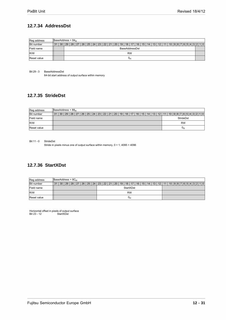
PixBlt Unit Revised 18/4/12
12.7.34 AddressDst
12.7.35 StrideDst
12.7.36 StartXDst
Reg address BaseAddress + 84H
Bit number 31 30 29 28 27 26 25 24 23 22 21 20 19 18 17 16 15 14 13 12 11 10 9 8 7 6 5 4 3 2 1 0
Field name BaseAddressDst
R/W RW
Reset value 0H
Bit 29 - 3 BaseAddressDst 64-bit start address of output surface within memory
Reg address BaseAddress + 88H
Bit number 31 30 29 28 27 26 25 24 23 22 21 20 19 18 17 16 15 14 13 12 11 10 9 8 7 6 5 4 3 2 1 0
Field name StrideDst
R/W RW
Reset value 0H
Bit 11 - 0 StrideDst Stride in pixels minus one of output surface within memory, 0 = 1, 4095 = 4096
Reg address BaseAddress + 8CH
Bit number 31 30 29 28 27 26 25 24 23 22 21 20 19 18 17 16 15 14 13 12 11 10 9 8 7 6 5 4 3 2 1 0
Field name StartXDst
R/W RW
Reset value 0H
Horizontal offset in pixels of output surface Bit 23 - 12 StartXDst
Fujitsu Semiconductor Europe GmbH 12 - 31
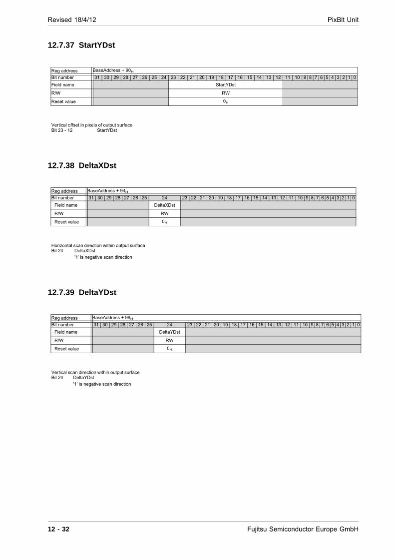
Revised 18/4/12 PixBlt Unit
12.7.37 StartYDst
12.7.38 DeltaXDst
12.7.39 DeltaYDst
Reg address BaseAddress + 90H
Bit number 31 30 29 28 27 26 25 24 23 22 21 20 19 18 17 16 15 14 13 12 11 10 9 8 7 6 5 4 3 2 1 0
Field name StartYDst
R/W RW
Reset value 0H
Vertical offset in pixels of output surface Bit 23 - 12 StartYDst
Reg address BaseAddress + 94H
Bit number 31 30 29 28 27 26 25 24 23 22 21 20 19 18 17 16 15 14 13 12 11 10 9 8 7 6 5 4 3 2 1 0
Field name DeltaXDst
R/W RW
Reset value 0H
Horizontal scan direction within output surface Bit 24 DeltaXDst
'1' is negative scan direction
Reg address BaseAddress + 98H
Bit number 31 30 29 28 27 26 25 24 23 22 21 20 19 18 17 16 15 14 13 12 11 10 9 8 7 6 5 4 3 2 1 0
Field name DeltaYDst
R/W RW
Reset value 0H
Vertical scan direction within output surface Bit 24 DeltaYDst
'1' is negative scan direction
12 - 32 Fujitsu Semiconductor Europe GmbH
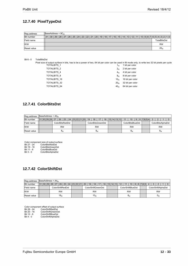
PixBlt Unit Revised 18/4/12
12.7.40 PixelTypeDst
12.7.41 ColorBitsDst
12.7.42 ColorShiftDst
Reg address BaseAddress + 9CH
Bit number 31 30 29 28 27 26 25 24 23 22 21 20 19 18 17 16 15 14 13 12 11 10 9 8 7 6 5 4 3 2 1 0
Field name TotalBitsDst
R/W RW
Reset value 20H
Bit 6 - 0 TotalBitsDst Pixel size of output surface in bits, has to be a power of two, 64 bit per color can be used in fill mode only, to write two 32 bit pixels per cycle
TOTALBITS_1 1H 1 bit per color
TOTALBITS_2 2H 2 bit per color
TOTALBITS_4 4H 4 bit per color
TOTALBITS_8 8H 8 bit per color
TOTALBITS_16 10H 16 bit per color
TOTALBITS_32 20H 32 bit per color
TOTALBITS_64 40H 64 bit per color
Reg address BaseAddress + A0H
Bit number 31 30 29 28 27 26 25 24 23 22 21 20 19 18 17 16 15 14 13 12 11 10 9 8 7 6 5 4 3 2 1 0
Field name ColorBitsRedDst ColorBitsGreenDst ColorBitsBlueDst ColorBitsAlphaDst
R/W RW RW RW RW
Reset value 8H 8H 8H 8H
Color component size of output surface Bit 27 - 24 ColorBitsRedDst Bit 19 - 16 ColorBitsGreenDst Bit 11 - 8 ColorBitsBlueDst Bit 3 - 0 ColorBitsAlphaDst
Reg address BaseAddress + A4H
Bit number 31 30 29 28 27 26 25 24 23 22 21 20 19 18 17 16 15 14 13 12 11 10 9 8 7 6 5 4 3 2 1 0
Field name ColorShiftRedDst ColorShiftGreenDst ColorShiftBlueDst ColorShiftAlphaDst
R/W RW RW RW RW
Reset value 18H 10H 8H 0H
Color component offset of output surface Bit 28 - 24 ColorShiftRedDst Bit 20 - 16 ColorShiftGreenDst Bit 12 - 8 ColorShiftBlueDst Bit 4 - 0 ColorShiftAlphaDst
Fujitsu Semiconductor Europe GmbH 12 - 33
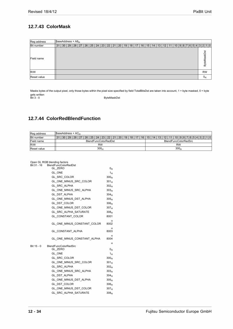
Revised 18/4/12 PixBlt Unit
12.7.43 ColorMask
12.7.44 ColorRedBlendFunction
Reg address BaseAddress + A8H
Bit number 31 30 29 28 27 26 25 24 23 22 21 20 19 18 17 16 15 14 13 12 11 10 9 8 7 6 5 4 3 2 1 0
Field name
Byt
eMas
kDst
R/W RW
Reset value 0H
Masks bytes of the output pixel, only those bytes within the pixel size specified by field TotalBitsDst are taken into account, 1 = byte masked, 0 = byte
gets written Bit 3 - 0 ByteMaskDst
Reg address BaseAddress + ACH
Bit number 31 30 29 28 27 26 25 24 23 22 21 20 19 18 17 16 15 14 13 12 11 10 9 8 7 6 5 4 3 2 1 0Field name BlendFuncColorRedDst BlendFuncColorRedSrc R/W RW RW
Reset value 300H 300H
Open GL RGB blending factors Bit 31 - 16 BlendFuncColorRedDst
GL_ZERO 0H
GL_ONE 1H
GL_SRC_COLOR 300H
GL_ONE_MINUS_SRC_COLOR 301H
GL_SRC_ALPHA 302H
GL_ONE_MINUS_SRC_ALPHA 303H
GL_DST_ALPHA 304H
GL_ONE_MINUS_DST_ALPHA 305H
GL_DST_COLOR 306H
GL_ONE_MINUS_DST_COLOR 307H
GL_SRC_ALPHA_SATURATE 308H
GL_CONSTANT_COLOR 8001
HGL_ONE_MINUS_CONSTANT_COLOR 8002
HGL_CONSTANT_ALPHA 8003
HGL_ONE_MINUS_CONSTANT_ALPHA 8004
HBit 15 - 0 BlendFuncColorRedSrc
GL_ZERO 0H
GL_ONE 1H
GL_SRC_COLOR 300H
GL_ONE_MINUS_SRC_COLOR 301H
GL_SRC_ALPHA 302H
GL_ONE_MINUS_SRC_ALPHA 303H
GL_DST_ALPHA 304H
GL_ONE_MINUS_DST_ALPHA 305H
GL_DST_COLOR 306H
GL_ONE_MINUS_DST_COLOR 307H
GL_SRC_ALPHA_SATURATE 308H
12 - 34 Fujitsu Semiconductor Europe GmbH
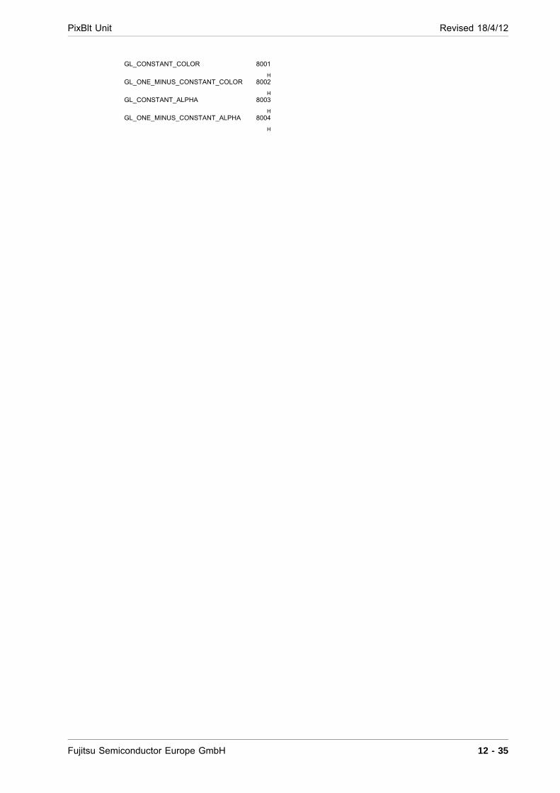
PixBlt Unit Revised 18/4/12
GL_CONSTANT_COLOR 8001
HGL_ONE_MINUS_CONSTANT_COLOR 8002
HGL_CONSTANT_ALPHA 8003
HGL_ONE_MINUS_CONSTANT_ALPHA 8004
H
Fujitsu Semiconductor Europe GmbH 12 - 35
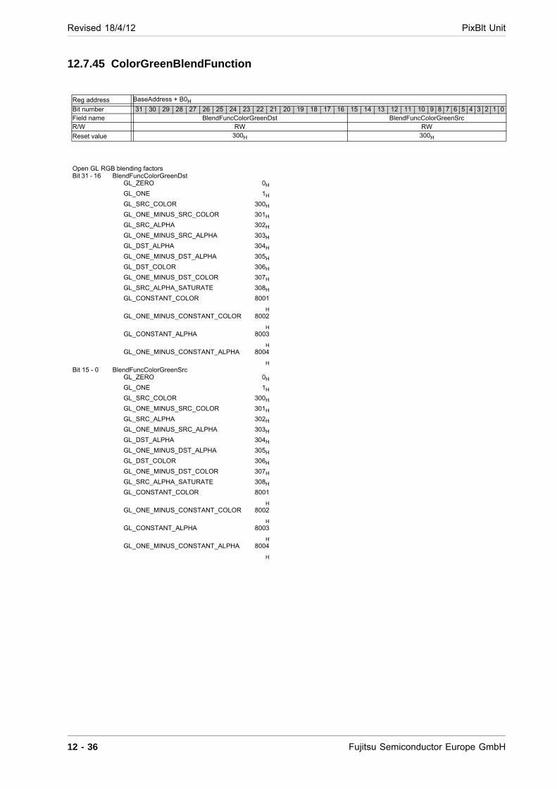
Revised 18/4/12 PixBlt Unit
12.7.45 ColorGreenBlendFunction
Reg address BaseAddress + B0H
Bit number 31 30 29 28 27 26 25 24 23 22 21 20 19 18 17 16 15 14 13 12 11 10 9 8 7 6 5 4 3 2 1 0Field name BlendFuncColorGreenDst BlendFuncColorGreenSrc R/W RW RW
Reset value 300H 300H
Open GL RGB blending factors Bit 31 - 16 BlendFuncColorGreenDst
GL_ZERO 0H
GL_ONE 1H
GL_SRC_COLOR 300H
GL_ONE_MINUS_SRC_COLOR 301H
GL_SRC_ALPHA 302H
GL_ONE_MINUS_SRC_ALPHA 303H
GL_DST_ALPHA 304H
GL_ONE_MINUS_DST_ALPHA 305H
GL_DST_COLOR 306H
GL_ONE_MINUS_DST_COLOR 307H
GL_SRC_ALPHA_SATURATE 308H
GL_CONSTANT_COLOR 8001
HGL_ONE_MINUS_CONSTANT_COLOR 8002
HGL_CONSTANT_ALPHA 8003
HGL_ONE_MINUS_CONSTANT_ALPHA 8004
HBit 15 - 0 BlendFuncColorGreenSrc
GL_ZERO 0H
GL_ONE 1H
GL_SRC_COLOR 300H
GL_ONE_MINUS_SRC_COLOR 301H
GL_SRC_ALPHA 302H
GL_ONE_MINUS_SRC_ALPHA 303H
GL_DST_ALPHA 304H
GL_ONE_MINUS_DST_ALPHA 305H
GL_DST_COLOR 306H
GL_ONE_MINUS_DST_COLOR 307H
GL_SRC_ALPHA_SATURATE 308H
GL_CONSTANT_COLOR 8001
HGL_ONE_MINUS_CONSTANT_COLOR 8002
HGL_CONSTANT_ALPHA 8003
HGL_ONE_MINUS_CONSTANT_ALPHA 8004
H
12 - 36 Fujitsu Semiconductor Europe GmbH
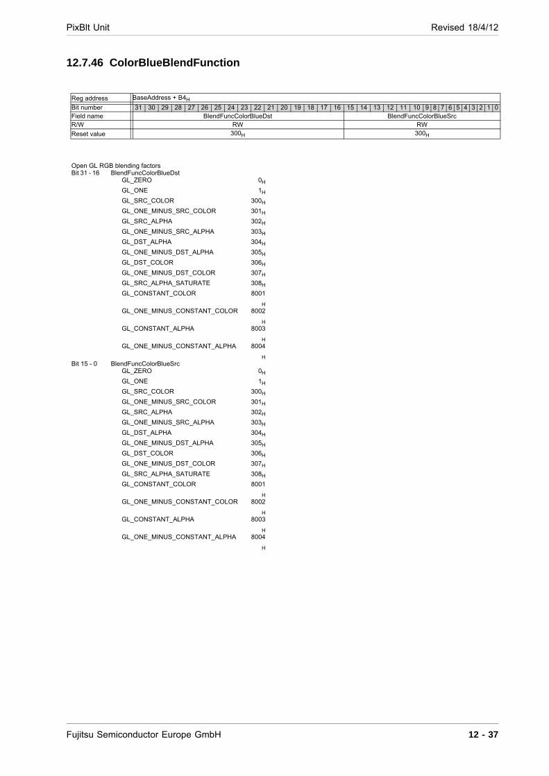
PixBlt Unit Revised 18/4/12
12.7.46 ColorBlueBlendFunction
Reg address BaseAddress + B4H
Bit number 31 30 29 28 27 26 25 24 23 22 21 20 19 18 17 16 15 14 13 12 11 10 9 8 7 6 5 4 3 2 1 0Field name BlendFuncColorBlueDst BlendFuncColorBlueSrc R/W RW RW
Reset value 300H 300H
Open GL RGB blending factors Bit 31 - 16 BlendFuncColorBlueDst
GL_ZERO 0H
GL_ONE 1H
GL_SRC_COLOR 300H
GL_ONE_MINUS_SRC_COLOR 301H
GL_SRC_ALPHA 302H
GL_ONE_MINUS_SRC_ALPHA 303H
GL_DST_ALPHA 304H
GL_ONE_MINUS_DST_ALPHA 305H
GL_DST_COLOR 306H
GL_ONE_MINUS_DST_COLOR 307H
GL_SRC_ALPHA_SATURATE 308H
GL_CONSTANT_COLOR 8001
HGL_ONE_MINUS_CONSTANT_COLOR 8002
HGL_CONSTANT_ALPHA 8003
HGL_ONE_MINUS_CONSTANT_ALPHA 8004
HBit 15 - 0 BlendFuncColorBlueSrc
GL_ZERO 0H
GL_ONE 1H
GL_SRC_COLOR 300H
GL_ONE_MINUS_SRC_COLOR 301H
GL_SRC_ALPHA 302H
GL_ONE_MINUS_SRC_ALPHA 303H
GL_DST_ALPHA 304H
GL_ONE_MINUS_DST_ALPHA 305H
GL_DST_COLOR 306H
GL_ONE_MINUS_DST_COLOR 307H
GL_SRC_ALPHA_SATURATE 308H
GL_CONSTANT_COLOR 8001
HGL_ONE_MINUS_CONSTANT_COLOR 8002
HGL_CONSTANT_ALPHA 8003
HGL_ONE_MINUS_CONSTANT_ALPHA 8004
H
Fujitsu Semiconductor Europe GmbH 12 - 37

Revised 18/4/12 PixBlt Unit
12.7.47 AlphaBlendFunction
Reg address BaseAddress + B8H
Bit number 31 30 29 28 27 26 25 24 23 22 21 20 19 18 17 16 15 14 13 12 11 10 9 8 7 6 5 4 3 2 1 0Field name BlendFuncAlphaDst BlendFuncAlphaSrc R/W RW RW
Reset value 300H 300H
Open GL alpha blending factors Bit 31 - 16 BlendFuncAlphaDst
GL_ZERO 0H
GL_ONE 1H
GL_SRC_COLOR 300H
GL_ONE_MINUS_SRC_COLOR 301H
GL_SRC_ALPHA 302H
GL_ONE_MINUS_SRC_ALPHA 303H
GL_DST_ALPHA 304H
GL_ONE_MINUS_DST_ALPHA 305H
GL_DST_COLOR 306H
GL_ONE_MINUS_DST_COLOR 307H
GL_SRC_ALPHA_SATURATE 308H
GL_CONSTANT_COLOR 8001
HGL_ONE_MINUS_CONSTANT_COLOR 8002
HGL_CONSTANT_ALPHA 8003
HGL_ONE_MINUS_CONSTANT_ALPHA 8004
HBit 15 - 0 BlendFuncAlphaSrc
GL_ZERO 0H
GL_ONE 1H
GL_SRC_COLOR 300H
GL_ONE_MINUS_SRC_COLOR 301H
GL_SRC_ALPHA 302H
GL_ONE_MINUS_SRC_ALPHA 303H
GL_DST_ALPHA 304H
GL_ONE_MINUS_DST_ALPHA 305H
GL_DST_COLOR 306H
GL_ONE_MINUS_DST_COLOR 307H
GL_SRC_ALPHA_SATURATE 308H
GL_CONSTANT_COLOR 8001
HGL_ONE_MINUS_CONSTANT_COLOR 8002
HGL_CONSTANT_ALPHA 8003
HGL_ONE_MINUS_CONSTANT_ALPHA 8004
H
12 - 38 Fujitsu Semiconductor Europe GmbH
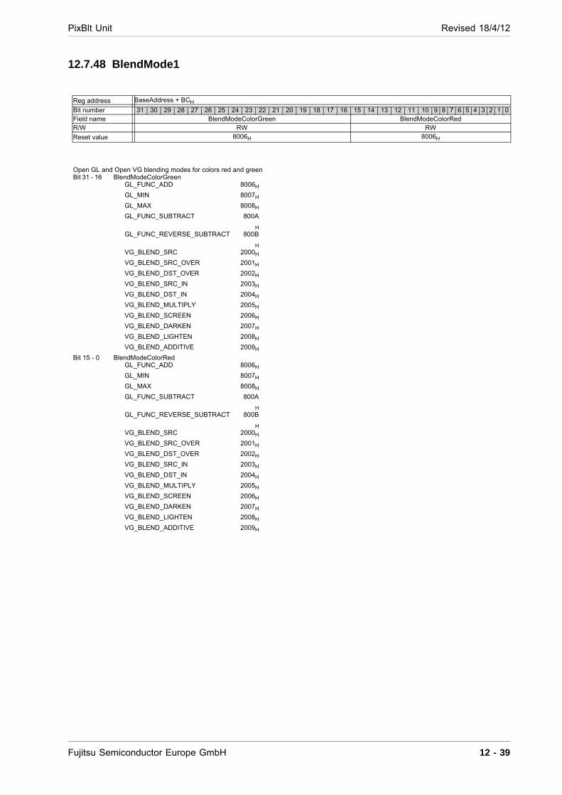
PixBlt Unit Revised 18/4/12
12.7.48 BlendMode1
Reg address BaseAddress + BCH
Bit number 31 30 29 28 27 26 25 24 23 22 21 20 19 18 17 16 15 14 13 12 11 10 9 8 7 6 5 4 3 2 1 0Field name BlendModeColorGreen BlendModeColorRed R/W RW RW
Reset value 8006H 8006H
Open GL and Open VG blending modes for colors red and green Bit 31 - 16 BlendModeColorGreen
GL_FUNC_ADD 8006H
GL_MIN 8007H
GL_MAX 8008H
GL_FUNC_SUBTRACT 800A
HGL_FUNC_REVERSE_SUBTRACT 800B
HVG_BLEND_SRC 2000H
VG_BLEND_SRC_OVER 2001H
VG_BLEND_DST_OVER 2002H
VG_BLEND_SRC_IN 2003H
VG_BLEND_DST_IN 2004H
VG_BLEND_MULTIPLY 2005H
VG_BLEND_SCREEN 2006H
VG_BLEND_DARKEN 2007H
VG_BLEND_LIGHTEN 2008H
VG_BLEND_ADDITIVE 2009H
Bit 15 - 0 BlendModeColorRed GL_FUNC_ADD 8006H
GL_MIN 8007H
GL_MAX 8008H
GL_FUNC_SUBTRACT 800A
HGL_FUNC_REVERSE_SUBTRACT 800B
HVG_BLEND_SRC 2000H
VG_BLEND_SRC_OVER 2001H
VG_BLEND_DST_OVER 2002H
VG_BLEND_SRC_IN 2003H
VG_BLEND_DST_IN 2004H
VG_BLEND_MULTIPLY 2005H
VG_BLEND_SCREEN 2006H
VG_BLEND_DARKEN 2007H
VG_BLEND_LIGHTEN 2008H
VG_BLEND_ADDITIVE 2009H
Fujitsu Semiconductor Europe GmbH 12 - 39

Revised 18/4/12 PixBlt Unit
12.7.49 BlendMode2
Reg address BaseAddress + C0H
Bit number 31 30 29 28 27 26 25 24 23 22 21 20 19 18 17 16 15 14 13 12 11 10 9 8 7 6 5 4 3 2 1 0Field name BlendModeAlpha BlendModeColorBlue R/W RW RW
Reset value 8006H 8006H
Open GL and Open VG blending modes for color blue and alpha Bit 31 - 16 BlendModeAlpha
GL_FUNC_ADD 8006H
GL_MIN 8007H
GL_MAX 8008H
GL_FUNC_SUBTRACT 800A
HGL_FUNC_REVERSE_SUBTRACT 800B
HVG_BLEND_SRC 2000H
VG_BLEND_SRC_OVER 2001H
VG_BLEND_DST_OVER 2002H
VG_BLEND_SRC_IN 2003H
VG_BLEND_DST_IN 2004H
VG_BLEND_MULTIPLY 2005H
VG_BLEND_SCREEN 2006H
VG_BLEND_DARKEN 2007H
VG_BLEND_LIGHTEN 2008H
VG_BLEND_ADDITIVE 2009H
Bit 15 - 0 BlendModeColorBlue GL_FUNC_ADD 8006H
GL_MIN 8007H
GL_MAX 8008H
GL_FUNC_SUBTRACT 800A
HGL_FUNC_REVERSE_SUBTRACT 800B
HVG_BLEND_SRC 2000H
VG_BLEND_SRC_OVER 2001H
VG_BLEND_DST_OVER 2002H
VG_BLEND_SRC_IN 2003H
VG_BLEND_DST_IN 2004H
VG_BLEND_MULTIPLY 2005H
VG_BLEND_SCREEN 2006H
VG_BLEND_DARKEN 2007H
VG_BLEND_LIGHTEN 2008H
VG_BLEND_ADDITIVE 2009H
12 - 40 Fujitsu Semiconductor Europe GmbH
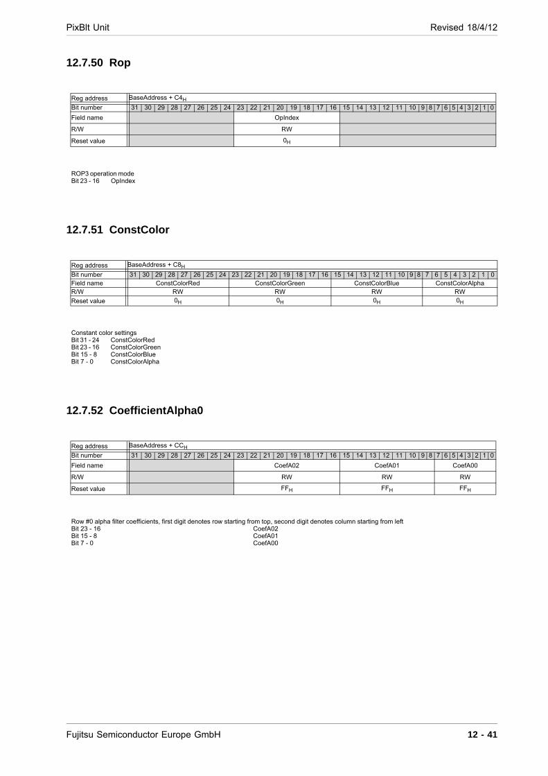
PixBlt Unit Revised 18/4/12
12.7.50 Rop
12.7.51 ConstColor
12.7.52 CoefficientAlpha0
Reg address BaseAddress + C4H
Bit number 31 30 29 28 27 26 25 24 23 22 21 20 19 18 17 16 15 14 13 12 11 10 9 8 7 6 5 4 3 2 1 0
Field name OpIndex
R/W RW
Reset value 0H
ROP3 operation mode Bit 23 - 16 OpIndex
Reg address BaseAddress + C8H
Bit number 31 30 29 28 27 26 25 24 23 22 21 20 19 18 17 16 15 14 13 12 11 10 9 8 7 6 5 4 3 2 1 0Field name ConstColorRed ConstColorGreen ConstColorBlue ConstColorAlpha R/W RW RW RW RW
Reset value 0H 0H 0H 0H
Constant color settings Bit 31 - 24 ConstColorRed Bit 23 - 16 ConstColorGreen Bit 15 - 8 ConstColorBlue Bit 7 - 0 ConstColorAlpha
Reg address BaseAddress + CCH
Bit number 31 30 29 28 27 26 25 24 23 22 21 20 19 18 17 16 15 14 13 12 11 10 9 8 7 6 5 4 3 2 1 0
Field name CoefA02 CoefA01 CoefA00
R/W RW RW RW
Reset value FFH FFH FFH
Row #0 alpha filter coefficients, first digit denotes row starting from top, second digit denotes column starting from left Bit 23 - 16 CoefA02 Bit 15 - 8 CoefA01 Bit 7 - 0 CoefA00
Fujitsu Semiconductor Europe GmbH 12 - 41
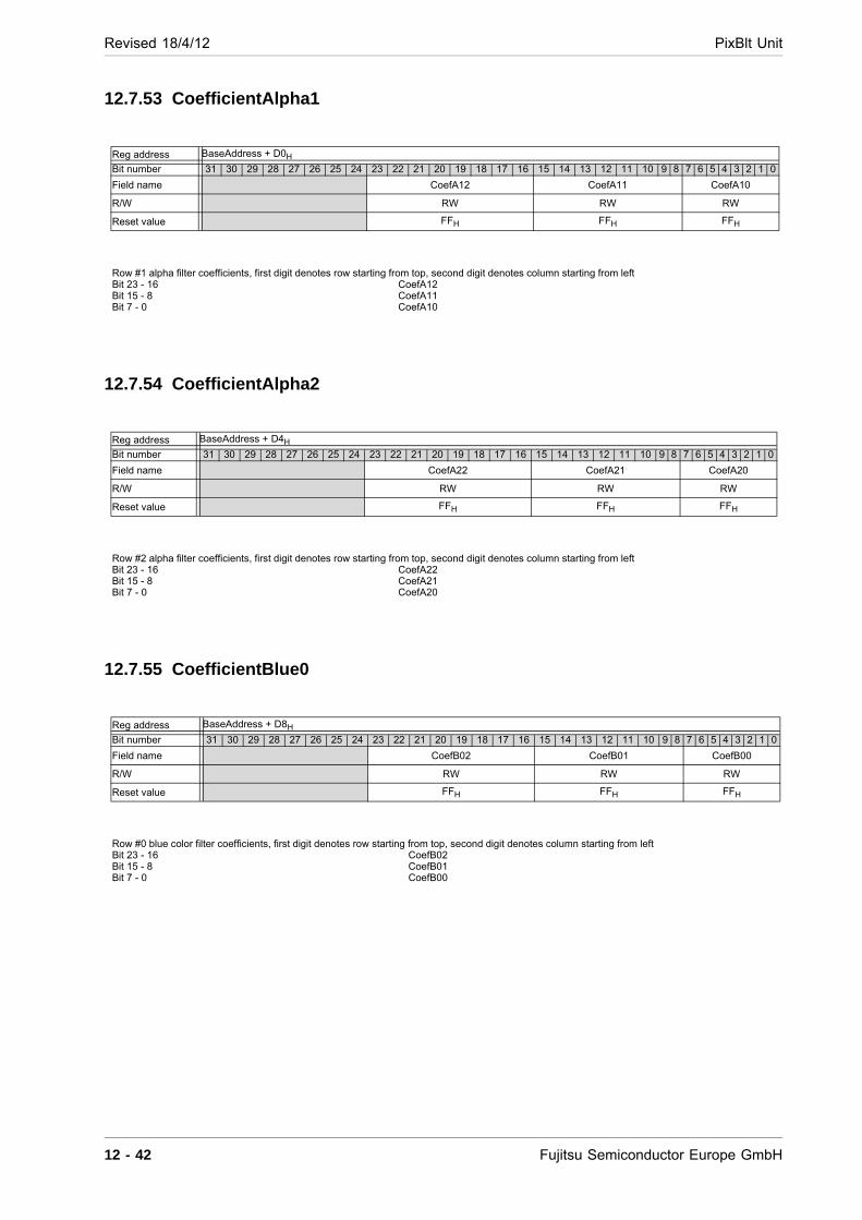
Revised 18/4/12 PixBlt Unit
12.7.53 CoefficientAlpha1
12.7.54 CoefficientAlpha2
12.7.55 CoefficientBlue0
Reg address BaseAddress + D0H
Bit number 31 30 29 28 27 26 25 24 23 22 21 20 19 18 17 16 15 14 13 12 11 10 9 8 7 6 5 4 3 2 1 0
Field name CoefA12 CoefA11 CoefA10
R/W RW RW RW
Reset value FFH FFH FFH
Row #1 alpha filter coefficients, first digit denotes row starting from top, second digit denotes column starting from left Bit 23 - 16 CoefA12 Bit 15 - 8 CoefA11 Bit 7 - 0 CoefA10
Reg address BaseAddress + D4H
Bit number 31 30 29 28 27 26 25 24 23 22 21 20 19 18 17 16 15 14 13 12 11 10 9 8 7 6 5 4 3 2 1 0
Field name CoefA22 CoefA21 CoefA20
R/W RW RW RW
Reset value FFH FFH FFH
Row #2 alpha filter coefficients, first digit denotes row starting from top, second digit denotes column starting from left Bit 23 - 16 CoefA22 Bit 15 - 8 CoefA21 Bit 7 - 0 CoefA20
Reg address BaseAddress + D8H
Bit number 31 30 29 28 27 26 25 24 23 22 21 20 19 18 17 16 15 14 13 12 11 10 9 8 7 6 5 4 3 2 1 0
Field name CoefB02 CoefB01 CoefB00
R/W RW RW RW
Reset value FFH FFH FFH
Row #0 blue color filter coefficients, first digit denotes row starting from top, second digit denotes column starting from left Bit 23 - 16 CoefB02 Bit 15 - 8 CoefB01 Bit 7 - 0 CoefB00
12 - 42 Fujitsu Semiconductor Europe GmbH
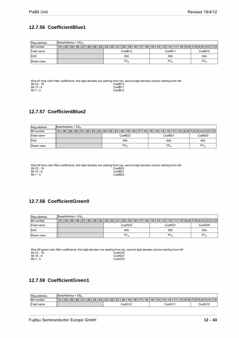
PixBlt Unit Revised 18/4/12
12.7.56 CoefficientBlue1
12.7.57 CoefficientBlue2
12.7.58 CoefficientGreen0
12.7.59 CoefficientGreen1
Reg address BaseAddress + DCH
Bit number 31 30 29 28 27 26 25 24 23 22 21 20 19 18 17 16 15 14 13 12 11 10 9 8 7 6 5 4 3 2 1 0
Field name CoefB12 CoefB11 CoefB10
R/W RW RW RW
Reset value FFH FFH FFH
Row #1 blue color filter coefficients, first digit denotes row starting from top, second digit denotes column starting from left Bit 23 - 16 CoefB12 Bit 15 - 8 CoefB11 Bit 7 - 0 CoefB10
Reg address BaseAddress + E0H
Bit number 31 30 29 28 27 26 25 24 23 22 21 20 19 18 17 16 15 14 13 12 11 10 9 8 7 6 5 4 3 2 1 0
Field name CoefB22 CoefB21 CoefB20
R/W RW RW RW
Reset value FFH FFH FFH
Row #2 blue color filter coefficients, first digit denotes row starting from top, second digit denotes column starting from left Bit 23 - 16 CoefB22 Bit 15 - 8 CoefB21 Bit 7 - 0 CoefB20
Reg address BaseAddress + E4H
Bit number 31 30 29 28 27 26 25 24 23 22 21 20 19 18 17 16 15 14 13 12 11 10 9 8 7 6 5 4 3 2 1 0
Field name CoefG02 CoefG01 CoefG00
R/W RW RW RW
Reset value FFH FFH FFH
Row #0 green color filter coefficients, first digit denotes row starting from top, second digit denotes column starting from left Bit 23 - 16 CoefG02 Bit 15 - 8 CoefG01 Bit 7 - 0 CoefG00
Reg address BaseAddress + E8H
Bit number 31 30 29 28 27 26 25 24 23 22 21 20 19 18 17 16 15 14 13 12 11 10 9 8 7 6 5 4 3 2 1 0
Field name CoefG12 CoefG11 CoefG10
Fujitsu Semiconductor Europe GmbH 12 - 43
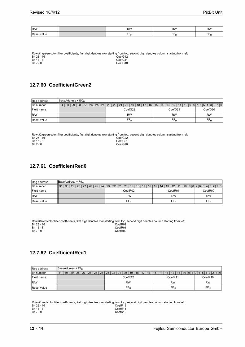
Revised 18/4/12 PixBlt Unit
12.7.60 CoefficientGreen2
12.7.61 CoefficientRed0
12.7.62 CoefficientRed1
R/W RW RW RW
Reset value FFH FFH FFH
Row #1 green color filter coefficients, first digit denotes row starting from top, second digit denotes column starting from left Bit 23 - 16 CoefG12 Bit 15 - 8 CoefG11 Bit 7 - 0 CoefG10
Reg address BaseAddress + ECH
Bit number 31 30 29 28 27 26 25 24 23 22 21 20 19 18 17 16 15 14 13 12 11 10 9 8 7 6 5 4 3 2 1 0
Field name CoefG22 CoefG21 CoefG20
R/W RW RW RW
Reset value FFH FFH FFH
Row #2 green color filter coefficients, first digit denotes row starting from top, second digit denotes column starting from left Bit 23 - 16 CoefG22 Bit 15 - 8 CoefG21 Bit 7 - 0 CoefG20
Reg address BaseAddress + F0H
Bit number 31 30 29 28 27 26 25 24 23 22 21 20 19 18 17 16 15 14 13 12 11 10 9 8 7 6 5 4 3 2 1 0
Field name CoefR02 CoefR01 CoefR00
R/W RW RW RW
Reset value FFH FFH FFH
Row #0 red color filter coefficients, first digit denotes row starting from top, second digit denotes column starting from left Bit 23 - 16 CoefR02 Bit 15 - 8 CoefR01 Bit 7 - 0 CoefR00
Reg address BaseAddress + F4H
Bit number 31 30 29 28 27 26 25 24 23 22 21 20 19 18 17 16 15 14 13 12 11 10 9 8 7 6 5 4 3 2 1 0
Field name CoefR12 CoefR11 CoefR10
R/W RW RW RW
Reset value FFH FFH FFH
Row #1 red color filter coefficients, first digit denotes row starting from top, second digit denotes column starting from left Bit 23 - 16 CoefR12 Bit 15 - 8 CoefR11 Bit 7 - 0 CoefR10
12 - 44 Fujitsu Semiconductor Europe GmbH
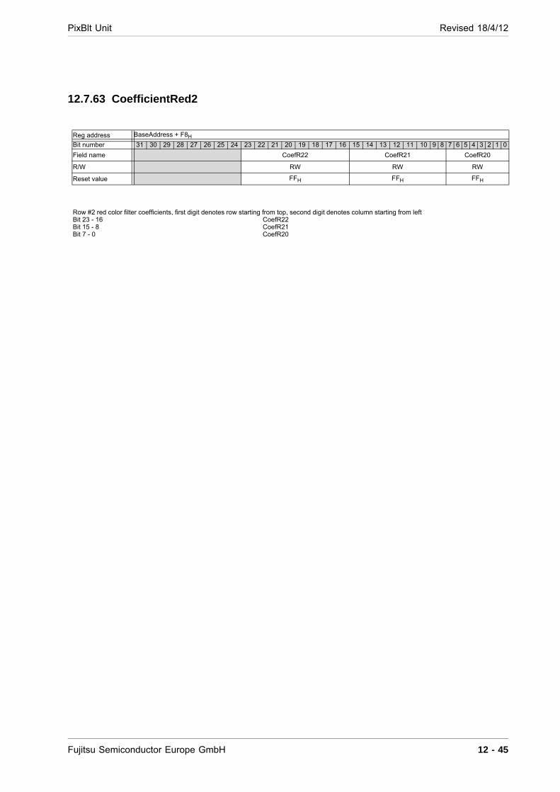
PixBlt Unit Revised 18/4/12
12.7.63 CoefficientRed2
Reg address BaseAddress + F8H
Bit number 31 30 29 28 27 26 25 24 23 22 21 20 19 18 17 16 15 14 13 12 11 10 9 8 7 6 5 4 3 2 1 0
Field name CoefR22 CoefR21 CoefR20
R/W RW RW RW
Reset value FFH FFH FFH
Row #2 red color filter coefficients, first digit denotes row starting from top, second digit denotes column starting from left Bit 23 - 16 CoefR22 Bit 15 - 8 CoefR21 Bit 7 - 0 CoefR20
Fujitsu Semiconductor Europe GmbH 12 - 45
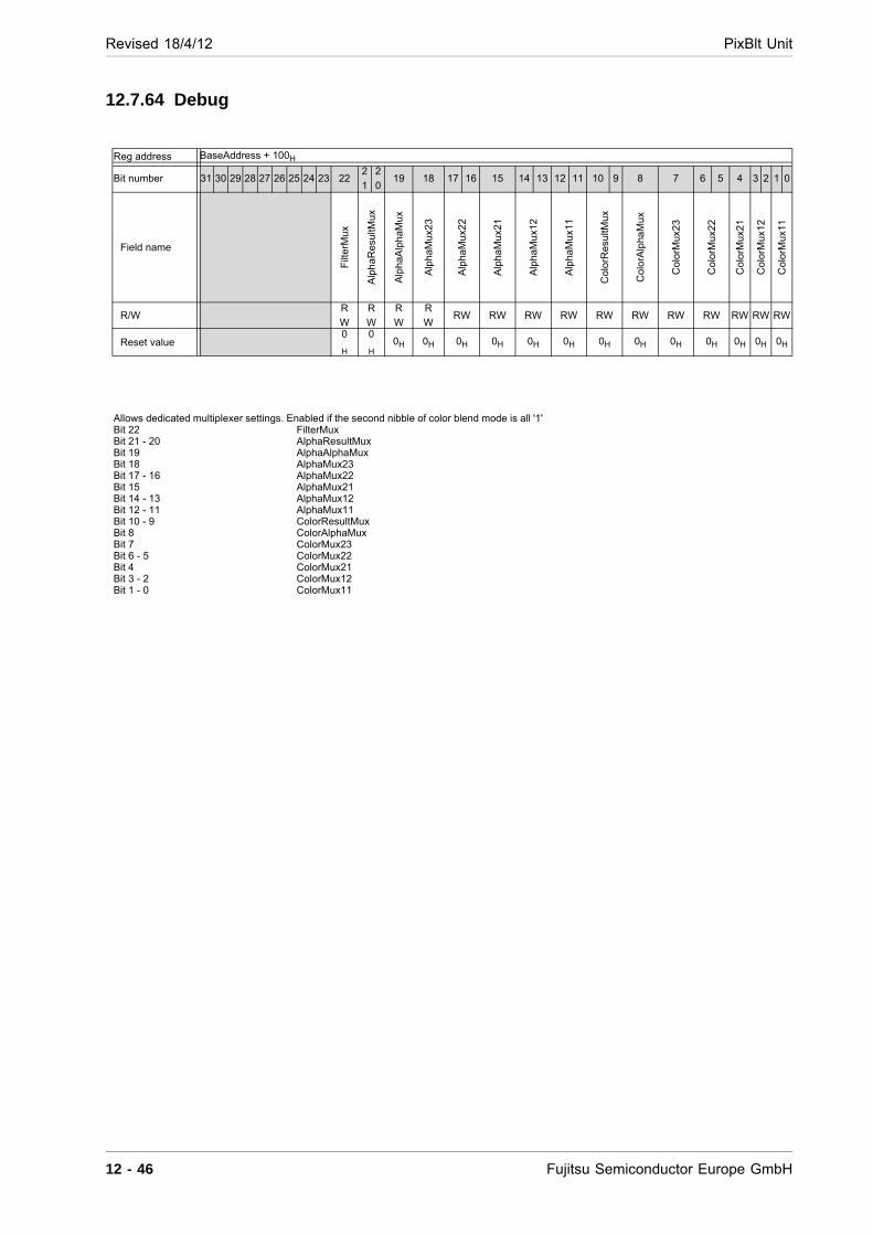
Revised 18/4/12 PixBlt Unit
12.7.64 Debug
Reg address BaseAddress + 100H
Bit number 31 30 29 28 27 26 25 24 23 222
1
2
019 18 17 16 15 14 13 12 11 10 9 8 7 6 5 4 3 2 1 0
Field name
Filt
erM
ux
Alp
ha
Re
sultM
ux
Alp
haA
lph
aM
ux
Alp
haM
ux2
3
Alp
haM
ux2
2
Alp
haM
ux2
1
Alp
haM
ux1
2
Alp
haM
ux1
1
Co
lorR
esu
ltMu
x
Co
lorA
lpha
Mu
x
Co
lorM
ux23
Co
lorM
ux22
Co
lorM
ux21
Co
lorM
ux12
Co
lorM
ux11
R/WR
W
R
W
R
W
R
W RW RW RW RW RW RW RW RW RW RW RW
Reset value0
H
0
H 0H 0H 0H 0H 0H 0H 0H 0H 0H 0H 0H 0H 0H
Allows dedicated multiplexer settings. Enabled if the second nibble of color blend mode is all '1' Bit 22 FilterMux Bit 21 - 20 AlphaResultMux Bit 19 AlphaAlphaMux Bit 18 AlphaMux23 Bit 17 - 16 AlphaMux22 Bit 15 AlphaMux21 Bit 14 - 13 AlphaMux12 Bit 12 - 11 AlphaMux11 Bit 10 - 9 ColorResultMux Bit 8 ColorAlphaMux Bit 7 ColorMux23 Bit 6 - 5 ColorMux22 Bit 4 ColorMux21 Bit 3 - 2 ColorMux12 Bit 1 - 0 ColorMux11
12 - 46 Fujitsu Semiconductor Europe GmbH

I2C Interface Revised 18/4/12
Chapter 13: I2C Interface
13.1 Overview
This interface is a serial interface that supports the Inter IC Bus, and operates as a master/slave device on the I2C bus.
NOTE MB86298 'Ruby' does not support slave mode. There are restrictions on use of the module in a multimaster environment (see further on in this chapter).
13.2 Features
This interface has the following features:
Master send/receive
Arbitration
Clock synchronization
Slave address detection
General call address detection
Transfer direction detection
Repetitive generation and detection of start condition
Bus error detection
Standard mode (max. 100 Kbps) / fast mode (max. 400 Kbps)
Fujitsu Semiconductor Europe GmbH 13 - 1
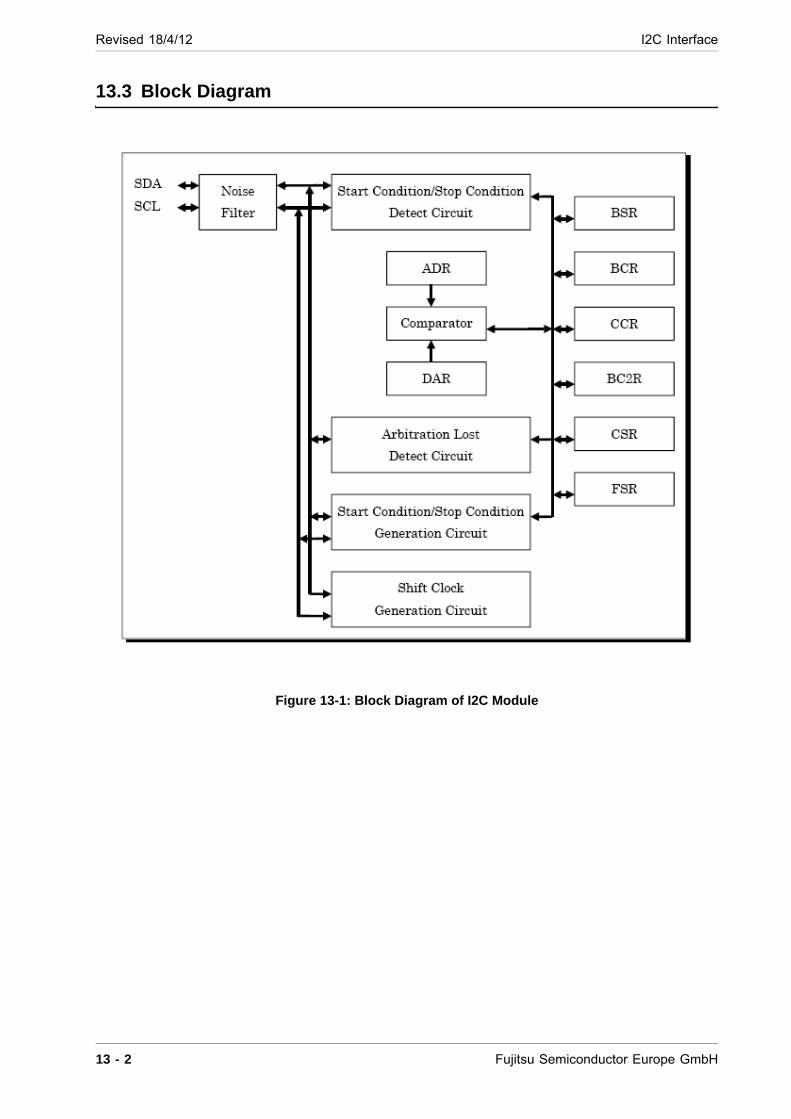
Revised 18/4/12 I2C Interface
13.3 Block Diagram
Figure 13-1: Block Diagram of I2C Module
13 - 2 Fujitsu Semiconductor Europe GmbH

I2C Interface Revised 18/4/12
13.4 Description of Block Functions
Noise filter
The noise filter consists of a three-stage shift register circuit. When all three values of the SCL/SDA input signal sampled continuously are “1s”, filter output is “1”; when all three values of the SCL/SDA input signal sampled continuously are “0s”, filter output is “0”; and when all the 3 values are not “1” or “0”, the state of the signal 1 clock before is held.
Figure 13-2: I2C Noise Filter Operation
Start condition/Stop condition detector
Detects start condition and stop condition from the status changes of SDA and SCL.
Start condition/Stop condition generator
Changes the status of SDA and SCL to generate a start or stop condition.
Arbitration Lost detector
When sending data, compares data output to the SDA line signal and data input from the SDA line signal, to check whether they match. If they do not match, the detector generates an Arbitration Lost state.
Shift clock generator
Counts the generation timing of serial data transfer clock and controls output of SCL clock signal according to the clock control register setting.
Comparator
Compares whether the received address and the own address specified for the address register are the same, or checks whether the received address is a global address.
ADR (Address Register Read/Write)
A 7-bit register to specify a slave address.
Fujitsu Semiconductor Europe GmbH 13 - 3
Revised 18/4/12 I2C Interface
DAR (Data Register Read/Write)
An 8-bit register used for serial data transfer.
BSR (Bus Status Register Read)
An 8-bit register that shows the status of the I2C bus, and has the following functions:
- Detects repeated start conditions
- Detects Arbitration Lost
- Stores acknowledge bit
- Detects data transfer direction
- Detects addressing
- Detects general call address
- Detects first byte
BCR (Bus Control Register Read/Write)
An 8-bit register that controls the I2C bus and interrupt, and has the following functions:
- Interrupt request / Interrupt permission
- Generation of start condition
- Master/slave selection
- Permission of acknowledge generation
CCR (Clock Control Register Read/Write)
A 7-bit register that sets the clock frequency for serial data transfer.
- Permission of operation
- Setting of serial clock frequency
- Standard mode and fast mode
BC2R (Bus Control 2 Register Read/Write)
Checks the status of the line after the signal passes through the noise filter and to forcibly drive the line “low”.
CSR (Expand Clock Period Select Register Read/Write)
Expands the CS bit in the CCR register.
FSR (Frequency Select Register Read/Write)
Specifies the frequency range of the bus clock used.
13 - 4 Fujitsu Semiconductor Europe GmbH
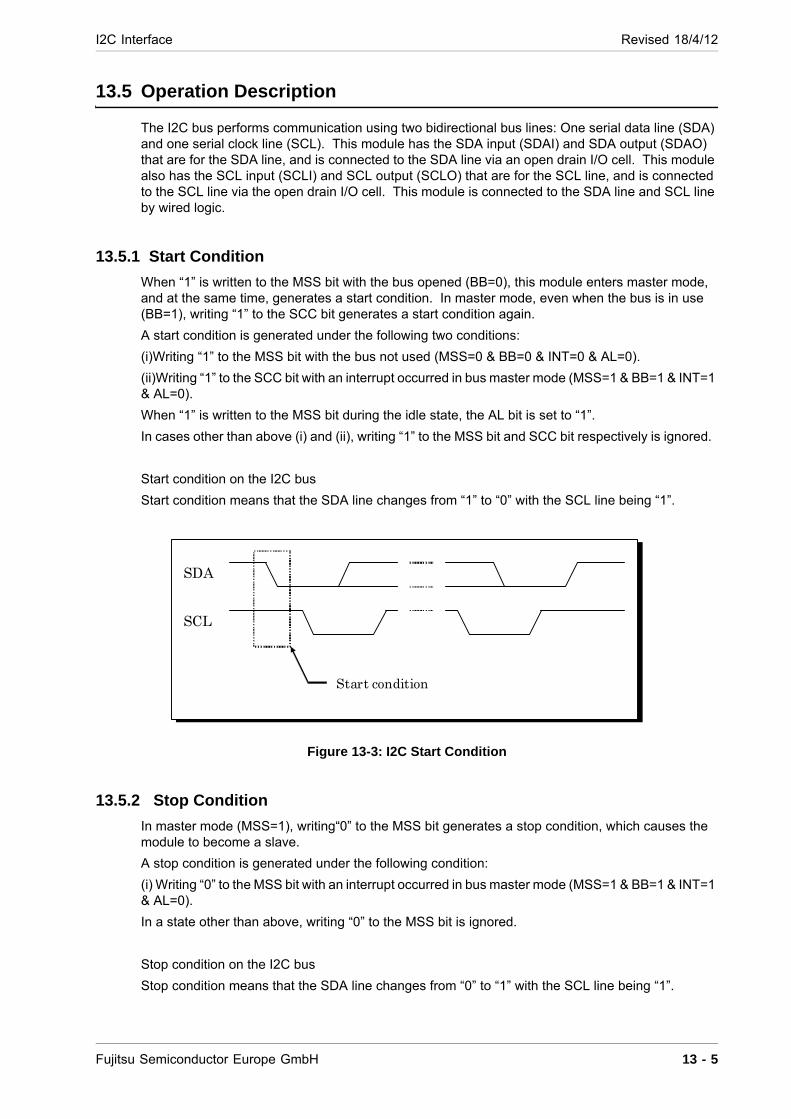
I2C Interface Revised 18/4/12
13.5 Operation Description
The I2C bus performs communication using two bidirectional bus lines: One serial data line (SDA) and one serial clock line (SCL). This module has the SDA input (SDAI) and SDA output (SDAO) that are for the SDA line, and is connected to the SDA line via an open drain I/O cell. This module also has the SCL input (SCLI) and SCL output (SCLO) that are for the SCL line, and is connected to the SCL line via the open drain I/O cell. This module is connected to the SDA line and SCL line by wired logic.
13.5.1 Start Condition
When “1” is written to the MSS bit with the bus opened (BB=0), this module enters master mode, and at the same time, generates a start condition. In master mode, even when the bus is in use (BB=1), writing “1” to the SCC bit generates a start condition again.
A start condition is generated under the following two conditions:
(i)Writing “1” to the MSS bit with the bus not used (MSS=0 & BB=0 & INT=0 & AL=0).
(ii)Writing “1” to the SCC bit with an interrupt occurred in bus master mode (MSS=1 & BB=1 & INT=1 & AL=0).
When “1” is written to the MSS bit during the idle state, the AL bit is set to “1”.
In cases other than above (i) and (ii), writing “1” to the MSS bit and SCC bit respectively is ignored.
Start condition on the I2C bus
Start condition means that the SDA line changes from “1” to “0” with the SCL line being “1”.
Figure 13-3: I2C Start Condition
13.5.2 Stop Condition
In master mode (MSS=1), writing“0” to the MSS bit generates a stop condition, which causes the module to become a slave.
A stop condition is generated under the following condition:
(i) Writing “0” to the MSS bit with an interrupt occurred in bus master mode (MSS=1 & BB=1 & INT=1 & AL=0).
In a state other than above, writing “0” to the MSS bit is ignored.
Stop condition on the I2C bus
Stop condition means that the SDA line changes from “0” to “1” with the SCL line being “1”.
SDA
SCL
Start condition
Fujitsu Semiconductor Europe GmbH 13 - 5
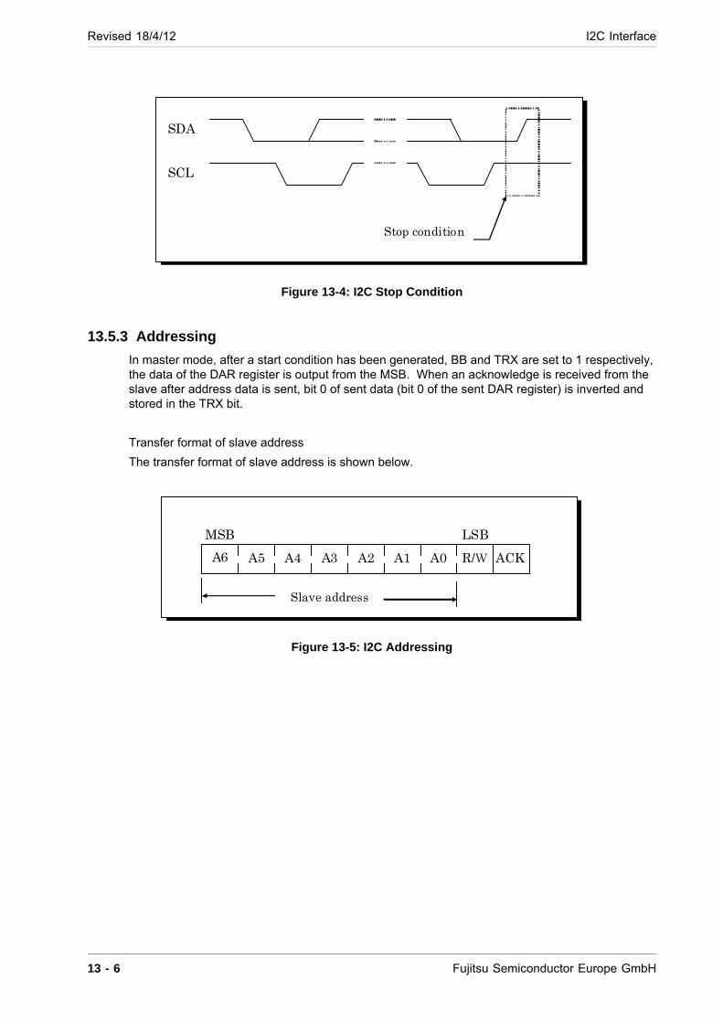
Revised 18/4/12 I2C Interface
Figure 13-4: I2C Stop Condition
13.5.3 Addressing
In master mode, after a start condition has been generated, BB and TRX are set to 1 respectively, the data of the DAR register is output from the MSB. When an acknowledge is received from the slave after address data is sent, bit 0 of sent data (bit 0 of the sent DAR register) is inverted and stored in the TRX bit.
Transfer format of slave address
The transfer format of slave address is shown below.
Figure 13-5: I2C Addressing
SDA
SCL
Stop condition
MSB LSB
Slave address
R/WA6 A0 A5 A1 A4 A2 A3 ACK
13 - 6 Fujitsu Semiconductor Europe GmbH
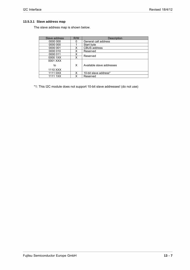
I2C Interface Revised 18/4/12
13.5.3.1 Slave address map
The slave address map is shown below.
*1: This I2C module does not support 10-bit slave addresses! (do not use)
Slave address R/W Description0000 000 0 General call address0000 000 1 Start byte0000 001 X CBUS address0000 010 X Reserved0000 011 X
Reserved0000 1XX X0001 XXX
to
1110 XXX
X Available slave addresses
1111 0XX X 10-bit slave address*1111 1XX X Reserved
Fujitsu Semiconductor Europe GmbH 13 - 7
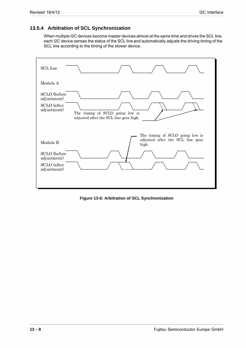
Revised 18/4/12 I2C Interface
13.5.4 Arbitration of SCL Synchronization
When multiple I2C devices become master devices almost at the same time and drives the SCL line, each I2C device senses the status of the SCL line and automatically adjusts the driving timing of the SCL line according to the timing of the slower device.
Figure 13-6: Arbitration of SCL Synchronization
SCL line
SCLO (before adjustment)
SCLO (before adjustment)
Module A
Module B
The timing of SCLO going low is adjusted after the SCL line goes high.
The timing of SCLO going low is adjusted after the SCL line goes high.
SCLO (after adjustment)
SCLO (after adjustment)
13 - 8 Fujitsu Semiconductor Europe GmbH

I2C Interface Revised 18/4/12
13.5.5 Arbitration
Arbitration occurs when one master and another master are sending data simultaneously. When a master’s send data is “1” and data on the SDA line is “0”, the master assumes that it has lost the arbitration and then sets 1 to AL.
Also, when the master tries to generate a start condition when another master is using the bus, the former master assumes that it has lost the arbitration and then sets 1 to AL.
Also, even when one master checks that the bus is not used and writes 1 to MSS, one master as-sumes that it has lost the arbitration and then sets 1 to AL when one master detects a start condition generated by another master before one master generates a start condition.
When “1” is set to the AL bit, MSS and TRX are set to “0s” respectively, which causes slave receive mode.
The master stops driving the SDA line at the point when the master loses the arbitration (the right to use the bus). However, the master does not stop driving the SCL line until 1-byte transfer ends and the interrupt is cleared.
Figure 13-7: Arbitration
SDA line
SCL line
SDAI
SDAO
SDAI
SDAO
Module A
Module B
Since output and input match with each other, the master has the right to use the bus.
Since output and input do not match with each other, the master loses the right to use the bus.
Fujitsu Semiconductor Europe GmbH 13 - 9
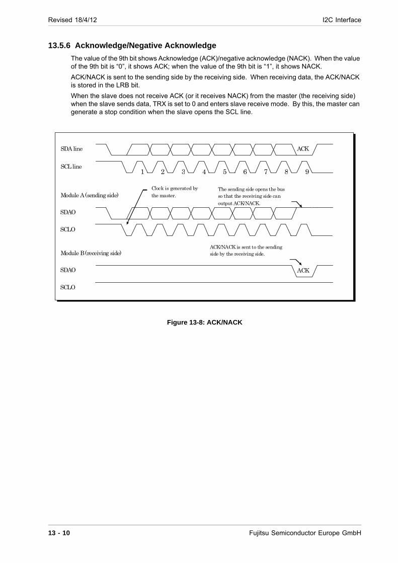
Revised 18/4/12 I2C Interface
13.5.6 Acknowledge/Negative Acknowledge
The value of the 9th bit shows Acknowledge (ACK)/negative acknowledge (NACK). When the value of the 9th bit is “0”, it shows ACK; when the value of the 9th bit is “1”, it shows NACK.
ACK/NACK is sent to the sending side by the receiving side. When receiving data, the ACK/NACK is stored in the LRB bit.
When the slave does not receive ACK (or it receives NACK) from the master (the receiving side) when the slave sends data, TRX is set to 0 and enters slave receive mode. By this, the master can generate a stop condition when the slave opens the SCL line.
Figure 13-8: ACK/NACK
SDA line
SCL line
SDAO
Module A (sending side)
Module B (receiving side) ACK/NACK is sent to the sending side by the receiving side.
The sending side opens the bus so that the receiving side can output ACK/NACK.
1 2 3 4 5 6 7 8 9
ACK
ACK
SCLO
SDAO
SCLO
Clock is generated by the master.
13 - 10 Fujitsu Semiconductor Europe GmbH
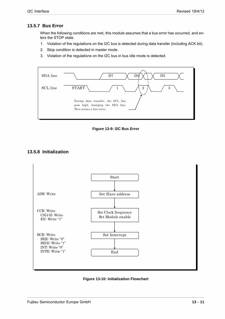
I2C Interface Revised 18/4/12
13.5.7 Bus Error
When the following conditions are met, this module assumes that a bus error has occurred, and en-ters the STOP state.
1. Violation of the regulations on the I2C bus is detected during data transfer (including ACK bit).
2. Stop condition is detected in master mode.
3. Violation of the regulations on the I2C bus in bus idle mode is detected.
Figure 13-9: I2C Bus Error
13.5.8 Initialization
Figure 13-10: Initialization Flowchart
SDA line
1START 3 SCL line 2
D7 D5 D6
During data transfer, the SCL line
goes high, changing the SDA line.
This causes a bus error.
Start
Set Slave address
Set Clock frequency Set Module enable
Set Interrupt
End
ADR: Write
CCR: Write CS[4:0]: Write EN: Write “1”
BCR: Write BER: Write “0” BEIE: Write “1” INT: Write “0” INTE: Write “1”
Fujitsu Semiconductor Europe GmbH 13 - 11
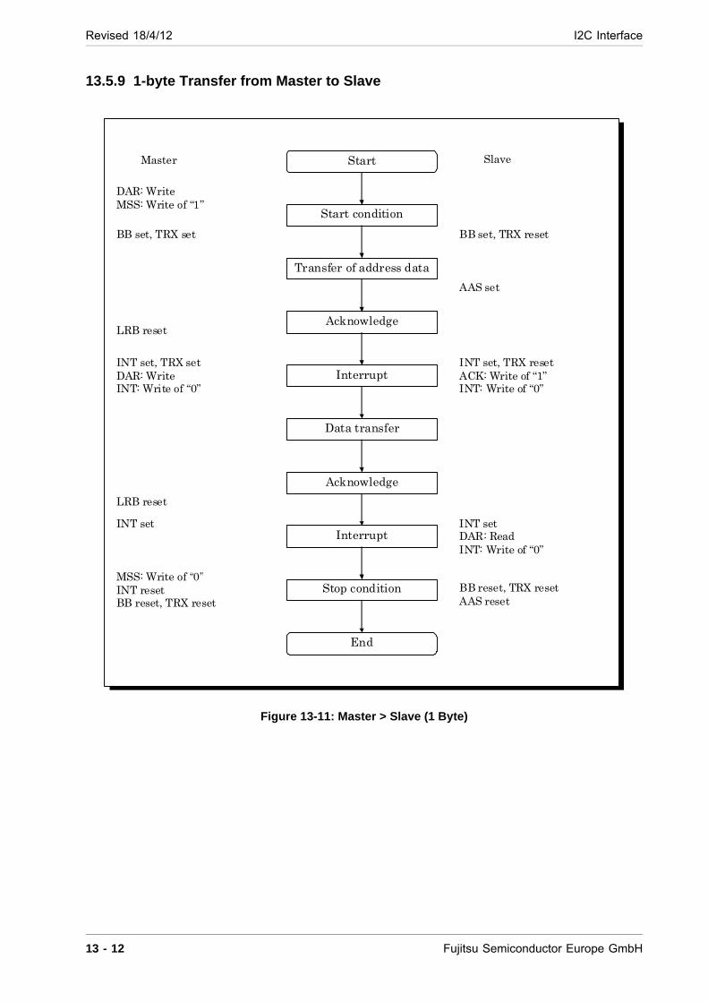
Revised 18/4/12 I2C Interface
13.5.9 1-byte Transfer from Master to Slave
Figure 13-11: Master > Slave (1 Byte)
Start
Start condition
Transfer of address data
Acknowledge
Interrupt
Data transfer
Acknowledge
Interrupt
Stop condition
End
Master
DAR: Write MSS: Write of “1”
BB set, TRX set
LRB reset
Slave
INT set, TRX set DAR: Write INT: Write of “0”
INT set
LRB reset
INT set, TRX reset ACK: Write of “1” INT: Write of “0”
MSS: Write of “0” INT reset BB reset, TRX reset
AAS set
BB set, TRX reset
INT set DAR: Read INT: Write of “0”
BB reset, TRX reset AAS reset
13 - 12 Fujitsu Semiconductor Europe GmbH
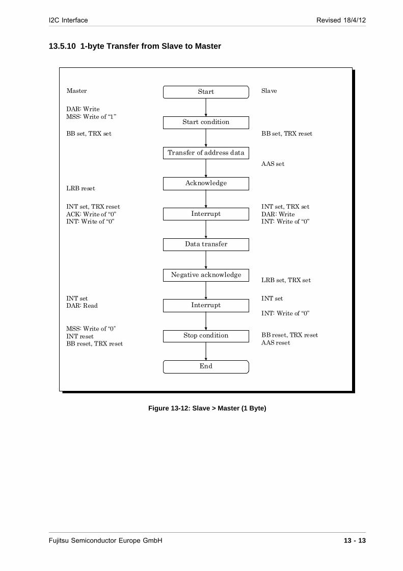
I2C Interface Revised 18/4/12
13.5.10 1-byte Transfer from Slave to Master
Figure 13-12: Slave > Master (1 Byte)
Start
Start condition
Transfer of address data
Acknowledge
Interrupt
Data transfer
Negative acknowledge
Interrupt
Stop condition
End
Master
DAR: Write MSS: Write of “1”
BB set, TRX set
LRB reset
Slave
INT set, TRX resetACK: Write of “0” INT: Write of “0”
INT set DAR: Read
LRB set, TRX set
INT set, TRX set DAR: Write INT: Write of “0”
MSS: Write of “0” INT reset BB reset, TRX reset
AAS set
BB set, TRX reset
INT set INT: Write of “0”
BB reset, TRX reset AAS reset
Fujitsu Semiconductor Europe GmbH 13 - 13
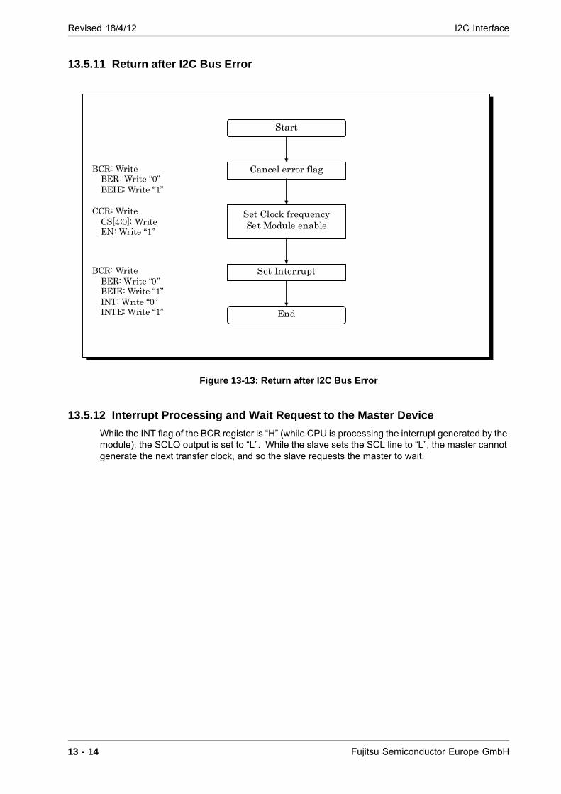
Revised 18/4/12 I2C Interface
13.5.11 Return after I2C Bus Error
Figure 13-13: Return after I2C Bus Error
13.5.12 Interrupt Processing and Wait Request to the Master Device
While the INT flag of the BCR register is “H” (while CPU is processing the interrupt generated by the module), the SCLO output is set to “L”. While the slave sets the SCL line to “L”, the master cannot generate the next transfer clock, and so the slave requests the master to wait.
Start
Cancel error flag
Set Clock frequency Set Module enable
Set Interrupt
End
BCR: Write BER: Write “0” BEIE: Write “1”
CCR: Write CS[4:0]: Write EN: Write “1”
BCR: Write BER: Write “0” BEIE: Write “1” INT: Write “0” INTE: Write “1”
13 - 14 Fujitsu Semiconductor Europe GmbH
I2C Interface Revised 18/4/12
13.6 Warnings
13.6.1 10-bit Slave Address
This module does not support 10-bit slave address. Do not specify slave addresses 78H-7BH for this module. If specified incorrectly, ACK is returned when receiving 1byte, but normal transfer can-not be performed.
13.6.2 Conflict among SCC, MSS and INT Bits
When write is performed to the SCC, MSS and INT bits simultaneously, a conflict occurs with next byte transfer, generation of start condition, and generation of stop condition. Priority at this time is as follows:
1. Priority between next byte transfer and generation of stop condition.When “0” is written to the INT bit and “0” is written to the MSS bit, writing to the MSS bit takes precedence over the writing to the INT bit, causing a stop condition.
2. Priority between next byte transfer and generation of start conditionWhen “0” is written to the INT bit and “1” is written to the SCC bit, the writing to the SCC bit takes precedence over the writing to the INT, causing a start condition.
3. Priority between generations of start condition and stop conditionIt is prohibited to simultaneously write “1” to the SCC bit and “0” to the MSS bit.
13.6.3 Setting of Serial Transfer Clock
When the rising delay of the SCL pin is large or when the slave device expands the clock, the fre-quency may be smaller than the set value (the calculated value) due to the overhead.
13.6.4 Restrictions on Multimaster Usage
When using this module as a multimaster, the following usage is prohibited: this module and another master sends a global call address simultaneously, and arbitration is lost in this module at the sec-ond byte and later.
This restriction does not apply to the following:
To use this module in a single-master environment.
To use this module in a multimaster environment. However, in this case, this module does not use the sending of a general call address.
To use this module in a multimaster environment. However, in this case, but module other than this module does not use the sending of a general call address.
To use this module in a multimaster environment and another master and this module send a global call address simultaneously. However, in this case, arbitration is not lost in this module at the second byte and later*.
* Arbitration is lost for larger send data sizes. Therefore, data value in the second byte and later must always be smaller than that in other masters.
13.7 Additional Notes
13.7.1 Serial Transfer Clock Setting (CSR)
Set FSCL not to exceed the following values::
Fujitsu Semiconductor Europe GmbH 13 - 15
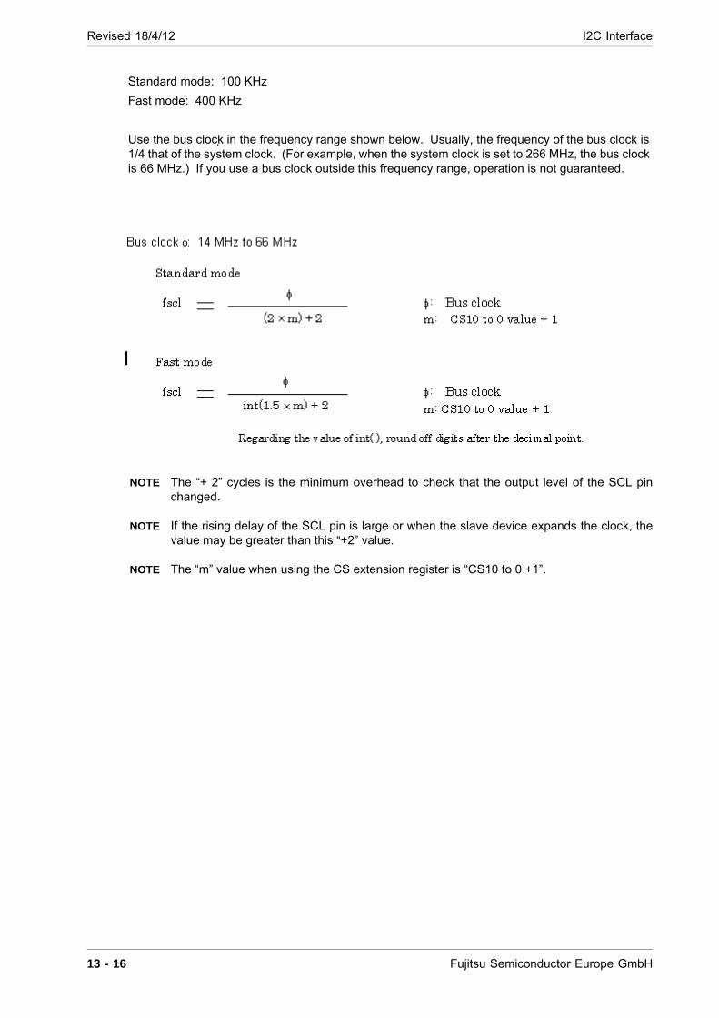
Revised 18/4/12 I2C Interface
Standard mode: 100 KHz
Fast mode: 400 KHz
Use the bus clock in the frequency range shown below. Usually, the frequency of the bus clock is 1/4 that of the system clock. (For example, when the system clock is set to 266 MHz, the bus clock is 66 MHz.) If you use a bus clock outside this frequency range, operation is not guaranteed.
NOTE The “+ 2” cycles is the minimum overhead to check that the output level of the SCL pin changed.
NOTE If the rising delay of the SCL pin is large or when the slave device expands the clock, the value may be greater than this “+2” value.
NOTE The “m” value when using the CS extension register is “CS10 to 0 +1”.
13 - 16 Fujitsu Semiconductor Europe GmbH
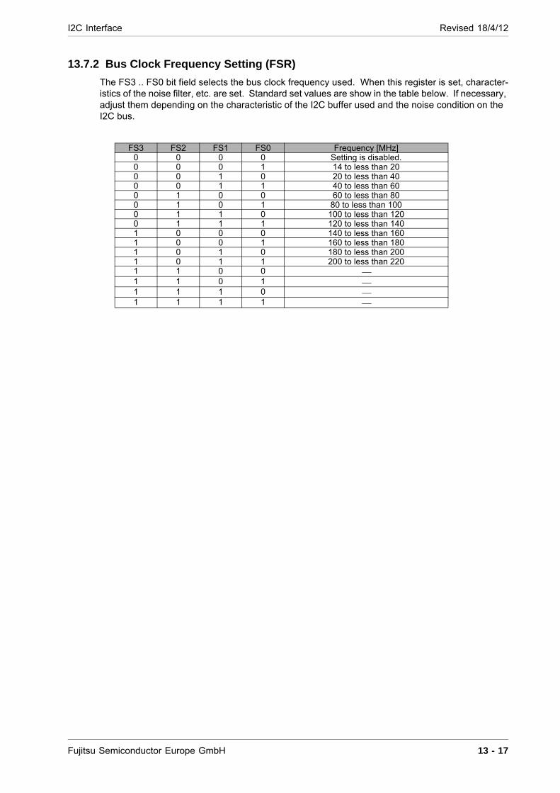
I2C Interface Revised 18/4/12
13.7.2 Bus Clock Frequency Setting (FSR)
The FS3 .. FS0 bit field selects the bus clock frequency used. When this register is set, character-istics of the noise filter, etc. are set. Standard set values are show in the table below. If necessary, adjust them depending on the characteristic of the I2C buffer used and the noise condition on the I2C bus.
FS3 FS2 FS1 FS0 Frequency [MHz]0 0 0 0 Setting is disabled.0 0 0 1 14 to less than 200 0 1 0 20 to less than 400 0 1 1 40 to less than 600 1 0 0 60 to less than 800 1 0 1 80 to less than 1000 1 1 0 100 to less than 1200 1 1 1 120 to less than 1401 0 0 0 140 to less than 1601 0 0 1 160 to less than 1801 0 1 0 180 to less than 2001 0 1 1 200 to less than 2201 1 0 0 1 1 0 1 1 1 1 0 1 1 1 1
Fujitsu Semiconductor Europe GmbH 13 - 17
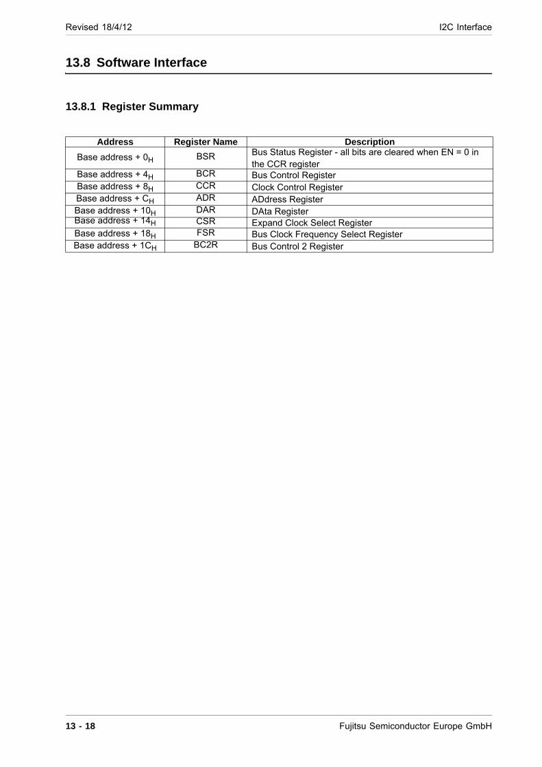
Revised 18/4/12 I2C Interface
13.8 Software Interface
13.8.1 Register Summary
Address Register Name Description
Base address + 0H BSR Bus Status Register - all bits are cleared when EN = 0 in the CCR register
Base address + 4H BCR Bus Control Register Base address + 8H CCR Clock Control Register Base address + CH ADR ADdress Register Base address + 10H DAR DAta Register Base address + 14H CSR Expand Clock Select Register Base address + 18H FSR Bus Clock Frequency Select Register Base address + 1CH BC2R Bus Control 2 Register
13 - 18 Fujitsu Semiconductor Europe GmbH
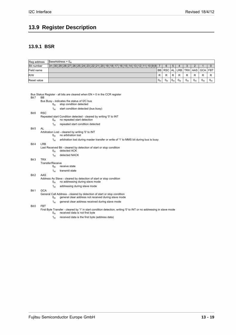
I2C Interface Revised 18/4/12
13.9 Register Description
13.9.1 BSR
Reg address BaseAddress + 0H
Bit number 31 30 29 28 27 26 25 24 23 22 21 20 19 18 17 16 15 14 13 12 11 10 9 8 7 6 5 4 3 2 1 0
Field name BB RSC AL LRB TRX AAS GCA FBT
R/W R R R R R R R R
Reset value 0H 0H 0H 0H 0H 0H 0H 0H
Bus Status Register - all bits are cleared when EN = 0 in the CCR register Bit 7 BB
Bus Busy - indicates the status of I2C bus 0H stop condition detected
1H start condition detected (bus busy)
Bit 6 RSC Repeated start Condition detected - cleared by writing '0' to INT
0H no repeated start detection
1H repeated start condition detected
Bit 5 AL Arbitration Lost - cleared by writing '0' to INT
0H no arbitration lost
1H arbitration lost during master transfer or write of '1' to MMS bit during bus is busy
Bit 4 LRB Last Received Bit - cleared by detection of start or stop condition
0H detected ACK
1H detected NACK
Bit 3 TRX Transfer/Receive
0H receive state
1H transmit state
Bit 2 AAS Address As Slave - cleared by detection of start or stop condition
0H no addressing during slave mode
1H addressing during slave mode
Bit 1 GCA General Call Address - cleared by detection of start or stop condition
0H general clear address not received during slave mode
1H general clear address received during slave mode
Bit 0 FBT First Byte Transfer - cleared by '1' in start condition detection, writing '0' to INT or no addressing in slave mode
0H received data is not first byte
1H received data is the first byte (address data)
Fujitsu Semiconductor Europe GmbH 13 - 19

Revised 18/4/12 I2C Interface
13.9.2 BCR
Reg address BaseAddress + 4H
Bit number 31 30 29 28 27 26 25 24 23 22 21 20 19 18 17 16 15 14 13 12 11 10 9 8 7 6 5 4 3 2 1 0
Field name BER BEIE SCC MSS ACK GCAA INTE INT
R/W RW RW RW RW RW RW RW RW
Reset value 0H 0H 0H 0H 0H 0H 0H 0H
Bus Control Register Bit 7 BER
Bus ERror interrupt request flag 0
H
(during WRITE:) write 0 to clear, (during READ:) no bus errors
1
H
(during WRITE:) not applicable, (during READ:) detected invalid start or stop condition during data transfer
Bit 6 BEIE Bus Error Interrupt Enable
0
H
interrupt disable
1
H
interrupt enable
Bit 5 SCC Start Condition Continue - automatically cleared
0
H
not applicable
1
H
continue start condition (generate it again)
Bit 4 MSS Master Slave Select - cleared after arbitration lost
0
H
enter slave mode after completing transmission and generating stop condition
1
H
enter master mode, generating start condition and start transmission
Bit 3 ACK ACKnowledge generation - enables generation of an ACK when data is received
0
H
no acknowledge
1
H
acknowledge
Bit 2 GCAA General Call Address Acknowledge - enables the generation of an ACK when a general call is received
0
H
no acknowledge
1
H
acknowledge
Bit 1 INTE INTerrupt Enable - enables the generation of an interrupt
0
H
interrupt disable
1
H
interrupt enable
Bit 0 INT INTerrupt - transfer complete interrupt flag
0
H
(during WRITE:) write 0 to clear the transfer end interrupt flag, (during READ:) transfer not completed
1
H
(during WRITE:) not applicable, (during READ:) signals different interrupt conditions
13 - 20 Fujitsu Semiconductor Europe GmbH
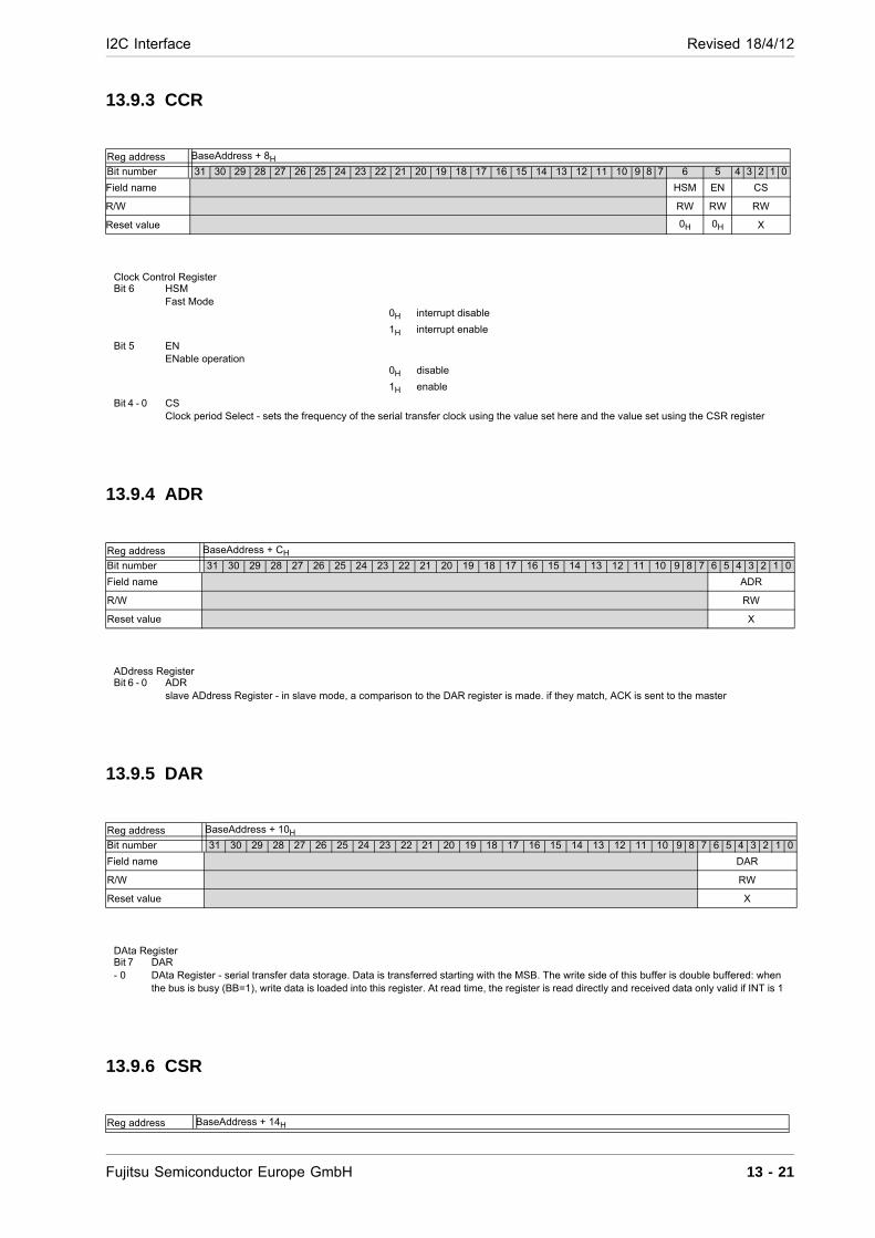
I2C Interface Revised 18/4/12
13.9.3 CCR
13.9.4 ADR
13.9.5 DAR
13.9.6 CSR
Reg address BaseAddress + 8H
Bit number 31 30 29 28 27 26 25 24 23 22 21 20 19 18 17 16 15 14 13 12 11 10 9 8 7 6 5 4 3 2 1 0
Field name HSM EN CS
R/W RW RW RW
Reset value 0H 0H X
Clock Control Register Bit 6 HSM
Fast Mode 0H interrupt disable
1H interrupt enable
Bit 5 EN ENable operation
0H disable
1H enable
Bit 4 - 0 CS Clock period Select - sets the frequency of the serial transfer clock using the value set here and the value set using the CSR register
Reg address BaseAddress + CH
Bit number 31 30 29 28 27 26 25 24 23 22 21 20 19 18 17 16 15 14 13 12 11 10 9 8 7 6 5 4 3 2 1 0
Field name ADR
R/W RW
Reset value X
ADdress Register Bit 6 - 0 ADR
slave ADdress Register - in slave mode, a comparison to the DAR register is made. if they match, ACK is sent to the master
Reg address BaseAddress + 10H
Bit number 31 30 29 28 27 26 25 24 23 22 21 20 19 18 17 16 15 14 13 12 11 10 9 8 7 6 5 4 3 2 1 0
Field name DAR
R/W RW
Reset value X
DAta Register Bit 7 - 0
DAR DAta Register - serial transfer data storage. Data is transferred starting with the MSB. The write side of this buffer is double buffered: when the bus is busy (BB=1), write data is loaded into this register. At read time, the register is read directly and received data only valid if INT is 1
Reg address BaseAddress + 14H
Fujitsu Semiconductor Europe GmbH 13 - 21
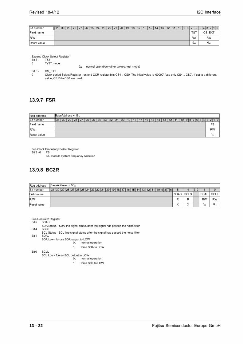
Revised 18/4/12 I2C Interface
13.9.7 FSR
13.9.8 BC2R
Bit number 31 30 29 28 27 26 25 24 23 22 21 20 19 18 17 16 15 14 13 12 11 10 9 8 7 6 5 4 3 2 1 0
Field name TST CS_EXT
R/W RW RW
Reset value 0H 0H
Expand Clock Select Register Bit 7 - 6
TST TeST mode
0H normal operation (other values: test mode)
Bit 5 - 0
CS_EXT Clock period Select Register - extend CCR register bits CS4 .. CS0. The initial value is '00000' (use only CS4 .. CS0). if set to a different value, CS10 to CS0 are used.
Reg address BaseAddress + 18H
Bit number 31 30 29 28 27 26 25 24 23 22 21 20 19 18 17 16 15 14 13 12 11 10 9 8 7 6 5 4 3 2 1 0
Field name FS
R/W RW
Reset value 1H
Bus Clock Frequency Select Register Bit 3 - 0 FS
I2C module system frequency selection
Reg address BaseAddress + 1CH
Bit number 31 30 29 28 27 26 25 24 23 22 21 20 19 18 17 16 15 14 13 12 11 10 9 8 7 6 5 4 3 2 1 0
Field name SDAS SCLS SDAL SCLL
R/W R R RW RW
Reset value X X 0H 0H
Bus Control 2 Register Bit 5 SDAS
SDA Status - SDA line signal status after the signal has passed the noise filter Bit 4 SCLS
SCL Status - SCL line signal status after the signal has passed the noise filter Bit 1 SDAL
SDA Low - forces SDA output to LOW 0H normal operation
1H force SDA to LOW
Bit 0 SCLL SCL Low - forces SCL output to LOW
0H normal operation
1H force SCL to LOW
13 - 22 Fujitsu Semiconductor Europe GmbH
GPIO Revised 18/4/12
Chapter 14: GPIO
14.1 Position of Block in whole LSI
The GPIO modules register interface is connected to an ARM AHB bus.
GPIO pad cells can directly be connected to the module.
14.2 Feature List
The GPIO unit has the following features:
8 bits GPIO ports
Each port can be shared with an other peripheral signal
14.2.1 GPIO Ports
Digital GPIO ports can be controlled by three registers:
Data Output Register (PORT)
Data Direction Register (DIR)
Data Input Register (PIN)
14.2.2 Peripheral Mode
Shared port mode is controlled using the Port Function Register (PFR).
I/O pins of GPIO module can be shared with other IPs within the LSI by using the peripheral mode.
14.2.3 General Restrictions
Maximum input sample rate is AHB bus clock frequency. When reading data from GPIO port, the synchronizer delay (2 clock cycles) has to be considered.
If GPIO inputs are used by other IPs (e.g. interrupt controller), connect according modules to PFI output of GPIO module. In this case peripheral mode has to be enabled for these signals.
14.3 Processing Mode
All bit references in this section are written in general form. A lower case “x” represents the bit num-ber. For example bit number x in PORT register, here documented generally as PORTx.
14.3.1 Processing Flow
The figure below shows a functional description of one I/O-port pin.
Fujitsu Semiconductor Europe GmbH 14 - 1
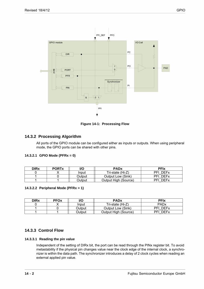
Revised 18/4/12 GPIO
Figure 14-1: Processing Flow
14.3.2 Processing Algorithm
All ports of the GPIO module can be configured either as inputs or outputs. When using peripheral mode, the GPIO ports can be shared with other pins.
14.3.2.1 GPIO Mode (PFRx = 0)
14.3.2.2 Peripheral Mode (PFRx = 1)
14.3.3 Control Flow
14.3.3.1 Reading the pin value
Independent of the setting of DIRx bit, the port can be read through the PINx register bit. To avoid metastability if the physical pin changes value near the clock edge of the internal clock, a synchro-nizer is within the data path. The synchronizer introduces a delay of 2 clock cycles when reading an external applied pin value.
DIRx PORTx I/O PADx PFIx0 X Input Tri-state (Hi-Z) PFI_DEFx1 0 Output Output Low (Sink) PFI_DEFx1 1 Output Output High (Source) PFI_DEFx
DIRx PFOx I/O PADx PFIx0 X Input Tri-state (Hi-Z) PADx1 0 Output Output Low (Sink) PFI_DEFx1 1 Output Output High (Source) PFI_DEFx
DIR
PORT
PFR
PIN
AH
B
1
0
10
Synchronizer
PFO
PFI
PFI_DEF
&
GPIO module
PAD
PC
PO
PI
I/O Cell
14 - 2 Fujitsu Semiconductor Europe GmbH
GPIO Revised 18/4/12
14.3.3.2 Driving the pin
If DIRx register bit is written logic one, the port is configured as an output pin. In this case the pin is driven with the content of the PORTx register bit. If PORTx is written logic zero, the port pin is driven low (zero). If PORTx is written logic one, the port pin is driven high (one). The port pins are tri-stated when reset condition becomes active.
14.3.3.3 Share pin with other peripheral blocks
The GPIO pins can be shared with other peripheral units when setting PFRx register bit to logic one (peripheral mode). Refer to respective LSI specification to see which ports are shared. When a reset condition occurs, the configuration switches back to GPIO input mode.
PFI signals are synchronized to GPIO clock domain and the synchronizer introduces a delay of 2 clock cycles when reading an external pin value.
Fujitsu Semiconductor Europe GmbH 14 - 3
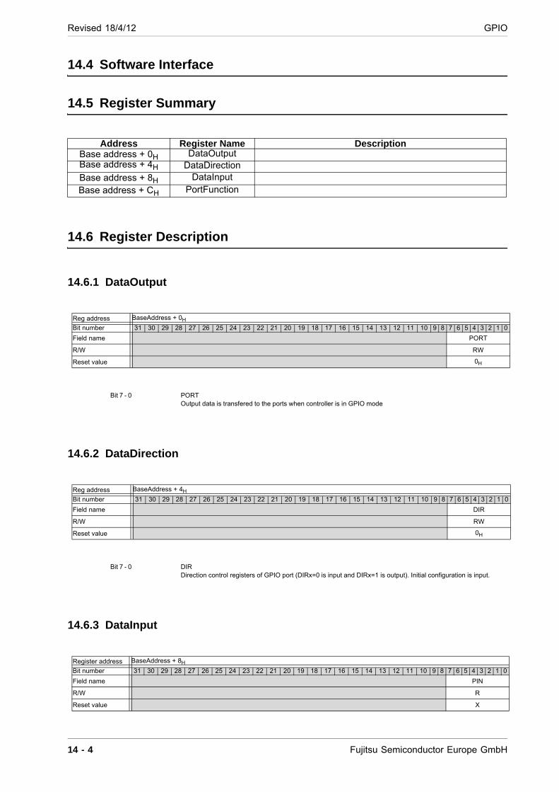
Revised 18/4/12 GPIO
14.4 Software Interface
14.5 Register Summary
14.6 Register Description
14.6.1 DataOutput
14.6.2 DataDirection
14.6.3 DataInput
Address Register Name DescriptionBase address + 0H DataOutput Base address + 4H DataDirection Base address + 8H DataInput Base address + CH PortFunction
Reg address BaseAddress + 0H
Bit number 31 30 29 28 27 26 25 24 23 22 21 20 19 18 17 16 15 14 13 12 11 10 9 8 7 6 5 4 3 2 1 0
Field name PORT
R/W RW
Reset value 0H
Bit 7 - 0 PORT Output data is transfered to the ports when controller is in GPIO mode
Reg address BaseAddress + 4H
Bit number 31 30 29 28 27 26 25 24 23 22 21 20 19 18 17 16 15 14 13 12 11 10 9 8 7 6 5 4 3 2 1 0
Field name DIR
R/W RW
Reset value 0H
Bit 7 - 0 DIR Direction control registers of GPIO port (DIRx=0 is input and DIRx=1 is output). Initial configuration is input.
Register address BaseAddress + 8H
Bit number 31 30 29 28 27 26 25 24 23 22 21 20 19 18 17 16 15 14 13 12 11 10 9 8 7 6 5 4 3 2 1 0
Field name PIN
R/W R
Reset value X
14 - 4 Fujitsu Semiconductor Europe GmbH

GPIO Revised 18/4/12
14.6.4 PortFunction
Bit 7 - 0 PIN Read data indicates the current value at the GPIO port.
Reg address BaseAddress + CH
Bit number 31 30 29 28 27 26 25 24 23 22 21 20 19 18 17 16 15 14 13 12 11 10 9 8 7 6 5 4 3 2 1 0
Field name PFR
R/W RW
Reset value 0H
Bit 7 - 0
PFR Port function control register (PFRx=0 is GPIO mode and PFRx=1 is PERIPHERAL mode). Default configuration is GPIO mode.
Fujitsu Semiconductor Europe GmbH 14 - 5

Revised 18/4/12 GPIO
14 - 6 Fujitsu Semiconductor Europe GmbH
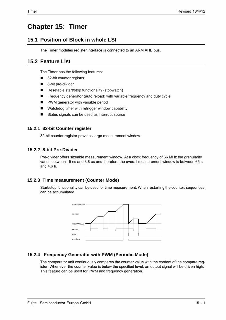
Timer Revised 18/4/12
Chapter 15: Timer
15.1 Position of Block in whole LSI
The Timer modules register interface is connected to an ARM AHB bus.
15.2 Feature List
The Timer has the following features:
32-bit counter register
8-bit pre-divider
Resetable start/stop functionality (stopwatch)
Frequency generator (auto reload) with variable frequency and duty cycle
PWM generator with variable period
Watchdog timer with retrigger window capability
Status signals can be used as interrupt source
15.2.1 32-bit Counter register
32-bit counter register provides large measurement window.
15.2.2 8-bit Pre-Divider
Pre-divider offers sizeable measurement window. At a clock frequency of 66 MHz the granularity varies between 15 ns and 3.8 us and therefore the overall measurement window is between 65 s and 4.6 h.
15.2.3 Time measurement (Counter Mode)
Start/stop functionality can be used for time measurement. When restarting the counter, sequences can be accumulated.
15.2.4 Frequency Generator with PWM (Periodic Mode)
The comparator unit continuously compares the counter value with the content of the compare reg-ister. Whenever the counter value is below the specified level, an output signal will be driven high. This feature can be used for PWM and frequency generation.
counter
0 xFFFFFFFF
0x 00000000
clear
overflow
enable
Fujitsu Semiconductor Europe GmbH 15 - 1
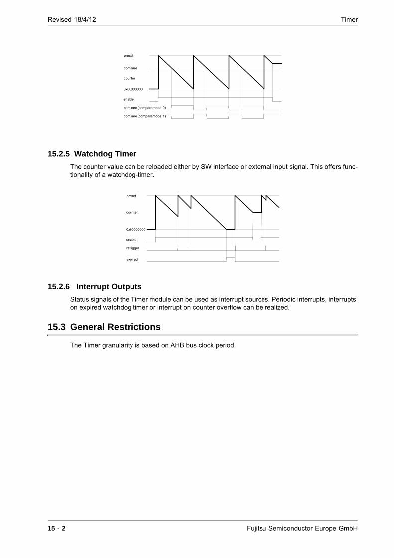
Revised 18/4/12 Timer
15.2.5 Watchdog Timer
The counter value can be reloaded either by SW interface or external input signal. This offers func-tionality of a watchdog-timer.
15.2.6 Interrupt Outputs
Status signals of the Timer module can be used as interrupt sources. Periodic interrupts, interrupts on expired watchdog timer or interrupt on counter overflow can be realized.
15.3 General Restrictions
The Timer granularity is based on AHB bus clock period.
counter
0x00000000
enable
compare (comparemode 0)
compare (comparemode 1)
preset
compare
counter
preset
0x00000000
retrigger
expired
enable
15 - 2 Fujitsu Semiconductor Europe GmbH
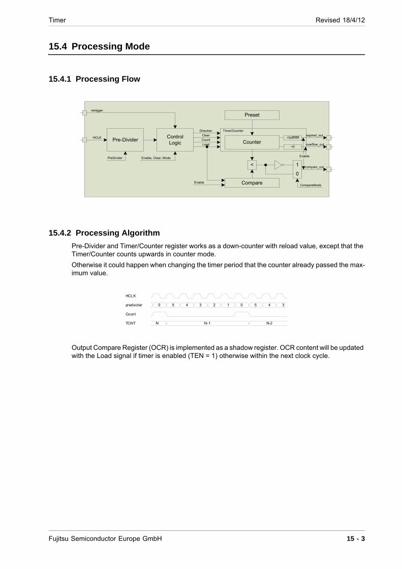
Timer Revised 18/4/12
15.4 Processing Mode
15.4.1 Processing Flow
15.4.2 Processing Algorithm
Pre-Divider and Timer/Counter register works as a down-counter with reload value, except that the Timer/Counter counts upwards in counter mode.
Otherwise it could happen when changing the timer period that the counter already passed the max-imum value.
Output Compare Register (OCR) is implemented as a shadow register. OCR content will be updated with the Load signal if timer is enabled (TEN = 1) otherwise within the next clock cycle.
Preset
Compare
Pre-DividerControlLogic Counter
=0
=0xffffffff
< 1
0
HCLK
overflow_out
expired_out
compare_out
Timer/CounterDirection
Clear
Count
Load
CompareMode
PreDivider Enable, Clear, Mode
Enable
retrigger
Enable
predivider
Count
TCNT
0 5 4 3 2 1 0 5 4 3
N-1N N-2
HCLK
Fujitsu Semiconductor Europe GmbH 15 - 3
Revised 18/4/12 Timer
15.5 Control Flow
15.5.1 Time measurement
Set TMODE = TMODE_COUNTER
Set TDIV dependent on measurement window
To start or restart the timer set TEN = ‘1’.
To stop the timer set TEN = ‘0’.
To clear or reset the timer set TCLR = ‘1’.
Elapsed time can be calculated by:
T = (1 / fHCLK) * (TDIV + 1) * TCNT
If an overflow occurs, TOVL will be set to ‘1’.
15.5.2 Watchdog Timer
Set TMODE = TMODE_WATCHDOG
Set TDIV dependent on measurement window
Set TLR to maximum time period. This can be calculated by:
TLR = Tmax * fHCLK / (TDIV + 1)
To start the watchdog timer set TEN = ‘1’.
To stop the watchdog timer set TEN = ‘0’.
To retrigger the watchdog timer write TCLR = ‘1’.
If the timer expires, TEXP will be set to ‘1’.
15 - 4 Fujitsu Semiconductor Europe GmbH
Timer Revised 18/4/12
15.5.3 Frequency Generator with PWM
Set TMODE = TMODE_PERIODIC
Set TDIV dependent on measurement window
Set TLR to desired PWM frequency. This can be calculated by:
TLR = fHCLK / (fPWM * (TDIV + 1)) - 1
Set TCM = ‘1’
Set OCR to the desired PWM pulse high time which can be calculated by:
OCR = (1 / fHCLK) * (TDIV + 1) * Thigh
To start the timer set TEN = ‘1’.
To stop the timer set TEN = ‘0’.
Fujitsu Semiconductor Europe GmbH 15 - 5
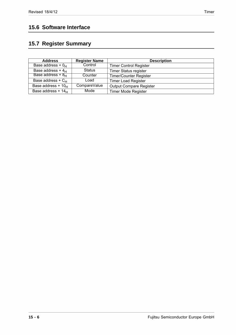
Revised 18/4/12 Timer
15.6 Software Interface
15.7 Register Summary
Address Register Name DescriptionBase address + 0H Control Timer Control Register Base address + 4H Status Timer Status register Base address + 8H Counter Timer/Counter Register Base address + CH Load Timer Load Register Base address + 10H CompareValue Output Compare Register Base address + 14H Mode Timer Mode Register
15 - 6 Fujitsu Semiconductor Europe GmbH
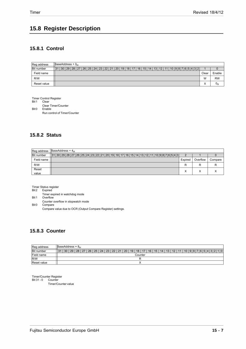
Timer Revised 18/4/12
15.8 Register Description
15.8.1 Control
15.8.2 Status
15.8.3 Counter
Reg address BaseAddress + 0H
Bit number 31 30 29 28 27 26 25 24 23 22 21 20 19 18 17 16 15 14 13 12 11 10 9 8 7 6 5 4 3 2 1 0
Field name Clear Enable
R/W W RW
Reset value X 0H
Timer Control Register Bit 1 Clear
Clear Timer/Counter Bit 0 Enable
Run control of Timer/Counter
Reg address BaseAddress + 4H
Bit number 31 30 29 28 27 26 25 24 23 22 21 20 19 18 17 16 15 14 13 12 11 10 9 8 7 6 5 4 3 2 1 0
Field name Expired Overflow Compare
R/W R R R
Reset
valueX X X
Timer Status register Bit 2 Expired
Timer expired in watchdog mode Bit 1 Overflow
Counter overflow in stopwatch mode Bit 0 Compare
Compare value due to OCR (Output Compare Register) settings.
Reg address BaseAddress + 8H
Bit number 31 30 29 28 27 26 25 24 23 22 21 20 19 18 17 16 15 14 13 12 11 10 9 8 7 6 5 4 3 2 1 0Field name Counter R/W R Reset value X
Timer/Counter Register Bit 31 - 0 Counter
Timer/Counter value
Fujitsu Semiconductor Europe GmbH 15 - 7
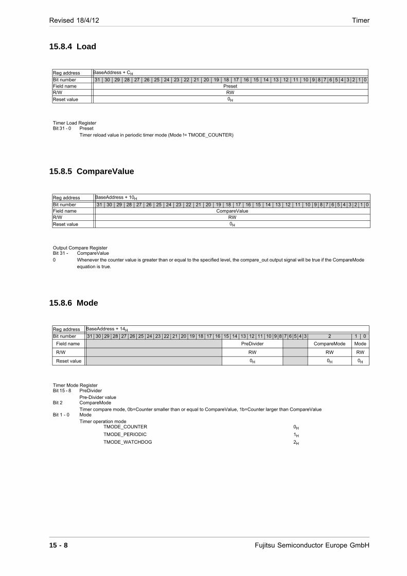
Revised 18/4/12 Timer
15.8.4 Load
15.8.5 CompareValue
15.8.6 Mode
Reg address BaseAddress + CH
Bit number 31 30 29 28 27 26 25 24 23 22 21 20 19 18 17 16 15 14 13 12 11 10 9 8 7 6 5 4 3 2 1 0Field name Preset R/W RW
Reset value 0H
Timer Load Register Bit 31 - 0 Preset
Timer reload value in periodic timer mode (Mode != TMODE_COUNTER)
Reg address BaseAddress + 10H
Bit number 31 30 29 28 27 26 25 24 23 22 21 20 19 18 17 16 15 14 13 12 11 10 9 8 7 6 5 4 3 2 1 0Field name CompareValue R/W RW
Reset value 0H
Output Compare Register Bit 31 -
0
CompareValue Whenever the counter value is greater than or equal to the specified level, the compare_out output signal will be true if the CompareMode
equation is true.
Reg address BaseAddress + 14H
Bit number 31 30 29 28 27 26 25 24 23 22 21 20 19 18 17 16 15 14 13 12 11 10 9 8 7 6 5 4 3 2 1 0
Field name PreDivider CompareMode Mode
R/W RW RW RW
Reset value 0H 0H 0H
Timer Mode Register Bit 15 - 8 PreDivider
Pre-Divider value Bit 2 CompareMode
Timer compare mode, 0b=Counter smaller than or equal to CompareValue, 1b=Counter larger than CompareValue Bit 1 - 0 Mode
Timer operation mode TMODE_COUNTER 0H
TMODE_PERIODIC 1H
TMODE_WATCHDOG 2H
15 - 8 Fujitsu Semiconductor Europe GmbH
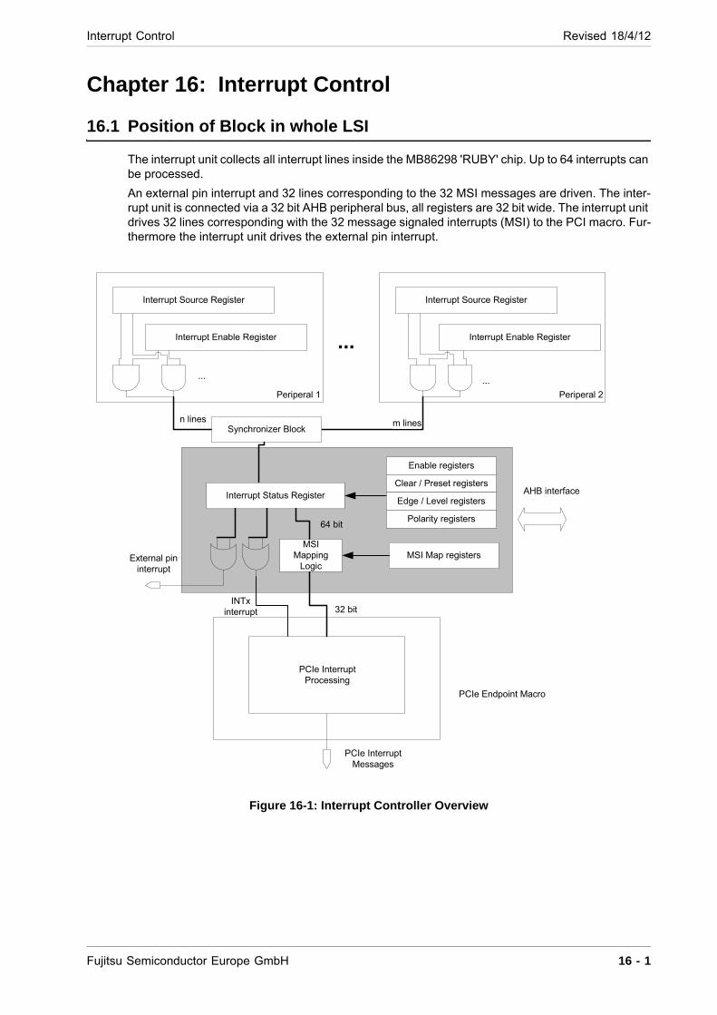
Interrupt Control Revised 18/4/12
Chapter 16: Interrupt Control
16.1 Position of Block in whole LSI
The interrupt unit collects all interrupt lines inside the MB86298 'RUBY' chip. Up to 64 interrupts can be processed.
An external pin interrupt and 32 lines corresponding to the 32 MSI messages are driven. The inter-rupt unit is connected via a 32 bit AHB peripheral bus, all registers are 32 bit wide. The interrupt unit drives 32 lines corresponding with the 32 message signaled interrupts (MSI) to the PCI macro. Fur-thermore the interrupt unit drives the external pin interrupt.
Figure 16-1: Interrupt Controller Overview
Interrupt Source Register
Interrupt Enable Register
Interrupt Source Register
Interrupt Enable Register
n lines m lines
PCIe InterruptProcessing
PCIe InterruptMessages
Periperal 1 Periperal 2
Interrupt Unit
PCIe Endpoint Macro
... ...
...
Interrupt Status Register
Enable registers
Clear / Preset registers
MSI Map registersMSI
Mapping Logic
External pin interrupt
32 bit
64 bit
AHB interface
Synchronizer Block
Edge / Level registers
Polarity registers
INTx interrupt
Fujitsu Semiconductor Europe GmbH 16 - 1
Revised 18/4/12 Interrupt Control
16.2 Feature List
The interrupt unit provides the following features:
Collects internal interrupt lines of the chip
Supports up to 64 internal interrupt input lines
Status registers istat0 / istat1 stores the status of the interrupt lines, can be read via AHB
Enable registers for PCIe MSI interrupt and external pin interrupt
Clear register for status registers
Preset register for status registers (for debugging purposes)
Polarity registers for adaptation of polarity of internal interrupt lines
MSI mapping registers for programming the mapping of each interrupt line to the MSI interrupt output line
Polarity register bit for the external interrupt
The status register istat0 and istat1 show the current status interrupt of each interrupt line. A “1” means that the interrupt bit is active, “0” means inactive.
Each interrupt bit can be enabled by the use of corresponding enable bits. Two sets of enable reg-isters exist: the ena_p0 / ena_p1 registers for enabling the interrupts for the PCI Express (PCIe) message based interrupts (MSI), and the ena_e0 / ena_e1 registers for enabling the interrupts for the external interrupt line.
The interrupt status bits in istat0 / istat1 can be cleared by writing a “1” to the respective bit position in the clear registers clear0 and clear1. Please note that the clear registers clear0 / clear1 read back 0x0 always.
The interrupt status bits in istat0 / istat1 can be preset by writing a “1” to the respective bit position in the preset registers preset0 and preset1. Please note that the preset registers preset0 / preset1 read back 0x0 always.
The polarity of the active level for each input interrupt line can be changed by writing a “1” to the respective bit position of the polarity registers pol0 / pol1. A “0” means interrupt polarity unchanged (high active interrupt), a “1” means interrupt polarity inverted (low active interrupt),
For mapping the up to 64 interrupt bits to the 32 MSI interrupt lines a set of MSI mapping registers exists, namely register msimap0 to msimap15. Each MSI mapping register contains 5 bit wide fields called intXXmap for programming the mapping of the resp. interrupt line to the 32 MSI interrupt lines of the interrupt unit. Each of the 16 msimap registers contains four intXXmap fields. A value of “0” means interrupt pin is mapped to MSI interrupt line 0, a value of “1” means interrupt pin is mapped to MSI interrupt line 1 and so on.
The polarity of the external interrupt can be programmed by writing the eint_pol bit in the icfg regis-ter.
16 - 2 Fujitsu Semiconductor Europe GmbH
Interrupt Control Revised 18/4/12
16.2.1 Mapping internal interrupt lines
The MB86298 'RUBY' registers are mapped to the corresponding bit index of istat0 / istat1 by map-ping table:
Table 16-1: Mapping to istat0
MB86298 'RUBY' interrupt name Mapped to istat0 bit: Commentintercom_err 0 Interconnection Error Interruptcap0_int 1 VSYNC Interrupt Capture 0cap1_int 2 VSYNC Interrupt Capture 1cap2_int 3 VSYNC Interrupt Capture 2cap3_int 4 VSYNC Interrupt Capture 3write_back_int 5 Write Back Unit Interruptdisp0_int0 6 VSYNC Display Controller 0disp0_int1 7 FSYNC Display Controller 0disp0_int2 8 EXT SYNC ERROR Display Controller 0disp0_int3 9 REGISTER UPDATE Display Controller 0disp1_int0 10 VSYNC Display Controller 1disp1_int1 11 FSYNC Display Controller 1disp1_int2 12 EXT SYNC ERROR Display Controller 1disp1_int3 13 REGISTER UPDATE Display Controller 1pixblt_int 14 PixBlt Interruptpcie 15 PCIE Interrupttimer_ov 16 Timer Overflow Interrupttimer_exp 17 Timer Expired Interrupttimer_cmp 18 Timer Compare Interruptcmd_watdog 19 Command Sequencer Watchdog Interruptcmd_fempty 20 Command Sequencer FIFO Empty Interruptcmd_flwm 21 Command Sequencer FIFO Low Water Interruptcmd_fhwm 22 Command Sequencer FIFO High Water Interruptcmd_ffull 23 Command Sequencer FIFO Full Interruptcmd_error 24 Command Sequencer Error Interruptcmd_idle 25 Command Sequencer Idle Interruptsscg_int 26 SSGC InterruptGPU_int 27 GPU InterruptGPU_eint 28 GPU Error InterruptI2C_int 29 I2C Interrupt<none> 30
<none> 31
Fujitsu Semiconductor Europe GmbH 16 - 3
Revised 18/4/12 Interrupt Control
Table 16-2: Mapping to istat1
16.2.2 MSI interrupt mapping
The MSI interrupt output is composed of 32 lines. A “1” on a line corresponds to a sent message on the PCIe bus later on. E.g. a “1” on bit 0 means a message “MSI 0” is sent on PCIe later on, a “1” on bit 1 means that a message “MSI 1” is sent on PCIe later on, and so on. Please note the MSI interrupt output has edge triggered behaviour, the MSI interrupt output is active for one HCLK cycle.
NOTE In case there are two interrupt lines are going active in two consecutive clock cycles, and the two interrupts are mapped to the same MSI message, the MSI message can be active for more than one HCLK cycle.
16.2.3 External pin interrupt mapping
The external pin interrupt is a logic OR out of all active and enabled (by ena_e0 / ena_e1) interrupt bits in istat0 and istat1, low active. That means if a least on interrupt line is enabled an goes to “1” the external pin interrupt goes active. The active level level depends on the value of the eint_pol bit in the icfg register.
MB86298 'RUBY' interrupt name Mapped to istat1 bit: Comment gpio_pfi[0] 0 GPIO PFI Interrupt 0 gpio_pfi[1] 1 GPIO PFI Interrupt 1 gpio_pfi[2] 2 GPIO PFI Interrupt 2 gpio_pfi[3] 3 GPIO PFI Interrupt 3 gpio_pfi[4] 4 GPIO PFI Interrupt 4 gpio_pfi[5] 5 GPIO PFI Interrupt 5 gpio_pfi[6] 6 GPIO PFI Interrupt 6 gpio_pfi[7] 7 GPIO PFI Interrupt 7ddr_flushpending_0 8 DDR flush pending 0 (sensitive to trailing edge)ddr_flushpending_1 9 DDR flush pending 1 (sensitive to trailing edge)ddr_flushpending_2 10 DDR flush pending 2 (sensitive to trailing edge)ddr_flushpending_3 11 DDR flush pending 3 (sensitive to trailing edge)<none> 12
<none> 13
<none> 14
<none> 15
<none> 16
<none> 17
<none> 18
<none> 19
<none> 20
<none> 21
<none> 22
<none> 23
<none> 24
<none> 25
<none> 26
<none> 27
<none> 28
<none> 29
<none> 30
<none> 31
16 - 4 Fujitsu Semiconductor Europe GmbH
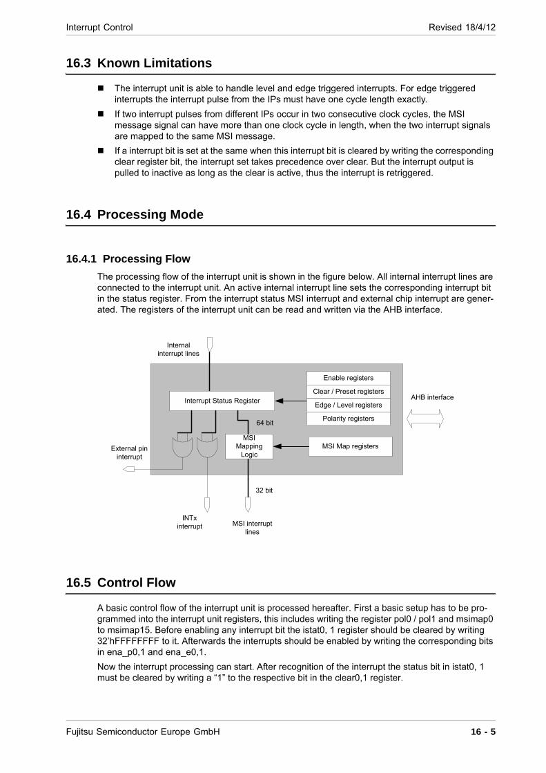
Interrupt Control Revised 18/4/12
16.3 Known Limitations
The interrupt unit is able to handle level and edge triggered interrupts. For edge triggered interrupts the interrupt pulse from the IPs must have one cycle length exactly.
If two interrupt pulses from different IPs occur in two consecutive clock cycles, the MSI message signal can have more than one clock cycle in length, when the two interrupt signals are mapped to the same MSI message.
If a interrupt bit is set at the same when this interrupt bit is cleared by writing the corresponding clear register bit, the interrupt set takes precedence over clear. But the interrupt output is pulled to inactive as long as the clear is active, thus the interrupt is retriggered.
16.4 Processing Mode
16.4.1 Processing Flow
The processing flow of the interrupt unit is shown in the figure below. All internal interrupt lines are connected to the interrupt unit. An active internal interrupt line sets the corresponding interrupt bit in the status register. From the interrupt status MSI interrupt and external chip interrupt are gener-ated. The registers of the interrupt unit can be read and written via the AHB interface.
16.5 Control Flow
A basic control flow of the interrupt unit is processed hereafter. First a basic setup has to be pro-grammed into the interrupt unit registers, this includes writing the register pol0 / pol1 and msimap0 to msimap15. Before enabling any interrupt bit the istat0, 1 register should be cleared by writing 32’hFFFFFFFF to it. Afterwards the interrupts should be enabled by writing the corresponding bits in ena_p0,1 and ena_e0,1.
Now the interrupt processing can start. After recognition of the interrupt the status bit in istat0, 1 must be cleared by writing a “1” to the respective bit in the clear0,1 register.
Interrupt Unit
Interrupt Status Register
Enable registers
Clear / Preset registers
MSI Map registersMSI
Mapping Logic
External pin interrupt
32 bit
64 bit
AHB interfaceEdge / Level registers
Polarity registers
INTx interrupt
Internal interrupt lines
MSI interrupt lines
Fujitsu Semiconductor Europe GmbH 16 - 5
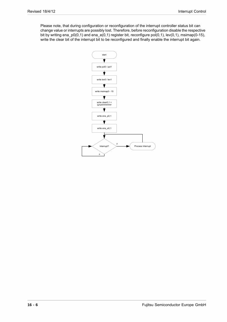
Revised 18/4/12 Interrupt Control
Please note, that during configuration or reconfiguration of the interrupt controller status bit can change value or interrupts are possibly lost. Therefore, before reconfiguration disable the respective bit by writing ena_p0(0,1) and ena_e(0,1) register bit, reconfigure pol(0,1), lev(0,1), msimap(0-15), write the clear bit of the interrupt bit to be reconfigured and finally enable the interrupt bit again.
write pol0 / pol1
write msimap0 - 15
start
write clear0,1 = 32'hFFFFFFFF
write ena_p0,1
write ena_e0,1
Interrupt? Process Interrupt
n
y
write lev0 / lev1
16 - 6 Fujitsu Semiconductor Europe GmbH
Interrupt Control Revised 18/4/12
16.6 Software Interface
16.7 Register Summary
16.8 Register Description
16.8.1 icfg
Address Register Name Description
Base address + 0H icfg Interrupt Configuration Register: used to configure the operation of the interrupt controller.
Base address + 4H istat0 Interrupt Status register 0. Shows the status of interrupts 0 to 31 (Read Only).
Base address + 8H istat1 Interrupt Status register 1. Shows the status of interrupts 32 to 63 (Read Only).
Base address + CH ena_p0 "Enable register 0 for PCIe interrupt, bits 0 to 31." Base address + 10H ena_p1 "Enable register 1 for PCIe interrupt, bits 32 to 63."
Base address + 14H ena_e0 "Enable register 0 for external pin for interrupt, bits 0 to 31."
Base address + 18H ena_e1 "Enable register 1 for external pin for interrupt, bits 32 to 63."
Base address + 1CH clear0 "Enable register 0 for interrupt bits 0 to 31." Base address + 20H clear1 "Enable register 1 for interrupt bits 32 to 63." Base address + 24H preset0 "Preset register 0 for interrupt bits 0 to 31." Base address + 28H preset1 "Preset register 1 for interrupt bits 32 to 63." Base address + 2CH pol0 "Polarity register 0 for interrupt bits 0 to 31." Base address + 30H pol1 "Polarity register 1 for interrupt bits 32 to 63." Base address + 34H lev0 "Level / edge triggered register 0 for interrupt bits 0 to 31."
Base address + 38H lev1 "Level / edge triggered register 1 for interrupt bits 32 to 63."
Base address + 3CH msimap0 "MSI map register for interrupts 0 to 3" Base address + 40H msimap1 "MSI map register for interrupts 4 to 7" Base address + 44H msimap2 "MSI map register for interrupts 8 to 11" Base address + 48H msimap3 "MSI map register for interrupts 12 to 15" Base address + 4CH msimap4 "MSI map register for interrupts 16 to 19" Base address + 50H msimap5 "MSI map register for interrupts 20 to 23" Base address + 54H msimap6 "MSI map register for interrupts 24 to 27" Base address + 58H msimap7 "MSI map register for interrupts 28 to 31" Base address + 5CH msimap8 "MSI map register for interrupts 32 to 35" Base address + 60H msimap9 "MSI map register for interrupts 36 to 39" Base address + 64H msimap10 "MSI map register for interrupts 40 to 43" Base address + 68H msimap11 "MSI map register for interrupts 44 to 47" Base address + 6CH msimap12 "MSI map register for interrupts 48 to 51" Base address + 70H msimap13 "MSI map register for interrupts 52 to 55" Base address + 74H msimap14 "MSI map register for interrupts 56 to 59" Base address + 78H msimap15 "MSI map register for interrupts 60 to 63"
Reg address BaseAddress + 0H
Fujitsu Semiconductor Europe GmbH 16 - 7
Revised 18/4/12 Interrupt Control
16.8.2 istat0
16.8.3 istat1
16.8.4 ena_p0
Bit number 31 30 29 28 27 26 25 24 23 22 21 20 19 18 17 16 15 14 13 12 11 10 9 8 7 6 5 4 3 2 1 0
Field name intx_pol eint_pol
R/W RW RW
Reset value 0H 0H
Interrupt Configuration Register: used to configure the operation of the interrupt controller. Bit 1 intx_pol
"Polarity of intx_n interrupt: 0 = intx_n port active-low, 1 = intx_n is active-high" Bit 0 eint_pol
"Polarity of an external interrupt: 0 = ext_int_n port is active-low, 1 = ext_int_n is active-high"
Reg address BaseAddress + 4H
Bit number 31 30 29 28 27 26 25 24 23 22 21 20 19 18 17 16 15 14 13 12 11 10 9 8 7 6 5 4 3 2 1 0Field name istat0 R/W R
Reset value 0H
Interrupt Status register 0. Shows the status of interrupts 0 to 31 (Read Only). Bit 31 - 0 istat0
"Status register 0 for interrupts, bits 0 to 31: 0 = Interrupt is inactive, 1 = Interrupt is active"
Reg address BaseAddress + 8H
Bit number 31 30 29 28 27 26 25 24 23 22 21 20 19 18 17 16 15 14 13 12 11 10 9 8 7 6 5 4 3 2 1 0Field name istat1 R/W R
Reset value 0H
Interrupt Status register 1. Shows the status of interrupts 32 to 63 (Read Only). Bit 31 - 0 istat1
"Status register 1 for interrupts, bits 32 to 63: 0 = Interrupt is inactive, 1 = Interrupt is active"
Reg address BaseAddress + CH
Bit number 31 30 29 28 27 26 25 24 23 22 21 20 19 18 17 16 15 14 13 12 11 10 9 8 7 6 5 4 3 2 1 0Field name ena_p0 R/W RW
Reset value 0H
"Enable register 0 for PCIe interrupt, bits 0 to 31." Bit 31 - 0 ena_p0
"Enables bits 0 to 31 for PCIe interrupt if set to 1."
16 - 8 Fujitsu Semiconductor Europe GmbH
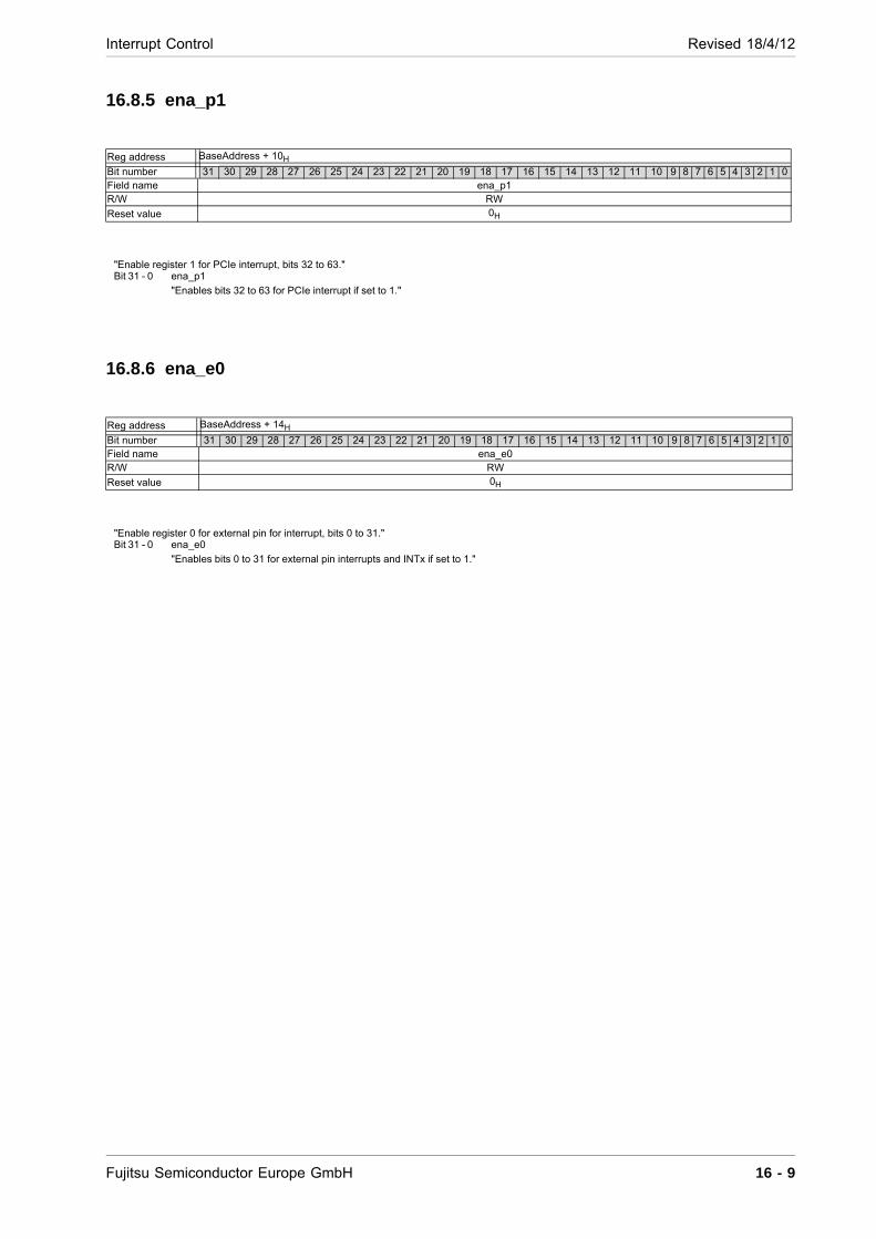
Interrupt Control Revised 18/4/12
16.8.5 ena_p1
16.8.6 ena_e0
Reg address BaseAddress + 10H
Bit number 31 30 29 28 27 26 25 24 23 22 21 20 19 18 17 16 15 14 13 12 11 10 9 8 7 6 5 4 3 2 1 0Field name ena_p1 R/W RW
Reset value 0H
"Enable register 1 for PCIe interrupt, bits 32 to 63." Bit 31 - 0 ena_p1
"Enables bits 32 to 63 for PCIe interrupt if set to 1."
Reg address BaseAddress + 14H
Bit number 31 30 29 28 27 26 25 24 23 22 21 20 19 18 17 16 15 14 13 12 11 10 9 8 7 6 5 4 3 2 1 0Field name ena_e0 R/W RW
Reset value 0H
"Enable register 0 for external pin for interrupt, bits 0 to 31." Bit 31 - 0 ena_e0
"Enables bits 0 to 31 for external pin interrupts and INTx if set to 1."
Fujitsu Semiconductor Europe GmbH 16 - 9
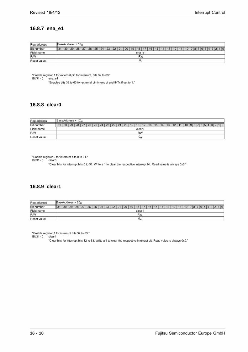
Revised 18/4/12 Interrupt Control
16.8.7 ena_e1
16.8.8 clear0
16.8.9 clear1
Reg address BaseAddress + 18H
Bit number 31 30 29 28 27 26 25 24 23 22 21 20 19 18 17 16 15 14 13 12 11 10 9 8 7 6 5 4 3 2 1 0Field name ena_e1 R/W RW
Reset value 0H
"Enable register 1 for external pin for interrupt, bits 32 to 63." Bit 31 - 0 ena_e1
"Enables bits 32 to 63 for external pin interrupt and INTx if set to 1."
Reg address BaseAddress + 1CH
Bit number 31 30 29 28 27 26 25 24 23 22 21 20 19 18 17 16 15 14 13 12 11 10 9 8 7 6 5 4 3 2 1 0Field name clear0 R/W RW
Reset value 0H
"Enable register 0 for interrupt bits 0 to 31." Bit 31 - 0 clear0
"Clear bits for interrupt bits 0 to 31. Write a 1 to clear the respective interrupt bit. Read value is always 0x0."
Reg address BaseAddress + 20H
Bit number 31 30 29 28 27 26 25 24 23 22 21 20 19 18 17 16 15 14 13 12 11 10 9 8 7 6 5 4 3 2 1 0Field name clear1 R/W RW
Reset value 0H
"Enable register 1 for interrupt bits 32 to 63." Bit 31 - 0 clear1
"Clear bits for interrupt bits 32 to 63. Write a 1 to clear the respective interrupt bit. Read value is always 0x0."
16 - 10 Fujitsu Semiconductor Europe GmbH

Interrupt Control Revised 18/4/12
16.8.10 preset0
16.8.11 preset1
16.8.12 pol0
Reg address BaseAddress + 24H
Bit number 31 30 29 28 27 26 25 24 23 22 21 20 19 18 17 16 15 14 13 12 11 10 9 8 7 6 5 4 3 2 1 0Field name preset0 R/W RW
Reset value 0H
"Preset register 0 for interrupt bits 0 to 31." Bit 31 - 0 preset0
"Preset bits for interrupt bits 0 to 31. Write a 1 to set the respective interrupt bit. Read value is always 0x0."
Reg address BaseAddress + 28H
Bit number 31 30 29 28 27 26 25 24 23 22 21 20 19 18 17 16 15 14 13 12 11 10 9 8 7 6 5 4 3 2 1 0Field name preset1 R/W RW
Reset value 0H
"Preset register 1 for interrupt bits 32 to 63." Bit 31 - 0 preset1
"Preset bits for interrupt bits 32 to 63. Write a 1 to set the respective interrupt bit. Read value is always 0x0."
Reg address BaseAddress + 2CH
Bit number 31 30 29 28 27 26 25 24 23 22 21 20 19 18 17 16 15 14 13 12 11 10 9 8 7 6 5 4 3 2 1 0Field name pol0 R/W RW
Reset value 0H
"Polarity register 0 for interrupt bits 0 to 31." Bit 31 - 0 pol0
"Polarity bits for interrupt input, bits 0 to 31: 0 = no change of polarity/active-high, 1 = change of polarity/active-low."
Fujitsu Semiconductor Europe GmbH 16 - 11
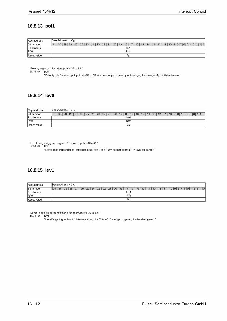
Revised 18/4/12 Interrupt Control
16.8.13 pol1
16.8.14 lev0
16.8.15 lev1
Reg address BaseAddress + 30H
Bit number 31 30 29 28 27 26 25 24 23 22 21 20 19 18 17 16 15 14 13 12 11 10 9 8 7 6 5 4 3 2 1 0Field name pol1 R/W RW
Reset value 0H
"Polarity register 1 for interrupt bits 32 to 63." Bit 31 - 0 pol1
"Polarity bits for interrupt input, bits 32 to 63: 0 = no change of polarity/active-high, 1 = change of polarity/active-low."
Reg address BaseAddress + 34H
Bit number 31 30 29 28 27 26 25 24 23 22 21 20 19 18 17 16 15 14 13 12 11 10 9 8 7 6 5 4 3 2 1 0Field name lev0 R/W RW
Reset value 0H
"Level / edge triggered register 0 for interrupt bits 0 to 31." Bit 31 - 0 lev0
"Level/edge trigger bits for interrupt input, bits 0 to 31: 0 = edge triggered, 1 = level triggered."
Reg address BaseAddress + 38H
Bit number 31 30 29 28 27 26 25 24 23 22 21 20 19 18 17 16 15 14 13 12 11 10 9 8 7 6 5 4 3 2 1 0Field name lev1 R/W RW
Reset value 0H
"Level / edge triggered register 1 for interrupt bits 32 to 63." Bit 31 - 0 lev1
"Level/edge trigger bits for interrupt input, bits 32 to 63: 0 = edge triggered, 1 = level triggered."
16 - 12 Fujitsu Semiconductor Europe GmbH
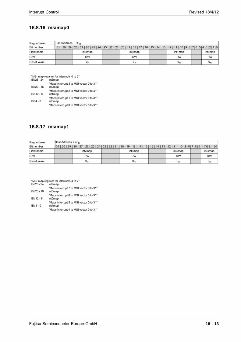
Interrupt Control Revised 18/4/12
16.8.16 msimap0
16.8.17 msimap1
Reg address BaseAddress + 3CH
Bit number 31 30 29 28 27 26 25 24 23 22 21 20 19 18 17 16 15 14 13 12 11 10 9 8 7 6 5 4 3 2 1 0
Field name int3map int2map int1map int0map
R/W RW RW RW RW
Reset value 0H 0H 0H 0H
"MSI map register for interrupts 0 to 3" Bit 28 - 24 int3map
"Maps interrupt 3 to MSI vector 0 to 31" Bit 20 - 16 int2map
"Maps interrupt 2 to MSI vector 0 to 31" Bit 12 - 8 int1map
"Maps interrupt 1 to MSI vector 0 to 31" Bit 4 - 0 int0map
"Maps interrupt 0 to MSI vector 0 to 31"
Reg address BaseAddress + 40H
Bit number 31 30 29 28 27 26 25 24 23 22 21 20 19 18 17 16 15 14 13 12 11 10 9 8 7 6 5 4 3 2 1 0
Field name int7map int6map int5map int4map
R/W RW RW RW RW
Reset value 0H 0H 0H 0H
"MSI map register for interrupts 4 to 7" Bit 28 - 24 int7map
"Maps interrupt 7 to MSI vector 0 to 31" Bit 20 - 16 int6map
"Maps interrupt 6 to MSI vector 0 to 31" Bit 12 - 8 int5map
"Maps interrupt 5 to MSI vector 0 to 31" Bit 4 - 0 int4map
"Maps interrupt 4 to MSI vector 0 to 31"
Fujitsu Semiconductor Europe GmbH 16 - 13

Revised 18/4/12 Interrupt Control
16.8.18 msimap2
16.8.19 msimap3
Reg address BaseAddress + 44H
Bit number 31 30 29 28 27 26 25 24 23 22 21 20 19 18 17 16 15 14 13 12 11 10 9 8 7 6 5 4 3 2 1 0
Field name int11map int10map int9map int8map
R/W RW RW RW RW
Reset value 0H 0H 0H 0H
"MSI map register for interrupts 8 to 11" Bit 28 - 24 int11map
"Maps interrupt 11 to MSI vector 0 to 31" Bit 20 - 16 int10map
"Maps interrupt 10 to MSI vector 0 to 31" Bit 12 - 8 int9map
"Maps interrupt 9 to MSI vector 0 to 31" Bit 4 - 0 int8map
"Maps interrupt 8 to MSI vector 0 to 31"
Reg address BaseAddress + 48H
Bit number 31 30 29 28 27 26 25 24 23 22 21 20 19 18 17 16 15 14 13 12 11 10 9 8 7 6 5 4 3 2 1 0
Field name int15map int14map int13map int12map
R/W RW RW RW RW
Reset value 0H 0H 0H 0H
"MSI map register for interrupts 12 to 15" Bit 28 - 24 int15map
"Maps interrupt 15 to MSI vector 0 to 31" Bit 20 - 16 int14map
"Maps interrupt 14 to MSI vector 0 to 31" Bit 12 - 8 int13map
"Maps interrupt 13 to MSI vector 0 to 31" Bit 4 - 0 int12map
"Maps interrupt 12 to MSI vector 0 to 31"
16 - 14 Fujitsu Semiconductor Europe GmbH

Interrupt Control Revised 18/4/12
16.8.20 msimap4
16.8.21 msimap5
Reg address BaseAddress + 4CH
Bit number 31 30 29 28 27 26 25 24 23 22 21 20 19 18 17 16 15 14 13 12 11 10 9 8 7 6 5 4 3 2 1 0
Field name int19map int18map int17map int16map
R/W RW RW RW RW
Reset value 0H 0H 0H 0H
"MSI map register for interrupts 16 to 19" Bit 28 - 24 int19map
"Maps interrupt 19 to MSI vector 0 to 31" Bit 20 - 16 int18map
"Maps interrupt 18 to MSI vector 0 to 31" Bit 12 - 8 int17map
"Maps interrupt 17 to MSI vector 0 to 31" Bit 4 - 0 int16map
"Maps interrupt 16 to MSI vector 0 to 31"
Reg address BaseAddress + 50H
Bit number 31 30 29 28 27 26 25 24 23 22 21 20 19 18 17 16 15 14 13 12 11 10 9 8 7 6 5 4 3 2 1 0
Field name int23map int22map int21map int20map
R/W RW RW RW RW
Reset value 0H 0H 0H 0H
"MSI map register for interrupts 20 to 23" Bit 28 - 24 int23map
"Maps interrupt 23 to MSI vector 0 to 31" Bit 20 - 16 int22map
"Maps interrupt 22 to MSI vector 0 to 31" Bit 12 - 8 int21map
"Maps interrupt 21 to MSI vector 0 to 31" Bit 4 - 0 int20map
"Maps interrupt 20 to MSI vector 0 to 31"
Fujitsu Semiconductor Europe GmbH 16 - 15
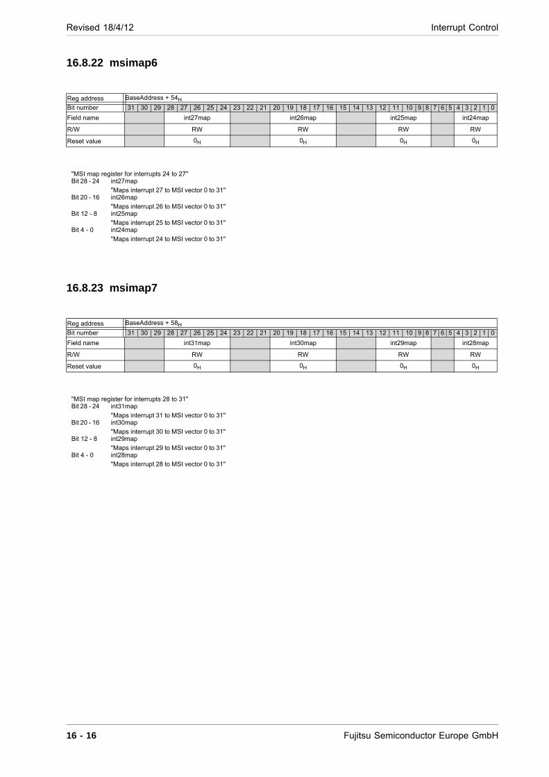
Revised 18/4/12 Interrupt Control
16.8.22 msimap6
16.8.23 msimap7
Reg address BaseAddress + 54H
Bit number 31 30 29 28 27 26 25 24 23 22 21 20 19 18 17 16 15 14 13 12 11 10 9 8 7 6 5 4 3 2 1 0
Field name int27map int26map int25map int24map
R/W RW RW RW RW
Reset value 0H 0H 0H 0H
"MSI map register for interrupts 24 to 27" Bit 28 - 24 int27map
"Maps interrupt 27 to MSI vector 0 to 31" Bit 20 - 16 int26map
"Maps interrupt 26 to MSI vector 0 to 31" Bit 12 - 8 int25map
"Maps interrupt 25 to MSI vector 0 to 31" Bit 4 - 0 int24map
"Maps interrupt 24 to MSI vector 0 to 31"
Reg address BaseAddress + 58H
Bit number 31 30 29 28 27 26 25 24 23 22 21 20 19 18 17 16 15 14 13 12 11 10 9 8 7 6 5 4 3 2 1 0
Field name int31map int30map int29map int28map
R/W RW RW RW RW
Reset value 0H 0H 0H 0H
"MSI map register for interrupts 28 to 31" Bit 28 - 24 int31map
"Maps interrupt 31 to MSI vector 0 to 31" Bit 20 - 16 int30map
"Maps interrupt 30 to MSI vector 0 to 31" Bit 12 - 8 int29map
"Maps interrupt 29 to MSI vector 0 to 31" Bit 4 - 0 int28map
"Maps interrupt 28 to MSI vector 0 to 31"
16 - 16 Fujitsu Semiconductor Europe GmbH

Interrupt Control Revised 18/4/12
16.8.24 msimap8
16.8.25 msimap9
Reg address BaseAddress + 5CH
Bit number 31 30 29 28 27 26 25 24 23 22 21 20 19 18 17 16 15 14 13 12 11 10 9 8 7 6 5 4 3 2 1 0
Field name int35map int34map int33map int32map
R/W RW RW RW RW
Reset value 0H 0H 0H 0H
"MSI map register for interrupts 32 to 35" Bit 28 - 24 int35map
"Maps interrupt 35 to MSI vector 0 to 31" Bit 20 - 16 int34map
"Maps interrupt 34 to MSI vector 0 to 31" Bit 12 - 8 int33map
"Maps interrupt 33 to MSI vector 0 to 31" Bit 4 - 0 int32map
"Maps interrupt 32 to MSI vector 0 to 31"
Reg address BaseAddress + 60H
Bit number 31 30 29 28 27 26 25 24 23 22 21 20 19 18 17 16 15 14 13 12 11 10 9 8 7 6 5 4 3 2 1 0
Field name int39map int38map int37map int36map
R/W RW RW RW RW
Reset value 0H 0H 0H 0H
"MSI map register for interrupts 36 to 39" Bit 28 - 24 int39map
"Maps interrupt 39 to MSI vector 0 to 31" Bit 20 - 16 int38map
"Maps interrupt 38 to MSI vector 0 to 31" Bit 12 - 8 int37map
"Maps interrupt 37 to MSI vector 0 to 31" Bit 4 - 0 int36map
"Maps interrupt 36 to MSI vector 0 to 31"
Fujitsu Semiconductor Europe GmbH 16 - 17
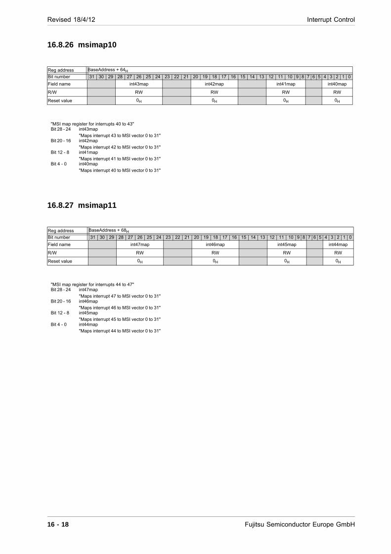
Revised 18/4/12 Interrupt Control
16.8.26 msimap10
16.8.27 msimap11
Reg address BaseAddress + 64H
Bit number 31 30 29 28 27 26 25 24 23 22 21 20 19 18 17 16 15 14 13 12 11 10 9 8 7 6 5 4 3 2 1 0
Field name int43map int42map int41map int40map
R/W RW RW RW RW
Reset value 0H 0H 0H 0H
"MSI map register for interrupts 40 to 43" Bit 28 - 24 int43map
"Maps interrupt 43 to MSI vector 0 to 31" Bit 20 - 16 int42map
"Maps interrupt 42 to MSI vector 0 to 31" Bit 12 - 8 int41map
"Maps interrupt 41 to MSI vector 0 to 31" Bit 4 - 0 int40map
"Maps interrupt 40 to MSI vector 0 to 31"
Reg address BaseAddress + 68H
Bit number 31 30 29 28 27 26 25 24 23 22 21 20 19 18 17 16 15 14 13 12 11 10 9 8 7 6 5 4 3 2 1 0
Field name int47map int46map int45map int44map
R/W RW RW RW RW
Reset value 0H 0H 0H 0H
"MSI map register for interrupts 44 to 47" Bit 28 - 24 int47map
"Maps interrupt 47 to MSI vector 0 to 31" Bit 20 - 16 int46map
"Maps interrupt 46 to MSI vector 0 to 31" Bit 12 - 8 int45map
"Maps interrupt 45 to MSI vector 0 to 31" Bit 4 - 0 int44map
"Maps interrupt 44 to MSI vector 0 to 31"
16 - 18 Fujitsu Semiconductor Europe GmbH

Interrupt Control Revised 18/4/12
16.8.28 msimap12
16.8.29 msimap13
Reg address BaseAddress + 6CH
Bit number 31 30 29 28 27 26 25 24 23 22 21 20 19 18 17 16 15 14 13 12 11 10 9 8 7 6 5 4 3 2 1 0
Field name int51map int50map int49map int48map
R/W RW RW RW RW
Reset value 0H 0H 0H 0H
"MSI map register for interrupts 48 to 51" Bit 28 - 24 int51map
"Maps interrupt 51 to MSI vector 0 to 31" Bit 20 - 16 int50map
"Maps interrupt 50 to MSI vector 0 to 31" Bit 12 - 8 int49map
"Maps interrupt 49 to MSI vector 0 to 31" Bit 4 - 0 int48map
"Maps interrupt 48 to MSI vector 0 to 31"
Reg address BaseAddress + 70H
Bit number 31 30 29 28 27 26 25 24 23 22 21 20 19 18 17 16 15 14 13 12 11 10 9 8 7 6 5 4 3 2 1 0
Field name int55map int54map int53map int52map
R/W RW RW RW RW
Reset value 0H 0H 0H 0H
"MSI map register for interrupts 52 to 55" Bit 28 - 24 int55map
"Maps interrupt 55 to MSI vector 0 to 31" Bit 20 - 16 int54map
"Maps interrupt 54 to MSI vector 0 to 31" Bit 12 - 8 int53map
"Maps interrupt 53 to MSI vector 0 to 31" Bit 4 - 0 int52map
"Maps interrupt 52 to MSI vector 0 to 31"
Fujitsu Semiconductor Europe GmbH 16 - 19
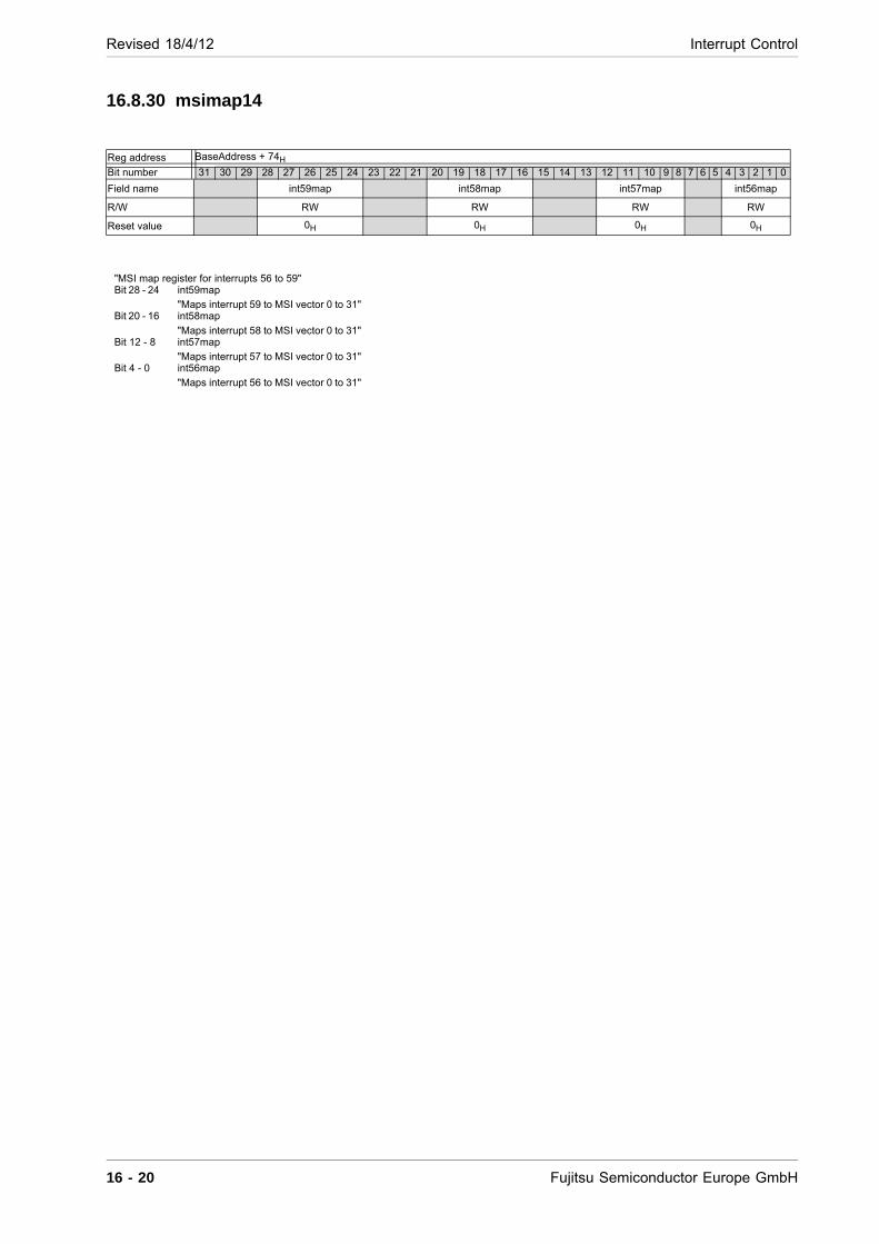
Revised 18/4/12 Interrupt Control
16.8.30 msimap14
Reg address BaseAddress + 74H
Bit number 31 30 29 28 27 26 25 24 23 22 21 20 19 18 17 16 15 14 13 12 11 10 9 8 7 6 5 4 3 2 1 0
Field name int59map int58map int57map int56map
R/W RW RW RW RW
Reset value 0H 0H 0H 0H
"MSI map register for interrupts 56 to 59" Bit 28 - 24 int59map
"Maps interrupt 59 to MSI vector 0 to 31" Bit 20 - 16 int58map
"Maps interrupt 58 to MSI vector 0 to 31" Bit 12 - 8 int57map
"Maps interrupt 57 to MSI vector 0 to 31" Bit 4 - 0 int56map
"Maps interrupt 56 to MSI vector 0 to 31"
16 - 20 Fujitsu Semiconductor Europe GmbH
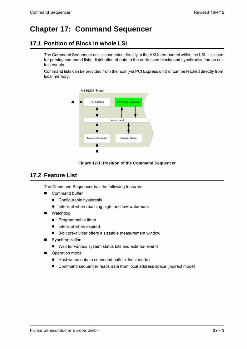
Command Sequencer Revised 18/4/12
Chapter 17: Command Sequencer
17.1 Position of Block in whole LSI
The Command Sequencer unit is connected directly to the AXI Interconnect within the LSI. It is used for parsing command lists, distribution of data to the addressed blocks and synchronization on cer-tain events.
Command lists can be provided from the host (via PCI Express unit) or can be fetched directly from local memory.
Figure 17-1: Position of the Command Sequencer
17.2 Feature List
The Command Sequencer has the following features:
Command buffer
Configurable hysteresis
Interrupt when reaching high- and low-watermark
Watchdog
Programmable timer
Interrupt when expired
8-bit pre-divider offers a sizeable measurement window
Synchronization
Wait for various system status bits and external events
Operation mode
Host writes data to command buffer (direct mode)
Command sequencer reads data from local address space (indirect mode)
Interconnect
PCI Express
Register SpaceMemory Controller
MB86298 “Ruby”
Command Sequencer
Fujitsu Semiconductor Europe GmbH 17 - 1
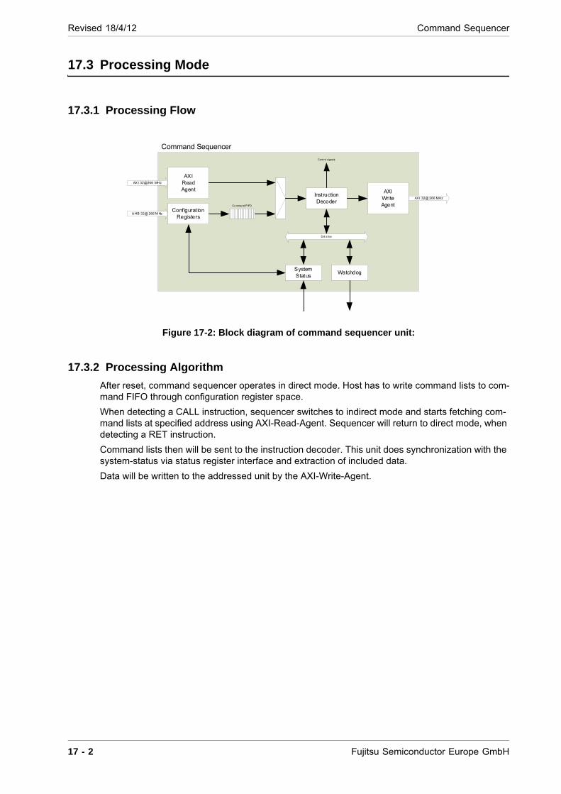
Revised 18/4/12 Command Sequencer
17.3 Processing Mode
17.3.1 Processing Flow
Figure 17-2: Block diagram of command sequencer unit:
17.3.2 Processing Algorithm
After reset, command sequencer operates in direct mode. Host has to write command lists to com-mand FIFO through configuration register space.
When detecting a CALL instruction, sequencer switches to indirect mode and starts fetching com-mand lists at specified address using AXI-Read-Agent. Sequencer will return to direct mode, when detecting a RET instruction.
Command lists then will be sent to the instruction decoder. This unit does synchronization with the system-status via status register interface and extraction of included data.
Data will be written to the addressed unit by the AXI-Write-Agent.
Watchdog
Command Sequencer
A HB 32@ 266 M Hz
AX I 32@266 MHz
AXI 32@ 266 MHz
SystemStatus
AXIReadAgent AXI
WriteAgent
InstructionDecoder
Dat a bus
Configurat ionRegisters
Contr ol signa ls
Co mma nd F IFO
17 - 2 Fujitsu Semiconductor Europe GmbH
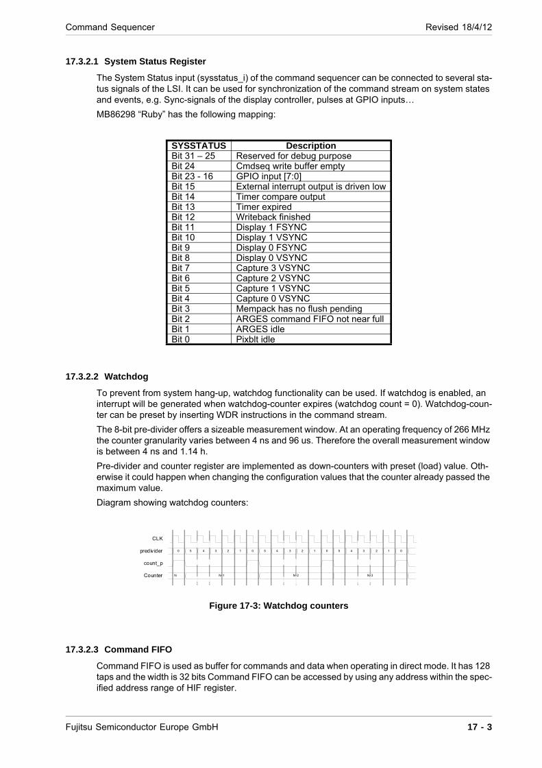
Command Sequencer Revised 18/4/12
17.3.2.1 System Status Register
The System Status input (sysstatus_i) of the command sequencer can be connected to several sta-tus signals of the LSI. It can be used for synchronization of the command stream on system states and events, e.g. Sync-signals of the display controller, pulses at GPIO inputs…
MB86298 “Ruby” has the following mapping:
17.3.2.2 Watchdog
To prevent from system hang-up, watchdog functionality can be used. If watchdog is enabled, an interrupt will be generated when watchdog-counter expires (watchdog count = 0). Watchdog-coun-ter can be preset by inserting WDR instructions in the command stream.
The 8-bit pre-divider offers a sizeable measurement window. At an operating frequency of 266 MHz the counter granularity varies between 4 ns and 96 us. Therefore the overall measurement window is between 4 ns and 1.14 h.
Pre-divider and counter register are implemented as down-counters with preset (load) value. Oth-erwise it could happen when changing the configuration values that the counter already passed the maximum value.
Diagram showing watchdog counters:
Figure 17-3: Watchdog counters
17.3.2.3 Command FIFO
Command FIFO is used as buffer for commands and data when operating in direct mode. It has 128 taps and the width is 32 bits Command FIFO can be accessed by using any address within the spec-ified address range of HIF register.
SYSSTATUS DescriptionBit 31 – 25 Reserved for debug purposeBit 24 Cmdseq write buffer emptyBit 23 - 16 GPIO input [7:0]Bit 15 External interrupt output is driven lowBit 14 Timer compare outputBit 13 Timer expiredBit 12 Writeback finishedBit 11 Display 1 FSYNCBit 10 Display 1 VSYNCBit 9 Display 0 FSYNCBit 8 Display 0 VSYNCBit 7 Capture 3 VSYNCBit 6 Capture 2 VSYNCBit 5 Capture 1 VSYNCBit 4 Capture 0 VSYNCBit 3 Mempack has no flush pendingBit 2 ARGES command FIFO not near fullBit 1 ARGES idleBit 0 Pixblt idle
0
CLK
prediv ider
count_p
Counter
0 0 05 4 5 54 43 3 32 2 21 1 1
N-1 N-2 N-3N
Fujitsu Semiconductor Europe GmbH 17 - 3
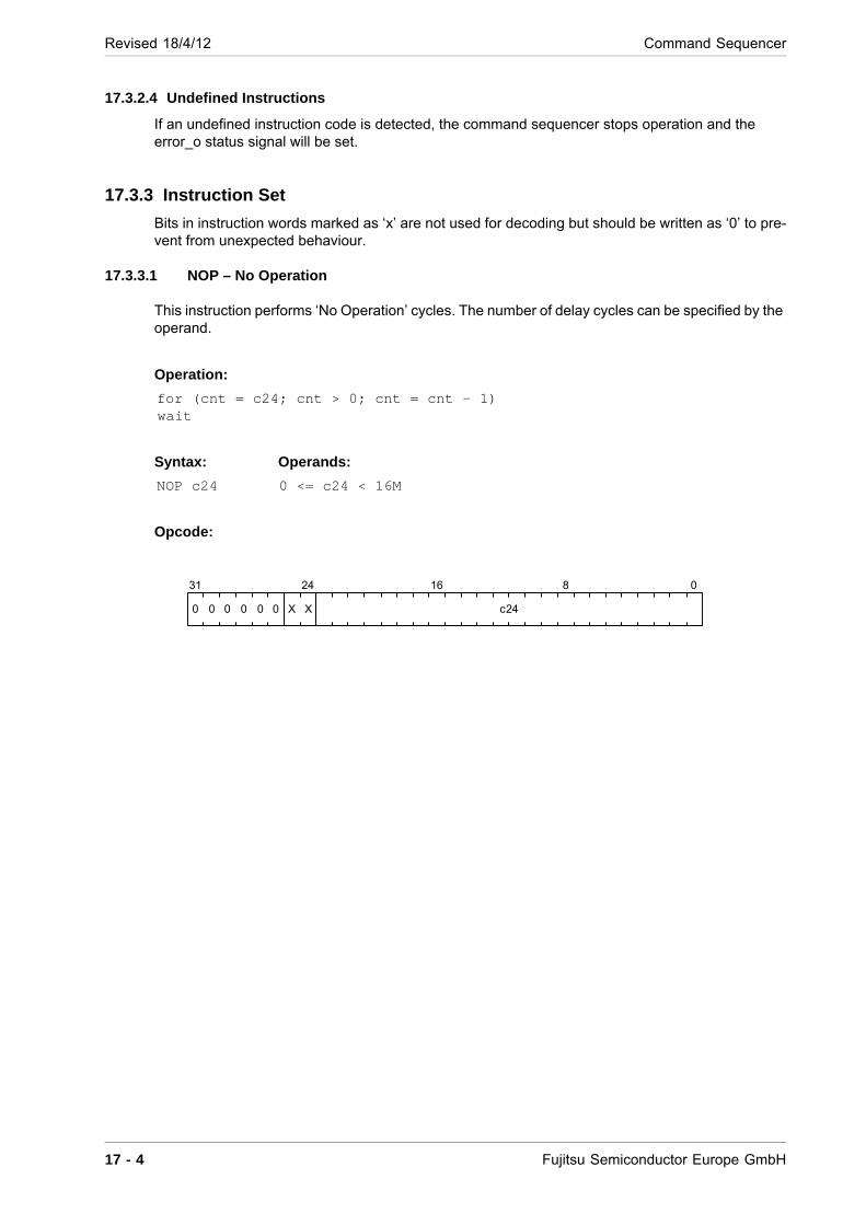
Revised 18/4/12 Command Sequencer
17.3.2.4 Undefined Instructions
If an undefined instruction code is detected, the command sequencer stops operation and the error_o status signal will be set.
17.3.3 Instruction Set
Bits in instruction words marked as ‘x’ are not used for decoding but should be written as ‘0’ to pre-vent from unexpected behaviour.
17.3.3.1 NOP – No Operation
This instruction performs ‘No Operation’ cycles. The number of delay cycles can be specified by the operand.
Operation:
for (cnt = c24; cnt > 0; cnt = cnt – 1)wait
Syntax: Operands:
NOP c24 0 <= c24 < 16M
Opcode:
031 24 16 8
00 0 0 0 0 X X c24
17 - 4 Fujitsu Semiconductor Europe GmbH
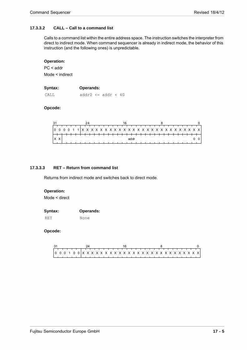
Command Sequencer Revised 18/4/12
17.3.3.2 CALL – Call to a command list
Calls to a command list within the entire address space. The instruction switches the interpreter from direct to indirect mode. When command sequencer is already in indirect mode, the behavior of this instruction (and the following ones) is unpredictable.
Operation:
PC < addr
Mode < indirect
Syntax: Operands:
CALL addr0 <= addr < 4G
Opcode:
17.3.3.3 RET – Return from command list
Returns from indirect mode and switches back to direct mode.
Operation:
Mode < direct
Syntax: Operands:
RET None
Opcode:
031 24 16 8
addrX X
X X X X X X X X X X X X X X X X X X X X X X X X X X110000
00
031 24 16 8
X X X X X X X X X X X X X X X X X X X X X X X X X X001000
Fujitsu Semiconductor Europe GmbH 17 - 5
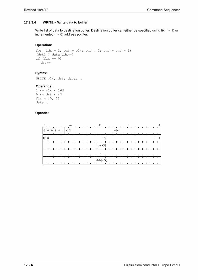
Revised 18/4/12 Command Sequencer
17.3.3.4 WRITE – Write data to buffer
Write list of data to destination buffer. Destination buffer can either be specified using fix (f = 1) or incremented (f = 0) address pointer.
Operation:
for (idx = 1, cnt = c24; cnt > 0; cnt = cnt - 1)(dst) ? data[idx++]if (fix == 0)
dst++
Syntax:
WRITE c24, dst, data, …
Operands:1 <= c24 < 16M0 <= dst < 4Gfix = [0, 1]data …
Opcode:
031 24 16 8
00 0 1 0 1 X X c24
dstfix X
data[1]
. . .
data[c24]
00
17 - 6 Fujitsu Semiconductor Europe GmbH
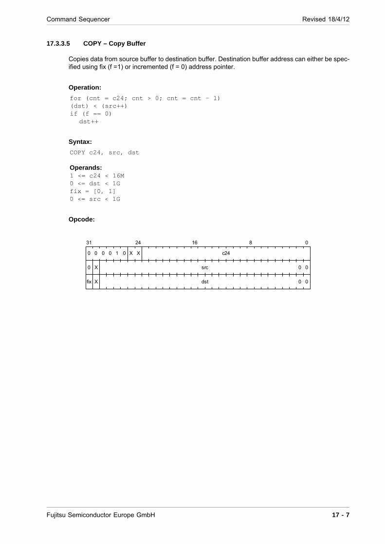
Command Sequencer Revised 18/4/12
17.3.3.5 COPY – Copy Buffer
Copies data from source buffer to destination buffer. Destination buffer address can either be spec-ified using fix (f =1) or incremented (f = 0) address pointer.
Operation:
for (cnt = c24; cnt > 0; cnt = cnt - 1)(dst) < (src++)if (f == 0)
dst++
Syntax:
COPY c24, src, dst
Operands:1 <= c24 < 16M0 <= dst < 1Gfix = [0, 1]0 <= src < 1G
Opcode:
031 24 16 8
00 0 0 1 0 X X c24
srcX
dst
0
X
00
00fix
Fujitsu Semiconductor Europe GmbH 17 - 7
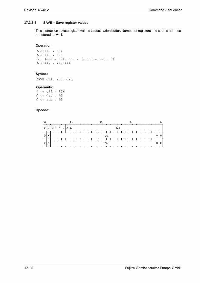
Revised 18/4/12 Command Sequencer
17.3.3.6 SAVE – Save register values
This instruction saves register values to destination buffer. Number of registers and source address are stored as well.
Operation:
(dst++) < c24(dst++) < srcfor (cnt = c24; cnt > 0; cnt = cnt - 1)(dst++) < (src++)
Syntax:
SAVE c24, src, dst
Operands:1 <= c24 < 16M0 <= dst < 1G0 <= src < 1G
Opcode:
031 24 16 8
00 0 1 1 0 X X c24
src0 X
dst0 X
00
00
17 - 8 Fujitsu Semiconductor Europe GmbH

Command Sequencer Revised 18/4/12
17.3.3.7 RESTORE – Restore register values from memory
Restoring register values from memory which have been stored by SAVE command.
Operation:
cnt < (src++)dst < (src++)for ( ; cnt > 0; cnt = cnt - 1) (dst++) < (src++)
Syntax: Operands:
RESTORE src 0 <= src < 1G
Opcode:
031 24 16 8
00 0 1 1 1
src0 X
X X X X X X X X X X X X X X X X X X X X X X X X X X
00
Fujitsu Semiconductor Europe GmbH 17 - 9
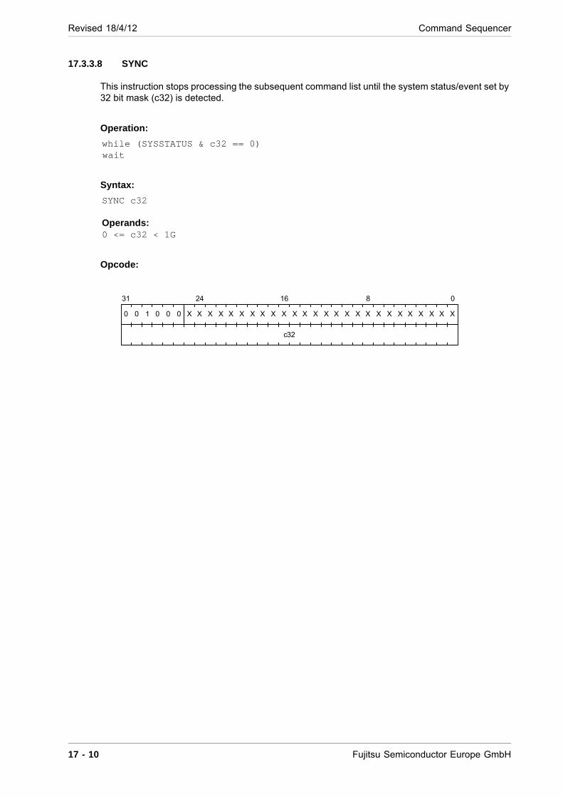
Revised 18/4/12 Command Sequencer
17.3.3.8 SYNC
This instruction stops processing the subsequent command list until the system status/event set by 32 bit mask (c32) is detected.
Operation:
while (SYSSTATUS & c32 == 0)wait
Syntax:
SYNC c32
Operands:0 <= c32 < 1G
Opcode:
031 24 16 8
c32
X X X X X X X X X X X X X X X X X X X X X X X X XX0 0 0 0 01
17 - 10 Fujitsu Semiconductor Europe GmbH
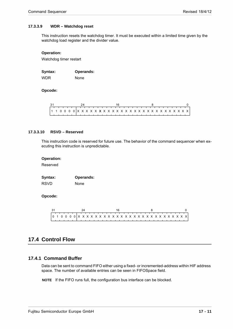
Command Sequencer Revised 18/4/12
17.3.3.9 WDR – Watchdog reset
This instruction resets the watchdog timer. It must be executed within a limited time given by the watchdog load register and the divider value.
Operation:
Watchdog timer restart
Syntax: Operands:
WDR None
Opcode:
17.3.3.10 RSVD – Reserved
This instruction code is reserved for future use. The behavior of the command sequencer when ex-ecuting this instruction is unpredictable.
Operation:
Reserved
Syntax: Operands:
RSVD None
Opcode:
17.4 Control Flow
17.4.1 Command Buffer
Data can be sent to command FIFO either using a fixed- or incremented-address within HIF address space. The number of available entries can be seen in FIFOSpace field.
NOTE If the FIFO runs full, the configuration bus interface can be blocked.
031 24 16 8
11 0 X X X X X X X X X X X X X X X X0 0 0 X X X X X XX X XX X
031 24 16 8
1 X X X X X X X X X X X X X X X X0 0 0 0 0 X X XX X XX XX X
Fujitsu Semiconductor Europe GmbH 17 - 11
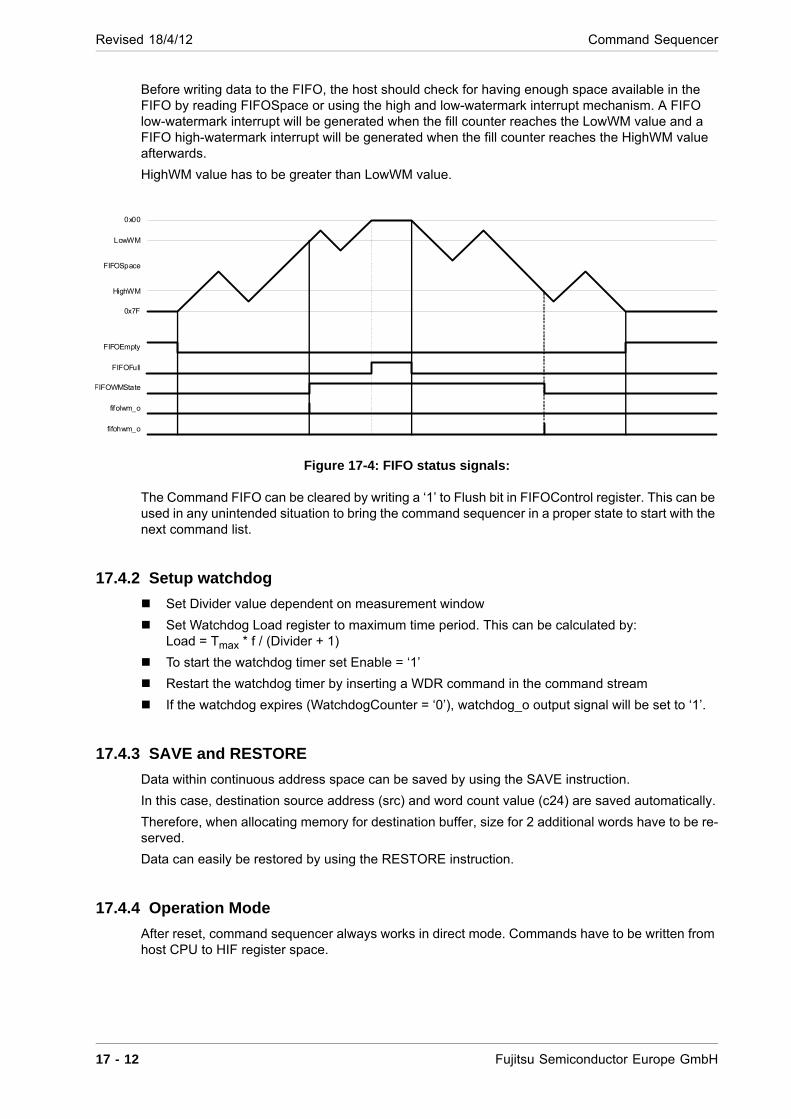
Revised 18/4/12 Command Sequencer
Before writing data to the FIFO, the host should check for having enough space available in the FIFO by reading FIFOSpace or using the high and low-watermark interrupt mechanism. A FIFO low-watermark interrupt will be generated when the fill counter reaches the LowWM value and a FIFO high-watermark interrupt will be generated when the fill counter reaches the HighWM value afterwards.
HighWM value has to be greater than LowWM value.
Figure 17-4: FIFO status signals:
The Command FIFO can be cleared by writing a ‘1’ to Flush bit in FIFOControl register. This can be used in any unintended situation to bring the command sequencer in a proper state to start with the next command list.
17.4.2 Setup watchdog
Set Divider value dependent on measurement window
Set Watchdog Load register to maximum time period. This can be calculated by:Load = Tmax * f / (Divider + 1)
To start the watchdog timer set Enable = ‘1’
Restart the watchdog timer by inserting a WDR command in the command stream
If the watchdog expires (WatchdogCounter = ‘0’), watchdog_o output signal will be set to ‘1’.
17.4.3 SAVE and RESTORE
Data within continuous address space can be saved by using the SAVE instruction.
In this case, destination source address (src) and word count value (c24) are saved automatically.
Therefore, when allocating memory for destination buffer, size for 2 additional words have to be re-served.
Data can easily be restored by using the RESTORE instruction.
17.4.4 Operation Mode
After reset, command sequencer always works in direct mode. Commands have to be written from host CPU to HIF register space.
FIFOSpace
0x00
0x7F
LowWM
HighWM
FIFOEmpty
FIFOFull
FIFOWMState
fifolwm_o
fifohwm_o
17 - 12 Fujitsu Semiconductor Europe GmbH

Command Sequencer Revised 18/4/12
If the system is up and command lists are available in memory, these lists can be executed by send-ing a CALL instruction. Command sequencer then switches to indirect mode and fetches command lists autonomous. When detecting a RET instruction, command sequencer switches back to direct mode and continues fetching commands from command buffer (FIFO).
17.4.5 Restart after detecting an illegal instruction
When detecting an illegal instruction code, command sequencer stops execution. It can be restarted by writing a ‘1’ to Flush bit in Control register.
Command FIFO will be flushed and the module switches to direct mode.
Fujitsu Semiconductor Europe GmbH 17 - 13
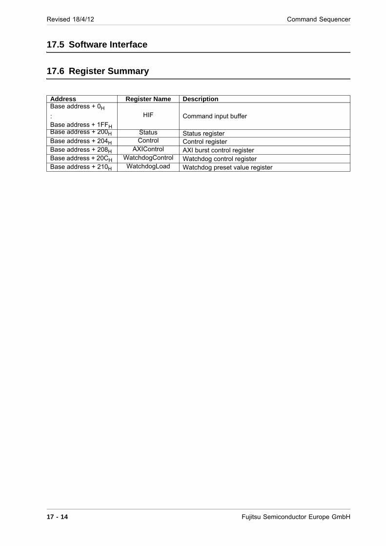
Revised 18/4/12 Command Sequencer
17.5 Software Interface
17.6 Register Summary
Address Register Name DescriptionBase address + 0H :Base address + 1FFH
HIF Command input buffer
Base address + 200H Status Status register Base address + 204H Control Control register Base address + 208H AXIControl AXI burst control registerBase address + 20CH WatchdogControl Watchdog control registerBase address + 210H WatchdogLoad Watchdog preset value register
17 - 14 Fujitsu Semiconductor Europe GmbH

Command Sequencer Revised 18/4/12
17.7 Register Description
17.7.1 HIF [0...127]
17.7.2 Status
Reg address
BaseAddress + 0H
:BaseAddress + 1FFH
Bit number 31 30 29 28 27 26 25 24 23 22 21 20 19 18 17 16 15 14 13 12 11 10 9 8 7 6 5 4 3 2 1 0Field name CommandFIFO R/W RW Reset value X
Command input buffer Bit 31 - 0 CommandFIFO
Reading always returns 0
Reg address BaseAddress + 200H
Bit number 31 30 29 28 27 26 25 24 23 22 21 20 19 18 17 16 15 14 13 12 11 10 9 8 7 6 5 4 3 2 1 0
Field name
Err
or
Idle
Wa
tchd
og
FIF
OW
MS
tate
FIF
OF
ull
FIF
OE
mpt
y
FIF
OS
pace
R/W R R R R R R R
Reset value 0H 1H 0H 0H 0H 1H 7FH
Status register Bit 31 Error
Execution stoped after illegal instruction Bit 30 Idle
Command sequencer is in IDLE state Bit 29 Watchdog
Watchdog expired Bit 10 FIFOWMState
Water mark state Bit 9 FIFOFull
Command FIFO full flag Bit 8 FIFOEmpty
Command FIFO empty flag Bit 6 - 0 FIFOSpace
Available space in command FIFO
Fujitsu Semiconductor Europe GmbH 17 - 15
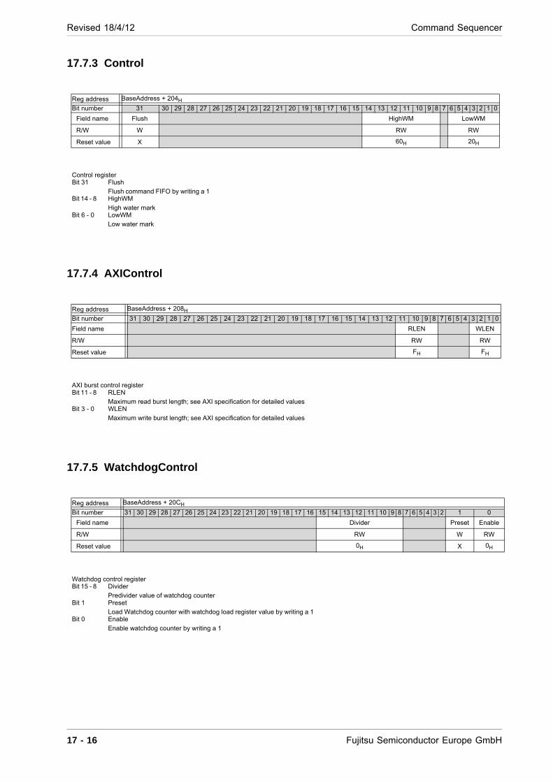
Revised 18/4/12 Command Sequencer
17.7.3 Control
17.7.4 AXIControl
17.7.5 WatchdogControl
Reg address BaseAddress + 204H
Bit number 31 30 29 28 27 26 25 24 23 22 21 20 19 18 17 16 15 14 13 12 11 10 9 8 7 6 5 4 3 2 1 0
Field name Flush HighWM LowWM
R/W W RW RW
Reset value X 60H 20H
Control register Bit 31 Flush
Flush command FIFO by writing a 1 Bit 14 - 8 HighWM
High water mark Bit 6 - 0 LowWM
Low water mark
Reg address BaseAddress + 208H
Bit number 31 30 29 28 27 26 25 24 23 22 21 20 19 18 17 16 15 14 13 12 11 10 9 8 7 6 5 4 3 2 1 0
Field name RLEN WLEN
R/W RW RW
Reset value FH FH
AXI burst control register Bit 11 - 8 RLEN
Maximum read burst length; see AXI specification for detailed values Bit 3 - 0 WLEN
Maximum write burst length; see AXI specification for detailed values
Reg address BaseAddress + 20CH
Bit number 31 30 29 28 27 26 25 24 23 22 21 20 19 18 17 16 15 14 13 12 11 10 9 8 7 6 5 4 3 2 1 0
Field name Divider Preset Enable
R/W RW W RW
Reset value 0H X 0H
Watchdog control register Bit 15 - 8 Divider
Predivider value of watchdog counter Bit 1 Preset
Load Watchdog counter with watchdog load register value by writing a 1 Bit 0 Enable
Enable watchdog counter by writing a 1
17 - 16 Fujitsu Semiconductor Europe GmbH

Command Sequencer Revised 18/4/12
17.7.6 WatchdogLoad
Reg address BaseAddress + 210H
Bit number 31 30 29 28 27 26 25 24 23 22 21 20 19 18 17 16 15 14 13 12 11 10 9 8 7 6 5 4 3 2 1 0Field name Load R/W RW
Reset value FFFFFFFFH
Watchdog preset value register Bit 31 - 0 Load
Watchdog counter preset value
Fujitsu Semiconductor Europe GmbH 17 - 17

Revised 18/4/12 Command Sequencer
17 - 18 Fujitsu Semiconductor Europe GmbH
SPI Debug Interface Revised 18/4/12
Chapter 18: SPI Debug Interface
18.1 Introduction
The Host Interface module is an internal module connected to the AHB which is used for debugging purposes for communication to an external host CPU (which is connected via the SPI interface). The host CPU can read and write to the internal module. From a host CPU point of view, this module functions as a slave, whereas internally it functions as a master.
This interface is not documented within the scope of this Hardware Manual because the SPI Inter-face is intended for internal debugging via dedicated driver software only.
Fujitsu Semiconductor Europe GmbH 18 - 1

Revised 18/4/12 SPI Debug Interface
18 - 2 Fujitsu Semiconductor Europe GmbH
Reference Literature / Glossary Revised 18/4/12
Chapter 19: Reference Literature / Glossary
19.1 Reference Literature / Glossary
19.1.1 Reference Literature
19.1.2 Glossary
Document Source CommentPCI-E 1.0 Specification http://www.pcisig.com/specifications/pciexpress/
PCI Express®Base SpecificationRevision 1.1March 28, 2005
Contact the PCI-SIG office to obtain the latest revision of this specification.Questions regarding the PCI Express Base Specification or membership in PCI-SIG may be forwarded to:
Membership Serviceswww.pcisig.comE-mail: [email protected]: 503-619-0569Fax: 503-644-6708
AMBA Specification Rev 2.0 http://www.arm.com/products/solutions/AMBA_Spec.html
AMBA AXI Protocol v1.0 SpecificationOpenGL ES 2.0 Specification http://www.khronos.org/opengles/
Terms, Definitions and Letter Symbols for Microcomputers, Microprocessors and Memory Integrated Circuits
http://www.jedec.org/Catalog/display.cfm
JEDEC StandardJESD100B.01 Dec. 2002
Double Data Rate (DDR) SDRAM Specification
http://www.jedec.org/Catalog/display.cfm
JEDEC StandardJESD79EMay 2005
Acronym SourceTLP (PCIe)Transaction Layer PacketMSI (PCIe) Message Signalling Interrupt
Fujitsu Semiconductor Europe GmbH 19 - 1

Revised 18/4/12 Reference Literature / Glossary
19 - 2 Fujitsu Semiconductor Europe GmbH


![Ruby on Rails [ Ruby On Rails.ppt ] - [Ruby - [Ruby-Doc.org](https://img.pdfslide.us/doc/110x75/5491e450b479597e6a8b57d5/ruby-on-rails-ruby-on-railsppt-ruby-ruby-docorg-.jpg)