Embed Size (px)
DESCRIPTION
Maximus VI Series UEFI Guide for Overclocking
Citation preview
1
Maximus VI Series UEFI Guide for Overclocking
This guide for overclocking provides basic to advanced tips on how to tweak the UEFI BIOS
on ASUS Z87 motherboards – predominantly ROG – with new LGA1150 „Haswell‟ CPUs.
As always, ROG has incorporated a comprehensive set of auto rules for all important
parameters, which makes for an easy overclocking experience.
Before You Start: The Foundation Info
For overclockers, the Haswell architecture incorporates several interesting changes from
previous generations:
1) Processor related voltage rails have been moved onto the die. The motherboard supplies
1.8V via the processor socket to Intel‟s on-die FIVR (fully integrated voltage regulators),
which then convert the voltage down to required levels for various parts of the CPU.
The external 1.8VDC supply is adjustable on ASUS motherboards. That‟s because Intel
advise the external supply should be at least 0.4V higher than processor Vcore. As
overclocking requires over-voltage of Vcore, the external 1.8VDC rail needs to be able to
maintain this delta under all normal operating conditions.
When information about Intel‟s shift towards integrating the power circuitry on-die were first
made public, there were concerns that overclocking would be limited. That‟s not the case at
all. The internal power circuitry can deliver enough current to overclock Haswell beyond
7GHz (when cooled with Ln2).
There is of course a side-effect. Having power circuitry on-die adds heat. Haswell processors
run hot when voltage levels are increased.
A very good air cooler is required for voltage levels above 1.15V. 1.20V-1.23V requires use of closed loop water coolers. At 1.24V-1.275V dual or triple radiator water cooling solutions are advised.
This is assuming the processor will be run at full load for extended periods of time.
Using Vcore higher than 1.275V is not advised for 4 core 8 thread CPUs under full load as
there are very few cooling solutions that can keep temps below thermal throttling point.
However, power consumption of the processor is very low. We measured no more than 11
amperes of current draw from the EPS 12V line (about 115 Watts if we take VRM losses into
account) from a 4770K clocked to 4.6GHz with 1.25Vcore under AIDA stress testing. This
tells us that the high temps are purely a facet of the substrate and process size. Getting heat
way from the die quickly is what matters.
To give an idea of how good the power consumption of Haswell is under load; a few years
ago I performed similar tests on Bloomfield processors (4 core, 8 thread). At 4.4GHz,
Bloomfield pulled 22 amperes of current from EPS 12V (220 Watts or so after losses), that‟s
over double in comparison to Haswell! Haswell‟s power consumption is an impressive
improvement for the tech enthusiasts among us.
2
At 4.6GHz, Haswell‟s power consumption is a mere 35 Watts over stock frequency (not
including IGP). A 700 MHz return, for a circa 35W bump in power – again impressive.
The kicker is finding a good processor sample. Not all samples will clock to 4.6GHz with less
than 1.25Vcore. The voltage variance between samples is also larger than we‟ve experienced
in the past – luck is needed to land a good sample!
Given Haswell‟s thermal and power characteristics, we expect enthusiasts will opt for water-
cooling solutions where possible, while the die-hard crowd will likely dust off their phase
change coolers. Haswell definitely benefits from lower temps and its power consumption
makes this a no brainer – expect stable frequencies above 5GHz with phase change cooling on
good CPUs.
2) Unlike Ivy Bridge and Sandy Bridge, Intel have provided control over ring bus frequency
for Haswell. On Sandy and Ivy Bridge, ring bus frequency was locked at 1:1 with processor
core frequency. From a performance perspective, this makes sense as it means that data can be
transferred between buses without waiting. Adding logic circuitry for asynchronous speeds
increases design complexity and latency, so engineers are reluctant to provide such features
unless there are valid reasons to do so.
The caveat to a locked synchronous design comes when the processor is overclocked. With
the ring bus frequency tied to the CPU core ratio, there‟s no way of telling which of them is
the limiting factor when overclocking a processor. Users provided this feedback to Intel,
managing to convince engineers of the need for asynchronous operation, and we now have
control over ring bus frequency.
“Unhinging” the ring bus frequency from synchronous operation with the processor cores
allows more flexibility for overclocking. The ring bus can be run slower than the processor
cores, without adversely affecting desktop performance. If absolute performance is a
requirement (for benchmarking), then bear in mind that keeping the ring bus frequency (cache
ratio) within 300MHz of processor core frequency is adequate.
On to the guide!
Trust our auto rules as a starting point! We put a tremendous amount of time tuning voltages
and working out parameter combinations for a wide range of processors. Take advantage of
our work, and use our settings as a starting point. Tune manually as you become accustomed
to the platform and the characteristics of the CPU used.
Other Important Notes:
Don’t skim read the guide! It will only give you a fraction of the info you need to OC properly. Grab a cup of coffee and make time to read it! Overclocking is serious business.
Don’t be afraid to ask questions if you are stuck or confused!We’ve got a great discussion thread going, not to mention an entire forum dedicated to the Maximus VI series motherboards.
3
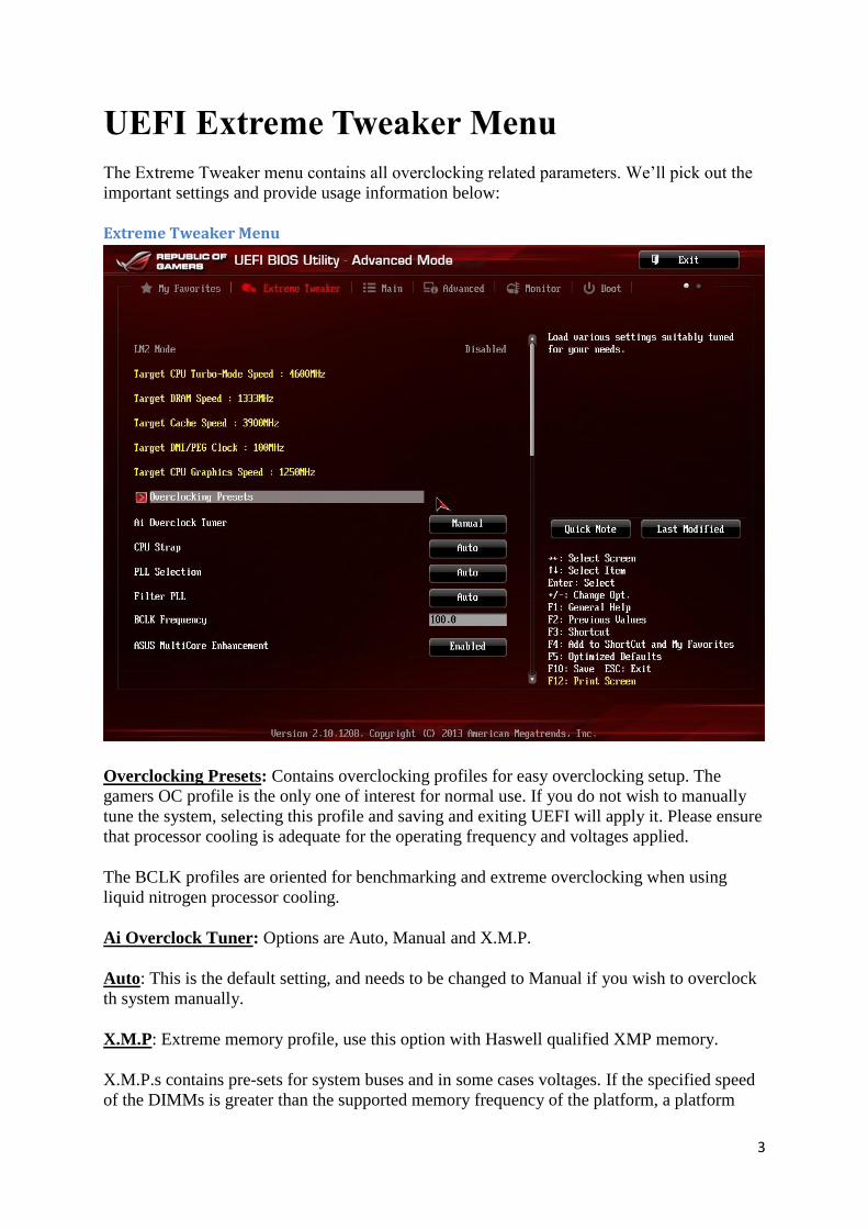
UEFI Extreme Tweaker Menu
The Extreme Tweaker menu contains all overclocking related parameters. We‟ll pick out the
important settings and provide usage information below:
Extreme Tweaker Menu
Overclocking Presets: Contains overclocking profiles for easy overclocking setup. The
gamers OC profile is the only one of interest for normal use. If you do not wish to manually
tune the system, selecting this profile and saving and exiting UEFI will apply it. Please ensure
that processor cooling is adequate for the operating frequency and voltages applied.
The BCLK profiles are oriented for benchmarking and extreme overclocking when using
liquid nitrogen processor cooling.
Ai Overclock Tuner: Options are Auto, Manual and X.M.P.
Auto: This is the default setting, and needs to be changed to Manual if you wish to overclock
th system manually.
X.M.P: Extreme memory profile, use this option with Haswell qualified XMP memory.
X.M.P.s contains pre-sets for system buses and in some cases voltages. If the specified speed
of the DIMMs is greater than the supported memory frequency of the platform, a platform
4
specific X.M.P. profile becomes mandatory because processor core and memory controller
voltage requirements vary from architecture to architecture.
High-speed enthusiast memory kits manufactured before the release of the Haswell platform
may not contain the necessary/adequate voltage offset settings for the system to be completely
stable. In such instances, manual adjustments of voltages and memory timings may be
necessary.
Selecting the X.M.P setting opens up options for X.M.P profile selection (the kit may contain
more than one X.M.P profile), and also opens up the BCLK option for changing system bus
frequency. Note that memory operating frequency and maximum CPU operating frequency
are shown towards the top of the Extreme Tweaker menu, while memory timings and voltage
are displayed next to the XMP profile selection box.
CPU Strap: This setting multiplies BCLK to increase CPU frequency asynchronously from
all other bus frequencies, giving us more granularity to maximise processor and memory
overclocking. Available settings are 100, 125, 167 and 250 MHz. Currently, the usable
“straps” are 100, 125 and 167 only. We have not found any processors that can run the 250
strap.
BCLK range around the base value is +/- 5% by default on most motherboards. On the Z87-
Deluxe and the Maximus VI Extreme this can be as much as 20% thanks to some proprietary
hardware tweaks.
PLL Selection (if available): LC PLL is an inductor capacitor based oscillator, offering low
noise and jitter. It works best at default BCLK, because LC based VCOs don‟t have much
range. If manipulating BCLK , using SB (shaping based) mode is advised for increased
BCLK range. The downside to shaping based PLL circuits are that they suffer from higher
levels of jitter, hence Intel provides both options to maximize stability and overclocking
range.
Auto will manipulate this setting automatically, so if it‟s not available in a particular UEFI
version or on ASUS motherboard, it‟s a non-issue.
Filter PLL: Select High BCLK is using BCLK of 170+. Leave on Auto for all other use.
BCLK Frequency: BCLK is the reference clock frequency from which processor related
frequencies are derived. 100 BCLK is default. Changing BCLK affects processor, memory,
DMI and PCIe bus speeds. We advise to leave BLCK at its base setting for most
overclocking. Usage of processor multiplier ratios and CPU strap settings is preferable.
5
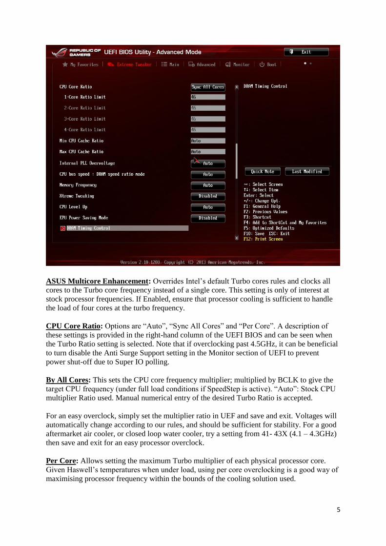
ASUS Multicore Enhancement: Overrides Intel‟s default Turbo cores rules and clocks all
cores to the Turbo core frequency instead of a single core. This setting is only of interest at
stock processor frequencies. If Enabled, ensure that processor cooling is sufficient to handle
the load of four cores at the turbo frequency.
CPU Core Ratio: Options are “Auto”, “Sync All Cores” and “Per Core”. A description of
these settings is provided in the right-hand column of the UEFI BIOS and can be seen when
the Turbo Ratio setting is selected. Note that if overclocking past 4.5GHz, it can be beneficial
to turn disable the Anti Surge Support setting in the Monitor section of UEFI to prevent
power shut-off due to Super IO polling.
By All Cores: This sets the CPU core frequency multiplier; multiplied by BCLK to give the
target CPU frequency (under full load conditions if SpeedStep is active). “Auto”: Stock CPU
multiplier Ratio used. Manual numerical entry of the desired Turbo Ratio is accepted.
For an easy overclock, simply set the multiplier ratio in UEF and save and exit. Voltages will
automatically change according to our rules, and should be sufficient for stability. For a good
aftermarket air cooler, or closed loop water cooler, try a setting from 41- 43X (4.1 – 4.3GHz)
then save and exit for an easy processor overclock.
Per Core: Allows setting the maximum Turbo multiplier of each physical processor core.
Given Haswell‟s temperatures when under load, using per core overclocking is a good way of
maximising processor frequency within the bounds of the cooling solution used.
6
The available multiplier range is limited by both processor model and the ability of each CPU.
Min CPU Cache Ratio and Max CPU Cache Ratio: Defines the maximum and minimum
cache ratios (ring bus frequency). The minimum ratio only comes into effect when processor
power saving features are enabled.
Keeping these settings in sync with processor core frequency is recommened from a
performance standpoint. Unfortunately, most CPUs cannot keep cache ratio in sync with
processor core frequency when they reach their frequency limits. Therefore, we advise
leaving these two settings on auto while overclocking to eliminate the ring bus as a possible
cause of instability. Once the limits of processor frequency have been reached, you may
experiment by setting the cache ratio within 300MHz of CPU core frequency and monitoring
for impact on system stability.
CPU Cache voltage may need to be increased to facilitate stability at higher CPU Cache
frequencies, although our auto rules do scale voltage in accordance with the Cache Ratio
applied – you may not need to tune the voltage manually at all.
Running CPU Cache Ratio faster than processor core frequency does not show any
performance gains so we recommend staying in sync with the CPU ratio or within 300MHz
(lower than CPU frequency).
Internal PLL Overvoltage: This setting can safely be left on Auto for all overclocking. We
have not seen any gains in enabling or disabling it.
CPU BUS: DRAM Ratio: Manipulates the ratio between CPU frequency and memory
frequency. Leave this setting on auto and use Memory Frequency to select the desired
memory frequency instead – auto will select the correct setting for this parameter.
Memory Frequency: “Auto” will automatically select a memory multiplier ratio according to
memory module SPD (Serial Presence Detect). Manual selection of the available memory
frequency multiplier ratios is possible and works according to the abilities of the DRAM and
processor. Granular control of memory frequency is available by manipulating BCLK, while
the base frequency of each divider is offset by changing the CPU strap settings (within
functional limits).
The highest working divider ratio is DDR3-2933 so far. Be mindful not to set a higher divider
ratio than this when changing CPU straps – otherwise the system will not POST.
The ability of these processors to run memory speeds above DDR3-2133 when the processor
is overclocked, varies from sample to sample. It is advised to overclock the processor without
ramping memory frequency first (leave memory at or below DDR3-1600 first). Once the
maximum stable operating frequency for the processor has been found, memory frequency
can be adjusted gradually while monitoring for impact on stability. Overclocking Haswell in
this way makes it easier to determine where the instability is coming from.
Performance of applications favors processor frequency over memory frequency so memory
takes a lower priority when overclocking.
7
Xtreme Tweaking: Leave this setting at default. Enable only for the 3D Mark 2001
benchmark.
CPU Level Up: Contains additional overclocking presets for users that don‟t wish to tune the
system manually. Again, ensure that processor cooling is adequate for the selected profile.
EPU Power Saving Mode: Configures the system for power savings – leave this setting
disabled for overclocking.
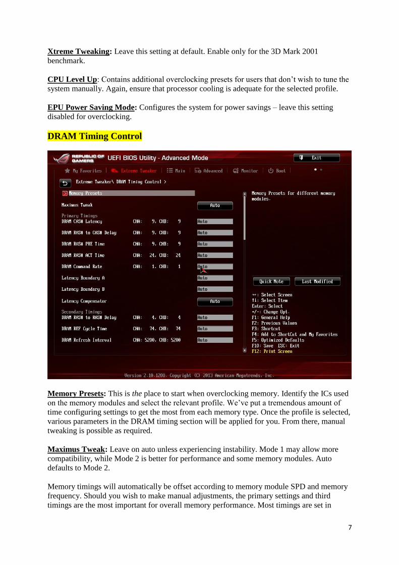
DRAM Timing Control
Memory Presets: This is the place to start when overclocking memory. Identify the ICs used
on the memory modules and select the relevant profile. We‟ve put a tremendous amount of
time configuring settings to get the most from each memory type. Once the profile is selected,
various parameters in the DRAM timing section will be applied for you. From there, manual
tweaking is possible as required.
Maximus Tweak: Leave on auto unless experiencing instability. Mode 1 may allow more
compatibility, while Mode 2 is better for performance and some memory modules. Auto
defaults to Mode 2.
Memory timings will automatically be offset according to memory module SPD and memory
frequency. Should you wish to make manual adjustments, the primary settings and third
timings are the most important for overall memory performance. Most timings are set in
8
DRAM clock cycles, hence a lower value results in a more aggressive setting (unless
otherwise stated).
As always, performance increases from memory tuning are marginal and are generally only
noticeable during synthetic benchmarks. Either way, voltage adjustments to VDIMM,
VCCIO-D, Cache Voltage and to a lesser extent CPU Core Voltage & VCCIO-A may be
necessary to facilitate tighter timings.
Primary Timings
CAS: Column Address Strobe, defines the time it takes for data to be ready for burst after a
read command is issued. As CAS factors in almost every read transaction, it is considered to
be the most important timing in relation to memory read performance.
To calculate the actual time period denoted by the number of clock cycles set for CAS we can
use the following formula:
tCAS in Nano seconds=(CAS*2000)/Memory Frequency
This same formula can be applied to all memory timings that are set in DRAM clock cycles.
DRAM RAS TO CAS Latency: Also known as tRCD. Defines the time it takes to complete
a row access after an activate command is issued to a rank of memory. This timing is of
secondary importance behind CAS as memory is divided into rows and columns (each row
contains 1024 column addresses). Once a row has been accessed, multiple CAS requests can
be sent to the row the read or write data. While a row is “open” it is referred to as an open
page. Up to eight pages can be open at any one time on a rank (a rank is one side of a memory
module) of memory.
DRAM RAS# PRE Time: Also known as tRP. Defines the number of DRAM clock cycles it
takes to precharge a row after a page close command is issued in preparation for the next row
access to the same physical bank. As multiple pages can be open on a rank before a page close
command is issued the impact of tRP towards memory performance is not as prevalent as
CAS or tRCD – although the impact does increase if multiple page open and close requests
are sent to the same memory IC and to a lesser extent rank (there are 8 physical ICs per rank
and only one page can be open per IC at a time, making up the total of 8 open pages per rank
simultaneously).
DRAM RAS Active Time: Also known as tRAS. This setting defines the number of DRAM
cycles that elapse before a precharge command can be issued. The minimum clock cycles
tRAS should be set to is the sum of CAS+tRCD+tRTP.
DRAM Command Mode: Also known as Command Rate. Specifies the number of DRAM
clock cycles that elapse between issuing commands to the DIMMs after a chip select. The
impact of Command Rate on performance can vary. For example, if most of the data
requested by the CPU is in the same row, the impact of Command Rate becomes negligible. If
however the banks in a rank have no open pages, and multiple banks need to be opened on
that rank or across ranks, the impact of Command Rate increases.
9
Most DRAM module densities will operate fine with a 1N Command Rate. Memory modules
containing older DRAM IC types may however need a 2N Command Rate.
Latency Boundary A sets timings for the main set of Third timings, lower is faster and tighter.
Latency Boundary B sets timings for the secondary set of Third timings, lower is faster and
tighter.
Manipulating Latency Boundary A and B, negates the need for setting third timings manually,
unless granular control of an individual setting is required. For most users, we recommend
tuning via the Latency Boundary settings. Advanced users who are tuning for Super Pi 32M
may wish to set timings manually instead.
Latency Compensator when enabled tries to make opportunistic latency compensation that
may increase performance or smoothen out the Memory training process. So try and compare
overclocking and performance with it enabled and disabled. You can also trying enabling it
when the whole system hangs at „55‟ or „03‟ or „69‟ when pushing tight timings with high
frequencies.
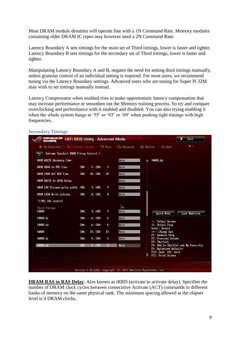
Secondary Timings
DRAM RAS to RAS Delay: Also known as tRRD (activate to activate delay). Specifies the
number of DRAM clock cycles between consecutive Activate (ACT) commands to different
banks of memory on the same physical rank. The minimum spacing allowed at the chipset
level is 4 DRAM clocks.
10
DRAM Ref Cycle Time: Also known as tRFC. Specifies the number of DRAM clocks that
must elapse before a command can be issued to the DIMMs after a DRAM cell refresh.
DRAM Refresh Interval: The charge stored in DRAM cells diminishes over time and must
be refreshed to avoid losing data. tREFI specifies the maximum time that can elapse before all
DRAM cells are refreshed. The value for tREFI is calculated according to module density. A
higher number than default is more aggressive as the cells will be refreshed less frequently.
During a refresh, the memory is not available for read or write transactions. Setting the
memory to refresh more often than required can impact scores negatively in memory sensitive
benchmarks. It can be worth tweaking the refresh interval to a larger value for improved
performance. For 24/7 use, this setting is best left at default, as real world applications do not
benefit to a noticeable degree by increasing this value.
DRAM Write Recovery Time: Defines the number of clock cycles that must elapse between
a memory write operation and a precharge command. Most DRAM configurations will
operate with a setting of 9 clocks up to DDR3-2500. Change to 12~16 clocks if experiencing
instability.
DRAM Read to Precharge Time: Also known as tRTP. Specifies the spacing between the
issuing of a read command and tRP (Precharge) when a read is followed by a page close
request. The minimum possible spacing is limited by DDR3 burst length which is 4 DRAM
clocks.
Most 2GB memory modules will operate fine with a setting of 4~6 clocks up to speeds of
DDR3-2000 (depending upon the number of DIMMs used in tandem). High performance
4GB DIMMs (DDR3-2000+) can handle a setting of 4 clocks provided you are running 8GB
of memory in total and that the processor memory controller is capable.
If running 8GB DIMMs a setting below 6 clocks at speeds higher than DDR3-1600 may be
unstable so increase as required.
DRAM Four Activate Window: Also known as tFAW. This timing specifies the number of
DRAM clocks that must elapse before more than four Activate commands can be sent to the
same rank. The minimum spacing is tRRD*4, and since we know that the minimum value of
tRRD is 4 clocks, we know that the minimum internal value for tFAW at the chipset level is
16 DRAM clocks.
As the effects of tFAW spacing are only realised after four Activates to the same DIMM, the
overall performance impact of tFAW is not large, however, benchmarks like Super Pi 32m
can benefit by setting tFAW to the minimum possible value.
As with tRRD, setting tFAW below its lowest possible value will result in the memory
controller reverting to the lowest possible value (16 DRAM clocks or tRRD * 4).
DRAM Write to Read Delay: Also known as tWTR. Sets the number of DRAM clocks to
wait before issuing a read command after a write command. The minimum internal spacing is
4 clocks. As with tRTP this value may need to be increased according to memory density and
memory frequency.
11
DRAM CKE Minimum Pulse width: This setting can be left on Auto for all overclocking.
CKE defines the minimum number of clocks that must elapse before the system can transition
from normal operating to low power state and vice versa.
CAS Write Latency: CWL is column access time for write commands to the DIMMs.
Typically, CWL is needs to be set at or +1 over the read CAS value. High performance
DIMMs can run CWL equal to or up to 3 clocks below read CAS for benchmarking (within
functional limits of the DIMMs and chipset).
Third Timings
tRDRD: Sets the delay between consecutive read requests to the same page. From a
performance perspective, this setting is best kept at 4 clocks. Relax only if the memory is not
stable or the system will not POST. Very few memory modules can handle a setting of 4
clocks at speeds above DDR3-2400 so you may need to relax accordingly, although the
performance hit may negate any gains in frequency.
tRDRD_dr: Sets the delay between consecutive read requests where the subsequent read is
on a different rank. A setting of 6 clocks or higher is required for most DIMMs.
tRDRD (dd): Sets the delay between consecutive read requests where the subsequent read is
on a different DIMM. A setting of 6 clocks or higher is required for most DIMMs.
tWRRD: Sets the delay between a write transaction and read command. The minimum value
we recommend is tWCL+tWTR.
Auto is preferred from a stability perspective, while setting as close to the minimum value as
possible is best from a performance perspective. For Super Pi 32m, try tWCl+tWTR+2 as a
starting point. If that is stable, then try -1 clock, if not, add+1 and repeat until stable.
tWRRD_dr: Sets the delay between a write transaction and read command where the
subsequent read is on a different rank. Keeping this setting as close to 4 clocks as possible is
advised, although it will need to be relaxed to 6+ clocks at high operating frequency or when
using high density memory configurations.
tWRRD_dd: Sets the delay between a write transaction and read command where the
subsequent read is on a different DIMM. Keeping this setting as close to 4 clocks as possible
is advised, although it will need to be relaxed to 6+ clocks at high operating frequency or
when using high density memory configurations.
12
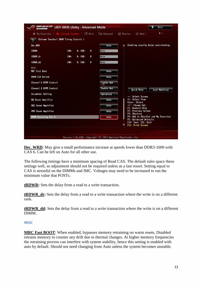
Dec_WRD: May give a small performance increase at speeds lower than DDR3-1600 with
CAS 6. Can be left on Auto for all other use.
The following timings have a minimum spacing of Read CAS. The default rules space these
settings well, so adjustment should not be required unless as a last resort. Setting equal to
CAS is stressful on the DIMMs and IMC. Voltages may need to be increased to run the
minimum value that POSTs.
tRDWR: Sets the delay from a read to a write transaction.
tRDWR_dr: Sets the delay from a read to a write transaction where the write is on a different
rank.
tRDWR_dd: Sets the delay from a read to a write transaction where the write is on a different
DIMM.
MISC
MRC Fast BOOT: When enabled, bypasses memory retraining on warm resets. Disabled
retrains memory to counter any drift due to thermal changes. At higher memory frequencies
the retraining process can interfere with system stability, hence this setting is enabled with
auto by default. Should not need changing from Auto unless the system becomes unstable.
13
DRAM CLK Period: Allows the application of different memory timing settings than default
for the operating frequency. Each number in the scale corresponds to a DRAM divider. The
lowest setting being DDR3-800. Ordinarily, the timing set applied automatically tracks the
DRAM ratio selected. This setting allows us to force timing sets from different dividers to be
used with the selected DRAM ratio.
A setting of 14 is recommended for high DRAM operating frequencies. For all other use,
leave on Auto.
Scrambler Setting: Alternates data patterns to minimize the impact of load transients and
noise on the memory bus. A setting of optimized is recommended for most configurations.
DQ, DQS and CMD Sense Amplifier: Alters the bias on signal lines to avoid mis-reads. The
Sense Amplifiers work good at Auto which lets BIOS decide the best for each. Reducing
usually is better. Reducing DQ Sense and CMD Sense to -1~ -6 may stabilize things further
when high VDIMM is used (2.2+v for example)
DRAM Swizzling Bit 0, 1 ,2, 3:
Enable Bit 0 for best OC most times, but disabling may help uncommon DRAM setups.
Enable Bit 1 for best OC most times, but disabling may sometimes help some 4GB DRAM
modules.
Disabling Bit 2 helps high frequency overclocking at the expense of performance. Enabling
improves performance but may need several tries to boot when frequencies are high and
timings are tight. You can retry training when the system hangs at „55‟ or „03‟ or „69‟ by
pressing reset here and waiting for the rig to complete a full reset.
Enabling Bit 3 usually helps overclocking and stability unless the IMC is unstable at cold
temperatures (Ln2 cooling) in which case try disabling.
RAW MHz Aid: May help to improve stability when using DRAM ratios above DDR3-3100
at the expense of performance.
IC Optimizer: IC Optimizer sets background invisible tweaks for the various DRAM ICs.
Note that these were fine-tuned with specific DRAM and CPUs so it may help or harm
depending on the likeness of the ones on your hands. So try with Auto first, then try with the
one for your ICs and compare. These will get updated over time in future BIOSes.
14
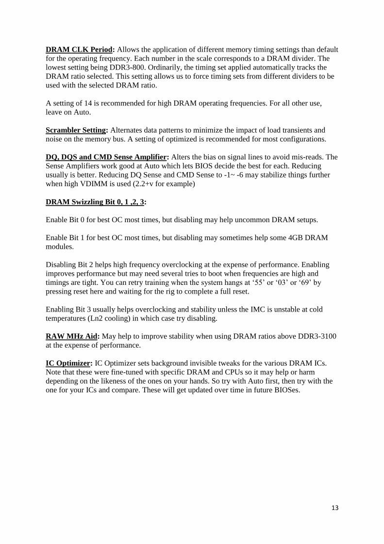
GPU.DIMM Post: Entering this section of UEFI allows us to check which memory slots are
occupied with modules and which PCIe slots have devices plugged in. Use this section of
UEFI to debug when devices or memory is not being mapped to the operating system.
Digi+VRM Power Control: All settings in the Digi+ sub-section have descriptive text in the
right hand pane of UEFI. Adjustment of these parameters is not normally needed as they will
scale as required when left on auto.
15
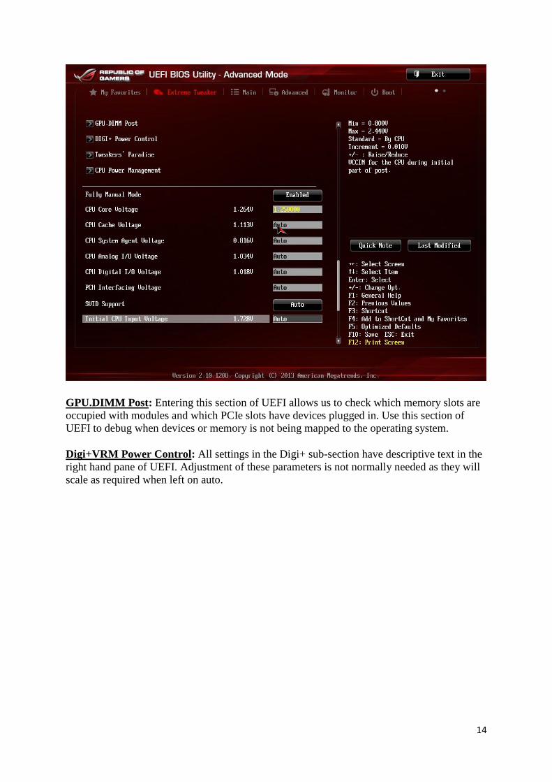
If manually making changes for extreme overclocking, simply set Vcore PWM mode to
Extreme and max out the over-current protection settings for Vcore and VDRAM.
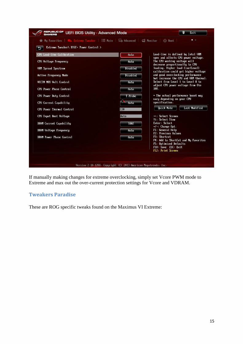
Tweakers Paradise
These are ROG specific tweaks found on the Maximus VI Extreme:
16
VCCIN Shadow: Is the very first input voltage level applied. The next input voltage level
applied is Initial input voltage. The final input voltage level applied is Eventual input voltage.
So it goes like this, Input voltage during post = – VCCIN Shadow, then Initial input voltage
till BIOS setup, and right before OS loads, Eventual input voltage is the final voltage applied.
You can leave Shadow at Auto unless you want to get input voltage very high or very low
throughout the boot process.
Termination Anti-Aliasing: Smoothens the PLL Termination voltage change process.
Enabling usually yields the best results.
PLL Termination Voltages: Very useful rail residing in the PCH ICC Integrated Clock
Controller. It is useful when pushing BCLK, when overclocking the Processor, and LN2
temperatures. Default is 1.2000v. The levels to try would be anything below 1.2500v or
anything above 1.6000v and higher. The dead-zone where voltages are not liked by the
processor is the region between 1.25v to the processor input voltage level.
When pushing BCLK (in excess of 160+MHz) you will want to set Reset voltage and
Eventual voltage to the same level (or higher) as the Input voltage (AKA CPU VCCIN). So
for example if you want to run 1.90v input voltage eventually, set Reset and eventual pll
termination voltage to 1.90v or higher. Even if you drag input voltage up in the OS, drag the
PLL Termination up as well before you drag input up.
When below 160+BCLK, sometimes it makes the CPU more stable at overclocking if you
reduce the PLL voltage. 1.10 or 1.00v might make the processor more stable at high clocks or
17
when temperature of processor is very low. So in other words, try lower than 1.25 or same as
or higher than Input Voltage.
PCH ICC Voltage: Voltage Rail of the Integrated Clock Controller. Default is 1.200v and
sweet spot depends on the DMI Frequency used.
High DMI‟s sweet spot (eg in excess of 115MHz) is around 1.2500v or lower.
Low DMI‟s sweet spot (eg lower than 86MHz) is around 1.7000v or higher.
So in other words, go high for low DMI frequency, go low for high DMI frequency.
ICC Ringback Canceller: Stubs noise levels at the ICC. Enable for High DMI frequency,
Disable for low DMI frequency.
Clock Crossing Voltages: The voltage level whereby positive clock fed to the processor
crosses the negative clock fed to the processor. Usually lower is better for overclocking.
Default is 1.15000v.
It is split into 3 instances, much like Input and PLL Termination. VBoot is the initial boot
voltage, reset applies at system resets and Clock Crossing is the eventual voltage you will be
running. Lower this for high DMI Frequencies, when pushing a lot of voltages or when over-
volting PLL Termination. The drawback of lowering is reduced PCIE Gen3.0 margins. So if
facing PCIE instability, one can actually increase these 3 voltages. 0.8000V is be a good
compromise.
Depending on the BCLK you are running, Increasing VBOOT to 1.65v or decreasing VBOOT
may help lower the Cold Boot Bug during LN2.
X-Talk Cancellation Voltage: Defaults is 1.00v. Increasing can sometimes yield a more
stable overclock (such as when you face BSOD 0124), and if Max VCore is enabled,
decreasing it may provide more stability.
PECI Voltage: PECI Voltage does nothing much but when increasing PCH Voltage it is best
to increase PECI voltage in sync.
BCLK Amplitude: Amplitude of the Base Clock Fed into the Processor. From a nominal
0.7v Amplitude at 0, it can go up to 1.40v Amplitude at +5. +5 usually works great for
overclocking.
DMI Gen 2: When pushing BCLK to the 200 region (meaning DMI Frequency of 120 MHz),
disabling Gen 2 DMI (meaning setting Gen 1 instead) will help get more DMI and thus
BCLK stability.
DMI De-emphasis Control: Also gives you an opportunity to improve DMI margins.
However, the default of -6dB usually works best.
CPU PCIE Controller: The CPU PCIE Controller can be disabled – which means the only
slot you will be able to use for graphics on the M6E would be the x4 slot from the PCH. This
may be better for 2D benching.
18
Gen 3 Preset: Auto works good and stable for Gen 3 preset while you can try different
presets especially for multi-card benching.
PLX Voltages: You can increase or decrease the rails on the PLX chipset.
PCIE Clock Amplitude: Similar to BCLK Amplitude but this one is for the PCIE Slots. You
can increase or decrease this when you are pushing high PCIE clocks from BCLK.
Internal Grpahics: This forces the IGPU to disabled or enabled.
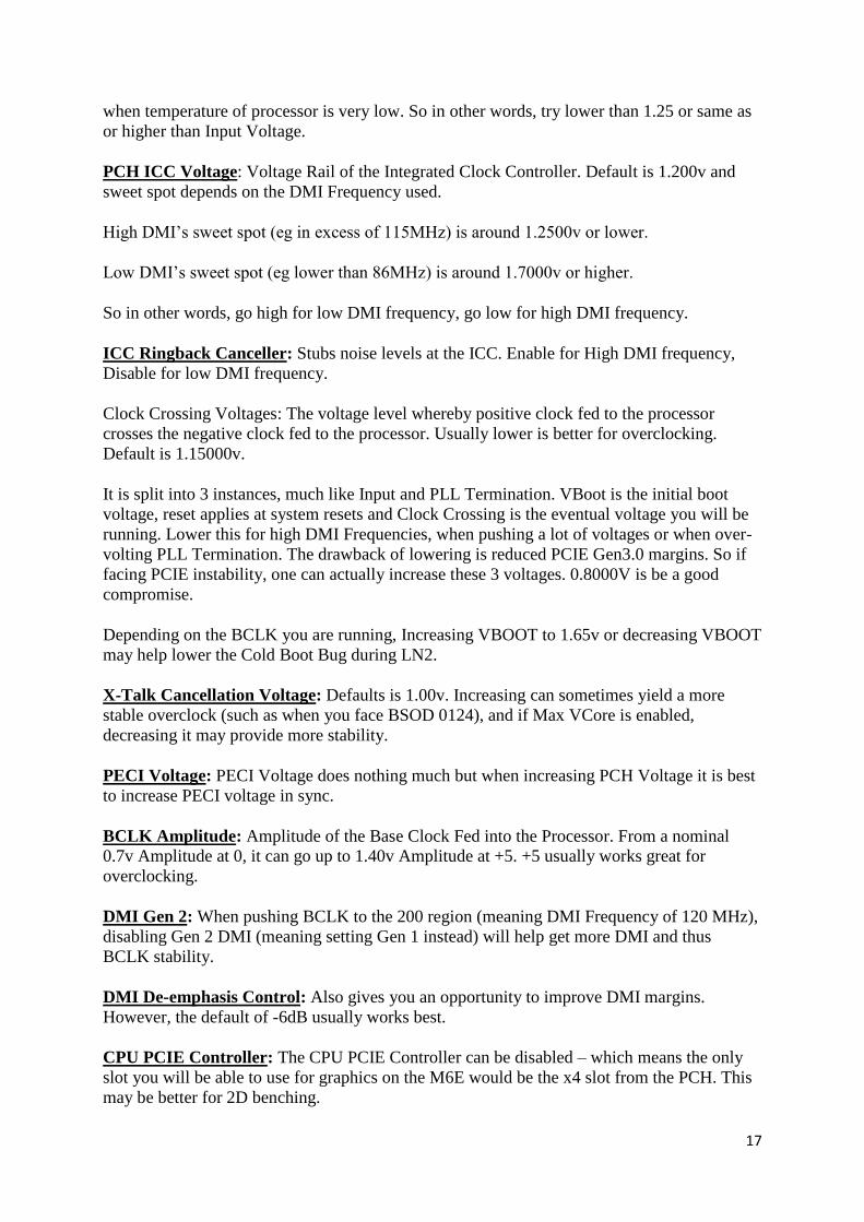
CPU Power Management: The CPU performance sub-menu contains parameters for the on-
die power circuitry. A short description of the function of each parameter is provided in the
right hand pane of UEFI as each parameter is highlighted. These settings do not need
adjustment for most overclocking as the auto settings will manipulate the settings as the
system is overclocked.
Fully Manual Mode: Haswell features FIVR (Fully integrated Voltage regulator) which
takes CPU Input voltage (A Default of 1.7~1.8v) and regulates internally on the processor to
various domains: Core, Graphics, Cache (AKA Uncore/Ring), SA, IO A, IO D, and PCH
Interface.
This is further classified into two modes on ROG boards; Fully Manual Mode (Which is
ROG‟s way of regulation) and Non Fully Manual Mode (Intel‟s Way of Regulation). The
preferred way for maximizing overclocking is with Fully Manual Mode enabled. This also
19
enables adjustments for these rails on ROG Connect and OC Panel. If you want to run C3, C6,
C7 states on the processor, then set Fully Manual Mode to Disabled.
Max VCore is an option only opened up with LN2 Mode Enabled – as it is for Ln2 cooling
only. When enabled, it pushes the processor IVR to output the maximum core voltage
possible, meaning it will try to synchronize core voltage level to the level of input voltage as
much as it can. Thus when you enable this, you cannot adjust Core voltage level. Instead, use
the input Voltage to move the level of VCore on the processor.
However on the latest stepping, with very small delta between VCCIN and Vcore, the
processors don‟t overclock well so this may not be a good option for the newer steppings. In
short, good setting with B0 (QDE4), early C0 (QE6S), but not good with later C0 (QEH6).
CPU Core Voltage as said above is for Core Frequency overclocking. You can adjust up to
2.20v on this option. Take note that anything above 1.80v VCore is potentially dangerous!
Obviously no voltages on the FIVR can exceed the input voltage as they are derived from it.
Manual Mode: Sets a static voltage for the associated rail. Using a static voltage means the
voltage will not change according to processor load. Manual mode is therefore a less efficient
way of overclocking the processor – unless AVX software loads are used (more on that in the
Adaptive section below).
We recommend using Manual mode for overclocking the processor prior to using Offset And
Adaptive mode. Once you have determined how much Vcore the processor needs to be stable,
you can use Adaptive or Offset mode to dial in the same load voltage.
There are some contra-indications to Adaptive and Offset mode however, and we discuss
those below.
Offset Mode: Setting any voltage by Offset Mode allows the processor to utilize dynamic
voltage – changing voltage levels according to load. This saves power and reduces heat output
when the processor is idling or under light loads.
When using Offset Mode, the voltage supplied to the processor can be increased or decreased
by using a positive or negative offset. The base voltage level is determined by the processor
according to frequency. You will need to use a voltage monitoring tool like AIDA in the
operating system to determine what the core voltage is under load, then offset accordingly to
the required level for stability.
It is advised not to use a positive offset too soon: Overclock the processor in small steps using
the multiplier ratio and monitor for the voltage applied before making manual changes to
offset voltage. This saves one from applying a voltage level that is too high and potentially
dangerous from the CPU. Refer to the Haswell primer section of this guide for our
recommendations on core voltage.
The disadvantage of using Offset Mode is that it affects the entire CPU Vcore VID stack.
When power saving states are enabled, the processor multiplier will change according to
software load along with the voltage. If a negative or positive offset is used, it will affect both
idle and full load voltage levels.
20
There are instances where using a large negative offset results in the idle/light load voltage
becoming too low – causing instability. Fortunately, Intel have introduced a new offset
mechanism called Adaptive Mode that works differently to Offset Mode and it doesn‟t have
this issue…
Adaptive Mode: Adaptive voltage affects voltage for Turbo multiplier ratios only. Unlike
Offset, using Adaptive does not affect idle/light load Vcore. Therefore, Adaptive mode is the
preferred method for overclocking Haswell processors if one wishes to retain dynamic voltage
changes according to processor load without running into issues with idle Vcore becoming too
low..
There is one issue with Offset and Adaptive Mode that needs to be taken into account. The
processor contains a power control unit which requests voltage based upon software load.
When the PCU detects AVX instructions, it will ramp Vcore automatically beyond normal
load voltage. There is no way to lock Vcore to prevent this if using Offset or Adapative Mode.
This is pre-programmed by Intel into the PCU.
As an example, a CPU is perfectly stable at 1.25V using a manual voltage (static), if Adaptive
or Offset Mode is used instead, it is impossible to lock the core voltage when running
software that contains AVX instruction sets – stress tests such as AIDA and Prime contain
AVX instruction sets. When the AVX instructions are detected by the PCU, the core voltage
will be ramped an additional ~0.1V over your target voltage – so 1.25V will become ~1.35V
under AVX load. If you intend to run heavy load AVX software, we recommend using
Manual Vcore, NOT Adaptive or Offset Mode.
Most of us do not run AVX related software, so this is a non-issue. Either way, dialing in an
overclock using Manual Vcore to determine how much voltage the processor needs under full
load is best – Adaptive or Offset mode can be used to match the stable voltage later on.
Simply type the target load voltage into the entry box “Additional Turbo Mode CPU core
voltage” to set adaptive voltage.
Cache Voltage: (Ring Bus Voltage), sets the voltage for the ring bus. Auto will scale the
voltage for you as ring bus frequency is increased. If manual settings are preferred, start by
keeping this voltage close to CPU core voltage and tune gradually according to stability.
As stated earlier, the performance hit from running lower ring bus frequency than CPU core
frequency is not large and will allow running lower cache voltages. DRAM operating
frequency and timings can also affect the level of cache voltage required. For 24/7
overclocking, keeping this voltage below 1.30V is probably a good idea.
VCCSA: System agent voltage. Helps with DRAM overclocking. 1.15~1.30 is more than
enough for maximizing DRAM clocks. You can use 1.30v when pushing high DRAM
frequencies to take the IMC out of the equation.
IO A: IO analog voltage. May help with DRAM overclocking. 1.15~1.30 is more than
enough for maximizing DRAM Clocks most times.
IO D voltage: IO digital voltage. Critical rail for DRAM overclocking. 1.15~1.30 is more
than enough for maximizing DRAM frequency. IO D can be sensitive on some processors
when cold and too high may worsen cold bug behaviour. The right level of I/O A and I/O D
21
will help maximize memory OC, too much or too little can cause code „55‟ on the Hex
display during POST or induce instability.
Find the right combination of SA/IOA/IOD for your setup and frequency – it will help push
DRAM further. It may not be this same combination of voltages throughout all frequencies, it
may be different at different frequencies, even on the same setup.
PCH Interface Voltage strengthens the DMI bus but does not seem to affect overclocking thus
far.
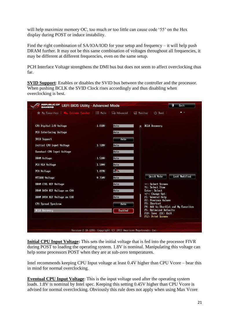
SVID Support: Enables or disables the SVID bus between the controller and the processor.
When pushing BCLK the SVID Clock rises accordingly and thus disabling when
overclocking is best.
Initial CPU Input Voltage: This sets the initial voltage that is fed into the processor FIVR
during POST to loading the operating system. 1.8V is nominal. Manipulating this voltage can
help some processors POST when they are at sub-zero temperatures.
Intel recommends keeping CPU Input voltage at least 0.4V higher than CPU Vcore – bear this
in mind for normal overclocking.
Eventual CPU Input Voltage: This is the input voltage used after the operating system
loads. 1.8V is nominal by Intel spec. Keeping this setting 0.45V higher than CPU Vcore is
advised for normal overclocking. Obviously this rule does not apply when using Max Vcore
22
mode (for Ln2 cooling), because the FIVR will set Vcore as close as possible to the input
voltage.
Take note that CPU Input voltage is capped at 2.44v for LN2 Mode Disabled and 3.04v for
LN2 Mode Enabled though you can set to 3.54v in the OS via TurboV/ROG Connect/OC
Panel.
Take note that when LN2 mode is enabled, to protect the CPU, CPU Input voltage will
automatically be set to 1.70v when the CPU encounters an unrecoverable hard lock. This will
not affect overclocking since the CPU is already hard-locked at that time.
DRAM Voltage: Sets voltage for memory modules. Set according to the specs of your
memory modules, or change as required for overclocking.
PCH VLX Voltage: Is useful when pushing DMI and effectively BCLK. Similar to PCH ICC
voltage, lower voltage for High DMI and increase for low DMI frequency. Eg, 1.10V or lower
(Some PCH can only go down to 1.05v before they stop working) for 118+MHz DMI and
1.70V or higher for low DMI ( <88MHz).
PCH Voltage: Can be left on Auto for all overclocking.
VTTDDR: Tracks and stays at 50% of DRAM voltage. Adjustment is not usually required
from 50%, though you may wish to experiment with small changes when trying to maximize
memory overclocking.
DRAM CTRL and DATA Ref: These can be left on Auto as they will track 50% of DRAM
voltage. Small changes may help at very high frequencies, though we have found that Auto
works best for us.
CPU Spread Spectrum: Modulates the processor clock to reduce the magnitude of radiated
noise emissions. This setting is best disabled for overclocking as modulation of the clock can
reduce signal margins.
BCLK Recovery: When enabled, this setting will return BCLK to a setting of 100 MHz
(default) if the system fails to POST. Disabling it will NOT return BCLK to 100MHz when
OC Failure is detected.