Embed Size (px)
Citation preview

University of LiègeFaculty of Applied Sciences
Automated spike analysisFor IC production testing solutions
A thesis proposed by MELEXIS.
Graduation Studies conducted for obtaining the Master's degree inCivil Electrical Engineering
By Maxime Javaux
Academic year 2015-2016
Supervisor: Pr. Vanderbemden


Special thanks to:
Mr. Mauroo for his support during the whole thesis,
Pr. Vanderbemden for the supervision of the thesis,
Mr. Legros for his clever advices,
Melexis for being open to students.


Automated spike analysis
For IC production testing solutions
Abstract
When a semiconductor company delivers a component to a customer, this compo-
nent has to work perfectly. A series of tests is carried out at the end of the production
line to ensure that the final product is not flawed.
One takes care of potential damages that can be caused to the component during
testing. Undesirable high frequency voltage spikes can damage the component during
the test sequence. These have to be detected during the validation of the test sequence
and suppressed.
In this document, two main goals are developed. First, the design and the creation
of an automated way of testing a sequence of tests to ensure that no spikes are
submitted to the tested component. Secondly, the research and the implementation
of an automated way of spike source localization to support the test engineer.
To reach the first goal of the thesis, several high frequency PCBs as well as an
acquisition program controlling a PC-based oscilloscope were designed and created.
To reach the second goal of the thesis, a mechanism was conceived to synchronize the
test equipment via TCP/IP with the computer that runs the acquisition program.
Finally, the tool created in the framework of this master thesis is able to detect
spikes and localize tests that produces these spikes, allowing the test engineer to work
more e�ciently. A job that lasted, initially, days or weeks can now be accomplished
within hours.
By Maxime JavauxSupervisor: Pr. Vanderbemden
University of LiegeFaculty of Applied Science
Graduation Studies conducted for obtaining the Master’s degree in CivilElectrical Engineering
Academic year 2015-2016

Thesis illustrations
Figure 1: Overview of the thesis. The two orange boxes are the test equipment and thetested component. The blue boxes are added to the test setup to detect and localize spikes.The top right blue box represents the PCBs created to allow the detection of spikes. Thebottom right blue box represents the PC-based oscilloscope programmed to acquire thewaveforms. The computer is the master of the oscilloscope, in addition, it stores the data,it synchronizes acquisitions with the test equipment via TCP/IP and it displays information.
Figure 2: Window displayed to show the acquired waveforms to the test engineer. Theuseful signal is the green one. The ID of the test, that generated the spike, is shown on thetop.


Contents
1 Introduction 1
1.1 Melexis, very briefly . . . . . . . . . . . . . . . . . . . . . . . . . . . 1
1.2 Positioning within the company . . . . . . . . . . . . . . . . . . . . . 1
1.2.1 The role of the test team . . . . . . . . . . . . . . . . . . . . . 1
1.2.1.1 Spikes above the supply . . . . . . . . . . . . . . . . 2
1.2.1.2 How were spikes detected currently . . . . . . . . . . 2
1.2.1.3 A real spike . . . . . . . . . . . . . . . . . . . . . . . 4
1.3 Melexis devices . . . . . . . . . . . . . . . . . . . . . . . . . . . . . . 5
1.3.1 Main projects . . . . . . . . . . . . . . . . . . . . . . . . . . . 5
1.3.2 Other projects . . . . . . . . . . . . . . . . . . . . . . . . . . . 5
1.4 Purpose of the thesis . . . . . . . . . . . . . . . . . . . . . . . . . . . 5
2 Overview 6
2.1 The ”tester” or the test machine or Automatic test equipment (ATE) 6
2.2 The device under test board or main board . . . . . . . . . . . . . . . 7
2.3 Spike analysis board . . . . . . . . . . . . . . . . . . . . . . . . . . . 7
2.3.1 Which signal is chosen? . . . . . . . . . . . . . . . . . . . . . 7
2.3.2 The communication with the tester . . . . . . . . . . . . . . . 7
2.4 Analog board . . . . . . . . . . . . . . . . . . . . . . . . . . . . . . . 8
2.4.1 Mounted on the spike analysis board . . . . . . . . . . . . . . 8
2.4.2 The input stage . . . . . . . . . . . . . . . . . . . . . . . . . . 9
2.4.3 Di↵erential stage . . . . . . . . . . . . . . . . . . . . . . . . . 9
2.4.4 The frequency requirement . . . . . . . . . . . . . . . . . . . . 9
2.5 Acquisition stage . . . . . . . . . . . . . . . . . . . . . . . . . . . . . 9
3 Input stage 11
3.1 Specifications . . . . . . . . . . . . . . . . . . . . . . . . . . . . . . . 11
3.2 Working principle . . . . . . . . . . . . . . . . . . . . . . . . . . . . . 11
i

3.2.1 Assumptions . . . . . . . . . . . . . . . . . . . . . . . . . . . . 12
3.2.2 Calculation . . . . . . . . . . . . . . . . . . . . . . . . . . . . 12
3.2.2.1 Input-output relation . . . . . . . . . . . . . . . . . . 12
3.2.2.2 Parasitic e↵ects . . . . . . . . . . . . . . . . . . . . . 13
3.2.2.3 Parasitic e↵ect at low frequency . . . . . . . . . . . . 14
3.2.2.4 Parasitic e↵ect at high frequency . . . . . . . . . . . 14
3.2.2.5 Conclusion . . . . . . . . . . . . . . . . . . . . . . . 15
3.2.3 Input impedance when ↵ = � . . . . . . . . . . . . . . . . . . 15
3.3 Transmission line e↵ects . . . . . . . . . . . . . . . . . . . . . . . . . 16
3.3.1 RG58 cables . . . . . . . . . . . . . . . . . . . . . . . . . . . . 16
3.4 Choice of components and placement . . . . . . . . . . . . . . . . . . 17
3.4.1 Operational amplifier . . . . . . . . . . . . . . . . . . . . . . . 17
3.4.1.1 OPA659 from Texas Instruments . . . . . . . . . . . 18
3.4.2 Resistors . . . . . . . . . . . . . . . . . . . . . . . . . . . . . . 18
3.4.3 Capacitors . . . . . . . . . . . . . . . . . . . . . . . . . . . . . 18
3.4.4 Placement of components . . . . . . . . . . . . . . . . . . . . 19
3.5 Simulations . . . . . . . . . . . . . . . . . . . . . . . . . . . . . . . . 20
3.5.1 Connections and value of components . . . . . . . . . . . . . . 20
3.5.2 Signal shape . . . . . . . . . . . . . . . . . . . . . . . . . . . . 20
3.5.3 Result in the ideal case . . . . . . . . . . . . . . . . . . . . . . 21
4 Di↵erential stage 23
4.1 Specifications . . . . . . . . . . . . . . . . . . . . . . . . . . . . . . . 23
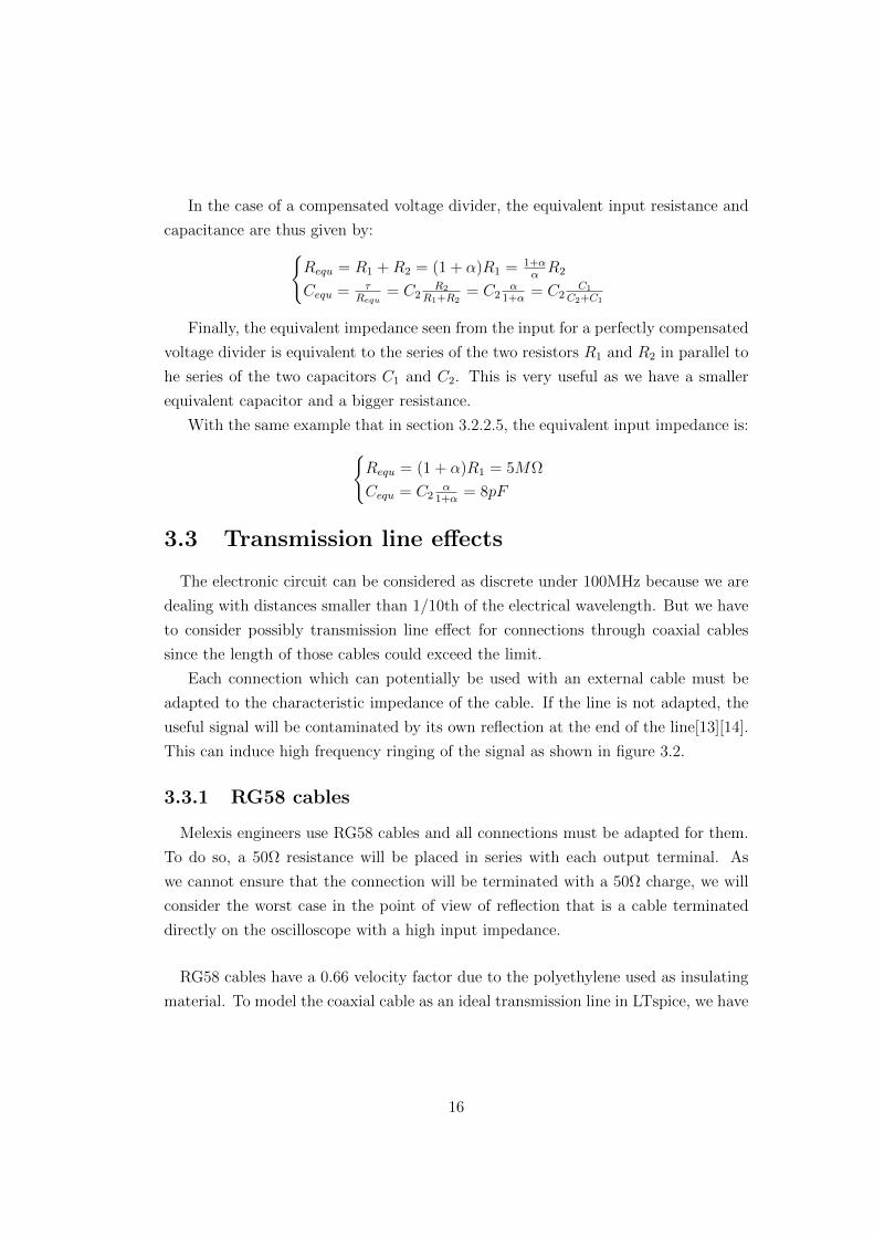
4.2 Circuit used . . . . . . . . . . . . . . . . . . . . . . . . . . . . . . . . 24
4.2.1 Input characteristics . . . . . . . . . . . . . . . . . . . . . . . 24
4.2.2 Input-output relation . . . . . . . . . . . . . . . . . . . . . . . 25
4.3 Choice of the components . . . . . . . . . . . . . . . . . . . . . . . . 25
4.3.1 Operational amplifier . . . . . . . . . . . . . . . . . . . . . . . 26
4.3.1.1 LM7171 from Texas Instruments . . . . . . . . . . . 26
4.3.2 Resistors . . . . . . . . . . . . . . . . . . . . . . . . . . . . . . 26
4.4 Simulations . . . . . . . . . . . . . . . . . . . . . . . . . . . . . . . . 26
4.4.1 Connections and value of components . . . . . . . . . . . . . . 27
4.4.2 Simulated results in the ideal case . . . . . . . . . . . . . . . . 27
ii

5 Analog prototype 30
5.1 First layout . . . . . . . . . . . . . . . . . . . . . . . . . . . . . . . . 30
5.1.1 Supply . . . . . . . . . . . . . . . . . . . . . . . . . . . . . . . 31
5.2 Simulation . . . . . . . . . . . . . . . . . . . . . . . . . . . . . . . . . 32
5.2.1 PCB e↵ects . . . . . . . . . . . . . . . . . . . . . . . . . . . . 32
5.2.1.1 Skin e↵ect . . . . . . . . . . . . . . . . . . . . . . . . 33
5.2.1.2 Computation of parasitic values . . . . . . . . . . . . 34
5.2.2 Simulation results . . . . . . . . . . . . . . . . . . . . . . . . . 34
5.3 Real board . . . . . . . . . . . . . . . . . . . . . . . . . . . . . . . . . 35
5.3.1 Characterization . . . . . . . . . . . . . . . . . . . . . . . . . 35
5.3.1.1 The CMRR in DC . . . . . . . . . . . . . . . . . . . 36
5.3.1.2 The o↵set voltage . . . . . . . . . . . . . . . . . . . . 38
5.3.1.3 The input impedance . . . . . . . . . . . . . . . . . . 39
5.3.1.4 The frequency response . . . . . . . . . . . . . . . . 39
5.4 Conclusion . . . . . . . . . . . . . . . . . . . . . . . . . . . . . . . . . 40
6 Acquisition subsystem 41
6.1 The oscilloscope . . . . . . . . . . . . . . . . . . . . . . . . . . . . . . 41
6.1.1 Choice . . . . . . . . . . . . . . . . . . . . . . . . . . . . . . . 41
6.2 Computer program . . . . . . . . . . . . . . . . . . . . . . . . . . . . 42
6.2.1 What does the program have to do? . . . . . . . . . . . . . . . 42
6.2.1.1 Communication with the oscilloscope . . . . . . . . . 42
6.2.1.2 Interface with the the user . . . . . . . . . . . . . . . 43
6.2.1.3 Communication with the test machine . . . . . . . . 43
6.2.1.4 User facilities . . . . . . . . . . . . . . . . . . . . . . 44
6.3 State diagram of the program . . . . . . . . . . . . . . . . . . . . . . 44
6.3.1 The TCP/synchronous mode . . . . . . . . . . . . . . . . . . 45
6.4 Synchronization of clocks . . . . . . . . . . . . . . . . . . . . . . . . . 46
6.4.1 Mechanism of synchronization . . . . . . . . . . . . . . . . . . 48
6.4.2 Estimator of �t . . . . . . . . . . . . . . . . . . . . . . . . . . 48
6.4.3 Test localization . . . . . . . . . . . . . . . . . . . . . . . . . . 50
6.4.3.1 Link between the test name and its reference . . . . 51
6.5 Storage of the information in a file . . . . . . . . . . . . . . . . . . . 51
6.6 Additional code on the tester . . . . . . . . . . . . . . . . . . . . . . 51
6.6.1 The connection initialization function . . . . . . . . . . . . . . 52
6.6.2 The add a time us function . . . . . . . . . . . . . . . . . . . 52
iii

6.6.3 The display name console function . . . . . . . . . . . . . . . 52
6.6.4 The finalize connection function . . . . . . . . . . . . . . . . . 53
6.6.5 A simple code on the tester . . . . . . . . . . . . . . . . . . . 53
6.7 The display window . . . . . . . . . . . . . . . . . . . . . . . . . . . . 53
7 Spike analysis board 55
7.1 The connection between the DUT board and the DUT . . . . . . . . 55
7.1.1 The spike analysis board and the analog board . . . . . . . . . 56
7.1.1.1 Note about the connectors . . . . . . . . . . . . . . . 56
7.2 Specifications needed for the spike analysis board . . . . . . . . . . . 56
7.3 Influence of the track impedance . . . . . . . . . . . . . . . . . . . . . 57
7.3.1 Assumption . . . . . . . . . . . . . . . . . . . . . . . . . . . . 57
7.3.1.1 Input impedance . . . . . . . . . . . . . . . . . . . . 58
7.3.2 Transfer functionVin
VS
, determined analytically . . . . . . . . . 59
7.3.3 Simulation of the transfer functionVin
VS
. . . . . . . . . . . . . 61
7.3.4 Conclusions . . . . . . . . . . . . . . . . . . . . . . . . . . . . 62
7.4 Practical realization of the PCB . . . . . . . . . . . . . . . . . . . . . 63
7.4.1 Operating principle . . . . . . . . . . . . . . . . . . . . . . . . 63
7.4.1.1 Driving the relays . . . . . . . . . . . . . . . . . . . 64
7.4.1.2 Driving the demultiplexers . . . . . . . . . . . . . . . 64
7.4.2 Communication with the tester . . . . . . . . . . . . . . . . . 66
7.5 Mbed microcontroller code . . . . . . . . . . . . . . . . . . . . . . . . 67
7.5.1 Corresponding code on the tester . . . . . . . . . . . . . . . . 68
7.6 The final board . . . . . . . . . . . . . . . . . . . . . . . . . . . . . . 69
8 Final analog board 73
8.1 Obtain 3pF of equivalent input capacitance . . . . . . . . . . . . . . . 74
8.1.1 Variable capacitor . . . . . . . . . . . . . . . . . . . . . . . . . 75
8.2 The final board . . . . . . . . . . . . . . . . . . . . . . . . . . . . . . 75
8.2.1 The DC CMRR . . . . . . . . . . . . . . . . . . . . . . . . . . 75
8.2.2 The o↵set voltage . . . . . . . . . . . . . . . . . . . . . . . . . 77
8.2.3 The input impedance . . . . . . . . . . . . . . . . . . . . . . . 77
8.2.4 The frequency response . . . . . . . . . . . . . . . . . . . . . . 77
iv

9 Supply 81
9.1 Design . . . . . . . . . . . . . . . . . . . . . . . . . . . . . . . . . . . 81
9.1.1 Components . . . . . . . . . . . . . . . . . . . . . . . . . . . . 82
9.1.2 Connections . . . . . . . . . . . . . . . . . . . . . . . . . . . . 82
9.2 The final supply . . . . . . . . . . . . . . . . . . . . . . . . . . . . . . 82
10 Final setup, test and result 83
10.1 The setup . . . . . . . . . . . . . . . . . . . . . . . . . . . . . . . . . 83
10.2 The test and the result . . . . . . . . . . . . . . . . . . . . . . . . . . 85
11 Conclusion 87
12 Melexis: strategic aspects 89
12.1 Some numbers . . . . . . . . . . . . . . . . . . . . . . . . . . . . . . . 89
12.2 R&D strategy . . . . . . . . . . . . . . . . . . . . . . . . . . . . . . . 90
12.3 HR strategy . . . . . . . . . . . . . . . . . . . . . . . . . . . . . . . . 91
12.4 Melexis, opinion of a student . . . . . . . . . . . . . . . . . . . . . . . 91
Bibliography 93
v


Chapter 1
Introduction
This thesis was carried out within Melexis, a Belgian microelectronic integrated
system company.
1.1 Melexis, very briefly
Specialized in the automotive industry, the company designs, tests and delivers
advanced mixed signal semiconductors, sensor ICs, and programmable sensor IC sys-
tems. The company is international but a sizeable part of the research and develop-
ment takes place in Belgium.
1.2 Positioning within the company
During the development phase of a new chip in the company, there are various
teams associated to the project. These teams come from di↵erent departments of the
company, including the analog design department, the digital design department, the
test department, etc. Each team has a specific responsibility in relation with the new
project. This thesis responds to a need of the test department of the company.
1.2.1 The role of the test team
Each device sold by the company must work perfectly. To ensure that, each device
which is sent by the company has to be tested to prevent any defective product from
being delivered to the customer. The test step occurs at the end of the production
lines. It is done using automated test solutions which are developed specifically for
each project by the test team. This test solution can involve thousand of lines of code
describing di↵erent complex situations in which the device response must lie within
established specifications.
1

During the development of the test solution, it is mandatory to ensure that no
damaging situations are induced by the test itself. Damaging treatments could be an
error of the applied voltage range or a voltage spike induced by an incorrect sequence
of operations in the implementation. The signal produced by such errors can either
be a low frequency error1 or a high speed voltage spike.
Low frequency errors are generally range errors in the code implementation. They
can be detected easily by the test engineer as the signal shape does not correspond
to the expected shape for a long period of time.
High speed voltage spikes are harder to detect. They can be as small as 100ns
and can occur negatively with respect to the ground or positively with respect to the
supply. A negative spike can then be easily detected by the test engineer with an
oscilloscope. By contrast, a spike that exceeds the supply is more di�cult to detect
because the supply voltage can take di↵erent values. This prohibit the usage of an
oscilloscope to trigger signals that exceed a given voltage.
1.2.1.1 Spikes above the supply
Spikes above the supply voltage are di�cult to detect because the supply is not
constant during the test sequence. Figure 1.1 shows a schematic representation of a
signal with a spike.
We have two signals represented in figure which are the supply signal and the
signal of the pin we are testing (PUT for Pin Under Test). In this example, we
consider a modification of the supply voltage from 5V to 15V which can occur several
times in a test sequence. The PUT is initially at a zero voltage and is connected to
the 15V at the same time as the supply pin, which induces a spike that exceeds the
supply pin voltage.
This is the role of the test engineer to determine the source of such a spike and
its potential danger against the DUT (Device Under Test). Then the engineer has to
suppress it.
1.2.1.2 How were spikes detected currently
The process is quite simple for the detection of a negative spike. The engineer uses
an oscilloscope with a bandwidth equal or bigger than 100MHz and sets the trigger
threshold to a negative value2. Then one follows the step sequence which is:
1In this application, it corresponds to a period in the ms range.2In falling edge mode at a threshold of -1V for example
2

Figure 1.1: Schematic time dependence of a spike. The supply voltage increases anda pin under test (PUT), initially at ground, is connected to the supply.
1. Connect the oscilloscope to the PUT.
2. Start the whole test program and obtain the number of negative spikes.
3. Use the debugger mode to determine the source of each spike.
4. Correct the code to avoid spikes.
5. Switch to another pin and repeat from point 2.
This process is time consuming and is prone to error due to the large amount of
manipulations.
For the spike that exceeds the supply voltage, the engineer cannot trigger on each
spike directly, as explained before. To solve this issue, the threshold of the trigger
can be set just above the minimum supply voltage of the DUT. Then, one follows the
sequence:
1. Connect the oscilloscope to the PUT.
3

2. Start the whole test program and obtain a given number of acquisitions.
3. Analyze the shape of the signals to see if an error occurs.
4. Determine the total number of error.
5. Use the debugger mode to determine the source of each spike.
6. Correct the code to avoid spikes.
7. Change to another pin and repeat from point 2.
This process is very long, it can take several days or weeks to an engineer to test
all pins of a device depending on the number of pins and the number of tests. In
addition, errors can arise from all manipulations that are done by the engineer.
One can notice that a spike can occur when the test is normally started and will
not appear anymore in debugging mode. This can be due to a capacitor having
enough time to be discharged when the test sequence is stopped, for example.
1.2.1.3 A real spike
Figure 1.2: Examples of spikes acquired with a 200MHz oscilloscope. There are 4consecutive negative spikes in less than a ms. The minimum voltage detected by theoscilloscope is -5.44V. Only one capture is made by the oscilloscope, as shown on thetop right corner.
A print-screen of an oscilloscope monitoring a real signal is shown in figure 1.2.
Four negative spikes are visible. The engineer knows here that these spikes are the
4

only ones occurring during the test on this pin since only one waveform is captured
by the oscilloscope. The problem is to try to localize the part of the code which is
the source of these spikes.
1.3 Melexis devices
In the Melexis company, a large number of di↵erent chips are manufactured with
various specifications. The company follows the needs of the customers regarding the
placement of the pins, the supply voltage and the device package.
1.3.1 Main projects
The main part of the Melexis chips have 16 pins and a 5V supply. The signals
which are applied to a 5V chip during a test can vary from -24V to 24V. However,
amplitude of the spikes remains generally restricted below 15V since amplitude of
24V are rarely used.
1.3.2 Other projects
Chips manufactured by Melexis contain between 8 and 64 pins. The supply voltage
can be 5V, 12V or 24V. Projects based on a 24V supply may experience spikes of
100V amplitude during a test.
1.4 Purpose of the thesis
The purpose of the thesis is to find an automated way to detect voltage spikes
and report the related information to the test engineer. The engineer must do as
few manipulations as possible to avoid errors. In addition, the created setup must
communicate with the test machine to locate (in the code) the source of an error and
provide a capture of the signals to support the test engineer in his/her work.
The spike analysis tool must be usable for most of the projects within the company.
The device must be easy to use and not too expensive so that the company can
reproduce and use it on di↵erent sites without di�culties.
5

Chapter 2
Overview
This chapter will present the di↵erent parts of the project from a high level point
of view.
The complete system can be seen with a reduced number of subsystems as shown
in figure 2.1.
Figure 2.1: Overview of the complete testing setup. The orange subsystems arethe ones used by engineers in the company to perform a test sequence. The bluesubsystems are the additional ones that were created to reach the goals of the thesis.
The orange subsystems represent the setup used by the company to test a de-
vice. This is what is required to test devices on the production line. We are going
to describe them first. The blue subsystems are those added to detect spikes and
report information to the engineer. The blue subsystems will be used only during the
validation of the test program to perform a spike analysis.
2.1 The ”tester” or the test machine or Automatictest equipment (ATE)
The tester is a measurement equipment that has large capabilities of signal gen-
eration and signal acquisition in the digital and analog domain. The machine can
6

simulate every signals that can potentially be connected to a DUT and will verify
that the DUT response is correct.
2.2 The device under test board or main board
The device under test board (or main board) is a PCB that is specific to the
DUT and provides the right connection between a pin of the DUT and a tester
output/input1.
This board is also used by the test engineer to realize actions that are not relate
to the spike analysis and will not be described.
2.3 Spike analysis board
The spike analysis board is a PCB mounted on the main board to pick up the
signals that must be measured. The signal connections are realized through the
help of a microcontroller development board often used inside the company and that
communicates with the tester.
2.3.1 Which signal is chosen?
Only one pin will be measured at a time. To perform a complete measurement
sequence of the whole set of pins of the device, a simple loop can be implemented.
To carry out the spike analysis, three signals are needed. There are: (i) the PUT,
(ii) the supply and (iii) the ground. It is important to note that the ground pin of
a DUT in a given project might be di↵erent from those used for other projects since
the company follows the needs of the customer.
2.3.2 The communication with the tester
The information needed from the tester and to be transferred to the board is only
the pin that must be tested. The spike analysis board must then connect the right
pin to the next subsystem. To do so, we use a Mbeb Microcontroller LPC17682 which
controls a set of relays.
1Melexis provides packages as well as pin mapping that depends on the needs of the customer.2The Mbed Microcontroller LPC1768 is overpowered for the present application but it allows to
work e�ciently and is available in the company. In addition, nearly all Melexis engineers know howto use it and can modify the Mbed program that was developed in this thesis if they want to.
7

2.4 Analog board
The analog board must provide a signal that can be used to detect a positive spike
as it is not possible to detect them directly with the PUT and the supply.
To detect a positive spike in reference to the supply voltage, the di↵erential voltage
between the PUT voltage and the supply voltage of the chip can be used: Vdiff =
VPUT � Vsupply. In this way, we can trigger and capture the signals when the PUT
exceeds the supply voltage.
In addition, the supply and the PUT signals must be measured as well to support
the test engineer and to verify that the di↵erential signal is correct.
There are thus three outputs to the analog board and the measurement of these
three outputs cannot perturb initial signals.
We will divide the analog board in two di↵erent stages as followed: the input stage
and the di↵erential stage as shown in figure 2.2.
Figure 2.2: System view of the analog board subdivided is subsystems.
2.4.1 Mounted on the spike analysis board
The analog board will be mounted on the spike analysis board to increase the
modularity. As the device under test board can di↵er from one project to another,
they will have several spike analysis boards designed for the di↵erent device under
test boards.
This do not mean that the analog board has to be di↵erent. Indeed, the analog
board has to be chosen only in view of its input voltage range (Corresponding to the
maximum voltage that can be applied to the DUT). The test engineer will choose
the spike analysis board to fit on the device under test board and he will choose the
analog board in view of the voltage range applied to the DUT.
8

2.4.2 The input stage
The input stage has to act like a bu↵er for each input. It must have an output
voltage equal to its input voltage divided by a given ratio. This voltage attenuation
is needed because some operational amplifiers are used and may be saturated with a
too large voltage.
The input impedance of this stage must be high enough to measure correctly the
signals. The initial target is the equivalent impedance of the measurement device used
initially within the company, i.e. a 10M⌦//⇠12pF probe of a standard oscilloscope3.
2.4.3 Di↵erential stage
The di↵erential stage output signal should be proportional to Vout / VPUT �Vsupply.
A very large input impedance is not needed since both input stages will be active and
will bu↵er both inputs. A unit gain is implemented to obtain a good frequency
response4. The di↵erential signal will be used to trigger and then capture all three
signals.
2.4.4 The frequency requirement
All parts must have a bandwidth in the range of 100MHz to detect spikes that have
a typical duration of 100ns. Such a bandwidth cannot be achieved with a commercial
instrumentation amplifier chip. Consequently we need to implement the di↵erential
stage with discrete components.
As we are dealing with relatively large voltage signals (of the order of 10V) and
as the shape is more important that the exact value of the signal, it is not needed to
have a high common mode rejection.
Some amplitude variations at high frequency can be tolerated for the di↵erential
signal.
2.5 Acquisition stage
The data acquisition will be carried out through a computer based oscilloscope
as shown in figure 2.3. This gives us a better signal integrity in comparison to a
dedicated implementation. In addition, the small size of those oscilloscopes compared
3A 1M⌦//20pF oscilloscope was used with a 1:10 N2863B probe from Keysight, resulting in thisequivalent impedance.
4The gain-bandwidth product will limit our bandwidth; the smaller the gain, the higher thebandwidth.
9

to benchtop oscilloscope allows us to decrease significantly the distance between the
signal output and the signal acquisition.
Figure 2.3: Picoscope 2000 series. Dimensions (including connectors) are: 142 x 92 x18.8 mm.
Finally, since we need to program the oscilloscope and there are no particular
oscilloscopes used within the company, we can choose an oscilloscope model that fits
best our requirements. Once again, computer based oscilloscopes are cheaper than
benchtop oscilloscopes so that the cost will be reduced if the company has to buy
several of them.
The programmation of the oscilloscope, the programmation of the Mbed, the design
of the analog and the spike analysis board have been developed as parts of this master
thesis from scratch. Everything in the following chapters was created/designed/stud-
ied as part of this master thesis.
10

Chapter 3
Input stage
The input stage plays the role of a bu↵er with a voltage division. Its output
is connected to an input terminal of the di↵erential amplifier. An adapted coaxial
output is also accessible to the user. The coaxial output allows the engineer to verify
the measurements with any measurement device if needed.
3.1 Specifications
The input stage must have the following specifications:
• A bandwidth from DC to 100MHz.
• A high input impedance equivalent (or better) than a 10M⌦ resistance in par-
allel with a 12pF capacitor.
• A voltage reduction to be in the range of operation of the input operational
amplifier.
• The time dependences of its output should follow as closely as possible that of
the input whatever that the coaxial cable is connected or not.
• It must be ESD protected.
3.2 Working principle
Figure 3.1 shows the input stage1 we are going to study and implement. It is
basically a high speed capacitor compensated voltage divider containing a simple
bu↵er implemented with a high speed operational amplifier.
1The notations of this figure will be used for further calculations.
11

Figure 3.1: Circuit of the input stage. This circuit is duplicated for both input signalsand their outputs are connected to the inputs of the di↵erential stage.
To design this stage, we have to know which parameters influence the output and
the frequency response.
3.2.1 Assumptions
We will first assume that the operational amplifier works ideally, so that its input
impedance is infinite and its own output is exactly its positive input. Similarly,
resistors and capacitors are supposed to be ideal.
3.2.2 Calculation
In the following points, the input-output relation will be studied in the ideal case.
3.2.2.1 Input-output relation
The calculation is carried out through admittance (Y) and conductance (G). The
input-output relation is given by:
Vout
Vin
=Y1
Y1 + Y2(3.1)
=G1 + j!C1
G1 +G2 + j!(C1 + C2)(3.2)
=(G1 + j!C1)(G1 +G2 � j!(C1 + C2))
(G1 +G2)2 + !2(C1 + C2)2(3.3)
12

If we choose: (G1 = ↵G2
C1 = �C2
Then:
Vout
Vin
=Y1
Y1 + Y2(3.4)
=(↵G2 + j!�C2)((1 + ↵)G2 � j!(1 + �)C2)
(1 + ↵)2G22 + !2(1 + �)2C2
2
(3.5)
=↵(1 + ↵)G2
2 + !2�(1 + �)C22
(1 + ↵)2G22 + !2(1 + �)2C2
2
(3.6)
+ j!�C2G2(1 + ↵)� !↵C2G2(1 + �)
(1 + ↵)2G22 + !2(1 + �)2C2
2
(3.7)
The purpose is to obtain a division without frequency variation of the output. To
avoid phase shift, the numerator of the imaginary part must be equal to zero. We
have:
Num
✓=(Vout
Vin
)
◆= !�C2G2(1 + ↵)� !↵C2G2(1 + �) = 0 (3.8)
!�(1 + ↵) = ↵(1 + �) (3.9)
!� = ↵ (3.10)
If � = ↵, the frequency response is linear and we have directly:
Vout
Vin
=↵
↵ + 1
In addition we also have: (G1 = ↵G2
C1 = ↵C2
Then:
G1
G2=
R2
R1=
C1
C2(3.11)
! R1C1 = C2R2 = ⌧ (3.12)
We have equality of both time constants[15].
3.2.2.2 Parasitic e↵ects
Now, we consider what happen if the matching is not perfect. Suppose that: � =
↵ + � with ↵ >> �, we have:
13

Num
✓=(Vout
Vin
)
◆= !C2G2(↵ + �)(1 + ↵)� !C2G2↵(1 + ↵ + �) (3.13)
= !C2G2� (3.14)
Num
✓<(Vout
Vin
)
◆= ↵(1 + ↵)G2
2 + !2↵(1 + ↵)C22 (3.15)
+ !2�C22 + 2!2↵�C2
2 + !2 �2|{z}=0
C22 (3.16)
= ↵(1 + ↵)G22 + !2↵(1 + ↵)C2
2 + !2�(1 + 2↵)C22 (3.17)
Denom
✓Vout
Vin
◆= (1 + ↵)2G2
2 + !2((1 + ↵)2 + 2(1 + ↵)�| {z }<(1+↵)2
+ �2|{z}=0
)C22 (3.18)
' (1 + ↵)2G22 + !2(1 + ↵)2C2
2 (3.19)
Then:
Vout
Vin
' ↵
↵ + 1(3.20)
+!2�(1 + 2↵)C2
2
(1 + ↵)2G22 + !2(1 + ↵)2C2
2
(3.21)
+ j!C2G2�
(1 + ↵)2G22 + !2(1 + ↵)2C2
2
(3.22)
3.2.2.3 Parasitic e↵ect at low frequency
Since the capacitors are of the pF order and the resistors are in the M⌦ range,
we have !C2 < G2 at low frequency. This induces that 3.21 and 3.22 are not large
enough to impact Vout
Vin
.
3.2.2.4 Parasitic e↵ect at high frequency
Consider the denominator 3.19: beyond the frequency !c = G2C2, the !C2 term
becomes bigger than the G2 term. When the frequency is higher than !c, we can
ideally consider the simplified denominator:
!2C22(1 + ↵)2
14

.
This induces that 3.21 can be simplified as:
!2�(1 + 2↵)C22
!2C22(1 + ↵)2
=�(1 + 2↵)
(1 + ↵)2= �
✓1
1 + ↵+
↵
(1 + ↵)2
◆
And the term 3.22 can be simplified as:
j!C2G2�
!2C22(1 + ↵)2
= j!c
!
�
(1 + ↵)2
The the term 3.22 is smaller than 3.21 because !c < !. To decrease parasitic
sensitivity, we must reduce as much as possible ↵(1+↵)2 and 1
1+↵.
As ↵(1+↵)2 < 1
1+↵, we have to keep ↵ is large as possible. However, the term ↵ is
fixed by our input division and the choice of the division is made only by considering
the voltage range.
3.2.2.5 Conclusion
To conclude, we can keep in mind that a high input division ratio can be necessary to
bring down the input voltage range within the allowable range of the input operational
amplifier. However, increasing this ratio means decreasing ↵ and then increasing the
sensitivity of the circuit against matching errors.
As an example, for a division ratio of 5 (↵ = 14), a conductance G2 =
1R2
= 10�6S
and a capacitance C2 = 40pF, the voltage ratio at 100MHz becomes:
Vout
Vin
' 1
5+ 0.96 � + j 2.6 10�5 � ' 1
5+ 0.96 �
As shown by the previous equation, the e↵ect of a mismatch of the capacitance ratio
(�) can impact the output voltage significantly.
3.2.3 Input impedance when ↵ = �
The input impedance of the input stage is given by:
Z = (R1//C1) + (R2//C2) (3.23)
=R1
1 + j!C1R1+
R2
1 + j! C2R2| {z }=C1R1=⌧
(3.24)
=R1 +R2
1 + j!⌧(3.25)
15
In the case of a compensated voltage divider, the equivalent input resistance and
capacitance are thus given by:(Requ = R1 +R2 = (1 + ↵)R1 =
1+↵↵
R2
Cequ = ⌧R
equ
= C2R2
R1+R2= C2
↵1+↵
= C2C1
C2+C1
Finally, the equivalent impedance seen from the input for a perfectly compensated
voltage divider is equivalent to the series of the two resistors R1 and R2 in parallel to
he series of the two capacitors C1 and C2. This is very useful as we have a smaller
equivalent capacitor and a bigger resistance.
With the same example that in section 3.2.2.5, the equivalent input impedance is:
(Requ = (1 + ↵)R1 = 5M⌦
Cequ = C2↵
1+↵= 8pF
3.3 Transmission line e↵ects
The electronic circuit can be considered as discrete under 100MHz because we are
dealing with distances smaller than 1/10th of the electrical wavelength. But we have
to consider possibly transmission line e↵ect for connections through coaxial cables
since the length of those cables could exceed the limit.
Each connection which can potentially be used with an external cable must be
adapted to the characteristic impedance of the cable. If the line is not adapted, the
useful signal will be contaminated by its own reflection at the end of the line[13][14].
This can induce high frequency ringing of the signal as shown in figure 3.2.
3.3.1 RG58 cables
Melexis engineers use RG58 cables and all connections must be adapted for them.
To do so, a 50⌦ resistance will be placed in series with each output terminal. As
we cannot ensure that the connection will be terminated with a 50⌦ charge, we will
consider the worst case in the point of view of reflection that is a cable terminated
directly on the oscilloscope with a high input impedance.
RG58 cables have a 0.66 velocity factor due to the polyethylene used as insulating
material. To model the coaxial cable as an ideal transmission line in LTspice, we have
16

Figure 3.2: Practical ringing observed without transmission line adaptation. Cap-ture observed on an fast inverting amplifier of unitary gain without any adaptation.Timebase: 250ns/div. Voltage ranges: 500mV/div.
to compute the time delay[7]. To do so, we choose a typical cable length of 1m, then
we have:
Td =l
rcc(3.26)
=1
0.66 ⇤ 3 108' 5ns (3.27)
Where l is the length of the cable (1m), rc is the velocity factor and c is the speed of
light.
This model will be used in LTspice simulations in section 3.5.
3.4 Choice of components and placement
The values of resistors and capacitors have to be determined as well as the type
of operational amplifier. The placement of components will be shortly discussed
thereafter.
3.4.1 Operational amplifier
The choice of an operational amplifier is crucial because its behavior will influence
the behavior of the voltage division. It is obvious that its input equivalent resistance
must be high and its input equivalent capacitance must be small. To achieve such a
condition, a JFET input is needed. For a given resistance R2, the input resistance
17

of the operational amplifier must be several orders of magnitude higher. The input
capacitance does not need to be extremely small as it will be taken into account by
adding its value to C2.
In addition, its input bias and o↵set current must be very small. For a voltage
of 100mV at the operational amplifier output, we have 100mV as well between both
terminals of R2 and, for R2 = 1M⌦, a current of 100nA. Typically, the sum of the
input bias and o↵set current of the operational amplifier must be at least one or two
orders below 100nA.
The operational amplifier must be unity-gain stable and its unit gain bandwidth
must be greater than the 100MHz target bandwidth. Finally, a high slew rate in the
1000V/µs order is needed to support rapid voltage variations.
3.4.1.1 OPA659 from Texas Instruments
The OPA659[5] operational amplifier fulfills the required specifications. It has a
650 MHz unity-gain bandwidth, a remarkable slew rate above 2500V/µs, a huge input
resistance in the tera-ohm range, a small input capacitance near to 1pF, a very small
input bias current of 10pA and a very small o↵set current of 5pA. It needs a ±5V or
a ±6V supply and has an output voltage swing of ±4V (±6V supply).
In addition to these characteristics, the amplifier has ESD diode protection on both
inputs able to support a current of around 30mA. No additional diodes are needed for
the ESD protection of both inputs since the resistor R1 used for the divider is large
enough to limit this current.
3.4.2 Resistors
Both resistors R1 and R2 must be large enough to obtain an equivalent input
resistance in the 10M⌦ range. Resistors larger than ⇠10M⌦ must be avoided because
they are more noise sensitive and they do not provide stable resistance values.
It is important to have low reactance resistors to keep the circuit behavior as
good as possible at high frequency. Surface-mount resistors work very well at high
frequency and allow the layout size to be reduced.
3.4.3 Capacitors
The capacitor C1 has to be variable in order to allow the user to compensate the
input. Without compensation, the matching will never be achieved due to the possibly
large value variation expected for fixed value capacitors.
18

The capacitor C2 has to be big enough to allow the user to compensate the circuit
correctly. Indeed, we could be tempted to use a very small capacitor to obtain a very
small equivalent input capacitance but this would lead to a small trimmer capacitor
with poor precision and then, a poor compensation.
We can notice that the capacitor C1 could be of fixed value and the capacitor
C2 could be variable to realize the compensation. This would imply that a smaller
input capacitance will be achieved with the same trimmer capacitor as in the previous
case and a smaller fixed value capacitor2. In addition to the reduction of the input
equivalent capacitance, the variable capacitor will be, in this configuration, subjected
to a smaller voltage range. This could be an important point of interest during the
circuit design because fixed capacitors are generally not able to support voltages above
50V whereas some variable capacitors can support more than 250V.
3.4.4 Placement of components
The rule is that distance between components must be minimized. Especially, as
high impedance paths are very sensitive to parasitic capacitance, each high impedance
path must be as small as possible[20]. The connection between the resistor R1, R2
and the operational amplifier have to be very small for example.
A connection on a small impedance point like the output of the operational am-
plifier is less sensitive to parasitic capacitance than a high impedance point. Con-
sequently, in case of perturbative signal on a high impedance point (e.g. the non-
inverting input of a bu↵er) a shield can be implemented directly on the layout. This
shield will reduce the e↵ect of parasitic capacitive signals on the sensitive path. How-
ever, this shield will add a capacitive load to the output of the bu↵er and can result
in an unstable output at high frequency. A trade-o↵ can be found by estimating the
loaded capacitance and place the corresponding isolation output resistor. This resis-
tance value can be found in the datasheet of all high speed operational amplifiers, if
needed3.
Since sensitive paths can be small enough, a shield is not needed here. No output
resistance is needed in our case as the output load capacitance is maintained smaller
than 5pF[5].
2The first prototype was based on a variable capacitor for C1. The final circuit use a variablecapacitor C2 to decrease the equivalent capacitance. This will be detailed later.
3See figure 17 of the OPA659 datasheet for example.
19

3.5 Simulations
For the simulations reported in this section, the LTspice software and the spice
model provided by TI for the OPA659 have been used.
3.5.1 Connections and value of components
A specific case is simulated hereafter. A 15V supply chip is supposed to be tested.
• The input division is 5 (↵ = 14 = �)
• The equivalent input resistance is set to 10M⌦ leading R1 and R2 to be equals
respectively to 8M⌦ and 2M⌦.
• The equivalent input resistance is set to 8pF leading C1 and C2 to be equals
respectively to 10pF and 40pF.
• Two loads are connected to the output of the bu↵er. The first is a 100⌦ re-
sistor presented in the datasheet as a typical load to achieve specified perfor-
mances. The second is a 50⌦ adapted ideal transmission line connected to a
high impedance oscilloscope (1M⌦//15pF).
3.5.2 Signal shape
The signal used as input of the di↵erential amplifier must correspond to critical
signal cases.
Two cases can be simulated to analyze the response of the input stage. The first
one will simulate a critical spike and the second one will simulate a very fast square
signal.
Fast spikes are nearly triangular with a 100ns base. They can have an amplitude
ranging from the ground to the supply voltage. A smaller negative spike will be also
simulated.
The square wave has a 1MHz frequency with an amplitude of ±Vdd. The rising
and falling edges of the signal are intentionally small (10ns) to investigate if some
oscillations could be noticed at the output of our circuit.
In addition to these signals, two sinusoidal signals at 25MHz and 10MHz are added
to mimic small perturbative signals (100mV). The shape of those two signals can be
seen in figure 3.3.
20

Figure 3.3: Two type of signals used as input of the first stage in simulations. Thetop signal represents a critical spike and bottom signal represent a high speed squaresignal.
3.5.3 Result in the ideal case
In the ideal case, the input stage works perfectly as shown on figure 3.4. The input
signal can be recovered by multiplying the output signal by the input division ratio,
which is 5 in this case.
The frequency response of the simulated circuit is shown on figure 3.5. We can see
an attenuation close to 14dB that corresponds to the input voltage division.
�14dB = 10�14/20 ' 1
5
As expected, the cut-o↵ frequency is greater than 100MHz. The -3dB cut-o↵
frequency is very close to 300MHz.
21

Figure 3.4: Two outputs for both type of signals used as input of the first stage insimulations. The signals are multiplied by 5 to have the same range as the inputsignal.
Figure 3.5: Ideal simulation of the frequency response of the input stage. The cut-o↵ frequency (-3dB in reference to the nominal attenuation) is at 300MHz and thenominal attenuation is -14dB.
22

Chapter 4
Di↵erential stage
The goal of this stage is to obtain a di↵erential signal which can be used to trigger
when a given signal exceeds the supply.
4.1 Specifications
The di↵erential stage will consist in a di↵erential amplifier based on discrete compo-
nents. This stage must have the following specifications:
• Bandwidth from DC to 100MHz
• Amplitudes of input signals are restricted between -5 to +5V for each type of
DUT supply voltage. Since our input stage has an output voltage swing of ±4V,
we do not have to care about the amplitude at the input of this stage.
• The common mode rejection must be good but does not need to be extremely
high as the output of the amplifier is principally used as a triggering signal.
• The precision must be su�cient to detect spikes.
• No gain is needed as the input voltages are already high enough.
• A large input impedance is not needed as the input stage is designed like a
bu↵er.
• The output has to be adapted to 50⌦ to allow the user to possibly connect any
RG58 cable.
23
4.2 Circuit used
This is a simple di↵erential stage implemented using a high performance opera-
tional amplifier. The corresponding circuit is shown on figure 4.1. For the following
calculations, the operational amplifier is supposed to be perfect and Z1 and Z2 are
impedances containing resistive and reactive components.
Figure 4.1: Circuit of a simple di↵erential amplifier.
4.2.1 Input characteristics
Both inputs are not equal in term of equivalent input impedance. The second input
(V2) has an input impedance that is the sum Z3 + Z4. In opposition, the first input
has an impedance that depends on V2 as the current that is drawn through the first
input is proportional to V1 � V�.
However, as the input stage provides a low impedance output, we do not have to
worry about the input impedance of the di↵erential stage as long as the input stage
is able to provide the required current.
We can then consider the worst case, which will be a voltage di↵erence of maximum
amplitude between both inputs. If V1 is maximum and V2 is minimum, the voltage at
the inputs of the operational amplifier are given by V+ = V� = V2Z4
Z4+Z3< V2. Then,
the current passing through Z1 will be:
Imax1 =
V max1 � V max
�Z1
<|2V max
in |Z1
24

Consequently, we know that whatever V2 or the value of other components Z2 to Z4,
the first impedance seen from V1 will be at least equivalent to Z12 .
4.2.2 Input-output relation
We have directly the relations:
8><
>:
V+ = V� = V2Z4
Z4+Z3
I1 =V1�V�
Z1
Vout = V� � I1Z2
From these equations, we can directly obtain the relation:
Vout = V2Z4
Z4 + Z3� Z2
Z1
✓V1 � V2
Z2
Z2 + Z1
◆(4.1)
= V2Z4
Z1
✓Z1 + Z2
Z3 + Z4
◆� V1
Z2
Z1(4.2)
From equation 4.2 we can see that the input-output relation will have a di↵erential
output if Z1 = Z3 and Z2 = Z4. When this condition is met, we have:
Vout
Vdiff
=Z2
Z1(4.3)
In our case, we want a unit gain circuit, therefore we will chose Z1 = Z2 = Z3 =
Z4 = Z.
Using the condition Z1 = Z2 = Z3 = Z4 = Z is not only a practical choice. But
also prevents mismatching of those impedances. Here, we can use four high precision
(0.1%) resistors which means that not only the real part will be nearly identical but
also the reactive one, leading the condition to be matched precisely.
By opposition, if we use Z1 = Z3 = x Z2 = x Z4 for example, the corresponding
reactive part of the condition would be more di�cult to be achieved even with high
precision components. Indeed, the reactive part of two precision resistors in the same
package will stay nearly identical either if both have the same resistance value or if
they have a di↵erent one[4, 1].
4.3 Choice of the components
The operational amplifier was supposed to be ideal until now. We must find an
operational amplifier able to work for this stage with some constraints.
25

4.3.1 Operational amplifier
As for the first stage, the operational amplifier is a crucial choice to obtain good
high frequency behavior of the circuit. As well as for the input stage, the unit gain
bandwidth of the component must be greater than the 100MHz target frequency and
its slew rate must be in the 1000V/µs range.
Unlike the input stage, this amplifier does not need to have JFET inputs but it
has to support a higher supply voltage because the output voltage range of this stage
is equivalent to twice the range of its inputs. Input bias and o↵set currents do not
need to be as small as for the first stage as we are dealing here with smaller resistors.
4.3.1.1 LM7171 from Texas Instruments
The LM7171 [6] operational amplifier is ideal for the application. It can be supplied
with ±15V and provides an output voltage swing of ±13V (For a supply of ±15V). It
has an even larger slew rate that the OPA659 (>4000V/µs) and an input impedance
in the M⌦ order.
In addition, it is specified in its datasheet that a high speed instrumentation
amplifier can be designed with this operational amplifier. Therefore, it will be suitable
for our di↵erential stage.
4.3.2 Resistors
As explained before, high quality resistors have to be used to improve the resistance
matching. Surface mounted resistors are preferable compared to through hole resistors
for their better high frequency behavior and their smaller geometrical dimensions.
We can use the datasheet of the LM7171 to help us in the selection of resistance
values. According to the suggestions of the datasheet where these operational ampli-
fiers are used for implementing a high speed instrumentation amplifier, we will use
four 1k⌦ resistors.
4.4 Simulations
The simulations used the spice model provided by TI for the LM7171.
In the simulations, we investigate the behavior of the circuit with the same signals
as those used for the input stage: the amplitude of both signals will be reduced from
±15V to ±4V and their time dependence is identical to that used in the input stage
26

modeling. The two signals will be used directly as both inputs of the di↵erential
stage. The shapes of these signals is shown in figure 4.2.
Figure 4.2: Inputs of the di↵erential stage used for simulation of the di↵erentialamplifier. First is the signal at the positive input, second is the signal at the negativeinput and the third is the di↵erential input signal. The first two have a voltage rangeof ±4V, resulting in a voltage range of ± 8V for the di↵erential input signal.
4.4.1 Connections and value of components
Unlike in the first stage, the di↵erential stage will remain the same for all input
voltage ranges whether the supply voltage of the DUT. This is the first stage which
is responsible to bring down the voltage within the right range. We have:
• Only 1k⌦ resistors.
• A RG58 coaxial cable connected to the output and is simulated like for the first
stage with an ideal 50⌦ adapted transmission line.
4.4.2 Simulated results in the ideal case
In the ideal case, the di↵erential stage works very well as shown in figure 4.3. An
overshoot is noticeable after both rising and falling edges of the square signal. The
amplitude of the overshoot is around 0.4V, which could influence the result if the
rising time of the input signal was as short as the one of the simulation. A zoom on
a rising edge of the signal is shown in figure 4.4.
27

Figure 4.3: Simulated time dependence of the output in the ideal case. The outputcorresponds well to the input with a small overshoot due to the steep edges of thesquare wave signal.
Figure 4.4: Zoom on ringing after a rising edge. On the left, the rising and fallingtimes are equal to 10ns, on the middle, 20ns and on the right, 40ns.
Remind that both rise times are fixed to 10ns and contain a variation of slope at
the end of each edge that will not happen in reality (cf. at 10ns in left of figure 4.4).
We can notice that increasing rise times to 20ns or 40ns results reduces the overshoots
(respectively 0.17V and 0.08V) as it can be seen in the same figure. The frequency of
the ringing signal resulting from this overshoot is around 200MHz regardless of the
rising/falling time.
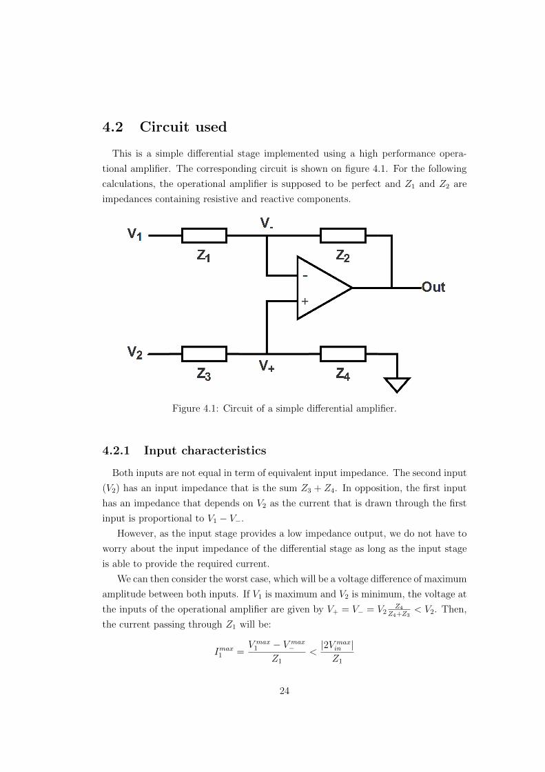
The frequency response of the di↵erential stage corresponds to our needs. As shown
in figure 4.5, the -3dB cut-o↵ frequency is around 180MHz and a small amplification
(<⇠1dB) is present from 20MHz to 150MHz. The amplification is the highest for a
frequency of 150MHz and is equal to 1.07dB which correspond to an increase of the
28
Figure 4.5: Ideal frequency response of the circuit output. The cut-o↵ frequency(-3dB) is above to 180MHz and a small 1dB resonance is noted at 150MHz.
voltage amplitude of 13% which is not problematic.
29

Chapter 5
Analog prototype
When a circuit has to be designed for high frequencies, there are several crucial
points to be considered compared to low frequencies. We can list some of them:
• A PCB track cannot be considered as ideal due to small parasitic capacitors,
resistors and inductors that have an influence on the circuit behavior.
• The circuit must be designed in the smallest possible size in order to avoid issues
arising from distributed circuit. If needed, the circuit could be considered as a
distributed circuit.
• The ground plane has to be designed di↵erently to stay as close as possible to
an unique potential.
In this chapter, we will first follow basic rules of high frequency design. Then,
we will analyzes the layout through a simulation using theoretical values of parasitic
elements. Finally, we will investigate the experimental results of our prototype.
5.1 First layout
The circuit we had to design does not use a lot of components. Moreover, the
operational amplifiers we are using are very small, which makes the design easier on
a small area. The circuit does not need to involve more than one layer. Because the
design is easier and better at high frequency, we will use a two layers design with the
second layer used as a ground plane.
The layout can be seen in figure 5.1. Both input stages are visible on the left of
figure, the red one is for the negative input and the blue is for the positive input. The
yellow part is the di↵erential stage. The five coaxial connectors used for both inputs
30

Figure 5.1: Layout of the prototype. In green, on the top, the positive supply. Inbrown, on the bottom, the negative supply. In yellow, on the middle right, thedi↵erential stage. In red and in blue, on the middle left, the two input stages. Thesize of the PCB is 64x67mm.
and the three outputs are also visible. In the gray part of the board, several vias are
used to connect both ground planes together.
The size of the board is 64x67mm. We use a FR4 board with a thickness of 1.6mm,
a track thickness of 35µm and a copper resistivity of 1.7 10�8⌦m.
5.1.1 Supply
The two types of operational amplifiers used for the circuit need two di↵erent
supplies. For both input stages, a ±5V supply is required whereas a ±12V supply is
31

required for the output1.
To be convenient, four linear voltage regulators are used. Two for both positive
supplies (5V and 12V) and two for both negative supplies (-5V and -12V). Each
supply was found to work very well with a global ±15V supply.
Decoupling capacitors (100nF) are placed as close as possible to each IC supply pin
to obtain a voltage as close as possible to a DC. In addition, electrolytic capacitors
and large (1µF) ceramic multilayer capacitors are placed on each side of each linear
regulator.
5.2 Simulation
To obtain a simulation as close as possible to reality, we have to quantify each
parasitic e↵ects that can play a role in the circuit. Our previous simulations already
took into account the characteristics of each specific operational amplifier we used.
5.2.1 PCB e↵ects
The wavelength at 100MHz is in the order of 3 meters, the board is small enough
to be considered as a discrete circuit. We are able to model each connection with its
parasitic elements[8]. As we use microstrip technology (cf. figure 5.2), we can model
each connection with a RLGC circuit as shown in figure 5.3 .
Figure 5.2: Microstrip structure representation. Same notation as for equations.(Figure from[8])
1The supply of the bu↵er is not ±6V because the corresponding regulators are not available onFarnell. The supply of the di↵erential does not need to exceed ±12V because the output voltage ismaintained in between ±8V.
32

Figure 5.3: Model used at low frequency to simulate the behavior of a track in amicrostrip structure. (Figure from[8])
C[pF/cm] =0.26(✏r + 1.41)
ln( 5.98 H0.8 W+T
)(5.1)
L[nH/cm] = 2 ln(5.98 H
0.8 W + T) (5.2)
R[⌦/m] = ⇢Cu1
W T(5.3)
In the latter, H is the thickness of the board, T and W are respectively the thickness
and the width of the copper track, ⇢Cu is the resistivity of the copper and ✏r is the
relative permittivity of the dielectric insulator.
The parallel conductance G representing the losses in the dielectric is high enough
to be neglected at our working frequency[8].
The parasitic capacitance of a line increases if either ✏r, the track width or the
track thickness increases and it decreases if board thickness increases. The parasitic
inductance will be influenced in opposition to the capacitance but without e↵ect of ✏r.
Finally, the resistance of the track is also influenced in opposition to the capacitance.
5.2.1.1 Skin e↵ect
The skin e↵ect will play a role at high frequency in first approximation when the
skin depth is smaller than half the thickness of the track. At 100MHz, one has:
�(100MHz) =
r2⇢Cu
2⇡108µCu
' 6.5µm <T
2
Where µCu is the permeability of the copper that can be considered as equal to µ0
33

We have an influence of the frequency due to the skin e↵ect on the e↵ective track
thickness. To take this into account, the track thickness is reduced to two times the
skin depth (13µm) in the equation 5.3.
5.2.1.2 Computation of parasitic values
A simple Matlab script is used to compute each parasitic parameter of the connec-
tion using the length and the width of each track.
The parasitic capacitance ranges from 0.5pF to 2.5pF, the parasitic inductance
ranges from 1.75nH to 4.7nF and the parasitic resistance ranges from 1.5m⌦ to 17m⌦.
5.2.2 Simulation results
With both stages and a dedicated parasitic model for each connection, the simulated
output remains very satisfying, as it can be observed in figure 5.4.
Figure 5.4: Simulation results with PCB track modeling, operational amplifier modeland transmission lines. Top graph is the expected di↵erential input, the center graphis the di↵erential input measured with the di↵erence of both bu↵ers outputs and thelast graph is the output of the circuit.
The output presents some overshoots of around 0.27V at each edge of the square
signal. Those are likely to be due to the very steep edge of the square signal, as it
was explained in section 4.4.2. The amplitude of those overshoots is smaller than
in the ideal case. When rising and falling times are increased to 40ns, the overshoot
amplitude decreases to a few mV, which is negligible and can be acceptable in practice.
34

The second graph of figure 5.4 represents the voltage di↵erence obtained using both
input stage outputs (Vin+ � Vin�). No overshoots are noticeable with the 10ns rising
and falling time of the square signal in this case. We can conclude that both input
stages do not su↵er from overshoots.
Figure 5.5: Frequency response of the output of the circuit with the final simulation.The cut-o↵ frequency (-3dB) is near to 148MHz. The initial gain is -14.03 dB and aresonance is noticeable at 60MHz with an attenuation of -12.41dB.
Figure 5.5 shows the simulated frequency response of the circuit. We have an
expected -14dB amplitude reduction due to the first stage voltage division by 5. A
small resonance at 60MHz with an attenuation of -12.41dB is visible. We can also
see that the attenuation is smaller in the range [30MHz 100MHz] than for smaller
frequencies.
5.3 Real board
As simulation results are encouraging for the layout that was described in the
section 5.1, the corresponding board was made and tested.
The PCB was printed and welded at the University of Liege. The final PCB can
be seen in figures 5.6 and 5.7.
5.3.1 Characterization
We will characterize some important features like the CMRR or the AC gain.
These characterizations will use a specified measurement configuration which will be
described for each measurement.
35

Figure 5.6: Side view of the prototype. The top layer was completely covered of tinto avoid oxidation of the copper, allowing easy change of components.
5.3.1.1 The CMRR in DC
We are going to measure the CMRR in DC which is defined as:
CMRRDC = 20 log10
✓ANM,DC
ACM,DC
◆(5.4)
To do that, we have to measure both the gain in normal mode and the gain in common
mode.
Measuring the gain in normal mode consists in measuring the output voltage in
DC when one input is set to the ground and the other is set to a DC voltage. This
procedure assumes that the common mode gain is very small compared to the the
normal mode gain. If it is not the case, we have to measure the normal mode gain
with a zero common mode voltage. This can be achieved if both inputs have equal
and opposite voltages.
The normal mode gains determined experimentally are respectively 0.20081 ' 0.2
when the voltage is applied to the non-inverting input and 0.199395 ' 0.2 when
the voltage is applied to the inverting input. This di↵erence of attenuation between
both input stages will inevitably impacts the CMRR as both input signals at the
di↵erential stage will be slightly di↵erent even if the signals at the input of the device
36

Figure 5.7: Top view of the prototype.
are equal to each other. For the CMRR computation, we will assume that the gain
is 0.2.
The configuration used for measuring the common mode gain is shown in figure
5.8.
The measurement is carried out for an input that goes from -15V to 15V. The
resulting output voltage is found to range in between -9mV and 9mV. The corre-
sponding input-output relation is shown in figure 5.9.
We can now find the gain in common mode by using the measurement results
plotted in figure 5.9. We will consider only the linear part of the relation. We have:
ACM,DC =�0.005377� 0.009334
12.787 + 11.481= �6.062 10�4
An we can easily compute the CMRR by:
CMRRDC = 20 log10
✓0.2
|� 6.062 10�4|
◆' 50dB
37

Figure 5.8: Connections used for the common mode rejection ratio measurement.
Figure 5.9: Input-output relation for the measurement of the CMRR.
The CMRR is found to be smaller than the one of a commercial instrumentation
amplifier. It is expected as a commercial instrumentation amplifier has a very precise
matching of its internal resistor and does not have a input divider. Nevertheless, this
CMRR is su�cient for the application.
5.3.1.2 The o↵set voltage
The o↵set voltage is the voltage that appears at the output of the circuit when
a zero voltage is applied on both inputs. Indeed, this o↵set voltage was already
measured during the measurement of the CMRR. As it can be seen in figure 5.9, the
output is not zero when both inputs are at zero voltage.
We have an o↵set voltage of 2.2mV which will result on the measurement of the
input with an error of 2.2mV * 5 = 11mV, which is small in comparison to the useful
range ([-15V, 15V]).
38

5.3.1.3 The input impedance
The equivalent input capacitance is too small to be measured precisely with the
equipment of the company or the university. Nevertheless, the capacitor c2 is a
precision (±5%) capacitor of 39pF resulting in a maximum capacitance of 41pF. We
have to add the capacitance of the track that is connected to the operational amplifier
input (⇠0.6pF) and the operational amplifier input equivalent capacitance (⇠2.5pF)
to be precise.
As the input divider is 5 (n), the input equivalent capacitance is equal to:
Cin = C1n� 1
n=
C2
n� 1
n� 1
n<
C2,Equiv.max
5pF = 8.82pF
In addition to this capacitance, we have to add the capacitance of the track that
goes from the coaxil connector to the divider which is around 0.4pF. Finally, the
evaluated input equivalent capacitance of this circuit is equal to around 9.2pF.
The equivalent resistance can be measured directly in DC. The equivalent input
resistance of the prototype is nearly 10M⌦.
5.3.1.4 The frequency response
We can measure the frequency response of the prototype using a high frequency
sinusoidal generator and a 200MHz oscilloscope.
Figure 5.10: Measured frequency response of the di↵erential output using the non-inverting input.
39

Figure 5.11: Measured frequency response of the non-inverting bu↵er output usingthe non-inverting input.
Figure 5.10 shows the frequency response of the di↵erential input using the non-
inverting input. The frequency response of the prototype is satisfying because the
-3dB cut o↵ frequency is around 130MHz.
Figure 5.11 shows the frequency response of the non-inverting bu↵er when the
non-inverting input is used. Again, the frequency response is satisfying as the -3dB
cut o↵ frequency is around 180MHz.
In both figures, a small amplification is visible but its magnitude is small and does
not hamper the spikes to be well detected.
5.4 Conclusion
The prototype that was created here above matches our project requirements. The
final analog PCB will be created using the same circuit and implemented in the same
way.
40

Chapter 6
Acquisition subsystem
As a computer based oscilloscope is used to acquire signals, the oscilloscope and
the computer are considered as part of the acquisition subsystem.
The choice of the oscilloscope will be discussed first. Then, we will see how the
program is working and how the interaction between both machines is managed.
Finally, we will go into the details of some specific points of the implementation.
6.1 The oscilloscope
We must determine the specifications needed for our oscilloscope and choose care-
fully the device based on the following requirements:
1. A bandwidth bigger or equal to 100MHz.
2. At least two inputs. One for the PUT and one for the di↵erential signal. If we
have a third input, we can use it to measure the supply pin voltage. If not, we
can determine the supply pin signal by using the two other signals.
3. The oscilloscope must have a substantial SDK (Software Development Kit) al-
lowing the user to control almost everything directly in a program running on
the computer.
4. The price should be reasonable to obtain a final project that can be extended
easily to other sites.
6.1.1 Choice
The Picoscope 2000 series matches exactly the specifications that were listed here-
inabove. There are two models that could be used, namely the 2207A (100MHz) and
41

the 2208A (200MHz). Only the bandwidth (and obviously, the price) di↵ers from one
to the other. As the price di↵erence is not significant, the 2208A is used here. It can
be noticed that new versions of the Picoscope 2000 series have been released in May
20161.
The 2208A can be easily programmed in C. This allows the use of C++ which is
a languages commonly used within the company.
6.2 Computer program
The personal computers of all engineers within company are running on Windows.
It was required to create a program that runs on this operating system. To do so,
the Qt software and its libraries have been used. Qt o↵ers the possibility to create
fast simple interfaces in C++, which are useful to display information that must be
transmitted to the engineer.
6.2.1 What does the program have to do?
There are several tasks that have to be carried out by the code running on the
computer. We will list them and show them on a state diagram to explain how they
interact between each other in section 6.3.
6.2.1.1 Communication with the oscilloscope
The SDK provided by Picoscope can be used to control all parameters related to
the oscilloscope. A large number of functions coded in C are available to start and
run the oscilloscope, set the channels, set the trigger, set the timebase, etc.
In our case, we want to be informed when a waveform is captured to localize the
source of this event in the code. This requires the creation of one thread only used to
wait for a waveform to be captured. This solution induces a small time delay after the
acquisition of a waveform in which the oscilloscope cannot acquire a new waveform
as the previous one is always stored in its own memory.
Unfortunately, we cannot use a specific mode of the oscilloscope called the ”rapid
block mode” in which the oscilloscope collects waveforms without the computer. The
reason is that the rapid block mode does not allow us to recover the time of each
waveform acquisition. In this mode, we can only know when the memory of the oscil-
loscope is full of waveforms without information about each capture independently.
1There is no SDK available at the writing time for the new versions of the scope and the 200MHzmodel is now no longer available.
42

The oscilloscope o↵ers the possibility to use complex triggers, i.e. trigger on several
conditions at the same time. This is useful because we need to detect negative or
positive spikes. For example, a first one could be set on a falling edge of the PUT
with a threshold at -1V to detect a negative spike and a second one could be set on
a rising edge of the di↵erential signal with a threshold of +1V to detect a positive
spike.
6.2.1.2 Interface with the the user
The interface with the user has three main tasks which are:
1. To allow the user to set the timebase, the triggers and several other options.
2. To keep the user informed about what is currently running on its personal
computer.
3. To display the waveforms acquired by the oscilloscope at the end of the process.
The program will start with two windows: the ”parameter window” which is used
to perform the first main task and the ”information window” which will be displayed
until the end of the program to keep the user advised. Once the user finished the
setting of the acquisition parameters, the acquisition will begin. The acquisition will
end when all tests are finished.
After the end of the acquisition, the ”display window” will appear to display the
waveforms that were captured during the acquisition, if any. This window allows the
user to inspect each capture and gives him the supposed location of the waveform in
the code.
When the display window is closed, the parameter window will be displayed again
to start another analysis. The program will be closed if the parameter window is
closed.
6.2.1.3 Communication with the test machine
The TCP/IP protocol is used to communicate with the test machine. The per-
sonal computer of the engineer will play the role of the server and the test machine
will connect itself to this server. The personal computer is chosen to be the server
because the tester has only the g++ 98 compiler which o↵ers less facilities for the
implementation of a server than Qt.
43

To connect both machines, only the IP and the port used by the server have to
be given to the test machine. The data transmission will always be initiated in a
specific command. For example, to synchronize both machines, we will start with a
specific command and then, send the useful information. Since the data that has to
be transferred between both machines is small, we do not need to have something
more e�cient with the command incorporated into a specific structure for example.
6.2.1.4 User facilities
The user will start several times the analysis of the test to try di↵erent parameters
or to test several pins. The program must o↵er the possibility for the user to restart
directly an acquisition with the same parameters after he finished with the previous
one.
In addition, the program has to run directly on Window through a ”.exe” file
allowing the user to directly run the program without any specific software pre-
installed on his computer.
6.3 State diagram of the program
A simple state diagram is shown in figure 6.1. This diagram shows how the program
is working on both machines and how they interact together.
When the program is started, the parameter window and the status window pop
up. These two windows are visible in figure 6.2 and 6.3.
The user has the possibility to use the program in synchronous or in asynchronous
mode. In asynchronous mode, the oscilloscope starts the acquisition directly for a
given number of seconds that can be set in the parameter window. At the end of
the acquisition, the captured waveforms are displayed on the display window. When
the user closes the display window, the parameter window appears on the screen to
restart an acquisition, if needed. The previous parameters are preserved to improve
the e�ciency of the process.
44

Figure 6.1: Global state diagram representing both machines and the interactionsbetween them.
6.3.1 The TCP/synchronous mode
In TCP or synchronous mode, the program waits for a connection to start the
acquisition. The tester has to initiate this connection to start the acquisition. When
the acquisition is e↵ective, the computer sends a message to the tester to start the
sequence of tests.
At the end of each test, the tester must store its own clock to obtain, at the end, a
table of times representing all the tests. Throughout the acquisition, the computer do
the same than the tester for each captured waveform. When the last test is finished,
the tester reports it to the computer to end the acquisition.
45

Figure 6.2: Parameter window when the program is lunched on the personal computerof the user.
When the acquisition is e↵ectively stopped, the tester receives a command coming
from the computer to send the data needed for the synchronization. The time table of
all tests is sent to the computer and both machines start synchronizing their clocks.
The synchronization of both clocks is needed because the two clocks are di↵erent and
then the two time tables do not have the same time base. The procedure used to
synchronize both clocks will be discussed hereafter.
When the whole data is sent, the tester can close the test program and the com-
puter starts a classification of each waveform based on both arrays of times. How the
computer classifies each waveform will be discussed in section 6.4.3. Finally, the com-
puter displays all waveforms though the display window and the parameter window
reappears when the display window is closed, in the same way as for the asynchronous
mode.
6.4 Synchronization of clocks
To obtain a precise localization of spikes in the code, we have to synchronize both
clocks. We will assume here that one clock is shifted in time in comparison to the
46

Figure 6.3: Status window when the program is waiting for a connection with thetester.
other and both clocks share exactly the same time unit2. We can then link the time
of the client (tc) and the time of the server (ts) with:
tc = ts +�t (6.1)
The objective here is to estimate correctly the o↵set �t existing between both
clocks. When this o↵set is known, it is easy to calculate the equivalent time on one
machine in reference to the other.
The objective is to achieve a synchronization smaller than the duration of the usual
smallest test provided by the tester, which is about 15-20ms. Even if the detection
can only have synchronization of this order, the engineer will have a good estimation
of where the error comes from. He/she can be helped by the shape of the waveforms
that are captured by the oscilloscope to localize it precisely.
The TCP/IP protocol does not provide a stable propagation delay. The delay can
vary form 1ms to hundreds of ms depending on the size of the packet sent and the
network on which the packet is sent. This variable delay must be taken into account
to synchronize the events.
Figure 6.4 shows how a transmission between the two machines works in the point
of view of the propagation delay. We supposed that the client sends a packet to the
server and the server replies to the client immediately.
There exists a propagation delay for the first message sent by the client before
being received by the server (Tp1) and a second propagation delay for the message
2One second delay on both machines are equals.
47

send by the server to the client (Tp2). Those two delays are di↵erent but nevertheless
close due to the fact both messages are sent nearly at the same time, which implies
that the state of the network should nearly be the same. We will assume for the
following that Tp1 and Tp2 are nearly equal to �t.
Figure 6.4: TCP/IP time line for a client-server transmission.
6.4.1 Mechanism of synchronization
To synchronize both machines, we will send the personal time of the client Tc to
the server. The time equivalent to Tc on the server side is Ts. The server will receive
this information at a time Ts + Tp1 ' Ts + �t due to the propagation time on the
network. This time is stored by the computer and is sent back to the client. When
the client receives the time Tc, its own time is equals to Tc + Tp1 + Tp2 ' Tc + 2 �t.
The client is then able to evaluate �t.
The client will send this value to the server. The server can use the evaluated �t
to obtain Ts with the time Ts+ �t which was previously stored. Thanks to Ts, we can
evaluate the o↵set �t existing between both clocks by computing Tc � Ts ' �t.
6.4.2 Estimator of �t
The variability of the propagation time is non negligible. For example, the table
6.1 shows the results of ten measurements of the propagation delay carried out on a
local network with the mechanism explained above.
As can be seen on this table, there is a significant variance in the estimation of
the propagation delay we have. From the first iteration to the second one (9324µs to
576µs), we have more than one order of variation. In some cases, this variation can
even be bigger than 100ms.
48

i 1 2 3 4 5 6 7 8 9 10�ti (µs) 9324 576 1132 934 5704 1391 1019 992 858 5172
Table 6.1: Ten measurements of the propagation delay carried out directly one afterthe other
The propagation delays that are very large could induce errors because they could
have been induced by one busy machine. For example, if the server is busy, Tp1 could
be bigger than Tp2 resulting on a poor evaluation of the delay Tp1 6= �t and as a
consequence, a poor evaluation of the corresponding o↵set �t. One simple solution
is to remove outliers from our estimator. We can, for example, remove measurements
that have a propagation delay larger than a given multiple of the smallest measured
propagation delay.
Once the outliers (iout) are removed from our data, n evaluations �ti remain. We
can compute the mean of each �ti and our estimator will be:
�t =i 6=i
outX �tin
We will assume that our n �ti estimator are independent and are identically dis-
tributed random variables (Independent and identically distributed random variables
hypothesis)[19]. We can then characterize the distribution from which our random
variables come from with:
E (�ti) = µ V ar (�ti) = �2
µ is the expectation of the random variable and � is its standard deviation.
In the case of an averaging, the expectation of the averaging is equal to the initial
random variable expectation. But the variance of our estimator is divided by the
number of elements used for the averaging: V ar (�t) = �2
n.
This last relation shows that the standard deviation is reduced by a factorpn
and confirms that the accuracy of the estimator will increase with the number of
measurements n.
The variance of our estimator is a good indicator of the performance of our synchro-
nization mechanism. We can try to fix the limit that determines if a measurement
is an outlier or not. With some tests, the best results are obtained when the limit
is fixed at twice the value of the smallest propagation time. We can also evaluate
49

the influence of the number of measurements. 10 measurements are found to give
acceptable results. As the synchronization has to be as fast as possible, we will carry
out 10 measurements as default for the synchronization (< 1s).
With 10 measurements, the variance is nearly always smaller than 2ms which is
much smaller than the shortest test provided by the tester (15-20ms). This informa-
tion will be visible on the display window to keep the engineer informed about the
reliability of the synchronization.
6.4.3 Test localization
We will suppose in what follows that the server and the client times are related to
the server time since epoch3.
To localize the test which was the source of a spike, the computer has the spike
trigger time and a array of time representing all tests. The display window will give
as output a number representing the test (The test ID) as shown in figure 6.5.
Figure 6.5: Representation of the value of the test given by the computer for eachpossible time interval. In blue are the numbers representing each interval and eachvertical line represents a time of the array of test time.
If the program has an acquisition triggered before the first time of the array, it will
give to this capture the reference 0. If it occurs between the first and the second time
of the array, the reference of the capture will be 1 and so on. If a capture takes place
after the last time of the array, the reference will become -1.
This classification can be used by the engineer to detect if a spike occurs before
the first test and after the last one. To do so, the user just has to put its first own
current time before the beginning of the sequence of tests and every time after each
test. Then, a capture occurring in the test sequence part number zero will refer to a
3January 1, 1970
50

spike occurring before the first test and similarly, a spike occurring after the end of
the test sequence will have a capture with a reference ”-1”.
6.4.3.1 Link between the test name and its reference
A simple number will not be intuitive for the engineer as a list of one hundred tests
could be available on the screen. For better clarity, a simple list can be displayed on
the tester screen with each test name and each associated test ID.
6.5 Storage of the information in a file
The program provides a storage of each waveform in a .txt file if the user selects
the appropriate box in the parameter window. All measurement points are present
for both channels as well as the time of the capture and the test ID.
This information can be used to do other processes that are not done by the
program itself. The format of the file is easy to read and a small Matlab function is
available to show a simple extraction of the information from these files.
The files are always stored in the same directory of the personal computer, which
is: home/PICO OUT/Waveforms. If the directory does not exist, the program will
create it.
6.6 Additional code on the tester
On the tester side, the code is much simpler than on the computer side and is easy
to integrate for a test engineer even if he does not know how the whole process is
working. The engineer needs only four functions which are:
1. connection initialization
2. add a time us
3. display name console
4. finalize connection
All of these functions are only using three static variables which are two C++
vectors and an integer. The first vector contains each time corresponding to each test
and the second vector contains the name of this test. The integer contains the socket
reference (UNIX file descriptor) which is used for the connection.
51
6.6.1 The connection initialization function
The function connection initialization is used to initialize the connection, as the
name suggests.
The function can be called with di↵erent argument types depending on what
the user wants to do. This uses function overloading and means that the C++
compiler will recognize and di↵erentiate two di↵erent calls of a function by matching
the argument types with the definitions of the di↵erent functions.
Without arguments, the function will pop up a window on the tester before the
test sequence to ask the IP of the computer. The IP address of the computer can
also be determined directly as an argument with a simple array of integers.
In the two latter cases, the user has the possibility to change the port of the
connection with an integer. This argument is optional, which means that a default
value is used if the argument is not present. This default value is 3980, which is
also the default value of the port used by the computer when the server is created.
Generally, the port must not be changed and the function has to be called only
without argument or with one array of integers4.
6.6.2 The add a time us function
The function add a time us is a simple function used to add an element to both
vectors. The current time since epoch of the machine is pushed back in the first
vector and the name of the test is pushed back to the other vector. The name of the
test has to be send as an argument of the function.
The function has an optional Boolean argument that can be used to resize both
vectors to zero. This could be useful if the test program is restarted several times.
This function must be called at the end of each test to allow the synchronization.
If the function is not added at the end of each test, the synchronization will suppose
that all tests in between the last and the next call of the function add a time us are
part of a same test. One can segment a test in several parts using this simple function
if a better precision about where a spike occurs within a test is needed.
6.6.3 The display name console function
The function display name console has to be used before the finalization of the TCP
connection. The function will display the names of the tests and the corresponding
4An IP address is represented by 4 numbers separated by points. These 4 numbers have to beplaced in an array of integers if the user does not want a pop up window asking the IP.
52

IDs of the tests. The user can easily obtain the name of the test which induces a
spike with this list. This function takes no arguments.
6.6.4 The finalize connection function
The function finalize connection transfers the information contained in the time
vector to the computer and realizes the synchronization of both clocks.
The function used the connection established with the computer in the function
connection initialization. The function has an optional argument that represent the
number of synchronization procedures that the user want to realize5. The default
value of this argument is 10 which is a trade-o↵ between a good precision and a fast
synchronization.
6.6.5 A simple code on the tester
A simple way to implement the code on the tester side could be:
c o n n e c t i o n i n i t i a l i z a t i o n ( ) ;
// I n i t i a l i z e the t e s t s e s s i o n. . .// End o f the i n i t i a l i z a t i o n
add a t ime us (” i n i tT e s t ” , t rue ) ;f o r ( i n t i = 0 ; i < number o f t e s t ; ++i ){
// Run o f the t e s t number i. . .// End o f the t e s t number i
add a t ime us (” Test named i ” ) ;}
d i sp l ay name conso l e ( ) ;f i n a l i z e c o n n e c t i o n ( ) ;
6.7 The display window
The display window is used to show the acquired waveforms to the user. This
window allows the user to navigate between the di↵erent captures and indicates the
5The number of times that the mechanism explained in the section 6.4 will be realized to syn-chronize both clocks.
53

source of a spike through the test ID.
The user is also aware of important information like the calculated standard de-
viation of the synchronization estimator used to determine the test ID or the average
propagation time of the network. Thanks to this information, one can stay critical
about the truthfulness of the synchronization. A print screen of the display window
is available in figure 6.6.
Figure 6.6: Display window used to show captures of the device. The two top buttonsare used to change the capture. The number at the right of both buttons representsthe number of waveforms going from zero to the number of waveforms acquired. Justat the right of these, we have two text boxes. The first one indicates in which test thecapture is supposed to be (The test ID), the duration of this test and the supposedtime from the beginning of the test to the capture. The second one indicates thesupposed synchronization delay (�t) between both machines, the standard deviationof the delay estimator and the mean computed propagation delay. At the top right,a slider allows the user to realize a vertical zoom or unzoom. The window supportsmoving and zooming with the mouse.
54
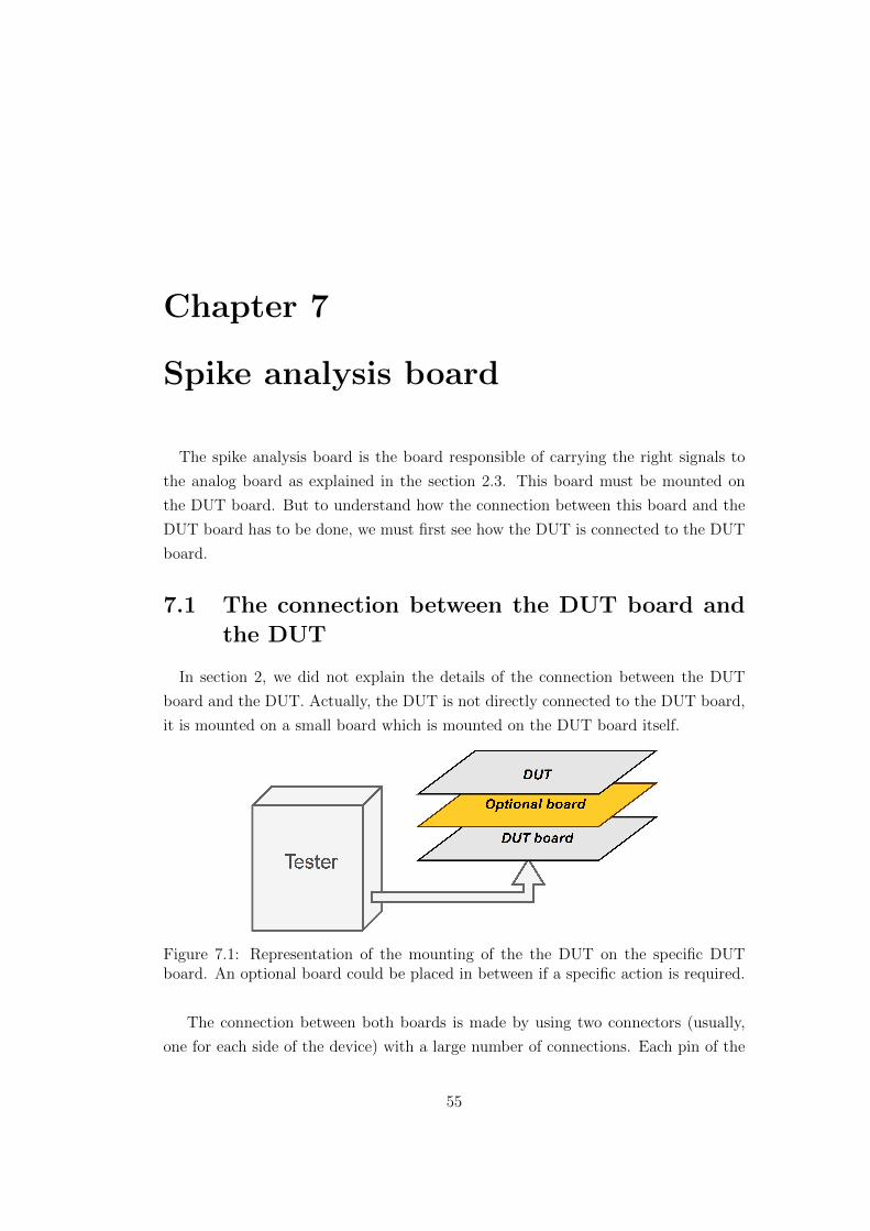
Chapter 7
Spike analysis board
The spike analysis board is the board responsible of carrying the right signals to
the analog board as explained in the section 2.3. This board must be mounted on
the DUT board. But to understand how the connection between this board and the
DUT board has to be done, we must first see how the DUT is connected to the DUT
board.
7.1 The connection between the DUT board andthe DUT
In section 2, we did not explain the details of the connection between the DUT
board and the DUT. Actually, the DUT is not directly connected to the DUT board,
it is mounted on a small board which is mounted on the DUT board itself.
Figure 7.1: Representation of the mounting of the the DUT on the specific DUTboard. An optional board could be placed in between if a specific action is required.
The connection between both boards is made by using two connectors (usually,
one for each side of the device) with a large number of connections. Each pin of the
55

DUT is directly connected to its corresponding connector pin, which means that each
signal passing through the connector is one signal sent to the DUT.
This allows the engineer to design any board useful to realize a required role as
long as each DUT pin stays connected to its dedicated connector pin. Schematically,
the configuration looks like a stack of boards as represented in figure 7.1. For example,
an optional board was created by another student, doing its master thesis last year,
to connect di↵erent specific resistors to a selected pin of the device.
7.1.1 The spike analysis board and the analog board
The choice that was made to split the work in two di↵erent boards comes first from
the connectors. Indeed, there are several types of connectors used but two are the
most common: the first with 50 connections for large pin number devices and the
second one with 20 connections for smaller packages. This induces that the optional
board, which fits in between the DUT board and the DUT, has to be di↵erent for
those two common connectors.
By contrast, the analog board remains the same if the supply voltage of the DUT
is the same. Thus, it will be a waste to incorporate the analog board directly on the
spike analysis board.
7.1.1.1 Note about the connectors
In fact, the most used connector is the smaller one which is physically composed
of two 10 connectors. The division in two connectors is essentially for convenience:
one is used for the left pins and one is used for right pins for the device. All other
connectors are also divided in two for the same reason. The smaller connectors are
used for 4, 8 and 16 pin devices.
Because our device has to work with the common projects of the company, we will
design a board for the 20 connectors that could be used for 4, 8 and 16 pin devices.
7.2 Specifications needed for the spike analysis board
Our optional board has to:
• Be modular to work with several projects.
• Fit with our 100MHz bandwidth as much as possible.
• Allow the engineer to change rapidly the pin he is currently testing.
56

• Use no more than the resource brought by the Mbed LPC1768 microcontroller.
• Work with 4, 8 and 16 pin devices.
7.3 Influence of the track impedance
To fit our bandwidth of 100MHz as much as possible, we have to be sure that the
signal received by the analog board is not too much modified. To analyze this issue,
we will model the board in the same way as it was done in the section 5.2.11.
Figure 7.2: Equivalent circuit of the spike analysis board seen from its input.
Figure 7.2 shows the equivalent circuitry of the board. VS, the voltage of the
signal the user wants to measure, RS, the equivalent resistance of the track plus
the equivalent resistance of the source, Cl and L the equivalent capacitance and
inductance of the track and finally Cin, Rin and Vin are respectively the equivalent
capacitance and resistance of the analog board2 and the voltage seen by the analog
board.
We will see what are the variations of the transfer function of the board (Vin
regarding to VS) with respect to parameters of the circuit.
7.3.1 Assumption
We will assume that we are dealing with frequencies larger or equal to 10MHz. In
addition, we will suppose that the paths could be modelled with a discrete circuit
which is only valid for a frequency[8]:
fvalid <1
10
rcc
lmax
1The size of the board will stay small enough to be considered as a discrete circuit.2equivalent to the input impedance of the input stage.
57

Where rc is the velocity factor of the polyethylene used as insulating material (' 0.66),
c is the speed of the light and lmax is the largest track length. By taking a maximum
track length of 10cm, one obtains a upper frequency limit of around 200MHz .
7.3.1.1 Input impedance
The input impedance of the analog board is equivalent to a capacitor in the order
of the pF in parallel to a resistor in the order of 10M⌦. We have:
Zin(!) = Cin//Rin
=Rin
1 + j!CinRin
The frequency at which the capacitor has a bigger e↵ect on the input than the
resistor is fin = 12⇡ C
in
Rin
. If one takes 1pF and 10M⌦ as equivalent input impedance:
fin =1
2⇡ 10�12107' 16kHz
Because we are dealing with much larger frequencies, we can assume that the
input impedance of the analog board is only capacitive. The final equivalent circuit
at high frequency is given in figure 7.3.
Figure 7.3: Equivalent simplified circuit of the spike analysis board seen from theinput of this one at high frequency (f >> fin).
Zin(!) '1
j!Cin
if!
2⇡>> fin
To obtain a final result analytically, we will simplify progressively our equations
during the computation. This will help use creating guidelines that could be useful to
improve our circuit even if the analytical result is not perfectly correct. After studying
analytically the circuit, a LTspice simulation will be used to check our results.
58

7.3.2 Transfer functionVin
VS, determined analytically
By using the same notations as in figure 7.3, we have:(Vin = V1
Zin
Zin
+ZL
V1 = VSZC
//(ZL
+Zin
)R
S
+ZC
//(ZL
+Zin
)
ZC//(ZL + Zin) =1
j!Cl +j!C
in
1�!2LCin
(7.1)
=1� !2LCin
j!(Cl + Cin)� j!3ClCinL(7.2)
The denominator of the equation 7.2 can be simplified to j!(Cl + Cin) if the
pulsation satisfies:
!2ClCinL < (Cl + Cin)
! <
rCl + Cin
ClCinL
Let us take some typical values: Cl = 10pF , Cin = 8pF 3 and L = 10nH. Then,
the in-equation is verified if f <q
Cl
+Cin
Cl
Cin
L/2⇡ ' 750MHz.
Thanks to this simplification of the equation 7.2, we have:
V1 = VS1� !2CinL
1 + j!(Cl + Cin)RS � !2LCin
(7.3)
! Vin = VS1� !2CinL
1 + j!(Cl + Cin)RS � !2LCin
1
1� !2CinL(7.4)
= VS1
1 + j!(Cl + Cin)RS � !2LCin
(7.5)
= VS1
CinL
11
Cin
L+ j! (C
l
+Cin
)RS
Cin
L+ (j!)2
(7.6)
We can compute the roots of the denominator of the equation 7.6. We have:
⇢ =
✓(Cl + Cin)RS
CinL
◆2
� 4
CinL(7.7)
If ⇢ is negative, we will have complex conjugate roots and an equation similar to a
second order filter. ⇢ is e↵ectively negative if: RS <q
4LCin
(Cl
+Cin
)2 which is equivalent to
RS < 31⌦ (With the same typical values).
3Note that the input impedance of the analog board can be smaller as explained in the section3.4.3. As a reminder, the equivalent input impedance of the prototype is around 10M⌦//8pF.
59

This means that the circuit will not act as a second order filter if the source
equivalent resistance is too large and therefore, will not have a resonance that could
be encountered with a second order filter.
As our goal is to detect spikes that could induce damages to a device, we will
suppose that this equivalent resistance is small enough to have a negative ⇢. Conse-
quently, we will have two complex conjugate poles[3] and our initial equation 7.6 can
be rewritten:
p, p⇤ =� (C
l
+Cin
)RS
Cin
L±p⇢
2(7.8)
! Vin
VS
=1
CinL
1
(j! � p)(j! � p⇤) (7.9)
=1
CinL
1
(j!)2 � 2Re(p) j! + abs(p)2(7.10)
Exact values of poles are not useful for us, there are two important things: (i) the
frequency resonance and (ii) the damping factor of this filter. By comparison of the
equation 7.6 and the general equation of a second order filter given hereafter, we can
deduce these two values.
H(j!) =!20
(j!)2 + 2⇣!0(j!) + !20
!!0 =1p
LCin
(7.11)
!⇣ =(Cl + Cin)RS
2pLCin
(7.12)
With the same typical values4, one obtains: f0 = !0/2⇡ ' 560MHz and ⇣ ' 0.32.
These values have to be considered with caution because of the strong hypothesis we
have made to obtain 7.11 and 7.12. The circuit cannot be considered as discrete at
the resonant frequency f0 if the length of the track exceeds lmax = 110
rc
cf0
' 4cm.
In spite of the above assumptions, these results could be very useful to establish
di↵erent guidelines. The resonance frequency only depends on the inductive param-
eter of our track and the input capacitance of our analog board. The damping ratio
depends on the source equivalent resistance and the track capacitance parameter in
addition to the inductive parameter of our track and the input capacitance of our
analog board.
4Rs is supposed to be equal to 10⌦.
60

7.3.3 Simulation of the transfer functionVin
VS
We will use LTspice to simulate the spike analysis board in discrete circuit using the
same model as in figure 7.2. We will use the LTspice model created for the prototype
to analyze the input stage in place of the simple equivalent circuit we used in the
analytical development.
Figure 7.4: Simulated bode diagram of the input bu↵er with the spike analysis boardmodel and the prototype model. RS = 10, Cl = 10pF, L = 10nF, Cin ' 8pF andRin ' 10M⌦.
Figure 7.4 shows the frequency response of the bu↵er. A resonance is visible at
'560MHz like it was the case analytically. This resonance is quite large as the peak
has a magnitude of -5.6dB when the initial gain is -14dB.
There are a lot of cases that could be explored here to see the influence of each
parameter of the model. We will illustrate results obtained in di↵erent cases in the
table hereafter (cf. table 7.1). The table compares what is obtained in simulation to
the analytical formula.
Globally, the trend of the simulation results are similar to the analytical results
for the resonant frequency. On the other side, the damping ratio (⇣) di↵ers. This is
obviously due to the simplification that was made during the analytic development
which are not valid for such high frequencies.
Determining how to avoid an undesirable resonance at high frequency is a di�cult
task. But from the results summarized in table 7.1, we can learn that the influence
of the parasitic capacitance of the track has a smaller influence than the parasitic
61

RS(⌦) Cl(pF) L(nH) Cin(pF) f0(MHz) ⇣ f simu0 (MHz) ⇣simu peak(dB)
1 10 10 8 562 0.032 562 0.014 13.455 10 10 8 562 0.16 562 0.064 -0.410 10 10 8 562 0.32 562 0.12 -5.620 10 10 8 562 0.64 NP NP NP10 20 10 8 562 0.49 581 0.10 -610 10 20 8 398 0.225 396 0.10 -2.4210 10 10 2 1125 0.424 1248 0.046 -610 20 20 2 795 0.55 871 0.021 3.26
Table 7.1: Results of simulations of the spike analysis board and the input bu↵er.(NP means No Peak)
inductance of the track whether on the resonance frequency or the magnitude of the
associated peak. The e↵ect of the equivalent source resistance on the magnitude of
the resonance is clearly significant but we do not have any control on this parameter.
7.3.4 Conclusions
The previous sections show how di�cult it is to model a simple track at high
frequency. The simple development that was exposed above is very restrictive. The
circuit is supposed to consist of lumped elements and assume that the length of the
track is kept very small (<4cm). This means that the whole set of results obtained
in simulation and summarized in the table 7.1 are not longer valid if we consider a
much longer track (10cm5 for example).
In the following, we will try to keep the inductive parameter and the length of
the track as small as possible. The track inductance can be reduced by reducing the
distance between the track and the ground plane (see equation 5.2). Reducing this
distance will increase the track capacitance (see equation 5.1) but the influence of the
capacitance seems to have less impact than the track inductance. In addition, we will
reduce the equivalent input capacitance of the final analog board as much as possible.
As explained in section 3.4.3, this capacitance can be reduced in comparison to that
of the prototype.
5The corresponding upper frequency limit is 200MHz.
62

7.4 Practical realization of the PCB
The PCB was routed using Altium software. The board has four layers, which
allows us to reduce the distance from the signal tracks to the ground plane and so
reduce the track inductance.
The four layers of the board are arranged as shown in figure 7.5. As can be seen,
we placed components on both sides of the board to reduce as much as possible its
size. Nearly all components we use on this project are SMD.
The first inner layer of the board is a ground plane. The top and the second inner
layer are used for high frequency signals as they are very close to our ground plane.
The bottom layer is not used for high frequency signal since the ground plane is a little
bit further. This layer is used for low frequency connections. The remained surface
in the top and the bottom layers is connected to ground. The remained surface of
the second inner layer is connected to the supply voltage (5V).
Figure 7.5: Cross section representation of the four di↵erent layers of the spike analysisboard. There are components on both sides of the board. The top layer is a highfrequency signal layer as well as the second inner layer. The first inner layer is aground plane which is only broken by vias. The bottom layer is a layer used forlow frequency. The remaining area of the top and bottom layer is connected to theground. The remaining area of the second inner layer is connected to 5V.
7.4.1 Operating principle
The board use a Mbed LPC1768 microcontroller to control a set of relays that are
used to connect the PUT to the analog board. The use of a set of relays for the
connection of the PUT leads us to use a bigger surface than the surface of an array of
DIP mechanical switches for example. However, they are needed to allow the engineer
to change rapidly the PUT.
63
On the other side, the supply and the ground pin of the device stay the same for a
given device. Thus, to decrease the overal volume, DIP mechanical switches are used
to connect the ground pin and the supply pin.
7.4.1.1 Driving the relays
We had several possibilities to drive relays of the board. Typically, Melexis engi-
neers use some PCF8574 chips which are ’remote 8-Bit I/O expanders for i2c bus’6.
This procedure has the advantage to use only a i2c bus to drive relays and then reduce
the amount of track needed. But this solution could lead to errors because we can
activate every relay independently and connect several pins to each other.
A much simpler solution is to use simple demultiplexers. Indeed, with demulti-
plexers, we cannot activate several relays at the same time. Therefore, we cannot
short circuit several pins. In addition, the program to be run on the Mbed microcon-
troller becomes very simple as only digital outputs are needed, unlike using i2c. In
practice 3 to 9 demultiplexers will be used here to drive the whole set of relays.
Melexis provides devices with a maximum number of 64 pins. This implies that
we will need two layers of demultiplexers to control the corresponding set of relays.
The relay control design is shown schematically in figure 7.6.
The design is composed of two stages of demultiplexers. The first involves one
demultiplexer - called ”the father” - that is always activated and controls the activa-
tion of the demultiplexers of the second stage - called ”the sons” . Only one son is
activated at a time and can close one of its 8 relays. The control is made through
6 digital outputs of the Mbed, the three most significant bits are connected to the
father to choose the corresponding son. The three least significant bits are connected
to every son to choose one specific relay. In this way, 6 digital outputs of the Mbed
can be used as the 6 bits of the control.
The relays selected are those commonly used in the company: the pickering 112-1-
A-5/2D driven with 5V. The circuitry used to control the relays is essentially printed
on the PCB bottom layer since the frequency of these signals is very low (The PUT
is changed in between each test sequence only).
7.4.1.2 Driving the demultiplexers
The multiplexer/demultiplexer model we will use here is the 74HC4051 from NXP.
This model can be used with supply going from 2V to 10V[17]. However, the ON
6The device is controlled via i2c to control 8 pins that can be set to ground or supply.
64

Figure 7.6: Block representation of the relay control principle. Two stages of demulti-plexers are used. The first stage is composed of one demultiplexer called ”the father”that takes the 3 most significant bits into account and activates the correspondingdemultiplexer of the second stage. Second stage relays are called ”the sons” and areonly activated by the father. They take the three least significant bits and activatethe corresponding relay (only if they are activated by the father).
resistance decreases if the supply is bigger which means that it will be better for us
to use the largest supply we can.
We have two possibilities for the supply of the board: (i) the 5V provided by
the USB connected to the board or (ii) the 3.3V provided by the Mbed. As the ON
resistance of the demultiplexer will become smaller with the 5V supply, we choose
the supply provided by the USB.
The problem related to this choice is the control of the demultiplexers with the
3.3V logic outputs of the Mbed . This issue is solved by using a simple voltage shift
circuit for each output of the Mbed. This circuit can be seen in figure 7.7. A BS170
n-channel transistor is chosen here due to its small gate threshold voltage of 2.1V
(max. 3V), perfectly suitable to be used with 3.3V devices.
65

Figure 7.7: Circuit used to shift the voltage from the 3.3 output of the Mbed to the5V logical input of the demultiplexer.
The circuit operating principle is simple: when the Mbed output is high, the
transistor is ON and the output voltage is zero, when the transistor is OFF, the
output voltage is 5V. The Riso resistance has no real utility except protecting the
Mbed pin from an error of connection that could create a short circuit.
7.4.2 Communication with the tester
The Mbed microcontroller has a micro-USB plug already installed on its body that
could be used to communicate with the tester but we will not use it. Indeed, to use
this USB, a driver would have to be installed on the tester, which is not possible since
the device we are creating must work on every tester on di↵erent sites of the company
and no change on the tester is allowed7.
Instead, a serial connection will be used on the Mbed microcontroller and a serial
to USB component will be used to transfer the information to the tester via USB.
Then, the tester can send directly the needed information via USB to the spike
analysis board. The device used to do that is a FT232R ”USB to serial UART
interface”. This circuit is often used by engineers within the company.
7Uploads of the tester software are uncommon in view of the time it might take for upgrading alltesters of all sites.
66

7.5 Mbed microcontroller code
The embedded Mbed microcontroller code has to be convenient for the user. The
user must have the possibility to choose the number of pins of the device as well as
defining the ground pin and the supply pin through the tester directly. After this
small initialization process, the user has the possibility to choose the PUT.
Figure 7.8: State diagram of the program running on the Mbed microcontroller withthe corresponding communication with the tester.
The program working process is summarized with a state diagram in figure 7.8.
Once the Mbed is powered, the board will activate all relays one by one to allow the
engineer to check if all relays are working. This can be done by simply hearing the
switching of each relay.
After that, the Mbed will wait for an initialization and set its own parameters
which are the number of pins, the ground pin and the supply pin of the DUT. Once
67

the parameters are received, the Mbed will be aware of the DUT and will change its
own mapping between pin and relay8 to activate the right relay when a PUT will be
asked.
After the initialization, the Mbed waits for a change of the PUT. The tester has
also the possibility to initiate a new parameter initialization if needed. This allows
the user to use the Mbed for di↵erent devices without restarting it.
At each action realized by the Mbed, there is a return message that is printed on
the console of the tester to inform the user about the state of the Mbed.
7.5.1 Corresponding code on the tester
On the tester side, the corresponding program starts by asking what are the number
of pins, the ground pin and the supply pin of the device to send the information to
the Mbed. Then, the program asks to the user the PUT and changes the connection
by communicating with the Mbed. Finally, one can start the test sequence as many
times needed and one can switch to another pin in between each test sequence if
asked.
The Mbed program will take care of a new initialization so that the engineer can
restart the test program without caring about the Mbed. If the test program crashes,
the Mbed does not need to be restarted as well.
8For example, the pin 8 corresponds to a di↵erent relay when the device has 8 or 16 pins.
68

7.6 The final board
Two pictures of the spike analysis board realized for the 20 pin connector are shown
in figures 7.9 and 7.10.
Figure 7.9: Top view of the spike analysis board. On the top, there are the Mbedand the USB interface, on the middle, there are the left and right connectors, theDIP mechanical switches for the ground and the supply pin connections and on thebottom, there are the female headers to place the analog board and the set of LEDscorresponding to the each relay.
69

Figure 7.10: Bottom view of the spike analysis board. The three ICs are the threemultiplexers needed for this board (the father and two sons). The 16 relays of theboard are visible on the bottom. Note that the holes around the board are not allconnected, they are placed to allow as possible some modification in case of layouterror.
The board size is 135x102mm. The longest track from the connector to the analog
board is around 7cm for the supply pin and 9.5cm for the PUT. As a consequence,
the board can be assumed as a discrete circuit until ⇠200MHz.
The width of the track used for high speed signals is 1mm which results in parasitic
capacitance and inductance parasites of around 1.7pF/cm and 1.71nH/cm9.
In addition to the parasitic signal elements due to the track itself, the PUT has an
additional inductance appearing because of the loop created by the relay. The height
9For the resistance, it is less than 10m⌦/cm and it can be neglected.
70

of the relay is 1cm and its two signal pins are spaced by 0.7cm. The average height
of the loop is assumed to be half the height of the relay. Thanks to tools available
online[2], we can estimate the equivalent inductance of the loop formed by the relay
to be around 9nH. Furthermore, the return path has to be considered here since the
ground pin is connected through a DIP switch. This connection to the ground is in
the worst case approximately 4cm far away from our connector pin, which will induce
an additional inductive parasitic signal. Figure 7.11 shows schematically the origin
of this additional inductance.
Figure 7.11: Schematic representation of the return path and the di↵erent surfacesthat induce inductive parasitic behavior. S1 is the surface embraced by the connector(cannot be modified). S2 is the surface embraced by the return path due to our board(can be minimized).
The surface S1 is induced by the connectors themselves and cannot be modified.
The inductance computed via the online tool gives us around 110nH simply due to
the connection between both boards10.
The surface S2 is induced by the fact that the ground pin is not connected very
close to the PUT and can even be on the other connector. The equivalent surface has
a height of 0.32mm (distance between 2 layers) and a length of maximum 4cm which
induces a maximum additional inductance of less than 5nH11
Finally, estimations of the equivalent inductance of the track and the equivalent
capacitance of the track are around 130nH and 17pF. It is important to notice that
it is di�cult to decrease these two numbers by changing the board configuration and
without changing the way boards are connected.
In addition, the size of this board is much smaller than the DUT board which could
have bigger dimensions than 25x25cm in some cases. Some of the tracks of the DUT
10The 2 connectors are spaced by 2cm and the distance between two boards is around 3cm.11Take care here that the surface is so small that the surface S2 alone will induce more than 5nH
due to non linearity of the equation that gives the inductance. By taking it into account in additionto the loop embraced by connectors, the equivalent increases of the inductance is very small. Seeequation of [2].
71

board have to be considered as transmission lines due to their length. Moreover,
the reduction of the track inductance and capacitance was not the primary target
during the design of these boards so that the associated parasitic signals could be
much bigger than those evaluated for the spike analysis board and the connectors.
As a further study, it could be very interesting to try to evaluate the impact of the
design of these boards on the spike measurements and, perhaps, design new boards
to reduce as much as possible their impact.
A first path could be to reduce the parasitic inductive behavior of the connection.
As an example, the connectors of this board are two sets of 20 connectors with each
pin connected two by two, so that one can recover only 10 connections per connector
(see on pictures 7.9 and 7.10). A better way would be to connect only one of the two
pins to the signal and use the second as a ground connection. By doing so, the return
path of the signal would be the smallest achievable and the parasitic inductance would
be the smallest as well. In addition, the ground loop would be the same for all pins
which is currently not the case.
72

Chapter 8
Final analog board
The final analog board is designed in the same way as the prototype board except
that:
1. The input dividers are changed to suit a larger voltage range. The input dividers
are now set to 10 (The voltage range is increased to±30V per input). It could be
noted that the supply voltage used for both input dividers stays ±5V and could
be changed to a ±6V to increase the voltage range by changing the dedicated
linear regulators.
2. A board with 4 layers is now used to decrease as much as possible the parasitic
inductances of tracks.
3. The board has specific connectors that fit on the spike analysis board.
4. The input equivalent capacitance is reduced to around 3pF and the input equiv-
alent resistance is increased to around 14.4⌦1.
5. The connector of the supply is changed to be more convenient to use. 6 headers
are placed so that no mistakes could be done if the corresponding connector is
soldered to the supply(cf. figure 8.1).
Figure 8.1: Connection used for the supply (±15V). The blue is -15V, gray is theground and the red is the +15V.
1Finding large values of resistors for a given voltage division ratio is not always easy because allresistance values are not available.
73

8.1 Obtain 3pF of equivalent input capacitance
To decrease as much as possible the input capacitance, the variable and the non
variable capacitor are swapped. The final configuration of the input stage is shown
in figure 8.2.
Figure 8.2: New location of the variable capacitor of both input stages to reduce theinput equivalent capacitance.
The input equivalent capacitance is in theory equal to:
Cin =C1
=C1/↵z}|{C2
C1 + C2=
1
↵|{z}=1/9
+1C1 =
9
10C1
C1 is chosen as a precision (±0.1pF) 2.2pF SMD capacitor so that the equivalent
capacitance is in theory nearly 2pF.
In addition to the theoretical capacitance, the capacitance of the input track has
to be taken into account. The equivalent capacitance of the track is limited to ⇠1pF
meaning that the final input equivalent capacitance is close to 3pF.
Two coaxial connectors are needed to realize the compensation and to determine
the characteristics and performances of the board so that the tracks used to connect
them to both inputs could increase the equivalent input capacitance. To solve this
issue, a DIP mechanical switch is used for each coaxial connection very close to the
input of the board.
74

8.1.1 Variable capacitor
A good compensation is very important to obtain faithful results when a voltage
input divider is used at high frequency (see section 3.2.2.5). Increasing the precision
can be achieved through dividing the variable capacitor C2 in two variable capacitors.
The first one is a ”large” variable capacitor and the second is smaller so that one
can start the compensation with the large one and tune as precisely as possible with
the small one.
8.2 The final board
The final board was routed using Altium and is made of 4 layers. The layer design
is the same as for the spike analysis board (cf. figure 7.5) except that the remaining
area of the second inner layer is also connected to ground as for the top and the
bottom layers.
The board size is around 90x60mm. The whole analog circuitry is restricted on
the top layer in a surface smaller than 35x55mm. The larger board size is actually
due to the five coaxial connectors needed for the three outputs and the two inputs.
The four linear regulators are placed on both sides of the board to reduce the total
height.
A picture of the board is visible in figure 8.3. The analog board mounted on the
spike analysis board is shown in figure 8.4.
The test that are performed here are made using the coaxial inputs. The conse-
quence is that a di↵erence could appear in comparison to the real inputs because of
the tracks routed from both coaxial connectors to the real inputs.
8.2.1 The DC CMRR
The DC CMRR is determined as for the prototype. Figure 8.5 shows the relation
between the di↵erential output when both inputs are connected to a common mode.
Using the same procedure as that followed in the section 5.3.1.1, the computed
CMRR is found to be:
CMRRDC ' 44dB
The common mode rejection ratio is poorer than the one of the prototype. This
is mainly due to the input voltage division ratio (10, against 5 for the prototype).
75

Figure 8.3: Picture of the final analog board.
This can be illustrated by the maximal relative error which is determined by R1
and R2 (cf. figure 8.2) because they set the voltage division. We have, with a perfectly
compensated voltage divider:
Vout =R2
R1 +R2(8.1)
! Erel(Vout) =iX
Erel(Ri)Ri
Vout
|@Vout
@Ri
| (8.2)
= Erel(R1)R1
R1 +R2+ Erel(R2)
R1
R1 +R2(8.3)
We see directly here that the voltage divider maximal relative error depends di-
rectly on both relative errors multiplied by R1R1+R2
= n�1n
where n is the voltage division
ratio. Thus, the larger the voltage division, the larger the maximal relative error and
the larger the common mode gain. In the meantime, the normal mode decreases,
since ANM = 1n, resulting in a poorer CMRR.
Nevertheless, the CMRR measured here is still su�cient for the application as we
are dealing with large amplitude voltages.
76

Figure 8.4: Picture of the final analog board mounted on the spike analysis board.
8.2.2 The o↵set voltage
The o↵set voltage was already measured when we draw the CMRR curve. For a
common mode of zero volts, one obtains around 1.1mV in output which is smaller
than for the prototype but represents the same error on the expected voltage: 1.1mV
* 10 = 11mV.
8.2.3 The input impedance
As for the prototype, the capacitance is too small to be measured but as explained
in section 8.1, we can assess the input equivalent capacitance to be nearly close to
3pF.
For the equivalent input resistance, a measurement on both inputs gives us nearly
13.4M⌦ which is nearly what was expected because we chose R1 and R2 as 12M⌦ and
1.33M⌦. Note that find resistance values to obtain a specific voltage input divider is
not always easy as not all resistance values are available2.
8.2.4 The frequency response
The frequency response is obtained by using a sinusoidal generator on one input
while the other input set to zero. The generator is connected to the input with
2And this is even more problematic for large value resistors.
77

Figure 8.5: Output with a DC common mode applied to the board. A HP34401A isused to measure the output voltage and the amprobe 38XR-A is used to measure thecommon mode voltage.
a coaxial cable of 50cm and another 50cm coaxial cable carries the signal to the
oscilloscope. The oscilloscope connection is adapted to 50⌦.
The measurements are made with a 200MHz 8-bits oscilloscope leading to a poor
precision. The frequency responses of the analog board for the inverting and the non
inverting inputs are shown in figure 8.6. A small peak of 2dB (in comparison to initial
gain) is noticeable at 40MHz. The -3dB cut-o↵ frequency is just above 100MHz.
The frequency responses of both bu↵ers were also measured and thanks to these
ones, one can directly compute the frequency response of the di↵erential stage. Fig-
ure 8.7 shows the frequency response of both bu↵ers and figure 8.8 shows you the
frequency response of the di↵erential stage when either one or the other input is
used.
The frequency responses of our di↵erential stage have the same shape as the one
of the simulation unlike the smaller cut o↵ frequency. The frequency limitation of
the di↵erential stage seems to be due to the component itself as it was the case in
simulation.
78

Figure 8.6: Measured frequency response of the device. The top graph correspondsto the frequency response of the non-inverting input and the second graph representsthe frequency response of the inverting input. The initial gain is -20dB, a 2dB peakis noticeable near to 40MHz and the measured -3dB cut-o↵ frequency is just above100MHz in both cases.
For both bu↵ers, the frequency response presents a large peak and no simple
explanations have been found. One can make the hypothesis that the peak is due
to a problem of distributed circuit in view of the very large frequency at which the
resonance appears: 180MHz.
This behaviour was not noticeable on the measurements made for the prototype.
A big di↵erence in between the prototype and the final analog board is the way coaxial
connectors are placed (cf. figure 8.3). To be accessible by the user, all connectors
had to be placed on the same side leading the tracks from both coaxial inputs to the
e↵ective circuit inputs to be much longer(⇠10cm) than for the prototype (<1cm).
The measurement was made at the coaxial input and not at the real input leading
to an e↵ect of these two tracks. This di↵erence could be an explanation of this high
frequency resonance.
An improvement of the analog board could be to terminate the track of both
coaxial inputs on an adapted 50⌦ resistor and try to design these two tracks to have
a line impedance very close to 50⌦ so that the measurement integrity will increase.
The adapted 50⌦ resistors will not a↵ect the behaviour of the board as both coaxial
inputs could be disconnected to the e↵ective inputs with their corresponding DIP
switches.
The board will be tester on real spikes in the final chapter with all boards and
programs working together.
79

Figure 8.7: Measured frequency response of both bu↵ers. The top graph correspondsto the frequency response of the non-inverting input and the second graph representsthe frequency response of the inverting input. In both cases, a large peak of around9dB in noticeable at a frequency of 180MHz.
Figure 8.8: Measured frequency responses of the di↵erential stage. The shapes of thefrequency responses are very close to each other.
80

Chapter 9
Supply
This small chapter will describe briefly the working principle of the supply designed
for the analog board. This supply must:
1. Have a stable ±15V output for the analog board.
2. Be decoupled from the ground. Note that, until now, the engineer has always
the possibility to use the tester decoupled from the ground. Indeed, the tester
could work decoupled from ground and the picoscope can work with a portable
computer so that it is also decoupled. A test decoupled from ground is some-
times carried out for some reasons which will not be described here.
3. Be powered by a simple 220V plug.
9.1 Design
The design of this supply is very simple and is resumed in figure 9.1. A decoupling
transformer is used to reduce the voltage from the 220V 50Hz to 2x18V 50Hz. The
transformer is protected by a fuse to avoid overloading of the core. The two secondary
windings are connected in series to create a virtual ground.
Figure 9.1: Circuitry of the supply.
81

The secondary is connected to a bridge rectifier which has its outputs connected to
two large capacitors. Consequently, the voltage V+ and V- in the circuit are nearly
DC compared to our virtual ground so that they can be connected to two linear
regulators to obtained the desired voltage.
Before the connection of each linear regulator, a very fast fuse is placed to ensure
that no large current will be delivered to one of the two supplies. For convenience,
two LEDs are placed on each side of both fuses so that the user can know if they are
blown out.
9.1.1 Components
The transformer used for this supply is a Myrra encapsulated transformer of 10VA
(278mA). As the current flow is not large, a small SOIC bridge rectifier is used. The
two large capacitors used to stock the bulk electric charges have a capacitance of
1000µF. One 1µF ceramic multilayer capacitor is used to filter the high frequency
component on each side of both linear regulators.
9.1.2 Connections
The device input connector is a standard supply connector. The output connector
is the same as the one of the analog board so that no mistakes could be done during
the connection of the analog board (cf. figure 8.1 of the previous chapter).
9.2 The final supply
A small picture of the power supply is shown in figure 9.2.
Figure 9.2: Final power supply.
82

Chapter 10
Final setup, test and result
The final tool developed in the framework of this thesis will be tested on a real
project of the company. The basic idea is simple: a spike is intentionally created in
a specific unknown test and one has to find the spike using the tools created for this
purpose.
10.1 The setup
Before testing the project, we have to install the test bench. The first thing to
do is to integrate the test API so that the TCP communication could be used. This
step follows what was described in chapter 6. The ground and the supply pins must
be connected to their respective pins by the help of the DIP switches of the spike
analysis board.
Next, one has to place the spike analysis board and the analog board in between
the DUT board and the DUT. Obviously, one ensures that the analog board has
been compensated before. The Mbed microcontroller must be connected to the tester
and the spike analysis board must be turned on (A LED on the board indicates that
the Mbed is waiting for a communication). The di↵erential and the PUT outputs of
the analog board must be connected to the picoscope that must be connected to the
computer that will run the acquisition program.
Once everything is setup, the test program can be launched on the tester. The
test control interface will start. One can set all the parameters of a test session, start
a specific installed driver used to control an equipment and see the results of the
previous test sessions.
The ”spike analysis” driver has to be started so that the tester starts the commu-
nication with the Mbed and asks the engineer the number of pins of the device, the
83
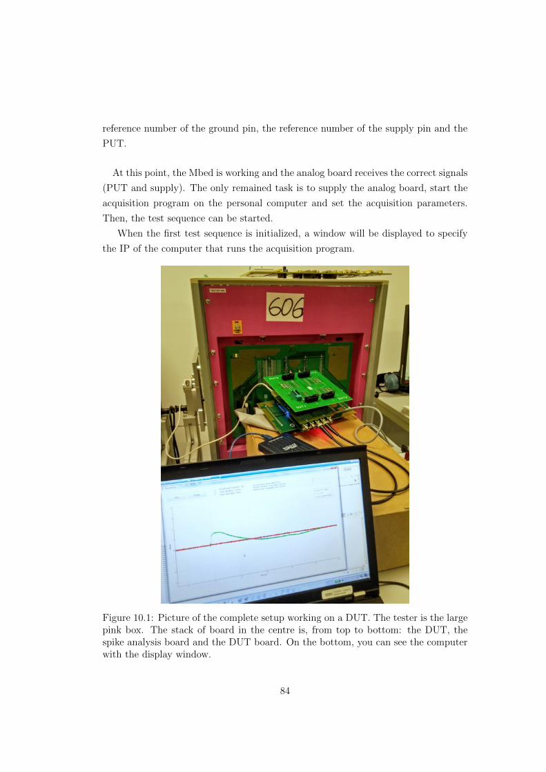
reference number of the ground pin, the reference number of the supply pin and the
PUT.
At this point, the Mbed is working and the analog board receives the correct signals
(PUT and supply). The only remained task is to supply the analog board, start the
acquisition program on the personal computer and set the acquisition parameters.
Then, the test sequence can be started.
When the first test sequence is initialized, a window will be displayed to specify
the IP of the computer that runs the acquisition program.
Figure 10.1: Picture of the complete setup working on a DUT. The tester is the largepink box. The stack of board in the centre is, from top to bottom: the DUT, thespike analysis board and the DUT board. On the bottom, you can see the computerwith the display window.
84

The acquisition will start directly and the waveforms acquired will be displayed
at the end of the test sequence as shown in figure 10.1. To start a new test sequence,
the engineer closes the display window and restarts the test sequence on the tester.
10.2 The test and the result
To test the final tool developed in the framework of this thesis, one has placed
intentionally a sequence of operations in an unknown test that generates a spike.
One has to find this test. During the test, a benchtop oscilloscope is also used to
compare the two acquisitions. The program gives in output the three waveforms as
shown in figure 10.2.
Figure 10.2: Screen capture of the detected spike. The green waveform is the PUT,the red is the supply voltage and the blue is the di↵erential signal. The arrow on theleft side indicates the detected spike. Note that another spike can be seen just after.
One can observe in figure 10.2 that the PUT voltage exceeds the supply voltage.
The supply voltage is equal to 5V and the PUT voltage goes from zero to 9V. When
the switch occurs, a large spike of maximum 14V is detected. The ID of the test
indicated by the display window is 35. One can find the corresponding test name in
the list displayed on the tester console. This test was e↵ectively the one in which a
spike was introduced intentionally.
The PUT signal is the same as the one captured by the benchtop oscilloscope
(cf. figure 10.3) except that the benchtop oscilloscope has 12bits of resolution leading
85

Figure 10.3: Screen capture of the detected spike on the benchtop oscilloscope. Thegreen waveform is the PUT and the pink is the measured supply voltage.
to a better precision than the picoscope (8bits). The maximum voltage of the spike
detected with the picoscope and the spike analysis board is the same as the one
detected with the benchtop oscilloscope (⇠14.1V).
This test gives evidence that the tool developed in the framework of this thesis work
very well. In addition, if the engineer has the ability to estimate the time interval
needed for each instruction of the test, he/she can localize more precisely the spike
source. To do so, the time interval from the start of the test to the spike is indicated
in the display window.
86

Chapter 11
Conclusion
The goal of the thesis was to obtain an automated way of detecting and localizing
high frequency spikes, and this objective has been fulfilled. A job that lasted initially
days or weeks can now be accomplished within hours, which is a large improvement
of the process e�ciency.
The tools created to reach the objective of this thesis have been designed to make
the work easier for the engineer while targeting precision of the measurement.
In the end two PCBs have been made to work with the material used by Melexis
test engineers. The PCBs allow one to detect directly high frequency spikes using a
simple oscilloscope. The first PCB - called the ”Spike analysis board” - is adapted
to the test material and connects the useful signals, namely: the ground, the supply
voltage and the pin under test to the second PCB.
The second PCB - called the analog board - takes two input signals: the supply
voltage and the pin under test (both referenced to the ground). First, the two input
signal voltages are brought back in a defined voltage range ([�3V ; 3V ]) and bu↵ered
to be measured without e↵ect on both inputs. Secondly, both outputs of the bu↵ers
are connected to a unit gain di↵erential amplifier. Thanks to the di↵erential output
signal, one is able to use the trigger of an oscilloscope to catch spikes.
A program was developed to run on Windows, to control an oscilloscope, to acquire
signals from PCBs, to communicate through TCP/IP with the test equipment used
within the company, to localize the test source of spikes and to display the whole
information on the screen. The code that has to be added in the test equipment
program to communicate with the first program was also developed especially for
this master thesis.
87

Simulations were made using lumped elements to model the PCBs. The maximum
frequency at which the lumped elements model is valid is around 200MHz, taking
into account the length of the tracks. This maximum frequency is higher than the
initial estimated maximum frequency of the spikes.
Nevertheless, a further study of the design as a distributed circuit could be very
interesting and could lead to a better understanding of what happens at very high
frequency above ⇠200MHz. Very high frequency resonance could appear considering
the results of our simulations, and a further study could investigate in more details this
resonance. Moreover, it could be worthwhile for the company to study thoroughly:
(i) the e↵ect of each PCBs used during a test session on the presence of spikes, (ii)
the source of those spikes and (iii) the e↵ect of the measurement equipment on the
presence of spikes.
This thesis was a valuable experience as a student. I had to learn a lot about high
frequency measurements, C++ and Windows programming, TCP/IP transmissions,
PCB design and I had to adapt my work to the expectations of the team I worked for.
Working within a company like Melexis was very rewarding because of the personnel
open-mindedness and skills, and the support o↵ered by the company.
88

Chapter 12
Melexis: strategic aspects
This non-technical chapter is dedicated to a brief analyse of some aspects of the
company that, personally, appear to be linked to its success.
Melexis is a company that develops, tests and delivers semiconductors. Renowned
in automotive applications, the company produces pressure sensors, infrared ther-
mometer sensors, optical sensors, current sensors, hall e↵ect switches and a lot of
other products[9]. The company was initially known as Melexis Tessenderlo NV.
Named due to the initial location of the company: Tessenderlo, Belgium. The com-
pany changed its name to Melexis Technologies NV in September, 2011.
12.1 Some numbers
First of all, some key numbers can be presented. The company is growing. From
2010 until 2015, the company revenues almost doubled [11]. In 2015, the revenue and
the net income of the company were 400Me and 99Me, respectively. Figure 12.1
shows the evolution of the company revenue from 2011 to 2015 and the net income
has followed the same trend. The average number of employees also increased as they
were 915 in 2014 and 1054 in 2015 [11].
The growth of the company, whereas its key customers (automotive) are not grow-
ing as much, can be explained by the rise of the number of electronic devices in cars.
The electronics having a significant role of di↵erentiation for the producer. In addi-
tion, the development of the electronics in various sectors like in consumer electronics,
industrial and personal health applications o↵ers new opportunities for the company
to grow in the next years[11]. For year 2016, Melexis expects sales growth to be
between 8% and 12% [10].
89

Figure 12.1: Revenues of the company from 2011 to 2015. Source [11].
12.2 R&D strategy
In 2015, the expenses of the R&D was around 56Me, which represented around
14% of the company revenues. This percentage is slightly larger than the average
spending percentage in R&D (⇠12%) in the same industry [18]. For 2016, the R&D
spending is expected to increase from 14% to 15% of the revenues [11].
The company invests significantly in its research and development department.
R&D is the principal activity of many sites of the company including Ukrainian,
Bulgarian or Belgian sites.
Products delivered by Melexis are designed, developed, tested and delivered by the
company. Only the wafer fabrication and the packaging are subcontracted. However,
at the end of the production, Melexis is in charge of testing the devices. This way,
the company can have the stranglehold on its products from creation to delivering.
The company develops its own test solutions, including the development of the test
platform by a sister company. This way, the company has a complete control over
the whole test system, allowing high quality at a lower cost to be reached.
Melexis is very customer oriented. The company follows the needs of its customers
to o↵er a product fully customized. Because Melexis is a B2B company, this cus-
90

tomizable service allows the company to o↵er products that have a larger business
value in comparison to other products.
12.3 HR strategy
Employees of the company are mostly highly skilled. The dominant coordination of
work within the company seems to correspond to a standardization of qualifications
(cf. [16]). In this coordination of work, the company ensures that the workers have
the skills needed to perform their work[16].
In Tessenderlo, nearly all employees of the operational core are engineers. They are
separated according to their skills in di↵erent departments during the recruitment.
However, the company o↵ers possibilities to switch to another department in order
to find the right place for each employee. According to workers in Tessenderlo, the
company is very flexible with them and they really appreciate working for Melexis.
The fact that the company is attentive to its employees and o↵ers them flexibility
are two important contributions that enabled Melexis to be named the most attractive
employer by Randstad. About this award, the CEO of Melexis, Francoise Chombar
said “We are very happy that an outside party – Randstad – has identified us as the
most attractive employer. In our view, our growth and the way we have realised it
are key. We adhere to one important rule: we aim to put the right people in the right
place. This approach ensures intrinsic motivation and job satisfaction. Our track
record of years of growth combined with a high level of employee loyalty prove the
success of our sustainable, innovative company culture. For us, achieving a balance
between people and results is crucial.”[12].
12.4 Melexis, opinion of a student
The work atmosphere as well as the work environment were very good. Melexis
seems to work hardly on workspaces to make them more convenient for the employ-
ees. For example, buildings of the Tessenderlo site were completely redesigned in
between the 2015 summer holidays and the beginning of 2016. New wellness areas,
new laboratories, new cafeteria etc. make the building enjoyable for all employees.
91

Workers of the Tessenderlo site are passionate about their jobs. There is something
that might look like the atmosphere of a start-up in which every individual is working
hard to make the company going further. Likewise, one can easily find any help inside
the company.
Working for Melexis is a great technical experience. One can directly be confronted
to very challenging projects and acquire new knowledges. In addition, according to
employees, the company is also flexible about switching to another work area allowing
employees to see others cultures, or about adapting the working schedule if the worker
wants to start part time studies, etc.
92

Bibliography
[1] Jeroen Belleman. Shunt capacitance of 1206 smd resistors. Online Jeroen Belle-
man’s web pages: https://jeroen.web.cern.ch/jeroen/, December 2010.
[2] Electrical Engineer Community EEweb. toolbox: Rectangle loop inductance.
Online toolbox.
[3] en.wikibooks.org. Signals and systems/second order transfer function. Online
open book of wikibooks, July 2014.
[4] Beyschlag GmbH. The hf resistor application guide. Resistor Products.
[5] Texas Instruments. Opa659 datasheet. TI online support, December 2008 -
Revisited November 2015.
[6] Texas Instruments. Lm7171 datasheet. TI online support, May 1999 – Revisited
September 2014.
[7] Gunthard Kraus. Spice-simulation using ltspice iv. Elektronikschule Tettnang,
Germany, Guest Lecturer at the DHBW, December 2010.
[8] Saverio Lerose. Integrite de signal et compatibilite electromagnetique (cem) des
cartes electroniques. Technique de l’ingenieur, May 2015.
[9] Melexis. Melexis products. Melexis website.
[10] Melexis. Melexis q1 report 2016 – strong sales growth to start the year. Melexis
Investor Reports, April 2016.
[11] Melexis. Melexis annual report 2015. Melexis Investor Reports, March 2016.
[12] Melexis. Melexis news: Melexis voted most attractive employer in randstad
regional awards. Melexis website, September 2015.
93

[13] NI. Proper termination for high-speed digital i/o applications. NI tutorials, May
2014.
[14] Benoıt Vanderheyden Patricia Rousseaux. Electromagnetisme. Universite de
Liege, Institut Montefiore, course: ELEN0076-1, 2013-2014.
[15] Vanderbemden Philippe. Analyse et conception des systemes de mesures
electriques. Universite de Liege, Institut Montefiore, course: ELEC0052-2, 2013-
2014.
[16] F. Pichault. Principles of management: Organizational theory and hu-
man resources management. Universite de Liege, Institut Montefiore, course:
GEST3162-1, 2015-2016.
[17] NXP Semiconductors. 74hc4051: 8-channel analog multiplexer/demultiplexe.
product data sheet. NXP Semiconductors: Product data sheet, February 2016.
[18] Strategy&. The global innovation 1000: Comparison of r&d spending by regions
and industries. Strategy& website.
[19] Louis Wehenkel. Elements de statistique. Universite de Liege, Institut Monte-
fiore, course: MATH0487-2, 2013-2014.
[20] Jim Williams. High speed amplifier techniques, a designer’s companion for wide-
band circuitry. Linear technology: Application Note, August 1991.
94