Embed Size (px)
Citation preview
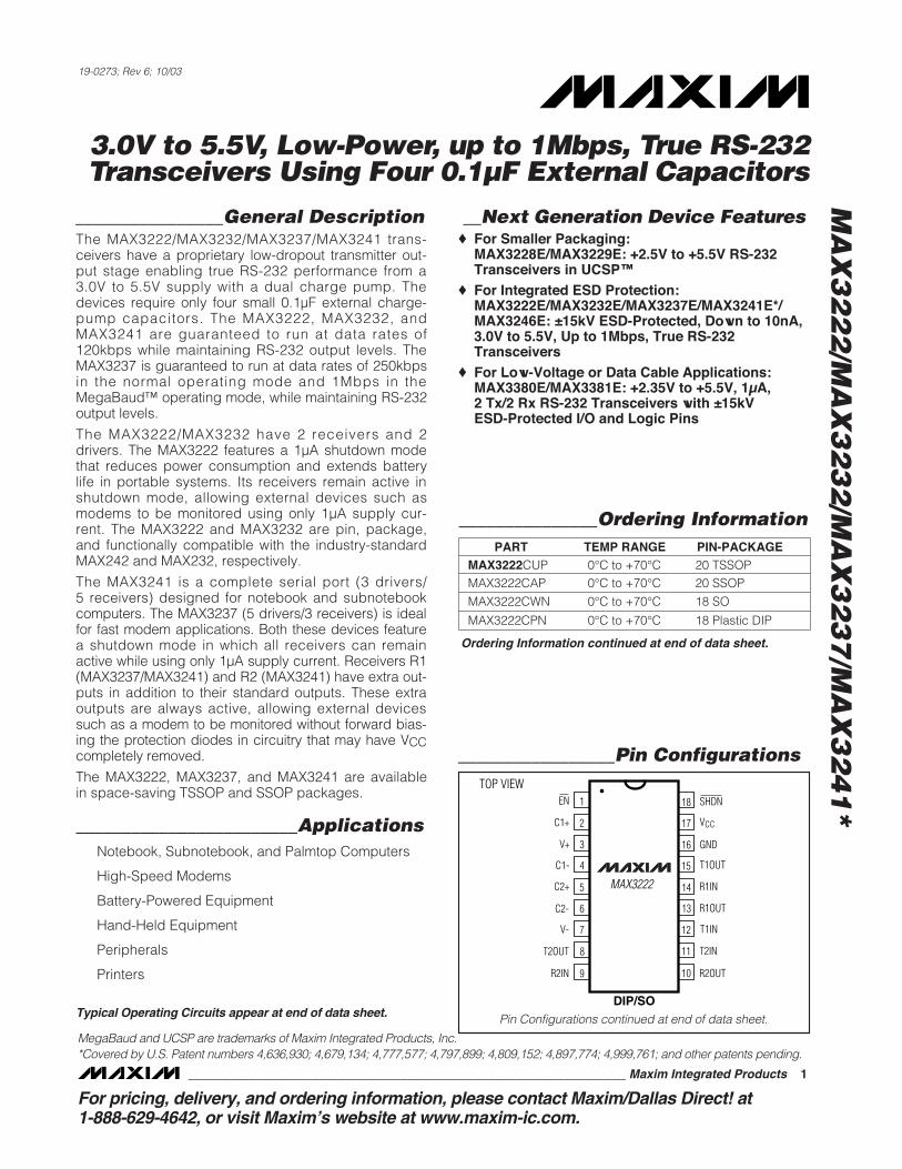
________________General DescriptionThe MAX3222/MAX3232/MAX3237/MAX3241 trans-ceivers have a proprietary low-dropout transmitter out-put stage enabling true RS-232 performance from a3.0V to 5.5V supply with a dual charge pump. Thedevices require only four small 0.1µF external charge-pump capacitors. The MAX3222, MAX3232, andMAX3241 are guaranteed to run at data rates of120kbps while maintaining RS-232 output levels. TheMAX3237 is guaranteed to run at data rates of 250kbpsin the normal operating mode and 1Mbps in theMegaBaud™ operating mode, while maintaining RS-232output levels.
The MAX3222/MAX3232 have 2 receivers and 2 drivers. The MAX3222 features a 1µA shutdown modethat reduces power consumption and extends batterylife in portable systems. Its receivers remain active inshutdown mode, allowing external devices such asmodems to be monitored using only 1µA supply cur-rent. The MAX3222 and MAX3232 are pin, package,and functionally compatible with the industry-standardMAX242 and MAX232, respectively.
The MAX3241 is a complete serial port (3 drivers/5 receivers) designed for notebook and subnotebookcomputers. The MAX3237 (5 drivers/3 receivers) is idealfor fast modem applications. Both these devices featurea shutdown mode in which all receivers can remainactive while using only 1µA supply current. Receivers R1(MAX3237/MAX3241) and R2 (MAX3241) have extra out-puts in addition to their standard outputs. These extraoutputs are always active, allowing external devicessuch as a modem to be monitored without forward bias-ing the protection diodes in circuitry that may have VCCcompletely removed.
The MAX3222, MAX3237, and MAX3241 are availablein space-saving TSSOP and SSOP packages.
________________________ApplicationsNotebook, Subnotebook, and Palmtop Computers
High-Speed Modems
Battery-Powered Equipment
Hand-Held Equipment
Peripherals
Printers
__Next Generation Device Features♦ For Smaller Packaging:
MAX3228E/MAX3229E: +2.5V to +5.5V RS-232Transceivers in UCSP™
♦ For Integrated ESD Protection:MAX3222E/MAX3232E/MAX3237E/MAX3241E*/MAX3246E: ±15kV ESD-Protected, Down to 10nA,3.0V to 5.5V, Up to 1Mbps, True RS-232Transceivers
♦ For Low-Voltage or Data Cable Applications:MAX3380E/MAX3381E: +2.35V to +5.5V, 1µA, 2 Tx/2 Rx RS-232 Transceivers with ±15kV ESD-Protected I/O and Logic Pins
MA
X3
22
2/M
AX
32
32
/MA
X3
23
7/M
AX
32
41
*
3.0V to 5.5V, Low-Power, up to 1Mbps, True RS-232Transceivers Using Four 0.1µF External Capacitors
________________________________________________________________ Maxim Integrated Products 1
18
17
16
15
14
13
12
11
1
2
3
4
5
6
7
8
SHDN
VCC
GND
T1OUTC1-
V+
C1+
ENTOP VIEW
R1IN
R1OUT
T1IN
T2INT2OUT
V-
C2-
C2+
109 R2OUTR2IN
DIP/SO
MAX3222
_________________Pin Configurations
_______________Ordering Information
19-0273; Rev 6; 10/03
PART TEMP RANGE PIN-PACKAGE
MegaBaud and UCSP are trademarks of Maxim Integrated Products, Inc.*Covered by U.S. Patent numbers 4,636,930; 4,679,134; 4,777,577; 4,797,899; 4,809,152; 4,897,774; 4,999,761; and other patents pending.
Typical Operating Circuits appear at end of data sheet. Pin Configurations continued at end of data sheet.
Ordering Information continued at end of data sheet.
MAX3222CUP 0°C to +70°C 20 TSSOPMAX3222CAP 0°C to +70°C 20 SSOP
MAX3222CWN 0°C to +70°C 18 SO
MAX3222CPN 0°C to +70°C 18 Plastic DIP
For pricing, delivery, and ordering information, please contact Maxim/Dallas Direct! at 1-888-629-4642, or visit Maxim’s website at www.maxim-ic.com.
VCC = 5.0V
MA
X3
22
2/M
AX
32
32
/MA
X3
23
7/M
AX
32
41
3.0V to 5.5V, Low-Power, up to 1Mbps, True RS-232Transceivers Using Four 0.1µF External Capacitors
2 _______________________________________________________________________________________
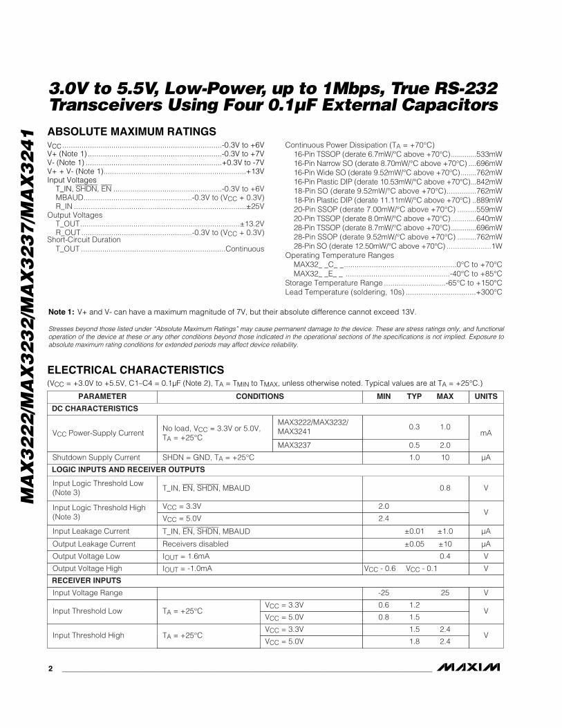
ABSOLUTE MAXIMUM RATINGS
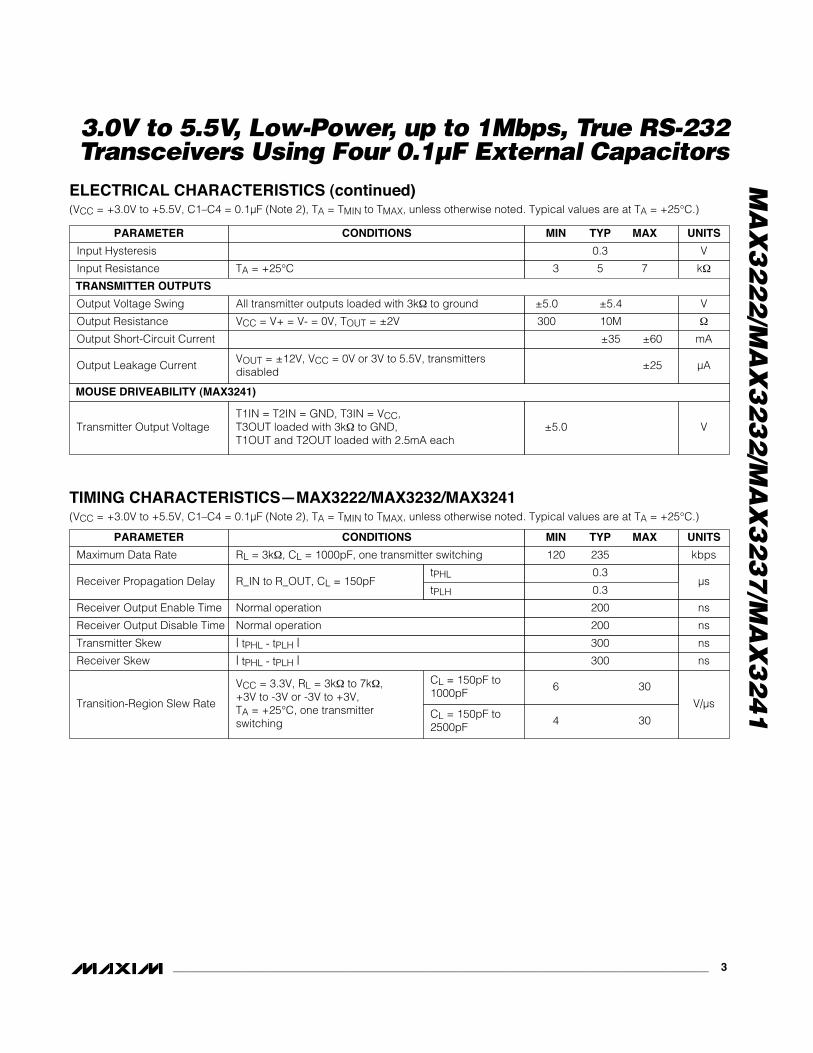
ELECTRICAL CHARACTERISTICS(VCC = +3.0V to +5.5V, C1–C4 = 0.1µF (Note 2), TA = TMIN to TMAX, unless otherwise noted. Typical values are at TA = +25°C.)
Stresses beyond those listed under “Absolute Maximum Ratings” may cause permanent damage to the device. These are stress ratings only, and functionaloperation of the device at these or any other conditions beyond those indicated in the operational sections of the specifications is not implied. Exposure toabsolute maximum rating conditions for extended periods may affect device reliability.
Note 1: V+ and V- can have a maximum magnitude of 7V, but their absolute difference cannot exceed 13V.
VCC...........................................................................-0.3V to +6VV+ (Note 1) ...............................................................-0.3V to +7VV- (Note 1) ................................................................+0.3V to -7VV+ + V- (Note 1)...................................................................+13VInput Voltages
T_IN, SHDN, EN ...................................................-0.3V to +6VMBAUD...................................................-0.3V to (VCC + 0.3V)R_IN .................................................................................±25V
Output VoltagesT_OUT...........................................................................±13.2VR_OUT....................................................-0.3V to (VCC + 0.3V)
Short-Circuit DurationT_OUT ....................................................................Continuous
Continuous Power Dissipation (TA = +70°C)16-Pin TSSOP (derate 6.7mW/°C above +70°C).............533mW16-Pin Narrow SO (derate 8.70mW/°C above +70°C) ....696mW16-Pin Wide SO (derate 9.52mW/°C above +70°C)........762mW16-Pin Plastic DIP (derate 10.53mW/°C above +70°C)...842mW18-Pin SO (derate 9.52mW/°C above +70°C)..............762mW18-Pin Plastic DIP (derate 11.11mW/°C above +70°C) ..889mW20-Pin SSOP (derate 7.00mW/°C above +70°C) .........559mW20-Pin TSSOP (derate 8.0mW/°C above +70°C).............640mW28-Pin TSSOP (derate 8.7mW/°C above +70°C).............696mW28-Pin SSOP (derate 9.52mW/°C above +70°C) .........762mW28-Pin SO (derate 12.50mW/°C above +70°C) .....................1W
Operating Temperature RangesMAX32_ _C_ _.....................................................0°C to +70°CMAX32_ _E_ _ .................................................-40°C to +85°C
Storage Temperature Range .............................-65°C to +150°CLead Temperature (soldering, 10s) .................................+300°C
IOUT = -1.0mA
IOUT = 1.6mA
Receivers disabled
T_IN, EN, SHDN, MBAUD
T_IN, EN, SHDN, MBAUD
CONDITIONS
V0.8 1.5
Input Threshold Low0.6 1.2
V-25 25Input Voltage Range
0.5 2.0
VCC Power-Supply Current
VVCC - 0.6 VCC - 0.1Output Voltage High
V0.4Output Voltage Low
µA±0.05 ±10Output Leakage Current
µA±0.01 ±1.0Input Leakage Current
V0.8Input Logic Threshold Low(Note 3)
UNITSMIN TYP MAXPARAMETER
TA = +25°C
TA = +25°C V1.8 2.4
Input Threshold High1.5 2.4
VCC = 3.3V
VCC = 5.0V
2.0V
2.4Input Logic Threshold High(Note 3)
No load, VCC = 3.3V or 5.0V,TA = +25°C
mA0.3 1.0
MAX3222/MAX3232/MAX3241
MAX3237
SHDN = GND, TA = +25°C µA1.0 10Shutdown Supply Current
VCC = 3.3V
VCC = 5.0V
VCC = 3.3V
VCC = 5.0V
DC CHARACTERISTICS
LOGIC INPUTS AND RECEIVER OUTPUTS
RECEIVER INPUTS
MA
X3
22
2/M
AX
32
32
/MA
X3
23
7/M
AX
32
41
3.0V to 5.5V, Low-Power, up to 1Mbps, True RS-232Transceivers Using Four 0.1µF External Capacitors
_______________________________________________________________________________________ 3
TIMING CHARACTERISTICS—MAX3222/MAX3232/MAX3241(VCC = +3.0V to +5.5V, C1–C4 = 0.1µF (Note 2), TA = TMIN to TMAX, unless otherwise noted. Typical values are at TA = +25°C.)
ELECTRICAL CHARACTERISTICS (continued)(VCC = +3.0V to +5.5V, C1–C4 = 0.1µF (Note 2), TA = TMIN to TMAX, unless otherwise noted. Typical values are at TA = +25°C.)
T1IN = T2IN = GND, T3IN = VCC,T3OUT loaded with 3kΩ to GND,T1OUT and T2OUT loaded with 2.5mA each
CONDITIONS
V±5.0Transmitter Output Voltage
V0.3Input Hysteresis
UNITSMIN TYP MAXPARAMETER
All transmitter outputs loaded with 3kΩ to ground V±5.0 ±5.4Output Voltage Swing
mA±35 ±60Output Short-Circuit Current
VCC = V+ = V- = 0V, TOUT = ±2V Ω300 10MOutput Resistance
VOUT = ±12V, VCC = 0V or 3V to 5.5V, transmitters disabled
µA±25Output Leakage Current
tPHL
RL = 3kΩ, CL = 1000pF, one transmitter switching
tPLH
| tPHL - tPLH || tPHL - tPLH |Normal operation
Normal operation
CONDITIONS
0.3µs
0.3Receiver Propagation Delay
kbps120 235Maximum Data Rate
ns300Receiver Skew
ns300Transmitter Skew
ns200Receiver Output Disable Time
ns200Receiver Output Enable Time
UNITSMIN TYP MAXPARAMETER
6 30VCC = 3.3V, RL = 3kΩ to 7kΩ, +3V to -3V or -3V to +3V,TA = +25°C, one transmitterswitching
V/µs
4 30
Transition-Region Slew Rate
R_IN to R_OUT, CL = 150pF
CL = 150pF to1000pF
CL = 150pF to2500pF
TA = +25°C kΩ3 5 7Input Resistance
MOUSE DRIVEABILITY (MAX3241)
TRANSMITTER OUTPUTS
MA
X3
22
2/M
AX
32
32
/MA
X3
23
7/M
AX
32
41
3.0V to 5.5V, Low-Power, up to 1Mbps, True RS-232Transceivers Using Four 0.1µF External Capacitors
4 _______________________________________________________________________________________
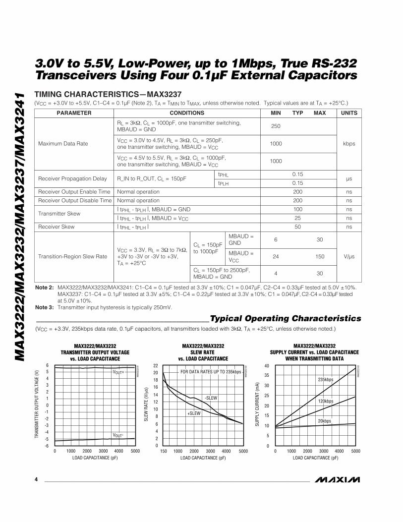
__________________________________________Typical Operating Characteristics(VCC = +3.3V, 235kbps data rate, 0.1µF capacitors, all transmitters loaded with 3kΩ, TA = +25°C, unless otherwise noted.)
-6-5
-4-3-2-10123456
0
MAX3222/MAX3232TRANSMITTER OUTPUT VOLTAGE
vs. LOAD CAPACITANCE
MAX
3222
-01
LOAD CAPACITANCE (pF)
TRAN
SMIT
TER
OUTP
UT V
OLTA
GE (V
)
2000 30001000 4000 5000
VOUT+
VOUT-
0
2
4
6
8
10
12
14
16
18
20
22
150
MAX3222/MAX3232SLEW RATE
vs. LOAD CAPACITANCE
MAX
3222
-02
LOAD CAPACITANCE (pF)
SLEW
RAT
E (V
/ µs)
2000 30001000 4000 5000
FOR DATA RATES UP TO 235kbps
+SLEW
-SLEW
0
5
10
15
20
25
30
35
40
0
MAX3222/MAX3232SUPPLY CURRENT vs. LOAD CAPACITANCE
WHEN TRANSMITTING DATAM
AX32
22-0
3
LOAD CAPACITANCE (pF)
SUPP
LY C
URRE
NT (m
A)
2000 30001000 4000 5000
235kbps
120kbps
20kbps
RL = 3kΩ, CL = 1000pF, one transmitter switching,MBAUD = GND
Normal operation
CONDITIONS
Normal operation ns200Receiver Output Disable Time
| tPHL - tPLH |, MBAUD = GND ns100
0.15
250
µs0.15
Receiver Propagation Delay
ns200Receiver Output Enable Time
UNITSMIN TYP MAXPARAMETER
TIMING CHARACTERISTICS—MAX3237(VCC = +3.0V to +5.5V, C1–C4 = 0.1µF (Note 2), TA = TMIN to TMAX, unless otherwise noted. Typical values are at TA = +25°C.)
VCC = 3.0V to 4.5V, RL = 3kΩ, CL = 250pF,one transmitter switching, MBAUD = VCC
1000
VCC = 4.5V to 5.5V, RL = 3kΩ, CL = 1000pF,one transmitter switching, MBAUD = VCC
kbps
1000
Maximum Data Rate
R_IN to R_OUT, CL = 150pF
| tPHL - tPLH |, MBAUD = VCC ns25Transmitter Skew
| tPHL - tPLH | ns50Receiver Skew
6 30
V/µs
4 30
tPHL
tPLH
CL = 150pF to 2500pF,MBAUD = GND
CL = 150pFto 1000pF
MBAUD =GND
VCC = 3.3V, RL = 3Ω to 7kΩ,+3V to -3V or -3V to +3V,TA = +25°C
Transition-Region Slew Rate MBAUD =VCC
24 150
Note 2: MAX3222/MAX3232/MAX3241: C1–C4 = 0.1µF tested at 3.3V ±10%; C1 = 0.047µF, C2–C4 = 0.33µF tested at 5.0V ±10%.MAX3237: C1–C4 = 0.1µF tested at 3.3V ±5%; C1–C4 = 0.22µF tested at 3.3V ±10%; C1 = 0.047µF, C2–C4 = 0.33µF testedat 5.0V ±10%.
Note 3: Transmitter input hysteresis is typically 250mV.

MA
X3
22
2/M
AX
32
32
/MA
X3
23
7/M
AX
32
41
3.0V to 5.5V, Low-Power, up to 1Mbps, True RS-232Transceivers Using Four 0.1µF External Capacitors
_______________________________________________________________________________________ 5
-7.5
-5.0
-2.5
0
2.5
5.0
7.5
0
MAX3241TRANSMITTER OUTPUT VOLTAGE
vs. LOAD CAPACITANCE
MAX
3222
-04
LOAD CAPACITANCE (pF)
TRAN
SMIT
TER
OUTP
UT V
OLTA
GE (V
)
2000 30001000 4000 5000
VOUT+
1 TRANSMITTER AT 235kbps2 TRANSMITTERS AT 30kbps
VOUT-ALL OUTPUTS LOADED WITH 3kΩ +CL 0.1µF CHARGE-PUMP CAPACITORSFOR ALL DATA RATES UP TO 235kbps4
6
8
10
12
14
16
18
20
22
24
0
MAX3241SLEW RATE
vs. LOAD CAPACITANCE
MAX
3222
-05
LOAD CAPACITANCE (pF)
SLEW
RAT
E (V
/ µs)
2000 30001000 4000 5000
+SLEW
-SLEW
0
5
10
15
20
25
30
35
45
40
0
MAX3241SUPPLY CURRENT vs. LOAD
CAPACITANCE WHEN TRANSMITTING DATA
MAX
3222
-06
LOAD CAPACITANCE (pF)
SUPP
LY C
URRE
NT (m
A)
2000 30001000 4000 5000
235kbps
120kbps
20kbps
-7.5
-5.0
-2.5
0
2.5
5.0
7.5
0
MAX3237TRANSMITTER OUTPUT VOLTAGE
vs. LOAD CAPACITANCE (MBAUD = GND)
MAX
3222
-07
LOAD CAPACITANCE (pF)
TRAN
SMIT
TER
OUTP
UT V
OLTA
GE (V
)
2000 30001000 4000 5000
1 TRANSMITTER AT 240kbps4 TRANSMITTERS AT 15kbps3kΩ + CL LOADSVCC = 3.3V
0
10
20
30
50
40
60
70
0
MAX3237SLEW RATE vs. LOAD CAPACITANCE
(MBAUD = VCC)
MAX
3222
-10
LOAD CAPACITANCE (pF)
SLEW
RAT
E (V
/µs)
500 1000 1500 2000
-SLEW, 1Mbps+SLEW, 1Mbps
1 TRANSMITTER AT FULL DATA RATE4 TRANSMITTERS AT 1/16 DATA RATE3kΩ + CL LOAD EACH OUTPUTVCC = 3.3V
-SLEW, 2Mbps+SLEW, 2Mbps
-7.5
-5.0
-2.5
0
2.5
5.0
7.5
0
MAX3237TRANSMITTER OUTPUT VOLTAGE
vs. LOAD CAPACITANCE (MBAUD = VCC)M
AX32
22-0
8
LOAD CAPACITANCE (pF)
TRAN
SMIT
TER
OUTP
UT V
OLTA
GE (V
)
500 1000 1500 2000
1 TRANSMITTER AT FULL DATA RATE4 TRANSMITTERS AT 1/16 DATA RATE3kΩ + CL LOAD, EACH OUTPUTVCC = 3.3V
2Mbps 1.5Mbps
1Mbps
2Mbps
1Mbps
1.5Mbps
0
10
20
30
40
50
60
0
MAX3237SUPPLY CURRENT vs.
LOAD CAPACITANCE (MBAUD = GND)
MAX
3222
-11
LOAD CAPACITANCE (pF)
SUPP
LY C
URRE
NT (m
A)
2000 30001000 4000 5000
240kbps
120kbps
20kbps
1 TRANSMITTER AT FULL DATA RATE4 TRANSMITTERS AT 1/16 DATA RATE3kΩ + CL LOADSVCC = 3.3V
0
2
4
6
8
10
12
0
MAX3237SLEW RATE vs. LOAD CAPACITANCE
(MBAUD = GND)
MAX
3222
-09
LOAD CAPACITANCE (pF)
SLEW
RAT
E (V
/ µs)
2000 30001000 4000 5000
+SLEW
-SLEW
1 TRANSMITTER AT 240kbps4 TRANSMITTERS AT 15kbps3kΩ + CL LOADSVCC = 3.3V
0
10
30
20
40
50
60
70
0
MAX3237SKEW vs. LOAD CAPACITANCE
(tPLH - tPHL)
MAX
3222
-12
LOAD CAPACITANCE (pF)1000 1500500 2000 2500
MAX
MIN
AVERAGE; 10 PARTS
SKEW
(ns)1 TRANSMITTER AT 512kbps
4 TRANSMITTERS AT 32kbps3kΩ + CL LOADSVCC = 3.3VMBAUD = VCC
_____________________________Typical Operating Characteristics (continued)(VCC = +3.3V, 235kbps data rate, 0.1µF capacitors, all transmitters loaded with 3kΩ, TA = +25°C, unless otherwise noted.)
MA
X3
22
2/M
AX
32
32
/MA
X3
23
7/M
AX
32
41
3.0V to 5.5V, Low-Power, up to 1Mbps, True RS-232Transceivers Using Four 0.1µF External Capacitors
6 _______________________________________________________________________________________
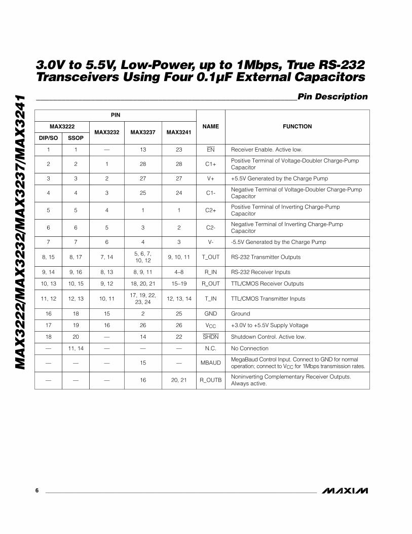
—
FUNCTION
—
MAX3222
Noninverting Complementary Receiver Outputs.Always active.
DIP/SO SSOP
— 11, 14
1 1 Receiver Enable. Active low.
2 2Positive Terminal of Voltage-Doubler Charge-PumpCapacitor
6 6Negative Terminal of Inverting Charge-PumpCapacitor
5 5Positive Terminal of Inverting Charge-PumpCapacitor
4 4Negative Terminal of Voltage-Doubler Charge-PumpCapacitor
3 3 +5.5V Generated by the Charge Pump
11, 12 12, 13 TTL/CMOS Transmitter Inputs
10, 13 10, 15 TTL/CMOS Receiver Outputs
9, 14 9, 16 RS-232 Receiver Inputs
8, 15 8, 17 RS-232 Transmitter Outputs
7 7 -5.5V Generated by the Charge Pump
18 20 Shutdown Control. Active low.
17 19 +3.0V to +5.5V Supply Voltage
16 18 Ground
No Connection
MAX3237MAX3232
— 16
— 13
1 28
5 3
4 1
3 25
2 27
10, 1117, 19, 22,
23, 24
9, 12 18, 20, 21
8, 13 8, 9, 11
7, 145, 6, 7, 10, 12
6 4
— 14
16 26
15 2
— —
NAME
EN
C1+
C2-
C2+
C1-
V+
T_IN
R_OUT
R_IN
T_OUT
V-
SHDN
VCC
GND
R_OUTB
N.C.
MAX3241
20, 21
23
28
2
1
24
27
12, 13, 14
15–19
4–8
9, 10, 11
3
22
26
25
—
PIN
— —MegaBaud Control Input. Connect to GND for normaloperation; connect to VCC for 1Mbps transmission rates.
— 15 MBAUD—
______________________________________________________________Pin Description
MA
X3
22
2/M
AX
32
32
/MA
X3
23
7/M
AX
32
41
3.0V to 5.5V, Low-Power, up to 1Mbps, True RS-232Transceivers Using Four 0.1µF External Capacitors
_______________________________________________________________________________________ 7
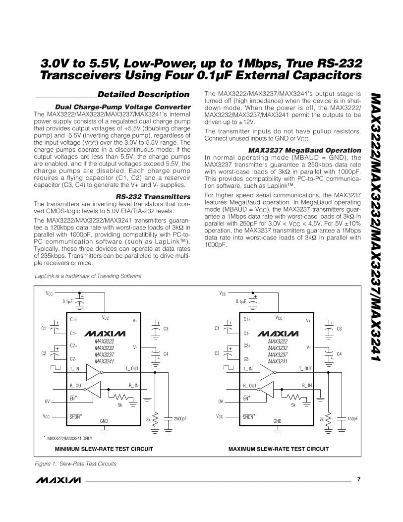
_______________Detailed DescriptionDual Charge-Pump Voltage Converter
The MAX3222/MAX3232/MAX3237/MAX3241’s internalpower supply consists of a regulated dual charge pumpthat provides output voltages of +5.5V (doubling chargepump) and -5.5V (inverting charge pump), regardless ofthe input voltage (VCC) over the 3.0V to 5.5V range. Thecharge pumps operate in a discontinuous mode; if theoutput voltages are less than 5.5V, the charge pumpsare enabled, and if the output voltages exceed 5.5V, thecharge pumps are disabled. Each charge pumprequires a flying capacitor (C1, C2) and a reservoircapacitor (C3, C4) to generate the V+ and V- supplies.
RS-232 TransmittersThe transmitters are inverting level translators that con-vert CMOS-logic levels to 5.0V EIA/TIA-232 levels.
The MAX3222/MAX3232/MAX3241 transmitters guaran-tee a 120kbps data rate with worst-case loads of 3kΩ inparallel with 1000pF, providing compatibility with PC-to-PC communication software (such as LapLink™).Typically, these three devices can operate at data ratesof 235kbps. Transmitters can be paralleled to drive multi-ple receivers or mice.
The MAX3222/MAX3237/MAX3241’s output stage isturned off (high impedance) when the device is in shut-down mode. When the power is off, the MAX3222/MAX3232/MAX3237/MAX3241 permit the outputs to bedriven up to ±12V.
The transmitter inputs do not have pullup resistors.Connect unused inputs to GND or VCC.
MAX3237 MegaBaud OperationIn normal operating mode (MBAUD = GND), theMAX3237 transmitters guarantee a 250kbps data ratewith worst-case loads of 3kΩ in parallel with 1000pF.This provides compatibility with PC-to-PC communica-tion software, such as Laplink™.
For higher speed serial communications, the MAX3237features MegaBaud operation. In MegaBaud operatingmode (MBAUD = VCC), the MAX3237 transmitters guar-antee a 1Mbps data rate with worst-case loads of 3kΩ inparallel with 250pF for 3.0V < VCC < 4.5V. For 5V ±10%operation, the MAX3237 transmitters guarantee a 1Mbpsdata rate into worst-case loads of 3kΩ in parallel with1000pF.
MAX3222MAX3232MAX3237MAX3241
5k
R_ INR_ OUT
EN*
C2-
C2+
C1-
C1+
V-
V+VCC
C4
C3C1
C2
0.1µF
VCC
SHDN*
T_ OUTT_ IN
GNDVCC
0V
7k 150pF
MAX3222MAX3232MAX3237MAX3241
5k
R_ INR_ OUT
EN*
C2-
C2+
C1-
C1+
V-
V+VCC
C4
C3C1
C2
0.1µF
VCC
SHDN*
T_ OUTT_ IN
GNDVCC
0V
3k 2500pF
MINIMUM SLEW-RATE TEST CIRCUIT MAXIMUM SLEW-RATE TEST CIRCUIT
* MAX3222/MAX3241 ONLY
Figure 1. Slew-Rate Test Circuits
LapLink is a trademark of Traveling Software.
MA
X3
22
2/M
AX
32
32
/MA
X3
23
7/M
AX
32
41
3.0V to 5.5V, Low-Power, up to 1Mbps, True RS-232Transceivers Using Four 0.1µF External Capacitors
8 _______________________________________________________________________________________
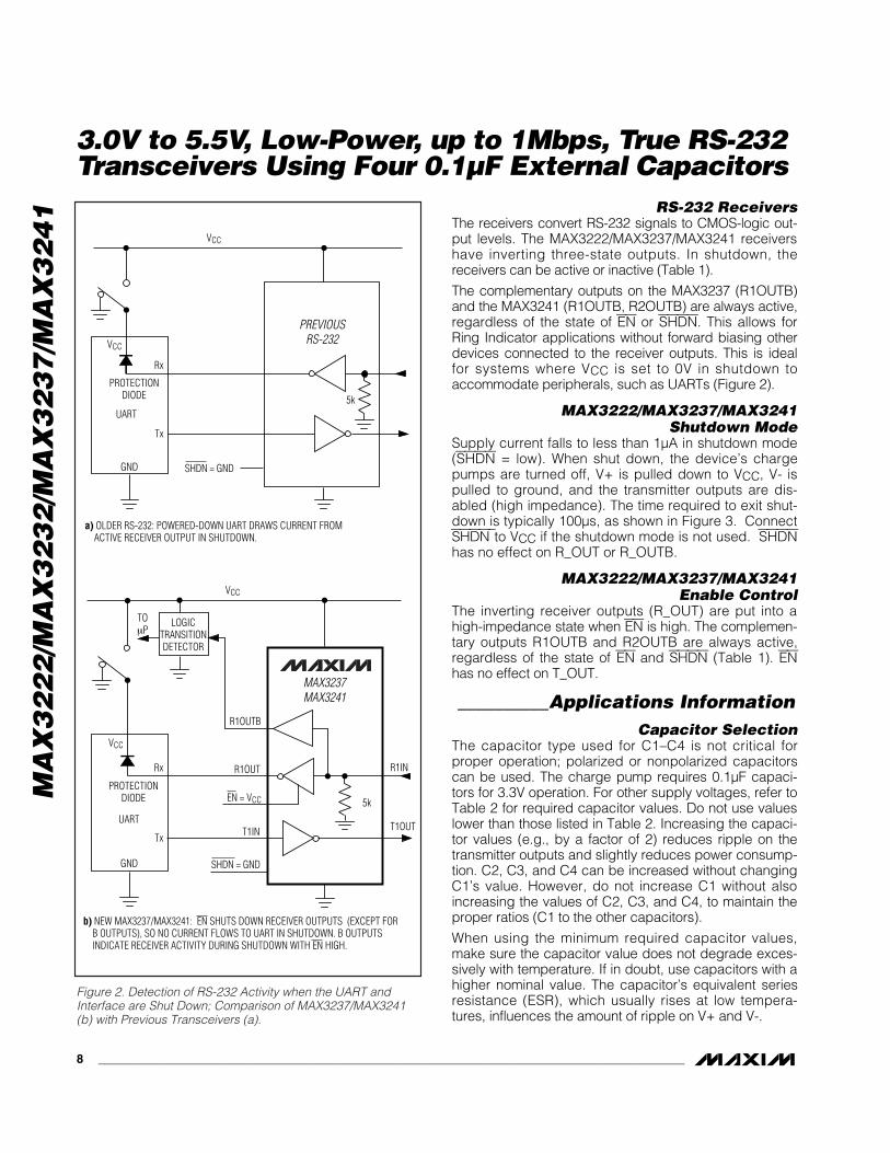
RS-232 ReceiversThe receivers convert RS-232 signals to CMOS-logic out-put levels. The MAX3222/MAX3237/MAX3241 receivershave inverting three-state outputs. In shutdown, thereceivers can be active or inactive (Table 1).
The complementary outputs on the MAX3237 (R1OUTB)and the MAX3241 (R1OUTB, R2OUTB) are always active,regardless of the state of EN or SHDN. This allows forRing Indicator applications without forward biasing otherdevices connected to the receiver outputs. This is idealfor systems where VCC is set to 0V in shutdown toaccommodate peripherals, such as UARTs (Figure 2).
MAX3222/MAX3237/MAX3241 Shutdown Mode
Supply current falls to less than 1µA in shutdown mode(SHDN = low). When shut down, the device’s chargepumps are turned off, V+ is pulled down to VCC, V- ispulled to ground, and the transmitter outputs are dis-abled (high impedance). The time required to exit shut-down is typically 100µs, as shown in Figure 3. ConnectSHDN to VCC if the shutdown mode is not used. SHDNhas no effect on R_OUT or R_OUTB.
MAX3222/MAX3237/MAX3241 Enable Control
The inverting receiver outputs (R_OUT) are put into ahigh-impedance state when EN is high. The complemen-tary outputs R1OUTB and R2OUTB are always active,regardless of the state of EN and SHDN (Table 1). ENhas no effect on T_OUT.
__________Applications InformationCapacitor Selection
The capacitor type used for C1–C4 is not critical forproper operation; polarized or nonpolarized capacitorscan be used. The charge pump requires 0.1µF capaci-tors for 3.3V operation. For other supply voltages, refer toTable 2 for required capacitor values. Do not use valueslower than those listed in Table 2. Increasing the capaci-tor values (e.g., by a factor of 2) reduces ripple on thetransmitter outputs and slightly reduces power consump-tion. C2, C3, and C4 can be increased without changingC1’s value. However, do not increase C1 without alsoincreasing the values of C2, C3, and C4, to maintain theproper ratios (C1 to the other capacitors).
When using the minimum required capacitor values,make sure the capacitor value does not degrade exces-sively with temperature. If in doubt, use capacitors with ahigher nominal value. The capacitor’s equivalent seriesresistance (ESR), which usually rises at low tempera-tures, influences the amount of ripple on V+ and V-.
MAX3237MAX3241
T1OUT
R1OUTB
Tx
5k
UART
VCC
T1IN
LOGICTRANSITIONDETECTOR
R1INR1OUT
EN = VCC
SHDN = GND
VCC
TOµP
Rx
PREVIOUSRS-232
Tx
UART
PROTECTIONDIODE
PROTECTIONDIODE
SHDN = GND
VCC
VCC
GND
Rx
5k
a) OLDER RS-232: POWERED-DOWN UART DRAWS CURRENT FROM ACTIVE RECEIVER OUTPUT IN SHUTDOWN.
b) NEW MAX3237/MAX3241: EN SHUTS DOWN RECEIVER OUTPUTS (EXCEPT FOR B OUTPUTS), SO NO CURRENT FLOWS TO UART IN SHUTDOWN. B OUTPUTS INDICATE RECEIVER ACTIVITY DURING SHUTDOWN WITH EN HIGH.
GND
Figure 2. Detection of RS-232 Activity when the UART andInterface are Shut Down; Comparison of MAX3237/MAX3241(b) with Previous Transceivers (a).
MA
X3
22
2/M
AX
32
32
/MA
X3
23
7/M
AX
32
41
3.0V to 5.5V, Low-Power, up to 1Mbps, True RS-232Transceivers Using Four 0.1µF External Capacitors
_______________________________________________________________________________________ 9
Power-Supply Decoupling In most circumstances, a 0.1µF bypass capacitor isadequate. In applications that are sensitive to power-supply noise, decouple VCC to ground with a capacitorof the same value as charge-pump capacitor C1. Connectbypass capacitors as close to the IC as possible.
Operation Down to 2.7VTransmitter outputs will meet EIA/TIA-562 levels of±3.7V with supply voltages as low as 2.7V.
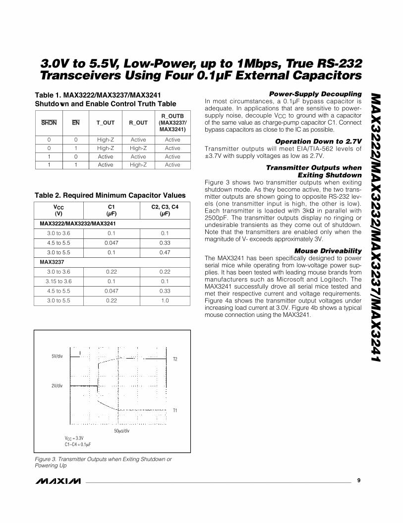
Transmitter Outputs when Exiting Shutdown
Figure 3 shows two transmitter outputs when exitingshutdown mode. As they become active, the two trans-mitter outputs are shown going to opposite RS-232 lev-els (one transmitter input is high, the other is low).Each transmitter is loaded with 3kΩ in parallel with2500pF. The transmitter outputs display no ringing orundesirable transients as they come out of shutdown.Note that the transmitters are enabled only when themagnitude of V- exceeds approximately 3V.
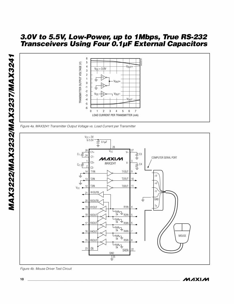
Mouse DriveabilityThe MAX3241 has been specifically designed to powerserial mice while operating from low-voltage power sup-plies. It has been tested with leading mouse brands frommanufacturers such as Microsoft and Logitech. TheMAX3241 successfully drove all serial mice tested andmet their respective current and voltage requirements.Figure 4a shows the transmitter output voltages underincreasing load current at 3.0V. Figure 4b shows a typicalmouse connection using the MAX3241.
Table 1. MAX3222/MAX3237/MAX3241 Shutdown and Enable Control Truth Table
Table 2. Required Minimum Capacitor Values
5V/div
VCC = 3.3VC1–C4 = 0.1µF
2V/div
T2
50µs/div
T1
Figure 3. Transmitter Outputs when Exiting Shutdown or Powering Up
VCC(V)
C1(µF)
4.5 to 5.5 0.047
3.0 to 5.5 0.1
C2, C3, C4(µF)
MAX3222/MAX3232/MAX3241
0.33
0.47
1 Active0
1Active1
SSHHDDNN
High-Z10
High-Z00
T_OUTEENN
High-ZActive
High-Z
Active
R_OUTR_OUTB
(MAX3237/MAX3241)
Active
Active
ActiveActive
3.0 to 3.6 0.22
3.15 to 3.6 0.1
MAX3237
0.22
0.1
4.5 to 5.5 0.047
3.0 to 5.5 0.22
0.33
1.0
3.0 to 3.6 0.1 0.1
MA
X3
22
2/M
AX
32
32
/MA
X3
23
7/M
AX
32
41
3.0V to 5.5V, Low-Power, up to 1Mbps, True RS-232Transceivers Using Four 0.1µF External Capacitors
10 ______________________________________________________________________________________
MAX3241
EN23
R5OUT15
R4OUT16
R3OUT17
R2OUT18
R1OUT19
R2OUTB20
R1OUTB21
5k
5k
5k
5k
5k
R5IN 8
R4IN 7
6
R2IN 5
R1IN 4
SHDN 22GND
25
T3IN12
T2IN13
T1IN14C2-2C2+1
C1-24C1+28
T3OUT 11
+V
COMPUTER SERIAL PORT
MOUSE
+V
-V
GND
Tx
T2OUT 10
T1OUT 9
V-3
V+27VCC
VCC
C4
C3 C1
C2
0.1µF
VCC = 3Vto 5.5V
26
R3IN
Figure 4b. Mouse Driver Test Circuit
-6-5
-4-3-2-10123456
0 1 2 3 4 5 6 7
MAX
3222
-04
LOAD CURRENT PER TRANSMITTER (mA)
TRAN
SMIT
TER
OUTP
UT V
OLTA
GE (V
)
VOUT+VCC = 3.0V
VOUT-
VOUT+
VCC VOUT-
T1
T2
T3
Figure 4a. MAX3241 Transmitter Output Voltage vs. Load Current per Transmitter
MA
X3
22
2/M
AX
32
32
/MA
X3
23
7/M
AX
32
41
3.0V to 5.5V, Low-Power, up to 1Mbps, True RS-232Transceivers Using Four 0.1µF External Capacitors
______________________________________________________________________________________ 11
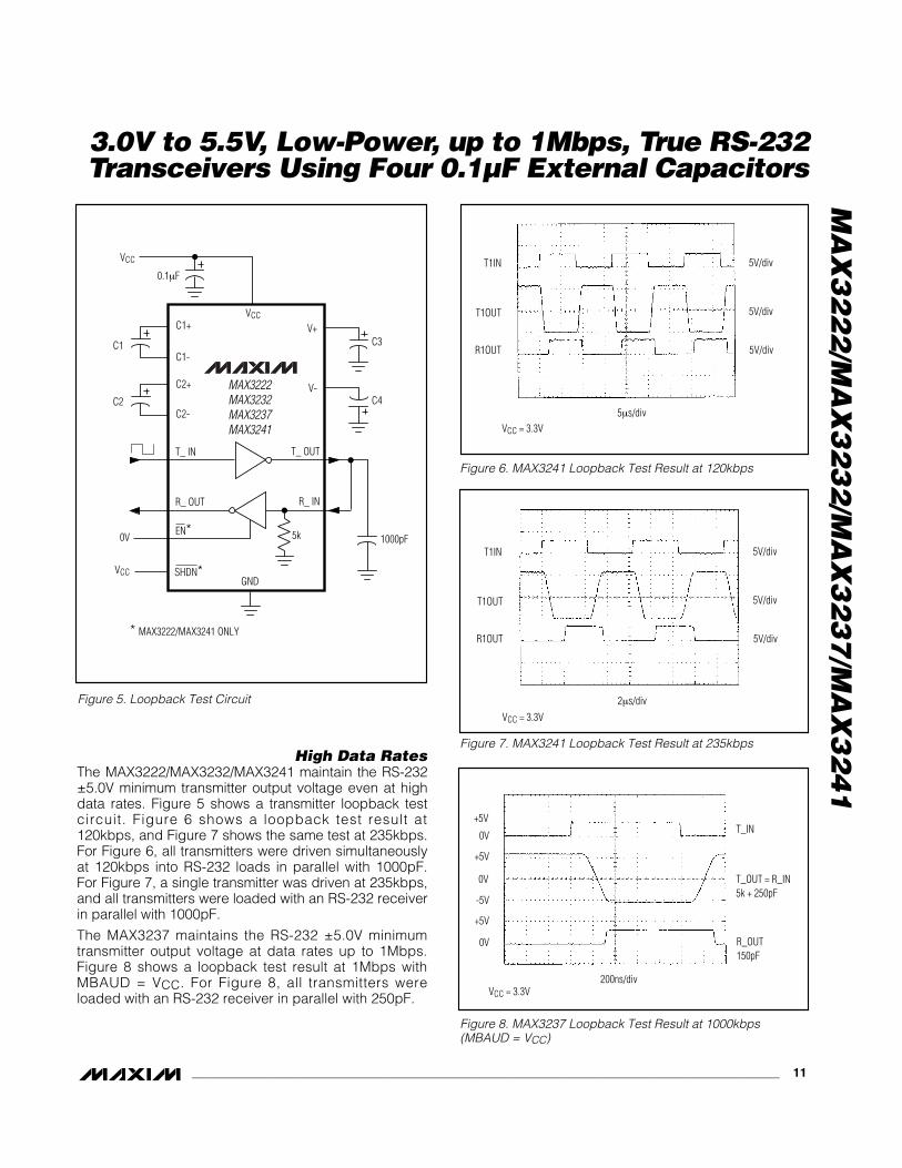
High Data RatesThe MAX3222/MAX3232/MAX3241 maintain the RS-232±5.0V minimum transmitter output voltage even at highdata rates. Figure 5 shows a transmitter loopback testcircuit. Figure 6 shows a loopback test result at120kbps, and Figure 7 shows the same test at 235kbps.For Figure 6, all transmitters were driven simultaneouslyat 120kbps into RS-232 loads in parallel with 1000pF.For Figure 7, a single transmitter was driven at 235kbps,and all transmitters were loaded with an RS-232 receiverin parallel with 1000pF.
The MAX3237 maintains the RS-232 ±5.0V minimumtransmitter output voltage at data rates up to 1Mbps.Figure 8 shows a loopback test result at 1Mbps withMBAUD = VCC. For Figure 8, all transmitters wereloaded with an RS-232 receiver in parallel with 250pF.
MAX3222MAX3232MAX3237MAX3241
5k
R_ INR_ OUT
EN*
C2-
C2+
C1-
C1+
V-
V+VCC
C4
C3C1
C2
0.1µF
VCC
SHDN*
T_ OUTT_ IN
GNDVCC
0V 1000pF
* MAX3222/MAX3241 ONLY
T1IN
R1OUT
VCC = 3.3V
T1OUT
5V/div
5V/div
5V/div
5µs/div
Figure 5. Loopback Test Circuit
Figure 6. MAX3241 Loopback Test Result at 120kbps
T1IN
R1OUT
VCC = 3.3V
T1OUT
5V/div
5V/div
2µs/div
5V/div
Figure 7. MAX3241 Loopback Test Result at 235kbps
+5V
0V
+5V
0V
-5V
+5V
0V
T_IN
T_OUT = R_IN5k + 250pF
R_OUT150pF
200ns/divVCC = 3.3V
Figure 8. MAX3237 Loopback Test Result at 1000kbps(MBAUD = VCC)
MA
X3
22
2/M
AX
32
32
/MA
X3
23
7/M
AX
32
41
3.0V to 5.5V, Low-Power, up to 1Mbps, True RS-232Transceivers Using Four 0.1µF External Capacitors
12 ______________________________________________________________________________________
__________________________________________________Typical Operating Circuits
MAX3222
R2OUT10
1
R1OUT13
R2IN 9
18GND
16
RS-232OUTPUTS
TTL/CMOSINPUTS
T2IN11
T1IN12
C2-6
C2+5
C1-4
C1+2
R1IN 14
T2OUT 8
T1OUT 15
V-7
V+3VCC
17
C10.1µF
C20.1µF
0.1µF
+3.3V
RS-232INPUTS
TTL/CMOSOUTPUTS
5k
5kEN
SHDN
C3*0.1µF
C40.1µF
PIN NUMBERS REFER TO DIP/SO PACKAGES.
* C3 CAN BE RETURNED TO EITHER VCC OR GROUND.
MAX3232
R2OUT9
R1OUT12
R2IN 8
GND
15
RS-232OUTPUTS
TTL/CMOSINPUTS
T2IN10
T1IN11
C2-5
C2+4
C1-3
C1+1
R1IN 13
T2OUT 7
T1OUT 14
V-6
V+2VCC
C40.1µF
16
0.1µF
0.1µF
0.1µF
+3.3V
RS-232INPUTS
TTL/CMOSOUTPUTS
C3*0.1µF
5k
5k
* C3 CAN BE RETURNED TO EITHER VCC OR GROUND.
SEE TABLE 2 FOR CAPACITOR SELECTION
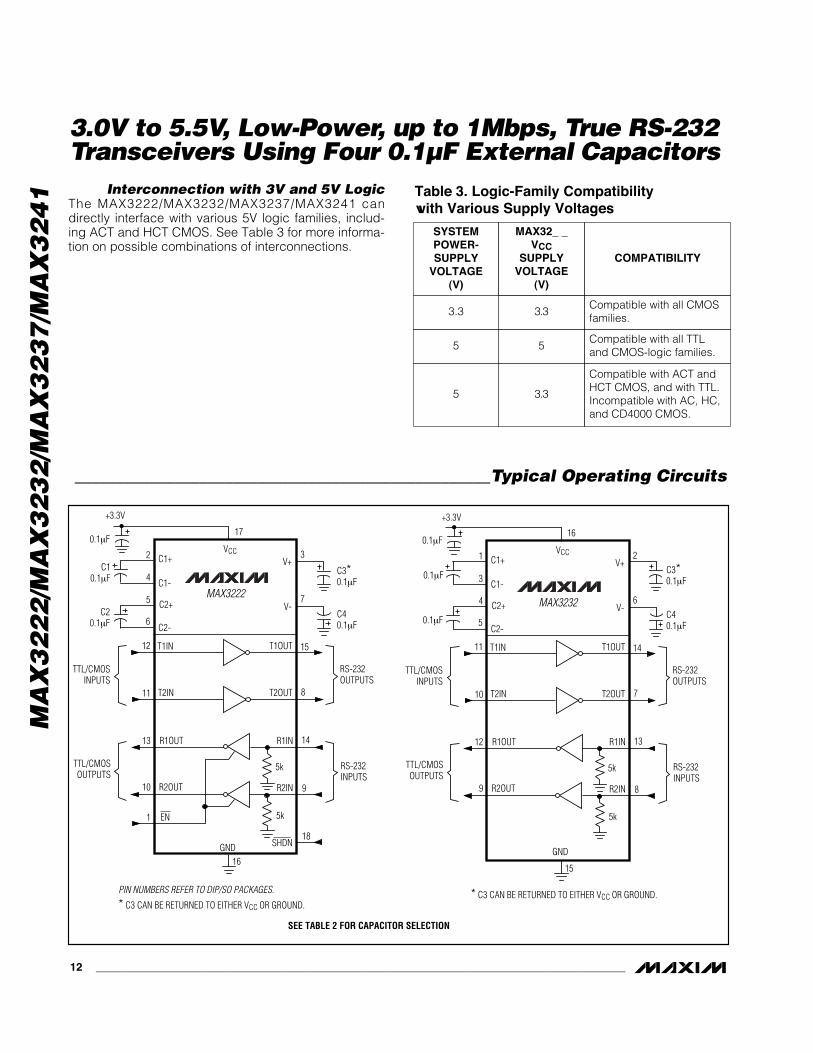
Interconnection with 3V and 5V LogicThe MAX3222/MAX3232/MAX3237/MAX3241 candirectly interface with various 5V logic families, includ-ing ACT and HCT CMOS. See Table 3 for more informa-tion on possible combinations of interconnections.
Table 3. Logic-Family Compatibility with Various Supply Voltages
Compatible with ACT andHCT CMOS, and with TTL.Incompatible with AC, HC,and CD4000 CMOS.
3.35
SYSTEMPOWER-SUPPLY
VOLTAGE(V)
Compatible with all TTL and CMOS-logic families.
55
Compatible with all CMOSfamilies.
3.33.3
COMPATIBILITY
MAX32_ _VCC
SUPPLYVOLTAGE
(V)

MA
X3
22
2/M
AX
32
32
/MA
X3
23
7/M
AX
32
41
3.0V to 5.5V, Low-Power, up to 1Mbps, True RS-232Transceivers Using Four 0.1µF External Capacitors
______________________________________________________________________________________ 13
_____________________________________Typical Operating Circuits (continued)
MAX3241
EN23
R5OUT15
R4OUT16
R3OUT17
R2OUT18
R1OUT19
R2OUTB20
R1OUTB21
TTL/CMOSOUTPUTS
5k
5k
5k
5k
5k
R5IN 8
* C3 CAN BE RETURNED TO EITHER VCC OR GROUND.
R4IN 7
R3IN 6
R2IN 5
R1IN 4
RS-232INPUTS
SHDN 22GND
25
RS-232OUTPUTS
TTL/CMOSINPUTS
T3IN12
T2IN13
T1IN14
C2-2
C2+1
C1-24
C1+28
T3OUT 11
T2OUT 10
T1OUT 9
V-3
V+27VCC
C40.1µF
C3*0.1µF
0.1µF
0.1µF
0.1µF+3.3V
26
MAX3237
EN13
R3OUT18
R2OUT20
R1OUT21
R1OUTB16
LOGICUTPUTS
5k
5k
5k
* C3 CAN BE RETURNED TO EITHER VCC OR GROUND.
R3IN 11
R2IN 9
R1IN 8
RS-232INPUTS
GND
2
RS-232OUTPUTS
LOGICINPUTS
T3IN22
T2IN23
T1IN24
C2-3
C2+1
C1-25
C1+28
T3OUT 7
T2OUT 6
T1OUT 5T1
T2
T3
R1
R2
R3
V-4
V+27VCC
0.1µF
0.1µF
0.1µF
0.1µF
0.1µF
26
MBAUD 15
T5IN17
T4IN19
T5OUT 12
T4OUT 10
SHDN14
T4
T5
MA
X3
22
2/M
AX
32
32
/MA
X3
23
7/M
AX
32
41
3.0V to 5.5V, Low-Power, up to 1Mbps, True RS-232Transceivers Using Four 0.1µF External Capacitors
14 ______________________________________________________________________________________
_____________________________________________Pin Configurations (continued)
16
15
14
13
12
11
10
9
1
2
3
4
5
6
7
8
VCC
GND
T1OUT
R1INC2+
C1-
V+
C1+
MAX3232
R1OUT
T1IN
T2IN
R2OUTR2IN
T2OUT
V-
C2-
DIP/SO/TSSOP
TOP VIEW
20
19
18
17
16
15
14
13
1
2
3
8
12
1110
4
5
6
7
SHDN
VCC
GND
T1OUTC1-
V+
C1+
EN
R1IN
R1OUT
T1IN
T2IN
T2OUT
V-
C2-
C2+
9R2IN
R2OUT
SSOP/TSSOP
N.C.
N.C.
MAX3222
28
27
26
25
24
23
22
21
20
19
18
17
16
15
1
2
3
4
5
6
7
8
9
10
11
12
13
14
C1+
V+
VCC
C1-
T1IN
T2IN
MBAUD
T3IN
R1OUT
R2OUT
T4IN
R3OUT
T5IN
R1OUTB
SHDN
EN
T5OUT
R3IN
T4OUT
R2IN
R1IN
T3OUT
T2OUT
T1OUT
V-
C2-
GND
C2+
SSOP
MAX3237
28
27
26
25
24
23
22
21
20
19
18
17
16
15
1
2
3
4
5
6
7
8
9
10
11
12
13
14
C1+
V+
VCC
GND
C1-
EN
R5OUT
SHDN
R1OUTB
R2OUTB
R1OUT
R2OUT
R3OUT
R4OUT
T1IN
T2IN
T3IN
T3OUT
T2OUT
T1OUT
R5IN
R4IN
R3IN
R2IN
R1IN
V-
C2-
C2+
SO/SSOP/TSSOP
MAX3241
MA
X3
22
2/M
AX
32
32
/MA
X3
23
7/M
AX
32
41
3.0V to 5.5V, Low-Power, up to 1Mbps, True RS-232Transceivers Using Four 0.1µF External Capacitors
______________________________________________________________________________________ 15
______3V-Powered EIA/TIA-232 and EIA/TIA-562 Transceivers from Maxim
Ordering Information (continued)
* Dice are tested at TA = +25°C, DC parameters only.
0.1µF capacitors, 1 complemen-tary receiver, MegaBaud operation
232250/100035/33.0 to 5.5MAX3237
0.1µF capacitors, AutoShutdown,complementary receiver, drives mice
23212013/53.0 to 5.5MAX3243
0.1µF capacitors232120N/A2/23.0 to 5.5MAX32320.1µF capacitors, AutoShutdown23212022/23.0 to 5.5MAX3223
0.1µF capacitors23212022/23.0 to 5.5MAX3222
232
562
232
562
232
EIA/TIA-232OR 562
2.7 to 3.6AutoShutdown, complementaryreceiver, drives mice, transientdetection
23553/5MAX3212
0.1µF capacitors23022/23.0 to 3.6MAX563
Operates directly from batterieswithout a voltage regulator
12022/21.8 to 4.25MAX218
No. OFRECEIVERSACTIVE IN
SHUTDOWN
POWER-SUPPLY
VOLTAGE(V)
Wide supply range23053/52.7 to 5.25MAX562
Drives mice12053/53.0 to 3.6MAX212
FEATURES
GUAR-ANTEED
DATARATE(kbps)
No. OFTRANSMITTERS/
RECEIVERSPART
0.1µF capacitors, 2 complemen-tary receivers, drives mice
23212053/53.0 to 5.5MAX3241
PART
MAX3222EUP
MAX3222EAP
MAX3222EWN -40°C to +85°C
-40°C to +85°C
-40°C to +85°C
TEMP RANGE PIN-PACKAGE
20 TSSOP
20 SSOP
18 SO
MAX3222EPN
MAX3232CUE
MAX3232CSE 0°C to +70°C
0°C to +70°C
-40°C to +85°C 18 Plastic DIP
16 TSSOP
16 Narrow SO
MAX3232CWE
MAX3232EUE
MAX3232ESE -40°C to +85°C
-40°C to +85°C
0°C to +70°C 16 Wide SO
16 TSSOP
16 Narrow SO
MAX3222C/D 0°C to +70°C Dice*
MAX3232CPE 0°C to +70°C 16 Plastic DIP
PART TEMP RANGE PIN-PACKAGE
MAX3232EWE
MAX3237CAI
MAX3237EAI -40°C to +85°C
0°C to +70°C
-40°C to +85°C 16 Wide SO
28 SSOP
28 SSOPMAX3241CUI 0°C to +70°C 28 TSSOP
MAX3241CAI
MAX3241EUI
MAX3241EAI -40°C to +85°C
-40°C to +85°C
0°C to +70°C 28 SSOP
28 TSSOP
28 SSOPMAX3241EWI -40°C to +85°C 28 SO
MAX3241CWI 0°C to +70°C 28 SO
MAX3232EPE -40°C to +85°C 16 Plastic DIP
MA
X3
22
2/M
AX
32
32
/MA
X3
23
7/M
AX
32
41
3.0V to 5.5V, Low-Power, up to 1Mbps, True RS-232Transceivers Using Four 0.1µF External Capacitors
Maxim cannot assume responsibility for use of any circuitry other than circuitry entirely embodied in a Maxim product. No circuit patent licenses areimplied. Maxim reserves the right to change the circuitry and specifications without notice at any time.
16 ____________________Maxim Integrated Products, 120 San Gabriel Drive, Sunnyvale, CA 94086 408-737-7600
© 2003 Maxim Integrated Products Printed USA is a registered trademark of Maxim Integrated Products.
___________________Chip Topography ___________________Chip Information
T1INT2IN
0.127"(3.225mm)
0.087"(2.209mm)
R2OUTR2INT2OUT
R1OUT
R1IN
T1OUT
VCCV+ C1+SHDN
EN
C1- C2+
C2-
V-
GND
MAX3222
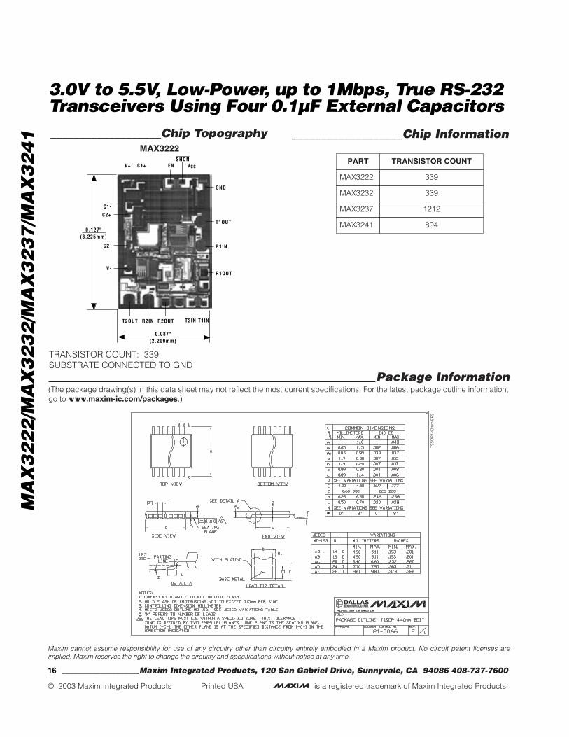
TRANSISTOR COUNT: 339SUBSTRATE CONNECTED TO GND
MAX3222 339
MAX3232 339
MAX3237 1212
MAX3241 894
TRANSISTOR COUNTPART
TSS
OP
4.40
mm
.EP
S
Package Information(The package drawing(s) in this data sheet may not reflect the most current specifications. For the latest package outline information,go to www.maxim-ic.com/packages.)