Embed Size (px)
Citation preview
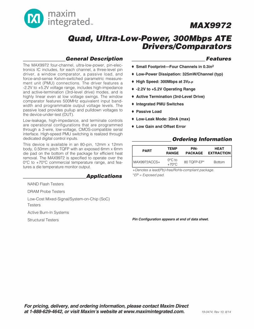
19-0474; Rev 10; 8/14
MAX9972
Quad, Ultra-Low-Power, 300Mbps ATEDrivers/Comparators
For pricing, delivery, and ordering information, please contact Maxim Directat 1-888-629-4642, or visit Maxim’s website at www.maximintegrated.com.
General DescriptionThe MAX9972 four-channel, ultra-low-power, pin-elec-tronics IC includes, for each channel, a three-level pindriver, a window comparator, a passive load, andforce-and-sense Kelvin-switched parametric measure-ment unit (PMU) connections. The driver features a-2.2V to +5.2V voltage range, includes high-impedanceand active-termination (3rd-level drive) modes, and ishighly linear even at low voltage swings. The windowcomparator features 500MHz equivalent input band-width and programmable output voltage levels. Thepassive load provides pullup and pulldown voltages tothe device-under-test (DUT).
Low-leakage, high-impedance, and terminate controlsare operational configurations that are programmedthrough a 3-wire, low-voltage, CMOS-compatible serialinterface. High-speed PMU switching is realized throughdedicated digital control inputs.
This device is available in an 80-pin, 12mm x 12mmbody, 0.50mm pitch TQFP with an exposed 6mm x 6mmdie pad on the bottom of the package for efficient heatremoval. The MAX9972 is specified to operate over the0°C to +70°C commercial temperature range, and fea-tures a die temperature monitor output.
ApplicationsNAND Flash Testers
DRAM Probe Testers
Low-Cost Mixed-Signal/System-on-Chip (SoC)
Testers
Active Burn-In Systems
Structural Testers
Features� Small Footprint—Four Channels in 0.3in2
� Low-Power Dissipation: 325mW/Channel (typ)
� High Speed: 300Mbps at 3VP-P
� -2.2V to +5.2V Operating Range
� Active Termination (3rd-Level Drive)
� Integrated PMU Switches
� Passive Load
� Low-Leak Mode: 20nA (max)
� Low Gain and Offset Error
PARTTEMP
RANGEPIN-
PACKAGEHEAT
EXTRACTION
MAX9972ACCS+0°C to+70°C
80 TQFP-EP* Bottom
Ordering Information
Pin Configuration appears at end of data sheet.
+Denotes a lead(Pb)-free/RoHs-compliant package.*EP = Exposed pad.
MAX9972Quad, Ultra-Low-Power, 300Mbps ATEDrivers/Comparators
2 Maxim Integrated
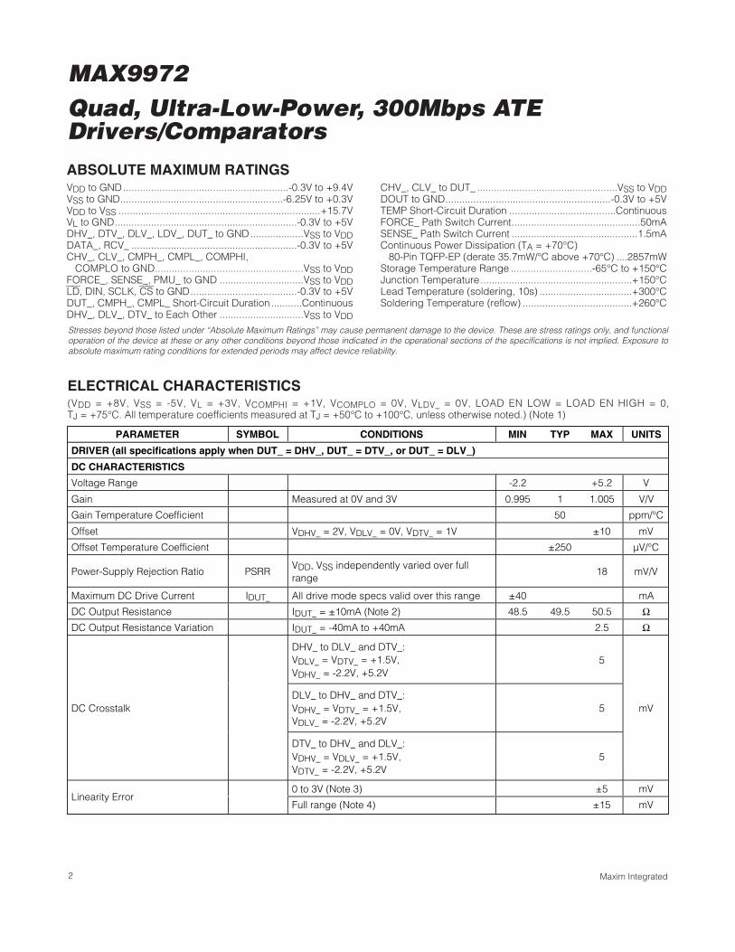
ABSOLUTE MAXIMUM RATINGS
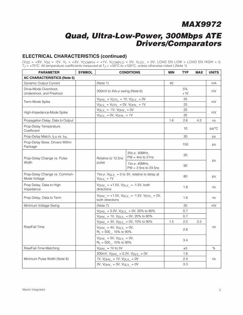
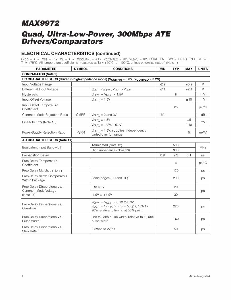
ELECTRICAL CHARACTERISTICS(VDD = +8V, VSS = -5V, VL = +3V, VCOMPHI = +1V, VCOMPLO = 0V, VLDV_ = 0V, LOAD EN LOW = LOAD EN HIGH = 0,TJ = +75°C. All temperature coefficients measured at TJ = +50°C to +100°C, unless otherwise noted.) (Note 1)
Stresses beyond those listed under “Absolute Maximum Ratings” may cause permanent damage to the device. These are stress ratings only, and functionaloperation of the device at these or any other conditions beyond those indicated in the operational sections of the specifications is not implied. Exposure toabsolute maximum rating conditions for extended periods may affect device reliability.
VDD to GND...........................................................-0.3V to +9.4VVSS to GND..........................................................-6.25V to +0.3VVDD to VSS ........................................................................+15.7VVL to GND.................................................................-0.3V to +5VDHV_, DTV_, DLV_, LDV_, DUT_ to GND...................VSS to VDDDATA_, RCV_ ...........................................................-0.3V to +5VCHV_, CLV_, CMPH_, CMPL_, COMPHI,
COMPLO to GND.....................................................VSS to VDDFORCE_, SENSE_, PMU_ to GND ..............................VSS to VDDLD, DIN, SCLK, CS to GND......................................-0.3V to +5VDUT_, CMPH_, CMPL_ Short-Circuit Duration ...........ContinuousDHV_, DLV_, DTV_ to Each Other ..............................VSS to VDD
CHV_, CLV_ to DUT_ ..................................................VSS to VDDDOUT to GND...........................................................-0.3V to +5VTEMP Short-Circuit Duration ......................................ContinuousFORCE_ Path Switch Current..............................................50mASENSE_ Path Switch Current .............................................1.5mAContinuous Power Dissipation (TA = +70°C)
80-Pin TQFP-EP (derate 35.7mW/°C above +70°C) ....2857mWStorage Temperature Range .............................-65°C to +150°CJunction Temperature ......................................................+150°CLead Temperature (soldering, 10s) .................................+300°CSoldering Temperature (reflow) .......................................+260°C
PARAMETER SYMBOL CONDITIONS MIN TYP MAX UNITS
DRIVER (all specifications apply when DUT_ = DHV_, DUT_ = DTV_, or DUT_ = DLV_)
DC CHARACTERISTICS
Voltage Range -2.2 +5.2 V
Gain Measured at 0V and 3V 0.995 1 1.005 V/V
Gain Temperature Coefficient 50 ppm/°C
Offset VDHV_ = 2V, VDLV_ = 0V, VDTV_ = 1V ±10 mV
Offset Temperature Coefficient ±250 µV/°C
Power-Supply Rejection Ratio PSRRVDD, VSS independently varied over fullrange
18 mV/V
Maximum DC Drive Current IDUT_ All drive mode specs valid over this range ±40 mA
DC Output Resistance IDUT_ = ±10mA (Note 2) 48.5 49.5 50.5 ΩDC Output Resistance Variation IDUT_ = -40mA to +40mA 2.5 Ω
DHV_ to DLV_ and DTV_:VDLV_ = VDTV_ = +1.5V,VDHV_ = -2.2V, +5.2V
5
DLV_ to DHV_ and DTV_:VDHV_ = VDTV_ = +1.5V,VDLV_ = -2.2V, +5.2V
5DC Crosstalk
DTV_ to DHV_ and DLV_:VDHV_ = VDLV_ = +1.5V,VDTV_ = -2.2V, +5.2V
5
mV
0 to 3V (Note 3) ±5 mVLinearity Error
Full range (Note 4) ±15 mV
MAX9972Quad, Ultra-Low-Power, 300Mbps ATE
Drivers/Comparators
3Maxim Integrated
ELECTRICAL CHARACTERISTICS (continued)(VDD = +8V, VSS = -5V, VL = +3V, VCOMPHI = +1V, VCOMPLO = 0V, VLDV_ = 0V, LOAD EN LOW = LOAD EN HIGH = 0,TJ = +75°C. All temperature coefficients measured at TJ = +50°C to +100°C, unless otherwise noted.) (Note 1)
PARAMETER SYMBOL CONDITIONS MIN TYP MAX UNITS
AC CHARACTERISTICS (Note 5)
Dynamic Output Current (Note 1) 40 mA
Drive-Mode Overshoot,Undershoot, and Preshoot
200mV to 4VP-P swing (Note 6)5%+10
mV
VDHV_ = VDTV_ = 1V, VDLV_ = 0V 25Term-Mode Spike
VDLV_ = VDTV_ = 0V, VDHV_ = 1V 25mV
VDLV_ = -1V, VDHV_ = 0V 25High-Impedance-Mode Spike
VDLV_ = 0V, VDHV_ = 1V 25mV
P r op ag ati on D el ay, D ata to Outp ut 1.6 2.6 4.2 ns
Prop-Delay TemperatureCoefficient
10 ps/°C
Prop-Delay Match, tLH vs. tHL 30 ps
Prop-Delay Skew, Drivers WithinPackage
150 ps
3VP-P, 40MHz,PW = 4ns to 21ns
20Prop-Delay Change vs. PulseWidth
Relative to 12.5nspulse 1VP-P, 40MHz,
PW = 2.5ns to 23.5ns90
ps
Prop-Delay Change vs. Common-Mode Voltage
1VP-P, VDLV_ = 0 to 3V, relative to delay atVDLV_ = 1V
80 ps
Prop Delay, Data to HighImpedance
VDHV_ = +1.5V, VDLV_ = -1.5V, bothdirections
1.8 ns
Prop Delay, Data to TermVDHV_ = +1.5V, VDLV_ = -1.5V, VDTV_ = 0V,both directions
1.6 ns
Minimum Voltage Swing (Note 7) 25 mV
VDHV_ = 0.2V, VDLV_ = 0V, 20% to 80% 0.7
VDHV_ = 1V, VDLV_ = 0V, 20% to 80% 0.7
VDHV_ = 3V, VDLV_ = 0V, 10% to 90% 1.5 2.0 2.5
VDHV_ = 4V, VDLV_ = 0V,RL = 500_, 10% to 90%
2.6Rise/Fall Time
VDHV_ = 5V, VDLV_ = 0V,RL = 500_, 10% to 90%
3.4
ns
Rise/Fall-Time Matching VDHV_ = 1V to 5V ±5 %
200mV, VDHV_ = 0.2V, VDLV_ = 0V 1.8
1V, VDHV_ = 1V, VDLV_ = 0V 2.4Minimum Pulse Width (Note 8)
3V, VDHV_ = 3V, VDLV_ = 0V 3.3
ns
MAX9972Quad, Ultra-Low-Power, 300Mbps ATEDrivers/Comparators
4 Maxim Integrated
ELECTRICAL CHARACTERISTICS (continued)(VDD = +8V, VSS = -5V, VL = +3V, VCOMPHI = +1V, VCOMPLO = 0V, VLDV_ = 0V, LOAD EN LOW = LOAD EN HIGH = 0,TJ = +75°C. All temperature coefficients measured at TJ = +50°C to +100°C, unless otherwise noted.) (Note 1)
PARAMETER SYMBOL CONDITIONS MIN TYP MAX UNITS
COMPARATOR (Note 9)
DC CHARACTERISTICS (driver in high-impedance mode) (VCOMPHI = 0.8V, VCOMPLO = 0.2V)
Input Voltage Range -2.2 +5.2 V
Differential Input Voltage VDUT_ - VCHV_, VDUT_ - VCLV_ -7.4 +7.4 V
Hysteresis VCHV_ = VCLV_ = 1.5V 8 mV
Input Offset Voltage VDUT_ = 1.5V ±10 mV
Input Offset Temperature Coefficient
25 µV/°C
Common-Mode Rejection Ratio CMRR VDUT_ = 0 and 3V 60 dB
VDUT_ = 1.5V ±5 Linearity Error (Note 10)
VDUT_ = -2.2V, +5.2V ±10 mV
Power-Supply Rejection Ratio PSRR VDUT_ = 1.5V, supplies independently varied over full range
5 mV/V
AC CHARACTERISTICS (Note 11)
Terminated (Note 12) 500 Equivalent Input Bandwidth
High impedance (Note 13) 300MHz
Propagation Delay 0.9 2.2 3.1 ns
Prop-Delay Temperature Coefficient
4 ps/°C
Prop-Delay Match, tLH to tHL 120 ps
Prop-Delay Skew, Comparators Within Package
Same edges (LH and HL) 200 ps
0 to 4.9V 20 Prop-Delay Dispersions vs. Common-Mode Voltage (Note 14) -1.9V to +4.9V 30
ps
Prop-Delay Dispersions vs. Overdrive
VCHV_ = VCLV_ = 0.1V to 0.9V, VDUT_ = 1VP-P, tR = tF = 500ps, 10% to 90% relative to timing at 50% point
220 ps
Prop-Delay Dispersions vs. Pulse Width
2ns to 23ns pulse width, relative to 12.5ns pulse width
±60 ps
Prop-Delay Dispersions vs. Slew Rate
0.5V/ns to 2V/ns 50 ps
MAX9972Quad, Ultra-Low-Power, 300Mbps ATE
Drivers/Comparators
5Maxim Integrated
ELECTRICAL CHARACTERISTICS (continued)(VDD = +8V, VSS = -5V, VL = +3V, VCOMPHI = +1V, VCOMPLO = 0V, VLDV_ = 0V, LOAD EN LOW = LOAD EN HIGH = 0,TJ = +75°C. All temperature coefficients measured at TJ = +50°C to +100°C, unless otherwise noted.) (Note 1)
PARAMETER SYMBOL CONDITIONS MIN TYP MAX UNITS
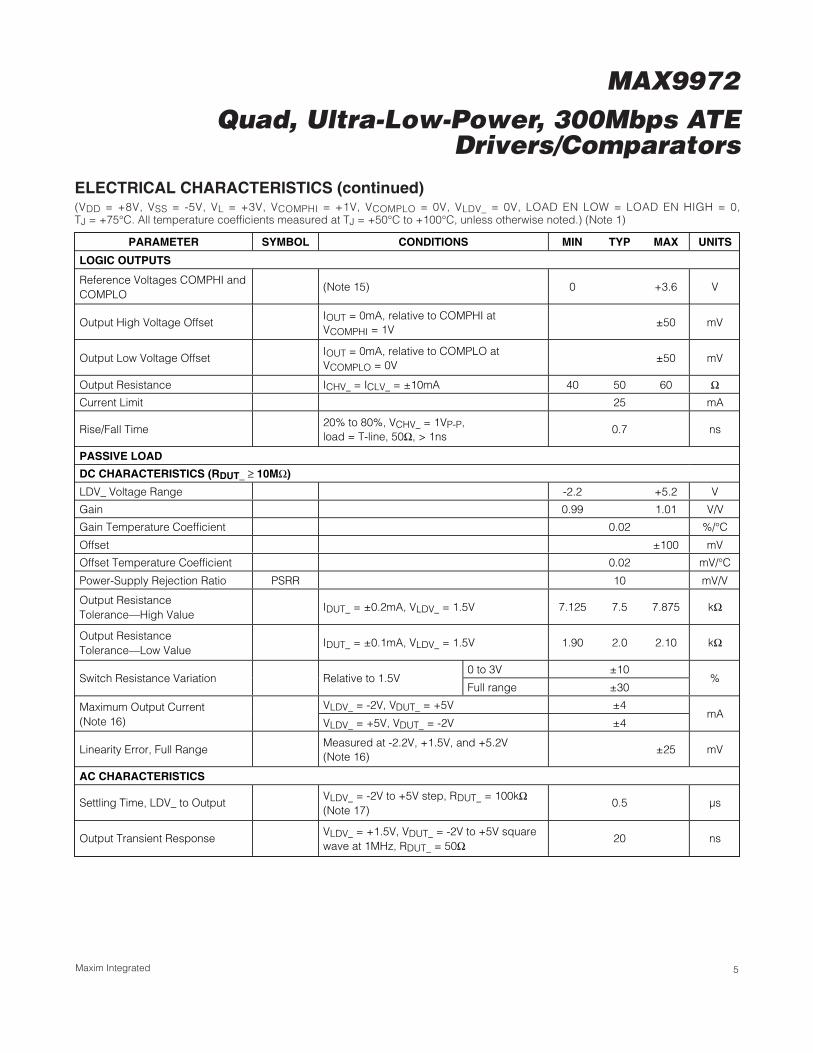
LOGIC OUTPUTS
Reference Voltages COMPHI andCOMPLO
(Note 15) 0 +3.6 V
Output High Voltage OffsetIOUT = 0mA, relative to COMPHI atVCOMPHI = 1V
±50 mV
Output Low Voltage OffsetIOUT = 0mA, relative to COMPLO atVCOMPLO = 0V
±50 mV
Output Resistance ICHV_ = ICLV_ = ±10mA 40 50 60 ΩCurrent Limit 25 mA
Rise/Fall Time20% to 80%, VCHV_ = 1VP-P,load = T-line, 50Ω, > 1ns
0.7 ns
PASSIVE LOAD
DC CHARACTERISTICS (RDUT_ ≥ 10MΩ)
LDV_ Voltage Range -2.2 +5.2 V
Gain 0.99 1.01 V/V
Gain Temperature Coefficient 0.02 %/°C
Offset ±100 mV
Offset Temperature Coefficient 0.02 mV/°C
Power-Supply Rejection Ratio PSRR 10 mV/V
Output ResistanceTolerance—High Value
IDUT_ = ±0.2mA, VLDV_ = 1.5V 7.125 7.5 7.875 kΩ
Output ResistanceTolerance—Low Value
IDUT_ = ±0.1mA, VLDV_ = 1.5V 1.90 2.0 2.10 kΩ
0 to 3V ±10Switch Resistance Variation Relative to 1.5V
Full range ±30%
VLDV_ = -2V, VDUT_ = +5V ±4Maximum Output Current(Note 16) VLDV_ = +5V, VDUT_ = -2V ±4
mA
Linearity Error, Full RangeMeasured at -2.2V, +1.5V, and +5.2V(Note 16)
±25 mV
AC CHARACTERISTICS
Settling Time, LDV_ to OutputVLDV_ = -2V to +5V step, RDUT_ = 100kΩ(Note 17)
0.5 µs
Output Transient ResponseVLDV_ = +1.5V, VDUT_ = -2V to +5V squarewave at 1MHz, RDUT_ = 50Ω
20 ns

MAX9972Quad, Ultra-Low-Power, 300Mbps ATEDrivers/Comparators
6 Maxim Integrated
ELECTRICAL CHARACTERISTICS (continued)(VDD = +8V, VSS = -5V, VL = +3V, VCOMPHI = +1V, VCOMPLO = 0V, VLDV_ = 0V, LOAD EN LOW = LOAD EN HIGH = 0,TJ = +75°C. All temperature coefficients measured at TJ = +50°C to +100°C, unless otherwise noted.) (Note 1)
PARAMETER SYMBOL CONDITIONS MIN TYP MAX UNITS
PMU SWITCHES (FORCE_, SENSE_, PMU_)
Voltage Range -2.2 +5.2 V
Force Switch Resistance VFORCE_ = 1.5V, IPMU_ = ±10mA 40 Ω
VPMU_ = 6.2V, VFORCE_ set to makeIFORCE_ = 30mA
25
Force Switch ComplianceVPMU_ = -3.2V, VFORCE_ set to makeIFORCE_ = -30mA
25
mA
0 to 3V ±10Force Switch ResistanceVariation (Note 18) Full range ±30
%
Sense Switch Resistance 700 1000 1300 Ω
Sense Switch ResistanceVariation
Relative to 1.3V, full range ±30 %
PMU_ Capacitance Force-and-sense switches open 5 pF
FORCE_ Capacitance 5 pF
SENSE_ Capacitance 0.2 pF
FORCE_ External Capacitance Allowable external capacitance 2 nF
SENSE_ External Capacitance Allowable external capacitance 1 nF
FORCE_ and SENSE_ SwitchingSpeed
Connect or disconnect 10 µs
PMU_ LeakageFORCE EN_ = SENSE EN_ = 0,VFORCE_ = VSENSE_ = -2.2V to +5.2V
±0.5 ±5 nA
TOTAL FUNCTION
DUT_
Leakage, High-Impedance Mode
Load switches open,VDUT_ = +5.2V,VCLV_ = VCHV_ = -2.2V,VDUT_ = -2.2V,VCLV_ = VCHV_ = +5.2V, full range
2 µA
Leakage, Low-Leakage Mode Full range ±1 ±20 nA
Low-Leakage Recovery Time (Note 19) 10 µs
Term mode 2Combined Capacitance
High-impedance mode 5pF
Load Resistance (Note 20) 1 GΩLoad Capacitance (Note 20) 12 nF

MAX9972Quad, Ultra-Low-Power, 300Mbps ATE
Drivers/Comparators
7Maxim Integrated
ELECTRICAL CHARACTERISTICS (continued)(VDD = +8V, VSS = -5V, VL = +3V, VCOMPHI = +1V, VCOMPLO = 0V, VLDV_ = 0V, LOAD EN LOW = LOAD EN HIGH = 0,TJ = +75°C. All temperature coefficients measured at TJ = +50°C to +100°C, unless otherwise noted.) (Note 1)
PARAMETER SYMBOL CONDITIONS MIN TYP MAX UNITS
VOLTAGE REFERENCE INPUTS (DHV_, DTV_, DLV_, DATA_, RCV_, CHV_, CLV_, LDV_, COMPHI, COMPLO)
Input Bias Current ±100 µA
Input Bias Current TemperatureCoefficient
±200 nA/°C
Settling to Output 0.1% of full-scale step 10 µs
DIGITAL INPUTS (DATA_, RCV_, LD, DIN, SCLK, CS)
Input High Voltage (Note 21)VL/2 +
0.2+3.6 V
Input Low Voltage (Note 21) 0VL/2 -
0.2V
D ATA_, 100
Input Bias Current LD, DIN,SCLK, CS
1µA
SERIAL DATA OUTPUT (DOUT)
Output High Voltage IOH = -1mAVL
- 0.4VL V
Output Low Voltage IOL = 1mA 0 +0.4 V
Output Rise and Fall Time CL = 10pF 1.1 ns
SERIAL-INTERFACE TIMING (Note 22)
SCLK Frequency 50 MHz
SCLK Pulse-Width High tCH 10 ns
SCLK Pulse-Width Low tCL 10 ns
CS Low to SCLK High Setup tCSS0 3.5 ns
SCLK High to CS Low Hold tCSH0 3.5 ns
CS High to SCLK High Setup tCSS1 3.5 ns
SCLK High to CS High Hold tCSH1 15 ns
DIN to SCLK High Setup tDS 7.5 ns
DIN to SCLK High Hold tDH 3.5 ns
CS High to LOAD Low Hold tCSHLD 6 ns
CS High Pulse Width tCSWH 20 ns
LD Low Pulse Width tLDW 20 ns
LD High to Any Activity 0 ns
SCLK Low to DOUT Delay tDO CL = 10pF 5 40 ns
VL Rising to CS Low Power-on delay 2 µs
TEMP SENSOR
Nominal Voltage TJ = +27°C 3.20 V
Temperature Coefficient +10 mV/°C
Output Resistance 500 Ω
MAX9972Quad, Ultra-Low-Power, 300Mbps ATEDrivers/Comparators
8 Maxim Integrated
ELECTRICAL CHARACTERISTICS (continued)(VDD = +8V, VSS = -5V, VL = +3V, VCOMPHI = +1V, VCOMPLO = 0V, VLDV_ = 0V, LOAD EN LOW = LOAD EN HIGH = 0,TJ = +75°C. All temperature coefficients measured at TJ = +50°C to +100°C, unless otherwise noted.) (Note 1)
PARAMETER SYMBOL CONDITIONS MIN TYP MAX UNITS
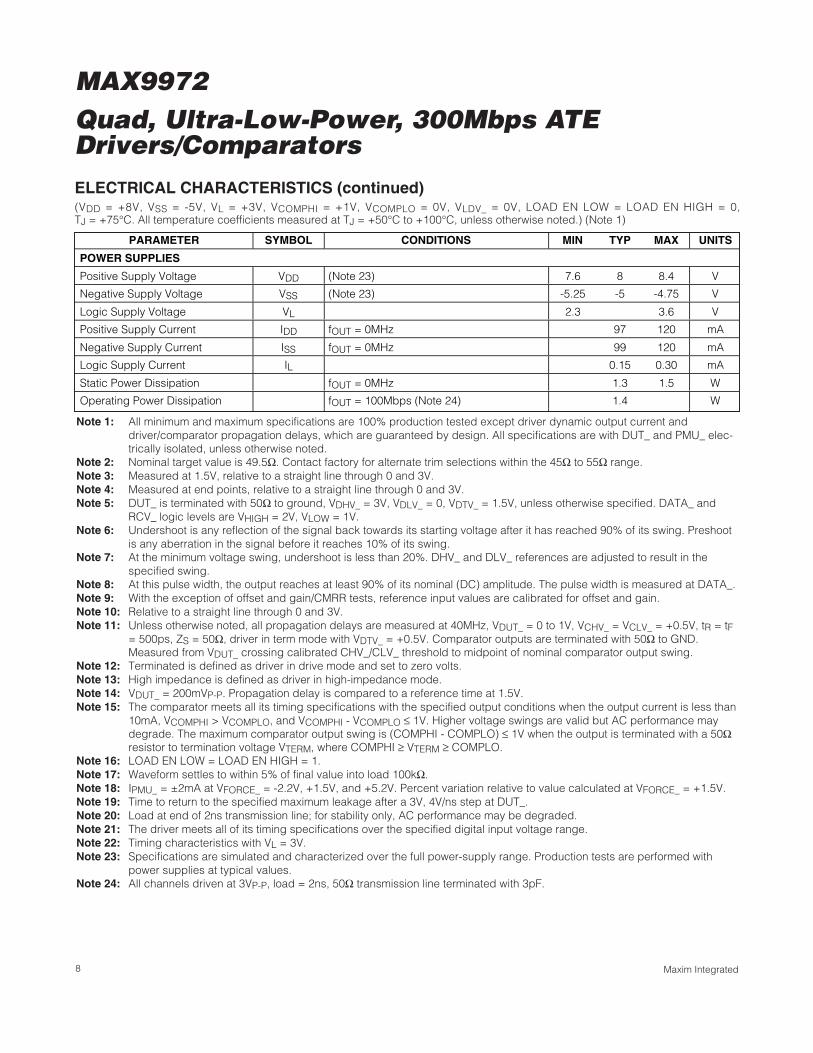
POWER SUPPLIES
Positive Supply Voltage VDD (Note 23) 7.6 8 8.4 V
Negative Supply Voltage VSS (Note 23) -5.25 -5 -4.75 V
Logic Supply Voltage VL 2.3 3.6 V
Positive Supply Current IDD fOUT = 0MHz 97 120 mA
Negative Supply Current ISS fOUT = 0MHz 99 120 mA
Logic Supply Current IL 0.15 0.30 mA
Static Power Dissipation fOUT = 0MHz 1.3 1.5 W
Operating Power Dissipation fOUT = 100Mbps (Note 24) 1.4 W
Note 1: All minimum and maximum specifications are 100% production tested except driver dynamic output current anddriver/comparator propagation delays, which are guaranteed by design. All specifications are with DUT_ and PMU_ elec-trically isolated, unless otherwise noted.
Note 2: Nominal target value is 49.5Ω. Contact factory for alternate trim selections within the 45Ω to 55Ω range.Note 3: Measured at 1.5V, relative to a straight line through 0 and 3V.Note 4: Measured at end points, relative to a straight line through 0 and 3V.Note 5: DUT_ is terminated with 50Ω to ground, VDHV_ = 3V, VDLV_ = 0, VDTV_ = 1.5V, unless otherwise specified. DATA_ and
RCV_ logic levels are VHIGH = 2V, VLOW = 1V.Note 6: Undershoot is any reflection of the signal back towards its starting voltage after it has reached 90% of its swing. Preshoot
is any aberration in the signal before it reaches 10% of its swing.Note 7: At the minimum voltage swing, undershoot is less than 20%. DHV_ and DLV_ references are adjusted to result in the
specified swing.Note 8: At this pulse width, the output reaches at least 90% of its nominal (DC) amplitude. The pulse width is measured at DATA_.Note 9: With the exception of offset and gain/CMRR tests, reference input values are calibrated for offset and gain.Note 10: Relative to a straight line through 0 and 3V.Note 11: Unless otherwise noted, all propagation delays are measured at 40MHz, VDUT_ = 0 to 1V, VCHV_ = VCLV_ = +0.5V, tR = tF
= 500ps, ZS = 50Ω, driver in term mode with VDTV_ = +0.5V. Comparator outputs are terminated with 50Ω to GND.Measured from VDUT_ crossing calibrated CHV_/CLV_ threshold to midpoint of nominal comparator output swing.
Note 12: Terminated is defined as driver in drive mode and set to zero volts.Note 13: High impedance is defined as driver in high-impedance mode.Note 14: VDUT_ = 200mVP-P. Propagation delay is compared to a reference time at 1.5V.Note 15: The comparator meets all its timing specifications with the specified output conditions when the output current is less than
10mA, VCOMPHI > VCOMPLO, and VCOMPHI - VCOMPLO ≤ 1V. Higher voltage swings are valid but AC performance maydegrade. The maximum comparator output swing is (COMPHI - COMPLO) ≤ 1V when the output is terminated with a 50Ωresistor to termination voltage VTERM, where COMPHI ≥ VTERM ≥ COMPLO.
Note 16: LOAD EN LOW = LOAD EN HIGH = 1.Note 17: Waveform settles to within 5% of final value into load 100kΩ.Note 18: IPMU_ = ±2mA at VFORCE_ = -2.2V, +1.5V, and +5.2V. Percent variation relative to value calculated at VFORCE_ = +1.5V.Note 19: Time to return to the specified maximum leakage after a 3V, 4V/ns step at DUT_.Note 20: Load at end of 2ns transmission line; for stability only, AC performance may be degraded.Note 21: The driver meets all of its timing specifications over the specified digital input voltage range.Note 22: Timing characteristics with VL = 3V.Note 23: Specifications are simulated and characterized over the full power-supply range. Production tests are performed with
power supplies at typical values.Note 24: All channels driven at 3VP-P, load = 2ns, 50Ω transmission line terminated with 3pF.
MAX
9971
toc0
1
t = 2.0ns/div
V DUT
_ =
50m
V/di
v
0
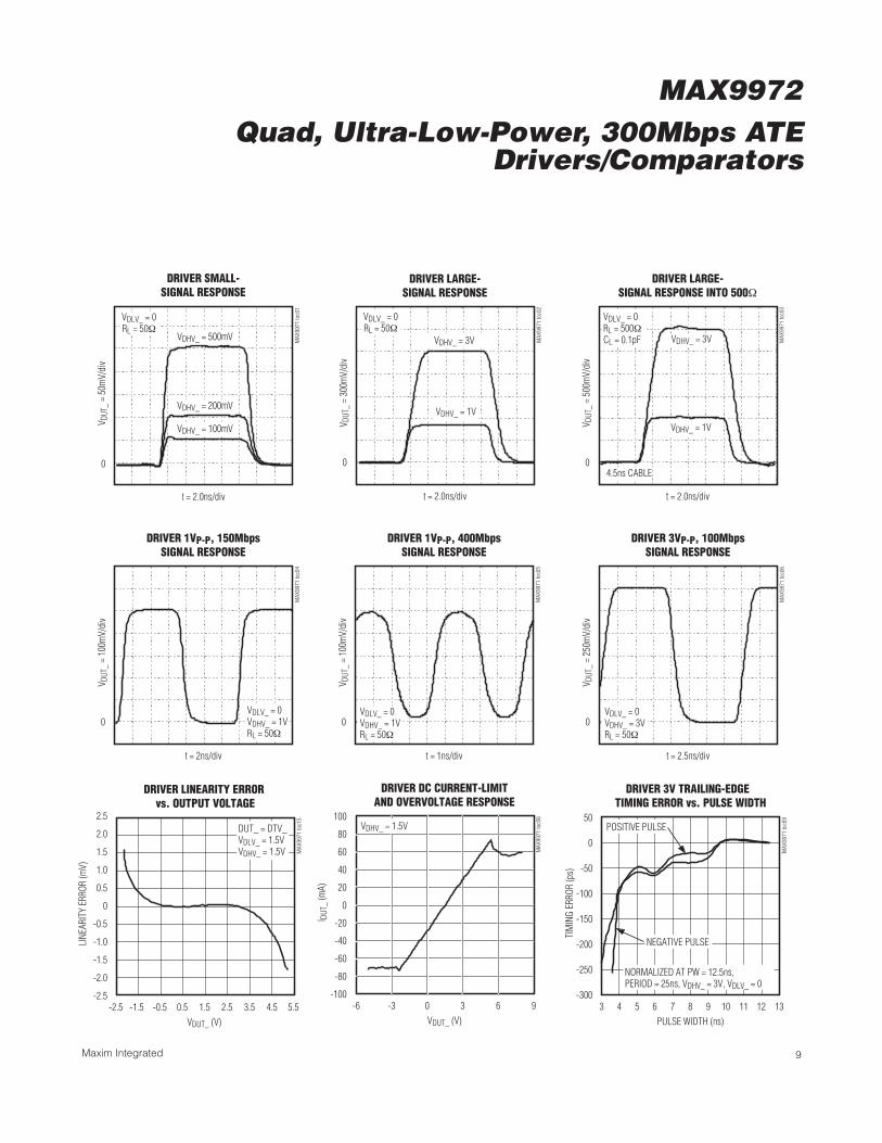
DRIVER SMALL-SIGNAL RESPONSE
VDLV_ = 0RL = 50Ω
VDHV_ = 500mV
VDHV_ = 100mV
VDHV_ = 200mV
MAX
9971
toc0
2
t = 2.0ns/div
V DUT
_ =
300m
V/di
v
0
DRIVER LARGE-SIGNAL RESPONSE
VDLV_ = 0RL = 50Ω
VDHV_ = 3V
VDHV_ = 1V
MAX
9971
toc0
3
t = 2.0ns/div
V DUT
_ =
500m
V/di
v
0
DRIVER LARGE-SIGNAL RESPONSE INTO 500Ω
VDLV_ = 0RL = 500ΩCL = 0.1pF VDHV_ = 3V
VDHV_ = 1V
4.5ns CABLE
MAX
9971
toc0
4
t = 2ns/div
V DUT
_ =
100m
V/di
v
0
DRIVER 1VP-P, 150MbpsSIGNAL RESPONSE
VDLV_ = 0VDHV_ = 1VRL = 50Ω
MAX
9971
toc0
5
t = 1ns/div
V DUT
_ =
100m
V/di
v
0
DRIVER 1VP-P, 400MbpsSIGNAL RESPONSE
VDLV_ = 0VDHV_ = 1VRL = 50Ω
MAX
9971
toc0
6
t = 2.5ns/div
V DUT
_ =
250m
V/di
v
0
DRIVER 3VP-P, 100MbpsSIGNAL RESPONSE
VDLV_ = 0VDHV_ = 3VRL = 50Ω
-2.5
-1.5
-2.0
-0.5
-1.0
0.5
0
1.0
2.0
1.5
2.5
DRIVER LINEARITY ERROR vs. OUTPUT VOLTAGE
MAX
9971
toc1
5
LINE
ARIT
Y ER
ROR
(mV)
DUT_ = DTV_VDLV_ = 1.5VVDHV_ = 1.5V
VDUT_ (V)1.50.5-0.5 4.53.52.5-1.5-2.5 5.5
MAX
9971
toc0
8
DRIVER DC CURRENT-LIMITAND OVERVOLTAGE RESPONSE
VDHV_ = 1.5V
VDUT_ (V)
I DUT
_ (m
A)
630-3
-80
-60
-40
-20
0
20
40
60
80
100
-100-6 9
-300
-200
-250
-100
-150
0
-50
50
3 75 9 114 86 10 12 13
DRIVER 3V TRAILING-EDGE TIMING ERROR vs. PULSE WIDTH
MAX
9971
toc0
9
PULSE WIDTH (ns)
TIM
ING
ERRO
R (p
s)
NORMALIZED AT PW = 12.5ns,PERIOD = 25ns, VDHV_ = 3V, VDLV_ = 0
NEGATIVE PULSE
POSITIVE PULSE
MAX9972Quad, Ultra-Low-Power, 300Mbps ATE
Drivers/Comparators
9Maxim Integrated
MAX9972Quad, Ultra-Low-Power, 300Mbps ATEDrivers/Comparators
10 Maxim Integrated
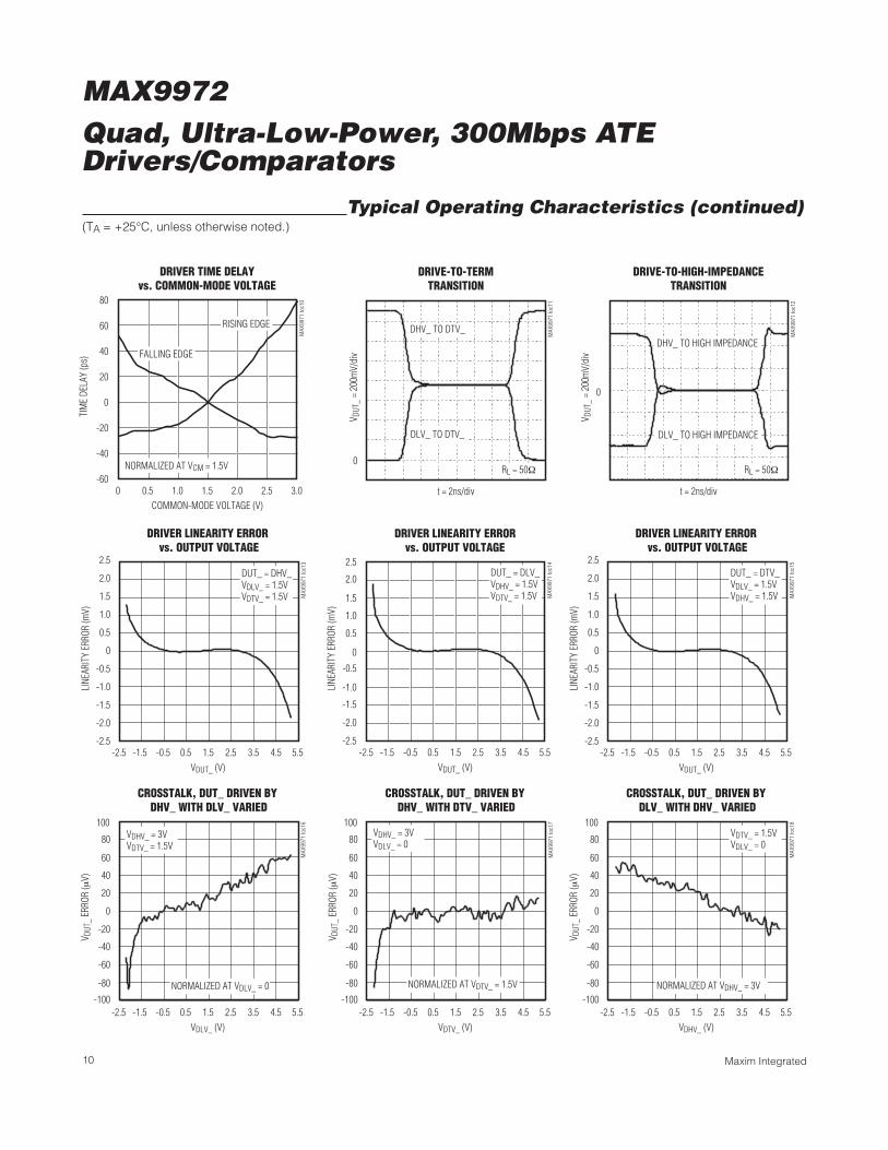
Typical Operating Characteristics (continued)(TA = +25°C, unless otherwise noted.)
MAX
9971
toc1
0
DRIVER TIME DELAYvs. COMMON-MODE VOLTAGE
NORMALIZED AT VCM = 1.5V
FALLING EDGE
RISING EDGE
COMMON-MODE VOLTAGE (V)
TIM
E DE
LAY
(ps)
2.52.01.51.00.5
-40
-20
0
20
40
60
80
-600 3.0
MAX
9971
toc1
1
t = 2ns/div
V DUT
_ =
200m
V/di
v
0
DRIVE-TO-TERMTRANSITION
RL = 50Ω
DHV_ TO DTV_
DLV_ TO DTV_
MAX
9971
toc1
2
t = 2ns/div
V DUT
_ =
200m
V/di
v
0
DRIVE-TO-HIGH-IMPEDANCETRANSITION
RL = 50Ω
DHV_ TO HIGH IMPEDANCE
DLV_ TO HIGH IMPEDANCE
-2.5
-1.5
-2.0
-0.5
-1.0
0.5
0
1.0
2.0
1.5
2.5
DRIVER LINEARITY ERROR vs. OUTPUT VOLTAGE
MAX
9971
toc1
3
LINE
ARIT
Y ER
ROR
(mV)
DUT_ = DHV_VDLV_ = 1.5VVDTV_ = 1.5V
VDUT_ (V)1.50.5-0.5 4.53.52.5-1.5-2.5 5.5
MAX
9971
toc1
4
DRIVER LINEARITY ERRORvs. OUTPUT VOLTAGE
DUT_ = DLV_VDHV_ = 1.5VVDTV_ = 1.5V
VDUT_ (V)
LINE
ARIT
Y ER
ROR
(mV)
1.50.5-0.5 4.53.52.5-1.5
-1.0
-1.5
-2.0
-0.5
0
0.5
1.0
1.5
2.0
2.5
-2.5-2.5 5.5
-2.5
-1.5
-2.0
-0.5
-1.0
0.5
0
1.0
2.0
1.5
2.5
DRIVER LINEARITY ERROR vs. OUTPUT VOLTAGE
MAX
9971
toc1
5
LINE
ARIT
Y ER
ROR
(mV)
DUT_ = DTV_VDLV_ = 1.5VVDHV_ = 1.5V
VDUT_ (V)1.50.5-0.5 4.53.52.5-1.5-2.5 5.5
CROSSTALK, DUT_ DRIVEN BY DHV_ WITH DLV_ VARIED
MAX
9971
toc1
6
VDLV_ (V)1.50.5-0.5 4.53.52.5-1.5-2.5 5.5
VDHV_ = 3VVDTV_ = 1.5V
NORMALIZED AT VDLV_ = 0
V DUT
_ ER
ROR
(μV)
-20
-40
-60
-80
0
20
40
60
80
-100
100
CROSSTALK, DUT_ DRIVEN BY DHV_ WITH DTV_ VARIED
MAX
9971
toc1
7
VDTV_ (V)1.50.5-0.5 4.53.52.5-1.5-2.5 5.5
V DUT
_ ER
ROR
(μV)
-20
-40
-60
-80
0
20
40
60
80
-100
100VDHV_ = 3VVDLV_ = 0
NORMALIZED AT VDTV_ = 1.5V
CROSSTALK, DUT_ DRIVEN BY DLV_ WITH DHV_ VARIED
MAX
9971
toc1
8
VDHV_ (V)1.50.5-0.5 4.53.52.5-1.5-2.5 5.5
V DUT
_ ER
ROR
(μV)
-20
-40
-60
-80
0
20
40
60
80
-100
100VDTV_ = 1.5VVDLV_ = 0
NORMALIZED AT VDHV_ = 3V
MAX9972Quad, Ultra-Low-Power, 300Mbps ATE
Drivers/Comparators
11Maxim Integrated
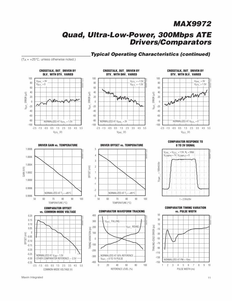
Typical Operating Characteristics (continued)(TA = +25°C, unless otherwise noted.)
CROSSTALK, DUT_ DRIVEN BY DLV_ WITH DTV_ VARIED
MAX
9971
toc1
9
VDTV_ (V)1.50.5-0.5 4.53.52.5-1.5-2.5 5.5
V DUT
_ ER
ROR
(μV)
-20
-40
-60
-80
0
20
40
60
80
-100
100VDHV_ = 3VVDLV_ = 0
NORMALIZED AT VDTV_ = 1.5V
CROSSTALK, DUT_ DRIVEN BY DTV_ WITH DHV_ VARIED
MAX
9971
toc2
0
VDHV_ (V)1.50.5-0.5 4.53.52.5-1.5-2.5 5.5
V DUT
_ ER
ROR
(μV)
-20
-40
-60
-80
0
20
40
60
80
-100
100VDTV_ = +1.5VVDLV_ = -1.5V
NORMALIZED AT VDHV_ = 3V
CROSSTALK, DUT_ DRIVEN BY DTV_ WITH DLV_ VARIED
MAX
9971
toc2
1
VDLV_ (V)1.50.5-0.5 4.53.52.5-1.5-2.5 5.5
V DUT
_ ER
ROR
(μV)
-20
-40
-60
-80
0
20
40
60
80
-100
100VDHV_ = 3VVDTV_ = 1.5V
NORMALIZED AT VDLV_ = 0
MAX
9971
toc2
2
DRIVER GAIN vs. TEMPERATURE
NORMALIZED AT TJ = +85°C
TEMPERATURE (°C)
GAIN
(V/V
)
70 8060 90
1.0000
1.0002
0.9998
1.0006
1.0004
1.0008
0.999650 100
MAX
9971
toc2
3DRIVER OFFSET vs. TEMPERATURE
NORMALIZED AT TJ = +85°C
TEMPERATURE (°C)
OFFS
ET (m
V)
70 8060 90
1
2
-1
0
-2
4
3
5
-350 100
MAX
9971
toc2
4
COMPARATOR RESPONSE TO0 TO 3V SIGNAL
VCHV_ = VCLV_ = 1.5V, RL = 50ΩVCOMPHI = 1V, VCOMPLO = 0
t = 2.0ns/div
V CM
P_ _
= 1
00m
V/di
v
MAX
9971
toc2
5
COMPARATOR OFFSETvs. COMMON-MODE VOLTAGE
NORMALIZED AT VCM = 1.5VOTHER COMPARATOR REFERENCE = -2.5V
COMMON-MODE VOLTAGE (V)
OFFS
ET (m
V)
-0.5 0.5-1.5 1.5 2.5 3.5 4.5
0
0.05
-0.10
-0.05
-0.15
-0.25
-0.20
-0.30
0.15
0.10
0.20
-0.35-2.5 5.5
-400
-300
-200
-100
0
100
200
300
400
0 20 40 60 80 100
COMPARATOR WAVEFORM TRACKING
MAX
9971
toc2
6
REFERENCE LEVEL (%)
TIM
ING
VARI
ATIO
N (p
s)
NORMALIZED AT 50% REFERENCEVDUT_ = 0 TO 1V PULSE
VDUT_ FALLING
VDUT_ RISING
-150
-110
-130
-70
-90
-30
-50
-10
30
10
50
1 3 4 52 6 7 8 9 10
COMPARATOR TIMING VARIATION vs. PULSE WIDTH
MAX
9971
toc2
7
PULSE WIDTH (ns)
TRAI
LING
-EDG
E ER
ROR
(ps)
NORMALIZED AT PW = 10ns
MAX9972Quad, Ultra-Low-Power, 300Mbps ATEDrivers/Comparators
12 Maxim Integrated
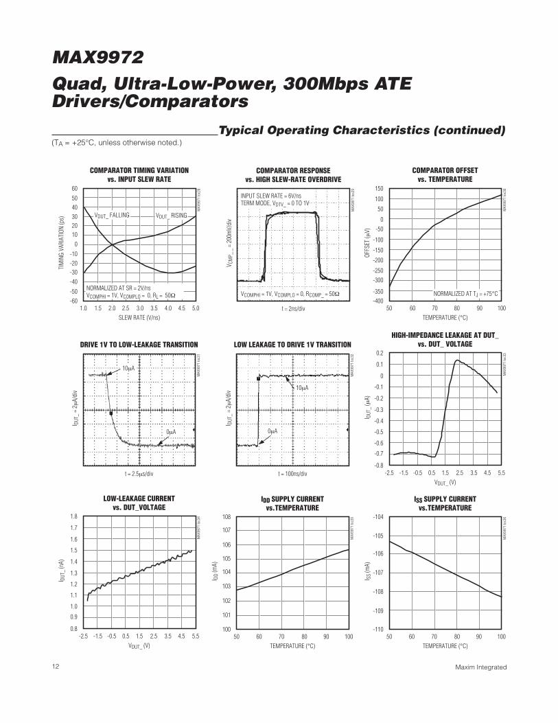
Typical Operating Characteristics (continued)(TA = +25°C, unless otherwise noted.)
MAX
9971
toc2
8
COMPARATOR TIMING VARIATIONvs. INPUT SLEW RATE
SLEW RATE (V/ns)
TIM
ING
VARI
ATIO
N (p
s)
1.5 2.0 2.5 3.0 3.5 4.0 4.5
50
3040
20100
-10-20-30-40
-50
60
-601.0 5.0
NORMALIZED AT SR = 2V/nsVCOMPHI = 1V, VCOMPLO = 0, RL = 50Ω
VDUT_ FALLING VDUT_ RISING
MAX
9971
toc2
9
COMPARATOR RESPONSEvs. HIGH SLEW-RATE OVERDRIVE
INPUT SLEW RATE = 6V/nsTERM MODE, VDTV_ = 0 TO 1V
VCOMPHI = 1V, VCOMPLO = 0, RCOMP_ = 50Ω
t = 2ns/div
V CM
P_ _
= 2
00m
V/di
v
MAX
9971
toc3
0
COMPARATOR OFFSETvs. TEMPERATURE
TEMPERATURE (°C)
OFFS
ET (μ
V)
60 70 80 90
100
0
50
-50
-100
-150
-200
-250-300
-350
150
-40050 100
NORMALIZED AT TJ = +75°C
MAX
9971
toc3
1
DRIVE 1V TO LOW-LEAKAGE TRANSITION
t = 2.5μs/div
I DUT
_ =
2μA/
div
10μA
0μA
MAX
9971
toc3
2
LOW LEAKAGE TO DRIVE 1V TRANSITION
t = 100ns/div
I DUT
_ =
2μA/
div 10μA
0μA
MAX
9971
toc3
3
HIGH-IMPEDANCE LEAKAGE AT DUT_vs. DUT_ VOLTAGE
VDUT_ (V)
I DUT
_ (μ
A)
-0.5 0.5-1.5 1.5 2.5 3.5 4.5
-0.2
-0.1
-0.4
-0.3
-0.6
-0.5
-0.7
0.1
0
0.2
-0.8-2.5 5.5
MAX
9971
toc3
4
LOW-LEAKAGE CURRENTvs. DUT_VOLTAGE
VDUT_ (V)
I DUT
_ (n
A)
-0.5 0.5-1.5 1.5 2.5 3.5 4.5
1.4
1.5
1.2
1.3
1.0
1.1
0.9
1.7
1.6
1.8
0.8-2.5 5.5
MAX
9971
toc3
5
IDD SUPPLY CURRENTvs.TEMPERATURE
TEMPERATURE (°C)
I DD
(mA)
70 8060 90 100
104
105
102
103
100
101
107
106
108
50
MAX
9971
toc3
6ISS SUPPLY CURRENT
vs.TEMPERATURE
TEMPERATURE (°C)
I SS
(mA)
70 8060 90 100
-108
-107
-109
-110
-105
-106
-104
50
MAX9972Quad, Ultra-Low-Power, 300Mbps ATE
Drivers/Comparators
13Maxim Integrated
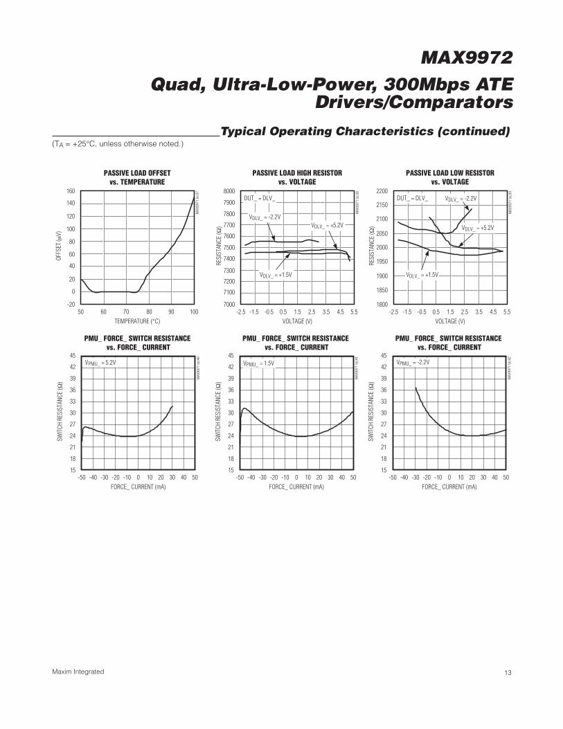
Typical Operating Characteristics (continued)(TA = +25°C, unless otherwise noted.)
MAX
9971
toc3
7
PASSIVE LOAD OFFSETvs. TEMPERATURE
TEMPERATURE (°C)
OFFS
ET (μ
V)
70 8060 90 100
80
100
60
20
40
0
-20
140
120
160
50
MAX
9971
toc3
8
PASSIVE LOAD HIGH RESISTORvs. VOLTAGE
DUT_ = DLV_
VDLV_ = -2.2V
VDLV_ = +1.5V
VDLV_ = +5.2V
VOLTAGE (V)
RESI
STAN
CE (Ω
)
1.50.5-0.5 4.53.52.5-1.5
7300
7200
7100
7700
7800
7900
7400
7500
7600
8000
7000-2.5 5.5
MAX
9971
toc3
9
PASSIVE LOAD LOW RESISTORvs. VOLTAGE
DUT_ = DLV_ VDLV_ = -2.2V
VDLV_ = +1.5V
VDLV_ = +5.2V
VOLTAGE (V)
RESI
STAN
CE (Ω
)
1.50.5-0.5 4.53.52.5-1.5
1900
1850
2100
2150
1950
2000
2050
2200
1800-2.5 5.5
15
21
18
27
24
33
30
36
42
39
45
-50 -30 -20 -10-40 0 10 20 4030 50
PMU_ FORCE_ SWITCH RESISTANCE vs. FORCE_ CURRENT
MAX
9971
toc4
0
FORCE_ CURRENT (mA)
SWIT
CH R
ESIS
TANC
E (Ω
)
VPMU_ = 5.2V
15
21
18
27
24
33
30
36
42
39
45
-50 -30 -20 -10-40 0 10 20 4030 50
PMU_ FORCE_ SWITCH RESISTANCE vs. FORCE_ CURRENT
MAX
9971
toc4
1
FORCE_ CURRENT (mA)
SWIT
CH R
ESIS
TANC
E (Ω
)
VPMU_ = 1.5V
15
21
18
27
24
33
30
36
42
39
45
-50 -30 -20 -10-40 0 10 20 4030 50
PMU_ FORCE_ SWITCH RESISTANCE vs. FORCE_ CURRENT
MAX
9971
toc4
2
FORCE_ CURRENT (mA)
SWIT
CH R
ESIS
TANC
E (Ω
)VPMU_ = -2.2V
MAX9972Quad, Ultra-Low-Power, 300Mbps ATEDrivers/Comparators
14 Maxim Integrated
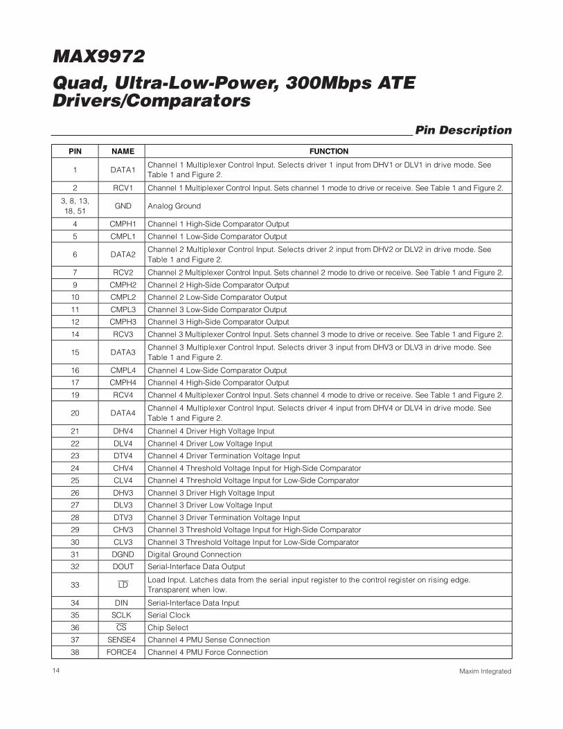
Pin Description
PIN NAME FUNCTION
1 DATA1 Channel 1 Multiplexer Control Input. Selects driver 1 input from DHV1 or DLV1 in drive mode. See Table 1 and Figure 2.
2 RCV1 Channel 1 Multiplexer Control Input. Sets channel 1 mode to drive or receive. See Table 1 and Figure 2.
3, 8, 13, 18, 51
GND Analog Ground
4 CMPH1 Channel 1 High-Side Comparator Output
5 CMPL1 Channel 1 Low-Side Comparator Output
6 DATA2 Channel 2 Multiplexer Control Input. Selects driver 2 input from DHV2 or DLV2 in drive mode. See Table 1 and Figure 2.
7 RCV2 Channel 2 Multiplexer Control Input. Sets channel 2 mode to drive or receive. See Table 1 and Figure 2.
9 CMPH2 Channel 2 High-Side Comparator Output
10 CMPL2 Channel 2 Low-Side Comparator Output
11 CMPL3 Channel 3 Low-Side Comparator Output
12 CMPH3 Channel 3 High-Side Comparator Output
14 RCV3 Channel 3 Multiplexer Control Input. Sets channel 3 mode to drive or receive. See Table 1 and Figure 2.
15 DATA3 Channel 3 Multiplexer Control Input. Selects driver 3 input from DHV3 or DLV3 in drive mode. See Table 1 and Figure 2.
16 CMPL4 Channel 4 Low-Side Comparator Output
17 CMPH4 Channel 4 High-Side Comparator Output
19 RCV4 Channel 4 Multiplexer Control Input. Sets channel 4 mode to drive or receive. See Table 1 and Figure 2.
20 DATA4 Channel 4 Multiplexer Control Input. Selects driver 4 input from DHV4 or DLV4 in drive mode. See Table 1 and Figure 2.
21 DHV4 Channel 4 Driver High Voltage Input
22 DLV4 Channel 4 Driver Low Voltage Input
23 DTV4 Channel 4 Driver Termination Voltage Input
24 CHV4 Channel 4 Threshold Voltage Input for High-Side Comparator
25 CLV4 Channel 4 Threshold Voltage Input for Low-Side Comparator
26 DHV3 Channel 3 Driver High Voltage Input
27 DLV3 Channel 3 Driver Low Voltage Input
28 DTV3 Channel 3 Driver Termination Voltage Input
29 CHV3 Channel 3 Threshold Voltage Input for High-Side Comparator
30 CLV3 Channel 3 Threshold Voltage Input for Low-Side Comparator
31 DGND Digital Ground Connection
32 DOUT Serial-Interface Data Output
33 LD Load Input. Latches data from the serial input register to the control register on rising edge. Transparent when low.
34 DIN Serial-Interface Data Input
35 SCLK Serial Clock
36 CS Chip Select
37 SENSE4 Channel 4 PMU Sense Connection
38 FORCE4 Channel 4 PMU Force Connection
MAX9972Quad, Ultra-Low-Power, 300Mbps ATE
Drivers/Comparators
15Maxim Integrated
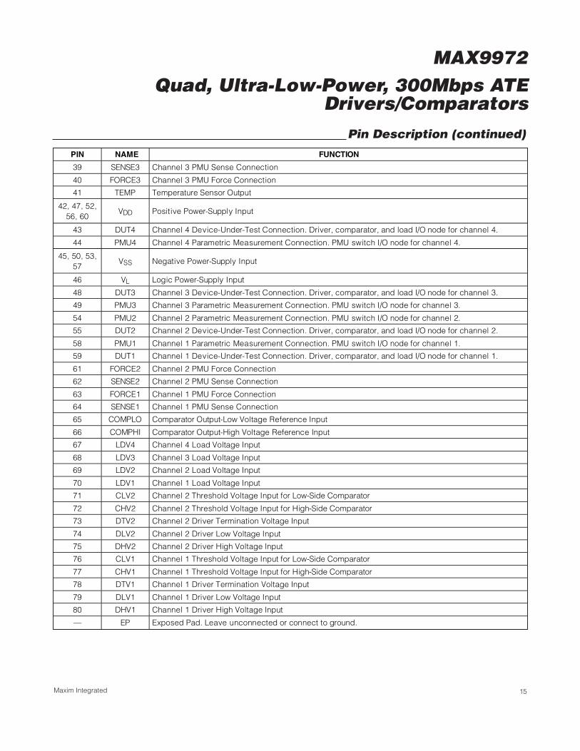
Pin Description (continued)
PIN NAME FUNCTION
39 SENSE3 Channel 3 PMU Sense Connection
40 FORCE3 Channel 3 PMU Force Connection
41 TEMP Temperature Sensor Output
42, 47, 52, 56, 60
VDD Positive Power-Supply Input
43 DUT4 Channel 4 Device-Under-Test Connection. Driver, comparator, and load I/O node for channel 4.
44 PMU4 Channel 4 Parametric Measurement Connection. PMU switch I/O node for channel 4.
45, 50, 53, 57
VSS Negative Power-Supply Input
46 VL Logic Power-Supply Input
48 DUT3 Channel 3 Device-Under-Test Connection. Driver, comparator, and load I/O node for channel 3.
49 PMU3 Channel 3 Parametric Measurement Connection. PMU switch I/O node for channel 3.
54 PMU2 Channel 2 Parametric Measurement Connection. PMU switch I/O node for channel 2.
55 DUT2 Channel 2 Device-Under-Test Connection. Driver, comparator, and load I/O node for channel 2.
58 PMU1 Channel 1 Parametric Measurement Connection. PMU switch I/O node for channel 1.
59 DUT1 Channel 1 Device-Under-Test Connection. Driver, comparator, and load I/O node for channel 1.
61 FORCE2 Channel 2 PMU Force Connection
62 SENSE2 Channel 2 PMU Sense Connection
63 FORCE1 Channel 1 PMU Force Connection
64 SENSE1 Channel 1 PMU Sense Connection
65 COMPLO Comparator Output-Low Voltage Reference Input
66 COMPHI Comparator Output-High Voltage Reference Input
67 LDV4 Channel 4 Load Voltage Input
68 LDV3 Channel 3 Load Voltage Input
69 LDV2 Channel 2 Load Voltage Input
70 LDV1 Channel 1 Load Voltage Input
71 CLV2 Channel 2 Threshold Voltage Input for Low-Side Comparator
72 CHV2 Channel 2 Threshold Voltage Input for High-Side Comparator
73 DTV2 Channel 2 Driver Termination Voltage Input
74 DLV2 Channel 2 Driver Low Voltage Input
75 DHV2 Channel 2 Driver High Voltage Input
76 CLV1 Channel 1 Threshold Voltage Input for Low-Side Comparator
77 CHV1 Channel 1 Threshold Voltage Input for High-Side Comparator
78 DTV1 Channel 1 Driver Termination Voltage Input
79 DLV1 Channel 1 Driver Low Voltage Input
80 DHV1 Channel 1 Driver High Voltage Input
— EP Exposed Pad. Leave unconnected or connect to ground.
MAX9972Quad, Ultra-Low-Power, 300Mbps ATEDrivers/Comparators
16 Maxim Integrated
MAX9972
BUFFER
HIGH-IMPEDANCELOGIC
HIGH IMPEDANCELLEAK
LOAD ENHIGH
PMU_
0
0
0
0
DUT_
TERM
MULTIPLEXER
ONE OF FOUR IDENTICAL CHANNELS SHOWN
50Ω
7.5kΩ
SEETABLE 3
2.0kΩ
LOAD ENLOW
SERIALINTERFACE
30Ω
FORCE EN1kΩ
SENSE EN
TERM
COMMON TO ALL FOUR CHANNELS
LLEAK
SENSE ENFORCE EN
LOAD EN LOW
CS
COMPLOCOMPHI
SENSE_
FORCE_
LDV_
CLV_
CMPL_
CMPH_
CHV_
RCV_
DATA_
DLV_
DTV_
DHV_
SCLK
DINLD
DOUT
LOAD EN HIGH
TEMP
VDD
VL
VSS
GND
DGND
0
0
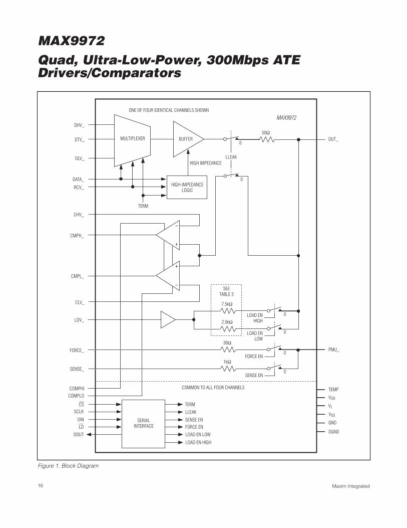
Figure 1. Block Diagram
MAX9972Quad, Ultra-Low-Power, 300Mbps ATE
Drivers/Comparators
17Maxim Integrated
Detailed DescriptionThe MAX9972 is a four-channel, pin-electronics IC forautomated test equipment that includes, for each chan-nel, a three-level pin driver, a window comparator, apassive load, and a Kelvin instrument connection(Figure 1). All functions feature a -2.2V to +5.2V operat-ing range and the drivers include both high-impedanceand active-termination (3rd-level drive) modes. Thecomparators feature programmable output voltages,allowing optimization for different CMOS interface stan-dards. The loads have selectable output resistance foroptimizing DUT current loading. The Kelvin paths allowaccurate connection of an instrument with ±25mAsource/sink capability. Additionally, the MAX9972 offersa low-leakage mode that reduces DUT_ leakage cur-rent to less than 20nA.
Each of the four channels feature single-ended CMOS-compatible inputs, DATA_ and RCV_, for control of thedriver signal path (Figure 2). The MAX9972 modaloperation is programmed through a 3-wire, low-voltageCMOS-compatible serial interface.
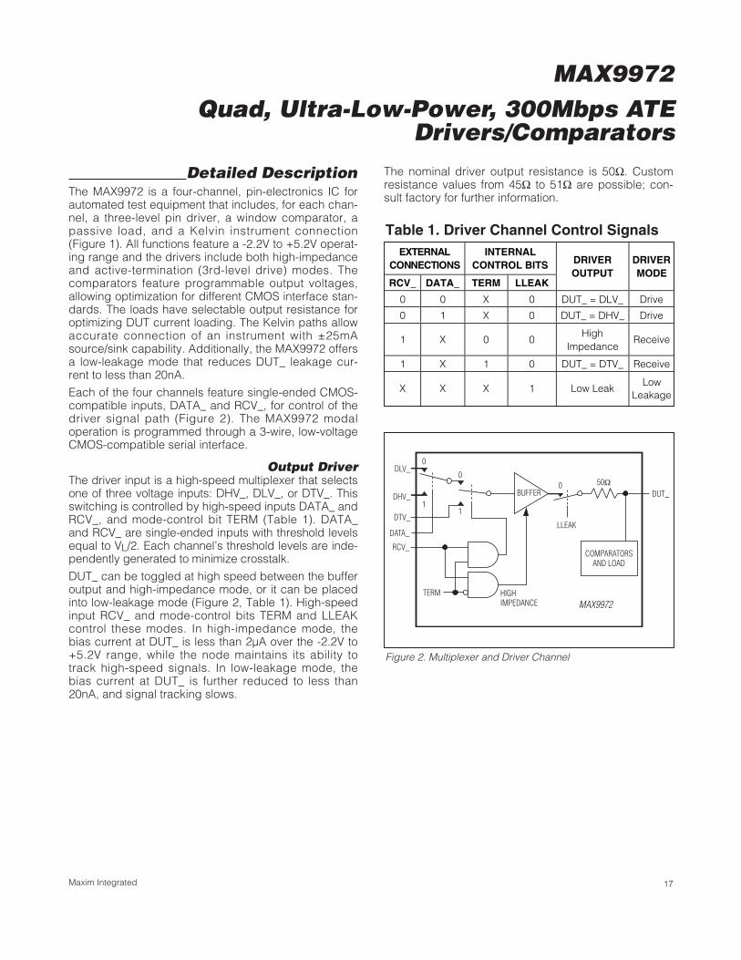
Output DriverThe driver input is a high-speed multiplexer that selectsone of three voltage inputs: DHV_, DLV_, or DTV_. Thisswitching is controlled by high-speed inputs DATA_ andRCV_, and mode-control bit TERM (Table 1). DATA_and RCV_ are single-ended inputs with threshold levelsequal to VL/2. Each channel’s threshold levels are inde-pendently generated to minimize crosstalk.
DUT_ can be toggled at high speed between the bufferoutput and high-impedance mode, or it can be placedinto low-leakage mode (Figure 2, Table 1). High-speedinput RCV_ and mode-control bits TERM and LLEAKcontrol these modes. In high-impedance mode, thebias current at DUT_ is less than 2µA over the -2.2V to+5.2V range, while the node maintains its ability totrack high-speed signals. In low-leakage mode, thebias current at DUT_ is further reduced to less than20nA, and signal tracking slows.
The nominal driver output resistance is 50Ω. Customresistance values from 45Ω to 51Ω are possible; con-sult factory for further information.
Table 1. Driver Channel Control SignalsEXTER N AL
C O NN EC TIO N SINTERNAL
CONTROL BITS
RCV_ DATA_ TERM LLEAK
DRIVEROUTPUT
DRIVERMODE
0 0 X 0 DUT_ = DLV_ Drive
0 1 X 0 DUT_ = DHV_ Drive
1 X 0 0High
ImpedanceReceive
1 X 1 0 DUT_ = DTV_ Receive
X X X 1 Low LeakLow
Leakage
MAX9972
DLV_
DHV_
DTV_
DATA_
RCV_
TERM
BUFFER50Ω
DUT_
0
00
11
COMPARATORSAND LOAD
LLEAK
HIGH IMPEDANCE
Figure 2. Multiplexer and Driver Channel
MAX9972Quad, Ultra-Low-Power, 300Mbps ATEDrivers/Comparators
18 Maxim Integrated
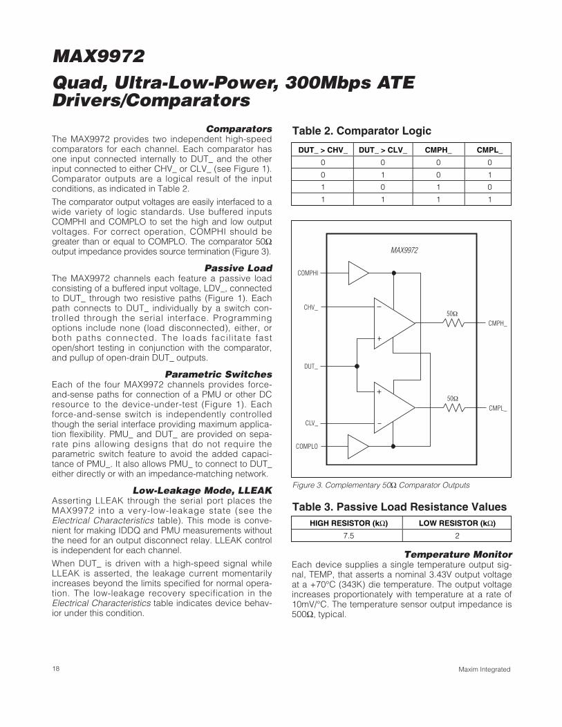
ComparatorsThe MAX9972 provides two independent high-speedcomparators for each channel. Each comparator hasone input connected internally to DUT_ and the otherinput connected to either CHV_ or CLV_ (see Figure 1).Comparator outputs are a logical result of the inputconditions, as indicated in Table 2.
The comparator output voltages are easily interfaced to awide variety of logic standards. Use buffered inputsCOMPHI and COMPLO to set the high and low outputvoltages. For correct operation, COMPHI should begreater than or equal to COMPLO. The comparator 50Ωoutput impedance provides source termination (Figure 3).
Passive LoadThe MAX9972 channels each feature a passive loadconsisting of a buffered input voltage, LDV_, connectedto DUT_ through two resistive paths (Figure 1). Eachpath connects to DUT_ individually by a switch con-trolled through the serial interface. Programmingoptions include none (load disconnected), either, orboth paths connected. The loads facil i tate fastopen/short testing in conjunction with the comparator,and pullup of open-drain DUT_ outputs.
Parametric SwitchesEach of the four MAX9972 channels provides force-and-sense paths for connection of a PMU or other DCresource to the device-under-test (Figure 1). Eachforce-and-sense switch is independently controlledthough the serial interface providing maximum applica-tion flexibility. PMU_ and DUT_ are provided on sepa-rate pins allowing designs that do not require theparametric switch feature to avoid the added capaci-tance of PMU_. It also allows PMU_ to connect to DUT_either directly or with an impedance-matching network.
Low-Leakage Mode, LLEAKAsserting LLEAK through the serial port places theMAX9972 into a very-low-leakage state (see theElectrical Characteristics table). This mode is conve-nient for making IDDQ and PMU measurements withoutthe need for an output disconnect relay. LLEAK controlis independent for each channel.
When DUT_ is driven with a high-speed signal whileLLEAK is asserted, the leakage current momentarilyincreases beyond the limits specified for normal opera-tion. The low-leakage recovery specification in theElectrical Characteristics table indicates device behav-ior under this condition.
Temperature MonitorEach device supplies a single temperature output sig-nal, TEMP, that asserts a nominal 3.43V output voltageat a +70°C (343K) die temperature. The output voltageincreases proportionately with temperature at a rate of10mV/°C. The temperature sensor output impedance is500Ω, typical.
Table 2. Comparator Logic
DUT_ > CHV_ DUT_ > CLV_ CMPH_ CMPL_
0 0 0 0
0 1 0 1
1 0 1 0
1 1 1 1
Table 3. Passive Load Resistance ValuesHIGH RESISTOR (kΩ) LOW RESISTOR (kΩ)
7.5 2
MAX9972
COMPHI
CHV_
DUT_
CLV_
COMPLO
50ΩCMPH_
50ΩCMPL_
Figure 3. Complementary 50Ω Comparator Outputs
MAX9972Quad, Ultra-Low-Power, 300Mbps ATE
Drivers/Comparators
19Maxim Integrated
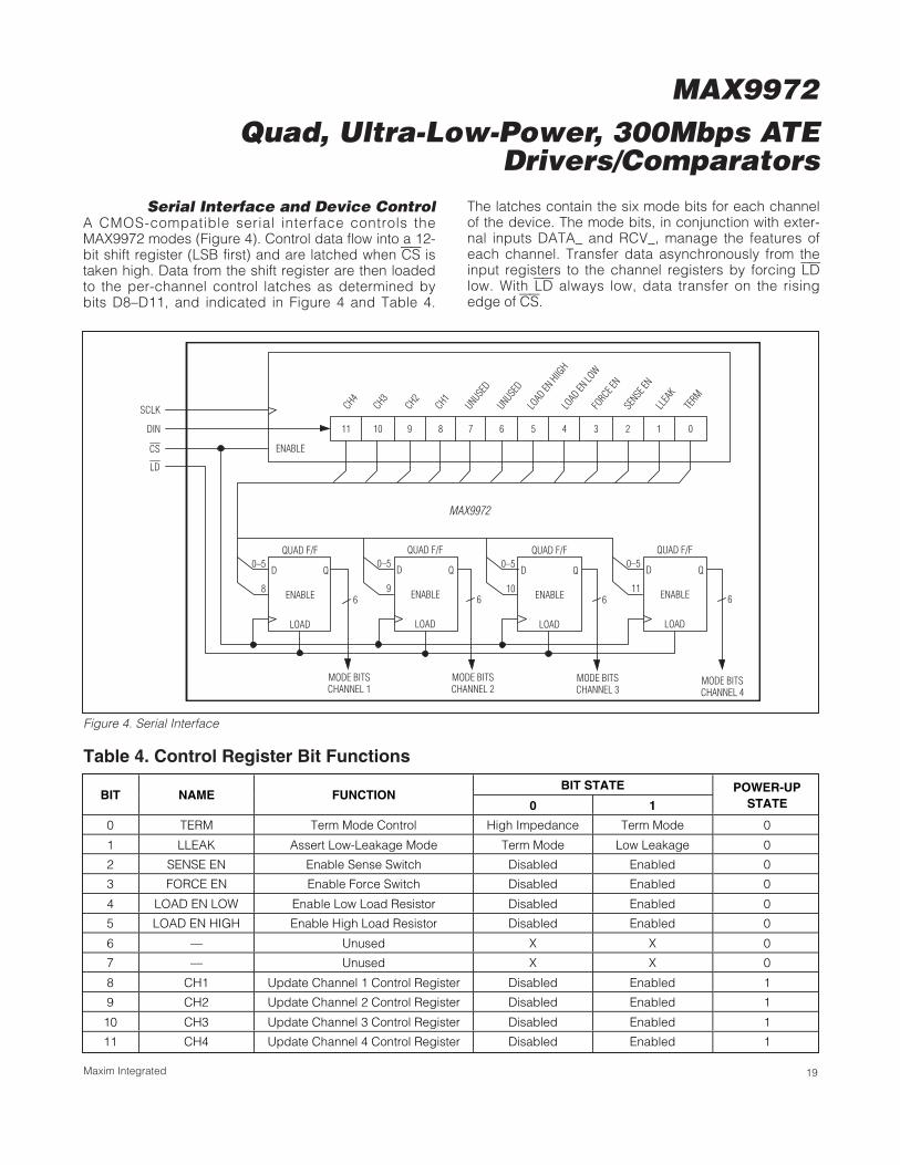
Serial Interface and Device ControlA CMOS-compatible serial interface controls theMAX9972 modes (Figure 4). Control data flow into a 12-bit shift register (LSB first) and are latched when CS istaken high. Data from the shift register are then loadedto the per-channel control latches as determined bybits D8–D11, and indicated in Figure 4 and Table 4.
The latches contain the six mode bits for each channelof the device. The mode bits, in conjunction with exter-nal inputs DATA_ and RCV_, manage the features ofeach channel. Transfer data asynchronously from theinput registers to the channel registers by forcing LDlow. With LD always low, data transfer on the risingedge of CS.
Table 4. Control Register Bit Functions
BIT STATEBIT NAME FUNCTION
0 1POWER-UP
STATE
0 TERM Term Mode Control High Impedance Term Mode 0
1 LLEAK Assert Low-Leakage Mode Term Mode Low Leakage 0
2 SENSE EN Enable Sense Switch Disabled Enabled 0
3 FORCE EN Enable Force Switch Disabled Enabled 0
4 LOAD EN LOW Enable Low Load Resistor Disabled Enabled 0
5 LOAD EN HIGH Enable High Load Resistor Disabled Enabled 0
6 — Unused X X 0
7 — Unused X X 0
8 CH1 Update Channel 1 Control Register Disabled Enabled 1
9 CH2 Update Channel 2 Control Register Disabled Enabled 1
10 CH3 Update Channel 3 Control Register Disabled Enabled 1
11 CH4 Update Channel 4 Control Register Disabled Enabled 1
MAX9972
SCLK
DIN
CS
LD
ENABLE
QUAD F/F
D Q
ENABLE
0–5
8
TERM
LLEA
K
SENSE
EN
FORC
E EN
LOAD
EN LO
W
LOAD
EN HIIG
H
UNUSED
UNUSED
CH1
CH2
CH3
CH4
MODE BITSCHANNEL 4
MODE BITSCHANNEL 3
MODE BITSCHANNEL 2
MODE BITSCHANNEL 1
LOAD
QUAD F/F
D Q
ENABLE
0–5
9
LOAD
QUAD F/F
D Q
ENABLE
0–5
10
LOAD
QUAD F/F
D Q
ENABLE
0–5
116666
LOAD
11 10 9 8 7 6 5 4 3 2 1 0
Figure 4. Serial Interface
MAX9972Quad, Ultra-Low-Power, 300Mbps ATEDrivers/Comparators
20 Maxim Integrated
Heat RemovalWith adequate airflow, no external heat sinking is need-ed under most operating conditions. If excess heat mustbe dissipated through the exposed pad, solder it to cir-cuit board copper. The exposed pad must be either leftunconnected, isolated, or connected to ground.
Power MinimizationTo minimize power consumption, activate only theneeded channels. Each channel placed in low-leakagemode saves approximately 240mW.
Chip InformationPROCESS: BiCMOS
SCLK
CS
DIN D0 D1 D2 D3 D4 D5 D10 D11
tCH
tCL
tDH
tDS
tCSHO
tCSS1
tCSH1
tCSWH
D0 LAST
tDO
tLDW
tCSHLD
DOUT
LOAD
tCSSO
D1 LAST D2 LAST D3 LAST D4 LAST D5 LAST D10 LAST D11 LAST D0
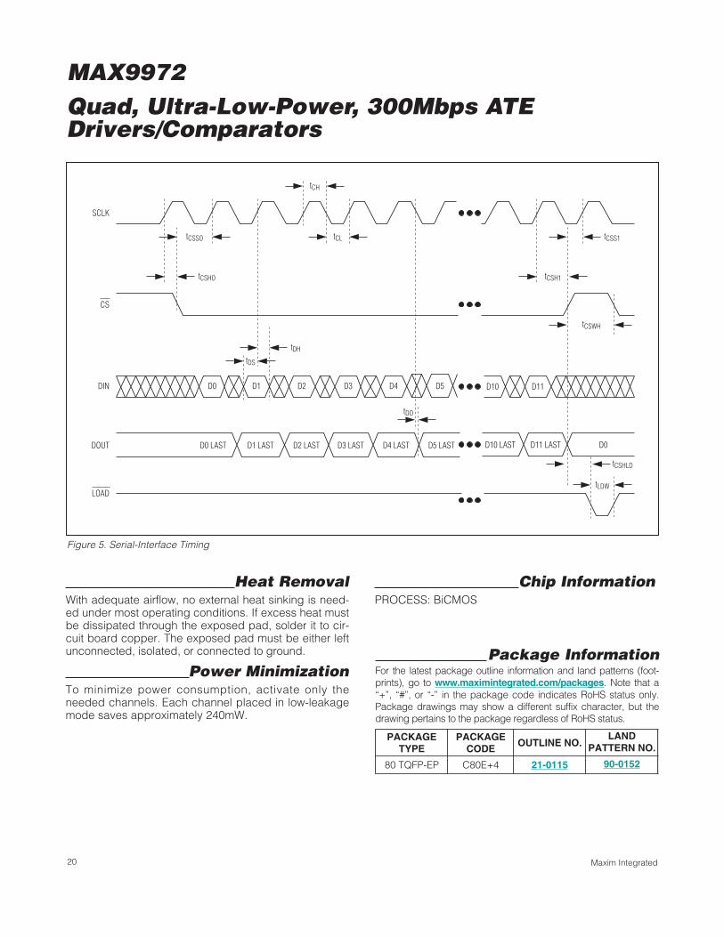
Figure 5. Serial-Interface Timing
Package InformationFor the latest package outline information and land patterns (foot-prints), go to www.maximintegrated.com/packages. Note that a“+”, “#”, or “-” in the package code indicates RoHS status only.Package drawings may show a different suffix character, but thedrawing pertains to the package regardless of RoHS status.
PACKAGETYPE
PACKAGECODE
OUTLINE NO.LAND
PATTERN NO.
80 TQFP-EP C80E+4 21-0115 90-0152
MAX9972Quad, Ultra-Low-Power, 300Mbps ATE
Drivers/Comparators
21Maxim Integrated
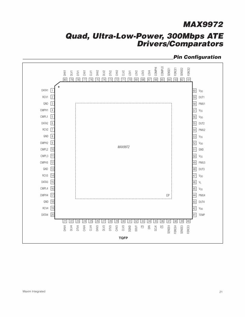
TQFP
MAX9972
21 22 23 24 25 26 27 28 29 30 32 33 34 35 36 37 38 39
EP
4031
80
+
79 78 77 76 75 74 73 72 71 69 68 67 66 65 64 63 62 6170
DHV1
DLV1
DTV1
CHV1
CLV1
DHV2
DLV2
DTV2
CHV2
CLV2
LDV1
60 VDD
DUT1
PMU1
VSS
VDD
DUT2
PMU2
VSS
VDD
GND
VSS
PMU3
DUT3
VDD
VL
VSS
PMU4
DUT4
VDD
TEMP
59
58
57
56
55
54
53
52
51
50
49
48
47
46
45
44
43
42
41
1
2
3
4
5
6
7
8
9
10
11
12
13
14
15
16
17
18
19
20
LDV2
LDV3
LDV4
COM
PHI
COM
PLO
SENS
E1
FORC
E1
SENS
E2
FORC
E2
DHV4
DLV4
DTV4
CHV4
CLV4
DHV3
DLV3
DTV3
CHV3
CLV3
DGND
DOUT LD DIN
SCLK CS
SENS
E4
FORC
E4
SENS
E3
FORC
E3
DATA2
CMPH1
GND
DATA1
RCV1
CMPL1
CMPH2
GND
RCV2
CMPL2
DATA3
CMPH3
GND
RCV3
CMPL3
DATA4
CMPH4
GND
RCV4
CMPL4
Pin Configuration
Maxim Integrated cannot assume responsibility for use of any circuitry other than circuitry entirely embodied in a Maxim Integrated product. No circuit patentlicenses are implied. Maxim Integrated reserves the right to change the circuitry and specifications without notice at any time. The parametric values (min andmax limits) shown in the Electrical Characteristics table are guaranteed. Other parametric values quoted in this data sheet are provided for guidance.
22 ________________________________Maxim Integrated 160 Rio Robles, San Jose, CA 95134 USA 1-408-601-1000
© 2014 Maxim Integrated Products, Inc. Maxim Integrated and the Maxim Integrated logo are trademarks of Maxim Integrated Products, Inc.
MAX9972Quad, Ultra-Low-Power, 300Mbps ATEDrivers/Comparators
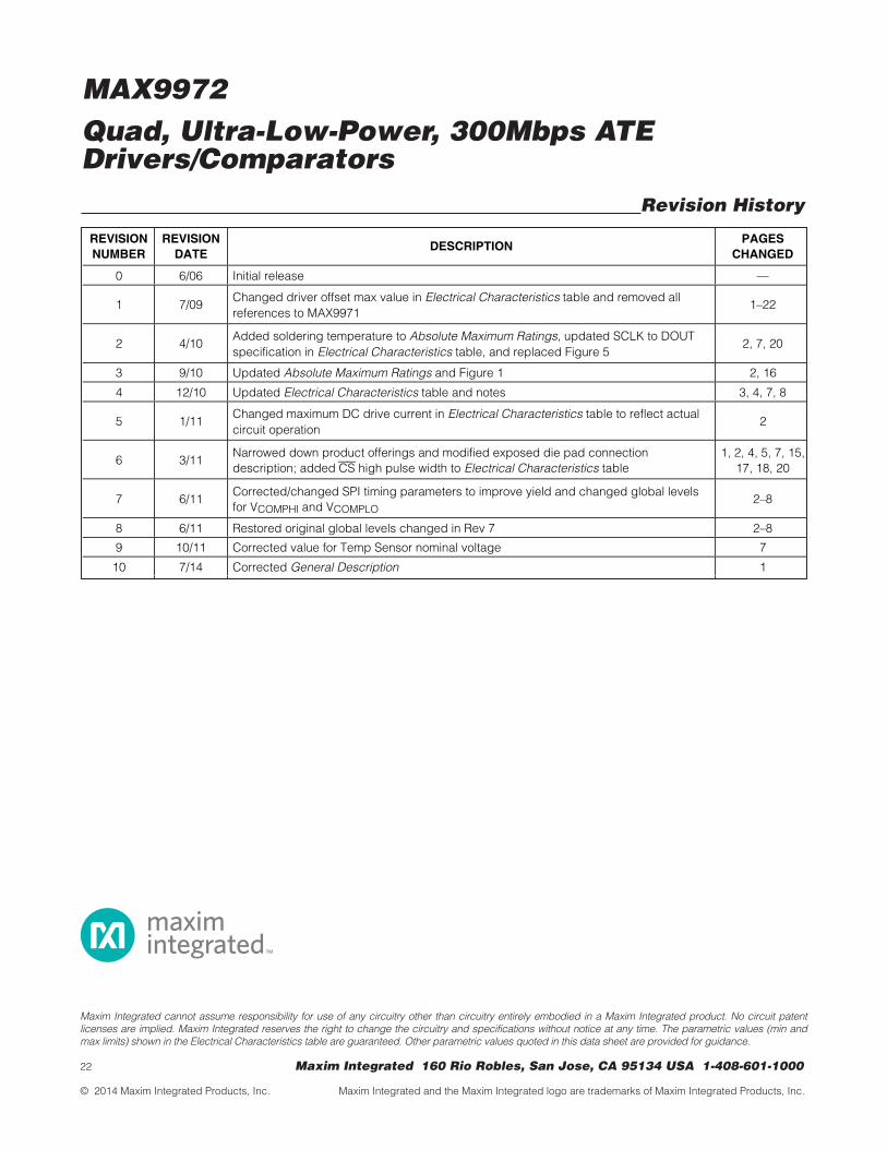
Revision History
REVISIONNUMBER
REVISIONDATE
DESCRIPTIONPAGES
CHANGED
0 6/06 Initial release —
1 7/09Changed driver offset max value in Electrical Characteristics table and removed allreferences to MAX9971
1–22
2 4/10Added soldering temperature to Absolute Maximum Ratings, updated SCLK to DOUTspecification in Electrical Characteristics table, and replaced Figure 5
2, 7, 20
3 9/10 Updated Absolute Maximum Ratings and Figure 1 2, 16
4 12/10 Updated Electrical Characteristics table and notes 3, 4, 7, 8
5 1/11Changed maximum DC drive current in Electrical Characteristics table to reflect actualcircuit operation
2
6 3/11Narrowed down product offerings and modified exposed die pad connectiondescription; added CS high pulse width to Electrical Characteristics table
1, 2, 4, 5, 7, 15,17, 18, 20
7 6/11Corrected/changed SPI timing parameters to improve yield and changed global levelsfor VCOMPHI and VCOMPLO
2–8
8 6/11 Restored original global levels changed in Rev 7 2–8
9 10/11 Corrected value for Temp Sensor nominal voltage 7
10 7/14 Corrected General Description 1