Embed Size (px)
Citation preview

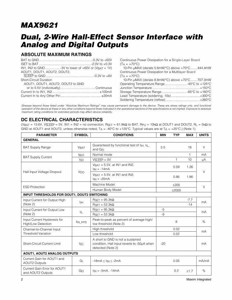
Dual, 2-Wire Hall-Effect Sensor Interface with Analog and Digital Outputs
MAX9621
EVALUATION KIT AVAILABLE
General DescriptionThe MAX9621 is a continuation of the Maxim family of Hall-effect sensor interfaces that already includes the MAX9921. The MAX9621 provides a single-chip solution to interface two 2-wire Hall-effect sensors to low-voltage microprocessors (FP) through either a digital output for Hall-effect switches or an analog output for linear infor-mation or both.
The MAX9621 protects the Hall sensors from supply transients up to 60V at the BAT supply. Normal operating supply voltage ranges from 5.5V to 18V. If the BAT sup-ply rises above 18V, the MAX9621 shuts off the current to the Hall sensors. When a short-to-ground fault condition is detected, the current to the Hall input is shut off and the condition is indicated at the analog output by a zero-current level and a high digital output.
The MAX9621 provides a minimum of 50Fs blanking time following Hall sensor power-up or restart. The open-drain digital outputs are compatible with logic levels up to 5.5V.
The MAX9621 is available in a 3mm x 5mm, 10-pin FMAXM package and is rated for operation in the -40NC to +125NC temperature range.
ApplicationsWindow Lifters
Seat Movers
Electric Sunroofs
Seatbelt Buckles
Door Power Locks
Ignition Key
Steering Column
Speed Sensing
FeaturesS Provides Supply Current and Interfaces to Two
2-Wire Hall-Effect SensorsS 5.5V to 18V Operating Voltage RangeS Protects Hall Sensors Against Up to 60V Supply
TransientsS Low-Power Shutdown for Power SavingS Filtered Digital OutputsS Analog Output Mirrors the Hall Sensor CurrentS Hall Inputs Protected from Short to GroundS Hall Sensor Blanking Following Power-Up and
Restart from Shutdown and Short to GroundS Operates with ±3V Ground Shift Between the Hall
Sensor and the MAX9621S ±2kV Human Body Model ESD and ±200V Machine
Model ESD at All PinsS 3mm x 5mm, 10-Pin µMAX Package
19-5024; Rev 1; 9/11
Ordering Information
+Denotes a lead(Pb)-free/RoHS-compliant package.T = Tape and reel./V denotes an automotive qualified part.
µMAX is a registered trademark of Maxim Integrated Products, Inc.
Functional Diagram
Typical Application Circuit appears at end of data sheet.
PART TEMP RANGE PIN-PACKAGE
MAX9621AUB+T -40NC to +125NC 10 FMAX
MAX9621AUB/V+ -40NC to +125NC 10 FMAX
BAT
REFERENCESLEEP-MODE
CONTROL
FILTER
AOUT1
10kI
AOUT2
DOUT1
INPUTSHORT
DETECTION
ISET
IN1
REF
REF
BAT
BAT
MAX9621
SLEEP
FILTER
DOUT2
IN2REF
GND
For pricing, delivery, and ordering information, please contact Maxim Direct at 1-888-629-4642, or visit Maxim’s website at www.maximintegrated.com.
2 Maxim Integrated
Dual, 2-Wire Hall-Effect Sensor Interface with Analog and Digital Outputs
MAX9621
Stresses beyond those listed under “Absolute Maximum Ratings” may cause permanent damage to the device. These are stress ratings only, and functional operation of the device at these or any other conditions beyond those indicated in the operational sections of the specifications is not implied. Exposure to absolute maximum rating conditions for extended periods may affect device reliability.
BAT to GND ...........................................................-0.3V to +60VISET to BAT ..........................................................-2.0V to +0.3VIN1, IN2 to GND ................ -3V to lower of +60V or (VBAT + 1V)AOUT1, DOUT1, AOUT2, DOUT2, SLEEP to GND .....................................................-0.3V to +6VShort-Circuit Duration AOUT1, DOUT1, AOUT2, DOUT2 to GND or to 5.5V (individually) .......................................ContinuousCurrent In to IN1, IN2 .................................................... ±100mACurrent In to Any Other Pin ............................................. ±20mA
Continuous Power Dissipation for a Single-Layer Board(TA = +70NC) 10-Pin µMAX (derate 5.6mW/NC) above +70NC........444.4mWContinuous Power Dissipation for a Multilayer Board (TA = +70NC) 10-Pin µMAX (derate 8.8mW/NC) above +70NC........707.3mWOperating Temperature Range ........................ -40NC to +125NCJunction Temperature .....................................................+150NCStorage Temperature Range ............................ -65NC to +160NCLead Temperature (soldering, 10s) ................................+300NCSoldering Temperature (reflow) ......................................+260NC
DC ELECTRICAL CHARACTERISTICS(VBAT = 13.6V, VSLEEP = 5V, IN1 = IN2 = no connection, RSET = 61.9kI to BAT, RPU = 10kI at DOUT1 and DOUT2, RL = 5kI to GND at AOUT1 and AOUT2, unless otherwise noted, TA = -40NC to +125NC. Typical values are at TA = +25NC.) (Note 1)
ABSOLUTE MAXIMUM RATINGS
PARAMETER SYMBOL CONDITIONS MIN TYP MAX UNITS
GENERAL
BAT Supply Range VBATGuaranteed by functional test of IIH, IIL, and GEI
5.5 18 V
BAT Supply CurrentIBAT Normal mode 1 mA
ISD VSLEEP = 0V 1 10 FA
Hall Input Voltage Dropout VDO
VBAT = 5.5V, at IN1 and IN2,IIN = -14mA
0.59 1.26
VVBAT = 5.5V, at IN1 and IN2,IIN = -20mA
0.86 1.86
ESD Protection Machine Model ±200
VHuman Body Model ±2000
INPUT THRESHOLDS FOR DOUT1, DOUT2 SWITCHING
Input Current for Output High (Note 2)
IIHRSET = 95.3kI -7.7
mARSET = 52.3kI -14
Input Current for Output Low (Note 2)
IILRSET = 95.3kI -5
mARSET = 52.3kI -9
Input Current Hysteresis for High/Low Detection
IIN_HYSPeak-to-peak as percent of average high/low threshold (Note 2)
8 %
Channel-to-Channel Input Threshold Variation
High threshold 0.02mA
Low threshold 0.02
Short-Circuit Current Limit ISC
A short to GND is not a sustained condition, Hall input reverts to -50FA when detected (Note 2)
-20 mA
AOUT1, AOUT2 ANALOG OUTPUTS
Current Gain for AOUT1 and AOUT2 Outputs
GI -18mA P IIN P -2mA 0.05 mA/mA
Current Gain Error for AOUT1 and AOUT2 Outputs
GEI IIN = -5mA, -14mA 0.2 ±1.7 %

3Maxim Integrated
Dual, 2-Wire Hall-Effect Sensor Interface with Analog and Digital Outputs
MAX9621
DC ELECTRICAL CHARACTERISTICS (continued)(VBAT = 13.6V, VSLEEP = 5V, IN1 = IN2 = no connection, RSET = 61.9kI to BAT, RPU = 10kI at DOUT1 and DOUT2, RL = 5kI to GND at AOUT1 and AOUT2, unless otherwise noted, TA = -40NC to +125NC. Typical values are at TA = +25NC.) (Note 1)
Note 1: All DC specifications are 100% production tested at TA = +25°C. AC specifications are guaranteed by design at TA = +25°C.
Note 2: Parameters that change with the value of the RSET resistor: IIH, IIL, IIN_HYS, ISC, tBL, tRAMP, tDEL, fMAX, and PR.Note 3: Following power-up or startup from sleep mode, the start of the blanking period is delayed 20Fs.
PARAMETER SYMBOL CONDITIONS MIN TYP MAX UNITS
Input Referred Current Offset IOSInferred from measurements atIIN = -5mA, -14mA
-120 +120 FA
AOUT_ Dropout VoltageVBAT = 5.5V, for 5% current reduction
IIN = -14mA 0.85 1.6V
IIN = -20mA 1.09 1.75
AOUT_ Output Impedance 500 MI
LOGIC I/O (DOUT1, DOUT2)
Output-Voltage Low DOUT1, DOUT2
VOL Sink current = 1mA 0.4 V
Three-State Output Current DOUT1, DOUT2
IOZ VSLEEP = 0V, 0V P VDOUT_ P 5V ±1 FA
SLEEPInput-Voltage High VIH 2.0 V
Input-Voltage Low VIL 0.8 V
Input Resistance to GND RIN 50 100 kI
AC TIMING CHARACTERISTICS
Shutdown Delay from SLEEP Low to IN_ Shutoff
tSHDNIIH = -14mA to GND, time from SLEEP low to IN_ drop 500mV, CL = 20pF
33 40 46 Fs
IN_, Blanking Time at Hall Sensor Power-Up
tBL
IIH = -14mA to GND, time from VIN_ = 500mV until DOUT_ high, CL = 20pF (Notes 2, 3)
76 89 103 Fs
IN_, Current Ramp Rate After Turn-On
tRAMP IN_ = GND (Note 2) 3.6 5 6.7 mA/Fs
Delay from IN_ to DOUT_ (Filter Delay)
tDELFrom IIH to IIL or from IIL to IIH,CL = 20pF, Figure 1 (Note 2)
10.8 13.5 16 Fs
Delay Difference Between Rising and Falling Edges of Both Channels
tDMCHALL-BYPASS = 0.01FF, IIH = -11.5mA and IIL = -7.5mA, CL = 20pF
1 Fs
Delay Difference Between Channels
tCCCHALL-BYPASS = 0.01FF, IIH = -11.5mA and IIL = -7.5mA, CL = 20pF
500 ns
Maximum Frequency on Hall Inputs
fMAXCHALL-BYPASS = 0.01FF, IIH = -11.5mA and IIL = -7.5mA, CL = 20pF (Note 2)
34 39 kHz
Maximum Analog Output Current During Short-to-GND Fault
IMAO -1.4 mA
IN_ Pulse Length Rejected by Filter to DOUT_
PR Figure 2 (Note 2) 7.8 11.5 14.6 Fs

4 Maxim Integrated
Dual, 2-Wire Hall-Effect Sensor Interface with Analog and Digital Outputs
MAX9621
Timing Diagrams
Figure 2. Hall Input Pulse Rejection
Figure 1. Timing Diagram
tDELtDEL
IN_
DOUT_
PR14mA
7mA
0mA
5V
0V
PR
IN1
DOUT1
7mA
14mA
APPROXIMATELY 100mA
0mA
0V
5V
HALL SENSOR OPEN
HALL SENSOROPEN
SHORT CIRCUITAPPROXIMATELY 100mA
AOUT10.35mA
0mA
5mA/µs
5mA/µs
tDELtDEL
APPROXIMATELY 1.4mA
RESTART
0.7mA

5Maxim Integrated
Dual, 2-Wire Hall-Effect Sensor Interface with Analog and Digital Outputs
MAX9621
Typical Operating Characteristics(VBAT = 13.6V, RSET = 61.9kI, RL = 5kI to GND at AOUT_, VSLEEP = 5V, TA = +25NC, unless otherwise noted.)
HALL INPUT CURRENTTHRESHOLDS vs. VBAT
MAX
9621
toc0
9
BAT VOLTAGE (V)
HALL
INPU
T CU
RREN
T (m
A)
15.513.08.0 10.5
8.75
9.00
9.25
9.50
10.00
9.75
10.25
10.50
8.505.5 18.0
LOW TO HIGH
HIGH TO LOW
HALL INPUT CURRENT THRESHOLDSFOR HIGH/LOW vs. TEMPERATURE
MAX
9621
toc0
8
TEMPERATURE (°C)
HALL
INPU
T CU
RREN
T (m
A)
11095-25 -10 5 35 50 6520 80
9.0
9.2
9.4
9.6
9.8
10.0
10.2
10.4
8.8-40 125
LOW TO HIGH
HIGH TO LOW
BAT SUPPLY CURRENTvs. VBAT IN SHUTDOWN MODE
MAX
9621
toc0
7
BAT VOLTAGE (V)
BAT
CURR
ENT
(nA)
604020
20
40
60
80
100
120
140
160
180
200
00 80
TA = +125°C
TA = +25°C AND -40°C
BAT SUPPLY CURRENTvs. VBAT IN OPERATING MODE
MAX
9621
toc0
6
BAT VOLTAGE (V)
BAT
CURR
ENT
(mA)
5040302010
0.4
0.6
0.8
1.0
0.20 60
TA = +125NC
BAT SUPPLY CURRENTvs. VBAT IN OPERATING MODE
MAX
9621
toc0
5
BAT VOLTAGE (V)
BAT
CURR
ENT
(mA)
5040302010
0.4
0.6
0.8
1.0
0.20 60
TA = +25NC
BAT SUPPLY CURRENTvs. VBAT IN OPERATING MODE
MAX
9621
toc0
4
BAT VOLTAGE (V)
BAT
CURR
ENT
(mA)
5040302010
0.4
0.6
0.8
1.0
0.20 60
TA = -40NC
BAT SUPPLY CURRENTvs. VBAT IN OPERATING MODE
MAX
9621
toc0
3
BAT VOLTAGE (V)
BAT
CURR
ENT
(mA)
20.520.019.5
0.5
0.6
0.7
0.8
0.9
0.419.0 21.0
TA = +125NC
BAT SUPPLY CURRENTvs. VBAT IN OPERATING MODE
MAX
9621
toc0
2
BAT VOLTAGE (V)
BAT
CURR
ENT
(mA)
20.520.019.5
0.5
0.6
0.7
0.8
0.9
0.419.0 21.0
TA = +25NC
BAT SUPPLY CURRENTvs. VBAT IN OPERATING MODE
MAX
9621
toc0
1
BAT VOLTAGE (V)
BAT
CURR
ENT
(mA)
20.520.019.5
0.5
0.6
0.7
0.8
0.9
0.419.0 21.0
TA = -40NC

6 Maxim Integrated
Dual, 2-Wire Hall-Effect Sensor Interface with Analog and Digital Outputs
MAX9621
Typical Operating Characteristics (continued)(VBAT = 13.6V, RSET = 61.9kI, RL = 5kI to GND at AOUT_, VSLEEP = 5V, TA = +25NC, unless otherwise noted.)
MAXIMUM FREQUENCY ONHALL INPUTS vs. TEMPERATURE
MAX
9621
toc1
5
TEMPERATURE (NC)
FREQ
UENC
Y (k
Hz)
1007550250-25
20
30
40
50
60
10-50 125
IN1
IN2
DELAY FROM IN_ TO DOUT_ (FILTER DELAY)vs. TEMPERATURE
MAX
9621
toc1
3
TEMPERATURE (NC)
DELA
Y (µ
s)
1007550250-25
5
10
15
20
0-50 125
DELAY DIFFERENCE BETWEEN CHANNELSvs. TEMPERATURE
MAX
9621
toc1
4
TEMPERATURE (NC)
DELA
Y DI
FFER
ENCE
(ns)
1007550250-25
100
300
500
700
900
-100-50 125
HALL INPUT CURRENT THRESHOLDSvs. ISET RESISTOR
MAX
9621
toc1
0
RESISTANCE (kI)
HALL
INPU
T CU
RREN
T (m
A)
90807060
6
8
10
12
14
16
450 100
LOW TO HIGH
HIGH TO LOW
INPUT BLANKING TIME AT RESTARTFROM SLEEP MODE (OR POWER-UP)
vs. TEMPERATURE
MAX
9621
toc1
1
TEMPERATURE (°C)
IN_
BLAN
KING
TIM
E (µ
s)
11095-25 -10 5 35 50 6520 80
65
70
75
80
85
90
95
100
60-40 125
IN-CURRENT RAMP RATE AFTERTURN-ON vs. TEMPERATURE
MAX
9621
toc1
2
TEMPERATURE (°C)
CURR
ENT
RATE
(mA/
us)
11095-25 -10 5 35 50 6520 80
3
4
5
6
7
8
9
10
2-40 125
IN_ PULSE LENGTH REJECTED BY FILTER TO DOUT_ vs. TEMPERATURE
MAX
9621
toc1
6
TEMPERATURE (NC)
PULS
E LE
NGTH
(µs)
1007525 500-25
2
4
6
8
10
12
14
16
18
20
0-50 125
POSITIVE PULSE
NEGATIVE PULSE
INPUT DROPOUT VOLTAGEvs. TEMPERATURE
MAX
9621
toc1
7
TEMPERATURE (°C)
DROP
OUT
VOLT
AGE
(V)
1109565 80-10 5 20 35 50-25
0.35
0.45
0.55
0.65
0.75
0.85
0.95
1.05
1.15
0.25-45 125
VBAT = 5.5VIIN1 = -14mA
INPUT DROPOUT VOLTAGEvs. VBAT
MAX
9621
toc1
8
VBAT (V)
INPU
T DR
OPOU
T VO
LTAG
E (V
)
0.35
0.45
0.55
0.65
0.75
0.85
0.95
1.05
1.15
0.255.50 8.00 10.50 13.00 15.50 18.00
IIN1 = -14mA
TA = +125°C
TA = +25°C
TA = -40°C

7Maxim Integrated
Dual, 2-Wire Hall-Effect Sensor Interface with Analog and Digital Outputs
MAX9621
Typical Operating Characteristics (continued)(VBAT = 13.6V, RSET = 61.9kI, RL = 5kI to GND at AOUT_, VSLEEP = 5V, TA = +25NC, unless otherwise noted.)
CURRENT GAIN vs. TEMPERATURE
MAX
9621
toc2
0
TEMPERATURE (NC)
CURR
ENT
GAIN
(mA/
mA)
1007550250-25
0.04
0.05
0.06
0.07
0.03-50 125
CURRENT GAIN vs. SUPPLY VOLTAGE
MAX
9621
toc1
9
SUPPLY VOLTAGE (V)
CURR
ENT
GAIN
(mA/
mA)
0.04
0.05
0.06
0.07
0.038.00 10.50 13.00 15.50 18.005.50
MAX9621 toc21
VIN1
IIN1
VAOUT1
400ns/div
RESPONSE TO SHORT TO GROUNDMAX9621 toc22
VAOUT1
VIN1
IIN1
VDOUT1
100µs/div
REENERGIZING OF THE HALL INPUTFROM OPEN-CIRCUIT CONDITION
MAX9621 toc23
VIN1VSLEEP
IIN1
VAOUT1
10µs/div
STARTUP OF IN_/AOUT_FROM SHUTDOWN
MAX9621 toc24
VIN1VSLEEP
IIN1
VDOUT1
20µs/div
STARTUP OF IN_/DOUT_FROM SHUTDOWN

8 Maxim Integrated
Dual, 2-Wire Hall-Effect Sensor Interface with Analog and Digital Outputs
MAX9621
Pin Description
Pin Configuration
PIN NAME FUNCTION
1 BATBattery Power Supply. Connect to the positive supply through an external reverse-polarity diode. Bypassed to GND with a 0.1FF capacitor.
2 ISET
Current Setting Input. Place a 1% resistor (RSET) between BAT and ISET to set the desired input current threshold range for the DOUT_ outputs. See the Typical Operating Characteristics section for the correct value of RSET for the desired range. Make no other connections to this pin. All routing must have low parasitic capacitance. See the Input Current Thresholds and Short to Ground section.
3 IN1Hall-Effect Sensor Input 1. Supplies current to the Hall sensor and monitors the current level drawn to determine the high/low state of the sensor. Bypass to GND with a 0.01FF capacitor. Connect an unused input to BAT pin.
4 IN2Hall-Effect Sensor Input 2. Supplies current to the Hall sensor and monitors the current level drawn to determine the high/low state of the sensor. Bypass to GND with a 0.01FF capacitor. Connect an unused input to BAT pin.
5 GND Ground
BAT SLEEP
AOUT1
DOUT1
AOUT2
DOUT2
IN2
GND
ISET
IN1
µMAX
TOP VIEW
+
MAX9621
1
4
5
2
3
10
9
8
7
6

9Maxim Integrated
Dual, 2-Wire Hall-Effect Sensor Interface with Analog and Digital Outputs
MAX9621
Detailed DescriptionThe MAX9621, an interface between two 2-wire Hall-effect sensors and a low-voltage microprocessor, sup-plies and monitors current through IN1 and IN2 to two Hall sensors.
The MAX9621 complements Maxim’s existing family of Hall-effect sensor interfaces that includes the MAX9921.
The MAX9621 provides two independent channels with two outputs for each channel, a digital output, and an analog output. The digital outputs (DOUT1 and DOUT2) are open-drain and indicate a logic level that corresponds to the Hall sensor status. DOUT1 or DOUT2 outputs high when the current out of IN1 or IN2, respectively, exceeds the high-input current threshold. DOUT1 or DOUT2
outputs low when the current flowing out of IN1 or IN2, respectively, is lower than the low-input current threshold. DOUT1 and DOUT2 provide a time domain output filter for robust noise immunity. See Figure 2.
The analog outputs (AOUT1 and AOUT2) mirror the cur-rent flowing out to the corresponding inputs IN1 and IN2 with a nominal gain of 0.05mA/mA.
Hall Sensor Protection from Supply Transients
The MAX9621 protects the hall sensors from supply transients by shutting off current at IN1 and IN2 when the BAT voltage is 18V. The digital outputs go low and analog outputs have zero output current. When VBAT returns to the proper operating range, both inputs restart following a blanking cycle.
Pin Description (continued)
PIN NAME FUNCTION
6 DOUT2Open-Drain Output. Signal translated from Hall sensor 2. DOUT2 is high when the current flowing out of IN2 exceeds the input current threshold high, and is low when less than the input current threshold low. See Table 1 for output response to operating conditions.
7 AOUT2Analog Current Output. Mirrors the current to the corresponding Hall sensor at IN2. When IN2 has been shut down due to a short to GND a current of zero is supplied to AOUT2. See Table 1 for output response to operating conditions. To obtain a voltage output, connect a resistor from AOUT_ to ground.
8 DOUT1Open-Drain Output. Signal translated from Hall sensor 1. DOUT1 is high when the current flowing out of IN1 exceeds the input current threshold high, and is low when less than the input current threshold low. See Table 1 for output response to operating conditions.
9 AOUT1Analog Current Output. Mirrors the current to the corresponding Hall sensor at IN1. When IN1 has been shut down due to a short to GND a current of zero is supplied to AOUT1. See Table 1 for output response to operating conditions. To obtain a voltage output, connect a resistor from AOUT_ to ground.
10 SLEEP
Sleep Mode Input. The part is placed in sleep mode when the SLEEP input is low for more than 40Fs. If the SLEEP input is low for less than 20Fs and then goes high, the part restarts any Hall input that has been shut off due to a detected short to GND. Any Hall input that is operational is not affected when SLEEP is cycled low for less than 20Fs. There is an internal 100kI pulldown resistance to GND.

10 Maxim Integrated
Dual, 2-Wire Hall-Effect Sensor Interface with Analog and Digital Outputs
MAX9621
Hall Input Short-to-Battery ConditionThe MAX9621 interprets a short to battery when the volt-age at IN1 or IN2 is higher than VBAT - 100mV. The digi-tal outputs go low and the analog outputs are set to zero output current. If IN1 or IN2 is more than 1V above VBAT, it back-drives current into BAT. The MAX9621 restarts the Hall inputs when the Hall input is loaded again.
Hall Input Short to GroundThe Hall input short-to-ground fault is effectively a latched condition if the input remains loaded by the Hall switch. The current required to power the Hall switch is shut off and only a 50µA pullup current remains. The Hall input can be manually reenergized or it can be reener-gized by the µP. A 10µs to 20µs negative pulse at SLEEP restarts with a blanking cycle any Hall input that has been shut down due to the short-to-ground condition. During startup or restart, it is possible for a Hall input to charge up an external capacitance of 0.02µF without
tripping into a short-to-ground latched state. During the short-to-ground fault, DOUT1 and DOUT2 are high impedance (pulled high by the pullup resistors), while AOUT1 and AOUT2 are set to zero-output current.
Manual Method for Reenergizing Hall Sensor and Means for Diagnosing an Intermittent Hall Sensor Connection
Figure 3 shows the behavior of the MAX9621 when a Hall input is open. Figure 4 shows the behavior of the MAX9621 when the open input is reconnected to a Hall sensor. Figures 3 and 4 demonstrate how a short-to-ground Hall input can be reset. Resetting a short-to-ground Hall input involves three steps:
1) Relieve the short to ground at the Hall sensor.
2) Disconnect the Hall input from the Hall sensor (open- input fault condition).
3) Reconnect the Hall input to the Hall sensor.
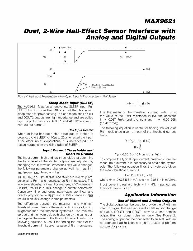
The MAX9621 restarts the Hall input with a blanking cycle. If the Hall input is disconnected from the Hall sensor for 10ms, it allows the Hall input to be pulled up by the 50FA pullup current to register the open-input fault condition. Reconnecting the Hall input to the Hall sensor restarts the Hall input with a blanking cycle. This provides a manual means of reenergizing a Hall input without having to resort to the FP to restart it. This also demonstrates the behavior of an intermittent connection to a Hall sensor.
Table 1. AOUT_/DOUT_ Truth Table
Figure 3. Hall Input Ramps to Open-Circuit Fault When a Short to Ground Is Relieved
*If IN_ is already shorted to BAT or open during power-up, DOUT_ goes to high-Z until IN_ is loaded.
14V
VIN_
VBAT - 25mV
HALL INPUTOPEN-CIRCUIT
FAULT
5mV/ms
IIN_
50µA
0V
0A TIME
TIME
HALL INPUTSHORT-TO-
GROUND FAULT
HALL INPUTDISCONNECTEDFROM SENSOR
CONDITION AOUT_ DOUT_
IN_ Short to GND 0 High-Z
IN_ Short to BAT or IN_ Open 0 Low*
SLEEP Low 0 High-Z
VBAT > 18V 0 Low*
11Maxim Integrated
Dual, 2-Wire Hall-Effect Sensor Interface with Analog and Digital Outputs
MAX9621
Sleep Mode Input (SLEEP)The MAX9621 features an active-low SLEEP input. Pull SLEEP low for more than 40Fs to put the device into sleep mode for power saving. In sleep mode, the DOUT1 and DOUT2 outputs are high impedance and are pulled high by pullup resistors. AOUT1 and AOUT2 are set to zero-output current.
Hall Input RestartWhen an input has been shut down due to a short to ground, cycle SLEEP for 10Fs to 20Fs to restart the input. If the other input is operational it is not affected. The restart happens on the rising edge of SLEEP.
Input Current Thresholds and Short to Ground
The input current high and low thresholds that determine the logic level of the digital outputs are adjusted by changing the RSET value. When the RSET value changes, the following parameters change as well: IIN_HYS, ISC, tBL, tRAMP, tDEL, fMAX, and PR.
IIH, IIL, IIN_HYS, ISC, tRAMP, and fMAX are inversely pro-portional to RSET and decrease as RSET increases. This inverse relationship is linear. For example, a 10% change in (1/RSET) results in a 10% change in current parameters. Conversely, time and delay parameters are linear and directly proportional to RSET, and a 10% change in RSET results in an 10% change in time parameters.
The difference between the maximum and minimum threshold current limits is the min/max limit spread, which is greater than the threshold hysteresis. The min/max spread and the hysteresis both change by the same per-centage as the mean of the threshold current limits. The following equation is useful for finding the mean of the threshold current limits given a value of RSET resistance:
( )01
I I I 0R m
= + <×
I is the mean of the threshold current limits, R is the value of the RSET resistance in kΩ, the constant I0 = 0.03717mA, and the constant m = -0.001668 (1/(kΩ x mA)).
The following equation is useful for finding the value of RSET resistance given a mean of the threshold current limits:
( )0Y Y m I I 0
1R
Y
= + × <
=
Y0 = 6.2013 x 10⁻⁵ units of (1/kΩ)
To compute the typical input current thresholds from the mean input current, it is necessary to obtain the hyster-esis. The following equation finds the hysteresis given the mean threshold current, I:
H = H0 + k x I (I < 0)
where H0 = -0.033463 in mA, and k = -0.08414 in mA/mA.
Input current threshold high = I - H/2, input current threshold low = I + H/2.
Application InformationUse of Digital and Analog Outputs
The digital output can be used to provide the FP with an interrupt signal that can represent a Hall sensor change of status. DOUT1 and DOUT2 provide a time domain output filter for robust noise immunity. See Figure 2. The analog output can be connected to an ADC with an appropriate load resistor, and can be used to perform custom diagnostics.
Figure 4. Hall Input Reenergized When Open Input Is Reconnected to Hall Sensor
14V
VIN_ 8V
5mA/µs HALL INPUT RECONNECTEDTO HALL SENSOR
11.5mA
IIN_
0V
0A TIME
TIME
VBAT - 500mV
VBAT - 25mV

12 Maxim Integrated
Dual, 2-Wire Hall-Effect Sensor Interface with Analog and Digital Outputs
MAX9621
Sleep ModeSleep mode can be used in applications that do not continuously require the polling of the Hall sensors. In such cases, the FP can enable the MAX9621 for a short time, check the sensor status, and then put the MAX9621 back to sleep. A blanking period follows upon exiting sleep mode.
Remote GroundThe MAX9621 targets applications with 2-wire Hall-effect sensors. 2-wire sensors have connections for supply and ground. The output level is signaled by means of modula-tion of the current drawn by the Hall sensor from its supply. The two threshold currents for high/low are generally in the range of 5mA to 14mA. Thus, the interfacing of a 2-wire sensor is not simply a matter of detecting two voltage thresholds, but requires a coarse current-sense function.
Because of the high-side current-sense structure of the MAX9621, the device is immune to shifts between the
sensor ground, the ground of the MAX9621 and FP. This ground-shift immunity eliminates the need for a ground-connection wire, allowing a single-wire interface to the Hall sensor.
Hall-Effect Sensor SelectionThe MAX9621 is optimized for use with 2-wire Hall-effect switches or with 3-wire Hall-effect switches connected as 2-wire (Figure 5). When using a 3-wire Hall sensor the resistor R is chosen so that the current drawn by the Hall sensor crosses the MAX9621 current threshold when the magnetic threshold of the Hall sensor is exceeded. A partial list of Hall switches that can be used with the MAX9621 is given in Table 2.
Input Current Threshold PrecisionTo get the best input current threshold precision, it is rec-ommended that the RSET resistor be directly connected to the BAT pin. A true Kelvin type connection is best.
Figure 5. 3-Wire Hall-Effect Switches Configured as 2-Wire
Table 2. A Partial List of Compatible Hall Switches
R
VCC IN_X
MAX9621
PART NO. MANUFACTURER WEBSITE COMMENTS
HAL573-6 Micronas www.micronas.com 2-wire
HAL556/560/566 Micronas www.micronas.com 2-wire
HAL579/581/584 Micronas www.micronas.com 2-wire
A1140/1/2/3 Allegro www.allegromicro.com 2-wire
A3161 Allegro www.allegromicro.com3-wire, optimized for 2-wire use without added resistor
TLE4941/C Infineon www.infineon.com 2-wire

13Maxim Integrated
Dual, 2-Wire Hall-Effect Sensor Interface with Analog and Digital Outputs
MAX9621
Chip InformationPROCESS: BiCMOS
Typical Application Circuit
REMOTEGROUND
GND
REMOTEGROUND
NS
NS
0.1µF
BATRSET
BATTERY: 5.5V TO 18VOPERATING,
60V WITHSTANDRPU
10kIRPU10kI
5kI
5kI
1.8V TO 5.5V
MICROPROCESSOR
ADC
ADC
SLEEP
AOUT1
AOUT2
DOUT2
DOUT1
FILTER
SLEEP-MODECONTROL
REFERENCEISET REF
REF
BAT
BAT
FILTERREF
0.01µF
IN2
IN1
INPUTSHORT
DETECTION
0.01µF
MAX9621
100kI
ECUC
ONNE
CTOR

14 Maxim Integrated
Dual, 2-Wire Hall-Effect Sensor Interface with Analog and Digital Outputs
MAX9621
Package InformationFor the latest package outline information and land patterns (footprints), go to www.maximintegrated.com/packages. Note that a “+”, “#”, or “-” in the package code indicates RoHS status only. Package drawings may show a different suffix character, but the drawing pertains to the package regardless of RoHS status.
α
α
PACKAGE TYPE PACKAGE CODE OUTLINE NO. LAND PATTERN NO.
10 FMAX U10+2 21-0061 90-0330

Maxim Integrated cannot assume responsibility for use of any circuitry other than circuitry entirely embodied in a Maxim Integrated product. No circuit patent licenses are implied. Maxim Integrated reserves the right to change the circuitry and specifications without notice at any time. The parametric values (min and max limits) shown in the Electrical Characteristics table are guaranteed. Other parametric values quoted in this data sheet are provided for guidance.
Maxim Integrated 160 Rio Robles, San Jose, CA 95134 USA 1-408-601-1000 15© 2011 Maxim Integrated Maxim Integrated and the Maxim Integrated logo are trademarks of Maxim Integrated Products, Inc.
Dual, 2-Wire Hall-Effect Sensor Interface with Analog and Digital Outputs
MAX9621
Revision History
REVISIONNUMBER
REVISION DATE
DESCRIPTIONPAGES
CHANGED
0 11/09 Initial release —
1 9/11 Added automotive qualified part 1