Embed Size (px)
Citation preview
MAX77812 PCB Layout Guide
UG6819 Rev 0; 2/19
Abstract
The MAX77812 is a quad-phase, high-current buck converter for high-end gaming consoles, VR/AR headsets, DSLR cameras, drones, network switches and routers, and FPGA systems that use multicore processors. The multiphase buck architecture reduces the size of the external components while providing the ripple current cancellation and world-class transient response. Differential remote sensing feedback enables tight DC and AC accuracy at the point of load. The MAX77812’s flexible architecture allows five user-selectable phase configurations: 4, (3+1), (2+2), (2+1+1), and (1+1+1+1).
Table of Contents
General Guidelines ....................................................................................................................... 3
Power Stage ................................................................................................................................. 4
PCB Layout Examples and Simulation Results ............................................................................ 8
PCB Layout Example .................................................................................................................. 10
Revision History .......................................................................................................................... 13
List of Figures
Figure 1. Buck power stage loop.
Figure 2. Dual-phase buck schematic and output voltage sensing point.
Figure 3. Dual-phase PCB layout recommendation.
Figure 4. Recommendation for 3-phase PCB layout.
Figure 5. Quad-phase PCB layout recommendation.
Figure 6. Dual-phase PCB layouts with balanced (Case 1) and unbalanced (Case 2) sensing.
Figure 7. Switching waveforms with balanced output sensing example (Case 1).
Figure 8. Switching waveforms with unbalanced output sensing example (Case 2).
Figure 9. Lamination diagram.
Figure 10. Top layer.
Figure 11. Second layer.
Figure 12. Third layer.
Figure 13. Fourth layer.
Figure 14. Fifth layer.
Figure 15. Bottom layer.
List of Tables
Table 1. Recommended Capacitors for Dual-Phase Configuration
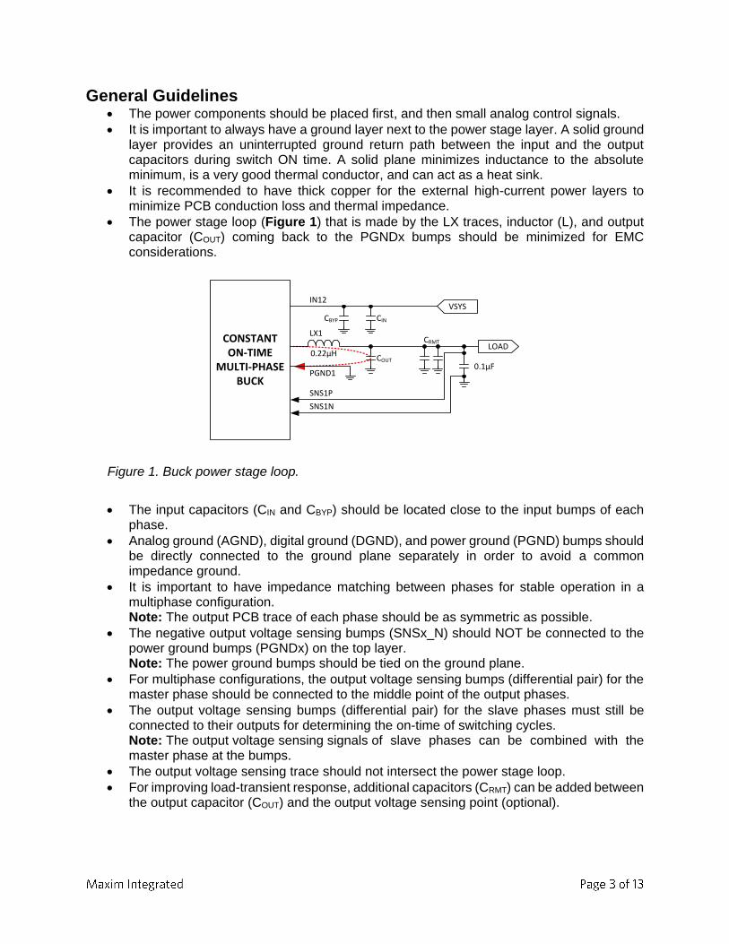
General Guidelines • The power components should be placed first, and then small analog control signals.
• It is important to always have a ground layer next to the power stage layer. A solid ground layer provides an uninterrupted ground return path between the input and the output capacitors during switch ON time. A solid plane minimizes inductance to the absolute minimum, is a very good thermal conductor, and can act as a heat sink.
• It is recommended to have thick copper for the external high-current power layers to minimize PCB conduction loss and thermal impedance.
• The power stage loop (Figure 1) that is made by the LX traces, inductor (L), and output capacitor (COUT) coming back to the PGNDx bumps should be minimized for EMC considerations.
Figure 1. Buck power stage loop.
• The input capacitors (CIN and CBYP) should be located close to the input bumps of each phase.
• Analog ground (AGND), digital ground (DGND), and power ground (PGND) bumps should be directly connected to the ground plane separately in order to avoid a common impedance ground.
• It is important to have impedance matching between phases for stable operation in a multiphase configuration.
Note: The output PCB trace of each phase should be as symmetric as possible.
• The negative output voltage sensing bumps (SNSx_N) should NOT be connected to the power ground bumps (PGNDx) on the top layer.
Note: The power ground bumps should be tied on the ground plane.
• For multiphase configurations, the output voltage sensing bumps (differential pair) for the master phase should be connected to the middle point of the output phases.
• The output voltage sensing bumps (differential pair) for the slave phases must still be connected to their outputs for determining the on-time of switching cycles.
Note: The output voltage sensing signals of slave phases can be combined with the master phase at the bumps.
• The output voltage sensing trace should not intersect the power stage loop.
• For improving load-transient response, additional capacitors (CRMT) can be added between the output capacitor (COUT) and the output voltage sensing point (optional).
CONSTANT ON-TIME
MULTI-PHASE BUCK
VSYS
LX1
0.22µH
CIN
IN12
PGND1
SNS1P
SNS1N
COUT
LOAD
0.1µF
CBYP
CRMT

Power Stage
Low-ESR ceramic bypass capacitors should be located as close to the input bumps as possible. Generally, 0.1µF to 10µF capacitors are suitable for effective decoupling of high-frequency power-supply noise. Crosstalk is essentially a capacitive coupling event that occurs when a noise signal is induced to nearby traces through parasitic low-impedance paths. It is recommended to keep the distance between adjacent PH1 and PH2 traces (for dual-phase configuration) at least two to three times their width apart. The power stage loop should be minimized for EMC considerations. It is important to have thick copper traces for the outer high-current power layers to minimize PCB conduction loss and improve the heat dissipation. Multiple vias are recommended for all paths that carry high currents (PGND, VIN, and LX). Placement of vias should create the shortest possible current loops and must not obstruct the flow of currents or mirror currents in the ground plane.
For the multiphase configurations, the impedance matching between phases is important for stable operation. The output trace of each phase should be as symmetric as possible. The output voltage sensing bumps (differential pair) for the master phase should be connected to the middle point of the output phases, as shown in Figure 2. The output voltage sensing bumps for slave phase(s) must be connected to their output for determining the on-time. The output voltage sensing signals of slave phase(s) can be tied with the corresponding master phase(s), as shown in Figure 3.
Figure 2. Dual-phase buck schematic and output voltage sensing point.
CONSTANT ON-TIME
MULTI-PHASE BUCK
VSYS
LX1
0.22µH
2 x0.1µF
IN12
PGND1
SNS1P
SNS1N
LX2
0.22µH
PGND2
SNS2P
SNS2N
22µF
2 x 22µFLOAD
22µF
10µF

SCL
IRQB
VIO SYS
MISO
CE
IN12
LX1PGND
1
SNS1P
PGND1
LX3
PGND3
PGND3
LX1
LX3
PGND1
PGND3
SNS1N
LX2PGND
2
PGND2
LX4PGND
4IN34
LX2PGND
2
LX4PGND
4
IN12
IN12
IN34
IN34
SNS3N
SNS3P
PH_CFG0
AGND
PH_CFG1
LX1 LX2
LX4
LX3
DGNDGPI0
IN12
IN34
PGND4
GPI1
WDTRSTB_IN
SDA/MOSI
SNS4P
SNS4N
SNS2N
SNS2P
SCS
AGND
I2C_SPI_SEL
PH_CFG2
EN
LPM
L
(2016 Size)
CBYP
(0603)
CBYP
(0603)
COUT
(0603)
COUT
(0603)L
(2016 Size)
AGNDAGND
AGNDAGND
CRMT
(0402)
LOAD
PGND
(Top Layer)
CIN
(0603)
VIN
(Top Layer)
CRMT
(0603)
CRMT
(0603)
2 x 0.1µF Cap
Additional Caps
for Load Transient
Improvement
(Optional)
Merged
Sensing
Signals
PGND
(Top Layer)
LX traces can be on
either the top or an
inner layer
LX LX
Figure 3. Dual-phase PCB layout recommendation.
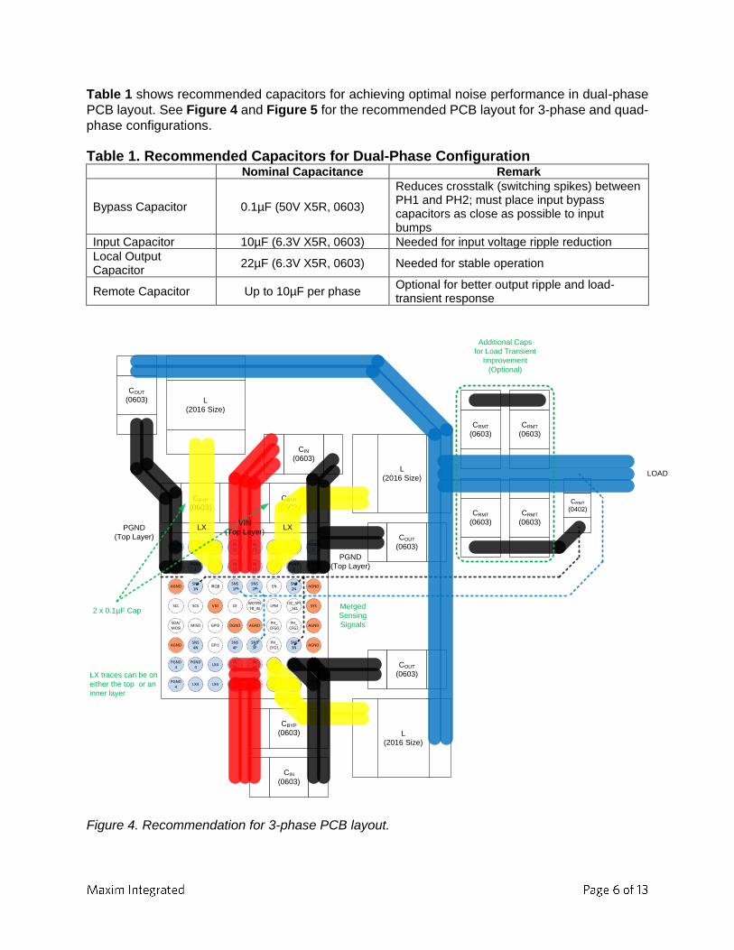
Table 1 shows recommended capacitors for achieving optimal noise performance in dual-phase
PCB layout. See Figure 4 and Figure 5 for the recommended PCB layout for 3-phase and quad-
phase configurations.
Table 1. Recommended Capacitors for Dual-Phase Configuration Nominal Capacitance Remark
Bypass Capacitor 0.1µF (50V X5R, 0603)
Reduces crosstalk (switching spikes) between PH1 and PH2; must place input bypass capacitors as close as possible to input bumps
Input Capacitor 10µF (6.3V X5R, 0603) Needed for input voltage ripple reduction
Local Output Capacitor
22µF (6.3V X5R, 0603) Needed for stable operation
Remote Capacitor Up to 10µF per phase Optional for better output ripple and load-transient response
SCL
IRQB
VIO SYS
MISO
CE
IN12
LX1PGND
1
SNS1P
PGND1
LX3
PGND3
PGND3
LX1
LX3
PGND1
PGND3
SNS1N
LX2PGND
2
PGND2
LX4PGND
4IN34
LX2PGND
2
LX4PGND
4
IN12
IN12
IN34
IN34
SNS3N
SNS3P
PH_CFG0
AGND
PH_CFG1
LX1 LX2
LX4
LX3
DGNDGPI0
IN12
IN34
PGND4
GPI1
WDTRSTB_IN
SDA/MOSI
SNS4P
SNS4N
SNS2N
SNS2P
SCS
AGND
I2C_SPI_SEL
PH_CFG2
EN
LPM
L
(2016 Size)
CBYP
(0603)
CBYP
(0603)
COUT
(0603)
COUT
(0603)
L
(2016 Size)
AGNDAGND
AGNDAGND
CRMT
(0402)
LOAD
PGND
(Top Layer)
CIN
(0603)
VIN
(Top Layer)
CRMT
(0603)
CRMT
(0603)
CRMT
(0603)
CRMT
(0603)
2 x 0.1µF Cap
Additional Caps
for Load Transient
Improvement
(Optional)
Merged
Sensing
Signals
PGND
(Top Layer)
LX traces can be on
either the top or an
inner layer
COUT
(0603)
L
(2016 Size)
CBYP
(0603)
CIN
(0603)
LXLX
Figure 4. Recommendation for 3-phase PCB layout.
SCL
IRQB
VIO SYS
MISO
CE
IN12
LX1PGND
1
SNS1P
PGND1
LX3
PGND3
PGND3
LX1
LX3
PGND1
PGND3
SNS1N
LX2PGND
2
PGND2
LX4PGND
4IN34
LX2PGND
2
LX4PGND
4
IN12
IN12
IN34
IN34
SNS3N
SNS3P
PH_CFG0
AGND
PH_CFG1
LX1 LX2
LX4
LX3
DGNDGPI0
IN12
IN34
PGND4
GPI1
WDTRSTB_IN
SDA/MOSI
SNS4P
SNS4N
SNS2N
SNS2P
SCS
AGND
I2C_SPI_SEL
PH_CFG2
EN
LPM
L
(2016 Size)
CBYP
(0603)
CBYP
(0603)
COUT
(0603)
COUT
(0603)
L
(2016 Size)
AGNDAGND
AGNDAGND
CRMT
(0402)
LOAD
PGND
(Top Layer)
CIN
(0603)
VIN
(Top Layer)
CRMT
(0603)
CRMT
(0603)
CRMT
(0603)
CRMT
(0603)
4 x 0.1µF Cap
Additional Caps
for Load Transient
Improvement
(Optional)
Merged
Sensing
Signals
PGND
(Top Layer)
LX traces can be
on either the top
or an inner layer
COUT
(0603)
L
(2016 Size)
CBYP
(0603)
CIN
(0603)
LXLX
LX
PGND
(Top Layer)
L
(2016 Size)COUT
(0603)
CBYP
(0603)
VIN
(Top Layer)LX
PGND
(Top Layer)
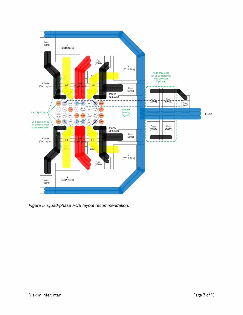
Figure 5. Quad-phase PCB layout recommendation.

PCB Layout Examples and Simulation Results
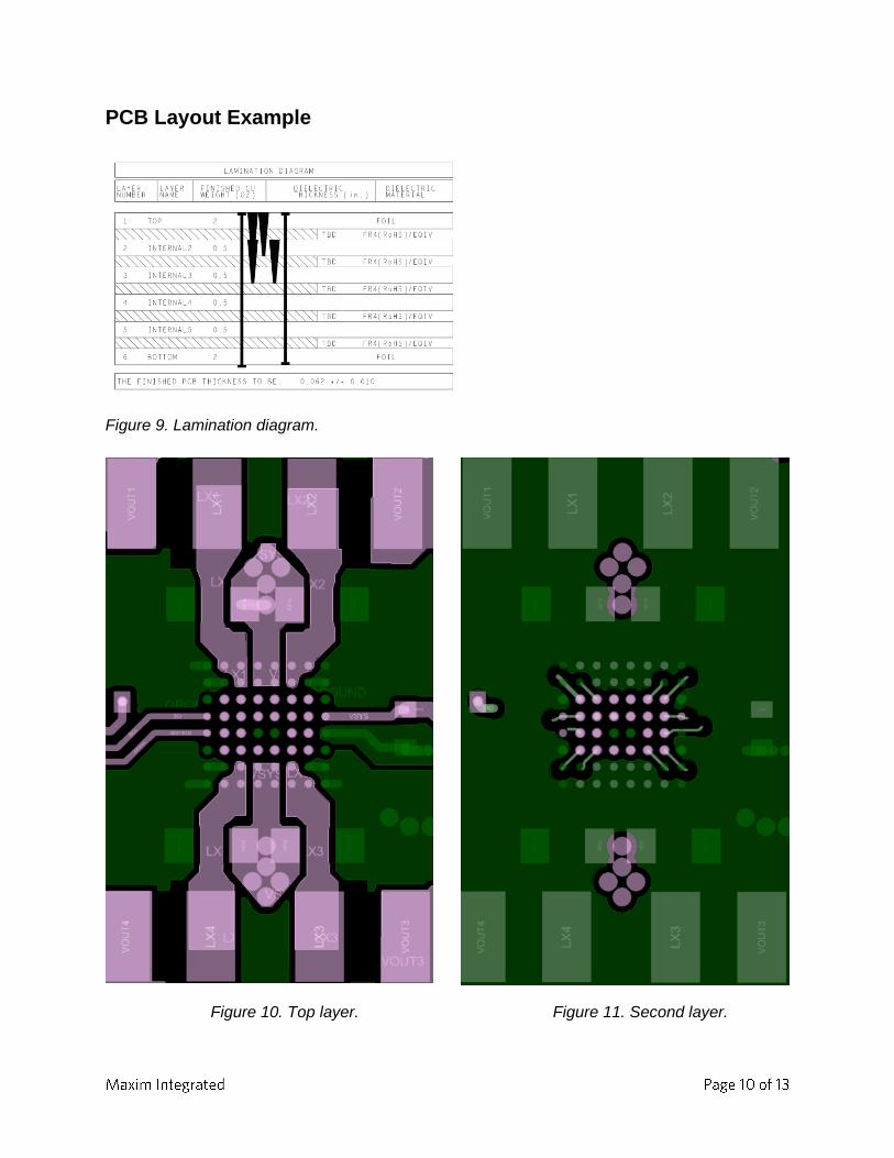
Figure 6 shows examples of a dual-phase PCB layout. With balanced output voltage sensing, the switching waveforms are regular, resulting in smaller output voltage ripple as shown in Figure 7. Figure 8 shows that unbalanced output voltage sensing gives higher output voltage ripple due to slight changes in off-time period cycle by cycle.
PCB Layout Details—Common for Balanced and Unbalanced Cases
• PH1 and PH2 outputs are tied from COUT and connected to the load together.
• Parasitics of PH1 and PH2 traces are matched (symmetric PCB layout).
• Load is connected to the middle point of the output phases.
Case 1—Balanced Output Sensing
The PH1 and PH2 output voltage sensing signals are tied together and connected to the middle point of the output phases (CRMT).
Case 2—Unbalanced Output Sensing
The PH1 and PH2 output voltage sensing signals are connected to their own local output capacitors (COUT) separately.
SCL
IRQB
VIO SYS
MISO
CE
IN12
LX1PGND
1
SNS1P
PGND1
LX3
PGND3
PGND3
LX1
LX3
PGND1
PGND3
SNS1N
LX2PGND
2
PGND2
LX4PGND
4IN34
LX2PGND
2
LX4PGND
4
IN12
IN12
IN34
IN34
SNS3N
SNS3P
PH_CFG0
AGND
PH_CFG1
LX1 LX2
LX4
LX3
DGNDGPI0
IN12
IN34
PGND4
GPI1
WDTRSTB_IN
SDA/MOSI
SNS4P
SNS4N
SNS2N
SNS2P
SCS
AGND
I2C_SPI_SEL
PH_CFG2
EN
LPM
L
(2016 Size)
CBYP
(0603)
CBYP
(0603)
COUT
(0603)
COUT
(0603)L
(2016 Size)
AGNDAGND
AGNDAGND
CRMT
(0402)
LOAD
PGND
(Top Layer)
CIN
(0603)
VIN
(Top Layer)
CRMT
(0603)
CRMT
(0603)
PGND
(Top Layer)
Case 1
(Balanced Sensing)
LX LX
SCL
IRQB
VIO SYS
MISO
CE
IN12
LX1PGND
1
SNS1P
PGND1
LX3
PGND3
PGND3
LX1
LX3
PGND1
PGND3
SNS1N
LX2PGND
2
PGND2
LX4PGND
4IN34
LX2PGND
2
LX4PGND
4
IN12
IN12
IN34
IN34
SNS3N
SNS3P
PH_CFG0
AGND
PH_CFG1
LX1 LX2
LX4
LX3
DGNDGPI0
IN12
IN34
PGND4
GPI1
WDTRSTB_IN
SDA/MOSI
SNS4P
SNS4N
SNS2N
SNS2P
SCS
AGND
I2C_SPI_SEL
PH_CFG2
EN
LPM
L
(2016 Size)
CBYP
(0603)
CBYP
(0603)
COUT
(0603)
COUT
(0603)L
(2016 Size)
AGNDAGND
AGNDAGND
CRMT
(0402)
LOAD
PGND
(Top Layer)
CIN
(0603)
VIN
(Top Layer)
CRMT
(0603)
CRMT
(0603)
PGND
(Top Layer)LX LX
Case 2
(Unbalanced Sensing)
Figure 6. Dual-phase PCB layouts with balanced (Case 1) and unbalanced (Case 2) sensing.
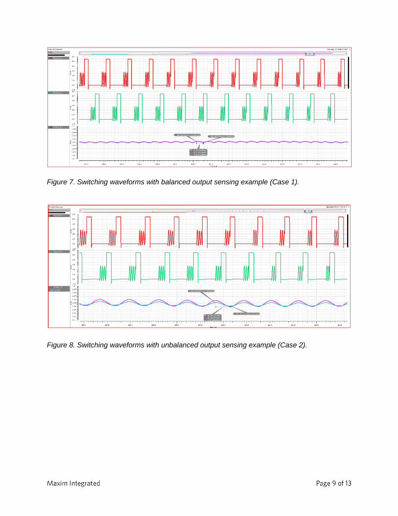
Figure 7. Switching waveforms with balanced output sensing example (Case 1).
Figure 8. Switching waveforms with unbalanced output sensing example (Case 2).
PCB Layout Example
Figure 9. Lamination diagram.
Figure 10. Top layer.
Figure 11. Second layer.
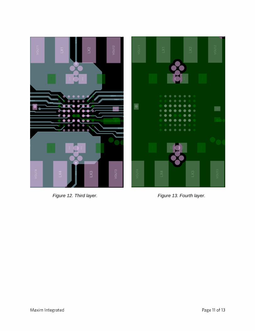
Figure 12. Third layer.
Figure 13. Fourth layer.
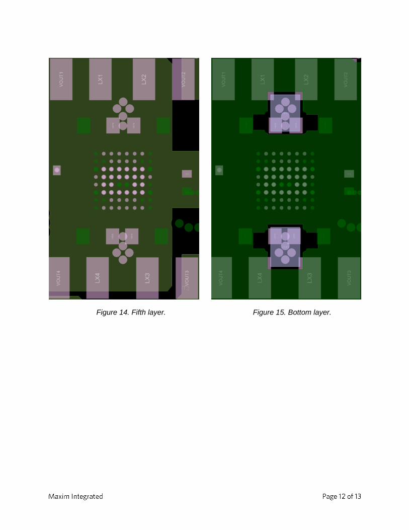
Figure 14. Fifth layer.
Figure 15. Bottom layer.

Revision History REVISION NUMBER
REVISION DATE
DESCRIPTION PAGES
CHANGED
0 02/19 Initial release —
©2019 by Maxim Integrated Products, Inc. All rights reserved. Information in this publication concerning the devices, applications, or technology described is intended to suggest possible uses and may be superseded. MAXIM INTEGRATED PRODUCTS, INC. DOES NOT ASSUME LIABILITY FOR OR PROVIDE A REPRESENTATION OF ACCURACY OF THE INFORMATION, DEVICES, OR TECHNOLOGY DESCRIBED IN THIS DOCUMENT. MAXIM ALSO DOES NOT ASSUME LIABILITY FOR INTELLECTUAL PROPERTY INFRINGEMENT RELATED IN ANY MANNER TO USE OF INFORMATION, DEVICES, OR TECHNOLOGY DESCRIBED HEREIN OR OTHERWISE. The information contained within this document has been verified according to the general principles of electrical and mechanical engineering or registered trademarks of Maxim Integrated Products, Inc. All other product or service names are the property of their respective owners.