Embed Size (px)
Citation preview
General DescriptionThe MAX6655/MAX6656 are precise voltage and temperature monitors. The digital thermometer reports the temperature of two remote sensors and its own die temperature. The remote sensors are diode-connected transistors—typically a low-cost, easily mounted 2N3906 PNP type—that replace conventional thermistors or thermocouples. Remote accuracy is ±1°C for multiple transistor manufacturers with no calibration necessary. The remote channels can also measure the die temperature of other ICs, such as microprocessors, that contain a substrate-connected PNP with its collector grounded and its base and emitter available for temperature-sensing purposes. The temperature is digitized with 11-bit resolution.The MAX6655/MAX6656 also measure their own supply voltage and three external voltages with 8-bit resolution. Each voltage input’s sensitivity is set to give approximately 3/4-scale output code when the input voltage is at its nominal value. The MAX6655 operates at +5V supply and its second voltage monitor is 3.3V. The MAX6656 operates on a +3.3V supply and its second voltage monitor is 5V.The 2-wire serial interface accepts standard SMBus™ Write Byte, Read Byte, Send Byte, and Receive Byte commands to program the alarm thresholds and to read data. The MAX6655/MAX6656 also provide SMBus alert response and timeout functions. The MAX6655/MAX6656 measure automatically and autonomously, with the con-version rate programmable. The adjustable rate allows the user to control the supply current.In addition to the SMBus ALERT output, the MAX6655/ MAX6656 feature an OVERT output, which is used as a temperature reset that remains active only while the temperature is above the maximum temperature limit. The OVERT output is optimal for fan control or for system shutdown.
Applications Notebooks Thin Clients Servers
Workstations Communication
Equipment Desktop PC
Features Three Temperature Channels
• Two Remote PN Junctions• One Local Sensor
Four Voltage Channels• +12V, +5V, +3.3V, +2.5V• Three External Monitors• One Internal Supply Monitor
11-Bit, 0.125°C Resolution High Accuracy: ±1°C Over +60°C to +100°C
Temperature Range Programmable Under/Over-Threshold Alarms Programmable Power-Saving Mode No Calibration Required SMBus/I2C-Compatible Interface OVERT Output for Fan Control and System
Shutdown
19-2117; Rev 2; 5/17
SMBus is a trademark of Intel Corp.
Typical Application Circuit appears at end of data sheet.
PART TEMP RANGE PIN-PACKAGE
PKG CODE
MAX6655MEE+ -55°C to +125°C 16 QSOP E16+5
MAX6656MEE+ -55°C to +125°C 16 QSOP E16+5
MAX6655/MAX6656 Dual Remote/Local Temperature Sensors and Four-Channel Voltage Monitors
Pin Configuration
Ordering Information
16
15
14
13
12
11
10
9
1
2
3
4
5
6
7
8
VCC STBY
SMBCLK
OVERT
SMBDATA
ALERT
VIN2
VIN1
VIN3
TOP VIEW
MAX6655MAX6656
QSOP
DXP1
DXN1
DXP2
ADD0
ADD1
DXN2
GND
VCC to GND ............................................................-0.3V to +6VDXN_ to GND .......................................................-0.3V to +0.8VSMBCLK, SMBDATA, ALERT, STBY,
OVERT to GND ...................................................-0.3V to +6VVIN1 to GND ..........................................................-0.3V to +16VVIN2 to GND ............................................................-0.3V to +6VVIN3 to GND ............................................................-0.3V to +6VAll Other Pins to GND .............................. -0.3V to (VCC + 0.3V)SMBDATA, ALERT, OVERT Current.................. -1mA to +50mA
DXN_ Current .....................................................................±1mAESD Protection (all pins, Human Body Model) .................2000VContinuous Power Dissipation (TA = +70°C)
16-Pin QSOP (derate 8.30mW/°C above +70°C) .......667mWOperating Temperature Range ......................... -55°C to +125°CJunction Temperature ......................................................+150°CStorage Temperature Range ............................ -65°C to +150°CLead Temperature (soldering, 10s) .................................+300°C
(VCC = +3.0V to +3.6V for MAX6656, VCC = +4.5V to +5.5V for MAX6655, TA = -55°C to +125°C, unless otherwise noted. Typical values are at VCC = +3.3V for MAX6656, VCC = +5.0V for MAX6655, TA = +25°C.)
PARAMETER SYMBOL CONDITIONS MIN TYP MAX UNITSSupply Range VCC 3.0 5.5 V
Accuracy (Local Sensor)+60°C ≤ TA ≤ +100°C ±1.5
°C0°C ≤ TA ≤ +125°C ±3
Accuracy (Remote Sensor)+60°C ≤ TRJ ≤ +100°C ±1
°C0°C ≤ TRJ ≤ +120°C ±3
Temperature Measurement Resolution
0.125 °C
11 Bits
ADC Input Impedance ZIN VIN1, VIN2, VIN3 input resistance 100 kΩ
ADC Total Error VIN1, VIN2, VIN3 between 30% and 120% of nominal ±1 ±1.5 %
VIN ADC Resolution 8 Bits
Undervoltage Lockout Threshold UVLO VCC input, disables A/D conversion,falling edge 2.50 2.70 2.90 V
Undervoltage Lockout Hysteresis 90 mV
Power-On Reset (POR) Threshold VCC, falling edge 1 1.7 2.5 V
POR Threshold Hysteresis 90 mV
Standby Current SMBus static, STBY = GND 3 10 µA
DXP and DXN Leakage Current In standby mode 2 µA
Average Operating Current Continuous temperature mode 550 1000 µA
Conversion Time for Single Temperature Measurement tCON From stop bit to conversion completed 95 125 155 ms
Monitoring Cycle Time tMONITotal of 3 temperature plus 4 voltage measurements 625 ms
MAX6655/MAX6656 Dual Remote/Local Temperature Sensors and Four-Channel Voltage Monitors
www.maximintegrated.com Maxim Integrated 2
Absolute Maximum Ratings
Stresses beyond those listed under “Absolute Maximum Ratings” may cause permanent damage to the device. These are stress ratings only, and functional operation of the device at these or any other conditions beyond those indicated in the operational sections of the specifications is not implied. Exposure to absolute maximum rating conditions for extended periods may affect device reliability.
Electrical Characteristics
(VCC = +3.0V to +3.6V for MAX6656, VCC = +4.5V to +5.5V for MAX6655, TA = -55°C to +125°C, unless otherwise noted. Typical values are at VCC = +3.3V for MAX6656, VCC = +5.0V for MAX6655, TA = +25°C.)
PARAMETER SYMBOL CONDITIONS MIN TYP MAX UNITS
Remote Junction Current(DXP, DXN)
High level 80 100 140µA
Low level 8 10 14
SMBus INTERFACE (SMBCLK, SMBDATA, STBY)Logic Input Low Voltage VIL VCC = +3.0V to +5.5V 0.8 V
Logic Input High Voltage VIHVCC = +3.0V 2.1
VVCC = +5.5V 2.6
Input Leakage Current ILEAK VIN = GND or VCC ±1 µA
Output Low Sink Current IOL VOL = +0.6V 6 mA
Input Capacitance CIN 5 pF
SMBus Timeout SMBCLK or SMBDATA time low for reset 30 35 60 ms
ALERT, OVERTOutput Low Sink Current VOL = +0.6V 6 mA
Output High Leakage Current VOH = +5.5V 1 µA
SMBus TIMINGSerial Clock Frequency fSCL 400 kHz
Bus Free Time Between STOP and START Condition tBUF 4.7 µs
START Condition Setup Time 4.7 µs
Repeat START Condition Setup Time tSU:STA 90% to 90% 50 ns
START Condition Hold Time tHD:STA 10% of SMBDATA to 90% of SMBCLK 4 µs
STOP Condition Setup Time tSU:STO 90% of SMBCLK to 10% of SMBDATA 4 µs
Clock Low Period tLOW 10% to 10% 4.7 µs
Clock High Period tHIGH 90% to 90% 4 µs
Data Setup Time tSU:DAT 90% of SMBDATA to 10% of SMBCLK 250 ns
Data Hold Time tHD:DAT (Note 1) 0 µs
Receive SMBCLK/SMBDATA Rise Time tR 1 µs
Receive SMBCLK/SMBDATA Fall Time tF 300 ns
Pulse Width of Spike Suppressed tSP 0 50 ns
MAX6655/MAX6656 Dual Remote/Local Temperature Sensors and Four-Channel Voltage Monitors
www.maximintegrated.com Maxim Integrated 3
Electrical Characteristics (continued)
(TA = +25°C, unless otherwise noted.)
-5
-2
-3
-4
-1
0
1
2
3
4
5
-55 -5 45 95
REMOTE TEMPERATURE ERRORvs. REMOTE-DIODE TEMPERATURE
MAX
6655
/MAX
6656
toc0
2
TEMPERATURE (°C)
REMO
TE T
EMPE
RATU
RE E
RROR
(°C) RANDOM SAMPLE
2N3906
20
15
10
5
00 2010 30 40 50
TEMPERATURE ERRORvs. POWER-SUPPLY NOISE FREQUENCY
MAX
6655
/MAX
6656
toc0
3
FREQUENCY (MHz)
TEMP
ERAT
URE
ERRO
R (°C
)
VIN = SQUARE WAVEAPPLIED TO VCC WITHNO VCC BYPASS CAPACITORVIN = 250mVp-pREMOTE DIODE
0
2
4
6
8
10
12
14
0 10 20 30 40 50
REMOTE TEMPERATURE ERRORvs. COMMON-MODE NOISE FREQUENCY
MAX
6655
/MAX
6656
toc0
4
FREQUENCY (MHz)
REMO
TE T
EMPE
RATU
RE E
RROR
(°C)
VIN = 200mVp-p
VIN = 100mVp-p
VIN = SQUARE WAVEAC-COUPLED TO DXN
0
2
4
6
8
10
12
14
0 50 100 150 200
REMOTE TEMPERATURE ERRORvs. DXP-DXN CAPACITANCE
MAX
6655
/MAX
6656
toc0
5
DXP-DXN CAPACITANCE (nF)
REMO
TE T
EMPE
RATU
RE E
RROR
(°C) VCC = +5V
0
15
10
5
20
25
30
35
40
45
50
1 10 100 1000
STANDBY SUPPLY CURRENTvs. CLOCK FREQUENCY
MAX
6655
/MAX
6656
toc0
6
SMBCLK FREQUENCY (kHz)
SUPP
LY C
URRE
NT (µ
A)SMBCLK IS DRIVENRAIL-TO-RAIL
0
20
40
60
80
100
120
140
0 1 2 3 4 5
STANDBY SUPPLY CURRENTvs. SUPPLY VOLTAGE
MAX
6655
/MAX
6656
toc0
7
SUPPLY VOLTAGE (V)
SUPP
LY C
URRE
NT (µ
A)
ADD0, ADD1 = HIGH-Z
ADD0, ADD1 = GND
20
10
0
-10
-201 10 100
REMOTE TEMPERATURE ERRORvs. PC BOARD RESISTANCE
MAX
6655
/MAX
6656
toc0
1
LEAKAGE RESISTANCE (MΩ)
REMO
TE T
EMPE
RATU
RE E
RROR
(°C)
PATH = DXP TO GND
PATH = DXP TO VCC (5V)
0
40
20
80
60
120
100
-1 1 20 3 4 5
RESPONSE TO THERMAL SHOCK
MAX
6655
/MAX
6656
toc0
8
TIME (s)
TEMP
ERAT
URE
(°C)
REMOTE DIODE IMMERSEDIN +115°C FLUORINERT BATH
0
4
2
8
6
12
10
0 40 6020 80 100 120
VOLTAGE ACCURACYvs. TEMPERATURE
MAX
6655
/MAX
6656
toc0
9
TEMPERATURE (°C)
OUTP
UT V
OLTA
GE (V
)
VIN1
VCC
VIN2
VIN3INPUT VOLTAGES ARE NOMINAL
MAX6655/MAX6656 Dual Remote/Local Temperature Sensors and Four-Channel Voltage Monitors
Maxim Integrated 4www.maximintegrated.com
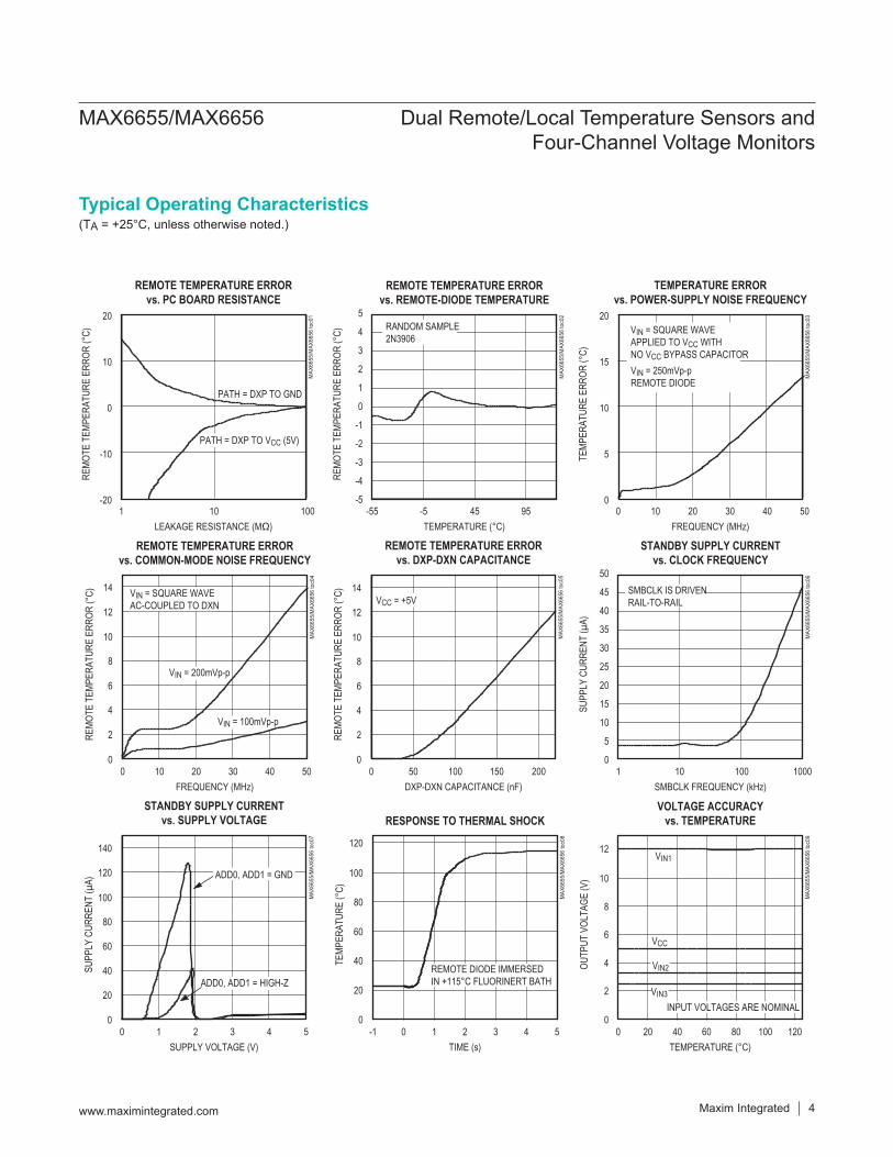
Typical Operating Characteristics
Detailed DescriptionThe MAX6655/MAX6656 are voltage and temperature monitors that communicate through an SMBus-compatible interface with a microprocessor or microcontroller in ther-mal management applications.Essentially an 11-bit serial ADC with a sophisticated front end, the MAX6655/MAX6656 contain a switched-current source, a multiplexer, an ADC, an SMBus interface, and the associated control logic. Temperature data from the ADC is loaded into a data register, where it is automati-cally compared with data previously stored in over/under-temperature alarm threshold registers. Temperature data can be read at any time with 11 bits of resolution.The MAX6655/MAX6656 can monitor external supply voltages of typically 12V, 2.5V, and 3.3V for the MAX6655 and 5.0V for the MAX6656, as well as their own supply voltage. All voltage inputs are converted to an 8-bit code using an ADC. Each input voltage is scaled down by an
on-chip resistive-divider so that its output, at the nominal input voltage, is approximately 3/4 of the ADC’s full-scale range, or a decimal count of 198.
ADCThe averaging ADC integrates over a 40ms period (typ) with excellent noise rejection. The ADC converts a tem-perature measurement in 125ms (typ) and a voltage measurement in 62.5ms (typ). For temperature measure-ments, the multiplexer automatically steers bias currents through the remote diode, then the forward voltage is measured and the temperature is computed. The DXN input is biased at one diode drop above ground by an internal diode to set up the ADC inputs for a differential measurement. The worst-case DXP-DXN differential input voltage range is +0.25V to +0.95V.Excess resistance in series with the remote diode causes about +1/2°C error/Ω. A 200μV offset voltage at DXP-DXN causes about -1°C error.
PIN NAME FUNCTION1 VCC Supply Voltage. +5V for MAX6655; +3.3V for MAX6656. Bypass VCC to GND with a 0.1µF capacitor.
2 DXP1 External Diode 1 Positive Connection. DXP1 is the combined current source and ADC positive input for remote-diode 1. If a remote-sensing junction is not used, connect DXP1 to DXN1.
3 DXN1 External Diode 1 Negative Connection. DXN1 is the combined current sink and ADC negative input for remote-diode 1. DXN1 is normally biased to a diode voltage above ground.
4 ADD0 SMBus Slave Address Select Input. ADD0 and ADD1 are sampled upon power-up. Table 5 is the truth table.
5 ADD1 SMBus Slave Address Select Input. ADD0 and ADD1 are sampled upon power-up.
6 DXP2 External Diode 2 Positive Connection. DXP2 is the combined current source and ADC positive input for remote-diode 2. If a remote-sensing junction is not used, connect DXP2 to DXN2.
7 DXN2 External Diode 2 Negative Connection. DXN2 is the combined current sink and ADC negative input for remote-diode 2. DXN2 is normally biased to a diode voltage above ground.
8 GND Ground
9 VIN3 External Voltage Monitor 3. VIN3 is typically used to monitor +2.5V supplies.
10 VIN1 External Voltage Monitor 1. VIN1 is typically used to monitor +12V supplies.
11 VIN2External Voltage Monitor 2. VIN2 is typically used to monitor voltage supplies of +3.3V for MAX6655 and +5.0V for MAX6656.
12 ALERT SMBus Alert (Interrupt) Output, Open-Drain
13 SMBDATA SMBus Serial-Data Input/Output, Open-Drain
14 OVERT Overtemperature Alarm Output, Open-Drain. OVERT is an unlatched alarm output that responds to the programmed maximum temperature limit for all temperature channels.
15 SMBCLK SMBus Serial-Clock Input
16 STBY Hardware Standby Input. Drive STBY low for low-power standby mode. Drive STBY high for normal operating mode. Temperature and comparison threshold data are retained in standby mode.
MAX6655/MAX6656 Dual Remote/Local Temperature Sensors and Four-Channel Voltage Monitors
www.maximintegrated.com Maxim Integrated 5
Pin Description
ADC Conversion SequenceEach time a conversion begins, all channels are con-verted, and the results of the measurements are avail-able after the end of conversion. A BUSY status bit in the Status Byte shows that the device is actually performing a new conversion; however, even if the ADC is busy, the results of the previous conversion are always available. The conversion sequence for the MAX6655 (MAX6656) is External Diode 1, External Diode 2, Internal Diode, VIN3, VIN2 (VCC), VIN1, VCC (VIN2).The ADC always converts at maximum speed, but the time between a sequence of conversions is adjustable. The Conversion Rate Control Byte (Table 1) shows the possible delays between conversions. Disabling voltage or temperature measurements with the Configuration Byte makes the ADC complete the conversion sequence faster.
Low-Power Standby ModeStandby mode disables the ADC and reduces the sup-ply current drain to 3μA (typ). Enter standby mode by forcing STBY low or through the RUN/STOP bit in
the Configuration Byte register. Hardware and software standby modes behave identically; all data is retained in memory, and the SMBus interface is alive and listening for reads and writes. Standby mode is not a shutdown mode. Activity on the SMBus draws extra supply current (see Typical Operating Characteristics).Enter hardware standby mode by forcing STBY low. In a notebook computer, this line may be connected to the system SUSTAT# suspend-state signal. The STBY low state overrides any software conversion command. If a hardware or software standby command is received while a conversion is in progress, the conversion cycle is trun-cated, and the data from that conversion is not latched into the Temperature Reading register. The previous data is not changed and remains available.Supply current during the 125ms conversion is typically 550μA. Between conversions, the instantaneous supply current is about 25μA, due to the current consumed by the conversion-rate timer. With very low supply voltages (under the POR threshold), the supply current is higher due to the address input bias currents.
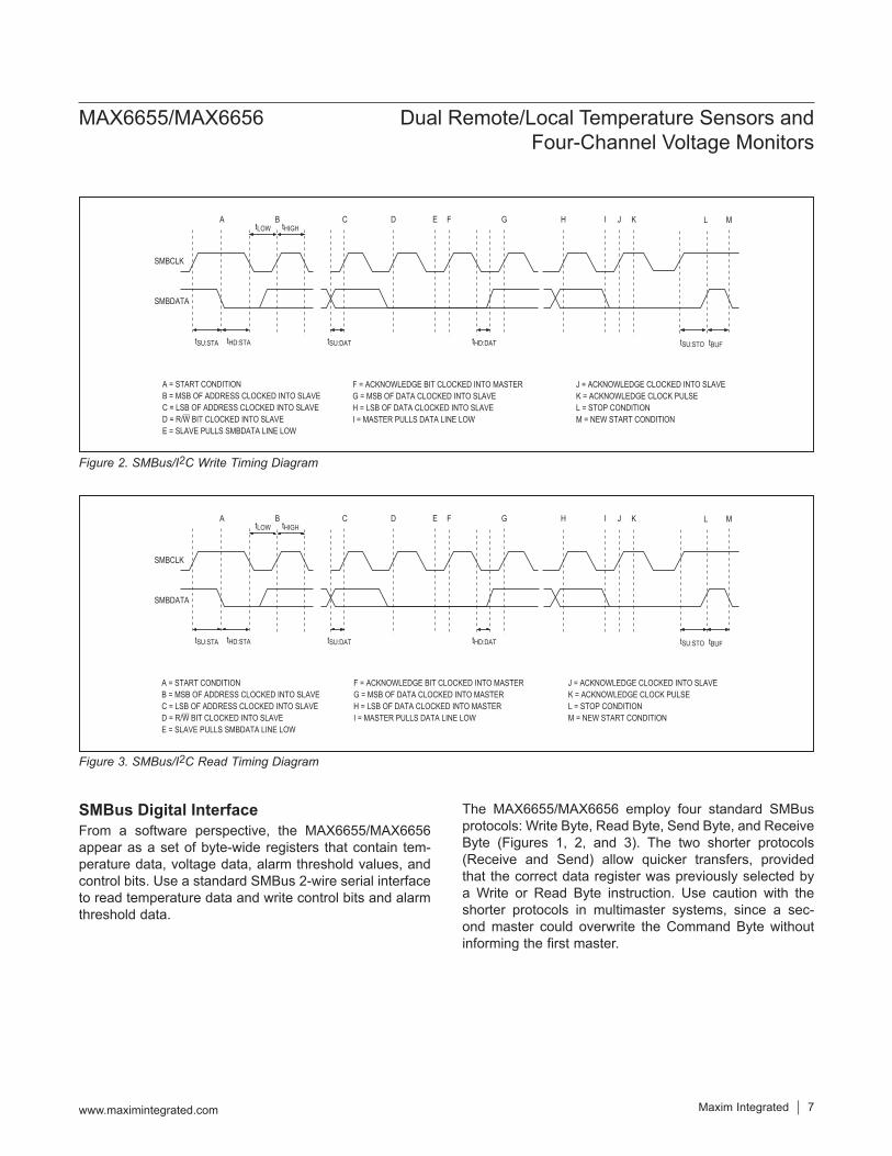
Figure 1. SMBus/I2C Protocols
Write Byte Format
Read Byte Format
Send Byte Format Receive Byte Format
Slave Address: equiva-lent to chip-select line ofa 3-wire interface
Command Byte: selects whichregister you are writing to
Data Byte: data goes into the registerset by the command byte ( to se tthresholds, configuration masks, andsampling rate)
Slave Address: equiva-lent to chip-select line
Command Byte: selectswhich register you arereading from
Slave Address: repeateddue to change in data-flow direction
Data Byte: reads fromthe register set by thecommand byte
Data Byte: writes data to theregister commanded by thelast read byte or write bytetransmission
Data Byte: reads data fromthe register commandedby the last read byte orwrite byte transmission;also used for SMBus alertresponse return addressS = Start condition
P = Stop conditionShaded = Slave transmissionA = Not acknowledged
ACK
7 bits
ADDRESS ACK
8 bits
DATA ACK P
8 bits
S COMMANDWR
ACK
7 bits
ADDRESS ACK S ACK
8 bits
DATA
7 bits
ADDRESS RD
8 bits
PS COMMAND AWR
ACK
7 bits
ADDRESS
8 bits
COMMAND ACK PS WR ACK
7 bits
ADDRESS RD
8 bits
DATA PS A
MAX6655/MAX6656 Dual Remote/Local Temperature Sensors and Four-Channel Voltage Monitors
www.maximintegrated.com Maxim Integrated 6
SMBus Digital InterfaceFrom a software perspective, the MAX6655/MAX6656 appear as a set of byte-wide registers that contain tem-perature data, voltage data, alarm threshold values, and control bits. Use a standard SMBus 2-wire serial interface to read temperature data and write control bits and alarm threshold data.
The MAX6655/MAX6656 employ four standard SMBus protocols: Write Byte, Read Byte, Send Byte, and Receive Byte (Figures 1, 2, and 3). The two shorter protocols (Receive and Send) allow quicker transfers, provided that the correct data register was previously selected by a Write or Read Byte instruction. Use caution with the shorter protocols in multimaster systems, since a sec-ond master could overwrite the Command Byte without informing the first master.
Figure 2. SMBus/I2C Write Timing Diagram
Figure 3. SMBus/I2C Read Timing Diagram
SMBCLK
A B C D E F G H I J K
SMBDATA
tSU:STA tHD:STA
tLOW tHIGH
tSU:DAT tHD:DAT tSU:STO tBUF
A = START CONDITIONB = MSB OF ADDRESS CLOCKED INTO SLAVEC = LSB OF ADDRESS CLOCKED INTO SLAVED = R/W BIT CLOCKED INTO SLAVEE = SLAVE PULLS SMBDATA LINE LOW
L M
F = ACKNOWLEDGE BIT CLOCKED INTO MASTERG = MSB OF DATA CLOCKED INTO SLAVE H = LSB OF DATA CLOCKED INTO SLAVEI = MASTER PULLS DATA LINE LOW
J = ACKNOWLEDGE CLOCKED INTO SLAVEK = ACKNOWLEDGE CLOCK PULSEL = STOP CONDITIONM = NEW START CONDITION
SMBCLK
A B C D E F G H I J K
SMBDATA
tSU:STA tHD:STA
tLOW tHIGH
tSU:DAT tHD:DAT tSU:STO tBUF
L M
F = ACKNOWLEDGE BIT CLOCKED INTO MASTERG = MSB OF DATA CLOCKED INTO MASTERH = LSB OF DATA CLOCKED INTO MASTERI = MASTER PULLS DATA LINE LOW
J = ACKNOWLEDGE CLOCKED INTO SLAVEK = ACKNOWLEDGE CLOCK PULSEL = STOP CONDITIONM = NEW START CONDITION
A = START CONDITIONB = MSB OF ADDRESS CLOCKED INTO SLAVEC = LSB OF ADDRESS CLOCKED INTO SLAVED = R/W BIT CLOCKED INTO SLAVEE = SLAVE PULLS SMBDATA LINE LOW
MAX6655/MAX6656 Dual Remote/Local Temperature Sensors and Four-Channel Voltage Monitors
www.maximintegrated.com Maxim Integrated 7
The temperature data is stored in internal registers RRTE, RRT2, and RLTS as 7 bits + sign in two’s complement form with each LSB representing 1°C. Additionally, the 3MSBs of the Extended Temperature register contain fractional temperature data with +0.125°C resolution (Tables 2 and 3). The voltage data is stored in RV0, RV1, RV2, and RV3 as 8 bits in binary form (Table 4).
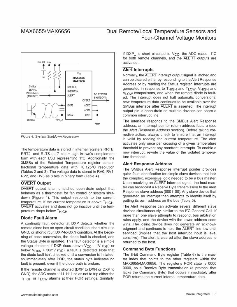
OVERT OutputOVERT output is an unlatched open-drain output that behaves as a thermostat for fan control or system shut-down (Figure 4). This output responds to the current temperature. If the current temperature is above THIGH, OVERT activates and does not go inactive until the tem-perature drops below THIGH.
Diode Fault AlarmA continuity fault detector at DXP detects whether the remote diode has an open-circuit condition, short-circuit to GND, or short-circuit DXP-to-DXN condition. At the begin-ning of each conversion, the diode fault is checked, and the Status Byte is updated. This fault detector is a simple voltage detector; if DXP rises above VCC - 1V (typ) or below VDXN + 50mV (typ), a fault is detected. Note that the diode fault isn’t checked until a conversion is initiated, so immediately after POR, the status byte indicates no fault is present, even if the diode path is broken.If the remote channel is shorted (DXP to DXN or DXP to GND), the ADC reads 1111 1111 so as not to trip either the THIGH or TLOW alarms at their POR settings. Similarly,
if DXP_ is short circuited to VCC, the ADC reads -1°C for both remote channels, and the ALERT outputs are activated.
Alert InterruptsNormally, the ALERT interrupt output signal is latched and can be cleared either by responding to the Alert Response Address or by reading the Status register. Interrupts are generated in response to THIGH and TLOW, VHIGH and VLOW comparisons, and when the remote diode is fault-ed. The interrupt does not halt automatic conversions; new temperature data continues to be available over the SMBus interface after ALERT is asserted. The interrupt output pin is open-drain so multiple devices can share a common interrupt line.The interface responds to the SMBus Alert Response address, an interrupt pointer return-address feature (see the Alert Response Address section). Before taking cor-rective action, always check to ensure that an interrupt is valid by reading the current temperature. The alert activates only once per crossing of a given temperature threshold to prevent any reentrant interrupts. To enable a new interrupt, rewrite the value of the violated tempera-ture threshold.
Alert Response AddressThe SMBus Alert Response interrupt pointer provides quick fault identification for simple slave devices that lack the complex, expensive logic needed to be a bus master. Upon receiving an ALERT interrupt signal, the host mas-ter can broadcast a Receive Byte transmission to the Alert Response slave address (0001100). Any slave device that generated an interrupt then attempts to identify itself by putting its own address on the bus (Table 5).The Alert Response can activate several different slave devices simultaneously, similar to the I2C General Call. If more than one slave attempts to respond, bus arbitration rules apply, and the device with the lower address code wins. The losing device does not generate an acknowl-edgment and continues to hold the ALERT line low until serviced (implies that the host interrupt input is level sensitive). The alert is cleared after the slave address is returned to the host.
Command Byte FunctionsThe 8-bit Command Byte register (Table 6) is the mas-ter index that points to the other registers within the MAX6655/MAX6656. The register’s POR state is 0000 0000, so a Receive Byte transmission (a protocol that lacks the Command Byte) that occurs immediately after POR returns the current internal temperature data.
Figure 4. System Shutdown Application
VCC
OVERT
SMBDATASMBCLK
ADD0
ADD1
GND
DXP2
DXN2
2200pF2N3906
TO SYSTEMSHUTDOWN
SMBusSERIAL
INTERFACE(TO HOST)
+3V TO +5.5V
ALERT
MAX6655MAX6656
MAX6655/MAX6656 Dual Remote/Local Temperature Sensors and Four-Channel Voltage Monitors
www.maximintegrated.com Maxim Integrated 8
Alarm Threshold RegistersSeventeen registers store ALARM and OVERT threshold data. The MAX6655/MAX6656 contain three registers for high-temperature (THIGH), three for low-temperature (TLOW), four for high-voltage (VHIGH), four for low-voltage (VLOW) thresholds, and three more registers store OVERT data. If a measured temperature or volt-age exceeds the corresponding alarm threshold value, an ALARM interrupt is asserted. OVERT asserts when temperature exceeds the corresponding alarm threshold value. The POR state of the THIGH register is full scale (0111 1111 or +127°C). The POR state of the TLOW regis-ter is 1100 1001 or -55°C.
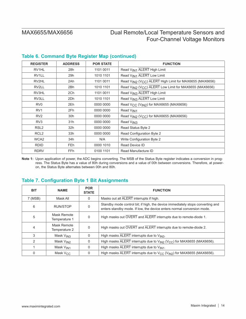
Configuration Byte FunctionsConfiguration Bytes 1 and 2 (Tables 7 and 8) are used to mask (disable) interrupts, disable temperature and voltage measurements, and put the device in software standby mode. The serial interface can read back the contents of these registers.
Status Byte FunctionsThe two Status Byte registers (Tables 9 and 10) indicate which (if any) temperature or voltage thresholds have been exceeded. Status Byte 1 also indicates whether the ADC is converting and whether there is a fault in the remote-diode DXP-DXN path. After POR, the normal state of all the flag bits is zero, except the MSB, assum-ing none of the alarm conditions are present. The MSB toggles between 1 and 0 indicating whether the ADC is converting or not. A Status Byte is cleared by any suc-cessful read of that Status Byte. Note that the ALERT interrupt latch clears when the status flag bit is read, but immediately asserts after the next conversion if the fault condition persists.High and low alarm conditions can exist at the same time in the Status Byte because the MAX6655/MAX6656 are correctly reporting environmental changes.
Applications InformationRemote-Diode SelectionRemote temperature accuracy depends on having a good-quality, diode-connected transistor. See Table 11 for appropriate discrete transistors. The MAX6655/MAX6656 can directly measure the die temperature of CPUs and other ICs with on-board temperature-sensing transistors.The transistor must be a small-signal type with a relatively high forward voltage. This ensures that the input voltage is within the ADC input voltage range. The forward voltage must be greater than 0.25V at 10μA at the highest expect-
ed temperature. The forward voltage must be less than 0.95V at 100μA at the lowest expected temperature. The base resistance has to be less than 100Ω. Tight specifi-cation of forward-current gain (+50 to +150, for example) indicates that the manufacturer has good process controls and that the devices have consistent VBE characteristics. Do not use power transistors.
Self-HeatingThermal mass can significantly affect the time required for a temperature sensor to respond to a sudden change in temperature. The thermal time constant of the 16-pin QSOP package is about 140s in still air. When measur-ing local temperature, it senses the temperature of the PC board to which it is soldered. The leads provide a good thermal path between the PC board traces and the MAX6655/MAX6656 die. Thermal conductivity between the MAX6655/MAX6656 die and the ambient air is poor by comparison. Because the thermal mass of the PC board is far greater than that of the MAX6655/MAX6656, the device follows temperature changes on the PC board with little or no perceivable delay.When measuring temperature with discrete remote sen-sors, the use of smaller packages, such as a SOT23, yields the best thermal response time. Take care to account for thermal gradients between the heat source and the sen-sor, and ensure that stray air currents across the sensor package do not interfere with measurement accuracy. When measuring the temperature of a CPU or other IC with an on-chip sense junction, thermal mass has virtually no effect; the measured temperature of the junction tracks the actual temperature within a conversion cycle.Self-heating does not significantly affect measurement accuracy. Remote-sensor self-heating due to the diode current source is negligible. For the local diode, the worst-case error occurs when autoconverting at the fast-est rate and simultaneously sinking maximum current at the ALERT output. For example, at the minimum delay between conversions, and with ALERT sinking 1mA, the typical power dissipation is VCC x 550μA + 0.4V x 1mA. Package θJA is about 150°C/W, so with VCC = +5V and no copper PC board heat sinking, the resulting tempera-ture rise is:
ΔT = 3.1mW x 150°C/W = +0.46°CEven with these contrived circumstances, it is difficult to introduce significant self-heating errors.
ADC Noise FilteringThe integrating ADC has inherently good noise rejection, especially of low-frequency signals such as 60Hz/120Hz power-supply hum. Micropower operation places con-
MAX6655/MAX6656 Dual Remote/Local Temperature Sensors and Four-Channel Voltage Monitors
www.maximintegrated.com Maxim Integrated 9
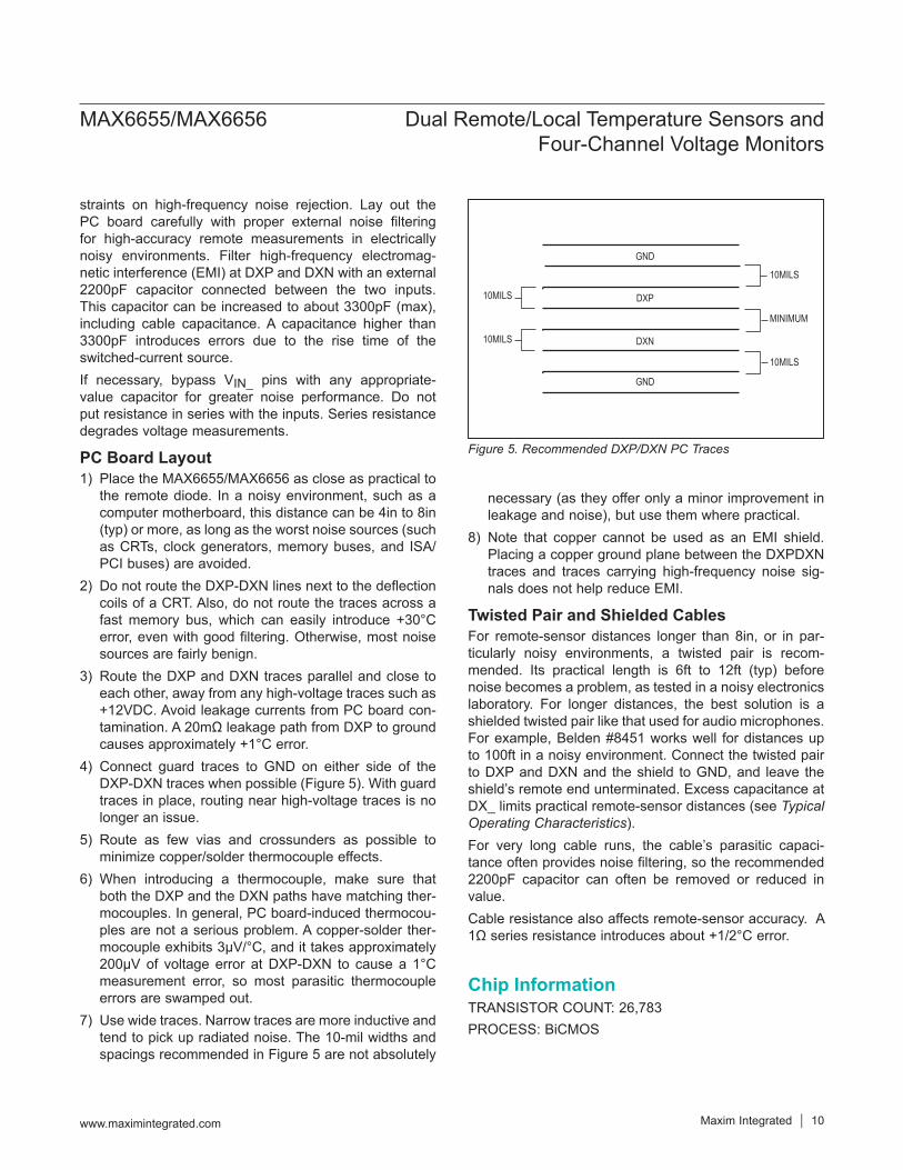
straints on high-frequency noise rejection. Lay out the PC board carefully with proper external noise filtering for high-accuracy remote measurements in electrically noisy environments. Filter high-frequency electromag-netic interference (EMI) at DXP and DXN with an external 2200pF capacitor connected between the two inputs. This capacitor can be increased to about 3300pF (max), including cable capacitance. A capacitance higher than 3300pF introduces errors due to the rise time of the switched-current source.If necessary, bypass VIN_ pins with any appropriate- value capacitor for greater noise performance. Do not put resistance in series with the inputs. Series resistance degrades voltage measurements.
PC Board Layout1) Place the MAX6655/MAX6656 as close as practical to
the remote diode. In a noisy environment, such as a computer motherboard, this distance can be 4in to 8in (typ) or more, as long as the worst noise sources (such as CRTs, clock generators, memory buses, and ISA/PCI buses) are avoided.
2) Do not route the DXP-DXN lines next to the deflection coils of a CRT. Also, do not route the traces across a fast memory bus, which can easily introduce +30°C error, even with good filtering. Otherwise, most noise sources are fairly benign.
3) Route the DXP and DXN traces parallel and close to each other, away from any high-voltage traces such as +12VDC. Avoid leakage currents from PC board con-tamination. A 20mΩ leakage path from DXP to ground causes approximately +1°C error.
4) Connect guard traces to GND on either side of the DXP-DXN traces when possible (Figure 5). With guard traces in place, routing near high-voltage traces is no longer an issue.
5) Route as few vias and crossunders as possible to minimize copper/solder thermocouple effects.
6) When introducing a thermocouple, make sure that both the DXP and the DXN paths have matching ther-mocouples. In general, PC board-induced thermocou-ples are not a serious problem. A copper-solder ther-mocouple exhibits 3μV/°C, and it takes approximately 200μV of voltage error at DXP-DXN to cause a 1°C measurement error, so most parasitic thermocouple errors are swamped out.
7) Use wide traces. Narrow traces are more inductive and tend to pick up radiated noise. The 10-mil widths and spacings recommended in Figure 5 are not absolutely
necessary (as they offer only a minor improvement in leakage and noise), but use them where practical.
8) Note that copper cannot be used as an EMI shield. Placing a copper ground plane between the DXPDXN traces and traces carrying high-frequency noise sig-nals does not help reduce EMI.
Twisted Pair and Shielded CablesFor remote-sensor distances longer than 8in, or in par-ticularly noisy environments, a twisted pair is recom-mended. Its practical length is 6ft to 12ft (typ) before noise becomes a problem, as tested in a noisy electronics laboratory. For longer distances, the best solution is a shielded twisted pair like that used for audio microphones. For example, Belden #8451 works well for distances up to 100ft in a noisy environment. Connect the twisted pair to DXP and DXN and the shield to GND, and leave the shield’s remote end unterminated. Excess capacitance at DX_ limits practical remote-sensor distances (see Typical Operating Characteristics).For very long cable runs, the cable’s parasitic capaci-tance often provides noise filtering, so the recommended 2200pF capacitor can often be removed or reduced in value.Cable resistance also affects remote-sensor accuracy. A 1Ω series resistance introduces about +1/2°C error.
Figure 5. Recommended DXP/DXN PC Traces
MINIMUM
10MILS
10MILS
10MILS
10MILS
GND
DXN
DXP
GND
MAX6655/MAX6656 Dual Remote/Local Temperature Sensors and Four-Channel Voltage Monitors
www.maximintegrated.com Maxim Integrated 10
Chip InformationTRANSISTOR COUNT: 26,783PROCESS: BiCMOS
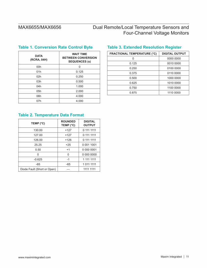
Table 1. Conversion Rate Control Byte Table 3. Extended Resolution Register
Table 2. Temperature Data Format
DATA(RCRA, 04H)
WAIT TIMEBETWEEN CONVERSION
SEQUENCES (s)
00h 0
01h 0.125
02h 0.250
03h 0.500
04h 1.000
05h 2.000
06h 4.000
07h 4.000
FRACTIONAL TEMPERATURE (°C) DIGITAL OUTPUT0 0000 0000
0.125 0010 0000
0.250 0100 0000
0.375 0110 0000
0.500 1000 0000
0.625 1010 0000
0.750 1100 0000
0.875 1110 0000
TEMP (°C) ROUNDED TEMP (°C)
DIGITALOUTPUT
130.00 +127 0 111 1111
127.00 +127 0 111 1111
126.00 +126 0 111 1111
25.25 +25 0 001 1001
0.50 +1 0 000 0001
0 0 0 000 0000
-0.625 -1 1 111 1111
-65 -65 1 011 1111
Diode Fault (Short or Open) — 1111 1111
MAX6655/MAX6656 Dual Remote/Local Temperature Sensors and Four-Channel Voltage Monitors
www.maximintegrated.com Maxim Integrated 11
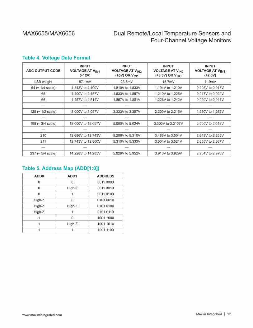
Table 4. Voltage Data Format
Table 5. Address Map (ADD[1:0])
ADC OUTPUT CODEINPUT
VOLTAGE AT VIN1(+12V)
INPUTVOLTAGE AT VIN2
(+5V) OR VCC
INPUTVOLTAGE AT VIN2(+3.3V) OR VCC
INPUTVOLTAGE AT VIN3
(+2.5V)
LSB weight 57.1mV 23.8mV 15.7mV 11.9mV
64 (≈ 1/4 scale) 4.343V to 4.400V 1.810V to 1.833V 1.194V to 1.210V 0.905V to 0.917V
65 4.400V to 4.457V 1.833V to 1.857V 1.210V to 1.226V 0.917V to 0.929V
66 4.457V to 4.514V 1.857V to 1.881V 1.226V to 1.242V 0.929V to 0.941V
— — — — —
128 (≈ 1/2 scale) 8.000V to 8.057V 3.333V to 3.357V 2.200V to 2.216V 1.250V to 1.262V
— — — — —
198 (≈ 3/4 scale) 12.000V to 12.057V 5.000V to 5.024V 3.300V to 3.3157V 2.500V to 2.512V
— — — — —
210 12.686V to 12.743V 5.286V to 5.310V 3.486V to 3.504V 2.643V to 2.655V
211 12.743V to 12.800V 5.310V to 5.333V 3.504V to 3.521V 2.655V to 2.667V
— — — — —
237 (≈ 5/4 scale) 14.228V to 14.285V 5.929V to 5.952V 3.913V to 3.929V 2.964V to 2.976V
ADD0 ADD1 ADDRESS0 0 0011 0000
0 High-Z 0011 0010
0 1 0011 0100
High-Z 0 0101 0010
High-Z High-Z 0101 0100
High-Z 1 0101 0110
1 0 1001 1000
1 High-Z 1001 1010
1 1 1001 1100
MAX6655/MAX6656 Dual Remote/Local Temperature Sensors and Four-Channel Voltage Monitors
www.maximintegrated.com Maxim Integrated 12
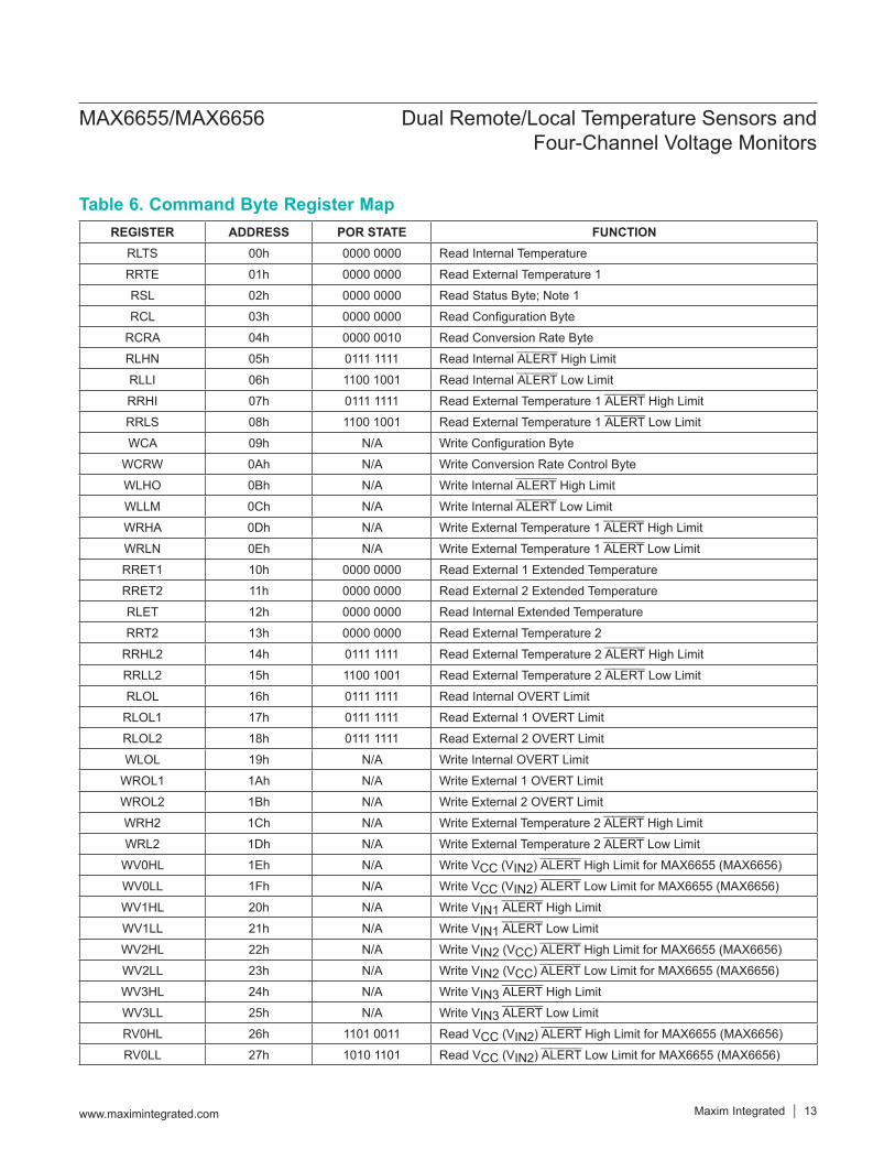
Table 6. Command Byte Register MapREGISTER ADDRESS POR STATE FUNCTION
RLTS 00h 0000 0000 Read Internal Temperature
RRTE 01h 0000 0000 Read External Temperature 1
RSL 02h 0000 0000 Read Status Byte; Note 1
RCL 03h 0000 0000 Read Configuration Byte
RCRA 04h 0000 0010 Read Conversion Rate Byte
RLHN 05h 0111 1111 Read Internal ALERT High Limit
RLLI 06h 1100 1001 Read Internal ALERT Low Limit
RRHI 07h 0111 1111 Read External Temperature 1 ALERT High Limit
RRLS 08h 1100 1001 Read External Temperature 1 ALERT Low Limit
WCA 09h N/A Write Configuration Byte
WCRW 0Ah N/A Write Conversion Rate Control Byte
WLHO 0Bh N/A Write Internal ALERT High Limit
WLLM 0Ch N/A Write Internal ALERT Low Limit
WRHA 0Dh N/A Write External Temperature 1 ALERT High Limit
WRLN 0Eh N/A Write External Temperature 1 ALERT Low Limit
RRET1 10h 0000 0000 Read External 1 Extended Temperature
RRET2 11h 0000 0000 Read External 2 Extended Temperature
RLET 12h 0000 0000 Read Internal Extended Temperature
RRT2 13h 0000 0000 Read External Temperature 2
RRHL2 14h 0111 1111 Read External Temperature 2 ALERT High Limit
RRLL2 15h 1100 1001 Read External Temperature 2 ALERT Low Limit
RLOL 16h 0111 1111 Read Internal OVERT Limit
RLOL1 17h 0111 1111 Read External 1 OVERT Limit
RLOL2 18h 0111 1111 Read External 2 OVERT Limit
WLOL 19h N/A Write Internal OVERT Limit
WROL1 1Ah N/A Write External 1 OVERT Limit
WROL2 1Bh N/A Write External 2 OVERT Limit
WRH2 1Ch N/A Write External Temperature 2 ALERT High Limit
WRL2 1Dh N/A Write External Temperature 2 ALERT Low Limit
WV0HL 1Eh N/A Write VCC (VIN2) ALERT High Limit for MAX6655 (MAX6656)
WV0LL 1Fh N/A Write VCC (VIN2) ALERT Low Limit for MAX6655 (MAX6656)
WV1HL 20h N/A Write VIN1 ALERT High Limit
WV1LL 21h N/A Write VIN1 ALERT Low Limit
WV2HL 22h N/A Write VIN2 (VCC) ALERT High Limit for MAX6655 (MAX6656)
WV2LL 23h N/A Write VIN2 (VCC) ALERT Low Limit for MAX6655 (MAX6656)
WV3HL 24h N/A Write VIN3 ALERT High Limit
WV3LL 25h N/A Write VIN3 ALERT Low Limit
RV0HL 26h 1101 0011 Read VCC (VIN2) ALERT High Limit for MAX6655 (MAX6656)
RV0LL 27h 1010 1101 Read VCC (VIN2) ALERT Low Limit for MAX6655 (MAX6656)
MAX6655/MAX6656 Dual Remote/Local Temperature Sensors and Four-Channel Voltage Monitors
www.maximintegrated.com Maxim Integrated 13
Note 1: Upon application of power, the ADC begins converting. The MSB of the Status Byte register indicates a conversion in prog-ress. The Status Byte has a value of 80h during conversions and a value of 00h between conversions. Therefore, at power-on, the Status Byte alternates between 00h and 80h.
Table 6. Command Byte Register Map (continued)
Table 7. Configuration Byte 1 Bit Assignments
REGISTER ADDRESS POR STATE FUNCTIONRV1HL 28h 1101 0011 Read VIN1 ALERT High Limit
RV1LL 29h 1010 1101 Read VIN1 ALERT Low Limit
RV2HL 2Ah 1101 0011 Read VIN2 (VCC) ALERT High Limit for MAX6655 (MAX6656)
RV2LL 2Bh 1010 1101 Read VIN2 (VCC) ALERT Low Limit for MAX6655 (MAX6656)
RV3HL 2Ch 1101 0011 Read VIN3 ALERT High Limit
RV3LL 2Dh 1010 1101 Read VIN3 ALERT Low Limit
RV0 2Eh 0000 0000 Read VCC (VIN2) for MAX6655 (MAX6656)
RV1 2Fh 0000 0000 Read VIN1RV2 30h 0000 0000 Read VIN2 (VCC) for MAX6655 (MAX6656)
RV3 31h 0000 0000 Read VIN3RSL2 32h 0000 0000 Read Status Byte 2
RCL2 33h 0000 0000 Read Configuration Byte 2
WCA2 34h N/A Write Configuration Byte 2
RDID FEh 0000 1010 Read Device ID
RDRV FFh 0100 1101 Read Manufacture ID
BIT NAME PORSTATE FUNCTION
7 (MSB) Mask All 0 Masks out all ALERT interrupts if high.
6 RUN/STOP 0 Standby mode control bit; if high, the device immediately stops converting and enters standby mode. If low, the device enters normal conversion mode.
5 Mask Remote Temperature 1 0 High masks out OVERT and ALERT interrupts due to remote-diode 1.
4 Mask Remote Temperature 2 0 High masks out OVERT and ALERT interrupts due to remote-diode 2.
3 Mask VIN3 0 High masks ALERT interrupts due to VIN3.
2 Mask VIN2 0 High masks ALERT interrupts due to VIN2 (VCC) for MAX6655 (MAX6656).
1 Mask VIN1 0 High masks ALERT interrupts due to VIN1.
0 Mask VCC 0 High masks ALERT interrupts due to VCC (VIN2) for MAX6655 (MAX6656).
MAX6655/MAX6656 Dual Remote/Local Temperature Sensors and Four-Channel Voltage Monitors
www.maximintegrated.com Maxim Integrated 14
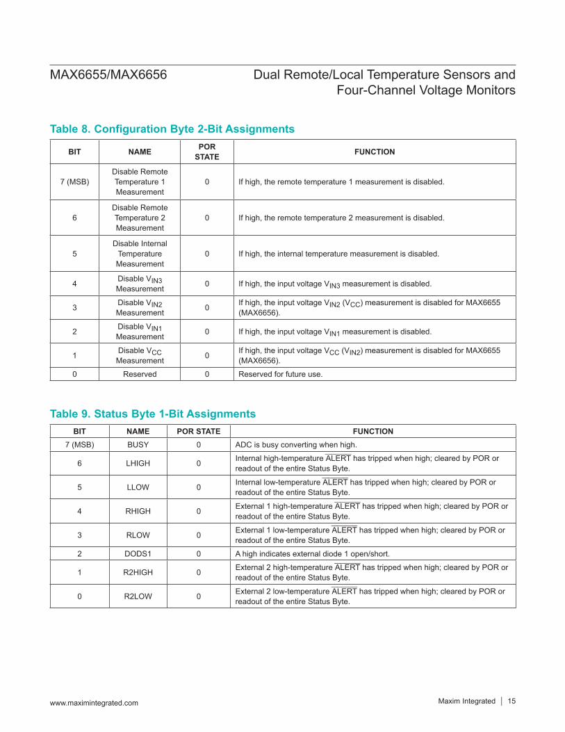
Table 8. Configuration Byte 2-Bit Assignments
Table 9. Status Byte 1-Bit Assignments
BIT NAME POR STATE FUNCTION
7 (MSB)Disable Remote Temperature 1 Measurement
0 If high, the remote temperature 1 measurement is disabled.
6Disable Remote Temperature 2 Measurement
0 If high, the remote temperature 2 measurement is disabled.
5Disable Internal
Temperature Measurement
0 If high, the internal temperature measurement is disabled.
4 Disable VIN3 Measurement 0 If high, the input voltage VIN3 measurement is disabled.
3 Disable VIN2 Measurement 0 If high, the input voltage VIN2 (VCC) measurement is disabled for MAX6655
(MAX6656).
2 Disable VIN1Measurement 0 If high, the input voltage VIN1 measurement is disabled.
1 Disable VCC Measurement 0 If high, the input voltage VCC (VIN2) measurement is disabled for MAX6655
(MAX6656).
0 Reserved 0 Reserved for future use.
BIT NAME POR STATE FUNCTION7 (MSB) BUSY 0 ADC is busy converting when high.
6 LHIGH 0 Internal high-temperature ALERT has tripped when high; cleared by POR or readout of the entire Status Byte.
5 LLOW 0 Internal low-temperature ALERT has tripped when high; cleared by POR or readout of the entire Status Byte.
4 RHIGH 0 External 1 high-temperature ALERT has tripped when high; cleared by POR or readout of the entire Status Byte.
3 RLOW 0 External 1 low-temperature ALERT has tripped when high; cleared by POR or readout of the entire Status Byte.
2 DODS1 0 A high indicates external diode 1 open/short.
1 R2HIGH 0 External 2 high-temperature ALERT has tripped when high; cleared by POR or readout of the entire Status Byte.
0 R2LOW 0 External 2 low-temperature ALERT has tripped when high; cleared by POR or readout of the entire Status Byte.
MAX6655/MAX6656 Dual Remote/Local Temperature Sensors and Four-Channel Voltage Monitors
www.maximintegrated.com Maxim Integrated 15
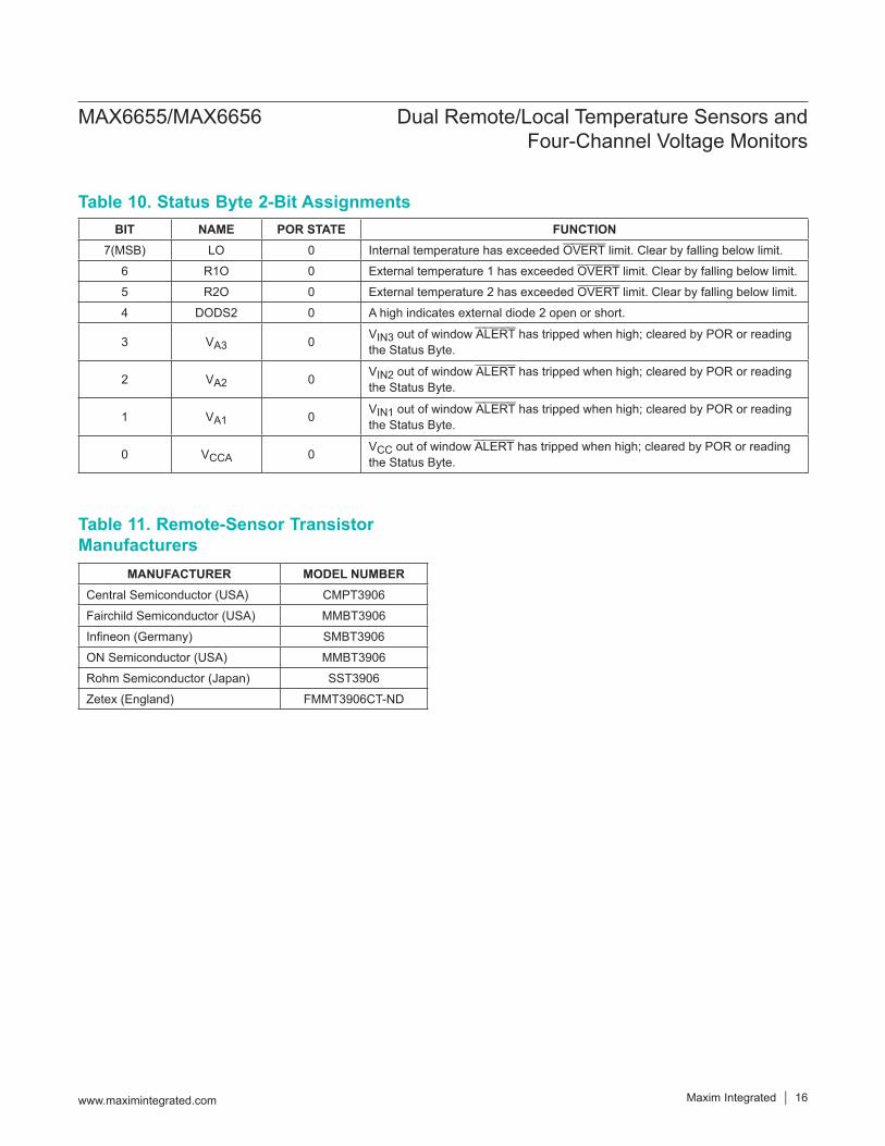
Table 10. Status Byte 2-Bit Assignments
Table 11. Remote-Sensor Transistor Manufacturers
BIT NAME POR STATE FUNCTION7(MSB) LO 0 Internal temperature has exceeded OVERT limit. Clear by falling below limit.
6 R1O 0 External temperature 1 has exceeded OVERT limit. Clear by falling below limit.
5 R2O 0 External temperature 2 has exceeded OVERT limit. Clear by falling below limit.
4 DODS2 0 A high indicates external diode 2 open or short.
3 VA3 0 VIN3 out of window ALERT has tripped when high; cleared by POR or reading the Status Byte.
2 VA2 0 VIN2 out of window ALERT has tripped when high; cleared by POR or reading the Status Byte.
1 VA1 0 VIN1 out of window ALERT has tripped when high; cleared by POR or reading the Status Byte.
0 VCCA 0 VCC out of window ALERT has tripped when high; cleared by POR or reading the Status Byte.
MANUFACTURER MODEL NUMBERCentral Semiconductor (USA) CMPT3906
Fairchild Semiconductor (USA) MMBT3906
Infineon (Germany) SMBT3906
ON Semiconductor (USA) MMBT3906
Rohm Semiconductor (Japan) SST3906
Zetex (England) FMMT3906CT-ND
MAX6655/MAX6656 Dual Remote/Local Temperature Sensors and Four-Channel Voltage Monitors
www.maximintegrated.com Maxim Integrated 16
VCC
OVERT
MAX6655MAX6656
SMBDATA
SMBCLK
ADD0
ADD1
GND
DXP2
DXN2
DXP1
DXN1
2200pF2N3906
TO SYSTEM SHUTDOWN
ALERT
0.1µF
VIN3
VIN1
VIN2TO 3.3V OR 5V
2.5V
TO 12V
TO 2.5V
CPU
VCC
10kΩ
SMBus/I2CCONTROLLER
VCC
SMBCLKSMBDATA
OVERT
ADD0 ADD1DXP2
DXP1
DXN2
DXN1
VIN3
VIN1VIN2
ALERT
ADC
VOLTAGEREFERENCE
DATA ANDCONTROL
LOGIC
TEMPERATURESENSOR
INPUT VOLTAGESCALING ANDMULTIPLEXER
SMBus/I2C-COMPATIBLEINTERFACE
MAX6655/MAX6656
MAX6655/MAX6656 Dual Remote/Local Temperature Sensors and Four-Channel Voltage Monitors
www.maximintegrated.com Maxim Integrated 17
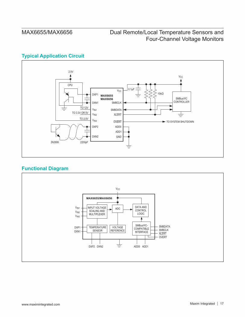
Typical Application Circuit
Functional Diagram
MAX6655/MAX6656 Dual Remote/Local Temperature Sensors and Four-Channel Voltage Monitors
www.maximintegrated.com Maxim Integrated 18
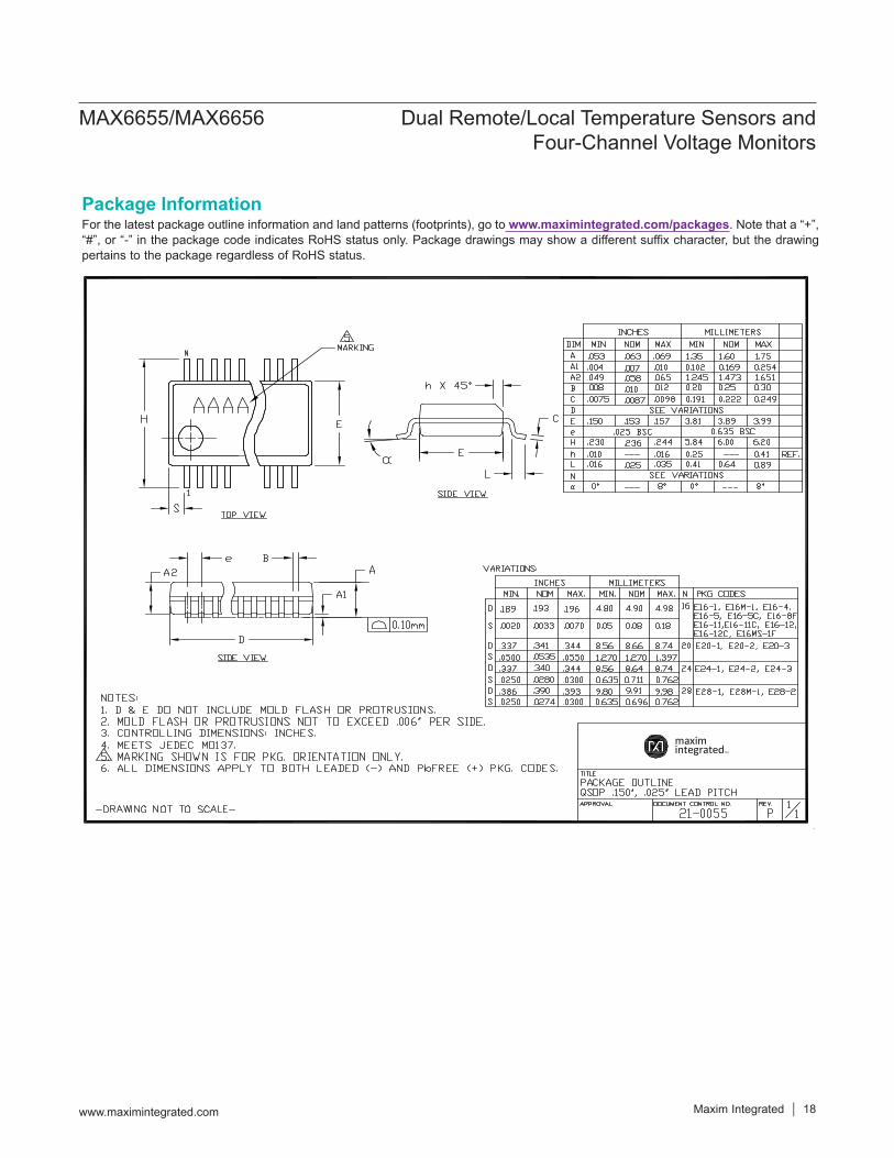
Package InformationFor the latest package outline information and land patterns (footprints), go to www.maximintegrated.com/packages. Note that a “+”, “#”, or “-” in the package code indicates RoHS status only. Package drawings may show a different suffix character, but the drawing pertains to the package regardless of RoHS status.
Revision HistoryREVISION NUMBER
REVISION DATE DESCRIPTION PAGES
CHANGED2 5/17 Updated Ordering Informaiton table 1
Maxim Integrated cannot assume responsibility for use of any circuitry other than circuitry entirely embodied in a Maxim Integrated product. No circuit patent licenses are implied. Maxim Integrated reserves the right to change the circuitry and specifications without notice at any time. The parametric values (min and max limits) shown in the Electrical Characteristics table are guaranteed. Other parametric values quoted in this data sheet are provided for guidance.
Maxim Integrated and the Maxim Integrated logo are trademarks of Maxim Integrated Products, Inc.
MAX6655/MAX6656 Dual Remote/Local Temperature Sensors and Four-Channel Voltage Monitors
© 2017 Maxim Integrated Products, Inc. 19
For pricing, delivery, and ordering information, please contact Maxim Direct at 1-888-629-4642, or visit Maxim Integrated’s website at www.maximintegrated.com.