Embed Size (px)
Citation preview

RX
TX
POWER3.3 V, 5 V
DIN
ROUT
DOUT
RS232
RIN
RS232
2
2
2
2
Product
Folder
Order
Now
Technical
Documents
Tools &
Software
Support &Community
An IMPORTANT NOTICE at the end of this data sheet addresses availability, warranty, changes, use in safety-critical applications,intellectual property matters and other important disclaimers. PRODUCTION DATA.
MAX3232ESLLS664D –AUGUST 2005–REVISED MAY 2017
MAX3232E 3-V to 5.5-V Multichannel RS-232 Line Driver and ReceiverWith ±15-kV IEC ESD Protection
1
1 Features1• ESD Protection for RS-232 Bus Pins
– ±15 kV (HBM)– ±8 kV (IEC61000-4-2, Contact Discharge)– ±15 kV (IEC61000-4-2, Air-Gap Discharge)
• Meets or Exceeds the Requirements of TIA/EIA-232-F and ITU V.28 Standards
• Operates With 3-V to 5.5-V VCC Supply• Operates up to 250 kbit/s• Two Drivers and Two Receivers• Low Supply Current: 300 μA (Typical)• External Capacitors: 4 × 0.1 μF• Accepts 5-V Logic Input With 3.3-V Supply• Pin Compatible to Alternative High-Speed Devices
(1 Mbit/s)– SN65C3232E (–40°C to +85°C)– SN75C3232E (0°C to 70°C)
2 Applications• Battery-Powered Systems• Notebooks• Laptops• Palmtop PCs• Hand-Held Equipment
3 DescriptionThe MAX3232E device consists of two line drivers,two-line receivers, and a dual charge-pump circuitwith ±15-kV IEC ESD protection pin to pin (serial-portconnection pins, including GND).
The device meets the requirements of TIA/EIA-232-Fand provides the electrical interface between anasynchronous communication controller and theserial-port connector. The charge pump and foursmall external capacitors allow operation from asingle 3-V to 5.5-V supply. The devices operate atdata signaling rates up to 250 kbit/s and a maximumof 30-V/μs driver output slew rate.
Device Information(1)
PART NUMBER PACKAGE BODY SIZE (NOM)MAX3232ExD SOIC (16) 9.90 mm × 3.91 mmMAX3232ExDB SSOP (16) 6.20 mm × 5.30 mmMAX3232ExDW SOIC (16) 10.30 mm × 7.50 mmMAX3232ExPW TSSOP (16) 5.00 mm × 4.40 mm
(1) For all available packages, see the orderable addendum atthe end of the data sheet.
Simplified Diagram
2
MAX3232ESLLS664D –AUGUST 2005–REVISED MAY 2017 www.ti.com
Product Folder Links: MAX3232E
Submit Documentation Feedback Copyright © 2005–2017, Texas Instruments Incorporated
Table of Contents1 Features .................................................................. 12 Applications ........................................................... 13 Description ............................................................. 14 Revision History..................................................... 25 Pin Configuration and Functions ......................... 36 Specifications......................................................... 4
6.1 Absolute Maximum Ratings ..................................... 46.2 ESD Ratings ............................................................ 46.3 Recommended Operating Conditions ...................... 46.4 Thermal Information .................................................. 56.5 Electrical Characteristics — Device ......................... 56.6 Electrical Characteristics — Driver .......................... 56.7 Electrical Characteristics — Receiver ...................... 56.8 Switching Characteristics ......................................... 66.9 Typical Characteristics .............................................. 6
7 Parameter Measurement Information .................. 78 Detailed Description .............................................. 8
8.1 Overview ................................................................... 88.2 Functional Block Diagram ......................................... 88.3 Feature Description................................................... 88.4 Device Functional Modes.......................................... 9
9 Application and Implementation ........................ 109.1 Application Information............................................ 109.2 Typical Application .................................................. 10
10 Power Supply Recommendations ..................... 1211 Layout................................................................... 12
11.1 Layout Guidelines ................................................. 1211.2 Layout Example .................................................... 12
12 Device and Documentation Support ................. 1312.1 Community Resources.......................................... 1312.2 Trademarks ........................................................... 1312.3 Electrostatic Discharge Caution............................ 1312.4 Glossary ................................................................ 13
13 Mechanical, Packaging, and OrderableInformation ........................................................... 13
4 Revision HistoryNOTE: Page numbers for previous revisions may differ from page numbers in the current version.
Changes from Revision C (June 2015) to Revision D Page
• Changed 3 V ± 5.5 V to 3 V to 5.5 V in the VCC column of Table 3 ..................................................................................... 10
Changes from Revision B (December 2013) to Revision C Page
• Added Device Information table, Pin Configuration and Functions section, ESD Ratings table, Feature Descriptionsection, Device Functional Modes, Application and Implementation section, Power Supply Recommendationssection, Layout section, Device and Documentation Support section, and Mechanical, Packaging, and OrderableInformation section ................................................................................................................................................................ 1
Changes from Revision A (April 2007) to Revision B Page
• Updated document to new TI data sheet format. ................................................................................................................... 1• Deleted Ordering Information table. ....................................................................................................................................... 1• Added Thermal Information table. .......................................................................................................................................... 5

1
2
3
4
5
6
7
8
16
15
14
13
12
11
10
9
C1+
V+
C1−
C2+
C2−
V−
DOUT2
RIN2
VCC
GND
DOUT1
RIN1
ROUT1
DIN1
DIN2
ROUT2
3
MAX3232Ewww.ti.com SLLS664D –AUGUST 2005–REVISED MAY 2017
Product Folder Links: MAX3232E
Submit Documentation FeedbackCopyright © 2005–2017, Texas Instruments Incorporated
5 Pin Configuration and Functions
D, DW, DB and PW Package16-Pin SOIC, SSOP and TSSOP
Top View
Pin FunctionsPIN
I/O DESCRIPTIONNAME NO.C1+ 1 — Positive lead of C1 capacitorV+ 2 O Positive charge pump output for storage capacitor onlyC1– 3 — Negative lead of C1 capacitorC2+ 4 — Positive lead of C2 capacitorC2– 5 — Negative lead of C2 capacitorV– 6 O Negative charge pump output for storage capacitor onlyDOUT2 7 O RS232 line data output (to remote RS232 system)RIN2 8 I RS232 line data input (from remote RS232 system)ROUT2 9 O Logic data output (to UART)DIN2 10 I Logic data input (from UART)DIN1 11 I Logic data input (from UART)ROUT1 12 O Logic data output (to UART)RIN1 13 I RS232 line data input (from remote RS232 system)DOUT1 14 O RS232 line data output (to remote RS232 system)GND 15 — GroundVCC 16 — Supply Voltage, Connect to external 3-V to 5.5-V power supply
4
MAX3232ESLLS664D –AUGUST 2005–REVISED MAY 2017 www.ti.com
Product Folder Links: MAX3232E
Submit Documentation Feedback Copyright © 2005–2017, Texas Instruments Incorporated
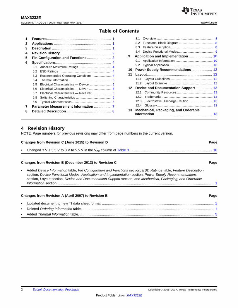
(1) Stresses beyond those listed under Absolute Maximum Ratings may cause permanent damage to the device. These are stress ratingsonly, and functional operation of the device at these or any other conditions beyond those indicated under Recommended OperatingConditions is not implied. Exposure to absolute-maximum-rated conditions for extended periods may affect device reliability.
(2) All voltages are with respect to network GND.
6 Specifications
6.1 Absolute Maximum Ratingsover operating free-air temperature range (unless otherwise noted) (1)
MIN MAX UNITVCC Supply voltage (2) –0.3 6 VV+ Positive output supply voltage (2) –0.3 7 VV– Negative output supply voltage (2) 0.3 –7 VV+ – V– Supply voltage difference (2) 13 V
VI Input voltageDrivers –0.3 6 VReceivers –25 25 V
VO Output voltageDrivers –13.2 13.2 VReceivers –0.3 VCC + 0.3 V
TJ Operating virtual junction temperature 150 °CTstg Storage temperature –65 150 °C
(1) JEDEC document JEP155 states that 500-V HBM allows safe manufacturing with a standard ESD control process.(2) JEDEC document JEP157 states that 250-V CDM allows safe manufacturing with a standard ESD control process.
6.2 ESD RatingsVALUE UNIT
V(ESD) Electrostatic discharge
Human body model (HBM), perANSI/ESDA/JEDEC JS-001 (1)
All pins except RIN andDOUT ±2000
V
RIN and DOUT Pins ±15,000Charged-device model (CDM), per JEDECspecification JESD22-C101 (2) All pins ±1500
IEC61000-4-2, Contact Discharge RS232 port pins(RIN, DOUT) ±8000
IEC61000-4-2, Air-Gap Discharge RS232 port pins(RIN, DOUT) ±15,000
(1) Test conditions are C1–C4 = 0.1 μF at VCC = 3.3 V ± 0.3 V; C1 = 0.047 μF, C2–C4 = 0.33 μF at VCC = 5 V ± 0.5 V.
6.3 Recommended Operating Conditions (1)
See Figure 7.MIN NOM MAX UNIT
Supply voltageVCC = 3.3 V 3 3.3 3.6
VVCC = 5 V 4.5 5 5.5
VIH Driver high-level input voltage DINVCC = 3.3 V 2 5.5
VVCC = 5 V 2.4 5.5
VIL Driver low-level input voltage DIN 0 0.8 VVI Receiver input voltage RIN –25 25 V
TA Operating free-air temperatureMAX3232EC 0 70
°CMAX3232EI –40 85

5
MAX3232Ewww.ti.com SLLS664D –AUGUST 2005–REVISED MAY 2017
Product Folder Links: MAX3232E
Submit Documentation FeedbackCopyright © 2005–2017, Texas Instruments Incorporated
(1) For more information about traditional and new thermal metrics, see the Semiconductor and IC Package Thermal Metrics applicationreport.
6.4 Thermal Information
THERMAL METRIC (1)MAX3232E
UNITPW (TSSOP) D (SOIC) DW (SOIC) DB (SSOP)16 PINS 16 PINS 16 PINS 16 PINS
RθJA Junction-to-ambient thermal resistance 99.3 76.1 72.3 90.9 °C/WRθJCtop Junction-to-case (top) thermal resistance 20.8 36.7 33.5 36.2 °C/WRθJB Junction-to-board thermal resistance 45.1 33.6 37.1 43.8 °C/WψJT Junction-to-top characterization parameter 0.6 4.2 7.5 4.2 °C/WψJB Junction-to-board characterization parameter 45.1 33.3 37.1 42.9 °C/WRθJCbot Junction-to-case (bottom) thermal resistance – – – – °C/W
(1) Test conditions are C1–C4 = 0.1 μF at VCC = 3.3 V ± 0.3 V; C1 = 0.047 μF, C2–C4 = 0.33 μF at VCC = 5 V ± 0.5 V.(2) All typical values are at VCC = 3.3 V or VCC = 5 V, and TA = 25°C.
6.5 Electrical Characteristics — Device (1)
over recommended ranges of supply voltage and operating free-air temperature (unless otherwise noted) (see Figure 7).PARAMETER TEST CONDITIONS MIN TYP (2) MAX UNIT
ICC Supply current No load, VCC = 3.3 V or 5 V 0.3 1 mA
(1) Test conditions are C1–C4 = 0.1 μF at VCC = 3.3 V ± 0.3 V; C1 = 0.047 μF, C2–C4 = 0.33 μF at VCC = 5 V ± 0.5 V.(2) Short-circuit durations should be controlled to prevent exceeding the device absolute power dissipation ratings, and not more than one
output should be shorted at a time.(3) All typical values are at VCC = 3.3 V or VCC = 5 V, and TA = 25°C.
6.6 Electrical Characteristics — Driver (1)
over operating free-air temperature range (unless otherwise noted) (see Figure 7).PARAMETER TEST CONDITIONS MIN TYP (2) MAX UNIT
VOH High-level output voltage DOUT at RL = 3 kΩ to GND, DIN = GND 5 5.4 VVOL Low-level output voltage DOUT at RL = 3 kΩ to GND, DIN = VCC –5 –5.4 VIIH High-level input current VI = VCC ±0.01 ±1 μAIIL Low-level input current VI at GND ±0.01 ±1 μA
IOS(3) Short-circuit output current
VCC = 3.6 V, VO = 0 V±35 ±60 mA
VCC = 5.5 V, VO = 0 VrO Output resistance VCC, V+, and V– = 0 V, VO = ±2 V 300 10M Ω
(1) Test conditions are C1–C4 = 0.1 μF at VCC = 3.3 V ± 0.3 V; C1 = 0.047 μF, C2–C4 = 0.33 μF at VCC = 5 V ± 0.5 V.(2) All typical values are at VCC = 3.3 V or VCC = 5 V, and TA = 25°C.
6.7 Electrical Characteristics — Receiver (1)
over recommended ranges of supply voltage and operating free-air temperature (unless otherwise noted) (see Figure 7).PARAMETER TEST CONDITIONS MIN TYP (2) MAX UNIT
VOH High-level output voltage IOH = –1 mA VCC – 0.6 VCC – 0.1 VVOL Low-level output voltage IOL = 1.6 mA 0.4 V
VIT+ Positive-going input threshold voltageVCC = 3.3 V 1.5 2.4
VVCC = 5 V 1.8 2.4
VIT– Negative-going input threshold voltageVCC = 3.3 V 0.6 1.2
VVCC = 5 V 0.8 1.5
Vhys Input hysteresis (VIT+ – VIT–) 0.3 Vri Input resistance VI = ±3 V to ±25 V 3 5 7 kΩ

0
1
2
3
4
5
6
0 5 10 15 20 25
DO
UT
Vol
tage
(V
)
DOUT Current (mA)
VOH
C001
±6
±5
±4
±3
±2
±1
0
0 5 10 15 20 25
DO
UT
Vol
tage
(V
)
DOUT Current (mA)
VOL
C001
6
MAX3232ESLLS664D –AUGUST 2005–REVISED MAY 2017 www.ti.com
Product Folder Links: MAX3232E
Submit Documentation Feedback Copyright © 2005–2017, Texas Instruments Incorporated
(1) Test conditions are C1–C4 = 0.1 μF at VCC = 3.3 V ± 0.3 V; C1 = 0.047 μF, C2–C4 = 0.33 μF at VCC = 5 V ± 0.5 V.(2) All typical values are at VCC = 3.3 V or VCC = 5 V, and TA = 25°C.(3) Pulse skew is defined as |tPLH – tPHL| of each channel of the same device.
6.8 Switching Characteristics (1)
over recommended ranges of supply voltage and operating free-air temperature (unless otherwise noted) (see Figure 7)PARAMETER TEST CONDITIONS MIN TYP (2) MAX UNIT
Maximum data rate RL = 3 kΩ,One DOUT switching,
CL = 1000 pF,see Figure 3 150 250 kbit/s
tsk(p) Driver pulse skew (3) RL = 3 kΩ to 7 kΩ,see Figure 4 CL = 150 pF to 2500 pF, 300 ns
SR(tr)Driver slew rate, transitionregion(see Figure 3)
RL = 3 kΩ to 7 kΩ,VCC = 3.3 V
CL = 150 pF to 1000 pF 6 30V/μs
CL = 150 pF to 2500 pF 4 30
tPLHReceiver propagation delaytime, low- to high-level output CL = 150 pF,
see Figure 5
300 ns
tPHLReceiver propagation delaytime, high- to low-level output 300 ns
tsk(p) Receiver pulse skew (3) 300 ns
6.9 Typical CharacteristicsVCC = 3.3 V
Figure 1. DOUT VOH vs Load Current, Both Drivers Loaded Figure 2. DOUT VOL vs Load Current, Both Drivers Loaded
TEST CIRCUIT VOLTAGE WAVEFORMS
50 Ω
50%50%
−3 V
3 V
1.5 V1.5 V
Output
Input
VOL
VOH
tPHL
Generator
(see Note B) tPLH
Output
CL
(see Note A)
TEST CIRCUIT VOLTAGE WAVEFORMS
0 V
3 V
Output
Input
VOL
VOH
tPLHtPHL
50% 50%
1.5 V 1.5 V
50 Ω
Generator
(see Note B)
RL
RS-232
Output
CL
(see Note A)
50 Ω
TEST CIRCUIT VOLTAGE WAVEFORMS
0 V
3 V
Output
Input
VOL
VOH
tTLH
Generator
(see Note B)
RL
RS-232
Output
tTHLCL
(see Note A)
SR(tr)6 V
tTHL
or tTLH
1.5 V 1.5 V
3 V
−3 V
3 V
−3 V
7
MAX3232Ewww.ti.com SLLS664D –AUGUST 2005–REVISED MAY 2017
Product Folder Links: MAX3232E
Submit Documentation FeedbackCopyright © 2005–2017, Texas Instruments Incorporated
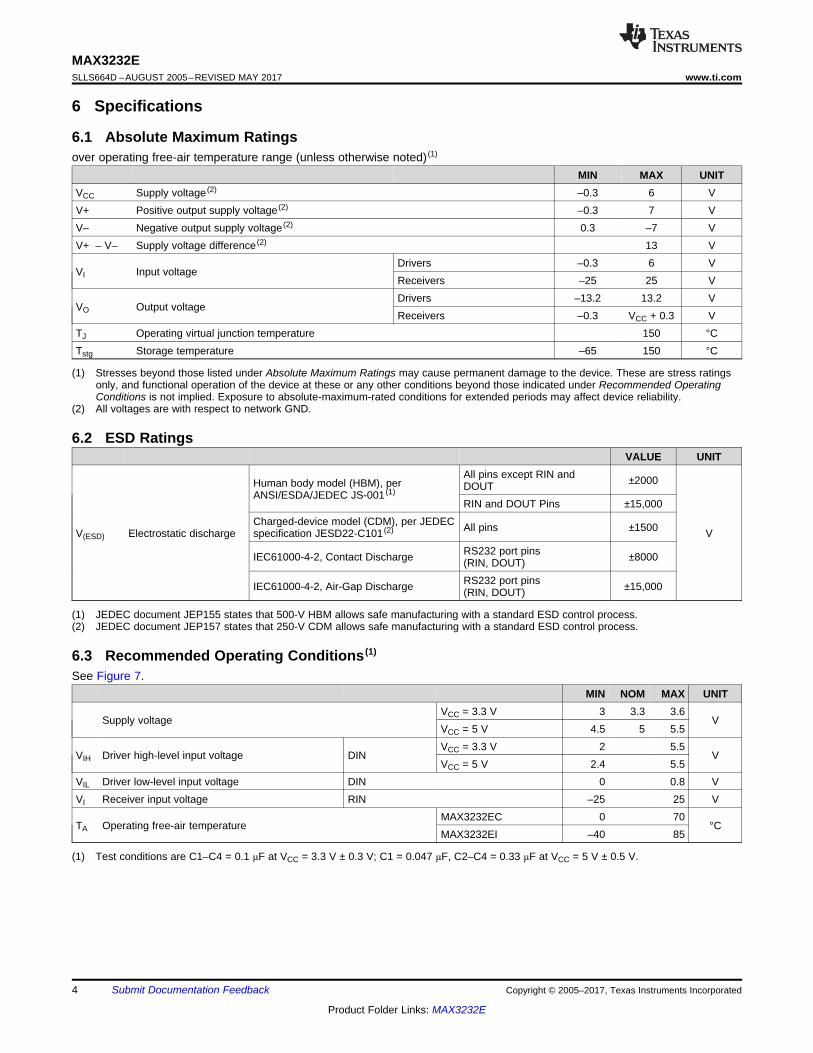
7 Parameter Measurement Information
A. CL includes probe and jig capacitanceB. The pulse generator has the following characteristics: PRR = 250 kbit/s, ZO = 50 Ω, 50% duty cycle, tr ≤ 10ns, tf ≤ 10 ns
Figure 3. Driver Slew Rate
A. CL includes probe and jig capacitanceB. The pulse generator has the following characteristics: PRR = 250 kbit/s, ZO = 50 Ω, 50% duty cycle, tr ≤ 10ns, tf ≤ 10 ns
Figure 4. Driver Pulse Skew
A. CL includes probe and jig capacitanceB. The pulse generator has the following characteristics: ZO = 50 Ω, 50% duty cycle, tr ≤ 10 ns, tf ≤ 10 ns
Figure 5. Receiver Propagation Delay Times

RX
TX
POWER3.3 V, 5 V
DIN
ROUT
DOUT
RS232
RIN
RS232
2
2
2
2
8
MAX3232ESLLS664D –AUGUST 2005–REVISED MAY 2017 www.ti.com
Product Folder Links: MAX3232E
Submit Documentation Feedback Copyright © 2005–2017, Texas Instruments Incorporated
8 Detailed Description
8.1 OverviewThe MAX3232E device consists of two line drivers, two-line receivers, and a dual charge-pump circuit withIEC61000-4-2 ESD protection terminal to terminal (serial-port connection terminals, including GND). The devicemeets the requirements of TIA/EIA-232-F and provides the electrical interface between an asynchronouscommunication controller and the serial-port connector. The charge pump and four small external capacitorsallow operation from a single 3-V to 5.5-V supply. The device operates at data signaling rates up to 250 kbit/sand a maximum of 30-V/μs driver output slew rate. Outputs are protected against shorts to ground.
8.2 Functional Block Diagram
8.3 Feature Description
8.3.1 PowerThe power block increases, inverts, and regulates voltage at V+ and V– pins using a charge pump that requiresfour external capacitors.
8.3.2 RS232 DriverTwo drivers interface standard logic level to RS232 levels. Both DIN inputs must be valid high or low.
8.3.3 RS232 ReceiverTwo receivers interface RS232 levels to standard logic levels. An open input will result in a high output on ROUT.Each RIN input includes an internal standard RS232 load.
DIN1 DOUT1
RIN1ROUT1
DIN2 DOUT2
RIN2ROUT2
11
10
12
9
14
7
13
8
9
MAX3232Ewww.ti.com SLLS664D –AUGUST 2005–REVISED MAY 2017
Product Folder Links: MAX3232E
Submit Documentation FeedbackCopyright © 2005–2017, Texas Instruments Incorporated
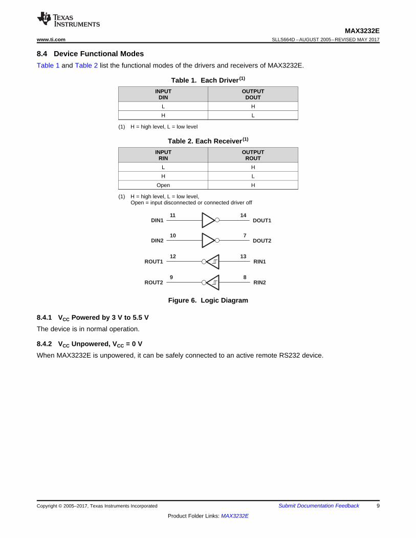
8.4 Device Functional ModesTable 1 and Table 2 list the functional modes of the drivers and receivers of MAX3232E.
(1) H = high level, L = low level
Table 1. Each Driver (1)
INPUTDIN
OUTPUTDOUT
L HH L
(1) H = high level, L = low level,Open = input disconnected or connected driver off
Table 2. Each Receiver (1)
INPUTRIN
OUTPUTROUT
L HH L
Open H
Figure 6. Logic Diagram
8.4.1 VCC Powered by 3 V to 5.5 VThe device is in normal operation.
8.4.2 VCC Unpowered, VCC = 0 VWhen MAX3232E is unpowered, it can be safely connected to an active remote RS232 device.
11
10
8
1
2
3
4
7
ROUT2
DIN2
9
RIN1
16
13
12
15
14
DIN1
5
6
+
−C3
VCC
C2+
C1
C2
C1+
GND
C1−
ROUT1
C2−
+
−
CBYPASS
= 0.1µF
V+
+
−
+
−
RIN2
C4+
−
DOUT1
DOUT2
(1)
V−
5 kΩ
5 kΩ
10
MAX3232ESLLS664D –AUGUST 2005–REVISED MAY 2017 www.ti.com
Product Folder Links: MAX3232E
Submit Documentation Feedback Copyright © 2005–2017, Texas Instruments Incorporated
9 Application and Implementation
NOTEInformation in the following applications sections is not part of the TI componentspecification, and TI does not warrant its accuracy or completeness. TI’s customers areresponsible for determining suitability of components for their purposes. Customers shouldvalidate and test their design implementation to confirm system functionality.
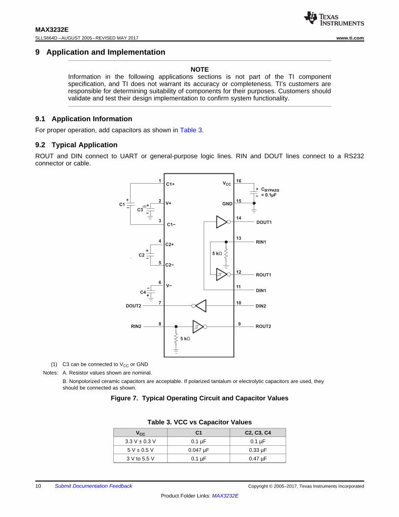
9.1 Application InformationFor proper operation, add capacitors as shown in Table 3.
9.2 Typical ApplicationROUT and DIN connect to UART or general-purpose logic lines. RIN and DOUT lines connect to a RS232connector or cable.
(1) C3 can be connected to VCC or GNDNotes: A. Resistor values shown are nominal.
B. Nonpolorized ceramic capacitors are acceptable. If polarized tantalum or electrolytic capacitors are used, theyshould be connected as shown.
Figure 7. Typical Operating Circuit and Capacitor Values
Table 3. VCC vs Capacitor ValuesVCC C1 C2, C3, C4
3.3 V ± 0.3 V 0.1 µF 0.1 µF5 V ± 0.5 V 0.047 µF 0.33 µF3 V to 5.5 V 0.1 µF 0.47 µF
±9 ±8 ±7 ±6 ±5 ±4 ±3 ±2 ±1
0123456
0 1 2 3 4 5 6 7 8 9 10
Vol
tage
(V
)
Time (s)
DINDOUT to RINROUT
C001
11
MAX3232Ewww.ti.com SLLS664D –AUGUST 2005–REVISED MAY 2017
Product Folder Links: MAX3232E
Submit Documentation FeedbackCopyright © 2005–2017, Texas Instruments Incorporated
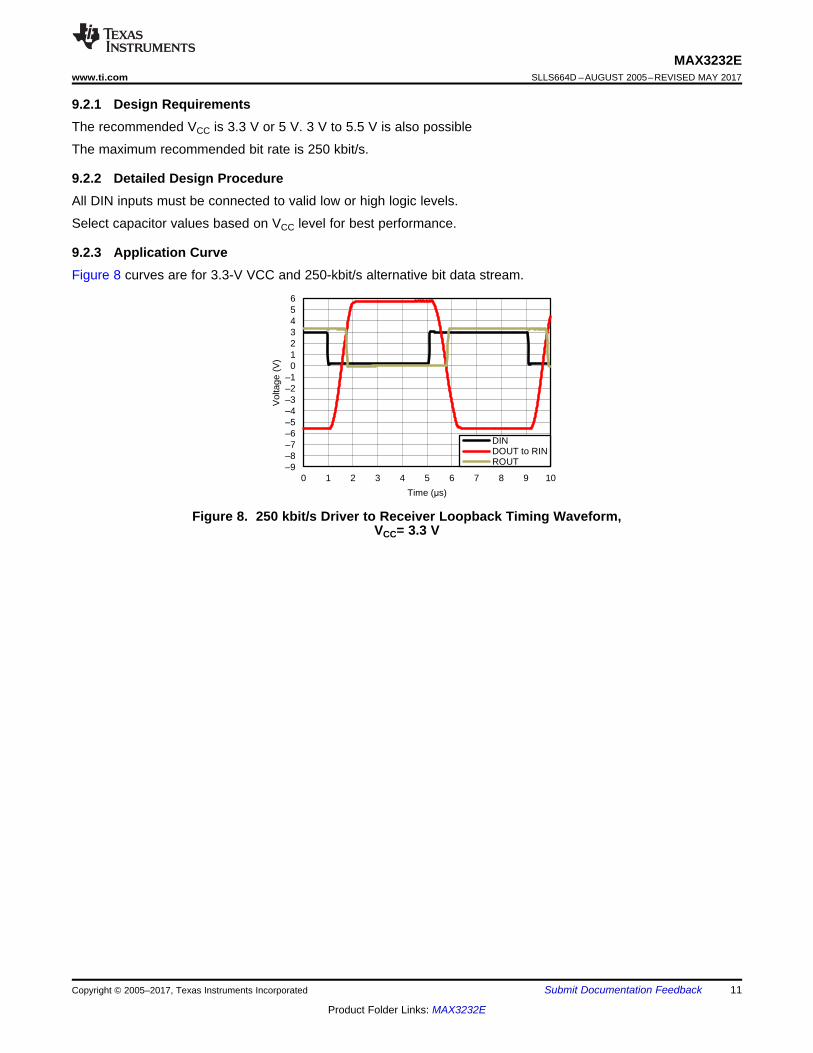
9.2.1 Design RequirementsThe recommended VCC is 3.3 V or 5 V. 3 V to 5.5 V is also possible
The maximum recommended bit rate is 250 kbit/s.
9.2.2 Detailed Design ProcedureAll DIN inputs must be connected to valid low or high logic levels.
Select capacitor values based on VCC level for best performance.
9.2.3 Application CurveFigure 8 curves are for 3.3-V VCC and 250-kbit/s alternative bit data stream.
Figure 8. 250 kbit/s Driver to Receiver Loopback Timing Waveform,VCC= 3.3 V

VCC
Ground
Ground
14
13
15
12
11
10
9
1
2
3
4
5
6
7
8
16
C2
C1
Ground
C3
C4
0.1µF
C1+
V+
C1–
C2+
C2–
V–
DOUT2
RIN2
VCC
GND
DOUT1
RIN1
ROUT1
DIN1
DIN2
ROUT2
12
MAX3232ESLLS664D –AUGUST 2005–REVISED MAY 2017 www.ti.com
Product Folder Links: MAX3232E
Submit Documentation Feedback Copyright © 2005–2017, Texas Instruments Incorporated
10 Power Supply RecommendationsThe supply voltage, VCC, should be between 3 V and 5.5 V. Select the values of the charge-pump capacitorsusing Table 3.
11 Layout
11.1 Layout GuidelinesKeep the external capacitor traces short, specifically on the C1 and C2 nodes that have the fastest rise and falltimes.
11.2 Layout Example
Figure 9. Layout Diagram

13
MAX3232Ewww.ti.com SLLS664D –AUGUST 2005–REVISED MAY 2017
Product Folder Links: MAX3232E
Submit Documentation FeedbackCopyright © 2005–2017, Texas Instruments Incorporated
12 Device and Documentation Support
12.1 Community ResourcesThe following links connect to TI community resources. Linked contents are provided "AS IS" by the respectivecontributors. They do not constitute TI specifications and do not necessarily reflect TI's views; see TI's Terms ofUse.
TI E2E™ Online Community TI's Engineer-to-Engineer (E2E) Community. Created to foster collaborationamong engineers. At e2e.ti.com, you can ask questions, share knowledge, explore ideas and helpsolve problems with fellow engineers.
Design Support TI's Design Support Quickly find helpful E2E forums along with design support tools andcontact information for technical support.
12.2 TrademarksE2E is a trademark of Texas Instruments.All other trademarks are the property of their respective owners.
12.3 Electrostatic Discharge CautionThese devices have limited built-in ESD protection. The leads should be shorted together or the device placed in conductive foamduring storage or handling to prevent electrostatic damage to the MOS gates.
12.4 GlossarySLYZ022 — TI Glossary.
This glossary lists and explains terms, acronyms, and definitions.
13 Mechanical, Packaging, and Orderable InformationThe following pages include mechanical packaging and orderable information. This information is the mostcurrent data available for the designated devices. This data is subject to change without notice and revision ofthis document. For browser based versions of this data sheet, refer to the left hand navigation.

PACKAGE OPTION ADDENDUM
www.ti.com 4-May-2017
Addendum-Page 1
PACKAGING INFORMATION
Orderable Device Status(1)
Package Type PackageDrawing
Pins PackageQty
Eco Plan(2)
Lead/Ball Finish(6)
MSL Peak Temp(3)
Op Temp (°C) Device Marking(4/5)
Samples
MAX3232ECD ACTIVE SOIC D 16 40 Green (RoHS& no Sb/Br)
CU NIPDAU Level-1-260C-UNLIM 0 to 70 MAX3232EC
MAX3232ECDB ACTIVE SSOP DB 16 80 Green (RoHS& no Sb/Br)
CU NIPDAU Level-1-260C-UNLIM 0 to 70 MP232EC
MAX3232ECDBE4 ACTIVE SSOP DB 16 80 Green (RoHS& no Sb/Br)
CU NIPDAU Level-1-260C-UNLIM 0 to 70 MP232EC
MAX3232ECDBG4 ACTIVE SSOP DB 16 80 Green (RoHS& no Sb/Br)
CU NIPDAU Level-1-260C-UNLIM 0 to 70 MP232EC
MAX3232ECDBR ACTIVE SSOP DB 16 2000 Green (RoHS& no Sb/Br)
CU NIPDAU Level-1-260C-UNLIM 0 to 70 MP232EC
MAX3232ECDBRG4 ACTIVE SSOP DB 16 2000 Green (RoHS& no Sb/Br)
CU NIPDAU Level-1-260C-UNLIM 0 to 70 MP232EC
MAX3232ECDE4 ACTIVE SOIC D 16 40 Green (RoHS& no Sb/Br)
CU NIPDAU Level-1-260C-UNLIM 0 to 70 MAX3232EC
MAX3232ECDG4 ACTIVE SOIC D 16 40 Green (RoHS& no Sb/Br)
CU NIPDAU Level-1-260C-UNLIM 0 to 70 MAX3232EC
MAX3232ECDR ACTIVE SOIC D 16 2500 Green (RoHS& no Sb/Br)
CU NIPDAU Level-1-260C-UNLIM 0 to 70 MAX3232EC
MAX3232ECDRE4 ACTIVE SOIC D 16 2500 Green (RoHS& no Sb/Br)
CU NIPDAU Level-1-260C-UNLIM 0 to 70 MAX3232EC
MAX3232ECDRG4 ACTIVE SOIC D 16 2500 Green (RoHS& no Sb/Br)
CU NIPDAU Level-1-260C-UNLIM 0 to 70 MAX3232EC
MAX3232ECDW ACTIVE SOIC DW 16 40 Green (RoHS& no Sb/Br)
CU NIPDAU Level-1-260C-UNLIM 0 to 70 MAX3232EC
MAX3232ECDWG4 ACTIVE SOIC DW 16 40 Green (RoHS& no Sb/Br)
CU NIPDAU Level-1-260C-UNLIM 0 to 70 MAX3232EC
MAX3232ECDWR ACTIVE SOIC DW 16 2000 Green (RoHS& no Sb/Br)
CU NIPDAU Level-1-260C-UNLIM 0 to 70 MAX3232EC
MAX3232ECPW ACTIVE TSSOP PW 16 90 Green (RoHS& no Sb/Br)
CU NIPDAU Level-1-260C-UNLIM 0 to 70 MP232EC
MAX3232ECPWE4 ACTIVE TSSOP PW 16 90 Green (RoHS& no Sb/Br)
CU NIPDAU Level-1-260C-UNLIM 0 to 70 MP232EC
MAX3232ECPWG4 ACTIVE TSSOP PW 16 90 Green (RoHS& no Sb/Br)
CU NIPDAU Level-1-260C-UNLIM 0 to 70 MP232EC

PACKAGE OPTION ADDENDUM
www.ti.com 4-May-2017
Addendum-Page 2
Orderable Device Status(1)
Package Type PackageDrawing
Pins PackageQty
Eco Plan(2)
Lead/Ball Finish(6)
MSL Peak Temp(3)
Op Temp (°C) Device Marking(4/5)
Samples
MAX3232ECPWR ACTIVE TSSOP PW 16 2000 Green (RoHS& no Sb/Br)
CU NIPDAU Level-1-260C-UNLIM 0 to 70 MP232EC
MAX3232ECPWRE4 ACTIVE TSSOP PW 16 2000 Green (RoHS& no Sb/Br)
CU NIPDAU Level-1-260C-UNLIM 0 to 70 MP232EC
MAX3232ECPWRG4 ACTIVE TSSOP PW 16 2000 Green (RoHS& no Sb/Br)
CU NIPDAU Level-1-260C-UNLIM 0 to 70 MP232EC
MAX3232EID ACTIVE SOIC D 16 40 Green (RoHS& no Sb/Br)
CU NIPDAU Level-1-260C-UNLIM -40 to 85 MAX3232EI
MAX3232EIDB ACTIVE SSOP DB 16 80 Green (RoHS& no Sb/Br)
CU NIPDAU Level-1-260C-UNLIM -40 to 85 MP232EI
MAX3232EIDBE4 ACTIVE SSOP DB 16 80 Green (RoHS& no Sb/Br)
CU NIPDAU Level-1-260C-UNLIM -40 to 85 MP232EI
MAX3232EIDBG4 ACTIVE SSOP DB 16 80 Green (RoHS& no Sb/Br)
CU NIPDAU Level-1-260C-UNLIM -40 to 85 MP232EI
MAX3232EIDBR ACTIVE SSOP DB 16 2000 Green (RoHS& no Sb/Br)
CU NIPDAU Level-1-260C-UNLIM -40 to 85 MP232EI
MAX3232EIDBRE4 ACTIVE SSOP DB 16 2000 Green (RoHS& no Sb/Br)
CU NIPDAU Level-1-260C-UNLIM -40 to 85 MP232EI
MAX3232EIDBRG4 ACTIVE SSOP DB 16 2000 Green (RoHS& no Sb/Br)
CU NIPDAU Level-1-260C-UNLIM -40 to 85 MP232EI
MAX3232EIDE4 ACTIVE SOIC D 16 40 Green (RoHS& no Sb/Br)
CU NIPDAU Level-1-260C-UNLIM -40 to 85 MAX3232EI
MAX3232EIDG4 ACTIVE SOIC D 16 40 Green (RoHS& no Sb/Br)
CU NIPDAU Level-1-260C-UNLIM -40 to 85 MAX3232EI
MAX3232EIDR ACTIVE SOIC D 16 2500 Green (RoHS& no Sb/Br)
CU NIPDAU Level-1-260C-UNLIM -40 to 85 MAX3232EI
MAX3232EIDRE4 ACTIVE SOIC D 16 2500 Green (RoHS& no Sb/Br)
CU NIPDAU Level-1-260C-UNLIM -40 to 85 MAX3232EI
MAX3232EIDRG4 ACTIVE SOIC D 16 2500 Green (RoHS& no Sb/Br)
CU NIPDAU Level-1-260C-UNLIM -40 to 85 MAX3232EI
MAX3232EIDW ACTIVE SOIC DW 16 40 Green (RoHS& no Sb/Br)
CU NIPDAU Level-1-260C-UNLIM -40 to 85 MAX3232EI
MAX3232EIDWG4 ACTIVE SOIC DW 16 40 Green (RoHS& no Sb/Br)
CU NIPDAU Level-1-260C-UNLIM -40 to 85 MAX3232EI
MAX3232EIDWR ACTIVE SOIC DW 16 2000 Green (RoHS& no Sb/Br)
CU NIPDAU Level-1-260C-UNLIM -40 to 85 MAX3232EI

PACKAGE OPTION ADDENDUM
www.ti.com 4-May-2017
Addendum-Page 3
Orderable Device Status(1)
Package Type PackageDrawing
Pins PackageQty
Eco Plan(2)
Lead/Ball Finish(6)
MSL Peak Temp(3)
Op Temp (°C) Device Marking(4/5)
Samples
MAX3232EIPW ACTIVE TSSOP PW 16 90 Green (RoHS& no Sb/Br)
CU NIPDAU Level-1-260C-UNLIM -40 to 85 MP232EI
MAX3232EIPWE4 ACTIVE TSSOP PW 16 90 Green (RoHS& no Sb/Br)
CU NIPDAU Level-1-260C-UNLIM -40 to 85 MP232EI
MAX3232EIPWG4 ACTIVE TSSOP PW 16 90 Green (RoHS& no Sb/Br)
CU NIPDAU Level-1-260C-UNLIM -40 to 85 MP232EI
MAX3232EIPWR ACTIVE TSSOP PW 16 2000 Green (RoHS& no Sb/Br)
CU NIPDAU Level-1-260C-UNLIM -40 to 85 MP232EI
MAX3232EIPWRG4 ACTIVE TSSOP PW 16 2000 Green (RoHS& no Sb/Br)
CU NIPDAU Level-1-260C-UNLIM -40 to 85 MP232EI
(1) The marketing status values are defined as follows:ACTIVE: Product device recommended for new designs.LIFEBUY: TI has announced that the device will be discontinued, and a lifetime-buy period is in effect.NRND: Not recommended for new designs. Device is in production to support existing customers, but TI does not recommend using this part in a new design.PREVIEW: Device has been announced but is not in production. Samples may or may not be available.OBSOLETE: TI has discontinued the production of the device.
(2) RoHS: TI defines "RoHS" to mean semiconductor products that are compliant with the current EU RoHS requirements for all 10 RoHS substances, including the requirement that RoHS substancedo not exceed 0.1% by weight in homogeneous materials. Where designed to be soldered at high temperatures, "RoHS" products are suitable for use in specified lead-free processes. TI mayreference these types of products as "Pb-Free".RoHS Exempt: TI defines "RoHS Exempt" to mean products that contain lead but are compliant with EU RoHS pursuant to a specific EU RoHS exemption.Green: TI defines "Green" to mean the content of Chlorine (Cl) and Bromine (Br) based flame retardants meet JS709B low halogen requirements of <=1000ppm threshold. Antimony trioxide basedflame retardants must also meet the <=1000ppm threshold requirement.
(3) MSL, Peak Temp. - The Moisture Sensitivity Level rating according to the JEDEC industry standard classifications, and peak solder temperature.
(4) There may be additional marking, which relates to the logo, the lot trace code information, or the environmental category on the device.
(5) Multiple Device Markings will be inside parentheses. Only one Device Marking contained in parentheses and separated by a "~" will appear on a device. If a line is indented then it is a continuationof the previous line and the two combined represent the entire Device Marking for that device.
(6) Lead/Ball Finish - Orderable Devices may have multiple material finish options. Finish options are separated by a vertical ruled line. Lead/Ball Finish values may wrap to two lines if the finishvalue exceeds the maximum column width.
Important Information and Disclaimer:The information provided on this page represents TI's knowledge and belief as of the date that it is provided. TI bases its knowledge and belief on informationprovided by third parties, and makes no representation or warranty as to the accuracy of such information. Efforts are underway to better integrate information from third parties. TI has taken and

PACKAGE OPTION ADDENDUM
www.ti.com 4-May-2017
Addendum-Page 4
continues to take reasonable steps to provide representative and accurate information but may not have conducted destructive testing or chemical analysis on incoming materials and chemicals.TI and TI suppliers consider certain information to be proprietary, and thus CAS numbers and other limited information may not be available for release.
In no event shall TI's liability arising out of such information exceed the total purchase price of the TI part(s) at issue in this document sold by TI to Customer on an annual basis.
OTHER QUALIFIED VERSIONS OF MAX3232E :
• Automotive: MAX3232E-Q1
NOTE: Qualified Version Definitions:
• Automotive - Q100 devices qualified for high-reliability automotive applications targeting zero defects

TAPE AND REEL INFORMATION
*All dimensions are nominal
Device PackageType
PackageDrawing
Pins SPQ ReelDiameter
(mm)
ReelWidth
W1 (mm)
A0(mm)
B0(mm)
K0(mm)
P1(mm)
W(mm)
Pin1Quadrant
MAX3232ECDBR SSOP DB 16 2000 330.0 16.4 8.2 6.6 2.5 12.0 16.0 Q1
MAX3232ECDR SOIC D 16 2500 330.0 16.4 6.5 10.3 2.1 8.0 16.0 Q1
MAX3232ECDWR SOIC DW 16 2000 330.0 16.4 10.75 10.7 2.7 12.0 16.0 Q1
MAX3232ECPWR TSSOP PW 16 2000 330.0 12.4 6.9 5.6 1.6 8.0 12.0 Q1
MAX3232EIDBR SSOP DB 16 2000 330.0 16.4 8.2 6.6 2.5 12.0 16.0 Q1
MAX3232EIDR SOIC D 16 2500 330.0 16.4 6.5 10.3 2.1 8.0 16.0 Q1
MAX3232EIDWR SOIC DW 16 2000 330.0 16.4 10.75 10.7 2.7 12.0 16.0 Q1
MAX3232EIPWR TSSOP PW 16 2000 330.0 12.4 6.9 5.6 1.6 8.0 12.0 Q1
PACKAGE MATERIALS INFORMATION
www.ti.com 5-May-2017
Pack Materials-Page 1

*All dimensions are nominal
Device Package Type Package Drawing Pins SPQ Length (mm) Width (mm) Height (mm)
MAX3232ECDBR SSOP DB 16 2000 367.0 367.0 38.0
MAX3232ECDR SOIC D 16 2500 367.0 367.0 38.0
MAX3232ECDWR SOIC DW 16 2000 367.0 367.0 38.0
MAX3232ECPWR TSSOP PW 16 2000 367.0 367.0 35.0
MAX3232EIDBR SSOP DB 16 2000 367.0 367.0 38.0
MAX3232EIDR SOIC D 16 2500 367.0 367.0 38.0
MAX3232EIDWR SOIC DW 16 2000 367.0 367.0 38.0
MAX3232EIPWR TSSOP PW 16 2000 367.0 367.0 35.0
PACKAGE MATERIALS INFORMATION
www.ti.com 5-May-2017
Pack Materials-Page 2


MECHANICAL DATA
MSSO002E – JANUARY 1995 – REVISED DECEMBER 2001
POST OFFICE BOX 655303 • DALLAS, TEXAS 75265
DB (R-PDSO-G**) PLASTIC SMALL-OUTLINE
4040065 /E 12/01
28 PINS SHOWN
Gage Plane
8,207,40
0,550,95
0,25
38
12,90
12,30
28
10,50
24
8,50
Seating Plane
9,907,90
30
10,50
9,90
0,38
5,605,00
15
0,22
14
A
28
1
2016
6,506,50
14
0,05 MIN
5,905,90
DIM
A MAX
A MIN
PINS **
2,00 MAX
6,90
7,50
0,65 M0,15
0°–8°
0,10
0,090,25
NOTES: A. All linear dimensions are in millimeters.B. This drawing is subject to change without notice.C. Body dimensions do not include mold flash or protrusion not to exceed 0,15.D. Falls within JEDEC MO-150
GENERIC PACKAGE VIEW
Images above are just a representation of the package family, actual package may vary.Refer to the product data sheet for package details.
DW 16 SOIC - 2.65 mm max heightSMALL OUTLINE INTEGRATED CIRCUIT
4040000-2/H

www.ti.com
PACKAGE OUTLINE
C
TYP10.639.97
2.65 MAX
14X 1.27
16X 0.510.31
2X8.89
TYP0.330.10
0 - 80.30.1
(1.4)
0.25GAGE PLANE
1.270.40
A
NOTE 3
10.510.1
BNOTE 4
7.67.4
4220721/A 07/2016
SOIC - 2.65 mm max heightDW0016ASOIC
NOTES: 1. All linear dimensions are in millimeters. Dimensions in parenthesis are for reference only. Dimensioning and tolerancing per ASME Y14.5M. 2. This drawing is subject to change without notice. 3. This dimension does not include mold flash, protrusions, or gate burrs. Mold flash, protrusions, or gate burrs shall not exceed 0.15 mm, per side. 4. This dimension does not include interlead flash. Interlead flash shall not exceed 0.25 mm, per side.5. Reference JEDEC registration MS-013.
1 16
0.25 C A B
98
PIN 1 IDAREA
SEATING PLANE
0.1 C
SEE DETAIL A
DETAIL ATYPICAL
SCALE 1.500

www.ti.com
EXAMPLE BOARD LAYOUT
0.07 MAXALL AROUND
0.07 MINALL AROUND
(9.3)
14X (1.27)
R0.05 TYP
16X (2)
16X (0.6)
4220721/A 07/2016
SOIC - 2.65 mm max heightDW0016ASOIC
NOTES: (continued) 6. Publication IPC-7351 may have alternate designs. 7. Solder mask tolerances between and around signal pads can vary based on board fabrication site.
METAL SOLDER MASKOPENING
NON SOLDER MASKDEFINED
SOLDER MASK DETAILS
OPENINGSOLDER MASK METAL
SOLDER MASKDEFINED
LAND PATTERN EXAMPLESCALE:7X
SYMM
1
8 9
16
SEEDETAILS
SYMM

www.ti.com
EXAMPLE STENCIL DESIGN
R0.05 TYP
16X (2)
16X (0.6)
14X (1.27)
(9.3)
4220721/A 07/2016
SOIC - 2.65 mm max heightDW0016ASOIC
NOTES: (continued) 8. Laser cutting apertures with trapezoidal walls and rounded corners may offer better paste release. IPC-7525 may have alternate design recommendations. 9. Board assembly site may have different recommendations for stencil design.
SOLDER PASTE EXAMPLEBASED ON 0.125 mm THICK STENCIL
SCALE:7X
SYMM
SYMM
1
8 9
16

IMPORTANT NOTICE
Texas Instruments Incorporated (TI) reserves the right to make corrections, enhancements, improvements and other changes to itssemiconductor products and services per JESD46, latest issue, and to discontinue any product or service per JESD48, latest issue. Buyersshould obtain the latest relevant information before placing orders and should verify that such information is current and complete.TI’s published terms of sale for semiconductor products (http://www.ti.com/sc/docs/stdterms.htm) apply to the sale of packaged integratedcircuit products that TI has qualified and released to market. Additional terms may apply to the use or sale of other types of TI products andservices.Reproduction of significant portions of TI information in TI data sheets is permissible only if reproduction is without alteration and isaccompanied by all associated warranties, conditions, limitations, and notices. TI is not responsible or liable for such reproduceddocumentation. Information of third parties may be subject to additional restrictions. Resale of TI products or services with statementsdifferent from or beyond the parameters stated by TI for that product or service voids all express and any implied warranties for theassociated TI product or service and is an unfair and deceptive business practice. TI is not responsible or liable for any such statements.Buyers and others who are developing systems that incorporate TI products (collectively, “Designers”) understand and agree that Designersremain responsible for using their independent analysis, evaluation and judgment in designing their applications and that Designers havefull and exclusive responsibility to assure the safety of Designers' applications and compliance of their applications (and of all TI productsused in or for Designers’ applications) with all applicable regulations, laws and other applicable requirements. Designer represents that, withrespect to their applications, Designer has all the necessary expertise to create and implement safeguards that (1) anticipate dangerousconsequences of failures, (2) monitor failures and their consequences, and (3) lessen the likelihood of failures that might cause harm andtake appropriate actions. Designer agrees that prior to using or distributing any applications that include TI products, Designer willthoroughly test such applications and the functionality of such TI products as used in such applications.TI’s provision of technical, application or other design advice, quality characterization, reliability data or other services or information,including, but not limited to, reference designs and materials relating to evaluation modules, (collectively, “TI Resources”) are intended toassist designers who are developing applications that incorporate TI products; by downloading, accessing or using TI Resources in anyway, Designer (individually or, if Designer is acting on behalf of a company, Designer’s company) agrees to use any particular TI Resourcesolely for this purpose and subject to the terms of this Notice.TI’s provision of TI Resources does not expand or otherwise alter TI’s applicable published warranties or warranty disclaimers for TIproducts, and no additional obligations or liabilities arise from TI providing such TI Resources. TI reserves the right to make corrections,enhancements, improvements and other changes to its TI Resources. TI has not conducted any testing other than that specificallydescribed in the published documentation for a particular TI Resource.Designer is authorized to use, copy and modify any individual TI Resource only in connection with the development of applications thatinclude the TI product(s) identified in such TI Resource. NO OTHER LICENSE, EXPRESS OR IMPLIED, BY ESTOPPEL OR OTHERWISETO ANY OTHER TI INTELLECTUAL PROPERTY RIGHT, AND NO LICENSE TO ANY TECHNOLOGY OR INTELLECTUAL PROPERTYRIGHT OF TI OR ANY THIRD PARTY IS GRANTED HEREIN, including but not limited to any patent right, copyright, mask work right, orother intellectual property right relating to any combination, machine, or process in which TI products or services are used. Informationregarding or referencing third-party products or services does not constitute a license to use such products or services, or a warranty orendorsement thereof. Use of TI Resources may require a license from a third party under the patents or other intellectual property of thethird party, or a license from TI under the patents or other intellectual property of TI.TI RESOURCES ARE PROVIDED “AS IS” AND WITH ALL FAULTS. TI DISCLAIMS ALL OTHER WARRANTIES ORREPRESENTATIONS, EXPRESS OR IMPLIED, REGARDING RESOURCES OR USE THEREOF, INCLUDING BUT NOT LIMITED TOACCURACY OR COMPLETENESS, TITLE, ANY EPIDEMIC FAILURE WARRANTY AND ANY IMPLIED WARRANTIES OFMERCHANTABILITY, FITNESS FOR A PARTICULAR PURPOSE, AND NON-INFRINGEMENT OF ANY THIRD PARTY INTELLECTUALPROPERTY RIGHTS. TI SHALL NOT BE LIABLE FOR AND SHALL NOT DEFEND OR INDEMNIFY DESIGNER AGAINST ANY CLAIM,INCLUDING BUT NOT LIMITED TO ANY INFRINGEMENT CLAIM THAT RELATES TO OR IS BASED ON ANY COMBINATION OFPRODUCTS EVEN IF DESCRIBED IN TI RESOURCES OR OTHERWISE. IN NO EVENT SHALL TI BE LIABLE FOR ANY ACTUAL,DIRECT, SPECIAL, COLLATERAL, INDIRECT, PUNITIVE, INCIDENTAL, CONSEQUENTIAL OR EXEMPLARY DAMAGES INCONNECTION WITH OR ARISING OUT OF TI RESOURCES OR USE THEREOF, AND REGARDLESS OF WHETHER TI HAS BEENADVISED OF THE POSSIBILITY OF SUCH DAMAGES.Unless TI has explicitly designated an individual product as meeting the requirements of a particular industry standard (e.g., ISO/TS 16949and ISO 26262), TI is not responsible for any failure to meet such industry standard requirements.Where TI specifically promotes products as facilitating functional safety or as compliant with industry functional safety standards, suchproducts are intended to help enable customers to design and create their own applications that meet applicable functional safety standardsand requirements. Using products in an application does not by itself establish any safety features in the application. Designers mustensure compliance with safety-related requirements and standards applicable to their applications. Designer may not use any TI products inlife-critical medical equipment unless authorized officers of the parties have executed a special contract specifically governing such use.Life-critical medical equipment is medical equipment where failure of such equipment would cause serious bodily injury or death (e.g., lifesupport, pacemakers, defibrillators, heart pumps, neurostimulators, and implantables). Such equipment includes, without limitation, allmedical devices identified by the U.S. Food and Drug Administration as Class III devices and equivalent classifications outside the U.S.TI may expressly designate certain products as completing a particular qualification (e.g., Q100, Military Grade, or Enhanced Product).Designers agree that it has the necessary expertise to select the product with the appropriate qualification designation for their applicationsand that proper product selection is at Designers’ own risk. Designers are solely responsible for compliance with all legal and regulatoryrequirements in connection with such selection.Designer will fully indemnify TI and its representatives against any damages, costs, losses, and/or liabilities arising out of Designer’s non-compliance with the terms and provisions of this Notice.
Mailing Address: Texas Instruments, Post Office Box 655303, Dallas, Texas 75265Copyright © 2018, Texas Instruments Incorporated


![MAX3221 3-V to 5.5-V RS-232 Line Driver and Receiver … TX POWER APD EN [RX] DIN ROUT DOUT RS232 RIN RS232 1 1 1 1 FORCEON FORCEOFF INVALID STATUS 3.3 V, 5 V Product Folder Sample](https://img.pdfslide.us/doc/110x75/5ae2df1f7f8b9a495c8c8d92/max3221-3-v-to-55-v-rs-232-line-driver-and-receiver-tx-power-apd-en-rx-din.jpg)