Embed Size (px)
Citation preview

General DescriptionThe MAX30003 is a complete, biopotential, analog front-end solution for wearable applications. It offers high performance for clinical and fitness applications, with ultra-low power for long battery life. The MAX30003 is a single biopotential channel providing ECG waveforms and heart rate detection.The biopotential channel has ESD protection, EMI filtering, internal lead biasing, DC leads-off detection, ultra-low power leads-on detection during standby mode, and extensive calibration voltages for built-in self-test. Soft power-up sequencing ensures no large transients are injected into the electrodes. The biopotential channel also has high input impedance, low noise, high CMRR, programmable gain, various low-pass and high-pass filter options, and a high resolution analog-to-digital converter. The biopotential channel is DC coupled, can handle large electrode voltage offsets, and has a fast recovery mode to quickly recover from overdrive conditions, such as defibrillation and electrosurgery.The MAX30003 is available in a 28-pin TQFN and 30-bump wafer-level package (WLP), operating over the 0°C to +70°C commercial temperature range.
Applications Single-Lead Event Monitors for Arrhythmia Detection Single-Lead Wireless Patches for At-Home/
In-Hospital Monitoring Chest Band Heart Rate Monitors for Fitness Applications Bio Authentication and ECG-On-Demand Applications
Benefits and Features Clinical-Grade ECG AFE with High-Resolution Data
Converter• 15.5 Bits Effective Resolution with 5µVP-P Noise
Better Dry Starts Due to Much Improved Real World CMRR and High Input Impedance• Fully Differential Input Structure with CMRR > 100dB
Offers Better Common-Mode to Differential Mode Conversion Due to High Input Impedance• High Input Impedance > 500MΩ for Extremely Low
Common-to-Differential Mode Conversion Minimum Signal Attenuation at the Input During Dry
Start Due to High Electrode Impedance High DC Offset Range of ±650mV (1.8V, typ) Allows
to Be Used with Wide Variety of Electrodes High AC Dynamic Range of 65mVP-P Will Help the
AFE Not Saturate in the Presence of Motion/Direct Electrode Hits
Longer Battery Life Compared to Competing Solutions• 85µW at 1.1V Supply Voltage
Leads-On Interrupt Feature Allows to Keep µC in Deep Sleep Mode with RTC Off Until Valid Lead Condition is Detected• Lead-On Detect Current: 0.7µA (typ)
Built-In Heart Rate Detection with Interrupt Feature Eliminates the Need to Run HR Algorithm on the µController• Robust R-R Detection in High Motion Environment
at Extremely Low Power Configurable Interrupts Allows the µC Wake-Up Only on
Every Heart Beat Reducing the Overall System Power High Accuracy Allows for More Physiological Data
Extractions 32-Word FIFO Allows You to Wake Up µController
Every 256ms with Full ECG Acquisition High-Speed SPI Interface Shutdown Current of 0.5µA (typ)
Ordering Information appears at end of data sheet.
19-8558; Rev 2; 9/19
MAX30003 Ultra-Low Power, Single-Channel Integrated Biopotential (ECG, R-to-R Detection) AFE

MAX30003 Ultra-Low Power, Single-Channel Integrated Biopotential (ECG, R-to-R Detection) AFE
www.maximintegrated.com Maxim Integrated 2
Functional Diagram
ECGP
ECG CHANNEL
18-BIT
fHFC
fCLK
MAX30003
ECGN
FASTSETTLING
ESD, EMI,INPUT MUX ,
DC LEADCHECK
INPUTAMP
AAF
f-3dB = 600Hz-40dB/dec
PGA Σ∆ADC
DECIMATIONFILTER
R TO RDETECTOR
SPI INTERFACE ,FIFO, AND SETUP
REGISTERS
CSB
SDI
SCLK
SDO
INTB
INT2B
COMMON -MODEBUFFER
BANDGAP INPUTAMP
BIASING PLL
SUPPORT CIRCUITRY
SEQUENCER FCLK
VCM VBG VREF RBIAS CPLLAGND
AVDD
CAPP
CAPN
DVDD OVDD
AVDD to AGND .....................................................-0.3V to +2.0VDVDD to DGND ....................................................-0.3V to +2.0VAVDD to DVDD ......................................................-0.3V to +0.3VOVDD to DGND ....................................................-0.3V to +3.6VAGND to DGND ...................................................-0.3V to +0.3VCSB, SCLK, SDI, FCLK to DGND .......................-0.3V to +3.6VSDO, INTB, INT2B to
DGND .............-0.3V to the lower of (3.6V and OVDD + 0.3V)All other pins to
AGND ..............-0.3V to the lower of (2.0V and AVDD + 0.3V)Maximum Current into Any Pin.........................................±50mA
Continuous Power Dissipation (TA = +70°C) 28-Pin TQFN (derate 34.5mW/°C above +70°C) ...2758.6mW 30-Bump WLP (derate 24.3mW/°C
above +70°C) .....................................................1945.5mWOperating Temperature Range ...............................0°C to +70°CJunction Temperature ......................................................+150°CStorage Temperature Range .............................-65ºC to +150°CLead Temperature (Soldering, 10sec) .............................+300°CSoldering Temperature (reflow) .......................................+260°C
TQFN Junction-to-Ambient Thermal Resistance (θJA) ..........29°C/W Junction-to-Case Thermal Resistance (θJC) .................2°C/W
WLP Junction-to-Ambient Thermal Resistance (θJA) ..........44°C/W
(Note 1)
(VDVDD = VAVDD = +1.1V to +2.0V, VOVDD = +1.65V to +3.6V, fFCLK = 32.768kHz, TA = TMIN to TMAX, unless otherwise noted. Typical values are at VDVDD = VAVDD = +1.8V, VOVDD = +2.5V, TA = +25°C.) (Note 2)
MAX30003 Ultra-Low Power, Single-Channel Integrated Biopotential (ECG, R-to-R Detection) AFE
www.maximintegrated.com Maxim Integrated 3
Note 1: Package thermal resistances were obtained using the method described in JEDEC specification JESD51-7, using a four-layer board. For detailed information on package thermal considerations, refer to www.maximintegrated.com/thermal-tutorial.
Absolute Maximum Ratings
Stresses beyond those listed under “Absolute Maximum Ratings” may cause permanent damage to the device. These are stress ratings only, and functional operation of the device at these or any other conditions beyond those indicated in the operational sections of the specifications is not implied. Exposure to absolute maximum rating conditions for extended periods may affect device reliability.
Package Thermal Characteristics
Electrical Characteristics
PARAMETER SYMBOL CONDITIONS MIN TYP MAX UNITS
ECG CHANNEL
AC Differential Input RangeVAVDD = +1.1V, THD < 0.3% -15 +15
mVp-pVAVDD = +1.8V, THD < 0.3% ±32.5
DC Differential Input RangeVAVDD = +1.1V, shift from nominal gain < 2% -300 +300
mVVAVDD = +1.8V ±650
Common Mode Input Range
VAVDD = +1.1V, from VMID, shift from nominal gain < 2% -150 +150
mVVAVDD = +1.8V, from VMID, shift from nominal gain < 2% ±550
Common Mode Rejection Ratio CMRR
0W source impedance, f = 64Hz (Note 3) 105 115dB
(Note 4) 77
ECG Channel Input Referred Noise
BW = 0.05 - 150Hz, GCH = 20x0.82 µVRMS
5.4 µVp-p
BW = 0.05 - 40Hz, GCH = 20x (Note 3)0.53 1.0 µVRMS
3.5 6.6 µVp-p
Input Leakage Current TA = +25°C -1 0.1 +1 nA
Input Impedance (INA)Common-mode, DC 45 GΩ
Differential, DC 1500 MΩ

(VDVDD = VAVDD = +1.1V to +2.0V, VOVDD = +1.65V to +3.6V, fFCLK = 32.768kHz, TA = TMIN to TMAX, unless otherwise noted. Typical values are at VDVDD = VAVDD = +1.8V, VOVDD = +2.5V, TA = +25°C.) (Note 2)
MAX30003 Ultra-Low Power, Single-Channel Integrated Biopotential (ECG, R-to-R Detection) AFE
www.maximintegrated.com Maxim Integrated 4
Electrical Characteristics (continued)
PARAMETER SYMBOL CONDITIONS MIN TYP MAX UNITS
ECG Channel Total Harmonic Distortion THD
VAVDD = +1.80V, VIN = 65mVp-p, FIN = 64Hz, GCH = 20x, electrode offset = ±300mV 0.025
%VAVDD = +1.1V, VIN = 30mVp-p, FIN = 64Hz, GCH = 20x, electrode offset = ±300mV 0.3
ECG Channel Gain Setting GCH Programmable, see register map 20 to 160 V/V
ECG Channel Gain Error
VAVDD = +1.8V, GCH = 20x, ECGP = ECGN = VMID -2.5 +2.5 %
VAVDD = +1.1V, GCH = 20x, ECGP = ECGN = VMID -4.5 +4.5 %
ECG Channel Offset Error (Note 5) 0.1 % of FSR
ADC Resolution 18 Bits
ADC Sample Rate Programmable, see register map 125 to 512 SPS
CAPP to CAPN Impedance RHPFFHP = 1/(2R x RHPF x CHPF), CHPF = capacitance between CAPP and CAPN 320 450 600 kΩ
Analog High-Pass Filter Slew Current
Fast recovery enabled (1.8V) 160
µAFast recovery enabled (1.1V) 55
Fast recovery disabled 0.09
Fast Settling Recovery Time CHPF = 10µF, Note: varies by sample rate, see Table 3. 500 ms
Digital Low-Pass Filter Linear phase FIR filter.
DLPF[0:1] = 01 40
HzDLPF[0:1] = 10 100
DLPF[0:1] = 11 150
Digital High-Pass Filter Phase-corrected 1st-order IIR filter. DHPF = 1 0.5 Hz
ECG Power Supply Rejection PSRRLead bias disabled, DC 107
dBLead bias disabled, fSW = 64Hz 110
ECG INPUT MUX
DC Lead Off Check Pullup/ pulldown
DCLOFF_IMAG[2:0] = 001 5
nA
DCLOFF_IMAG[2:0] = 010 10
DCLOFF_IMAG[2:0] = 011 20
DCLOFF_IMAG[2:0] = 100 50
DCLOFF_IMAG[2:0] = 101 100

(VDVDD = VAVDD = +1.1V to +2.0V, VOVDD = +1.65V to +3.6V, fFCLK = 32.768kHz, TA = TMIN to TMAX, unless otherwise noted. Typical values are at VDVDD = VAVDD = +1.8V, VOVDD = +2.5V, TA = +25°C.) (Note 2)
MAX30003 Ultra-Low Power, Single-Channel Integrated Biopotential (ECG, R-to-R Detection) AFE
www.maximintegrated.com Maxim Integrated 5
Electrical Characteristics (continued)
PARAMETER SYMBOL CONDITIONS MIN TYP MAX UNITS
DC Lead Off Comparator Low Threshold
DCLOFF_VTH[1:0] = 11 (Note 6) VMID - 0.50
VDCLOFF_VTH[1:0] = 10 (Note 7) VMID - 0.45
DCLOFF_VTH[1:0] = 01 (Note 8) VMID - 0.40
DCLOFF_VTH[1:0] = 00 VMID - 0.30
DC Lead Off Comparator High Threshold
DCLOFF_VTH[1:0] = 11 (Note 6) VMID + 0.50
VDCLOFF_VTH[1:0] = 10 (Note 7) VMID + 0.45
DCLOFF_VTH[1:0] = 01 (Note 8) VMID + 0.40
DCLOFF_VTH[1:0] = 00 VMID + 0.30
Lead Bias Impedance Lead bias enabled
RBIASV[1:0] = 00 50
MΩRBIASV[1:0] = 01 100
RBIASV[1:0] = 10 200
Lead Bias Voltage VMID Lead bias enabled VAVDD/ 2.15 V
Calibration Voltage Magnitude Single-ended
VMAG = 0 0.25mV
VMAG = 1 0.50
Calibration Voltage Magnitude Error Single-ended (Note 9) -2 +2 %
Calibration Voltage Frequency Programmable, see register map 0.0156
to 256 Hz
Calibration Voltage Pulse Time
Programmable, see register map
FIFTY = 0 0.03052 to 62.474 ms
FIFTY = 1 50 %
INTERNAL REFERENCE/COMMON-MODE
VBG Output Voltage VBG 0.650 V
VBG Output Impedance 100 kΩ
External VBG Compensation Capacitor CVBG 1 µF
VREF Output Voltage VREF TA = +25°C 0.995 1.000 1.005 V
VREF Temperature Coefficient TCREF TA = 0°C to +70°C 10 ppm/°C
VREF Buffer Line Regulation 330 µV/V
VREF Buffer Load Regulation ILOAD = 0 to 100µA 25 µV/µA
(VDVDD = VAVDD = +1.1V to +2.0V, VOVDD = +1.65V to +3.6V, fFCLK = 32.768kHz, TA = TMIN to TMAX, unless otherwise noted. Typical values are at VDVDD = VAVDD = +1.8V, VOVDD = +2.5V, TA = +25°C.) (Note 2)
MAX30003 Ultra-Low Power, Single-Channel Integrated Biopotential (ECG, R-to-R Detection) AFE
www.maximintegrated.com Maxim Integrated 6
Electrical Characteristics (continued)
PARAMETER SYMBOL CONDITIONS MIN TYP MAX UNITS
External VREF Compensation Capacitor CREF 1 10 µF
VCM Output Voltage VCM 0.650 V
External VCM Compensation Capacitor CCM 1 10 µF
DIGITAL INPUTS (SDI, SCLK, CSB, FCLK)
Input-Voltage High VIH0.7 ×
VOVDDV
Input-Voltage Low VIL0.3 ×
VOVDDV
Input Hysteresis VHYS0.05 × VOVDD
V
Input Capacitance CIN 10 pF
Input Current IIN -1 +1 µA
DIGITAL OUTPUTS (SDO, INTB, INT2B)
Output Voltage High VOH ISOURCE = 1mA VOVDD – 0.04 V
Output Voltage Low VOL ISINK = 1mA 0.4 VThree-State Leakage Current -1 +1 µAThree-State Output Capacitance 15 pF
POWER SUPPLY
Analog Supply Voltage VAVDD Connect VAVDD to VDVDD 1.1 2.0 V
Digital Supply Voltage VDVDD Connect VDVDD to VAVDD 1.1 2.0 V
Interface Supply Voltage VOVDD Power for I/O drivers only 1.65 3.6 V
Supply Current IAVDD + IDVDD
ECG channel
VAVDD = VDVDD = +1.1V 76
µA
VAVDD = VDVDD = +1.8V 100
VAVDD = VDVDD = +2.0V 109 120
ULP Lead On Detect
TA = +70°C 0.98
TA = +25°C 0.73 2.5
Interface Supply Current IOVDD
VOVDD = +1.65V, ECG channel at 512sps (Note 10) 0.2
µAVOVDD = +3.6V, ECG channel at 512sps (Note 10) 0.6 1.6

(VDVDD = VAVDD = +1.1V to +2.0V, VOVDD = +1.65V to +3.6V, fFCLK = 32.768kHz, TA = TMIN to TMAX, unless otherwise noted. Typical values are at VDVDD = VAVDD = +1.8V, VOVDD = +2.5V, TA = +25°C.) (Note 2)
(VDVDD = VAVDD = +1.1V to +2.0V, VOVDD = +1.65V to +3.6V, TA = TMIN to TMAX, unless otherwise noted. Typical values are at VDVDD = +1.8V, VOVDD = +2.5V, TA = +25°C.) (Notes 2, 3)
MAX30003 Ultra-Low Power, Single-Channel Integrated Biopotential (ECG, R-to-R Detection) AFE
www.maximintegrated.com Maxim Integrated 7
Electrical Characteristics (continued)
PARAMETER SYMBOL CONDITIONS MIN TYP MAX UNITS
Shutdown Current ISAVDD + ISDVDD
VAVDD = VDVDD = 2.0V(Note 5)
TA = +70°C 0.79
µATA = +25°C 0.51 2.5
ISOVDD VOVDD = +3.6V, VAVDD = VDVDD = +2.0V 1.1
ESD PROTECTION
ECGP, ECGN
IEC61000-4-2 Contact Discharge (Note 11) ±8
kVIEC61000-4-2 Air-Gap Discharge (Note 11) ±15
HMM ±8
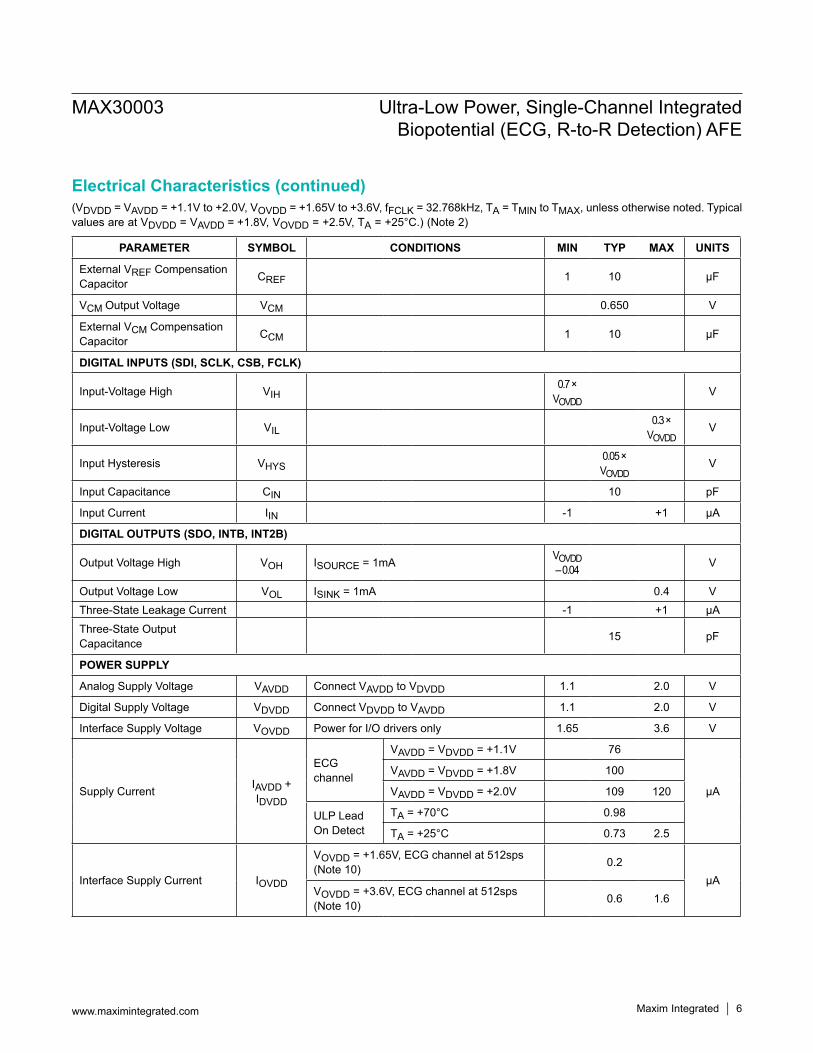
Timing Characteristics
PARAMETER SYMBOL CONDITIONS MIN TYP MAX UNITS
TIMING CHARACTERISTICS
SCLK Frequency fSCLK 0 12 MHz
SCLK Period tCP 83 ns
SCLK Pulse Width High tCH 15 ns
SCLK Pulse Width Low tCL 15 ns
CSB Fall to SCLK Rise Setup Time tCSS0 To 1st SCLK rising edge (RE) 15 ns
CSB Fall to SCLK Rise Hold Time tCSH0 Applies to inactive RE preceding 1st RE 0 ns
CSB Rise to SCLK Rise Hold Time tCSH1 Applies to 32nd RE, executed write 10 ns
CSB Rise to SCLK Rise tCSAApplies to 32nd RE, aborted write sequence 15 ns
SCLK Rise to CSB Fall tCSF Applies to 32nd RE 100 ns
CSB Pulse-Width High tCSPW 20 ns
SDI-to-SCLK Rise Setup Time tDS 8 ns
SDI to SCLK Rise Hold Time tDH 8 ns
SCLK Fall to SDO Transition tDOT
CLOAD = 20pf 40 ns
CLOAD = 20pf, VAVDD = VDVDD ≥ 1.8V, VDVDD ≥ 2.5V
20 ns
SCLK Fall to SDO Hold tDOH CLOAD = 20pf 2 ns
(VDVDD = VAVDD = +1.1V to +2.0V, VOVDD = +1.65V to +3.6V, TA = TMIN to TMAX, unless otherwise noted. Typical values are at VDVDD = +1.8V, VOVDD = +2.5V, TA = +25°C.) (Notes 2, 3)
Note 2: Limits are 100% tested at TA = +25°C. Limits over the operating temperature range and relevant supply voltage range are guaranteed by design and characterization.
Note 3: Guaranteed by design and characterization. Not tested in production.Note 4: One electrode drive with <10Ω source impedance, the other driven with 51kΩ in parallel with a 47nF per IEC60601-2-47.Note 5: Inputs connected to 51kΩ in parallel with a 47nF to VCM.Note 6: Use this setting only for VAVDD = VDVDD ≥ 1.65V.Note 7: Use this setting only for VAVDD = VDVDD ≥ 1.55V.Note 8: Use this setting only for VAVDD = VDVDD ≥ 1.45V.Note 9: This specification defines the accuracy of the calibration voltage source as applied to the ECG input, not as measured
through the ADC channel.Note 10: fSCLK = 4MHz, burst mode, EFIT = 8, CSDO = CINTB = 50pF.Note 11: ESD test performed with 1kΩ series resistor designed to withstand 8kV surge voltage.
Figure 1a. SPI Timing Diagram
Figure 1b. FCLK Timing Diagram
MAX30003 Ultra-Low Power, Single-Channel Integrated Biopotential (ECG, R-to-R Detection) AFE
www.maximintegrated.com Maxim Integrated 8
DO23
tCSH1
tCSF
1 2 3 4 5 6 7 8 31
A5A6 A4 A3 A2 A1 A0 R/WB DIN1 DIN0
tDS
tCSS0
SDI
tCSH0
32 1'
tCSA
tCSPW
DO1
tDOE
Z Z
9 10
DIN23 DIN22
DO0
A6'
DO22
SCLK
CSB
SDO
tDHtCP
tCH
tCL
tDOT tDOH
tDOZ
tFP
FCLK
tFH tFL
PARAMETER SYMBOL CONDITIONS MIN TYP MAX UNITS
CSB Fall to SDO Fall tDOE Enable time, CLOAD = 20pf 30 ns
CSB Rise to SDO Hi-Z tDOZ Disable time 35 ns
FCLK Frequency fFCLK External reference clock 32.768 kHz
FCLK Period tFP 30.52 µs
FCLK Pulse-Width High tFH 50% duty cycle assumed 15.26 µs
FCLK Pulse-Width Low tFL 50% duty cycle assumed 15.26 µs
Timing Characteristics (continued)
(VDVDD = VAVDD = +1.8V, VOVDD = 2.5V, TA = +25°C, unless otherwise noted.)
MAX30003 Ultra-Low Power, Single-Channel Integrated Biopotential (ECG, R-to-R Detection) AFE
Maxim Integrated 9www.maximintegrated.com
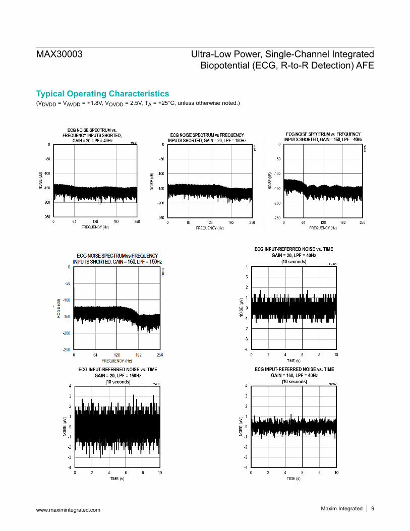
Typical Operating Characteristics
(VDVDD = VAVDD = +1.8V, VOVDD = 2.5V, TA = +25°C, unless otherwise noted.)
MAX30003 Ultra-Low Power, Single-Channel Integrated Biopotential (ECG, R-to-R Detection) AFE
Maxim Integrated 10www.maximintegrated.com
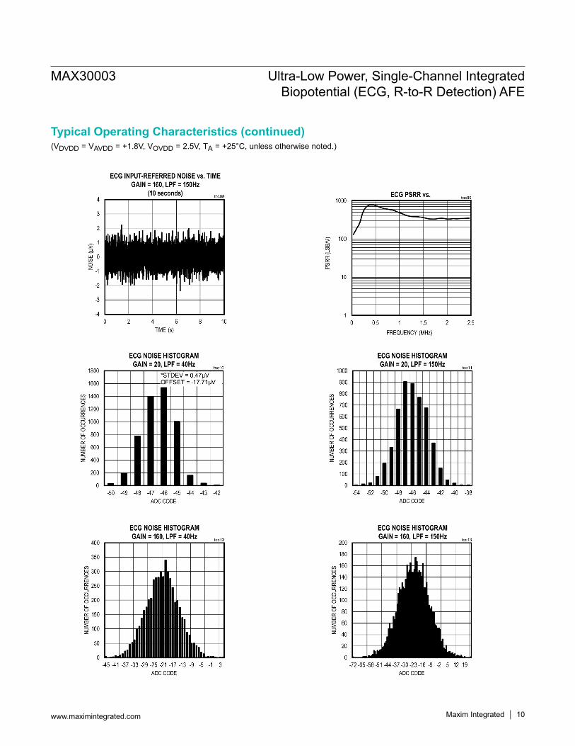
Typical Operating Characteristics (continued)

MAX30003 Ultra-Low Power, Single-Channel Integrated Biopotential (ECG, R-to-R Detection) AFE
Maxim Integrated 11www.maximintegrated.com
Typical Operating Characteristics (continued)(VDVDD = VAVDD = +1.8V, VOVDD = 2.5V, TA = +25°C, unless otherwise noted.)

MAX30003 Ultra-Low Power, Single-Channel Integrated Biopotential (ECG, R-to-R Detection) AFE
Maxim Integrated 12www.maximintegrated.com
Typical Operating Characteristics (continued)(VDVDD = VAVDD = +1.8V, VOVDD = 2.5V, TA = +25°C, unless otherwise noted.)

MAX30003 Ultra-Low Power, Single-Channel Integrated Biopotential (ECG, R-to-R Detection) AFE
www.maximintegrated.com Maxim Integrated 13
Pin Configurations
Pin Description
MAX30003
TQFN(5mm x 5mm)
*CONNECT EP TO AGND
TOP VIEW
I.C.
I.C.
I.C.
ECGP
ECGNI.C
.
INT2
B
SDO
SDI
INTB
SCLK
CSB
VCMI.C.
VBG
DGND
CPLL
CAPNCAPP
AGND
OVDD
AGND AGND
+
I.C.
DVDDVREF
FCLKAVDD 14
8
9
10
11
12
13
22
28
27
26
25
24
23
15161718192021
7654321
*EP
TEXTOP VIEW(BUMP SIDE DOWN)
A
B
C
D
WLP(2.74mm x 2.9mm)
E
I.C.
1
I.C.
2
I.C.
3
I.C. ECGP ECGN
VBG I.C. AGND AGND CAPN CAPP
VCM I.C. AGND AGND DGND CPLL
VREF INTB OVDD AGND FCLK DVDD
AVDD INT2B SDO SDI SCLK CSB
4 5 6
MAX30003
PIN BUMPNAME FUNCTION
TQFN WLP
1, 2, 4, 5, 24, 26
A1, A2, A3, A4, B2, C2 I.C. Internally Connected. Connect to AGND.
3,8,28 B3, B4, C3, C4, D4 AGND Analog Power and Reference Ground. Connect into the printed circuit board
ground plane.
6 A5 ECGP ECG Positive Input
7 A6 ECGN ECG Negative Input
9 B6 CAPP Analog High-Pass Filter Input. Connect a 1μF X7R capacitor (CHPF) between CAPP and CAPN to form a 0.5Hz high-pass response in the ECG channel.
10 B5 CAPN Analog High-Pass Filter Input. Connect a 1μF X7R capacitor (CHPF) between CAPP and CAPN to form a 0.5Hz high-pass response in the ECG channel.
11 C6 CPLL PLL Loop Filter Input. Connect 1nF COG cap between CPLL and AGND.
12 C5 DGND Digital Ground for Both Digital Core and I/O Pad Drivers. Recommended to connect to AGND plane.
13 D6 DVDD Digital Core Supply Voltage. Connect to AVDD

MAX30003 Ultra-Low Power, Single-Channel Integrated Biopotential (ECG, R-to-R Detection) AFE
www.maximintegrated.com Maxim Integrated 14
Pin Description (continued)PIN BUMP
NAME FUNCTIONTQFN WLP
14 D5 FCLK External 32.768kHz Clock that Controls the Sampling of the Internal Sigma-Delta Converters and Decimator.
15 E6 CSB Active-Low Chip-Select Input. Enables the serial interface.
16 E5 SCLK Serial Clock Input. Clocks data in and out of the serial interface when CSB is low.
17 E4 SDI Serial Data Input. SDI is sampled into the device on the rising edge of SCLK when CSB is low.
18 E3 SDO Serial Data Output. SDO will change state on the falling edge of SCLK when CSB is low. SDO is three-stated when CSB is high.
19 D3 OVDD Logic Interface Supply Voltage
20 E2 INT2B Interrupt 2 Output. INT2B is an active-low status output. It can be used to interrupt an external device.
21 D2 INTB Interrupt Output. INTB is an active low status output. It can be used to interrupt an external device.
22 E1 AVDD Analog Core Supply Voltage. Connect to DVDD.
23 D1 VREFADC Reference Buffer Output. Connect a 10μF X5R ceramic capacitor between VREF and AGND.
25 C1 VCMCommon Mode Buffer Output. Connect a 10μF X5R ceramic capacitor between VCM and AGND.
27 B1 VBGBandgap Noise Filter Output. Connect a 1.0μF X7R ceramic capacitor between VBG and AGND.
EP — — Exposed Paddle. Connect to AGND.
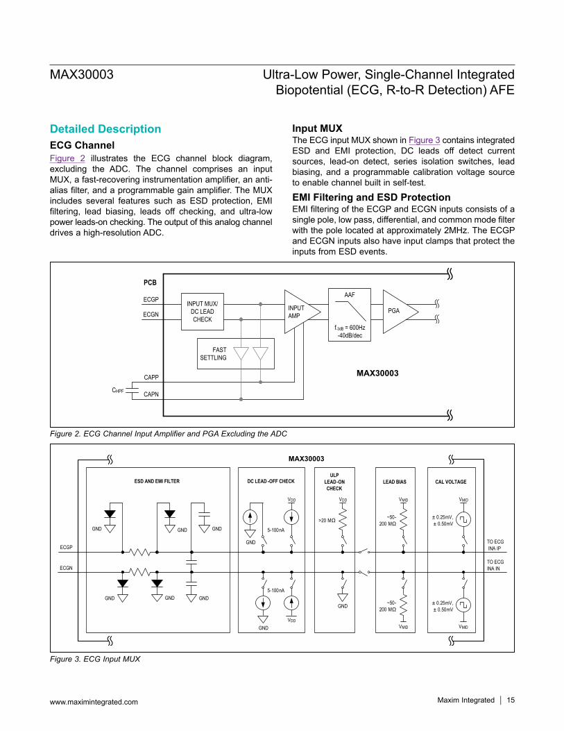
Detailed DescriptionECG ChannelFigure 2 illustrates the ECG channel block diagram, excluding the ADC. The channel comprises an input MUX, a fast-recovering instrumentation amplifier, an anti-alias filter, and a programmable gain amplifier. The MUX includes several features such as ESD protection, EMI filtering, lead biasing, leads off checking, and ultra-low power leads-on checking. The output of this analog channel drives a high-resolution ADC.
Input MUXThe ECG input MUX shown in Figure 3 contains integrated ESD and EMI protection, DC leads off detect current sources, lead-on detect, series isolation switches, lead biasing, and a programmable calibration voltage source to enable channel built in self-test.
EMI Filtering and ESD ProtectionEMI filtering of the ECGP and ECGN inputs consists of a single pole, low pass, differential, and common mode filter with the pole located at approximately 2MHz. The ECGP and ECGN inputs also have input clamps that protect the inputs from ESD events.
Figure 2. ECG Channel Input Amplifier and PGA Excluding the ADC
Figure 3. ECG Input MUX
MAX30003 Ultra-Low Power, Single-Channel Integrated Biopotential (ECG, R-to-R Detection) AFE
www.maximintegrated.com Maxim Integrated 15
ECGP
ECGN
FAST SETTLING
INPUT MUX/DC LEAD CHECK
INPUTAMP
AAF
f-3dB = 600Hz-40dB/dec
PGA
PCB
CAPP
CAPNCHPF
MAX30003
VDD
TO ECGINA IP
GND GND
ESD AND EMI FILTER
GND GND GND
GND
DC LEAD -OFF CHECK
5-100nA
ULPLEAD-ONCHECK
>20 MΩ
LEAD BIAS
~50-200 MΩ
CAL VOLTAGE
± 0.25mV,± 0.50mV
VDD VMID
ECGP
VMID
VMID
~50-200 MΩ
ECGN
5-100nA
GND
VDD
GND
GND
VMID
± 0.25mV,± 0.50mV
TO ECGINA IN
MAX30003

±8kV using the Contact Discharge method specified in IEC61000-4-2 ESD
±15kV using the Air Gap Discharge method specified in IEC61000-4-2 ESD
±8kV HBM For IEC61000-4-2 ESD protection, use 1kΩ series
resistors on ECGP and ECGN that is rated to with-stand 8kV surge voltages.
DC Leads-Off Detection and ULP Leads-On DetectionThe input MUX leads-off detect circuitry consists of programmable sink/source DC current sources that allow for DC leads-off detection, while the channel is powered up in normal operation and an ultra-low-power (ULP) leads-on detect while the channel is powered-down. The MAX30003 accomplishes DC leads-off detection by applying a DC current to pull the ECG input voltage up to above VMID + VTH or down to below VMID - VTH. The current sources have user selectable values of 0nA, 5nA, 10nA, 20nA, 50nA, and 100nA that allow coverage of dry and wet electrode impedance ranges. Supported thresholds are VMID ± 0.30V (recommended), VMID ± 0.40V, VMID ± 0.45V, and VMID ± 0.50V. A threshold of 400mV, 450mV, and 500mV should only be used when VAVDD ≥ 1.45V, 1.55V, and 1.65V, respectively. A dynamic comparator protects against false flags generated by the input amplifier and input chopping. The comparator checks for a minimum continuous violation (or threshold exceeded) of 115ms to 140ms depending on the setting of FMSTR[1:0] before asserting any one of the LDOFF_* interrupt flags (Figure 4). See registers CNFG_GEN (0x10) and CNFG_EMUX 0x14) for configuration settings and see Table 1 for recommended values given electrode type and supply voltage.The ULP lead on detect operates by pulling ECGN low with a pulldown resistance larger than 5mΩ and pulling ECGP high with a pullup resistance larger than 15MΩ. A low-power comparator determines if ECGP is pulled below a predefined threshold that occurs when both electrodes make contact with the body. When the impedance between ECGP and ECGN is less than 20mΩ, an interrupt LONINT is asserted, alerting the µC to a leads-on condition.A 0nA/VMID ± 300mV selection is available allowing monitoring of the input compliance of the INA during non-DC lead-off checks.
Lead BiasThe MAX30003 limits the ECGP and ECGN DC input common mode range to VMID ±150mV. This range can be maintained either through external/internal lead-biasing.Internal DC lead-biasing consists of 50MΩ, 100MΩ, or 200MΩ selectable resistors to VMID that drive the
electrodes within the input common mode requirements of the ECG channel and can drive the connected body to the proper common mode voltage level. See register CNFG_GEN (0x10) to select a configuration.
Isolation SwitchesThe series switches in the MAX30003 isolate ECGP and ECGN pins (subject) from the internal signal path. the series switches are disabled by default. They must be enabled to record ECG.
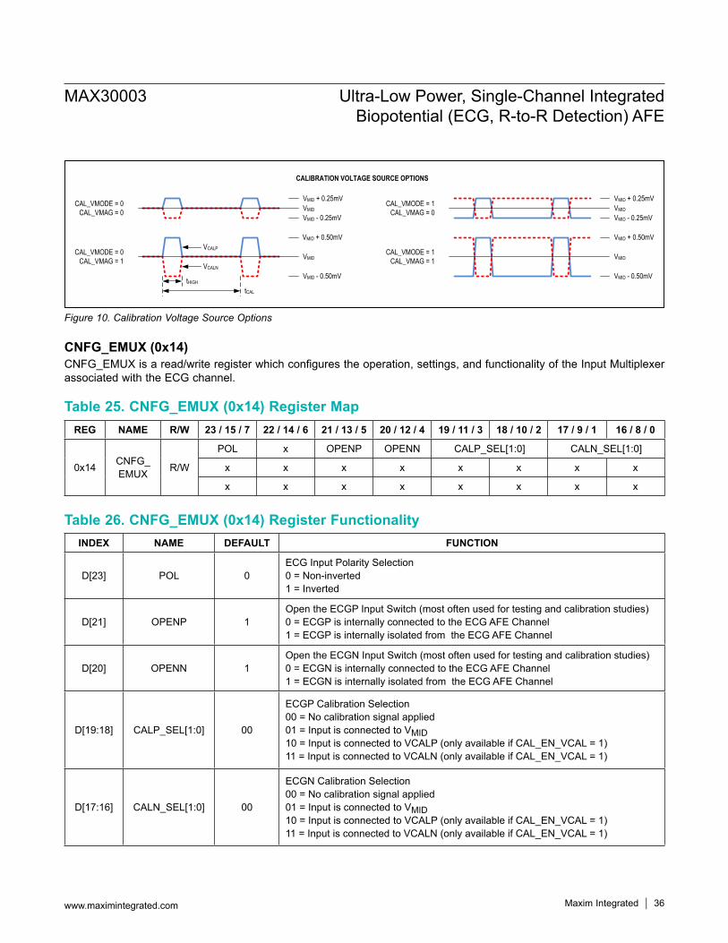
Calibration Voltage SourcesCalibration voltage sources are available to provide ±0.25mV (0.5mVP-P) or ±0.5mV (1.0mVP-P) inputs to the ECG channel with programmable frequency and duty cycle. The sources can be unipolar/bipolar relative to VMID.Figure 5 illustrates the possible calibration waveforms. Frequency selections are available in 4X increments from 15.625mHz to 256Hz with selected pulse widths varying from 30.5µs to 31.723ms and 50% duty cycle. Signals can be single-ended, differential, or common mode. This flexibility allows end-to-end channel-testing of the ECG signal path.When applying calibration voltage sources with the device connected to a subject, the series input switches must be disconnected so as not to drive signals into the subject. See registers CNFG_CAL (0x12) and CNFG_EMUX (0x14) to select configuration.
Figure 4. Lead-Off Detect Behavior
MAX30003 Ultra-Low Power, Single-Channel Integrated Biopotential (ECG, R-to-R Detection) AFE
www.maximintegrated.com Maxim Integrated 16
VDD
VMID
VSS
ECGP,N
VTH_H
VTH_L
INTB
>115ms
LDOFF_*H BITS ASSERTED
ABOVE THRESHOLD
BELOW THRESHOLD
<115ms
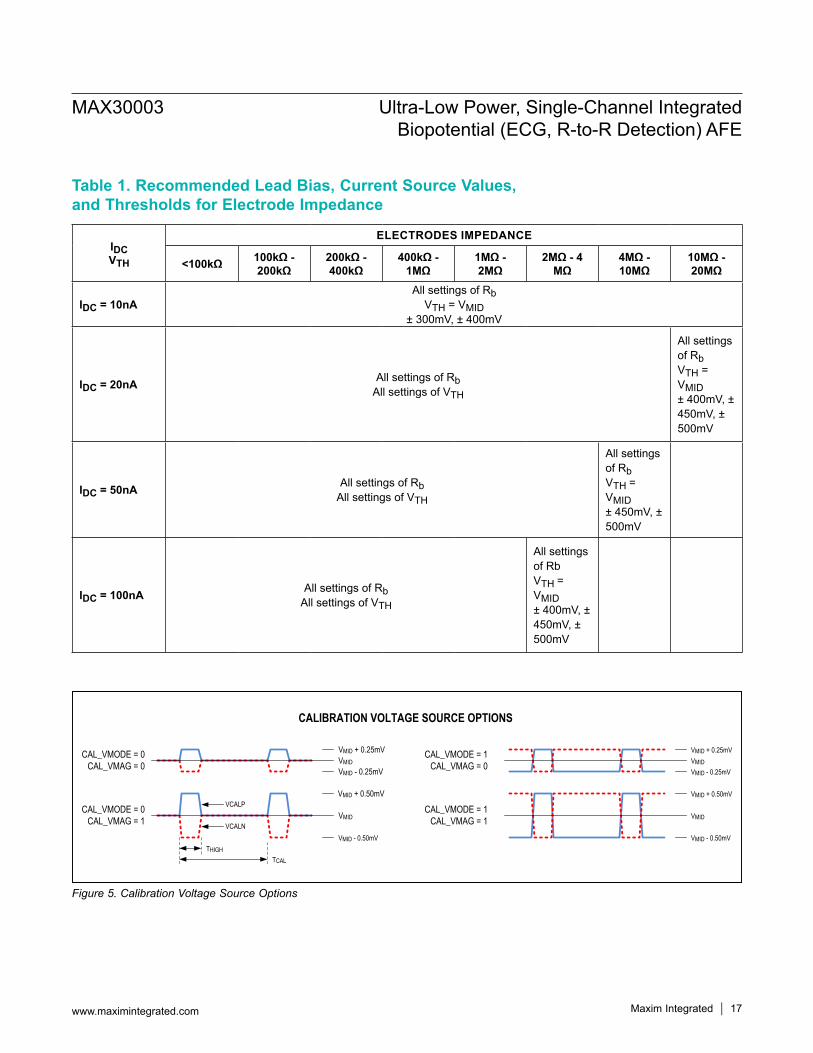
Table 1. Recommended Lead Bias, Current Source Values, and Thresholds for Electrode Impedance
Figure 5. Calibration Voltage Source Options
MAX30003 Ultra-Low Power, Single-Channel Integrated Biopotential (ECG, R-to-R Detection) AFE
www.maximintegrated.com Maxim Integrated 17
IDCVTH
ELECTRODES IMPEDANCE
<100kΩ 100kΩ - 200kΩ
200kΩ - 400kΩ
400kΩ - 1MΩ
1MΩ - 2MΩ
2MΩ - 4MΩ
4MΩ - 10MΩ
10MΩ - 20MΩ
IDC = 10nAAll settings of Rb
VTH = VMID ± 300mV, ± 400mV
IDC = 20nA All settings of RbAll settings of VTH
All settings of RbVTH = VMID ± 400mV, ± 450mV, ± 500mV
IDC = 50nA All settings of RbAll settings of VTH
All settings of RbVTH = VMID ± 450mV, ± 500mV
IDC = 100nA All settings of RbAll settings of VTH
All settings of RbVTH = VMID ± 400mV, ± 450mV, ± 500mV
CALIBRATION VOLTAGE SOURCE OPTIONS
VMID + 0.50mV
CAL_VMODE = 0CAL_VMAG = 0
CAL_VMODE = 1CAL_VMAG = 0VMID
VMID + 0.25mV
VMID - 0.25mVVMID
VMID + 0.25mV
VMID - 0.25mV
CAL_VMODE = 0CAL_VMAG = 1
CAL_VMODE = 1CAL_VMAG = 1VMID
VMID + 0.50mV
VMID - 0.50mV
VMID
VMID - 0.50mVTHIGH
TCAL
VCALP
VCALN

Gain Settings and Input RangeThe device’s ECG channel contains an input instrumentation amplifier that provides low-noise, fixed-gain amplification of the differential signal, rejects differential DC voltage due to electrode polarization, rejects common-mode interference primarily due to AC mains interference, and provides high input impedance to guarantee high CMRR even in the presence of severe electrode impedance mismatch (see Figure 2). The differential DC rejection corner frequency is set by an external capacitor (CHPF) placed between pins CAPP and CAPN, refer to Table 2 for appropriate value selection. There are three recommended options for the cutoff frequency: 4.4Hz, 0.4Hz, and 0.04Hz. Setting the cutoff frequency to 4.4Hz provides the most motion artifact rejection at the expense of ECG waveform quality, making it best suited for heart rate monitoring. For ambulatory applications requiring more robust ECG waveforms with moderate motion artifact rejection, 0.4Hz is recommended. Select 0.04Hz for patient monitoring applications in which ECG waveform quality is the primary concern and poor rejection of motion artifacts can be tolerated. The high-pass corner frequency is calculated by the following equation:1/(2r x RHPF x CHPF)RHPF is specified in the Electrical Characteristics table.Following the instrumentation amplifier is a 2-pole active anti-aliasing filter with a 600Hz -3dB frequency that provides 57dB of attenuation at half the modulator sampling rate (approximately 16kHz) and a PGA with programmable gains of 1, 2, 4, and 8V/V for an overall gain of 20, 40, 80, and 160V/V. The instrumentation amplifier and PGA are chopped to minimize offset and 1/f noise. Gain settings are configured via the CNFG_ECG (0x15) register. The useable common-mode range is VMID ±150mV, internal lead biasing can be used to meet this requirement. The useable DC differential range is ±300mV to allow for electrode polarization voltages on each electrode. The input AC differential range is ±32.5mV or ±65mVP-P.
Fast Recovery ModeThe input instrumentation amplifier has the ability to rapidly recover from an excessive overdrive event such as a defibrillation pulse, high-voltage external pacing, and electro-surgery interference. There are two modes of recovery that can be used: automatic or manual recovery. The mode is programmed by the FAST[1:0] bits in the MNGR_DYN (0x05) register.Automatic mode engages once the saturation counter exceeds approximately 125ms (tSAT). The counter is activated the first time the ADC output exceeds the symmetrical threshold defined by the FAST_TH[5:0] bits
in the MNGR_DYN (0x05) register and accumulates the time that the ADC output exceeds either the positive or negative threshold. If the saturation counter exceeds 125ms, it triggers the fast settling mode (if enabled) and resets. The saturation counter can also be reset prior to triggering the fast settling mode if the ADC output falls below the threshold continuously for 125ms (tBLW). This feature is designed to avoid false triggers due to the QRS complex. Once triggered, fast settling mode will be engaged for 500ms, see Figure 6. ECG samples are tagged if they were taken while fast settling mode was asserted.In manual mode, a user algorithm running on the host microcontroller or an external stimulus input will generate the trigger to enter fast recovery mode. The host microcontroller then enables the manual fast recovery mode in the MNGR_DYN (0x05) register. The manual fast recovery mode can be of a much shorter duration than the automatic mode and allows for more rapid recovery. One such example is recovery from external high-voltage pacing signals in a few milliseconds to allow the observation of a subsequent p-wave.
Table 2. ECG Analog HPF Corner Frequency Selection
Table 3. Fast Recovery Mode Recovery Time vs. Number of Samples
MAX30003 Ultra-Low Power, Single-Channel Integrated Biopotential (ECG, R-to-R Detection) AFE
www.maximintegrated.com Maxim Integrated 18
CHPF HPF CORNER FREQUENCY
0.1µ ≤ 5Hz
1.0µ ≤ 0.5Hz
10µ ≤ 0.05Hz
SAMPLE RATE (sps)
NUMBER OF SAMPLES
RECOVERY TIME (APPROXIMATE)
(ms)512 255 498
256 127 496
128 63 492
500 249 498
250 124 496
125 64 512
200 99 495
199.8 99 495.5

Decimation FilterThe decimation filter consists of a Cascaded Integrator Comb (CIC) decimation filter to the data rate followed by a programmable FIR filter to implement HPF and LPF selections.The high-pass filter options include a 1st-order IIR Butterworth filter with a 0.4Hz corner frequency along with a pass-through setting for DC coupling.
Low-pass filter options include a 12-tap linear phase (constant group delay) FIR filter with approximately 40Hz, 100Hz, or 150Hz corner frequencies, depending on the sampling rate. See register CNFG_ECG (0x15) to con-figure the filters. Table 4 illustrates the ECG latency in samples and time for each ADC data rate.
Table 4. ECG Latency in Samples and Time as a Function of ECG Data Rate and Decimation
Figure 6. Automatic Fast Settling Behavior
MAX30003 Ultra-Low Power, Single-Channel Integrated Biopotential (ECG, R-to-R Detection) AFE
www.maximintegrated.com Maxim Integrated 19
ECG
VDD
FAST SETTLING
FAST NORMALNORMALETAG
tBLW125ms
VMID
VSS
ENABLED DISABLEDDISABLED
COUNTERSTART STOP RESET START RESET
tSAT125ms
VSAT_THH
VSAT_THL
tFAST
ECG CHANNEL SETTINGS LATENCY
INPUT SAMPLE
RATE (Hz)
OUTPUT DATA RATE
(sps)
DECIMATION RATIO
WITHOUT LFP (INPUT SAMPLES)
WITH LPF (INPUT
SAMPLES)
WITHOUT LFP (ms)
WITH LPF (ms)
32,768 512 64 650 1,034 19.836 31.555
32,000 500 64 650 1,034 20.313 32.313
32,768 256 128 2,922 3,690 89.172 112.610
32,000 250 128 2,922 3,690 91.313 115.313
32,000 200 160 1,242 2,202 38.813 68.813
31,968 199.8 160 1,242 2,202 38.851 68.881
32,768 128 256 3,370 4,906 102.844 149.719
32,000 125 256 3,370 4,906 105.313 153.313
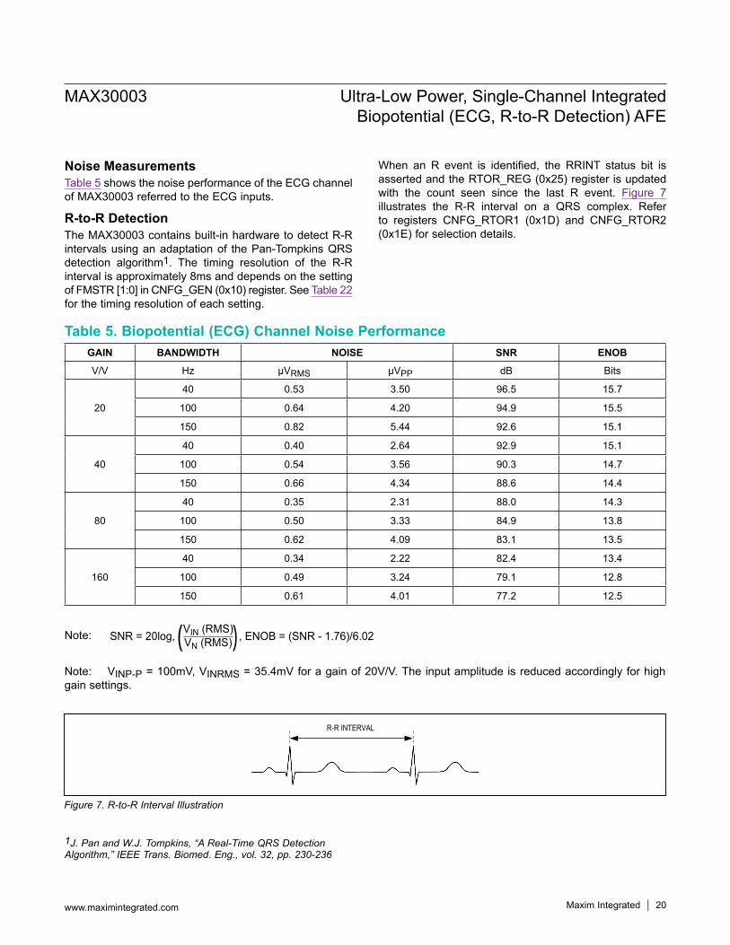
Noise MeasurementsTable 5 shows the noise performance of the ECG channel of MAX30003 referred to the ECG inputs.
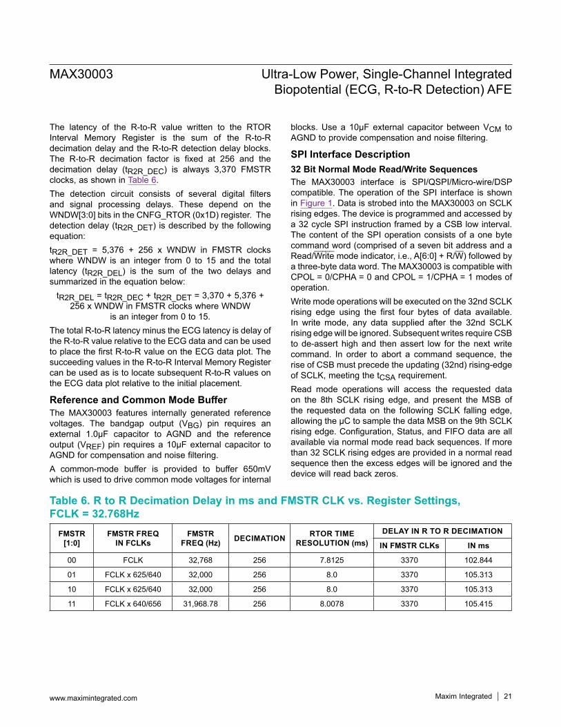
R-to-R DetectionThe MAX30003 contains built-in hardware to detect R-R intervals using an adaptation of the Pan-Tompkins QRS detection algorithm1. The timing resolution of the R-R interval is approximately 8ms and depends on the setting of FMSTR [1:0] in CNFG_GEN (0x10) register. See Table 22 for the timing resolution of each setting.
When an R event is identified, the RRINT status bit is asserted and the RTOR_REG (0x25) register is updated with the count seen since the last R event. Figure 7 illustrates the R-R interval on a QRS complex. Refer to registers CNFG_RTOR1 (0x1D) and CNFG_RTOR2 (0x1E) for selection details.
1J. Pan and W.J. Tompkins, “A Real-Time QRS Detection Algorithm,” IEEE Trans. Biomed. Eng., vol. 32, pp. 230-236
Table 5. Biopotential (ECG) Channel Noise Performance
Note: SNR = 20log, , ENOB = (SNR - 1.76)/6.02VIN (RMS)VN (RMS)( )
Note: VINP-P = 100mV, VINRMS = 35.4mV for a gain of 20V/V. The input amplitude is reduced accordingly for high gain settings.
Figure 7. R-to-R Interval Illustration
MAX30003 Ultra-Low Power, Single-Channel Integrated Biopotential (ECG, R-to-R Detection) AFE
www.maximintegrated.com Maxim Integrated 20
GAIN BANDWIDTH NOISE SNR ENOBV/V Hz µVRMS µVPP dB Bits
20
40 0.53 3.50 96.5 15.7
100 0.64 4.20 94.9 15.5
150 0.82 5.44 92.6 15.1
40
40 0.40 2.64 92.9 15.1
100 0.54 3.56 90.3 14.7
150 0.66 4.34 88.6 14.4
80
40 0.35 2.31 88.0 14.3
100 0.50 3.33 84.9 13.8
150 0.62 4.09 83.1 13.5
160
40 0.34 2.22 82.4 13.4
100 0.49 3.24 79.1 12.8
150 0.61 4.01 77.2 12.5
R-R INTERVAL
The latency of the R-to-R value written to the RTOR Interval Memory Register is the sum of the R-to-R decimation delay and the R-to-R detection delay blocks. The R-to-R decimation factor is fixed at 256 and the decimation delay (tR2R_DEC) is always 3,370 FMSTR clocks, as shown in Table 6.The detection circuit consists of several digital filters and signal processing delays. These depend on the WNDW[3:0] bits in the CNFG_RTOR (0x1D) register. The detection delay (tR2R_DET) is described by the following equation:tR2R_DET = 5,376 + 256 x WNDW in FMSTR clocks where WNDW is an integer from 0 to 15 and the total latency (tR2R_DEL) is the sum of the two delays and summarized in the equation below:
tR2R_DEL = tR2R_DEC + tR2R_DET = 3,370 + 5,376 + 256 x WNDW in FMSTR clocks where WNDW
is an integer from 0 to 15.The total R-to-R latency minus the ECG latency is delay of the R-to-R value relative to the ECG data and can be used to place the first R-to-R value on the ECG data plot. The succeeding values in the R-to-R Interval Memory Register can be used as is to locate subsequent R-to-R values on the ECG data plot relative to the initial placement.
Reference and Common Mode BufferThe MAX30003 features internally generated reference voltages. The bandgap output (VBG) pin requires an external 1.0µF capacitor to AGND and the reference output (VREF) pin requires a 10µF external capacitor to AGND for compensation and noise filtering.A common-mode buffer is provided to buffer 650mV which is used to drive common mode voltages for internal
blocks. Use a 10µF external capacitor between VCM to AGND to provide compensation and noise filtering.
SPI Interface Description32 Bit Normal Mode Read/Write SequencesThe MAX30003 interface is SPI/QSPI/Micro-wire/DSP compatible. The operation of the SPI interface is shown in Figure 1. Data is strobed into the MAX30003 on SCLK rising edges. The device is programmed and accessed by a 32 cycle SPI instruction framed by a CSB low interval. The content of the SPI operation consists of a one byte command word (comprised of a seven bit address and a Read/Write mode indicator, i.e., A[6:0] + R/W) followed by a three-byte data word. The MAX30003 is compatible with CPOL = 0/CPHA = 0 and CPOL = 1/CPHA = 1 modes of operation.Write mode operations will be executed on the 32nd SCLK rising edge using the first four bytes of data available. In write mode, any data supplied after the 32nd SCLK rising edge will be ignored. Subsequent writes require CSB to de-assert high and then assert low for the next write command. In order to abort a command sequence, the rise of CSB must precede the updating (32nd) rising-edge of SCLK, meeting the tCSA requirement.Read mode operations will access the requested data on the 8th SCLK rising edge, and present the MSB of the requested data on the following SCLK falling edge, allowing the µC to sample the data MSB on the 9th SCLK rising edge. Configuration, Status, and FIFO data are all available via normal mode read back sequences. If more than 32 SCLK rising edges are provided in a normal read sequence then the excess edges will be ignored and the device will read back zeros.
Table 6. R to R Decimation Delay in ms and FMSTR CLK vs. Register Settings, FCLK = 32.768Hz
MAX30003 Ultra-Low Power, Single-Channel Integrated Biopotential (ECG, R-to-R Detection) AFE
www.maximintegrated.com Maxim Integrated 21
FMSTR [1:0]
FMSTR FREQ IN FCLKs
FMSTR FREQ (Hz) DECIMATION RTOR TIME
RESOLUTION (ms)DELAY IN R TO R DECIMATION
IN FMSTR CLKs IN ms
00 FCLK 32,768 256 7.8125 3370 102.844
01 FCLK x 625/640 32,000 256 8.0 3370 105.313
10 FCLK x 625/640 32,000 256 8.0 3370 105.313
11 FCLK x 640/656 31,968.78 256 8.0078 3370 105.415
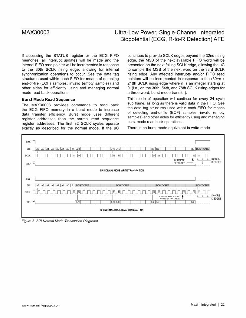
If accessing the STATUS register or the ECG FIFO memories, all interrupt updates will be made and the internal FIFO read pointer will be incremented in response to the 30th SCLK rising edge, allowing for internal synchronization operations to occur. See the data tag structures used within each FIFO for means of detecting end-of-file (EOF) samples, invalid (empty samples) and other aides for efficiently using and managing normal mode read back operations.
Burst Mode Read SequenceThe MAX30003 provides commands to read back the ECG FIFO memory in a burst mode to increase data transfer efficiency. Burst mode uses different register addresses than the normal read sequence register addresses. The first 32 SCLK cycles operate exactly as described for the normal mode. If the µC
continues to provide SCLK edges beyond the 32nd rising edge, the MSB of the next available FIFO word will be presented on the next falling SCLK edge, allowing the µC to sample the MSB of the next word on the 33rd SCLK rising edge. Any affected interrupts and/or FIFO read pointers will be incremented in response to the (30+n x 24)th SCLK rising edge where n is an integer starting at 0. (i.e., on the 30th, 54th, and 78th SCLK rising-edges for a three-word, burst-mode transfer).This mode of operation will continue for every 24 cycle sub frame, as long as there is valid data in the FIFO. See the data tag structures used within each FIFO for means of detecting end-of-file (EOF) samples, invalid (empty samples) and other aides for efficiently using and managing burst mode read back operations.There is no burst mode equivalent in write mode.
Figure 8. SPI Normal Mode Transaction Diagrams
MAX30003 Ultra-Low Power, Single-Channel Integrated Biopotential (ECG, R-to-R Detection) AFE
www.maximintegrated.com Maxim Integrated 22
1 8 9 16 17 24 25 32 33
A6 A5 A4 A3 A2 A1 A0 W D23 D16 D15 D8 D7 D0
COMMAND EXECUTED
IGNORED EDGESZ Z
CSB
SDI
SCLK
SDO
SPI NORMAL MODE WRITE TRANSACTION
1 8 9 16 17 24 25 32 33
A6 A5 A4 A3 A2 A1 A0 R
INTERRUPT/READ POINTER UPDATED (IF APPLICABLE)
IGNORED EDGES
Z
CSB
SDI
SCLK
SDO
SPI NORMAL MODE READ TRANSACTION
DON’T CARE
DON’T CARE DON’T CARE DON’T CARE DON’T CARE
DO23 DO16 DO15 DO8 DO7 DO0
30
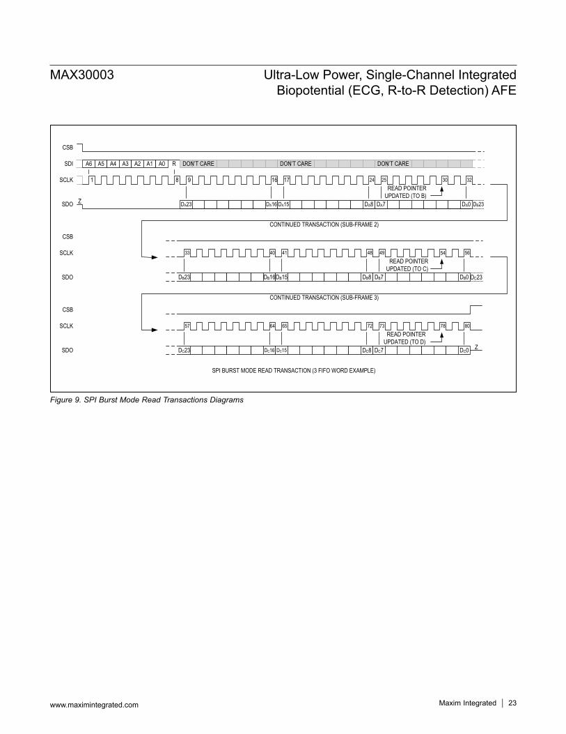
Figure 9. SPI Burst Mode Read Transactions Diagrams
MAX30003 Ultra-Low Power, Single-Channel Integrated Biopotential (ECG, R-to-R Detection) AFE
www.maximintegrated.com Maxim Integrated 23
1 8 9 16 17 24 25 32
A6 A5 A4 A3 A2 A1 A0 R
READ POINTER UPDATED (TO B)
Z
CSB
SDI
SCLK
SDO
SPI BURST MODE READ TRANSACTION (3 FIFO WORD EXAMPLE)
DON’T CARE DON’T CARE DON’T CARE
DA23 DA16 DA15 DA8 DA7 DA0
33 40 41 48 49 56
DB16DB15 DB8 DB7 DB0
DB23
DB23
57 64 65 72 73 80
DC16 DC15 DC8 DC7 DC0DC23
CSB
SCLK
SDO
CSB
SCLK
SDO
CONTINUED TRANSACTION (SUB-FRAME 2)
CONTINUED TRANSACTION (SUB-FRAME 3)
Z
DC23
30
READ POINTER UPDATED (TO C)
READ POINTER UPDATED (TO D)
54
78
MAX30003 Ultra-Low Power, Single-Channel Integrated Biopotential (ECG, R-to-R Detection) AFE
www.maximintegrated.com Maxim Integrated 24
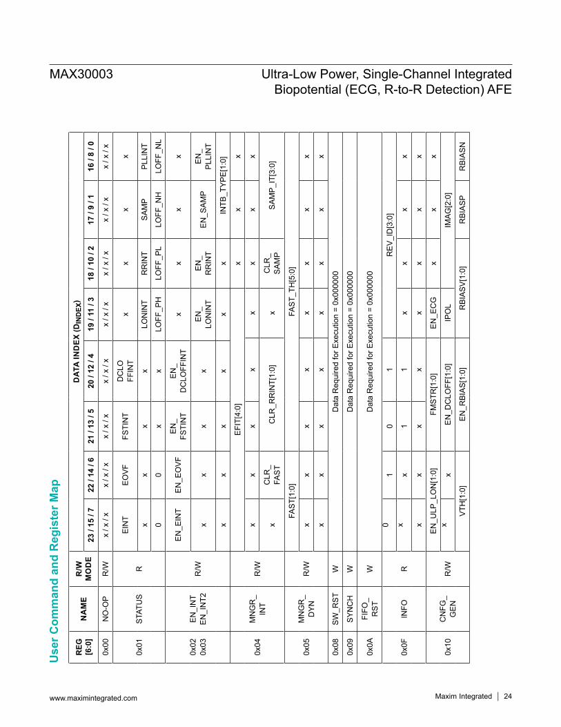
Use
r Com
man
d an
d R
egis
ter M
ap
REG
[6
:0]
NA
ME
R/W
M
OD
ED
ATA
IND
EX (D
IND
EX)
23 /
15 /
722
/ 14
/ 6
21 /
13 /
520
/ 12
/ 4
19 /
11 /
318
/ 10
/ 2
17 /
9 / 1
16 /
8 / 0
0x00
NO
-OP
R/W
x / x
/ x
x / x
/ x
x / x
/ x
x / x
/ x
x / x
/ x
x / x
/ x
x / x
/ x
x / x
/ x
0x01
STAT
US
R
EIN
TEO
VFFS
TIN
TD
CLO
FF
INT
xx
xx
xx
xx
LON
INT
RR
INT
SAM
PPL
LIN
T
00
xx
LOFF
_PH
LOFF
_PL
LOFF
_NH
LOFF
_NL
0x02
0x03
EN_I
NT
EN_I
NT2
R/W
EN_E
INT
EN_E
OVF
EN_
FSTI
NT
EN_
DC
LOFF
INT
xx
xx
xx
xx
EN_
LON
INT
EN_
RR
INT
EN_S
AMP
EN_
PLLI
NT
xx
xx
xx
INTB
_TYP
E[1:
0]
0x04
MN
GR
_ IN
TR
/W
EFIT
[4:0
]x
xx
xx
xx
xx
xx
xC
LR_
FAST
CLR
_RR
INT[
1:0]
xC
LR_
SAM
PSA
MP_
IT[3
:0]
0x05
MN
GR
_ D
YNR
/W
FAST
[1:0
]FA
ST_T
H[5
:0]
xx
xx
xx
xx
xx
xx
xx
xx
0x08
SW_R
STW
Dat
a R
equi
red
for E
xecu
tion
= 0x
0000
00
0x09
SYN
CH
WD
ata
Req
uire
d fo
r Exe
cutio
n =
0x00
0000
0x0A
FIFO
_ R
STW
Dat
a R
equi
red
for E
xecu
tion
= 0x
0000
00
0x0F
INFO
R
01
01
REV
_ID
[3:0
]x
x1
1x
xx
x
xx
xx
xx
xx
0x10
CN
FG_
GEN
R/W
EN_U
LP_L
ON
[1:0
]FM
STR
[1:0
]EN
_EC
Gx
xx
xx
EN_D
CLO
FF[1
:0]
IPO
LIM
AG[2
:0]
VTH
[1:0
]EN
_RBI
AS[1
:0]
RBI
ASV[
1:0]
RBI
ASP
RBI
ASN

MAX30003 Ultra-Low Power, Single-Channel Integrated Biopotential (ECG, R-to-R Detection) AFE
www.maximintegrated.com Maxim Integrated 25
Use
r Com
man
d an
d R
egis
ter M
ap (c
ontin
ued)
REG
[6
:0]
NA
ME
R/W
M
OD
ED
ATA
IND
EX (D
IND
EX)
23 /
15 /
722
/ 14
/ 6
21 /
13 /
520
/ 12
/ 4
19 /
11 /
318
/ 10
/ 2
17 /
9 / 1
16 /
8 / 0
0x12
CN
FG_
CAL
R/W
xEN
_VC
ALVM
OD
EVM
AGx
xx
x
xFC
AL[2
:0]
FIFT
YTH
IGH
[10:
8]
THIG
H[7
:0]
0x14
CN
FG_
EMU
XR
/W
POL
xO
PEN
PO
PEN
NC
ALP_
SEL[
1:0]
CAL
N_S
EL[1
:0]
xx
xx
xx
xx
xx
xx
xx
xx
0x15
CN
FG_
ECG
R/W
RAT
E[1:
0]x
xx
xG
AIN
[1:0
]
xD
HPF
DLP
F[1:
0]x
xx
x
xx
xx
xx
xx
0x1D
CN
FG_
RTO
R1
R/W
WN
DW
[3:0
]R
GAI
N[3
:0]
EN_R
TOR
xPA
VG[1
:0]
PTSF
[3:0
]
xx
xx
xx
xx
0x1E
CN
FG_
RTO
R2
R/W
xx
HO
FF[5
:0]
xx
RAV
G[1
:0]
xR
HSF
[2:0
]
xx
xx
xx
xx
0x20
ECG
_ FI
FO_
BUR
STR
+EC
G F
IFO
Bur
st M
ode
Rea
d Ba
ckSe
e FI
FO D
escr
iptio
n fo
r det
ails
0x21
ECG
_ FI
FOR
ECG
FIF
O N
orm
al M
ode
Rea
d Ba
ckSe
e FI
FO D
escr
iptio
n fo
r det
ails
0x25
RTO
RR
R to
R In
terv
al R
egis
ter R
ead
Back
See
FIFO
Des
crip
tion
for d
etai
ls
0x7F
NO
-OP
R/W
x/x/
xx/
x/x
x/x/
xx/
x/x
x/x/
xx/
x/x
x/x/
xx/
x/x

Register DescriptionsNO_OP (0x00 and 0x7F) RegistersNo Operation (NO_OP) registers are read-write registers that have no internal effect on the device. If these registers are read back, DOUT remains zero for the entire SPI transaction. Any attempt to write to these registers is ignored without impact to internal operation.
STATUS (0x01) RegisterSTATUS is a read-only register that provides a compre-hensive overview of the current status of the device. The first two bytes indicate the state of all interrupt terms (regardless of whether interrupts are enabled in registers EN_INT (0x02) or EN_INT2 (0x03)). All interrupt terms are active high. The last byte includes detailed status information for conditions associated with the interrupt terms.
Table 7. STATUS (0x01) Register Map
Table 8. Status (0x01) Register Meaning
MAX30003 Ultra-Low Power, Single-Channel Integrated Biopotential (ECG, R-to-R Detection) AFE
www.maximintegrated.com Maxim Integrated 26
REG NAME R/W 23 / 15 / 7 22 / 14 / 6 21 / 13 / 5 20 / 12 / 4 19 / 11 / 3 18 / 10 / 2 17 / 9 / 1 16 / 8 / 0
0x01 STATUS R
EINT EOVF FSTINT DCLOFF INT x x x x
x x x x LONINT RRINT SAMP PLLINT
x x x x LDOFF_PH
LDOFF_PL
LDOFF_NH
LDOFF_NL
INDEX NAME MEANING
D[23] EINTECG FIFO Interrupt. Indicates that ECG records meeting/exceeding the ECG FIFO Interrupt Threshold (EFIT) are available for readback. Remains active until ECG FIFO is read back to the extent required to clear the EFIT condition.
D[22] EOVFECG FIFO Overflow. Indicates that the ECG FIFO has overflown and the data record has been corrupted.Remains active until a FIFO Reset (recommended) or SYNCH operation is issued.
D[21] FSTINTECG Fast Recovery Mode. Issued when the ECG Fast Recovery Mode is engaged (either manually or automatically).Status and Interrupt Clear behavior is defined by CLR_FAST, see MNGR_INT for details.
D[20] DCLOFFINT
DC Lead-Off Detection Interrupt. Indicates that the MAX30003 has determined it is in an ECG leads off condition (as selected in CNFG_GEN) for more than 115ms. Remains active as long as the leads-off condition persists, then held until cleared by STATUS read back (32nd SCLK).
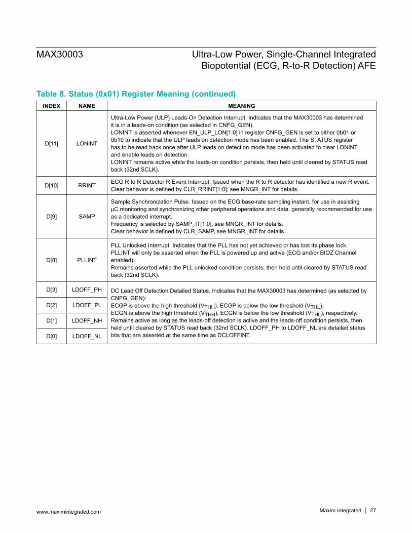
Table 8. Status (0x01) Register Meaning (continued)
MAX30003 Ultra-Low Power, Single-Channel Integrated Biopotential (ECG, R-to-R Detection) AFE
www.maximintegrated.com Maxim Integrated 27
INDEX NAME MEANING
D[11] LONINT
Ultra-Low Power (ULP) Leads-On Detection Interrupt. Indicates that the MAX30003 has determined it is in a leads-on condition (as selected in CNFG_GEN).LONINT is asserted whenever EN_ULP_LON[1:0] in register CNFG_GEN is set to either 0b01 or 0b10 to indicate that the ULP leads on detection mode has been enabled. The STATUS register has to be read back once after ULP leads on detection mode has been activated to clear LONINT and enable leads on detection.LONINT remains active while the leads-on condition persists, then held until cleared by STATUS read back (32nd SCLK).
D[10] RRINT ECG R to R Detector R Event Interrupt. Issued when the R to R detector has identified a new R event.Clear behavior is defined by CLR_RRINT[1:0]; see MNGR_INT for details.
D[9] SAMP
Sample Synchronization Pulse. Issued on the ECG base-rate sampling instant, for use in assisting µC monitoring and synchronizing other peripheral operations and data, generally recommended for use as a dedicated interrupt. Frequency is selected by SAMP_IT[1:0], see MNGR_INT for details. Clear behavior is defined by CLR_SAMP, see MNGR_INT for details.
D[8] PLLINT
PLL Unlocked Interrupt. Indicates that the PLL has not yet achieved or has lost its phase lock. PLLINT will only be asserted when the PLL is powered up and active (ECG and/or BIOZ Channel enabled). Remains asserted while the PLL unlocked condition persists, then held until cleared by STATUS read back (32nd SCLK).
D[3] LDOFF_PH DC Lead Off Detection Detailed Status. Indicates that the MAX30003 has determined (as selected by CNFG_GEN): ECGP is above the high threshold (VTHH), ECGP is below the low threshold (VTHL), ECGN is above the high threshold (VTHH), ECGN is below the low threshold (VTHL), respectively. Remains active as long as the leads-off detection is active and the leads-off condition persists, then held until cleared by STATUS read back (32nd SCLK). LDOFF_PH to LDOFF_NL are detailed status bits that are asserted at the same time as DCLOFFINT.
D[2] LDOFF_PL
D[1] LDOFF_NH
D[0] LDOFF_NL

EN_INT (0x02) and EN_INT2 (0x03) RegistersEN_INT and EN_INT2 are read/write registers that govern the operation of the INTB output and INT2B output, respectively. The first two bytes indicate which interrupt input terms are included in the interrupt output OR term (ex. a one in an EN_INT register indicates that the corresponding input term is included in the INTB interrupt output OR term). See the STATUS register for detailed descriptions of the interrupt terms. The power-on reset state of all EN_INT terms is 0 (ignored by INT).EN_INT and EN_INT2 can also be used to mask persistent interrupt conditions in order to perform other interrupt-driven operations until the persistent conditions are resolved.
INTB_TYPE[1:0] allows the user to select between a CMOS or an open-drain NMOS mode INTB output. If using open-drain mode, an option for an internal 125kΩ pullup resistor is also offered.All INTB and INT2B types are active-low (INTB low indicates the device requires servicing by the µC); however, the open-drain mode allows the INTB line to be shared with other devices in a wired-or configuration.In general, it is suggested that INT2B be used to support specialized/dedicated interrupts of use in specific applications, such as the self-clearing versions of SAMP or RRINT.
Table 9. EN_INT (0x02) and EN_INT2 (0x03) Register Maps
Table 10. EN_INT (0x02 and 0x03) Register Meaning
MAX30003 Ultra-Low Power, Single-Channel Integrated Biopotential (ECG, R-to-R Detection) AFE
www.maximintegrated.com Maxim Integrated 28
REG NAME R/W 23 / 15 / 7 22 / 14 / 6 21 / 13 / 5 20 / 12 / 4 19 / 11 / 3 18 / 10 / 2 17 / 9 / 1 16 / 8 / 0
0x020x03
EN_INTEN_INT2 R/W
EN_EINT EN_ EOVF
EN_ FSTINT
EN_DCL OFFINT x x x x
x x x x EN_ LONINT
EN_ RRINT
EN_ SAMP
EN_PLLINT
x x x x x x INTB_TYPE[1:0]
INDEX NAME DEFAULT FUNCTION
D[23:20]D[11:8]
EN_EINTEN_EOVF
EN_FSTINTEN_DCLOFFINT
EN_LONINTEN_RRINTEN_SAMP
EN_PLLINT
0x0000Interrupt Enables for interrupt terms in STATUS[23:8]0 = Individual interrupt term is not included in the interrupt OR term1 = Individual interrupt term is included in the interrupt OR term
D[1:0] INTB_TYPE[1:0]
11
INTB Port Type (EN_INT Selections)00 = Disabled (Three-state) 01 = CMOS Driver10 = Open-Drain NMOS Driver11 = Open-Drain NMOS Driver with Internal 125kΩ Pullup Resistance
11
INT2B Port Type (EN_INT2 Selections)00 = Disabled (three-state)01 = CMOS Driver10 = Open-Drain nMOS Driver11 = Open-Drain nMOS Driver with Internal 125kΩ Pullup Resistance

MNGR_INT (0x04)MNGR_INT is a read/write register that manages the operation of the configurable interrupt bits in response to ECG FIFO conditions (see the STATUS register and ECG
FIFO descriptions for more details). Finally, this register contains the configuration bits supporting the sample synchronization pulse (SAMP) and RTOR heart rate detection interrupt (RRINT).
Table 11. MNGR_INT (0x04) Register Map
Table 12. MNGR_INT (0x04) Register Functionality
MAX30003 Ultra-Low Power, Single-Channel Integrated Biopotential (ECG, R-to-R Detection) AFE
www.maximintegrated.com Maxim Integrated 29
REG NAME R/W 23 / 15 / 7 22 / 14 / 6 21 / 13 / 5 20 / 12 / 4 19 / 11 / 3 18 / 10 / 2 17 / 9 / 1 16 / 8 / 0
0x04 MNGR_ INT R/W
EFIT[4:0] x x xx x x x x x x x
x CLR_ FAST CLR_RRINT[1:0] x CLR_
SAMP SAMP_IT[1:0]
INDEX NAME DEFAULT FUNCTION
D[23:19] EFIT[4:0] 01111ECG FIFO Interrupt Threshold (issues EINT based on number of unread FIFO records)00000 to 11111 = 1 to 32, respectively (i.e. EFIT[4:0]+1 unread records)
D[6] CLR_FAST 0
FAST MODE Interrupt Clear Behavior:0 = FSTINT remains active until the FAST mode is disengaged (manually or automatically), then held until cleared by STATUS read back (32nd SCLK).1 = FSTINT remains active until cleared by STATUS read back (32nd SCLK), even if the MAX30003 remains in FAST recovery mode. Once cleared, FSTINT will not be re-asserted until FAST mode is exited and re-entered, either manually or automatically.
D[5:4] CLR_RRINT[1:0] 00
RTOR R Detect Interrupt (RRINT) Clear Behavior:00 = Clear RRINT on STATUS Register Read Back01 = Clear RRINT on RTOR Register Read Back10 = Self-Clear RRINT after one ECG data rate cycle, approximately 2ms to 8ms 11 = Reserved. Do not use.
D[2] CLR_SAMP 1
Sample Synchronization Pulse (SAMP) Clear Behavior:0 = Clear SAMP on STATUS Register Read Back (recommended for debug/evaluation only).1 = Self-clear SAMP after approximately one-fourth of one data rate cycle.
D[1:0] SAMP_IT[1:0] 00
Sample Synchronization Pulse (SAMP) Frequency 00 = issued every sample instant01 = issued every 2nd sample instant10 = issued every 4th sample instant11 = issued every 16th sample instant

MNGR_DYN (0x05)MNGR_DYN is a read/write register that manages the settings of any general/dynamic modes within the device. The ECG Fast Recovery modes and thresholds are managed here. Unlike many CNFG registers, changes to dynamic modes do not impact FIFO operations or require a SYNCH operation (though the affected circuits may require time to settle, resulting in invalid/corrupted FIFO output voltage information during the settling interval).
SW_RST (0x08)SW_RST (Software Reset) is a write-only register/ command that resets the MAX30003 to its original default conditions at the end of the SPI SW_RST transaction (i.e. the 32nd SCLK rising edge). Execution occurs only if DIN[23:0] = 0x000000. The effect of a SW_RST is identical to power-cycling the device.
Table 13. MNGR_DYN (0x05) Register Map
Table 14. MNGR_DYN (0x05) Register Functionality
Table 15. SW_RST (080x) Register Map
MAX30003 Ultra-Low Power, Single-Channel Integrated Biopotential (ECG, R-to-R Detection) AFE
www.maximintegrated.com Maxim Integrated 30
REG NAME R/W 23 / 15 / 7 22 / 14 / 6 21 / 13 / 5 20 / 12 / 4 19 / 11 / 3 18 / 10 / 2 17 / 9 / 1 16 / 8 / 0
0x05 MNGR_DYN R/W
FAST[1:0] FAST_TH[5:0]
x x x x x x x x
x x x x x x x x
INDEX NAME DEFAULT FUNCTION
D[23:22] FAST[1:0] 00
ECG Channel Fast Recovery Mode Selection (ECG High Pass Filter Bypass):00 = Normal Mode (Fast Recovery Mode Disabled)01 = Manual Fast Recovery Mode Enable (remains active until disabled)10 = Automatic Fast Recovery Mode Enable (Fast Recovery automatically activated when/while ECG outputs are saturated, using FAST_TH).11 = Reserved. Do not use.
D[21:16] FAST_TH[5:0] 0x3F
Automatic Fast Recovery Threshold:If FAST[1:0] = 10 and the output of an ECG measurement exceeds the symmetric thresholds defined by 2048*FAST_TH for more than 125ms, the Fast Recovery mode will be automatically engaged and remain active for 500ms.For example, the default value (FAST_TH = 0x3F) corresponds to an ECG output upper threshold of 0x1F800, and an ECG output lower threshold of 0x20800.
REG NAME R/W 23 / 15 / 7 22 / 14 / 6 21 / 13 / 5 20 / 12 / 4 19 / 11 / 3 18 / 10 / 2 17 / 9 / 1 16 / 8 / 0
0x08 SW_RST R/W
D[23:16] = 0x00
D[15:8] = 0x00
D[7:0] = 0x00

SYNCH (0x09)SYNCH (Synchronize) is a write-only register/command that begins new ECG operations and recording, beginning on the internal MSTR clock edge following the end of the SPI SYNCH transaction (i.e. the 32nd SCLK rising edge). Execution occurs only if DIN[23:0] = 0x000000. In addition to resetting and synchronizing the operations of any active ECG and RtoR circuitry, SYNCH will also reset and clear the FIFO memories and the DSP filters (to midscale), allowing the user to effectively set the “Time Zero” for the FIFO records. No configuration settings are impacted. For best results, users should wait until the PLL has achieved lock before synchronizing if the CNFG_GEN settings have been altered.Once the device is initially powered up, it will need to be fully configured prior to launching recording operations. Likewise, anytime a change to CNFG_GEN or CNFG_ECG registers are made there may be discontinuities in the ECG record and possibly changes to the size of the time steps recorded in the FIFOs. The SYNCH command provides a means to restart operations cleanly following any such disturbances.
During multi-channel operations, if a FIFO overflow event occurs and a portion of the record is lost, it is recommended to use the SYNCH command to recover and restart the recording (avoiding issues with missing data in one or more channel records). Note that the two channel records cannot be directly synchronized within the device, due to significant differences in group delays, depending on filter selections—alignment of the records will have to be done externally.
FIFO_RST (0x0A)FIFO_RST (FIFO Reset) is a write-only register/command that begins a new ECG recording by resetting the FIFO memories and resuming the record with the next available ECG data. Execution occurs only if DIN[23:0]=0x000000. Unlike the SYNCH command, the operations of any active ECG and R-to-R circuitry are not impacted by FIFO_RST, so no settling/recovery transients apply. FIFO_RST can also be used to quickly recover from a FIFO overflow state (recommended for single-channel use, see above).
Table 17. FIFO_RST (0x0A) Register Map
Table 16. SYNCH (0x09) Register Map
MAX30003 Ultra-Low Power, Single-Channel Integrated Biopotential (ECG, R-to-R Detection) AFE
www.maximintegrated.com Maxim Integrated 31
REG NAME R/W 23 / 15 / 7 22 / 14 / 6 21 / 13 / 5 20 / 12 / 4 19 / 11 / 3 18 / 10 / 2 17 / 9 / 1 16 / 8 / 0
0x09 SYNCH R/W
D[23:16] = 0x00
D[15:8] = 0x00
D[7:0] = 0x00
REG NAME R/W 23 / 15 / 7 22 / 14 / 6 21 / 13 / 5 20 / 12 / 4 19 / 11 / 3 18 / 10 / 2 17 / 9 / 1 16 / 8 / 0
0x0A FIFO_RST R/W
D[23:16] = 0x00
D[15:8] = 0x00
D[7:0] = 0x00

INFO (0x0F)INFO is a read-only register that provides information about the MAX30003. The first nibble contains an alternating bit pattern to aide in interface verification. The second nibble contains the revision ID. The third nibble includes part ID information. The final 3 nibbles contain a serial number for Maxim internal use—note that individual units are not given unique serial numbers, and these bits should not be used as serial numbers for end products, though they may be useful during initial development efforts.Note: due to internal initialization procedures, this command will not read-back valid data if it is the first command executed following either a power-cycle event, or a SW_RST event.
CNFG_GEN (0x10)CNFG_GEN is a read/write register which governs general settings, most significantly the master clock rate for all internal timing operations. Anytime a change to CNFG_GEN is made, there may be discontinuities in the ECG record and possibly changes to the size of the time steps recorded in the FIFOs. The SYNCH command can be used to restore internal synchronization resulting from configuration changes. Note when EN_ECG is logic-low, the device is in one of two ultra-low power modes (determined by EN_ULP_LON).
Table 18. INFO (0x0F) Register Map
Table 19. INFO (0x0F) Register Meaning
Table 20. CNFG_GEN (0x10) Register Map
MAX30003 Ultra-Low Power, Single-Channel Integrated Biopotential (ECG, R-to-R Detection) AFE
www.maximintegrated.com Maxim Integrated 32
REG NAME R/W 23 / 15 / 7 22 / 14 / 6 21 / 13 / 5 20 / 12 / 4 19 / 11 / 3 18 / 10 / 2 17 / 9 / 1 16 / 8 / 0
0x0F FIFO_RST R/W
0 1 0 1 REV_ID[3:0]
x x 1 1 x x x x
x x x x x x x x
INDEX NAME MEANING
D[19:16] REV_ID[3:0] Revision ID
REG NAME R/W 23 / 15 / 7 22 / 14 / 6 21 / 13 / 5 20 / 12 / 4 19 / 11 / 3 18 / 10 / 2 17 / 9 / 1 16 / 8 / 0
0x10 CNFG_ GEN R/W
EN_ULP_LON[1:0] FMSTR[1:0] EN_ECG x x x
x x EN_DCLOFF[1:0] IPOL IMAG[2:0]
VTH[1:0] EN_RBIAS[1:0] RBIASV[1:0] RBIASP RBIASN
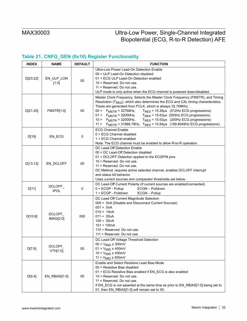
Table 21. CNFG_GEN (0x10) Register Functionality
MAX30003 Ultra-Low Power, Single-Channel Integrated Biopotential (ECG, R-to-R Detection) AFE
www.maximintegrated.com Maxim Integrated 33
INDEX NAME DEFAULT FUNCTION
D[23:22] EN_ULP_LON [1:0] 00
Ultra-Low Power Lead-On Detection Enable00 = ULP Lead-On Detection disabled 01 = ECG ULP Lead-On Detection enabled 10 = Reserved. Do not use.11 = Reserved. Do not use.ULP mode is only active when the ECG channel is powered down/disabled.
D[21:20] FMSTR[1:0] 00
Master Clock Frequency. Selects the Master Clock Frequency (FMSTR), and Timing Resolution (TRES), which also determines the ECG and CAL timing characteristics. These are generated from FCLK, which is always 32.768Khz.00 = FMSTR = 32768Hz, TRES = 15.26µs (512Hz ECG progressions)01 = FMSTR = 32000Hz, TRES = 15.63µs (500Hz ECG progressions)10 = FMSTR = 32000Hz, TRES = 15.63µs (200Hz ECG progressions)11 = FMSTR = 31968.78Hz, TRES = 15.64µs (199.8049Hz ECG progressions)
D[19] EN_ECG 0
ECG Channel Enable0 = ECG Channel disabled 1 = ECG Channel enabledNote: The ECG channel must be enabled to allow R-to-R operation.
D[13:12] EN_DCLOFF 00
DC Lead-Off Detection Enable00 = DC Lead-Off Detection disabled 01 = DCLOFF Detection applied to the ECGP/N pins10 = Reserved. Do not use.11 = Reserved. Do not use.DC Method, requires active selected channel, enables DCLOFF interrupt and status bit behavior.Uses current sources and comparator thresholds set below.
D[11] DCLOFF_ IPOL 0
DC Lead-Off Current Polarity (if current sources are enabled/connected)0 = ECGP - Pullup ECGN – Pulldown1 = ECGP - Pulldown ECGN – Pullup
D[10:8] DCLOFF_ IMAG[2:0] 000
DC Lead-Off Current Magnitude Selection000 = 0nA (Disable and Disconnect Current Sources)001 = 5nA010 = 10nA011 = 20nA100 = 50nA101 = 100nA110 = Reserved. Do not use.111 = Reserved. Do not use.
D[7:6] DCLOFF_ VTH[1:0] 00
DC Lead-Off Voltage Threshold Selection 00 = VMID ± 300mV01 = VMID ± 400mV10 = VMID ± 450mV11 = VMID ± 500mV
D[5:4] EN_RBIAS[1:0] 00
Enable and Select Resistive Lead Bias Mode 00 = Resistive Bias disabled 01 = ECG Resistive Bias enabled if EN_ECG is also enabled10 = Reserved. Do not use.11 = Reserved. Do not use.If EN_ECG is not asserted at the same time as prior to EN_RBIAS[1:0] being set to 01, then EN_RBIAS[1:0] will remain set to 00.

Table 22 shows the ECG data rates that can be realized with various setting of FMSTR, along with RATE configuration bits available in the CNFG_ECG register. Note FMSTR also determines the timing resolution of the CAL waveform generator.
Table 21. CNFG_GEN (0x10) Register Functionality (continued)
Table 22. Master Frequency Summary Table
MAX30003 Ultra-Low Power, Single-Channel Integrated Biopotential (ECG, R-to-R Detection) AFE
www.maximintegrated.com Maxim Integrated 34
INDEX NAME DEFAULT FUNCTION
D[3:2] RBIASV[1:0] 01
Resistive Bias Mode Value Selection 00 = RBIAS = 50MΩ01 = RBIAS = 100MΩ10 = RBIAS = 200MΩ11 = Reserved. Do not use.
D[1] RBIASP 0Enables Resistive Bias on Positive Input0 = ECGP is not resistively connected to VMID1 = ECGP is connected to VMID through a resistor (selected by RBIASV).
D[0] RBIASN 0Enables Resistive Bias on Negative Input0 = ECGN is not resistively connected to VMID1 = ECGN is connected to VMID through a resistor (selected by RBIASV).
FMSTR[1:0]
MASTER FREQUENCY(fMSTR) (Hz)
ECG DATA RATES & RELATED TIMING (RATE SELECTIONS)CALIBRATION
TIMING RESOLUTION (CAL_RES) (µs)
ECG RTOR
DATA RATE (sps)
TIMING RESOLUTION (RTOR_RES) (ms)
00 3276800 = 51201 = 25610 = 128
7.8125 30.52
01 3200000 = 50001 = 25010 = 125
8.000 31.25
10 32000 10 = 200 8.000 31.25
11 31968.78 10 =199.8049 8.008 31.28
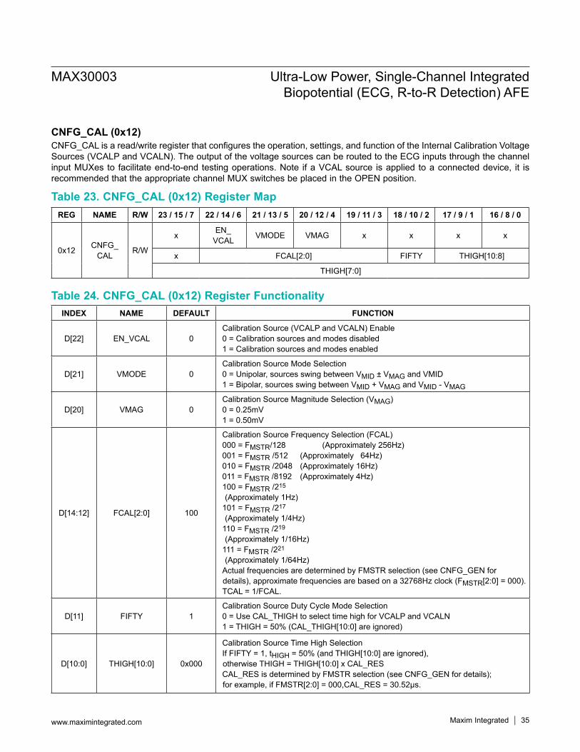
CNFG_CAL (0x12)CNFG_CAL is a read/write register that configures the operation, settings, and function of the Internal Calibration Voltage Sources (VCALP and VCALN). The output of the voltage sources can be routed to the ECG inputs through the channel input MUXes to facilitate end-to-end testing operations. Note if a VCAL source is applied to a connected device, it is recommended that the appropriate channel MUX switches be placed in the OPEN position.
Table 23. CNFG_CAL (0x12) Register Map
Table 24. CNFG_CAL (0x12) Register Functionality
MAX30003 Ultra-Low Power, Single-Channel Integrated Biopotential (ECG, R-to-R Detection) AFE
www.maximintegrated.com Maxim Integrated 35
INDEX NAME DEFAULT FUNCTION
D[22] EN_VCAL 0Calibration Source (VCALP and VCALN) Enable 0 = Calibration sources and modes disabled1 = Calibration sources and modes enabled
D[21] VMODE 0Calibration Source Mode Selection 0 = Unipolar, sources swing between VMID ± VMAG and VMID1 = Bipolar, sources swing between VMID + VMAG and VMID - VMAG
D[20] VMAG 0Calibration Source Magnitude Selection (VMAG)0 = 0.25mV1 = 0.50mV
D[14:12] FCAL[2:0] 100
Calibration Source Frequency Selection (FCAL)000 = FMSTR/128 (Approximately 256Hz)001 = FMSTR /512 (Approximately 64Hz)010 = FMSTR /2048 (Approximately 16Hz)011 = FMSTR /8192 (Approximately 4Hz)100 = FMSTR /215 (Approximately 1Hz)101 = FMSTR /217 (Approximately 1/4Hz)110 = FMSTR /219 (Approximately 1/16Hz)111 = FMSTR /221 (Approximately 1/64Hz)Actual frequencies are determined by FMSTR selection (see CNFG_GEN for details), approximate frequencies are based on a 32768Hz clock (FMSTR[2:0] = 000). TCAL = 1/FCAL.
D[11] FIFTY 1Calibration Source Duty Cycle Mode Selection0 = Use CAL_THIGH to select time high for VCALP and VCALN1 = THIGH = 50% (CAL_THIGH[10:0] are ignored)
D[10:0] THIGH[10:0] 0x000
Calibration Source Time High SelectionIf FIFTY = 1, tHIGH = 50% (and THIGH[10:0] are ignored), otherwise THIGH = THIGH[10:0] x CAL_RESCAL_RES is determined by FMSTR selection (see CNFG_GEN for details); for example, if FMSTR[2:0] = 000,CAL_RES = 30.52µs.
REG NAME R/W 23 / 15 / 7 22 / 14 / 6 21 / 13 / 5 20 / 12 / 4 19 / 11 / 3 18 / 10 / 2 17 / 9 / 1 16 / 8 / 0
0x12 CNFG_ CAL R/W
x EN_ VCAL VMODE VMAG x x x x
x FCAL[2:0] FIFTY THIGH[10:8]
THIGH[7:0]
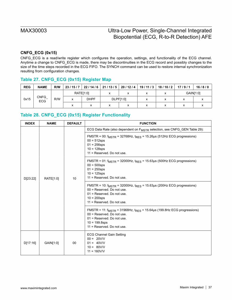
CNFG_EMUX (0x14)CNFG_EMUX is a read/write register which configures the operation, settings, and functionality of the Input Multiplexer associated with the ECG channel.
Figure 10. Calibration Voltage Source Options
Table 25. CNFG_EMUX (0x14) Register Map
Table 26. CNFG_EMUX (0x14) Register Functionality
MAX30003 Ultra-Low Power, Single-Channel Integrated Biopotential (ECG, R-to-R Detection) AFE
www.maximintegrated.com Maxim Integrated 36
CALIBRATION VOLTAGE SOURCE OPTIONS
VMID + 0.50mV
CAL_VMODE = 0CAL_VMAG = 0
CAL_VMODE = 1CAL_VMAG = 0VMID
VMID + 0.25mV
VMID - 0.25mVVMID
VMID + 0.25mV
VMID - 0.25mV
CAL_VMODE = 0CAL_VMAG = 1
CAL_VMODE = 1CAL_VMAG = 1VMID
VMID + 0.50mV
VMID - 0.50mV
VMID
VMID - 0.50mVtHIGH
tCAL
VCALP
VCALN
REG NAME R/W 23 / 15 / 7 22 / 14 / 6 21 / 13 / 5 20 / 12 / 4 19 / 11 / 3 18 / 10 / 2 17 / 9 / 1 16 / 8 / 0
0x14 CNFG_ EMUX R/W
POL x OPENP OPENN CALP_SEL[1:0] CALN_SEL[1:0]
x x x x x x x x
x x x x x x x x
INDEX NAME DEFAULT FUNCTION
D[23] POL 0ECG Input Polarity Selection0 = Non-inverted1 = Inverted
D[21] OPENP 1Open the ECGP Input Switch (most often used for testing and calibration studies)0 = ECGP is internally connected to the ECG AFE Channel1 = ECGP is internally isolated from the ECG AFE Channel
D[20] OPENN 1Open the ECGN Input Switch (most often used for testing and calibration studies)0 = ECGN is internally connected to the ECG AFE Channel1 = ECGN is internally isolated from the ECG AFE Channel
D[19:18] CALP_SEL[1:0] 00
ECGP Calibration Selection00 = No calibration signal applied01 = Input is connected to VMID10 = Input is connected to VCALP (only available if CAL_EN_VCAL = 1)11 = Input is connected to VCALN (only available if CAL_EN_VCAL = 1)
D[17:16] CALN_SEL[1:0] 00
ECGN Calibration Selection00 = No calibration signal applied01 = Input is connected to VMID10 = Input is connected to VCALP (only available if CAL_EN_VCAL = 1)11 = Input is connected to VCALN (only available if CAL_EN_VCAL = 1)
CNFG_ECG (0x15)CNFG_ECG is a read/write register which configures the operation, settings, and functionality of the ECG channel. Anytime a change to CNFG_ECG is made, there may be discontinuities in the ECG record and possibly changes to the size of the time steps recorded in the ECG FIFO. The SYNCH command can be used to restore internal synchronization resulting from configuration changes.
Table 27. CNFG_ECG (0x15) Register Map
Table 28. CNFG_ECG (0x15) Register Functionality
MAX30003 Ultra-Low Power, Single-Channel Integrated Biopotential (ECG, R-to-R Detection) AFE
www.maximintegrated.com Maxim Integrated 37
INDEX NAME DEFAULT FUNCTION
D[23:22] RATE[1:0] 10
ECG Data Rate (also dependent on FMSTR selection, see CNFG_GEN Table 29):
FMSTR = 00: fMSTR = 32768Hz, tRES = 15.26µs (512Hz ECG progressions)00 = 512sps01 = 256sps10 = 128sps11 = Reserved. Do not use.
FMSTR = 01: fMSTR = 32000Hz, tRES = 15.63µs (500Hz ECG progressions)00 = 500sps01 = 250sps10 = 125sps11 = Reserved. Do not use.
FMSTR = 10: fMSTR = 32000Hz, tRES = 15.63µs (200Hz ECG progressions)00 = Reserved. Do not use.01 = Reserved. Do not use.10 = 200sps11 = Reserved. Do not use.
FMSTR = 11: fMSTR = 31968Hz, tRES = 15.64µs (199.8Hz ECG progressions)00 = Reserved. Do not use.01 = Reserved. Do not use.10 = 199.8sps11 = Reserved. Do not use.
D[17:16] GAIN[1:0] 00
ECG Channel Gain Setting 00 = 20V/V01 = 40V/V10 = 80V/V11 = 160V/V
REG NAME R/W 23 / 15 / 7 22 / 14 / 6 21 / 13 / 5 20 / 12 / 4 19 / 11 / 3 18 / 10 / 2 17 / 9 / 1 16 / 8 / 0
0x15 CNFG_ECG R/W
RATE[1:0] x x x x GAIN[1:0]
x DHPF DLPF[1:0] x x x x
x x x x x x x x
Table 28. CNFG_ECG (0x15) Register Functionality (continued)
Table 29. Supported ECG_RATE and ECG_DLPF Options
Note: Combinations shown in grey are unsupported and will be internally mapped to the default settings shown.
MAX30003 Ultra-Low Power, Single-Channel Integrated Biopotential (ECG, R-to-R Detection) AFE
www.maximintegrated.com Maxim Integrated 38
INDEX NAME DEFAULT FUNCTION
D[14] DHPF 1ECG Channel Digital High-Pass Filter Cutoff Frequency0 = Bypass (DC)1 = 0.50Hz
D[13:12] DLPF[1:0] 01
ECG Channel Digital Low-Pass Filter Cutoff Frequency00 = Bypass (Decimation only, no FIR filter applied)01 = approximately 40Hz (Except for 125 and 128sps settings) Note: See Table 33.10 = approximately 100Hz (Available for 512, 256, 500, and 250sps ECG Rate selections only)11 = approximately 150Hz (Available for 512 and 500sps ECG Rate selections only)Note: See Table 29. If an unsupported DLPF setting is specified, the 40Hz setting (DLPF[1:0] = 01) will be used internally; the CNFG_ECG register will continue to hold the value as written, but return the effective internal value when read back.
CNFG_GENFMSTR[1:0]
RATE[1:0] SAMPLE RATE
(sps)
DLPF[1:0]/DIGITAL LPF CUTOFF
00 01 (Hz) 10 (Hz) 11 (Hz)
00 = 32768Hz
00 = 512 Bypass 40.96 102.4 153.6
01 = 256 Bypass 40.96 102.4 40.96
10 = 128 Bypass 28.35 28.35 28.35
01 = 32000Hz
00 = 500 Bypass 40.00 100.0 150.0
01 = 250 Bypass 40.00 100.0 40.00
10 = 125 Bypass 27.68 27.68 27.68
10 = 32000Hz 10 = 200 Bypass 40.00 40.00 40.00
11 = 31968Hz 10 = 199.8 Bypass 39.96 39.96 39.96
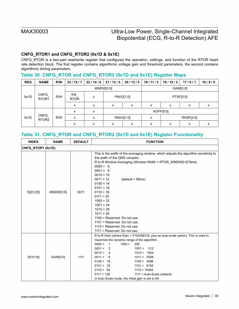
CNFG_RTOR1 and CNFG_RTOR2 (0x1D & 0x1E)CNFG_RTOR is a two-part read/write register that configures the operation, settings, and function of the RTOR heart rate detection block. The first register contains algorithmic voltage gain and threshold parameters, the second contains algorithmic timing parameters.
Table 30. CNFG_RTOR and CNFG_RTOR2 (0x1D and 0x1E) Register Maps
Table 31. CNFG_RTOR and CNFG_RTOR2 (0x1D and 0x1E) Register Functionality
MAX30003 Ultra-Low Power, Single-Channel Integrated Biopotential (ECG, R-to-R Detection) AFE
www.maximintegrated.com Maxim Integrated 39
INDEX NAME DEFAULT FUNCTION
CNFG_RTOR1 (0x1D)
D[23:20] WNDW[3:0] 0011
This is the width of the averaging window, which adjusts the algorithm sensitivity to the width of the QRS complex. R to R Window Averaging (Window Width = RTOR_WNDW[3:0]*8ms)0000 = 60001 = 80010 = 100011 = 12 (default = 96ms)0100 = 140101 = 160110 = 180111 = 201000 = 221001 = 241010 = 261011 = 281100 = Reserved. Do not use.1101 = Reserved. Do not use.1110 = Reserved. Do not use.1111 = Reserved. Do not use.
D[19:16] GAIN[3:0] 1111
R to R Gain (where Gain = 2^GAIN[3:0], plus an auto-scale option). This is used to maximize the dynamic range of the algorithm.0000 = 1 1000 = 2560001 = 2 1001 = 5120010 = 4 1010 = 10240011 = 8 1011 = 20480100 = 16 1100 = 40960101 = 32 1101 = 81920110 = 64 1110 = 163840111 = 128 1111 = Auto-Scale (default)In Auto-Scale mode, the initial gain is set to 64.
REG NAME R/W 23 / 15 / 7 22 / 14 / 6 21 / 13 / 5 20 / 12 / 4 19 / 11 / 3 18 / 10 / 2 17 / 9 / 1 16 / 8 / 0
0x1D CNFG_RTOR1 R/W
WNDW[3:0] GAIN[3:0]
EN_ RTOR x PAVG[1:0] PTSF[3:0]
x x x x x x x x
0x1E CNFG_RTOR2 R/W
x x HOFF[5:0]
x x RAVG[1:0] x RHSF[2:0]
x x x x x x x x
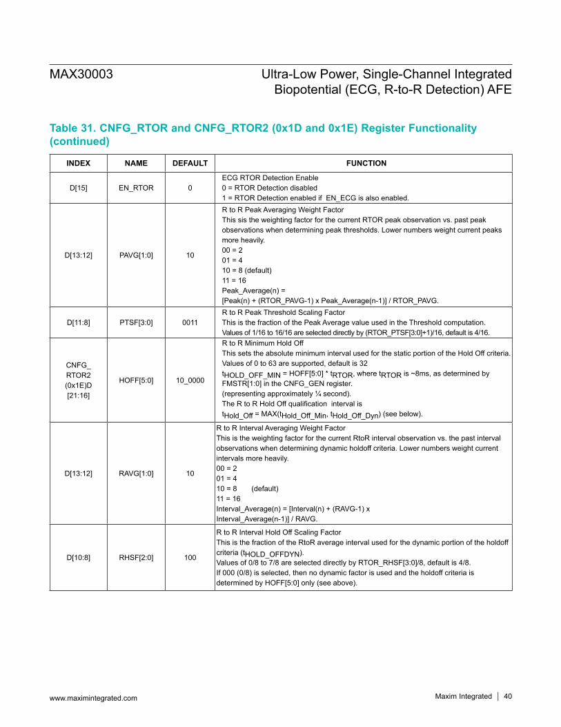
Table 31. CNFG_RTOR and CNFG_RTOR2 (0x1D and 0x1E) Register Functionality (continued)
MAX30003 Ultra-Low Power, Single-Channel Integrated Biopotential (ECG, R-to-R Detection) AFE
www.maximintegrated.com Maxim Integrated 40
INDEX NAME DEFAULT FUNCTION
D[15] EN_RTOR 0ECG RTOR Detection Enable 0 = RTOR Detection disabled 1 = RTOR Detection enabled if EN_ECG is also enabled.
D[13:12] PAVG[1:0] 10
R to R Peak Averaging Weight FactorThis sis the weighting factor for the current RTOR peak observation vs. past peak observations when determining peak thresholds. Lower numbers weight current peaks more heavily.00 = 201 = 4 10 = 8 (default)11 = 16Peak_Average(n) = [Peak(n) + (RTOR_PAVG-1) x Peak_Average(n-1)] / RTOR_PAVG.
D[11:8] PTSF[3:0] 0011R to R Peak Threshold Scaling FactorThis is the fraction of the Peak Average value used in the Threshold computation.Values of 1/16 to 16/16 are selected directly by (RTOR_PTSF[3:0]+1)/16, default is 4/16.
CNFG_ RTOR2 (0x1E)D [21:16]
HOFF[5:0] 10_0000
R to R Minimum Hold OffThis sets the absolute minimum interval used for the static portion of the Hold Off criteria.Values of 0 to 63 are supported, default is 32tHOLD_OFF_MIN = HOFF[5:0] * tRTOR, where tRTOR is ~8ms, as determined by FMSTR[1:0] in the CNFG_GEN register. (representing approximately ¼ second).The R to R Hold Off qualification interval is tHold_Off = MAX(tHold_Off_Min, tHold_Off_Dyn) (see below).
D[13:12] RAVG[1:0] 10
R to R Interval Averaging Weight Factor This is the weighting factor for the current RtoR interval observation vs. the past interval observations when determining dynamic holdoff criteria. Lower numbers weight current intervals more heavily.00 = 201 = 4 10 = 8 (default)11 = 16Interval_Average(n) = [Interval(n) + (RAVG-1) x Interval_Average(n-1)] / RAVG.
D[10:8] RHSF[2:0] 100
R to R Interval Hold Off Scaling Factor This is the fraction of the RtoR average interval used for the dynamic portion of the holdoff criteria (tHOLD_OFFDYN).Values of 0/8 to 7/8 are selected directly by RTOR_RHSF[3:0]/8, default is 4/8.If 000 (0/8) is selected, then no dynamic factor is used and the holdoff criteria is determined by HOFF[5:0] only (see above).

FIFO Memory DescriptionThe device provides FIFO memory for ECG information. Single memory registers are also supported for heart rate detection output data (RTOR). The operation of these FIFO memories and registers is detailed in the following sections.Table 32 summarizes the method of access and data structure within the FIFO memory.
ECG FIFO Memory (32 Words x 24 Bits)The ECG FIFO memory is a standard circular FIFO consisting of 32 words, each with 24 bits of information.The ECG FIFO is independently managed by internal read and write pointers. The read pointer is updated in response to the 32nd SCLK rising edge in a normal mode read back transaction and on the (32+n x 24)th SCLK rising edge(s) in a burst mode transaction. Once a FIFO sample is marked as read, it cannot be accessed again.
The write pointer is governed internally. To aide data management and reduce µC overhead, the device provides a user-programmable ECG FIFO Interrupt Threshold (EFIT) governing the ECG Interrupt term (EINT). This threshold can be programmed with values from 1 to 32, representing the number of unread ECG FIFO entries required before the EINT term will be asserted, alerting the µC that there is a significant amount of data in the ECG FIFO ready for read back (see MNGR_INT (0x04) for details).If the write pointer ever traverses the entire FIFO array and catches up to the read pointer (due to failure of the µC to read/maintain FIFO data), a FIFO overflow will occur and data will be corrupted. The EOVF STATUS and tag bits will indicate this condition and the FIFO should be cleared before continuing measurements using either a SYNCH or FIFO_RST command—note overflow events will result in the loss of samples and thus timing information, so these conditions should not occur in well-designed applications.
Table 32. FIFO Memory Access and Data Structure Summary
MAX30003 Ultra-Low Power, Single-Channel Integrated Biopotential (ECG, R-to-R Detection) AFE
www.maximintegrated.com Maxim Integrated 41
CMD FIFO & MODE DATA STRUCTURE (DO[23:0])
23 22 21 20 19 18 17 16 15 14 13 12 11 10 9 8 7 6 5 4 3 2 1 0
0x20 ECG Burst ECG Sample Voltage Data [17:0] ETAG [2:0]
PTAG [2:0]
0x21 ECG ECG Sample Voltage Data [17:0] ETAG [2:0]
PTAG [2:0]
23 22 21 20 19 18 17 16 15 14 13 12 11 10 9 8 7 6 5 4 3 2 1 0
0x25 RTOR RTOR Interval Timing Data [13:0] 0 0 0 0 0 0 0 0 0 0

ECG FIFO Data StructureThe data portion of the word contains the 18 Bit ECG voltage information measured at the requested sample rate in
left justified two’s complement format. The remaining six bits of data hold important data tagging information (see details in Table 33).
Table 33. ECG FIFO Data Tags (ETAG[2:0] = DO[5:3])
MAX30003 Ultra-Low Power, Single-Channel Integrated Biopotential (ECG, R-to-R Detection) AFE
www.maximintegrated.com Maxim Integrated 42
ETAG[2:0] MEANING DETAILED DESCRIPTION RECOMMENDED USER ACTION DATA
VALIDTIME
VALID
000 Valid Sample This is a valid FIFO sample.Log sample into ECG record and increment the time step.Continue to gather data from the ECG FIFO.
Yes Yes
001 Fast Mode Sample
This sample was taken while the ECG channel was in a FAST recovery mode. The voltage information is not valid, but the sample represents a valid time step.
Discard, note, or post-process this voltage sample, but increment the time base.Continue to gather data from the ECG FIFO.
No Yes
010Last Valid Sample(EOF)
This is a valid FIFO sample, but this is the last sample currently available in the FIFO (End of File indicator).
Log sample into ECG record and increment the time step.Suspend read back operations on the ECG FIFO until more samples are available.
Yes Yes
011Last Fast Mode Sample(EOF)
See above (ETAG=001), but in addition, this is the last sample currently available in the FIFO (End of File indicator).
Discard, note, or post-process this voltage sample, but increment the time base.Suspend read back operations on the ECG FIFO until more samples are available.
No Yes
10x Unused -- --
110 FIFO Empty(Exception)
This is an invalid sample provided in response to an SPI request to read an empty FIFO.
Discard this sample, without incrementing the time base.Suspend read back operations on this FIFO until more samples are available.
No No
111 FIFO Overflow(Exception)
The FIFO has been allowed to overflow – the data is corrupted.
Issue a FIFO_RST command to clear the FIFOs or re-SYNCH if necessary.Note the corresponding halt and resumption in ECG/BIOZ time/voltage records.
No No
ECG Data Tags (ETAG)Three bits in the sample record are used as a ECG data tag (ETAG[2:0] = DO[5:3]). This section outlines the meaning of the various data tags used in the ECG FIFO and recommended handling within the continuous ECG record.VALID: ETAG = 000 indicates the ECG data for this sample represents both a valid voltage and time step in the ECG record.FAST: ETAG = 001 indicates the ECG data for this sample was taken in the FAST settling mode and that the voltage information in the sample should be treated as transient and invalid. Note that while the voltage data is invalid, samples of this type do represent valid time steps in the ECG record.VALID EOF: ETAG = 010 indicates the ECG data for this sample represents both a valid voltage and time step in the ECG record, and that this is the last sample currently available in the ECG FIFO (End-of-File, EOF). The µC should wait until further samples are available before requesting more data from the ECG FIFO.FAST EOF: ETAG = 011 indicates the ECG data for this sample was taken in the FAST settling mode and that the voltage information in the sample should be treated as transient and invalid. Note that while the voltage data is invalid, samples of this type do represent valid time steps in the ECG record. In addition, this is the last sample currently available in the ECG FIFO (End-of-File, EOF). The µC should wait until further samples are available before requesting more data from the ECG FIFO.EMPTY: ETAG = 110 is appended to any requested read back data from an empty ECG FIFO. The presence of this tag alerts the user that this FIFO data does not represent a valid sample or time step. Note that if handled properly by the µC, an occurrence of an empty tag will not compromise the integrity of a continuous ECG record – this tag only indicates that the read back request was either premature or unnecessary.OVERFLOW: ETAG = 111 indicates that the ECG FIFO has overflowed and that there are interruptions or missing data in the sample records. The ECG Overflow (EOVF) bit is also included in the STATUS register. A FIFO_RESET is required to resolve this situation, effectively clearing the FIFO so that valid sampling going forward is assured. Depending on the application, it may also be necessary to resynchronize the MAX30003 internal channel operations to move forward with valid recordings, the SYNCH command can perform this function while also resetting the FIFO memories
RTOR Interval Memory Register (1 Word x 24 Bits)The RTOR Interval (RTOR) memory register is a single read-only register consisting of 14 bits of timing interval information, left justified (and 8 unused bits, set to zero).The RTOR register stores the time interval between the last two R events, as identified by the RTOR detection circuitry, which operates on the ECG output data. Each LSB in the RTOR register is approximately equal to 8ms (CNFG_GEN for exact figures). The resulting 14 bit storage interval can thus be approximately 130 seconds in length, again depending on device settings.Each time the RTOR detector identifies a new R event, the RTOR register is updated, and the RRINT interrupt term is asserted (see STATUS register for details).Users wishing to log heart rate based on RTOR register data should set CLR_RRINT equals 01 in the MNGR_INT register. This will clear the RRINT interrupt term after the RTOR register has been read back, preparing the device for identification of the next RTOR interval.Users wishing to log heart rate based on the time elapsed between RRINT assertions using the µC to keep track of the time base (and ignoring the RTOR register data) have two choices for interrupt management. If CLR_RRINT equals 00 in the MNGR_INT register, the RRINT interrupt term will clear after each STATUS register read back, preparing the device for identification of the next RTOR interval. If CLR_RRINT equals 10 in the MNGR_INT register, the RRINT interrupt term will self-clear after each one full ECG data cycle has passed, preparing the device for identification of the next RTOR interval (this mode is recommended only if using the INT2B as a dedicated heart rate indicator).If the RTOR detector reaches an overflow state after several minutes without detection of an R event, the counter will simply roll over, and the lack of the RRINT activity on the dedicated INT2B line will inform the µC that no RTOR activity was detected.
MAX30003 Ultra-Low Power, Single-Channel Integrated Biopotential (ECG, R-to-R Detection) AFE
www.maximintegrated.com Maxim Integrated 43

Figure 11. Two-terminal, with Differential and Common-Mode Filtering Typical Operating Circuit
MAX30003 Ultra-Low Power, Single-Channel Integrated Biopotential (ECG, R-to-R Detection) AFE
www.maximintegrated.com Maxim Integrated 44
1kΩ
ENERGYRATED
ECGP
1kΩECGN
CAPP
CAPN
1µF
CSB CSB
SDI MOSI
SCLK SCLK
SDO MISO
INTb INTB
INT2b INT2B
FCLK FCLK
AVDD DVDD 0VDD
10µF 0.1µF 10µF 0.1µF1nF
CPLL
MCU
VCM
VBG
VREF
10µF1.0µF10µF
MAX30003
Typical Application Circuit

Application DiagramsTwo Electrode Heart Rate FitnessSee Figure 12 for an example of a fitness monitoring configuration.
Figure 12. Two Electrode Heart Rate Monitoring for Fitness
+Denotes a lead(Pb)-free/RoHS-compliant package. T = Tape and reel. **EP = Exposed pad.
MAX30003 Ultra-Low Power, Single-Channel Integrated Biopotential (ECG, R-to-R Detection) AFE
www.maximintegrated.com Maxim Integrated 45
RB
OD
Y
100Ω
-300
Ω
ELECTRODE MODEL
PHYSICALELECTRODE
REPRESENTATIONELECTRODEPOLARIZATIONVOLTAGE
±150mV
10kΩ-20MΩ
1nF-50nF
50-200Ω
ZEL
PCB
EXTERNAL EMIFILTERS
ECGP
ECGN
MAX30003
Ordering Information
Chip InformationPROCESS: CMOS
Package InformationFor the latest package outline information and land patterns (footprints), go to www.maximintegrated.com/packages. Note that a “+”, “#”, or “-” in the package code indicates RoHS status only. Package drawings may show a different suffix character, but the drawing pertains to the package regardless of RoHS status.
PART TEMP RANGE PIN-PACKAGEMAX30003CTI+ 0°C to +70°C 28 TQFN-EP**MAX30003CTI+T 0°C to +70°C 28 TQFN-EP**MAX30003CWV+T 0°C to +70°C 30 WLP
PACKAGE TYPE
PACKAGE CODE
OUTLINE NO.
LAND PATTERN NO.
28-TQFN T2855+8 21-0140 90-0028
30-WLP W302L2+1 21-100074Refer to
Application Note 1891
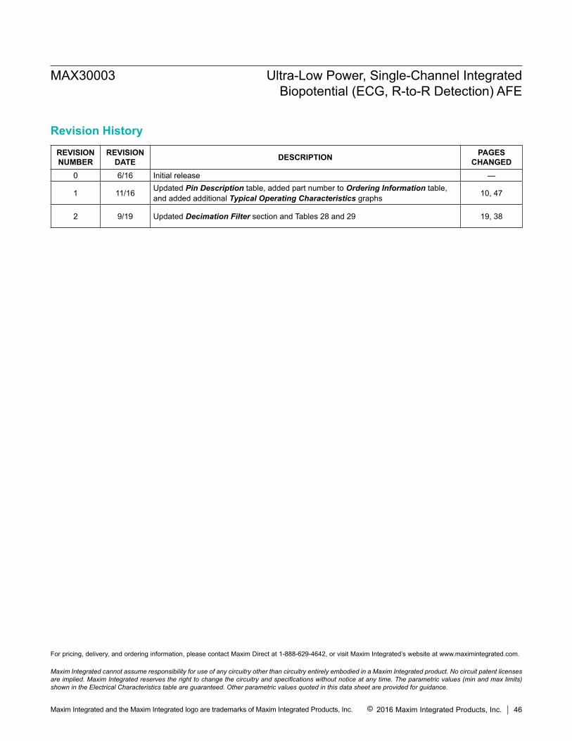
Maxim Integrated cannot assume responsibility for use of any circuitry other than circuitry entirely embodied in a Maxim Integrated product. No circuit patent licenses are implied. Maxim Integrated reserves the right to change the circuitry and specifications without notice at any time. The parametric values (min and max limits) shown in the Electrical Characteristics table are guaranteed. Other parametric values quoted in this data sheet are provided for guidance.
Maxim Integrated and the Maxim Integrated logo are trademarks of Maxim Integrated Products, Inc.
MAX30003 Ultra-Low Power, Single-Channel Integrated Biopotential (ECG, R-to-R Detection) AFE
© 2016 Maxim Integrated Products, Inc. 46
Revision HistoryREVISIONNUMBER
REVISIONDATE DESCRIPTION PAGES
CHANGED0 6/16 Initial release —
1 11/16 Updated Pin Description table, added part number to Ordering Information table, and added additional Typical Operating Characteristics graphs 10, 47
2 9/19 Updated Decimation Filter section and Tables 28 and 29 19, 38
For pricing, delivery, and ordering information, please contact Maxim Direct at 1-888-629-4642, or visit Maxim Integrated’s website at www.maximintegrated.com.