Embed Size (px)
Citation preview

General DescriptionThe MAX20047 is an automotive-grade, low-cost, small-footprint dual-port charger IC designed for automotive charging applications. It combines a fully synchronous 6A step-down buck converter with integrated high-side and low-side FETs capable of operating with input voltages from 3.5V to 36V and delivering 5.2V output voltage. The IC features integrated iPod®/iPhone® 1.0A and iPad® 2.1A dedicated charging modes.The IC delivers up to 3A of charging current with 93% efficiency per port through integrated switches with programmable current limit and thermal foldback control. The buck converter switching frequency is programmable from 0.4MHz to 2.2MHz. Short-to-ground protection and overcurrent protection are also provided on the protected HVBUS outputs to protect the internal BUS power rail from an overcurrent fault. The MAX20047 offers short-to-battery up to +18V and can also be ordered with spread-spectrum operation to reduce EMI.
Applications USB Dedicated Charging Ports (DCP) Automotive Cigarette Lighter Adapters Power Supply for Linear Chargers
Benefits and Features Operating VIN Range of 3.5V to 36V 40V Load-Dump Protection Synchronous DC-DC Converter with Integrated FETs 93% Charge Efficiency at 3A Charging 0.4MHz to 2.2MHz Programmable Switching
Frequency by External Pin Settings Spread-Spectrum Operation Fixed 8ms Internal Soft-Start 5.20V Output 99% Duty-Cycle Operation with Low Dropout ±2% Output-Voltage Accuracy Input System Overvoltage and Short-Circuit
Protection Accurate SRC_DMOS Current Limiting with Minimal
Voltage Drop• Low RON 15mΩ Dual USB Power Switches• Adjustable SRC_DMOS Current Limit by External
Pin Settings• Integrated Current Sensing
Thermal Regulation and Thermal Shutdown Dual Autonomous Battery-Charging Ports with
Portable Device Detection• Integrated Apple® 2.4A, 2.1A, 1.0A Detection• Integrated Samsung® Detection• Integrated DCP Detection
Robust for the Automotive Environment• Short-to-Battery and Short-to-Ground Protection on
Protected SRC_DMOS Output• Short-to-Battery and Short-to-PV Protection on
Protected HVDP1, HVDM1, HVDP2, and HVDM2 Inputs
• Tested to ISO 10605 and IEC 61000-4-2 ESD Standards
• 20-Pin (5.0mm x 3.5mm) FC2-QFN Package• -40°C to +125°C Operating Temperature Range• AEC-Q100 Qualified
Ordering Information appears at end of data sheet.
iPod, iPhone, iPad, and Apple are registered trademarks of Apple Inc.
19-100165; Rev 0; 9/17
Samsung is a registered trademark of Samsung Electronics Co., Ltd.
MAX20047 Dual 3A USB DCP Charger

SUPSW, HVEN to PGND ......................................-0.3V to +40VLX to PGND..........................................-0.3V to VSUPSW + 0.3VBIAS to Ground ....................................................-0.3V to +6.0VCOMP to Ground ...................................... -0.3V to VBIAS + 0.3VG_DMOS to Ground ...........................................-0.3V to +16.0VAGND to PGND ....................................................-0.3V to +0.3VPV to PGND ..........................................................-03V to +6.0VOUT to PGND .........................................................-0.3V to VPVBST to LX .............................................................-0.3V to +6.0VS_DMOS1, S_DMOS2 to Ground ...........................-0.3V to VPVILIM, CONFIG, FOSC to Ground ............. -0.3V to VBIAS + 0.3V
HVDP1, HVDP2, HVPM1, HVDM2 to Ground ......-0.3V to +18VLX Continuous Current ............................................................8AContinuous Power Dissipation (TA = +70°C) (Single-Layer Board
derate 13.2mW/°C over +70°C) .............................1052.6mWOperating Temperature Range ......................... -40°C to +125°CMaximum Junction Temperature .....................................+150°CStorage Temperature Range ..............................-60°C to+150°CLead Temperature (soldering, 10s) .................................+300°CSoldering Temperature (reflow) .......................................+260°C
FC2-QFN Junction-to-Ambient Thermal Resistance (θJA) ..........36°C/W Junction-to-Case Thermal Resistance (θJC) .....................2°C/W
(Note 1)
(TA = -40ºC to +125ºC. Typical values are at VSUPSW = +14V and TA = +25ºC, unless otherwise noted.) (Note 3)
PARAMETER SYMBOL CONDITIONS MIN TYP MAX UNITS
Supply Voltage Range VSUP 3.5 36 V
Load-Dump-Event Supply Voltage VSUP_LD tLD < 1s 40 V
Shutdown Supply Current ISHDNVSUPSW = 14V; HVEN = 0V, off state 6 15 µA
BIAS Regulator Voltage (Nominal) VBIAS
VSUPSW = 14V, IBIAS < 10mA, BIAS not switched over to VOUT
4.7 4.96 5.45 V
BIAS Undervoltage Lockout (Rising) VUV_BIAS_R VBIAS rising 2.7 3 3.3 V
BIAS Undervoltage Lockout (Falling) VUV_BIAS_F 2.5 V
BIAS Current Limit IBIAS 50 mA
PACKAGE TYPE PACKAGE CODE OUTLINE NO. LAND PATTERN NO.
20 FC2-QFN F203A5F+1 21-100124 90-100045
Note 1: Thermal resistance can be lowered with improved board design.Note 2: Package thermal resistances were obtained using the method described in JEDEC specification JESD51-7, using a four-layer
board. For detailed information on package thermal considerations, refer to www.maximintegrated.com/thermal-tutorial.
Absolute Maximum Ratings
Stresses beyond those listed under “Absolute Maximum Ratings” may cause permanent damage to the device. These are stress ratings only, and functional operation of the device at these or any other conditions beyond those indicated in the operational sections of the specifications is not implied. Exposure to absolute maximum rating conditions for extended periods may affect device reliability.
Package Thermal Characteristics
Electrical Characteristics
Package InformationFor the latest package outline information and land patterns (footprints), go to www.maximintegrated.com/packages. Note that a “+”, “#”, or “-” in the package code indicates RoHS status only. Package drawings may show a different suffix character, but the drawing pertains to the package regardless of RoHS status.
MAX20047 Dual 3A USB DCP Charger
www.maximintegrated.com Maxim Integrated 2

(TA = -40ºC to +125ºC. Typical values are at VSUPSW = +14V and TA = +25ºC, unless otherwise noted.) (Note 3)
PARAMETER SYMBOL CONDITIONS MIN TYP MAX UNITS
Thermal-Shutdown Temperature TSHDN TJ rising 165 °C
Thermal-Shutdown Hysteresis TSHDN_HYS 15 °C
Thermal-Foldback Temperature TFLDBK TJ rising 140 °C
Thermal-Foldback Hysteresis TFLDBK_HYS 15 °C
STEP-DOWN DC-DCPWM-Mode Output Voltage VOUT 5.05 5.2 V
Load Regulation VLOAD_REG 30mA < ILOAD < IMAX 0.5 %
Line Regulation VLINE_REG 6V < VSUPSW < 36V 0.02 %/V
BST Input CurrentIBST_ON
High-side MOSFET on, VBST - VLX = 5V 1.5 mA
IBST_OFFHigh-side MOSFET off, VBST - VLX = 5V 1.5 µA
LX Current Limit ILX 7.5 10 13 A
Spread-Spectrum Frequency fSS Ordering option ±3 %
High-Side Switch On-Resistance RDS(ON)_HS VBIAS = 5V, ILX = 0.5A 35 76 mΩ
High-Side Switch Leakage ILEAK_HS
High-side MOSFET off, VSUPSW = 36V, VLX = 36V, TA = +25°C
1 5 µA
Low-Side Switch On-Resistance RDS(ON)_LS VBIAS = 5V, ILX = 0.5A 18 35 mΩ
Low-Side Switch Leakage ILEAK_LS
Low-side MOSFET off, VSUPSW = 36V, VLX = 36V, TA = +25°C
1 5 µA
Minimum On-Time tON_MIN 65 100 ns
Maximum Duty Cycle DCMAX 95 98 99 %
Oscillator Frequency fOSCRFOSC = 73.2kΩ 363 400 437 kHz
RFOSC = 12.7kΩ 2.2 MHz
Soft-Start Time tSS 4 8 12 ms
HVEN PIN
HVEN High Threshold VHVEN_HI 2.4 V
HVEN Low Threshold VHVEN_LO 0.6 V
HVEN Hysteresis VHVEN_HYS 0.2 V
HVEN Leakage Current IHVEN TA = +25°C 1 10 µA
Electrical Characteristics (continued)
MAX20047 Dual 3A USB DCP Charger
www.maximintegrated.com Maxim Integrated 3

(TA = -40ºC to +125ºC. Typical values are at VSUPSW = +14V and TA = +25ºC, unless otherwise noted.) (Note 3)
PARAMETER SYMBOL CONDITIONS MIN TYP MAX UNITS
G_DMOS PIN (CHARGE PUMP)
Unloaded Output Voltage VOCHPReferenced to PV, internal discharge path 2MΩ to ground 7 9 11 V
Output Impedance ROCHP 50 75 kΩ
Output DC Current IOCHPVG_DMOS - PV > 8V (min), 10V (typ) 20 µA
HVDM_/HVDP_ DCP PINS
HVDP_/HVDM_ Short Pulldown RPD 300 500 750 kΩ
HVDP_/HVDM_ Off-Leakage IHVD_OFF HVDP_/HVDM_ = 18V, HVEN = 9V 50 µA
HVDP_/HVDM_ Overvoltage-Protection- Trip Threshold
VOV_DAT 3.85 3.99 V
HVDM_/HVDP_ Overvoltage-Protection-Response Time
tOV_DAT HVDP_/HVDM_ OV rising 1.0 2.5 µs
SRC_DMOS1/SRC_DMOS2 USB POWER SWITCHES
SRC_DMOS_ Protection Overvoltage VOV_USB SRC_DMOS_ rising 5.5 5.8 V
SRC_DMOS_ Protection-Response Time tOV_USB 200 ns
SRC_DMOS_ Relative Protection-Trip Threshold VOV_REL SRC_DMOS_ rising VPV +
0.300 V
SRC_DMOS_ Relative Protection-Response Time tOV_REL 500 ns
SRC_DMOS_ Undervoltage-Protection Trip Absolute VUV_USB
If ILIM < UV_USB, turn off; if ILIM > UV_USB, stay on 4.3 4.45 4.6 V
SRC_DMOS_ Undervoltage-Protection-Response Time tUV_USB
SRC_DMOS rising OV_REL, OV_USB (750ns typ rising) 300 ns
PV Undervoltage Protection VUV_PV
PV falling from 5V with slew rate of 0.5V/µs, switch turned off (with RL= 50Ω on; SRC_DMOS measured when SRC_DMOS goes low)
3.65 3.85 4 V
Electrical Characteristics (continued)
MAX20047 Dual 3A USB DCP Charger
www.maximintegrated.com Maxim Integrated 4

(TA = -40ºC to +125ºC. Typical values are at VSUPSW = +14V and TA = +25ºC, unless otherwise noted.) (Note 3)
PARAMETER SYMBOL CONDITIONS MIN TYP MAX UNITS
VBUS Undervoltage-Protection-Response Time tUV_PV
PV falling from 5V with slew rate of 0.5V/µs, switch turned off (with RL = 50Ω on, SRC_DMOS_ measured when SRC_DMOS_ goes low)
300 ns
USB FET On-Resistance RDS(ON)_FET 15 mΩ
Forward-Current Limit ILIM
RISET = 68.1kΩ 1.8 2.1
ARISET = 49.9kΩ 2.1 2.41
RISET = 24.9kΩ 2.5 2.75
RISET = 15.8kΩ 3 3.3
ILIM-Fault Discharge FET ILIM_DIS_FET 250 Ω
Continuous-Current-Limit Blanking-Timeout Period tILIM_BLANK 2 ms
SRC_DMOS_ Output Rise Time tDMOS_RISE
From 10% to 90% of VOUT, 2s after HVEN = high 0.4 ms
SRC_DMOS_ Output Fall Time tDMOS_FALL From 90% to 10% of VOUT 1.2 ms
SRC_DMOS_ OUT Autoreset Current IRETRY
In latched-off state, SRC_DMOS_ = 0V, diagnostic current
25 mA
SRC_DMOS_ OUT Autoreset Threshold VRETRY
In latched-off state, SRC_DMOS_ rising 0.5 V
SRC_DMOS_ Off-Leakage Current IDMOS_LEAK
VPV = 5.5V, VSRC_DMOS_ = 0V, TA = +25°C 1 µA
CONFIG/ILIM RESISTORS CONVERTER
Current Leakage ILEAK 0 to 5V -1 +1 µA
TIMERS
Low-Frequency Oscillator fLFOSC 110 kHz
High-Frequency Oscillator fHFOSC 8 MHz
DSCHG Timer tDSCHG 2 s
Hold Timer tHOLD
Referred to the LFOSC (CONFIG HOLD Time = 30 min) 30
minReferred to the LFOSC (CONFIG HOLD Time = 60 min) 60
Electrical Characteristics (continued)
MAX20047 Dual 3A USB DCP Charger
www.maximintegrated.com Maxim Integrated 5
(TA = -40ºC to +125ºC. Typical values are at VSUPSW = +14V and TA = +25ºC, unless otherwise noted.) (Note 3)
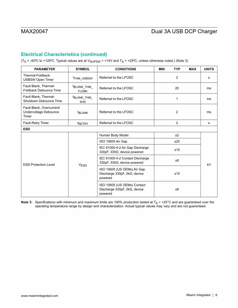
Note 3: Specifications with minimum and maximum limits are 100% production tested at TA = +25°C and are guaranteed over the operating temperature range by design and characterization. Actual typical values may vary and are not guaranteed.
PARAMETER SYMBOL CONDITIONS MIN TYP MAX UNITS
Thermal-Foldback USBSW Open Timer tTHM_USBSW Referred to the LFOSC 2 s
Fault Blank, Thermal-Foldback Debounce Time
tBLANK_THM_ FLDBK
Referred to the LFOSC 20 ms
Fault Blank, Thermal-Shutdown Debounce Time
tBLANK_THM_ SHD
Referred to the LFOSC 1 ms
Fault Blank, Overcurrent/Undervoltage Debounce Timer
tBLANK Referred to the LFOSC 2 ms
Fault-Retry Timer tRETRY Referred to the LFOSC 2 s
ESD
ESD Protection Level VESD
Human Body Model ±2
kV
ISO 10605 Air Gap ±25
IEC 61000-4-2 Air Gap Discharge 330pF, 330Ω, device powered ±15
IEC 61000-4-2 Contact Discharge 330pF, 330Ω, device powered ±8
ISO 10605 (US OEMs) Air Gap Discharge 330pF, 2kΩ, device powered
±15
ISO 10605 (US OEMs) Contact Discharge 330pF, 2kΩ, device powered
±8
Electrical Characteristics (continued)
MAX20047 Dual 3A USB DCP Charger
www.maximintegrated.com Maxim Integrated 6

(TA = +25°C)
Typical Operating Characteristics
50.00
55.00
60.00
65.00
70.00
75.00
80.00
85.00
90.00
95.00
100.00
0.00 1.00 2.00 3.00 4.00 5.00 6.00
EFFIC
IENC
Y (%
)
LOAD CURRENT (A)
VOUT EFFICIENCYtoc01
VSUPSW = 8V
VSUPSW = 14V
VSUPSW = 36V
5.158
5.168
5.179
5.189
5.200
0.00 1.00 2.00 3.00 4.00 5.00 6.00
V OUT
(V)
LOAD CURRENT (A)
VOUT LOAD REGULATION
VSUPSW = 14V
toc02
VSUPSW = 36V
VSUPSW = 8V
5.180
5.185
5.190
5.195
5.200
5.205
5.210
5.215
5.220
5 10 15 20 25 30 35 40
V OUT
(V)
VSUPSW (V)
VOUT LINE REGULATIONtoc03
0
10
20
30
40
50
60
5.150 5.170 5.190 5.210 5.230 5.250
NORM
ALIZE
D FR
EQUE
NCY
VHVBUS1/HVBUS2 (V)
-40C
+25C
+125C
NO LOAD OUTPUT VOLTAGEVSUPSW = 14V
toc04
0.000
0.500
1.000
1.500
2.000
2.500
0.0 50.0 100.0 150.0
FREQ
UENC
Y (M
Hz)
RFOSC (kΩ)
SWITCHING FREQUENCY vs. RFOSCtoc05
0
5
10
15
20
25
30
35
40
45
388 390 392 394 396 398 400 402 404 406 408 410
NORM
ALIZE
D FR
EQUE
NCY
SWITCHING FREQUENCY (kHz)
-40C
+25C
+125C
SWITCHING FREQUENCYvs.
TEMPERATUREtoc06
RFOSC = 73.2kΩ
fSW = 400kHz
0
5
10
15
20
25
30
35
40
45
50
2.200 2.250 2.300 2.350 2.400 2.450 2.500
NORM
ALIZE
D FR
EQUE
NCY
SWITCHING FREQUENCY (kHz)
-40C
+25C
+125C
SWITCHING FREQUENCY vs. TEMPERATURE
toc07
RFOSC = 12.1kΩ
fSW = 2.2MHz
MAX20047 Dual 3A USB DCP Charger
Maxim Integrated 7www.maximintegrated.com

(TA = +25°C)
Typical Operating Characteristics (continued)
19.40
19.60
19.80
20.00
20.20
20.40
20.60
20.80
21.00
-50 -25 0 25 50 75 100 125 150
SUPP
LY C
URRE
NT (m
A)
TEMPERATURE (°C)
OPERATING SUPPLY CURRENT vs.TEMPERATURE
toc08
fSW = 400kHzVSUPSW = 14V
0.00
5.00
10.00
15.00
20.00
25.00
3.0 8.0 13.0 18.0 23.0 28.0 33.0
SUPP
LY C
URRE
NT (µ
A)
VSUPSW (V)
SHUTDOWN SUPPLY CURRENT vs.VSUPSW vs. TEMPERATURE
toc09
TA = +125°C
TA = +25°C
TA = -40°C
0
10
20
30
40
50
60
70
80
1.90 2.00 2.10 2.20 2.30 2.40
NORM
ALIZE
D FR
EQUE
NCY
IHVBUS1/HVBUS2 (A)
-40C
+25C
+125C
HVBUS1/HVBUS2CURRENT-LIMIT ACCURACY
vs. TEMPERATUREtoc10
RISET = 68.1kΩILIMIT = 2.1A
0
10
20
30
40
50
60
70
2.30 2.35 2.40 2.45 2.50 2.55 2.60
NORM
ALIZE
D FR
EQUE
NCY
IHVBUS1/HVBUS2 (A)
-40C
+25C
+125C
HVBUS1/HVBUS2CURRENT-LIMIT ACCURACY
vs. TEMPERATUREtoc11
RISET = 49.9kΩ
ILIMIT = 2.4A
0
10
20
30
40
50
60
70
2.60 2.65 2.70 2.75 2.80 2.85 2.90 2.95 3.00
NORM
ALIZE
D FR
EQUE
NCY
IHVBUS1/HVBUS2 (A)
-40C
+25C
+125C
HVBUS1/HVBUS2CURRENT-LIMIT ACCURACY
vs. TEMPERATUREtoc12
RISET = 24.9kΩ
ILIMIT = 2.75A
0
10
20
30
40
50
60
70
3.15 3.20 3.25 3.30 3.35 3.40 3.45 3.50
NORM
ALIZE
D FR
EQUE
NCY
IHVBUS1/HVBUS2 (A)
-40C
+25C
+125C
HVBUS1/HVBUS2CURRENT-LIMIT ACCURACY
vs. TEMPERATUREtoc13
RISET = 15.8kΩ
ILIMIT = 3.3A
0
10
20
30
40
50
60
70
80
10.0 11.5 13.0 14.5 16.0 17.5 19.0
NORM
ALIZE
D FR
EQUE
NCY
RDSON(1) (mΩ)
-40C
+25C
+125C
USB1 FET ON-RESISTANCE vs.TEMPERATURE
toc14
MAX20047 Dual 3A USB DCP Charger
Maxim Integrated 8www.maximintegrated.com

(TA = +25°C)
Typical Operating Characteristics (continued)
2A/div
5V/div
5V/div
toc17
100µs/div
IHVBUS1
VHVBUS1
HVBUS1/HVBUS2 LOAD TRANSIENT
VHVBUS2
80mA
2.4A
0
10
20
30
40
50
60
70
12.0 13.5 15.0 16.5 18.0 19.5 21.0
NORM
ALIZE
D FR
EQUE
NCY
RDSON(2) (mΩ)
-40C
+25C
+125C
USB2 FET ON-RESISTANCE vs.TEMPERATURE
toc15
toc18
5µs/div
VHVBUS1
HVBUS1/HVBUS2RIPPLE VOLTAGE (NO LOAD)
VHVBUS2
fSW = 400kHz
VSUPSW = 14V
20mV/div (AC-COUPLED)
20mV/div (AC-COUPLED)
10V/div
5V/div
5V/div
toc16
500ms/div
VHVEN
VHVBUS1
HVBUS1/HVBUS2STARTUP
VHVBUS2
toc19
5µs/div
VHVBUS1
HVBUS1RIPPLE VOLTAGE
VHVBUS2
fSW = 400kHz
VSUPSW = 14V
20mV/div (AC-COUPLED)
20mV/div (AC-COUPLED)
IHVBUS1 = 3A
toc20
5µs/div
VHVBUS1
HVBUS2RIPPLE VOLTAGE
VHVBUS2
fSW = 400kHz
VSUPSW = 14V
20mV/div (AC-COUPLED)
20mV/div (AC-COUPLED)
IHVBUS2 = 3A
MAX20047 Dual 3A USB DCP Charger
Maxim Integrated 9www.maximintegrated.com
(TA = +25°C)
Typical Operating Characteristics (continued)
toc23
1µs/div
VHVBUS1
HVBUS2RIPPLE VOLTAGE
VHVBUS2
fSW = 2.2MHz
VSUPSW = 14V
20mV/div (AC-COUPLED)
20mV/div (AC-COUPLED)
IHVBUS2 = 3A
toc21
1µs/div
VHVBUS1
HVBUS1/HVBUS2RIPPLE VOLTAGE (NO LOAD)
VHVBUS2
fSW = 2.2MHz
VSUPSW = 14V
20mV/div (AC-COUPLED)
20mV/div (AC-COUPLED)
5V/div
5V/div
5V/div
toc24
2s/div
HVBUS1SHORT-TO-BATTERY
VHVBUS1
VSRC_DMOS1
VHVBUS2
toc22
1µs/div
VHVBUS1
HVBUS1RIPPLE VOLTAGE
VHVBUS2
fSW = 2.2MHz
VSUPSW = 14V
20mV/div (AC-COUPLED)
20mV/div (AC-COUPLED)
IHVBUS1 = 3A
5V/div
5V/div
5V/div
toc25
500ms/div
HVBUS1/HVBUS2SHORT-TO-BATTERY (UNPOWERED)
VHVBUS1
VSRC_DMOS1
VHVBUS2
5V/div
2A/div
5V/div
toc26
1s/div
HVBUS1HOT SHORT-TO-GROUND
5V/div
IHVBUS1
VHVBUS1
VHVBUS2
VSRC_DMOS1
MAX20047 Dual 3A USB DCP Charger
Maxim Integrated 10www.maximintegrated.com

(TA = +25°C)
Typical Operating Characteristics (continued)
5V/div
10A/div
5V/div
toc29
1s/div
HVBUS1/HVBUS2HOT SHORT-TO-GROUND (AUTORETRY)
5V/div
5V/div
2A/div
5V/div
toc27
1s/div
HVBUS1HOT SHORT-TO-GROUND
(RECOVERY)
5V/div
IHVBUS1
VHVBUS1
VHVBUS2
VSRC_DMOS1
5V/div
2A/div
5V/div
toc30
2ms/div
HVBUS1/HVBUS2OVERCURRENT
5V/div
IHVBUS1
VHVBUS1
VHVBUS2
VSRC_DMOS1
10V/div
5A/div
5V/div
toc28
1s/div
VHVEN
IHVBUS1
HVBUS1/HVBUS2ENABLE INTO SHORT-TO-GROUND
VHVBUS1
VHVBUS2 5V/div
5V/div
2A/div
5V/div
toc31
1s/div
HVBUS1/HVBUS2OVERCURRENT (AUTORETRY)
5V/div
IHVBUS1
VHVBUS1
VHVBUS2
VSRC_DMOS1
5V/div
5V/div
toc32
500ms/div
HVDP_/HVDM_SHORT-TO-BATTERY
5V/div
VHVBUS1
VHVBUS2
VHVDP1
MAX20047 Dual 3A USB DCP Charger
Maxim Integrated 11www.maximintegrated.com

Pin Configuration
1
2
3
4
6
7
5
8
14
13
12
11
10
9
8
20 19 18 17 16 15
SRC_DMOS1
PV
OUT
FOSC
ILIM
BST
LX
PGNDFC2-QFN
(5.0mm x 3.5mm)
PGND
VBAT
HVEN
BIAS
SRC_DMOS2
COMP
AGND
G_DM
OS
CONF
IG
HVDP
1
HVDM
1
HVDM
2
HVDP
2TOP VIEW
MAX20047
MAX20047 Dual 3A USB DCP Charger
www.maximintegrated.com Maxim Integrated 12

PIN NAME FUNCTION
1 SRC_DMOS1 External DMOS Source Input. Connect to the source of the external n-channel DMOS device. Connect a 1µF ceramic capacitor between the SRC_DMOS2 pin and ground.
2 PV SRC_DMOS1 and SRC_DMOS2 High-Side Current-Limited Switching-Supply Input. Connect PV to the DC-DC converter output (e.g., OUT). Connect a 47µF capacitor between PV and ground.
3 OUT Synchronous Buck Feedback Voltage-Sense Input. Connect OUT to the output of the DC-DC converter.
4 FOSC Synchronous Buck Switching-Frequency Setting. Connect a resistor between FOSC and ground to set the switching frequency.
5 ILIM Synchronous Switching Power-MOSFET Forward-Current-Limit Set Point. Connect a resistor between ILIM and ground to set the current limit.
6 BST Bootstrap Capacitor for the High-Side Power-MOSFET Driver. Connect a 0.1µF capacitor between BST and LX.
7 LX Synchronous Buck Converter Output. Connect to the switched-side of the power inductor.
8 PGND Power Ground. Ground return for the internal low-side power MOSFET.
9 SUPSWBias Supply Input and Internal High-Side Switch Supply. Connect a 47µF ceramic capacitor at the board edge. Connect a 10µF capacitor between SUPSW and PGND, as close as possible to the device.
10 HVEN Active-High Enable Input for the Device (BIAS, DC-DC). HVEN is high-voltage compatible. Drive HVEN high to initiate the startup sequence and enable normal operation.
11 BIAS 5V Bias LDO Output. Connect a 2.2µF ceramic capacitor between BIAS and ground, as close as possible to the pin.
12 SRC_DMOS2 External DMOS Source Input. Connect to the source of the external n-channel DMOS device. Connect a 1µF ceramic capacitor between the SRC_DMOS2 pin and ground.
13 COMP Error-Amplifier Output. Connect an RC network from COMP to ground for stable operation. See the Compensation Network section more details.
14 AGND Analog Ground Return
15 G_DMOS DMOS Gate-Drive Output. Connect to the gates of the external n-channel DMOS devices.
16 CONFIG Sets the Hold Startup Configuration. Connect a resistor to ground for target operation (see Table 4)
17 HVDP1 Protected USB1 D+ Connection. Connect HVDP1 to the D+ pin on the USB1 connector.
18 HVDM1 Protected USB1 D- Connection. Connect HVDM1 to the D- pin on the USB1 connector.
19 HVDP2 Protected USB2 D+ Connection. Connect HVDP2 to the D+ pin on the USB2 connector.
20 HVDM2 Protected USB2 D- Connection. Connect HVDM2 to the D- pin on the USB2 connector.
Pin Description
MAX20047 Dual 3A USB DCP Charger
www.maximintegrated.com Maxim Integrated 13

Functional Diagram
1SRC_DMOS1
15G_DMOS
1µF
HVBUS1
USB1
12SRC_DMOS2
19HVDP2
20HVDM2
17HVDP1
18HVDM1 D-
D+
GND
HVBUS2
D-
D+
GND
7
6
8
LX
PGND
BST
2 PV
47µF
4.7µH
0.1µF
47µF
3 OUT
6A FPWM DC-DC
9VBAT
10 HVEN
11 BIAS
2.2µF
BIASLDO
13COMP
14AGND
4FOSC
16.2kΩ
3pF
2.2nF
73.2kΩ
USB AUTO DCPiPhone/iPadCHARGER
DETECTION
HIGH-SIDECURRENT-LIMITED
LOAD SWITCH
CHARGEPUMP
OSC
HIGH-SIDECURRENT-LIMITED
LOAD SWITCH
47µF 10µF
16CONFIG
RCONFIG
CURRENT-LIMITAND
HVBUS FAULTPROTECTION
5 ILIM
RILIM
1µF
±15kV ESD
0.1µF
STARTUPCONFIG
SUPSW
MAX20047DUAL 3A USB DCP CHARGER
USB2
MAX20047 Dual 3A USB DCP Charger
www.maximintegrated.com Maxim Integrated 14

Detailed DescriptionDC-DC ConverterThe MAX20047 IC incorporates a 6A, current-mode, synchronous step-down converter as the charge source for its two 3A USB DCP ports. The DC-DC converter output voltage is 5.2V fixed, and regulates using FPWM. The IC can accept a 3.5V to 36V input voltage range. The wide input voltage range, along with its ability to operate at 99% duty cycle during undervoltage transients, makes the MAX20047 ideal for automotive applications.
Soft-StartThe soft-start feature reduces inrush current when the DC-DC converter starts up. When the DC-DC converter is enabled, the soft-start function gradually ramps the output voltage from 0 to 5.2V in approximately 8ms.
Programmable Oscillator with Spread-Spectrum OptionThe DC-DC converter switching frequency is resistor programmable from 400kHz to 2.2MHz. The IC can also be ordered with spread-spectrum operation enabled (see the Ordering Information table for details. With spread spectrum enabled, EMI performance is improved as the internal oscillator frequency is modulated up/down ±3% relative to the selected operating frequency.
System Enable (HVEN)The HVEN pin activates the device from the low-pow-er shutdown mode. HVEN is compatible with inputs from automotive battery level down to 3.5V. HVEN turns on the internal regulator. Once VBIAS is above the internal lockout threshold VUVBIAS = 3V (typ), the converter activates and the output voltage ramps up with the programmed soft-start time. A logic-low at HVEN shuts down the device. During shut-down, the internal linear regulator and gate drivers turn off. Shutdown is the lowest power state and reduces the quiescent current to 6μA (typ). Drive HVEN high to bring the device out of shutdown.
Maximum Duty-Cycle OperationThe device has a maximum 98% (typ) duty cycle. The IC monitors the on-time (time for which the high-side FET is on) in PWM mode every switching cycle. Once the on-time is detected continuously for 10μs, the low-side FET is forced on for 150ns (typ) every 10μs. The input
voltage at which the device enters dropout changes depending on the input voltage, output voltage, switching frequency, load current, and the efficiency of the design.The input voltage at which the device enters dropout can be approximated as shown in following equation:
+ ×=
OUT OUT ( ON)_HSUP
V (I R )V
0.98
Note: Equation 1 does not take into account the efficiency and switching frequency, but is a good first-order approxi-mation. Use the RDS(ON)_HS number from the max column in the Electrical Characteristics table.
Current-Limit ControlUpon exceeding the DC-DC converter current-limit thresh-old of 10A, the high-side FET is turned off and is held of until the current goes below the valley current threshold of 11A to prevent current runaway when OUT is at a very low value (this is set high intentionally). If OUT is above 2.5V when this occurs, the high-side FET is allowed to turn on again at the next clock cycle. If the current-limit threshold is reached and OUT is below 2.5V, the converter resets for 16ms and initiates a new soft-start cycle. If OUT is greater than 2.5V at the end of soft-start, it goes into nor-mal operation. If OUT is below 2.5V, it resets for 16ms and initiates a new soft-start cycle again. This pattern repeats until OUT is greater than 2.5V at the end of soft-start.
Overtemperature Protection/Thermal ShutdownThermal-overload protection limits the total power dissipa-tion, which could be destructive, so when the junction tem-perature exceeds 165°C, an internal thermal sensor shuts down the step-down converter, allowing the IC to cool. The thermal sensor turns the IC on again once the junction temperature cools by 15°C.
USB VBUS Fault ProtectionThe IC provides robust protection and fault recovery for the USB HVBUS1 and HVBUS2 pins. The device has an on-chip charge pump to provide the proper gate drive to control an external n-channel MOSFET, which functions as a load switch for the HVBUS output. Figure 1 shows the VBUS protection circuitry for one of the IC’s two char-ger channels. The protection circuitry is duplicated for the other charger channel, permitting independent protection and fault recovery.
MAX20047 Dual 3A USB DCP Charger
www.maximintegrated.com Maxim Integrated 15

Figure 1. USB Fault Protection (HVBUS1)
1SRC_DMOS1PV
CHARGEPUMP
ILIM REFERENCE
15G_DMOSCHARGEPUMP
2
14 AGND
OV_USB
TIMER2 SEC
MOSFETCONTROL
LOGIC
RDIS
5Ω
1µF
MAX20047
VBUS5.20V
ILIMREGULATION
+THERMAL
FOLDBACK
BANDGAPREFERENCE
DIETEMP
5ILIM
RILIM
UV_PV3.85V
5.8VOV_RELPV + 0.3V
UV_USB 4.45V
VRETRY 0.5V
25mA
CSA
ILIM_FAULT
USB1
CURRENTSENSE
LOADSWITCH
MAX20047 Dual 3A USB DCP Charger
www.maximintegrated.com Maxim Integrated 16

VBUS Short-to-Battery ProtectionThe OV_USB threshold for both VBUS channels is continu-ally monitored, and if the voltage on either VBUS channel exceeds 5.8V, the G_DMOS pin is immediately driven low, disabling the external DMOS MOSFETs. To ensure that the external MOSFETs are instantaneously turned off, an internal 5Ω discharge FET is also enabled, bleeding off any
remaining gate charge. After 2s, the G_DMOS pin is driven high, enabling the external MOSFETs, with the OV_USB threshold again tested. If the OV_USB threshold is no longer tripped, power to both VBUS channels is restored; otherwise, the IC retries every 2s while the fault persists. Figure 2 illustrates the process.
Figure 2. HVBUS2 Short-to-Battery
OVER-VOLTAGE APPLIED
OVER-VOLTAGE REMOVED
OVER-VOLTAGE REMOVED
FAULT RECOVERY COMPLETE
5.2V
VHVBUS1
0V
14.0V
5.8V
5.2V
VHVBUS2
0V
VG_DMOS
0V
VSRC_DMOS1
0V
VSRC_DMOS2
0V
2 seconds 2 seconds
5.7V
0V2 seconds
5.2V
MAX20047 Dual 3A USB DCP Charger
www.maximintegrated.com Maxim Integrated 17

VBUS Short-to-Ground ProtectionThe IC also protects the VBUS channels against shorts to ground. The UV_USB threshold for both VBUS channels is continually monitored and if the voltage on either VBUS channel falls below 4.45V, the internal MOSFET for the affected channel is disabled instantaneously, disconnecting the channel from PV. The 25mA diagnostic current source is connected to the SRC_DMOS_ pin of the shorted chan-
nel, forcing a small current. When the short is removed and the voltage monitored by the VRETRY comparator rises above the 0.5V threshold, the 2s timer is started. After the timer expires, the internal MOSFET for the previ-ously shorted channel is enabled, reconnecting the VBUS channel to the PV supply. Figure 3 depicts how a short-to-ground on VBUS1 is detected and the fault recovered.
Figure 3. HVBUS1 Short-to-Ground
5.2V
VHVBUS1
0V
SHORTAPPLIED
SHORT REMOVED
VRETRYTHRESHOLD
FAULT RECOVERY COMPLETE
NORMAL
2 seconds
RECOVERNORMAL
0.5V
25mA DIAGNOSTIC CURRENT ENABLEDISRC_DMOS1
VSRC_DMOS1
0V
VG_DMOS
0V
5.2V
VHVBUS2
0V
5.2V
VSRC_DMOS1
0V
MAX20047 Dual 3A USB DCP Charger
www.maximintegrated.com Maxim Integrated 18

Thermal FoldbackIf the die temperature reaches the 140°C foldback threshold, the DC-DC output current is reduced. Once the die tempera-ture falls below tthe hermal trip point, a retry is attempted after 2s.
Table 1. Fault Table
FAULT CONDITION ACTION
FAULT-DEBOUNCE
TIMERECOVERY ACTION FAULT/
RETRY TIMER
• HVDP_/HVDM_ overvoltage
• Disable SRC_DMOS1• Disable SRC_DMOS2• Disable G_DMOS• Disable both DCP data
switches• Reset DCP FSMs
0s
• Enable SRC_DMOS1• Enable SRC_DMOS2• Enable G_DMOS• Enable both DCP data switches• Enable DCP FSMs
2s
• SRC_DMOS1/ SRC_DMOS2
• Short-to-battery
• Disable SRC_DMOS1• Disable SRC_DMOS2• Disable G_DMOS• Disable both DCP data
switches• Reset DCP FSMs
0s
• Enable SRC_DMOS1• Enable SRC_DMOS2• Enable G_DMOS• Enable both DCP data switches• Enable DCP FSMs
2s
• SRC_DMOS1/• SRC_DMOS2• Short-to-ground
• Disable Respective SRC_DMOS_
• Disable respective DCP data switches
• Reset DCP FSMs
0s• Enable respective SRC_DMOS_• Enable respective DCP data
switches and enable DCP FSMs2s
• SRC_DMOS1/ SRC_DMOS2
• Overcurrent
• Disable respective SRC_DMOS_
• Disable respective DCP data switches
• Reset DCP FSMs
2ms
• Enable respective SRC_DMOS_• Enable respective DCP data
switches• Enable DCP FSMs
2s
• SRC_DMOS1/ SRC_DMOS2
• Undervoltage
• Disable respective SRC_DMOS_
• Disable respective DCP data switches
• Reset DCP FSMs
2ms
• Enable respective SRC_DMOS_• Enable respective DCP data
switches• Enable DCP FSMs
2s
• PV• Undervoltage
• Disable SRC_DMOS1• Disable SRC_DMOS2• Disable G_DMOS• Disable both DCP
data switches• Reset DCP FSMs
0s
• Enable SRC_DMOS1• Enable SRC_DMOS2• Enable G_DMOS• Enable both DCP data switches• Enable DCP FSMs
2s
MAX20047 Dual 3A USB DCP Charger
www.maximintegrated.com Maxim Integrated 19

USB Automatic Charge DetectionThe IC combines two USB dedicated charging ports (DCP) and automatic charge detection in one device. The IC features an iPad/iPod/SSG/DCP-detection block for emulating and charging dedicated Apple, Samsung, and USB-IF DCPs. Autodetection mode’s HVDP_/HVDM_ pins are connected to internal resistor-dividers to provide the proper Apple-compliant iPad bias voltage. Initially, if the iPad bias voltage is presented on the HVDP_/HVDM_ pins, the IC monitors the voltage to determine the type of device attached.If the voltage at HVDM_ is +2.3V (typ) (PV x 0.46) or higher and the voltage at HVDP_ is +2.3V (typ) (PV x 0.46) or lower, the state remains unchanged and the iPhone termination resistors remain present. If the volt-age at HVDM_ is forced below the +2.3V (typ) threshold, or if the voltage at HVDP_ is forced higher than the +2.3V threshold, the internal switch disconnects HVDM_ and HVDP_ from the resistor-divider (iPhone switch open) and HVDP_ and HVDM_ are shorted together for dedicated charging mode.
Hold ModeWhen hold mode is enabled, an internal enable signal keeps the buck converter and logic circuitry powered. An internal hold timer determines how long the USB ports (i.e., buck converter, DCP charge detection) remain pow-ered on. When the hold timer has expired, the internal enable signal is dropped and the IC is powered off.When hold-only mode is enabled and the external HVEN is set low, the USB port must be discharged and remain in this state for 2s (typ) as USB-IF and Apple require this dead time when the USB port switches roles between on/off to DCP operation. The DCP circuitry is always active in hold mode; If HVEN is set high while still in hold mode, the 5V output must once again be discharged first for 2s duration.
Table 1. Fault Table (continued)
FAULT CONDITION ACTION
FAULT-DEBOUNCE
TIMERECOVERY ACTION FAULT/
RETRY TIMER
• Thermal shutdown
• +165°C
• Disable DC-DC converter• Disable SRC_DMOS1• Disable SRC_DMOS2• Disable G_DMOS• Disable both DCP data
switches• Reset DCP FSMs
1ms • Reset device 0s
• Thermal Foldback• +140°C
• Set ILIM to foldback value
• Disable SRC_DMOS1• Disable SRC_DMOS2• Disable G_DMOS• Disable both DCP data
switches• Reset DCP FSMs
20ms
• Restore ILIM to ILIM selection• Enable SRC_DMOS1• Enable SRC_DMOS2• Enable G_DMOS• Enable both DCP data switches• Enable DCP FSMs
2s
MAX20047 Dual 3A USB DCP Charger
www.maximintegrated.com Maxim Integrated 20
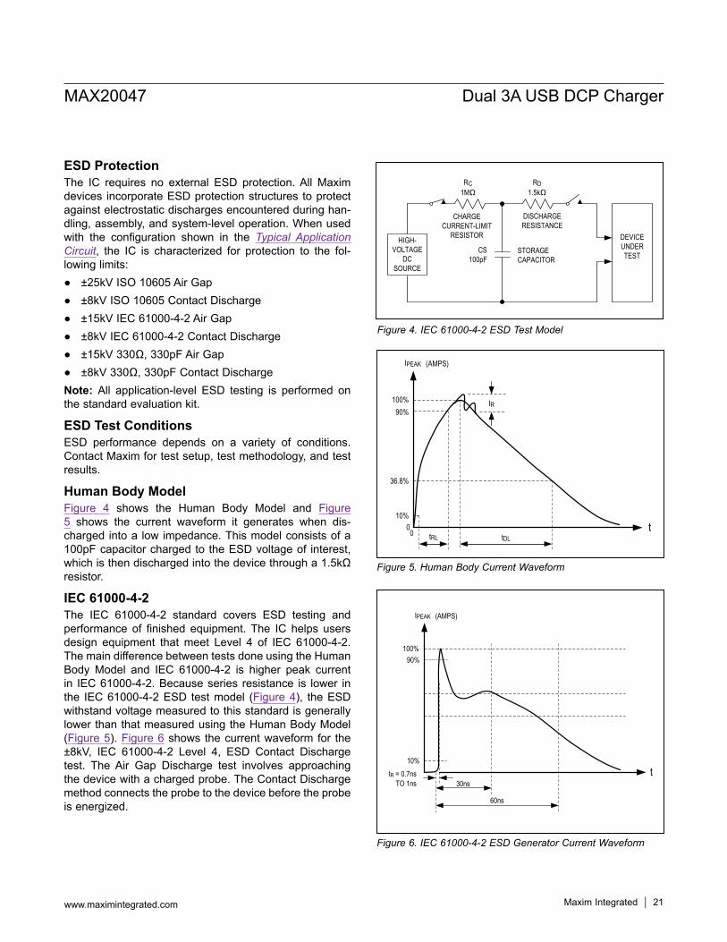
ESD ProtectionThe IC requires no external ESD protection. All Maxim devices incorporate ESD protection structures to protect against electrostatic discharges encountered during han-dling, assembly, and system-level operation. When used with the configuration shown in the Typical Application Circuit, the IC is characterized for protection to the fol-lowing limits:
±25kV ISO 10605 Air Gap ±8kV ISO 10605 Contact Discharge ±15kV IEC 61000-4-2 Air Gap ±8kV IEC 61000-4-2 Contact Discharge ±15kV 330Ω, 330pF Air Gap ±8kV 330Ω, 330pF Contact Discharge
Note: All application-level ESD testing is performed on the standard evaluation kit.
ESD Test ConditionsESD performance depends on a variety of conditions. Contact Maxim for test setup, test methodology, and test results.
Human Body ModelFigure 4 shows the Human Body Model and Figure 5 shows the current waveform it generates when dis-charged into a low impedance. This model consists of a 100pF capacitor charged to the ESD voltage of interest, which is then discharged into the device through a 1.5kΩ resistor.
IEC 61000-4-2The IEC 61000-4-2 standard covers ESD testing and performance of finished equipment. The IC helps users design equipment that meet Level 4 of IEC 61000-4-2. The main difference between tests done using the Human Body Model and IEC 61000-4-2 is higher peak current in IEC 61000-4-2. Because series resistance is lower in the IEC 61000-4-2 ESD test model (Figure 4), the ESD withstand voltage measured to this standard is generally lower than that measured using the Human Body Model (Figure 5). Figure 6 shows the current waveform for the ±8kV, IEC 61000-4-2 Level 4, ESD Contact Discharge test. The Air Gap Discharge test involves approaching the device with a charged probe. The Contact Discharge method connects the probe to the device before the probe is energized.
Figure 4. IEC 61000-4-2 ESD Test Model
Figure 5. Human Body Current Waveform
Figure 6. IEC 61000-4-2 ESD Generator Current Waveform
RC1MΩ
DEVICEUNDERTEST
HIGH-VOLTAGE
DCSOURCE
STORAGECAPACITOR
CS100pF
CHARGECURRENT-LIMIT
RESISTOR
RD1.5kΩ
DISCHARGERESISTANCE
IPEAK (AMPS)
100%90%
10%
tRL tDLt
36.8%
00
IR
100%90%
10%tR = 0.7ns
TO 1ns 30ns
60ns
t
IPEAK (AMPS)
MAX20047 Dual 3A USB DCP Charger
www.maximintegrated.com Maxim Integrated 21

Applications InformationComponent SelectionRFOSC SelectionThe switching frequency of the MAX20047 DC-DC IC is set by connecting a resistor between the FOSC pin and AGND. The internal oscillator can be tuned across a wide frequency range, providing greater system-design flex-ibility. The graph shown in Figure 7 plots frequency vs. RFOSC resistance.Table 2 lists switching frequencies set with standard 1% resistor values.
Spread-Spectrum OptionThere is a version of the IC that enables the oscillator to run in spread-spectrum mode. This improves EMI per-formance by modulating the internal oscillator frequency up/down ±3% relative to the operating frequency. If the spread-spectrum option is desired, see the Ordering Information table for the correct part number.
Setting the VBUS Current Limit (ILIM)ILIM is a multifunctional pin that can be used to program the VBUS current limit, the Apple divider-current, and the foldback-current threshold. Table 3 lists the configuration options for the ILIM pin.
Hold ModeDuring device boot, the hold configuration is loaded with a value that depends on decoding/reading the external CONFIG resistor. For more details regarding the value loaded as a function of resistors connected, see Table 4.
Table 2. Switching Frequencies
Table 3. Configuration Options for ILIM Pin Table 4. Configuration Pin Options
FOSC (kHz) 224,320 300,840 380,500 493,100 595,800 756,000 1,000,500 1,479,000 2,237,000
RFOSC (kΩ) 133 97.6 73.2 59 48.7 38.3 28.7 19.1 12.7
ILIM PIN CONNECTION
APPLE DIVIDER (A)
ILIM (A)
FOLDBACK (A)
Connect to AGND 2.4 3.3 None
8,870Ω to AGND 2.4 3.3 2.41
15,800Ω to AGND 2.4 3.3 2.1
24,900Ω to AGND 2.4 2.75 2.1
35,700Ω to AGND 2.4 2.75 None
49,900Ω to AGND 2.1 2.41 None
68,100Ω to AGND 2.1 2.41 2.1
Connect to BIAS 1.0 2.1 None
CONFIG PIN CONNECTION
LEVEL (AT 50µA)
HOLD MODE
HOLD TIME (MIN)
Connect to AGND Ground Disabled N/A
24,900Ω to AGND 1.25V Enabled 30
Connect to BIAS VBIAS Enabled 60
Figure 7. Frequency vs. RFOSC Resistance
FREQUENCY vs. RFOSC
RFOSC (Ω)
FREQ
UENC
Y (H
z)
120000100000
8000060000
4000020000
2.5E+6
2.0E+6
1.5E+6
1.0E+6
500.0E+3
000.0E+00 140000
MAX20047 Dual 3A USB DCP Charger
www.maximintegrated.com Maxim Integrated 22

Inductor SelectionThree key inductor parameters must be specified for operation with the device: inductance value (L), inductor saturation current (ISAT), and DC resistance (RDCR). The device is designed to operate with the ratio of inductor peak-to-peak AC current to DC average current (LIR) between 15% and 30% (typ). The switching frequency, input voltage, and output voltage then determine the inductor value as follows:
SUPSW OUT_ OUTMIN1
SUPSW SW MAX
( V V ) VL
V f I 33%
− ×=
× × ×
where VSUPSW and VOUT are typical values (so that efficiency is optimum for typical conditions). The switching frequency is set by RFOSC.RCS = 300mΩIMAX = 6AfSW = The operating frequency is set by RFOSC.The next equation ensures that the inductor current downslope is less than the internal slope compensation. For this to be the case, the following equation needs to be satisfied:
m2m2
− ≥
where m2 = The inductor current downslope:
OUTCS
VR
L×
-m = Slope compensation: V1.333µs
Solving for L and adding a 1.5 multiplier to account for tolerances in the system:
CSMIN2 OUT
RL = V 1.5
2 m× ×
×
To satisfy both LMIN1 and LMIN2, LMIN must be set to the larger of the two:
LMIN = Max (LMIN1,LMIN2)The maximum nominal inductor value recommended is 1.6 times the chosen value from the above formula.
LMAX = 1.6 x LMINSelect a nominal inductor value based on the following formula:
LMIN < LNOM < LMAX
The best choice of inductor is usually the first standard inductor value greater than LMIN.
Input CapacitorThe input filter capacitor reduces peak currents drawn from the power source and reduces noise and voltage ripple on the input caused by the circuit’s switching.Place a 4.7µF (or larger) ceramic capacitor directly from SUPSW to PGND positioned as close as possible to the pins. A bulk capacitor with higher ESR (such as an electro-lytic capacitor) is normally required as well to lower the Q of the front-end circuit and provide the remaining capacitance needed to minimize input-voltage ripple.The input capacitor RMS current requirement (IRMS) is defined by the following equation:
× −= × OUT SUPSW OUT
RMS LOAD(MAX)SUPSW
V ( V V )I I
V
IRMS has a maximum value when the input voltage equals twice the output voltage:
VSUPSW = 2 x VOUTTherefore:
=LOAD(MAX)
RMSSUPSW
II
V
Choose an input capacitor that exhibits less than +10°C self-heating temperature rise at the RMS input current for optimal long-term reliability.The input-voltage ripple is comprised of ΔVQ (caused by the capacitor discharge) and ΔVESR (caused by the ESR of the capacitor). Use low-ESR ceramic capacitors with high ripple-current capability at the input. Assume the contribution from the ESR and capacitor discharge equal to 50%. Calculate the input capacitance and ESR required for a specified input voltage ripple using the following equations:
ESRIN
LOUT
VESR =
II +
2
∆
∆
where:
( )SUPSW OUT OUTL
SUPSW SW
V V VI =
V f L− ×
∆× ×
MAX20047 Dual 3A USB DCP Charger
www.maximintegrated.com Maxim Integrated 23

and:
× −
∆ ×OUT
INQ SW
OUT
SUPSW
I D(1 D)C =
V fV
D =V
where: IOUT is the maximum output current and D is the duty cycle.
Output CapacitorThe output filter capacitor must have low enough equiva-lent series resistance (ESR) to meet output-ripple and load-transient requirements. The output capacitance must be high enough to absorb the inductor energy while transition-ing from full-load to no-load conditions, without tripping the overvoltage-fault protection. When using high-capacitance, low-ESR capacitors, the filter capacitor’s ESR dominates the output-voltage ripple, so the size of the output capaci-tor depends on the maximum ESR required to meet the output-voltage ripple (VRIPPLE(P-P)) specifications shown below:
VRIPPLE(P-P) = ESR x ILOAD(MAX) x LIRThe actual capacitance value required relates to the physical size needed to achieve low ESR, as well as to the chemistry of the capacitor technology. Thus, the capacitor is usually selected by ESR and voltage rating, rather than capacitance value.When using low-capacity filter capacitors, such as ceram-ic capacitors, size is usually determined by the capacity needed to prevent voltage droop and voltage rise from causing problems during load transients. Generally, once enough capacitance is added to meet the overshoot requirement, undershoot at the rising load edge is no longer a problem. However, low-capacity filter capacitors typically have high-ESR zeros that can affect the overall stability.
Compensation NetworkThe IC uses an internal transconductance error amplifier, with its inverting input and its output available to the user for external frequency compensation. The output capacitor and compensation network determine the loop stability. The inductor and the output capacitor are chosen based on performance, size, and cost. Additionally, the compensa-tion network optimizes the control-loop stability.The converter uses a current-mode-control scheme that regulates the output voltage by forcing the required current through the external inductor. The device uses the volt-age drop across the high-side MOSFET to sense inductor current. Current-mode control eliminates the double pole in the feedback loop caused by the inductor and output capacitor, resulting in a smaller phase shift and requiring less elaborate error-amplifier compensation than voltage-mode control. Only a simple single-series resistor (RC) and capacitor (CC) are required to have a stable, high-bandwidth loop in applications where ceramic capacitors are used for output filtering (see Figure 3). For other types of capacitors, due to the higher capacitance and ESR, the frequency of the zero created by the capacitance and ESR is lower than the desired closed-loop crossover frequency. To stabilize a nonceramic output-capacitor loop, add another compensation capacitor (CF) from COMP to ground to cancel this ESR zero.The basic regulator loop is modeled as a power modula-tor, output feedback-divider, and an error amplifier (see Figure 8). The power modulator has a DC gain set by gm x RLOAD, with a pole and zero pair set by RLOAD, the output capacitor (COUT), and its ESR. The following equations help to approximate the value for the gain of the power modulator (GAINMOD(dc)), neglecting the effect of the ramp stabilization. Ramp stabilization is necessary when the duty cycle is above 50% and is internally done for the devices:
GAINMOD(dc) = gmc x RLOADwhere:
= OUTLOAD
OUT(MAX)
VR
I
and:gmc = 3s
MAX20047 Dual 3A USB DCP Charger
www.maximintegrated.com Maxim Integrated 24

In a current-mode step-down converter, the output capaci-tor, its ESR, and the load resistance introduce a pole at the following frequency:
=π× ×pMOD
OUT LOAD
1f2 C R
The output capacitor and its ESR also introduce a zero at:
=π × ×zMOD
OUT
1f2 ESR C
When COUT is composed of “n” identical capacitors in parallel, the resulting COUT = n x COUT(EACH), and ESR = ESR (EACH)/n. Note that the capacitor zero for a parallel combination of alike capacitors is the same as for an individual capacitor.The feedback voltage-divider has a gain of GAINFB = VFB/VOUT, where VFB is 1V (typ).The transconductance error amplifier has a DC gain of GAINEA(DC) = gm_EA x ROUT_EA, where gm_EA is the error-amplifier transconductance, which is 700μS (typ), and ROUT_EA is the output resistance of the error ampli-fier (50MΩ).A dominant pole (fdpEA) is set by the compensation capacitor (CC) and the amplifier output resistance (ROUT_EA). A zero (fzEA) is set by the compensation resistor (RC) and the compensation capacitor (CC). There is an optional pole (fpEA) set by CF and RC to cancel the
output capacitor ESR zero if it occurs near the crossover frequency (fC, where the loop gain equals 1 (0dB)). Thus:
( )
zEAC C
dpEAC OUT_EA C
PEAF C
1f2 C R
1f2 C R R
1f2 C R
=π× ×
=π× × +
=π× ×
The loop-gain crossover frequency (fC) should be set below 1/5 of the switching frequency and much higher than the power-modulator pole (fpMOD).
SWpMOD C
ff « f
5≤
The total loop gain as the product of the modulator gain, the feedback voltage-divider gain, and the error-amplifier gain at fC should be equal to 1. So:
( ) ( )C C
FBMOD f EA fOUT
VGAIN GAIN 1
V× × =
For the case where fZMOD is greater than fC:GAINEA(fC) = gm_EA x RC
Therefore:
( )C
FBm_EA CMOD f OUT
VGAIN g R 1
V× × × =
Solving for RC:
( )C
OUTC
m_EA FB MOD f
VR
g V GAIN=
× ×
Set the error-amplifier compensation zero formed by RC and CC (fzEA) at the fpMOD. Calculate the value of CC as follows:
CpMOD C
1C2 f R
=π× ×
Figure 8. Compensation Network
VOUT
REF
CC
RC CF
COMP
gm
MAX20047 Dual 3A USB DCP Charger
www.maximintegrated.com Maxim Integrated 25

If fzMOD is less than 5 x fC, add a second capacitor (CF) from COMP to ground and set the compensation pole formed by RC and CF (fpAE) at the fzMOD. Calculate the value of CF as follows:
FzMOD C
1C2 f R
=π× ×
As the load current decreases, the modulator pole also decreases; however, the modulator gain increases accordingly and the crossover frequency remains the same. For the case where fzMOD is less than fC:The power-modulator gain at fC is:
( ) ( )C
pMODEA dcMOD f zMOD
fGAIN GAIN
f= ×
The error-amplifier gain at fC is:
( )C
zMODm_EA CEA f C
fGAIN g R
f= × ×
Therefore:
( )C
zMODFBm_EA CMOD f OUT C
fVGAIN g R 1
V f× × × × =
Solving for RC:
( )C
OUT CC
m_EA FB zMODMOD f
V fR
g V GAIN f×
=× × ×
Set the error-amplifier compensation zero formed by RC and CC at the fpMOD (fzEA = fzMOD).
CpMOD C
1C2 f R
=π× ×
If fzMOD is less than 5 x fC, add a second capacitor (CF) from COMP to ground. Set fpEA = fzMOD and calculate CF as follows:
FzMOD C
1C2 f R
=π× ×
PCB Layout GuidelinesCareful PCB layout is critical to achieve low switching losses and clean, stable operation. Use a multilayer board whenever possible for better noise immunity and power dissipation. Follow these guidelines for good PCB layout:
Place the ceramic input capacitor as close as possible to the SUPSW and PGND pins on the same side as the device. This will provide the best EMI rejection and minimize internal noise on the device, which can degrade performance.
Use a large contiguous copper plane connected to the PGND pads. Ensure that all heat-dissipating components have adequate cooling. Use multiple vias to drop the PGND plane to the inner/bottom layers for maximum heat dissipation.
Isolate the power components and high-current path from the sensitive analog circuitry. This is essential to prevent any noise coupling into the analog signals.
Keep the high-current paths short, especially at the ground terminals. This practice is essential for stable, jitter-free operation. The high-current path comprising input capacitor, high-side FET, inductor, and output capacitor should be as short as possible.
Keep the power traces and load connections short. This practice is essential for high efficiency. Use thick copper PCBs (2oz vs. 1oz) to enhance full-load efficiency.
The analog signal lines should be routed away from the high-frequency planes. This ensures integrity of sensitive signals feeding back into the IC.
The ground connection for the analog and power section should be close to the IC. This keeps the ground current loops to a minimum. In cases where only one ground is used, adequate isolation between analog return signals and high-power signals must be maintained.
MAX20047 Dual 3A USB DCP Charger
www.maximintegrated.com Maxim Integrated 26

Typical Application Circuit
6
2
7
BST
LX
PV3
OUT
8PGND
9SUPSW
10HVEN
11BIAS
4FOSC
5ILIM
16CONFIG
13COMP
14AGND
47µF
4.7µH
0.1µF
47µF
16.2kΩ
2.2nF3pF
73.2kΩ RCONFIG
2.2µF100kΩ
2.2nF 2.2nF
Ferrite BeadBLM41PG600
VBAT
HVEN
MAX20047
1
SHIELD
FERRITE BEAD
0.1µF
1
SHIELD
GND
VBUS
D-
D+
ID
USB2
0.22µF
FERRITE BEAD
0.1µF 0.22µF
2
3
4
5
1
USB1
2
3
4
5GND
VBUS
D-
D+
ID
19
20
12
17
18
SRC_DMOS1
HVDM1
HVDP1
SRC_DMOS2
HVDM2
HVDP2
15G_DMOS
1µF
1µF
8PGND
NTMD4820N
BLM41PG600
BLM41PG600
PGND
HVBUS2
HVBUS1
NTMD4820N
VOUT
10µF47µF
RILIMIT
PGNDAGND
*PLACE HOLDER: 0.1µF
MAX20047 Dual 3A USB DCP Charger
www.maximintegrated.com Maxim Integrated 27

Note: For variants with different options, contact factory. /V+ denotes an automotive qualified part. +Denotes a lead(Pb)-free/RoHS-compliant package.
PART TEMP RANGE PIN-PACKAGE SPREAD SPECTRUM
MAX20047AFPA/V+ -40°C to +125°C 20 FC-2QFN Yes
MAX20047AFPB/V+ -40°C to +125°C 20 FC-2QFN No
Ordering Information
Chip InformationPROCESS: CMOS
MAX20047 Dual 3A USB DCP Charger
www.maximintegrated.com Maxim Integrated 28

REVISIONNUMBER
REVISIONDATE DESCRIPTION PAGES
CHANGED0 9/17 Initial release —
Revision History
Maxim Integrated cannot assume responsibility for use of any circuitry other than circuitry entirely embodied in a Maxim Integrated product. No circuit patent licenses are implied. Maxim Integrated reserves the right to change the circuitry and specifications without notice at any time. The parametric values (min and max limits) shown in the Electrical Characteristics table are guaranteed. Other parametric values quoted in this data sheet are provided for guidance.
Maxim Integrated and the Maxim Integrated logo are trademarks of Maxim Integrated Products, Inc.
MAX20047 Dual 3A USB DCP Charger
© 2017 Maxim Integrated Products, Inc. 29
For pricing, delivery, and ordering information, please contact Maxim Direct at 1-888-629-4642, or visit Maxim Integrated’s website at www.maximintegrated.com.