Embed Size (px)
Citation preview
General DescriptionThe MAX19713 is an ultra-low-power, highly integrated mixed-signal analog front-end (AFE) ideal for wideband communication applications operating in full-duplex (FD) mode. Optimized for high dynamic performance and ultra-low power, the device integrates a dual 10-bit, 45Msps receive (Rx) ADC; dual 10-bit, 45Msps transmit (Tx) DAC; three fast-settling 12-bit aux-DAC channels for ancillary RF front-end control; and a 10-bit, 333ksps housekeep-ing aux-ADC. The typical operating power in FD mode is 91.8mW at a 45MHz clock frequency.The Rx ADCs feature 54dB SINAD and 72.2dBc SFDR at 5.5MHz input frequency with a 45MHz clock frequency. The analog I/Q input amplifiers are fully differential and accept 1.024VP-P full-scale signals. Typical I/Q channel matching is ±0.03 phase and ±0.02dB gain.The Tx DACs feature 70.3dBc SFDR at fOUT = 2.2MHz and fCLK = 45MHz. The analog I/Q full-scale output volt-age range is ±400mV differential. The output DC com-mon-mode voltage is selectable from 0.71V to 1.06V. The I/Q channel offset is adjustable to optimize radio lineup sideband/carrier suppression. Typical I/Q channel match-ing is ±0.01dB gain and ±0.05° phase.Two independent 10-bit parallel, high-speed digital buses used by the Rx ADC and Tx DAC allow full-duplex opera-tion for frequency-division duplex applications. The Rx ADC and Tx DAC can be disabled independently to opti-mize power management. A 3-wire serial interface con-trols power-management modes, the aux-DAC channels, and the aux-ADC channels.The MAX19713 operates on a single 2.7V to 3.3V analog supply and 1.8V to 3.3V digital I/O supply. The MAX19713 is specified for the extended (-40°C to +85°C) tempera-ture range and is available in a 56-pin, TQFN package. The Selector Guide at the end of the data sheet lists other pin-compatible versions in this AFE family. For time-divi-sion duplex (TDD) applications, refer to the MAX19705–MAX19708 AFE family of products.
Applications WiMAX CPEs 801.11a/b/g WLAN VoIP Terminals
Portable Communication Equipment
Features Dual 10-Bit, 45Msps Rx ADC and Dual 10-Bit,
45Msps Tx DAC Ultra-Low Power
• 91.8mW at fCLK = 45MHz, FD Mode • 79.2mW at fCLK = 45MHz, Slow Rx Mode • 49.5mW at fCLK = 45MHz, Slow Tx Mode • Low-Current Standby and Shutdown Modes
Programmable Tx DAC Common-Mode DC Level and I/Q Offset Trim
Excellent Dynamic Performance • SNR = 54.1dB at fIN = 5.5MHz (Rx ADC) • SFDR = 70.3dBc at fOUT = 2.2MHz (Tx DAC)
Three 12-Bit, 1μs Aux-DACs 10-Bit, 333ksps Aux-ADC with 4:1 Input Mux and
Data Averaging Excellent Gain/Phase Match
• ±0.03° Phase, ±0.02dB Gain (Rx ADC) at fIN = 5.5MHz
Multiplexed Parallel Digital I/O Serial-Interface Control Versatile Power-Control Circuits
• Shutdown, Standby, Idle, Tx/Rx Disable Miniature 56-Pin TQFN Package
(7mm x 7mm x 0.8mm)
Functional Diagram and Functional Diagram appear at end of data sheet.
19-0529; Rev 1; 9/06
*All devices are specified over the -40°C to +85°C operating range.**EP = Exposed paddle. +Denotes lead-free package.
PART* PIN-PACKAGE PKG CODEMAX19713ETN 56 TQFN-EP** T5677-1MAX19713ETN+ 56 TQFN-EP** T5677-1
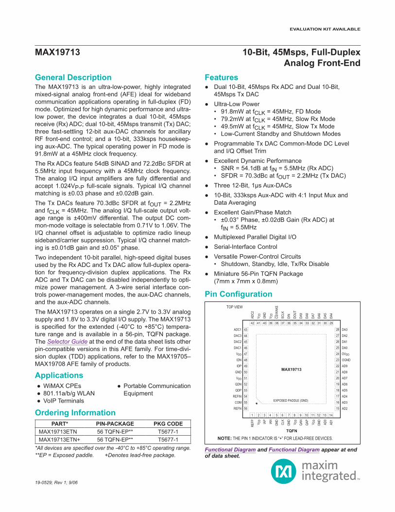
TOP VIEW
MAX19713
TQFN
15
17
16
18
19
20
21
22
23
24
25
26
27
28
AD2
AD3
AD4
AD5
AD6
AD7
AD8
AD9
OGND
OVDD
DA0
DA1
DA2
DA3
REFN
COM
REFIN
QDP
QDN
VDD
GND
IDP
IDN
VDD
DAC1
DAC2
DAC3
ADC1
48
47
46
45
44
43
54
53
56
55
52
51
50
49
1 2 3 4 5 6 7 8 9 10 11 12 13 14
42 41 40 39 38 37 36 35 34 33 32 31 30 29GN
D
AD0
AD1
V DD
QAP
QAN
V DD
GND
CLK
GND
IAN
IAP
V DD
REFP
DA6
DA5
DA4
DA7
DA8
DA9
DOUT
DIN
SCLK
V DD
GND
V DD
ADC2
EXPOSED PADDLE (GND)
CS/W
AKE
NOTE: THE PIN 1 INDICATOR IS “+” FOR LEAD-FREE DEVICES.
MAX19713 10-Bit, 45Msps, Full-DuplexAnalog Front-End
Pin Configuration
Ordering Information
EVALUATION KIT AVAILABLE
VDD to GND, OVDD to OGND .............................-0.3V to +3.6VGND to OGND ......................................................-0.3V to +0.3VIAP, IAN, QAP, QAN, IDP, IDN, QDP,
QDN, DAC1, DAC2, DAC3 to GND ................... -0.3V to VDDADC1, ADC2 to GND ............................... -0.3V to (VDD + 0.3V)REFP, REFN, REFIN, COM to GND ........ -0.3V to (VDD + 0.3V)AD0–AD9, DA0–DA9, SCLK, DIN, CS/WAKE,
CLK, DOUT to OGND ....................... -0.3V to (OVDD + 0.3V)
Continuous Power Dissipation (TA = +70°C) 56-Pin TQFN-EP (derate 27.8mW/°C above +70°C) ........2.22W
Thermal Resistance θJA ..................................................36°C/WOperating Temperature Range ........................... -40°C to +85°CJunction Temperature ......................................................+150°CStorage Temperature Range ............................ -60°C to +150°CLead Temperature (soldering, 10s) .................................+300°C
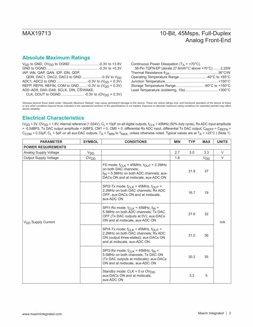
(VDD = 3V, OVDD = 1.8V, internal reference (1.024V), CL ≈ 10pF on all digital outputs, fCLK = 45MHz (50% duty cycle), Rx ADC input amplitude = -0.5dBFS, Tx DAC output amplitude = 0dBFS, CM1 = 0, CM0 = 0, differential Rx ADC input, differential Tx DAC output, CREFP = CREFN = CCOM = 0.33μF, CL < 5pF on all aux-DAC outputs, TA = TMIN to TMAX, unless otherwise noted. Typical values are at TA = +25°C.) (Note 1)
PARAMETER SYMBOL CONDITIONS MIN TYP MAX UNITSPOWER REQUIREMENTSAnalog Supply Voltage VDD 2.7 3.0 3.3 VOutput Supply Voltage OVDD 1.8 VDD V
VDD Supply Current
FD mode: fCLK = 45MHz, fOUT = 2.2MHz on both DAC channels; fIN = 5.5MHz on both ADC channels; aux-DACs ON and at midscale, aux-ADC ON
31.9 37
mA
SPI2-Tx mode: fCLK = 45MHz, fOUT = 2.2MHz on both DAC channels; Rx ADC OFF; aux-DACs ON and at midscale, aux-ADC ON
16.7 19
SPI1-Rx mode: fCLK = 45MHz, fIN = 5.5MHz on both ADC channels; Tx DAC OFF (Tx DAC outputs at 0V); aux-DACs ON and at midscale, aux-ADC ON
27.6 32
SPI4-Tx mode: fCLK = 45MHz, fOUT = 2.2MHz on both DAC channels; Rx ADC ON (output three-stated); aux-DACs ON and at midscale, aux-ADC ON
31.0 36
SPI3-Rx mode: fCLK = 45MHz, fIN = 5.5MHz on both channels; Tx DAC ON (Tx DAC outputs at midscale); aux-DACs ON and at midscale, aux-ADC ON
30.2 35
Standby mode: CLK = 0 or OVDD; aux-DACs ON and at midscale, aux-ADC ON
3.3 5
MAX19713 10-Bit, 45Msps, Full-DuplexAnalog Front-End
www.maximintegrated.com Maxim Integrated 2
Absolute Maximum Ratings
Stresses beyond those listed under “Absolute Maximum Ratings” may cause permanent damage to the device. These are stress ratings only, and functional operation of the device at these or any other conditions beyond those indicated in the operational sections of the specifications is not implied. Exposure to absolute maximum rating conditions for extended periods may affect device reliability.
Electrical Characteristics
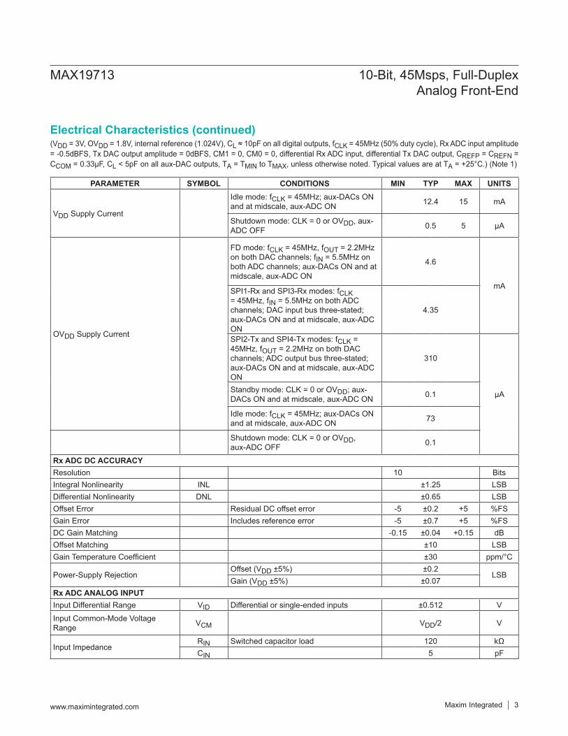
(VDD = 3V, OVDD = 1.8V, internal reference (1.024V), CL ≈ 10pF on all digital outputs, fCLK = 45MHz (50% duty cycle), Rx ADC input amplitude = -0.5dBFS, Tx DAC output amplitude = 0dBFS, CM1 = 0, CM0 = 0, differential Rx ADC input, differential Tx DAC output, CREFP = CREFN = CCOM = 0.33μF, CL < 5pF on all aux-DAC outputs, TA = TMIN to TMAX, unless otherwise noted. Typical values are at TA = +25°C.) (Note 1)
PARAMETER SYMBOL CONDITIONS MIN TYP MAX UNITS
VDD Supply Current
Idle mode: fCLK = 45MHz; aux-DACs ON and at midscale, aux-ADC ON 12.4 15 mA
Shutdown mode: CLK = 0 or OVDD, aux-ADC OFF 0.5 5 µA
OVDD Supply Current
FD mode: fCLK = 45MHz, fOUT = 2.2MHz on both DAC channels; fIN = 5.5MHz on both ADC channels; aux-DACs ON and at midscale, aux-ADC ON
4.6
mASPI1-Rx and SPI3-Rx modes: fCLK = 45MHz, fIN = 5.5MHz on both ADC channels; DAC input bus three-stated; aux-DACs ON and at midscale, aux-ADC ON
4.35
SPI2-Tx and SPI4-Tx modes: fCLK = 45MHz, fOUT = 2.2MHz on both DAC channels; ADC output bus three-stated; aux-DACs ON and at midscale, aux-ADC ON
310
µAStandby mode: CLK = 0 or OVDD; aux-DACs ON and at midscale, aux-ADC ON 0.1
Idle mode: fCLK = 45MHz; aux-DACs ON and at midscale, aux-ADC ON 73
Shutdown mode: CLK = 0 or OVDD, aux-ADC OFF 0.1
Rx ADC DC ACCURACYResolution 10 BitsIntegral Nonlinearity INL ±1.25 LSBDifferential Nonlinearity DNL ±0.65 LSBOffset Error Residual DC offset error -5 ±0.2 +5 %FSGain Error Includes reference error -5 ±0.7 +5 %FSDC Gain Matching -0.15 ±0.04 +0.15 dBOffset Matching ±10 LSBGain Temperature Coefficient ±30 ppm/°C
Power-Supply RejectionOffset (VDD ±5%) ±0.2
LSBGain (VDD ±5%) ±0.07
Rx ADC ANALOG INPUTInput Differential Range VID Differential or single-ended inputs ±0.512 V
Input Common-Mode Voltage Range VCM VDD/2 V
Input ImpedanceRIN Switched capacitor load 120 kΩCIN 5 pF
MAX19713 10-Bit, 45Msps, Full-DuplexAnalog Front-End
www.maximintegrated.com Maxim Integrated 3
Electrical Characteristics (continued)
(VDD = 3V, OVDD = 1.8V, internal reference (1.024V), CL ≈ 10pF on all digital outputs, fCLK = 45MHz (50% duty cycle), Rx ADC input amplitude = -0.5dBFS, Tx DAC output amplitude = 0dBFS, CM1 = 0, CM0 = 0, differential Rx ADC input, differential Tx DAC output, CREFP = CREFN = CCOM = 0.33μF, CL < 5pF on all aux-DAC outputs, TA = TMIN to TMAX, unless otherwise noted. Typical values are at TA = +25°C.) (Note 1)
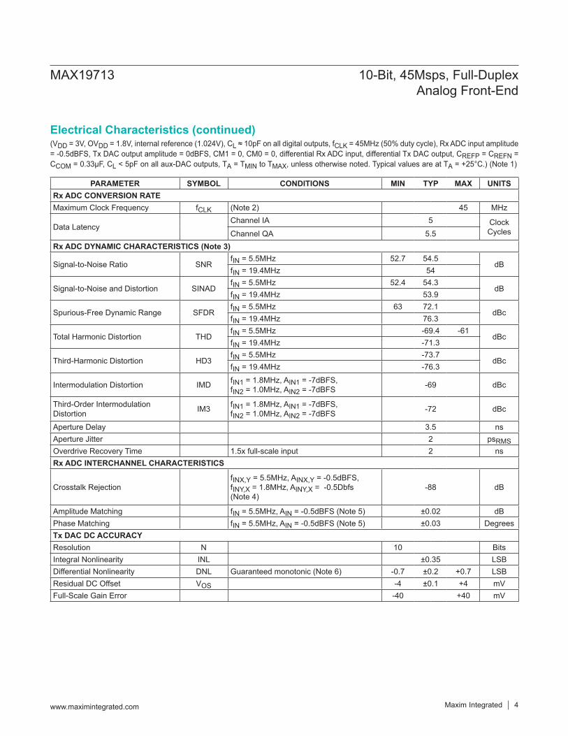
PARAMETER SYMBOL CONDITIONS MIN TYP MAX UNITSRx ADC CONVERSION RATEMaximum Clock Frequency fCLK (Note 2) 45 MHz
Data LatencyChannel IA 5 Clock
CyclesChannel QA 5.5Rx ADC DYNAMIC CHARACTERISTICS (Note 3)
Signal-to-Noise Ratio SNRfIN = 5.5MHz 52.7 54.5
dBfIN = 19.4MHz 54
Signal-to-Noise and Distortion SINADfIN = 5.5MHz 52.4 54.3
dBfIN = 19.4MHz 53.9
Spurious-Free Dynamic Range SFDRfIN = 5.5MHz 63 72.1
dBcfIN = 19.4MHz 76.3
Total Harmonic Distortion THDfIN = 5.5MHz -69.4 -61
dBcfIN = 19.4MHz -71.3
Third-Harmonic Distortion HD3fIN = 5.5MHz -73.7
dBcfIN = 19.4MHz -76.3
Intermodulation Distortion IMD fIN1 = 1.8MHz, AIN1 = -7dBFS, fIN2 = 1.0MHz, AIN2 = -7dBFS -69 dBc
Third-Order Intermodulation Distortion IM3 fIN1 = 1.8MHz, AIN1 = -7dBFS,
fIN2 = 1.0MHz, AIN2 = -7dBFS -72 dBc
Aperture Delay 3.5 nsAperture Jitter 2 psRMSOverdrive Recovery Time 1.5x full-scale input 2 nsRx ADC INTERCHANNEL CHARACTERISTICS
Crosstalk RejectionfINX,Y = 5.5MHz, AINX,Y = -0.5dBFS, fINY,X = 1.8MHz, AINY,X = -0.5Dbfs (Note 4)
-88 dB
Amplitude Matching fIN = 5.5MHz, AIN = -0.5dBFS (Note 5) ±0.02 dBPhase Matching fIN = 5.5MHz, AIN = -0.5dBFS (Note 5) ±0.03 DegreesTx DAC DC ACCURACYResolution N 10 BitsIntegral Nonlinearity INL ±0.35 LSBDifferential Nonlinearity DNL Guaranteed monotonic (Note 6) -0.7 ±0.2 +0.7 LSBResidual DC Offset VOS -4 ±0.1 +4 mVFull-Scale Gain Error -40 +40 mV
MAX19713 10-Bit, 45Msps, Full-DuplexAnalog Front-End
www.maximintegrated.com Maxim Integrated 4
Electrical Characteristics (continued)
(VDD = 3V, OVDD = 1.8V, internal reference (1.024V), CL ≈ 10pF on all digital outputs, fCLK = 45MHz (50% duty cycle), Rx ADC input amplitude = -0.5dBFS, Tx DAC output amplitude = 0dBFS, CM1 = 0, CM0 = 0, differential Rx ADC input, differential Tx DAC output, CREFP = CREFN = CCOM = 0.33μF, CL < 5pF on all aux-DAC outputs, TA = TMIN to TMAX, unless otherwise noted. Typical values are at TA = +25°C.) (Note 1)
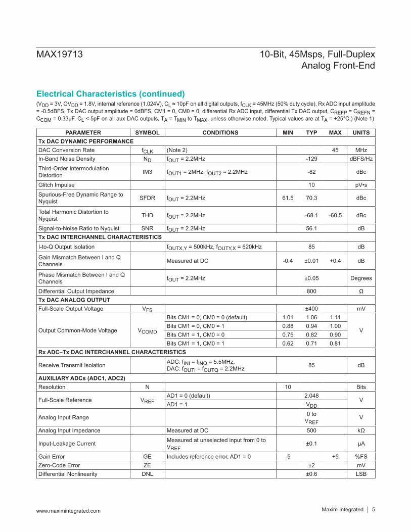
PARAMETER SYMBOL CONDITIONS MIN TYP MAX UNITSTx DAC DYNAMIC PERFORMANCEDAC Conversion Rate fCLK (Note 2) 45 MHzIn-Band Noise Density ND fOUT = 2.2MHz -129 dBFS/Hz
Third-Order Intermodulation Distortion IM3 fOUT1 = 2MHz, fOUT2 = 2.2MHz -82 dBc
Glitch Impulse 10 pV•s
Spurious-Free Dynamic Range to Nyquist SFDR fOUT = 2.2MHz 61.5 70.3 dBc
Total Harmonic Distortion to Nyquist THD fOUT = 2.2MHz -68.1 -60.5 dBc
Signal-to-Noise Ratio to Nyquist SNR fOUT = 2.2MHz 56.1 dBTx DAC INTERCHANNEL CHARACTERISTICSI-to-Q Output Isolation fOUTX,Y = 500kHz, fOUTY,X = 620kHz 85 dB
Gain Mismatch Between I and Q Channels Measured at DC -0.4 ±0.01 +0.4 dB
Phase Mismatch Between I and Q Channels fOUT = 2.2MHz ±0.05 Degrees
Differential Output Impedance 800 ΩTx DAC ANALOG OUTPUTFull-Scale Output Voltage VFS ±400 mV
Output Common-Mode Voltage VCOMD
Bits CM1 = 0, CM0 = 0 (default) 1.01 1.06 1.11
VBits CM1 = 0, CM0 = 1 0.88 0.94 1.00Bits CM1 = 1, CM0 = 0 0.75 0.82 0.90Bits CM1 = 1, CM0 = 1 0.62 0.71 0.81
Rx ADC–Tx DAC INTERCHANNEL CHARACTERISTICS
Receive Transmit Isolation ADC: fINI = fINQ = 5.5MHz, DAC: fOUTI = fOUTQ = 2.2MHz 85 dB
AUXILIARY ADCs (ADC1, ADC2)Resolution N 10 Bits
Full-Scale Reference VREFAD1 = 0 (default) 2.048
VAD1 = 1 VDD
Analog Input Range 0 to VREF
V
Analog Input Impedance Measured at DC 500 kΩ
Input-Leakage Current Measured at unselected input from 0 to VREF
±0.1 µA
Gain Error GE Includes reference error, AD1 = 0 -5 +5 %FSZero-Code Error ZE ±2 mVDifferential Nonlinearity DNL ±0.6 LSB
MAX19713 10-Bit, 45Msps, Full-DuplexAnalog Front-End
www.maximintegrated.com Maxim Integrated 5
Electrical Characteristics (continued)
(VDD = 3V, OVDD = 1.8V, internal reference (1.024V), CL ≈ 10pF on all digital outputs, fCLK = 45MHz (50% duty cycle), Rx ADC input amplitude = -0.5dBFS, Tx DAC output amplitude = 0dBFS, CM1 = 0, CM0 = 0, differential Rx ADC input, differential Tx DAC output, CREFP = CREFN = CCOM = 0.33μF, CL < 5pF on all aux-DAC outputs, TA = TMIN to TMAX, unless otherwise noted. Typical values are at TA = +25°C.) (Note 1)
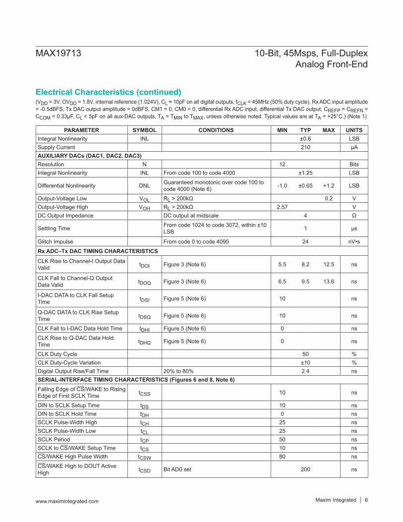
PARAMETER SYMBOL CONDITIONS MIN TYP MAX UNITSIntegral Nonlinearity INL ±0.6 LSBSupply Current 210 µAAUXILIARY DACs (DAC1, DAC2, DAC3)Resolution N 12 BitsIntegral Nonlinearity INL From code 100 to code 4000 ±1.25 LSB
Differential Nonlinearity DNL Guaranteed monotonic over code 100 to code 4000 (Note 6) -1.0 ±0.65 +1.2 LSB
Output-Voltage Low VOL RL > 200kΩ 0.2 VOutput-Voltage High VOH RL > 200kΩ 2.57 VDC Output Impedance DC output at midscale 4 Ω
Settling Time From code 1024 to code 3072, within ±10 LSB 1 µs
Glitch Impulse From code 0 to code 4095 24 nV•s
Rx ADC–Tx DAC TIMING CHARACTERISTICS
CLK Rise to Channel-I Output Data Valid tDOI Figure 3 (Note 6) 5.5 8.2 12.5 ns
CLK Fall to Channel-Q Output Data Valid tDOQ Figure 3 (Note 6) 6.5 9.5 13.6 ns
I-DAC DATA to CLK Fall Setup Time tDSI Figure 5 (Note 6) 10 ns
Q-DAC DATA to CLK Rise Setup Time tDSQ Figure 5 (Note 6) 10 ns
CLK Fall to I-DAC Data Hold Time tDHI Figure 5 (Note 6) 0 ns
CLK Rise to Q-DAC Data Hold Time tDHQ Figure 5 (Note 6) 0 ns
CLK Duty Cycle 50 %CLK Duty-Cycle Variation ±10 %Digital Output Rise/Fall Time 20% to 80% 2.4 nsSERIAL-INTERFACE TIMING CHARACTERISTICS (Figures 6 and 8, Note 6)Falling Edge of CS/WAKE to Rising Edge of First SCLK Time tCSS 10 ns
DIN to SCLK Setup Time tDS 10 nsDIN to SCLK Hold Time tDH 0 nsSCLK Pulse-Width High tCH 25 nsSCLK Pulse-Width Low tCL 25 nsSCLK Period tCP 50 nsSCLK to CS/WAKE Setup Time tCS 10 nsCS/WAKE High Pulse Width tCSW 80 ns
CS/WAKE High to DOUT Active High tCSD Bit AD0 set 200 ns
MAX19713 10-Bit, 45Msps, Full-DuplexAnalog Front-End
www.maximintegrated.com Maxim Integrated 6
Electrical Characteristics (continued)
(VDD = 3V, OVDD = 1.8V, internal reference (1.024V), CL ≈ 10pF on all digital outputs, fCLK = 45MHz (50% duty cycle), Rx ADC input amplitude = -0.5dBFS, Tx DAC output amplitude = 0dBFS, CM1 = 0, CM0 = 0, differential Rx ADC input, differential Tx DAC output, CREFP = CREFN = CCOM = 0.33μF, CL < 5pF on all aux-DAC outputs, TA = TMIN to TMAX, unless otherwise noted. Typical values are at TA = +25°C.) (Note 1)
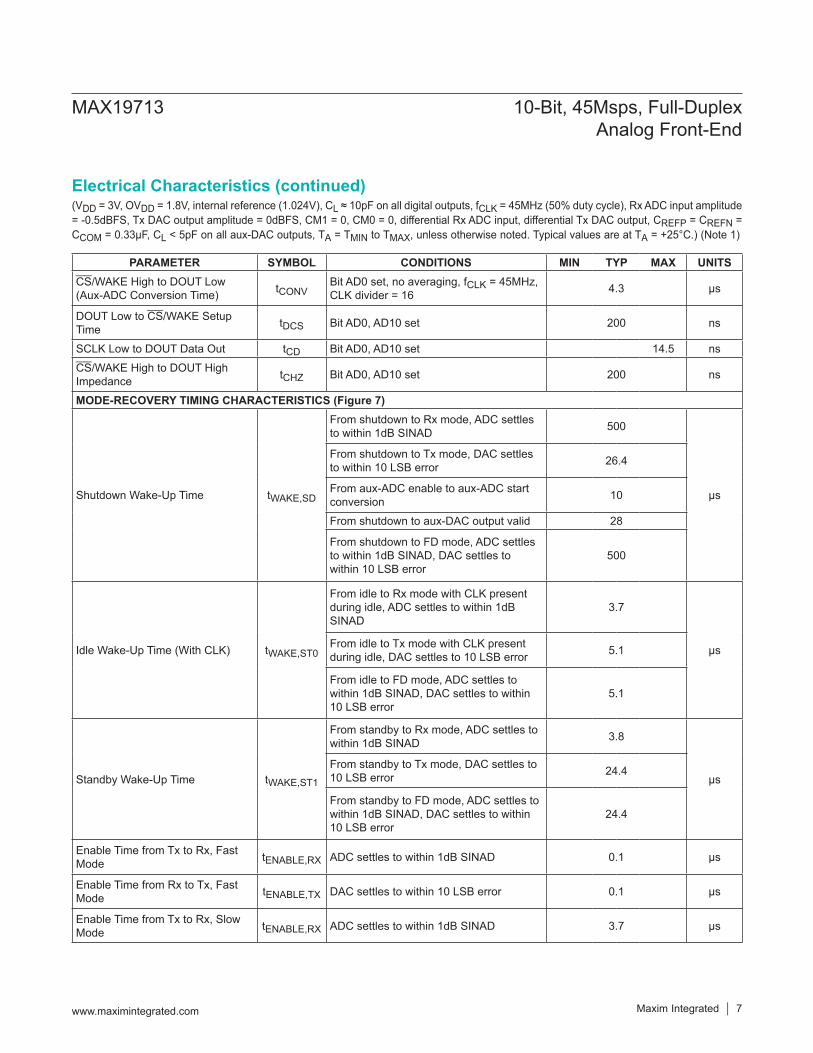
PARAMETER SYMBOL CONDITIONS MIN TYP MAX UNITSCS/WAKE High to DOUT Low (Aux-ADC Conversion Time) tCONV
Bit AD0 set, no averaging, fCLK = 45MHz, CLK divider = 16 4.3 µs
DOUT Low to CS/WAKE Setup Time tDCS Bit AD0, AD10 set 200 ns
SCLK Low to DOUT Data Out tCD Bit AD0, AD10 set 14.5 ns
CS/WAKE High to DOUT High Impedance tCHZ Bit AD0, AD10 set 200 ns
MODE-RECOVERY TIMING CHARACTERISTICS (Figure 7)
Shutdown Wake-Up Time tWAKE,SD
From shutdown to Rx mode, ADC settles to within 1dB SINAD 500
µs
From shutdown to Tx mode, DAC settles to within 10 LSB error 26.4
From aux-ADC enable to aux-ADC start conversion 10
From shutdown to aux-DAC output valid 28
From shutdown to FD mode, ADC settles to within 1dB SINAD, DAC settles to within 10 LSB error
500
Idle Wake-Up Time (With CLK) tWAKE,ST0
From idle to Rx mode with CLK present during idle, ADC settles to within 1dB SINAD
3.7
µsFrom idle to Tx mode with CLK present during idle, DAC settles to 10 LSB error 5.1
From idle to FD mode, ADC settles to within 1dB SINAD, DAC settles to within 10 LSB error
5.1
Standby Wake-Up Time tWAKE,ST1
From standby to Rx mode, ADC settles to within 1dB SINAD 3.8
µsFrom standby to Tx mode, DAC settles to 10 LSB error 24.4
From standby to FD mode, ADC settles to within 1dB SINAD, DAC settles to within 10 LSB error
24.4
Enable Time from Tx to Rx, Fast Mode tENABLE,RX ADC settles to within 1dB SINAD 0.1 µs
Enable Time from Rx to Tx, Fast Mode tENABLE,TX DAC settles to within 10 LSB error 0.1 µs
Enable Time from Tx to Rx, Slow Mode tENABLE,RX ADC settles to within 1dB SINAD 3.7 µs
MAX19713 10-Bit, 45Msps, Full-DuplexAnalog Front-End
www.maximintegrated.com Maxim Integrated 7
Electrical Characteristics (continued)
(VDD = 3V, OVDD = 1.8V, internal reference (1.024V), CL ≈ 10pF on all digital outputs, fCLK = 45MHz (50% duty cycle), Rx ADC input amplitude = -0.5dBFS, Tx DAC output amplitude = 0dBFS, CM1 = 0, CM0 = 0, differential Rx ADC input, differential Tx DAC output, CREFP = CREFN = CCOM = 0.33μF, CL < 5pF on all aux-DAC outputs, TA = TMIN to TMAX, unless otherwise noted. Typical values are at TA = +25°C.) (Note 1)
PARAMETER SYMBOL CONDITIONS MIN TYP MAX UNITSEnable Time from Rx to Tx, Slow Mode tENABLE,TX DAC settles to within 10 LSB error 4.9 µs
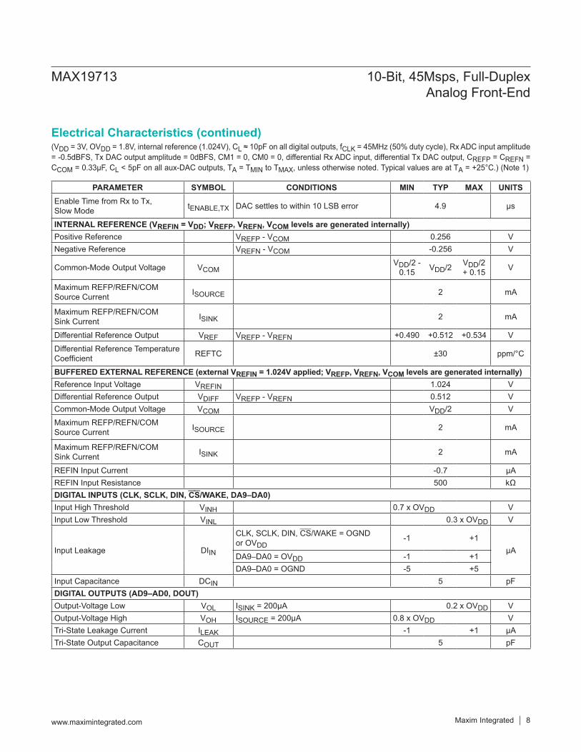
INTERNAL REFERENCE (VREFIN = VDD; VREFP, VREFN, VCOM levels are generated internally)Positive Reference VREFP - VCOM 0.256 VNegative Reference VREFN - VCOM -0.256 V
Common-Mode Output Voltage VCOMVDD/2 -
0.15 VDD/2 VDD/2 + 0.15 V
Maximum REFP/REFN/COM Source Current ISOURCE 2 mA
Maximum REFP/REFN/COM Sink Current ISINK 2 mA
Differential Reference Output VREF VREFP - VREFN +0.490 +0.512 +0.534 V
Differential Reference Temperature Coefficient REFTC ±30 ppm/°C
BUFFERED EXTERNAL REFERENCE (external VREFIN = 1.024V applied; VREFP, VREFN, VCOM levels are generated internally)Reference Input Voltage VREFIN 1.024 VDifferential Reference Output VDIFF VREFP - VREFN 0.512 VCommon-Mode Output Voltage VCOM VDD/2 V
Maximum REFP/REFN/COM Source Current ISOURCE 2 mA
Maximum REFP/REFN/COM Sink Current ISINK 2 mA
REFIN Input Current -0.7 µAREFIN Input Resistance 500 kΩDIGITAL INPUTS (CLK, SCLK, DIN, CS/WAKE, DA9–DA0)Input High Threshold VINH 0.7 x OVDD VInput Low Threshold VINL 0.3 x OVDD V
Input Leakage DIIN
CLK, SCLK, DIN, CS/WAKE = OGND or OVDD
-1 +1µA
DA9–DA0 = OVDD -1 +1DA9–DA0 = OGND -5 +5
Input Capacitance DCIN 5 pFDIGITAL OUTPUTS (AD9–AD0, DOUT)Output-Voltage Low VOL ISINK = 200µA 0.2 x OVDD VOutput-Voltage High VOH ISOURCE = 200µA 0.8 x OVDD VTri-State Leakage Current ILEAK -1 +1 µATri-State Output Capacitance COUT 5 pF
MAX19713 10-Bit, 45Msps, Full-DuplexAnalog Front-End
www.maximintegrated.com Maxim Integrated 8
Electrical Characteristics (continued)
(VDD = 3V, OVDD = 1.8V, internal reference (1.024V), CL ≈ 10pF on all digital outputs, fCLK = 45MHz (50% duty cycle), Rx ADC input amplitude = -0.5dBFS, Tx DAC output amplitude = 0dBFS, CM1 = 0, CM0 = 0, differential Rx ADC input, differential Tx DAC output, CREFP = CREFN = CCOM = 0.33μF, CL < 5pF on all aux-DAC outputs, TA = TMIN to TMAX, unless otherwise noted. Typical values are at TA = +25°C.) (Note 1)
Note 1: Specifications from TA = +25°C to +85°C guaranteed by production tests. Specifications at TA < +25°C guaranteed by design and characterization.
Note 2: The minimum clock frequency (fCLK) for the MAX19713 is 7.5MHz (typ). The minimum aux-ADC sample rate clock frequen-cy (ACLK) is determined by fCLK and the chosen aux-ADC clock-divider value. The minimum aux-ADC ACLK > 7.5MHz / 128 = 58.6kHz. The aux-ADC conversion time does not include the time to clock the serial data out of DOUT. The maximum conversion time (for no averaging, NAVG = 1) will be tCONV (max) = (12 x 1 x 128) / 7.5MHz = 205μs.
Note 3: SNR, SINAD, SFDR, HD3, and THD are based on a differential analog input voltage of -0.5dBFS referenced to the ampli-tude of the digital outputs. SINAD and THD are calculated using HD2 through HD6.
Note 4: Crosstalk rejection is measured by applying a high-frequency test tone to one channel and a low-frequency tone to the sec-ond channel. FFTs are performed on each channel. The parameter is specified as the power ratio of the first and second channel FFT test tones.
Note 5: Amplitude and phase matching are measured by applying the same signal to each channel, and comparing the two output signals using a sine-wave fit.
Note 6: Guaranteed by design and characterization.
(VDD = 3V, OVDD = 1.8V, internal reference (1.024V), CL ≈ 10pF on all digital outputs, fCLK = 45MHz (50% duty cycle), Rx ADC input amplitude = -0.5dBFS, Tx DAC output amplitude = 0dBFS, CM1 = 0, CM0 = 0, differential Rx ADC input, differential Tx DAC output, CREFP = CREFN = CCOM = 0.33μF, TA = +25°C, unless otherwise noted.)
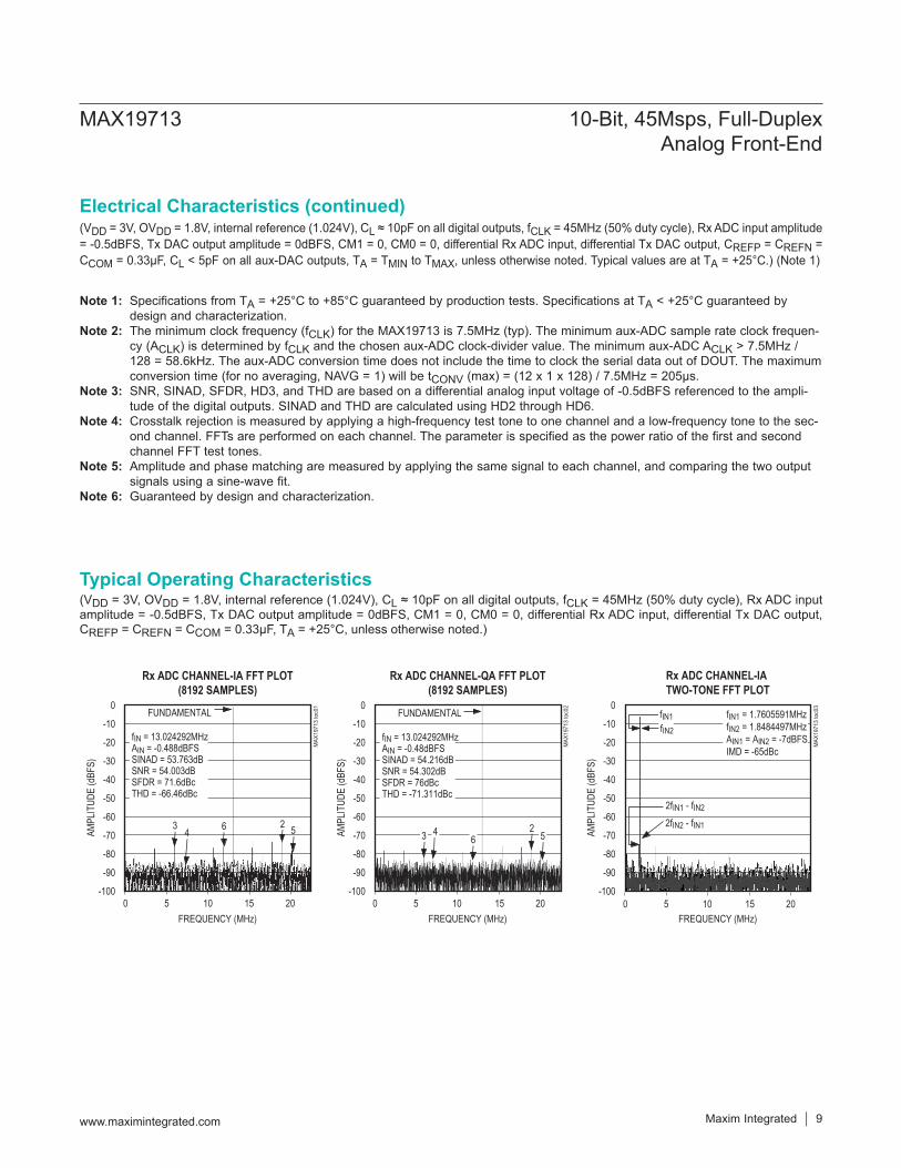
Rx ADC CHANNEL-QA FFT PLOT(8192 SAMPLES)
MAX
1971
3 to
c02
FREQUENCY (MHz)
AMPL
ITUD
E (d
BFS)
-90
-80
-70
-60
-50
-40
-30
-20
-10
0
-100
54 23 6
FUNDAMENTAL
0 5 10 15 20
fIN = 13.024292MHzAIN = -0.48dBFSSINAD = 54.216dBSNR = 54.302dBSFDR = 76dBcTHD = -71.311dBc
Rx ADC CHANNEL-IA TWO-TONE FFT PLOT
MAX
1971
3 to
c03
FREQUENCY (MHz)
AMPL
ITUD
E (d
BFS)
-90
-80
-70
-60
-50
-40
-30
-20
-10
0
-100
fIN1 = 1.7605591MHzfIN2 = 1.8484497MHzAIN1 = AIN2 = -7dBFSIMD = -65dBc
2fIN1 - fIN2
fIN1fIN2
2fIN2 - fIN1
0 5 10 15 20
Rx ADC CHANNEL-IA FFT PLOT(8192 SAMPLES)
MAX
1971
3 to
c01
FREQUENCY (MHz)
AMPL
ITUD
E (d
BFS)
-90
-80
-70
-60
-50
-40
-30
-20
-10
0
-100
5423 6
0 5 10 15 20
FUNDAMENTAL
fIN = 13.024292MHzAIN = -0.488dBFSSINAD = 53.763dBSNR = 54.003dBSFDR = 71.6dBcTHD = -66.46dBc
MAX19713 10-Bit, 45Msps, Full-DuplexAnalog Front-End
www.maximintegrated.com Maxim Integrated 9
Electrical Characteristics (continued)
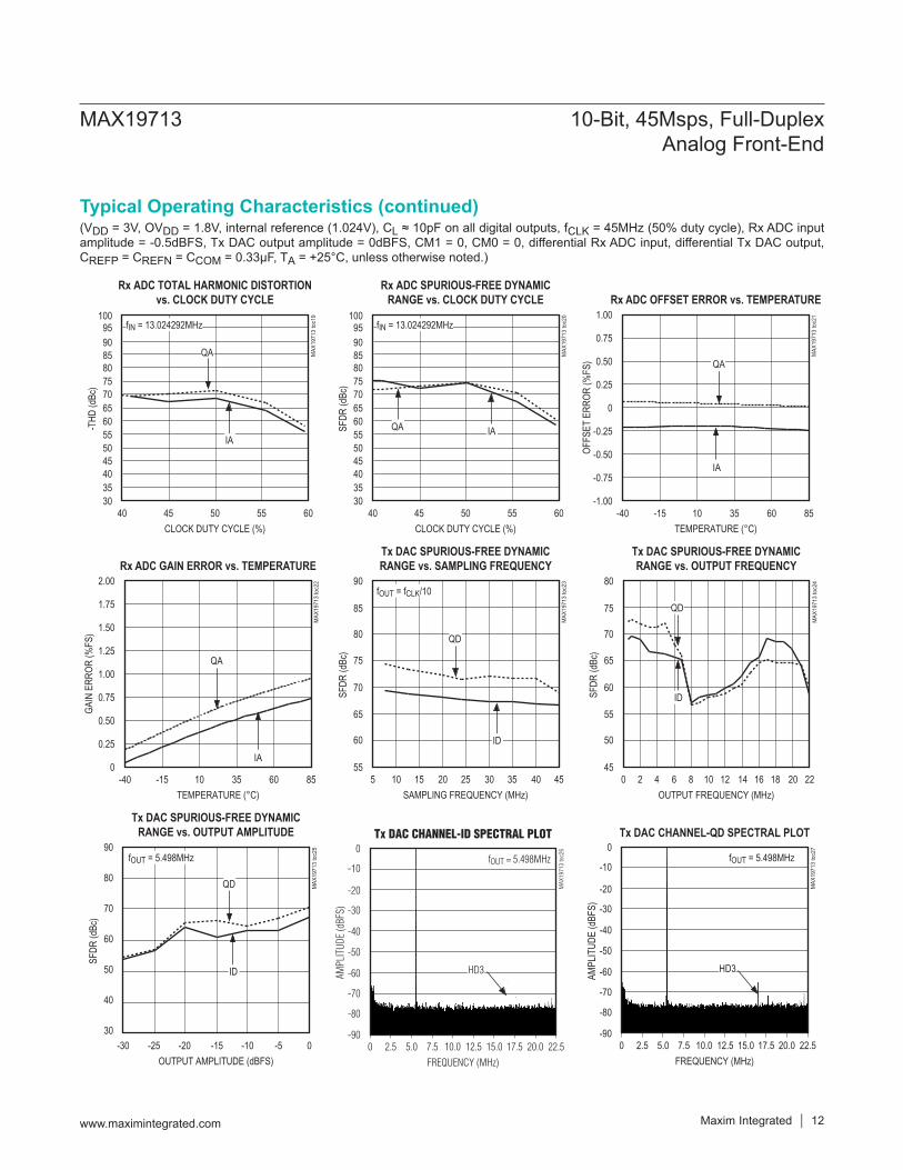
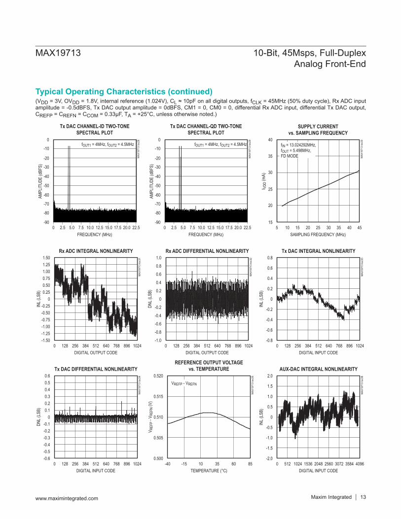
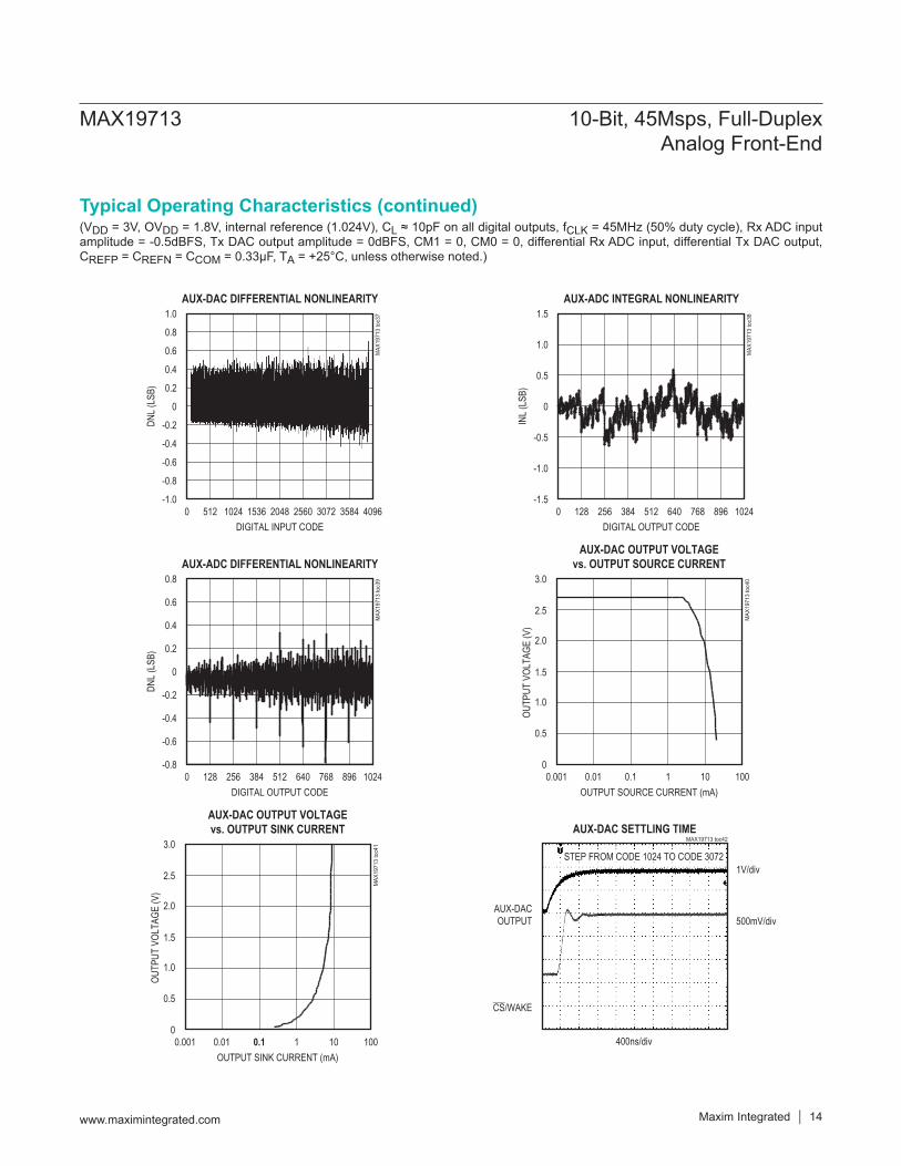
Typical Operating Characteristics
(VDD = 3V, OVDD = 1.8V, internal reference (1.024V), CL ≈ 10pF on all digital outputs, fCLK = 45MHz (50% duty cycle), Rx ADC input amplitude = -0.5dBFS, Tx DAC output amplitude = 0dBFS, CM1 = 0, CM0 = 0, differential Rx ADC input, differential Tx DAC output, CREFP = CREFN = CCOM = 0.33μF, TA = +25°C, unless otherwise noted.)
Rx ADC SIGNAL-TO-NOISE RATIOvs. ANALOG INPUT FREQUENCY
MAX
1971
3 to
c05
ANALOG INPUT FREQUENCY (MHz)
SNR
(dB)
806020 40
51
52
53
54
55
57
56
500 100705010 30 90
QA
IA
Rx ADC SIGNAL-TO-NOISE AND DISTORTIONRATIO vs. ANALOG INPUT FREQUENCY
MAX
1971
3 to
c06
ANALOG INPUT FREQUENCY (MHz)
SINA
D (d
B)
806020 40
51
52
53
54
55
57
56
500 100705010 30 90
QA
IA
Rx ADC TOTAL HARMONIC DISTORTIONvs. ANALOG INPUT FREQUENCY
MAX
1971
3 to
c07
ANALOG INPUT FREQUENCY (MHz)
-THD
(dBc
)
806020 40
55
60
65
70
75
85
90
80
500 100705010 30 90
QA
IA
Rx ADC SPURIOUS-FREE DYNAMIC RANGEvs. ANALOG INPUT FREQUENCY
MAX
1971
3 to
c08
ANALOG INPUT FREQUENCY (MHz)
SFDR
(dBc
)
806020 40
55
60
65
70
75
85
90
80
500 100705010 30 90
QA
IA
Rx ADC SIGNAL-TO-NOISE RATIOvs. ANALOG INPUT AMPLITUDE
MAX
1971
3 to
c09
ANALOG INPUT AMPLITUDE (dBFS)
SNR
(dB)
-5-25 -20
25
30
35
40
45
55
60
50
20-30 0-10-15
QA
IA
fIN = 13.057251MHz
Rx ADC SIGNAL-TO-NOISE AND DISTORTIONRATIO vs. ANALOG INPUT AMPLITUDE
MAX
1971
3 to
c10
ANALOG INPUT AMPLITUDE (dBFS)
SINA
D (d
B)
-5-25 -20
25
30
35
40
45
55
60
50
20-30 0-10-15
QA
IA
fIN = 13.057251MHz
Rx ADC CHANNEL-QA TWO-TONE FFT PLOT
MAX
1971
3 to
c04
FREQUENCY (MHz)
AMPL
ITUD
E (d
BFS)
-90
-80
-70
-60
-50
-40
-30
-20
-10
0
-1000 2.5 5.0 7.5 10.0 12.5 15.0 17.5 20.0 22.5
fIN1 = 1.7605591MHzfIN2 = 1.8484497MHzAIN1 = AIN2 = -7dBFSIMD = -66dBc
2fIN1 - fIN2
2fIN2 - fIN1
fIN2
fIN1
Rx ADC TOTAL HARMONIC DISTORTIONvs. ANALOG INPUT AMPLITUDE
MAX
1971
3 to
c11
ANALOG INPUT AMPLITUDE (dBFS)
-THD
(dBc
)
-5-25 -20
35
40
45
5055
6570
7580
60
30-30 0-10-15
QA
IA
fIN = 13.057251MHz
Maxim Integrated 10www.maximintegrated.com
MAX19713 10-Bit, 45Msps, Full-DuplexAnalog Front-End
Typical Operating Characteristics (continued)
(VDD = 3V, OVDD = 1.8V, internal reference (1.024V), CL ≈ 10pF on all digital outputs, fCLK = 45MHz (50% duty cycle), Rx ADC input amplitude = -0.5dBFS, Tx DAC output amplitude = 0dBFS, CM1 = 0, CM0 = 0, differential Rx ADC input, differential Tx DAC output, CREFP = CREFN = CCOM = 0.33μF, TA = +25°C, unless otherwise noted.)
Rx ADC SPURIOUS-FREE DYNAMIC RANGEvs. ANALOG INPUT AMPLITUDE
MAX
1971
3 to
c12
ANALOG INPUT AMPLITUDE (dBFS)
SFDR
(dBc
)
-5-25 -20
35
40
45
5055
6570
7580
60
30-30 0-10-15
QAIA
fIN = 13.057251MHz
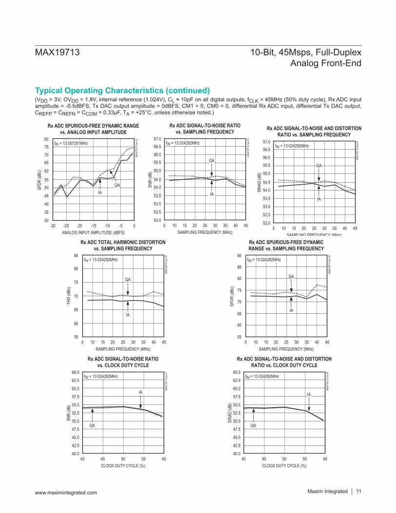
Rx ADC SIGNAL-TO-NOISE RATIOvs. SAMPLING FREQUENCY
MAX
1971
3 to
c13
SAMPLING FREQUENCY (MHz)
SNR
(dB)
3010 15
52.5
53.0
53.5
54.054.5
55.556.0
56.557.0
55.0
52.05 4525 403520
QA
IA
fIN = 13.024292MHz
Rx ADC SIGNAL-TO-NOISE AND DISTORTIONRATIO vs. SAMPLING FREQUENCY
MAX
1971
3 to
c14
SAMPLING FREQUENCY (MHz)
SINA
D (d
B)
3010 15
52.5
53.0
53.5
54.054.5
55.556.0
56.557.0
55.0
52.05 4525 403520
QA
IA
fIN = 13.024292MHz
Rx ADC TOTAL HARMONIC DISTORTIONvs. SAMPLING FREQUENCY
MAX
1971
3 to
c15
SAMPLING FREQUENCY (MHz)
-THD
(dBc
)
3010 15
60
65
70
75
80
85
555 4525 403520
QA
IA
fIN = 13.024292MHz
Rx ADC SPURIOUS-FREE DYNAMICRANGE vs. SAMPLING FREQUENCY
MAX
1971
3 to
c16
SAMPLING FREQUENCY (MHz)
SFDR
(dBc
)
3010 15
65
60
70
75
80
85
90
555 4525 403520
QA
IA
fIN = 13.024292MHz
Rx ADC SIGNAL-TO-NOISE RATIOvs. CLOCK DUTY CYCLE
MAX
1971
3 to
c17
CLOCK DUTY CYCLE (%)
SNR
(dB)
45
47.5
45.0
50.0
55.0
52.5
57.5
62.5
60.0
65.0
40.0
42.5
40 6050 55
QA
IA
fIN = 13.024292MHz
Rx ADC SIGNAL-TO-NOISE AND DISTORTIONRATIO vs. CLOCK DUTY CYCLE
MAX
1971
3 to
c18
CLOCK DUTY CYCLE (%)
SINA
D (d
B)
45
47.5
45.0
50.0
55.0
52.5
57.5
62.5
60.0
65.0
40.0
42.5
40 6050 55
QA
IA
fIN = 13.024292MHz
Maxim Integrated 11www.maximintegrated.com
MAX19713 10-Bit, 45Msps, Full-DuplexAnalog Front-End
Typical Operating Characteristics (continued)
(VDD = 3V, OVDD = 1.8V, internal reference (1.024V), CL ≈ 10pF on all digital outputs, fCLK = 45MHz (50% duty cycle), Rx ADC input amplitude = -0.5dBFS, Tx DAC output amplitude = 0dBFS, CM1 = 0, CM0 = 0, differential Rx ADC input, differential Tx DAC output, CREFP = CREFN = CCOM = 0.33μF, TA = +25°C, unless otherwise noted.)
Rx ADC SPURIOUS-FREE DYNAMICRANGE vs. CLOCK DUTY CYCLE
MAX
1971
3 to
c20
CLOCK DUTY CYCLE (%)
SFDR
(dBc
)
45
5045
5560
7065
8075
85
9590
100
303540
40 6050 55
QA IA
fIN = 13.024292MHz
Rx ADC OFFSET ERROR vs. TEMPERATURE
TEMPERATURE (°C)
OFFS
ET E
RROR
(%FS
)
MAX
1971
3 to
c21
-40 -15 10 35 60 85-1.00
-0.75
-0.50
-0.25
0
0.25
0.50
0.75
1.00
QA
IA
Rx ADC GAIN ERROR vs. TEMPERATURE
TEMPERATURE (°C)
GAIN
ERR
OR (%
FS)
MAX
1971
3 to
c22
-40 -15 10 35 60 850
0.25
0.50
0.75
1.00
1.25
1.50
1.75
2.00
QA
IA
Tx DAC SPURIOUS-FREE DYNAMICRANGE vs. OUTPUT AMPLITUDE
MAX
1971
3 to
c25
OUTPUT AMPLITUDE (dBFS)
SFDR
(dBc
)
-25
40
50
70
60
80
90
30-30 0-20 -15 -10 -5
QD
ID
fOUT = 5.498MHz
Tx DAC SPURIOUS-FREE DYNAMICRANGE vs. SAMPLING FREQUENCY
MAX
1971
3 to
c23
SAMPLING FREQUENCY (MHz)
SFDR
(dBc
)
15
65
70
80
75
85
90
55
60
5 4525 3510 4020 30
fOUT = fCLK/10
QD
ID
Tx DAC CHANNEL-ID SPECTRAL PLOT
MAX
1971
3 to
c26
FREQUENCY (MHz)
AMPL
ITUD
E (d
BFS)
-70
-40
-20
-30
-60
-50
-10
0
-90
-80
fOUT = 5.498MHz
HD3
0 2.5 5.0 7.5 10.0 12.5 15.0 17.5 20.0 22.5
Tx DAC SPURIOUS-FREE DYNAMICRANGE vs. OUTPUT FREQUENCY
MAX
1971
3 to
c24
OUTPUT FREQUENCY (MHz)
SFDR
(dBc
)
4
55
60
70
65
75
80
45
50
0 228 122 146 10 18 2016
QD
ID
Tx DAC CHANNEL-QD SPECTRAL PLOT
MAX
1971
3 to
c27
FREQUENCY (MHz)
AMPL
ITUD
E (d
BFS)
-70
-40
-20
-30
-60
-50
-10
0
-90
-80
fOUT = 5.498MHz
HD3
0 2.5 5.0 7.5 10.0 12.5 15.0 17.5 20.0 22.5
Rx ADC TOTAL HARMONIC DISTORTIONvs. CLOCK DUTY CYCLE
MAX
1971
3 to
c19
CLOCK DUTY CYCLE (%)
-THD
(dBc
)
45
5045
5560
7065
8075
85
9590
100
303540
40 6050 55
QA
IA
fIN = 13.024292MHz
Maxim Integrated 12www.maximintegrated.com
MAX19713 10-Bit, 45Msps, Full-DuplexAnalog Front-End
Typical Operating Characteristics (continued)
(VDD = 3V, OVDD = 1.8V, internal reference (1.024V), CL ≈ 10pF on all digital outputs, fCLK = 45MHz (50% duty cycle), Rx ADC input amplitude = -0.5dBFS, Tx DAC output amplitude = 0dBFS, CM1 = 0, CM0 = 0, differential Rx ADC input, differential Tx DAC output, CREFP = CREFN = CCOM = 0.33μF, TA = +25°C, unless otherwise noted.)
Tx DAC CHANNEL-QD TWO-TONESPECTRAL PLOT
MAX
1971
3 to
c29
FREQUENCY (MHz)
AMPL
ITUD
E (d
BFS)
-70
-40
-20
-30
-60
-50
-10
0
-90
-80
fOUT1 = 4MHz, fOUT2 = 4.5MHz
0 2.5 5.0 7.5 10.0 12.5 15.0 17.5 20.0 22.5
SUPPLY CURRENTvs. SAMPLING FREQUENCY
MAX
1971
3 to
c30
SAMPLING FREQUENCY (MHz)
I VDD
(mA)
15
25
30
35
40
15
20
5 4525 3510 4020 30
fIN = 13.024292MHz,fOUT = 5.498MHz,FD MODE
Rx ADC INTEGRAL NONLINEARITY
DIGITAL OUTPUT CODE
INL (
LSB)
MAX
1971
3 to
c31
0 128 256 384 512 640 768 896 1024-1.50-1.25-1.00-0.75-0.50-0.25
00.250.500.751.001.251.50
Tx DAC DIFFERENTIAL NONLINEARITY
DIGITAL INPUT CODE
DNL (
LSB)
MAX
1971
3 to
c34
0 128 256 384 512 640 768 896 1024-0.6-0.5-0.4-0.3-0.2-0.1
00.10.20.30.40.50.6
Rx ADC DIFFERENTIAL NONLINEARITY
DIGITAL OUTPUT CODE
DNL (
LSB)
MAX
1971
3 to
c32
0 128 256 384 512 640 768 896 1024-1.0
-0.8
-0.6
-0.4
-0.2
0
0.2
0.4
0.6
0.8
1.0
REFERENCE OUTPUT VOLTAGEvs. TEMPERATURE
TEMPERATURE (°C)
V REF
P - V
REFN
(V)
MAX
1971
3 to
c35
-40 -15 10 35 60 850.500
0.505
0.510
0.515
0.520VREFP - VREFN
Tx DAC INTEGRAL NONLINEARITY
DIGITAL INPUT CODE
INL (
LSB)
MAX
1971
3 to
c33
0 128 256 384 512 640 768 896 1024-0.8
-0.6
-0.4
-0.2
0
0.2
0.4
0.6
0.8
AUX-DAC INTEGRAL NONLINEARITY
DIGITAL INPUT CODE
INL (
LSB)
MAX
1971
3 to
c36
0 512 1024 1536 2048 2560 3072 3584 4096-2.0
-1.5
-1.0
-0.5
0
0.5
1.0
1.5
2.0
Tx DAC CHANNEL-ID TWO-TONESPECTRAL PLOT
MAX
1971
3 to
c28
FREQUENCY (MHz)
AMPL
ITUD
E (d
BFS)
-70
-40
-20
-30
-60
-50
-10
0
-90
-80
fOUT1 = 4MHz, fOUT2 = 4.5MHz
0 2.5 5.0 7.5 10.0 12.5 15.0 17.5 20.0 22.5
Maxim Integrated 13www.maximintegrated.com
MAX19713 10-Bit, 45Msps, Full-DuplexAnalog Front-End
Typical Operating Characteristics (continued)
(VDD = 3V, OVDD = 1.8V, internal reference (1.024V), CL ≈ 10pF on all digital outputs, fCLK = 45MHz (50% duty cycle), Rx ADC input amplitude = -0.5dBFS, Tx DAC output amplitude = 0dBFS, CM1 = 0, CM0 = 0, differential Rx ADC input, differential Tx DAC output, CREFP = CREFN = CCOM = 0.33μF, TA = +25°C, unless otherwise noted.)
AUX-ADC INTEGRAL NONLINEARITY
DIGITAL OUTPUT CODEIN
L (LS
B)
MAX
1971
3 to
c38
0 128 256 384 512 640 768 896 1024-1.5
-1.0
-0.5
0
0.5
1.0
1.5
AUX-ADC DIFFERENTIAL NONLINEARITY
DIGITAL OUTPUT CODE
DNL (
LSB)
MAX
1971
3 to
c39
0 128 256 384 512 640 768 896 1024-0.8
-0.6
-0.4
-0.2
0
0.2
0.4
0.6
0.8
AUX-DAC OUTPUT VOLTAGEvs. OUTPUT SINK CURRENT
MAX
1971
3 to
c41
OUTPUT SINK CURRENT (mA)
OUTP
UT V
OLTA
GE (V
)
0.01
1.5
2.0
2.5
3.0
0
1.0
0.5
0.001 100100.1 1
AUX-DAC OUTPUT VOLTAGEvs. OUTPUT SOURCE CURRENT
MAX
1971
3 to
c40
OUTPUT SOURCE CURRENT (mA)
OUTP
UT V
OLTA
GE (V
)
0.01
1.5
2.0
2.5
3.0
0
1.0
0.5
0.001 100100.1 1
AUX-DAC SETTLING TIMEMAX19713 toc42
AUX-DACOUTPUT
CS/WAKE
1V/div
500mV/div
400ns/div
STEP FROM CODE 1024 TO CODE 3072
AUX-DAC DIFFERENTIAL NONLINEARITY
DIGITAL INPUT CODE
DNL (
LSB)
MAX
1971
3 to
c37
0 512 1024 1536 2048 2560 3072 3584 4096-1.0
-0.8
-0.6
-0.4
-0.2
0
0.2
0.4
0.6
0.8
1.0
Maxim Integrated 14www.maximintegrated.com
MAX19713 10-Bit, 45Msps, Full-DuplexAnalog Front-End
Typical Operating Characteristics (continued)
Detailed DescriptionThe MAX19713 integrates a dual, 10-bit Rx ADC and a dual, 10-bit Tx DAC while providing ultra-low power and high dynamic performance at 45Msps conversion rate.
The Rx ADC analog input amplifiers are fully differential and accept 1.024VP-P full-scale signals. The Tx DAC analog outputs are fully differential with ±400mV full-scale output, selectable common-mode DC level, and adjust-able channel ID–QD offset trim.
PIN NAME FUNCTION
1 REFP Positive Reference Voltage Input Terminal. Bypass with a 0.33µF capacitor to GND as close as possible to REFP.
2, 8, 11, 39, 41, 47, 51 VDD
Analog Supply Voltage. Bypass VDD to GND with a combination of a 2.2µF capacitor in parallel with a 0.1µF capacitor.
3 IAP Channel-IA Positive Analog Input. For single-ended operation, connect signal source to IAP.4 IAN Channel-IA Negative Analog Input. For single-ended operation, connect IAN to COM.
5, 7, 12, 40, 50 GND Analog Ground. Connect all GND pins to ground plane.6 CLK Conversion Clock Input. Clock signal for both receive ADCs and transmit DACs.9 QAN Channel-QA Negative Analog Input. For single-ended operation, connect QAN to COM.
10 QAP Channel-QA Positive Analog Input. For single-ended operation, connect signal source to QAP.
13–22 AD0–AD9 Receive ADC Digital Outputs. AD9 is the most significant bit (MSB) and AD0 is the least significant bit (LSB).
23 OGND Output-Driver Ground
24 OVDDOutput-Driver Power Supply. Supply range from +1.8V to VDD. Bypass OVDD to OGND with a combination of a 2.2µF capacitor in parallel with a 0.1µF capacitor.
25–34 DA0–DA9 Transmit DAC Digital Inputs. DA9 is the most significant bit (MSB) and DA0 is the least significant bit (LSB). DA0–DA9 are internally pulled up to OVDD.
35 DOUT Aux-ADC Digital Output36 DIN 3-Wire Serial-Interface Data Input. Data is latched on the rising edge of SCLK.37 SCLK 3-Wire Serial-Interface Clock Input
38 CS/WAKE 3-Wire Serial-Interface Chip-Select/WAKE Input. When the MAX19713 is in shutdown, CS/WAKE controls the wake-up function. See the Wake-Up Function section.
42 ADC2 Selectable Auxiliary ADC Analog Input 243 ADC1 Selectable Auxiliary ADC Analog Input 144 DAC3 Auxiliary DAC3 Analog Output (VOUT = 0 at Power-Up)45 DAC2 Auxiliary DAC2 Analog Output (VOUT = 0 at Power-Up)46 DAC1 Auxiliary DAC1 Analog Output (AFC DAC, VOUT = 1.1V at Power-Up)48 IDN Tx DAC Channel-ID Differential Negative Output49 IDP Tx DAC Channel-ID Differential Positive Output52 QDN Tx DAC Channel-QD Differential Negative Output53 QDP Tx DAC Channel-QD Differential Positive Output54 REFIN Reference Input. Connect to VDD for internal reference.55 COM Common-Mode Voltage I/O. Bypass COM to GND with a 0.33µF capacitor.
56 REFN Negative Reference Voltage Input Terminal. Rx ADC conversion range is ±(VREFP - VREFN). Bypass REFN to GND with a 0.33µF capacitor.
— EP Exposed Paddle. Internally connected to GND. Connect EP to the GND plane.
MAX19713 10-Bit, 45Msps, Full-DuplexAnalog Front-End
www.maximintegrated.com Maxim Integrated 15
Pin Description
The MAX19713 integrates three 12-bit auxiliary DACs (aux-DACs) and a 10-bit, 333ksps auxiliary ADC (aux-ADC) with 4:1 input multiplexer. The aux-DAC channels feature 1μs settling time for fast AGC, VGA, and AFC level setting. The aux-ADC features data averaging to reduce processor overhead and a selectable clock-divider to program the conversion rate.The MAX19713 includes a 3-wire serial interface to control operating modes and power management. The serial interface is SPI and MICROWIRE compatible. The MAX19713 serial interface selects shutdown, idle, stand-by, FD, transmit (Tx), and receive (Rx) modes, as well as controls aux-DAC and aux-ADC channels.The MAX19713 features two independent, high-speed, 10-bit buses for the Rx ADC and Tx DAC, which allow full-duplex (FD) operation for frequency-division duplex applications. Each bus can be disabled to optimize power management through the 3-wire interface. The MAX19713
operates from a single 2.7V to 3.3V analog supply and a 1.8V to 3.3V digital supply.
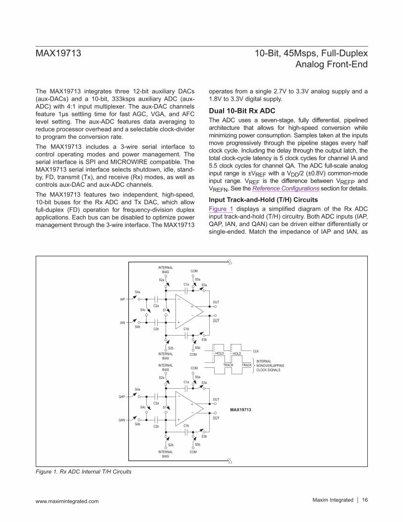
Dual 10-Bit Rx ADCThe ADC uses a seven-stage, fully differential, pipelined architecture that allows for high-speed conversion while minimizing power consumption. Samples taken at the inputs move progressively through the pipeline stages every half clock cycle. Including the delay through the output latch, the total clock-cycle latency is 5 clock cycles for channel IA and 5.5 clock cycles for channel QA. The ADC full-scale analog input range is ±VREF with a VDD/2 (±0.8V) common-mode input range. VREF is the difference between VREFP and VREFN. See the Reference Configurations section for details.
Input Track-and-Hold (T/H) CircuitsFigure 1 displays a simplified diagram of the Rx ADC input track-and-hold (T/H) circuitry. Both ADC inputs (IAP, QAP, IAN, and QAN) can be driven either differentially or single-ended. Match the impedance of IAP and IAN, as
Figure 1. Rx ADC Internal T/H Circuits
S3b
S3a
COM
S5b
S5a
QAP
QAN
S1
OUT
OUT
C2a
C2b
S4c
S4a
S4b C1b
C1a
INTERNALBIAS
INTERNALBIAS
COM
HOLD HOLD CLK
INTERNALNONOVERLAPPINGCLOCK SIGNALS
TRACK TRACK
S2a
S2b
S3b
S3a
COM
S5b
S5a
IAP
IAN
S1
OUT
OUT
C2a
C2b
S4c
S4a
S4b C1b
C1a
INTERNALBIAS
INTERNALBIAS
COM
S2a
S2b
MAX19713
MAX19713 10-Bit, 45Msps, Full-DuplexAnalog Front-End
www.maximintegrated.com Maxim Integrated 16
well as QAP and QAN, and set the input signal common-mode voltage within the VDD/2 (±0.8V) Rx ADC range for optimum performance.
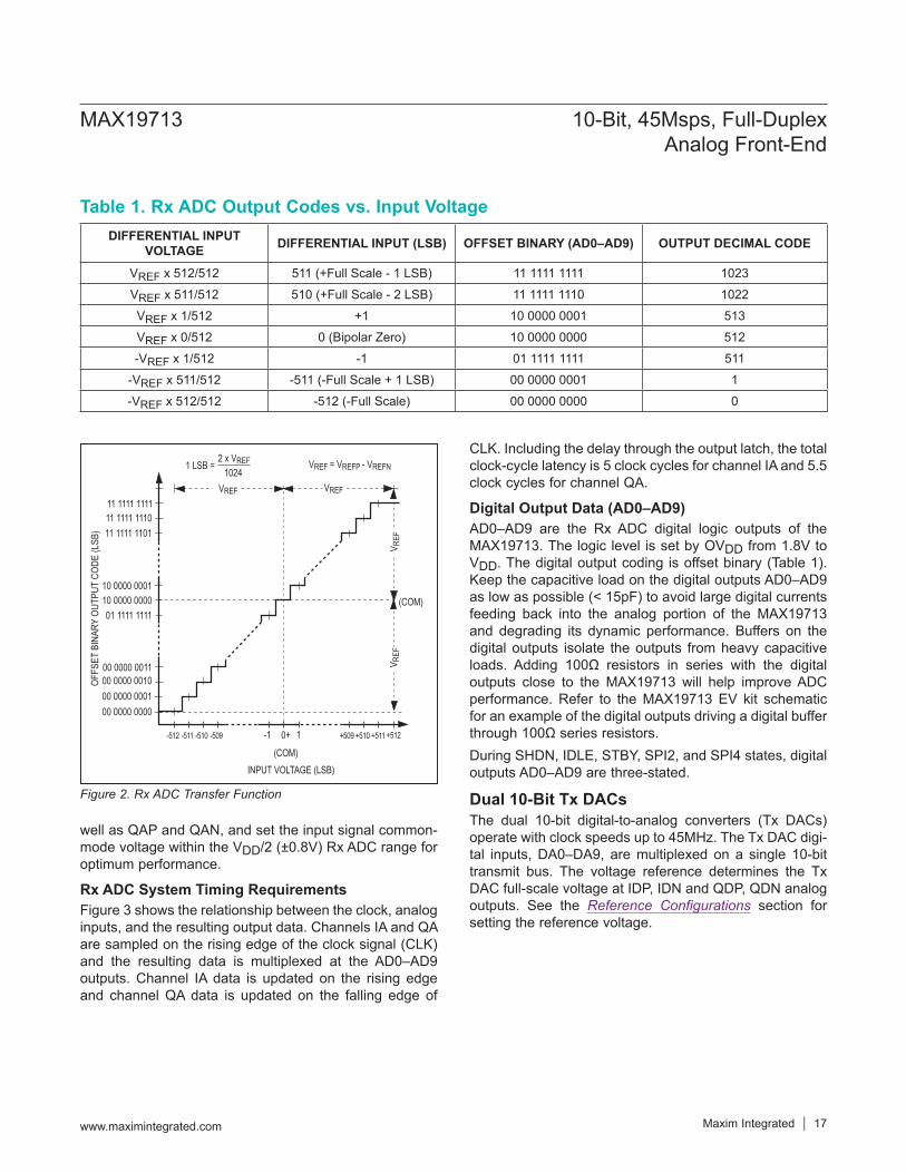
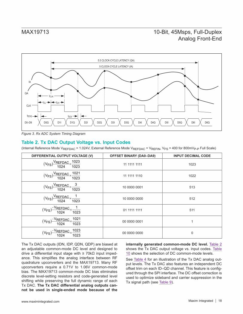
Rx ADC System Timing RequirementsFigure 3 shows the relationship between the clock, analog inputs, and the resulting output data. Channels IA and QA are sampled on the rising edge of the clock signal (CLK) and the resulting data is multiplexed at the AD0–AD9 outputs. Channel IA data is updated on the rising edge and channel QA data is updated on the falling edge of
CLK. Including the delay through the output latch, the total clock-cycle latency is 5 clock cycles for channel IA and 5.5 clock cycles for channel QA.
Digital Output Data (AD0–AD9)AD0–AD9 are the Rx ADC digital logic outputs of the MAX19713. The logic level is set by OVDD from 1.8V to VDD. The digital output coding is offset binary (Table 1). Keep the capacitive load on the digital outputs AD0–AD9 as low as possible (< 15pF) to avoid large digital currents feeding back into the analog portion of the MAX19713 and degrading its dynamic performance. Buffers on the digital outputs isolate the outputs from heavy capacitive loads. Adding 100Ω resistors in series with the digital outputs close to the MAX19713 will help improve ADC performance. Refer to the MAX19713 EV kit schematic for an example of the digital outputs driving a digital buffer through 100Ω series resistors.During SHDN, IDLE, STBY, SPI2, and SPI4 states, digital outputs AD0–AD9 are three-stated.
Dual 10-Bit Tx DACsThe dual 10-bit digital-to-analog converters (Tx DACs) operate with clock speeds up to 45MHz. The Tx DAC digi-tal inputs, DA0–DA9, are multiplexed on a single 10-bit transmit bus. The voltage reference determines the Tx DAC full-scale voltage at IDP, IDN and QDP, QDN analog outputs. See the Reference Configurations section for setting the reference voltage.
Figure 2. Rx ADC Transfer Function
Table 1. Rx ADC Output Codes vs. Input VoltageDIFFERENTIAL INPUT
VOLTAGE DIFFERENTIAL INPUT (LSB) OFFSET BINARY (AD0–AD9) OUTPUT DECIMAL CODE
VREF x 512/512 511 (+Full Scale - 1 LSB) 11 1111 1111 1023
VREF x 511/512 510 (+Full Scale - 2 LSB) 11 1111 1110 1022
VREF x 1/512 +1 10 0000 0001 513
VREF x 0/512 0 (Bipolar Zero) 10 0000 0000 512
-VREF x 1/512 -1 01 1111 1111 511
-VREF x 511/512 -511 (-Full Scale + 1 LSB) 00 0000 0001 1
-VREF x 512/512 -512 (-Full Scale) 00 0000 0000 0
INPUT VOLTAGE (LSB)
-1-510 -509
10242 x VREF1 LSB = VREF = VREFP - VREFN
VREF VREF
V REF
V REF
0+ 1-511 +510 +512+511-512 +509
(COM)
(COM)
OFFS
ET B
INAR
Y OU
TPUT
COD
E (L
SB)
00 0000 000000 0000 000100 0000 001000 0000 0011
11 1111 111111 1111 111011 1111 1101
01 1111 111110 0000 000010 0000 0001
MAX19713 10-Bit, 45Msps, Full-DuplexAnalog Front-End
www.maximintegrated.com Maxim Integrated 17
(Internal Reference Mode VREFDAC = 1.024V, External Reference Mode VREFDAC = VREFIN, VFS = 400 for 800mVP-P Full Scale)
The Tx DAC outputs (IDN, IDP, QDN, QDP) are biased at an adjustable common-mode DC level and designed to drive a differential input stage with ≥ 70kΩ input imped-ance. This simplifies the analog interface between RF quadrature upconverters and the MAX19713. Many RF upconverters require a 0.71V to 1.06V common-mode bias. The MAX19713 common-mode DC bias eliminates discrete level-setting resistors and code-generated level shifting while preserving the full dynamic range of each Tx DAC. The Tx DAC differential analog outputs can-not be used in single-ended mode because of the
internally generated common-mode DC level. Table 2 shows the Tx DAC output voltage vs. input codes. Table 10 shows the selection of DC common-mode levels.See Table 4 for an illustration of the Tx DAC analog out-put levels. The Tx DAC also features an independent DC offset trim on each ID–QD channel. This feature is config-ured through the SPI interface. The DC offset correction is used to optimize sideband and carrier suppression in the Tx signal path (see Table 9).
Figure 3. Rx ADC System Timing Diagram
Table 2. Tx DAC Output Voltage vs. Input Codes
DIFFERENTIAL OUTPUT VOLTAGE (V) OFFSET BINARY (DA0–DA9) INPUT DECIMAL CODE
11 1111 1111 1023
11 1111 1110 1022
10 0000 0001 513
10 0000 0000 512
01 1111 1111 511
00 0000 0001 1
00 0000 0000 0
( ) REFDACFS
V 1023V1024 1023
×
( ) REFDACFS
V 1021V1024 1023
×
( ) REFDACFS
V 3V1024 1023
×
( ) REFDACFS
V 1V1024 1023
×
( ) REFDACFS
V 1V1024 1023
−×
( ) REFDACFS
V 1021V1024 1023
−×
( ) REFDACFS
V 1023V1024 1023
−×
tDOQ
tCL tCH
tCLK
tDOI
5 CLOCK-CYCLE LATENCY (IA)
5.5 CLOCK-CYCLE LATENCY (QA)
D0–D9 D0Q D1I D1Q D2I D2Q D3I D3Q D4I D4Q D5I D5Q D6I D6Q
IA
QA
CLK
MAX19713 10-Bit, 45Msps, Full-DuplexAnalog Front-End
www.maximintegrated.com Maxim Integrated 18
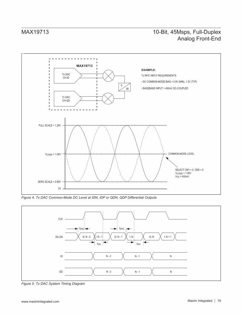
Figure 4. Tx DAC Common-Mode DC Level at IDN, IDP or QDN, QDP Differential Outputs
Figure 5. Tx DAC System Timing Diagram
0
FULL SCALE = 1.26V
VCOMD = 1.06V
ZERO SCALE = 0.86V
0V
COMMON-MODE LEVEL
EXAMPLE:
Tx RFIC INPUT REQUIREMENTS
• DC COMMON-MODE BIAS = 0.9V (MIN), 1.3V (TYP)
• BASEBAND INPUT = 400mV DC-COUPLED90
MAX19713
SELECT CM1 = 0, CM0 = 0VCOMD = 1.06VVFS = 400mV
Tx DACCH-ID
Tx DACCH-QD
tDSQ
tDSI
Q: N - 2 I: N - 1D0–D9
CLK
ID
QD
Q: N - 1 I: N Q: N I: N + 1
N - 2 N - 1 N
N - 2 N - 1 N
tDHQ
tDHI
Figure 4
MAX19713 10-Bit, 45Msps, Full-DuplexAnalog Front-End
www.maximintegrated.com Maxim Integrated 19
Tx DAC TimingFigure 5 shows the relationship among the clock, input data, and analog outputs. Channel ID data is latched on the falling edge of the clock signal, and channel QD data is latched on the rising edge of the clock signal, at which point both ID and QD outputs are simultaneously updated.
3-Wire Serial Interface and Operation ModesThe 3-wire serial interface controls the MAX19713 opera-tion modes as well as the three 12-bit aux-DACs and the 10-bit aux-ADC. Upon power-up, program the MAX19713 to operate in the desired mode. Use the 3-wire serial inter-face to program the device for shutdown, idle, standby, FD, Rx, Tx, aux-DAC controls, or aux-ADC conversion. A 16-bit data register sets the mode control as shown in Table 3. The 16-bit word is composed of four control bits (A3–A0) and 12 data bits (D11–D0). Data is shifted in MSB first (D11) and LSB last (A0) format. Table 4 shows the MAX19713 power-management modes. Table 5 shows the SPI-controlled Tx, Rx, and FD modes. The serial interface remains active in all modes.
SPI Register DescriptionProgram the control bits, A3–A0, in the register as shown in Table 3 to select the operating mode. Modify A3–A0 bits to select from ENABLE-16, Aux-DAC1, Aux-DAC2, Aux-DAC3, IOFFSET, QOFFSET, COMSEL, Aux-ADC, ENABLE-8, and WAKEUP-SEL modes. ENABLE-16 is the default operating mode (Table 6). This mode allows for shutdown, idle, and standby states as well as switching between FAST, SLOW, Rx and Tx modes. Table 4 and Table 5 show the required SPI settings for each mode.In ENABLE-16 mode, the aux-DACs have independent control bits E4, E5, and E6, bit E9 enables the aux-ADC. Table 7 shows the auxiliary DAC enable codes. Table 8 shows the auxiliary ADC enable code. Bits E11 and E10 are reserved. Program bits E11 and E10 to logic-low. Bits E3, E7, and E8 are not used.Modes aux-DAC1, aux-DAC2, and aux-DAC3 select the aux-DAC channels named DAC1, DAC2, and DAC3 and hold the data inputs for each DAC. Bits _D11–_D0 are the data inputs for each aux-DAC and can be programmed through SPI. The MAX19713 also includes two 6-bit reg-isters that can be programmed to adjust the offsets for the Tx DAC ID and QD channels independently (see Table 9). Use the COMSEL mode to select the output common-mode voltage with bits CM1 and CM0 (Table 10). Use aux-ADC mode to start the auxiliary ADC conversion (see the 10-Bit, 333ksps Auxiliary ADC section for details). Use ENABLE-8 mode for faster enable and switching
between shutdown, idle, and standby states as well as switching between FAST, SLOW, Rx and Tx modes and the FD mode.The WAKEUP-SEL register selects the operating mode that the MAX19713 is to enter immediately after coming out of shutdown (Table 11). See the Wake-Up Function section for more information.Shutdown mode offers the most dramatic power savings by shutting down all the analog sections (including the reference) of the MAX19713. In shutdown mode, the Rx ADC digital outputs are in three-state mode, the Tx DAC digital inputs are internally pulled to OVDD, and the Tx DAC outputs are at 0V. When the Rx ADC outputs transi-tion from three-state to active mode, the last converted word is placed on the digital output bus. The Tx DAC previously stored data is lost when coming out of shut-down mode. The wake-up time from shutdown mode is dominated by the time required to charge the capacitors at REFP, REFN, and COM. In internal reference mode and buffered external reference mode, the wake-up time is typically 500μs to enter Rx mode, 26.4μs to enter Tx mode, and 500μs to enter FD mode.In all operating modes, the Tx DAC inputs DA0–DA9 are internally pulled to OVDD. To reduce the supply current of the MAX19713 in shutdown mode do not pull DA0–DA9 low. This consideration is especially important in shut-down mode to achieve the lowest quiescent current.In idle mode, the reference and clock distribution circuits are powered, but all other functions are off. The Rx ADC outputs AD0–AD9 are forced to three-state. The Tx DAC DA0–DA9 inputs are internally pulled to OVDD, while the Tx DAC outputs are at 0V. The wake-up time is 3.7μs to enter Rx mode, 5.1μs to enter Tx mode, and 5.1μs to enter FD mode. When the Rx ADC outputs transition from three-state to active, the last converted word is placed on the digital output bus.In standby mode, the reference is powered but all other device functions are off. The wake-up time from standby mode is 3.8μs to enter Rx mode, 24.4μs to enter Tx mode, and 24.4μs to enter FD mode. When the Rx ADC outputs transition from three-state to active, the last con-verted word is placed on the digital output bus.
FAST and SLOW Rx and Tx ModesThe MAX19713 features FAST and SLOW modes for switching between Rx and Tx operation. In FAST Tx mode, the Rx ADC core is powered on but the ADC digital outputs AD0–AD9 are three-stated. The Tx DAC digital bus is active and the DAC core is fully operational.
MAX19713 10-Bit, 45Msps, Full-DuplexAnalog Front-End
www.maximintegrated.com Maxim Integrated 20
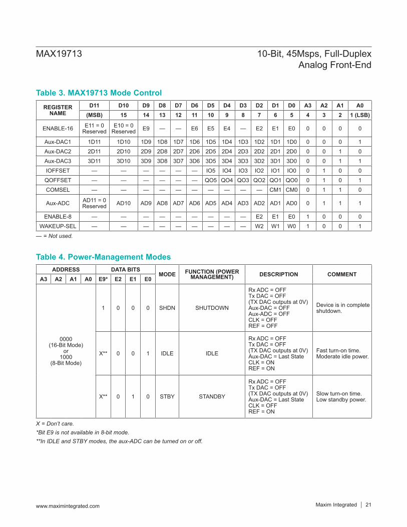
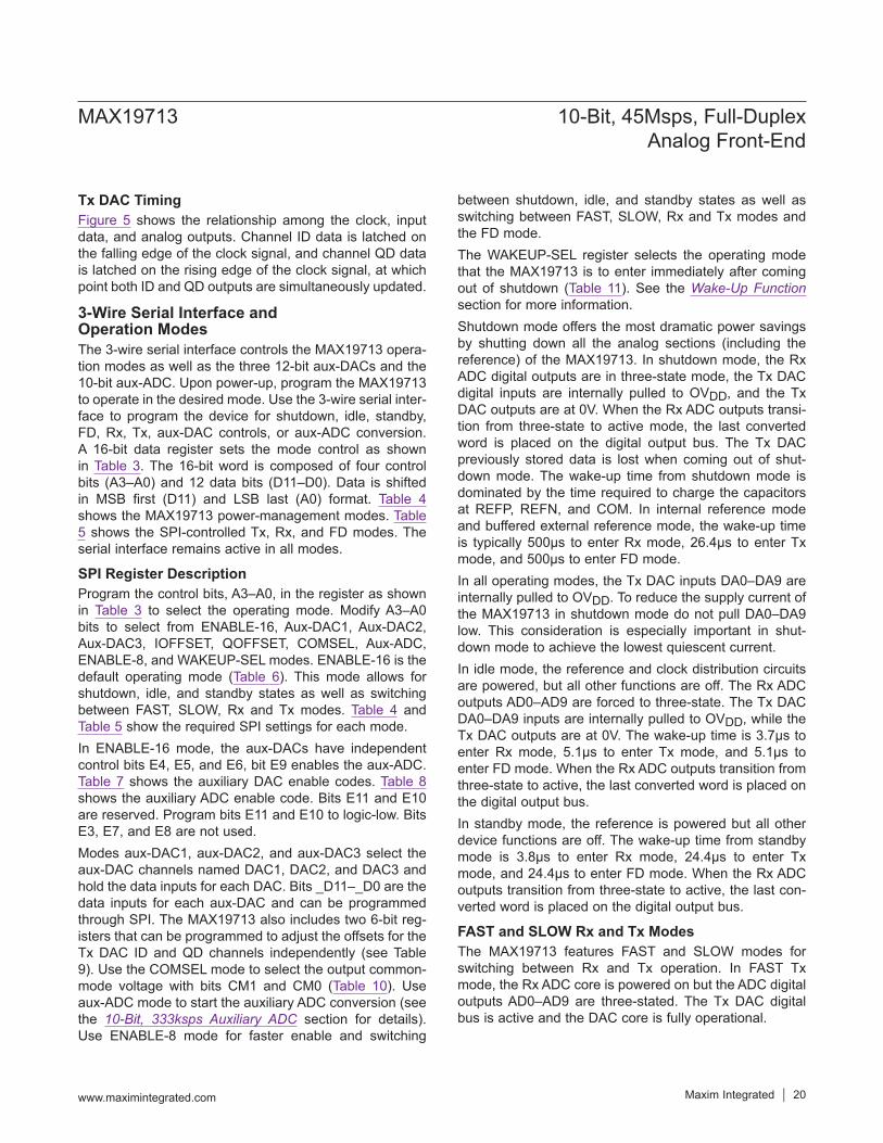
Table 3. MAX19713 Mode Control
Table 4. Power-Management Modes
— = Not used.
X = Don’t care.*Bit E9 is not available in 8-bit mode.**In IDLE and STBY modes, the aux-ADC can be turned on or off.
REGISTER NAME
D11 D10 D9 D8 D7 D6 D5 D4 D3 D2 D1 D0 A3 A2 A1 A0(MSB) 15 14 13 12 11 10 9 8 7 6 5 4 3 2 1 (LSB)
ENABLE-16 E11 = 0 Reserved
E10 = 0 Reserved E9 — — E6 E5 E4 — E2 E1 E0 0 0 0 0
Aux-DAC1 1D11 1D10 1D9 1D8 1D7 1D6 1D5 1D4 1D3 1D2 1D1 1D0 0 0 0 1
Aux-DAC2 2D11 2D10 2D9 2D8 2D7 2D6 2D5 2D4 2D3 2D2 2D1 2D0 0 0 1 0
Aux-DAC3 3D11 3D10 3D9 3D8 3D7 3D6 3D5 3D4 3D3 3D2 3D1 3D0 0 0 1 1
IOFFSET — — — — — — IO5 IO4 IO3 IO2 IO1 IO0 0 1 0 0
QOFFSET — — — — — — QO5 QO4 QO3 QO2 QO1 QO0 0 1 0 1
COMSEL — — — — — — — — — — CM1 CM0 0 1 1 0
Aux-ADC AD11 = 0 Reserved AD10 AD9 AD8 AD7 AD6 AD5 AD4 AD3 AD2 AD1 AD0 0 1 1 1
ENABLE-8 — — — — — — — — — E2 E1 E0 1 0 0 0
WAKEUP-SEL — — — — — — — — — W2 W1 W0 1 0 0 1
ADDRESS DATA BITSMODE FUNCTION (POWER
MANAGEMENT) DESCRIPTION COMMENTA3 A2 A1 A0 E9* E2 E1 E0
0000 (16-Bit Mode)
or 1000
(8-Bit Mode)
1 0 0 0 SHDN SHUTDOWN
Rx ADC = OFF Tx DAC = OFF (TX DAC outputs at 0V) Aux-DAC = OFF Aux-ADC = OFF CLK = OFF REF = OFF
Device is in complete shutdown.
X** 0 0 1 IDLE IDLE
Rx ADC = OFF Tx DAC = OFF (TX DAC outputs at 0V) Aux-DAC = Last State CLK = ON REF = ON
Fast turn-on time. Moderate idle power.
X** 0 1 0 STBY STANDBY
Rx ADC = OFF Tx DAC = OFF (TX DAC outputs at 0V) Aux-DAC = Last State CLK = OFF REF = ON
Slow turn-on time. Low standby power.
MAX19713 10-Bit, 45Msps, Full-DuplexAnalog Front-End
www.maximintegrated.com Maxim Integrated 21
In FAST Rx mode, the Tx DAC core is powered on. The Tx DAC outputs are set to midscale. In this mode, the Tx DAC input bus is disconnected from the DAC core and DA0–DA9 are internally pulled to OVDD. The Rx ADC digital bus is active and the ADC core is fully operational.In FAST mode, the switching time from Tx to Rx, or Rx to Tx is minimized because the converters are on and do not have to recover from a power-down state. In FAST mode, the switching time from Rx to Tx and Tx to Rx is 0.1μs. Power consumption is higher in FAST mode because both Tx and Rx cores are always on.In SLOW Tx mode, the Rx ADC core is powered off and the ADC digital outputs AD0–AD9 are three-stated. The
Tx DAC digital bus is active and the DAC core is fully operational. In SLOW Rx mode, the Tx DAC core is powered off. The Tx DAC outputs are set to 0. In SLOW Rx mode, the Tx DAC input bus is disconnected from the DAC core and DA0–DA9 are internally pulled to OVDD. The Rx ADC digital bus is active and the ADC core is fully operational. The switching times for SLOW modes are 4.9μs for Rx to Tx and 3.7μs for Tx to Rx.Power consumption in SLOW Tx mode is 49.5mW, and 79.2mW in SLOW Rx mode. Power consumption in FAST Tx mode is 89.1mW, and 86.4mW in FAST Rx mode.
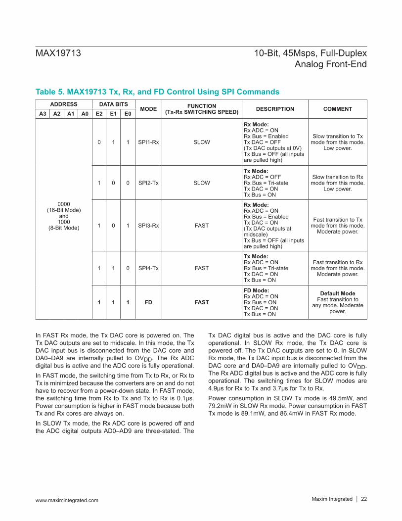
Table 5. MAX19713 Tx, Rx, and FD Control Using SPI CommandsADDRESS DATA BITS
MODE FUNCTION (Tx-Rx SWITCHING SPEED) DESCRIPTION COMMENT
A3 A2 A1 A0 E2 E1 E0
0000 (16-Bit Mode)
and 1000
(8-Bit Mode)
0 1 1 SPI1-Rx SLOW
Rx Mode: Rx ADC = ON Rx Bus = Enabled Tx DAC = OFF (Tx DAC outputs at 0V) Tx Bus = OFF (all inputs are pulled high)
Slow transition to Tx mode from this mode.
Low power.
1 0 0 SPI2-Tx SLOW
Tx Mode: Rx ADC = OFF Rx Bus = Tri-state Tx DAC = ON Tx Bus = ON
Slow transition to Rx mode from this mode.
Low power.
1 0 1 SPI3-Rx FAST
Rx Mode: Rx ADC = ON Rx Bus = Enabled Tx DAC = ON (Tx DAC outputs at midscale) Tx Bus = OFF (all inputs are pulled high)
Fast transition to Tx mode from this mode.
Moderate power.
1 1 0 SPI4-Tx FAST
Tx Mode: Rx ADC = ON Rx Bus = Tri-state Tx DAC = ON Tx Bus = ON
Fast transition to Rx mode from this mode.
Moderate power.
1 1 1 FD FAST
FD Mode: Rx ADC = ON Rx Bus = ON Tx DAC = ON Tx Bus = ON
Default Mode Fast transition to
any mode. Moderate power.
MAX19713 10-Bit, 45Msps, Full-DuplexAnalog Front-End
www.maximintegrated.com Maxim Integrated 22
FD ModeThe MAX19713 features an FD mode, which is ideal for applications supporting frequency-division duplex. In FD mode, both Rx ADC and Tx DAC, as well as their respec-tive digital buses, are active and the device can receive and transmit simultaneously. Switching from FD mode to other Rx or Tx modes is fast (0.1μs) since the on-board
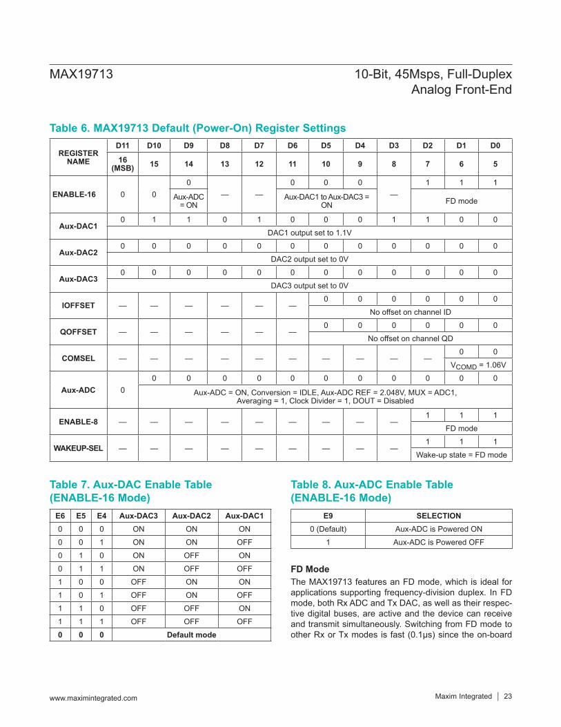
Table 6. MAX19713 Default (Power-On) Register Settings
Table 7. Aux-DAC Enable Table (ENABLE-16 Mode)
Table 8. Aux-ADC Enable Table (ENABLE-16 Mode)
REGISTER NAME
D11 D10 D9 D8 D7 D6 D5 D4 D3 D2 D1 D0
16 (MSB) 15 14 13 12 11 10 9 8 7 6 5
ENABLE-16 0 00
— —0 0 0
—1 1 1
Aux-ADC = ON
Aux-DAC1 to Aux-DAC3 = ON FD mode
Aux-DAC10 1 1 0 1 0 0 0 1 1 0 0
DAC1 output set to 1.1V
Aux-DAC20 0 0 0 0 0 0 0 0 0 0 0
DAC2 output set to 0V
Aux-DAC30 0 0 0 0 0 0 0 0 0 0 0
DAC3 output set to 0V
IOFFSET — — — — — —0 0 0 0 0 0
No offset on channel ID
QOFFSET — — — — — —0 0 0 0 0 0
No offset on channel QD
COMSEL — — — — — — — — — —0 0
VCOMD = 1.06V
Aux-ADC 00 0 0 0 0 0 0 0 0 0 0
Aux-ADC = ON, Conversion = IDLE, Aux-ADC REF = 2.048V, MUX = ADC1, Averaging = 1, Clock Divider = 1, DOUT = Disabled
ENABLE-8 — — — — — — — — —1 1 1
FD mode
WAKEUP-SEL — — — — — — — — —1 1 1
Wake-up state = FD mode
E6 E5 E4 Aux-DAC3 Aux-DAC2 Aux-DAC10 0 0 ON ON ON
0 0 1 ON ON OFF
0 1 0 ON OFF ON
0 1 1 ON OFF OFF
1 0 0 OFF ON ON
1 0 1 OFF ON OFF
1 1 0 OFF OFF ON
1 1 1 OFF OFF OFF
0 0 0 Default mode
E9 SELECTION0 (Default) Aux-ADC is Powered ON
1 Aux-ADC is Powered OFF
MAX19713 10-Bit, 45Msps, Full-DuplexAnalog Front-End
www.maximintegrated.com Maxim Integrated 23
converters are already powered. Consequently, power consumption in this mode is the maximum of all operating modes. In FD mode the MAX19713 consumes 91.8mW.
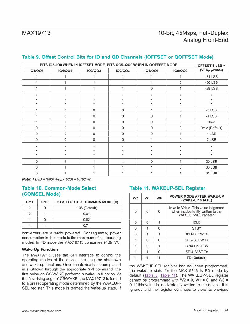
Wake-Up FunctionThe MAX19713 uses the SPI interface to control the operating modes of the device including the shutdown and wake-up functions. Once the device has been placed in shutdown through the appropriate SPI command, the first pulse on CS/WAKE performs a wake-up function. At the first rising edge of CS/WAKE, the MAX19713 is forced to a preset operating mode determined by the WAKEUP-SEL register. This mode is termed the wake-up state. If
the WAKEUP-SEL register has not been programmed, the wake-up state for the MAX19713 is FD mode by default (Table 6, Table 11). The WAKEUP-SEL register cannot be programmed with W2 = 0, W1 = 0, and W0 = 0. If this value is inadvertently written to the device, it is ignored and the register continues to store its previous
Table 9. Offset Control Bits for ID and QD Channels (IOFFSET or QOFFSET Mode)
Table 10. Common-Mode Select (COMSEL Mode)
Table 11. WAKEUP-SEL Register
Note: 1 LSB = (800mVP-P/1023) = 0.782mV.
BITS IO5–IO0 WHEN IN IOFFSET MODE, BITS QO5–QO0 WHEN IN QOFFSET MODE OFFSET 1 LSB = (VFSP-P/1023)IO5/QO5 IO4/QO4 IO3/QO3 IO2/QO2 IO1/QO1 IO0/QO0
1 1 1 1 1 1 -31 LSB
1 1 1 1 1 0 -30 LSB
1 1 1 1 0 1 -29 LSB
• • •
• • •
• • •
• • •
• • •
• • •
• • •
1 0 0 0 1 0 -2 LSB
1 0 0 0 0 1 -1 LSB
1 0 0 0 0 0 0mV
0 0 0 0 0 0 0mV (Default)
0 0 0 0 0 1 1 LSB
0 0 0 0 1 0 2 LSB
• • •
• • •
• • •
• • •
• • •
• • •
• • •
0 1 1 1 0 1 29 LSB
0 1 1 1 1 0 30 LSB
0 1 1 1 1 1 31 LSB
CM1 CM0 Tx PATH OUTPUT COMMON MODE (V)0 0 1.06 (Default)
0 1 0.94
1 0 0.82
1 1 0.71
W2 W1 W0 POWER MODE AFTER WAKE-UP (WAKE-UP STATE)
0 0 0Invalid Value. This value is ignored
when inadvertently written to the WAKEUP-SEL register.
0 0 1 IDLE
0 1 0 STBY
0 1 1 SPI1-SLOW Rx
1 0 0 SPI2-SLOW Tx
1 0 1 SPI3-FAST Rx
1 1 0 SPI4-FAST Tx
1 1 1 FD (Default)
MAX19713 10-Bit, 45Msps, Full-DuplexAnalog Front-End
www.maximintegrated.com Maxim Integrated 24
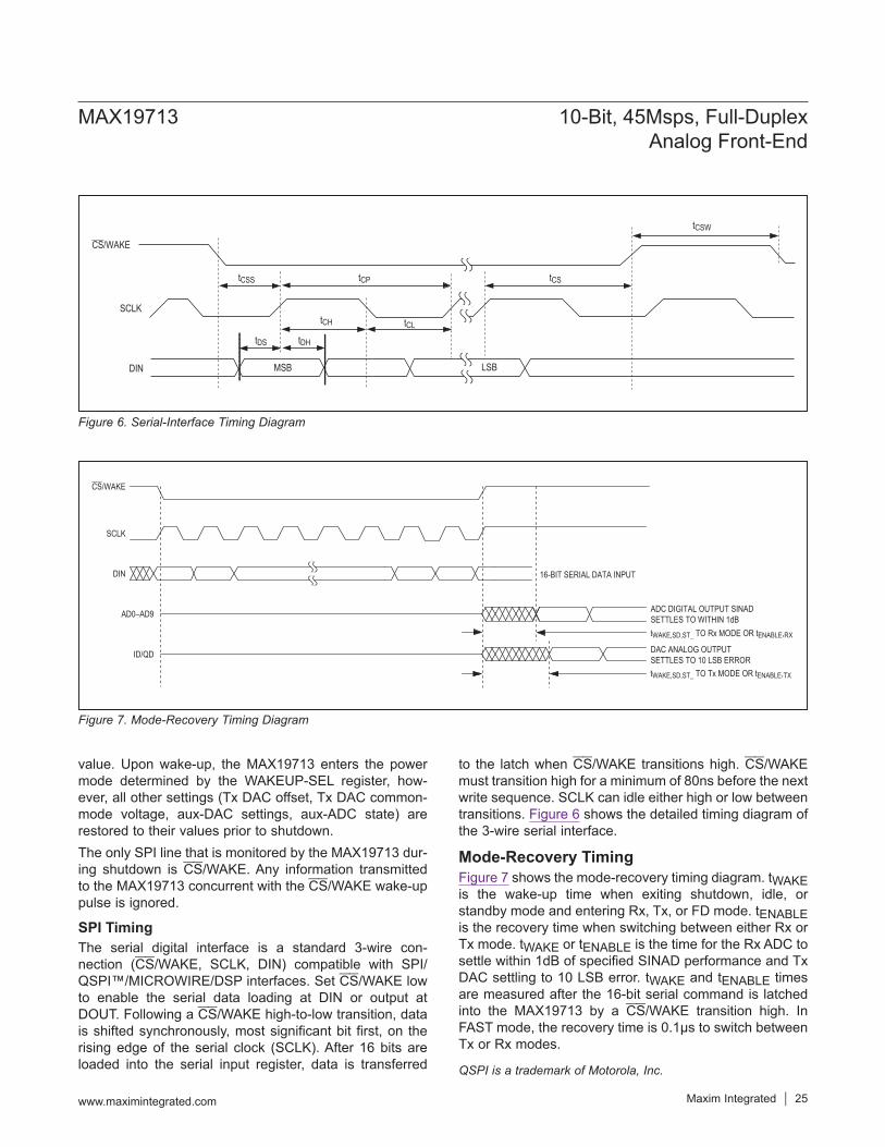
value. Upon wake-up, the MAX19713 enters the power mode determined by the WAKEUP-SEL register, how-ever, all other settings (Tx DAC offset, Tx DAC common-mode voltage, aux-DAC settings, aux-ADC state) are restored to their values prior to shutdown.The only SPI line that is monitored by the MAX19713 dur-ing shutdown is CS/WAKE. Any information transmitted to the MAX19713 concurrent with the CS/WAKE wake-up pulse is ignored.
SPI TimingThe serial digital interface is a standard 3-wire con-nection (CS/WAKE, SCLK, DIN) compatible with SPI/QSPI™/MICROWIRE/DSP interfaces. Set CS/WAKE low to enable the serial data loading at DIN or output at DOUT. Following a CS/WAKE high-to-low transition, data is shifted synchronously, most significant bit first, on the rising edge of the serial clock (SCLK). After 16 bits are loaded into the serial input register, data is transferred
to the latch when CS/WAKE transitions high. CS/WAKE must transition high for a minimum of 80ns before the next write sequence. SCLK can idle either high or low between transitions. Figure 6 shows the detailed timing diagram of the 3-wire serial interface.
Mode-Recovery TimingFigure 7 shows the mode-recovery timing diagram. tWAKE is the wake-up time when exiting shutdown, idle, or standby mode and entering Rx, Tx, or FD mode. tENABLE is the recovery time when switching between either Rx or Tx mode. tWAKE or tENABLE is the time for the Rx ADC to settle within 1dB of specified SINAD performance and Tx DAC settling to 10 LSB error. tWAKE and tENABLE times are measured after the 16-bit serial command is latched into the MAX19713 by a CS/WAKE transition high. In FAST mode, the recovery time is 0.1μs to switch between Tx or Rx modes.
Figure 6. Serial-Interface Timing Diagram
Figure 7. Mode-Recovery Timing Diagram
QSPI is a trademark of Motorola, Inc.
tCSW
tCS
LSB
tCL
tCP
tCH
tDHtDS
MSB
tCSS
SCLK
DIN
CS/WAKE
CS/WAKE
SCLK
DIN 16-BIT SERIAL DATA INPUT
AD0–AD9
ID/QD DAC ANALOG OUTPUTSETTLES TO 10 LSB ERROR
ADC DIGITAL OUTPUT SINADSETTLES TO WITHIN 1dBtWAKE,SD,ST_ TO Rx MODE OR tENABLE,RX
tWAKE,SD,ST_ TO Tx MODE OR tENABLE,TX
MAX19713 10-Bit, 45Msps, Full-DuplexAnalog Front-End
www.maximintegrated.com Maxim Integrated 25
System Clock Input (CLK)Both the Rx ADC and Tx DAC share the CLK input. The CLK input accepts a CMOS-compatible signal level set by OVDD from 1.8V to VDD. Since the interstage conversion of the device depends on the repeatability of the rising and falling edges of the external clock, use a clock with low jitter and fast rise and fall times (< 2ns). Specifically, sampling occurs on the rising edge of the clock signal, requiring this edge to provide the lowest possible jitter. Any significant clock jitter limits the SNR performance of the on-chip Rx ADC as follows:
IN AJ
1 SNR 20 log2 f t
= × ×π× ×
where fIN represents the analog input frequency and tAJ is the time of the clock jitter.Clock jitter is especially critical for undersampling applica-tions. Consider the clock input as an analog input and route away from any analog input or other digital signal lines. The MAX19713 clock input operates with an OVDD/2 voltage threshold and accepts a 50% ±10% duty cycle.When the clock signal is stopped at CLK input (CLK = 0 or OVDD), all internal registers hold their last value and the MAX19713 saves the last power-management mode or Tx/Rx/FD command. All converter circuits (Rx ADC, Tx DAC, aux-ADC, and aux-DACs) hold their last value. When the clock signal is restarted at CLK, allow 3.8μs (clock wake-up time) for the internal clock circuitry to settle before updating the Tx DAC, reading a valid Rx ADC conversion result, or starting an aux-ADC conver-sion. This ensures the converters (Rx ADC, Tx DAC, aux-ADC) meet all dynamic performance specifications. The aux-DAC channels are not dependent on CLK, so they can be updated when CLK is idle.
12-Bit, Auxiliary Control DACsThe MAX19713 includes three 12-bit aux-DACs (DAC1, DAC2, DAC3) with 1μs settling time for controlling vari-able- gain amplifier (VGA), automatic gain-control (AGC), and automatic frequency-control (AFC) functions. The aux-DAC output range is 0.2V to 2.57V as defined by VOH - VOL. During power-up, the VGA and AGC outputs (DAC2 and DAC3) are at zero. The AFC DAC (DAC1) is at 1.1V during power-up. The aux-DACs can be independently controlled through the SPI bus, except during SHDN mode where the aux-DACs are turned off completely and the output voltage is set to zero. In STBY and IDLE modes the aux-DACs maintain the last value. On wake-up from SHDN, the aux-DACs resume the last values.
Loading on the aux-DAC outputs should be carefully observed to achieve the specified settling time and stabil-ity. The capacitive load must be kept to a maximum of 5pF including package and trace capacitance. The resistive load must be greater than 200kΩ. If capacitive loading exceeds 5pF, then add a 10kΩ resistor in series with the output. Adding the series resistor helps drive larger load capaci-tance (< 15pF) at the expense of slower settling time.
10-Bit, 333ksps Auxiliary ADCThe MAX19713 integrates a 333ksps, 10-bit aux-ADC with an input 4:1 multiplexer. In the aux-ADC mode regis-ter, setting bit AD0 begins a conversion with the auxiliary ADC. Bit AD0 automatically clears when the conversion is complete. Setting or clearing AD0 during a conversion has no effect (Table 12). Bit AD1 determines the internal reference of the auxiliary ADC (Table 13). Bits AD2 and AD3 determine the auxiliary ADC input source (Table 14). Bits AD4, AD5, and AD6 select the number of averages taken when a single start-convert command is given. The conversion time increases as the number of averages increases (Table 15). The conversion clock can be divided down from the system clock by properly setting bits AD7, AD8, and AD9 (Table 16). The aux-ADC output data can be written out of DOUT by setting bit AD10 high (Table 17).The aux-ADC features a 4:1 input multiplexer to allow measurements on four input sources. The input sources are selected by AD3 and AD2 (Table 14). Two of the multiplexer inputs (ADC1 and ADC2) can be connected to external sources such as an RF power detector like the MAX2208 or temperature sensor like the MAX6613. The other two multiplexer inputs are internal connections to VDD and OVDD that monitor the powersupply volt-ages. The internal VDD and OVDD connections are made through integrated dividers that yield VDD/2 and OVDD/2 measurement results. The aux- ADC voltage reference can be selected between an internal 2.048V bandgap reference or VDD (Table 13). The VDD reference selec-tion is provided to allow measurement of an external voltage source with a full-scale range extending beyond the 2.048V level. The input source voltage range cannot extend above VDD.The conversion requires 12 clock edges (1 for input sampling, 1 for each of the 10 bits, and 1 at the end for loading into the serial output register) to complete one conversion cycle (when no averaging is being done). Each conversion of an average (when averaging is set greater than 1) requires 12 clock edges. The conversion clock is generated from the system clock input (CLK). An SPI-programmable divider divides the system clock by the appropriate divisor (set with bits AD7, AD8, and
MAX19713 10-Bit, 45Msps, Full-DuplexAnalog Front-End
www.maximintegrated.com Maxim Integrated 26
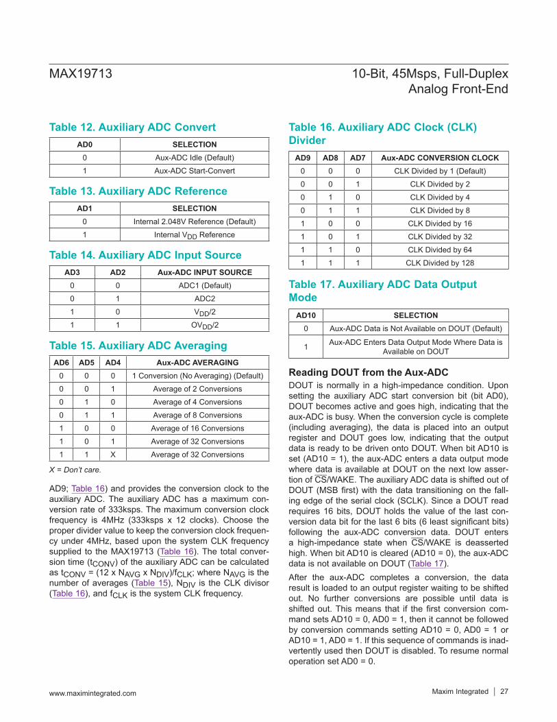
AD9; Table 16) and provides the conversion clock to the auxiliary ADC. The auxiliary ADC has a maximum con-version rate of 333ksps. The maximum conversion clock frequency is 4MHz (333ksps x 12 clocks). Choose the proper divider value to keep the conversion clock frequen-cy under 4MHz, based upon the system CLK frequency supplied to the MAX19713 (Table 16). The total conver-sion time (tCONV) of the auxiliary ADC can be calculated as tCONV = (12 x NAVG x NDIV)/fCLK; where NAVG is the number of averages (Table 15), NDIV is the CLK divisor (Table 16), and fCLK is the system CLK frequency.
Reading DOUT from the Aux-ADCDOUT is normally in a high-impedance condition. Upon setting the auxiliary ADC start conversion bit (bit AD0), DOUT becomes active and goes high, indicating that the aux-ADC is busy. When the conversion cycle is complete (including averaging), the data is placed into an output register and DOUT goes low, indicating that the output data is ready to be driven onto DOUT. When bit AD10 is set (AD10 = 1), the aux-ADC enters a data output mode where data is available at DOUT on the next low asser-tion of CS/WAKE. The auxiliary ADC data is shifted out of DOUT (MSB first) with the data transitioning on the fall-ing edge of the serial clock (SCLK). Since a DOUT read requires 16 bits, DOUT holds the value of the last con-version data bit for the last 6 bits (6 least significant bits) following the aux-ADC conversion data. DOUT enters a high-impedance state when CS/WAKE is deasserted high. When bit AD10 is cleared (AD10 = 0), the aux-ADC data is not available on DOUT (Table 17).After the aux-ADC completes a conversion, the data result is loaded to an output register waiting to be shifted out. No further conversions are possible until data is shifted out. This means that if the first conversion com-mand sets AD10 = 0, AD0 = 1, then it cannot be followed by conversion commands setting AD10 = 0, AD0 = 1 or AD10 = 1, AD0 = 1. If this sequence of commands is inad-vertently used then DOUT is disabled. To resume normal operation set AD0 = 0.
Table 12. Auxiliary ADC Convert
Table 13. Auxiliary ADC Reference
Table 14. Auxiliary ADC Input Source
Table 15. Auxiliary ADC Averaging
Table 16. Auxiliary ADC Clock (CLK) Divider
Table 17. Auxiliary ADC Data Output Mode
X = Don’t care.
AD0 SELECTION0 Aux-ADC Idle (Default)
1 Aux-ADC Start-Convert
AD1 SELECTION0 Internal 2.048V Reference (Default)
1 Internal VDD Reference
AD3 AD2 Aux-ADC INPUT SOURCE0 0 ADC1 (Default)
0 1 ADC2
1 0 VDD/2
1 1 OVDD/2
AD6 AD5 AD4 Aux-ADC AVERAGING0 0 0 1 Conversion (No Averaging) (Default)
0 0 1 Average of 2 Conversions
0 1 0 Average of 4 Conversions
0 1 1 Average of 8 Conversions
1 0 0 Average of 16 Conversions
1 0 1 Average of 32 Conversions
1 1 X Average of 32 Conversions
AD9 AD8 AD7 Aux-ADC CONVERSION CLOCK0 0 0 CLK Divided by 1 (Default)
0 0 1 CLK Divided by 2
0 1 0 CLK Divided by 4
0 1 1 CLK Divided by 8
1 0 0 CLK Divided by 16
1 0 1 CLK Divided by 32
1 1 0 CLK Divided by 64
1 1 1 CLK Divided by 128
AD10 SELECTION0 Aux-ADC Data is Not Available on DOUT (Default)
1 Aux-ADC Enters Data Output Mode Where Data is Available on DOUT
MAX19713 10-Bit, 45Msps, Full-DuplexAnalog Front-End
www.maximintegrated.com Maxim Integrated 27
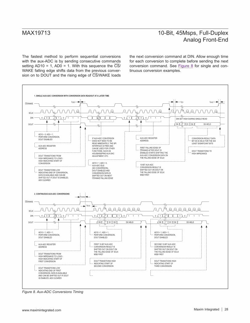
The fastest method to perform sequential conversions with the aux-ADC is by sending consecutive commands setting AD10 = 1, AD0 = 1. With this sequence the CS/WAKE falling edge shifts data from the previous conver-sion on to DOUT and the rising edge of CS/WAKE loads
the next conversion command at DIN. Allow enough time for each conversion to complete before sending the next conversion command. See Figure 8 for single and con-tinuous conversion examples.
Figure 8. Aux-ADC Conversions Timing
CS/WAKE
2. CONTINUOUS AUX-ADC CONVERSIONS
tDCS
tCONV
SCLK
0 00 1 11 1 110 0 11 1 110 0 11 1
16 1 10 11 12 13 14 15 16 1 10 11 12 13 14 15 161
DIN
DOUT D1 D0 D0 HELDD9D1 D0 D0 HELDD9
FIRST 10-BIT AUX-ADCCONVERSION RESULT ISSHIFTED OUT ON DOUT ONTHE FALLING EDGE OF SCLK MSB FIRST
SECOND 10-BIT AUX-ADCCONVERSION RESULT ISSHIFTED OUT ON DOUT ONTHE FALLING EDGE OF SCLK MSB FIRST
AD10 = 1, AD0 = 1, PERFORM CONVERSION, DOUT ENABLED
AD10 = 1, AD0 = 1, PERFORM CONVERSION, DOUT ENABLED
AD10 = 1, AD0 = 1, PERFORM CONVERSION, DOUT ENABLED
DOUT TRANSITIONS FROM HIGH IMPEDANCE TO LOGIC- HIGH INDICATING START OFFIRST CONVERSION DOUT TRANSITIONS HIGH
INDICATING START OFSECOND CONVERSION
DOUT TRANSITIONS HIGH INDICATING START OFTHIRD CONVERSION
DOUT TRANSITIONS LOW INDICATING END OF FIRST CONVERSION, DATA IS AVAILABLE AND CAN BE SHIFTED OUT IF DOUT IS ENABLED, AD0 CLEARED
AUX-ADC REGISTERADDRESS
tCSD tCD tCHZCS/WAKE
SCLK
1. SINGLE AUX-ADC CONVERSION WITH CONVERSION DATA READOUT AT A LATER TIME
1
0 0 1 1 0 1 0 0 1 DIN SET HIGH DURING SINGLE READ1 11 1
16 1 16 1 16 1 1610
D1 D0 D0 HELDD9
11
DIN
DOUT
AD10 = 0, AD0 = 1, PERFORM CONVERSION, DOUT DISABLED
DOUT TRANSITIONS FROM HIGH IMPEDANCE TO LOGIC- HIGH INDICATING START OFCONVERSION
DOUT TRANSITIONS LOW INDICATING END OF CONVERSION, DATA IS AVAILABLE AND CAN BESHIFTED OUT IF DOUT IS ENABLED, AD0 CLEARED
0
IF AUX-ADC CONVERSIONDOES NOT NEED TO BE READ IMMEDIATELY, THE SPIINTERFACE IS FREE AND CAN BE USED FOR OTHERFUNCTIONS, SUCH ASHOUSEKEEPING AUX-DACADJUSTMENT, ETC.
AUX-ADC REGISTERADDRESS
CONVERSION RESULT DATABIT D0 IS HELD FOR THE SIXLEAST SIGNIFICANT BITS
DOUT TRANSITIONS TOHIGH IMPEDANCE
10-BIT AUX-ADCCONVERSION RESULT ISSHIFTED OUT ON DOUT ONTHE FALLING EDGE OF SCLK MSB FIRST
AUX-ADC REGISTERADDRESS
AD10 = 1, AD0 = 0,AUX-ADC IDLE (NO CONVERSION),DOUT ENABLED ANDCONVERSION DATA ISSHIFTED OUT ON NEXTCS/WAKE FALLING EDGE
FIRST FALLING EDGE OFCS/WAKE AFTER DOUT ISENABLED STARTS SHIFTING THE AUX-ADC CONVERSION DATA ON THE FALLING EDGE OF SCLK
MAX19713 10-Bit, 45Msps, Full-DuplexAnalog Front-End
www.maximintegrated.com Maxim Integrated 28

DIN can be written independent of DOUT state. A 16-bit instruction at DIN updates the device configuration. To prevent modifying internal registers while reading data from DOUT, hold DIN at a high state (only applies if sequential aux-ADC conversions are not executed). This effectively writes all ones into address 1111. Since address 1111 does not exist, no internal registers are affected.
Reference ConfigurationsThe MAX19713 features an internal precision 1.024V- bandgap reference that is stable over the entire power-supply and temperature ranges. The REFIN input pro-vides two modes of reference operation. The voltage at REFIN (VREFIN) sets the reference operation mode (Table 18).In internal reference mode, connect REFIN to VDD. VREF is an internally generated 0.512V ±4% reference level. COM, REFP, and REFN are low-impedance outputs with VCOM = VDD/2, VREFP = VDD/2 + VREF/2, and VREFN = VDD/2 - VREF/2. Bypass REFP, REFN, and COM each with a 0.33μF capacitor. Bypass REFIN to GND with a 0.1μF capacitor.In buffered external reference mode, apply 1.024V ±10% at REFIN. In this mode, COM, REFP, and REFN are low-impedance outputs with VCOM = VDD/2, VREFP = VDD/2 + VREFIN/4, and VREFN = VDD/2 - VREFIN/4. Bypass REFP, REFN, and COM each with a 0.33μF capacitor. Bypass REFIN to GND with a 0.1μF capacitor. In this mode, the Tx DAC full-scale output is proportional to the external reference. For example, if the VREFIN is increased by 10% (max), the Tx DAC full-scale output is also increased by 10% or ±440mV.
Applications InformationUsing Balun Transformer AC-CouplingAn RF transformer (Figure 9) provides an excellent solution to convert a single-ended signal source to a fully differential signal for optimum ADC performance. Connecting the center tap of the transformer to COM provides a VDD/2 DC level shift to the input. A 1:1 trans-former can be used, or a step-up transformer can be selected to reduce the drive requirements. In general, the MAX19713 provides better SFDR and THD with fully differential input signals than single-ended signals, especially for high input frequencies. In differential mode, even-order harmonics are lower as both inputs (IAP, IAN, QAP, QAN) are balanced, and each of the Rx ADC inputs
Figure 9. Balun Transformer-Coupled Single-Ended-to-Differential Input Drive for Rx ADC
Table 18. Reference ModesVREFIN REFERENCE MODE
> 0.8V x VDDInternal Reference Mode. VREF is internally generated to be 0.512V. Bypass REFP, REFN, and COM each with a 0.33µF capacitor.
1.024V ±10%Buffered External Reference Mode. An external 1.024V ±10% reference voltage is applied to REFIN. VREF is internally generated to be VREFIN/2. Bypass REFP, REFN, and COM each with a 0.33µF capacitor. Bypass REFIN to GND with a 0.1µF capacitor.
COM
IAP
IAN
25Ω
0.1µF0.33µF
25Ω
0.1µFVIN
MAX1971322pF
22pF
QAP
QAN
25Ω
0.1µF0.33µF
25Ω
0.1µFVIN
22pF
22pF
MAX19713 10-Bit, 45Msps, Full-DuplexAnalog Front-End
www.maximintegrated.com Maxim Integrated 29
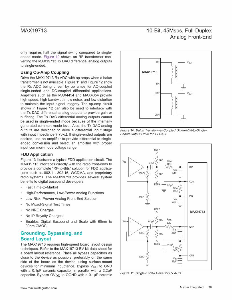
only requires half the signal swing compared to single-ended mode. Figure 10 shows an RF transformer con-verting the MAX19713 Tx DAC differential analog outputs to single-ended.
Using Op-Amp CouplingDrive the MAX19713 Rx ADC with op amps when a balun transformer is not available. Figure 11 and Figure 12 show the Rx ADC being driven by op amps for AC-coupled single-ended and DC-coupled differential applications. Amplifiers such as the MAX4454 and MAX4354 provide high speed, high bandwidth, low noise, and low distortion to maintain the input signal integrity. The op-amp circuit shown in Figure 12 can also be used to interface with the Tx DAC differential analog outputs to provide gain or buffering. The Tx DAC differential analog outputs cannot be used in single-ended mode because of the internally generated common-mode level. Also, the Tx DAC analog outputs are designed to drive a differential input stage with input impedance ≥ 70kΩ. If single-ended outputs are desired, use an amplifier to provide differential-to-single-ended conversion and select an amplifier with proper input common-mode voltage range.
FDD ApplicationFigure 13 illustrates a typical FDD application circuit. The MAX19713 interfaces directly with the radio front-ends to provide a complete “RF-to-Bits” solution for FDD applica-tions such as 802.11, 802.16, WCDMA, and proprietary radio systems. The MAX19713 provides several system benefits to digital baseband developers:• Fast Time-to-Market• High-Performance, Low-Power Analog Functions• Low-Risk, Proven Analog Front-End Solution• No Mixed-Signal Test Times• No NRE Charges• No IP Royalty Charges• Enables Digital Baseband and Scale with 65nm to
90nm CMOS
Grounding, Bypassing, and Board LayoutThe MAX19713 requires high-speed board layout design techniques. Refer to the MAX19713 EV kit data sheet for a board layout reference. Place all bypass capacitors as close to the device as possible, preferably on the same side of the board as the device, using surface-mount devices for minimum inductance. Bypass VDD to GND with a 0.1μF ceramic capacitor in parallel with a 2.2μF capacitor. Bypass OVDD to OGND with a 0.1μF ceramic
Figure 10. Balun Transformer-Coupled Differential-to-Single-Ended Output Drive for Tx DAC
Figure 11. Single-Ended Drive for Rx ADC
MAX19713
IDP
IDN
VOUT
QDP
QDN
VOUT
MAX19713
0.1µF
1kΩ
1kΩ100Ω
100Ω
CIN22pF
CIN22pF
QAP
QAN
COM
IAP
IAN
0.1µFRISO50Ω
RISO50Ω
REFP
REFN
VIN
0.1µF
1kΩ
1kΩ100Ωt
100Ω
CIN22pF
CIN22pF
0.1µFRISO50Ω
RISO50Ω
REFP
REFN
VIN
MAX19713 10-Bit, 45Msps, Full-DuplexAnalog Front-End
www.maximintegrated.com Maxim Integrated 30
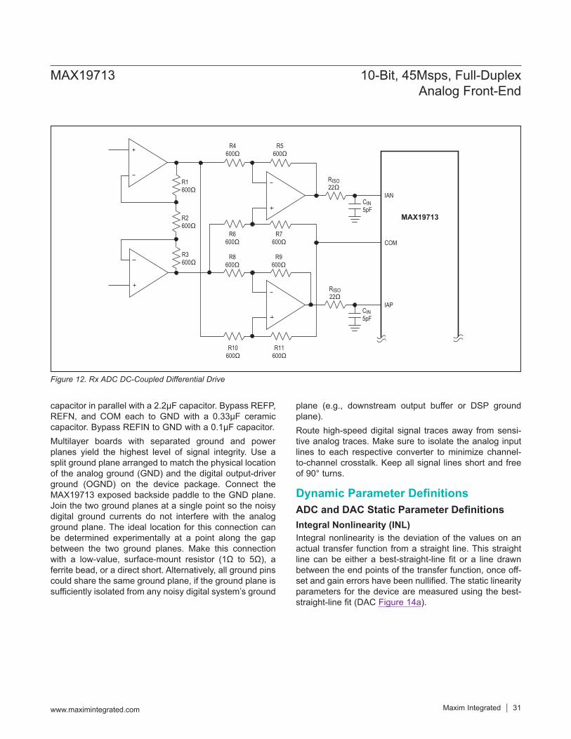
capacitor in parallel with a 2.2μF capacitor. Bypass REFP, REFN, and COM each to GND with a 0.33μF ceramic capacitor. Bypass REFIN to GND with a 0.1μF capacitor.Multilayer boards with separated ground and power planes yield the highest level of signal integrity. Use a split ground plane arranged to match the physical location of the analog ground (GND) and the digital output-driver ground (OGND) on the device package. Connect the MAX19713 exposed backside paddle to the GND plane. Join the two ground planes at a single point so the noisy digital ground currents do not interfere with the analog ground plane. The ideal location for this connection can be determined experimentally at a point along the gap between the two ground planes. Make this connection with a low-value, surface-mount resistor (1Ω to 5Ω), a ferrite bead, or a direct short. Alternatively, all ground pins could share the same ground plane, if the ground plane is sufficiently isolated from any noisy digital system’s ground
plane (e.g., downstream output buffer or DSP ground plane).Route high-speed digital signal traces away from sensi-tive analog traces. Make sure to isolate the analog input lines to each respective converter to minimize channel-to-channel crosstalk. Keep all signal lines short and free of 90° turns.
Dynamic Parameter DefinitionsADC and DAC Static Parameter DefinitionsIntegral Nonlinearity (INL)Integral nonlinearity is the deviation of the values on an actual transfer function from a straight line. This straight line can be either a best-straight-line fit or a line drawn between the end points of the transfer function, once off-set and gain errors have been nullified. The static linearity parameters for the device are measured using the best-straight-line fit (DAC Figure 14a).
Figure 12. Rx ADC DC-Coupled Differential Drive
MAX19713
IAP
COM
IAN
RISO22Ω
RISO22Ω
R11600Ω
R9600Ω
R3600Ω
R2600Ω
R1600Ω
R10600Ω
R8600Ω
R5600Ω
R4600Ω
R7600Ω
R6600Ω
CIN5pF
CIN5pF
MAX19713 10-Bit, 45Msps, Full-DuplexAnalog Front-End
www.maximintegrated.com Maxim Integrated 31
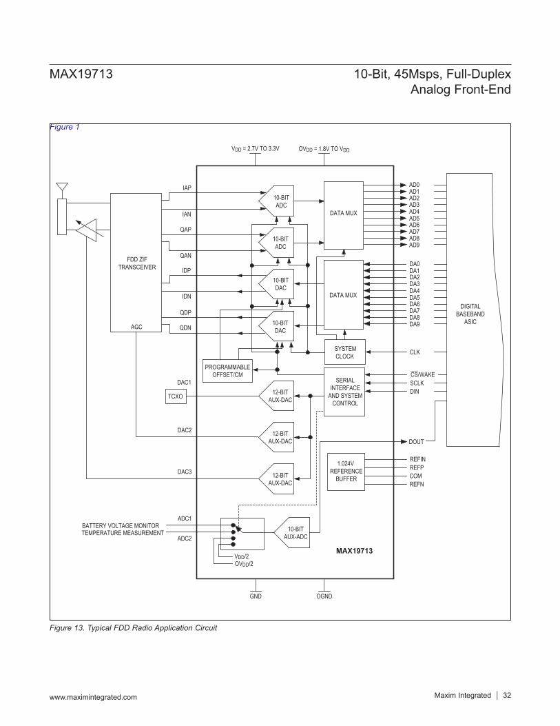
Figure 13. Typical FDD Radio Application Circuit
CLK
SERIALINTERFACE
AND SYSTEMCONTROL
IAP
IAN
QAP
QAN
IDP
IDN
QDP
QDN
REFPCOMREFN
DOUT
REFIN
DINSCLKCS/WAKE
SYSTEMCLOCK
PROGRAMMABLEOFFSET/CM
1.024V REFERENCE
BUFFER
10-BITADC
10-BITADC
10-BITDAC
10-BITDAC
12-BITAUX-DAC
12-BITAUX-DAC
10-BITAUX-ADC
12-BITAUX-DAC
GND
VDD/2OVDD/2
DAC1
DAC2
DAC3
ADC1
ADC2
OGND
VDD = 2.7V TO 3.3V OVDD = 1.8V TO VDD
DATA MUX
DATA MUX
DA0DA1DA2DA3DA4DA5DA6DA7DA8DA9
AD0AD1AD2AD3AD4AD5AD6AD7AD8AD9
MAX19713
DIGITALBASEBAND
ASIC
TCXO
FDD ZIFTRANSCEIVER
AGC
TEMPERATURE MEASUREMENTBATTERY VOLTAGE MONITOR
Figure 1
MAX19713 10-Bit, 45Msps, Full-DuplexAnalog Front-End
www.maximintegrated.com Maxim Integrated 32
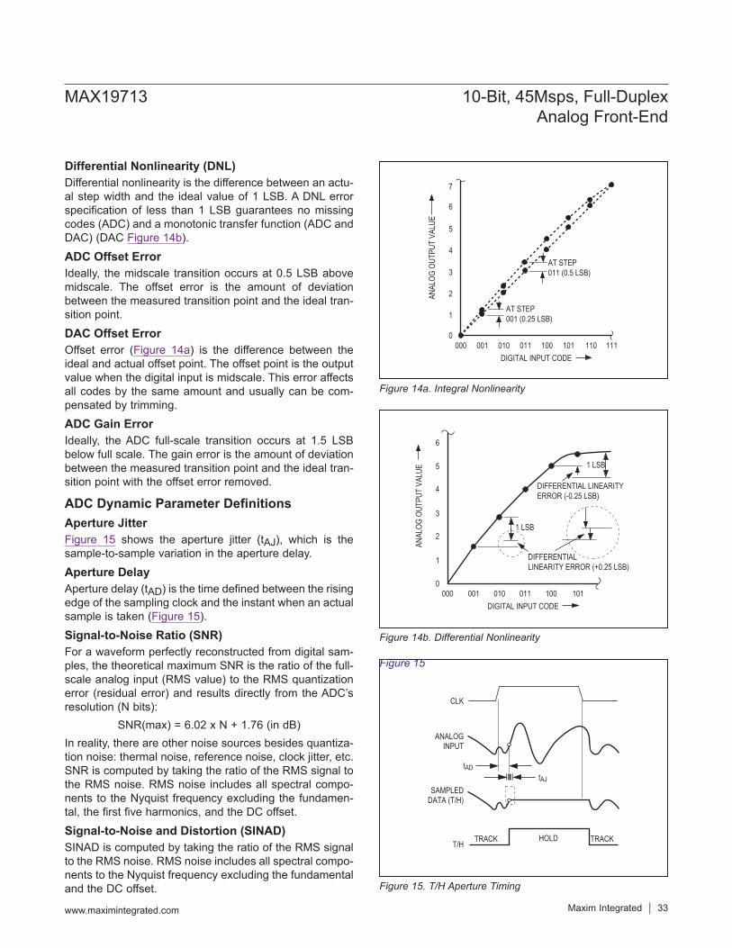
Differential Nonlinearity (DNL)Differential nonlinearity is the difference between an actu-al step width and the ideal value of 1 LSB. A DNL error specification of less than 1 LSB guarantees no missing codes (ADC) and a monotonic transfer function (ADC and DAC) (DAC Figure 14b).
ADC Offset ErrorIdeally, the midscale transition occurs at 0.5 LSB above midscale. The offset error is the amount of deviation between the measured transition point and the ideal tran-sition point.
DAC Offset ErrorOffset error (Figure 14a) is the difference between the ideal and actual offset point. The offset point is the output value when the digital input is midscale. This error affects all codes by the same amount and usually can be com-pensated by trimming.
ADC Gain ErrorIdeally, the ADC full-scale transition occurs at 1.5 LSB below full scale. The gain error is the amount of deviation between the measured transition point and the ideal tran-sition point with the offset error removed.
ADC Dynamic Parameter DefinitionsAperture JitterFigure 15 shows the aperture jitter (tAJ), which is the sample-to-sample variation in the aperture delay.
Aperture DelayAperture delay (tAD) is the time defined between the rising edge of the sampling clock and the instant when an actual sample is taken (Figure 15).
Signal-to-Noise Ratio (SNR)For a waveform perfectly reconstructed from digital sam-ples, the theoretical maximum SNR is the ratio of the full-scale analog input (RMS value) to the RMS quantization error (residual error) and results directly from the ADC’s resolution (N bits):
SNR(max) = 6.02 x N + 1.76 (in dB)In reality, there are other noise sources besides quantiza-tion noise: thermal noise, reference noise, clock jitter, etc. SNR is computed by taking the ratio of the RMS signal to the RMS noise. RMS noise includes all spectral compo-nents to the Nyquist frequency excluding the fundamen-tal, the first five harmonics, and the DC offset.
Signal-to-Noise and Distortion (SINAD)SINAD is computed by taking the ratio of the RMS signal to the RMS noise. RMS noise includes all spectral compo-nents to the Nyquist frequency excluding the fundamental and the DC offset.
Figure 14a. Integral Nonlinearity
Figure 14b. Differential Nonlinearity
Figure 15. T/H Aperture Timing
0
2
1
4
3
7
6
5
000 010001 011 100 101 110
AT STEP011 (0.5 LSB)
AT STEP001 (0.25 LSB)
111DIGITAL INPUT CODE
ANAL
OG O
UTPU
T VA
LUE
0
2
1
4
3
6
5
000 010001 011 100 101
DIFFERENTIAL LINEARITYERROR (-0.25 LSB)
DIFFERENTIALLINEARITY ERROR (+0.25 LSB)
1 LSB
1 LSB
DIGITAL INPUT CODE
ANAL
OG O
UTPU
T VA
LUE
HOLD
ANALOGINPUT
SAMPLEDDATA (T/H)
T/H
tADtAJ
TRACK TRACK
CLK
Figure 15
MAX19713 10-Bit, 45Msps, Full-DuplexAnalog Front-End
www.maximintegrated.com Maxim Integrated 33
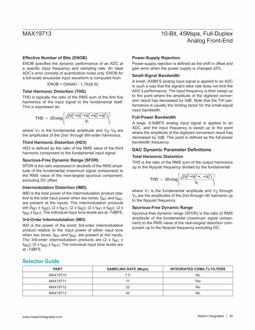
Effective Number of Bits (ENOB)ENOB specifies the dynamic performance of an ADC at a specific input frequency and sampling rate. An ideal ADC’s error consists of quantization noise only. ENOB for a full-scale sinusoidal input waveform is computed from:
ENOB = (SINAD - 1.76)/6.02
Total Harmonic Distortion (THD)THD is typically the ratio of the RMS sum of the first five harmonics of the input signal to the fundamental itself. This is expressed as:
2 2 2 2 22 3 4 5 6
1
(V +V +V +V +V )THD 20xlogV
=
where V1 is the fundamental amplitude and V2–V6 are the amplitudes of the 2nd- through 6th-order harmonics.
Third Harmonic Distortion (HD3)HD3 is defined as the ratio of the RMS value of the third harmonic component to the fundamental input signal.
Spurious-Free Dynamic Range (SFDR)SFDR is the ratio expressed in decibels of the RMS ampli-tude of the fundamental (maximum signal component) to the RMS value of the next-largest spurious component, excluding DC offset.
Intermodulation Distortion (IMD)IMD is the total power of the intermodulation product rela-tive to the total input power when two tones, fIN1 and fIN2, are present at the inputs. The intermodulation products are (fIN1 ± fIN2), (2 x fIN1), (2 x fIN2), (2 x fIN1 ± fIN2), (2 x fIN2 ± fIN1). The individual input tone levels are at -7dBFS.
3rd-Order Intermodulation (IM3)IM3 is the power of the worst 3rd-order intermodulation product relative to the input power of either input tone when two tones, fIN1 and fIN2, are present at the inputs. The 3rd-order intermodulation products are (2 x fIN1 ± fIN2), (2 x fIN2 ± fIN1). The individual input tone levels are at -7dBFS.
Power-Supply RejectionPower-supply rejection is defined as the shift in offset and gain error when the power supply is changed ±5%.
Small-Signal BandwidthA small -20dBFS analog input signal is applied to an ADC in such a way that the signal’s slew rate does not limit the ADC’s performance. The input frequency is then swept up to the point where the amplitude of the digitized conver-sion result has decreased by 3dB. Note that the T/H per-formance is usually the limiting factor for the small-signal input bandwidth.
Full-Power BandwidthA large -0.5dBFS analog input signal is applied to an ADC, and the input frequency is swept up to the point where the amplitude of the digitized conversion result has decreased by 3dB. This point is defined as the full-power bandwidth frequency.
DAC Dynamic Parameter DefinitionsTotal Harmonic DistortionTHD is the ratio of the RMS sum of the output harmonics up to the Nyquist frequency divided by the fundamental:
2 2 22 3 n
1
(V +V +...+V )THD 20xlogV
=
where V1 is the fundamental amplitude and V2 through Vn are the amplitudes of the 2nd through nth harmonic up to the Nyquist frequency.
Spurious-Free Dynamic RangeSpurious-free dynamic range (SFDR) is the ratio of RMS amplitude of the fundamental (maximum signal compo-nent) to the RMS value of the next-largest distortion com-ponent up to the Nyquist frequency excluding DC.
PART SAMPLING RATE (Msps) INTEGRATED CDMA Tx FILTERS MAX19710 7.5 No
MAX19711 11 Yes
MAX19712 22 No
MAX19713 45 No
MAX19713 10-Bit, 45Msps, Full-DuplexAnalog Front-End
www.maximintegrated.com Maxim Integrated 34
Selector Guide
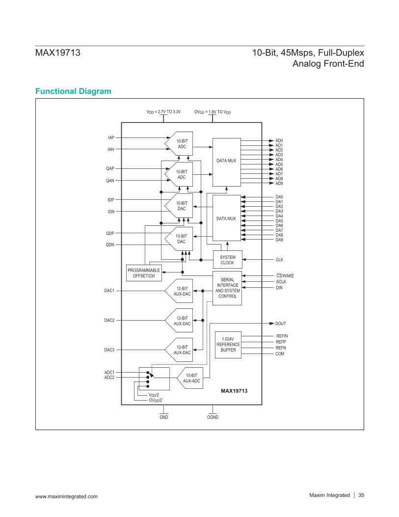
CLK
SERIALINTERFACE
AND SYSTEMCONTROL
IAP
IAN
QAP
QAN
IDP
IDN
QDP
QDN
REFPREFNCOM
DOUT
REFIN
DINSCLKCS/WAKE
SYSTEMCLOCK
PROGRAMMABLEOFFSET/CM
1.024V REFERENCE
BUFFER
10-BITADC
10-BITADC
10-BITDAC
10-BITDAC
12-BITAUX-DAC
12-BITAUX-DAC
12-BITAUX-DAC
GND
VDD/2OVDD/2
DAC1
DAC2
DAC3
ADC1 10-BITAUX-ADC
ADC2
OGND
VDD = 2.7V TO 3.3V OVDD = 1.8V TO VDD
DATA MUX
DATA MUX
DA0DA1DA2DA3DA4DA5DA6DA7DA8DA9
AD0AD1AD2AD3AD4AD5AD6AD7AD8AD9
MAX19713
MAX19713 10-Bit, 45Msps, Full-DuplexAnalog Front-End
www.maximintegrated.com Maxim Integrated 35
Functional Diagram
MAX19713 10-Bit, 45Msps, Full-DuplexAnalog Front-End
www.maximintegrated.com Maxim Integrated 36
Package InformationFor the latest package outline information and land patterns (footprints), go to www.maximintegrated.com/packages. Note that a “+”, “#”, or “-” in the package code indicates RoHS status only. Package drawings may show a different suffix character, but the drawing pertains to the package regardless of RoHS status.
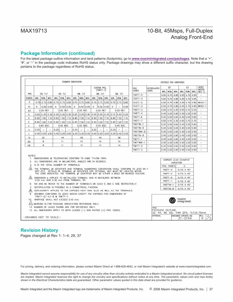
Maxim Integrated cannot assume responsibility for use of any circuitry other than circuitry entirely embodied in a Maxim Integrated product. No circuit patent licenses are implied. Maxim Integrated reserves the right to change the circuitry and specifications without notice at any time. The parametric values (min and max limits) shown in the Electrical Characteristics table are guaranteed. Other parametric values quoted in this data sheet are provided for guidance.
Maxim Integrated and the Maxim Integrated logo are trademarks of Maxim Integrated Products, Inc. © 2006 Maxim Integrated Products, Inc. 37
MAX19713 10-Bit, 45Msps, Full-DuplexAnalog Front-End
Package Information (continued)For the latest package outline information and land patterns (footprints), go to www.maximintegrated.com/packages. Note that a “+”, “#”, or “-” in the package code indicates RoHS status only. Package drawings may show a different suffix character, but the drawing pertains to the package regardless of RoHS status.
Revision HistoryPages changed at Rev 1: 1–4, 29, 37
For pricing, delivery, and ordering information, please contact Maxim Direct at 1-888-629-4642, or visit Maxim Integrated’s website at www.maximintegrated.com.