Embed Size (px)
Citation preview

General DescriptionMAX1846/MAX1847 high-efficiency PWM inverting controllers allow designers to implement compact, low-noise, negative-output DC-DC converters for telecom and networking applications. Both devices operate from +3V to +16.5V input and generate -500mV to -200V output. To minimize switching noise, both devices feature a current-mode, constant-frequency PWM control scheme. The operating frequency can be set from 100kHz to 500kHz through a resistor.The MAX1846 is available in an ultra-compact 10-pin µMAX® package. Operation at high frequency, com-patibility with ceramic capacitors, and inverting topol-ogy without transformers allow for a compact design. Compatibility with electrolytic capacitors and flexibility to operate down to 100kHz allow users to minimize the cost of external components. The high-current output drivers are designed to drive a P-channel MOSFET and allow the converter to deliver up to 30W.The MAX1847 features clock synchronization and shut-down functions. The MAX1847 can also be configured to operate as an inverting flyback controller with an N-channel MOSFET and a transformer to deliver up to 70W. The MAX1847 is available in a 16-pin QSOP package.Current-mode control simplifies compensation and provides good transient response. Accurate current-mode control and over current protection are achieved through low-side current sensing.
Applications Cellular Base Stations Networking Equipment Optical Networking Equipment SLIC Supplies CO DSL Line Driver Supplies Industrial Power Supplies Servers VOIP Supplies
Features 90% Efficiency +3.0V to +16.5V Input Range -500mV to -200V Output Drives High-Side P-Channel MOSFET 100kHz to 500kHz Switching Frequency Current-Mode, PWM Control Internal Soft-Start Electrolytic or Ceramic Output Capacitor The MAX1847 also offers:
Synchronization to External Clock Shutdown N-Channel Inverting Flyback Option
µMAX is a registered trademark of Maxim Integrated Products, Inc.
Pin Configurations appear at end of data sheet.
19-2091; Rev 4; 7/16
+Denotes a lead(Pb)-free/RoHS-compliant package.
PART TEMP RANGE PIN-PACKAGEMAX1846EUB -40°C to +85°C 10 µMAX
MAX1846EUB+ -40°C to +105°C 10 µMAX
MAX1847EEE -40°C to +85°C 16 QSOP
MAX1847EEE+ -40°C to +85°C 16 QSOP
MAX1846MAX1847
VL IN
COMP
FREQ
REFGND FB
PGND
CS
EXT
P
POSITIVEVIN
NEGATIVEVOUT
MAX1846/MAX1847 High-Efficiency, Current-Mode, Inverting PWM Controller
Typical Operating Circuit
Ordering Information
EVALUATION KIT AVAILABLE

IN, SHDN to GND .................................................-0.3V to +20VPGND to GND ......................................................-0.3V to +0.3VVL to PGND for VIN ≤ 5.7V ........................-0.3V to (VIN + 0.3V)VL to PGND for VIN > 5.7V .....................................-0.3V to +6VEXT to PGND .............................................-0.3V to (VIN + 0.3V)REF, COMP to GND ....................................-0.3V to (VL + 0.3V)CS, FB, FREQ, POL, SYNC to GND ......................-0.3V to +6V
Continuous Power Dissipation (TA = +70°C) 10-Pin µMAX (derate 5.6mW/°C above +70°C) ..........444mW 16-Pin QSOP (derate 8.3mW/°C above +70°C)..........696mWOperating Temperature Range ......................... -40°C to +105°CJunction Temperature ......................................................+150°CStorage Temperature Range ............................ -65°C to +150°CLead Temperature (soldering, 10s) .................................+300°CSoldering Temperature (reflow) Lead(Pb)-free...............................................................+260°C Containing lead(Pb) .....................................................+240°C
(VSHDN = VIN = +12V, SYNC = GND, PGND = GND, RFREQ = 147kΩ ±1%, CVL = 0.47µF, CREF = 0.1µF, TA = 0°C to +85°C, unless otherwise noted.)
PARAMETER CONDITIONS MIN TYP MAX UNITSPWM CONTROLLEROperating Input Voltage Range 3.0 16.5 V
UVLO ThresholdVIN rising
-40°C to ~+85°C 2.8 2.95V-40°C to ~+105°C 2.8 2.96
VIN falling-40°C to ~+85°C 2.6 2.74-40°C to ~+105°C 2.59 2.74
UVLO Hysteresis 60 mVFB Threshold No load -12 0 12 mVFB Input Current VFB = -0.1V -50 -6 50 nA
Load RegulationCCOMP = 0.068µF, VOUT = -48V, IOUT = 20mA to 200mA (Note 1)
-1 0 %
Line RegulationCCOMP = 0.068µF, VOUT = -48V, VIN = +8V to +16.5V, IOUT = 100mA
0.04 %
Current-Limit Threshold 85 100 115 mVCS Input Current CS = GND 10 20 µASupply Current VFB = -0.1V, VIN = +3.0V to +16.5V 0.75 1.2 mA
Shutdown Supply CurrentSHDN = GND, VIN = +3.0V to +16.5VVIN = +3.0V to +16.5V
10 25 µA
REFERENCE AND VL REGULATORREF Output Voltage IREF = 50µA 1.236 1.25 1.264 VREF Load Regulation IREF = 0 to 500µA -2 -15 mVVL Output Voltage IVL = 100µA 3.85 4.25 4.65 VVL Load Regulation IVL = 0.1mA to 2.0mA -20 -60 mV
www.maximintegrated.com Maxim Integrated 2
MAX1846/MAX1847 High-Efficiency, Current-Mode, Inverting PWM Controller
Electrical Characteristics
Stresses beyond those listed under “Absolute Maximum Ratings” may cause permanent damage to the device. These are stress ratings only, and functional operation of the device at these or any other conditions beyond those indicated in the operational sections of the specifications is not implied. Exposure to absolute maximum rating conditions for extended periods may affect device reliability.
Absolute Maximum Ratings

Note 1: Production test correlates to operating conditions.Note 2: Guaranteed by design and characterization.
(VSHDN = VIN = +12V, SYNC = GND, PGND = GND, RFREQ = 147kΩ ±1%, CVL = 0.47µF, CREF = 0.1µF, TA = 0°C to +85°C, unless otherwise noted.)
PARAMETER CONDITIONS MIN TYP MAX UNITSOSCILLATOR
Oscillator FrequencyRFREQ = 500kΩ ±1% 88 100 112
kHzRFREQ = 147kΩ ±1% 255 300 345RFREQ = 76.8kΩ ±1% 500
Maximum Duty CycleRFREQ = 500kΩ ±1% 93 96 98
%RFREQ = 147kΩ ±1% 85 88 92RFREQ = 76.8kΩ ±1% 80
SYNC Input Signal Duty-CycleRange
7 93 %
Minimum SYNC Input Logic-LowPulse Width
50 200 ns
SYNC Input Rise/Fall Time (Note 2) 200 nsSYNC Input Frequency Range 100 550 kHzDIGITAL INPUTSPOL, SYNC, SHDN Input HighVoltage
2.0 V
POL, SYNC, SHDN Input LowVoltage
0.45 V
POL, SYNC Input Current POL, SYNC = GND or VL 20 40 µA
SHDN Input CurrentVSHDN = +5V or GND -12 -4 0
µAVSHDN = +16.5V 1.5 6
SOFT-STARTSoft-Start Clock Cycles 1024Soft-Start Levels 64EXT OUTPUTEXT Sink/Source Current VIN = +5V, VEXT forced to +2.5V 1 A
EXT On-ResistanceEXT high or low, tested with 100mA load, VIN = +5V 3 7.5
ΩEXT high or low, tested with 100mA load, VIN = +3V 5 12
www.maximintegrated.com Maxim Integrated 3
MAX1846/MAX1847 High-Efficiency, Current-Mode, Inverting PWM Controller
Electrical Characteristics (continued)

(VSHDN = VIN = +12V, SYNC = GND, PGND = GND, RFREQ = 147kΩ ±1%, CVL = 0.47µF, CREF = 0.1µF, TA = -40°C to +85°C, unless otherwise noted.) (Note 3)
PARAMETER CONDITIONS MIN MAX UNITSPWM CONTROLLEROperating Input Voltage Range 3.0 16.5 V
UVLO ThresholdVIN rising 2.95
VVIN falling 2.6
FB Threshold No load -20 +20 mV
FB Input Current VFB = -0.1V-40°C to ~+85°C -50 +50
nA-40°C to ~+105°C -150 +150
Load RegulationCCOMP = 0.068µF, VOUT = -48V, IOUT= 20mA to 200mA (Note 1)
-2 0 %
Current Limit Threshold 85 115 mVCS Input Current CS = GND 20 µASupply Current VFB = -0.1V, VIN = +3.0V to +16.5V 1.2 mAShutdown Supply Current SHDN = GND, VIN = +3.0V to +16.5V 25 µAREFERENCE AND VL REGULATORREF Output Voltage IREF = 50µA 1.225 1.275 VREF Load Regulation IREF = 0 to 500µA -15 mVVL Output Voltage IVL = 100µA 3.85 4.65 VVL Load Regulation IVL = 0.1mA to 2.0mA -60 mVOSCILLATOR
Oscillator FrequencyRFREQ = 500kΩ ±1% 84 116
kHzRFREQ = 147kΩ ±1% 255 345
Maximum Duty CycleRFREQ = 500kΩ ±1% 93 98
%RFREQ = 147kΩ ±1% 84 93
SYNC Input Signal Duty-Cycle Range 7 93 %
Minimum SYNC Input Logic Low Pulse Width 200 ns
SYNC Input Rise/Fall Time (Note 2) 200 nsSYNC Input Frequency Range 100 550 kHzDIGITAL INPUTSPOL, SYNC, SHDN Input High Voltage 2.0 V
POL, SYNC, SHDN Input Low Voltage 0.45 V
www.maximintegrated.com Maxim Integrated 4
MAX1846/MAX1847 High-Efficiency, Current-Mode, Inverting PWM Controller
Electrical Characteristics
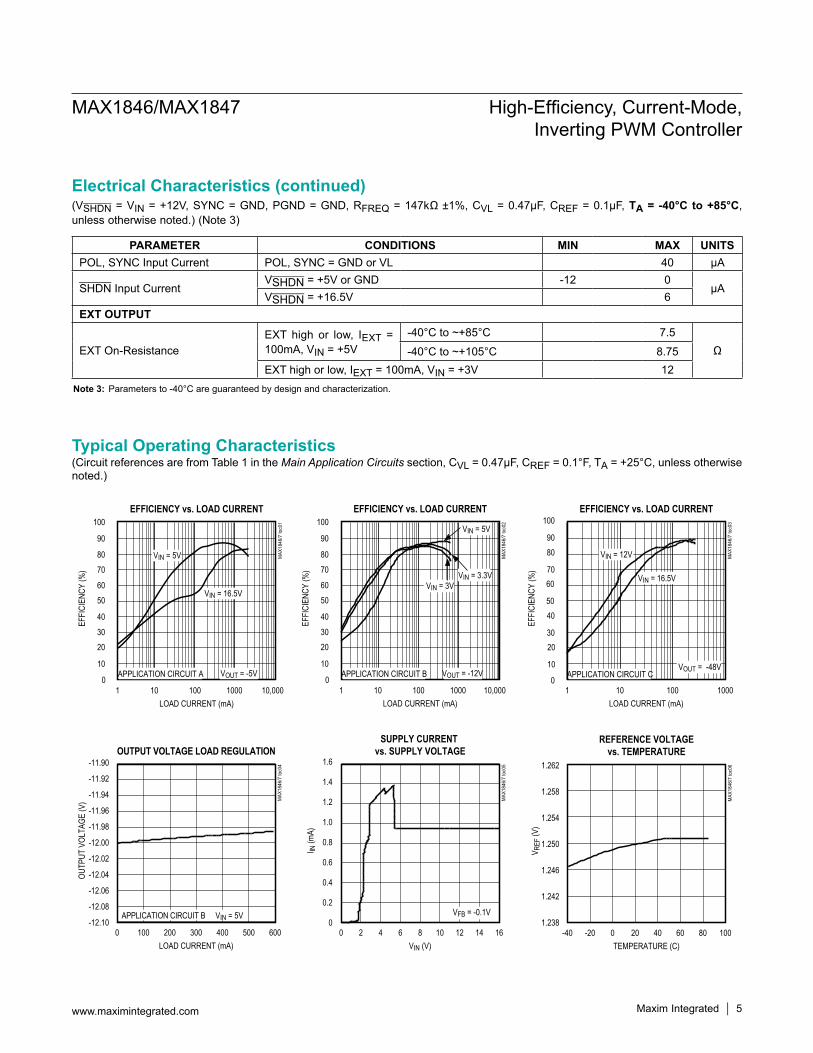
(Circuit references are from Table 1 in the Main Application Circuits section, CVL = 0.47µF, CREF = 0.1°F, TA = +25°C, unless otherwise noted.)
Note 3: Parameters to -40°C are guaranteed by design and characterization.
(VSHDN = VIN = +12V, SYNC = GND, PGND = GND, RFREQ = 147kΩ ±1%, CVL = 0.47µF, CREF = 0.1µF, TA = -40°C to +85°C, unless otherwise noted.) (Note 3)
PARAMETER CONDITIONS MIN MAX UNITSPOL, SYNC Input Current POL, SYNC = GND or VL 40 µA
SHDN Input CurrentVSHDN = +5V or GND -12 0
µAVSHDN = +16.5V 6
EXT OUTPUT
EXT On-ResistanceEXT high or low, IEXT = 100mA, VIN = +5V
-40°C to ~+85°C 7.5Ω-40°C to ~+105°C 8.75
EXT high or low, IEXT = 100mA, VIN = +3V 12
1.238
1.246
1.242
1.254
1.250
1.258
1.262
-40 20 40-20 0 60 80 100
REFERENCE VOLTAGEvs. TEMPERATURE
MAX
1846
/7 to
c06
TEMPERATURE (C)
V REF
(V)
0
0.4
0.2
0.8
0.6
1.0
1.2
1.4
1.6
0 4 62 8 10 12 14 16
SUPPLY CURRENT vs. SUPPLY VOLTAGE
MAX
1846
/7 to
c05
VIN (V)
I IN (m
A)
VFB = -0.1V-12.10
-12.04
-12.06
-12.08
-12.02
-12.00
-11.98
-11.96
-11.94
-11.92
-11.90
0 200100 300 400 500 600
OUTPUT VOLTAGE LOAD REGULATION
MAX
1846
/7 to
c04
LOAD CURRENT (mA)
OUTP
UT V
OLTA
GE (V
)
APPLICATION CIRCUIT B VIN = 5V
90
01 100010010
EFFICIENCY vs. LOAD CURRENT
30
10
70
50
100
40
20
80
60
MAX
1846
/7 to
c03
LOAD CURRENT (mA)
EFFI
CIEN
CY (%
)
VIN = 12V
VIN = 16.5V
APPLICATION CIRCUIT CVOUT = -48V
100
01 10 100 1000 10,000
EFFICIENCY vs. LOAD CURRENT
20
MAX
1846
/7 to
c02
LOAD CURRENT (mA)
EFFI
CIEN
CY (%
)
40
60
8070
50
30
10
90VIN = 5V
VIN = 3.3V
VOUT = -12VAPPLICATION CIRCUIT B
VIN = 3V
100
01 10 100 1000 10,000
EFFICIENCY vs. LOAD CURRENT
20
MAX
1846
/7 to
c01
LOAD CURRENT (mA)
EFFI
CIEN
CY (%
)
40
60
8070
50
30
10
90
VIN = 5V
VIN = 16.5V
VOUT = -5VAPPLICATION CIRCUIT A
Maxim Integrated 5www.maximintegrated.com
MAX1846/MAX1847 High-Efficiency, Current-Mode, Inverting PWM Controller
Typical Operating Characteristics
Electrical Characteristics (continued)

(Circuit references are from Table 1 in the Main Application Circuits section, CVL = 0.47µF, CREF = 0.1°F, TA = +25°C, unless otherwise noted.)
IL
0
5V/div
1A/div
5V/div
VOUT
EXITING SHUTDOWNMAX1846/7 toc15
APPLICATION CIRCUIT B1ms/div
SHDN
0
40
20
60
120
140
100
80
160
0 2000 4000 6000 8000 10,000
EXT RISE/FALL TIMEvs. CAPACITANCE
MAX
1846
/7 to
c14
CAPACITANCE (pF)
TIME
(ns)
RISE TIME
FALL TIME
VIN = 12V
SWITCHING FREQUENCYvs. TEMPERATURE
MAX
1846
/7 to
c13
294
295
297
296
300
301
299
298
302
FREQ
UENC
Y (kH
z)
-40 0 20-20 40 60 80 100TEMPERATURE (C)
RFREQ = 147k 1%
0
100
300
200
400
500
0 200100 300 400 500 600
SWITCHING FREQUENCYvs. RFREQ
MAX
1846
/7 to
c12
RFREQ (k)
f OSC
(kHz
)
0
4
2
8
6
12
10
14
-40 0 20-20 40 60 80 100
OPERATING CURRENTvs. TEMPERATURE
MAX
1846
/7 to
c11
TEMPERATURE (C)
OPER
ATIN
G CU
RREN
T (m
A)
A
B
C
A: VIN = 3V, VOUT = -12V
B: VIN = 5V, VOUT = -5VC: VIN = 16.5V, VOUT = -5V
APPLICATION CIRCUIT A
SHUTDOWN SUPPLY CURRENTvs. TEMPERATURE
MAX
1846
/7 to
c10
0
2
6
4
12
14
10
8
16
SHUT
DOW
N SU
PPLY
CUR
RENT
(A)
-40 0 20-20 40 60 80 100TEMPERATURE (C)
VIN = 10VVIN = 16.5V
VIN = 3V
4.22
4.23
4.24
4.25
4.26
4.27
0 0.8 1.00.4 0.60.2 1.2 1.4 1.6 1.8 2.0
VL LOAD REGULATION
MAX
1846
/7 to
c09
IVL (mA)
VL (V
)
4.100
4.180
4.140
4.260
4.220
4.300
4.340
-40 20 40-20 0 60 80 100
VL VOLTAGE vs. TEMPERATURE
MAX
1846
/7 to
c08
TEMPERATURE (C)
VL (V
)
IVL = 01.240
1.245
1.255
1.250
1.260
0 100 200 300 400 500
REFERENCE LOAD REGULATION
MAX
1846
/7 to
c07
IREF (A)
V REF
(V)
Maxim Integrated 6www.maximintegrated.com
MAX1846/MAX1847 High-Efficiency, Current-Mode, Inverting PWM Controller
Typical Operating Characteristics (continued)
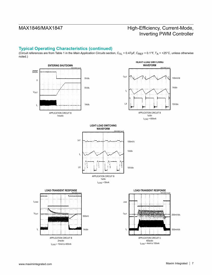
(Circuit references are from Table 1 in the Main Application Circuits section, CVL = 0.47µF, CREF = 0.1°F, TA = +25°C, unless otherwise noted.)
IL 500mA/div
200mV/div
ILOAD
VOUT
LOAD-TRANSIENT RESPONSEMAX1846/7 toc20
APPLICATION CIRCUIT C400s/div
ILOAD = 4mA to 100mA
IL 1A/div
500mV/div
ILOAD
VOUT
LOAD-TRANSIENT RESPONSEMAX1846/7 toc19
APPLICATION CIRCUIT B2ms/div
ILOAD = 10mA to 400mA
IL
LX
1A/div
10V/div
100mV/divVOUT
LIGHT-LOAD SWITCHINGWAVEFORM
MAX1846/7 toc18
APPLICATION CIRCUIT B1s/div
ILOAD = 50mA
IL
LX
1A/div
10V/div
100mV/divVOUT
HEAVY-LOAD SWITCHINGWAVEFORM
MAX1846/7 toc17
APPLICATION CIRCUIT B1s/div
ILOAD = 600mA
IL
0
5V/div
1A/div
5V/div
VOUT
ENTERING SHUTDOWNMAX1846/7 toc16
APPLICATION CIRCUIT B1ms/div
SHDN
www.maximintegrated.com Maxim Integrated 7
MAX1846/MAX1847 High-Efficiency, Current-Mode, Inverting PWM Controller
Typical Operating Characteristics (continued)

PIN NAME FUNCTIONMAX1846 MAX1847
— 1 POLSets polarity of the EXT pin. Connect POL to GND to set EXT for use with an external PMOS high-side FET. Connect POL to VL to set EXT for use with an external NMOS low-side FET in transformer-based applications.
1 2 VL VL Low-Dropout Regulator. Connect 0.47µF ceramic capacitor from VL to GND.
2 3 FREQ
Oscillator Frequency Set Input. Connect a resistor (RFREQ) from FREQ to GND to set the internal oscillator frequency from 100kHz (RFREQ = 500kW) to 500kHz (RFREQ = 76.8kW). RFREQ is still required if an external clock is used at SYNC. See Setting the Operating Frequency section.
3 4 COMP Compensation Node for Error Amp/Integrator. Connect a series resistor/capacitor network from COMP to GND for loop compensation. See Design Procedure.
4 5 REF 1.25V Reference Output. REF can source up to 500µA. Bypass with a 0.1µF ceramic capacitor from REF to GND.
5 6 FB Feedback Input. Connect FB to the center of a resistor-divider connected between the output and REF. The FB threshold is 0.
— 7, 9 N.C. No Connection
— 8 SHDN Shutdown Control. Drive SHDN low to turn off the DC-DC controller. Drive high or connect to IN for normal operation.
6 10, 11 GND Analog Ground. Connect to PGND.7 12 PGND Negative Rail for EXT Driver and Negative Current-Sense Input. Connect to GND.
8 13 CS Positive Current-Sense Input. Connect a current-sense resistor (RCS) between CS and PGND.
9 14 EXT External MOSFET Gate-Driver Output. EXT swings from IN to PGND.10 15 IN Power-Supply Input
— 16 SYNC
Operating Frequency Synchronization Control. Drive SYNC low or connect to GND to set the internal oscillator frequency with RFREQ. Drive SYNC with a logic-level clock input signal to externally set the converter’s operating frequency. DC-DC conversion cycles initiate on the rising edge of the input clock signal. Note that when driving SYNC with an external signal, RFREQ must still be connected to FREQ.
www.maximintegrated.com Maxim Integrated 8
MAX1846/MAX1847 High-Efficiency, Current-Mode, Inverting PWM Controller
Pin Description

MAX1847
REF FB
GND
CS
EXT
PGNDFREQ
COMP
VL IN
0.22µF
150kΩ
0.1µF
R210.0kΩ1%
R195.3kΩ1%
0.02Ω1W
10µHDO5022P-103
CMSH5-40
47µF16V
FDS6375
3 x 22µF10V
POL
SYNC
SHDN
10kΩ
47µF16V
22kΩ
1
2
16
8
3
4
5
10, 11
6
12
13
14
15
7, 9N.C.
VIN+3V to +5.5V
0.47µFVOUT-12V AT 400mA
SANYO16TPB47M
1200pF
220pF
www.maximintegrated.com Maxim Integrated 9
MAX1846/MAX1847 High-Efficiency, Current-Mode, Inverting PWM Controller
Typical Application Circuit
MAX1846MAX1847
STARTUPCIRCUITRY
CONTROLCIRCUITRY
VLREGULATOR
OSCILLATOR
REFERENCE
SLOPECOMP
UNDER-VOLTAGELOCK OUT
SOFT-START
IN
MAX1847 ONLY
MAX1847 ONLY
POL
FREQ
COMP
FB
REF
SYNC
SHDN
ERRORAMPLIFIER
CURRENT-SENSE
AMPLIFIER
GND
ERRORCOMPARATOR
EXT DRIVER
EXT
VL
CS
PGND
PGND
GM
X3.3
www.maximintegrated.com Maxim Integrated 10
MAX1846/MAX1847 High-Efficiency, Current-Mode, Inverting PWM Controller
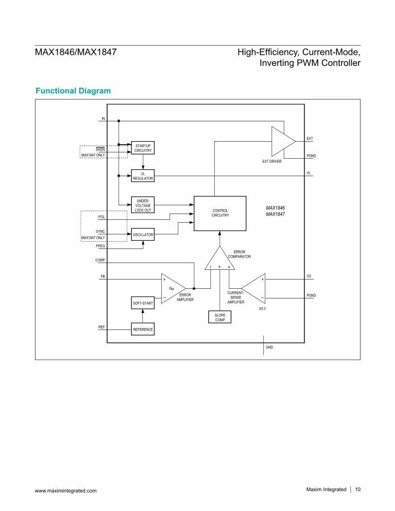
Functional Diagram

Detailed DescriptionThe MAX1846/MAX1847 current-mode PWM controllers use an inverting topology that is ideal for generating output voltages from -500mV to -200V. Features include shutdown, adjustable internal operating frequency or synchronization to an external clock, soft-start, adjustable current limit, and a wide (+3V to +16.5V) input range.
PWM ControllerThe architecture of the MAX1846/MAX1847 current-mode PWM controller is a BiCMOS multi-input system that simultaneously processes the output-error signal, the current-sense signal, and a slope-compensation ramp (Functional Diagram). Slope compensation prevents sub-harmonic oscillation, a potential result in current-mode regulators operating at greater than 50% duty cycle. The controller uses fixed-frequency, current-mode operation where the duty ratio is set by the input-to-output voltage ratio. The current-mode feedback loop regulates peak inductor current as a function of the output error signal.
Internal RegulatorThe MAX1846/MAX1847 incorporate an internal low- dropout regulator (LDO). This LDO has a 4.25V output and powers all MAX1846/MAX1847 functions (excluding EXT) for the primary purpose of stabilizing the perfor-mance of the IC over a wide input voltage range (+3V to +16.5V). The input to this regulator is connected to IN, and the dropout voltage is typically 100mV, so that when VIN is less than 4.35V, VL is typically VIN minus 100mV. When the LDO is in dropout, the MAX1846/MAX1847 still operate with VIN as low as 3V. For best performance, it is recommended to connect VL to IN when the input supply is less than 4.5V.
Undervoltage LockoutThe MAX1846/MAX1847 have an undervoltage lockout circuit that monitors the voltage at VL. If VL falls below the UVLO threshold (2.8V typ), the control logic turns the P-channel FET off (EXT high impedance). The rest of the IC circuitry is still powered and operating. When VL increases to 60mV above the UVLO threshold, the IC resumes operation from a start up condition (soft-start).
Soft-StartThe MAX1846/MAX1847 feature a “digital” soft-start that is preset and requires no external capacitor. Upon startup, the FB threshold decrements from the refer-ence voltage to 0 in 64 steps over 1024 cycles of fOSC or fSYNC. See the Typical Operating Characteristics for a scope picture of the soft-start operation. Soft-start is implemented: 1) when power is first applied to the IC,
2) when exiting shutdown with power already applied, and 3) when exiting undervoltage lockout.
Shutdown (MAX1847 only)The MAX1847 shuts down to reduce the supply current to 10µA when SHDN is low. In this mode, the internal reference, error amplifier, comparators, and biasing circuitry turn off. The EXT output becomes high imped-ance and the external pullup resistor connected to EXT pulls VEXT to VIN, turning off the P-channel MOSFET. When in shutdown mode, the converter's output goes to 0.
Frequency Synchronization (MAX1847 only)The MAX1847 is capable of synchronizing its switching frequency with an external clock source. Drive SYNC with a logic-level clock input signal to synchronize the MAX1847. A switching cycle starts on the rising edge of the signal applied to SYNC. Note that the frequen-cy of the signal applied to SYNC must be higher than the default frequency set by RFREQ. This frequency is required so that the internal clock does not start a switching cycle prematurely. If SYNC is inactive for an entire clock cycle of the internal oscillator, the internal oscillator takes over the switching operation. Choose RFREQ such that fOSC = 0.9 5 fSYNC.
EXT Polarity (MAX1847 only)The MAX1847 features an option to utilize an N-channel MOSFET configuration, rather than the typical p-channel MOSFET configuration (Figure 1). In order to drive the different polarities of these MOSFETs, the MAX1847 is capable of reversing the phase of EXT by 180 degrees. When driving a P-channel MOSFET, connect POL to GND. When driving an n-channel MOSFET, connect POL to VL. These POL connections ensure the proper polarity for EXT. For design guidance in regard to this application, refer to the MAX1856 data sheet.
Design ProcedureInitial SpecificationsIn order to start the design procedure, a few parameters must be identified: the minimum input voltage expect-ed (VIN(MIN)), the maximum input voltage expected (VIN(MAX)), the desired output voltage (VOUT), and the expected maximum load current (ILOAD).
Calculate the Equivalent Load ResistanceThis is a simple calculation used to shorten the verifica-tion equations:
RLOAD = VOUT / ILOAD
www.maximintegrated.com Maxim Integrated 11
MAX1846/MAX1847 High-Efficiency, Current-Mode, Inverting PWM Controller

Calculate the Duty CycleThe duty cycle is the ratio of the on-time of the MOSFET switch to the oscillator period. It is determined by the ratio of the input voltage to the output voltage. Since the input voltage typically has a range of operation, a minimum (DMIN) and maximum (DMAX) duty cycle is calculated by:
OUT DMIN
IN(MAX) SW LIM OUT D
V VDV V V V V
−
− −
+=
− +
OUT DMAX
IN(MIN) SW LIM OUT D
V VDV V V V V
−
− − −
+=
+
where VD is the forward drop across the output diode, VSW is the drop across the external FET when on, and VLIM is the current-limit threshold. To begin with, assume VD = 0.5V for a Schottky diode, VSW = 100mV, and VLIM = 100mV. Remember that VOUT is negative when using this formula.
Setting the Output VoltageThe output voltage is set using two external resistors to form a resistive-divider to FB between the output and REF (refer to R1 and R2 in Figure 1). VREF is nominally
1.25V and the regulation voltage for FB is nominally 0. The load presented to the reference by the feedback resistors must be less than 500µA to guarantee that VREF is in regulation (see Electrical Characteristics Table). Conversely, the current through the feedback resistors must be large enough so that the leakage current of the FB input (50nA) is insignificant. Therefore, select R2 so that IR2 is between 50µA and 250µA.
IR2 = VREF / R2where VREF = 1.25V. A typical value for R2 is 10kW.Once R2 is selected, calculate R1 with the following equation:
R1 = R2 x (-VOUT / VREF)
Setting the Operating FrequencyThe MAX1846/MAX1847 are capable of operating at switching frequencies from 100kHz to 500kHz. Choice of operating frequency depends on a number of factors:1) Noise considerations may dictate setting (or
synchronizing) fOSC above or below a certain frequency or band of frequencies, particularly in RF applications.
Figure 1. Using an N-Channel MOSFET (MAX1847 only)
REF
COMP0.033µF 270kΩ
SYNC
150kΩGND
FREQ
VL
VIN+12V
VOUT-48V AT 100mA
12µF100V
12µF25V
2
14
13
12
65
3
4
0.05Ω0.5W
1800pF
150.47µF
0.1µF
10, 11
EXT
PGND
IN
CS
FB
N.C.MAX1847
10.0kΩ1%
383kΩ1%
7, 9
POL1
8
16
VP1-019012.2µH 1:4
CMR1U-02
470Ω
100pF100V
SHDN
IRLL2705
www.maximintegrated.com Maxim Integrated 12
MAX1846/MAX1847 High-Efficiency, Current-Mode, Inverting PWM Controller

2) Higher frequencies allow the use of smaller value (hence smaller size) inductors and capacitors.
3) Higher frequencies consume more operating power both to operate the IC and to charge and discharge the gate at the external FET, which tends to reduce the efficiency at light loads.
4) Higher frequencies may exhibit lower overall efficiency due to more transition losses in the FET; however, this shortcoming can often be nullified by trading some of the inductor and capacitor size benefits for lower- resistance components.
5) High-duty-cycle applications may require lower fre-quencies to accommodate the controller minimum off-time of 0.4µs. Calculate the maximum oscillator frequency with the following formula:
IN(MIN) SW LIMOSC(MAX)
IN(MIN) SW LIM OUT D
OFF(MIN)
V V Vf
V V V V V
1 t
− −
− − −=
+
×
Remember that VOUT is negative when using this formula. When running at the maximum oscillator frequency (fOSCILLATOR) and maximum duty cycle (DMAX), do not exceed the minimum value of DMAX stated in the Electrical Characteristics table. For designs that exceed the DMAX and fOSC(MAX), an autotransformer can reduce the duty cycle and allow higher operating frequencies.The oscillator frequency is set by a resistor, RFREQ, which is connected from FREQ to GND. The relation-ship between fOSC (in Hz) and RFREQ (in W) is slightly nonlinear, as illustrated in the Typical Operating Characteristics. Choose the resistor value from the graph and check the oscillator frequency using the following formula:
( ) ( ) ( ) ( )27 11 19OSC FREQ FREQ
1f5.21 10 1.92 10 R 4.86 10 R− − −−
= × + × × × ×
External Synchronization (MAX1847 only)The SYNC input provides external-clock synchroniza-tion (if desired). When SYNC is driven with an exter-nal clock, the frequency of the clock directly sets the MAX1847's switching frequency. A rising clock edge on SYNC is interpreted as a synchronization input. If the sync signal is lost, the internal oscillator takes over at the end of the last cycle, and the frequency is returned
to the rate set by RFREQ. Choose RFREQ such that fOSC = 0.9 x fSYNC.
Choosing Inductance ValueThe inductance value determines the operation of the current-mode regulator. Except for low-current applica-tions, most circuits are more efficient and economical operating in continuous mode, which refers to continu-ous current in the inductor. In continuous mode there is a trade-off between efficiency and transient response. Higher inductance means lower inductor ripple current, lower peak current, lower switching losses, and, there-fore, higher efficiency. Lower inductance means higher inductor ripple current and faster transient response. A reasonable compromise is to choose the ratio of inductor ripple current to average continuous current at mini-mum duty cycle to be 0.4. Calculate the inductor ripple with the following formula:
( )( )
RIPPLE
LOAD(MAX) IN(MAX) SW LIM OUT D
IN(MAX) SW LIM
I
0.4 I V V V V V
V V V
− − −
− −
=
× × +
Then calculate an inductance value:L = (VIN(MAX) / IRIPPLE) x (DMIN / fOSC)
Choose the closest standard value. Once again, remem-ber that VOUT is negative when using this formula.
Determining Peak Inductor CurrentThe peak inductor current required for a particular output is:
ILPEAK = ILDC + (ILPP / 2)where ILDC is the average DC inductor current and ILPP is the inductor peak-to-peak ripple current. The ILDC and ILPP terms are determined as follows:
( )
( )( )
LOADLDC
MAX
SW LIM MAXIN MINLPP
OSC
II1 D
V V V x DI
L x f
=−
− −=
where L is the selected inductance value. The saturation rating of the selected inductor should meet or exceed the calculated value for ILPEAK, although most coil types can be operated up to 20% over their saturation rating without difficulty. In addition to the sat-uration criteria, the inductor should have as low a series resistance as possible. For continuous inductor current,
www.maximintegrated.com Maxim Integrated 13
MAX1846/MAX1847 High-Efficiency, Current-Mode, Inverting PWM Controller

the power loss in the inductor resistance (PLR) is approximated by:
2LOAD
LR LMAX
IP ~R xI D −
where RL is the inductor series resistance.Once the peak inductor current is calculated, the current sense resistor, RCS, is determined by:
RCS = 85mV / ILPEAKFor high peak inductor currents (>1A), Kelvin-sensing connections should be used to connect CS and PGND to RCS. Connect PGND and GND together at the ground side of RCS. A lowpass filter between RCS and CS may be required to prevent switching noise from tripping the current-sense comparator at heavy loads. Connect a 100W resistor between CS and the high side of RCS, and connect a 1000pF capacitor between CS and GND.
Checking Slope-Compensation StabilityIn a current-mode regulator, the cycle-by-cycle stability is dependent on slope compensation to prevent subharmonic oscillation at duty cycles greater than 50%. For the MAX1846/MAX1847, the internal slope compensation is optimized for a minimum inductor value (LMIN) with respect to duty cycle. For duty cycles greater then 50%, check stability by calculating LMIN using the following equation:
( )( ) ( )
MIN IN(MIN) CS S
MAX MAX
L V xR /M
x 2 xD 1 / 1 D− −
=
where VIN(MIN) is the minimum expected input voltage, Ms is the Slope Compensation Ramp (41 mV/µs) and DMAX is the maximum expected duty cycle. If LMIN is larger than L, increase the value of L to the next standard value that is larger than LMIN to ensure slope compensa-tion stability.
Choosing the Inductor CoreChoosing the most cost-effective inductor usually requires optimizing the field and flux with size. With higher output voltages the inductor may require many turns, and this can drive the cost up. Choosing an inductor value at LMIN can provide a good solution if discontinuous inductor current can be tolerated. Powdered iron cores can pro-vide the most economical solution but are larger in size than ferrite.
Power MOSFET SelectionThe MAX1846/MAX1847 drive a wide variety of P-channel power MOSFETs (PFETs). The best performance, especially with input voltages below 5V, is achieved with low-threshold PFETs that specify on-resistance with a gate-to-source voltage (VGS) of 2.7V or less. When selecting a PFET, key parameters include:
Total gate charge (QG) Reverse transfer capacitance (CRSS) On-resistance (RDS(ON)) Maximum drain-to-source voltage (VDS(MAX)) Minimum threshold voltage (VTH(MIN))
At high-switching rates, dynamic characteristics (para- meters 1 and 2 above) that predict switching losses may have more impact on efficiency than RDS(ON), which predicts DC losses. QG includes all capacitance associated with charging the gate. In addition, this parameter helps predict the current needed to drive the gate at the selected operating frequency. The power MOSFET in an inverting converter must have a high enough voltage rating to handle the input voltage plus the magnitude of the output voltage and any spikes induced by leakage inductance and ringing. An RC snubber circuit across the drain to ground might be required to reduce the peak ringing and noise.Choose RDS(ON)(MAX) specified at VGS < VIN(MIN) to be one to two times RCS. Verify that VIN(MAX) < VGS(MAX) and VDS(MAX) > VIN(MAX) - VOUT + VD. Choose the rise- and-fall times (tR, tF) to be less than 50ns.
Output Capacitor SelectionThe output capacitor (COUT) does all the filtering in an inverting converter. The output ripple is created by the variations in the charge stored in the output capacitor with each pulse and the voltage drop across the capacitor’s equivalent series resistance (ESR) caused by the current into and out of the capacitor. There are two properties of the output capacitor that affect ripple voltage: the capacitance value, and the capacitor’s ESR. The output ripple due to the output capacitor’s value is given by:
VRIPPLE-C = (ILOAD × DMAX × TOSC ) / COUTThe output ripple due to the output capacitor’s ESR is given by:
VRIPPLE-R = ILPP × RESRThese two ripple voltages are additive and the total output ripple is:
VRIPPLE-T = VRIPPLE-C + VRIPPLE-R
www.maximintegrated.com Maxim Integrated 14
MAX1846/MAX1847 High-Efficiency, Current-Mode, Inverting PWM Controller

The ESR-induced ripple usually dominates this last equation, so typically output capacitor selection is based mostly upon the capacitor's ESR, voltage rating, and ripple current rating. Use the following formula to deter-mine the maximum ESR for a desired output ripple volt-age (VRIPPLE-D):
RESR = VRIPPLE-D / ILPPSelect a capacitor with ESR rating less than RESR. The value of this capacitor is highly dependent on dielectric type, package size, and voltage rating. In general, when choosing a capacitor, it is recommended to use low-ESR capacitor types such as ceramic, organic, or tanta-lum capacitors. Ensure that the selected capacitor has sufficient margin to safely handle the maximum RMS ripple current.For continuous inductor current the maximum RMS ripple current in the output filter capacitor is:
2LOADRMS MAX MAX
MAX
II x D DI D
−=−
Choosing Compensation ComponentsThe MAX1846/MAX1847 are externally loop-compensat-ed devices. This feature provides flexibility in designs to accommodate a variety of applications. Proper compen-sation of the control loop is important to prevent excessive output ripple and poor efficiency caused by instability. The goal of compensation is to cancel unwanted poles and zeros in the DC-DC converter’s transfer function created by the power-switching and filter elements. More precise-ly, the objective of compensation is to ensure stability by ensuring that the DC-DC converter’s phase shift is less than 180° by a safe margin, at the frequency where the loop gain falls below unity. One method for ensuring ade-quate phase margin is to introduce corresponding zeros and poles in the feedback network to approximate a sin-gle-pole response with a -20dB/decade slope all the way to unity-gain crossover.
Calculating Poles and ZerosThe MAX1846/MAX1847 current-mode architecture takes the double pole caused by the inductor and output capacitor and shifts one of these poles to a much higher frequency to make loop compensation easier. To compen-sate these devices, we must know the center frequencies of the right-half plane zero (zRHP) and the higher frequen-cy pole (pOUT2). Calculate the zRHP frequency with the following formula:
( ) ( )( )
2MAX IN(MIN) OUT LOAD
RHPOUT
1 D x V V xRZ
2 x V L
− − − =π ×
The calculations for pOUT2 are very complex. For most applications where VOUT does not exceed -48V (in a negative sense), the pOUT2 will not be lower than 1/8th of the oscillator frequency and is generally at a higher frequency than zRHP. Therefore:
pOUT2 ≥ 0.125 × fOSCA pole is created by the output capacitor and the load resistance. This pole must also be compensated and its center frequency is given by the formula:
pOUT1 = 1 / (2π × RLOAD × COUT)Finally, there is a zero introduced by the ESR of the output capacitor. This zero is determined from the follow-ing equation:
zESR = 1 / (2π × COUT × RESR)
Calculating the Required Pole FrequencyTo ensure stability of the MAX1846/MAX1847, the gain of the error amplifier must roll-off the total loop gain to 1 before ZRHP or POUT2 occurs. First, calculate the DC open-loop gain ADC:
x xM O MAX LOADDC
CS CS
BxG R (1 D )RAA xR
−=
where: ACS is the current-sense amplifier gain = 3.3 B is the feedback-divider attenuation factor =
R2R1 R2+
GM is the error-amplifier transconductance =
400 µA/V RO is the error-amplifier output resistance = 3 MW
RCS is the selected current-sense resistor
Determining the Compensation Component ValuesSelect a unity-gain crossover frequency (fCROS), which is lower than zRHP and pOUT2 and higher than pOUT1. Using fCROS, calculate the compensation resistor (RCOMP).
CROS OCOMP
DC OUT1 CROS
f x RR A xP f
=−
www.maximintegrated.com Maxim Integrated 15
MAX1846/MAX1847 High-Efficiency, Current-Mode, Inverting PWM Controller
Select the next smaller standard value of resistor and then calculate the compensation capacitor required to cancel out the output-capacitor-induced pole (POUT1) determined previously.
Choose the next larger standard value of capacitor.In order for pCOMP to compensate the loop, the open-loop gain must reach unity at a lower frequency than the right-half-plane zero or the second output pole, whichever is lower in frequency. If the second output pole and the right-half-plane zero are close together in frequency, the higher resulting phase shift at unity gain may require a lower crossover frequency. For duty cycles greater than 50%, slope compensation reduces ADC, reducing the actual crossover frequency from fCROS. It is also a good practice to reduce noise on COMP with a capacitor (CCOMP2) to ground. To avoid adding extra phase margin at the crossover, the capacitor (CCOMP2) should roll-off noise at five times the crossover frequency. The value for CCOMP2 can be found using:
It might require a couple iterations to obtain a suitable combination of compensation components.Finally, the zero introduced by the output capacitor's ESR must be compensated. This compensation is accomplished by placing a capacitor between REF and FB creating a pole directly in the feedback loop. Calculate the value of this capacitor using the frequency of zESR and the selected feedback resistor values with the formula:
1 2FB ESR OUT
1 2
R RC R xC xR xR
+=
When using low-ESR, ceramic chip capacitors (MLCCs) at the output, calculate the value of CFB as follows:
1 2FB
OSC 1 2
R RC 2 3.14 f R R
+=
× × × ×
Applications InformationMaximum Output PowerThe maximum output power that the MAX1846/MAX1847 can provide depends on the maximum input power available and the circuit's efficiency:
POUT(MAX) = Efficiency × PIN(MAX)Furthermore, the efficiency and input power are both functions of component selection. Efficiency losses can be divided into three categories: 1) resistive losses across the inductor, MOSFET on-resistance, current-sense resis-tor, rectification diode, and the ESR of the input and out-put capacitors; 2) switching losses due to the MOSFET's transition region, and charging the MOSFET's gate capacitance; and 3) inductor core losses. Typically, 80% efficiency can be assumed for initial calculations. The required input power depends on the inductor current limit, input voltage, output voltage, output current, inductor value, and the switching frequency. The max-imum output power is approximated by the following formula:
PMAX = [VIN - (VLIM + ILIM x RDS(ON))] x ILIM x [1 - (LIR / 2)] x [(-VOUT + VD) / (VIN - VSW - VLIM
- VOUT + VD)]where ILIM is the peak current limit and LIR is the inductor current-ripple ratio and is calculated by:
LIR = ILPP / ILDCAgain, remember that VOUT for the MAX1846/MAX1847 is negative.
Diode SelectionThe MAX1846/MAX1847's high-switching frequency demands a high-speed rectifier. Schottky diodes are recommended for most applications because of their fast recovery time and low forward voltage. Ensure that the diode's average current rating exceeds the peak inductor current by using the diode manufacturer's data. Additionally, the diode's reverse breakdown voltage must exceed the potential difference between VOUT and the input voltage plus the leakage-inductance spikes. For high output voltages (-50V or more), Schottky diodes may not be practical because of this voltage requirement. In these cases, use an ultrafast recovery diode with adequate reverse-breakdown voltage.
COMPOUT1 COMP
1C 6.28 x P xR
=
O COMP
COMP2CROS O COMP
R RC 5 x 6.28 x f xR xR
+=
www.maximintegrated.com Maxim Integrated 16
MAX1846/MAX1847 High-Efficiency, Current-Mode, Inverting PWM Controller
Input Filter CapacitorThe input capacitor (CIN) must provide the peak current into the inverter. This capacitor is selected the same way as the output capacitor (COUT). Under ideal conditions, the RMS current for the input capacitor is the same as the output capacitor. The capacitor value and ESR must be selected to reduce noise to an acceptable value and also handle the ripple current (INRMS where:
O 2 NRMS MAX MAXMAX
1.2 xII x D D(I D )
−−
=
Bypass CapacitorIn addition to CIN and COUT, other ceramic bypass capacitors are required with the MAX1846/MAX1847. Bypass REF to GND with a 0.1µF or larger capacitor. Bypass VL to GND with a 0.47µF or larger capacitor. All bypass capacitors should be located as close to their respective pins as possible.
PC Board Layout GuidelinesGood PC board layout and routing are required in high- frequency-switching power supplies to achieve good regulation, high efficiency, and stability. It is strongly recommended that the evaluation kit PC board layouts be followed as closely as possible. Place power components as close together as possible, keeping their traces short, direct, and wide. Avoid interconnecting the ground pins of the power components using vias through an internal ground plane. Instead, keep the power components close together and route them in a “star” ground configuration using component-side copper, then connect the star ground to internal ground using multiple vias.
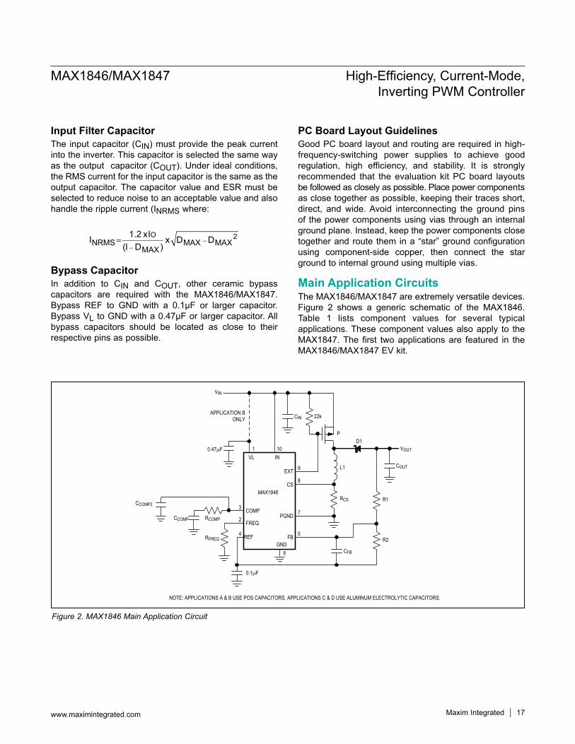
Main Application CircuitsThe MAX1846/MAX1847 are extremely versatile devices. Figure 2 shows a generic schematic of the MAX1846. Table 1 lists component values for several typical applications. These component values also apply to the MAX1847. The first two applications are featured in the MAX1846/MAX1847 EV kit.
Figure 2. MAX1846 Main Application Circuit
COMPCCOMP RCOMP
RFREQGND
FREQ
VL
VIN
VOUT
COUT
CIN
1
9
8
7
54
2
3
P
L1
RCS
CFB
D110
22k
0.47µF
0.1µF
6
EXT
PGND
REF
IN
CS
FB
MAX1846
R2
R1
APPLICATION BONLY
NOTE: APPLICATIONS A & B USE POS CAPACITORS. APPLICATIONS C & D USE ALUMINUM ELECTROLYTIC CAPACITORS.
CCOMP2
www.maximintegrated.com Maxim Integrated 17
MAX1846/MAX1847 High-Efficiency, Current-Mode, Inverting PWM Controller

Table 1. Component List for Main Application Circuits
Note: Indicate that you are using the MAX1846/MAX1847 when contacting these component suppliers.
SUPPLIER COMPONENT PHONE WEBSITEAVX Capacitors 803-946-0690 www.avxcorp.comCentral Semiconductor Diodes 516-435-1110 www.centralsemi.comCoilcraft Inductors 847-639-6400 www.coilcraft.comDale Resistors 402-564-3131 www.vishay.com/company/brands/dale/Fairchild MOSFETs 408-721-2181 www.fairchildsemi.comInternational Rectifier MOSFETs 310-322-3331 www.irf.comIRC Resistors 512-992-7900 www.irctt.comKemet Capacitors 864-963-6300 www.kemet.comOn Semiconductor MOSFETs, Diodes 602-303-5454 www.onsemi.comPanasonic Capacitors, resistors 201-348-7522 www.panasonic.comSanyo Capacitors 619-661-6835 www.secc.co.jpSiliconix MOSFETs 408-988-8000 www.siliconix.comSprague Capacitors 603-224-1961 www.vishay.com/company/brands/sprague/Sumida Inductors 847-956-0666 www.remtechcorp.comVitramon Resistors 203-268-6261 www.vishay.com/company/brands/vitramon/
CIRCUIT ID A B C DInput (V) 12 3 to 5.5 12 12Output (V) -5 -12 -48 -72Output (A) 2 0.4 0.1 0.1CCOMP (µF) 0.047 0.22 0.1 0.068CIN (µF) 3 x 10 3 x 22 10 10COUT (µF) 2 x 100 2 x 47 39 39CFB (pF) 390 1200 1000 1000R1 (kW) (1%) 40.2 95.3 383 576R2 (kW) (1%) 10 10 10 10RCOMP (kΩ) 8.2 10 220 470RCS (W) 0.02 0.02 0.05 0.05RFREQ (kW) 150 150 150 150D1 CMSH5-40 CMSH5-40 CMR1U-02 CMR1U-02L1 (µH) 10 10 47 82P1 FDS6685 FDS6375 IRFR5410 IRFR5410CCOMP2 (pF) 220 220 22 12
www.maximintegrated.com Maxim Integrated 18
MAX1846/MAX1847 High-Efficiency, Current-Mode, Inverting PWM Controller
Component Suppliers

PACKAGE TYPE
PACKAGECODE
OUTLINENO.
LANDPATTERN NO.
10 µMAX U10+2 21-0061 90-033016 QSOP E16+1 21-0055 90-0167QSOP
16
15
14
13
12
11
10
9
1
2
3
4
5
6
7
8
POL SYNC
IN
EXT
CS
PGND
GND
GND
N.C.
MAX1847
VL
FREQ
FB
COMP
REF
N.C.
1++
2
3
4
5
10
9
8
7
6
IN
EXT
CS
PGNDREF
COMP
FREQ
VL
MAX1846
µMAX
TOP VIEW
GNDFB
SHDN
www.maximintegrated.com Maxim Integrated 19
MAX1846/MAX1847 High-Efficiency, Current-Mode, Inverting PWM Controller
Package InformationFor the latest package outline information and land patterns (footprints), go to www.maximintegrated.com/packages. Note that a “+”, “#”, or “-” in the package code indicates RoHS status only. Package drawings may show a different suffix character, but the drawing pertains to the package regardless of RoHS status.
Chip InformationPROCESS: BiCMOS
Pin Configurations

REVISIONNUMBER
REVISIONDATE DESCRIPTION PAGES
CHANGED2 9/10 Added equation in the Determining the Compensation Component Values section 163 3/14 Removed automotive application from the Applications section 14 7/16 Extended maximum operating temperature from +85°C to +105°C 1, 2, 4
© 2016 Maxim Integrated Products, Inc. 20
Maxim Integrated cannot assume responsibility for use of any circuitry other than circuitry entirely embodied in a Maxim Integrated product. No circuit patent licenses are implied. Maxim Integrated reserves the right to change the circuitry and specifications without notice at any time. The parametric values (min and max limits) shown in the Electrical Characteristics table are guaranteed. Other parametric values quoted in this data sheet are provided for guidance.
Maxim Integrated and the Maxim Integrated logo are trademarks of Maxim Integrated Products, Inc.
MAX1846/MAX1847 High-Efficiency, Current-Mode, Inverting PWM Controller
Revision History
For pricing, delivery, and ordering information, please contact Maxim Direct at 1-888-629-4642, or visit Maxim Integrated’s website at www.maximintegrated.com.