Embed Size (px)
Citation preview
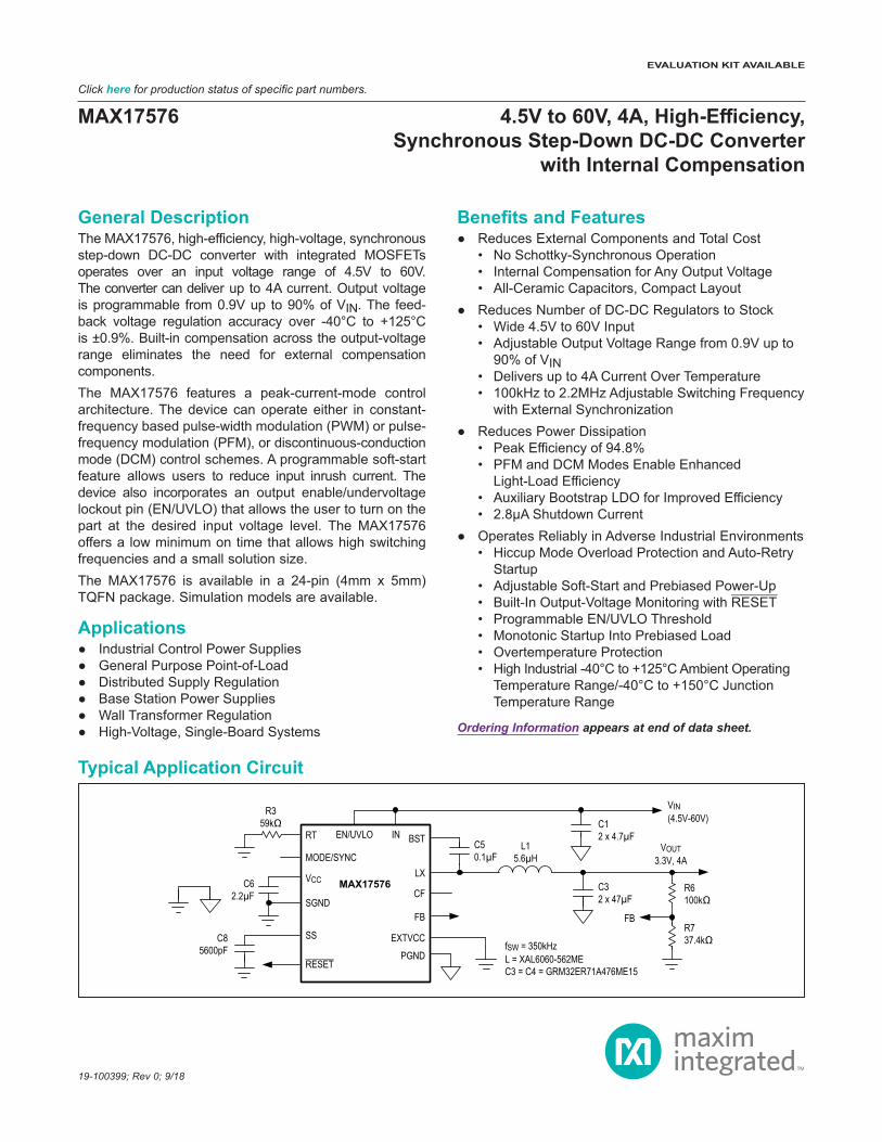
General DescriptionThe MAX17576, high-efficiency, high-voltage, synchronous step-down DC-DC converter with integrated MOSFETs operates over an input voltage range of 4.5V to 60V. The converter can deliver up to 4A current. Output voltage is programmable from 0.9V up to 90% of VIN. The feed-back voltage regulation accuracy over -40°C to +125°C is ±0.9%. Built-in compensation across the output-voltage range eliminates the need for external compensation components.The MAX17576 features a peak-current-mode control architecture. The device can operate either in constant-frequency based pulse-width modulation (PWM) or pulse-frequency modulation (PFM), or discontinuous-conduction mode (DCM) control schemes. A programmable soft-start feature allows users to reduce input inrush current. The device also incorporates an output enable/undervoltage lockout pin (EN/UVLO) that allows the user to turn on the part at the desired input voltage level. The MAX17576 offers a low minimum on time that allows high switching frequencies and a small solution size.The MAX17576 is available in a 24-pin (4mm x 5mm) TQFN package. Simulation models are available.
Applications Industrial Control Power Supplies General Purpose Point-of-Load Distributed Supply Regulation Base Station Power Supplies Wall Transformer Regulation High-Voltage, Single-Board Systems
Benefits and Features Reduces External Components and Total Cost
• No Schottky-Synchronous Operation• Internal Compensation for Any Output Voltage• All-Ceramic Capacitors, Compact Layout
Reduces Number of DC-DC Regulators to Stock• Wide 4.5V to 60V Input• Adjustable Output Voltage Range from 0.9V up to
90% of VIN• Delivers up to 4A Current Over Temperature• 100kHz to 2.2MHz Adjustable Switching Frequency
with External Synchronization Reduces Power Dissipation
• Peak Efficiency of 94.8%• PFM and DCM Modes Enable Enhanced
Light-Load Efficiency• Auxiliary Bootstrap LDO for Improved Efficiency • 2.8µA Shutdown Current
Operates Reliably in Adverse Industrial Environments• Hiccup Mode Overload Protection and Auto-Retry
Startup• Adjustable Soft-Start and Prebiased Power-Up• Built-In Output-Voltage Monitoring with RESET• Programmable EN/UVLO Threshold • Monotonic Startup Into Prebiased Load • Overtemperature Protection • High Industrial -40°C to +125°C Ambient Operating
Temperature Range/-40°C to +150°C Junction Temperature Range
Ordering Information appears at end of data sheet.
19-100399; Rev 0; 9/18
Typical Application Circuit
RESET
EN/UVLO BSTRT
MODE/SYNC
VCC
SGNDCF
SS
FB
LX
IN
EXTVCC
C62.2μF
C12 x 4.7μF
C50.1μF
VOUT3.3V, 4A
R6100kΩ
R737.4kΩ
MAX17576
C85600pF
L15.6μH
PGND
VIN(4.5V-60V)
fSW = 350kHzL = XAL6060-562MEC3 = C4 = GRM32ER71A476ME15
FB
R359kΩ
C32 x 47μF
MAX17576 4.5V to 60V, 4A, High-Efficiency, Synchronous Step-Down DC-DC Converter
with Internal Compensation
EVALUATION KIT AVAILABLE
Click here for production status of specific part numbers.
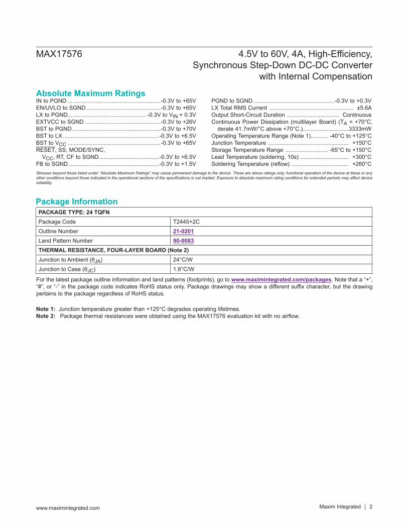
IN to PGND ...........................................................-0.3V to +65VEN/UVLO to SGND ...............................................-0.3V to +65VLX to PGND.................................................. -0.3V to VIN + 0.3VEXTVCC to SGND ................................................-0.3V to +26VBST to PGND ........................................................-0.3V to +70VBST to LX .............................................................-0.3V to +6.5VBST to VCC ...........................................................-0.3V to +65VRESET, SS, MODE/SYNC,
VCC, RT, CF to SGND ......................................-0.3V to +6.5VFB to SGND .........................................................-0.3V to +1.5V
PGND to SGND ....................................................-0.3V to +0.3VLX Total RMS Current ..................................................... ±5.6AOutput Short-Circuit Duration ................................. ContinuousContinuous Power Dissipation (multilayer Board) (TA = +70°C,
derate 41.7mW/°C above +70°C.) .............................3333mWOperating Temperature Range (Note 1)........... -40°C to +125°CJunction Temperature ................................................... +150°CStorage Temperature Range ........................... -65°C to +150°CLead Temperature (soldering, 10s) ............................... +300°CSoldering Temperature (reflow) .................................... +260°C
Note 1: Junction temperature greater than +125°C degrades operating lifetimes.Note 2: Package thermal resistances were obtained using the MAX17576 evaluation kit with no airflow.
Absolute Maximum Ratings
Stresses beyond those listed under “Absolute Maximum Ratings” may cause permanent damage to the device. These are stress ratings only; functional operation of the device at these or any other conditions beyond those indicated in the operational sections of the specifications is not implied. Exposure to absolute maximum rating conditions for extended periods may affect device reliability.
Package Information
For the latest package outline information and land patterns (footprints), go to www.maximintegrated.com/packages. Note that a “+”, “#”, or “-” in the package code indicates RoHS status only. Package drawings may show a different suffix character, but the drawing pertains to the package regardless of RoHS status.
PACKAGE TYPE: 24 TQFNPackage Code T2445+2COutline Number 21-0201Land Pattern Number 90-0083THERMAL RESISTANCE, FOUR-LAYER BOARD (Note 2)Junction to Ambient (θJA) 24°C/WJunction to Case (θJC) 1.8°C/W
MAX17576 4.5V to 60V, 4A, High-Efficiency, Synchronous Step-Down DC-DC Converter
with Internal Compensation
www.maximintegrated.com Maxim Integrated 2

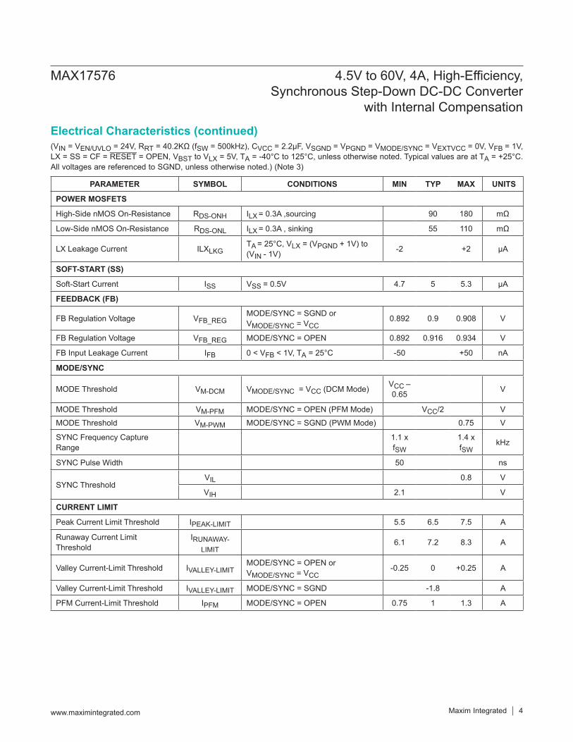
(VIN = VEN/UVLO = 24V, RRT = 40.2KΩ (fSW = 500kHz), CVCC = 2.2µF, VSGND = VPGND = VMODE/SYNC = VEXTVCC = 0V, VFB = 1V, LX = SS = CF = RESET = OPEN, VBST to VLX = 5V, TA = -40°C to 125°C, unless otherwise noted. Typical values are at TA = +25°C. All voltages are referenced to SGND, unless otherwise noted.) (Note 3)
Electrical Characteristics
PARAMETER SYMBOL CONDITIONS MIN TYP MAX UNITS
INPUT SUPPLY (IN)
Input Voltage Range V IN 4.5 60 V
Input Shutdown Current IIN-SH VEN/UVLO = 0V (shutdown mode) 2.8 4.5 µA
Input Quiescent Current
IQ_PFM
MODE/SYNC = RT = open, VEXTVCC = 5V 61 µA
MODE/SYNC = open, VEXTVCC = 5V 71 µA
IQ_DCM DCM Mode, VLX = 0.1V 1.2 1.8 mA
IQ_PWMNormal switching mode, fSW = 500kHz, VFB = 0.8V 14 mA
ENABLE/UVLO (EN)
EN/UVLO Threshold VENR VEN/UVLO rising 1.19 1.215 1.26 V
EN/UVLO Threshold VENF VEN/UVLO falling 1.068 1.09 1.131 V
EN/UVLO Threshold VEN-TRUESD VEN/UVLO falling 0.8 V
EN Input Leakage Current IEN VEN/UVLO = 0V, TA = +25°C -50 0 +50 nA
VCC LDO
VCC Output Voltage Range VCC1mA ≤ IVCC ≤ 25mA 4.75 5 5.25 V
6V ≤ VIN ≤ 60V; IVCC = 1mA 4.75 5 5.25 V
VCC Current Limit VCC = 4.3V, VIN = 7V 40 65 130 mA
VCC Dropout VCC-DO VIN = 4.5V , IVCC = 20mA 4.2 V
VCC UVLO VCC-UVR Rising 4.05 4.2 4.3 V
VCC-UVF Falling 3.65 3.8 3.9 V
EXT LDO
EXTVCC Operating Voltage Range 4.84 24 V
EXTVCC Switchover ThresholdEXTVCC Rising 4.56 4.7 4.84 VEXTVCC Falling 4.3 4.45 4.6 V
EXTVCC Dropout EXTVCC_DO VEXTVCC = 4.75V, IVCC = 20mA 0.3 V
EXTVCC Current Limit VCC = 4.5V, VEXTVCC = 7V 40 85 160 mA
MAX17576 4.5V to 60V, 4A, High-Efficiency, Synchronous Step-Down DC-DC Converter
with Internal Compensation
www.maximintegrated.com Maxim Integrated 3
(VIN = VEN/UVLO = 24V, RRT = 40.2KΩ (fSW = 500kHz), CVCC = 2.2µF, VSGND = VPGND = VMODE/SYNC = VEXTVCC = 0V, VFB = 1V, LX = SS = CF = RESET = OPEN, VBST to VLX = 5V, TA = -40°C to 125°C, unless otherwise noted. Typical values are at TA = +25°C. All voltages are referenced to SGND, unless otherwise noted.) (Note 3)
Electrical Characteristics (continued)
PARAMETER SYMBOL CONDITIONS MIN TYP MAX UNITS
POWER MOSFETS
High-Side nMOS On-Resistance RDS-ONH ILX = 0.3A ,sourcing 90 180 mΩ
Low-Side nMOS On-Resistance RDS-ONL ILX = 0.3A , sinking 55 110 mΩ
LX Leakage Current ILXLKGTA = 25°C, VLX = (VPGND + 1V) to (VIN - 1V) -2 +2 µA
SOFT-START (SS)
Soft-Start Current ISS VSS = 0.5V 4.7 5 5.3 µA
FEEDBACK (FB)
FB Regulation Voltage VFB_REGMODE/SYNC = SGND or VMODE/SYNC = VCC 0.892 0.9 0.908 V
FB Regulation Voltage VFB_REG MODE/SYNC = OPEN 0.892 0.916 0.934 V
FB Input Leakage Current IFB 0 < VFB < 1V, TA = 25°C -50 +50 nA
MODE/SYNC
MODE Threshold VM-DCM VMODE/SYNC = VCC (DCM Mode) VCC – 0.65 V
MODE Threshold VM-PFM MODE/SYNC = OPEN (PFM Mode) VCC/2 VMODE Threshold VM-PWM MODE/SYNC = SGND (PWM Mode) 0.75 V
SYNC Frequency Capture Range
1.1 x fSW
1.4 x fSW
kHz
SYNC Pulse Width 50 ns
SYNC ThresholdVIL 0.8 V
VIH 2.1 V
CURRENT LIMIT
Peak Current Limit Threshold IPEAK-LIMIT 5.5 6.5 7.5 A
Runaway Current Limit Threshold
IRUNAWAY-LIMIT
6.1 7.2 8.3 A
Valley Current-Limit Threshold IVALLEY-LIMITMODE/SYNC = OPEN or VMODE/SYNC = VCC
-0.25 0 +0.25 A
Valley Current-Limit Threshold IVALLEY-LIMIT MODE/SYNC = SGND -1.8 A
PFM Current-Limit Threshold IPFM MODE/SYNC = OPEN 0.75 1 1.3 A
MAX17576 4.5V to 60V, 4A, High-Efficiency, Synchronous Step-Down DC-DC Converter
with Internal Compensation
www.maximintegrated.com Maxim Integrated 4
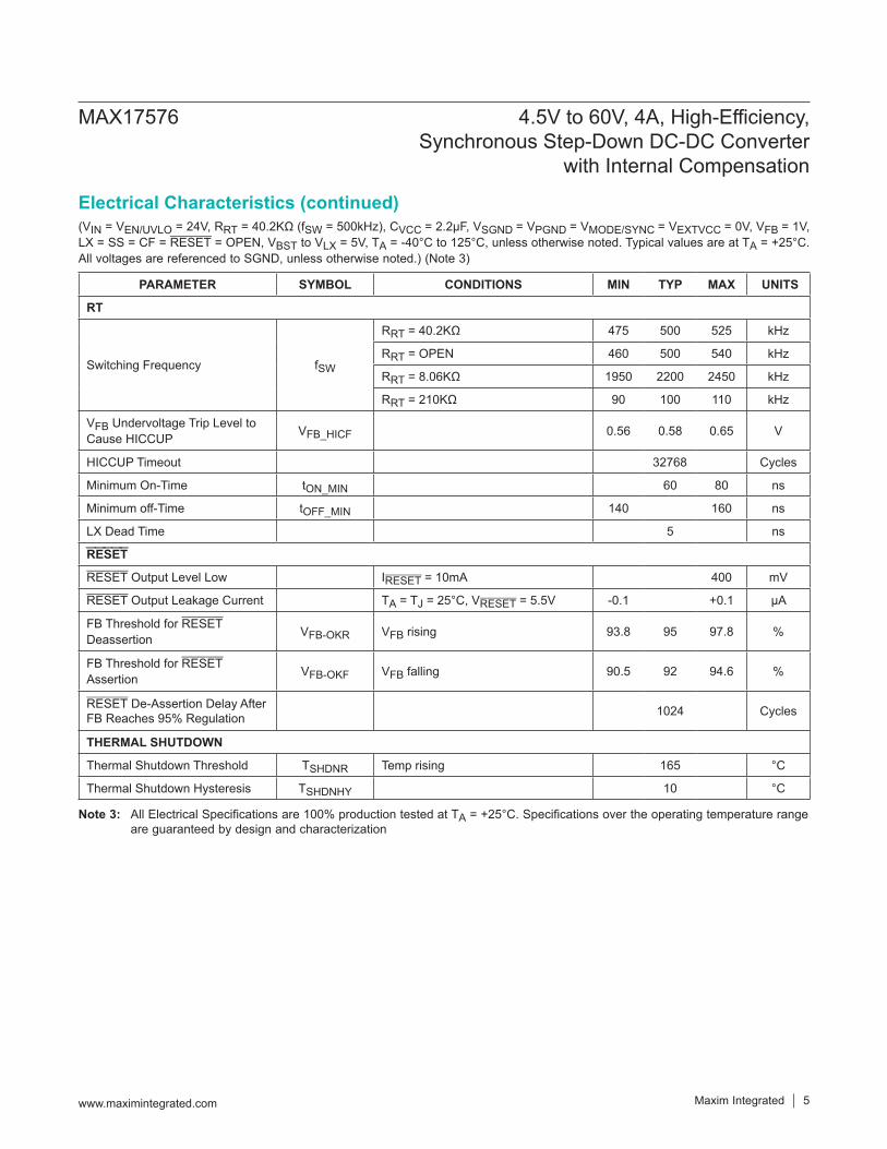
Note 3: All Electrical Specifications are 100% production tested at TA = +25°C. Specifications over the operating temperature range are guaranteed by design and characterization
(VIN = VEN/UVLO = 24V, RRT = 40.2KΩ (fSW = 500kHz), CVCC = 2.2µF, VSGND = VPGND = VMODE/SYNC = VEXTVCC = 0V, VFB = 1V, LX = SS = CF = RESET = OPEN, VBST to VLX = 5V, TA = -40°C to 125°C, unless otherwise noted. Typical values are at TA = +25°C. All voltages are referenced to SGND, unless otherwise noted.) (Note 3)
Electrical Characteristics (continued)
PARAMETER SYMBOL CONDITIONS MIN TYP MAX UNITS
RT
Switching Frequency fSW
RRT = 40.2KΩ 475 500 525 kHz
RRT = OPEN 460 500 540 kHz
RRT = 8.06KΩ 1950 2200 2450 kHz
RRT = 210KΩ 90 100 110 kHz
VFB Undervoltage Trip Level to Cause HICCUP VFB_HICF 0.56 0.58 0.65 V
HICCUP Timeout 32768 Cycles
Minimum On-Time tON_MIN 60 80 ns
Minimum off-Time tOFF_MIN 140 160 ns
LX Dead Time 5 ns
RESET
RESET Output Level Low IRESET = 10mA 400 mV
RESET Output Leakage Current TA = TJ = 25°C, VRESET = 5.5V -0.1 +0.1 µA
FB Threshold for RESET Deassertion VFB-OKR VFB rising 93.8 95 97.8 %
FB Threshold for RESET Assertion VFB-OKF VFB falling 90.5 92 94.6 %
RESET De-Assertion Delay After FB Reaches 95% Regulation 1024 Cycles
THERMAL SHUTDOWN
Thermal Shutdown Threshold TSHDNR Temp rising 165 °C
Thermal Shutdown Hysteresis TSHDNHY 10 °C
MAX17576 4.5V to 60V, 4A, High-Efficiency, Synchronous Step-Down DC-DC Converter
with Internal Compensation
www.maximintegrated.com Maxim Integrated 5
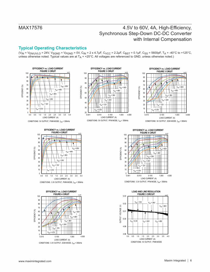
(VIN = VEN/UVLO = 24V, VSGND = VPGND = 0V, CIN = 2 x 4.7μF, CVCC = 2.2μF, CBST = 0.1μF, CSS = 5600pF, TA = -40°C to +125°C, unless otherwise noted. Typical values are at TA = +25°C. All voltages are referenced to GND, unless otherwise noted.)
Typical Operating Characteristics
0
10
20
30
40
50
60
70
80
90
100
0.0 0.5 1.0 1.5 2.0 2.5 3.0 3.5 4.0
EFFI
CIEN
CY(%
)
LOAD CURRENT (A)
EFFICIENCY vs. LOAD CURRENTFIGURE 3 CIRUIT
VIN = 36V
VIN = 24V
VIN = 12V
VIN = 6.5V
toc01
CONDITIONS: 5V OUTPUT, PWM MODE, fSW = 350kHz
VIN = 48V
VIN = 60V
20
30
40
50
60
70
80
90
100
0.001 0.010 0.100 1.000
EFFI
CIEN
CY(%
)
LOAD CURRENT (A)
EFFICIENCY vs. LOAD CURRENTFIGURE 3 CIRUIT
VIN = 36V
VIN = 24V
VIN = 12V
VIN = 6.5V
toc02
CONDITIONS: 5V OUTPUT, PFM MODE, fSW = 350kHz
VIN = 48V
VIN = 60V
4.0000
10
20
30
40
50
60
70
80
90
100
0.010 0.100 1.000
EFF
ICIE
NC
Y(%
)
LOAD CURRENT (A)
EFFICIENCY vs. LOAD CURRENTFIGURE 3 CIRUIT
VIN = 36V
VIN = 24V
VIN = 12V
VIN = 6.5V
toc03
CONDITIONS: 5V OUTPUT, DCM MODE, fSW = 350kHz
VIN = 48V
VIN = 60V
4.000
0
10
20
30
40
50
60
70
80
90
100
0.010 0.100 1.000
EFFI
CIEN
CY(%
)
LOAD CURRENT (A)
VIN = 36V
VIN = 24V
VIN = 12V
VIN = 4.5V
toc06
CONDITIONS: 3.3V OUTPUT, DCM MODE, fSW = 350kHz
VIN = 48V
VIN = 60V
EFFICIENCY vs. LOAD CURRENTFIGURE 4 CIRUIT
4.000
0
10
20
30
40
50
60
70
80
90
100
0.0 0.5 1.0 1.5 2.0 2.5 3.0 3.5 4.0
EFFI
CIEN
CY(%
)
LOAD CURRENT (A)
EFFICIENCY vs. LOAD CURRENTFIGURE 4 CIRUIT
VIN = 36V
VIN = 24V
VIN = 12V
VIN = 4.5V
toc04
CONDITIONS: 3.3V OUTPUT, PWM MODE, fSW = 350kHz
VIN = 48V
VIN = 60V
4.98
4.99
5.00
5.01
5.02
5.03
0.0 0.5 1.0 1.5 2.0 2.5 3.0 3.5 4.0
OUT
PUT
VO
LTAG
E (V
)
LOAD CURRENT (A)
LOAD AND LINE REGULATIONFIGURE 3 CIRCUIT
VIN = 24V
VIN = 12V
VIN = 6.5V
VIN = 36V
toc07
CONDITIONS: 5V OUTPUT, PWM MODE
VIN = 48V
VIN = 60V
0
10
20
30
40
50
60
70
80
90
100
0.001 0.010 0.100 1.000
EFFI
CIEN
CY(%
)
LOAD CURRENT (A)
VIN = 36V
VIN = 24V
VIN = 12V
VIN = 4.5V
toc05
CONDITIONS: 3.3V OUTPUT, PFM MODE, fSW = 350kHz
VIN = 48V
VIN = 60V
EFFICIENCY vs. LOAD CURRENTFIGURE 4 CIRUIT
4.000
MAX17576 4.5V to 60V, 4A, High-Efficiency, Synchronous Step-Down DC-DC Converter
with Internal Compensation
Maxim Integrated 6www.maximintegrated.com

Typical Operating Characteristics (continued)(VIN = VEN/UVLO = 24V, VSGND = VPGND = 0V, CIN = 2 x 4.7μF, CVCC = 2.2μF, CBST = 0.1μF, CSS = 5600pF, TA = -40°C to +125°C, unless otherwise noted. Typical values are at TA = +25°C. All voltages are referenced to GND, unless otherwise noted.)
4.95
5.00
5.05
5.10
5.15
0.0 0.5 1.0 1.5 2.0 2.5 3.0 3.5 4.0
OUT
PUT
VO
LTAG
E (V
)
LOAD CURRENT (A)
LOAD AND LINE REGULATIONFIGURE 3 CIRCUIT
VIN = 24V
VIN = 12V
VIN = 6.5V
VIN = 36V
toc08
CONDITIONS: 5V OUTPUT, PFM MODE
VIN = 48V
VIN = 60V
4.98
4.99
5.00
5.01
5.02
5.03
0.0 0.5 1.0 1.5 2.0 2.5 3.0 3.5 4.0
OUT
PUT
VO
LTAG
E (V
)
LOAD CURRENT (A)
LOAD AND LINE REGULATIONFIGURE 3 CIRCUIT
VIN = 24V
VIN = 12V
VIN = 6.5V
VIN = 36V
toc09
CONDITIONS: 5V OUTPUT, DCM MODE
VIN = 60V
VIN = 48V
3.28
3.29
3.30
3.31
3.32
3.33
0.0 0.5 1.0 1.5 2.0 2.5 3.0 3.5 4.0
OUT
PUT
VO
LTAG
E (V
)
LOAD CURRENT (A)
LOAD AND LINE REGULATIONFIGURE 4 CIRCUIT
VIN = 24V
VIN = 12V
VIN = 4.5V
VIN = 36V
toc10
CONDITIONS: 3.3V OUTPUT, PWM MODE
VIN = 48V
VIN = 60V
0
200
400
600
800
1000
1200
1400
1600
1800
2000
2200
2400
0 20 40 60 80 100 120 140 160 180 200
SWIT
CHIN
G F
REQ
UENC
Y (k
Hz)
RRT (kΩ)
SWITCHING FREQUENCY vs. RT RESISTANCE toc13
3.24
3.26
3.28
3.30
3.32
3.34
3.36
3.38
3.40
3.42
3.44
0.0 0.5 1.0 1.5 2.0 2.5 3.0 3.5 4.0
OUT
PUT
VO
LTAG
E (V
)
LOAD CURRENT (A)
LOAD AND LINE REGULATIONFIGURE 4 CIRCUIT
VIN = 24V
VIN = 12V
VIN = 6.5V
VIN = 36V
toc11
CONDITIONS: 3.3V OUTPUT, PFM MODE
VIN = 48V
VIN = 60V
5V/div
5V/div
2ms/div
VEN/UVLO
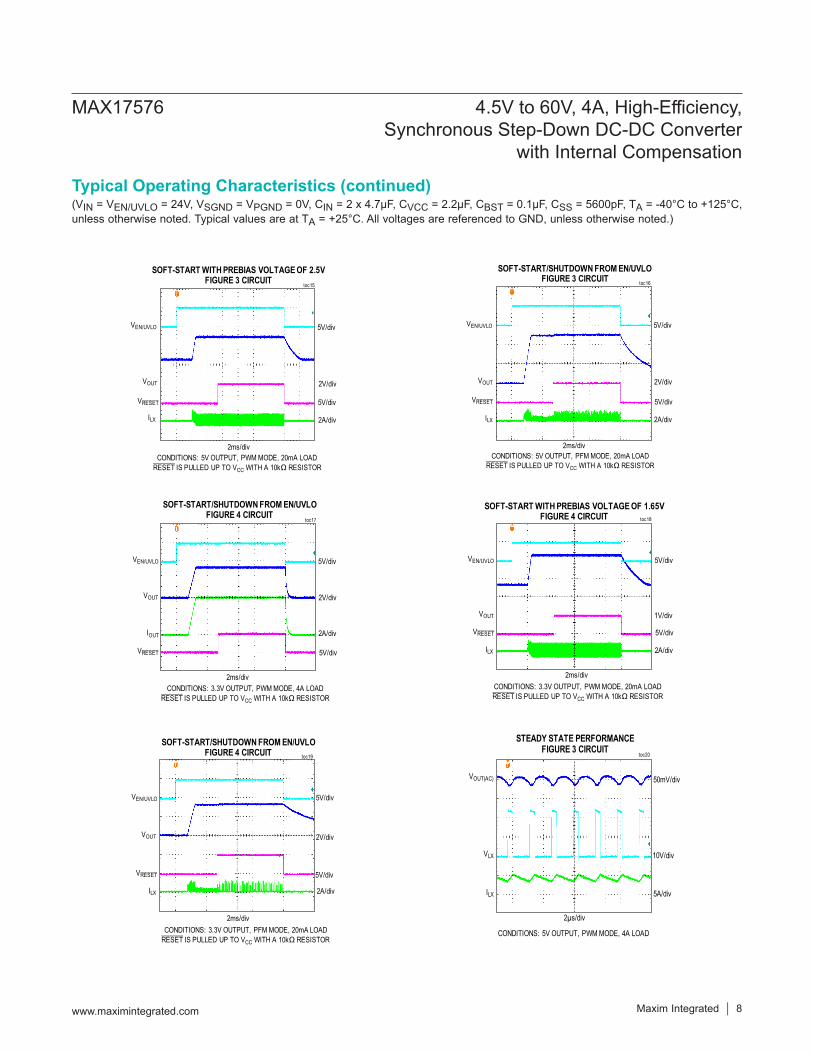
SOFT-START/SHUTDOWN FROM EN/UVLOFIGURE 3 CIRCUIT toc14
2V/divVOUT
IOUT
VRESET
2A/div
CONDITIONS: 5V OUTPUT, PWM MODE, 4A LOADRESET IS PULLED UP TO VCC WITH A 10kΩ RESISTOR
3.25
3.27
3.29
3.31
3.33
3.35
0.0 0.5 1.0 1.5 2.0 2.5 3.0 3.5 4.0
OUT
PUT
VO
LTAG
E (V
)
LOAD CURRENT (A)
LOAD AND LINE REGULATIONFIGURE 4 CIRCUIT
VIN = 24V
VIN = 12V
VIN = 6.5V
VIN = 36V
toc12
CONDITIONS: 3.3V OUTPUT, DCM MODE
VIN = 60V
VIN = 48V
MAX17576 4.5V to 60V, 4A, High-Efficiency, Synchronous Step-Down DC-DC Converter
with Internal Compensation
Maxim Integrated 7www.maximintegrated.com
(VIN = VEN/UVLO = 24V, VSGND = VPGND = 0V, CIN = 2 x 4.7μF, CVCC = 2.2μF, CBST = 0.1μF, CSS = 5600pF, TA = -40°C to +125°C, unless otherwise noted. Typical values are at TA = +25°C. All voltages are referenced to GND, unless otherwise noted.)
Typical Operating Characteristics (continued)
5V/div
5V/div
2ms/div
VEN/UVLO
SOFT-START/SHUTDOWN FROM EN/UVLOFIGURE 4 CIRCUIT toc19
2V/divVOUT
ILX
VRESET
2A/div
CONDITIONS: 3.3V OUTPUT, PFM MODE, 20mA LOADRESET IS PULLED UP TO VCC WITH A 10kΩ RESISTOR
5V/div
5V/div
2ms/div
VEN/UVLO
SOFT-START/SHUTDOWN FROM EN/UVLOFIGURE 4 CIRCUIT
toc17
2V/divVOUT
IOUT
VRESET
2A/div
CONDITIONS: 3.3V OUTPUT, PWM MODE, 4A LOADRESET IS PULLED UP TO VCC WITH A 10kΩ RESISTOR
5V/div
5V/div
2ms/div
VEN/UVLO
SOFT-START WITH PREBIAS VOLTAGE OF 2.5VFIGURE 3 CIRCUIT
toc15
2V/divVOUT
ILX
VRESET
2A/div
CONDITIONS: 5V OUTPUT, PWM MODE, 20mA LOADRESET IS PULLED UP TO VCC WITH A 10kΩ RESISTOR
10V/div
2µs/div
VOUT(AC)
STEADY STATE PERFORMANCEFIGURE 3 CIRCUIT
toc20
50mV/div
VLX
ILX 5A/div
CONDITIONS: 5V OUTPUT, PWM MODE, 4A LOAD
5V/div
5V/div
2ms/div
VEN/UVLO
SOFT-START WITH PREBIAS VOLTAGE OF 1.65VFIGURE 4 CIRCUIT toc18
1V/divVOUT
ILX
VRESET
2A/div
CONDITIONS: 3.3V OUTPUT, PWM MODE, 20mA LOADRESET IS PULLED UP TO VCC WITH A 10kΩ RESISTOR
5V/div
5V/div
2ms/div
VEN/UVLO
SOFT-START/SHUTDOWN FROM EN/UVLOFIGURE 3 CIRCUIT
toc16
2V/divVOUT
ILX
VRESET
2A/div
CONDITIONS: 5V OUTPUT, PFM MODE, 20mA LOADRESET IS PULLED UP TO VCC WITH A 10kΩ RESISTOR
MAX17576 4.5V to 60V, 4A, High-Efficiency, Synchronous Step-Down DC-DC Converter
with Internal Compensation
Maxim Integrated 8www.maximintegrated.com
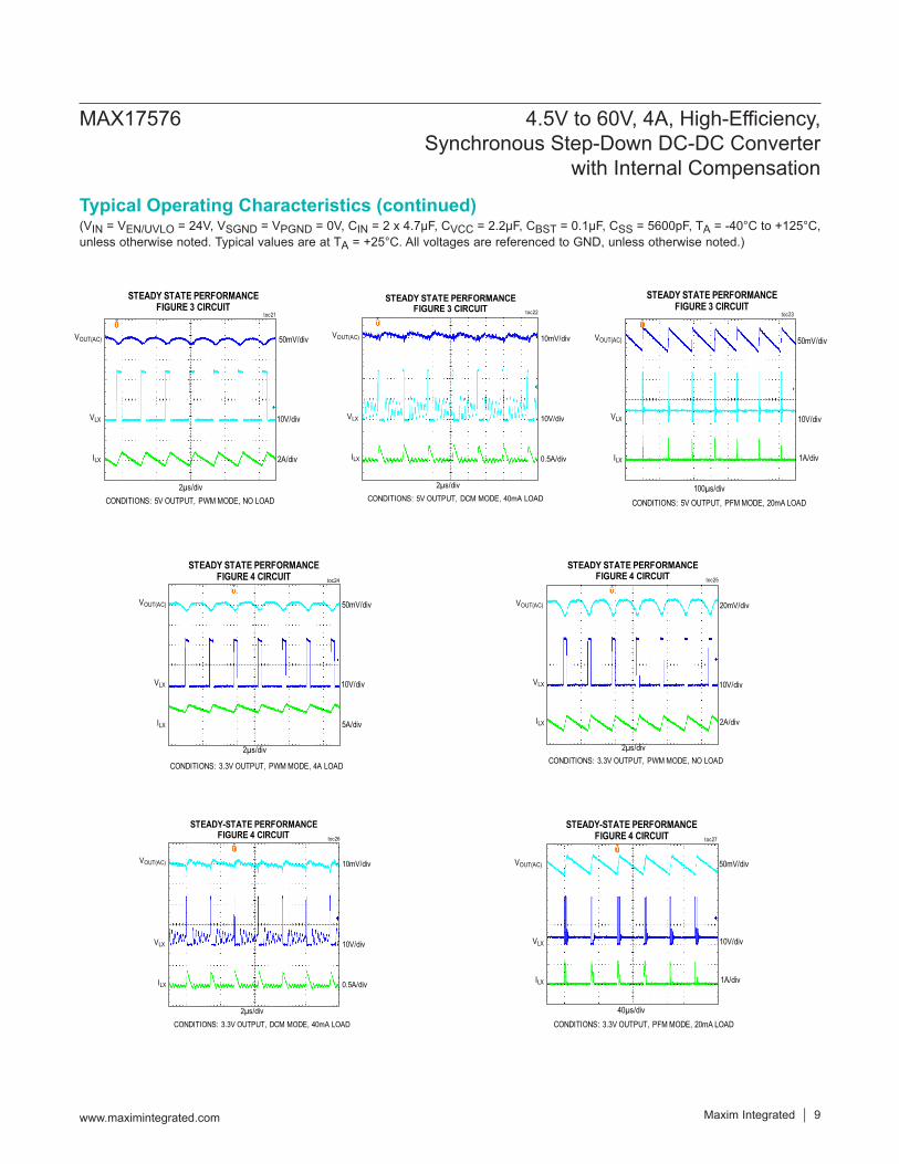
Typical Operating Characteristics (continued)(VIN = VEN/UVLO = 24V, VSGND = VPGND = 0V, CIN = 2 x 4.7μF, CVCC = 2.2μF, CBST = 0.1μF, CSS = 5600pF, TA = -40°C to +125°C, unless otherwise noted. Typical values are at TA = +25°C. All voltages are referenced to GND, unless otherwise noted.)
10V/div
2µs/div
VOUT(AC)
STEADY-STATE PERFORMANCEFIGURE 4 CIRCUIT toc26
10mV/div
VLX
ILX 0.5A/div
CONDITIONS: 3.3V OUTPUT, DCM MODE, 40mA LOAD
10V/div
2µs/div
VOUT(AC)
STEADY STATE PERFORMANCEFIGURE 4 CIRCUIT toc24
50mV/div
VLX
ILX 5A/div
CONDITIONS: 3.3V OUTPUT, PWM MODE, 4A LOAD
10V/div
40µs/div
VOUT(AC)
toc27
50mV/div
VLX
ILX 1A/div
CONDITIONS: 3.3V OUTPUT, PFM MODE, 20mA LOAD
STEADY-STATE PERFORMANCEFIGURE 4 CIRCUIT
10V/div
2µs/div
VOUT(AC)
STEADY STATE PERFORMANCEFIGURE 4 CIRCUIT toc25
20mV/div
VLX
ILX 2A/div
CONDITIONS: 3.3V OUTPUT, PWM MODE, NO LOAD
10V/div
2µs/div
VOUT(AC)
STEADY STATE PERFORMANCEFIGURE 3 CIRCUIT
toc21
50mV/div
VLX
ILX 2A/div
CONDITIONS: 5V OUTPUT, PWM MODE, NO LOAD
10V/div
2µs/div
VOUT(AC)
STEADY STATE PERFORMANCEFIGURE 3 CIRCUIT toc22
10mV/div
VLX
ILX 0.5A/div
CONDITIONS: 5V OUTPUT, DCM MODE, 40mA LOAD
10V/div
100µs/div
VOUT(AC)
toc23
50mV/div
VLX
ILX 1A/div
CONDITIONS: 5V OUTPUT, PFM MODE, 20mA LOAD
STEADY STATE PERFORMANCEFIGURE 3 CIRCUIT
MAX17576 4.5V to 60V, 4A, High-Efficiency, Synchronous Step-Down DC-DC Converter
with Internal Compensation
www.maximintegrated.com Maxim Integrated 9
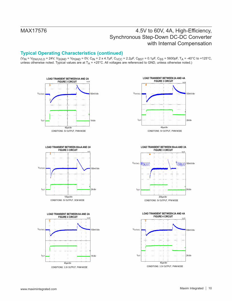
(VIN = VEN/UVLO = 24V, VSGND = VPGND = 0V, CIN = 2 x 4.7μF, CVCC = 2.2μF, CBST = 0.1μF, CSS = 5600pF, TA = -40°C to +125°C, unless otherwise noted. Typical values are at TA = +25°C. All voltages are referenced to GND, unless otherwise noted.)
Typical Operating Characteristics (continued)
100mV/div
100µs/div
LOAD TRANSIENT BETWEEN 80mA AND 2AFIGURE 3 CIRCUIT
toc30
VOUT(AC)
IOUT 2A/div
CONDITIONS: 5V OUTPUT, DCM MODE
100mV/div
40µs/div
LOAD TRANSIENT BETWEEN 0A AND 2AFIGURE 4 CIRCUIT toc32
VOUT(AC)
IOUT 1A/div
CONDITIONS: 3.3V OUTPUT, PWM MODE
100mV/div
40µs/div
LOAD TRANSIENT BETWEEN 0A AND 2AFIGURE 3 CIRCUIT toc28
VOUT(AC)
IOUT 1A/div
CONDITIONS: 5V OUTPUT, PWM MODE
100mV/div
200µs/div
LOAD TRANSIENT BETWEEN 50mA AND 2AFIGURE 3 CIRCUIT
toc31
VOUT(AC)
IOUT 2A/div
CONDITIONS: 5V OUTPUT, PFM MODE
100mV/div
40µs/div
LOAD TRANSIENT BETWEEN 2A AND 4AFIGURE 4 CIRCUIT
toc33
VOUT(AC)
IOUT 2A/div
CONDITIONS: 3.3V OUTPUT, PWM MODE
100mV/div
40µs/div
LOAD TRANSIENT BETWEEN 2A AND 4AFIGURE 3 CIRCUIT
toc29
VOUT(AC)
IOUT 2A/div
CONDITIONS: 5V OUTPUT, PWM MODE
MAX17576 4.5V to 60V, 4A, High-Efficiency, Synchronous Step-Down DC-DC Converter
with Internal Compensation
Maxim Integrated 10www.maximintegrated.com
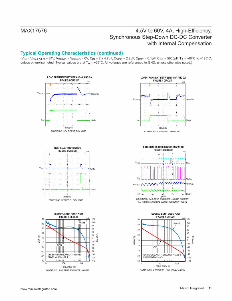
(VIN = VEN/UVLO = 24V, VSGND = VPGND = 0V, CIN = 2 x 4.7μF, CVCC = 2.2μF, CBST = 0.1μF, CSS = 5600pF, TA = -40°C to +125°C, unless otherwise noted. Typical values are at TA = +25°C. All voltages are referenced to GND, unless otherwise noted.)
Typical Operating Characteristics (continued)
1V/div
20ms/div
OVERLOAD PROTECTIONFIGURE 3 CIRCUIT toc36
VOUT
ILX 2A/div
CONDITIONS: 5V OUTPUT, PWM MODE
-140
-120
-100
-80
-60
-40
-20
0
20
40
60
80
100
120
1k 10k 100k-40
-30
-20
-10
0
10
20
30
40
50
PHAS
E (°)
GAI
N (d
B)
FREQUENCY (Hz)
GAIN
toc38
PHASE
CROSSOVER FREQUENCY = 42.6kHzPHASE MARGIN = 66.4
CLOSED-LOOP BODE PLOTFIGURE 3 CIRCUIT
CONDITIONS: 5V OUTPUT, PWM MODE, 4A LOAD
100mV/div
100µs/div
LOAD TRANSIENT BETWEEN 80mA AND 2AFIGURE 4 CIRCUIT
toc34
VOUT(AC)
IOUT 1A/div
CONDITIONS: 3.3V OUTPUT, DCM MODE
5V/div
4µs/div
EXTERNAL CLOCK SYNCHRONIZATIONFIGURE 3 CIRCUIT
toc37
VSYNC
IOUT 5A/div
CONDITIONS: 5V OUTPUT, PWM MODE, 4A LOAD CURRENT,fSW = 350kHz, EXTERNAL CLOCK FREQUENCY = 490kHz
VLX
VOUT(AC)
10V/div
50mV/div
-120
-100
-80
-60
-40
-20
0
20
40
60
80
100
120
1k 10k 100k-30
-20
-10
0
10
20
30
40
50
PHAS
E ( °)
GAI
N (d
B)
FREQUENCY (Hz)
GAIN
toc39
PHASE
GAIN CROSSOVER FREQUENCY = 43.5kHzPHASE MARGIN = 67.4
CLOSED-LOOP BODE PLOTFIGURE 4 CIRCUIT
CONDITIONS: 3.3V OUTPUT, PWM MODE, 4A LOAD
100mV/div
200µs/div
LOAD TRANSIENT BETWEEN 50mA AND 2AFIGURE 4 CIRCUIT
toc35
VOUT(AC)
IOUT 2A/div
CONDITIONS: 3.3V OUTPUT, PFM MODE
MAX17576 4.5V to 60V, 4A, High-Efficiency, Synchronous Step-Down DC-DC Converter
with Internal Compensation
Maxim Integrated 11www.maximintegrated.com
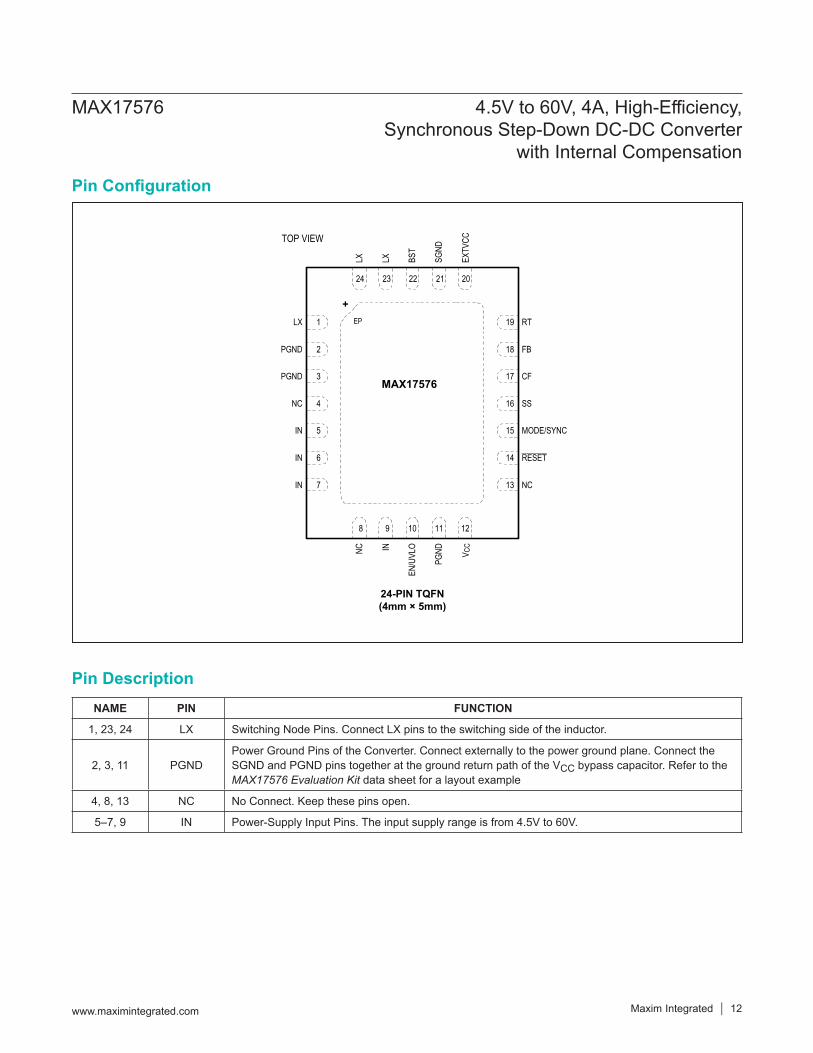
Pin Configuration
Pin Description
24-PIN TQFN(4mm × 5mm)
TOP VIEW
1LX
2PGND
3PGND
4NC
5IN
6IN
7IN
EP 19 RT
18 FB
17 CF
16 SS
15 MODE/SYNC
LX LX BST
SGND
EXTV
CC14 RESET
13 NC
8
NC
9
IN
10
EN/U
VLO
11
PGND
12
V CC
24 23 22 21 20
+
MAX17576
NAME PIN FUNCTION
1, 23, 24 LX Switching Node Pins. Connect LX pins to the switching side of the inductor.
2, 3, 11 PGNDPower Ground Pins of the Converter. Connect externally to the power ground plane. Connect the SGND and PGND pins together at the ground return path of the VCC bypass capacitor. Refer to the MAX17576 Evaluation Kit data sheet for a layout example
4, 8, 13 NC No Connect. Keep these pins open.
5–7, 9 IN Power-Supply Input Pins. The input supply range is from 4.5V to 60V.
MAX17576 4.5V to 60V, 4A, High-Efficiency, Synchronous Step-Down DC-DC Converter
with Internal Compensation
www.maximintegrated.com Maxim Integrated 12
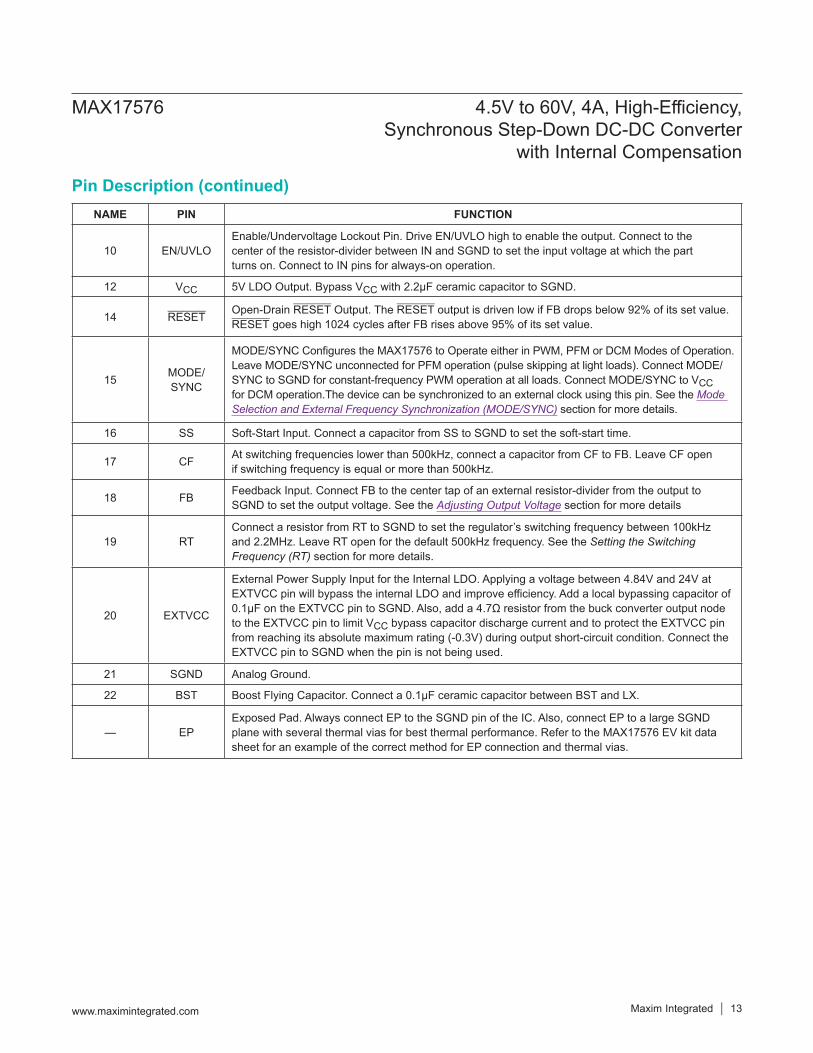
Pin Description (continued)NAME PIN FUNCTION
10 EN/UVLOEnable/Undervoltage Lockout Pin. Drive EN/UVLO high to enable the output. Connect to the center of the resistor-divider between IN and SGND to set the input voltage at which the part turns on. Connect to IN pins for always-on operation.
12 VCC 5V LDO Output. Bypass VCC with 2.2μF ceramic capacitor to SGND.
14 RESET Open-Drain RESET Output. The RESET output is driven low if FB drops below 92% of its set value. RESET goes high 1024 cycles after FB rises above 95% of its set value.
15 MODE/ SYNC
MODE/SYNC Configures the MAX17576 to Operate either in PWM, PFM or DCM Modes of Operation. Leave MODE/SYNC unconnected for PFM operation (pulse skipping at light loads). Connect MODE/SYNC to SGND for constant-frequency PWM operation at all loads. Connect MODE/SYNC to VCC for DCM operation.The device can be synchronized to an external clock using this pin. See the Mode Selection and External Frequency Synchronization (MODE/SYNC) section for more details.
16 SS Soft-Start Input. Connect a capacitor from SS to SGND to set the soft-start time.
17 CF At switching frequencies lower than 500kHz, connect a capacitor from CF to FB. Leave CF open if switching frequency is equal or more than 500kHz.
18 FB Feedback Input. Connect FB to the center tap of an external resistor-divider from the output to SGND to set the output voltage. See the Adjusting Output Voltage section for more details
19 RTConnect a resistor from RT to SGND to set the regulator’s switching frequency between 100kHz and 2.2MHz. Leave RT open for the default 500kHz frequency. See the Setting the Switching Frequency (RT) section for more details.
20 EXTVCC
External Power Supply Input for the Internal LDO. Applying a voltage between 4.84V and 24V at EXTVCC pin will bypass the internal LDO and improve efficiency. Add a local bypassing capacitor of 0.1μF on the EXTVCC pin to SGND. Also, add a 4.7Ω resistor from the buck converter output node to the EXTVCC pin to limit VCC bypass capacitor discharge current and to protect the EXTVCC pin from reaching its absolute maximum rating (-0.3V) during output short-circuit condition. Connect the EXTVCC pin to SGND when the pin is not being used.
21 SGND Analog Ground.
22 BST Boost Flying Capacitor. Connect a 0.1μF ceramic capacitor between BST and LX.
— EPExposed Pad. Always connect EP to the SGND pin of the IC. Also, connect EP to a large SGND plane with several thermal vias for best thermal performance. Refer to the MAX17576 EV kit data sheet for an example of the correct method for EP connection and thermal vias.
MAX17576 4.5V to 60V, 4A, High-Efficiency, Synchronous Step-Down DC-DC Converter
with Internal Compensation
www.maximintegrated.com Maxim Integrated 13
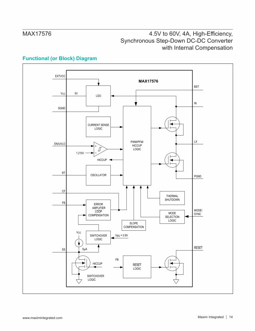
Functional (or Block) Diagram
HICCUP
SWITCHOVER LOGIC
VBG = 0.9V
VCC LDO5V
CURRENT SENSELOGIC
1.215V
EN/UVLO
OSCILLATORRT
PWM/PFM/HICCUPLOGIC
HICCUP
ERROR AMPLIFIER
LOOP COMPENSATION
CF
FB
SWITCHOVERLOGIC
VCC
SS
SGND
SLOPECOMPENSATION
MODESELECTION
LOGIC
RESETLOGIC
FB
RESET
MODE/SYNC
PGND
LX
IN
BSTMAX17576
5µA
EXTVCC
THERMALSHUTDOWN
MAX17576 4.5V to 60V, 4A, High-Efficiency, Synchronous Step-Down DC-DC Converter
with Internal Compensation
www.maximintegrated.com Maxim Integrated 14

Detailed DescriptionThe MAX17576, high-efficiency, high-voltage, synchronous step-down DC-DC converter with integrated MOSFETs operates over a 4.5V to 60V input. The converter can deliv-er up to 4A current. Output voltage is programmable from 0.9V up to 90% of VIN. The feedback voltage regulation accuracy over -40°C to +125°C is ±0.9%.The device features a peak-current-mode control archi-tecture. An internal transconductance error amplifier produces an integrated error voltage at an internal node, which sets the duty cycle using a PWM comparator, a high-side current-sense amplifier, and a slope-compen-sation generator. At each rising edge of the clock, the high-side MOSFET turns on and remains on until either the appropriate or maximum duty cycle is reached, or the peak current limit is detected. During the high-side MOSFET’s on-time, the inductor current ramps up. During the second half of the switching cycle, the high-side MOSFET turns off and the low-side MOSFET turns on. The inductor releases the stored energy as its current ramps down and provides current to the output.The device can operate either in the pulse-width modu-lation (PWM), pulse-frequency modulation (PFM), or discontinuous-conduction mode (DCM) control schemes. A programmable soft-start feature allows users to reduce input inrush current. The device also incorporates an output enable/undervoltage lockout pin (EN/UVLO) that allows the user to turn on the part at the desired input volt-age level. An open-drain RESET pin provides a delayed power-good signal to the system upon achieving success-ful regulation of the output voltage.
Mode Selection and External Frequency Synchronization (MODE/SYNC)The logic state of the MODE/SYNC pin is latched when VCC and EN/UVLO voltages exceed the respective UVLO rising thresholds and all internal voltages are ready to allow LX switching. If the MODE/SYNC pin is open at pow-er-up, the device operates in PFM mode at light loads. If the MODE/SYNC pin is grounded at power-up, the device operates in constant-frequency PWM mode at all loads. Finally, if the MODE/SYNC pin is connected to VCC at power-up, the device operates in constant-frequency DCM mode at light loads. State changes on the MODE/SYNC pin are ignored during normal operation.The internal oscillator of the MAX17576 can be synchronized to an external clock signal on the MODE/SYNC pin. The external synchronization clock frequency must be between 1.1 x fSW and 1.4 x fSW, where fSW is the fre-quency programmed by the RT resistor. When an external clock is applied to MODE/SYNC pin, the internal oscilla-tor frequency changes to external clock frequency (from
original frequency based on RT setting) after detecting 16 external clock edges. The converter will operate in PWM mode during synchronization operation. When the external clock is applied on-fly then the mode of operation will change to PWM from the initial state of PFM/DCM/PWM. When the external clock is removed on-fly then the internal oscillator frequency changes to the RT set frequency and the converter will still continue to operate in PWM mode. The minimum external clock pulse-width high should be greater than 50ns. See the MODE/SYNC section in the Electrical Characteristics table for details.
PWM Mode OperationIn PWM mode, the inductor current is allowed to go negative. PWM operation provides constant frequency operation at all loads, and is useful in applications sensitive to switching frequency. However, the PWM mode of operation gives lower efficiency at light loads compared to PFM and DCM modes of operation.
PFM Mode OperationPFM mode of operation disables negative inductor current and additionally skips pulses at light loads for high efficiency. In PFM mode, the inductor current is forced to a fixed peak of 1A (typ) every clock cycle until the output rises to 102.3% of the nominal voltage. Once the output reaches 102.3% of the nominal voltage, both the high-side and low-side FETs are turned off and the device enters hibernate operation until the load discharges the output to 101.1% of the nominal volt-age. Most of the internal blocks are turned off in hibernate operation to save quiescent current. After the output falls below 101.1% of the nominal voltage, the device comes out of hibernate operation, turns on all internal blocks, and again commences the process of delivering pulses of energy to the output until it reaches 102.3% of the nominal output voltage. The advantage of the PFM mode is higher efficiency at light loads because of lower quiescent current drawn from supply. The trade-off is that the output-voltage ripple is higher compared to PWM or DCM modes of operation and switching frequency is not constant at light loads. The output voltage ripple in PFM mode can be reduced by increasing the amount of output capacitance.
DCM Mode OperationDCM mode of operation features constant frequency operation down to lighter loads than PFM mode, by not skipping pulses but only disabling negative inductor current at light loads. DCM operation offers efficiency performance that lies between PWM and PFM modes.
MAX17576 4.5V to 60V, 4A, High-Efficiency, Synchronous Step-Down DC-DC Converter
with Internal Compensation
www.maximintegrated.com Maxim Integrated 15
Linear Regulator (VCC and EXTVCC)The MAX17576 has two internal LDO (Low Dropout) regulators which powers VCC. One LDO is powered from input supply (IN) (INLDO) and the other LDO is powered from EXTVCC (EXTVCC LDO). Only one of the two LDOs is in operation at a time, depending on the voltage levels present at EXTVCC. If EXTVCC voltage is greater than 4.7V (typ), VCC is powered from EXTVCC. If EXTVCC is lower than 4.7V (typ), VCC is powered from input supply (IN). Powering VCC from EXTVCC increases efficiency at higher input voltages. EXTVCC voltage should not exceed 24V. Typical VCC output voltage is 5V. Bypass VCC to GND with a 2.2μF ceramic capacitor. VCC powers the inter-nal blocks and the low-side MOSFET driver and re-charges the external bootstrap capacitor. Both INLDO and EXTVCC LDO can source up to 40mA for bias requirements. The MAX17576 employs an undervoltage lockout circuit that forces both the regulators off when VCC falls below VCC-UVF. The regulators can be immedi-ately enabled again when VCC goes above VCC-UVR. The 400mV UVLO hysteresis prevents chattering on power-up/power-down. Add a local bypassing capacitor of 0.1μF on the EXTVCC pin to SGND. Also, add a 4.7Ω resistor from the buck con-verter output node to the EXTVCC pin to limit VCC bypass capacitor discharge current and to protect the EXTVCC pin from reaching its absolute maximum rating (-0.3V) during output short-circuit condition. In applications where the buck converter output is connected to EXTVCC pin, if the output is shorted to ground then the transfer from EXTVCC LDO to INLDO happens seamlessly without any impact on the normal functionality. Connect the EXTVCC pin to SGND when the pin is not being used.
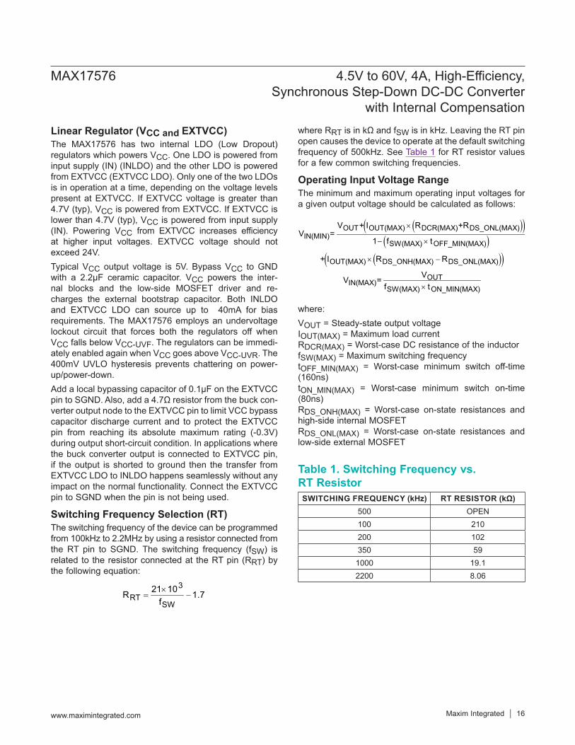
Switching Frequency Selection (RT)The switching frequency of the device can be programmed from 100kHz to 2.2MHz by using a resistor connected from the RT pin to SGND. The switching frequency (fSW) is related to the resistor connected at the RT pin (RRT) by the following equation:
3RT
SW
21 10R 1.7f×
= −
where RRT is in kΩ and fSW is in kHz. Leaving the RT pin open causes the device to operate at the default switching frequency of 500kHz. See Table 1 for RT resistor values for a few common switching frequencies.
Operating Input Voltage RangeThe minimum and maximum operating input voltages for a given output voltage should be calculated as follows:
( )( )( )
( )( )
OUT OUT(MAX) DCR(MAX) DS_ONL(MAX)IN(MIN)
SW(MAX) OFF_MIN(MAX)
OUT(MAX) DS_ONH(MAX) DS_ONL(MAX)
OUTIN(MAX)
SW(MAX) ON_MIN(MAX)
V + I R +RV =
1 f t
+ I R R
VV =f t
×
− ×
× −
×
where:VOUT = Steady-state output voltageIOUT(MAX) = Maximum load currentRDCR(MAX) = Worst-case DC resistance of the inductorfSW(MAX) = Maximum switching frequencytOFF_MIN(MAX) = Worst-case minimum switch off-time (160ns)tON_MIN(MAX) = Worst-case minimum switch on-time (80ns)RDS_ONH(MAX) = Worst-case on-state resistances and high-side internal MOSFETRDS_ONL(MAX) = Worst-case on-state resistances and low-side external MOSFET
Table 1. Switching Frequency vs. RT ResistorSWITCHING FREQUENCY (kHz) RT RESISTOR (kΩ)
500 OPEN100 210200 102350 59
1000 19.12200 8.06
MAX17576 4.5V to 60V, 4A, High-Efficiency, Synchronous Step-Down DC-DC Converter
with Internal Compensation
www.maximintegrated.com Maxim Integrated 16

Overcurrent Protection/Hiccup ModeThe device is provided with a robust overcurrent protec-tion scheme that protects the device under overload and output short-circuit conditions. A cycle-by-cycle peak current limit turns off the high-side MOSFET whenever the high-side switch current exceeds an internal limit of IPEAK-LIMIT 6.5A (typ). A runaway current limit on the high-side switch current at IRUNAWAY-LIMIT 7.2A (typ) protects the device under high input voltage, short-circuit conditions when there is insufficient output voltage available to restore the inductor current that was built up during the on period of the step-down converter. One occurrence of the runaway current limit triggers a hiccup mode. In addition, if, due to a fault condition, feedback voltage drops to VFB-HICF any time after soft-start is com-plete, and hiccup mode is triggered. In hiccup mode, the converter is protected by suspending switching for a hic-cup timeout period of 32,768 clock cycles. Once the hic-cup timeout period expires, soft-start is attempted again. Note that when soft-start is attempted under overload condition, if feedback voltage does not exceed VFB-HICF, the device switches at half the programmed switching frequency. Hiccup mode of operation ensures low power dissipation under output short-circuit conditions.
RESET OutputThe device includes a RESET comparator to monitor the status of the output voltage. The open-drain RESET out-put requires an external pullup resistor. RESET goes high (high impedance) 1024 switching cycles after the regula-tor output increases above 95% of the designed nominal regulated voltage. RESET goes low when the regulator output voltage drops to below 92% of the set nominal output regulated voltage. RESET also goes low during thermal shutdown.
Prebiased OutputWhen the MAX17576 starts into a prebiased output, both the high-side and the low-side switches are turned off so that the converter does not sink current from the output. High-side and low-side switches do not start switching until the PWM comparator commands the first PWM pulse, at which point switching commences. The output voltage is then smoothly ramped up to the target value in alignment with the internal reference.
Thermal Shutdown ProtectionThermal shutdown protection limits total power dissipation in the device. When the junction temperature of the device exceeds +165°C, an on-chip thermal sensor shuts down the device, allowing the device to cool. The MAX17576 turns on with soft-start after the junction temperature reduces by 10°C. Carefully evaluate the total power dissipation (see the Power Dissipation section) to avoid unwanted triggering of the thermal shutdown protection in normal operation.
Application InformationInput Capacitor SelectionThe input filter capacitor reduces peak currents drawn from the power source and reduces noise and voltage ripple on the input caused by the circuit’s switching. The input capacitor RMS current requirement (IRMS) is defined by the following equation:
OUT IN OUTRMS OUT(MAX )
IN
V ( V V )I I
V× −
= ×
where, IOUT(MAX) is the maximum load current. IRMS has a maximum value when the input voltage equals twice the output voltage (VIN = 2 x VOUT), so IRMS(MAX) = IOUT(MAX)/2. Choose an input capacitor that exhibits less than +10°C temperature rise at the RMS input current for optimal long-term reliability. Use low-ESR ceramic capacitors with high-ripple-current capability at the input. X7R capacitors are recommended in industrial applications for their temperature stability. Calculate the input capacitance using the following equation:
OUT(MAX )IN
SW IN
I D (1 D)C
f V
× × −=
η× × ∆
where D = VOUT/VIN is the duty ratio of the converter, fSW is the switching frequency, ΔVIN is the allowable input voltage ripple, and η is the efficiency.In applications where the source is located distant from the device input, an electrolytic capacitor should be added in parallel to the ceramic capacitor to provide necessary damping for potential oscillations caused by the inductance of the longer input power path and input ceramic capacitor.
MAX17576 4.5V to 60V, 4A, High-Efficiency, Synchronous Step-Down DC-DC Converter
with Internal Compensation
www.maximintegrated.com Maxim Integrated 17
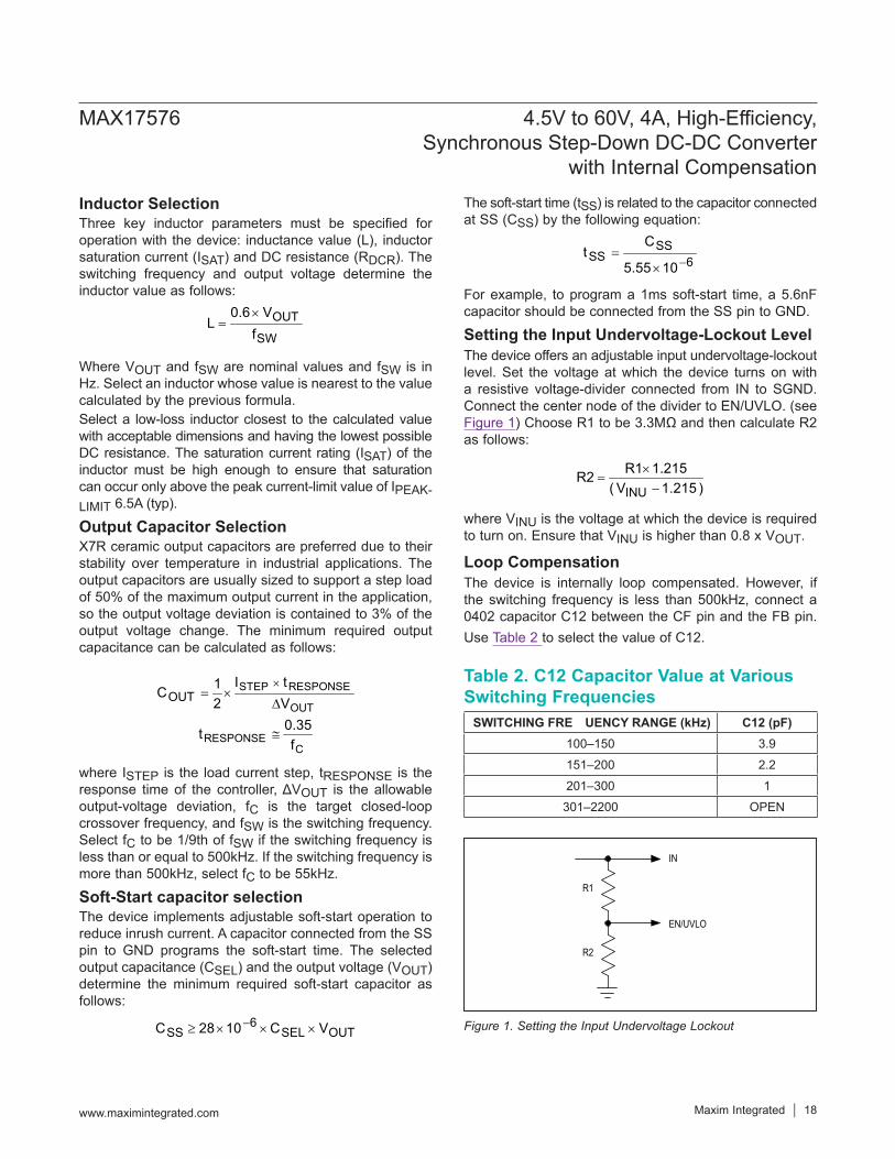
Inductor SelectionThree key inductor parameters must be specified for operation with the device: inductance value (L), inductor saturation current (ISAT) and DC resistance (RDCR). The switching frequency and output voltage determine the inductor value as follows:
OUT
SW
0.6 VL
f×
=
Where VOUT and fSW are nominal values and fSW is in Hz. Select an inductor whose value is nearest to the value calculated by the previous formula.Select a low-loss inductor closest to the calculated value with acceptable dimensions and having the lowest possible DC resistance. The saturation current rating (ISAT) of the inductor must be high enough to ensure that saturation can occur only above the peak current-limit value of IPEAK-LIMIT 6.5A (typ).
Output Capacitor SelectionX7R ceramic output capacitors are preferred due to their stability over temperature in industrial applications. The output capacitors are usually sized to support a step load of 50% of the maximum output current in the application, so the output voltage deviation is contained to 3% of the output voltage change. The minimum required output capacitance can be calculated as follows:
STEP RESPONSE
OUT
RESPONSEC
OUTI t1C
2 V0.35tf
×= ×
∆
≅
where ISTEP is the load current step, tRESPONSE is the response time of the controller, ΔVOUT is the allowable output-voltage deviation, fC is the target closed-loop crossover frequency, and fSW is the switching frequency. Select fC to be 1/9th of fSW if the switching frequency is less than or equal to 500kHz. If the switching frequency is more than 500kHz, select fC to be 55kHz.
Soft-Start capacitor selection The device implements adjustable soft-start operation to reduce inrush current. A capacitor connected from the SS pin to GND programs the soft-start time. The selected output capacitance (CSEL) and the output voltage (VOUT) determine the minimum required soft-start capacitor as follows:
6SS SEL OUTC 28 10 C V−≥ × × ×
The soft-start time (tSS) is related to the capacitor connected at SS (CSS) by the following equation:
SSSS 6
Ct
5.55 10−=
×
For example, to program a 1ms soft-start time, a 5.6nF capacitor should be connected from the SS pin to GND.
Setting the Input Undervoltage-Lockout LevelThe device offers an adjustable input undervoltage-lockout level. Set the voltage at which the device turns on with a resistive voltage-divider connected from IN to SGND. Connect the center node of the divider to EN/UVLO. (see Figure 1) Choose R1 to be 3.3MΩ and then calculate R2 as follows:
INU
R1 1.215R2( V 1.215 )
×=
−
where VINU is the voltage at which the device is required to turn on. Ensure that VINU is higher than 0.8 x VOUT.
Loop CompensationThe device is internally loop compensated. However, if the switching frequency is less than 500kHz, connect a 0402 capacitor C12 between the CF pin and the FB pin. Use Table 2 to select the value of C12.
Figure 1. Setting the Input Undervoltage Lockout
Table 2. C12 Capacitor Value at Various Switching Frequencies
R1
IN
EN/UVLO
R2
SWITCHING FREQUENCY RANGE (kHz) C12 (pF)100–150 3.9151–200 2.2201–300 1
301–2200 OPEN
MAX17576 4.5V to 60V, 4A, High-Efficiency, Synchronous Step-Down DC-DC Converter
with Internal Compensation
www.maximintegrated.com Maxim Integrated 18
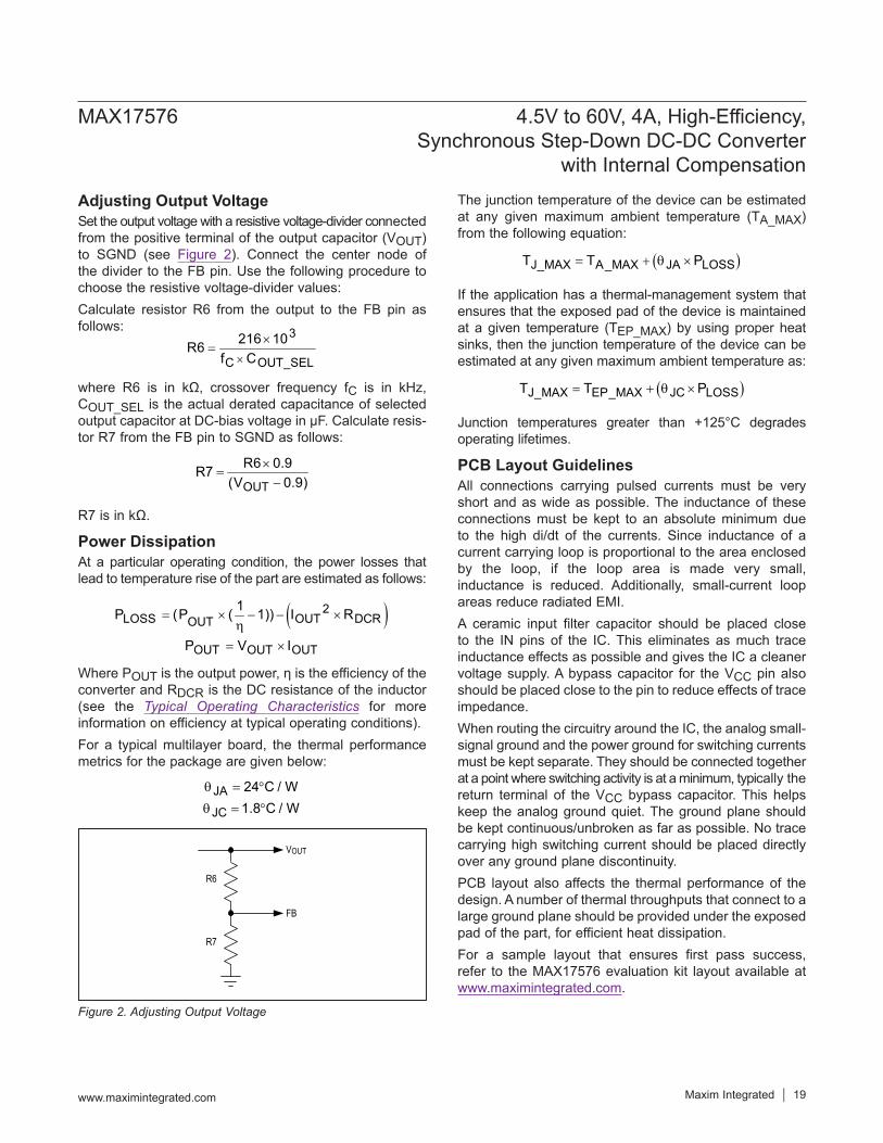
Adjusting Output VoltageSet the output voltage with a resistive voltage-divider connected from the positive terminal of the output capacitor (VOUT) to SGND (see Figure 2). Connect the center node of the divider to the FB pin. Use the following procedure to choose the resistive voltage-divider values:Calculate resistor R6 from the output to the FB pin as follows: 3
C OUT_SEL
216 10R6f C×
×=
where R6 is in kΩ, crossover frequency fC is in kHz, COUT_SEL is the actual derated capacitance of selected output capacitor at DC-bias voltage in μF. Calculate resis-tor R7 from the FB pin to SGND as follows:
OUT
R6 0.9R7(V 0.9)
×=
−
R7 is in kΩ.
Power DissipationAt a particular operating condition, the power losses that lead to temperature rise of the part are estimated as follows:
( )2LOSS OUT DCROUT
OUT OUT OUT
1P (P ( 1)) I R
P V I
= × − − ×η
= ×
Where POUT is the output power, η is the efficiency of the converter and RDCR is the DC resistance of the inductor (see the Typical Operating Characteristics for more information on efficiency at typical operating conditions). For a typical multilayer board, the thermal performance metrics for the package are given below:
JA
JC
24 C / W1.8 C / W
θ = °
θ = °
The junction temperature of the device can be estimated at any given maximum ambient temperature (TA_MAX) from the following equation:
( )J_MAX A_MAX JA LOSST T P= + θ ×
If the application has a thermal-management system that ensures that the exposed pad of the device is maintained at a given temperature (TEP_MAX) by using proper heat sinks, then the junction temperature of the device can be estimated at any given maximum ambient temperature as:
( )J_MAX EP_MAX JC LOSST T P= + θ ×
Junction temperatures greater than +125°C degrades operating lifetimes.
PCB Layout GuidelinesAll connections carrying pulsed currents must be very short and as wide as possible. The inductance of these connections must be kept to an absolute minimum due to the high di/dt of the currents. Since inductance of a current carrying loop is proportional to the area enclosed by the loop, if the loop area is made very small, inductance is reduced. Additionally, small-current loop areas reduce radiated EMI.A ceramic input filter capacitor should be placed close to the IN pins of the IC. This eliminates as much trace inductance effects as possible and gives the IC a cleaner voltage supply. A bypass capacitor for the VCC pin also should be placed close to the pin to reduce effects of trace impedance. When routing the circuitry around the IC, the analog small-signal ground and the power ground for switching currents must be kept separate. They should be connected together at a point where switching activity is at a minimum, typically the return terminal of the VCC bypass capacitor. This helps keep the analog ground quiet. The ground plane should be kept continuous/unbroken as far as possible. No trace carrying high switching current should be placed directly over any ground plane discontinuity.PCB layout also affects the thermal performance of the design. A number of thermal throughputs that connect to a large ground plane should be provided under the exposed pad of the part, for efficient heat dissipation.For a sample layout that ensures first pass success, refer to the MAX17576 evaluation kit layout available at www.maximintegrated.com.
Figure 2. Adjusting Output Voltage
R6
R7
VOUT
FB
MAX17576 4.5V to 60V, 4A, High-Efficiency, Synchronous Step-Down DC-DC Converter
with Internal Compensation
www.maximintegrated.com Maxim Integrated 19
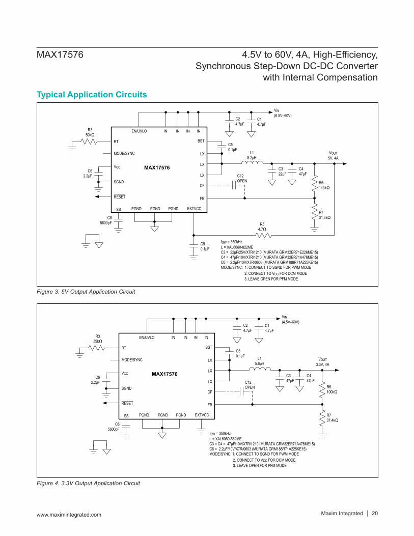
Figure 3. 5V Output Application Circuit
Figure 4. 3.3V Output Application Circuit
fSW = 350kHzL = XAL6060-562MEC3 = C4 = 47μF/10V/X7R/1210 (MURATA GRM32ER71A476ME15)C6 = 2.2μF/10V/X7R/0603 (MURATA GRM188R71A225KE15)MODE/SYNC: 1. CONNECT TO SGND FOR PWM MODE
2. CONNECT TO VCC FOR DCM MODE 3. LEAVE OPEN FOR PFM MODE
RESET
EN/UVLO IN
BSTRT
IN
MODE/SYNC
VCC
SGNDCF
SS
FB
PGND
LX
LX
LX
IN
C85600pF
EXTVCC
C62.2μF
C24.7μF
C14.7μF
C50.1μF
C347μF
VOUT3.3V, 4A
C447μF
R6100kΩ
R737.4kΩ
MAX17576
L15.6μH
PGND PGND
R359kΩ
IN
VIN(4.5V–60V)
C12OPEN
Typical Application Circuits
R54.7Ω
fSW = 350kHzL = XAL6060-822MEC3 = 22μF/25V/X7R/1210 (MURATA GRM32ER71E226ME15)C4 = 47μF/10V/X7R/1210 (MURATA GRM32ER71A476ME15)C6 = 2.2μF/10V/X7R/0603 (MURATA GRM188R71A225KE15)MODE/SYNC: 1. CONNECT TO SGND FOR PWM MODE
2. CONNECT TO VCC FOR DCM MODE 3. LEAVE OPEN FOR PFM MODE
RESET
EN/UVLO IN
BSTRT
IN
MODE/SYNC
VCC
SGNDCF
SS
FB
PGND
LX
LX
LX
IN
C85600pF
EXTVCC
C62.2μF
C24.7μF
C14.7μF
C50.1μF
C322μF
VOUT5V, 4A
C447μF
R6143kΩ
R731.6kΩ
MAX17576
L18.2μH
PGND PGND
R359kΩ
C90.1μF
IN
VIN(6.5V–60V)
C12OPEN
MAX17576 4.5V to 60V, 4A, High-Efficiency, Synchronous Step-Down DC-DC Converter
with Internal Compensation
www.maximintegrated.com Maxim Integrated 20

+Denotes a lead(Pb)-free/RoHS-compliant package. *EP = Exposed pad.
Ordering InformationPART PIN-PACKAGE PACKAGE-SIZE
MAX17576ATG+ 24-TQFN EP* 4mm x 5mm
MAX17576 4.5V to 60V, 4A, High-Efficiency, Synchronous Step-Down DC-DC Converter
with Internal Compensation
www.maximintegrated.com Maxim Integrated 21
Revision HistoryREVISIONNUMBER
REVISIONDATE DESCRIPTION PAGES
CHANGED
0 9/18 Initial release —
Maxim Integrated cannot assume responsibility for use of any circuitry other than circuitry entirely embodied in a Maxim Integrated product. No circuit patent licenses are implied. Maxim Integrated reserves the right to change the circuitry and specifications without notice at any time. The parametric values (min and max limits) shown in the Electrical Characteristics table are guaranteed. Other parametric values quoted in this data sheet are provided for guidance.
Maxim Integrated and the Maxim Integrated logo are trademarks of Maxim Integrated Products, Inc.
MAX17576 4.5V to 60V, 4A, High-Efficiency, Synchronous Step-Down DC-DC Converter
with Internal Compensation
© 2018 Maxim Integrated Products, Inc. 22
For pricing, delivery, and ordering information, please visit Maxim Integrated’s online storefront at https://www.maximintegrated.com/en/storefront/storefront.html.