Embed Size (px)
Citation preview

Rev.0, December 2016 Maxim Integrated Page 1
MAX17055 MODELGAUGE M5 EZ USER GUIDE Single-Cell ModelGauge m5 Fuel Gauge December 2016

Rev.0, December 2016 Maxim Integrated Page 2
©2016 Maxim Integrated Products, Inc. All rights reserved.
Rev. 0, Month 2016
No part of this documentation may be reproduced nor distributed in any form or by any means, graphic, electronic, or mechanical, including but not limited to photocopying, scanning, recording, taping, e-mailing, or storing in information storage and retrieval systems without the written permission of Maxim Integrated Products, Inc. (hereafter, “Maxim”). Products that are referenced in this document such as Microsoft Windows® may be trademarks and/or registered trademarks of their respective owners. Maxim makes no claim to these trademarks. While every precaution has been taken in the preparation of this document, individually, as a series, in whole, or in part, Maxim, the publisher, and the author assume no responsibility for errors or omissions, including any damages resulting from the express or implied application of information contained in this document or from the use of products, services, or programs that may accompany it. In no event shall Maxim, publishers, authors, or editors of this guide be liable for any loss of profit or any other commercial damage caused or alleged to have been caused directly or indirectly by this document.
Rev.0, December 2016 Maxim Integrated Page 3
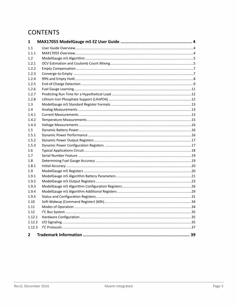
CONTENTS 1 MAX17055 ModelGauge m5 EZ User Guide ......................................................... 4 1.1 User Guide Overview .........................................................................................................................4 1.1.1 MAX17055 Overview .........................................................................................................................4 1.2 ModelGauge m5 Algorithm ...............................................................................................................5 1.2.1 OCV Estimation and Coulomb Count Mixing .....................................................................................5 1.2.2 Empty Compensation ........................................................................................................................7 1.2.3 Converge-to-Empty ...........................................................................................................................7 1.2.4 99% and Empty Hold .........................................................................................................................8 1.2.5 End-of-Charge Detection ...................................................................................................................9 1.2.6 Fuel Gauge Learning ........................................................................................................................11 1.2.7 Predicting Run Time for a Hypothetical Load ..................................................................................12 1.2.8 Lithium Iron Phosphate Support (LiFePO4) .....................................................................................12 1.3 ModelGauge m5 Standard Register Formats ..................................................................................13 1.4 Analog Measurements ....................................................................................................................13 1.4.1 Current Measurements ...................................................................................................................13 1.4.2 Temperature Measurements ...........................................................................................................15 1.4.3 Voltage Measurements ...................................................................................................................16 1.5 Dynamic Battery Power ...................................................................................................................16 1.5.1 Dynamic Power Performance ..........................................................................................................16 1.5.2 Dynamic Power Output Registers ....................................................................................................17 1.5.3 Dynamic Power Configuration Registers .........................................................................................17 1.6 Typical Applications Circuit ..............................................................................................................18 1.7 Serial Number Feature ....................................................................................................................19 1.8 Determining Fuel Gauge Accuracy ..................................................................................................19 1.8.1 Initial Accuracy ................................................................................................................................20 1.9 ModelGauge m5 Registers ..............................................................................................................20 1.9.1 ModelGauge m5 Algorithm Battery Parameters .............................................................................21 1.9.2 ModelGauge m5 Output Registers ..................................................................................................23 1.9.3 ModelGauge m5 Algorithm Configuration Registers .......................................................................26 1.9.4 ModelGauge m5 Algorithm Additional Registers ............................................................................29 1.9.5 Status and Configuration Registers ..................................................................................................31 1.10 Soft-Wakeup (Command Register) (60h) .........................................................................................34 1.11 Modes of Operation ........................................................................................................................34 1.12 I2C Bus System .................................................................................................................................35 1.12.1 Hardware Configuration ..................................................................................................................35 1.12.2 I/O Signaling ....................................................................................................................................35 1.12.3 I2C Protocols ....................................................................................................................................37
2 Trademark Information ..................................................................................... 39
Rev.0, December 2016 Maxim Integrated Page 4
1 MAX17055 ModelGauge m5 EZ User Guide
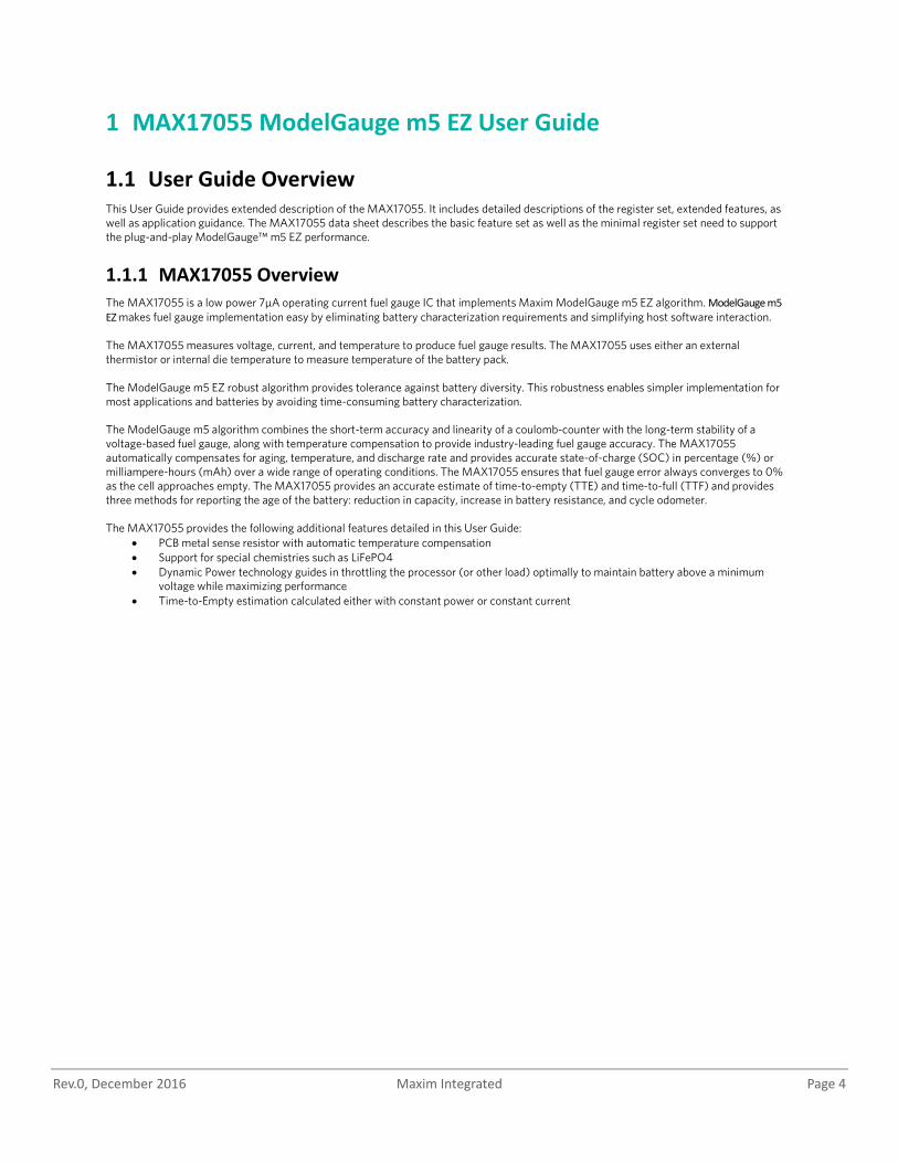
1.1 User Guide Overview This User Guide provides extended description of the MAX17055. It includes detailed descriptions of the register set, extended features, as well as application guidance. The MAX17055 data sheet describes the basic feature set as well as the minimal register set need to support the plug-and-play ModelGauge™ m5 EZ performance.
1.1.1 MAX17055 Overview The MAX17055 is a low power 7μA operating current fuel gauge IC that implements Maxim ModelGauge m5 EZ algorithm. ModelGauge m5 EZ makes fuel gauge implementation easy by eliminating battery characterization requirements and simplifying host software interaction. The MAX17055 measures voltage, current, and temperature to produce fuel gauge results. The MAX17055 uses either an external thermistor or internal die temperature to measure temperature of the battery pack. The ModelGauge m5 EZ robust algorithm provides tolerance against battery diversity. This robustness enables simpler implementation for most applications and batteries by avoiding time-consuming battery characterization. The ModelGauge m5 algorithm combines the short-term accuracy and linearity of a coulomb-counter with the long-term stability of a voltage-based fuel gauge, along with temperature compensation to provide industry-leading fuel gauge accuracy. The MAX17055 automatically compensates for aging, temperature, and discharge rate and provides accurate state-of-charge (SOC) in percentage (%) or milliampere-hours (mAh) over a wide range of operating conditions. The MAX17055 ensures that fuel gauge error always converges to 0% as the cell approaches empty. The MAX17055 provides an accurate estimate of time-to-empty (TTE) and time-to-full (TTF) and provides three methods for reporting the age of the battery: reduction in capacity, increase in battery resistance, and cycle odometer. The MAX17055 provides the following additional features detailed in this User Guide:
• PCB metal sense resistor with automatic temperature compensation • Support for special chemistries such as LiFePO4 • Dynamic Power technology guides in throttling the processor (or other load) optimally to maintain battery above a minimum
voltage while maximizing performance • Time-to-Empty estimation calculated either with constant power or constant current
Rev.0, December 2016 Maxim Integrated Page 5
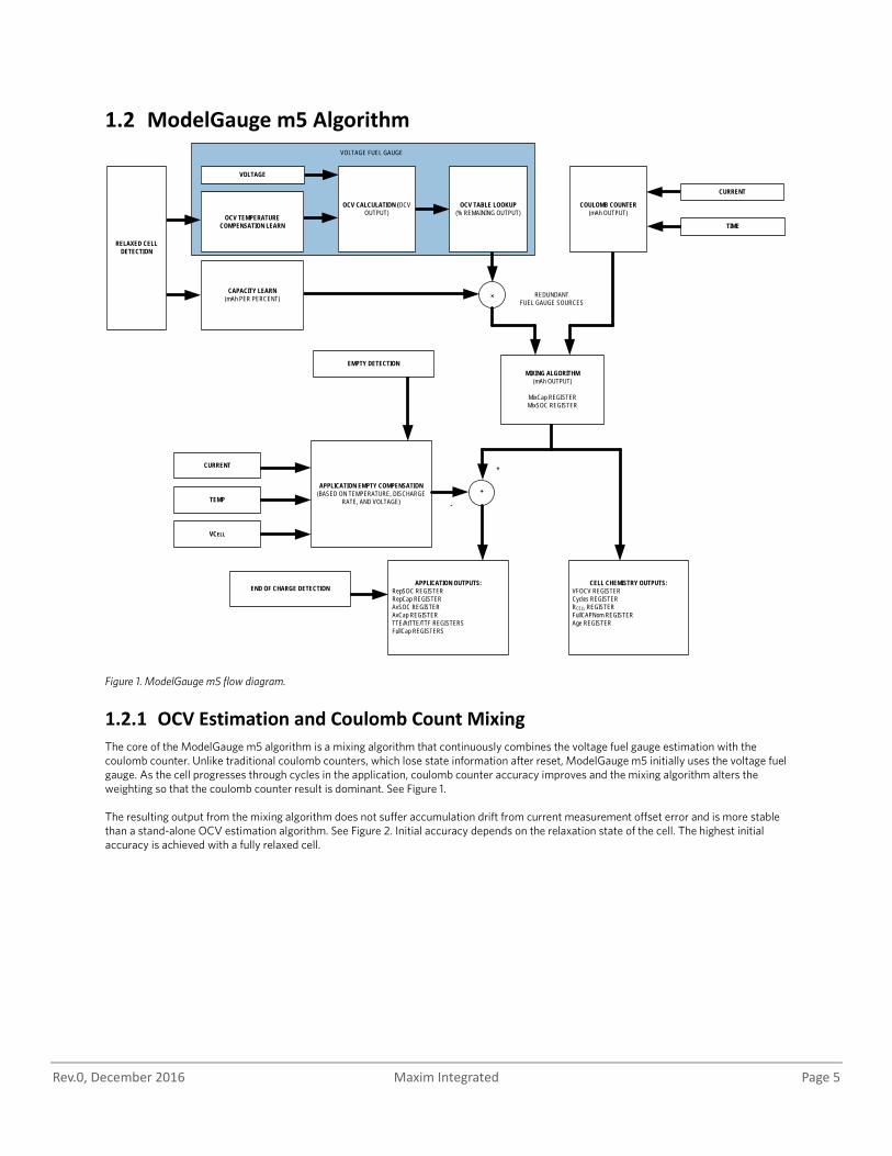
1.2 ModelGauge m5 Algorithm
Figure 1. ModelGauge m5 flow diagram.
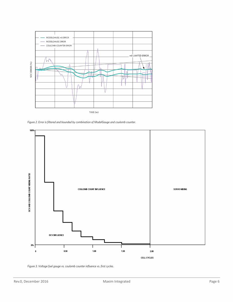
1.2.1 OCV Estimation and Coulomb Count Mixing The core of the ModelGauge m5 algorithm is a mixing algorithm that continuously combines the voltage fuel gauge estimation with the coulomb counter. Unlike traditional coulomb counters, which lose state information after reset, ModelGauge m5 initially uses the voltage fuel gauge. As the cell progresses through cycles in the application, coulomb counter accuracy improves and the mixing algorithm alters the weighting so that the coulomb counter result is dominant. See Figure 1. The resulting output from the mixing algorithm does not suffer accumulation drift from current measurement offset error and is more stable than a stand-alone OCV estimation algorithm. See Figure 2. Initial accuracy depends on the relaxation state of the cell. The highest initial accuracy is achieved with a fully relaxed cell.
APPLICATION OUTPUTS:RepSOC REGISTERRepCap REGISTERAvSOC REGISTERAvCap REGISTERTTE/AtTTE/TTF REGISTERSFullCap REGISTERS
APPLICATION EMPTY COMPENSATION (BASED ON TEMPERATURE, DISCHARGE
RATE, AND VOLTAGE)
×
+
CELL CHEMISTRY OUTPUTS:VFOCV REGISTERCycles REGISTERRCELL REGISTERFullCAPNom REGISTERAge REGISTER
+
-
VOLTAGE FUEL GAUGE
REDUNDANT FUEL GAUGE SOURCES
RELAXED CELL DETECTION
OCV CALCULATION (OCV OUTPUT)
VOLTAGE
CAPACITY LEARN(mAh PER PERCENT)
OCV TEMPERATURE COMPENSATION LEARN
EMPTY DETECTION
OCV TABLE LOOKUP (% REMAINING OUTPUT)
COULOMB COUNTER (mAh OUTPUT)
MIXING ALGORITHM (mAh OUTPUT)
MixCap REGISTERMixSOC REGISTER
TEMP
VCELL
END OF CHARGE DETECTION
CURRENT
TIME
CURRENT
Rev.0, December 2016 Maxim Integrated Page 6
Figure 2. Error is filtered and bounded by combination of ModelGauge and coulomb counter.
Figure 3. Voltage fuel gauge vs. coulomb counter influence vs. first cycles.
0.50
CELL CYCLES
0 1.00 1.50 2.00
OCV
AND
COUL
OMB
COUN
T MI
RAT
IO
OCV INFLUENCE
COULOMB COUNT INFLUENCE
0%
100%
SERVO MIXING
Rev.0, December 2016 Maxim Integrated Page 7
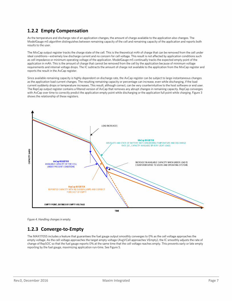
1.2.2 Empty Compensation As the temperature and discharge rate of an application changes, the amount of charge available to the application also changes. The ModelGauge m5 algorithm distinguishes between remaining capacity of the cell and remaining capacity of the application and reports both results to the user. The MixCap output register tracks the charge state of the cell. This is the theoretical mAh of charge that can be removed from the cell under ideal conditions—extremely low discharge current and no concern for cell voltage. This result is not affected by application conditions such as cell impedance or minimum operating voltage of the application. ModelGauge m5 continually tracks the expected empty point of the application in mAh. This is the amount of charge that cannot be removed from the cell by the application because of minimum voltage requirements and internal voltage drops. The IC subtracts the amount of charge not available to the application from the MixCap register and reports the result in the AvCap register. Since available remaining capacity is highly dependent on discharge rate, the AvCap register can be subject to large instantaneous changes as the application load current changes. The resulting remaining capacity or percentage can increase, even while discharging, if the load current suddenly drops or temperature increases. This result, although correct, can be very counterintuitive to the host software or end user. The RepCap output register contains a filtered version of AvCap that removes any abrupt changes in remaining capacity. RepCap converges with AvCap over time to correctly predict the application empty point while discharging or the application full point while charging. Figure 3 shows the relationship of these registers.
Figure 4. Handling changes in empty.
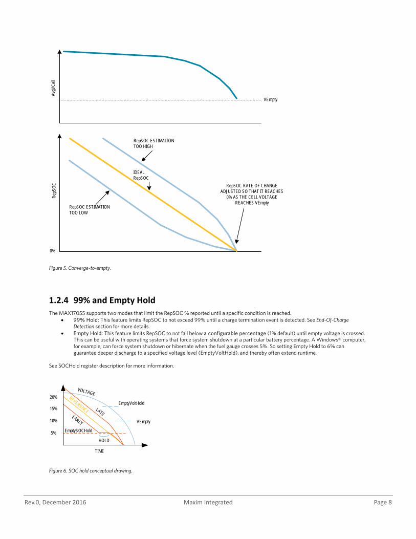
1.2.3 Converge-to-Empty The MAX17055 includes a feature that guarantees the fuel gauge output smoothly converges to 0% as the cell voltage approaches the empty voltage. As the cell voltage approaches the target empty voltage (AvgVCell approaches VEmpty), the IC smoothly adjusts the rate of change of RepSOC so that the fuel gauge reports 0% at the same time that the cell voltage reaches empty. This prevents early or late empty reporting by the fuel gauge, maximizing application run-time. See Figure 5.
MixCap REGISTER ABSOLUTE mAh STATE OF BATTERY NOT CONSIDERING TEMPERATURE AND DISCHARGE
RATE (I.E., CAPACITY AVAILABLE IF VERY LIGHT LOAD)
RepCap REGISTERREPORTED CAPACITY WITH NO SUDDEN JUMPS AND CORRECT
FORECAST OF EMPTY
EMPTY POINT, DEFINED BY EMPTY VOLTAGE
LOAD INCREASES
AvCap REGISTERAVAILABLE CAPACITY OF THE CELL
UNDER PRESENT CONDITIONS
CAPA
CITY
(mAh
)
INCREASE IN AVAILABLE CAPACITY WHEN UNDER LOAD IS COUNTERINTUITIVE TO USERS AND OPERATING SYSTEMS
TIME
Rev.0, December 2016 Maxim Integrated Page 8
Figure 5. Converge-to-empty.
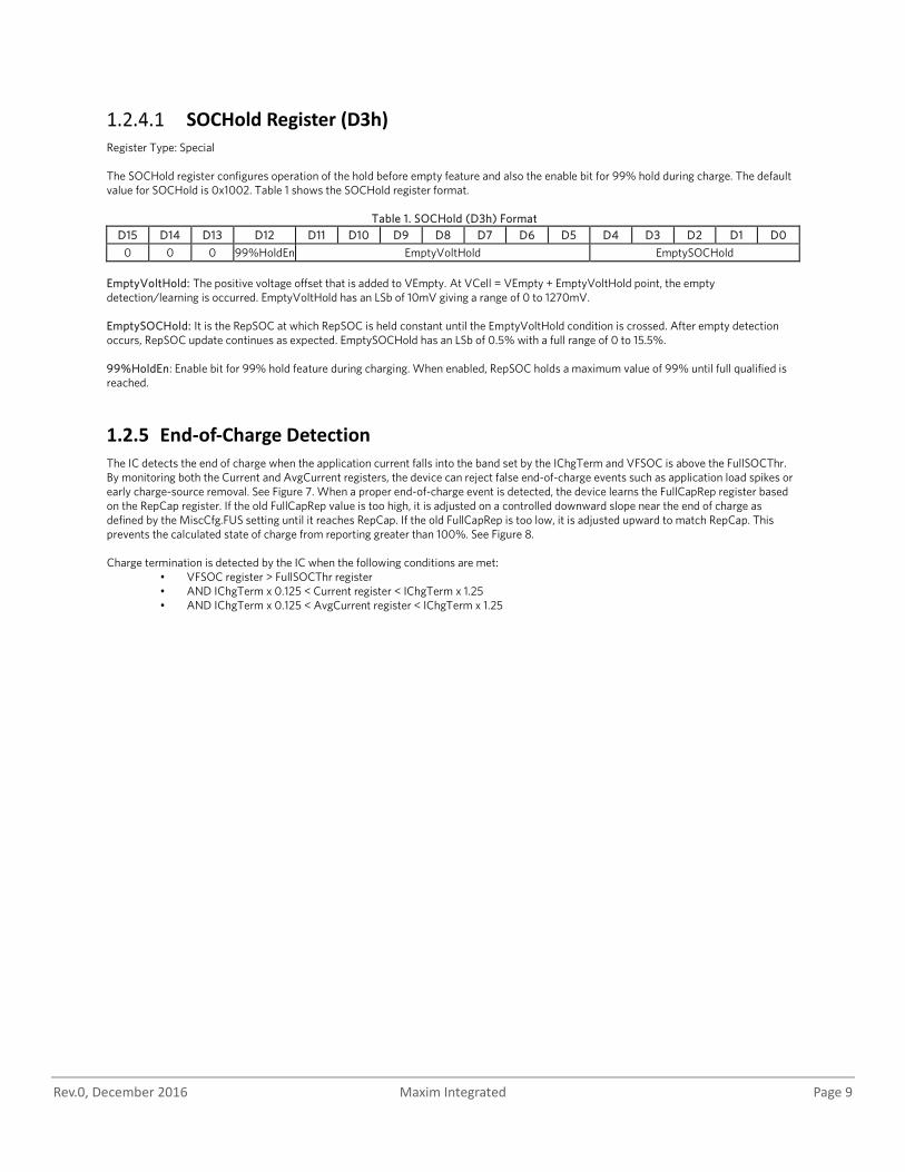
1.2.4 99% and Empty Hold The MAX17055 supports two modes that limit the RepSOC % reported until a specific condition is reached.
• 99% Hold: This feature limits RepSOC to not exceed 99% until a charge termination event is detected. See End-Of-Charge Detection section for more details.
• Empty Hold: This feature limits RepSOC to not fall below a configurable percentage (1% default) until empty voltage is crossed. This can be useful with operating systems that force system shutdown at a particular battery percentage. A Windows® computer, for example, can force system shutdown or hibernate when the fuel gauge crosses 5%. So setting Empty Hold to 6% can guarantee deeper discharge to a specified voltage level (EmptyVoltHold), and thereby often extend runtime.
See SOCHold register description for more information.
Figure 6. SOC hold conceptual drawing.
0%
RepS
OC
VEmpty
RepSOC ESTIMATION TOO HIGH
AvgV
Cell
RepSOC ESTIMATION TOO LOW
IDEAL RepSOC
RepSOC RATE OF CHANGE ADJUSTED SO THAT IT REACHES
0% AS THE CELL VOLTAGE REACHES VEmpty
VOLTAGE
EmptyVoltHold
VEmpty
REFERENCE
EmptySOCHold
EARLY
LATE
HOLD
10%
TIME
15%
20%
5%
Rev.0, December 2016 Maxim Integrated Page 9
SOCHold Register (D3h) Register Type: Special The SOCHold register configures operation of the hold before empty feature and also the enable bit for 99% hold during charge. The default value for SOCHold is 0x1002. Table 1 shows the SOCHold register format.
Table 1. SOCHold (D3h) Format D15 D14 D13 D12 D11 D10 D9 D8 D7 D6 D5 D4 D3 D2 D1 D0
0 0 0 99%HoldEn EmptyVoltHold EmptySOCHold EmptyVoltHold: The positive voltage offset that is added to VEmpty. At VCell = VEmpty + EmptyVoltHold point, the empty detection/learning is occurred. EmptyVoltHold has an LSb of 10mV giving a range of 0 to 1270mV. EmptySOCHold: It is the RepSOC at which RepSOC is held constant until the EmptyVoltHold condition is crossed. After empty detection occurs, RepSOC update continues as expected. EmptySOCHold has an LSb of 0.5% with a full range of 0 to 15.5%. 99%HoldEn: Enable bit for 99% hold feature during charging. When enabled, RepSOC holds a maximum value of 99% until full qualified is reached.
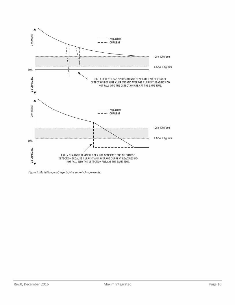
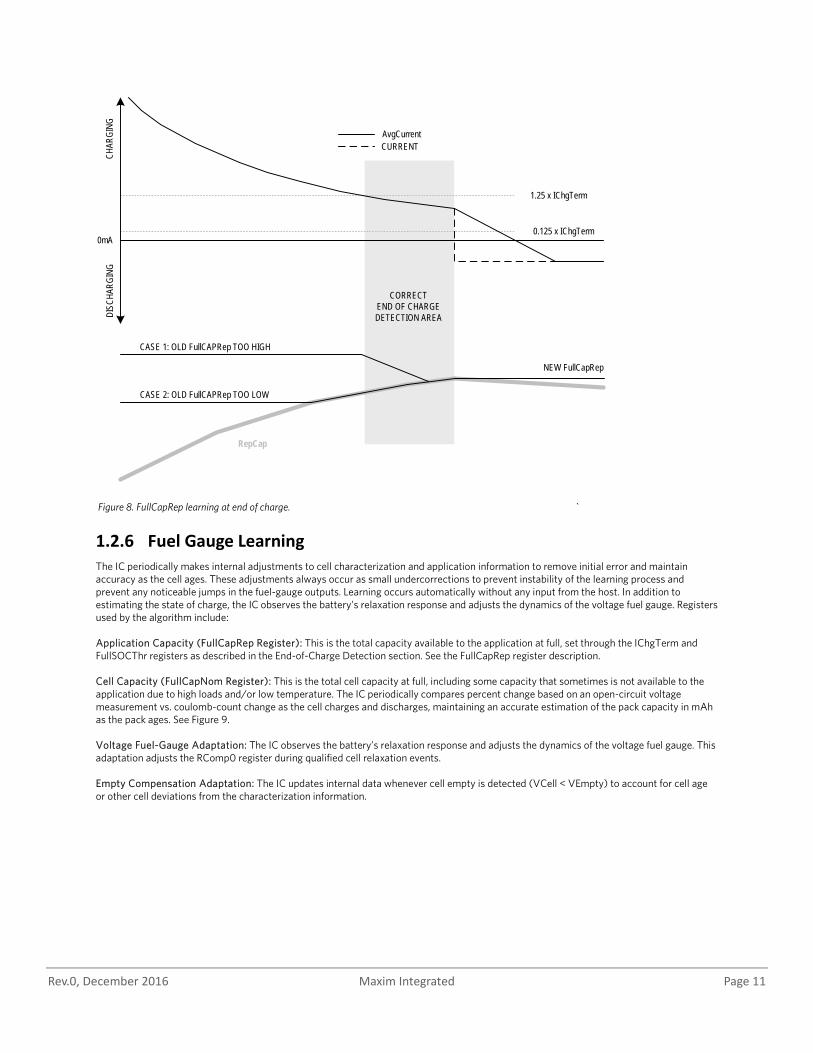
1.2.5 End-of-Charge Detection The IC detects the end of charge when the application current falls into the band set by the IChgTerm and VFSOC is above the FullSOCThr. By monitoring both the Current and AvgCurrent registers, the device can reject false end-of-charge events such as application load spikes or early charge-source removal. See Figure 7. When a proper end-of-charge event is detected, the device learns the FullCapRep register based on the RepCap register. If the old FullCapRep value is too high, it is adjusted on a controlled downward slope near the end of charge as defined by the MiscCfg.FUS setting until it reaches RepCap. If the old FullCapRep is too low, it is adjusted upward to match RepCap. This prevents the calculated state of charge from reporting greater than 100%. See Figure 8. Charge termination is detected by the IC when the following conditions are met:
• VFSOC register > FullSOCThr register • AND IChgTerm x 0.125 < Current register < IChgTerm x 1.25 • AND IChgTerm x 0.125 < AvgCurrent register < IChgTerm x 1.25
Rev.0, December 2016 Maxim Integrated Page 10
Figure 7. ModelGauge m5 rejects false end-of-charge events.
1.25 x IChgTerm
0.125 x IChgTerm0mA
CHAR
GING
DISC
HARG
ING
AvgCurrentCURRENT
1.25 x IChgTerm
0.125 x IChgTerm0mA
CHAR
GING
DISC
HARG
ING HIGH CURRENT LOAD SPIKES DO NOT GENERATE END OF CHARGE
DETECTION BECAUSE CURRENT AND AVERAGE CURRENT READINGS DO NOT FALL INTO THE DETECTION AREA AT THE SAME TIME.
EARLY CHARGER REMOVAL DOES NOT GENERATE END OF CHARGE DETECTION BECAUSE CURRENT AND AVERAGE CURRENT READINGS DO
NOT FALL INTO THE DETECTION AREA AT THE SAME TIME.
AvgCurrentCURRENT
Rev.0, December 2016 Maxim Integrated Page 11
Figure 8. FullCapRep learning at end of charge. `
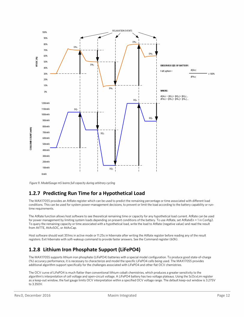
1.2.6 Fuel Gauge Learning The IC periodically makes internal adjustments to cell characterization and application information to remove initial error and maintain accuracy as the cell ages. These adjustments always occur as small undercorrections to prevent instability of the learning process and prevent any noticeable jumps in the fuel-gauge outputs. Learning occurs automatically without any input from the host. In addition to estimating the state of charge, the IC observes the battery’s relaxation response and adjusts the dynamics of the voltage fuel gauge. Registers used by the algorithm include: Application Capacity (FullCapRep Register): This is the total capacity available to the application at full, set through the IChgTerm and FullSOCThr registers as described in the End-of-Charge Detection section. See the FullCapRep register description. Cell Capacity (FullCapNom Register): This is the total cell capacity at full, including some capacity that sometimes is not available to the application due to high loads and/or low temperature. The IC periodically compares percent change based on an open-circuit voltage measurement vs. coulomb-count change as the cell charges and discharges, maintaining an accurate estimation of the pack capacity in mAh as the pack ages. See Figure 9. Voltage Fuel-Gauge Adaptation: The IC observes the battery’s relaxation response and adjusts the dynamics of the voltage fuel gauge. This adaptation adjusts the RComp0 register during qualified cell relaxation events. Empty Compensation Adaptation: The IC updates internal data whenever cell empty is detected (VCell < VEmpty) to account for cell age or other cell deviations from the characterization information.
AvgCurrentCURRENT
1.25 x IChgTerm
0.125 x IChgTerm0mA
CHAR
GING
DISC
HARG
ING
CORRECTEND OF CHARGE DETECTION AREA
RepCap
CASE 1: OLD FullCAPRep TOO HIGH
CASE 2: OLD FullCAPRep TOO LOW
NEW FullCapRep
Rev.0, December 2016 Maxim Integrated Page 12
Figure 9. ModelGauge m5 learns full capacity during arbitrary cycling
1.2.7 Predicting Run Time for a Hypothetical Load The MAX17055 provides an AtRate register which can be used to predict the remaining percentage or time associated with different load conditions. This can be used for system power-management decisions, to prevent or limit the load according to the battery capability or run-time requirements. The AtRate function allows host software to see theoretical remaining time or capacity for any hypothetical load current. AtRate can be used for power management by limiting system loads depending on present conditions of the battery. To use AtRate, set AtRateEn = 1 in Config2. To query the remaining capacity or time associated with a hypothetical load, write the load to AtRate (negative value) and read the result from AtTTE, AtAvSOC, or AtAvCap. Host software should wait 351ms in active mode or 11.25s in hibernate after writing the AtRate register before reading any of the result registers. Exit hibernate with soft-wakeup command to provide faster answers. See the Command register (60h).
1.2.8 Lithium Iron Phosphate Support (LiFePO4) The MAX17055 supports lithium iron phosphate (LiFePO4) batteries with a special model configuration. To produce good state-of-charge (%) accuracy performance, it is necessary to characterize and model the specific LiFePO4 cells being used. The MAX17055 provides additional algorithm support specifically for the challenges associated with LiFePO4 and other flat OCV chemistries. The OCV curve of LiFePO4 is much flatter than conventional lithium cobalt chemistries, which produces a greater sensitivity to the algorithm's interpretation of cell voltage and open-circuit voltage. A LiFePO4 battery has two voltage plateaus. Using the ScOcvLim register as a keep-out window, the fuel gauge limits OCV interpretation within a specified OCV voltage range. The default keep-out window is 3.275V to 3.350V.
0%
10%
30%
50%
70%
20%
40%
60%
80%
90%
100%
VFSO
C (%
)
D%1
D%2
D%3
D%4
D%5
DQ1
DQ2
DQ3
DQ4
DQ5
0mAh
100mAh
300mAh
500mAh
700mAh
200mAh
400mAh
600mAh
800mAh
900mAh
1000mAh
1100mAh
1200mAh
OBSERVED SIZE OF BATTERY:
FullCapNom = dQAcc
dPAcc x 100%
COUL
OMB
COUN
T (m
Ah)
RELAXATION EVENTS
WHERE:
dQAcc = |DQ1| + |DQ2| + |DQ3| ...dPAcc = |D%1| + |D%2| + |D%3| ...
Rev.0, December 2016 Maxim Integrated Page 13
To configure the MAX17055 for LiFePO4 support, do the following:
1. Characterize the battery. The characterization data should be translated by Maxim into a battery model. 2. Configure the ScOcvLim register according to the desired OCV keep-out window. 3. Configure ModelCfg.ModelID = 6 to enable LiFePO4 mode. 4. Load the rest of the battery model. Refer to the MAX17055 Software Implementation Guide.
ScOcvLim Register (D1h) Register Type: Special Initial Value: 0x479E This register only has usage when ModelCfg.ModelID is selected as 6 (LiFePO4). Table 2 shows the register format.
Table 2. ScOcvLim (D1h) Format D15 D14 D13 D12 D11 D10 D9 D8 D7 D6 D5 D4 D3 D2 D1 D0
OCV_Low_Lim OCV_Delta OCV_Low_Lim: Defines the lower limit for keep-out OCV region. A 5mV resolution gives a 2.56 to 5.12V range. Lower limit voltage of OCV keep-out region is calculated as 2.56V + OCV_Low_Lim x 5mV. Default value is 0x8F. OCV_Delta: Defines the delta between lower and upper limits for keep-out OCV region. A 2.5mV resolution gives a 0 to 320mV range. Upper limit voltage of OCV keep-out region is calculated as 2.56V + OCV_Low_Lim x 5mV + OCV_Delta x 2.5mV. Default value is 0x1E. Default OCV_low is 3275mV and OCV_high is 3350mV.
1.3 ModelGauge m5 Standard Register Formats Unless otherwise stated during a given register's description, all IC registers follow the same format depending on the type of register. See Table 3 for the resolution and range of any register described hereafter. Note that current and capacity values are displayed as a voltage and must be divided by the sense resistor to determine Amps or Amp-hours. It is strongly recommended to use the nRSense (1CFh) register to store the sense resistor value for use by host software.
Table 3. Standard Register Formats REGISTER
TYPE LSb SIZE MINIMUM VALUE MAXIMUM VALUE NOTES
Capacity 5.0μVH/RSENSE 0.0μVH 327.675mVH/RSENSE Equivalent to 0.5mA with a 0.010Ω sense resistor. Percentage 1/256% 0.0% 255.9961% 1% LSb when reading only the upper byte.
Voltage 0.078125mV 0.0V 5.11992V
Current 1.5625μV/RSENSE -51.2mV/RSENSE 51.1984mV/RSENSE Signed 2's complement format. Equivalent to 156.25μA with a
0.010Ω sense resistor.
Temperature 1/256°C -128.0°C 127.996°C Signed 2's complement format. 1°C LSb when reading only the upper byte.
Resistance 1/4096 Ω 0.0 Ω 15.99976 Ω Time 5.625s 0.0s 102.3984h
Special Format details are included with the register description.
1.4 Analog Measurements To properly fuel gauge a battery the MAX17055 continually monitors the battery voltage, battery temperature, and current flow into and out of the battery. The following sections detail how these measurements occur.
1.4.1 Current Measurements Current flow through the battery is determined by making voltage measurements between the CSP and CSN pins. An external sense resistor placed between these pins creates a positive voltage when the battery is charged and a negative voltage when the battery is discharged. The resulting value is reported in μV or μVh and must be divided by the sense resistor value in ohms to convert to current.
Rev.0, December 2016 Maxim Integrated Page 14
The value of the sense resistor determines the range and the resolution of current values that can be reported. The MAX17055 has a maximum measurement range of ±51.2mV and a reporting resolution of 1.5625μV. Table 4 shows the measurement ranges and resolutions of several common-sense resistor values.
Table 4. Measurement Range and Resolution vs. Sense Resistor Value
SENSE RESISTOR (mΩ) MEASUREMENT RANGE (A) MEASUREMENT RESOLUTION (μA) 20.0 ±2.56 78.125 10.0 ±5.12 156.25 5.0 ±10.24 312.50
3.5 (board trace) ±14.69 446.43 2.0 ±25.60 781.25
CGain Register (2Eh) and COff (2Fh) Registers Register Type: Special Initial Value: CGain = 0x0400 and COff = 0x0000 The CGain and COff registers adjust the gain and offset of the current measurement result. The current measurement A/D is factory trimmed to data-sheet accuracy without the need for the user to make further adjustments. The default power-up settings for CGain and COff apply no adjustments to the Current register reading. For specific application requirements, the CGain and COff registers can be used to adjust readings as follows: Current register = Current A/D reading × (CGain register/0400h) + COff register
Copper Trace Current Sensing The MAX17055 has the ability to measure current using a copper board trace instead of a traditional sense resistor. The main difference being the ability to adjust to the change in sense resistance over temperature. The MAX17055 EV kit includes a PCB trace that demonstrates this functionality. Board-to-board variation makes it challenging to use PCB current-sensing to achieve the normally stringent requirements for fuel gauging. However, the MAX17055 can meet this challenge due to the robust ModelGauge m5 EZ algorithm, plus PCB compensations provided in the MAX17055. To configure the MAX17055 for accurate PCB current-sensing, configure the following:
1. Set CGTempCo to 0x20C8, corresponding to copper at 0.4% per °C. Set CGTempCo to 0 to disable copper current sensing when using a normal sense resistor.
2. Set CGAIN according to the room-temperature resistance associated with the PCB trace. Configure CCurve to compensate for the self-heating of the trace. The PCB trace temperature mismatches the MAX17055 die temperature (used for compensation), especially at high currents. This self-heating is also compensated by the MAX17055 using the CCurve configuration register. For 1oz copper, a length to width ratio of 6:1 creates a 0.0035Ω sense resistor that is suitable for most applications. PCB manufacturing process can produce a trace-resistance variation of ±20%. ModelGauge m5 adapts to this variation and reports SOC accurately. The adaptation is similar to supporting battery-to-battery, full-capacity variation.
Curve Register (B9h) Register Type: Special The upper half of the Curve register applies curvature correction current measurements made by the IC when using a copper trace as the sense resistor. See the Temperature Measurements section for a description of the lower half of the register.
Table 5. Curve (B9h) Format D15 D14 D13 D12 D11 D10 D9 D8 D7 D6 D5 D4 D3 D2 D1 D0
Metal Trace Curve Thermistor Curve
Rev.0, December 2016 Maxim Integrated Page 15
CGTempCo Register (B8h) Register Type: Special Initial Value: 0x0 If CGTempCo is nonzero then CGTempCo is used to adjust current measurements for temperature. CGTempCo has a range of 0% to 3.1224% per °C with a step size of 3.1224/0x10000 percent per °C. If a copper trace is used to measure battery current, CGTempCo should be written to 0x20C8 or 0.4% per °C, which is the approximate temperature coefficient of a copper trace.
1.4.2 Temperature Measurements The MAX17055 can measure and report its own internal temperature or report an external temperature by using an NTC thermistor divider network connected to the THRM and AIN pins. Only one measurement path can be active at any time. When measuring temperature externally, the MAX17055 takes a raw percentage reading and converts that value to temperature using gain (TGain register), offset (TOff register), and second order curve adjustment (Curve register). This allows an accurate temperature to be reported over a variety of different NTC thermistor options. Internal temperature measurement does not use TGain, TOff, or Curve.
AIN Register (27h) Register Type: Special External temperature measurement on the AIN pin is compared to the THRM pin voltage. The MAX17055 stores the result as a ratio-metric value from 0% to 100% in the AIN register with an LSB of 0.0122%. The TGain, TOff, and Curve register values are then applied to this ratio-metric reading to convert the result to temperature.
TGain (2Ch) Register/TOff (2Dh) Register Register Type: Special Initial Value: TGain = 0xEE56 and TOff = 0x1DA4 The TGain, TOff, and Curve registers are used to calculate temperature from the measurement of the AIN pin with an accuracy of ±3°C over a range of -40°C to +85°C. Table 6 lists the recommended TGain, TOff, and Curve register values for common NTC thermistors.
Table 6. Thermistor Configuration
THERMISTOR R25C (kΩ) BETA RECOMMENDED TGain
RECOMMENDED Toff
RECOMMENDED Curve.TCurve
Semitec 103AT-2, Murata NCP15XH103F03RC 10 3435 0xEE56 0x1DA4 0x0025
Fenwal 197-103LAG-A01 10 3974 0xF49A 0x16A1 0x0064 TDK Type F 10 4550 0xF284 0x18E8 0x0035
Curve Register (B9h) Register Type: Special Default Value: 0x0025 The lower half of the Curve register applies thermistor measurement curvature correction to allow thermistor measurements to be accurate over a wider temperature range. A ±3°C accuracy can be achieved over a -40°C to 85°C operating range. See the Copper Trace Current Sensing section for a description of MCurve.
Rev.0, December 2016 Maxim Integrated Page 16
Table 7. Curve (B9h) Format
D15 D14 D13 D12 D11 D10 D9 D8 D7 D6 D5 D4 D3 D2 D1 D0 MCurve TCurve
1.4.3 Voltage Measurements Measurement of the battery voltage is performed by determining the voltage difference between the VBATT and CSP pins.
1.5 Dynamic Battery Power To achieve better run-time and CPU performance, the MAX17055 supports a variant of Intel Turbo Boost Technology that provides the on-demand battery capability used for managing pulse-loads such as CPU loads. A CPU requires the battery to deliver short pulses of high power. To support these high pulses without system undervoltage, the MAX17055 indicates the peak power levels that can be taken from the battery. The host can use this information to set its maximum current in accordance with battery power capability. In many 1-Series applications, the system requires at least 3.3V to operate correctly. By configuring the MAX17055 for Dynamic Battery Power, the system's loads can be controlled or limited to stay within the battery's capability and ensure that a minimum system voltage (MinSysVolt) is not crossed until the battery is a very low state. The implementation of Intel Dynamic Battery Power Technology v2.0 relies on new functions and corresponding registers. This document defines those new functions. The implementation in the MAX17055 includes all of the same registers as the Intel spec. However, it uses different LSB's and addresses to match the current/voltage/resistance LSBs used elsewhere in the MAX17055. The LSB is 78.125µV for voltage, 0.15625mA for current, and 0.8mW for power and 0.244mΩ for resistance.
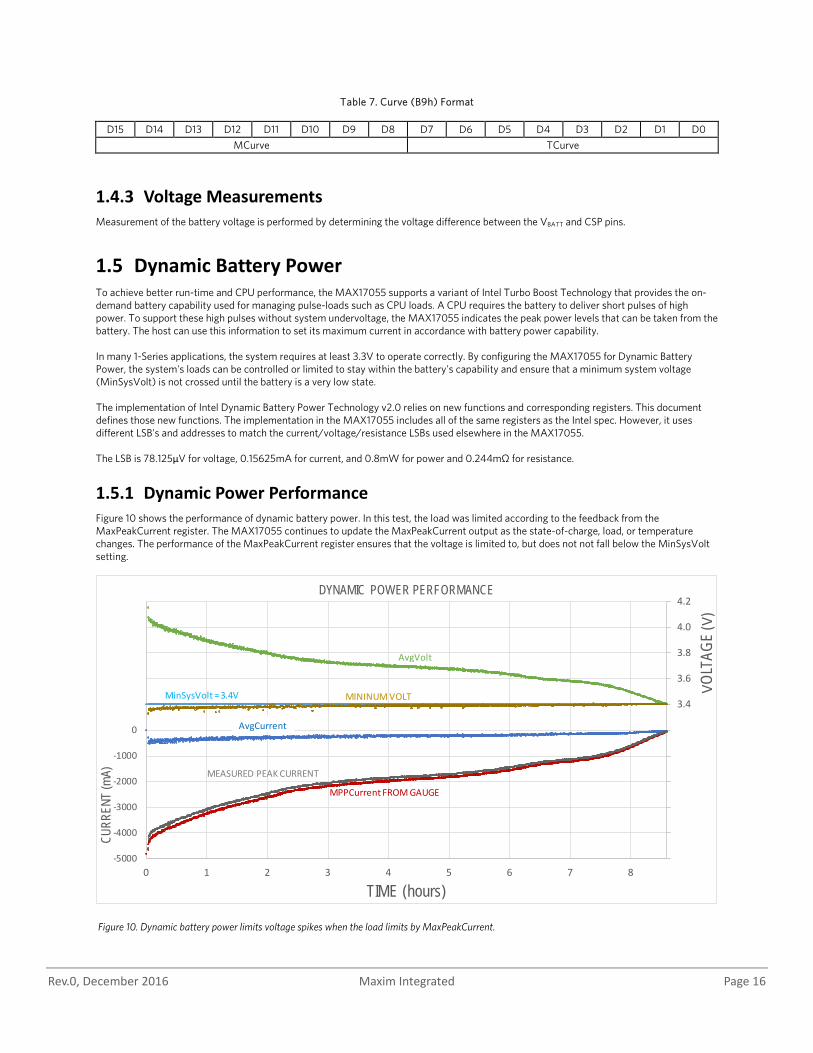
1.5.1 Dynamic Power Performance Figure 10 shows the performance of dynamic battery power. In this test, the load was limited according to the feedback from the MaxPeakCurrent register. The MAX17055 continues to update the MaxPeakCurrent output as the state-of-charge, load, or temperature changes. The performance of the MaxPeakCurrent register ensures that the voltage is limited to, but does not not fall below the MinSysVolt setting.
Figure 10. Dynamic battery power limits voltage spikes when the load limits by MaxPeakCurrent.
2.2
2.4
2.6
2.8
3.0
3.2
3.4
3.6
3.8
4.0
4.2
-5000
-4000
-3000
-2000
-1000
0
1000
2000
3000
4000
5000
0 1 2 3 4 5 6 7 8
VOLT
AGE(
V)
CURR
ENT
(mA)
TIME (hours)
DYNAMIC POWER PERFORMANCE
MinSysVolt = 3.4V
AvgVolt
MEASURED PEAK CURRENT
AvgCurrent
MPPCurrent FROM GAUGE
MININUM VOLT
Rev.0, December 2016 Maxim Integrated Page 17
1.5.2 Dynamic Power Output Registers
MPPCurrent() (D9h) The MAX17055 estimates the maximum instantaneous peak current of the battery pack in mA, which the battery can support for up to 10ms, given the external resistance and required minimum voltage of the voltage regulator. The MPPCurrent() value is negative and updates every 175ms.
SPPCurrent() (DAh) The MAX17055 estimates the sustained peak current of the battery pack in mA, which the battery can support for up to 10s, given the external resistance and required minimum voltage of the voltage regulator. The SPPCurrent() value is negative and updates every 175ms.
MaxPeakPower() Register (D4h) The MAX17055 estimates the maximum instantaneous peak output power of the battery pack in mW, which the battery can support for up to 10ms, given the external resistance and required minimum voltage of the voltage regulator. The MaxPeakPower() value is negative (discharge) and updates every 175ms. LSB is 0.8mW. Calculation: MaxPeakPower = MPPCurrent() x AvgVCell
SusPeakPower() Register (D5h) The fuel gauge estimates the sustainable peak output power of the battery pack in mW, which the battery supports for up to 10s, given the external resistance and required minimum voltage of the voltage regulator. The SusPeakPower() value is negative and updated each 175ms. LSB is 0.8mW. Calculation: SusPeakPower = SPPCurrent() x AvgVCell
1.5.3 Dynamic Power Configuration Registers The following registers provide the battery capability estimates from the Dynamic Power calculations.
PackResistance() (D6h) When the MAX17055 is installed host-side, simply set PackResistance to zero, since the MAX17055 can observe the total resistance between it and the battery. However, when the MAX17055 is installed pack-side, configure PackResistance according to the total non-cell pack resistance. This should account for all resistances due to cell interconnect, sense resistor, FET, fuse, connector, and other resistance between the cells and output of the battery pack. The cell internal resistance should not be included and is estimated by the MAX17055. 0x1000 is 1000mΩ, which results in an LSB of 0.244140625mΩ per LSB.
SysResistance() (D7h) Set SysResistance according to the total system resistance. This should include any connector and PCB trace between the MAX17055 and the system at risk for dropout when the voltage falls below MinSysVolt.
Rev.0, December 2016 Maxim Integrated Page 18
SysResistance() is initialized to a default value upon removal or insertion of a battery pack. Writes with this function overwrite the default value. 0x1000 is 1000mΩ, which results in an LSB of 0.244140625mΩ per LSB.
MinSysVoltage() (D8h) Set MinSysVoltage according to the minimum operating voltage of the system. This is generally associated with a regulator dropout or other system failure/shutdown. The system should still operate normally until this voltage. MinSysVoltage() is initialized to the default value (3.0V). Writes with this function overwrite the default value.
RGain Register (43h) Register Type: Special Initial Value: 0x8080 The RGain register sets the value of RGain1 and RGain2 during DBPT register calculation. Table 8 shows the register format.
Table 8. RGain (43h) Format D15 D14 D13 D12 D11 D10 D9 D8 D7 D6 D5 D4 D3 D2 D1 D0
RGain1 RGain2 SusToMaxRatio RGAIN provides additional limitations to ensure that the dynamic power outputs (MPPCurrent, MaxPeakPower, SPPCurrent, SusPeakPower) are conservative, thereby preventing any risk of system shutdown. RGain1: Gain resistance used for peak current and power calculation. RGain1 = 80% + 0.15625% x RG1. The range of RGain1 is between 80~120%. RGain2: Gain resistance used for peak current and power calculation. RGain2 = 60% + 5% x RG2. The range of RGain1 is between 60~140%. SusToMaxRatio: Used to calculate the maximum ratio between SPPCurrent to MPPCurrent. The maximum value of SPPCurrent = MPPCurrent x (0.75-SusToPeakRatio x 0.04).
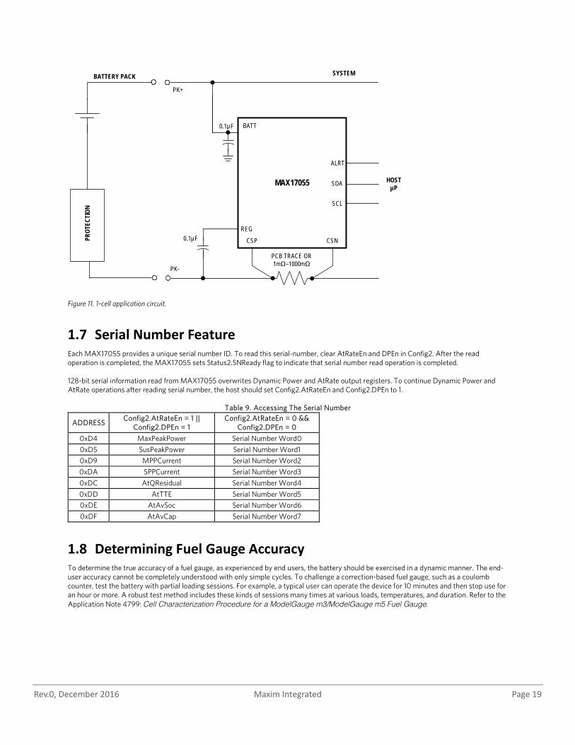
1.6 Typical Applications Circuit The application example in Figure 11 shows the MAX17055 monitoring a captive battery. An external thermistor measurement circuit is not required since measurements are made internal to the IC. Cell voltage is measured from VBATT to CSP and current measurements are made differentially from CSN to CSP. Results are reported on the SDA, SCL, and ALRT lines. The other pin connections to the IC are not used in this application and can be left unconnected.
Rev.0, December 2016 Maxim Integrated Page 19
Figure 11. 1-cell application circuit.
1.7 Serial Number Feature Each MAX17055 provides a unique serial number ID. To read this serial-number, clear AtRateEn and DPEn in Config2. After the read operation is completed, the MAX17055 sets Status2.SNReady flag to indicate that serial number read operation is completed. 128-bit serial information read from MAX17055 overwrites Dynamic Power and AtRate output registers. To continue Dynamic Power and AtRate operations after reading serial number, the host should set Config2.AtRateEn and Config2.DPEn to 1.
Table 9. Accessing The Serial Number
ADDRESS Config2.AtRateEn = 1 || Config2.DPEn = 1
Config2.AtRateEn = 0 && Config2.DPEn = 0
0xD4 MaxPeakPower Serial Number Word0 0xD5 SusPeakPower Serial Number Word1 0xD9 MPPCurrent Serial Number Word2 0xDA SPPCurrent Serial Number Word3 0xDC AtQResidual Serial Number Word4 0xDD AtTTE Serial Number Word5 0xDE AtAvSoc Serial Number Word6 0xDF AtAvCap Serial Number Word7
1.8 Determining Fuel Gauge Accuracy To determine the true accuracy of a fuel gauge, as experienced by end users, the battery should be exercised in a dynamic manner. The end-user accuracy cannot be completely understood with only simple cycles. To challenge a correction-based fuel gauge, such as a coulomb counter, test the battery with partial loading sessions. For example, a typical user can operate the device for 10 minutes and then stop use for an hour or more. A robust test method includes these kinds of sessions many times at various loads, temperatures, and duration. Refer to the Application Note 4799: Cell Characterization Procedure for a ModelGauge m3/ModelGauge m5 Fuel Gauge.
REG
CSNCSP
PCB TRACE OR1mΩ–1000mΩ
PK+
MAX17055 SDA
SCL
ALRT
HOSTµP
PROT
ECTI
ONBATTERY PACK SYSTEM
PK-
BATT0.1µF
0.1µF
Rev.0, December 2016 Maxim Integrated Page 20
1.8.1 Initial Accuracy The IC uses the first voltage reading after power-up or after cell insertion to determine the starting output of the fuel gauge. It is assumed that the cell is fully relaxed prior to this reading; however, this is not always the case. If there is a load or charge current at this time, the initial reading is compensated using a default battery resistance of 40mΩ to estimate the relaxed cell voltage. If the cell was recently charged or discharged, the voltage measured by the IC may not represent the true state of charge of the cell, resulting in initial error in the fuel gauge outputs. In most cases, this error is minor and is quickly removed by the fuel gauge algorithm during the first hour of normal operation.
1.9 ModelGauge m5 Registers Table 10 shows the user memory space. Register locations shown in gray are reserved locations and should not be written to.
Table 10. MAX17055 Register Map PAGE/ WOR
D 00h 10h 20h 30h 40h B0h D0h
0h Status FullCapRep TTF Reserved UserMem1 Status2 RSense/UserMem3 1h VAlrtTh TTE DevName Reserved Reserved Power ScOcvLim 2h TAlrtTh QRTable00 QRTable10 QRTable20 QRTable30 ID/UserMem2 Reserved 3h SAlrtTh FullSocThr FullCapNom Reserved RGain AvgPower SOCHold 4h AtRate RCell Reserved DieTemp Reserved IAlrtTh MaxPeakPower 5h RepCap Reserved Reserved FullCap dQAcc Reserved SusPeakPower 6h RepSOC AvgTA Reserved Reserved dPAcc CVMixCap PackResistance 7h Age Cycles AIN Reserved Reserved CVHalfTime SysResistance 8h Temp DesignCap LearnCfg RComp0 Reserved CGTempCo MinSysVoltage 9h VCell AvgVCell FilterCfg TempCo ConvgCfg Curve MPPCurrent Ah Current MaxMinTemp RelaxCfg VEmpty VFRemCap HibCfg SPPCurrent Bh AvgCurrent MaxMinVolt MiscCfg Reserved Reserved Config2 ModelCfg Ch QResidual MaxMinCurr TGain Reserved Reserved VRipple AtQResidual Dh MixSOC Config TOff FStat QH RippleCfg AtTTE Eh AvSOC IChgTerm CGain Timer Reserved TimerH AtAvSOC Fh MixCap AvCap COff ShdnTimer Reserved Reserved AtAvCap
Rev.0, December 2016 Maxim Integrated Page 21
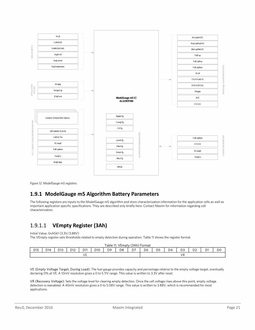
Figure 12. ModelGauge m5 registers.
1.9.1 ModelGauge m5 Algorithm Battery Parameters The following registers are inputs to the ModelGauge m5 algorithm and store characterization information for the application cells as well as important application specific specifications. They are described only briefly here. Contact Maxim for information regarding cell characterization.
VEmpty Register (3Ah) Initial Value: 0xA561 (3.3V/3.88V) The VEmpty register sets thresholds related to empty detection during operation. Table 11 shows the register format.
Table 11. VEmpty (3Ah) Format D15 D14 D13 D12 D11 D10 D9 D8 D7 D6 D5 D4 D3 D2 D1 D0
VE VR
VE (Empty Voltage Target, During Load): The fuel gauge provides capacity and percentage relative to the empty voltage target, eventually declaring 0% at VE. A 10mV resolution gives a 0 to 5.11V range. This value is written to 3.3V after reset. VR (Recovery Voltage): Sets the voltage level for clearing empty detection. Once the cell voltage rises above this point, empty voltage detection is reenabled. A 40mV resolution gives a 0 to 5.08V range. This value is written to 3.88V, which is recommended for most applications.
Characterization TableCharacterization Table
VCell
CURRENT
TEMPERATURE
ModelGauge m5 EZALGORITHM
FilterCfg
RelaxCfg
MiscCfg
AvgVCell
AvgCurrent
AvgTemperature
CHARACTERIZATION TABLES
DesignCap
IChgTerm
QRTable00,10,20,30
FullSOCThr
RComp0
FullCapNom
ANAL
OG IN
PUTS
APPL
ICAT
ION
SPEC
IFIC
CELL
CHA
RACT
ERIZ
ATIO
N IN
FORM
ATIO
N
LEAR
NED
INFO
RMAT
ION
Mode
lGau
ge A
LGOR
ITHM
OUT
PUTS
ALGO
RITH
M CO
NFIG
URAT
ION
AtRate
FullCapNom
CYCLES
RComp0
TempCo
VRipple
AGE
TTE/TTF/AtTTE
VFOCV/VFSOC
RCell
MixCap/MixSOC
FullCap
FullCapRep
RepCap/RepSOC
AvCap/AvSOC
FullCapNom
VEmpty
LearnCfg
CYCLES
TempCo
CVCfg
ConvgCfg
RippleCfg
IAvgEmpty
Rev.0, December 2016 Maxim Integrated Page 22
DesignCap Register(18h) Register Type: Capacity The DesignCap register holds the expected capacity of the cell. This value is used to determine age and health of the cell by comparing against the measured present cell capacity.
ModelCfg Register (DBh) The ModelCFG register controls basic options of the EZ algorithm. Table 12 shows the register format.
Table 12. ModelCFG (DBh) Format
D15 D14 D13 D12 D11 D10 D9 D8 D7 D6 D5 D4 D3 D2 D1 D0 Refresh 0 0 0 0 VChg 0 0 ModelID 0 0 0 0
Refresh: Set 1 to command the model refreshing. After firmware executes the command, it will be cleared by firmware. ModelID: Choose from one of 3 common classifications of lithium cobalt batteries supported by EZ, without characterization. For the majority of batteries, use ModelID = 0. ModelID = 0: Use for most lithium cobalt-oxide variants (a large majority of lithium in the market-place). ModelID = 6: Use for lithium iron-phosphate (LiFePO4). However, since LiFePO4 is a challenging chemistry, custom characterization is recommended. VChg: Set VChg = 1 for 4.35V or 4.4V models. Set VChg = 0 for 4.2V models.
IChgTerm Register (1Eh) Register Type: Current Initial Value: 0x0640 (250mA on 10mΩ) The IChgTerm register allows the device to detect when a charge cycle of the cell has completed. IChgTerm should be programmed to the exact charge termination current used in the application. The device detects end of charge if all the following conditions are met: • VFSOC register > FullSOCThr register • AND IChgTerm x 0.125 < Current register < IChgTerm x 1.25 • AND IChgTerm x 0.125 < AvgCurrent register < IChgTerm x 1.25
See the End-of-Charge Detection section for more details.
FullSOCThr Register (13h) Register Type: Percentage Initial Value: 95% The FullSOCThr register gates detection of end-of-charge. VFSOC must be larger than the FullSOCThr value before IChgTerm is compared to the AvgCurrent register value. The recommended FullSOCThr register setting for most custom characterized applications is 95% (default, 0x5F05). For EZ Performance applications the recommendation is 80% (0x5005). See the IChgTerm register description and the End-Of-Charge Detection section for details. Table 13 shows the register format.
Table 13. FullSOCThr (13h) Format D15 D14 D13 D12 D11 D10 D9 D8 D7 D6 D5 D4 D3 D2 D1 D0
FullSOCThr 1 0 1
Rev.0, December 2016 Maxim Integrated Page 23
XTable0 (90h) to XTable15 (9Fh) Registers Register Type: Special Cell characterization information used by the ModelGauge algorithm to determine capacity versus operating conditions. This table comes from battery characterization data.
OCVTable0 (80h) to OCVTable15 (8Fh) Registers Register Type: Special Cell characterization information used by the ModelGauge algorithm to determine capacity versus operating conditions. This table comes from battery characterization data.
QRTable00 (12h) to QRTable30 (42h) Registers Register Type: Special The QRTable00 to QRTable30 register locations contain characterization information regarding cell capacity under different application conditions.
RComp0 Register (38h) Register Type: Special The RComp0 register holds characterization information critical to computing the open-circuit voltage of a cell under loaded conditions.
TempCo Register (39h) Register Type: Special The TempCo register holds temperature compensation information for the RComp0 register value.
1.9.2 ModelGauge m5 Output Registers
RepCap Register (05h) Register Type: Capacity RepCap or reported remaining capacity in mAh. This register is protected from making sudden jumps during load changes.
AtAvCap Register (DFh) Register Type: Capacity The AtAvCap register holds the estimated remaining capacity of the cell based on the theoretical load current value of the AtRate register. The value is stored in terms of µVh and must be divided by the application sense-resistor value to determine the remaining capacity in mAh.
RepSOC Register (06h) Register Type: Percentage RepSOC is the reported state-of-charge percentage output for use by the application GUI.
Rev.0, December 2016 Maxim Integrated Page 24
AtAvSOC Register (DEh) Register Type: Percentage The AtAvSOC register holds the theoretical state of charge of the cell based on the theoretical load of the AtRate register. The register value is stored as a percentage with a resolution of 1/256 % per LSB. The high byte indicates 1% resolution.
FullCapRep Register (10h) Register Type: Capacity This register reports the full capacity that goes with RepCap, generally used for reporting to the GUI. Most applications should only monitor FullCapRep, instead of FullCap or FullCapNom. A new full-capacity value is calculated at the end of every charge cycle in the application.
FullCap Register (35h) Register Type: Capacity FullCap is the full discharge capacity compensated according to the present conditions. A new full-capacity value is calculated continuously as application conditions change (temperature and load).
FullCapNom Register (23h) Register Type: Capacity This register holds the calculated full capacity of the cell, not including temperature and empty compensation. A new full-capacity nominal value is calculated each time a cell relaxation event is detected. This register is used to calculate other outputs of the ModelGauge m5 algorithm.
TTE Register (11h) Register Type: Time The TTE register holds the estimated time to empty for the application under present temperature and load conditions. The TTE value is determined by relating AvCap with AvgCurrent. The corresponding AvgCurrent filtering gives a delay in TTE, but provides more stable results.
AtTTE Register (DDh) Register Type: Time The AtTTE register can be used to estimate time to empty for any theoretical load entered into the AtRate register.
TTF Register (20h) Register Type: Time The TTF register holds the estimated time to full for the application under present conditions. The TTF value is determined by learning the constant current and constant voltage portions of the charge cycle based on experience of prior charge cycles. Time to full is then estimated by comparing present charge current to the charge termination current. Operation of the TTF register assumes all charge profiles are consistent in the application.
Cycles Register (17h) Register Type: Special
Rev.0, December 2016 Maxim Integrated Page 25
The Cycles register maintains a total count of the number of charge/discharge cycles of the cell that have occurred. The result is stored as a percentage of a full cycle. For example, a full charge/discharge cycle results in the Cycles register incrementing by 100%. The Cycles register accumulates fractional or whole cycles. For example, if a battery is cycles 10% x 10 times, then it tracks 100% of a cycle. The Cycles register has a full range of 0 to 655.35 cycles with a 1% LSb.
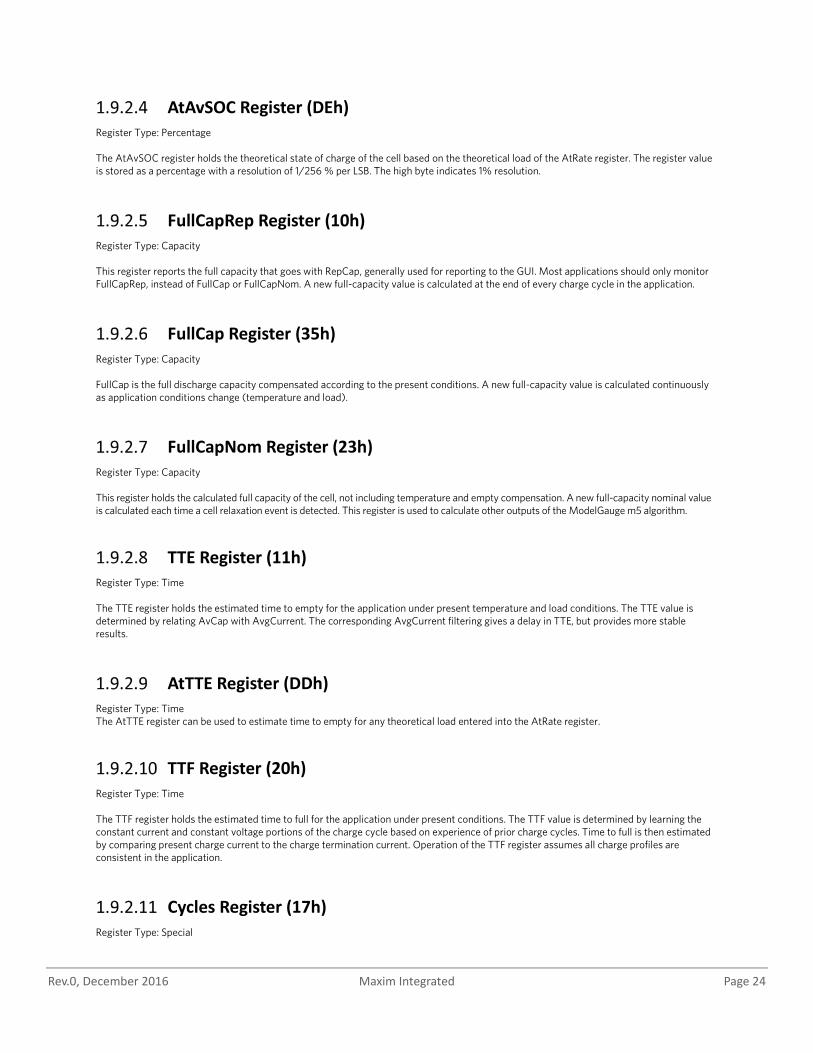
Status Register (00h) Register Type: Special Initial Value: 0x0002 The Status register maintains all flags related to alert thresholds and battery insertion or removal. Table 14 shows the Status register format.
Table 14. Status (00h) Format D15 D14 D13 D12 D11 D10 D9 D8 D7 D6 D5 D4 D3 D2 D1 D0 Br Smx Tmx Vmx Bi Smn Tmn Vmn dSOCi Imx X X Bst Imn POR X
POR (Power-On Reset): This bit is set to a 1 when the device detects that a software or hardware POR event has occurred. This bit must be cleared by system software to detect the next POR event. POR is set to 1 at power-up. Imn and Imx (Minimum/Maximum Current Alert Threshold Exceeded): These bits set to a 1 whenever a Current register reading is below (Imn) or above (Imx) the IAlrtTh thresholds. These bits may or may not need to be cleared by system software to detect the next event. See Config.IS bit description. Imn and Imx are cleared to 0 at power-up. Vmn and Vmx (Minimum/Maximum Voltage Alert Threshold Exceeded): These bits set to a 1 whenever a VCell register reading is below (Vmn) or above (Vmx) the VAlrtTh thresholds. These bits may or may not need to be cleared by system software to detect the next event. See Config.VS bit description. Vmn and Vmx are cleared to 0 at power-up. Tmn and Tmx (Minimum/Maximum Temperature Alert Threshold Exceeded): These bits set to a 1 whenever a Temperature register reading is below (Tmn) or above (Tmx) the TAlrtTh thresholds. These bits may or may not need to be cleared by system software to detect the next event. See Config.TS bit description. Tmn and Tmx are cleared to 0 at power-up. Smn and Smn (Minimum/Maximum SOC Alert Threshold Exceeded): These bits set to a 1 whenever SOC is below (Smn) or above (Smx) the SAlrtTh thresholds. These bits may or may not need to be cleared by system software to detect the next event. See Config.SS and MiscCFG.SACFG bit descriptions. Smn and Smx are cleared to 0 at power-up. dSOCi (State of Charge 1% Change Alert): This is set to 1 whenever the RepSOC register crosses an integer percentage boundary such as 50.0%, 51.0%, etc. Must be cleared by host software. Bst (Battery Status): Useful when the IC is used in a host side application. This bit is set to 0 when a battery is present in the system and set to 1 when the battery is absent. Bst is set to 0 at power-up. Bi (Battery Insertion): Useful when the IC is used in a host-side application. This bit is set to a 1 when the device detects that a battery has been inserted into the system by monitoring the AIN pin. This bit must be cleared by system software to detect the next insertion event. Bi is cleared to 0 at power-up. Br (Battery Removal): Useful when the IC is used in a host side application. This bit is set to a 1 when the system detects that a battery has been removed from the system. This bit must be cleared by system software to detect the next removal event. Br is cleared to 0 at power-up. X (Don’t Care): This bit is undefined and can be logic 0 or 1.
Age Register (07h) Register Type: Percentage The Age register contains a calculated percentage value of the application’s present cell capacity compared to its original design capacity. The result can be used by the host to gauge the battery pack health as compared to a new pack of the same type. The equation for the register output is: Age Register(%) = 100% x (FullCapRep register/DesignCap register)
Rev.0, December 2016 Maxim Integrated Page 26
For example, if DesignCap = 2000mAh and FullCapRep = 1800mAh, then Age = 90% (or 0x5A00)
TimerH (BEh) and Timer (3Eh) Registers Register Type: Special Initial Value: 0x0000 TimerH and Timer provide a long-duration time count since last POR. 3.2 hour LSb gives a full scale range for the register of up to 23.94 years. The Timer register LSb is 175.8ms giving a full-scale range of 0 to 3.2 hours. TimerH and Timer can be interpreted together as a 32-bit timer.
RCell Register (14h) Register Type: Resistance Initial Value: 0x0290 (160mΩ) The RCell register provides the calculated internal resistance of the cell. RCell is determined by comparing open-circuit voltage (VFOCV) against measured voltage (VCell) over a long time period while under load or charge current.
VRipple Register (BCh) Register Type: Special Initial Value: 0x0000 The VRipple register holds the slow average RMS ripple value of VCell register reading variation compared to the AvgVCell register. The default filter time is 22.5 seconds. See RippleCfg register description. VRipple has an LSb weight of 1.25mV/128.
1.9.3 ModelGauge m5 Algorithm Configuration Registers The following registers allow operation of the ModelGauge m5 algorithm to be adjusted for the application. It is recommended that the default values for these registers be used.
AtRate Register (04h) Register Type: Current Host software should write the AtRate register with a negative two’s-complement 16-bit value of a theoretical load current prior to reading any of the at-rate output registers (AtTTE, AtAvSOC, AtAvCap).
FilterCfg Register (29h) Register Type: Special Initial Value: 0xCEA4 The FilterCfg register sets the averaging time period for all A/D readings, for mixing OCV results and coulomb count results. It is recommended that these values are not changed, unless absolutely required by the application. Table 15 shows the FilterCfg register format.
Table 15. FilterCfg (29h) Format D15 D14 D13 D12 D11 D10 D9 D8 D7 D6 D5 D4 D3 D2 D1 D0
1 1 TEMP MIX VOLT CURR
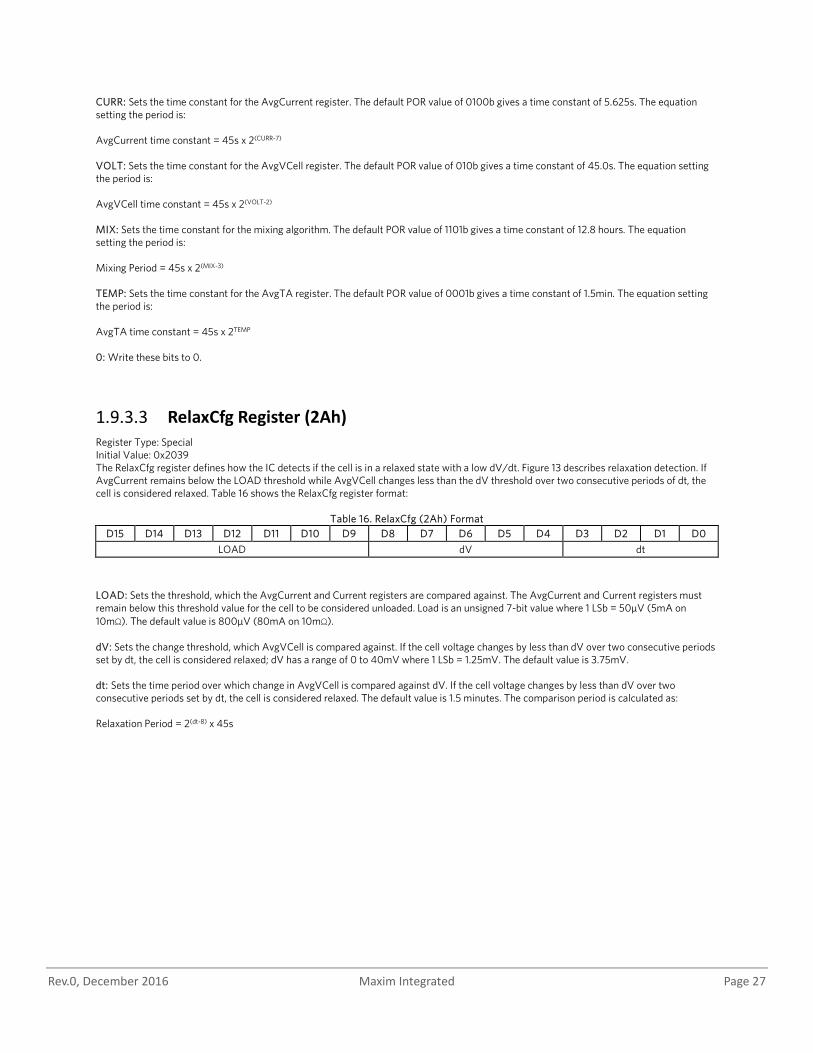
Rev.0, December 2016 Maxim Integrated Page 27
CURR: Sets the time constant for the AvgCurrent register. The default POR value of 0100b gives a time constant of 5.625s. The equation setting the period is: AvgCurrent time constant = 45s x 2(CURR-7) VOLT: Sets the time constant for the AvgVCell register. The default POR value of 010b gives a time constant of 45.0s. The equation setting the period is: AvgVCell time constant = 45s x 2(VOLT-2) MIX: Sets the time constant for the mixing algorithm. The default POR value of 1101b gives a time constant of 12.8 hours. The equation setting the period is: Mixing Period = 45s x 2(MIX-3) TEMP: Sets the time constant for the AvgTA register. The default POR value of 0001b gives a time constant of 1.5min. The equation setting the period is: AvgTA time constant = 45s x 2TEMP 0: Write these bits to 0.
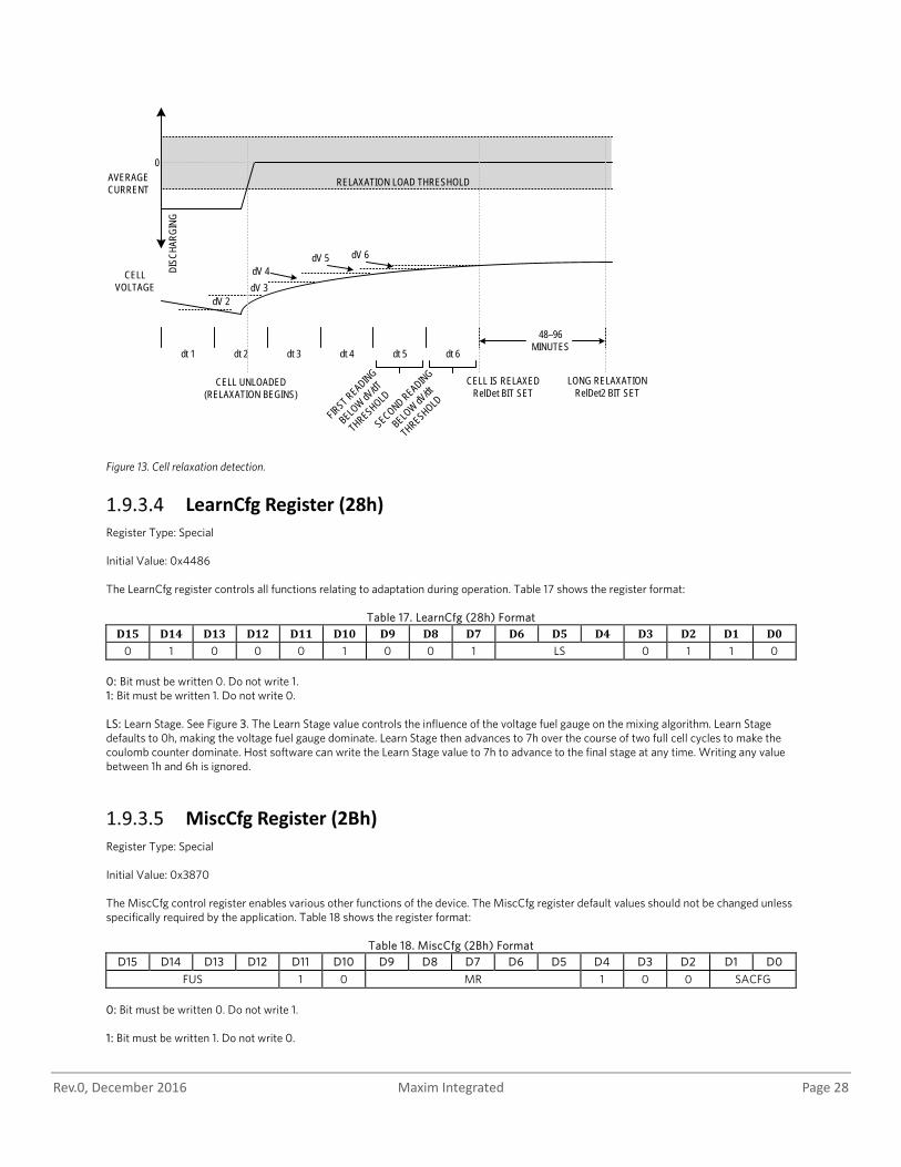
RelaxCfg Register (2Ah) Register Type: Special Initial Value: 0x2039 The RelaxCfg register defines how the IC detects if the cell is in a relaxed state with a low dV/dt. Figure 13 describes relaxation detection. If AvgCurrent remains below the LOAD threshold while AvgVCell changes less than the dV threshold over two consecutive periods of dt, the cell is considered relaxed. Table 16 shows the RelaxCfg register format:
Table 16. RelaxCfg (2Ah) Format D15 D14 D13 D12 D11 D10 D9 D8 D7 D6 D5 D4 D3 D2 D1 D0
LOAD dV dt
LOAD: Sets the threshold, which the AvgCurrent and Current registers are compared against. The AvgCurrent and Current registers must remain below this threshold value for the cell to be considered unloaded. Load is an unsigned 7-bit value where 1 LSb = 50μV (5mA on 10mΩ). The default value is 800μV (80mA on 10mΩ). dV: Sets the change threshold, which AvgVCell is compared against. If the cell voltage changes by less than dV over two consecutive periods set by dt, the cell is considered relaxed; dV has a range of 0 to 40mV where 1 LSb = 1.25mV. The default value is 3.75mV. dt: Sets the time period over which change in AvgVCell is compared against dV. If the cell voltage changes by less than dV over two consecutive periods set by dt, the cell is considered relaxed. The default value is 1.5 minutes. The comparison period is calculated as: Relaxation Period = 2(dt-8) x 45s
Rev.0, December 2016 Maxim Integrated Page 28
Figure 13. Cell relaxation detection.
LearnCfg Register (28h) Register Type: Special Initial Value: 0x4486 The LearnCfg register controls all functions relating to adaptation during operation. Table 17 shows the register format:
Table 17. LearnCfg (28h) Format D15 D14 D13 D12 D11 D10 D9 D8 D7 D6 D5 D4 D3 D2 D1 D0
0 1 0 0 0 1 0 0 1 LS 0 1 1 0
0: Bit must be written 0. Do not write 1. 1: Bit must be written 1. Do not write 0. LS: Learn Stage. See Figure 3. The Learn Stage value controls the influence of the voltage fuel gauge on the mixing algorithm. Learn Stage defaults to 0h, making the voltage fuel gauge dominate. Learn Stage then advances to 7h over the course of two full cell cycles to make the coulomb counter dominate. Host software can write the Learn Stage value to 7h to advance to the final stage at any time. Writing any value between 1h and 6h is ignored.
MiscCfg Register (2Bh) Register Type: Special Initial Value: 0x3870 The MiscCfg control register enables various other functions of the device. The MiscCfg register default values should not be changed unless specifically required by the application. Table 18 shows the register format:
Table 18. MiscCfg (2Bh) Format D15 D14 D13 D12 D11 D10 D9 D8 D7 D6 D5 D4 D3 D2 D1 D0
FUS 1 0 MR 1 0 0 SACFG 0: Bit must be written 0. Do not write 1. 1: Bit must be written 1. Do not write 0.
AVERAGE CURRENT
DISC
HARG
ING
dt 1 dt 2 dt 3 dt 4 dt 5 dt 6
48–96 MINUTES
dV 2dV 3dV 4
dV 5 dV 6
CELL VOLTAGE
CELL UNLOADED(RELAXATION BEGINS)
RELAXATION LOAD THRESHOLD
CELL IS RELAXEDRelDet BIT SET
FIRST READING
BELOW dV
/dT
THRESHOLD
SECOND READING
BELOW dV
/dt
THRESHOLD
LONG RELAXATIONRelDet2 BIT SET
0
Rev.0, December 2016 Maxim Integrated Page 29
SACFG: SOC Alert Config. SOC Alerts can be generated by monitoring any of the SOC registers as follows. SACFG defaults to 00 at power-up: 00 SOC alerts are generated based on the RepSOC register. 01 SOC alerts are generated based on the AvSOC register. 10 SOC alerts are generated based on the MixSOC register. 11 SOC alerts are generated based on the VFSOC register. MR (Mixing Rate): This value sets the strength of the servo mixing rate after the final mixing state has been reached (> 2.08 complete cycles). The units are MR0 = 6.25μV, giving a range up to 19.375mA with a standard 10mΩ sense resistor. Setting this value to 00000b disables servo mixing and the MAX17055 continues with time-constant mixing indefinitely. The default setting is 18.75μV or 1.875mA with a standard sense resistor. FUS (Full Update Slope): This value prevents jumps in the RepSOC and FullCapRep registers by setting the rate of adjustment of FullCapRep near the end of a charge cycle. The update slope adjustment range is from 2% per 15 minutes (0000b) to a maximum of 32% per 15 minutes (1111b).
ConvgCfg Register (49h) Register Type: Special The ConvgCfg register configures operation of the converge-to-empty feature. The default and recommended value for ConvgCfg is 0x2241.
RippleCfg Register (BDh) Register Type: Special The RippleCfg register configures ripple measurement and ripple compensation. The default and recommended value for this register is 0x0204. Table 19 shows the register format.
Table 19. RippleCfg (BDh) Format D15 D14 D13 D12 D11 D10 D9 D8 D7 D6 D5 D4 D3 D2 D1 D0
kDV NR NR (Ripple Measurement Filter): Sets the filter magnitude for ripple observation as defined by the following equation giving a range of 1.4s to 180s. Ripple Time Range = 1.4 seconds x 2NR kDV (Ripple Empty Compensation Coefficient): Configures MAX17055 to compensate the fuel gauge % according to the ripple.
1.9.4 ModelGauge m5 Algorithm Additional Registers The following registers contain intermediate ModelGauge m5 data that can be useful for debugging or performance analysis. The values in these registers initially update within 710ms after the IC is reset.
dQAcc Register (05h) Register Type: Capacity (16mAh/LSB) Initial Value: 0x0017 (368mAh) This register tracks change in battery charge between relaxation points. It is available to the user for debug purposes.
dPAcc Register (46h) Register Type: Percentage (1/16% per LSB) Initial Value: 0x0190 (25%)
Rev.0, December 2016 Maxim Integrated Page 30
This register tracks change in battery state of charge between relaxation points. It is available to the user for debug purposes.
QResidual Register (0Ch) Register Type: Capacity The QResidual register provides the calculated amount of charge in mAh that is presently inside of, but cannot be removed from the cell under present application conditions (load and temperature). This value is subtracted from the MixCap value to determine capacity available to the user under present conditions (AvCap).
AtQResidual Register (DCh) Register Type: Capacity The AtQResidual register provides the calculated amount of charge in mAh that is presently inside of, but cannot be removed from the cell under present temperature and hypothetical load (AtRate). This value is subtracted from the MixCap value to determine capacity available to the user (AtAvCap). See the Predicting Run Time for a Hypothetical Load section for more explanation.
VFSOC Register (FFh) Register Type: Percentage The VFSOC register holds the calculated present state of charge of the battery according to the voltage fuel gauge.
VFOCV Register (FBh) Register Type: Voltage The VFOCV register contains the calculated open-circuit voltage of the cell as determined by the voltage fuel gauge. This value is used in other internal calculations.
QH Register (4Dh) Register Type: Capacity Initial Value: 0x0000 The QH register displays the raw coulomb count generated by the device. This register is used internally as an input to the mixing algorithm. Monitoring changes in QH over time can be useful for debugging device operation.
AvCap (1Fh) and AvSOC (0Eh) Registers Register Type: Capacity (AvCap), Percentage (AvSOC) The AvCap and AvSOC registers hold the calculated available capacity and percentage of the battery based on all inputs from the ModelGauge m5 algorithm including empty compensation. These registers provide unfiltered results. Jumps in the reported values can be caused by abrupt changes in load current or temperature. See the Empty Compensation section for details.
MixCap (0Fh) and MixSOC (0Dh) Registers Register Type: Capacity (MixCap) and Percentage (MixSOC)
Rev.0, December 2016 Maxim Integrated Page 31
The MixCap and MixSOC registers holds the calculated remaining capacity and percentage of the cell before any empty compensation adjustments are performed. See the Empty Compensation section for details.
VFRemCap Register (4Ah) Register Type: Capacity The VFRemCap register holds the remaining capacity of the cell as determined by the voltage fuel gauge before any empty compensation adjustments are performed. See the Empty Compensation section for details.
FStat Register (3Dh) Register Type: Special The FStat register is a read-only register that monitors the status of the ModelGauge m5 algorithm. Table 20 is the FStat register format:
Table 20. FStat (3Dh) Format D15 D14 D13 D12 D11 D10 D9 D8 D7 D6 D5 D4 D3 D2 D1 D0
X X X X X X RelDt EDet FQ RelDt2 X X X X X DNR DNR (Data Not Ready): This bit is set to 1 at cell insertion and remains set until the output registers have been updated. Afterwards, the IC clears this bit indicating the fuel gauge calculations are now up to date. This takes 710ms from power-up. FQ (Full Qualified): This bit is set when all charge termination conditions have been met. See the End-of-Charge Detection section for details. EDet (Empty Detection): This bit is set to 1 when the IC detects that the cell empty point has been reached. This bit is reset to 0 when the cell voltage rises above the recovery threshold. See the VEmpty register for details. RelDt (Relaxed Cell Detection): This bit is set to a 1 whenever the ModelGauge m5 algorithm detects that the cell is in a fully relaxed state. This bit is cleared to 0 whenever a current greater than the Load threshold is detected. See Figure 13. RelDt2 (Long Relaxation): This bit is set to a 1 whenever the ModelGauge m5 algorithm detects that the cell has been relaxed for a period of 48 to 96 minutes or longer. This bit is cleared to 0 whenever the cell is no longer in a relaxed state. See Figure 13. X (Don’t Care): This bit is undefined and can be logic 0 or 1.
1.9.5 Status and Configuration Registers The following registers control IC operation not related to the fuel gauge such as power-saving modes and ALRT pin functionality.
Config Register (1Dh) and Config2 Register (BBh) Register Type: Special Initial Value: 0x2210 for Config, 0x3658 for Config2 The Config register holds all shutdown enable, alert enable, and temperature enable control bits. Writing a bit location enables the corresponding function within 175ms in active mode and 5.625s in hibernate mode. Table 21 and Table 22 show the register formats.
Table 21. Config (1Dh) Format D15 D14 D13 D12 D11 D10 D9 D8 D7 D6 D5 D4 D3 D2 D1 D0 TSel SS TS VS IS AINSH Ten Tex SHDN COMMSH 0 ETHRM FTHRM Aen Bei Ber
Table 22. Config2 (BBh) Format
D15 D14 D13 D12 D11 D10 D9 D8 D7 D6 D5 D4 D3 D2 D1 D0 0 0 AtRateEn DPEn POWR dSOCen TAlrtEn LDMDL 1 10 CPMode 0
0: Bit must be written 0. Do not write 1.

Rev.0, December 2016 Maxim Integrated Page 32
1: Bit must be written 1. Do not write 0. POWR: Sets the time constant for the AvgPower register. The default POR value of 0100b gives a time constant of 11.25s. The equation setting the period is: AvgPower time constant = 45s x 2(POWR-6) IS (Current ALRT Sticky): When IS = 1, current alerts can only be cleared through software. When IS = 0, current alerts are cleared automatically when the threshold is no longer exceeded. VS (Voltage ALRT Sticky): When VS = 1, voltage alerts can only be cleared through software. When VS = 0, voltage alerts are cleared automatically when the threshold is no longer exceeded. TS (Temperature ALRT Sticky): When TS = 1, temperature alerts can only be cleared through software. When TS = 0, temperature alerts are cleared automatically when the threshold is no longer exceeded. SS (SOC ALRT Sticky): When SS = 1, SOC alerts can only be cleared through software. When SS = 0, SOC alerts are cleared automatically when the threshold is no longer exceeded. AtRateEn (AtRate Enable): When this bit is set to 0, AtRate calculations are disabled and registers AtQResidual/AtTTE/AtAvSOC/AtAvCap are not updated by AtRate calculations. DPEn (Dynamic Power Enable): When this bit is set to 0, Dynamic Power calculations are disabled and registers MaxPeakPower/SusPeakPower/MPPCurrent/SPPCurrent are not updated by Dynamic Power calculations. CPMode (Constant-Power Mode): Set to 1 to enable constant-power mode. If it is set to 0, all remaining capacity and remaining time calculations are estimated assuming a constant-current load. If it is set to 1, the remaining capacity and remaining time calculations are estimated assuming a constant-power load. TSel: Set to 0 to use internal die temperature. Set to 1 to measure temperature using external thermistor. Set ETHRM to 1 when TSel is 1. Ber: Enable alert on battery removal when the IC is mounted on the host side. When Ber = 1, a battery-removal condition, as detected by the AIN pin voltage, triggers an alert. Bei: Enable alert on battery insertion when the IC is mounted on the host side. When Bei = 1, a battery-insertion condition, as detected by the AIN pin voltage, triggers an alert. Aen (Enable ALRT Pin Output): When Aen = 1, violation of any of the alert threshold register values by temperature, voltage, current, or SOC triggers an alert. This bit affects the ALRT pin operation only. The Smx, Smn, Tmx, Tmn, Vmx, Vmn, Imx, and Imn bits of the Status register (00h) are not disabled. FTHRM (Force Thermistor Bias Switch): This allows the host to control the bias of the thermistor switch or enable fast detection of battery removal. Set FTHRM = 1 to always enable the thermistor bias switch. With a standard 10kΩ thermistor, this adds an additional 200μA to the current drain of the circuit. ETHRM (Enable Thermistor Automatic Bias):. Set to logic 1 to enable the automatic THRM output bias and AIN measurement. COMMSH (Communication Shutdown): Set to logic 1 to force the device to enter shutdown mode if both SDA and SCL are held low for more than timeout of the ShdnTimer register. This also configures the device to wake up on a rising edge of any communication . Note that if COMMSH and AINSH are both set to 0, the device wakes up on any edge of the SDA or SCL pins. See the Modes of Operation section. SHDN (Shutdown): Write this bit to logic 1 to force a shutdown of the device after timeout of the ShdnTimer register (default 45s delay). SHDN is reset to 0 at power-up and upon exiting shutdown mode. To command shutdown within 22.5s, write ShdnTimer = 0x001E. Tex (Temperature External): Set to 1 to allow external temperature measurements to be written to Temp from the host. When set to 0, the IC's own measurements as used as selected by Config.TSEL. Ten (Enable Temperature Channel): Set to 1 and set ETHRM or FTHRM to 1 to enable temperature measurements selected by Config.TSel. TAlrten (Temperature Alert Enable:): Set this bit to 1 to enable temperature based alerts. Write this bit to 0 to disable temperature alerts. This bit is set to 1 at power-up. dSOCen (SOC Change Alert Enable): Set this bit to 1 to enable alert output with the Status.dSOCi bit function. Write this bit to 0 to disable the dSOCi alert output. This bit is set to 0 at power-up. LDMdl: Host sets this bit to 1 to initiate firmware to finish processing a newly loaded model. Firmware clears this bit to zero to indicate that model loading is finished.
Rev.0, December 2016 Maxim Integrated Page 33
DevName Register (21h) Register Type: Special The DevName register holds revision information. The initial silicon is DevName = 0x4010.
ShdnTimer Register (3Fh) Register Type: Special Initial Value: 0x0000 The ShdnTimer register sets the timeout period from when a shutdown event is detected until the device disables the regulators and enters low-power mode. Table 23 shows the ShdnTimer register format.
Table 23. ShdnTimer (3Fh) Format D15 D14 D13 D12 D11 D10 D9 D8 D7 D6 D5 D4 D3 D2 D1 D0
THR CTR CTR (Shutdown Counter): This register counts the total amount of elapsed time since the shutdown trigger event. This counter value stops and resets to 0 when the shutdown timeout completes. The counter LSb is 1.4s. THR: Sets the shutdown timeout period from a minimum of 45s to a maximum of 1.6h. The default POR value of 0h gives a shutdown delay of 45s. The equation setting the period is: Shutdown timeout period = 175.8ms x 2(8+THR)
Status2 Register (B0h) Register Type: Special Initial Value: 0x0000 The Status2 register maintains status of various firmware functions. Table 24 shows the Status register format.
Table 24. Status2 (B0h) Format
D15 D14 D13 D12 D11 D10 D9 D8 D7 D6 D5 D4 D3 D2 D1 D0
X X AtRateReady DPReady X X X SNReady X X FullDet X X X Hib X Hib (Hibernate Status): This bit is set to a 1 when the device is in hibernate mode or 0 when the device is in active mode. Hib is set to 0 at power-up. FullDet: Full detected. For the following 3 bits, also see the Serial Number Feature section for more details. SNReady: If SNReady = 1, the unique serial number is available over the I2C. This bit is set to 1 by firmware after serial number is read internally and placed into RAM. The serial number overwrites the Dynamic Power and AtRate output registers as described in the Serial Number Feature section. AtRateReady: If AtRateReady = 1, AtRate output registers are filled by the firmware and ready to be read by the host. DPReady: If DPReady = 1, Dynamic Power output registers are filled by the firmware and ready to be read by the host. X: Don’t Care. This bit is undefined and can be logic 0 or 1.
HibCfg Register (BAh) Register Type: Special Initial Value: 0x870C (0x890C)
Rev.0, December 2016 Maxim Integrated Page 34
The HibCfg register controls hibernate mode functionality. The MAX17055 enters and exits hibernate when the battery current is less than about C/100. While in hibernate mode the MAX17055 reduces its operating current to 7µA by reducing ADC sampling to once every 5.625s. Table 25 shows the register format.
Table 25. HibCfg (BAh) Format D15 D14 D13 D12 D11 D10 D9 D8 D7 D6 D5 D4 D3 D2 D1 D0
EnHib HibConfig Set HibCfg to 0x870C for most applications. EnHib (Enable Hibernate Mode): When set to 1 the IC enters hibernate mode if conditions are met. When set to 0 the IC always remains in active mode of operation.
1.10 Soft-Wakeup (Command Register) (60h) Register Type: Special The Command register accepts commands to perform functions listed in Table 26.
Table 26: Special Commands COMMAN
D MNEUMONI
C DESCRIPTION
0000h Clear Clears all commands.
0090h Soft wakeup
Wakes up the fuel gauge from hibernate mode, to reduce the response time of the IC to configuration changes. This
command must be manually cleared (0000h) afterwards to keep proper fuel gauge timing.
To wake and exit hibernate, do the following sequence:
1. Write HibCfg = 0x0000. 2. Soft-Wakeup Command. Write Command register (60h) to 0x0090. 3. Clear Command. Write Command register (60h) to 0x0000. 4. Eventually restore HibCfg to again allow automatic hibernate decisions.
1.11 Modes of Operation The IC operates in one of three power modes: shutdown, hibernate, and active. While in active mode, the IC operates as a high-precision fuel gauge with temperature, voltage, current, and accumulated current measurements acquired continuously, and the resulting values updated in the measurement registers. Hibernate mode is a fully functional reduced power (7µA) consumption version of active mode. In hibernate mode all registers are updated every 5.625s instead of the normal 175.8ms. In shutdown mode, the internal LDO regulator is disabled, all activity stops, A/D register and fuel-gauge output values are lost. Entering Hibernate Mode Pack Idle: Hibernate mode must be enabled by setting HibCfg.EnHib = 1. The IC then enters hibernate mode if the current persists below about C/100. Exiting Hibernate Mode Pack Active: The IC returns to active mode if the current exceeds about C/100. Entering Shutdown Mode (from Active Mode or Hibernate Mode) Since the MAX17055 supports a 1µA shutdown as well as a 7µA hibernate mode (fully-functional and fuel-gauging), it is generally best to keep the fuel-gauge enabled to continue to track the battery state even when the system is shutdown. However, for small batteries and long storage periods, it might be necessary to save the additional 6µA.
Rev.0, December 2016 Maxim Integrated Page 35
• Software Shutdown: Software shutdown can be forced by setting Config.SHDN = 1. To command shutdown within 22.5s, write ShdnTimer = 0x001E.
• Pack Disconnect: The IC enters shutdown if Config.COMMSH = 1 and communication lines are open (logic-low) for longer than the ShdnTimer period.
These shutdown entry modes are all programmable according to the application. Shutdown events are gated by the ShdnTimer register, which allows a delay between the shutdown event/command and entering the mode to prevent final I2C traffic from inadvertently reawakening the IC. Exiting Shutdown Mode (IC Always Exits into Active Mode) Pack Connect: The IC returns to active mode on any edge of any communication line. IC Reset: If the IC is power cycled or the software RESET command is sent the IC returns to active mode of operation. See the detailed descriptions of the ShdnTimer, HibCfg, and Config registers.
1.12 I2C Bus System The MAX17055 uses the standard I2C protocol. See the I2C Protocols section for specific protocol details.
1.12.1 Hardware Configuration The I2C bus system supports operation as a slave-only device in a single or multi-slave, and single or multi-master system. Up to 128 slave devices may share the bus using 7-bit slave addresses. The I2C interface consists of a serial data line (SDA) and serial clock line (SCL). SDA and SCL provide bidirectional communication between the IC and a master device at speeds up to 400kHz. The IC's SDA pin operates bi-directionally. When the IC receives data SDA operates as an input. When the IC returns data SDA operates as an open-drain output with the host system providing a resistive pull-up. See Figure 14. The IC always operates as a slave device, receiving and transmitting data under the control of a master device. The master initiates all transactions on the bus and generates the SCL signal, as well as the START and STOP bits that begin and end each transaction.
Figure 14: I2C bus interface.
1.12.2 I/O Signaling The following individual signals are used to build byte level I2C communication sequences.
VPULLUP
Rx DATA
Tx DATA
Rx DATA
Tx DATARx = RECEIVE
Tx = TRANSMIT
WEAK PULLDOWN
BUS MASTER SLAVE I2C PORT RPULLUP
SDA
SCLTx CLOCK Rx CLOCK
WEAK PULLDOWN
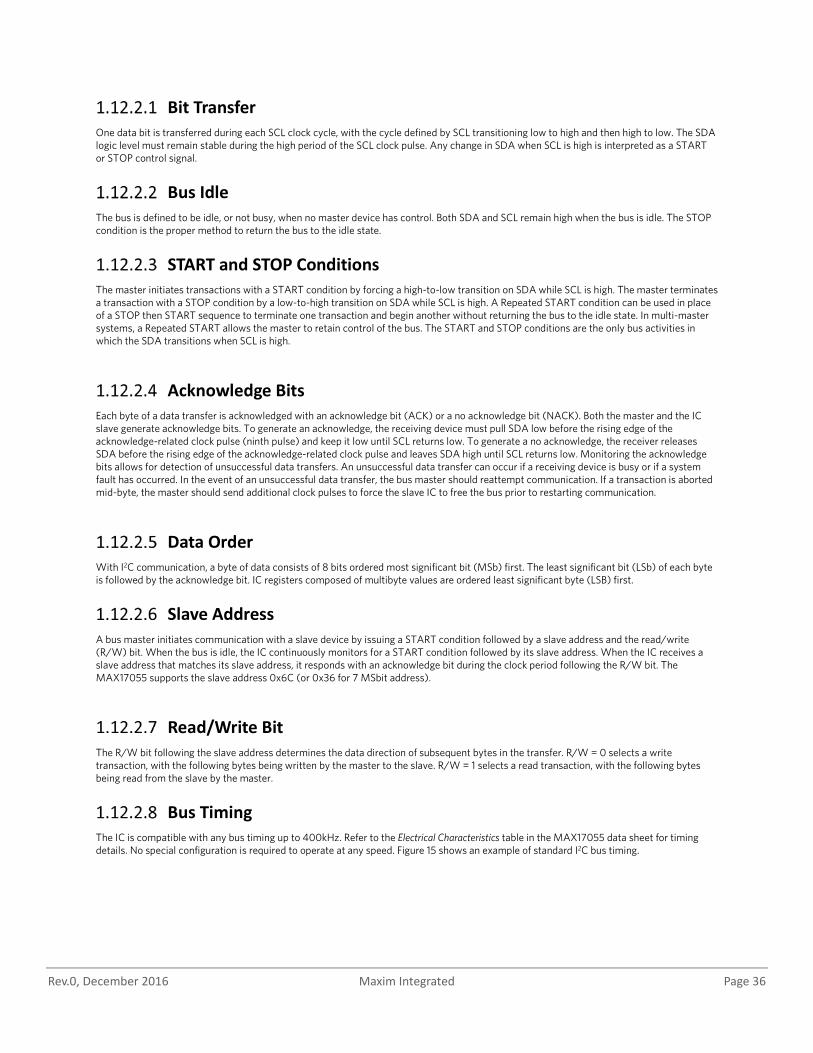
Rev.0, December 2016 Maxim Integrated Page 36
Bit Transfer One data bit is transferred during each SCL clock cycle, with the cycle defined by SCL transitioning low to high and then high to low. The SDA logic level must remain stable during the high period of the SCL clock pulse. Any change in SDA when SCL is high is interpreted as a START or STOP control signal.
Bus Idle The bus is defined to be idle, or not busy, when no master device has control. Both SDA and SCL remain high when the bus is idle. The STOP condition is the proper method to return the bus to the idle state.
START and STOP Conditions The master initiates transactions with a START condition by forcing a high-to-low transition on SDA while SCL is high. The master terminates a transaction with a STOP condition by a low-to-high transition on SDA while SCL is high. A Repeated START condition can be used in place of a STOP then START sequence to terminate one transaction and begin another without returning the bus to the idle state. In multi-master systems, a Repeated START allows the master to retain control of the bus. The START and STOP conditions are the only bus activities in which the SDA transitions when SCL is high.
Acknowledge Bits Each byte of a data transfer is acknowledged with an acknowledge bit (ACK) or a no acknowledge bit (NACK). Both the master and the IC slave generate acknowledge bits. To generate an acknowledge, the receiving device must pull SDA low before the rising edge of the acknowledge-related clock pulse (ninth pulse) and keep it low until SCL returns low. To generate a no acknowledge, the receiver releases SDA before the rising edge of the acknowledge-related clock pulse and leaves SDA high until SCL returns low. Monitoring the acknowledge bits allows for detection of unsuccessful data transfers. An unsuccessful data transfer can occur if a receiving device is busy or if a system fault has occurred. In the event of an unsuccessful data transfer, the bus master should reattempt communication. If a transaction is aborted mid-byte, the master should send additional clock pulses to force the slave IC to free the bus prior to restarting communication.
Data Order With I2C communication, a byte of data consists of 8 bits ordered most significant bit (MSb) first. The least significant bit (LSb) of each byte is followed by the acknowledge bit. IC registers composed of multibyte values are ordered least significant byte (LSB) first.
Slave Address A bus master initiates communication with a slave device by issuing a START condition followed by a slave address and the read/write (R/W) bit. When the bus is idle, the IC continuously monitors for a START condition followed by its slave address. When the IC receives a slave address that matches its slave address, it responds with an acknowledge bit during the clock period following the R/W bit. The MAX17055 supports the slave address 0x6C (or 0x36 for 7 MSbit address).
Read/Write Bit The R/W bit following the slave address determines the data direction of subsequent bytes in the transfer. R/W = 0 selects a write transaction, with the following bytes being written by the master to the slave. R/W = 1 selects a read transaction, with the following bytes being read from the slave by the master.
Bus Timing The IC is compatible with any bus timing up to 400kHz. Refer to the Electrical Characteristics table in the MAX17055 data sheet for timing details. No special configuration is required to operate at any speed. Figure 15 shows an example of standard I2C bus timing.
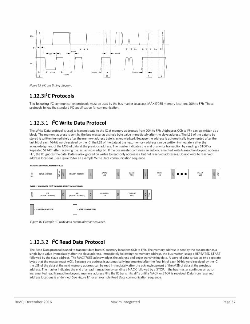
Rev.0, December 2016 Maxim Integrated Page 37
Figure 15: I2C bus timing diagram.
1.12.3 I2C Protocols The following I2C communication protocols must be used by the bus master to access MAX17055 memory locations 00h to FFh. These protocols follow the standard I2C specification for communication.
I2C Write Data Protocol The Write Data protocol is used to transmit data to the IC at memory addresses from 00h to FFh. Addresses 00h to FFh can be written as a block. The memory address is sent by the bus master as a single byte value immediately after the slave address. The LSB of the data to be stored is written immediately after the memory address byte is acknowledged. Because the address is automatically incremented after the last bit of each 16-bit word received by the IC, the LSB of the data at the next memory address can be written immediately after the acknowledgment of the MSB of data at the previous address. The master indicates the end of a write transaction by sending a STOP or Repeated START after receiving the last acknowledge bit. If the bus master continues an autoincremented write transaction beyond address FFh, the IC ignores the data. Data is also ignored on writes to read-only addresses, but not reserved addresses. Do not write to reserved address locations. See Figure 16 for an example Write Data communication sequence.
Figure 16. Example I2C write data communication sequence.
I2C Read Data Protocol The Read Data protocol is used to transmit data from IC memory locations 00h to FFh. The memory address is sent by the bus master as a single byte value immediately after the slave address. Immediately following the memory address, the bus master issues a REPEATED START followed by the slave address. The MAX17055 acknowledges the address and begin transmitting data. A word of data is read as two separate bytes that the master must ACK. Because the address is automatically incremented after the final bit of each 16-bit word received by the IC, the LSB of the data at the next memory address can be read immediately after the acknowledgment of the MSB of data at the previous address. The master indicates the end of a read transaction by sending a NACK followed by a STOP. If the bus master continues an auto-incremented read transaction beyond memory address FFh, the IC transmits all 1s until a NACK or STOP is received. Data from reserved address locations is undefined. See Figure 17 for an example Read Data communication sequence.
SDA
SCL
tF
tLOW
tHD:STAtHD:DAT
tSU:STA tSU:STO
tSU:DATtHD:STA
tSP tR tBUF
tR
tF
S Sr P S
WRITE DATA COMMUNICATION PROTOCOL
STAR
T
SLAVE ADDRESS
W/R
=0
ACK MEMORY ADDRESS ACK DATA0
LSB ACK DATA0
MSB ACK DATA1
LSB ACK DATA N
MSB ACK
STOP
EXAMPLE WORD WRITE TO I2C COMMAND REGISTER ADDRESS 060h
STAR
T 6Ch(SLAVE ADDRESS) AC
K
ACK COMMAND
LSB ACK COMMANDMSB ACK
STOP60h
(MEMORY ADDRESS)
= SLAVE TRANSMISSION = HOST TRANSMISSION
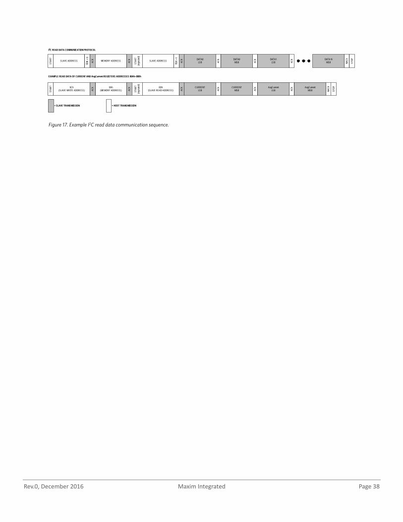
Rev.0, December 2016 Maxim Integrated Page 38
Figure 17. Example I2C read data communication sequence.
I2C READ DATA COMMUNICATION PROTOCOLST
ART
SLAVE ADDRESS
W/R
= 0
ACK MEMORY ADDRESS ACK DATA0
LSB ACK DATA0
MSB ACK DATA1
LSB ACK DATA N
MSB NACK
STOP
EXAMPLE READ DATA OF CURRENT AND AvgCurrent REGISTERS ADDRESSES 00Ah–00Bh
= SLAVE TRANSMISSION = HOST TRANSMISSION
STAR
T(re
peate
d)
SLAVE ADDRESS
W/R
=1
ACK
0Ah(MEMORY ADDRESS)ST
ART
ACK
ACK CURRENT
LSB ACK CURRENT
MSB ACK
STOP
STAR
T(re
peate
d)
ACK6Ch
(SLAVE WRITE ADDRESS)6Dh
(SLAVE READ ADDRESS)AvgCurrent
LSB ACK AvgCurrent
MSB NACK

Rev.0, December 2016 Maxim Integrated Page 39
2 Trademark Information
ModelGauge is trademark of Maxim Integrated Products, Inc. Windows is a registered trademark and registered service mark or Microsoft Corporation.