Embed Size (px)
Citation preview
General DescriptionThe MAX15096 family of devices are integrated solu-tions for hot-swap applications requiring the safe insertion and removal of circuit line cards from a live backplane. They can also be used as electronics circuit breaker for hard drive and solid-state drive and fans. The devices integrate a hot-swap controller, 12mΩ (typ) power MOSFET, and an electronic circuit-breaker protection in a single package. The devices are designed for protection of 2.7V to 18V supply voltages. These devices implement a foldback current limit during startup to control inrush current, lowering di/dt and keeping the MOSFET operating under safe operating area (SOA) conditions. After the startup cycle is complete, on-chip comparators provide VariableSpeed/BiLevel™ protection against short-circuit and overcurrent faults, and immunity against system noise and load transients. The load is disconnected in the event of a fault condition. The devices are factory calibrated to deliver accurate overcurrent protection with ±10% accuracy. During a fault condition, PG goes low and the devices latch off (MAX15096) or automatic retry (MAX15096A); the output could also be discharged after a fault event (MAX15096D).The devices feature an IN-to-OUT short-circuit detection before startup. The devices provide a power-MOSFET GATE pin to program the slew rate during startup by adding an external capacitor. The devices have an under-voltage/overvoltage input pin (UVOV) that can detect an undervoltage/overvoltage fault and disconnect the IN from the OUT. Additional features include internal overtem-perature protection and a power-good output (PG). The devices are available in a 16-bump, 2mm x 2mm wafer-level package (WLP) and are rated over the -40°C to +105°C extended temperature range.
Benefits and Features Integration Reduces Solution size for Blade Servers
and Other Space-Constrained Designs• Integrated 12mΩ (typ) Internal Power MOSFET• Programmable Overvoltage Protection and
Undervoltage-Lockout Threshold• Drive-Present Signal Input (PRSNT pin)• Thermal Protection
Flexibility Enables Use in Many Unique Designs• 2.7V to 18V Operating Voltage Range• Programmable Inrush Current Control Under SOA
Operation• Adjustable Circuit-Breaker Current/Current-Limit
Threshold• Programmable Slew-Rate Control• Variable-Speed Circuit-Breaker Response• Latchoff (MAX15096) or Automatic Retry
(MAX15096A) Options Safety Features Ensure Accurate, Robust Protection
• 6A (max) Load Current Capability• ±10% Circuit-Breaker Threshold Accuracy• IN-to-OUT Short-Circuit Detection• Open-Drain PG Output• Output Discharge After a Fault Event (MAX15096D Only)• Programmable Additional Delay (2µs max) to
Fast-Comparator Response Time• Enable Input (EN)
Applications Blade Servers Server I/O Cards RAID Systems Disk Drive Power Storage Applications Industrial Applications
Ordering Information appears at end of data sheet.
VariableSpeed/BiLevel is a trademark of Maxim Integrated Products, Inc.
19-7304; Rev 4; 2/17
MAX15096/MAX15096A 2.7V to 18V, 6A Integrated Hot-Swap/Electronic Circuit Breaker
EVALUATION KIT AVAILABLE

VCC to GND ............................................................-0.3V to 20VIN to GND ..............................................................-0.3V to +20VPG, PRSNT to GND ..............................................-0.3V to +20VOUT to GND ...............................................-0.3V to (VIN + 0.3V)GATE to OUT ..........................................................-0.3V to +6VEN, UVOV to GND ..................................................-0.3V to +6VTIMER, CB to GND ................................-0.3V to (VREG + 0.3V)REG to GND ............................-0.3V to min (+6V, (VCC + 0.3V))
Continuous Power Dissipation (TA = +70°C) 16-bump WLP (derate 20.4mW/°C above +70°C) ....1633mWOperating Temperature Range ......................... -40°C to +105°CJunction Temperature ..................................................... +150°CStorage Temperature Range ............................ -60°C to +150°CLead Temperature (soldering, 10s) ................................ +300°CSoldering Temperature (reflow) ...................................... +260°C
Junction-to-Ambient Thermal Resistance (θJA) ...................49°C/W
(Note 1)
(VIN = VCC = 2.7V to 18V, TA = TJ = -40°C to +105°C, unless otherwise noted. Typical values are at VIN = 12V, RCB = 10.5kΩ, and TA = +25°C.) (Note 2)
PARAMETER SYMBOL CONDITIONS MIN TYP MAX UNITSPOWER SUPPLIESVCC Operating Range VCC 2.7 18 V
IN Operating Range VIN 2.7 18 V
VCC Supply Current ICCVIN = VCC = 2.7V to 18V, enable 0.58 0.9 mA
VIN = VCC = 2.7V to 18V, disable 0.590 μA
IN Supply Current IINRCB = 41.67kΩ, no load 3.3 3.8
mARCB = 10.42kΩ, no load 1.3 1.8
VCC Default Undervoltage Lockout VUVLO VCC rising 2.35 2.5 2.65 V
VCC Default Undervoltage-Lockout Hysteresis VUVLO_HYS 0.1 V
REG Regulator Voltage VREG No load, VCC > 4V 3 3.3 3.6 V
UV Turn-On Threshold VUV_TH VUVOV rising 0.536 0.55 0.564 V
UV Turn-On Threshold Hysteresis VUV_HYS VUVOV falling 50 mV
OV Turn-On Threshold VOV_TH VUVOV rising 1.199 1.23 1.261 V
OV Turn-On Threshold Hysteresis VOV_HYS VUVOV falling 50 mV
OVUV Input Leakage Current ILEAK VUVOV = VEN = 0 to 5.5V -1 +1 µA
CURRENT LIMIT
Circuit-Breaker Accuracy (Note 3) ICB_TH VIN = 12VRCB = 41.2kΩ 5.4 6 6.6
ARCB = 10.5kΩ 1.14 1.27 1.40
Circuit-Breaker Accuracy Deviation (Note 4)
RCB = 10.5kΩ to 21.5kΩ, compared to nominal current-limit value, VIN = VCC = 8V to 15V
-10 +10%
RCB = 21.5kΩ to 41.2kΩ, compared to nominal current-limit value -10 +10
Note 1: Package thermal resistances were obtained using the method described in JEDEC specification JESD51-7, using a four-layer board. For detailed information on package thermal considerations, refer to www.maximintegrated.com/thermal-tutorial.
Absolute Maximum Ratings
Stresses beyond those listed under “Absolute Maximum Ratings” may cause permanent damage to the device. These are stress ratings only, and functional operation of the device at these or any other conditions beyond those indicated in the operational sections of the specifications is not implied. Exposure to absolute maximum rating conditions for extended periods may affect device reliability.
Package Thermal Characteristics
Electrical Characteristics
MAX15096/MAX15096A 2.7V to 18V, 6A Integrated Hot-Swap/ Electronic Circuit Breaker
www.maximintegrated.com Maxim Integrated 2
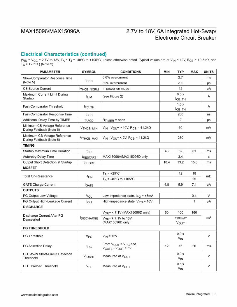
(VIN = VCC = 2.7V to 18V, TA = TJ = -40°C to +105°C, unless otherwise noted. Typical values are at VIN = 12V, RCB = 10.5kΩ, and TA = +25°C.) (Note 2)
PARAMETER SYMBOL CONDITIONS MIN TYP MAX UNITS
Slow-Comparator Response Time (Note 5) tSCD
0.6% overcurrent 2.7 ms
30% overcurrent 200 µs
CB Source Current ITHCB_NORM In power-on mode 12 µA
Maximum Current Limit During Startup ILIM (see Figure 2) 0.5 x
ICB_THA
Fast-Comparator Threshold IFC_TH1.5 x
ICB_THA
Fast-Comparator Response Time tFCD 200 ns
Additional Delay Time by TIMER tAFCD RTIMER = open 2 µs
Minimum CB Voltage Reference During Foldback (Note 6) VTHCB_MIN VIN - VOUT > 10V, RCB = 41.2kΩ 60 mV
Maximum CB Voltage Reference During Foldback (Note 6) VTHCB_MAX VIN - VOUT < 2V, RCB = 41.2kΩ 250 mV
TIMINGStartup Maximum Time Duration tSU 43 52 61 ms
Autoretry Delay Time tRESTART MAX15096A/MAX15096D only 3.4 s
Output Short Detection at Startup tSHORT 10.4 13.2 15.6 ms
MOSFET
Total On-Resistance RONTA = +25°C 12 18
mΩTA = -40°C to +105°C 25
GATE Charge Current IGATE 4.8 5.9 7.1 μA
OUTPUTSPG Output Low Voltage VOL Low-impedance state, IPG = +5mA 0.4 V
PG Output High-Leakage Current IOH High-impedance state, VPG = 16V 1 μA
DISCHARGE
Discharge Current After PG Deasserted IDISCHARGE
VOUT < 7.1V (MAX15096D only) 50 100 160mAVOUT ≥ 7.1V to 18V
(MAX15096D only)710mW/
VOUT
PG THRESHOLD
PG Threshold VPG VIN = 12V 0.9 x VIN
V
PG Assertion Delay tPGFrom VOUT > VPG and VGATE - VOUT > 3V 12 16 20 ms
OUT-to-IN Short-Circuit Detection Threshold VIOSHT Measured at VOUT
0.9 x VIN
V
OUT Preload Threshold VPL Measured at VOUT0.5 x VIN
V
Electrical Characteristics (continued)
MAX15096/MAX15096A 2.7V to 18V, 6A Integrated Hot-Swap/ Electronic Circuit Breaker
www.maximintegrated.com Maxim Integrated 3

(VIN = VCC = 2.7V to 18V, TA = TJ = -40°C to +105°C, unless otherwise noted. Typical values are at VIN = 12V, RCB = 10.5kΩ, and TA = +25°C.) (Note 2)
Note 2: All devices are 100% production tested at TA = +25°C. Limits over temperature are guaranteed by design.Note 3: 41.2kΩ is the maximum allowed external resistance value to be connected at the CB pin to GND for safe operation. All
devices are tested with 10.5kΩ, the parameter specified at RCB = 41.2kΩ is guaranteed by bench characterization and cor-relation, with respect to the tested parameter at RCB = 10.5kΩ. The formula that describes the relationship between RCB and the circuit-breaker current threshold is: ICB = RCB/6510)(Ω/A) - 0.34A.
Note 4: Guaranteed by design and not production tested.Note 5: The current-limit slow-comparator response time is weighed against the amount of overcurrent so the higher the
overcurrent condition, the faster the response time.Note 6: Foldback is active during the startup phase so the internal power MOSFET operates within SOA.
Electrical Characteristics (continued)
PARAMETER SYMBOL CONDITIONS MIN TYP MAX UNITSINPUTSInput Logic Threshold EN VEN_TH Rising 0.95 1 1.05 VThreshold Hysteresis EN VEN_TH_HYS Falling 50 mVInput Logic Threshold PRSNT VPRSNT_TH Falling 0.92 0.97 1.02 VThreshold Hysteresis PRSNT VPRSNT_TH_HYS Rising 50 mVEN Bias Current IEN_BIAS VEN = 0 or 5.5V 1 μAPRSNT Input Bias Current IPRSNT_BIAS VPRSNT = 0 or 18V 1 μAEN Deglitch Time tEN_DEG 100 μsPRSNT High-to-Low Deglitch Time tPRSNT_DEG 400 μs
THERMAL SHUTDOWNThermal Shutdown TSD TJ rising 150 °C
Thermal Shutdown Hysteresis TJ falling 20 °C
MAX15096/MAX15096A 2.7V to 18V, 6A Integrated Hot-Swap/ Electronic Circuit Breaker
www.maximintegrated.com Maxim Integrated 4

(VIN = VCC = 2.7V to 18V, TA = TJ = -40°C to +85°C, unless otherwise noted. Typical values are at VIN = 12V, RCB = 10.5kΩ, and TA = +25°C.)
Typical Operating Characteristics
8
10
12
14
16
18
-40 -25 -10 5 20 35 50 65 80 95 110
ON-R
ESIS
TANC
E(mΩ
)
TEMPERATURE (°C)
ON-RESISTANCEvs. TEMPERATURE toc04
VIN = 12V,ILOAD = 0.5A
10V/div
500mV/div
toc06
10ms/div
VUV
VPG
UV TURN-OFF WAVEFORMS
ILOAD
1V/div
VOUT
2A/div
CGATE = 5.6nF
5V/div
500mV/div
toc05
10ms/div
VUV
VPG
UV TURN-ON WAVEFORMS
ILOAD
1V/divVOUT
2A/div
CGATE = 5.6nF
5A/div
10V/div
toc07
1ms/div
VOUT
VPG
FAULT-SHUTDOWN WAVEFORMS OVERLOAD (SLOW TRIP)
ILOAD
10V/div
VGATE 10V/div
0.0
0.5
1.0
1.5
2.0
2.5
3.0
3.5
4.0
4.5
5.0
-40 -25 -10 5 20 35 50 65 80 95 110
SUPP
LY C
URRE
NT(m
A)
TEMPERATURE (°C)
SUPPLY CURRENTvs. TEMPERATURE
toc01
ICC
IINRCB = 41.2kΩVIN = VCC= 12V
0
1
2
3
4
5
6
7
8
-40 -25 -10 5 20 35 50 65 80 95 110
CIRC
UIT
BREA
KER
THRE
SHOL
D(A)
TEMPERATURE (°C)
CIRCUIT BREAKER THRESHODvs. TEMPERATURE
toc03
RCB = 41.2kΩ
RCB = 30kΩ
RCB = 20kΩ
RCB = 10.5kΩ
0.00.51.01.52.02.53.03.54.04.55.05.56.06.57.0
10 15 20 25 30 35 40
CIRC
UIT
BREA
KER
THRE
SHOL
D (A
)
CIRCUIT BREAKER RESISTANCE (kΩ)
CIRCUIT BREAKER THRESHOLDvs. CIRCUIT BREAKER
REISISTANCE toc02
VIN = VCC = 12V
MAX15096/MAX15096A 2.7V to 18V, 6A Integrated Hot-Swap/ Electronic Circuit Breaker
Maxim Integrated 5www.maximintegrated.com

(VIN = VCC = 2.7V to 18V, TA = TJ = -40°C to +85°C, unless otherwise noted. Typical values are at VIN = 12V, RCB = 10.5kΩ, and TA = +25°C.)
Typical Operating Characteristics (continued)
5V/div
10V/div
10V/div
toc11
1s/div
VIN
ILOAD
VGATE
AUTORETRYFUNCTIONALITY
VOUT
5A/div
CLOAD = 620nF
10V/div
2V/div
10V/div
toc14
2ms/div
VIN
VPG
VGATE
OUTPUT DISCHARGE BEHAVIOR
VOUT
5V/div
COUT = 1060µF
MAX15096D ONLY
10A/div
10V/div
toc08
400µs/div
VOUT
VPG
FAULT-SHUTDOWN WAVEFORMS OVERLOAD (SHORT CIRCUIT)
ILOAD
10V/div
VGATE 20V/div 0.5
0.51
0.52
0.53
0.54
0.55
0.56
-40 -25 -10 5 20 35 50 65 80 95 110
UV R
ISIN
G/FA
LLIN
G TH
RESH
OLD
VOLT
AGE(
V)
TEMPERATURE (°C)
UV RISING\FALLING THRESHOLDVOLTAGE vs. TEMPERATURE
toc09
VIN = 12V,
VUV FALLING
VUV RISING
0.00.20.40.60.81.01.21.41.61.82.02.22.42.62.83.0
0 5 10 15 20 25 30
CIRC
UIT
BREA
KER
THRE
SHOL
D TI
ME (m
s)
OVERCURRENT(%)
CIRCUIT BREAKER THRESHOLD TIME vs. OVERCURRENT
toc12
VIN = VCC = 12V
5V/div
500mV/div
toc10
10ms/div
VUV
VPG
PG ASSERTION DELAY
VOUT
500mV/div
CGATE = 5.6nF
0
0.5
1
1.5
2
2.5
3
-40 -25 -10 5 20 35 50 65 80 95 110
FAST
COM
PARA
TOR
DELA
Y(µs
)
TEMPERATURE( OC)
FAST COMPARATOR DELAYvs. TEMPERATURE
toc13
RTIMER = OPEN
RTIMER = 44kΩ RTIMER = 22kΩ
RTIMER =0ΩRTIMER = 10.9kΩ
MAX15096/MAX15096A 2.7V to 18V, 6A Integrated Hot-Swap/ Electronic Circuit Breaker
Maxim Integrated 6www.maximintegrated.com

BUMP NAME FUNCTION
A1 VCCPower-Supply Input. Connect VCC to a voltage between 2.7V and 18V. Connect a Schottky diode (or 10Ω resistor) from IN to VCC, and a 1µF bypass capacitor to GND to guarantee full operation in the event VIN collapses during a strong short from OUT to GND.
A2 PG Power-Good Output. PG is an open-drain output. Connect to an external pullup resistor to make it an active-high output. PG pulls low until the internal power MOSFET is fully enhanced.
A3 TIMERTiming Input. Connect a resistor from TIMER to GND to program the maximum time the part is allowed to remain in current limit. See the TIMER section. If TIMER is not connected, the parasitic capacitance between TIMER and GND must be less than 10pF.
A4 UVOV Undervoltage and Overvoltage Threshold Pin. UVOV sets the under/overvoltage threshold. See the Setting the Undervoltage/Overvoltage Threshold section.
B1 CBCurrent-Limit Threshold Set. Connect a resistor from CB to GND to set the circuit-breaker threshold. Maximum value of 41.2kΩ can be accepted for safe operation. Having the CB pin connected to GND sets the circuit- breaker threshold at 0A.
B2–B4 INSupply Voltage Input. IN is connected to the drain of the internal 12mΩ (typ) MOSFET. Bypass IN with a transient voltage-suppressor diode to GND for clamping inductive kick transients in the case of fast output short circuit to GND.
C1 GND Ground
C2–C4 OUT Load Output. Source of the internal power MOSFET.
D1 REG Internal Regulator Output. Bypass to ground with a 1µF capacitor. Do not power external circuitry using the REG output.
D2 GATEGate of Internal MOSFET. During startup, a 5.9µA (typ) current is sourced to enhance the internal MOSFET with a 10V/ms slew rate. Connect an external capacitance from GATE to GND to reduce the output slew rate during startup.
D3 EN Active-High Enable Comparator Input. Pulling EN high enables the output if PRSNT is held low.
D4 PRSNT Active-Low Present-Detect Logic Input. Pulling PRSNT to GND enables the output if EN is high.
Bump Description
Bump Configuration
WLP(2mm x 2mm)
TOP VIEW(BUMP SIDE DOWN)
MAX15096MAX15096AMAX15096D
+1 2 3 4
A
B
C
D
VCC
PG TIMER UVOV
CB
IN IN IN
GND
OUT OUT OUT
REG
GATE EN PRSNT
MAX15096/MAX15096A 2.7V to 18V, 6A Integrated Hot-Swap/ Electronic Circuit Breaker
www.maximintegrated.com Maxim Integrated 7
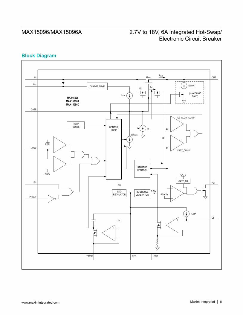
Block Diagram
CHARGE PUMP
CONTROLLOGIC
STARTUPCONTROL
GATE_OK
GATE
0.9 x VIN
1.25VREFERENCEGENERATOR
VCC
1V
REF2
REF1
CB_SLOW_COMP
EN
MPOW
TEMP SENSE
ILOAD
IREF
IGATE
100mA
OUT
FAST_COMP
PG
12µACB
LDOREGULATOR
PRSNT
UVOV
GATE
VCC
IN
TIMER REG GND
2x ISLEW
IPD
MAX15096MAX15096AMAX15096D
MS1
(MAX15096D ONLY)
MAX15096/MAX15096A 2.7V to 18V, 6A Integrated Hot-Swap/ Electronic Circuit Breaker
www.maximintegrated.com Maxim Integrated 8
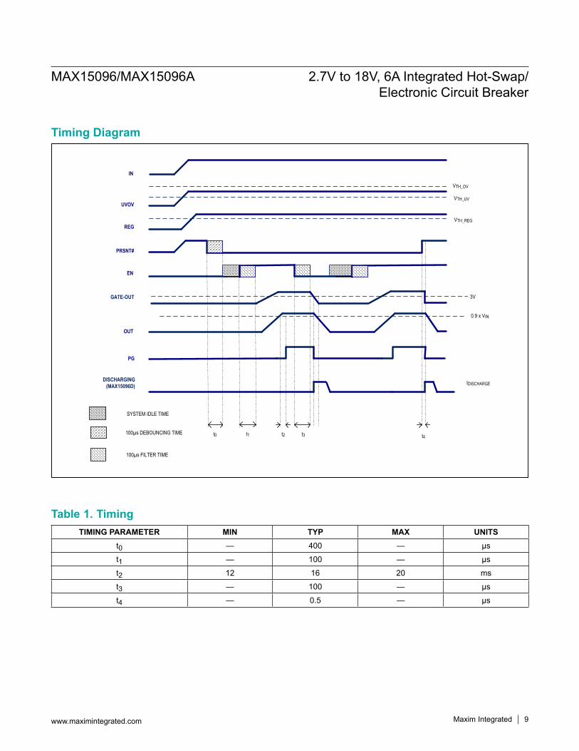
Table 1. Timing
Timing Diagram
TIMING PARAMETER MIN TYP MAX UNITSt0 — 400 — μs
t1 — 100 — μs
t2 12 16 20 ms
t3 — 100 — μs
t4 — 0.5 — μs
PRSNT#
100µs DEBOUNCING TIME
100µs FILTER TIME
GATE-OUT
t2
VTH_UV
3V
VTH_REG
SYSTEM IDLE TIME
VTH_OV
DISCHARGING(MAX15096D) IDISCHARGE
IN
UVOV
REG
EN
OUT
PG
0.9 x VIN
t1t0 t3 t4
MAX15096/MAX15096A 2.7V to 18V, 6A Integrated Hot-Swap/ Electronic Circuit Breaker
www.maximintegrated.com Maxim Integrated 9
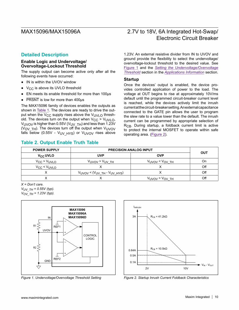
Detailed DescriptionEnable Logic and Undervoltage/ Overvoltage-Lockout ThresholdThe supply output can become active only after all the following events have occurred: IN is within the UVOV window VCC is above its UVLO threshold EN meets its enable threshold for more than 100μs PRSNT is low for more than 400µsThe MAX15096 family of devices enables the outputs as shown in Table 1. The devices are ready to drive the out-put when the VCC supply rises above the VUVLO thresh-old. The devices turn on the output when VCC > VUVLO, VUVOV is higher than 0.55V (VUV_TH) and less than 1.23V (VOV_TH). The devices turn off the output when VUVOV falls below (0.55V - VUV_HYS) or VUVOV rises above
1.23V. An external resistive divider from IN to UVOV and ground provide the flexibility to select the undervoltage/overvoltage-lockout threshold to the desired value. See Figure 1 and the Setting the Undervoltage/Overvoltage Threshold section in the Applications Information section.
StartupOnce the devices’ output is enabled, the device pro-vides controlled application of power to the load. The voltage at OUT begins to rise at approximately 10V/ms default until the programmed circuit-breaker current level is reached, while the devices actively limit the inrush current at the circuit-breaker setting. An external capacitance connected to the GATE pin allows the user to program the slew rate to a value lower than the default. The inrush current can be programmed by appropriate selection of RCB. During startup, a foldback current limit is active to protect the internal MOSFET to operate within safe operating area. (Figure 2).
Table 2. Output Enable Truth Table
Figure 1. Undervoltage/Overvoltage Threshold Setting Figure 2. Startup Inrush Current Foldback Characteristics
X = Don’t care.VUV_TH = 0.55V (typ).VOV_TH = 1.23V (typ).
POWER SUPPLY PRECISION ANALOG INPUTOUT
VCC UVLO UVP OVPVCC > VUVLO VUVOV > VUV_TH VUVOV < VOV_TH On
VCC < VUVLO X X Off
X VUVOV < (VUV_TH - VUV_HYS) X Off
X X VUVOV > VOV_TH Off
CONTROLLOGIC
REF1
REF2
R1
R2
IN
UVOV
MAX15096MAX15096AMAX15096D
GND
RCB = 41.2kΩ
2VVIN - VOUT
0.64A
3A
10V
IINRUSH
0.5A
0.1A
RCB = 10.5kΩ
MAX15096/MAX15096A 2.7V to 18V, 6A Integrated Hot-Swap/ Electronic Circuit Breaker
www.maximintegrated.com Maxim Integrated 10

An internal 52ms (typ) timer starts counting when the device enters startup phase. The devices complete startup phase and enter normal operation mode if the volt-age at OUT rises above the preload threshold (0.9 x VIN) and (VGATE - VOUT) > 3V. An open-drain power-good output (PG) goes high impedance 16ms after the startup successfully completes. The thermal-protection circuit is always active and the internal MOSFET is immediately turned off so thermal-shutdown threshold condition can be reached.If the startup is not successful because the output is shorted or the load is too high (OUT voltage < 1V), the devices turn off the hot-swap switch after the output short detection at startup tSHORT (13.2ms) elapses.
VariableSpeed/BiLevel-Fault ProtectionVariableSpeed/BiLevel-fault protection incorporates com-parators with different thresholds and response times to monitor the load current (Figure 3). Protection is provided in normal operation (after the startup period has expired) by discharging the MOSFET gate in response to a fault condition. During a fault condition, the MAX15096A enters an autoretry mode while the MAX15096 latches off (see the Autoretry and Latchoff Fault Management section).
Enable Input (EN)The devices allow for enabling the MOSFET in an active-high configuration. When all other enabling conditions are verified and the EN pin is at a logic-high level, the MOSFET is enabled. Similarly, when the EN pin is at a logic-low level, the MOSFET is disabled.
Charge PumpAn integrated charge pump provides the gate-drive volt-age for the internal power MOSFET. The charge pump generates the proper gate-drive voltage above VIN to fully enhance the internal power MOSFET and guarantee low RON operation during normal state condition.During startup, the internal charge pump drives the GATE of the MOSFET with a 5.9μA current to enhance the internal MOSFET with 10V/ms slew rate. Connect an external capacitor (CGATE) from GATE to GND to reduce the output slew rate during startup. CGATE can be calculated according to the formula below:
CGATE = (IGATE x Δt)/ΔVGATEwhere IGATE is 5.9μA (typ), Δt is the desired slew rate time, and the 5V of ΔVGATE is the voltage at the gate of the internal MOSFET at turn-on.
Figure 3. VariableSpeed/BiLevel Response
0.6% OVERCURRENT
OUT CURRENT
2.7ms
TUR
N-O
FF T
IME
SLOWCOMPARATOR
FASTCOMPARATOR
30% OVERCURRENT
200ns
50% OVERCURRENT
MAX15096/MAX15096A 2.7V to 18V, 6A Integrated Hot-Swap/ Electronic Circuit Breaker
www.maximintegrated.com Maxim Integrated 11
Circuit-Breaker Comparator and Current LimitThe current through the internal power MOSFET is com-pared to a circuit-breaker threshold. An external resistor between CB and ground sets this threshold according to the following formula:
ICB = (RCB/6501)(A/Ω) - 0.34Awhere ICB is in amps and RCB (the resistor between CB and ground) is in ohms.The circuit-breaker comparator is designed so that the load current can exceed the threshold for some amount of time before tripping. The time delay varies inversely with the overdrive above the threshold. The greater the overcurrent condition, the faster the response time, allowing the devices to tolerate load transients and noise near the circuit-breaker threshold. The maximum allowed external resistor value is 41.2kΩ, which corresponds to a 6A CB threshold setting. Programming the CB threshold to a value higher than 6A could cause unsafe operating conditions, resulting in damage to the device.The devices also feature catastrophic short-circuit protection. During normal operation, if OUT is shorted directly to ground, a fast protection circuit forces the gate of the internal MOSFET to discharge quickly and disconnect the output from the input.
Autoretry and Latchoff Fault ManagementDuring a fault condition, the devices turn off the internal MOSFET, disconnecting the output from the input. The MAX15096A enters an autoretry mode and restarts after tRESTART (3.4s typ.) time delay elapses. The MAX15096 latches off and remains off until the enable logic is cycled off and on after a certain delay. The delay prevents the latchoff device to restart and operate with unsafe power-dissipation duty cycle. See the Timing diagram and Table 1 for delay values.
Latchoff ResetThe latchoff could be reset if any one of the following happens: VCC is below its UVLO threshold EN is disabled for longer than 100μs UV is triggered
PRSNT goes above its threshold OV is triggered
Power-Good (PG) DelayThe devices feature an open-drain, power-good output that asserts after tPG delay, indicating that OUT voltage has reached (0.9 x VIN) voltage and (VGATE - VOUT) > 3V.
REGThe devices include a linear regulator that outputs 3.3V at REG. REG provides power to the internal circuit blocks of the devices and must not be loaded externally (except a resistor > 50kΩ connected from REG to EN). REG requires a 1µF capacitor to ground for proper operation.
Output DischargingThe discharge FET is active when the output is disabled or under fault event. In this event, the hot-swap is off and the output is on the way down. The discharging is triggered after the main FET has completely turned off.The maximum output capacitance is approximately 1000µF. The voltage could be up to 18V. Ideally, it discharges the output capacitor in constant power mode (710mW typ) to ensure the voltage rail is below 0.3V within 2s or less time.
TIMERConnect a resistor from the TIMER pin to the GND pin to program the fast-trip response time. This time is the sum of the internal fast-comparator propagation delay (less than 200ns typ) plus an additional delay set by the external resistor connected from TIMER to ground. Choosing different resistance values, it is possible to change the value of additional delay. If the TIMER pin is connected to REG, the total response time is less than 200ns (typ).Additional delay is disabled also during the startup phase or after a short-circuit event (VOUT < 90% VIN). Be careful about additional delay settings related to a short event.Additional delay can be calculated using the following formula:
Additional_Delay (µs) = RTIMER (kΩ) x 22.9E-03
Maximum additional delay time is set to 2µs. Table 3 provides additional delay settings.
MAX15096/MAX15096A 2.7V to 18V, 6A Integrated Hot-Swap/ Electronic Circuit Breaker
www.maximintegrated.com Maxim Integrated 12

Thermal ProtectionThe devices enter a thermal shutdown mode in the event of overheating caused by excessive power dissipation or high ambient temperature. When the junction temperature exceeds TJ = +150°C (typ), the internal thermal protec-tion circuitry turns off the internal power MOSFET. The devices recover from thermal shutdown mode once the junction temperature drops by 20ºC (typ).
IN-to-OUT Short-Circuit ProtectionAt startup, after all the input conditions are satisfied (UV, OV, VUVLO), the devices immediately check for IN-to-OUT short-circuit faults. If VOUT is greater than 90% of
VIN, the internal MOSFET cannot be turned on, then the MAX15096A autoretries in tRESTART (3.4s typ), while the MAX15096 latches off.If VOUT is in the range from 50% to 90% of VIN, then the internal MOSFET still cannot be turned on after tSU time elapses. The MAX15096A autoretries in tRESTART, while the MAX15096 latches off.
Applications InformationSetting the Undervoltage/Overvoltage ThresholdSee Table 4 for options.
Table 3. Additional Delay Settings
Table 4. Setting the Undervoltage/Overvoltage Thresholds
OPTION RTIMER (kΩ) RESPONSE TIME (μs)1 Open 2
2 86.6 2
3 43.2 1
4 21.5 0.5
5 11 0.25
6 0 0.050
OPTION R1 TABLE (kΩ)R2 = 10kΩ OVP UVP
1 133 17.6 7.9
2 127 16.9 7.5
3 118 15.7 7.0
4 115 15.4 6.9
5 113 15.1 6.8
6 107 14.4 6.4
7 102 13.8 6.2
8 49.9 7.4 3.3
9 46.4 6.9 3.1
10 43.2 6.5 2.9
11 39.2 6.1 2.7
12 33.2 5.3 2.4
MAX15096/MAX15096A 2.7V to 18V, 6A Integrated Hot-Swap/ Electronic Circuit Breaker
www.maximintegrated.com Maxim Integrated 13
+Denotes a lead (Pb)-free/RoHS-compliant package.
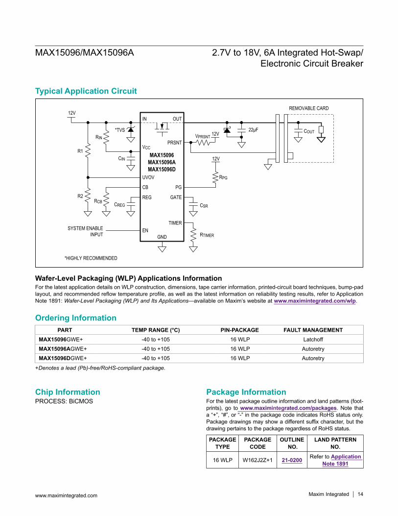
Typical Application Circuit
Chip InformationPROCESS: BiCMOS
Package InformationFor the latest package outline information and land patterns (foot-prints), go to www.maximintegrated.com/packages. Note that a “+”, “#”, or “-” in the package code indicates RoHS status only. Package drawings may show a different suffix character, but the drawing pertains to the package regardless of RoHS status.
Wafer-Level Packaging (WLP) Applications InformationFor the latest application details on WLP construction, dimensions, tape carrier information, printed-circuit board techniques, bump-pad layout, and recommended reflow temperature profile, as well as the latest information on reliability testing results, refer to Application Note 1891: Wafer-Level Packaging (WLP) and Its Applications—available on Maxim’s website at www.maximintegrated.com/wlp.
Ordering InformationPART TEMP RANGE (°C) PIN-PACKAGE FAULT MANAGEMENT
MAX15096GWE+ -40 to +105 16 WLP Latchoff
MAX15096AGWE+ -40 to +105 16 WLP Autoretry
MAX15096DGWE+ -40 to +105 16 WLP Autoretry
PACKAGE TYPE
PACKAGE CODE
OUTLINE NO.
LAND PATTERN NO.
16 WLP W162J2Z+1 21-0200 Refer to Application Note 1891
UVOV
CB
MAX15096MAX15096AMAX15096D
GNDEN
REG
R1
IN OUT 12V
VCC
R2
CIN
CREGRCB
GATECSR
PRSNT
SYSTEM ENABLE INPUT
*HIGHLY RECOMMENDED
COUT22μF
RTIMER
TIMER
VPRSNT*TVS
RIN
REMOVABLE CARD
PG
RPG
12V
12V
MAX15096/MAX15096A 2.7V to 18V, 6A Integrated Hot-Swap/ Electronic Circuit Breaker
www.maximintegrated.com Maxim Integrated 14

Revision HistoryREVISIONNUMBER
REVISIONDATE DESCRIPTION PAGES
CHANGED
0 3/14 Initial release —
1 8/14 Replaced TOCs 1, 3, 4, 9, and 13 5, 6
2 1/15 Updated Benefits and Features section 1
3 5/16 Removed future part information; updated Header, General Description and Benefits and Features sections, and Pin Description table 1–15
4 2/17 Updated Typical Application Circuit diagram 14
Maxim Integrated cannot assume responsibility for use of any circuitry other than circuitry entirely embodied in a Maxim Integrated product. No circuit patent licenses are implied. Maxim Integrated reserves the right to change the circuitry and specifications without notice at any time. The parametric values (min and max limits) shown in the Electrical Characteristics table are guaranteed. Other parametric values quoted in this data sheet are provided for guidance.
Maxim Integrated and the Maxim Integrated logo are trademarks of Maxim Integrated Products, Inc.
MAX15096/MAX15096A 2.7V to 18V, 6Am Integrated Hot-Swap/ Electronic Circuit Breaker
© 2017 Maxim Integrated Products, Inc. 15
For pricing, delivery, and ordering information, please contact Maxim Direct at 1-888-629-4642, or visit Maxim Integrated’s website at www.maximintegrated.com.