Embed Size (px)
Citation preview

General DescriptionThe MAX14914 is a high-side/push-pull driver that operates as both an industrial digital output (DO) and an industrial digital input (DI). The MAX14914 is specified for operation with supplies up to 40V. The high-side switch current is resistor settable from 135mA (min) to 1.3A (min). The high-side driver’s on-resistance is 120mΩ (typ) at 125°C ambient temperature. Optional push-pull operation allows driving of cables and fast discharge of load capacitance. The output voltage is monitored and indicated through the DOI_LVL pin for safety applications.The MAX14914 complies with Type 1, Type 2, or Type 3 input characteristics when configured for DI operation.
Applications Industrial Digital Outputs and Inputs Modules Configurable Digital Input/Output Motor Control Safety Systems
Benefits and Features Reduces Power and Heat Dissipation
• 240mΩ (max) HS RON at TA = 125°C• Accurate Short-Circuit Current Limit• Accurate Internal Current Limiter for Types 1, Type 2,
and Type 3 Digital Inputs Enhances System Robustness
• “Safe-Demagnetization” for Safe Turn-Off of Unlimited Inductance
• 60V Supply Tolerance• Loss of GND Protection• Thermal Shutdown Protection• ±2kV IEC 61000-4-5 Surge Protection• ±20kV IEC 61000-4-2 Air-Gap ESD Protection• ±7kV IEC 61000-4-2 Contact ESD Protection• -40°C to +125°C Ambient Operating Temperature
Reduces BOM Count and PCB Space• Small 4mm x 4mm TQFN Package• Internal Clamps for Fast Inductive Load Turn-Off• On-Chip 5V Regulator
Provides Flexibility• Configurable as a Digital Input or a High-Side or
Push-Pull Digital Output• Resistor Settable Current Limiting for the High-Side
Switch (135mA - 1.3A)• 10V to 40V Operating Supply Range
Improves System Speed and Throughput• Propagation Delay of Less Than 2µs
Ordering Information and Functional Diagram appears at end of data sheet.
19-8712; Rev 2; 12/17
MAX14914
FAULT
IN
VDDV5VL
DOI
GND
DOI_LVL
40V
DI_EN
PP
PGND
REGIN
24V
DO
DOI
CLIM
MAX14914 High-Side Switch with Settable Current-Limiting, Push-Pull Driver Option and Digital Input Configuration
Typical DO Application Diagram

VDD ........................................................................-0.3V to +65VREGIN ........................-0.3V to lower of +65V and (VDD + 0.3)VPGND ..................................................................-0.3V to + 0.3VDOI (VDD < VDDOVLOTH) ..............(VDD - 49)V to (VDD + 0.3)VDOI (VDD > VDDOVLOTH) ........................... -1V to (VDD + 0.3)VV5 ............................ -0.3V to lower of +6V and (REGIN + 0.3)V VL ............................................................................-0.3V to +6VIN, PP, DIN_EN, FAULT, CLIM ..............................-0.3V to +6VDOI_LVL .....................................................-0.3V to (VL + 0.3)VOV_VDD .....................-0.3V to lower of +65V and (VDD + 0.3)V
DOI Load Current .............................................Internally LimitedContinuous Current (any other terminal) ...... -100mA to +100mAContinuous Power Dissipation
(TA = +70°C, derate 28.6mW/°C above +70°C.) .......2280mWInductive Demagnetization Energy (ILOAD < 0.6A) ...... Unlimited Operating Temperature Range ......................... -40°C to +125°CJunction Temperature .......................................Internally Limited Storage Temperature Range ............................ -65°C to +150°CLead Temperature (Soldering, 10 sec) ............................+260°C
TQFN16 Junction-to-Ambient Thermal Resistance (θJA) ..........35°C/W Junction-to-Case Thermal Resistance (θJC) ..............2.7°C/W
(Note 1)
(VDD = +10V to +40V, V5 = +4.5V to +5.5V, VL = +2.5V to +5.5V, RLIM = 27kΩ to 220kΩ, TA = -40°C to +125°C, unless otherwise noted. Typical values are at TA = +25°C and VDD = +24V, VL = +3.3V and V5 = +5V, RLIM = 50kΩ) (Note 2)
PARAMETER SYMBOL CONDITIONS MIN TYP MAX UNITSVDD SUPPLY
Supply Voltage VVDDOperating Conditions 10 40 V
Tolerant 0 60 V
Supply Current
IVDD_ON_HS
HS mode, PP = low, IN = VL, DOI high (no switching), no load, V5 = VL = REGIN, VDD = 40V
0.6 0.95
mAIVDD_ON_PP
PP mode, PP = high, 10kHz switching, V5 = VL = REGIN, no load 0.85 1.4
IVDD_ON_DI DI_EN = VL, REGIN = 40V 0.13 0.3
Undervoltage-Lockout Threshold VVDD_UV
VDD rising, V5 = VL 8.5 9.1 9.7 V
VDD falling, V5 = VL 8 8.6 9 VUndervoltage-Lockout Hysteresis VVDD_UVHYST V5 = 5V 0.5 V
VDD Overvoltage-Lockout Threshold VVDD_OVLO
VDD rising, V5 = 5V 41.5 43.5 45 V
VDD falling, V5 = 5V 40.5 42.2 44 VVDD Overvoltage-Lockout Hysteresis VVDD_OVHYST V5 = 5V 1 V
VL LOGIC INTERFACE SUPPLYVL Supply Voltage VVL 2.5 5.5 V
VL Supply Current IVLAll logic inputs high or low, all outputs unloaded 10 25 µA
VL POR Threshold VVL_POR VL falling 1.12 1.27 1.52 V
MAX14914 High-Side Switch with Settable Current-Limiting, Push-Pull Driver Option and Digital Input Configuration
www.maximintegrated.com Maxim Integrated 2
Note 1: Package thermal resistances were obtained using the method described in JEDEC specification JESD51-7, using a four-layer board. For detailed information on package thermal considerations, refer to www.maximintegrated.com/thermal-tutorial.
Absolute Maximum Ratings(All voltages referenced to GND)
Stresses beyond those listed under “Absolute Maximum Ratings” may cause permanent damage to the device. These are stress ratings only, and functional operation of the device at these or any other conditions beyond those indicated in the operational sections of the specifications is not implied. Exposure to absolute maximum rating conditions for extended periods may affect device reliability.
Package Thermal Characteristics
Electrical Characteristics

(VDD = +10V to +40V, V5 = +4.5V to +5.5V, VL = +2.5V to +5.5V, RLIM = 27kΩ to 220kΩ, TA = -40°C to +125°C, unless otherwise noted. Typical values are at TA = +25°C and VDD = +24V, VL = +3.3V and V5 = +5V, RLIM = 50kΩ) (Note 2)
PARAMETER SYMBOL CONDITIONS MIN TYP MAX UNITS5V SUPPLY/LINEAR REGULATOR
REGIN Current HS Mode IREGIN_ON_HSHS mode, REGIN = 40V, IN = VL, no load on DOI, no load on V5 0.3 0.5 mA
REGIN Current PP Mode IREGIN_ON_PPPP = high, REGIN = 40V, 10kHz switching, no load on DOI, no load on V5 0.35 0.6 mA
REGIN Current DI Mode IREGIN_ON_DI DI_EN=VL, REGIN = 40V 0.5 mA
V5 Supply Current
IV5HSHS Mode, REGIN = V5, IN = VL, no load on DOI 0.24 0.4 mA
IV5PPPP Mode, REGIN = V5,10kHz switching, no load on DOI 0.3 0.5 mA
IV5DI DI Mode, DI_EN = high, REGIN = V5 0.22 0.4 mA
REGIN Undervoltage-Lockout Threshold VREG_UV REGIN rising 6.75 7.6 V
REGIN Undervoltage-Lockout Hysteresis VREG_UVHYST 0.45 V
V5 Undervoltage-Lockout Threshold
VV5_UV V5 rising 3.8 4.2 V
V5 Undervoltage-Lockout Hysteresis
VV5UV_UVHYST 0.3 V
V5 Output Voltage V5 0mA – 20mA external load 4.75 5.0 5.25 V
V5 Current Limit IV5_CL 25 mA
DRIVER OUTPUT (DOI)HS On-Resistance RDOI_ON_HS PP = X, IN = high, IDOI = 500mA 120 240 mΩ
LS Output Low VDOI_LOW PP = high, IN = low, IDOI = 100mA 1.2 V
DOI Clamp Voltage VDOI_CL
Relative to VDD, IDOI = 500mA,VVDD < VVDD_OVLO
-63 -55 -49 V
Relative to GND, IDOI = 500mA,VVDD_OVLO < VVDD <60V -4.5 -2.9 -1.5 V
DOI Leakage IDOI_LK
VDD = 40V, PP = IN = low, DI_EN = low, 0V< VDOI < VVDD
-60 60µA
VDD = 60V, PP = IN = X, DI_EN = low, 0V < VDOI < VVDD
-150 150
OUTPUT DRIVER CURRENT LIMITING (DOI)HS Current-Limit Minimum ICLIM_HS_MIN RLIM = 220kΩ 135 196 255 mA
HS Current-Limit Maximum ICLIM_HS_MAX RLIM = 27kΩ 1.3 1.6 1.9 A
HS Current-Limit Offset Error ICLIM_HS_OE (Note 3) -25 +25 mA
HS Current-Limit Gain Error ICLIM_HS_GE (Note 3) -20 +20 %
MAX14914 High-Side Switch with Settable Current-Limiting, Push-Pull Driver Option and Digital Input Configuration
www.maximintegrated.com Maxim Integrated 3
Electrical Characteristics (continued)

(VDD = +10V to +40V, V5 = +4.5V to +5.5V, VL = +2.5V to +5.5V, RLIM = 27kΩ to 220kΩ, TA = -40°C to +125°C, unless otherwise noted. Typical values are at TA = +25°C and VDD = +24V, VL = +3.3V and V5 = +5V, RLIM = 50kΩ) (Note 2)
PARAMETER SYMBOL CONDITIONS MIN TYP MAX UNITSCLIM Voltage VCLIM 1.21 V
CLIM Short Resistor Threshold Value RLIM_SHORT (Note 4) 10 12.9 15 kΩ
CLIM Open Resistor Threshold Value RLIM_OPEN (Note 5) 440 750 kΩ
LS Current Limit ICLIM_LS 150 280 mA
DIGITAL INPUT / DOI MONITOR
DO Monitor Threshold Voltage VTH_DODI_EN = low, DOI rising 1.5 2.0
VDI_EN = low, DOI falling 1.3 1.8
DO Monitor Hysteresis VHYS_DO DI_EN = low 0.2 V
DI Threshold Voltage VTH_DIDI_EN = high, DOI rising 6.7 8
VDI_EN = high, DOI falling 5.5 6.8
DI Hysteresis VHYS_DI DI_EN = high 1.2 V
DI Current Sink Type 1, 3 IDOI
DI_EN = high, PP = low, 0V< VDOI< 5V 2.6mADI_EN = high, PP = low, 8V< VDOI < 40V
VDOI < VDD2.0 2.3 2.6
DI Current Sink Type 2 IDOI
DI_EN = high, PP = high, 0V < VDOI < 5V 0 7.5mADI_EN = high, PP = high, 8V < VDOI < 40V,
VDOI < VDD6.0 7.0 7.7
LOGIC (I/O)Input Voltage High VIH 0.7 x VVL V
Input Voltage Low VIL 0.3 x VVL V
Input Threshold Hysteresis VIHYST 0.11 x VVL V
Input Pulldown Resistor RI All logic input pins 140 200 275 kΩ
Output Logic-Low VOL ILOAD = +5mA 0.33 V
DOI_LVL Tristate Leakage ILEAK GND < VDOI_LVL < VL -1 +1 µA
FAULT Tristate Leakage ILEAK GND < VFAULT < V5 -1 +1 µA
OV_VDD Leakage ILEAK GND < VOV_VDD < VDD -1 +1 µA
THERMAL PROTECTIONDriver Thermal-Shutdown Temperature TJSHDN Junction temperature rising 170 °C
Driver Thermal-Shutdown Hysteresis TJSHDN_HYST 15 °C
Chip Thermal Shutdown TCSHDN Temperature rising 150 °C
Chip Thermal-Shutdown Hysteresis TCSHDN_HYST 10 °C
MAX14914 High-Side Switch with Settable Current-Limiting, Push-Pull Driver Option and Digital Input Configuration
www.maximintegrated.com Maxim Integrated 4
Electrical Characteristics (continued)

(VDD = +10V to +40V, V5 = +4.5V to +5.5V, VL = +2.5V to +5.5V, RLIM = 27kΩ to 220kΩ, TA = -40°C to +125°C, unless otherwise noted. Typical values are at TA = +25°C and VDD = +24V, VL = +3.3V and V5 = +5V, RLIM = 50kΩ) (Note 2)
Note 2: All units are production tested at TA = +25°C. Specification over temperature are guaranteed by characterization and design.Note 3: Specification is guaranteed by design; not production tested.Note 4: Lower resistor values than CLIM_SHORT act like a CLIM pin short to GND.Note 5: Higher resistor values than CLIM_OPEN act like a CLIM open circuit.
PARAMETER SYMBOL CONDITIONS MIN TYP MAX UNITSTIMING CHARACTERISTICSOUTPUT DRIVER (DOI)Output Propagation Delay LH tPD_LH
PP = X, delay from IN to DOI rising by 1V, RL = 5kΩ, CL = 100pF (Figure 1) 0.4 1.5 µs
Output Propagation Delay HL tPD_HL
PP = low, delay between IN switching low to DOI falling by 1V. RL = 5kΩ, CL = 100pF, VDD = 24V (Figure 1)
0.6 1.5
µsPP = high, delay between IN switching low to DOI falling by 1V. RL = 5kΩ, CL = 100pF (Figure 1)
0.6 1.5
DOI Output Rise Time tRPP = X, 20% to 80% VDD, RL = 5kΩ, CL = 100pF, (Figure 2) 0.9 2 µs
DOI Output Fall Time tF
PP=high, 80% to 20% VDD, VDD = 24V, RL = 5kΩ, CL = 100pF (Figure 2) 0.65 2
µsPP=low, 80% to 20% VDD, VDD = 24V, RL = 47Ω, CL = 100pF (Figure 2) 1
PROPAGATION DELAY (DOI toDOI_LVL)
Propagation Delay LH tPDL_LHDOI_EN = low, delay from DOI rising to 5V to DI_LVL low (Figure 3) 2.7 5 µs
Propagation Delay LH DI tPDL_LH_DIDOI _EN = high, delay from DOI rising to 8V to DI_LVL low 1.1 µs
Propagation Delay HL tPDL_HLDOI _EN = low, delay from DOI falling to 3.5V to DI_LVL high 0.9 8 µs
Propagation Delay HL DI tPDL_HL_DIDOI _EN = high, delay from DOI falling to 5.5V to DI_LVL high 0.9 µs
GLITCH REJECTION (IN)Pulse Length of Rejected Glitch tFPL_GF 0 80 ns
Glitch Filter Delay Time tD_GF 140 300 ns
FAULT DETECTION (OV_VDD, FAULT)OV_VDD Threshold VTH_OV_VDD DI_EN = low, relative to VDD 0.22 V
OVLO_VDD Debounce Time TDOVLO_VDD DI_EN = low 200 µs
OVLO_VDD Output Leakage ILK_OV_VDD_ 0 < IOV < VDD -1 +1 µA
FAULT Output Leakage ILK_FAULT 0 < IFAULT < 5V -1 +1 µA
MAX14914 High-Side Switch with Settable Current-Limiting, Push-Pull Driver Option and Digital Input Configuration
www.maximintegrated.com Maxim Integrated 5
Electrical Characteristics (continued)

Note 6: Bypass VDD pin to PGND with 1µF capacitor as close as possible to the device for high ESD protection.Note 7: With a TVS protection on VDD to PGND.
Figure 1. IN to DOI Propagation Delay
Figure 2. DOI Rise and Fall Time
PARAMETER SYMBOL CONDITIONS TYP UNITS
ESD VESD
DOI pin contact (Note 6) ±7 kV
DOI pin Air Discharge (Note 6) ±20 kV
All other pins. Human Body Model ±2 kV
IEC Surge VSURGEDOI to PGND or Earth GND per IEC 61000-4-5 (42Ω/0.5µF) (Note 7) ±2 kV
VDD - 1V
IN
DOI
tPD_LHtPD_HL
1V
20%
80%
IN
DOI
tPD_LH tPD_HL
80%
tR_LH tR_HL
20%
MAX14914 High-Side Switch with Settable Current-Limiting, Push-Pull Driver Option and Digital Input Configuration
www.maximintegrated.com Maxim Integrated 6
ESD and Surge Protection

Figure 3. DOI to DOI_LVL Propagation Delay
MAX14914 High-Side Switch with Settable Current-Limiting, Push-Pull Driver Option and Digital Input Configuration
www.maximintegrated.com Maxim Integrated 7

(VDD = +24V, VL = +3.3V and V5 = +5V, TA = +25°C, unless otherwise noted.)
0
50
100
150
200
250
0 200 400 600 800 1000
HIG
H-S
IDE
RO
N(m
Ω)
ILOAD (mA)
HIGH-SIDE RON RESISTANCEvs. LOAD CURRENT
toc01
VDD = 24V 125°C
25°C
-40°C
0.0
0.2
0.4
0.6
0.8
1.0
1.2
1.4
-50 -25 0 25 50 75 100 125
PUSH
PU
LL P
RO
PAG
ATIO
N D
ELAY
(µs)
TEMPERATURE (°C)
PROPAGATION DELAYvs. TEMPERATURE (PUSH-PULL MODE)
toc03VDD = 24V, PP = HIGH, 100kHz, NO LOAD
HIGH-TO-LOW
LOW-TO-HIGH
DELAY FROM IN TO 50% OF DOI
0.8
0.9
1.0
1.1
1.2
10 20 30 40
V DD
SUPP
LYC
UR
REN
T(m
A)
VDD (V)
SUPPLY CURRENTvs. SUPPLY VOLTAGE (HIGH-SIDE MODE)
toc05VDD = REGIN = 24V, VL = V5, PP = LOW,NO LOADS, NO SWITCHING
0
50
100
150
200
250
10 20 30 40
HIG
H-S
IDE
RO
N(m
Ω)
VDD (V)
HIGH-SIDE RON RESISTANCEvs. SUPPLY VOLTAGE
toc02
125°C
-40°C
25°C
ILOAD = 500mA
0.50
0.70
0.90
1.10
1.30
1.50
1.70
1.90
-50 -25 0 25 50 75 100 125
PRO
PAG
ATIO
N D
ELAY
(µs)
TEMPERATURE (ºC)
PROPAGATION DELAYvs. TEMPERATURE (DI MODE)
toc04
LOW-TO-HIGH
HIGH-TO-LOW
VDD = REGIN = 24V, DI_EN = HIGH, 100kHz
0.7
0.8
0.9
1.0
1.1
1.2
-50 -25 0 25 50 75 100 125
V DD
SUPP
LYC
UR
REN
T(m
A)
TEMPERATURE (ºC)
SUPPLY CURRENTvs. TEMPERATURE (HIGH-SIDE MODE)
toc06
VDD = 40V
VDD = 10V
VDD = REGIN, PP = LOW,NO LOAD, NO SWITCHING
VDD = 24V
MAX14914 High-Side Switch with Settable Current-Limiting, Push-Pull Driver Option and Digital Input Configuration
Maxim Integrated 8www.maximintegrated.com
Typical Operating Characteristics
(VDD = +24V, VL = +3.3V and V5 = +5V, TA = +25°C, unless otherwise noted.)
0.0
0.5
1.0
1.5
2.0
2.5
3.0
-50 -25 0 25 50 75 100 125
V DD
SUPP
LY C
UR
REN
T (m
A)
TEMPERATURE (ºC)
SUPPLY CURRENTvs. TEMPERATURE (PUSH-PULL MODE)
toc07
10kHz
100kHz
VDD = REGIN = 24V, PP = HIGH, NO LOAD
0.2
0.3
0.4
0.5
0.6
-50 -25 0 25 50 75 100 125
REG
IN S
UPP
LY C
UR
REN
T (m
A)
TEMPERATURE (ºC)
REGIN SUPPLY CURRENTvs. TEMPERATURE toc09
REGIN = 10V
HS, VDD = 24V, NO SWITCHING, NO LOAD
REGIN = 24V - 40V
0.3
0.4
0.5
0.6
0.7
-50 -25 0 25 50 75 100 125
V DD
SUPP
LYC
UR
REN
T(m
A)
TEMPERATURE (ºC)
SUPPLY CURRENTvs. TEMPERATURE (DI MODE) toc11
VDD = REGIN = 24V, V5 = VL,DI_EN = HIGH, DOI = 20V
0.0
0.5
1.0
1.5
2.0
2.5
3.0
3.5
4.0
0 25 50 75 100 125 150 175 200
V DD
SUPP
LY C
UR
REN
T (m
A)
FREQUENCY (kHz)
SUPPLY CURRENTvs. FREQUENCY (PUSH-PULL MODE)
toc08
VDD = REGIN = 24V, PP = HIGH, NO LOAD
4.7
4.8
4.9
5.0
5.1
5.2
-50 -25 0 25 50 75 100 125
V5O
UTP
UT
(V)
TEMPERATURE (ºC)
V5 OUTPUTvs. TEMPERATURE toc10
REGIN = 10V - 40V, V5 = VL
-1.0
1.0
3.0
5.0
7.0
9.0
11.0
-3 0 3 6 9 12 15 18 21 24 27 30
DO
I IN
PUT
CU
RR
ENT
(mA)
INPUT VOLTAGE (V)
DOI INPUT CURRENTvs. INPUT VOLTAGE (DI MODE)
toc12
VDD = REGIN THROUGH PMOS = 24V,V5 = VL, DI_EN = HIGH
TYPE 1, 3 INPUT (PP = LOW)
TYPE 2 INPUT (PP = HIGH)
MAX14914 High-Side Switch with Settable Current-Limiting, Push-Pull Driver Option and Digital Input Configuration
Maxim Integrated 9www.maximintegrated.com
Typical Operating Characteristics (continued)

PIN NAME FUNCTION
1 VL Logic Supply Input. VL defines the levels on all I/O logic interface pins. Bypass VL to GND through a 100nF ceramic capacitor.
2 GND Analog Ground.
3 CLIM Current Limit Set Input. Connect a resistor from CLIM to GND to set the current limit. See Detailed Description for further information.
4 FAULT Open-Drain Fault Output. The FAULT transistor turns on when a fault condition (driver thermal shutdown or loss of ground) occurs. Connect a pullup to VL or V5.
5 DOI_LVLOpen-Drain DOI Level Output. DOI_LVL is logic-low when the DOI voltage is higher than the threshold voltage. DI_LVL is logic-high when the DOI voltage is lower than the threshold voltage. The threshold voltage depends on DI_EN.
6 DI_ENDigital Input Mode Logic Enable Input. Set DI_EN high to enable digital input operation on the DOI pin, which enables the internal current sink and sets Type 1, Type 2, or Type 3 thresholds on DIO_LVL. Select between Type 1 and 3 and Type 2 DI characteristics through the PP input.
7 IN Switch Control Input. Drive IN high to close the HS switch; drive IN low to open the HS switch and close the LS switch (when PP = low).
8 PPPush-Pull DO or DI Type Select Input. In DO mode, set PP high to enable push-pull mode operation of the DO driver. In DI mode, set PP low for IEC Type 1/3 input characterisitcs and set high for Type 2 input characteristics.
9 PGND Power Ground
10,11 DOI High-Side/Push-Pull Output (DI_EN = low) or Digital Input (DI_EN = high). Connect both DOI pins together externally.
12, 13 VDD Supply Voltage, Nominally 24V. Bypass VDD to GND through a 1µF capacitor.
14 REGIN 5V Regulator Input. Connect REGIN to VDD when using the internal 5V regulator. Connect REGIN to V5 when powering V5 from an external regulator.
15 OV_VDD Open-Drain Overvoltage Output. The OV_VDD transistor turns off when: 1) a device configured for DI operation; 2) DOI level is higher than VDD
16 V5 Analog Supply Voltage/LDO Output. 5V supply and LDO output. Bypass to GND through a 1µF ceramic capacitor.
15
16
14
13
6
5
7
GN
D
FAUL
T
8
VL
DO
I
PGN
D
VDD
1 2
REGIN
4
12 11 9
OV_VDD
V5
PP
IN
DI_EN
DOI_LVL+
CLI
MD
OI
3
10
VDD
MAX14914
*EP = EXPOSED PAD. CONNECT EP TO GND
TOP VIEW
MAX14914 High-Side Switch with Settable Current-Limiting, Push-Pull Driver Option and Digital Input Configuration
www.maximintegrated.com Maxim Integrated 10
Pin Configuration
Pin Description

Table 1. Operation Truth TableMODE DI_EN IN PP DOI DOI_LVL
DO High-Side0 0 0 Three-state 1/0
0 1 0 1 0
DO Push-Pull0 0 1 0 1
0 1 1 1 0
DI Type 1, 31 X 0 0 1
1 X 0 1 0
DI Type 21 X 1 0 1
1 X 1 1 0
MAX14914 High-Side Switch with Settable Current-Limiting, Push-Pull Driver Option and Digital Input Configuration
www.maximintegrated.com Maxim Integrated 11

MAX14914 High-Side Switch with Settable Current-Limiting, Push-Pull Driver Option and Digital Input Configuration
www.maximintegrated.com Maxim Integrated 12
Functional Diagram

Detailed DescriptionThe MAX14914 is a high-side/push-pull driver that operates as an industrial digital output and can also operate as an industrial digital input. The MAX14914 is specified for operation with supplies up to 40V. The high-side switch current limiting is resistor settable from 135mA (min) to 1.3A (min). The high-side driver’s on-resistance is 120mΩ (typ) and 240mΩ (max) at +125°C ambient temperature. Optional push-pull operation allows driving of cables and fast discharge of load capacitance. A separate digital DOI_LVL allows supervision of the DOI voltage in DO mode for safety applications. The MAX14914 complies with IEC Type 1, Type 2, or Type 3 input character-istics when configured for digital input operation.
5V Supply and RegulatorThe MAX14914 requires a 5V supply on the V5 pin for normal operation. This 5V supply can come from an external supply or from the internal 5V linear regulator. Connect REGIN pin to VDD to enable the internal regulator. Connect REGIN pin to V5 pin to disable the internal regulator, when an external 5V is used. The internal 5V regulator also can power the external loads/circuits with of up to 20mA.
Logic InterfaceThe logic interface features flexible logic levels, allowing interfacing to a wide range of common logic. The VL supply input defines the logic levels and can be set in the range of 2.5V to 5.5V. Connect a 0.1µF capacitor to VL.
Digital Output OperationThe driver can be configured for high-side (PP pin is driven low) or push-pull (PP pin is driven high) operation. In DO high-side mode, the DOI output voltage is high (VDD) when the logic level on IN pin is high, and three-state (Hi-Z), when the logic level on IN pin is low. In DO push-Pull mode, the DOI output voltage follows the logic level on IN pin. The high-side driver has 240mΩ (max) on-resistance at 500mA and TA = 125°C. The DOI voltage can go below ground, as will occur during inductive load demagnetization. An internal clamping diode limits the negative excursion to (VDD - VCL). See Driving Inductive Loads for details. The low-side (LS) switch speeds up the discharge of RC loads in Push-Pull mode.
Current Limit Adjustment The MAX14914 has a settable current limiting of the HS switch. The load current is limited to between 135mA (min) and 1.3A (min), depending on the value of the resistor used at the CLIM pin. A short-circuit or overcurrent generally creates a temperature rise in the chip; both the HS and LS FET’s temperatures are continuously monitored. When any switch temperatures exceed 170°C, the DOI output is put in Hi-Z until the temperature falls by 15°C. Connect a resistor (RLIM) from CLIM to GND to set the required current limit. The current is given by:
ILIM = K x VLIM/RLIMwhere, VLIM = 1.21V and K = 35.6 x 10³ If no resistor is connected to CLIM (i.e., CLIM is kept floating) or RLIM is more than 440k, the ILIM is internally set to 1.1A (typ). If the RLIM resistor is less than 12.9k (typ), the output is turned off. CLIM is short-circuit protected.Use the formulas below to validate the accuracy rangeILIM_MAX = ILIM x (1 + |ICLIM_HS_GE|/100) + |ICLIM_HS_OE|ILIM_MIN = ILIM x (1 - |ICLIM_HS_GE|/100) - |ICLIM_HS_OE|
Low-Side Current LimitThe low-side transistor has fixed-current limiting, when enabled in push-pull mode (PP driven high). The low-side driver limits current at 200mA (typ). The load current is actively controlled and the low-side switch only turns off if the driver temperature has fallen by the hysteresis value.
Figure 4. Digital Output Driver
VDD
VCL
ZL
DOIHS
LS
MAX14914
PGND
MAX14914 High-Side Switch with Settable Current-Limiting, Push-Pull Driver Option and Digital Input Configuration
www.maximintegrated.com Maxim Integrated 13
Short Circuit ProtectionShort circuits at the DOI output will generate high transient current until the active current limiting kicks in. In order to protect the MAX14914 against high currents that can be seen over an extended time, especially if the output is switching at a high rate into a short circuit, the MAX14914 enters a protect mode. When the MAX14914 detects that the DOI current is over 3x higher than the set current limit, the driver is switched to protect mode with reduced turn-on slew rate of the rising and falling edges for a duration of 4ms. The FAULT signal does not become active and the chip operates normally, but with reduced slew rate. If the cause for the short circuit is not removed, the protect mode will remain for an additional 4ms until the short circuit is removed.
Overvoltage Lockout When the VDD supply voltage exceeds the OVLO threshold voltage of 42.2V (typ), for a time duration larger than 200μs, the high-side and low-side switches automatically turn off. They remain off until VDD is reduced to below the threshold OVLO voltage minus hysteresis. When VDD is above the OVLO threshold, the OV_VDD output goes active.
Undervoltage Lockout When the VDD, V5, or VL supply voltages are under their respective UVLO thresholds the DOI driver is turned off (three-stated). DOI will automatically turn back on, once VDD, V5, and VL rise above their UVLO threshold.
Driving Capacitive Loads When charging/discharging purely capacitive loads with a push-pull driver, the driver dissipates power that is proportional to the switching frequency. The power can be estimated by PD ~ C x VDD2 x f, where C is the load capacitance, VDD is the supply voltage, and f is the switching frequency. For example, in an application with a 10nF load and 10kHz switching frequency, the driver dissipates 130mW at VDD = 36V. Therefore, switching a higher capacitance can induce thermal shutdown and that limits the operational frequency.
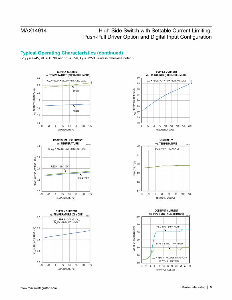
Driving Inductive Loads The DOI pins can be pulled below ground potential when the high-side transistor is off. The MAX14914 has an internal clamping diode from VDD to DOI that limits the negative voltage excursion to (VDD - 55V) typ. Turning off the current flowing in ground-connected inductive loads will result in a negative voltage at DOI pin that is limited to VDOI_CL below VDD by the internal clamping diodes. The MAX14914 features SafeDemag, meaning that there are no limits for load inductance that it can demagnetize, for load currents of up to 600mA.Turn-off of large inductive loads with currents larger than 600mA requires an external clamping diode, as shown in Figure 5. The clamping (breakdown) voltage of such diode needs to be less than VDOI_CL: VZ < VDOI_CL. Ensure that the Zener diode is able to dissipate the energy.
Monitoring of the DOI OutputThe driver output (DOI) is monitored in both high-side and push-pull modes and corresponding logic level can be seen through the inversed DOI_LVL logic output. The threshold voltage for the DOI_LVL comparator is between 1.5V and 2.0V. This feature is useful for functional safety applications.
Digital Input OperationThe MAX14914 can operate as an industrial digital input. Drive the DI_EN pin high to enable digital input operation. The 2.3mA/7mA internal current sink on DIO is then enabled and the DOI_LVL logic output presents the inverse of the DOI logic, with threshold voltages compliant with IEC61131-2 Type 1, Type 2, or Type 3 levels.
Figure 5. External Inductive Load Clamping
VDD
VCL
ZL
DOIHS
LS
MAX14914
PGND
VZ
MAX14914 High-Side Switch with Settable Current-Limiting, Push-Pull Driver Option and Digital Input Configuration
www.maximintegrated.com Maxim Integrated 14

IN DI mode, the PP input allows selection between IEC Type 1/3 and Type 2 input characteristics. Set PP low for Type 1/3 compatibility and set PP high for Type 2 compatibility. In order to allow the DOI input voltage to go above the VDD supply voltage and preventing race condition, an external Schottky diode can be placed in series with the VDD supply, as shown in Figure 6. Alternatively, an external PMOS transistor can be placed in series with the 24V supply, as shown in Figure 7, to allow the DOI voltage to exceed VDD. The gate of the PMOS can be driven by the open drain OV_VDD output. When DI_EN = high, the OV_VDD pin turns the PMOS off permanently.
Therefore, VDD is one forward diode voltage (of the PMOS) below the external 24V field supply, when the DOI voltage is less than the field supply voltage. The MAX14914 is parasitically powered by the external DOI input, when the DOI voltage is higher than the VDD supply.Note that the power dissipation increases strongly when Type 2 DI mode is selected (PP = high), particularly with high DOI input voltages due to the 7mA (typ) current sink. When the VDOI voltage exceeds 42.5V (typ) the sink current is automatically decreased from 7mA (typ) to 2.3mA (typ) to reduce the power dissipation.
Figure 6. DO/DI Configuration with External Schottky Diode
Figure 7. DO/DI Configuration with External pMOSFET
MAX14914 High-Side Switch with Settable Current-Limiting, Push-Pull Driver Option and Digital Input Configuration
www.maximintegrated.com Maxim Integrated 15

Diagnostics and FAULT ConditionsThermal Shutdown FaultThe driver’s temperature is constantly monitored while VDD > VDD_UV. If the temperature of the driver rises above the thermal shutdown threshold of 170°C (typ), the channel is automatically turned off for protection.After the temperature drops below 150°C, the drivers will be turned on again. Both high-side and low-side drivers are thermally protected.The V5 regulator is also thermally protected and it is switched off if chip temperature rises above the thermal shutdown threshold of150°C (typ). When the driver turns off due to thermal shutdown a fault is indicated through the global FAULT output.
FAULT ConditionsThe FAULT pin is a pulldown open-drain output. The pulldown transistor is turned on (FAULT goes low) as soon as any of the following conditions becomes true:
Driver Thermal-protection activated (DOI_LVL low) Chip thermal-protection activated (DOI_LVL low) Loss of ground event (DOI_LVL high)
During a loss of ground event with large inductive load, the inductor energy might be partially dissipated by VDD TVS diode. To avoid stress on TVS diode set IN pin low when Loss of ground event fault is detected.FAULT does not go active for any other conditions, like over- or under-voltage. Therefore, monitoring both FAULT and DOI_LVL by microcontroller is recommended.
Applications InformationPower Supply RequirementIf the MAX14914 is powered from a single 24V power supply, then the REGIN pin must be connected to the VDD pin. In this case, the MAX14914 will be powered from the internal +5V voltage regulator. It is also possible to power the device from an external 5V supply. In this case, the REGIN pin should be connected to V5 pin, allowing the external power supply to power the chip through the V5 pin and bypassing the internal regulator. In both cases, the VL pin should be provided with the appropriate logic level. All three supply pins (VDD, V5, and VL) should be bypassed with at least 0.1µF low-ESR ceramic capacitor to ground.
Layout ConsiderationsThe PCB designer should follow some critical recommenda-tions in order to get the best performance from the design.
Keep the input/output traces as short as possible. Avoid using vias to make low-inductance paths for the signals.
Have a solid ground plane underneath the high-speed signal layer.
A suppressor/TVS diode should be used between VDD and PGND to clamp positive-surge transients on the VDD supply input and surges from DOI. The standoff voltage should be higher than the maximum operating voltage of the device while the breakdown voltage should be below 65V. As long field-supply cables can generate large voltage transients on the VDD supply due to large dI/dt, it is recommended to add a large 10µF capacitor on VDD at the point of field supply entry.
Surge ProtectionDOI is protected against ±2kV/42Ω surge pulses as per IEC61000-4-5. Thus, no external surge suppression is needed on DOI. A suppressor/TVS diode (SMBJ40A, for example) should be used between VDD and PGND to clamp high-surge transients on the VDD supply input and surges from DOI. The breakdown voltage of TVS should be higher than the maximum operating voltage of the equipment, while the maximum clamping voltage should be below 70V.
Conducted RF ImmunityTo insure that the DOI driver, configured for HS mode with the switch turned off, is not turned on during IEC61000-4-6 RF immunity testing, a 10nF capacitor should be applied between the DOI output and PGND. For PP mode a capacitor on DOI is not needed.
Reverse Current into DOIReverse current flow into DOI pin in DO mode will heat up the device and can destroy it thermally. The allowed reverse current depends on VDD, the ambient temperature and the thermal resistance. At 25°C ambient temperature the continuous reverse current into DOI pin should be limited to 250mA at VDD = 40V and 400mA at VDD = 24V.Using a PMOS transistor or a Schottky diode (as shown in Figure 6 and Figure 7) removes the reverse current flow path into the 24V field supply.
MAX14914 High-Side Switch with Settable Current-Limiting, Push-Pull Driver Option and Digital Input Configuration
www.maximintegrated.com Maxim Integrated 16

+Denotes a lead (Pb)-free/RoHS-compliant packageT = Tape and Reel
PART PACKAGE BODY SIZE PIN PITCH TEMP RANGE (°C)MAX14914ATE+ TQFN16 4mm x 4mm 0.65mm -40 to +125
MAX14914ATE+T TQFN16 4mm x 4mm 0.65mm -40 to +125
PACKAGE TYPE PACKAGE CODE OUTLINE NO. LAND PATTERN NO.16 TQFN T1644-4C 21-0139 90-0070
MAX14914 High-Side Switch with Settable Current-Limiting, Push-Pull Driver Option and Digital Input Configuration
www.maximintegrated.com Maxim Integrated 17
Package InformationFor the latest package outline information and land patterns (footprints), go to www.maximintegrated.com/packages. Note that a “+”, “#”, or “-” in the package code indicates RoHS status only. Package drawings may show a different suffix character, but the drawing pertains to the package regardless of RoHS status.
Ordering Information
Chip InformationPROCESS: BiCMOS

REVISIONNUMBER
REVISIONDATE DESCRIPTION PAGES
CHANGED
0 12/16 Initial release —
1 7/17 Corrected pin number in Pin Description section and updated various typos 1, 10, 13
2 12/17 Updated Electrical Characteristics global specifications 2–5
Maxim Integrated cannot assume responsibility for use of any circuitry other than circuitry entirely embodied in a Maxim Integrated product. No circuit patent licenses are implied. Maxim Integrated reserves the right to change the circuitry and specifications without notice at any time. The parametric values (min and max limits) shown in the Electrical Characteristics table are guaranteed. Other parametric values quoted in this data sheet are provided for guidance.
Maxim Integrated and the Maxim Integrated logo are trademarks of Maxim Integrated Products, Inc.
MAX14914 High-Side Switch with Settable Current-Limiting, Push-Pull Driver Option and Digital Input Configuration
© 2017 Maxim Integrated Products, Inc. 18
Revision History
For pricing, delivery, and ordering information, please contact Maxim Direct at 1-888-629-4642, or visit Maxim Integrated’s website at www.maximintegrated.com.


![Mozart - Violin Concerto No 1 [Vl,Pf]](https://img.pdfslide.us/doc/110x75/5448f309b1af9f65618b4e22/mozart-violin-concerto-no-1-vlpf.jpg)