Embed Size (px)
Citation preview
General DescriptionThe MAX1470 is a fully integrated low-power CMOS superheterodyne receiver for use with amplitude-shift-keyed (ASK) data in the 315MHz band. With few required external components, and a low-current power-down mode, it is ideal for cost- and power-sensitive applica-tions in the consumer markets. The chip consists of a 315MHz low-noise amplifier (LNA), an image rejection mixer, a fully integrated 315MHz phase-lock-loop (PLL), a 10.7MHz IF limiting amplifier stage with received-signal-strength indicator (RSSI) and an ASK demodulator, and analog baseband data-recovery circuitry.The MAX1470 is available in a 28-pin TSSOP package.Applications
Remote Keyless Entry Garage Door Openers Remote Controls Wireless Sensors Wireless Computer Peripherals Security Systems Toys Video Game Controllers Medical Systems
Features Operates from a Single +3.0V to +3.6V Supply Built-In 53dB RF Image Rejection -115dBm Receive Sensitivity* 250μs Startup Time Low 5.5mA Operating Supply Current 1.25μA Low-Current Power-Down Mode for Efficient
Power Cycling 250MHz to 500MHz Operating Band
(Image Rejection Optimized at 315MHz) Integrated PLL with On-Board Voltage-Controlled
Oscillator (VCO) and Loop Filter Selectable IF Bandwidth Through External Filter Complete Receive System from RF to Digital Data Out
Typical Application Circuit and Pin Configuration appear at end of data sheet.
19-2135; Rev 1; 9/14
*See Note 2, AC Electrical Characteristics.
PART TEMP RANGE PIN-PACKAGEMAX1470EUI -40°C to +85°C 28 TSSOP
LNA
LNAOUT6
MIXIN1 MIXIN2
0°
90°
IFIN1MIXOUT IFIN2
181712
RSSI
RDF1100kΩ
RDF2100kΩ
DIVIDEBY 64 VCO
LOOPFILTER
PHASEDETECTOR
CRYSTALDRIVER
SHUTDOWN
8 9
4
IFLIMITING
AMPS
22212619202527281
DFOPPPDOUTDSPDSNDATAOUTPWRDNXTAL1 XTAL2
5,10
13
2,7
14
AGND
DGND
DVDD
AVDD
LNASRC
LNAIN
DATASLICER
DATAFILTER
3
Q
I
MAX1470
PEAKDETECTOR
MAX1470 315MHz Low-Power, +3V Superheterodyne Receiver
Functional Diagram
Ordering Information
AVDD to AGND ......................................................-0.3V to +4.0VDVDD to DGND......................................................-0.3V to +4.0VAll Other Pins Referenced to AGND...........-0.3V to (VDD + 0.3V)Continuous Power Dissipation (TA = +70°C)
28-Pin TSSOP (derate 13mW/°C above +70°C).......1039mW
Operating Temperature Range MAX1470EUI...................................................-40°C to +85°C
Storage Temperature Range .............................-60°C to +150°CLead Temperature (soldering, 10s) .................................+300°C
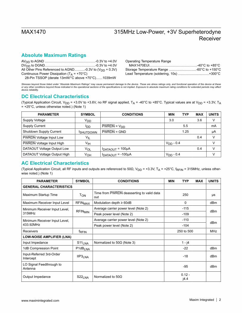
(Typical Application Circuit, VDD = +3.0V to +3.6V, no RF signal applied, TA = -40°C to +85°C. Typical values are at VDD = +3.3V, TA = +25°C, unless otherwise noted.) (Note 1)
(Typical Application Circuit, all RF inputs and outputs are referenced to 50Ω, VDD = +3.3V, TA = +25°C, fRFIN = 315MHz, unless other-wise noted.) (Note 1)
PARAMETER SYMBOL CONDITIONS MIN TYP MAX UNITSSupply Voltage VDD 3.0 3.6 V
Supply Current IDD PWRDN = VDD 5.5 mA
Shutdown Supply Current ISHUTDOWN PWRDN = GND 1.25 µA
PWRDN Voltage Input Low VIL 0.4 V
PWRDN Voltage Input High VIH VDD - 0.4 V
DATAOUT Voltage Output Low VOL IDATAOUT = 100µA 0.4 V
DATAOUT Voltage Output High VOH IDATAOUT = -100µA VDD - 0.4 V
PARAMETER SYMBOL CONDITIONS MIN TYP MAX UNITSGENERAL CHARACTERISTICS
Maximum Startup Time TONTime from PWRDN deasserting to valid data out
250 µs
Maximum Receiver Input Level RFINMAX Modulation depth ≥ 60dB 0 dBm
Minimum Receiver Input Level, 315MHz RFINMIN
Average carrier power level (Note 2) -115dBm
Peak power level (Note 2) -109
Minimum Receiver Input Level, 433.92MHz
Average carrier power level (Note 2) -110dBm
Peak power level (Note 2) -104
Receivers fRFIN 250 to 500 MHz
LOW-NOISE AMPLIFIER (LNA)Input Impedance S11LNA Normalized to 50Ω (Note 3) 1 - j4
1dB Compression Point P1dBLNA -22 dBm
Input-Referred 3rd-Order Intercept IIP3LNA -18 dBm
LO Signal Feedthrough to Antenna -95 dBm
Output Impedance S22LNA Normalized to 50Ω 0.12 - j4.4
MAX1470 315MHz Low-Power, +3V Superheterodyne Receiver
www.maximintegrated.com Maxim Integrated 2
Absolute Maximum Ratings
Stresses beyond those listed under “Absolute Maximum Ratings” may cause permanent damage to the device. These are stress ratings only, and functional operation of the device at these or any other conditions beyond those indicated in the operational sections of the specifications is not implied. Exposure to absolute maximum rating conditions for extended periods may affect device reliability.
DC Electrical Characteristics
AC Electrical Characteristics
(Typical Application Circuit, all RF inputs and outputs are referenced to 50Ω, VDD = +3.3V, TA = +25°C, fRFIN = 315MHz, unless other-wise noted.) (Note 1)
Note 1: Parts are production tested at TA = +25°C; Min and Max values are guaranteed by design and characterization.Note 2: BER = 2E-3, Manchester encoded, data rate = 4kbps, IF bandwidth = 350kHz.Note 3: Input impedance is measured at the LNAIN pin. Note that the impedance includes the 15nH inductive degeneration
connected from the LNASRC.Note 4: Guaranteed by production test.
PARAMETER SYMBOL CONDITIONS MIN TYP MAX UNITSNoise Figure NFLNA 2.0 dB
Power Gain 16 dB
MIXERInput Impedance S11MIX Normalized to 50Ω 0.25 - j2.4
Input-Referred 3rd-Order Intercept IIP3MIX -18 dBm
Output Impedance ZOUT_MIX 330 Ω
Image RejectionfRFIN = 315MHz, fRF_IMAGE = 293.6MHz (Note 4) 40 53
dBfRFIN = 433.92MHz, fRF_IMAGE = 412.52MHz 39
Noise Figure NFMIX 16 dB
Conversion Gain 330Ω IF filter load 13 dB
INTERMEDIATE-FREQUENCY DEMODULATOR BLOCKInput Impedance ZIN_IF 330 Ω
Operating Frequency fIF 10.7 MHz
RSSI Linearity ±1 dB
RSSI Dynamic Range 65 dB
RSSI LevelPRFIN < -120dBm 1.2
VPRFIN > -50dBm 2.0
DATA FILTERMaximum Bandwidth BWDF 100 kHz
DATA SLICERComparator Bandwidth BWCMP 100 kHz
Maximum Load Capacitance CLOAD 10 pF
CRYSTAL OSCILLATORReference Frequency fREF 4.7547 MHz
MAX1470 315MHz Low-Power, +3V Superheterodyne Receiver
www.maximintegrated.com Maxim Integrated 3
AC Electrical Characteristics (continued)
(VDD = +3.3V, TA = +25°C, unless otherwise noted. Typical Application Circuit.)
10
0.1-120 -116 -114
1
AVERAGE RF INPUT POWER (dBm)
BIT-
ERRO
R RA
TE (%
)
-118
BIT-ERROR RATE vs. AVERAGERF INPUT POWER
MAX1
470 t
oc02
1.0
1.4
1.2
1.8
1.6
2.0
2.2
-140 -80 -60-120 -100 -40 -20
RSSI vs. AVERAGE RF INPUT POWER
MAX
1470
toc0
3
AVERAGE RF INPUT POWER (dBm)
RSSI
(V)
IF BANDWIDTH = 350kHz
-116.0
-116.5
-117.0
-117.5
-118.0-40 20-20 0 40 60 80
RECEIVER SENSITIVITYvs. TEMPERATURE
MAX
1470
toc0
4
TEMPERATURE (°C)
RECE
IVER
SEN
SITI
VITY
(dBm
)
AVERAGE RF INPUT POWER1% BERIF BANDWIDTH = 350kHz
45
50
55
60IMAGE REJECTION vs. TEMPERATURE
MAX
1470
toc0
5
TEMPERATURE (°C)
IMAG
E RE
JECT
ION
(dB)
-40 20 40-20 0 60 80-10
10
0
30
20
50
40
60SYSTEM GAIN vs. IF FREQUENCY
MAX
1470
toc0
6
IF FREQUENCY (MHz)
SYST
EM G
AIN
(dB)
0 10 20 30 40
FROM RFIN TO MIXOUTfLO = 304.3MHz
UPPER SIDEBAND
LOWER SIDEBAND
53dB IMAGEREJECTION
30
25
20
15
10250 325275 300 350 375
LNA GAIN vs. RF FREQUENCY
MAX
1470
toc0
7
RF FREQUENCY (MHz)
LNA
GAIN
(dB)
LC TANKFILTER TUNEDTO 315MHz
4.7
5.1
4.9
5.5
5.3
5.9
5.7
6.1
2.7 3.12.9 3.3 3.5
SUPPLY CURRENT vs.SUPPLY VOLTAGE
MAX
1470
toc0
1
SUPPLY VOLTAGE (V)
SUPP
LY C
URRE
NT (m
A) TA = +85°C
TA = +25°C
TA = -40°C
4.2
5.2
4.7
6.2
5.7
6.7
7.2
150 300 350200 250 400 450 500
SUPPLY CURRENT vs. LO FREQUENCY
MAX
1470
toc0
8
LO FREQUENCY (MHz)
SUPP
LY C
URRE
NT (m
A)
0
20
10
40
30
60
50
70
1 10 100
INPUT IMPEDANCE vs.INDUCTIVE DEGENERATION
MAX1470 toc09
INDUCTIVE DEGENERATION (nH)
REAL
IMPE
DANC
E (Ω
)
-350
-250
-300
-150
-200
-50
-100
0IM
AGIN
ARY
IMPE
DANC
E (Ω
)
REAL IMPEDANCE
IMAGINARY IMPEDANCE
Maxim Integrated 4www.maximintegrated.com
MAX1470 315MHz Low-Power, +3V Superheterodyne Receiver
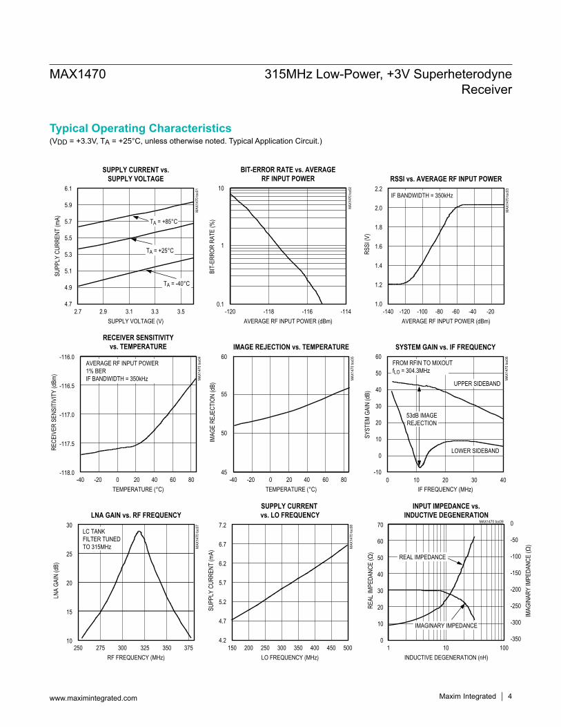
Typical Operating Characteristics
(VDD = +3.3V, TA = +25°C, unless otherwise noted. Typical Application Circuit.)
-20
-15
-5
-10
0
5
NORMALIZED IF GAINvs. IF FREQUENCY
MAX
1470
toc1
0
IF FREQUENCY (MHz)
NORM
ALIZ
ED IF
GAI
N (d
B)
1 10 100
3dB BANDWIDTH = 11.7MHz
20
30
40
50
60
IMAGE REJECTION vs. RF FREQUENCY
MAX
1470
toc1
1
RF FREQUENCY (MHz)IM
AGE
REJE
CTIO
N (d
B)150 300 350200 250 400 450 500
S11 MAGNITUDE-LOG PLOT OF RFINMAX1470 toc12
1GHz50MHz
10dB/div
0dB
315MHz,-29.5dB
S11 SMITH PLOT OF RFIN
MAX
1470
toc1
3
315MHz
50MHz
1GHz
Maxim Integrated 5www.maximintegrated.com
MAX1470 315MHz Low-Power, +3V Superheterodyne Receiver
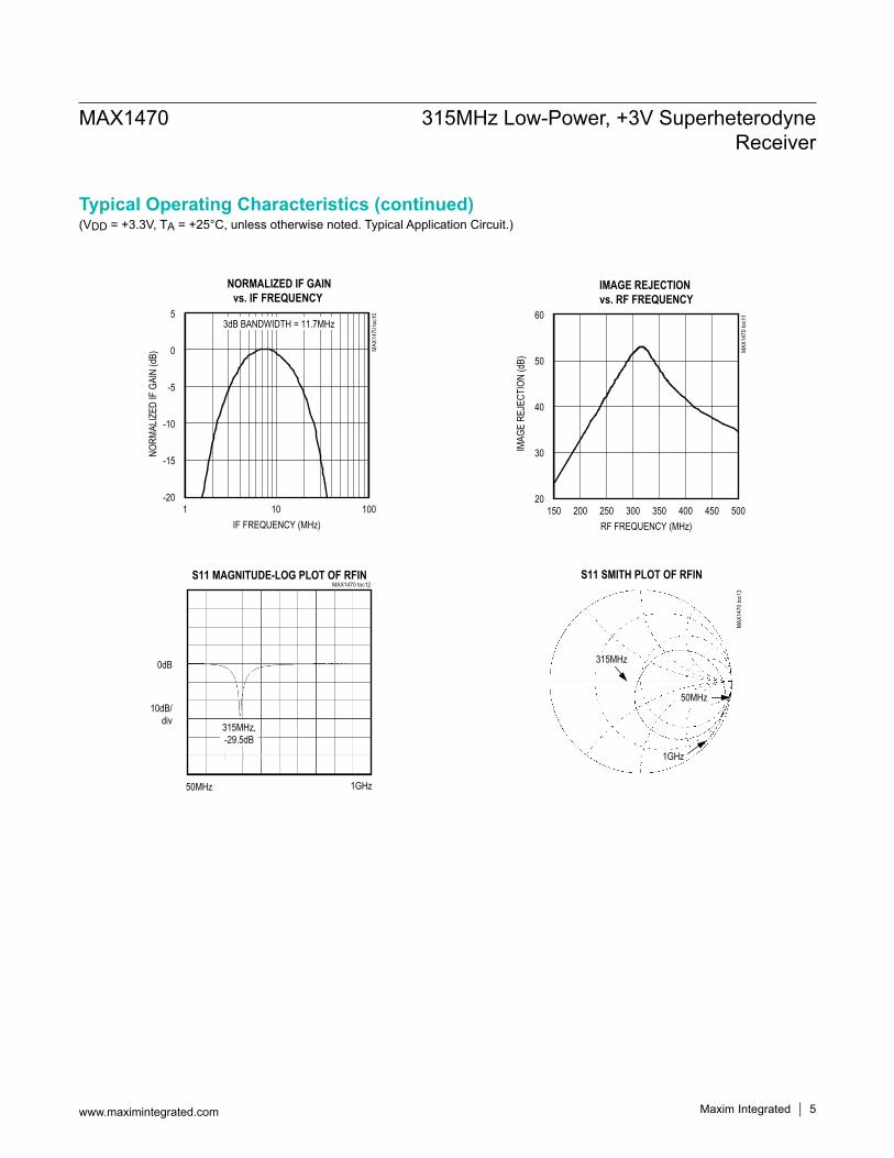
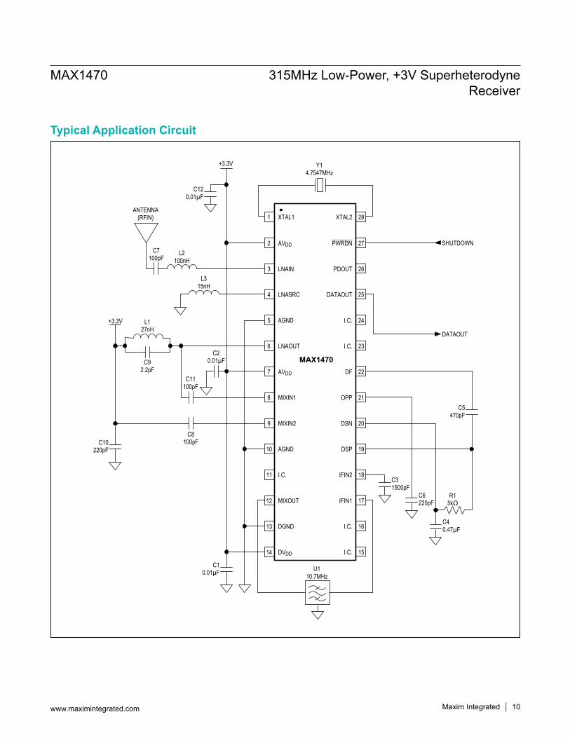
Typical Operating Characteristics (continued)
Detailed DescriptionThe MAX1470 CMOS superheterodyne receiver and a few external components provide the complete receive chain from the antenna to the digital output data. Depending on signal power and component selection, data rates as high as 100kbps can be achieved.The MAX1470 is designed to receive binary ASK data on a 315MHz carrier. ASK modulation uses a difference in amplitude of the carrier to represent logic 0 and logic 1 data.
Low-Noise AmplifierThe LNA is a cascode amplifier with off-chip inductive degeneration that achieves approximately 16dB of power gain with a 2.0dB noise figure and an IIP3 of -18dBm. The gain and noise figure is dependent on both the antenna
matching network at the LNA input, and the LC tank net-work between the LNA output and the mixer inputs.The off-chip inductive degeneration is achieved by con-necting an inductor from LNASRC to AGND. This inductor sets the real part of the input impedance at LNAIN, allow-ing for a more flexible match for low-input impedance such as a PC board trace antenna. A nominal value for this inductor with a 50Ω input impedance is 15nH, but is affected by PC board trace. See Typical Operating Characteristics for the relationship between the induc-tance and input impedance.The LC tank filter connected to LNAOUT comprises L1 and C9 (see Typical Applications Circuit). L1 and C9 val-ues are selected to resonate at the RF input frequency of 315MHz. The resonant frequency is given by:
PIN NAME FUNCTION
1 XTAL1 1st Crystal Input
2, 7 AVDD Positive Analog Supply Voltage for RF Sections. Decouple to AGND with 0.01µF capacitors.
3 LNAIN Low-Noise Amplifier Input
4 LNASRC Low-Noise Amplifier Source. Connect inductor to ground to set LNA input impedance (see Low-Noise Amplifier section).
5, 10 AGND Analog Ground
6 LNAOUT Low-Noise Amplifier Output
8 MIXIN1 1st Differential Mixer Input. Must be AC-coupled to driving input.
9 MIXIN2 2nd Differential Mixer Input. Must be AC-coupled to driving input.
11, 15, 16, 23, 24 I.C. Internally Connected. Do not make connection to these pins.
12 MIXOUT 330Ω Mixer Output
13 DGND Digital Ground
14 DVDD Positive Digital Supply Voltage. Decouple to DGND with a 0.01µF capacitor.
17 IFIN1 1st Differential Intermediate Frequency Limiter Amplifier Input
18 IFIN2 2nd Differential Intermediate Frequency Limiter Amplifier Input
19 DSP Positive Data Slicer Input
20 DSN Negative Data Slicer Input
21 OPP Noninverting Op Amp. Input for the Sallen-Key data filter.
22 DF Data Filter Feedback Node. Input for the feedback of the Sallen-Key data filter.
25 DATAOUT Digital Baseband Data Output
26 PDOUT Peak Detector Output
27 PWRDN Power-Down Select Input. Drive this pin with a logic low to shut down the IC.
28 XTAL2 2nd Crystal Input
MAX1470 315MHz Low-Power, +3V Superheterodyne Receiver
www.maximintegrated.com Maxim Integrated 6
Pin Description
TOTAL TOTAL
12 L C
ƒ =π ×
where:
TOTAL PARASITICS
TOTAL PARASITICS
L L1 LC C9 C
= +
= +
LPARASITICS and CPARASITICS include inductance and capacitance of the PC board traces, package pins, mixer input impedance, LNA output impedance, etc. These parasitics at high frequencies cannot be ignored and can have a dramatic effect on the tank filter center frequency. Lab experimentation should be done to optimize the cen-ter frequency of the tank.
MixerA unique feature of the MAX1470 is the integrated image rejection of the mixer. This device was designed to elimi-nate the need for a costly front-end SAW filter for many applications. The advantage of not using a SAW filter is increased sensitivity, simplified antenna matching, less board space, and lower cost.The mixer cell is a pair of double-balanced mixers that perform an IQ downconversion of the 315MHz RF input to the 10.7MHz IF with low-side injection (i.e., fLO = fRF - fIF). The image rejection circuit then combines these signals to achieve ~50dB of image rejection over the full temperature range. Low-side injection is required due to the on-chip image-rejection architecture. The IF output is driven by a source-follower, biased to create a driving impedance of 330Ω to interface with an off-chip 330Ω ceramic IF filter. The voltage conversion gain driving a 330Ω load is approximately 13dB.
Phase-Lock LoopThe PLL block contains a phase detector, charge pump/integrated loop filter, VCO, asynchronous 64x clock divider, and crystal oscillator. This PLL does not require any external components. The quadrature VCO is cen-tered at the nominal LO frequency of 304.3MHz. For an input RF frequency of 315MHz, a reference frequency of 4.7547MHz is needed for a 10.7MHz IF frequency (low-side injection is required). The relationship between the RF, IF, and reference frequencies is given by:
( )REF RF IFf f f / 64= −
To allow the smallest possible IF bandwidth (for best sen-sitivity), the tolerance of the reference must be minimized.
Intermediate FrequencyThe IF section presents a differential 330Ω load to pro-vide matching for the off-chip ceramic filter. The internal five AC-coupled limiting amplifiers produce an overall gain of approximately 65dB, with a bandpass-filter-type response centered near the 10.7MHz IF frequency with a 3dB bandwidth of approximately 11.5MHz. The RSSI circuit demodulates the IF to baseband by producing a DC output proportional to the log of the IF signal level with a slope of approximately 15mV/dB (see Typical Operating Characteristics).
Applications InformationCrystal OscillatorThe XTAL oscillator in the MAX1470 is designed to pres-ent a capacitance of approximately 3pF between XTAL1 and XTAL2. If a crystal designed to oscillate with a differ-ent load capacitance is used, the crystal is pulled away from its stated operating frequency, introducing an error in the reference frequency. Crystals designed to operate with higher differential load capacitance always pull the reference frequency higher. For example, a 4.7547MHz crystal designed to operate with a 10pF load capacitance oscillates at 4.7563MHz with the MAX1470, causing the receiver to be tuned to 315.1MHz rather than 315.0MHz, an error of about 100kHz, or 320ppm.In actuality, the oscillator pulls every crystal. The crystal’s natural frequency is really below its specified frequency, but when loaded with the specified load capacitance, the crystal is pulled and oscillates at its specified frequency. This pulling is already accounted for in the specification of the load capacitance. Additional pulling can be calculated if the electrical parameters of the crystal are known. The frequency pulling is given by:
6mp
case load case spec
C 1 1 102 C C C C
ƒ = − × + +
where:fp is the amount the crystal frequency is pulled in ppm.Cm is the motional capacitance of the crystal.Ccase is the case capacitance.Cspec is the specified load capacitance.Cload is the actual load capacitance.
MAX1470 315MHz Low-Power, +3V Superheterodyne Receiver
www.maximintegrated.com Maxim Integrated 7
When the crystal is loaded as specified, i.e., Cload = Cspec, the frequency pulling equals zero.
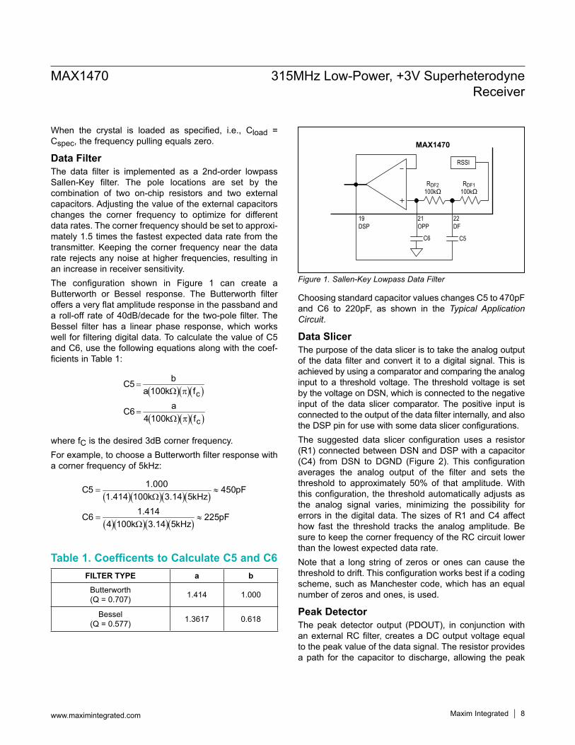
Data FilterThe data filter is implemented as a 2nd-order lowpass Sallen-Key filter. The pole locations are set by the combination of two on-chip resistors and two external capacitors. Adjusting the value of the external capacitors changes the corner frequency to optimize for different data rates. The corner frequency should be set to approxi-mately 1.5 times the fastest expected data rate from the transmitter. Keeping the corner frequency near the data rate rejects any noise at higher frequencies, resulting in an increase in receiver sensitivity.The configuration shown in Figure 1 can create a Butterworth or Bessel response. The Butterworth filter offers a very flat amplitude response in the passband and a roll-off rate of 40dB/decade for the two-pole filter. The Bessel filter has a linear phase response, which works well for filtering digital data. To calculate the value of C5 and C6, use the following equations along with the coef-ficients in Table 1:
( )( )( )
( )( )( )
c
c
bC5a 100k f
aC64 100k f
=Ω π
=Ω π
where fC is the desired 3dB corner frequency.For example, to choose a Butterworth filter response with a corner frequency of 5kHz:
( )( )( )( )
( )( )( )( )
1.000C5 450pF1.414 100k 3.14 5kHz
1.414C6 225pF4 100k 3.14 5kHz
= ≈Ω
= ≈Ω
Choosing standard capacitor values changes C5 to 470pF and C6 to 220pF, as shown in the Typical Application Circuit.
Data SlicerThe purpose of the data slicer is to take the analog output of the data filter and convert it to a digital signal. This is achieved by using a comparator and comparing the analog input to a threshold voltage. The threshold voltage is set by the voltage on DSN, which is connected to the negative input of the data slicer comparator. The positive input is connected to the output of the data filter internally, and also the DSP pin for use with some data slicer configurations.The suggested data slicer configuration uses a resistor (R1) connected between DSN and DSP with a capacitor (C4) from DSN to DGND (Figure 2). This configuration averages the analog output of the filter and sets the threshold to approximately 50% of that amplitude. With this configuration, the threshold automatically adjusts as the analog signal varies, minimizing the possibility for errors in the digital data. The sizes of R1 and C4 affect how fast the threshold tracks the analog amplitude. Be sure to keep the corner frequency of the RC circuit lower than the lowest expected data rate.Note that a long string of zeros or ones can cause the threshold to drift. This configuration works best if a coding scheme, such as Manchester code, which has an equal number of zeros and ones, is used.
Peak DetectorThe peak detector output (PDOUT), in conjunction with an external RC filter, creates a DC output voltage equal to the peak value of the data signal. The resistor provides a path for the capacitor to discharge, allowing the peak
Figure 1. Sallen-Key Lowpass Data Filter
Table 1. Coefficents to Calculate C5 and C6FILTER TYPE a b
Butterworth(Q = 0.707) 1.414 1.000
Bessel(Q = 0.577) 1.3617 0.618
19DSP
C6 C5
RDF2100kΩ
RDF1100kΩ
RSSI
21OPP
22DF
MAX1470
MAX1470 315MHz Low-Power, +3V Superheterodyne Receiver
www.maximintegrated.com Maxim Integrated 8
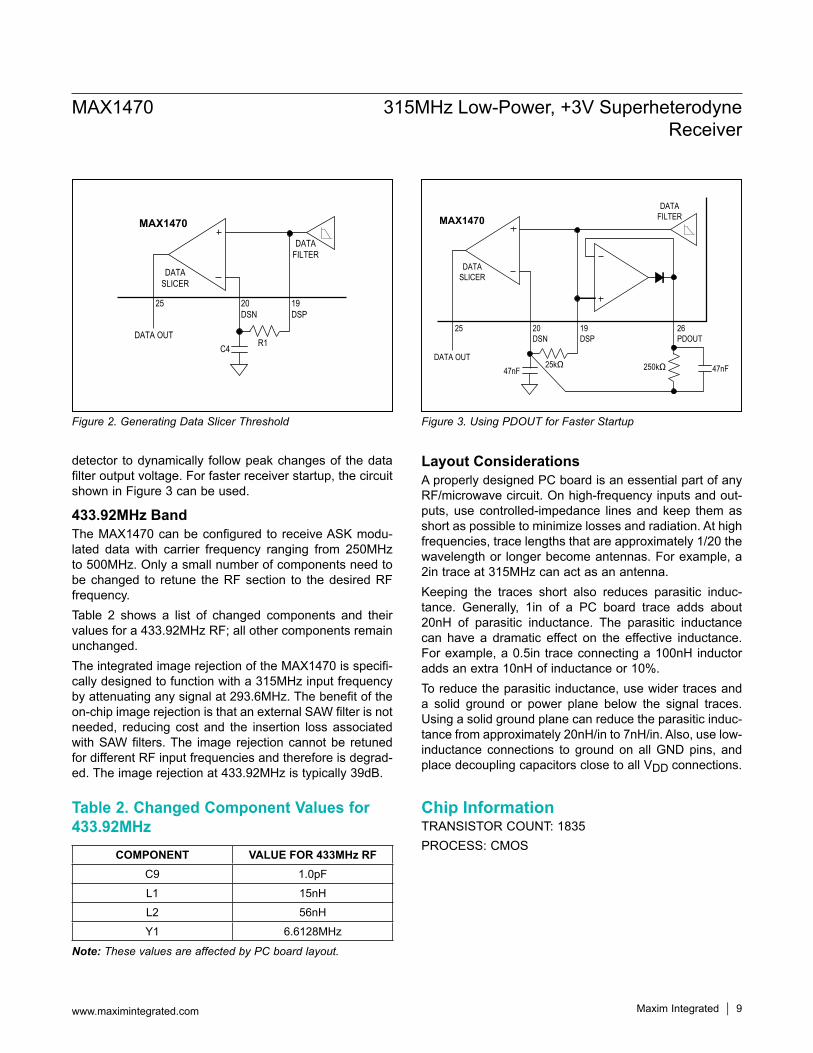
detector to dynamically follow peak changes of the data filter output voltage. For faster receiver startup, the circuit shown in Figure 3 can be used.
433.92MHz BandThe MAX1470 can be configured to receive ASK modu-lated data with carrier frequency ranging from 250MHz to 500MHz. Only a small number of components need to be changed to retune the RF section to the desired RF frequency.Table 2 shows a list of changed components and their values for a 433.92MHz RF; all other components remain unchanged.The integrated image rejection of the MAX1470 is specifi-cally designed to function with a 315MHz input frequency by attenuating any signal at 293.6MHz. The benefit of the on-chip image rejection is that an external SAW filter is not needed, reducing cost and the insertion loss associated with SAW filters. The image rejection cannot be retuned for different RF input frequencies and therefore is degrad-ed. The image rejection at 433.92MHz is typically 39dB.
Layout ConsiderationsA properly designed PC board is an essential part of any RF/microwave circuit. On high-frequency inputs and out-puts, use controlled-impedance lines and keep them as short as possible to minimize losses and radiation. At high frequencies, trace lengths that are approximately 1/20 the wavelength or longer become antennas. For example, a 2in trace at 315MHz can act as an antenna.Keeping the traces short also reduces parasitic induc-tance. Generally, 1in of a PC board trace adds about 20nH of parasitic inductance. The parasitic inductance can have a dramatic effect on the effective inductance. For example, a 0.5in trace connecting a 100nH inductor adds an extra 10nH of inductance or 10%.To reduce the parasitic inductance, use wider traces and a solid ground or power plane below the signal traces. Using a solid ground plane can reduce the parasitic induc-tance from approximately 20nH/in to 7nH/in. Also, use low-inductance connections to ground on all GND pins, and place decoupling capacitors close to all VDD connections.
Figure 2. Generating Data Slicer Threshold Figure 3. Using PDOUT for Faster Startup
Table 2. Changed Component Values for 433.92MHz
Note: These values are affected by PC board layout.
COMPONENT VALUE FOR 433MHz RFC9 1.0pF
L1 15nH
L2 56nH
Y1 6.6128MHz
25
C4 R1
20DSN
19DSP
MAX1470
DATA OUT
DATASLICER
DATAFILTER
25
47nF25kΩ
20DSN
19DSP
MAX1470
DATA OUT
DATASLICER
DATAFILTER
26PDOUT
250kΩ 47nF
MAX1470 315MHz Low-Power, +3V Superheterodyne Receiver
www.maximintegrated.com Maxim Integrated 9
Chip InformationTRANSISTOR COUNT: 1835PROCESS: CMOS
28
27
26
25
24
23
22
21
20
19
18
17
16
15
1
2
3
4
5
6
7
8
9
10
11
12
13
14
XTAL2
PWRDN
PDOUT
DATAOUT
I.C.
I.C.
I.C.
DF
OPP
DSN
DSP
IFIN2
IFIN1
I.C.
DVDD
DGND
MIXOUT
I.C.
AGND
MIXIN2
MIXIN1
AVDD
LNAOUT
AGND
LNASRC
LNAIN
AVDD
XTAL1
MAX1470
U110.7MHz
Y14.7547MHz
+3.3V
C120.01µF
C10.01µF
C31500pF
C6220pF
C40.47µF
C20.01µF
C11100pF
C8100pF
C92.2pF
L127nH
+3.3V
C10220pF
L315nH
L2100nH
C7100pF
ANTENNA(RFIN)
C5470pF
R15kΩ
DATAOUT
SHUTDOWN
MAX1470 315MHz Low-Power, +3V Superheterodyne Receiver
www.maximintegrated.com Maxim Integrated 10
Typical Application Circuit
28
27
26
25
24
23
22
21
20
19
18
17
16
15
1
2
3
4
5
6
7
8
9
10
11
12
13
14
XTAL2
PWRDN
PDOUT
DATAOUT
I.C.
I.C.
I.C.
DF
OPP
DSN
DSP
IFIN2
IFIN1
I.C.
DVDD
DGND
MIXOUT
I.C.
AGND
MIXIN2
MIXIN1
AVDD
LNAOUT
AGND
LNASRC
LNAIN
AVDD
XTAL1
TSSOP
TOP VIEW
MAX1470
MAX1470 315MHz Low-Power, +3V Superheterodyne Receiver
www.maximintegrated.com Maxim Integrated 11
Pin Configuration
Package InformationFor the latest package outline information and land patterns (footprints), go to www.maximintegrated.com/packages. Note that a “+”, “#”, or “-” in the package code indicates RoHS status only. Package drawings may show a different suffix character, but the drawing pertains to the package regardless of RoHS status.
PACKAGE TYPE
PACKAGE CODE
OUTLINE NO.
LAND PATTERN NO.
28 TSSOP U28+1 21-0066 —
Maxim Integrated cannot assume responsibility for use of any circuitry other than circuitry entirely embodied in a Maxim Integrated product. No circuit patent licenses are implied. Maxim Integrated reserves the right to change the circuitry and specifications without notice at any time. The parametric values (min and max limits) shown in the Electrical Characteristics table are guaranteed. Other parametric values quoted in this data sheet are provided for guidance.
Maxim Integrated and the Maxim Integrated logo are trademarks of Maxim Integrated Products, Inc. © 2014 Maxim Integrated Products, Inc. 12
MAX1470 315MHz Low-Power, +3V Superheterodyne Receiver
REVISIONNUMBER
REVISIONDATE DESCRIPTION PAGES
CHANGED
0 8/01 Initial release —
1 9/14 Removed automotive reference from page 1 1
Revision History
For pricing, delivery, and ordering information, please contact Maxim Direct at 1-888-629-4642, or visit Maxim Integrated’s website at www.maximintegrated.com.


![INDEX [] Wireless/30s... · GENERAL INDEX PAGE ... Radiotecnica, E. Montù Superheterodyne Receiver, Alfred T. Wells Television Reception, Manfred von Ardenne](https://img.pdfslide.us/doc/110x75/5b15eff07f8b9a472e8c0603/index-wireless30s-general-index-page-radiotecnica-e-montu-superheterodyne.jpg)