Embed Size (px)
Citation preview
System Level Solutions, Inc. (USA) 14100 Murphy AvenueSan Martin, CA 95046 (408) 852 - 0067
http://www.slscorp.com
MAX II/MAX IIZ Development Board
Reference Manual
Board Version: r2aDocument Version: 1.4
Document Date: September 2010
ii System Level SolutionsSeptember 2010MAX II/MAX IIZ Development Board Reference Manual
Copyright ©2009, System Level Solutions, Inc. (SLS) All rights reserved. SLS, an Embedded systems company, the styl-ized SLS logo, specific device designations, and all other words and logos that are identified as trademarks and/or service marks are, unless noted otherwise, the trademarks and service marks of SLS in India and other countries. All other prod-ucts or service names are the property of their respective holders. SLS products are protected under numerous U.S. and foreign patents and pending applications, mask working rights, and copyrights. SLS reserves the right to make changes to any products and services at any time without notice. SLS assumes no responsibility or liability arising out of the application or use of any information, products, or service described herein except as expressly agreed to in writing by SLS. SLS cus-tomers are advised to obtain the latest version of specifications before relying on any published information and before orders for products or services.
rm_dbmaxiiz_1.4
About this Manual
Introduction This manual provides component details about the MAX II/MAX IIZ development board.
Table below shows the revision history of the reference manual.
How to find Information
• The Adobe Acrobat Find feature allows you to search the contents of a PDF file. Use Ctrl + F to open the Find dialog box. Use Ctrl + N to open to the Go To Page dialog box.
• Bookmarks serve as an additional table of contents.• Thumbnail icons, which provide miniature preview of each page,
provides a link to the pages.• Numerous links shown in Navy Blue colour allow you to jump to related
information.
How to Contact SLS
For the most up-to-date information about SLS products, go to the SLS worldwide website at http://www.slscorp.com. For additional information about SLS products, consult the source shown below.
Version Date Description1.4 September Modified document as per the board version
r2a• Added information for GPIO Supply Select
Jumper (J13 & J14) in Chapter 2
1.3 July 2010 Add table footnote in Table 2-7 and Table 2-8
1.2 April 2010 Remove EPM570Z from document
1.1 September 2009 Modified document as per the board version r1b
1.0 July 2009 First Publication of the Reference Manual
Information Type E-mailProduct literature services, SLS literature ser-vices, Non-technical customer services, Tech-nical support.
iiiMAX II/MAX IIZ Development Board Reference Manual
System Level SolutionsSeptember 2010
Typographic Conventions
Typographic Conventions
The MAX II/MAX IIZ development board reference manual uses the typographic conventions as shown below:
Visual Cue MeaningBold Type with Initial Capital let-ters
All headings and Sub headings Titles in a document are displayed in bold type with initial capital letters; Example: General Description, Block Diagram
Bold Type with Italic Letters All Definitions, Figure and Table Headings are displayed in Italics. Examples: Figure 1-1. MAX II/ MAX IIZ Development Board Top View, Table 1-1. Peripheral difference between EPM240/EPM240z and EPM570 versions of MAX II/MAX IIZ Development Board.
1., 2. Numbered steps are used in a list of items, when the sequence of items is important. such as steps listed in procedure.
• Bullets are used in a list of items when the sequence of items is not important.
The hand points to special information that requires special attention
The caution indicates required information that needs special consider-ation and understanding and should be read prior to starting or continu-ing with the procedure or process.
The warning indicates information that should be read prior to starting or continuing the procedure or processes.
The feet direct you to more information on a particular topic.
iv System Level SolutionsSeptember 2010MAX II/MAX IIZ Development Board Reference Manual
Contents
About this Manual.............................................................................................................. iiiIntroduction..............................................................................................................................................iiiHow to find Information ..........................................................................................................................iiiHow to Contact SLS ................................................................................................................................iiiTypographic Conventions ........................................................................................................................ iv
1. Introduction ............................................................................................................................... 1General Description .................................................................................................................................. 1Features ..................................................................................................................................................... 1Board Components and Block Diagram ................................................................................................... 2
Board Components ............................................................................................................................ 2Block Diagram................................................................................................................................... 3
2. Board Components................................................................................................................... 5Featured Device ........................................................................................................................................ 7
MAX II/MAX IIZ CPLD (U1) .......................................................................................................... 7Memory Component ................................................................................................................................. 8
SPI Serial Flash Memory (U3) .......................................................................................................... 8User Interfaces .......................................................................................................................................... 9
Push Button Switches (SW3, SW4)................................................................................................... 9Capsense Touch Buttons (CSB1, CSB2) ........................................................................................... 9JTAG Connector (J1)....................................................................................................................... 10
Expansion Connector .............................................................................................................................. 10General Purpose I/O Connector (J5, J6) .......................................................................................... 10
Jumpers and Headers .............................................................................................................................. 15Power Supply Select Jumper (J3) .................................................................................................... 15Battery Supply Header (J4).............................................................................................................. 15Motor Driving Header (J7 & J8)...................................................................................................... 16Speaker Header (J9)......................................................................................................................... 16Motor & Speaker Supply Jumper Settings (J10, J11 & J12) ........................................................... 17
vSystem Level SolutionsSeptember 2010 MAX II/MAX IIZ Development Board Reference Manual
GPIO Supply Select Jumper (J13 & J14) ........................................................................................ 17Status LEDs and Reset/Power Switches ................................................................................................. 18
Power Supply and Reset Indication LEDs (LED1 & LED2) .......................................................... 18User Defined Reset Push Buttons Switch (SW1) ............................................................................ 18Power Switch (SW2) ....................................................................................................................... 18
Clock ....................................................................................................................................................... 19Oscillator (Y1) ................................................................................................................................. 19
Power Supply Circuitary ......................................................................................................................... 19DC Power Supply Input Jack (J2).................................................................................................... 19Power Regulator (U5 & U6) ............................................................................................................ 19
vi System Level SolutionsSeptember 2010MAX II/MAX IIZ Development Board Reference Manual
1. Introduction
General Description
The MAX II/MAX IIZ Development board provides a hardware platform for designing and developing simple and low-end systems based on Altera MAX II/MAX IIZ Devices. The board features a MAX II/MAX IIZ EPM240T100Cx/EPM240ZM100Cx device with 240 Logic Elements (LEs) and 8,192 bits of User Flash Memory (UFM). The board also supports vertical migration with the EPM570T100Cx device with 570 Logic Elements (LEs) and 8,192 bits of User Flash Memory (UFM) for larger design support.
The board is pre programmed with the MAX IIZ Board Diagnostic System to verify the board’s functionality. The programming files for the MAX IIZ Board Diagnostic System are also supplied with the board to verify the board’s functionality at any time later.
Features MAX II/MAX IIZ CPLD64 General Purpose IOsTwo Capsense Buttons and two Push Button SwitchesUser interface headerExternal Battery Interface HeaderOn Board logic for MAX II/MAX IIZ configuration (Quartus II Compatible)On Board Power SupplyOn Board Global System Reset circuitryMigration support from EPM240T100Cx to EPM240ZM100Cx and EPM240T100Cx to EPM570T100Cx devices for higher density support for larger designs
The MAX II/MAX IIZ board is manufactured and assembled by making use of PB-free processes and hence it is designated as an ECO friendly board.
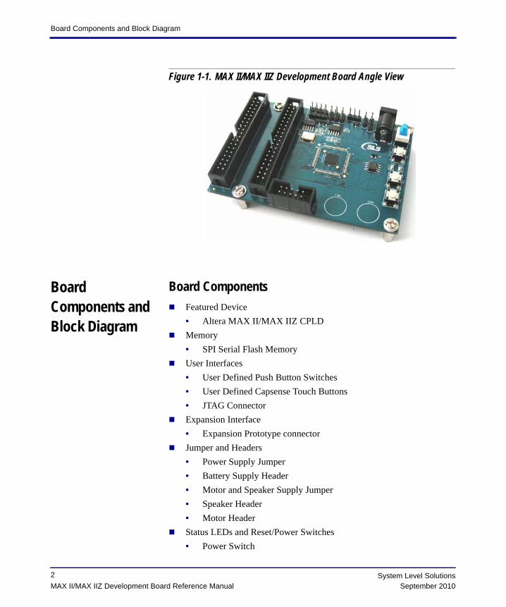
Figure 1-1. shows the angle view of MAX II/MAX IIZ Development board.
1MAX II/MAX IIZ Development Board Reference Manual
System Level SolutionsSeptember 2010
Board Components and Block Diagram
Figure 1-1. MAX II/MAX IIZ Development Board Angle View
Board Components and Block Diagram
Board ComponentsFeatured Device• Altera MAX II/MAX IIZ CPLDMemory• SPI Serial Flash MemoryUser Interfaces• User Defined Push Button Switches• User Defined Capsense Touch Buttons• JTAG ConnectorExpansion Interface• Expansion Prototype connectorJumper and Headers• Power Supply Jumper• Battery Supply Header• Motor and Speaker Supply Jumper• Speaker Header• Motor HeaderStatus LEDs and Reset/Power Switches• Power Switch
2 System Level SolutionsSeptember 2010MAX II/MAX IIZ Development Board Reference Manual
• Reset Push Buttons Switch• Reset and +3.3v Power LED• Clock OscillatorPower Supply• DC Power Jack• Power Regulator
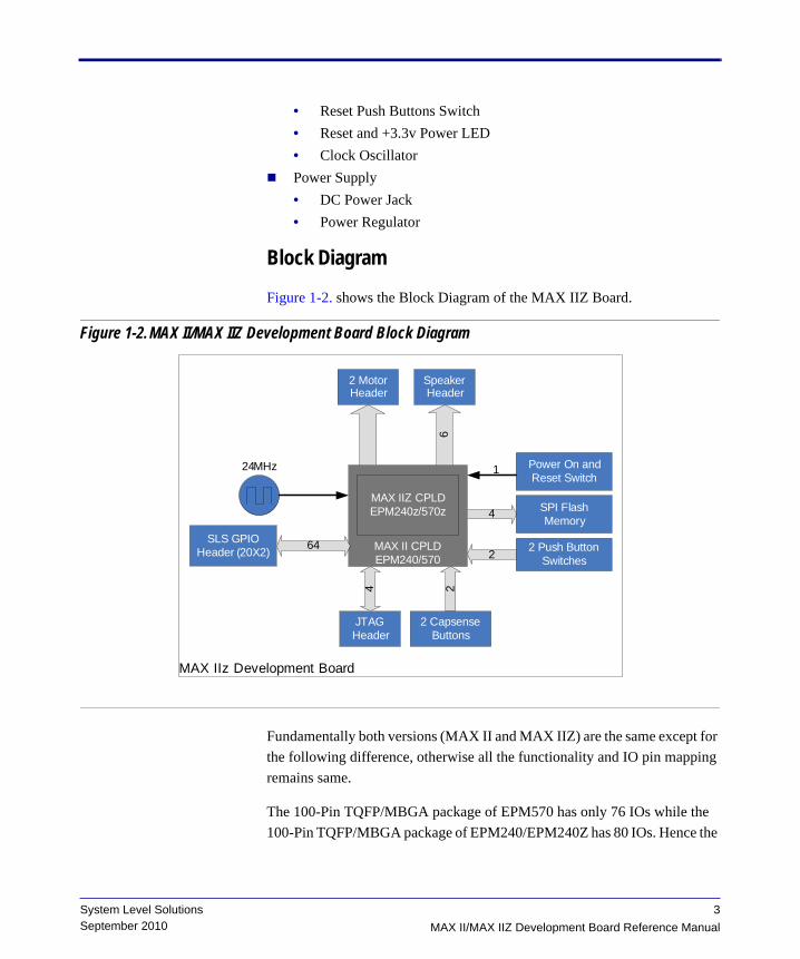
Block Diagram
Figure 1-2. shows the Block Diagram of the MAX IIZ Board.
Figure 1-2. MAX II/MAX IIZ Development Board Block Diagram
Fundamentally both versions (MAX II and MAX IIZ) are the same except for the following difference, otherwise all the functionality and IO pin mapping remains same.
The 100-Pin TQFP/MBGA package of EPM570 has only 76 IOs while the 100-Pin TQFP/MBGA package of EPM240/EPM240Z has 80 IOs. Hence the
MAX IIz Development Board
MAX II CPLDEPM240/570
MAX IIZ CPLDEPM240z/570z
2
2
6
SLS GPIO Header (20X2)
2 Capsense Buttons
2 Push Button Switches
SPI Flash Memory4
JTAG Header
4
64
2 Motor Header
Speaker Header
24MHz Power On and Reset Switch
1
3MAX II/MAX IIZ Development Board Reference Manual
System Level SolutionsSeptember 2010
Board Components and Block Diagram
board with EPM240/EPM240Z has all the features mentioned in this document, where as the board with EPM570 lacks some peripherals.
The peripheral difference between the EPM240/EPM240Z and EPM570 versions of the MAX IIZ board is mentioned in the Table 1-1 below.
All other peripherals and the Pin Mapping of the Peripherals with the MAX II/MAX IIZ device remains same in both the versions.
Table 1-1. Peripheral difference between EPM240/EPM240Z and EPM570 versions of MAXII/MAX IIZ Development Board
Sr. No. Peripheral EPM240/EPM240Z Version
EPM570 Version
1. SLS GPIO 64 60
4 System Level SolutionsSeptember 2010MAX II/MAX IIZ Development Board Reference Manual
2. Board Components
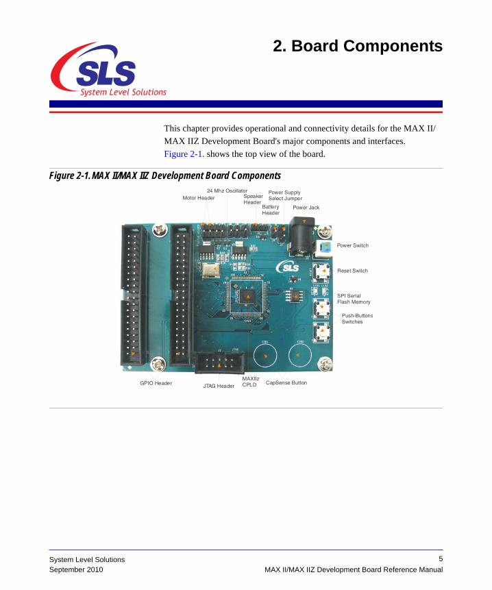
This chapter provides operational and connectivity details for the MAX II/MAX IIZ Development Board's major components and interfaces. Figure 2-1. shows the top view of the board.
Figure 2-1. MAX II/MAX IIZ Development Board Components
SpeakerHeader
24 Mhz OscillatorMotor Header
SPI SerialFlash Memory
CapSense ButtonJTAG HeaderGPIO Header
MAXIIzCPLD
Push-ButtonsSwitches
Power SupplySelect Jumper
BatteryHeader
Power Jack
Reset Switch
Power Switch
5MAX II/MAX IIZ Development Board Reference Manual
System Level SolutionsSeptember 2010
Table 2-1 describes the major components on MAX II/MAX IIZ development board and related interfaces.
Table 2-1. MAX II/MAX IIZ Board Components and Interfaces
Board Reference Name Description Page
Featured Device
U1 Altera MAX II/MAX IIZ CPLD
Altera MAX II (EPM240T100/EPM570T100) or MAX IIZ (EPM240ZM100) CPLD
7
Memory
U3 SPI Serial Flash Memory Atmel Corp. AT25DF041A, 4MBit SPI Serial Flash Memory
8
User Interfaces
SW3, SW4 User Defined Push Button switches
Two user defined momentary contact push but-ton switches
9
CSB1, CSB2 User Defined Capsense Touch Buttons
Two user defined capacitive touch buttons 9
J1 JTAG Connector The Joint Test Action Group (JTAG) connector, used to directly configure MAX II/MAX IIZ CPLD
10
Expansion Interface
J5, J6 Expansion Prototype connector
Two expansion prototype connection of SLS GPIO Header for peripheral expansion or for debugging and prototyping purpose
10
Jumpers and Headers
J3 Power Supply Jumper Jumper that enables power supply input to MAX IIZ board
15
J4 Battery Supply Header Header which used to connect external battery 15
J7, J8 Motor Header Motor Driving Header 16
J9 Speaker Header Speaker Driving Header 16
J10, J11, J12 Motor and Speaker Supply Jumper
Jumper that enables power input for Motor and Speaker
17
J13, J14 GPIO Supply Select Jumper
Jumper that enables power input for GPIO 17
Status LEDs and Reset/Power switches
LED1, LED2 Reset LED, +3.3V Power LED
Indicates when 3.3V Power is present and when reset switch is pressed
18
6 System Level SolutionsSeptember 2010MAX II/MAX IIZ Development Board Reference Manual
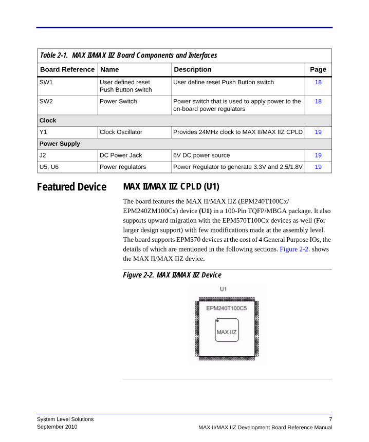
Featured Device MAX II/MAX IIZ CPLD (U1)The board features the MAX II/MAX IIZ (EPM240T100Cx/EPM240ZM100Cx) device (U1) in a 100-Pin TQFP/MBGA package. It also supports upward migration with the EPM570T100Cx devices as well (For larger design support) with few modifications made at the assembly level. The board supports EPM570 devices at the cost of 4 General Purpose IOs, the details of which are mentioned in the following sections. Figure 2-2. shows the MAX II/MAX IIZ device.
Figure 2-2. MAX II/MAX IIZ Device
SW1 User defined reset Push Button switch
User define reset Push Button switch 18
SW2 Power Switch Power switch that is used to apply power to the on-board power regulators
18
Clock
Y1 Clock Oscillator Provides 24MHz clock to MAX II/MAX IIZ CPLD 19
Power Supply
J2 DC Power Jack 6V DC power source 19
U5, U6 Power regulators Power Regulator to generate 3.3V and 2.5/1.8V 19
Table 2-1. MAX II/MAX IIZ Board Components and Interfaces
Board Reference Name Description Page
7MAX II/MAX IIZ Development Board Reference Manual
System Level SolutionsSeptember 2010
Memory Component
Table 2-2 shown below lists the MAX II/MAX IIZ device features.
Note: to Table 2-2:
(1) User IO Pins for the EPM570 Device is for the 100-Pin TQFP package used on the MAX IIZ Board.
The MAX II/MAX IIZ device can be configured directly using an Altera download cable connected to the JTAG Header (J1).
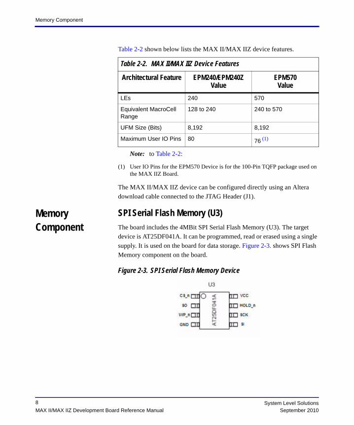
Memory Component
SPI Serial Flash Memory (U3)The board includes the 4MBit SPI Serial Flash Memory (U3). The target device is AT25DF041A. It can be programmed, read or erased using a single supply. It is used on the board for data storage. Figure 2-3. shows SPI Flash Memory component on the board.
Figure 2-3. SPI Serial Flash Memory Device
Table 2-2. MAX II/MAX IIZ Device Features
Architectural Feature EPM240/EPM240Z Value
EPM570 Value
LEs 240 570
Equivalent MacroCell Range
128 to 240 240 to 570
UFM Size (Bits) 8,192 8,192
Maximum User IO Pins 80 76 (1)
8 System Level SolutionsSeptember 2010MAX II/MAX IIZ Development Board Reference Manual
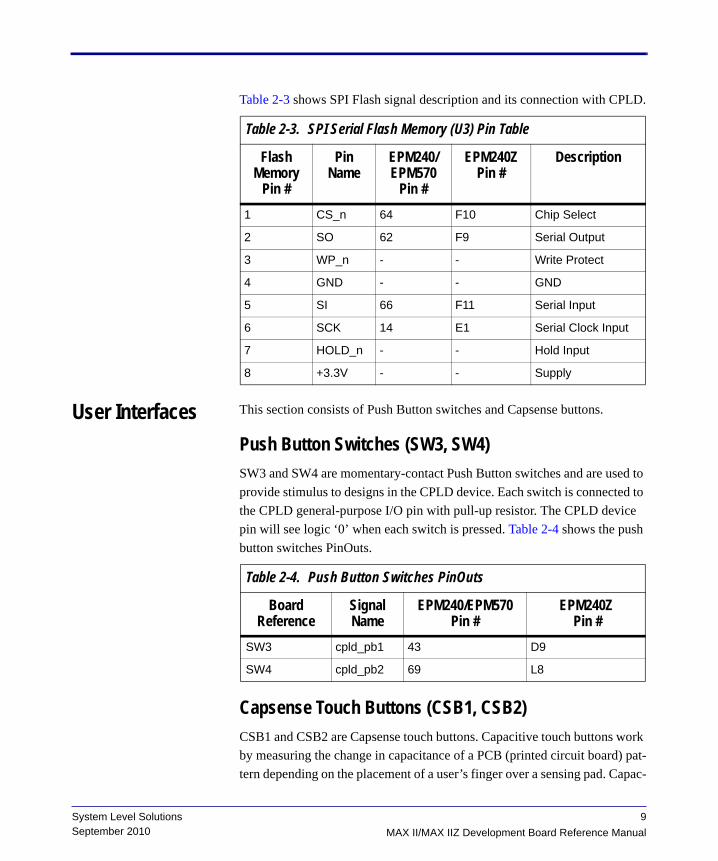
Table 2-3 shows SPI Flash signal description and its connection with CPLD.
User Interfaces This section consists of Push Button switches and Capsense buttons.
Push Button Switches (SW3, SW4)SW3 and SW4 are momentary-contact Push Button switches and are used to provide stimulus to designs in the CPLD device. Each switch is connected to the CPLD general-purpose I/O pin with pull-up resistor. The CPLD device pin will see logic ‘0’ when each switch is pressed. Table 2-4 shows the push button switches PinOuts.
Capsense Touch Buttons (CSB1, CSB2)CSB1 and CSB2 are Capsense touch buttons. Capacitive touch buttons work by measuring the change in capacitance of a PCB (printed circuit board) pat-tern depending on the placement of a user’s finger over a sensing pad. Capac-
Table 2-3. SPI Serial Flash Memory (U3) Pin Table
Flash Memory
Pin #
Pin Name
EPM240/EPM570
Pin #
EPM240Z Pin #
Description
1 CS_n 64 F10 Chip Select
2 SO 62 F9 Serial Output
3 WP_n - - Write Protect
4 GND - - GND
5 SI 66 F11 Serial Input
6 SCK 14 E1 Serial Clock Input
7 HOLD_n - - Hold Input
8 +3.3V - - Supply
Table 2-4. Push Button Switches PinOuts
Board Reference
Signal Name
EPM240/EPM570Pin #
EPM240Z Pin #
SW3 cpld_pb1 43 D9
SW4 cpld_pb2 69 L8
9MAX II/MAX IIZ Development Board Reference Manual
System Level SolutionsSeptember 2010
Expansion Connector
itive switches are becoming popular because they are less expensive than mechanical switches. Each button is connected to CPLD using general pur-pose I/Os. Table 2-5 shows Capsense touch buttons PinOuts.
JTAG Connector (J1)The board contains a JTAG Header (J1) to configure the CPLD Device. Table 2-6 shows JTAG connector signal name, pin number and corresponding CPLD pin number.
Expansion Connector
General Purpose I/O Connector (J5, J6)There are two 40 pins connector (J5, J6), which can be used for general purpose I/O or debugging signals. Figure 2-4. shows GPIO connector.
Table 2-5. Capsense Touch Buttons PinOuts
Board Reference
Signal Name
EPM240/EPM570Pin #
EPM240Z Pin #
CSB1 cpld_csb1 68 E11
CSB2 cpld_csb2 67 E10
Table 2-6. JTAG Connector (J1) PinOuts
Pin # Pin Name EPM240/EPM570 Pin #
EPM240Z Pin #
1 jtag_tck 24 K1
2 GND - -
3 jtag_tdo 25 K2
4 +3.3V - -
5 jtag_tms 22 J1
6 +3.3V - -
7 NC - -
8 NC - -
9 jtag_tdi 23 J2
10 GND - -
10 System Level SolutionsSeptember 2010MAX II/MAX IIZ Development Board Reference Manual
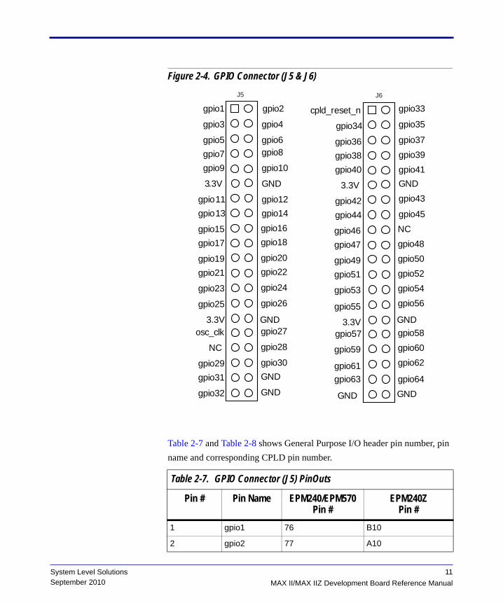
Figure 2-4. GPIO Connector (J5 & J6)
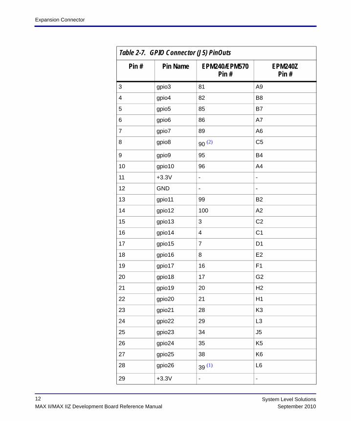
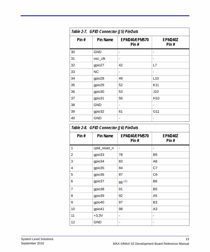
Table 2-7 and Table 2-8 shows General Purpose I/O header pin number, pin name and corresponding CPLD pin number.
Table 2-7. GPIO Connector (J5) PinOuts
Pin # Pin Name EPM240/EPM570 Pin #
EPM240Z Pin #
1 gpio1 76 B10
2 gpio2 77 A10
J5
gpio1
gpio19
gpio17gpio15
gpio13gpio11
3.3V
gpio9gpio7gpio5
gpio3
gpio21
gpio32
gpio31gpio29
NC
osc_clk3.3V
gpio25
gpio23
gpio2
gpio20
gpio18gpio16gpio14gpio12
GND
gpio10
gpio8gpio6
gpio4
gpio22
GND
GNDgpio30
gpio28
gpio27GND
gpio26
gpio24
J6
cpld_reset_n
gpio49
gpio47gpio46
gpio44gpio42
3.3V
gpio40gpio38gpio36
gpio34
gpio51
GND
gpio63gpio61
gpio59
gpio573.3V
gpio55
gpio53
gpio33
gpio50gpio48NCgpio45
gpio43GNDgpio41gpio39gpio37
gpio35
gpio52
GNDgpio64
gpio62gpio60gpio58GND
gpio56gpio54
11MAX II/MAX IIZ Development Board Reference Manual
System Level SolutionsSeptember 2010
Expansion Connector
3 gpio3 81 A9
4 gpio4 82 B8
5 gpio5 85 B7
6 gpio6 86 A7
7 gpio7 89 A6
8 gpio8 90 (2) C5
9 gpio9 95 B4
10 gpio10 96 A4
11 +3.3V - -
12 GND - -
13 gpio11 99 B2
14 gpio12 100 A2
15 gpio13 3 C2
16 gpio14 4 C1
17 gpio15 7 D1
18 gpio16 8 E2
19 gpio17 16 F1
20 gpio18 17 G2
21 gpio19 20 H2
22 gpio20 21 H1
23 gpio21 28 K3
24 gpio22 29 L3
25 gpio23 34 J5
26 gpio24 35 K5
27 gpio25 38 K6
28 gpio26 39 (1) L6
29 +3.3V - -
Table 2-7. GPIO Connector (J5) PinOuts
Pin # Pin Name EPM240/EPM570 Pin #
EPM240Z Pin #
12 System Level SolutionsSeptember 2010MAX II/MAX IIZ Development Board Reference Manual
30 GND - -
31 osc_clk - -
32 gpio27 42 L7
33 NC - -
34 gpio28 49 L10
35 gpio29 52 K11
36 gpio30 53 J10
37 gpio31 56 H10
38 GND - -
39 gpio32 61 G11
40 GND - -
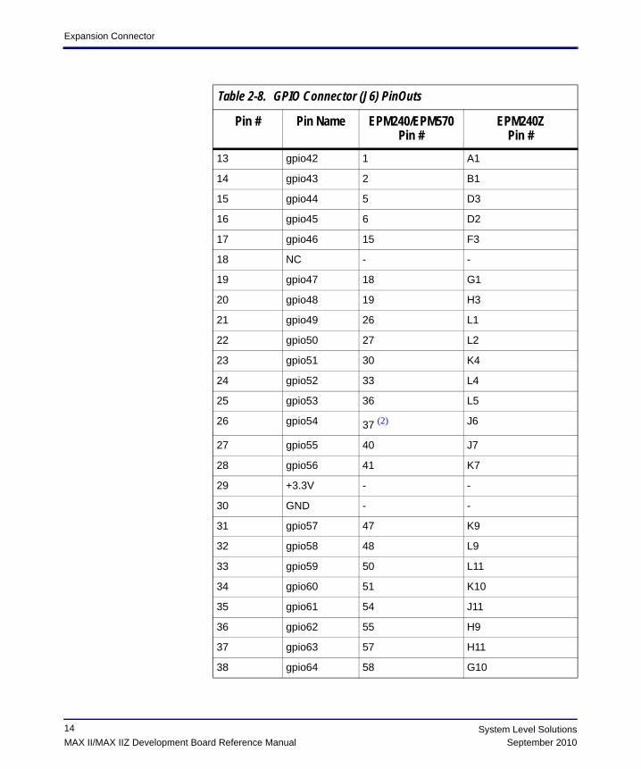
Table 2-8. GPIO Connector (J6) PinOuts
Pin # Pin Name EPM240/EPM570 Pin #
EPM240Z Pin #
1 cpld_reset_n - -
2 gpio33 78 B9
3 gpio34 83 A8
4 gpio35 84 C7
5 gpio36 87 C6
6 gpio37 88 (1) B6
7 gpio38 91 B5
8 gpio39 92 A5
9 gpio40 97 B3
10 gpio41 98 A3
11 +3.3V - -
12 GND - -
Table 2-7. GPIO Connector (J5) PinOuts
Pin # Pin Name EPM240/EPM570 Pin #
EPM240Z Pin #
13MAX II/MAX IIZ Development Board Reference Manual
System Level SolutionsSeptember 2010
Expansion Connector
13 gpio42 1 A1
14 gpio43 2 B1
15 gpio44 5 D3
16 gpio45 6 D2
17 gpio46 15 F3
18 NC - -
19 gpio47 18 G1
20 gpio48 19 H3
21 gpio49 26 L1
22 gpio50 27 L2
23 gpio51 30 K4
24 gpio52 33 L4
25 gpio53 36 L5
26 gpio54 37 (2) J6
27 gpio55 40 J7
28 gpio56 41 K7
29 +3.3V - -
30 GND - -
31 gpio57 47 K9
32 gpio58 48 L9
33 gpio59 50 L11
34 gpio60 51 K10
35 gpio61 54 J11
36 gpio62 55 H9
37 gpio63 57 H11
38 gpio64 58 G10
Table 2-8. GPIO Connector (J6) PinOuts
Pin # Pin Name EPM240/EPM570 Pin #
EPM240Z Pin #
14 System Level SolutionsSeptember 2010MAX II/MAX IIZ Development Board Reference Manual
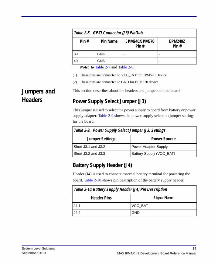
Note: to Table 2-7 and Table 2-8:
(1) These pins are connected to VCC_INT for EPM570 Device.
(2) These pins are connected to GND for EPM570 device.
Jumpers and Headers
This section describes about the headers and jumpers on the board.
Power Supply Select Jumper (J3)This jumper is used to select the power supply to board from battery or power supply adapter. Table 2-9 shows the power supply selection jumper settings for the board.
Battery Supply Header (J4)Header (J4) is used to connect external battery terminal for powering the board. Table 2-10 shows pin description of the battery supply header.
39 GND - -
40 GND - -
Table 2-8. GPIO Connector (J6) PinOuts
Pin # Pin Name EPM240/EPM570 Pin #
EPM240Z Pin #
Table 2-9. Power Supply Select Jumper (J3) Settings
Jumper Settings Power SourceShort J3.1 and J3.2 Power Adapter Supply
Short J3.2 and J3.3 Battery Supply (VCC_BAT)
Table 2-10.Battery Supply Header (J4) Pin Description
Header Pins Signal Name
J4.1 VCC_BAT
J4.2 GND
15MAX II/MAX IIZ Development Board Reference Manual
System Level SolutionsSeptember 2010
Jumpers and Headers
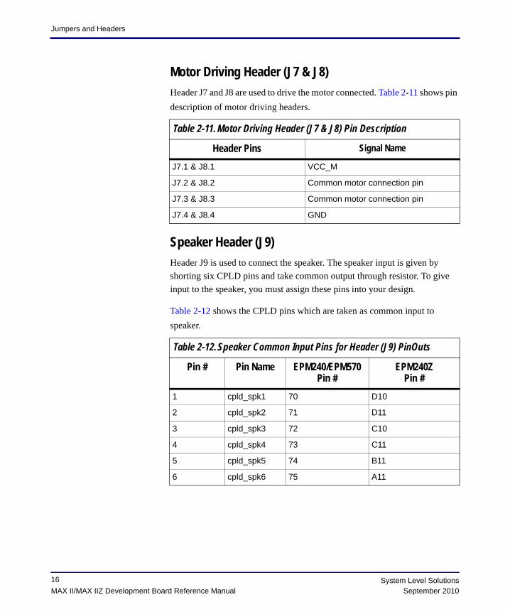
Motor Driving Header (J7 & J8)Header J7 and J8 are used to drive the motor connected. Table 2-11 shows pin description of motor driving headers.
Speaker Header (J9)Header J9 is used to connect the speaker. The speaker input is given by shorting six CPLD pins and take common output through resistor. To give input to the speaker, you must assign these pins into your design.
Table 2-12 shows the CPLD pins which are taken as common input to speaker.
Table 2-11. Motor Driving Header (J7 & J8) Pin Description
Header Pins Signal Name
J7.1 & J8.1 VCC_M
J7.2 & J8.2 Common motor connection pin
J7.3 & J8.3 Common motor connection pin
J7.4 & J8.4 GND
Table 2-12.Speaker Common Input Pins for Header (J9) PinOuts
Pin # Pin Name EPM240/EPM570 Pin #
EPM240Z Pin #
1 cpld_spk1 70 D10
2 cpld_spk2 71 D11
3 cpld_spk3 72 C10
4 cpld_spk4 73 C11
5 cpld_spk5 74 B11
6 cpld_spk6 75 A11
16 System Level SolutionsSeptember 2010MAX II/MAX IIZ Development Board Reference Manual
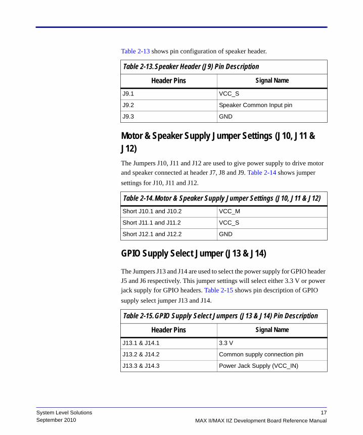
Table 2-13 shows pin configuration of speaker header.
Motor & Speaker Supply Jumper Settings (J10, J11 & J12)The Jumpers J10, J11 and J12 are used to give power supply to drive motor and speaker connected at header J7, J8 and J9. Table 2-14 shows jumper settings for J10, J11 and J12.
GPIO Supply Select Jumper (J13 & J14)
The Jumpers J13 and J14 are used to select the power supply for GPIO header J5 and J6 respectively. This jumper settings will select either 3.3 V or power jack supply for GPIO headers. Table 2-15 shows pin description of GPIO supply select jumper J13 and J14.
Table 2-13.Speaker Header (J9) Pin Description
Header Pins Signal Name
J9.1 VCC_S
J9.2 Speaker Common Input pin
J9.3 GND
Table 2-14.Motor & Speaker Supply Jumper Settings (J10, J11 & J12)Short J10.1 and J10.2 VCC_M
Short J11.1 and J11.2 VCC_S
Short J12.1 and J12.2 GND
Table 2-15.GPIO Supply Select Jumpers (J13 & J14) Pin Description
Header Pins Signal Name
J13.1 & J14.1 3.3 V
J13.2 & J14.2 Common supply connection pin
J13.3 & J14.3 Power Jack Supply (VCC_IN)
17MAX II/MAX IIZ Development Board Reference Manual
System Level SolutionsSeptember 2010
Status LEDs and Reset/Power Switches
Status LEDs and Reset/Power Switches
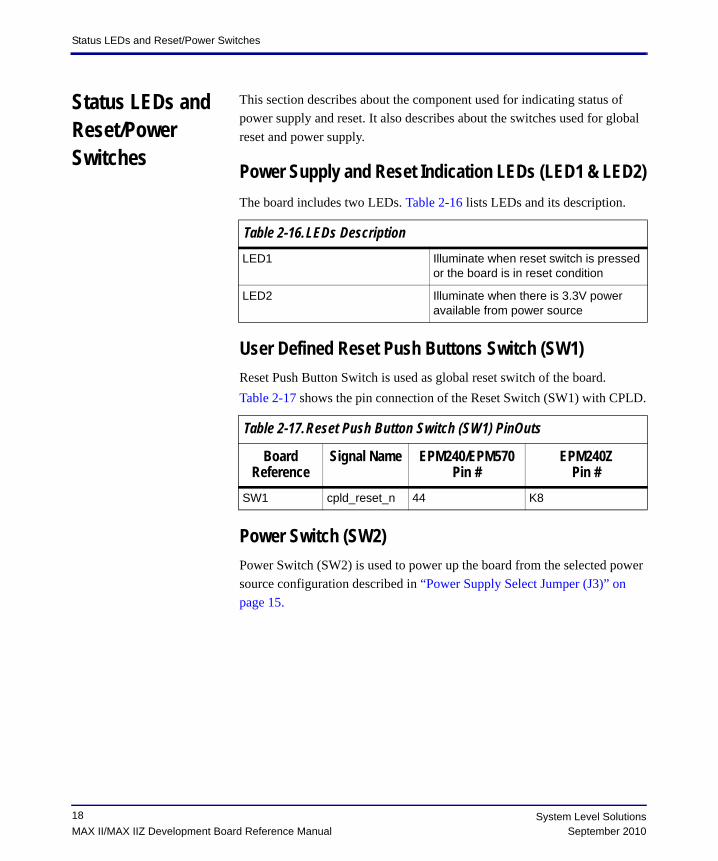
This section describes about the component used for indicating status of power supply and reset. It also describes about the switches used for global reset and power supply.
Power Supply and Reset Indication LEDs (LED1 & LED2)The board includes two LEDs. Table 2-16 lists LEDs and its description.
User Defined Reset Push Buttons Switch (SW1)Reset Push Button Switch is used as global reset switch of the board. Table 2-17 shows the pin connection of the Reset Switch (SW1) with CPLD.
Power Switch (SW2)Power Switch (SW2) is used to power up the board from the selected power source configuration described in “Power Supply Select Jumper (J3)” on page 15.
Table 2-16.LEDs DescriptionLED1 Illuminate when reset switch is pressed
or the board is in reset condition
LED2 Illuminate when there is 3.3V power available from power source
Table 2-17.Reset Push Button Switch (SW1) PinOuts
Board Reference
Signal Name EPM240/EPM570 Pin #
EPM240Z Pin #
SW1 cpld_reset_n 44 K8
18 System Level SolutionsSeptember 2010MAX II/MAX IIZ Development Board Reference Manual
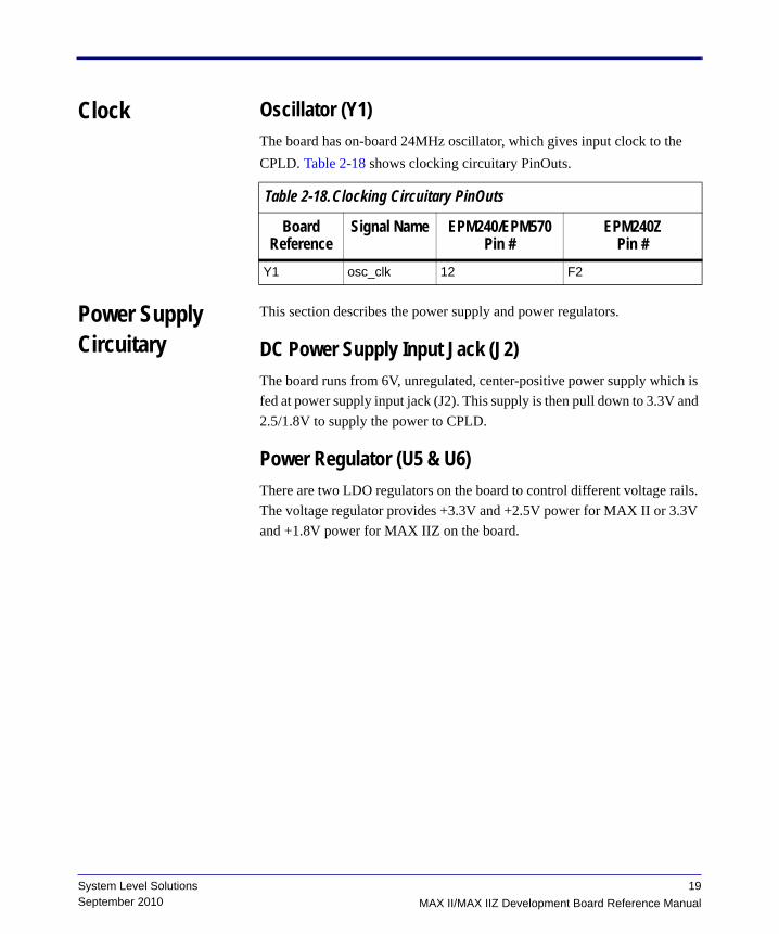
Clock Oscillator (Y1)The board has on-board 24MHz oscillator, which gives input clock to the CPLD. Table 2-18 shows clocking circuitary PinOuts.
Power Supply Circuitary
This section describes the power supply and power regulators.
DC Power Supply Input Jack (J2)The board runs from 6V, unregulated, center-positive power supply which is fed at power supply input jack (J2). This supply is then pull down to 3.3V and 2.5/1.8V to supply the power to CPLD.
Power Regulator (U5 & U6)There are two LDO regulators on the board to control different voltage rails. The voltage regulator provides +3.3V and +2.5V power for MAX II or 3.3V and +1.8V power for MAX IIZ on the board.
Table 2-18.Clocking Circuitary PinOuts
Board Reference
Signal Name EPM240/EPM570 Pin #
EPM240ZPin #
Y1 osc_clk 12 F2
19MAX II/MAX IIZ Development Board Reference Manual
System Level SolutionsSeptember 2010
Power Supply Circuitary
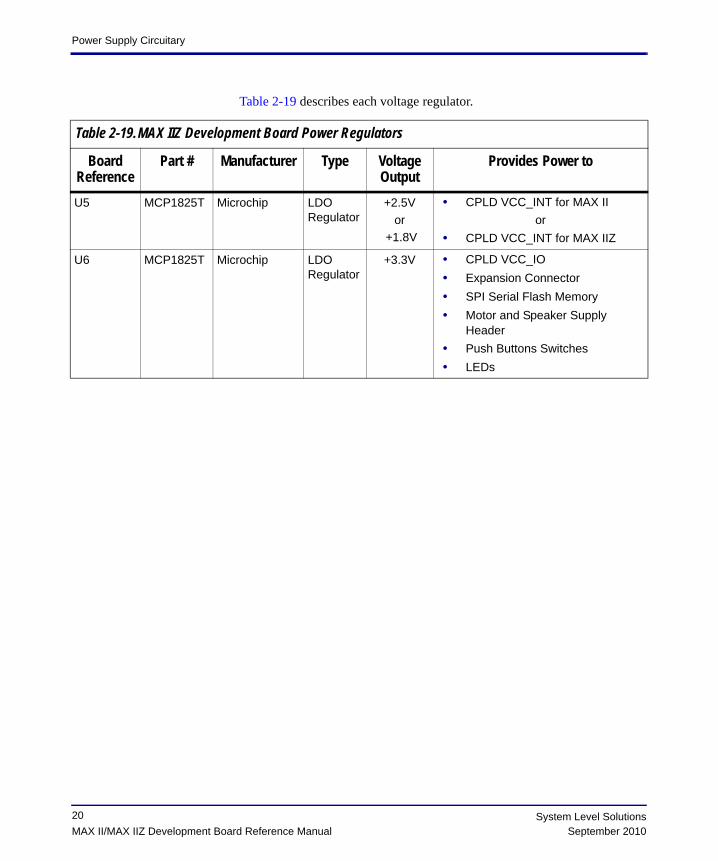
Table 2-19 describes each voltage regulator.
Table 2-19.MAX IIZ Development Board Power Regulators
Board Reference
Part # Manufacturer Type Voltage Output
Provides Power to
U5 MCP1825T Microchip LDO Regulator
+2.5V or
+1.8V
• CPLD VCC_INT for MAX IIor
• CPLD VCC_INT for MAX IIZ
U6 MCP1825T Microchip LDO Regulator
+3.3V • CPLD VCC_IO• Expansion Connector• SPI Serial Flash Memory• Motor and Speaker Supply
Header• Push Buttons Switches• LEDs
20 System Level SolutionsSeptember 2010MAX II/MAX IIZ Development Board Reference Manual