Embed Size (px)
Citation preview

UNIQUE TEMPLATING OF AND APPLICATIONS ENABLED
THROUGH MESOPOROUS COLLOIDS
BY
MATTHEW DAVE GOODMAN
DISSERTATION
Submitted in partial fulfillment of the requirements
for the degree of Doctor of Philosophy in Materials Science and Engineering
in the Graduate College of the
University of Illinois at Urbana-Champaign, 2014
Urbana, Illinois
Doctoral Committee:
Professor Paul V. Braun, Chair
Assistant Professor Lane W. Martin
Assistant Professor Shen Dillon
Professor Kenneth S. Suslick
ii
ABSTRACT
This work describes the templating process and applications enabled by utilizing mesoporous
colloids, colloidal crystals, and films. Silica colloidal crystals, having colloids of less than 300
nm, were fabricated and used as a template for silicon deposition. Brillouin Light Scattering
(BLS) experiments conducted on a silicon templated silica colloidal crystal show unusual
behavior in the BLS spectrum where the Stokes and anti-Stokes phonon intensities were
asymmetrical. The dispersion relationship between the phonon frequencies and wave vectors had
no phononic band bending, possibility due to the unusual phenomenon.
Mesoporous silica was used as a template for platinum and silicon deposition. After a successful
colloidal crystal fabrication from mesoporous silica colloids, platinum was deposited and
partially infiltrated the mesopores. Removing the silica template revealed a mesoporous platinum
shell, replicating the mesopores of the colloids and the colloidal crystal structures. The silicon-
silica composite was used to study the thermal conductivity of the confined silicon.
Polycrystalline silicon, deposited as a reference, was shown to have a thermal conductivity of 38
W m-1
K-1
; the silicon-silica composite had an effective thermal conductivity between 2.2 and 2.4
W m-1
K-1
, an order of magnitude less than the polycrystalline film. Material thermal conductivity
of the silicon could not be determined with simple modeling; accurate results need a more
detailed investigation.
The first successful carbon colloidal crystal is fabricated through tailoring the surface charge of
the individual colloids through a partial oxidation. This colloidal crystal was used as a unique
template for a variety of materials. The templated materials penetrate deep into the mesopores,

iii
creating a nanostructured inverse opal after carbon removal. Crucially, the carbon removal is
completely orthogonal to the deposited material removal, allowing thorough template replication
and preserving the fine-scale mesostructure of the colloid. This approach can be generalized for
templating materials, which are inherently difficult to template with conventional colloidal
crystals.
Two major applications were investigated utilizing the mesoporous colloids. The first involved
the templating of titania for improvement in dye-sensitized solar cells. A carbon colloidal crystal
could successfully be fabricated on the conductive glass substrate after an initial titania
deposition. Titania was deposited and infiltrated the mesoporous carbon colloidal crystal
template. After titania crystallization, the carbon was removed orthogonally through a simple
oxidation, followed by solar cell assembly. The performance of the cell indicated low dye
loading in the titania nanostructure; however, experiments to increase the dye loading were
unsuccessful.
The second major application investigated also utilized the carbon colloidal crystal. Lithium
battery anodes were fabricated by having the active materials, silicon and Fe3O4, inside the
mesopores. The mesoporous carbon is unique in that it provides a porous, conductive network,
allowing both electrolyte diffusion and electron extraction, and confines the active materials.
This confinement minimizes capacity loss through electrical isolation of the active materials and
suppresses any pulverization or migration. The silicon-carbon anode showed stability through 85
cycles after the addition of vinylene carbonate to the electrolyte, effectively stabilizing the solid-
electrolyte interface. The Fe3O4-carbon anode showed excellent coulombic efficiency with a

iv
dramatic decrease in the charge hysteresis, from 0.90 V in conventional systems to 0.60 V in the
templated, confined anode, attributed to the confinement of the Fe3O4 active material.
Preliminary magnetic measurements were also conducted on the deposited iron-carbon
composite, showing unique behavior.

v
To Stac
vi
ACKNOWLEDGMENTS
This work is the culmination of years of work that could not have been accomplished without the
support of a number of people. My advisor, Prof. Paul Braun, provided me with indispensable
guidance on my doctoral research, yet still allowed personal pursuits on various topics.
Additionally, his support outside the research lab was instrumental in my development, be it in
academic courses, career options, or a myriad of other endeavors. My Toyota collaborators, Dr.
Kazuhisa Yano and Dr. Narihito Tatsuda, were a tremendous asset: their numerous discussions
on the research projects and the extensive mesoporous samples they provided allowed for some
truly unique results. I would also like to acknowledge my committee members, Prof. Lane W.
Martin, Prof. Shen Dillon, and Prof. Kenneth S. Suslick, for providing valuable feedback and
critical assessment.
In the Braun group, I have worked with some amazing people who have significantly assisted in
my progress. Dr. Matthew George was instrumental when I first arrived and helped me settle into
research at the University of Illinois. Dr. Dara Gough provided numerous discussions on various
chemistries, allowed me a place to stay for a summer in Albuquerque, and was always up for a
game of soccer. Dr. Abby Juhl, Dr. Mark Losego, Dr. Sidhartha Gupta, Dr. Aaron Jackson, Dr.
Erik Nelson, Dr. Joe Geddes, Dr. Jiung Cho, Bibek Parajuli, and Ha Seong Kim have all helped
through discussions, running samples for me, or teaching me a new technique. Dr. Agustin Mihi,
Dr. Kevin Arpin, Dr. Hui (Steven) Zhang, and Dr. Hailong Ning have all been influential and
contributed significantly to my success. Current group members of James Pikul, Chunjie Zhang,
Neil Krueger, Junjie Wang, Jin Gu Kang, Runyu Zhang, and Osman Cifci have also been helpful
in their discussions and suggestions. A special thanks to Sanghyeon Kim and Qiye Zheng, who

vii
helped fabricate and run the last few experiments. Additionally, I’d like to thank David Gross,
who assisted in the FIB liftouts in the iron oxide work. To everyone else in the Braun group, past
and present, thank you for making these years here memorable.
The work presented here benefited from financial support by Toyota Central R&D and the U.S.
Department of Energy ‘Light Material Interactions in Energy Conversion’ Energy Frontier
Research Center under grant DE-SC0001293. Additionally, this work was carried out in part in
the Frederick Seitz Materials Research Laboratory Central Research Facilities, University of
Illinois. I would like to thank all the staff in the MRL and Beckman who trained, assisted, or ran
samples for me.
Furthermore, I would like to acknowledge all the support staff that made things easier for me.
Erica Malloch, thank you for your tireless help and assistance in keeping my schedule
coordinated with Prof. Braun’s. The support staffs in the Materials Science Department and the
MRL offices have been amazing: Judy Brewer, Michelle Malloch, Kimberly Anderson, Debbie
Kluge, Sandy Helregel, Cindy Brya, Susie Lighty and Chris Jones.
Finally, I would like to thank my family for their support. To my parents, thank you for pushing
me to pursue my passions. Cassie and Philip: I thank you for always providing a joke, a much-
needed distraction, and even a grounding rod. Stacy, thanks for your love, support,
encouragement, and perspective.

viii
TABLE OF CONTENTS
CHAPTER 1 INTRODUCTION .................................................................................................. 1
1.1 Colloidal Crystals and Their Optical Properties ................................................................... 2
1.2 Fabricating Colloidal Crystals ............................................................................................... 6
1.3 Current Templating Strategies with Colloidal Crystals ...................................................... 13
1.4 Porous Carbon ..................................................................................................................... 17
1.5 Mesoporous Silica and Carbon Spheres .............................................................................. 19
CHAPTER 2 BRILLOUIN LIGHT SCATTERING IN SILICON INVERSE OPALS............. 22
2.1 Brillouin Light Scattering.................................................................................................... 22
2.2 Silica Colloidal Crystal Fabrication .................................................................................... 23
2.3 BLS Measurements ............................................................................................................. 31
2.4 Conclusions ......................................................................................................................... 34
CHAPTER 3 UTILIZING MESOPOROUS SILICA TEMPLATES: PT LOADED PHOTONIC
CRYSTAL AND HEAT TRANSPORT IN TEMPLATED SI ............................ 36
3.1 Mesoporous Silica for Pt template ...................................................................................... 36
3.2 Thermal Transport in Nanostructured Silicon ..................................................................... 38
3.3 Conclusions ......................................................................................................................... 47
CHAPTER 4 CARBON COLLOIDAL CRYSTALS: FABRICATION, TEMPLATING, AND
OPTICAL PROPERTIES ..................................................................................... 48
4.1 Fabricating Carbon Colloidal Crystal ................................................................................. 48
4.2 Mesoporous Starburst Carbon Spheres as Templates ......................................................... 54
4.3 Conclusions ......................................................................................................................... 61
4.4 Experimental Procedures..................................................................................................... 62
CHAPTER 5 ENERGY HARVESTING USING CARBON COLLOIDAL CRYSTALS ....... 64
5.1 Carbon Colloidal Crystals on Conductive Substrates ......................................................... 64
5.2 Mesoporous Carbon for DSSC ............................................................................................ 65

ix
5.3 Increasing Dye Adsorption in DSSC .................................................................................. 73
5.4 Conclusions ......................................................................................................................... 75
CHAPTER 6 ENERGY STORAGE UTILIZING CARBON COLLOIDS AS TEMPLATES . 76
6.1 Introduction and Anode Fabrication ................................................................................... 76
6.2 Silicon CVD for Battery Applications ................................................................................ 81
6.3 Iron CVD for Battery Applications ..................................................................................... 91
6.4 Magnetic Investigation of Iron CVD ................................................................................ 106
6.5 Conclusions ....................................................................................................................... 108
6.6 Experimental Procedures................................................................................................... 109
CHAPTER 7 CONCLUSIONS................................................................................................. 111
REFERENCES ........................................................................................................................... 115

1
CHAPTER 1
INTRODUCTION
Chapter 1 introduces the key components and background of the work presented in this thesis:
colloidal crystals, their optical properties, and typical fabrication routes. Current templating
strategies involving colloidal crystals are described and specific applications presented.
Additionally, limitations in the materials available for conventional colloidal crystals and the
subsequent templating strategies are illustrated. Chapter 2 describes work done using non-porous
silica colloids for Brillouin Light Scattering experiments. By depositing silicon on a silica
colloidal crystal, the phononic band structure of the composite is investigated; this work was
done in collaboration with Dr. Huihui Pan and Prof. Jay Bass. Chapter 3 provides two examples
of templated materials utilizing mesoporous silica. Platinum was deposited into the mesopores of
silica colloids arranged in a colloidal crystal. Additionally, silicon was deposited into mesopores
with preliminary thermal transport experiments conducted. Initial work done on mesoporous
carbon colloids are presented in Chapter 4. After fabrication into a colloidal crystal, the carbon is
used as a unique template to create porous oxide and semiconductor inverse opals. Results in this
chapter have been published in Advanced Optical Materials [1]. The mesoporous carbon
colloidal crystals were then used as templates for titania infiltration, shown in Chapter 5. The
carbon was removed and the porous titania investigated for dye-sensitized solar cell applications.
Chapter 6 expands on the carbon template with silicon and iron deposited in the mesopores. The
iron was oxidized to Fe3O4 without removing the carbon template and thoroughly characterized.
The Fe3O4-carbon and the silicon-carbon composites were tested as anodes for lithium batteries.
Finally, Chapter 7 presents overall conclusions of this work.

2
1.1 Colloidal Crystals and Their Optical Properties
Colloidal crystals are periodic assemblies of colloidal particles, typically (but not necessarily)
less than 1 µm in diameter. Most commonly, the colloids are arranged in a hexagonal, close-
packed face-center cubic (FCC) structure [2]. Other crystal structures have been formed;
however, the literature is dominated by FCC structures due to the fact that this is the preferred
crystal structure for most colloidal systems [3-6]. Naturally occurring colloidal crystals, or opals,
have been the fascination of people for the unique optical properties, namely opalescence,
associated with the structures. The opalescence results from their periodic nanostructure, where
the periodicity is similar to the wavelength of light (Figure 1) [7, 8]. This periodic structure
alters photon propagation, resulting in a photonic band structure that is superficially analogous to
semiconductors and electronic band diagrams, as semiconductors have a periodicity of atoms
similar to the wavelength of electrons [9]. Comparing the non-simplified band diagrams of the
electronic bands of semiconductors to the photonic bands of colloidal crystals reinforces this
comparison, shown in Figure 2. Structures with a photonic band gap over all directions are
stated to contain a photonic band gap; typically colloidal crystals have a photonic gap in only one
or two directions, commonly referred to as a stop band [7, 9, 10]. Importantly, this modulation of
photon propagation is due to the optical properties of the colloids, namely the dielectric
permittivity (and in special cases, the magnetic permeability), rather than the electronic
properties of the atoms in semiconductors [11]. The dielectric permittivity and the magnetic
permeability are commonly simplified to the refractive index of the colloids due to the
relationship of
√ 1

3
where the refractive index, n, is related to the relative permittivity, , and relative permeability,
. At optical frequencies with typical dielectric materials (e.g., oxides), the relatively
permeability, , is effectively 1 and can be ignored [12]. However, if the colloids interact with
the magnetic field, e.g., magnetic domains of iron within the colloids, the permeability must be
taken into consideration. While colloidal crystals can in principle be made from any colloid,
naturally occurring opals consist mainly of silica colloids containing impurities of iron,
aluminum, or titanium, and fabricated colloidal crystals are made of primarily silica, polystyrene,
or poly(methyl methacrylate) colloids [8].
Figure 1. (a) Naturally occurring opal. (b) The periodic structure of the opal; light interacting
with this structure results in the color observed. (c) The FCC structure present in this crystal. In
this example, the colloidal particles are approximately 300 nm in diameter. Adopted from
Reference [8].

4
Figure 2. Left: Non-simplified electronic band diagrams of germanium (Ge), silicon (Si), and
gallium arsenide (GaAs) showing energy (frequency) vs. wave vector (position), adapted from
Reference [13]. Right: photonic band diagram of a colloidal crystal, showing frequency vs.
position. There is no full photonic band gap; only stop band (i.e., band gap in one direction).
Adopted from Reference [7].
In naturally occurring opals, between the silica colloids there is typically porous, water-
containing silica; this porous silica provides mechanical integrity as well as changes the optical
properties [8]. While colloidal crystals cannot have full photonic band gaps, regardless of the
refractive index of the spheres, inverse opals, where the voids between the colloids are filled
with a material and the colloids removed, can have a full photonic band gap if the refractive
index of the infilled material is sufficiently high [9-11, 14, 15]. The optical properties of the
inverse structure, as with the colloidal crystal template, are again determined by their dielectric
properties, more conveniently expressed as the refractive index contrast of the materials [16].
Structures with a higher refractive index contrast (e.g., silicon-air structure compared to silica-
air) have a larger photonic band gap, i.e., no allowed photonic states over a larger spectrum range

5
[7]. As such, many research groups have utilized colloidal crystals as templates, infilling the
interstitial voids with a host of materials including high index materials of silicon [17], titania
[18, 19], and zinc oxide [20], as well as lower refractive index materials of hydrogels [21] and
carbon [22] for other interesting applications. In the case of naturally occurring opals, instead of
a silica-air colloid crystal, with a refractive index contrast of ~0.55 (n of silica is ~1.55, air is 1),
the refractive index contrast is now smaller, as the porous silica and water interstitial material’s
index is greater than 1. Indeed, by simply changing the amount of hydration in the interstitial, the
optical properties can be influenced, shown in Figure 3. Additionally, the lower index contrast
reduces scattering, changing the milky, opaque appearance of the opal to one that has a clearer
structure where the color seems to come from deeper in the opal. This change in optical
properties via an analyte is heavily utilized in sensor applications, both using a colloidal crystal
[23-25] as well as an inverse opal replicate [20, 21].
Figure 3. (a) Naturally occurring hydrophane opal in the dehydrated state. (b) Same opal in the
hydrated state. Figure adapted from Reference [26].

6
1.2 Fabricating Colloidal Crystals
Colloidal crystals are advantageous in conducting research for two main reasons: their three-
dimensional periodic structure alters photon properties in all directions, which is the most
interesting in terms of photonic crystals and described in the previous section, and secondly, the
relative ease of fabricating colloidal crystals through bottom-up self-assembly [8, 27-30].
Colloidal crystal fabrication can be broadly classified as a bottom-up assembly technique, in
which colloids are driven to pack together through use of a variety of fields. These different
methods are summarized in Figure 4; for discussion on each method, Marlow, et al., provides an
excellent summary [8]. For this work, the flow-induced method of colloidal crystal fabrication
was exclusively used.
Colloidal crystal fabrication begins with the individual colloids. As mentioned previously, most
colloidal crystals are fabricated with silica, polystyrene, or poly(methyl methacrylate) spheres.
This is due to one of the main requirements for a high-quality colloidal crystal: the colloids must
be monodisperse. Increasing the colloidal size distribution creates packing defects, which disrupt
the lattice similar to substitution atoms on the atomic scale. Experimentally, a size distribution of
greater than 5% leads to numerous defects, with the resulting structure having little long-range
order and inferior optical properties. Colloids of silica, polystyrene, and poly(methyl
methacrylate) can be easily fabricated with low polydispersity and are available commercially
[31, 32].

7
Figure 4. Colloidal crystal (opal) deposition methods, as summarized by Marlow, et al. Adopted
from Reference [8].
While the exact mechanisms for colloidal crystal formation are not firmly established [2],
experimental results provide some insight. A stable suspension of the colloids, with any excess
surface contamination removed, is necessary for high-quality colloidal crystals; this suspension
has been typically water- or ethanol-based. The suspension needs to be stable longer than the
colloidal crystal fabrication; most high-quality crystals use suspensions that are stable for days or
weeks. With polymeric colloids, this requirement is easily met; however, silica colloids tend to
crash out of solution, especially when the colloid diameter becomes greater than 700 nm. These

8
larger silica colloids require unique deposition procedures to form a well-ordered colloidal
crystal, with some recent success using dimethyl sulfoxide (DMSO) as the solvent [33].
This work utilized a hybrid horizontal-vertical deposition method. One of the easiest ways to
create an opalescent film is to allow a colloidal suspension to dry on a flat substrate. The
suspension is pinned at the circumference where the solvent evaporates the quickest [34]. Due to
particle convection, and thus the flow-induced classification, the resulting film is thickest at the
pinned contact line and thinnest in the center. Pinning contact lines and using a variety of
suspensions have resulted in a number of unique arrays [35] with the particle convection well
understood [36]. A modification of the horizontal deposition method utilizes spincoating;
however, a successful ordered film requires precise control of numerous parameters, including
the colloid concentration, spinning speed, and suspension viscosity [37].
Vertical deposition sets the substrate into the suspension vertically, as shown in Figure 5. There
are several advantages gained when the substrate is placed vertically, chief among them the
smaller amount of suspension needed and lower defect concentration. A key challenge in the
horizontal deposition method is the sedimentation of the colloids: any colloid that crashes out of
solution prior to packing into the close-pack structure results in a defect. With the vertical
deposition method, any colloids unstable enough to sediment will instead deposit on the floor of
the deposition vial, preserving the substrate and providing fewer defects in the resulting colloidal
crystal. With vertical deposition relying on solvent evaporation, the rate of crystal formation was
inherently slow, limiting the suspension to small colloids. Heating, mechanical agitation, and
using ethanol as the solvent increases the evaporation rate and allows larger colloids to be used.
9
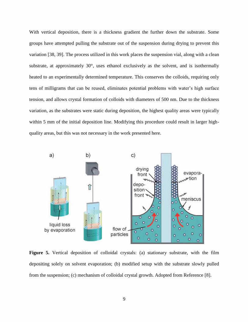
With vertical deposition, there is a thickness gradient the further down the substrate. Some
groups have attempted pulling the substrate out of the suspension during drying to prevent this
variation [38, 39]. The process utilized in this work places the suspension vial, along with a clean
substrate, at approximately 30°, uses ethanol exclusively as the solvent, and is isothermally
heated to an experimentally determined temperature. This conserves the colloids, requiring only
tens of milligrams that can be reused, eliminates potential problems with water’s high surface
tension, and allows crystal formation of colloids with diameters of 500 nm. Due to the thickness
variation, as the substrates were static during deposition, the highest quality areas were typically
within 5 mm of the initial deposition line. Modifying this procedure could result in larger high-
quality areas, but this was not necessary in the work presented here.
Figure 5. Vertical deposition of colloidal crystals: (a) stationary substrate, with the film
depositing solely on solvent evaporation; (b) modified setup with the substrate slowly pulled
from the suspension; (c) mechanism of colloidal crystal growth. Adopted from Reference [8].

10
While these experimental conditions can be tailored for high-quality colloidal crystal formation,
the actual mechanisms are not fully understood. As mentioned previously, the convection of
colloids is well understood [36] and drives the colloids to pack at the meniscus. However, a clear
understanding of why the colloids pack in a closed-pack, FCC structure, instead of a hexagonal
ABA packing or even a random glass, is still missing. One hypothesis is a solvent flow argument
proposed by Norris, et al, depicted in Figure 6 [2]. During colloidal crystal formation, solvent is
driven through the packed colloids and evaporated (see Figure 5). The “clear niche” in Figure 6,
one that does not have a colloid directly behind it, allows higher solvent flux and drives the
colloid to pack in the FCC ABC packing. Additionally, colloids and the substrate must have a
relatively strong and long-range repulsive force; otherwise, short-range attractive forces (van der
Waals) will cause colloid aggregation and premature deposition on the substrate creating defects
that disrupt the colloidal crystal. Self-assembly of high-quality colloidal crystals require colloids
that are both monodisperse and form a stable suspension (typically accomplished by imparting
them with a repulsive surface charge [8, 40]).
Figure 6. Proposed mechanism for flow-induced colloidal crystal formation. Adopted from
Reference [2].

11
Modifying the experimental conditions of the colloidal deposition has resulted in a number of
unique structures. Due to the colloidal crystal’s and inverse opal’s modification of photonic
bands, work has progressed in using them for improving photovoltaic devices. As silicon cells
can be made with high efficiency, most of the work has been focused on dye-sensitized solar
cells (DSSC) [41-46]. In DSSC, the light is absorbed through a dye, typically ruthenium-based,
which is excited from the ground state [47]. The excited electron is then transferred into the
conduction band of a wide-band gap semiconductor, typically nanoparticles of titania, and
transported to the back contact to be collected. The dye accepts an electron from the electrolyte,
with the oxidized electrolyte reduced at the front contact. Due to the dye’s optical absorption, the
majority of the red part of the visible spectrum passes through the cell and is not utilized [44].
Incorporating a colloidal crystal into the cell would allow select wavelength to be reflected back,
improving the absorption. Additionally, the porous structure of the colloidal crystal allows the
electrolyte to regenerate the dye. A challenging part of using a colloidal crystal is the fabrication
on the rough nanoparticle titania surface. By fabricating the colloidal crystal on a sacrificial
substrate, followed by a polymeric infilling and etching, the colloidal crystal can be transferred
to the titania with high fidelity (see Figure 7) [48]. Additionally, the colloidal crystal can be used
as a template prior to transferring; templating with the colloidal crystal on the titania will fill the
pores between the titania nanoparticles, preventing the electrolyte from reaching and
regenerating the dye.
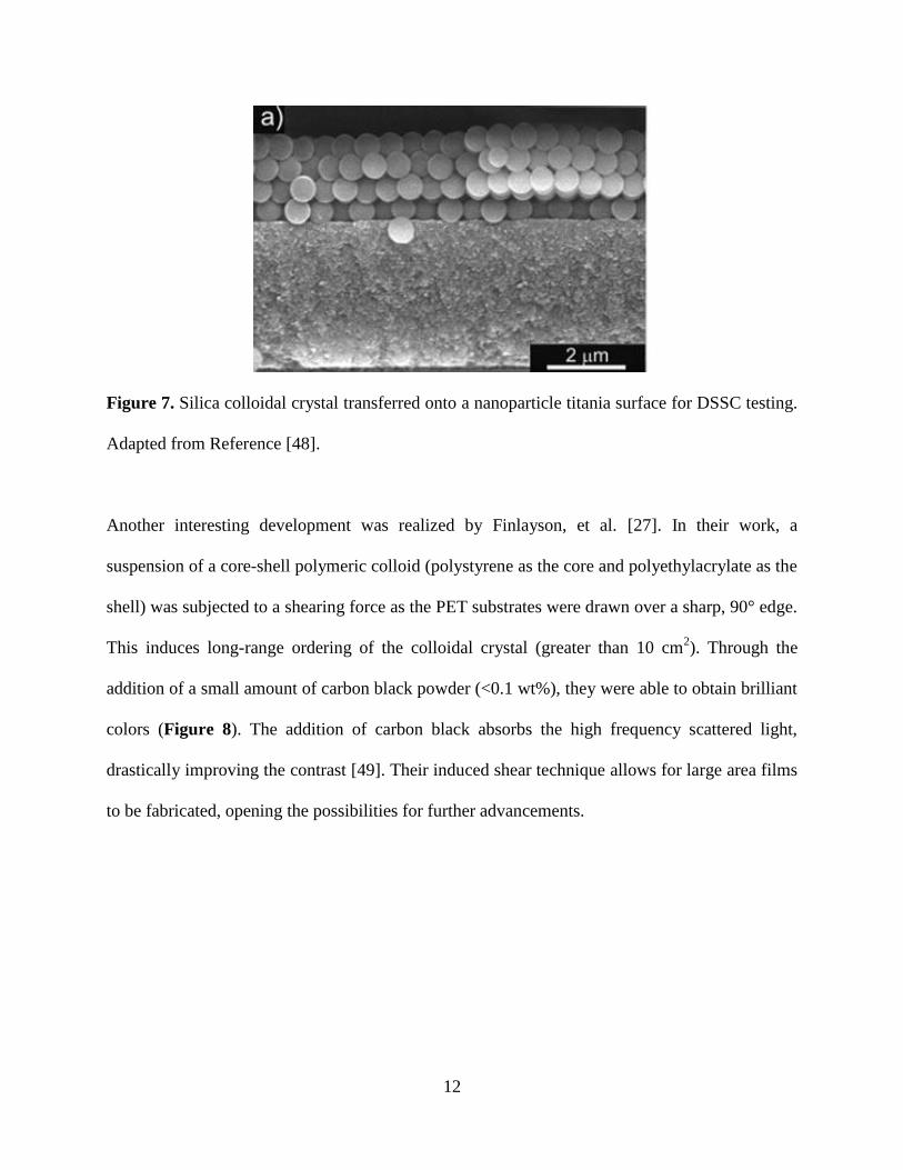
12
Figure 7. Silica colloidal crystal transferred onto a nanoparticle titania surface for DSSC testing.
Adapted from Reference [48].
Another interesting development was realized by Finlayson, et al. [27]. In their work, a
suspension of a core-shell polymeric colloid (polystyrene as the core and polyethylacrylate as the
shell) was subjected to a shearing force as the PET substrates were drawn over a sharp, 90° edge.
This induces long-range ordering of the colloidal crystal (greater than 10 cm2). Through the
addition of a small amount of carbon black powder (<0.1 wt%), they were able to obtain brilliant
colors (Figure 8). The addition of carbon black absorbs the high frequency scattered light,
drastically improving the contrast [49]. Their induced shear technique allows for large area films
to be fabricated, opening the possibilities for further advancements.

13
Figure 8. Polymeric core-shell colloidal crystals, with the addition of carbon black. Left:
polystyrene core diameter of 215 nm; right: core diameter of 250 nm. Angle of viewing is
normal incidence. Samples are approximately 6 cm long. Adapted from Reference [27].
1.3 Current Templating Strategies with Colloidal Crystals
The use of colloidal crystals as templates to impart periodic patterns into various materials has
been broadly employed to create, for example, unique optoelectronic devices [48, 50], sensors
[21, 51-54], and energy storage devices [55, 56]. The general motivation for templating is to
utilize the colloidal crystals’ interconnected 3D structure to define the 3D structure of a material
that is inherently difficult to form into a highly regular 3D structure on its own. A single
replication yields a structure that is an inverse of the colloidal template, and a double replication
yields the original structure of the template. This process is only successful if the colloidal
template can withstand the deposition conditions of the material to be templated and there exist
conditions whereby the original template can be removed without damaging the templated
material. Given that the most popular template, silica, can only be removed with hydrofluoric
acid or strong base, chemicals that dissolve many materials, this can be challenging. Polymer

14
templates (e.g. polystyrene or poly(methyl methacrylate)) are easy to remove, but cannot
withstand high-temperature deposition strategies, limiting their use [8]. Thermally stable colloids
that could be removed under orthogonal conditions, i.e., conditions that do not damage the
templated material, would allow currently inaccessible materials templating strategies.
Additionally, if the templates contained additional desirable structural complexities (e.g. a high
surface area) which are replicated in the templated material, additional applications may emerge;
for example, dye sensitized solar cells require high-surface area electrodes [57], as do many
other catalytic devices.
Figure 9. GaAs epitaxial growth through a silica colloidal crystal. (a) Schematic and scanning
electron microscopy (SEM) image showing the bottom-up growth of the GaAs, where the GaAs
has grown through 4 layers. (b) Schematic and SEM image of the GaAs-filled silica colloidal

15
crystal. (c) Schematic and SEM image of GaAs inverse opal once the silica template was
removed. Adapted from Reference [50].
Two examples of templating in the Braun group have utilized the colloidal crystal for modifying
the light emission of a templated emitter as well as a template for a three-dimensional metal
electrode. Nelson, et al., was able to fabricate a silica colloidal crystal on a gallium arsenide
(GaAs) substrate [50]. Through tailoring the deposition conditions, an epitaxial, single-crystal
GaAs was grown from the bottom substrate (Figure 9). By incorporating an indium gallium
arsenide (InGaAs) emitting layer, sandwiched between two GaAs layers, the change in emission
could be realized. This templating took advantage of the GaAs’ resistance to the hydrofluoric
acid etching that removed the silica colloidal crystal. In the other example, Zhang, et al., was
able to use a polystyrene colloidal crystal, on a tungsten foil, as the template [56, 58]. The final
structure was a 3D porous nickel scaffold where active materials for batteries could be deposited
(Figure 10). By annealing the polystyrene after colloidal assembly, the interconnects between
the colloids increased and allowed larger voids after templating. Nickel was electrodeposited in
the interstitials and the colloids removed via a solvent rinse. To further increase the void space,
an electropolish was done prior to depositing the active materials. The final structure allowed for
improved battery performance due to the 3D structure.

16
Figure 10. Schematic of templating process used by Zhang, et al., creating a 3D porous
electrode. Adapted from Reference [56].
Figure 11. Top left: polystyrene colloidal crystal used as a template for PAM. Bottom left:
Inverse opal of PAM after polystyrene removal. Right: optical response of the inverse PAM opal
with varying ethanol concentrations in water. Adapted from Reference [52].
Another example capitalizing on the optical properties was conducted by Pan, et al. [52].
Intriguingly, the colloidal crystal utilized was again made from polystyrene colloids; however,
the templating material was another polymer, namely polyacrylamide (PAM). To template the

17
PAM, PAM precursors were allowed to infiltrate the polystyrene colloidal crystal, after which
the sample was placed in an oven for the monomers to polymerize, followed again by a solvent
rinse to remove the polystyrene. The PAM inverse opal showed excellent optical properties,
which were used to detect ethanol concentrations in an aqueous solution (Figure 11). By
increasing the ethanol concentration, there is a blue-shift in the optical response. This is due to
the PAM response to the solution: water will swell the cross-linked PAM but the alcohol will
cause it to shrink. Increasing the alcohol content displaces the water, thus gradually shrinking the
structure. As the optical response is dictated by the lattice spacing, this results in the blue-shift
seen in Figure 11. Numerous groups have utilized inverse opals in sensor applications where the
analyte of interest interacts with the structure [20, 21, 53, 59-61].
In summary, while colloidal crystals are an important research tool, they currently have strong
limitations. The colloids used are typically limited to either silica or polystyrene, both of which
have tradeoffs in their properties. Silica is stable at high temperatures; however, a harsh removal
is needed, which limits the templated material. Polystyrene can be easily removed via a solvent
rinse, but it can be utilized only where the temperature does not exceed 100 °C. Finally, the
colloidal crystal template allows only for an inverse opal structure, limiting the potential
applications.
1.4 Porous Carbon
Porous carbon is broadly utilized both for fundamental studies and large-scale commercial
applications, including water purification, ion exchange [62], catalysis [63], conventional battery
electrodes [64], emerging battery electrode designs [65], capacitor electrodes [55], and as a

18
polymer filler. The incorporation of small amounts of carbon-black into polymer-based colloidal
crystals has resulted in brilliant colors by absorbing the scattered light, as shown previously [27].
An interesting study was done to make a carbon inverse opal using a silica colloidal crystal as a
template, as reported by Isshiki, et al. [55]. In this, furfuryl alcohol was infiltrated into the silica
colloidal crystal, polymerized, and carbonized (Figure 12). After etching the silica template, the
inverse carbon opal was tested as a capacitor, showing that the higher surface area carbon
increases the specific capacity.
Figure 12. Inverse carbon opal fabricated from a silica colloidal crystal template. Adopted from
Reference [50].
While carbon spheres [66-71] and inverse opals [22, 55, 72] have been fabricated, carbon
colloidal crystals have been realized only through Chemical Vapor Deposition (CVD) on a

19
sacrificial, mesoporous silica colloidal crystal [73]. While this creates the colloidal crystal
structure, it would be much more attractive to utilize the self-assembly of carbon colloids, which
would eliminate the CVD and etching steps as well as enable large crack-free structures. Due to
carbon’s high thermal stability (>1000 °C in inert environment) [74], a self-assembled carbon
colloidal crystal would be an ideal template for materials that can be grown only at high
temperature. Additionally, carbon can be removed by a simple oxidation step, eliminating the
HF etching step required to remove silica.
1.5 Mesoporous Silica and Carbon Spheres
The majority of this work is an extension from and performed in collaboration with Dr. Kazuhisa
Yano, Dr. Narihito Tatsuda, and coworkers from Toyota Research and Development. In 2003
and 2004, Yano and coworkers started reporting success on making monodisperse silica spheres
having mesopores throughout the structure [75, 76]. The mesopores were created during the
silica colloid growth by adding in a surfactant, typically an alkyltrimethylammonium bromide or
chloride. By changing the alkyl length, e.g., a chain of 8 carbons compared to 14 carbons, the
diameter of the mesopores can be tailored: a longer alkyl chain resulted in a larger pore diameter.
These spheres are characterized through nitrogen adsorption measurements to determine the
mesoporous properties. Infilling the silica with platinum allows for direct observation of the
pores through transmission electron microscopy, shown in Figure 13.

20
Figure 13. Transmission electron micrograph of a platinum infiltrated mesoporous silica sphere.
Dark areas in the sphere correspond to the infiltrated platinum. Adopted from Reference [75].
These monodispersed mesoporous silica spheres were then able to be utilized as a template for
monodispersed starburst carbon spheres (MSCS) [77]. Furfuryl alcohol is infiltrated into the
silica mesopores, polymerized, carbonized, with the silica finally removed via a hydrofluoric
acid etch. The resulting carbon colloids have “spokes” that are inverse replicates of the silica
mesopores; the diameter of the carbon colloids is slightly less than the template due to volume
restriction during polymerization and carbonization. A transmission electron micrograph can be
seen in Figure 14. The diameter of the “spokes” can be tailored via the surfactant used during
silica colloid growth; tailoring the mesoporous nature of the MSCS is more difficult due to the
templating process: the MSCS mesopores were silica in the original template. Yano and
coworkers were not able to utilize the MSCS in a self-assembled colloidal crystal. However, they

21
were able to create a MSCS colloidal crystal through the combination of bottom-up self-
assembly of the mesoporous silica spheres and converting them to the MSCS through the
established templating route.
Figure 14. Transmission electron micrograph of the MSCS. Adopted from Reference [77].

22
CHAPTER 2
BRILLOUIN LIGHT SCATTERING IN SILICON INVERSE OPALS
This chapter describes work done using non-porous silica colloids for Brillouin Light Scattering
experiments. Silica colloids were fabricated into a colloid crystal and used as a template for
silicon deposition via CVD. Utilizing small (less than 400 nm diameter) colloids, the resulting
silicon structure has periodicity on the wavelength of visible light, allowing strong interactions.
By scattering light off the structure, the phononic band structure can be investigated. This work
was done in collaboration with Dr. Huihui Pan and Prof. Jay Bass, who conducted the
measurements on the samples provided.
2.1 Brillouin Light Scattering
Brillouin Light Scattering (BLS) occurs when monochromatic light is scattered and reflected by
an acoustic wave. As photons travel several orders of magnitude faster than phonons, the
acoustic wave can be described as quasi-stationary [78]. This acoustic wave, which shifts atoms
slightly as it propagates, changes the density of the material in a periodic fashion and behaves as
a one-dimensional Bragg stack, sharply reflecting photons that meet the Bragg conditions. To
date, BLS studies on colloidal crystals have been scant [79-82], even as they show interesting
acoustic behaviors. Similar to electronic and photonic behavior in low-dimensional systems,
acoustic waves in a silica colloidal crystal have distinct propagation modes where the continuous
energy landscape changes to discrete bands [83]. By having a periodic structure, the photonic
crystal inverse opal has the potential of unique responses due to the photon and phonon
confinements. To investigate Brillouin Light Scattering, an inverse opal of silicon using small
diameter colloids is desired. By having small diameter colloids as the template, the periodicity of

23
the silicon inverse opal will be on the order of the wavelength of visible light. Thus, a strong
reflectance peak can be observed, both in the colloidal crystal sample as well as the inverse opal,
when the incident light is normal to the sample surface; the colloidal crystal’s optical response is
due to the stop band while the inverse opal’s response is due to a photonic band gap. By rotating
the incident light off normal, the different photonic bands can be accessed. With a generated
acoustic wave, these bands can be further influenced due to the effective refractive index
modulation due to the compression and expansion of lattice constants.
2.2 Silica Colloidal Crystal Fabrication
Due to the template inversion into silicon, the process dictates that silica colloids be arranged
into colloidal crystals. While silica colloidal crystals have been fabricated in the Braun group,
most have utilized silica colloids with diameters greater than 400 nm [17, 84-86]; below this, the
assembled arrays have had numerous defects (e.g., vacancies and general colloidal disorder) that
prevent further utilization, especially in optical studies. For the BLS studies, however, it is
required that the colloidal crystal have the smaller periodicity to allow probing of the photonic
bands. Also required is the use of substrates, ideally transparent, that can withstand the silicon
crystallization conditions of heating to 1000 °C. Quartz is an obvious choice; however, assembly
of silica on quartz has also been problematic. Silicon substrates can also be used; the optical
measurements could be obtained through reflection instead of transmission. A silicon substrate,
however, does allow the complete removal of the silica colloidal crystal via HF etching, which a
quartz substrate does not allow.

24
Initially, 400 nm diameter silica colloids were synthesized using the Stöber method [31] (Figure
15); after calcination at 550 °C for 6 hr to remove surfactants and prevent cracking in the
assembled array, the colloid diameter reduced to approximately 380 nm. Fresh quartz slides were
cut to size, blown with dry air, and then cleaned in piranha solution (3:1 volume ratio of sulfuric
acid (H2SO4) to hydrogen peroxide (H2O2); Caution: extremely exothermic and reactive) for 1
hr. After cleaning, the quartz substrates were thoroughly rinsed in Millipore water, followed by
an ethanol rinse and blown dry. The substrates were then placed at a 20° angle in a scintillation
vial containing 2, 3, or 4 wt% silica in ethanol, all within an incubator at a constant temperature
between 32 and 40 °C. Experimentally, it was determined that the best colloidal crystals, i.e.,
with the best optical properties, were obtained using the 3 and 4 wt% silica ethanolic solutions at
an incubation temperature of 32 °C. Comparing with larger diameter silica colloids, the observed
trend for high-quality colloidal crystals requires a lower temperature when using a smaller silica
colloid, assuming other parameters are held constant (e.g., colloid solution concentration).
Presumably, the larger silica colloids sediment quicker, requiring the faster evaporation of the
solvent for colloidal assembly.
Figure 15. SEM of precalcined silica colloids used for colloidal crystal fabrication. Colloid
diameter is approximately 400 nm.

25
A silica colloidal crystal was then fabricated on the quartz substrates. The silica colloidal crystal,
consisting of 8 layers of silica colloids, showed reasonable opalescence; optical reflectance was
measured, shown in Figure 16, with a main peak of 44% at 937 nm. Increasing the number of
colloid layers would increase the magnitude of the reflectance peak, assuming the resulting
layers still assembled with little to no defects. Si CVD was then conducted, depositing
approximately 30 nm (3hr, 350 °C, ~50 mbar disilane). After CVD, the sample had a brownish
appearance due to the amorphous silicon. Crystallization of the silicon was attempted by heating
to 1000 °C for 10 hr. Unfortunately, oxygen was present during the crystallization, due to gas
0.6 0.7 0.8 0.9 1.0 1.1 1.2
0.0
0.1
0.2
0.3
0.4
0.5
0.6
0.7
0.8
0.9
1.0 Silica Opal
SiO2 Coated Silica Opal
Refle
cta
nce
Wavelength (m)
Figure 16. Optical reflectance measurements on silica colloidal crystal (black) and colloidal
crystal after Si CVD with subsequent oxidation (red). The main peak blue shifted slightly from
937 nm (44%) to 928 nm (43%) after the silicon oxidation.

26
impurity, a leak, or an incomplete purge, and the silicon oxidized to silica. The colloidal crystal
remained opalescent, with the new reflectance data also shown in Figure 16. Interestingly, the
main reflection peak blue shifted slightly to 928 nm, with a reflectance of 43%. SEM
micrographs were taken of the oxidized silicon colloidal crystal (Figure 17). “Dots” were
evident on the surface of the colloids, as well as nano-ribbons on the top surface. These are
probably due to a poor CVD run and the oxidation process.
Figure 17. SEM micrographs after the subsequent oxidation of the silicon CVD. Left: cross-
section views showing “dots” on the colloids. Right: 45° oblique view on the colloidal crystal
showing nano-ribbons on the top-surface.

27
By improving the silicon crystallization process, new samples were fabricated without silicon
oxidation. BLS experiments were performed on these samples; however, there was little to no
response. It is believe that the lattice spacing provided by the 380 nm diameter silica was too
large to effectively modulate the optical response in the detection regime. To improve the
response, 270 nm diameter calcined silica colloids were synthesized and assembled into a
colloidal crystal. These show excellent optical properties on quartz (Figure 18), with a main
reflectance peak of 59% at 587 nm. Upon silicon CVD, two samples cracked and delaminated.
This is assumed to be due to the excess silicon deposition. The pinch-off point for the colloidal
crystals is 23 nm; the amount deposited was ~35 nm. Two new colloidal crystals were grown on
silicon, with their reflectance measurements in Figure 19. After decreasing amount of silicon
deposited during CVD, the colloidal crystal remained intact.
500 550 600 650 700 750 800 850 900
0
10
20
30
40
50
60
70
80
90
100
Refle
cta
nce
Wavelength (nm)
Figure 18. Optical response from a 270 nm diameter calcined silica colloidal crystal grown on
quartz. The main reflection peak is at 587 nm and 59%.

28
500 550 600 650 700 750 800 850 9000
10
20
30
40
50
60
70
80
90
100
Reflecta
nce
Wavelength (nm)
500 550 600 650 700 750 800 850 9000
10
20
30
40
50
60
70
80
90
100
Reflecta
nce
Wavelength (nm) Figure 19. Silica colloidal crystals grown on silicon substrates. Left: 4 wt% silica having a
reflection peak of 66.1% at 590 nm. Right: 4.5 wt% silica having a reflection peak of 75.5% at
593 nm.
After crystallizing at 1000°C, the samples grown on silicon were subjected to a masked RIE to
expose the silica template, which was subjected to a hydrofluoric (HF) acid etch; however, it was
determined that the hydrofluoric acid etching did not completely remove the silica template.
After repeating the RIE and etching process, reflectance spectra were taken of both quartz and
the etched silicon samples (Figure 20). After the HF etching, the silicon samples did not show
the desired reflectance peak at ~770 nm, indicating the RIE or HF etch damaged the samples,
confirmed by SEM in Figure 21. A new etching solution of 5% HF in ethanol was made to
cleanly etch the silica template, preventing subsequent RIE treatments that damage the sample.

29
Figure 20. Reflectance spectra of silicon-coated silica on quartz (left) and silicon inverse opal on
silicon (right).
Figure 21. SEM of BLS sample, top surface after RIE and HF etching.
Through a strict, clean process, two sets of samples were created using 270 nm diameter silica
colloidal crystals. The first was fabricated on quartz substrates, followed by silicon CVD; the
second has a silicon substrate with, after silicon CVD, the silica template removed via
hydrofluoric acid. Both sets were subjected to silicon crystallization at 1000 °C for 10 hr under
argon gas, with a 2 hr purge prior to heating, after which the silicon substrate sample set
underwent the RIE and HF etching process. The quartz substrate samples have excellent optical
0.6 0.7 0.8 0.9 1.00.0
0.1
0.2
0.3
0.4
0.5
0.6
0.7
0.8
0.9
1.0 6-03-13
6-10-13
6-20-13
R
efle
cta
nce
Wavelength (m)
0.6 0.7 0.8 0.9 1.00.0
0.1
0.2
0.3
0.4
0.5
0.6
0.7
0.8
0.9
1.0 4 wt% CVD 5-28-13
4.5wt% CVD 5-21-13
Reflecta
nce
Wavelength (m)

30
properties and are shown in Figure 22. The different spectra are from different spots on the same
sample, all showing a reflectance peak around 740 nm with a magnitude between 63% and 67%.
The silicon substrate samples are shown in Figure 23, along with a quartz substrate sample as a
comparison. To remove the silica template after silicon crystallization, an RIE etch was
conducted to open the top surface coated with silicon: 20 sccm SF6 and 20 sccm O2 were flowed
into the chamber, which was held at 50 mTorr; power was set to 70 W. One sample was
subjected to a 2 min etch (black and red spectra in Figure 23) while the other was subjected to
only 1 min. To prevent complete delamination during HF etching, a Kapton film was used as an
etch mask, having a 2 x 5 mm window to expose the silicon-coated colloidal crystal. After
etching, optical measurement in the center of the window had a lower reflectance magnitude than
measurements off-center, i.e., where the silicon was protected by the Kapton film (black vs. red
spectra in Figure 23).
0.6 0.7 0.8 0.9 1.0 1.1
0.0
0.2
0.4
0.6
0.8
1.0
Re
fle
cta
nce
Wavelength (m)
Figure 22. Optical reflection of Si CVD coated 270 nm diameter silica colloidal crystal on
quartz.

31
Figure 23. Optical data on silicon CVD BLS samples. Two samples were subjected to a 1 min or
2 min RIE to open the silicon overlayer prior to HF etching of the silica template. The 2 min RIE
off-center spectrum is data collected where there is still a silicon overlayer, but within 2 mm of
the opening so the silica could be etched out. For reference, a silicon-coated silica colloidal
crystal, fabricated on quartz, is also shown. All silicon was successfully crystallized at 1000 °C
for 10 hr.
2.3 BLS Measurements
BLS measurements were conducted on the samples using a backscattered system. A 514.5 nm
diode-pump laser was shown incident on the sample with the backscattered light collected and
analyzed, i.e., the laser and backscattered light traveled in the same optical path. The sample was
placed at varying angles to the beam, between 12.5° and 62.5°; placing the sample at an angle
less than 12.5° resulted in signal saturation due to the strong backscattering of the samples. Due
0.6 0.7 0.8 0.9 1.0 1.10.0
0.1
0.2
0.3
0.4
0.5
0.6
0.7
0.8
0.9
1.0 2 min RIE center
2 min RIE off-center
1 min RIE
Si on Silica (quartz substrate)
Reflecta
nce
Wavelength (m)

32
to conservation of momentum, any deviation of the wave vector from the scattered photon
compared to the incident photon must be accounted by a phonon wave vector, namely
2
where q is the phonon wave vector, ks and ki are the scattered and incident photon wave vectors,
respectively [87]. The positive sign refers to the anti-Stokes event where a phonon is annihilated,
whereas the negative sign refers to the Stokes event and the creation of a phonon [78]. Due to the
phonon having several orders of magnitude less energy than the incident and scattered light, one
can approximate the incident, ki, and scattered, ks, wave vectors to be the same, with the only
variation due to the scattering angle. For the semiconductor samples, BLS investigates the
propagating surface acoustic waves, and, for the 180° backscattered setup utilized, the surface
phonon wave vector qs can be determined by
3
where k is the photon wave vector, θ is the angle between sample normal and the optical path,
and λ0 is the wavelength of the laser [78]. The frequency of the scattered phonons can be
obtained through the recording of the Brillouin spectrum. Additionally, by changing the incident
angle, the dispersion of the surface acoustic waves can be mapped.
A representative recorded BLS spectrum is shown in Figure 24; this spectrum was collected
with the sample tilted at 37.5° to the incident photons. Very unusual is the asymmetric Stokes
and anti-Stokes intensities, and these cannot yet be explained. However, the peaks can be easily
extracted and plotted for different incident angles (i.e., phonon wave vectors), shown in Figure
25. No clear phononic band structures can be seen. This could be due to strong photon

33
resonances in the silica colloids, a symptom of the non-symmetric results, or simply that this
system does not alter the phononic landscape.
-20 -15 -10 -5 0 5 10 15 20
Inte
nsity (
a.u
.)
Frequency (GHz)
Figure 24. BLS data taken at a sample angle of 37.5° of the quartz substrate sample.

34
0 5 10 15 20 25 30
0
5
10
15
20
ASP1
ASP2
ASP3
F
G
SP1
SP2
SP3
K
L
M
Fre
qu
en
cy (
GH
z)
Wavevector, q (m-1)
Figure 25. Dispersion relation between the phonon frequencies, extracted from the BLS spectra,
and the phonon wave vector. ASP 1, 2, & 3 are the peak positions in the anti-Stokes region of the
BLS spectrum; SP 1, 2, & 3 are from the Stokes region. Single letters indicate a unique peak that
appeared in one or more measurements but could not be found in all.
2.4 Conclusions
Through varying the experimental conditions, silica colloidal crystals could be successfully
fabricated on quartz and silicon substrates using colloids less than 300 nm in diameter.
Additionally, by tailoring the silicon CVD reaction, the interstitial voids could be filled without
significant over-deposition. Careful processing allowed the silica template, on the silicon
substrate, to be removed via HF etching after a brief RIE to open the top silicon shell. These
samples showed excellent optical properties and were given to collaborators for BLS
measurements. However, the BLS spectra showed unusual behavior in that the Stokes and anti-

35
Stokes were not symmetrical, with no clear explanation. The dispersion relationship between the
phonon frequencies and wave vectors did not show any phononic band structure, which may be
due to the unusual spectra obtained.

36
CHAPTER 3
UTILIZING MESOPOROUS SILICA TEMPLATES:
PT LOADED PHOTONIC CRYSTAL AND HEAT TRANSPORT IN TEMPLATED SI
Two templating examples are presented in this chapter utilizing mesoporous silica. The first
fabricates a colloidal crystal with the mesoporous silica spheres, followed by platinum deposition
via atomic layer deposition (ALD). The second example shows preliminary work on thermal
transport studies of silicon deposited in the mesopores. The thermal transport study originally
used the mesoporous silica colloidal crystal; however, the template was changed to a mesoporous
silica film for ease of sample measurements.
3.1 Mesoporous Silica for Pt template
Mesoporous silica spheres were fabricated into a colloidal crystal and used successfully as a
template for platinum ALD; a Focused Ion Beam (FIB) cross-section is shown in Figure 26. The
large crack near the substrate is presumably due to thermal expansion mismatch between the
silica colloidal crystal and the substrate during ALD, as the deposition temperature is 270 °C.
Due to the atomic number contrast, the platinum appears bright in the SEM image, infiltrating
the silica colloids quite significantly. After creating a thinner colloidal crystal, the mesoporous
silica colloidal crystal proved to be an effective template for platinum ALD. Figure 27 shows the
mesoporous platinum “shell” that is created after silica removal via hydrofluoric acid etching.
The platinum infiltrated approximately 115 nm in the 622 nm diameter silica colloids, which had
a pore diameter of 2.27 nm; deeper infiltration could be possible if larger mesopores were used.
While this is a unique structure, mesoporous platinum has already been shown in literature to
have catalytic activity [88, 89], so no further tests were performed.

37
Figure 26 FIB cross-section of silica template coated with 500 cycle Pt ALD.
Figure 27 FIB cross-section of silica template coated with 500 cycle Pt ALD after HF etching of
the silica.

38
3.2 Thermal Transport in Nanostructured Silicon
It has been recently shown that control of heat flow can be achieved by confining phonon waves
in silicon inverse opals [90]. Using different size colloidal crystals as templates for silicon CVD,
different silicon thickness will arise due to varying pinch-off points (e.g., 23 nm for 300 nm
diameter colloids and 49 nm for 640 nm diameter colloids). Crystallizing these shells creates
nano-crystalline silicon, where the grain size is approximately the shell thickness due to
confinement. With thinner silicon shell, and therefore smaller grains, the thermal conductivity
drops. This section describes the work done to extend these concepts to silicon CVD in
mesoporous silica, broadening the understanding in thermal transport of nanostructured
materials.
Several challenges present themselves by undertaking this study, the main two being as follows:
(i) how to obtain meaningful thermal data, and (ii) whether this data can be correlated to sample
parameters (e.g., silicon thickness, grain size, etc.). The recent paper employed the 3-ω method
to measure the thermal conductance of the effective thin film. This is appropriate due to the
inverse opal structure: heat will flow into the silicon “shell” and travel around the air voids. By
modeling this system, the authors can extract quantitative thermal conductance of the effective
film and, as a result, the silicon material. However, by studying the thermal conductance in the
silicon nanowires deposited inside the mesopores, the model they used is no longer valid; a new,
detailed model that takes into consideration the silicon shell and nanowires would have to be
created, one where extracting the nanowire thermal conductance is not guaranteed. Another
approach is using time-domain thermoreflectance (TDTR); TDTR is a surface measurement
technique, measuring only ~50 nm into the sample [91]. TDTR measurements require that the

39
sample surface be smooth, much smoother than the opal contour. Fortunately, an area of ~20x20
μm is sufficient for the measurement, which may be possible with a FIB cut. Correlating the data
to sample parameters requires forethought in what samples are tested and how the samples are
prepared. To study the effect of the nanowire size, heat must travel through the nanowires,
instead of simply around the shell. This is partially solved by switching to the TDTR technique;
additionally, depositing only enough silicon to fill the mesopores will keep the shell thickness to
a minimum. To gain a greater understanding of the thermal conductivity, the silicon nanowire
diameter should be varied significantly, at least by a factor of two. Additionally, there may be
correlations between the conductivity and surface area or pore volume. Finally, the best thermal
conductance measurements will come from silicon nanowires surrounded by air, so the colloids
will have to be removed prior to measurements.
As mentioned previously, the pore size of the silica can be easily controlled by the addition of
alkyl chain surfactants during colloid growth, with silica colloids containing mesopores with
diameters spanning 2 – 7.3 nm fabricated by Yano and coworkers [75, 76]. Additionally, another
silica colloidal batch was synthesized to have pore diameter of 10 nm or greater, which is outside
the range of the nitrogen adsorption tests; transmission electron micrographs were used to
estimate the pore diameter to be approximately 18 nm. Mesoporous carbon spheres, while
advantageous due to the ease of colloid removal, vary between only 1.5 and 4.3 nm in pore size.
While using silica incorporates hydrofluoric acid etching, the mesopore range allows for better
experiments. Using a dilute, ethanolic HF etch, or a glycerin/ethanolic one, should reduce or
eliminate any etching of the silicon nanowires, especially after silicon crystallization.

40
For sample fabrication, a number of different options presented themselves, with two that
appeared promising. In one case, a silica colloidal crystal would be fabricated as a template,
followed by silicon CVD. After silicon crystallization and template removal, a spot ~10x10 or
20x20 μm needs to be polished using the FIB, allowing for TDTR measurements. The second
method involves creating a mesoporous silica film that can be infiltrated via CVD. This
eliminates the FIB polishing, as the film will not have the colloid curvature. For both of these,
pore size should vary by at least a factor of two for meaningful results. As such, the silica
colloids with 18 nm pores were initially used.
Figure 28. FIB cross-sectional image of the large-pore silica template used for silicon CVD.
Due to the synthesis conditions creating the large mesopores, the silica colloids are not as
monodisperse compared to their smaller pore counterparts. However, a colloidal crystal with
numerous defects still would allow adequate measurements, due to TDTR only probing the
surface. A disordered colloidal crystal of the 18-nm pore silica was deposited on a silicon

41
substrate, followed by silicon CVD. The FIB cross-sectional image is shown in Figure 28,
showing the silicon infiltrating the pores. The silica colloids, without silicon CVD, were imaged
via transmission electron microscopy (TEM) (Figure 29).
Figure 29. TEM images of the “large-pore” silica.
Prior to the extensive sample preparation needed to make a smooth top surface for TDTR
measurements, four samples of mesoporous silica on silicon substrates were obtained, greatly
simplifying the thermal measurement sample prep. These samples were fabricated by changing
the synthesis time of the mesoporous silica, with times of 24, 48, and 72 hr. SEM analysis
showed the 48 hr sample has a thickness of approximately 150 nm, which is significantly large
enough to effectively ignore substrate effects during the thermal measurements, as TDTR
samples approximately 50 nm into the surface. After silicon CVD and crystallization, aluminum
was sputtered on the top surface of the 48 hr mesoporous silica film for TDTR measurements.
Unfortunately, after the sputtering, the sample exhibited a diffuse reflectance, even though the
silicon-silica composite reflectance was specular. SEM was done (Figure 30), and the images
show large-scale roughness and inconsistent coverage. This may be due to the aluminum
100 nm 40 nm

42
sputtering process. As TDTR utilizes a reflected laser beam off the aluminum surface to detect
the thermal change, the surface needs to have specular reflectance for accurate data.
Figure 30. SEM of the aluminum-coated silicon-silica composite for TDTR measurements
showing large-scale roughness that leads to the diffuse reflectance.
Another trial resulted in successful thermal measurements. A control sample of 200 nm of CVD
silicon was deposited on a silicon wafer and crystallized. After sputtering aluminum, TDTR
measurements were taken, with the data shown in Figure 31. By fitting the data to thermal
conductance models, the thermal conductivity of the polycrystalline silicon was determined to be
38 W m-1
K-1
, which is in good agreement with published values between 22 and 65 W m-1
K-1
[92, 93]; the full parameter set used in the modeling is listed in Table 1.

43
100 1000
0
2
4
6
8
-Vin
/Vout
Time (ps)
Figure 31. TDTR data from 200 nm polycrystalline silicon on a silicon wafer substrate.
Table 1. Parameters used in fitting the TDTR measurement data to determine the polycrystalline
silicon thermal conductivity.
Material Thermal Conductivity
[W m-1
K-1
]
Heat Capacity
[J cm-3
K-1
]
Thickness
[nm]
Al (Absorption layer) 1840 24.2 1 (64.6 nm)
Al 184 2.42 57.6
Interface 0.1 0.1 1
Si (CVD) 38 1.64 200
Interface 0.1 0.1 1
Si 142 1.64 1.0 x 10⁷
By using this value of 38 W m-1
K-1
for the polycrystalline Si CVD thermal conductivity, the
thermal conductivity of the composite can be determined, as there will be an overlayer of Si
deposited on the mesoporous silica template, even with low-pressure Si CVD. Samples
containing 150 nm of mesoporous silica were coated with Si via CVD under conditions that
should have deposited approximately 20 nm nominally. However, the acoustic signal indicates
44
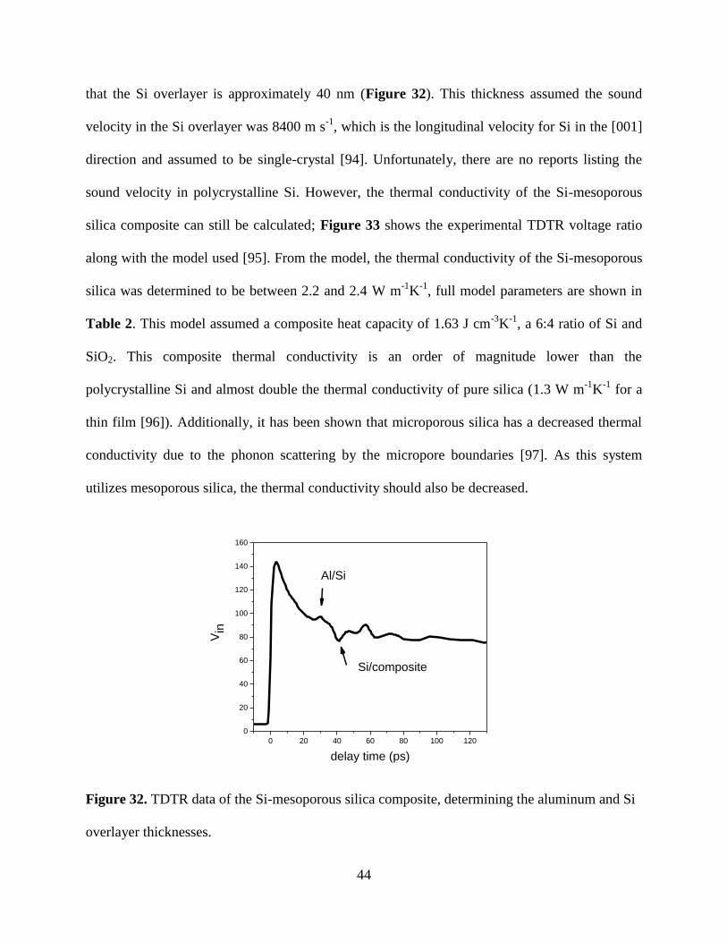
that the Si overlayer is approximately 40 nm (Figure 32). This thickness assumed the sound
velocity in the Si overlayer was 8400 m s-1
, which is the longitudinal velocity for Si in the [001]
direction and assumed to be single-crystal [94]. Unfortunately, there are no reports listing the
sound velocity in polycrystalline Si. However, the thermal conductivity of the Si-mesoporous
silica composite can still be calculated; Figure 33 shows the experimental TDTR voltage ratio
along with the model used [95]. From the model, the thermal conductivity of the Si-mesoporous
silica was determined to be between 2.2 and 2.4 W m-1
K-1
, full model parameters are shown in
Table 2. This model assumed a composite heat capacity of 1.63 J cm-3
K-1
, a 6:4 ratio of Si and
SiO2. This composite thermal conductivity is an order of magnitude lower than the
polycrystalline Si and almost double the thermal conductivity of pure silica (1.3 W m-1
K-1
for a
thin film [96]). Additionally, it has been shown that microporous silica has a decreased thermal
conductivity due to the phonon scattering by the micropore boundaries [97]. As this system
utilizes mesoporous silica, the thermal conductivity should also be decreased.
0 20 40 60 80 100 120
0
20
40
60
80
100
120
140
160
Vin
delay time (ps)
Al/Si
Si/composite
Figure 32. TDTR data of the Si-mesoporous silica composite, determining the aluminum and Si
overlayer thicknesses.

45
Figure 33. TDTR experimental data and model for the Si-mesoporous silica composite.
Table 2. Parameters used in modeling the TDTR measurement data for the Si-mesoporous silica
composite thermal conductivity.
Material Thermal Conductivity
[W m-1
K-1
]
Heat Capacity
[J cm-3
K-1
]
Thickness
[nm]
Al (Absorption layer) 1840 24.2 1 (81.4 nm)
Al 184 2.42 74.4
Interface 0.1 0.1 1
Si (overlayer) 38 1.64 40
Interface 0.1 0.1 1
Si (CVD) / SiO2 2.2-2.4 1.63 150
Interface 0.1 0.1 1
Si 142 1.64 1.0 x 10⁷
10-9
0
0.5
1
1.5
2
time delay (s)
Vra
tio
Model
Experiment

46
To extract the exact thermal conductivity of each component of the Si-mesoporous silica, a
detailed study would be required; at a minimum, the silica mesopores should be varied to allow
for increased Si deposition. However, modeling of thermal conductivities of composites [98] can
provide estimates. In this system, a simple parallel model can provide a first-order
approximation:
4
where kc, ksilica, and kSi are the thermal conductivities of the composite, mesoporous silica
(continuous phase), and Si (discrete phase), respectively, and φ is the volume fraction of the Si.
From the microporous silica study [97], the thermal conductivity range is between 0.85 and 1.1
W m-1
K-1
. From the mesoporous silica synthesis, the mesopore diameter is approximately 2.3 nm
with 58% porosity. Due to the confinement of the silicon, the silicon grain size should be similar
to the mesopore diameter [90]. Modeling the system by inputting the silica thermal conductivity
in a range of 0.85 to 1.3 W m-1
K-1
, taking into the full range of the microporous study as well as
the thin film silica, estimates of the Si thermal conductivity can be obtained and are shown in
Figure 34. Clearly, the model deviates and sets a lower boundary of the silica thermal
conductivity to 0.93 W m-1
K-1
. In Fang, et al., microporous silica study, their sample with
porosity 58%, the same used in this study, had a room temperature thermal conductivity of
approximately 1.05 W m-1
K-1
. Substituting this value into the parallel model provides a Si
thermal conductivity of 10.6 W m-1
K-1
, less than a third of the polycrystalline Si film; however,
this is still a factor of 2 higher than the reported polycrystalline inverse Si opal with a 20 nm
crystallite size (approximately 5 W m-1
K-1
) [90]. Additionally, reports on the thermal
conductivity of porous silicon have it as low as 0.1 W m-1
K-1
at room temperature [99]. A more
detailed study, with varying the mesopore diameter, is necessary for obtaining a clear result.

47
0.85 0.90 0.95 1.00 1.05 1.10 1.15 1.20 1.25 1.300
10
20
30
40
50
Therm
al co
nd
uctivity o
f S
ilicon
[W
m-1K
-1]
Thermal conductivity of Silica [W m-1K
-1]
Figure 34. Modeled thermal conductivity of Si as a function of the thermal conductivity of
silica, using the parallel thermal conductivity model [98].
3.3 Conclusions
Mesoporous silica was employed in two unique applications. A colloidal crystal, containing 622
nm diameter silica colloids with 2.27 nm diameter mesopores, was used to template platinum
deposited via ALD. This created a mesoporous shell of platinum after the HF etching of the
silica, due to the incomplete penetration of the platinum during the ALD. Additionally, silicon
was infiltrated into the mesoporous silica for thermal conductivity measurements. These
measurements were successful and showed polycrystalline silicon, deposited via CVD, has a
thermal conductivity of 38 W m-1
K-1
, while the effective thermal conductivity of the Si-silica
composite was an order of magnitude less, between 2.2 and 2.4 W m-1
K-1
. Simple modeling
using a parallel thermal conductivity model attempted to extract the material thermal
conductivity of the silicon; however, detailed investigations are needed for accurate results.

48
CHAPTER 4
CARBON COLLOIDAL CRYSTALS:
FABRICATION, TEMPLATING, AND OPTICAL PROPERTIES
The fabrication of high-quality colloidal crystals from mesoporous carbon colloids is first
demonstrated by tailoring the surface charge on the mesoporous carbon colloids. This colloidal
crystal is then used as a unique template, due to its high temperature stability, nanostructured and
high surface area, and easy removal, with porous oxide and semiconductor inverse opals
obtained through an orthogonal process. Through atomic layer deposition and static chemical
vapor deposition, the templated materials penetrate deep into the ultra-high surface area colloids,
generating the porous inverse opal after carbon removal processes that are not destructive to the
deposited materials. This allows for the fabrication and preservation of unique, nanostructured
materials that are inherently difficult to template with conventional techniques. Presented in this
chapter is primarily work published in Advanced Optical Materials [1].
4.1 Fabricating Carbon Colloidal Crystal
As a first attempt to make a carbon colloidal crystal, Monodispersed Starburst Carbon Spheres
(MSCS), synthesized as previously reported [77], were dispersed into ethanol and deposited on a
substrate via convective deposition [48, 100, 101]. Even though the polydispersity of the MSCS
was very low (only 1.038), the result was a disordered film, probably because the zeta-potential
of the as synthesized MSCS was only -14 mV. This compares to a zeta-potential of -31 mV
measured for typical opal-forming silica particles. It has been shown that partial oxidation of
carbon fibers introduces ionizable oxygen species (e.g., carboxylic acid) [102]; these species
would increase the surface charge. Heating the MSCS in air at 300 and 400 °C increased the

49
surface charge with no significant size change; see Table 3 and Figure 35 for zeta-potential and
SEM analysis.
Table 3. MSCS surface properties after heat treatment for 30 min.
Heat treatment
[°C]
Diameter
[nm]
Zeta Potential
[mV]
Pore volume
[mL g-1
]
Pore size
[nm]
Specific surface
area
[m2 g
-1]
As prepared 484 ± 19 -14 ± 6 1.00 1.67 1670
300 475 ± 7 -26 ± 6 0.92 1.74 1490
400 473 ± 7 -46 ± 4 0.92 1.87 1360
500 244 ± 10 -34 ± 4 0.37 - 420
600 - - - - -
Figure 35. MSCS oxidized for 30 min. at (a) 300 °C, (b) 400 °C, and (c) 500 °C.
Significant size reduction occurred at 500 °C, and by 600 °C, the MSCS sample disappeared due
to complete oxidation of the carbon [102]. To verify the porous structure of the MSCS remained
through the oxidations, nitrogen adsorption measurements were conducted (Figure 36); the pore
volume, size, and specific surface area are included in Table 3. The structural characteristics of
the MSCS oxidized at 300 and 400 °C change very little. There is only a minor decrease in pore
volume and a slight increase in pore size due to partial collapse of micropores, with the surface

50
0.0 0.2 0.4 0.6 0.8 1.0
0
100
200
300
400
500
600
700
Volu
me A
dsorb
ed [cm
3 S
TP
g-1]
Relative Pressure, P/P0
As Synthesized
300 C
400 C
500 C
0 1 2 3 4 5
0.0
0.1
0.2
0.3
0.4
0.5
0.6
0.7
0.8
0.9
1.0
dV
(w)
[cm
3 n
m-1 g
-1]
Pore Width [nm]
As synthesized
300 °C
400 °C
500 °C
Figure 36. (a) Nitrogen adsorption (solid circles) and desorption (open circles) isotherms of as
prepared MSCS (black curve), and MSCS oxidized at 300 °C (red), 400 °C (blue), and 500 °C
(green). (b) Calculated pore size distribution from (a).
b
a

51
296 294 292 290 288 286 284 282 280
0
1x10³
2x10³
3x10³
4x10³
5x10³
6x10³
7x10³
C
PS
Binding Energy (eV)
296 294 292 290 288 286 284 282 280
0
1x10³
2x10³
3x10³
4x10³
5x10³
6x10³
CP
S
Binding Energy (eV)
Figure 37. XPS C1s region for (a) as-synthesized MSCS and (b) oxidized MSCS at 400 °C. The
main C-C was set to a binding energy of 284.5 eV.
a
b

52
Table 4. XPS data for virgin and 400 °C oxidized MSCS
XPS atomic bonding [%]
Bond Binding
Energy
[eV]
As prepared 400 °C
C-C 284.5 97.5 92.0
C-OH 286.3 2.5 5.0
C=O 288.1 0 1.9
C-OOH 291.3 0 1.1
area remaining over 1300 m2 g
-1. Oxidation at 500 °C resulted in significant decreases in both
pore volume and surface area, and there is now no clear mesopore pore size distribution. To
investigate the surface chemical effects of oxidation, X-ray Photoelectron Spectroscopy (XPS)
was conducted on the as-synthesized and 400 °C treated samples (Figure 37 & Table 4). In
these, the main C 1s peak was set to a binding energy of 284.5 eV, with the pi-pi* shake-up
shifted 5.231 eV to 289.731 eV. Table 4 lists the atomic binding percentages for the two
samples. The surface of the oxidized carbon contained significantly more oxygen containing
moieties, i.e., hydroxyls, quinones, and carboxylic acids (C-OH, C=O, C-OOH). The presence of
these functional groups agree well with the increased surface charge measured for the oxidized
MSCS and is consistent with other results [102]. Colloidal crystal formation was then attempted
using the MSCS with the increased surface charge. Both the 300 °C and 400 °C oxidized
samples formed colloidal crystals, with the sample oxidized at 400 °C producing the highest
quality (shown in Figure 38). The higher quality of the colloidal crystals fabricated using the
400 °C oxidized MSCS can be attributed to the increased stability of the suspension due to the
higher surface charge compared to the as-synthesized and 300 °C oxidized (-46 mV vs. -14 &
-26 mV, respectively). Although colloidal crystals produced this way show high degree of order

53
in the Scanning Electron Microscopy (SEM) micrographs, due to the strong absorption of
carbon, a low optical reflectivity and transmission was observed (Figure 39).
b
1 µm
1 µm
d c
1 µm
a
500 nm
Figure 38. (a & b) SEM micrographs showing cross-section views of a 5-layer colloidal
crystal. (c) Oblique view of (a & b). (d) Cross-section micrograph of 7-layer colloidal
crystal. Colloidal crystal was fabricated from 400 °C oxidized MSCS.

54
0.6 0.8 1.0 1.2 1.4 1.6 1.8 2.0 2.2 2.4 2.60.00
0.05
0.10
0.15
0.20
0.00
0.05
0.10
0.15
0.20
Tra
nsm
ittance
Refle
ctance
Wavelength (m)
Reflection
Transmission
Figure 39. Optical measurements of MSCS colloidal crystal.
4.2 Mesoporous Starburst Carbon Spheres as Templates
Due to the MSCS porosity and potential for complete removal by oxidation in air, the carbon
colloidal crystals are ideally suited as templates to create unique nanostructures after inversion.
Employed here are two gas-phase deposition techniques that allow deep infilling of the
mesopores: atomic layer deposition (ALD) of hafnia (HfO2) and alumina (Al2O3) and static
chemical vapor deposition (CVD) of silicon (Si). SEM micrographs after 100 cycles of ALD
HfO2, 10 nm nominally on a flat substrate, are shown in Figure 40. Verification of pore
infiltration was done through a Focused Ion Beam (FIB) cut on a carbon/HfO2 composite
colloidal crystal, i.e., prior to carbon removal (Figure 40a). Transmission Electron Microscopy
(TEM) was also conducted on the composite colloid (Figure 40a, top). The top of the colloidal
crystal has a thick sputtered gold coating required for FIB milling; no gold was coated after
milling on the exposed surface. Carbon, due to its low atomic number, appears darker than the
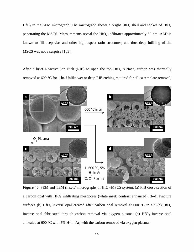
55
HfO2 in the SEM micrograph. The micrograph shows a bright HfO2 shell and spokes of HfO2
penetrating the MSCS. Measurements reveal the HfO2 infiltrates approximately 80 nm. ALD is
known to fill deep vias and other high-aspect ratio structures, and thus deep infilling of the
MSCS was not a surprise [103].
After a brief Reactive Ion Etch (RIE) to open the top HfO2 surface, carbon was thermally
removed at 600 °C for 1 hr. Unlike wet or deep RIE etching required for silica template removal,
600 °C in air
O2 Plasma
1. 600 °C, 5% H
2 in Ar
2. O2 Plasma
200 nm
a
500 nm
d
500 nm
b
500 nm
c
100 nm
100 nm
100 nm
100 nm
Figure 40. SEM and TEM (insets) micrographs of HfO2-MSCS system. (a) FIB cross-section of
a carbon opal with HfO2 infiltrating mesopores (white inset: contrast enhanced). (b-d) Fracture
surfaces (b) HfO2 inverse opal created after carbon opal removal at 600 °C in air. (c) HfO2
inverse opal fabricated through carbon removal via oxygen plasma. (d) HfO2 inverse opal
annealed at 600 °C with 5% H2 in Ar, with the carbon removed via oxygen plasma.

56
this thermal removal process does not remove HfO2, so all the deposited HfO2 remains. Figure
40b shows the HfO2 inverse opal SEM and TEM micrographs. In these, a granular HfO2
structure exists, perhaps due to the HfO2 crystallizing during the thermal MSCS removal. Since
carbon can be readily removed through oxygen plasma at room temperature, it was possible to
evaluate the structure of the HfO2 in the as-deposited state. The top of the HfO2-coated MSCS
colloidal crystal was opened via RIE etching, followed by an oxygen plasma etch to remove the
MSCS. The resulting inverse opal (Figure 40c) contrasts sharply with the thermally removed
MSCS; a smooth, instead of granular, nanostructure is observed. It appears that during the MSCS
thermal removal process, grain growth and sintering in the HfO2 occur simultaneously with
carbon removal. Once the MSCS support is removed, the HfO2 is free to crystallize and coarsen,
while the as-deposited HfO2 better replicates the ultra-high surface area MSCS.
To verify these hypotheses, experiments were conducted to crystallize the HfO2 prior to MSCS
template removal. As deposited, the HfO2 is amorphous. To crystallize the HfO2 prior to carbon
removal, the sample was annealed in forming gas (5% H2 in Ar) at 600 °C for 1 hr. This
replicates the thermal removal process time and temperature; however, the forming gas limits
MSCS oxidation. Crystallization of the HfO2 prior to template removal is only possible due to
carbon’s high thermal stability and inert nature with respect to HfO2. After annealing, the MSCS
was removed through oxygen plasma. Cross-sectional SEM (Figure 40d) of this sample is
strikingly similar to the as-deposited, oxygen plasma removed samples (Figure 40c). It appears
the MSCS provided a support and template during HfO2 crystallization, limiting sintering and
grain growth, preserving the templated nanostructure. X-ray diffraction (XRD) on the as-
deposited and annealed samples was used to confirm the amorphous nature of the as deposited

57
HfO2 and its crystalline nature after annealing. For this experiment, it is important that the
majority of the HfO2 is deposited in the pores of the MSCS and not on the MSCS surface (the x-
ray experiment does not distinguish between HfO2 on the surface of the MSCS surface and in the
pores), and so the number of ALD cycles was reduced to 60, depositing nominally 6 nm of HfO2.
Most of the HfO2 will be inside the MSCS, and only a few nm will be on the surface of the
carbon colloids. XRD shows the as-deposited HfO2 is amorphous, while the annealed sample is
Figure 41. (a) XRD data of as-deposited (black) and annealed (red) HfO2 ALD coated
MSCS colloidal crystals. The HfO2 JCPDS PDF file 04-004-7637 is shown for reference. (b)
XRD data of the Al2O3 ALD coated MSCS opals. (c) XRD data of as-deposited Si static
CVD. (d) XRD of the glass substrate used in these measurements.

58
crystalline (Figure 41). From the Scherrer Equation, the average crystallite was found to be 8.4
nm, substantially greater than the 1.87 nm MSCS pore size but significantly less than the total
length infiltrated into the pores (~80 nm), indicating the HfO2 crystallites may be rod-like.
Transmission electron microscopy (TEM) (Figure 40d, top) and selected area electron diffraction
(SAED, Figure 42) confirmed the crystalline nature of HfO2.
Figure 42. SAED and corresponding TEM images of the (a) as-deposited HfO2 and (b) annealed
HfO2 on a MSCS.
100 cycles (10 nm nominally) of ALD Al2O3, with the MSCS thermally removed, is shown with
a FIB cut in Figure 43a. As with the HfO2, the thermal removal process is completely
orthogonal to Al2O3 removal. In most of the MSCS, the Al2O3 infiltrates into the center;
however, “defects” of partially unfilled MSCS occur (top right MSCS in Figure 43a). The TEM
micrograph of the Al2O3 inverse colloid in Figure 43b shows the solid Al2O3 shell and porous
center. Unlike for HfO2, the Al2O3 inverse opal did not crystallize, and its mesostructure did not
appear to Oswald ripen during thermal carbon removal at 600 °C (XRD in Figure 41). This may
not be surprising, as 1100 °C is a typical crystallization temperature for alumina [104].
a
50 nm 100 nm
b

59
Figure 43. (a) FIB cross-section cut of ALD Al2O3 inverse opal with carbon template thermally
removed. (b) TEM micrograph of Al2O3 structure in (a). (c) Silicon inverse opal fabricated via
static CVD; carbon colloidal crystal template was removed via oxygen plasma. (d) TEM
micrograph of silicon structures in (c).
The final successful material investigated for template inversion was Si, which is grown using
static CVD. SEM and TEM micrographs are shown in Figure 43c & d. To prevent Si oxidation,
MSCS were removed via room-temperature oxygen plasma after removing the top Si overlayer
via RIE. The conformal Si static CVD deposition infiltrates the MSCS template, creating a
porous-Si interior. As expected, XRD (Figure 41) reveals the as-grown Si is amorphous, as Si
crystallization requires heating to 1000 °C for several hours. Platinum ALD in the MSCS was
also attempted. However, due to oxygen being a reactant in the ALD growth, the MSCS colloidal
crystal oxidizes and loses its well-defined order (Figure 44).
100 nm
d
300 nm
a
100 nm
b
250 nm
c

60
Figure 44. 500 cycle platinum ALD on carbon colloidal crystal.
Figure 45. Optical measurements on inverse opals structures after carbon removal: (a) 100 cycle
ALD HfO2; (b) 300 cycle ALD HfO2; (c) 100 cycle ALD Al2O3; (d) static CVD silicon.
500 nm
0.6 0.8 1.0 1.2 1.4 1.6 1.8 2.0 2.2 2.4 2.60.0
0.1
0.2
0.3
0.4
0.5
0.6
0.7
0.8
0.9
1.0
0.0
0.1
0.2
0.3
0.4
0.5
0.6
0.7
0.8
0.9
1.0
Tra
nsm
itta
nce
Re
fle
cta
nce
Wavelength (m)
0.6 0.8 1.0 1.2 1.4 1.6 1.8 2.0 2.2 2.4 2.60.0
0.1
0.2
0.3
0.4
0.5
0.6
0.7
0.8
0.9
1.0
0.0
0.1
0.2
0.3
0.4
0.5
0.6
0.7
0.8
0.9
1.0
Tra
nsm
itta
nce
Re
fle
cta
nce
Wavelength (m)
0.6 0.8 1.0 1.2 1.4 1.6 1.8 2.0 2.2 2.4 2.60.0
0.1
0.2
0.3
0.4
0.5
0.6
0.7
0.8
0.9
1.0
0.0
0.1
0.2
0.3
0.4
0.5
0.6
0.7
0.8
0.9
1.0
Tra
nsm
itta
nce
Re
fle
cta
nce
Wavelength (m)
0.6 0.8 1.0 1.2 1.4 1.6 1.8 2.0 2.2 2.4 2.60.0
0.1
0.2
0.3
0.4
0.5
0.6
0.7
0.8
0.9
1.0
0.0
0.1
0.2
0.3
0.4
0.5
0.6
0.7
0.8
0.9
1.0
Tra
nsm
itta
nce
Reflecta
nce
Wavelength (m)
d
a b
c
61
Optical measurements were conducted on HfO2, Al2O3, and Si inverted opals (Figure 45). Figure
45a shows the 100 cycle ALD HfO2 inverse structure with a primary reflection peak of 16% at a
wavelength of 840 nm. A MSCS colloidal crystal was also coated with 300 cycles HfO2 (30 nm
nominally). The optical measurements are shown in Figure 45b after the MSCS were removed.
30 nm of HfO2 is below the pinch-off point (when the colloid interstitials fill and block further
precursor deposition) of 37 nm for the 479 nm colloids. For the thicker HfO2 deposition, the
reflection peak red-shifts to 1.0 μm and increases to 35% with well-defined Fabry-Perot fringes.
Since the mesopores are already full after 100 ALD cycles, the extra 200 cycles simply increase
the thickness of solid HfO2 shell around each MSCS particle, leading to the red-shift and
increases in intensity of the reflection peak. The Al2O3 optical measurements are shown in
Figure 45c. Interestingly, no reflection peak is observed; this could be the result of the infilling
“defects,” where a portion of the colloids have large voids in the center. These defects perhaps
act as strong scattering centers. Optical measurements of the Si inverse structure are shown in
Figure 45d; the main reflectance peak is at 940 nm with 19% reflectance. The transmittance
measurement shows a primary dip of 63% corresponding with the reflectance peak; the
remaining 18% of the light is either absorbed or scattered. Interestingly, the Si inverse structure
has a transmittance of near 95% at longer wavelengths, compared to only ~55% for a typical Si
inverse opal [105]. The high transmittance (low reflectance) is evidence that the effective
refractive index of the porous Si structure is much lower than pure Si (~3.5).
4.3 Conclusions
In conclusion, by tailoring the surface charge of carbon colloids, high-quality carbon colloidal
crystals can be fabricated and these high-surface area colloidal crystals can be used as templates

62
for a variety of materials, creating unique, high-surface area nanostructured inverse opals. These
materials, HfO2, Al2O3, and Si, penetrate deep into the mesopores of the MSCS. Importantly, the
carbon removal process is completely orthogonal to the deposited material removal, preserving
the fine-scale mesostructure of the MSCS in the templated materials. Because MSCS removal is
orthogonal to the etching of many materials, MSCS provide a general approach for templating
materials that currently cannot be templated by conventional colloidal crystals.
4.4 Experimental Procedures
Synthesis: Monodisperse Starburst Carbon Spheres (MSCS) were synthesized as previously
reported [77]. The MSCS were oxidized in a Lindberg Furnace using a 30-min. ramp, 30-min.
hold, and cooled to room temperature. For colloidal crystal fabrication, Piranha-cleaned
substrates (glass or quartz) were placed at a 20° angle in a 20 mL scintillation vial with 0.7 g
colloidal suspension (0.5-2 wt% in ethanol). The vials were placed in an incubator (Fisher,
Isotemp 125D) and held at 40 °C overnight.
Infiltration and template removal: HfO2 and Al2O3 ALD, using a Cambridge Nanotech ALD
system, were done at 200 °C and 80 °C, respectively, on fabricated carbon colloidal crystals with
both recipes having a growth rate of 1 Å cycle-1
. Si static CVD was done at 350 °C for 2 hr using
Si2H6 [17]. A Reactive Ion Etch (RIE) using O2 and CF4 gasses (1 sccm each, 10 mTorr, 75 W, 1
nm min-1
HfO2 removal) was done to expose the MSCS for thermal or oxygen plasma removal.
Thermal removal was done at 600 °C for 1 hr with a 30-min. ramp. Oxygen plasma removal was
done using 20 sccm O2 at 400 mTorr, 200 W, for 2 hr.
Characterization: Nitrogen physisorption isotherms, BET specific surface area, and pore volume
were measured and calculated as previously described [77]. Scanning Electron Microscopy

63
(SEM) was done on Hitachi S-4700 or S-4800. Transmission Electron Microscopy (TEM) was
done on a JEOL 2010LAB6 at an accelerating voltage of 200 kV. Focus Ion Beam (FIB) milling
was done on a FEI Beam 235 FIB. Zeta-potential measurements were conducted in Millipore
water on a NICOMP 380 ZLS Particle Sizer.

64
CHAPTER 5
ENERGY HARVESTING USING CARBON COLLOIDAL CRYSTALS
One of the most common energy-harvesting practices is through the absorption of photons and
conversion into electrical energy; conventionally, this has been done with silicon solar cells.
Dye-sensitized solar cells (DSSC), while not as efficient as conventional silicon solar cells, are
attractive due to their low cost and thin film design, allowing a broad range of substrates and
applications. By treating conductive surfaces appropriately, either through a thin oxide
deposition or a self-assembly monolayer, monodispersed starburst carbon spheres could be
assembled into colloidal crystals. When fabricated on a transparent conductive oxide, these
colloidal crystals were used as a high-surface area template for dye-sensitized solar cells
(DSSC). Through an atomic layer deposition, titania was deposited into the mesopores and was
crystallized into the anatase phase without carbon oxidation and removal through an annealing
process in an inert atmosphere. After crystallization, carbon was easily and orthogonally
removed by simply changing from an inert to a non-inert atmosphere containing oxygen. Using a
ruthenium dye and a standard iodine-iodide electrolyte, DSSC were fabricated from the
templated titania and compared to another cell constructed using the standard, nanoparticle
titania paste. While a number of experimental adjustments were made, ultimately the templated
DSSC could not perform as well as the DSSC fabricated with the titania paste.
5.1 Carbon Colloidal Crystals on Conductive Substrates
For energy harvesting, as well as energy storage (see Chapter 6) devices, an electrical pathway is
required to extract the charges from the device. For both applications, MSCS offer a unique,
high-surface template. However, the adhesion between the carbon starburst spheres and

65
conductive substrates was found to be problematic, with most colloidal assemblies delaminating
prior to final templating. This is presumably due to the inability of the substrate to maintain a
surface charge, which is necessary for colloidal crystal formation [58]. MSCS assemblies on
oxide substrates, including glass and quartz specimen slides, have resulted in well-arranged
colloidal crystals due to the anionic surface charge of the substrate and the generation of
oxidizable species on the MSCS surface [1].
Mentioned previously, Dye Sensitized Solar Cells (DSSCs) incorporate a wide-bad gap
semiconductor, typically titania, to transport the electron to the back contact. Expanding upon the
earlier success of oxide substrates, a thin layer of titania (8 nm) was deposited on the conductive,
fluorine-doped tin oxide (FTO) substrate via ALD. Using the established procedure with this
substrate, MSCS colloidal crystals were successfully fabricated. These assemblies were rather
fragile; however, with careful handling and immediate processing, they were successfully
templated.
5.2 Mesoporous Carbon for DSSC
DSSC, classified as a third-generation solar technology, consists of a wide-band gap
semiconductor, a photosensitive dye, and an electrolyte. The photosensitive dye is adsorbed onto
the mesoporous semiconductor; upon incident light, the dye absorbs the photon and charge
separation occurs at the dye/semiconductor interface with the semiconductor providing a
pathway for the electron [106]. This is in contrast to traditional silicon solar cells where the light
absorption, charge separation, and the species transport all occur within the semiconductor. The
mesoporous semiconductor provides high surface area for the dye adsorption; additionally, it

66
provides light scattering, increasing the optical path length, especially for high-frequency (short
wavelength) photons [107]. Due to the dye’s absorption properties, the long wavelength photons
require multiple optical path lengths to be fully absorbed [45]. To improve the optical absorption
of these long wavelengths, groups have incorporated larger particles that scatter longer
wavelength (sacrificing surface area) [107], coupled the mesoporous semiconductor to a
photonic crystal [41-45, 48], and used nanotubes [108] and hemispheres [46] in the
semiconductor architecture. These techniques either sacrifice the surface area or require an
additional processing step. Using a MSCS colloidal crystal as a template could allow for an
improved optical response while keeping the high surface area. The colloid diameter could be
tuned for optimal response in the red spectrum and the mesopores could be replicated in the
templating process.
Prior to utilizing a titania oxide layer for colloidal crystal growth, a disordered MSCS film was
deposited via drop-casting a colloidal solution onto a masked FTO substrate; titania was
immediately deposited via ALD after solvent evaporation and mask removal. Future assemblies
utilized the titania-coated FTO substrate and MSCS colloidal crystal as the template for titania
ALD. As the anatase crystalline form of titania has improved electrical properties to the rutile
crystal structure [109], the titania-MSCS composite was annealed at 500 °C for 2 hr under
forming gas (5% H2 in Ar). Annealing in forming gas prevented the MSCS oxidation, allowing
the MSCS to act as a structural support during the titania crystallization. To remove the MSCS,
the composite was heated for an additional 2 hr in air, also at 500 °C. The ruthenium dye and
photovoltaic (PV) cell fabrication followed a similar procedure set by Wang, et al. [106]. The
ruthenium dye (N-719) was dissolved as a 0.5 mM solution in 1:1 volume ratio of acetonitrile

67
and tert-butyl alcohol. To prevent water condensation, the titania substrates were placed in the
dye solution once they cooled to 80 °C after the crystallization and MSCS removal process; the
titania substrates were removed after 48 hr and assembled. For a reference electrode, a standard
20 nm titania particle paste was deposited on the FTO substrates after a titanium chloride
treatment; the crystallization and subsequent processes were kept the same.
The initial, disordered MSCS template PV performance is shown in Figure 46 against a standard
reference cell made with the titania paste also fabricated at the same time. Of important note is
all values reported here are externally measured on a broadband solar simulator; Quantum
Efficiency (QE) and Incident Photon to Current Efficiency (IPCE) have not been measured. The
reference cell has a Power Conversion Efficiency (PCE) of 3.6% under AM 1.5 illumination
(100 mW cm-2
), while the templated cell only has a PCE of 0.9%. The majority of this efficiency
loss is due to the decreased short-circuit current (ISC), which corresponds to the magnitude of
photons absorbed and successfully separated into charge carriers. This indicates that the
templated cell absorbed less photons, possibility due to lack of adsorbed dye, or did not
effectively separate the charges at the dye/titania interface. The open circuit voltage (VOC) of the
templated cell is 50 mV less than the reference (0.65 vs. 0.70 V) and the fill factor (FF) is also
reduced from 0.61 to 0.52. These suggest internal resistances due to poor device fabrication.

68
-0.2 -0.1 0.0 0.1 0.2 0.3 0.4 0.5 0.6 0.7 0.8 0.9 1.0
-10
-9
-8
-7
-6
-5
-4
-3
-2
-1
0
1
2
Cu
rre
nt
De
nsity (
mA
cm
-2)
Voltage (V)
Reference
ALD
Figure 46. PV performance of reference DSSC fabricated via standard techniques (black) and
DSSC using mesoporous titania via ALD (red). Standard DSSC: PCE = 3.6%, FF = 0.61, Isc =
8.50 mA cm-2
, Voc = 0.70 V; Mesoporous DSSC: PCE = 0.9%, FF = 0.52, Isc = 2.61 mA cm-2
,
Voc = 0.65 V.
To investigate the titania electrodes, the cells were dismantled and imaged with the FIB (Figure
47). The ALD titania had a polymeric impurity coating the colloids, perhaps from the tape used
to mask the FTO. This impurity would drastically alter the PV performance, increasing the
internal resistance, limiting the light absorbed, and even affecting the charge separation.
Switching from the drop-casting and masking process to the use of a MSCS colloidal crystal
template on the titania-coated FTO should eliminate this impurity. The SEM of the titania paste
electrode shows a clean film, consisting of the 20 nm titania nanoparticles, approximately 3 µm
thick.

69
Figure 47. (Top) SEM micrographs of the top surface of ALD titania (left) and titania paste
(right) electrodes. The ALD titania had a polymeric impurity present, coating the colloids.
(Bottom) FIB cross-section cut on the titania paste electrode. Thickness is approximately 3 µm.
MSCS colloidal crystals were fabricated on the titania-coated FTO substrates using 480 nm
diameter spheres with a pore size of 1.87 nm, followed by titania ALD, crystallization, and
carbon removal. To confirm the annealed titania crystallized into the anatase phase, X-Ray
Diffraction (XRD) was conducted on the annealed ALD titania (Figure 48). The amount
deposited was 27 nm, as measured through ellipsometry on a flat, reference silicon wafer placed
in the ALD chamber with the MSCS colloidal crystal. The as-deposited titania is confirmed to be
amorphous (data not shown). The XRD in Figure 48 verifies that the titania does crystallize into

70
the anatase phase; through peak analysis, the crystallite size was found to be 16.6 nm.
Additionally, the titania unit cell has dimensions of 3.7698 x 9.2678 Å, slightly smaller than the
theoretical, unstrained unit cell of 3.784 x 9.515 Å. Interestingly, this corresponds to a 0.3%
strain in the a direction, while a 2.6% strain along the c-axis.
20 30 40 50 60 70 80
Inte
nsity [
a.u
.]
Angle [2]
Figure 48. XRD spectra of ALD titania grown on carbon colloidal crystal after titania
crystallization. The peaks correspond to the anatase crystal structure, with the PDF file shown in
blue (PDF#04-002-2750).
The titania electrode templated via the MSCS colloidal crystal was assembled into a DSSC and
the PV performance tested. However, the performance, especially the short circuit current (ISC),
was still extremely poor. To investigate this, FIB cuts and SEM imaging were done on the
carbon-removed titania, shown in Figure 49. These show the titania infiltrates partway into the

71
carbon but do not fully replicate the mesoporous structure. Additionally, these micrographs show
a thick shell of titania; this would prevent dye infiltration, which limits the number of photons
absorbed, and thus severely decreases cell performance.
Figure 49. FIB cuts on carbon-removed titania. The titania infiltrates partway into the pore
network of the carbon.
To test whether the dye is being adsorbed onto the titania electrode, UV-Vis measurements were
conducted on the titania paste, used as a reference, and the ALD titania, both before and after 3-
day immersion in dye solution (Figure 50). The titania paste shows a clear dip in the
transmission where the dye absorbs (~550 nm). The ALD titania, however, does not show this

72
dip. Instead, the entire spectrum is suppressed due to scattering of the light. While scattering is
preferred in the PV cell to increase the optical path length, dye must be present to absorb these.
In the templated titania, there is no strong absorption from the dye, indicating low dye loading.
FTIR measurements were also conducted on the templated titania (Figure 51) and show a main
reflectance peak at ~1.0 μm with a magnitude of ~40%. Due to the increased density of states
near the stop band edge [15, 44], this should improve the absorption of the red photons. This
could be tailored through the use of differing diameters of MSCS.
250 300 350 400 450 500 550 600 650 700 750 800 850 900
0.0
0.1
0.2
0.3
0.4
0.5
0.6
0.7
0.8
0.9
1.0
Tra
nsm
itta
nce
Wavelength (nm)
TiO2 paste
TiO2 paste w/ dye
ALD TiO2
ALD TiO2 w/ dye
Figure 50. UV-Vis spectra of titania paste (solid lines) and ALD titania (dotted). The black
indicates neat titania and red is the same sample after 3 days of immersion in dye solution.
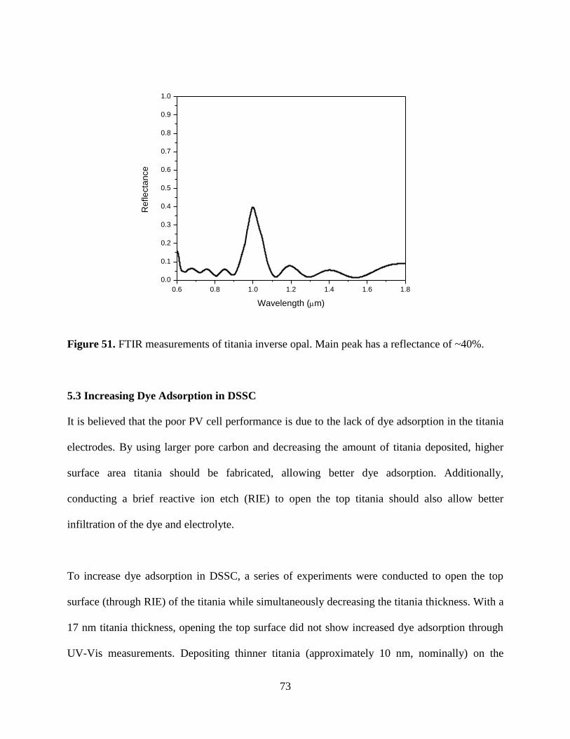
73
0.6 0.8 1.0 1.2 1.4 1.6 1.8
0.0
0.1
0.2
0.3
0.4
0.5
0.6
0.7
0.8
0.9
1.0
Refle
cta
nce
Wavelength (m)
Figure 51. FTIR measurements of titania inverse opal. Main peak has a reflectance of ~40%.
5.3 Increasing Dye Adsorption in DSSC
It is believed that the poor PV cell performance is due to the lack of dye adsorption in the titania
electrodes. By using larger pore carbon and decreasing the amount of titania deposited, higher
surface area titania should be fabricated, allowing better dye adsorption. Additionally,
conducting a brief reactive ion etch (RIE) to open the top titania should also allow better
infiltration of the dye and electrolyte.
To increase dye adsorption in DSSC, a series of experiments were conducted to open the top
surface (through RIE) of the titania while simultaneously decreasing the titania thickness. With a
17 nm titania thickness, opening the top surface did not show increased dye adsorption through
UV-Vis measurements. Depositing thinner titania (approximately 10 nm, nominally) on the

74
larger pore MSCS (pore diameter = 4.3 nm) resulted in a titania inverse structure that had its
integrity compromised through the RIE process, both before and after titania crystallization and
MSCS removal. While the 10 nm titania deposited would overfill the pores, the experiment
assumed the RIE process would allow the dye and electrolyte to penetrate where the MSCS
colloids had vacated, and thus be able to infiltrate other shells through the packing of the MSCS
template. RIE before titania crystallization and MSCS removal resulted in titania powder (after
subsequent MSCS removal) with no clear structure, probably due to the ease of etching the
amorphous titania; however, decreasing the RIE settings (e.g., power, time, etc.) had little effect.
Conducting RIE after crystallization resulted in delamination, presumably from undercutting at
the titania-FTO surface.
Decreasing the amount of titania deposited via ALD, approaching 1-2 nm, would allow a full
replica of the mesopores. Additionally, the large pore MSCS could provide a large enough
mesoporous template where, after the thin titania deposition, there exist mesopores within the
titania shell. The requirements for this, however, are quite daunting: the largest mesoporous
carbon used in this study had a diameter of 4.3 nm; the deposited titania would need to be less
than 2 nm, as the titania deposits conformally, coating the walls of the mesopores evenly. If this
is successful, however, the dye should be able to infiltration through inherent cracks in the
inverse opal, removing the need for the RIE process. After numerous attempts, decreasing the
titania thickness to only a few nanometers compromises the structure during and after carbon
removal. All samples made with the extremely thin titania failed prior to cell fabrication. There
does not appear to be an experiment window that allows effective use of the surface area
provided by the mesoporous carbon.

75
5.4 Conclusions
High-quality colloidal crystals were able to be formed on the conductive FTO substrate after an
initial coating of titania. Through ALD, titania was deposited onto the colloidal crystals,
infiltrating the pores. After crystallization into the anatase crystal phase, the MSCS template was
removed through a simple oxidation process. The PV characteristics showed a low short circuit
current indicating low absorption of the incident photons. Low dye loading in the templated
titania was revealed to be the source of the low photon absorption. Attempts to increase the dye
adsorption by opening the top colloid surface through RIE or by depositing only a very thin
coating of titania were unsuccessful. As such, MSCS colloidal crystals are not suitable as a
template for DSSC applications.

76
CHAPTER 6
ENERGY STORAGE UTILIZING CARBON COLLOIDS AS TEMPLATES
In this chapter, the MSCS colloidal crystals are used as unique templates for energy storage,
namely lithium battery anodes. CVD is done to deposit Si as the active material and, through an
extension of recent work in the Abelson group, Fe (which is converted into Fe3O4 as the active
material) into the mesoporous template. The Si-MSCS is immediately assembled into a half-cell
for battery testing to minimize oxidation. The newly deposited Fe is fully characterized to ensure
deep infilling and then oxidized to Fe3O4. By controlling the partial pressure, the Fe-MSCS can
be oxidized to Fe3O4-MSCS without significant oxidation of the MSCS template. The MSCS
template provides a conductive pathway with the active materials, Si and Fe3O4, confined in the
mesopores, preventing any loss of material through pulverization. When cycled using an
electrolyte that contains vinylene carbonate, the Si-MSCS anode could be cycled over 85 cycles.
The Fe3O4-MSCS anode showed remarkable coulombic efficiency and revealed that the MSCS
template decreased the charge hysteresis from 0.90 V for a conventional system, to 0.60 V at a
rate of 0.2 C. Preliminary magnetic measurements were done on the Fe-MSCS composite, and a
unique, dual superparamagnetic and ferromagnetic behavior was observed.
6.1 Introduction and Anode Fabrication
Secondary lithium-based batteries, due to the ever-increasing demand from numerous
applications, including consumer electronics, space applications, and electric vehicles, have
received considerable attention for a number of years [65, 110, 111]. Battery applications have a
number of requirements, chief among these are long-term stability [112], high cycling rate [56,
110], and high capacity [113-116]. For good cycle life and long-term stability, the active

77
electrode material and its interface with the electrolyte (the solid-electrolyte interface, SEI) must
be stabilized [117]. As cycling rate is typically limited by either electron extraction or Li-ion
diffusion, higher cycling rate can be achieved via electrode design [56]. One such example is a
conductive, and porous, electrode that can improve these limitations [56, 118]. To address issues
of increased capacity, new active materials are necessary.
Typical commercial batteries utilize graphitic carbon as the anode, which has reasonable stability
and cycling rate performance. The theoretical capacity of graphite is around 370 mA g-1
and
stores Li ions via intercalation, up to the nominal formula LiC6 [111, 119]. Other anode
materials, due to their high theoretical capacities, have been investigated, including those based
on Si [58, 120, 121], Sn [114, 122], and metal oxides [123-125]. Si, with a theoretical capacity of
~4,200 mA hr g-1
, is an exceptional high-capacity anode material. However, during lithium
insertion, the Si expands significantly, up to 400% volumetrically, with a corresponding
contraction upon lithium extraction. The stress associated with this large volumetric change
causes cracking and pulverization, leading to rapid capacity decay [120]. To alleviate the
induced strain, electrode designs have utilized Si in the nanometer range with sufficient space to
accommodate the expansion. Electrode design can also improve the electron extraction, typically
employing a porous, conductive scaffold [58, 113], a carbon coating [126, 127], or the addition
of carbon black [128]. The solid-electrolyte interface (SEI) stability is another challenge in the
silicon anode and has not been effectively addressed; however, mechanical clamping via a SiOx
protective layer [129] and the addition of vinylene carbonate (VC) to the electrolyte [130, 131]
have promise. Interestingly, not all reports indicate the VC additive improves performance; one
report, with an electrode containing nano-Si, carbon black, and cellulose binder, obtained

78
optimal cyclability with a VC-free electrolyte [117]. This suggests that Si-electrolyte SEI
stabilization using VC is dependent upon the numerous possible chemistries, of which the
polymer binder-electrolyte reaction plays a pivotal role.
Another promising anode candidate is iron oxide, Fe3O4, due to its high theoretical capacity
(upwards of 1000 mA hr g-1
), low cost, and low toxicity, in addition to it being environmentally
benign [110, 132]. Unlike the Si-Li intercalation reaction, Fe3O4 stores energy primarily through
a conversion reaction of Fe3O4 + 8Li+ + 8e
- → 3Fe + 4Li2O. Challenges with Fe3O4 include its
low conductivity, resulting in capacity fade and poor calendar life, and the large charge
hysteresis, resulting in energy and coulombic efficiency loss [110]. Similar strategies employed
with Si active materials can be utilized to improve conductivity: addition of carbon [133],
utilization of a conductive scaffold [110, 123, 124] and carbon nanotubes [132], and “coating”
by graphene encapsulation [125, 134]. Due to the conversion reaction, charge-discharge
hysteresis remains a challenge. Prominently, this hysteresis is due to an activation barrier for the
reduction and oxidation reactions, directly linked to the size and uniformity of the Fe3O4 active
materials formed after the first discharge [110]. Several groups have exploited Fe3O4
nanoparticles to decrease this barrier; however, particle aggregation is still a challenge [123, 125,
132, 134, 135]. One group in particular had success in hysteresis reduction: an anode comprising
of Fe3O4 nanoparticles decorated on graphene sheets was compared to an anode with only Fe3O4
nanoparticles [135]. The average reduced hysteresis, reported as the voltage difference between
the charge and discharge curves, is approximated to be 0.7 V, with the average hysteresis of the
pure Fe3O4 anode approximately 0.9 V.

79
Reported here is a novel anode system utilizing monodisperse starburst carbon spheres (MSCS)
as a scaffold for active materials, namely Si and Fe3O4, in lithium ion battery anodes. The MSCS
can be fabricated into a colloidal crystal structure, allowing electrolyte and ion diffusion between
the spheres. With their mesoporous nature, the MSCS offer unique templating opportunities, as
active materials can be deposited into the mesopores via static chemical vapor deposition
(sCVD); the carbon structure then acts as a confining layer and individual current collectors. By
utilizing an electrolyte containing VC, Si anodes show excellent coulombic efficiency while
retaining over 1000 mA hr g-1
capacity over 85 cycles at a cycling rate of 0.33 C. The Fe3O4
anodes were synthesized in a two-step process where, after sCVD of Fe, a partial oxidation
occurred. The anode showed good performance over 40 cycles and maintained a capacity of
~700 mA hr g-1
. Importantly, by confining Fe3O4 only in the mesopores, the charge hysteresis
dropped significantly to 0.60 V; increasing the amount of active material so that the Fe3O4 is no
longer confined in the mesopores raised the hysteresis to 0.75 V. This low hysteresis decreases
the energy loss, resulting in the high coulombic efficiency.
Monodisperse starburst carbon spheres (MSCS) were synthesized [77] and oxidized [1] as
previously reported. The MSCS structure is a wheel-like arrangement of carbon “spokes” due to
the templated synthesis. The specific MSCS used in the final anode have a diameter of 480 nm, a
polydispersity index (PDI) of 1.039, a pore volume of 1.47 mL g-1
, and a specific surface area of
1190 m2 g
-1. Most importantly, the average pore size, measured and calculated via nitrogen
isotherms, was 4.29 nm, with a distribution between 2 and 8 nm. By utilizing the large pore
MSCS, sCVD of active materials can easily infiltrate deep into the mesopores, increasing the
volumetric density of the anodes. After cleaning and modification, substrates were placed in an

80
ethanolic solution of MSCS for scaffold fabrication. Of note, unlike the previous work on the
MSCS colloidal crystal optics [1], the MSCS here are solely utilized as an anode scaffold, so
perfect order is not necessary. The MSCS-coated substrates were then put into a reaction
chamber and heated under vacuum to drive off any residual moisture in the mesopores. After
cooling to room temperature, the precursor, either disilane (Si2H4) or iron pentacarbonyl
(Fe(CO)5), was introduced into the reaction chamber, sealed, and heated to drive the reaction.
The Fe-MSCS was then oxidized to Fe3O4-MSCS by heating under partial vacuum (10 mbar).
Both the Si-MSCS and the Fe3O4-MSCS were then tested as anodes in a half-cell (coin cell
configuration) with lithium metal as the counter electrode.
For MSCS adhesion on the conductive substrates, a new approach is need as, unlike the DSSC
work, a layer of semiconductor oxide will increase the voltage drop in the electrode, making an
inferior device, or preventing charge collection altogether. By using a gold-coated substrate, a
self-assembled monolayer (SAM) of sodium 3-mercapto-1-propanesulfonate was deposited (5
mM solution in H2O, overnight). The sulfur group binds strongly to the gold surface while the
sulfonate group provides the necessary, negative charge. This allows for a possible salt bridge
between the carbon and the sulfonate to form. Another option that was ultimately employed was
switching to tungsten substrates, as this provides the necessary surface charge [58]. Both the
SAM treatment of the gold substrates and using tungsten films allowed MSCS colloidal crystal
growth.

81
6.2 Silicon CVD for Battery Applications
While there are numerous studies on silicon for Li-ion anodes, several advantages exist for using
CVD grown silicon with the MSCS colloidal crystal as a template. The MSCS create a
nanostructured electrode that will allow efficient charge collection, assuming the carbon is
conductive enough. 4-point probe measurements and an order of magnitude calculation show the
voltage drop through the MSCS template will be only ~25 mV for a 10 μm film. Of note, the 4-
point probe measurements were conducted on a drop-cast MSCS film on a glass substrate. Due
to the fragile nature of the MSCS structure, the probe points broke through and made contact
with the underlying substrate, even with diligent and careful lowering of the probe. As such, it is
believed that the resistivity measured is erroneously high due to the substrate. Regardless, this
voltage drop, even the high estimation, is sufficiently low for battery applications. By using
carbon as the current pathway, significant weight reduction can be realized compared to
conventional metal foils. With the nanostructure of the MSCS, any nanoparticle of silicon that
does break off during cycling has a high probability of striking and attaching to another carbon
colloid. Thus, capacity fade due to pulverization of the silicon and loss of electrical contact is
diminished. A drawback, however, manifests in the fragility of the carbon colloidal crystal.
Unlike silica colloidal crystals where the colloids have covalent bonds binding them together and
to the substrate, the MSCS have only weak van der Waals attraction. Conventional anode
construction uses a slurry of graphitic carbon, carbon black, and a polymer binder (typically
polyvinylidene difluoride, PVDF) cast onto the substrate current collector. Due to the processing
conditions required, i.e., silicon CVD occurs after MSCS colloidal crystal formation, the
polymer binder cannot be used during MSCS colloidal crystal fabrication.

82
Initially, a MSCS colloidal crystal was fabricated on a sulfonated thiol-treated gold-chrome
coated glass substrate with low-pressure silicon CVD conducted to deposit only a thin layer into
the MSCS mesopores. Placing the anode in a jar cell, it was cycled against lithium metal in
organic electrolyte (ethylene carbonate, dimethyl carbonate, & lithium perchlorate,
EC:DMC:LiClO4). However, due to its fragility and lack of binder, the MSCS colloidal crystal
anode severely delaminated. With the anode set perpendicular in the jar, any colloid that
delaminates falls into the electrolyte, eliminating any chance of electrical reconnection. Instead,
by switching to a coin cell configuration, the MSCS colloidal crystal can be clamped by the
spacer, allowing electrical reconnection if colloids delaminate. To determine the capacity and
round-trip efficiency, coin cells containing the Si-MSCS anode were cycled at 0.05 C in the
voltage window of 0.1 to 2 V, shown in Figure 52. Of note, the voltage window for typical
silicon anodes drops to 0.05 or 0.01 V [58, 120]; however, due to using gold-coated slides as the
electrodes, 0.1 V was chosen to limit the lithium-gold alloying processes that occur at 0.130 and
0.075 V [136]. The MSCS used had a pore size of 4.29 nm, which allows easy infiltration by the
silicon CVD. The silicon-based capacity is similar to reported values at 3450 mAh g-1
for coin
cell 1 and 3140 mAh g-1
for coin cell 2, and, after the first cycle, the round-trip efficiency is
above 90%. The sharp drops in the capacity during testing are assumed to be instrument error, as
the raw data shows a charge/discharge switch before reaching the voltage set points. Samples
were also cycled against lithium metal at approximately 1 C. Unfortunately, the capacity dropped
significantly after each cycle, with evidence that the carbon was delaminating from the substrate.
To combat this, Si anodes can be cycled at much slower rates while delivering significant power
due to their high capacity [58].

83
0 1 2 3 4 5 6 7 8 9 10 110
500
1000
1500
2000
2500
3000
3500
4000
4500
Capacity
Ca
pa
cit
y (
mA
h g
-1)
Cycle Number
0
10
20
30
40
50
60
70
80
90
100
Efficiency
Eff
icie
nc
y (
%)
Figure 52. Si-MSCS anode coin cell cycled at 0.05 C on gold-coated substrates.
0 5 10 15 20 25 300
100
200
300
400
500
600
700
800
900
1000
Ca
pa
cit
y (
mA
h g
-1)
Cycle Number
0
10
20
30
40
50
60
70
80
90
100
110
Eff
icie
nc
y (
%)
Figure 53. Anode cycled at 0.125 C consisting of only MSCS (i.e., no silicon deposition).
Additionally, cycling a carbon anode will provide a baseline capacity as well as determine if the
silicon expansion is the cause of delamination. The carbon anode was cycled at 0.125 C for 30
times (Figure 53). The capacity is fairly constant, aside from a drop around cycle 16 (extreme

84
low points are most likely experimental or equipment error). Unfortunately, the roundtrip
efficiency reached only 90% after 30 cycles. However, this shows that the MSCS template can
withstand numerous cycles, allowing further use in the Si-MSCS anode.
0 20 40 60 80 1000
500
1000
1500
2000
2500
3000
3500
4000
Ca
pa
cit
y (
mA
h g
-1)
Cycle Number
Capacity
Si Jar Cell w/ Binder
50
60
70
80
90
100
110
120
Efficiency
Eff
icie
ncy
(%
)
Figure 54. Cycle performance on Si-MSCS jar cell with binder at 0.6C.
To determine the cycle capability, a new setup was attempted using the jar cell. In this, PVDF
binder in N-Methyl-2-pyrrolidone (NMP) was drop-casted onto the silicon-MSCS anode; as the
silicon has already been deposited, blocking the MSCS pores is no longer a concern. The number
average molecular weight of the PVDF is 71,000 g mol-1
(PDI of 2.5), with a radius of gyration
approximately 4.2 nm, assuming theta solvent conditions. With this, the polymer should slightly
infiltrate into the mesopores (vp = 4.29 nm, pore distribution between 2-8 nm). 100 cycles at
0.6C on this anode configuration shows a steady and significant capacity drop, even though the
round-trip efficiency was over 90% after two cycles and maintained 97-98% through 60 cycles

85
(Figure 54). A 0.6 C rate was chosen to obtain data in a timely fashion; however, decreasing the
C rate may improve the capacity retention during cycling as other cycle performance studies
have been conducted at 0.1C [120, 137], and 0.3C [58]. Post-cycling, top-view SEM was
conducted (Figure 55); these show a film, be it SEI or binder, covering the colloidal crystal
anode with large, 10 μm diameter holes surrounded by nano- and micro-particles. These may be
silicon-coated MSCS that have pulverized, PVDF binder, or even SEI formation on one or both;
without elemental analysis, confirmation is impossible.
Figure 55. Post-cycling SEM (top-view) of silicon-MSCS coated with binder. Anode was cycled
100 times at 0.6 C.

86
To improve performance and understand this unique system, three routes were taken: (i)
decreasing silicon loading, (ii) determining if the PVDF binder is appropriate, and (iii) switching
from gold-coated substrates. Decreasing the silicon loading will allow for silicon to be deposited
inside the mesopores but not create a shell around the colloids. A cross-sectional FIB image on a
virgin anode shows faint outlines of a silicon shell, indicating that the performance may be due
to a silicon film (which is easily pulverized), rather than discrete particles inside the mesopores
(Figure 56). If a silicon shell has formed, decreasing the deposited silicon can be done by
changing the CVD reaction conditions. While PVDF binder is commonly used, researchers have
had mixed success; one study with an anode consisting of a silicon nanowire array showed poor
stability with PVDF but respectable stability with sodium alginate binder [137]. Even in the
preliminary studies above, coin cells without the binder show adequate capacity, at least in the
first 10 cycles. Longer cycling by the coin cell may determine that the binder is not needed, due
to the clamped configuration. If the binder is necessary, an increase in the molecular weight of
the binder will prevent infiltration into the mesopores, allowing silicon to expand unhindered.
Unstable SEI formation, as some papers suggest the anode failure mechanism [120, 121, 137],
could be potentially solved with the correct electrolyte and binder combination; if not, the most
promising technique is a thin oxide shell deposited via ALD [138]. As stated earlier, gold alloys
with lithium at low potentials, proving difficult to use in anodes. Studies have shown that gold
interferes with silicon anode performance (loss of capacity, rate, and fade) [137] as well as
potentially delaminating when used in thicknesses of 10 nm or greater [136]. Eliminating gold
from the anode will undoubtedly improve performance. A promising candidate is a tungsten foil
substrate, as they showed promise in previous studies [58].

87
Figure 56. FIB cut on virgin silicon-MSCS anode.
TEM imaging was also conducted on the low-pressure silicon CVD on carbon for Li-ion
batteries (Figure 57). Due to the colloid contrast, i.e., darker in the center than the edges, one
can deduce that there is silicon deposited inside the mesopores, rather than just the shell. This is
expected, as the results from the 1.87 nm pore MSCS templating also showed Si infiltration [1];
these MSCS colloids for battery applications had mesopores with a diameter of 4.3 nm. Thicker
electrodes, for more practical applications, were attempted by first depositing silicon on a carbon
colloidal crystal, then redispersing the colloids in a binder solution. However, the small quantity
of carbon-silicon sample does not allow this. Instead, thicker electrodes would need to be created
via a Xia Cell or similar method.

88
Figure 57. TEM images of the low-pressure silicon CVD on mesoporous carbon colloids.
To combat the gold delamination, tungsten substrates were utilized, providing the necessary
anionic surface charge for colloidal crystal formation [58]; and cut to fit into the coin cell
configuration. A cleaning process using concentrated KOH in ethanol makes the tungsten
substrate suitable for high-quality carbon colloidal crystal growth, followed by a low-pressure
silicon CVD. These were made into coin cells with a standard electrolyte (1.0 M LiPF6 in
EC/DEC/DMC (1:1:1 by vol)) and cycled at different C rates (Figure 58). While the efficiency
is good (99% at greater than 1 C rates), the capacity fade is significant; returning to the initial
0.065 C rate after 40 cycles resulted in a capacity loss of nearly 50%. To improve this, additional
processing of the Si CVD samples can be employed. As the Si CVD is non-selective, Si will be
deposited on the back and exposed top of the tungsten substrate. This Si will not be confined in
the carbon pores and, as such, will be more subjected to the pulverization due to volume
expansion. In order to remove this Si, RIE has been conducted with a Kapton film as a mask.
Additionally, incorporating incorporate vinylene carbonate (VC) as an additive into the
electrolyte has been shown to improve performance in a number of studies [130, 131].

89
Figure 58. Si-MSCS coin cell fabricated with the standard electrolyte (1.0 M LiPF6 in
EC/DEC/DMC (1:1:1 by vol)).
By modifying the electrolyte with the addition of VC, totaling approximately 5 wt%, the
performance was significantly improved. Figure 59 shows the rate performance of the Si-MSCS
with the VC electrolyte. The Si-MSCS anode was fabricated using experimental conditions to
underfill the structure, allowing the Si to deposit into the mesopores but not creating a thick
overlayer on the MSCS. This is a two-fold imperative: the mesoporous structure of the MSCS
allows for the volumetric expansion of the Si during lithiation through the rearrangement of the
MSCS “spokes.” Additionally, keeping the Si within the mesopores provides an intimate
connection and allows easy electron extraction and transport. Due to the large surface area and
pore volume of the MSCS, the mass ratio of the Si to MSCS was 5:1, signifying the majority of
the capacity obtained was provided by the Si. During the first 10 cycles, when the cycling rate

90
was 0.07 C, there is a steady decline in capacity with the coulombic efficiency between 90 and
95%. However, after the tenth cycle, the cycling rate was increased to 0.25 C with the coulombic
efficiency increasing to 99%, which was maintained throughout 85 cycles, even when the rate
was further increased to 0.33 C. Also of importance is that the Si-MSCS anode, after rapidly
losing capacity in the first 10 cycles, stabilizes its specific capacity at approximately 1680 mA hr
g-1
during the cycling at 0.25 C. At 0.33 C, the capacity drops slightly but again stabilizes
through 85 cycles, ending with a capacity of 1090 mA hr g-1
. In this Si-MSCS system, the anode
design allows for volumetric expansion and, even if partially pulverized, an extended
mesoporous network allows efficient electron extraction and transportation. Since there is no
binder in the Si-MSCS anode system, the SEI stability could be easily addressed through the
addition of VC to the electrolyte without concern of secondary reactions.
0 5 10 15 20 25 30 35 40 45 50 55 60 65 70 75 80 85 90
0
500
1000
1500
2000
2500
3000
3500
4000
0.07 C
0.25 C
0.33 C
Lithiation
Delithiation
Capacity (
mA
h g
-1)
Cycle
0.0
0.1
0.2
0.3
0.4
0.5
0.6
0.7
0.8
0.9
1.0
Effic
iency
Figure 59. Cycle performance of Si-MSCS anode vs. Li using VC containing electrolyte.
91
6.3 Iron CVD for Battery Applications
While the Braun group has extensively utilized sCVD of Si with conformal deposition [139],
only a few reports show Fe deposition with Fe(CO)5 as a precursor; these are fabricated using the
traditional flow CVD and are analogous with rough and/or discontinuous films [140-142]. This
work takes advantage of the recent advancement in sCVD of Fe, where a conformal, continuous
Fe film can be deposited [143]. Unlike Si sCVD where the precursor is a gas that can be charged
to a given pressure, Fe(CO)5 is a liquid at room temperature with a high vapor pressure of ~33
mbar. As such, a sCVD system pumps to vacuum, seals off the vacuum line, and allows the
chambers to reach equilibrium, which introduces the precursor. Much to the advantage of this
system, it has been shown that there is strong selectivity of the Fe deposited between silicon
dioxide (SiO2) and tungsten, with a 100% selectivity to the SiO2 [141]. As the reaction chamber
is glass, the tungsten substrate should remain Fe free, allowing investigation into the role of the
mesoporous MSCS. Initially, a MSCS colloidal crystal, 479 nm diameter MSCS, pore diameter
of 1.87 nm, was used as the iron template. After diffusion of the Fe(CO)5 vapor, the samples
were heated at 150 °C for 10 hr, depositing iron that reached the pinch-off point of 37 nm
(Figure 60).

92
Figure 60. Fe static CVD on MSCS colloidal crystal. Left: fracture surface, right: FIB cross-
sectional cut.
Preliminary work done by a collaborator has shown that depositing iron on silica results in a
composition of 96 at% Fe, 2.5 at% O, and 1.5 at% C, as measured by XPS [143], eliminating
concerns of oxidation during deposition. The fracture surface and FIB cut in Figure 60 show the
deep infilling of the iron, even in the 1.87 nm pores. Additionally, XRD has been conducted on
the Fe-deposited MSCS colloidal crystal (Figure 61), with the peaks corresponding only to
metallic Fe. Analyzing the peaks, the crystallite size was determined to be 11.4 nm; the large
crystallite size compared to the pore diameter is similar to the phenomenon shown by the hafnia.
Additionally, as the iron is not confined to the pores, the interstitial sites in the colloidal crystal
can support large iron crystallites. Fe CVD was then conducted on larger pore diameter carbon
(4.3 nm) to allow a thin shell to be deposited in the pore. XRD on the larger pore (4.3 nm) shows
crystallite size to be slightly larger at 12.9 nm. Additionally, the XRD data on iron-coated 4.3 nm
mesopore carbon showed an additional peak at 43° 2θ (Figure 62).

93
20 30 40 50 60 70 80 90
Inte
nsity (
a.u
.)
Angle (2)
Fe PDF
Figure 61. XRD on Fe deposited carbon colloidal crystal. Peaks correspond to α-iron, BCC
symmetry (PDF#00-006-0696).

94
20 30 40 50 60 70 80 90
Inte
nsity (
a.u
.)
Angle (2)
Fe PDF
Figure 62. XRD data on CVD-grown iron on carbon colloidal crystal with 4.3 nm mesopores.
Bottom shows the PDF card file for iron (PDF#00-006-0696).
Interestingly, the Fe CVD has shown near-100% deposition selectivity by depositing on the
MSCS colloidal crystal, but not on the glass sidewalls of the reaction chamber. To investigate
this, two colloidal crystal samples, one carbon and one silica, were placed in the reaction
chamber. After the 10 hr CVD run was complete, the silica colloidal crystal had sparse Fe
nanoparticles decorating the silica colloids (Figure 63). However, Fe deposited readily on the
carbon colloidal crystal, infilling the colloidal crystal over 20 µm thick, presumably due to Fe-
MSCS surface reactions.

95
Figure 63. SEM of the silica colloidal crystal (left) and the carbon colloidal crystal (right) after
Fe CVD for 10 hours at 150 °C.
To combat the thick iron deposition, the selectivity shown between glass and carbon was
utilized. Increasing the carbon content would allow for thinner deposition (more area to deposit
onto, similar starting precursor content). This is in direct contrast to the silicon CVD, as the
silicon deposits more uniformly across numerous materials. By introducing a second sample in
the reaction chamber, effectively doubling the surface area for the Fe deposition, and having a
two-minute diffusion, thin iron deposits in “island” configurations were observed (Figure 64).
To determine the infilling of iron inside the carbon mesopores, a FIB cut was conducted on the
Fe-C composite. To deposit iron, a shorter (30 sec.) precursor (Fe(CO)5) diffusion was utilized
after pumping down to 10-6
mbar; two carbon colloidal crystal samples were in the reactor. After
sealing, the reactor was placed in a furnace having a heating process of 1 °C/min ramp to 150 °C,
hold for 1 hour, and a 0.3 °C/min cool. The fracture cross-section was similar to Figure 64;
however, Figure 65 shows the FIB cut, along with a contrast-enhanced portion. Due to the two-
toned contrast on the cut, one can conclude the iron deposits through the pores.

96
Figure 64. Thin “islands” of iron deposited on carbon opal utilizing two samples in the reactor
and a 2-minute precursor diffusion (150 °C, 1 hr, heating).
Figure 65. FIB cut of the Fe-C composite; two samples were placed in the reactor with a 30-
second precursor diffusion (150 °C, 1 hr, heating). Inset is a contrast-enhance portion, showing
the two-toned iron-carbon composite.
To further verify Fe infiltration, a focused ion beam (FIB) lift-out was performed; Figure 66(a)
shows the scanning electron microscopy (SEM) image of the Fe-MSCS composite, Figure 66(b)
and (c) are transmission electron microscopy (TEM) and scanning transmission electron

97
microscopy (STEM) images, respectively. An electron energy loss spectrum (EELS) was taken
on the inset of Figure 66(c) and shown in Figure 66(d); the peaks at 700 and 713 eV correspond
to the Fe-L3 and Fe-L2 lines (i.e., excitation of Fe 2p3/2
and 2p1/2
electrons) [144, 145], verifying
Fe deposition into the center of the MSCS. By changing the diffusion and heating time, along
with the amount of MSCS templates, the thickness of the Fe can be controlled. For this sample, a
precursor diffusion time of 30 seconds and heating at 150 °C for 1 hour were used.
Figure 66. (a) SEM image of Monodispersed Starburst Carbon Spheres (MSCS) after Fe CVD
deposition (incomplete infilling) and subsequent FIB liftout. (b) TEM and (c) STEM of the Fe-
MSCS. (d) EELS spectrum taken from the inset in (c); the O and Fe peaks can be seen at ~520
and ~700 eV, respectively.
c
100 nm
100 nm
500 600 700 800 900
40
60
80
100
120
Inte
nsity (
x10
3)
Energy Loss (eV)
500 nm
a
d
b
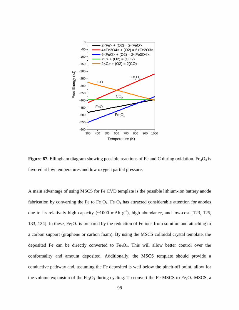
98
300 400 500 600 700 800 900 1000
-600
-550
-500
-450
-400
-350
-300
-250
-200
-150
-100
-50
0
CO2
CO
Fe3O
4
FeO
Fe2O
3
Fre
e E
nerg
y (
kJ)
Temperature (K)
2<Fe> + (O2) = 2<FeO>
4<Fe3O4> + (O2) = 6<Fe2O3>
6<FeO> + (O2) = 2<Fe3O4>
<C> + (O2) = (CO2)
2<C> + (O2) = 2(CO)
Figure 67. Ellingham diagram showing possible reactions of Fe and C during oxidation. Fe3O4 is
favored at low temperatures and low oxygen partial pressure.
A main advantage of using MSCS for Fe CVD template is the possible lithium-ion battery anode
fabrication by converting the Fe to Fe3O4. Fe3O4 has attracted considerable attention for anodes
due to its relatively high capacity (~1000 mAh g-1
), high abundance, and low-cost [123, 125,
133, 134]. In these, Fe3O4 is prepared by the reduction of Fe ions from solution and attaching to
a carbon support (graphene or carbon foam). By using the MSCS colloidal crystal template, the
deposited Fe can be directly converted to Fe3O4. This will allow better control over the
conformality and amount deposited. Additionally, the MSCS template should provide a
conductive pathway and, assuming the Fe deposited is well below the pinch-off point, allow for
the volume expansion of the Fe3O4 during cycling. To convert the Fe-MSCS to Fe3O4-MSCS, a

99
partial oxidation is needed, while maintaining the MSCS scaffold, i.e., little to no carbon
oxidation. Figure 67 shows the calculated Ellingham diagram of the possible C and Fe oxidation
reactions [146]. At temperatures below 843 K (570 °C), Fe3O4 is thermodynamically favored. An
initial attempt at converting the Fe to Fe3O4 was made by oxidizing the sample in air at 400 °C
for 3 hr. This resulted in a reddish sample, indicating conversion to Fe2O3 instead of Fe3O4.
While Fe3O4 is energetically favored, an excess of oxygen will drive the reaction to Fe2O3, with
XRD confirmation in Figure 68. Additionally, when Fe2O3 is formed, the thermodynamic
energy landscape dictates that the carbon template should be oxidized and removed; a FIB cut
(Figure 69) confirms this. By reducing the time and/or temperature for oxidation, conversion to
Fe3O4 should be possible.
20 30 40 50 60 70 80 90
Inte
nsity (
a.u
.)
Angle (2)
Fe2O3 PDF
Figure 68. XRD of oxidized iron at 400°C for 3 hours. The sharp peaks line up perfectly with
the Fe2O3 PDF file (PDF#00-033-0664).

100
Figure 69. FIB cut on the MSCS template, coated via Fe CVD, and oxidized at 400 °C in air for
3 hr.
20 30 40 50 60 70 80 90
Inte
nsity (
a.u
.)
Angle (2)
Fe3O4 PDF
Fe PDF
Figure 70. XRD of oxidized Fe-C under 7.4 E-6 mbar vacuum. The Fe partially oxidized to
Fe3O4; PDF files are Fe PDF#00-006-0696 and Fe3O4 PDF#04-005-4319.

101
To reduce the oxygen content and obtain Fe3O4, a Fe-C colloidal crystal sample was placed in a
reactor vessel under vacuum (7.4 E-6 mbar), sealed, and placed in a furnace for 4 hours at 400°C
(1 hour ramp). There should be a small amount of oxygen in the reactor vessel, allowing the iron
to convert to magnetite and preserve the carbon colloids, as well as preventing full oxidation to
Fe2O3. XRD analysis (Figure 70) shows the iron was partially oxidized with some Fe3O4 peaks;
however, the majority remained in the zero-valence iron. Experimentally, it was determined that
heating at 400 °C under a partial pressure of 10 mbar fully oxidized the Fe to Fe3O4 while
maintaining the MSCS scaffold. Figure 71 shows the XRD plot of the Fe3O4-MSCS on a
tungsten substrate. The peaks are indexed to both tungsten and Fe3O4 with no residual Fe peaks
or fully oxidized Fe2O3 peaks. The crystallite size of the Fe3O4 was calculated to be 18.4 nm.
While this is larger than the pore size, it is similar to the previous results where the crystallites
Figure 71. XRD plot showing complete conversion from Fe to Fe3O4. Crystallite size is 18.4 nm.
20 30 40 50 60 70 80 9010
2
103
104
Inte
nsity
Angle (2) (deg)
W PDF
Fe3O
4 PDF

102
are aligned in the pores [1]. This same oxidation condition was then conducted to the sample in
Figure 66 and similarly investigated, shown in Figure 72. The SEM, TEM, and STEM images
(Figure 72(a-c)) show no degradation due to the oxidation. Figure 72(d) and (e) are the
reconstructed images from the inset of Figure 72(c); Figure 72(d) is the reconstruction of only
the oxygen EELS signal with Figure 72(e) from only the iron EELS signal. These show the
oxidation and Fe infiltration is complete through the entire MSCS colloids.
Figure 72. (a) SEM image of Fe-MSCS after partial oxidation of the Fe to Fe3O4. (b) TEM and
(c) STEM of the Fe3O4-MSCS from (a). EELS reconstructed imaging using the (d) O signal and
the (e) Fe signal from the inset of (c).
c
200 nm
50 nm
O EELS Fe EELS
500 nm
a
d
b
e
103
The Fe3O4-MSCS anode system utilizes the same electrode design and its advantages as the Si-
MSCS anode with intriguing results. Figure 73 shows the rate performance of an underfilled
Fe3O4-MSCS, i.e., the Fe3O4 is confined in the mesopores (mass ration of Fe3O4 to C is 4:1).
Similar to the Si-MSCS system, the initial 10 cycles at 0.15 C rate results in a sharp capacity
fade, with the coulombic efficiency under 95%. The coulombic efficiency, however, continues to
improve during cycling, aside from the one-cycle drop when C rates were changed. After 40
cycles, the coulombic efficiency improved to over 99%, quite significant in conversion reaction
electrodes. Correspondingly, the capacity stabilizes after the initial drop with only mild loss
during cycling at 0.5 and 1.2 C rates. After the initial 10 cycles, the rate was increased to 0.5 C
for cycles 11-20 and further increased to 1.2 C for cycles 21-30. With higher cycling rates, more
power can be delivered if the capacity does not drop significantly. At a rate of 1.2 C, the Fe3O4-
MSCS anode still provides a capacity of 600 mA hr g-1
, 80% of the capacity at 0.5 C in cycles
11-20 (750 mA hr g-1
). By dropping the rate back to 0.5 C, the capacity improved to 700 mA hr
g-1
, signifying little or no permanent damage was done to the anode through faster cycling.
During fast charging, the rapid expansion conformational change of the active materials typically
leads to aggregation and loss of electrical contact. Through the electrode design where the Fe3O4
active material is confined in MSCS mesopores, this loss of electrical contact is severely limited.
Only through migration out of the mesopores could active material be lost and result in capacity
fade.

104
Figure 73. Cycle performance of Fe3O4-MSCS anode vs. Li.
With the high coulombic efficiency, the charge hysteresis was investigated. In this study, Fe3O4-
MSCS anodes were fabricated with varying initial deposition amounts of Fe; providing insight
are the two extremes, namely an underfilled anode similar to the anode cycled in Figure 73 and
an overfilled Fe (and subsequent Fe3O4) anode, creating a shell on the MSCS. The charge
hysteresis was determined by taking the differential charge with respect to voltage (dQ dV-1
) and
analyzing the peaks. These were taken at the second charge/discharge cycle with a cycling rate of
0.2 C and 5 C. These dQ dV-1
plots are shown in Figure 74, with the underfilled anode in Figure
74(a & c) and overfilled in Figure 74(b & d). The peak near 1.0 V (1.0 V for the underfilled
anode and 0.95 V for the overfilled) is the major contributor of the derived capacity and is

105
generated by the reduction reaction LixFe3O4 + (8-x) = 3Fe + 4Li2O [147]. Due to the
nanoparticle size, the structural transformation of Fe3O4 to a Li-Fe-O complex (LixFe3O4) can
easily occur. Indeed, due to the mesopores confinement, there is little likelihood of large Fe
particle formation that could suppress this transformation; this complex is responsible for the
broad shoulder-peak from 1.0 to 1.6 V [147]. For the 0.2 C cycling test, the hysteresis was taken
as the difference between the reduction peak and the lower voltage of the two oxidation peaks
(1.6 V for the underfilled and 1.7 V for the overfilled anode), which corresponds to the oxidation
of Fe0 to Fe
2+ [148]. In the case of the underfilled Fe3O4-MSCS anode, the hysteresis is quite low
at 0.60 V while the overfilled hysteresis is increased to 0.75 V. The confinement of the Fe3O4
active material in the mesopores imposes the nanoparticle size and reduces, perhaps eliminates,
particle aggregation, and provides an intimate current collector. For cycling at 5 C, the two
oxidation peaks merge, with both the underfilled and overfilled samples having similar
hysteresis: 1.1 V and 1.05 V, respectively.

106
Figure 74. Differential capacity (dQ dV-1
) plots of the Fe3O4-MSCS anode cycled at (a & c) 0.2
C and (c & d) 5 C: (a & c) low-filled Fe3O4 with a hysteresis of 0.60 V at 0.2 C and 1.1 V at 5 C;
(b & d) overfilled Fe3O4 with a hysteresis of 0.75 V at 0.2 C and 1.05 V at 5 C.
6.4 Magnetic Investigation of Iron CVD
An interesting experiment with the Fe-MSCS composites presented itself when a collaborator
indicated a new vibrating sample magnetometer (VSM) was available for testing. As such, a
MSCS colloidal crystal was fabricated (480 nm diameter, 1.79 nm pore diameter) and Fe CVD
was performed, fabricating a sample similar to Figure 60. The Fe infiltrated the mesopores and
also completely filled the interstitials between the colloids. Preliminary magnetic measurements
on the Fe-MSCS colloidal crystal composite show a coercivity of 68 Oe at 300 K (Figure 75);
0.0 0.5 1.0 1.5 2.0 2.5 3.0-1.5
-1.0
-0.5
0.0
0.5
1.0
Diffe
ren
tia
l C
ap
acity /
dQ
dV
-1
Voltage / V
0.0 0.5 1.0 1.5 2.0 2.5 3.0-0.4
-0.2
0.0
0.2
0.4
Diffe
ren
tia
l C
ap
acity /
dQ
dV
-1
Voltage / V
0.0 0.5 1.0 1.5 2.0 2.5 3.0-1.0
-0.5
0.0
0.5D
iffe
ren
tia
l C
ap
acity /
dQ
dV
-1
Voltage / V
0.0 0.5 1.0 1.5 2.0 2.5 3.0-1.5
-1.0
-0.5
0.0
0.5
1.0
Diffe
ren
tia
l C
ap
acity /
dQ
dV
-1
Voltage / V
a b
c d

107
this is similar to 7 nm particles [149], even though a nanostructured, 3-dimensional inverse
colloidal crystal was used. Room-temperature (300 K) superparamagnetism has been observed in
5 nm iron particles embedded in alumina matrix [149], particles consisting of 5 nm or less core
Fe surrounded by a shell of iron oxides [150], and larger 20-40 nm Fe3O4 particles-on-graphene
composites [124]. The current hypothesis is the Fe inside the pores behaves superparamagnetic,
due to the small diameter (pore size of 1.87 nm), while the outer shell of Fe is large enough to
support ferromagnetic behavior. This could be tested by varying the deposition thickness of the
Fe layer through different static CVD times. XRD was taken on a Fe-coated carbon colloidal
crystal grown on glass and was confirmed to have the Fe crystalline structure, with the crystallite
size determined to be 11.4 nm

108
Figure 75. Magnetic measurements on Fe-MSCS as a function of temperature. Inset shows the
upper-left quadrant.
6.5 Conclusions
In conclusion, anode systems that take advantage of a unique scaffold structure, namely the
mesoporous MSCS, were developed. These carbon scaffolds provide a conductive network
where the active materials, Si and Fe3O4, are confined in mesopores with short electron diffusion
lengths, due to the pore diameter of 4.29 nm, allowing facile electron extraction. Additionally, by
confining the active material in the pores, any pulverization or migration is suppressed and loss
of capacity through material loss (electrical isolation) is minimized. The Si-MSCS anode showed
stability through 85 cycles with the addition of VC to the electrolyte for SEI stabilization.
-1000 -800 -600 -400 -200 0 200 400 600 800 1000
-0.08
-0.06
-0.04
-0.02
0.00
0.02
0.04
0.06
0.08
Mag
ne
tizatio
n,
M,
a.u
.
Magnetic Field, H, Oe
50K
60K
70K
80K
90K
100K
150K
200K
300K
-100 -80 -60 -40 -20 00.000
0.005
0.010
0.015
0.020
0.025
0.030
M
300K
H
50K

109
Confining the Fe3O4 active material into the mesopores resulted in high coulombic efficiency,
and most intriguingly, a decrease in the charge hysteresis to 0.60 V at a cycling rate of 0.2 C.
This decrease is attributed to the unique electrode design (i.e., confinement in the mesopores);
increasing the Fe3O4 active material content overfills the mesopores and results in an increase in
the hysteresis. Additionally, preliminary magnetic measurements on the Fe-MSCS composite
show unique performance, a combination of superparamagnetic and ferromagnetic behavior.
6.6 Experimental Procedures
Formation of Carbon Template: Monodisperse starburst carbon spheres (MSCS) were
synthesized [77] and oxidized [1] as previously reported. Tungsten substrates were sonicated for
1 hr in concentrated ethanolic KOH, rinsed, dried, and placed in a solution of known
concentration (typically 0.75 wt%) of well-dispersed MSCS in ethanol at 40 °C overnight.
Material Deposition: Iron pentacarbonyl (Fe(CO)5 from Sigma) was used as the iron source
during Fe static CVD. Using standard air-free techniques, ~5 mL of Fe(CO)5 was placed in a
flask purged with nitrogen. MSCS-coated substrates were heated to 150 °C for 2 hr under a
vacuum of 10-5
mbar. After cooling and sealing the vacuum line, the precursor valve was opened
for equilibrated Fe(CO)5 vapors to enter the sample chamber, typically less than 2 minutes. The
reactor was sealed and placed into a furnace at 150 °C (1 °C/min ramp) for 1 hr (underfilled) or 5
hr (overfilled). Si CVD was conducted by decreasing the Si2H6 precursor amount from previous
reports [1]. To oxidize the Fe to Fe3O4, a Fe-coated sample was heated under 10 mbar partial
pressure to 400 °C for 3 hr (16 °C/min ramp). Oxidizing in air converted the Fe to Fe2O3 while
completely oxidizing (i.e., removing) the carbon template.

110
Coin Cell Fabrication and Testing: Li-ion half cells were fabricated in the standard coin cell
configuration using Celgard spacer, Novolyte electrolyte (1.0 M LiPF6 in EC/DEC/DMC (1:1:1
by vol.)), and Li metal as the counter electrode. Electrolyte modification was conducted by the
addition of vinylene carbonate (VC) to the Novolyte, resulting in ~5wt% VC. The half cells were
cycled at room temperature under constant current at varying rates. The Si-MSCS anode was
cycled between 0.1 and 2.0 V while the Fe3O4-MSCS anode was cycled between 0.1 and 3.0 V.

111
CHAPTER 7
CONCLUSIONS
Colloidal crystals, and specifically, mesoporous silica and carbon colloids, were used in
templating a variety of materials and a number of applications investigated. The first
investigation (Chapter 2) used nonporous silica colloids less than 300 nm in diameter to fabricate
a colloidal crystal for Brillouin Light Scattering (BLS) experiments. By varying the experimental
conditions, colloidal crystals, with the small diameter silica, could be successfully fabricated on
quartz and silicon substrates, which has previously been a challenge. Over-deposition in the
silicon chemical vapor deposition (CVD) process was eliminated by modifying the precursor
concentration while still filling the interstitial voids. Through careful processing, the silica
template was removed via hydrofluoric acid (HF) etching after a brief reactive ion etch (RIE) to
open the top silicon shell; the silicon inverse opal maintained excellent optical properties after
the etching. However, the BLS spectra showed unusual behavior in that the Stokes and anti-
Stokes were not symmetrical, with no clear explanation. The dispersion relationship between the
phonon frequencies and wave vectors did not show any phononic band structure, which may be
due to the unusual spectra obtained.
Mesoporous silica, with a mesopore diameter of approximately 2.3 nm, was used as templates
for platinum and silicon deposition (Chapter 3). A colloidal crystal of the mesoporous silica (622
nm diameter) was fabricated, and platinum was deposited via atomic layer deposition (ALD).
After HF etching of the silica, a mesoporous platinum shell was revealed due to the incomplete
infilling during the ALD process. Silicon was deposited via CVD, again modifying the reaction
condition to infiltrate the mesopores with thermal conductivity measurements taken on the

112
silicon-silica composite. The results show that a polycrystalline silicon film, deposited via CVD,
has a thermal conductivity of 38 W m-1
K-1
, while the effective thermal conductivity of the
silicon-silica composite was an order of magnitude less, between 2.2 and 2.4 W m-1
K-1
. Simple
modeling, using a parallel thermal conductivity model, attempted to extract the material thermal
conductivity of the silicon; however, more detailed investigations are needed for accurate results.
Tailoring the surface charge of mesoporous starburst carbon spheres (MSCS) through a partial
oxidation allowed the first high-quality carbon colloidal crystals to be fabricated (Chapter 4).
Templating a variety of materials, i.e., hafnia, alumina, and silicon, on these high-surface area
colloidal crystals resulted in deep penetration of the mesopores, creating unique, high-surface
area, nanostructured inverse opals. Importantly, the MSCS removal process is completely
orthogonal to the deposited material removal, preserving the fine-scale mesostructure of the
MSCS in the templated materials. Because MSCS removal is orthogonal to the etching of many
materials, MSCS provide a general approach for templating materials that currently cannot be
templated by conventional colloidal crystals.
For improvement in dye-sensitized solar cells (DSSC), further templating of the MSCS colloidal
crystal was done with titania (Chapter 5). By depositing a few nanometers of titania on the
conductive substrate, high-quality MSCS colloidal crystals were fabricated, followed by a titania
ALD to infiltrate the mesopores. The MSCS template was removed orthogonally: a simple
oxidation process after the crystallization of the titania into the anatase crystal phase. After
assembling the nanostructured titania into a DSSC, the photovoltaic characteristics indicated low
absorption of the incident photons, with low dye loading in the titania nanostructure revealed to

113
be the cause. Attempts to increase the dye adsorption by opening the top colloid surface through
RIE or by depositing only a very thin coating of titania were unsuccessful. As such, MSCS
colloidal crystals are not suitable as a template for DSSC applications.
Anode systems that take advantage of the MSCS unique scaffold structure were developed for
lithium batteries (Chapter 6). Silicon and Fe3O4 active materials are confined in the mesopores,
and the MSCS template provides a porous, conductive network allowing both electrolyte
diffusion and electron extraction. Confinement of the active materials suppresses any
pulverization or migration and also minimizes capacity loss through electrical isolation of active
materials. Through the addition of vinylene carbonate to the electrolyte, the silicon-MSCS anode
was cycled 85 times, indicating that the solid-electrolyte interface was stabilized. Through the
active material confinement, high coulombic efficiency was achieved in the Fe3O4-MSCS anode,
with a decrease in the charge hysteresis, from 0.90 V in conventional systems to 0.60 V in the
confined Fe3O4-MSCS anode. This decrease is attributed to the unique electrode design;
increasing the Fe3O4 active material content overfills the mesopores and results in an increase in
the hysteresis. Preliminary magnetic measurements on the Fe-MSCS composite show unique
performance, a combination of superparamagnetic and ferromagnetic behavior.
These results demonstrate the unique structures that can be fabricated through the use of
colloidal crystals and mesoporous templates. Fundamental studies of the phononic band structure
and thermal conductivity were investigated. Carbon colloids, for the first time, self-assembled
into a high-quality colloidal crystal, changing the templating paradigm due to the orthogonal
removal of the carbon. Additionally, the mesoporous structure allowed for applications that

114
previously were inaccessible, specifically the DSSC and lithium battery anodes. While the
mesoporous DSSC structure was ultimately inferior, the mesoporous carbon colloidal crystal
provided an excellent scaffold for the lithium battery anodes, with some exceptional properties
directly enabled by the mesoporous colloids.

115
REFERENCES
1. Goodman, M.D., et al., Enabling New Classes of Templated Materials through
Mesoporous Carbon Colloidal Crystals. Advanced Optical Materials, 2013. 1(4): p. 300-
304.
2. Norris, D.J., et al., Opaline photonic crystals: How does self-assembly work? Advanced
Materials, 2004. 16(16): p. 1393-1399.
3. Jiang, P., et al., Single-crystal colloidal multilayers of controlled thickness. Chemistry of
Materials, 1999. 11(8): p. 2132-2140.
4. Dimitrov, A.S. and K. Nagayama, Continuous convective assembling of fine particles
into two-dimensional arrays on solid surfaces. Langmuir, 1996. 12(5): p. 1303-1311.
5. Xu, X.L. and S.A. Asher, Synthesis and utilization of monodisperse hollow polymeric
particles in photonic crystals. Journal of the American Chemical Society, 2004. 126(25):
p. 7940-7945.
6. Park, S.H. and Y.N. Xia, Assembly of mesoscale particles over large areas and its
application in fabricating tunable optical filters. Langmuir, 1999. 15(1): p. 266-273.
7. Joannopoulos, J.D., et al., Photonic Crystals: Molding the Flow of Light (Second
Edition)2008: Princeton University Press. 304.
8. Marlow, F., et al., Opals: status and prospects. Angewandte Chemie International
Edition, 2009. 48(34): p. 6212-33.
9. Yablonovitch, E., PHOTONIC BAND-GAP STRUCTURES. Journal of the Optical
Society of America B-Optical Physics, 1993. 10(2): p. 283-295.
10. Yablonovitch, E., T.J. Gmitter, and K.M. Leung, PHOTONIC BAND-STRUCTURE -
THE FACE-CENTERED-CUBIC CASE EMPLOYING NONSPHERICAL ATOMS.
Physical Review Letters, 1991. 67(17): p. 2295-2298.
11. Yablonovitch, E., INHIBITED SPONTANEOUS EMISSION IN SOLID-STATE PHYSICS
AND ELECTRONICS. Physical Review Letters, 1987. 58(20): p. 2059-2062.
12. Gennady, S. and A.U. Yaroslav, Electric and magnetic properties of sub-wavelength
plasmonic crystals. Journal of Optics A: Pure and Applied Optics, 2005. 7(2): p. S23.
13. Zeghbroeck, B.V., Principles of Semiconductor Devices, 2011.
14. Schroden, R.C., et al., Optical properties of inverse opal photonic crystals. Chemistry of
Materials, 2002. 14(8): p. 3305-3315.
15. Busch, K. and S. John, Photonic band gap formation in certain self-organizing systems.
Physical Review E, 1998. 58(3): p. 3896-3908.
16. Vos, W.L., et al., Strong effects of photonic band structures on the diffraction of colloidal
crystals. Physical Review B, 1996. 53(24): p. 16231-16235.
17. Rinne, S.A., F. Garcia-Santamaria, and P.V. Braun, Embedded cavities and waveguides
in three-dimensional silicon photonic crystals. Nature Photonics, 2008. 2(1): p. 52-56.
18. Huang, Z., et al., Design and Fabrication of Carbon Quantum Dots/TiO2 Photonic
Crystal Complex with Enhanced Photocatalytic Activity. Journal of Nanoscience and
Nanotechnology, 2014. 14(6): p. 4156-4163.
19. Quan, L.N., et al., Soft-template-carbonization route to highly textured mesoporous
carbon-TiO2 inverse opals for efficient photocatalytic and photoelectrochemical
applications. Physical Chemistry Chemical Physics, 2014. 16(19): p. 9023-9030.

116
20. Xia, L., et al., Zinc oxide inverse opal electrodes modified by glucose oxidase for
electrochemical and photoelectrochemical biosensor. Biosensors & bioelectronics, 2014.
59: p. 350-7.
21. Lee, Y.J. and P.V. Braun, Tunable inverse opal hydrogel pH sensors. Advanced
Materials, 2003. 15(7-8): p. 563-566.
22. Zakhidov, A.A., et al., Carbon structures with three-dimensional periodicity at optical
wavelengths. Science, 1998. 282(5390): p. 897-901.
23. Holtz, J.H. and S.A. Asher, Polymerized colloidal crystal hydrogel films as intelligent
chemical sensing materials. Nature, 1997. 389(6653): p. 829-832.
24. Lee, K. and S.A. Asher, Photonic crystal chemical sensors: pH and ionic strength.
Journal of the American Chemical Society, 2000. 122(39): p. 9534-9537.
25. Velev, O.D. and E.W. Kaler, In situ assembly of colloidal particles into miniaturized
biosensors. Langmuir, 1999. 15(11): p. 3693-3698.
26. Eckert, A.W., The World of Opals1997, New York: Wiley.
27. Finlayson, C.E., et al., 3D bulk ordering in macroscopic solid opaline films by edge-
induced rotational shearing. Advanced Materials, 2011. 23(13): p. 1540-4.
28. Yamada, H., et al., Colloidal-Crystal Laser Using Monodispersed Mesoporous Silica
Spheres. Advanced Materials, 2009. 21(41): p. 4134-+.
29. Aguirre, C.I., E. Reguera, and A. Stein, Tunable Colors in Opals and Inverse Opal
Photonic Crystals (vol 20, pg 2565, 2010). Advanced Functional Materials, 2011. 21(2):
p. 210-210.
30. Kim, S.-H., et al., Self-assembled colloidal structures for photonics. Npg Asia Materials,
2011. 3(1): p. 25-33.
31. Stöber, W., A. Fink, and E. Bohn, Controlled growth of monodisperse silica spheres in
the micron size range. Journal of Colloid and Interface Science, 1968. 26(1): p. 62-69.
32. Reese, C.E., et al., Synthesis of highly charged, monodisperse polystyrene colloidal
particles for the fabrication of photonic crystals. Journal of Colloid and Interface
Science, 2000. 232(1): p. 76-80.
33. Ocier, C. and P.V. Braun, Facile Growth of Micron-sized Silica Colloids into a Well
Ordered Colloidal Crystal. unpublished, 2014.
34. Deegan, R.D., et al., Capillary flow as the cause of ring stains from dried liquid drops.
Nature, 1997. 389(6653): p. 827-829.
35. Xu, J., J. Xia, and Z. Lin, Evaporation-induced self-assembly of nanoparticles from a
sphere-on-flat geometry. Angewandte Chemie-International Edition, 2007. 46(11): p.
1860-1863.
36. Fischer, B.J., Particle Convection in an Evaporating Colloidal Droplet. Langmuir, 2002.
18(1): p. 60-67.
37. Jiang, P. and M.J. McFarland, Large-scale fabrication of wafer-size colloidal crystals,
macroporous polymers and nanocomposites by spin-coating. Journal of the American
Chemical Society, 2004. 126(42): p. 13778-13786.
38. Ferrand, P., et al., Micromoulding of three-dimensional photonic crystals on silicon
substrates. Nanotechnology, 2003. 14(2): p. 323-326.
39. Ye, J., et al., Integration of self-assembled three-dimensional photonic crystals onto
structured silicon wafers. Langmuir, 2006. 22(17): p. 7378-7383.

117
40. Wong, S., V. Kitaev, and G.A. Ozin, Colloidal crystal films: Advances in universality
and perfection. Journal of the American Chemical Society, 2003. 125(50): p. 15589-
15598.
41. Colodrero, S., et al., Porous One-Dimensional Photonic Crystals Improve the Power-
Conversion Efficiency of Dye-Sensitized Solar Cells. Advanced Materials, 2009. 21(7): p.
764-+.
42. Guldin, S., et al., Dye-Sensitized Solar Cell Based on a Three-Dimensional Photonic
Crystal. Nano Letters, 2010. 10(7): p. 2303-2309.
43. Halaoui, L.I., N.M. Abrams, and T.E. Mallouk, Increasing the conversion efficiency of
dye-sensitized TiO2 photoelectrochemical cells by coupling to photonic crystals. Journal
of Physical Chemistry B, 2005. 109(13): p. 6334-6342.
44. Mihi, A. and H. Miguez, Origin of light-harvesting enhancement in colloidal-photonic-
crystal-based dye-sensitized solar cells. Journal of Physical Chemistry B, 2005. 109(33):
p. 15968-15976.
45. Nishimura, S., et al., Standing wave enhancement of red absorbance and photocurrent in
dye-sensitized titanium dioxide photoelectrodes coupled to photonic crystals. Journal of
the American Chemical Society, 2003. 125(20): p. 6306-6310.
46. Yang, S.-C., et al., Hollow TiO2 hemispheres obtained by colloidal templating for
application in dye-sensitized solar cells. Advanced Materials, 2008. 20(5): p. 1059-+.
47. Oregan, B. and M. Gratzel, A Low-Cost, High-Efficiency Solar-Cell Based On Dye-
Sensitized Colloidal TiO2 Films. Nature, 1991. 353(6346): p. 737-740.
48. Mihi, A., C. Zhang, and P.V. Braun, Transfer of Preformed Three-Dimensional Photonic
Crystals onto Dye-Sensitized Solar Cells. Angewandte Chemie International Edition,
2011. 50(25): p. 5712-5715.
49. Pursiainen, O.L.J., et al., Compact strain-sensitive flexible photonic crystals for sensors.
Applied Physics Letters, 2005. 87(10): p. -.
50. Nelson, E.C., et al., Epitaxial growth of three-dimensionally architectured optoelectronic
devices. Nature Materials, 2011. 10(9): p. 676-681.
51. Griffete, N., et al., Inverse Opals of Molecularly Imprinted Hydrogels for the Detection of
Bisphenol A and pH Sensing. Langmuir, 2012. 28(1): p. 1005-1012.
52. Pan, Z., et al., Response of inverse-opal hydrogels to alcohols. Journal of Materials
Chemistry, 2012. 22(5): p. 2018-2025.
53. Barry, R.A. and P. Wiltzius, Humidity-sensing inverse opal hydrogels. Langmuir, 2006.
22(3): p. 1369-1374.
54. Wang, J., et al., Multiresponsive inverse-opal hydrogels. Advanced Materials, 2007.
19(22): p. 3865-+.
55. Isshiki, Y., et al., Electric Double-Layer Capacitance of Inverse Opal Carbon Prepared
Through Carbonization of Poly(Furfuryl Alcohol) in Contact With Polymer Gel
Electrolyte Containing Ionic Liquid. Polymers for Advanced Technologies, 2011. 22(8):
p. 1254-1260.
56. Zhang, H., X. Yu, and P.V. Braun, Three-dimensional bicontinuous ultrafast-charge and
-discharge bulk battery electrodes. Nature Nanotechnology, 2011. 6(5): p. 277-281.
57. Mandlmeier, B., et al., Formation of Interpenetrating Hierarchical Titania Structures by
Confined Synthesis in Inverse Opal. Journal of the American Chemical Society, 2011.
133(43): p. 17274-17282.

118
58. Zhang, H. and P.V. Braun, Three-Dimensional Metal Scaffold Supported Bicontinuous
Silicon Battery Anodes. Nano Letters, 2012. 12(6): p. 2778-2783.
59. Zhang, M.-L., et al., Inverse opal hydrogel sensor for the detection of pH and mercury
ions. Rsc Advances, 2014. 4(39): p. 20567-20572.
60. Bai, Y., et al., Enzyme-free glucose sensor based on a three-dimensional gold film
electrode. Sensors and Actuators B-Chemical, 2008. 134(2): p. 471-476.
61. Scott, R.W.J., et al., Tin dioxide opals and inverted opals: Near-ideal microstructures for
gas sensors. Advanced Materials, 2001. 13(19): p. 1468-+.
62. Benak, K.R., et al., Sulfonation of pyropolymeric fibers derived from phenol-
formaldehyde resins. Carbon, 2002. 40(13): p. 2323-2332.
63. Zhang, J., et al., Highly ordered macroporous carbon spheres and their catalytic
application for methanol oxidation. Journal of Colloid and Interface Science, 2011.
361(2): p. 503-508.
64. Cheng, F., et al., Template-directed materials for rechargeable lithium-ion batteries.
Chemistry of Materials, 2008. 20(3): p. 667-681.
65. Xiao, J., et al., Hierarchically porous graphene as a lithium-air battery electrode. Nano
Letters, 2011. 11(11): p. 5071-8.
66. Liu, J., et al., Extension of The Stober Method to the Preparation of Monodisperse
Resorcinol-Formaldehyde Resin Polymer and Carbon Spheres. Angewandte Chemie-
International Edition, 2011. 50(26): p. 5947-5951.
67. Sun, X.M. and Y.D. Li, Colloidal carbon spheres and their core/shell structures with
noble-metal nanoparticles. Angewandte Chemie-International Edition, 2004. 43(5): p.
597-601.
68. Yoon, S.B., et al., Fabrication of carbon capsules with hollow macroporous
core/mesoporous shell structures. Advanced Materials, 2002. 14(1): p. 19-21.
69. Zheng, M.B., et al., Preparation of oxide hollow spheres by colloidal carbon spheres.
Materials Letters, 2006. 60(24): p. 2991-2993.
70. Paraknowitsch, J.P., A. Thomas, and M. Antonietti, Carbon Colloids Prepared by
Hydrothermal Carbonization as Efficient Fuel for Indirect Carbon Fuel Cells. Chemistry
of Materials, 2009. 21(7): p. 1170-+.
71. Chen, C.Y., et al., A Two-Step Hydrothermal Synthesis Approach to Monodispersed
Colloidal Carbon Spheres. Nanoscale Research Letters, 2009. 4(9): p. 971-976.
72. Lee, J., J. Kim, and T. Hyeon, Recent progress in the synthesis of porous carbon
materials. Advanced Materials, 2006. 18(16): p. 2073-2094.
73. Yamada, Y., et al., Artificial black opal fabricated from nanoporous carbon spheres.
Langmuir, 2010. 26(12): p. 10044-9.
74. Ferrari, A.C., et al., Stress reduction and bond stability during thermal annealing of
tetrahedral amorphous carbon. Journal of Applied Physics, 1999. 85(10): p. 7191-7197.
75. Yano, K. and Y. Fukushima, Particle size control of mono-dispersed super-microporous
silica spheres. Journal of Materials Chemistry, 2003. 13(10): p. 2577-2581.
76. Yano, K. and Y. Fukushima, Synthesis of mono-dispersed mesoporous silica spheres with
highly ordered hexagonal regularity using conventional alkyltrimethylammonium halide
as a surfactant. Journal of Materials Chemistry, 2004. 14(10): p. 1579-1584.
77. Nakamura, T., Y. Yamada, and K. Yano, Monodispersed nanoporous starburst carbon
spheres and their three-dimensionally ordered arrays. Microporous and Mesoporous
Materials, 2009. 117(1-2): p. 478-485.

119
78. Pan, H.H., ACOUSTIC DYNAMICS OF NANOPARTICLES AND NANOSTRUCTURED
PHONONIC CRYSTALS, in Physics2013, National University of Singapore.
79. de Lima, M.M., R. Hey, and P.V. Santos, Active photonic crystals based on surface
acoustic waves. Applied Physics Letters, 2003. 83(15): p. 2997-2999.
80. Still, T., et al., Colloidal systems: a promising material class for tailoring sound
propagation at high frequencies. Journal of Physics-Condensed Matter, 2008. 20(40).
81. de Lima, M.M., et al., Modulation of photonic crystals by surface acoustic waves.
Physica E-Low-Dimensional Systems & Nanostructures, 2004. 21(2-4): p. 809-813.
82. Cheng, W., et al., The spectrum of vibration modes in soft opals. Journal of Chemical
Physics, 2005. 123(12).
83. Kuok, M.H., et al., Brillouin Study of the Quantization of Acoustic Modes in
Nanospheres. Physical Review Letters, 2003. 90(25): p. 255502.
84. Mihi, A., C.J. Zhang, and P.V. Braun, Transfer of Preformed Three-Dimensional
Photonic Crystals onto Dye-Sensitized Solar Cells. Angewandte Chemie-International
Edition, 2011. 50(25): p. 5711-5714.
85. Jun, Y., et al., Holographically Defined Nanoparticle Placement in 3D Colloidal
Crystals. Journal of the American Chemical Society, 2010. 132(29): p. 9958-9959.
86. Yu, X.D., et al., Template-Assisted Three-Dimensional Nanolithography via
Geometrically Irreversible Processing. Nano Letters, 2009. 9(12): p. 4424-4427.
87. Zhu, G.H., et al., Direct observation of the phonon dispersion of a three-dimensional
solid/solid hypersonic colloidal crystal. Physical Review B, 2013. 88(14).
88. Yamauchi, Y., et al., Electrochemical Synthesis of Mesoporous Pt-Au Binary Alloys with
Tunable Compositions for Enhancement of Electrochemical Performance. Journal of the
American Chemical Society, 2012. 134(11): p. 5100-5109.
89. Wang, H., et al., Synthesis of Mesoporous Pt Films with Tunable Pore Sizes from
Aqueous Surfactant Solutions. Chemistry of Materials, 2012. 24(9): p. 1591-1598.
90. Ma, J., et al., Coherent Phonon-Grain Boundary Scattering in Silicon Inverse Opals.
Nano Letters, 2013. 13(2): p. 618-624.
91. Losego, M.D., et al., Ultralow Thermal Conductivity in Organoclay Nanolaminates
Synthesized via Simple Self-Assembly. Nano Letters, 2013. 13(5): p. 2215-2219.
92. Uma, S., et al., Temperature-dependent thermal conductivity of undoped polycrystalline
silicon layers. International Journal of Thermophysics, 2001. 22(2): p. 605-616.
93. Hopkins, P.E. and L.M. Phinney, Thermal Conductivity Measurements on Polycrystalline
Silicon Microbridges Using the 3 omega Technique. Journal of Heat Transfer-
Transactions of the Asme, 2009. 131(4): p. 043201-8
94. Silicon (Si), sound velocities, O. Madelung, U. Rössler, and M. Schulz, Editors. 2002.
95. Cahill, D.G., et al., Nanoscale thermal transport. Journal of Applied Physics, 2003.
93(2): p. 793-818.
96. Lee, S.-M. and D.G. Cahill, Heat transport in thin dielectric films. Journal of Applied
Physics, 1997. 81(6): p. 2590-2595.
97. Fang, J., et al., Temperature dependent thermal conductivity of pure silica MEL and MFI
zeolite thin films. Journal of Applied Physics, 2012. 111(5): p. -.
98. Progelhof, R.C., J.L. Throne, and R.R. Ruetsch, Methods for predicting the thermal
conductivity of composite systems: A review. Polymer Engineering & Science, 1976.
16(9): p. 615-625.

120
99. Gesele, G., et al., Temperature-dependent thermal conductivity of porous silicon. Journal
of Physics D-Applied Physics, 1997. 30(21): p. 2911-2916.
100. Yang, H.T. and P. Jiang, Scalable fabrication of superhydrophobic hierarchical colloidal
arrays. Journal of Colloid and Interface Science, 2010. 352(2): p. 558-565.
101. Prevo, B.G. and O.D. Velev, Controlled, rapid deposition of structured coatings from
micro- and nanoparticle suspensions. Langmuir, 2004. 20(6): p. 2099-2107.
102. Mangun, C.L., et al., Oxidation of activated carbon fibers: Effect on pore size, surface
chemistry, and adsorption properties. Chemistry of Materials, 1999. 11(12): p. 3476-
3483.
103. Koyanagi, M., T. Fukushima, and T. Tanaka, High-Density Through Silicon Vias for 3-D
LSIs. Proceedings of the Ieee, 2009. 97(1): p. 49-59.
104. Santos, P.S., H.S. Santos, and S.P. Toledo, Standard transition aluminas. Electron
microscopy studies. Materials Research, 2000. 3: p. 104-114.
105. von Freymann, G., et al., Bottom-up assembly of photonic crystals. Chemical Society
Reviews, 2013. 42: p. 2528-2554.
106. Wang, Q., et al., Characteristics of high efficiency dye-sensitized solar cells. Journal of
Physical Chemistry B, 2006. 110(50): p. 25210-25221.
107. Wang, Z.S., et al., Significant influence of TiO2 photoelectrode morphology on the
energy conversion efficiency of N719 dye-sensitized solar cell. Coordination Chemistry
Reviews, 2004. 248(13-14): p. 1381-1389.
108. Mor, G.K., et al., Use of highly-ordered TiO2 nanotube arrays in dye-sensitized solar
cells. Nano Letters, 2006. 6(2): p. 215-218.
109. Park, N.G., J. van de Lagemaat, and A.J. Frank, Comparison of Dye-Sensitized Rutile-
and Anatase-Based TiO2 Solar Cells. The Journal of Physical Chemistry B, 2000.
104(38): p. 8989-8994.
110. Taberna, P.L., et al., High rate capabilities Fe3O4-based Cu nano-architectured
electrodes for lithium-ion battery applications. Nature Materials, 2006. 5(7): p. 567-73.
111. Tarascon, J.M. and M. Armand, Issues and challenges facing rechargeable lithium
batteries. Nature, 2001. 414(6861): p. 359-367.
112. Zhou, G., et al., Graphene-Wrapped Fe3O4 Anode Material with Improved Reversible
Capacity and Cyclic Stability for Lithium Ion Batteries. Chemistry of Materials, 2010.
22(18): p. 5306-5313.
113. Cui, L.F., et al., Carbon-Silicon Core-Shell Nanowires as High Capacity Electrode for
Lithium Ion Batteries. Nano Letters, 2009. 9(9): p. 3370-3374.
114. Chen, J. and K. Yano, Highly Monodispersed Tin Oxide/Mesoporous Starbust Carbon
Composite as High-Performance Li-Ion Battery Anode. ACS Applied Materials &
Interfaces, 2013. 5(16): p. 7682-7687.
115. Kang, K.S., et al., Electrodes with high power and high capacity for rechargeable lithium
batteries. Science, 2006. 311(5763): p. 977-980.
116. Wang, H., et al., Mn3O4-Graphene Hybrid as a High-Capacity Anode Material for
Lithium Ion Batteries. Journal of the American Chemical Society, 2010. 132(40): p.
13978-13980.
117. Ding, N., et al., Improvement of cyclability of Si as anode for Li-ion batteries. Journal of
Power Sources, 2009. 192(2): p. 644-651.
118. Pikul, J.H., et al., High-power lithium ion microbatteries from interdigitated three-
dimensional bicontinuous nanoporous electrodes. Nature Communications, 2013. 4.

121
119. Winter, M., et al., Insertion electrode materials for rechargeable lithium batteries.
Advanced Materials, 1998. 10(10): p. 725-763.
120. Esmanski, A. and G.A. Ozin, Silicon Inverse-Opal-Based Macroporous Materials as
Negative Electrodes for Lithium Ion Batteries. Advanced Functional Materials, 2009.
19(12): p. 1999-2010.
121. Wu, H., et al., Engineering Empty Space between Si Nanoparticles for Lithium-Ion
Battery Anodes. Nano Letters, 2012. 12(2): p. 904-909.
122. Jiang, D., et al., Electrodeposition and characterization of assembly of Sn on Cu
nanorods for Li-ion microbattery application. Journal of Solid State Electrochemistry,
2011. 15(11-12): p. 2639-2644.
123. Kang, E., et al., Fe3O4 Nanoparticles Confined in Mesocellular Carbon Foam for High
Performance Anode Materials for Lithium-Ion Batteries. Advanced Functional Materials,
2011. 21(13): p. 2430-2438.
124. Li, B., et al., Superparamagnetic Fe3O4 nanocrystals@graphene composites for energy
storage devices. Journal of Materials Chemistry, 2011. 21(13): p. 5069-5075.
125. Zhou, G.M., et al., Graphene-Wrapped Fe3O4 Anode Material with Improved Reversible
Capacity and Cyclic Stability for Lithium Ion Batteries. Chemistry of Materials, 2010.
22(18): p. 5306-5313.
126. Dimov, N., S. Kugino, and M. Yoshio, Carbon-coated silicon as anode material for
lithium ion batteries: advantages and limitations. Electrochimica Acta, 2003. 48(11): p.
1579-1587.
127. Ng, S.-H., et al., Highly reversible lithium storage in spheroidal carbon-coated silicon
nanocomposites as anodes for lithium-ion batteries. Angewandte Chemie-International
Edition, 2006. 45(41): p. 6896-6899.
128. Li, H., et al., A high capacity nano-Si composite anode material for lithium rechargeable
batteries. Electrochemical and Solid State Letters, 1999. 2(11): p. 547-549.
129. Wu, H., et al., Stable cycling of double-walled silicon nanotube battery anodes through
solid-electrolyte interphase control. Nature Nanotechnology, 2012. 7(5): p. 309-314.
130. Chen, L.B., et al., Effect of vinylene carbonate (VC) as electrolyte additive on
electrochemical performance of Si film anode for lithium ion batteries. Journal of Power
Sources, 2007. 174(2): p. 538-543.
131. Li, M.Q., et al., Effects of electrolytes on the electrochemical performance of
Si/graphite/disordered carbon composite anode for lithium-ion batteries. Electrochimica
Acta, 2009. 54(19): p. 4506-4513.
132. Wu, Y., et al., Conformal Fe3O4 Sheath on Aligned Carbon Nanotube Scaffolds as High-
Performance Anodes for Lithium Ion Batteries. Nano Letters, 2013. 13(2): p. 818-823.
133. Cui, Z.-M., et al., High-Yield Gas-Liquid Interfacial Synthesis of Highly Dispersed
Fe3O4 Nanocrystals and Their Application in Lithium-Ion Batteries. Chemistry of
Materials, 2009. 21(6): p. 1162-1166.
134. Wang, J.-Z., et al., Graphene-Encapsulated Fe3O4 Nanoparticles with 3D Laminated
Structure as Superior Anode in Lithium Ion Batteries. Chemistry-a European Journal,
2011. 17(2): p. 661-667.
135. Wang, T.Q., et al., Self-assembly of hierarchical Fe3O4 microsphere/graphene
nanosheet composite: towards a promising high-performance anode for Li-ion batteries.
Rsc Advances, 2014. 4(1): p. 322-330.

122
136. Kulova, T.L., et al., A study of lithium insertion into electrodes with thin gold films.
Russian Journal of Electrochemistry, 2010. 46(8): p. 877-881.
137. Chockla, A.M., et al., Influences of Gold, Binder and Electrolyte on Silicon Nanowire
Performance in Li-Ion Batteries. Journal of Physical Chemistry C, 2012. 116(34): p.
18079-18086.
138. Knoops, H.C.M., et al., Atomic layer deposition for nanostructured Li-ion batteries.
Journal of Vacuum Science & Technology A: Vacuum, Surfaces, and Films, 2012. 30(1):
p. 010801-10.
139. Gratson, G.M., et al., Direct-write assembly of three-dimensional photonic crystals:
Conversion of polymer scaffolds to silicon hollow-woodpile structures. Advanced
Materials, 2006. 18(4): p. 461-+.
140. Bain, M.F., et al., Investigation into the selectivity of CVD iron from Fe(CO)(5)
precursor on various metal and dielectric patterned substrates. Surface & Coatings
Technology, 2007. 201(22-23): p. 8998-9002.
141. Low, Y.H., et al., Selective deposition of CVD iron on silicon dioxide and tungsten.
Microelectronic Engineering, 2006. 83(11-12): p. 2229-2233.
142. Cireasa, R., et al., An experimental study on iron thin films obtained by laser pyrolysis of
iron pentacarbonyl vapour. Surface and Coatings Technology, 1996. 80(1–2): p. 229-
232.
143. Cloud, A.N., et al., Additive synthesis of advanced nanostructures by high performance
low temperature infilling. unpublished, 2014.
144. Chen, S.-Y., et al., Electron energy loss spectroscopy and <i>ab initio</i> investigation
of iron oxide nanomaterials grown by a hydrothermal process. Physical Review B, 2009.
79(10): p. 104103.
145. Miedema, P.S. and F.M.F. de Groot, The iron L edges: Fe 2p X-ray absorption and
electron energy loss spectroscopy. Journal of Electron Spectroscopy and Related
Phenomena, 2013. 187(0): p. 32-48.
146. Li, H. and G. Selvaduray. Ellingham Diagram Web Project. 2013 [cited 2013 8 Aug];
Available from: http://www.engr.sjsu.edu/ellingham/.
147. Kim, H.-S., et al., Fe-Fe3O4 Composite Electrode for Lithium Secondary Batteries.
Journal of the Electrochemical Society, 2012. 159(3): p. A325-A329.
148. Lee, S.H., et al., Self-Assembled Fe3O4 Nanoparticle Clusters as High-Performance
Anodes for Lithium Ion Batteries via Geometric Confinement. Nano Letters, 2013. 13(9):
p. 4249-4256.
149. Kumar, D., et al., High coercivity and superparamagnetic behavior of nanocrystalline
iron particles in alumina matrix. Journal of Magnetism and Magnetic Materials, 2001.
232(3): p. 161-167.
150. Gangopadhyay, S., et al., MAGNETIC-PROPERTIES OF ULTRAFINE IRON
PARTICLES. Physical Review B, 1992. 45(17): p. 9778-9787.