Embed Size (px)
Citation preview
MALAVIYA NATIONAL INSTITUTE OF TECHNOLOGY JAIPUR
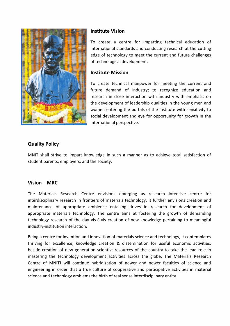
Materials Research Centre
Information Brochure
Institute Vision
To create a centre for imparting technical education of
international standards and conducting research at the cutting
edge of technology to meet the current and future challenges
of technological development.
Institute Mission
To create technical manpower for meeting the current and
future demand of industry; to recognize education and
research in close interaction with industry with emphasis on
the development of leadership qualities in the young men and
women entering the portals of the institute with sensitivity to
social development and eye for opportunity for growth in the
international perspective.
Quality Policy
MNIT shall strive to impart knowledge in such a manner as to achieve total satisfaction of
student parents, employers, and the society.
Vision – MRC
The Materials Research Centre envisions emerging as research intensive centre for
interdisciplinary research in frontiers of materials technology. It further envisions creation and
maintenance of appropriate ambience entailing drives in research for development of
appropriate materials technology. The centre aims at fostering the growth of demanding
technology research of the day vis-à-vis creation of new knowledge pertaining to meaningful
industry-institution interaction.
Being a centre for invention and innovation of materials science and technology, it contemplates
thriving for excellence, knowledge creation & dissemination for useful economic activities,
beside creation of new generation scientist resources of the country to take the lead role in
mastering the technology development activities across the globe. The Materials Research
Centre of MNITJ will continue hybridization of newer and newer faculties of science and
engineering in order that a true culture of cooperative and participative activities in material
science and technology emblems the birth of real sense interdisciplinary entity.
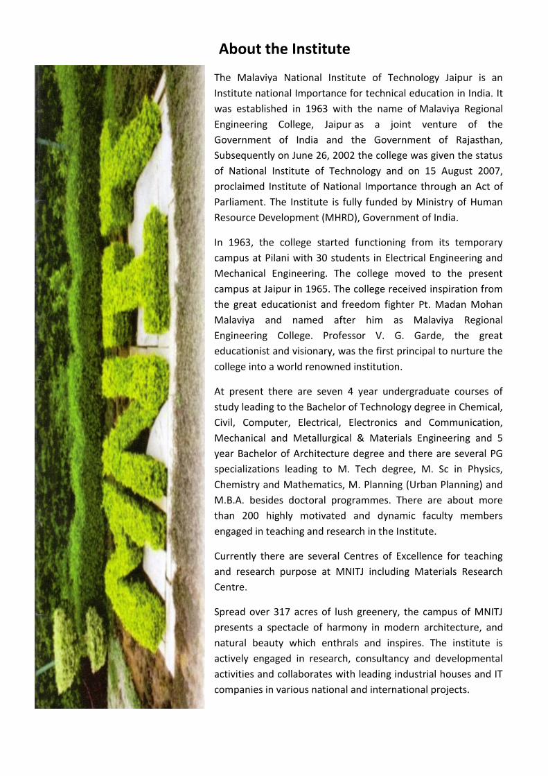
About the Institute
The Malaviya National Institute of Technology Jaipur is an
Institute national Importance for technical education in India. It
was established in 1963 with the name of Malaviya Regional
Engineering College, Jaipur as a joint venture of the
Government of India and the Government of Rajasthan,
Subsequently on June 26, 2002 the college was given the status
of National Institute of Technology and on 15 August 2007,
proclaimed Institute of National Importance through an Act of
Parliament. The Institute is fully funded by Ministry of Human
Resource Development (MHRD), Government of India.
In 1963, the college started functioning from its temporary
campus at Pilani with 30 students in Electrical Engineering and
Mechanical Engineering. The college moved to the present
campus at Jaipur in 1965. The college received inspiration from
the great educationist and freedom fighter Pt. Madan Mohan
Malaviya and named after him as Malaviya Regional
Engineering College. Professor V. G. Garde, the great
educationist and visionary, was the first principal to nurture the
college into a world renowned institution.
At present there are seven 4 year undergraduate courses of
study leading to the Bachelor of Technology degree in Chemical,
Civil, Computer, Electrical, Electronics and Communication,
Mechanical and Metallurgical & Materials Engineering and 5
year Bachelor of Architecture degree and there are several PG
specializations leading to M. Tech degree, M. Sc in Physics,
Chemistry and Mathematics, M. Planning (Urban Planning) and
M.B.A. besides doctoral programmes. There are about more
than 200 highly motivated and dynamic faculty members
engaged in teaching and research in the Institute.
Currently there are several Centres of Excellence for teaching
and research purpose at MNITJ including Materials Research
Centre.
Spread over 317 acres of lush greenery, the campus of MNITJ
presents a spectacle of harmony in modern architecture, and
natural beauty which enthrals and inspires. The institute is
actively engaged in research, consultancy and developmental
activities and collaborates with leading industrial houses and IT
companies in various national and international projects.
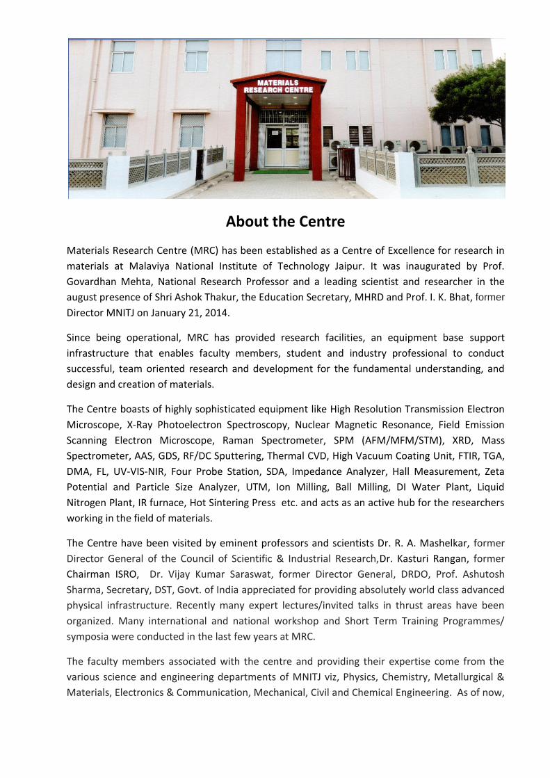
About the Centre
Materials Research Centre (MRC) has been established as a Centre of Excellence for research in
materials at Malaviya National Institute of Technology Jaipur. It was inaugurated by Prof.
Govardhan Mehta, National Research Professor and a leading scientist and researcher in the
august presence of Shri Ashok Thakur, the Education Secretary, MHRD and Prof. I. K. Bhat, former
Director MNITJ on January 21, 2014.
Since being operational, MRC has provided research facilities, an equipment base support
infrastructure that enables faculty members, student and industry professional to conduct
successful, team oriented research and development for the fundamental understanding, and
design and creation of materials.
The Centre boasts of highly sophisticated equipment like High Resolution Transmission Electron
Microscope, X-Ray Photoelectron Spectroscopy, Nuclear Magnetic Resonance, Field Emission
Scanning Electron Microscope, Raman Spectrometer, SPM (AFM/MFM/STM), XRD, Mass
Spectrometer, AAS, GDS, RF/DC Sputtering, Thermal CVD, High Vacuum Coating Unit, FTIR, TGA,
DMA, FL, UV-VIS-NIR, Four Probe Station, SDA, Impedance Analyzer, Hall Measurement, Zeta
Potential and Particle Size Analyzer, UTM, Ion Milling, Ball Milling, DI Water Plant, Liquid
Nitrogen Plant, IR furnace, Hot Sintering Press etc. and acts as an active hub for the researchers
working in the field of materials.
The Centre have been visited by eminent professors and scientists Dr. R. A. Mashelkar, former
Director General of the Council of Scientific & Industrial Research,Dr. Kasturi Rangan, former
Chairman ISRO, Dr. Vijay Kumar Saraswat, former Director General, DRDO, Prof. Ashutosh
Sharma, Secretary, DST, Govt. of India appreciated for providing absolutely world class advanced
physical infrastructure. Recently many expert lectures/invited talks in thrust areas have been
organized. Many international and national workshop and Short Term Training Programmes/
symposia were conducted in the last few years at MRC.
The faculty members associated with the centre and providing their expertise come from the
various science and engineering departments of MNITJ viz, Physics, Chemistry, Metallurgical &
Materials, Electronics & Communication, Mechanical, Civil and Chemical Engineering. As of now,

more than 30 sponsored research projects at national and international level are being run by
the faculty. Currently there are two Scientific Officers, eight Technical Assistants and three
Technicians working at MRC to provide the required scientific and technical support to the users.
Since 2016 MRC have started M. Tech and Ph. D in Material Science & Engineering.
Director’s Message
MNIT Jaipur consistently efforts towards the growth and
transformation of young science and technical persons to develop leadership qualities,
interpersonal skills, creativity along with strong moral values to make them a better human
being. We continuously effort to attract the best students throughout the country and abroad
for our Bachelor’s, Master’s and Doctorate programs in several disciplines of science and
technology.
The excellence in teaching and research comes from the careful choice of faculty members in
which MNIT Jaipur has not made any compromise. The global perspective of our faculty makes
us a premiere Institute of higher learning in India. MNIT Jaipur has expanded its outreach to
industry and the best academic institution in the world by entering into active collaborations
with them.
The Material Research Centre envisions emerging as research intensive centre for
interdisciplinary research in frontiers of Materials technology. It further envisions creation and
maintenance of appropriate ambience entailing research in drives for development of
appropriate materials technology. The center aims at fostering the growth of demanding
technology of the day vis-à-vis creation of new knowledge pertaining to meaningful industry-
institution interaction for invention & being a centre for innovation on materials science and
technology, it contemplates striving for excellence knowledge creation & dissemination for
useful economic activities beside creation of new generation scientist resources of the country
to take the lead role in mastering the technology development activities across the globe. The
Materials Research Centre of MNIT will continue hybridization of be latest facilities of science
and engineering in order that a true culture of cooperative and participative activities in material
science and technology emblems the birth of the real sense interdisciplinary entity.
I with the Centre a bright future in furthering the cause of research.
Prof. Udaykumar R Yaragatti
Message from the Head, MRC
Materials Science and engineering (MS&E) is one the most important of
the engineering disciplines as it impacts nearly all the traditional fields of engineering. The
discipline is concerned with the structure, properties and application of materials used in
modern technology. Undoubtedly, Materials Science and Engineering is at the forefront of high
technology as the advancements in technology are the direct result of advances in materials.
Material Research Centre (MRC) was established at MNIT Jaipur, with the vision to translate the
fundamental understanding of materials into sustainable and environmental friendly
technologies and products for the social benefits. MRC is deeply involved in various domains,
namely, structural materials, functional materials, nanotechnology, energy materials and
computational materials science. With a goal of achieving excellence in education and research,
MRC houses state of the art research facilities equipped with sophisticated instrumentation for
synthesizing, characterizing, processing and imaging various types of advanced materials and
samples, which makes the MRC, second to none in the country.
MRC offers a two years M.Tech degree program in Material Science & Engineering and Ph.D.
degree program, where Course curriculums are uniquely designed, to meet the demand of
industries as well as R&D. Department believes in the holistic development of student, leading to
a good human being, to serve the nation and society.
MRC provides access of all the research facilities to the academic and industrial users in their
research work. In the Centre several Workshops, Seminars, National and International
Conferences and Visits from eminent persons are organized for active collaborations and benefit
of the industry, academia and students. This brochure provides the information about the
activities and resources of the Material Research Centre.
Prof. Vijay Janyani
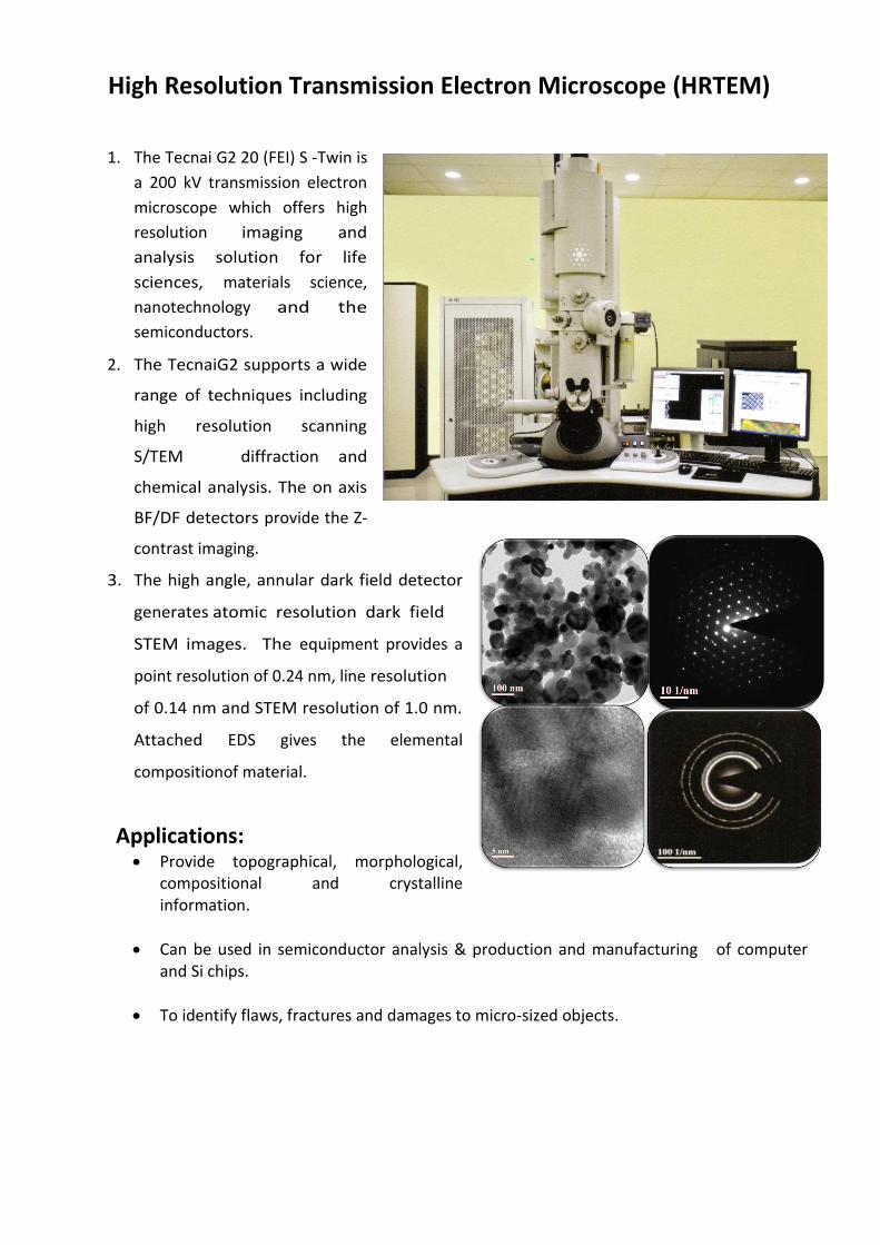
High Resolution Transmission Electron Microscope (HRTEM)
1. The Tecnai G2 20 (FEI) S -Twin is
a 200 kV transmission electron
microscope which offers high
resolution imaging and
analysis solution for life
sciences, materials science,
nanotechnology and the
semiconductors.
2. The TecnaiG2 supports a wide
range of techniques including
high resolution scanning
S/TEM diffraction and
chemical analysis. The on axis
BF/DF detectors provide the Z-
contrast imaging.
3. The high angle, annular dark field detector
generates atomic resolution dark field
STEM images. The equipment provides a
point resolution of 0.24 nm, line resolution
of 0.14 nm and STEM resolution of 1.0 nm.
Attached EDS gives the elemental
compositionof material.
Applications: Provide topographical, morphological,
compositional and crystalline information.
Can be used in semiconductor analysis & production and manufacturing of computer and Si chips.
To identify flaws, fractures and damages to micro-sized objects.
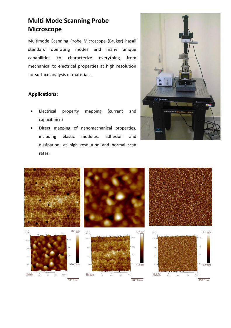
Multi Mode Scanning Probe Microscope
Multimode Scanning Probe Microscope (Bruker) hasall
standard operating modes and many unique
capabilities to characterize everything from
mechanical to electrical properties at high resolution
for surface analysis of materials.
Applications:
Electrical property mapping (current and
capacitance)
Direct mapping of nanomechanical properties,
including elastic modulus, adhesion and
dissipation, at high resolution and normal scan
rates.
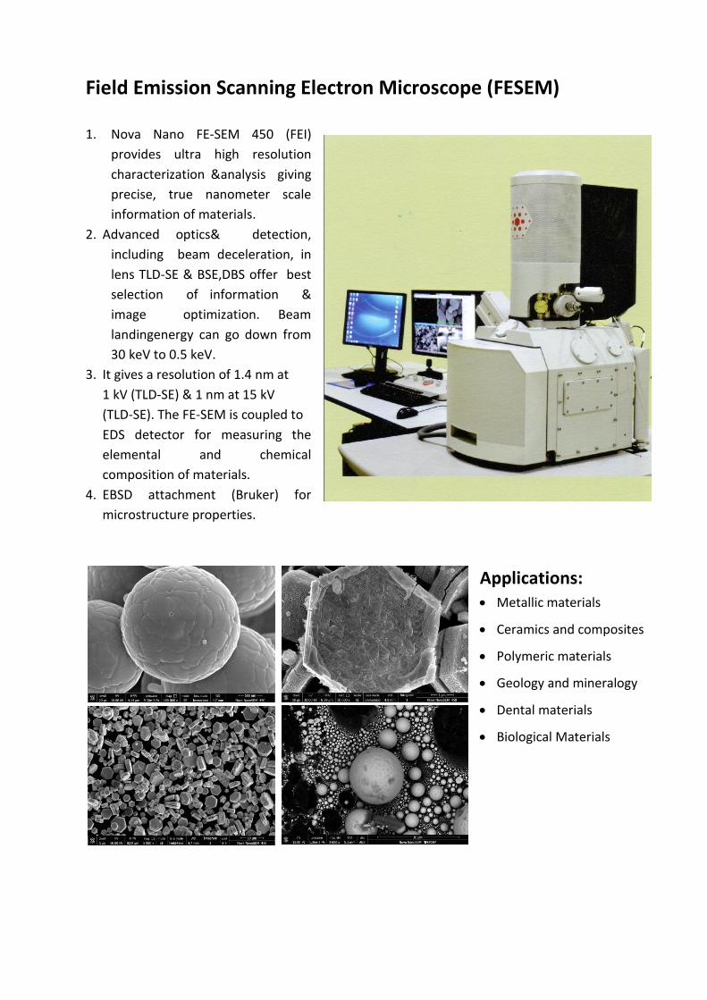
Field Emission Scanning Electron Microscope (FESEM)
1. Nova Nano FE-SEM 450 (FEI)
provides ultra high resolution
characterization &analysis giving
precise, true nanometer scale
information of materials.
2. Advanced optics& detection,
including beam deceleration, in
lens TLD-SE & BSE,DBS offer best
selection of information &
image optimization. Beam
landingenergy can go down from
30 keV to 0.5 keV.
3. It gives a resolution of 1.4 nm at
1 kV (TLD-SE) & 1 nm at 15 kV
(TLD-SE). The FE-SEM is coupled to
EDS detector for measuring the
elemental and chemical
composition of materials.
4. EBSD attachment (Bruker) for
microstructure properties.
Applications: Metallic materials
Ceramics and composites
Polymeric materials
Geology and mineralogy
Dental materials
Biological Materials
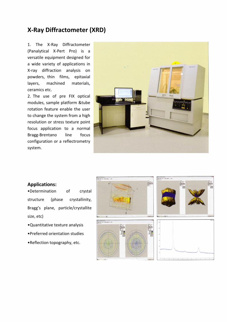
X-Ray Diffractometer (XRD)
1. The X-Ray Diffractometer
(Panalytical X-Pert Pro) is a
versatile equipment designed for
a wide variety of applications in
X-ray diffraction analysis on
powders, thin films, epitaxial
layers, machined materials,
ceramics etc.
2. The use of pre FIX optical
modules, sample platform &tube
rotation feature enable the user
to change the system from a high
resolution or stress texture point
focus application to a normal
Bragg-Brentano line focus
configuration or a reflectrometry
system.
Applications: •Determination of crystal
structure (phase crystallinity,
Bragg’s plane, particle/crystallite
size, etc)
•Quantitative texture analysis
•Preferred orientation studies
•Reflection topography, etc.
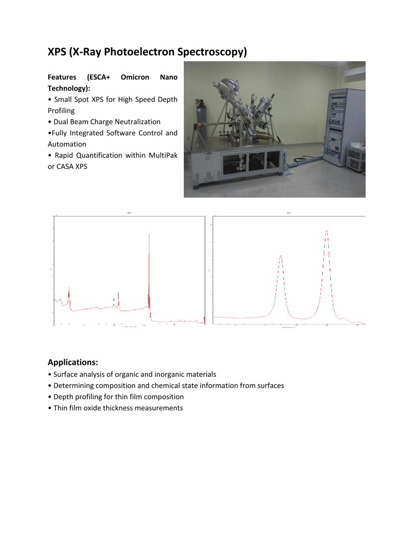
XPS (X-Ray Photoelectron Spectroscopy)
Features (ESCA+ Omicron Nano
Technology):
• Small Spot XPS for High Speed Depth
Profiling
• Dual Beam Charge Neutralization
•Fully Integrated Software Control and
Automation
• Rapid Quantification within MultiPak
or CASA XPS
Applications:
• Surface analysis of organic and inorganic materials
• Determining composition and chemical state information from surfaces
• Depth profiling for thin film composition
• Thin film oxide thickness measurements
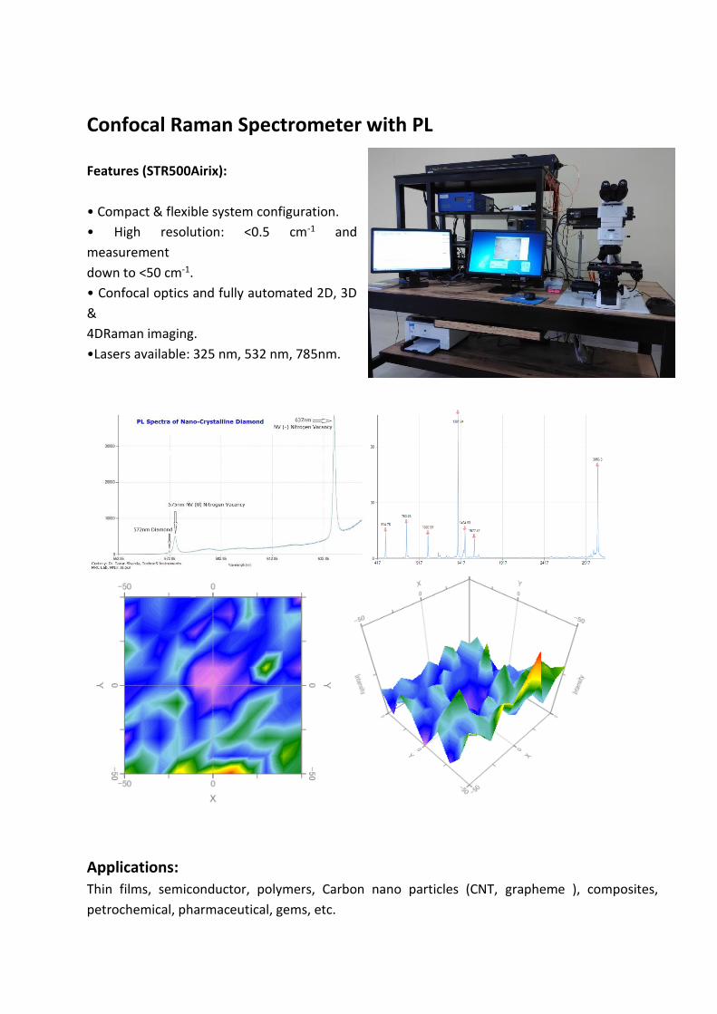
Confocal Raman Spectrometer with PL
Features (STR500Airix):
• Compact & flexible system configuration.
• High resolution: <0.5 cm-1 and
measurement
down to <50 cm-1.
• Confocal optics and fully automated 2D, 3D
&
4DRaman imaging.
•Lasers available: 325 nm, 532 nm, 785nm.
Applications:
Thin films, semiconductor, polymers, Carbon nano particles (CNT, grapheme ), composites,
petrochemical, pharmaceutical, gems, etc.
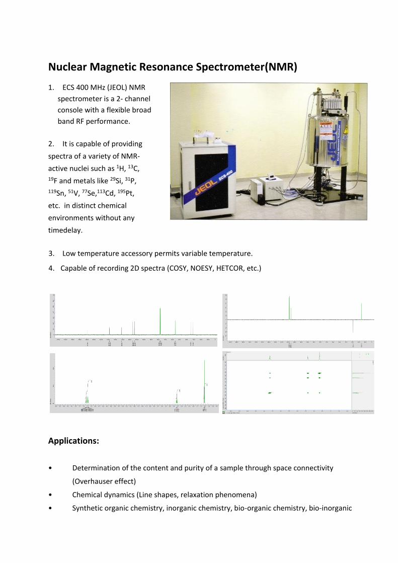
Nuclear Magnetic Resonance Spectrometer(NMR)
1. ECS 400 MHz (JEOL) NMR
spectrometer is a 2- channel
console with a flexible broad
band RF performance.
2. It is capable of providing
spectra of a variety of NMR-
active nuclei such as 1H, 13C, 19F and metals like 29Si, 31P, 119Sn, 51V, 77Se,113Cd, 195Pt,
etc. in distinct chemical
environments without any
timedelay.
3. Low temperature accessory permits variable temperature.
4. Capable of recording 2D spectra (COSY, NOESY, HETCOR, etc.)
Applications:
• Determination of the content and purity of a sample through space connectivity
(Overhauser effect)
• Chemical dynamics (Line shapes, relaxation phenomena)
• Synthetic organic chemistry, inorganic chemistry, bio-organic chemistry, bio-inorganic
Chemistry, polymer chemistry & organometallic chemistry.
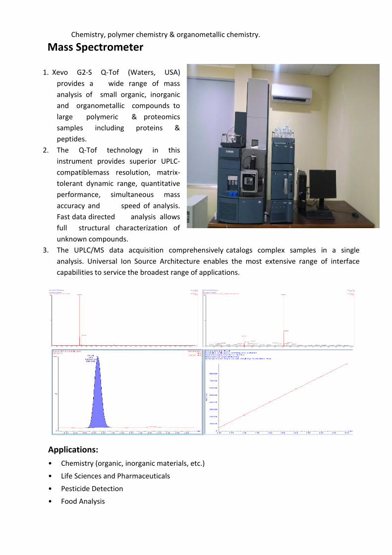
Mass Spectrometer
1. Xevo G2-S Q-Tof (Waters, USA)
provides a wide range of mass
analysis of small organic, inorganic
and organometallic compounds to
large polymeric & proteomics
samples including proteins &
peptides.
2. The Q-Tof technology in this
instrument provides superior UPLC-
compatiblemass resolution, matrix-
tolerant dynamic range, quantitative
performance, simultaneous mass
accuracy and speed of analysis.
Fast data directed analysis allows
full structural characterization of
unknown compounds.
3. The UPLC/MS data acquisition comprehensively catalogs complex samples in a single
analysis. Universal Ion Source Architecture enables the most extensive range of interface
capabilities to service the broadest range of applications.
Applications:
• Chemistry (organic, inorganic materials, etc.)
• Life Sciences and Pharmaceuticals
• Pesticide Detection
• Food Analysis
Environmental
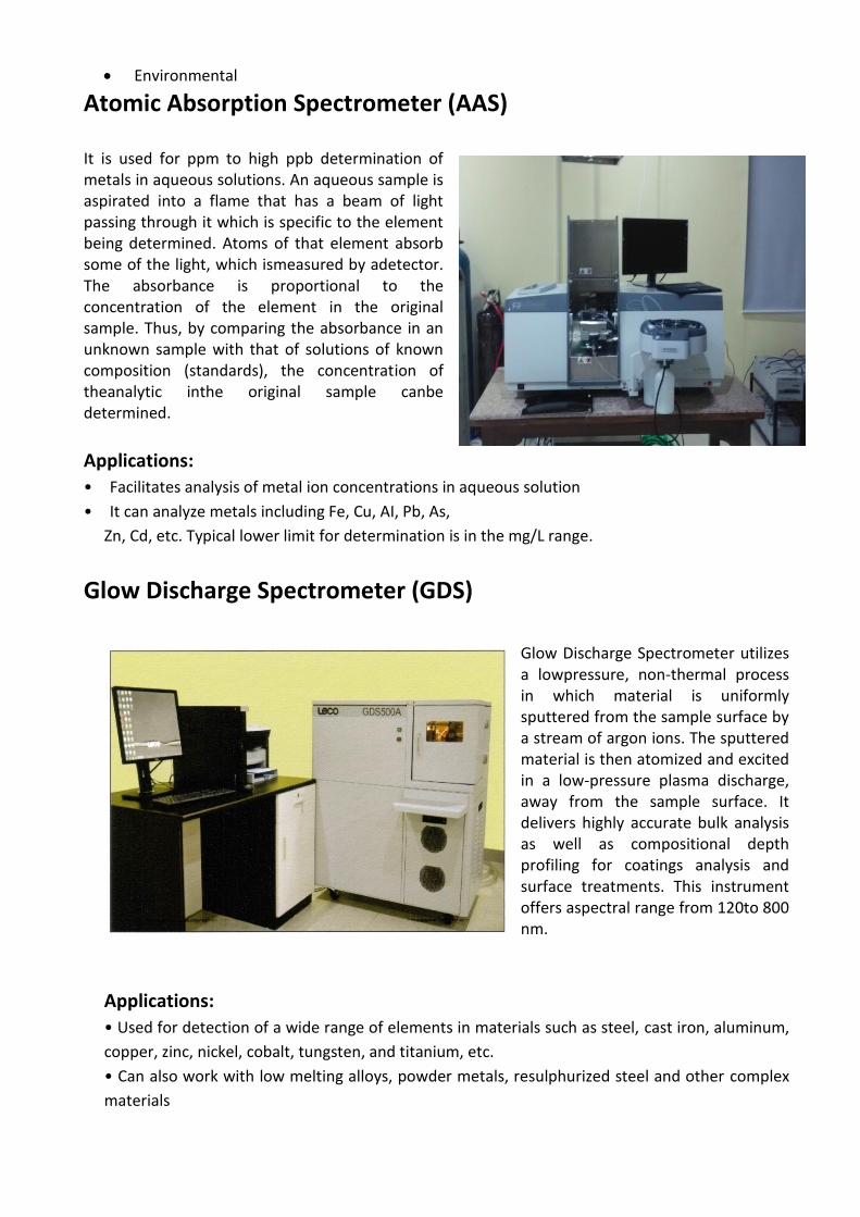
Atomic Absorption Spectrometer (AAS)
It is used for ppm to high ppb determination of metals in aqueous solutions. An aqueous sample is aspirated into a flame that has a beam of light passing through it which is specific to the element being determined. Atoms of that element absorb some of the light, which ismeasured by adetector. The absorbance is proportional to the concentration of the element in the original sample. Thus, by comparing the absorbance in an unknown sample with that of solutions of known composition (standards), the concentration of theanalytic inthe original sample canbe determined.
Applications:
• Facilitates analysis of metal ion concentrations in aqueous solution
• It can analyze metals including Fe, Cu, AI, Pb, As,
Zn, Cd, etc. Typical lower limit for determination is in the mg/L range.
Glow Discharge Spectrometer (GDS)
Glow Discharge Spectrometer utilizes a lowpressure, non-thermal process in which material is uniformly sputtered from the sample surface by a stream of argon ions. The sputtered material is then atomized and excited in a low-pressure plasma discharge, away from the sample surface. It delivers highly accurate bulk analysis as well as compositional depth profiling for coatings analysis and surface treatments. This instrument offers aspectral range from 120to 800 nm.
Applications:
• Used for detection of a wide range of elements in materials such as steel, cast iron, aluminum,
copper, zinc, nickel, cobalt, tungsten, and titanium, etc.
• Can also work with low melting alloys, powder metals, resulphurized steel and other complex
materials
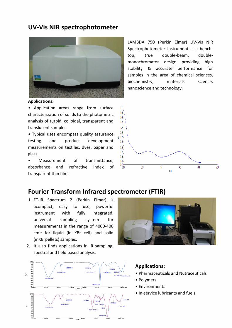
UV-Vis NIR spectrophotometer
LAMBDA 750 (Perkin Elmer) UV-Vis NIR
Spectrophotometer instrument is a bench-
top, true double-beam, double-
monochromator design providing high
stability & accurate performance for
samples in the area of chemical sciences,
biochemistry, materials science,
nanoscience and technology.
Applications:
• Application areas range from surface
characterization of solids to the photometric
analysis of turbid, colloidal, transparent and
translucent samples.
• Typical uses encompass quality assurance
testing and product development
measurements on textiles, dyes, paper and
glass.
• Measurement of transmittance,
absorbance and refractive index of
transparent thin films.
Fourier Transform Infrared spectrometer (FTIR) 1. FT-IR Spectrum 2 (Perkin Elmer) is
acompact, easy to use, powerful
instrument with fully integrated,
universal sampling system for
measurements in the range of 4000-400
cm-1 for liquid (in KBr cell) and solid
(inKBrpellets) samples.
2. It also finds applications in IR sampling,
spectral and field based analysis.
Applications:
• Pharmaceuticals and Nutraceuticals
• Polymers
• Environmental
• In-service lubricants and fuels
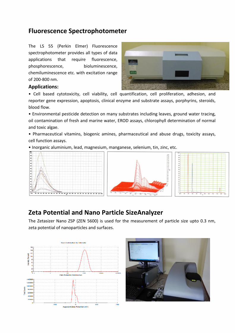
Fluorescence Spectrophotometer
The LS 55 (Perkin Elmer) Fluorescence
spectrophotometer provides all types of data
applications that require fluorescence,
phosphorescence, bioluminescence,
chemiluminescence etc. with excitation range
of 200-800 nm.
Applications:
• Cell based cytotoxicity, cell viability, cell quantification, cell proliferation, adhesion, and
reporter gene expression, apoptosis, clinical enzyme and substrate assays, porphyrins, steroids,
blood flow.
• Environmental pesticide detection on many substrates including leaves, ground water tracing,
oil contamination of fresh and marine water, EROD assays, chlorophyll determination of normal
and toxic algae.
• Pharmaceutical vitamins, biogenic amines, pharmaceutical and abuse drugs, toxicity assays,
cell function assays.
• Inorganic aluminium, lead, magnesium, manganese, selenium, tin, zinc, etc.
Zeta Potential and Nano Particle SizeAnalyzer The Zetasizer Nano ZSP (ZEN 5600) is used for the measurement of particle size upto 0.3 nm,
zeta potential of nanoparticles and surfaces.
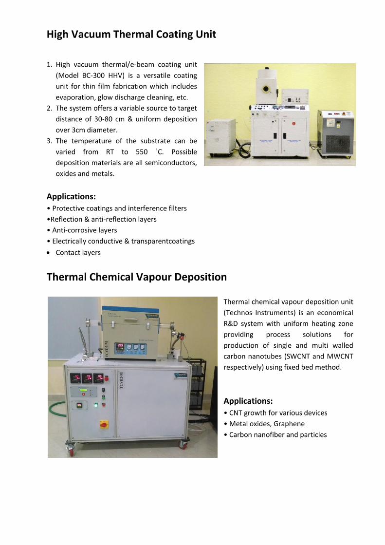
High Vacuum Thermal Coating Unit
1. High vacuum thermal/e-beam coating unit
(Model BC-300 HHV) is a versatile coating
unit for thin film fabrication which includes
evaporation, glow discharge cleaning, etc.
2. The system offers a variable source to target
distance of 30-80 cm & uniform deposition
over 3cm diameter.
3. The temperature of the substrate can be
varied from RT to 550 ˚C. Possible
deposition materials are all semiconductors,
oxides and metals.
Applications:
• Protective coatings and interference filters
•Reflection & anti-reflection layers
• Anti-corrosive layers
• Electrically conductive & transparentcoatings
Contact layers
Thermal Chemical Vapour Deposition
Thermal chemical vapour deposition unit
(Technos Instruments) is an economical
R&D system with uniform heating zone
providing process solutions for
production of single and multi walled
carbon nanotubes (SWCNT and MWCNT
respectively) using fixed bed method.
Applications:
• CNT growth for various devices
• Metal oxides, Graphene
• Carbon nanofiber and particles
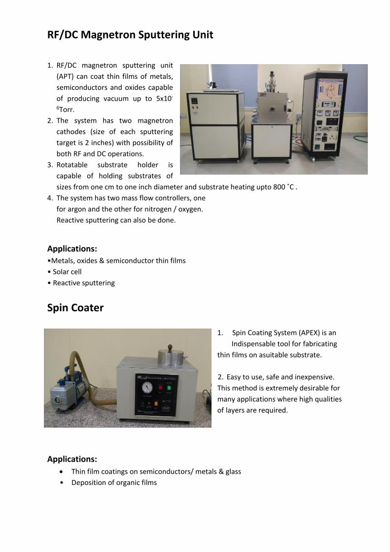
RF/DC Magnetron Sputtering Unit
1. RF/DC magnetron sputtering unit
(APT) can coat thin films of metals,
semiconductors and oxides capable
of producing vacuum up to 5x10-
6Torr.
2. The system has two magnetron
cathodes (size of each sputtering
target is 2 inches) with possibility of
both RF and DC operations.
3. Rotatable substrate holder is
capable of holding substrates of
sizes from one cm to one inch diameter and substrate heating upto 800 ˚C .
4. The system has two mass flow controllers, one
for argon and the other for nitrogen / oxygen.
Reactive sputtering can also be done.
Applications:
•Metals, oxides & semiconductor thin films
• Solar cell
• Reactive sputtering
Spin Coater
1. Spin Coating System (APEX) is an
Indispensable tool for fabricating
thin films on asuitable substrate.
2. Easy to use, safe and inexpensive.
This method is extremely desirable for
many applications where high qualities
of layers are required.
Applications:
Thin film coatings on semiconductors/ metals & glass
• Deposition of organic films
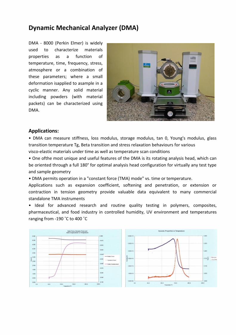
Dynamic Mechanical Analyzer (DMA)
DMA - 8000 (Perkin Elmer) is widely
used to characterize materials
properties as a function of
temperature, time, frequency, stress,
atmosphere or a combination of
these parameters; where a small
deformation isapplied to asample in a
cyclic manner. Any solid material
including powders (with material
packets) can be characterized using
DMA.
Applications:
• DMA can measure stiffness, loss modulus, storage modulus, tan 0, Young's modulus, glass
transition temperature Tg, Beta transition and stress relaxation behaviours for various
visco-elastic materials under time as well as temperature scan conditions
• One ofthe most unique and useful features of the DMA is its rotating analysis head, which can
be oriented through a full 180° for optimal analysis head configuration for virtually any test type
and sample geometry
• DMA permits operation in a "constant force (TMA) mode" vs. time or temperature.
Applications such as expansion coefficient, softening and penetration, or extension or
contraction in tension geometry provide valuable data equivalent to many commercial
standalone TMA instruments
• Ideal for advanced research and routine quality testing in polymers, composites,
pharmaceutical, and food industry in controlled humidity, UV environment and temperatures
ranging from -190 ˚C to 400 ˚C
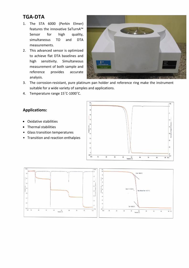
TGA-DTA 1. The STA 6000 (Perkin Elmer)
features the innovative SaTurnA™
Sensor for high quality,
simultaneous TO and DTA
measurements.
2. This advanced sensor is optimized
to achieve flat DTA baselines and
high sensitivity. Simultaneous
measurement of both sample and
reference provides accurate
analysis.
3. The corrosion-resistant, pure platinum pan holder and reference ring make the instrument
suitable for a wide variety of samples and applications.
4. Temperature range 15˚C-1000˚C.
Applications:
Oxidative stabilities
Thermal stabilities
• Glass transition temperatures
• Transition and reaction enthalpies

Abrasive Cutter
The AbrasiMatic® 300 (Buehler) abrasive cutter is
abenchtop cutter featuring manual cutting action in
three directions and automated cutting in one
direction .
High Speed Diamond Cutter Isomet 4000 (Buehler) is a versatile linear precision
saw which enables to cut all kind of delicate
specimen with minimal damage due to deformation.
Semi-Automatic Polisher
MetaServ® 250 (Buehler) High Speed Twin
grinderpolishers offer a combination of
performance, economy and reliability for most
microstructural analysis applications. The platen
diameter is 8inch with 50-500 rpm speed in 10rpm
increment.
Hot Mounting Press Simplimet 3000 (Buehler) Automatic Mounting
Press is a durable press with basic features that
provides effective mounting, increases productivity
and specimen consistency verses manual mounting
press.
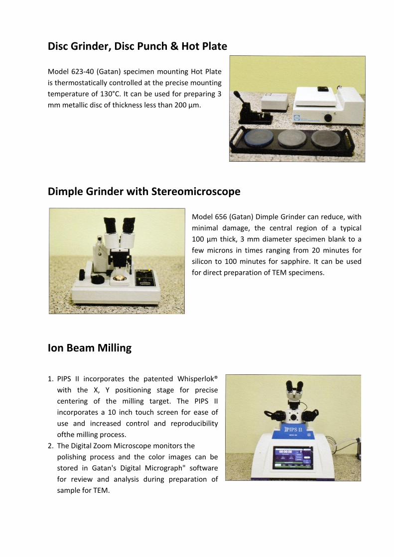
Disc Grinder, Disc Punch & Hot Plate
Model 623-40 (Gatan) specimen mounting Hot Plate
is thermostatically controlled at the precise mounting
temperature of 130°C. It can be used for preparing 3
mm metallic disc of thickness less than 200 µm.
Dimple Grinder with Stereomicroscope
Model 656 (Gatan) Dimple Grinder can reduce, with
minimal damage, the central region of a typical
100 µm thick, 3 mm diameter specimen blank to a
few microns in times ranging from 20 minutes for
silicon to 100 minutes for sapphire. It can be used
for direct preparation of TEM specimens.
Ion Beam Milling
1. PIPS II incorporates the patented Whisperlok®
with the X, Y positioning stage for precise
centering of the milling target. The PIPS II
incorporates a 10 inch touch screen for ease of
use and increased control and reproducibility
ofthe milling process.
2. The Digital Zoom Microscope monitors the
polishing process and the color images can be
stored in Gatan's Digital Micrograph" software
for review and analysis during preparation of
sample for TEM.
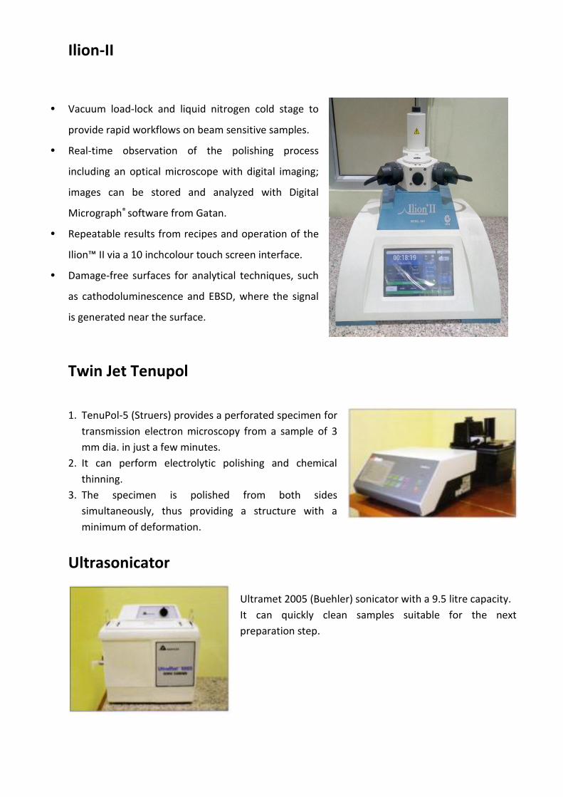
Ilion-II
Vacuum load-lock and liquid nitrogen cold stage to
provide rapid workflows on beam sensitive samples.
Real-time observation of the polishing process
including an optical microscope with digital imaging;
images can be stored and analyzed with Digital
Micrograph® software from Gatan.
Repeatable results from recipes and operation of the
Ilion™ II via a 10 inchcolour touch screen interface.
Damage-free surfaces for analytical techniques, such
as cathodoluminescence and EBSD, where the signal
is generated near the surface.
Twin Jet Tenupol
1. TenuPol-5 (Struers) provides a perforated specimen for
transmission electron microscopy from a sample of 3
mm dia. in just a few minutes.
2. It can perform electrolytic polishing and chemical
thinning.
3. The specimen is polished from both sides
simultaneously, thus providing a structure with a
minimum of deformation.
Ultrasonicator
Ultramet 2005 (Buehler) sonicator with a 9.5 litre capacity.
It can quickly clean samples suitable for the next
preparation step.
Planetary Ball Mill
1. Pulverisette 6 (Fritsch) Planetary Ball Mill is capable of
mixing and perfect homogenising of emulsions or
pastes.
2. Maximum output sample quantity is40 ml.
3. Tungsten carbide and tempered steel ball and bowl
material with variable speed upto 650 rpm.
4. GTM attachment for temperature monitoring.
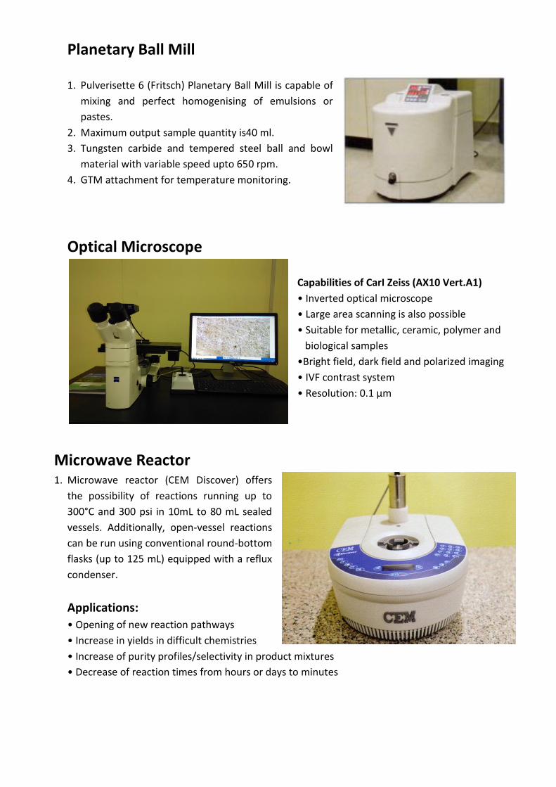
Optical Microscope
Capabilities of CarI Zeiss (AX10 Vert.A1)
• Inverted optical microscope
• Large area scanning is also possible
• Suitable for metallic, ceramic, polymer and
biological samples
•Bright field, dark field and polarized imaging
• IVF contrast system
• Resolution: 0.1 µm
Microwave Reactor 1. Microwave reactor (CEM Discover) offers
the possibility of reactions running up to
300°C and 300 psi in 10mL to 80 mL sealed
vessels. Additionally, open-vessel reactions
can be run using conventional round-bottom
flasks (up to 125 mL) equipped with a reflux
condenser.
Applications:
• Opening of new reaction pathways
• Increase in yields in difficult chemistries
• Increase of purity profiles/selectivity in product mixtures
• Decrease of reaction times from hours or days to minutes
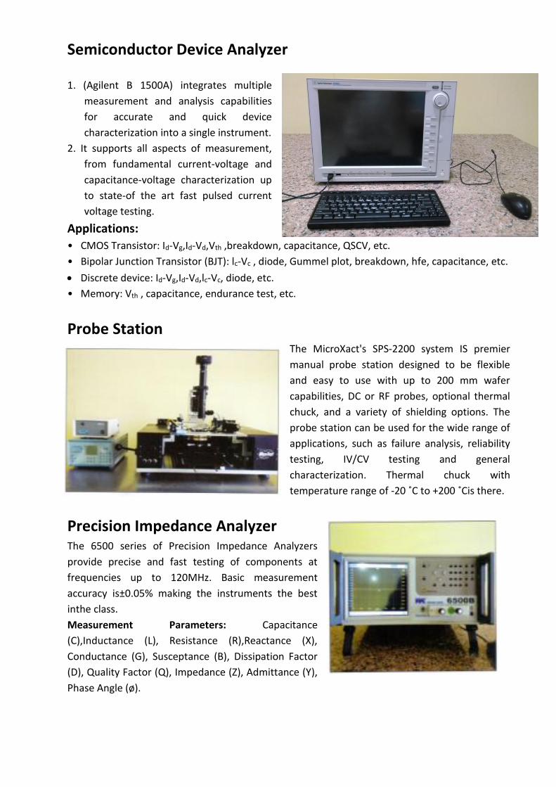
Semiconductor Device Analyzer
1. (Agilent B 1500A) integrates multiple
measurement and analysis capabilities
for accurate and quick device
characterization into a single instrument.
2. It supports all aspects of measurement,
from fundamental current-voltage and
capacitance-voltage characterization up
to state-of the art fast pulsed current
voltage testing.
Applications:
• CMOS Transistor: Id-Vg,Id-Vd,Vth ,breakdown, capacitance, QSCV, etc.
• Bipolar Junction Transistor (BJT): lc-Vc , diode, Gummel plot, breakdown, hfe, capacitance, etc.
Discrete device: Id-Vg,Id-Vd,lc-Vc, diode, etc.
• Memory: Vth , capacitance, endurance test, etc.
Probe Station The MicroXact's SPS-2200 system IS premier
manual probe station designed to be flexible
and easy to use with up to 200 mm wafer
capabilities, DC or RF probes, optional thermal
chuck, and a variety of shielding options. The
probe station can be used for the wide range of
applications, such as failure analysis, reliability
testing, IV/CV testing and general
characterization. Thermal chuck with
temperature range of -20 ˚C to +200 ˚Cis there.
Precision Impedance Analyzer The 6500 series of Precision Impedance Analyzers
provide precise and fast testing of components at
frequencies up to 120MHz. Basic measurement
accuracy is±0.05% making the instruments the best
inthe class.
Measurement Parameters: Capacitance
(C),Inductance (L), Resistance (R),Reactance (X),
Conductance (G), Susceptance (B), Dissipation Factor
(D), Quality Factor (Q), Impedance (Z), Admittance (Y),
Phase Angle (ø).
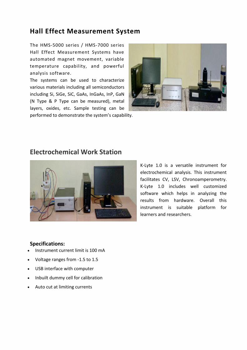
Hall Effect Measurement System
The HMS-5000 series / HMS-7000 series
Hall Effect Measurement Systems have
automated magnet movement, variable
temperature capability, and powerful
analysis software.
The systems can be used to characterize
various materials including all semiconductors
including Si, SiGe, SiC, GaAs, InGaAs, InP, GaN
(N Type & P Type can be measured), metal
layers, oxides, etc. Sample testing can be
performed to demonstrate the system’s capability.
Electrochemical Work Station
K-Lyte 1.0 is a versatile instrument for
electrochemical analysis. This instrument
facilitates CV, LSV, Chronoamperometry.
K-Lyte 1.0 includes well customized
software which helps in analyzing the
results from hardware. Overall this
instrument is suitable platform for
learners and researchers.
Specifications:
Instrument current limit is 100 mA
Voltage ranges from -1.5 to 1.5
USB interface with computer
Inbuilt dummy cell for calibration
Auto cut at limiting currents
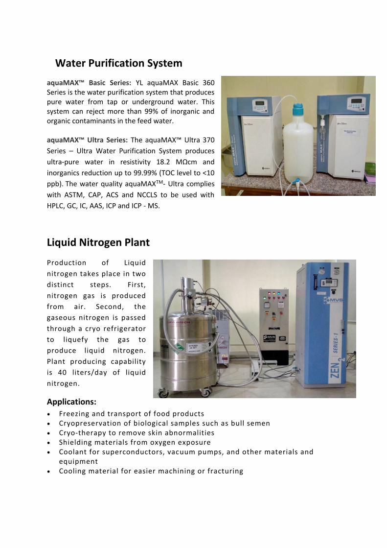
Water Purification System
aquaMAX™ Basic Series: YL aquaMAX Basic 360 Series is the water purification system that produces pure water from tap or underground water. This system can reject more than 99% of inorganic and organic contaminants in the feed water.
aquaMAX™ Ultra Series: The aquaMAX™ Ultra 370
Series – Ultra Water Purification System produces
ultra-pure water in resistivity 18.2 MΩcm and
inorganics reduction up to 99.99% (TOC level to <10
ppb). The water quality aquaMAXTM- Ultra complies
with ASTM, CAP, ACS and NCCLS to be used with
HPLC, GC, IC, AAS, ICP and ICP - MS.
Liquid Nitrogen Plant
Production of Liquid
nitrogen takes place in two
distinct steps. First,
nitrogen gas is produced
from air. Second, the
gaseous nitrogen is passed
through a cryo refrigerator
to liquefy the gas to
produce liquid nitrogen.
Plant producing capability
is 40 liters/day of liquid
nitrogen.
Applications:
Freezing and transport of food products Cryopreservation of biological samples such as bull semen Cryo-therapy to remove skin abnormalities Shielding materials from oxygen exposure Coolant for superconductors, vacuum pumps, and other materials and
equipment Cooling material for easier machining or fracturing
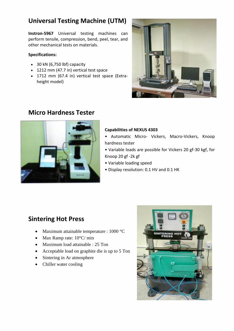
Universal Testing Machine (UTM)
Instron-5967 Universal testing machines can perform tensile, compression, bend, peel, tear, and other mechanical tests on materials.
Specifications:
30 kN (6,750 lbf) capacity 1212 mm (47.7 in) vertical test space 1712 mm (67.4 in) vertical test space (Extra-
height model)
Micro Hardness Tester
Capabilities of NEXUS 4303
• Automatic Micro- Vickers, Macro-Vickers, Knoop
hardness tester
• Variable loads are possible for Vickers 20 gf-30 kgf, for
Knoop 20 gf -2k gf
• Variable loading speed
• Display resolution: 0.1 HV and 0.1 HK
Sintering Hot Press
Maximum attainable temperature : 1000 °C
Max Ramp rate: 10°C/ min
Maximum load attainable : 25 Ton
Acceptable load on graphite die is up to 5 Ton
Sintering in Ar atmosphere
Chiller water cooling
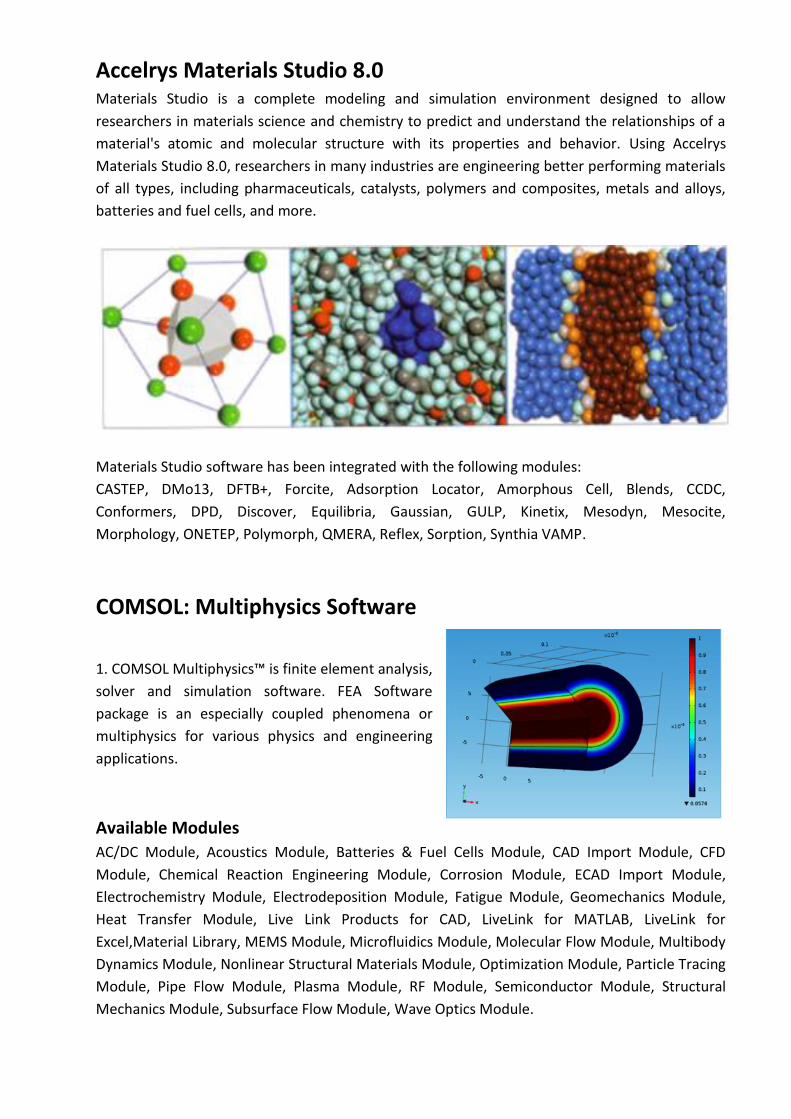
Accelrys Materials Studio 8.0 Materials Studio is a complete modeling and simulation environment designed to allow
researchers in materials science and chemistry to predict and understand the relationships of a
material's atomic and molecular structure with its properties and behavior. Using Accelrys
Materials Studio 8.0, researchers in many industries are engineering better performing materials
of all types, including pharmaceuticals, catalysts, polymers and composites, metals and alloys,
batteries and fuel cells, and more.
Materials Studio software has been integrated with the following modules:
CASTEP, DMo13, DFTB+, Forcite, Adsorption Locator, Amorphous Cell, Blends, CCDC,
Conformers, DPD, Discover, Equilibria, Gaussian, GULP, Kinetix, Mesodyn, Mesocite,
Morphology, ONETEP, Polymorph, QMERA, Reflex, Sorption, Synthia VAMP.
COMSOL: Multiphysics Software
1. COMSOL Multiphysics™ is finite element analysis,
solver and simulation software. FEA Software
package is an especially coupled phenomena or
multiphysics for various physics and engineering
applications.
Available Modules
AC/DC Module, Acoustics Module, Batteries & Fuel Cells Module, CAD Import Module, CFD
Module, Chemical Reaction Engineering Module, Corrosion Module, ECAD Import Module,
Electrochemistry Module, Electrodeposition Module, Fatigue Module, Geomechanics Module,
Heat Transfer Module, Live Link Products for CAD, LiveLink for MATLAB, LiveLink for
Excel,Material Library, MEMS Module, Microfluidics Module, Molecular Flow Module, Multibody
Dynamics Module, Nonlinear Structural Materials Module, Optimization Module, Particle Tracing
Module, Pipe Flow Module, Plasma Module, RF Module, Semiconductor Module, Structural
Mechanics Module, Subsurface Flow Module, Wave Optics Module.
IC Cap Device Software 1. Integrated Circuit Characterization and Analysis Program (lC-CAP) is the industry
standard for DC and RF semiconductor device modeling. IC-CAP extracts accurate
compact models used in high speed/digital, analog and power RF applications.
2. The most advanced semiconductor foundries and IDMs rely on IC-CAP for modeling
silicon CMOS, Bipolar, compound gallium arsenide (GaAs), gallium nitride (GaN) and
many other device technologies. IC-CAP is the most advanced, customizable modeling
software and includes measurement, simulation, optimization and statistical analysis
tools.
Applications:
• Open software architecture enables maximum accuracy and provides ultimate flexibility to
create and automate measurement, extraction and verification procedures.
• Turnkey extraction solutions for industry standard CMOS models, such as BSIM3/BSIM4, PSP
and HiSIM, minimize the learning curve and maximize model accuracy.
• Most direct links to commercial simulators ensure consistency between extracted models and
the simulators used by circuit designers.

Faculty Profile
Dr. Vijay Janyani
Professor & Head, MRC
Ph.D. (UK), M.E. (Electronics & Electrical Comm), B.E. (Electronics and
Communication)
Research Interests: Optical Communication, Optoelectronics and
Photonics, Numerical Modelling, Nonlinear Optics, RF and Microwaves,
Optical Networks, Solar Energy.
Prof. Kanupriya Sachdev
Professor, MRC
Ph.D. (Physics), M.Phil. (Physics) M.Sc. (Physics), B.Sc. (Physics, Maths,
Chemistry)
Research Interests: Material Science and technology, Condensed Matter
Physics, Transparent Conducting thin film oxides , Metal oxide doped
with metal & rare earth metal , Surface modification by ionbeam
irradiation/ Glow Discharge Plasma, Thermo-chemical behaviour of
amorphous alloys.
Prof. Ragini Gupta
Professor, MRC
Ph.D. (Organic Chemistry), M. Sc. (Organic Chemistry) , B.Sc.
Research Interests: Synthetic Organo-Fluorine Compounds, Some aspects
of the Chemistry of Biologically Active Heterocyclic Compounds, Click
Chemistry, Nano-chemistry, Green Chemistry, Biocatalysis, Phase Transfer
Catalysis and Microwave Chemistry.
Dr. Amit Kumar Singh
Assistant Professor, MRC
Ph.D. (Mechanical Engg), M.Tech.(Manufacturing Systems Eng), B.Tech.
(Mechanical Engg)
Research Interests: Bio-Mechanics, Additive Manufacturing, Rapid Tooling,
CAD/CAM/CAE.
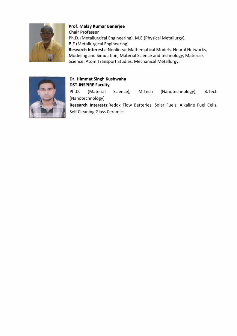
Prof. Malay Kumar Banerjee Chair Professor Ph.D. (Metallurgical Engineering), M.E.(Physical Metallurgy), B.E.(Metallurgical Engineering) Research Interests: Nonlinear Mathematical Models, Neural Networks, Modeling and Simulation, Material Science and technology, Materials Science: Atom Transport Studies, Mechanical Metallurgy.
Dr. Himmat Singh Kushwaha DST-INSPIRE Faculty
Ph.D. (Material Science), M.Tech (Nanotechnology), B.Tech
(Nanotechnology)
Research Interests:Redox Flow Batteries, Solar Fuels, Alkaline Fuel Cells,
Self Cleaning Glass Ceramics.
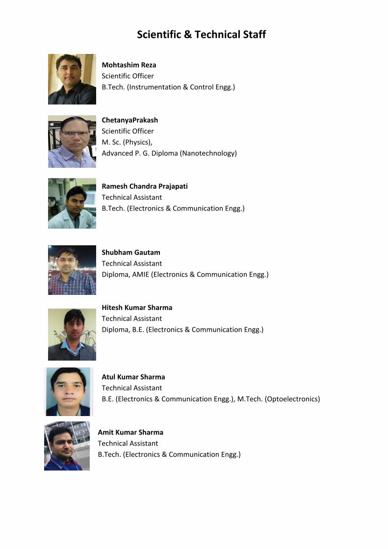
Scientific & Technical Staff
Mohtashim Reza
Scientific Officer
B.Tech. (Instrumentation & Control Engg.)
ChetanyaPrakash
Scientific Officer
M. Sc. (Physics),
Advanced P. G. Diploma (Nanotechnology)
Ramesh Chandra Prajapati
Technical Assistant
B.Tech. (Electronics & Communication Engg.)
Shubham Gautam
Technical Assistant
Diploma, AMIE (Electronics & Communication Engg.)
Hitesh Kumar Sharma
Technical Assistant
Diploma, B.E. (Electronics & Communication Engg.)
Atul Kumar Sharma
Technical Assistant
B.E. (Electronics & Communication Engg.), M.Tech. (Optoelectronics)
Amit Kumar Sharma
Technical Assistant
B.Tech. (Electronics & Communication Engg.)
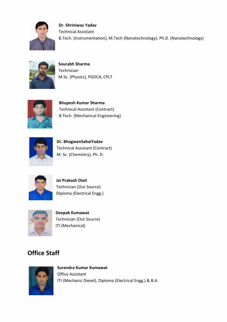
Dr. Shriniwas Yadav
Technical Assistant
B.Tech. (Instrumentation), M.Tech (Nanotechnology), Ph.D. (Nanotechnology)
Sourabh Sharma
Technician
M.Sc. (Physics), PGDCA, CPLT
Bhupesh Kumar Sharma
Technical Assistant (Contract)
B.Tech. (Mechanical Engineering)
Dr. BhagwanSahaiYadav
Technical Assistant (Contract)
M. Sc. (Chemistry), Ph. D.
Jai Prakash Dixit
Technician (Out Source)
Diploma (Electrical Engg.)
Deepak Kumawat
Technician (Out Source)
ITI (Mechanical)
Office Staff
Surendra Kumar Kumawat
Office Assistant
ITI (Mechanic Diesel), Diploma (Electrical Engg.) & B.A.
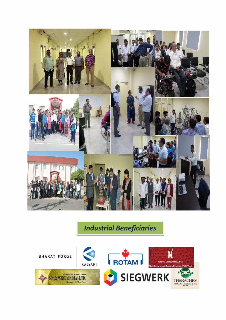
Industrial Beneficiaries
Materials Research Centre
MALAVIYA NATIONAL INSTITUTE OF TECHNOLOGY JAIPUR
JawaharLal Nehru Marg, Jaipur-302017, E-mail: [email protected]
Phone No: +91-141-2713568
Director’s Office: +91-141-2529087, Registrar: +91-141-2529078, Fax: +91-141-2529029
www.mnit.ac.in