Embed Size (px)
Citation preview
4–252MIT Reports to the President 2007–2008
Materials Processing Center/Microphotonics Center
This report discusses the FY2008 activities of the Materials Processing Center (MPC) and its major affiliate, the Microphotonics Center (MPhC). MPC is an interdisciplinary center within MIT’s School of Engineering; MPhC is a center within MPC. MPhC and MPC share an overlapping staff in a common headquarters space. During FY2008, the staff numbered five, led by the director, Professor Lionel C. Kimerling of the Department of Materials Science and Engineering.
Materials Processing Center
MPC exists to create opportunities for industry and government to take advantage of the wealth of exciting materials science and engineering research taking place at MIT. From better batteries, stronger metals, and thin films and coatings (see Fig. 1) to integrated optical communication processors, materials science and engineering at MIT remains at the cutting edge.
As a leading research university in the world, MIT is fertile ground for materials innovation. With a plethora of impressive ideas and breakthroughs, MIT routinely leads among U.S. universities in patents granted. The sheer volume of new knowledge generated at MIT can be overwhelming. When a company or federal agency has an interest in materials innovation, MPC acts as a guide to information, facilities, and researchers relevant to the particular needs of that organization.
A key advantage of MPC is its structure as a “virtual center,” without facilities, laboratory space, or equipment as such; its function is
to bring people and resources together in an “intellectual space” to examine problems and pursue opportunities with a science-to-systems approach. With its finger on the pulse of all things materials related at MIT, MPC is able to assemble faculty resources and leverage existing knowledge to help companies and federal agencies address their challenges and create opportunities.
MPC/MPhC continues to expand its collaborations with other materials-related centers across the campus to provide a common and guided gateway to the current maze of possibilities outside visitors face when approaching MIT with a materials interest. MPC maintains relationships with the Center for Materials Science and Engineering (CMSE), Department of Materials Science and Engineering (DMSE), Institute for Soldier Nanotechnologies (ISN), Industrial Liaison Program (ILP), Research Laboratory of Electronics (RLE), Materials Systems Laboratory (MSL), Microsystems Technology Laboratory (MTL), Media Lab, and Computer Science and Artificial Intelligence Laboratory (CSAIL). The Materials@MIT gateway web initiative (cosponsored by MPC,
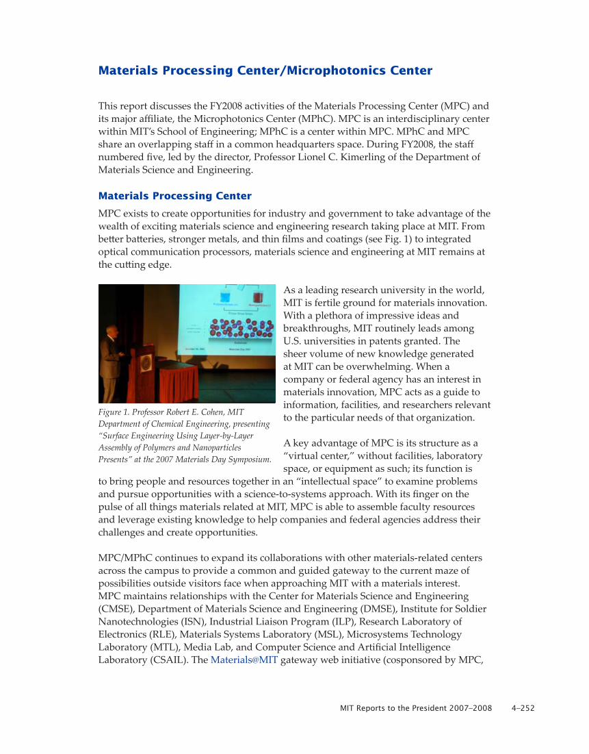
Figure 1. Professor Robert E. Cohen, MIT Department of Chemical Engineering, presenting “Surface Engineering Using Layer-by-Layer Assembly of Polymers and Nanoparticles Presents” at the 2007 Materials Day Symposium.
Materials Processing Center/Microphotonics Center
4–253MIT Reports to the President 2007–2008
CMSE, and DMSE) actively encourages the participation of all campus organizations involved in materials research. This website has observed impressive international and local monthly traffic since its launch in FY2007. The increasing shift to online information transfer has catalyzed a more focused initiative utilizing this site as a campus-wide materials reporting resource.
Over 25 Years of Service to the Institute
Established in 1980 with support under a NASA Center of Excellence grant, MPC initiated with a metallurgy focus under the stewardship of its founding director, Professor Merton C. Flemings. With the arrival of the center’s second director, Professor Kent Bowen, MPC’s vision widened to address the development of advanced ceramic materials during the 1980s. By the time of its fifth and current director, Professor Lionel C. Kimerling, MPC’s research activities have been organized into six industry sectors (electronics, transportation, primary materials, construction, energy, and biomaterials) and have expanded to include all four primary material fields (metals, ceramics, semiconductors, polymers) and spawn a sister center, MPhC, to address the joint industry–academia effort to roadmap a major 21st century technology: semiconductor-based photonics.
In the course of its first 27 years of activity, MPC has, in conjunction with the ILP and the Industry Collegium, pioneered the establishment of a new foundation for interdisciplinary research collaborations and pedagogy at MIT.
Microphotonics Center
The primary focus of MPhC is the interdisciplinary convergence of electronics and photonics. MPhC has focused in the last year on four research areas:
• Microphotonics devices for CMOS integration
• Microphotonics systems
• Thin-film photovoltaic cells
• Multiwavelength detectors and sensors
Microphotonics Devices for CMOS Integration
The goal of this project is to provide novel photonics devices for integration into silicon-based processing. In the past few years, we have focused on devices that contain germanium-silicon alloys. Germanium-silicon alloys are process compatible with silicon electronics and exhibit properties that can be used for novel devices. Highlights of this research area are realization of an electroabsorption modulator, published in Nature Photonics in June 2008 and development of Ge-based materials for CMOS integrated lasers. The electroabsorption modulator is the first fully integrated modulator that combines small size (~10 µm2), high speed (>50 GHz), and extremely low-power consumption, making the device compatible with large scale electronic-photonic on-chip integration. The laser work is receiving wide recognition reflected in invitations to international conferences and workshops. Pioneering work has been done on so-called vertical slot waveguides, a new waveguide design that allows light guiding in low-index materials.
4–254MIT Reports to the President 2007–2008
Materials Processing Center/Microphotonics Center
Microphotonics Systems
In this area, requirements for on-chip photonic systems designs are evaluated. With CSAIL, a computer architecture incorporating photonic devices is being developed. Initial results show mixed photonic electronic circuits for multicore microprocessors are superior to processors without photonic devices. Based on these findings seminal work was done on athermal photonic designs to make photonic device performance independent of thermal fluctuation, a common occurrence in microprocessors.
Thin-film Photovoltaic Cells
Thin-film, silicon-based solar cells are limited by the absorption of light in the thin film. To overcome this limitation, light-trapping photonic structures were successfully implemented and resulted in a significant efficiency increase of 30%. This research demonstrated that photonic designs on solar cells can improve efficiencies considerably.
Multiwavelength Detectors and Sensors
In these two projects, polycrystalline and amorphous chalcogenide materials are monolithically integrated onto a silicon platform to extend the capability of planar silicon-based microphotonics to the fields of imaging and sensing, where traditionally silicon-based materials cannot meet the performance requirements and high-cost material alternatives have to be used. We have fabricated mid-infrared photodetector pixels grown on silicon and spectrally engineered using one-dimensional photonic crystal structure, rendering them a unique wavelength discrimination capability. In the sensor project, we have pioneered the processing of optical resonators in chalcogenide glasses, a key component for multimode sensing, and demonstrated miniaturized optofluidic resonator biosensors that show 10-fold sensitivity improvement over commercial sensors. Our work opens up avenues toward compact, low-cost yet highly sensitive “lab-on-a-chip” systems for biomedical and security applications.
Federal Programs
MPhC proudly assists in our nation’s defense by working to advance emerging technologies that keep our armed forces on the forefront of military capability. Two major Department of Defense (DoD) programs, the BAE Systems-led Defense Advanced Research Projects Agency (DARPA) Electronic and Photonic Integrated Circuits (EPIC) program (in collaboration with Lucent, Cornell, and Columbia) and the Air Force Office of Scientific Research (AFOSR) Multidisciplinary University Research Initiative (MURI) program in silicon lasers and nanophotonics (in collaboration with seven other leading universities), are currently under way through MPhC.
In addition, a DoD-funded one-year feasibility study helped to explore an ultradense photonic-electronic integration initiative involving MPhC, CSAIL, and Sandia National Labs. This all-to-all-computing (ATAC) initiative led to a critical mass of results under the ultraperformance nanophotonic intrachip communications program.
MPhC Consortium
The MPhC Consortium features the Communications Technology Roadmap (CTR) program and its industry-led technology working groups (TWGs). The second phase
Materials Processing Center/Microphotonics Center
4–255MIT Reports to the President 2007–2008
of the CTR’s groundbreaking program has now matured into the formation of three active TWGs: (1) cross-market applications; (2) CMOS (Si) platform; and (3) integration, packaging, and interconnect. TWG activities have helped to support the funding of three CTR fellows who work closely with each TWG, resulting in the authorship of white papers under the diligent direction of industry-based TWG leaders. This effort has yielded a highly productive interaction between academics and industry in order to formulate a roadmap for the future of the microphotonics industry. So far, this initiative has involved 80 organizations from all over the world. Highlights of the CTR report can be found at http://mph-roadmap.mit.edu/index.php/ctr/roadmap/. The next roadmap document is scheduled for spring 2009.
MPC Industry Collegium
For the past quarter century, MPC has acted as a hub for cooperation among MIT researchers exploring materials science issues from their individual academic specialties. The knowledge and experience of MPC helps open up the breadth of the MIT materials community to industry and government interests in materials science. Personal attention and guidance of MPC can provide invaluable assistance to any enterprise seeking a solution to an issue or an opportunity in materials science, engineering, or processing.
When people from industry want to explore innovative materials processing research ongoing at MIT, the MPC Industry Collegium is a considerable tool. Expanding on MIT’s traditionally close ties with industry, the collegium provides a direct link between MIT’s materials community and short-, medium-, and long-term needs of member companies.
The collegium consists of domestic and international companies in a range of industries, from traditional structural materials to biomaterials. For member companies, the collegium provides both broad access to MIT’s materials community and one-on-one guided access to faculty, research staff, and students. For more information about the Industry Collegium, visit http://mpc-web.mit.edu/index.php/mpc/industry-collegium/.
Advancing Materials Research at MIT
MPC functions as a liaison between the cutting-edge materials research being performed here and other materials science, engineering, and processing interests within and outside of MIT. Interdisciplinary collaboration on research initiatives, graduate education, technology transfer, continuing education of industry personnel, and communication among industrial and governmental entities are MPC’s priorities.
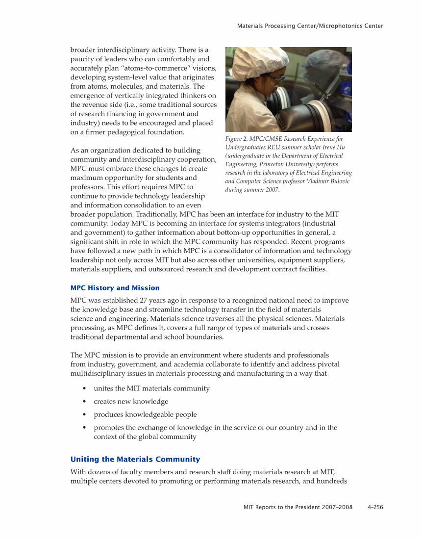
A major priority of MPC is its outreach to new materials faculty and researchers at MIT as well as to the global materials community. MPC has more than 10 visiting scientists working within the center. The center is proactive in inviting faculty to participate in its research activities and educational programs, including the development of new initiatives, symposia, seminars, and summer student internship projects (see Fig. 2).
Vertical Integration
The secret to MPC’s success is taking the science and moving it with a vertically integrated team up to the systems level. Materials innovation and process innovation, already interdisciplinary since the field’s inception, are at the center of an even
4–256MIT Reports to the President 2007–2008
Materials Processing Center/Microphotonics Center
broader interdisciplinary activity. There is a paucity of leaders who can comfortably and accurately plan “atoms-to-commerce” visions, developing system-level value that originates from atoms, molecules, and materials. The emergence of vertically integrated thinkers on the revenue side (i.e., some traditional sources of research financing in government and industry) needs to be encouraged and placed on a firmer pedagogical foundation.
As an organization dedicated to building community and interdisciplinary cooperation, MPC must embrace these changes to create maximum opportunity for students and professors. This effort requires MPC to continue to provide technology leadership and information consolidation to an even broader population. Traditionally, MPC has been an interface for industry to the MIT community. Today MPC is becoming an interface for systems integrators (industrial and government) to gather information about bottom-up opportunities in general, a significant shift in role to which the MPC community has responded. Recent programs have followed a new path in which MPC is a consolidator of information and technology leadership not only across MIT but also across other universities, equipment suppliers, materials suppliers, and outsourced research and development contract facilities.
MPC History and Mission
MPC was established 27 years ago in response to a recognized national need to improve the knowledge base and streamline technology transfer in the field of materials science and engineering. Materials science traverses all the physical sciences. Materials processing, as MPC defines it, covers a full range of types of materials and crosses traditional departmental and school boundaries.
The MPC mission is to provide an environment where students and professionals from industry, government, and academia collaborate to identify and address pivotal multidisciplinary issues in materials processing and manufacturing in a way that
• unites the MIT materials community
• creates new knowledge
• produces knowledgeable people
• promotes the exchange of knowledge in the service of our country and in the context of the global community
Uniting the Materials Community
With dozens of faculty members and research staff doing materials research at MIT, multiple centers devoted to promoting or performing materials research, and hundreds
Figure 2. MPC/CMSE Research Experience for Undergraduates REU summer scholar Irene Hu (undergraduate in the Department of Electrical Engineering, Princeton University) performs research in the laboratory of Electrical Engineering and Computer Science professor Vladimir Bulovic during summer 2007.
Materials Processing Center/Microphotonics Center
4–257MIT Reports to the President 2007–2008
of graduate and undergraduate students, the materials community at MIT is a vibrant, diverse group. We are united as a community in that we are all committed to advancing materials science, engineering, and processing. However, to grow as a community and truly leverage our collective intellectual resources, it is vital to connect with each other in more ways than with simply a broad common goal. MPC creates opportunities for the materials community to come together in research, in education, and in celebration.
MPC interacts with materials-related centers on campus, such as CMSE, ISN, RLE, MSL, MTL, Media Lab, and CSAIL. MPC maintains a close relationship with DMSE and works closely with ILP, providing specific guidance to companies with materials-related needs. Our ongoing strategy is to improve our position as an information resource for the campus community and portal for consortium and collegium member companies. With our program sponsors and research alliance partners, our key value continues to be our building of interdisciplinary faculty teams for tackling new areas of intellectual activity.
Materials@MIT Gateway Web Initiative
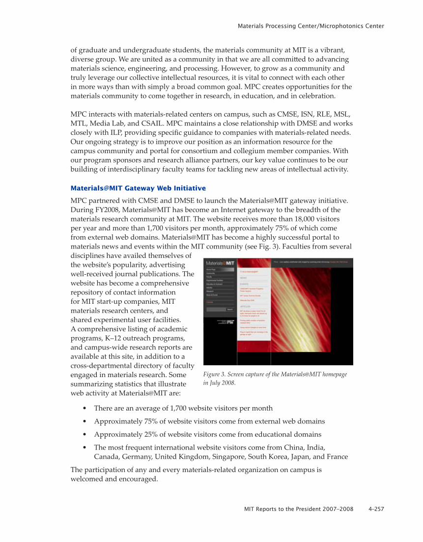
MPC partnered with CMSE and DMSE to launch the Materials@MIT gateway initiative. During FY2008, Materials@MIT has become an Internet gateway to the breadth of the materials research community at MIT. The website receives more than 18,000 visitors per year and more than 1,700 visitors per month, approximately 75% of which come from external web domains. Materials@MIT has become a highly successful portal to materials news and events within the MIT community (see Fig. 3). Faculties from several disciplines have availed themselves of the website’s popularity, advertising well-received journal publications. The website has become a comprehensive repository of contact information for MIT start-up companies, MIT materials research centers, and shared experimental user facilities. A comprehensive listing of academic programs, K–12 outreach programs, and campus-wide research reports are available at this site, in addition to a cross-departmental directory of faculty engaged in materials research. Some summarizing statistics that illustrate web activity at Materials@MIT are:
• There are an average of 1,700 website visitors per month
• Approximately 75% of website visitors come from external web domains
• Approximately 25% of website visitors come from educational domains
• The most frequent international website visitors come from China, India, Canada, Germany, United Kingdom, Singapore, South Korea, Japan, and France
The participation of any and every materials-related organization on campus is welcomed and encouraged.
Figure 3. Screen capture of the Materials@MIT homepage in July 2008.
4–258MIT Reports to the President 2007–2008
Materials Processing Center/Microphotonics Center
Creating New Knowledge
Focus on Interdisciplinary Research Collaborations
Fostering cooperative inquiry and experimentation in the cross-disciplinary area of materials science and engineering is the cornerstone of MPC. The MPC strategy includes leveraging core federal research funding within the MIT materials community into expanded industrial–academic collaborations. Center research covers a broad range of materials and processes via a number of common themes. Foremost among them is the control of materials structure, properties, and performance in an ecologically and economically sound manner. Our philosophy focuses on an understanding of processing fundamentals to control internal structure, from the nanoscale to the macroscale, thereby optimizing a material’s properties and performance.
MPC builds relationships with faculty by familiarizing itself with their current research projects, future interests, and resource needs; by bringing industries’ materials and processing needs and interests to them; and by inviting them individually or in teams to collaborate with industry. MPC provides seed research program development funding to new faculty members and teams and assists with proposals, budgets, and the administration of research accounts. More than 50 faculty and senior research staff members have active research accounts in MPC. The faculty affiliated with MPC hail from nine departments in the Schools of Engineering, Science, and Humanities, Arts, and Social Sciences as well as the Sloan School of Management.
During FY2008, MPC continued to focus on the development of microphotonics projects through MPhC, which conducts collaborative research focused on advancing basic science and emerging technology to enable the convergence of electronics and photonics. As a research community dedicated to optimizing interdisciplinary academic and industrial collaboration to advance basic science and precompetitive technology in areas relevant to applied microphotonics, MPhC engenders research and development cross-fertilization, leading to innovation. The vision of MPhC is a future where the microphotonics platform enables enhanced information access, bandwidth, reliability, and complexity that extends the advance of silicon integrated circuit (IC) technology. MPhC has several major research thrusts in addition to individual faculty members’ research. MPhC research programs have continued to generate significant new intellectual property for their sponsors in FY2007.
Research Volume
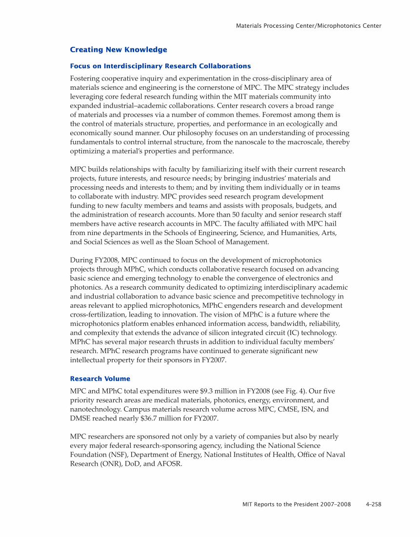
MPC and MPhC total expenditures were $9.3 million in FY2008 (see Fig. 4). Our five priority research areas are medical materials, photonics, energy, environment, and nanotechnology. Campus materials research volume across MPC, CMSE, ISN, and DMSE reached nearly $36.7 million for FY2007.
MPC researchers are sponsored not only by a variety of companies but also by nearly every major federal research-sponsoring agency, including the National Science Foundation (NSF), Department of Energy, National Institutes of Health, Office of Naval Research (ONR), DoD, and AFOSR.
Materials Processing Center/Microphotonics Center
4–259MIT Reports to the President 2007–2008
Federal Programs
DARPA EPIC Program
One of the largest federal programs of MPhC is the Application-Specific Electronic and Photonic Integrated Circuits Program (AS-EPIC) sponsored by DARPA, the central research and development organization for DoD. This major, multiyear research contract (awarded in December 2004) is funding a collaboration led by BAE Systems (http://www.baesystems.com/), with MIT, Lucent Technologies, Applied Wave Research, Cornell University, and Columbia University.
The overall DARPA EPIC program supports research intended to produce novel approaches that “enable revolutionary advances in science, devices, and/or systems” in three areas: CMOS-compatible high-performance Si nanophotonic devices, application specific electronic and photonic integrated circuits, and novel photonic devices. The MPhC project is in the second area of interest: fabrication and demonstration of AS-EPICs.
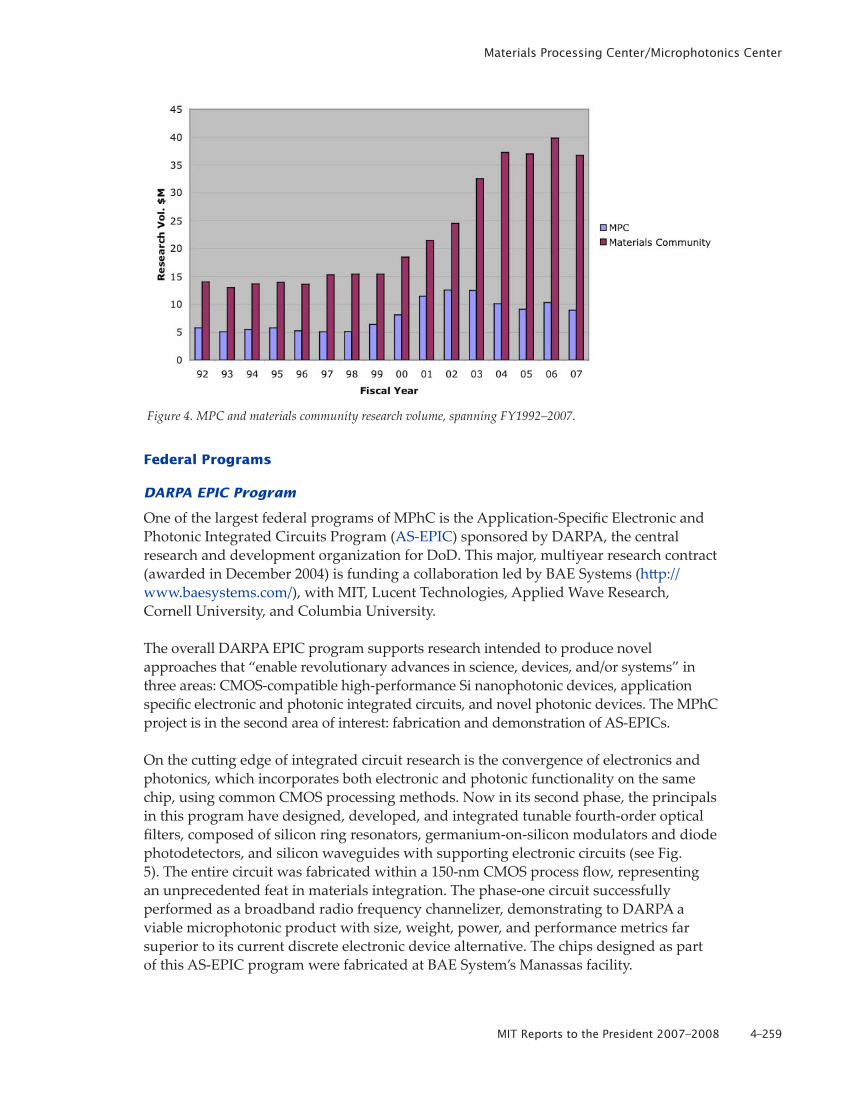
On the cutting edge of integrated circuit research is the convergence of electronics and photonics, which incorporates both electronic and photonic functionality on the same chip, using common CMOS processing methods. Now in its second phase, the principals in this program have designed, developed, and integrated tunable fourth-order optical filters, composed of silicon ring resonators, germanium-on-silicon modulators and diode photodetectors, and silicon waveguides with supporting electronic circuits (see Fig. 5). The entire circuit was fabricated within a 150-nm CMOS process flow, representing an unprecedented feat in materials integration. The phase-one circuit successfully performed as a broadband radio frequency channelizer, demonstrating to DARPA a viable microphotonic product with size, weight, power, and performance metrics far superior to its current discrete electronic device alternative. The chips designed as part of this AS-EPIC program were fabricated at BAE System’s Manassas facility.
Figure 4. MPC and materials community research volume, spanning FY1992–2007.
4–260MIT Reports to the President 2007–2008
Materials Processing Center/Microphotonics Center
MURI Silicon Lasers and Nanophotonics Program
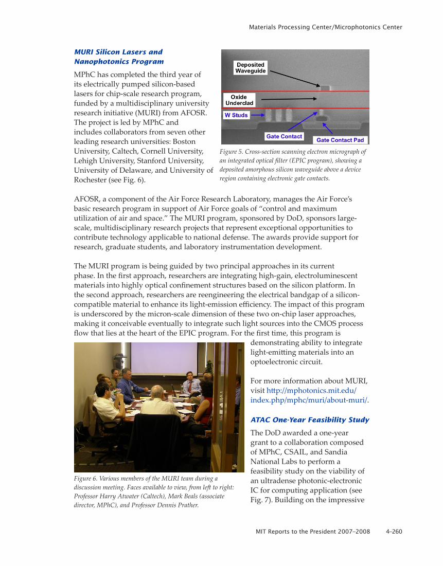
MPhC has completed the third year of its electrically pumped silicon-based lasers for chip-scale research program, funded by a multidisciplinary university research initiative (MURI) from AFOSR. The project is led by MPhC and includes collaborators from seven other leading research universities: Boston University, Caltech, Cornell University, Lehigh University, Stanford University, University of Delaware, and University of Rochester (see Fig. 6).
AFOSR, a component of the Air Force Research Laboratory, manages the Air Force’s basic research program in support of Air Force goals of “control and maximum utilization of air and space.” The MURI program, sponsored by DoD, sponsors large-scale, multidisciplinary research projects that represent exceptional opportunities to contribute technology applicable to national defense. The awards provide support for research, graduate students, and laboratory instrumentation development.
The MURI program is being guided by two principal approaches in its current phase. In the first approach, researchers are integrating high-gain, electroluminescent materials into highly optical confinement structures based on the silicon platform. In the second approach, researchers are reengineering the electrical bandgap of a silicon-compatible material to enhance its light-emission efficiency. The impact of this program is underscored by the micron-scale dimension of these two on-chip laser approaches, making it conceivable eventually to integrate such light sources into the CMOS process flow that lies at the heart of the EPIC program. For the first time, this program is
demonstrating ability to integrate light-emitting materials into an optoelectronic circuit.
For more information about MURI, visit http://mphotonics.mit.edu/index.php/mphc/muri/about-muri/.
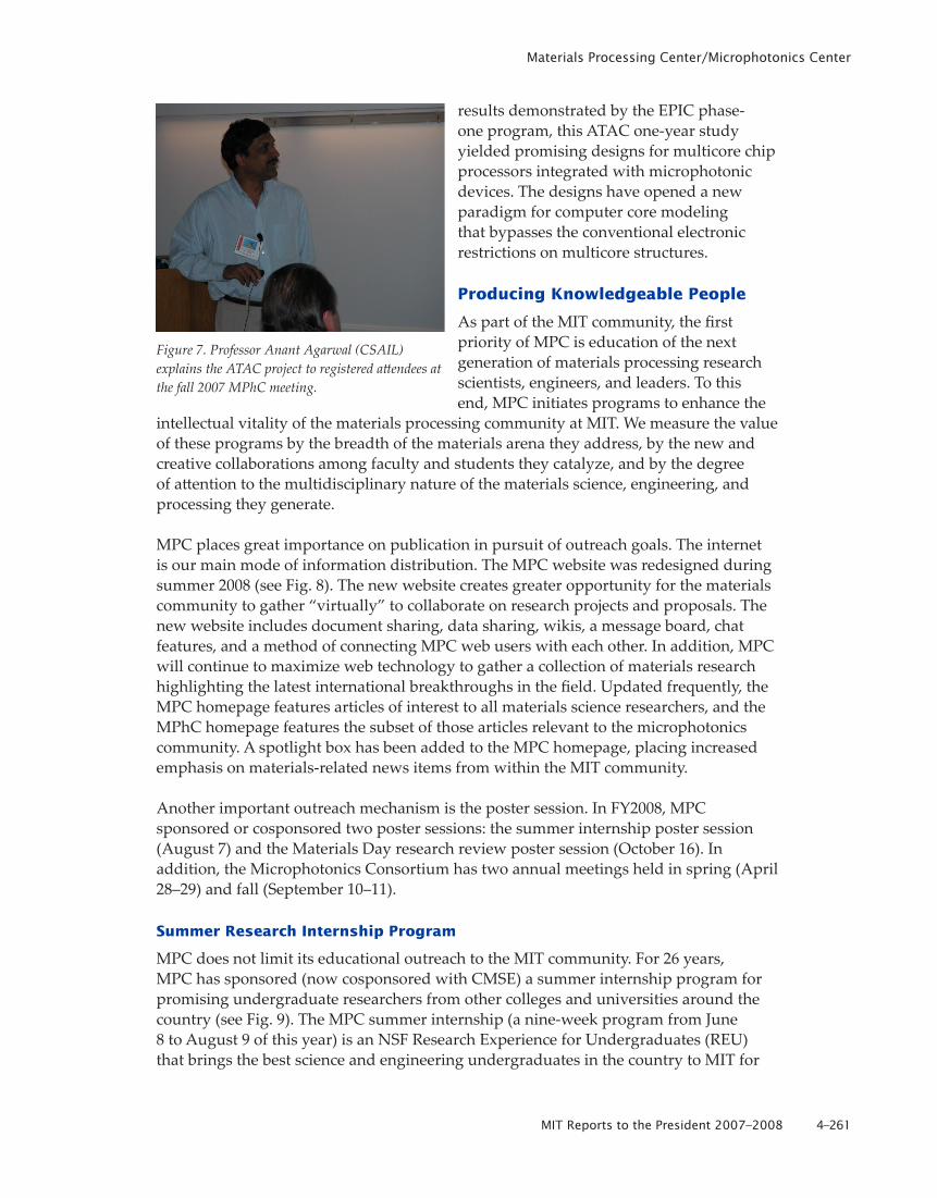
ATAC One-Year Feasibility Study
The DoD awarded a one-year grant to a collaboration composed of MPhC, CSAIL, and Sandia National Labs to perform a feasibility study on the viability of an ultradense photonic-electronic IC for computing application (see Fig. 7). Building on the impressive
Figure 5. Cross-section scanning electron micrograph of an integrated optical filter (EPIC program), showing a deposited amorphous silicon waveguide above a device region containing electronic gate contacts.
Figure 6. Various members of the MURI team during a discussion meeting. Faces available to view, from left to right: Professor Harry Atwater (Caltech), Mark Beals (associate director, MPhC), and Professor Dennis Prather.
Materials Processing Center/Microphotonics Center
4–261MIT Reports to the President 2007–2008
results demonstrated by the EPIC phase-one program, this ATAC one-year study yielded promising designs for multicore chip processors integrated with microphotonic devices. The designs have opened a new paradigm for computer core modeling that bypasses the conventional electronic restrictions on multicore structures.
Producing Knowledgeable People
As part of the MIT community, the first priority of MPC is education of the next generation of materials processing research scientists, engineers, and leaders. To this end, MPC initiates programs to enhance the
intellectual vitality of the materials processing community at MIT. We measure the value of these programs by the breadth of the materials arena they address, by the new and creative collaborations among faculty and students they catalyze, and by the degree of attention to the multidisciplinary nature of the materials science, engineering, and processing they generate.
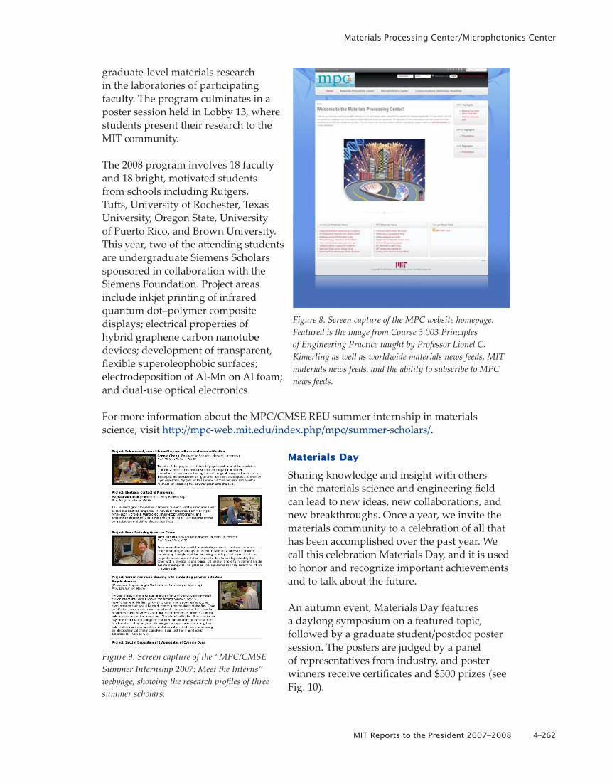
MPC places great importance on publication in pursuit of outreach goals. The internet is our main mode of information distribution. The MPC website was redesigned during summer 2008 (see Fig. 8). The new website creates greater opportunity for the materials community to gather “virtually” to collaborate on research projects and proposals. The new website includes document sharing, data sharing, wikis, a message board, chat features, and a method of connecting MPC web users with each other. In addition, MPC will continue to maximize web technology to gather a collection of materials research highlighting the latest international breakthroughs in the field. Updated frequently, the MPC homepage features articles of interest to all materials science researchers, and the MPhC homepage features the subset of those articles relevant to the microphotonics community. A spotlight box has been added to the MPC homepage, placing increased emphasis on materials-related news items from within the MIT community.
Another important outreach mechanism is the poster session. In FY2008, MPC sponsored or cosponsored two poster sessions: the summer internship poster session (August 7) and the Materials Day research review poster session (October 16). In addition, the Microphotonics Consortium has two annual meetings held in spring (April 28–29) and fall (September 10–11).
Summer Research Internship Program
MPC does not limit its educational outreach to the MIT community. For 26 years, MPC has sponsored (now cosponsored with CMSE) a summer internship program for promising undergraduate researchers from other colleges and universities around the country (see Fig. 9). The MPC summer internship (a nine-week program from June 8 to August 9 of this year) is an NSF Research Experience for Undergraduates (REU) that brings the best science and engineering undergraduates in the country to MIT for
Figure 7. Professor Anant Agarwal (CSAIL) explains the ATAC project to registered attendees at the fall 2007 MPhC meeting.
4–262MIT Reports to the President 2007–2008
Materials Processing Center/Microphotonics Center
graduate-level materials research in the laboratories of participating faculty. The program culminates in a poster session held in Lobby 13, where students present their research to the MIT community.
The 2008 program involves 18 faculty and 18 bright, motivated students from schools including Rutgers, Tufts, University of Rochester, Texas University, Oregon State, University of Puerto Rico, and Brown University. This year, two of the attending students are undergraduate Siemens Scholars sponsored in collaboration with the Siemens Foundation. Project areas include inkjet printing of infrared quantum dot–polymer composite displays; electrical properties of hybrid graphene carbon nanotube devices; development of transparent, flexible superoleophobic surfaces; electrodeposition of Al-Mn on Al foam; and dual-use optical electronics.
For more information about the MPC/CMSE REU summer internship in materials science, visit http://mpc-web.mit.edu/index.php/mpc/summer-scholars/.
Materials Day
Sharing knowledge and insight with others in the materials science and engineering field can lead to new ideas, new collaborations, and new breakthroughs. Once a year, we invite the materials community to a celebration of all that has been accomplished over the past year. We call this celebration Materials Day, and it is used to honor and recognize important achievements and to talk about the future.
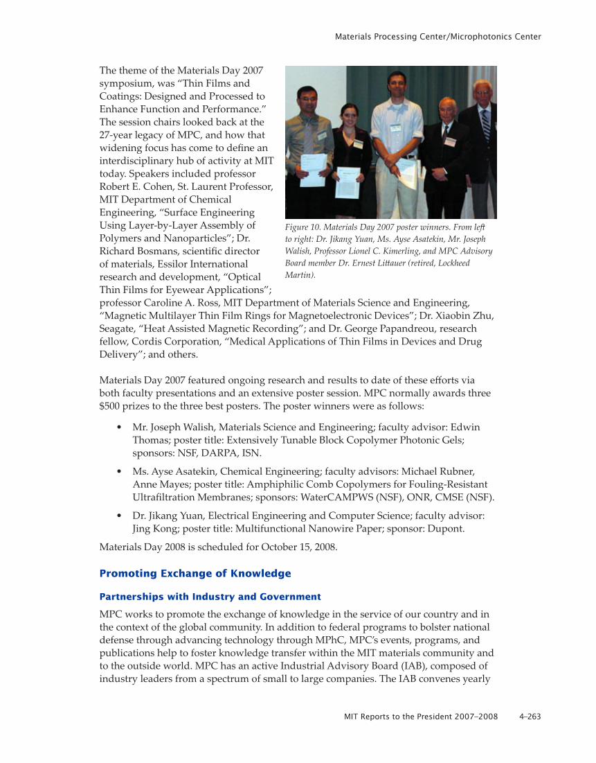
An autumn event, Materials Day features a daylong symposium on a featured topic, followed by a graduate student/postdoc poster session. The posters are judged by a panel of representatives from industry, and poster winners receive certificates and $500 prizes (see Fig. 10).
Figure 8. Screen capture of the MPC website homepage. Featured is the image from Course 3.003 Principles of Engineering Practice taught by Professor Lionel C. Kimerling as well as worldwide materials news feeds, MIT materials news feeds, and the ability to subscribe to MPC news feeds.
Figure 9. Screen capture of the “MPC/CMSE Summer Internship 2007: Meet the Interns” webpage, showing the research profiles of three summer scholars.
Materials Processing Center/Microphotonics Center
4–263MIT Reports to the President 2007–2008
The theme of the Materials Day 2007 symposium, was “Thin Films and Coatings: Designed and Processed to Enhance Function and Performance.” The session chairs looked back at the 27-year legacy of MPC, and how that widening focus has come to define an interdisciplinary hub of activity at MIT today. Speakers included professor Robert E. Cohen, St. Laurent Professor, MIT Department of Chemical Engineering, “Surface Engineering Using Layer-by-Layer Assembly of Polymers and Nanoparticles”; Dr. Richard Bosmans, scientific director of materials, Essilor International research and development, “Optical Thin Films for Eyewear Applications”; professor Caroline A. Ross, MIT Department of Materials Science and Engineering, “Magnetic Multilayer Thin Film Rings for Magnetoelectronic Devices”; Dr. Xiaobin Zhu, Seagate, “Heat Assisted Magnetic Recording”; and Dr. George Papandreou, research fellow, Cordis Corporation, “Medical Applications of Thin Films in Devices and Drug Delivery”; and others.
Materials Day 2007 featured ongoing research and results to date of these efforts via both faculty presentations and an extensive poster session. MPC normally awards three $500 prizes to the three best posters. The poster winners were as follows:
• Mr. Joseph Walish, Materials Science and Engineering; faculty advisor: Edwin Thomas; poster title: Extensively Tunable Block Copolymer Photonic Gels; sponsors: NSF, DARPA, ISN.
• Ms. Ayse Asatekin, Chemical Engineering; faculty advisors: Michael Rubner, Anne Mayes; poster title: Amphiphilic Comb Copolymers for Fouling-Resistant Ultrafiltration Membranes; sponsors: WaterCAMPWS (NSF), ONR, CMSE (NSF).
• Dr. Jikang Yuan, Electrical Engineering and Computer Science; faculty advisor: Jing Kong; poster title: Multifunctional Nanowire Paper; sponsor: Dupont.
Materials Day 2008 is scheduled for October 15, 2008.
Promoting Exchange of Knowledge
Partnerships with Industry and Government
MPC works to promote the exchange of knowledge in the service of our country and in the context of the global community. In addition to federal programs to bolster national defense through advancing technology through MPhC, MPC’s events, programs, and publications help to foster knowledge transfer within the MIT materials community and to the outside world. MPC has an active Industrial Advisory Board (IAB), composed of industry leaders from a spectrum of small to large companies. The IAB convenes yearly
Figure 10. Materials Day 2007 poster winners. From left to right: Dr. Jikang Yuan, Ms. Ayse Asatekin, Mr. Joseph Walish, Professor Lionel C. Kimerling, and MPC Advisory Board member Dr. Ernest Littauer (retired, Lockheed Martin).
4–264MIT Reports to the President 2007–2008
Materials Processing Center/Microphotonics Center
on the day after Materials Day. Last fall’s meeting, held on October 17, 2007, featured presentations from faculty conducting materials research at MIT, the dean of the School of Engineering and various department heads.
In FY2007, MPhC continued major research programs with industry affiliates. MPhC maintained its relationship with sponsors of its major research programs; visiting industrial scientists affiliated with these programs are appointed through MPC.
MPhC Consortium
The MPhC Consortium consisted in FY2008 of 16 member companies (up from 12 in the previous year), from the materials-to-systems technology supply chain of the computing, data communications, and telecommunications sectors.
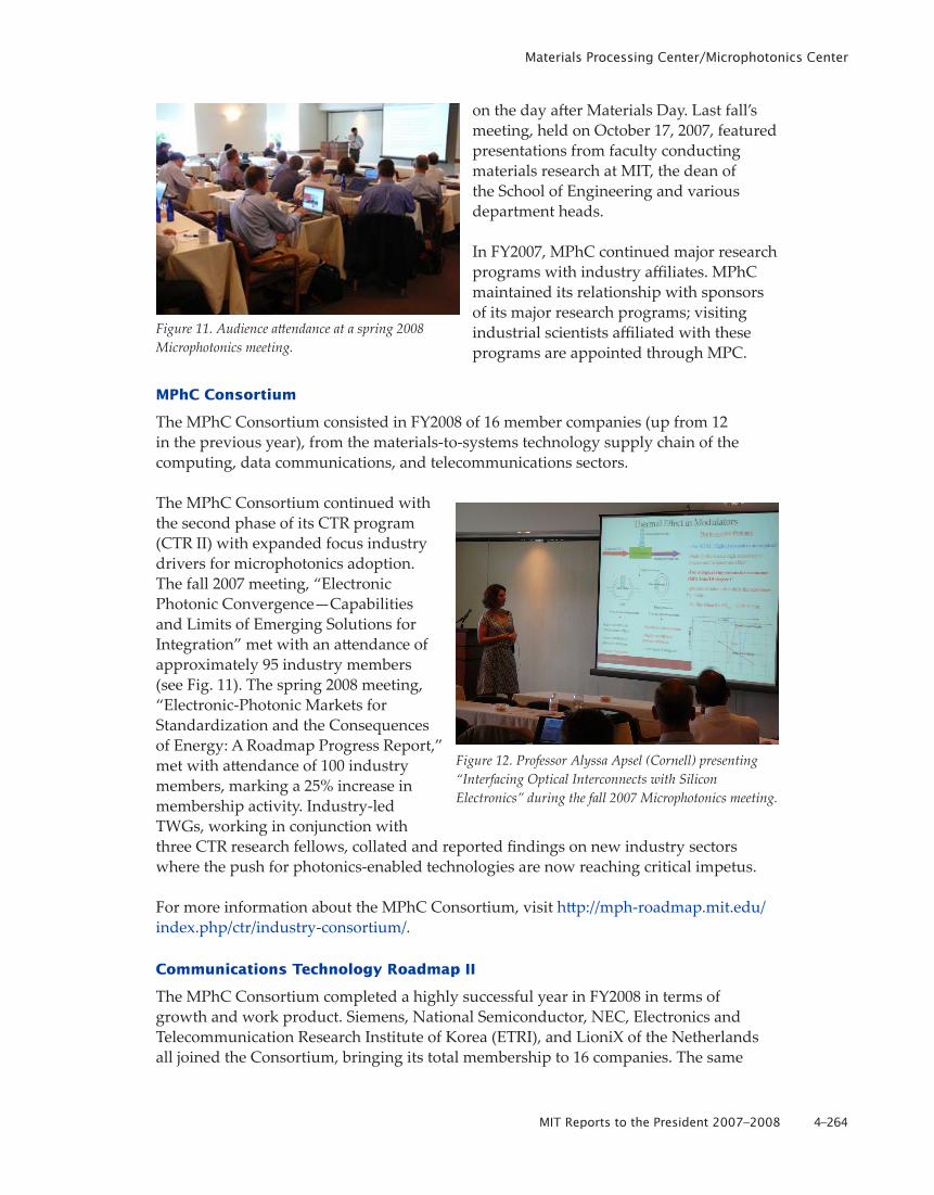
The MPhC Consortium continued with the second phase of its CTR program (CTR II) with expanded focus industry drivers for microphotonics adoption. The fall 2007 meeting, “Electronic Photonic Convergence—Capabilities and Limits of Emerging Solutions for Integration” met with an attendance of approximately 95 industry members (see Fig. 11). The spring 2008 meeting, “Electronic-Photonic Markets for Standardization and the Consequences of Energy: A Roadmap Progress Report,” met with attendance of 100 industry members, marking a 25% increase in membership activity. Industry-led TWGs, working in conjunction with three CTR research fellows, collated and reported findings on new industry sectors where the push for photonics-enabled technologies are now reaching critical impetus.
For more information about the MPhC Consortium, visit http://mph-roadmap.mit.edu/index.php/ctr/industry-consortium/.
Communications Technology Roadmap II
The MPhC Consortium completed a highly successful year in FY2008 in terms of growth and work product. Siemens, National Semiconductor, NEC, Electronics and Telecommunication Research Institute of Korea (ETRI), and LioniX of the Netherlands all joined the Consortium, bringing its total membership to 16 companies. The same
Figure 11. Audience attendance at a spring 2008 Microphotonics meeting.
Figure 12. Professor Alyssa Apsel (Cornell) presenting “Interfacing Optical Interconnects with Silicon Electronics” during the fall 2007 Microphotonics meeting.
Materials Processing Center/Microphotonics Center
4–265MIT Reports to the President 2007–2008
companies, together with the staff of MPhC and other contributors, produced the interim draft of its upcoming CTR II document, due to be released in spring 2009.
Discussion, conference presentations, and survey work by the three TWGs highlighted key issues facing the convergence of electronics and photonics such as optical storage networks, computer-aided design of board-level optical interconnects, mixed-signal propagation on a silicon platform, germanium-based devices on Si CMOS, and the growing importance of many-to-many core computation. Historically, clockspeed, form-factor, and bandwidth have driven the design of IC technology; however, new industry consensus indicates that the most significant emerging constraint to data communication is power, with electromagnetic induction (EMI) as a close second.
An exponentially growing server market, fueled by rapid buildup of data farms and the proposition of cloud computing, has power requirements that threaten to exacerbate existing supply. Such data centers reportedly expend 2 megawatts of power on cooling for every 1 megawatt of computing. Japan’s power consumption for internet protocol routers is 1% of the country’s total electricity generation. Photonic integration offers a potential solution to foreseen demands by providing more power-efficient communications.
Reduction of the current form factor is limited by the EMI associated with the incumbent electronic process; photonics is increasingly viewed by both network and hardware markets as solving this problem. The past year saw the introduction in what is considered the segue interconnect to electronic photonic convergence: the active cable. With electronic end connectors capping an all-photonic cable for box-to-box computing, active cables convert electronic signal to photonic and back to electronic again within its single unit, while reducing cable size, increasing speed, and allowing a more nimble and densely configured server area. Standardization and demand volume continue to teeter as the leading influence for widespread E-P market adoption. The highly active CTR board of directors discusses these and other issues biweekly with a goal of establishing current trends and recommendations for deployment in the datacom and imaging markets for the next 15 years. CTR II is under the codirection of Professor Randolph Kirchain (DMSE) and Professor Lionel Kimerling.
Three TWGs are meeting regularly to focus on specific areas of interest. The CTR II TWGs are:
• Cross Market Applications: Characterizing Technical Requirements and Architectural Options, chaired by Alan Benner (IBM) and Tremont Miao (Analog Devices)
• Realizing a CMOS (Si) Platform, chaired by Michael Morse (Intel Corporation) and Raymond Beausoleil (HP)
• Integration, Packaging, and Interconnection, chaired by Louay Eldada (DuPont Photonics Technologies) and Richard Grzybowski (Corning).
For more information about the CTR program, visit http://mph-roadmap.mit.edu/.
4–266MIT Reports to the President 2007–2008
Materials Processing Center/Microphotonics Center
Outlook
Interdisciplinary collaboration among the various fields of inquiry related to materials science, engineering, and processing is the prime focus of MPC. Over the next few years, there are five key trends in materials science that will affect MPC. The first, interdisciplinary research teams with vertical integration to applications, is a wonderful confirmation of the idea, which MPC has always promoted, that strategically bringing together specialists from various academic specialties can produce a synergistic whole that is far more than the sum of its parts. Another key trend, vanishing academic department boundaries, has resulted in dual appointments for some new faculty. The interdepartmental faculty member is a great example of how the entire community is moving toward more interdisciplinary pursuits. A third key trend is a new type of triangular industry: government–university partnership, such as the EPIC program described earlier in this report. More intellectual property (IP) creation, a fourth key trend, is related to the collaboration we help arrange. Industry seeks IP, from its sponsored research, so more collaboration means more IP creation. The application-rich nature of industry enables researchers to do what we do best: develop basic, fundamental results and then apply them when we get the opportunities. The last key trend that will affect MPC going forward is the fact that materials innovation is pervasive in our 21st century world. As more of the scientific community around the world begins to focus on materials science, engineering, and processing, we may look forward to a truly exponential increase in new ideas, materials, and applications.
The long-term strategic vision of MPC must be to act as the intellectual leader in materials innovation and processing across the MIT community and the external community and interface with government and industrial systems integrators. The short-term plan is to continue building the relationship base to act as this central consolidator and leader in the materials community. In each sector of MPC research activity, system integrators must be identified and relationships established. This process in the defense sector is well under way, and the process has also started in the biomaterials and biotechnology area. With system integrator relationships growing, key community membership of individuals and resources outside the MIT community can also be folded into the MPC community.
A major challenge at MIT is the need for a better sense of community. MPC has provided, for the past quarter century, a successful means of achieving a better sense of community within the School of Engineering and across the whole campus. Looking ahead, MPC anticipates that the next quarter century will be even more exciting than the first, as collaborative initiatives with other materials research organizations on and off campus take shape and take flight.
Lionel C. Kimerling Director Professor of Materials Science and Engineering
More information about the Materials Processing Center can be found at http://mpc-web.mit.edu/. More information about the Microphotonics Center can be found at http://mphotonics.mit.edu/.