Embed Size (px)
Citation preview
Design guide for rubber keypads
J.W. Electronic Components GmbH
Phone: +49 2137 / 9 37 44 96, Fax: +49 211 / 68 57 97, @:[email protected], Internet: www.jw-electronic-components.de
1
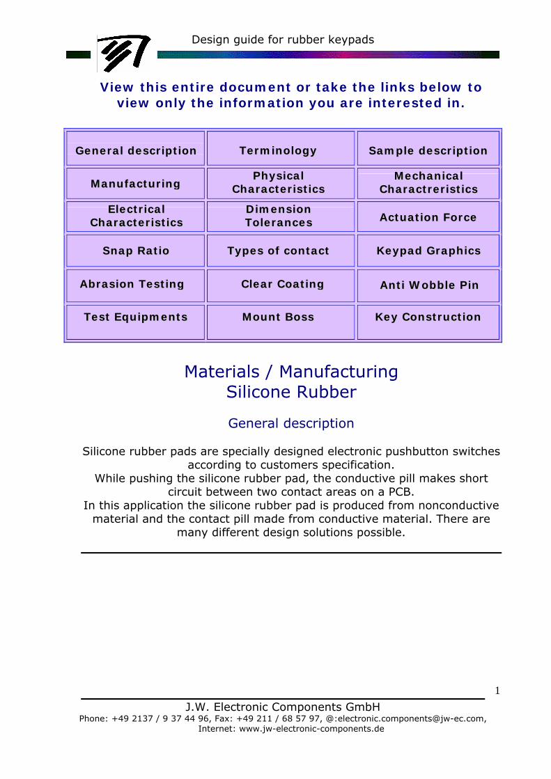
View this entire document or take the links below to
view only the information you are interested in.
Materials / Manufacturing
Silicone Rubber
General description
Silicone rubber pads are specially designed electronic pushbutton switches according to customers specification.
While pushing the silicone rubber pad, the conductive pill makes short circuit between two contact areas on a PCB.
In this application the silicone rubber pad is produced from nonconductive material and the contact pill made from conductive material. There are
many different design solutions possible.
TTeerrmmiinnoollooggyy GGeenneerraall ddeessccrriippttiioonn SSaammppllee ddeessccrriippttiioonn
MMaannuuffaaccttuurriinngg PPhhyyssiiccaall
CChhaarraacctteerriissttiiccss MMeecchhaanniiccaall
CChhaarraaccttrreerriissttiiccss
EElleeccttrriiccaall CChhaarraacctteerriissttiiccss
DDiimmeennssiioonn TToolleerraanncceess AAccttuuaattiioonn FFoorrccee
SSnnaapp RRaattiioo TTyyppeess ooff ccoonnttaacctt KKeeyyppaadd GGrraapphhiiccss
AAbbrraassiioonn TTeessttiinngg CClleeaarr CCooaattiinngg AAnnttii WWoobbbbllee PPiinn
TTeesstt EEqquuiippmmeennttss MMoouunntt BBoossss KKeeyy CCoonnssttrruuccttiioonn
Design guide for rubber keypads
J.W. Electronic Components GmbH
Phone: +49 2137 / 9 37 44 96, Fax: +49 211 / 68 57 97, @:[email protected], Internet: www.jw-electronic-components.de
2
Terminology
Actuation Force: The force required to collapse the membrane of a rubber switch (identified as F1 on the force/stroke curve).
Air Channel: Air path(s) on the bottom of rubber keypads and switches that allows for air passage (venting) when switch is actuated. Switches must be vented on a least two sides.
Alignment Hole: Through hole in rubber keypad that is used to position keypad in enclosure when overall keypad size exceeds three inches in either length or width.
Base: Silicone sheet material that joins all keys/switches on a rubber keypad. Also known as apron.
Bezel: The faceplate or cover, typically either plastic or metal, used to secure a key pad to a printed circuit board. The bezel also aligns the keypad during the final assembly and protects keypad-base material from contact with human hands.
Breakdown Voltage: Voltage at which an insulator or dielectric ruptures. Also know as dielectric strength.
Design guide for rubber keypads
J.W. Electronic Components GmbH
Phone: +49 2137 / 9 37 44 96, Fax: +49 211 / 68 57 97, @:[email protected], Internet: www.jw-electronic-components.de
3
Compression Set: The measurement of a material's ability to recover
it's original size and shape after compression under prescribed conditions. It is usually expressed as a recover percentage (fraction) of the compression condition.
Conductive Rubber Switch: Mechanical switch made of silicone rubber, either direct or indirect contact.
Contact: The current-carrying area/surface under each rubber switch (conductive pill or carbon-inked surface) that makes electrical connection with the electrode on a printed circuit board when the switch is actuated.
Contact Force: The force required to maintain rubber-switch contact closure (F2) force/stroke curve) with a printed circuit board.
Contact Rating: The electric power handling capability for rubber contacts under strictly controlled laboratory conditions.
Contact Resistance: Silicone-rubber keypads manufactured using a two-shot molding process and two-material hardnesses.
Dual Durometer: Silicone-rubber keypads manufactured using a two-shot molding process and two-material hardnesses.
Electrode: Contact surface/design on a printed circuit board that conducts current when rubber switch is actuated and switch closure occurs.
Key Height: The measured distance from the bottom of a keypad (base) to the top surface of a key.
Legend: Some type of printed graphic (symbol, letter or number) on the top of the key surface.
Life: The number of switch actuations realized before the switch membrane ruptures or over stresses.
Membrane: The non-conductive hinge that permits a rubber key to flex, and is responsible for the tactile feel realized.
Negative-Image Graphics: Graphics that allow switch color or switch masking color to be seen through top-surface printing on keypad.
Overstroke: Additional travel experienced with a rubber switch after initial switch closure has been realized. Rubber switches with overstroke require a double-cone or double-bell shaped membrane.
Positive-Image Graphics: Single or multi-color printing on top of key surface.
Return Force: Force created by switch membrane as it returns the key to a non-actuated position.
Snap Ratio: (F1-F2) divided by F1. The difference between the actuation force (F1) and the contact force (F2) of a switch divided by the actuation force.
Stroke: Distance from the contact surface on a rubber switch to an electrode pattern on a printed circuit board
Design guide for rubber keypads
.
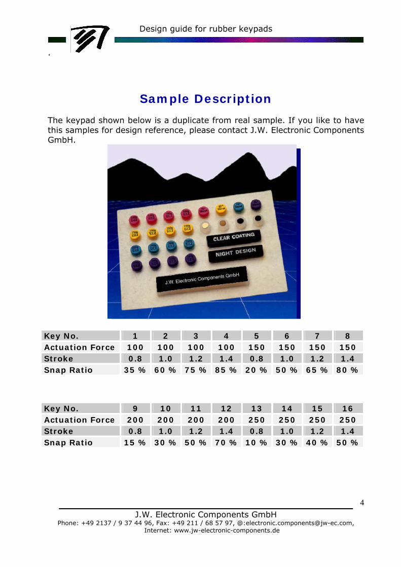
Sample Description
The keypad shown below is a duplicate from real sample. If you like to have this samples for design reference, please contact J.W. Electronic Components GmbH.
J.W. Electronic Components GmbH
Phone: +49 2137 / 9 37 44 96, Fax: +49 211 / 68 57 97, @:[email protected], Internet: www.jw-electronic-components.de
4
Key No. 1 2 3 4 5 6 7 8 Actuation Force 100 100 100 100 150 150 150 150 Stroke 0.8 1.0 1.2 1.4 0.8 1.0 1.2 1.4 Snap Ratio 35 % 60 % 75 % 85 % 20 % 50 % 65 % 80 %
Key No. 9 10 11 12 13 14 15 16 Actuation Force 200 200 200 200 250 250 250 250 Stroke 0.8 1.0 1.2 1.4 0.8 1.0 1.2 1.4 Snap Ratio 15 % 30 % 50 % 70 % 10 % 30 % 40 % 50 %

Design guide for rubber keypads
Key No.
17. Hardness 50° Shore A. 18. Hardness 60° Shore A. 19. Hardness 70° Shore A. 20. Hardness 80° Shore A. 21. Gold plate pill contact. 22. silver powder pill contact. 23. Carbon pill contact. 24. Screen-printing contact. 25. Key with clear coating. 26. Laser-etching key.
J.W. Electronic Components GmbH
Phone: +49 2137 / 9 37 44 96, Fax: +49 211 / 68 57 97, @:[email protected], Internet: www.jw-electronic-components.de
5
Design guide for rubber keypads
Materials / Manufacturing
Silicone Rubber
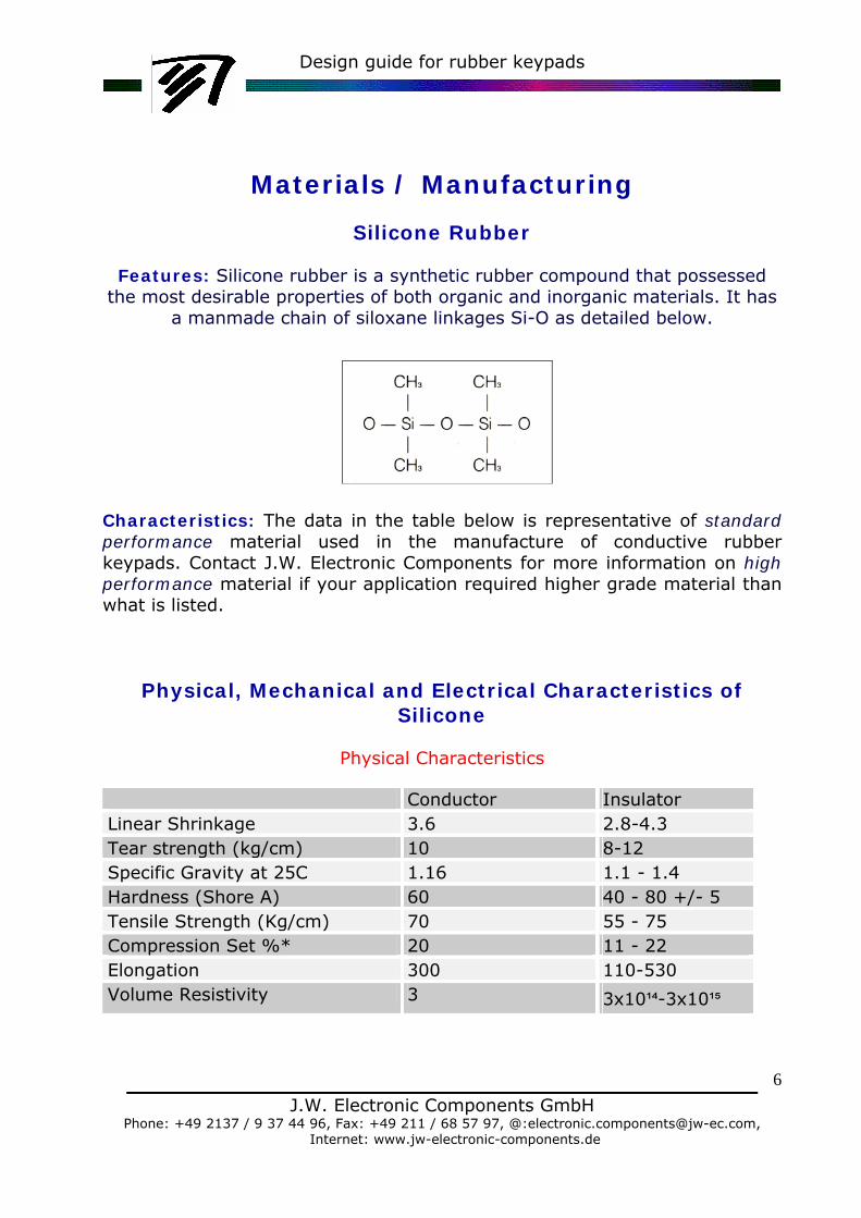
Features: Silicone rubber is a synthetic rubber compound that possessed the most desirable properties of both organic and inorganic materials. It has
a manmade chain of siloxane linkages Si-O as detailed below.
Characteristics: The data in the table below is representative of standard performance material used in the manufacture of conductive rubber keypads. Contact J.W. Electronic Components for more information on high performance material if your application required higher grade material than what is listed.
Physical, Mechanical and Electrical Characteristics of Silicone
Physical Characteristics
Conductor Insulator Linear Shrinkage 3.6 2.8-4.3 Tear strength (kg/cm) 10 8-12 Specific Gravity at 25C 1.16 1.1 - 1.4 Hardness (Shore A) 60 40 - 80 +/- 5 Tensile Strength (Kg/cm) 70 55 - 75 Compression Set %* 20 11 - 22 Elongation 300 110-530 Volume Resistivity 3 3x10¹⁴-3x10¹⁵
J.W. Electronic Components GmbH
Phone: +49 2137 / 9 37 44 96, Fax: +49 211 / 68 57 97, @:[email protected], Internet: www.jw-electronic-components.de
6

Design guide for rubber keypads
J.W. Electronic Components GmbH
Phone: +49 2137 / 9 37 44 96, Fax: +49 211 / 68 57 97, @:[email protected], Internet: www.jw-electronic-components.de
7
Mechanical Characteristics
Key stroke 0,25-5,0 mm Actuation force 20-350 gr Operating life 1 million actuations (typical) Operating temperature - 40 ° C / + 85 ° C** Storage temperature - 60 ° C / + 120 ° C**
Electrical Characteristics
Contact resistance <200 ohms*** Insulation Resistance @ 500VDC >100 Mohms Contact Bounce <12 msec Contact Rating 30 mA @ 12V DC .5 sec. Dielectric Strength >1 min. @ 500V RMS
* After 22 hours at 175ºC ** To convert degrees Fahrenheit to degrees Centigrade use formula: (ºF-32) divided by 1.8 *** Based on gold or nickel-plated printed circuit board
Dimension Tolerances
Size (m/m)
Ultra-precise Tolerance (+/-)
Precise Tolerance (+/-)
General Tolerance (+/-)
6.3 or less 0.10 m/m 0.15 m/m 0.25 m/m 6.3-10 0.10 m/m 0.20 m/m 0.30 m/m 10-16 0.15 m/m 0.20 m/m 0.40 m/m 16-25 0.20 m/m 0.25 m/m 0.50 m/m 25-40 0.20 m/m 0.35 m/m 0.60 m/m 40-63 0.25 m/m 0.40 m/m 0.80 m/m 63-100 0.35 m/m 0.50 m/m 1.00 m/m 100-160 0.40 m/m 0.70 m/m 1.30 m/m 160 or up 0.3 % 0.5 % 0.8 %
*The testing criterion of finished products is according to Ultra-precise tolerance standard if there is no specified dimension tolerance or special request before ordering.
Design guide for rubber keypads
J.W. Electronic Components GmbH
Phone: +49 2137 / 9 37 44 96, Fax: +49 211 / 68 57 97, @:[email protected], Internet: www.jw-electronic-components.de
8
Actuation Force Tolerances**
The membrane shape and size of all rubber switches can be designed so that almost any actuation force and tactile feel can be realized. Most applications require positive tactile feel with relatively long life, so an actuation force of approximately 125 - 150 grams is typically recommended with an accompanying snap ratio of approximately 40 - 60%.
Design Force (grams) Tolerance (+/-) 50 15 g 75 20 g 100 25 g 125 30 g 150 35 g 175 40 g
200-250 50 g 250.1 and up 30 %
** Typical tolerance for actuation force is +/- 25 grams. Optimum actuation force for best key performance is 80 - 150 grams. Conductive rubber switches can be successfully designed and manufactured with actuation forces ranging from minimum of 20 grams to a maximum of 500 grams.
Snap Ratio
The snap ratio (or click ratio) of any conductive rubber keypad directly affects the tactile feel realized by the operator. Keypads with snap ratios of 40 - 60% have excellent tactile feel and relatively long life, while keypads with snap ratios below 40% have relatively weak tactile feel, but longer life. Dual-durometer keypads also improve tactile feel. The snap ratio of any keypad can be calculated by working with the formula F1-F2 divided by F1, where F1 is the actuation force and F2 is the contact resistance.
Design guide for rubber keypads
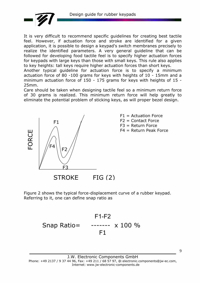
It is very difficult to recommend specific guidelines for creating best tactile feel. However, if actuation force and stroke are identified for a given application, it is possible to design a keypad's switch membranes precisely to realize the identified parameters. A very general guideline that can be followed for developing food tactile feel is to specify higher actuation forces for keypads with large keys than those with small keys. This rule also applies to key heights: tall keys require higher actuation forces than short keys. Another typical guideline for actuation force is to specify a minimum actuation force of 80 -100 grams for keys with heights of 10 - 15mm and a minimum actuation force of 150 - 175 grams for keys with heights of 15 - 25mm. Care should be taken when designing tactile feel so a minimum return force of 30 grams is realized. This minimum return force will help greatly to eliminate the potential problem of sticking keys, as will proper bezel design. F1 = Actuation Force
F2 = Contact Force F3 = Return Force F4 = Return Peak Force
J.W. Electronic Components GmbH
Phone: +49 2137 / 9 37 44 96, Fax: +49 211 / 68 57 97, @:[email protected], Internet: www.jw-electronic-components.de
9
Figure 2 shows the typical force-displacement curve of a rubber keypad. Referring to it, one can define snap ratio as
F1-F2
Snap Ratio= ------- x 100 % F1
FORCE
STROKE FIG (2)
F1
F4 F2
F3
Design guide for rubber keypads
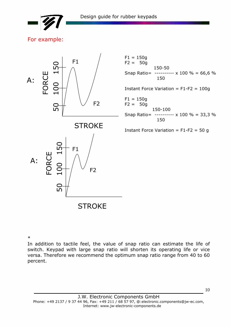
For example:
FORCE
A:
50
100
1
50
F1
F2
FORCE
A:
50
100
1
50 F1
F2
STROKE
F1 = 150g F2 = 50g 150-50 Snap Ratio= ---------- x 100 % = 66,6 % 150 Instant Force Variation = F1-F2 = 100g F1 = 150g F2 = 50g 150-100 Snap Ratio= ---------- x 100 % = 33,3 % 150 Instant Force Variation = F1-F2 = 50 g
STROKE * In addition to tactile feel, the value of snap ratio can estimate the life of switch. Keypad with large snap ratio will shorten its operating life or vice versa. Therefore we recommend the optimum snap ratio range from 40 to 60 percent.
J.W. Electronic Components GmbH
Phone: +49 2137 / 9 37 44 96, Fax: +49 211 / 68 57 97, @:[email protected], Internet: www.jw-electronic-components.de
10
Design guide for rubber keypads
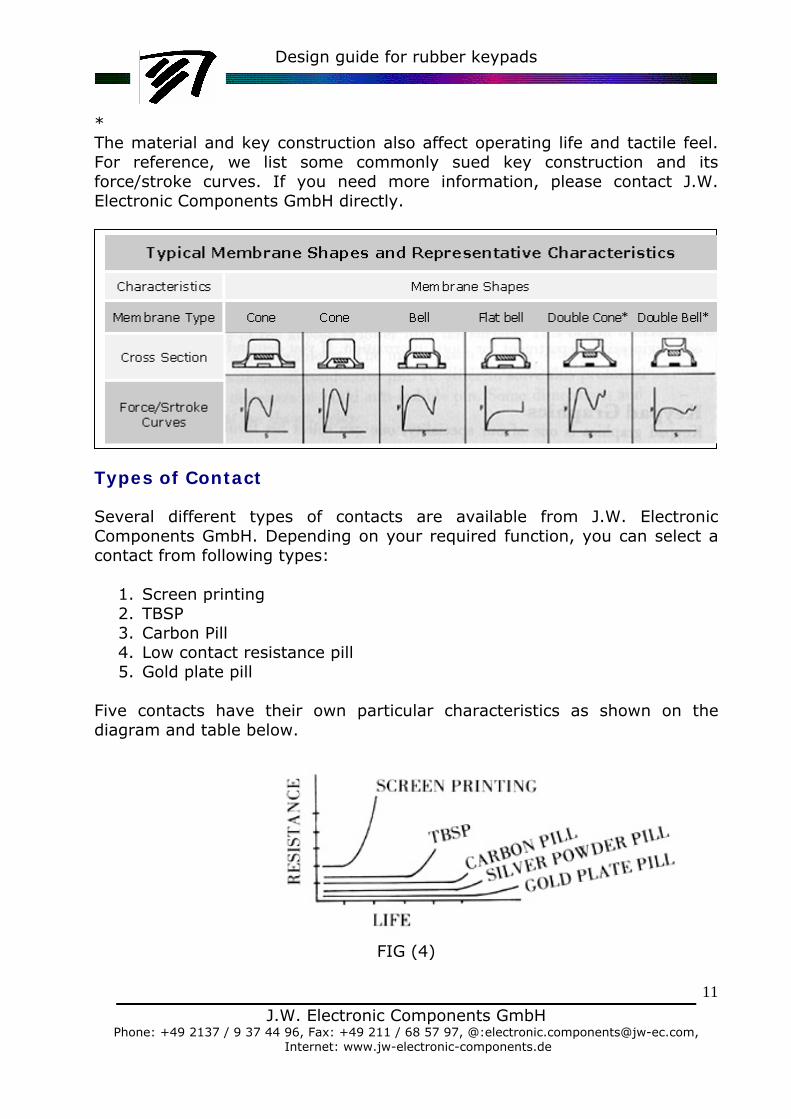
* The material and key construction also affect operating life and tactile feel. For reference, we list some commonly sued key construction and its force/stroke curves. If you need more information, please contact J.W. Electronic Components GmbH directly.
FIG (3)
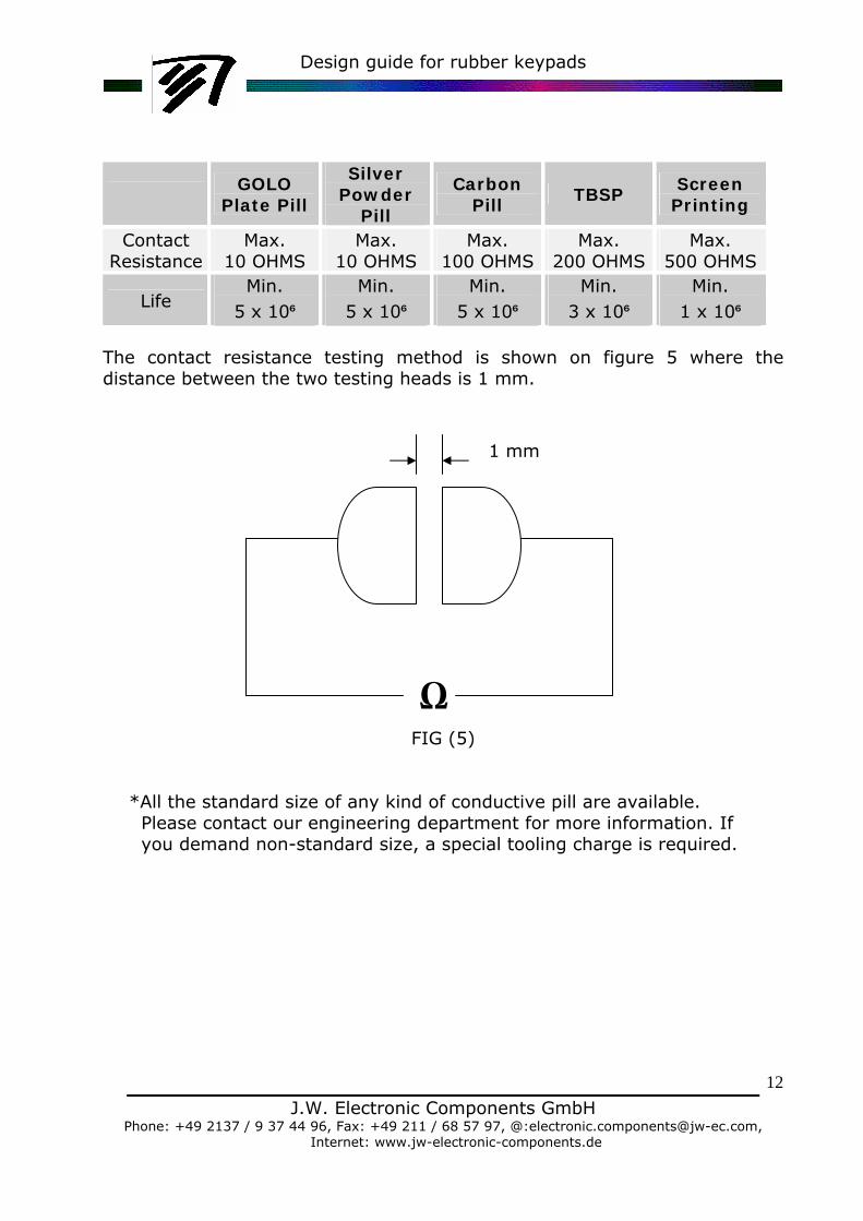
Types of Contact Several different types of contacts are available from J.W. Electronic Components GmbH. Depending on your required function, you can select a contact from following types:
1. Screen printing 2. TBSP 3. Carbon Pill 4. Low contact resistance pill 5. Gold plate pill
Five contacts have their own particular characteristics as shown on the diagram and table below.
FIG (4)
J.W. Electronic Components GmbH
Phone: +49 2137 / 9 37 44 96, Fax: +49 211 / 68 57 97, @:[email protected], Internet: www.jw-electronic-components.de
11
Design guide for rubber keypads
GOLO Plate Pill
Silver Powder
Pill
Carbon Pill TBSP Screen
Printing
Contact Resistance
Max. 10 OHMS
Max. 10 OHMS
Max. 100 OHMS
Max. 200 OHMS
Max. 500 OHMS
Life Min.
5 x 10⁶ Min.
5 x 10⁶ Min.
5 x 10⁶ Min.
3 x 10⁶ Min.
1 x 10⁶ The contact resistance testing method is shown on figure 5 where the distance between the two testing heads is 1 mm. 1 mm
Ω
FIG (5)
*All the standard size of any kind of conductive pill are available. Please contact our engineering department for more information. If you demand non-standard size, a special tooling charge is required.
J.W. Electronic Components GmbH
Phone: +49 2137 / 9 37 44 96, Fax: +49 211 / 68 57 97, @:[email protected], Internet: www.jw-electronic-components.de
12
Design guide for rubber keypads
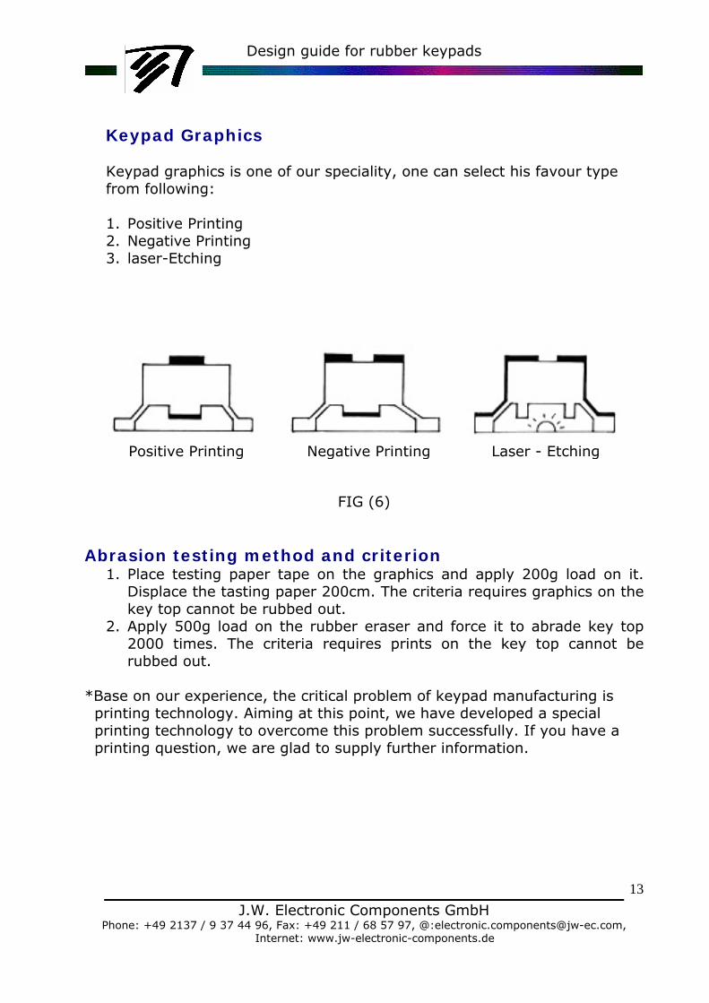
Keypad Graphics Keypad graphics is one of our speciality, one can select his favour type from following: 1. Positive Printing 2. Negative Printing 3. laser-Etching
Laser - Etching Positive Printing Negative Printing
FIG (6)
Abrasion testing method and criterion
1. Place testing paper tape on the graphics and apply 200g load on it. Displace the tasting paper 200cm. The criteria requires graphics on the key top cannot be rubbed out.
2. Apply 500g load on the rubber eraser and force it to abrade key top 2000 times. The criteria requires prints on the key top cannot be rubbed out.
*Base on our experience, the critical problem of keypad manufacturing is printing technology. Aiming at this point, we have developed a special printing technology to overcome this problem successfully. If you have a printing question, we are glad to supply further information.
J.W. Electronic Components GmbH
Phone: +49 2137 / 9 37 44 96, Fax: +49 211 / 68 57 97, @:[email protected], Internet: www.jw-electronic-components.de
13
Design guide for rubber keypads
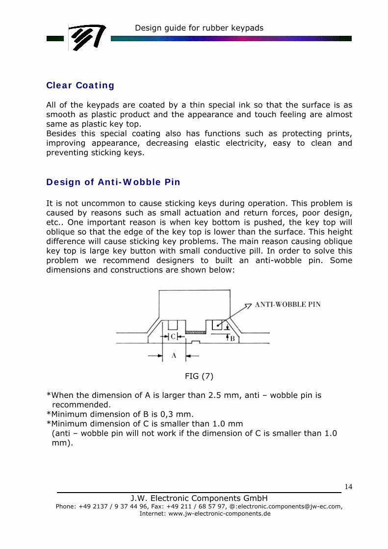
Clear Coating All of the keypads are coated by a thin special ink so that the surface is as smooth as plastic product and the appearance and touch feeling are almost same as plastic key top. Besides this special coating also has functions such as protecting prints, improving appearance, decreasing elastic electricity, easy to clean and preventing sticking keys. Design of Anti-Wobble Pin It is not uncommon to cause sticking keys during operation. This problem is caused by reasons such as small actuation and return forces, poor design, etc.. One important reason is when key bottom is pushed, the key top will oblique so that the edge of the key top is lower than the surface. This height difference will cause sticking key problems. The main reason causing oblique key top is large key button with small conductive pill. In order to solve this problem we recommend designers to built an anti-wobble pin. Some dimensions and constructions are shown below:
FIG (7)
*When the dimension of A is larger than 2.5 mm, anti – wobble pin is recommended.
*Minimum dimension of B is 0,3 mm. *Minimum dimension of C is smaller than 1.0 mm (anti – wobble pin will not work if the dimension of C is smaller than 1.0 mm).
J.W. Electronic Components GmbH
Phone: +49 2137 / 9 37 44 96, Fax: +49 211 / 68 57 97, @:[email protected], Internet: www.jw-electronic-components.de
14
Design guide for rubber keypads
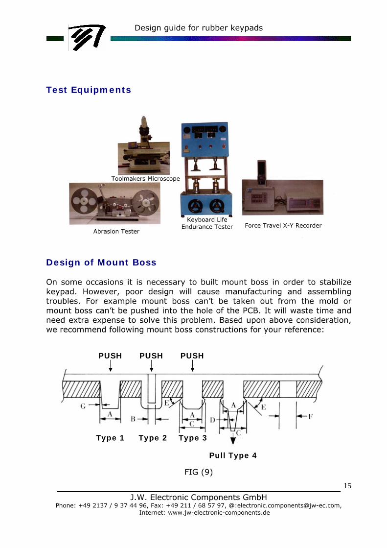
Test Equipments Toolmakers Microscope
Keyboard Life Endurance Tester Force Travel X-Y Recorder
Abrasion Tester Design of Mount Boss On some occasions it is necessary to built mount boss in order to stabilize keypad. However, poor design will cause manufacturing and assembling troubles. For example mount boss can’t be taken out from the mold or mount boss can’t be pushed into the hole of the PCB. It will waste time and need extra expense to solve this problem. Based upon above consideration, we recommend following mount boss constructions for your reference:
PUSH PUSH PUSH Type 1 Type 2 Type 3 Pull Type 4
FIG (9)
J.W. Electronic Components GmbH
Phone: +49 2137 / 9 37 44 96, Fax: +49 211 / 68 57 97, @:[email protected], Internet: www.jw-electronic-components.de
15
Design guide for rubber keypads
J.W. Electronic Components GmbH
Phone: +49 2137 / 9 37 44 96, Fax: +49 211 / 68 57 97, @:[email protected], Internet: www.jw-electronic-components.de
16
Type 1.
1. Minimum diameter is 1.0 (A) 2. The diameter must be equal or larger than the hole of PCB 0.2 mm. 3. The mount boss must have 2° taper.
Type 2. 1. Minimum central hole of mount boss is 1.0 mm 2. The diameter of mount boss is equal or larger than the hole of PCB 0.3
mm. 3. Minimum diameter of PCB is 2.0 mm.
Type 3. 1. The dimension of C must be larger than dimension A 0.8-1.0 mm. 2. The diameter of mount boss is equal or less than the hole of PCB 0.2
mm. 3. Minimum diameter of mount boss is 2.5 mm. 4. The mount boss must have 30° taper for manufacturing and
assembling.
Type 4. 1. The dimension of C must be larger than dimension A 0.8–1.0 mm. 2. The diameter of mount boss may be larger or less than the hole of PCB
0.2 mm. 3. Minimum diameter of mount boss is 2.5 mm. 4. For manufacturing and assembling the mount boss have 30° taper. 5. The mount boss has a pin so that it can be assembled easily by pulling
the pin into the hole of PCB.
*It is beneficial for manufacturing that the diameter of the mount boss is designed as large as possible. *The larger the mount boss the bigger diameter is required in order to reduce the manufacturing difficulties.

Design guide for rubber keypads
J.W. Electronic Components GmbH
Phone: +49 2137 / 9 37 44 96, Fax: +49 211 / 68 57 97, @:[email protected], Internet: www.jw-electronic-components.de
17
Printed Circuit Board Design
Conductive rubber keypads are very reliable, but the environment in which they are used should be considered very carefully when the printed circuit board is designed. In order for any keypad to provide trouble-free operation, it is imperative that all components be designed properly, particularly the printed circuit board. Printed circuit boards can be supplied with several different types of plating; the only type that is specifically not suitable for use with conductive rubber switches is tin-lead solder boards. Gold plating over nickel on the printed circuit board offers the lowest possible contact resistance (less than 100 ohms) for any keypad application, and a minimum layer of 30 -50 micro inches of gold over 100 - 200 micro inches of nickel is recommended for best switch performance. The width of gold traces typically ranges from 0.25 - 0.40mm, while the minimum distance between them is typically 0.30mm and the maximum is usually 0.40mm. Nickel plating, like gold, is extremely reliable and relatively inexpensive when compared to the cost of gold-plated boards. Contact resistance for nickel-plated boards is typically less than 100 ohms, and nickel has an excellent track record in even the most severe environmental conditions. If nickel plating is used without gold, a minimum plating thickness of 200 micro inches is recommended for best overall performance. Most keypad applications utilize nickel-plated boards because of their high reliability and low cost. Silk-screened carbon boards can also be used with conductive rubber switches, but should only be selected when contact resistance between 500 - 1,000 ohms can be tolerated. If screened carbon boards are used, the minimum distance between the traces should be 0.50mm, and the overall size of the electrode should be greater than 5.0mm. It should be noted that there is not a single recommended pad pattern for use with rubber keypads. Printed circuit board electrode design should be developed carefully taking all switch characteristics into consideration. The most important single objective to be considered in designing any pad pattern is to provide as many shorting paths as possible so best switch operation can be realized when the button is actuated. Several common contact patterns are:
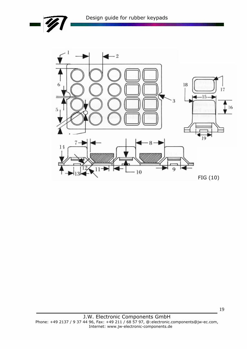
Design guide for rubber keypads
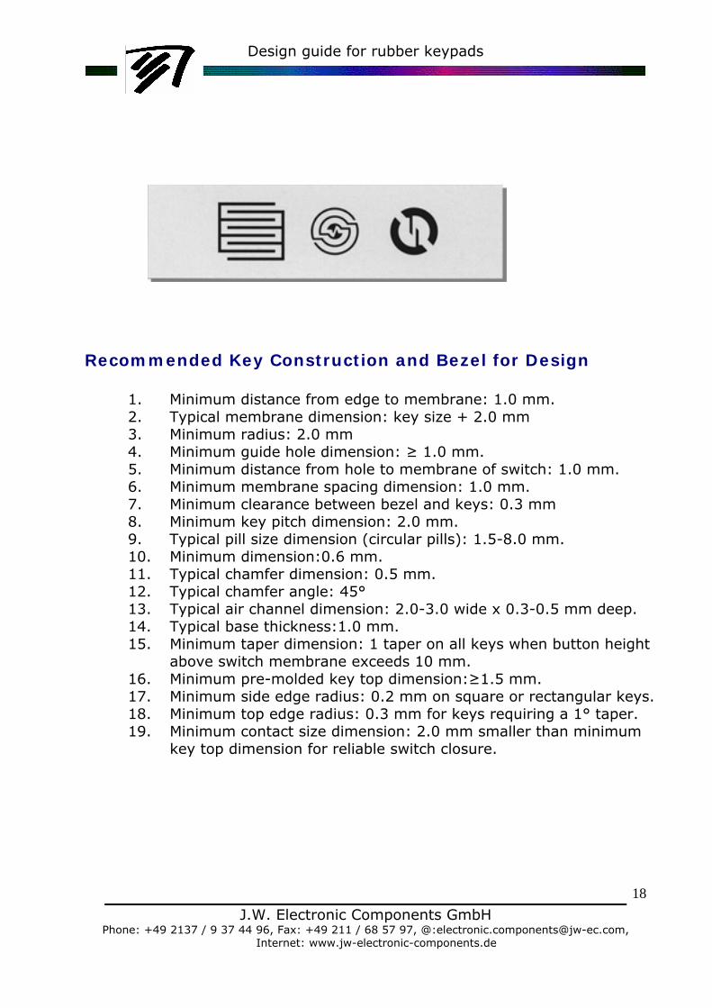
Recommended Key Construction and Bezel for Design
1. Minimum distance from edge to membrane: 1.0 mm. 2. Typical membrane dimension: key size + 2.0 mm 3. Minimum radius: 2.0 mm 4. Minimum guide hole dimension: ≥ 1.0 mm. 5. Minimum distance from hole to membrane of switch: 1.0 mm. 6. Minimum membrane spacing dimension: 1.0 mm. 7. Minimum clearance between bezel and keys: 0.3 mm 8. Minimum key pitch dimension: 2.0 mm. 9. Typical pill size dimension (circular pills): 1.5-8.0 mm. 10. Minimum dimension:0.6 mm. 11. Typical chamfer dimension: 0.5 mm. 12. Typical chamfer angle: 45° 13. Typical air channel dimension: 2.0-3.0 wide x 0.3-0.5 mm deep. 14. Typical base thickness:1.0 mm. 15. Minimum taper dimension: 1 taper on all keys when button height
above switch membrane exceeds 10 mm. 16. Minimum pre-molded key top dimension:≥1.5 mm. 17. Minimum side edge radius: 0.2 mm on square or rectangular keys. 18. Minimum top edge radius: 0.3 mm for keys requiring a 1° taper. 19. Minimum contact size dimension: 2.0 mm smaller than minimum
key top dimension for reliable switch closure.
J.W. Electronic Components GmbH
Phone: +49 2137 / 9 37 44 96, Fax: +49 211 / 68 57 97, @:[email protected], Internet: www.jw-electronic-components.de
18
Design guide for rubber keypads
J.W. Electronic Components GmbH Phone: +49 2137 / 9 37 44 96, Fax: +49 211 / 68 57 97, @:[email protected],
Internet: www.jw-electronic-components.de
19
FIG (10)