Embed Size (px)
Citation preview

Materials for white-LED:efforts for Ab initio Materials Design
M. Mikami et al., IOP Conf. Ser.: Mater. Sci. Eng. 1, 012002 (2009)M. Mikami, N. Kijima, B.Bertrand, M.Stankovski, X.Gonze, ibid (in press).
Masayoshi MikamiMitsubishi Chemical Group Science & Technology Research Center
Bruno Bertrand*, Martin Stankovski, Xavier GonzeETSF/Universite Catholique de Louvain, Belgium
* CERDECAM, Institut Supérieur Industriel ECAM, Belgium
ABINT 2011 Workshop (11-14 April, 2011, Han-sur-Lesse, Belgium)
Cross-section of present type(Blue-LED + yellow phosphor) 板東ら , 応物 , 71(2002),1518
Conventional type:Blue-LED + yellow phosphor
New (Next) type:
High color rendering typesBlue-LED + yellow & redNear UV-LED + blue & green & red Blue-LED + green & red
InGaN chip YAG phosphor
“ww
w.li
ghte
mit
ting
dio
des
.org
”
B Y
lacking red cool white
New phosphorsNew phosphors to be explored !
YAG phosphor
Blue from LEDYellow from YAG
(typically, Y3Al5O12:Ce3+)
Phosphor-converted white LEDsPhosphor-converted white LEDsBackground
M.Mikami & B.Bertrand – ABINIT 2011 Workshop, Han-sur-Lesse - 2
MM
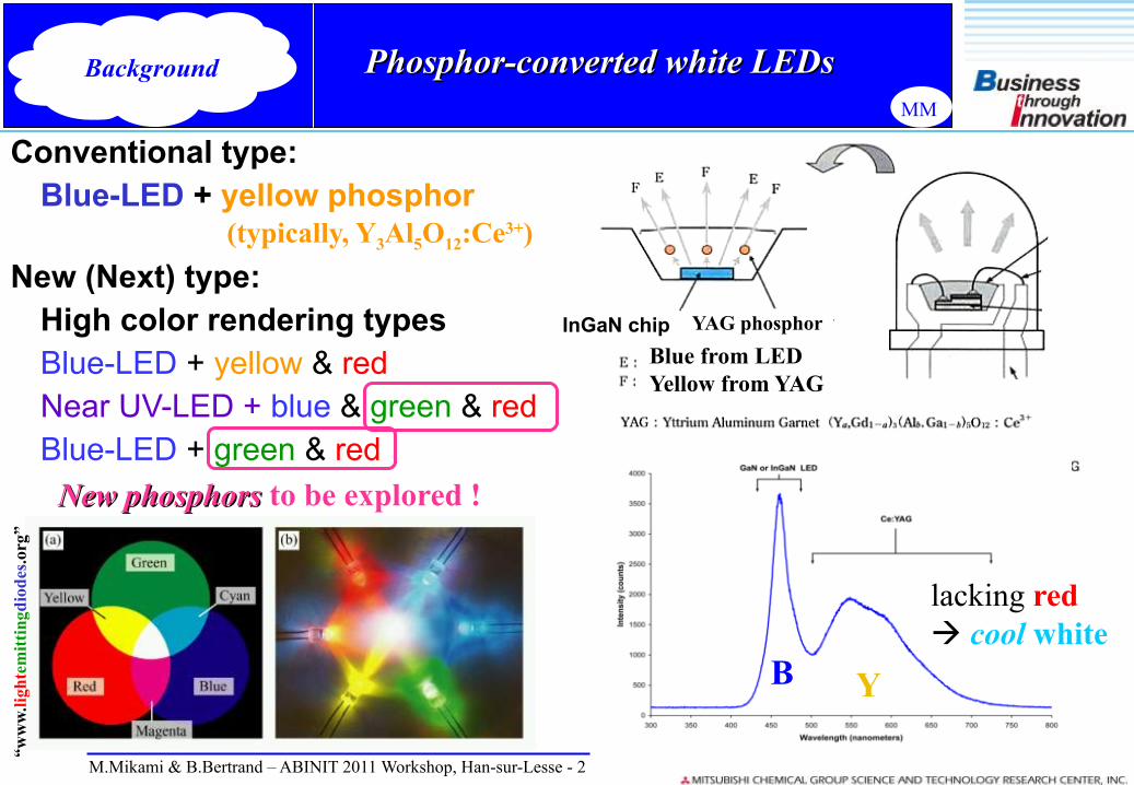
“Phosphor Handbook” (2006)
� -SiAlON:Eu2+
blue(-green) nitride?!AlN:Eu2+,Si4+BaSi7N10:Eu2+
(Sr,Ca)AlSiN3:Eu2+SrAlSi4N7:Eu2+
Ba3Si6O12N2:Eu2+Ba3Si6O9N4:Eu2+Ba1Si2O2N2:Eu2+
LaSi3N5:Ce3+La3Si6N11:Ce3+
Sr1Si2O2N2:Eu2+Ca1Si2O2N2:Eu2+
WE NEED GUIDING PRINCIPLES (THEORY) !
+ updates (from literatures)
M.Mikami & B.Bertrand – ABINIT 2011 Workshop, Han-sur-Lesse - 3
from oxides to (oxy)nitrides (or sulfides…)
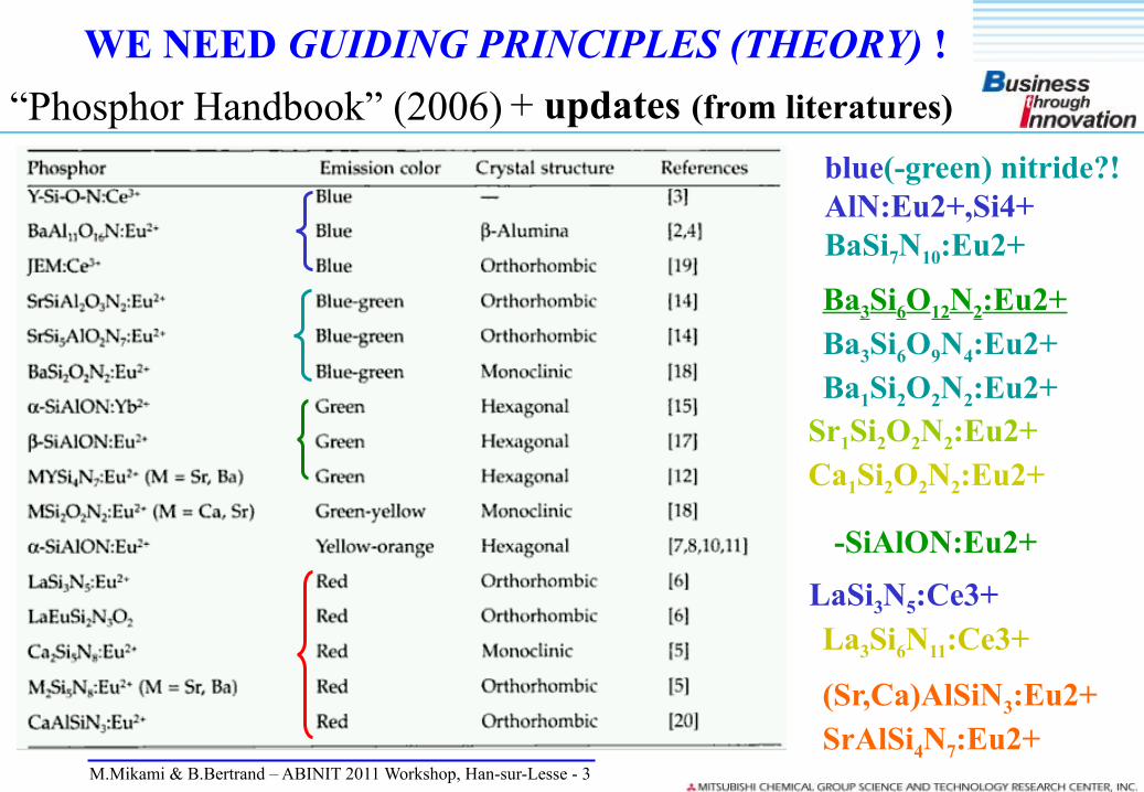
4f7 ground state
4f65d1
Eab
s(E
u2+, A
)
EF
reeA
(Eu
2+)
D(2
+, A
) εcfs (2+
)
� c(2+
, A)
isolated Eu2+ in solid “A”
Crystal Field Splitting
(Likewise with Ce3+)
Notations based on Dorenbos
Eu2+/Ce3+ in “more covalent host”exhibits longer � em ? ... Not always!
Centroid Shift“Nephelauxetic” Covalency??Dielectric const., � (Refractive index, n)
spectroscopic polarizability
atomic polarizability (Dorenbos)
M.Mikami & B.Bertrand – ABINIT 2011 Workshop, Han-sur-Lesse - 4
From oxides to (oxy)nitrides (or sulfides)From oxides to (oxy)nitrides (or sulfides)Background
MM
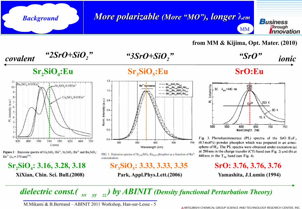
More polarizable (More “MO”), longer � em
ioniccovalent
Sr2SiO4:Eu Sr3SiO5:Eu SrO:Eu
dielectric const.(� xx � yy � zz ) by ABINIT (Density functional Perturbation Theory)
Sr2SiO4: 3.16, 3.28, 3.18 Sr3SiO5: 3.33, 3.33, 3.35 SrO: 3.76, 3.76, 3.76
“3SrO+SiO2” “SrO”“2SrO+SiO2”
Yamashita, J.Lumin (1994)XiXian, Chin. Sci. Bull.(2008) Park, Appl.Phys.Lett.(2006)
from MM & Kijima, Opt. Mater. (2010)
M.Mikami & B.Bertrand – ABINIT 2011 Workshop, Han-sur-Lesse - 5
from oxides to (oxy)nitrides (or sulfides…)More polarizable More polarizable (More “MO”)(More “MO”), longer , longer λememBackgroundBackground
MM
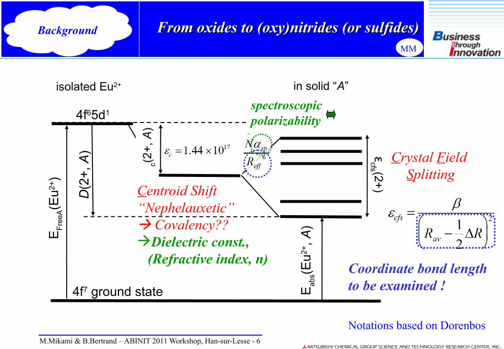
Notations based on Dorenbos
Coordinate bond lengthto be examined !
M.Mikami & B.Bertrand – ABINIT 2011 Workshop, Han-sur-Lesse - 6
4f7 ground state
4f65d1
Eab
s(E
u2+
, A
)
EF
reeA
(Eu
2+)
D(2
+, A
) εcfs (2+
)
� c(2+
, A)
in solid “A”
Crystal Field Splitting
Centroid Shift“Nephelauxetic” Covalency??Dielectric const., � (Refractive index, n)
spectroscopic polarizability
from oxides to (oxy)nitrides (or sulfides…)
isolated Eu2+
From oxides to (oxy)nitrides (or sulfides)From oxides to (oxy)nitrides (or sulfides)Background
MM
v.s.
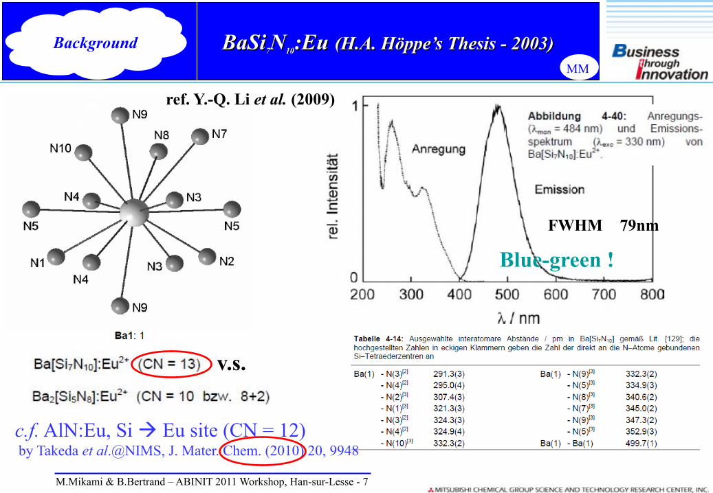
FWHM � 79nm
c.f. AlN:Eu, Si Eu site (CN = 12) by Takeda et al.@NIMS, J. Mater. Chem. (2010) 20, 9948
Blue-green !
M.Mikami & B.Bertrand – ABINIT 2011 Workshop, Han-sur-Lesse - 7
from oxides to (oxy)nitrides (or sulfides…)BaSiBaSi77NN1010:Eu:Eu (H.A. Höppe’s Thesis - 2003)(H.A. Höppe’s Thesis - 2003)Background
ref. Y.-Q. Li et al. (2009)
Background
MM
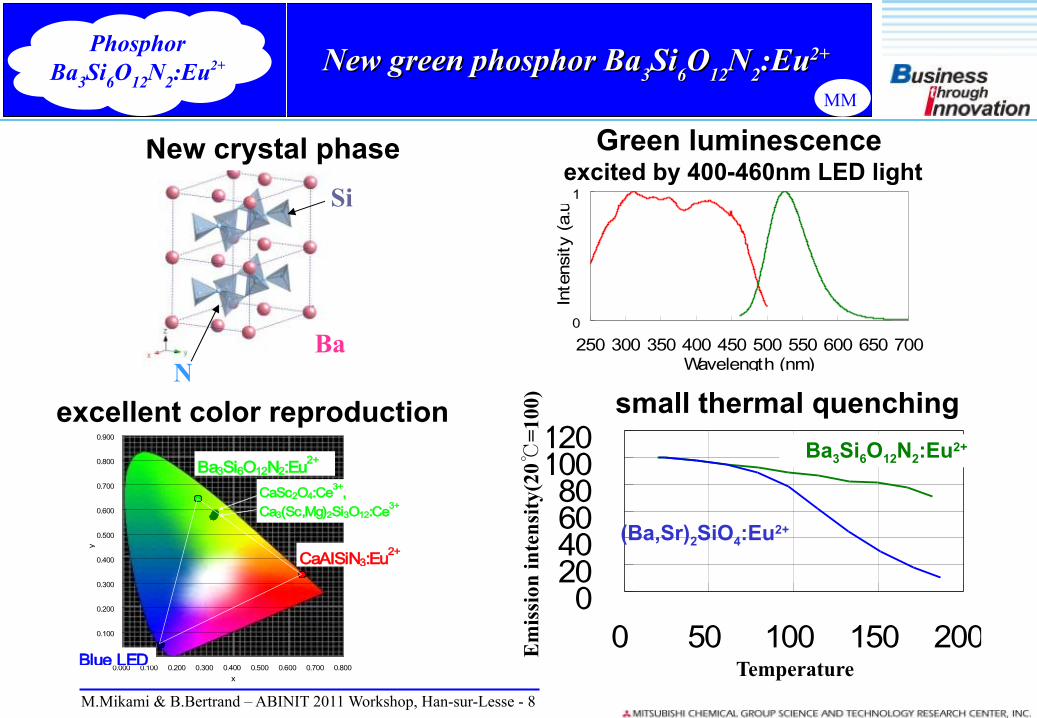
Green luminescence excited by 400-460nm LED light
020406080
100120
0 50 100 150 200表面温度(℃)
発光
強度
(℃
)
Ba3Si6O12N2:Eu2+
small thermal quenching
0
1
250 300 350 400 450 500 550 600 650 700Wavelength (nm)
Inte
nsity
(a.
u.)
(Ba,Sr)2SiO4:Eu2+E
mis
sion
inte
nsi
ty(2
0℃=
100)
Chromaticity Diagram
0.000
0.100
0.200
0.300
0.400
0.500
0.600
0.700
0.800
0.900
0.000 0.100 0.200 0.300 0.400 0.500 0.600 0.700 0.800x
y
Ba3Si6O12N2:Eu2+
CaAlSiN3:Eu2+
Blue LED
CaSc2O4:Ce3+,Ca3(Sc,Mg)2Si3O12:Ce3+
Temperature
BaN
Si
New crystal phase
excellent color reproduction
M.Mikami & B.Bertrand – ABINIT 2011 Workshop, Han-sur-Lesse - 8
from oxides to (oxy)nitrides (or sulfides…)New green phosphor BaNew green phosphor Ba
33SiSi66OO1212NN22:Eu:Eu2+2+Background
PhosphorBa3Si6O12N2:Eu2+
MM
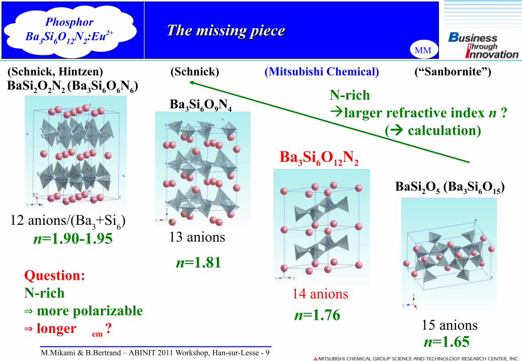
(Schnick, Hintzen) (Schnick) (Mitsubishi Chemical) (“Sanbornite”)
BaSi2O5 (Ba3Si6O15)
BaSi2O2N2 (Ba3Si6O6N6)
Ba3Si6O9N4
Ba3Si6O12N2
12 anions/(Ba3+Si
6)
13 anions
14 anions
15 anions
Question:N-rich⇒ more polarizable⇒ longer � em ?
n=1.90-1.95
n=1.81
n=1.76
n=1.65
N-rich larger refractive index n ? ( calculation)
The missing pieceThe missing piece
M.Mikami & B.Bertrand – ABINIT 2011 Workshop, Han-sur-Lesse - 9
MM
PhosphorBa3Si6O12N2:Eu2+

14
12
10
8
6
4
2
0in
ten
sit
y
700650600550500450400
wavelength / nm
Ba3Si6O9N4:Eu340nm excit.
4K 10K 25K 50K 75K 100K 150K 200K 250K 300K
14
12
10
8
6
4
2
0
inte
nsit
y
700650600550500450400
wavelength / nm
BSON310nm excit.
4K 10K 25K 50K 75K 100K 150K 200K 250K 300K
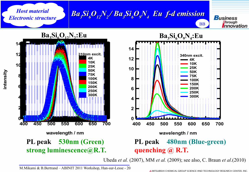
Ba3Si6O12N2:Eu Ba3Si6O9N4:Eu
PL peak � 530nm (Green)strong [email protected].
PL peak � 480nm (Blue-green)quenching @ R.T.
Uheda et al. (2007), MM et al. (2009); see also, C. Braun et al.(2010)
M.Mikami & B.Bertrand – ABINIT 2011 Workshop, Han-sur-Lesse - 10
from oxides to (oxy)nitrides (or sulfides…)BaBa
33SiSi66OO1212NN2 2 / Ba/ Ba
33SiSi66OO99NN44 Eu f-d emission Eu f-d emission
MM
PhosphorBa3Si6O12N2:Eu2+

B.Dierre et al. (2007)
configurational coordinate auto-ionization
heatabsorptionemission
e - releaseheat
from oxides to (oxy)nitrides (or sulfides…)Thermal quenching mechanismThermal quenching mechanism
M.Mikami & B.Bertrand – ABINIT 2011 Workshop, Han-sur-Lesse - 11
Difficult to explain thermal quenching with configurational coordinate diagram… Natural to explain with auto-ionization mechanism
MM
PhosphorBa3Si6O12N2:Eu2+
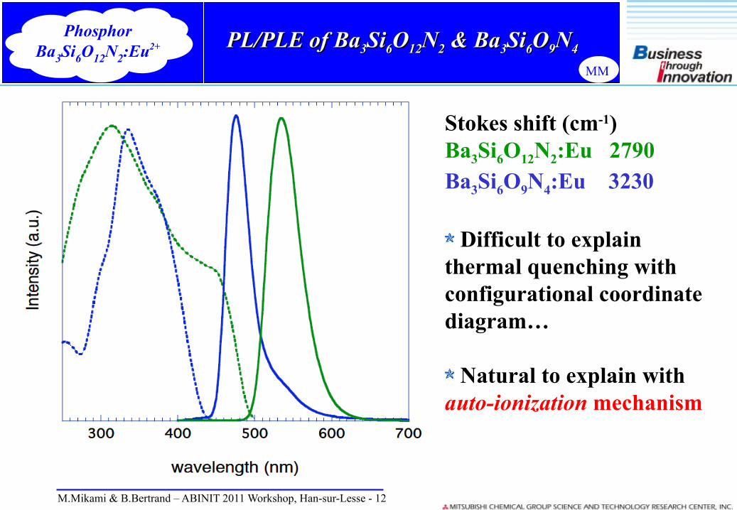
from oxides to (oxy)nitrides (or sulfides…)PL/PLE of BaPL/PLE of Ba33SiSi66OO1212NN22 & Ba & Ba33SiSi66OO99NN44
M.Mikami & B.Bertrand – ABINIT 2011 Workshop, Han-sur-Lesse - 12
Stokes shift (cm-1)Ba3Si6O12N2:Eu 2790Ba3Si6O9N4:Eu 3230 Difficult to explain
thermal quenching withconfigurational coordinate diagram… Natural to explain with
auto-ionization mechanism
MM
PhosphorBa3Si6O12N2:Eu2+
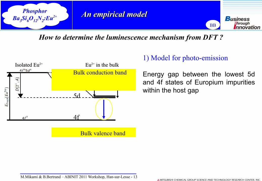
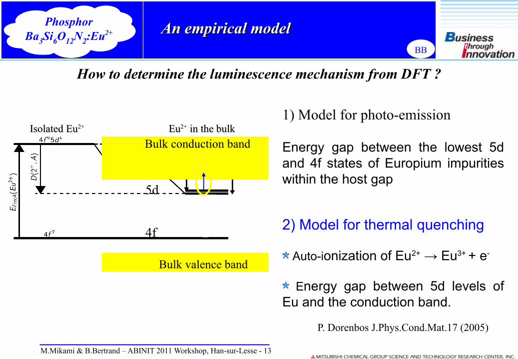
Isolated EuIsolated Eu2+2+ EuEu2+2+ in the bulk in the bulk
Bulk valence band
Bulk conduction band
How to determine the luminescence mechanism from DFT ?
1) Model for photo-emission
Energy gap between the lowest 5d and 4f states of Europium impurities within the host gap
4f
5d
from oxides to (oxy)nitrides (or sulfides…)An empirical modelAn empirical model
M.Mikami & B.Bertrand – ABINIT 2011 Workshop, Han-sur-Lesse - 13
BB
PhosphorBa3Si6O12N2:Eu2+
Isolated EuIsolated Eu2+2+ EuEu2+2+ in the bulk in the bulk
Bulk valence band
Bulk conduction band
How to determine the luminescence mechanism from DFT ?
1) Model for photo-emission
Energy gap between the lowest 5d and 4f states of Europium impurities within the host gap
2) Model for thermal quenching
Auto-ionization of Eu2+ → Eu3+ + e-
Energy gap between 5d levels of Eu and the conduction band.
4f
5d
P. Dorenbos J.Phys.Cond.Mat.17 (2005)
from oxides to (oxy)nitrides (or sulfides…)An empirical modelAn empirical model
M.Mikami & B.Bertrand – ABINIT 2011 Workshop, Han-sur-Lesse - 13
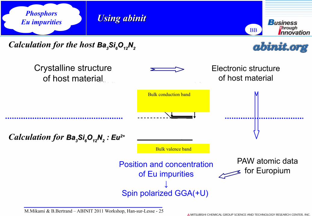
BB
PhosphorBa3Si6O12N2:Eu2+
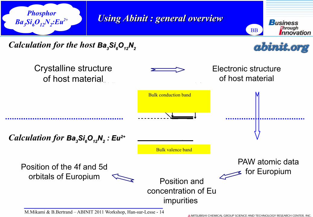
PAW atomic datafor Europium
Position of the 4f and 5d orbitals of Europium
Position and concentration of Eu
impurities
Electronic structureof host material
Bulk valence band
Bulk conduction band
Crystalline structure of host material
Calculation for BaBa33SiSi
66OO1212NN22 : Eu : Eu2+2+
from oxides to (oxy)nitrides (or sulfides…)Using Abinit : general overviewUsing Abinit : general overviewBackground
Calculation for the host BaBa33SiSi
66OO1212NN22
M.Mikami & B.Bertrand – ABINIT 2011 Workshop, Han-sur-Lesse - 14
BB
PhosphorBa3Si6O12N2:Eu2+

Bulk valence band
Bulk conduction band
Calculation for BaBa33SiSi
66OO1212NN22 : Eu : Eu2+2+
from oxides to (oxy)nitrides (or sulfides…)Using abinit : DFT calculationUsing abinit : DFT calculationBackground
Host materialCrystal structure
Crystalline structure of host material
↓Ground state
structural relaxation
Calculation for the host BaBa33SiSi
66OO1212NN22
M.Mikami & B.Bertrand – ABINIT 2011 Workshop, Han-sur-Lesse - 15
BB
Ba Ba
NN
SiSi
OO
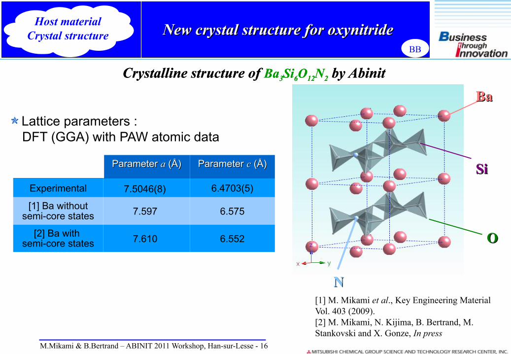
Lattice parameters : DFT (GGA) with PAW atomic data
Crystalline structure of Ba3Si6O12N2 by Abinit
Parameter Parameter aa ( (Å)Å) Parameter Parameter cc ( (Å)Å)
Experimental 7.5046(8) 6.4703(5)
[1] Ba without semi-core states 7.597 6.575
[2] Ba with semi-core states 7.610 6.552
Ba Ba
Crystalline structure of Ba3Si6O12N2 by Abinit
New crystal structure for oxynitrideNew crystal structure for oxynitrideHost material
Crystal structure
M.Mikami & B.Bertrand – ABINIT 2011 Workshop, Han-sur-Lesse - 16
BB
[1] M. Mikami et al., Key Engineering Material Vol. 403 (2009).[2] M. Mikami, N. Kijima, B. Bertrand, M. Stankovski and X. Gonze, In press

Ba Ba
NN
SiSi
OO
Lattice parameters : DFT (GGA) with PAW atomic data
Crystalline structure of Ba3Si6O12N2 by Abinit
PAW atomic data for Barium
Results are coherent with experimental data whether semi-core states are used or not
[1] M. Mikami et al., Key Engineering Material Vol. 403 (2009).[2] M. Mikami, N. Kijima, B. Bertrand, M. Stankovski and X. Gonze, In press
Parameter Parameter aa ( (Å)Å) Parameter Parameter cc ( (Å)Å)
Experimental 7.5046(8) 6.4703(5)
[1] Ba without semi-core states 7.597 6.575
[2] Ba with semi-core states 7.610 6.552
Ba Ba
Crystalline structure of Ba3Si6O12N2 by Abinit
New crystal structure for oxynitrideNew crystal structure for oxynitrideHost material
Crystal structure
M.Mikami & B.Bertrand – ABINIT 2011 Workshop, Han-sur-Lesse - 16
BB
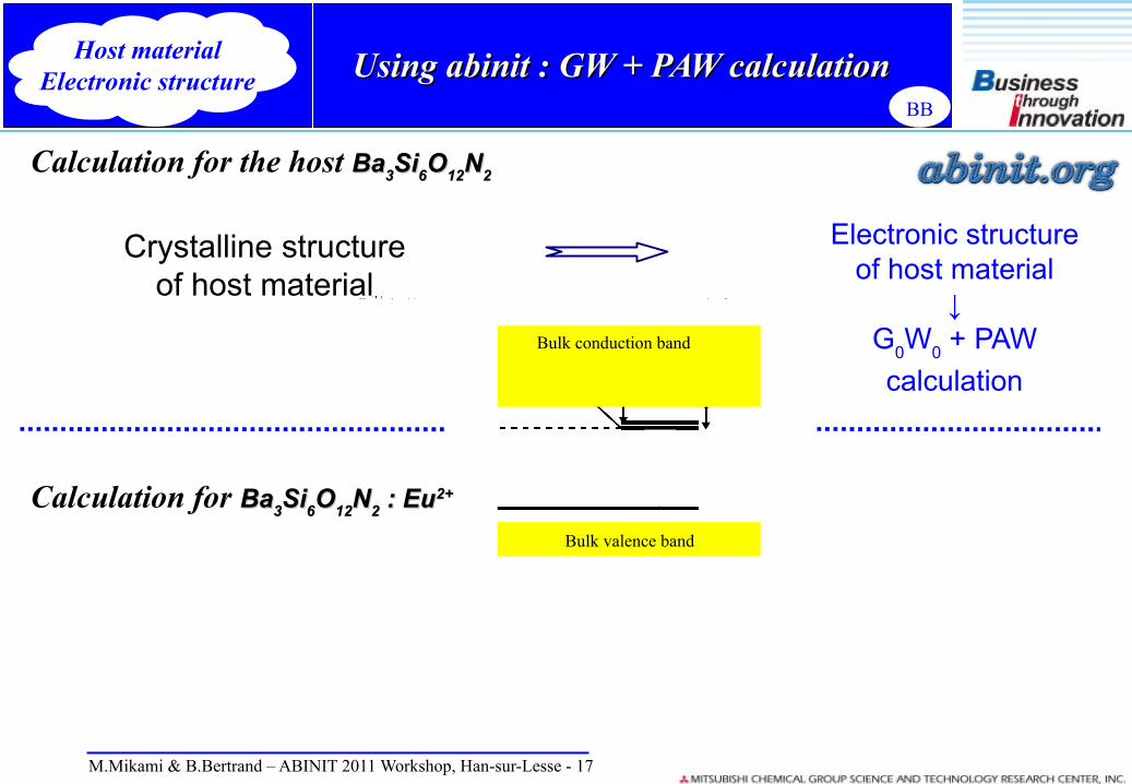
Bulk valence band
Bulk conduction band
Crystalline structure of host material
Calculation for BaBa33SiSi
66OO1212NN22 : Eu : Eu2+2+
from oxides to (oxy)nitrides (or sulfides…)Using abinit : GW + PAW calculationUsing abinit : GW + PAW calculationBackground
Calculation for the host BaBa33SiSi
66OO1212NN22
Electronic structureof host material
↓G
0W
0 + PAW
calculation
Host materialElectronic structure
M.Mikami & B.Bertrand – ABINIT 2011 Workshop, Han-sur-Lesse - 17
BB
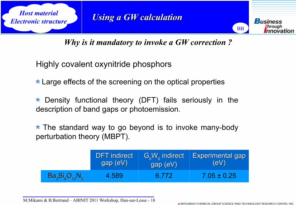
Highly covalent oxynitride phosphors Large effects of the screening on the optical properties
Density functional theory (DFT) fails seriously in the
description of band gaps or photoemission. The standard way to go beyond is to invoke many-body
perturbation theory (MBPT).
DFT indirect DFT indirect gap (eV)gap (eV)
GG00WW00 indirect indirect gap (eV)gap (eV)
ExperimentalExperimental gap gap (eV)(eV)
BaBa33SiSi
66OO1212NN224.589 6.772 7.05 ± 0.25
Why is it mandatory to invoke a GW correction ?
from oxides to (oxy)nitrides (or sulfides…)Using a GW calculationUsing a GW calculationBackground
Host materialElectronic structure
M.Mikami & B.Bertrand – ABINIT 2011 Workshop, Han-sur-Lesse - 18
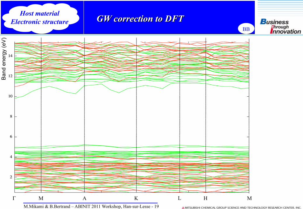
BB

Γ AM LK H M
Ban
d en
ergy
(eV
)
DFT Gap :4.589 eV
Zoom on the state around the band gap
from oxides to (oxy)nitrides (or sulfides…)
Host materialElectronic structure GW correction to DFTGW correction to DFT
M.Mikami & B.Bertrand – ABINIT 2011 Workshop, Han-sur-Lesse - 19
BB
Γ AM LK H M
GW correction to DFTGW correction to DFTHost material
Electronic structure
Ban
d en
ergy
(eV
)
M.Mikami & B.Bertrand – ABINIT 2011 Workshop, Han-sur-Lesse - 19
BB
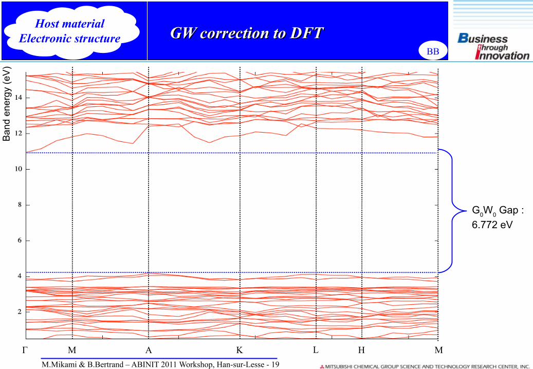
Γ AM LK H M
G0W
0 Gap :
6.772 eV
Ban
d en
ergy
(eV
)
GW correction to DFTGW correction to DFTHost material
Electronic structure
M.Mikami & B.Bertrand – ABINIT 2011 Workshop, Han-sur-Lesse - 19
BB
14
12
10
8
6
4
2
0in
ten
sit
y
700650600550500450400
wavelength / nm
Ba3Si6O9N4:Eu340nm excit.
4K 10K 25K 50K 75K 100K 150K 200K 250K 300K
14
12
10
8
6
4
2
0
inte
nsit
y
700650600550500450400
wavelength / nm
BSON310nm excit.
4K 10K 25K 50K 75K 100K 150K 200K 250K 300K
Ba3Si6O12N2:Eu Ba3Si6O9N4:Eu
PL peak � 530nm (Green)strong [email protected].
PL peak � 480nm (Blue-green)quenching @ R.T.
Uheda et al. (2007), MM et al. (2009); see also, C. Braun et al.(2010)
M.Mikami & B.Bertrand – ABINIT 2011 Workshop, Han-sur-Lesse - 20
from oxides to (oxy)nitrides (or sulfides…)BaBa
33SiSi66OO1212NN2 2 / Ba/ Ba
33SiSi66OO99NN44 Eu f-d emission Eu f-d emission Background
Host materialElectronic structure
BB
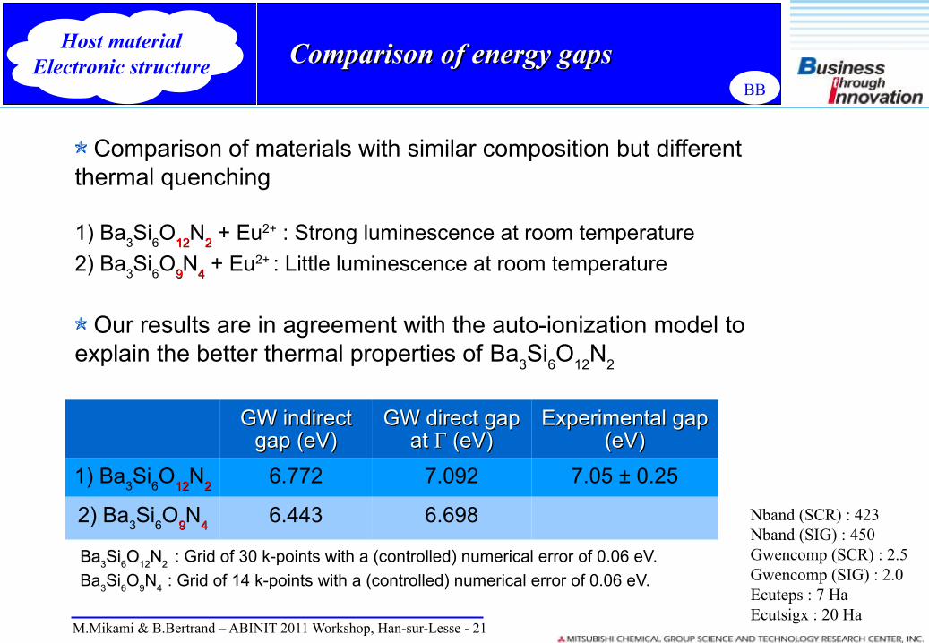
GW indirect GW indirect gap (eV)gap (eV)
GW direct gap GW direct gap at at ΓΓ (eV) (eV)
Experimental gap Experimental gap (eV)(eV)
1) Ba3Si
6O
1212N
226.772 7.092 7.05 ± 0.25
2) Ba3Si
6O
99N
446.443 6.698
BaBa33SiSi
66OO1212NN2 2 : Grid of 30 k-points with a (controlled) numerical error of 0.06 eV.
Ba3Si
6O
9N
4 : Grid of 14 k-points with a (controlled) numerical error of 0.06 eV.
from oxides to (oxy)nitrides (or sulfides…)Comparison of energy gapsComparison of energy gapsHost material
Electronic structure
M.Mikami & B.Bertrand – ABINIT 2011 Workshop, Han-sur-Lesse - 21
Comparison of materials with similar composition but different thermal quenching
1) Ba3Si
6O
1212N
22 + Eu2+ : Strong luminescence at room temperature
2) Ba3Si
6O
99N
44 + Eu2+ : Little luminescence at room temperature
Our results are in agreement with the auto-ionization model to explain the better thermal properties of Ba
3Si
6O
12N
2
BB
Nband (SCR) : 423Nband (SIG) : 450Gwencomp (SCR) : 2.5Gwencomp (SIG) : 2.0Ecuteps : 7 HaEcutsigx : 20 Ha
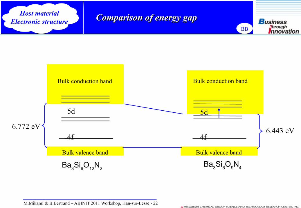
Bulk valence band
Bulk conduction band
Bulk valence band
Bulk conduction band
6.772 eV 6.443 eV
Ba3Si
6O
12N
2Ba
3Si
6O
9N
4
4f
5d
4f
5d
Host materialElectronic structure Comparison of energy gapComparison of energy gap
M.Mikami & B.Bertrand – ABINIT 2011 Workshop, Han-sur-Lesse - 22
BB

Electronic structureof host material
Bulk valence band
Bulk conduction band
Crystalline structure of host material
Calculation for BaBa33SiSi
66OO1212NN22 : Eu : Eu2+2+
from oxides to (oxy)nitrides (or sulfides…)Using abinit : PAW atomic dataUsing abinit : PAW atomic dataBackground
Calculation for the host BaBa33SiSi
66OO1212NN22
PAW atomic datafor Europium
↓Semi-core states
PAWAtomic data
M.Mikami & B.Bertrand – ABINIT 2011 Workshop, Han-sur-Lesse - 23
BB

Europium
BaBa33SiSi
66OO1212NN22GG00WW00 indirect indirect
gap (eV)gap (eV)GG00WW00 direct direct
gap (eV)gap (eV)
4d semi-core4d semi-core 6.772Γ - A
7.092Γ
WithoutWithoutsemi-core statesemi-core state
3.740L - A
3.807L
Experimental 7.05
Semi-core : 4d10 5s2
Valence : 5p6 6p2
Barium
Semi-core : 4d10 5s2
Valence : 5p6 4f7 6p2
Test of the G0W
0 correction to EuO : - Introduction of semi-core 4d10 states
- Problems with the correction of 4f states
from oxides to (oxy)nitrides (or sulfides…)Construction of PAW atomic dataConstruction of PAW atomic dataBackground
PAWAtomic dataBackground
PAWAtomic data
Semi-core states are required in order to make sensible the G0W
0 correction.
M.Mikami & B.Bertrand – ABINIT 2011 Workshop, Han-sur-Lesse - 24
BB
PAW atomic datafor Europium
Electronic structureof host material
Bulk valence band
Bulk conduction band
Crystalline structure of host material
Calculation for BaBa33SiSi
66OO1212NN22 : Eu : Eu2+2+
from oxides to (oxy)nitrides (or sulfides…)Using abinitUsing abinitBackground
Calculation for the host BaBa33SiSi
66OO1212NN22
Position and concentration of Eu impurities
↓Spin polarized GGA(+U)
M.Mikami & B.Bertrand – ABINIT 2011 Workshop, Han-sur-Lesse - 25
PhosphorsEu impurities
BB
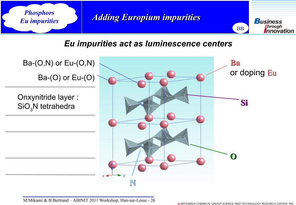
Ba Ba or doping EuEu
NN
SiSi
OO
Onxynitride layer :SiO
3N tetrahedra
Ba-(O,N) or Eu-(O,N)
Ba-(O) or Eu-(O)
Eu impurities act as luminescence centers
from oxides to (oxy)nitrides (or sulfides…)Adding Europium impuritiesAdding Europium impuritiesBackgroundBackgroundBackground
PhosphorsEu impurities
M.Mikami & B.Bertrand – ABINIT 2011 Workshop, Han-sur-Lesse - 26
BB

from oxides to (oxy)nitrides (or sulfides…)Non equivalent positionsNon equivalent positions
BB
BackgroundBackgroundBackgroundPhosphors
Eu impurities
Europium substitutes to Barium atoms in two possible non equivalent positions
O
O
O
O
O
O
O
O
O
OO
O
NN
NN
M.Mikami & B.Bertrand – ABINIT 2011 Workshop, Han-sur-Lesse - 27
EuEu EuEu
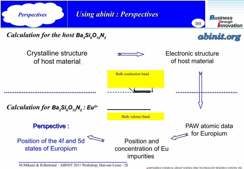
PAW atomic datafor Europium
Position and concentration of Eu
impurities
Electronic structureof host material
Bulk valence band
Bulk conduction band
Crystalline structure of host material
Calculation for BaBa33SiSi
66OO1212NN22 : Eu : Eu2+2+
from oxides to (oxy)nitrides (or sulfides…)Using abinit : PerspectivesUsing abinit : PerspectivesBackgroundPerspectives
Calculation for the host BaBa33SiSi
66OO1212NN22
Perspective :Perspective :
Position of the 4f and 5d states of Europium
M.Mikami & B.Bertrand – ABINIT 2011 Workshop, Han-sur-Lesse - 28
BB

Ba3Si6O12N2:Eu Ba3Si6O9N4:Eu
conduction bands
Eu 4f
Eu 5d
Eu-O6
cluster
Eu-O6
clusterEu2+Eu3++ e- (auto-ionization)
Eu-Nligand
Eu-Nligand
Green PLpeak � 530nm
Blue-Green PL
peak � 480nm
valence bands
Eu 4f
Eu 5d
6.77
2 eV
(G
W)
6.44
3eV
(G
W)
proposed by MM et al.(2009): based on Dorenbos scheme (J.Phys.Cond.Mat.17, 2005)
from oxides to (oxy)nitrides (or sulfides…)The difference of EU PL : a modelThe difference of EU PL : a model
M.Mikami & B.Bertrand – ABINIT 2011 Workshop, Han-sur-Lesse - 29
MM
Perspectives
Eu 4f
Eu 5d
Eu-Nligand
valence bands
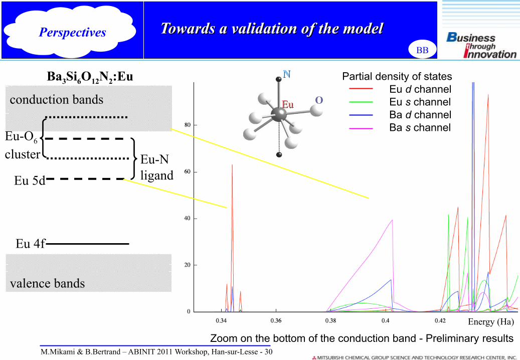
from oxides to (oxy)nitrides (or sulfides…)Towards a validation of the modelTowards a validation of the model
M.Mikami & B.Bertrand – ABINIT 2011 Workshop, Han-sur-Lesse - 30
BB
Ba3Si6O12N2:Eu
conduction bands
Eu-O6
cluster
Zoom on the bottom of the conduction band - Preliminary results
Partial density of statesEu d channelEu s channelBa d channelBa s channel
EuEu O
NN
Perspectives
Energy (Ha)

M.Mikami & B.Bertrand – ABINIT 2011 Workshop, Han-sur-Lesse - 31
Conclusion New crystal structure for oxynitrideNew crystal structure for oxynitride
Scientific interest Luminescence properties of rare-earth doping oxynitrides phosphors
Emission and absorption spectra Thermal quenching
Numerical Challenge
Electronic structure of Ba3Si
6O
12N
2 phosphor
Current : G0W0 with PAW atomic data including semi-core and 4f states
Future : Electron-phonon interaction
Industry ► Reducing the cost of R&D Discovery of new compounds Prediction of properties before synthesis
BB
Acknowledgments
(MCRC) for development/analysis of our phosphors, encouragement from theoretical Gr.
Kyota Uheda, Satoshi Shimooka, Yasuo Shimomura, Tomoyuki Kurushima,
Takatoshi Seto, Hiromu Watanabe, Toshio Akai, Masaki Takashima,
Yutaka Sasaki, Motoyuki Shigeiwa, Kaoru Okamoto, Hiroyuki Imura,
Katsuya Kanda, Shinichiro Nakamura
(ETSF/Universite Catholique de Louvain) for PAW-GW calc. & build system of ABINIT
Matteo Giantomassi, Alain Jacques, Gian-Marco Rignanese, Yann Pouillon
BB, MS, XG: financial support from the European Union, 7th Framework Programme (Grant Agreement 211956 ETSF I3 e-Infrastructure project), the Agentschap voor Innovatie door Wetenschap en Technologie (IWT project N°080023 ISIMADE), as well as the Walloon region Belgium (RW project N°816849, WALL-ETSF)
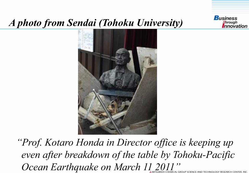
A photo from Sendai (Tohoku University)
“Prof. Kotaro Honda in Director office is keeping up even after breakdown of the table by Tohoku-Pacific Ocean Earthquake on March 11 2011”