Embed Size (px)
Citation preview

IEEE TRANSACTIONS ON INDUSTRIAL ELECTRONICS 1
Matching Network Elimination in BroadbandRectennas for High-Efficiency Wireless Power
Transfer and Energy Harvesting
1
2
3
Chaoyun Song, Yi Huang, Senior Member, IEEE, Jiafeng Zhou, Paul Carter, Sheng Yuan,Qian Xu, and Zhouxiang Fei
4
5
Abstract—Impedance matching networks for nonlinear6devices such as amplifiers and rectifiers are normally very7challenging to design, particularly for broadband and multi-8band devices. A novel design concept for a broadband9high-efficiency rectenna without using matching networks10is presented in this paper for the first time. An off-center-fed11dipole antenna with relatively high input impedance over a12wide frequency band is proposed. The antenna impedance13can be tuned to the desired value and directly provides a14complex conjugate match to the impedance of a rectifier.15The received RF power by the antenna can be delivered to16the rectifier efficiently without using impedance matching17networks; thus, the proposed rectenna is of a simple struc-18ture, low cost, and compact size. In addition, the rectenna19can work well under different operating conditions and us-20ing different types of rectifying diodes. A rectenna has been21designed and made based on this concept. The measured22results show that the rectenna is of high power conversion23efficiency (more than 60%) in two wide bands, which are 0.9–241.1 and 1.8–2.5 GHz, for mobile, Wi-Fi, and ISM bands. More-25over, by using different diodes, the rectenna can maintain26its wide bandwidth and high efficiency over a wide range of27input power levels (from 0 to 23 dBm) and load values (from28200 to 2000 Ω). It is, therefore, suitable for high-efficiency29wireless power transfer or energy harvesting applications.30The proposed rectenna is general and simple in structure31without the need for a matching network hence is of great32significance for many applications.33
Index Terms—Broadband rectennas, impedance match-34ing networks, off-center-fed dipole (OCFD), wireless energy35harvesting (WEH), wireless power transmission.36
Manuscript received July 5, 2016; revised October 17, 2016 andNovember 14, 2016; accepted December 3, 2016. This work wassupported in part by the Engineering and Physical Sciences ResearchCouncil, U.K., and in part by Aeternum LLC. (Corresponding Author: YiHuang.)
C. Song, Y. Huang, J. Zhou, S. Yuan, and Z. Fei are with the Depart-ment of Electrical Engineering and Electronics, University of Liverpool,Liverpool, L69 3GJ, U.K. (e-mail: [email protected]; [email protected]; [email protected]; [email protected]; [email protected]).
P. Carter is with Global Wireless Solutions, Inc., Dulles, VA 20166USA (e-mail: [email protected]).
Q. Xu is with the College of Electronic and Information Engineering,Nanjing University of Aeronautics and Astronautics, Nanjing 211106,China (e-mail: [email protected]).
Color versions of one or more of the figures in this paper are availableonline at http://ieeexplore.ieee.org
Digital Object Identifier 10.1109/TIE.2016.2645505
I. INTRODUCTION 37
IMPEDANCE matching is a basic but crucial concept in elec- 38
tronics and electrical engineering, since it can maximize the 39
power transfer from a source to a load or minimize the signal 40
reflection from a load. In the wireless industry today, there have 41
been many devices (such as oscillators, inverters, amplifiers, rec- 42
tifiers, power dividers, boost converters) and systems that have 43
a high demand for impedance matching networks. A number of 44
techniques for the network design have been reported [1]–[6]. 45
Among them, rectifiers and power amplifiers (PAs) normally 46
utilize nonlinear elements such as diodes and transistors in the 47
circuits. Hence their input impedance varies with the frequency, 48
input power, and load impedance. The impedance matching net- 49
works for such nonlinear circuits become very challenging to 50
design. 51
Wireless power transfer (WPT) and wireless energy harvest- 52
ing (WEH) have attracted significant attention in the past few 53
years [7]–[10]. In both radiative and inductive wireless power 54
transmissions, the rectifiers are a vital device for converting ac 55
or RF power to dc power, while impedance matching networks 56
are required to achieve high conversion efficiency [9]. 57
A rectifying antenna (rectenna) is one of the most popular 58
devices for WPT and WEH applications, and much progress 59
has been made [11]–[19]. Multiband and broadband rectennas 60
[15]–[19] can receive or harvest RF power from different sources 61
and from different channels simultaneously; thus, they outper- 62
form the conventional single band rectennas [11]–[14] in terms 63
of overall conversion efficiency as well as total output power. 64
However, the design of the impedance matching network for 65
broadband or multiband rectennas is very challenging, and the 66
structure of the matching network is relatively complex which 67
may increase the cost and loss, and also introduce errors in 68
manufacturing. 69
Some techniques such as resistance compression networks 70
and frequency selective networks have been developed to re- 71
duce the nonlinear effects of the rectenna [20]–[24] so that 72
the performance can be maintained under different operating 73
conditions. But, they all require introduction of further circuit 74
components in the matching network which increases the com- 75
plexity of the overall design. Using more components could 76
increase the loss and decrease the overall efficiency. A need 77
exists, therefore, for rectennas comprising simple structures 78
0278-0046 © 2016 IEEE. Personal use is permitted, but republication/redistribution requires IEEE permission.See http://www.ieee.org/publications standards/publications/rights/index.html for more information.
2 IEEE TRANSACTIONS ON INDUSTRIAL ELECTRONICS
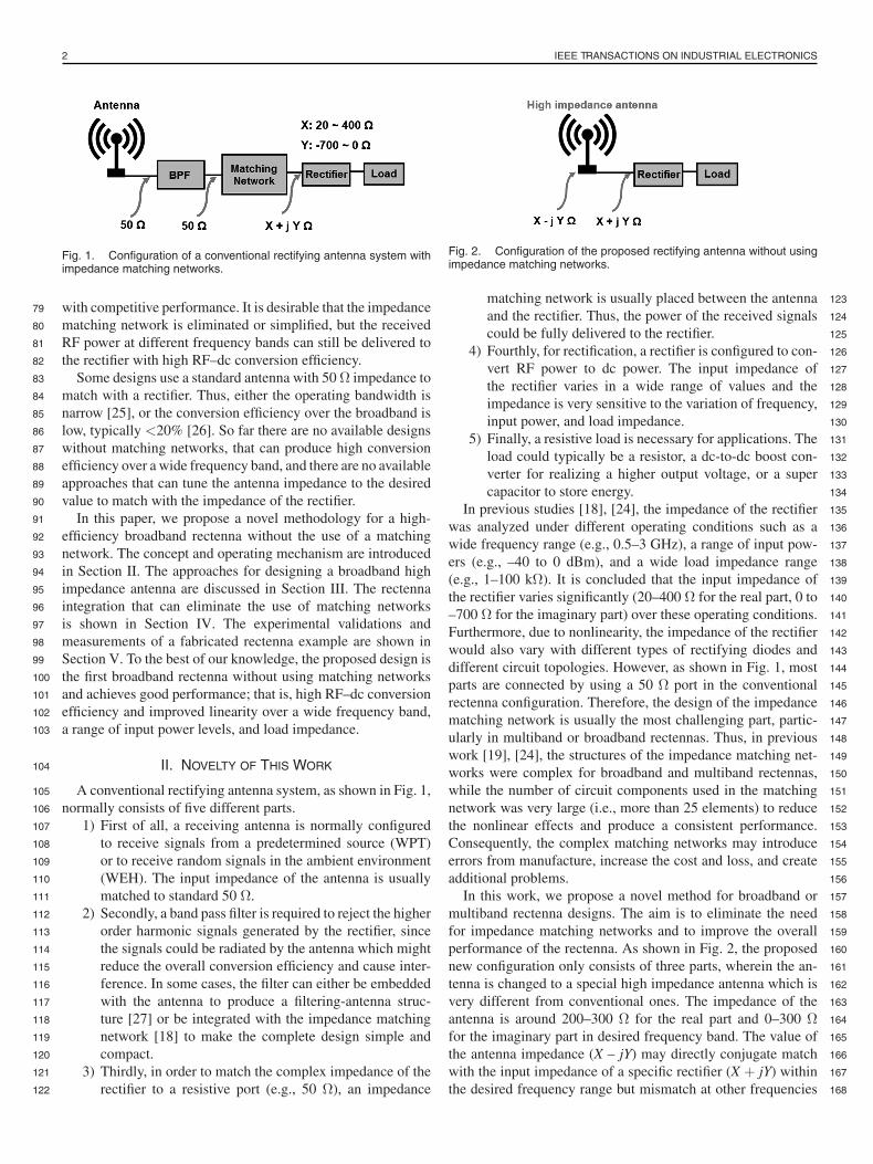
Fig. 1. Configuration of a conventional rectifying antenna system withimpedance matching networks.
with competitive performance. It is desirable that the impedance79
matching network is eliminated or simplified, but the received80
RF power at different frequency bands can still be delivered to81
the rectifier with high RF–dc conversion efficiency.82
Some designs use a standard antenna with 50 Ω impedance to83
match with a rectifier. Thus, either the operating bandwidth is84
narrow [25], or the conversion efficiency over the broadband is85
low, typically <20% [26]. So far there are no available designs86
without matching networks, that can produce high conversion87
efficiency over a wide frequency band, and there are no available88
approaches that can tune the antenna impedance to the desired89
value to match with the impedance of the rectifier.90
In this paper, we propose a novel methodology for a high-91
efficiency broadband rectenna without the use of a matching92
network. The concept and operating mechanism are introduced93
in Section II. The approaches for designing a broadband high94
impedance antenna are discussed in Section III. The rectenna95
integration that can eliminate the use of matching networks96
is shown in Section IV. The experimental validations and97
measurements of a fabricated rectenna example are shown in98
Section V. To the best of our knowledge, the proposed design is99
the first broadband rectenna without using matching networks100
and achieves good performance; that is, high RF–dc conversion101
efficiency and improved linearity over a wide frequency band,102
a range of input power levels, and load impedance.103
II. NOVELTY OF THIS WORK104
A conventional rectifying antenna system, as shown in Fig. 1,105
normally consists of five different parts.106
1) First of all, a receiving antenna is normally configured107
to receive signals from a predetermined source (WPT)108
or to receive random signals in the ambient environment109
(WEH). The input impedance of the antenna is usually110
matched to standard 50 Ω.111
2) Secondly, a band pass filter is required to reject the higher112
order harmonic signals generated by the rectifier, since113
the signals could be radiated by the antenna which might114
reduce the overall conversion efficiency and cause inter-115
ference. In some cases, the filter can either be embedded116
with the antenna to produce a filtering-antenna struc-117
ture [27] or be integrated with the impedance matching118
network [18] to make the complete design simple and119
compact.120
3) Thirdly, in order to match the complex impedance of the121
rectifier to a resistive port (e.g., 50 Ω), an impedance122
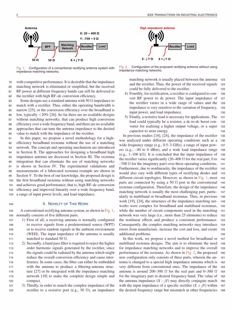
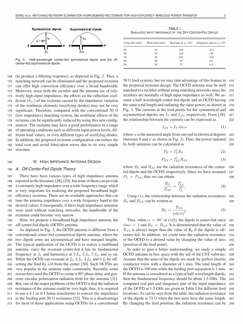
Fig. 2. Configuration of the proposed rectifying antenna without usingimpedance matching networks.
matching network is usually placed between the antenna 123
and the rectifier. Thus, the power of the received signals 124
could be fully delivered to the rectifier. 125
4) Fourthly, for rectification, a rectifier is configured to con- 126
vert RF power to dc power. The input impedance of 127
the rectifier varies in a wide range of values and the 128
impedance is very sensitive to the variation of frequency, 129
input power, and load impedance. 130
5) Finally, a resistive load is necessary for applications. The 131
load could typically be a resistor, a dc-to-dc boost con- 132
verter for realizing a higher output voltage, or a super 133
capacitor to store energy. 134
In previous studies [18], [24], the impedance of the rectifier 135
was analyzed under different operating conditions such as a 136
wide frequency range (e.g., 0.5–3 GHz), a range of input pow- 137
ers (e.g., –40 to 0 dBm), and a wide load impedance range 138
(e.g., 1–100 kΩ). It is concluded that the input impedance of 139
the rectifier varies significantly (20–400 Ω for the real part, 0 to 140
–700 Ω for the imaginary part) over these operating conditions. 141
Furthermore, due to nonlinearity, the impedance of the rectifier 142
would also vary with different types of rectifying diodes and 143
different circuit topologies. However, as shown in Fig. 1, most 144
parts are connected by using a 50 Ω port in the conventional 145
rectenna configuration. Therefore, the design of the impedance 146
matching network is usually the most challenging part, partic- 147
ularly in multiband or broadband rectennas. Thus, in previous 148
work [19], [24], the structures of the impedance matching net- 149
works were complex for broadband and multiband rectennas, 150
while the number of circuit components used in the matching 151
network was very large (i.e., more than 25 elements) to reduce 152
the nonlinear effects and produce a consistent performance. 153
Consequently, the complex matching networks may introduce 154
errors from manufacture, increase the cost and loss, and create 155
additional problems. 156
In this work, we propose a novel method for broadband or 157
multiband rectenna designs. The aim is to eliminate the need 158
for impedance matching networks and to improve the overall 159
performance of the rectenna. As shown in Fig. 2, the proposed 160
new configuration only consists of three parts, wherein the an- 161
tenna is changed to a special high impedance antenna which is 162
very different from conventional ones. The impedance of the 163
antenna is around 200–300 Ω for the real part and 0–300 Ω 164
for the imaginary part in desired frequency band. The value of 165
the antenna impedance (X – jY) may directly conjugate match 166
with the input impedance of a specific rectifier (X + jY) within 167
the desired frequency range but mismatch at other frequencies 168
SONG et al.: MATCHING NETWORK ELIMINATION IN BROADBAND RECTENNAS FOR HIGH-EFfiCIENCY WIRELESS POWER TRANSFER 3
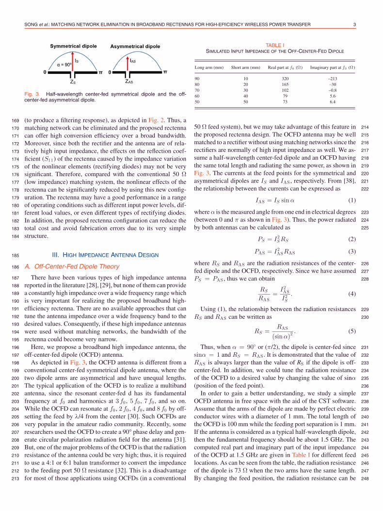
Fig. 3. Half-wavelength center-fed symmetrical dipole and the off-center-fed asymmetrical dipole.
(to produce a filtering response), as depicted in Fig. 2. Thus, a169
matching network can be eliminated and the proposed rectenna170
can offer high conversion efficiency over a broad bandwidth.171
Moreover, since both the rectifier and the antenna are of rela-172
tively high input impedance, the effects on the reflection coef-173
ficient (S11) of the rectenna caused by the impedance variation174
of the nonlinear elements (rectifying diodes) may not be very175
significant. Therefore, compared with the conventional 50 Ω176
(low impedance) matching system, the nonlinear effects of the177
rectenna can be significantly reduced by using this new config-178
uration. The rectenna may have a good performance in a range179
of operating conditions such as different input power levels, dif-180
ferent load values, or even different types of rectifying diodes.181
In addition, the proposed rectenna configuration can reduce the182
total cost and avoid fabrication errors due to its very simple183
structure.184
III. HIGH IMPEDANCE ANTENNA DESIGN185
A. Off-Center-Fed Dipole Theory186
There have been various types of high impedance antenna187
reported in the literature [28], [29], but none of them can provide188
a constantly high impedance over a wide frequency range which189
is very important for realizing the proposed broadband high-190
efficiency rectenna. There are no available approaches that can191
tune the antenna impedance over a wide frequency band to the192
desired values. Consequently, if these high impedance antennas193
were used without matching networks, the bandwidth of the194
rectenna could become very narrow.195
Here, we propose a broadband high impedance antenna, the196
off-center-fed dipole (OCFD) antenna.197
As depicted in Fig. 3, the OCFD antenna is different from a198
conventional center-fed symmetrical dipole antenna, where the199
two dipole arms are asymmetrical and have unequal lengths.200
The typical application of the OCFD is to realize a multiband201
antenna, since the resonant center-fed d has its fundamental202
frequency at f0 and harmonics at 3 f0 , 5 f0 , 7 f0 , and so on.203
While the OCFD can resonate at f0 , 2 f0 , 4 f0 , and 8 f0 by off-204
setting the feed by λ/4 from the center [30]. Such OCFDs are205
very popular in the amateur radio community. Recently, some206
researchers used the OCFD to create a 90° phase delay and gen-207
erate circular polarization radiation field for the antenna [31].208
But, one of the major problems of the OCFD is that the radiation209
resistance of the antenna could be very high; thus, it is required210
to use a 4:1 or 6:1 balun transformer to convert the impedance211
to the feeding port 50 Ω resistance [32]. This is a disadvantage212
for most of those applications using OCFDs (in a conventional213
TABLE ISIMULATED INPUT IMPEDANCE OF THE OFF-CENTER-FED DIPOLE
Long arm (mm) Short arm (mm) Real part at f0 (Ω) Imaginary part at f0 (Ω)
90 10 320 –21380 20 165 –3070 30 102 –0.860 40 79 5.650 50 73 6.4
50 Ω feed system), but we may take advantage of this feature in 214
the proposed rectenna design. The OCFD antenna may be well 215
matched to a rectifier without using matching networks since the 216
rectifiers are normally of high input impedance as well. We as- 217
sume a half-wavelength center-fed dipole and an OCFD having 218
the same total length and radiating the same power, as shown in 219
Fig. 3. The currents at the feed points for the symmetrical and 220
asymmetrical dipoles are IS and IAS , respectively. From [38], 221
the relationship between the currents can be expressed as 222
IAS = IS sinα (1)
where α is the measured angle from one end in electrical degrees 223
(between 0 and π as shown in Fig. 3). Thus, the power radiated 224
by both antennas can be calculated as 225
PS = I2S RS (2)
PAS = I2ASRAS (3)
where RS and RAS are the radiation resistances of the center- 226
fed dipole and the OCFD, respectively. Since we have assumed 227
PS = PAS , thus we can obtain 228
RS
RAS=
I2AS
I2S
. (4)
Using (1), the relationship between the radiation resistances 229
RS and RAS can be written as 230
RS =RAS
(sin α)2 . (5)
Thus, when α = 90◦ or (π/2), the dipole is center-fed since 231
sinα = 1 and RS = RAS . It is demonstrated that the value of 232
RAS is always larger than the value of RS if the dipole is off- 233
center-fed. In addition, we could tune the radiation resistance 234
of the OCFD to a desired value by changing the value of sinα 235
(position of the feed point). 236
In order to gain a better understanding, we study a simple 237
OCFD antenna in free space with the aid of the CST software. 238
Assume that the arms of the dipole are made by perfect electric 239
conductor wires with a diameter of 1 mm. The total length of 240
the OCFD is 100 mm while the feeding port separation is 1 mm. 241
If the antenna is considered as a typical half-wavelength dipole, 242
then the fundamental frequency should be about 1.5 GHz. The 243
computed real part and imaginary part of the input impedance 244
of the OCFD at 1.5 GHz are given in Table I for different feed 245
locations. As can be seen from the table, the radiation resistance 246
of the dipole is 73 Ω when the two arms have the same length. 247
By changing the feed position, the radiation resistance can be 248
4 IEEE TRANSACTIONS ON INDUSTRIAL ELECTRONICS
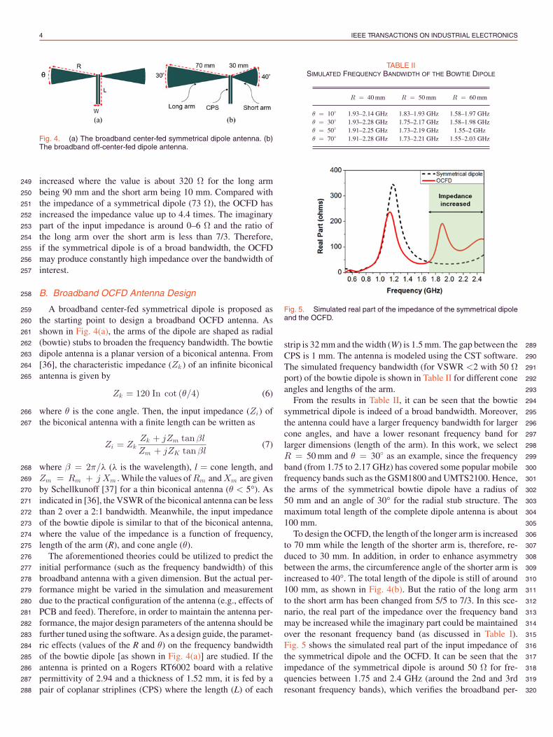
Fig. 4. (a) The broadband center-fed symmetrical dipole antenna. (b)The broadband off-center-fed dipole antenna.
increased where the value is about 320 Ω for the long arm249
being 90 mm and the short arm being 10 mm. Compared with250
the impedance of a symmetrical dipole (73 Ω), the OCFD has251
increased the impedance value up to 4.4 times. The imaginary252
part of the input impedance is around 0–6 Ω and the ratio of253
the long arm over the short arm is less than 7/3. Therefore,254
if the symmetrical dipole is of a broad bandwidth, the OCFD255
may produce constantly high impedance over the bandwidth of256
interest.257
B. Broadband OCFD Antenna Design258
A broadband center-fed symmetrical dipole is proposed as259
the starting point to design a broadband OCFD antenna. As260
shown in Fig. 4(a), the arms of the dipole are shaped as radial261
(bowtie) stubs to broaden the frequency bandwidth. The bowtie262
dipole antenna is a planar version of a biconical antenna. From263
[36], the characteristic impedance (Zk ) of an infinite biconical264
antenna is given by265
Zk = 120 In cot (θ/4) (6)
where θ is the cone angle. Then, the input impedance (Zi) of266
the biconical antenna with a finite length can be written as267
Zi = ZkZk + jZm tan βl
Zm + jZK tan βl(7)
where β = 2π/λ (λ is the wavelength), l = cone length, and268
Zm = Rm + j Xm . While the values of Rm and Xm are given269
by Schellkunoff [37] for a thin biconical antenna (θ < 5°). As270
indicated in [36], the VSWR of the biconical antenna can be less271
than 2 over a 2:1 bandwidth. Meanwhile, the input impedance272
of the bowtie dipole is similar to that of the biconical antenna,273
where the value of the impedance is a function of frequency,274
length of the arm (R), and cone angle (θ).275
The aforementioned theories could be utilized to predict the276
initial performance (such as the frequency bandwidth) of this277
broadband antenna with a given dimension. But the actual per-278
formance might be varied in the simulation and measurement279
due to the practical configuration of the antenna (e.g., effects of280
PCB and feed). Therefore, in order to maintain the antenna per-281
formance, the major design parameters of the antenna should be282
further tuned using the software. As a design guide, the paramet-283
ric effects (values of the R and θ) on the frequency bandwidth284
of the bowtie dipole [as shown in Fig. 4(a)] are studied. If the285
antenna is printed on a Rogers RT6002 board with a relative286
permittivity of 2.94 and a thickness of 1.52 mm, it is fed by a287
pair of coplanar striplines (CPS) where the length (L) of each288
TABLE IISIMULATED FREQUENCY BANDWIDTH OF THE BOWTIE DIPOLE
R = 40 mm R = 50 mm R = 60 mm
θ = 10◦ 1.93–2.14 GHz 1.83–1.93 GHz 1.58–1.97 GHzθ = 30◦ 1.93–2.28 GHz 1.75–2.17 GHz 1.58–1.98 GHzθ = 50◦ 1.91–2.25 GHz 1.73–2.19 GHz 1.55–2 GHzθ = 70◦ 1.91–2.28 GHz 1.73–2.21 GHz 1.55–2.03 GHz
Fig. 5. Simulated real part of the impedance of the symmetrical dipoleand the OCFD.
strip is 32 mm and the width (W) is 1.5 mm. The gap between the 289
CPS is 1 mm. The antenna is modeled using the CST software. 290
The simulated frequency bandwidth (for VSWR <2 with 50 Ω 291
port) of the bowtie dipole is shown in Table II for different cone 292
angles and lengths of the arm. 293
From the results in Table II, it can be seen that the bowtie 294
symmetrical dipole is indeed of a broad bandwidth. Moreover, 295
the antenna could have a larger frequency bandwidth for larger 296
cone angles, and have a lower resonant frequency band for 297
larger dimensions (length of the arm). In this work, we select 298
R = 50 mm and θ = 30◦ as an example, since the frequency 299
band (from 1.75 to 2.17 GHz) has covered some popular mobile 300
frequency bands such as the GSM1800 and UMTS2100. Hence, 301
the arms of the symmetrical bowtie dipole have a radius of 302
50 mm and an angle of 30° for the radial stub structure. The 303
maximum total length of the complete dipole antenna is about 304
100 mm. 305
To design the OCFD, the length of the longer arm is increased 306
to 70 mm while the length of the shorter arm is, therefore, re- 307
duced to 30 mm. In addition, in order to enhance asymmetry 308
between the arms, the circumference angle of the shorter arm is 309
increased to 40°. The total length of the dipole is still of around 310
100 mm, as shown in Fig. 4(b). But the ratio of the long arm 311
to the short arm has been changed from 5/5 to 7/3. In this sce- 312
nario, the real part of the impedance over the frequency band 313
may be increased while the imaginary part could be maintained 314
over the resonant frequency band (as discussed in Table I). 315
Fig. 5 shows the simulated real part of the input impedance of 316
the symmetrical dipole and the OCFD. It can be seen that the 317
impedance of the symmetrical dipole is around 50 Ω for fre- 318
quencies between 1.75 and 2.4 GHz (around the 2nd and 3rd 319
resonant frequency bands), which verifies the broadband per- 320
SONG et al.: MATCHING NETWORK ELIMINATION IN BROADBAND RECTENNAS FOR HIGH-EFfiCIENCY WIRELESS POWER TRANSFER 5
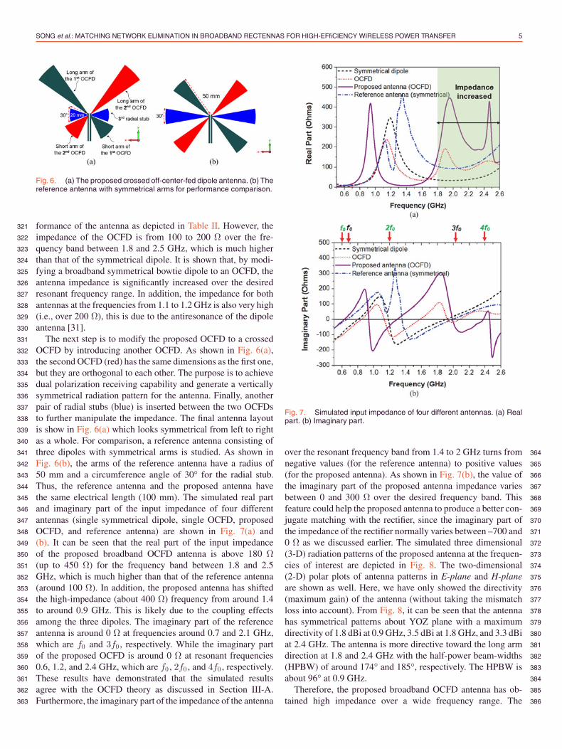
Fig. 6. (a) The proposed crossed off-center-fed dipole antenna. (b) Thereference antenna with symmetrical arms for performance comparison.
formance of the antenna as depicted in Table II. However, the321
impedance of the OCFD is from 100 to 200 Ω over the fre-322
quency band between 1.8 and 2.5 GHz, which is much higher323
than that of the symmetrical dipole. It is shown that, by modi-324
fying a broadband symmetrical bowtie dipole to an OCFD, the325
antenna impedance is significantly increased over the desired326
resonant frequency range. In addition, the impedance for both327
antennas at the frequencies from 1.1 to 1.2 GHz is also very high328
(i.e., over 200 Ω), this is due to the antiresonance of the dipole329
antenna [31].330
The next step is to modify the proposed OCFD to a crossed331
OCFD by introducing another OCFD. As shown in Fig. 6(a),332
the second OCFD (red) has the same dimensions as the first one,333
but they are orthogonal to each other. The purpose is to achieve334
dual polarization receiving capability and generate a vertically335
symmetrical radiation pattern for the antenna. Finally, another336
pair of radial stubs (blue) is inserted between the two OCFDs337
to further manipulate the impedance. The final antenna layout338
is show in Fig. 6(a) which looks symmetrical from left to right339
as a whole. For comparison, a reference antenna consisting of340
three dipoles with symmetrical arms is studied. As shown in341
Fig. 6(b), the arms of the reference antenna have a radius of342
50 mm and a circumference angle of 30° for the radial stub.343
Thus, the reference antenna and the proposed antenna have344
the same electrical length (100 mm). The simulated real part345
and imaginary part of the input impedance of four different346
antennas (single symmetrical dipole, single OCFD, proposed347
OCFD, and reference antenna) are shown in Fig. 7(a) and348
(b). It can be seen that the real part of the input impedance349
of the proposed broadband OCFD antenna is above 180 Ω350
(up to 450 Ω) for the frequency band between 1.8 and 2.5351
GHz, which is much higher than that of the reference antenna352
(around 100 Ω). In addition, the proposed antenna has shifted353
the high-impedance (about 400 Ω) frequency from around 1.4354
to around 0.9 GHz. This is likely due to the coupling effects355
among the three dipoles. The imaginary part of the reference356
antenna is around 0 Ω at frequencies around 0.7 and 2.1 GHz,357
which are f0 and 3f0 , respectively. While the imaginary part358
of the proposed OCFD is around 0 Ω at resonant frequencies359
0.6, 1.2, and 2.4 GHz, which are f0 , 2f0 , and 4f0 , respectively.360
These results have demonstrated that the simulated results361
agree with the OCFD theory as discussed in Section III-A.362
Furthermore, the imaginary part of the impedance of the antenna363
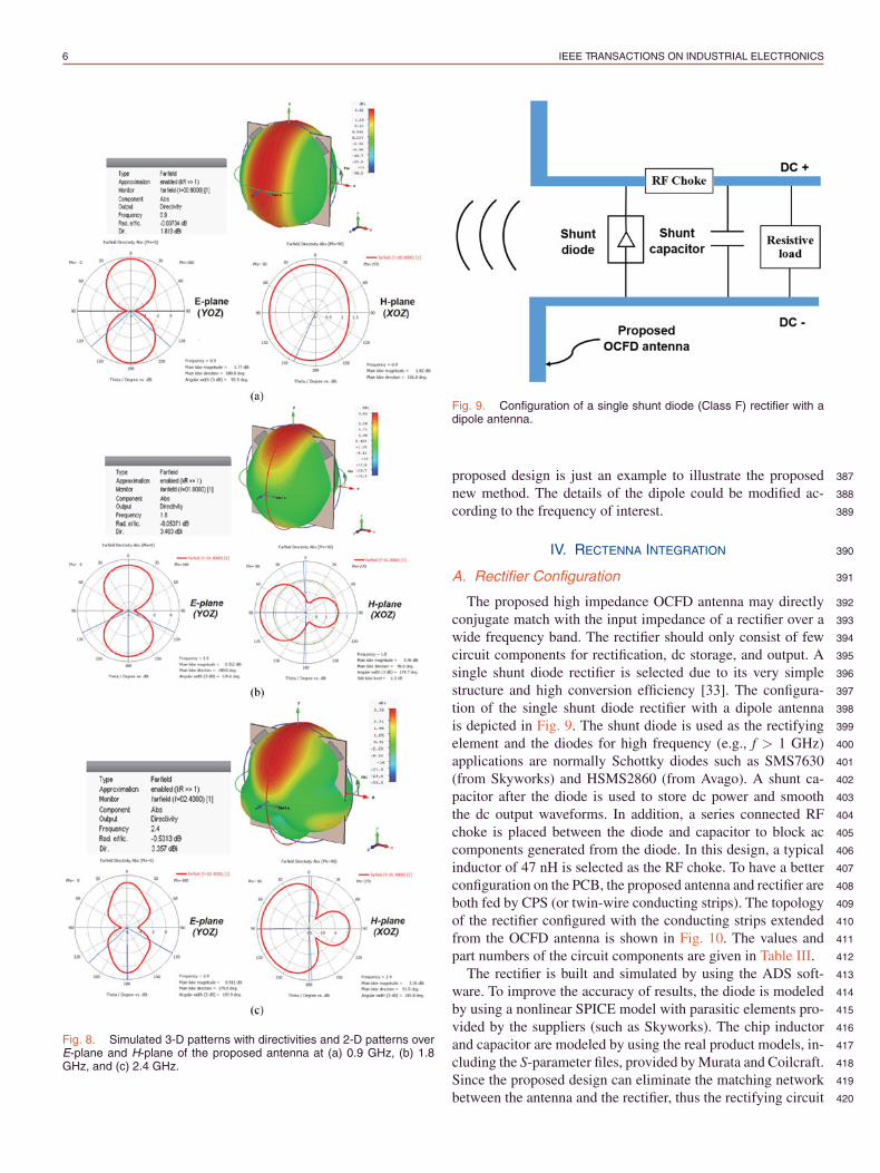
Fig. 7. Simulated input impedance of four different antennas. (a) Realpart. (b) Imaginary part.
over the resonant frequency band from 1.4 to 2 GHz turns from 364
negative values (for the reference antenna) to positive values 365
(for the proposed antenna). As shown in Fig. 7(b), the value of 366
the imaginary part of the proposed antenna impedance varies 367
between 0 and 300 Ω over the desired frequency band. This 368
feature could help the proposed antenna to produce a better con- 369
jugate matching with the rectifier, since the imaginary part of 370
the impedance of the rectifier normally varies between –700 and 371
0 Ω as we discussed earlier. The simulated three dimensional 372
(3-D) radiation patterns of the proposed antenna at the frequen- 373
cies of interest are depicted in Fig. 8. The two-dimensional 374
(2-D) polar plots of antenna patterns in E-plane and H-plane 375
are shown as well. Here, we have only showed the directivity 376
(maximum gain) of the antenna (without taking the mismatch 377
loss into account). From Fig. 8, it can be seen that the antenna 378
has symmetrical patterns about YOZ plane with a maximum 379
directivity of 1.8 dBi at 0.9 GHz, 3.5 dBi at 1.8 GHz, and 3.3 dBi 380
at 2.4 GHz. The antenna is more directive toward the long arm 381
direction at 1.8 and 2.4 GHz with the half-power beam-widths 382
(HPBW) of around 174° and 185°, respectively. The HPBW is 383
about 96° at 0.9 GHz. 384
Therefore, the proposed broadband OCFD antenna has ob- 385
tained high impedance over a wide frequency range. The 386
6 IEEE TRANSACTIONS ON INDUSTRIAL ELECTRONICS
Fig. 8. Simulated 3-D patterns with directivities and 2-D patterns overE-plane and H-plane of the proposed antenna at (a) 0.9 GHz, (b) 1.8GHz, and (c) 2.4 GHz.
Fig. 9. Configuration of a single shunt diode (Class F) rectifier with adipole antenna.
proposed design is just an example to illustrate the proposed 387
new method. The details of the dipole could be modified ac- 388
cording to the frequency of interest. 389
IV. RECTENNA INTEGRATION 390
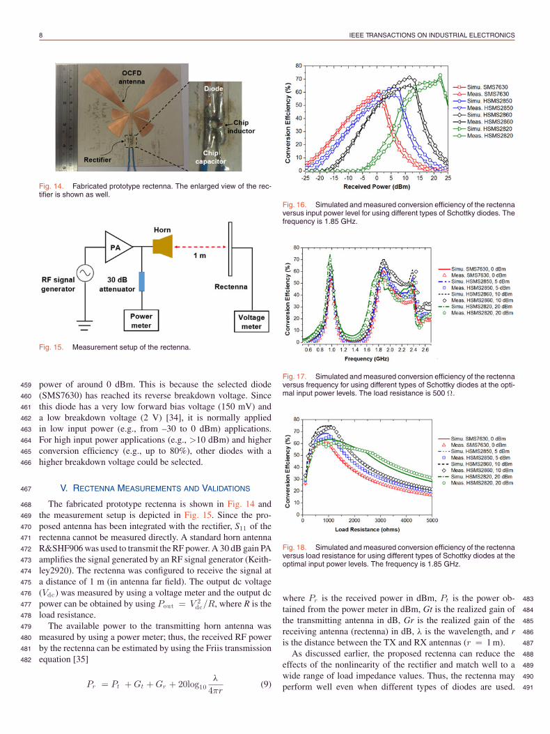
A. Rectifier Configuration 391
The proposed high impedance OCFD antenna may directly 392
conjugate match with the input impedance of a rectifier over a 393
wide frequency band. The rectifier should only consist of few 394
circuit components for rectification, dc storage, and output. A 395
single shunt diode rectifier is selected due to its very simple 396
structure and high conversion efficiency [33]. The configura- 397
tion of the single shunt diode rectifier with a dipole antenna 398
is depicted in Fig. 9. The shunt diode is used as the rectifying 399
element and the diodes for high frequency (e.g., f > 1 GHz) 400
applications are normally Schottky diodes such as SMS7630 401
(from Skyworks) and HSMS2860 (from Avago). A shunt ca- 402
pacitor after the diode is used to store dc power and smooth 403
the dc output waveforms. In addition, a series connected RF 404
choke is placed between the diode and capacitor to block ac 405
components generated from the diode. In this design, a typical 406
inductor of 47 nH is selected as the RF choke. To have a better 407
configuration on the PCB, the proposed antenna and rectifier are 408
both fed by CPS (or twin-wire conducting strips). The topology 409
of the rectifier configured with the conducting strips extended 410
from the OCFD antenna is shown in Fig. 10. The values and 411
part numbers of the circuit components are given in Table III. 412
The rectifier is built and simulated by using the ADS soft- 413
ware. To improve the accuracy of results, the diode is modeled 414
by using a nonlinear SPICE model with parasitic elements pro- 415
vided by the suppliers (such as Skyworks). The chip inductor 416
and capacitor are modeled by using the real product models, in- 417
cluding the S-parameter files, provided by Murata and Coilcraft. 418
Since the proposed design can eliminate the matching network 419
between the antenna and the rectifier, thus the rectifying circuit 420
SONG et al.: MATCHING NETWORK ELIMINATION IN BROADBAND RECTENNAS FOR HIGH-EFfiCIENCY WIRELESS POWER TRANSFER 7
Fig. 10. Configuration of the proposed rectifier on coplanar striplines(CPS).
TABLE IIICIRCUIT COMPONENTS USED IN THE DESIGN
Component name Nominal Value Part number and supplier
D1 Schottky diode SMS7630-079LF, SkyworksL1 47 nH chip inductor 0603HP47N, CoilcraftC1 100 nF chip capacitor GRM188R71H104JA93D, Murata
Fig. 11. (a) The simulated S11 and (b) the simulated and measuredRF–dc conversion efficiency of the rectenna at three different input powerlevels. The load resistance is 400 Ω.
is indeed simplified. The frequency domain power source port is421
used in the simulation, and the port impedance is defined as the422
impedance of the proposed OCFD antenna by using the touch-423
stone S1P files exported from the CST, similarly to the results424
shown in Fig. 7(a) and (b).425
B. Rectenna Performance426
After the complete rectenna has been designed, its perfor-427
mance is evaluated by using the harmonic balance simulation428
and the large signal S-parameter simulation using the ADS. The429
performances of the proposed rectenna in terms of the reflection430
coefficient (S11) and RF–dc conversion efficiency are shown in431
Figs. 11–13. The RF–dc conversion efficiency is obtained by432
ηRF−dc =Pdc
Pin(8)
Fig. 12. (a) The simulated S11 and (b) the simulated and measuredRF–dc conversion efficiency of the rectenna at three different load val-ues. The input power level is 0 dBm.
Fig. 13. Simulated and measured conversion efficiency of the rectennaversus input power level at three frequencies. The load resistance is 600Ω.
where Pdc is the output dc power and Pin is the input RF power 433
to the antenna. S11 (simulated) and conversion efficiency (sim- 434
ulated and measured) of the rectenna at different input power 435
levels are shown in Fig. 11(a) and (b) as a function of frequency. 436
A typical load resistor of 400 Ω is selected. From Fig. 11, it 437
can be seen that the rectenna covers the desired broad frequency 438
band from 1.8 to 2.5 GHz and an additional frequency band 439
around 1 GHz. The S11 of the rectenna is lower than –10 dB 440
between 1.8 and 2 GHz and around 1 GHz. The conversion effi- 441
ciency is higher than 40% (up to 55%) over the entire frequency 442
band of interest for the input power level of 0 dBm (1 mW). In 443
addition, when the input power is doubled (3 dBm) or halved 444
(–3 dBm), the reflection coefficients are always smaller than –6 445
dB from 1.8 to 2.5 GHz, while the efficiency over the band of 446
interest is still high (e.g., greater than 35%). 447
Fig. 12(a) and (b) depicts the S11 (simulated) and conversion 448
efficiency (simulated and measured) of the rectenna for different 449
load values. It can be seen that the efficiency is higher than 30% 450
(up to 60%) for the load values from 200 to 1000 Ω and for 451
the frequencies between 1.8 and 2.5 and the around 1 GHz. 452
It is demonstrated that the nonlinear effects linked to the input 453
power and load are reduced in the proposed broadband rectenna, 454
which verifies our predictions in Section II. The simulated and 455
measured conversion efficiency of the rectenna versus input 456
power level is shown in Fig. 13 at three frequencies. It can be 457
seen that the rectenna has the highest efficiency at the input 458
8 IEEE TRANSACTIONS ON INDUSTRIAL ELECTRONICS
Fig. 14. Fabricated prototype rectenna. The enlarged view of the rec-tifier is shown as well.
Fig. 15. Measurement setup of the rectenna.
power of around 0 dBm. This is because the selected diode459
(SMS7630) has reached its reverse breakdown voltage. Since460
this diode has a very low forward bias voltage (150 mV) and461
a low breakdown voltage (2 V) [34], it is normally applied462
in low input power (e.g., from –30 to 0 dBm) applications.463
For high input power applications (e.g., >10 dBm) and higher464
conversion efficiency (e.g., up to 80%), other diodes with a465
higher breakdown voltage could be selected.466
V. RECTENNA MEASUREMENTS AND VALIDATIONS467
The fabricated prototype rectenna is shown in Fig. 14 and468
the measurement setup is depicted in Fig. 15. Since the pro-469
posed antenna has been integrated with the rectifier, S11 of the470
rectenna cannot be measured directly. A standard horn antenna471
R&SHF906 was used to transmit the RF power. A 30 dB gain PA472
amplifies the signal generated by an RF signal generator (Keith-473
ley2920). The rectenna was configured to receive the signal at474
a distance of 1 m (in antenna far field). The output dc voltage475
(Vdc) was measured by using a voltage meter and the output dc476
power can be obtained by using Pout = V 2dc/R, where R is the477
load resistance.478
The available power to the transmitting horn antenna was479
measured by using a power meter; thus, the received RF power480
by the rectenna can be estimated by using the Friis transmission481
equation [35]482
Pr = Pt + Gt + Gr + 20log10λ
4πr(9)
Fig. 16. Simulated and measured conversion efficiency of the rectennaversus input power level for using different types of Schottky diodes. Thefrequency is 1.85 GHz.
Fig. 17. Simulated and measured conversion efficiency of the rectennaversus frequency for using different types of Schottky diodes at the opti-mal input power levels. The load resistance is 500 Ω.
Fig. 18. Simulated and measured conversion efficiency of the rectennaversus load resistance for using different types of Schottky diodes at theoptimal input power levels. The frequency is 1.85 GHz.
where Pr is the received power in dBm, Pt is the power ob- 483
tained from the power meter in dBm, Gt is the realized gain of 484
the transmitting antenna in dB, Gr is the realized gain of the 485
receiving antenna (rectenna) in dB, λ is the wavelength, and r 486
is the distance between the TX and RX antennas (r = 1 m). 487
As discussed earlier, the proposed rectenna can reduce the 488
effects of the nonlinearity of the rectifier and match well to a 489
wide range of load impedance values. Thus, the rectenna may 490
perform well even when different types of diodes are used. 491

SONG et al.: MATCHING NETWORK ELIMINATION IN BROADBAND RECTENNAS FOR HIGH-EFfiCIENCY WIRELESS POWER TRANSFER 9
TABLE IVRECTENNA PERFORMANCE FOR USING DIFFERENT DIODES
Schottky diodes name Simulated input impedance under the same condition (Ω) Optimal input power level Maximum conversion efficiency Optimal load resistance range (Ω)
SMS7630 173 – j 36 0 dBm 60% 250–1500HSMS2850 325 – j 57 5 dBm 65% 200–2000HSMS2860 349 – j 166 10 dBm 70% 200–2500HSMS2820 82 – j 145 20 dBm 75% 250–3000
This advantage is normally not available in the conventional492
rectenna designs, since the input impedance and characteristics493
of the diodes can be very different. Thus, in order to validate494
this point, the proposed rectenna was measured by using differ-495
ent types of Schottky diodes such as HSMS2850, HSMS2860,496
and HSMS2820. The measured conversion efficiency versus497
input power level is shown in Fig. 16 along with simulated498
results. High conversion efficiency is obtained in all cases.499
When the load is selected as 500 Ω and the frequency is se-500
lected as 1.85 GHz, we have Gt = 8.5 dBi, Gr = 3.45 dBi,501
λ = 0.162 m, and r = 1 m. Using (9), the correlation be-502
tween the transmitting power and the receiving power can be503
obtained as504
Pr (dBm) = Pt (dBm) − 25.84 dB. (10)
It can be seen that the maximum conversion efficiency and the505
corresponding input powers of the rectenna are 60% at 0 dBm,506
65% at 5 dBm, 70% at 10 dBm, and 75% at 20 dBm for us-507
ing the Schottky diodes SMS7630, HSMS2850, HSMS2860,508
and HSMS2820, respectively. The peak efficiency is realized509
at different input power levels. This is because the breakdown510
voltages for the selected diodes are different, which are 2 V511
(SMS7630), 3.8 V (HSMS2850), 7 V (HSMS2860), and 15 V512
(HSMS2820), respectively. The efficiency is much higher at513
high input power levels for using the diodes with large break-514
down voltages (e.g., HSMS2820), while the efficiency is higher515
at low input power levels for using the diodes with small forward516
bias voltages (e.g., SMS7630). The simulated and measured517
conversion efficiencies of the rectenna (using the four different518
diodes) are depicted in Fig. 17 as a function of the frequency.519
The load is still 500 Ω while the input power levels are selected520
as the optimal input powers for these diodes (e.g., 0 dBm for521
SMS7630, 5 dBm for HSMS2850, 10 dBm for HSMS2860, and522
20 dBm for HSMS2820). Note that in the measurements, the cor-523
relation between the transmitting power and the receiving power524
[as given in (9)] might be changed if the frequencies are differ-525
ent. Thus, the transmitting power should be tuned to make sure526
that the received power is approximately a constant value in the527
broadband (e.g., 0 dBm for the frequencies from 0.9 to 3 GHz).528
From the results in Fig. 17, it can be seen that the rectenna529
is still of broadband performance (1.8 to 2.5 GHz) when using530
different diodes, and the conversion efficiency is constantly high531
over the frequency bandwidth of interest for the selected input532
power levels. Figs. 16 and 17 show a good agreement between533
the simulated and measured results.534
Fig. 18 shows the simulated and measured conversion ef-535
ficiency by using different load resistances. The frequency is536
selected as 1.85 GHz while the input power levels are still set 537
as the optimal input powers. In reality, the load impedance may 538
vary over a large range in different applications; thus, it is impor- 539
tant to reduce the sensitivity of efficiency versus load variation 540
in a nonlinear system (rectenna). From Fig. 18, it can be seen 541
that, when using different diodes, the efficiency of the rectenna 542
is constantly high (from 40% to 75%) for the load values be- 543
tween 200 and 2000 Ω, then the efficiency starts to decease 544
due to the impedance mismatch between the antenna and the 545
rectifier. It demonstrates that the nonlinear effects have been 546
reduced over the load range from 200 to 2000 Ω. For other load 547
values, the details of the rectenna can be modified to achieve 548
good performance. 549
According to the results in Figs. 16–18, the performance of 550
the rectenna by using different diodes is summarized in Table IV. 551
The simulated input impedance of the rectifier is shown under 552
the same condition (frequency: 1.85 GHz, input power: 553
10 dBm, and load: 500 Ω). The impedance is very different 554
for different types of diodes, but our rectenna can still be well 555
configured with these diodes without using matching networks. 556
It is demonstrated that the proposed broadband rectenna can 557
work well under different operating conditions. The nonlinear 558
effects have been reduced. The matching networks have indeed 559
been eliminated. In addition, the optimal input power level 560
of the device is tunable (from 0 to 23 dBm) by selecting 561
appropriate diodes so that the conversion efficiency of the 562
broadband rectenna can be always higher than 60% (as shown 563
in Fig. 16). This is very important for WPT or WEH used in 564
practice. 565
A comparison between our rectennna and other related work 566
is shown in Table V. It can be seen that our design seems to 567
be the only one without using the matching networks, but still 568
achieves high conversion efficiency over a relatively wide fre- 569
quency band. The conversion efficiency of our design is com- 570
parable with that of the other work used matching networks, 571
while the performance of the rectenna is reasonably well in a 572
range of input powers and load impedance. In addition, our de- 573
vice is also the only one which can use different types of diodes 574
without changing any other part of the circuit. The structure of 575
our design is the simplest for broadband rectennas with similar 576
performance. The proposed rectenna is of good industrial value 577
due to its simplicity and universality, and is of good practical 578
value due to its consistent performance under different operating 579
conditions. 580
Also, the proposed concept for eliminating the matching net- 581
works is not just limited in the presented design, and can also 582
be used in other similar nonlinear systems. 583
10 IEEE TRANSACTIONS ON INDUSTRIAL ELECTRONICS
TABLE VCOMPARISON OF THE PROPOSED RECTENNA AND RELATED DESIGNS
Ref. (year) Frequency (GHz) Use of Complexity Maximum Input power level Optimal load Type ofimpedance matching of the overall conversion for conversion range with good Schottky diode
networks design efficiency (%) efficiency > 60% performance (kΩ)
[18] (2015) Four-band 0.9, 1.8, 2.1, 2.4 Yes Very complex 65 at 0 dBm –5 to 0 dBm 11 MSS20-141[19] (2015) Broad-band 1.8–2.5 Yes Complex 70 at 0 dBm –7 to 0 dBm 14.7 SMS7630[20] (2015) Dual-band 0.915, 2.45 Yes Complex 70 at 0 dBm –5 to 0 dBm 0.5–3 SMS7630[23] (2012) Tunable 0.9–2.45 Yes Very complex 80 at 30 dBm Tunable 5 to 30 dBm 1–4 Tunable[24] (2016) Six-band 0.55, 0.75, 0.9, 1.85, 2.15, 2.45 Yes Very complex 68 at –5 dBm –5 to 0 dBm 10–75 SMS7630[25] (2012) Single-band 2.45 No Simple 70 at –5 dBm –10 to 5 dBm 2.8 HSMS2852[26] (2004) Broad-band 2–18 No Medium 20 at 17 dBm Not available 0.6 SMS7630This work (2016) Broad-band 0.9–1.1, 1.8–2.5 No Simplest 75 at 20 dBm Tunable 0 to 23 dBm 0.2–2 Tunable
VI. CONCLUSION584
A novel method for eliminating the matching network of585
broadband rectennas was presented. An OCFD antenna was586
designed, where the antenna impedance was tuned to directly587
match with the rectifier. The proposed rectenna was of a broad588
bandwidth and high efficiency, and had excellent performance589
under different operating conditions. The measured perfor-590
mance showed that the operating frequencies of the experi-591
mental rectenna were from 0.9 to 1.1 GHz and from 1.8 to592
2.5 GHz (which were the typical cellular mobile, WLAN, and593
ISM bands), while the maximum conversion efficiency was up594
to 75% and the optimal input power range was tunable from595
0 to 23 dBm by selecting appropriate diodes. In addition, the596
rectenna had a very simple structure and low cost. Consider-597
ing the excellent overall performance of the proposed rectenna,598
it is suitable for high efficiency WPT and WEH applications.599
The design concept is easy to follow while its details can be600
optimized for different applications.601
ACKNOWLEDGMENT602
The authors would like to thank the anonymous reviewers603
for their constructive feedback of this paper. The authors would604
also like to thank Prof. S. Hall from the University of Liverpool605
for the refinement of the manuscript.606
REFERENCES607
[1] S. Carreon-Bautista, A. Eladawy, A. N. Mohieldin, and E. Sanchez-608Sinencio, “Boost converter with dynamic input impedance matching609for energy harvesting with multi-array thermoelectric generators,” IEEE610Trans. Ind. Electron., vol. 61, no. 10, pp. 5345–5353, Oct. 2014.611
[2] J. Jeong and D. Jang, “Design technique for harmonic-tuned RF power612oscillators for high-efficiency operation,” IEEE Trans. Ind. Electron., vol.61362, no. 1, pp. 221–228, Jan. 2015.614
[3] J. Kim, D.-H. Kim, and Y.-J. Park, “Analysis of capacitive impedance615matching networks for simultaneous wireless power transfer to multiple616devices,” IEEE Trans. Ind. Electron., vol. 62, no. 5, pp. 2807–2813, May6172015.618
[4] K. Song and Q. Xue, “Ultra-wideband ring-cavity multiple-way parallel619power divider,” IEEE Trans. Ind. Electron., vol. 60, no. 10, pp. 4737–4745,620Oct. 2013621
[5] K. Rawat and F. M. Ghannouchi, “Design methodology for dual-band622Doherty power amplifier with performance enhancement using dualband623offset lines,” IEEE Trans. Ind. Electron., vol. 59, no. 12, pp. 4831–4842,624Dec. 2012625
[6] X. Wang, X. K. Guan, and S. Q. Fan, “ESD-protected power amplifier 626design in CMOS for highly reliable RFICs,” IEEE Trans. Ind. Electron., 627vol. 58, no. 7, pp. 2736–2743, Jun. 2011. 628
[7] R. Johari, J. V. Krogmeier, and D. J. Love, “Analysis and practical consid- 629erations in implementing multiple transmitters for wireless power transfer 630via coupled magnetic resonance,” IEEE Trans. Ind. Electron., vol. 61, no. 6314, pp. 1174–1183, Apr. 2014. 632
[8] L. Chen, Y. C. Zhou, and T. J. Cui, “An optimizable circuit structure for 633high-efficiency wireless power transfer,” IEEE Trans. Ind. Electron., vol. 63460, no. 1, pp. 339–349, Jan. 2013. 635
[9] H. J. Visser and R. J. M. Vullers, “RF energy harvesting and transport for 636wireless sensor network applications: Principles and requirements,” Proc. 637IEEE, vol. 101, no. 6, pp. 1410–1423, Jun. 2013. 638
[10] S. Cheon, Y.-H. Kim, S.-Y. Kang, M. L. Lee, J.-M. Lee, and T. Zyung, 639“Circuit-model-based analysis of a wireless energy-transfer system via 640coupled magnetic resonances,” IEEE Trans. Ind. Electron., vol. 58, no. 7, 641pp. 2906–2914, Jul. 2011. 642
[11] J. Colomer-Farrarons, P. Miribel-Catala, A. Saiz-Vela, and J. Samitier, 643“A multiharvested self-powered system in a low-voltage low-power tech- 644nology,” IEEE Trans. Ind. Electron., vol. 58, no. 9, pp. 4250–4263, Sep. 6452011. 646
[12] Y. Huang, N. Shinohara, and T. Mitani, “A constant efficiency of rectifying 647circuit in an extremely wide load range,” IEEE Trans. Microw. Theory 648Techn., vol. 62, no. 4, pp. 986–993, Apr. 2014. 649
[13] P. Lu, X. Yang, J. Li, and B. Wang, “A compact frequency reconfigurable 650rectenna for 5.2- and 5.8-GHz wireless power transmission,” IEEE Trans. 651Power Electron., vol. 30, no. 11, pp. 6006–6010, Nov. 2015. 652
[14] J. O. McSpadden, F. Lu, and K. Chang, “Design and experiments of 653a high conversion efficiency 5.8-GHz rectenna,” IEEE Trans. Microw. 654Theory Techn., vol. 46, no. 12, pp. 2053–2060, Dec. 1998. 655
[15] H. Sun, Y.-X. Guo, M. He, and Z. Zhong, “A dual-band rectenna using 656broadband Yagi antenna array for ambient RF power harvesting,” IEEE 657Antennas Wireless Propag. Lett., vol. 12, pp. 918–921, 2013. 658
[16] K. Niotaki, S. Kim, S. Jeong, A. Collado, A. Georgiadis, and M. Tentzeris, 659“A compact dual-band rectenna using slot-loaded dual band folded dipole 660antenna,” IEEE Antennas Wireless Propag. Lett., vol. 12, pp. 1634–1637, 6612013. 662
[17] R. Scheeler, S. Korhummel, and Z. Popovic, “A dual-frequency ultralow- 663power efficient 0.5-g rectenna,” IEEE Microw. Mag., vol. 15, no. 1, pp. 664109–114, Jan. 2014. 665
[18] V. Kuhn, C. Lahuec, F. Seguin, and C. Person, “A multi-band stacked RF 666energy harvester with rf-to-dc efficiency up to 84%,” IEEE Trans. Microw. 667Theory Techn., vol. 63, no. 5, pp. 1768–1778, May 2015. 668
[19] C. Song, Y. Huang, J. Zhou, J. Zhang, S. Yuan, and P. Carter, “A high- 669efficiency broadband rectenna for ambient wireless energy harvesting,” 670IEEE Trans. Antennas Propag., vol. 63, no. 8, pp. 3486–3495, May 2015. 671
[20] K. Niotaki, A. Georgiadis, A. Collado, and J. S. Vardakas, “Dual-band re- 672sistance compression networks for improved rectifier performance,” IEEE 673Trans. Microw. Theory Techn., vol. 62, no. 12, pp. 3512–3521, Nov. 2015. 674
[21] Y. Han, O. Leitermann, D. A. Jackson, J. M. Rivas, and D. J. Perreault, “Re- 675sistance compression networks for radio-frequency power conversion,” 676IEEE Trans. Power Electron., vol. 22, no. 1, pp. 41–53, Jan. 2007. 677
[22] T. Paing, J. Shin, R. Zane, and Z. Popovic, “Resistor emulation approach 678to low-power RF energy harvesting,” IEEE Trans. Power Electron., vol. 67923, no. 3, pp. 1494–1501, Mar. 2008. 680
SONG et al.: MATCHING NETWORK ELIMINATION IN BROADBAND RECTENNAS FOR HIGH-EFfiCIENCY WIRELESS POWER TRANSFER 11
[23] V. Marian, B. Allard, C. Vollaire, and J. Verdier, “Strategy for microwave681energy harvesting from ambient field or a feeding source,” IEEE Trans.682Power Electron., vol. 27, no. 11, pp. 4481–4491, Nov. 2012.683
[24] C. Song et al., “A novel six-band dual CP rectenna using improved684impedance matching technique for ambient RF energy harvesting,” IEEE685Trans. Antennas Propag., vol. 64, no. 7, pp. 3160–3171, Jul. 2016.686
[25] H. Sun, Y.-X. Guo, M. He, and Z. Zhong, “Design of a high-efficiency6872.45-GHz rectenna for low-input-power energy harvesting,” IEEE Anten-688nas Wireless Propag. Lett., vol. 11, pp. 929–932, 2012.689
[26] J. A. Hagerty, F. B. Helmbrecht, W. H. McCalpin, R. Zane, and Z. B.690Popovic, “Recycling ambient microwave energy with broad-band rectenna691arrays,” IEEE Trans. Microw. Theory Techn., vol. 52, no. 3, pp. 1014–1024,692Mar. 2004.693
[27] Z. K. Ma and G. A. E. Vandenbosch, “Wideband harmonic rejection694filtenna for wireless power transfer,” IEEE Trans. Antennas Propag., vol.69562, no. 1, pp. 371–377, Oct. 2013.696
[28] N. Shinohara and Y. Zhou, “Development of rectenna with high impedance697and high Q antenna,” in Proc. 2014 Asia–Pac. Microw. Conf., Nov. 2014,698pp. 600–602.699
[29] H. Miyagoshi, K. Noguchi, K. Itoh, and J. Ida, “High-impedance wideband700folded dipole antenna for energy harvesting applications,” in Proc. 2014701Int. Symp. Antennas Propag., Dec. 2014, pp. 601–602.702
[30] H. Chu, Y.-X. Guo, and Z. Wang, “60-GHz LTCC wideband vertical703offcenter dipole antenna and arrays,” IEEE Trans. Antennas Propag., vol.70461, no. 1, pp. 153–161, Jan. 2013.705
[31] R. Li, L. Pan, and Y. Cui, “A novel broadband circularly polarized antenna706based on off-center-fed dipoles,” IEEE Trans. Antennas Propag., vol. 63,707no. 12, pp. 5296–5304, Dec. 2015.708
[32] J. Belrose and P. Bouliane, “The off-center-fed dipole revisited: a broad-709band, multiband antenna,” QST Mag., vol. 74, no. 8, pp. 28–34, 1990.710
[33] J. Guo, H. Zhang, and X. Zhu, “Theoretical analysis of RF–DC conversion711efficiency for class-F rectifiers,” IEEE Trans. Microw. Theory Techn., vol.71262, no. 4, pp. 977–985, Apr. 2014.713
[34] Surface Mount Mixer and Detector Schottky Diodes, Data Sheet. Sky-714works Solutions, Inc., Woburn, MA, USA, 2013.715
[35] S. Ladan, A. B. Guntupalli, and K. Wu, “A high-efficiency 24 GHz716rectenna development towards millimeter-wave energy harvesting and717wireless power transmission,” IEEE Trans. Circuits Syst. I, Reg. Papers,718vol. 61, no. 12, pp. 3358–3366, Dec. 2014.719
[36] J. D. Kraus and R. J. Marhefka, Antennas: For All Applications, 3rd ed.720New York, NY, USA: McGraw-Hill, 2001.721
[37] S. Schellkunoff, Electromagnetic Waves. New York, NY, USA: Van Nos-722trand, 1943.723
[38] E. Spingola, “Multiband HF antennas, part 3, Windom and OCF dipole,”724Communicator, vol. 13, no. 4, pp. 7–11, 2010.725
Chaoyun Song (S’16) received the B.Eng.726(Hons.) degree in telecommunication engineer-727ing from Xi’an Jiaotong-Liverpool University,728Suzhou, China, in 2012, and the M.Sc. de-729gree with distinction in microelectronics and730telecommunication in 2013 from the Univer-731sity of Liverpool, Liverpool, U.K., where he is732currently working toward the Ph.D. degree in733wireless communications and radio frequency734engineering.735
His current research interests include recti-736fying antennas, circular polarization antennas, power management cir-737cuits, wireless power transfer and energy harvesting, and wearable an-738tennas.739
Mr. Song has been a Regular Reviewer for the IEEE TRANSACTIONS740ON CIRCUITS AND SYSTEMS I: REGULAR PAPERS, IEEE TRANSACTIONS ON741MICROWAVE THEORY AND TECHINQUES, and IEEE ANTENNAS AND WIRE-742LESS PROPAGATION LETTERS.743
744
Yi Huang (S’91–M’96–SM’06) received the 745D.Phil. degree in communications from the Uni- 746versity of Oxford, Oxford, U.K., in 1994. 747
In 1995, he oined the Department of Electrical 748Engineering and Electronics, University of Liver- 749pool, Liverpool, U.K., where he is currently a Full 750Professor in wireless engineering. He has pub- 751lished more than 200 refereed papers in leading 752international journals and conference proceed- 753ings, and is the principal author of the popular 754book Antennas: From Theory to Practice (Wiley, 755
2008). He has been conducting research in the areas of wireless com- 756munications, applied electromagnetics, radar, and antennas for the past 75725 years. 758
Prof. Huang has been an Editor, an Associate Editor, or a Guest Ed- 759itor of four international journals. He is at present the Editor-in-Chief of 760Wireless Engineering and Technology, an Associate Editor of the IEEE 761ANTENNAS AND WIRELESS PROPAGATION LETTERS, a U.K. National Rep- 762resentative of the European COST-IC1102, a Fellow of the Institution of 763Engineering and Technology (IET), U.K., and an Executive Committee 764Member of the IET Electromagnetics PN. 765
766
Jiafeng Zhou received the B.Sc. degree in radio 767physics from Nanjing University, Nanjing, China, 768in 1997, and the Ph.D. degree from the Univer- 769sity of Birmingham, Birmingham, U.K., in 2004. 770His Ph.D. research concerned high-temperature 771superconductor microwave filters. 772
Beginning in 1997, for two and a half years, 773he was with the National Meteorological Satellite 774Centre of China, Beijing, China, where he was 775involved in the development of communication 776systems for Chinese geostationary meteorolog- 777
ical satellites. From 2004 to 2006, he was a Research Fellow with the 778University of Birmingham, where he was involved in phased arrays for 779reflector observing systems. Until 2013, he was with the Department of 780Electronic and Electrical Engineering, University of Bristol, Bristol, U.K., 781where he was involved in the development of highly efficient and linear 782amplifiers. He is currently with the Department of Electrical Engineer- 783ing and Electronics, University of Liverpool, Liverpool, U.K. His current 784research interests include microwave power amplifiers, filters, electro- 785magnetic energy harvesting, and wireless power transfer. 786
787
Paul Carter received the B.Sc. degree (Hons.) 788in physics from the University of Manchester, 789Manchester, U.K., in 1987, and the M.Sc. degree 790(Eng.) in microelectronic systems and telecom- 791munications and the Ph.D. degree in electrical 792engineering and electronics from the University 793of Liverpool, Liverpool, U.K., in 1988 and 1991, 794respectively. 795
He is the President and the CEO of Global 796Wireless Solutions, Inc. (GWS), Dulles, VA, 797USA, a leading independent benchmarking so- 798
lution vendor for the wireless industry. With more than 25 years of expe- 799rience in the cellular network industry, he founded GWS to provide oper- 800ators with access to in-depth, accurate network benchmarking, analysis, 801and testing. Prior to GWS, he directed business development and CDMA 802engineering efforts for LLC, the world’s largest independent wireless en- 803gineering company. 804
805
12 IEEE TRANSACTIONS ON INDUSTRIAL ELECTRONICS
Sheng Yuan received the B.Eng. degree (first806class) in microelectronics and telecommunica-807tion engineering and the Ph.D. degree in elec-808trical engineering and electronics from the Uni-809versity of Liverpool, Liverpool, U.K., in 2012 and8102016, respectively.811
He is currently with the Department of In-812telligent Transportation Systems, Arup Group813Limited, Newcastle, U.K. His research interests814include wireless energy harvesting, ferromag-815netic materials, indoor navigation systems, en-816
ergy management circuits, wireless power transfer, radio-frequency iden-817tification, and intelligent transportation systems.818
819
Qian Xu received the B.Eng. and M.Eng. de-820grees in electrical engineering and electronics821from the Department of Electronics and Infor-822mation, Northwestern Polytechnical University,823Xi’an, China, in 2007 and 2010, respectively,824and the Ph.D. degree in electrical engineering825from the University of Liverpool, Liverpool, U.K.,826in 2016.827
He is currently an Associate Professor in the828College of Electronic and Information Engineer-829ing, Nanjing University of Aeronautics and Astro-830
nautics, Nanjing, China. He worked as an RF Engineer in Nanjing, China,831in 2011, an Application Engineer at CST Company, Shanghai, China, in8322012, and a Research Assistant at the University of Liverpool in 2016.833His research interests include statistical electromagnetics, reverberation834chambers, computational electromagnetics, and anechoic chambers.835
836
Zhouxiang Fei was born in Xi’an, China, in 8371990. He received the B.Eng. degree in elec- 838tronics and information engineering from North- 839western Polytechnical University, Xi’an, China, 840in 2012, and the M.Sc. degree with distinction in 841wireless communications from the University of 842Southampton, Southampton, U.K., in 2013. He 843is currently working toward the Ph.D. degree at 844the University of Liverpool, Liverpool, U.K. 845
His research interests include numerical and 846experimental studies of crosstalk in complex ca- 847
ble bundles, with a particular emphasis on considering parameter vari- 848ability using efficient statistical approaches. 849
Mr. Fei received a student scholarship from the IEEE Electromagnetic 850Compatibility Society to attend the 2016 IEEE International Symposium 851on EMC, held in Ottawa, ON, Canada. He was also selected as a Best 852EMC Paper Finalist at the 2016 IEEE International Symposium on EMC. 853
854
IEEE TRANSACTIONS ON INDUSTRIAL ELECTRONICS 1
Matching Network Elimination in BroadbandRectennas for High-Efficiency Wireless Power
Transfer and Energy Harvesting
1
2
3
Chaoyun Song, Yi Huang, Senior Member, IEEE, Jiafeng Zhou, Paul Carter, Sheng Yuan,Qian Xu, and Zhouxiang Fei
4
5
Abstract—Impedance matching networks for nonlinear6devices such as amplifiers and rectifiers are normally very7challenging to design, particularly for broadband and multi-8band devices. A novel design concept for a broadband9high-efficiency rectenna without using matching networks10is presented in this paper for the first time. An off-center-fed11dipole antenna with relatively high input impedance over a12wide frequency band is proposed. The antenna impedance13can be tuned to the desired value and directly provides a14complex conjugate match to the impedance of a rectifier.15The received RF power by the antenna can be delivered to16the rectifier efficiently without using impedance matching17networks; thus, the proposed rectenna is of a simple struc-18ture, low cost, and compact size. In addition, the rectenna19can work well under different operating conditions and us-20ing different types of rectifying diodes. A rectenna has been21designed and made based on this concept. The measured22results show that the rectenna is of high power conversion23efficiency (more than 60%) in two wide bands, which are 0.9–241.1 and 1.8–2.5 GHz, for mobile, Wi-Fi, and ISM bands. More-25over, by using different diodes, the rectenna can maintain26its wide bandwidth and high efficiency over a wide range of27input power levels (from 0 to 23 dBm) and load values (from28200 to 2000 Ω). It is, therefore, suitable for high-efficiency29wireless power transfer or energy harvesting applications.30The proposed rectenna is general and simple in structure31without the need for a matching network hence is of great32significance for many applications.33
Index Terms—Broadband rectennas, impedance match-34ing networks, off-center-fed dipole (OCFD), wireless energy35harvesting (WEH), wireless power transmission.36
Manuscript received July 5, 2016; revised October 17, 2016 andNovember 14, 2016; accepted December 3, 2016. This work wassupported in part by the Engineering and Physical Sciences ResearchCouncil, U.K., and in part by Aeternum LLC. (Corresponding Author: YiHuang.)
C. Song, Y. Huang, J. Zhou, S. Yuan, and Z. Fei are with the Depart-ment of Electrical Engineering and Electronics, University of Liverpool,Liverpool, L69 3GJ, U.K. (e-mail: [email protected]; [email protected]; [email protected]; [email protected]; [email protected]).
P. Carter is with Global Wireless Solutions, Inc., Dulles, VA 20166USA (e-mail: [email protected]).
Q. Xu is with the College of Electronic and Information Engineering,Nanjing University of Aeronautics and Astronautics, Nanjing 211106,China (e-mail: [email protected]).
Color versions of one or more of the figures in this paper are availableonline at http://ieeexplore.ieee.org
Digital Object Identifier 10.1109/TIE.2016.2645505
I. INTRODUCTION 37
IMPEDANCE matching is a basic but crucial concept in elec- 38
tronics and electrical engineering, since it can maximize the 39
power transfer from a source to a load or minimize the signal 40
reflection from a load. In the wireless industry today, there have 41
been many devices (such as oscillators, inverters, amplifiers, rec- 42
tifiers, power dividers, boost converters) and systems that have 43
a high demand for impedance matching networks. A number of 44
techniques for the network design have been reported [1]–[6]. 45
Among them, rectifiers and power amplifiers (PAs) normally 46
utilize nonlinear elements such as diodes and transistors in the 47
circuits. Hence their input impedance varies with the frequency, 48
input power, and load impedance. The impedance matching net- 49
works for such nonlinear circuits become very challenging to 50
design. 51
Wireless power transfer (WPT) and wireless energy harvest- 52
ing (WEH) have attracted significant attention in the past few 53
years [7]–[10]. In both radiative and inductive wireless power 54
transmissions, the rectifiers are a vital device for converting ac 55
or RF power to dc power, while impedance matching networks 56
are required to achieve high conversion efficiency [9]. 57
A rectifying antenna (rectenna) is one of the most popular 58
devices for WPT and WEH applications, and much progress 59
has been made [11]–[19]. Multiband and broadband rectennas 60
[15]–[19] can receive or harvest RF power from different sources 61
and from different channels simultaneously; thus, they outper- 62
form the conventional single band rectennas [11]–[14] in terms 63
of overall conversion efficiency as well as total output power. 64
However, the design of the impedance matching network for 65
broadband or multiband rectennas is very challenging, and the 66
structure of the matching network is relatively complex which 67
may increase the cost and loss, and also introduce errors in 68
manufacturing. 69
Some techniques such as resistance compression networks 70
and frequency selective networks have been developed to re- 71
duce the nonlinear effects of the rectenna [20]–[24] so that 72
the performance can be maintained under different operating 73
conditions. But, they all require introduction of further circuit 74
components in the matching network which increases the com- 75
plexity of the overall design. Using more components could 76
increase the loss and decrease the overall efficiency. A need 77
exists, therefore, for rectennas comprising simple structures 78
0278-0046 © 2016 IEEE. Personal use is permitted, but republication/redistribution requires IEEE permission.See http://www.ieee.org/publications standards/publications/rights/index.html for more information.
2 IEEE TRANSACTIONS ON INDUSTRIAL ELECTRONICS
Fig. 1. Configuration of a conventional rectifying antenna system withimpedance matching networks.
with competitive performance. It is desirable that the impedance79
matching network is eliminated or simplified, but the received80
RF power at different frequency bands can still be delivered to81
the rectifier with high RF–dc conversion efficiency.82
Some designs use a standard antenna with 50 Ω impedance to83
match with a rectifier. Thus, either the operating bandwidth is84
narrow [25], or the conversion efficiency over the broadband is85
low, typically <20% [26]. So far there are no available designs86
without matching networks, that can produce high conversion87
efficiency over a wide frequency band, and there are no available88
approaches that can tune the antenna impedance to the desired89
value to match with the impedance of the rectifier.90
In this paper, we propose a novel methodology for a high-91
efficiency broadband rectenna without the use of a matching92
network. The concept and operating mechanism are introduced93
in Section II. The approaches for designing a broadband high94
impedance antenna are discussed in Section III. The rectenna95
integration that can eliminate the use of matching networks96
is shown in Section IV. The experimental validations and97
measurements of a fabricated rectenna example are shown in98
Section V. To the best of our knowledge, the proposed design is99
the first broadband rectenna without using matching networks100
and achieves good performance; that is, high RF–dc conversion101
efficiency and improved linearity over a wide frequency band,102
a range of input power levels, and load impedance.103
II. NOVELTY OF THIS WORK104
A conventional rectifying antenna system, as shown in Fig. 1,105
normally consists of five different parts.106
1) First of all, a receiving antenna is normally configured107
to receive signals from a predetermined source (WPT)108
or to receive random signals in the ambient environment109
(WEH). The input impedance of the antenna is usually110
matched to standard 50 Ω.111
2) Secondly, a band pass filter is required to reject the higher112
order harmonic signals generated by the rectifier, since113
the signals could be radiated by the antenna which might114
reduce the overall conversion efficiency and cause inter-115
ference. In some cases, the filter can either be embedded116
with the antenna to produce a filtering-antenna struc-117
ture [27] or be integrated with the impedance matching118
network [18] to make the complete design simple and119
compact.120
3) Thirdly, in order to match the complex impedance of the121
rectifier to a resistive port (e.g., 50 Ω), an impedance122
Fig. 2. Configuration of the proposed rectifying antenna without usingimpedance matching networks.
matching network is usually placed between the antenna 123
and the rectifier. Thus, the power of the received signals 124
could be fully delivered to the rectifier. 125
4) Fourthly, for rectification, a rectifier is configured to con- 126
vert RF power to dc power. The input impedance of 127
the rectifier varies in a wide range of values and the 128
impedance is very sensitive to the variation of frequency, 129
input power, and load impedance. 130
5) Finally, a resistive load is necessary for applications. The 131
load could typically be a resistor, a dc-to-dc boost con- 132
verter for realizing a higher output voltage, or a super 133
capacitor to store energy. 134
In previous studies [18], [24], the impedance of the rectifier 135
was analyzed under different operating conditions such as a 136
wide frequency range (e.g., 0.5–3 GHz), a range of input pow- 137
ers (e.g., –40 to 0 dBm), and a wide load impedance range 138
(e.g., 1–100 kΩ). It is concluded that the input impedance of 139
the rectifier varies significantly (20–400 Ω for the real part, 0 to 140
–700 Ω for the imaginary part) over these operating conditions. 141
Furthermore, due to nonlinearity, the impedance of the rectifier 142
would also vary with different types of rectifying diodes and 143
different circuit topologies. However, as shown in Fig. 1, most 144
parts are connected by using a 50 Ω port in the conventional 145
rectenna configuration. Therefore, the design of the impedance 146
matching network is usually the most challenging part, partic- 147
ularly in multiband or broadband rectennas. Thus, in previous 148
work [19], [24], the structures of the impedance matching net- 149
works were complex for broadband and multiband rectennas, 150
while the number of circuit components used in the matching 151
network was very large (i.e., more than 25 elements) to reduce 152
the nonlinear effects and produce a consistent performance. 153
Consequently, the complex matching networks may introduce 154
errors from manufacture, increase the cost and loss, and create 155
additional problems. 156
In this work, we propose a novel method for broadband or 157
multiband rectenna designs. The aim is to eliminate the need 158
for impedance matching networks and to improve the overall 159
performance of the rectenna. As shown in Fig. 2, the proposed 160
new configuration only consists of three parts, wherein the an- 161
tenna is changed to a special high impedance antenna which is 162
very different from conventional ones. The impedance of the 163
antenna is around 200–300 Ω for the real part and 0–300 Ω 164
for the imaginary part in desired frequency band. The value of 165
the antenna impedance (X – jY) may directly conjugate match 166
with the input impedance of a specific rectifier (X + jY) within 167
the desired frequency range but mismatch at other frequencies 168
SONG et al.: MATCHING NETWORK ELIMINATION IN BROADBAND RECTENNAS FOR HIGH-EFfiCIENCY WIRELESS POWER TRANSFER 3
Fig. 3. Half-wavelength center-fed symmetrical dipole and the off-center-fed asymmetrical dipole.
(to produce a filtering response), as depicted in Fig. 2. Thus, a169
matching network can be eliminated and the proposed rectenna170
can offer high conversion efficiency over a broad bandwidth.171
Moreover, since both the rectifier and the antenna are of rela-172
tively high input impedance, the effects on the reflection coef-173
ficient (S11) of the rectenna caused by the impedance variation174
of the nonlinear elements (rectifying diodes) may not be very175
significant. Therefore, compared with the conventional 50 Ω176
(low impedance) matching system, the nonlinear effects of the177
rectenna can be significantly reduced by using this new config-178
uration. The rectenna may have a good performance in a range179
of operating conditions such as different input power levels, dif-180
ferent load values, or even different types of rectifying diodes.181
In addition, the proposed rectenna configuration can reduce the182
total cost and avoid fabrication errors due to its very simple183
structure.184
III. HIGH IMPEDANCE ANTENNA DESIGN185
A. Off-Center-Fed Dipole Theory186
There have been various types of high impedance antenna187
reported in the literature [28], [29], but none of them can provide188
a constantly high impedance over a wide frequency range which189
is very important for realizing the proposed broadband high-190
efficiency rectenna. There are no available approaches that can191
tune the antenna impedance over a wide frequency band to the192
desired values. Consequently, if these high impedance antennas193
were used without matching networks, the bandwidth of the194
rectenna could become very narrow.195
Here, we propose a broadband high impedance antenna, the196
off-center-fed dipole (OCFD) antenna.197
As depicted in Fig. 3, the OCFD antenna is different from a198
conventional center-fed symmetrical dipole antenna, where the199
two dipole arms are asymmetrical and have unequal lengths.200
The typical application of the OCFD is to realize a multiband201
antenna, since the resonant center-fed d has its fundamental202
frequency at f0 and harmonics at 3 f0 , 5 f0 , 7 f0 , and so on.203
While the OCFD can resonate at f0 , 2 f0 , 4 f0 , and 8 f0 by off-204
setting the feed by λ/4 from the center [30]. Such OCFDs are205
very popular in the amateur radio community. Recently, some206
researchers used the OCFD to create a 90° phase delay and gen-207
erate circular polarization radiation field for the antenna [31].208
But, one of the major problems of the OCFD is that the radiation209
resistance of the antenna could be very high; thus, it is required210
to use a 4:1 or 6:1 balun transformer to convert the impedance211
to the feeding port 50 Ω resistance [32]. This is a disadvantage212
for most of those applications using OCFDs (in a conventional213
TABLE ISIMULATED INPUT IMPEDANCE OF THE OFF-CENTER-FED DIPOLE
Long arm (mm) Short arm (mm) Real part at f0 (Ω) Imaginary part at f0 (Ω)
90 10 320 –21380 20 165 –3070 30 102 –0.860 40 79 5.650 50 73 6.4
50 Ω feed system), but we may take advantage of this feature in 214
the proposed rectenna design. The OCFD antenna may be well 215
matched to a rectifier without using matching networks since the 216
rectifiers are normally of high input impedance as well. We as- 217
sume a half-wavelength center-fed dipole and an OCFD having 218
the same total length and radiating the same power, as shown in 219
Fig. 3. The currents at the feed points for the symmetrical and 220
asymmetrical dipoles are IS and IAS , respectively. From [38], 221
the relationship between the currents can be expressed as 222
IAS = IS sinα (1)
where α is the measured angle from one end in electrical degrees 223
(between 0 and π as shown in Fig. 3). Thus, the power radiated 224
by both antennas can be calculated as 225
PS = I2S RS (2)
PAS = I2ASRAS (3)
where RS and RAS are the radiation resistances of the center- 226
fed dipole and the OCFD, respectively. Since we have assumed 227
PS = PAS , thus we can obtain 228
RS
RAS=
I2AS
I2S
. (4)
Using (1), the relationship between the radiation resistances 229
RS and RAS can be written as 230
RS =RAS
(sin α)2 . (5)
Thus, when α = 90◦ or (π/2), the dipole is center-fed since 231
sinα = 1 and RS = RAS . It is demonstrated that the value of 232
RAS is always larger than the value of RS if the dipole is off- 233
center-fed. In addition, we could tune the radiation resistance 234
of the OCFD to a desired value by changing the value of sinα 235
(position of the feed point). 236
In order to gain a better understanding, we study a simple 237
OCFD antenna in free space with the aid of the CST software. 238
Assume that the arms of the dipole are made by perfect electric 239
conductor wires with a diameter of 1 mm. The total length of 240
the OCFD is 100 mm while the feeding port separation is 1 mm. 241
If the antenna is considered as a typical half-wavelength dipole, 242
then the fundamental frequency should be about 1.5 GHz. The 243
computed real part and imaginary part of the input impedance 244
of the OCFD at 1.5 GHz are given in Table I for different feed 245
locations. As can be seen from the table, the radiation resistance 246
of the dipole is 73 Ω when the two arms have the same length. 247
By changing the feed position, the radiation resistance can be 248
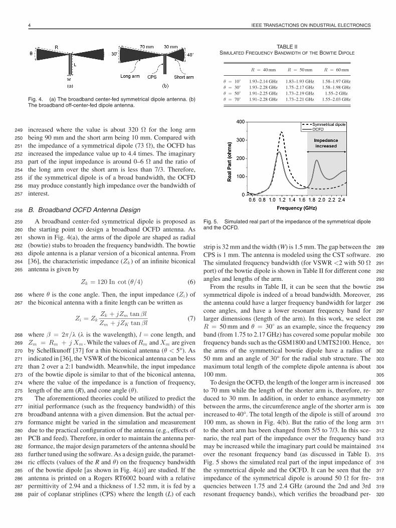
4 IEEE TRANSACTIONS ON INDUSTRIAL ELECTRONICS
Fig. 4. (a) The broadband center-fed symmetrical dipole antenna. (b)The broadband off-center-fed dipole antenna.
increased where the value is about 320 Ω for the long arm249
being 90 mm and the short arm being 10 mm. Compared with250
the impedance of a symmetrical dipole (73 Ω), the OCFD has251
increased the impedance value up to 4.4 times. The imaginary252
part of the input impedance is around 0–6 Ω and the ratio of253
the long arm over the short arm is less than 7/3. Therefore,254
if the symmetrical dipole is of a broad bandwidth, the OCFD255
may produce constantly high impedance over the bandwidth of256
interest.257
B. Broadband OCFD Antenna Design258
A broadband center-fed symmetrical dipole is proposed as259
the starting point to design a broadband OCFD antenna. As260
shown in Fig. 4(a), the arms of the dipole are shaped as radial261
(bowtie) stubs to broaden the frequency bandwidth. The bowtie262
dipole antenna is a planar version of a biconical antenna. From263
[36], the characteristic impedance (Zk ) of an infinite biconical264
antenna is given by265
Zk = 120 In cot (θ/4) (6)
where θ is the cone angle. Then, the input impedance (Zi) of266
the biconical antenna with a finite length can be written as267
Zi = ZkZk + jZm tan βl
Zm + jZK tan βl(7)
where β = 2π/λ (λ is the wavelength), l = cone length, and268
Zm = Rm + j Xm . While the values of Rm and Xm are given269
by Schellkunoff [37] for a thin biconical antenna (θ < 5°). As270
indicated in [36], the VSWR of the biconical antenna can be less271
than 2 over a 2:1 bandwidth. Meanwhile, the input impedance272
of the bowtie dipole is similar to that of the biconical antenna,273
where the value of the impedance is a function of frequency,274
length of the arm (R), and cone angle (θ).275
The aforementioned theories could be utilized to predict the276
initial performance (such as the frequency bandwidth) of this277
broadband antenna with a given dimension. But the actual per-278
formance might be varied in the simulation and measurement279
due to the practical configuration of the antenna (e.g., effects of280
PCB and feed). Therefore, in order to maintain the antenna per-281
formance, the major design parameters of the antenna should be282
further tuned using the software. As a design guide, the paramet-283
ric effects (values of the R and θ) on the frequency bandwidth284
of the bowtie dipole [as shown in Fig. 4(a)] are studied. If the285
antenna is printed on a Rogers RT6002 board with a relative286
permittivity of 2.94 and a thickness of 1.52 mm, it is fed by a287
pair of coplanar striplines (CPS) where the length (L) of each288
TABLE IISIMULATED FREQUENCY BANDWIDTH OF THE BOWTIE DIPOLE
R = 40 mm R = 50 mm R = 60 mm
θ = 10◦ 1.93–2.14 GHz 1.83–1.93 GHz 1.58–1.97 GHzθ = 30◦ 1.93–2.28 GHz 1.75–2.17 GHz 1.58–1.98 GHzθ = 50◦ 1.91–2.25 GHz 1.73–2.19 GHz 1.55–2 GHzθ = 70◦ 1.91–2.28 GHz 1.73–2.21 GHz 1.55–2.03 GHz
Fig. 5. Simulated real part of the impedance of the symmetrical dipoleand the OCFD.
strip is 32 mm and the width (W) is 1.5 mm. The gap between the 289
CPS is 1 mm. The antenna is modeled using the CST software. 290
The simulated frequency bandwidth (for VSWR <2 with 50 Ω 291
port) of the bowtie dipole is shown in Table II for different cone 292
angles and lengths of the arm. 293
From the results in Table II, it can be seen that the bowtie 294
symmetrical dipole is indeed of a broad bandwidth. Moreover, 295
the antenna could have a larger frequency bandwidth for larger 296
cone angles, and have a lower resonant frequency band for 297
larger dimensions (length of the arm). In this work, we select 298
R = 50 mm and θ = 30◦ as an example, since the frequency 299
band (from 1.75 to 2.17 GHz) has covered some popular mobile 300
frequency bands such as the GSM1800 and UMTS2100. Hence, 301
the arms of the symmetrical bowtie dipole have a radius of 302
50 mm and an angle of 30° for the radial stub structure. The 303
maximum total length of the complete dipole antenna is about 304
100 mm. 305
To design the OCFD, the length of the longer arm is increased 306
to 70 mm while the length of the shorter arm is, therefore, re- 307
duced to 30 mm. In addition, in order to enhance asymmetry 308
between the arms, the circumference angle of the shorter arm is 309
increased to 40°. The total length of the dipole is still of around 310
100 mm, as shown in Fig. 4(b). But the ratio of the long arm 311
to the short arm has been changed from 5/5 to 7/3. In this sce- 312
nario, the real part of the impedance over the frequency band 313
may be increased while the imaginary part could be maintained 314
over the resonant frequency band (as discussed in Table I). 315
Fig. 5 shows the simulated real part of the input impedance of 316
the symmetrical dipole and the OCFD. It can be seen that the 317
impedance of the symmetrical dipole is around 50 Ω for fre- 318
quencies between 1.75 and 2.4 GHz (around the 2nd and 3rd 319
resonant frequency bands), which verifies the broadband per- 320
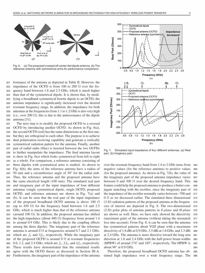
SONG et al.: MATCHING NETWORK ELIMINATION IN BROADBAND RECTENNAS FOR HIGH-EFfiCIENCY WIRELESS POWER TRANSFER 5
Fig. 6. (a) The proposed crossed off-center-fed dipole antenna. (b) Thereference antenna with symmetrical arms for performance comparison.
formance of the antenna as depicted in Table II. However, the321
impedance of the OCFD is from 100 to 200 Ω over the fre-322
quency band between 1.8 and 2.5 GHz, which is much higher323
than that of the symmetrical dipole. It is shown that, by modi-324
fying a broadband symmetrical bowtie dipole to an OCFD, the325
antenna impedance is significantly increased over the desired326
resonant frequency range. In addition, the impedance for both327
antennas at the frequencies from 1.1 to 1.2 GHz is also very high328
(i.e., over 200 Ω), this is due to the antiresonance of the dipole329
antenna [31].330
The next step is to modify the proposed OCFD to a crossed331
OCFD by introducing another OCFD. As shown in Fig. 6(a),332
the second OCFD (red) has the same dimensions as the first one,333
but they are orthogonal to each other. The purpose is to achieve334
dual polarization receiving capability and generate a vertically335
symmetrical radiation pattern for the antenna. Finally, another336
pair of radial stubs (blue) is inserted between the two OCFDs337
to further manipulate the impedance. The final antenna layout338
is show in Fig. 6(a) which looks symmetrical from left to right339
as a whole. For comparison, a reference antenna consisting of340
three dipoles with symmetrical arms is studied. As shown in341
Fig. 6(b), the arms of the reference antenna have a radius of342
50 mm and a circumference angle of 30° for the radial stub.343
Thus, the reference antenna and the proposed antenna have344
the same electrical length (100 mm). The simulated real part345
and imaginary part of the input impedance of four different346
antennas (single symmetrical dipole, single OCFD, proposed347
OCFD, and reference antenna) are shown in Fig. 7(a) and348
(b). It can be seen that the real part of the input impedance349
of the proposed broadband OCFD antenna is above 180 Ω350
(up to 450 Ω) for the frequency band between 1.8 and 2.5351
GHz, which is much higher than that of the reference antenna352
(around 100 Ω). In addition, the proposed antenna has shifted353
the high-impedance (about 400 Ω) frequency from around 1.4354
to around 0.9 GHz. This is likely due to the coupling effects355
among the three dipoles. The imaginary part of the reference356
antenna is around 0 Ω at frequencies around 0.7 and 2.1 GHz,357
which are f0 and 3f0 , respectively. While the imaginary part358
of the proposed OCFD is around 0 Ω at resonant frequencies359
0.6, 1.2, and 2.4 GHz, which are f0 , 2f0 , and 4f0 , respectively.360
These results have demonstrated that the simulated results361
agree with the OCFD theory as discussed in Section III-A.362
Furthermore, the imaginary part of the impedance of the antenna363
Fig. 7. Simulated input impedance of four different antennas. (a) Realpart. (b) Imaginary part.
over the resonant frequency band from 1.4 to 2 GHz turns from 364
negative values (for the reference antenna) to positive values 365
(for the proposed antenna). As shown in Fig. 7(b), the value of 366
the imaginary part of the proposed antenna impedance varies 367
between 0 and 300 Ω over the desired frequency band. This 368
feature could help the proposed antenna to produce a better con- 369
jugate matching with the rectifier, since the imaginary part of 370
the impedance of the rectifier normally varies between –700 and 371
0 Ω as we discussed earlier. The simulated three dimensional 372
(3-D) radiation patterns of the proposed antenna at the frequen- 373
cies of interest are depicted in Fig. 8. The two-dimensional 374
(2-D) polar plots of antenna patterns in E-plane and H-plane 375
are shown as well. Here, we have only showed the directivity 376
(maximum gain) of the antenna (without taking the mismatch 377
loss into account). From Fig. 8, it can be seen that the antenna 378
has symmetrical patterns about YOZ plane with a maximum 379
directivity of 1.8 dBi at 0.9 GHz, 3.5 dBi at 1.8 GHz, and 3.3 dBi 380
at 2.4 GHz. The antenna is more directive toward the long arm 381
direction at 1.8 and 2.4 GHz with the half-power beam-widths 382
(HPBW) of around 174° and 185°, respectively. The HPBW is 383
about 96° at 0.9 GHz. 384
Therefore, the proposed broadband OCFD antenna has ob- 385
tained high impedance over a wide frequency range. The 386
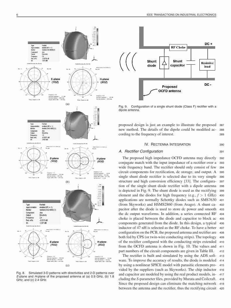
6 IEEE TRANSACTIONS ON INDUSTRIAL ELECTRONICS
Fig. 8. Simulated 3-D patterns with directivities and 2-D patterns overE-plane and H-plane of the proposed antenna at (a) 0.9 GHz, (b) 1.8GHz, and (c) 2.4 GHz.
Fig. 9. Configuration of a single shunt diode (Class F) rectifier with adipole antenna.
proposed design is just an example to illustrate the proposed 387
new method. The details of the dipole could be modified ac- 388
cording to the frequency of interest. 389
IV. RECTENNA INTEGRATION 390
A. Rectifier Configuration 391
The proposed high impedance OCFD antenna may directly 392
conjugate match with the input impedance of a rectifier over a 393
wide frequency band. The rectifier should only consist of few 394
circuit components for rectification, dc storage, and output. A 395
single shunt diode rectifier is selected due to its very simple 396
structure and high conversion efficiency [33]. The configura- 397
tion of the single shunt diode rectifier with a dipole antenna 398
is depicted in Fig. 9. The shunt diode is used as the rectifying 399
element and the diodes for high frequency (e.g., f > 1 GHz) 400
applications are normally Schottky diodes such as SMS7630 401
(from Skyworks) and HSMS2860 (from Avago). A shunt ca- 402
pacitor after the diode is used to store dc power and smooth 403
the dc output waveforms. In addition, a series connected RF 404
choke is placed between the diode and capacitor to block ac 405
components generated from the diode. In this design, a typical 406
inductor of 47 nH is selected as the RF choke. To have a better 407
configuration on the PCB, the proposed antenna and rectifier are 408
both fed by CPS (or twin-wire conducting strips). The topology 409
of the rectifier configured with the conducting strips extended 410
from the OCFD antenna is shown in Fig. 10. The values and 411
part numbers of the circuit components are given in Table III. 412
The rectifier is built and simulated by using the ADS soft- 413
ware. To improve the accuracy of results, the diode is modeled 414
by using a nonlinear SPICE model with parasitic elements pro- 415
vided by the suppliers (such as Skyworks). The chip inductor 416
and capacitor are modeled by using the real product models, in- 417
cluding the S-parameter files, provided by Murata and Coilcraft. 418
Since the proposed design can eliminate the matching network 419
between the antenna and the rectifier, thus the rectifying circuit 420
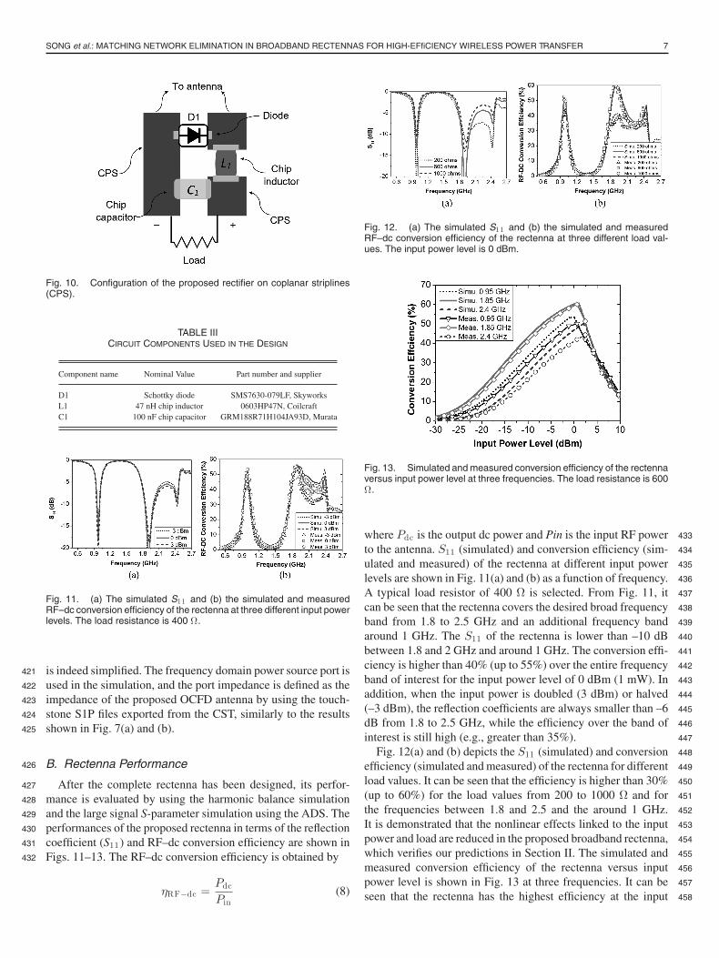
SONG et al.: MATCHING NETWORK ELIMINATION IN BROADBAND RECTENNAS FOR HIGH-EFfiCIENCY WIRELESS POWER TRANSFER 7
Fig. 10. Configuration of the proposed rectifier on coplanar striplines(CPS).
TABLE IIICIRCUIT COMPONENTS USED IN THE DESIGN
Component name Nominal Value Part number and supplier
D1 Schottky diode SMS7630-079LF, SkyworksL1 47 nH chip inductor 0603HP47N, CoilcraftC1 100 nF chip capacitor GRM188R71H104JA93D, Murata
Fig. 11. (a) The simulated S11 and (b) the simulated and measuredRF–dc conversion efficiency of the rectenna at three different input powerlevels. The load resistance is 400 Ω.
is indeed simplified. The frequency domain power source port is421
used in the simulation, and the port impedance is defined as the422
impedance of the proposed OCFD antenna by using the touch-423
stone S1P files exported from the CST, similarly to the results424
shown in Fig. 7(a) and (b).425
B. Rectenna Performance426
After the complete rectenna has been designed, its perfor-427
mance is evaluated by using the harmonic balance simulation428
and the large signal S-parameter simulation using the ADS. The429
performances of the proposed rectenna in terms of the reflection430
coefficient (S11) and RF–dc conversion efficiency are shown in431
Figs. 11–13. The RF–dc conversion efficiency is obtained by432
ηRF−dc =Pdc
Pin(8)
Fig. 12. (a) The simulated S11 and (b) the simulated and measuredRF–dc conversion efficiency of the rectenna at three different load val-ues. The input power level is 0 dBm.
Fig. 13. Simulated and measured conversion efficiency of the rectennaversus input power level at three frequencies. The load resistance is 600Ω.
where Pdc is the output dc power and Pin is the input RF power 433
to the antenna. S11 (simulated) and conversion efficiency (sim- 434
ulated and measured) of the rectenna at different input power 435
levels are shown in Fig. 11(a) and (b) as a function of frequency. 436
A typical load resistor of 400 Ω is selected. From Fig. 11, it 437
can be seen that the rectenna covers the desired broad frequency 438
band from 1.8 to 2.5 GHz and an additional frequency band 439
around 1 GHz. The S11 of the rectenna is lower than –10 dB 440
between 1.8 and 2 GHz and around 1 GHz. The conversion effi- 441
ciency is higher than 40% (up to 55%) over the entire frequency 442
band of interest for the input power level of 0 dBm (1 mW). In 443
addition, when the input power is doubled (3 dBm) or halved 444
(–3 dBm), the reflection coefficients are always smaller than –6 445
dB from 1.8 to 2.5 GHz, while the efficiency over the band of 446
interest is still high (e.g., greater than 35%). 447
Fig. 12(a) and (b) depicts the S11 (simulated) and conversion 448
efficiency (simulated and measured) of the rectenna for different 449
load values. It can be seen that the efficiency is higher than 30% 450
(up to 60%) for the load values from 200 to 1000 Ω and for 451
the frequencies between 1.8 and 2.5 and the around 1 GHz. 452
It is demonstrated that the nonlinear effects linked to the input 453
power and load are reduced in the proposed broadband rectenna, 454
which verifies our predictions in Section II. The simulated and 455
measured conversion efficiency of the rectenna versus input 456
power level is shown in Fig. 13 at three frequencies. It can be 457
seen that the rectenna has the highest efficiency at the input 458
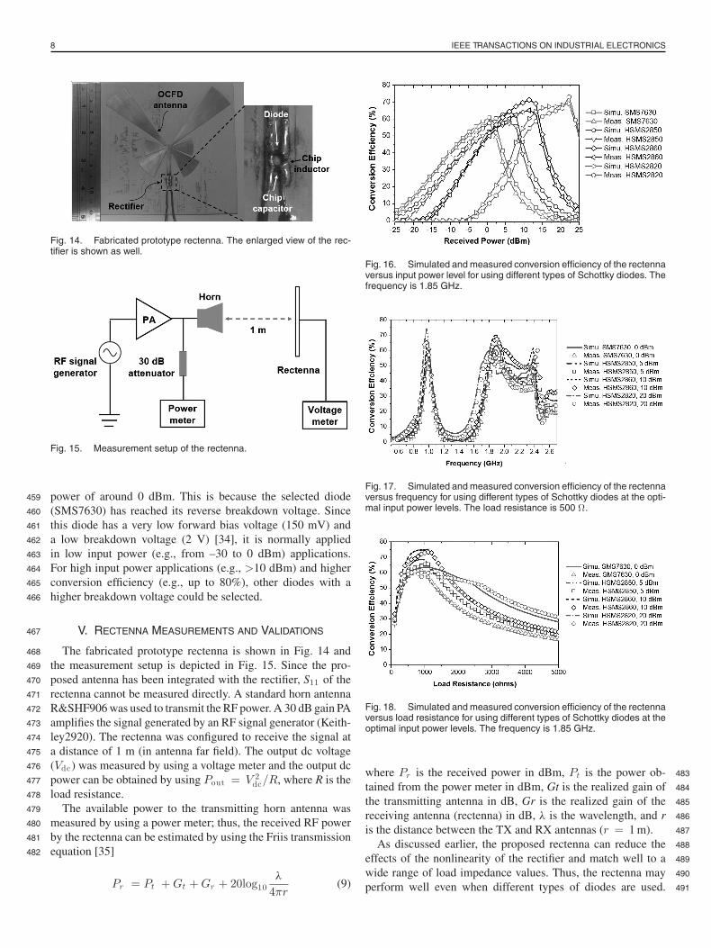
8 IEEE TRANSACTIONS ON INDUSTRIAL ELECTRONICS
Fig. 14. Fabricated prototype rectenna. The enlarged view of the rec-tifier is shown as well.
Fig. 15. Measurement setup of the rectenna.
power of around 0 dBm. This is because the selected diode459
(SMS7630) has reached its reverse breakdown voltage. Since460
this diode has a very low forward bias voltage (150 mV) and461
a low breakdown voltage (2 V) [34], it is normally applied462
in low input power (e.g., from –30 to 0 dBm) applications.463
For high input power applications (e.g., >10 dBm) and higher464
conversion efficiency (e.g., up to 80%), other diodes with a465
higher breakdown voltage could be selected.466
V. RECTENNA MEASUREMENTS AND VALIDATIONS467
The fabricated prototype rectenna is shown in Fig. 14 and468
the measurement setup is depicted in Fig. 15. Since the pro-469
posed antenna has been integrated with the rectifier, S11 of the470
rectenna cannot be measured directly. A standard horn antenna471
R&SHF906 was used to transmit the RF power. A 30 dB gain PA472
amplifies the signal generated by an RF signal generator (Keith-473
ley2920). The rectenna was configured to receive the signal at474
a distance of 1 m (in antenna far field). The output dc voltage475
(Vdc) was measured by using a voltage meter and the output dc476
power can be obtained by using Pout = V 2dc/R, where R is the477
load resistance.478
The available power to the transmitting horn antenna was479
measured by using a power meter; thus, the received RF power480
by the rectenna can be estimated by using the Friis transmission481
equation [35]482
Pr = Pt + Gt + Gr + 20log10λ
4πr(9)
Fig. 16. Simulated and measured conversion efficiency of the rectennaversus input power level for using different types of Schottky diodes. Thefrequency is 1.85 GHz.
Fig. 17. Simulated and measured conversion efficiency of the rectennaversus frequency for using different types of Schottky diodes at the opti-mal input power levels. The load resistance is 500 Ω.
Fig. 18. Simulated and measured conversion efficiency of the rectennaversus load resistance for using different types of Schottky diodes at theoptimal input power levels. The frequency is 1.85 GHz.
where Pr is the received power in dBm, Pt is the power ob- 483
tained from the power meter in dBm, Gt is the realized gain of 484
the transmitting antenna in dB, Gr is the realized gain of the 485
receiving antenna (rectenna) in dB, λ is the wavelength, and r 486
is the distance between the TX and RX antennas (r = 1 m). 487
As discussed earlier, the proposed rectenna can reduce the 488
effects of the nonlinearity of the rectifier and match well to a 489
wide range of load impedance values. Thus, the rectenna may 490
perform well even when different types of diodes are used. 491

SONG et al.: MATCHING NETWORK ELIMINATION IN BROADBAND RECTENNAS FOR HIGH-EFfiCIENCY WIRELESS POWER TRANSFER 9
TABLE IVRECTENNA PERFORMANCE FOR USING DIFFERENT DIODES
Schottky diodes name Simulated input impedance under the same condition (Ω) Optimal input power level Maximum conversion efficiency Optimal load resistance range (Ω)
SMS7630 173 – j 36 0 dBm 60% 250–1500HSMS2850 325 – j 57 5 dBm 65% 200–2000HSMS2860 349 – j 166 10 dBm 70% 200–2500HSMS2820 82 – j 145 20 dBm 75% 250–3000
This advantage is normally not available in the conventional492
rectenna designs, since the input impedance and characteristics493
of the diodes can be very different. Thus, in order to validate494
this point, the proposed rectenna was measured by using differ-495
ent types of Schottky diodes such as HSMS2850, HSMS2860,496
and HSMS2820. The measured conversion efficiency versus497
input power level is shown in Fig. 16 along with simulated498
results. High conversion efficiency is obtained in all cases.499
When the load is selected as 500 Ω and the frequency is se-500
lected as 1.85 GHz, we have Gt = 8.5 dBi, Gr = 3.45 dBi,501
λ = 0.162 m, and r = 1 m. Using (9), the correlation be-502
tween the transmitting power and the receiving power can be503
obtained as504
Pr (dBm) = Pt (dBm) − 25.84 dB. (10)
It can be seen that the maximum conversion efficiency and the505
corresponding input powers of the rectenna are 60% at 0 dBm,506
65% at 5 dBm, 70% at 10 dBm, and 75% at 20 dBm for us-507
ing the Schottky diodes SMS7630, HSMS2850, HSMS2860,508
and HSMS2820, respectively. The peak efficiency is realized509
at different input power levels. This is because the breakdown510
voltages for the selected diodes are different, which are 2 V511
(SMS7630), 3.8 V (HSMS2850), 7 V (HSMS2860), and 15 V512
(HSMS2820), respectively. The efficiency is much higher at513
high input power levels for using the diodes with large break-514
down voltages (e.g., HSMS2820), while the efficiency is higher515
at low input power levels for using the diodes with small forward516
bias voltages (e.g., SMS7630). The simulated and measured517
conversion efficiencies of the rectenna (using the four different518
diodes) are depicted in Fig. 17 as a function of the frequency.519
The load is still 500 Ω while the input power levels are selected520
as the optimal input powers for these diodes (e.g., 0 dBm for521
SMS7630, 5 dBm for HSMS2850, 10 dBm for HSMS2860, and522
20 dBm for HSMS2820). Note that in the measurements, the cor-523
relation between the transmitting power and the receiving power524
[as given in (9)] might be changed if the frequencies are differ-525
ent. Thus, the transmitting power should be tuned to make sure526
that the received power is approximately a constant value in the527
broadband (e.g., 0 dBm for the frequencies from 0.9 to 3 GHz).528
From the results in Fig. 17, it can be seen that the rectenna529
is still of broadband performance (1.8 to 2.5 GHz) when using530
different diodes, and the conversion efficiency is constantly high531
over the frequency bandwidth of interest for the selected input532
power levels. Figs. 16 and 17 show a good agreement between533
the simulated and measured results.534
Fig. 18 shows the simulated and measured conversion ef-535
ficiency by using different load resistances. The frequency is536
selected as 1.85 GHz while the input power levels are still set 537
as the optimal input powers. In reality, the load impedance may 538
vary over a large range in different applications; thus, it is impor- 539
tant to reduce the sensitivity of efficiency versus load variation 540
in a nonlinear system (rectenna). From Fig. 18, it can be seen 541
that, when using different diodes, the efficiency of the rectenna 542
is constantly high (from 40% to 75%) for the load values be- 543
tween 200 and 2000 Ω, then the efficiency starts to decease 544
due to the impedance mismatch between the antenna and the 545
rectifier. It demonstrates that the nonlinear effects have been 546
reduced over the load range from 200 to 2000 Ω. For other load 547
values, the details of the rectenna can be modified to achieve 548
good performance. 549
According to the results in Figs. 16–18, the performance of 550
the rectenna by using different diodes is summarized in Table IV. 551
The simulated input impedance of the rectifier is shown under 552
the same condition (frequency: 1.85 GHz, input power: 553
10 dBm, and load: 500 Ω). The impedance is very different 554
for different types of diodes, but our rectenna can still be well 555
configured with these diodes without using matching networks. 556
It is demonstrated that the proposed broadband rectenna can 557
work well under different operating conditions. The nonlinear 558
effects have been reduced. The matching networks have indeed 559
been eliminated. In addition, the optimal input power level 560
of the device is tunable (from 0 to 23 dBm) by selecting 561
appropriate diodes so that the conversion efficiency of the 562
broadband rectenna can be always higher than 60% (as shown 563
in Fig. 16). This is very important for WPT or WEH used in 564
practice. 565
A comparison between our rectennna and other related work 566
is shown in Table V. It can be seen that our design seems to 567
be the only one without using the matching networks, but still 568
achieves high conversion efficiency over a relatively wide fre- 569
quency band. The conversion efficiency of our design is com- 570
parable with that of the other work used matching networks, 571
while the performance of the rectenna is reasonably well in a 572
range of input powers and load impedance. In addition, our de- 573
vice is also the only one which can use different types of diodes 574
without changing any other part of the circuit. The structure of 575
our design is the simplest for broadband rectennas with similar 576
performance. The proposed rectenna is of good industrial value 577
due to its simplicity and universality, and is of good practical 578
value due to its consistent performance under different operating 579
conditions. 580
Also, the proposed concept for eliminating the matching net- 581
works is not just limited in the presented design, and can also 582
be used in other similar nonlinear systems. 583
10 IEEE TRANSACTIONS ON INDUSTRIAL ELECTRONICS
TABLE VCOMPARISON OF THE PROPOSED RECTENNA AND RELATED DESIGNS
Ref. (year) Frequency (GHz) Use of Complexity Maximum Input power level Optimal load Type ofimpedance matching of the overall conversion for conversion range with good Schottky diode
networks design efficiency (%) efficiency > 60% performance (kΩ)
[18] (2015) Four-band 0.9, 1.8, 2.1, 2.4 Yes Very complex 65 at 0 dBm –5 to 0 dBm 11 MSS20-141[19] (2015) Broad-band 1.8–2.5 Yes Complex 70 at 0 dBm –7 to 0 dBm 14.7 SMS7630[20] (2015) Dual-band 0.915, 2.45 Yes Complex 70 at 0 dBm –5 to 0 dBm 0.5–3 SMS7630[23] (2012) Tunable 0.9–2.45 Yes Very complex 80 at 30 dBm Tunable 5 to 30 dBm 1–4 Tunable[24] (2016) Six-band 0.55, 0.75, 0.9, 1.85, 2.15, 2.45 Yes Very complex 68 at –5 dBm –5 to 0 dBm 10–75 SMS7630[25] (2012) Single-band 2.45 No Simple 70 at –5 dBm –10 to 5 dBm 2.8 HSMS2852[26] (2004) Broad-band 2–18 No Medium 20 at 17 dBm Not available 0.6 SMS7630This work (2016) Broad-band 0.9–1.1, 1.8–2.5 No Simplest 75 at 20 dBm Tunable 0 to 23 dBm 0.2–2 Tunable
VI. CONCLUSION584
A novel method for eliminating the matching network of585
broadband rectennas was presented. An OCFD antenna was586
designed, where the antenna impedance was tuned to directly587
match with the rectifier. The proposed rectenna was of a broad588
bandwidth and high efficiency, and had excellent performance589
under different operating conditions. The measured perfor-590
mance showed that the operating frequencies of the experi-591
mental rectenna were from 0.9 to 1.1 GHz and from 1.8 to592
2.5 GHz (which were the typical cellular mobile, WLAN, and593
ISM bands), while the maximum conversion efficiency was up594
to 75% and the optimal input power range was tunable from595
0 to 23 dBm by selecting appropriate diodes. In addition, the596
rectenna had a very simple structure and low cost. Consider-597
ing the excellent overall performance of the proposed rectenna,598
it is suitable for high efficiency WPT and WEH applications.599
The design concept is easy to follow while its details can be600
optimized for different applications.601
ACKNOWLEDGMENT602
The authors would like to thank the anonymous reviewers603
for their constructive feedback of this paper. The authors would604
also like to thank Prof. S. Hall from the University of Liverpool605
for the refinement of the manuscript.606
REFERENCES607
[1] S. Carreon-Bautista, A. Eladawy, A. N. Mohieldin, and E. Sanchez-608Sinencio, “Boost converter with dynamic input impedance matching609for energy harvesting with multi-array thermoelectric generators,” IEEE610Trans. Ind. Electron., vol. 61, no. 10, pp. 5345–5353, Oct. 2014.611
[2] J. Jeong and D. Jang, “Design technique for harmonic-tuned RF power612oscillators for high-efficiency operation,” IEEE Trans. Ind. Electron., vol.61362, no. 1, pp. 221–228, Jan. 2015.614
[3] J. Kim, D.-H. Kim, and Y.-J. Park, “Analysis of capacitive impedance615matching networks for simultaneous wireless power transfer to multiple616devices,” IEEE Trans. Ind. Electron., vol. 62, no. 5, pp. 2807–2813, May6172015.618
[4] K. Song and Q. Xue, “Ultra-wideband ring-cavity multiple-way parallel619power divider,” IEEE Trans. Ind. Electron., vol. 60, no. 10, pp. 4737–4745,620Oct. 2013621
[5] K. Rawat and F. M. Ghannouchi, “Design methodology for dual-band622Doherty power amplifier with performance enhancement using dualband623offset lines,” IEEE Trans. Ind. Electron., vol. 59, no. 12, pp. 4831–4842,624Dec. 2012625
[6] X. Wang, X. K. Guan, and S. Q. Fan, “ESD-protected power amplifier 626design in CMOS for highly reliable RFICs,” IEEE Trans. Ind. Electron., 627vol. 58, no. 7, pp. 2736–2743, Jun. 2011. 628
[7] R. Johari, J. V. Krogmeier, and D. J. Love, “Analysis and practical consid- 629erations in implementing multiple transmitters for wireless power transfer 630via coupled magnetic resonance,” IEEE Trans. Ind. Electron., vol. 61, no. 6314, pp. 1174–1183, Apr. 2014. 632
[8] L. Chen, Y. C. Zhou, and T. J. Cui, “An optimizable circuit structure for 633high-efficiency wireless power transfer,” IEEE Trans. Ind. Electron., vol. 63460, no. 1, pp. 339–349, Jan. 2013. 635
[9] H. J. Visser and R. J. M. Vullers, “RF energy harvesting and transport for 636wireless sensor network applications: Principles and requirements,” Proc. 637IEEE, vol. 101, no. 6, pp. 1410–1423, Jun. 2013. 638
[10] S. Cheon, Y.-H. Kim, S.-Y. Kang, M. L. Lee, J.-M. Lee, and T. Zyung, 639“Circuit-model-based analysis of a wireless energy-transfer system via 640coupled magnetic resonances,” IEEE Trans. Ind. Electron., vol. 58, no. 7, 641pp. 2906–2914, Jul. 2011. 642
[11] J. Colomer-Farrarons, P. Miribel-Catala, A. Saiz-Vela, and J. Samitier, 643“A multiharvested self-powered system in a low-voltage low-power tech- 644nology,” IEEE Trans. Ind. Electron., vol. 58, no. 9, pp. 4250–4263, Sep. 6452011. 646
[12] Y. Huang, N. Shinohara, and T. Mitani, “A constant efficiency of rectifying 647circuit in an extremely wide load range,” IEEE Trans. Microw. Theory 648Techn., vol. 62, no. 4, pp. 986–993, Apr. 2014. 649
[13] P. Lu, X. Yang, J. Li, and B. Wang, “A compact frequency reconfigurable 650rectenna for 5.2- and 5.8-GHz wireless power transmission,” IEEE Trans. 651Power Electron., vol. 30, no. 11, pp. 6006–6010, Nov. 2015. 652
[14] J. O. McSpadden, F. Lu, and K. Chang, “Design and experiments of 653a high conversion efficiency 5.8-GHz rectenna,” IEEE Trans. Microw. 654Theory Techn., vol. 46, no. 12, pp. 2053–2060, Dec. 1998. 655
[15] H. Sun, Y.-X. Guo, M. He, and Z. Zhong, “A dual-band rectenna using 656broadband Yagi antenna array for ambient RF power harvesting,” IEEE 657Antennas Wireless Propag. Lett., vol. 12, pp. 918–921, 2013. 658
[16] K. Niotaki, S. Kim, S. Jeong, A. Collado, A. Georgiadis, and M. Tentzeris, 659“A compact dual-band rectenna using slot-loaded dual band folded dipole 660antenna,” IEEE Antennas Wireless Propag. Lett., vol. 12, pp. 1634–1637, 6612013. 662
[17] R. Scheeler, S. Korhummel, and Z. Popovic, “A dual-frequency ultralow- 663power efficient 0.5-g rectenna,” IEEE Microw. Mag., vol. 15, no. 1, pp. 664109–114, Jan. 2014. 665
[18] V. Kuhn, C. Lahuec, F. Seguin, and C. Person, “A multi-band stacked RF 666energy harvester with rf-to-dc efficiency up to 84%,” IEEE Trans. Microw. 667Theory Techn., vol. 63, no. 5, pp. 1768–1778, May 2015. 668
[19] C. Song, Y. Huang, J. Zhou, J. Zhang, S. Yuan, and P. Carter, “A high- 669efficiency broadband rectenna for ambient wireless energy harvesting,” 670IEEE Trans. Antennas Propag., vol. 63, no. 8, pp. 3486–3495, May 2015. 671
[20] K. Niotaki, A. Georgiadis, A. Collado, and J. S. Vardakas, “Dual-band re- 672sistance compression networks for improved rectifier performance,” IEEE 673Trans. Microw. Theory Techn., vol. 62, no. 12, pp. 3512–3521, Nov. 2015. 674
[21] Y. Han, O. Leitermann, D. A. Jackson, J. M. Rivas, and D. J. Perreault, “Re- 675sistance compression networks for radio-frequency power conversion,” 676IEEE Trans. Power Electron., vol. 22, no. 1, pp. 41–53, Jan. 2007. 677
[22] T. Paing, J. Shin, R. Zane, and Z. Popovic, “Resistor emulation approach 678to low-power RF energy harvesting,” IEEE Trans. Power Electron., vol. 67923, no. 3, pp. 1494–1501, Mar. 2008. 680
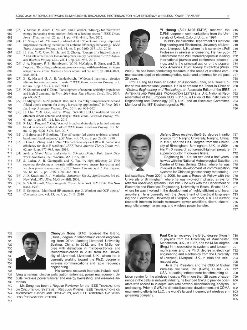
SONG et al.: MATCHING NETWORK ELIMINATION IN BROADBAND RECTENNAS FOR HIGH-EFfiCIENCY WIRELESS POWER TRANSFER 11
[23] V. Marian, B. Allard, C. Vollaire, and J. Verdier, “Strategy for microwave681energy harvesting from ambient field or a feeding source,” IEEE Trans.682Power Electron., vol. 27, no. 11, pp. 4481–4491, Nov. 2012.683
[24] C. Song et al., “A novel six-band dual CP rectenna using improved684impedance matching technique for ambient RF energy harvesting,” IEEE685Trans. Antennas Propag., vol. 64, no. 7, pp. 3160–3171, Jul. 2016.686
[25] H. Sun, Y.-X. Guo, M. He, and Z. Zhong, “Design of a high-efficiency6872.45-GHz rectenna for low-input-power energy harvesting,” IEEE Anten-688nas Wireless Propag. Lett., vol. 11, pp. 929–932, 2012.689
[26] J. A. Hagerty, F. B. Helmbrecht, W. H. McCalpin, R. Zane, and Z. B.690Popovic, “Recycling ambient microwave energy with broad-band rectenna691arrays,” IEEE Trans. Microw. Theory Techn., vol. 52, no. 3, pp. 1014–1024,692Mar. 2004.693
[27] Z. K. Ma and G. A. E. Vandenbosch, “Wideband harmonic rejection694filtenna for wireless power transfer,” IEEE Trans. Antennas Propag., vol.69562, no. 1, pp. 371–377, Oct. 2013.696
[28] N. Shinohara and Y. Zhou, “Development of rectenna with high impedance697and high Q antenna,” in Proc. 2014 Asia–Pac. Microw. Conf., Nov. 2014,698pp. 600–602.699
[29] H. Miyagoshi, K. Noguchi, K. Itoh, and J. Ida, “High-impedance wideband700folded dipole antenna for energy harvesting applications,” in Proc. 2014701Int. Symp. Antennas Propag., Dec. 2014, pp. 601–602.702
[30] H. Chu, Y.-X. Guo, and Z. Wang, “60-GHz LTCC wideband vertical703offcenter dipole antenna and arrays,” IEEE Trans. Antennas Propag., vol.70461, no. 1, pp. 153–161, Jan. 2013.705
[31] R. Li, L. Pan, and Y. Cui, “A novel broadband circularly polarized antenna706based on off-center-fed dipoles,” IEEE Trans. Antennas Propag., vol. 63,707no. 12, pp. 5296–5304, Dec. 2015.708
[32] J. Belrose and P. Bouliane, “The off-center-fed dipole revisited: a broad-709band, multiband antenna,” QST Mag., vol. 74, no. 8, pp. 28–34, 1990.710
[33] J. Guo, H. Zhang, and X. Zhu, “Theoretical analysis of RF–DC conversion711efficiency for class-F rectifiers,” IEEE Trans. Microw. Theory Techn., vol.71262, no. 4, pp. 977–985, Apr. 2014.713
[34] Surface Mount Mixer and Detector Schottky Diodes, Data Sheet. Sky-714works Solutions, Inc., Woburn, MA, USA, 2013.715
[35] S. Ladan, A. B. Guntupalli, and K. Wu, “A high-efficiency 24 GHz716rectenna development towards millimeter-wave energy harvesting and717wireless power transmission,” IEEE Trans. Circuits Syst. I, Reg. Papers,718vol. 61, no. 12, pp. 3358–3366, Dec. 2014.719
[36] J. D. Kraus and R. J. Marhefka, Antennas: For All Applications, 3rd ed.720New York, NY, USA: McGraw-Hill, 2001.721
[37] S. Schellkunoff, Electromagnetic Waves. New York, NY, USA: Van Nos-722trand, 1943.723
[38] E. Spingola, “Multiband HF antennas, part 3, Windom and OCF dipole,”724Communicator, vol. 13, no. 4, pp. 7–11, 2010.725
Chaoyun Song (S’16) received the B.Eng.726(Hons.) degree in telecommunication engineer-727ing from Xi’an Jiaotong-Liverpool University,728Suzhou, China, in 2012, and the M.Sc. de-729gree with distinction in microelectronics and730telecommunication in 2013 from the Univer-731sity of Liverpool, Liverpool, U.K., where he is732currently working toward the Ph.D. degree in733wireless communications and radio frequency734engineering.735
His current research interests include recti-736fying antennas, circular polarization antennas, power management cir-737cuits, wireless power transfer and energy harvesting, and wearable an-738tennas.739
Mr. Song has been a Regular Reviewer for the IEEE TRANSACTIONS740ON CIRCUITS AND SYSTEMS I: REGULAR PAPERS, IEEE TRANSACTIONS ON741MICROWAVE THEORY AND TECHINQUES, and IEEE ANTENNAS AND WIRE-742LESS PROPAGATION LETTERS.743
744
Yi Huang (S’91–M’96–SM’06) received the 745D.Phil. degree in communications from the Uni- 746versity of Oxford, Oxford, U.K., in 1994. 747
In 1995, he oined the Department of Electrical 748Engineering and Electronics, University of Liver- 749pool, Liverpool, U.K., where he is currently a Full 750Professor in wireless engineering. He has pub- 751lished more than 200 refereed papers in leading 752international journals and conference proceed- 753ings, and is the principal author of the popular 754book Antennas: From Theory to Practice (Wiley, 755
2008). He has been conducting research in the areas of wireless com- 756munications, applied electromagnetics, radar, and antennas for the past 75725 years. 758
Prof. Huang has been an Editor, an Associate Editor, or a Guest Ed- 759itor of four international journals. He is at present the Editor-in-Chief of 760Wireless Engineering and Technology, an Associate Editor of the IEEE 761ANTENNAS AND WIRELESS PROPAGATION LETTERS, a U.K. National Rep- 762resentative of the European COST-IC1102, a Fellow of the Institution of 763Engineering and Technology (IET), U.K., and an Executive Committee 764Member of the IET Electromagnetics PN. 765
766
Jiafeng Zhou received the B.Sc. degree in radio 767physics from Nanjing University, Nanjing, China, 768in 1997, and the Ph.D. degree from the Univer- 769sity of Birmingham, Birmingham, U.K., in 2004. 770His Ph.D. research concerned high-temperature 771superconductor microwave filters. 772
Beginning in 1997, for two and a half years, 773he was with the National Meteorological Satellite 774Centre of China, Beijing, China, where he was 775involved in the development of communication 776systems for Chinese geostationary meteorolog- 777
ical satellites. From 2004 to 2006, he was a Research Fellow with the 778University of Birmingham, where he was involved in phased arrays for 779reflector observing systems. Until 2013, he was with the Department of 780Electronic and Electrical Engineering, University of Bristol, Bristol, U.K., 781where he was involved in the development of highly efficient and linear 782amplifiers. He is currently with the Department of Electrical Engineer- 783ing and Electronics, University of Liverpool, Liverpool, U.K. His current 784research interests include microwave power amplifiers, filters, electro- 785magnetic energy harvesting, and wireless power transfer. 786
787
Paul Carter received the B.Sc. degree (Hons.) 788in physics from the University of Manchester, 789Manchester, U.K., in 1987, and the M.Sc. degree 790(Eng.) in microelectronic systems and telecom- 791munications and the Ph.D. degree in electrical 792engineering and electronics from the University 793of Liverpool, Liverpool, U.K., in 1988 and 1991, 794respectively. 795
He is the President and the CEO of Global 796Wireless Solutions, Inc. (GWS), Dulles, VA, 797USA, a leading independent benchmarking so- 798
lution vendor for the wireless industry. With more than 25 years of expe- 799rience in the cellular network industry, he founded GWS to provide oper- 800ators with access to in-depth, accurate network benchmarking, analysis, 801and testing. Prior to GWS, he directed business development and CDMA 802engineering efforts for LLC, the world’s largest independent wireless en- 803gineering company. 804
805

12 IEEE TRANSACTIONS ON INDUSTRIAL ELECTRONICS
Sheng Yuan received the B.Eng. degree (first806class) in microelectronics and telecommunica-807tion engineering and the Ph.D. degree in elec-808trical engineering and electronics from the Uni-809versity of Liverpool, Liverpool, U.K., in 2012 and8102016, respectively.811
He is currently with the Department of In-812telligent Transportation Systems, Arup Group813Limited, Newcastle, U.K. His research interests814include wireless energy harvesting, ferromag-815netic materials, indoor navigation systems, en-816
ergy management circuits, wireless power transfer, radio-frequency iden-817tification, and intelligent transportation systems.818
819
Qian Xu received the B.Eng. and M.Eng. de-820grees in electrical engineering and electronics821from the Department of Electronics and Infor-822mation, Northwestern Polytechnical University,823Xi’an, China, in 2007 and 2010, respectively,824and the Ph.D. degree in electrical engineering825from the University of Liverpool, Liverpool, U.K.,826in 2016.827
He is currently an Associate Professor in the828College of Electronic and Information Engineer-829ing, Nanjing University of Aeronautics and Astro-830
nautics, Nanjing, China. He worked as an RF Engineer in Nanjing, China,831in 2011, an Application Engineer at CST Company, Shanghai, China, in8322012, and a Research Assistant at the University of Liverpool in 2016.833His research interests include statistical electromagnetics, reverberation834chambers, computational electromagnetics, and anechoic chambers.835
836
Zhouxiang Fei was born in Xi’an, China, in 8371990. He received the B.Eng. degree in elec- 838tronics and information engineering from North- 839western Polytechnical University, Xi’an, China, 840in 2012, and the M.Sc. degree with distinction in 841wireless communications from the University of 842Southampton, Southampton, U.K., in 2013. He 843is currently working toward the Ph.D. degree at 844the University of Liverpool, Liverpool, U.K. 845
His research interests include numerical and 846experimental studies of crosstalk in complex ca- 847
ble bundles, with a particular emphasis on considering parameter vari- 848ability using efficient statistical approaches. 849
Mr. Fei received a student scholarship from the IEEE Electromagnetic 850Compatibility Society to attend the 2016 IEEE International Symposium 851on EMC, held in Ottawa, ON, Canada. He was also selected as a Best 852EMC Paper Finalist at the 2016 IEEE International Symposium on EMC. 853
854


![A Compact Dual-Band Rectenna for GSM900 and GSM1800 … · ious dual-band rectennas [3], broadband rectennas [4, 5], and multiband rectennas [6] are reported in recent years. Several](https://img.pdfslide.us/doc/110x75/60d53f7e76b1547e045b0c36/a-compact-dual-band-rectenna-for-gsm900-and-gsm1800-ious-dual-band-rectennas-3.jpg)


![Matching Network Elimination in Broadband Rectennas for High … · rectennas. Thus in previous work [19] [24], the structures of the impedance matching networks were complex for](https://img.pdfslide.us/doc/110x75/60d541f11e8a1a043b412401/matching-network-elimination-in-broadband-rectennas-for-high-rectennas-thus-in.jpg)