Embed Size (px)
Citation preview
CHAPTER I
INTRODUCTION TO INDUCTANCE
The impact of inductance has been a critical issue in the printed circuit board
(PCB) design for quite some time. Since a PCB has both nearly perfect dielectric and
ground plane, resistive losses in conductors as well as dielectrics are reasonably ignored.
The inductance and capacitance are the major concerns in terms of the on-board signal
transmission. In addition, the dimension of a PCB is relatively large compared with the
signal wavelength, especially in the radio-frequency (RF) and microwave regime. For
example, a 1 GHz signal has a wavelength of 30 cm in free space while a typical PCB
can easily have one of its dimensions larger than several inches. This means the board
has to be treated as a distributed system where the transmission line theory instead of
KCL and KVL applies.
The significance of inductance includes increased transmission delay, signal
reflection and ringing, inductive coupling, and digital switching noise due to AC voltage
drop.
However, inductance has been largely ignored in an on-chip environment, where
resistive together with capacitive effects are bigger concerns. In addition, the chip size is
no larger than several millimeters, which is tiny enough compared with signal
wavelengths.
1
With the operating frequencies looming into the gigahertz range, inductance is
quickly coming into play. On one hand, the parasitic inductance of on-chip interconnects
gives rise to signal delay and crosstalk between different signal paths. On the other hand,
spiral inductors have been specifically designed and integrated onto a chip to achieve
enhanced system integrity. Therefore there is a dramatically increased demand of IC
designers for an accurate inductance model, both analytical and computational.
MAXWELL EQUATIONS
Maxwell’s Equations are the complete set of laws for time-varying
electromagnetic phenomena.
The four physical terms that describe electromagnetic fields are the electric field
, electric displacement , magnetic field , and magnetic
intensity . and are analogous in nature in that they both give the force on a
moving charge given by,
(1)
where is the velocity of the charge. and are analogous because they are
independent of material properties and correspond to the space free charge and current
respectively. and are related to and through the electric and magnetic
polarization of the media material,
2
(2)
(3)
where is the electric permittivity and is the magnetic permeability.
The first one of Maxwell Equations is derived from Faraday’s Law, which states
that a time-varying magnetic field induces electric fields. The integral form of Faraday’s
Law is
(4)
where is an arbitrary surface and is the edge of on which the magnetic field is
integrated. Although the integral of electric field along a closed loop has the unit of
voltage, it is different from the voltage defined for static fields, which is equal to the
potential difference between two points and is independent of the path connecting the two
points. The loop integral of the electric field induced by the time-varying magnetic field
is defined as the electromotive force (emf) of that loop,
(5)
Applying Stoke’s Theorem, the large-scale form of Faraday’s Law can be transferred to
the differential form
3
(6)
The second one of Maxwell’s Equations is based on Ampere’s Law, which
describes that both conducting currents and time-varying electric fields generate magnetic
fields. The integral form of Ampere’s Law is
(7)
where is an arbitrary surface and is the edge of . Applying Stoke’s Theorem, the
differential form of Ampere’s Law is
(8)
The time derivative of the electric displacement has the same unit as current density that
is so-called displacement current.
The third one of Maxwell’s Equations is based on Gauss’s Law, which states that
the total flux of electric displacement from an arbitrary volume is equal to the net
charge enclosed in that volume. The integral form of Gauss’s Law is
(9)
where is the enclosed surface of volume and is the charge density. Applying the
divergence theorem, the differential form of Gauss’s Law is
4
(10)
The fourth one of Maxwell’s Equations is validated from the fact that there is no
magnetic charge existing in nature. Thus the magnetic field lines are always closed and
the net flux of magnetic fields through any closed surface is always zero,
(11)
(12)
Writing the four equations together, the Maxwell’s Equations are
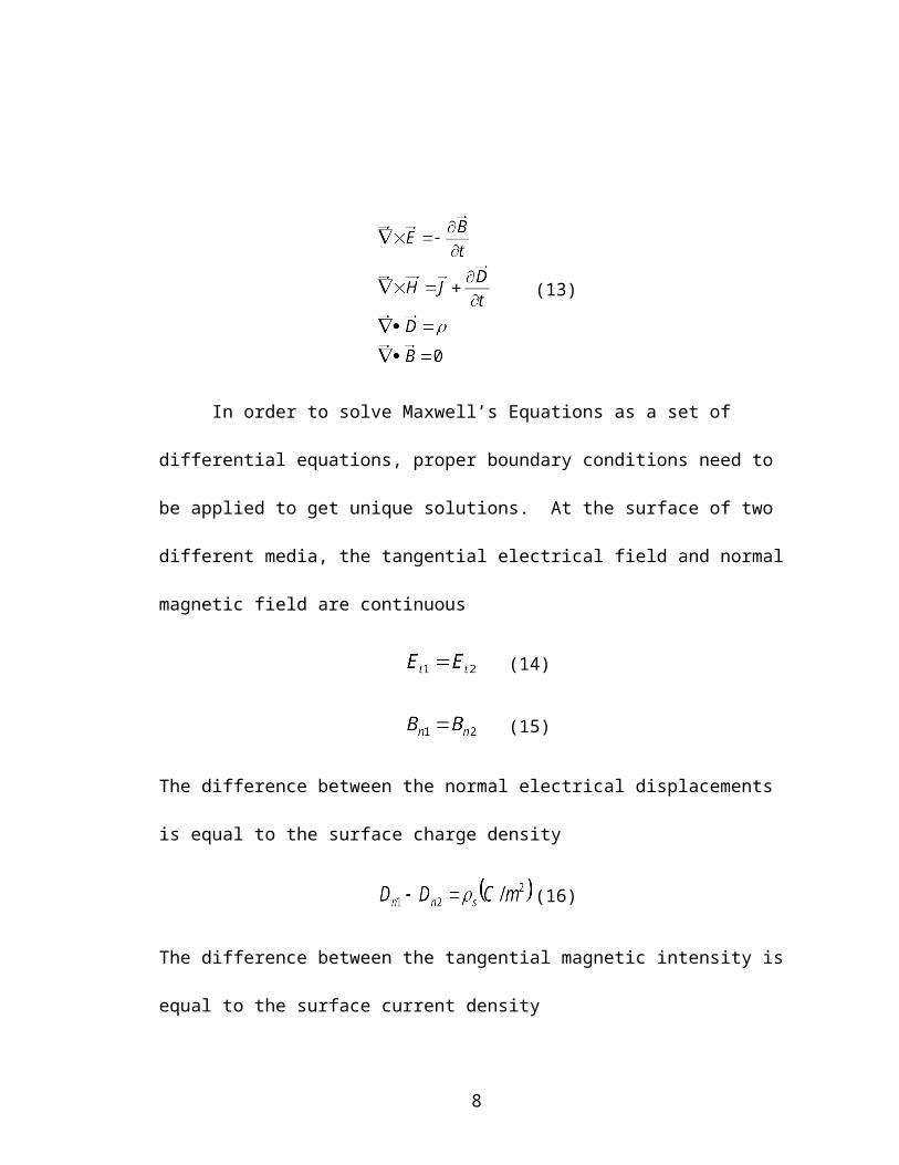
(13)
In order to solve Maxwell’s Equations as a set of differential equations, proper
boundary conditions need to be applied to get unique solutions. At the surface of two
different media, the tangential electrical field and normal magnetic field are continuous
(14)
(15)
The difference between the normal electrical displacements is equal to the surface charge
density
5
(16)
The difference between the tangential magnetic intensity is equal to the surface current
density
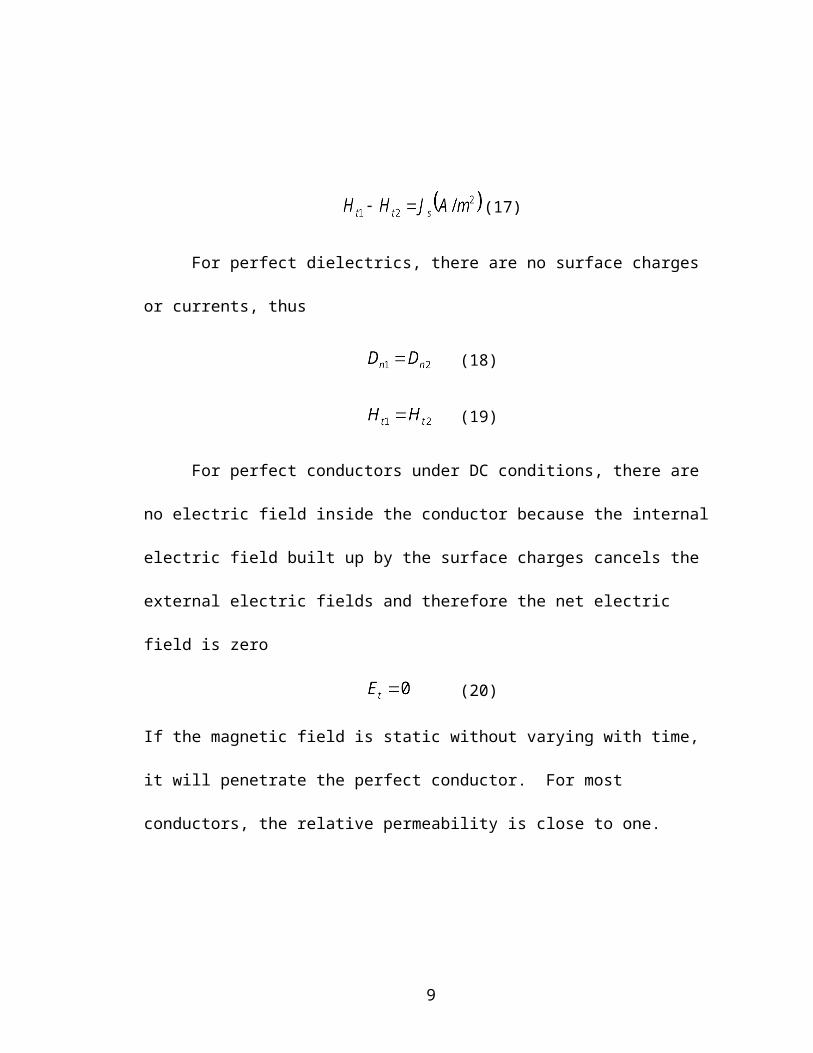
(17)
For perfect dielectrics, there are no surface charges or currents, thus
(18)
(19)
For perfect conductors under DC conditions, there are no electric field inside the
conductor because the internal electric field built up by the surface charges cancels the
external electric fields and therefore the net electric field is zero
(20)
If the magnetic field is static without varying with time, it will penetrate the perfect
conductor. For most conductors, the relative permeability is close to one.
For perfect conductors under AC conditions, both the electric and the magnetic
fields inside the conductor are zero
(21)
(22)
6
INDUCTANCE DEFINITION
Inductance can be defined in several ways that are inherently consistent.
From the energy point of view, the inductance of a device describes the magnetic
energy storage capability of the device. The time-average energy stored in the magnetic
field is given by
(23)
where is the current flowing through the device. Thus the energy definition of
inductance is given by
(24)
Although the energy definition is the most fundamental definition of inductance, a
more popular definition of inductance is through the magnetic flux leakage that is given
by
(25)
where is the magnetic flux expressed as
7
(26)
It is seen that the energy and flux definition are linked by the magnetic field.
Therefore the inductance of a device can be calculated from computing the field
pattern associated with the device.
From Faraday’s Law, voltage is linked to the magnetic flux by
(27)
By substituting Equation (27) into Equation (25), the AC voltage drop across a device is
proportional to the time derivative of the current
(28)
This is commonly used in the circuit theory and the directions of and are defined in
Figure 1
Figure 1 – Voltage and Current Direction in Inductance Definition
The inductance definition gives insight of the impact of inductance on an electric
network:
1. Current flowing through a conductor creates a magnetic field;
8
2. A time-varying current generates a time-varying magnetic field, which induces
electric fields;
3. The induced electric field exerts forces on the electrons in the conductor carrying
the current and causes emf.
The induced electric field from a conductor can affect not only the electron
movement of the conductor itself, but also another conductor nearby. This leads to the
separation of inductance definition into self-inductance and mutual inductance.
The self-inductance of a conductor describes the effects of the electromagnetic
field generated by the conductor on itself. For a real conductor instead of an ideally
filamentary one, it is convenient to further separate the definition of self-inductance into
internal self-inductance and external self-inductance. The external one is due to the
magnetic flux leakage from the inductor to the external surrounding. The internal one
arises from the magnetic energy stored inside the conductor.
The overall classification of inductance is summarized in Figure 2.
9
Figure 2 – Inductance Classification
INTERNAL SELF-INDUCTANCE
When applying the flux leakage definition to the internal of the conductor, the
inconvenience arises from the difficulty of distinguishing the flux area, especially.
To gain better understanding of internal inductance, the magnetic energy
definition of inductance is used. When a conductor carries a current, magnetic field is
generated both inside and outside the conductor. Thus some of the magnetic energy is
stored inside the conductor, which gives rise to the internal inductance. For those
conductors that are not filamentary, the internal inductance exists. For example, the
internal inductance of an infinitely long straight thick wire exists while the external one
does not.
10

Although one can try to solve the field pattern inside a given conductor to
calculate the energy and thus internal inductance, a more efficient way to solve the
problem is by using the definition of internal impedance per unit length, which is given
by [2]
(29)
where is the electric field on the conductor surface and is the total current flowing
through the conductor.
The question is what is for a given ?
From Ohm’s Law, electric field is directly related to the conducting current and
material conductivity
(30)
Thus the internal impedance of a conductor per unit length is
(31)
where the current is replaced by the integration of the current density over the
conductor cross-section.
Since the conductivity of a practical conductor cannot be infinite, the internal
impedance of a conductor includes not only internal inductance, but also internal
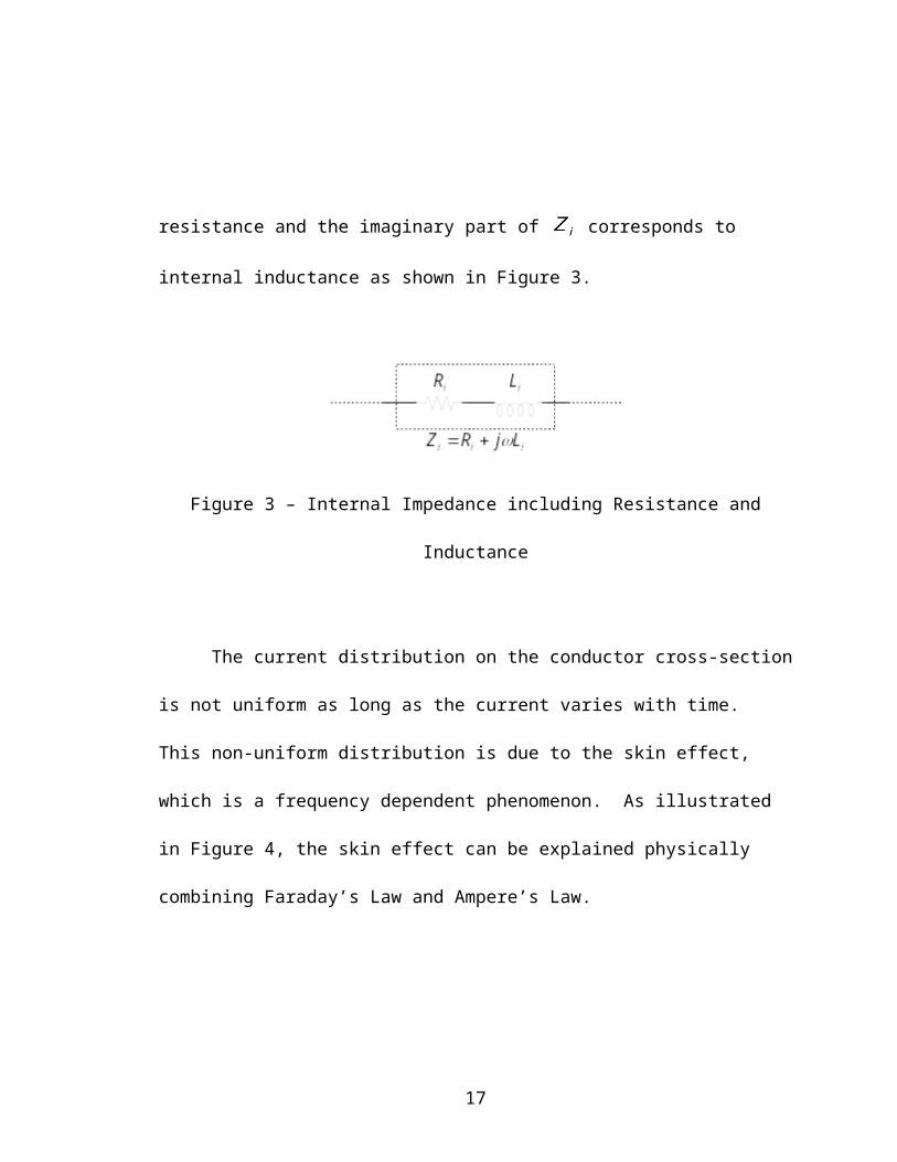
resistance. In another word, the real part of represents internal resistance and the
imaginary part of corresponds to internal inductance as shown in Figure 3.
11
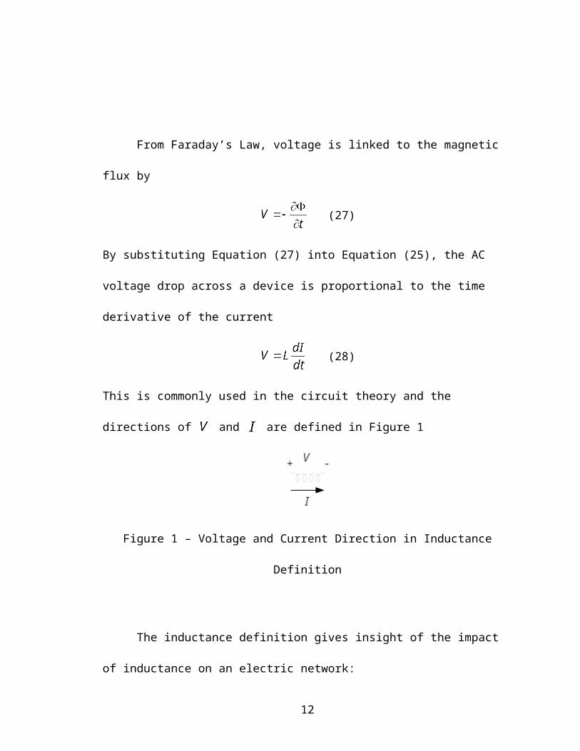
Figure 3 – Internal Impedance including Resistance and Inductance
The current distribution on the conductor cross-section is not uniform as long as
the current varies with time. This non-uniform distribution is due to the skin effect,
which is a frequency dependent phenomenon. As illustrated in Figure 4, the skin effect
can be explained physically combining Faraday’s Law and Ampere’s Law.
12
Figure 4 – Physical Explanation of Skin Effect
The conducting current generates magnetic field that is given by Ampere’s Law
(32)
A time varying results in a time varying that induces an electric field given by
Faraday’s Law
(33)
The induced electric field causes a displacement current that in turn adds to the magnetic
fields
13
(34)
It is evident from Figure 4 that the induced electric field points to the direction that tends
to cancel the conducting electric fields at the center of the conductor and reinforce it at
the surface. From Ohm’s Law, therefore, the current will crowd at the conductor surface
and void at the center. The skin effect becomes more significant at increased frequencies.
From the carrier transportation point of view, the current density can be written as
(35)
where is the electron charge magnitude, is the carrier density, and is the carrier
velocity. For good conductors like metals, the non-uniform distribution of current
density as a result of skin effect is mainly due to the non-uniform distribution of the
carrier velocity rather than the carrier density. This is because the conductivity of metals
is so large that it is a good approximation that the electron density is uniform throughout
the conductor. Thus skin effect in good conductors can also be viewed as the non-
uniform distribution of the electron velocity, which is higher at the conductor surface
than the center.
The extreme case will be a superconductive conductor, whose conductivity is
infinity. All the current will flow at the surface of the conductor. There will be only
surface current and no body current.
Since the carrier density is assumed to be uniform, there will be no normal
electric fields perpendicular to the conductor surface, but only tangential ones along the
14
current path. Choosing the tangential direction to be , the electric field can be expressed
as
(36)
The non-uniform distribution of the electric field can be solved through
Maxwell’s Equations. The first and second equations are rewritten below
(6)
(8)
By taking curl on both sides, Equation (6) becomes
(37)
Substitute Equation (8) into Equation (37),
(38)
From Gauss’s Law,
(39)
The first term in Equation (38) can be expressed as
15
(40)
For most of the practical conductors, it is a good assumption that there is no gradient of
both the charge density and the material permittivity . Therefore Equation (38) can
be simplified as
(41)
The phasor form of this equation becomes a complex Helmholtz equation
(42)
This is a partial differential equation and its solution depends on the boundary conditions.
A useful parameter called skin depth is defined to describe quantitatively the skin
effect, which is defined as
(43)
where is the angular frequency of the fields and is the conductor conductivity. The
skin depth is derived as the depth at which the magnetic field can penetrate a conductor.
It is also consistent with the depth beneath the surface of a conductor at which the current
mainly flows.
EXTERNAL SELF-INDUCTANCE
16
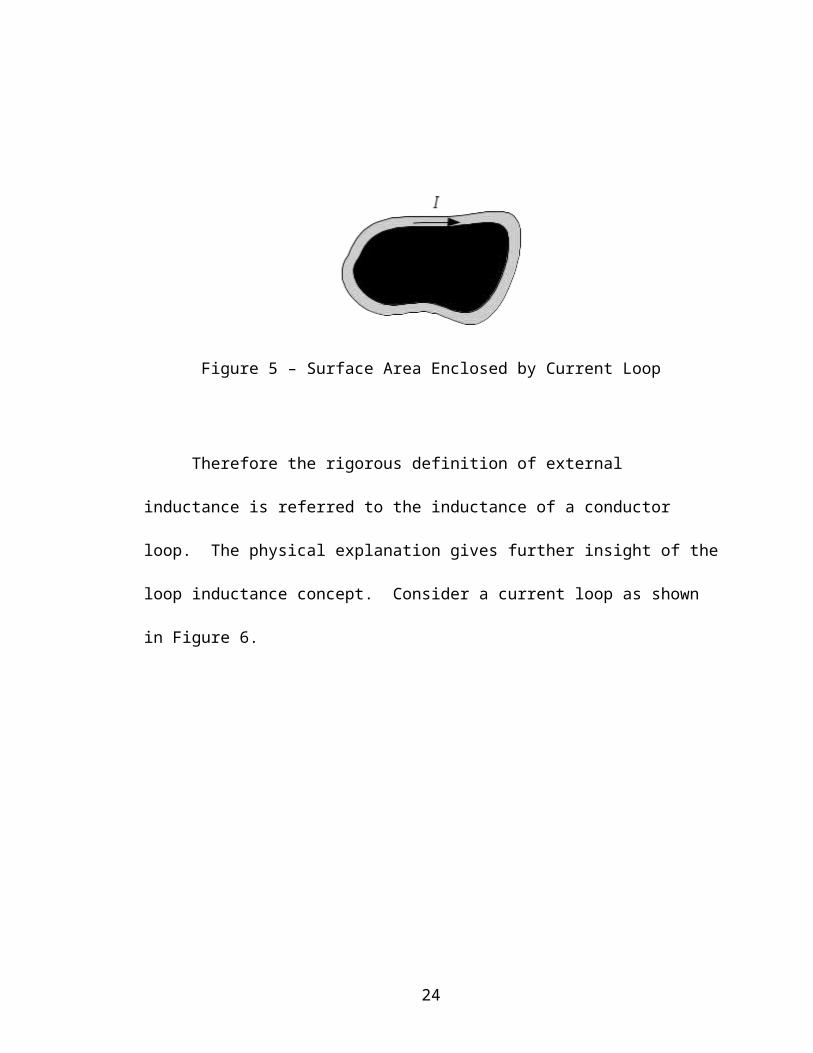
A current flowing through a conductor generates magnetic field in its
surroundings, which gives rise to the external inductance of the conductor. In order to
calculate the external inductance using the flux definition, a finite flux area has to be
properly defined. Since a current always flows through a closed path, the surface area
can then be chosen as enclosed by the current loop that is illustrated in Figure 5.
Figure 5 – Surface Area Enclosed by Current Loop
Therefore the rigorous definition of external inductance is referred to the
inductance of a conductor loop. The physical explanation gives further insight of the
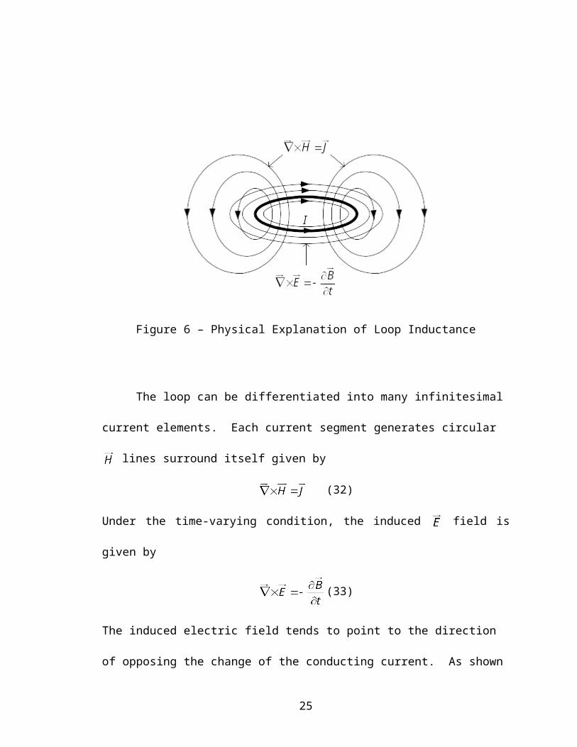
loop inductance concept. Consider a current loop as shown in Figure 6.
17
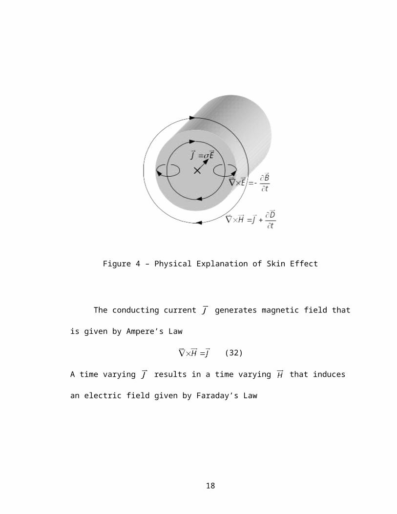
Figure 6 – Physical Explanation of Loop Inductance
The loop can be differentiated into many infinitesimal current elements. Each
current segment generates circular lines surround itself given by
(32)
Under the time-varying condition, the induced field is given by
(33)
The induced electric field tends to point to the direction of opposing the change of the
conducting current. As shown in Figure 6, if the current increases, the induced electric
field points to the opposite direction of .
It is seen that the lines are closed, corresponding to the electromotive force
(emf). For most of the cases in integrated circuits, the circuit operating frequency is so
18
low that the displacement current is much smaller than the conducting current and
therefore can be ignored.
The loop concept of the external inductance can be further illustrated by
considering a straight wire with infinite length. Since the wire by itself does not
construct a complete loop, there is no external inductance associated with the infinitely
long wire.
The inductance of a filamentary conductor is given by
(44)
where is the flux area bounded by the conductor. In reality, however, a conductor will
have an arbitrary cross-section. The concept of average flux [12] is used to account for
the conductor cross-section. The average flux is defined as
(45)
where is the area of the conductor cross-section as illustrated in Figure 7.
19
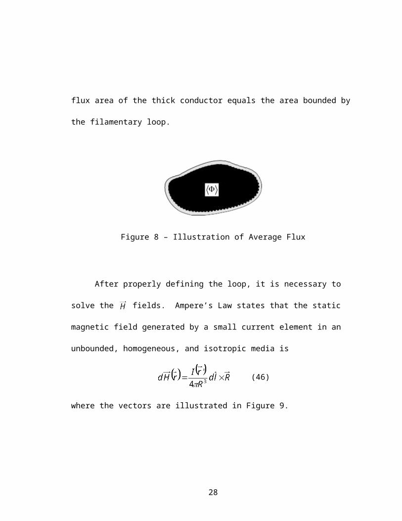
Figure 7 – Area of Conductor Cross-Section
As shown in Figure 8, the average flux can be understood by replacing the thick
conductor loop with a filamentary loop that is located somewhere in between the inner
and outer edges of the thick conductor. The average flux area of the thick conductor
equals the area bounded by the filamentary loop.
Figure 8 – Illustration of Average Flux
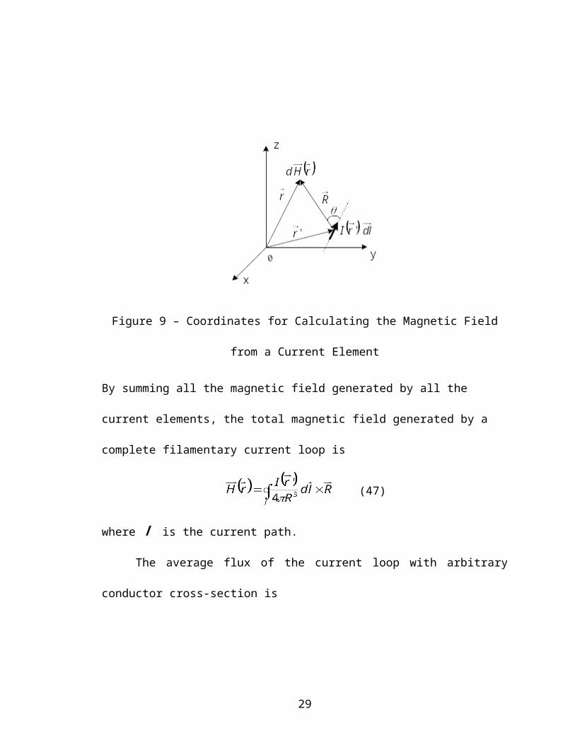
After properly defining the loop, it is necessary to solve the fields. Ampere’s
Law states that the static magnetic field generated by a small current element in an
unbounded, homogeneous, and isotropic media is
20
(46)
where the vectors are illustrated in Figure 9.
Figure 9 – Coordinates for Calculating the Magnetic Field from a Current Element
By summing all the magnetic field generated by all the current elements, the total
magnetic field generated by a complete filamentary current loop is
(47)
where is the current path.
The average flux of the current loop with arbitrary conductor cross-section is
(48)
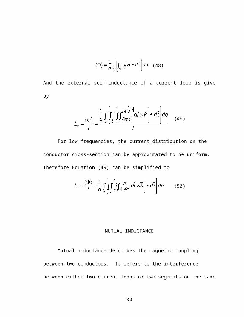
And the external self-inductance of a current loop is give by
21
(49)
For low frequencies, the current distribution on the conductor cross-section can be
approximated to be uniform. Therefore Equation (49) can be simplified to
(50)
MUTUAL INDUCTANCE
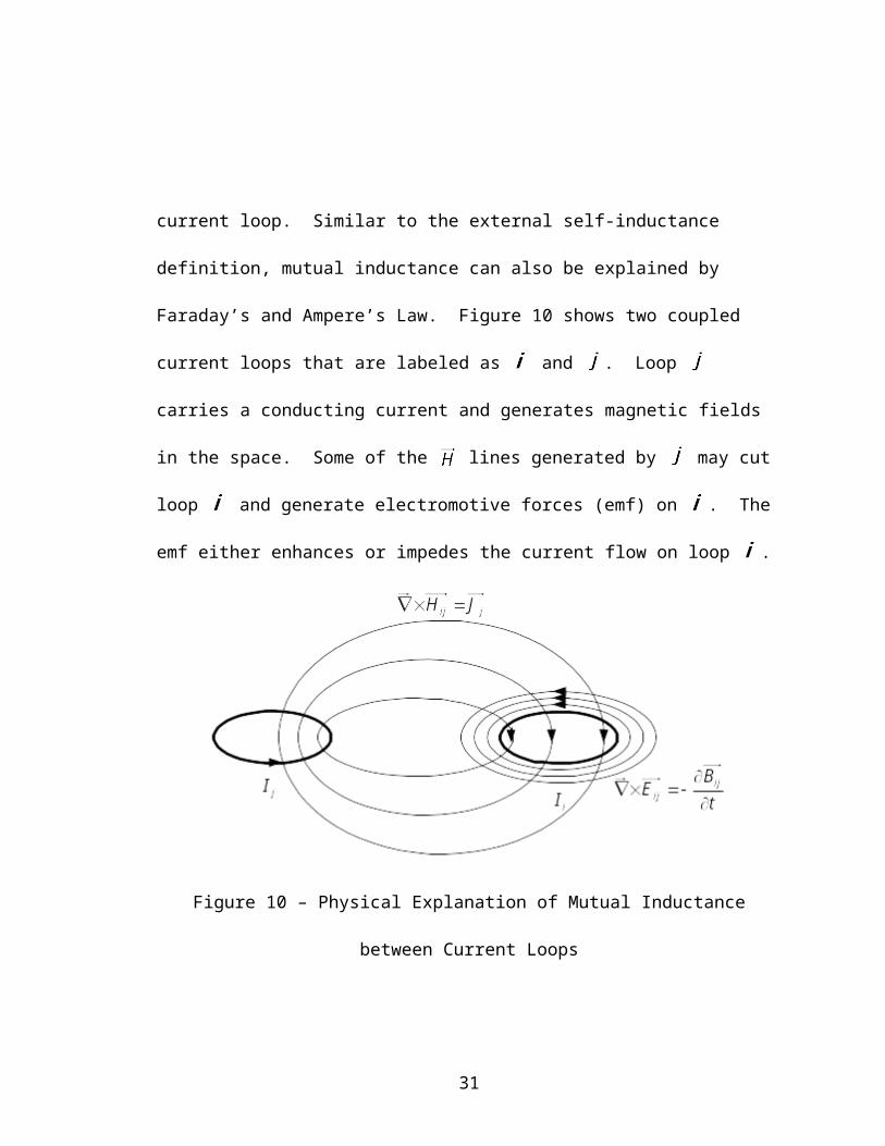
Mutual inductance describes the magnetic coupling between two conductors. It
refers to the interference between either two current loops or two segments on the same
current loop. Similar to the external self-inductance definition, mutual inductance can
also be explained by Faraday’s and Ampere’s Law. Figure 10 shows two coupled current
loops that are labeled as and . Loop carries a conducting current and generates
magnetic fields in the space. Some of the lines generated by may cut loop and
generate electromotive forces (emf) on . The emf either enhances or impedes the current
flow on loop .
22
Figure 10 – Physical Explanation of Mutual Inductance between Current Loops
Mutual inductance defined by the magnetic flux leakage is given by
(51)
The mutual flux between and is
(52)
where is the surface bounded by loop . This expression is derived from two loops. It,
however, does not seem to apply to the mutual inductance between conductor segments
for the difficulty of defining the flux area. To solve this problem, the vector magnetic
potential is used instead of the magnetic flux to calculate the mutual inductance, which
avoids the use of flux area.
The magnetic vector potential is defined as
23
(53)
From Ampere’s Law, the magnetic field generated by a conducting current is
(47)
Combining Equation (53) and (47), vector magnetic potential generated by a current loop
is
(54)
By replacing the current with current density, can be expressed as
(55)
where is the volume of the conductor.
The magnetic flux can be expressed by , applying Stoke’s theorem
(56)
Thus the average mutual flux between two conductor loops is
(57)
or
24
(58)
where and are the cross section area of loop and respectively as illustrated in
Figure 11, and are the infinitesimal segments of loop and respectively, and
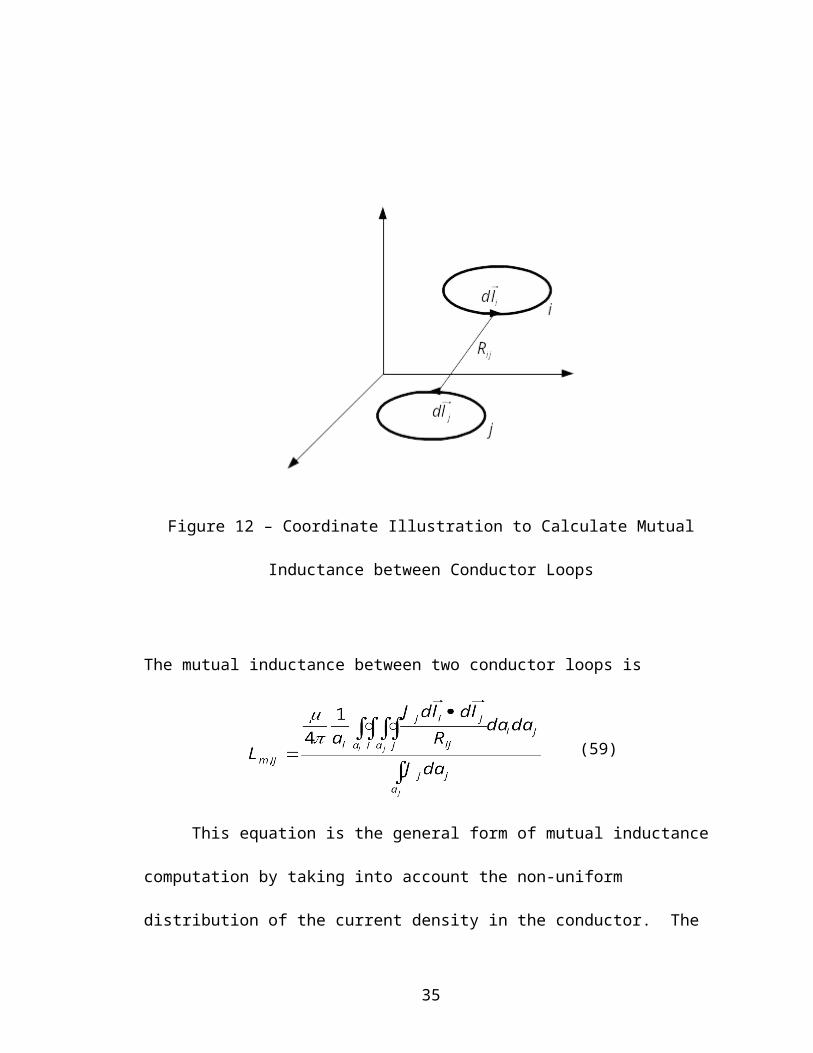
is the distance vector from to as shown in Figure 12.
Figure 11 – Illustration of Conductor Cross-Sections
25
Figure 12 – Coordinate Illustration to Calculate Mutual Inductance between Conductor
Loops
The mutual inductance between two conductor loops is
(59)
This equation is the general form of mutual inductance computation by taking into
account the non-uniform distribution of the current density in the conductor. The dot
product in this equation implies that the mutual inductance between two orthogonal loops
is zero. The mutual inductance is positive when the currents in the two loops flow in the
same direction, and vice versa.
26

Although this equation is derived from conductor loops, it can be easily modified
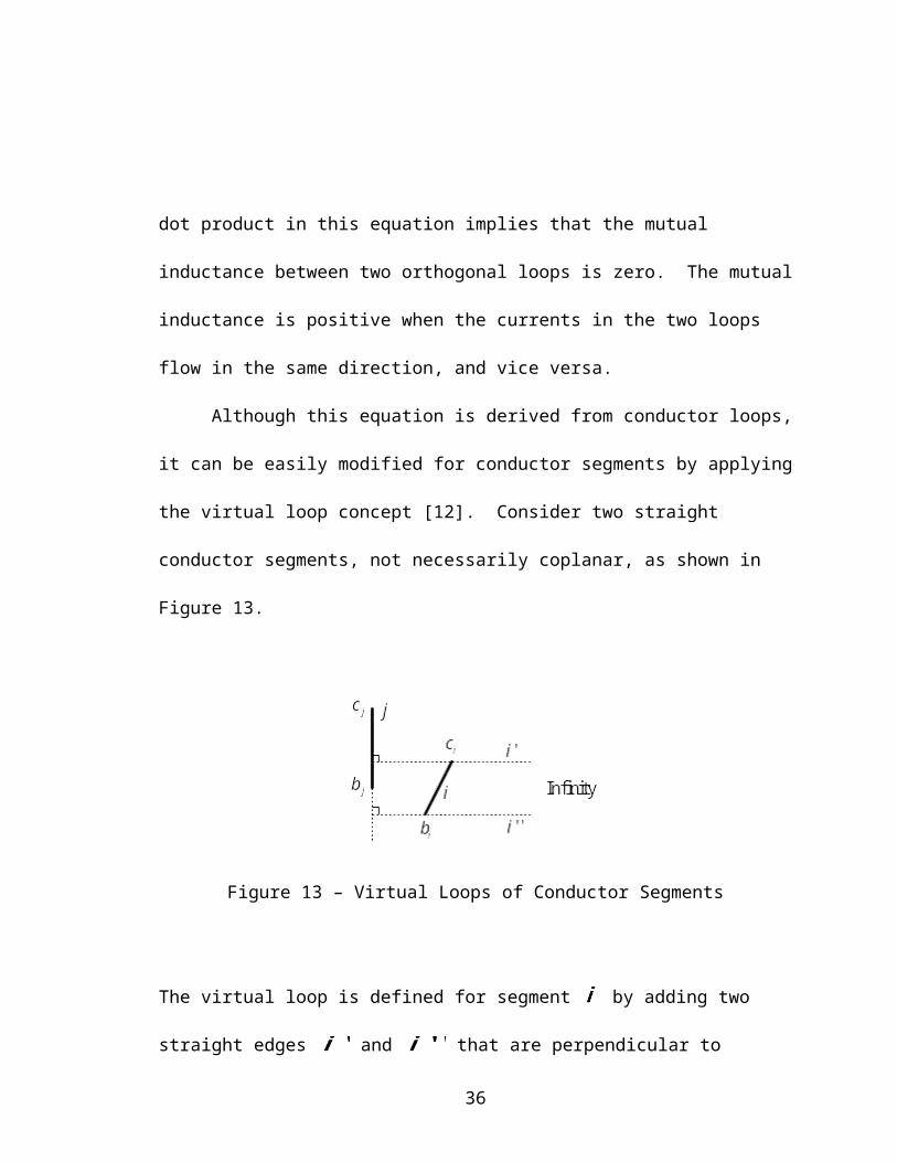
for conductor segments by applying the virtual loop concept [12]. Consider two straight
conductor segments, not necessarily coplanar, as shown in Figure 13.
Figure 13 – Virtual Loops of Conductor Segments
The virtual loop is defined for segment by adding two straight edges and that are
perpendicular to segment and extend to infinity. The virtual loop is closed at infinity.
Thus the mutual inductance between segment and the virtual loop is the summation of
the mutual inductance between segment and the four segments of the virtual loop
(60)
and are both zeros because and are orthogonal to . is also zero
because of the infinite distance from to infinity. Therefore
(61)
In this way, Equation (59) can be modified to calculate the mutual inductance between
two conductor segments
27
where and donate the starting points of segment and respectively, and
represent the ending points on segment and .
THESIS OVERVIEW
In this chapter, the concept of inductance has been explained in detail. Three
inherently consistent definitions of inductance are given in different aspects: magnetic
energy storage, magnetic flux leakage, and voltage-current relationship. The
classification of inductance provides a more insightful understanding of the inductive
mechanism, including internal self-inductance, external self-inductance, and mutual
inductance.
Starting with Maxwell’s Equations, analytical expressions are derived for the
three kinds of inductance, which serve as the guidelines for inductance calculation of
specific cases.
The internal self-inductance is caused by the skin effect, which is calculated by
solving the complex Helmholtz equation. The external self-impedance can be computed
by using the flux leakage definition. The mutual inductance is modeled by introducing
28
the magnetic vector potential to revise the flux definition. It changes the surface integral
of the magnetic field into the loop integral of the magnetic vector potential to calculate
flux. In this way, one can develop the partial mutual inductance idea to compute the
mutual inductance between two conductor segments instead of conductor loops.
In the next chapters, the inductance classification and analytical model are applied
to an on-chip environment to characterize interconnects and integrated inductors. The
analytical model is revised to include the semiconductor substrate losses and the skin
effect. And the computer simulation gives numerical solutions of the analytical model
applied to on-chip interconnects and inductors.
29
CHAPTER II
CHARACTERIZATIONS OF ON-CHIP INTERCONNECTS
As the integrated circuit evolves towards faster operating speed and higher level
of system integration, the on-chip interconnection network becomes more complicated.
On-chip interconnects are carrying signals with higher frequencies and extending into
larger dimensions. There is a growing demand of high-frequency circuit designers to
accurately characterize on-chip interconnects. A distributed equivalent circuit model has
been used to model on-chip interconnects in terms of distributed impedance and
admittance of the interconnect. The line inductance and resistance are closely related to
the signal delay and attenuation. An on-chip interconnect defers from an ideal microstrip
line because of the presence of the lossy semiconductor substrate. High frequency effects
such as the skin effect should also be considered to model the interconnect.
INTERNAL SELF-IMPEDANCE OF ON-CHIP INTERCONNECTS
From the discussion of the internal self-inductance in Chapter I, the internal
impedance of an on-chip interconnect per unit length is given by
30
(31)
where is the current density on the interconnect cross-section, is the current
density at the interconnect surface, and is the interconnect conductivity.
The current distribution on the interconnect cross-section is given by solving the
complex Helmholtz equation
(42)
The shape of the interconnect cross-section can be approximated to be
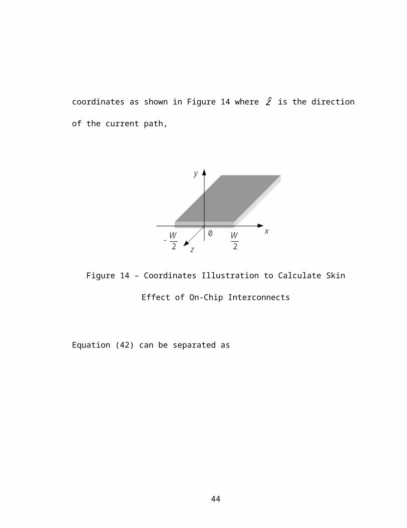
rectangular. Applying the rectangular coordinates as shown in Figure 14 where is the
direction of the current path,
Figure 14 – Coordinates Illustration to Calculate Skin Effect of On-Chip Interconnects
Equation (42) can be separated as
31
(62)
(63)
(64)
For good conductors, the normal electric fields and are negligible compared with
. The propagation form of can be written as
(65)
where gives the current distribution on the conductor cross-section. Substituting
Equation (65) into (64) gives
(66)
This a two dimensional problem.
For on-chip interconnects, the thickness of different metal layers is listed in Appendix II
in terms of various CMOS processes [37]. It is seen that the thickness of the metal
interconnects ranges roughly from 0.5 to 1 .
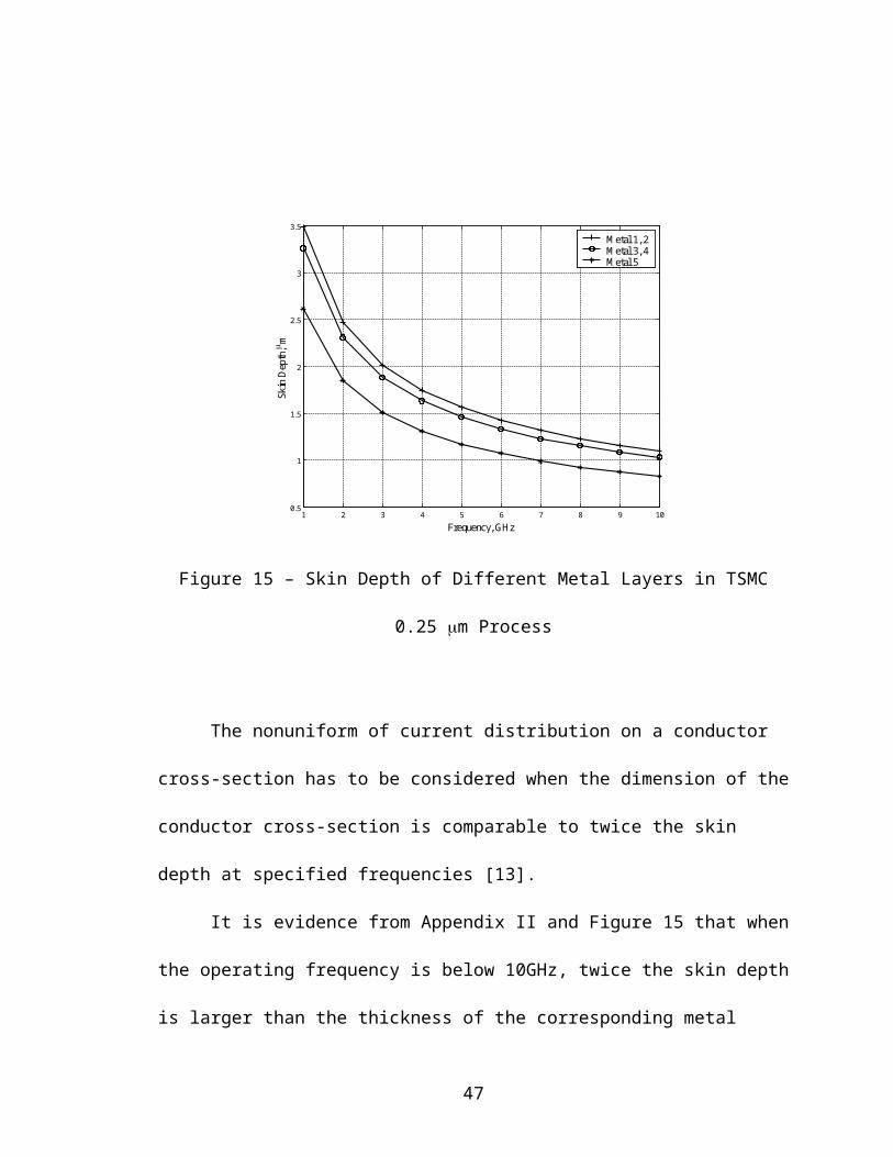
Taking the 0.25 m Aluminum process as an example, the skin depths of different
metal layers versus frequency are compared in Figure 15. It is seen that in the typical
radio-frequency range from 1GHz to 10GHz, the skin depth varies around several
microns. Since higher metal layers have better conductivity, they have smaller skin depth
than lower layers.
32
1 2 3 4 5 6 7 8 9 100.5
1
1.5
2
2.5
3
3.5
Frequency, GHz
Skin
Dep
th,
m
Metal 1, 2Metal 3, 4Metal 5
Figure 15 – Skin Depth of Different Metal Layers in TSMC 0.25 m Process
The nonuniform of current distribution on a conductor cross-section has to be
considered when the dimension of the conductor cross-section is comparable to twice the
skin depth at specified frequencies [13].
It is evidence from Appendix II and Figure 15 that when the operating frequency
is below 10GHz, twice the skin depth is larger than the thickness of the corresponding
metal layers. Thus the skin effect can be neglected on the thickness dimension of on-chip
interconnects by assuming there is no current density variation. And the skin effect is
only considered on the width dimension. This leads to the one dimensional
approximation of Equation (66), which for on-chip interconnects can be written as
33

(67)
where
The homogeneous solution of Equation (67) can be written as
(68)
By choosing the coordinates to have the origin located at the center of the conductor as
illustrated in Figure 14, becomes an even function in terms of
(69)
where is a constant.
If the current density at the interconnect edge is assumed to be unity, the
normalized current density is given by
(70)
where is the width of the interconnect.
Since is a complex number, both the electric field and the current density inside
the interconnect are also complex. This means the current flow on the interconnect cross-
section will have a spatial dependent phase. As an example, the current density on the
cross-section of a 4 m wide interconnect is plotted in Figure 16. The interconnect is on
the Metal 5 layer in a 0.25 m CMOS process.
34
-2 -1.5 -1 -0.5 0 0.5 1 1.5 2-0.2
0
0.2
0.4
0.6
0.8
1
1.2
x, m
Re(
J z/Jz0
)
f=1GHzf=5GHzf=10GHz
(a) Real Part of the Current Density
-2 -1.5 -1 -0.5 0 0.5 1 1.5 2-0.1
0
0.1
0.2
0.3
0.4
0.5
0.6
x, m
Im(J
z/Jz0
)
f=1GHzf=5GHzf=10GHz
(b) Imaginary Part of the Current Density
35
-2 -1.5 -1 -0.5 0 0.5 1 1.5 2
0.2
0.4
0.6
0.8
1
1.2
x, m
|J z/Jz0
|
f=1GHzf=5GHzf=10GHz
(c) Magnitude of the Current Density
Figure 16 – Current Density on the Interconnect Cross-Section at Different Frequencies
It is evidence from Figure 16 that the skin effect becomes more significant at
increased frequencies. At 1GHz, the magnitude of the current density in the middle of
the interconnect is about 90% of that at the edge. However, when the frequency goes up
to 10GHz, nearly all the current crowds to the edge of the interconnect.
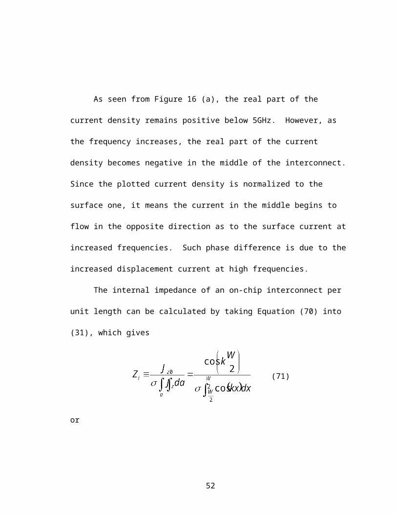
As seen from Figure 16 (a), the real part of the current density remains positive
below 5GHz. However, as the frequency increases, the real part of the current density
becomes negative in the middle of the interconnect. Since the plotted current density is
normalized to the surface one, it means the current in the middle begins to flow in the
36
opposite direction as to the surface current at increased frequencies. Such phase
difference is due to the increased displacement current at high frequencies.
The internal impedance of an on-chip interconnect per unit length can be
calculated by taking Equation (70) into (31), which gives
(71)
or
(72)
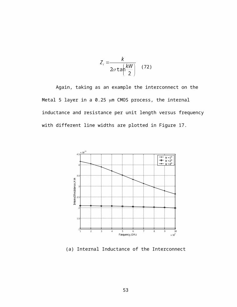
Again, taking as an example the interconnect on the Metal 5 layer in a 0.25 m
CMOS process, the internal inductance and resistance per unit length versus frequency
with different line widths are plotted in Figure 17.
37
1 2 3 4 5 6 7 8 9 10
x 109
1
1.5
2
2.5
3
3.5
4
4.5x 10
-13
Frequency, GHz
Inte
rnal
Res
ista
nce,
H/m
W=1
W=2
W=4
(a) Internal Inductance of the Interconnect
1 2 3 4 5 6 7 8 9 10
x 109
0.005
0.01
0.015
0.02
0.025
0.03
Frequency, GHz
Inte
rnal
Res
ista
nce,
/m
W=1
W=2
W=4
(b) Internal Resistance of the Interconnect
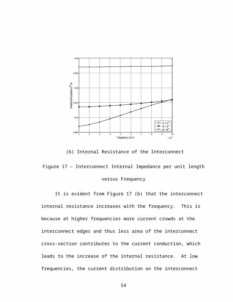
Figure 17 – Interconnect Internal Impedance per unit length versus Frequency
38
It is evident from Figure 17 (b) that the interconnect internal resistance increases
with the frequency. This is because at higher frequencies more current crowds at the
interconnect edges and thus less area of the interconnect cross-section contributes to the
current conduction, which leads to the increase of the internal resistance. At low
frequencies, the current distribution on the interconnect cross-section is close to uniform
and thus wider interconnects have smaller internal resistance. However, at high
frequencies, the current distribution is dominated by the skin effects and the interconnect
width tends to have less effects on the internal resistance.
It is seen from Figure 17 (a) that the interconnect internal inductance decreases
with the frequency. This is mainly because at higher frequencies, the total current carried
by the interconnect decreases for an increased internal resistance. This results in less
magnetic energy stored inside the interconnect and thus less internal inductance.
Wider interconnects have more internal inductance and less internal resistance
than narrower interconnects. This is because wider interconnects have bigger area of
cross-section and thus more internal volume to store magnetic energy and conduct
current. However, at higher frequencies, the interconnect width shows less effects on the
internal impedance. This is mainly due to the skin effect that at high frequencies all
current flow on the interconnect edges and the width do not really matter.
The internal impedance of interconnects with less width shows less frequency-
dependence in that the skin effect is less important than in the wider interconnects.
39
ON-CHIP MICROSTRIP SYSTEM
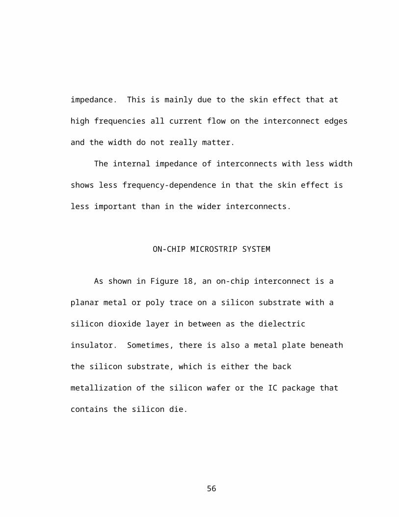
As shown in Figure 18, an on-chip interconnect is a planar metal or poly trace on
a silicon substrate with a silicon dioxide layer in between as the dielectric insulator.
Sometimes, there is also a metal plate beneath the silicon substrate, which is either the
back metallization of the silicon wafer or the IC package that contains the silicon die.
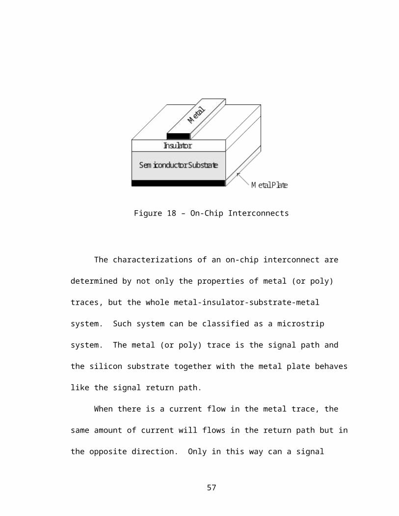
Figure 18 – On-Chip Interconnects
The characterizations of an on-chip interconnect are determined by not only the
properties of metal (or poly) traces, but the whole metal-insulator-substrate-metal system.
Such system can be classified as a microstrip system. The metal (or poly) trace is the
signal path and the silicon substrate together with the metal plate behaves like the signal
return path.
When there is a current flow in the metal trace, the same amount of current will
flows in the return path but in the opposite direction. Only in this way can a signal
40

transmit (or propagate). If the silicon substrate is a perfect dielectric without a
conductive plane beneath it, there will be no return path for the current and the signal will
not transmit or propagate along the metal trace.
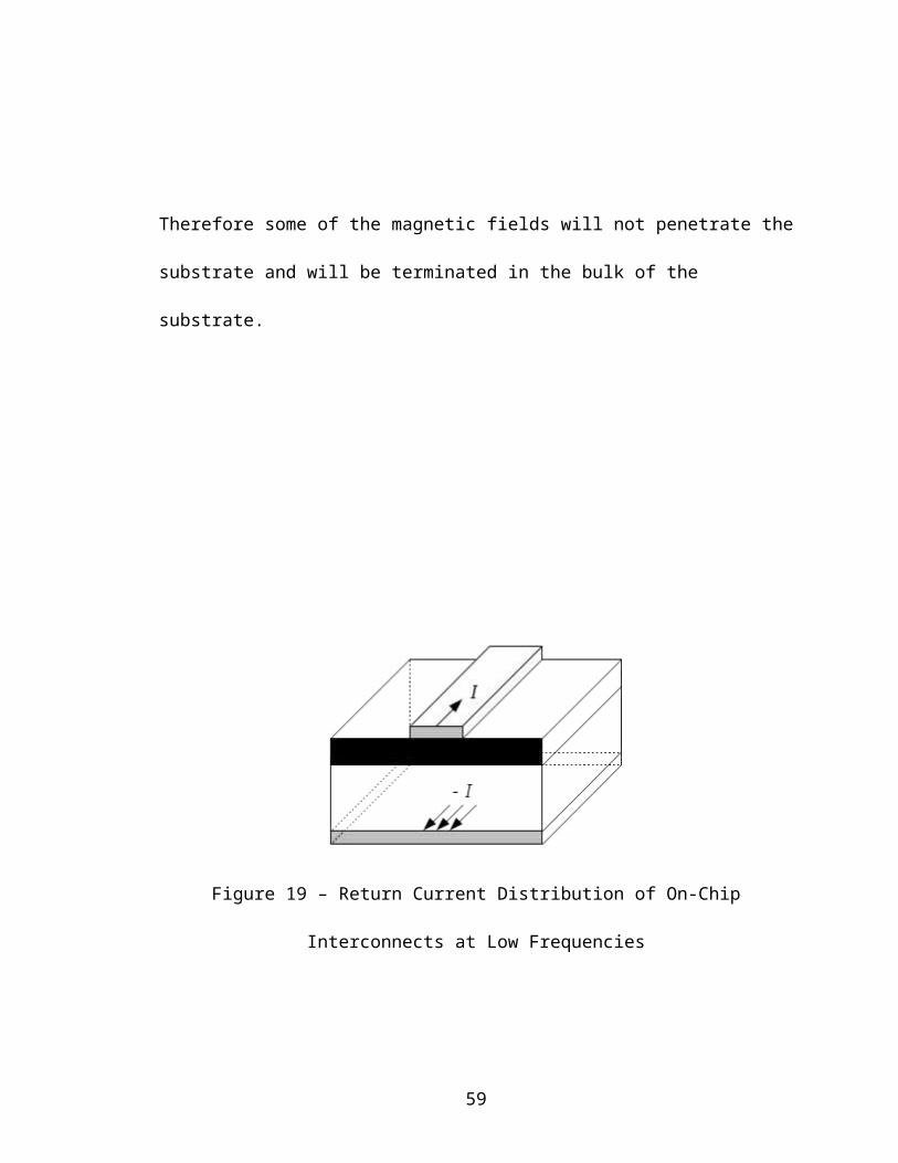
The distribution of the return current is strongly dependent on the frequency. At
low frequencies as shown in Figure 19, the skin depth of the substrate is much larger than
the substrate thickness. The magnetic field generated by the signal current will penetrate
both the insulator and the substrate. It will be terminated at the surface of the metal plate.
By assuming that the metal plate has perfect conductivity, there is no magnetic field
inside the metal plate. The return current mainly flows on the surface of the metal plate
given by
(73)
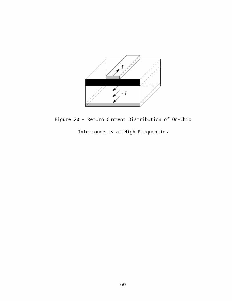
At high frequencies as shown in Figure 20, the magnetic field generated by the
signal induces eddy current in the substrate, which shields the magnetic field penetration.
Therefore some of the magnetic fields will not penetrate the substrate and will be
terminated in the bulk of the substrate.
41
Figure 19 – Return Current Distribution of On-Chip Interconnects at Low Frequencies
Figure 20 – Return Current Distribution of On-Chip Interconnects at High Frequencies
42
The depth at which the magnetic field can penetrate the substrate depends on the
substrate properties and the frequency, which is given by the skin depth
(43)
It is seen from Equation (43) that the higher frequency and the higher substrate
conductivity, the less the skin depth. This implies that more magnetic fields will be
terminated in the substrate and therefore more return current flows in the substrate. If the
frequency and the substrate conductivity are so high that the skin depth of the substrate is
smaller than the substrate thickness, the majority of the return current will flow in the
substrate instead of the metal plate. In this condition, the signal propagation on the
interconnect will not be in quasi-TEM model any more, but in a so-called slow mode
[14].
EXTERNAL SELF-IMPEDANCE OF ON-CHIP INTERCONNECTS
For an ideal microstrip system with perfect dielectrics and ground planes, the line
will be lossless. However, for an on-chip interconnect with a semi-conductive
semiconductor substrate, there will be both external self-inductance and self-resistance.
The external self-inductance arises from the magnetic flux leakage from microstrip line.
The external self-resistance is a result of the low conductivity of the substrate.
43
In order to calculate the external self-impedance of an on-chip chip interconnect,
one needs to solve the field pattern associated with the system, which requires the
solution of the current distribution. However, the distribution of the return current in the
substrate and the metal plate is complicated that requires solving Maxwell’s Equations.
A more time-efficient way of solving the problem is the magnetic image approach.
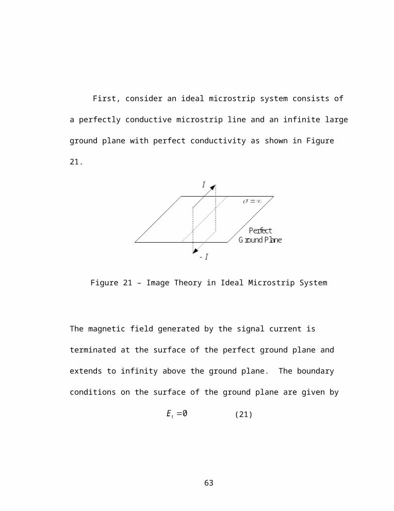
First, consider an ideal microstrip system consists of a perfectly conductive
microstrip line and an infinite large ground plane with perfect conductivity as shown in
Figure 21.
Figure 21 – Image Theory in Ideal Microstrip System
The magnetic field generated by the signal current is terminated at the surface of the
perfect ground plane and extends to infinity above the ground plane. The boundary
conditions on the surface of the ground plane are given by
(21)
44
(74)
(22)
(75)
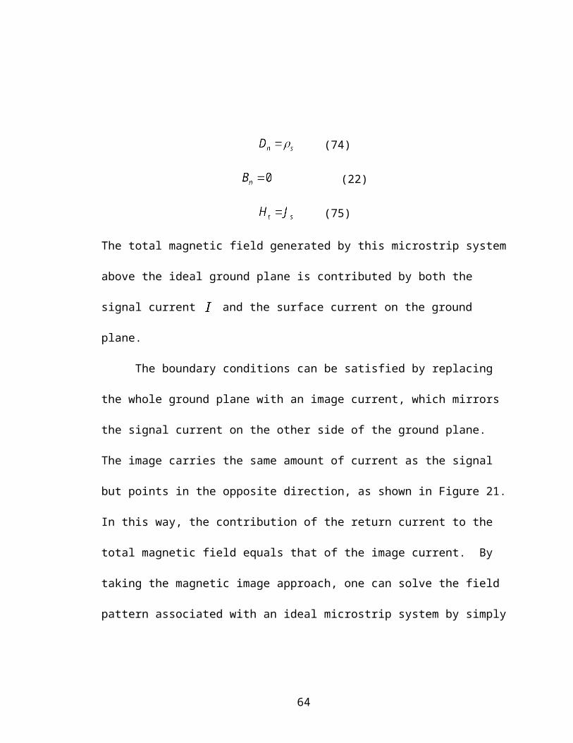
The total magnetic field generated by this microstrip system above the ideal ground plane
is contributed by both the signal current and the surface current on the ground plane.
The boundary conditions can be satisfied by replacing the whole ground plane
with an image current, which mirrors the signal current on the other side of the ground
plane. The image carries the same amount of current as the signal but points in the
opposite direction, as shown in Figure 21. In this way, the contribution of the return
current to the total magnetic field equals that of the image current. By taking the
magnetic image approach, one can solve the field pattern associated with an ideal
microstrip system by simply summing the magnetic fields generated by the signal current
and its image.
There are closed-form expressions available to calculate the external self-
inductance of an ideal microstrip system [1]. For an ideal microstrip line as shown in
Figure 22, its external self-inductance is given by [17]
45
Figure 22 – Ideal Microstrip Line
(76)
where is the width of the microstrip line and is the vertical distance between the
microstrip line and the ground plane.
However, Equations (76) cannot accurately model an on-chip interconnect mainly
because of the lossy semiconductor substrate. In order to account for the lossy
semiconductor substrate, the complex image method [16] is used.
The complex image method is similar to the magnetic image approach for the
ideal microstrip system. The difference is that for the complex image method, the
vertical distance between the signal current and its image is complex. This is due to the
lossy nature of the substrate.
The discussion of the complex image method can be divided into two conditions
[15]:
46
1. The skin depth of the substrate is much smaller than the substrate thickness and
the signal propagates in the skin mode;
2. The skin depth of the substrate is larger than the substrate thickness and the signal
propagates in the quasi-TEM mode.
First, when the skin depth of the substrate is much smaller than the substrate
thickness, the majority of the return current flows near the surface of the substrate instead
of the metal plate. As illustrated in Figure 23, all the return current in the substrate can
be replace by an image current.
Figure 23 – Illustration of Complex Image Method when the Skin Depth of the Substrate
is Much Smaller than the Substrate Thickness
The vertical distance between the signal current and its image is given by solving the
Green’s Function [15]
47
(77)
where is the oxide thickness and is the skin depth of the lossy substrate
rewritten as
(43)
Here is the substrate permeability and is the substrate conductivity. The magnetic
permeability of silicon is very close to that of free space, which equals H/m.
The conductivity of the silicon substrate is directly related to the doping level [5].
It is worth clarifying that a complex distance does not have a physical
representation, rather a computational convenience [16].
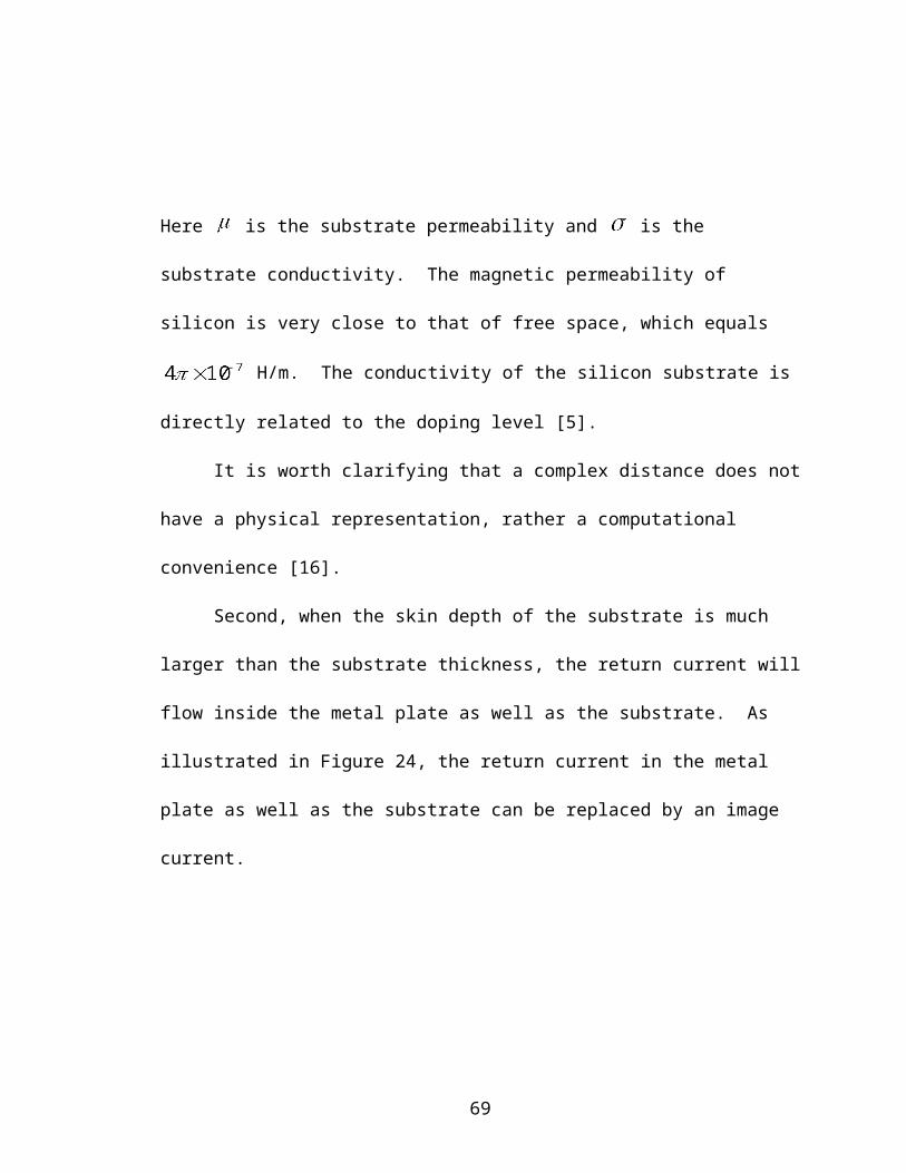
Second, when the skin depth of the substrate is much larger than the substrate
thickness, the return current will flow inside the metal plate as well as the substrate. As
illustrated in Figure 24, the return current in the metal plate as well as the substrate can be
replaced by an image current.
48
Figure 24 – Illustration of Complex Image Method when the Skin Depth of the Substrate
is Much Smaller than the Substrate Thickness
The vertical distance between the signal current and its image is given by [15]
(78)
where is the oxide thickness, the thickness of the substrate, and is the skin
depth of the lossy substrate.
By taking the complex image approach, the external self-impedance of an on-chip
interconnect as shown in Figure 18 equals the external inductance of an ideal microstrip
line as shown in Figure 22, where the vertical distance between the microstrip line and
the ideal ground plane is given by
49
(79)
There are two expressions for as given by Equation (77) and (78), depending on the
relationship between the substrate thickness and the substrate skin depth.
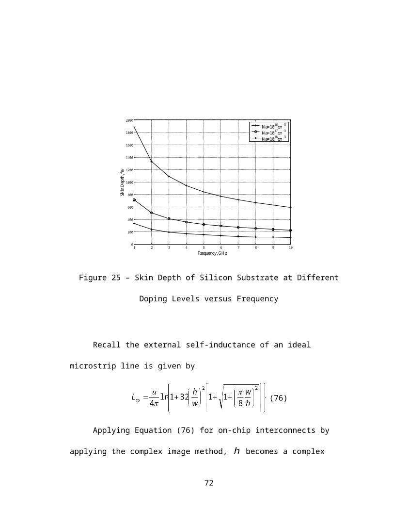
The skin depth of a silicon substrate with different doping level is plotted in
Figure 25.
1 2 3 4 5 6 7 8 9 100
200
400
600
800
1000
1200
1400
1600
1800
2000
Frequency, GHz
Skin
Dep
th,
m
Na=1016cm-3
Na=1017cm-3
Na=1018cm-3
Figure 25 – Skin Depth of Silicon Substrate at Different Doping Levels versus Frequency
Recall the external self-inductance of an ideal microstrip line is given by
(76)
50
Applying Equation (76) for on-chip interconnects by applying the complex image
method, becomes a complex number that gives a complex inductance. By examining
the flux definition of the external self-inductance, a complex inductance can by explained
by a complex flux given by [15]
(80)
where the term appears as the complex inductance.
What physically gives rise to the external self-resistance? The answer is the lossy
substrate. Since the silicon substrate serves as part of the current return path with a poor
conductivity (about ten thousand times smaller than the conductivity of metal), the return
current in the substrate suffers from resistive losses and therefore limits the signal
current.
Figure 26 plots the self inductance and resistance of an on-chip interconnect on
the Metal 5 layer in a 0.25 m CMOS process.
51
1 2 3 4 5 6 7 8 9 1010
10.5
11
11.5
12
12.5
13
Frequency, GHz
Exte
rnal
Sel
f-In
duct
ance
, nH
/cm
Na=1015cm-3
Na=1016cm-3
Na=1017cm-3
(a) External Self-Inductance of an On-Chip Interconnect
1 2 3 4 5 6 7 8 9 100
10
20
30
40
50
60
70
80
90
100
Frequency, GHz
Exte
rnal
Sel
f-R
esis
tanc
e,
/cm
Na=1015cm-3
Na=1016cm-3
Na=1017cm-3
(b) External Self-Resistance of an On-Chip Interconnect
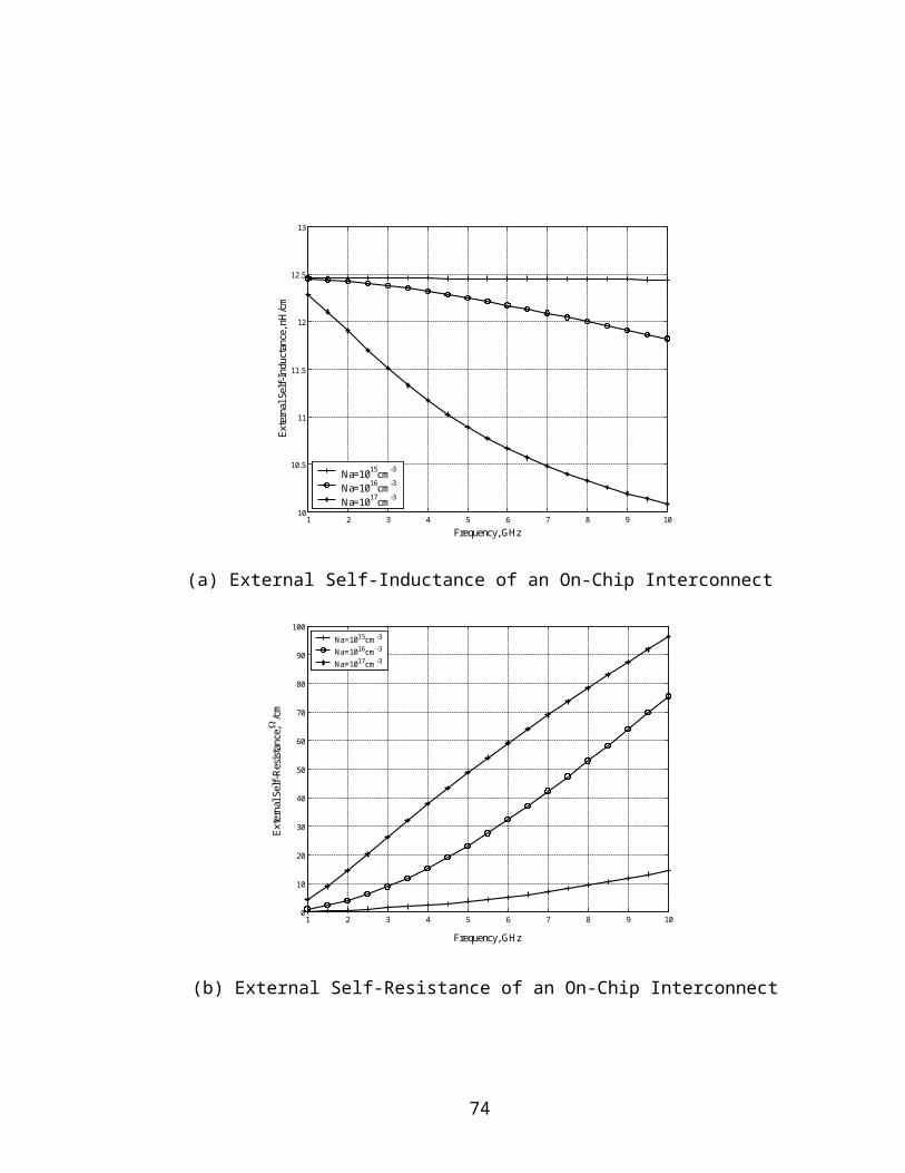
Figure 26 – External Self-Impedance of an On-Chip Interconnect [Equation (76)]
52
The thickness of silicon substrate is 250 m [36]. The oxide thickness between the metal
strip and the substrate is about 4 m. The width of the interconnect is taken to be 4 m.
The result agrees with the full-wave solution given by ADS Momentum [15].
It is seen from Figure 26 that the substrate conductivity will greatly affect the
external self-impedance of on-chip interconnects. Figure 26 (a) shows that external self-
inductance decreases with increased substrate conductivity. This is because a higher
conductive substrate has a smaller skin depth. Therefore fewer magnetic fields can
penetrate the substrate and more return current is induced inside the substrate. This
implies more return current will flow in the substrate instead of the metal ground plane.
The external self-inductance is proportional to the flux area bounded by the signal current
and the return current. The largest flux area and external self-inductance is achieved if all
return current flows in the metal ground plane as shown in Figure 19. However, if more
return current flows in the substrate as shown in Figure 20, the average vertical distance
between the signal current and the total return current becomes smaller and thus the
average flux becomes smaller. This is why higher substrate conductivity results in
smaller external self-inductance. This also explains that when the substrate conductivity
is very low, the external self-inductance shows little frequency dependence because the
metal ground plane is the main return path. However, when the substrate conductivity
becomes higher, the external self-inductance shows more frequency dependence.
53
Similar analysis can be applied to external self-resistance, which increases with
increased substrate conductivity. The smallest external self-resistance is achieved when
the substrate has the lowest conductivity. And the whole system approaches an ideal
microstrip system.
MUTUAL IMPEDANCE BETWEEN ON-CHIP INTERCONNECTS
Between two coupled on-chip interconnects, there exist mutual inductance. The
typical layout of on-chip interconnects are either vertical or horizontal. If the two
interconnects are perpendicular to each other, they are not inductive coupled and the
mutual inductance is zero. If they are parallel to each other, the mutual inductance is
maximized.
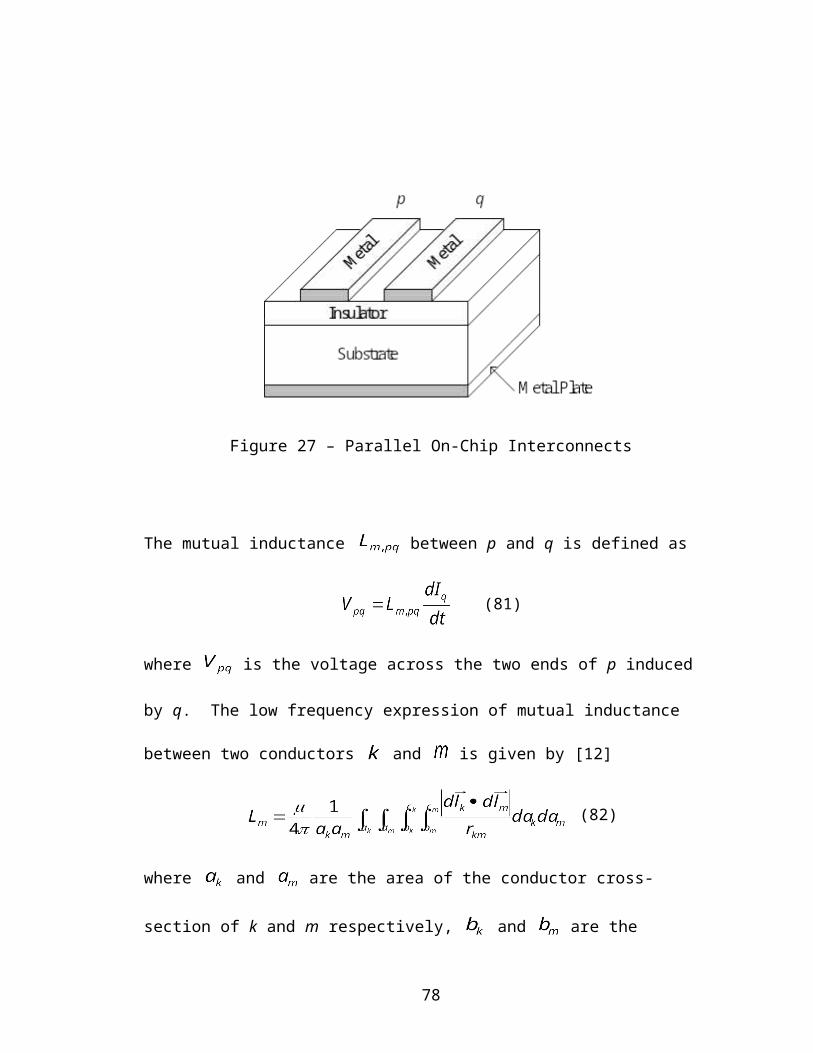
Consider two parallel interconnects and as shown in Figure 27.
54
Figure 27 – Parallel On-Chip Interconnects
The mutual inductance between p and q is defined as
(81)
where is the voltage across the two ends of p induced by q. The low frequency
expression of mutual inductance between two conductors and is given by [12]
(82)
where and are the area of the conductor cross-section of k and m respectively,
and are the starting points, and are the end points, and and are
infinitesimal conductor segments. To account for high frequency effects and the lossy
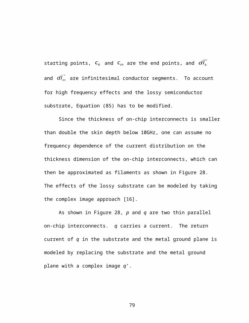
semiconductor substrate, Equation (85) has to be modified.
55
Since the thickness of on-chip interconnects is smaller than double the skin depth
below 10GHz, one can assume no frequency dependence of the current distribution on
the thickness dimension of the on-chip interconnects, which can then be approximated as
filaments as shown in Figure 28. The effects of the lossy substrate can be modeled by
taking the complex image approach [16].
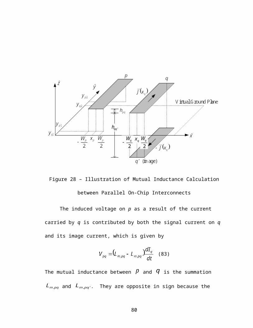
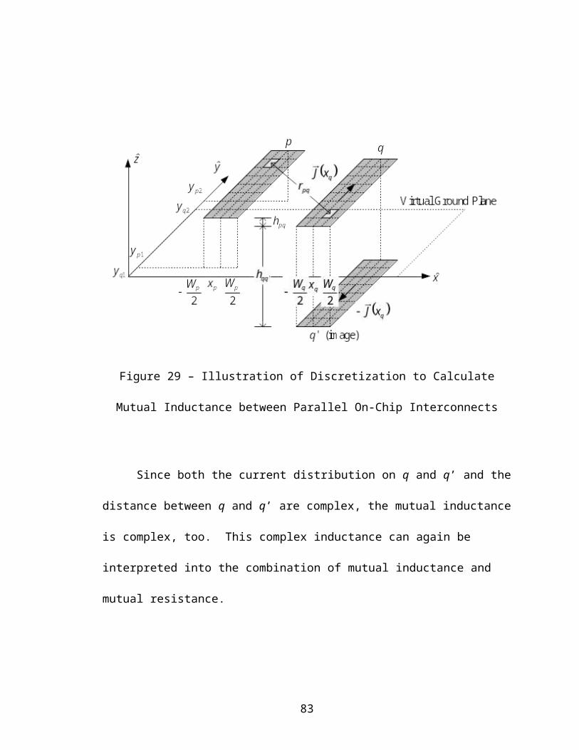
As shown in Figure 28, p and q are two thin parallel on-chip interconnects. q
carries a current. The return current of q in the substrate and the metal ground plane is
modeled by replacing the substrate and the metal ground plane with a complex image q’.
Figure 28 – Illustration of Mutual Inductance Calculation between Parallel On-Chip
Interconnects
56
The induced voltage on p as a result of the current carried by q is contributed by
both the signal current on q and its image current, which is given by
(83)
The mutual inductance between and is the summation and . They are
opposite in sign because the image current flows in the opposite direction of the signal
current. By expanding Equation (85), is given by
(84)
where and are the width of p and q respectively and is given by the complex
image method. Similarly, is expressed as
(85)
The total mutual inductance between the two parallel on-chip interconnects p and
q is given by
(86)
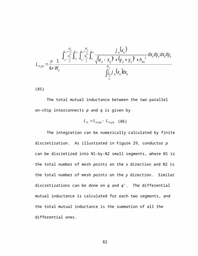
The integration can be numerically calculated by finite discretization. As
illustrated in Figure 29, conductor p can be discretized into N1-by-N2 small segments,
57
where N1 is the total number of mesh points on the x direction and N2 is the total number
of mesh points on the y direction. Similar discretizations can be done on q and q’. The
differential mutual inductance is calculated for each two segments, and the total mutual
inductance is the summation of all the differential ones.
Figure 29 – Illustration of Discretization to Calculate Mutual Inductance between Parallel
On-Chip Interconnects
Since both the current distribution on q and q’ and the distance between q and q’
are complex, the mutual inductance is complex, too. This complex inductance can again
be interpreted into the combination of mutual inductance and mutual resistance.
58
(87)
The mutual inductance represents the magnetic coupling of the two interconnects
through the magnetic field. The mutual resistance can be explained by the resistive
coupling between the two interconnect through the substrate. The substrate provides a
resistive path between the return current of both p and q.
The simulation results have been compared with published results and agree well
with the full-wave solution given by ADS Momentum [15].
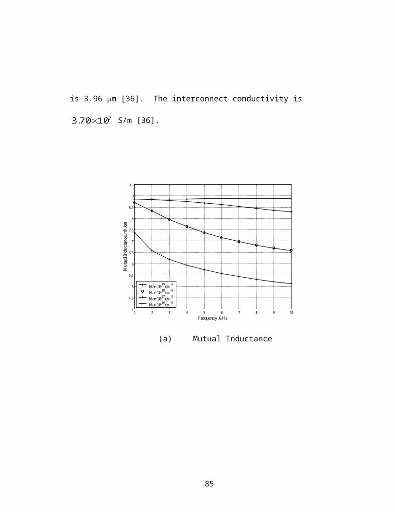
Here, the mutual impedance between two parallel interconnects in a 0.25 m
CMOS process is studied.
Figure 30 plots the mutual impedance at different substrate doping levels versus
the frequency. The two interconnects are both on Metal 5 layer and 4 m wide. The
edge-to-edge spacing between them is taken to be 2um. The thickness of the substrate is
250 m and the oxide thickness is 3.96 m [36]. The interconnect conductivity is
S/m [36].
59
1 2 3 4 5 6 7 8 9 104
4.5
5
5.5
6
6.5
7
7.5
8
8.5
9
9.5
Frequency, GHz
Mut
ual I
nduc
tanc
e, n
H/c
m
Na=1019cm-3
Na=1018cm-3
Na=1017cm-3
Na=1016cm-3
(a) Mutual Inductance
1 2 3 4 5 6 7 8 9 100
10
20
30
40
50
60
70
80
90
100
Frequency, GHz
Mut
ual R
esis
tanc
e,
/cm
Na=1019cm-3
Na=1018cm-3
Na=1017cm-3
Na=1016cm-3
(b) Mutual Resistance
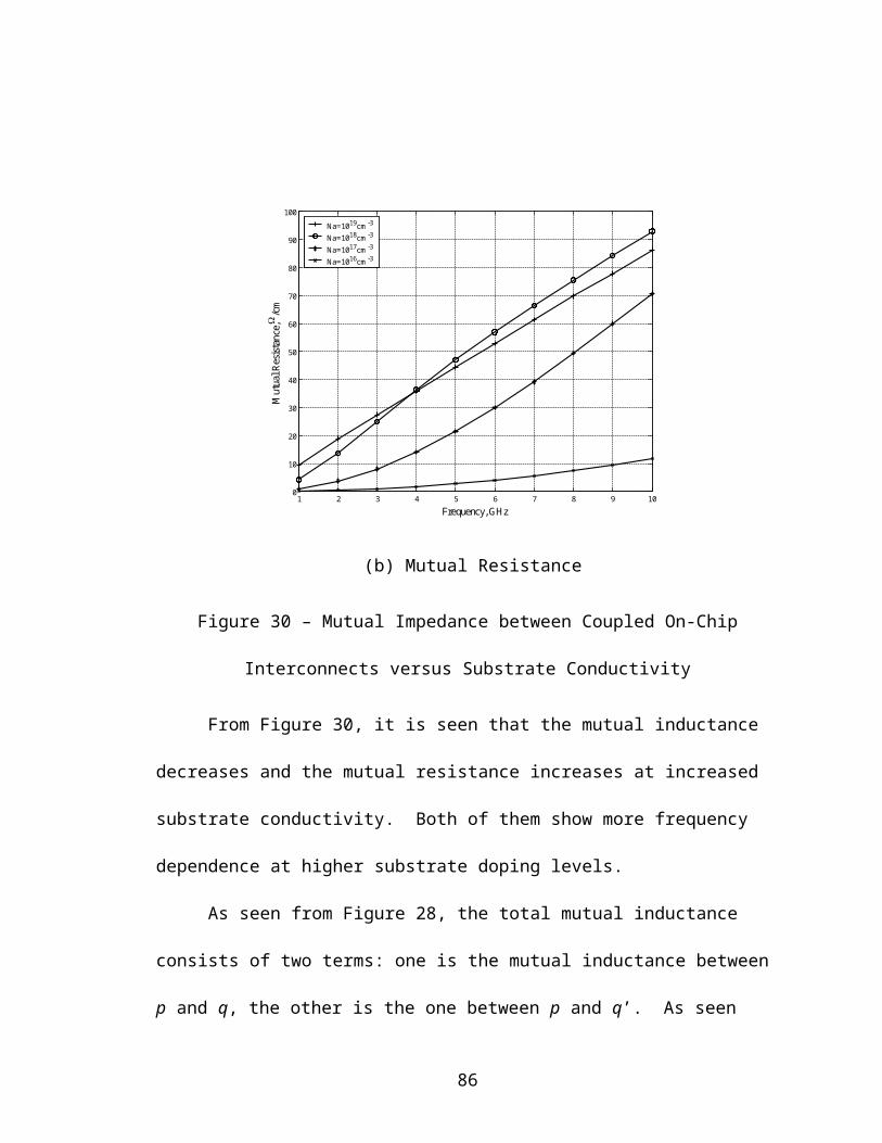
Figure 30 – Mutual Impedance between Coupled On-Chip Interconnects versus Substrate
Conductivity
60
From Figure 30, it is seen that the mutual inductance decreases and the mutual
resistance increases at increased substrate conductivity. Both of them show more
frequency dependence at higher substrate doping levels.
As seen from Figure 28, the total mutual inductance consists of two terms: one is
the mutual inductance between p and q, the other is the one between p and q’. As seen
from Equation (85), mutual inductance is reverse proportional to the spacing between the
two interconnects. Since the spacing between p and q is much smaller than that between
p and q’, dominates the total mutual inductance. Since the current on q and q’ are
in the opposite direction, will subtract to get the total mutual inductance as
shown in Equation (89). Therefore, if the spacing between p and q is constant, the further
q’ is away from p, the smaller and the larger the total mutual inductance. When
the substrate conductivity is very low, the majority of the return current of the
interconnect flows in the metal ground plane. The distance between the signal current
and the return current is close to twice the substrate thickness. The total mutual
inductance is maximized. However, at increased substrate conductivity, more return
current flows in the substrate instead of the metal ground plane, which leads to reduced
vertical distance between q and q’. This implies a larger and a smaller total
mutual inductance.
Similar analysis can be applied for the mutual resistance. If the substrate
conductivity is low, the return current of q will be mainly the surface current on the metal
ground plane. Since the vertical distance between the metal ground plane and p is
61
relatively large, the return current will induce little current on p. Therefore the mutual
resistive coupling is small. However, if the substrate conductivity is high, more return
current will flow near the substrate surface. Since they are very close to p with a thin
insulator in between, they will induce significant amount of current on p and the mutual
resistive coupling is strong.
62
CHAPTER III
CHARACTERIZATIONS OF ON-CHIP INDUCTORS
With the appearance of 0.25 m, 0.18 m, and recent 0.13 m CMOS
technologies, a complete radio-frequency system operating in the gigahertz range can be
integrated on silicon with a conventional CMOS process including both active and
passive components, such as a wireless transceiver. In monolithic radio-frequency
analog integrated circuits, the on-chip inductor plays an important role. It is widely used
in low noise amplifiers, mixers, and voltage-controlled oscillators. Integrating inductors
on chip greatly increases the system integrity and reduces the packaging parasitic effects.
However, because of its large occupation of chip area and significant magnetic energy
leakage, on-chip inductors also affect the performance of high-frequency integrated
circuits through electromagnetic coupling. Therefore, it is of great importance to
accurately characterize on-chip inductors.
INDUCTANCE OF RECTANGULAR ON-CHIP INDUCTORS
Conventional on-chip inductor design follows the pattern of metal spirals. The
metal is typically chosen to be on the top metal layer in order to reduce the parasitic
capacitance between the metal and the silicon substrate. As an example, Figure 31 shows
63
a rectangular on-chip inductor. Aside from the rectangular shape, circular and octagonal
spirals are also commonly used.
Figure 31 – On-Chip Rectangular Spiral Inductor
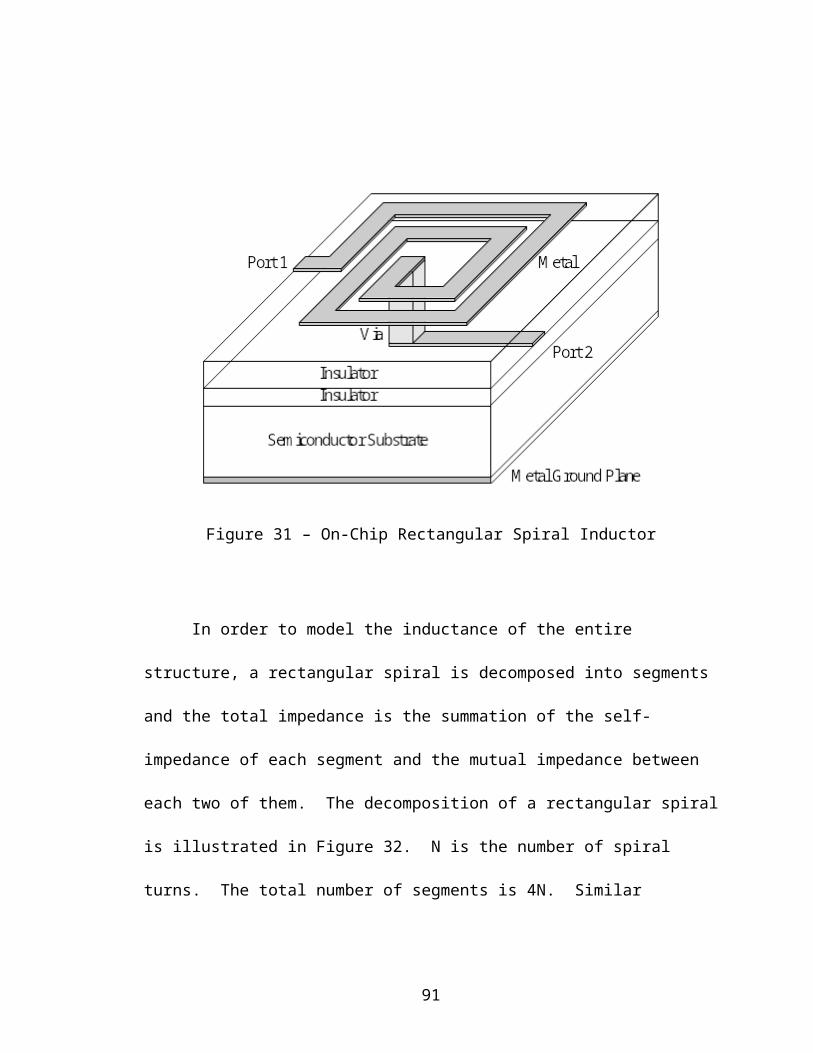
In order to model the inductance of the entire structure, a rectangular spiral is
decomposed into segments and the total impedance is the summation of the self-
impedance of each segment and the mutual impedance between each two of them. The
decomposition of a rectangular spiral is illustrated in Figure 32. N is the number of spiral
turns. The total number of segments is 4N. Similar decomposition can also be applied to
octagonal and circular spirals.
64
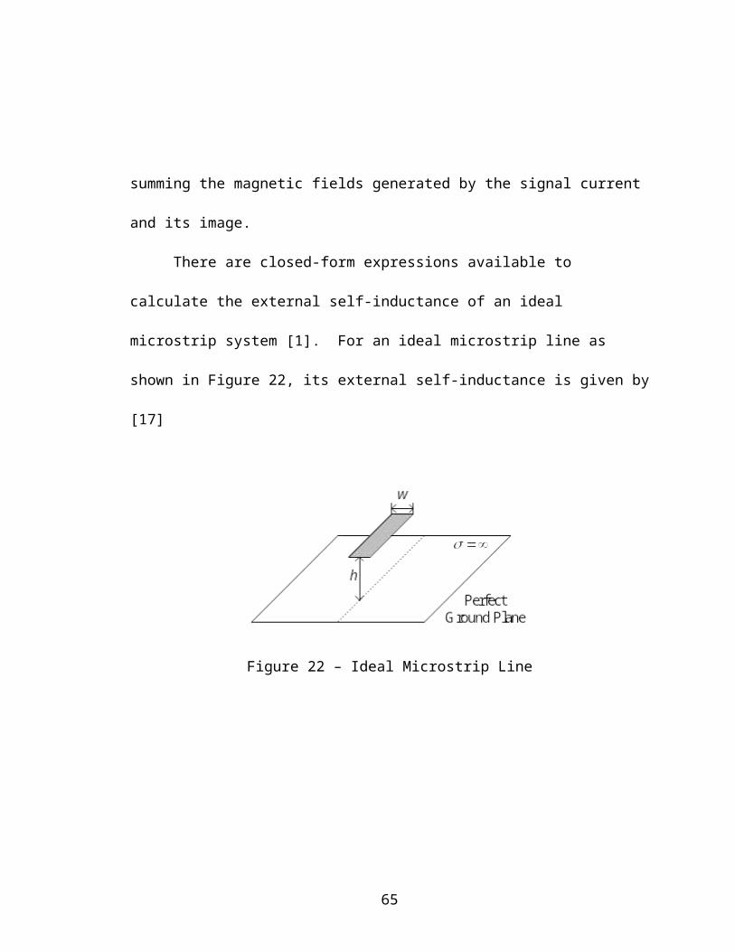
Figure 32 – Illustration of the Decomposition of an N-Turn Rectangular Spiral
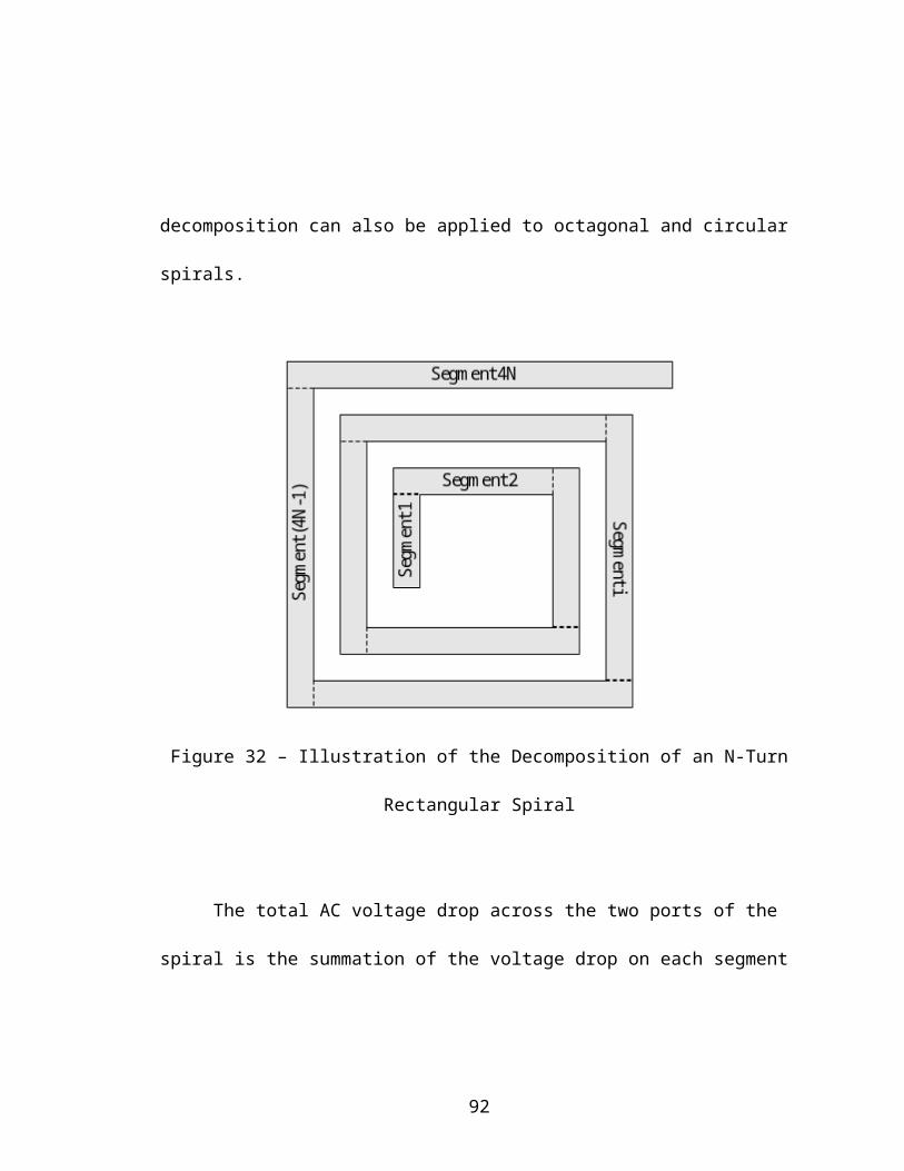
The total AC voltage drop across the two ports of the spiral is the summation of
the voltage drop on each segment
(88)
According to the inductance definition, the voltage drop on each segment is
contributed by both the self-inductance and the mutual inductance between the segment
and every other segments
(89)
Therefore, a matrix of voltage-current relationship can be established given by
65
(90)
or
(91)
where the inductance matrix is given by
(92)
In this matrix, the diagonal elements are the self-inductance of each segment and the off-
diagonal elements are the mutual inductance between each two segments. Applying
Equation (91), the total inductance of the rectangular spiral is the summation of all the
elements of the inductance matrix.
(93)
Since the inductor is an on-chip component, the inductance of the spiral given by
Equation (96) is a complex inductance, which includes both inductance and resistance.
66

MODELING IMPEDANCE OF ON-CHIP INDUCTORS
The inductance of an on-chip inductor depends on several factors, such as total
spiral length, number of turns, line spacing, line width, and substrate conductivity. These
factors are illustrated in Figure 33. The effects of these factors are studied by computer
simulation.
Figure 33 – Illustration of Spiral Parameters
67
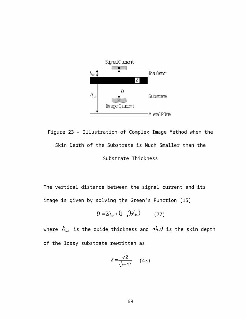
Figure 34 plots the impedance of a rectangular spiral with different total spiral
lengths versus frequency, while keeping constant the number of turns, the line spacing,
the line width, and the substrate conductivity. The process is chosen to be a 0.25 m
CMOS process. The spiral is on the Metal 5 layer. The number of turns is set to be 4.
The line width is set to be 8 m and line spacing is set to be 2 m. The oxide thickness is
3.96 m and the substrate thickness is 250 m [36]. The metal conductivity is
S/m [36]. The substrate doping level is assumed to be cm-3.
1 2 3 4 5 6 7 8 9 101
2
3
4
5
6
7
8
Frequency, GHz
Indu
ctan
ce, n
H
Total Length = 3000mTotal Length = 2000mTotal Length = 1000m
(a) Inductance
68
1 2 3 4 5 6 7 8 9 100
5
10
15
20
25
Frequency, GHz
Res
ista
nce,
Total Length = 3000mTotal Length = 2000mTotal Length = 1000m
(b) Resistance
Figure 34 – Spiral Inductor Impedance with Different Total Spiral Lengths versus
Frequency
It is seen from Figure 34 that both the inductance and the resistance of the spiral
are roughly proportional to the total spiral length. Therefore, increasing the total length
not only increases the inductance, but also gives rise to the resistive loss and thus
decreases the inductor quality factor.
Figure 35 plots the impedance of a spiral inductor with different numbers of turns
versus frequency, while keeping constant the total spiral length, the line spacing, the line
width, and the substrate conductivity. The spiral parameters are the same as the previous
analysis except that the total length is set to be 3000 m and the number of turns varies.
69
1 2 3 4 5 6 7 8 9 10
5.8
6
6.2
6.4
6.6
6.8
Frequency, GHz
Indu
ctan
ce, n
H
N=3N=4N=5
(a) Inductance
1 2 3 4 5 6 7 8 9 100
5
10
15
20
25
Frequency, GHz
Res
ista
nce,
nH
N=3N=4N=5
(b) Resistance
Figure 35 – Spiral Inductor Impedance with Different Number of Turns versus Frequency
70

It is seen evident from Figure 35 that increasing the number of turns can
effectively increase the spiral inductance as well as slightly decrease the resistance. This
is because increasing the number of turns can effectively increases the total magnetic flux
of the spiral [4].
Figure 36 plots the impedance of a spiral inductor with different line spacing
versus frequency, while keeping constant the total spiral length, the number of turns, the
line width, and the substrate conductivity. The spiral parameters are the same as the
previous analysis except that the line spacing varies.
1 2 3 4 5 6 7 8 9 105.7
5.8
5.9
6
6.1
6.2
6.3
6.4
6.5
Frequency, GHz
Indu
ctan
ce, n
H
S=2mS=4mS=6m
(a) Inductance
71
1 2 3 4 5 6 7 8 9 100
5
10
15
20
25
Frequency, GHz
Res
ista
nce,
S=2mS=4mS=6m
(b) Resistance
Figure 36 – Spiral Inductor Impedance with Different Line Spacing versus Frequency
It is seen from Figure 36 that decreasing the line spacing is an effective way to
increase the spiral inductance without having much effects on the resistance. This is
mainly because decreasing the line spacing increases the mutual inductance between the
adjacent segments and thus the total inductance. The smallest line spacing is limited by
the process design rule.
Figure 37 plots the impedance of a spiral inductor with different substrate doping
levels versus frequency, while keeping constant the total spiral length, the number of
turns, the line spacing, and the line width. The spiral parameters are the same as the
previous analysis except that the substrate conductivity varies.
72
1 2 3 4 5 6 7 8 9 104.6
4.8
5
5.2
5.4
5.6
5.8
6
6.2
6.4
6.6
Frequency, GHz
Indu
ctan
ce, n
H
Na=1016cm-3
Na=1017cm-3
Na=1018cm-3
Na=1019cm-3
(a) Inductance
1 2 3 4 5 6 7 8 9 10-10
0
10
20
30
40
50
60
70
80
Frequency, GHz
Res
ista
nce,
Na=1016cm-3
Na=1017cm-3
Na=1018cm-3
Na=1019cm-3
(b) Resistance
Figure 37 – Spiral Inductor Impedance with Different Substrate Doping Levels versus
Frequency
73
It is seen from Figure 37 that when the substrate doping level is low (around
cm-3), the inductance increases slightly at higher frequencies. This is because the skin
effect in the substrate can be neglected. As a result of the skin effect, the current crowds
at the edge of the conductor at higher frequencies. This implies a decreased spacing
between the current elements in the adjacent segments and therefore an increased mutual
inductance. However, if the substrate doping level is high (above cm-3), the spiral
inductance decreases with increased frequencies, because both the self-inductance of
each segment and the mutual inductance between each two segments decreases at higher
substrate doping levels, as explained in the previous chapter. Similar analysis can be
applied for the spiral resistance, which increases at higher substrate conductivity.
MULTI-LAYER ON-CHIP INDUCTORS
There are several drawbacks of the conventional spiral inductors. First, they
occupy large chip areas. Taken as an example, Figure 38 shows the die photo of a 1.5
GHz CMOS low noise amplifier [20], where two on-chip inductors (square spirals) take
about two thirds of the die area.
74
Figure 38 – Die Photo of A 1.5V 1.5 GHz CMOS Low Noise Amplifier
Even though, it is hard to fit an inductor of more than 10nH on a chip. The inductance
value is greatly limited for on-chip inductors. As a result, intermediate and low
frequency applications have to turn to off-chip alternatives. Second, because of the lossy
semiconductor substrate on which an on-chip inductor is laid out, there are significant
resistive as well as capacitive losses associated with on-chip inductors. Therefore the
quality factor of an on-chip inductor is much lower than their off-chip counterparts. For
example, the quality factor of on-chip inductors whose inductance is several nanohenries
will not go beyond ten in the lower gigahertz range [29].
Achieving high quality factor is the key goal of the on-chip inductor design. The
inductor quality factor is directly related to the noise performance of RF circuits, such as
the phase noise of a LC tank voltage-controlled oscillator [21]. An effective way to
increase the quality factor of an on-chip inductor without decreasing the inductance is the
75
implementation of multi-layer on-chip inductors. The concept of multi-layer inductors is
illustrated in Figure 39.
Figure 39 – Illustration of Multilayer On-Chip Inductors
The multi-layer inductor takes advantage of the multiple metal layers in the conventional
CMOS processes. It consists of several stacked N-turn planar spirals. As seen from
76
Figure 39, all planar spirals have the same direction of current flow (either clockwise or
counterclockwise) to maximize the magnetic coupling between them. There are several
publications on the experimental investigation of such 3D on-chip inductors [22] [23]
[24].
77
CHAPTER IV
HIGH-SPEED ON-CHIP DIGITAL SIGNAL TRANSMISSION
With the appearance of advanced CMOS processes, traditional digital circuits are
operating at faster speed and higher level of system integration. For example, the latest
microprocessors (Intel Pentium 4) have a clock speed up to 3.2 GHz with an 800 MHz
front-side bus. When the signal switching speeds exceed 1 GHz and the chip densities
exceed tens of millions of transistors, the RLC delays due to on-chip interconnects
become significant [27].
At high frequencies especially in the radio-frequency regime, a distributed system
analysis has to be applied to the on-chip interconnect networks, instead of the traditional
lumped analysis. The transmission line theory is necessary to accurately analyze high-
speed on-chip signal transmissions. Although the distributed transmission line has been
largely applied for on-board situations with relatively large physical dimensions, it is
only recently that attention has been drawn into an on-chip environment [26]. On-chip
interconnects together with the lossy silicon substrate behave like a transmission line
system when carrying high-frequency signals, especially digital pulses with steep rising
and falling edges. The on-chip transmission line systems affects signal transmission in
various aspects, including signal delay, attenuation, and dispersion.
78
TRANSMISSION LINE THEORY
As its name implies, a transmission line is a physical path along which the signal
transmits, which consists of two or more parallel conductors. Typical examples of
transmission lines are shown in Figure 40.
(a) Parallel Lines
(b) Coaxial Cable
(c) Strip Lines
79
(d) Microstrip Lines
(e) Coplanar Lines
Figure 40 – Cross-Sections of Typical Transmission Lines
What all transmission lines have in common is that they all consist of both the
signal path and the return path. This is easily understood because current has to flow in a
closed conducting loop. Same amount of current flow in the return path as in the signal
path, but in an opposite direction.
It is worth clarifying that the transmission theory applies to all signals, no matter
the signal frequency or the line dimension. However, it is mainly used for radio-
frequency and microwave regimes instead of low frequency situations where KVL and
KCL are more convenient to analyze problems. KVL and KCL are the approximations of
Maxwell’s Equation at low frequencies, assuming the space derivatives are negligible.
80
There are three fundamental modes of signal transmission: TEM, TE, and TM.
For TEM mode, the electric and magnetic fields along the transmission direction are both
zero. Taking to be the direction of transmission, the tangential fields are zeros
(94)
For TE mode, there is only magnetic field on the direction of transmission,
(95)
For TM mode, there is only electric field on the direction of transmission,
(96)
When the conductors are completely surrounded by a uniform dielectric medium,
the principal mode that can exist on a transmission line is the TEM mode. Since a
microstrip line is not fully surrounded by a uniform dielectric medium, it does not
support a TEM model. However, at low frequencies, the dominant mode on a microstrip
line approaches TEM mode and is therefore called quasi-TEM mode.
For a TEM mode, the relationship between electric and magnetic fields is unique,
which is given by
(97)
where is a constant. Here the plus sign refers to the signal transmission along the
direction and the minus sign refers to direction. Since has the unit of and
81
relates uniquely the electric and magnetic fields, it is defined as the characteristic
impedance of the transmission line. The characteristic impedance is the most
fundamental parameter of a transmission line. For TE and TM modes, the relationship
between and is more complicated so that it requires solving Maxwell’s Equations
with properly applied boundary conditions.
Although one can solve the field patterns associated with certain mode of signal
transmission on a transmission line, it is more straightforward and convenient for
integrated circuit designers to model the transmission line with circuit elements: , , ,
and , which are distributed components that refer to inductance, resistance, capacitance,
and conductance per unit length. The classic distributed model of a transmission line is
shown in Figure 41.
Figure 41 – Distributed Model of Transmission Lines per Unit Length
Physically, represents the electric field between the two conductors of the
transmission line. stands for the magnetic field generated by both the conducting and
82
displacement current. correspond to the resistive loss of the two conductors. means
the loss in the dielectric.
The speed that a signal transmits on a transmission line is no faster than the speed
of light, which is given by
(98)
This means even for a superconductive transmission, there is still LC delay of the signal
although the RC delay is negligible. The more inductive and capacitive of the
transmission line, the more delay of the signal transmission.
The characteristic impedance of a transmission line is given by
(99)
For a lossless transmission where and are zeros, is a real number
(100)
Since a realistic transmission line cannot have infinite length, it has to be
arbitrarily terminated with a load. Terminating a transmission line gives rise to signal
reflection. As shown in Figure 42, when an incident signal reaches the end of the
transmission line, part of it transmits into the load and the rest of the signal is reflected
and travels backward along the transmission line.
83
Figure 42 – Terminated Transmission Line
In order to quantitate the signal reflection, a reflection coefficient at the
impedance discontinuity is defined as
(101)
where and are the voltage and current of the incident signal respectively and
and are the voltage and current of the reflected signal. depends on the
characteristic impedance of the transmission line and the load impedance only, which is
given by
(102)
When the load impedance is matched to the characteristic impedance
(103)
there will be no signal reflection.
84
Signal reflection happens as long as impedances are mismatched. It is
independent of frequencies and line dimensions. Or in another word, it happens for both
high frequency and low frequency signals, both short and long lines, although people
always ignore it at low frequencies on short lines. Consider a source driving a load
through a transmission line as shown in Figure 43.
Figure 43 – Source Drives Load through Transmission Line
Once an incident signal is sent onto the transmission line, it will bounce back and
forth until it reaches the steady state. The steady state is determined by satisfying the
boundary conditions. Given enough time, the magnitude of the voltage at the end of the
transmission line is an infinite series given by
(104)
This series will finally converge to
85
(105)
which satisfies the boundary conditions. The steady state solution agrees with KVL or
KCL. This is why at low frequency KVL and KCL are used instead of the transmission
line theory because the convergence happens so fast compared with the time scale so that
a transmitted signal reaches the steady state without notice. However, at high
frequencies, the convergence time and the signal time scale are comparable and therefore
the signal reflection can be observed such as the ringing effects.
ON-CHIP TRANSMISSION LINES
The transmission line theory applies to signals at any frequencies. However, in
the low frequency regime when the wavelength of the signal is much larger than the
physical dimensions of the transmission line, classic circuit theory are more convenient to
analyze problems. A rule of thumb [8] is when the signal wavelength is larger than ten-
time the line length, KVL and KCL are good enough to analyze the electric network
instead of applying the distributed transmission line theory.
The question is which one to use, distributed transmission line theory or KCL and
KVL, in an on-chip environment.
The answer depends on both the signal frequency and the interconnect length.
Special cases of interest includes on-chip bus lines and high-speed digital clock trees,
where the interconnect lengths are relatively long and the rising and falling time of the
86
digital pulses are extremely short. Therefore signal degradation, dispersion, and
reflection will come into play.
On-chip interconnects are essentially microstrip lines. As shown in Figure 44, the
oxide layer serves as the dielectric insulator and the lossy substrate together with a metal
plate acts like the return path or the ground plane.
Figure 44 – On-Chip Interconnects
In order to accurately model the line characterizations, the commercial field
solver, Sonnet, has been used for computer simulation.
Sonnet is a high-frequency electromagnetic simulator for 3D planar circuits.
Sonnet together with HFSS and ADS Momentum are the three most popular
electromagnetic simulation tools for radio-frequency and microwave design. Sonnet
differs from HFSS in that Sonnet is limited to planar structures while HFSS is a complete
87
3D EM solver. Unlike HFSS and Sonnet, ADS Momentum is based on equivalent circuit
theories instead of solving the fields. The accuracy and time efficiency of HFSS, Sonnet,
and ADS Momentum are compared in Table 1.
Table 1 – Comparison of HFSS, Sonnet, and ADS Momentum
HFSS Sonnet ADS Momentum
Accuracy Highest Medium Lowest
Time Efficiency Lowest Medium Highest
Sonnet yields good trade-off between accuracy and time efficiency compared with HFSS
and ADS Momentum.
Sonnet treats the simulated structure as an N-port network and outputs the
scattering parameters of the network. Scattering parameters can be transformed into
impedance matrix, which can then be plugged into EDA (Electronics Design
Automation) tools such as SPICE and ADS for electric network simulation.
Taking for example the interconnect on Metal 1 layer in TSMC 0.25 m CMOS
process. The oxide thickness is 3.96 m and the substrate thickness is 250 m. The
metal conductivity is S/m and the substrate doping level is cm-3, which
corresponds to a conductivity of about 500 S/m. The characteristic impedance simulated
by Sonnet is plotted in Figure 45.
88
108
109
1010
1011
20
40
60
80
100
120
140
160
180
Frequency, Hz
Re(
Z 0),
W=4mW=8m
(a) Real Part
108
109
1010
1011
-160
-140
-120
-100
-80
-60
-40
-20
0
20
Frequency, Hz
Im(Z
0),
W=4mW=8m
(b) Imaginary Part
89
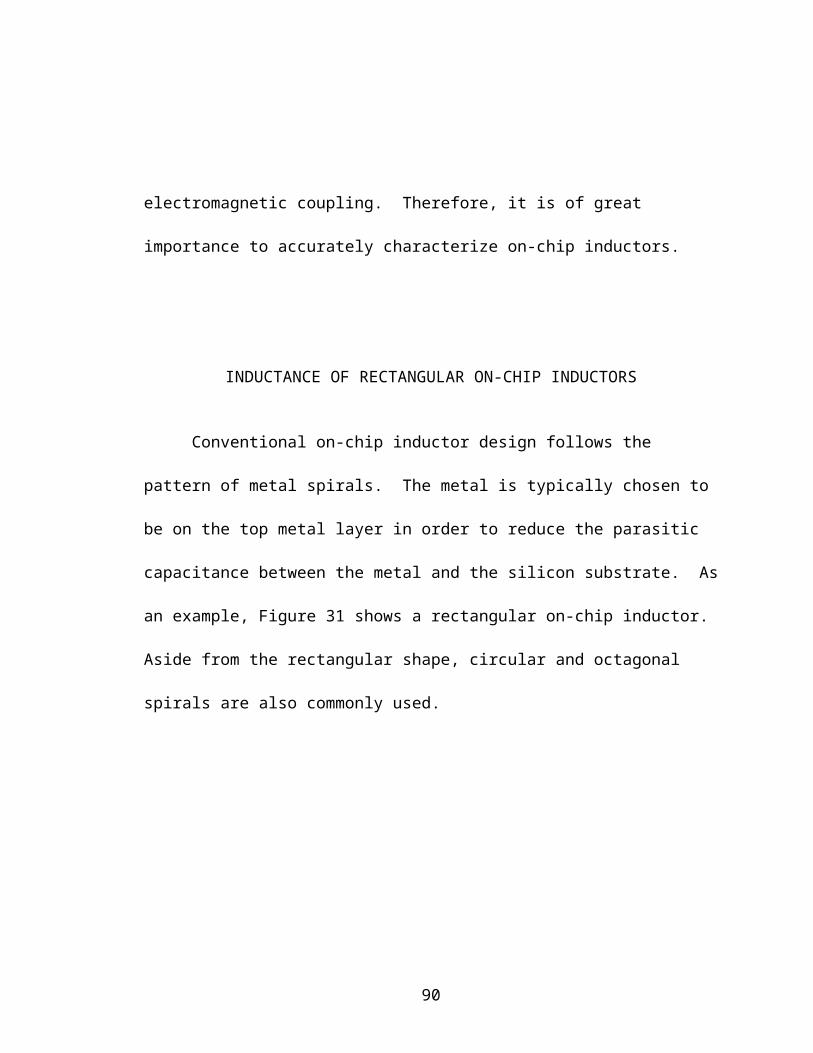
Figure 45 – Characteristic Impedance of On-Chip Interconnect versus Frequency
It is seen from Figure 45 that the characteristic impedance is a frequency dependent
complex number. At low frequencies, is given by
(103)
At very high frequencies, the term dominates and is approximated as
(104)
It is evident from Figure 45 that at ten’s of gigahertz, the imaginary part of quickly
approaches zero and the real part of shows less frequency dependence than at low
frequencies.
The scattering parameters of the interconnect on Metal 1 layer in TSMC 0.25 m
CMOS process is plotted in Figure 46, which is 1 mm long and 4 m wide.
90
108
109
1010
1011
0
0.05
0.1
0.15
0.2
Frequency, Hz
|S11
|
108
109
1010
1011
0
0.2
0.4
0.6
0.8
1
Frequency, Hz
|S12
|
108
109
1010
1011
0
0.2
0.4
0.6
0.8
1
Frequency, Hz
|S21
|
108
109
1010
1011
0
0.05
0.1
0.15
0.2
Frequency, Hz
|S22
|
Figure 46 – S Parameters of On-Chip Interconnect
Once the scattering parameters are known, they are saved as a Touchstone file
with the .snp file extension and taken into ADS for simulation. ADS can directly
interpret the Touchstone file as a circuit component.
91
ON-CHIP SIGNAL ATTENUATION AND DISPERSION
First, the Sonnet simulation was run on a 1 cm long on-chip interconnect to
investigate the signal reflection. As shown in Figure 47, the interconnect is driven by an
ideal pulse source. Each box represents a 1 mm long 4 m wide on-chip interconnect on
Metal 1 layer in a TSMC 0.25 m CMOS process.
V0 V1 V10V2 V3 V4 V5 V6 V7 V8 V9
VtPulseSRC1
Period=1000 psecWidth=30 psecFall=10 psecRise=10 psecEdge=linearDelay=0 nsecVhigh=1 VVlow=0 V
t
S2PSNP1File="tl_4u_x_1mm.s2p"
21
Ref
TranTran1
MaxTimeStep=1 psecStopTime=500.0 psec
TRANSIENT
S2PSNP10File="tl_4u_x_1mm.s2p"
21
Ref
S2PSNP9File="tl_4u_x_1mm.s2p"
21
Ref
S2PSNP8File="tl_4u_x_1mm.s2p"
21
Ref
S2PSNP7File="tl_4u_x_1mm.s2p"
21
Ref
S2PSNP6File="tl_4u_x_1mm.s2p"
21
Ref
S2PSNP5File="tl_4u_x_1mm.s2p"
21
Ref
S2PSNP4File="tl_4u_x_1mm.s2p"
21
Ref
S2PSNP3File="tl_4u_x_1mm.s2p"
21
Ref
S2PSNP2File="tl_4u_x_1mm.s2p"
21
Ref
Figure 47 – Simulation Setup of Signal Reflection
If the interconnect is open ended, the pulse signal transmission and reflection is
shown in Figure 48.
92
Pulse Propagation with Open Termination
0.5
0.0
1.0
V0, V
0.20.40.60.8
0.0
1.0
V1, V
0200400600
-200
800
V2, m
V
0200400600
-200
800
V3, m
V
0200400
-200
600
V4, m
V
0200400
-200
600
V5, m
V
0100200300
-100
400
V6, m
V
0100200300
-100
400
V7, m
V
0100200
-100
300
V8, m
V
0100200
-100
300
V9, m
V
20 40 60 80 100 120 140 160 180 200 220 240 260 280 300 320 340 360 380 400 420 440 460 4800 500
0100200300
-100
400
time, psec
V10,
mV
Figure 48 – Pulse Propagation with Open Ended
It is clearly seen the signal degradation and positive reflection in Figure 48. The
amplitude attenuation is about 200 mV every 3 mm. This is mainly due to the resistive
loss of the transmission line. Such resistive loss depends on not only the metal
conductivity, but also the silicon substrate loss.
93
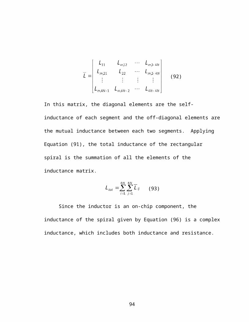
Figure 49 shows the situation with short ended, where negative reflection is seen
as well as signal degradation.
Pulse Propagation with Open Termination
0.5
0.0
1.0
V0, V
0.00.5
-0.5
1.0
V1, V
0.00.5
-0.5
1.0
V2, V
0.00.5
-0.5
1.0
V3, V
0200400
-200
600
V4, m
V
0200400
-200
600
V5, m
V
0200
-200
400
V6, m
V
0200
-200
400
V7, m
V
0200
-200
400
V8, m
V
20 40 60 80 100 120 140 160 180 200 220 240 260 280 300 320 340 360 380 400 420 440 460 4800 500
0100
-100
200
time, psec
V9, m
V
Figure 49 – Pulse Transmission with Short Ended
94
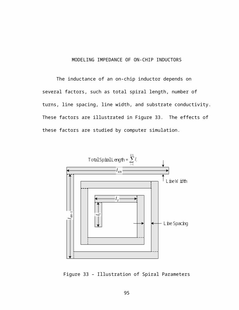
According to Figure 45, the characteristic impedance of the interconnect
approaches around 10 GHz. Therefore by terminating the line with a resistor,
the signal reflection is minimized as seen in Figure 50.
Pulse Propagation with Open Termination
0.5
0.0
1.0
V0, V
-0.00.20.40.60.8
-0.2
1.0
V1, V
0200400600
-200
800
V2, m
V
0200400600
-200
800
V3, m
V
0200400
-200
600
V4, m
V
0200400
-200
600
V5, m
V
0100200300
-100
400
V6, m
V
0100200300
-100
400
V7, m
V
0100200
-100
300
V8, m
V
0100200
-100
300
V9, m
V
20 40 60 80 100 120 140 160 180 200 220 240 260 280 300 320 340 360 380 400 420 440 460 4800 500
050
100150
-50
200
time, psec
V10,
mV
Figure 50 – Pulse Transmission with Matched Load
95
Next, the ideal source and load in Figure 47 are replaced by two inverters to
investigate the effect of on-chip interconnects on the digital signal transmission. The
simulation setup is shown in Figure 51. A driver inverter drives the receiver inverter
through the interconnect. A pulse is generated by the driver inverter, transmits along the
interconnect, and tries to switch the receiver inverter.
V10 VoVs V0 V1 V2 V3 V4 V5 V6 V7 V8 V9
MOSFET_PMOSMOSFET3
Width=30 umLength=0.24 umModel=PMOS
V_DCSRC3Vdc=2.5 V
MOSFET_NMOSMOSFET4
Width=10 umLength=0.24 umModel=NMOS
VtPulseSRC4
Period=100 psecWidth=50 psecFall=10 psecRise=10 psecEdge=linearDelay=1 psecVhigh=0 VVlow=2.5 Vt
I_ProbeI_dd
V_DCSRC1Vdc=2.5 V
BSIM3_ModelPMOS
BSIM3_ModelNMOS
TranTran1
MaxTimeStep=1 psecStopTime=1000.0 psec
TRANSIENT
S2PSNP10File="tl_4u_x_1mm.s2p"
21
Ref
S2PSNP9File="tl_4u_x_1mm.s2p"
21
Ref
S2PSNP8File="tl_4u_x_1mm.s2p"
21
Ref
S2PSNP7File="tl_4u_x_1mm.s2p"
21
Ref
S2PSNP6File="tl_4u_x_1mm.s2p"
21
Ref
S2PSNP5File="tl_4u_x_1mm.s2p"
21
Ref
S2PSNP4File="tl_4u_x_1mm.s2p"
21
Ref
S2PSNP3File="tl_4u_x_1mm.s2p"
21
Ref
S2PSNP2File="tl_4u_x_1mm.s2p"
21
Ref
S2PSNP1File="tl_4u_x_1mm.s2p"
21
Ref
MOSFET_PMOSMOSFET2
Width=150 umLength=0.24 umModel=PMOS
MOSFET_NMOSMOSFET1
Width=50 umLength=0.24 umModel=NMOS
Figure 51 – Simulation Setup for Digital Signal Transmission
In order to achieve a digital pulse with short rising and falling time around 10 ps, the
driver inverter has been designed with TSMC 0.25 m CMOS process as shown in
Figure 52. The SPICE BSIM models of both NMOS and PMOS of this process are listed
in Appendix III.
96
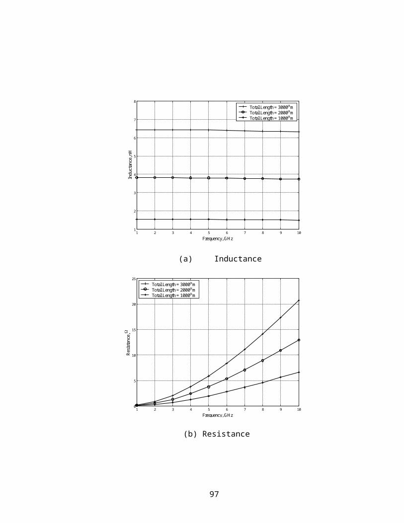
Vs Vo
TranTran1
MaxTimeStep=1 psecStopTime=200.0 psec
TRANSIENT
VtPulseSRC4
Period=5000 psecWidth=100 psecFall=1 psecRise=1 psecEdge=linearDelay=10 psecVhigh=0 VVlow=2.5 Vt
VARVAR1Wn=50u
EqnVar
MOSFET_PMOSMOSFET2
Width=WpLength=0.24 umModel=PMOS
MOSFET_NMOSMOSFET1
Width=WnLength=0.24 umModel=NMOS
VARVAR2Wp=3*Wn
EqnVar BSIM3_Model
NMOSBSIM3_ModelPMOS
V_DCSRC1Vdc=2.5 V
Figure 52 – Schematic of Driver Inverter
The lengths of both the NMOS and the PMOS are 0.24 m. The DC power supply (VDD)
for this process is 2.5 V. In order to set the inverter switching point to be around half of
VDD, the width of the PMOS is set to be 3 times larger than the NMOS. Figure 53 shows
the switching characteristics of the inverter where the switching point is about 1.26 V.
97
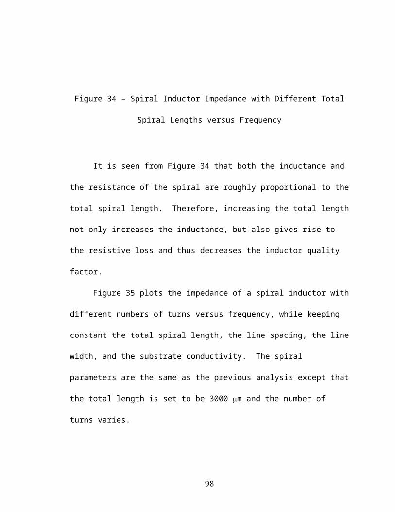
0.25 0.50 0.75 1.00 1.25 1.50 1.75 2.00 2.250.00 2.50
0.250.500.751.001.251.501.752.002.25
0.00
2.50
Vin
Vout
Inverter Transfer Characteristics
Figure 53 – Switching Characteristics of the Driver Inverter
By choosing the width of the NMOS to be 50 m and PMOS 150 m, the delay of the
inverter is minimized. The result of the transient simulation is shown in Figure 54.
98
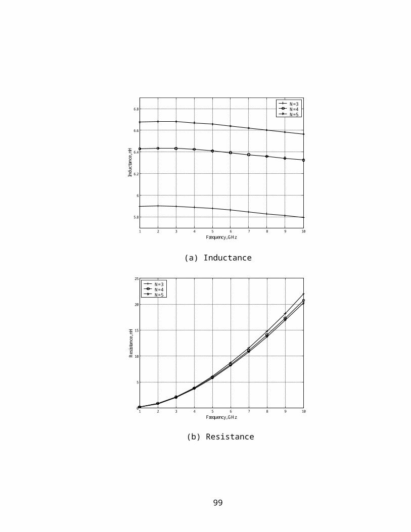
Intrinsic Interver Delay
0.00.51.01.52.02.5
-0.5
3.0
Vs, V
20 40 60 80 100 120 140 160 1800 200
0
2
-2
4
time, psec
Vo, V
Figure 54 – Intrinsic Inverter Delay
As read from Figure 54,
This corresponds to ten’s of gigahertz frequency components of the pulse.
The receiver inverter has the minimum length and width as shown in Figure 55.
In this process, the MOSFET’s are constructed with standard gate fingers. Each gate
finger is 10 m long. Thus the width of each MOSFET is in multiples of 10 m.
99
Vout
BSIM3_ModelPMOS
BSIM3_ModelNMOS
VARVAR1Vin=1.0
EqnVar
DCDC1SweepVar="Vin"
DC
MOSFET_PMOSMOFET2
Width=30 umLength=0.24 umModel=PMOS
MOSFET_NMOSMOSFET1
Width=10 umLength=0.24 umModel=NMOS
V_DCSRC1Vdc=2.5 V
V_DCSRC2Vdc=Vin
Figure 55 – Schematic of Receiver Inverter
Because of the signal attenuation along the interconnect, there exists a critical
length of the interconnect above which the digital pulse will not switch the receiver
inverter. ADS simulation shows that the critical length is about 8 mm. As shown in
Figure 56, if the interconnect is longer than 8mm, the signal is not able to reach the
switching point at the end of the transmission line and therefore cannot switch the next
digital stage.
100
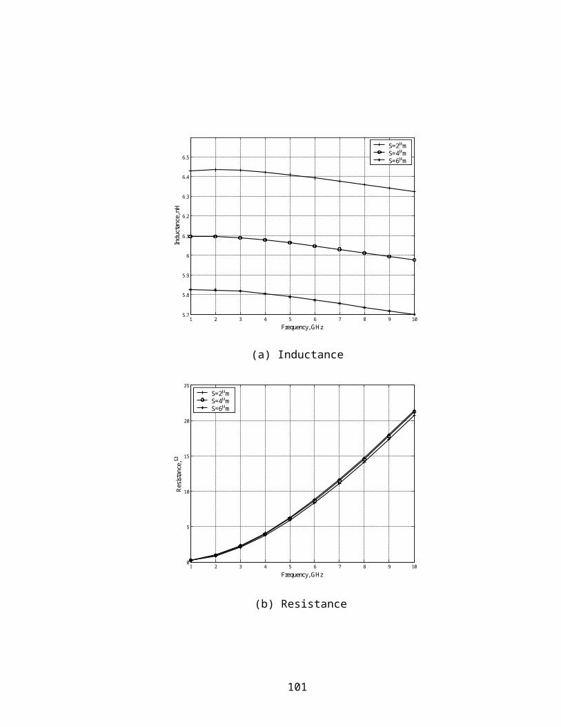
12
0
3
Vs, V
012
-1
3
V0, V
012
-1
3
V1, V
0.00.51.01.5
-0.5
2.0
V2, V
0.00.51.0
-0.5
1.5
V3, V
0.00.51.0
-0.5
1.5
V4, V
0.00.51.0
-0.5
1.5
V5, V
0.00.51.0
-0.5
1.5
V6, V
0.00.51.0
-0.5
1.5
V7, V
0.00.51.0
-0.5
1.5
V8, V
0.1 0.2 0.3 0.4 0.5 0.6 0.7 0.8 0.90.0 1.0
1.82.02.22.42.6
1.6
2.8
time, nsec
Vo, V
Figure 56 – Effects of Interconnect on Digital Gates Driving Capability
High frequency components suffer more from signal attenuation than lower
frequency components. This is mainly because the skin effect in the substrate becomes
101
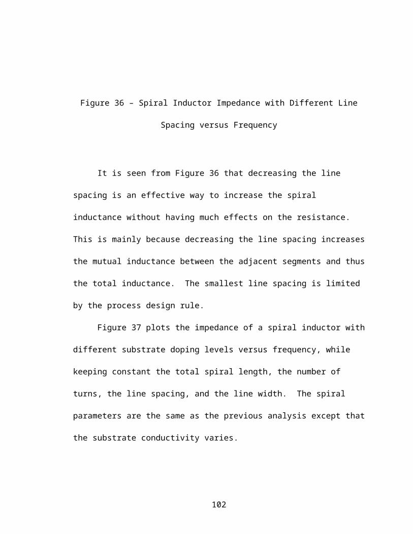
more significant at higher frequencies. The eddy current shields the magnetic field from
penetrating further into the substrate. Therefore, the more eddy current induced near the
substrate surface, the more return current flows in the substrate instead of the metal plate.
This gives rise to the effective resistance of the interconnect and thus the signal
attenuation.
ADS simulation compares the signal attenuation on a 1 cm interconnect at
different frequencies: 1 GHz, 3 GHz, 5 GHz, 7 GHz, and 9 GHz. As seen from Figure
57, the attenuation of the 1 GHz signal is 20% while that of the 9 GHz signal is about
70%.
0.5
0.0
1.0
Vs1,
V
-0.50.0
0.5
-1.0
1.0
Vs3,
V
-0.5
0.00.5
-1.0
1.0
Vs5,
V
-0.50.0
0.5
-1.0
1.0
Vs7,
V
100 200 300 4000 500
-0.5
0.00.5
-1.0
1.0
time, psec
Vs9,
V
200400
600
0
800
Vo1,
mV
-2000
200400
-400
600
Vo3,
mV
-200
0200
-400
400
Vo5,
mV
-2000
200
-400
400
Vo7,
mV
100 200 300 4000 500
-200
0200
-400
400
time, psec
Vo9,
mV
Figure 57 – Signal Attenuation at Different Frequencies
102
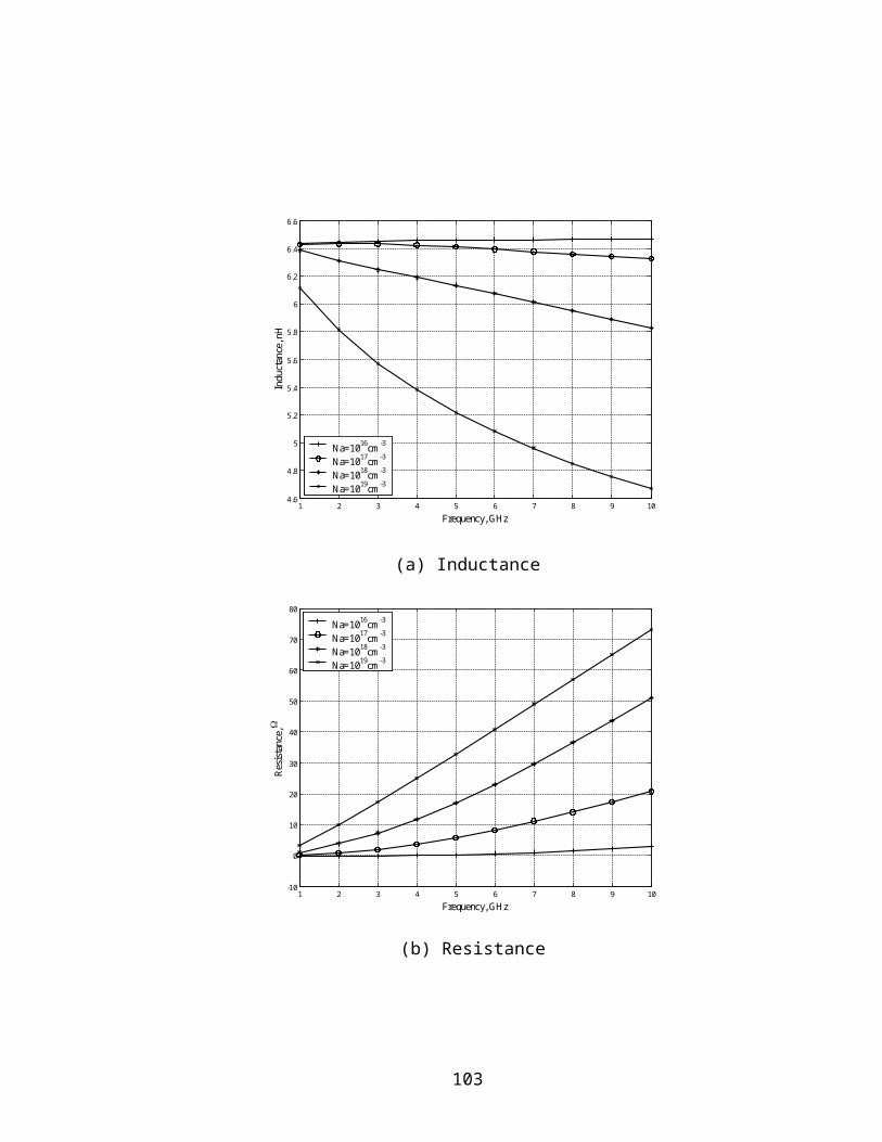
Another problem with the high-speed digital signal transmission is the signal
dispersion. This is because different frequency components have different transmission
speeds. Again, the transmission speed of one frequency component is given by
(106)
where and are both frequency dependent. From Figure 57, it is seen that the
delay of the 1 GHz signal on a 1 cm long interconnect is about 220 ps while the delay of
the 9 GHz signal is close to 150 ps. The signal dispersion strongly depends on the
substrate doping. Computer simulation [15] shows that at higher substrate doping level,
the distributed inductance and capacitance of an on-chip interconnect show more
frequency dependence than the substrate with less conductivity.
103
CHAPTER V
ELECTROMAGNETIC COUPLING EFFECTS
While advanced semiconductor technologies have brought into integrated circuits
faster operating speed and higher level of system integration, electromagnetic effects
accompany the on-chip evolutions.
In an on-chip environment, all circuit components share a common substrate. The
substrate is not a perfect dielectric, but a semiconductor. There are significant parasitic
resistance, capacitance, and inductance associated with the semiconductor substrate. It
thus establishes a complicated connection between circuit components although they are
not connected directly. Once the operating frequency of the circuit devices becomes
higher, the substrate parasitics becomes more significant and the coupling between
devices through substrate becomes stronger.
Since achieving high chip density is pursued by VLSI designers, the spacing
between the integrated circuit components decreases significantly with advanced
technology. For those devices operating at high frequencies and carries high power
signals, they will leak large amount of electric and magnetic energy into the
surroundings. The electric and magnetic field can directly couple to the nearby devices
and induce noise voltage and current.
104
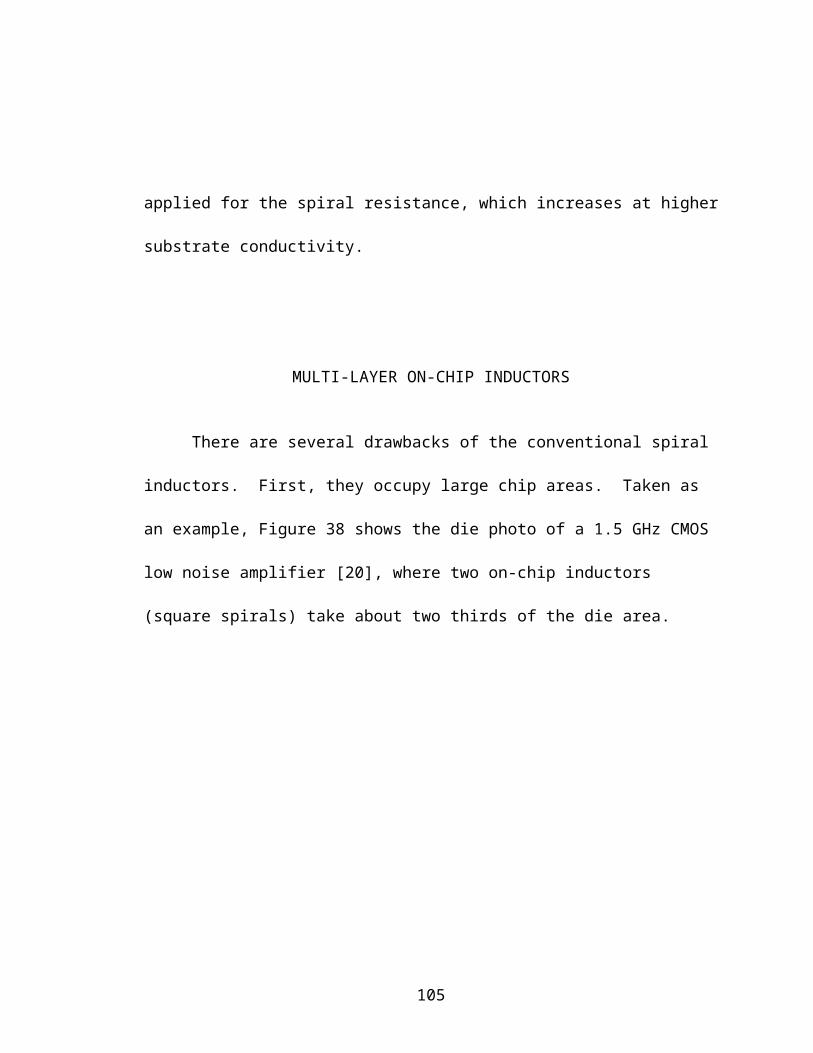
SCATTERING PARAMETERS
Scattering Parameters, or simply S Parameters, are widely used in radio-frequency
and microwave electric network analysis.
Consider an N-port network as shown in Figure 58. is the voltage of the
incident signal and is the voltage of the reflected signal.
Figure 58 – N-port Network
The S Parameters of such a network are defined as
105
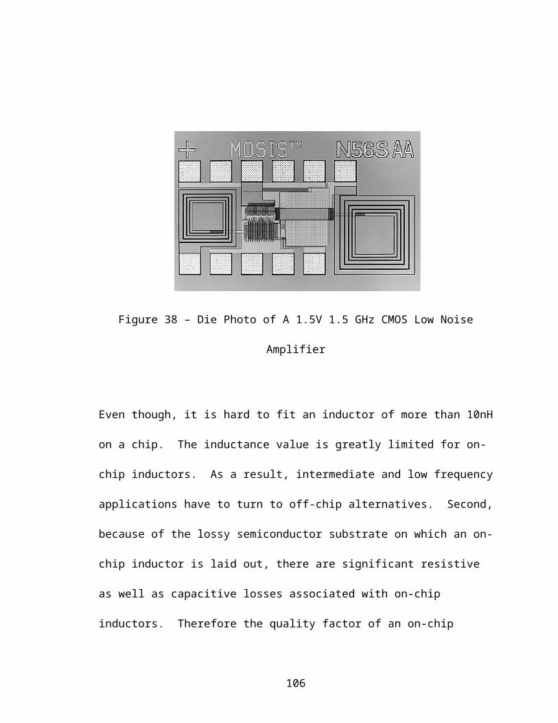
(107)
or
(108)
The S matrix defines the relationship between the reflected and the incident signals.
The advantage of using S Parameters lies in the fact that they can be directly
measured by instruments, such as a network analyzer. However, voltage and current
cannot be measured in a direct manner at microwave frequencies. Instead, what can be
measured directly are field and power. Therefore, S Parameters are more straightforward
than impedance parameters (or Z Parameters) and admittance parameters (or Y
Parameters) to analyze high-frequency electric networks. Z and Y Parameters can be
derived from S Parameters, which are given by
(109)
(110)
For a commonly seen two-port network, the S matrix is given by
(111)
where the four S parameters are defined as
106
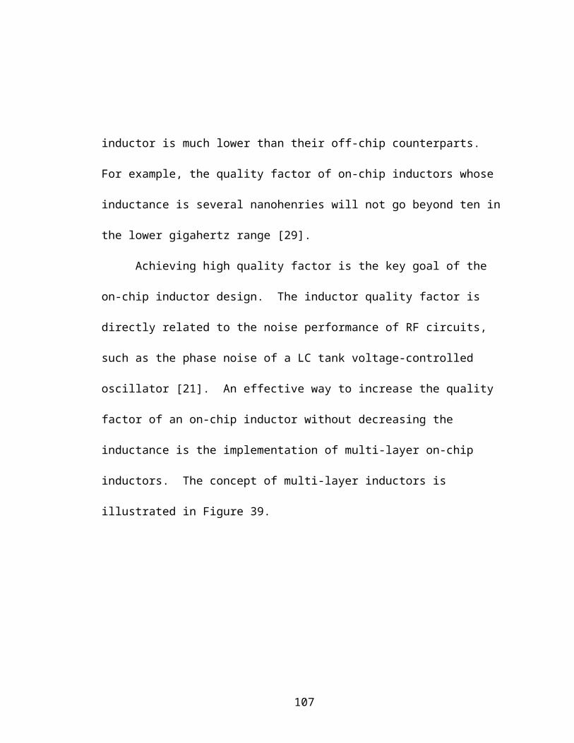
(112)
is the insertion loss of Port 1 when Port 2 is matched. is the forward gain from
Port 1 to Port 2 when Port 2 is matched. is the insertion loss of Port 2 when Port 1 is
matched. is the forward gain from Port 2 to Port 1 when Port 1 is matched.
For a symmetric network,
(113)
EXPERIMENT SETUP OF ELECTROMAGNETIC COUPLING MEASUREMENT
In order to experimentally investigate the electromagnetic coupling effects in an
on-chip environment, several testing structures have been designed to demonstrate the
coupling effects. The testing chip was taped out through MOSIS in an AMI 0.5 m
CMOS process. for this process is 0.3 m and all feature dimensions are multiples of
. The smallest feature size, the MOSFET gate length, is 0.6 m. This process has 3
metal layers and 2 poly layers. The process is for 5-V single power supply applications.
Each pair of coupled devices is tested as a two port network by connecting each
device to a single port. The electromagnetic coupling between them is investigated by
measuring the S Parameters of the network.
The experiment is set up as shown in Figure 59.
107
Figure 59 – Experiment Setup for Electromagnetic Coupling Measurement
The devices are first connected to bond pads through on-chip interconnects. For active
devices, the electrostatic discharge (ESD) structure has to be used together with the bond
pad to avoid breakdown caused by the high electrostatic voltage on the package pin. On
the p-type substrate, a p+ guard ring is buried to isolate the coupled devices from other
108
on-chip structures. The die is packaged for on-board manipulation. In this experiment,
the IC package is a standard 28-pin leadless chip carrier (LCC) ceramic package. The
advantage of using the LCC package instead of the lead dual-inline package (DIP) is the
greatly reduced parasitics induced by the bond wire and the package pin. The IC package
is soldered onto a printed circuit board. The pins are connected to the SMA (semi-
miniature adapter) connectors via on-board copper traces. SMA connectors have the
characteristic impedance of 50 if properly terminated. The network analyzer is
connected to the SMA connectors through 50 cables. To reduce on-board AC noise
and crosstalk, a ground plane has to be plated on the back side of the board.
COUPLING BETWEEN N-WELLS
In order to investigate the electromagnetic coupling through the substrate, two n-
wells have been laid out on a p-type silicon substrate as shown in Figure 60. Each n-well
is 28.8 m long by 28.8 m wide. The edge-to-edge distance between the two wells is
102.45 m. For this process, the n-channel low-field mobility is 496.57 cm2/V-s and the
p-channel low-field mobility is 151.80 cm2/V-s [36]. This corresponds to the surface
doping level of the p-type substrate of about cm-3 and the n-well doping level of
about cm-3 [5].
109
Figure 60 – Coupled n-wells
The measured data is plotted in Figure 61. Two peaks of |S21| are observed at 8
GHz and 4 GHz respectively. A maximum |S21| of about -16 dB occurs at 8 GHz. |S21|
varies around -20 dB in the frequency range of 2 GHz to 9 GHz.
110
2 3 4 5 6 7 8 9 10-30
-28
-26
-24
-22
-20
-18
-16
Frequency, GHz
|S21
|, dB
Measured DataFitted Curve
Figure 61 - |S21| of Coupled N-Wells
COUPLING BETWEEN ON-CHIP SPIRAL INDUCTORS
On-chip inductors have relative large physical dimensions and are associated with
significant magnetic energy leakage. Since they are typically used in analog radio-
frequency circuits and operate in the gigahertz range, the electromagnetic coupling
between two spiral inductors needs to be investigated.
Planar coupling between two side-by-side spiral inductors on the same metal layer
has been experimentally studied in [28] and a maximum of -25 dB has been
observed at 1.5 GHz.
111
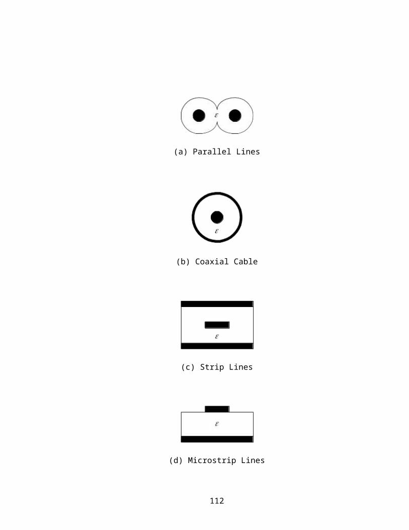
Here, the vertical coupling of two spirals has been investigated. As shown in
Figure 62, two identical spirals overlap with one on top of the other. The vertical
distance between them is about 1 m.
Figure 62 – Vertically Coupled On-Chip Inductors
The physical dimensions of the spiral are shown in Figure 63. The total number
of turns is six. The line width is 12 m. The line spacing is 3 m.
112
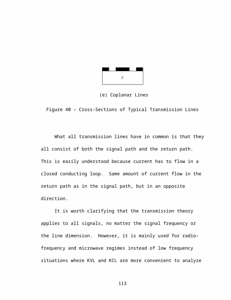
Figure 63 – Physical Dimensions of the Coupled Spirals in the Transformer
The equivalent circuit model for an on-chip spiral inductor is shown in Figure 64 [31].
and are the series inductance and resistance of the spiral respectively.
represents the capacitance between metal traces. is the oxide capacitance from the
spiral to the substrate. and models the substrate capacitance and conductance.
113
Figure 64 – Single- Equivalent Circuit Model of On-Chip Spiral Inductors
The equivalent circuit model of the coupled spirals is shown in Figure 65. The
coupling is mainly due to the magnetic field coupling represented by the mutual
inductance .
114
Figure 65 – Equivalent Circuit Model of Vertically Coupled Spirals
The measured data is plotted in Figure 61. A maximum |S21| of about -11 dB
occurs at 3 GHz and 5 GHz. In a wide bandwidth from 2.5 GHz to 5.5 GHz, |S21| remains
above -15 dB.
115
2 3 4 5 6 7 8 9 10-35
-30
-25
-20
-15
-10
Frequency, GHz
|S21
|, dB
Measured DataFitted Curve
Figure 66 – |S21| of Vertically Coupled Spirals
Since the coupling between two vertically coupled spirals is very strong, they can
be used as an on-chip transformer, especially for heterogeneous integration applications,
where the via through the wafer is hard to fabricate.
COUPLING BETWEEN ON-CHIP INDUCTORS AND TRANSISTORS
In radio-frequency integrated circuits where passive and active devices coexist on
the same chip, spiral inductors can couple a significant amount of electromagnetic energy
to sensitive transistors [33]. In order to investigate the coupling between on-chip
116
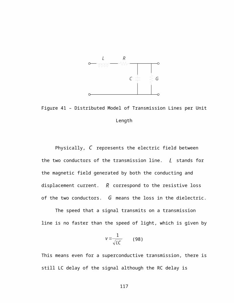
inductors and transistors, on-chip experiment has been implemented. As shown in Figure
67, a spiral inductor and a transistor have been laid out side-by-side.
Figure 67 – Coupled Spiral Inductor and Transistor
The physical dimensions of the spiral are shown in Figure 68. The total number
of turns is 4.75. The width and spacing of the conductor are 15 m and 5.1 m
respectively. The spiral is on the Metal 3 layer.
117
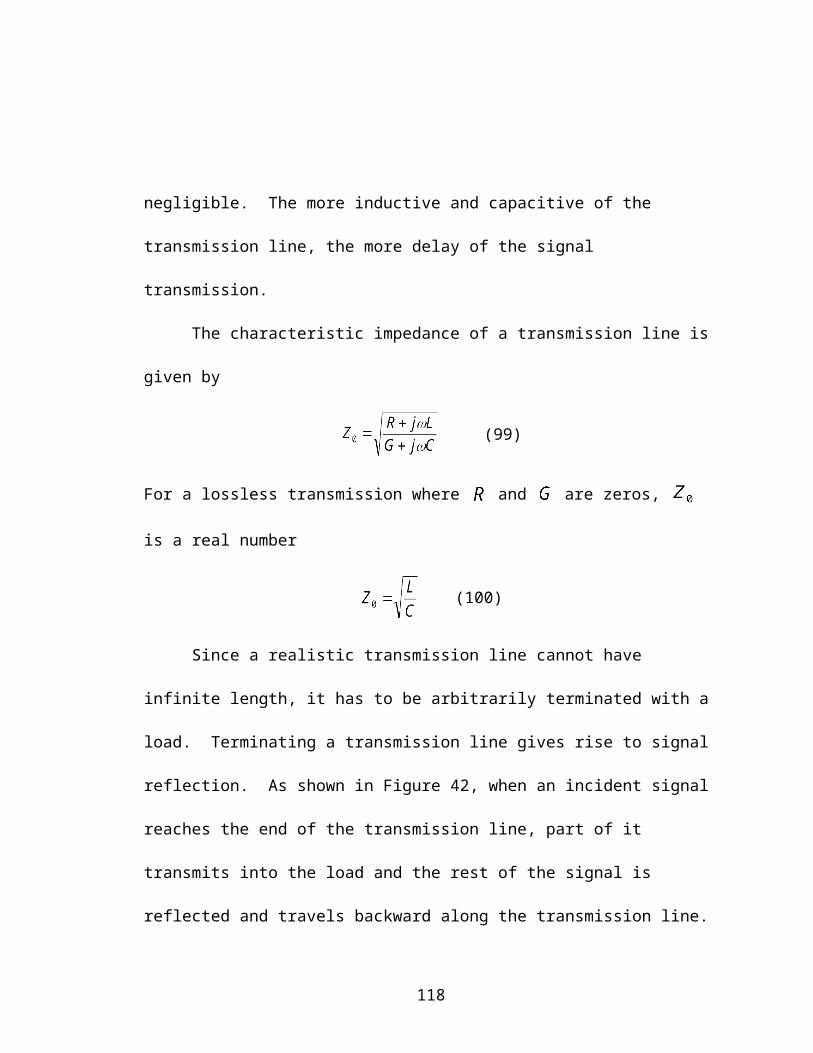
Figure 68 – Physical Dimensions of the Spirals coupled to the Transistor
The transistor has a gate length of 0.6 m and a width of 300 m. The edge-to-
edge spacing between the spiral and the poly gate is 51.45 m. The experiment compares
the coupling effects on two kinds of transistor layout configurations: one has single gate
finger and the other has multiple gate fingers, as illustrated in Figure 69.
118
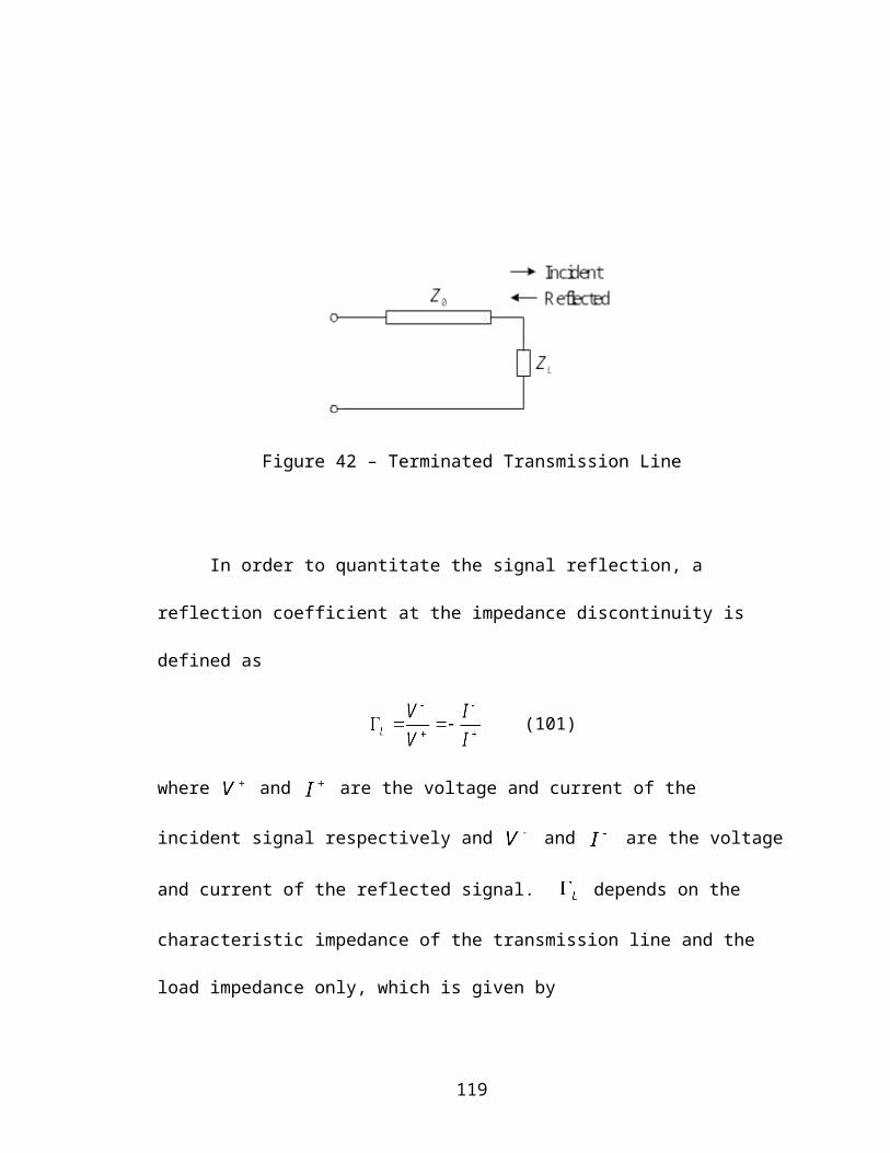
(a) NMOS with Single Gate Finger
(b) NMOS with 5 Gate Fingers
Figure 69 – Layout of Single and Multiple Gate Finger NMOS Transistors
119
The measured data is plotted in Figure 70. Both curves show a maximum |S21| of
about -17 dB, although at different frequencies.
2 3 4 5 6 7 8 9 10-55
-50
-45
-40
-35
-30
-25
-20
-15
Frequency, GHz
|S21
|, dB
Measured Data (N=1)Measured Data (N=5)Fitted Curve (N=1)Fitted Curve (N=5)
Figure 70 – |S21| of Coupled Spiral and NMOS Transistor with Single and Multiple Gate
Fingers
The coupling between spirals and transistors can significantly affect the
performance of analog radio-frequency integrated circuits, especially wireless
transceivers. In a monolithic wireless transceiver, on-chip inductors are used in both the
low noise amplifier at the input stage and the power amplifier at the output stage. Since
the low noise amplifier typically has a high power gain of about 20 dB, the active
transistors in the amplifier have to be very wide typically up to several hundred microns.
120
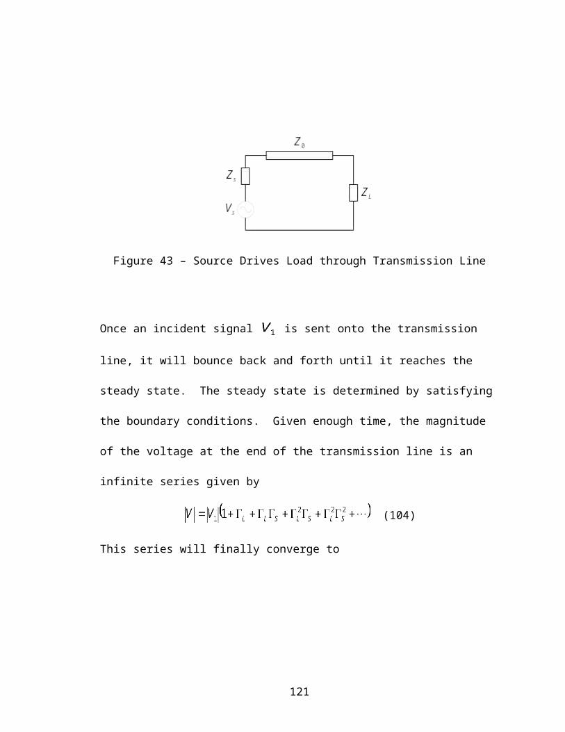
Therefore, the electromagnetic coupling between the inductors and the amplifying
transistors can form feedbacks either inside the low noise amplifier or between the low
noise amplifier and the power amplifier. Such feedback will degrade the noise
performance of the low noise amplifier.
DIGITAL SWITCHING NOISE
The fast switching of integrated digital circuits can induce large amount switching
current into the substrate, which can propagate in the substrate and couple to analog
components [9] [34]. In order to investigate the digital switching noise effects, the
coupling between an inverter and a transistor has been studied. As shown in Figure 71, a
digital inverter and a NMOS transistor have been laid out side by side on a common
substrate.
121
Figure 71 – Coupling between Digital Inverter and Transistor
The transistor is 0.6 m long and 300 m wide. The schematic of the digital inverter is
shown in Figure 72.
122
Figure 72 – Schematic of Digital Inverter as the Digital Switching Noise Generator
The induced noise signal on the transistor gate caused by the inverter switching is
measured by the oscilloscope and displayed in Figure 73. The top waveform is the input
signal into the inverter, which is an 800 MHz sinusoidal signal with the amplitude of 1.5
V. The waveform below is the induced signal on the transistor gate whose amplitude
goes up to 180 mV.
123
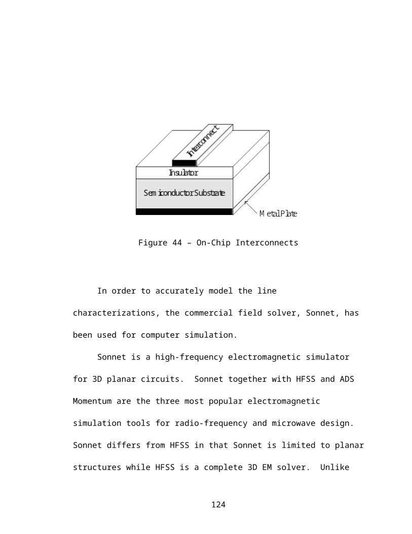
Figure 73 – Induced Noise Signal on Transistor Gate by Digital Switching
Since digital switching generates frequency harmonics, the coupling effects will vary
with different frequency components. Figure 74 is a 3D bar plotting showing the digital
switching noise. The axis is the inverter switching speed. Measurement has been
taken at ten different frequencies from 100 MHz to 990 MHz at which the inverter
operates. The axis is the frequency at which the coupling effect on the transistor is
measured. The axis is the voltage that is induced on the transistor gate by the digital
switching of the inverter.
124
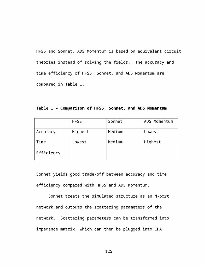
Figure 74 – Voltage induced by Digital Switching on the Transistor Gate
It is seen from Figure 74 that a maximum induced voltage of about 130 mV occurs at 800
MHz when the inverter is operating at the same frequency. Strong coupling happens
mainly at the fundamental and the second harmonic frequency of the inverter switching
speed. When the inverter is operating in the frequency range of 600 MHz to 1 GHz, the
coupling is maximized.
125
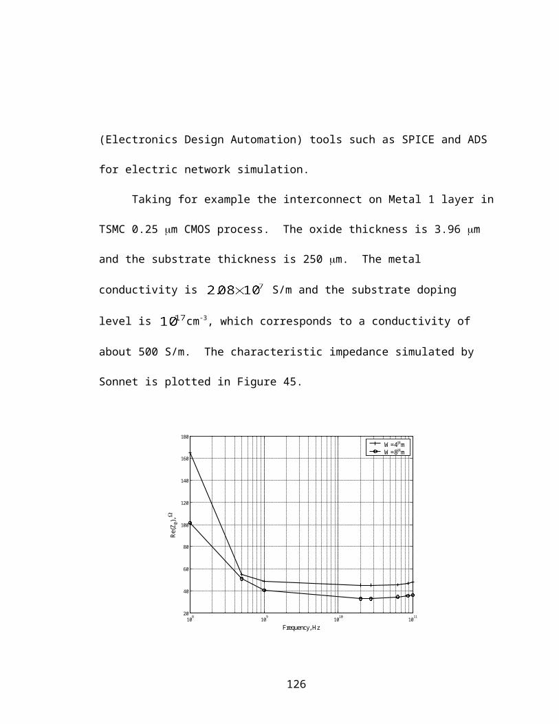
CONCLUSIONS AND FUTURE WORK
This thesis investigates some of the radio-frequency effects associated with
modern high frequency, high chip density integrated circuits.
First, the concept of inductance has been explained in detail. Three inherently
consistent definitions of inductance are given in different aspects: magnetic energy
storage, magnetic flux leakage, and voltage-current relationship. The classification of
inductance provides a more insightful understanding of the inductive mechanism,
including internal self-inductance, external self-inductance, and mutual inductance.
Physical pictures are used to explain the fundamentals behind each of the inductance
classifications. Starting with Maxwell’s Equations, analytical expressions are also
derived for the three kinds of inductance, which serve as the guidelines for inductance
calculation for specific cases.
The universal inductance definitions and analytical expressions are applied to an
on-chip environment by considering semiconductor substrate losses as well as the skin
effect to model metal interconnects and integrated spiral inductors.
The internal self-impedance of on-chip interconnects is caused by the skin effect.
It is calculated by solving the complex Helmholtz equation, which can be simplified by
applying the 1D approximation for on-chip interconnects. The external self-impedance
of a single on-chip interconnect and the mutual inductance between parallel interconnects
are modeled by taking the complex image theory approach and considering the skin
126
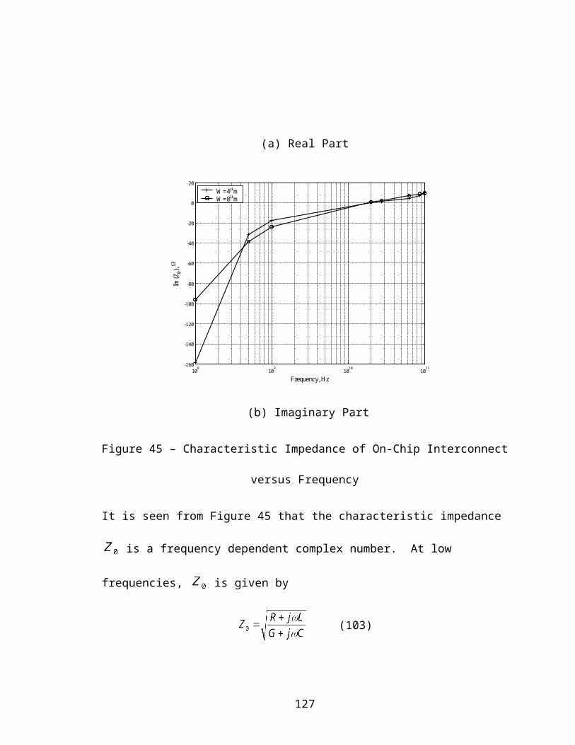
effects. The method of modeling on-chip interconnects is extended to characterize
integrated inductors by decomposing the spiral into an inductance matrix.
Computer simulation gives accurate results compared with the published data
simulated by ADS Momentum. Detailed discussion explains the effects of the
semiconductor substrate on both the inductance and resistance of on-chip interconnects
and inductors. Design optimization of spiral inductors is also provided aided by the
computer simulation.
The modeling technique presented in this thesis adds the skin effect into the
existing complex image approach to characterize on-chip interconnects. It further
provides an alternative way of optimizing on-chip inductors, and the design of novel
inductive devices (3D inductors). Comparing with full-wave simulation done by
commercial software tools, the numerical method developed here not only provides time-
efficient solutions, but also gives insight into the factors that determine the inductance
and resistance of on-chip interconnects and inductors.
The characterization of on-chip interconnects is used to investigate the high-speed
on-chip digital signal transmission. It is found out that the resistance of the interconnect
is the main factor that gives rise to the signal attenuation, while the frequency-dependent
line inductance causes the signal dispersion and delay.
Experimental measurement demonstrates the electromagnetic coupling effects
between on-chip high frequency integrated circuit components, including n-wells, spiral
inductors, and transistors. Digital switching noise induced by digital circuits on
127
transistors is also investigated. The measured data shows that the on-chip
electromagnetic coupling can induce serious problems on the performance of analog
radio-frequency integrated circuits.
Future work will be adding admittance to the on-chip interconnect model,
including capacitance and conductance. By calculating the parasitic capacitance and
conductance, one can numerically analyze the quality factor of on-chip inductors instead
of going through the experimental measurement or the time-consuming full-wave
simulation. The computer simulation should be compared with the on-chip measurement
to validate the model. The investigation of electromagnetic coupling should also be
carried further to analytical analysis, such as equivalent circuit models and numerical
simulation. The coupling between stand-alone components should be put into active
circuits to investigate effects of the coupling on the circuit performance. In addition,
coupling reduction techniques may be developed.
128
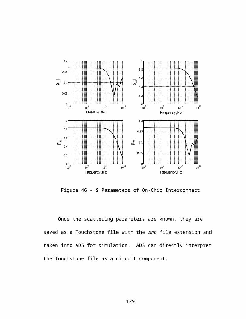
APPENDIX I
Material Properties
Name Symbol Value, UnitsVacuum Permittivity 8.85 aF/mSilicon Permittivity 11.9Silicon Dioxide Permittivity 3.97FR-4 Permittivity 4.9Teflon Permittivity 2.08Vacuum Permeability , H/mSilicon PermeabilitySilicon Dioxide PermeabilityCopper PermeabilityAluminum PermeabilityIntrinsic Silicon Conductivity , S/mAluminum Conductivity , S/mCopper Conductivity , S/mGold Conductivity , S/m
129
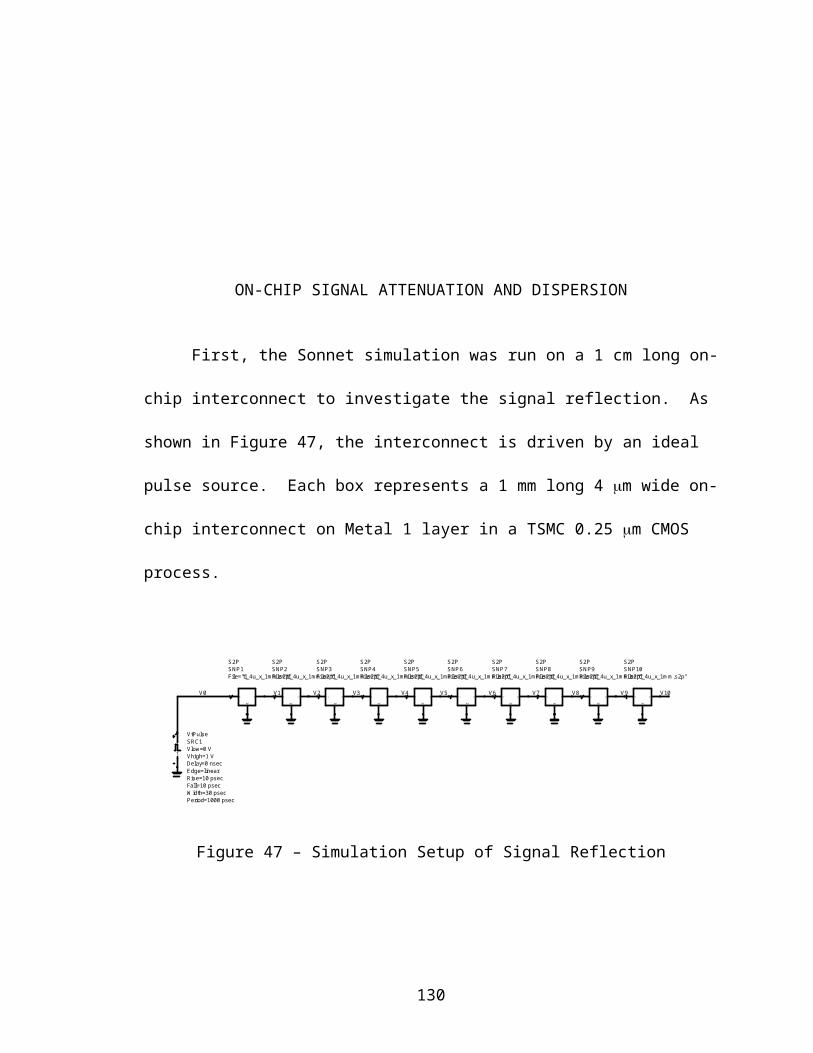
APPENDIX II
CMOS PROCESS PARAMETERS
Thickness of Gate Oxide
Process 0.5 m 0.25 m 0.18 m, 142 57 40
Thickness of Silicon Substrate
Process 0.5 m 0.25 m 0.18 m, m 250 250 250
Conductivity of Metal (Aluminum) Layers
, 107 S/mProcess Metal 1 Metal 2 Metal 3 Metal 4 Metal 5 Metal 60.5 m 1.74 2.150.25 m 2.08 2.08 2.38 2.38 3.700.18 m 2.60 2.16 2.16 2.16 2.46 3.88
Thickness of Metal Layers
, mProcess Metal 1 Metal 2 Metal 3 Metal 4 Metal 5 Metal 60.5 m 0.67 0.64 0.930.25 m 0.6 0.6 0.6 0.6 0.90.18 m 0.48 0.58 0.58 0.58 0.58 0.86
130
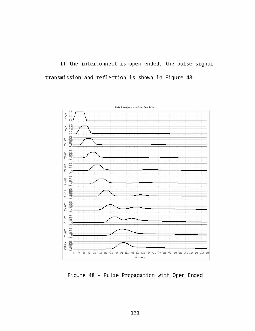
Insulator (Oxide) Thickness of Metal Layers
, mProcess Metal 1 Metal 2 Metal 3 Metal 4 Metal 5 Metal 60.5 m 0.58 1.61 2.670.25 m 0.58 1.42 2.22 3.06 3.960.18 m 0.53 1.45 2.35 3.21 4.11 5.11
131
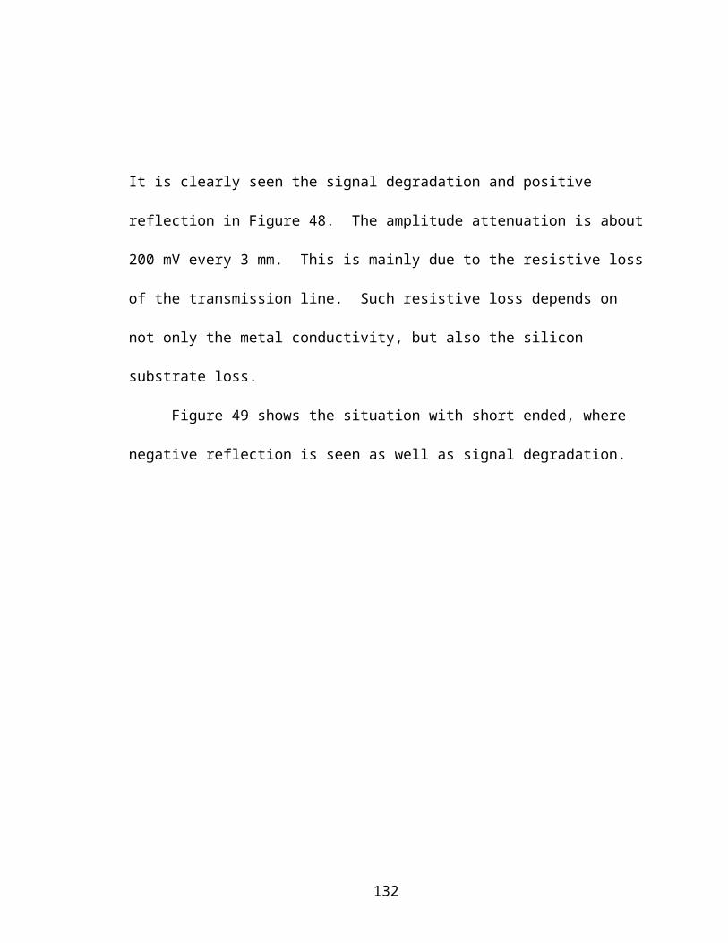
APPENDIX III
BSIM3 SPICE MODELS OF TSMC 0.25 M MOSFET’S
NMOS PMOSLength 0.24 mWidth N*10 m (N=1, 2, 3, …)Model Level BSIM3VERSIONMOBMODCAPMODNOIMODCHKDELTATNOMTOXNCHXJVTH0K1K2K3K3BW0DVT0DVT1DVT2DVT0WDVT1WDVT2WETA0ETABDSUBU0UAUBUCVSATA0AGSB0B1KETAA1A2RDSW
3.2001.0003.0001.0001.00010.00m27.005.500n2.38090E+17180.0n406.2m447.8m2.421m-315.5m518.1m6.305n3.044490.8m-50.00m-95.28m45.00MEG360.0m55.57m-13.47m321.1m36.23m-687.2p2.371a64.92p122.0K1.965385.8m9.578n70.00n-17.43m22.40n744.5m160.0
3.2001.0003.0001.0001.00010.00m27.005.500n4.00890E+17180.0n-482.8m581.0m5.217m24.97m622.0m6.305n1.869442.8m-130.3m-109.3m10.77MEG-11.5237.44m-23.94m319.7m8.199m-302.2p1.667a-83.31p159.5K1.222180.3m53.25n70.00n-26.39m0.000400.0m552.3
132
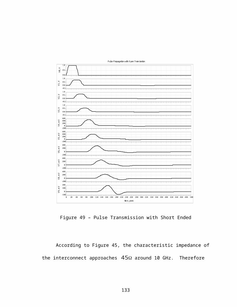
PRWBPRWGWINTWLWLNWWWWNWWLDWGDWBLINTLLLLNLWLWNLWLVOFFNFACTORCITCDSCCDSCBCDSCDPDIBLC1PDIBLC2PDIBLCBDROUTPSCBE1PSCBE2PVAGALPHA0ALPHA1BETA0JSJSWNJCJMJPBCJSWMJSWPBSWCJSWGMJSWGPBSWGCGDOCGSOCGBOCKAPPACFDLC
-30.00m415.5m4.390n0.0001.000-1.656p635.9m5.00000E-212.000u4.487n3.540n-2.13700E-221.9670.0001.0001.84800E-28-96.34m1.190-198.8u450.0u-809.3u7.00000E-2127.89m6.651m187.9m308.0m500.0MEG97.00u238.0m0.0001.50130.001.390u1.260p1.050927.0u366.2m801.4m181.2p208.7m1.000500.0p330.0m1.000465.0p155p0.00060.00m1.390p12n
-536.6m170.0m101.8n80.00f1.00011.20n100.0m-16.20f-14.03n3.640n-17.00n33.55a1.3760.0001.0000.000-116.7m1.281-81.19u1.229m60.03u0.00017.29m3.140m183.4m62.19m662.0MEG59.14m4.0200.0001.50130.001.390u1.260p1.050927.0u366.2m801.4m181.2p208.7m1.000540.0p330.0m1.000405.0p105.0p0.00060.00m127.9p33n
133
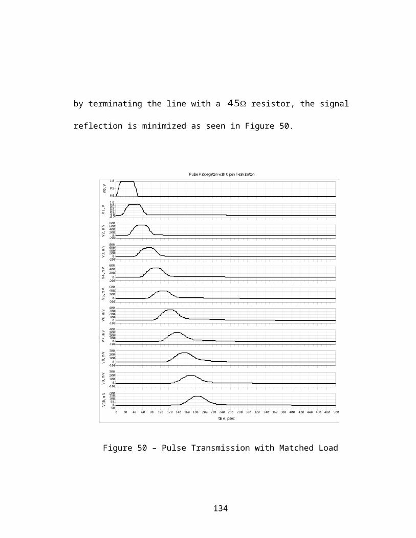
DWCLLCLWCLWLCWLCWWCWWLCCLCCLEXPARTKT1KT2ATUTEUA1UB1UC1KT1LPRTEFEMNOIANOIBNOIC
4.390n0.0000.0000.0000.0000.0000.0003.040n1.000500.0m-313.750m-60.0m33.0K-1.561.6n-2.431a8.8a-1.999E-210.0000.92746.15K7.088E+20-338.9K66.42p
-101.8n0.0000.0000.0000.0000.0000.0005.540n1.000500.0m-225.99m-36.9m4.05K-931.5m1.19n-2.329a-8.8223E-11-1.9E-80.0001.05646.15K6.671E+19-435.710.3200p
134
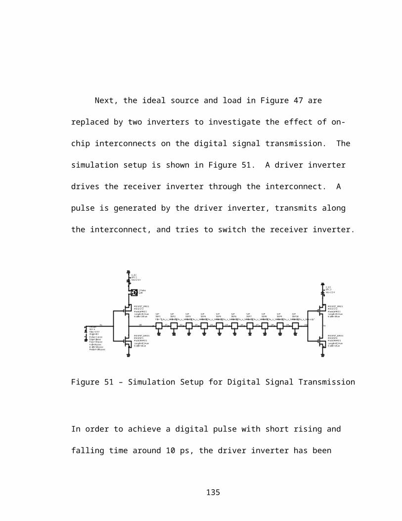
REFERENCES
[1] Frederick W. Grover, Inductance Calculations – Working Formulas and Tables, D.
Van Nostrand Company, Inc. 1946.
[2] Simon Ramo, John R. Whinnery, Theodore Van Duzer, Fields and Waves in
Communication Electronics, Third Edition, John Wiley & Sons, Inc., 1993.
[3] Robert E. Collin, Foundations for Microwave Engineering, Second Edition, The
IEEE Press Series on Electromagnetic Wave Theory, 2000.
[4] William H. Hayt, Jr. Engineering Electromagnetics, Fifth Edition, McGraw-Hill
Book Company, 1989.
[5] Richard S. Muller and Theodore I. Kamins, Device Electronics for Integrated
Circuits, John Wiley & Sons, Inc. Second Edition, 1997.
[6] Gray Hurst and Lewis Meyer, Analysis and Design of Analog Integrated Circuits,
John Wiley & Sons, Inc. Fourth Edition, 2000.
[7] R. Jacob Baker, Harry W. Li, David E. Boyce, CMOS Circuit Design, Layout, and
Simulation, IEEE Press Series on Microelectronic Systems, 1997.
[8] Thomas H. Lee, The Design of CMOS Radio-Frequency Integrated Circuits,
Cambridge University Press, 1998.
[9] Edoardo Charbon, Ranjit Gharpurey, Paolo Miliozzi, Robert G. Meyer, Alberto
Sangiovanni-Vincentelli, Substrate Noise – Analysis and Optimization for IC
Design, Kluwer Academic Publishers, 2001.
135
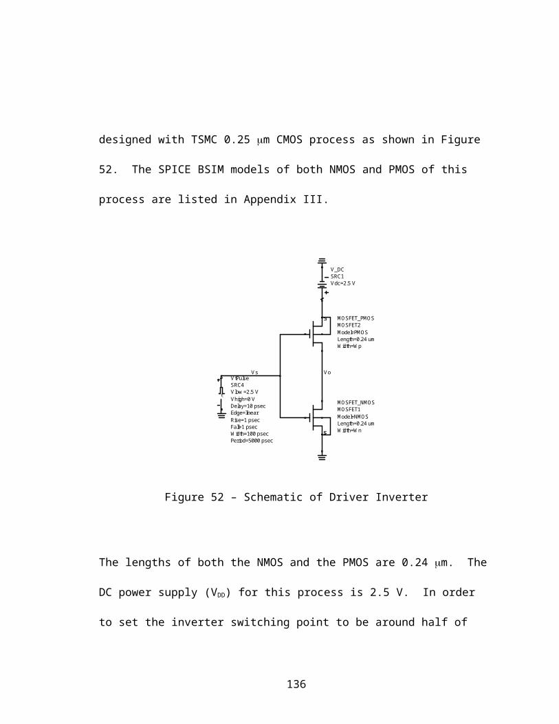
[10] Bruce R. Archambeault, PCB Design for Real-World EMI Control, Kluwer
Academic Publishers, 2002.
[11] Liang Dai and Ramesh Harjani, Design of High-Performance CMOS Voltage
Controlled Oscillators, Kluwer Academic Publishers, 2002.
[12] E. Ruehli, “Inductance Calculation in a Complex Integrated Circuit Environment,”
IBM Journal of Research and Development, Vol. 16, No. 5, Sep 1972.
[13] Sequence Design, Inc. “Modeling Skin Effect in Resistive Interconnect,”
Technology White Paper, 2002.
[14] H. Hasegawa, M. Furukawa, and H. Yanai, “Properties of Microstrip Line on Si-
SiO2 System,” IEEE Transactions on Microwave Theory and Technology, Vol. 19,
Issue 11, Nov 1971.
[15] Andreas Weisshaar, Hai Lan, Amy Luoh, “Accurate Closed-Form Expressions for
the Frequency-Dependent Line Parameters of On-Chip Interconnects on Lossy
Silicon Substrate,” IEEE Transactions on Advanced Packaging, Vol. 25, No. 2,
May 2002.
[16] Peter R. Bannister, “Application of Complex Image Theory,” Radio Science, Vol.
21, No. 4, Jul 1986.
[17] Harold A. Wheeler, “Transmission Line Properties of A Strip on A Dielectric Sheet
on A Plane,” IEEE Transactions on Microwave Theory and Technology, Vol. 25,
Aug 1977.
136
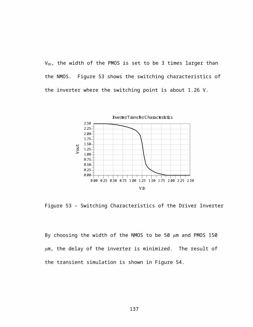
[18] Christopher L. Holloway and Edward F. Kuester, “Closed-Form Expressions for
the Current Density on the Ground Plane of a Microstrip Line, with Application to
Ground Plane Loss,” IEEE Transactions on Microwave Theory and Techniques,
Vol. 43, No. 5, May 1995.
[19] Peter Meuris, Wim Schoenmaker, and Wim Magnus, “Stragegy for
Electromagnetic Interconnect Modeling,” IEEE Transactions on Computer-Aided
Design of Integrated Circuits and Systems, Vol. 20, No. 6, Jun 2001.
[20] Derek K. Shaeffer, Thomas H. Lee, “A 1.5-V, 1.5-GHz CMOS Low Noise
Amplifier,” IEEE Journal of Solid-State Circuits, Vol. 32, No. 5, May 1997.
[21] Jan Craninckx and Michiel S. J. Steyaert, “A 1.8-GHz Low-Phase-Noise CMOS
VCO Using Optimized Hollow Spiral Inductors,” IEEE Journal of Solid-State
Circuits, Vol. 32, No. 5, May 1997.
[22] Alireza Zolfaghari, Andrew Chan, Behzad Ravazi, “Staked Inductors and
Transformers in CMOS Technology,” IEEE Journal of Solid-State Circuits, Vol.
36, No. 4, Apr 2001.
[23] Chih-Chun Tang, Chia-Hsin Wu, and Shen-Iuan Liu, “Miniature 3-D Inductors in
Standard CMOS Process,” IEEE Journal of Solid-State Circuits, Vol. 37, No. 4,
Apr 2002.
[24] Guo Lihui, Yu Mingbin, Chen Zhen, He Han, and Zhang Yi, “High Q Multilayer
Spiral Inductor on Silicon Chip for 5-6 GHz,” IEEE Electron Device Letters, Vol.
23, No. 8, Aug 2002.
137
[25] Joachim N. Burghartz, D. C. Edelstein, Mehmet Soyuer, H. A. Ainspan, and Keith
A. Jenkins, “RF Circuit Design Aspects of Spiral Inductors on Silicon,” IEEE
Journal of Solid-State Circuits, Vol. 33, No. 12, Dec 1998.
[26] Alina Deutsch, Gerard V. Kopcsay, Phillip J. Restle, Howard H. Smith, G. Katopis,
Wiren D. Becker, Paul W. Coteus, Christopher W. Surovic, Barry J. Rubin,
Richard P. Dunne, Jr., T. Gallo, Keith A. Jenkins, Lewis M. Terman, Robert H.
Dennard, George A. Sai-Halasz, Byron L. Krauter, and Daniel R. Knebel, “When
are Transmission-Line Effects Important for On-Chip Interconnects?” IEEE
Transactions on Microwave Theory and Techniques, Vol. 45, No. 10, Oct 1997.
[27] Bendik Kleveland, Xiaoning Qi, Liam Madden, Takeshi Furusawa, Robert W.
Dutton, Mark A. Horowitz, and S. Simon Wong, “High-Frequency
Characterization of On-Chip Digital Interconnects,” IEEE Journal of Solid-State
Circuits, Vol. 37, No. 6, Jun 2002.
[28] A. O. Adan, M. Fukumi, K Higashi, T. Suyama, M. Miyamoto, and M. Hayashi,
“Electromagnetic Coupling Effects in RFCMOS Circuits,” IEEE MTT-S Digest,
2002.
[29] E. M. T. Jones and J. T. Bolljahn, “Coupled-Strip-Transmission-Line Filters and
Directional Couplers,” IRE Transactions on Microwave Theory and Techniques,
1956.
138
[30] Jia-Sheng Hong and Michael J. Lancaster, “Couplings of Microstrip Square Open-
Loop Resonators for Cross-Coupled Planar Microwave Filters,” IEEE Transactions
on Microwave Theory and Techniques, Vol. 44, No. 12, Dec 1996.
[31] Yu Cao, Robert A. Groves, Xuejue Huang, Noah D. Zamdmer, Jean-Olivier
Plouchart, Richard A. Wachnik, Tsu-Jae King, Chenming Hu, “Frequency-
Independent Equivalent-Circuit Model for On-Chip Spiral Inductors,” IEEE
Journal of Solid-State Circuits, Vol. 38, No. 3, Mar 2003.
[32] Sunderarajan S. Mohan, C. Patrick Yue, Maria del Mar Hershenson, S. Simon
Wong, and Thomas H. Lee, “Modeling and Characterization of On-Chip
Transformers,” Electron Devices Meeting, 1998. IEDM '98 Technical Digest.,
International , 6-9 Dec. 1998.
[33] Alan L. L. Pun, Tony Yeung, Jack Lau, Francois J. R. Clement, David K. Su,
“Substrate Noise Coupling Through Planar Spiral Inductor,” IEEE Journal of
Solid-State Circuits, Vol. 33, No. 6, Jun 1998.
[34] Patrik Larsson, “Measurement and Analysis of PLL Jitter Caused by Digital
Switching Noise,” IEEE Journal of Solid-State Circuits, Vol. 36, No. 7, Jul 2001.
[35] Tallis Blalack, Youri Leelercq, C. Patrick Yue, “On-Chip RF Isolation
Techniques,” IEEE BCTM, 2002.
[36] MOSIS IC Service.
[37] The EUROPRACTICE IC Service.
[38] American National Standard for Telecommunications
139