Embed Size (px)
Citation preview

Masters for micro- and nanostructure replication by
Diplomvej 381
DK-2800 Kongens Lyngby
Denmark
www.nilt.com
CVR: DK 29310203
Contact: Phone: +45 3111 1797 – Email: [email protected]

Background
• More than 8 years of experience in providing stamps to the imprint community
• 12 Full time employees
• More than 250 clients across the more than 30 countries
• Delivering products to meet technical and economical expectations from clients
• Striving to achieve the highest possible quality of stamps
• Working in state-of-the-art silicon processing cleanrooms, class 10/100, in Denmark and Sweden

• Reduced prices if more than one stamp is ordered
• Repeat orders are subject to discounts
• High focus on delivered stamps fulfilling specs
• Close interaction with client already in design phase of the stamp
• High degree of production status to client
Added value by NILT

Products
• Silicon stamps
• Quartz stamps (including 65 Templates)
• Nickel shims
• Steel tools
Technologies where master/stamps/molds are used
• Nanoimprint
• Hot embossing
• Roll-2-Roll printing
• Injection molding
Stamps/molds by NILT

Available sizes:
• Round: 2-inch, 4-inch round, 6-inch round, 8-inch round
• Any square format cut from wafers.
Stamp thickness
• In general the stamp thickness will follow the standard wafer thickness, i.e. 525 µm (2-inch and 4-inch), 675 µm (6-inch), and 725µm (8-inch)
Anti-sticking and stamp cleaning
• We can apply anti-sticking coating (FDTS, 1H,1H,2H,2H-perflourodecyltrichlorosilane) onto all silicon stamps upon request
• Cleaning service is available upon request
Patterns
• We can prepare silicon stamps with features from below 20 nm
• Structures with lateral size of below 20 nm to 300 nm will be patterned with EBL
• Structures with lateral size of 300 nm to 2 µm will be patterned with DUV
• Structures with lateral size larger than 2 µm will be patterned with UVL
Pattern depth/height
• The pattern depth/height depends on the lateral feature size
Side wall
• Regular specification: 85-90°
• Other angles available upon request
Line Edge Roughness
• Depends on etch depth and lateral and vertical dimensions
Silicon stamps/molds
2-inch silicon NIL stamp with photonic crystal structures
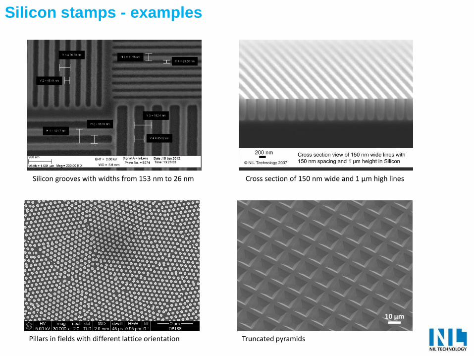
Silicon stamps - examples
Silicon grooves with widths from 153 nm to 26 nm
Pillars in fields with different lattice orientation Truncated pyramids
Cross section of 150 nm wide and 1 µm high lines

Silicon stamps - examples
Shaping of silicon structures. Here pencil type protrusions
2 µm wide and 2 µm deep square holes Polymer micro needles hot embossed from silicon master
500 nm diameter holes in silicon

Materials
• Quartz, Fused silica, glass
Available sizes:
• Round: 2-inch, 4-inch round, 6-inch round, 8-inch round
• Any square format cut from wafers
• 65 mm X 65 mm x 6.35 mm (cut from 6026 mask blanks)
Stamp thickness
• Stamp thickness from 200 µm
Stamp cleaning
• Cleaning service is available upon request
Patterns
• We can prepare quartz stamps with features from 20 nm
• Structures with lateral size of 20 nm to 300 nm will be patterned with EBL
• Structures with lateral size of 300 nm to 2 µm will be patterned with DUV
• Structures with lateral size larger than 2 µm will be patterned with UVL
Pattern depth/height
• The pattern depth/height depends on the lateral feature size
Side walls
• Regular specification: 80-85°
Line Edge Roughness
• Depends on etch depth and lateral and vertical dimensions
Quartz stamps
Image of 65 Template, cut from a 6025 Photomask. Pattern is located on central mesa

Quartz stamps - examples
100 nm wide grooves
50 µm diameter concave lenses
30 nm wide lines etched to a depth of 1 µm

Nickel shims for nanoimprint lithography, hot embossing, Roll-2-Roll printing and injection moulding.
Available sizes:
• Any shape/size cut from Ø140 mm diameter
• Up to 500 mm x 500 mm upon request and with certain limitation regarding structures
Shim thickness according to specification. Regular thickness is 300 µm (thickness from tens of µm to several mm can be made)
Anti-sticking and stamp cleaning
• We can apply anti-sticking coating (FDTS, 1H,1H,2H,2H-perflourodecyltrichlorosilane) onto all silicon stamps upon request
• Cleaning service is available upon request
Patterns
• The Nickel shims are made from a resist pattern or a Silicon or Quartzmaster. Dimensions are available from 30 nm.
Pattern depth/height
• The pattern depth/height depends on the lateral feature size
• Regular aspect ratio up to 1:2 as standard (higher upon request)
Side walls
• Regular specification: 80-85°
Line Edge Roughness
• Depends on etch depth and lateral and vertical dimensions
Various types of nickel (different hardness) can be provided upon request
Nickel shims
• Developed technology for shim fabrication for microfluidics and lab-on-a-chip purposes.
• Combining micro- and nanostructures• Several layers• Contact NILT to learn more
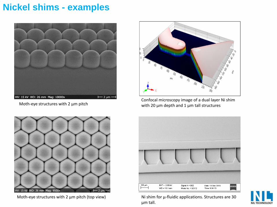
Nickel shims - examples
Moth-eye structures with 2 µm pitch
Moth-eye structures with 2 µm pitch (top view) Ni shim for µ-fluidic applications. Structures are 30 µm tall.
Confocal microscopy image of a dual layer Ni shimwith 20 µm depth and 1 µm tall structures

Nickel shims - examples
Nickel shim with isolated mesas, each havingdiffraction grating on top.
Nickel shim ready for replication by injectionmoulding.
Pattern consist of holes placed in hexagonal lattice, having diameter of 500 nm, period of 750 nm and depth of 825 nm.

Nickel shim ready for replication by injectionmoulding.
Pattern consist of holes placed in hexagonallattice, having diameter of 500 nm, period of 750 nm and depth of 825 nm.
NICKEL SHIM WITH 500 NM DIAMETER HOLES

Multilevel structures
• Alignment accuracy between layers
– <30 nm with EBL
– <100 nm with DUV
– <4 µm with UVL
3D structures
• Arbitrary continous functions f(x,y) canbe made with 3D EBL and transferred both to Silicon and Quartz. However dueto scattering effects there is a limit to how sharp transitions between different heights can be achieved.
Micro Lenses
• Concave lens shapes can be done in quartz
• SAG < 2D where D=diameter of lens
Advanced processing by NILT
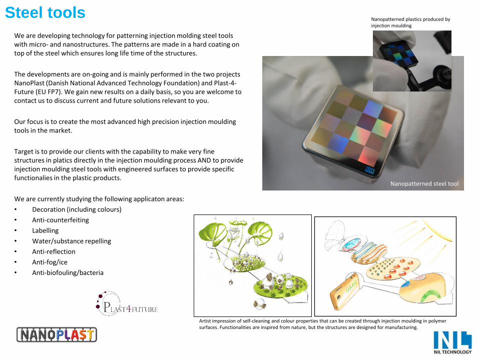
We are developing technology for patterning injection molding steel tools with micro- and nanostructures. The patterns are made in a hard coating on top of the steel which ensures long life time of the structures.
The developments are on-going and is mainly performed in the two projectsNanoPlast (Danish National Advanced Technology Foundation) and Plast-4-Future (EU FP7). We gain new results on a daily basis, so you are welcome to contact us to discuss current and future solutions relevant to you.
Our focus is to create the most advanced high precision injection mouldingtools in the market.
Target is to provide our clients with the capability to make very fine structures in platics directly in the injection moulding process AND to provide injection moulding steel tools with engineered surfaces to provide specificfunctionalies in the plastic products.
We are currently studying the following applicaton areas:
• Decoration (including colours)
• Anti-counterfeiting
• Labelling
• Water/substance repelling
• Anti-reflection
• Anti-fog/ice
• Anti-biofouling/bacteria
Steel tools
Nanopatterned steel tool
Nanopatterned plastics produced by injection moulding
Artist impression of self-cleaning and colour properties that can be created through injection moulding in polymer surfaces. Functionalities are inspired from nature, but the structures are designed for manufacturing.

NIL Technology ApS (Headquarters)Diplomvej 381Kongens LyngbyDenmarkPhone: +45 3171 [email protected]
NILT Sweden Filial (Branch)Stena Center 1B412 92 GothenburgSwedenPhone: +46 70-857 96 [email protected]
Agents
Japan
HTL Co Japan Ltd
Tachikawa City (Tokyo), Japan
www.htlco.co.jp
Masashi Tsutsui
Singapore
Gaia Science Pte Ltd
Singapore, Singapore
www.gaiascience.com.sg
Tony Lee
India
HTL Co Ltd India
Bangalore, India
www.htl.co.jp
Sanjay Acharya:
Contact NILT

NIL Technology ApS
Diplomvej 381
Kongens Lyngby
Denmark
Phone: +45 3171 9036
Email: [email protected]
Contact persons:
Theodor Nielsen, founder, CEO
Phone: +45 3171 9036
Email: [email protected]
Brian Bilenberg, founder, CTO
Phone: +45 3171 9037
Email: [email protected]
Niklas Hansson, Director of Sales
Phone: +46 70 857 9669
Email: [email protected]
Contact NILT