Embed Size (px)
Citation preview

MA
ST
ER
THESIS
Master's Programme in Embedded and Intelligent Systems, 120 credits
Implementation of a Generic Gateway as aMultipurpose Communication Node
Hesam Moshiri
Information Science, Computer and Electrical Engineering, 30 Credits
Halmstad 2014-03-12

3
Technical Report, IDE1402
Implementation of a generic gateway as a multipurpose communication node
Master Thesis in Embedded and Intelligent Systems Design
Hesam Moshiri
School of Information Science, Computer and Electrical Engineering
Halmstad University
Box 823, S-301 18 Halmstad, Sweden
March 2014

4
Acknowledgement
This report is the result of a thesis work within the master’s program: Embedded and
Intelligent Systems at Halmstad University.
I thank my supervisor Mr. Stefan Lundgren, Hardware team manager at CPAC for his
sympathetic leadership, help and providing project equipment and material, Dr. Urban Bilstrup
and Professor Mohammad Reza Mousavi, respectively, my university supervisor and examiner
for their helpful comments and guidance, Fredrik Karlemon, Magnus Johansson, Michael
Petterson, Bo Ericsson, Marco Monzani, Viktor Stensson, Steve Brown and Martin Jangeberg for
guiding me through the project.
I especially thank my parents for their financial and spiritual supports.
This is the concluding part of my two years education at Halmstad University, Sweden.
Hesam Moshiri
5
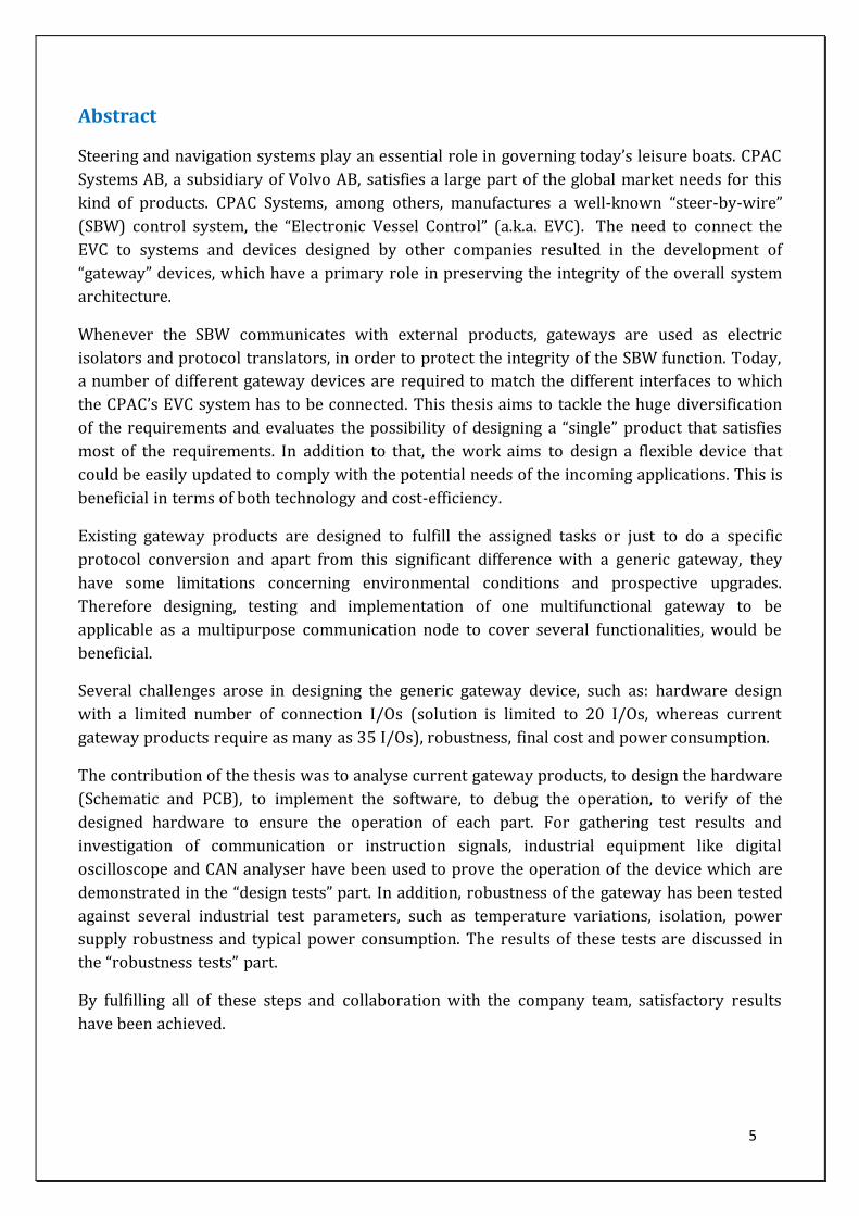
Abstract
Steering and navigation systems play an essential role in governing today’s leisure boats. CPAC
Systems AB, a subsidiary of Volvo AB, satisfies a large part of the global market needs for this
kind of products. CPAC Systems, among others, manufactures a well-known “steer-by-wire”
(SBW) control system, the “Electronic Vessel Control” (a.k.a. EVC). The need to connect the
EVC to systems and devices designed by other companies resulted in the development of
“gateway” devices, which have a primary role in preserving the integrity of the overall system
architecture.
Whenever the SBW communicates with external products, gateways are used as electric
isolators and protocol translators, in order to protect the integrity of the SBW function. Today,
a number of different gateway devices are required to match the different interfaces to which
the CPAC’s EVC system has to be connected. This thesis aims to tackle the huge diversification
of the requirements and evaluates the possibility of designing a “single” product that satisfies
most of the requirements. In addition to that, the work aims to design a flexible device that
could be easily updated to comply with the potential needs of the incoming applications. This is
beneficial in terms of both technology and cost-efficiency.
Existing gateway products are designed to fulfill the assigned tasks or just to do a specific
protocol conversion and apart from this significant difference with a generic gateway, they
have some limitations concerning environmental conditions and prospective upgrades.
Therefore designing, testing and implementation of one multifunctional gateway to be
applicable as a multipurpose communication node to cover several functionalities, would be
beneficial.
Several challenges arose in designing the generic gateway device, such as: hardware design
with a limited number of connection I/Os (solution is limited to 20 I/Os, whereas current
gateway products require as many as 35 I/Os), robustness, final cost and power consumption.
The contribution of the thesis was to analyse current gateway products, to design the hardware
(Schematic and PCB), to implement the software, to debug the operation, to verify of the
designed hardware to ensure the operation of each part. For gathering test results and
investigation of communication or instruction signals, industrial equipment like digital
oscilloscope and CAN analyser have been used to prove the operation of the device which are
demonstrated in the “design tests” part. In addition, robustness of the gateway has been tested
against several industrial test parameters, such as temperature variations, isolation, power
supply robustness and typical power consumption. The results of these tests are discussed in
the “robustness tests” part.
By fulfilling all of these steps and collaboration with the company team, satisfactory results
have been achieved.
6
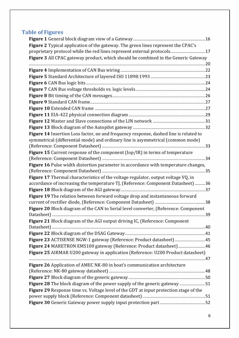
Table of Figures Figure 1 General block diagram view of a Gateway .............................................................. 16
Figure 2 Typical application of the gateway. The green lines represent the CPAC’s proprietary protocol while the red lines represent external protocols.............................. 17
Figure 3 All CPAC gateway product, which should be combined in the Generic Gateway........................................................................................................................................................ 20
Figure 4 Implementation of CAN Bus wiring ......................................................................... 22
Figure 5 Standard Architecture of layered ISO 11898:1993 ............................................... 23
Figure 6 CAN Bus logic bits ....................................................................................................... 24
Figure 7 CAN Bus voltage thresholds vs. logic levels............................................................ 24
Figure 8 Bit timing of the CAN messages................................................................................ 26
Figure 9 Standard CAN frame................................................................................................... 27
Figure 10 Extended CAN frame ............................................................................................... 27
Figure 11 EIA-422 physical connection diagram .................................................................. 29
Figure 12 Master and Slave connections of the LIN network ............................................. 31
Figure 13 Block diagram of the Autopilot gateway .............................................................. 32
Figure 14 Insertion Loss factor, αe and frequency response, dashed line is related to
symmetrical (differential mode) and ordinary line is asymmetrical (common mode) (Reference: Component Datasheet) ......................................................................................... 33
Figure 15 Current response of the component (Iop/IR) in terms of temperature (Reference: Component Datasheet) ......................................................................................... 34
Figure 16 Pulse width distortion parameter in accordance with temperature changes, (Reference: Component Datasheet) ......................................................................................... 35
Figure 17 Thermal characteristics of the voltage regulator, output voltage VQ, in accordance of increasing the temperature TJ, (Reference: Component Datasheet) ......... 36
Figure 18 Block diagram of the AGI gateway......................................................................... 37
Figure 19 The relation between forward voltage drop and instantaneous forward current of rectifier diode, (Reference: Component Datasheet) ........................................... 38
Figure 20 Block diagram of the CAN to Serial level converter, (Reference: Component Datasheet) .................................................................................................................................... 39
Figure 21 Block diagram of the AGI output driving IC, (Reference: Component Datasheet) .................................................................................................................................... 40
Figure 22 Block diagram of the DSAG Gateway..................................................................... 41
Figure 23 ACTISENSE NGW-1 gateway (Reference: Product datasheet) .......................... 45
Figure 24 MARETRON EMS100 gateway (Reference: Product datasheet) ....................... 46
Figure 25 AIRMAR U200 gateway in application (Reference: U200 Product datasheet)........................................................................................................................................................ 47
Figure 26 Application of AMEC NK-80 in boat’s communication architecture (Reference: NK-80 gateway datasheet) ................................................................................... 48
Figure 27 Block diagram of the generic gateway .................................................................. 50
Figure 28 The block diagram of the power supply of the generic gateway ...................... 51
Figure 29 Response time vs. Voltage level of the GDT at input protection stage of the power supply block (Reference: Component datasheet) ...................................................... 51
Figure 30 Generic Gateway power supply input protection part ....................................... 52

7
Figure 31 required robustness of the generic gateway power supply input line, against sudden voltage glitch (Black vs. Blue line) .............................................................................. 53
Figure 32 Generic Gateway CAN input filtering .................................................................... 54
Figure 33 Generic Gateway 1587 (Serial) input interface ................................................... 55
Figure 34 PCB Layers stack demonstration of generic gateway (Top-GND-Power-Bottom) ......................................................................................................................................... 59
Figure 35 Isolated PCB copper ground planes (one and two) with proper insulation gap........................................................................................................................................................ 60
Figure 36 Block diagram of the generic gateway software ................................................. 63
Figure 37 Flowchart diagram of the generic gateway software ......................................... 64
Figure 38 The temperature of the heart of the power supply (voltage regulator) 10 seconds after +48V injection to the inputs .............................................................................. 65
Figure 39 The temperature of the heart of the power supply (voltage regulator), 2 minutes after +48V injection to the inputs ............................................................................. 66
Figure 40 The level of the output voltages of the generic gateway power supply block, in front of input voltage variation ............................................................................................ 67
Figure 41 The provided signal isolation by the optocoupler and the test points in the generic gateway........................................................................................................................... 68
Figure 42 Test room of the temperature chamber, a PC and a digital oscilloscope are connected to the generic gateway to record the events........................................................ 70
Figure 43 Temperature chamber software and related adjustments, dark red line
shows the adjusted temperature and the normal red line shows the real time
temperature inside the chamber (Adjustments are done inside analogue channels box in the software) ................................................................................................................................ 71
Figure 44 The received text message from the generic gateway, which shows healthy
communication between the generic gateway inside the chamber and the PC outside (Temperature: 25°C) .................................................................................................................. 72
Figure 45 Signal demonstration of the UART messages between the generic gateway inside the chamber and the digital oscilloscope outside (Temperature: 25°C) ................ 72
Figure 46 Temperature chamber adjustments for 85°C, dark red line shows the
adjusted temperature and the normal red line shows the real time temperature inside the chamber (Adjustments are done inside “analogue channels” box in the software) .. 73
Figure 47 The received text message from the generic gateway, which shows healthy
communication between the generic gateway inside the chamber and the PC outside (Temperature: +85°C) ................................................................................................................ 74
Figure 48 Signal demonstration of the UART messages between the generic gateway inside the chamber and the digital oscilloscope outside (Temperature: +85°C) .............. 74
Figure 49 Temperature chamber adjustments for -20°C, dark red line shows the
adjusted temperature and the normal red line shows the real time temperature inside the chamber (Adjustments are done inside analogue channels box in the software) ...... 75
Figure 50 The received text message from the generic gateway, which shows healthy
communication between the generic gateway inside the chamber and the PC outside (Temperature: -20°C) ................................................................................................................. 76
Figure 51 Signal demonstration of the UART messages between the generic gateway inside the chamber and the digital oscilloscope outside (Temperature: -20°C) ............... 76
8
Figure 52 Assembled PCB board of the generic gateway (TOP) ......................................... 78
Figure 53 Assembled PCB board of the generic gateway (Bottom) ................................... 79
Figure 54 Signal overview of CAN on microcontroller output pin ..................................... 80
Figure 55 Analysis of the CAN data signals on communication wires (influence of wires and filters are noticeable) .......................................................................................................... 81
Figure 56 Demonstration of the Figure 32 signal, in a shorter period (1uS) ................... 82
Figure 57 Short time frame cut of CAN communication signal on line wire (200nS) ..... 83
Figure 58 Demonstration of CAN data transmission with the CAN analyzer software (Black boxes show baud rate: 500Kb/s and the Data) .......................................................... 84
Figure 59 Reception of transmitted CAN data on related receive interrupt event (Green highlight, Data: Black rectangle in the debug window)......................................................... 85
Figure 60 Demonstration of serial 1587 communication signal on output lines ............ 85
Figure 61 Typical current consumption of all existing gateways (Average=73mA, generic gateway=90mA) ............................................................................................................ 86
Figure 62 A comparison between the design performance of the generic gateway and others existing ones in terms of the I/O multiplexing ........................................................... 87
9
Table of Tables Table 1 ISO11898 Electrical Requirements ........................................................................... 25
Table 2 Suggested cable length vs. signaling rate ................................................................. 26
Table 3 NMEA2000 communication protocol Characteristics ............................................ 30
Table 4 Temperature & humidity tests (chamber room) .................................................... 43
Table 5 Overview of the existing functionalities of the CPAC gateways and the summation of all separate I/Os which the generic gateway supports................................ 49
Table 6 Instrumentation I/Os of Generic Gateway ............................................................... 56
Table 7 CAN and Power demonstration of Generic Gateway .............................................. 56
Table 8 Characteristics of the all Input/output signals (CAN and power lines are excluded because their I/Os are fixed) .................................................................................... 57
Table 9 Some examples of STM32 interrupt and priorities................................................. 61
Table 10 The test results of the generic gateway’s power supply against the variable inputs ............................................................................................................................................ 66
Table 11 Isolation test results of the generic gateway ......................................................... 68
Table 12 Typical current consumption test of the Generic Gateway ................................. 69
Table 13 Temperature test results of the generic gateway ................................................. 77
Table 14 The price difference between the suggested and the selected components of the generic gateway and its influence on the total material price ....................................... 88

10
Table of Contents 1 Introduction ............................................................................................................................13
1.1 Motivation ........................................................................................................................................... 13
1.2 Goals ...................................................................................................................................................... 13
1.3 Problem Statement & Approach ................................................................................................. 13
1.5 Structure .............................................................................................................................................. 15
2 Background .............................................................................................................................................. 16
2.1 Block Diagram of a Gateway ........................................................................................................ 16
2.2 Description of the CPAC Gateways ............................................................................................ 18
2.2.1 AGI .................................................................................................................................................. 18
2.2.2 NMEA0183 .................................................................................................................................. 18
2.2.3 NMEA2000 .................................................................................................................................. 18
2.2.4 Autopilot ...................................................................................................................................... 18
2.2.5 DSAG .............................................................................................................................................. 18
2.2.6 PFM ................................................................................................................................................ 18
2.2.7 LZGW ............................................................................................................................................. 19
2.2.8 DPS ................................................................................................................................................. 19
2.2.9 TJSGW ........................................................................................................................................... 19
2.2.10 ACU .............................................................................................................................................. 19
2.2.11 MOTORSIM ............................................................................................................................... 19
2.3 CAN Interface ..................................................................................................................................... 21
2.3.1 Physical Layer ............................................................................................................................ 22
2.3.2 Bit Timing .................................................................................................................................... 26
2.3.3 CAN Message frame description ......................................................................................... 27
2.4 NMEA0183 .......................................................................................................................................... 28
2.5 NMEA2000 .......................................................................................................................................... 29
2.6 Local Interconnect Network (LIN) ............................................................................................ 30
2.7 Hardware analysis of the existing gateways (CPAC) .......................................................... 32
2.7. Autopilot Gateway ...................................................................................................................... 32
2.7.2 Internal CAN Interface ............................................................................................................ 32
2.7.3 External Isolated CAN ............................................................................................................. 35
2.7.4 Power Supply ............................................................................................................................. 36
2.7.5 Main Controller ......................................................................................................................... 37

11
2.7.6 AGI Gateway ............................................................................................................................... 37
2.7.7 Power Supply ............................................................................................................................. 38
2.7.8 Internal CAN Interface ............................................................................................................ 39
2.7.9 Instrumentation ........................................................................................................................ 40
2.7.10 DSAG Gateway ......................................................................................................................... 41
2.7.11 Power Supply........................................................................................................................... 41
2.7.12 Internal CAN Interface ......................................................................................................... 42
2.7.13 Instrumentation ..................................................................................................................... 42
2.7.14 Main Controller ....................................................................................................................... 42
2.8 General and exclusive standards ................................................................................................ 43
3 Related Work ........................................................................................................................................... 45
3.1 ACTISENSE NGW-1 Gateway (non-CPAC) .............................................................................. 45
3.1.1 Generic Gateway and ACTISENSE NGW-1 ...................................................................... 45
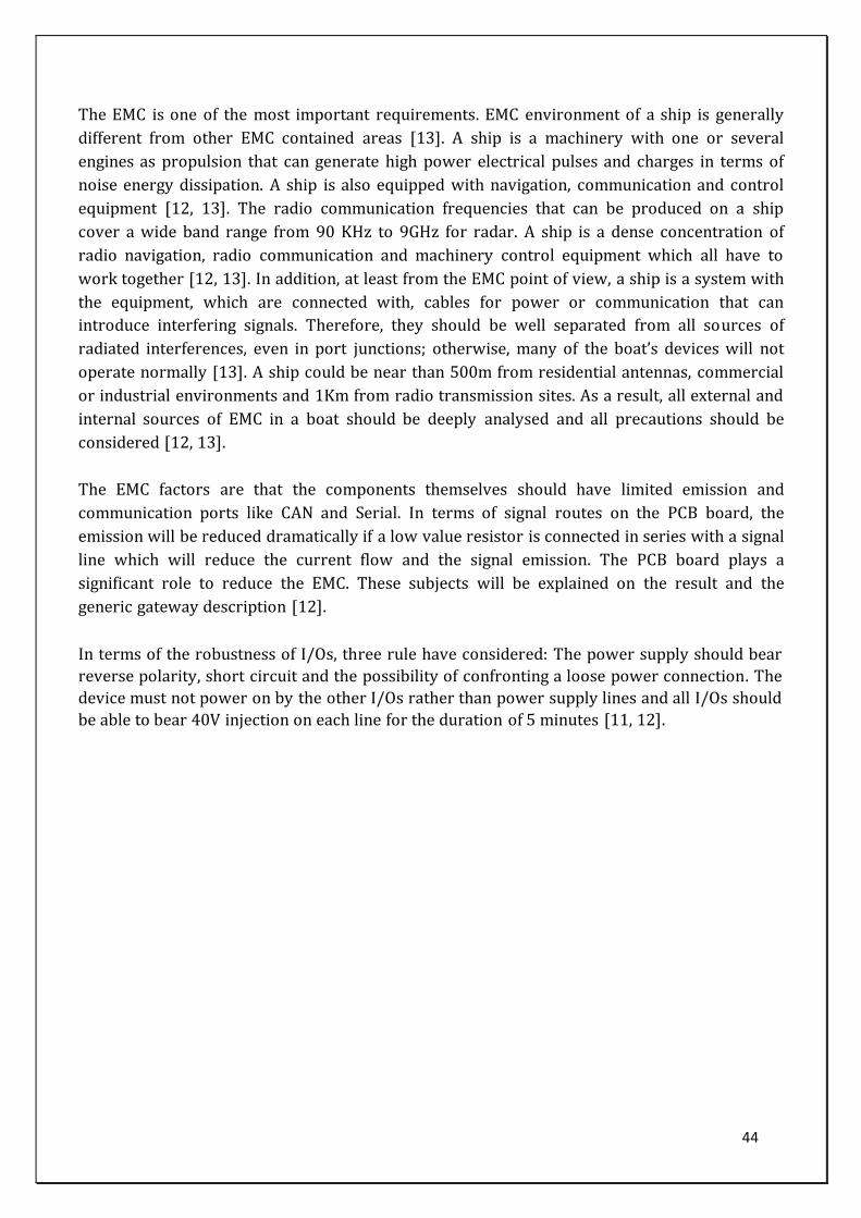
3.2 MARETRON EMS100 (non-CPAC).............................................................................................. 46
3.2.1 Generic Gateway and EMS100............................................................................................. 46
3.3 AIRMAR U200 (non-CPAC) ........................................................................................................... 47
3.3.1 AIRMAR U200 and Generic Gateway ................................................................................ 47
3.4 AMEC NK-80 ....................................................................................................................................... 47
3.4.1 AMEC NK-80 and Generic Gateway ................................................................................... 48
3.5 Comparison Analysis....................................................................................................................... 49
4 Methodology............................................................................................................................................. 50
4.1 Block Diagram of the Generic Gateway.................................................................................... 50
4.2 Hardware description of the generic gateway ...................................................................... 51
4.2.1 Power Supply ............................................................................................................................. 51
4.2.2 CAN Interface ............................................................................................................................. 53
4.2.3 Instrumentation ........................................................................................................................ 54
4.2.5 Inclinometers ............................................................................................................................. 58
4.2.6 PCB & Component Assembly ............................................................................................... 58
4.3 Generic Gateway Embedded Software Description ............................................................ 60
5 Results (Robustness Tests) .............................................................................................................. 65
5.1 Power supply robustness .............................................................................................................. 65
5.2 Isolation ............................................................................................................................................... 67
5.3 Power Consumption ........................................................................................................................ 69

12
5.4 Temperature ...................................................................................................................................... 69
6 Results (Design Tests) ........................................................................................................................ 78
6.1 Hardware Test Results ................................................................................................................... 78
6.2 Software Test Results (Joint test with the hardware)........................................................ 79
6.2.1 Power consumption ................................................................................................................ 86
6.2.2 Multiplexing Factor (Design Performance) .................................................................... 87
6.2.3 Cost Efficiency............................................................................................................................ 88
7 Conclusions ............................................................................................................................................... 89
8 References ................................................................................................................................................. 90
13
1 Introduction
1.1 Motivation
In the modern boats, the navigation control unit is a main part of the boat’s controlling system.
There are few companies in the world that produce navigation control units and CPAC Systems
AB as a subsidiary of VOLVO AB is one such company, which designs, develops and produces
electronic controlling systems for vehicles; including steer by wire (SBW) for boats. In the
whole controlling system, when the SBW communicates with external (Non-CPAC) products,
gateways are used as isolators and protocol translators to protect the integrity of the SBW
system.
Gateways are designed to accomplish several tasks based on their assigned operation,
environmental and/or end customer needs. In practice, for every connection establishment
request, like NMEA2000 (CAN based) protocol to NMEA0183 (Serial based) or internal CAN
(CPAC CAN) to external CAN (non-CPAC CAN), a proper connection is made just by having a
“Gateway”. It means for each connection, a proprietary gateway is to be developed, which is not
acceptable in product development for the manufacturer in the long term.
1.2 Goals
Currently, the CPAC Systems produces 10 different gateways [1]. They are named: NMEA2000,
NMEA0183, Autopilot, DPS, PFM, ACU, DSAG, AGI, MOTORSIM, LZGW and TJSGW [1]. Each of
these gateways is designed to accomplish a specific task, which mainly includes CAN interface
and some instruction lines. The goal of the thesis work is to combine all existing gateways in a
universal product, which must have the capability to handle the functionalities of all gateways
in a limited number of I/Os.
In this project, we design and implement a pertinent hardware and modify and write some
segments of the embedded software to test and verify the designed hardware. The hardware
design should be according to the industrial requirements, in order to be considered as a first
prototype of the final product.
1.3 Problem Statement & Approach
The hardware design of the generic gateway that could cover all functionalities of the existing
gateways, requires 35 I/O lines, but the generic gateway should be designed with 20 I/Os. In
other words, the designer should design the hardware in a way that most of I/O lines could
handle several functionalities, instead of just one. For example, if there is an output I/O line
that controls the boat’s trim level gauge through a PWM signal, it should also handle the LIN
connection as its second functionality (Multiplexing). The device should be designed from
scratch and the gateway’s MCU must be selected from the types which could deliver enough
processing power (at least double in performance (MIPS) compared to the existing gateway
MCUs) as well as enough internal flash memory size (at least 64Kbyte), SRAM (minimum
64Kbytes) to process signal processing functions and filters and providing sufficient embedded
facilities to complement the functionalities of the existing gateways as well, such as UART and
CAN [1, 10].
14
The gateway is an important part in the boat controlling system. It connects unknown
customer devices (Mainly CAN-based) to the CPAC-designed boat controlling products. The
designer should consider how and what he designs and how each part of the design may
perform in the real environment.
The main challenges, which have been investigated, are:
Designing a gateway hardware with the multiplexed I/Os, which covers all existing
gateways’ functionalities within a limited number of I/Os (20 I/Os).
All of the I/O lines which must be included are: Internal CAN (CPAC CAN, 4 lines), External
CAN (Non-CPAC CAN, 2 lines), Select1, Select2, TempAlarm, Tachometer, PowerTrimAngle,
OilAlarm, UART (3 Lines), StatusOut, Enable (2 Lines), PositionIN, GearStatus+, GPSUART (3
Lines), 1587(2 Lines), LIN, Internal power (CPAC supply, 2 lines) and external power (non-
CPAC supply, 2 lines).
Reliability and robustness of the gateway, which is derived into four categories:
Isolation (Physical and signal): according to the requirements, the resistance between
two test points should be at least 1MOhm in 60V.
Power supply robustness: The power supply should tolerate short circuit and 48V
injection for the duration of 2 minutes. In addition, it should bear with the reverse
polarity.
Temperature: the gateway should perform flawlessly in the temperature boundaries.
The up and down temperature test points are +85C and -20C.
Power consumption: the current consumption of the gateway should not exceed
150mA.
15
1.5 Structure
The thesis contains six main parts. In the background section (Section 2), the main blocks of a
gateway, description of the several existing gateways, investigation and studies of the most
important implemented communication protocols, analysis of hardware of the existing
gateways in addition to the roles of the key components and blocks are discussed. In addition,
the major requested standards for the implementation of the generic gateway are introduced
briefly. In the related work section (Section 3), similar products of different non-CPAC
companies have been investigated and compared with the generic gateway and at the end, a
comparison between all CPAC gateways and the Generic Gateway has been made. In the
methodology section (Section 4), the major contribution and description of the hardware and
software blocks in addition to the associated challenges have been discussed and
demonstrated. The results section (Section 5) consists of the investigation of the major
communication lines in accompany with some signal images, CAN analyser results and design
achievements in comparison with existing gateways. The conclusions part (Section 6) consists
of a brief description of the motivation of the project, the main challenges, contribution and the
outcome of the thesis.
16
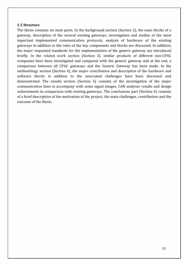
2 Background
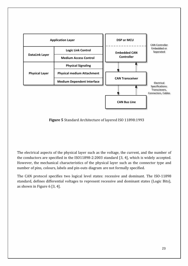
2.1 Block Diagram of a Gateway
In principle, the block diagram of a gateway product is a combination of a Microcontroller, one
or two CAN bus communication interfaces, some discrete hardware circuits and instruction
I/Os. The gateway block diagram view is shown in Figure 1.
Figure 1 General block diagram view of a Gateway
Figure 1 demonstrates all possible hardware blocks of one gateway (existing CPAC gateways).
In some gateways, all blocks have not been implemented and in some of them the
instrumentation I/Os and/or the external isolated CAN have been not implemented. For
example, the AGI gateway has 6 instrumentation I/Os and the internal CAN (“Internal” refers to
the CPAC devices, design blocks, communication interfaces and all related equipment and
“External” term refers to the non-CPAC design blocks and communication interfaces). It is
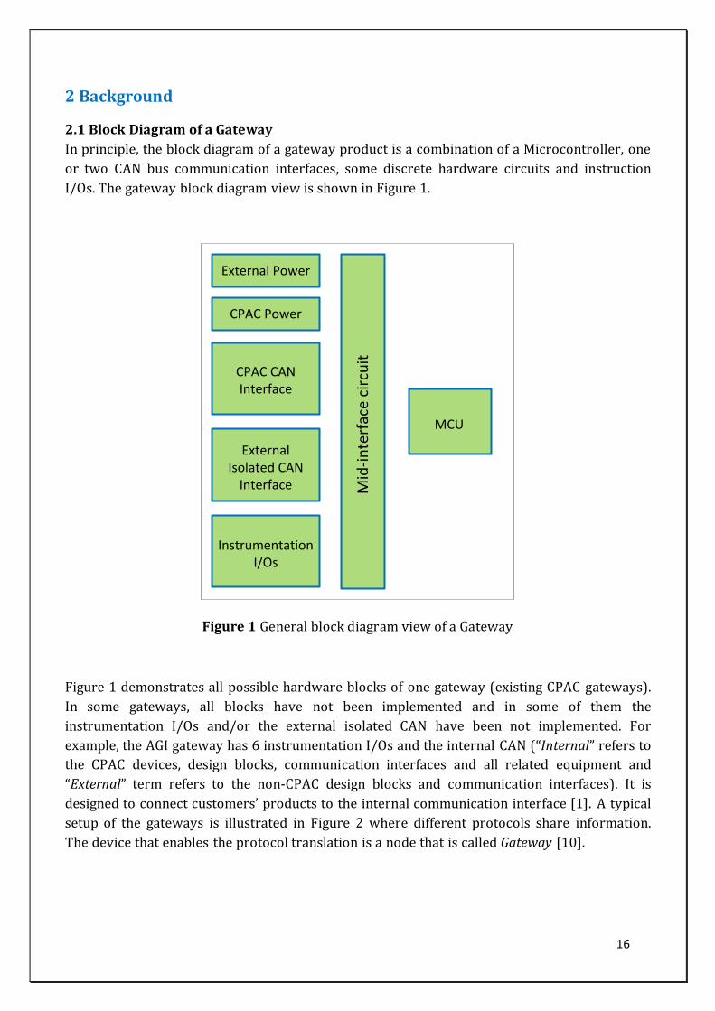
designed to connect customers’ products to the internal communication interface [1]. A typical
setup of the gateways is illustrated in Figure 2 where different protocols share information.
The device that enables the protocol translation is a node that is called Gateway [10].
CPAC CAN Interface
External Isolated CAN
Interface
Instrumentation I/Os
MCU
CPAC Power
External Power
Mid
-in
terf
ace
circ
uit
17
Driver interface
Gateway
Gateway
Trim planes
Twin IPS
GPS ReceiverOther External Devices
Gateway
Figure 2 Typical application of the gateway. The green lines represent the CPAC’s proprietary protocol while the red lines represent external protocols.
18
2.2 Description of the CPAC Gateways
The description and an overview of the existing CPAC Company’s gateway products are given in
this section.
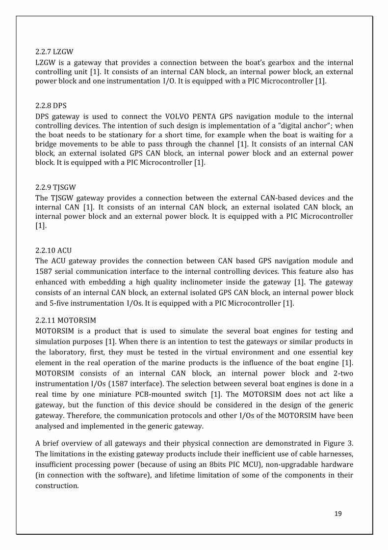
2.2.1 AGI
AGI is a gateway that provides a connection between the analogue gauges monitoring interface of the customer’s marine monitoring dashboard and the internal controlling unit (CPAC side) [1]. It consists of an internal CAN block, an internal power block and six instrumentation I/Os. It is equipped with a PIC Microcontroller [1].
2.2.2 NMEA0183
NMEA0183 provides a connection between all non-internal products, which are using CAN, NMEA0183 serial communication protocol and the internal controlling unit (CPAC devices). It consists of an internal CAN block, an internal power block, an external power block and a serial NMEA0183 communication interface [1]. It is equipped with a PIC Microcontroller [1].
2.2.3 NMEA2000
NMEA2000 provides a connection between customer devices which use CAN to connect the GPS navigation unit to the main internal controller (NMEA2000 is a newer version of the NMEA0183 which is mainly based on CAN bus) [1]. The gateway consists of an internal CAN block, an external isolated CAN block, an external power block and one internal power block. It is equipped with a PIC Microcontroller [1].
2.2.4 Autopilot
The autopilot is a gateway that provides a connection between the customer GPS devices, which use CAN or serial communication for data transaction and the internal controlling unit [1]. It consists of an internal power block, an internal CAN block, an external power block, an external isolated CAN block and an isolated UART interface [1]. It is equipped with a PIC microcontroller [1].
2.2.5 DSAG
DSAG is a gateway which provides a connection between the boat steering system and the internal controlling unit (boat steering unit can operate manually or in automatic mode) [1]. It consists of an internal CAN block, an internal Power block and 4-four I/O instrumentation interface. It is equipped with a PIC Microcontroller [1].
2.2.6 PFM
PFM is a gateway that transfers both CAN and power in the longer distances in the boat [1], in other words, it acts like a network repeater for both power and the CAN bus [1]. It connects the secondary power supply unit also, because the boat’s dashboard colourful graphical displays consume high current and the dissipation in the power line is significant, so this gateway should be used in such circumstances [1] (This gateway has been removed from the combination list).
19
2.2.7 LZGW
LZGW is a gateway that provides a connection between the boat’s gearbox and the internal controlling unit [1]. It consists of an internal CAN block, an internal power block, an external power block and one instrumentation I/O. It is equipped with a PIC Microcontroller [1].
2.2.8 DPS
DPS gateway is used to connect the VOLVO PENTA GPS navigation module to the internal controlling devices. The intention of such design is implementation of a ”digital anchor”; when the boat needs to be stationary for a short time, for example when the boat is waiting for a bridge movements to be able to pass through the channel [1]. It consists of an internal CAN block, an external isolated GPS CAN block, an internal power block and an external power block. It is equipped with a PIC Microcontroller [1].
2.2.9 TJSGW
The TJSGW gateway provides a connection between the external CAN-based devices and the internal CAN [1]. It consists of an internal CAN block, an external isolated CAN block, an internal power block and an external power block. It is equipped with a PIC Microcontroller [1].
2.2.10 ACU
The ACU gateway provides the connection between CAN based GPS navigation module and
1587 serial communication interface to the internal controlling devices. This feature also has
enhanced with embedding a high quality inclinometer inside the gateway [1]. The gateway
consists of an internal CAN block, an external isolated GPS CAN block, an internal power block
and 5-five instrumentation I/Os. It is equipped with a PIC Microcontroller [1].
2.2.11 MOTORSIM
MOTORSIM is a product that is used to simulate the several boat engines for testing and
simulation purposes [1]. When there is an intention to test the gateways or similar products in
the laboratory, first, they must be tested in the virtual environment and one essential key
element in the real operation of the marine products is the influence of the boat engine [1].
MOTORSIM consists of an internal CAN block, an internal power block and 2-two
instrumentation I/Os (1587 interface). The selection between several boat engines is done in a
real time by one miniature PCB-mounted switch [1]. The MOTORSIM does not act like a
gateway, but the function of this device should be considered in the design of the generic
gateway. Therefore, the communication protocols and other I/Os of the MOTORSIM have been
analysed and implemented in the generic gateway.
A brief overview of all gateways and their physical connection are demonstrated in Figure 3.
The limitations in the existing gateway products include their inefficient use of cable harnesses,
insufficient processing power (because of using an 8bits PIC MCU), non-upgradable hardware
(in connection with the software), and lifetime limitation of some of the components in their
construction.
20
NMEA2000 Deutsch DT06-6S
Micro C – 5 Pin
CAN / Power
Isolated CAN / Power
AutoPilot Deutsch DT06-6S
Micro C – 5 Pin
CAN / Power
Isolated CAN / Power
NMEA0183 Deutsch DT06-6S
3 wires
CAN / Power
Data, GND, PWR
DPS Deutsch DT06-6S
Deutsch DT04-6P
CAN / Power
CAN / Power
RFM Deutsch DT06-6S
Power Wires
Passive CAN
Power
Deutsch DT04-6P Passive CAN / Power
ACU Deutsch DT06-6S
3 Wires
Passive CAN
DATA / GND / PWR
Deutsch DT04-6P Passive CAN / Power
Inclinometer
DSAG Deutsch DT06-6S
5 Wires
CAN / Power
ReqAngle, Button, Engage
AGI Deutsch DT06-6S
9 Wires
CAN / Power
Instrumentation
MOTORSIM Deutsch DT06-6S
2 Wires
CAN / Power / 1587 / IGN
Power
LZGW Deutsch DT06-6S
2 Wires
CAN / Power
Gear Output Status
TJSGW Deutsch DT06-6S
MicroC – 5Pin
CAN / Power
Isolated CAN / Power
Figure 2
Gateways which should be combined in one
Gateway Product
Figure 3 All CPAC gateway product, which should be combined in the Generic Gateway
21
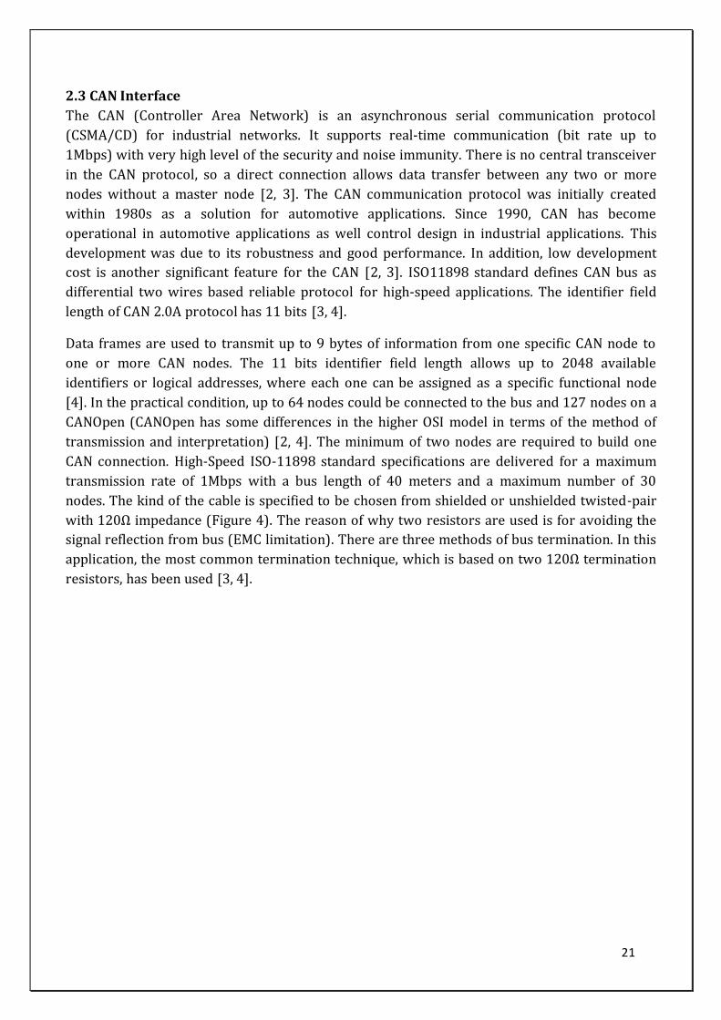
2.3 CAN Interface
The CAN (Controller Area Network) is an asynchronous serial communication protocol
(CSMA/CD) for industrial networks. It supports real-time communication (bit rate up to
1Mbps) with very high level of the security and noise immunity. There is no central transceiver
in the CAN protocol, so a direct connection allows data transfer between any two or more
nodes without a master node [2, 3]. The CAN communication protocol was initially created
within 1980s as a solution for automotive applications. Since 1990, CAN has become
operational in automotive applications as well control design in industrial applications. This
development was due to its robustness and good performance. In addition, low development
cost is another significant feature for the CAN [2, 3]. ISO11898 standard defines CAN bus as
differential two wires based reliable protocol for high-speed applications. The identifier field
length of CAN 2.0A protocol has 11 bits [3, 4].
Data frames are used to transmit up to 9 bytes of information from one specific CAN node to
one or more CAN nodes. The 11 bits identifier field length allows up to 2048 available
identifiers or logical addresses, where each one can be assigned as a specific functional node
[4]. In the practical condition, up to 64 nodes could be connected to the bus and 127 nodes on a
CANOpen (CANOpen has some differences in the higher OSI model in terms of the method of
transmission and interpretation) [2, 4]. The minimum of two nodes are required to build one
CAN connection. High-Speed ISO-11898 standard specifications are delivered for a maximum
transmission rate of 1Mbps with a bus length of 40 meters and a maximum number of 30
nodes. The kind of the cable is specified to be chosen from shielded or unshielded twisted-pair
with 120Ω impedance (Figure 4). The reason of why two resistors are used is for avoiding the
signal reflection from bus (EMC limitation). There are three methods of bus termination. In this
application, the most common termination technique, which is based on two 120Ω termination
resistors, has been used [3, 4].
22
Figure 4 Implementation of CAN Bus wiring
The CAN protocol, as many network protocols is structured in the following layers [2]:
Application Layer
Data Link Layer
Physical Layer
2.3.1 Physical Layer
The CAN physical layer will be discussed in more details, because it has been considered more
in the design of the “generic gateway”. The physical layer is the basic hardware requirement
for the CAN network, based on the ISO-11898 electrical specifications. The physical layer,
converts logic-1 and Logic-0’s into the corresponding differential electrical pulses which leave
a node [3, 4]. Although other communication layers may be implemented in software or within
hardware as integrated embedded parts, the Physical Layer is always implemented in the
hardware. The standard architecture of the layered ISO 11898:1993 has been shown in the
Figure 5.
CAN Transceiver
CAN Controller
DSP or MCU
Node#01
CAN Transceiver
CAN Controller
DSP or MCU
Node#02
CAN Transceiver
CAN Controller
DSP or MCU
Node#n1
20
R
12
0R
Figure-3CAN Bus implementation
23
The electrical aspects of the physical layer such as the voltage, the current, and the number of
the conductors are specified in the ISO11898-2:2003 standard [3, 4], which is widely accepted.
However, the mechanical characteristics of the physical layer such as the connector type and
number of pins, colours, labels and pin-outs diagram are not formally specified.
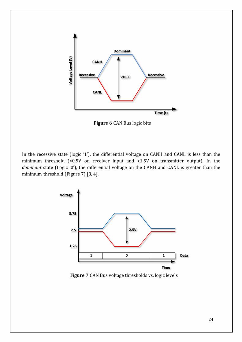
The CAN protocol specifies two logical level states: recessive and dominant. The ISO-11898
standard, defines differential voltages to represent recessive and dominant states (Logic Bits),
as shown in Figure 6 [3, 4].
Application Layer
DataLink Layer
Physical Layer
Logic Link Control
Medium Access Control
Physical Signaling
Physical medium Attachment
Medium Dependent Interface
DSP or MCU
Embedded CAN Controller
CAN Transceiver
CAN Bus Line
CAN ControllerEmbedded or
Seperated
Electrical Specifications:Transcievers,
Connectors, Cables
Figure-4The layered ISO 1189:1993 standard architectureFigure 5 Standard Architecture of layered ISO 11898:1993
24
In the recessive state (logic ‘1’), the differential voltage on CANH and CANL is less than the
minimum threshold (<0.5V on receiver input and <1.5V on transmitter output). In the
dominant state (Logic ‘0’), the differential voltage on the CANH and CANL is greater than the
minimum threshold (Figure 7) [3, 4].
CANH
CANL
Recessive Recessive
Dominant
VDIFF
Vo
ltag
e L
eve
l (V
)
Time (t)
Figure-5CAN Logic Bits
Voltage
Time
2.5V2.5
3.75
1.25
Data1 0 1
Figure 6 CAN Bus logic bits
Figure 7 CAN Bus voltage thresholds vs. logic levels
25
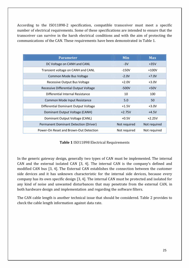
According to the ISO11898-2 specification, compatible transceiver must meet a specific
number of electrical requirements. Some of these specifications are intended to ensure that the
transceiver can survive in the harsh electrical conditions and with the aim of protecting the
communications of the CAN. These requirements have been demonstrated in Table 1.
Table 1 ISO11898 Electrical Requirements
In the generic gateway design, generally two types of CAN must be implemented. The internal
CAN and the external isolated CAN [3, 4]. The internal CAN is the company’s defined and
modified CAN bus [3, 4]. The External CAN establishes the connection between the customer
side devices and it has unknown characteristic for the internal side devices, because every
company has its own specific design [3, 4]. The internal CAN must be protected and isolated for
any kind of noise and unwanted disturbances that may penetrate from the external CAN, in
both hardware design and implementation and regarding the software filters.
The CAN cable length is another technical issue that should be considered. Table 2 provides to
check the cable length information against data rate.
Parameter Min Max
DC Voltage on CANH and CANL -3V +35V
Transient voltage on CANH and CANL -150V +100V
Common Mode Bus Voltage -2.0V +7.0V
Recessive Output Bus Voltage +2.0V +3.0V
Recessive Differential Output Voltage -500V +50V
Differential Internal Resistance 10 100
Common Mode Input Resistance 5.0 50
Differential Dominant Output Voltage +1.5V +3.0V
Dominant Output Voltage (CANH) +2.75V +4.5V
Dominant Output Voltage (CANL) +0.5V +2.25V
Permanent Dominant Detection (Driver) Not required Not required
Power-On Reset and Brown-Out Detection Not required Not required
26
Bus Length (M) Signalling Rate
(Mbps)
40 1
100 0.5
200 0.25
500 0.10
1000 0.05
Table 2 Suggested cable length vs. signaling rate
As a rule of thumb, the bus wire length in meters (for busses over 100m) multiplied by the
baud rate in Mbps, should always be always less than or equal to 50 (Equation 1).
Data communication Rate (Mbps) * Bus Length (m) ≤ 50 (1)
In the gateway communication, the maximum signalling rate is 0.5Mbps and hence, up to 100
meters cable length is permitted [3, 4].
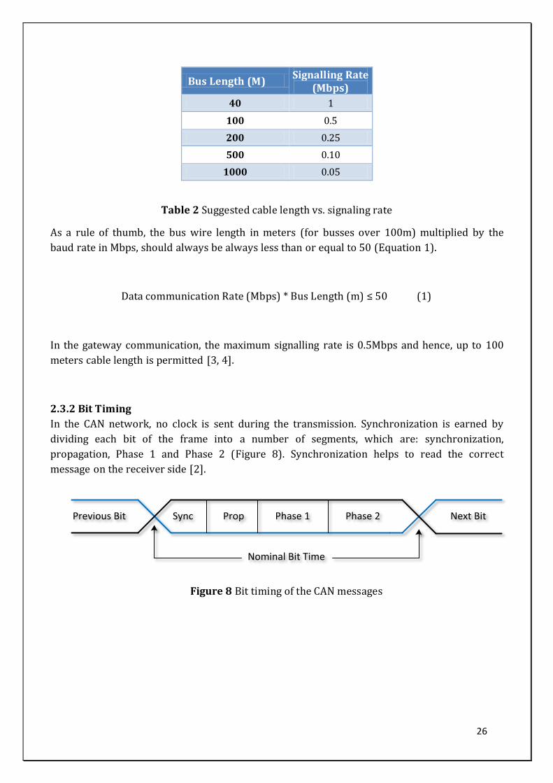
2.3.2 Bit Timing
In the CAN network, no clock is sent during the transmission. Synchronization is earned by
dividing each bit of the frame into a number of segments, which are: synchronization,
propagation, Phase 1 and Phase 2 (Figure 8). Synchronization helps to read the correct
message on the receiver side [2].
Previous Bit Sync Prop Phase 1 Phase 2 Next Bit
Nominal Bit Time
Figure-7Bit timing of CAN message
Figure 8 Bit timing of the CAN messages
27
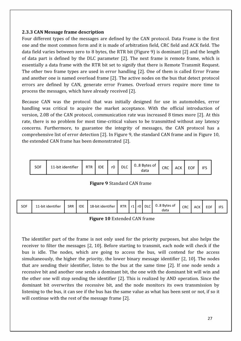
2.3.3 CAN Message frame description
Four different types of the messages are defined by the CAN protocol. Data Frame is the first
one and the most common form and it is made of arbitration field, CRC field and ACK field. The
data field varies between zero to 8 bytes, the RTR bit (Figure 9) is dominant [2] and the length
of data part is defined by the DLC parameter [2]. The next frame is remote frame, which is
essentially a data frame with the RTR bit set to signify that there is Remote Transmit Request.
The other two frame types are used in error handling [2]. One of them is called Error Frame
and another one is named overload frame [2]. The active nodes on the bus that detect protocol
errors are defined by CAN, generate error Frames. Overload errors require more time to
process the messages, which have already received [2].
Because CAN was the protocol that was initially designed for use in automobiles, error
handling was critical to acquire the market acceptance. With the official introduction of
version, 2.0B of the CAN protocol, communication rate was increased 8 times more [2]. At this
rate, there is no problem for most time-critical values to be transmitted without any latency
concerns. Furthermore, to guarantee the integrity of messages, the CAN protocol has a
comprehensive list of error detection [2]. In Figure 9, the standard CAN frame and in Figure 10,
the extended CAN frame has been demonstrated [2].
Figure 9 Standard CAN frame
The identifier part of the frame is not only used for the priority purposes, but also helps the
receiver to filter the messages [2, 10]. Before starting to transmit, each node will check if the
bus is idle. The nodes, which are going to access the bus, will contend for the access
simultaneously, the higher the priority, the lower binary message identifier [2, 10]. The nodes
that are sending their identifier, listen to the bus at the same time [2]. If one node sends a
recessive bit and another one sends a dominant bit, the one with the dominant bit will win and
the other one will stop sending the identifier [2]. This is realized by AND operation. Since the
dominant bit overwrites the recessive bit, and the node monitors its own transmission by
listening to the bus, it can see if the bus has the same value as what has been sent or not, if so it
will continue with the rest of the message frame [2].
SOF 11-bit identifier RTR IDE r0 DLC 0..8 Bytes of data
CRC ACK EOF IFS
SOF 11-bit identifier SRR IDE 0..8 Bytes of data
CRC ACK EOF IFS18-bit identifier RTR r1 r0 DLC
Figure 10 Extended CAN frame
28
2.4 NMEA0183
NMEA0183 is a standard, which defines both the electrical interface and the data
communication protocol for transmission/reception among marine instrumentation and
devices [6]. NMEA0183 is an industry standard, first released in the March-1983. The electrical
standard of NMEA0183 is EIA-422 although most hardware with NMEA0183 outputs are also
capable to drive single EIA-232 port. NMEA0183 can handle single talker and several listeners
on one bus. Interconnect wiring is recommended to be a shielded twisted pair, with the
grounded shield only at the talker [6]. The specification of serial communication is:
Baud rate: 4800
Number of data bits: 8 (bit 7 is 0)
Stop bits: one (or more)
Parity: none
Handshake: none
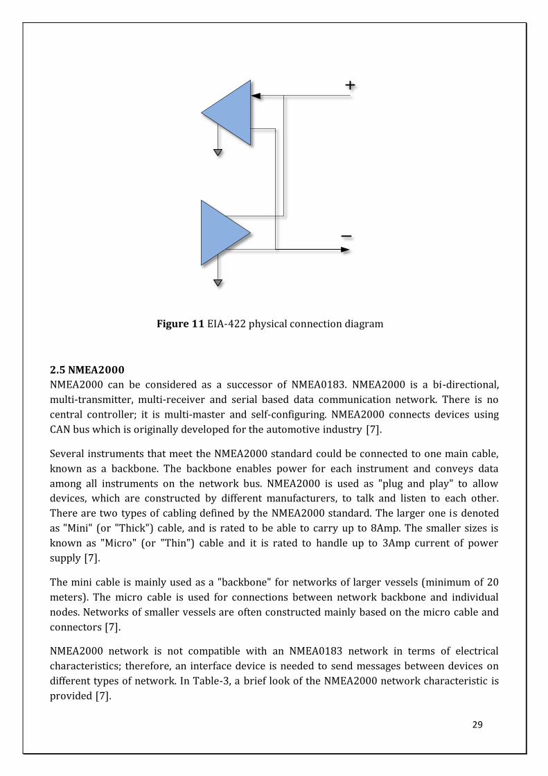
The recommendation is that the talker output complies with the RS-422 standard. It is
differential based with two signal lines, "A" and "B". These differential drive signals have no
reference to ground and therefore the signal has more immunity to noises.
EIA422 (Full duplex: EIA-485): The standard is published by the ANSI Telecommunications
Industry Association/Electronic Industries Alliance (TIA/EIA) [6]. The devices based on EIA-
485 communication standard can be used widely for long distances and in noisy and harsh
environments. These characteristics make EIA422 more practical in industrial applications.
EIA-485 (RS485) offers data transmission speeds of 35 Mbit/s up to 10m and 100Kbit/s up to
1200m, because it applies differential balanced line over twisted pair wire and one optional
ground wire for more convenient matching balance and noise reduction (like EIA-422) (Figure
11). One easy rule could be used in this case: the speed in bit/s multiplied by the length in
meters should not exceed than 108. Thus, for example on a 50-meter cable, one should not
signal faster than 2Mbit/s.
29
2.5 NMEA2000
NMEA2000 can be considered as a successor of NMEA0183. NMEA2000 is a bi-directional,
multi-transmitter, multi-receiver and serial based data communication network. There is no
central controller; it is multi-master and self-configuring. NMEA2000 connects devices using
CAN bus which is originally developed for the automotive industry [7].
Several instruments that meet the NMEA2000 standard could be connected to one main cable,
known as a backbone. The backbone enables power for each instrument and conveys data
among all instruments on the network bus. NMEA2000 is used as "plug and play" to allow
devices, which are constructed by different manufacturers, to talk and listen to each other.
There are two types of cabling defined by the NMEA2000 standard. The larger one is denoted
as "Mini" (or "Thick") cable, and is rated to be able to carry up to 8Amp. The smaller sizes is
known as "Micro" (or "Thin") cable and it is rated to handle up to 3Amp current of power
supply [7].
The mini cable is mainly used as a "backbone" for networks of larger vessels (minimum of 20
meters). The micro cable is used for connections between network backbone and individual
nodes. Networks of smaller vessels are often constructed mainly based on the micro cable and
connectors [7].
NMEA2000 network is not compatible with an NMEA0183 network in terms of electrical
characteristics; therefore, an interface device is needed to send messages between devices on
different types of network. In Table-3, a brief look of the NMEA2000 network characteristic is
provided [7].
Figure 8EIA-485 Connection
Figure 11 EIA-422 physical connection diagram
30
Network Architecture
Bus wiring configuration using four conductor twisted pair wires to
transfer power for the operation of the interface and data signals. Linear network with end terminators and multiple short-length cables. It
connects the cable backbone to the individual nodes.
Network Operation
Multi-master network operation, ie., there is no central node. Self-Configuring.
Network Size Physical nodes: Max 50 connections. Functional nodes: Max 252 network addresses. Length: Max 200 meters (at 250kbits/second bit rate).
Table 3 NMEA2000 communication protocol Characteristics
2.6 Local Interconnect Network (LIN)
Two dominating factors for a technical choice in the networking technology are cost and the
transaction speed. At the field level, we are more concerned about controlling actuators, small
electrical motors and reading data from sensors. At this control level, the challenge is in dealing
with mechanical component with low speed requirements (several kbit/s) [8]. In the vehicle
industry, the request for a protocol with low computational power, small amount of memory
and low cost along with the simplicity of the communication controllers always exists and LIN
satisfies these requirements. The LIN communication is based on the master-slave mechanism.
Each cluster in LIN consists of one master and some slaves connected to a common single serial
bus. Due to EMI limitation, it is not possible to achieve a data rate higher than 20kbps [8].
LIN is a time-triggered network and the master node to manage the message transmission uses
a schedule table. The table contains of a list of frames and their frame slots, which ensure
determinism in the sequence of transmission [8]. A data frame can contain up to eight bytes of
data. The master broadcasts data and all the nodes can listen and the one which possesses the
identifier (one byte length) can respond. The identifier is made of a six-bit address field and a
two-bit check field [8]. If there is no update for the requested data, then there will be no
response and the bandwidth will be saved. By providing the sleep mode in nodes, energy is
saved in time of no data transaction [8].
31
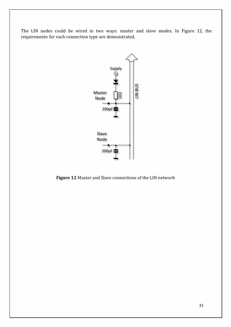
The LIN nodes could be wired in two ways: master and slave modes. In Figure 12, the
requirements for each connection type are demonstrated.
Figure 12 Master and Slave connections of the LIN network
LIN
BU
S
Supply
Master Node
Slave Node
200pF
200pF
1K
Ω
32
2.7 Hardware analysis of the existing gateways (CPAC)
2.7. Autopilot Gateway
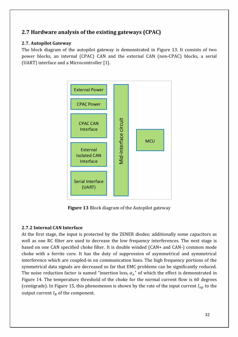
The block diagram of the autopilot gateway is demonstrated in Figure 13. It consists of two
power blocks, an internal (CPAC) CAN and the external CAN (non-CPAC) blocks, a serial
(UART) interface and a Microcontroller [1].
CPAC CAN Interface
External Isolated CAN
Interface
Serial Interface(UART)
MCU
CPAC Power
External Power
Mid
-in
terf
ace
circ
uit
Figure 13 Block diagram of the Autopilot gateway
2.7.2 Internal CAN Interface
At the first stage, the input is protected by the ZENER diodes; additionally some capacitors as
well as one RC filter are used to decrease the low frequency interferences. The next stage is
based on one CAN specified choke filter. It is double winded (CAN+ and CAN-) common mode
choke with a ferrite core. It has the duty of suppression of asymmetrical and symmetrical
interference which are coupled-in on communication lines. The high frequency portions of the
symmetrical data signals are decreased so far that EMC problems can be significantly reduced.
The noise reduction factor is named “insertion loss, 𝛼𝑒” of which the effect is demonstrated in
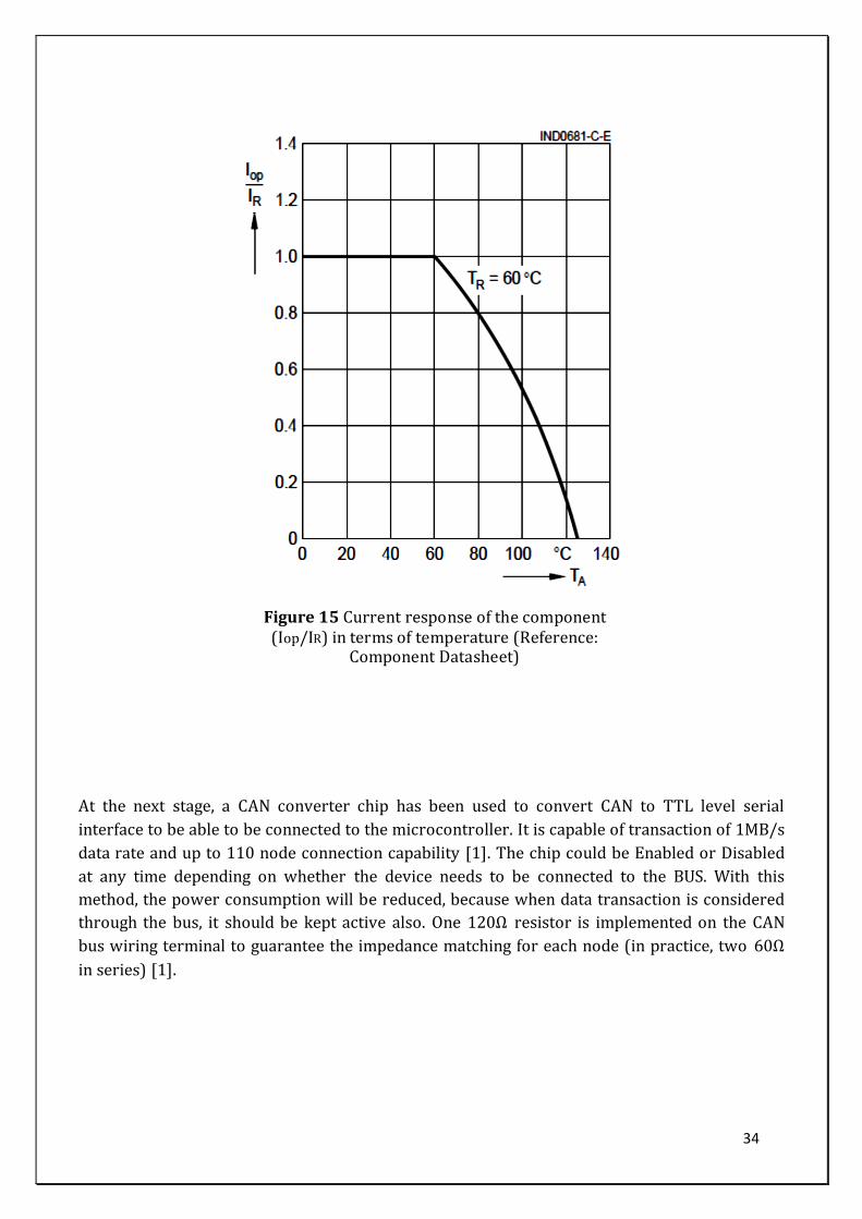
Figure 14. The temperature threshold of the choke for the normal current flow is 60 degrees
(centigrade). In Figure 15, this phenomenon is shown by the rate of the input current 𝐼𝑜𝑝 to the
output current 𝐼𝑅 of the component.
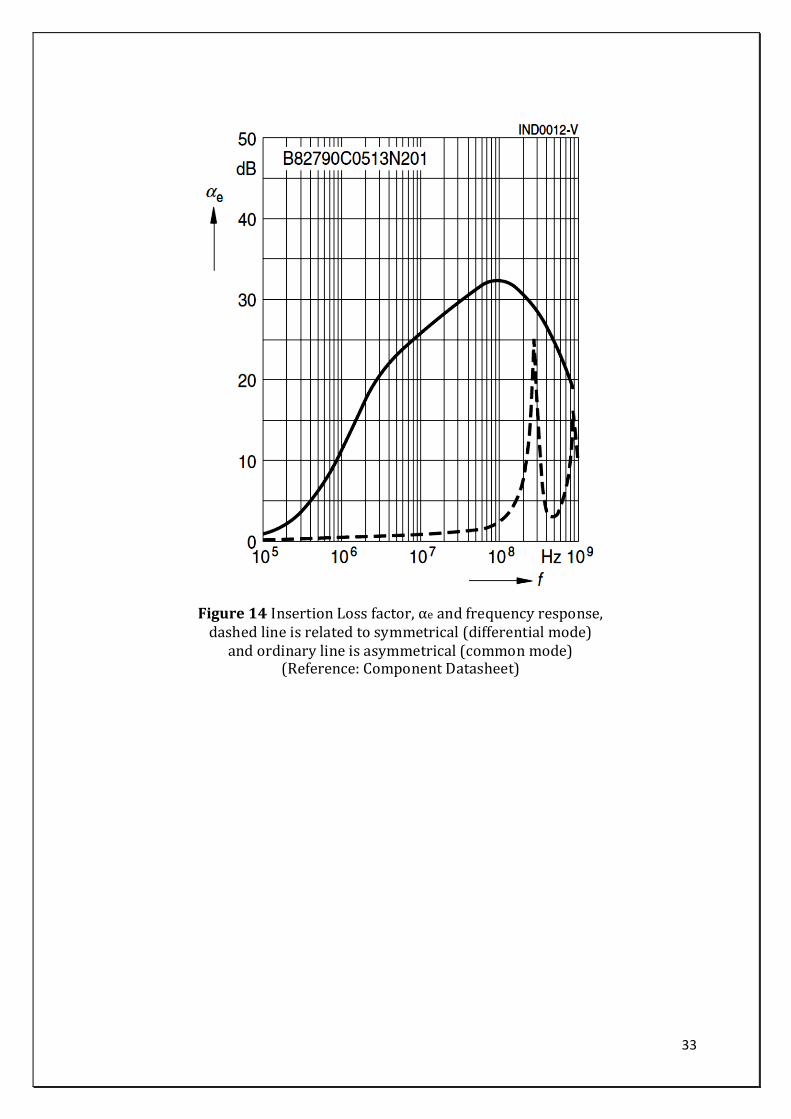
33
Figure 14 Insertion Loss factor, αe and frequency response, dashed line is related to symmetrical (differential mode)
and ordinary line is asymmetrical (common mode) (Reference: Component Datasheet)
34
At the next stage, a CAN converter chip has been used to convert CAN to TTL level serial
interface to be able to be connected to the microcontroller. It is capable of transaction of 1MB/s
data rate and up to 110 node connection capability [1]. The chip could be Enabled or Disabled
at any time depending on whether the device needs to be connected to the BUS. With this
method, the power consumption will be reduced, because when data transaction is considered
through the bus, it should be kept active also. One 120Ω resistor is implemented on the CAN
bus wiring terminal to guarantee the impedance matching for each node (in practice, two 60Ω
in series) [1].
Figure 15 Current response of the component (Iop/IR) in terms of temperature (Reference:
Component Datasheet)
35
2.7.3 External Isolated CAN
The first stage of the external isolated CAN (non-CPAC CAN) is the same as the internal CAN
(CPAC CAN), but it has an extended filter at next stages, also one optocoupler IC has been used
for isolation and noise immunity. Due to handle the data transaction speed (500Kbit/s), an
optocoupler is selected from the types to show proper response during data transaction and
does not make distortion in signals (Minimum operation frequency of 1MHz). The temperature
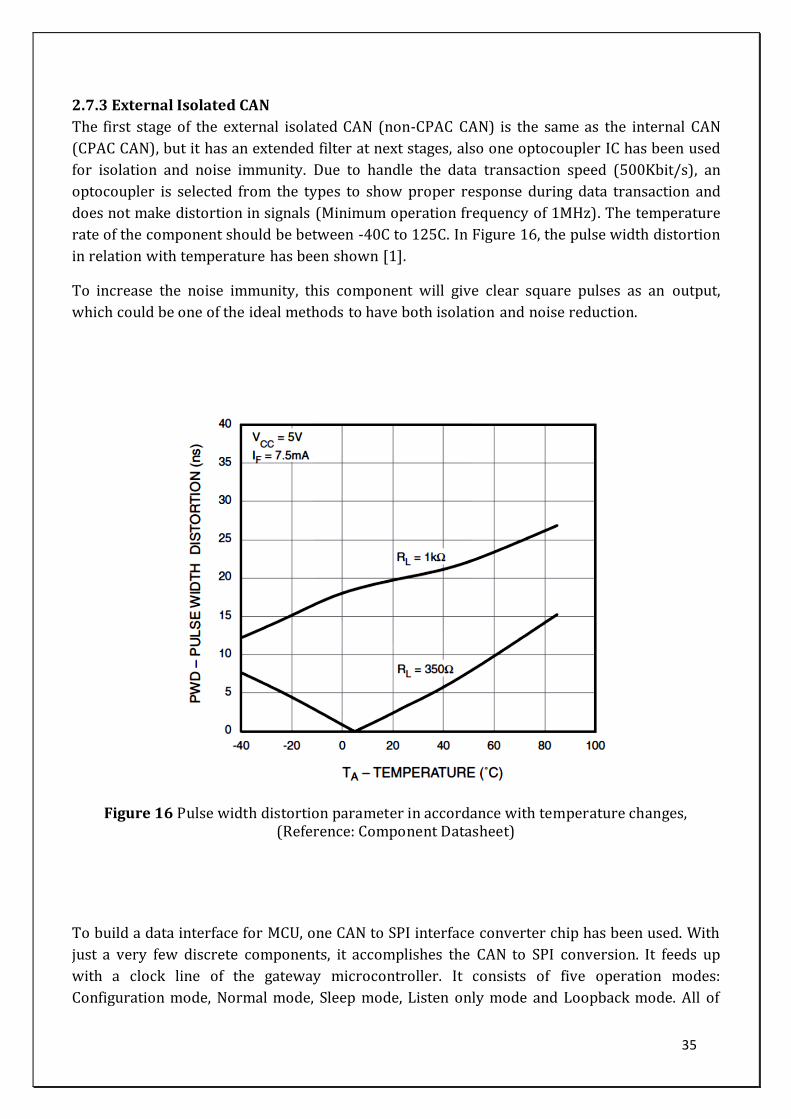
rate of the component should be between -40C to 125C. In Figure 16, the pulse width distortion
in relation with temperature has been shown [1].
To increase the noise immunity, this component will give clear square pulses as an output,
which could be one of the ideal methods to have both isolation and noise reduction.
Figure 16 Pulse width distortion parameter in accordance with temperature changes, (Reference: Component Datasheet)
To build a data interface for MCU, one CAN to SPI interface converter chip has been used. With
just a very few discrete components, it accomplishes the CAN to SPI conversion. It feeds up
with a clock line of the gateway microcontroller. It consists of five operation modes:
Configuration mode, Normal mode, Sleep mode, Listen only mode and Loopback mode. All of
36
these configurations are addressed through appropriate commands from SPI line. It uses CRC
for error detection and it supports several interrupts for several conditions. In this design one
interrupt pin is used to be able to detect and pick up available data on BUS and avoid
unnecessary loop to check the condition of the BUS every time [1].
2.7.4 Power Supply
The power of the gateway is provided from the vehicle battery (14-28V). Therefore, because
the battery itself is one pure source of the electrical energy, some sort of low frequency filters
would be sufficient to suppress unwanted noises. The next step is power regulator. This
regulator has been selected from the types with low voltage drop feature and also lower
thermal dissipation. One additional benefit of the low voltage drop feature is for the conditions
like engine start-up time that high level of voltage drop will occur on the power supply line.
The total voltage drop, in addition to the voltage drop of the regulator itself will not come to
one level to decrease the logical component voltage level (fixed 5V after regulator) and
therefore no MCU reset or whole device malfunction will happen. Unwanted high voltage
noises could be suppressed by using a varistor in parallel with the power lines; this is one of
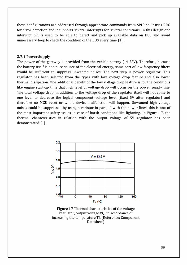
the most important safety issues in case of harsh conditions like lightning. In Figure 17, the
thermal characteristics in relation with the output voltage of 5V regulator has been
demonstrated [1].
Figure 17 Thermal characteristics of the voltage regulator, output voltage VQ, in accordance of
increasing the temperature TJ, (Reference: Component Datasheet)
37
2.7.5 Main Controller
The main controller of the device consists of one PIC MCU. It controls all of the data flows and
commands and all instructions come from this unit. It is equipped with 4MHz crystal oscillator,
which supplies the MCU clock itself and the clock of the CAN chip. The whole system is
designed in an efficient way and the noise immunity factor is also considered in all areas [1].
2.7.6 AGI Gateway
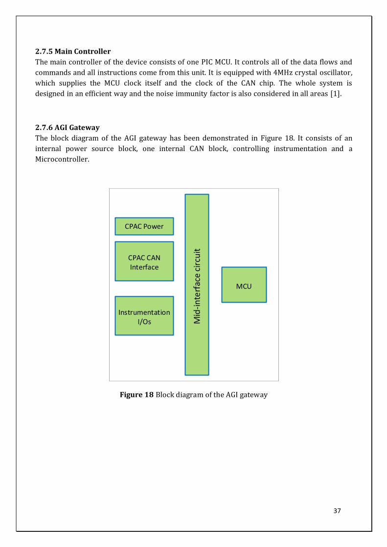
The block diagram of the AGI gateway has been demonstrated in Figure 18. It consists of an
internal power source block, one internal CAN block, controlling instrumentation and a
Microcontroller.
CPAC CAN Interface
InstrumentationI/Os
MCU
CPAC Power
Mid
-in
terf
ace
circ
uit
Figure 18 Block diagram of the AGI gateway
38
2.7.7 Power Supply
At the first stage of the power supply, a network of capacitors have been implemented to
reduce unforeseen low frequency noises. Similar to other industrial circuits, the input in the
first stage should be protected by a varistor component. At the next stage, a bipolar diode is
used to protect against voltage overloads. Its breakdown voltage is ordered as 58V [1].
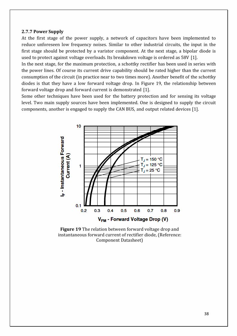
In the next stage, for the maximum protection, a schottky rectifier has been used in series with
the power lines. Of course its current drive capability should be rated higher than the current
consumption of the circuit (in practice near to two times more). Another benefit of the schottky
diodes is that they have a low forward voltage drop. In Figure 19, the relationship between
forward voltage drop and forward current is demonstrated [1].
Some other techniques have been used for the battery protection and for sensing its voltage
level. Two main supply sources have been implemented. One is designed to supply the circuit
components, another is engaged to supply the CAN BUS, and output related devices [1].
Figure 19 The relation between forward voltage drop and instantaneous forward current of rectifier diode, (Reference:
Component Datasheet)
39
2.7.8 Internal CAN Interface
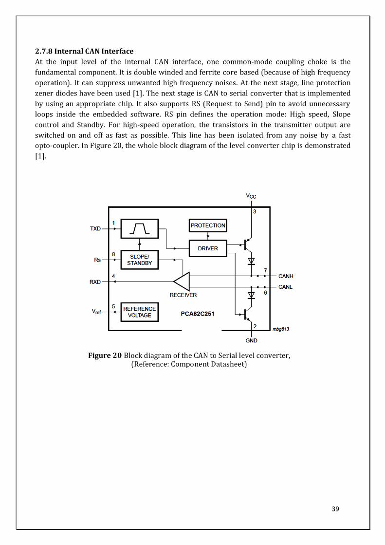
At the input level of the internal CAN interface, one common-mode coupling choke is the
fundamental component. It is double winded and ferrite core based (because of high frequency
operation). It can suppress unwanted high frequency noises. At the next stage, line protection
zener diodes have been used [1]. The next stage is CAN to serial converter that is implemented
by using an appropriate chip. It also supports RS (Request to Send) pin to avoid unnecessary
loops inside the embedded software. RS pin defines the operation mode: High speed, Slope
control and Standby. For high-speed operation, the transistors in the transmitter output are
switched on and off as fast as possible. This line has been isolated from any noise by a fast
opto-coupler. In Figure 20, the whole block diagram of the level converter chip is demonstrated
[1].
Figure 20 Block diagram of the CAN to Serial level converter, (Reference: Component Datasheet)
40
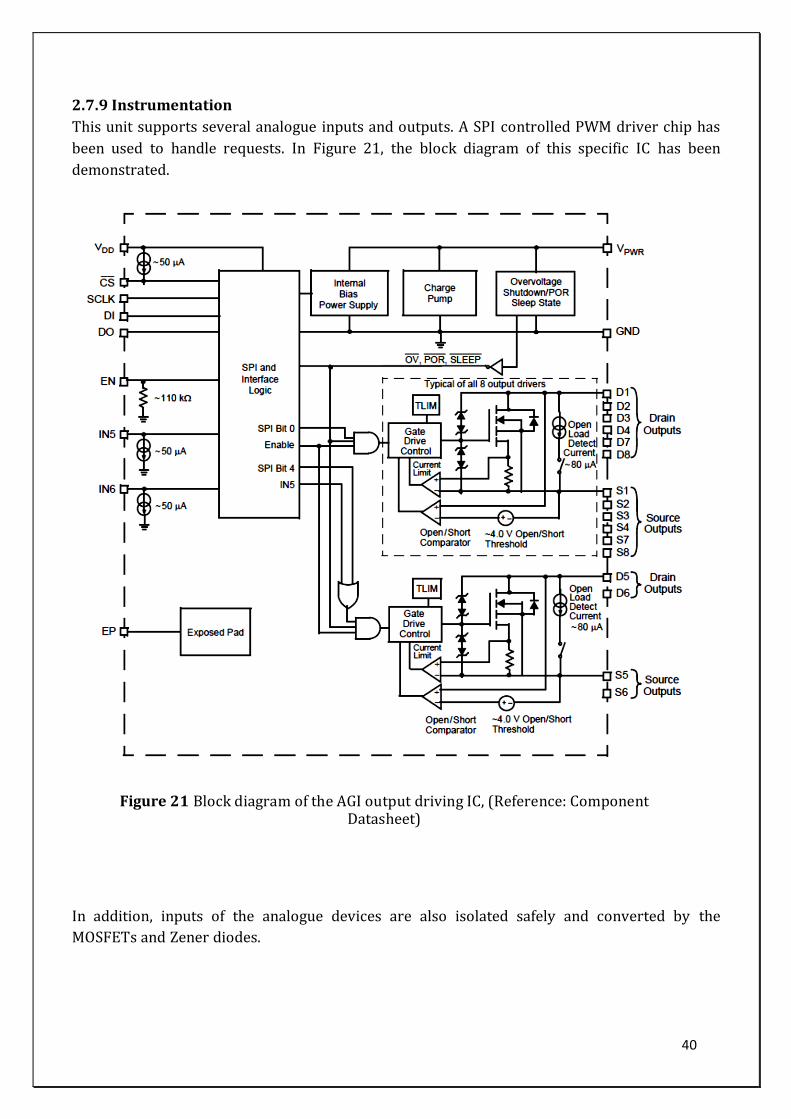
2.7.9 Instrumentation
This unit supports several analogue inputs and outputs. A SPI controlled PWM driver chip has
been used to handle requests. In Figure 21, the block diagram of this specific IC has been
demonstrated.
In addition, inputs of the analogue devices are also isolated safely and converted by the
MOSFETs and Zener diodes.
Figure 21 Block diagram of the AGI output driving IC, (Reference: Component Datasheet)
41
2.7.10 DSAG Gateway
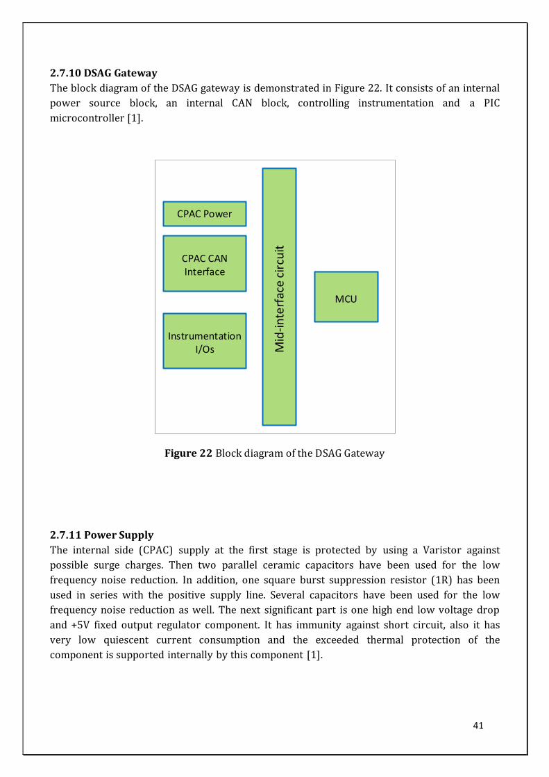
The block diagram of the DSAG gateway is demonstrated in Figure 22. It consists of an internal
power source block, an internal CAN block, controlling instrumentation and a PIC
microcontroller [1].
CPAC CAN Interface
InstrumentationI/Os
MCU
CPAC Power
Mid
-in
terf
ace
circ
uit
Figure 22 Block diagram of the DSAG Gateway
2.7.11 Power Supply
The internal side (CPAC) supply at the first stage is protected by using a Varistor against
possible surge charges. Then two parallel ceramic capacitors have been used for the low
frequency noise reduction. In addition, one square burst suppression resistor (1R) has been
used in series with the positive supply line. Several capacitors have been used for the low
frequency noise reduction as well. The next significant part is one high end low voltage drop
and +5V fixed output regulator component. It has immunity against short circuit, also it has
very low quiescent current consumption and the exceeded thermal protection of the
component is supported internally by this component [1].
42
2.7.12 Internal CAN Interface
Like other before-mentioned gateways, this product also uses almost the same circuit diagram.
It is also based on the CAN line filtering, protection and conversion stages. By using a specific
chip, protocol conversion is done from CAN to Serial (RX, TX signals) to be connected directly
to the MCU [1].
2.7.13 Instrumentation
Within instrumentation I/Os, two lines come from the steering system that contain analogue
positive and negative voltages that should be converted to digital TTL voltage “levels” to be
applicable to be connected to MCU’s ADC. Therefore, circuit is mainly based on several
resistors-based voltage conversion circuit and two capacitors in parallel with the line for noise
reduction. There is an “Enable” signal line as well which indicates that an external device wants
to be connected to the DSAG dongle. It passes through opto-coupler for the maximum isolation
and noise immunity, and then it is applied to the MCU. Last instrumentation line is an output
signal and conveys the information of the external device connected (activated) or
disconnected. The remaining line is ground but it is the ground of the external device, which
comes just with the external device activation signal line [1].
2.7.14 Main Controller
This part consists of a PIC microcontroller that works at 4MHz clock. It is equipped with two
LED indicators that show the condition of the gateway operation for the user.
43
2.8 General and exclusive standards Considering the requirements and standards was one of the most challenging parts of this
gateway design. We considered how we could design the hardware to satisfy tests, as much as
it is necessary. The main sources for these requirements are [11, 12, 13, 14]:
Environmental Tests (General)
Vibration: the device is vibrated with the frequency of 13.2Hz, with amplitude of ±1mm and
13.2Hz to 100Hz and the acceleration of ±0. 7g [11]. Second, the device is vibrated with the
periods of 2Hz to 25Hz and amplitude of ±1.6mm, and with the frequency period of 25Hz to
100Hz with the acceleration of ±4g.
Temperature: In general, the device is tested at three temperature points: -20°C, 25°C and
+85°C, otherwise it is tested under more detailed temperature conditions in relation with the
humidity (Table 4).
Humidity: In general, the device is tested under 60% ± 30% of the humidity level, otherwise,
the device is tested under more detailed condition (Table 4).
EMC (Electro Magnetic Compliance) [12]
Customer Requirements (Exclusive)
VOLVO PENTA: In general, the current leakage between power lines and the isolated signal
lines are tested. Under 60V to 100V, two testing points should not show the resistance (R)
lower than 1MΩ (R = V/I) [12].
The standards which have been considered are a combination of IEC60068, IEC60945
(external customer), IACS E10 and TR21354582 (VOLVO). The temperature tests are written in
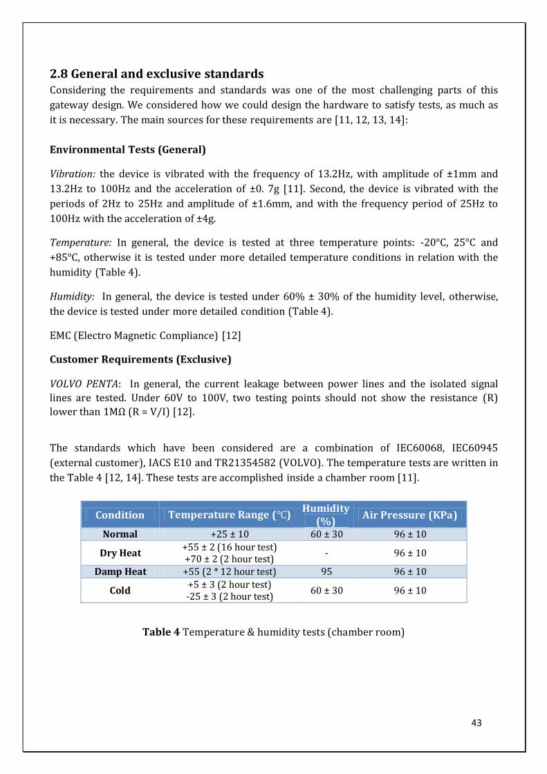
the Table 4 [12, 14]. These tests are accomplished inside a chamber room [11].
Condition Temperature Range () Humidity
(%) Air Pressure (KPa)
Normal +25 ± 10 60 ± 30 96 ± 10
Dry Heat +55 ± 2 (16 hour test) +70 ± 2 (2 hour test)
- 96 ± 10
Damp Heat +55 (2 * 12 hour test) 95 96 ± 10
Cold +5 ± 3 (2 hour test) -25 ± 3 (2 hour test)
60 ± 30 96 ± 10
Table 4 Temperature & humidity tests (chamber room)
44
The EMC is one of the most important requirements. EMC environment of a ship is generally
different from other EMC contained areas [13]. A ship is a machinery with one or several
engines as propulsion that can generate high power electrical pulses and charges in terms of
noise energy dissipation. A ship is also equipped with navigation, communication and control
equipment [12, 13]. The radio communication frequencies that can be produced on a ship
cover a wide band range from 90 KHz to 9GHz for radar. A ship is a dense concentration of
radio navigation, radio communication and machinery control equipment which all have to
work together [12, 13]. In addition, at least from the EMC point of view, a ship is a system with
the equipment, which are connected with, cables for power or communication that can
introduce interfering signals. Therefore, they should be well separated from all sources of
radiated interferences, even in port junctions; otherwise, many of the boat’s devices will not
operate normally [13]. A ship could be near than 500m from residential antennas, commercial
or industrial environments and 1Km from radio transmission sites. As a result, all external and
internal sources of EMC in a boat should be deeply analysed and all precautions should be
considered [12, 13].
The EMC factors are that the components themselves should have limited emission and
communication ports like CAN and Serial. In terms of signal routes on the PCB board, the
emission will be reduced dramatically if a low value resistor is connected in series with a signal
line which will reduce the current flow and the signal emission. The PCB board plays a
significant role to reduce the EMC. These subjects will be explained on the result and the
generic gateway description [12].
In terms of the robustness of I/Os, three rule have considered: The power supply should bear
reverse polarity, short circuit and the possibility of confronting a loose power connection. The
device must not power on by the other I/Os rather than power supply lines and all I/Os should
be able to bear 40V injection on each line for the duration of 5 minutes [11, 12].

45
3 Related Work
3.1 ACTISENSE NGW-1 Gateway (non-CPAC)
This gateway is designed to make a proper connection and protocol conversion between
NMEA2000 CAN based protocol and the older serial NMEA0183 protocol [21]. It provides
Opto-isolation between input and output up to 2500V to the ground. The output is protected
against short circuit and ESD. The input is protected against continuous -15V to +15V voltage
injection and is protected for the voltage range of -35V to +35V but in a short time period (less
than one second). It consumes 85mA supply current [21]. The data transaction speed is defined
up to 250Kbps [21]. It does not provide visual interface (LEDs) for the user to verify the
operation. Figure 23 demonstrates the NGW-1 gateway.
Figure 23 ACTISENSE NGW-1 gateway (Reference: Product datasheet)
3.1.1 Generic Gateway and ACTISENSE NGW-1
The generic gateway that was designed in this thesis covers all communication protocols of the
Actisense gateway as just one part of its architecture. In other words, it is designed to be
general and multipurpose. The power consumption of the generic gateway in the worst
condition is about 90mA and it is almost the same as the Actisense gateway which covers much
less features and functionality. The generic gateway is protected against lightning but this
feature is missing in the Actisense gateway. Both gateways are optically isolated. The Actisense
gateway does not provide a proper connector to harness I/Os as the generic gateway. Finally,
the generic gateway provides LEDs as a user interface but this feature is also missing in the
Actisense designed product. The size of the Atisense gateway is smaller than the generic
gateway but it should be mentioned that this size in accordance with more complex hardware
design which obviously needs more space.
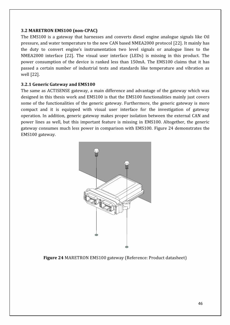
46
3.2 MARETRON EMS100 (non-CPAC)
The EMS100 is a gateway that harnesses and converts diesel engine analogue signals like Oil
pressure, and water temperature to the new CAN based NMEA2000 protocol [22]. It mainly has
the duty to convert engine’s instrumentation two level signals or analogue lines to the
NMEA2000 interface [22]. The visual user interface (LEDs) is missing in this product. The
power consumption of the device is ranked less than 150mA. The EMS100 claims that it has
passed a certain number of industrial tests and standards like temperature and vibration as
well [22].
3.2.1 Generic Gateway and EMS100
The same as ACTISENSE gateway, a main difference and advantage of the gateway which was
designed in this thesis work and EMS100 is that the EMS100 functionalities mainly just covers
some of the functionalities of the generic gateway. Furthermore, the generic gateway is more
compact and it is equipped with visual user interface for the investigation of gateway
operation. In addition, generic gateway makes proper isolation between the external CAN and
power lines as well, but this important feature is missing in EMS100. Altogether, the generic
gateway consumes much less power in comparison with EMS100. Figure 24 demonstrates the
EMS100 gateway.
Figure 24 MARETRON EMS100 gateway (Reference: Product datasheet)
47
3.3 AIRMAR U200 (non-CPAC)
This gateway is designed to convert the NMEA2000 marine CAN based communication
protocol to the USB protocol to be plugged to a computer or similar smart devices [23]. It is
used to transfer all related boat information such as speed, GPS data, oil level and water
temperature [23]. It is designed with a small size, but a visual user interface is missing. It
supports up to 115,200Kbps data transaction rate [23]. Figure 25 demonstrates AIRMAR U200
gateway in its application which converts NMEA2000 to USB.
3.3.1 AIRMAR U200 and Generic Gateway
The U200 gateway functionalities are not like the generic gateway because generic gateway
does not support USB; it does not need to be connected to a PC, because the type of operation
and place of the function is different. However, in case of the request, it will be possible to have
a USB connection in generic gateway in the future. Visual inspection for user is also missing in
the U200. It is also does not have standard connectors on the enclosure for NMEA and USB and
cables are fixed which is another disadvantage of the U200, while the generic gateway is
equipped with a standard connector and proper wire harness mechanism
3.4 AMEC NK-80 This gateway is mainly designed to convert the NMEA0183 to the NMEA2000 protocol [24].
The communication baud rate could be changed during operation by sending related
commands. User interface LEDs are included in this design. The NK-80 has a compact size and a
well-designed enclosure. Proper ground isolation is also considered for this product [24].
Figure 26 demonstrates NK-80 in the boat communication architecture which is used to
Figure 25 AIRMAR U200 gateway in application (Reference: U200 Product datasheet)
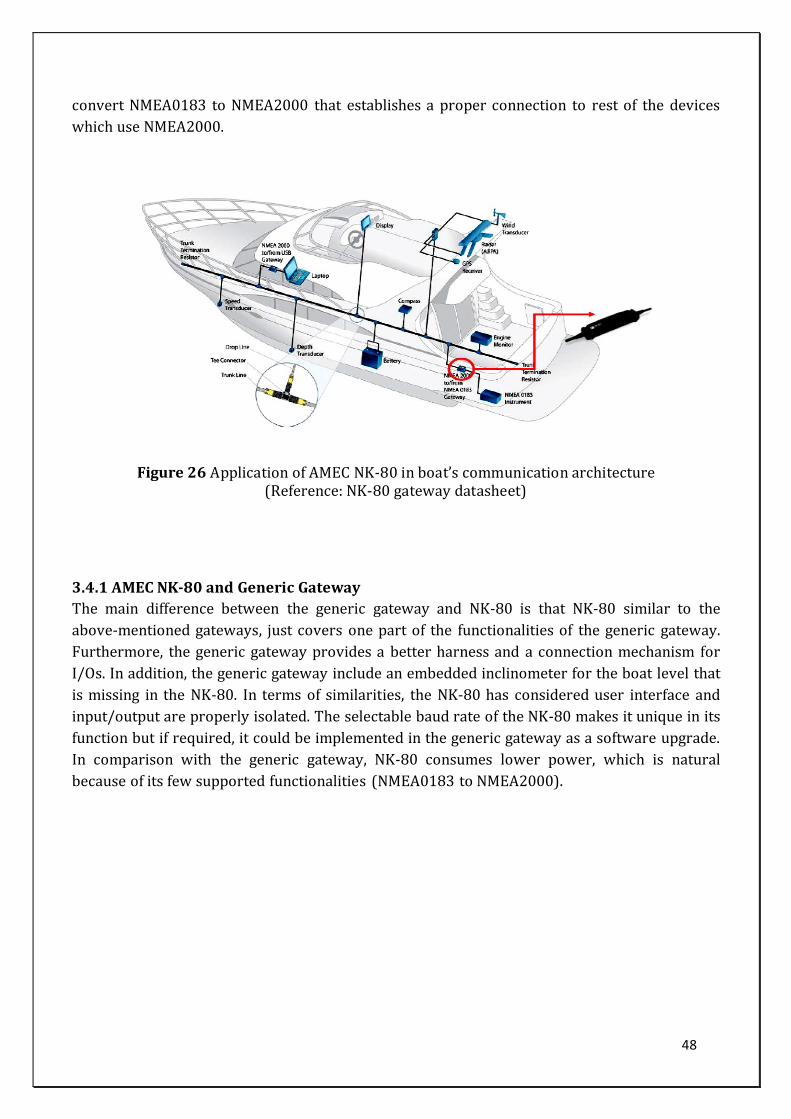
48
convert NMEA0183 to NMEA2000 that establishes a proper connection to rest of the devices
which use NMEA2000.
Figure 26 Application of AMEC NK-80 in boat’s communication architecture (Reference: NK-80 gateway datasheet)
3.4.1 AMEC NK-80 and Generic Gateway
The main difference between the generic gateway and NK-80 is that NK-80 similar to the
above-mentioned gateways, just covers one part of the functionalities of the generic gateway.
Furthermore, the generic gateway provides a better harness and a connection mechanism for
I/Os. In addition, the generic gateway include an embedded inclinometer for the boat level that
is missing in the NK-80. In terms of similarities, the NK-80 has considered user interface and
input/output are properly isolated. The selectable baud rate of the NK-80 makes it unique in its
function but if required, it could be implemented in the generic gateway as a software upgrade.
In comparison with the generic gateway, NK-80 consumes lower power, which is natural
because of its few supported functionalities (NMEA0183 to NMEA2000).
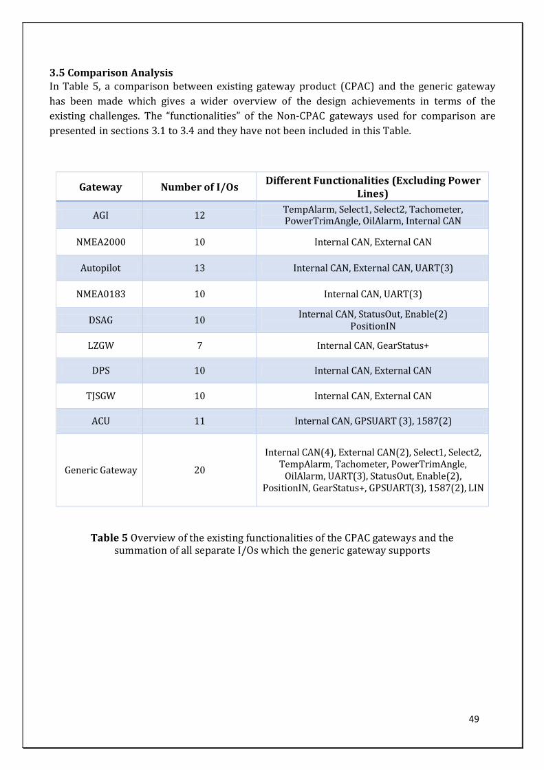
49
3.5 Comparison Analysis In Table 5, a comparison between existing gateway product (CPAC) and the generic gateway
has been made which gives a wider overview of the design achievements in terms of the
existing challenges. The “functionalities” of the Non-CPAC gateways used for comparison are
presented in sections 3.1 to 3.4 and they have not been included in this Table.
Gateway Number of I/Os Different Functionalities (Excluding Power
Lines)
AGI 12 TempAlarm, Select1, Select2, Tachometer, PowerTrimAngle, OilAlarm, Internal CAN
NMEA2000 10 Internal CAN, External CAN
Autopilot 13 Internal CAN, External CAN, UART(3)
NMEA0183 10 Internal CAN, UART(3)
DSAG 10 Internal CAN, StatusOut, Enable(2)
PositionIN
LZGW 7 Internal CAN, GearStatus+
DPS 10 Internal CAN, External CAN
TJSGW 10 Internal CAN, External CAN
ACU 11 Internal CAN, GPSUART (3), 1587(2)
Generic Gateway
20
Internal CAN(4), External CAN(2), Select1, Select2, TempAlarm, Tachometer, PowerTrimAngle,
OilAlarm, UART(3), StatusOut, Enable(2), PositionIN, GearStatus+, GPSUART(3), 1587(2), LIN
Table 5 Overview of the existing functionalities of the CPAC gateways and the summation of all separate I/Os which the generic gateway supports
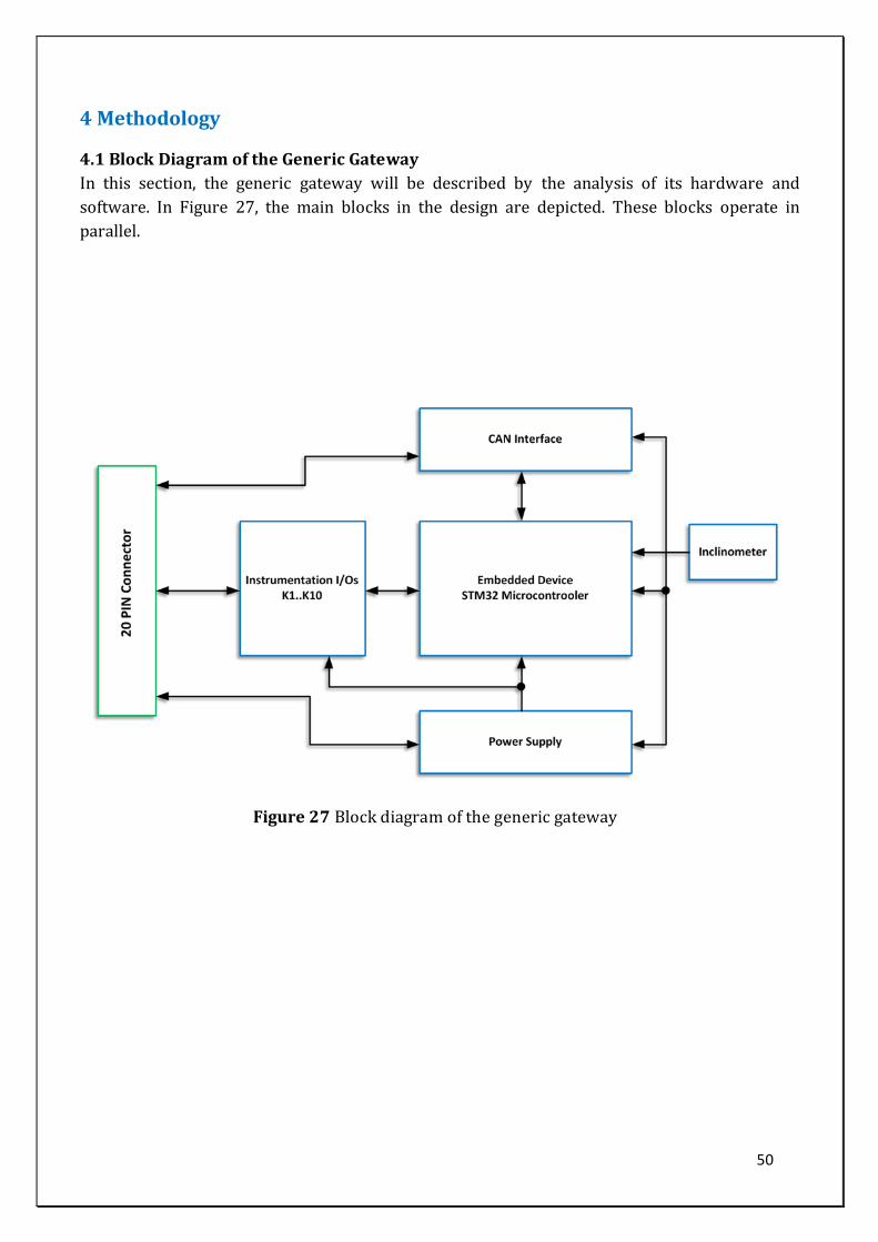
50
4 Methodology
4.1 Block Diagram of the Generic Gateway
In this section, the generic gateway will be described by the analysis of its hardware and
software. In Figure 27, the main blocks in the design are depicted. These blocks operate in
parallel.
Figure 27 Block diagram of the generic gateway
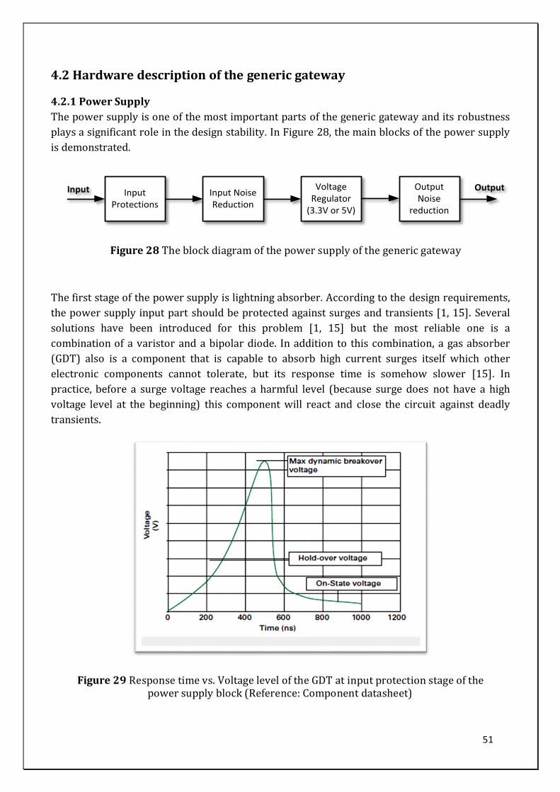
51
4.2 Hardware description of the generic gateway
4.2.1 Power Supply
The power supply is one of the most important parts of the generic gateway and its robustness
plays a significant role in the design stability. In Figure 28, the main blocks of the power supply
is demonstrated.
The first stage of the power supply is lightning absorber. According to the design requirements,
the power supply input part should be protected against surges and transients [1, 15]. Several
solutions have been introduced for this problem [1, 15] but the most reliable one is a
combination of a varistor and a bipolar diode. In addition to this combination, a gas absorber
(GDT) also is a component that is capable to absorb high current surges itself which other
electronic components cannot tolerate, but its response time is somehow slower [15]. In
practice, before a surge voltage reaches a harmful level (because surge does not have a high
voltage level at the beginning) this component will react and close the circuit against deadly
transients.
Figure 29 Response time vs. Voltage level of the GDT at input protection stage of the power supply block (Reference: Component datasheet)
Input Protections
Input Noise Reduction
VoltageRegulator
(3.3V or 5V)
Output Noise
reduction
Input Output
Figure 28 The block diagram of the power supply of the generic gateway
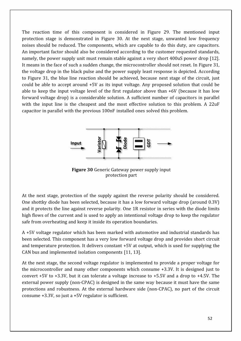
52
The reaction time of this component is considered in Figure 29. The mentioned input
protection stage is demonstrated in Figure 30. At the next stage, unwanted low frequency
noises should be reduced. The components, which are capable to do this duty, are capacitors.
An important factor should also be considered according to the customer requested standards,
namely, the power supply unit must remain stable against a very short 400uS power drop [12].
It means in the face of such a sudden change, the microcontroller should not reset. In Figure 31,
the voltage drop in the black pulse and the power supply least response is depicted. According
to Figure 31, the blue line reaction should be achieved, because next stage of the circuit, just
could be able to accept around +5V as its input voltage. Any proposed solution that could be
able to keep the input voltage level of the first regulator above than +6V (because it has low
forward voltage drop) is a considerable solution. A sufficient number of capacitors in parallel
with the input line is the cheapest and the most effective solution to this problem. A 22uF
capacitor in parallel with the previous 100nF installed ones solved this problem.
At the next stage, protection of the supply against the reverse polarity should be considered.
One shottky diode has been selected, because it has a low forward voltage drop (around 0.3V)
and it protects the line against reverse polarity. One 1R resistor in series with the diode limits
high flows of the current and is used to apply an intentional voltage drop to keep the regulator
safe from overheating and keep it inside its operation boundaries.
A +5V voltage regulator which has been marked with automotive and industrial standards has
been selected. This component has a very low forward voltage drop and provides short circuit
and temperature protection. It delivers constant +5V at output, which is used for supplying the
CAN bus and implemented isolation components [11, 13].
At the next stage, the second voltage regulator is implemented to provide a proper voltage for
the microcontroller and many other components which consume +3.3V. It is designed just to
convert +5V to +3.3V, but it can tolerate a voltage increase to +5.5V and a drop to +4.5V. The
external power supply (non-CPAC) is designed in the same way because it must have the same
protections and robustness. At the external hardware side (non-CPAC), no part of the circuit
consume +3.3V, so just a +5V regulator is sufficient.
Var
isto
r
Dio
de
InputG
DT
Figure-20Suggested Protection Stage
Figure 30 Generic Gateway power supply input protection part
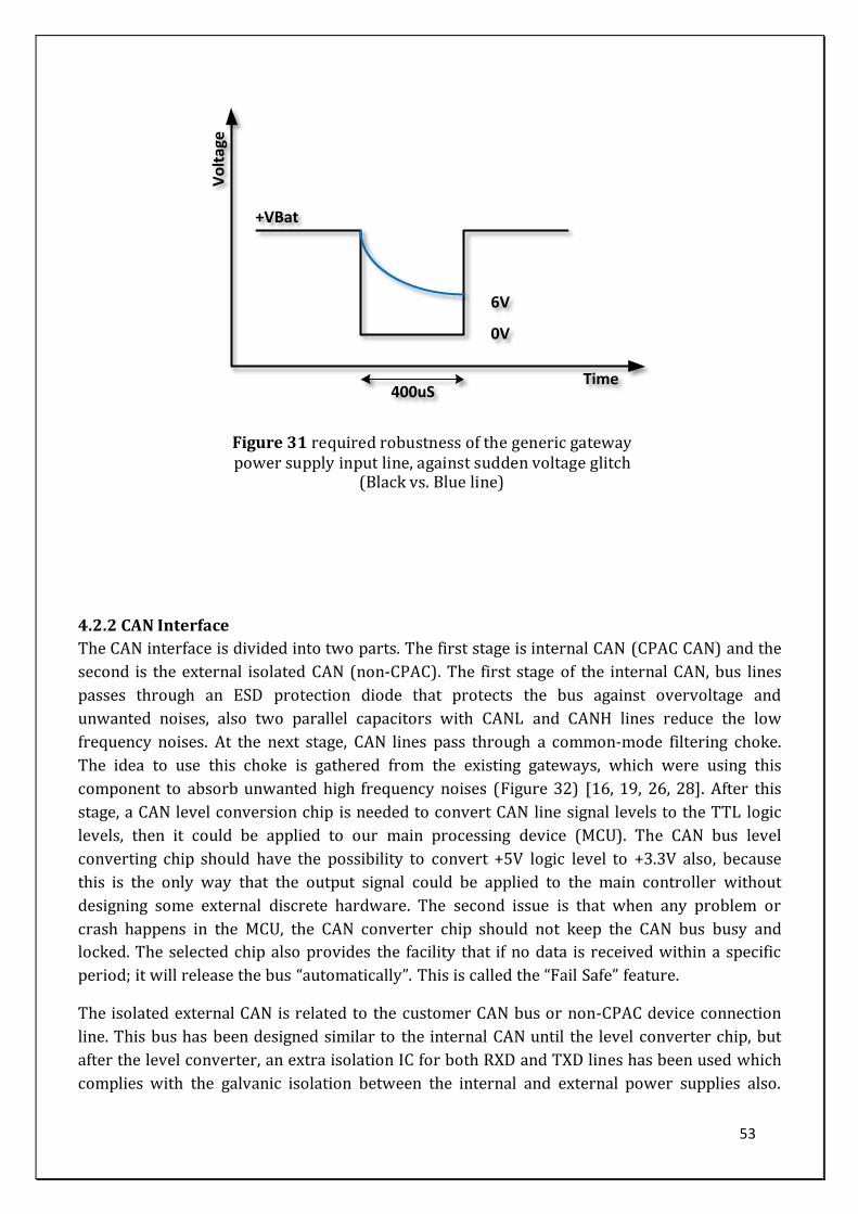
53
4.2.2 CAN Interface
The CAN interface is divided into two parts. The first stage is internal CAN (CPAC CAN) and the
second is the external isolated CAN (non-CPAC). The first stage of the internal CAN, bus lines
passes through an ESD protection diode that protects the bus against overvoltage and
unwanted noises, also two parallel capacitors with CANL and CANH lines reduce the low
frequency noises. At the next stage, CAN lines pass through a common-mode filtering choke.
The idea to use this choke is gathered from the existing gateways, which were using this
component to absorb unwanted high frequency noises (Figure 32) [16, 19, 26, 28]. After this
stage, a CAN level conversion chip is needed to convert CAN line signal levels to the TTL logic
levels, then it could be applied to our main processing device (MCU). The CAN bus level
converting chip should have the possibility to convert +5V logic level to +3.3V also, because
this is the only way that the output signal could be applied to the main controller without
designing some external discrete hardware. The second issue is that when any problem or
crash happens in the MCU, the CAN converter chip should not keep the CAN bus busy and
locked. The selected chip also provides the facility that if no data is received within a specific
period; it will release the bus “automatically”. This is called the “Fail Safe” feature.
The isolated external CAN is related to the customer CAN bus or non-CPAC device connection
line. This bus has been designed similar to the internal CAN until the level converter chip, but
after the level converter, an extra isolation IC for both RXD and TXD lines has been used which
complies with the galvanic isolation between the internal and external power supplies also.
0V
+VBat
6V
Vo
ltag
e
Time400uS
Figure-21Blue line shows minimum immunity for sudden voltage drop
Figure 31 required robustness of the generic gateway power supply input line, against sudden voltage glitch
(Black vs. Blue line)
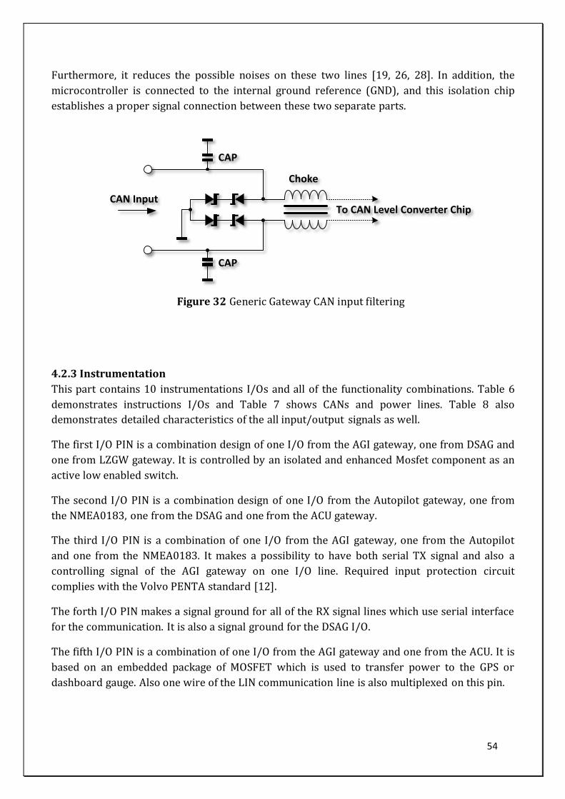
54
Furthermore, it reduces the possible noises on these two lines [19, 26, 28]. In addition, the
microcontroller is connected to the internal ground reference (GND), and this isolation chip
establishes a proper signal connection between these two separate parts.
4.2.3 Instrumentation
This part contains 10 instrumentations I/Os and all of the functionality combinations. Table 6
demonstrates instructions I/Os and Table 7 shows CANs and power lines. Table 8 also
demonstrates detailed characteristics of the all input/output signals as well.
The first I/O PIN is a combination design of one I/O from the AGI gateway, one from DSAG and
one from LZGW gateway. It is controlled by an isolated and enhanced Mosfet component as an
active low enabled switch.
The second I/O PIN is a combination design of one I/O from the Autopilot gateway, one from
the NMEA0183, one from the DSAG and one from the ACU gateway.
The third I/O PIN is a combination of one I/O from the AGI gateway, one from the Autopilot
and one from the NMEA0183. It makes a possibility to have both serial TX signal and also a
controlling signal of the AGI gateway on one I/O line. Required input protection circuit
complies with the Volvo PENTA standard [12].
The forth I/O PIN makes a signal ground for all of the RX signal lines which use serial interface
for the communication. It is also a signal ground for the DSAG I/O.
The fifth I/O PIN is a combination of one I/O from the AGI gateway and one from the ACU. It is
based on an embedded package of MOSFET which is used to transfer power to the GPS or
dashboard gauge. Also one wire of the LIN communication line is also multiplexed on this pin.
CAN Input
Choke
CAP
CAP
To CAN Level Converter Chip
Figure-22CAN BUS Input filtering
Figure 32 Generic Gateway CAN input filtering
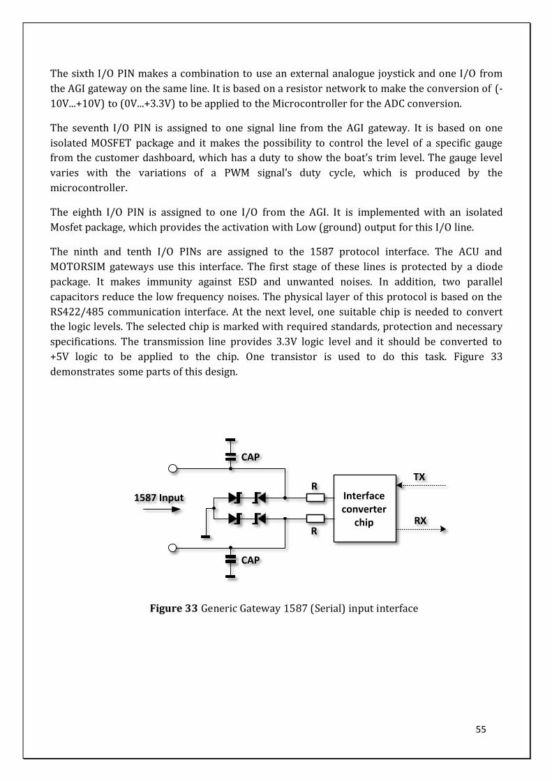
55
The sixth I/O PIN makes a combination to use an external analogue joystick and one I/O from
the AGI gateway on the same line. It is based on a resistor network to make the conversion of (-
10V...+10V) to (0V...+3.3V) to be applied to the Microcontroller for the ADC conversion.
The seventh I/O PIN is assigned to one signal line from the AGI gateway. It is based on one
isolated MOSFET package and it makes the possibility to control the level of a specific gauge
from the customer dashboard, which has a duty to show the boat’s trim level. The gauge level
varies with the variations of a PWM signal’s duty cycle, which is produced by the
microcontroller.
The eighth I/O PIN is assigned to one I/O from the AGI. It is implemented with an isolated
Mosfet package, which provides the activation with Low (ground) output for this I/O line.
The ninth and tenth I/O PINs are assigned to the 1587 protocol interface. The ACU and
MOTORSIM gateways use this interface. The first stage of these lines is protected by a diode
package. It makes immunity against ESD and unwanted noises. In addition, two parallel
capacitors reduce the low frequency noises. The physical layer of this protocol is based on the
RS422/485 communication interface. At the next level, one suitable chip is needed to convert
the logic levels. The selected chip is marked with required standards, protection and necessary
specifications. The transmission line provides 3.3V logic level and it should be converted to
+5V logic to be applied to the chip. One transistor is used to do this task. Figure 33
demonstrates some parts of this design.
1587 Input
CAP
CAP
Figure-231587 (serial) input interface
TX
RX
Interface converter
chip
R
R
Figure 33 Generic Gateway 1587 (Serial) input interface
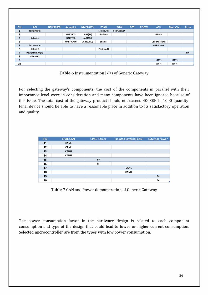
56
For selecting the gateway’s components, the cost of the components in parallel with their
importance level were in consideration and many components have been ignored because of
this issue. The total cost of the gateway product should not exceed 400SEK in 1000 quantity.
Final device should be able to have a reasonable price in addition to its satisfactory operation
and quality.
The power consumption factor in the hardware design is related to each component
consumption and type of the design that could lead to lower or higher current consumption.
Selected microcontroller are from the types with low power consumption.
PIN CPAC CAN CPAC Power Isolated External CAN External Power
11 CANL
12 CANL
13 CANH
14 CANH
15 B+
16 B-
17 CANL
18 CANH
19 B+
20 B-
PIN AGI NMEA2000 Autopilot NMEA0183 DSAG LZGW DPS TJSGW ACU MotorSim Extra
1 TempAlarm StatusOut GearStatus+
2 UART(RX) UART(RX) Enable+ GPSRX
3 Select-1 UART(TX) UART(TX)
4 UART(GND) UART(GND) Enable- GPSRXGround
5 Tachometer GPS Power
6 Select-2 PositionIN
7 PowerTrimAngle LIN
8 OilAlarm
9 1587+ 1587+
10 1587- 1587-
Table 6 Instrumentation I/Os of Generic Gateway
Table 7 CAN and Power demonstration of Generic Gateway
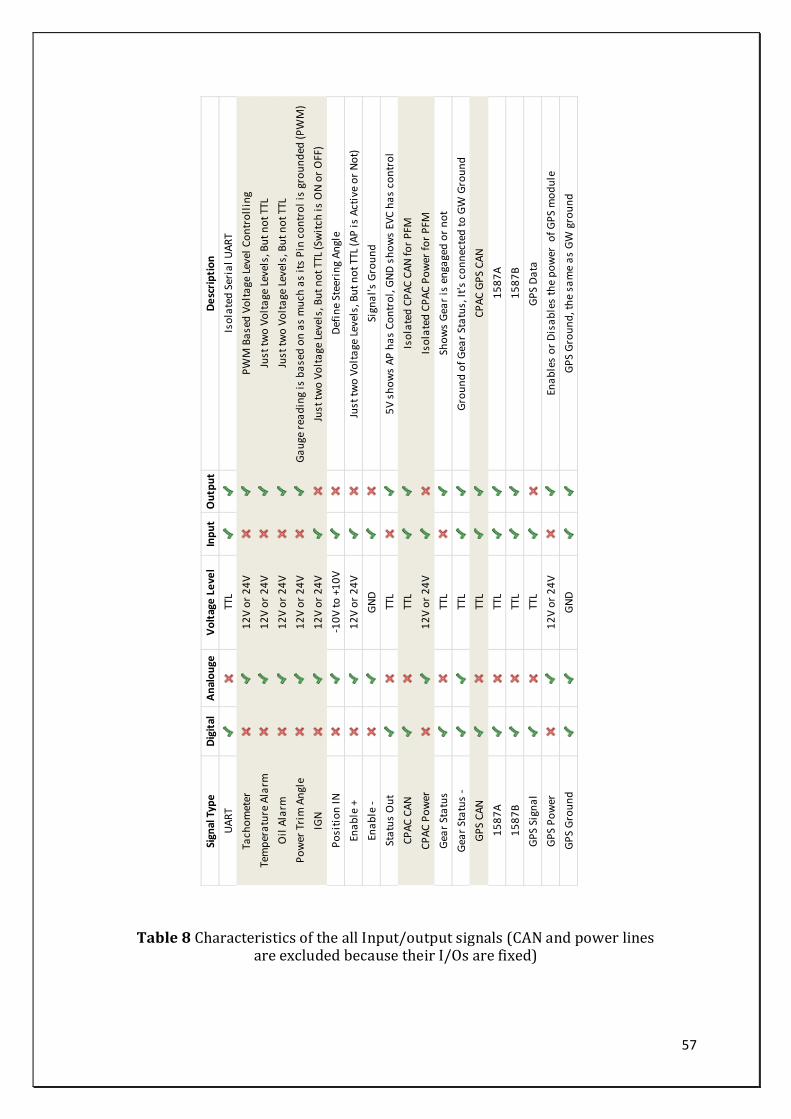
57
Sign
al T
ype
Dig
ital
An
alo
uge
Vo
ltag
e L
eve
lIn
pu
tO
utp
ut
De
scri
pti
on
UA
RT
TTL
Iso
late
d S
eria
l U
AR
T
Tach
om
eter
12
V o
r 2
4V
PW
M B
ase
d V
olt
age
Lev
el C
on
tro
llin
g
Tem
per
atu
re A
larm
12
V o
r 2
4V
Just
tw
o V
olt
age
Lev
els,
Bu
t n
ot
TTL
Oil
Ala
rm1
2V
or
24
VJu
st t
wo
Vo
lta
ge L
evel
s, B
ut
no
t TT
L
Po
wer
Tri
m A
ngl
e1
2V
or
24
VG
au
ge r
ead
ing
is b
ase
d o
n a
s m
uch
as
its
Pin
co
ntr
ol
is g
rou
nd
ed (
PW
M)
IGN
12
V o
r 2
4V
Just
tw
o V
olt
age
Lev
els,
Bu
t n
ot
TTL
(Sw
itch
is
ON
or
OFF
)
Po
siti
on
IN
-10
V t
o +
10
VD
efin
e St
eeri
ng
An
gle
Ena
ble
+1
2V
or
24
VJu
st t
wo
Vo
lta
ge L
evel
s, B
ut
no
t TT
L (A
P i
s A
ctiv
e o
r N
ot)
Ena
ble
-G
ND
Sign
al'
s G
rou
nd
Sta
tus
Ou
tTT
L5
V s
ho
ws
AP
ha
s C
on
tro
l, G
ND
sh
ow
s EV
C h
as
con
tro
l
CP
AC
CA
NTT
LIs
ola
ted
CP
AC
CA
N f
or
PFM
CP
AC
Po
wer
12
V o
r 2
4V
Iso
late
d C
PA
C P
ow
er f
or
PFM
Gea
r St
atu
sTT
LSh
ow
s G
ear
is e
nga
ged
or
no
t
Gea
r St
atu
s -
TTL
Gro
un
d o
f G
ear
Sta
tus,
It'
s co
nn
ecte
d t
o G
W G
rou
nd
GP
S C
AN
TTL
CP
AC
GP
S C
AN
15
87
ATT
L1
58
7A
15
87
BTT
L1
58
7B
GP
S Si
gna
lTT
LG
PS
Da
ta
GP
S P
ow
er1
2V
or
24
VEn
ab
les
or
Dis
ab
les
the
po
wer
of
GP
S m
od
ule
GP
S G
rou
nd
GN
DG
PS
Gro
un
d, t
he
sam
e a
s G
W g
rou
nd
Table 8 Characteristics of the all Input/output signals (CAN and power lines are excluded because their I/Os are fixed)
58
4.2.4 Embedded Device (Microcontroller)
For this stage, one 32-bit microcontroller from the STM family MCUs has been selected. The
reasons for choosing this type of microcontroller are:
1. Low Cost
2. Several embedded hardware features and a powerful core (ARM Cortex-M3 Core)
3. Low power consumption
4. It is in production and tested by the company in many projects
5. Very low internal FLASH memory access time (it increases the MCU speed dramatically)
[17]
6. High speed, 72MHz clock rate (144MHz in the overclocking mode)
The main controller has been selected from the series with support for embedded CAN 2.0B
interface. This Microcontroller can handle internal clocking up to 72MHz (by its internal PLL);
it can perform at 144MHz in overclocked mode and can drive 1.25DMIPS of performance. It
claims to do multiplication and division in just one clock cycle.
4.2.5 Inclinometers
The inclinometer component is used to realize the level of the boat when there is a request to
balance the level of the boat by sending the relative instructions to the boat trims, which are in
accordance with the boat speed. Two types of inclinometers have been implemented to be
tested. In the final product, one of the inclinometers will be used, but for the first prototype,
both selected components will be tested. First inclinometer uses SPI communication interface
and it sends exact actual values of X, Y and Z through the SPI bus. Another inclinometer
provides analogue outputs in terms of voltage level variation between 210mV to 850mV, which
is in accordance with changes in X, Y and Z-axis. The price difference between the two
inclinometer components is quite high. The goal is to check that the second inclinometer could
perform almost the same as the first one, which is much cheaper.
4.2.6 PCB & Component Assembly
The PCB (Printed circuit board) of the generic gateway was designed by the ALTIUM Designer
10 software. It was designed based on the four layers PCB board. Figure 34 demonstrates all
layers, which have contributed in the board structure. Top layer and bottom layer are mounted
on the both surfaces of the board and two mid-layers are integrated in between to carry two
separate layers of ground and power (+5V, +3.3V). The PCB design is a key element for the
lower noise, robustness, stability and in summary higher reliability of the device. The
robustness requirements in the PCB design generally means to have lower EMC factor
(emission and absorption), proper supply current handling and isolation, having a steady and
‘calm’ ground area exactly one layer below the components (TOP layer). Furthermore, with
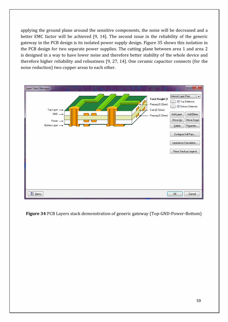
59
applying the ground plane around the sensitive components, the noise will be decreased and a
better EMC factor will be achieved [9, 14]. The second issue in the reliability of the generic
gateway in the PCB design is its isolated power supply design. Figure 35 shows this isolation in
the PCB design for two separate power supplies. The cutting plane between area 1 and area 2
is designed in a way to have lower noise and therefore better stability of the whole device and
therefore higher reliability and robustness [9, 27, 14]. One ceramic capacitor connects (for the
noise reduction) two copper areas to each other.
Figure 34 PCB Layers stack demonstration of generic gateway (Top-GND-Power-Bottom)
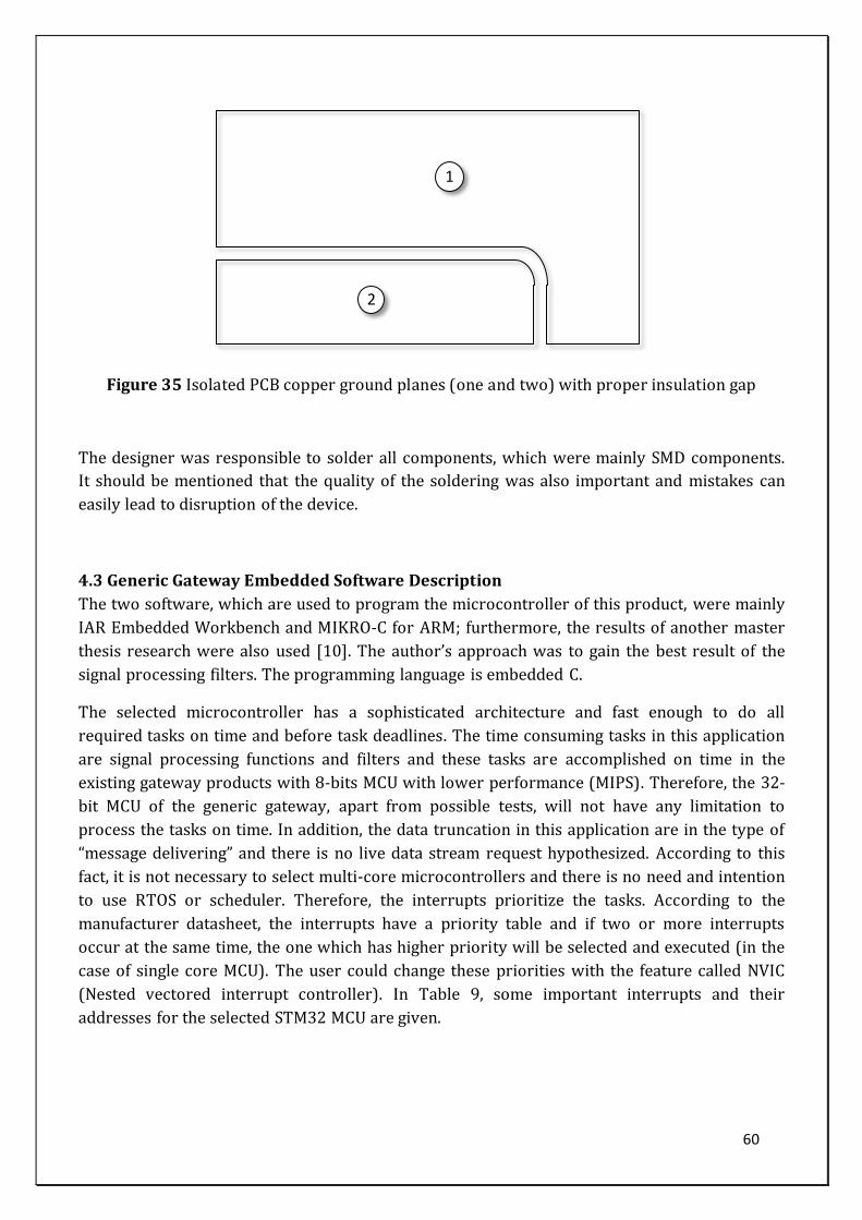
60
Figure 35 Isolated PCB copper ground planes (one and two) with proper insulation gap
The designer was responsible to solder all components, which were mainly SMD components.
It should be mentioned that the quality of the soldering was also important and mistakes can
easily lead to disruption of the device.
4.3 Generic Gateway Embedded Software Description
The two software, which are used to program the microcontroller of this product, were mainly
IAR Embedded Workbench and MIKRO-C for ARM; furthermore, the results of another master
thesis research were also used [10]. The author’s approach was to gain the best result of the
signal processing filters. The programming language is embedded C.
The selected microcontroller has a sophisticated architecture and fast enough to do all
required tasks on time and before task deadlines. The time consuming tasks in this application
are signal processing functions and filters and these tasks are accomplished on time in the
existing gateway products with 8-bits MCU with lower performance (MIPS). Therefore, the 32-
bit MCU of the generic gateway, apart from possible tests, will not have any limitation to
process the tasks on time. In addition, the data truncation in this application are in the type of
“message delivering” and there is no live data stream request hypothesized. According to this
fact, it is not necessary to select multi-core microcontrollers and there is no need and intention
to use RTOS or scheduler. Therefore, the interrupts prioritize the tasks. According to the
manufacturer datasheet, the interrupts have a priority table and if two or more interrupts
occur at the same time, the one which has higher priority will be selected and executed (in the
case of single core MCU). The user could change these priorities with the feature called NVIC
(Nested vectored interrupt controller). In Table 9, some important interrupts and their
addresses for the selected STM32 MCU are given.
1
2
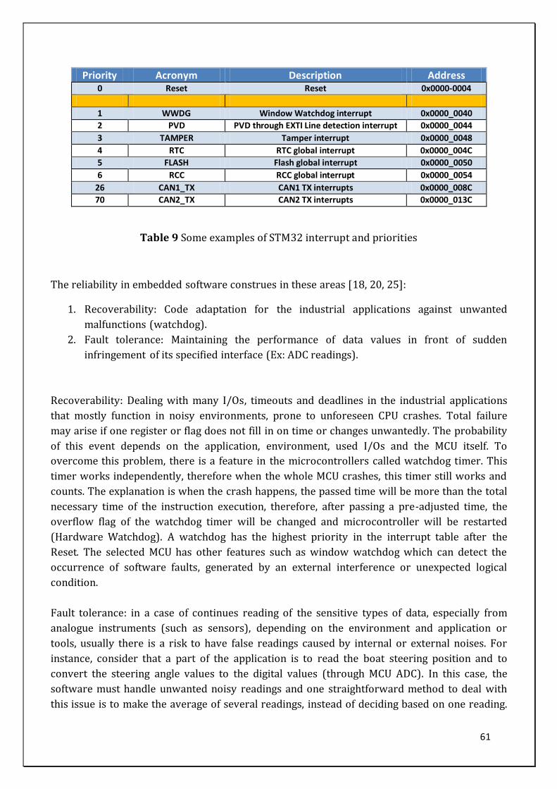
61
Priority Acronym Description Address 0 Reset Reset 0x0000-0004
1 WWDG Window Watchdog interrupt 0x0000_0040
2 PVD PVD through EXTI Line detection interrupt 0x0000_0044
3 TAMPER Tamper interrupt 0x0000_0048
4 RTC RTC global interrupt 0x0000_004C
5 FLASH Flash global interrupt 0x0000_0050
6 RCC RCC global interrupt 0x0000_0054
26 CAN1_TX CAN1 TX interrupts 0x0000_008C
70 CAN2_TX CAN2 TX interrupts 0x0000_013C
Table 9 Some examples of STM32 interrupt and priorities
The reliability in embedded software construes in these areas [18, 20, 25]:
1. Recoverability: Code adaptation for the industrial applications against unwanted
malfunctions (watchdog).
2. Fault tolerance: Maintaining the performance of data values in front of sudden
infringement of its specified interface (Ex: ADC readings).
Recoverability: Dealing with many I/Os, timeouts and deadlines in the industrial applications
that mostly function in noisy environments, prone to unforeseen CPU crashes. Total failure
may arise if one register or flag does not fill in on time or changes unwantedly. The probability
of this event depends on the application, environment, used I/Os and the MCU itself. To
overcome this problem, there is a feature in the microcontrollers called watchdog timer. This
timer works independently, therefore when the whole MCU crashes, this timer still works and
counts. The explanation is when the crash happens, the passed time will be more than the total
necessary time of the instruction execution, therefore, after passing a pre-adjusted time, the
overflow flag of the watchdog timer will be changed and microcontroller will be restarted
(Hardware Watchdog). A watchdog has the highest priority in the interrupt table after the
Reset. The selected MCU has other features such as window watchdog which can detect the
occurrence of software faults, generated by an external interference or unexpected logical
condition.
Fault tolerance: in a case of continues reading of the sensitive types of data, especially from
analogue instruments (such as sensors), depending on the environment and application or
tools, usually there is a risk to have false readings caused by internal or external noises. For
instance, consider that a part of the application is to read the boat steering position and to
convert the steering angle values to the digital values (through MCU ADC). In this case, the
software must handle unwanted noisy readings and one straightforward method to deal with
this issue is to make the average of several readings, instead of deciding based on one reading.
62
Consider equation (2a) and equation (2b). In equation (2b), value “i” is dependent on the speed
of the ADC, the deadline for ADC reading and conversion and the variety of noise in the data
series.
𝐴𝐷𝐶 = 𝑥. 𝐾 (𝑥: 𝑎𝑛𝑎𝑙𝑜𝑔𝑢𝑒 𝑚𝑎𝑔𝑛𝑖𝑡𝑢𝑑𝑒, 𝐾 = 𝑐𝑜𝑟𝑟𝑒𝑐𝑡𝑖𝑜𝑛 𝑡𝑒𝑟𝑚) (2𝑎)
𝐴𝐷𝐶 = (𝑥1+𝑥2+𝑥3+⋯+𝑥𝑖
𝑖) . 𝐾 (𝑖 = 𝑛𝑢𝑚𝑏𝑒𝑟 𝑜𝑓 𝑟𝑒𝑎𝑑𝑖𝑛𝑔𝑠, 𝐾 = 𝑐𝑜𝑟𝑟𝑒𝑐𝑡𝑖𝑜𝑛 𝑡𝑒𝑟𝑚) (2𝑏)
The power consumption of the MCU could be reduced by using the sleep mode but it is not
considered at this level of design because the difference of several milliamps is not significant
for this application, furthermore this device will always work in the operational mode and the
sleep time is very short. A simple view of the software block diagram structure is demonstrated
in Figure 36 and a flow chart of the general software operation is demonstrated in Figure 37.
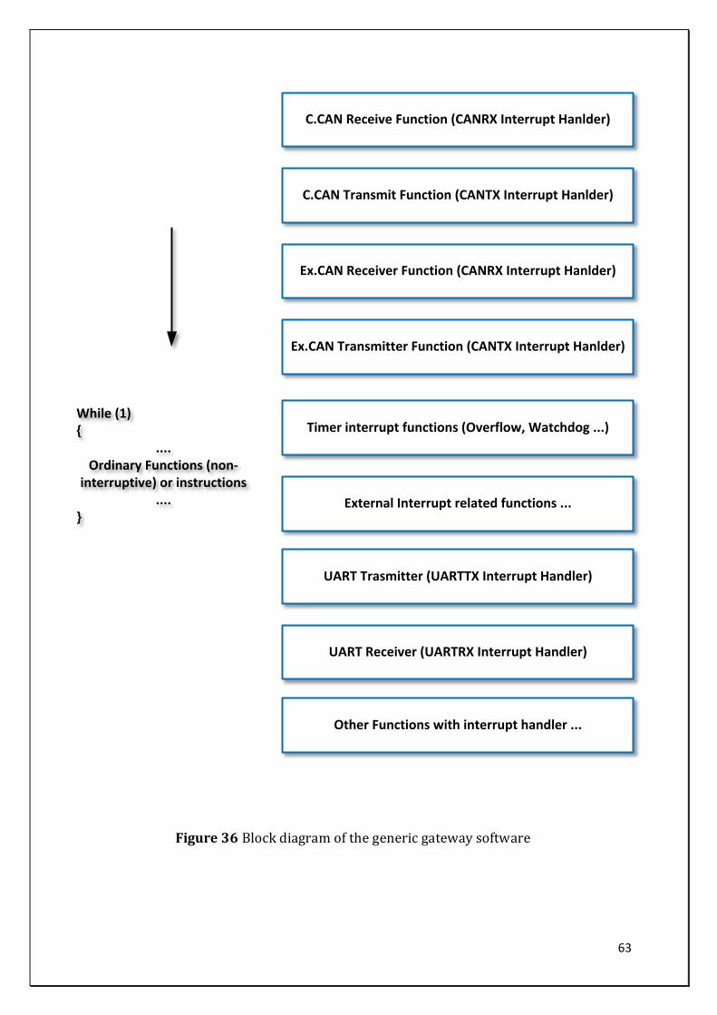
63
C.CAN Transmit Function (CANTX Interrupt Hanlder)
Ex.CAN Receiver Function (CANRX Interrupt Hanlder)
Ex.CAN Transmitter Function (CANTX Interrupt Hanlder)
While (1)
....Ordinary Functions (non-
interruptive) or instructions....
UART Trasmitter (UARTTX Interrupt Handler)
UART Receiver (UARTRX Interrupt Handler)
Other Functions with interrupt handler ...
C.CAN Receive Function (CANRX Interrupt Hanlder)
Figure-24(I)Generic Gateway’s main design blocks
Timer interrupt functions (Overflow, Watchdog ...)
External Interrupt related functions ...
Figure 36 Block diagram of the generic gateway software
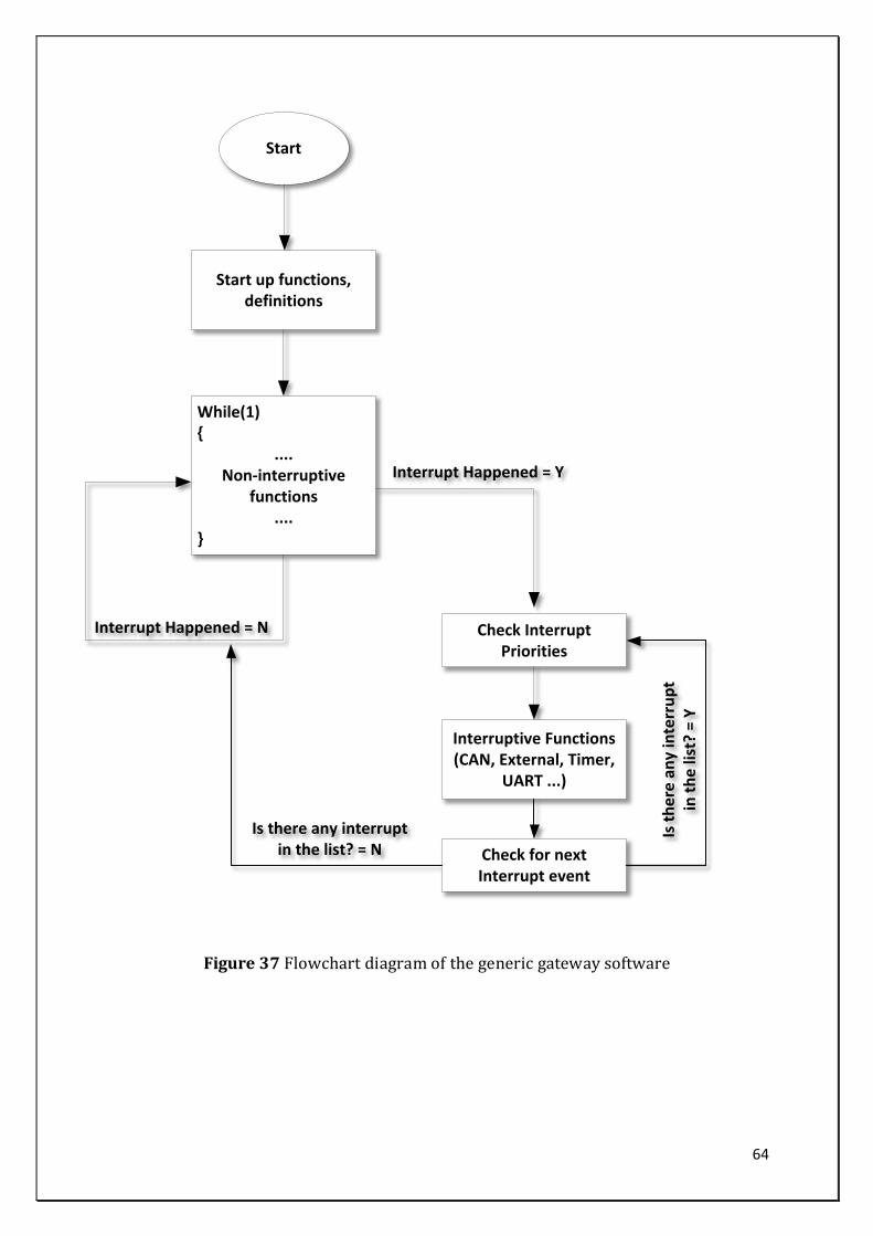
64
Figure 37 Flowchart diagram of the generic gateway software
Start
Start up functions, definitions
While(1)
....Non-interruptive
functions....
Check Interrupt Priorities
Interruptive Functions (CAN, External, Timer,
UART ...)
Interrupt Happened = Y
Interrupt Happened = N
Check for next Interrupt event
Figure-24(II) Flowchart of general operation of the generic gateway
Is t
he
re a
ny
inte
rru
pt
in t
he
list
? =
Y
Is there any interrupt in the list? = N
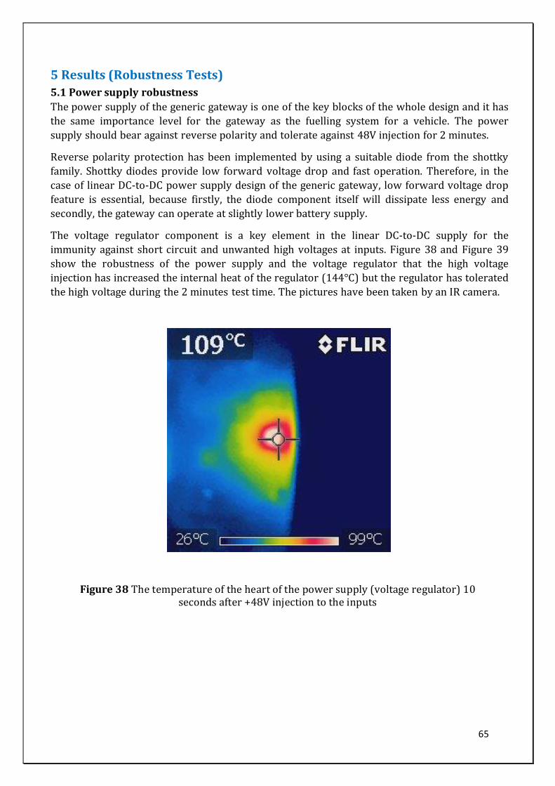
65
5 Results (Robustness Tests)
5.1 Power supply robustness
The power supply of the generic gateway is one of the key blocks of the whole design and it has
the same importance level for the gateway as the fuelling system for a vehicle. The power
supply should bear against reverse polarity and tolerate against 48V injection for 2 minutes.
Reverse polarity protection has been implemented by using a suitable diode from the shottky
family. Shottky diodes provide low forward voltage drop and fast operation. Therefore, in the
case of linear DC-to-DC power supply design of the generic gateway, low forward voltage drop
feature is essential, because firstly, the diode component itself will dissipate less energy and
secondly, the gateway can operate at slightly lower battery supply.
The voltage regulator component is a key element in the linear DC-to-DC supply for the
immunity against short circuit and unwanted high voltages at inputs. Figure 38 and Figure 39
show the robustness of the power supply and the voltage regulator that the high voltage
injection has increased the internal heat of the regulator (144°C) but the regulator has tolerated
the high voltage during the 2 minutes test time. The pictures have been taken by an IR camera.
Figure 38 The temperature of the heart of the power supply (voltage regulator) 10 seconds after +48V injection to the inputs
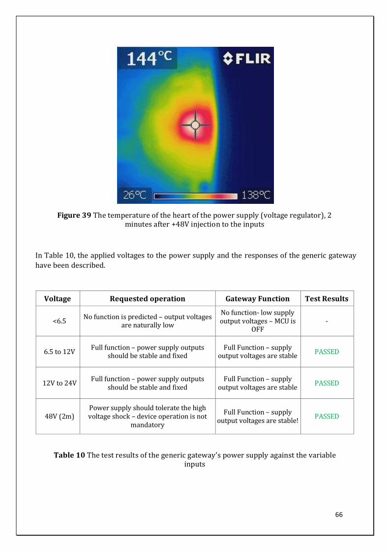
66
Figure 39 The temperature of the heart of the power supply (voltage regulator), 2 minutes after +48V injection to the inputs
In Table 10, the applied voltages to the power supply and the responses of the generic gateway
have been described.
Voltage Requested operation Gateway Function Test Results
<6.5 No function is predicted – output voltages
are naturally low
No function- low supply output voltages – MCU is
OFF -
6.5 to 12V Full function – power supply outputs
should be stable and fixed Full Function – supply
output voltages are stable PASSED
12V to 24V Full function – power supply outputs
should be stable and fixed Full Function – supply
output voltages are stable PASSED
48V (2m) Power supply should tolerate the high voltage shock – device operation is not
mandatory
Full Function – supply output voltages are stable!
PASSED
Table 10 The test results of the generic gateway’s power supply against the variable inputs
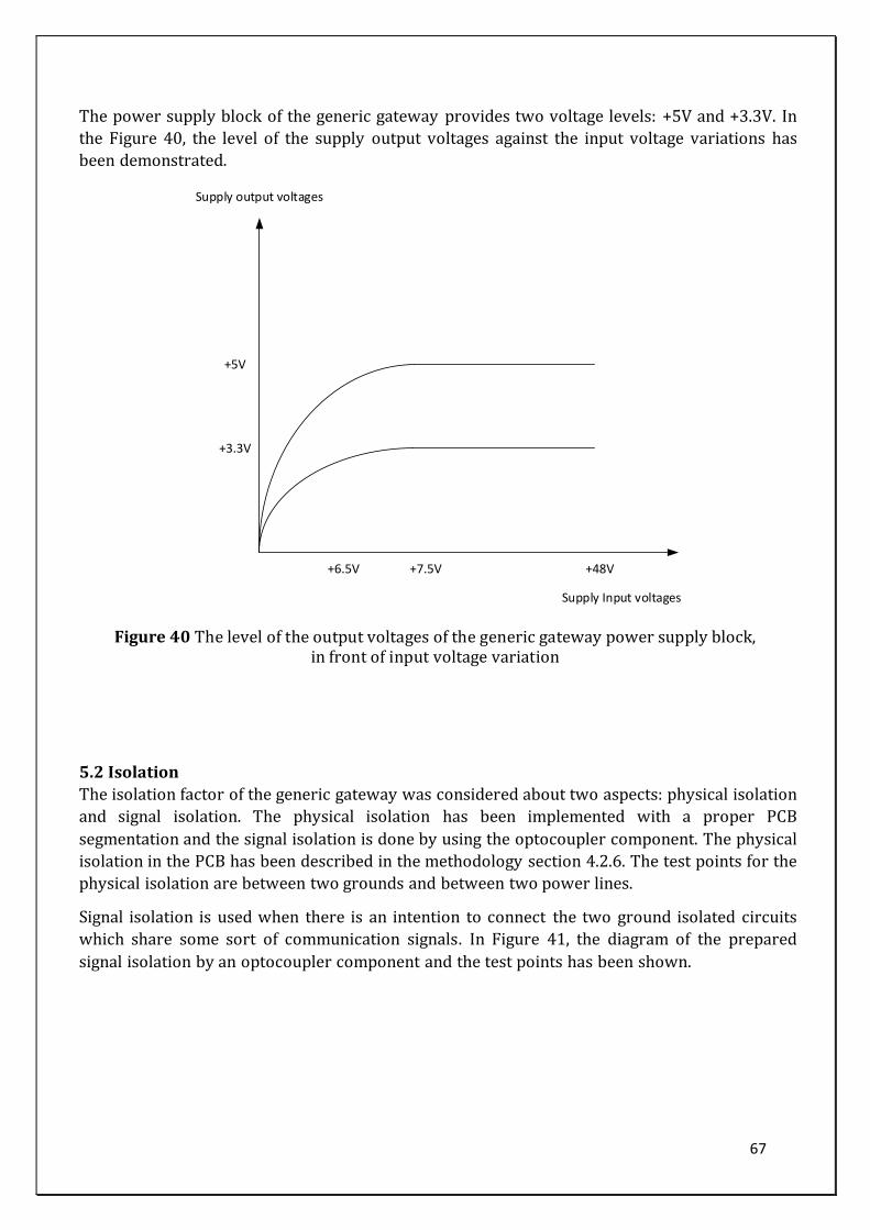
67
The power supply block of the generic gateway provides two voltage levels: +5V and +3.3V. In
the Figure 40, the level of the supply output voltages against the input voltage variations has
been demonstrated.
Figure 40 The level of the output voltages of the generic gateway power supply block, in front of input voltage variation
5.2 Isolation
The isolation factor of the generic gateway was considered about two aspects: physical isolation
and signal isolation. The physical isolation has been implemented with a proper PCB
segmentation and the signal isolation is done by using the optocoupler component. The physical
isolation in the PCB has been described in the methodology section 4.2.6. The test points for the
physical isolation are between two grounds and between two power lines.
Signal isolation is used when there is an intention to connect the two ground isolated circuits
which share some sort of communication signals. In Figure 41, the diagram of the prepared
signal isolation by an optocoupler component and the test points has been shown.
Supply output voltages
+48V+6.5V
Supply Input voltages
+3.3V
+5V
+7.5V
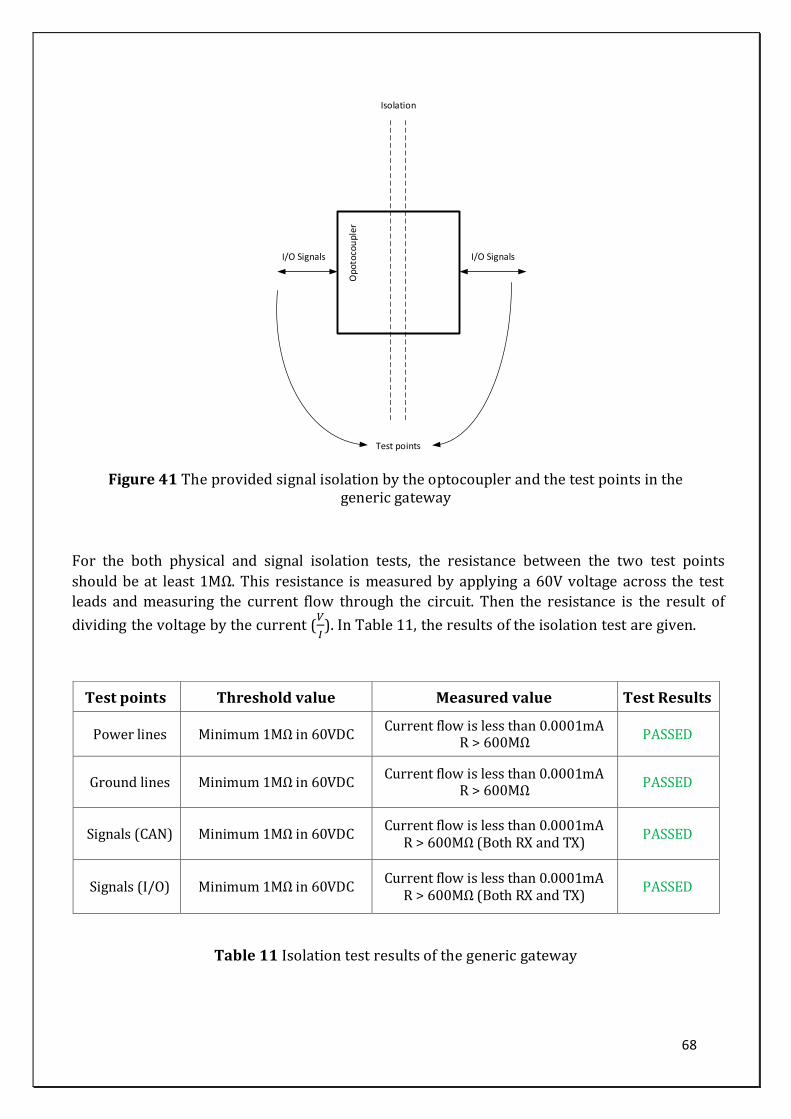
68
Figure 41 The provided signal isolation by the optocoupler and the test points in the generic gateway
For the both physical and signal isolation tests, the resistance between the two test points
should be at least 1MΩ. This resistance is measured by applying a 60V voltage across the test
leads and measuring the current flow through the circuit. Then the resistance is the result of
dividing the voltage by the current (𝑉
𝐼). In Table 11, the results of the isolation test are given.
Test points Threshold value Measured value Test Results
Power lines Minimum 1MΩ in 60VDC Current flow is less than 0.0001mA
R > 600MΩ PASSED
Ground lines Minimum 1MΩ in 60VDC Current flow is less than 0.0001mA
R > 600MΩ PASSED
Signals (CAN) Minimum 1MΩ in 60VDC Current flow is less than 0.0001mA
R > 600MΩ (Both RX and TX) PASSED
Signals (I/O) Minimum 1MΩ in 60VDC Current flow is less than 0.0001mA
R > 600MΩ (Both RX and TX) PASSED
Table 11 Isolation test results of the generic gateway
Op
oto
cou
ple
r
Isolation
I/O Signals I/O Signals
Test points
69
5.3 Power Consumption
The input voltage to the generic gateway varies between 12V to 24V. Hence, the current
consumption is used as a reference value.
To reduce the current consumption of the generic gateway, firstly, the power supply block
should have high efficiency and secondly, the microcontroller should be selected from the types
with lower power consumption. In the generic gateway, the linear DC-to-DC supply has been
implemented and hence lower power consumption of the power supply in the generic gateway
is minimized by selecting a regulator chip with lower forward voltage drop.
In Table 12, the typical current consumption of the gateway has been measured and compared
with the requirement. The typical current consumption of the generic gateway is measured at
90mA. Around 40mA of the total current consumption is just consumed by the two separate
CAN buses.
Test points Threshold value Measured value Test Results
Typical current consumption of the
gateway Maximum 150mA 90mA at full enabled device PASSED
Table 12 Typical current consumption test of the Generic Gateway
5.4 Temperature
The generic gateway should operate flawlessly in the presence of temperature variations. The
upper limit for the temperature test is +85C and the lower limit is -20C. The implementation
inside the design has been done by using components of which the temperature specifications
fit within the requested temperature boundaries.
For testing, the device operation is examined with an active communication line to check the
activity of the device, specially the MCU.
First, the generic gateway is tested and examined in the “room temperature”. Then it is tested at
the upper and the lower temperature boundaries. The used equipment for these tests is a
temperature chamber. Figure 42 shows the temperature chamber room, equipment and the test
room.
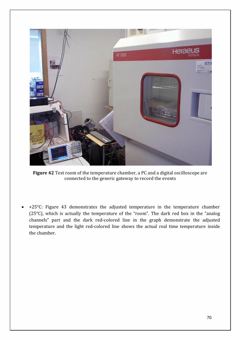
70
Figure 42 Test room of the temperature chamber, a PC and a digital oscilloscope are connected to the generic gateway to record the events
+25°C: Figure 43 demonstrates the adjusted temperature in the temperature chamber
(25°C), which is actually the temperature of the “room”. The dark red box in the “analog
channels” part and the dark red-colored line in the graph demonstrate the adjusted
temperature and the light red-colored line shows the actual real time temperature inside
the chamber.
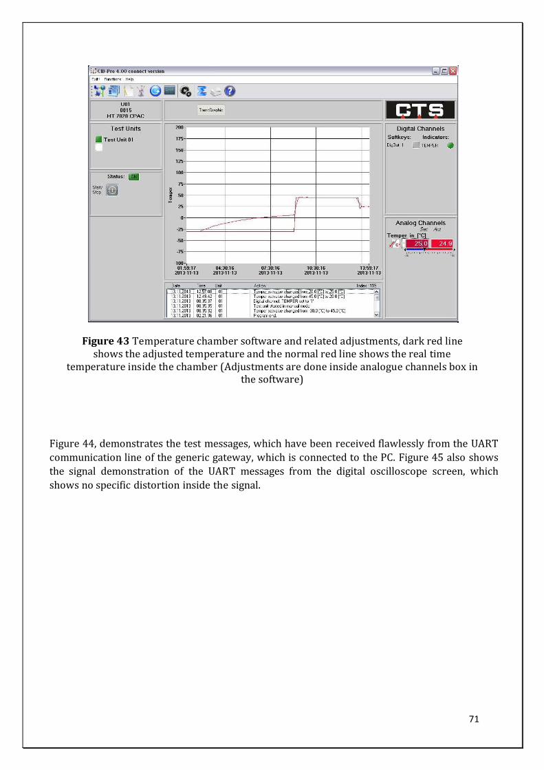
71
Figure 43 Temperature chamber software and related adjustments, dark red line shows the adjusted temperature and the normal red line shows the real time
temperature inside the chamber (Adjustments are done inside analogue channels box in the software)
Figure 44, demonstrates the test messages, which have been received flawlessly from the UART
communication line of the generic gateway, which is connected to the PC. Figure 45 also shows
the signal demonstration of the UART messages from the digital oscilloscope screen, which
shows no specific distortion inside the signal.
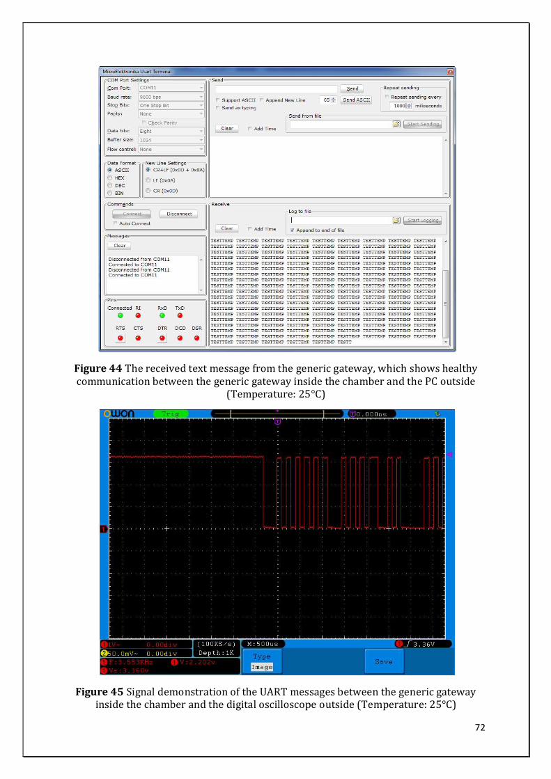
72
Figure 44 The received text message from the generic gateway, which shows healthy communication between the generic gateway inside the chamber and the PC outside
(Temperature: 25°C)
Figure 45 Signal demonstration of the UART messages between the generic gateway inside the chamber and the digital oscilloscope outside (Temperature: 25°C)
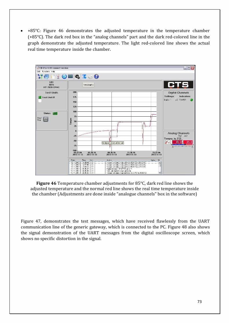
73
+85°C: Figure 46 demonstrates the adjusted temperature in the temperature chamber
(+85°C). The dark red box in the “analog channels” part and the dark red-colored line in the
graph demonstrate the adjusted temperature. The light red-colored line shows the actual
real time temperature inside the chamber.
Figure 46 Temperature chamber adjustments for 85°C, dark red line shows the adjusted temperature and the normal red line shows the real time temperature inside the chamber (Adjustments are done inside “analogue channels” box in the software)
Figure 47, demonstrates the test messages, which have received flawlessly from the UART
communication line of the generic gateway, which is connected to the PC. Figure 48 also shows
the signal demonstration of the UART messages from the digital oscilloscope screen, which
shows no specific distortion in the signal.
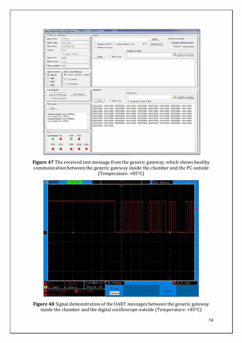
74
Figure 47 The received text message from the generic gateway, which shows healthy communication between the generic gateway inside the chamber and the PC outside
(Temperature: +85°C)
Figure 48 Signal demonstration of the UART messages between the generic gateway inside the chamber and the digital oscilloscope outside (Temperature: +85°C)
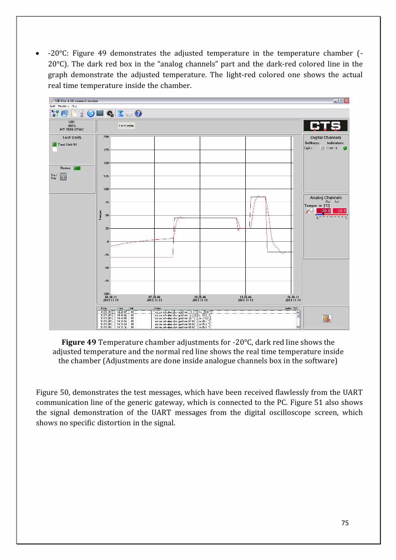
75
-20°C: Figure 49 demonstrates the adjusted temperature in the temperature chamber (-
20°C). The dark red box in the “analog channels” part and the dark-red colored line in the
graph demonstrate the adjusted temperature. The light-red colored one shows the actual
real time temperature inside the chamber.
Figure 49 Temperature chamber adjustments for -20°C, dark red line shows the adjusted temperature and the normal red line shows the real time temperature inside
the chamber (Adjustments are done inside analogue channels box in the software)
Figure 50, demonstrates the test messages, which have been received flawlessly from the UART
communication line of the generic gateway, which is connected to the PC. Figure 51 also shows
the signal demonstration of the UART messages from the digital oscilloscope screen, which
shows no specific distortion in the signal.
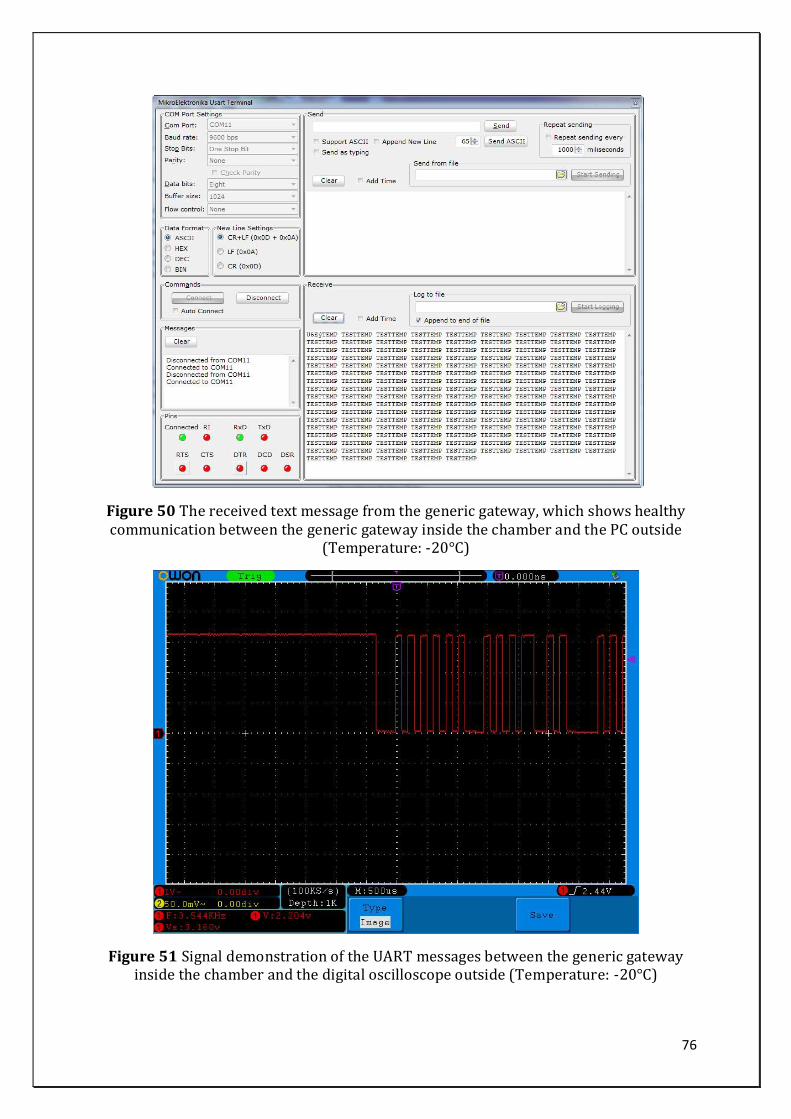
76
Figure 50 The received text message from the generic gateway, which shows healthy communication between the generic gateway inside the chamber and the PC outside
(Temperature: -20°C)
Figure 51 Signal demonstration of the UART messages between the generic gateway inside the chamber and the digital oscilloscope outside (Temperature: -20°C)
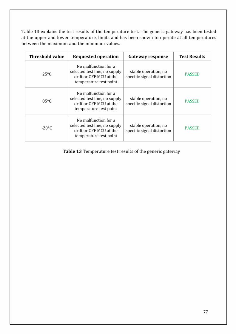
77
Table 13 explains the test results of the temperature test. The generic gateway has been tested
at the upper and lower temperature, limits and has been shown to operate at all temperatures
between the maximum and the minimum values.
Table 13 Temperature test results of the generic gateway
Threshold value Requested operation Gateway response Test Results
25°C
No malfunction for a selected test line, no supply
drift or OFF MCU at the temperature test point
stable operation, no specific signal distortion
PASSED
85°C
No malfunction for a selected test line, no supply
drift or OFF MCU at the temperature test point
stable operation, no specific signal distortion
PASSED
-20°C
No malfunction for a selected test line, no supply
drift or OFF MCU at the temperature test point
stable operation, no specific signal distortion
PASSED
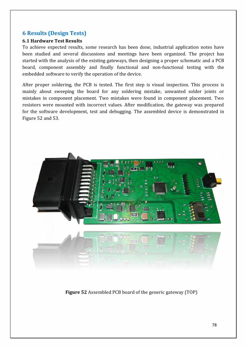
78
6 Results (Design Tests)
6.1 Hardware Test Results
To achieve expected results, some research has been done, industrial application notes have
been studied and several discussions and meetings have been organized. The project has
started with the analysis of the existing gateways, then designing a proper schematic and a PCB
board, component assembly and finally functional and non-functional testing with the
embedded software to verify the operation of the device.
After proper soldering, the PCB is tested. The first step is visual inspection. This process is
mainly about sweeping the board for any soldering mistake, unwanted solder joints or
mistakes in component placement. Two mistakes were found in component placement. Two
resistors were mounted with incorrect values. After modification, the gateway was prepared
for the software development, test and debugging. The assembled device is demonstrated in
Figure 52 and 53.
Figure 52 Assembled PCB board of the generic gateway (TOP)
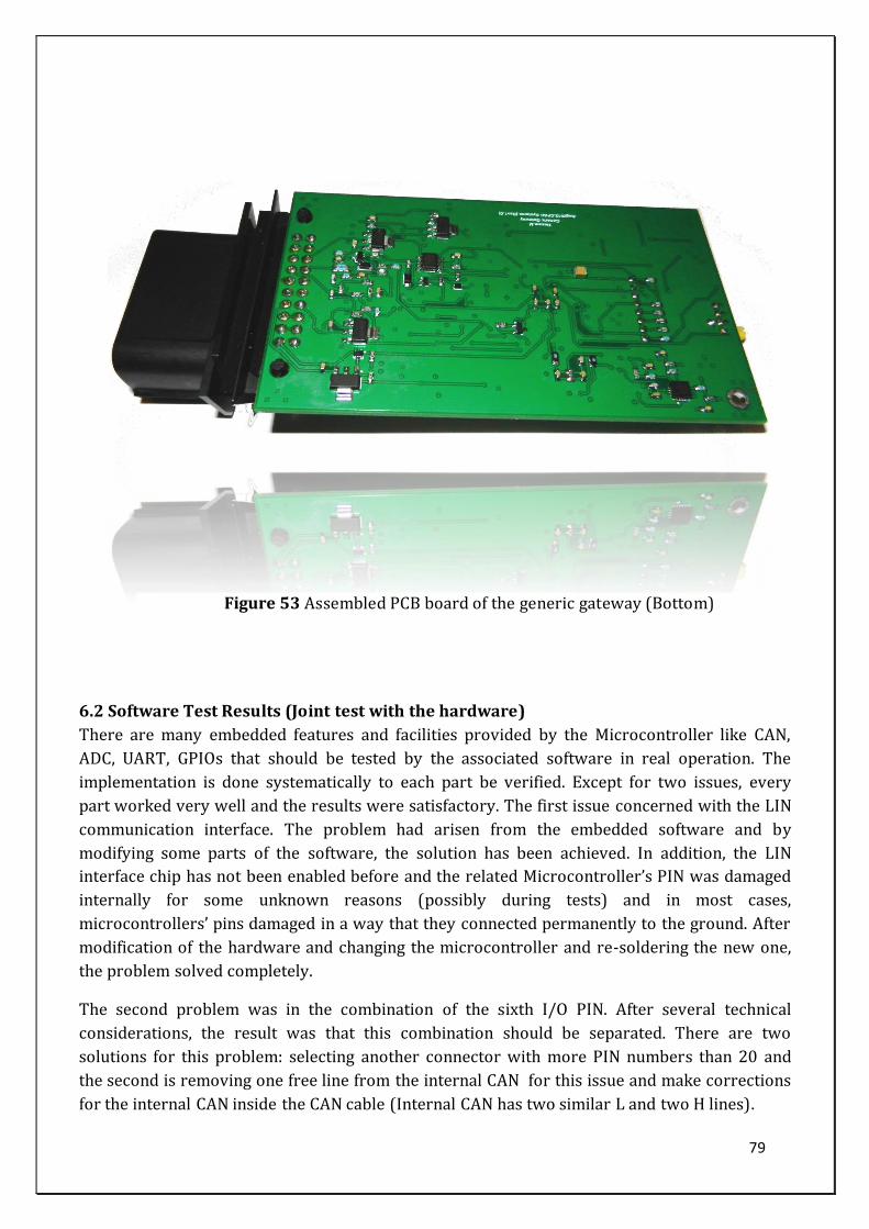
79
6.2 Software Test Results (Joint test with the hardware)
There are many embedded features and facilities provided by the Microcontroller like CAN,
ADC, UART, GPIOs that should be tested by the associated software in real operation. The
implementation is done systematically to each part be verified. Except for two issues, every
part worked very well and the results were satisfactory. The first issue concerned with the LIN
communication interface. The problem had arisen from the embedded software and by
modifying some parts of the software, the solution has been achieved. In addition, the LIN
interface chip has not been enabled before and the related Microcontroller’s PIN was damaged
internally for some unknown reasons (possibly during tests) and in most cases,
microcontrollers’ pins damaged in a way that they connected permanently to the ground. After
modification of the hardware and changing the microcontroller and re-soldering the new one,
the problem solved completely.
The second problem was in the combination of the sixth I/O PIN. After several technical
considerations, the result was that this combination should be separated. There are two
solutions for this problem: selecting another connector with more PIN numbers than 20 and
the second is removing one free line from the internal CAN for this issue and make corrections
for the internal CAN inside the CAN cable (Internal CAN has two similar L and two H lines).
Figure 53 Assembled PCB board of the generic gateway (Bottom)
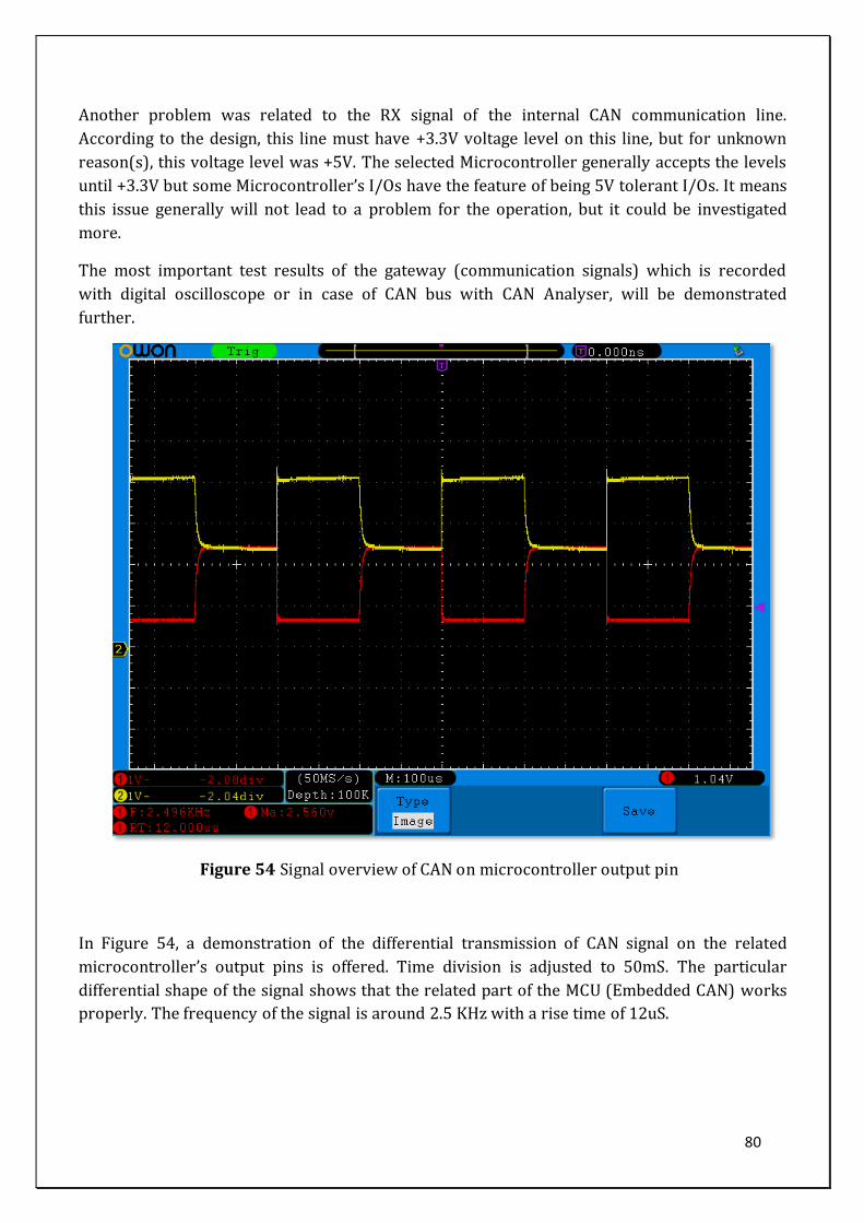
80
Another problem was related to the RX signal of the internal CAN communication line.
According to the design, this line must have +3.3V voltage level on this line, but for unknown
reason(s), this voltage level was +5V. The selected Microcontroller generally accepts the levels
until +3.3V but some Microcontroller’s I/Os have the feature of being 5V tolerant I/Os. It means
this issue generally will not lead to a problem for the operation, but it could be investigated
more.
The most important test results of the gateway (communication signals) which is recorded
with digital oscilloscope or in case of CAN bus with CAN Analyser, will be demonstrated
further.
In Figure 54, a demonstration of the differential transmission of CAN signal on the related
microcontroller’s output pins is offered. Time division is adjusted to 50mS. The particular
differential shape of the signal shows that the related part of the MCU (Embedded CAN) works
properly. The frequency of the signal is around 2.5 KHz with a rise time of 12uS.
Figure-26CAN Signal demostration on Microcontroller output
Figure 54 Signal overview of CAN on microcontroller output pin
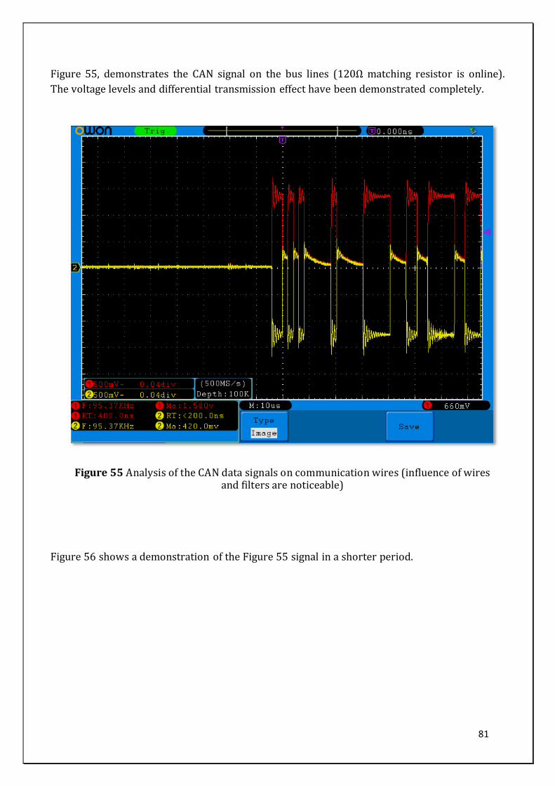
81
Figure 55, demonstrates the CAN signal on the bus lines (120Ω matching resistor is online).
The voltage levels and differential transmission effect have been demonstrated completely.
Figure 56 shows a demonstration of the Figure 55 signal in a shorter period.
Figure-27CAN Signal demostration on real communication line Figure 55 Analysis of the CAN data signals on communication wires (influence of wires
and filters are noticeable)
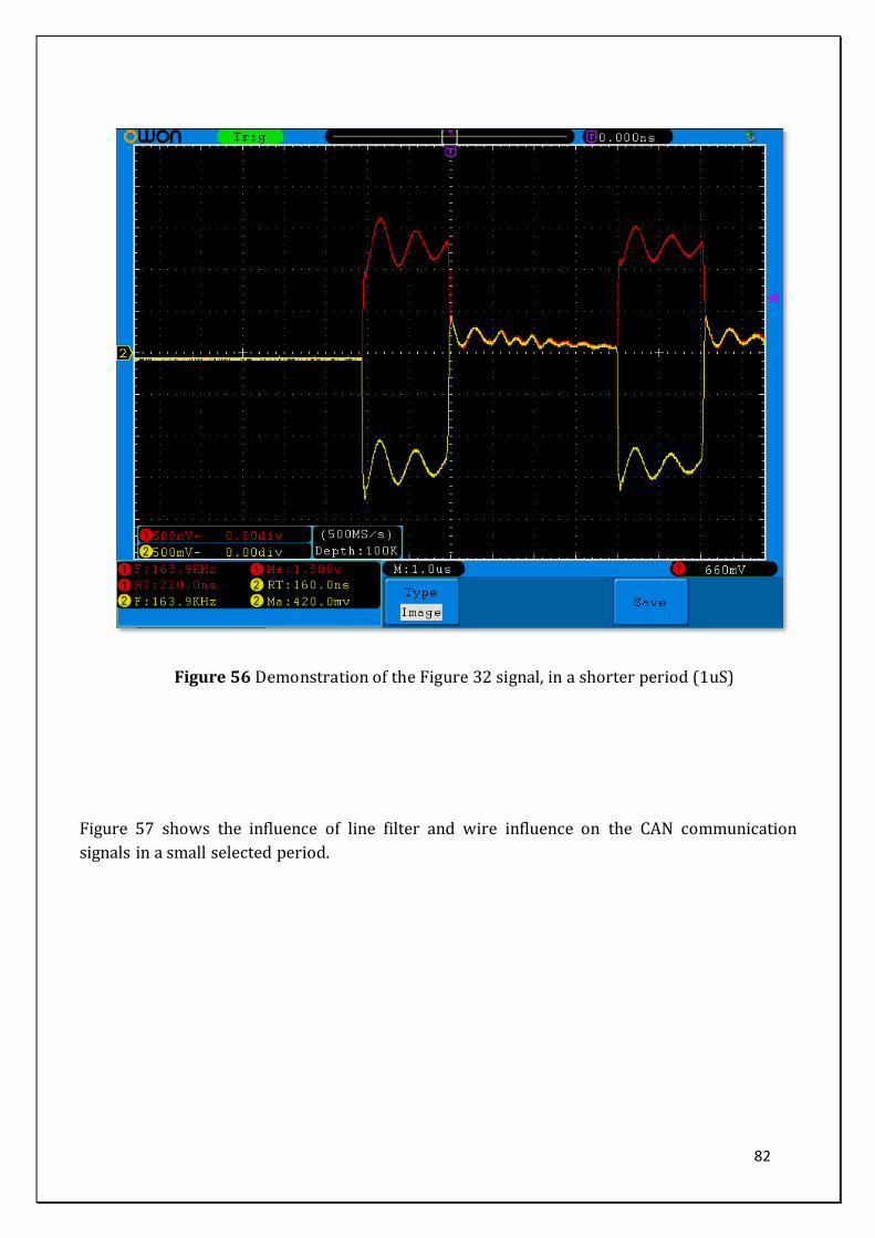
82
Figure 57 shows the influence of line filter and wire influence on the CAN communication
signals in a small selected period.
Figure-28CAN Signal demostration on real communication line (Time division of 1uS) Figure 56 Demonstration of the Figure 32 signal, in a shorter period (1uS)
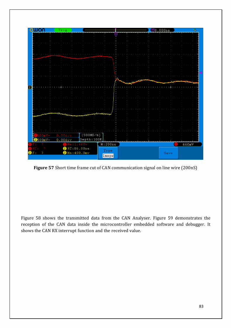
83
Figure 57 Short time frame cut of CAN communication signal on line wire (200nS)
Figure 58 shows the transmitted data from the CAN Analyser. Figure 59 demonstrates the
reception of the CAN data inside the microcontroller embedded software and debugger. It
shows the CAN RX interrupt function and the received value.
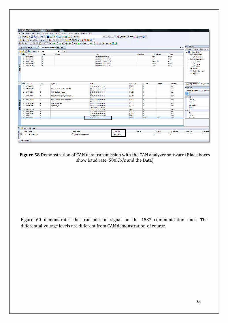
84
Figure 60 demonstrates the transmission signal on the 1587 communication lines. The
differential voltage levels are different from CAN demonstration of course.
Figure 58 Demonstration of CAN data transmission with the CAN analyzer software (Black boxes show baud rate: 500Kb/s and the Data)
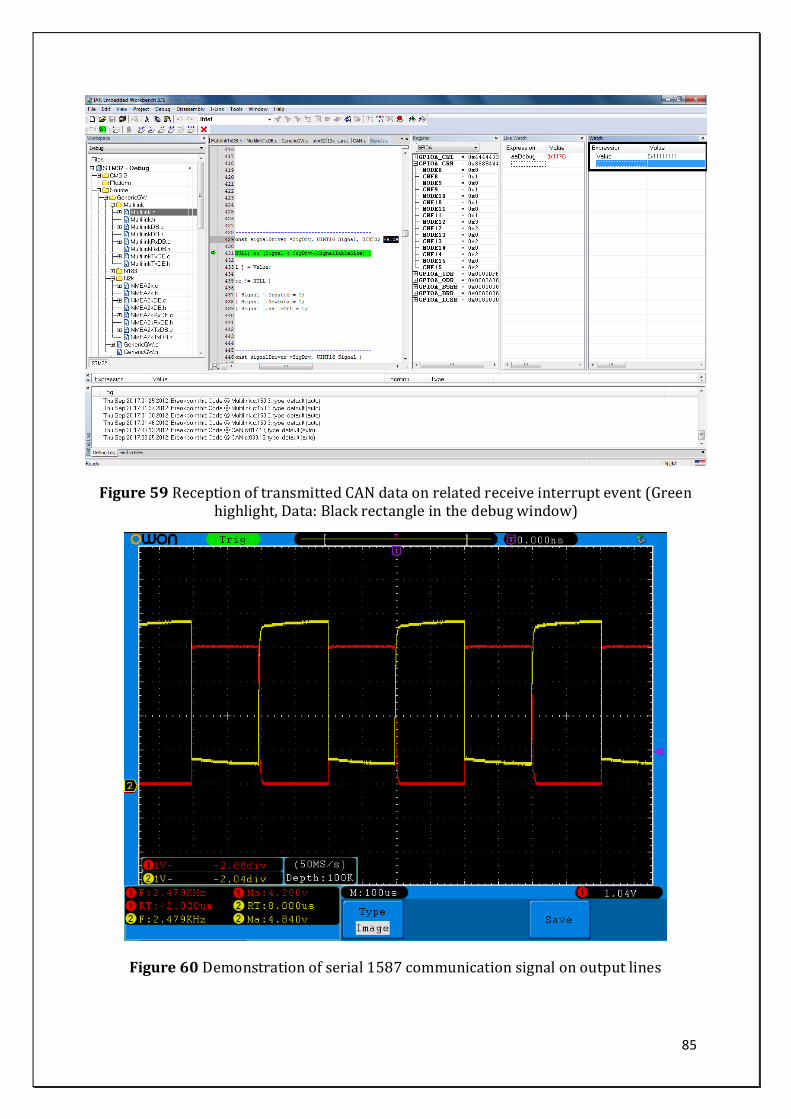
85
Figure 59 Reception of transmitted CAN data on related receive interrupt event (Green highlight, Data: Black rectangle in the debug window)
Figure 60 Demonstration of serial 1587 communication signal on output lines
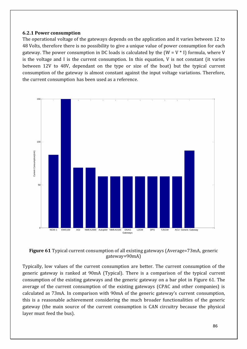
86
6.2.1 Power consumption The operational voltage of the gateways depends on the application and it varies between 12 to
48 Volts, therefore there is no possibility to give a unique value of power consumption for each
gateway. The power consumption in DC loads is calculated by the (W = V * I) formula, where V
is the voltage and I is the current consumption. In this equation, V is not constant (it varies
between 12V to 48V, dependant on the type or size of the boat) but the typical current
consumption of the gateway is almost constant against the input voltage variations. Therefore,
the current consumption has been used as a reference.
Typically, low values of the current consumption are better. The current consumption of the
generic gateway is ranked at 90mA (Typical). There is a comparison of the typical current
consumption of the existing gateways and the generic gateway on a bar plot in Figure 61. The
average of the current consumption of the existing gateways (CPAC and other companies) is
calculated as 73mA. In comparison with 90mA of the generic gateway’s current consumption,
this is a reasonable achievement considering the much broader functionalities of the generic
gateway (the main source of the current consumption is CAN circuitry because the physical
layer must feed the bus).
NGW-1 EMS100 AGI NMEA2000 Autopilot NMEA0183 DSAG LZGW DPS TJSGW ACU Generic Gateway0
50
100
150
Gateways
Curr
ent
Consum
ption(m
A)
Figure 61 Typical current consumption of all existing gateways (Average=73mA, generic gateway=90mA)
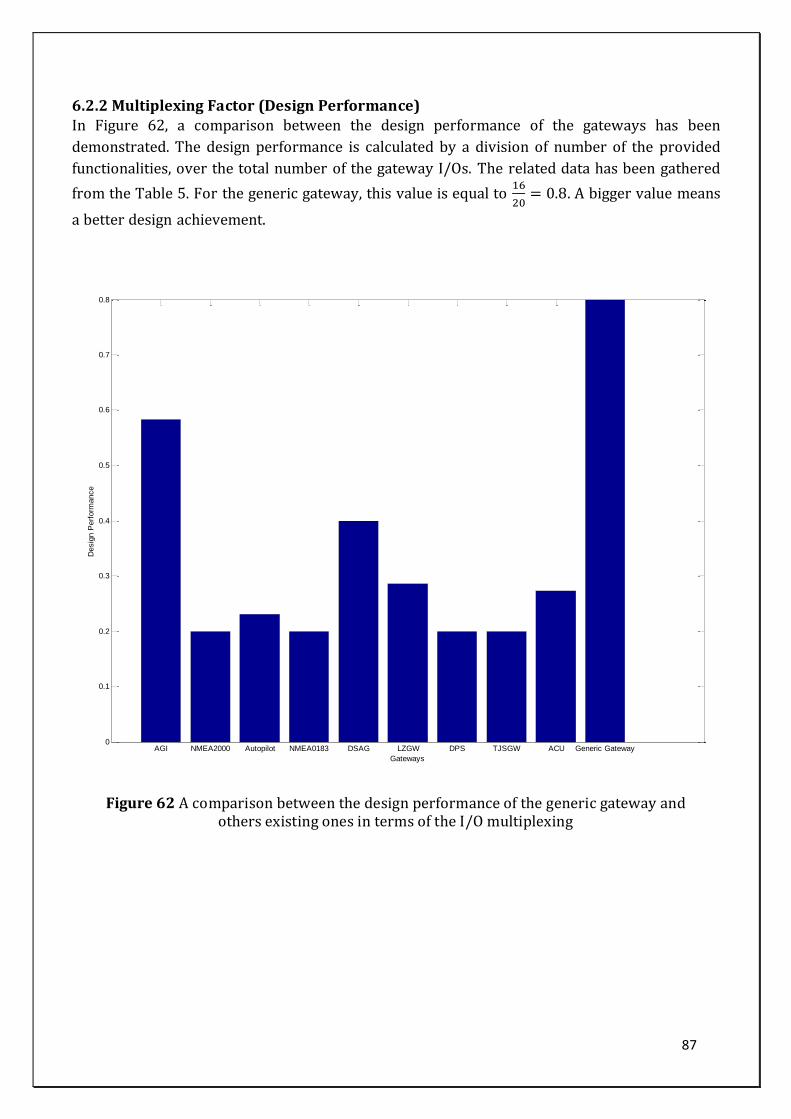
87
6.2.2 Multiplexing Factor (Design Performance) In Figure 62, a comparison between the design performance of the gateways has been
demonstrated. The design performance is calculated by a division of number of the provided
functionalities, over the total number of the gateway I/Os. The related data has been gathered
from the Table 5. For the generic gateway, this value is equal to 16
20= 0.8. A bigger value means
a better design achievement.
Figure 62 A comparison between the design performance of the generic gateway and others existing ones in terms of the I/O multiplexing
AGI NMEA2000 Autopilot NMEA0183 DSAG LZGW DPS TJSGW ACU Generic Gateway0
0.1
0.2
0.3
0.4
0.5
0.6
0.7
0.8
Gateways
Desig
n P
erf
orm
ance
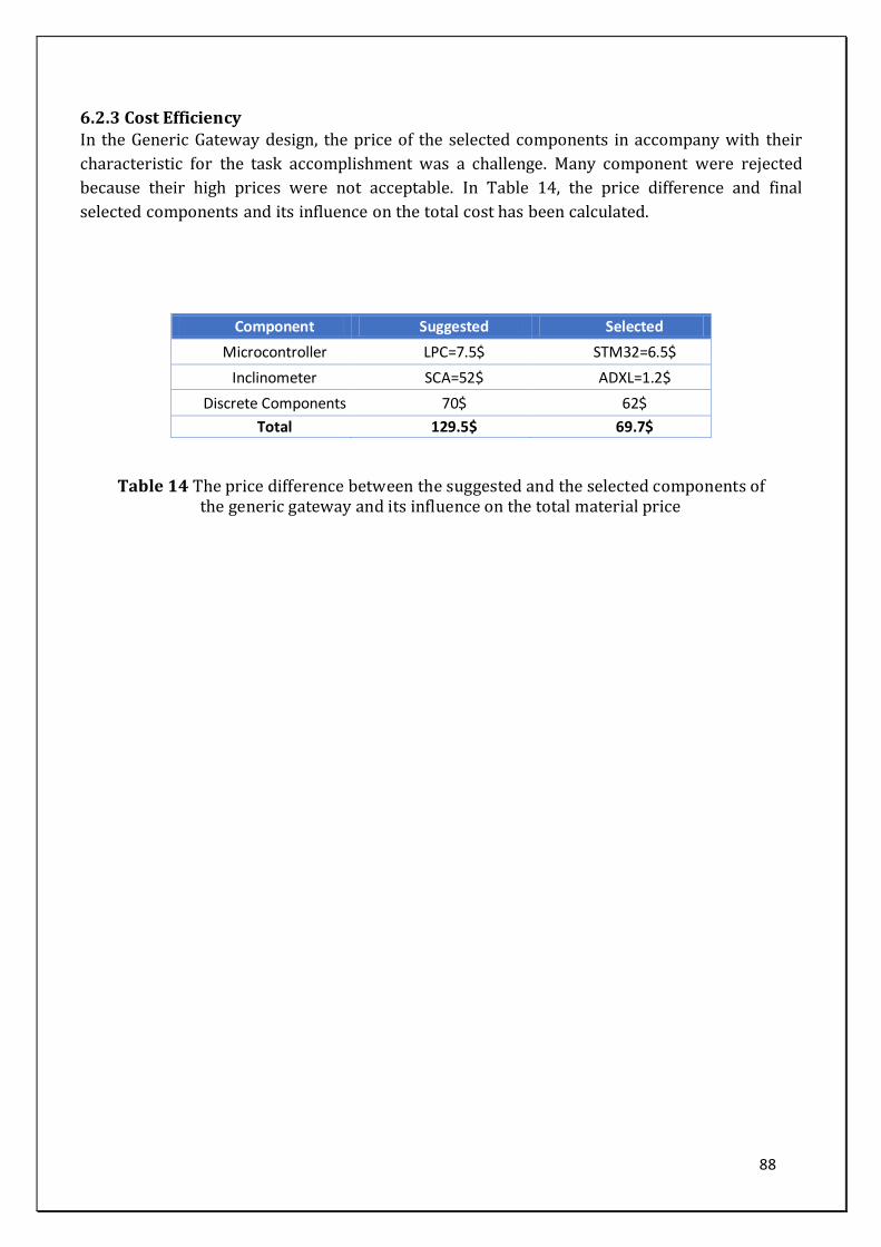
88
6.2.3 Cost Efficiency In the Generic Gateway design, the price of the selected components in accompany with their
characteristic for the task accomplishment was a challenge. Many component were rejected
because their high prices were not acceptable. In Table 14, the price difference and final
selected components and its influence on the total cost has been calculated.
Component Suggested Selected
Microcontroller LPC=7.5$ STM32=6.5$
Inclinometer SCA=52$ ADXL=1.2$
Discrete Components 70$ 62$
Total 129.5$ 69.7$
Table 14 The price difference between the suggested and the selected components of the generic gateway and its influence on the total material price
89
7 Conclusions Currently, the problem in the boat gateway market is that all existing gateways are designed to
fulfill specific tasks or requirements and no system upgrade has been considered in their
design. Furthermore, few gateways account for technical or environmental restrictions. As a
result, introducing an innovative product in this market will remove many technical obstacles
of the manufacturer and other competitors in boat gateway products. The “generic gateway”
was introduced and designed to address these concerns. The most challenging issues in the
design of this gateway is the limitation in communications I/Os.
Implementation of the generic gateway was started by designing the hardware. A combination
of ten CPAC Systems gateways produces 35 communication and instruction lines which have
been multiplexed within twenty I/Os. This challenge was in addition to other design
requirements such as reliability, final cost, power consumption, general and customer-
requested technical requirements, modifications from the existing gateway products and many
other issues.
Investigation of the four gateways from different manufacturers demonstrated that similar
products are designed first just to accomplish special requests, such as NMEA0183 to
NMEA2000 protocol conversion (similar to a few of the existing CPAC gateways). Additionally,
most of them lacked a user interface of operation (LEDs). Furthermore, two of them had not
considered the power isolation factor and, finally, none of the similar products has included
embedded inclinometer and proper connection for wire harness. Therefore, rather than
technical analyses, the gateway, which designed in this thesis that is named “generic gateway”,
covers much broader communication and instrumentation interfaces. The generic gateway is
designed with future prospects; other features could be added or removed based on the
production line policy. The production of one device instead of ten devices for any company
has lower cost and after sale regulations and satisfies several customer requests with one
product.
With the exception of two minor problems, satisfactory test results have been achieved. For
future work, the gateway could be designed in a more compact way and removing one of the
inclinometers will help to decrease the size of the PCB board. Also, changing the connector
type (20PIN) to another product with a higher number of pins (Ex: 28 PIN), creates an option
to include an Ethernet interface to the gateway; the selected STM32 microcontroller provides
an embedded Ethernet transceiver, which could be used to design a device with such interface
as well. Recently Ethernet was highly considered by industrial communication companies and
there is significant movement toward this protocol to be used more for communication among
industrial equipment.
90
8 References [1]: Internal documents of products’ description (Confidential), CPAC Systems AB, Göteborg-
Sweden
[2]: Wolfhard Lawrenz, CAN system engineering from theory to practical applications,
Springer, New York, pp. 26, 1997.
[3]: Texas Instrument, Controller Area Network Physical Layer Requirements, SLLA270–
January 2008
[4]: ANN228, 2002, A CAN Physical Layer Discussion, Microchip Technology Intercorporated
[5]: Ken Tindell, Hans Hansson, Andy Wellings, “Analysing Real-Time Communications:
Controller Area Network (CAN)”, Real-Time Systems Symposium, 1994.
[6]: The NMEA 0183 Information sheet, Active Research Limited (Actisense), 2011.
[7]: Lee Luft, Larry Anderson, Frank Cassidy, NMEA 2000 A Digital Interface for the 21st
Century, Presented at the Institute of Navigation, National Technical Meeting, January 30-2002,
San Diego-California.
[8]: ARV332 application note, ATMEL Corporation, May.2012.
[9]: Brian Kennedy and Mark Cantrell, Analog Devices, AN-1109 application note,
recommendations for Control of Radiated Emissions with Coupler Devices. Rev0-2011.
[10]: Martin Byrhult, Victor Stensson, Multi-Purpose Gateway for Vessel Steer-By-Wire
Systems, Department of Signals and Systems, Chalmers University of Technology, Göteborg,
Sweden-2011
[11]: IEC international standard, IEC60945, fourth edition, 2008.
[12]: VOLVO PENTA, Electromagnetic Compatibility (EMC) and Power Quality Requirements
for complete systems and components, 2009.01.12
[13]: International association of classification societies, Concerning Electrical Installations,
2009 edition.
[14]: Fluke Corporation, Electrical noise and transients, Application Note, October of 2004,
USA.
[15]: Hitoshi Kijima, Kazuo Murakawa, Lightning Surge Response Improvement by
Combinations of Varistors and Gas Discharge Tubes, Issue 2, Volume 7, April 2012, Japan.
[16]: Microchip Company, Control Area Network (CAN) Basics Application note AN-713, 2002,
United States.
[17]: Tom Starnes, Objective Analysis for Convergence Promotions LLC, Memory
Considerations for Faster MCUs, DIGIKEY Corporation, January 2012.
91
[18]: Application note JN-AN-1107, Designing Robust Embedded Systems, Jennic, November
2008, Sheffield-United Kingdom
[19]: Javier Diaz, Elias Rodriguez, Luis Hurtado, Hugo Cacique, Nimrod Vazquez, Agustin
Ramirez, CAN Bus Embedded System for Lighting Network Applications, 2008 IEEE, Instituto
Tecnologico de Celaya Celaya, Guanajuato, MEXICO.
[20]: Rob Kusters, Rini van Solingen, Jos Trienekens, Hans Wijnands, User-perceptions Of
Embedded Software Reliability, Eindhoven University of Technology.
[21]: ACTISENSE Company, NMEA 2000® to NMEA 0183 gateway, NGW-1 Datasheet – issue
2.00
[22]: MARETORN, EMS100 Engine Monitoring System User’s Manual, Rev 1.0, 2007.
[23]: AIRMAR Technology Corporation, U200 NMEA2000 to USB gateway datasheet, 2010.
[24]: AMEC, NK-80 NMEA0813 to NMEA2000 user manual, V1.1.
[25]: Vijaykrishnan Narayanan, Yuan Xie, Reliability Concerns in Embedded System Designs,
Pennsylvania State University, January 2006.
[26]: Jose m. giron-sierra, c. Insaurralde, m. seminario, j. f. jim´enez, peter klose, CANbus-Based
distributed fuel system with smart components, 2008 IEEE.
[27]: Wei Cui, Jun Fan, Yong Ren, Hao Shi, James L. Drewniak, Richard E. Dubroff, DC Power-bus
noise isolation with Power-Plane Segmentation, IEEE transactions on electromagnetic
compatibility, VOL. 45, NO.2, MAY 2003.
[28]: Peng Zhou Ligang Hou, Implementation of CAN bus device driver design Base on
Embedded System, Information Science and Engineering (ICISE), 2010 2nd International
Conference.

PO Box 823, SE-301 18 HalmstadPhone: +35 46 16 71 00E-mail: [email protected]
Hesam Moshiri received his bachelordegree in Computer HardwareEngineering from Islamic AzadUniversity, Iran and attended theHalmstad University to follow theM.Sc.degree in Embedded andIntelligent Systems Design. Hisinterests are programming, electronicdesign and R&D.