Embed Size (px)
Citation preview
© 2017 NXP B.V.
Mask Set Errata for Mask 5N96B
This document contains a subset of errata for Kinetis Mask Set 5N96B. Errata for security-related modules are not included in this document and are only available after a nondisclosure agreement (NDA) has been signed. For more information on obtaining an NDA and viewing the comprehensive errata list for this mask set, please contact your local NXP sales representative.
NXP Semiconductors
Mask Set Errata
KINETIS_K_5N96B
Rev. 21 APR 2017
This report applies to mask 5N96B for these products:• MK10FX512xxx12, MK10FN1M0xxx12• MK20FX512xxx12, MK20FN1M0xxx12• MK60FX512xxx12, MK60FN1M0xxx12, MK60FX512xxx15, MK60FN1M0xxx15• MK61FX512xxx12, MK61FN1M0xxx12, MK61FX512xxx15, MK61FN1M0xxx15• MK70FX512xxx12, MK70FN1M0xxx12, MK70FX512xxx15, MK70FN1M0xxx15
Table 1. Errata and Information Summary
Erratum ID Erratum Title
e8992 AWIC: Early NMI wakeup not detected upon entry to stop mode from VLPR mode
e6378 Cache: Cache write buffer error enable (MCM_ISCR[CWBEE]) does not work
e6804 CJTAG: Performing a mode change from Standard Protocol to Advanced Protocol may reset theCJTAG.
e6990 CJTAG: possible incorrect TAP state machine advance during Check Packet
e6939 Core: Interrupted loads to SP can cause erroneous behavior
e9004 Core: ITM can deadlock when global timestamping is enabled
e9005 Core: Store immediate overlapping exception return operation might vector to incorrect interrupt
e6940 Core: VDIV or VSQRT instructions might not complete correctly when very short ISRs are used
e5243 DDRMC: It is possible for data corruption to occur If the value programmed in RDLATADJ is largerthan the CAS latency,
e5241 DDRMC: Putting the memory into a power down mode while DDR_CR11[AREFMODE] is set canprevent the DDRMC from providing refreshes to the memory while it is powered down.
e5263 DDRMC: While the memory is in a power down state, setting DDR_CR11[AREF] in an attempt to forcea refresh command will cause a refresh cycle to be missed.
e4588 DMAMUX: When using PIT with "always enabled" request, DMA request does not deassert correctly
e6933 eDMA: Possible misbehavior of a preempted channel when using continuous link mode
e10066 eDMA: UART0 and UART1 peripheral requests trigger DMA twice if core clock and internal bus clockfrequencies are equal
e6358 ENET: Write to Transmit Descriptor Active Register (ENET_TDAR) is ignored
e9595 FlexCAN: Corrupted frame possible if Freeze Mode or Low Power Mode are entered during a Bus-Offstate
Table continues on the next page...
NXP Semiconductors KINETIS_K_5N96B
Mask Set Errata Rev. 21 APR 2017
Mask Set Errata for Mask 5N96B
Table 1. Errata and Information Summary (continued)
Erratum ID Erratum Title
e5641 FlexCAN: Module does not transmit a message that is enabled to be transmitted at a specific momentduring the arbitration process.
e9527 FlexCAN: The transmission abort mechanism may not work properly
e5861 FTM: FTM2 and FTM3 do not correctly enter BDM mode when a debugger connection is active
e4710 FTM: FTMx_PWMLOAD register does not support 8-/16-bit accesses
e9265 FTM: Incorrect match may be generated if intermediate load feature is used in toggle mode
e6484 FTM: The process of clearing the FTMx_SC[TOF] bit does not work as expected under a certaincondition when the FTM counter reaches FTM_MOD value.
e6573 JTAG: JTAG TDO function on the PTA2 disables the pull resistor
e4553 LCDC: Cursor Color Limited in 24bpp Mode
e4569 LCDC: Graphic Window Color Key Limited in 24bpp Mode
e4570 LCDC: Graphic Window May Shift Pixel Data
e4571 LCDC: LCDC can only use half of internal SRAM for frame buffer
e8010 LLWU: CMP flag in LLWU_Fx register cleared by multiple CMP out toggles when exiting LLSx orVLLSx modes.
e7993 MCG: FLL frequency may be incorrect after changing the FLL reference clock
e7735 MCG: IREFST status bit may set before the IREFS multiplexor switches the FLL reference clock
e3898 MCG: Setting the MCG_C6[PLLS] bit will enable both OSC0 and OSC1.
e4590 MCG: Transitioning from VLPS to VLPR low power modes while in BLPI clock mode is not supported.
e4176 NMI: NMI interrupt service routine (ISR) might not be called when MCU wakes up from VLLSx modes.
e3794 NVIC: NMI interrupt does not wakeup MCU from STOP and VLPS
e5667 PMC: When used as an input to ADC or CMP modules, the PMC bandgap 1-V voltage reference is notavailable in VLPx, LLS, or VLLSx modes
e9293 PORT: Internal pull resistors not enabled for all pin functions
e5130 SAI: Under certain conditions, the CPU cannot reenter STOP mode via an asynchronous interruptwakeup event
e3981 SDHC: ADMA fails when data length in the last descriptor is less or equal to 4 bytes
e3982 SDHC: ADMA transfer error when the block size is not a multiple of four
e4624 SDHC: AutoCMD12 and R1b polling problem
e3977 SDHC: Does not support Infinite Block Transfer Mode
e4627 SDHC: Erroneous CMD CRC error and CMD Index error may occur on sending new CMD during datatransfer
e3984 SDHC: eSDHC misses SDIO interrupt when CINT is disabled
e3980 SDHC: Glitch is generated on card clock with software reset or clock divider change
e6934 SDHC: Issues with card removal/insertion detection
e3983 SDHC: Problem when ADMA2 last descriptor is LINK or NOP
e3978 SDHC: Software can not clear DMA interrupt status bit after read operation
e3941 SIM/DDR: SIM_SOPT2[FBSL] does not determine allowable DDR controller accesses when security isenabled
e4218 SIM/FLEXBUS: SIM_SCGC7[FLEXBUS] bit should be cleared when the FlexBus is not being used.
e5952 SMC: Wakeup via the LLWU from LLS/VLLS to RUN to VLPR incorrectly triggers an immediatewakeup from the next low power mode entry
Table continues on the next page...
Mask Set Errata for Mask 5N96B, Rev. 21 APR 2017
2 NXP Semiconductors
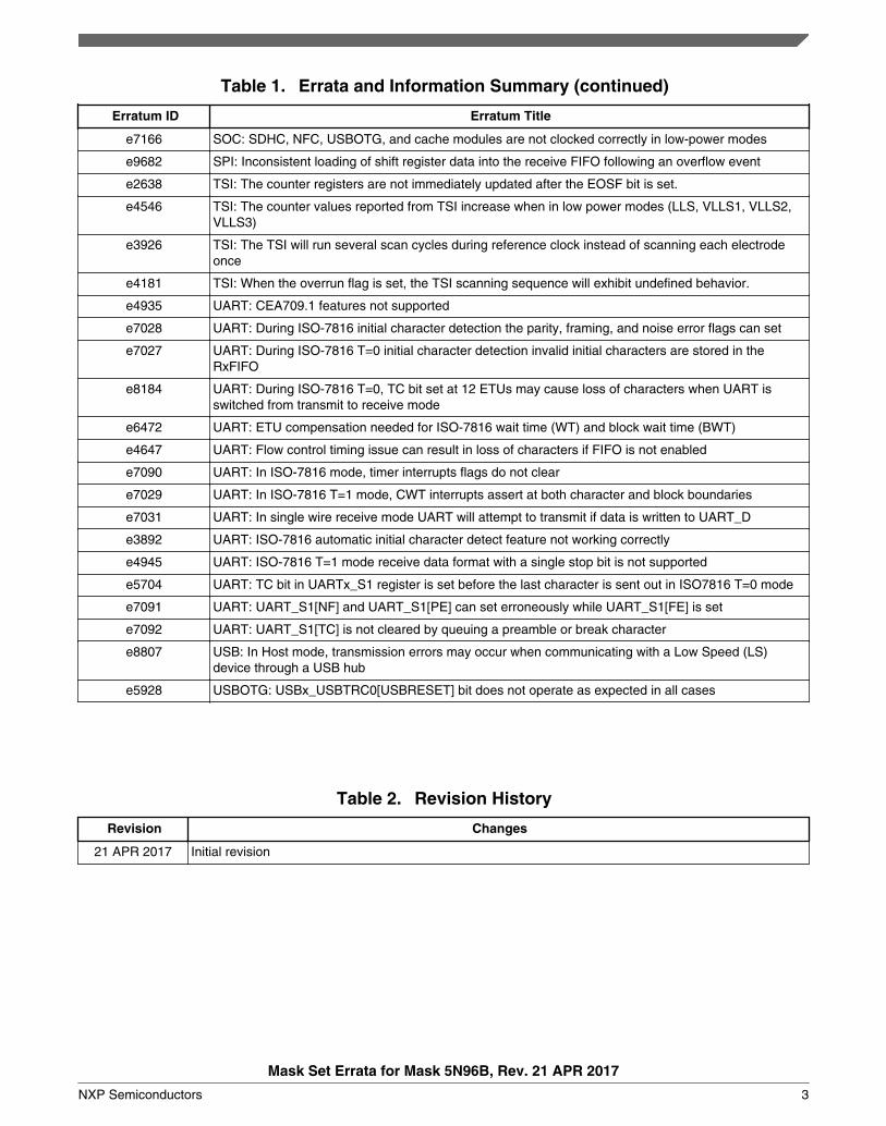
Table 1. Errata and Information Summary (continued)
Erratum ID Erratum Title
e7166 SOC: SDHC, NFC, USBOTG, and cache modules are not clocked correctly in low-power modes
e9682 SPI: Inconsistent loading of shift register data into the receive FIFO following an overflow event
e2638 TSI: The counter registers are not immediately updated after the EOSF bit is set.
e4546 TSI: The counter values reported from TSI increase when in low power modes (LLS, VLLS1, VLLS2,VLLS3)
e3926 TSI: The TSI will run several scan cycles during reference clock instead of scanning each electrodeonce
e4181 TSI: When the overrun flag is set, the TSI scanning sequence will exhibit undefined behavior.
e4935 UART: CEA709.1 features not supported
e7028 UART: During ISO-7816 initial character detection the parity, framing, and noise error flags can set
e7027 UART: During ISO-7816 T=0 initial character detection invalid initial characters are stored in theRxFIFO
e8184 UART: During ISO-7816 T=0, TC bit set at 12 ETUs may cause loss of characters when UART isswitched from transmit to receive mode
e6472 UART: ETU compensation needed for ISO-7816 wait time (WT) and block wait time (BWT)
e4647 UART: Flow control timing issue can result in loss of characters if FIFO is not enabled
e7090 UART: In ISO-7816 mode, timer interrupts flags do not clear
e7029 UART: In ISO-7816 T=1 mode, CWT interrupts assert at both character and block boundaries
e7031 UART: In single wire receive mode UART will attempt to transmit if data is written to UART_D
e3892 UART: ISO-7816 automatic initial character detect feature not working correctly
e4945 UART: ISO-7816 T=1 mode receive data format with a single stop bit is not supported
e5704 UART: TC bit in UARTx_S1 register is set before the last character is sent out in ISO7816 T=0 mode
e7091 UART: UART_S1[NF] and UART_S1[PE] can set erroneously while UART_S1[FE] is set
e7092 UART: UART_S1[TC] is not cleared by queuing a preamble or break character
e8807 USB: In Host mode, transmission errors may occur when communicating with a Low Speed (LS)device through a USB hub
e5928 USBOTG: USBx_USBTRC0[USBRESET] bit does not operate as expected in all cases
Table 2. Revision History
Revision Changes
21 APR 2017 Initial revision
Mask Set Errata for Mask 5N96B, Rev. 21 APR 2017
NXP Semiconductors 3
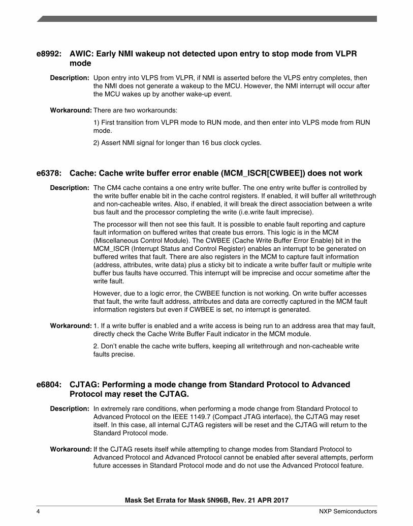
e8992: AWIC: Early NMI wakeup not detected upon entry to stop mode from VLPRmode
Description: Upon entry into VLPS from VLPR, if NMI is asserted before the VLPS entry completes, thenthe NMI does not generate a wakeup to the MCU. However, the NMI interrupt will occur afterthe MCU wakes up by another wake-up event.
Workaround: There are two workarounds:
1) First transition from VLPR mode to RUN mode, and then enter into VLPS mode from RUNmode.
2) Assert NMI signal for longer than 16 bus clock cycles.
e6378: Cache: Cache write buffer error enable (MCM_ISCR[CWBEE]) does not work
Description: The CM4 cache contains a one entry write buffer. The one entry write buffer is controlled bythe write buffer enable bit in the cache control registers. If enabled, it will buffer all writethroughand non-cacheable writes. Also, if enabled, it will break the direct association between a writebus fault and the processor completing the write (i.e.write fault imprecise).
The processor will then not see this fault. It is possible to enable fault reporting and capturefault information on buffered writes that create bus errors. This logic is in the MCM(Miscellaneous Control Module). The CWBEE (Cache Write Buffer Error Enable) bit in theMCM_ISCR (Interrupt Status and Control Register) enables an interrupt to be generated onbuffered writes that fault. There are also registers in the MCM to capture fault information(address, attributes, write data) plus a sticky bit to indicate a write buffer fault or multiple writebuffer bus faults have occurred. This interrupt will be imprecise and occur sometime after thewrite fault.
However, due to a logic error, the CWBEE function is not working. On write buffer accessesthat fault, the write fault address, attributes and data are correctly captured in the MCM faultinformation registers but even if CWBEE is set, no interrupt is generated.
Workaround: 1. If a write buffer is enabled and a write access is being run to an address area that may fault,directly check the Cache Write Buffer Fault indicator in the MCM module.
2. Don’t enable the cache write buffers, keeping all writethrough and non-cacheable writefaults precise.
e6804: CJTAG: Performing a mode change from Standard Protocol to AdvancedProtocol may reset the CJTAG.
Description: In extremely rare conditions, when performing a mode change from Standard Protocol toAdvanced Protocol on the IEEE 1149.7 (Compact JTAG interface), the CJTAG may resetitself. In this case, all internal CJTAG registers will be reset and the CJTAG will return to theStandard Protocol mode.
Workaround: If the CJTAG resets itself while attempting to change modes from Standard Protocol toAdvanced Protocol and Advanced Protocol cannot be enabled after several attempts, performfuture accesses in Standard Protocol mode and do not use the Advanced Protocol feature.
Mask Set Errata for Mask 5N96B, Rev. 21 APR 2017
4 NXP Semiconductors
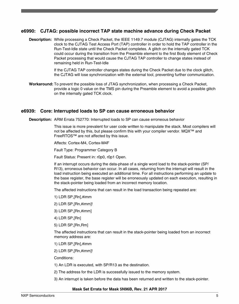
e6990: CJTAG: possible incorrect TAP state machine advance during Check Packet
Description: While processing a Check Packet, the IEEE 1149.7 module (CJTAG) internally gates the TCKclock to the CJTAG Test Access Port (TAP) controller in order to hold the TAP controller in theRun-Test-Idle state until the Check Packet completes. A glitch on the internally gated TCKcould occur during the transition from the Preamble element to the first Body element of CheckPacket processing that would cause the CJTAG TAP controller to change states instead ofremaining held in Run-Test-Idle
If the CJTAG TAP controller changes states during the Check Packet due to the clock glitch,the CJTAG will lose synchronization with the external tool, preventing further communication.
Workaround: To prevent the possible loss of JTAG synchronization, when processing a Check Packet,provide a logic 0 value on the TMS pin during the Preamble element to avoid a possible glitchon the internally gated TCK clock.
e6939: Core: Interrupted loads to SP can cause erroneous behavior
Description: ARM Errata 752770: Interrupted loads to SP can cause erroneous behavior
This issue is more prevalent for user code written to manipulate the stack. Most compilers willnot be affected by this, but please confirm this with your compiler vendor. MQX™ andFreeRTOS™ are not affected by this issue.
Affects: Cortex-M4, Cortex-M4F
Fault Type: Programmer Category B
Fault Status: Present in: r0p0, r0p1 Open.
If an interrupt occurs during the data-phase of a single word load to the stack-pointer (SP/R13), erroneous behavior can occur. In all cases, returning from the interrupt will result in theload instruction being executed an additional time. For all instructions performing an update tothe base register, the base register will be erroneously updated on each execution, resulting inthe stack-pointer being loaded from an incorrect memory location.
The affected instructions that can result in the load transaction being repeated are:
1) LDR SP,[Rn],#imm
2) LDR SP,[Rn,#imm]!
3) LDR SP,[Rn,#imm]
4) LDR SP,[Rn]
5) LDR SP,[Rn,Rm]
The affected instructions that can result in the stack-pointer being loaded from an incorrectmemory address are:
1) LDR SP,[Rn],#imm
2) LDR SP,[Rn,#imm]!
Conditions:
1) An LDR is executed, with SP/R13 as the destination.
2) The address for the LDR is successfully issued to the memory system.
3) An interrupt is taken before the data has been returned and written to the stack-pointer.
Mask Set Errata for Mask 5N96B, Rev. 21 APR 2017
NXP Semiconductors 5
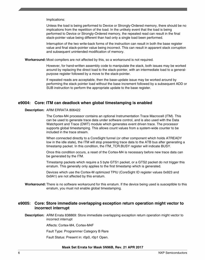
Implications:
Unless the load is being performed to Device or Strongly-Ordered memory, there should be noimplications from the repetition of the load. In the unlikely event that the load is beingperformed to Device or Strongly-Ordered memory, the repeated read can result in the finalstack-pointer value being different than had only a single load been performed.
Interruption of the two write-back forms of the instruction can result in both the base registervalue and final stack-pointer value being incorrect. This can result in apparent stack corruptionand subsequent unintended modification of memory.
Workaround: Most compilers are not affected by this, so a workaround is not required.
However, for hand-written assembly code to manipulate the stack, both issues may be workedaround by replacing the direct load to the stack-pointer, with an intermediate load to a general-purpose register followed by a move to the stack-pointer.
If repeated reads are acceptable, then the base-update issue may be worked around byperforming the stack pointer load without the base increment followed by a subsequent ADD orSUB instruction to perform the appropriate update to the base register.
e9004: Core: ITM can deadlock when global timestamping is enabled
Description: ARM ERRATA 806422
The Cortex-M4 processor contains an optional Instrumentation Trace Macrocell (ITM). Thiscan be used to generate trace data under software control, and is also used with the DataWatchpoint and Trace (DWT) module which generates event driven trace. The processorsupports global timestamping. This allows count values from a system-wide counter to beincluded in the trace stream.
When connected directly to a CoreSight funnel (or other component which holds ATREADYlow in the idle state), the ITM will stop presenting trace data to the ATB bus after generating atimestamp packet. In this condition, the ITM_TCR.BUSY register will indicate BUSY.
Once this condition occurs, a reset of the Cortex-M4 is necessary before new trace data canbe generated by the ITM.
Timestamp packets which require a 5 byte GTS1 packet, or a GTS2 packet do not trigger thiserratum. This generally only applies to the first timestamp which is generated.
Devices which use the Cortex-M optimized TPIU (CoreSight ID register values 0x923 and0x9A1) are not affected by this erratum.
Workaround: There is no software workaround for this erratum. If the device being used is susceptible to thiserratum, you must not enable global timestamping.
e9005: Core: Store immediate overlapping exception return operation might vector toincorrect interrupt
Description: ARM Errata 838869: Store immediate overlapping exception return operation might vector toincorrect interrupt
Affects: Cortex-M4, Cortex-M4F
Fault Type: Programmer Category B Rare
Fault Status: Present in: r0p0, r0p1 Open.
Mask Set Errata for Mask 5N96B, Rev. 21 APR 2017
6 NXP Semiconductors
The Cortex-M4 includes a write buffer that permits execution to continue while a store iswaiting on the bus. Under specific timing conditions, during an exception return while thisbuffer is still in use by a store instruction, a late change in selection of the next interrupt to betaken might result in there being a mismatch between the interrupt acknowledged by theinterrupt controller and the vector fetched by the processor.
Configurations Affected
This erratum only affects systems where writeable memory locations can exhibit more thanone wait state.
Workaround: For software not using the memory protection unit, this erratum can be worked around bysetting DISDEFWBUF in the Auxiliary Control Register.
In all other cases, the erratum can be avoided by ensuring a DSB occurs between the storeand the BX instruction. For exception handlers written in C, this can be achieved by insertingthe appropriate set of intrinsics or inline assembly just before the end of the interrupt function,for example:
ARMCC:
...
__schedule_barrier();
__asm{DSB};
__schedule_barrier();
}
GCC:
...
__asm volatile (“dsb 0xf” ::: “memory”);
}
e6940: Core: VDIV or VSQRT instructions might not complete correctly when veryshort ISRs are used
Description: ARM Errata 709718: VDIV or VSQRT instructions might not complete correctly when veryshort ISRs are used
Affects: Cortex-M4F
Fault Type: Programmer Category B
Fault Status: Present in: r0p0, r0p1 Open.
On Cortex-M4 with FPU, the VDIV and VSQRT instructions take 14 cycles to execute. Whenan interrupt is taken a VDIV or VSQRT instruction is not terminated, and completes itsexecution while the interrupt stacking occurs. If lazy context save of floating point state isenabled then the automatic stacking of the floating point context does not occur until a floatingpoint instruction is executed inside the interrupt service routine.
Lazy context save is enabled by default. When it is enabled, the minimum time for the firstinstruction in the interrupt service routine to start executing is 12 cycles. In certain timingconditions, and if there is only one or two instructions inside the interrupt service routine, thenthe VDIV or VSQRT instruction might not write its result to the register bank or to the FPSCR.
Mask Set Errata for Mask 5N96B, Rev. 21 APR 2017
NXP Semiconductors 7
Workaround: A workaround is only required if the floating point unit is present and enabled. A workaround isnot required if the memory system inserts one or more wait states to every stack transaction.
There are two workarounds:
1) Disable lazy context save of floating point state by clearing LSPEN to 0 (bit 30 of theFPCCR at address 0xE000EF34).
2) Ensure that every interrupt service routine contains more than 2 instructions in addition tothe exception return instruction.
e5243: DDRMC: It is possible for data corruption to occur If the value programmed inRDLATADJ is larger than the CAS latency,
Description: If DDR_CR56[RDLATADJ] is programmed to be larger than the CAS latency of the devicethere is the possibility that data corruption may occur because the controller will pre-maturelyissue DFI update requests.
Workaround: Do not set DDR_CR56[RDLATADJ] to a value larger than the CAS latency of the device. If alarger delay is required, set the RDLATADJ equal to the CAS latency of the device and use theDDR_CR52[RDDTENBAS] parameter to add any additional delay that is required.
e5241: DDRMC: Putting the memory into a power down mode whileDDR_CR11[AREFMODE] is set can prevent the DDRMC from providingrefreshes to the memory while it is powered down.
Description: The DDR_CR11[AREFMODE] parameter is used to determine when a refresh command isissued to the memory. The refresh command can either be issued at the next memorycommand boundary, or it can be held off and issued only at the next system commandboundary. One system command may result in many memory commands, depending on howmuch data the system command is moving.
When the AREFMODE parameter is set, if a refresh is needed the controller will hold off thisrefresh until the next system command boundary. If the memory is manually placed into powerdown, and this happens at a memory command boundary but not at a system commandboundary the logic holding off the refresh will erroneously continue to hold off the refresh forthe duration of time the memory is placed in power down.
If the memory does not receive refreshes while in power down it is possible for the contents ofthe memory to degrade and become corrupted.
This condition can only occur if the low-power mode entry is done manually. This is not anissue if you are using the LPAUTO parameter to automatically enter low-power modes.
Workaround: Always clear the DDR_CR11[AREFMODE] bit before manually entering a power-down mode.If you wish to have normal operations with the AREFMODE bit set, you can do so, but ensurethat you clear it before you manually place the memory into power down. After you bring thememory out of power down you can then set the AREFMODE bit again.
Mask Set Errata for Mask 5N96B, Rev. 21 APR 2017
8 NXP Semiconductors
e5263: DDRMC: While the memory is in a power down state, setting DDR_CR11[AREF]in an attempt to force a refresh command will cause a refresh cycle to bemissed.
Description: When the DDRMC has the auto refresh mode enabled (DDR_CR11[TREFEN] = 1), it will loada counter with the value in the TREF parameter, count to zero, then issue a refresh to thememory, reload the counter and repeat this cycle. There are several events which use thecount value of zero from this counter to function. If a refresh is requested via a write to theAREF parameter, the counter associated with the automatic issuance of refreshes by theDDRMC will automatically be reloaded with the value in the TREF parameter and will not beable to achieve a count of zero.
One of the key pieces of logic which monitors the refresh counter equaling zero is logicassociated with bringing the memory out of a power down state to enable the controller toissue a refresh command to the memory. So if the memory is in a power down state and arefresh is requested via a method other than the automatic refresh counter reaching zero thememory will not be able to be brought out of the power down state to allow the refresh tooccur. This will result in extra delay before the refresh can be issued to the memory, or willresult in the memory never being refreshed while in a power down state if the automaticrefresh counter is disabled.
Example
Assume the memory is in a power down state and the automatic refresh mode of the DDRMCis enabled. The counter will be loaded with the value in the TREF parameter and will begincounting down. If, when the counter reaches a value near zero (but not zero), software write toAREF paramter, the counter will be automatically reloaded with the value in the TREFparameter and will then have to count down to 0 before the controller will bring the memory outof the power down state and issue the refresh. In this case the memory will fail to receive onerefresh.
Workaround: Do not use the DDR_CR11[AREF] bit to attempt a refresh command to the memory while thememory is in power down mode. Always enable the automatic refresh feature of the DDRMC(set DDR_CR11[TREFEN]) and rely on it to provide refreshes to the memory.
e4588: DMAMUX: When using PIT with "always enabled" request, DMA request doesnot deassert correctly
Description: The PIT module is not assigned as a stand-alone DMA request source in the DMA requestmux. Instead, the PIT is used as the trigger for the DMAMUX periodic trigger mode. If you wantto use one of the PIT channels for periodic DMA requests, you would use the periodic triggermode in conjunction with one of the “always enabled” DMA requests. However, the DMArequest does not assert correctly in this case.
Instead of sending a single DMA request every time the PIT expires, the first time the PITtriggers a DMA transfer the “always enabled” source will not negate its request. This results inthe DMA request remaining asserted continuously after the first trigger.
Workaround: Use of the PIT to trigger DMA channels where the major loop count is greater than one is notrecommended. For periodic triggering of DMA requests with major loop counts greater thanone, we recommended using another timer module instead of the PIT.
Mask Set Errata for Mask 5N96B, Rev. 21 APR 2017
NXP Semiconductors 9
If using the PIT to trigger a DMA channel where the major loop count is set to one, then inorder to get the desired periodic triggering, the DMA must do the following in the interruptservice routine for the DMA_DONE interrupt:
1. Set the DMA_TCDn_CSR[DREQ] bit and configure DMAMUX_CHCFGn[ENBL] = 0
2. Then again DMAMUX_CHCFGn[ENBL] = 1, DMASREQ=channel in your DMA DONEinterrupt service routine so that “always enabled” source could negate its request then DMArequest could be negated.
This will allow the desired periodic triggering to function as expected.
e6933: eDMA: Possible misbehavior of a preempted channel when using continuouslink mode
Description: When using continuous link mode (DMA_CR[CLM] = 1) with a high priority channel linking toitself, if the high priority channel preempts a lower priority channel on the cycle before its lastread/write sequence, the counters for the preempted channel (the lower priority channel) arecorrupted. When the preempted channel is restored, it runs past its “done” point instead ofperforming a single read/write sequence and retiring.
The preempting channel (the higher priority channel) will execute as expected.
Workaround: Disable continuous link mode (DMA_CR[CLM]=0) if a high priority channel is using minor loopchannel linking to itself and preemption is enabled. The second activation of the preemptingchannel will experience the normal startup latency (one read/write sequence + startup) insteadof the shortened latency (startup only) provided by continuous link mode.
e10066: eDMA: UART0 and UART1 peripheral requests trigger DMA twice if core clockand internal bus clock frequencies are equal
Description: The UART0 and UART1 DMA request signals are routed through a gasket that translates thesignals to the internal bus clock domain before routing them to the DMA. The gasket works asintended for typical cases when the core clock is faster than the internal bus clock. For caseswhen the core clock and internal bus clock are the same frequency the gasket will cause theDMA request to be held too long. This results in triggering the DMA twice instead of once.
Workaround: Any of the following can be used as workarounds:
• Use the UART FIFOs with watermarks set to prevent underflows and/or overflows.• Use a UART other than UART0 or UART1. The other UARTs are clocked by the internal
bus clock so they are not impacted.• Use the UART interrupt instead of the DMA request, then software trigger the DMA in the
UART interrupt handler.• Decrease the bus clock frequency so that the core clock is at least two times faster than
the internal bus clock.
e6358: ENET: Write to Transmit Descriptor Active Register (ENET_TDAR) is ignored
Description: If the ready bit in the transmit buffer descriptor (TxBD[R]) is previously detected as not setduring a prior frame transmission, then the ENET_TDAR[TDAR] bit is cleared at a later time,even if additional TxBDs were added to the ring and the ENET_TDAR[TDAR] bit is set. Thisresults in frames not being transmitted until there is a 0-to-1 transition on ENET_TDAR[TDAR].
Mask Set Errata for Mask 5N96B, Rev. 21 APR 2017
10 NXP Semiconductors

Workaround: Code can use the transmit frame interrupt flag (ENET_EIR[TXF]) as a method to detectwhether the ENET has completed transmission and the ENET_TDAR[TDAR] has beencleared. If ENET_TDAR[TDAR] is detected as cleared when packets are queued and waitingfor transmit, then a write to the TDAR bit will restart TxBD processing.
e9595: FlexCAN: Corrupted frame possible if Freeze Mode or Low Power Mode areentered during a Bus-Off state
Description: In the Flexible Controller Area Network (FlexCAN) module, if the Freeze Enable bit (FRZ) ofthe Module Configuration Register (MCR) is asserted and the Freeze Mode is requested byasserting the Halt bit (HALT) of the MCR register during the Bus Off state, the transmissionafter exiting the Bus-Off condition will be corrupted. The issue occurs only if a transmission ispending before the freeze mode request. In addition, the same issue can happen if Low-PowerMode is requested instead of Freeze Mode.
Workaround: The workaround depends on whether the bus-off condition occurs prior to requesting Freezemode or low power mode.
A) Procedure to enter Freeze Mode:
1. Set the Freeze Enable bit (FRZ) in the Module Control Register (MCR).
2. Check if the Module Disable bit (MDIS) in MCR register is set. If yes, clear the MDIS bit.
3. Poll the MCR register until the Low-Power Mode Acknowledge (LPMACK) bit in MCR iscleared (timeout for software implementation is 2 CAN Bits length).
4. Read the Fault Confinement State (FLTCONF) field in the Error and Status 1 Register(ESR1) to check if FlexCAN is in bus off state. If yes, go to step 5A. Otherwise, go to step 5B.
5A. Set the Soft Reset bit (SOFTRST) in MCR.
6A. Poll the MCR register until the Soft Reset (SOFTRST) bit is cleared (timeout for softwareimplementation is 2 CAN Bits length).
7A. Poll the MCR register until the Freeze Acknowledge (FRZACK) bit is set (timeout forsoftware implementation is 2 CAN Bits length).
8A. Reconfigure the Module Control Register (MCR).
9A. Reconfigure all the Interrupt Mask Registers (IMASKn).
5B. Set the Halt FlexCAN (HALT) bit in MCR.
6B. Poll the MCR register until the Freeze Acknowledge (FRZACK) bit is set (timeout forsoftware implementation is 178 CAN Bits length).
NOTE: The time between step 4 and step 5B must be less than 1353 CAN bit periods.
B) Procedure to enter in Low-Power Mode:
1. Enter in Freeze Mode (execute the procedure A).
2. Request the Low-Power Mode.
3. Poll the MCR register until the Low-Power Mode Acknowledge (LPMACK) bit in MCR is set(timeout for software implementation is 2 CAN Bits length).
Mask Set Errata for Mask 5N96B, Rev. 21 APR 2017
NXP Semiconductors 11
e5641: FlexCAN: Module does not transmit a message that is enabled to betransmitted at a specific moment during the arbitration process.
Description: FlexCAN does not transmit a message that is enabled to be transmitted in a specific momentduring the arbitration process. The following conditions are necessary to have the issue.
• Only one MB is configured to be transmitted• The write which enables the MB to be transmitted (write on Control status word) happens
during a specific clock during the arbitration process.
After this arbitration process occurs, the bus goes to Idle state and no new message isreceived on bus.
For example:
1) MB13 is deactivated on RxIntermission (write 0x0 on CODE field from Control Status word)- First write on CODE
2) Reconfigure the ID and data fields
3) Enable the MB13 to be transmitted on BusIdle (write 0xC on Code field) - Second write oncode
4) CAN bus keeps in Idle state
5) No write on Control status from any MB happens.
During the second write on code (step 3), the write must happen one clock before the currentMB13 is to be scanned by arbitration process. In this case, it does not detect the new code(0xC) and no new arbitration is scheduled.
The problem can be detectable only if the message traffic ceases and the CAN bus enters intoIdle state after the described sequence of events.
There is NO ISSUE if any of the conditions below holds:
a) Any MB (either Tx or Rx) is reconfigured (by writing its CS field) just after the Intermissionfield.
b) There is other configured MB to be transmitted
c) A new incoming message sent by any external node starts just after the Intermission field.
Workaround: To transmit a CAN frame, the CPU must prepare a Message Buffer for transmission byexecuting the following standard 5 step procedure:
1. Check if the respective interrupt bit is set and clear it.
2. If the MB is active (transmission pending), write the ABORT code (0b1001) to the CODEfield of the Control and Status word to request an abortion of the transmission.Wait for thecorresponding IFLAG to be asserted by polling the IFLAG register or by the interrupt request ifenabled by the respective IMASK. Then read back the CODE field to check if the transmissionwas aborted or transmitted. If backwards compatibility is desired (MCR[AEN] bit negated), justwrite the INACTIVE code (0b1000) to the CODE field to inactivate the MB but then the pendingframe may be transmitted without notification.
3. Write the ID word.
4. Write the data bytes.
5. Write the DLC, Control and CODE fields of the Control and Status word to activate the MB.
The workaround consists of executing two extra steps:
Mask Set Errata for Mask 5N96B, Rev. 21 APR 2017
12 NXP Semiconductors
6. Reserve the first valid mailbox as an inactive mailbox (CODE=0b1000). If RX FIFO isdisabled, this mailbox must be MB0. Otherwise, the first valid mailbox can be found by usingtable “RX FIFO filters” on FlexCAN3 chapter.
7. Write twice INACTIVE code (0b1000) into the first valid mailbox.
Note: The first mailbox cannot be used for reception or transmission process.
e9527: FlexCAN: The transmission abort mechanism may not work properly
Description: The Flexible Controller Area NEtwork (FlexCAN) is not able to abort a transmission frame andthe abort process may remain pending in the following cases:
a) If a pending abort request occurs while the FlexCAN is receiving a remote frame.
b) When a frame is aborted during an overload frame after a frame reception.
c) When an abort is requested while the FlexCAN has just started a transmission.
d) When Freeze Mode request occurs and the FlexCAN has just started a transmission.
Workaround: Use the Mailbox Inactivation mechanism instead of the transmission abort mechanism. TheAbort Enable bit (AEN) of the Module Configuration Register should be kept cleared and theabort code value “0b1001" should not be written into the CODE field of the Message BufferControl and Status word.
e5861: FTM: FTM2 and FTM3 do not correctly enter BDM mode when a debuggerconnection is active
Description: The FTM modules include an FTMxCONF[BDMMODE] field that can be configured to controlthe operation of the FTM when debugging. There is a connection error in the FTM2 and FTM3integration that prevents those modules from detecting when debug is active. As a result thesetwo modules will operate in normal functional mode even while debugging.
Workaround: The FTMs behave as expected during normal operation (no debugger present). The issue onlyimpacts the ability to control the operation and stop the timers while debugging.
e4710: FTM: FTMx_PWMLOAD register does not support 8-/16-bit accesses
Description: The FTM PWM Load register should support 8-bit and 16-bit accesses. However, theFTMx_PWMLOAD[LDOK] bit is cleared automatically by FTM with these sized accesses, thusdisabling the loading of the FTMx_MOD, FTMx_CNTIN, and FTMx_CnV registers.
Workaround: Always use a 32-bit write access to modify contents of the FTMx_PWMLOAD register.
e9265: FTM: Incorrect match may be generated if intermediate load feature is used intoggle mode
Description: When a channel (n) match is used as an intermediate reload, an incorrect second match mayoccur immediately following the correct match. The issue is problematic only if channel (n) isconfigured for output compare with the output configured to toggle mode. In this scenario,
Mask Set Errata for Mask 5N96B, Rev. 21 APR 2017
NXP Semiconductors 13
channel (n) toggles on the correct match and again on the incorrect match. The issue may alsooccur if a certain channel has a match which is coincident with an intermediate reload point ofany other channel.
Workaround: If any channel is configured for output compare mode with the output set for toggle mode, theintermediate reload feature must not be used.
e6484: FTM: The process of clearing the FTMx_SC[TOF] bit does not work as expectedunder a certain condition when the FTM counter reaches FTM_MOD value.
Description: The process of clearing the TOF bit does not work as expected whenFTMx_CONF[NUMTOF] != 0 and the current TOF count is less than FTMx_CONF[NUMTOF],if the FTM counter reaches the FTM_MOD value between the reading of the TOF bit and thewriting of 0 to the TOF bit. If the above condition is met, the TOF bit remains set, and if theTOF interrupt is enabled (FTMx_SC[TOIE] = 1), the TOF interrupt also remains asserted.
Workaround: Two possible workarounds exist for this erratum and the decision on which one to use is basedon the requirements of your particular application.
1) Repeat the clearing sequence mechanism until the TOF bit is cleared.
Below is a pseudo-code snippet that would need to be included in the TOF interrupt routine.
while (FTM_SC[TOF]!=0) { void FTM_SC() ; // Read SC register FTM_SC[TOF]=0 ; // Write 0to TOF bit }
2) With FTMx_CONF[TOFNUM] = 0 and a variable in the software, count the number of timesthat the TOF bit is set. In the TOF interrupt routine, clear the TOF bit and increment thevariable that counts the number of times that the TOF bit was set.
e6573: JTAG: JTAG TDO function on the PTA2 disables the pull resistor
Description: The JTAG TDO function on the PTA2 pin disables the pull resistor, but keeps the input bufferenabled. Because the JTAG will tri-state this pin during JTAG reset (or other conditions), thispin will float with the input buffer enabled. If the pin is unconnected in the circuit, there can beincreased power consumption in low power modes for some devices.
Workaround: Disable JTAG TDO functionality when the JTAG interface is not needed and left floating in acircuit. Modify the PORTA_PCR2 mux before entering low power modes. Set the mux to a pinfunction other than ALT7. If set up as a digital input and left unconnected in the circuit, then apull-up or pull-down should be enabled. Alternatively, an external pull device or external sourcecan be added to the pin.
Note: Enabling the pull resistor on the JTAG TDO function violates the JTAG specification.
e4553: LCDC: Cursor Color Limited in 24bpp Mode
Description: The LCCMR register which determines the cursor color has a maximum of 6 bits per color(18bpp). Thus when trying to use the cursor in 24bpp mode, the first two bits of each 8-bitcursor color sent to the LCD are zero.
Workaround: The least significant 6 bits of each color can be used for the cursor color in 24bpp mode.
Mask Set Errata for Mask 5N96B, Rev. 21 APR 2017
14 NXP Semiconductors
e4569: LCDC: Graphic Window Color Key Limited in 24bpp Mode
Description: The GWCKR, GWCKG, and GWCKB fields in the LGWCR register determine which color inthe graphic window is transparent. These fields are each 6 bits in length (18bpp). This limitsthe colors that can be used for the color key in 24bpp mode.
Workaround: In 24bpp mode, the color that is being keyed out must have the first two bits be zero for thecomparison to work. The lower 6 bits will be compared as usual.
e4570: LCDC: Graphic Window May Shift Pixel Data
Description: When a graphic window is located at location (0,0) or (1,0), the data output to the LCD in thegraphic window will be shifted over by one pixel.
This means that the first piece of pixel data in your frame buffer will be the second pixel sentout instead of the first pixel as expected. Then the second piece of data will be the third pixelsent out, and so on. This continues throughout the buffer, so that the first pixel of the graphicwindow display will come from the very end of the frame buffer data instead of from the veryfront.
The end result is a pixel-wide line of data that should be on the far right of the graphic windowis instead displayed on the far left of the graphic window. The data displayed in the graphicwindow is also one pixel further to the right than it should be.
Workaround: Ensure your graphic window is not located at either (0,0) or (1,0) or account for this shift in thedata being used for the graphic window.
e4571: LCDC: LCDC can only use half of internal SRAM for frame buffer
Description: The LCDC background plane or graphic window requires that its frame buffer be with-in a 4MBboundary, as address A[31:22] has a fixed value for a picture’s image. As the LCDC tries toread data from the internal SRAM, it will loop back to the start of that 4MB boundary, and intoinvalid memory space, upon reaching address 0x2000_0000.
Thus only half of the available SRAM is available for a frame buffer instead of the entireSRAM.
Workaround: Use the background plane to display data located in the first half of the SRAM, and place theimage in RAM so that it will be at the end of a line when it reaches location 0x1FFF_FFFF.
Then use the graphic window to display the data from the other half of SRAM starting at0x2000_0000, taking care to place the graphic window so as to line up seamlessly with theend of the background plane.
e8010: LLWU: CMP flag in LLWU_Fx register cleared by multiple CMP out toggleswhen exiting LLSx or VLLSx modes.
Description: The comparator’s corresponding wakeup flag in the LLWU_Fx register is cleared prematurelyif:
Mask Set Errata for Mask 5N96B, Rev. 21 APR 2017
NXP Semiconductors 15
1.The CMP output is toggled more than one time during the LLSx wakeup sequence and thecomparator’s corresponding flag in the LLWU_Fx register is cleared.
Or
2.The CMP output is toggled more than one time during the VLLSx wakeup sequence,PMC_REGSC[ACKISO] is cleared, and the comparator’s corresponding flag in the LLWU_Fxregister is cleared.
Workaround: When MCU is waking up from LLS, code can implement a software flag to retain the wakeupsource, if required by software.
When MCU is waking up from VLLSx, code can implement a software flag prior to clearingPMC_REGSC[ACKISO] to retain the wakeup source, if required by software.
e7993: MCG: FLL frequency may be incorrect after changing the FLL reference clock
Description: When the FLL reference clock is switched between the internal reference clock and theexternal reference clock, the FLL may jump momentarily or lock at a higher than configuredfrequency. The higher FLL frequency can affect any peripheral using the FLL clock as its inputclock. If the FLL is being used as the system clock source, FLL Engaged Internal (FEI) or FLLEngaged External (FEE), the maximum system clock frequency may be exceeded and cancause indeterminate behavior.
Only transitions from FLL External reference (FBE, FEE) to FLL Internal reference (FBI, FEI)modes and vice versa are affected. Transitions to and from BLPI, BLPE, or PLL clock modes(if supported) are not affected because they disable the FLL. Transitions between the externalreference modes or between the internal reference modes are not affected because thereference clock is not changed.
Workaround: To prevent the occurrence of this jump in frequency either the MCG_C4[DMX32] bit must beinverted or the MCG_C4[DRST_DRS] bits must be modified to a different value immediatelybefore the change in reference clock is made and then restored back to their original valueafter the MCG_S[IREFST] bit reflects the selected reference clock.
If you want to change the MCG_C4[DMX32] or MCG_C4[DRST_DRS] to new values alongwith the reference clock, the sequence described above must be performed before settingthese values to the new value(s).
e7735: MCG: IREFST status bit may set before the IREFS multiplexor switches the FLLreference clock
Description: When transitioning from MCG clock modes FBE or FEE to either FBI or FEI, theMCG_S[IREFST] bit will set to 1 before the IREFS clock multiplexor has actually selected theslow IRC as the reference clock. The delay before the multiplexor actually switches is:
2 cycles of the slow IRC + 2 cycles of OSCERCLK
In the majority of cases this has no effect on the operation of the device.
Workaround: In the majority of applications no workaround is required. If there is a requirement to knowwhen the IREFS clock multiplexor has actually switched, and OSCERCLK is no longer beingused by the FLL, then wait the equivalent time of:
2 cycles of the slow IRC + 2 cycles of OSCERCLK
after MCG_S[IREFST] has been set to 1.
Mask Set Errata for Mask 5N96B, Rev. 21 APR 2017
16 NXP Semiconductors
e3898: MCG: Setting the MCG_C6[PLLS] bit will enable both OSC0 and OSC1.
Description: When the PLL is enabled by means of setting the MCG_C6[PLLS] bit, both OSC0 and OSC1will be enabled. This will only occur when moving the MCG to PBE, BLPE or PEE modes.
Workaround: If an oscillator is not being used and PBE, BLPE or PEE modes are to be used, ensure that theEREFS bit associated with the unused oscillator is cleared. The IO pins associated with thatoscillator should also be configured as GPIO outputs driving a logic 0. This will place the IOpads in a consistent state and keep excess current consumption to a minimum level.
e4590: MCG: Transitioning from VLPS to VLPR low power modes while in BLPI clockmode is not supported.
Description: Transitioning from VLPS mode back to VLPR (LPWUI control bit = 0) while using BLPI clockmode only, is not supported. During Fast IRC startup, the output clock frequency may exceedthe maximum VLPR operating frequency. This does not apply to the BLPE clock mode.
Workaround: There are two options for workarounds
a) Exit to Run instead of VLPR. Before entering VLPR set the LPWUI bit so that when exitingVLPS mode the MCU exits to RUN mode instead of VLPR mode. With LPWUI set any interruptwill exit VLPR or VLPS back into RUN mode. To minimize the impact of the higher RUNcurrent re-enter VLPR quickly.
or
b) Utilize MCG clock mode BLPE when transitioning from VLPS to VLPR modes.
e4176: NMI: NMI interrupt service routine (ISR) might not be called when MCU wakesup from VLLSx modes.
Description: When MCU wakes up from VLLSx modes via NMI pin the NMI ISR might not be called if theNMI pulse width is lower than 120us..
Workaround: NMI pulse width must be asserted for at least 120usec to ensure NMI ISR is called andentered. Note that a short NMI pulse will still wakeup the part, and the LLWU ISR will still beentered.
e3794: NVIC: NMI interrupt does not wakeup MCU from STOP and VLPS
Description: NMI interrupt does not wakeup MCU from STOP and VLPS when the bits CSYSPWRUPREQand CDBGPWRUPREQ in the Control/Status Register of the DAP Port are cleared.
Workaround: If a debugger connection is established, the CSYSPWRUPREQ and CDBGPWRUPREQ bitsare set by default, so an NMI interrupt will wake up the MCU from STOP and VLPS modes. Inthe absence of a debug connection and after a POR event, the bits will be cleared and thus anNMI interrupt will not wake the MCU.
Mask Set Errata for Mask 5N96B, Rev. 21 APR 2017
NXP Semiconductors 17
e5667: PMC: When used as an input to ADC or CMP modules, the PMC bandgap 1-Vvoltage reference is not available in VLPx, LLS, or VLLSx modes
Description: The Power Management Controller (PMC) bandgap 1-V reference is not available as an inputto the Analog-to-Digital Converter (ADC) module (using ADC input channel AD27) or theComparator (CMP) module (using CMP input IN6) in Very Low Power Run (VLPR), Very LowPower Wait (VLPW), Very Low Power Stop (VLPS), Low Leakage Stop (LLS), Very LowLeakage Stop3 (VLLS3), Very Low Leakage Stop2 (VLLS2), Very Low Leakage Stop1(VLLS1), or Very Low Leakage Stop0 (VLLS0) modes.
This erratum does not apply to the VREF module 1.2 V reference voltage.
Workaround: Use of the PMC bandgap 1-V reference voltage as an input to the ADC and CMP modulesrequires the MCU to be in Run, Wait, or Stop modes.
e9293: PORT: Internal pull resistors not enabled for all pin functions
Description: The PORTx_PCRn registers contain pull enable (PE) and pull select (PS) bits that can be usedto enable an internal pullup or pulldown resistor on each pin. The pull resistor is intended to beactive for any selected digital function when enabled, however, for certain digital output signalsthe internal pull resistor is not enabled even when the pin function is not actively driving thepin.
The pin functions impacted are:
FB_An (dedicated address lines only, AD functions are not impacted)
FB_R/W
SPIx_PCSn
SPIx_SOUT
I2Sx_TXD[1:0]
CMPx_OUT
Note: The internal pull resistor is not enabled when the JTAG_TDO function is selected on apin. This is intentional because the JTAG_TDO pin must not have a pullup.
Workaround: The workaround depends on the which pin function is used.
For FlexBus signals, the pins will float any time there is not a FlexBus cycle in progress.External pull resistors should be used on the FB_An and FB_R/W pins to avoid floating pinconditions.
For SPI signals, the SPI module must be initialized including selected master or slave modebefore the SPI functions are enabled in the PORTx_PCRn registers. After the SPI module isenabled as a master, the SPI chip select signals will be actively driven.
For I2S signals, the I2S module must be initialized before the PORTx_PCRn registers areconfigured to select the I2S functions.
For comparator signals, the comparator module must be initialized including setting the OPEand EN bits in the CMPx_CR1 register before configuring the PORTx_PCRn registers toenable comparator functions.
Mask Set Errata for Mask 5N96B, Rev. 21 APR 2017
18 NXP Semiconductors
The workarounds above are intended to eliminate floating conditions for the affected pinfunctions. As an alternative, external pull resistors could be used for any of the modules listedabove to ensure that signals do not float.
e5130: SAI: Under certain conditions, the CPU cannot reenter STOP mode via anasynchronous interrupt wakeup event
Description: If the SAI generates an asynchronous interrupt to wake the core and it attempts to reenterSTOP mode, then under certain conditions the STOP mode entry is blocked and theasynchronous interrupt will remain set.
This issue applies to interrupt wakeups due to the FIFO request flags or FIFO warning flagsand then only if the time between the STOP mode exit and subsequent STOP mode reentry isless than 3 asynchronous bit clock cycles.
Workaround: Ensure that at least 3 bit clock cycles elapse following an asynchronous interrupt wakeupevent, before STOP mode is reentered.
e3981: SDHC: ADMA fails when data length in the last descriptor is less or equal to 4bytes
Description: A possible data corruption or incorrect bus transactions on the internal AHB bus, causingpossible system corruption or a stall, can occur under the combination of the followingconditions:
1. ADMA2 or ADMA1 type descriptor
2. TRANS descriptor with END flag
3. Data length is less than or equal to 4 bytes (the length field of the corresponding descriptoris set to 1, 2, 3, or 4) and the ADMA transfers one 32-bit word on the bus
4. Block Count Enable mode
Workaround: The software should avoid setting ADMA type last descriptor (TRANS descriptor with ENDflag) to data length less than or equal to 4 bytes. In ADMA1 mode, if needed, a last NOPdescriptor can be appended to the descriptors list. In ADMA2 mode this workaround is notfeasible due to ERR003983.
e3982: SDHC: ADMA transfer error when the block size is not a multiple of four
Description: Issue in eSDHC ADMA mode operation. The eSDHC read transfer is not completed whenblock size is not a multiple of 4 in transfer mode ADMA1 or ADMA2. The eSDHC DMAcontroller is stuck waiting for the IRQSTAT[TC] bit in the interrupt status register.
The following examples trigger this issue:
1. Working with an SD card while setting ADMA1 mode in the eSDHC
2. Performing partial block read
3. Writing one block of length 0x200
Mask Set Errata for Mask 5N96B, Rev. 21 APR 2017
NXP Semiconductors 19
4. Reading two blocks of length 0x22 each. Reading from the address where the writeoperation is performed. Start address is 0x512 aligned. Watermark is set as one word duringread. This read is performed using only one ADMA1 descriptor in which the total size of thetransfer is programmed as 0x44 (2 blocks of 0x22).
Workaround: When the ADMA1 or ADMA2 mode is used and the block size is not a multiple of 4, the blocksize should be rounded to the next multiple of 4 bytes via software. In case of write, thesoftware should add the corresponding number of bytes at each block end, before the write isinitialized. In case of read, the software should remove the dummy bytes after the read iscompleted.
For example, if the original block length is 22 bytes, and there are several blocks to transfer,the software should set the block size to 24. The following data is written/stored in the externalmemory:
4 Bytes valid data
4 Bytes valid data
4 Bytes valid data
4 Bytes valid data
4 Bytes valid data
2 Bytes valid data + 2 Byte dummy data
4 Bytes valid data
4 Bytes valid data
4 Bytes valid data
4 Bytes valid data
4 Bytes valid data
2 Bytes valid data + 2 Byte dummy data
In this example, 48 (24 × 2) bytes are transferred instead of 44 bytes. The software shouldremove the dummy data.
e4624: SDHC: AutoCMD12 and R1b polling problem
Description: Occurs when a pending command which issues busy is completed. For a command with R1bresponse, the proper software sequence is to poll the DLA for R1b commands to determinebusy state completion. The DLA polling is not working properly for the ESDHC module andthus the DLA bit in PRSSTAT register cannot be polled to wait for busy state completion. Thisis relevant for all eSDHC ports (eSDHC1-4 ports).
Workaround: Poll bit 24 in PRSSTAT register (DLSL[0] bit) to check that wait busy state is over.
e3977: SDHC: Does not support Infinite Block Transfer Mode
Description: The eSDHC does not support infinite data transfers, if the Block Count register is set to one,even when block count enable is not set.
Workaround: The following software workaround can be used instead of the infinite block mode:
1. Set BCEN bit to one and enable block count
Mask Set Errata for Mask 5N96B, Rev. 21 APR 2017
20 NXP Semiconductors
2. Set the BLKCNT to the maximum value in Block Attributes Register (BLKATTR) (0xFFFFfor65535 blocks)
e4627: SDHC: Erroneous CMD CRC error and CMD Index error may occur on sendingnew CMD during data transfer
Description: When sending new, non data CMD during data transfer between the eSDHC and EMMC card,the module may return an erroneous CMD CRC error and CMD Index error. This occurs whenthe CMD response has arrived at the moment the FIFO clock is stopped. The following bitsafter the start bit of the response are wrongly interpreted as index, generating the CRC andIndex errors.
The data transfer itself is not impacted.
The rate of occurrence of the issue is very small, as there is a need for the followingcombination of conditions to occur at the same cycle:
• The FIFO clock is stopped due to FIFO full or FIFO empty
• The CMD response start bit is received
Workaround: The recommendation is to not set FIFO watermark level to a too small value in order to reducefrequency of clock pauses.
The problem is identified by receiving the CMD CRC error and CMD Index error. Once thisissue occurs, one can send the same CMD again until operation is successful.
e3984: SDHC: eSDHC misses SDIO interrupt when CINT is disabled
Description: An issue is identified when interfacing the SDIO card. There is a case where an SDIO interruptfrom the card is not recognized by the hardware, resulting in a hang.
If the SDIO card lowers the DAT1 line (which indicates an interrupt) when the SDIO interrupt isdisabled in the eSDHC registers (that is, CINTEN bits in IRQSTATEN and IRQSIGEN are setto zero), then, after the SDIO interrupt is enabled (by setting the CINTEN bits in IRQSTATENand IRQSIGEN registers), the eSDHC does not sense that the DAT1 line is low. Therefore, itfails to set the CINT interrupt in IRQSTAT even if DAT1 is low.
Generally, CINTEN bit is disabled in interrupt service.
The SDIO interrupt service steps are as follows:
1. Clear CINTEN bit in IRQSTATEN and IRQSIGEN.
2. Reset the interrupt factors in the SDIO card and write 1 to clear the CINT interrupt inIRQSTAT.
3. Re-enable CINTEN bit in IRQSTATEN and IRQSIGEN.
If a new SDIO interrupt from the card occurs between step 2 and step 3, the eSDHC skips it.
Workaround: The workaround interrupt service steps are as follows:
1. Clear CINTEN bit in IRQSTATEN and IRQSIGEN.
2. Reset the interrupt factors in the SDIO card and write 1 to clear CINT interrupt in IRQSTAT.
3. Clear and then set D3CD bit in the PROCTL register. Clearing D3CD bit sets the reversesignal of DAT1 to low, even if DAT1 is low. After D3CD bit is re-enabled, the eSDHC can catchthe posedge of the reversed DAT1 signal, if the DAT1 line is still low.
Mask Set Errata for Mask 5N96B, Rev. 21 APR 2017
NXP Semiconductors 21
4. Re-enable CINTEN bit in IRQSTATEN and IRQSIGEN.
e3980: SDHC: Glitch is generated on card clock with software reset or clock dividerchange
Description: A glitch may occur on the SDHC card clock when the software sets the RSTA bit (softwarereset) in the system control register. It can also be generated by setting the clock divider value.The glitch produced can cause the external card to switch to an unknown state. Theoccurrence is not deterministic.
Workaround: A simple workaround is to disable the SD card clock before the software reset, and enable itwhen the module resumes the normal operation. The Host and the SD card are in a master-slave relationship. The Host provides clock and control transfer across the interface.Therefore, any existing operation is discarded when the Host controller is reset.
The recommended flow is as follows:
1. Software disable bit[3], SDCLKEN, of the System Control Register
2. Trigger software reset and/or set clock divider
3. Check bit[3], SDSTB, of the Present State Register for stable clock
4. Enable bit[3], SDCLKEN, of the System Control Register.
Using the above method, the eSDHC cannot send command or transfer data when there is aglitch in the clock line, and the glitch does not cause any issue.
e6934: SDHC: Issues with card removal/insertion detection
Description: SD cards include a 50K pullup that is used to detect when a card is inserted. A weak (500K)pulldown on the line is sufficient to allow for the first card insertion to be detected (the 50Kpullup on the card will dominate the pulldown and cause the signal to go high).
The 5 V tolerant I/O cells used on this processor require a pulldown resistor stronger than 50Kto ensure that a signal will reach a proper low voltage level after the pin has been high. Astronger pulldown cannot be used on the SD card detect signal because it would prevent thecard detection from working correctly. Because of this, the automatic card removal detectionwill not work reliably.
Workaround: A software workaround can be used to check for card removal or verify that a card is stillpresent by redetecting it.
1. Temporarily change the appropriate PORTx_PCRn to configure the SD card detect pin as aGPIO.
2. Configure the GPIO as an output driving low.
3. Leave the pin in this state for several us. The exact amount of time required can varydepending on pin loading.
4. Change the PORTx_PCRn to switch the pin back to its SDHC function.
When this sequence is complete the SDHC will be ready to detect card insertion again. Thesequence above should be run periodically or if an unexpected response is received from theSD card. The procedure will discharge the I/O cell so that the card detect pin is low and an SDcard (if present) can be detected.
Mask Set Errata for Mask 5N96B, Rev. 21 APR 2017
22 NXP Semiconductors
e3983: SDHC: Problem when ADMA2 last descriptor is LINK or NOP
Description: ADMA2 mode in the eSDHC is used for transfers to/from the SD card. There are three types ofADMA2 descriptors: TRANS, LINK or NOP. The eSDHC has a problem when the lastdescriptor (which has the End bit ‘1’) is a LINK descriptor or a NOP descriptor.
In this case, the eSDHC completes the transfers associated with this descriptor set, whereas itdoes not even start the transfers associated with the new data command. For example, if aWRITE transfer operation is performed on the card using ADMA2, and the last descriptor ofthe WRITE descriptor set is a LINK descriptor, then the WRITE is successfully finished. Now, ifa READ transfer is programmed from the SD card using ADMA2, then this transfer does not gothrough.
Workaround: Software workaround is to always program TRANS descriptor as the last descriptor.
e3978: SDHC: Software can not clear DMA interrupt status bit after read operation
Description: After DMA read operation, if the SDHC System Clock is automatically gated off, the DINTstatus can not be cleared by software.
Workaround: Set HCKEN bit before starting DMA read operation, to disable SDHC System Clock auto-gating feature; after the DINT and TC bit received when read operation is done, clear HCKENbit to re-enable the SDHC System Clock auto-gating feature.
e3941: SIM/DDR: SIM_SOPT2[FBSL] does not determine allowable DDR controlleraccesses when security is enabled
Description: On devices that include a DDR controller, the SIM_SOPT2[FBSL] field should determine whatFlexBus and DDR accesses are allowed when the device is secure, but currently the FBSLfield only controls the allowable FlexBus accesses.
Workaround: Until the feature is corrected customers should be aware that DDR could be used to executecode even when the device is secure. Some applications might want to avoid using DDR whensecure and/or use the MPU to restrict the DDR to supervisor access only.
e4218: SIM/FLEXBUS: SIM_SCGC7[FLEXBUS] bit should be cleared when the FlexBusis not being used.
Description: The SIM_SCGC7[FLEXBUS] bit is set by default. This means that the FlexBus will be enabledand come up in global chip select mode.
With some code sequence and register value combinations the core could attempt to prefetchfrom the FlexBus even though it might not actually use the value it prefetched. In the casewhere the FlexBus is unconfigured, this can result in a hung bus cycle on the FlexBus.
Workaround: If the FlexBus is not being used, disabled the clock to the FlexBus during chip initialization byclearing the SIM_SCGC7[FLEXBUS] bit.
If the FlexBus will be used, then enable at least one chip select as early in the chip initializationprocess as possible.
Mask Set Errata for Mask 5N96B, Rev. 21 APR 2017
NXP Semiconductors 23
e5952: SMC: Wakeup via the LLWU from LLS/VLLS to RUN to VLPR incorrectlytriggers an immediate wakeup from the next low power mode entry
Description: Entering VLPR immediately after an LLWU wakeup event from LLS/VLLS, will cause anysubsequent entry into LLS/VLLS to fail if entry into VLPR mode occurs before clearing thepending LLWU interrupt.
Workaround: After an LLWU wakeup event from LLS/VLLS, the user must clear the LLWU interrupt prior toentering VLPR mode.
e7166: SOC: SDHC, NFC, USBOTG, and cache modules are not clocked correctly inlow-power modes
Description: The SDHC, NFC, and USBOTG are connected to a single master port on the crossbar switchthrough a multiplexer. The modules themselves are still clocked in Wait mode, but themultiplexer connecting them to the crossbar switch has its clock shut off immediately duringentry into low-power modes. This prevents these three modules from completing bustransactions during any low-power mode entry or starting new bus transactions when thesystem enters Wait mode (even though the modules themselves remain clocked in Wait).
In addition the cache tag and data RAMs have their clock gated off in Wait mode. This canlead to corruption of cache contents during low-power entry.
Workaround: To resolve the low-power mode entry issue with the SDHC, NFC, and USBOTG, softwareshould ensure that all bus master operations for these three modules are complete beforerequesting the system entry into any of the low-power modes. In addition, no bus traffic fromthese modules should be generated while the system is in Wait.
To avoid cache corruption during low-power mode entry, the following code sequence shouldbe used for entry into low-power modes when the cache is enabled:
/* The LMEM writes below will perform NOP operations on both of the caches */
LMEM_PCCLCR = 0x09000001;
LMEM_PSCLCR = 0x09000001;
/* Wait for cache command to complete */
While (LMEM_PCCLCR & 1);
/* Wait for cache command to complete */
While (LMEM_PSCLCR & 1);
Asm(“DSB”);
Asm(“WFI”);
Asm(“NOP”);
Asm(“NOP”);
Asm(“NOP”);
Asm(“NOP”);
Asm(“NOP”);
Mask Set Errata for Mask 5N96B, Rev. 21 APR 2017
24 NXP Semiconductors
Asm(“NOP”);
Asm(“NOP”);
Asm(“NOP”);
The code sequence above must be executed from a memory location that is not cached(SRAM_L is recommended). In addition, the start of the code sequence through the WFI mustexecute uninterrupted. If an interrupt occurs between the start of the sequence and the WFIinstruction, then the code sequence must be restarted from the beginning. The NOPs in thesequence can be replaced with other code if desired, as long as that code doesn’t makereference to any cached addresses.
e9682: SPI: Inconsistent loading of shift register data into the receive FIFO followingan overflow event
Description: In the Serial Peripheral Interface (SPI) module, when both the receive FIFO and shift registerare full (Receive FIFO Overflow Flag bit in Status Register is set (SR [RFOF] = 0b1)) and thenthe Clear Rx FIFO bit in Module Configuration Register (MCR [CLR_RXF]) is asserted to clearthe receive FIFO, shift register data is loaded into the receive FIFO after the clear operationcompletes.
Workaround: 1. Avoid a receive FIFO overflow condition (SR[RFOF] should never be 0b1). To do this,monitor the RX FIFO Counter field of the Status Register (SR[RXCTR]) which indicates thenumber of entries in receive FIFO and clear before the counter equals the FIFO depth.
2. Alternatively, after every receive FIFO clear operation (MCR[CLR_RXF] = 0b1) following areceive FIFO overflow (SR[RFOF] = 0b1) scenario, perform a single read from receive FIFOand discard the read data.
e2638: TSI: The counter registers are not immediately updated after the EOSF bit isset.
Description: The counter registers are not immediately updated after the end of scan event (EOSF is set).The counter registers will become available 0.25 ms after the EOSF flag is set. This alsoapplies for the end-of-scan interrupt, as it is triggered with the EOSF flag. This behavior willoccur both in continuous scan and in software triggered scan modes.
Workaround: Insert a delay of 0.25 ms or greater prior to accessing the counter registers after an end ofscan event or an end of scan interrupt that is triggered by the EOSF flag. This delay does notneed to be a blocking delay, so it can be executing other actions before reading the counterregisters. Notice that the out-of-range flag (OUTRGF) and interrupt occur after the countershave been updated, so if the OUTRGF flag is polled or the out-of-range interrupt is used, theworkaround is not necessary.
e4546: TSI: The counter values reported from TSI increase when in low power modes(LLS, VLLS1, VLLS2, VLLS3)
Description: When the MCU goes into LLS or VLLSx modes, with the TSI enabled for wakeup, the countervalue reported by the TSI increases with respect to what was reported in active mode.Because the wakeup threshold is calculated in active mode, it is highly likely that MCU willwakeup immediately after going to low power.
Mask Set Errata for Mask 5N96B, Rev. 21 APR 2017
NXP Semiconductors 25
Workaround: 1. Use Wait, Stop, or VLPS. These modes do not require any wakeup threshold calibration asTSI remains in active mode and wakes up each end of scan so that normal baseline trackingalgorithm can be used.
2. To use LLS or VLLSx modes with the TSI as a wakeup source, calibrate the wakeupthreshold using the desired low power mode. During application initialization, configure the TSIto exit low power via the LLWUI (low-leakage wake-up interrupt) with an End of Scan using thedesired wakeup electrode. For example enter LLS mode with automatic scanning enabled sothat after the first scan the TSI module causes an exit from low power at the end of scan. Afterthe wakeup event, read the TSIx_WUCNTR Register, this register will have the value for thecount during low power mode. Use this value to calculate THRSHLD register value.
e3926: TSI: The TSI will run several scan cycles during reference clock instead ofscanning each electrode once
Description: The TSI will run several scan cycles during reference clock instead of scanning each electrodeonce. For each automatic scanning period determined by AMCLKS (clock source), AMPSC(prescaler) and SMOD (period modulo), TSI will scan during one reference clock cycle dividedby the AMPSC prescaler.
This does not affect the count result from TSI because TSI counters keep the last scan result.
Workaround: 1. Because counter results are not affected, a simple workaround is to use the smallestprescaler possible and use a bigger SMOD value, this will minimize the number of extra scans,thus also minimizing the amount of average extra current used by the module.
2. If strict control of number of scan cycles is needed, trigger scans with software control (usingthe SWTS bit) and control time between scans with a separate timer. This solution is onlyrecommended if strict control of scan cycles is needed, if not, recommendation is to useworkaround 1.
e4181: TSI: When the overrun flag is set, the TSI scanning sequence will exhibitundefined behavior.
Description: When the overrun flag is set, the TSI scanning sequence will exhibit undefined behavior, sothe results of measurements are invalid at this point. In order to continue reading validmeasurements, disable the TSI module and reconfigure it.
Workaround: During development make sure to measure the required scanning time for all the electrodes inyour system and configure the scanning time with AMCLKS, AMPSC and SMOD so that anoverrun will not happen. Consider adding about 30 to 70% more time as headroom to makesure overrun is not triggered. If scanning time is critical and added scan time is not acceptable,detect the overrun condition either by polling the overrun flag in a loop or through the TSIinterrupt. Once overrun is detected, disable the TSI module, clear all flags and reconfigure.During reconfiguration, SMOD can be increased by 10% or more of the current value to reducethe number of overrun occurrences.
e4935: UART: CEA709.1 features not supported
Description: Due to some issues that affect compliance with the specification, the CEA709.1 features of theUART module are not supported. Normal UART mode, IrDA, and ISO-7816 are unaffected.
Mask Set Errata for Mask 5N96B, Rev. 21 APR 2017
26 NXP Semiconductors
Workaround: Do not use the UART in CEA709.1 mode.
e7028: UART: During ISO-7816 initial character detection the parity, framing, and noiseerror flags can set
Description: When performing initial character detection (UART_C7816[INIT] = 1) in ISO-7816 mode theUART should not set error flags for any receive traffic before a valid initial character isdetected, but the UART will still set these error flags if any of the conditions are true.
Workaround: After a valid initial charcter is detected (UART_IS7816[INITD] sets), check the UART_S1[NF,FE, and PF] flags. If any of them are set, then clear them.
e7027: UART: During ISO-7816 T=0 initial character detection invalid initial charactersare stored in the RxFIFO
Description: When performing initial character detection (UART_C7816[INIT] = 1) in ISO-7816 T=0 modewith UART_C7816[ANACK] cleared, the UART samples incoming traffic looking for a validinitial character. Instead of discarding any invalid initial characters that are received, the UARTwill store them in the receive FIFO.
Workaround: After a valid initial charcter is detected (UART_IS7816[INITD] sets), flush the RxFIFO todiscard any invalid initial characters that might have been received before the valid initialcharacter.
e8184: UART: During ISO-7816 T=0, TC bit set at 12 ETUs may cause loss ofcharacters when UART is switched from transmit to receive mode
Description: In ISO-7816 T=0 mode, if S1[TC] is set at 12 ETUs to indicate end of transmission andsoftware then switches the UART to receive mode by setting C2[RE], the first receivedcharacter may be lost.
Workaround: For EMV card applications, no workaround is required since the maximum turnaround time forEMV-compliant cards is 15 ETUs, per the EMV L1 test specification (1CF.004.00).
No workaround is available for ISO-7816-compliant cards.
e6472: UART: ETU compensation needed for ISO-7816 wait time (WT) and block waittime (BWT)
Description: When using the default ISO-7816 values for wait time integer (UARTx_WP7816T0[WI]), guardtime FD multiplier (UARTx_WF7816[GTFD]), and block wait time integer(UARTx_WP7816T1[BWI]), the calculated values for Wait Time (WT) and Block Wait Time(BWT) as defined in the Reference Manual will be 1 ETU less than the ISO-7816-3requirement.
Workaround: To comply with ISO-7816 requirements, compensation for the extra 1 ETU is needed. Thiscompensation can be achieved by using a timer, such as the low-power timer (LPTMR), tointroduce a 1 ETU delay after the WT or BWT expires.
Mask Set Errata for Mask 5N96B, Rev. 21 APR 2017
NXP Semiconductors 27
e4647: UART: Flow control timing issue can result in loss of characters if FIFO is notenabled
Description: On UARTx modules with FIFO depths greater than 1, when the /RTS flow control signal isused in receiver request-to-send mode, the /RTS signal is negated if the number of charactersin the Receive FIFO is equal to or greater than the receive watermark. The /RTS signal will notnegate until after the last character (the one that makes the condition for /RTS negation true) iscompletely received and recognized. This creates a delay between the end of the STOP bitand the negation of the /RTS signal. In some cases this delay can be long enough that atransmitter will start transmission of another character before it has a chance to recognize thenegation of the /RTS signal (the /CTS input to the transmitter).
Workaround: Always enable the RxFIFO if you are using flow control for UARTx modules with FIFO depthsgreater than 1. The receive watermark should be set to seven or less. This will ensure thatthere is space for at least one more character in the FIFO when /RTS negates. So in this caseno data would be lost.
Note that only UARTx modules with FIFO depths greater than 1 are affected. The UARTs thatdo not have the RxFIFO feature are not affected. Check the Reference Manual for your deviceto determine the FIFO depths that are implemented on the UARTx modules for your device.
e7090: UART: In ISO-7816 mode, timer interrupts flags do not clear
Description: In ISO-7816, when any of the timer counter expires, the corresponding interrupt status registerbits gets set. The timer register bits cannot be cleared by software without additional steps,because the counter expired signal remains asserted internally. Therefore, these bits can becleared only after forcing the counters to reload.
Workaround: Follow these steps to clear the UART_IS7816 WT, CWT, or BWT bits:
1. Clear the UART_C7816[ISO_7816E] bit, to temporarily disable ISO-7816 mode.
2. Write 1 to the WT, CWT, or BWT bits that need to be cleared.
3. Set UART_C7816[ISO_7816E] to re-enable ISO-7816 mode.
Note that the timers will start counting again as soon as the ISO_7816E bit is set. To avoidunwanted timeouts, software might need to wait until new transmit or receive traffic is expectedor desired before re-enabling ISO-7816 mode.
e7029: UART: In ISO-7816 T=1 mode, CWT interrupts assert at both character andblock boundaries
Description: When operating in ISO-7816 T=1 mode and switching from transmission to reception block,the character wait time interrupt flag (UART_IS7816[CWT]) should not be set, only block typeinterrupts should be valid. However, the UART can set the CWT flag while switching fromtransmit to receive block and at the start of transmit blocks.
Workaround: If a CWT interrupt is detected at a block boundary instead of a character boundary, then theinterrupt flag should be cleared and otherwise ignored.
Mask Set Errata for Mask 5N96B, Rev. 21 APR 2017
28 NXP Semiconductors
e7031: UART: In single wire receive mode UART will attempt to transmit if data iswritten to UART_D
Description: If transmit data is loaded into the UART_D register while the UART is configured for single wirereceive mode, the UART will attempt to send the data. The data will not be driven on the pin,but it will be shifted out of the FIFO and the UART_S1[TDRE] bit will set when the charactershifting is complete.
Workaround: Do not queue up characters to transmit while the UART is in receive mode. Always writeUART_C3[TXDIR] = 1 before writing to UART_D in single wire mode.
e3892: UART: ISO-7816 automatic initial character detect feature not working correctly
Description: The ISO-7816 automatic initial character detection feature does not work. The directconvention initial character can be detected correctly, but the inverse convention initialcharacter will only be detected if the S2[MSBF] and S2[RXINV] bits are set. This defeats thepurpose of the initial character detection and automatic configuration of the S2[MSBF],S2[RXINV], and C3[TXINV] bits.
Workaround: Use software to manually detect initial characters. Configure the UART with S2[MSBF] andS2[RXINV] cleared. Then check UART receive characters looking for 0x3B or 0x03. If 0x3B isreceived, then the connected card is direct convention. If 0x03 is received, then the connectedcard is inverse convention. If an inverse convention card is detected, then software should setS2[MSBF], S2[RXINV], and C3[TXINV].
e4945: UART: ISO-7816 T=1 mode receive data format with a single stop bit is notsupported
Description: Transmission of ISO-7816 data frames with single stop bit is supported in T=1 mode. Currentlyin order to receive a frame, two or more stop bits are required. This means that 11 ETUreception based on T=1 protocol is not supported. T=0 protocol is unaffected.
Workaround: Do not send T=1, 11 ETU frames to the UART in ISO-7816 mode. Use 12 ETU transmissionsfor T=1 protocol instead.
e5704: UART: TC bit in UARTx_S1 register is set before the last character is sent out inISO7816 T=0 mode
Description: When using the UART in ISO-7816 mode, the UARTx_S1[TC] flag sets after a NACK isreceived, but before guard time expires.
Workaround: If using the UART in ISO-7816 mode with T=0 and a guard time of 12 ETU, check theUARTn_S1[TC] bit after each byte is transmitted. If a NACK is detected, then the transmittershould be reset.
The recommended code sequence is:
UART0_C2 &= ~UART_C2_TE_MASK; //make sure the transmitter is disabled at firstUART0_C3 |= UART_C3_TXDIR_MASK; //set the TX pin as output UART0_C2 |=UART_C2_TE_MASK; //enable TX UART0_C2 |= UART_C2_RE_MASK; //enable RX to
Mask Set Errata for Mask 5N96B, Rev. 21 APR 2017
NXP Semiconductors 29
detect NACK for(i=0;i<length;i++) { while(!(UART0_S1&UART_S1_TDRE_MASK)){} UART0_D= data[i]; while(!(UART0_S1&UART_S1_TC_MASK)){}//check for NACK if(UART0_IS7816 &UART_IS7816_TXT_MASK)//check if TXT flag set { /* Disable transmit to clear the internalNACK detection counter */ UART0_C2 &= ~UART_C2_TE_MASK; UART0_IS7816 =UART_IS7816_TXT_MASK;// write one to clear TXT UART0_C2 |= UART_C2_TE_MASK; //re-enable transmit } } UART0_C2 &= ~UART_C2_TE_MASK; //disable after transmit
e7091: UART: UART_S1[NF] and UART_S1[PE] can set erroneously whileUART_S1[FE] is set
Description: While the UART_S1[FE] framing error flag is set the UART will discard any received data.Even though the data is discarded, if characters are received that include noise or parityerrors, then the UART_S1[NF] or UART_S1[PE] bits can still set. This can lead to triggering ofunwanted interrupts if the parity or noise error interrupts are enabled and framing errorinterrupts are disabled.
Workaround: If a framing error is detected (UART_S1[FE] = 1), then the noise and parity error flags can beignored until the FE flag is cleared. Note: the process to clear the FE bit will also clear the NFand PE bits.
e7092: UART: UART_S1[TC] is not cleared by queuing a preamble or break character
Description: The UART_S1[TC] flag can be cleared by first reading UART_S1 with TC set and thenperforming one of the following: writing to UART_D, queuing a preamble, or queuing a breakcharacter. If the TC flag is cleared by queuing a preamble or break character, then the flag willclear as expected the first time. When TC sets again, the flag can be cleared by any of thethree clearing mechanisms without reading the UART_S1 register first. This can cause a TCflag occurrence to be missed.
Workaround: If preamble and break characters are never used to clear the TC flag, then no workaround isrequired.
If a preamble or break character is used to clear TC, then write UART_D immediately afterqueuing the preamble or break character.
e8807: USB: In Host mode, transmission errors may occur when communicating with aLow Speed (LS) device through a USB hub
Description: In Host mode, if the required 48 MHz USB clock is not derived from the same clock sourceused by the core, transmission errors may occur when communicating with a Low Speed (LS)device through a USB hub. A typical example that causes this issue is when an external 48MHz clock is used for the USB module via the USB_CLKIN pin, and a separate external clockon XTAL/EXTAL is used to generate the system/core clock.
This issue does not occur when in USB Device mode or if the LS device is not connectedthrough a USB hub.
Mask Set Errata for Mask 5N96B, Rev. 21 APR 2017
30 NXP Semiconductors
Workaround: In Host mode, ensure the 48 MHz USB clock is derived from the same clock source that thesystem clock uses. The two clocks, while they do not need to be the same frequency, bothneed to come from the same source so that they are in sync. For example, generate the 48MHz USB clock by dividing down the PLL clock used by the core/system via theSIM_CLKDIV2[USBFRAC] and SIM_CLKDIV2[USBDIV] bit fields.
e5928: USBOTG: USBx_USBTRC0[USBRESET] bit does not operate as expected in allcases
Description: The USBx_USBTCR0[USBRESET] bit is not properly synchronized. In some cases using thebit can cause the USB module to enter an undefined state.
Workaround: Do not use the USBx_USBTCR0[USBRESET] bit. If USB registers need to be written to theirreset states, then write those registers manually instead of using the module reset bit.
Mask Set Errata for Mask 5N96B, Rev. 21 APR 2017
NXP Semiconductors 31
How to Reach Us:
Home Page:nxp.com
Web Support:nxp.com/support
Information in this document is provided solely to enable system and software
implementers to use NXP products. There are no express or implied copyright
licenses granted hereunder to design or fabricate any integrated circuits based
on the information in this document. NXP reserves the right to make changes
without further notice to any products herein.
NXP makes no warranty, representation, or guarantee regarding the suitability of
its products for any particular purpose, nor does NXP assume any liability arising
out of the application or use of any product or circuit, and specifically disclaims
any and all liability, including without limitation consequential or incidental
damages. “Typical” parameters that may be provided in NXP data sheets and/or
specifications can and do vary in different applications, and actual performance
may vary over time. All operating parameters, including “typicals,” must be
validated for each customer application by customerʼs technical experts. NXP
does not convey any license under its patent rights nor the rights of others. NXP
sells products pursuant to standard terms and conditions of sale, which can be
found at the following address: nxp.com/SalesTermsandConditions.
NXP, the NXP logo, NXP SECURE CONNECTIONS FOR A SMARTER
WORLD, Freescale, the Freescale logo, and Kinetis are trademarks of NXP B.V.
All other product or service names are the property of their respective owners.
ARM, AMBA, and ARM Powered registered trademarks of ARM Limited
(or its subsidiaries) in the EU and/or elsewhere.
All rights reserved.
© 2017 NXP B.V.


![Mask Set Errata for Mask 0N68H - nxp.com · e2981 FMPLL: Do not poll flag FMPLL_CR[PLL_FAIL] e2883 FMPLL: FMPLL_CR[UNLOCK_ONCE] wrongly set e3198 F_SOFT bit set on STANDBY exit through](https://img.pdfslide.us/doc/110x75/5f9da3af6bc777521f020922/mask-set-errata-for-mask-0n68h-nxpcom-e2981-fmpll-do-not-poll-flag-fmpllcrpllfail.jpg)