Embed Size (px)
Citation preview
© 2011 Altera Corporation—Public
Altera’s Partial Reconfiguration Flow Mark Bourgeault June 23, 2011

© 2011 Altera Corporation—Public 2
Outline
High Level Overview Hardware Support Reconfigurable Projects Software Implementation Details Upcoming Features & Summary

© 2011 Altera Corporation—Public
Example System: 10*10GbpsàOTN4 Muxponder
3
10GbE 10Gbs
100Gps
Channel 1
10Gbs
10GbE 10Gbs
Channel 2
Channel 10
OTN2 OTN4
Client Side Line Side MUXPonder
OTN2

© 2011 Altera Corporation—Public
Altera Partial Reconfiguration Strategy
Software flow is key Enter design intent, automate low-level details Build on existing incremental design & floorplanning tools Intuitive simulation flow, including effect of reconfiguration
Partial reconfiguration can be controlled by soft logic, or an external device Load partial programming files while device operating Support Configuration Via Protocol (CvP, e.g. PCIe)
Targets multi-modal applications Coarse-grained reconfiguration
4

© 2011 Altera Corporation—Public 5
Partial Reconfiguration Sequence Bring-up the chip with a
known configuration Make decision to reprogram
reconfigurable components Issue “PR request” Send “PR data”
- Partial bitstream generated by Quartus
Receive “PR ready” Rest of logic can now interact
with reconfigured component
OTN2
OTN4
10GbE
OTN4
10GbE
FPG
A C
ore
FPG
A C
ore
Tran
scei
vers
Tr
ansc
eive
rs
© 2011 Altera Corporation—Public
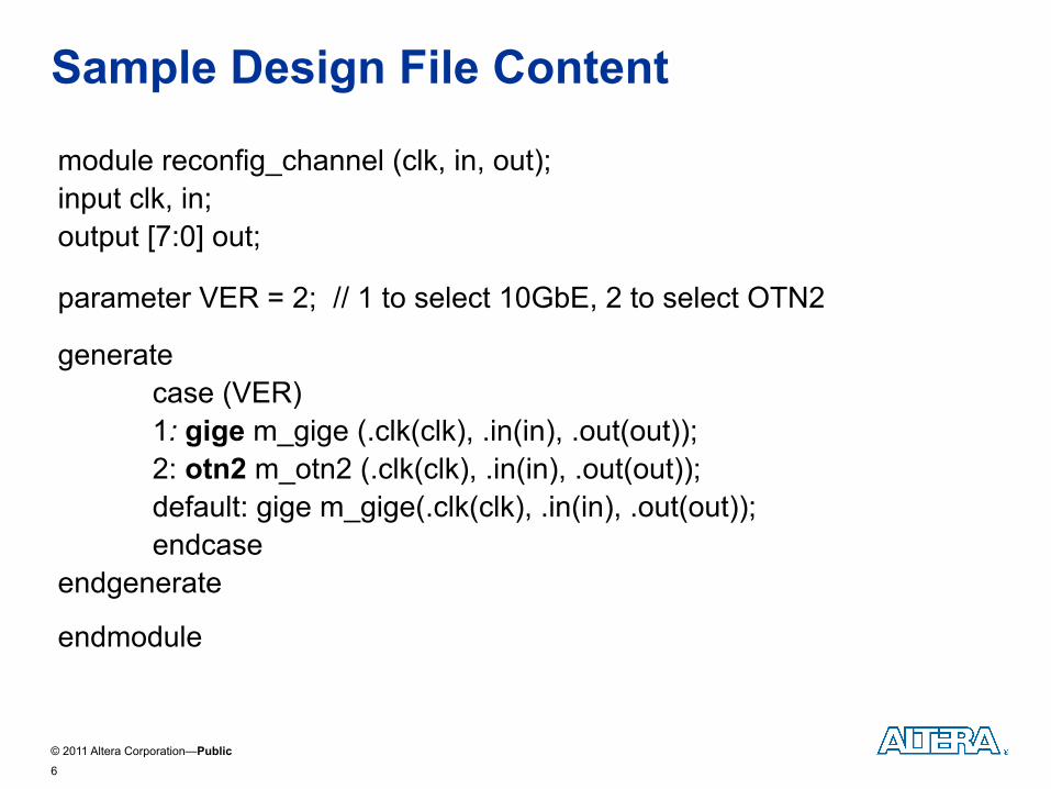
Sample Design File Content
6
module reconfig_channel (clk, in, out); input clk, in; output [7:0] out;
parameter VER = 2; // 1 to select 10GbE, 2 to select OTN2
generate case (VER) 1: gige m_gige (.clk(clk), .in(in), .out(out)); 2: otn2 m_otn2 (.clk(clk), .in(in), .out(out)); default: gige m_gige(.clk(clk), .in(in), .out(out)); endcase
endgenerate
endmodule

© 2011 Altera Corporation—Public 7
Stratix V Device Floorplan
I/O, Memory Interfaces, Clocks, etc…
PLL, JTAG, CRC, control circuitry, etc…
Transceivers, Hard IP Blocks
LAB, RAM, DSP
PLLs, Clocks
© 2011 Altera Corporation—Public
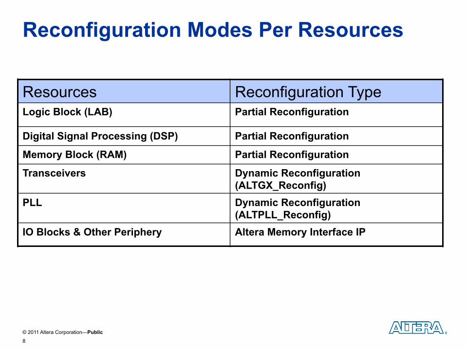
Reconfiguration Modes Per Resources
Resources Reconfiguration Type Logic Block (LAB) Partial Reconfiguration
Digital Signal Processing (DSP) Partial Reconfiguration
Memory Block (RAM) Partial Reconfiguration
Transceivers Dynamic Reconfiguration (ALTGX_Reconfig)
PLL Dynamic Reconfiguration (ALTPLL_Reconfig)
IO Blocks & Other Periphery Altera Memory Interface IP
8

© 2011 Altera Corporation—Public
Configuration RAM Bits
FPGA is fixed HW with millions of 1-bit memory cells (CRAM) - Core bits are directly addressable
by Frame (column) & Index (row) - Large devices have >107 CRAMs
By changing CRAM values, can reconfigure individual LABs, RAMs, DSPs, and routing muxes Not all CRAM sequences are legal Quartus will not provide details
about CRAM logical function
9
Bit 1
Bit 2
Fram
e 1
Fram
e 2
Fram
e m
Fram
e m
+1
Bit i
Bit i+1
Bit i+j-1
Bit i+j
Last
Fra
me
Last Bit
CRAM address space Fr
ame
n
Fram
e n+
1
Fram
e m
+2
Fram
e n+
2
Non-PR Region
PR Region

© 2011 Altera Corporation—Public
Basic PR Operation
Use handshaking commands - From user I/O or from core logic
Speed of operation - Small overhead to engage PR - Depends on size of region - Depends on orientation of region
Sample configuration times - ~5kLEs - Region A ~ 2ms - Region B ~ 10ms - 2ms @ 400 MHz = 800,000 cycles
10
Region A
x
5x
Region B x
5x

© 2011 Altera Corporation—Public
Changing CRAM Bit State For each affected frame, control block generates
- An AND instruction to set reconfigured bits to zero - An OR instruction to set them to one
11
1
1
0 1
0
0 1
1
0
0 0
0
0 1
1
0
0 0
1
0 1
Mask Frame + AND instruction
1
1
1 0
0
0 1
0
1
1 0
0
0 0
Mask Frame + OR instruction
Temporary Frame

© 2011 Altera Corporation—Public
Implications of Temporary Frame
12
1
0
0
Must carefully consider electrical effects - NMOS-based logic is very common - Requires weak pull-up transistor to strengthen internal node when
input signal is VDD - Global “freeze” signal can’t be used during PR
x
y

© 2011 Altera Corporation—Public
Implications of Temporary Frame
13
0
0
0
‘AND’ instruction may cause all CRAM bits of a routing driver to be zero - No electrical issues if ‘x’ is VDD at the time when the CRAM bit
flips from a ‘1’ to a ‘0’
x
y
© 2011 Altera Corporation—Public
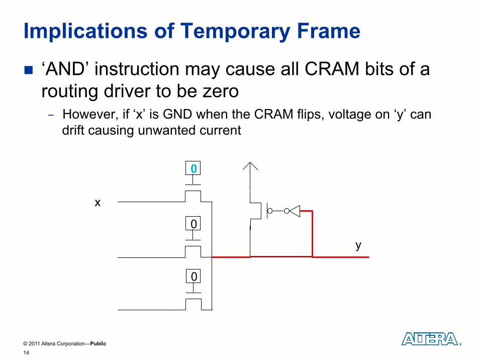
Implications of Temporary Frame
14
0
0
0
‘AND’ instruction may cause all CRAM bits of a routing driver to be zero - However, if ‘x’ is GND when the CRAM flips, voltage on ‘y’ can
drift causing unwanted current
x
y

© 2011 Altera Corporation—Public
Partial Reconfiguration Inputs & Outputs
15
Design Files
Project Info
(.qpf)
Reports (timing)
Bitstream Files
Multiple Compiles Needed!
1 full chip + 1 per persona

© 2011 Altera Corporation—Public 16
Incremental Design Background
Top
Channel 1 Channel 2 OTN4 MUXponder …
Specify partitions in your design hierarchy
Can independently recompile any partition
- CAD optimizations across partitions prevented - Can preserve synthesis, placement and routing of unchanged
partitions - Supports multiple processors for faster compile

© 2011 Altera Corporation—Public 17
Reconfigurable Instances Top
C1, 10GbE C2, 10GbE
OTN4 MUXponder … C1, OTN2 C2, OTN2
Static partition
PR Partition 2 PR Partition 1
Each design instance in a reconfigurable partition is called a “persona” - Above design hierarchy has 4 personae (C1 x 2, C2 x 2) - PR partitions must be assigned to fixed regions on the chip

© 2011 Altera Corporation—Public
Partial Reconfiguration Project
Revision = set of input files for a single compile - Can change parameters, timing constraints, fitter settings, etc…
Revision types in a PR project - Base: Content that always exists on the chip (a.k.a. static compile) - Reconfigurable: Content that can be programmed via PR commands - Aggregate: User-defined groupings of reconfigurable revisions
(consider 10 PR partitions with 6 personae each, 106 possible combos)
No limit to the # of regions or # of personae / PR region
18
PR Project Base
revision Reconfigurable
revisions Aggregate revisions

© 2011 Altera Corporation—Public
Partial Reconfiguration Project
19
PR Project
Base revision
Reconfigurable revisions
Aggregate revisions
PR 2
PR 1
Static Logic
Bitstream File
#1: Compile static logic - User can specify PR1 & PR2 for base revision - Can be empty, initial content, or “hardest-to-
route” personae

© 2011 Altera Corporation—Public
Partial Reconfiguration Project
#2: Compile reconfigurable logic - Personae compile imports base revision P&R - Quartus can compile all personae in parallel
Combine personae in different regions together # compiles = max # personae across all regions
20
PR1: Persona1
PR2: Persona 2
PR Project
Base revision
Reconfigurable revisions
Aggregate revisions
Bitstream File x 4
PR1: Persona2
PR2: Persona 1

© 2011 Altera Corporation—Public
Partial Reconfiguration Project
#3: Compile user-defined groups of reconfigurable logic - This step is completely optional - Generates complete bitstream, without requiring
PR commands - Useful for timing analysis / simulation
21
PR2: Persona 2
PR1: Persona 1
Static Logic
PR Project
Base revision
Reconfigurable revisions
Aggregate revisions
Bitstream File

© 2011 Altera Corporation—Public
Managing Revisions
22
Quartus contains dedicated GUI to navigate PR project - Can directly launch “regular” Quartus
GUI for a specific revision - Can easily create new revisions - Can “compile all” via single click - Can obtain summary of all compiles

© 2011 Altera Corporation—Public
Design Flow
23

© 2011 Altera Corporation—Public
PR Introduces New Software Challenges
Handling inputs/output signals to PR partitions - PR inputs/outputs must stay in same spot in all compiles
Partitioning routing resources across all compiles - Different PR partitions cannot use same routing resource - Different personae in same PR region can use same routing wires
Utilizing shared FPGA resources - E.G. pre-fabricated clock networks
Timing closure on cross-partition paths - E.G. reg in PR1 reg in PR2
24

© 2011 Altera Corporation—Public
PR Partition Input Signals
25
0
0
0
Recall electrical problem with GND inputs - Option 1: User “guarantees” inputs will be VDD when PR engages - Option 2: Let compiler solve the problem automatically
x
y

© 2011 Altera Corporation—Public
PR Partition Input Signals
For each PR partition, reserve one LUT for GND For each input signal into a PR partition,
- Add OR gate outside PR partition and connect GND LUT to other input - Connect OR gate output to a 1-input anchor LUT inside PR partition
This connectivity is inserted during the base revision
26
PR1 OR
GND LUT
OR

© 2011 Altera Corporation—Public
PR Partition Output Signals
For each output signal, - Create anchor 1-LUT inside PR partition - Connect output to logic in static region, according to design files
27
PR1

© 2011 Altera Corporation—Public
Using Anchor 1-LUTs in PR Partitions
(+) Increases routing flexibility on inputs/outputs - FPGA architecture not designed to route to/from specific wires
(+) P&R is well-defined for each compile - Otherwise, how should path from OR gate to logic be chosen? - Inputs can branch from the OR gate 1-LUT path, if desired
(-) Reduces # of usable LUTs in PR region (-) Increases latency on signals entering region
28

© 2011 Altera Corporation—Public
OTN2
Route-Throughs At The Top Level
HW supports reconfiguration of individual routing muxes - Enables routing through PR regions - Simplifies / removes many floorplanning restrictions - Quartus records routing reserved for top-level use and prevents
PR instances from using these wires
29
10GbE OTN4
Tran
scei
vers

© 2011 Altera Corporation—Public
Inter-Region Communication SW design decisions make this easy to support
- Anchor LUTs & inserted OR gate are routed in the static compile - Resources used by the static compile are disallowed by all
personae compilations
30
PR Region 3
PR Region 1
PR Region 2
GND LUT
OR

© 2011 Altera Corporation—Public
16 global networks - Balanced H-tree - Reaches every block - Only 6 unique clocks can drive
each “row clock region” (~12x1) PR designs should
consider clocking regions - Match region size to clock
boundaries = easier problem - Quartus supports any PR region - P&R engine assumes clock feeds
every location in PR region
Global Networks On Stratix V Devices
31

© 2011 Altera Corporation—Public
Sharing Global Wires Between Regions
32
Clk buffer
PR Region 1 PR Region 2

© 2011 Altera Corporation—Public
Wires in the base revision bitstream Wires that may used in a persona bitstream targeting region 2 Wires that may used in a persona bitstream targeting region 1 Wires that must be in the base revision bitstream because any persona in region 1 or 2 may use them
Static logic
Sharing Global Wires Between Regions
33
Clk buffer
PR Region 1 PR Region 2

© 2011 Altera Corporation—Public
Simple Timing Closure (Base Compile)
Add registers at all PR partition boundaries - Fitter routes intra-region connections for minimum delay
pr1_out~wire reg1 reg2 pr2_in~wire
OR gate can be placed before ‘reg2’ (assuming no clock enable)
34
PR1 PR2 OR
Pr1_out~wire Pr2_in~wire reg1 reg2
© 2011 Altera Corporation—Public
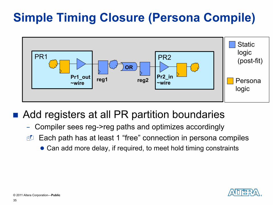
Simple Timing Closure (Persona Compile)
35
PR1 PR2 OR
Pr1_out~wire
Pr2_in~wire reg1 reg2
Static logic (post-fit)
Persona logic
Add registers at all PR partition boundaries - Compiler sees reg->reg paths and optimizes accordingly Each path has at least 1 “free” connection in persona compiles
Can add more delay, if required, to meet hold timing constraints

© 2011 Altera Corporation—Public
Advanced Timing Closure
User explicitly manages clock period - Divide into three segments - Specify timing constraints for each segment in SDC file
36
PR1 PR2 OR Comb
set_max/min_delay set_output_delay set_input_delay
src_reg wire1 wire2
dst_reg

© 2011 Altera Corporation—Public
The SDC File
User will be provided the worst-case clock arrival times for each global signal entering PR region - Will be known at the end of the base revision - Generally, these numbers are a function of device/speedgrade
37
The clock period and how the user has divided it
The clock, and a virtual clock for each input/output domain of the PR partitions The worst case clock arrival times over all locations in the PR region
Timing budget for the static region (base revision)
Timing budget for PR compiles

© 2011 Altera Corporation—Public 38
Upcoming Idea: Translatable Bitstreams
10GbE OTN2 10Gb/s
100Gb/s
Channel 1
10Gb/s
10Gb/s
Channel 2
Channel 10
OTN4
Client Side Line Side MUXPonder
10GbE OTN2
10GbE OTN2
10 PR regions, 2 personae per PR region - But, there’s only 2 unique personae across all regions - Users would prefer to generate 2 partial bitstream files, not 20
© 2011 Altera Corporation—Public
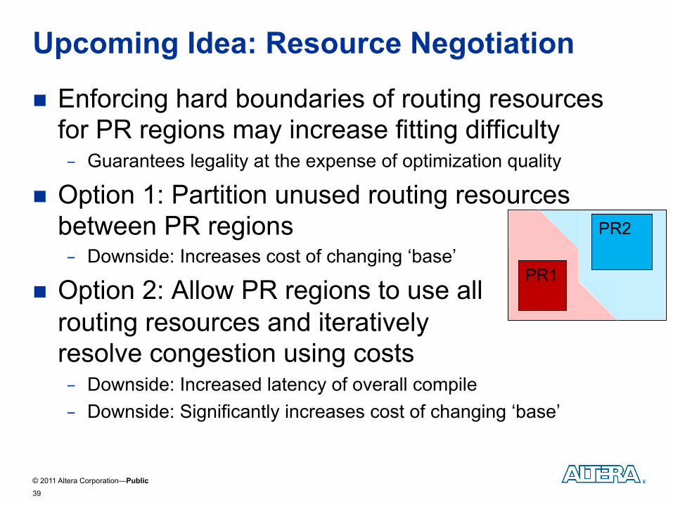
Enforcing hard boundaries of routing resources for PR regions may increase fitting difficulty - Guarantees legality at the expense of optimization quality
Option 1: Partition unused routing resources between PR regions - Downside: Increases cost of changing ‘base’
Option 2: Allow PR regions to use all routing resources and iteratively resolve congestion using costs - Downside: Increased latency of overall compile - Downside: Significantly increases cost of changing ‘base’
Upcoming Idea: Resource Negotiation
39
PR1
PR2

© 2011 Altera Corporation—Public
Upcoming Idea: Minimize Overhead
Current SW implementation approach works well for multi-modal applications - Overhead << PR region size
Some advanced applications would want to create hundreds of very small regions - SW approach doesn’t prohibit this design style - However, overhead added by SW reduces becomes limiting factor
40

© 2011 Altera Corporation—Public 41
Summary
Altera devices have flexible hardware support for partial reconfiguration - Able to reconfigure individual LABs, RAMs, routing muxes
Altera has provided a well-defined design flow for implementing multi-modal applications using PR - Intuitive design entry, simulation, and project cockpit (GUI) - User can manage complex timing situations between PR regions
Quartus automatically handles implementation details efficiently & effectively - “OR”-gate insertion - Route throughs - Cross-region clocking


![Stegosaurus Development Report - University of Torontojayar/ece1778.2015/stegosaurus.pdf · analysis [5], which can reveal a large amount of information about the individual without](https://img.pdfslide.us/doc/110x75/5eb092c92f25ae18ac37224e/stegosaurus-development-report-university-of-jayarece17782015stegosauruspdf.jpg)