Embed Size (px)
Citation preview
Mark 5B System User’s Manual MIT Haystack Observatory
8 August 2006
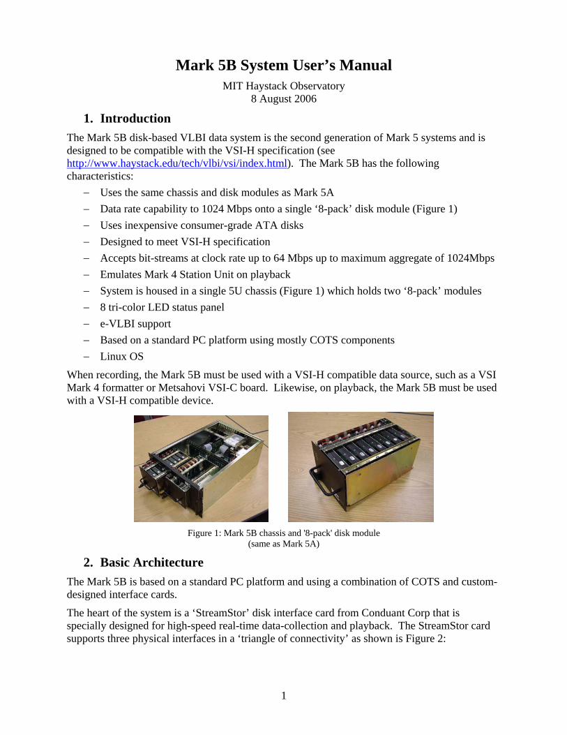
1. Introduction The Mark 5B disk-based VLBI data system is the second generation of Mark 5 systems and is designed to be compatible with the VSI-H specification (see http://www.haystack.edu/tech/vlbi/vsi/index.html). The Mark 5B has the following characteristics:
− Uses the same chassis and disk modules as Mark 5A − Data rate capability to 1024 Mbps onto a single ‘8-pack’ disk module (Figure 1) − Uses inexpensive consumer-grade ATA disks − Designed to meet VSI-H specification − Accepts bit-streams at clock rate up to 64 Mbps up to maximum aggregate of 1024Mbps − Emulates Mark 4 Station Unit on playback − System is housed in a single 5U chassis (Figure 1) which holds two ‘8-pack’ modules − 8 tri-color LED status panel − e-VLBI support − Based on a standard PC platform using mostly COTS components − Linux OS
When recording, the Mark 5B must be used with a VSI-H compatible data source, such as a VSI Mark 4 formatter or Metsahovi VSI-C board. Likewise, on playback, the Mark 5B must be used with a VSI-H compatible device.
Figure 1: Mark 5B chassis and '8-pack' disk module
(same as Mark 5A)
2. Basic Architecture The Mark 5B is based on a standard PC platform and using a combination of COTS and custom-designed interface cards.
The heart of the system is a ‘StreamStor’ disk interface card from Conduant Corp that is specially designed for high-speed real-time data-collection and playback. The StreamStor card supports three physical interfaces in a ‘triangle of connectivity’ as shown is Figure 2:
1
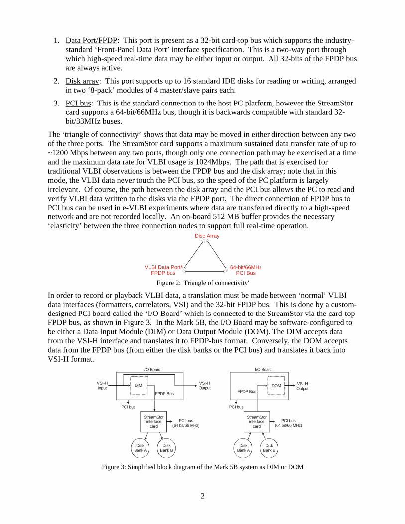
1. Data Port/FPDP: This port is present as a 32-bit card-top bus which supports the industry-standard ‘Front-Panel Data Port’ interface specification. This is a two-way port through which high-speed real-time data may be either input or output. All 32-bits of the FPDP bus are always active.
2. Disk array: This port supports up to 16 standard IDE disks for reading or writing, arranged in two ‘8-pack’ modules of 4 master/slave pairs each.
3. PCI bus: This is the standard connection to the host PC platform, however the StreamStor card supports a 64-bit/66MHz bus, though it is backwards compatible with standard 32-bit/33MHz buses.
The ‘triangle of connectivity’ shows that data may be moved in either direction between any two of the three ports. The StreamStor card supports a maximum sustained data transfer rate of up to ~1200 Mbps between any two ports, though only one connection path may be exercised at a time and the maximum data rate for VLBI usage is 1024Mbps. The path that is exercised for traditional VLBI observations is between the FPDP bus and the disk array; note that in this mode, the VLBI data never touch the PCI bus, so the speed of the PC platform is largely irrelevant. Of course, the path between the disk array and the PCI bus allows the PC to read and verify VLBI data written to the disks via the FPDP port. The direct connection of FPDP bus to PCI bus can be used in e-VLBI experiments where data are transferred directly to a high-speed network and are not recorded locally. An on-board 512 MB buffer provides the necessary ‘elasticity’ between the three connection nodes to support full real-time operation.
VLBI Data Port/FPDP bus
Disc Array
64-bit/66MHzPCI Bus
Figure 2: 'Triangle of connectivity'
In order to record or playback VLBI data, a translation must be made between ‘normal’ VLBI data interfaces (formatters, correlators, VSI) and the 32-bit FPDP bus. This is done by a custom-designed PCI board called the ‘I/O Board’ which is connected to the StreamStor via the card-top FPDP bus, as shown in Figure 3. In the Mark 5B, the I/O Board may be software-configured to be either a Data Input Module (DIM) or Data Output Module (DOM). The DIM accepts data from the VSI-H interface and translates it to FPDP-bus format. Conversely, the DOM accepts data from the FPDP bus (from either the disk banks or the PCI bus) and translates it back into VSI-H format.
VSI-HInput
I/O Board
DIM
StreamStorinterface
card
DiskBank A
PCI bus
PCI bus(64 bit/66 MHz)
DiskBank B
FPDP Bus
I/O Board
DOM
StreamStorinterface
card
DiskBank A
PCI bus
PCI bus(64 bit/66 MHz)
DiskBank B
FPDP Bus
VSI-HOutput
VSI-HOutput
Figure 3: Simplified block diagram of the Mark 5B system as DIM or DOM
2
When recording data to disks, the set of mounted disks records data in much the same way as magnetic tape. That is to say, scans are recorded sequentially, one after another. Once recorded, individual scans, except the last-recorded scan, may not be erased; normally, the entire module is erased as a whole.
A scan directory is maintained by the Mark 5B that allows individual scans to be named when recorded. Once recorded, individual scans may be randomly accessed by scan name or sequential scan number. All or part of any scan may be reproduced. The data set may be extended at any time with additional recording, including after removing and re-inserting the disk set.
Data recorded to disks is recorded in a proprietary format optimized for high-speed real-time performance. The number of disk in a disk module may be 1, 2, 3, 4, 6 or 8, depending on data-rate and data-capacity requirements. If a disk fails or is missing during playback, the Mark 5 will fill data gaps with preset ‘fill-pattern’ data that can be detected at the correlator and cause the associated data to be invalidated.
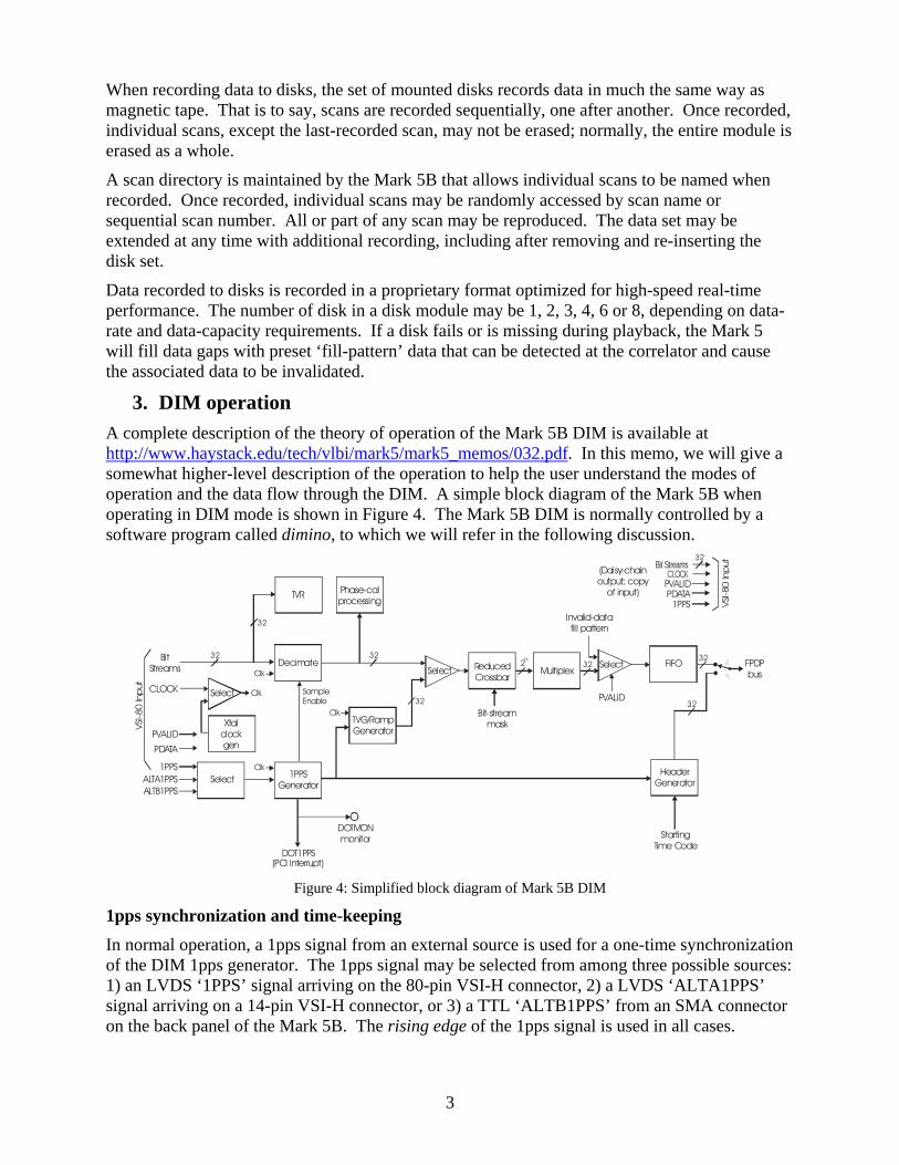
3. DIM operation A complete description of the theory of operation of the Mark 5B DIM is available at http://www.haystack.edu/tech/vlbi/mark5/mark5_memos/032.pdf. In this memo, we will give a somewhat higher-level description of the operation to help the user understand the modes of operation and the data flow through the DIM. A simple block diagram of the Mark 5B when operating in DIM mode is shown in Figure 4. The Mark 5B DIM is normally controlled by a software program called dimino, to which we will refer in the following discussion.
1PPSGenerator
Select
TVG/RampGenerator
Decimate
SampleEnable
Xtalclockgen
Select ReducedCrossbar
MultiplexSelect FIFO
TVR
HeaderGenerator
Clk
Clk
Clk
BitStreams
CLOCK
1PPS
VSI-8
0 In
put
Clk
ALTA1PPSALTB1PPS
PVALID
PVALID
Bit-streammask
StartingTime Code
Invalid-datafill pattern
FPDPbus
PDATA
Select
DOT1PPS
32 32 32
32
32
(PCI Interrupt)
DOTMONmonitor
Phase-calprocessing
2n32
CLOCK
1PPS VSI-8
0 In
put
PVALIDPDATA
32Bit Streams(Daisy-chain
output; copyof input)
32
Figure 4: Simplified block diagram of Mark 5B DIM
1pps synchronization and time-keeping In normal operation, a 1pps signal from an external source is used for a one-time synchronization of the DIM 1pps generator. The 1pps signal may be selected from among three possible sources: 1) an LVDS ‘1PPS’ signal arriving on the 80-pin VSI-H connector, 2) a LVDS ‘ALTA1PPS’ signal arriving on a 14-pin VSI-H connector, or 3) a TTL ‘ALTB1PPS’ from an SMA connector on the back panel of the Mark 5B. The rising edge of the 1pps signal is used in all cases.
3
Upon a synchronization request, the next selected 1pps signal is used to initialize the ‘1PPS Generator’, which thereafter only counts cycles of CLOCK (whose frequency must have been previously specified to dimino) from the VSI-H interface; thereafter the selected 1pps signal serves no functional purpose other than monitoring at the DIM1PPS back-panel SMA connector. A ‘DOTMON’ signal is available to monitor the epoch of the 1pps tick from the 1PPS Generator. Normally, the 1PPS Generator is synchronized only once per experiment. The 1PPS Generator is designed to remain synchronized through shutdown (or crash) and restart of the Mark 5B software control program and re-boot of the host computer.
Higher-order time-keeping above one second is done in software by initializing a YYYYDDDHHMMSS time and thereafter counting DOT1PPS interrupts. This higher-order time must always be reset when dimino is restarted.
Setup for normal data-acquisition Prior to the start of data taking, both the decimation ratio and bit-stream mask must be specified. The decimation value, which may be 1, 2, 4, 8, or 16, specifies the number of CLOCK cycles between samples collected from the VSI-H bit-streams and thus determines the effective sample rate (BSIR or bit-stream information rate in VSI-H-speak). The bit-stream mask specifies which 2n (0<=n<=4) of the 32 bit-streams are actually to be recorded; a ‘reduced crossbar switch’ which takes advantage of the 2n nature of the bit-streams selects only those indicated by the bit-stream mask.
Operation during data-acquisition Actual data acquisition always starts on a second tick (and ends on a second tick). Upon request to start data-acquistion, dimino creates a “starting-time timecode” corresponding to the time of the next second tick and transmits it to the Header Generator. The job of the Header Generator is to generate Mark 5B Disk Frame Headers which are inserted into the data stream to the disk every 104 data bytes.
Data acquisition (scan) starts on the next DOT1PPS tick. All VSI bit-streams are first decimated according to the previously-specified decimation value, then sent to the reduced crossbar which packs the selected bit-streams into adjacent parallel bit-streams emerging from the crossbar. A multiplexer then packs the data from 32/2n sample periods into a single 32-bit word. These data are then sent to a FIFO, though data marked invalid by PVALID is replaced by a special ‘fill pattern’ which can be later recognized at the correlator and excluded from correlation. The FIFO allows 32-byte disk frame headers to be periodically inserted into the FPDP data stream which goes to the Mark 5B disk module or to the PCI bus; the output of the FIFO is clocked at 33MHz, slightly above the maximum data rate coming into the FIFO, which allows time for the disk frame headers to be inserted.
Data-acquisition stops on the next DOT1PPS tick following the receipt of a request to stop data collection.
A directory entry is written to the Mark 5B disk module for every scan.
The DIM input on the MDR-80 connector is buffered and output to the card-top MDR-80 connector for use in daisy-chain operation of Mark 5B systems.
Phase-cal extraction Data arriving at the VSI input port of the DIM may be analyzed for phase-calibration tones by a sophisticated phase-cal extraction module. The phase-cal extractor can extract up to 16 tones
4
from each of 16 data channels. The phase-cal extractor assumes that each even-numbered VSI bit-stream is a sign-bit data stream; for 2-bit samples, the adjacent (next higher number) odd-numbered VSI bit-stream must carry the corresponding magnitude bits. For 1-bit samples the magnitude stream is ignored. Details of the operation of the phase-cal extractor are available in Mark 5 memo #21 available at http://www.haystack.edu/tech/vlbi/mark5/memo.html.
Test-vector/ramp generator and test-vector receiver operation An internal test-vector generator (TVG), which may be driven either by the VSI clock or by a settable on-board clock generator (0 to 40MHz) is available to write either a VSI-H test pattern or a monotonically increasing 32-bit counting ramp for diagnostic purposes. Note that the tvg signal is inserted after the decimator so that tvg data may never be decimated. The VSI-H test pattern is re-initialized on every second tick, as per the VSI-H specification. The counting ramp is initialized to zero at the next second tick after a received command, and then counts for 100 seconds before resetting to zero again.
A test-vector receiver (TVR), operating according to the VSI-H specification, is available to test tvg data arriving at the VSI input to the DIM. The TVR cannot be used to check data generated by the internal TVG (see Figure 4)
FPDP bus A standard FPDP (Front-Panel Data Port) bus is used to transfer data to the StreamStor card. Normally the maximum data transfer rate is 33 MHz, though the Mark 5B I/O card is also designed to be compatible with the FPDP2 specification which allows data transfer on both edges of the 33 MHz clock. The next-generation StreamStor card will also support FPDP2, which will allow data transfer at 66 MHz and an aggregate data rate of 2048Mbps to be recorded. Switching from FPDP to FPDP2 mode is done under software control.
Handling of PDATA Any incoming LVDS serial PDATA data are converted to standard RS-232 and routed to board connector J21 (see Figure 9), which may be connected to a standard serial port on the host computer for capture and processing. Additionally, the PDATA signal is optionally replicated to QDATA (under software control) to support “daisy-chaining” of Mark 5Bs.
DIM PCI Interrupts Table 1 lists the single DIM PCI interrupt and its purpose. An interrupt mask allows the control software to enable/disable this interrupt. An interrupt register readable by the control software identifies the source of the interrupt; reading this register clears all bits in the register.
Name Source Description Comments
DOT1PPS DIM Internal DIM 1PPS tick Provides DOT clock 1PPS marker to control software
Table 1: DIM PCI Interrupt
The DOT1PPS interrupt is generated at each DOT clock 1pps tick to allow the control software to do accurate high-order timekeeping.
LED status display The Mark 5B includes a LED status display at the lower-right of the front panel; the status display is made up of 8 tri-color LEDs, which are intended to convey the state of the Mark 5B at
5
any time. Figure 5 shows a diagram of the status panel along with the meaning of each of the individual LEDs.
MOD PPS VAL FLO
ERR TVR SW1 SW2
OPERATING MODE G - DIM mode Off - FPGA program failure
1PPSG - Sync'ed - flashes with DOT1PPSR - Not sync'ed - flashes with external 1PPSNot flashing - no clock
DATA VALIDITYG - 'valid' data at DIM inputB - Internal TVG selectedR - 'invalid' data at DIM input
FPDP DATA FLOWG - writing valid data to FPDP busR - writing fill patternOff - no data flow
ERRORG - Normal operationR - Internal error
TEST VECTOR RECEIVERG - TVR activeR - error detected by TVR
SOFTWARE 1Software controlled:Function may vary
SOFTWARE 2Software controlled:Function may vary
Figure 5: Definition of DIM status-panel LED states
MOD - Operating mode Green –Xilinx chip is loaded with DIM code and is operating as a DIM Off – FPGA has failed to initialize properly. This may be due to some sort of hardware
failure or perhaps an incomplete or faulty loaded of the PROM associated with the Xilinx chip.
(Red or Blue – Xilinx chip is loaded with DOM code)
PPS Green – flashes in synchronism with DOT1PPS once DOT clock is synchronized Red – DOT clock not yet synchronized; flashes in synchronism with selected external 1PPS
signal.
VAL – data validity Green – DIM is receiving data marked as ‘valid’ by PVALID signal Red – DIM is receiving data marked as ‘invalid’ by PVALID signal Blue – Internal TVG is selected as data source
FLO – FPDP data flow Green - Indicates that data is flowing on the FPDP data bus Red – Fill pattern is being written Off – No data is flowing on FPDP buf
ERR – Error indicator Green – Normal operation; no errors Red – Internal error has been detected
TVR – Test vector generator Green – TVR is active Red – Error detected by TVR (latched)
SW1 – Software-controlled LED1 Under control of the Mark 5B control software
SW2 – Software-controlled LED2 Under control of the Mark 5B control software
6
4. DOM operation Modes of operation
DOM SU mode The DOM can be configured to emulate a Mark 4 correlator Station Unit. Before discussing this mode in detail, it is useful to define some terms and signals:
TOT (‘tape observe time’) – the time scale on the recorded data; the ‘TOT’ acronym is a holdover from magnetic tape days!
TOT1PPS – TOT second tick, generated each time a DF Frame #0 is read from the data disks.
ROT (‘reconstituted observe time’) – the correlation processing time scale, which is pegged to an abstract clock at the center of the earth. Due to the fact that playback may be speeded-up or slowed-down by up to a factor of 16, ROT second ticks may occur at a rate from 1/16 to 16 times the record rate, though maximum playback bitstream rate is always 32MHz.
DOM1PPS – correlator second tick, which has the same rate as the correlator wall-clock (DPS1PPS).
4.1 Sequence of operations
The sequence for SU emulation is as follows:
Preparation:
1. The correlator software selects a particular DOM1PPS tick on which playback is to be started, which is assigned (by correlator software) to correspond to the ROT start second tick for scan processing, which we define as ROT0.
2. In advance of the actual playback start, the Mark 5B software commands a pre-load of the DOM Data Buffer, which always starts precisely with a TOT second tick, defined as TOT0 (see footnote1). The minimum size of the Data Buffer is 256MB, corresponding to two TOT seconds of data at 1024 Mbps (fCLOCK=32MHz) or up to 32 TOT seconds for the slowest record rate (fCLOCK=2MHz)2. The Data Buffer will always be filled with this pre-load data. The Data Buffer may, of course, be filled at the maximum rate provided by the StreamStor disks.
3. In advance of playback start, the Mark 5B software loads the delay/CF-header data for the first CF to the DOM.
Playback:
1. The Mark 5B software issues a ‘start playback’ command to the DOM sometime in the DOM1PPS period prior to the DOM1PPS start tick (chosen by the software to correspond to the desired ROT start time). At the instant of the start DOM1PPS, the DOM starts
1 The actual choice of TOT0 depends on the sign of the initial delay at ROT0, which will always have a value between +/-½ ROT second. If the initial delay is positive (as specified by the sign of the initial delay parameter), the DOM will begin playback at TOT0+abs(initial delay); if the initial delay is negative, the DOM will begin playback at TOT0+1-abs(initial delay). Note: Delays greater than ½ ROT second can be handled by correlator software by adjusting the TOT0 value by integer seconds. 2 Data are loaded as 32-bit words into the DOM Data Buffer (as if there are always 32 active bit streams); dummy data may be loaded into the parts of the 32-bit word that correspond to unused bit streams. Each 32-bit word is accompanied by a validity bit. If the scan ends before the Data Buffer is filled, the remainder of the Data Buffer are flagged invalid.
7
playback of data from the Data Buffer according to the delay parameters and enables TOT1PPS and CFINT interrupts. The data are divided into CF’s as specified, with the data dynamically delayed according to the delay model and CF headers being created as required (see Section 4.3).
2. A TOT1PPS interrupt is generated every time the DF count should roll over to zero (if a fill pattern obliterates a header, a TOT1PPS tick is still generated). The whole number of seconds in the VLBA time code is posted to a register and a TOTCOUNT register is incremented. At each TOT1PPS interrupt (or any other time) the software may check that the TOTCOUNT and posted VLBA time code are consistent.
3. At each CFINT interrupt, including the one occurring at the start of playback, a CFINT interrupt is generated which causes the Mark 5B software to load the delay/CF header data array for the next CF into the DOM. In this manner, the DOM always has a fresh set of delay/CF-header data available for each CF. The process continues through the duration of the scan. See Section 4.6 for more details.
4. When the DOM read point passes the midpoint of the Data Buffer, the DOM reads the next data from the disks into the first half of the Data Buffer and then pauses. When the DOM read point reaches the end of the Data Buffer, the read point is moved back to the beginning and disk data are backfilled into the second half of the Data Buffer, etc. The average read rate from the disks during the backfill operation should be regulated to be perhaps no more than about 10% than the playback rate in order to maximize the dynamic delay range during playback.
5. A ‘pause playback’ command may be issued at any time during playback, in which case the output continues until the end of the current ROT second; at this point all further output data will be marked invalid, though BOCF and RCLOCK signals will continue to be active.3
6. A ‘resume playback’ command will re-start playback on the next DPS1PPS tick, picking up exactly where the data output was stopped with the ‘pause playback’ command, but with an updated delay model.
7. If the recording or playback configuration changes between scans, the DOM must be reset and the internal data buffer re-loaded before playback can be restarted.
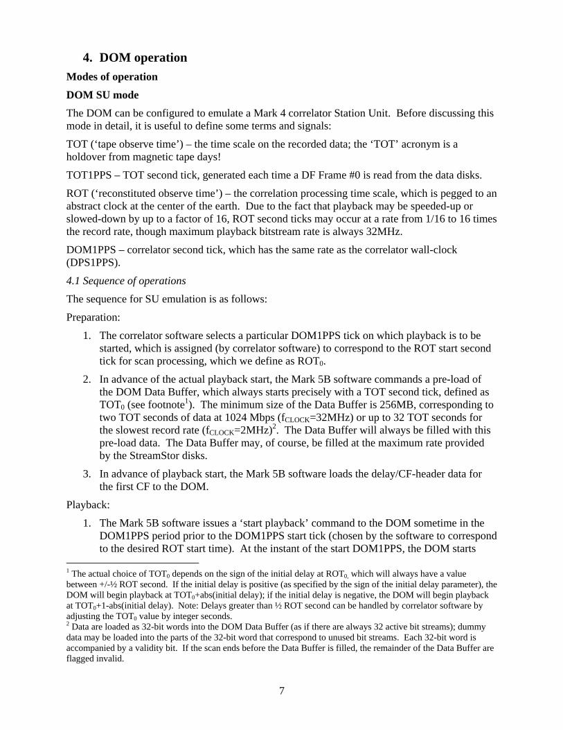
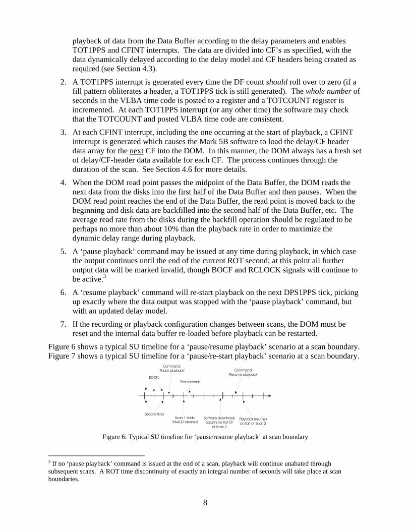
Figure 6 shows a typical SU timeline for a ‘pause/resume playback’ scenario at a scan boundary. Figure 7 shows a typical SU timeline for a ‘pause/re-start playback’ scenario at a scan boundary.
Second ticks
BOCFs
Command:‘Pause playback’
Scan 1 ends;INVALID asserted
Few seconds
Software downloadsparams for first CF
of Scan 2
Command:‘Resume playback’
Playback resumesat start of Scan 2
Figure 6: Typical SU timeline for ‘pause/resume playback’ at scan boundary
3 If no ‘pause playback’ command is issued at the end of a scan, playback will continue unabated through subsequent scans. A ROT time discontinuity of exactly an integral number of seconds will take place at scan boundaries.
8
Second ticks
BOCFs
Command:‘Pause playback’
Scan 1 ends;INVALID asserted
Few seconds
Command:Pre-load buffers
for Scan 2
Pre-loading buffers
Pre-load complete;software notified
Command:‘Start playback’
Playback startsfor Scan 2
Software downloadsparams for first CF
of Scan 2 Figure 7: Typical SU timeline for ‘pause/restart playback’ at scan boundary
4.2 Sign, Magnitude Codes
When operating as an SU, the DOM must remap the Mark 4/VLBA codes according to Table 2, which is identical to the old Mark 4 SU remapping.
BBC analog output (mv)
Mark 4/VLBA code DOM Output
Sign (S) Mag (M) Sign (S’) Mag (M’)
>220 1 1 1 1
0→220 1 0 1 0
0→-220 0 1 0 0
<-220 0 0 0 1
Table 2: Codes used when Mark 5B is operating as an SU (2-bits/sample)
The code transformation in Table 2 may also be expressed as logically as , S S′ = M M S′ = ⊕ .
In the case where the channels are 1-bit/sample, the corresponding magnitude bit-stream must be dynamically constructed as and M’=1. S S′ =
4.3 Correlator Frames
When operating in SU mode, the output data are always organized into 16 2-bits/sample channels, where all sign bits appear on even-numbered bit streams and magnitude bits on the corresponding odd-numbered bit streams.
All output bit-streams are divided into Correlator Frames (CF), which have the following characteristics:
1. The length of a CF will be specified by the user in units of RCLOCK cycles, but the rate will not exceed 32 CFs per DOM1PPS period; the maximum length of a CF will be 0.5 DOM1PPS periods (corresponds to maximum of 1.6x10⁷ RCLOCK cycles at 32 MHz). There are always integral number of CFs per DOM1PPS period.
2. A CF begins on every ROT second tick.
3. For each of the 16 ‘magnitude’ bit streams, the 240 bits occurring during BOCF are replaced by CF header data provided by the host computer; the CF-header data are different for each ‘magnitude’ bit-stream.
9
4.4 RCLOCK
When operating in SU mode, RCLOCK always operates at fDPSCLOCK (32 MHz), even though the DOM output bit-stream rate may be 2, 4, 8, 16 or 32 MHz. This is unlike normal DOM operation where fRCLOCK is always the same as the DOM output sample rate. RCLOCK shall be continuous and uninterrupted while operating in Station Unit mode.
4.5 BOCF
A Beginning of Correlator Frame (BOCF) signal, which applies to all bit streams, is asserted at the beginning of each CF for a period of 240*n RCLOCK cycles, where n is software selectable to be 1, 2, 4, 8 or 16. (Note that the RCLOCK rate is always constant, as stated above.) After setting of the BOCF period and length, the BOCF signal shall be continuous and uninterrupted from scan to scan until the BOCF is explicitly reset.
4.6 Delay Management
An initial delay of the data (TOT wrt ROT), which applies to all bit-streams, is specified for the beginning of each CF, as well as a constant delay-rate to be used by the SU during the CF. The maximum initial delay will be ±0.5 seconds (TOT wrt ROT). During the course of a single CF, the delay may change by a maximum of 600 samples, determined by the delay parameters applied to the CF.
Three delay parameters are provided for every CF. Minimum requirements are:
1. Initial TOT-ROT offset: 24-bit magnitude + 1-bit sign
2. Initial fractional-bit delay: 32 bits
3. Delay rate: 18-bit magnitude + 1-bit sign
It may be simplest to manage these as three 32-bit words, in which case the maximum data rate (at 32 CF/second) for the delay parameters is 32x12=384 bytes/second.
During a CF, the delay will be managed by a delay-generator exactly analogous to the delay generator in the Correlator Chip (see paper on Mark 4 correlator by Whitney et al). At each carry out of the delay generator, a sample will either be dropped or duplicated, depending on the sign of the delay rate.
The delay parameters for the first CF must be provided to the DOM preceding the start of playback. Subsequently, a CFINT interrupt signal is generated at each CF boundary (including the one at the first instant of the scan), which will prompt the software to download the delay parameters for the next CF. It is the responsibility of the software to deliver the CF data in a timely manner.
Within a scan, the SU is able to handle an instantaneous delay step of up to about 20 msec with no loss of data synchronization and no invalid data.
Data-Checking and Valid-Data Management
During recording, the DIM replaces normal data being record to disk by a user-specified ‘DIM fill pattern’ whenever PVALID is enabled and de-asserted, or if software declares the data ‘invalid’.
During playback, the DOM obeys the following rules in managing the QVALID signal:
10
1. De-assert QVALID for all samples associated with FPDP words which match a user-specified ‘DIM fill pattern’ or ‘SS fill pattern’. During this period, keep track of where DF headers are supposed to be.
2. When fill data cease, re-assert QVALID, subject to rule 3.
3. If the correct DF header does not occur in the expected position, all subsequent data will be marked invalid. The DF checks are:
a. Playback must start precisely with a TOST DF frame header
b. All DF headers must occur in the correct position and with the expected DF sync and frame number (not necessary to check CRC).
If either of these checks fail, an error flag is posted and all subsequent data are marked invalid.
Notes:
1. RCLOCK and ROT1PPS are continuous and uninterrupted so long as the playback configuration (fRCLOCK, data multiplex ratio from disk, crossbar settings) does not change.
2. The ‘pause playback’ and ‘resume playback’ features work identically as in SU mode.
3. The TOT1PPS is generated in exactly the same manner as in SU mode and the same information made available to the software (TOTCOUNT and whole number of seconds in the VLBA time code)
4. The ROT1PPS-to-R1PPS delay model may be updated once per ROT second in a manner entirely analogous to the SU. The VSI specification mandates only a fixed delay over a ROT second, but the same linear model used in SU mode may be used, if desired. The CFINT interrupt is replaced by an analogous ROTINT interrupt signal.
SU Output
The SU-emulation output will be on the standard 80-pin VSI output connector. For connection to a Mark 4 correlator, this output will go to a separate “correlator interface board” (CIB) which converts the data to high-speed-serial format compatible with the Mark 4 correlator input.
Phase-cal extraction and state counting
As shown in Figure ??, an output from the DOM feeds undelayed data, along with the necessary timing and validity signals, for state counting and extraction of the phase-cal signals. [Details of these functions are TBD.]
Functional limitations of Mark 5B SU emulation
There are two primary functional limitations of the above-outlined approach compared to the existing Station Units:
1. The Station Unit allows each channel to use an independent delay model within the limits of its on-board buffer memory. This capability is not supported on the Haystack, USNO or MPI correlators; support on the JIVE correlator is unknown. The approach outlined here allows only a single common delay model across all channels.
2. The Station Unit allows the Validity line associated with each channel to be controlled according to a pulsar-gating model. The approach outlined here has no pulsar-gating capability.
11
Adding either or both of these capabilities will significantly complicate the Mark 5B design. If either of these capabilities are needed, the Mark 5B data may be played back through a (to be) upgraded Mark 5A connected to a standard Mark 4 Station Unit.
DOM VSI-H mode During normal VSI playback from disk, the SU emulation features are turned off and the DOM acts in accordance with the VSI-H specification.
Handling of QDATA Any RS-232 data arriving at board connector J?? are translated to LVDS and output to the MDR-80 connector as QDATA. Normally J?? is connected to a standard serial port on the host computer as a source of QDATA. Additionally, the PDATA signal is optionally replicated to QDATA (under software control) to support “daisy-chaining” of Mark 5Bs.
DOM PCI interrupts The PCI interrupt can be generated by the occurrence of up to five signals shown in Figure ??. An interrupt mask will allow the user to enable/disable each interrupt source individually. An interrupt register (may be separate registers for DIM and DOM, if desired) readable by the user specifies which interrupt source(s) caused an interrupt; reading this register will clear all bits in the register. Table 3 lists all the DOM PCI interrupts, their purpose, and when they are enabled.
Name Source Description When enabled/used?
DOM1PPS DOM External correlator 1PPS tick. Prior to scan-playback start-up; provides second tick to coordinate playback startup; disabled during actual scan playback
TOT1PPS DOM Generated whenever DF Header #0 is read (corresponding to TOT second tick)
During scan playback. TOTCOUNT and VLBA integer-second count returned to user.
CFINT DOM(SU) Generated at every CF boundary
During scan playback
ROTINT DOM(VSI) Generated every ROT second tick
During scan playback
Table 3: DOM PCI Interrupts
DOM1PPS Interrupt
The DOM1PPS interrupt is generated at each tick of the selected DOM input second tick (DPS1PPS or DPS1PPSX) to coordinate DOM software operations.
TOT1PPS Interrupt
At playback start and continuing through the duration of a scan, a TOT1PPS interrupt is generated every time the DF count should be zero (if a fill pattern obliterates a header, a TOT1PPS tick is still generated). The whole number of seconds in the VLBA time code is posted to a register and a TOTCOUNT register is incremented. At each TOT1PPS interrupt (or any other time) the software may check that the TOTCOUNT and posted VLBA time code are consistent. If this check fails, the software will take appropriate action. Note that playback may, in some cases, be speeded up by a factor of up to 16, in which case the TOT1PPS interrupts will be generated at a rate of up to 16 per DOM1PPS period.
12
CFINT Interrupt (DOM SU mode)
The CF Interrupt Generator is initiated by playback start and generates a ‘CFINT’ interrupt at every CF boundary, including at the initiating DOM1PPS tick. The CFINT must be serviced by the host CPU before the following CF boundary by loading the delay/CF-header data for the next CF. The maximum rate of CFINT interrupts is 32 per DOT1PPS period. It is the responsibility of the software to deliver the CF data in a timely manner.
ROTINT Interrupt (DOM VSI mode)
The ROTINT is generated only during VSI playback and is analogous to CFINT in SU mode. The user response to ROTINT is to load the delay model for the next ROT second interval. If more convenient for the designer, the TOT1PPS interrupt could be used for this purpose in VSI playback mode.
Summary of Differences between VSI-H and SU playback modes Table 4 summarizes the differences between VSI playback mode and SU playback mode.
Item VSI playback mode SU playback mode fRCLOCK fRCLOCK=fplayback_rate fRCLOCK=fDOMCLOCK (normally 32MHz)
(i.e. RCLOCK rate is independent of output sample rate) Number of active ouput bit streams
1-32; bit-stream meaning unspecified
Always 32, organized as 16 channels; sign bits on even-numbered bit-streams; mag bit on odd-numbered bit-streams; for sign-only channels, mag bit must be constructed.
Correlator Frame Not defined or used Data are segmented into 2 to 32 Correlator Frames per DOM1PPS.
CF Header None Replaces first 240 samples of the magnitude bit-stream for each of the 16 output channels
BOCF Not defined or used BOCF=1 for first 240*2n samples of each CF (n=1,2,4,8 or 16)
Delay/delay-rate Fixed integer-sample delay can be specified for each ROT second
Independent SU delay/delay rate model specified for each CF
Phase-cal/state-count None Extracts up to 16 phase-cal tones from each of the 16 channels of data.
Table 4: Differences between VSI and SU playback modes
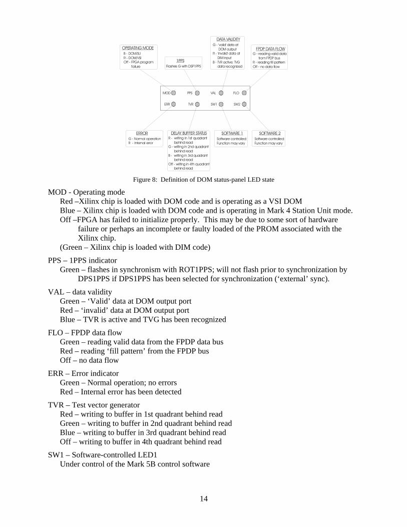
LED status display
The Mark 5B includes a LED status display at the lower-right of the front panel; the status display is made up of 8 tri-color LEDs, which are intended to convey the state of the Mark 5B at any time. Figure 8 shows a diagram of the status panel along with the meaning of each of the individual LEDs.
13
MOD PPS VAL FLO
ERR TVR SW1 SW2
OPERATING MODEB - DOM/SUR - DOM/VSIOff - FPGA program failure
1PPSFlashes G with DSP1PPS
DATA VALIDITYG - 'valid' data at DOM outputR - 'invalid' data at DIM inputB - TVR active; TVG data recognized
FPDP DATA FLOWG - reading valid data from FPDP busR - reading fill patternOff - no data flow
ERRORG - Normal operationR - Internal error
DELAY BUFFER STATUSR - writing in 1st quadrant behind readG - writing in 2nd quadrant behind readB - writing in 3rd quadrant behind readOff - writing in 4th quadrant behind read
SOFTWARE 1Software controlled:Function may vary
SOFTWARE 2Software controlled:Function may vary
Figure 8: Definition of DOM status-panel LED state
MOD - Operating mode Red –Xilinx chip is loaded with DOM code and is operating as a VSI DOM Blue – Xilinx chip is loaded with DOM code and is operating in Mark 4 Station Unit mode. Off –FPGA has failed to initialize properly. This may be due to some sort of hardware
failure or perhaps an incomplete or faulty loaded of the PROM associated with the Xilinx chip.
(Green – Xilinx chip is loaded with DIM code)
PPS – 1PPS indicator Green – flashes in synchronism with ROT1PPS; will not flash prior to synchronization by
DPS1PPS if DPS1PPS has been selected for synchronization (‘external’ sync).
VAL – data validity Green – ‘Valid’ data at DOM output port Red – ‘invalid’ data at DOM output port Blue – TVR is active and TVG has been recognized
FLO – FPDP data flow Green – reading valid data from the FPDP data bus Red – reading ‘fill pattern’ from the FPDP bus Off – no data flow
ERR – Error indicator Green – Normal operation; no errors Red – Internal error has been detected
TVR – Test vector generator Red – writing to buffer in 1st quadrant behind read Green – writing to buffer in 2nd quadrant behind read Blue – writing to buffer in 3rd quadrant behind read Off – writing to buffer in 4th quadrant behind read
SW1 – Software-controlled LED1 Under control of the Mark 5B control software
14
SW2 – Software-controlled LED2 Under control of the Mark 5B control software
5. Data format on Mark 5B disks Within each scan, the data on the SS disk are divided into equal-length ‘disk frames’ (DFs). Each DF carries a frame header of four 32-bit words followed by 2500 32-bit words of data. There is always a DF boundary at each UT second tick.
Recording starts on the first DOT second tick after a VSI-S ‘receive=start’ command is issued, so each scan always begin with a DF header. Recording stops on the first DOT second tick after a VSI-S ‘receive=stop’ command is issued.
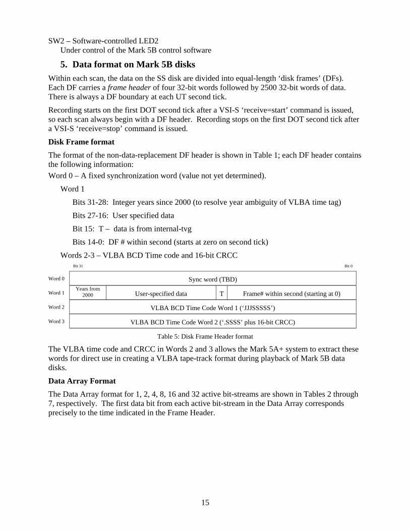
Disk Frame format The format of the non-data-replacement DF header is shown in Table 1; each DF header contains the following information: Word 0 – A fixed synchronization word (value not yet determined).
Word 1
Bits 31-28: Integer years since 2000 (to resolve year ambiguity of VLBA time tag)
Bits 27-16: User specified data
Bit 15: T – data is from internal-tvg
Bits 14-0: DF # within second (starts at zero on second tick)
Words 2-3 – VLBA BCD Time code and 16-bit CRCC Bit 31 Bit 0
Word 0 Sync word (TBD)
Word 1 Years from
2000 User-specified data T Frame# within second (starting at 0)
Word 2 VLBA BCD Time Code Word 1 (‘JJJSSSSS’)
Word 3 VLBA BCD Time Code Word 2 (‘.SSSS’ plus 16-bit CRCC)
Table 5: Disk Frame Header format
The VLBA time code and CRCC in Words 2 and 3 allows the Mark 5A+ system to extract these words for direct use in creating a VLBA tape-track format during playback of Mark 5B data disks.
Data Array Format The Data Array format for 1, 2, 4, 8, 16 and 32 active bit-streams are shown in Tables 2 through 7, respectively. The first data bit from each active bit-stream in the Data Array corresponds precisely to the time indicated in the Frame Header.
15
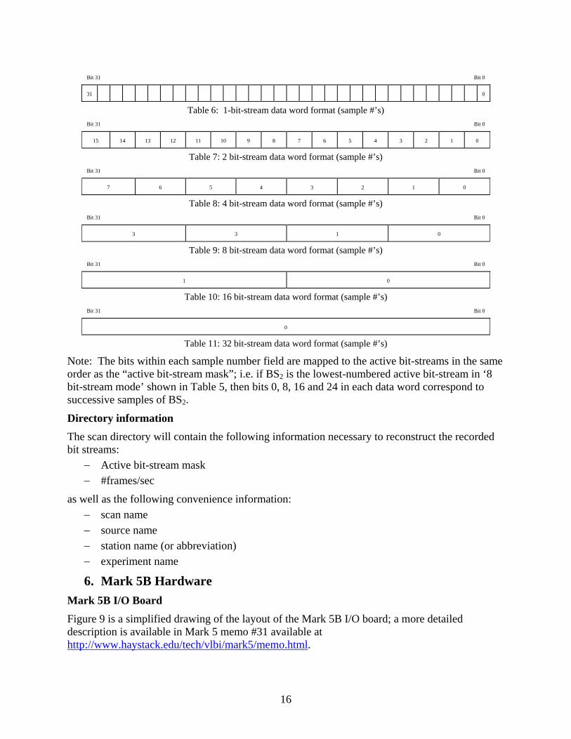
Bit 31 Bit 0
31 0
Table 6: 1-bit-stream data word format (sample #’s) Bit 31 Bit 0
15 14 13 12 11 10 9 8 7 6 5 4 3 2 1 0
Table 7: 2 bit-stream data word format (sample #’s) Bit 31 Bit 0
7 6 5 4 3 2 1 0
Table 8: 4 bit-stream data word format (sample #’s) Bit 31 Bit 0
3 3 1 0
Table 9: 8 bit-stream data word format (sample #’s) Bit 31 Bit 0
1 0
Table 10: 16 bit-stream data word format (sample #’s) Bit 31 Bit 0
0
Table 11: 32 bit-stream data word format (sample #’s)
Note: The bits within each sample number field are mapped to the active bit-streams in the same order as the “active bit-stream mask”; i.e. if BS2 is the lowest-numbered active bit-stream in ‘8 bit-stream mode’ shown in Table 5, then bits 0, 8, 16 and 24 in each data word correspond to successive samples of BS2.
Directory information The scan directory will contain the following information necessary to reconstruct the recorded bit streams:
− Active bit-stream mask − #frames/sec
as well as the following convenience information: − scan name − source name − station name (or abbreviation) − experiment name
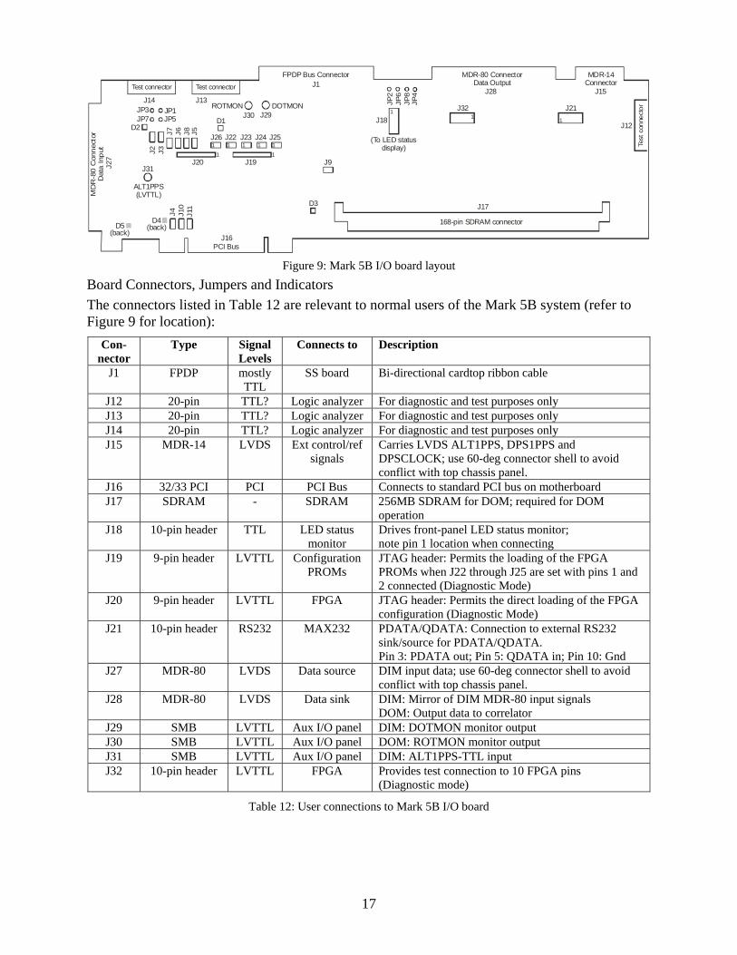
6. Mark 5B Hardware Mark 5B I/O Board Figure 9 is a simplified drawing of the layout of the Mark 5B I/O board; a more detailed description is available in Mark 5 memo #31 available at http://www.haystack.edu/tech/vlbi/mark5/memo.html.
16
J26
J18
J9
J29J30
J4
J1
J16PCI Bus
FPDP Bus Connector
J13J14
J10
J11
J31
J22 J23 J24 J25J7 J6 J8 J5
J2 J3J20 J19
JP1JP5JP7
JP3
JP2
JP6
JP8
JP4
MDR-80 ConnectorData Output
MDR-14Connector
MD
R-8
0 C
onne
ctor
Dat
a In
put
J28 J15
J12
J32 J21
Test connector Test connector
Test
con
nect
or
J17
J27
168-pin SDRAM connector
D2D1
11 1
(To LED statusdisplay)
DOTMONROTMON
ALT1PPS(LVTTL)
1 1 1 1 1
1 1
D3
D5D4
(back)(back)
Figure 9: Mark 5B I/O board layout
Board Connectors, Jumpers and Indicators The connectors listed in Table 12 are relevant to normal users of the Mark 5B system (refer to Figure 9 for location):
Con- nector
Type Signal Levels
Connects to Description
J1 FPDP mostly TTL
SS board Bi-directional cardtop ribbon cable
J12 20-pin TTL? Logic analyzer For diagnostic and test purposes only J13 20-pin TTL? Logic analyzer For diagnostic and test purposes only J14 20-pin TTL? Logic analyzer For diagnostic and test purposes only J15 MDR-14 LVDS Ext control/ref
signals Carries LVDS ALT1PPS, DPS1PPS and DPSCLOCK; use 60-deg connector shell to avoid conflict with top chassis panel.
J16 32/33 PCI PCI PCI Bus Connects to standard PCI bus on motherboard J17 SDRAM - SDRAM 256MB SDRAM for DOM; required for DOM
operation J18 10-pin header TTL LED status
monitor Drives front-panel LED status monitor; note pin 1 location when connecting
J19 9-pin header LVTTL Configuration PROMs
JTAG header: Permits the loading of the FPGA PROMs when J22 through J25 are set with pins 1 and 2 connected (Diagnostic Mode)
J20 9-pin header LVTTL FPGA JTAG header: Permits the direct loading of the FPGA configuration (Diagnostic Mode)
J21 10-pin header RS232 MAX232 PDATA/QDATA: Connection to external RS232 sink/source for PDATA/QDATA. Pin 3: PDATA out; Pin 5: QDATA in; Pin 10: Gnd
J27 MDR-80 LVDS Data source DIM input data; use 60-deg connector shell to avoid conflict with top chassis panel.
J28 MDR-80 LVDS Data sink DIM: Mirror of DIM MDR-80 input signals DOM: Output data to correlator
J29 SMB LVTTL Aux I/O panel DIM: DOTMON monitor output J30 SMB LVTTL Aux I/O panel DOM: ROTMON monitor output J31 SMB LVTTL Aux I/O panel DIM: ALT1PPS-TTL input J32 10-pin header LVTTL FPGA Provides test connection to 10 FPGA pins
(Diagnostic mode)
Table 12: User connections to Mark 5B I/O board
17
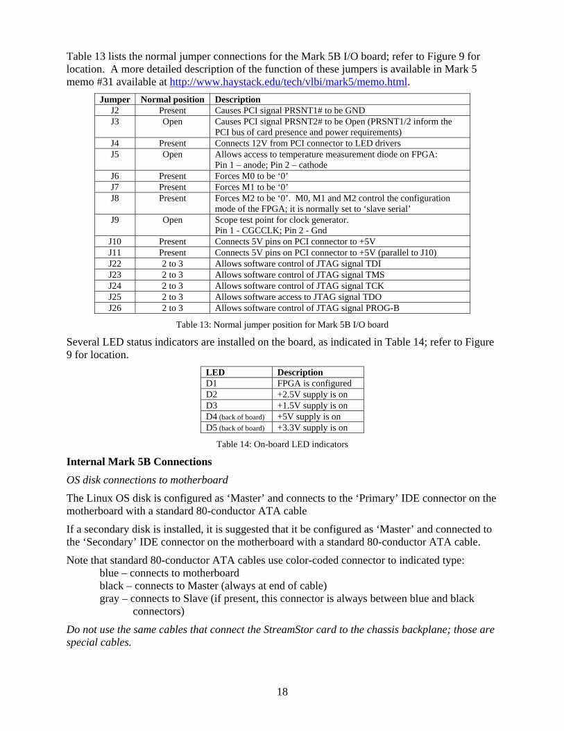
Table 13 lists the normal jumper connections for the Mark 5B I/O board; refer to Figure 9 for location. A more detailed description of the function of these jumpers is available in Mark 5 memo #31 available at http://www.haystack.edu/tech/vlbi/mark5/memo.html.
Jumper Normal position Description J2 Present Causes PCI signal PRSNT1# to be GND J3 Open Causes PCI signal PRSNT2# to be Open (PRSNT1/2 inform the
PCI bus of card presence and power requirements) J4 Present Connects 12V from PCI connector to LED drivers J5 Open Allows access to temperature measurement diode on FPGA:
Pin 1 – anode; Pin 2 – cathode J6 Present Forces M0 to be ‘0’ J7 Present Forces M1 to be ‘0’ J8 Present Forces M2 to be ‘0’. M0, M1 and M2 control the configuration
mode of the FPGA; it is normally set to ‘slave serial’ J9 Open Scope test point for clock generator.
Pin 1 - CGCCLK; Pin 2 - Gnd J10 Present Connects 5V pins on PCI connector to +5V J11 Present Connects 5V pins on PCI connector to +5V (parallel to J10) J22 2 to 3 Allows software control of JTAG signal TDI J23 2 to 3 Allows software control of JTAG signal TMS J24 2 to 3 Allows software control of JTAG signal TCK J25 2 to 3 Allows software access to JTAG signal TDO J26 2 to 3 Allows software control of JTAG signal PROG-B
Table 13: Normal jumper position for Mark 5B I/O board
Several LED status indicators are installed on the board, as indicated in Table 14; refer to Figure 9 for location.
LED Description D1 FPGA is configured D2 +2.5V supply is on D3 +1.5V supply is on D4 (back of board) +5V supply is on D5 (back of board) +3.3V supply is on
Table 14: On-board LED indicators
Internal Mark 5B Connections
OS disk connections to motherboard
The Linux OS disk is configured as ‘Master’ and connects to the ‘Primary’ IDE connector on the motherboard with a standard 80-conductor ATA cable
If a secondary disk is installed, it is suggested that it be configured as ‘Master’ and connected to the ‘Secondary’ IDE connector on the motherboard with a standard 80-conductor ATA cable.
Note that standard 80-conductor ATA cables use color-coded connector to indicated type: blue – connects to motherboard black – connects to Master (always at end of cable) gray – connects to Slave (if present, this connector is always between blue and black
connectors)
Do not use the same cables that connect the StreamStor card to the chassis backplane; those are special cables.
18
Card placement
The StreamStor card is normally plugged into the first 64-bit PCI slot (leftmost as viewed from the rear of the chassis). The Mark 5B I/O board is normally plugged into the first 32-bit PCI slot, which is separated from the SS card by two slot positions (due to the many cables coming from the StreamStor card, they cannot be in adjacent slots).
FPDP Bus
An 80-conductor FPDP cardtop-bus cable is connected between the StreamStor card and the I/O card.
Mark 5B I/O Extender
A convenience rear-panel I/O extender is available for the Mark 5B which brings I/O board connections to the rear panel on SMA connectors:
ALT1PPS – alternate input external 1PPS signal (TTL) for synchronizing the DOT clock 1pps (DIM personality only).
DOTMON – monitor connection (TTL) for DOT clock 1pps signal (DIM personality only).
ROTMON – monitor connection (TTL) for ROT clock ‘1pps’ signal (DOM personality only).
The extender has three attached cables which connect to the corresponding SMB connectors on the Mark 5B I/O board (see Figure 9)
Mark 5B front-panel status display
The Mark 5B front-panel LED status display connects to J18 on the Mark 5B I/O board (see Figure 9) via a 10-conductor flat-ribbon cable. Take care to orient the connector correctly for pin 1.
Chassis-backplane connections
Figure 10 shows the connections on the chassis backplane. Please refer to this figure in the following discussion.
J14 J15J16
J19
J12 J13
J17
J18
J11
J5 J6 J7 J8 J1 J2 J3 J4
Left
Right
Fan
Fan
Fan
Power
+12V+12V+12V
+5VGNDGNDGNDGND
1 1 1 1 1 1 1 1
4 5 6 7 0 1 2 3Corresponding StreamStor connectors
Figure 10: Chassis backplane connectors (as viewed from rear of chassis)
StreamStor card connections
There are eight 80-conductor cables connecting the StreamStor to the chassis backplane. Though these are ATA bus cables, they are special cables with black connectors on each end. They are connected as shown in Figure 10 and Table 15.
19
Chassis backplane connectors (in order, L-to-R, as viewed from rear of chassis)
J5 J6 J7 J8 J1 J2 J3 J4
StreamStor connectors (0 to 7, top to bottom, respectively) 4 5 6 7 0 1 2 3
Table 15: Connections from Chassis Backplane to StreamStor card
Power connections
Power connections from the chassis power supply to the chassis backplane are made via an 8-pin connector on the chassis backplane. Figure 10 shows the connections. Important: Cut off the standard plugs on the power supply wires and connect the wires directly to the chassis-backplane power connector.
Front-panel bank-status LED connections The cables from the Bank A (left) and Bank B (right) LED’s connect to J17 and J18 (Figure 10), respectively.
Fan connections
Fan connectors J14, J15 and J16 (see Figure 10) provide power to sets of fans. The fan connectors are all identical; by convention, the following connections are made:
J14 Dual fans under disk Bank A (left) J16 Dual fans under disk Bank B (right) J15 Fan behind system disk
Front-Panel Controls and Indicators Please refer to the front-panel diagram in Figure 11 for the following discussion.
Locked Power ReadySelected Locked Power ReadySelected
Bank A Bank B
Power
Reset
(LED Status Display)
(CD
Drive or R
emovable H
ard Disk)
0/1
2/3
4/5
6/7
0/1
2/3
4/5
6/7
Figure 11: Mark 5B Front Panel Layout
Power and Reset Switches and LED’s
The POWER switch applies power to the unit, illuminating the corresponding LED. If the POWER switch is held depressed for several seconds while power is already applied, power will be shut off.
The RESET switch applies a reset to the motherboard, which causes it to re-boot.
20
Disk-Bank Switches and LED’s
Associated with each disk bank is one keyswitch and four LED’s. When operating in ‘bank mode’ these function as explained in Table 16:
Keyswitch When moved to ‘locked’ position, physically locks the module into place and initiates mounting process; no attempt should be made to remove the module when the keyswitch is in the ‘locked’ position. When moved to ‘unlock’ position, physically unlocks module and initiates module power-down and dismount; under no circumstances should the keyswitch be moved to the ‘unlock’ position while the module is actively recording or playing. The module must not be physically removed until power is removed (‘Power’ LED is off).
‘Locked’ LED (green) Indicates keyswitch is in ‘locked’ position
‘Power’ LED (green) Indicates power is applied to module; power is applied sequentially to four disks at a time to reduce load on the power supply.
‘Ready’ LED (green) Steady ‘on’ Indicates the module has been successfully initialized and all drives are ready. Flashing indicates module is not available for recording (module is full, protected, or bad drive is detected).
‘Selected’ LED (red) Indicates module is selected as ‘active’ module – DO NOT TOUCH!
Table 16: Disk bank switches and indicators when operating in ‘bank mode’
Note: On some early chassis, the LED’s are marked ‘Power’ ‘Ready’ ‘Selected’ and ‘Full’. They must be re-labeled to correspond to Table 16, namely ‘Locked’ ‘Power’ ‘Ready’ and ‘Selected’.
Some systems have been modified by users to add two additional LED’s to the left of each group of four LED’s. These two LED’s are connected directly to +5V power on each set of four disks in the module and directly show that power is applied.
Chassis-Backplane Power-Indicator LED’s
When a module bank is empty, two LED’s are visible on the chassis backplane (into which the module plugs). These LED’s indicate that +5V and +12V are applied to the module and should never be illuminated when no module is present. If either of these LED’s is ‘on’ for any reason, do not insert a module.
Disk-Module LED’s
Each disk module has four LED’s, each LED indicates disk activity on the corresponding Master/Slave disk pair. ‘0/1’ corresponds to the first and second disks from the front of the module; ‘6/7’ corresponds to the rearmost pair of disks.
LED Status Display
Detailed status information is shown on this display with 8 tri-colored LEDs.
External DIM connections
DIM connections
The typical connections to a Mark 5B DIM are shown in Figure 12. Only one of the external 1pps sources would normally be connected (1PPS, ALT1PPS-LVTTL, or ALT1PPS-LVDS) and used to synchronize the DOT clock. The VSI bit-stream, CLOCK and 1PPS signals are re-generated and sent to the VSI MDR-80 output connector on the Mark 5B I/O card for use in
21
daisy-chaining VSI recording systems (could be another Mark 5B). Please see Appendix A for VSI bit-stream conventions and definitions.
ALT1PPS (LVDS)
ALT1PPS (LVTTL)
BS32
CLOCK1PPS
PDATA
BS32
CLOCK1PPS
MDR-80IN
MDR-14
SMA
MDR-80OUT
Mark 5B
Ethernetcontrol
Figure 12: External connections to Mark 5B DIM
External DOM connections Figure 13 shows the normal connections to the Mark 5B DOM at the Mark 4 correlators; connections to other correlators will be similar.
Mark 5BCorrelatorInterface
Board(CIB)
CorrelatorInput Board
TSPU
DPSCLK
DPS1PPSSerial link
Serial link
Serial link
MD
R-1
4
RBS 32QVALIDBOCFRCLK
MD
R-8
0
Ethernetcontrol
Figure 13: Mark 5B DOM connection to Mark 4 correlator
VSI cable-length restrictions The Mark 5B has been successfully tested at 64 MHz clock rate with an MDR-80 signal-cable length of 5m. Cables longer than 5m have not been tested and should be used with caution.
7. Mark 5B Software Support Operating System Each Mark 5 system is normally shipped with a full installation of Red Hat Linux and the current version of Mark 5 software. However, each Mark 5 must be configured with an IP address and domain name supplied by your system administrator. In some cases, this information may have been provided before shipping, in which case the system may already be pre-configured. A convention has been adopted to assign Mark 5 system names in the format ‘mark5-xx’ where ‘xx’ is the serial number of the particular Mark 5 unit; it is preferable if you can maintain that name as it helps to keep track of the Mark 5 systems and their configurations. Instructions for local network, time-zone and ntp configuration is available at http://web.haystack.mit.edu/mark5/software.html.
Mark 5B Software
The Mark 5B is normally controlled by a program called dimino, which may be downloaded and installed with a simple procedure. Detailed information installing and updating the dimino software is available at http://web.haystack.mit.edu/mark5/software.html. For best operation of the Mark 5B system, it is recommended that dimino be regularly updated.
22
8. Changing Personality Between DIM and DOM
The Mark 5B system may be configured to be either a DIM or a DOM (but not both at the same time) by downloading the appropriate Xilinx configuration code to the Mark 5B I/O Interface Board. The only hardware difference is that the SDRAM memory card is optional in the DIM configuration; the SDRAM card is required in the DOM configuration.
A standalone utility program called ‘XSVF’, included with the Mark 5B tarball, is used to download the DIM or DOM personality file to an on-board PROM which is used to configure the Xilinx chip on power-up or reset. The calling sequence for XSVF is
XSVF –m0 –f <filename>
The filenames are of the form ‘DIMREVxx.xsvf’ for DIM personality files and ‘DOMREVxx.xsvf’ for DOM personality files, where ‘xx’ is the hex firmware revision code read from bits 0-7 of register E on the Mark 5B board and reported by dimino by a ‘DTS_id?’ query. The xsvf files for the DIM and DOM are available at the Mark 5B website.
9. Utility and Test Programs tstdimino <machine> - where <machine> is the target Mark 5B system (defaults to localhost).
dimino must be running on <machine>. tstdimino accepts manually entered Mark 5B commands and queries.
ssopen – initializes StreamStor card and mounted disks (from Conduant)
sstest – erases disks and writes a small (~30 MB) amount of ‘StreamStor test data’ to the disks from main memory. Reported as ‘SS’ on data_check, track_check and scan_check queries. (From Conduant)
SSReset – standalone StreamStor reset program. dimino must not be running
SSErase – standalone disk-erase and disk-conditioning program. dimino must not be running.
DirList – reads the Mark 5B data directory and list the contents.
Net2file <filename> – accepts a connection from a Mark 5B machine and write the received data to <filename>.
File2Net <machine> [<filename> [<startbyte> [<endbyte>]]] – sends a file or part of a file to the Mark 5B disks.
XSVF –m0 –f <filename> - loads PROM with DIM or DIM Xilinx code (see previous section)
For more detailed information on auxiliary and test programs please see http://web.haystack.mit.edu/mark5/software.html.
10. Operating the Mark 5B System System Boot Booting will take place automatically when power is turned on. The first time you boot the Mark 5B it is recommended that you attached a monitor and keyboard so that you can observe that it is booting properly. No intervention from the keyboard should be necessary during the boot process; if keyboard intervention is necessary, it may not be possible to boot the system ‘headless’ (without monitor or keyboard), which is often the standard mode of operation. If you need help, please contact Richard Crowley at Haystack ([email protected]).
23

If the system boots into X-windows, you must force a normal Linux prompt with <Cntl><Alt><F1>.
Using dimino The main Mark 5B DIM control program is called dimino, which must be started before the system will respond to normal Mark 5B commands. dimino may be started either locally or remotely through a terminal session.
1. Login name: oper
Login password: ------
Contact Richard Crowley ([email protected]) for a password, if needed.
2. Issue ‘script –f [filename]’ if you wish to retain a record of your session ( use ‘-af’ to append to current file). Default file name is ‘typescript’ in the default directory.
3. If this is your first time starting up a new system, the following steps are recommended. Once the system is known to operate properly, this step may be skipped:
a. Run ‘ssopen’ This initializes the StreamStor (may take 10 or so seconds). If successful, ‘StreamStor opened successfully’ will be reported.
b. If ‘ssopen’ fails, try ‘SSReset’ to reset the StreamStor card; then try ‘ssopen’ again.
4. Start dimino, which is the primary control program for the Mark 5B DIM system:
‘dimino –m [-1|0|1|2|3] –f [0|1] –s [1|2|3|4|5|6|7] &’ (defaults underlined) where
m – message level (range –1 to 3, default 1) -1 A vast quantity of debug 0 Some debug 1 Normal operation; warnings and errors 2 Only errors and operational messages 3 Only fatal errors when the program dies
f – parsing mode (0–‘informal’ syntax; 1–formal VSI-S syntaxError! Bookmark not
defined.; default 1)
s – maximum number of allowed socket connections (range 1 to 7; default 7)
& - runs dimino in backgroundError! Bookmark not defined.
5. Run ‘tstdimino’ tstdimino is small standalone program4 with a simple operator interface that allows commands to be sent and responses to be received from dimino. It provides the operator with a convenient ‘>’ prompt and accepts the normal Mark 5 commands, but does not require the normal termination semi-colons required by VSI syntax. You may type any
4 ‘tstdimino’ can be run on the same computer as dimino or on a different computer such as ccc. It connects to an m5drive tcp socket on a prescribed computer with dimino running, accepts dimino commands typed into the controlling terminal, sends these through the socket to dimino, and prints replies from dimino as read from the socket. The socket configuration in ‘tstdimino.c’ can be used as a model for other programs that connect to dimino’s socket.
24
command or query from Mark 5B command set (http://web.haystack.mit.edu/mark5/software.html)
Type ‘status?;’ to query system status. Return should be ‘!status?=0:0x001;’ (0x001 indicates ‘ready’ status)
Important: Determine software version Type ‘DTS_id’?;’. Return should be something like ’!DTS_id? 0 : Mark5BDIM : 2003y044d20h : 1 : mark4-18 : 1 : 1 : 2.4 : 1 : 1;’ The value ‘2.4’ in this example specifies the revision level of the command set that corresponds to this particular version of dimino control software5; this value is updated at each new command set update.
6. Program Shutdown: To end ‘tstdimino’, type <Ctrl C>. This should bring you back to a system prompt. Then, to end dimino, type ‘Enddim’. Do not use just <Ctrl C> to try to end dimino because this sends interrupts to all threads and may create confusion.
7. System Shutdown: From a local console, enter ‘halt’; system will halt but power will not shutdown. From a local or remote console issue ‘su’ to become root, then use the normal Linux shutdown ‘/sbin/shutdown –h now’; system will be halted and powered down. Root password will be supplied on phone or e-mail request.
Mark 5B Control Syntax The Mark 5B command and query syntax is based on the VSI-S syntax6, which is worthwhile becoming acquainted with if you wish to directly exercise the Mark 5B system through its command set. A summary of this syntax is given in the ‘Mark 5B command set’ (available at http://web.haystack.mit.edu/mark5/software.html.
Getting Started – Some Basic Commands We briefly describe here some commonly-used commands and queries in normal Mark 5B operation. For complete details of all Mark 5B commands, refer to the memo ‘Mark 5B command set’ (available at http://web.haystack.mit.edu/mark5/software.html).
Set and check DOT clock
clock_set=<clk freq in MHz>; Specify clock freq
1pps_source=<1pps source>; Specify source for external 1pps tick
dot_set=<time>; Set DOT clock to specified time
dot?; Check DOT time
5 Software versions earlier than 2.4 do not return this command-set revision level; for these earlier versions, the date returned by the ‘DTS_id’ query (‘2003y044d20h’ in the example) must be compared with release dates in the Mark 5B software update file (http://fourier.haystack.edu/Mark5/UpdateMark5.html). Earlier versions of the command set are available in the Mark 5 memo series at http://web.haystack.mit.edu/mark5/software.html. It is the users responsibility to keep the Mark 5B control software up-to-date. 6 The full VSI-S specification is available at http://web.haystack.edu/vsi/index.html. The Mark 5B implement using many VSI-S commands, but is not fully VSI-S compliant.
25
Select active bank
bank_set=A; Select bank A as active bank (assumes Bank A is ready)
bank_set=B; Select bank B as active bank (assumes Bank B is ready)
bank_set=inc; ‘Increment’ active bank (switches to alternate bank)
Show disk serial numbers in module
disk_serial?; Returns serial numbers of all mounted disks
Erase all disks in module
reset=erase; Erases all data on the mounted disks.
Set data mode
mode=<data source>:<bit-stream mask>:<decimation ratio>; (example: ‘mode= ext : 0xffffffff : 2’)
Record data
record=on:<scan name>:<experiment name>:<station code>;
Starts recording from end of last recorded scan beginning on the next second tick. The assigned scan name is stored in a directory on the disk module. Recording mode is controlled by the mode command.
record=off; Stop recording
record?;
Returns <recording status>, <scan number>, <scan name>
Quick scan check
scan_set=<scan_name>;
Sets the scan pointer (and play pointer) to the beginning of the named scan (defaults to last-recorded scan).
scan_set?;
Returns <scan number>, <scan name>, <start byte#>, <end byte#>
scan_check?; This is probably the most useful general check for a recorded scan. To use it, first point to the scan of interest with the command ‘scan_set=<scan_name>;’. Then issue the ‘scan_check?;’ query, which will sample data near both the beginning and end of the scan and return such information as data mode, data type, scan start time, scan length, and data rate. By examining time tags at the beginning and end of the scan and counting the number of bytes in between, it also determines whether there are any missing or extra bytes in the recorded data.
Get system status
status?;
Returns system status as a hex number. Useful for diagnostic purposes, but you must decode the bits - see ‘Mark 5B command set’ memo for details’.
26
Examples of some simple procedures In this section are a few examples of simple procedures you can try. Consult the appropriate Mark 5B command set document for detailed explanations.
5.5.1 Get system and disk information
DTS_id?; Get system information
disk_serial?; Get disk serial numbers
disk_size?; Get disk sizes (bytes)
status?; Get current system status
5.5.2 Record two successive scans
mode=ext:0xffffffff:2;; Record ext (i.e. VSI) data with bit-stream mask 0xffffffff and decimation ratio of 2
record=on:testscan1:exp123:ef; Start recording; assign scan name ‘testscan1’ experiment exp123, station ef
record=off; Stop recording
scan_check?; Do cursory check on just-recorded data
record=on:testscan2:exp123:ef; Start recording; assign scan name ‘testscan2’
record=off; Stop recording
scan_check?; Do cursory check on just-recorded data
5.5.3 Check recorded scans
scan_set=testscan1; Select ‘testscan1’
scan_check?; Do cursory check on recorded data
scan_set=inc; Increment to next scan (‘testscan2’)
scan_check?; Do cursory check on recorded data
Bank management procedures
Each Mark 5B system support two ‘banks’, labeled ‘Bank A’ and ‘Bank B’. Only a single bank may be ‘active’ at a single time, as indicated by the ‘Selected’ LED above each bank. All commands issued to the Mark 5B are focused only on the active bank with the exception only of the ‘bank_set’ command, which selects the active bank, and the ‘bank_switch’ command (NYI), which manages optional automatic bank-switching. The following rules apply to operation of the module banks:
1. The control program dimino may be started with any combination of modules present and ‘Locked’ (none, A, B, or both). The modules will be initialized; ‘A’ will be ‘Selected’ if present and ‘Ready’, otherwise ‘B’ will be ‘Selected’ if present and ‘Ready’. If no modules are present, none will be ‘Selected’; in this case, the first module to be inserted and ‘Locked’ will be made ‘Ready’ and ‘Selected’.
2. A keyswitch should be turned to the ‘Locked’ position only if a module is present in the associated bank. Turning the keyswitch to the ‘Locked’ position will cause the module to be powered, initialized and made ‘Ready’; however, the module will be ‘Selected’ only if
27
another module is not already ‘Selected’. When the keyswitch is turned to the ‘Locked’ position, the following should be observed on the LED’s associated with that module:
a. ‘Locked’ and ‘Power’ LED’s will illuminate quickly; all ‘activity’ LED’s on module will illuminate (for all buses with installed disks).
b. ‘Activity’ LED’s will extinguish one-by-one from top to bottom; this should progress smoothly and take no more than a few seconds. If this process stalls or significantly hestitates, there may be a problem with the disk pack.
c. The ‘Ready’ LED illuminates; this signifies the module is ready to be used.
d. If the other module is not already ‘Selected’, the ‘Selected’ LED will illuminate and the module is made active; otherwise it sits ready to be activated.
3. A keyswitch should never be turned to the ‘unlocked’ position when the associated module is actively recording or playing; data may be lost or corrupted.
4. An inserted module in the ‘unlocked’ state is not recognized by the system.
5. No attempt should be made to remove a module unless the associated keyswitch is unlocked and the ‘Power’ LED is extinguished.
6. Only one bank may be ‘Selected’ at any one time.
7. If both ‘A’ and ‘B’ are both present, ‘Ready’, and quiescent (i.e. not recording or playing), the ‘bank_set’ command may be used to change the active (‘Selected’) bank. A ‘bank_set=inc’ command will switch to the alternate bank.
8. If a module fails to come ‘Ready’ after more than ~15 seconds, unlock the keyswitch, wait ~10 seconds, and try again.
9. Recording on the ‘Selected’ module will always append to any existing recording.
10. A ‘reset=erase’ command will erase all data on the ‘Selected’ module.
11. A ‘reset=erase_last_scan’ command will erase the last recorded scan on the ‘Selected module. This command may be issued repeatedly to erase multiple scans.
12. Do not attempt to use the ‘reset=mount’ or ‘reset=dismount’ commands (these commands will soon be completely eliminated). All mount and dismount operations are controlled by the keyswitches.
28
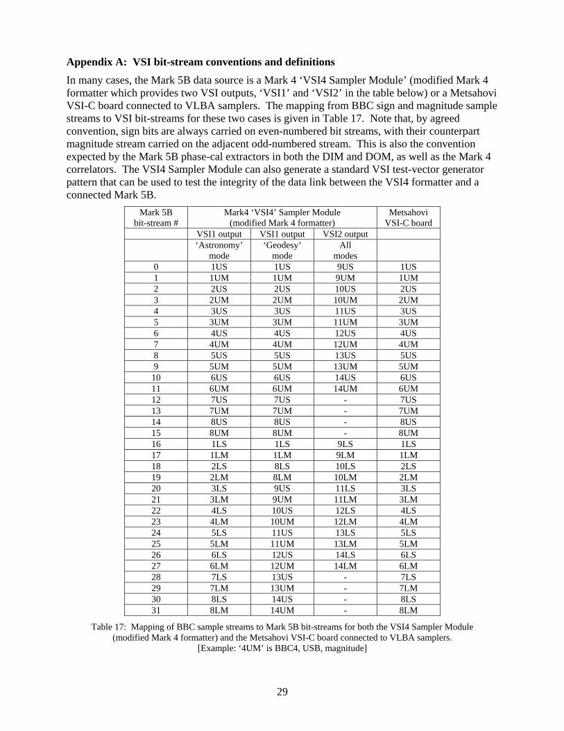
Appendix A: VSI bit-stream conventions and definitions In many cases, the Mark 5B data source is a Mark 4 ‘VSI4 Sampler Module’ (modified Mark 4 formatter which provides two VSI outputs, ‘VSI1’ and ‘VSI2’ in the table below) or a Metsahovi VSI-C board connected to VLBA samplers. The mapping from BBC sign and magnitude sample streams to VSI bit-streams for these two cases is given in Table 17. Note that, by agreed convention, sign bits are always carried on even-numbered bit streams, with their counterpart magnitude stream carried on the adjacent odd-numbered stream. This is also the convention expected by the Mark 5B phase-cal extractors in both the DIM and DOM, as well as the Mark 4 correlators. The VSI4 Sampler Module can also generate a standard VSI test-vector generator pattern that can be used to test the integrity of the data link between the VSI4 formatter and a connected Mark 5B.
Mark 5B bit-stream #
Mark4 ‘VSI4’ Sampler Module (modified Mark 4 formatter)
Metsahovi VSI-C board
VSI1 output VSI1 output VSI2 output ‘Astronomy’
mode ‘Geodesy’
mode All
modes
0 1US 1US 9US 1US 1 1UM 1UM 9UM 1UM 2 2US 2US 10US 2US 3 2UM 2UM 10UM 2UM 4 3US 3US 11US 3US 5 3UM 3UM 11UM 3UM 6 4US 4US 12US 4US 7 4UM 4UM 12UM 4UM 8 5US 5US 13US 5US 9 5UM 5UM 13UM 5UM
10 6US 6US 14US 6US 11 6UM 6UM 14UM 6UM 12 7US 7US - 7US 13 7UM 7UM - 7UM 14 8US 8US - 8US 15 8UM 8UM - 8UM 16 1LS 1LS 9LS 1LS 17 1LM 1LM 9LM 1LM 18 2LS 8LS 10LS 2LS 19 2LM 8LM 10LM 2LM 20 3LS 9US 11LS 3LS 21 3LM 9UM 11LM 3LM 22 4LS 10US 12LS 4LS 23 4LM 10UM 12LM 4LM 24 5LS 11US 13LS 5LS 25 5LM 11UM 13LM 5LM 26 6LS 12US 14LS 6LS 27 6LM 12UM 14LM 6LM 28 7LS 13US - 7LS 29 7LM 13UM - 7LM 30 8LS 14US - 8LS 31 8LM 14UM - 8LM
Table 17: Mapping of BBC sample streams to Mark 5B bit-streams for both the VSI4 Sampler Module (modified Mark 4 formatter) and the Metsahovi VSI-C board connected to VLBA samplers.
[Example: ‘4UM’ is BBC4, USB, magnitude]
29