Embed Size (px)
Citation preview
M44C260/M48C260
Rev. A2, 01-Oct-98 1 (51)
MARC4 – 4-bit Microcontroller
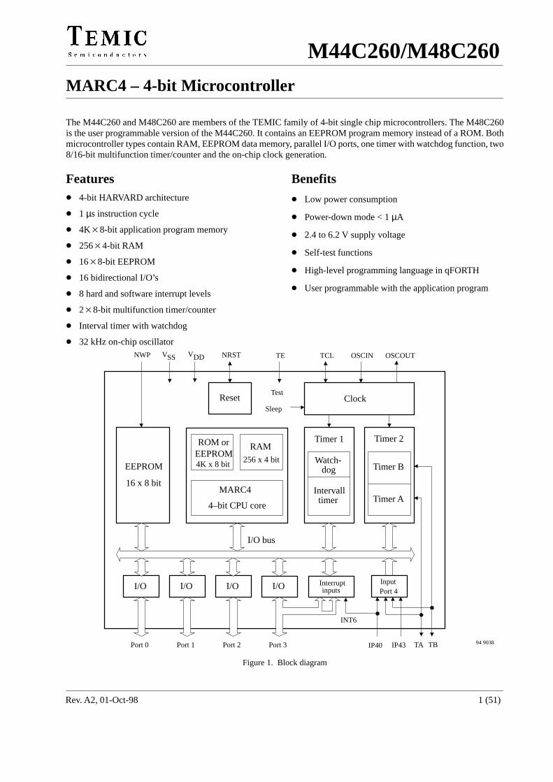
The M44C260 and M48C260 are members of the TEMIC family of 4-bit single chip microcontrollers. The M48C260is the user programmable version of the M44C260. It contains an EEPROM program memory instead of a ROM. Bothmicrocontroller types contain RAM, EEPROM data memory, parallel I/O ports, one timer with watchdog function, two8/16-bit multifunction timer/counter and the on-chip clock generation.
Features 4-bit HARVARD architecture
1 µs instruction cycle
4K8-bit application program memory
2564-bit RAM
168-bit EEPROM
16 bidirectional I/O’s
8 hard and software interrupt levels
28-bit multifunction timer/counter
Interval timer with watchdog
32 kHz on-chip oscillator
Benefits
Low power consumption
Power-down mode < 1 µA
2.4 to 6.2 V supply voltage
Self-test functions
High-level programming language in qFORTH
User programmable with the application program
MARC4
Interrupt inputs
Clock
Timer 2Timer 1
EEPROM
Timer AIntervall timer
Timer B
Reset
TE TCL
Port 0 Port 1 Port 2 Port 3
InputPort 4
OSCIN OSCOUT
TA TB
16 x 8 bit
I/O bus
EEPROMRAM
4–bit CPU core
4K x 8 bit 256 x 4 bit Watch- dog
I/O I/O I/O I/O
INT6
Test
Sleep
NWP NRST
IP40 IP43
VDDVSS
94 9038
ROM or
Figure 1. Block diagram
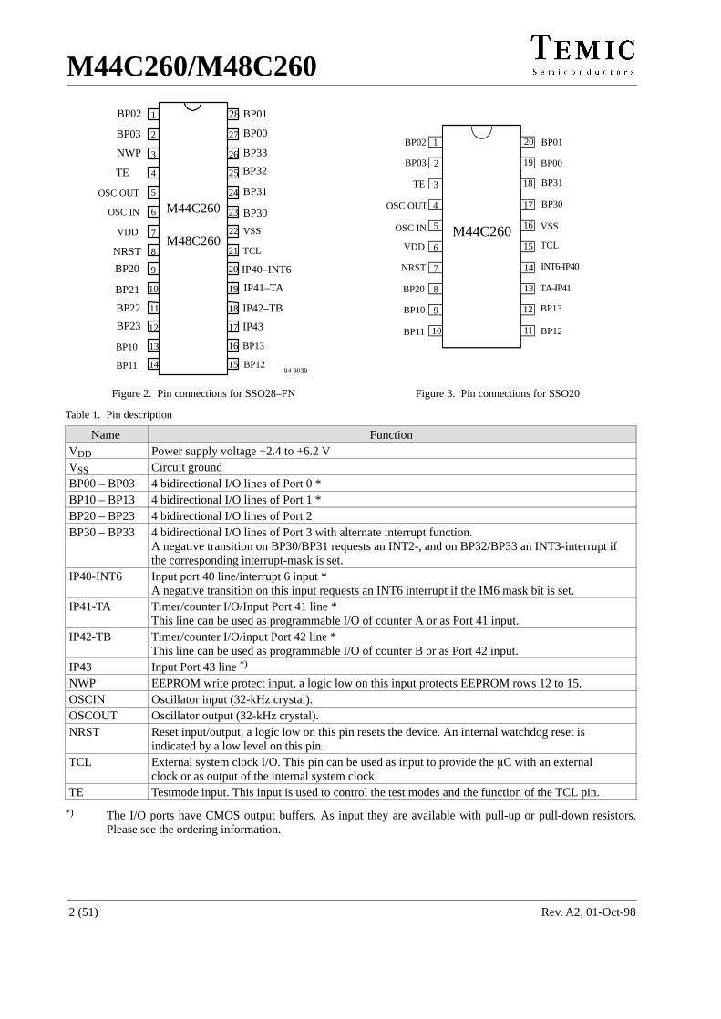
M44C260/M48C260
Rev. A2, 01-Oct-982 (51)
1
2
3
4
5
6
7
8
9
10
11
12
13
14 15
16
17
18
19
20
21
23
24
IP40–INT6
BP00
BP01BP02
BP03
BP13
BP12BP11
BP10
TCL
VSS
OSC IN
OSC OUT
VDD
BP33
22
25
26
27
28
BP30
BP31
BP32
NWP
TE
NRST
BP20
BP21
BP22
BP23
IP41–TA
M48C260
IP43
IP42–TB
94 9039
M44C260
Figure 2. Pin connections for SSO28–FN
INT6–IP40
BP03
BP02 BP01
BP00
BP13
BP12BP11
BP10
NRST
TCL
BP20
TE
VSSOSC IN
OSC OUT
VDD
BP31
BP30
TA–IP41
1
2
4
5
6
7
8
9
10
15
16
17
19
20
14
11
12
13
M44C260
3 18
Figure 3. Pin connections for SSO20
Table 1. Pin description
Name FunctionÁÁÁÁÁÁÁÁÁÁ
VDDÁÁÁÁÁÁÁÁÁÁÁÁÁÁÁÁÁÁÁÁÁÁÁÁÁÁÁÁÁÁÁÁÁÁÁÁÁÁÁÁÁÁÁÁÁÁÁÁÁÁÁÁÁÁÁÁ
Power supply voltage +2.4 to +6.2 VÁÁÁÁÁÁÁÁÁÁ
VSSÁÁÁÁÁÁÁÁÁÁÁÁÁÁÁÁÁÁÁÁÁÁÁÁÁÁÁÁÁÁÁÁÁÁÁÁÁÁÁÁÁÁÁÁÁÁÁÁÁÁÁÁÁÁÁÁ
Circuit groundÁÁÁÁÁÁÁÁÁÁ
BP00 – BP03ÁÁÁÁÁÁÁÁÁÁÁÁÁÁÁÁÁÁÁÁÁÁÁÁÁÁÁÁÁÁÁÁÁÁÁÁÁÁÁÁÁÁÁÁÁÁÁÁÁÁÁÁÁÁÁÁ
4 bidirectional I/O lines of Port 0 *ÁÁÁÁÁÁÁÁÁÁ
BP10 – BP13ÁÁÁÁÁÁÁÁÁÁÁÁÁÁÁÁÁÁÁÁÁÁÁÁÁÁÁÁÁÁÁÁÁÁÁÁÁÁÁÁÁÁÁÁÁÁÁÁÁÁÁÁÁÁÁÁ
4 bidirectional I/O lines of Port 1 *ÁÁÁÁÁÁÁÁÁÁ
BP20 – BP23ÁÁÁÁÁÁÁÁÁÁÁÁÁÁÁÁÁÁÁÁÁÁÁÁÁÁÁÁÁÁÁÁÁÁÁÁÁÁÁÁÁÁÁÁÁÁÁÁÁÁÁÁÁÁÁÁ
4 bidirectional I/O lines of Port 2
ÁÁÁÁÁÁÁÁÁÁÁÁÁÁÁ
BP30 – BP33ÁÁÁÁÁÁÁÁÁÁÁÁÁÁÁÁÁÁÁÁÁÁÁÁÁÁÁÁÁÁÁÁÁÁÁÁÁÁÁÁÁÁÁÁÁÁÁÁÁÁÁÁÁÁÁÁÁÁÁÁÁÁÁÁÁÁÁÁÁÁÁÁÁÁÁÁÁÁÁÁÁÁÁÁ
4 bidirectional I/O lines of Port 3 with alternate interrupt function.A negative transition on BP30/BP31 requests an INT2-, and on BP32/BP33 an INT3-interrupt ifthe corresponding interrupt-mask is set.
ÁÁÁÁÁÁÁÁÁÁÁÁÁÁÁ
IP40-INT6 ÁÁÁÁÁÁÁÁÁÁÁÁÁÁÁÁÁÁÁÁÁÁÁÁÁÁÁÁÁÁÁÁÁÁÁÁÁÁÁÁÁÁÁÁÁÁÁÁÁÁÁÁÁÁÁÁÁÁÁÁÁÁÁÁÁÁÁÁÁÁÁÁÁÁÁÁÁÁÁÁÁÁÁÁ
Input port 40 line/interrupt 6 input *A negative transition on this input requests an INT6 interrupt if the IM6 mask bit is set.
ÁÁÁÁÁÁÁÁÁÁ
IP41-TA ÁÁÁÁÁÁÁÁÁÁÁÁÁÁÁÁÁÁÁÁÁÁÁÁÁÁÁÁÁÁÁÁÁÁÁÁÁÁÁÁÁÁÁÁÁÁÁÁÁÁÁÁÁÁÁÁ
Timer/counter I/O/Input Port 41 line *This line can be used as programmable I/O of counter A or as Port 41 input.ÁÁÁÁÁ
ÁÁÁÁÁÁÁÁÁÁ
IP42-TBÁÁÁÁÁÁÁÁÁÁÁÁÁÁÁÁÁÁÁÁÁÁÁÁÁÁÁÁÁÁÁÁÁÁÁÁÁÁÁÁÁÁÁÁÁÁÁÁÁÁÁÁÁÁÁÁÁÁÁÁÁÁÁÁÁÁÁÁÁÁÁÁÁÁÁÁÁÁÁÁÁÁÁÁ
Timer/counter I/O/input Port 42 line *This line can be used as programmable I/O of counter B or as Port 42 input.
ÁÁÁÁÁÁÁÁÁÁ
IP43 ÁÁÁÁÁÁÁÁÁÁÁÁÁÁÁÁÁÁÁÁÁÁÁÁÁÁÁÁÁÁÁÁÁÁÁÁÁÁÁÁÁÁÁÁÁÁÁÁÁÁÁÁÁÁÁÁ
Input Port 43 line *)
ÁÁÁÁÁÁÁÁÁÁ
NWP ÁÁÁÁÁÁÁÁÁÁÁÁÁÁÁÁÁÁÁÁÁÁÁÁÁÁÁÁÁÁÁÁÁÁÁÁÁÁÁÁÁÁÁÁÁÁÁÁÁÁÁÁÁÁÁÁ
EEPROM write protect input, a logic low on this input protects EEPROM rows 12 to 15.
ÁÁÁÁÁÁÁÁÁÁ
OSCIN ÁÁÁÁÁÁÁÁÁÁÁÁÁÁÁÁÁÁÁÁÁÁÁÁÁÁÁÁÁÁÁÁÁÁÁÁÁÁÁÁÁÁÁÁÁÁÁÁÁÁÁÁÁÁÁÁ
Oscillator input (32-kHz crystal).
ÁÁÁÁÁOSCOUT ÁÁÁÁÁÁÁÁÁÁÁÁÁÁÁÁÁÁÁÁÁÁÁÁÁÁÁÁOscillator output (32-kHz crystal).ÁÁÁÁÁÁÁÁÁÁÁÁÁÁÁ
NRSTÁÁÁÁÁÁÁÁÁÁÁÁÁÁÁÁÁÁÁÁÁÁÁÁÁÁÁÁÁÁÁÁÁÁÁÁÁÁÁÁÁÁÁÁÁÁÁÁÁÁÁÁÁÁÁÁÁÁÁÁÁÁÁÁÁÁÁÁÁÁÁÁÁÁÁÁÁÁÁÁÁÁÁÁ
Reset input/output, a logic low on this pin resets the device. An internal watchdog reset is indicated by a low level on this pin.
ÁÁÁÁÁÁÁÁÁÁÁÁÁÁÁ
TCL ÁÁÁÁÁÁÁÁÁÁÁÁÁÁÁÁÁÁÁÁÁÁÁÁÁÁÁÁÁÁÁÁÁÁÁÁÁÁÁÁÁÁÁÁÁÁÁÁÁÁÁÁÁÁÁÁÁÁÁÁÁÁÁÁÁÁÁÁÁÁÁÁÁÁÁÁÁÁÁÁÁÁÁÁ
External system clock I/O. This pin can be used as input to provide the C with an externalclock or as output of the internal system clock.
ÁÁÁÁÁÁÁÁÁÁ
TE ÁÁÁÁÁÁÁÁÁÁÁÁÁÁÁÁÁÁÁÁÁÁÁÁÁÁÁÁÁÁÁÁÁÁÁÁÁÁÁÁÁÁÁÁÁÁÁÁÁÁÁÁÁÁÁÁ
Testmode input. This input is used to control the test modes and the function of the TCL pin.
*) The I/O ports have CMOS output buffers. As input they are available with pull-up or pull-down resistors.Please see the ordering information.
M44C260/M48C260
Rev. A2, 01-Oct-98 3 (51)
Contents
1 MARC4 Architecture 5. . . . . . . . . . . . . . . . . . . . . . . . . . . . . . . . . . . . . . . . . . . . . . . . . . . . . . . . . . . . . . . 1.1 General Description 5. . . . . . . . . . . . . . . . . . . . . . . . . . . . . . . . . . . . . . . . . . . . . . . . . . . . . . . . . .
1.2 Components of MARC4 Core 5. . . . . . . . . . . . . . . . . . . . . . . . . . . . . . . . . . . . . . . . . . . . . . . . . .
1.2.1 Program Memory (ROM or EEPROM) 5. . . . . . . . . . . . . . . . . . . . . . . . . . . . . . . . . .
1.2.2 Data Memory (RAM) 6. . . . . . . . . . . . . . . . . . . . . . . . . . . . . . . . . . . . . . . . . . . . . . . .
1.2.3 Registers 7. . . . . . . . . . . . . . . . . . . . . . . . . . . . . . . . . . . . . . . . . . . . . . . . . . . . . . . . . .
1.2.4 ALU 8. . . . . . . . . . . . . . . . . . . . . . . . . . . . . . . . . . . . . . . . . . . . . . . . . . . . . . . . . . . . .
1.2.5 Self-Check 8. . . . . . . . . . . . . . . . . . . . . . . . . . . . . . . . . . . . . . . . . . . . . . . . . . . . . . . .
1.2.6 Instruction Cycles 8. . . . . . . . . . . . . . . . . . . . . . . . . . . . . . . . . . . . . . . . . . . . . . . . . . .
1.2.7 I/O Bus 8. . . . . . . . . . . . . . . . . . . . . . . . . . . . . . . . . . . . . . . . . . . . . . . . . . . . . . . . . . .
1.2.8 Interrupt Structure 9. . . . . . . . . . . . . . . . . . . . . . . . . . . . . . . . . . . . . . . . . . . . . . . . . . .
Software Interrupts 10. . . . . . . . . . . . . . . . . . . . . . . . . . . . . . . . . . . . . . . . . . . . . . . . . .
Hardware Interrupts 10. . . . . . . . . . . . . . . . . . . . . . . . . . . . . . . . . . . . . . . . . . . . . . . . .
1.3 Reset 10. . . . . . . . . . . . . . . . . . . . . . . . . . . . . . . . . . . . . . . . . . . . . . . . . . . . . . . . . . . . . . . . . . . . . .
1.4 Clock Generation 11. . . . . . . . . . . . . . . . . . . . . . . . . . . . . . . . . . . . . . . . . . . . . . . . . . . . . . . . . . . .
1.4.1 Clock Status/Control Register (CSC) 12. . . . . . . . . . . . . . . . . . . . . . . . . . . . . . . . . . . .
1.4.2 TCL Signal 12. . . . . . . . . . . . . . . . . . . . . . . . . . . . . . . . . . . . . . . . . . . . . . . . . . . . . . . .
1.5 Power Down Modes 12. . . . . . . . . . . . . . . . . . . . . . . . . . . . . . . . . . . . . . . . . . . . . . . . . . . . . . . . . .
2 Peripheral Modules 13. . . . . . . . . . . . . . . . . . . . . . . . . . . . . . . . . . . . . . . . . . . . . . . . . . . . . . . . . . . . . . . . 2.1 Addressing Peripherals 13. . . . . . . . . . . . . . . . . . . . . . . . . . . . . . . . . . . . . . . . . . . . . . . . . . . . . . . .
2.1.1 Input Port 4 15. . . . . . . . . . . . . . . . . . . . . . . . . . . . . . . . . . . . . . . . . . . . . . . . . . . . . . . .
2.1.2 Bidirectional Ports 15. . . . . . . . . . . . . . . . . . . . . . . . . . . . . . . . . . . . . . . . . . . . . . . . . .
2.1.3 External Interrupt Inputs 16. . . . . . . . . . . . . . . . . . . . . . . . . . . . . . . . . . . . . . . . . . . . . .
2.2 Timer 1 17. . . . . . . . . . . . . . . . . . . . . . . . . . . . . . . . . . . . . . . . . . . . . . . . . . . . . . . . . . . . . . . . . . . .
2.2.1 T1C – Timer 1 Control Register 18. . . . . . . . . . . . . . . . . . . . . . . . . . . . . . . . . . . . . . . .
2.2.2 WDC – Watchdog Control Register 18. . . . . . . . . . . . . . . . . . . . . . . . . . . . . . . . . . . . .
2.3 Timer 2 19. . . . . . . . . . . . . . . . . . . . . . . . . . . . . . . . . . . . . . . . . . . . . . . . . . . . . . . . . . . . . . . . . . . .
2.3.1 Timer 2 Status/Control Register (T2SC) 21. . . . . . . . . . . . . . . . . . . . . . . . . . . . . . . . .
2.3.2 Timer 2 Subport (T2SUB) 22. . . . . . . . . . . . . . . . . . . . . . . . . . . . . . . . . . . . . . . . . . . .
2.3.3 Timer 2 Reload Register 22. . . . . . . . . . . . . . . . . . . . . . . . . . . . . . . . . . . . . . . . . . . . . .
2.3.4 Timer 2 Capture Register 23. . . . . . . . . . . . . . . . . . . . . . . . . . . . . . . . . . . . . . . . . . . . .
2.3.5 Timer A Mode Register 1 (TAM1) 23. . . . . . . . . . . . . . . . . . . . . . . . . . . . . . . . . . . . . .
2.3.6 Timer A Mode Register 2 (TAM2) 24. . . . . . . . . . . . . . . . . . . . . . . . . . . . . . . . . . . . . .
2.3.7 Timer B Mode Register 1 (TBM1) 24. . . . . . . . . . . . . . . . . . . . . . . . . . . . . . . . . . . . . .
2.3.8 Timer B Mode Register 2 (TBM2) 25. . . . . . . . . . . . . . . . . . . . . . . . . . . . . . . . . . . . . .
2.3.9 Timer 2 Prescaler Control Register (T2PC) 25. . . . . . . . . . . . . . . . . . . . . . . . . . . . . . .
2.3.10 Timer 2 Interrupt Control Register (T2IC) 26. . . . . . . . . . . . . . . . . . . . . . . . . . . . . . . .
2.3.11 Timer I/O (TA/TB) 27. . . . . . . . . . . . . . . . . . . . . . . . . . . . . . . . . . . . . . . . . . . . . . . . . .
2.4 EEPROM 28. . . . . . . . . . . . . . . . . . . . . . . . . . . . . . . . . . . . . . . . . . . . . . . . . . . . . . . . . . . . . . . . . .
2.4.1 EEPROM SubPort (ESUB) 28. . . . . . . . . . . . . . . . . . . . . . . . . . . . . . . . . . . . . . . . . . .
2.4.2 EEPROM Mode/Status Register (EMS) 29. . . . . . . . . . . . . . . . . . . . . . . . . . . . . . . . . .
M44C260/M48C260
Rev. A2, 01-Oct-984 (51)
Contents (continued)
3 Appendix 30. . . . . . . . . . . . . . . . . . . . . . . . . . . . . . . . . . . . . . . . . . . . . . . . . . . . . . . . . . . . . . . . . . . . . . . . . 3.1 Emulation 30. . . . . . . . . . . . . . . . . . . . . . . . . . . . . . . . . . . . . . . . . . . . . . . . . . . . . . . . . . . . . . . . . .
3.2 Programming the EEPROM Program Memory 30. . . . . . . . . . . . . . . . . . . . . . . . . . . . . . . . . . . . .
3.3 MARC4 Instruction Set 30. . . . . . . . . . . . . . . . . . . . . . . . . . . . . . . . . . . . . . . . . . . . . . . . . . . . . . .
3.3.1 MARC4 Instruction Set Overview 31. . . . . . . . . . . . . . . . . . . . . . . . . . . . . . . . . . . . . .
3.3.2 qFORTH Language Overview 32. . . . . . . . . . . . . . . . . . . . . . . . . . . . . . . . . . . . . . . . .
3.4 The qFORTH Language - Quick Reference Guide 33. . . . . . . . . . . . . . . . . . . . . . . . . . . . . . . . . .
3.4.1 Arithmetic/Logical 33. . . . . . . . . . . . . . . . . . . . . . . . . . . . . . . . . . . . . . . . . . . . . . . . . .
3.4.2 Comparisons 33. . . . . . . . . . . . . . . . . . . . . . . . . . . . . . . . . . . . . . . . . . . . . . . . . . . . . . .
3.4.3 Control Structures 34. . . . . . . . . . . . . . . . . . . . . . . . . . . . . . . . . . . . . . . . . . . . . . . . . . .
3.4.4 Stack Operations 34. . . . . . . . . . . . . . . . . . . . . . . . . . . . . . . . . . . . . . . . . . . . . . . . . . . .
3.4.5 Memory Operations 35. . . . . . . . . . . . . . . . . . . . . . . . . . . . . . . . . . . . . . . . . . . . . . . . .
3.4.6 Predefined Structures 36. . . . . . . . . . . . . . . . . . . . . . . . . . . . . . . . . . . . . . . . . . . . . . . .
3.4.7 Assembler Mnemonics 36. . . . . . . . . . . . . . . . . . . . . . . . . . . . . . . . . . . . . . . . . . . . . . .
4 Electrical Characteristics 38. . . . . . . . . . . . . . . . . . . . . . . . . . . . . . . . . . . . . . . . . . . . . . . . . . . . . . . . . . . .
4.1 Absolute Maximum Ratings 38. . . . . . . . . . . . . . . . . . . . . . . . . . . . . . . . . . . . . . . . . . . . . . . . . . . .
4.2 DC Operating Characteristics 38. . . . . . . . . . . . . . . . . . . . . . . . . . . . . . . . . . . . . . . . . . . . . . . . . . .
4.3 AC Characteristics 39. . . . . . . . . . . . . . . . . . . . . . . . . . . . . . . . . . . . . . . . . . . . . . . . . . . . . . . . . . .
4.4 Schmitt-Trigger Inputs 45. . . . . . . . . . . . . . . . . . . . . . . . . . . . . . . . . . . . . . . . . . . . . . . . . . . . . . . .
5 Pad Layout 46. . . . . . . . . . . . . . . . . . . . . . . . . . . . . . . . . . . . . . . . . . . . . . . . . . . . . . . . . . . . . . . . . . . . . . .
6 Package Information 48. . . . . . . . . . . . . . . . . . . . . . . . . . . . . . . . . . . . . . . . . . . . . . . . . . . . . . . . . . . . . . .
7 Standard Design of M48C260 49. . . . . . . . . . . . . . . . . . . . . . . . . . . . . . . . . . . . . . . . . . . . . . . . . . . . . . . .
8 Ordering Information for M44C260 50. . . . . . . . . . . . . . . . . . . . . . . . . . . . . . . . . . . . . . . . . . . . . . . . . .
M44C260/M48C260
Rev. A2, 01-Oct-98 5 (51)
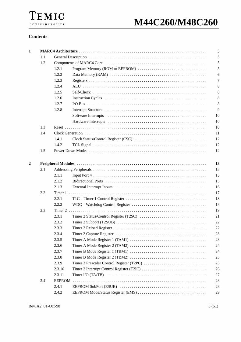
1 MARC4 Architecture1.1 General Description
ÏÏÏÏÏÏÏÏÏÏÏÏÏÏÏÏÏÏÏÏÏÏÏÏÏÏÏÏÏÏÏÏÏÏÏÏÏÏÏÏÏÏÏÏÏÏÏÏÏÏÏÏÏÏÏÏÏÏÏÏÏÏÏÏÏÏÏÏÏÏÏÏÏÏÏÏÏÏÏÏÏÏÏÏÏÏÏÏÏÏÏÏÏÏÏÏÏÏÏÏÏÏÏÏÏÏÏÏÏÏÏÏÏÏÏÏÏÏÏÏÏÏÏÏÏÏÏÏÏÏÏÏÏÏÏÏÏÏÏÏÏÏÏÏÏÏÏÏÏÏÏÏÏÏÏÏÏÏÏÏÏÏÏÏÏÏÏÏÏÏÏÏÏÏÏÏÏÏÏÏÏÏÏÏÏÏÏÏÏÏÏÏÏÏÏÏÏÏÏÏÏÏÏÏÏÏÏÏÏÏÏÏÏÏÏÏÏÏÏÏÏÏÏÏÏÏÏÏÏÏÏÏÏÏÏÏÏÏÏÏÏÏÏÏÏÏÏÏÏÏÏÏÏÏÏÏÏÏÏÏÏÏÏÏÏÏÏÏÏÏÏÏÏÏÏÏÏÏÏÏÏÏÏÏÏÏÏÏÏÏÏÏÏÏÏÏÏÏÏÏÏÏÏÏÏÏÏÏÏÏÏÏÏÏÏÏÏÏÏÏÏÏÏÏÏÏÏÏÏÏÏÏÏÏÏÏÏÏÏÏÏÏÏÏÏÏÏÏÏÏÏÏÏÏÏÏÏ
ÏÏÏÏÏÏ
Instruction decoder
CCR
TOS
ALU
RAMPC
RPSP
XYProgram
256 x 4-bit
MARC4 CORE
Clock
Reset
Sleep
Memory bus
I/O bus
Instruction bus
Reset
System clock Interrupt
controller
On–chip peripheral modules94 8973
memory
Figure 4. MARC4 core
The MARC4 microcontroller consists of an advancedstack based 4-bit CPU core and on-chip peripherals. TheCPU is based on the HARVARD architecture with aphysically separate program memory (ROM orEEPROM) and data memory (RAM). Three independentbuses the instruction bus, the memory bus and the I/O busare used for parallel communication between programmemory, RAM and peripherals. This enhances programexecution speed by allowing both instruction prefetching,and simultaneous communication to the on-chip periph-eral circuitry. The integrated powerful interruptcontroller with eight prioritized interrupt levels, supportsfast processing of hardware events.The MARC4 is designed for the high level programminglanguage qFORTH. The core contains both FORTHstacks, expression stack and return stack. This architec-ture allows high level language programming without anyloss in efficiency or code density.
1.2 Components of MARC4 CoreThe core contains a program memory, RAM, ALU, pro-gram counter, RAM address register, instruction decoder
and interrupt controller. The following sections describeeach of these parts.
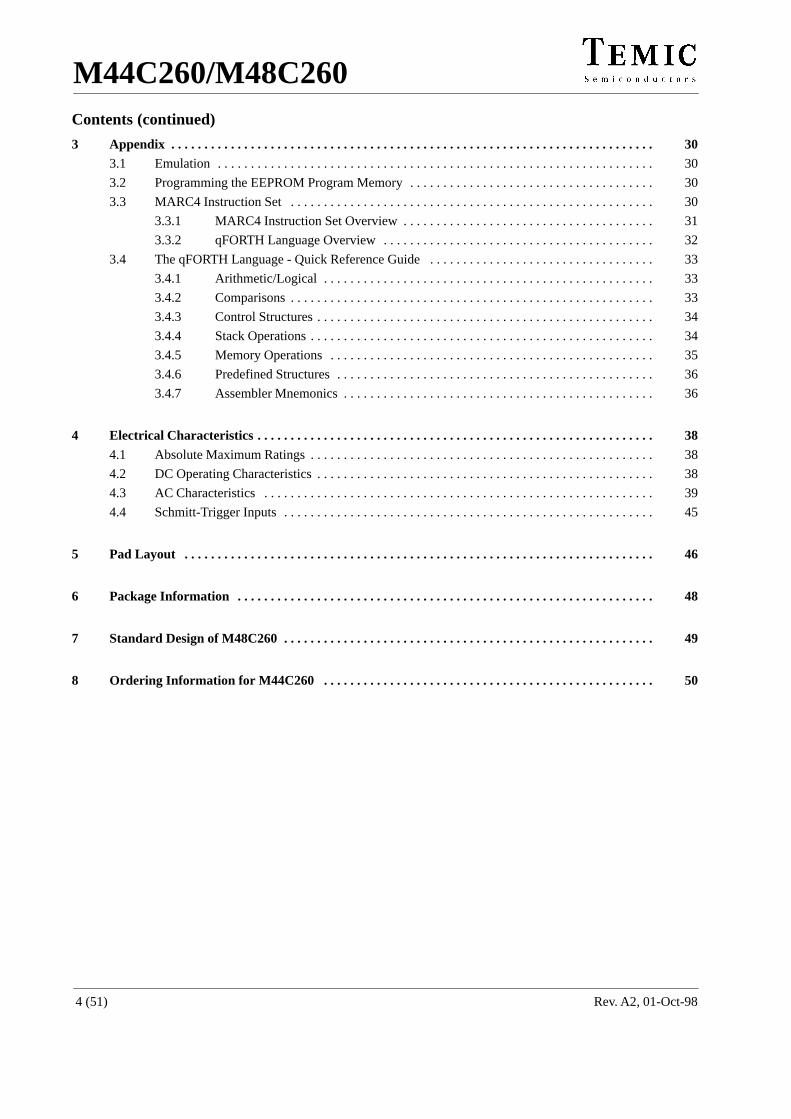
1.2.1 Program Memory (ROM orEEPROM)
The ROM is mask programmed with the application pro-gram during the fabrication of the microcontroller. TheEEPROM is programmed by the customer using a specialprogramming device (see chapter ”Progamming theEEPROM Program Memory”). The program memory isaddressed by a 12-bit wide program counter, thus limitingthe program size to a maximum of 4 Kbytes. TheM44C260 contains an additional 1 Kbyte ROM for testsoftware. The program memory starts with a 512 byte seg-ment (zero page) which contains predefined startaddresses for interrupt service routines and special sub-routines accessible with single byte instructions(SCALL). The corresponding memory map is shown inthe figure 4.Look-up tables of constants can also be heldin the program memory and are accessed via theMARC4’s built-in TABLE instruction.
M44C260/M48C260
Rev. A2, 01-Oct-986 (51)
FFFh
1FFh
000h
memory(4K x 8-bit)
ÏÏÏÏÏÏÏÏÏÏÏÏ
Zero page
Self test
140h
180h
040h
0C0h
008h $AUTOSLEEP$RESET
INT0
INT1
INT2
INT3
INT4
INT5
INT6
INT71E0h
1C0h
100h
080h
Zeropage
1F0h1F8h
010h018h
000h008h
020h
1E8h1E0h
SC
ALL
add
ress
es
000h
000h
3FFh
94 8974
Program
bank (1K)
M44C260only
Figure 5. Program memory map
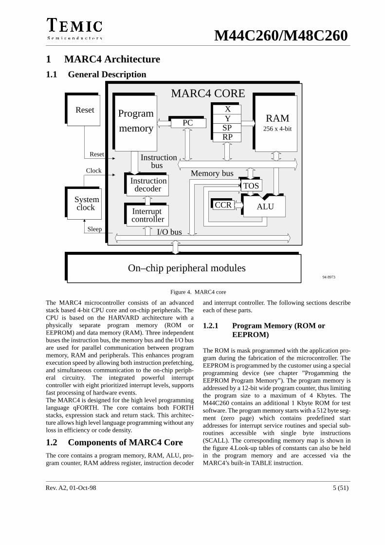
1.2.2 Data Memory (RAM)
The MARC4 contains a 256 x 4-bit wide static random ac-cess memory (RAM). It is used for the expression stack,the return stack and data memory for variables and arrays.The RAM is addressed by any of the four 8-bit wide RAMaddress registers SP, RP, X and Y.
Expression Stack
The 4-bit wide expression stack is addressed with the ex-pression stack pointer (SP). All arithmetic, I/O andmemory reference operations take their operands from,and return their result to the expression stack. TheMARC4 performs the operations with the top of stackitems (TOS and TOS-1). The TOS register contains the
top element of the expression stack and works like anaccumulator. This stack is also used for passing parame-ters between subroutines, and as a scratchpad area fortemporary storage of data.
Return Stack
The 12-bit wide return stack is addressed by the returnstack pointer (RP). It is used for storing return addressesof subroutines, interrupt routines and for keeping loop in-dex counts. The return stack can also be used as atemporary storage area.
The MARC4 instruction set supports the exchange of databetween the top elements of the expression stack and thereturn stack. The two stacks within the RAM have a userdefinable location and maximum depth.
ÏÏÏÏÏÏ
ÏÏÏÏÏÏÏÏÏÏÏÏÏÏÏÏÏÏÏÏÏÏÏÏÏ
ÏÏÏÏÏÏÏÏÏÏ
ÏÏÏÏÏÏÏÏÏÏÏÏÏÏÏÏÏÏÏÏÏÏÏÏÏ
ÏÏÏÏÏÏ
RAM
FCh
00h
Autosleep
FFh
03h04h
X
Y
SP
RP
TOS–1
Expressionstack
Returnstack
Globalvariables
RA
M a
ddre
ss r
egis
ter:
07h
(256 x 4-bit)
Globalvariables
4-bit
TOSTOS–1TOS–2
3 0
SP
Expression stack
Return stack
ÏÏÏÏÏ011
12-bit
RP
v
94 8975
Figure 6. RAM map
M44C260/M48C260
Rev. A2, 01-Oct-98 7 (51)
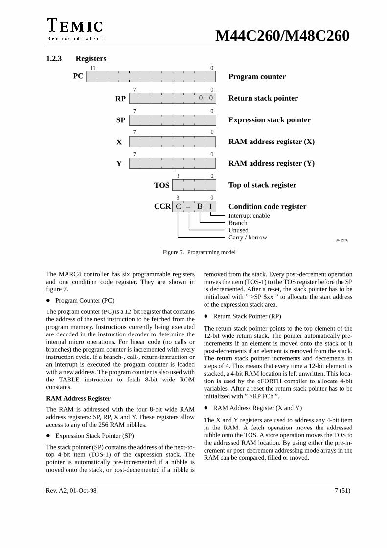
1.2.3 Registers
ÏÏÏÏÏÏÏÏÏÏÏÏÏÏÏÏÏÏÏÏÏÏÏÏÏÏÏÏ
ÏÏÏÏÏÏÏÏÏÏÏÏÏÏÏÏÏÏÏÏÏÏÏÏÏÏÏÏÏÏÏÏÏÏÏÏÏÏÏÏ
ÏÏÏÏÏÏÏÏÏÏÏÏÏÏÏÏÏÏÏÏÏÏÏÏÏÏÏÏÏÏÏÏÏÏÏÏÏÏÏÏ
ÏÏÏÏÏÏÏÏÏÏÏÏÏÏÏÏÏÏÏÏÏÏÏÏÏ
TOS
CCR
03
03
07
07
07
011
RP
SP
X
Y
PC
– B I
Program counter
Return stack pointer
Expression stack pointer
RAM address register (X)
RAM address register (Y)
Top of stack register
Condition code register
Carry / borrow
BranchInterrupt enable
Unused
07
0 0
C
94 8976
Figure 7. Programming model
The MARC4 controller has six programmable registersand one condition code register. They are shown infigure 7.
Program Counter (PC)
The program counter (PC) is a 12-bit register that containsthe address of the next instruction to be fetched from theprogram memory. Instructions currently being executedare decoded in the instruction decoder to determine theinternal micro operations. For linear code (no calls orbranches) the program counter is incremented with everyinstruction cycle. If a branch-, call-, return-instruction oran interrupt is executed the program counter is loadedwith a new address. The program counter is also used withthe TABLE instruction to fetch 8-bit wide ROMconstants.
RAM Address Register
The RAM is addressed with the four 8-bit wide RAMaddress registers: SP, RP, X and Y. These registers allowaccess to any of the 256 RAM nibbles.
Expression Stack Pointer (SP)
The stack pointer (SP) contains the address of the next-to-top 4-bit item (TOS-1) of the expression stack. Thepointer is automatically pre-incremented if a nibble ismoved onto the stack, or post-decremented if a nibble is
removed from the stack. Every post-decrement operationmoves the item (TOS-1) to the TOS register before the SPis decremented. After a reset, the stack pointer has to beinitialized with ” >SP $xx ” to allocate the start addressof the expression stack area.
Return Stack Pointer (RP)
The return stack pointer points to the top element of the12-bit wide return stack. The pointer automatically pre-increments if an element is moved onto the stack or itpost-decrements if an element is removed from the stack.The return stack pointer increments and decrements insteps of 4. This means that every time a 12-bit element isstacked, a 4-bit RAM location is left unwritten. This loca-tion is used by the qFORTH compiler to allocate 4-bitvariables. After a reset the return stack pointer has to beinitialized with ” >RP FCh ”.
RAM Address Register (X and Y)
The X and Y registers are used to address any 4-bit itemin the RAM. A fetch operation moves the addressednibble onto the TOS. A store operation moves the TOS tothe addressed RAM location. By using either the pre-in-crement or post-decrement addressing mode arrays in theRAM can be compared, filled or moved.
M44C260/M48C260
Rev. A2, 01-Oct-988 (51)
Top Of Stack (TOS)
The top of stack register is the accumulator of theMARC4. All arithmetic/logic, memory reference and I/Ooperations use this register. The TOS register gets the datafrom the ALU, the program memory, the RAM or via theI/O bus.
Condition Code Register (CCR)
The 4-bit wide condition code register contains thebranch, the carry and the interrupt enable flag. These bitsindicate the current state of the CPU. The CCR flags areset or reset by ALU operations. The instructionsSET_BCF, TOG_BF, CCR! and DI allow a directmanipulation of the condition code register.
Carry/Borrow (C)
The carry/borrow flag indicates that borrow or carry outof arithmetic logic unit (ALU) occurred during the lastarithmetic operation. During shift and rotate operationsthis bit is used as a fifth bit. Boolean operations have noaffect on the C flag.
Branch (B)
The branch flag controls the conditional program branch-ing. When the branch flag has been set by one of theprevious instructions a conditional branch is taken. Thisflag is affected by arithmetic, logic, shift, and rotate op-erations.
Interrupt Enable (I)
The interrupt enable flag enables or disables the interruptprocessing on a global basis. After reset or by executingthe DI instruction, the interrupt enable flag is reset and allinterrupts are disabled. The µC does not process furtherinterrupt requests until the interrupt enable flag is setagain by either executing an EI, RTI or SLEEPinstruction.
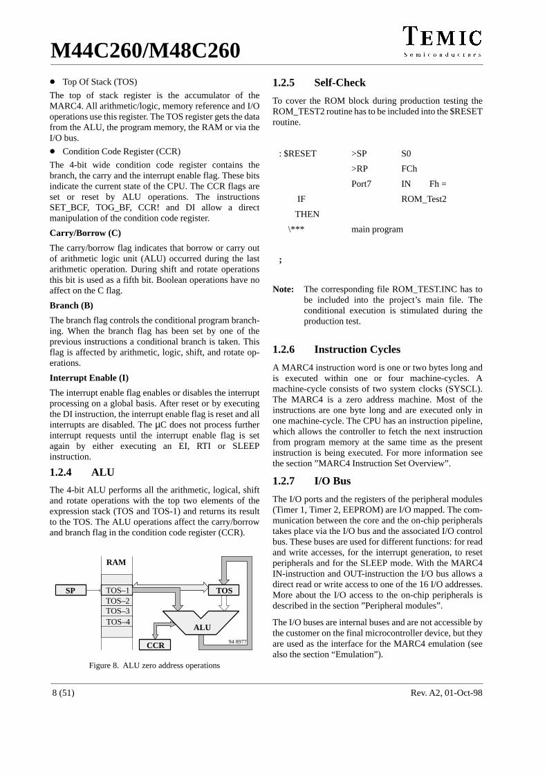
1.2.4 ALU
The 4-bit ALU performs all the arithmetic, logical, shiftand rotate operations with the top two elements of theexpression stack (TOS and TOS-1) and returns its resultto the TOS. The ALU operations affect the carry/borrowand branch flag in the condition code register (CCR).
ÏÏÏÏ
ÏÏÏÏÏÏÏÏÏÏÏÏÏÏÏÏÏÏÏÏÏÏÏÏ
ÏÏÏÏÏÏÏÏÏ
ÏÏÏÏÏÏÏÏÏÏÏÏÏÏÏÏÏÏÏÏÏÏÏÏÏÏÏÏÏÏÏÏ
ÏÏÏÏÏÏÏÏÏÏÏÏ
TOS–1
CCR
RAM
ÏÏÏÏÏÏÏÏ TOS–2
SP
TOS–3
ÏÏÏÏÏÏÏÏÏÏÏÏÏÏÏÏÏÏÏÏÏÏÏÏ
TOS
ALUTOS–4
94 8977
Figure 8. ALU zero address operations
1.2.5 Self-Check
To cover the ROM block during production testing theROM_TEST2 routine has to be included into the $RESETroutine.
: $RESET >SP S0
>RP FCh
Port7 IN Fh =
IF ROM_Test2
THEN
\*** main program
;
Note: The corresponding file ROM_TEST.INC has tobe included into the project’s main file. Theconditional execution is stimulated during theproduction test.
1.2.6 Instruction Cycles
A MARC4 instruction word is one or two bytes long andis executed within one or four machine-cycles. Amachine-cycle consists of two system clocks (SYSCL).The MARC4 is a zero address machine. Most of theinstructions are one byte long and are executed only inone machine-cycle. The CPU has an instruction pipeline,which allows the controller to fetch the next instructionfrom program memory at the same time as the presentinstruction is being executed. For more information seethe section ”MARC4 Instruction Set Overview”.
1.2.7 I/O Bus
The I/O ports and the registers of the peripheral modules(Timer 1, Timer 2, EEPROM) are I/O mapped. The com-munication between the core and the on-chip peripheralstakes place via the I/O bus and the associated I/O controlbus. These buses are used for different functions: for readand write accesses, for the interrupt generation, to resetperipherals and for the SLEEP mode. With the MARC4IN-instruction and OUT-instruction the I/O bus allows adirect read or write access to one of the 16 I/O addresses.More about the I/O access to the on-chip peripherals isdescribed in the section ”Peripheral modules”.
The I/O buses are internal buses and are not accessible bythe customer on the final microcontroller device, but theyare used as the interface for the MARC4 emulation (seealso the section “Emulation”).
M44C260/M48C260
Rev. A2, 01-Oct-98 9 (51)
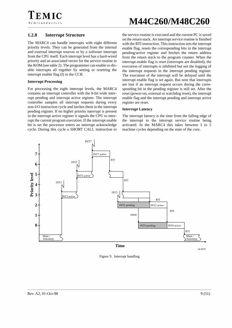
1.2.8 Interrupt Structure
The MARC4 can handle interrupts with eight differentpriority levels. They can be generated from the internaland external interrupt sources or by a software interruptfrom the CPU itself. Each interrupt level has a hard-wiredpriority and an associated vector for the service routine inthe ROM (see table 2). The programmer can enable or dis-able interrupts all together by setting or resetting theinterrupt enable flag (I) in the CCR.
Interrupt Processing
For processing the eight interrupt levels, the MARC4contains an interrupt controller with the 8-bit wide inter-rupt pending and interrupt active register. The interruptcontroller samples all interrupt requests during everynon-I/O instruction cycle and latches them in the interruptpending register. If no higher priority interrupt is presentin the interrupt active register it signals the CPU to inter-rupt the current program execution. If the interrupt enablebit is set the processor enters an interrupt acknowledgecycle. During this cycle a SHORT CALL instruction to
the service routine is executed and the current PC is savedon the return stack. An interrupt service routine is finishedwith the RTI instruction. This instruction sets the interruptenable flag, resets the corresponding bits in the interruptpending/active register and fetches the return addressfrom the return stack to the program counter. When theinterrupt enable flag is reset (interrupts are disabled), theexecution of interrupts is inhibited but not the logging ofthe interrupt requests in the interrupt pending register.The execution of the interrupt will be delayed until theinterrupt enable flag is set again. But note that interruptsare lost if an interrupt request occurs during the corre-sponding bit in the pending register is still set. After thereset (power-on, external or watchdog reset), the interruptenable flag and the interrupt pending and interrupt activeregister are reset.
Interrupt Latency
The interrupt latency is the time from the falling edge ofthe interrupt to the interrupt service routine beingactivated. In the MARC4 this takes between 3 to 5machine cycles depending on the state of the core.
7
6
5
4
3
2
1
0
Prio
rity
leve
l
ÁÁÁÁÁÁÁÁ
ÁÁÁÁÁÁÁÁ
ÁÁÁÁÁÁ
ÁÁÁÁÁÁÁÁÁÁ
INT5 active
INT7 active
ÏÏÏÏÏÏÏÏÏÏÏÏÏÏ
INT2 pending
SWI0
ÁÁÁÁÁÁÁÁ
INT2 active
ÏÏÏÏÏÏÏÏÏÏÏÏ
ÁÁÁÁÁÁÁÁ
INT0 pending INT0 active
INT2
RTI
RTIINT5
ÁÁÁÁÁÁÁÁ
INT3 active
INT3
RTI
RTI
RTI
INT7
Time
ÁÁÁÁÁÁÁÁÁÁ
ÁÁÁÁÁÁÁÁ
Main / Autosleep
Main / Autosleep
94 8978
Figure 9. Interrupt handling
M44C260/M48C260
Rev. A2, 01-Oct-9810 (51)
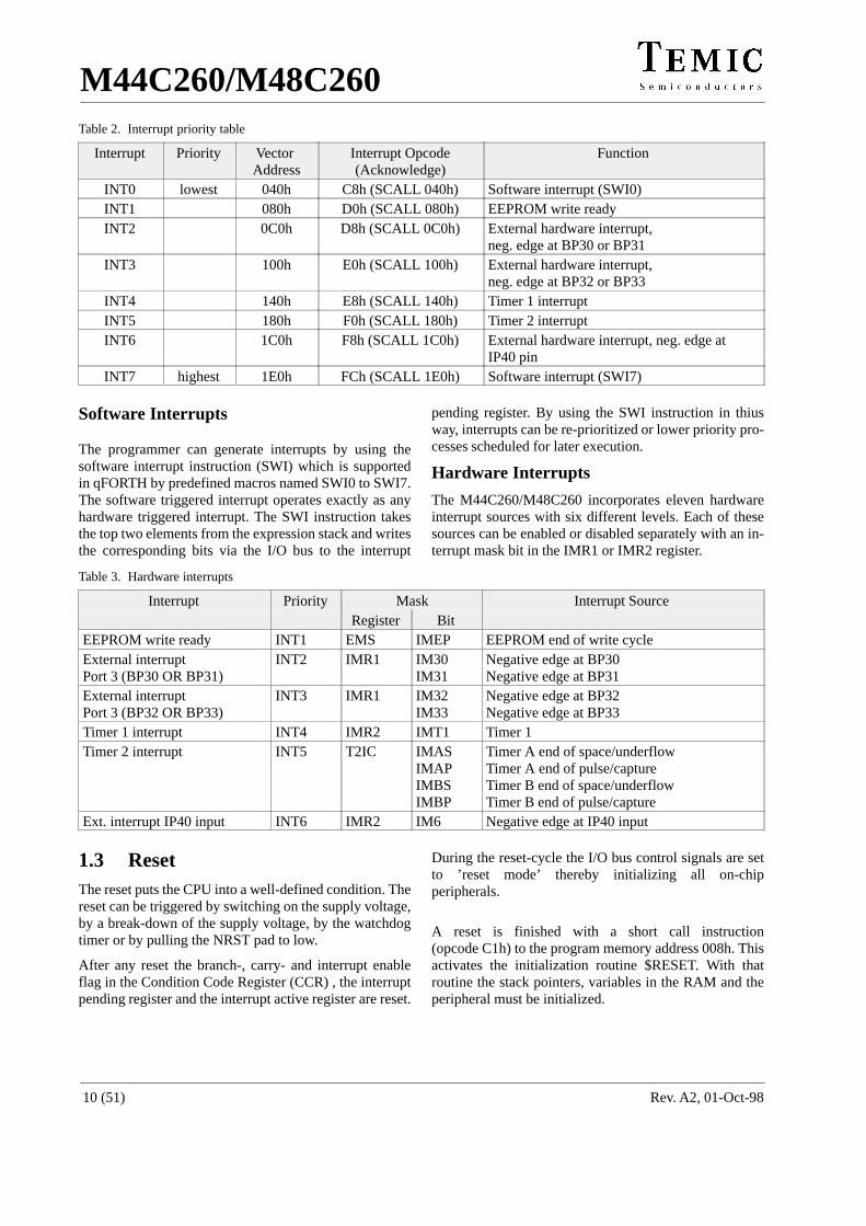
Table 2. Interrupt priority table
Interrupt Priority Vector Address
Interrupt Opcode(Acknowledge)
Function
ÁÁÁÁÁINT0 ÁÁÁÁlowestÁÁÁÁÁ040h ÁÁÁÁÁÁÁÁC8h (SCALL 040h)ÁÁÁÁÁÁÁÁÁÁÁÁÁÁSoftware interrupt (SWI0)ÁÁÁÁÁÁÁÁÁÁINT1
ÁÁÁÁÁÁÁÁ
ÁÁÁÁÁÁÁÁÁÁ080h
ÁÁÁÁÁÁÁÁÁÁÁÁÁÁÁÁD0h (SCALL 080h)
ÁÁÁÁÁÁÁÁÁÁÁÁÁÁÁÁÁÁÁÁÁÁÁÁÁÁÁÁEEPROM write readyÁÁÁÁÁ
ÁÁÁÁÁÁÁÁÁÁ
INT2ÁÁÁÁÁÁÁÁÁÁÁÁ
ÁÁÁÁÁÁÁÁÁÁÁÁÁÁÁ
0C0hÁÁÁÁÁÁÁÁÁÁÁÁÁÁÁÁÁÁÁÁÁÁÁÁ
D8h (SCALL 0C0h)ÁÁÁÁÁÁÁÁÁÁÁÁÁÁÁÁÁÁÁÁÁÁÁÁÁÁÁÁÁÁÁÁÁÁÁÁÁÁÁÁÁÁ
External hardware interrupt, neg. edge at BP30 or BP31
ÁÁÁÁÁÁÁÁÁÁÁÁÁÁÁ
INT3 ÁÁÁÁÁÁÁÁÁÁÁÁ
ÁÁÁÁÁÁÁÁÁÁÁÁÁÁÁ
100h ÁÁÁÁÁÁÁÁÁÁÁÁÁÁÁÁÁÁÁÁÁÁÁÁ
E0h (SCALL 100h)ÁÁÁÁÁÁÁÁÁÁÁÁÁÁÁÁÁÁÁÁÁÁÁÁÁÁÁÁÁÁÁÁÁÁÁÁÁÁÁÁÁÁ
External hardware interrupt,neg. edge at BP32 or BP33
ÁÁÁÁÁINT4 ÁÁÁÁÁÁÁÁÁ140h ÁÁÁÁÁÁÁÁE8h (SCALL 140h)ÁÁÁÁÁÁÁÁÁÁÁÁÁÁTimer 1 interruptÁÁÁÁÁÁÁÁÁÁINT5
ÁÁÁÁÁÁÁÁ
ÁÁÁÁÁÁÁÁÁÁ180h
ÁÁÁÁÁÁÁÁÁÁÁÁÁÁÁÁF0h (SCALL 180h)
ÁÁÁÁÁÁÁÁÁÁÁÁÁÁÁÁÁÁÁÁÁÁÁÁÁÁÁÁTimer 2 interruptÁÁÁÁÁ
ÁÁÁÁÁÁÁÁÁÁ
INT6ÁÁÁÁÁÁÁÁÁÁÁÁ
ÁÁÁÁÁÁÁÁÁÁÁÁÁÁÁ
1C0hÁÁÁÁÁÁÁÁÁÁÁÁÁÁÁÁÁÁÁÁÁÁÁÁ
F8h (SCALL 1C0h)ÁÁÁÁÁÁÁÁÁÁÁÁÁÁÁÁÁÁÁÁÁÁÁÁÁÁÁÁÁÁÁÁÁÁÁÁÁÁÁÁÁÁ
External hardware interrupt, neg. edge atIP40 pin
ÁÁÁÁÁÁÁÁÁÁ
INT7 ÁÁÁÁÁÁÁÁ
highestÁÁÁÁÁÁÁÁÁÁ
1E0h ÁÁÁÁÁÁÁÁÁÁÁÁÁÁÁÁ
FCh (SCALL 1E0h)ÁÁÁÁÁÁÁÁÁÁÁÁÁÁÁÁÁÁÁÁÁÁÁÁÁÁÁÁ
Software interrupt (SWI7)
Software Interrupts
The programmer can generate interrupts by using thesoftware interrupt instruction (SWI) which is supportedin qFORTH by predefined macros named SWI0 to SWI7.The software triggered interrupt operates exactly as anyhardware triggered interrupt. The SWI instruction takesthe top two elements from the expression stack and writesthe corresponding bits via the I/O bus to the interrupt
pending register. By using the SWI instruction in thiusway, interrupts can be re-prioritized or lower priority pro-cesses scheduled for later execution.
Hardware Interrupts
The M44C260/M48C260 incorporates eleven hardwareinterrupt sources with six different levels. Each of thesesources can be enabled or disabled separately with an in-terrupt mask bit in the IMR1 or IMR2 register.
Table 3. Hardware interrupts
Interrupt Priority Mask Interrupt SourceRegister Bit
ÁÁÁÁÁÁÁÁÁÁÁÁÁÁÁÁÁÁÁÁ
EEPROM write ready ÁÁÁÁÁÁÁÁINT1 ÁÁÁÁ
ÁÁÁÁEMS ÁÁÁÁ
ÁÁÁÁIMEP ÁÁÁÁÁÁÁÁÁÁÁÁÁÁ
ÁÁÁÁÁÁÁÁÁÁÁÁÁÁEEPROM end of write cycle
ÁÁÁÁÁÁÁÁÁÁÁÁÁÁÁÁÁÁÁÁ
External interrupt Port 3 (BP30 OR BP31)
ÁÁÁÁÁÁÁÁ
INT2 ÁÁÁÁÁÁÁÁ
IMR1 ÁÁÁÁÁÁÁÁ
IM30IM31
ÁÁÁÁÁÁÁÁÁÁÁÁÁÁÁÁÁÁÁÁÁÁÁÁÁÁÁÁ
Negative edge at BP30 Negative edge at BP31
ÁÁÁÁÁÁÁÁÁÁÁÁÁÁÁÁÁÁÁÁÁÁÁÁÁÁÁÁÁÁ
External interruptPort 3 (BP32 OR BP33)
ÁÁÁÁÁÁÁÁÁÁÁÁ
INT3 ÁÁÁÁÁÁÁÁÁÁÁÁ
IMR1 ÁÁÁÁÁÁÁÁÁÁÁÁ
IM32IM33
ÁÁÁÁÁÁÁÁÁÁÁÁÁÁÁÁÁÁÁÁÁÁÁÁÁÁÁÁÁÁÁÁÁÁÁÁÁÁÁÁÁÁ
Negative edge at BP32 Negative edge at BP33
ÁÁÁÁÁÁÁÁÁÁÁÁÁÁÁÁÁÁÁÁ
Timer 1 interrupt ÁÁÁÁÁÁÁÁINT4 ÁÁÁÁ
ÁÁÁÁIMR2 ÁÁÁÁ
ÁÁÁÁIMT1 ÁÁÁÁÁÁÁÁÁÁÁÁÁÁ
ÁÁÁÁÁÁÁÁÁÁÁÁÁÁTimer 1
ÁÁÁÁÁÁÁÁÁÁÁÁÁÁÁÁÁÁÁÁÁÁÁÁÁÁÁÁÁÁÁÁÁÁÁÁÁÁÁÁ
Timer 2 interrupt ÁÁÁÁÁÁÁÁÁÁÁÁÁÁÁÁ
INT5 ÁÁÁÁÁÁÁÁÁÁÁÁÁÁÁÁ
T2IC ÁÁÁÁÁÁÁÁÁÁÁÁÁÁÁÁ
IMASIMAPIMBSIMBP
ÁÁÁÁÁÁÁÁÁÁÁÁÁÁÁÁÁÁÁÁÁÁÁÁÁÁÁÁÁÁÁÁÁÁÁÁÁÁÁÁÁÁÁÁÁÁÁÁÁÁÁÁÁÁÁÁ
Timer A end of space/underflowTimer A end of pulse/captureTimer B end of space/underflowTimer B end of pulse/capture
ÁÁÁÁÁÁÁÁÁÁÁÁÁÁÁÁÁÁÁÁ
Ext. interrupt IP40 input ÁÁÁÁÁÁÁÁINT6 ÁÁÁÁ
ÁÁÁÁIMR2 ÁÁÁÁ
ÁÁÁÁIM6 ÁÁÁÁÁÁÁÁÁÁÁÁÁÁ
ÁÁÁÁÁÁÁÁÁÁÁÁÁÁNegative edge at IP40 input
1.3 ResetThe reset puts the CPU into a well-defined condition. Thereset can be triggered by switching on the supply voltage,by a break-down of the supply voltage, by the watchdogtimer or by pulling the NRST pad to low.
After any reset the branch-, carry- and interrupt enableflag in the Condition Code Register (CCR) , the interruptpending register and the interrupt active register are reset.
During the reset-cycle the I/O bus control signals are setto ’reset mode’ thereby initializing all on-chipperipherals.
A reset is finished with a short call instruction(opcode C1h) to the program memory address 008h. Thisactivates the initialization routine $RESET. With thatroutine the stack pointers, variables in the RAM and theperipheral must be initialized.
M44C260/M48C260
Rev. A2, 01-Oct-98 11 (51)
Power-on Reset
The M44C260/M48C260 incorporates an on-chippower-on reset (POR) circuitry which provides internalchip reset for most power-up situations. The power-onreset ensures that the core is not activated before the oper-ating supply voltage has been reached.
The C will function normally at > 2.4 V under all condi-tions. For VDD below 2.4 V, the device will eitherfunction normally or the device reset will be globally acti-vated by the brown-out circuit. The actual brown-out trippoint is a function of temperature and process parameters.
External Reset (NRST)
An external reset can be triggered with the NRST pin. Forthe external reset the pin should be low for a minimum oftwo machine-cycles.
Watchdog Timer Reset
If the watchdog timer function of Timer 1 is enabled, a re-set is triggered with every watchdog counter overflow. Tosuppress that, the watchdog counter must be reset by anaccess to the CWD-register (see also Timer 1/watchdogcounter).
The power-on reset and the watchdog reset are indicatedin the same way as an external reset on the NRST pad.
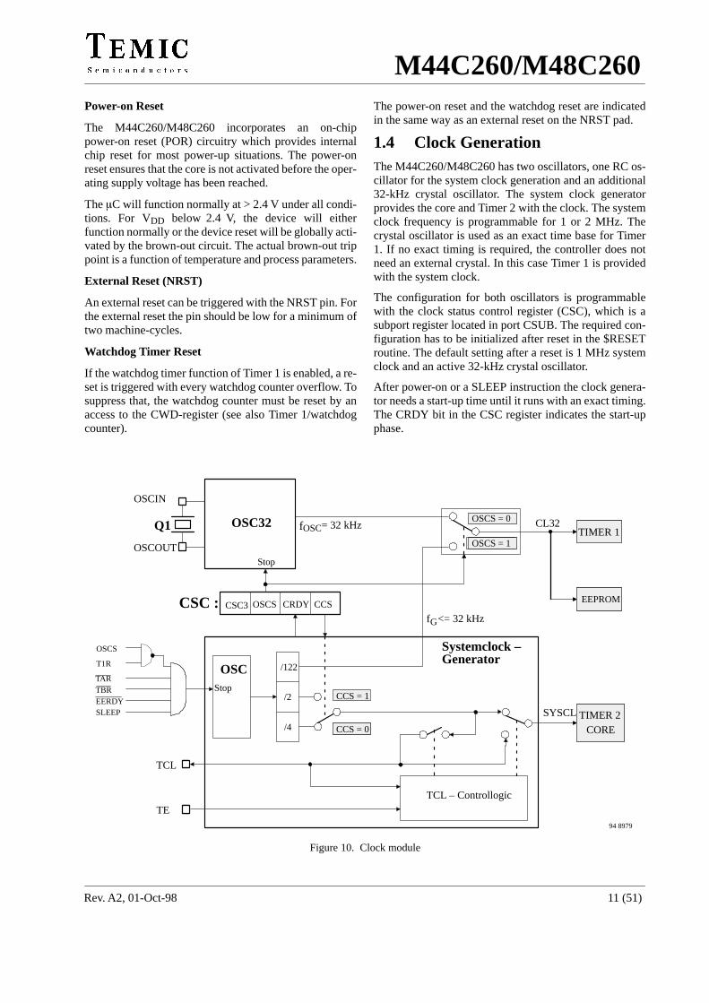
1.4 Clock GenerationThe M44C260/M48C260 has two oscillators, one RC os-cillator for the system clock generation and an additional32-kHz crystal oscillator. The system clock generatorprovides the core and Timer 2 with the clock. The systemclock frequency is programmable for 1 or 2 MHz. Thecrystal oscillator is used as an exact time base for Timer1. If no exact timing is required, the controller does notneed an external crystal. In this case Timer 1 is providedwith the system clock.
The configuration for both oscillators is programmablewith the clock status control register (CSC), which is asubport register located in port CSUB. The required con-figuration has to be initialized after reset in the $RESETroutine. The default setting after a reset is 1 MHz systemclock and an active 32-kHz crystal oscillator.
After power-on or a SLEEP instruction the clock genera-tor needs a start-up time until it runs with an exact timing.The CRDY bit in the CSC register indicates the start-upphase.
OSC32
OSCS CRDY CCSCSC :
Stop
fOSC
SYSCL
Q1OSCS = 0
/122
/2
/4
CCS = 1
ÏÏÏÏÏÏ
CCS = 0
OSC
Systemclock – Generator
Stop
CL32
SLEEPEERDY
TARTBR
OSCS
T1R
= 32 kHz
fG<= 32 kHz
ÏÏ
ÏÏ
TCL
TE
TCL – Controllogic
OSCIN
OSCOUT
TIMER 2CORE
TIMER 1
EEPROM
OSCS = 1
94 8979
CSC3
Figure 10. Clock module
M44C260/M48C260
Rev. A2, 01-Oct-9812 (51)
1.4.1 Clock Status/Control Register (CSC)
Address: Ch Subaddress: 2h
Bit 3 Bit 2 Bit 1 Bit 0ÁÁÁÁÁÁÁÁÁÁÁÁÁÁÁ
CSCÁÁÁÁÁÁÁÁÁÁÁÁÁÁÁ
CSC3ÁÁÁÁÁÁÁÁÁÁÁÁ
OSCSÁÁÁÁÁÁÁÁÁÁÁÁÁÁÁ
CRDYÁÁÁÁÁÁÁÁÁÁÁÁÁÁÁ
CCS ÁÁ
ÁÁÁÁÁÁÁÁÁÁÁÁÁÁÁÁÁÁÁÁÁÁÁÁÁÁÁ
Reset value: 0000h
ÁÁÁÁÁÁÁÁÁÁÁÁÁÁÁÁÁÁÁÁÁÁÁÁÁÁÁÁÁÁÁÁÁÁÁÁÁÁÁÁÁÁÁÁÁÁ
CSC3 ÁÁÁÁÁÁÁÁÁÁÁÁÁÁÁÁÁÁÁÁÁÁÁÁÁÁÁÁÁÁÁÁÁÁÁÁÁÁÁÁÁÁÁÁÁÁÁÁÁÁÁÁÁÁÁÁÁÁÁÁÁÁÁÁÁÁÁÁÁÁÁÁÁÁÁÁÁÁÁÁÁÁÁÁÁÁÁ
This bit must always be zero
ÁÁÁÁÁÁÁÁÁÁÁÁÁÁÁÁ
OSCS ÁÁÁÁÁÁÁÁÁÁÁÁÁÁÁÁÁÁÁÁÁÁÁÁÁÁÁÁÁÁÁÁÁÁÁÁÁÁÁÁÁÁÁÁÁÁÁÁÁÁÁÁÁÁÁÁÁÁÁÁÁÁÁÁÁÁÁÁÁÁÁÁÁÁÁÁÁÁÁÁÁÁÁÁÁÁÁÁÁÁÁÁÁÁÁÁÁÁÁÁÁÁÁÁÁÁÁÁÁÁÁÁÁÁÁÁ
Oscillator Stop OSCS = 0 the C runs with the 32-kHz crystal oscillator for Timer 1 OSCS = 1 the 32-kHz oscillator stops. For C operation without crystal, this bit must be set after reset. In that case Timer 1 is provided from the internal RC oscillator.
ÁÁÁÁÁÁÁÁÁÁÁÁ
CRDY ÁÁÁÁÁÁÁÁÁÁÁÁÁÁÁÁÁÁÁÁÁÁÁÁÁÁÁÁÁÁÁÁÁÁÁÁÁÁÁÁÁÁÁÁÁÁÁÁÁÁÁÁÁÁÁÁÁÁÁÁÁÁÁÁÁÁÁÁÁÁÁÁÁÁÁÁÁÁÁÁÁÁÁÁÁÁÁ
Clock Ready (status bit) CRDY = 0 indicates the start-up time of the oscillators.CRDY = 1 indicates that the clock is ready and has the exact timing.
ÁÁÁÁÁÁÁÁ
CCS ÁÁÁÁÁÁÁÁÁÁÁÁÁÁÁÁÁÁÁÁÁÁÁÁÁÁÁÁÁÁÁÁÁÁÁÁÁÁÁÁÁÁÁÁÁÁÁÁÁÁÁÁÁÁÁÁÁÁ
Core Clock Select CCS = 0 selects 1 MHz system clock (SYSCL/TCL)CCS = 1 selects 2 MHz system clock (SYSCL/TCL)
1.4.2 TCL Signal
The TCL pin can be used as input to supply the controllerwith an external clock. For this configuration, the TCLpin must be held low for at least 0.5 ms during the resetcycle. The controller is working with clock frequenciesup to 2.5 MHz. It is also possible to use the TCL pin asoutput to supply peripherals with the system clock. In thiscase the TE pin must be connected to VDD level and theTCL pin must have a high impedance load.
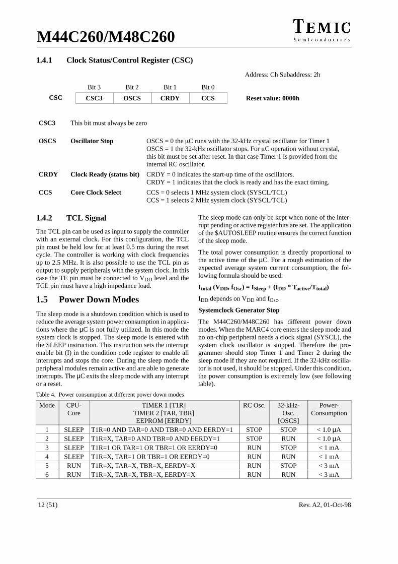
1.5 Power Down Modes
The sleep mode is a shutdown condition which is used toreduce the average system power consumption in applica-tions where the µC is not fully utilized. In this mode thesystem clock is stopped. The sleep mode is entered withthe SLEEP instruction. This instruction sets the interruptenable bit (I) in the condition code register to enable allinterrupts and stops the core. During the sleep mode theperipheral modules remain active and are able to generateinterrupts. The µC exits the sleep mode with any interruptor a reset.
The sleep mode can only be kept when none of the inter-rupt pending or active register bits are set. The applicationof the $AUTOSLEEP routine ensures the correct functionof the sleep mode.
The total power consumption is directly proportional tothe active time of the µC. For a rough estimation of theexpected average system current consumption, the fol-lowing formula should be used:
I total (VDD, fOsc) = ISleep + (IDD * Tactive/Ttotal)
IDD depends on VDD and fOsc.
Systemclock Generator Stop
The M44C260/M48C260 has different power downmodes. When the MARC4 core enters the sleep mode andno on-chip peripheral needs a clock signal (SYSCL), thesystem clock oscillator is stopped. Therefore the pro-grammer should stop Timer 1 and Timer 2 during thesleep mode if they are not required. If the 32-kHz oscilla-tor is not used, it should be stopped. Under this condition,the power consumption is extremely low (see followingtable).
Table 4. Power consumption at different power down modes
Mode CPU-Core
TIMER 1 [T1R]TIMER 2 [TAR, TBR]EEPROM [EERDY]
RC Osc. 32-kHz-Osc.
[OSCS]
Power-Consumption
ÁÁÁÁÁÁ
1ÁÁÁÁÁÁÁÁ
SLEEPÁÁÁÁÁÁÁÁÁÁÁÁÁÁÁÁÁÁÁÁÁÁÁÁÁÁÁÁÁÁÁÁ
T1R=0 AND TAR=0 AND TBR=0 AND EERDY=1ÁÁÁÁÁÁÁÁ
STOP ÁÁÁÁÁÁÁÁ
STOPÁÁÁÁÁÁÁÁÁÁÁÁ
< 1.0 µA
ÁÁÁÁÁÁ
2ÁÁÁÁÁÁÁÁ
SLEEPÁÁÁÁÁÁÁÁÁÁÁÁÁÁÁÁÁÁÁÁÁÁÁÁÁÁÁÁÁÁÁÁ
T1R=X, TAR=0 AND TBR=0 AND EERDY=1 ÁÁÁÁÁÁÁÁ
STOP ÁÁÁÁÁÁÁÁ
RUNÁÁÁÁÁÁÁÁÁÁÁÁ
< 1.0 µA
ÁÁÁ3ÁÁÁÁSLEEPÁÁÁÁÁÁÁÁÁÁÁÁÁÁÁÁT1R=1 OR TAR=1 OR TBR=1 OR EERDY=0 ÁÁÁÁRUN ÁÁÁÁSTOPÁÁÁÁÁÁ< 1 mAÁÁÁÁÁÁ4ÁÁÁÁÁÁÁÁSLEEP
ÁÁÁÁÁÁÁÁÁÁÁÁÁÁÁÁÁÁÁÁÁÁÁÁÁÁÁÁÁÁÁÁT1R=X, TAR=1 OR TBR=1 OR EERDY=0
ÁÁÁÁÁÁÁÁRUN
ÁÁÁÁÁÁÁÁRUN
ÁÁÁÁÁÁÁÁÁÁÁÁ< 1 mAÁÁÁ
ÁÁÁ5ÁÁÁÁÁÁÁÁ
RUNÁÁÁÁÁÁÁÁÁÁÁÁÁÁÁÁÁÁÁÁÁÁÁÁÁÁÁÁÁÁÁÁ
T1R=X, TAR=X, TBR=X, EERDY=XÁÁÁÁÁÁÁÁ
RUNÁÁÁÁÁÁÁÁ
STOPÁÁÁÁÁÁÁÁÁÁÁÁ
< 3 mAÁÁÁÁÁÁ
6ÁÁÁÁÁÁÁÁ
RUNÁÁÁÁÁÁÁÁÁÁÁÁÁÁÁÁÁÁÁÁÁÁÁÁÁÁÁÁÁÁÁÁ
T1R=X, TAR=X, TBR=X, EERDY=X ÁÁÁÁÁÁÁÁ
RUN ÁÁÁÁÁÁÁÁ
RUNÁÁÁÁÁÁÁÁÁÁÁÁ
< 3 mA
M44C260/M48C260
Rev. A2, 01-Oct-98 13 (51)
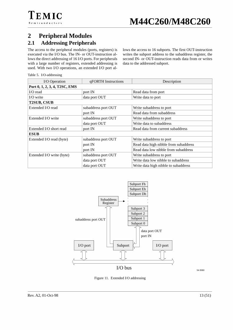
2 Peripheral Modules2.1 Addressing PeripheralsThe access to the peripheral modules (ports, registers) isexecuted via the I/O bus. The IN- or OUT-instruction al-lows the direct addressing of 16 I/O ports. For peripheralswith a large number of registers, extended addressing isused. With two I/O operations, an extended I/O port al-
lows the access to 16 subports. The first OUT-instructionwrites the subport address to the subaddress register, thesecond IN- or OUT-instruction reads data from or writesdata to the addressed subport.
Table 5. I/O-addressing
I/O Operation qFORTH Instructions DescriptionÁÁÁÁÁÁÁÁÁÁÁÁÁÁÁÁÁÁÁÁÁÁÁÁÁÁÁÁÁÁÁÁÁÁÁÁÁÁÁÁÁÁÁÁÁÁÁÁÁÁÁÁÁÁÁÁÁÁÁÁÁÁÁÁPort 0, 1, 2, 3, 4, T2SC, EMSÁÁÁÁÁÁÁÁÁÁÁÁÁÁÁÁÁÁÁÁ
I/O readÁÁÁÁÁÁÁÁÁÁÁÁÁÁÁÁÁÁ
port INÁÁÁÁÁÁÁÁÁÁÁÁÁÁÁÁÁÁÁÁÁÁÁÁÁÁÁÁÁÁ
Read data from portÁÁÁÁÁÁÁÁÁÁÁÁÁÁÁÁÁÁÁÁ
I/O writeÁÁÁÁÁÁÁÁÁÁÁÁÁÁÁÁÁÁ
data port OUTÁÁÁÁÁÁÁÁÁÁÁÁÁÁÁÁÁÁÁÁÁÁÁÁÁÁÁÁÁÁ
Write data to portÁÁÁÁÁÁÁÁÁÁÁÁÁÁÁÁÁÁÁÁÁÁÁÁÁÁÁÁÁÁÁÁÁÁÁÁÁÁÁÁÁÁÁÁÁÁÁÁÁÁÁÁÁÁÁÁÁÁÁÁÁÁÁÁ
T2SUB, CSUBÁÁÁÁÁÁÁÁÁÁÁÁÁÁÁÁÁÁÁÁ
Extended I/O read ÁÁÁÁÁÁÁÁÁÁÁÁÁÁÁÁÁÁ
subaddress port OUT ÁÁÁÁÁÁÁÁÁÁÁÁÁÁÁÁÁÁÁÁÁÁÁÁÁÁÁÁÁÁ
Write subaddress to portÁÁÁÁÁÁÁÁÁÁÁÁÁÁÁÁÁÁÁÁ
ÁÁÁÁÁÁÁÁÁÁÁÁÁÁÁÁÁÁ
port IN ÁÁÁÁÁÁÁÁÁÁÁÁÁÁÁÁÁÁÁÁÁÁÁÁÁÁÁÁÁÁ
Read data from subaddress
ÁÁÁÁÁÁÁÁÁÁÁÁÁÁÁÁÁÁÁÁ
Extended I/O write ÁÁÁÁÁÁÁÁÁÁÁÁÁÁÁÁÁÁ
subaddress port OUT ÁÁÁÁÁÁÁÁÁÁÁÁÁÁÁÁÁÁÁÁÁÁÁÁÁÁÁÁÁÁ
Write subaddress to port
ÁÁÁÁÁÁÁÁÁÁÁÁÁÁÁÁÁÁÁdata port OUT ÁÁÁÁÁÁÁÁÁÁÁÁÁÁÁWrite data to subaddressÁÁÁÁÁÁÁÁÁÁÁÁÁÁÁÁÁÁÁÁExtended I/O short read
ÁÁÁÁÁÁÁÁÁÁÁÁÁÁÁÁÁÁport IN
ÁÁÁÁÁÁÁÁÁÁÁÁÁÁÁÁÁÁÁÁÁÁÁÁÁÁÁÁÁÁRead data from current subaddressÁÁÁÁÁÁÁÁÁÁÁÁÁÁÁÁÁÁÁÁÁÁÁÁÁÁÁÁÁÁÁÁ
ÁÁÁÁÁÁÁÁÁÁÁÁÁÁÁÁÁÁÁÁÁÁÁÁÁÁÁÁÁÁÁÁESUBÁÁÁÁÁÁÁÁÁÁÁÁÁÁÁÁÁÁÁÁ
Extended I/O read (byte) ÁÁÁÁÁÁÁÁÁÁÁÁÁÁÁÁÁÁ
subaddress port OUT ÁÁÁÁÁÁÁÁÁÁÁÁÁÁÁÁÁÁÁÁÁÁÁÁÁÁÁÁÁÁ
Write subaddress to portÁÁÁÁÁÁÁÁÁÁÁÁÁÁÁÁÁÁÁÁ
ÁÁÁÁÁÁÁÁÁÁÁÁÁÁÁÁÁÁ
port IN ÁÁÁÁÁÁÁÁÁÁÁÁÁÁÁÁÁÁÁÁÁÁÁÁÁÁÁÁÁÁ
Read data high nibble from subaddressÁÁÁÁÁÁÁÁÁÁÁÁÁÁÁÁÁÁÁÁ
ÁÁÁÁÁÁÁÁÁÁÁÁÁÁÁÁÁÁ
port IN ÁÁÁÁÁÁÁÁÁÁÁÁÁÁÁÁÁÁÁÁÁÁÁÁÁÁÁÁÁÁ
Read data low nibble from subaddressÁÁÁÁÁÁÁÁÁÁÁÁÁÁÁÁÁÁÁÁ
Extended I/O write (byte) ÁÁÁÁÁÁÁÁÁÁÁÁÁÁÁÁÁÁ
subaddress port OUT ÁÁÁÁÁÁÁÁÁÁÁÁÁÁÁÁÁÁÁÁÁÁÁÁÁÁÁÁÁÁ
Write subaddress to port
ÁÁÁÁÁÁÁÁÁÁÁÁÁÁÁÁÁÁÁÁ
ÁÁÁÁÁÁÁÁÁÁÁÁÁÁÁÁÁÁ
data port OUT ÁÁÁÁÁÁÁÁÁÁÁÁÁÁÁÁÁÁÁÁÁÁÁÁÁÁÁÁÁÁ
Write data low nibble to subaddress
ÁÁÁÁÁÁÁÁÁÁÁÁÁÁÁÁÁÁÁdata port OUT ÁÁÁÁÁÁÁÁÁÁÁÁÁÁÁWrite data high nibble to subaddress
ÏÏÏÏÏÏÏÏÏÏÏÏÏÏÏÏÏÏÏÏ
ÏÏÏÏÏÏÏÏ
ÏÏÏÏÏÏÏÏ
ÏÏÏÏÏÏÏÏ
ÏÏÏÏ
I/O port Subport I/O port
Subaddress Register
Subport 0
Subport 1
Subport 3
Subport Fh
Subport EhSubport Dh
data port OUT
port IN
I/O bus
Subport 2
subaddress port OUT
94 8980
Figure 11. Extended I/O addressing
M44C260/M48C260
Rev. A2, 01-Oct-9814 (51)
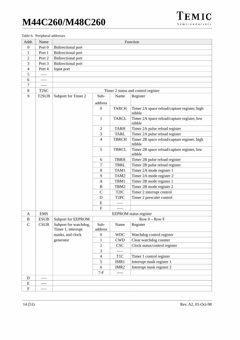
Table 6. Peripheral addresses
Addr. Name Function
ÁÁÁÁÁÁ
0ÁÁÁÁÁÁÁÁ
Port 0ÁÁÁÁÁÁÁÁÁÁÁÁÁÁÁÁÁÁÁÁ
Bidirectional port ÁÁÁÁÁÁÁÁÁÁ
ÁÁÁÁÁÁÁÁÁÁÁÁÁÁÁÁÁÁÁÁÁÁÁÁÁÁÁÁÁÁÁ1ÁÁÁÁPort 1ÁÁÁÁÁÁÁÁÁÁBidirectional port ÁÁÁÁÁÁÁÁÁÁÁÁÁÁÁÁÁÁÁÁÁÁ
ÁÁÁ2ÁÁÁÁÁÁÁÁPort 2
ÁÁÁÁÁÁÁÁÁÁÁÁÁÁÁÁÁÁÁÁBidirectional port
ÁÁÁÁÁÁÁÁÁÁ
ÁÁÁÁÁÁÁÁÁÁÁÁÁÁÁÁÁÁÁÁÁÁÁÁÁÁÁÁÁÁÁ
ÁÁÁ3ÁÁÁÁÁÁÁÁ
Port 3ÁÁÁÁÁÁÁÁÁÁÁÁÁÁÁÁÁÁÁÁ
Bidirectional portÁÁÁÁÁÁÁÁÁÁ
ÁÁÁÁÁÁÁÁÁÁÁÁÁÁÁÁÁÁÁÁÁÁÁÁÁÁÁÁÁÁÁ
ÁÁÁ4ÁÁÁÁÁÁÁÁ
Port 4ÁÁÁÁÁÁÁÁÁÁÁÁÁÁ
Input port ÁÁÁÁÁÁÁÁ
ÁÁÁÁÁÁÁÁÁÁ
ÁÁÁÁÁÁÁÁÁÁÁÁÁÁÁÁÁÁÁÁÁÁÁÁÁÁÁÁÁÁÁ
ÁÁÁ5ÁÁÁÁÁÁÁÁ
––– ÁÁÁÁÁÁÁÁÁÁÁÁÁÁ
ÁÁÁÁÁÁÁÁ
ÁÁÁÁÁÁÁÁÁÁ
ÁÁÁÁÁÁÁÁÁÁÁÁÁÁÁÁÁÁÁÁÁÁÁÁÁÁÁÁÁÁÁ
ÁÁÁ6ÁÁÁÁÁÁÁÁ
––– ÁÁÁÁÁÁÁÁÁÁÁÁÁÁ
ÁÁÁÁÁÁÁÁ
ÁÁÁÁÁÁÁÁÁÁ
ÁÁÁÁÁÁÁÁÁÁÁÁÁÁÁÁÁÁÁÁÁÁÁÁÁÁÁÁÁÁÁ
ÁÁÁ7ÁÁÁÁÁÁÁÁ
––– ÁÁÁÁÁÁÁÁÁÁÁÁÁÁ
ÁÁÁÁÁÁÁÁ
ÁÁÁÁÁÁÁÁÁÁ
ÁÁÁÁÁÁÁÁÁÁÁÁÁÁÁÁÁÁÁÁÁÁÁÁÁÁÁÁÁÁÁ
ÁÁÁ8ÁÁÁÁÁÁÁÁ
T2SCÁÁÁÁÁÁÁÁÁÁÁÁÁÁÁÁÁÁÁÁÁÁÁÁÁÁÁÁÁÁÁÁÁÁÁÁÁÁÁÁÁÁÁÁÁÁÁÁÁÁÁÁÁÁ
Timer 2 status and control register
ÁÁÁÁÁÁÁÁÁ
9ÁÁÁÁÁÁÁÁÁÁÁÁ
T2SUBÁÁÁÁÁÁÁÁÁÁÁÁÁÁÁÁÁÁÁÁÁ
Subport for Timer 2ÁÁÁÁÁÁÁÁÁÁÁÁ
Sub-
addressÁÁÁÁÁÁÁÁÁÁÁÁÁÁÁ
Name ÁÁÁÁÁÁÁÁÁÁÁÁÁÁÁÁÁÁÁÁÁÁÁÁÁÁÁÁÁÁÁÁÁÁÁÁÁÁÁÁÁÁ
Register
ÁÁÁÁÁÁÁÁÁÁÁÁÁÁ
ÁÁÁÁÁÁÁÁÁÁÁÁÁÁ
ÁÁÁÁÁÁÁÁ
0 ÁÁÁÁÁÁÁÁÁÁ
TARCH ÁÁÁÁÁÁÁÁÁÁÁÁÁÁÁÁÁÁÁÁÁÁÁÁÁÁÁÁ
Timer 2A space reload/capture register, highnibble
ÁÁÁÁÁÁÁÁÁ
ÁÁÁÁÁÁÁÁÁÁÁÁ
ÁÁÁÁÁÁÁÁÁÁÁÁÁÁÁÁÁÁÁÁÁ
ÁÁÁÁÁÁÁÁÁÁÁÁ
1 ÁÁÁÁÁÁÁÁÁÁÁÁÁÁÁ
TARCL ÁÁÁÁÁÁÁÁÁÁÁÁÁÁÁÁÁÁÁÁÁÁÁÁÁÁÁÁÁÁÁÁÁÁÁÁÁÁÁÁÁÁ
Timer 2A space reload/capture register, lownibble
ÁÁÁÁÁÁÁÁÁÁÁÁÁÁ
ÁÁÁÁÁÁÁÁÁÁÁÁÁÁ
ÁÁÁÁÁÁÁÁ
2 ÁÁÁÁÁÁÁÁÁÁ
TARH ÁÁÁÁÁÁÁÁÁÁÁÁÁÁÁÁÁÁÁÁÁÁÁÁÁÁÁÁTimer 2A pulse reload register
ÁÁÁÁÁÁÁÁÁÁÁÁÁÁ
ÁÁÁÁÁÁÁÁÁÁÁÁÁÁ
ÁÁÁÁÁÁÁÁ
3 ÁÁÁÁÁÁÁÁÁÁ
TARL ÁÁÁÁÁÁÁÁÁÁÁÁÁÁÁÁÁÁÁÁÁÁÁÁÁÁÁÁTimer 2A pulse reload register
ÁÁÁÁÁÁÁÁÁÁÁÁÁÁ
ÁÁÁÁÁÁÁÁÁÁÁÁÁÁ
ÁÁÁÁÁÁÁÁ
4 ÁÁÁÁÁÁÁÁÁÁ
TBRCH ÁÁÁÁÁÁÁÁÁÁÁÁÁÁÁÁÁÁÁÁÁÁÁÁÁÁÁÁ
Timer 2B space reload/capture register, highnibble
ÁÁÁÁÁÁÁÁÁ
ÁÁÁÁÁÁÁÁÁÁÁÁ
ÁÁÁÁÁÁÁÁÁÁÁÁÁÁÁÁÁÁÁÁÁ
ÁÁÁÁÁÁÁÁÁÁÁÁ
5 ÁÁÁÁÁÁÁÁÁÁÁÁÁÁÁ
TBRCL ÁÁÁÁÁÁÁÁÁÁÁÁÁÁÁÁÁÁÁÁÁÁÁÁÁÁÁÁÁÁÁÁÁÁÁÁÁÁÁÁÁÁ
Timer 2B space reload/capture register, lownibble
ÁÁÁÁÁÁÁÁÁÁÁÁÁÁ
ÁÁÁÁÁÁÁÁÁÁÁÁÁÁ
ÁÁÁÁÁÁÁÁ
6 ÁÁÁÁÁÁÁÁÁÁ
TBRH ÁÁÁÁÁÁÁÁÁÁÁÁÁÁÁÁÁÁÁÁÁÁÁÁÁÁÁÁTimer 2B pulse reload register
ÁÁÁÁÁÁÁÁÁÁÁÁÁÁ
ÁÁÁÁÁÁÁÁÁÁÁÁÁÁ
ÁÁÁÁÁÁÁÁ
7 ÁÁÁÁÁÁÁÁÁÁ
TBRL ÁÁÁÁÁÁÁÁÁÁÁÁÁÁÁÁÁÁÁÁÁÁÁÁÁÁÁÁTimer 2B pulse reload register
ÁÁÁÁÁÁÁÁÁÁÁÁÁÁÁÁÁÁ8 ÁÁÁÁÁTAM1 ÁÁÁÁÁÁÁÁÁÁÁÁÁÁTimer 2A mode register 1ÁÁÁÁÁÁÁÁÁÁÁÁÁÁ
ÁÁÁÁÁÁÁÁÁÁÁÁÁÁ
ÁÁÁÁÁÁÁÁ9
ÁÁÁÁÁÁÁÁÁÁTAM2
ÁÁÁÁÁÁÁÁÁÁÁÁÁÁÁÁÁÁÁÁÁÁÁÁÁÁÁÁTimer 2A mode register 2ÁÁÁ
ÁÁÁÁÁÁÁÁÁÁÁ
ÁÁÁÁÁÁÁÁÁÁÁÁÁÁ
ÁÁÁÁÁÁÁÁ
AÁÁÁÁÁÁÁÁÁÁ
TBM1ÁÁÁÁÁÁÁÁÁÁÁÁÁÁÁÁÁÁÁÁÁÁÁÁÁÁÁÁTimer 2B mode register 1
ÁÁÁÁÁÁÁÁÁÁÁÁÁÁ
ÁÁÁÁÁÁÁÁÁÁÁÁÁÁ
ÁÁÁÁÁÁÁÁ
B ÁÁÁÁÁÁÁÁÁÁ
TBM2 ÁÁÁÁÁÁÁÁÁÁÁÁÁÁÁÁÁÁÁÁÁÁÁÁÁÁÁÁTimer 2B mode register 2
ÁÁÁÁÁÁÁÁÁÁÁÁÁÁ
ÁÁÁÁÁÁÁÁÁÁÁÁÁÁ
ÁÁÁÁÁÁÁÁ
C ÁÁÁÁÁÁÁÁÁÁ
T2IC ÁÁÁÁÁÁÁÁÁÁÁÁÁÁÁÁÁÁÁÁÁÁÁÁÁÁÁÁTimer 2 interrupt control
ÁÁÁÁÁÁÁÁÁÁÁÁÁÁ
ÁÁÁÁÁÁÁÁÁÁÁÁÁÁ
ÁÁÁÁÁÁÁÁ
D ÁÁÁÁÁÁÁÁÁÁ
T2PC ÁÁÁÁÁÁÁÁÁÁÁÁÁÁÁÁÁÁÁÁÁÁÁÁÁÁÁÁTimer 2 prescaler control
ÁÁÁÁÁÁÁÁÁÁÁÁÁÁ
ÁÁÁÁÁÁÁÁÁÁÁÁÁÁ
ÁÁÁÁÁÁÁÁ
E ÁÁÁÁÁÁÁÁÁÁ
––– ÁÁÁÁÁÁÁÁÁÁÁÁÁÁÁÁÁÁÁÁÁÁÁÁÁÁÁÁÁÁÁÁÁÁÁÁÁÁÁÁÁÁÁÁÁÁF ÁÁÁÁÁ––– ÁÁÁÁÁÁÁÁÁÁÁÁÁÁÁÁÁ
ÁÁÁAÁÁÁÁÁÁÁÁEMS
ÁÁÁÁÁÁÁÁÁÁÁÁÁÁÁÁÁÁÁÁÁÁÁÁÁÁÁÁÁÁÁÁÁÁÁÁÁÁÁÁÁÁÁÁÁÁÁÁÁÁÁÁÁÁEEPROM status registerÁÁÁ
ÁÁÁBÁÁÁÁÁÁÁÁESUB
ÁÁÁÁÁÁÁÁÁÁÁÁÁÁSubport for EEPROM
ÁÁÁÁÁÁÁÁÁÁÁÁÁÁÁÁÁÁÁÁÁÁÁÁÁÁÁÁÁÁÁÁÁÁÁÁÁÁÁÁÁÁRow 0 – Row FÁÁÁ
ÁÁÁÁÁÁ
CÁÁÁÁÁÁÁÁÁÁÁÁ
CSUBÁÁÁÁÁÁÁÁÁÁÁÁÁÁÁÁÁÁÁÁÁ
Subport for watchdog,Timer 1, interrupt
ÁÁÁÁÁÁÁÁÁÁÁÁ
Sub-address
ÁÁÁÁÁÁÁÁÁÁÁÁÁÁÁ
NameÁÁÁÁÁÁÁÁÁÁÁÁÁÁÁÁÁÁÁÁÁÁÁÁÁÁÁÁÁÁÁÁÁÁÁÁÁÁÁÁÁÁ
Register
ÁÁÁÁÁÁÁÁÁÁÁÁÁÁ
ÁÁÁÁÁÁÁÁÁÁÁÁÁÁ
masks, and clock ÁÁÁÁÁÁÁÁ
0 ÁÁÁÁÁÁÁÁÁÁ
WDC ÁÁÁÁÁÁÁÁÁÁÁÁÁÁÁÁÁÁÁÁÁÁÁÁÁÁÁÁWatchdog control register
ÁÁÁÁÁÁÁÁÁÁÁÁÁÁ
ÁÁÁÁÁÁÁÁÁÁÁÁÁÁ
generator ÁÁÁÁÁÁÁÁ
1 ÁÁÁÁÁÁÁÁÁÁ
CWD ÁÁÁÁÁÁÁÁÁÁÁÁÁÁÁÁÁÁÁÁÁÁÁÁÁÁÁÁClear watchdog counter
ÁÁÁÁÁÁÁÁÁÁÁÁÁÁÁÁÁÁ2 ÁÁÁÁÁCSC ÁÁÁÁÁÁÁÁÁÁÁÁÁÁClock status/control registerÁÁÁÁÁÁÁÁÁÁÁÁÁÁ
ÁÁÁÁÁÁÁÁÁÁÁÁÁÁ
ÁÁÁÁÁÁÁÁ3
ÁÁÁÁÁÁÁÁÁÁ–––
ÁÁÁÁÁÁÁÁÁÁÁÁÁÁÁÁÁÁÁÁÁÁÁÁÁÁÁÁÁÁÁ
ÁÁÁÁÁÁÁÁÁÁÁ
ÁÁÁÁÁÁÁÁÁÁÁÁÁÁ
ÁÁÁÁÁÁÁÁ4
ÁÁÁÁÁÁÁÁÁÁT1C
ÁÁÁÁÁÁÁÁÁÁÁÁÁÁÁÁÁÁÁÁÁÁÁÁÁÁÁÁTimer 1 control registerÁÁÁ
ÁÁÁÁÁÁÁÁÁÁÁ
ÁÁÁÁÁÁÁÁÁÁÁÁÁÁ
ÁÁÁÁÁÁÁÁ
5ÁÁÁÁÁÁÁÁÁÁ
IMR1ÁÁÁÁÁÁÁÁÁÁÁÁÁÁÁÁÁÁÁÁÁÁÁÁÁÁÁÁInterrupt mask register 1
ÁÁÁÁÁÁÁÁÁÁÁÁÁÁ
ÁÁÁÁÁÁÁÁÁÁÁÁÁÁ
ÁÁÁÁÁÁÁÁ
6 ÁÁÁÁÁÁÁÁÁÁ
IMR2 ÁÁÁÁÁÁÁÁÁÁÁÁÁÁÁÁÁÁÁÁÁÁÁÁÁÁÁÁInterrupt mask register 2
ÁÁÁÁÁÁÁÁÁÁÁÁÁÁ
ÁÁÁÁÁÁÁÁÁÁÁÁÁÁ
ÁÁÁÁÁÁÁÁ
7-FÁÁÁÁÁÁÁÁÁÁ
––– ÁÁÁÁÁÁÁÁÁÁÁÁÁÁÁÁÁÁÁÁÁÁÁÁÁÁÁÁÁÁÁ
ÁÁÁDÁÁÁÁÁÁÁÁ
––– ÁÁÁÁÁÁÁÁÁÁÁÁÁÁ
ÁÁÁÁÁÁÁÁ
ÁÁÁÁÁÁÁÁÁÁ
ÁÁÁÁÁÁÁÁÁÁÁÁÁÁÁÁÁÁÁÁÁÁÁÁÁÁÁÁÁÁÁ
ÁÁÁEÁÁÁÁÁÁÁÁ
––– ÁÁÁÁÁÁÁÁÁÁÁÁÁÁ
ÁÁÁÁÁÁÁÁ
ÁÁÁÁÁÁÁÁÁÁ
ÁÁÁÁÁÁÁÁÁÁÁÁÁÁÁÁÁÁÁÁÁÁÁÁÁÁÁÁÁÁÁFÁÁÁÁ––– ÁÁÁÁÁÁÁÁÁÁÁÁÁÁÁÁÁÁÁÁÁÁÁÁÁÁÁÁÁÁ
M44C260/M48C260
Rev. A2, 01-Oct-98 15 (51)
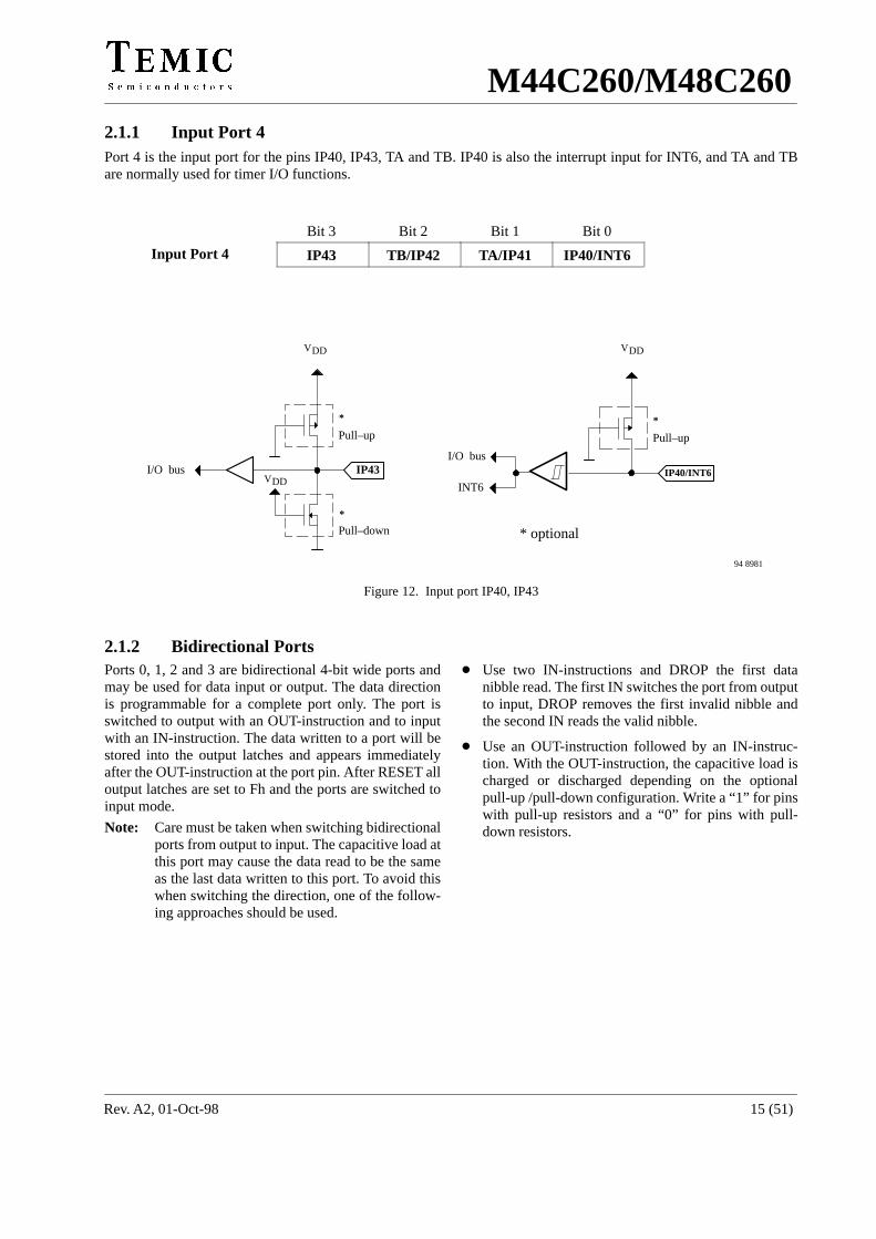
2.1.1 Input Port 4Port 4 is the input port for the pins IP40, IP43, TA and TB. IP40 is also the interrupt input for INT6, and TA and TBare normally used for timer I/O functions.
Bit 3 Bit 2 Bit 1 Bit 0ÁÁÁÁÁÁÁÁÁÁÁÁÁÁÁÁÁÁ
Input Port 4ÁÁÁÁÁÁÁÁÁÁIP43
ÁÁÁÁÁÁÁÁÁÁTB/IP42
ÁÁÁÁÁÁÁÁÁÁTA/IP41
ÁÁÁÁÁÁÁÁÁÁIP40/INT6
ÁÁÁÁÁÁÁÁÁÁÁÁÁÁÁÁÁÁÁÁÁÁÁÁÁ
ÁÁÁÁÁÁÁÁÁÁÁÁÁÁÁÁÁÁÁ
ÁÁÁÁÁÁÁÁÁÁ
ÁÁÁÁÁÁÁÁÁÁ
ÁÁÁÁÁÁÁÁÁÁ
ÁÁÁÁÁÁÁÁÁÁÁÁÁÁÁÁ
*
*
Pull–down
Pull–up
IP43
VDD
* optional
VDDI/O bus
*
Pull–up
IP40/INT6
VDD
INT6
I/O bus
94 8981
Figure 12. Input port IP40, IP43
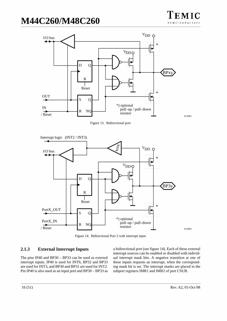
2.1.2 Bidirectional PortsPorts 0, 1, 2 and 3 are bidirectional 4-bit wide ports andmay be used for data input or output. The data directionis programmable for a complete port only. The port isswitched to output with an OUT-instruction and to inputwith an IN-instruction. The data written to a port will bestored into the output latches and appears immediatelyafter the OUT-instruction at the port pin. After RESET alloutput latches are set to Fh and the ports are switched toinput mode.
Note: Care must be taken when switching bidirectionalports from output to input. The capacitive load atthis port may cause the data read to be the sameas the last data written to this port. To avoid thiswhen switching the direction, one of the follow-ing approaches should be used.
Use two IN-instructions and DROP the first datanibble read. The first IN switches the port from outputto input, DROP removes the first invalid nibble andthe second IN reads the valid nibble.
Use an OUT-instruction followed by an IN-instruc-tion. With the OUT-instruction, the capacitive load ischarged or discharged depending on the optionalpull-up /pull-down configuration. Write a “1” for pinswith pull-up resistors and a “0” for pins with pull-down resistors.
M44C260/M48C260
Rev. A2, 01-Oct-9816 (51)
OUT
IN
Reset
I/O bus
D
R
S
Q
Q
NQ
R
/ Reset
VDD
VDD
BPxy
*) optional pull–up / pull–down resistor
*
*
94 8982
Figure 13. Bidirectional port
PortX_OUT
PortX_IN
Reset
I/O bus
D
R
S
Q
Q
NQ
R
/ Reset
VDD
VDD
BP3y
*) optional pull–up / pull–down resistor
*
*
Interrupt logic (INT2 / INT3)
94 8983
Figure 14. Bidirectional Port 3 with interrupt input
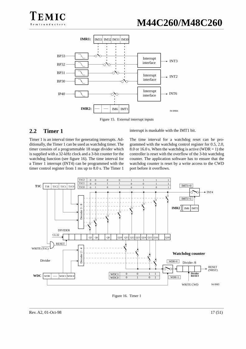
2.1.3 External Interrupt Inputs
The pins IP40 and BP30 – BP33 can be used as externalinterrupt inputs. IP40 is used for INT6, BP32 and BP33are used for INT3, and BP30 and BP31 are used for INT2.Pin IP40 is also used as an input port and BP30 – BP33 as
a bidirectional port (see figure 14). Each of these externalinterrupt sources can be enabled or disabled with individ-ual interrupt mask bits. A negative transition at one ofthese inputs requests an interrupt, when the correspond-ing mask bit is set. The interrupt masks are placed in thesubport registers IMR1 and IMR2 of port CSUB.
M44C260/M48C260
Rev. A2, 01-Oct-98 17 (51)
IM32 IM31 IM30IMR1: IM33
Interruptinterface
INT2
INT3BP33
BP32
BP31
BP30
IM6 IMT1IMR2:
Interruptinterface
INT6IP40Interruptinterface
94 8984
Figure 15. External interrupt inputs
2.2 Timer 1Timer 1 is an interval timer for generating interrupts. Ad-ditionally, the Timer 1 can be used as watchdog timer. Thetimer consists of a programmable 18 stage divider whichis supplied with a 32-kHz clock and a 3-bit counter for thewatchdog function (see figure 16). The time interval fora Timer 1 interrupt (INT4) can be programmed with thetimer control register from 1 ms up to 8.0 s. The Timer 1
interrupt is maskable with the IMT1 bit.
The time interval for a watchdog reset can be pro-grammed with the watchdog control register for 0.5, 2.0,8.0 or 16.0 s. When the watchdog is active (WDR = 1) thecontroller is reset with the overflow of the 3-bit watchdogcounter. The application software has to ensure that thewatchdog counter is reset by a write access to the CWDport before it overflows.
ÏÏÏÏÏÏÏÏÏÏÏÏÏÏÏÏÏÏ
T1R T1C1 T1C0T1C
CL32
Dec
oder
3 :
8
ÏÏÏÏÏÏÏÏÏÏÏÏÏÏÏÏÏÏÏÏÏÏÏÏÏÏÏÏÏÏÏÏÏÏÏÏÏÏÏÏÏÏÏÏÏ
0
0 10
0
1 1
1T1C0
T1C1
INT4
Dec
oder
2 :
4
WDR WDC1 WDC0WDC
Divider /8
DividerRESET
Watchdog counter
00
01
10
11
RESET(NRST)
ÏÏÏWDR=1
ÏÏÏÏÏÏ
WDR=0
IM6 IMT1IMR2
IMT1=1
IMT1=0
WRITE CWD
DIVIDER
T1C2
WDC1WDC0
Q5 Q6 Q8 Q10 Q12 Q14Q11 Q13 Q15 Q16 Q18
0
0 0 0 0T1C2 1
0
0 1 0 1
1 1
11 1
94 8985
Divider
RESET
WRITE (T1C)
Figure 16. Timer 1
M44C260/M48C260
Rev. A2, 01-Oct-9818 (51)
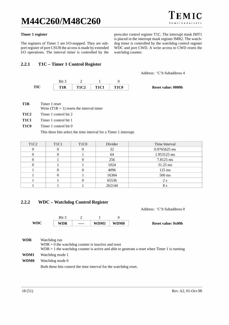
Timer 1 register
The registers of Timer 1 are I/O-mapped. They are sub-port register of port CSUB the access is made by extendedI/O operations. The interval timer is controlled by the
prescaler control register T1C. The interrupt mask IMT1is placed in the interrupt mask register IMR2. The watch-dog timer is controlled by the watchdog control registerWDC and port CWD. A write access to CWD resets thewatchdog counter.
2.2.1 T1C – Timer 1 Control Register
Address: ‘C’h Subaddress 4
Bit 3 2 1 0
ÁÁÁÁÁÁÁÁÁÁÁÁÁÁ
TIC ÁÁÁÁÁÁÁÁ
T1R ÁÁÁÁÁÁÁÁ
T1C2 ÁÁÁÁÁÁÁÁ
T1C1 ÁÁÁÁÁÁÁÁ
T1C0ÁÁÁÁÁÁÁÁÁÁÁÁÁÁÁÁÁÁÁÁÁÁÁÁÁÁÁÁÁÁ
Reset value: 0000b
ÁÁÁÁÁÁÁÁÁÁÁÁÁÁÁÁÁÁÁÁÁÁÁÁÁÁÁÁÁÁÁÁÁÁÁÁÁÁÁÁÁÁÁÁÁÁÁÁÁÁ
T1RÁÁÁÁÁÁÁÁÁÁÁÁÁÁÁÁÁÁÁÁÁÁÁÁÁÁÁÁÁÁÁÁÁÁÁÁÁÁÁÁÁÁÁÁÁÁÁÁÁÁÁÁÁÁÁÁÁÁÁÁÁÁÁÁÁÁÁÁÁÁÁÁÁÁÁÁÁÁÁÁÁÁÁÁÁÁÁ
Timer 1 resetWrite (T1R = 1) resets the interval timerÁÁÁÁ
ÁÁÁÁT1C2
ÁÁÁÁÁÁÁÁÁÁÁÁÁÁÁÁÁÁÁÁÁÁÁÁÁÁÁÁÁÁÁÁÁÁÁÁÁÁÁÁÁÁÁÁÁÁÁÁÁÁÁÁÁÁÁÁÁÁ
Timer 1 control bit 2ÁÁÁÁÁÁÁÁ
T1C1ÁÁÁÁÁÁÁÁÁÁÁÁÁÁÁÁÁÁÁÁÁÁÁÁÁÁÁÁÁÁÁÁÁÁÁÁÁÁÁÁÁÁÁÁÁÁÁÁÁÁÁÁÁÁÁÁÁÁ
Timer 1 control bit 1ÁÁÁÁÁÁÁÁ
T1C0ÁÁÁÁÁÁÁÁÁÁÁÁÁÁÁÁÁÁÁÁÁÁÁÁÁÁÁÁÁÁÁÁÁÁÁÁÁÁÁÁÁÁÁÁÁÁÁÁÁÁÁÁÁÁÁÁÁÁ
Timer 1 control bit 0ÁÁÁÁÁÁÁÁ
ÁÁÁÁÁÁÁÁÁÁÁÁÁÁÁÁÁÁÁÁÁÁÁÁÁÁÁÁÁÁÁÁÁÁÁÁÁÁÁÁÁÁÁÁÁÁÁÁÁÁÁÁÁÁÁÁÁÁ
This three bits select the time interval for a Timer 1 interrupt.
T1C2 T1C1 T1C0 Divider Time IntervalÁÁÁÁÁÁÁÁÁÁ
0ÁÁÁÁÁÁÁÁÁÁ
0ÁÁÁÁÁÁÁÁÁÁÁÁ
0ÁÁÁÁÁÁÁÁÁÁÁÁ
32ÁÁÁÁÁÁÁÁÁÁÁÁÁÁÁÁÁÁÁÁÁÁÁÁÁÁÁÁ
0.9765625 msÁÁÁÁÁÁÁÁÁÁ
0 ÁÁÁÁÁÁÁÁÁÁ
0 ÁÁÁÁÁÁÁÁÁÁÁÁ
1 ÁÁÁÁÁÁÁÁÁÁÁÁ
64 ÁÁÁÁÁÁÁÁÁÁÁÁÁÁÁÁÁÁÁÁÁÁÁÁÁÁÁÁ
1.953125 msÁÁÁÁÁÁÁÁÁÁ
0 ÁÁÁÁÁÁÁÁÁÁ
1 ÁÁÁÁÁÁÁÁÁÁÁÁ
0 ÁÁÁÁÁÁÁÁÁÁÁÁ
256 ÁÁÁÁÁÁÁÁÁÁÁÁÁÁÁÁÁÁÁÁÁÁÁÁÁÁÁÁ
7.8125 msÁÁÁÁÁÁÁÁÁÁ
0 ÁÁÁÁÁÁÁÁÁÁ
1 ÁÁÁÁÁÁÁÁÁÁÁÁ
1 ÁÁÁÁÁÁÁÁÁÁÁÁ
1024 ÁÁÁÁÁÁÁÁÁÁÁÁÁÁÁÁÁÁÁÁÁÁÁÁÁÁÁÁ
31.25 ms
ÁÁÁÁÁÁÁÁÁÁ
1 ÁÁÁÁÁÁÁÁÁÁ
0 ÁÁÁÁÁÁÁÁÁÁÁÁ
0 ÁÁÁÁÁÁÁÁÁÁÁÁ
4096 ÁÁÁÁÁÁÁÁÁÁÁÁÁÁÁÁÁÁÁÁÁÁÁÁÁÁÁÁ
125 ms
ÁÁÁÁÁ1 ÁÁÁÁÁ0 ÁÁÁÁÁÁ1 ÁÁÁÁÁÁ16384 ÁÁÁÁÁÁÁÁÁÁÁÁÁÁ500 msÁÁÁÁÁÁÁÁÁÁ1
ÁÁÁÁÁÁÁÁÁÁ1
ÁÁÁÁÁÁÁÁÁÁÁÁ0
ÁÁÁÁÁÁÁÁÁÁÁÁ65536
ÁÁÁÁÁÁÁÁÁÁÁÁÁÁÁÁÁÁÁÁÁÁÁÁÁÁÁÁ2 sÁÁÁÁÁ
ÁÁÁÁÁ1ÁÁÁÁÁÁÁÁÁÁ1
ÁÁÁÁÁÁÁÁÁÁÁÁ1
ÁÁÁÁÁÁÁÁÁÁÁÁ262144
ÁÁÁÁÁÁÁÁÁÁÁÁÁÁÁÁÁÁÁÁÁÁÁÁÁÁÁÁ8 s
2.2.2 WDC – Watchdog Control Register
Address: ‘C’h Subaddress 0
Bit 3 2 1 0
ÁÁÁÁÁÁÁÁÁÁÁÁÁÁ
WDC ÁÁÁÁÁÁÁÁ
WDR ÁÁÁÁÁÁÁÁ
––– ÁÁÁÁÁÁÁÁ
WDM1ÁÁÁÁÁÁÁÁ
WDM0ÁÁÁÁÁÁÁÁÁÁÁÁÁÁÁÁÁÁÁÁÁÁÁÁÁÁÁÁÁÁ
Reset value: 0x00b
ÁÁÁÁÁÁÁÁÁÁÁÁÁÁÁÁÁÁÁÁÁÁÁÁÁÁÁÁÁÁÁÁÁÁÁÁÁÁÁÁÁÁÁÁÁÁÁÁÁÁÁÁÁÁ
WDRÁÁÁÁÁÁÁÁÁÁÁÁÁÁÁÁÁÁÁÁÁÁÁÁÁÁÁÁÁÁÁÁÁÁÁÁÁÁÁÁÁÁÁÁÁÁÁÁÁÁÁÁÁÁÁÁÁÁÁÁÁÁÁÁÁÁÁÁÁÁÁÁÁÁÁÁÁÁÁÁÁÁÁÁÁÁÁÁÁÁÁÁÁÁÁÁÁÁÁÁÁÁÁÁÁÁÁÁÁÁÁÁÁÁÁÁ
Watchdog run WDR = 0 the watchdog counter is inactive and resetWDR = 1 the watchdog counter is active and able to generate a reset when Timer 1 is running
ÁÁÁÁÁÁÁÁ
WDM1ÁÁÁÁÁÁÁÁÁÁÁÁÁÁÁÁÁÁÁÁÁÁÁÁÁÁÁÁÁÁÁÁÁÁÁÁÁÁÁÁÁÁÁÁÁÁÁÁÁÁÁÁÁÁÁÁÁÁ
Watchdog mode 1ÁÁÁÁÁÁÁÁ
WDM0ÁÁÁÁÁÁÁÁÁÁÁÁÁÁÁÁÁÁÁÁÁÁÁÁÁÁÁÁÁÁÁÁÁÁÁÁÁÁÁÁÁÁÁÁÁÁÁÁÁÁÁÁÁÁÁÁÁÁ
Watchdog mode 0ÁÁÁÁÁÁÁÁ
ÁÁÁÁÁÁÁÁÁÁÁÁÁÁÁÁÁÁÁÁÁÁÁÁÁÁÁÁÁÁÁÁÁÁÁÁÁÁÁÁÁÁÁÁÁÁÁÁÁÁÁÁÁÁÁÁÁÁ
Both these bits control the time interval for the watchdog reset.
M44C260/M48C260
Rev. A2, 01-Oct-98 19 (51)
WDM 1 WDM 0 Divider Delay Time to Reset (s)ÁÁÁÁÁÁÁÁÁÁ
0 ÁÁÁÁÁÁÁÁÁÁÁÁ
0 ÁÁÁÁÁÁÁÁÁÁÁÁÁÁ
2048 ÁÁÁÁÁÁÁÁÁÁÁÁÁÁÁÁÁÁÁÁÁÁÁÁÁÁÁÁÁÁÁÁÁÁ
0.5ÁÁÁÁÁÁÁÁÁÁ
0 ÁÁÁÁÁÁÁÁÁÁÁÁ
1 ÁÁÁÁÁÁÁÁÁÁÁÁÁÁ
8192 ÁÁÁÁÁÁÁÁÁÁÁÁÁÁÁÁÁÁÁÁÁÁÁÁÁÁÁÁÁÁÁÁÁÁ
2
ÁÁÁÁÁÁÁÁÁÁ
1 ÁÁÁÁÁÁÁÁÁÁÁÁ
0 ÁÁÁÁÁÁÁÁÁÁÁÁÁÁ
32768 ÁÁÁÁÁÁÁÁÁÁÁÁÁÁÁÁÁÁÁÁÁÁÁÁÁÁÁÁÁÁÁÁÁÁ
8
ÁÁÁÁÁ1 ÁÁÁÁÁÁ1 ÁÁÁÁÁÁÁ524288 ÁÁÁÁÁÁÁÁÁÁÁÁÁÁÁÁÁ16
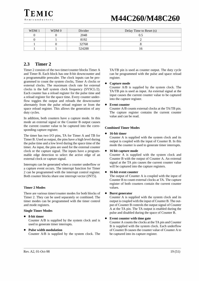
2.3 Timer 2Timer 2 consists of the two timer/counter blocks Timer Aand Timer B. Each block has one 8-bit downcounter anda programmable prescaler. The clock inputs can be pro-grammed to count the system clocks, Timer A clocks orexternal clocks. The maximum clock rate for externalclocks is the half system clock frequency (SYSCL/2).Each counter has a reload register for the pulse time anda reload register for the space time. Every counter under-flow toggles the output and reloads the downcounteralternately from the pulse reload register or from thespace reload register. This allows the generation of anyduty cycles.
In addition, both counters have a capture mode. In thismode an external signal or the Counter B output causesthe current counter value to be captured into the corre-sponding capture register.
The timer has two I/O pins, TA for Timer A and TB forTimer B. Used as output, the pins have a high level duringthe pulse time and a low level during the space time of thetimer. As input, the pins are used for the external counterclock or the capture signal. The inputs have a program-mable edge detection to select the active edge of anexternal clock or capture signal.
Interrupts can be generated when a counter underflow ora capture event occurs. The interrupt function for Timer2 can be programmed with the interrupt control register.Both counter blocks share one interrupt vector (INT5).
Timer 2 Modes
There are various timer/counter modes for both blocks ofTimer 2. They can be used separately or combined. Thetimer modes can be programmed with the timer controland mode registers.
Single Timer Modes
8-bit timerCounter A/B is supplied by the system clock and isused to generate timer interrupts.
Pulse width modulationCounter A/B is supplied by the system clock. The
TA/TB pin is used as counter output. The duty cyclecan be programmed with the pulse and space reloadregister.
Capture modeCounter A/B is supplied by the system clock. TheTA/TB pin is used as input. An external signal at theinput causes the current counter value to be capturedinto the capture register.
Event counterCounter A/B counts external clocks at the TA/TB pin.The capture register contains the current countervalue and can be read.
Combined Timer Modes
16-bit timerCounter A is supplied with the system clock and itsoutput is coupled with the input of Counter B. In thismode the counter is used to generate timer interrupts.
16 bit capture modeCounter A is supplied with the system clock andCounter B with the output of Counter A. An externalsignal at the TA pin causes the current counter valuewill be captured into the capture registers.
16-bit event counterThe output of Counter A is coupled with the input ofCounter B to count external clocks at TA. The captureregister of both counters contain the current countervalues.
Burst generatorCounter A is supplied with the system clock and itsoutput is coupled with the input of Counter B. The out-put of Counter B controls the output signal of CounterA at the TA pin. The TA output is enabled during thepulse and disabled during the space of Counter B.
Event counter with time gateCounter A counts the clocks at the TA pin and CounterB is supplied with the system clock. Each underflowof Counter B causes the counter value of Counter A tobe captured into its capture register.
M44C260/M48C260
Rev. A2, 01-Oct-9820 (51)
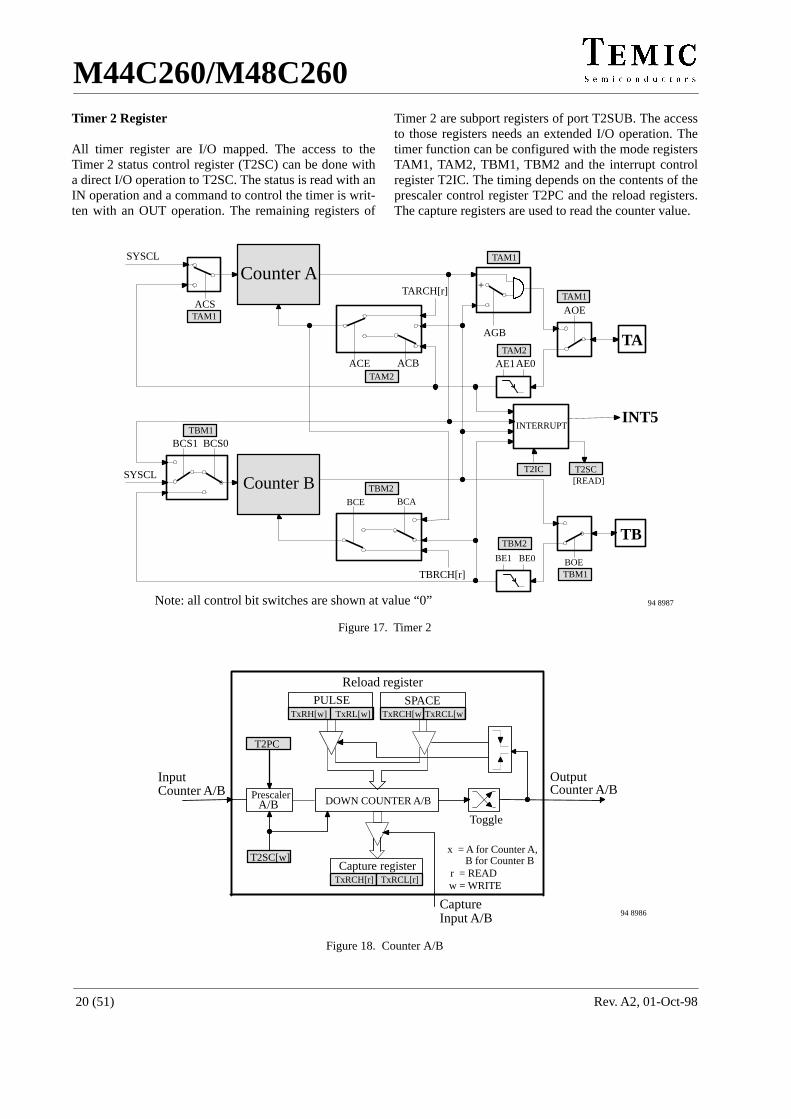
Timer 2 Register
All timer register are I/O mapped. The access to theTimer 2 status control register (T2SC) can be done witha direct I/O operation to T2SC. The status is read with anIN operation and a command to control the timer is writ-ten with an OUT operation. The remaining registers of
Timer 2 are subport registers of port T2SUB. The accessto those registers needs an extended I/O operation. Thetimer function can be configured with the mode registersTAM1, TAM2, TBM1, TBM2 and the interrupt controlregister T2IC. The timing depends on the contents of theprescaler control register T2PC and the reload registers.The capture registers are used to read the counter value.
TB
TA
SYSCL
T2SCT2ICSYSCL
ACS
ACE ACB AE1AE0
AGB
AOE
BE1 BE0 BOE
BCS1 BCS0
BCE
[READ]
+
TAM1
TAM1
TBM1
TBM2
TBM1
TARCH[r]
TAM2
TAM2
Counter ATAM1
Counter BBCA
TBRCH[r]
TBM2
INTERRUPTINT5
Note: all control bit switches are shown at value “0” 94 8987
Figure 17. Timer 2
DOWN COUNTER A/B
SPACEPULSE
Prescaler A/B
Capture register
T2PC
InputCounter A/B
OutputCounter A/B
CaptureInput A/B
Toggle
Reload register
TxRCH[r] TxRCL[r]
TxRCH[w]TxRCL[w]TxRH[w] TxRL[w]
T2SC[w]x = A for Counter A, B for Counter Br = READw = WRITE
94 8986
Figure 18. Counter A/B
M44C260/M48C260
Rev. A2, 01-Oct-98 21 (51)
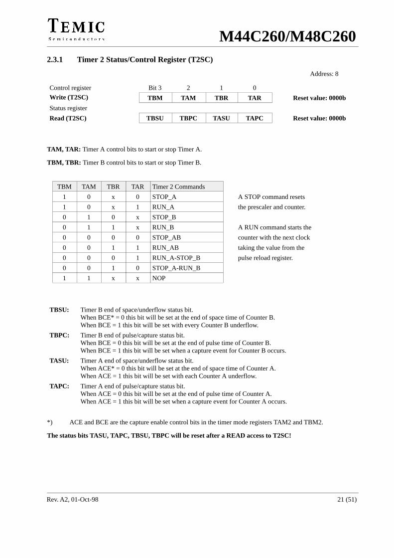
2.3.1 Timer 2 Status/Control Register (T2SC)
Address: 8
Control register Bit 3 2 1 0
ÁÁÁÁÁÁÁÁÁÁÁÁÁÁÁÁÁÁÁÁ
Write (T2SC) ÁÁÁÁÁÁÁÁ
TBMÁÁÁÁÁÁÁÁÁÁ
TAM ÁÁÁÁÁÁÁÁ
TBR ÁÁÁÁÁÁÁÁ
TAR ÁÁÁÁÁÁÁÁÁÁÁÁÁÁÁÁÁÁÁÁÁÁ
Reset value: 0000b
ÁÁÁÁÁÁÁÁÁÁÁÁÁÁÁÁÁÁÁÁ
Status register ÁÁÁÁÁÁÁÁ
ÁÁÁÁÁÁÁÁÁÁ
ÁÁÁÁÁÁÁÁ
ÁÁÁÁÁÁÁÁ
ÁÁÁÁÁÁÁÁÁÁÁÁÁÁÁÁÁÁÁÁÁÁÁÁÁÁÁÁÁÁÁÁ
ÁÁÁÁÁÁÁÁÁÁRead (T2SC) ÁÁÁÁ
ÁÁÁÁTBSUÁÁÁÁÁÁÁÁÁÁ
TBPC ÁÁÁÁÁÁÁÁ
TASU ÁÁÁÁÁÁÁÁ
TAPCÁÁÁÁÁÁÁÁÁÁÁÁÁÁÁÁÁÁÁÁÁÁ
Reset value: 0000b
ÁÁÁÁÁÁÁÁÁÁÁÁÁÁÁÁÁÁÁÁ
ÁÁÁÁÁÁÁÁ
ÁÁÁÁÁÁÁÁÁÁ
ÁÁÁÁÁÁÁÁ
ÁÁÁÁÁÁÁÁ
ÁÁÁÁÁÁÁÁÁÁÁÁÁÁÁÁÁÁÁÁÁÁ
TAM, TAR: Timer A control bits to start or stop Timer A.
TBM, TBR: Timer B control bits to start or stop Timer B.ÁÁÁÁÁÁÁÁÁÁÁÁÁÁÁÁÁÁÁÁÁÁÁÁ
ÁÁÁÁÁÁÁÁÁÁÁÁÁÁÁÁÁÁÁÁÁÁ
ÁÁÁÁÁÁÁÁÁÁÁÁÁÁÁÁÁÁÁÁÁÁÁÁÁÁÁÁÁÁÁÁ
TBM TAM TBR TAR Timer 2 CommandsÁÁÁÁÁÁÁÁÁÁ1ÁÁÁÁÁÁ0ÁÁÁÁÁÁÁÁx
ÁÁÁÁÁÁ0ÁÁÁÁÁÁÁÁÁÁÁÁÁÁÁÁSTOP_A
ÁÁÁÁÁÁÁÁÁÁÁÁÁÁÁÁÁÁÁÁÁÁÁÁÁÁÁÁÁÁÁÁA STOP command resetsÁÁ
ÁÁÁÁÁÁÁÁ1ÁÁÁÁÁÁ0ÁÁÁÁÁÁÁÁx
ÁÁÁÁÁÁ1ÁÁÁÁÁÁÁÁÁÁÁÁÁÁÁÁRUN_A
ÁÁÁÁÁÁÁÁÁÁÁÁÁÁÁÁÁÁÁÁÁÁÁÁÁÁÁÁÁÁÁÁthe prescaler and counter.ÁÁ
ÁÁÁÁÁÁÁÁ0ÁÁÁÁÁÁ1ÁÁÁÁÁÁÁÁ0
ÁÁÁÁÁÁxÁÁÁÁÁÁÁÁÁÁÁÁÁÁÁÁSTOP_B
ÁÁÁÁÁÁÁÁÁÁÁÁÁÁÁÁÁÁÁÁÁÁÁÁÁÁÁÁÁÁÁÁÁÁ
ÁÁÁÁÁÁÁÁ0ÁÁÁÁÁÁ1ÁÁÁÁÁÁÁÁ1
ÁÁÁÁÁÁxÁÁÁÁÁÁÁÁÁÁÁÁÁÁÁÁRUN_B
ÁÁÁÁÁÁÁÁÁÁÁÁÁÁÁÁÁÁÁÁÁÁÁÁÁÁÁÁÁÁÁÁA RUN command starts theÁÁ
ÁÁÁÁÁÁÁÁ0ÁÁÁÁÁÁ0ÁÁÁÁÁÁÁÁ0
ÁÁÁÁÁÁ0ÁÁÁÁÁÁÁÁÁÁÁÁÁÁÁÁSTOP_AB
ÁÁÁÁÁÁÁÁÁÁÁÁÁÁÁÁÁÁÁÁÁÁÁÁÁÁÁÁÁÁÁÁcounter with the next clockÁÁ
ÁÁÁÁÁÁÁÁ0ÁÁÁÁÁÁ0ÁÁÁÁÁÁÁÁ1
ÁÁÁÁÁÁ1ÁÁÁÁÁÁÁÁÁÁÁÁÁÁÁÁRUN_AB
ÁÁÁÁÁÁÁÁÁÁÁÁÁÁÁÁÁÁÁÁÁÁÁÁÁÁÁÁÁÁÁÁtaking the value from theÁÁ
ÁÁÁÁÁÁÁÁ0ÁÁÁÁÁÁ0ÁÁÁÁÁÁÁÁ0
ÁÁÁÁÁÁ1ÁÁÁÁÁÁÁÁÁÁÁÁÁÁÁÁRUN_A-STOP_B
ÁÁÁÁÁÁÁÁÁÁÁÁÁÁÁÁÁÁÁÁÁÁÁÁÁÁÁÁÁÁÁÁpulse reload register.ÁÁ
ÁÁÁÁÁÁÁÁ0ÁÁÁÁÁÁ0ÁÁÁÁÁÁÁÁ1
ÁÁÁÁÁÁ0ÁÁÁÁÁÁÁÁÁÁÁÁÁÁÁÁSTOP_A-RUN_B
ÁÁÁÁÁÁÁÁÁÁÁÁÁÁÁÁÁÁÁÁÁÁÁÁÁÁÁÁÁÁÁÁÁÁ
ÁÁÁÁÁÁÁÁ1ÁÁÁÁÁÁ1ÁÁÁÁÁÁÁÁx
ÁÁÁÁÁÁxÁÁÁÁÁÁÁÁÁÁÁÁÁÁÁÁNOP
ÁÁÁÁÁÁÁÁÁÁÁÁÁÁÁÁÁÁÁÁÁÁÁÁÁÁÁÁÁÁÁÁÁÁ
ÁÁÁÁÁÁÁÁÁÁÁÁÁÁÁÁÁÁÁÁÁÁ
ÁÁÁÁÁÁÁÁÁÁÁÁÁÁÁÁÁÁÁÁÁÁ
ÁÁÁÁÁÁÁÁÁÁÁÁÁÁÁÁÁÁÁÁÁÁÁÁÁÁÁÁÁÁÁÁ
ÁÁÁÁÁÁÁÁÁÁÁÁÁÁÁÁ
TBSU:ÁÁÁÁÁÁÁÁÁÁÁÁÁÁÁÁÁÁÁÁÁÁÁÁÁÁÁÁÁÁÁÁÁÁÁÁÁÁÁÁÁÁÁÁÁÁÁÁÁÁÁÁÁÁÁÁÁÁÁÁÁÁÁÁÁÁÁÁÁÁÁÁÁÁÁÁÁÁÁÁÁÁÁÁÁÁÁÁÁÁÁÁÁÁÁÁÁÁÁÁÁÁÁÁÁÁÁÁÁÁÁÁÁÁÁÁ
Timer B end of space/underflow status bit.When BCE* = 0 this bit will be set at the end of space time of Counter B.When BCE = 1 this bit will be set with every Counter B underflow.
ÁÁÁÁÁÁÁÁÁÁÁÁ
TBPC:ÁÁÁÁÁÁÁÁÁÁÁÁÁÁÁÁÁÁÁÁÁÁÁÁÁÁÁÁÁÁÁÁÁÁÁÁÁÁÁÁÁÁÁÁÁÁÁÁÁÁÁÁÁÁÁÁÁÁÁÁÁÁÁÁÁÁÁÁÁÁÁÁÁÁÁÁÁÁÁÁÁÁÁÁÁÁÁ
Timer B end of pulse/capture status bit.When BCE = 0 this bit will be set at the end of pulse time of Counter B.When BCE = 1 this bit will be set when a capture event for Counter B occurs.ÁÁÁÁ
ÁÁÁÁÁÁÁÁÁÁÁÁ
TASU:ÁÁÁÁÁÁÁÁÁÁÁÁÁÁÁÁÁÁÁÁÁÁÁÁÁÁÁÁÁÁÁÁÁÁÁÁÁÁÁÁÁÁÁÁÁÁÁÁÁÁÁÁÁÁÁÁÁÁÁÁÁÁÁÁÁÁÁÁÁÁÁÁÁÁÁÁÁÁÁÁÁÁÁÁÁÁÁÁÁÁÁÁÁÁÁÁÁÁÁÁÁÁÁÁÁÁÁÁÁÁÁÁÁÁÁÁ
Timer A end of space/underflow status bit.When ACE* = 0 this bit will be set at the end of space time of Counter A.When ACE = 1 this bit will be set with each Counter A underflow.
ÁÁÁÁÁÁÁÁÁÁÁÁ
TAPC:ÁÁÁÁÁÁÁÁÁÁÁÁÁÁÁÁÁÁÁÁÁÁÁÁÁÁÁÁÁÁÁÁÁÁÁÁÁÁÁÁÁÁÁÁÁÁÁÁÁÁÁÁÁÁÁÁÁÁÁÁÁÁÁÁÁÁÁÁÁÁÁÁÁÁÁÁÁÁÁÁÁÁÁÁÁÁÁ
Timer A end of pulse/capture status bit.When ACE = 0 this bit will be set at the end of pulse time of Counter A.When ACE = 1 this bit will be set when a capture event for Counter A occurs.
*) ACE and BCE are the capture enable control bits in the timer mode registers TAM2 and TBM2.
The status bits TASU, TAPC, TBSU, TBPC will be reset after a READ access to T2SC!
M44C260/M48C260
Rev. A2, 01-Oct-9822 (51)
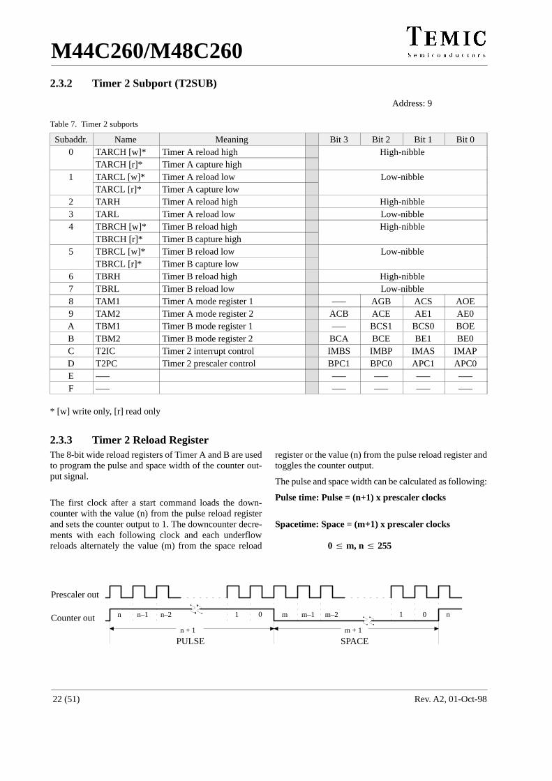
2.3.2 Timer 2 Subport (T2SUB)
Address: 9
Table 7. Timer 2 subports
Subaddr. Name Meaning Bit 3 Bit 2 Bit 1 Bit 0
ÁÁÁÁÁÁÁÁ
0 ÁÁÁÁÁÁÁÁÁÁÁÁ
TARCH [w]* ÁÁÁÁÁÁÁÁÁÁÁÁÁÁÁÁÁÁÁÁÁÁ
Timer A reload high ÁÁÁÁÁÁÁÁÁÁÁÁÁÁÁÁÁÁÁÁÁÁÁÁÁÁ
High-nibble
ÁÁÁÁÁÁÁÁÁÁTARCH [r]* ÁÁÁÁÁÁÁÁÁÁÁTimer A capture high ÁÁÁÁÁÁÁÁÁÁÁÁÁÁÁÁÁÁÁÁÁ1
ÁÁÁÁÁÁÁÁÁÁÁÁTARCL [w]*
ÁÁÁÁÁÁÁÁÁÁÁÁÁÁÁÁÁÁÁÁÁÁTimer A reload low
ÁÁÁÁÁÁÁÁÁÁÁÁÁÁÁÁÁÁÁÁÁÁÁÁÁÁLow-nibbleÁÁÁÁ
ÁÁÁÁÁÁÁÁÁÁÁÁÁÁÁÁTARCL [r]*
ÁÁÁÁÁÁÁÁÁÁÁÁÁÁÁÁÁÁÁÁÁÁTimer A capture low
ÁÁÁÁÁÁÁÁÁÁÁÁÁÁÁÁÁÁÁÁÁÁÁÁÁÁÁÁÁÁ
ÁÁÁÁ2ÁÁÁÁÁÁÁÁÁÁÁÁ
TARHÁÁÁÁÁÁÁÁÁÁÁÁÁÁÁÁÁÁÁÁÁÁ
Timer A reload highÁÁÁÁÁÁÁÁÁÁÁÁÁÁÁÁÁÁÁÁÁÁÁÁÁÁ
High-nibbleÁÁÁÁÁÁÁÁ
3 ÁÁÁÁÁÁÁÁÁÁÁÁ
TARL ÁÁÁÁÁÁÁÁÁÁÁÁÁÁÁÁÁÁÁÁÁÁ
Timer A reload low ÁÁÁÁÁÁÁÁÁÁÁÁÁÁÁÁÁÁÁÁÁÁÁÁÁÁ
Low-nibbleÁÁÁÁÁÁÁÁ
4 ÁÁÁÁÁÁÁÁÁÁÁÁ
TBRCH [w]* ÁÁÁÁÁÁÁÁÁÁÁÁÁÁÁÁÁÁÁÁÁÁ
Timer B reload high ÁÁÁÁÁÁÁÁÁÁÁÁÁÁÁÁÁÁÁÁÁÁÁÁÁÁ
High-nibbleÁÁÁÁÁÁÁÁ
ÁÁÁÁÁÁÁÁÁÁÁÁ
TBRCH [r]* ÁÁÁÁÁÁÁÁÁÁÁÁÁÁÁÁÁÁÁÁÁÁ
Timer B capture high ÁÁÁÁÁÁÁÁÁÁÁÁÁÁÁÁÁÁÁÁÁÁÁÁÁÁÁÁÁÁ
ÁÁÁÁ5 ÁÁÁÁÁÁÁÁÁÁÁÁ
TBRCL [w]* ÁÁÁÁÁÁÁÁÁÁÁÁÁÁÁÁÁÁÁÁÁÁ
Timer B reload low ÁÁÁÁÁÁÁÁÁÁÁÁÁÁÁÁÁÁÁÁÁÁÁÁÁÁ
Low-nibble
ÁÁÁÁÁÁÁÁÁÁTBRCL [r]* ÁÁÁÁÁÁÁÁÁÁÁTimer B capture low ÁÁÁÁÁÁÁÁÁÁÁÁÁÁÁÁÁÁÁÁÁ6
ÁÁÁÁÁÁÁÁÁÁÁÁTBRH
ÁÁÁÁÁÁÁÁÁÁÁÁÁÁÁÁÁÁÁÁÁÁTimer B reload high
ÁÁÁÁÁÁÁÁÁÁÁÁÁÁÁÁÁÁÁÁÁÁÁÁÁÁHigh-nibbleÁÁÁÁ
ÁÁÁÁ7ÁÁÁÁÁÁÁÁÁÁÁÁ
TBRLÁÁÁÁÁÁÁÁÁÁÁÁÁÁÁÁÁÁÁÁÁÁ
Timer B reload lowÁÁÁÁÁÁÁÁÁÁÁÁÁÁÁÁÁÁÁÁÁÁÁÁÁÁ
Low-nibbleÁÁÁÁÁÁÁÁ
8ÁÁÁÁÁÁÁÁÁÁÁÁ
TAM1ÁÁÁÁÁÁÁÁÁÁÁÁÁÁÁÁÁÁÁÁÁÁ
Timer A mode register 1ÁÁÁÁÁÁÁÁ
–––ÁÁÁÁÁÁÁÁ
AGBÁÁÁÁÁÁÁÁ
ACSÁÁÁÁÁÁÁÁ
AOEÁÁÁÁÁÁÁÁ
9 ÁÁÁÁÁÁÁÁÁÁÁÁ
TAM2 ÁÁÁÁÁÁÁÁÁÁÁÁÁÁÁÁÁÁÁÁÁÁ
Timer A mode register 2 ÁÁÁÁÁÁÁÁ
ACB ÁÁÁÁÁÁÁÁ
ACE ÁÁÁÁÁÁÁÁ
AE1 ÁÁÁÁÁÁÁÁ
AE0ÁÁÁÁÁÁÁÁ
A ÁÁÁÁÁÁÁÁÁÁÁÁ
TBM1 ÁÁÁÁÁÁÁÁÁÁÁÁÁÁÁÁÁÁÁÁÁÁ
Timer B mode register 1 ÁÁÁÁÁÁÁÁ
––– ÁÁÁÁÁÁÁÁ
BCS1 ÁÁÁÁÁÁÁÁ
BCS0 ÁÁÁÁÁÁÁÁ
BOEÁÁÁÁÁÁÁÁ
B ÁÁÁÁÁÁÁÁÁÁÁÁ
TBM2 ÁÁÁÁÁÁÁÁÁÁÁÁÁÁÁÁÁÁÁÁÁÁ
Timer B mode register 2 ÁÁÁÁÁÁÁÁ
BCA ÁÁÁÁÁÁÁÁ
BCE ÁÁÁÁÁÁÁÁ
BE1 ÁÁÁÁÁÁÁÁ
BE0
ÁÁÁÁÁÁÁÁ
C ÁÁÁÁÁÁÁÁÁÁÁÁ
T2IC ÁÁÁÁÁÁÁÁÁÁÁÁÁÁÁÁÁÁÁÁÁÁ
Timer 2 interrupt control ÁÁÁÁÁÁÁÁ
IMBS ÁÁÁÁÁÁÁÁ
IMBP ÁÁÁÁÁÁÁÁ
IMAS ÁÁÁÁÁÁÁÁ
IMAP
ÁÁÁÁD ÁÁÁÁÁÁT2PC ÁÁÁÁÁÁÁÁÁÁÁTimer 2 prescaler control ÁÁÁÁBPC1 ÁÁÁÁBPC0 ÁÁÁÁAPC1 ÁÁÁÁAPC0ÁÁÁÁÁÁÁÁE
ÁÁÁÁÁÁÁÁÁÁÁÁ–––
ÁÁÁÁÁÁÁÁÁÁÁÁÁÁÁÁÁÁÁÁÁÁ
ÁÁÁÁÁÁÁÁ–––
ÁÁÁÁÁÁÁÁ–––
ÁÁÁÁÁÁÁÁ–––
ÁÁÁÁÁÁÁÁ–––ÁÁÁÁ
ÁÁÁÁFÁÁÁÁÁÁÁÁÁÁÁÁ
–––ÁÁÁÁÁÁÁÁÁÁÁÁÁÁÁÁÁÁÁÁÁÁ
ÁÁÁÁÁÁÁÁ
–––ÁÁÁÁÁÁÁÁ
–––ÁÁÁÁÁÁÁÁ
–––ÁÁÁÁÁÁÁÁ
–––
* [w] write only, [r] read only
2.3.3 Timer 2 Reload RegisterThe 8-bit wide reload registers of Timer A and B are usedto program the pulse and space width of the counter out-put signal.
The first clock after a start command loads the down-counter with the value (n) from the pulse reload registerand sets the counter output to 1. The downcounter decre-ments with each following clock and each underflowreloads alternately the value (m) from the space reload
register or the value (n) from the pulse reload register andtoggles the counter output.
The pulse and space width can be calculated as following:
Pulse time: Pulse = (n+1) x prescaler clocks
Spacetime: Space = (m+1) x prescaler clocks
0 m, n 255
n n–1 n–2 1 0 m m–1 m–2
PULSE
1 0 n
SPACE
Prescaler out
Counter outn + 1 m + 1
M44C260/M48C260
Rev. A2, 01-Oct-98 23 (51)
Timer 2 Space Reload RegisterThe space reload register of Timer 2 is programmed bytwo write accesses to the subport addresses TARCH andTARCL or TBRCH and TBRCL of the Timer 2 subportT2SUB. The value (m) in the space reload register deter-mines the space width. At the end of the pulse, thedowncounter reloads the 8–bit value from the space re-load register with the next clock of the prescaler output.
Space width: Space = (m+1) prescaler clocks0 ≤ m ≤ 255
Timer 2 Pulse Reload RegisterThe pulse reload register of Timer 2 is programmed bytwo write accesses to the subport addresses TERH andTARL or TBRH and TBRL of the Timer 2 subportT2SUB. The value (n) in the pulse reload register deter-mines the space width. At the end of space thedowncounter reloads the 8-bit value from the pulse reloadregister with the next clock of the prescaler output.
Pulse width: Pulse = (n+1) prescaler clocks0 ≤ n ≤ 255
2.3.4 Timer 2 Capture Register
The capture register is used to capture the current down-counter value when a capture event occurs. The value iskept in the capture register until the next capture eventand can be read independent of the state of the down-counter. The capture events are programmable with thetimer mode registers TAM2 and TBM2.
The capture registers are also used to read the countervalue when the external capture mode is disabled. In thiscase the 8-bit counter value is transferred into the captureregister by reading the high nibble TARCH or TBRCH.If the 16-bit event counter mode is enabled the complete16-bit value is captured by reading first the high nibbleTARCH of Timer A. This mechanism ensures the coher-ence of the counter high and low nibble during the readaccess.
2.3.5 Timer A Mode Register 1 (TAM1)
Address: 9 – Subaddress: 8
Bit 3 2 1 0ÁÁÁÁÁÁÁÁÁÁÁÁÁÁTAM1
ÁÁÁÁÁÁÁÁ–––
ÁÁÁÁÁÁÁÁAGB
ÁÁÁÁÁÁÁÁACS
ÁÁÁÁÁÁÁÁAOE
ÁÁÁÁÁÁÁÁÁÁÁÁÁÁÁÁÁÁÁÁÁÁÁÁÁÁÁÁÁÁReset value: 0000bÁÁÁÁÁÁÁ
ÁÁÁÁÁÁÁÁÁÁÁÁÁÁÁ
ÁÁÁÁÁÁÁÁ
ÁÁÁÁÁÁÁÁ
ÁÁÁÁÁÁÁÁ
ÁÁÁÁÁÁÁÁÁÁÁÁÁÁÁÁÁÁÁÁÁÁÁÁÁÁÁÁÁÁ
ÁÁÁÁÁÁÁÁÁÁÁÁ
AGB ÁÁÁÁÁÁÁÁÁÁÁÁÁÁÁÁÁÁÁÁÁÁÁÁÁÁÁÁÁÁÁÁÁÁÁÁÁÁÁÁÁÁÁÁÁÁÁÁÁÁÁÁÁÁÁÁÁÁÁÁÁÁÁÁÁÁÁÁÁÁÁÁÁÁÁÁÁÁÁÁÁÁÁÁÁÁÁ
Counter A output gated by Counter B output AGB = 1 enables the burst generation mode. The output of Timer A is enabled during the pulse timeof the Counter B and disabled (TA= 0) during the space time of the Counter B.
ÁÁÁÁÁÁÁÁÁÁÁÁÁÁÁÁ
ACS ÁÁÁÁÁÁÁÁÁÁÁÁÁÁÁÁÁÁÁÁÁÁÁÁÁÁÁÁÁÁÁÁÁÁÁÁÁÁÁÁÁÁÁÁÁÁÁÁÁÁÁÁÁÁÁÁÁÁÁÁÁÁÁÁÁÁÁÁÁÁÁÁÁÁÁÁÁÁÁÁÁÁÁÁÁÁÁÁÁÁÁÁÁÁÁÁÁÁÁÁÁÁÁÁÁÁÁÁÁÁÁÁÁÁÁÁ
Counter A clock select This bit selects the source of the Counter A clock. When ACS = 0 the timer is supplied with internalSYSCL. When ACS = 1 the timer is supplied with an external clock on TA pin.
ÁÁÁÁÁÁÁÁÁÁÁÁ
AOE ÁÁÁÁÁÁÁÁÁÁÁÁÁÁÁÁÁÁÁÁÁÁÁÁÁÁÁÁÁÁÁÁÁÁÁÁÁÁÁÁÁÁÁÁÁÁÁÁÁÁÁÁÁÁÁÁÁÁÁÁÁÁÁÁÁÁÁÁÁÁÁÁÁÁÁÁÁÁÁÁÁÁÁÁÁÁÁ
Timer A output enableAOE = 0 disables the counter output TA.AOE = 1 enables the counter output TA.
M44C260/M48C260
Rev. A2, 01-Oct-9824 (51)
2.3.6 Timer A Mode Register 2 (TAM2)
Address: 9 – Subaddress: 9
Bit 3 2 1 0
ÁÁÁÁÁÁÁÁÁÁÁÁÁÁ
TAM2 ÁÁÁÁÁÁÁÁ
ACB ÁÁÁÁÁÁ
ACEÁÁÁÁÁÁÁÁ
AE1ÁÁÁÁÁÁÁÁÁÁ
AE0 ÁÁÁÁÁÁÁÁÁÁÁÁÁÁÁÁÁÁÁÁÁÁÁÁÁÁÁÁÁÁ
Reset Value: 0000b
ÁÁÁÁÁÁÁÁÁÁÁÁÁÁ
ÁÁÁÁÁÁÁÁ
ÁÁÁÁÁÁÁÁÁÁÁÁÁÁ
ÁÁÁÁÁÁÁÁÁÁ
ÁÁÁÁÁÁÁÁÁÁÁÁÁÁÁÁÁÁÁÁÁÁÁÁÁÁÁÁÁÁ
ÁÁÁÁÁÁÁÁÁÁÁÁÁÁÁÁ
ACB ÁÁÁÁÁÁÁÁÁÁÁÁÁÁÁÁÁÁÁÁÁÁÁÁÁÁÁÁÁÁÁÁÁÁÁÁÁÁÁÁÁÁÁÁÁÁÁÁÁÁÁÁÁÁÁÁÁÁÁÁÁÁÁÁÁÁÁÁÁÁÁÁÁÁÁÁÁÁÁÁÁÁÁÁÁÁÁÁÁÁÁÁÁÁÁÁÁÁÁÁÁÁÁÁÁÁÁÁÁÁÁÁÁÁÁÁ
Timer A captured by Timer BSelects the capture source for Timer A. When ACB = 0 the signal at the TA pin is used to generate acapture event. When ACB = 1 each transition at the Counter B output is used to generate a captureevent for Timer A.
ÁÁÁÁÁÁÁÁÁÁÁÁÁÁÁÁ
ACE ÁÁÁÁÁÁÁÁÁÁÁÁÁÁÁÁÁÁÁÁÁÁÁÁÁÁÁÁÁÁÁÁÁÁÁÁÁÁÁÁÁÁÁÁÁÁÁÁÁÁÁÁÁÁÁÁÁÁÁÁÁÁÁÁÁÁÁÁÁÁÁÁÁÁÁÁÁÁÁÁÁÁÁÁÁÁÁÁÁÁÁÁÁÁÁÁÁÁÁÁÁÁÁÁÁÁÁÁÁÁÁÁÁÁÁÁ
Timer A capture enable ACE = 1 enables the capture mode for Counter A. The occurrence of a capture event causes that thecurrent downcounter value is loaded into the capture register.
ÁÁÁÁÁÁÁÁ
AE1 ÁÁÁÁÁÁÁÁÁÁÁÁÁÁÁÁÁÁÁÁÁÁÁÁÁÁÁÁÁÁÁÁÁÁÁÁÁÁÁÁÁÁÁÁÁÁÁÁÁÁÁÁÁÁÁÁÁÁ
Timer A edge select bit 1
ÁÁÁÁÁÁÁÁ
AE0 ÁÁÁÁÁÁÁÁÁÁÁÁÁÁÁÁÁÁÁÁÁÁÁÁÁÁÁÁÁÁÁÁÁÁÁÁÁÁÁÁÁÁÁÁÁÁÁÁÁÁÁÁÁÁÁÁÁÁ
Timer A edge select bit 0With these bits the active edge for the counter clocks and capture signal is selected.
AE1 AE0 Active Edge for Counter Clock/Capture EventsÁÁÁÁÁÁ
0ÁÁÁÁÁÁÁÁ
0ÁÁÁÁÁÁÁÁÁÁÁÁÁÁÁÁÁÁÁÁÁÁÁÁÁÁÁÁÁÁÁÁÁÁÁÁÁÁÁÁÁÁÁÁÁÁÁÁÁÁÁÁÁÁ
positive edge at TA pinÁÁÁÁÁÁ
0ÁÁÁÁÁÁÁÁ
1ÁÁÁÁÁÁÁÁÁÁÁÁÁÁÁÁÁÁÁÁÁÁÁÁÁÁÁÁÁÁÁÁÁÁÁÁÁÁÁÁÁÁÁÁÁÁÁÁÁÁÁÁÁÁ
negative edge at TA pinÁÁÁÁÁÁ
1ÁÁÁÁÁÁÁÁ
0 ÁÁÁÁÁÁÁÁÁÁÁÁÁÁÁÁÁÁÁÁÁÁÁÁÁÁÁÁÁÁÁÁÁÁÁÁÁÁÁÁÁÁÁÁÁÁÁÁÁÁÁÁÁÁ
first positive edge after timer start and then each transition at TA pinÁÁÁÁÁÁ
1ÁÁÁÁÁÁÁÁ
1 ÁÁÁÁÁÁÁÁÁÁÁÁÁÁÁÁÁÁÁÁÁÁÁÁÁÁÁÁÁÁÁÁÁÁÁÁÁÁÁÁÁÁÁÁÁÁÁÁÁÁÁÁÁÁ
first negative edge after timer start and then each transition at TA pin
2.3.7 Timer B Mode Register 1 (TBM1)
Address: 9 – Subaddress: Ah
Bit 3 2 1 0
ÁÁÁÁÁÁÁÁÁÁÁÁÁÁ
TBM1 ÁÁÁÁÁÁÁÁ
––– ÁÁÁÁÁÁÁÁ
BCS1 ÁÁÁÁÁÁÁÁ
BCS0ÁÁÁÁÁÁÁÁ
BOEÁÁÁÁÁÁÁÁÁÁÁÁÁÁÁÁÁÁÁÁÁÁÁÁÁÁÁÁÁÁ
Reset value: 0000b
ÁÁÁÁÁÁÁÁÁÁÁÁÁÁ
ÁÁÁÁÁÁÁÁ
ÁÁÁÁÁÁÁÁ
ÁÁÁÁÁÁÁÁ
ÁÁÁÁÁÁÁÁ
ÁÁÁÁÁÁÁÁÁÁÁÁÁÁÁÁÁÁÁÁÁÁÁÁÁÁÁÁÁÁ
ÁÁÁÁÁÁÁÁÁÁ
BCS1 ÁÁÁÁÁÁÁÁÁÁÁÁÁÁÁÁÁÁÁÁÁÁÁÁÁÁÁÁÁÁÁÁÁÁÁÁÁÁÁÁÁÁÁÁÁÁÁÁÁÁÁÁÁÁÁÁTimer B clock select bit 1
ÁÁÁÁÁÁÁÁÁÁ
BCS0 ÁÁÁÁÁÁÁÁÁÁÁÁÁÁÁÁÁÁÁÁÁÁÁÁÁÁÁÁÁÁÁÁÁÁÁÁÁÁÁÁÁÁÁÁÁÁÁÁÁÁÁÁÁÁÁÁTimer B clock select bit 0
ÁÁÁÁÁÁÁÁÁÁ
ÁÁÁÁÁÁÁÁÁÁÁÁÁÁÁÁÁÁÁÁÁÁÁÁÁÁÁÁÁÁÁÁÁÁÁÁÁÁÁÁÁÁÁÁÁÁÁÁÁÁÁÁÁÁÁÁThese bits select the source of Counter B clock.
BCS1 BCS0 Counter B Input SignalÁÁÁÁÁÁ0ÁÁÁÁÁÁÁÁ0
ÁÁÁÁÁÁÁÁÁÁÁÁÁÁÁÁÁÁÁÁÁÁSystem clock (SYSCL)ÁÁÁ
ÁÁÁ1ÁÁÁÁÁÁÁÁ0
ÁÁÁÁÁÁÁÁÁÁÁÁÁÁÁÁÁÁÁÁÁÁOutput signal of Counter AÁÁÁ
ÁÁÁxÁÁÁÁÁÁÁÁ
1ÁÁÁÁÁÁÁÁÁÁÁÁÁÁÁÁÁÁÁÁÁÁ
External input signal at TB
ÁÁÁÁÁÁÁÁÁÁÁÁÁÁÁÁÁÁÁÁ
BOEÁÁÁÁÁÁÁÁÁÁÁÁÁÁÁÁÁÁÁÁÁÁÁÁÁÁÁÁÁÁÁÁÁÁÁÁÁÁÁÁÁÁÁÁÁÁÁÁÁÁÁÁÁÁÁÁÁÁÁÁÁÁÁÁÁÁÁÁÁÁÁÁÁÁÁÁÁÁÁÁÁÁÁÁÁÁÁÁÁÁÁÁÁÁÁÁÁÁÁÁÁÁÁÁÁÁÁÁÁÁÁÁ
Timer B output enableBOE = 0 disables the counter output TB.BOE = 1 enables the counter output TB.
M44C260/M48C260
Rev. A2, 01-Oct-98 25 (51)
2.3.8 Timer B Mode Register 2 (TBM2)
Address: 9 – Subaddress: Bh
Bit 3 2 1 0
ÁÁÁÁÁÁÁÁÁÁÁÁÁÁ
TBM2 ÁÁÁÁÁÁÁÁ
BCA ÁÁÁÁÁÁ
BCEÁÁÁÁÁÁÁÁÁÁ
BE1 ÁÁÁÁÁÁÁÁ
BE0 ÁÁÁÁÁÁÁÁÁÁÁÁÁÁÁÁÁÁÁÁÁÁÁÁÁÁÁÁÁÁ
Reset value: 0000b
ÁÁÁÁÁÁÁÁÁÁÁÁÁÁ
ÁÁÁÁÁÁÁÁ
ÁÁÁÁÁÁÁÁÁÁÁÁÁÁÁÁ
ÁÁÁÁÁÁÁÁ
ÁÁÁÁÁÁÁÁÁÁÁÁÁÁÁÁÁÁÁÁÁÁÁÁÁÁÁÁÁÁ
ÁÁÁÁÁÁÁÁ
BCA ÁÁÁÁÁÁÁÁÁÁÁÁÁÁÁÁÁÁÁÁÁÁÁÁÁÁÁÁÁÁÁÁÁÁÁÁÁÁÁÁÁÁÁÁÁÁÁÁÁÁÁÁÁÁÁÁÁÁ
Timer B is captured with Timer A capture signal. With BCA = 1 the external capture signal forTimer A is used to capture Timer B simultaneously with Timer A.ÁÁÁÁ
ÁÁÁÁÁÁÁÁÁÁÁÁ
BCEÁÁÁÁÁÁÁÁÁÁÁÁÁÁÁÁÁÁÁÁÁÁÁÁÁÁÁÁÁÁÁÁÁÁÁÁÁÁÁÁÁÁÁÁÁÁÁÁÁÁÁÁÁÁÁÁÁÁÁÁÁÁÁÁÁÁÁÁÁÁÁÁÁÁÁÁÁÁÁÁÁÁÁÁÁÁÁÁÁÁÁÁÁÁÁÁÁÁÁÁÁÁÁÁÁÁÁÁÁÁÁÁÁÁÁÁ
Timer B capture enable BCE = 1 enables the capture mode for Counter B. A capture event loads the current downcountervalue into the capture register.
ÁÁÁÁÁÁÁÁ
BE1 ÁÁÁÁÁÁÁÁÁÁÁÁÁÁÁÁÁÁÁÁÁÁÁÁÁÁÁÁÁÁÁÁÁÁÁÁÁÁÁÁÁÁÁÁÁÁÁÁÁÁÁÁÁÁÁÁÁÁ
Timer B edge select bit 1ÁÁÁÁÁÁÁÁÁÁÁÁ
BE0 ÁÁÁÁÁÁÁÁÁÁÁÁÁÁÁÁÁÁÁÁÁÁÁÁÁÁÁÁÁÁÁÁÁÁÁÁÁÁÁÁÁÁÁÁÁÁÁÁÁÁÁÁÁÁÁÁÁÁÁÁÁÁÁÁÁÁÁÁÁÁÁÁÁÁÁÁÁÁÁÁÁÁÁÁÁÁÁ
Timer B edge select bit 0With these bits the active edge for the counter clocks and capture signal is selected.
BE1 BE0 Active Edge for Clock/Capture Events
ÁÁÁÁÁÁÁÁ
0 ÁÁÁÁÁÁ
0 ÁÁÁÁÁÁÁÁÁÁÁÁÁÁÁÁÁÁÁÁÁÁÁÁÁÁÁÁÁÁÁÁÁÁÁÁÁÁÁÁÁÁÁÁÁÁÁÁÁÁÁÁÁÁ
positive edge on TB pin
ÁÁÁÁ0 ÁÁÁ1 ÁÁÁÁÁÁÁÁÁÁÁÁÁÁÁÁÁÁÁÁÁÁÁÁÁÁÁnegative edge on TB pinÁÁÁÁÁÁÁÁ1
ÁÁÁÁÁÁ0ÁÁÁÁÁÁÁÁÁÁÁÁÁÁÁÁÁÁÁÁÁÁÁÁÁÁÁÁÁÁÁÁÁÁÁÁÁÁÁÁÁÁÁÁÁÁÁÁÁÁÁÁÁÁfirst positive edge after start timer and then each transition on TB pinÁÁÁÁ
ÁÁÁÁ1ÁÁÁÁÁÁ
1ÁÁÁÁÁÁÁÁÁÁÁÁÁÁÁÁÁÁÁÁÁÁÁÁÁÁÁÁÁÁÁÁÁÁÁÁÁÁÁÁÁÁÁÁÁÁÁÁÁÁÁÁÁÁ
first negative edge after start timer and then each transition on TB pin
2.3.9 Timer 2 Prescaler Control Register (T2PC)
Address: 9 – Subaddress: Dh
Bit 3 2 1 0ÁÁÁÁÁÁÁÁÁÁÁÁÁÁ
T2PC ÁÁÁÁÁÁÁÁ
BPC1 ÁÁÁÁÁÁÁÁ
BPC0ÁÁÁÁÁÁÁÁ
APC1ÁÁÁÁÁÁÁÁ
APC0ÁÁÁÁÁÁÁÁÁÁÁÁÁÁÁÁÁÁÁÁÁÁÁÁÁÁÁÁÁÁ
Reset Value: 0000bÁÁÁÁÁÁÁÁÁÁÁÁÁÁ
ÁÁÁÁÁÁÁÁ
ÁÁÁÁÁÁÁÁ
ÁÁÁÁÁÁÁÁ
ÁÁÁÁÁÁÁÁ
ÁÁÁÁÁÁÁÁÁÁÁÁÁÁÁÁÁÁÁÁÁÁÁÁÁÁÁÁÁÁ
ÁÁÁÁÁÁÁÁ
BPC1ÁÁÁÁÁÁÁÁÁÁÁÁÁÁÁÁÁÁÁÁÁÁÁÁÁÁÁÁÁÁÁÁÁÁÁÁÁÁÁÁÁÁÁÁÁÁÁÁÁÁÁÁÁÁÁÁÁÁ
Timer B prescaler control bit 1ÁÁÁÁÁÁÁÁÁÁÁÁ
BPC0ÁÁÁÁÁÁÁÁÁÁÁÁÁÁÁÁÁÁÁÁÁÁÁÁÁÁÁÁÁÁÁÁÁÁÁÁÁÁÁÁÁÁÁÁÁÁÁÁÁÁÁÁÁÁÁÁÁÁÁÁÁÁÁÁÁÁÁÁÁÁÁÁÁÁÁÁÁÁÁÁÁÁÁÁÁÁÁ
Timer B prescaler control bit 0These bits determine the divider for the prescaler of Timer B.
ÁÁÁÁÁÁÁÁ
APC1 ÁÁÁÁÁÁÁÁÁÁÁÁÁÁÁÁÁÁÁÁÁÁÁÁÁÁÁÁÁÁÁÁÁÁÁÁÁÁÁÁÁÁÁÁÁÁÁÁÁÁÁÁÁÁÁÁÁÁ
Timer A prescaler control bit 1ÁÁÁÁÁÁÁÁÁÁÁÁ
APC0 ÁÁÁÁÁÁÁÁÁÁÁÁÁÁÁÁÁÁÁÁÁÁÁÁÁÁÁÁÁÁÁÁÁÁÁÁÁÁÁÁÁÁÁÁÁÁÁÁÁÁÁÁÁÁÁÁÁÁÁÁÁÁÁÁÁÁÁÁÁÁÁÁÁÁÁÁÁÁÁÁÁÁÁÁÁÁÁ
Timer A prescaler control bit 0These bits determine the divider for the prescaler of Timer A.
BPC1/APC1 BPC0/APC0 Divider
ÁÁÁÁÁÁÁÁÁÁÁÁ
0 ÁÁÁÁÁÁÁÁÁÁÁÁ
0 ÁÁÁÁÁÁÁÁÁÁ
1
ÁÁÁÁÁÁ0 ÁÁÁÁÁÁ1 ÁÁÁÁÁ4ÁÁÁÁÁÁÁÁÁÁÁÁ1
ÁÁÁÁÁÁÁÁÁÁÁÁ0
ÁÁÁÁÁÁÁÁÁÁ16ÁÁÁÁÁÁ
ÁÁÁÁÁÁ1ÁÁÁÁÁÁÁÁÁÁÁÁ
1ÁÁÁÁÁÁÁÁÁÁ
64
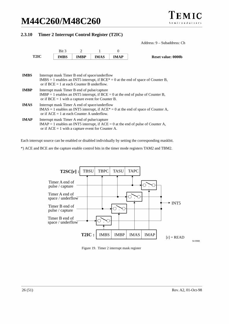
M44C260/M48C260
Rev. A2, 01-Oct-9826 (51)
2.3.10 Timer 2 Interrupt Control Register (T2IC)
Address: 9 – Subaddress: Ch
Bit 3 2 1 0
ÁÁÁÁÁÁÁÁÁÁÁÁÁÁ
T2IC ÁÁÁÁÁÁÁÁ
IMBS ÁÁÁÁÁÁÁÁ
IMBP ÁÁÁÁÁÁÁÁ
IMAS ÁÁÁÁÁÁÁÁ
IMAPÁÁÁÁÁÁÁÁÁÁÁÁÁÁÁÁÁÁÁÁÁÁÁÁÁÁÁÁÁÁ
Reset value: 0000b
ÁÁÁÁÁÁÁÁÁÁÁÁÁÁ
ÁÁÁÁÁÁÁÁ
ÁÁÁÁÁÁÁÁ
ÁÁÁÁÁÁÁÁ
ÁÁÁÁÁÁÁÁ
ÁÁÁÁÁÁÁÁÁÁÁÁÁÁÁÁÁÁÁÁÁÁÁÁÁÁÁÁÁÁ
ÁÁÁÁÁÁÁÁÁÁÁÁ
IMBS ÁÁÁÁÁÁÁÁÁÁÁÁÁÁÁÁÁÁÁÁÁÁÁÁÁÁÁÁÁÁÁÁÁÁÁÁÁÁÁÁÁÁÁÁÁÁÁÁÁÁÁÁÁÁÁÁÁÁÁÁÁÁÁÁÁÁÁÁÁÁÁÁÁÁÁÁÁÁÁÁÁÁÁÁÁÁÁ
Interrupt mask Timer B end of space/underflowIMBS = 1 enables an INT5 interrupt, if BCE* = 0 at the end of space of Counter B, or if BCE = 1 at each Counter B underflow.
ÁÁÁÁÁÁÁÁÁÁÁÁÁÁÁÁ
IMBPÁÁÁÁÁÁÁÁÁÁÁÁÁÁÁÁÁÁÁÁÁÁÁÁÁÁÁÁÁÁÁÁÁÁÁÁÁÁÁÁÁÁÁÁÁÁÁÁÁÁÁÁÁÁÁÁÁÁÁÁÁÁÁÁÁÁÁÁÁÁÁÁÁÁÁÁÁÁÁÁÁÁÁÁÁÁÁÁÁÁÁÁÁÁÁÁÁÁÁÁÁÁÁÁÁÁÁÁÁÁÁÁÁÁÁÁ
Interrupt mask Timer B end of pulse/captureIMBP = 1 enables an INT5 interrupt, if BCE = 0 at the end of pulse of Counter B, or if BCE = 1 with a capture event for Counter B.
ÁÁÁÁÁÁÁÁÁÁÁÁ
IMAS ÁÁÁÁÁÁÁÁÁÁÁÁÁÁÁÁÁÁÁÁÁÁÁÁÁÁÁÁÁÁÁÁÁÁÁÁÁÁÁÁÁÁÁÁÁÁÁÁÁÁÁÁÁÁÁÁÁÁÁÁÁÁÁÁÁÁÁÁÁÁÁÁÁÁÁÁÁÁÁÁÁÁÁÁÁÁÁ
Interrupt mask Timer A end of space/underflowIMAS = 1 enables an INT5 interrupt, if ACE* = 0 at the end of space of Counter A, or if ACE = 1 at each Counter A underflow.
ÁÁÁÁÁÁÁÁÁÁÁÁÁÁÁÁ
IMAPÁÁÁÁÁÁÁÁÁÁÁÁÁÁÁÁÁÁÁÁÁÁÁÁÁÁÁÁÁÁÁÁÁÁÁÁÁÁÁÁÁÁÁÁÁÁÁÁÁÁÁÁÁÁÁÁÁÁÁÁÁÁÁÁÁÁÁÁÁÁÁÁÁÁÁÁÁÁÁÁÁÁÁÁÁÁÁÁÁÁÁÁÁÁÁÁÁÁÁÁÁÁÁÁÁÁÁÁÁÁÁÁÁÁÁÁ
Interrupt mask Timer A end of pulse/captureIMAP = 1 enables an INT5 interrupt, if ACE = 0 at the end of pulse of Counter A, or if ACE = 1 with a capture event for Counter A.
Each interrupt source can be enabled or disabled individually by setting the corresponding maskbit.
*) ACE and BCE are the capture enable control bits in the timer mode registers TAM2 and TBM2.
INT5
TBSU TBPC TASU TAPC
IMBS IMBP IMAS IMAP
T2SC[r] :
T2IC :
Timer A end of space / underflow
Timer A end of pulse / capture
Timer B end of space / underflow
Timer B end of pulse / capture
[r] = READ94 8988
Figure 19. Timer 2 interrupt mask register
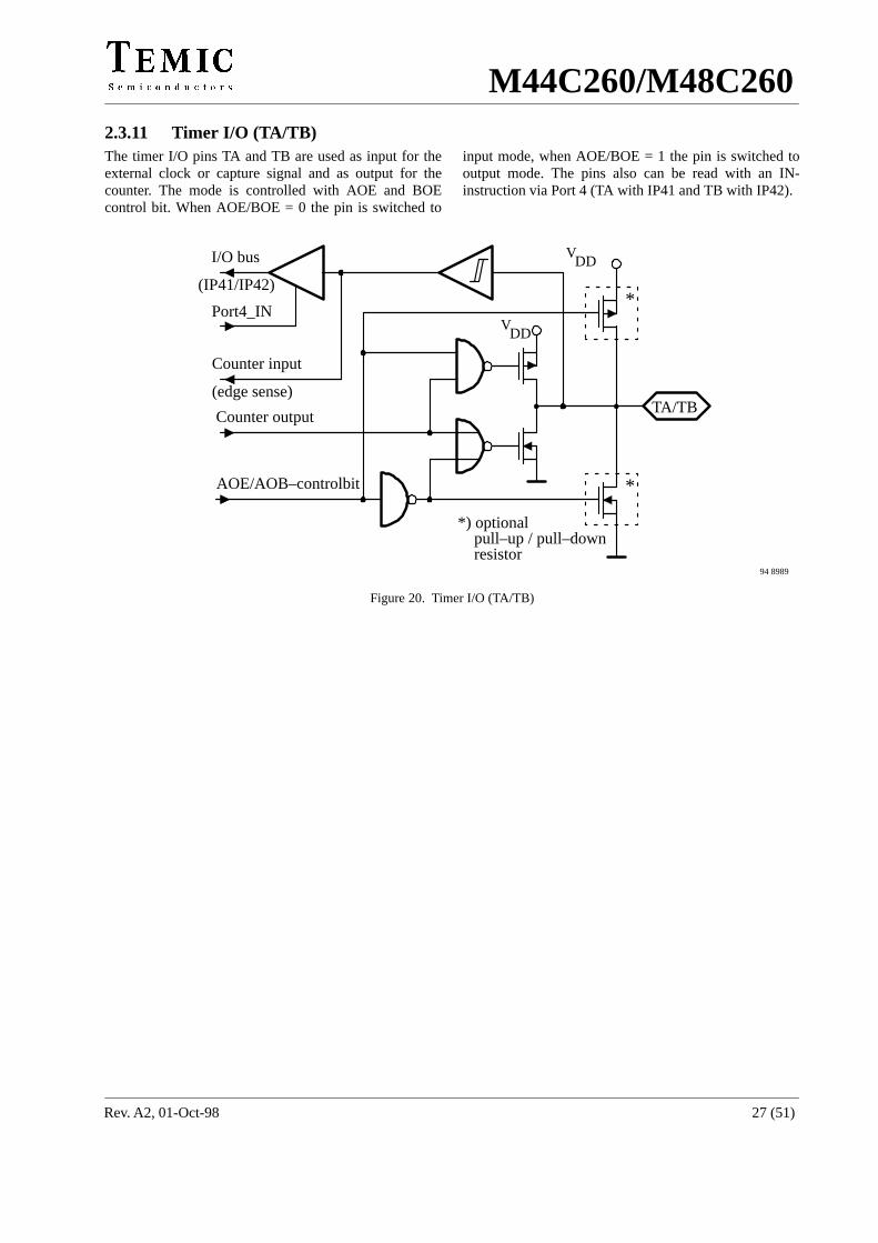
M44C260/M48C260
Rev. A2, 01-Oct-98 27 (51)
2.3.11 Timer I/O (TA/TB)The timer I/O pins TA and TB are used as input for theexternal clock or capture signal and as output for thecounter. The mode is controlled with AOE and BOEcontrol bit. When AOE/BOE = 0 the pin is switched to
input mode, when AOE/BOE = 1 the pin is switched tooutput mode. The pins also can be read with an IN-instruction via Port 4 (TA with IP41 and TB with IP42).
Port4_IN
I/O bus VDD
VDD
TA/TB
*) optional pull–up / pull–down resistor
*
*
Counter input
Counter output
AOE/AOB–controlbit
(edge sense)
(IP41/IP42)
94 8989
Figure 20. Timer I/O (TA/TB)
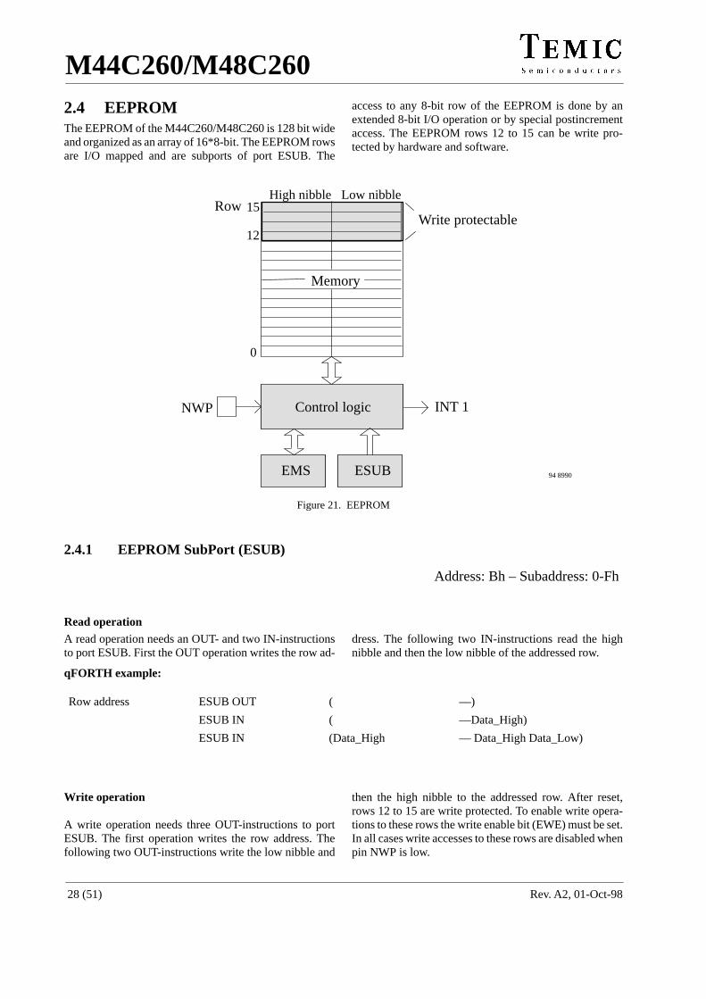
M44C260/M48C260
Rev. A2, 01-Oct-9828 (51)
2.4 EEPROMThe EEPROM of the M44C260/M48C260 is 128 bit wideand organized as an array of 16*8-bit. The EEPROM rowsare I/O mapped and are subports of port ESUB. The
access to any 8-bit row of the EEPROM is done by anextended 8-bit I/O operation or by special postincrementaccess. The EEPROM rows 12 to 15 can be write pro-tected by hardware and software.
Write protectable
NWP Control logic
EMS ESUB
0
12
15
INT 1
Memory
RowHigh nibble Low nibble
94 8990
Figure 21. EEPROM
2.4.1 EEPROM SubPort (ESUB)
Address: Bh – Subaddress: 0-Fh
Read operationA read operation needs an OUT- and two IN-instructionsto port ESUB. First the OUT operation writes the row ad-
dress. The following two IN-instructions read the highnibble and then the low nibble of the addressed row.
qFORTH example:
Row address ESUB OUT ( ––)
ESUB IN ( ––Data_High)
ESUB IN (Data_High –– Data_High Data_Low)
Write operation
A write operation needs three OUT-instructions to portESUB. The first operation writes the row address. Thefollowing two OUT-instructions write the low nibble and
then the high nibble to the addressed row. After reset,rows 12 to 15 are write protected. To enable write opera-tions to these rows the write enable bit (EWE) must be set.In all cases write accesses to these rows are disabled whenpin NWP is low.
M44C260/M48C260
Rev. A2, 01-Oct-98 29 (51)
qFORTH example:
Row address ESUB OUT (Data_High Data_Low –– Data_High Data_Low)
ESUB OUT (Data_High Data_Low ––Data_High)
ESUB OUT (Data_High ––)
The internal EEPROM write cycle needs about 16 ms(with connected quartz crystal and running crystal oscil-lator). During this cycle the EEPROM ready bit is reset(EPR = 0). After the data high nibble is written to the portESUB, the internal write cycle is started. During theinternal write cycle (while EPR = 0), only read and writeaccesses to the EMS register are possible. All otherEEPROM accesses have no effect.
Postincrement operations
The postincrement mode supports a fast access toconsecutive EEPROM rows. A postincrement access isstarted by setting the EPI bit in the EEPROM mode regis-ter (EMS) followed by writing the row start address toport ESUB. After that, the read or write operations to theconsecutive EEPROM area, beginning at the start ad-
dress, need only two IN- or OUT-instructions to read orwrite the data. The row address is incremented automati-cally after each complete row access (2 nibbles). A writeaccess to the EEPROM mode register (EMS) terminatesthe postincrement mode.
Note: In the postincrement mode, it is not possible tochange from read to write operations or viceversa before the current postincrement operationis finished.
Write ready interrupt (INT1)
At the end of the internal write cycle an interrupt is gener-ated when the interrupt mask bit IMEP in the EEPROMmode register EMS is set. With this interrupt, successivewrite operations can be executed interrupt controlledwithin the INT1 interrupt service routine.
2.4.2 EEPROM Mode/Status Register (EMS)
Address: Ah
Mode register Bit 3 2 1 0ÁÁÁÁÁÁÁÁÁÁÁÁÁÁÁÁÁÁÁÁ
Write (EMS) ÁÁÁÁÁÁÁÁ
–––ÁÁÁÁÁÁÁÁÁÁ
EWE ÁÁÁÁÁÁÁÁ
EPI ÁÁÁÁÁÁÁÁ
IMEPÁÁÁÁÁÁÁÁÁÁÁÁÁÁÁÁÁÁÁÁÁÁ
Reset value: 0000bÁÁÁÁÁÁÁÁÁÁÁÁÁÁÁÁÁÁÁÁ
Status register ÁÁÁÁÁÁÁÁ
ÁÁÁÁÁÁÁÁÁÁ
ÁÁÁÁÁÁÁÁ
ÁÁÁÁÁÁÁÁ
ÁÁÁÁÁÁÁÁÁÁÁÁÁÁÁÁÁÁÁÁÁÁÁÁÁÁÁÁÁÁÁÁ
ÁÁÁÁÁÁÁÁÁÁRead (EMS) ÁÁÁÁ
ÁÁÁÁ–––ÁÁÁÁÁÁÁÁÁÁ
––– ÁÁÁÁÁÁÁÁ
––– ÁÁÁÁÁÁÁÁ
EPRÁÁÁÁÁÁÁÁÁÁÁÁÁÁÁÁÁÁÁÁÁÁ
Reset value: xxx1bÁÁÁÁÁÁÁÁÁÁÁÁÁÁÁÁÁÁÁÁ
ÁÁÁÁÁÁÁÁ
ÁÁÁÁÁÁÁÁÁÁ
ÁÁÁÁÁÁÁÁ
ÁÁÁÁÁÁÁÁ
ÁÁÁÁÁÁÁÁÁÁÁÁÁÁÁÁÁÁÁÁÁÁ
ÁÁÁÁÁÁÁÁÁÁÁÁ
EWE ÁÁÁÁÁÁÁÁÁÁÁÁÁÁÁÁÁÁÁÁÁÁÁÁÁÁÁÁÁÁÁÁÁÁÁÁÁÁÁÁÁÁÁÁÁÁÁÁÁÁÁÁÁÁÁÁÁÁÁÁÁÁÁÁÁÁÁÁÁÁÁÁÁÁÁÁÁÁÁÁÁÁÁÁÁÁÁ
EEPROM write enable bit EWE = 0 disables write accesses to rows 12-15EWE = 1 enables write accesses to rows 12-15 when the NWP pin is highÁÁÁÁ
ÁÁÁÁÁÁÁÁ
EPIÁÁÁÁÁÁÁÁÁÁÁÁÁÁÁÁÁÁÁÁÁÁÁÁÁÁÁÁÁÁÁÁÁÁÁÁÁÁÁÁÁÁÁÁÁÁÁÁÁÁÁÁÁÁÁÁÁÁÁÁÁÁÁÁÁÁÁÁÁÁÁÁÁÁÁÁÁÁÁÁÁÁÁÁÁÁÁ
EEPROM postincrement mode enableEPI = 1 activates a postincrement access after the next row address is written to port ESUB
ÁÁÁÁÁÁÁÁÁÁÁÁ
IMEPÁÁÁÁÁÁÁÁÁÁÁÁÁÁÁÁÁÁÁÁÁÁÁÁÁÁÁÁÁÁÁÁÁÁÁÁÁÁÁÁÁÁÁÁÁÁÁÁÁÁÁÁÁÁÁÁÁÁÁÁÁÁÁÁÁÁÁÁÁÁÁÁÁÁÁÁÁÁÁÁÁÁÁÁÁÁÁ
Interrupt mask for EEPROM write ready interruptWhen IMEP is set an INT1 is generated with the end of the internal EEPROM write cycle
ÁÁÁÁÁÁÁÁÁÁÁÁÁÁÁÁ
EPR ÁÁÁÁÁÁÁÁÁÁÁÁÁÁÁÁÁÁÁÁÁÁÁÁÁÁÁÁÁÁÁÁÁÁÁÁÁÁÁÁÁÁÁÁÁÁÁÁÁÁÁÁÁÁÁÁÁÁÁÁÁÁÁÁÁÁÁÁÁÁÁÁÁÁÁÁÁÁÁÁÁÁÁÁÁÁÁÁÁÁÁÁÁÁÁÁÁÁÁÁÁÁÁÁÁÁÁÁÁÁÁÁÁÁÁÁ
EEPROM ready status flagEPR = 0 indicates that the EEPROM is not ready for read or write operations
(an internal write cycle is executed)EPR = 1 indicates that the EEPROM is ready for read and write operations
After a write access to the EMS-Register, postincrement operations are terminated and any incomplete EEPROM readand write sequence must be started again!
M44C260/M48C260
Rev. A2, 01-Oct-9830 (51)
3 Appendix
3.1 EmulationFor emulation all MARC4 controllers have a specialemulation mode. It is activated by setting the TE pin tologic HIGH level during reset. In this mode the internalCPU core is inactive and the I/O buses are available viaPort 0 and Port 1 to allow the emulator the access to theon-chip peripherals. The emulator contains a specialemulation CPU with a MARC4 core and additional break-point logic and takes over the core function. The basicfunction of the emulator is to evaluate the customer’s pro-gram and hardware in real time. Thus, the analysation ofany timing, hardware or software problems the simula-tion of the application is possible. For more informationabout emulation see “Emulator Manual”.
3.2 Programming the EEPROMProgram Memory
Programming the 4K8-bit EEPROM program memoryis done using a special PC-controlled programming de-vice. Details on how to use this device and thecorresponding software are given in the ProgrammingDevice User Manual.
To start programming the data memory, the micro-controller is switched to a special I/O mode, where thecore and all peripherals are set inactive and the two I/Obuses are available via Port 0 (data) and Port 1 (control).Then the customer application data is transfered to thecontroller via Port 0 in blocks of 64 nibble size. Program-ming is started automatically after each block. Theprogramming high voltage is generated on chip.
After programming the memory, a verify run is startedwhere the just written data is read out and compared bitby bit to the original source file. This ensures that the con-tent of the ROM is error free.
3.3 MARC4 Instruction SetThe MARC4 instruction set is optimized for the high levelprogramming language qFORTH. A lot of MARC4instructions are qFORTH words. This enables the com-piler to generate a fast and compact program code. TheMARC4 is a zero address machine with a compact and ef-ficient instruction code. Most of the instructions are
single byte instructions. These operations are performedand no source or destination address information . OnlyBRANCH, CALL and RAM access instructions need ad-dress information and a length of two bytes for longaddress operations. In total, there are five types of instruc-tion formats with a length of one and two bytes.
Zero address operations such as arithmetical, logical,shift and rotate operations are performed with data placedon the top of the expression stack (TOS and TOS–1). AlsoI/O– and stack operations are single byte zero address op-erations and are performed with the top expression stacklocation.
A literal is a 4-bit constant value which is placed on thedata stack. In the MARC4 native code they are repre-sented as LIT_<value>, where <value> is thehexadecimal representation from 0 to 15 (0...F). Thisrange is a result of the MARC4’s 4-bit data width. The6-bit short address and the 12-bit long address formats areboth used to address the byte-wide ROM via CALL andconditional branch instructions. This results in a ROMaddress space of up to 4K8-bit words.
The MARC4 instruction includes both short and long callinstructions as well as conditional branch instructions. Onexecution the address part of the instruction’s word is di-rectly loaded into the program counter. Long call andbranch instructions can jump anywhere within the pro-gram memory area. The lower six bits from the short call(SCALL) and short branch (SBRA) instruction are han-dled in a different way. The six bit SCALL address ismultiplied by three and then loaded into the PC. Thisallows calls within the zero page (000 to 1FFh). The sixbit SBRA address is loaded immediately into the lowersix bits of the PC. This allows jumps within the 64 bytesegment addressed by the upper six bits of the PC.
The CALL and SCALL instructions write the increm-ented program counter contents to the return stack. Thisaddress is loaded back to the PC when the associatedEXIT or RTI instruction is encountered. The long RAMaddress format is used by the four 8-bit RAM addressregisters which can be pre-increment, post-decrement orloaded directly from the MARC4’s internal bus. Thisresults in a direct accessible RAM address space of up to256 4-bit.
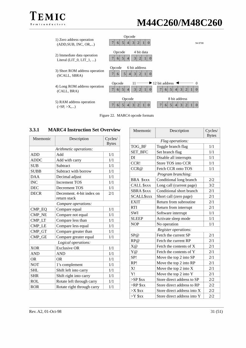
M44C260/M48C260
Rev. A2, 01-Oct-98 31 (51)
7 6 5 4
3 2 1 07 6 5 4
3 2 1 0
3 2 1 05 47 6
7 6 5 4 3 2 1 0 3 2 1 07 6 5 4
3 2 1 07 6 5 4 3 2 1 07 6 5 4
Opcode
Opcode 4 bit data
Opcode
Opcode
Opcode 8 bit address
6 bit address
12 bit address11 0
1) Zero address operation
2) Immediate data operation
3) Short ROM address operation
4) Long ROM address operation
5) RAM address operation
Literal (LIT_0, LIT_1, ...)
(ADD,SUB, INC, OR,...)
(SCALL, SBRA)
(CALL, BRA)
(>SP, >X,...)
94 8708
Figure 22. MARC4 opcode formats
3.3.1 MARC4 Instruction Set Overview
Mnemonic Description Cycles/Bytes
Arithmetic operations:ÁÁÁÁÁÁÁÁÁÁADD
ÁÁÁÁÁÁÁÁÁÁÁÁÁÁÁÁÁÁAdd
ÁÁÁÁÁÁ1/1ÁÁÁÁÁ
ÁÁÁÁÁADDC
ÁÁÁÁÁÁÁÁÁÁÁÁÁÁÁÁÁÁ
Add with carryÁÁÁÁÁÁ
1/1ÁÁÁÁÁÁÁÁÁÁ
SUB ÁÁÁÁÁÁÁÁÁÁÁÁÁÁÁÁÁÁ
Subtract ÁÁÁÁÁÁ
1/1ÁÁÁÁÁÁÁÁÁÁ
SUBB ÁÁÁÁÁÁÁÁÁÁÁÁÁÁÁÁÁÁ
Subtract with borrow ÁÁÁÁÁÁ
1/1ÁÁÁÁÁÁÁÁÁÁ
DAA ÁÁÁÁÁÁÁÁÁÁÁÁÁÁÁÁÁÁ
Decimal adjust ÁÁÁÁÁÁ
1/1
ÁÁÁÁÁÁÁÁÁÁ
INC ÁÁÁÁÁÁÁÁÁÁÁÁÁÁÁÁÁÁ
Increment TOS ÁÁÁÁÁÁ
1/1
ÁÁÁÁÁDEC ÁÁÁÁÁÁÁÁÁDecrement TOS ÁÁÁ1/1ÁÁÁÁÁÁÁÁÁÁÁÁÁÁÁ
DECRÁÁÁÁÁÁÁÁÁÁÁÁÁÁÁÁÁÁÁÁÁÁÁÁÁÁÁ
Decrement. 4-bit index onreturn stack
ÁÁÁÁÁÁÁÁÁ
2/1
Compare operations:ÁÁÁÁÁÁÁÁÁÁ
CMP_EQ ÁÁÁÁÁÁÁÁÁÁÁÁÁÁÁÁÁÁ
Compare equal ÁÁÁÁÁÁ
1/1ÁÁÁÁÁÁÁÁÁÁ
CMP_NE ÁÁÁÁÁÁÁÁÁÁÁÁÁÁÁÁÁÁ
Compare not equal ÁÁÁÁÁÁ
1/1
ÁÁÁÁÁÁÁÁÁÁ
CMP_LT ÁÁÁÁÁÁÁÁÁÁÁÁÁÁÁÁÁÁ
Compare less than ÁÁÁÁÁÁ
1/1
ÁÁÁÁÁCMP_LE ÁÁÁÁÁÁÁÁÁCompare less equal ÁÁÁ1/1ÁÁÁÁÁÁÁÁÁÁCMP_GT
ÁÁÁÁÁÁÁÁÁÁÁÁÁÁÁÁÁÁCompare greater than
ÁÁÁÁÁÁ1/1ÁÁÁÁÁ
ÁÁÁÁÁCMP_GEÁÁÁÁÁÁÁÁÁÁÁÁÁÁÁÁÁÁCompare greater equal
ÁÁÁÁÁÁ1/1
Logical operations:ÁÁÁÁÁÁÁÁÁÁ
XOR ÁÁÁÁÁÁÁÁÁÁÁÁÁÁÁÁÁÁ
Exclusive OR ÁÁÁÁÁÁ
1/1ÁÁÁÁÁÁÁÁÁÁ
AND ÁÁÁÁÁÁÁÁÁÁÁÁÁÁÁÁÁÁ
AND ÁÁÁÁÁÁ
1/1ÁÁÁÁÁÁÁÁÁÁ
OR ÁÁÁÁÁÁÁÁÁÁÁÁÁÁÁÁÁÁ
OR ÁÁÁÁÁÁ
1/1
ÁÁÁÁÁÁÁÁÁÁ
NOT ÁÁÁÁÁÁÁÁÁÁÁÁÁÁÁÁÁÁ
1’s complement ÁÁÁÁÁÁ
1/1
ÁÁÁÁÁSHL ÁÁÁÁÁÁÁÁÁShift left into carry ÁÁÁ1/1ÁÁÁÁÁÁÁÁÁÁSHR
ÁÁÁÁÁÁÁÁÁÁÁÁÁÁÁÁÁÁShift right into carry
ÁÁÁÁÁÁ1/1ÁÁÁÁÁ
ÁÁÁÁÁROLÁÁÁÁÁÁÁÁÁÁÁÁÁÁÁÁÁÁRotate left through carry
ÁÁÁÁÁÁ1/1ÁÁÁÁÁ
ÁÁÁÁÁROR
ÁÁÁÁÁÁÁÁÁÁÁÁÁÁÁÁÁÁ
Rotate right through carryÁÁÁÁÁÁ
1/1
Mnemonic Description Cycles/Bytes
Flag operations:ÁÁÁÁÁÁÁÁÁÁ
TOG_BF ÁÁÁÁÁÁÁÁÁÁÁÁÁÁÁÁÁÁ
Toggle branch flag ÁÁÁÁÁÁ
1/1ÁÁÁÁÁÁÁÁÁÁ
SET_BFC ÁÁÁÁÁÁÁÁÁÁÁÁÁÁÁÁÁÁ
Set branch flag ÁÁÁÁÁÁ
1/1ÁÁÁÁÁÁÁÁÁÁ
DI ÁÁÁÁÁÁÁÁÁÁÁÁÁÁÁÁÁÁ
Disable all interrupts ÁÁÁÁÁÁ
1/1
ÁÁÁÁÁÁÁÁÁÁ
CCR! ÁÁÁÁÁÁÁÁÁÁÁÁÁÁÁÁÁÁ
Store TOS into CCR ÁÁÁÁÁÁ
1/1
ÁÁÁÁÁCCR@ ÁÁÁÁÁÁÁÁÁFetch CCR onto TOS ÁÁÁ1/1Program branching:ÁÁÁÁÁ
ÁÁÁÁÁBRA $xxxÁÁÁÁÁÁÁÁÁÁÁÁÁÁÁÁÁÁConditional long branch
ÁÁÁÁÁÁ2/2ÁÁÁÁÁ
ÁÁÁÁÁCALL $xxx
ÁÁÁÁÁÁÁÁÁÁÁÁÁÁÁÁÁÁ
Long call (current page)ÁÁÁÁÁÁ
3/2ÁÁÁÁÁÁÁÁÁÁ
SBRA $xxxÁÁÁÁÁÁÁÁÁÁÁÁÁÁÁÁÁÁ
Conditional short branch ÁÁÁÁÁÁ
2/1ÁÁÁÁÁÁÁÁÁÁ
SCALL$xxxÁÁÁÁÁÁÁÁÁÁÁÁÁÁÁÁÁÁ
Short call (zero page) ÁÁÁÁÁÁ
2/1ÁÁÁÁÁÁÁÁÁÁ
EXIT ÁÁÁÁÁÁÁÁÁÁÁÁÁÁÁÁÁÁ
Return from subroutine ÁÁÁÁÁÁ
2/1
ÁÁÁÁÁÁÁÁÁÁ
RTI ÁÁÁÁÁÁÁÁÁÁÁÁÁÁÁÁÁÁ
Return from interrupt ÁÁÁÁÁÁ
2/1
ÁÁÁÁÁSWI ÁÁÁÁÁÁÁÁÁSoftware interrupt ÁÁÁ1/1ÁÁÁÁÁÁÁÁÁÁSLEEP
ÁÁÁÁÁÁÁÁÁÁÁÁÁÁÁÁÁÁActivate sleep mode
ÁÁÁÁÁÁ1/1ÁÁÁÁÁ
ÁÁÁÁÁNOPÁÁÁÁÁÁÁÁÁÁÁÁÁÁÁÁÁÁNo operation
ÁÁÁÁÁÁ1/1
Register operations:ÁÁÁÁÁÁÁÁÁÁ
SP@ ÁÁÁÁÁÁÁÁÁÁÁÁÁÁÁÁÁÁ
Fetch the current SP ÁÁÁÁÁÁ
2/1ÁÁÁÁÁÁÁÁÁÁ
RP@ ÁÁÁÁÁÁÁÁÁÁÁÁÁÁÁÁÁÁ
Fetch the current RP ÁÁÁÁÁÁ
2/1ÁÁÁÁÁÁÁÁÁÁ
X@ ÁÁÁÁÁÁÁÁÁÁÁÁÁÁÁÁÁÁ
Fetch the contents of X ÁÁÁÁÁÁ
2/1
ÁÁÁÁÁÁÁÁÁÁ
Y@ ÁÁÁÁÁÁÁÁÁÁÁÁÁÁÁÁÁÁ
Fetch the contents of Y ÁÁÁÁÁÁ
2/1
ÁÁÁÁÁSP! ÁÁÁÁÁÁÁÁÁMove the top 2 into SP ÁÁÁ2/1ÁÁÁÁÁÁÁÁÁÁRP!
ÁÁÁÁÁÁÁÁÁÁÁÁÁÁÁÁÁÁMove the top 2 into RP
ÁÁÁÁÁÁ2/1ÁÁÁÁÁ
ÁÁÁÁÁX!
ÁÁÁÁÁÁÁÁÁÁÁÁÁÁÁÁÁÁ
Move the top 2 into XÁÁÁÁÁÁ
2/1ÁÁÁÁÁÁÁÁÁÁ
Y! ÁÁÁÁÁÁÁÁÁÁÁÁÁÁÁÁÁÁ
Move the top 2 into Y ÁÁÁÁÁÁ
2/1ÁÁÁÁÁÁÁÁÁÁ
>SP $xx ÁÁÁÁÁÁÁÁÁÁÁÁÁÁÁÁÁÁ
Store direct address to SPÁÁÁÁÁÁ
2/2ÁÁÁÁÁÁÁÁÁÁ
>RP $xx ÁÁÁÁÁÁÁÁÁÁÁÁÁÁÁÁÁÁ
Store direct address to RPÁÁÁÁÁÁ
2/2ÁÁÁÁÁÁÁÁÁÁ
>X $xx ÁÁÁÁÁÁÁÁÁÁÁÁÁÁÁÁÁÁ
Store direct address into XÁÁÁÁÁÁ
2/2
ÁÁÁÁÁÁÁÁÁÁ
>Y $xx ÁÁÁÁÁÁÁÁÁÁÁÁÁÁÁÁÁÁ
Store direct address into YÁÁÁÁÁÁ
2/2
M44C260/M48C260
Rev. A2, 01-Oct-9832 (51)
Mnemonic Description Cycles/Bytes
ÁÁÁÁÁÁÁÁÁÁÁÁÁÁÁÁÁÁÁÁÁÁÁÁÁÁÁÁÁÁ
Stack operations:
ÁÁÁÁÁSWAP ÁÁÁÁÁÁÁÁÁExchange the top 2 nibbleÁÁÁ1/1ÁÁÁÁÁÁÁÁÁÁOVER
ÁÁÁÁÁÁÁÁÁÁÁÁÁÁÁÁÁÁCopy TOS-1 to the top
ÁÁÁÁÁÁ1/1ÁÁÁÁÁ
ÁÁÁÁÁDUP
ÁÁÁÁÁÁÁÁÁÁÁÁÁÁÁÁÁÁ
Duplicate the top nibbleÁÁÁÁÁÁ
1/1ÁÁÁÁÁÁÁÁÁÁ
ROT ÁÁÁÁÁÁÁÁÁÁÁÁÁÁÁÁÁÁ
Move TOS-2 to the top ÁÁÁÁÁÁ
3/1ÁÁÁÁÁÁÁÁÁÁ
DROP ÁÁÁÁÁÁÁÁÁÁÁÁÁÁÁÁÁÁ
Remove the top nibble ÁÁÁÁÁÁ
1/1ÁÁÁÁÁÁÁÁÁÁÁÁÁÁÁ
>R ÁÁÁÁÁÁÁÁÁÁÁÁÁÁÁÁÁÁÁÁÁÁÁÁÁÁÁ
Move the top nibble ontothe return stack
ÁÁÁÁÁÁÁÁÁ
1/1
ÁÁÁÁÁÁÁÁÁÁ
2>R ÁÁÁÁÁÁÁÁÁÁÁÁÁÁÁÁÁÁ
Move the top 2 nibbleonto the return stack
ÁÁÁÁÁÁ
3/1
ÁÁÁÁÁÁÁÁÁÁÁÁÁÁÁ
3>R ÁÁÁÁÁÁÁÁÁÁÁÁÁÁÁÁÁÁÁÁÁÁÁÁÁÁÁ
Move the top 3 nibbleonto the return stack
ÁÁÁÁÁÁÁÁÁ
4/1
ÁÁÁÁÁÁÁÁÁÁ
R@ ÁÁÁÁÁÁÁÁÁÁÁÁÁÁÁÁÁÁ
Copy 1 nibble from the re-turn stack
ÁÁÁÁÁÁ
1/1
ÁÁÁÁÁÁÁÁÁÁÁÁÁÁÁ
2R@ÁÁÁÁÁÁÁÁÁÁÁÁÁÁÁÁÁÁÁÁÁÁÁÁÁÁÁ
Copy 2 nibbles from thereturn stack
ÁÁÁÁÁÁÁÁÁ
2/1
ÁÁÁÁÁÁÁÁÁÁÁÁÁÁÁ
3R@ ÁÁÁÁÁÁÁÁÁÁÁÁÁÁÁÁÁÁÁÁÁÁÁÁÁÁÁ
Copy 3 nibbles from thereturn stack
ÁÁÁÁÁÁÁÁÁ
4/1
ÁÁÁÁÁÁÁÁÁÁ
DROPR ÁÁÁÁÁÁÁÁÁÁÁÁÁÁÁÁÁÁ
Remove the top of returnstack (12-Bit)
ÁÁÁÁÁÁ
1/1
ÁÁÁÁÁÁÁÁÁÁÁÁÁÁÁ
LIT_nÁÁÁÁÁÁÁÁÁÁÁÁÁÁÁÁÁÁÁÁÁÁÁÁÁÁÁ
Push immediate value
(1 nibble) onto TOS
ÁÁÁÁÁÁÁÁÁ
1/1
ÁÁÁÁÁÁÁÁÁÁÁÁÁÁÁÁÁÁÁÁÁÁÁÁÁÁÁÁÁÁ
ROM data operations:ÁÁÁÁÁÁÁÁÁÁÁÁÁÁÁ
TABLE ÁÁÁÁÁÁÁÁÁÁÁÁÁÁÁÁÁÁÁÁÁÁÁÁÁÁÁ
Fetch 8-bit constant fromROM
ÁÁÁÁÁÁÁÁÁ
3
Mnemonic Description Cycles/Bytes
ÁÁÁÁÁÁÁÁÁÁÁÁÁÁÁÁÁÁÁÁÁÁÁÁÁÁÁÁÁÁ
Memory operations:
ÁÁÁÁÁÁÁÁÁÁÁÁÁÁÁ
[X]@
[Y]@ÁÁÁÁÁÁÁÁÁÁÁÁÁÁÁÁÁÁÁÁÁÁÁÁ
Fetch 1 nibble from RAMindirect addressed by X-or Y-register
ÁÁÁÁÁÁÁÁÁÁÁÁ
1/1
ÁÁÁÁÁÁÁÁÁÁÁÁÁÁÁ
[+X]@
[+Y]@
ÁÁÁÁÁÁÁÁÁÁÁÁÁÁÁÁÁÁÁÁÁÁÁÁ
Fetch 1 nibble from RAMindirect addr. by pre-in-crem. X- or Y-register
ÁÁÁÁÁÁÁÁÁÁÁÁ
1/1
ÁÁÁÁÁÁÁÁÁÁÁÁÁÁÁÁÁÁÁÁ
[X-]@
[Y-]@
ÁÁÁÁÁÁÁÁÁÁÁÁÁÁÁÁÁÁÁÁÁÁÁÁÁÁÁÁÁÁÁÁ
Fetch 1 nibble from RAMindirect addr. by post-dej-crem. X- or Y-register
ÁÁÁÁÁÁÁÁÁÁÁÁÁÁÁÁ
1/1
ÁÁÁÁÁÁÁÁÁÁÁÁÁÁÁ
[>X]@ $xx
[>Y]@ $xx
ÁÁÁÁÁÁÁÁÁÁÁÁÁÁÁÁÁÁÁÁÁÁÁÁ
Fetch 1 nibble from RAMdirect addressed by X- orY-register
ÁÁÁÁÁÁÁÁÁÁÁÁ
2/2
ÁÁÁÁÁÁÁÁÁÁÁÁÁÁÁ
[X]!
[Y]!
ÁÁÁÁÁÁÁÁÁÁÁÁÁÁÁÁÁÁÁÁÁÁÁÁ
Store 1 nibble into RAMindirect addressed by [X]
ÁÁÁÁÁÁÁÁÁÁÁÁ
1/1
ÁÁÁÁÁÁÁÁÁÁÁÁÁÁÁ
[+X]!
[+Y]!
ÁÁÁÁÁÁÁÁÁÁÁÁÁÁÁÁÁÁÁÁÁÁÁÁ
Store 1 nibble into RAMindirect addressed by pre-incremented [X]
ÁÁÁÁÁÁÁÁÁÁÁÁ
1/1
ÁÁÁÁÁÁÁÁÁÁÁÁÁÁÁÁÁÁÁÁ
[X-]!
[Y-]!
ÁÁÁÁÁÁÁÁÁÁÁÁÁÁÁÁÁÁÁÁÁÁÁÁÁÁÁÁÁÁÁÁ
Store 1 nibble into RAMindirect addr. by post-de-crem. X- or Y-register
ÁÁÁÁÁÁÁÁÁÁÁÁÁÁÁÁ
1/1
ÁÁÁÁÁÁÁÁÁÁÁÁÁÁÁ
[>X]! $xx
[>Y]! $xx
ÁÁÁÁÁÁÁÁÁÁÁÁÁÁÁÁÁÁÁÁÁÁÁÁ
Store 1 nibble into RAMdirect addressed by X- orY-register
ÁÁÁÁÁÁÁÁÁÁÁÁ
2/2
ÁÁÁÁÁÁÁÁÁÁÁÁÁÁÁÁÁÁÁÁÁÁÁÁÁÁÁÁÁÁ
I/O operations:ÁÁÁÁÁÁÁÁÁÁ
IN ÁÁÁÁÁÁÁÁÁÁÁÁÁÁÁÁ
Read I/O-Port onto TOSÁÁÁÁÁÁÁÁ
1/1ÁÁÁÁÁÁÁÁÁÁ
OUT ÁÁÁÁÁÁÁÁÁÁÁÁÁÁÁÁ
Write TOS to I/O port ÁÁÁÁÁÁÁÁ
1/1
3.3.2 qFORTH Language Overview
MARC4 controllers are programmed in the high levellanguage qFORTH which is based on the FORTH-83 lan-guage standard. The qFORTH compiler generates anative code for a 4-bit FORTH-architecture single chipmicrocomputer, the TEMIC MARC4 .MARC4 applica-tions are all programmed in qFORTH which is designedspecifically for efficient real time control. Since theqFORTH compiler generates highly optimized codes,there is no advantage or point in programming theMARC4 in assembly code. The high level of codeefficiency generated by the qFORTH compiler isachieved by the use of modern optimization techniquessuch as branch-instruction size minimization, fastprocedure calls, pointer tracking and many peephole opti-mizations.
Language features:
ExpandabilityMany of the fundamental qFORTH operationsare directly implemented in the MARC4 instruc-tion set.
Stack orientedAll operations communicate with one anothervia the data stack and use the reverse polish formof notation (RPN)
Structured programmingqFORTH supports structured programming
ReentrantDifferent tasks can share the same code.
RecursiveqFORTH routines can call themselves.
Native code inclusionIn qFORTH there is no separation of high levelconstructs from the native code mnemonics.
M44C260/M48C260
Rev. A2, 01-Oct-98 33 (51)
3.4 The qFORTH Language - Quick Reference Guide
3.4.1 Arithmetic/Logical
- EXP ( n1 n2 –– n1-n2 ) Subtract the top two nibbles + EXP ( n1 n2 –– n1+n2 ) Add up the two top 4-bit values-C EXP ( n1 n2 –– n1+/n+/C ) 1’s compl. subtract with borrow+C EXP ( n1 n2 –– n1+n2+C ) Add with carry top two values1+ EXP ( n –– n+1 ) Increment the top value by 11- EXP ( n –– n–1 ) Decrement the top value by 12* EXP ( n –– n*2 ) Multiply the top value by 22/ EXP ( n –– n DIV 2 ) Divide the 4-bit top value by 2D+ EXP ( d1 d2 –– d1+d2 ) Add the top two 8-bit valuesD- EXP ( d1 d2 –– d1-d2 ) Subtract the top two 8-bit valuesD2/ EXP ( d –– d/2 ) Divide the top 8-bit value by 2D2* EXP ( d –– d*2 ) Multiply the top 8-bit value by 2M+ EXP ( d1 n –– d2 ) Add a 4-bit to an 8-bit valueM- EXP ( d1 n –– d2 ) Subtract 4-bit from an 8-bit valueAND EXP ( n1 n2 –– n1^n2 ) Bitwise AND of top two valuesOR EXP ( n1 n2 –– n1 v n2 ) Bitwise OR the top two valuesROL EXP ( –– ) Rotate TOS left through carryROR EXP ( –– ) Rotate TOS right through carrySHL EXP ( n –– n*2 ) Shift TOS value left into carrySHR EXP ( n –– n/2 ) Shift TOS value right into carryNEGATE EXP ( n –– –n ) 2’s complement the TOS valueDNEGATE EXP ( d –– –d ) 2’s complement top 8-bit valueNOT EXP ( n –– /n ) 1’s complement of the top valueXOR EXP ( n1 n2 –– n3 ) Bitwise Ex-OR the top 2 values
3.4.2 Comparisons
> EXP ( n1 n2 –– ) If n1>n2, then branch flag set < EXP ( n1 n2 –– ) If n1<n2, then branch flag set >= EXP ( n1 n2 –– ) If n1>=n2, then branch flag set <= EXP ( n1 n2 –– ) If n1<=n2, then branch flag set <> EXP ( n1 n2 –– ) If n1<>n2, then branch flag set = EXP ( n1 n2 –– ) If n1=n2, then branch flag set0<> EXP ( n –– ) If n <>0, then branch flag set0= EXP ( n –– ) If n = 0, then branch flag setD> EXP ( d1 d2 –– ) If d1>d2, then branch flag setD< EXP ( d1 d2 –– ) If d1<d2, then branch flag setD>= EXP ( d1 d2 –– ) If d1>=d2, then branch flag setD<= EXP ( d1 d2 –– ) If d1<=d2, then branch flag setD= EXP ( d1 d2 –– ) If d1=d2, then branch flag setD<> EXP ( d1 d2 –– ) If d1<>d2, then branch flag setD0<> EXP ( d –– ) If d <>0, then branch flag setD0= EXP ( d –– ) If d =0, then branch flag setDMAX EXP ( d1 d2 –– dMax ) 8-bit maximum value of d1, d2DMIN EXP ( d1 d2 –– dMin ) 8-bit minimum value of d1, d2MAX EXP ( n1 n2 –– nMax ) 4-bit maximum value of n1, n2MIN EXP ( n1 n2 –– nMin ) 4-bit minimum value of n1, n2
M44C260/M48C260
Rev. A2, 01-Oct-9834 (51)
3.4.3 Control StructuresAGAIN EXP ( –– ) Ends an infinite loop BEGIN .. AGAINBEGIN EXP ( –– ) BEGIN of most control structuresCASE EXP ( n –– n ) Begin of CASE .. ENDCASE blockDO EXP ( limit start –– ) Initializes an iterative DO..LOOP
RET ( –– u|limit|start )ELSE EXP ( –– ) Executed when IF condition is falseENDCASE EXP ( n –– ) End of CASE..ENDCASE blockENDOF EXP ( n –– n ) End of <n> OF .. ENDOF blockEXECUTE EXP ( ROMAddr –– ) Execute word located at ROMAddrEXIT RET ( ROMAddr –– ) Unstructured EXIT from ‘:’-definitionIF EXP ( –– ) Conditional IF .. ELSE .. THEN blockLOOP EXP ( –– ) Repeat LOOP, if index+1<limit<n> OF EXP ( c n –– ) Execute CASE block, if n =cREPEAT EXP ( –– ) Unconditional branch to BEGIN of BEGIN .. WHILE
REPEATTHEN EXP ( –– ) Closes an IF statementUNTIL EXP ( –– ) Branch to BEGIN, if condition is falseWHILE EXP ( –– ) Execute WHILE .. REPEAT block,
if condition is true+LOOP EXP ( n –– ) Repeat LOOP, if I+n < limit
RET ( u|limit|I –– u|limit|I+n )#DO EXP ( n –– ) RET ( –– u|u|n ) Execute the #DO .. #LOOP block n-times#LOOP EXP ( –– ) Decrement loop index by 1 downto zero
RET ( u|u|I––u|u|I–1 )?DO EXP ( Limit Start –– ) if start=limit, skip LOOP block?LEAVE EXP ( –– ) Exit any loop, if condition is true–?LEAVE EXP ( –– ) Exit any loop, if condition is false
3.4.4 Stack Operations
0 .. Fh, EXP ( –– n )0 .. 15 EXP ( –– n ) Push 4-bit literal on EXP stack’ <name> EXP ( –– ROMAddr ) Places ROM address
of colon-definition <name> on EXP stack<ROT EXP ( n1 n2 n –– n n1 n2) Move top value to 3rd stack pos. >R EXP ( n –– ) RET ( –– u|u|n ) Move top value onto the return stack?DUP EXP ( n –– n n ) Duplicate top value, if n <>0DEPTH EXP ( –– n ) Get current expression stack depthDROP EXP ( n –– ) Remove the top 4-bit valueDUP EXP ( n –– n n ) Duplicate the top 4-bit valueI EXP ( –– I ) RET ( u|u|I — u|u|I ) Copy loop index I from return to expression stackJ EXP ( –– J ) Fetch index value of outer loop
[2nd return stack levelRET ( u|u|J u|u|I –– u|u|J u|u|I ) entry]
NIP EXP ( n1 n2 –– n2 ) Drop second to top 4-bit valueOVER EXP ( n1 n2 –– n1 n2 n1 ) Copy 2nd over top 4-bit valuePICK EXP ( × –– n[x] ) Copy the x-th value from the expression stack
onto TOSRFREE EXP ( –– n ) Get # of unused RET stack entriesR> EXP ( –– n ) RET ( u|u|n –– ) Move top 4-bits from return to expression stackR@ EXP ( –– n ) Copy top 4-bits from return to expression stack
RET ( u|u|n –– u|u|n )ROLL EXP ( n –– ) Move n-th value within stack to top
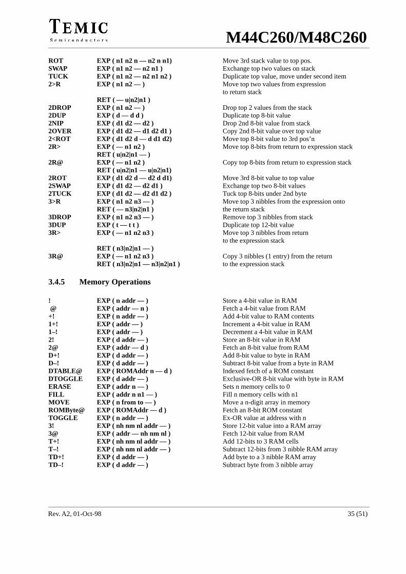
M44C260/M48C260
Rev. A2, 01-Oct-98 35 (51)
ROT EXP ( n1 n2 n –– n2 n n1) Move 3rd stack value to top pos.SWAP EXP ( n1 n2 –– n2 n1 ) Exchange top two values on stackTUCK EXP ( n1 n2 –– n2 n1 n2 ) Duplicate top value, move under second item2>R EXP ( n1 n2 –– ) Move top two values from expression
to return stackRET ( –– u|n2|n1 )
2DROP EXP ( n1 n2 –– ) Drop top 2 values from the stack2DUP EXP ( d –– d d ) Duplicate top 8-bit value2NIP EXP ( d1 d2 –– d2 ) Drop 2nd 8-bit value from stack2OVER EXP ( d1 d2 –– d1 d2 d1 ) Copy 2nd 8-bit value over top value2<ROT EXP ( d1 d2 d –– d d1 d2) Move top 8-bit value to 3rd pos’n2R> EXP ( –– n1 n2 ) Move top 8-bits from return to expression stack
RET ( u|n2|n1 –– )2R@ EXP ( –– n1 n2 ) Copy top 8-bits from return to expression stack
RET ( u|n2|n1 –– u|n2|n1)2ROT EXP ( d1 d2 d –– d2 d d1) Move 3rd 8-bit value to top value2SWAP EXP ( d1 d2 –– d2 d1 ) Exchange top two 8-bit values2TUCK EXP ( d1 d2 –– d2 d1 d2 ) Tuck top 8-bits under 2nd byte3>R EXP ( n1 n2 n3 –– ) Move top 3 nibbles from the expression onto
RET ( –– n3|n2|n1 ) the return stack3DROP EXP ( n1 n2 n3 –– ) Remove top 3 nibbles from stack3DUP EXP ( t –– t t ) Duplicate top 12-bit value3R> EXP ( –– n1 n2 n3 ) Move top 3 nibbles from return
to the expression stackRET ( n3|n2|n1 –– )
3R@ EXP ( –– n1 n2 n3 ) Copy 3 nibbles (1 entry) from the returnRET ( n3|n2|n1 –– n3|n2|n1 ) to the expression stack
3.4.5 Memory Operations
! EXP ( n addr –– ) Store a 4-bit value in RAM @ EXP ( addr –– n ) Fetch a 4-bit value from RAM+! EXP ( n addr –– ) Add 4-bit value to RAM contents1+! EXP ( addr –– ) Increment a 4-bit value in RAM1–! EXP ( addr –– ) Decrement a 4-bit value in RAM2! EXP ( d addr –– ) Store an 8-bit value in RAM2@ EXP ( addr –– d ) Fetch an 8-bit value from RAMD+! EXP ( d addr –– ) Add 8-bit value to byte in RAMD–! EXP ( d addr –– ) Subtract 8-bit value from a byte in RAMDTABLE@ EXP ( ROMAddr n –– d ) Indexed fetch of a ROM constantDTOGGLE EXP ( d addr –– ) Exclusive-OR 8-bit value with byte in RAMERASE EXP ( addr n –– ) Sets n memory cells to 0FILL EXP ( addr n n1 –– ) Fill n memory cells with n1MOVE EXP ( n from to –– ) Move a n-digit array in memoryROMByte@ EXP ( ROMAddr –– d ) Fetch an 8-bit ROM constantTOGGLE EXP ( n addr –– ) Ex-OR value at address with n3! EXP ( nh nm nl addr –– ) Store 12-bit value into a RAM array3@ EXP ( addr –– nh nm nl ) Fetch 12-bit value from RAMT+! EXP ( nh nm nl addr –– ) Add 12-bits to 3 RAM cellsT–! EXP ( nh nm nl addr –– ) Subtract 12-bits from 3 nibble RAM arrayTD+! EXP ( d addr –– ) Add byte to a 3 nibble RAM arrayTD–! EXP ( d addr –– ) Subtract byte from 3 nibble array
M44C260/M48C260
Rev. A2, 01-Oct-9836 (51)
3.4.6 Predefined Structures
( ccccccc) In-line comment definition\ ccccccc Comment until end of the line: <name> RET ( –– ) Begin of a colon definition; RET ( ROMAddr –– ) Exit; ends any colon definition[FIRST] EXP ( –– 0 ) Index (=0) for first array element[LAST] EXP ( –– n|d ) Index for last array elementCODE EXP ( –– ) Begins an in-line macro definitionEND-CODE EXP ( –– ) Ends an In-line macro definitionARRAY EXP ( n –– ) Allocates space for a 4-bit array2ARRAY EXP ( n –– ) Allocates space for an 8-bit arrayCONSTANT EXP ( n –– ) Defines a 4-bit constant2CONSTANT EXP ( d –– ) Defines an 8-bit constantLARRAY EXP ( d –– ) Allocates space for a long 4-bit array
with up to 255 elements2LARRAY EXP ( d –– ) Allocates space for a long byte arrayIndex EXP (n|d addr––addr’) Run-time array access using a variable array indexROMCONST EXP ( –– ) Define ROM look-up table with 8-bit valuesVARIABLE EXP ( –– ) Allocates memory for 4-bit value2VARIABLE EXP ( –– ) Creates an 8-bit variable<n> ALLOT Allocate space for <n+1> nibbles
of un-initialized RAMAT <address> Fixed <address> placement: INTx RET ( –– ROMAddr ) Interrupt service routine entry: $AutoSleep Entry point address on return stack underflow: $RESET EXP ( –– ) Entry point on power-on reset
3.4.7 Assembler Mnemonics
ADD EXP ( n1 n2 –– n1+n2 ) Add the top two 4-bit valuesADDC EXP ( n1 n2 –– n1+n2+C ) Add with carry top two valuesCCR! EXP ( n –– ) Write top value into the CCRCCR@ EXP ( –– n ) Fetch the CCR onto top of stackCMP_EQ EXP ( n1 n2 –– n1 ) If n1=n2, then branch flag setCMP_GE EXP ( n1 n2 –– n1 ) If n1>=n2, then branch flag setCMP_GT EXP ( n1 n2 –– n1 ) If n1>n2, then branch flag setCMP_LE EXP ( n1 n2 –– n1 ) If n1<=n2, then branch flag setCMP_LT EXP ( n1 n2 –– n1 ) If n1<n2, then branch flag setCMP_NE EXP ( n1 n2 –– n1 ) If n1<>n2, then branch flag setCLR_BCF EXP ( –– ) Clear branch and carry flagSET_BCF EXP ( –– ) Set branch and carry flagTOG_BF EXP ( –– ) Toggle the branch flagDAA EXP ( n>9 or C set –– n+6) BCD arithmetic adjust [addition]DAS EXP ( n –– 10+/n+C ) 9’s complement for BCD subtractDEC EXP ( n –– n–1 ) Decrement top value by 1DECR RET ( u|u|I — u|u|I–1 ) Decrement value on the return stackDI EXP ( –– ) Disable interruptsDROPR RET ( u|u|u –– ) Drop element from return stackEXIT RET ( ROMAddr –– ) Exit from current ‘:’-definitionEI EXP ( –– ) Enable interruptsIN EXP ( port –– data ) Read data from an I/O portINC EXP ( n –– n+1 ) Increment the top value by 1NOP EXP ( –– ) No operationNOT EXP ( n –– /n ) 1’s complement of the top value
M44C260/M48C260
Rev. A2, 01-Oct-98 37 (51)
RP! EXP ( d –– ) Store as return stack pointerRP@ EXP ( –– d ) Fetch current RET stack pointerRTI RET ( RETAddr –– ) Return from interrupt routineSLEEP EXP ( –– ) Enter ’sleep-mode’, enable all interruptsSWI0 SWI7 EXP ( –– ) Software triggered interruptSP! EXP ( d –– ) Store as stack pointerSP@ EXP ( –– d ) Fetch current stack pointerSUB EXP ( n1 n2 –– n1-n2 ) 2’s complement subtractionSUBB EXP ( n1 n2 –– n1+/n2+C ) 1’s compl. subtract with borrowTABLE EXP ( –– d )
RET ( RetAddr RomAddr ––) Fetches an 8-bit constant from an address in ROMOUT EXP ( data port –– ) Write data to I/O portX@ EXP ( –– d ) Fetch current× register contents[X]@ EXP ( –– n ) Indirect× fetch of RAM contents[+X]@ EXP ( –– n ) Pre-incr.× indirect RAM fetch[X–]@ EXP ( –– n ) Postdecr.× indirect RAM fetch[>X]@ $xx EXP ( –– n ) Direct RAM fetch,× addressedX! EXP ( d –– ) Move 8-bit address to× register[X]! EXP ( n –– ) Indirect× store of RAM contents[+X]! EXP ( n –– ) Pre-incr.× indirect RAM store[X–]! EXP ( n –– ) Postdecr.× indirect RAM store[>X]! $xx EXP ( n –– ) Direct RAM store,× addressedY@ EXP ( –– d ) Fetch current Y register contents[Y]@ EXP ( –– n ) Indirect Y fetch of RAM contents[+Y]@ EXP ( –– n ) Pre-incr. Y indirect RAM fetch[Y–]@ EXP ( –– n ) Postdecr. Y indirect RAM fetch[>Y]@ $xx EXP ( –– n ) Direct RAM fetch, Y addressedY! EXP ( d –– ) Move address to Y register[Y]! EXP ( n –– ) Indirect Y store of RAM contents[+Y]! EXP ( n –– ) Pre-incr. Y indirect RAM store[Y–]! EXP ( n –– ) Postdecr. Y indirect RAM store[>Y]! $xx EXP ( n –– ) Direct RAM store, Y addressed >RP $xx EXP ( –– ) Set return stack pointer >SP $xx EXP ( –– ) Set expression stack pointer >X $xx EXP ( –– ) Set× register immediate >Y $xx EXP ( –– ) Set Y register immediate
Notes:
RET (–) Return address stack effects
EXP (–) Expression (or data) stack effects
True condition Means branch flag set in CCR
False condition Means branch flag reset in CCR
n 4-bit data value
d 8-bit data value
addr 8-bit RAM address
ROMaddr 12-bit ROM address
M44C260/M48C260
Rev. A2, 01-Oct-9838 (51)
4 Electrical Characteristics4.1 Absolute Maximum RatingsVoltages are given relative to VSS.
Parameters Symbol Value Unit
ÁÁÁÁÁÁÁÁÁÁÁÁÁÁÁÁÁÁÁÁÁÁÁÁÁÁÁÁÁÁÁÁ
Supply voltage ÁÁÁÁÁÁÁÁÁÁ
VDD ÁÁÁÁÁÁÁÁÁÁÁÁÁÁÁÁÁÁ
– 0.3 to + 7.0 ÁÁÁÁÁÁÁÁÁÁ
V
ÁÁÁÁÁÁÁÁÁÁÁÁÁÁÁÁInput voltage (on any pin) ÁÁÁÁÁVIN ÁÁÁÁÁÁÁÁÁVSS –0.3 ≤ VIN ≤ VDD +0.3ÁÁÁÁÁVÁÁÁÁÁÁÁÁÁÁÁÁÁÁÁÁÁÁÁÁÁÁÁÁÁÁÁÁÁÁÁÁOutput short circuit duration
ÁÁÁÁÁÁÁÁÁÁtshort
ÁÁÁÁÁÁÁÁÁÁÁÁÁÁÁÁÁÁindefinite
ÁÁÁÁÁÁÁÁÁÁsecÁÁÁÁÁÁÁÁÁÁÁÁÁÁÁÁ
ÁÁÁÁÁÁÁÁÁÁÁÁÁÁÁÁOperating temperature rangeÁÁÁÁÁÁÁÁÁÁTamb
ÁÁÁÁÁÁÁÁÁÁÁÁÁÁÁÁÁÁ–40 to +85
ÁÁÁÁÁÁÁÁÁÁ°CÁÁÁÁÁÁÁÁÁÁÁÁÁÁÁÁ
ÁÁÁÁÁÁÁÁÁÁÁÁÁÁÁÁStorage temperature range
ÁÁÁÁÁÁÁÁÁÁ
TstgÁÁÁÁÁÁÁÁÁÁÁÁÁÁÁÁÁÁ
–40 to +130ÁÁÁÁÁÁÁÁÁÁ
°CÁÁÁÁÁÁÁÁÁÁÁÁÁÁÁÁÁÁÁÁÁÁÁÁÁÁÁÁÁÁÁÁ
Thermal resistance (PLCC) ÁÁÁÁÁÁÁÁÁÁ
RthJAÁÁÁÁÁÁÁÁÁÁÁÁÁÁÁÁÁÁ
110 ÁÁÁÁÁÁÁÁÁÁ
K/WÁÁÁÁÁÁÁÁÁÁÁÁÁÁÁÁÁÁÁÁÁÁÁÁÁÁÁÁÁÁÁÁ
Soldering temperature (t ≤ 10 s) ÁÁÁÁÁÁÁÁÁÁ
Tsld ÁÁÁÁÁÁÁÁÁÁÁÁÁÁÁÁÁÁ
260 ÁÁÁÁÁÁÁÁÁÁ
°C
Stresses greater than those listed under absolute maxi-mum ratings may cause permanent damage to the device.This is a stress rating only and functional operation of thedevice at any condition above those indicated in the op-erational section of this specification is not implied.Exposure to absolute maximum rating condition for anextended period may affect device reliability. All inputs
and outputs are protected against high electrostatic volt-ages or electric fields. However, precautions to minimizebuild-up of electrostatic charges during handling are rec-ommended. Reliability of operation is enhanced if unusedinputs are connected to an appropriate logic voltage level(e.g., VDD).
4.2 DC Operating CharacteristicsSupply voltage VDD = 2.4 to 6.2 V, VSS = 0 V, Tamb = –40 to +85°C, unless otherwise specified.
Parameters Test Conditions / Pins Symbol Min. Typ. Max. UnitÁÁÁÁÁÁÁÁÁÁÁÁÁÁÁÁÁÁÁÁÁÁÁÁÁÁÁÁÁÁÁÁÁÁÁÁÁÁÁÁÁÁÁÁÁÁÁÁÁÁÁÁÁÁÁÁÁÁÁÁÁÁÁÁ
Power supply ( ) values for M48C260ÁÁÁÁÁÁÁÁÁÁÁÁÁÁÁÁÁÁÁÁÁÁÁÁÁÁÁÁÁÁÁÁ
Active current(CPU active)
ÁÁÁÁÁÁÁÁÁÁÁÁÁÁÁÁÁÁÁÁÁÁÁÁÁÁÁÁÁÁÁÁÁÁÁÁ
VDD = 2.4 V fSYSCL=1MHzfSYSCL=2MHz
VDD = 6.2 V fSYSCL=1MHzfSYSCL=2MHz
ÁÁÁÁÁÁÁÁÁÁÁÁÁÁÁÁ
IDD ÁÁÁÁÁÁÁÁÁÁÁÁÁÁÁÁ
ÁÁÁÁÁÁÁÁÁÁÁÁÁÁÁÁÁÁÁÁ
0.9 (1.3)1.3 (1.8)2.1 (2.7)3.6 (4.4)
ÁÁÁÁÁÁÁÁÁÁÁÁÁÁÁÁ
1.6 (2.1)2.1 (2.9)3.1 (4.0)5.2 (6.4)
ÁÁÁÁÁÁÁÁÁÁÁÁÁÁÁÁ
mAmAmAmA
ÁÁÁÁÁÁÁÁÁÁÁÁÁÁÁÁÁÁÁÁÁÁÁÁÁÁÁÁÁÁÁÁ
Power down current (CPU sleep, RC oscillator active)
ÁÁÁÁÁÁÁÁÁÁÁÁÁÁÁÁÁÁÁÁÁÁÁÁÁÁÁÁÁÁÁÁÁÁÁÁ
VDD = 2.4 V fSYSCL=1MHzfSYSCL=2MHz
VDD = 6.2 V fSYSCL=1MHzfSYSCL=2MHz
ÁÁÁÁÁÁÁÁÁÁÁÁÁÁÁÁ
IPDÁÁÁÁÁÁÁÁÁÁÁÁÁÁÁÁ
ÁÁÁÁÁÁÁÁÁÁÁÁÁÁÁÁÁÁÁÁ
0.3 (0.9)0.4 (1.0)0.6 (1.3)0.8 (1.9)
ÁÁÁÁÁÁÁÁÁÁÁÁÁÁÁÁ
0.5 (1.6)0.8 (1.7)1.0 (2.0)1.3 (2.3)
ÁÁÁÁÁÁÁÁÁÁÁÁÁÁÁÁ
mAmAmAmA
ÁÁÁÁÁÁÁÁÁÁÁÁÁÁÁÁÁÁÁÁÁÁÁÁÁÁÁÁÁÁÁÁ
Sleep current(CPU sleep, RC oscillator inactive)
ÁÁÁÁÁÁÁÁÁÁÁÁÁÁÁÁÁÁÁÁÁÁÁÁÁÁÁÁÁÁÁÁÁÁÁÁ
VDD = 2.4 VVDD = 6.2 V
ÁÁÁÁÁÁÁÁÁÁÁÁÁÁÁÁ
ISleepÁÁÁÁÁÁÁÁÁÁÁÁÁÁÁÁ
ÁÁÁÁÁÁÁÁÁÁÁÁÁÁÁÁÁÁÁÁ
0.4 (0.4)0.5 (0.5)
ÁÁÁÁÁÁÁÁÁÁÁÁÁÁÁÁ
1.0 (1.0)1.0 (1.0)
ÁÁÁÁÁÁÁÁÁÁÁÁÁÁÁÁ
µAµA
ÁÁÁÁÁÁÁÁÁÁÁÁÁÁÁÁÁÁÁÁÁÁÁÁ
Sleep current(CPU sleep, RC oscillator inactive)
ÁÁÁÁÁÁÁÁÁÁÁÁÁÁÁÁÁÁÁÁÁÁÁÁÁÁÁ
VDD = 2.4 VVDD = 6.2 VTamb = 25°C
ÁÁÁÁÁÁÁÁÁÁÁÁ
ISleepÁÁÁÁÁÁÁÁÁÁÁÁ
ÁÁÁÁÁÁÁÁÁÁÁÁÁÁÁ
ÁÁÁÁÁÁÁÁÁÁÁÁ
0.8 (0.8)0.8 (0.8)
ÁÁÁÁÁÁÁÁÁÁÁÁ
µAµA
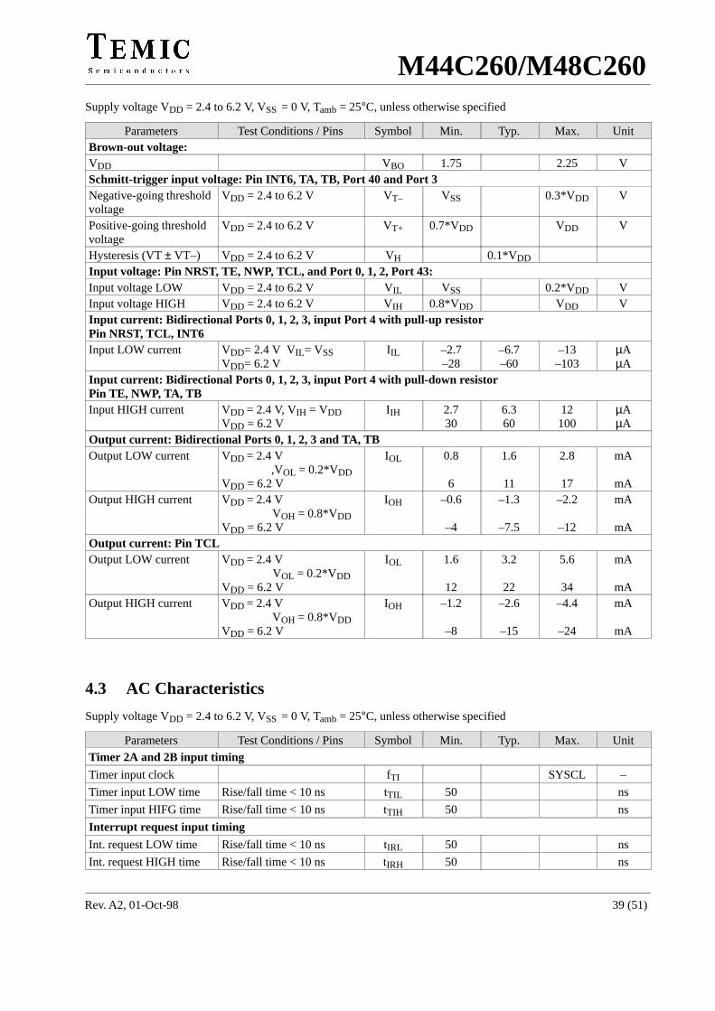
M44C260/M48C260
Rev. A2, 01-Oct-98 39 (51)
Supply voltage VDD = 2.4 to 6.2 V, VSS = 0 V, Tamb = 25°C, unless otherwise specified
Parameters Test Conditions / Pins Symbol Min. Typ. Max. UnitÁÁÁÁÁÁÁÁÁÁÁÁÁÁÁÁÁÁÁÁÁÁÁÁÁÁÁÁÁÁÁÁÁÁÁÁÁÁÁÁÁÁÁÁÁÁÁÁÁÁÁÁÁÁÁÁÁÁÁÁÁÁÁÁ
Brown-out voltage:ÁÁÁÁÁÁÁÁÁÁÁÁÁÁÁÁ
VDD ÁÁÁÁÁÁÁÁÁÁÁÁÁÁÁÁÁÁ
ÁÁÁÁÁÁÁÁ
VBOÁÁÁÁÁÁÁÁÁÁ
1.75 ÁÁÁÁÁÁÁÁ
ÁÁÁÁÁÁÁÁ
2.25 ÁÁÁÁÁÁÁÁ
V
ÁÁÁÁÁÁÁÁÁÁÁÁÁÁÁÁÁÁÁÁÁÁÁÁÁÁÁÁÁÁÁÁÁÁÁÁÁÁÁÁÁÁÁÁÁÁÁÁÁÁÁÁÁÁÁÁÁÁÁÁÁÁÁÁ
Schmitt-trigger input voltage: Pin INT6, TA, TB, Port 40 and Port 3
ÁÁÁÁÁÁÁÁÁÁÁÁÁÁÁÁ
Negative-going thresholdvoltage
ÁÁÁÁÁÁÁÁÁÁÁÁÁÁÁÁÁÁ
VDD = 2.4 to 6.2 V ÁÁÁÁÁÁÁÁ
VT–ÁÁÁÁÁÁÁÁÁÁ
VSS ÁÁÁÁÁÁÁÁ
ÁÁÁÁÁÁÁÁ
0.3*VDDÁÁÁÁÁÁÁÁ
V
ÁÁÁÁÁÁÁÁÁÁÁÁÁÁÁÁÁÁÁÁÁÁÁÁ
Positive-going thresholdvoltage
ÁÁÁÁÁÁÁÁÁÁÁÁÁÁÁÁÁÁÁÁÁÁÁÁÁÁÁ
VDD = 2.4 to 6.2 VÁÁÁÁÁÁÁÁÁÁÁÁ
VT+ÁÁÁÁÁÁÁÁÁÁÁÁÁÁÁ
0.7*VDDÁÁÁÁÁÁÁÁÁÁÁÁ
ÁÁÁÁÁÁÁÁÁÁÁÁ
VDDÁÁÁÁÁÁÁÁÁÁÁÁ
V
ÁÁÁÁÁÁÁÁÁÁÁÁÁÁÁÁ
Hysteresis (VT ± VT–)ÁÁÁÁÁÁÁÁÁÁÁÁÁÁÁÁÁÁ
VDD = 2.4 to 6.2 V ÁÁÁÁÁÁÁÁ
VH ÁÁÁÁÁÁÁÁÁÁ
ÁÁÁÁÁÁÁÁ
0.1*VDDÁÁÁÁÁÁÁÁ
ÁÁÁÁÁÁÁÁÁÁÁÁÁÁÁÁÁÁÁÁÁÁÁÁÁÁÁÁÁÁÁÁÁÁÁÁÁÁÁÁ
ÁÁÁÁÁÁÁÁÁÁÁÁÁÁÁÁÁÁÁÁÁÁÁÁÁÁÁÁÁÁÁÁInput voltage: Pin NRST, TE, NWP, TCL, and Port 0, 1, 2, Port 43:
ÁÁÁÁÁÁÁÁÁÁÁÁÁÁÁÁ
Input voltage LOW ÁÁÁÁÁÁÁÁÁÁÁÁÁÁÁÁÁÁ
VDD = 2.4 to 6.2 V ÁÁÁÁÁÁÁÁ
VIL ÁÁÁÁÁÁÁÁÁÁ
VSS ÁÁÁÁÁÁÁÁ
ÁÁÁÁÁÁÁÁ
0.2*VDDÁÁÁÁÁÁÁÁ
V
ÁÁÁÁÁÁÁÁInput voltage HIGH ÁÁÁÁÁÁÁÁÁVDD = 2.4 to 6.2 V ÁÁÁÁVIHÁÁÁÁÁ0.8*VDD ÁÁÁÁÁÁÁÁVDD ÁÁÁÁVÁÁÁÁÁÁÁÁÁÁÁÁÁÁÁÁÁÁÁÁÁÁÁÁÁÁÁÁÁÁÁÁÁÁÁÁÁÁÁÁÁÁÁÁÁÁÁÁÁÁÁÁÁÁÁÁÁÁÁÁÁÁÁÁÁÁÁÁÁÁÁÁÁÁÁÁÁÁÁÁÁÁÁÁÁÁÁÁÁÁÁÁÁÁÁÁ
Input current: Bidirectional Ports 0, 1, 2, 3, input Port 4 with pull-up resistorPin NRST, TCL, INT6ÁÁÁÁÁÁÁÁÁÁÁÁÁÁÁÁÁÁÁÁÁÁÁÁ
Input LOW current ÁÁÁÁÁÁÁÁÁÁÁÁÁÁÁÁÁÁÁÁÁÁÁÁÁÁÁ
VDD= 2.4 V VIL= VSSVDD= 6.2 V
ÁÁÁÁÁÁÁÁÁÁÁÁ
IIL ÁÁÁÁÁÁÁÁÁÁÁÁÁÁÁ
–2.7–28
ÁÁÁÁÁÁÁÁÁÁÁÁ
–6.7–60
ÁÁÁÁÁÁÁÁÁÁÁÁ
–13–103
ÁÁÁÁÁÁÁÁÁÁÁÁ
µAµA
ÁÁÁÁÁÁÁÁÁÁÁÁÁÁÁÁÁÁÁÁÁÁÁÁÁÁÁÁÁÁÁÁÁÁÁÁÁÁÁÁÁÁÁÁÁÁÁÁÁÁÁÁÁÁÁÁÁÁÁÁÁÁÁÁ
Input current: Bidirectional Ports 0, 1, 2, 3, input Port 4 with pull-down resistorPin TE, NWP, TA, TBÁÁÁÁÁÁÁÁÁÁÁÁÁÁÁÁÁÁÁÁÁÁÁÁ
Input HIGH currentÁÁÁÁÁÁÁÁÁÁÁÁÁÁÁÁÁÁÁÁÁÁÁÁÁÁÁ
VDD = 2.4 V, VIH = VDDVDD = 6.2 V
ÁÁÁÁÁÁÁÁÁÁÁÁ
IIHÁÁÁÁÁÁÁÁÁÁÁÁÁÁÁ
2.730
ÁÁÁÁÁÁÁÁÁÁÁÁ
6.360
ÁÁÁÁÁÁÁÁÁÁÁÁ
12100
ÁÁÁÁÁÁÁÁÁÁÁÁ
µAµA
ÁÁÁÁÁÁÁÁÁÁÁÁÁÁÁÁÁÁÁÁÁÁÁÁÁÁÁÁÁÁÁÁÁÁÁÁÁÁÁÁÁÁÁÁÁÁÁÁÁÁÁÁÁÁÁÁÁÁÁÁÁÁÁÁ
Output current: Bidirectional Ports 0, 1, 2, 3 and TA, TB
ÁÁÁÁÁÁÁÁÁÁÁÁÁÁÁÁÁÁÁÁÁÁÁÁ
Output LOW current ÁÁÁÁÁÁÁÁÁÁÁÁÁÁÁÁÁÁÁÁÁÁÁÁÁÁÁ
VDD = 2.4 V ,VOL = 0.2*VDDVDD = 6.2 V
ÁÁÁÁÁÁÁÁÁÁÁÁ
IOLÁÁÁÁÁÁÁÁÁÁÁÁÁÁÁ
0.8
6
ÁÁÁÁÁÁÁÁÁÁÁÁ
1.6
11
ÁÁÁÁÁÁÁÁÁÁÁÁ
2.8
17
ÁÁÁÁÁÁÁÁÁÁÁÁ
mA
mAÁÁÁÁÁÁÁÁÁÁÁÁÁÁÁÁÁÁÁÁÁÁÁÁ
Output HIGH currentÁÁÁÁÁÁÁÁÁÁÁÁÁÁÁÁÁÁÁÁÁÁÁÁÁÁÁ
VDD = 2.4 V VOH = 0.8*VDDVDD = 6.2 V
ÁÁÁÁÁÁÁÁÁÁÁÁ
IOHÁÁÁÁÁÁÁÁÁÁÁÁÁÁÁ
–0.6
–4
ÁÁÁÁÁÁÁÁÁÁÁÁ
–1.3
–7.5
ÁÁÁÁÁÁÁÁÁÁÁÁ
–2.2
–12
ÁÁÁÁÁÁÁÁÁÁÁÁ
mA
mAÁÁÁÁÁÁÁÁÁÁÁÁÁÁÁÁÁÁÁÁÁÁÁÁÁÁÁÁÁÁÁÁÁÁÁÁÁÁÁÁÁÁÁÁÁÁÁÁÁÁÁÁÁÁÁÁÁÁÁÁÁÁÁÁOutput current: Pin TCLÁÁÁÁÁÁÁÁÁÁÁÁÁÁÁÁÁÁÁÁÁÁÁÁÁÁÁÁÁÁÁÁ
Output LOW currentÁÁÁÁÁÁÁÁÁÁÁÁÁÁÁÁÁÁÁÁÁÁÁÁÁÁÁÁÁÁÁÁÁÁÁÁ
VDD = 2.4 V VOL = 0.2*VDDVDD = 6.2 V
ÁÁÁÁÁÁÁÁÁÁÁÁÁÁÁÁ
IOLÁÁÁÁÁÁÁÁÁÁÁÁÁÁÁÁÁÁÁÁ
1.6
12
ÁÁÁÁÁÁÁÁÁÁÁÁÁÁÁÁ
3.2
22
ÁÁÁÁÁÁÁÁÁÁÁÁÁÁÁÁ
5.6
34
ÁÁÁÁÁÁÁÁÁÁÁÁÁÁÁÁ
mA
mA
ÁÁÁÁÁÁÁÁÁÁÁÁÁÁÁÁÁÁÁÁÁÁÁÁ
Output HIGH currentÁÁÁÁÁÁÁÁÁÁÁÁÁÁÁÁÁÁÁÁÁÁÁÁÁÁÁ
VDD = 2.4 V VOH = 0.8*VDDVDD = 6.2 V
ÁÁÁÁÁÁÁÁÁÁÁÁ
IOHÁÁÁÁÁÁÁÁÁÁÁÁÁÁÁ
–1.2
–8
ÁÁÁÁÁÁÁÁÁÁÁÁ
–2.6
–15
ÁÁÁÁÁÁÁÁÁÁÁÁ
–4.4
–24
ÁÁÁÁÁÁÁÁÁÁÁÁ
mA
mA
4.3 AC Characteristics
Supply voltage VDD = 2.4 to 6.2 V, VSS = 0 V, Tamb = 25°C, unless otherwise specified
Parameters Test Conditions / Pins Symbol Min. Typ. Max. UnitÁÁÁÁÁÁÁÁÁÁÁÁÁÁÁÁÁÁÁÁÁÁÁÁÁÁÁÁÁÁÁÁÁÁÁÁÁÁÁÁÁÁÁÁÁÁÁÁÁÁÁÁÁÁÁÁÁÁÁÁÁÁÁÁ
Timer 2A and 2B input timingÁÁÁÁÁÁÁÁÁÁÁÁÁÁÁÁ
Timer input clock ÁÁÁÁÁÁÁÁÁÁÁÁÁÁÁÁÁÁ
ÁÁÁÁÁÁÁÁ
fTIÁÁÁÁÁÁÁÁÁÁ
ÁÁÁÁÁÁÁÁ
ÁÁÁÁÁÁÁÁ
SYSCLÁÁÁÁÁÁÁÁ
–ÁÁÁÁÁÁÁÁÁÁÁÁÁÁÁÁ
Timer input LOW timeÁÁÁÁÁÁÁÁÁÁÁÁÁÁÁÁÁÁ
Rise/fall time < 10 ns ÁÁÁÁÁÁÁÁ
tTILÁÁÁÁÁÁÁÁÁÁ
50 ÁÁÁÁÁÁÁÁ
ÁÁÁÁÁÁÁÁ
ÁÁÁÁÁÁÁÁ
nsÁÁÁÁÁÁÁÁÁÁÁÁÁÁÁÁ
Timer input HIFG timeÁÁÁÁÁÁÁÁÁÁÁÁÁÁÁÁÁÁ
Rise/fall time < 10 ns ÁÁÁÁÁÁÁÁ
tTIHÁÁÁÁÁÁÁÁÁÁ
50 ÁÁÁÁÁÁÁÁ
ÁÁÁÁÁÁÁÁ
ÁÁÁÁÁÁÁÁ
nsÁÁÁÁÁÁÁÁÁÁÁÁÁÁÁÁÁÁÁÁÁÁÁÁÁÁÁÁÁÁÁÁÁÁÁÁÁÁÁÁÁÁÁÁÁÁÁÁÁÁÁÁÁÁÁÁÁÁÁÁÁÁÁÁ
Interrupt request input timing
ÁÁÁÁÁÁÁÁÁÁÁÁÁÁÁÁ
Int. request LOW timeÁÁÁÁÁÁÁÁÁÁÁÁÁÁÁÁÁÁ
Rise/fall time < 10 ns ÁÁÁÁÁÁÁÁ
tIRLÁÁÁÁÁÁÁÁÁÁ
50 ÁÁÁÁÁÁÁÁ
ÁÁÁÁÁÁÁÁ
ÁÁÁÁÁÁÁÁ
ns
ÁÁÁÁÁÁÁÁÁÁÁÁÁÁÁÁ
Int. request HIGH timeÁÁÁÁÁÁÁÁÁÁÁÁÁÁÁÁÁÁ
Rise/fall time < 10 ns ÁÁÁÁÁÁÁÁ
tIRHÁÁÁÁÁÁÁÁÁÁ
50 ÁÁÁÁÁÁÁÁ
ÁÁÁÁÁÁÁÁ
ÁÁÁÁÁÁÁÁ
ns
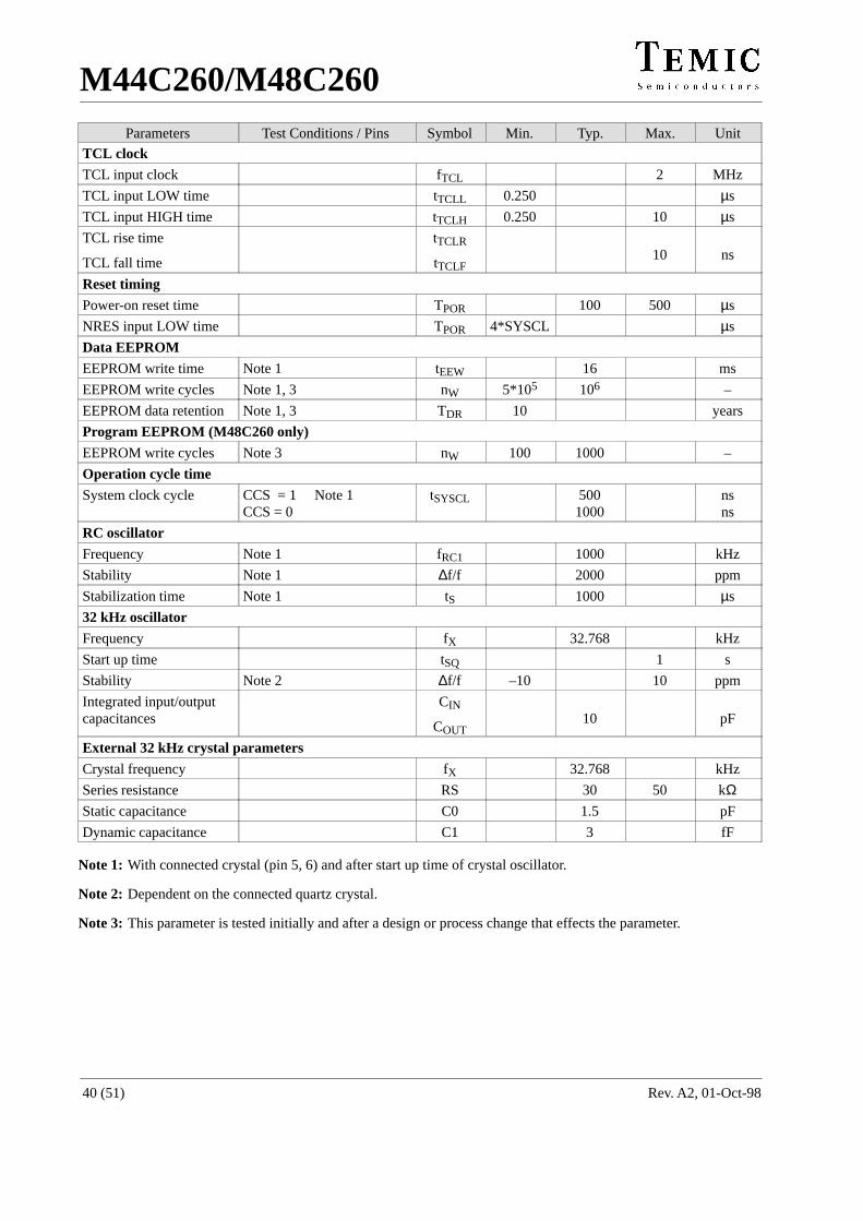
M44C260/M48C260
Rev. A2, 01-Oct-9840 (51)
UnitMax.Typ.Min.SymbolTest Conditions / PinsParametersÁÁÁÁÁÁÁÁÁÁÁÁÁÁÁÁÁÁÁÁÁÁÁÁÁÁÁÁÁÁÁÁÁÁÁÁÁÁÁÁÁÁÁÁÁÁÁÁÁÁÁÁÁÁÁÁÁÁÁÁÁÁÁÁ
TCL clockÁÁÁÁÁÁÁÁÁÁÁÁÁÁÁÁ
TCL input clock ÁÁÁÁÁÁÁÁÁÁÁÁÁÁÁÁÁÁ
ÁÁÁÁÁÁÁÁ
fTCLÁÁÁÁÁÁÁÁ
ÁÁÁÁÁÁÁÁÁÁ
ÁÁÁÁÁÁÁÁ
2 ÁÁÁÁÁÁÁÁ
MHz
ÁÁÁÁÁÁÁÁÁÁÁÁÁÁÁÁ
TCL input LOW time ÁÁÁÁÁÁÁÁÁÁÁÁÁÁÁÁÁÁ
ÁÁÁÁÁÁÁÁ
tTCLLÁÁÁÁÁÁÁÁ
0.250ÁÁÁÁÁÁÁÁÁÁ
ÁÁÁÁÁÁÁÁ
ÁÁÁÁÁÁÁÁ
µs
ÁÁÁÁÁÁÁÁÁÁÁÁÁÁÁÁ
TCL input HIGH timeÁÁÁÁÁÁÁÁÁÁÁÁÁÁÁÁÁÁ
ÁÁÁÁÁÁÁÁ
tTCLHÁÁÁÁÁÁÁÁ
0.250ÁÁÁÁÁÁÁÁÁÁ
ÁÁÁÁÁÁÁÁ
10 ÁÁÁÁÁÁÁÁ
µs
ÁÁÁÁÁÁÁÁÁÁÁÁÁÁÁÁÁÁÁÁÁÁÁÁ
TCL rise time
TCL fall time
ÁÁÁÁÁÁÁÁÁÁÁÁÁÁÁÁÁÁÁÁÁÁÁÁÁÁÁ
ÁÁÁÁÁÁÁÁÁÁÁÁ
tTCLR
tTCLF
ÁÁÁÁÁÁÁÁÁÁÁÁ
ÁÁÁÁÁÁÁÁÁÁÁÁÁÁÁ
ÁÁÁÁÁÁÁÁÁÁÁÁ
10ÁÁÁÁÁÁÁÁÁÁÁÁ
ns
ÁÁÁÁÁÁÁÁÁÁÁÁÁÁÁÁÁÁÁÁÁÁÁÁÁÁÁÁÁÁÁÁÁÁÁÁÁÁÁÁÁÁÁÁÁÁÁÁÁÁÁÁÁÁÁÁÁÁÁÁÁÁÁÁ
Reset timing
ÁÁÁÁÁÁÁÁÁÁÁÁÁÁÁÁ
Power-on reset time ÁÁÁÁÁÁÁÁÁÁÁÁÁÁÁÁÁÁ
ÁÁÁÁÁÁÁÁ
TPORÁÁÁÁÁÁÁÁ
ÁÁÁÁÁÁÁÁÁÁ
100 ÁÁÁÁÁÁÁÁ
500 ÁÁÁÁÁÁÁÁ
µs
ÁÁÁÁÁÁÁÁÁÁÁÁÁÁÁÁ
NRES input LOW timeÁÁÁÁÁÁÁÁÁÁÁÁÁÁÁÁÁÁ
ÁÁÁÁÁÁÁÁ
TPORÁÁÁÁÁÁÁÁ
4*SYSCLÁÁÁÁÁÁÁÁÁÁ
ÁÁÁÁÁÁÁÁ
ÁÁÁÁÁÁÁÁ
µs
ÁÁÁÁÁÁÁÁÁÁÁÁÁÁÁÁÁÁÁÁÁÁÁÁÁÁÁÁÁÁÁÁÁÁÁÁÁÁÁÁÁÁÁÁÁÁÁÁÁÁÁÁÁÁÁÁÁÁÁÁÁÁÁÁ
Data EEPROM
ÁÁÁÁÁÁÁÁÁÁÁÁÁÁÁÁ
EEPROM write time ÁÁÁÁÁÁÁÁÁÁÁÁÁÁÁÁÁÁ
Note 1 ÁÁÁÁÁÁÁÁ
tEEWÁÁÁÁÁÁÁÁ
ÁÁÁÁÁÁÁÁÁÁ
16 ÁÁÁÁÁÁÁÁ
ÁÁÁÁÁÁÁÁ
msÁÁÁÁÁÁÁÁÁÁÁÁÁÁÁÁEEPROM write cycles
ÁÁÁÁÁÁÁÁÁÁÁÁÁÁÁÁÁÁNote 1, 3
ÁÁÁÁÁÁÁÁnW
ÁÁÁÁÁÁÁÁ5*105
ÁÁÁÁÁÁÁÁÁÁ106
ÁÁÁÁÁÁÁÁ
ÁÁÁÁÁÁÁÁ–ÁÁÁÁÁÁÁÁ
ÁÁÁÁÁÁÁÁEEPROM data retentionÁÁÁÁÁÁÁÁÁÁÁÁÁÁÁÁÁÁNote 1, 3
ÁÁÁÁÁÁÁÁTDR
ÁÁÁÁÁÁÁÁ10
ÁÁÁÁÁÁÁÁÁÁ
ÁÁÁÁÁÁÁÁ
ÁÁÁÁÁÁÁÁyearsÁÁÁÁÁÁÁÁÁÁÁÁÁÁÁÁÁÁÁÁÁÁÁÁÁÁÁÁÁÁÁÁ
ÁÁÁÁÁÁÁÁÁÁÁÁÁÁÁÁÁÁÁÁÁÁÁÁÁÁÁÁÁÁÁÁProgram EEPROM (M48C260 only)ÁÁÁÁÁÁÁÁÁÁÁÁÁÁÁÁEEPROM write cycles
ÁÁÁÁÁÁÁÁÁÁÁÁÁÁÁÁÁÁNote 3
ÁÁÁÁÁÁÁÁnW
ÁÁÁÁÁÁÁÁ100
ÁÁÁÁÁÁÁÁÁÁ1000
ÁÁÁÁÁÁÁÁ
ÁÁÁÁÁÁÁÁ–ÁÁÁÁÁÁÁÁÁÁÁÁÁÁÁÁÁÁÁÁÁÁÁÁÁÁÁÁÁÁÁÁ
ÁÁÁÁÁÁÁÁÁÁÁÁÁÁÁÁÁÁÁÁÁÁÁÁÁÁÁÁÁÁÁÁOperation cycle timeÁÁÁÁÁÁÁÁÁÁÁÁÁÁÁÁÁÁÁÁÁÁÁÁ
System clock cycleÁÁÁÁÁÁÁÁÁÁÁÁÁÁÁÁÁÁÁÁÁÁÁÁÁÁÁ
CCS = 1 Note 1CCS = 0
ÁÁÁÁÁÁÁÁÁÁÁÁ
tSYSCLÁÁÁÁÁÁÁÁÁÁÁÁ
ÁÁÁÁÁÁÁÁÁÁÁÁÁÁÁ
5001000
ÁÁÁÁÁÁÁÁÁÁÁÁ
ÁÁÁÁÁÁÁÁÁÁÁÁ
nsns
ÁÁÁÁÁÁÁÁÁÁÁÁÁÁÁÁÁÁÁÁÁÁÁÁÁÁÁÁÁÁÁÁÁÁÁÁÁÁÁÁÁÁÁÁÁÁÁÁÁÁÁÁÁÁÁÁÁÁÁÁÁÁÁÁ
RC oscillatorÁÁÁÁÁÁÁÁÁÁÁÁÁÁÁÁ
Frequency ÁÁÁÁÁÁÁÁÁÁÁÁÁÁÁÁÁÁ
Note 1 ÁÁÁÁÁÁÁÁ
fRC1ÁÁÁÁÁÁÁÁ
ÁÁÁÁÁÁÁÁÁÁ
1000 ÁÁÁÁÁÁÁÁ
ÁÁÁÁÁÁÁÁ
kHzÁÁÁÁÁÁÁÁÁÁÁÁÁÁÁÁ
Stability ÁÁÁÁÁÁÁÁÁÁÁÁÁÁÁÁÁÁ
Note 1 ÁÁÁÁÁÁÁÁ
∆f/f ÁÁÁÁÁÁÁÁ
ÁÁÁÁÁÁÁÁÁÁ
2000 ÁÁÁÁÁÁÁÁ
ÁÁÁÁÁÁÁÁ
ppm
ÁÁÁÁÁÁÁÁÁÁÁÁÁÁÁÁ
Stabilization time ÁÁÁÁÁÁÁÁÁÁÁÁÁÁÁÁÁÁ
Note 1 ÁÁÁÁÁÁÁÁ
tS ÁÁÁÁÁÁÁÁ
ÁÁÁÁÁÁÁÁÁÁ
1000 ÁÁÁÁÁÁÁÁ
ÁÁÁÁÁÁÁÁ
µs
ÁÁÁÁÁÁÁÁÁÁÁÁÁÁÁÁÁÁÁÁÁÁÁÁÁÁÁÁÁÁÁÁÁÁÁÁÁÁÁÁÁÁÁÁÁÁÁÁÁÁÁÁÁÁÁÁÁÁÁÁÁÁÁÁ
32 kHz oscillator
ÁÁÁÁÁÁÁÁÁÁÁÁÁÁÁÁ
Frequency ÁÁÁÁÁÁÁÁÁÁÁÁÁÁÁÁÁÁ
ÁÁÁÁÁÁÁÁ
fX ÁÁÁÁÁÁÁÁ
ÁÁÁÁÁÁÁÁÁÁ
32.768 ÁÁÁÁÁÁÁÁ
ÁÁÁÁÁÁÁÁ
kHz
ÁÁÁÁÁÁÁÁÁÁÁÁÁÁÁÁ
Start up time ÁÁÁÁÁÁÁÁÁÁÁÁÁÁÁÁÁÁ
ÁÁÁÁÁÁÁÁ
tSQ ÁÁÁÁÁÁÁÁ
ÁÁÁÁÁÁÁÁÁÁ
ÁÁÁÁÁÁÁÁ
1 ÁÁÁÁÁÁÁÁ
s
ÁÁÁÁÁÁÁÁStability ÁÁÁÁÁÁÁÁÁNote 2 ÁÁÁÁ∆f/f ÁÁÁÁ–10ÁÁÁÁÁÁÁÁÁ10 ÁÁÁÁppmÁÁÁÁÁÁÁÁÁÁÁÁÁÁÁÁÁÁÁÁÁÁÁÁÁÁÁÁÁÁÁÁ
Integrated input/outputcapacitances
ÁÁÁÁÁÁÁÁÁÁÁÁÁÁÁÁÁÁÁÁÁÁÁÁÁÁÁÁÁÁÁÁÁÁÁÁ
ÁÁÁÁÁÁÁÁÁÁÁÁÁÁÁÁ
CIN
COUT
ÁÁÁÁÁÁÁÁÁÁÁÁÁÁÁÁ
ÁÁÁÁÁÁÁÁÁÁÁÁÁÁÁÁÁÁÁÁ
10
ÁÁÁÁÁÁÁÁÁÁÁÁÁÁÁÁ
ÁÁÁÁÁÁÁÁÁÁÁÁÁÁÁÁ
pF
ÁÁÁÁÁÁÁÁÁÁÁÁÁÁÁÁÁÁÁÁÁÁÁÁÁÁÁÁÁÁÁÁÁÁÁÁÁÁÁÁÁÁÁÁÁÁÁÁÁÁÁÁÁÁÁÁÁÁÁÁÁÁÁÁ
External 32 kHz crystal parameters
ÁÁÁÁÁÁÁÁCrystal frequency ÁÁÁÁÁÁÁÁÁÁÁÁÁfX ÁÁÁÁÁÁÁÁÁ32.768 ÁÁÁÁÁÁÁÁkHzÁÁÁÁÁÁÁÁÁÁÁÁÁÁÁÁSeries resistance
ÁÁÁÁÁÁÁÁÁÁÁÁÁÁÁÁÁÁ
ÁÁÁÁÁÁÁÁRS
ÁÁÁÁÁÁÁÁ
ÁÁÁÁÁÁÁÁÁÁ30
ÁÁÁÁÁÁÁÁ50
ÁÁÁÁÁÁÁÁkΩÁÁÁÁÁÁÁÁ
ÁÁÁÁÁÁÁÁStatic capacitanceÁÁÁÁÁÁÁÁÁÁÁÁÁÁÁÁÁÁ
ÁÁÁÁÁÁÁÁC0
ÁÁÁÁÁÁÁÁ
ÁÁÁÁÁÁÁÁÁÁ1.5
ÁÁÁÁÁÁÁÁ
ÁÁÁÁÁÁÁÁpFÁÁÁÁÁÁÁÁ
ÁÁÁÁÁÁÁÁDynamic capacitanceÁÁÁÁÁÁÁÁÁÁÁÁÁÁÁÁÁÁ
ÁÁÁÁÁÁÁÁC1
ÁÁÁÁÁÁÁÁ
ÁÁÁÁÁÁÁÁÁÁ3
ÁÁÁÁÁÁÁÁ
ÁÁÁÁÁÁÁÁfF
Note 1: With connected crystal (pin 5, 6) and after start up time of crystal oscillator.
Note 2: Dependent on the connected quartz crystal.
Note 3: This parameter is tested initially and after a design or process change that effects the parameter.
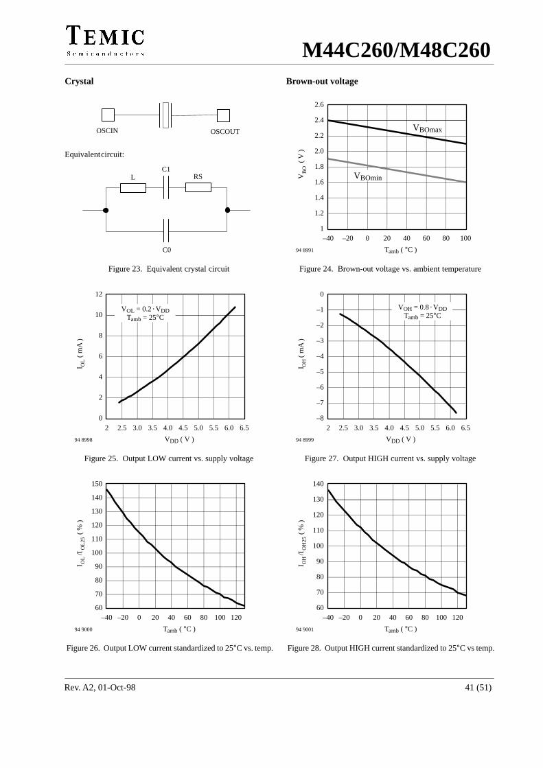
M44C260/M48C260
Rev. A2, 01-Oct-98 41 (51)
Crystal
LC1
RS
C0
OSCIN OSCOUT
Equivalentcircuit:
Figure 23. Equivalent crystal circuit
Brown-out voltage
1
1.2
1.4
1.6
1.8
2.0
2.2
2.4
2.6
–40 –20 0 20 40 60 80 100
V
(
V )
Tamb ( °C )94 8991
BO
VBOmin
VBOmax
Figure 24. Brown-out voltage vs. ambient temperature
0
2
4
6
8
10
12
2 2.5 3.0 3.5 4.0 4.5 5.0 5.5 6.0 6.5
I
( m
A )
OL
VDD ( V )94 8998
VOL = 0.2VDDTamb = 25°C
Figure 25. Output LOW current vs. supply voltage
60
70
80
90
100
110
120
130
140
150
–40 –20 0 20 40 60 80 100 120
I
/I
(
% )
OL
Tamb ( °C )94 9000
OL2
5
Figure 26. Output LOW current standardized to 25°C vs. temp.
–8
–7
–6
–5
–4
–3
–2
–1
0
2 2.5 3.0 3.5 4.0 4.5 5.0 5.5 6.0 6.5
I
( m
A )
OH
VDD ( V )94 8999
VOH = 0.8VDDTamb = 25°C
Figure 27. Output HIGH current vs. supply voltage
60
70
80
90
100
110
120
130
140
–40 –20 0 20 40 60 80 100 120
I
/I
(
% )
OH
Tamb ( °C )94 9001
OH
25
Figure 28. Output HIGH current standardized to 25°C vs temp.
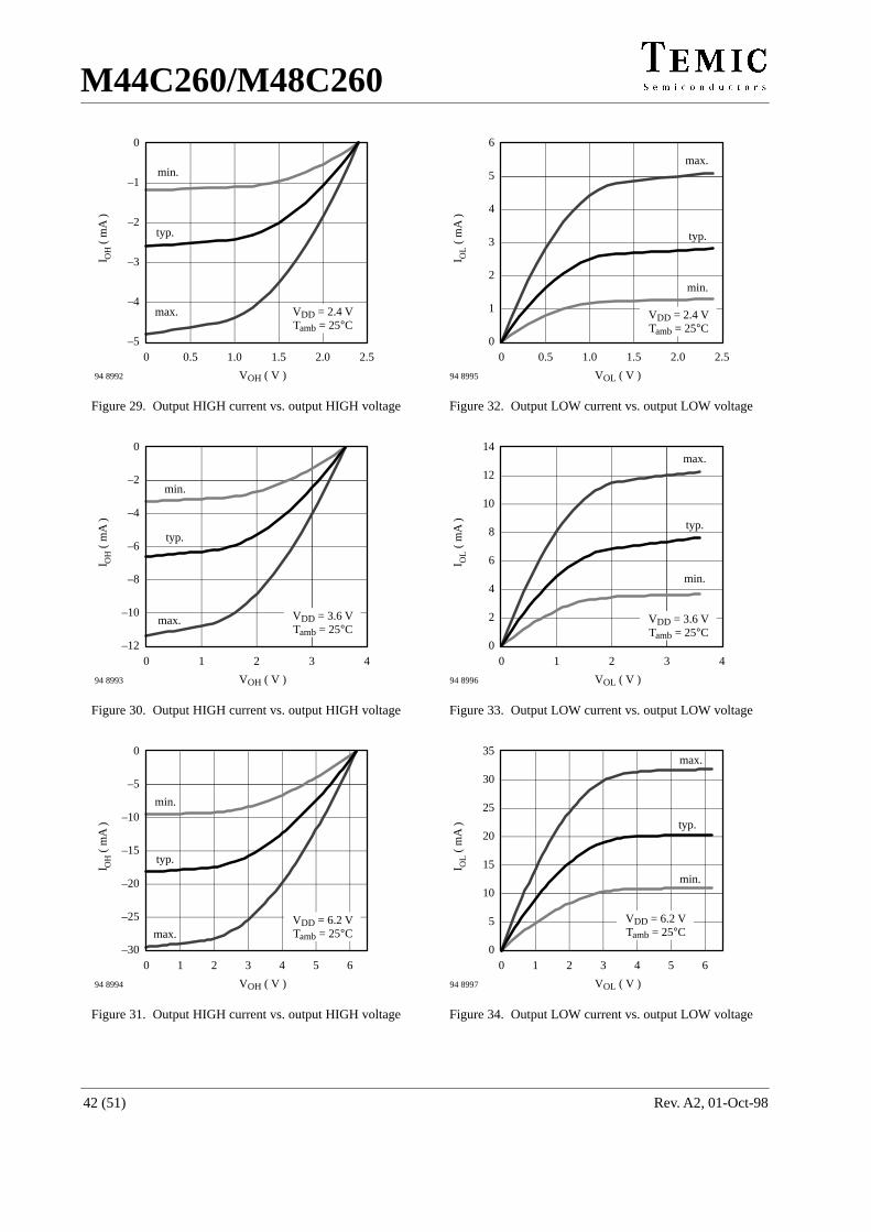
M44C260/M48C260
Rev. A2, 01-Oct-9842 (51)
max.
min.
typ.
–5
–4
–3
–2
–1
0
0 0.5 1.0 1.5 2.0 2.5
I
( m
A )
OH
VOH ( V )94 8992
VDD = 2.4 VTamb = 25°C
Figure 29. Output HIGH current vs. output HIGH voltage
max.
min.
typ.
–12
–10
–8
–6
–4
–2
0
0 1 2 3 4
I
( m
A )
OH
VOH ( V )94 8993
VDD = 3.6 VTamb = 25°C
Figure 30. Output HIGH current vs. output HIGH voltage
max.
typ.
min.
–30
–25
–20
–15
–10
–5
0
0 1 2 3 4 5 6
I
( m
A )
OH
VOH ( V )94 8994
VDD = 6.2 VTamb = 25°C
Figure 31. Output HIGH current vs. output HIGH voltage
min.
typ.
max.
0
1
2
3
4
5
6
0 0.5 1.0 1.5 2.0 2.5
I
( m
A )
OL
VOL ( V )94 8995
VDD = 2.4 VTamb = 25°C
Figure 32. Output LOW current vs. output LOW voltage
min.
typ.
max.
0
2
4
6
8
10
12
14
0 1 2 3 4
I
( m
A )
OL
VOL ( V )94 8996
VDD = 3.6 VTamb = 25°C
Figure 33. Output LOW current vs. output LOW voltage
max.
typ.
min.
0
5
10
15
20
25
30
35
0 1 2 3 4 5 6
I
( m
A )
OL
VOL ( V )94 8997
VDD = 6.2 VTamb = 25°C
Figure 34. Output LOW current vs. output LOW voltage
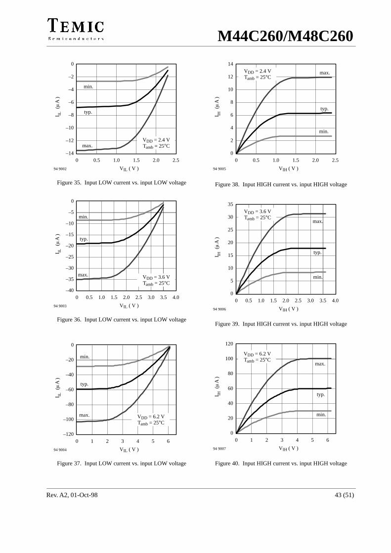
M44C260/M48C260
Rev. A2, 01-Oct-98 43 (51)
min.
typ.
max.
–14
–12
–10
–8
–6
–4
–2
0
0 0.5 1.0 1.5 2.0 2.5
I
( A
)IL
VIL ( V )94 9002
VDD = 2.4 VTamb = 25°C
Figure 35. Input LOW current vs. input LOW voltage
min.
typ.
max.
–40
–35
–30
–25
–20
–15
–10
–5
0
0 0.5 1.0 1.5 2.0 2.5 3.0 3.5 4.0
I
( A
)IL
VIL ( V )94 9003
VDD = 3.6 VTamb = 25°C
Figure 36. Input LOW current vs. input LOW voltage
min.
typ.
max.
–120
–100
–80
–60
–40
–20
0
0 1 2 3 4 5 6
I
( A
)IL
VIL ( V )94 9004
VDD = 6.2 VTamb = 25°C
Figure 37. Input LOW current vs. input LOW voltage
min.
typ.
max.
0
2
4
6
8
10
12
14
0 0.5 1.0 1.5 2.0 2.5
I
( A
)IH
VIH ( V )94 9005
VDD = 2.4 VTamb = 25°C
Figure 38. Input HIGH current vs. input HIGH voltage
min.
typ.
max.
0
5
10
15
20
25
30
35
0 0.5 1.0 1.5 2.0 2.5 3.0 3.5 4.0
I
( A
)IH
VIH ( V )94 9006
VDD = 3.6 VTamb = 25°C
Figure 39. Input HIGH current vs. input HIGH voltage
min.
typ.
max.
0
20
40
60
80
100
120
0 1 2 3 4 5 6
I
( A
)IH
VIH ( V )94 9007
VDD = 6.2 VTamb = 25°C
Figure 40. Input HIGH current vs. input HIGH voltage
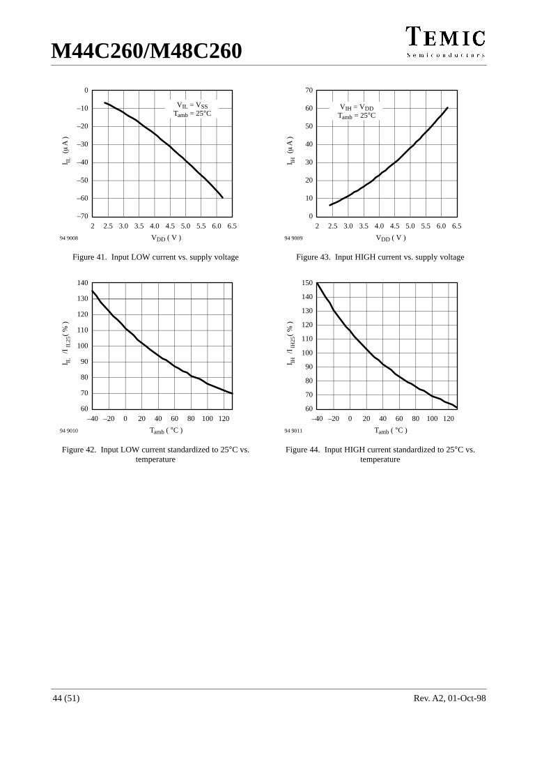
M44C260/M48C260
Rev. A2, 01-Oct-9844 (51)
–70
–60
–50
–40
–30
–20
–10
0
2 2.5 3.0 3.5 4.0 4.5 5.0 5.5 6.0 6.5
I
( A
)IL
VDD ( V )94 9008
VIL = VSSTamb = 25°C
Figure 41. Input LOW current vs. supply voltage
60
70
80
90
100
110
120
130
140
–40 –20 0 20 40 60 80 100 120
I
/I
(
% )
IL
Tamb ( °C )94 9010
IL25
Figure 42. Input LOW current standardized to 25°C vs.temperature
0
10
20
30
40
50
60
70
2 2.5 3.0 3.5 4.0 4.5 5.0 5.5 6.0 6.5
I
( A
)IH
VDD ( V )94 9009
VIH = VDDTamb = 25°C
Figure 43. Input HIGH current vs. supply voltage
60
70
80
90
100
110
120
130
140
150
–40 –20 0 20 40 60 80 100 120
I
/I
(
% )
IH
Tamb ( °C )94 9011
IH25
Figure 44. Input HIGH current standardized to 25°C vs.temperature
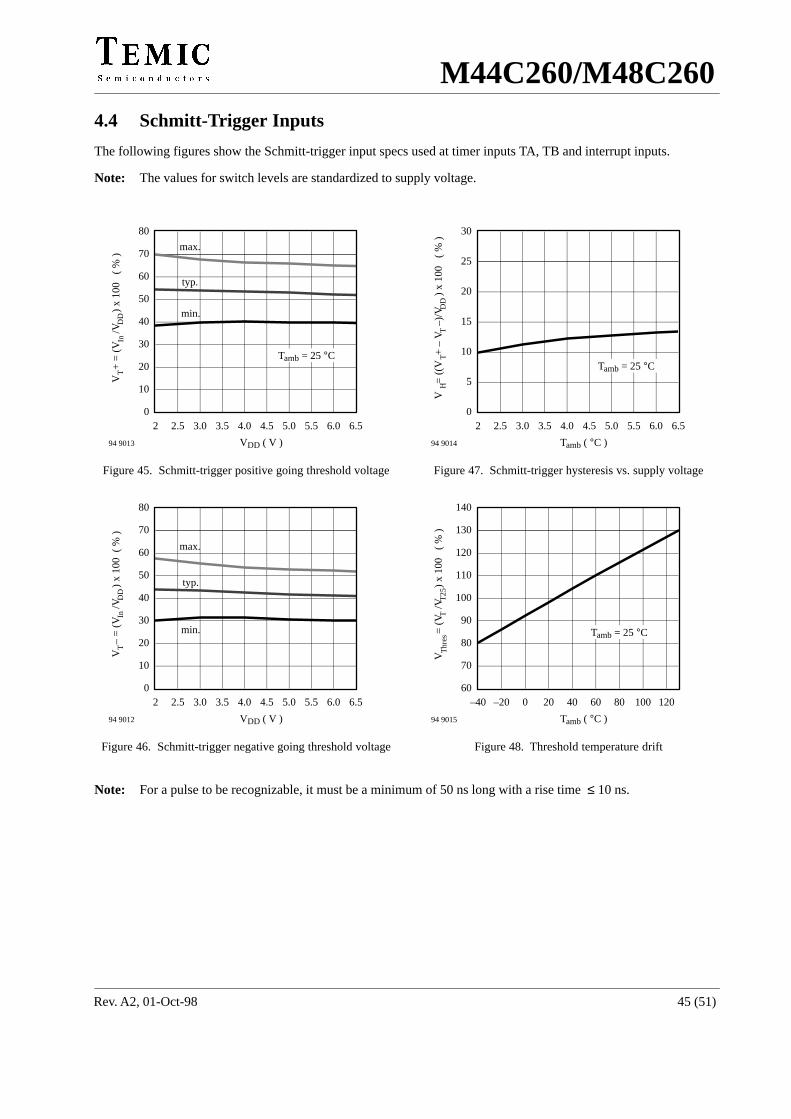
M44C260/M48C260
Rev. A2, 01-Oct-98 45 (51)
4.4 Schmitt-Trigger Inputs
The following figures show the Schmitt-trigger input specs used at timer inputs TA, TB and interrupt inputs.
Note: The values for switch levels are standardized to supply voltage.
max.
typ.
min.
0
10
20
30
40
50
60
70
80
2 2.5 3.0 3.5 4.0 4.5 5.0 5.5 6.0 6.5
V +
= (
V
/V
) x
100
(
% )
T
VDD ( V )94 9013
DD
Tamb = 25 °C
In
Figure 45. Schmitt-trigger positive going threshold voltage
typ.
max.
min.
0
10
20
30
40
50
60
70
80
2 2.5 3.0 3.5 4.0 4.5 5.0 5.5 6.0 6.5
V –
= (
V
/V
) x
100
( %
)T
VDD ( V )94 9012
DD
In
Figure 46. Schmitt-trigger negative going threshold voltage
0
5
10
15
20
25
30
2 2.5 3.0 3.5 4.0 4.5 5.0 5.5 6.0 6.5V
=
((V
+ –
V –
)/V
)
x 1
00
( %
)T
Tamb ( °C )94 9014D
D
Tamb = 25 °C
HT
Figure 47. Schmitt-trigger hysteresis vs. supply voltage
60
70
80
90
100
110
120
130
140
–40 –20 0 20 40 60 80 100 120
V
=
(V
/V
)
x 1
00
( %
)T
Tamb ( °C )94 9015
T25
Tamb = 25 °C
Thr
es
Figure 48. Threshold temperature drift
Note: For a pulse to be recognizable, it must be a minimum of 50 ns long with a rise time ≤ 10 ns.
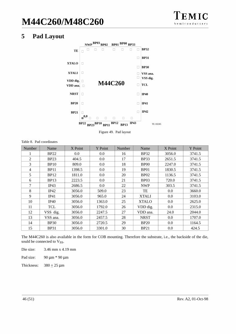
M44C260/M48C260
Rev. A2, 01-Oct-9846 (51)
5 Pad Layout
BP22BP23
BP10BP11
BP12 BP13 IP43
IP42
IP41
IP40
TCL
VSS dig.VSS ana.
BP30
BP31
BP32
BP33BP00BP01BP02BP03NWP
TE
XTALI
XTALO
VDD dig.
VDD ana.
NRST
BP20
BP21
M44C260
95 10245
0,0
Figure 49. Pad layout
Table 8. Pad coordinates
Number Name X Point Y Point Number Name X Point Y PointÁÁÁÁÁÁÁÁ
1ÁÁÁÁÁÁÁÁÁÁ
BP22ÁÁÁÁÁÁÁÁÁÁ
0.0ÁÁÁÁÁÁÁÁÁÁ
0.0ÁÁÁÁÁÁÁÁ
16ÁÁÁÁÁÁÁÁÁÁ
BP32ÁÁÁÁÁÁÁÁÁÁÁÁ
3056.0ÁÁÁÁÁÁÁÁÁÁ
3741.5ÁÁÁÁÁÁÁÁ
2 ÁÁÁÁÁÁÁÁÁÁ
BP23 ÁÁÁÁÁÁÁÁÁÁ
404.5 ÁÁÁÁÁÁÁÁÁÁ
0.0 ÁÁÁÁÁÁÁÁ
17 ÁÁÁÁÁÁÁÁÁÁ
BP33 ÁÁÁÁÁÁÁÁÁÁÁÁ
2651.5 ÁÁÁÁÁÁÁÁÁÁ
3741.5ÁÁÁÁÁÁÁÁ
3 ÁÁÁÁÁÁÁÁÁÁ
BP10 ÁÁÁÁÁÁÁÁÁÁ
809.0 ÁÁÁÁÁÁÁÁÁÁ
0.0 ÁÁÁÁÁÁÁÁ
18 ÁÁÁÁÁÁÁÁÁÁ
BP00 ÁÁÁÁÁÁÁÁÁÁÁÁ
2247.0 ÁÁÁÁÁÁÁÁÁÁ
3741.5ÁÁÁÁÁÁÁÁ
4 ÁÁÁÁÁÁÁÁÁÁ
BP11 ÁÁÁÁÁÁÁÁÁÁ
1398.5ÁÁÁÁÁÁÁÁÁÁ
0.0 ÁÁÁÁÁÁÁÁ
19 ÁÁÁÁÁÁÁÁÁÁ
BP01 ÁÁÁÁÁÁÁÁÁÁÁÁ
1830.5 ÁÁÁÁÁÁÁÁÁÁ
3741.5
ÁÁÁÁÁÁÁÁ
5 ÁÁÁÁÁÁÁÁÁÁ
BP12 ÁÁÁÁÁÁÁÁÁÁ
1811.0 ÁÁÁÁÁÁÁÁÁÁ
0.0 ÁÁÁÁÁÁÁÁ
20 ÁÁÁÁÁÁÁÁÁÁ
BP02 ÁÁÁÁÁÁÁÁÁÁÁÁ
1136.5 ÁÁÁÁÁÁÁÁÁÁ
3741.5
ÁÁÁÁ6 ÁÁÁÁÁBP13 ÁÁÁÁÁ2223.5ÁÁÁÁÁ0.0 ÁÁÁÁ21 ÁÁÁÁÁBP03 ÁÁÁÁÁÁ720.0 ÁÁÁÁÁ3741.5ÁÁÁÁÁÁÁÁ7
ÁÁÁÁÁÁÁÁÁÁIP43
ÁÁÁÁÁÁÁÁÁÁ2686.5
ÁÁÁÁÁÁÁÁÁÁ0.0
ÁÁÁÁÁÁÁÁ22
ÁÁÁÁÁÁÁÁÁÁNWP
ÁÁÁÁÁÁÁÁÁÁÁÁ303.5
ÁÁÁÁÁÁÁÁÁÁ3741.5ÁÁÁÁ
ÁÁÁÁ8ÁÁÁÁÁÁÁÁÁÁIP42
ÁÁÁÁÁÁÁÁÁÁ3056.0
ÁÁÁÁÁÁÁÁÁÁ509.0
ÁÁÁÁÁÁÁÁ23
ÁÁÁÁÁÁÁÁÁÁTE
ÁÁÁÁÁÁÁÁÁÁÁÁ0.0
ÁÁÁÁÁÁÁÁÁÁ3660.0ÁÁÁÁ
ÁÁÁÁ9ÁÁÁÁÁÁÁÁÁÁ
IP41ÁÁÁÁÁÁÁÁÁÁ
3056.0ÁÁÁÁÁÁÁÁÁÁ
965.0ÁÁÁÁÁÁÁÁ
24ÁÁÁÁÁÁÁÁÁÁ
XTALIÁÁÁÁÁÁÁÁÁÁÁÁ
0.0ÁÁÁÁÁÁÁÁÁÁ
3103.0ÁÁÁÁÁÁÁÁ
10 ÁÁÁÁÁÁÁÁÁÁ
IP40 ÁÁÁÁÁÁÁÁÁÁ
3056.0ÁÁÁÁÁÁÁÁÁÁ
1363.0ÁÁÁÁÁÁÁÁ
25 ÁÁÁÁÁÁÁÁÁÁ
XTALOÁÁÁÁÁÁÁÁÁÁÁÁ
0.0 ÁÁÁÁÁÁÁÁÁÁ
2625.0ÁÁÁÁÁÁÁÁ
11 ÁÁÁÁÁÁÁÁÁÁ
TCL ÁÁÁÁÁÁÁÁÁÁ
3056.0ÁÁÁÁÁÁÁÁÁÁ
1792.0ÁÁÁÁÁÁÁÁ
26 ÁÁÁÁÁÁÁÁÁÁ
VDD dig.ÁÁÁÁÁÁÁÁÁÁÁÁ
0.0 ÁÁÁÁÁÁÁÁÁÁ
2315.0ÁÁÁÁÁÁÁÁ
12 ÁÁÁÁÁÁÁÁÁÁ
VSS dig.ÁÁÁÁÁÁÁÁÁÁ
3056.0ÁÁÁÁÁÁÁÁÁÁ
2247.5ÁÁÁÁÁÁÁÁ
27 ÁÁÁÁÁÁÁÁÁÁ
VDD ana.ÁÁÁÁÁÁÁÁÁÁÁÁ
24.0 ÁÁÁÁÁÁÁÁÁÁ
2044.0
ÁÁÁÁÁÁÁÁ
13 ÁÁÁÁÁÁÁÁÁÁ
VSS ana.ÁÁÁÁÁÁÁÁÁÁ
3056.0ÁÁÁÁÁÁÁÁÁÁ
2457.5ÁÁÁÁÁÁÁÁ
28 ÁÁÁÁÁÁÁÁÁÁ
NRSTÁÁÁÁÁÁÁÁÁÁÁÁ
0.0 ÁÁÁÁÁÁÁÁÁÁ
1707.0
ÁÁÁÁ14 ÁÁÁÁÁBP30 ÁÁÁÁÁ3056.0ÁÁÁÁÁ2720.5ÁÁÁÁ29 ÁÁÁÁÁBP20 ÁÁÁÁÁÁ0.0 ÁÁÁÁÁ1164.5ÁÁÁÁÁÁÁÁ15
ÁÁÁÁÁÁÁÁÁÁBP31
ÁÁÁÁÁÁÁÁÁÁ3056.0
ÁÁÁÁÁÁÁÁÁÁ3301.0
ÁÁÁÁÁÁÁÁ30
ÁÁÁÁÁÁÁÁÁÁBP21
ÁÁÁÁÁÁÁÁÁÁÁÁ0.0
ÁÁÁÁÁÁÁÁÁÁ424.5
The M44C260 is also available in the form for COB mounting. Therefore the substrate, i.e., the backside of the die,sould be connected to VSS.
Die size: 3.46 mm x 4.19 mm
Pad size: 90 µm * 90 µm
Thickness: 380 + 25 µm
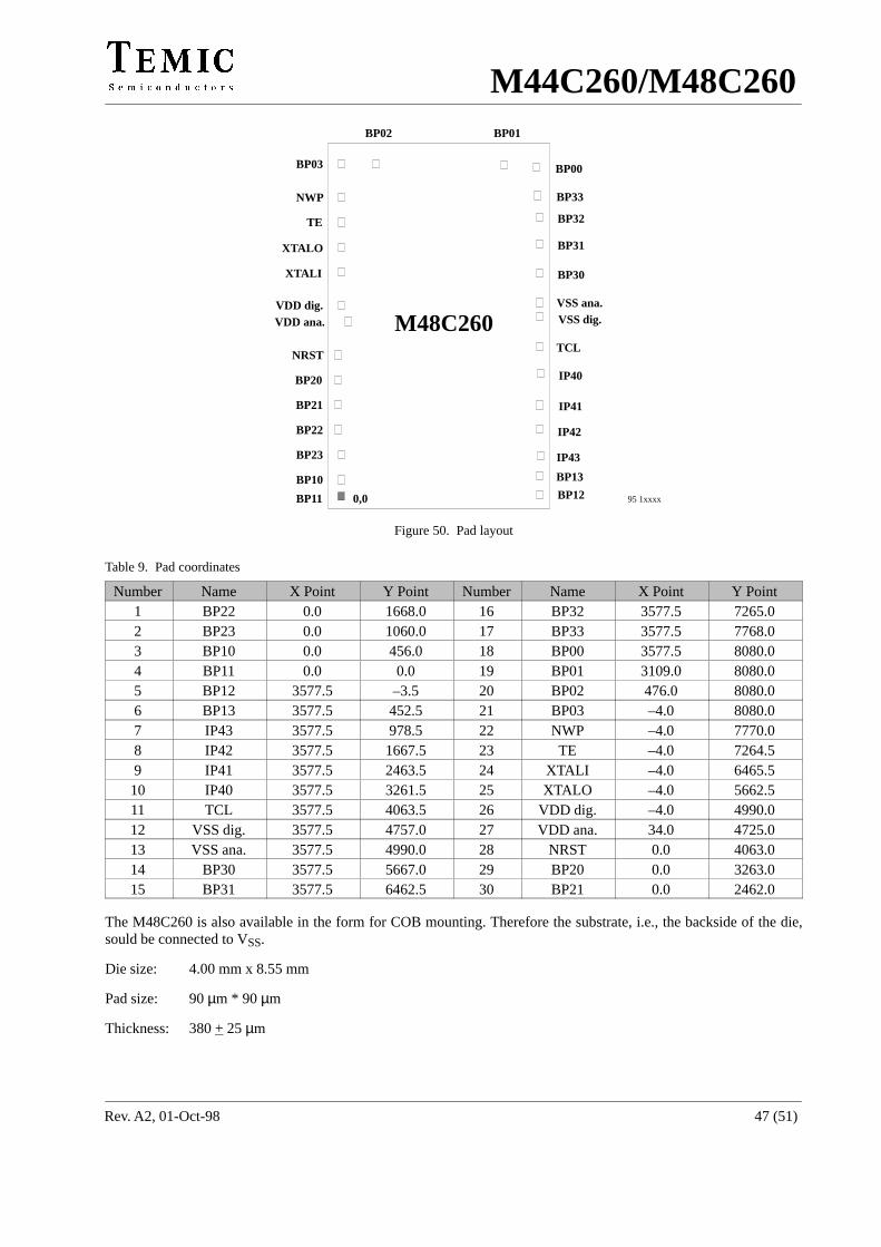
M44C260/M48C260
Rev. A2, 01-Oct-98 47 (51)
BP22
BP23
BP10
BP11 BP12
BP13
IP43
IP42
IP41
IP40
TCL
VSS dig.VSS ana.
BP30
BP31
BP32
BP33
BP00
BP01BP02
BP03
NWP
TE
XTALI
XTALO
VDD dig.VDD ana.
NRST
BP20
BP21
M48C260
95 1xxxx0,0
Figure 50. Pad layout
Table 9. Pad coordinates
Number Name X Point Y Point Number Name X Point Y PointÁÁÁÁÁÁÁÁ
1 ÁÁÁÁÁÁÁÁÁÁ
BP22 ÁÁÁÁÁÁÁÁÁÁ
0.0 ÁÁÁÁÁÁÁÁÁÁ
1668.0ÁÁÁÁÁÁÁÁ
16ÁÁÁÁÁÁÁÁÁÁÁÁ
BP32 ÁÁÁÁÁÁÁÁÁÁ
3577.5 ÁÁÁÁÁÁÁÁÁÁ
7265.0ÁÁÁÁÁÁÁÁ
2 ÁÁÁÁÁÁÁÁÁÁ
BP23 ÁÁÁÁÁÁÁÁÁÁ
0.0 ÁÁÁÁÁÁÁÁÁÁ
1060.0ÁÁÁÁÁÁÁÁ
17ÁÁÁÁÁÁÁÁÁÁÁÁ
BP33 ÁÁÁÁÁÁÁÁÁÁ
3577.5 ÁÁÁÁÁÁÁÁÁÁ
7768.0
ÁÁÁÁÁÁÁÁ
3 ÁÁÁÁÁÁÁÁÁÁ
BP10 ÁÁÁÁÁÁÁÁÁÁ
0.0 ÁÁÁÁÁÁÁÁÁÁ
456.0ÁÁÁÁÁÁÁÁ
18ÁÁÁÁÁÁÁÁÁÁÁÁ
BP00 ÁÁÁÁÁÁÁÁÁÁ
3577.5 ÁÁÁÁÁÁÁÁÁÁ
8080.0
ÁÁÁÁ4 ÁÁÁÁÁBP11 ÁÁÁÁÁ0.0 ÁÁÁÁÁ0.0 ÁÁÁÁ19ÁÁÁÁÁÁBP01 ÁÁÁÁÁ3109.0 ÁÁÁÁÁ8080.0ÁÁÁÁÁÁÁÁ5
ÁÁÁÁÁÁÁÁÁÁBP12
ÁÁÁÁÁÁÁÁÁÁ3577.5
ÁÁÁÁÁÁÁÁÁÁ–3.5
ÁÁÁÁÁÁÁÁ20
ÁÁÁÁÁÁÁÁÁÁÁÁBP02
ÁÁÁÁÁÁÁÁÁÁ476.0
ÁÁÁÁÁÁÁÁÁÁ8080.0ÁÁÁÁ
ÁÁÁÁ6ÁÁÁÁÁÁÁÁÁÁ
BP13ÁÁÁÁÁÁÁÁÁÁ
3577.5ÁÁÁÁÁÁÁÁÁÁ
452.5ÁÁÁÁÁÁÁÁ
21ÁÁÁÁÁÁÁÁÁÁÁÁ
BP03ÁÁÁÁÁÁÁÁÁÁ
–4.0ÁÁÁÁÁÁÁÁÁÁ
8080.0ÁÁÁÁÁÁÁÁ
7 ÁÁÁÁÁÁÁÁÁÁ
IP43 ÁÁÁÁÁÁÁÁÁÁ
3577.5ÁÁÁÁÁÁÁÁÁÁ
978.5ÁÁÁÁÁÁÁÁ
22ÁÁÁÁÁÁÁÁÁÁÁÁ
NWP ÁÁÁÁÁÁÁÁÁÁ
–4.0 ÁÁÁÁÁÁÁÁÁÁ
7770.0ÁÁÁÁÁÁÁÁ
8 ÁÁÁÁÁÁÁÁÁÁ
IP42 ÁÁÁÁÁÁÁÁÁÁ
3577.5ÁÁÁÁÁÁÁÁÁÁ
1667.5ÁÁÁÁÁÁÁÁ
23ÁÁÁÁÁÁÁÁÁÁÁÁ
TE ÁÁÁÁÁÁÁÁÁÁ
–4.0 ÁÁÁÁÁÁÁÁÁÁ
7264.5ÁÁÁÁÁÁÁÁ
9 ÁÁÁÁÁÁÁÁÁÁ
IP41 ÁÁÁÁÁÁÁÁÁÁ
3577.5ÁÁÁÁÁÁÁÁÁÁ
2463.5ÁÁÁÁÁÁÁÁ
24ÁÁÁÁÁÁÁÁÁÁÁÁ
XTALI ÁÁÁÁÁÁÁÁÁÁ
–4.0 ÁÁÁÁÁÁÁÁÁÁ
6465.5
ÁÁÁÁÁÁÁÁ
10 ÁÁÁÁÁÁÁÁÁÁ
IP40 ÁÁÁÁÁÁÁÁÁÁ
3577.5ÁÁÁÁÁÁÁÁÁÁ
3261.5ÁÁÁÁÁÁÁÁ
25ÁÁÁÁÁÁÁÁÁÁÁÁ
XTALO ÁÁÁÁÁÁÁÁÁÁ
–4.0 ÁÁÁÁÁÁÁÁÁÁ
5662.5
ÁÁÁÁÁÁÁÁ
11 ÁÁÁÁÁÁÁÁÁÁ
TCL ÁÁÁÁÁÁÁÁÁÁ
3577.5ÁÁÁÁÁÁÁÁÁÁ
4063.5ÁÁÁÁÁÁÁÁ
26ÁÁÁÁÁÁÁÁÁÁÁÁ
VDD dig. ÁÁÁÁÁÁÁÁÁÁ
–4.0 ÁÁÁÁÁÁÁÁÁÁ
4990.0
ÁÁÁÁ12 ÁÁÁÁÁVSS dig.ÁÁÁÁÁ3577.5ÁÁÁÁÁ4757.0ÁÁÁÁ27ÁÁÁÁÁÁVDD ana. ÁÁÁÁÁ34.0 ÁÁÁÁÁ4725.0ÁÁÁÁÁÁÁÁ13
ÁÁÁÁÁÁÁÁÁÁVSS ana.
ÁÁÁÁÁÁÁÁÁÁ3577.5
ÁÁÁÁÁÁÁÁÁÁ4990.0
ÁÁÁÁÁÁÁÁ28
ÁÁÁÁÁÁÁÁÁÁÁÁNRST
ÁÁÁÁÁÁÁÁÁÁ0.0
ÁÁÁÁÁÁÁÁÁÁ4063.0ÁÁÁÁ
ÁÁÁÁ14ÁÁÁÁÁÁÁÁÁÁ
BP30ÁÁÁÁÁÁÁÁÁÁ
3577.5ÁÁÁÁÁÁÁÁÁÁ
5667.0ÁÁÁÁÁÁÁÁ
29ÁÁÁÁÁÁÁÁÁÁÁÁ
BP20ÁÁÁÁÁÁÁÁÁÁ
0.0ÁÁÁÁÁÁÁÁÁÁ
3263.0ÁÁÁÁÁÁÁÁ
15 ÁÁÁÁÁÁÁÁÁÁ
BP31 ÁÁÁÁÁÁÁÁÁÁ
3577.5ÁÁÁÁÁÁÁÁÁÁ
6462.5ÁÁÁÁÁÁÁÁ
30ÁÁÁÁÁÁÁÁÁÁÁÁ
BP21 ÁÁÁÁÁÁÁÁÁÁ
0.0 ÁÁÁÁÁÁÁÁÁÁ
2462.0
The M48C260 is also available in the form for COB mounting. Therefore the substrate, i.e., the backside of the die,sould be connected to VSS.
Die size: 4.00 mm x 8.55 mm
Pad size: 90 µm * 90 µm
Thickness: 380 + 25 µm
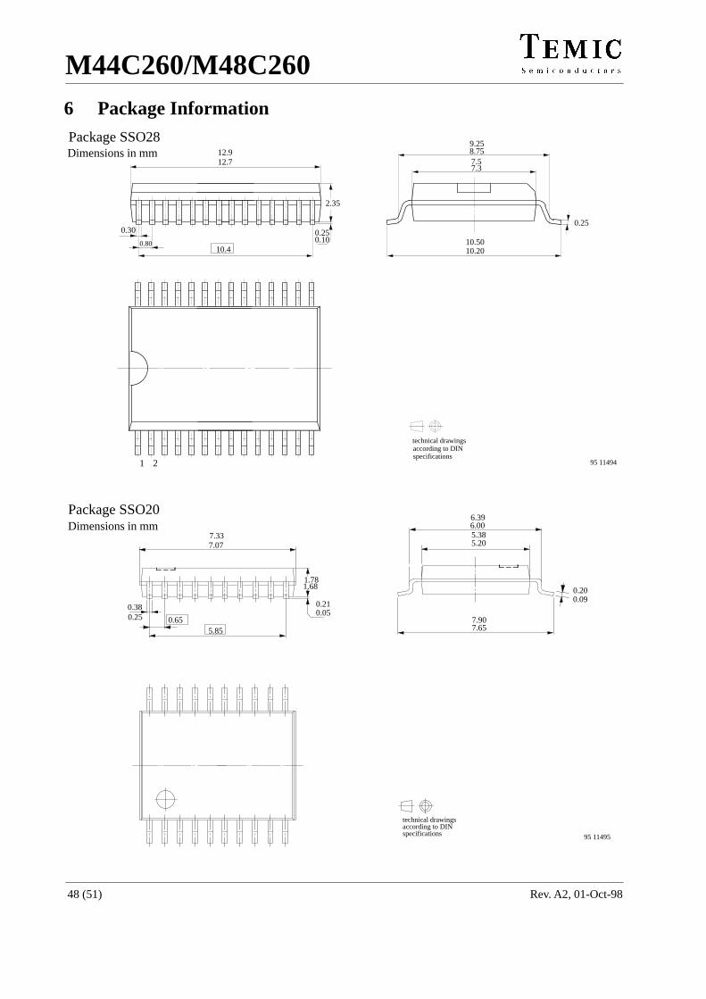
M44C260/M48C260
Rev. A2, 01-Oct-9848 (51)
6 Package Information
2.35
0.250.10
0.30
0.80
7.57.3
9.258.75
0.25
10.5010.20
technical drawingsaccording to DINspecifications
95 114941 2
12.712.9
10.4
Package SSO28Dimensions in mm
0.25 0.65
1.68
0.210.05
5.385.20
0.09
7.907.65
technical drawingsaccording to DINspecifications 95 11495
7.33
5.85
7.07
Package SSO20
1.780.20
0.38
6.396.00Dimensions in mm
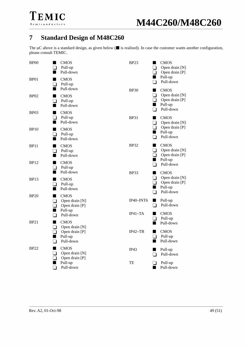
M44C260/M48C260
Rev. A2, 01-Oct-98 49 (51)
7 Standard Design of M48C260The C above is a standard design, as given below ( is realised). In case the customer wants another configuration,please consult TEMIC.
BP00 CMOS Pull-up Pull-down
BP01 CMOS Pull-up Pull-down
BP02 CMOS Pull-up Pull-down
BP03 CMOS Pull-up Pull-down
BP10 CMOS Pull-up Pull-down
BP11 CMOS Pull-up Pull-down
BP12 CMOS Pull-up Pull-down
BP13 CMOS Pull-up Pull-down
BP20 CMOS Open drain [N] Open drain [P] Pull-up Pull-down
BP21 CMOS Open drain [N] Open drain [P] Pull-up Pull-down
BP22 CMOS Open drain [N] Open drain [P] Pull-up Pull-down
BP23 CMOS Open drain [N] Open drain [P] Pull-up Pull-down
BP30 CMOS Open drain [N] Open drain [P] Pull-up Pull-down
BP31 CMOS Open drain [N] Open drain [P] Pull-up Pull-down
BP32 CMOS Open drain [N] Open drain [P] Pull-up Pull-down
BP33 CMOS Open drain [N] Open drain [P] Pull-up Pull-down
IP40–INT6 Pull-up Pull-down
IP41–TA CMOS Pull-up Pull-down
IP42–TB CMOS Pull-up Pull-down
IP43 Pull-up Pull-down
TE Pull-up Pull-down
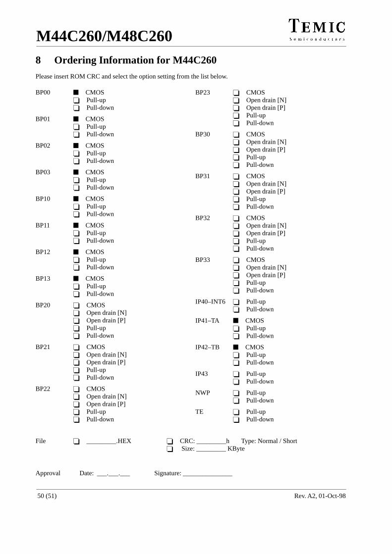
M44C260/M48C260
Rev. A2, 01-Oct-9850 (51)
8 Ordering Information for M44C260Please insert ROM CRC and select the option setting from the list below.
BP00 CMOS Pull-up Pull-down
BP01 CMOS Pull-up Pull-down
BP02 CMOS Pull-up Pull-down
BP03 CMOS Pull-up Pull-down
BP10 CMOS Pull-up Pull-down
BP11 CMOS Pull-up Pull-down
BP12 CMOS Pull-up Pull-down
BP13 CMOS Pull-up Pull-down
BP20 CMOS Open drain [N] Open drain [P] Pull-up Pull-down
BP21 CMOS Open drain [N] Open drain [P] Pull-up Pull-down
BP22 CMOS Open drain [N] Open drain [P] Pull-up Pull-down
BP23 CMOS Open drain [N] Open drain [P] Pull-up Pull-down
BP30 CMOS Open drain [N] Open drain [P] Pull-up Pull-down
BP31 CMOS Open drain [N] Open drain [P] Pull-up Pull-down
BP32 CMOS Open drain [N] Open drain [P] Pull-up Pull-down
BP33 CMOS Open drain [N] Open drain [P] Pull-up Pull-down
IP40–INT6 Pull-up Pull-down
IP41–TA CMOS Pull-up Pull-down
IP42–TB CMOS Pull-up Pull-down
IP43 Pull-up Pull-down
NWP Pull-up Pull-down
TE Pull-up Pull-down
File _________.HEX CRC: _________h Type: Normal / Short Size: _________ KByte
Approval Date: ___.___.___ Signature: _______________
M44C260/M48C260
Rev. A2, 01-Oct-98 51 (51)
We reserve the right to make changes to improve technical design and may do so without further notice.Parameters can vary in different applications. All operating parameters must be validated for each customer
application by the customer. Should the buyer use TEMIC products for any unintended or unauthorizedapplication, the buyer shall indemnify TEMIC against all claims, costs, damages, and expenses, arising out of,
directly or indirectly, any claim of personal damage, injury or death associated with such unintended orunauthorized use.
TEMIC Semiconductor GmbH, P.O.B. 3535, D-74025 Heilbronn, GermanyTelephone: 49 (0)7131 67 2594, Fax number: 49 (0)7131 67 2423