Embed Size (px)
DESCRIPTION
Manufacture of High Aspect Ratio Carbon Nanotube Atomic Force Microscopy Probes. Y.N. Emirov 1 , J.D. Schumacher 1 , M. M. Beerbom 1 , B. Lagel 1 B.B. Rossie 2 , and R. Schlaf 1*. University of South Florida, Dept. of Electrical Engineering USF Center for Ocean Technology - PowerPoint PPT Presentation
Citation preview
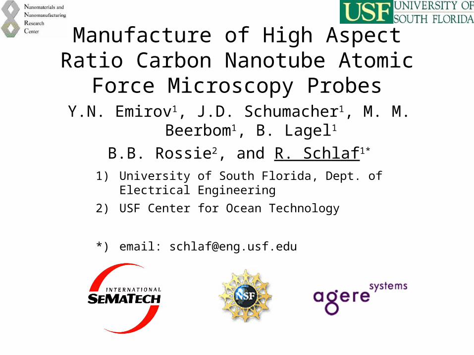
Manufacture of High Aspect Ratio Carbon Nanotube Atomic Force Microscopy Probes
Y.N. Emirov1, J.D. Schumacher1, M. M. Beerbom1, B. Lagel1
B.B. Rossie2, and R. Schlaf1*
1) University of South Florida, Dept. of Electrical Engineering
2) USF Center for Ocean Technology
*) email: [email protected]
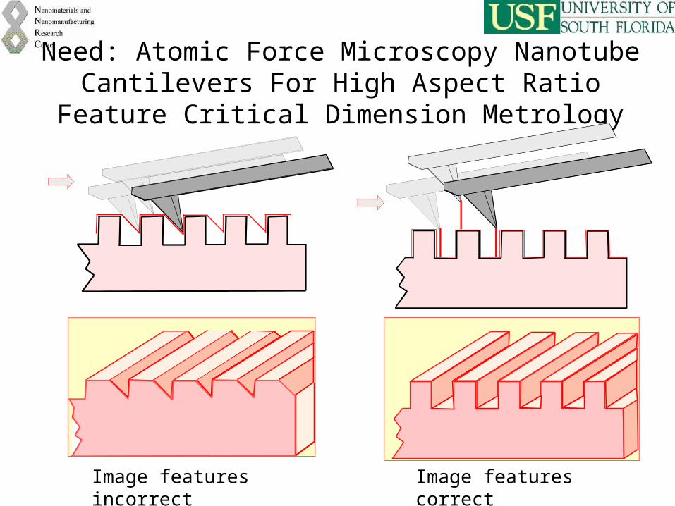
Need: Atomic Force Microscopy Nanotube Cantilevers For High Aspect Ratio Feature Critical Dimension Metrology
Image features incorrect Image features correct
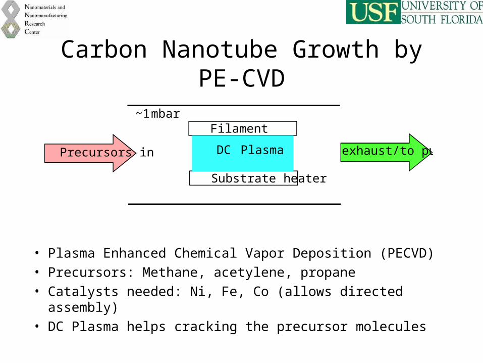
Carbon Nanotube Growth by PE-CVD
• Plasma Enhanced Chemical Vapor Deposition (PECVD)
• Precursors: Methane, acetylene, propane
• Catalysts needed: Ni, Fe, Co (allows directed assembly)
• DC Plasma helps cracking the precursor molecules
exhaust/to pumpPrecursors in
Substrate heater
Filament
DC Plasma
~1 mbar
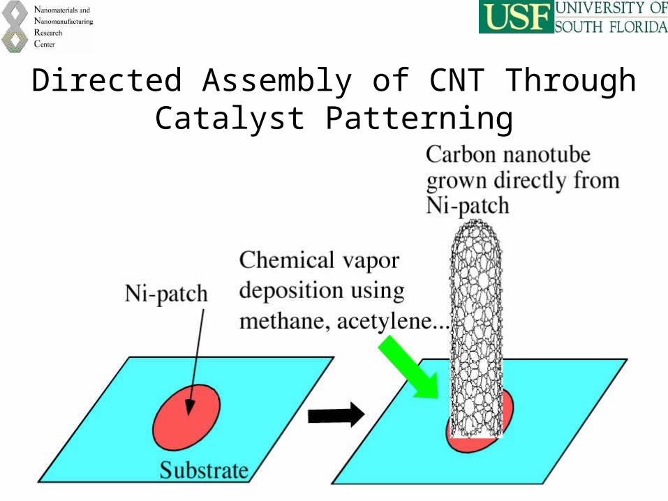
Directed Assembly of CNT Through Catalyst Patterning
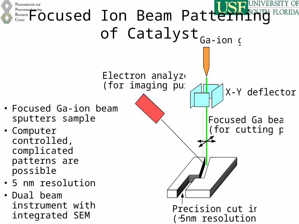
Focused Ion Beam Patterning of Catalyst
• Focused Ga-ion beam sputters sample
• Computer controlled, complicated patterns are possible
• 5 nm resolution• Dual beam instrument
with integrated SEM
X-Y deflector plates
Ga-ion gun
Electron analyzer(for imaging purposes)
Focused Ga beam(for cutting patterns)
Precision cut in sample(~5nm resolution)
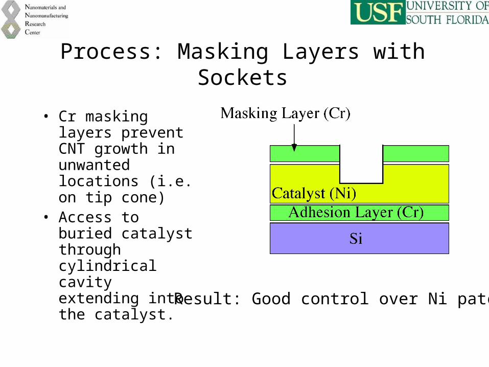
Process: Masking Layers with Sockets
• Cr masking layers prevent CNT growth in unwanted locations (i.e. on tip cone)
• Access to buried catalyst through cylindrical cavity extending into the catalyst.
Result: Good control over Ni patch
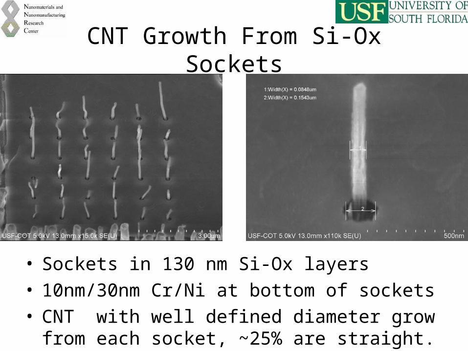
CNT Growth From Si-Ox Sockets
• Sockets in 130 nm Si-Ox layers• 10nm/30nm Cr/Ni at bottom of sockets• CNT with well defined diameter grow from each
socket, ~25% are straight.
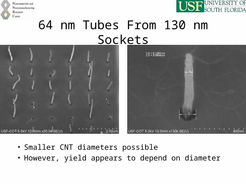
64 nm Tubes From 130 nm Sockets
• Smaller CNT diameters possible• However, yield appears to depend on diameter
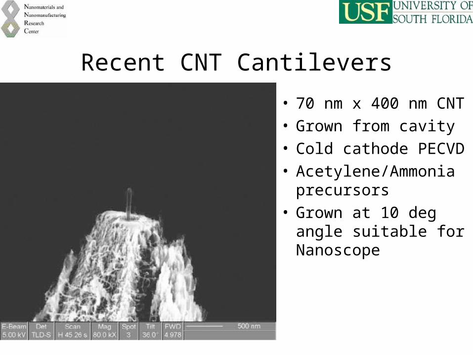
Recent CNT Cantilevers
• 70 nm x 400 nm CNT• Grown from cavity• Cold cathode PECVD• Acetylene/Ammonia
precursors• Grown at 10 deg angle
suitable for Nanoscope
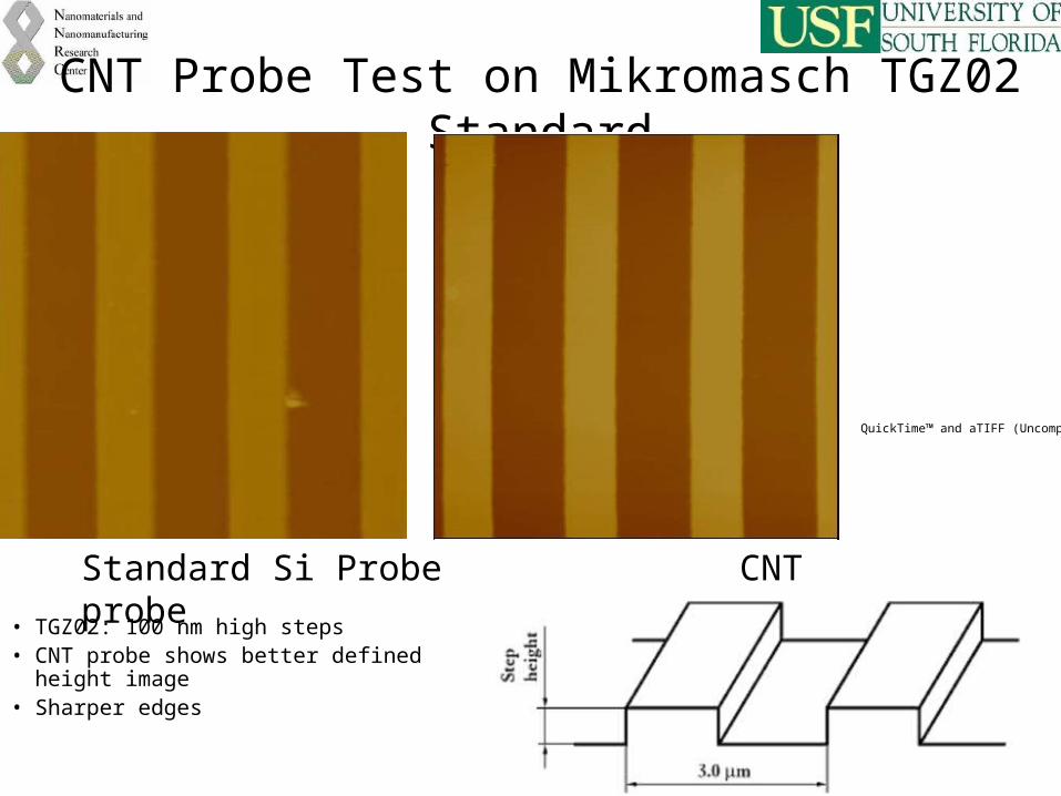
CNT Probe Test on Mikromasch TGZ02 Standard
• TGZ02: 100 nm high steps• CNT probe shows better defined height image• Sharper edges
QuickTime™ and aTIFF (Uncompressed) decompressorare needed to see this picture.
Standard Si Probe CNT probe
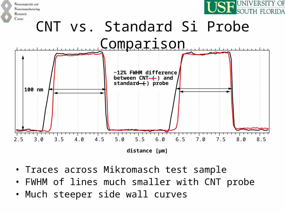
CNT vs. Standard Si Probe Comparison
• Traces across Mikromasch test sample• FWHM of lines much smaller with CNT probe• Much steeper side wall curves
8.58.07.57.06.56.05.55.04.54.03.53.02.5
distance [µm]
~12% FWHM differencebetween CNT ( ) andstandard ( ) probe 100 nm
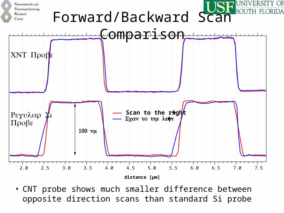
Forward/Backward Scan Comparison
• CNT probe shows much smaller difference between opposite direction scans than standard Si probe
7.57.06.56.05.55.04.54.03.53.02.52.0
distance [µm]
Scan to the right → Scan to the left ←
100 nm
CNT Probe
Regular SiProbe
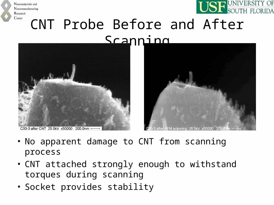
CNT Probe Before and After Scanning
• No apparent damage to CNT from scanning process• CNT attached strongly enough to withstand torques
during scanning• Socket provides stability
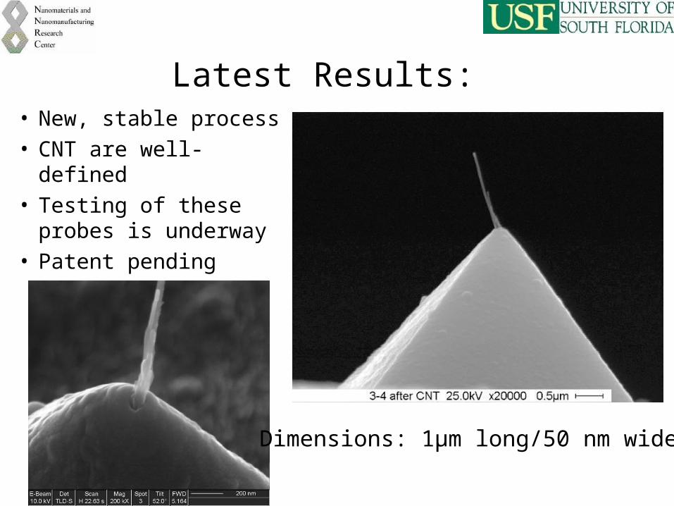
Latest Results:• New, stable process• CNT are well-defined• Testing of these
probes is underway• Patent pending
Dimensions: 1µm long/50 nm wide
Summary
• Goal: Well-defined CNT on standard AFM tips suitable for critical dimension metrology
• Concept has been demonstrated• Focused ion beam/e-beam litho patterning
used for prototyping• Outlook: Testing on state-of-the-art industry
structures/expansion of process to wafer scale• Thank you for your kind attention!
Contact: [email protected]