Embed Size (px)
Citation preview

BROADCAST EQUIPMENTVia G. Amendola 9
44028 Poggio RenaticoFerrara - Italy
Tel : +39 532 829 965Fax : +39 532 829 177
E-mail: [email protected] [email protected]
Web Site: http://www.elenos.com

Handbook SF 250 - 2
Technical office TEL: +39 532 829 965 FAX: +39 532 829 177
The constructor reserves the right to modify the information in this manual at any time withoutadvising update.
2000 Elenos S.r.l.Printed in ItalyCod. MAN0009
21/10/1996 Preliminary mater in English10/04/1997 Rev. 104/01/1998 Rev. 203/05/2000 Rev. 3

Handbook SF 250 - 3
Technical Office TEL: +39 532 829 965 FAX: +39 532 829 177
SUMMARY
GENERAL DESCRIPTION............................................................................................... 4
FRONT VIEW ..................................................................................................................... 5
TECHNICAL FEATURES................................................................................................. 7
PRECAUTIONS .................................................................................................................. 8
MANUFACTURER'S RECOMMENDATIONS.............................................................. 9
TECHNICAL DESCRIPTION ........................................................................................ 10
USER INTERFACE .......................................................................................................... 11
REMOTE INTERFACE ................................................................................................... 12
INSTALLATION............................................................................................................... 14
FRONT PANEL DIAGNOSTICS.................................................................................... 16
TROUBLESHOOTING.................................................................................................... 19
TOP VIEW ......................................................................................................................... 21
BOTTOM VIEW ............................................................................................................... 22
R.F. BLOCK DIAGRAM.................................................................................................. 23
POWER SUPPLY AND MEASUREMENT BLOCK DIAGRAM............................... 24
LAYOUT OF COMPONENTS ........................................................................................ 26ESPL02.1 (Splitter input Board)...................................................................................... 26EF150FM.1 (Power Amplifier)......................................................................................... 28LPF501FM (Low Pass Filter) ........................................................................................... 30E20147 (Power Supply Board) ......................................................................................... 33E30501.2N (Protection board) .......................................................................................... 39E30502 (Front panel board) .............................................................................................. 44E40101 (back board)......................................................................................................... 47E40500 (connection board)............................................................................................... 50SF000070 - Thermal Probe ............................................................................................... 53EPCB0200 (Clock Buffer Board) ..................................................................................... 54EPCB0240 ( R.F.I. Protection Board)............................................................................... 55EPCB0239 (Watch-Dog Board)........................................................................................ 56
INDEX................................................................................................................................. 59

Handbook SF 250 - 4
Technical office TEL: +39 532 829 965 FAX: +39 532 829 177
GENERAL DESCRIPTION
The SF250 model is a solid state amplifier without variable tuning circuits for the 87.5 to 108 MHz
frequency band, intended as a supplementary power stage for FM modulators. The unit is designed to
operate as a final stage powering a radiating system, or as an intermediate stage in a chain of
amplifiers, thus loaded by the input stage of a following amplifier. In both cases an exciter modulator
is necessary.

Handbook SF 250 - 5
Technical Office TEL: +39 532 829 965 FAX: +39 532 829 177
FRONT VIEW

Handbook SF 250 - 6
Technical office TEL: +39 532 829 965 FAX: +39 532 829 177
REAR VIEW

Handbook SF 250 - 7
Technical Office TEL: +39 532 829 965 FAX: +39 532 829 177
TECHNICAL FEATURES
Max. power output: 250W
Input power for 250W output: from 5W to 10W
Mosfet efficiency at 250W output: from 52% to 68%
Mosfet voltage: from 22V to 48V d.c.
Mosfet rest current: from 3mA to 25mA
Mosfet current at 250W: from 8A to 10A
Input SWR: <1.65
Differential of the heat-sink temperature at 250W out : 20°C
Mono supply voltage: 208/220/240 V with mains voltage changeover to 110V
Mains frequency: from 47Hz to 70Hz
Power supply for 250W output: 900VA maximum
Spurious emission at the antenna connector: - 72dBc
Ambient temperature: from -5 to +45°C
Relative ambient humidity: up 95% (45°C) NOT CONDENSED
Protection of output reflected power: 40W max.
Protection of Mosfet current: 12A max.
Protection of input power: 40W max.
Thermal protection: 85°C

Handbook SF 250 - 8
Technical office TEL: +39 532 829 965 FAX: +39 532 829 177
PRECAUTIONS
Do not handle the unit in any way unless all its protection panels are completelyclosed and it is connected to a good earth which can ground parasiticcurrents circulating in the chassis.
Of the Do not operate the unit unless all its panels are completely closed.
Do not open the unit for internal inspection of any sort unless the line supplycable is disconnected from the supply and all other connections to otherequipment are also disconnected.
Any operations which need to be carried out with panels open should be leftexclusively to qualified personnel and those aware of all the risks associatedwith operating high voltage equipment generating significant RF powerlevels.
Some components used in the construction of the unit contain TOXICSUBSTANCES. If, on a visual inspection, any components reveal themselvesto be damaged, fractured or incomplete, proceed with extreme caution toavoid contact with the hands or any other part of the body. The principalcomponents of the unit operating at radio frequency contain the highlydangerous substance, Beryllium Oxide.
WARNING! BERYLLIUM OXIDE IS LETHAL
Only qualified, competent personnel are capable of handling the equipmentand its electronic components without risk. Owners equipment are obliged toconform with these recommendations.

Handbook SF 250 - 9
Technical Office TEL: +39 532 829 965 FAX: +39 532 829 177
MANUFACTURER'S RECOMMENDATIONS
The installation of any electronic apparatus exposes personnel to risk; ELENOS explcitly requests
that no work is carried out unless at least two people are present. This is in view of the fact that
over and above the electrical connections that are necessary, the sheer physical weight of the unit
will not allow a single person to install the unit with complete safety. Do not commence any
operation before reading all safety and operational instructions. ELENOS advises the following
safeguards: hang a poster in the equipment room with clear instructions for first aid in the event of
personal injury; provide local first aid equipment and facilities and display telephone numbers and
means of contacting local public or private emergency services which can easily be referred to by
all personnel.

Handbook SF 250 - 10
Technical office TEL: +39 532 829 965 FAX: +39 532 829 177
TECHNICAL DESCRIPTION
The SF250 is a solid state amplifier using MOSFET power devices as the active radio frequency
element. The equipment comprises 2 RF amplifier modules (card EF150FM1) which are matched for
input/output impedance of 50Ω, an input divider circuit (card ESPL06) and a low-pass filter (card
LPF501FM) which is also a low-pass filter and an output power measurement circuit. The equipment
features a sophisticated array of supervisory circuits which monitor the operation of the RF circuits so
as to maximise operational life and minimise down-time and operator intervention. The RF modules'
power supply circuit (card E20147) employs phase-angle switching rectification. The line transformer
is of toroidal construction with an electrostatic screen separating the primary and secondary windings.
The rectifier's filter is inductive and capacitative. Control of the stabilised voltage is by a
microcontroller which controls the output voltage as a function of the RF power being developed. The
microcontroller on the power supply card (one of three) also monitors the safety of the RF power
modules; in the event of parameters going outside their limits, it will reduce the voltage supplied to
the modules and thus the total RF power. The power supply is protected against accidental short
circuits and, importantly, features a rapid power shut-down system (reaction time about 200µs) which
can save the delicate MOSFET devices from damage which they would otherwise incur even after
short periods of overload. The master card (card E30501) controls the power-up sequence and any
reset required after a fault has triggered a protection mechanism of any sort. The program of the
microcontroller may be partially customised at the customer's request to adapt it to local operating
requirements. This card is in continual digital communication with the power supply card and the
front panel card (card E30502). It collates information received from the power supply and the
operator and can supply current or past data to the operator via codes displayed on the front panel. It
also routes commands to the power supply received from the front panel or from the remote connector
situated on the remote interface card (card E40101).

Handbook SF 250 - 11
Technical Office TEL: +39 532 829 965 FAX: +39 532 829 177
USER INTERFACE
All the controls and indications of the status of the unit needed by the operator are situated on the front panel.
The unit does not have a power on/off switch but rather a STAND BY switch. This switch is situated on the
lower left of the panel; in ( • ) the equipment is operational, otherwise operation is suspended, i.e. power is no
longer supplied to the RF amplifier stages and the auxiliary line output for an external modulator is disabled. In
the front panel also features a meter which can display alternatively: power output (F. PWR), reflected power
(R. PWR), current drawn by the RF amplifier stages (CURRENT), amplifier stage supply voltage (VOLTAGE)
and input power from the exciter (INPUT L.). Other indicators with the same names display the normal or
abnormal, current or past operating status of the apparatus. The LOCK indicator lights when a temporary or
permanent shut-down of the unit has occured as a result of either operator intervention or a fault. An
alphanumeric display (COUNT) is situated on the front panel together with a selector. The selector selects the
parameter to be shown on the meter and also influences the alphanumeric display. When the unit has been
functioning normally, the alphanumeric display shows a 0 (except in the case of F. PWR and VOLTAGE).
Otherwise the number of faults pertaining to the parameter selected is displayed. If, in the past, an anomaly
occured, the corresponding indicator remains permanently lit. These indicators can light intermittently during
Automatic Power Control intervention. If an operational parameter being monitored, has exceeded the alarm
threshold, the RF modules' power supply will reduce the supply voltage and therefore the power dissapated, in
an attempt to avoid a complete shut-down with the consequential loss of service, on the basis that: better less
power output than no power output. When the selector is in the F. PWR position, the function is special: the
alphanumeric display will show S if the unit is in stand-by and P if it is operational. When VOLTAGE is
selected, the alphanumeric display will show a sequence of 2 consecutive characters, an error code useful as a
diagnostic (see table of error codes) or a confirmation of normal operation. Not all faults generating error codes
are permanent, the temporary removal of electrical power from the apparatus leaves two possibilities: remove
the cause of the shut-down or repair the equipment. Clearly, faults due to failure of the microcontrollers cannot
be ruled out and these will preclude any diagnostic assistance. Shut-downs (LOCK indicator lit) are of two
types: permanent, without any attempt to reset, and temporary shut-down with successive attempts at automatic
rest. The period between resets have been programmed according to the type of fault. The equipment will
attempt resets for 24 hours without operator intervention, unless the fault is considered non-resetable. The
RESET button can be used by the operator when the equipment has shutdown due to a fault which is no longer
believed to be a cause of malfunction. This will clear the memory of previous faults but has no effect if the fault
has been identified as fatal. Three indicator lights for other internal voltages are situated in the lower central
part of the panel; these should be lit whenever the unit is powered from the line supply. The R.F. MONITOR
socket provides a sample of the power output of the unit, attenuated by 40-50 dB, for connection to a spectrum
analyser and can be used to check correct operation of the apparatus and any anomalies present in the radio
spectrum.

Handbook SF 250 - 12
Technical office TEL: +39 532 829 965 FAX: +39 532 829 177
REMOTE INTERFACE
At the rear of the unit, a CANNON DB25F connector is situated, labelled REMOTE. This connector allows
remote devices to control various operational parameters of the unit and to activate various operations even
via automatic controllers such as timers, interlocks and other similar electronic or electromechanical
devices.
Pin description:
Pin #1 (remote STAND BY 1). Can be used in conjunction with pin #14 to reset after an enforced shut-down.
The unit will leave the STAND BY state when pin #1 and pin #14 are connected for a short period.
Pin #2 (remote STAND BY 2). Can be used in conjunction with pin #14 to enforce a shut-down. The unit will
enter STAND BY mode when pin #2 and pin #14 are connected together for a short period.
Pin #3, pin #4, pin #5, pin #15, pin #16, pin #17, (GND.) are connected to the units chassis and may be used as
analog signal returns when connecting to external equipment.
Pin #6 RESERVED
Pin #7 (S.C.L.). One of two serial communication lines; IIC BUS, clock signal
Pin #8 (LOCK). If low (0V), the unit is operational, if high (12 Volts), the unit has shut-down.
Pin #9 (5 Volts). Internal 5V supply indicator.
Pin #10 (R. PWR). Reflected power signal normalised at 2 Volts f.s.d. on the front panel meter.
Pin #11 (CURRENT). Signal representing current drawn by the RF stages, normalised at 2 Volts f.s.d. on the
front panel meter.
Pin #12 (INPUT L.). Signal representing RF exciter input voltage, normalised at 2 Volts f.s.d. on the front
panel meter.
Pin #13 (V. REF.). Voltage normalised for the front panel meter (2 Volts).
Pin #14 (STAND BY COMMON) see pin #1 and pin #2.
Pin #18 (STAND BY SWITCH). When connected to GND via an external switch, the unit is forced in stand
by mode.
Pin #19 (S.D.A.) One of two serial communication lines; IIC BUS, data signal.
Pin #20 RESERVED
Pin #21 (TEMP.). Signal representing heatsink temperature, normalised at 2 Volts f.s.d. on front panel meter.
Pin #22 (VOLTAGE). Signal representing RF module power supply voltage, normalised at 2 Volts f.s.d. on
front panel meter.
Pin #23 (F. PWR.). Signal representing the units RF power output, normalised at 2 Volts f.s.d. on front panel
meter.
Pin #24 (-12V). Internal -12V voltage indicator.
Pin #25 (+12V). Internal +12V voltage indicator.

Handbook SF 250 - 13
Technical Office TEL: +39 532 829 965 FAX: +39 532 829 177

Handbook SF 250 - 14
Technical office TEL: +39 532 829 965 FAX: +39 532 829 177
INSTALLATION
The following is an important pre-requisite to operation: the installation site must conform to
necessary safety standards for equipment and personnel. In particular, the power supply should
feature a cut-out facility in the event of over-current; safety breakers for protecting personnel and
earth connections for all equipment. The installation site should have outlets for the discharge of hot
air produced by the equipment and a supply of fresh air. The equipment must operate within an
ambient temperature range of -5 to 45ºC and at relative humidities of less than 95% (non-condensing).
The SF250 is not a transmitter but an amplifier which requires at least a modulator, if not additional
power stages. This poses the problem of integrating a system with other technical specifications which
must comply with the tranmission regulations of the country of installation. It is therefore necessary to
consult this technical manual and especially the chapter regarding problems of transmitter systems
which are assembled from diverse components. Two configurations of the SF250 are envisaged:
1) as the final amplifier driving the radiating system.
2) as an intermediate amplifier driving the input stages of another amplifier.
In both cases, the equipment will leave ELENOS laboratories without any special setup. Before
installation, all packing pieces used during transit should be removed from the equipment. Then a
visual inspection should be made of the equipment to ensure that no damage has been incurred during
transport. In the case of any evident damage, contact ELENOS, for return under warranty. All the
technical manuals supplied with each unit which make up the system being installed should be read to
ensure that the conditions of guarantee are complied with and, most importantly, that any danger to
personnel is avoided. Check that the line voltage stated on the test documents corresponds with that of
the local supply, if not, connect an appropriate means of conversion. Situate the SF250 and its
modulator in their final position. The modulator must be of a quality commensurate with the service
required (mono/stereo) and of variable power output from the lowest power possible upto at least
17W. The connections between the SF250 and its modulator must be as follows: the modulator must
receive its line supply from the AUX SUPPLY socket on the rear of the SF250. In turn the SF250
receives its line supply from a successive amplifier, if present, or direct from the electricity supply
(see the technical manuials of other stages connected to the SF250 for more information). The radio
frequency connections start at the modulator, the output of which should be connected to the R.F.
INPUT socket of the SF250. The R.F. OUPUT connector of the SF250 should be connected to the
antenna or successive amplifying stages. The modulator features a regulator to adjust the RF power
output, this should be set so that, at switch-on, output power is at a minimum (see the modulator
technical manual for more information regarding adjustment and connection to other equipment). On
the rear of the unit, a supplementary earth connection can be made via the exposed captive screw.
This allows a low-resistance path to earth for atmospheric electrostatic discharges and may also be
used for special connection configurations. When all the equipment is connected and all panels are

Handbook SF 250 - 15
Technical Office TEL: +39 532 829 965 FAX: +39 532 829 177
closed, the units can be switched on in the following sequence: first the final stage the whole
transmitter system, then the intermediate stages and finally the modulator. If the system is configured
with the SF250 as the final stage, the modulator should be adjusted to regulate the output power of the
SF250 amplifier to comply with the terms of the homologation licence for the site in question. It will
clearly be necessary to test not only the correct operation of the system but also compliance of
parameters with transmission regulations. If the SF250 is instead an intermediate stage of a more
complex transmitter, the calibration instructions regarding the final stage should be referred to,
ensuring that the SF250 is not exposed to risk of damage by other devices in the system. The SF250
amplifier has no adjustment for tuning or other parameters; from a functional point of view it is
passive. Its characteristics are determined by equipment up- and down-stream of it. The operator
using the SF250 is therefore only concerned with ensuring that the limits of safe operation are not
exceeded indefinately: the modulator must not exceed the tolerated level of excitation power,
including situations in which ambiental factors downgrade performance; for successive stages the
operator must perform the calibration of input stages to ensure safe levels of reflected power
displayed by the SF250's meter. For safety limits on all operational parameters, see the table of typical
and maximum specifications. The SF250 features internal circuits which automatically reduce the
output power if other parameters go outside the limits of safety. The operator responsible for
calibration may exceed some of the limits temporarily, but must not leave the site with the unit
indicating Automatic Power Control (flasing lights on the front panel). In this case the stability of the
RF output power is not guaranteed (see the chapters entitled TECHNICAL DESCRIPTION and
USER INTERFACE of the SF250 manual). Consult the table of typical operating parameters and
their safety limits for the SF250 and other connected equipment to ensure that the installation
operations are complete.

Handbook SF 250 - 16
Technical office TEL: +39 532 829 965 FAX: +39 532 829 177
FRONT PANEL DIAGNOSTICS
A) Diagnostic with selector in VOLTAGE position
When the selector is in the VOLTAGE position, it is possible to obtain useful diagnostic data from
the COUNT alphanumeric display. This display shows a 2 character code which identifies the
functional status of the unit. Anomalies can be permanent or temporary. The error code disappears
if the amplifier returns to normal working. The code will remain displayed permanently if the fault
remains indefinitely. Each message has a technical and logical significance and timing which is
described below:
A0: Appears when there are communication difficulties between cards E30501 and E20147.4. The
status of other indicators is irrelevant and the equipment will not function. Check the integrity of
connections between the two electronic cards and the efficiency of the screen which protects
against RF interference. A permanent fault on one of the automatic control cards is also possible.
A1: This code appears when the supply current drawn by the RF modules is excessive. In this case
the (CURRENT) and (VOLTAGE) indicator will also be lit. For each occurrence of this alarm
condition, the amplifier will shut down for 7 seconds and will then attempt an automatic reset. If 9
of these events occur consecutively, the unit will shut down for 9 seconds, clear the event counter
(CURRENT) and again attempt an automatic reset . If, instead, this message appears only once,
the fault is not permanent and is considered as an isolated incident and consequently ignored by
the protection logic Check the power transistors of the series regulator and for short circuits
caused by foreign bodies.
If this message has appeared just once it is not a permanent fault but a single event which is then
ignored by the protection logic. Check the integrity of the EF150FM1 module; if a module is not
functioning, it is possible that excess current will be drawn. Check the output and low-pass filter
connections.
A2: This code appears when there is a short circuit between input and output of the series regulator
on the E20147.4 power supply card. The RF module power supply is not functioning correctly.
For each intervention of this type, the amplifier will shut down for 7 seconds before trying again.
If 2 of these events occur consecutively, the amplifier will shut down for 9 seconds, clear the event
counter (CURRENT) and again attempt an automatic reset. The LOCK and VOLTAGE indicator
will also appear on the front panel. If, instead, this message appears only once, the fault is not
permanent and is considered as an isolated incident and consequently ignored by the protection
logic. Check the power transistors of the series regulator and for short circuits caused by foreign
bodies.
A3: This code appears when current consumption becomes excessive but there is no input voltage on
the power supply card E20147.4. For each occurrence of this type, the amplifier will shut down
for 7 seconds before trying again. If 2 of these events occur consecutively, the amplifier will shut

Handbook SF 250 - 17
Technical Office TEL: +39 532 829 965 FAX: +39 532 829 177
down for 9 seconds clear the event counter (CURRENT) and again attempt an automatic reset.
The LOCK and VOLTAGE indicator will also appear on the front panel.. If, instead, this message
appears only once, the fault is not permanent and is considered as an isolated incident and
consequently ignored by the protection logic. Check for short circuits between the power supply
card input and the chassis. Quite common in this instance is the breakdown of the thermal
insulator of one of the series regulator power transistors.
A4: This code appears when current consumption is high but there is no power output. For each
occurrence of this type, the amplifier will shut down for 7 seconds before trying again. If 2 of
these events occur consecutively, the amplifier will shut down for 9 seconds clear the event
counter (CURRENT) and again attempt an automatic reset. The LOCK and CURRENT indicator
will also appear on the front panel. If, instead, this message appears only once, the fault is not
permanent and is considered as an isolated incident and consequently ignored by the protection
logic. Check that the RF power modules are functioning.
A5: This code appears when there are problems with the RF output of the amplifier, in particular
when there are sporadic variations in output power. In this case the R. PWR indicator will be
illuminated. For each occurrence of this alarm condition, the amplifier will shut down for 7
seconds and will then attempt an automatic reset If 9 of these events occur consecutively, the unit
will shut down for 9 seconds clear the event counter (CURRENT) and again attempt an automatic
reset There are many causes of this alarm condition which can be complex: check that there is no
RF self-oscillation; check for instability of excitation due to poor connections or modulator faults.
If the modulator is a frequency conversion type, intervention of the squelch function of the radio
link receiver can cause problems.
A6: This code appears when there are problems with the RF output of the amplifier, in particular
when there is a sporadic or persistent mismatch with the radiating system or successive amplifying
stage. In this case the R. PWR indicator will be illuminated. For each occurrence of this alarm
condition, the amplifier will shut down for 7 seconds and will then attempt an automatic reset. If 2
of these events occur consecutively, the unit will shut down for 9 seconds, clear the event counter
(R. PWR) and again attempt an automatic reset. Check if the amplifier's RF load is abnormal and
for any intermittent faults. When the amplifier is driving a thermionic tube stage, this alarm
condition can arise during the tuning phase of the input or when the tube is either very new or near
the end of its life.
A7: This code appears when there are thermal problems with the amplifier, in particular excessive
heating of the heatsink on which the RF modules and power supply are mounted. In this case the
TEMP indicator will illuminate. For each occurrence of this alarm condition, the amplifier will
shut down for 7 seconds and will then attempt an automatic reset. If 9 of these events occur
consecutively, the unit will shut down for 9 seconds then, clear the event counter (TEMP) and
again attempt an automatic reset. If, instead, this message appears only once, the fault is not

Handbook SF 250 - 18
Technical office TEL: +39 532 829 965 FAX: +39 532 829 177
permanent and is considered as an isolated incident and consequently ignored by the protection
logic Check if the ambient temperature is occasionally exceeding specified values. Check if the
flow of cooling air is working effectively. Check that the amplifier's internal cooling fan is
functioning normally. Check the output of the amplifier; if the RF load is abnormal, overheating
can occur.
A8: Message reserved.
A9: This does not indicate an anomaly. This code appears when the amplifier is in STAND BY mode
as a result of operator intervention or control by other equipment. The LOCK indicator will also
be lit.
AA: This does not indicate an anomaly. This code confirms that the equipment is fully functional,
regardless of status of other front panel indicators. The code remains displayed even when the unit
is in Automatic Power Control mode.
AB: This code appears when an RF input signal is present but the amplifier is disabled. Check that
the modulator is connected to the AUX SUPPLY connector situated at the rear of the unit.
AC: This code appears when no voltage is present at the input of the power supply card. For each
occurrence of this type, the amplifier will shut down for 7 seconds before trying again. If 2 of
these events occur consecutively, the amplifier will shut down for 9 seconds then, clear the event
counter and again attempt an automatic reset. The LOCK indicator will also appear on the front
panel.. Check the input circuits of the power supply card; the most likely cause is a short circuit.
AD: This code indicates that the 'syncro' circuit of the power supply card is not synchronising with
line frequency; the unit is faulty. In this case the LOCK indicator will also be lit. Check the
relevant parts of the E20147.4 card.
AE: Message reserved
AF: Message reserved
Note: During the initial phase of powering the unit, it is normal for all indicators to briefly light. If,
when this sequence has finished, the segments of the alphanumeric display light in a rotating
sequence, the unit is faulty. The problem should be sought in the digital connections between all
the microcontroller cards.
B) Diagnostic with the rotary selector in the PWR position.
When the rotary selector is in the F PWR position, the fault count is not displayed and excess
power protection is not expected. The following status codes appear on the alphanumeric display:
S: indicates that the amplifier is in STAND BY mode as a result of operator intervention or control by
external equipment.
P: Indicates that the unit is ready to generate RF power.
L: Indicates faulty connection or operating sequence. Confirmed by the Ab message.

Handbook SF 250 - 19
Technical Office TEL: +39 532 829 965 FAX: +39 532 829 177
TROUBLESHOOTING
(1) The equipment cannot develop nominal output power.
Check the front panel for an intermittant indicator light, this signifies that the equipment is
operating automatically at reduced power level due to the corresponding parameter having
exceeded its safe operating level. The only solution is to remove the electrical or ambiental cause
of the malfunction. Check that the output connections are correct - this is one of the most frequent
causes of problems. Low output power can manifest even if the reading of the power output
indicator is correct. The power supply regulates the voltage supplied to the RF modules as a
function of the internal output power measurement; if the power does not rise, it is because the
voltage is not increasing and it will be impossible to achieve maximum performance. In this case it
will be necessary to either recalibrate the measurement of RF output power or to repair the circuits
in question (consult ELENOS for necessary assistance). The reduced power output can be caused
by a fault in one of the RF amplifier modules, or, less frequently, in other parts.
(2) The unit does not develop power and immediately enters R. PWR protection or, at random,
CURRENT protection, as soon as the input is excited.
Check the RF output connections; it is likely that one or more of the radiating system
connections is defective or operating inefficiently. A second important cause of this malfunction is
the quality of the RF load which is connected to the output of the unit. If a narrow-band filter is
connected, it is possible that some instability can arise leading to oscillations in some of the
internal RF modules. If the filter is well connected and of high quality, this phenomenon is rare,
nevertheless sporadic anomalies can occur. The solution in this case is to experiment: modify the
length of the RF cables which connect the unit to the output filter and recalibrate the narrow-band
output filter, attempting to better match the load which the filter presents to the amplifier. The loss
of performance in the previous cases is the price that is paid for the wide-band characteristics of
the tuning circuits. Check the behaviour of the modulator when RF power is developed; if the
excitation of the SF250 is intermittent, the transmission spectrum becomes that of a pulse
transmitter, not an FM transmitter. In this case it is likely that protection against a load mismatch,
due to an excessively wide spectrum, is active and the only remedy is to eliminate the defect of the
preceeding modulator.
(3) Output power is unstable
Check the front panel for flashing indicators; the instability is due to reduced operating power
by the internal protection circuits which avoid indefinate power reduction but do not guarantee
stability. Remove the cause of the Automatic Power Control intervention by checking ambiental
factors or connections to other equipment as indicated, guided by the parameter indicated on the
front panel. Furthermore check that the instability is not being generated by the modulator but
being reflected by the SF250. Even successive stages can cause power instability; this can occur if

Handbook SF 250 - 20
Technical office TEL: +39 532 829 965 FAX: +39 532 829 177
the load presented to the unit is unstable or there is a high content of harmonic or spurious radio
frequencies. Check the harmonic and out-of-band content of the RF present between the SF250
and successive equipment.
(4) The SF250 unit sporadically interrupts operation (even at reduced power) indicating R.
PWR and CURRENT faults on the front panel.
Check that the connectors of the radiating system and the successive stage are not defective
or damaged. Check that the modulator is not generating instability with sudden power fluctuations
or even large swings of carrier frequency. Check that the modulation frequency deviation is not
excessive or that the frequency synthesizer is not losing control. Check the bandwidth of any
selective filter attached to the output of the unit; if the frequency deviation is greater than the
calibration, the transmitter cannot function properly. Check that the receiver of the radio link does
not destabilise the modulator during squelch intervention. Check that overvoltage of the line
supply is not destabilising the modulator frequency control. Many difficult problems can be
resolved with low-cost solutions: connection of an input filter to the SF250 with the same transfer
function as the output filter; supply of the modulator and SF250 via mains-borne interference
filters; supply of equipment via stabilisers with reserves of power capacity.

Handbook SF 250 - 21
Technical Office TEL: +39 532 829 965 FAX: +39 532 829 177
TOP VIEW

Handbook SF 250 - 22
Technical office TEL: +39 532 829 965 FAX: +39 532 829 177
BOTTOM VIEW

Handbook SF 250 - 23
Technical Office TEL: +39 532 829 965 FAX: +39 532 829 177
R.F. BLOCK DIAGRAM
Part List of R.F. Block Diagram
Rif. Description Value RemarksESPL06.0 Splitter input and power measurement boardEF150FM.1 Power amplifier boardLPF501FM Low pass filter boardSC1, SC2 Cable type RG178 50 ohm 1/4 wave
lengthSC3, SC4 Cable type RG179 75 ohm 1/4 wave
lengthR.F.INPUT Coaxial connector type N femaleR.F.OUTPUT Coaxial connector type N femaleR.F.TEST Coaxial connector type BNC male

Handbook SF 250 - 24
Technical office TEL: +39 532 829 965 FAX: +39 532 829 177
POWER SUPPLY AND MEASUREMENT BLOCK DIAGRAM

Handbook SF 250 - 25
Technical Office TEL: +39 532 829 965 FAX: +39 532 829 177
PART LIST OF POWER SUPPLY AND MEASUREMENTBLOCK DIAGRAM
Rif. Description Value Remarks ElenosCode
BLOWER 1,BLOWER 2
Blower 120x120 30W
C1,C2 Electrolytic capacitor 4700 µF 63V
E20147-4 Power supply boardE30501-2N Protection boardE30502 Front panel boardE40101 Back boardE40500 Connection boardLPF501FM Low pass filterESPL02.1 2 ways splitterEPCB0200 Clock buffer BoardEPCB0239 Watch-Dog Board
F1, F2 Fuse holder with 10A fuse
FL1 Flat Cable 10 pin CSF- F006FL2 Flat Cable 40 pin CSF- F007FL3 Flat Cable 20 pin CSF- F008FL4 Flat Cable 20 pin CSF- F004FL5 Flat Cable 2 pin CSF- F016FL6 Flat Cable 2 pin CSF- 0024FL7 Flat Cable 4 pin CSF- F005FL8 Cable type RG178 35 cm
L1 Inductor 750 µH 11 A
Meter Meter 100µA f.s. M3D
R1 Wire wound resistor 50Ω 5%R2 Resistor 10Ω 25W 5%
RL1 Relay FINDER type 65.31 12 V DC
R.F.I. filter Arcotronics FAMDB3600ZEST-BY SWITCH 2-way 2-position switch 250V 6A
SF000070 Thermal Probe Board
Transformer Toroidal transformer with electrostatic shield 900 VA
VAR1, VAR2 MOV type S20K-275

Handbook SF 250 - 26
Technical office TEL: +39 532 829 965 FAX: +39 532 829 177
LAYOUT OF COMPONENTS
ESPL02.1 (Splitter input Board)
Part List of ESPL02.1 Board
Rif. Description Value Remarks ElenosCode
PCB Print Board 2PCB0210R1, R2 Resistor 34 KΩ 1%R3 Resistor 100 Ω 2WT1 Trimmer type 67W 50 KΩC1, C2 Ceramic Capacitor 10 pF 50 VC3, C4 Ceramic Capacitor 4n7 50 VD1 Diode Germanium AA118SC1, SC2 Cable type RG179 75 ohm ¼ wave
lengthSC3, SC4 Cable type RG178 50 ohm ¼ wave
lengthCN1 Connector AMP MODU II 2 pin angled

Handbook SF 250 - 27
Technical Office TEL: +39 532 829 965 FAX: +39 532 829 177

Handbook SF 250 - 28
Technical office TEL: +39 532 829 965 FAX: +39 532 829 177
EF150FM.1 (Power Amplifier)

Handbook SF 250 - 29
Technical Office TEL: +39 532 829 965 FAX: +39 532 829 177
PART LIST BOARD EF150FM1
Rif. Description Value Remarks ElenosCode
PCB 2PCB0190R1, R2 Resistor 100 Ω 0.5 W 5%R3 Resistor 820 Ω 0.25 W 5%R4 Resistor 10 Ω 2 W 5%R5 Resistor 15 KΩ 0.25 W 5%R6 Resistor 2k7 0.25 W 5%C1 Mica Capacitor 1000 pF 500 VC2 Electrolytic. Vert. Capacitor 47 µF 63 VC3 Ceramic Capacitor 4n7 2 KVC4 Mylar Capacitor 220 nF 100 VC5 Ceramic Capacitor 4n7 2 KVC6, C7 Ceramic Capacitor SMD 4n7 50 VC9 Mica Capacitor 1000 pF 500 VC10 Ceramic Capacitor NPO 82 pF 100 VC11, C12 Mica Capacitor 330 pF 500 VC13 Mica Capacitor 220 pF 500 VC14 Mica Capacitor 47 pF 500 VC15 Mica Capacitor 1000 pF 500 VC16 Ceramic Capacitor NPO 82 pF 100 VL1, L2 Inductor type VK200 200 µHL3 Coil #8 turns D=8.0 W=1.0 2L000110L4 Coil #3 turns D=5.0 W=1.0 2L000100L5 Coil #0.5 turns D=8.5 W=1.0 2L000140L6 Coil #2 turns D=5.0 W=1.0 2L000130L7 Coil #3 turns D=6.5 W=1.0 2L000120M1 Mosfet type BLF177

Handbook SF 250 - 30
Technical office TEL: +39 532 829 965 FAX: +39 532 829 177
LPF501FM (Low Pass Filter)

Handbook SF 250 - 31
Technical Office TEL: +39 532 829 965 FAX: +39 532 829 177
Handbook SF 250 - 32
Technical office TEL: +39 532 829 965 FAX: +39 532 829 177
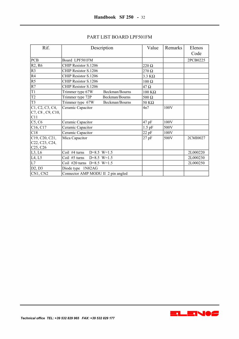
PART LIST BOARD LPF501FM
Rif. Description Value Remarks ElenosCode
PCB Board LPF501FM 2PCB0225R2, R6 CHIP Resistor S.1206 220 ΩR3 CHIP Resistor S.1206 270 ΩR4 CHIP Resistor S.1206 3.3 KΩR5 CHIP Resistor S.1206 100 ΩR7 CHIP Resistor S.1206 47 ΩT1 Trimmer type 67W Beckman/Bourns 100 KΩT2 Trimmer type 72P Beckman/Bourns 500 ΩT3 Trimmer type 67W Beckman/Bourns 50 KΩC1, C2, C3, C4,C7, C8 , C9, C10,C11
Ceramic Capacitor 4n7 100V
C5, C6 Ceramic Capacitor 47 pF 100VC16, C17 Ceramic Capacitor 1.5 pF 500VC18 Ceramic Capacitor 22 pF 100VC19, C20, C21,C22, C23, C24,C25, C26
Mica Capacitor 27 pF 500V 2CMI0027
L3, L6 Coil #4 turns D=8.5 W=1.5 2L000220L4, L5 Coil #5 turns D=8.5 W=1.5 2L000230L7 Coil #20 turns D=8.5 W=1.5 2L000250D2, D3 Diode type 1N82AGCN1, CN2 Connector AMP MODU II 2 pin angled

Handbook SF 250 - 33
Technical Office TEL: +39 532 829 965 FAX: +39 532 829 177
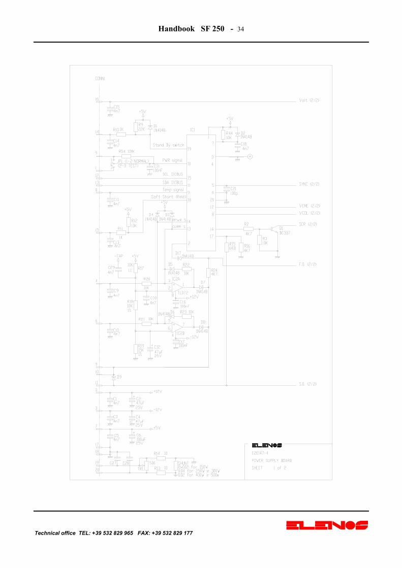
E20147 (Power Supply Board)
Handbook SF 250 - 34
Technical office TEL: +39 532 829 965 FAX: +39 532 829 177

Handbook SF 250 - 35
Technical Office TEL: +39 532 829 965 FAX: +39 532 829 177

Handbook SF 250 - 36
Technical office TEL: +39 532 829 965 FAX: +39 532 829 177
Part List Board E20147
Item Description Value RemarksPCB1 Board code 2PCB0224PCB2 Board code 2PCB0221R1 Resistor 330 Ω 1/4W 5%R2 Resistor 4.7 KΩ 1/4W 1%R3 Resistor 10 KΩ 1/4W 1%R4 Resistor 47 Ω 1W 5%R5 Resistor 10 KΩ 2W 5%R6 Resistor 680 Ω 1/4W 5%R7 Resistor 100 KΩ 1/4W 1%R8 Resistor 10 KΩ 1/4W 1%R9 Resistor 22 KΩ 1/4W 1%R10, R11 Resistor 1KΩ 1/4W 1%R12 Resistor 10 KΩ 1/4W 1%R13, R14 Resistor 10 Ω 1/4W 1%R15 Resistor 6.8 KΩ 1/4W 1%R16 Resistor 4.7 KΩ 1/4W 1%R17, R18 Resistor 10 KΩ 1/4W 1%R19 Resistor 15 KΩ 1/4W 1%R20, R21, R22,R23
Resistor 10 KΩ 1/4W 1%
R24 Resistor 4.7 KΩ 1/4W 1%R25 Resistor 150 Ω 1W 5%R26 Resistor 4.7 KΩ 1/4W 1%R27 Resistor 10 KΩ 1/4W 1%R28 Resistor 18 KΩ 1/4W 5%R29 Resistor 680 Ω 5W 5%R30, R31 Resistor 56 Ω 2W 5%R32 Resistor 10 KΩ 1/4W 1%R33 Resistor 1 KΩ 1/4W 1%R34 Resistor 12 KΩ 1/4W 1%R35, R36, R37,R38,R39, R40
Resistor 0.22 Ω 5 W 5%
R41 Resistor 12 KΩ 1/4W 1%R42, R43 Resistor 1 KΩ 1/4W 1%R44 Resistor 10 KΩ 1/4W 1%R45 Resistor 4.7 KΩ 2 W 5%R46 Resistor 10 KΩ 1/4W 1%R47 Resistor 680 Ω 1/4W 5%R49 Resistor 330 Ω 1/4W 5%R51 Resistor 270 Ω 1/4W 5%R52 Resistor 0.22 Ω 5 W 5%R54 Resistor 100 K=Ω 1/4W 1%R55, R56, R57,R58, R59, R60
Resistor 100 Ω 1/4W 1%

Handbook SF 250 - 37
Technical Office TEL: +39 532 829 965 FAX: +39 532 829 177
SHUNT SF150 Resistor 0.12 Ω 5W 1%SHUNTSF250, SF300
Resistor 0.04 Ω 5W 1%
SHUNT SF400 Resistor 0.02 Ω 5W 1%SHUNTSF500, HF1000
Resistor 0.02 Ω 5W 1%
TR1 Trimmer Vert. Mult. Type 67W 500 ΩC1, C3, C5 Ceramic Capacitor 4n7 50VC2, C4 Electrolytic. Vert. Capacitor 47 µF 35VC6 Electrolytic. Vert. Capacitor 100µF 35VC7, C8 Ceramic Capacitor 4n7 2KVC9, C10, C11 Ceramic Capacitor 4n7 50VC12 Electrolytic. Vert. Capacitor 47 µF 35VC13, C14, C15 Ceramic Capacitor 4n7 50VC16, C17 Ceramic Capacitor Multis. 100 nF 50 VC18 Ceramic Capacitor 4n7 50VC21 Ceramic Capacitor 100 pF 50 VC22, C23 Electrolytic. Vert. Capacitor 10 µF 63 VC24 Ceramic Capacitor 4n7 2KVC25 Electrolytic. Vert. Capacitor 47 µF 63 VC26 Electrolytic. Vert. Capacitor 470 µF 63 VC27, C28, C29,C30
Ceramic Capacitor 4n7 50V
C31 Polyester Capacitor 220 nF 63 VC32 Polyester Capacitor 470 nF 63 VC33, C34 Ceramic Capacitor 4n7 2KVD1, D2, D3, D4,D5, D6, D7, D8
Diode type 1N4148
D11 Diode type BTW81P or RUR1520+ Mica Insulator+ Insulating Ring
D12, D13, D14,D15
Diode type 1N4007
D16 Diode type BTW81PD17, D18 Diode type 1N4148D19 - D22 Diode type 1N4007D23 Green Led 3 mm.DZ1, DZ2 Zener diode 9.1 V.Q1, Q2 Transistor type BC337Q3 Transistor type TIP142CQ4, Q5, Q6, Q7,Q8, Q9
Transistor type TIP142C+ Mica Insulator+ Insulating Ring
Q10 Transistor type TIP142CSCR1, SCR2,SCR3
SCR type BTW68-600 25A600V

Handbook SF 250 - 38
Technical office TEL: +39 532 829 965 FAX: +39 532 829 177
IC1 ST62T10B6/HWD+ Socket 20 pin
IC2 MOC072C+ Socket 8 pin
IC3 Opto TLP3021+ Socket 6 pin
IC4 Opto TLP630+ Socket 6 pin
CN1 ANSLEY connector 2 x 10p-CAP Fixing stud F/M 15mm. M3R50 Fixing stud F/M 15mm. M354 V.A.C. Fixing stud F/M 15mm. M3+R50 Fixing stud F/M 15mm. M354 V.A.C. Fixing stud F/M 15mm. M3+CAP Fixing stud F/M 15mm. M3DC OUT Fixing stud F/M 15mm. M3Heat Sink Elenos code 9RSX0201JP1 Jumper 3 pin
Handbook SF 250 - 39
Technical Office TEL: +39 532 829 965 FAX: +39 532 829 177
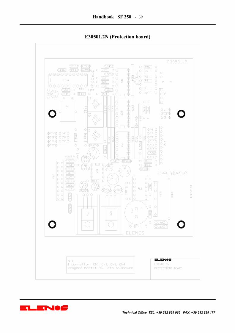
E30501.2N (Protection board)

Handbook SF 250 - 40
Technical office TEL: +39 532 829 965 FAX: +39 532 829 177

Handbook SF 250 - 41
Technical Office TEL: +39 532 829 965 FAX: +39 532 829 177

Handbook SF 250 - 42
Technical office TEL: +39 532 829 965 FAX: +39 532 829 177
Part List Board E30501.2N
Rif. Description Value RemarksPCB Board code 2PCB0206R1, R2 Resistor 10 KΩ ¼ W 1%R4, R5 Resistor 34 KΩ ¼ W 1%R6 Resistor 10 KΩ ¼ W 1%R20 Resistor 2.2 KΩ 0.125 WR25 Resistor 1.05 KΩ ¼ W 1%R26 Resistor 34 KΩ ¼ W 1%R31 Resistor 1.3 KΩ ¼ W 1%R32 Resistor 4.75 KΩ ¼ W 1%R44 Resistor 1.3 KΩ ¼ W 1%R46 Resistor 4.75 KΩ ¼ W 1%R54 Resistor 100 Ω ¼ W 1%R56 Resistor 100 KΩ ¼ W 1%R57 Resistor 4.75 KΩ ¼ W 1%R59 Resistor 10 KΩ ¼ W 1%R60 Resistor 34 KΩ ¼ W 1%R61 Resistor 22 KΩ ¼ W 1%R63 Resistor 4.75 KΩ ¼ W 1%R66 Copper wire 0 ΩR67 Resistor 4.75 KΩ ¼ W 1%R68 Resistor 1 KΩ ¼ W 1%R69 Resistor 4.75 KΩ ¼ W 1%R101 Copper wire 0 ΩRR1 Resistor Array 83S104 4 x 100 KΩRR2 Resistor Array 83S103 4 x 10 KΩRR3 Resistor Array 83S105 4 x 1 MΩRR4 Resistor Array 83S103 4 x 10 KΩRR5 Resistor Array 4X101J 4 x 100 ΩRR6 Resistor Array 83S102 4 x 1 KΩRR7 Resistor Array 83S103 4 x 10 KΩRR8 Resistor Array 83S102 4 x 1 KΩRR9 Resistor Array 83S474 4 x 470 KΩRR10 Resistor Array 83S333 4 x 33KRR11 Resistor Array 4X101J 4 x 100 ΩRR12 Resistor Array 83S103 4 x 10 KΩT1, T2, T3 Trimmer type X 100KΩC1, C2, C3 Ceramic Capacitor 4.7 nF 50VC5 to C26 Ceramic Capacitor 4.7 nF 50VC27 Ceramic Capacitor 100 nF 63VC28, C29, C30 Ceramic Capacitor 4.7 nF 50VC31 Electrolytic. Vert. Capacitor 10 µF 63 VC32 Electrolytic. Vert. Capacitor 1 µF 35 VC33 Electrolytic. Vert. Capacitor 10 µF 63 VC34 Electrolytic. Vert. Capacitor 1 µF 35 VC35 Electrolytic. Vert. Capacitor 1000 µF 35 VC36, C37 Ceramic Capacitor 4.7 nF 2KVC38 Electrolytic. Vert. Capacitor 10µF 63 V

Handbook SF 250 - 43
Technical Office TEL: +39 532 829 965 FAX: +39 532 829 177
C39, C40, C41 Electrolytic. Vert. Capacitor 100uF 35 VC42, C43, C44,C45, C46, C47
Ceramic Capacitor 100 nF 63 V
C48 Ceramic Capacitor 4.7 nF 50 VC49, C50 Ceramic Capacitor 22 pF 63 VC51 Ceramic Capacitor 100 nF 63 VC52 Electrolytic. Vert. Capacitor 1 uF 63 VC53, C54, C55,C56, C57, C58,C59, C60
Ceramic Capacitor 4.7 nF 50V
C61, C62 Ceramic Capacitor 4.7 nF 2KVC63 Ceramic Capacitor 4.7 nF 50VD1 Diode type 1N4148D2, D3, D4 Diode type 1N4007Q1, Q2, Q3 Transistor type BC337IC1, IC2, IC3 I.C. type TL074
+ Socket 14 pinIC4 ST62T10B6/HWD
+ Socket 20 pin+ Epcb0240 Board
IC5 LT1054CNB+ Socket 8 pin
IC6 T7805CT+ Heat-sink 21C / W
IC7 T7812CT+ Heat-sink 21C / W
RL1 Relay Siemens V23101-D0106-B201X1 Crystal 8MHzCN1 Strip step 2.54 1 x 4pCN2 Strip step 2.54 1 x 10pCN3 Strip step 2.54 2 x 10pCN4 Strip step 5.08 1 x 5 or 1 x 9
step 2.54

Handbook SF 250 - 44
Technical office TEL: +39 532 829 965 FAX: +39 532 829 177
E30502 (Front panel board)

Handbook SF 250 - 45
Technical Office TEL: +39 532 829 965 FAX: +39 532 829 177

Handbook SF 250 - 46
Technical office TEL: +39 532 829 965 FAX: +39 532 829 177
Part List Board E30502
Rif. Description Value RemarksPCB Board Code 2PCB0207R1 Resistor 10 KΩ 1/4W 1%R2 Copper Wire 0 ΩR3, R4 Resistor 10 KΩ 1/4W 1%R6 Resistor 1.8 KΩ 1/4W 5%R7, R8 Resistor 1 KΩ 1/4W 1%R9 Resistor 330 Ω 1/4W 1%R10 Resistor 10 KΩ 1/4W 1%R11 Copper Wire 0ΩRR1, RR2 Resistor Array 4 x 680ΩRR3 Resistor Array 9 x 470ΩT1 Trimmer type 89P 20 KΩC1, C2 Ceramic Capacitor 22 pF 50VC3 Ceramic Capacitor 100 nF 63 VC4, C5, C6, C7 Ceramic Capacitor 4n7 50VC8 Ceramic Capacitor 10 nF 50VC9 Electrolytic. Vert. Capacitor 100 uF 35VD1, D2, D3 Diode type 1N4148DL1, DL2, DL3,DL4, DL5, DL6
Red Led 5 mm.
DL7, DL8, DL9 Green Led 5 mm.DSP1 Display type FND367IC1 ST62T10B6/HWD
+Socket 20 pinCN1 AMP connector MODU II 2p angledCN3 ANSLEY connector 10+10 pin straightJ1 Jumper 3 pinSW1 push-buttonSW2 Rotary Switch 6 pos. 2 way

Handbook SF 250 - 47
Technical Office TEL: +39 532 829 965 FAX: +39 532 829 177
E40101 (back board)

Handbook SF 250 - 48
Technical office TEL: +39 532 829 965 FAX: +39 532 829 177

Handbook SF 250 - 49
Technical Office TEL: +39 532 829 965 FAX: +39 532 829 177
PART LIST BOARD E40101
Rif. Description Value RemarksPCB Board code 2PCB0231R1 Resistor 150 Ω 2 W 5%R2, R2A Resistor 47 Ω 2 W 5%R3 Resistor 1 KΩ 1/4W 1%R4 Resistor 10 KΩ 1/4W 1%R5 Resistor 2k2 1/4W 5%R6, R7 Resistor 470 Ω 1/2W 5%R8, R9 Resistor 2k2 1/4W 5%RR1, RR2, RR3 Resistor Array L83S222 4 x 2k2 8 pinC1 Electrolytic. Vert. Capacitor 470 µF 50 V 10%C2 Ceramic Capacitor p5 100 nF 50 V 10%C3, C4, C5, C6,C7
Ceramic Capacitor p5 4n7 50 V
D1, D2 Diode type 1N4007D3, D4, D5, D6 Diode type 1N4148D7, D8 Diode type 1N4007Q1 Transistor Darlington BD679RL1 Relay FINDER 40.31-12V DCRL2 Relay TAKAMISAWA RALD12W-KJP1 PHOENIX connector 5p StraightJP2 ANSLEY male connector 20+20 pin straightJP3 ANSLEY male connector 5+5 pin StraightJP4 Female connector type DB 25 pin straightJP5 PHOENIX connector type KDS4 3 pair pin

Handbook SF 250 - 50
Technical office TEL: +39 532 829 965 FAX: +39 532 829 177
E40500 (connection board)

Handbook SF 250 - 51
Technical Office TEL: +39 532 829 965 FAX: +39 532 829 177
Handbook SF 250 - 52
Technical office TEL: +39 532 829 965 FAX: +39 532 829 177
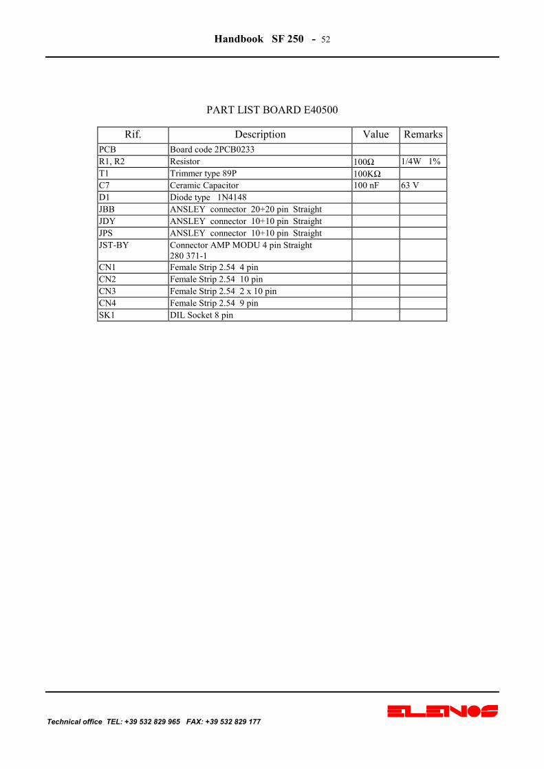
PART LIST BOARD E40500
Rif. Description Value RemarksPCB Board code 2PCB0233R1, R2 Resistor 100Ω 1/4W 1%T1 Trimmer type 89P 100KΩC7 Ceramic Capacitor 100 nF 63 VD1 Diode type 1N4148JBB ANSLEY connector 20+20 pin StraightJDY ANSLEY connector 10+10 pin StraightJPS ANSLEY connector 10+10 pin StraightJST-BY Connector AMP MODU 4 pin Straight
280 371-1CN1 Female Strip 2.54 4 pinCN2 Female Strip 2.54 10 pinCN3 Female Strip 2.54 2 x 10 pinCN4 Female Strip 2.54 9 pinSK1 DIL Socket 8 pin

Handbook SF 250 - 53
Technical Office TEL: +39 532 829 965 FAX: +39 532 829 177
SF000070 - Thermal Probe
Part List of Thermal Probe Board
Rif. Description Value RemarksPCB Board Code 2PCB0208R1, R2 Resistor 6980Ω 1/4W 1%C1, C2 Ceramic Capacitor 4700 pFC3 Electrolytic. Capacitor 10 µF 63 VIC1 Sensor type LM35DHCN1 AMP connector 4 pin angled

Handbook SF 250 - 54
Technical office TEL: +39 532 829 965 FAX: +39 532 829 177
EPCB0200 (Clock Buffer Board)
Part List Board EPCB0200
Rif. Description Value RemarksPCB Board Code 2PCB0200IC1 I.C. type DM7400N

Handbook SF 250 - 55
Technical Office TEL: +39 532 829 965 FAX: +39 532 829 177
EPCB0240 ( R.F.I. Protection Board)
Part List Board EPCB0240
Rif. Description Value RemarksPCB Board Code 2PCB0240C1 - C15 SMD Capacitor 4.7 nFCN1, CN2 Strip step 2.54 1 x 10 p

Handbook SF 250 - 56
Technical office TEL: +39 532 829 965 FAX: +39 532 829 177
EPCB0239 (Watch-Dog Board)

Handbook SF 250 - 57
Technical Office TEL: +39 532 829 965 FAX: +39 532 829 177

Handbook SF 250 - 58
Technical office TEL: +39 532 829 965 FAX: +39 532 829 177
PART LIST BOARD EPCB0239
Rif. Description Value RemarksPCB Board Code 2PCB0239R1 Resistor 100 KΩR2 Resistor 1 KΩR3 Resistor 10 KΩR4 Resistor 1 KΩR5, R6 Resistor 10 KΩR7 Resistor 100 KΩR8 Resistor 10 KΩC1, C2, C3, C4,C5
SMD Capacitor 100 nF
C6 Electrolytic Capacitor 22 µF 25VC7 SMD Capacitor 100 nFC8 SMD Capacitor 4n7C9 SMD Capacitor 470 nFC10 Electrolytic. Capacitor 10 µF 25VC11 to C24 SMD Capacitor 4n7D1, D2, D3, D4,D5
SMD Diode
Q1 SMD TransistorU1 I.C. type HEF4017BTU2 I.C. type HEF4020BTU3 I.C. type CD4093BCMU4 I.C. type 14077BU5 ST62T10B6/HWD
+ Socket 20pCN1, CN2 Strip step 2.54 1 x 10pCN3 Connector AMP MODU II 4p straightCN4 Connector AMP MODU II 2p straight

Handbook SF 250 - 59
Technical Office TEL: +39 532 829 965 FAX: +39 532 829 177
INDEX
B
BOTTOM VIEW · 23
E
E20147 (POWER SUPPLY BOARD) · 34E30501 (PROTECTION BOARD) · 40E30502. (FRONT PANEL BOARD) · 45E40101 (BACK BOARD) · 48E40500 (CONNECTION BOARD) · 51EF150FM.1 (POWER AMPLIFIER) · 29EPCB0200 (CLOCK BUFFER BOARD) · 55EPCB0239 (WATCH-DOG BOARD) · 57EPCB0240 ( RF PROTECTION BOARD) · 56ESPL02.1 (SPLITTER INPUT BOARD) · 27
F
FRONT PANEL DIAGNOSTICS · 16FRONT VIEW · 5
G
GENERAL DESCRIPTION · 4
I
INSTALLATION · 14
L
LPF501FM (LOW PASS FILTER) · 31
M
MANUFACTURER'S RECOMMENDATIONS · 9
P
POWER SUPPLY AND MEASUREMENT BLOCKDIAGRAM · 25
PRECAUTIONS · 8
R
R.F. BLOCK DIAGRAM · 24REAR VIEW · 6REMOTE INTERFACE · 12
S
SF000070 - THERMAL PROBE · 54
T
TECHNICAL DESCRIPTION · 10TECHNICAL FEATURES · 7TOP VIEW · 22TROUBLESHOOTING · 20
U
USER INTERFACE · 11