Embed Size (px)
Citation preview

MAHARASHTRA STATE BOARD OF TECHNICAL EDUCATION (Autonomous)
(ISO/IEC - 27001 - 2005 Certified) ______________________________________________________________________________________________________
WINTER – 2014 EXAMINATION Subject Code: 17210 Model Answer (Applied Science- Physics) Page No: 01/15
Que. No.
Sub. Que.
Stepwise Solution Marks Total
Marks
Important Instructions to examiners: 1) The answers should be examined by key words and not as word-to-word as given in the model answer scheme. 2) The model answer and the answer written by candidate may vary but the examiner may try to assess the understanding level of the candidate. 3) The language errors such as grammatical, spelling errors should not be given more Importance (Not applicable for subject English and Communication Skills). 4) While assessing figures, examiner may give credit for principal components indicated in the figure. The figures drawn by candidate and model answer may vary. The examiner may give credit for any equivalent figure drawn. 5) Credits may be given step wise for numerical problems. In some cases, the assumed constant values may vary and there may be some difference in the candidate’s answers and model answer. 6) In case of some questions credit may be given by judgment on part of examiner of relevant answer based on candidate’s understanding. 7) For programming language papers, credit may be given to any other program based on equivalent concept.

MAHARASHTRA STATE BOARD OF TECHNICAL EDUCATION (Autonomous)
(ISO/IEC - 27001 - 2005 Certified) ______________________________________________________________________________________________________
WINTER – 2014 EXAMINATION Subject Code: 17210 Model Answer Page No: 02/15
Que. No.
Sub. Que.
Stepwise Solution Marks Total
Marks
1) a) b) c) d) e)
Attempt any Nine State Unit of resistance and resistivity. Each unit Resistance : ohm (Ω) Resistivity : ohm-meter OR Ω-m. State Ohm’s law. Statement Ohm’s law: If physical state of the conductor remains same, the potential difference between two ends of the conductor is directly proportional to the current flowing through it. State the principle of potentiometer. Principle The fall of potential is directly proportional to the length of conducting wire.
V L OR
The potential difference between two points of conductive wire is directly proportional to the length/distance between the two points. Write the factors on which capacity of parallel plate condenser depends. Each factor Factors on which capacity of parallel plate condenser depends : A = Area of each plate d= Distance between two plate k = Dielectric constant of the medium
0ε = Permittivity of free space
State the difference between an insulator and semiconductor in terms of energy level or band energy. Each point
1 2 2 1/2 1
18 2 2 2 2 2
MAHARASHTRA STATE BOARD OF TECHNICAL EDUCATION (Autonomous)
(ISO/IEC - 27001 - 2005 Certified) ______________________________________________________________________________________________________
WINTER – 2014 EXAMINATION Subject Code: 17210 Model Answer Page No: 03/15
Que. No.
Sub. Que.
Stepwise Solution Marks Total
Marks
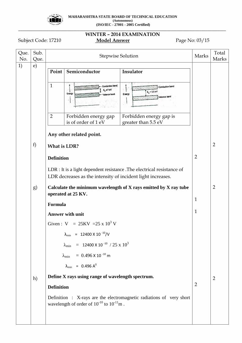
1) e) f) g) h)
Point Semiconductor Insulator
1
2 Forbidden energy gap is of order of 1 eV
Forbidden energy gap is greater than 5.5 eV
Any other related point. What is LDR? Definition LDR : It is a light dependent resistance .The electrical resistance of
LDR decreases as the intensity of incident light increases.
Calculate the minimum wavelength of X rays emitted by X ray tube operated at 25 KV.
Formula
Answer with unit
Given : V = 25KV =25 x 103 V
λmin = 12400 X 10 -10
/V
λmin = 12400 X 10 -10 / 25 x 103
λmin = 0.496 X 10 -10
m
λmin = 0.496 A0
Define X rays using range of wavelength spectrum.
Definition
Definition : X-rays are the electromagnetic radiations of very short wavelength of order of 10-10 to 10-11m .
2 1 1 2
2 2 2
MAHARASHTRA STATE BOARD OF TECHNICAL EDUCATION (Autonomous)
(ISO/IEC - 27001 - 2005 Certified) ______________________________________________________________________________________________________
WINTER – 2014 EXAMINATION Subject Code: 17210 Model Answer Page No: 04/15
Que. No.
Sub. Que.
Stepwise Solution Marks Total
Marks
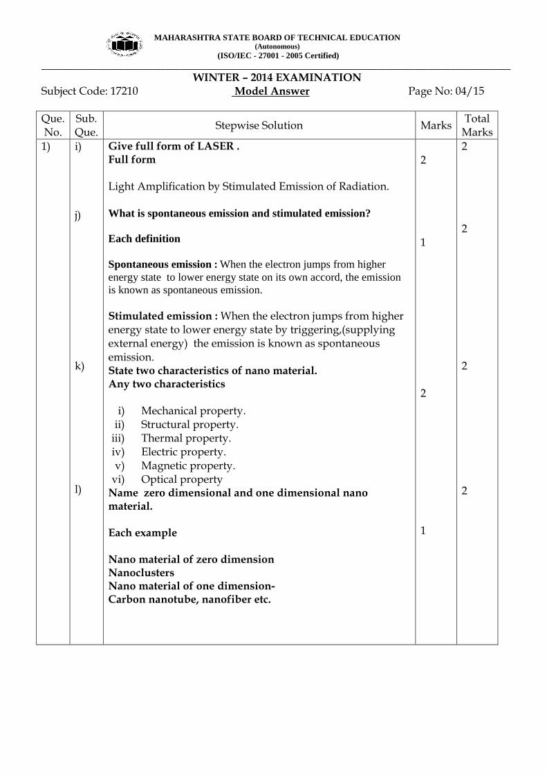
1) i) j) k) l)
Give full form of LASER . Full form Light Amplification by Stimulated Emission of Radiation. What is spontaneous emission and stimulated emission? Each definition Spontaneous emission : When the electron jumps from higher energy state to lower energy state on its own accord, the emission is known as spontaneous emission. Stimulated emission : When the electron jumps from higher energy state to lower energy state by triggering,(supplying external energy) the emission is known as spontaneous emission. State two characteristics of nano material. Any two characteristics
i) Mechanical property. ii) Structural property.
iii) Thermal property. iv) Electric property. v) Magnetic property.
vi) Optical property Name zero dimensional and one dimensional nano material. Each example Nano material of zero dimension Nanoclusters Nano material of one dimension- Carbon nanotube, nanofiber etc.
2 1 2 1
2 2 2
2

MAHARASHTRA STATE BOARD OF TECHNICAL EDUCATION (Autonomous)
(ISO/IEC - 27001 - 2005 Certified) ______________________________________________________________________________________________________
WINTER – 2014 EXAMINATION Subject Code: 17210 Model Answer Page No: 05/15
Que. No.
Sub. Que.
Stepwise Solution Marks Total
Marks
2 a) b)
Attempt any Four A resistance in the form of wire has length of 4 m and thickness 2mm shows a current of 500 mA for a potential difference of 12 V. Calculate resistance in ohm and conductance in mho. Also calculate specific resistance of material of wire. Given Three Formula and Answer with unit Solution: - Given:- Required:- L= 4m R = ? d= 2mm =2x10⁻³ m , r = 1x10⁻³ m σ = ? V = 12 V ρ= ? I = 500 = 500x 10-3 A 1) R = V/I R = 12 / 500X10-3 R = 24 ohm (Ω) 2) σ = 1/R σ = 1 /24 σ = 0.041 mho 3) ρ = R A/ L = R. r2/L ρ = 24 X 3.14X(1x10-3)2/4 ρ = 1.88x10⁻⁵ Ωm State and explain balancing condition of Wheatstone’s
network.
Condition
Diagram
Explanation
4 1 1 2
16 4
4

MAHARASHTRA STATE BOARD OF TECHNICAL EDUCATION (Autonomous)
(ISO/IEC - 27001 - 2005 Certified) ______________________________________________________________________________________________________
WINTER – 2014 EXAMINATION Subject Code: 17210 Model Answer Page No: 06/15
Que. No.
Sub. Que.
Stepwise Solution Marks Total
Marks
2 b)
Condition : The balancing condition Wheatstone’s network is given as follows.
1 4
2 3
R R
R R=
In this network R1,R2,R3 are kept constant and R4 is so adjusted that galvanometer shows zero deflection. When galvanometer shows zero deflection, network is said to be balanced. Network is balanced means points B and D are at equal potential. This is possible if , (P.D. across AB) =(P.D. across AD) and (P.D. across BC)= (P.D. across DC) Using Ohm’s law, I1R1 = I2R4 ………..(1) I1R2 = I2R3 ………..(2) Dividing equation (1) by (2) we get
1 1 2 4
1 2 2 3
I R I R
I R I R=
1 4
2 3
R R
R R=
This is of the balancing condition Wheatstone’s network.

MAHARASHTRA STATE BOARD OF TECHNICAL EDUCATION (Autonomous)
(ISO/IEC - 27001 - 2005 Certified) ______________________________________________________________________________________________________
WINTER – 2014 EXAMINATION Subject Code: 17210 Model Answer Page No: 07/15
Que. No.
Sub. Que.
Stepwise Solution Marks Total
Marks
2) c)
State and prove parallel law of condensers. Statement Well Labeled Diagram Explanation and Final Expression Statement: When two or more than two condensers are connected in parallel the resultant capacity of the combination is algebraic sum of capacity of individual condensers. C = C1+ C2+ C3
Proof:
Consider three condensers C1, C2 & C3 are connected in parallel
between two points AB with potential difference of V volt. When
condenser are connected in parallel the total charge across each
condenser gets divided into three parts Q1, Q2 & Q3 which depends
on values of capacitor and the potential difference on each
condenser remains the same.
2 2
4

MAHARASHTRA STATE BOARD OF TECHNICAL EDUCATION (Autonomous)
(ISO/IEC - 27001 - 2005 Certified) ______________________________________________________________________________________________________
WINTER – 2014 EXAMINATION Subject Code: 17210 Model Answer Page No: 08/15
Que. No.
Sub. Que.
Stepwise Solution Marks Total
Marks
2) c) d)
Q = Q1+Q2 +Q3 -------------(1)
But
QC
V=
Therefore, Q = CV
The charge on 1C is Q1 = C1V
The charge on 2C is Q2 = C2V
The charge on 3C is Q3 = C3V The charge on C is Q = CV From equation (1) CV = C1V + C2V+ C3V CV = V (C1+ C2+ C3 ) C = C1+ C2+ C3
Three condensers with capacity 6µF , 12 µF and 18 µF are connected in parallel circuit. If p.d. of 440 volt is given to circuit .Calculate charge on each condenser. Given Three formulas with answer and unit (Each) Given : Required: C1= 6µF = 6 x 10 -6 F Q1= ? C2= 12µF = 12 x 10 -6 F Q2= ? C2= 18µF = 18 x 10 -6 F Q3= ? V = 440 V
Formula: C = Q/ V
Q = C.V
1) Q1 = C1.V
Q1 = 6 x 10 -6 x 440
Q1= 2.64x10⁻³ C
4
4

MAHARASHTRA STATE BOARD OF TECHNICAL EDUCATION (Autonomous)
(ISO/IEC - 27001 - 2005 Certified) ______________________________________________________________________________________________________
WINTER – 2014 EXAMINATION Subject Code: 17210 Model Answer Page No: 09/15
Que. No.
Sub. Que.
Stepwise Solution Marks Total
Marks
2) d) e)
2) Q2 = C2.V
Q2 = 12 x 10 -6 x 440
Q2 = 5.28x10⁻³ C
3) Q3 = C3.V
Q3 = 18 x 10 -6 x 440
Q3 = 7.92x10⁻³ C
Draw and explain energy bands (Fermi energy) in conductor,
semiconductor, and insulators
Band diagram
Explaination
Conductor
Semiconductor
3 1
4

MAHARASHTRA STATE BOARD OF TECHNICAL EDUCATION (Autonomous)
(ISO/IEC - 27001 - 2005 Certified) ______________________________________________________________________________________________________
WINTER – 2014 EXAMINATION Subject Code: 17210 Model Answer Page No: 10/15
Que. No.
Sub. Que.
Stepwise Solution Marks Total
Marks
2) e)
Insulator
Explaination:
As shown above conductor , semiconductor and insulators are
distinguished from each other by band theory.
In conductors there is no energy gap between valance band and
conduction band, they are overlapped on each other. So electrons can
jump from valance band to conduction band easily and material
conducts the current.
In semiconductors the energy gap between valance band and
conduction band is very small i.e. 1eV. So electrons can jump from
valance band to conduction band when small amount of energy is
supplied to it. Therefore conductivity of semiconductors is in
between conductors and insulators.
In insulators the energy gap between valance band and conduction
band is very large i.e. 5eV. So electrons cannot jump from valance
band to conduction band when some amount of energy is supplied
to it. Therefore insulators cannot conduct the current.

MAHARASHTRA STATE BOARD OF TECHNICAL EDUCATION (Autonomous)
(ISO/IEC - 27001 - 2005 Certified) ______________________________________________________________________________________________________
WINTER – 2014 EXAMINATION Subject Code: 17210 Model Answer Page No: 11/15
Que. No.
Sub. Que.
Stepwise Solution Marks Total
Marks
2) f) Explain forward bias and reserves bias characteristic for PN junction diode.
Diagram
Explanation
Forward Bias Characteristic: -
If external voltage is increased from zero onwards , initially the forward voltage is increased and values of currents are recorded and the graph is plotted as shown above.
Initially for increase in voltage there is no corresponding increase in current. Above barrier potential current increases rapidly and diode starts conducting current.
Reverse Bias Characteristics: -
As the reverse biased voltage is increased , at critical voltage VBR the reverse current through the diode increases sharply. The corresponding voltage is called breakdown voltage.
2 2
4

MAHARASHTRA STATE BOARD OF TECHNICAL EDUCATION (Autonomous)
(ISO/IEC - 27001 - 2005 Certified) ______________________________________________________________________________________________________
WINTER – 2014 EXAMINATION Subject Code: 17210 Model Answer Page No: 12/15
Que. No.
Sub. Que.
Stepwise Solution Marks Total
Marks
3) a) b)
Attempt any Four
Distinguish between n-type and p- type semiconductor
Each Points
Sr.
No
N- type Semiconductor P- type Semiconductor
1 When small amount of
pentavalent impurity is
added to a pure
semiconductor is called
N-type semiconductor
When small amount of
trivalent impurity is
added to a pure
semiconductor is called P-
type semiconductor
2 Impurity is used for
doping is arsenic,
anatomy, phosphorus
Impurity is used for
doping is gallium,
indium, boron,
aluminium
3 It is called donor
impurity
It is called acceptor
impurity
4 There are excess of
electrons
There are shortage of
electrons
5 The electrons are
majority carriers
The holes are majority
carriers
The threshold wavelength of silver is 3800A0. Calculate maximum energy in eV of photoelectrons emitted in ultra – violet light of wavelength 2600A0is incident on it.
Formula
Substitution
Answer with unit
1 1 1 2
16 4 4
MAHARASHTRA STATE BOARD OF TECHNICAL EDUCATION (Autonomous)
(ISO/IEC - 27001 - 2005 Certified) ______________________________________________________________________________________________________
WINTER – 2014 EXAMINATION Subject Code: 17210 Model Answer Page No: 13/15
Que. No.
Sub. Que.
Stepwise Solution Marks Total
Marks
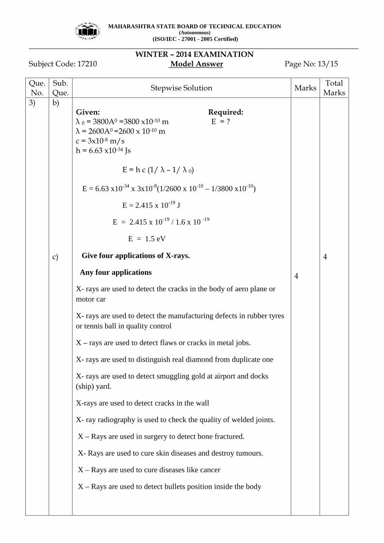
3) b) c)
Given: Required: λ 0 = 3800A0 =3800 x10-10 m E = ? λ = 2600A0 =2600 x 10-10 m c = 3x10⁻⁸ m/s h = 6.63 x10⁻³⁴ Js E = h c (1/ λ – 1/ λ 0) E = 6.63 x10-34 x 3x10-8(1/2600 x 10-10 – 1/3800 x10-10)
E = 2.415 x 10⁻¹⁹ J
E = 2.415 x 10⁻¹⁹ / 1.6 x 10 -19
E = 1.5 eV
Give four applications of X-rays.
Any four applications
X- rays are used to detect the cracks in the body of aero plane or motor car
X- rays are used to detect the manufacturing defects in rubber tyres or tennis ball in quality control
X – rays are used to detect flaws or cracks in metal jobs.
X- rays are used to distinguish real diamond from duplicate one
X- rays are used to detect smuggling gold at airport and docks (ship) yard.
X-rays are used to detect cracks in the wall
X- ray radiography is used to check the quality of welded joints.
X – Rays are used in surgery to detect bone fractured.
X- Rays are used to cure skin diseases and destroy tumours.
X – Rays are used to cure diseases like cancer
X – Rays are used to detect bullets position inside the body
4
4

MAHARASHTRA STATE BOARD OF TECHNICAL EDUCATION (Autonomous)
(ISO/IEC - 27001 - 2005 Certified) ______________________________________________________________________________________________________
WINTER – 2014 EXAMINATION Subject Code: 17210 Model Answer Page No: 14/15
Que. No.
Sub. Que.
Stepwise Solution Marks Total
Marks
3)
d) e)
State any four properties of LASER. Any four properties Properties i) The light is coherent: The light with waves, all exactly in same phase. ii) The light is monochromatic: The light whose waves all have the same frequency or wavelength. iii) The light is unidirectional: The light produces sharp focus. iv) The beam is extremely intense: The light has extreme brightness State principle of photo cell. Give its type and their symbols. Principle Any twoTypes Symbol Principle: When light of suitable frequency is incident on metallic surface, electrons are emitted from the metal surface. Thus light energy is converted into electrical energy. Types:
i) Photoconductive cell ii) Photoemissive cell iii) Photovoltaic cell
4 1 2 1
4 4

MAHARASHTRA STATE BOARD OF TECHNICAL EDUCATION (Autonomous)
(ISO/IEC - 27001 - 2005 Certified) ______________________________________________________________________________________________________
WINTER – 2014 EXAMINATION Subject Code: 17210 Model Answer Page No: 15/15
Que. No.
Sub. Que.
Stepwise Solution Marks Total
Marks
3) f)
State four applications of nano-material in engineering
field.
Each application
Applications of nano-material in engineering field.
1. Data storage system – Semiconductor material in the form of film can be deposited on substrate to form the chip.
2. Use of nanomaterial in energy sector – The conventional energy sources like coal, fuel are depleting day by day, thus use of alternative energy source is inevitable.
3. Application in automobiles- High mechanical strength material but light in weight can be produced by using nanotechnology. Nanopainting materials can be used to get uniform layer of coating on the vehicle body.
4. Application in consumer goods – Nanotechnology has wide applications in cosmetics, domestics products and textiles. Using nanomaterial fiber, one can get comfort of cotton clothes.
Any other relevant application
1
4


![HR - Runes & Radiations [Edited]](https://img.pdfslide.us/doc/110x75/577ce7301a28abf103948b15/hr-runes-radiations-edited.jpg)