Embed Size (px)
Citation preview
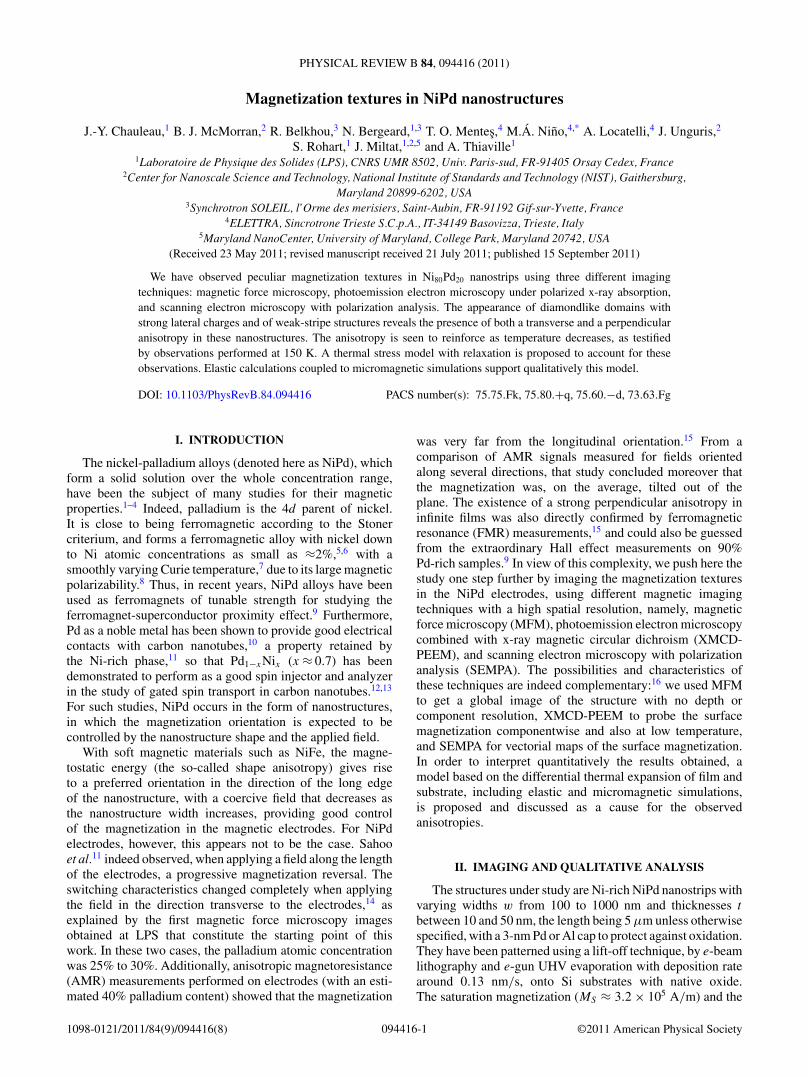
PHYSICAL REVIEW B 84, 094416 (2011)
Magnetization textures in NiPd nanostructures
J.-Y. Chauleau,1 B. J. McMorran,2 R. Belkhou,3 N. Bergeard,1,3 T. O. Mentes,4 M.A. Nino,4,* A. Locatelli,4 J. Unguris,2
S. Rohart,1 J. Miltat,1,2,5 and A. Thiaville1
1Laboratoire de Physique des Solides (LPS), CNRS UMR 8502, Univ. Paris-sud, FR-91405 Orsay Cedex, France2Center for Nanoscale Science and Technology, National Institute of Standards and Technology (NIST), Gaithersburg,
Maryland 20899-6202, USA3Synchrotron SOLEIL, l’Orme des merisiers, Saint-Aubin, FR-91192 Gif-sur-Yvette, France
4ELETTRA, Sincrotrone Trieste S.C.p.A., IT-34149 Basovizza, Trieste, Italy5Maryland NanoCenter, University of Maryland, College Park, Maryland 20742, USA
(Received 23 May 2011; revised manuscript received 21 July 2011; published 15 September 2011)
We have observed peculiar magnetization textures in Ni80Pd20 nanostrips using three different imagingtechniques: magnetic force microscopy, photoemission electron microscopy under polarized x-ray absorption,and scanning electron microscopy with polarization analysis. The appearance of diamondlike domains withstrong lateral charges and of weak-stripe structures reveals the presence of both a transverse and a perpendicularanisotropy in these nanostructures. The anisotropy is seen to reinforce as temperature decreases, as testifiedby observations performed at 150 K. A thermal stress model with relaxation is proposed to account for theseobservations. Elastic calculations coupled to micromagnetic simulations support qualitatively this model.
DOI: 10.1103/PhysRevB.84.094416 PACS number(s): 75.75.Fk, 75.80.+q, 75.60.−d, 73.63.Fg
I. INTRODUCTION
The nickel-palladium alloys (denoted here as NiPd), whichform a solid solution over the whole concentration range,have been the subject of many studies for their magneticproperties.1–4 Indeed, palladium is the 4d parent of nickel.It is close to being ferromagnetic according to the Stonercriterium, and forms a ferromagnetic alloy with nickel downto Ni atomic concentrations as small as ≈2%,5,6 with asmoothly varying Curie temperature,7 due to its large magneticpolarizability.8 Thus, in recent years, NiPd alloys have beenused as ferromagnets of tunable strength for studying theferromagnet-superconductor proximity effect.9 Furthermore,Pd as a noble metal has been shown to provide good electricalcontacts with carbon nanotubes,10 a property retained bythe Ni-rich phase,11 so that Pd1−xNix (x ≈ 0.7) has beendemonstrated to perform as a good spin injector and analyzerin the study of gated spin transport in carbon nanotubes.12,13
For such studies, NiPd occurs in the form of nanostructures,in which the magnetization orientation is expected to becontrolled by the nanostructure shape and the applied field.
With soft magnetic materials such as NiFe, the magne-tostatic energy (the so-called shape anisotropy) gives riseto a preferred orientation in the direction of the long edgeof the nanostructure, with a coercive field that decreases asthe nanostructure width increases, providing good controlof the magnetization in the magnetic electrodes. For NiPdelectrodes, however, this appears not to be the case. Sahooet al.11 indeed observed, when applying a field along the lengthof the electrodes, a progressive magnetization reversal. Theswitching characteristics changed completely when applyingthe field in the direction transverse to the electrodes,14 asexplained by the first magnetic force microscopy imagesobtained at LPS that constitute the starting point of thiswork. In these two cases, the palladium atomic concentrationwas 25% to 30%. Additionally, anisotropic magnetoresistance(AMR) measurements performed on electrodes (with an esti-mated 40% palladium content) showed that the magnetization
was very far from the longitudinal orientation.15 From acomparison of AMR signals measured for fields orientedalong several directions, that study concluded moreover thatthe magnetization was, on the average, tilted out of theplane. The existence of a strong perpendicular anisotropy ininfinite films was also directly confirmed by ferromagneticresonance (FMR) measurements,15 and could also be guessedfrom the extraordinary Hall effect measurements on 90%Pd-rich samples.9 In view of this complexity, we push here thestudy one step further by imaging the magnetization texturesin the NiPd electrodes, using different magnetic imagingtechniques with a high spatial resolution, namely, magneticforce microscopy (MFM), photoemission electron microscopycombined with x-ray magnetic circular dichroism (XMCD-PEEM), and scanning electron microscopy with polarizationanalysis (SEMPA). The possibilities and characteristics ofthese techniques are indeed complementary:16 we used MFMto get a global image of the structure with no depth orcomponent resolution, XMCD-PEEM to probe the surfacemagnetization componentwise and also at low temperature,and SEMPA for vectorial maps of the surface magnetization.In order to interpret quantitatively the results obtained, amodel based on the differential thermal expansion of film andsubstrate, including elastic and micromagnetic simulations,is proposed and discussed as a cause for the observedanisotropies.
II. IMAGING AND QUALITATIVE ANALYSIS
The structures under study are Ni-rich NiPd nanostrips withvarying widths w from 100 to 1000 nm and thicknesses t
between 10 and 50 nm, the length being 5 μm unless otherwisespecified, with a 3-nm Pd or Al cap to protect against oxidation.They have been patterned using a lift-off technique, by e-beamlithography and e-gun UHV evaporation with deposition ratearound 0.13 nm/s, onto Si substrates with native oxide.The saturation magnetization (MS ≈ 3.2 × 10⁵ A/m) and the
094416-11098-0121/2011/84(9)/094416(8) ©2011 American Physical Society
J.-Y. CHAULEAU et al. PHYSICAL REVIEW B 84, 094416 (2011)
typical composition have been measured by, respectively,alternating gradient force magnetometry (AGFM) and Ruther-ford backscattering spectroscopy (RBS), giving an atomiccomposition of Pd of ≈20% (slightly drifting with sourceusage). Note that the following results involve only the virginmagnetization states, but that a magnetic field has also beenapplied, showing that the magnetization textures under studyare more robust than simple metastable states generated duringgrowth.
A. In-plane anisotropy
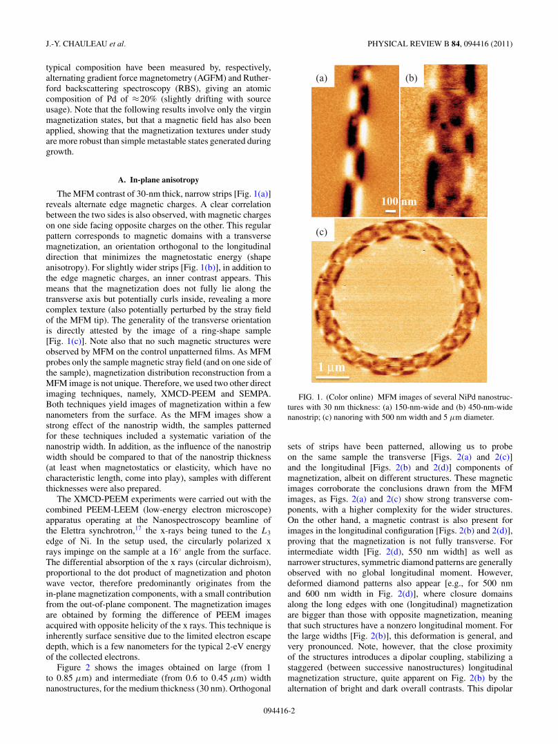
The MFM contrast of 30-nm thick, narrow strips [Fig. 1(a)]reveals alternate edge magnetic charges. A clear correlationbetween the two sides is also observed, with magnetic chargeson one side facing opposite charges on the other. This regularpattern corresponds to magnetic domains with a transversemagnetization, an orientation orthogonal to the longitudinaldirection that minimizes the magnetostatic energy (shapeanisotropy). For slightly wider strips [Fig. 1(b)], in addition tothe edge magnetic charges, an inner contrast appears. Thismeans that the magnetization does not fully lie along thetransverse axis but potentially curls inside, revealing a morecomplex texture (also potentially perturbed by the stray fieldof the MFM tip). The generality of the transverse orientationis directly attested by the image of a ring-shape sample[Fig. 1(c)]. Note also that no such magnetic structures wereobserved by MFM on the control unpatterned films. As MFMprobes only the sample magnetic stray field (and on one side ofthe sample), magnetization distribution reconstruction from aMFM image is not unique. Therefore, we used two other directimaging techniques, namely, XMCD-PEEM and SEMPA.Both techniques yield images of magnetization within a fewnanometers from the surface. As the MFM images show astrong effect of the nanostrip width, the samples patternedfor these techniques included a systematic variation of thenanostrip width. In addition, as the influence of the nanostripwidth should be compared to that of the nanostrip thickness(at least when magnetostatics or elasticity, which have nocharacteristic length, come into play), samples with differentthicknesses were also prepared.
The XMCD-PEEM experiments were carried out with thecombined PEEM-LEEM (low-energy electron microscope)apparatus operating at the Nanospectroscopy beamline ofthe Elettra synchrotron,17 the x-rays being tuned to the L3
edge of Ni. In the setup used, the circularly polarized xrays impinge on the sample at a 16◦ angle from the surface.The differential absorption of the x rays (circular dichroism),proportional to the dot product of magnetization and photonwave vector, therefore predominantly originates from thein-plane magnetization components, with a small contributionfrom the out-of-plane component. The magnetization imagesare obtained by forming the difference of PEEM imagesacquired with opposite helicity of the x rays. This technique isinherently surface sensitive due to the limited electron escapedepth, which is a few nanometers for the typical 2-eV energyof the collected electrons.
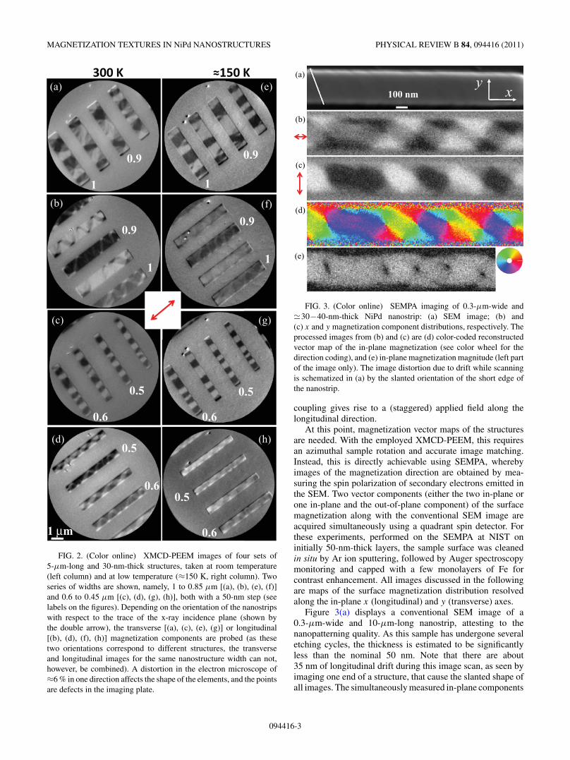
Figure 2 shows the images obtained on large (from 1to 0.85 μm) and intermediate (from 0.6 to 0.45 μm) widthnanostructures, for the medium thickness (30 nm). Orthogonal
(a) (b)
(c)
100 nm
1 µm
FIG. 1. (Color online) MFM images of several NiPd nanostruc-tures with 30 nm thickness: (a) 150-nm-wide and (b) 450-nm-widenanostrip; (c) nanoring with 500 nm width and 5 μm diameter.
sets of strips have been patterned, allowing us to probeon the same sample the transverse [Figs. 2(a) and 2(c)]and the longitudinal [Figs. 2(b) and 2(d)] components ofmagnetization, albeit on different structures. These magneticimages corroborate the conclusions drawn from the MFMimages, as Figs. 2(a) and 2(c) show strong transverse com-ponents, with a higher complexity for the wider structures.On the other hand, a magnetic contrast is also present forimages in the longitudinal configuration [Figs. 2(b) and 2(d)],proving that the magnetization is not fully transverse. Forintermediate width [Fig. 2(d), 550 nm width] as well asnarrower structures, symmetric diamond patterns are generallyobserved with no global longitudinal moment. However,deformed diamond patterns also appear [e.g., for 500 nmand 600 nm width in Fig. 2(d)], where closure domainsalong the long edges with one (longitudinal) magnetizationare bigger than those with opposite magnetization, meaningthat such structures have a nonzero longitudinal moment. Forthe large widths [Fig. 2(b)], this deformation is general, andvery pronounced. Note, however, that the close proximityof the structures introduces a dipolar coupling, stabilizing astaggered (between successive nanostructures) longitudinalmagnetization structure, quite apparent on Fig. 2(b) by thealternation of bright and dark overall contrasts. This dipolar
094416-2
MAGNETIZATION TEXTURES IN NiPd NANOSTRUCTURES PHYSICAL REVIEW B 84, 094416 (2011)
300 K ≈150 K(a)
(b)
(c)
(f)
(g)
(e)
1
0.9
1
0.9
1
0.9
1
0.9
(h)(d)
1 µm
0.5
0.6
0.5
0.6
0.5
0.6
0.5
0.6
FIG. 2. (Color online) XMCD-PEEM images of four sets of5-μm-long and 30-nm-thick structures, taken at room temperature(left column) and at low temperature (≈150 K, right column). Twoseries of widths are shown, namely, 1 to 0.85 μm [(a), (b), (e), (f)]and 0.6 to 0.45 μm [(c), (d), (g), (h)], both with a 50-nm step (seelabels on the figures). Depending on the orientation of the nanostripswith respect to the trace of the x-ray incidence plane (shown bythe double arrow), the transverse [(a), (c), (e), (g)] or longitudinal[(b), (d), (f), (h)] magnetization components are probed (as thesetwo orientations correspond to different structures, the transverseand longitudinal images for the same nanostructure width can not,however, be combined). A distortion in the electron microscope of≈6 % in one direction affects the shape of the elements, and the pointsare defects in the imaging plate.
(e)
(d)
(c)
(b)
(a)
xy
100 nm
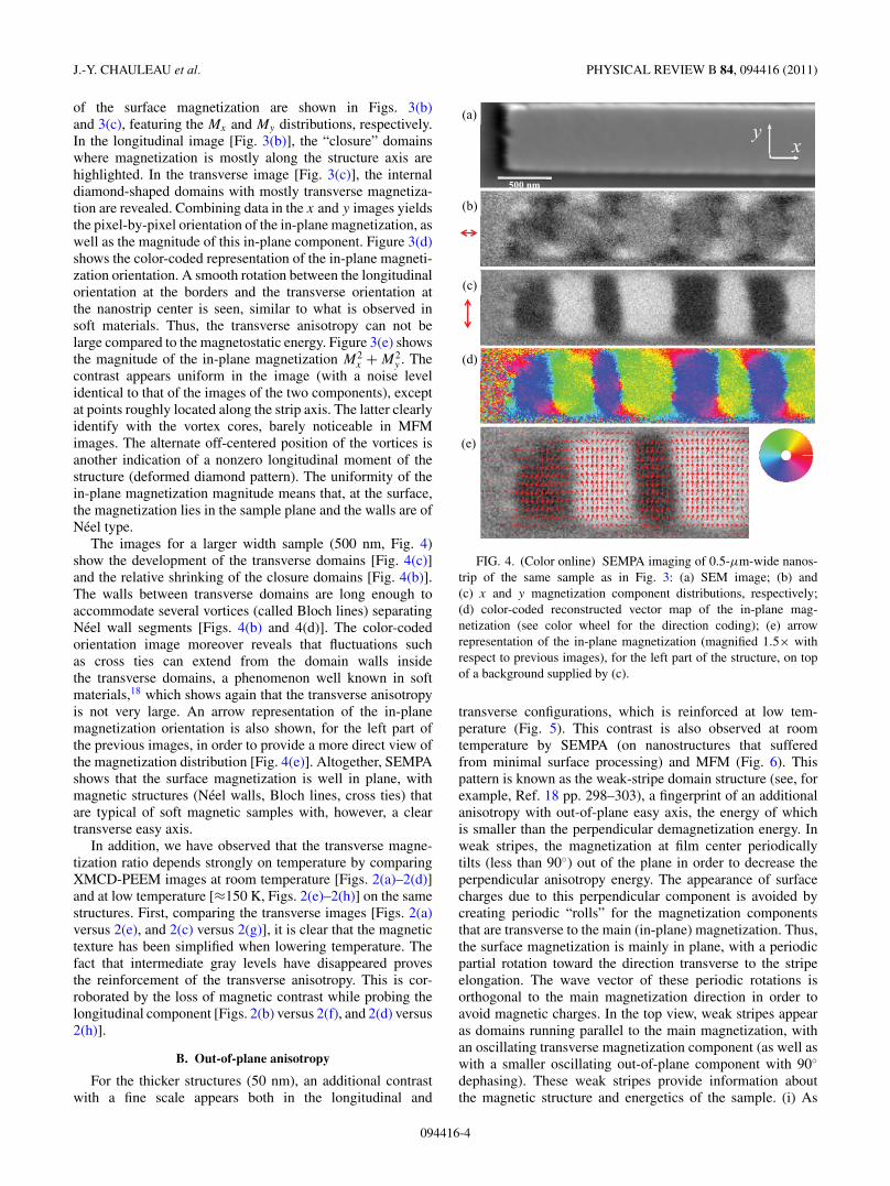
FIG. 3. (Color online) SEMPA imaging of 0.3-μm-wide and�30−40-nm-thick NiPd nanostrip: (a) SEM image; (b) and(c) x and y magnetization component distributions, respectively. Theprocessed images from (b) and (c) are (d) color-coded reconstructedvector map of the in-plane magnetization (see color wheel for thedirection coding), and (e) in-plane magnetization magnitude (left partof the image only). The image distortion due to drift while scanningis schematized in (a) by the slanted orientation of the short edge ofthe nanostrip.
coupling gives rise to a (staggered) applied field along thelongitudinal direction.
At this point, magnetization vector maps of the structuresare needed. With the employed XMCD-PEEM, this requiresan azimuthal sample rotation and accurate image matching.Instead, this is directly achievable using SEMPA, wherebyimages of the magnetization direction are obtained by mea-suring the spin polarization of secondary electrons emitted inthe SEM. Two vector components (either the two in-plane orone in-plane and the out-of-plane component) of the surfacemagnetization along with the conventional SEM image areacquired simultaneously using a quadrant spin detector. Forthese experiments, performed on the SEMPA at NIST oninitially 50-nm-thick layers, the sample surface was cleanedin situ by Ar ion sputtering, followed by Auger spectroscopymonitoring and capped with a few monolayers of Fe forcontrast enhancement. All images discussed in the followingare maps of the surface magnetization distribution resolvedalong the in-plane x (longitudinal) and y (transverse) axes.
Figure 3(a) displays a conventional SEM image of a0.3-μm-wide and 10-μm-long nanostrip, attesting to thenanopatterning quality. As this sample has undergone severaletching cycles, the thickness is estimated to be significantlyless than the nominal 50 nm. Note that there are about35 nm of longitudinal drift during this image scan, as seen byimaging one end of a structure, that cause the slanted shape ofall images. The simultaneously measured in-plane components
094416-3
J.-Y. CHAULEAU et al. PHYSICAL REVIEW B 84, 094416 (2011)
of the surface magnetization are shown in Figs. 3(b)and 3(c), featuring the Mx and My distributions, respectively.In the longitudinal image [Fig. 3(b)], the “closure” domainswhere magnetization is mostly along the structure axis arehighlighted. In the transverse image [Fig. 3(c)], the internaldiamond-shaped domains with mostly transverse magnetiza-tion are revealed. Combining data in the x and y images yieldsthe pixel-by-pixel orientation of the in-plane magnetization, aswell as the magnitude of this in-plane component. Figure 3(d)shows the color-coded representation of the in-plane magneti-zation orientation. A smooth rotation between the longitudinalorientation at the borders and the transverse orientation atthe nanostrip center is seen, similar to what is observed insoft materials. Thus, the transverse anisotropy can not belarge compared to the magnetostatic energy. Figure 3(e) showsthe magnitude of the in-plane magnetization M2
x + M2y . The
contrast appears uniform in the image (with a noise levelidentical to that of the images of the two components), exceptat points roughly located along the strip axis. The latter clearlyidentify with the vortex cores, barely noticeable in MFMimages. The alternate off-centered position of the vortices isanother indication of a nonzero longitudinal moment of thestructure (deformed diamond pattern). The uniformity of thein-plane magnetization magnitude means that, at the surface,the magnetization lies in the sample plane and the walls are ofNeel type.
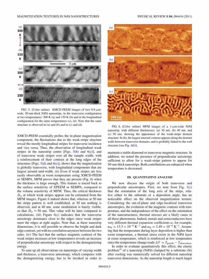
The images for a larger width sample (500 nm, Fig. 4)show the development of the transverse domains [Fig. 4(c)]and the relative shrinking of the closure domains [Fig. 4(b)].The walls between transverse domains are long enough toaccommodate several vortices (called Bloch lines) separatingNeel wall segments [Figs. 4(b) and 4(d)]. The color-codedorientation image moreover reveals that fluctuations suchas cross ties can extend from the domain walls insidethe transverse domains, a phenomenon well known in softmaterials,18 which shows again that the transverse anisotropyis not very large. An arrow representation of the in-planemagnetization orientation is also shown, for the left part ofthe previous images, in order to provide a more direct view ofthe magnetization distribution [Fig. 4(e)]. Altogether, SEMPAshows that the surface magnetization is well in plane, withmagnetic structures (Neel walls, Bloch lines, cross ties) thatare typical of soft magnetic samples with, however, a cleartransverse easy axis.
In addition, we have observed that the transverse magne-tization ratio depends strongly on temperature by comparingXMCD-PEEM images at room temperature [Figs. 2(a)–2(d)]and at low temperature [≈150 K, Figs. 2(e)–2(h)] on the samestructures. First, comparing the transverse images [Figs. 2(a)versus 2(e), and 2(c) versus 2(g)], it is clear that the magnetictexture has been simplified when lowering temperature. Thefact that intermediate gray levels have disappeared provesthe reinforcement of the transverse anisotropy. This is cor-roborated by the loss of magnetic contrast while probing thelongitudinal component [Figs. 2(b) versus 2(f), and 2(d) versus2(h)].
B. Out-of-plane anisotropy
For the thicker structures (50 nm), an additional contrastwith a fine scale appears both in the longitudinal and
(d)
(c)
(b)
(a)
xy
500 nm
(e)
FIG. 4. (Color online) SEMPA imaging of 0.5-μm-wide nanos-trip of the same sample as in Fig. 3: (a) SEM image; (b) and(c) x and y magnetization component distributions, respectively;(d) color-coded reconstructed vector map of the in-plane mag-netization (see color wheel for the direction coding); (e) arrowrepresentation of the in-plane magnetization (magnified 1.5× withrespect to previous images), for the left part of the structure, on topof a background supplied by (c).
transverse configurations, which is reinforced at low tem-perature (Fig. 5). This contrast is also observed at roomtemperature by SEMPA (on nanostructures that sufferedfrom minimal surface processing) and MFM (Fig. 6). Thispattern is known as the weak-stripe domain structure (see, forexample, Ref. 18 pp. 298–303), a fingerprint of an additionalanisotropy with out-of-plane easy axis, the energy of whichis smaller than the perpendicular demagnetization energy. Inweak stripes, the magnetization at film center periodicallytilts (less than 90◦) out of the plane in order to decrease theperpendicular anisotropy energy. The appearance of surfacecharges due to this perpendicular component is avoided bycreating periodic “rolls” for the magnetization componentsthat are transverse to the main (in-plane) magnetization. Thus,the surface magnetization is mainly in plane, with a periodicpartial rotation toward the direction transverse to the stripeelongation. The wave vector of these periodic rotations isorthogonal to the main magnetization direction in order toavoid magnetic charges. In the top view, weak stripes appearas domains running parallel to the main magnetization, withan oscillating transverse magnetization component (as well aswith a smaller oscillating out-of-plane component with 90◦dephasing). These weak stripes provide information aboutthe magnetic structure and energetics of the sample. (i) As
094416-4
MAGNETIZATION TEXTURES IN NiPd NANOSTRUCTURES PHYSICAL REVIEW B 84, 094416 (2011)
(a)
(b)
(c)
(d)
300K
150K
300K
150
1 µm
150K
FIG. 5. (Color online) XMCD-PEEM images of two 0.9-μm-wide, 50-nm-thick NiPd nanostrips, in the transverse configurationat two temperatures: 300 K (a) and 150 K (b) and in the longitudinalconfiguration for the same temperatures (c), (d). Note that the samestructure is observed in (a) and (b) and in (c) and (d).
XMCD-PEEM essentially probes the in-plane magnetizationcomponent, the fluctuations due to the weak-stripe structurereveal the mostly longitudinal stripes for transverse incidenceand vice versa. Thus, the observation of longitudinal weakstripes in the nanostrip center [Figs. 5(b) and 6(c)], andof transverse weak stripes over all the sample width, witha reinforcement of their contrast at the long edges of thestructures [Figs. 5(d) and 6(c)], shows that the magnetizationis globally transverse, with longitudinal components that arelargest around mid-width. (ii) Even if weak stripes are lesseasily observable at room temperature using XMCD-PEEMor SEMPA, MFM proves that they are present (Fig. 6) whenthe thickness is large enough. This feature is traced back tothe surface sensitivity of XPEEM or SEMPA, compared tothe volume sensitivity of MFM. Thus, the critical thicknessDcr at which weak stripes appear can be estimated from theMFM images. Figure 6 indeed shows that, whereas at 50 nmthe stripe pattern is well established, at 30 nm nothing isobserved, and at 40 nm, some modulation is barely visible,so that Dcr ≈ 50 nm. This value will be later compared tocalculations. (iii) Figure 6(c) indicates that the transverseanisotropy dominates close to the edges since weak stripesmeet the edges at right angles. Note that, at these nanostripdimensions, it is still possible to observe the bright and darkedge contrast, yet with no correlation anymore between the twosides. (iv) The fact that the surface magnetic contrast of theweak stripes increases at low temperatures reveals an increaseof perpendicular anisotropy with respect to the demagnetizingenergy.
To sum up all observations on nanostrips of varying widthand thickness, a transverse anisotropy, which competes withthe demagnetizing energy, has to be invoked in order to
(a)
(b)
(c)
500 nm
FIG. 6. (Color online) MFM images of a 1-μm-wide NiPdnanostrip, with different thicknesses: (a) 30 nm, (b) 40 nm, and(c) 50 nm, showing the appearance of the weak-stripe domainstructure. In (b), the largest internal contrast appears along the domainwalls between transverse domains, and is probably linked to the wallstructure [see Fig. 4(b)].
maintain a stable diamond or transverse magnetic structure. Inaddition, we noted the presence of perpendicular anisotropysufficient to allow for a weak-stripe pattern to appear for50-nm-thick nanostrips. Both contributions are enhanced whentemperature is decreased.
III. QUANTITATIVE ANALYSIS
We now discuss the origin of both transverse andperpendicular anisotropies. First, we note from Fig. 1(c)that the orientation of the long axis of the strips, rela-tive either to the substrate or a deposition angle, has nonoticeable effect on the observed magnetization texture.Considering the out-of-plane and edge-localized transverseanisotropies, the evolution of the magnetic contrast with tem-perature, and the independence of the effect on the orientationof the nanostructures, thermal stresses are a likely cause toall these phenomena. Indeed, metals and semiconductors havevery different thermal expansion coefficients α, for example,αNi = 13.3 × 10⁻⁶ K−1 and αSi = 2.49 × 10⁻⁶ K−1. Assum-ing that the temperature during layer deposition is higher thanroom temperature, a thermal stress exists in the NiPd layerat room temperature, which is reinforced at low temperaturesince the temperature change reads �T = Tgrowth − Tobservation.
In order to evaluate quantitatively this effect, the elasticproblem19 of a nanostrip (NiPd) clamped by a substrate (Si)after cooling was numerically solved for different nanostriptransverse dimensions. As the nanostrip length is much larger
094416-5
J.-Y. CHAULEAU et al. PHYSICAL REVIEW B 84, 094416 (2011)
(a)
(b)
(c)
(d)
y
z
0
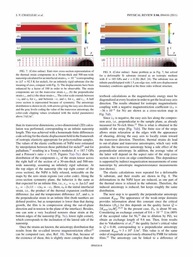
FIG. 7. (Color online) End-view cross-section representation ofthe thermal strain components in a 30-nm-thick and 500-nm-widenanostrip calculated for an interfacial strain ε0 = 10−3 (correspondingto �T = 92.5 K for nickel), for an infinitely rigid substrate (for themeaning of axes, compare with Fig. 3). The displacements have beenenhanced by a factor of 100 in order to be observable. The straincomponents are (a) the transverse strain εyy , (b) the perpendicularstrain εzz, and (c) the shear strain εyz. The color scale extends between−ε0 and ε0 for εyy and between −ε1 and ε1 for εzz and εyz. A halfcross section is represented because of symmetry. The anisotropydistribution is shown in (d), with arrows giving the easy axis directionand the gray levels coding the value of the transverse anisotropy, thecolor-code clipping values (evaluated with the nickel parameters)above 3 kJ/m3.
than its transverse dimensions, a two-dimensional (2D) calcu-lation was performed, corresponding to an infinite nanostriplength. This was achieved with a homemade finite differencescode solving for the elastic displacement field in the frameworkof isotropic elasticity appropriate for polycrystalline samples.The values of the elastic coefficients of NiPd were estimatedby interpolation between those published for nickel20 and forpalladium,21 resulting in a Young’s modulus E = 187.7 GPaand a Poisson’s ratio ν = 0.35. Figures 7(a)–7(c) show thedistribution of the components εij of the strain tensor acrossthe right half of the section of a 30-nm-thick and 500-nm-wide nanostrip, assuming an infinitely rigid substrate. Atthe top edges of the nanostrip (the top right corner of thecross section), the NiPd is fully relaxed, noticeable on themaps by the zero strain regions (see color code). Along thecross-section symmetry plane, the behavior is the same asthat expected for an infinite film, i.e., εyy = ε0 ≡ �α�T andεzz = −2ν/(1 − ν)ε0 ≡ −ε1. Here, ε0 is the initial interfacialstrain, i.e., the product of the thermal expansion coefficientdifference �α and the temperature difference �T , and ε1 isthe perpendicular strain in an infinite film (both numbers aredefined positive, but as temperature is lower than that duringgrowth, the film is in compression along the out-of-planedirection and in tension in the plane of the interface). Besides,one can note a very localized nonzero shear strain at thebottom edges of the nanostrip [Fig. 7(c), lower right corner],which corresponds to the inclination of the lateral side of thenanostrip.
Once the strains are known, the anisotropy distribution thatresults from the so-called inverse magnetostriction effect22
can be computed (see, also, Ref. 18). Note that, because ofthe existence of shear, this is slightly more complex than the
0
y
z
(a)
(b)
(c)
(d)
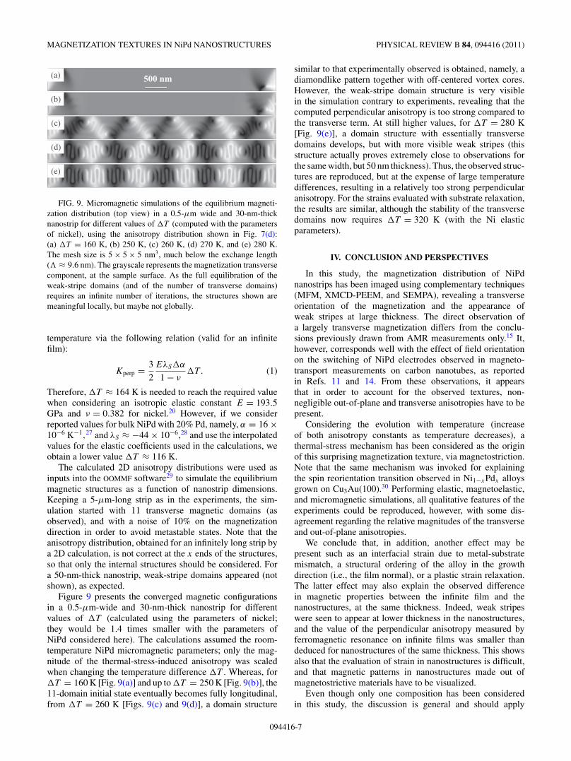
FIG. 8. (Color online) Same problem as in Fig. 7, but solvedfor a deformable Si substrate (treated as an isotropic mediumwith E = 185 GPa and ν = 0.26) (Ref. 24). The substrate was aninfinite parallelepiped with 1.5 μm edge size, with zero displacementboundary conditions applied at the three sides without structure.
textbook calculations as the magnetoelastic energy must bediagonalized at every location in order to get the local easy axisdirection. The results obtained for isotropic magnetoelasticcoupling with a negative magnetostriction coefficient (λS =−36 × 10−6 for Ni) are shown as a cross-section map inFig. 7(d).
Since λS is negative, the easy axis lies along the compres-sion axis, i.e., perpendicular to the sample plane, as alreadymeasured for Ni-rich films.23 This is what is obtained in themiddle of the strips [Fig. 7(d)]. The finite size of the stripsallows strain relaxation at the edges with the appearanceof shearing, driving the easy axis to locally rotate towardthe transverse direction. Therefore, thermal strains do leadto out-of-plane and transverse anisotropies, which vary withposition, the transverse anisotropy being a side effect of theperpendicular anisotropy. In addition, the average value ofthe latter will depend on the aspect ratio of the strip crosssection since it rests on edge contributions. This dependenceis supported by indirect magnetization measurements of somenanostrips by anisotropic magnetoresistance measurements(not shown).
The elastic calculations were repeated for a deformableSi substrate, and their results are shown in Fig. 8. Thedeformations in the NiPd layer are reduced, as one part ofthe thermal stress is relaxed in the substrate. Therefore, theinduced anisotropy is reduced, but keeps roughly the samedistribution.
The next step is to quantify the perpendicular anisotropyconstant Kperp. The appearance of the weak-stripe domainsprovides information about this constant since the criticalthickness (Dcr) for this depends on the quality factor Q =2Kperp/μ0M
2S .18,25 In the present case, Dcr is about 50 nm.
Considering an exchange constant of 0.6 × 10⁻¹¹ J/m (80%of the accepted value for Ni,26 due to dilution by Pd), weobtain an exchange length of 9.6 nm. Then, from resultsdue to Vukadinovic et al.,25 the quality factor’s critical valueis Q = 0.48, corresponding to a perpendicular anisotropyconstant Kperp ≈ 3 × 10⁴ J/m3. This value is of the sameorder of magnitude as previously obtained by FMR for infinitefilms.15 The anisotropy can be linked to a difference of
094416-6
MAGNETIZATION TEXTURES IN NiPd NANOSTRUCTURES PHYSICAL REVIEW B 84, 094416 (2011)
(a)
(b)
(c)
(d)
(e)
500 nm
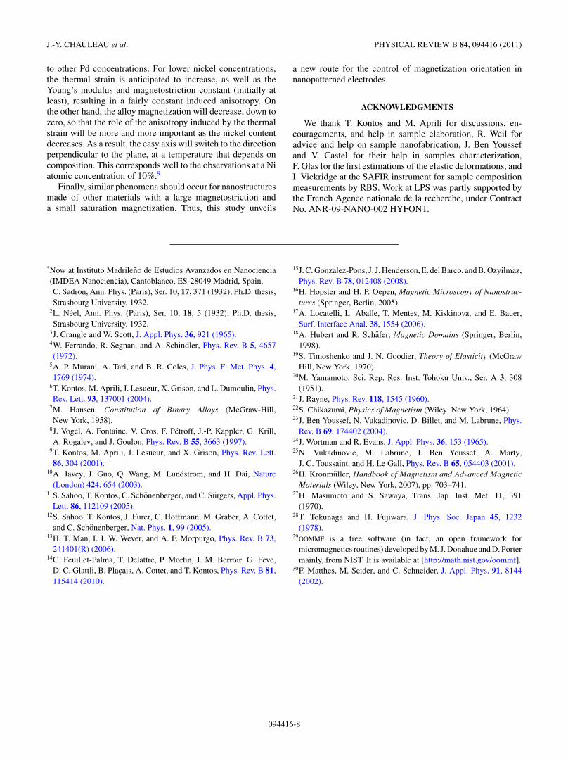
FIG. 9. Micromagnetic simulations of the equilibrium magneti-zation distribution (top view) in a 0.5-μm wide and 30-nm-thicknanostrip for different values of �T (computed with the parametersof nickel), using the anisotropy distribution shown in Fig. 7(d):(a) �T = 160 K, (b) 250 K, (c) 260 K, (d) 270 K, and (e) 280 K.The mesh size is 5 × 5 × 5 nm3, much below the exchange length(� ≈ 9.6 nm). The grayscale represents the magnetization transversecomponent, at the sample surface. As the full equilibration of theweak-stripe domains (and of the number of transverse domains)requires an infinite number of iterations, the structures shown aremeaningful locally, but maybe not globally.
temperature via the following relation (valid for an infinitefilm):
Kperp = 3
2
EλS�α
1 − ν�T . (1)
Therefore, �T ≈ 164 K is needed to reach the required valuewhen considering an isotropic elastic constant E = 193.5GPa and ν = 0.382 for nickel.20 However, if we considerreported values for bulk NiPd with 20% Pd, namely, α = 16 ×10−6 K−1,27 and λS ≈ −44 × 10−6,28 and use the interpolatedvalues for the elastic coefficients used in the calculations, weobtain a lower value �T ≈ 116 K.
The calculated 2D anisotropy distributions were used asinputs into the OOMMF software29 to simulate the equilibriummagnetic structures as a function of nanostrip dimensions.Keeping a 5-μm-long strip as in the experiments, the sim-ulation started with 11 transverse magnetic domains (asobserved), and with a noise of 10% on the magnetizationdirection in order to avoid metastable states. Note that theanisotropy distribution, obtained for an infinitely long strip bya 2D calculation, is not correct at the x ends of the structures,so that only the internal structures should be considered. Fora 50-nm-thick nanostrip, weak-stripe domains appeared (notshown), as expected.
Figure 9 presents the converged magnetic configurationsin a 0.5-μm-wide and 30-nm-thick nanostrip for differentvalues of �T (calculated using the parameters of nickel;they would be 1.4 times smaller with the parameters ofNiPd considered here). The calculations assumed the room-temperature NiPd micromagnetic parameters; only the mag-nitude of the thermal-stress-induced anisotropy was scaledwhen changing the temperature difference �T . Whereas, for�T = 160 K [Fig. 9(a)] and up to �T = 250 K [Fig. 9(b)], the11-domain initial state eventually becomes fully longitudinal,from �T = 260 K [Figs. 9(c) and 9(d)], a domain structure
similar to that experimentally observed is obtained, namely, adiamondlike pattern together with off-centered vortex cores.However, the weak-stripe domain structure is very visiblein the simulation contrary to experiments, revealing that thecomputed perpendicular anisotropy is too strong compared tothe transverse term. At still higher values, for �T = 280 K[Fig. 9(e)], a domain structure with essentially transversedomains develops, but with more visible weak stripes (thisstructure actually proves extremely close to observations forthe same width, but 50 nm thickness). Thus, the observed struc-tures are reproduced, but at the expense of large temperaturedifferences, resulting in a relatively too strong perpendicularanisotropy. For the strains evaluated with substrate relaxation,the results are similar, although the stability of the transversedomains now requires �T = 320 K (with the Ni elasticparameters).
IV. CONCLUSION AND PERSPECTIVES
In this study, the magnetization distribution of NiPdnanostrips has been imaged using complementary techniques(MFM, XMCD-PEEM, and SEMPA), revealing a transverseorientation of the magnetization and the appearance ofweak stripes at large thickness. The direct observation ofa largely transverse magnetization differs from the conclu-sions previously drawn from AMR measurements only.15 It,however, corresponds well with the effect of field orientationon the switching of NiPd electrodes observed in magneto-transport measurements on carbon nanotubes, as reportedin Refs. 11 and 14. From these observations, it appearsthat in order to account for the observed textures, non-negligible out-of-plane and transverse anisotropies have to bepresent.
Considering the evolution with temperature (increaseof both anisotropy constants as temperature decreases), athermal-stress mechanism has been considered as the originof this surprising magnetization texture, via magnetostriction.Note that the same mechanism was invoked for explainingthe spin reorientation transition observed in Ni1−xPdx alloysgrown on Cu3Au(100).30 Performing elastic, magnetoelastic,and micromagnetic simulations, all qualitative features of theexperiments could be reproduced, however, with some dis-agreement regarding the relative magnitudes of the transverseand out-of-plane anisotropies.
We conclude that, in addition, another effect may bepresent such as an interfacial strain due to metal-substratemismatch, a structural ordering of the alloy in the growthdirection (i.e., the film normal), or a plastic strain relaxation.The latter effect may also explain the observed differencein magnetic properties between the infinite film and thenanostructures, at the same thickness. Indeed, weak stripeswere seen to appear at lower thickness in the nanostructures,and the value of the perpendicular anisotropy measured byferromagnetic resonance on infinite films was smaller thandeduced for nanostructures of the same thickness. This showsalso that the evaluation of strain in nanostructures is difficult,and that magnetic patterns in nanostructures made out ofmagnetostrictive materials have to be visualized.
Even though only one composition has been consideredin this study, the discussion is general and should apply
094416-7
J.-Y. CHAULEAU et al. PHYSICAL REVIEW B 84, 094416 (2011)
to other Pd concentrations. For lower nickel concentrations,the thermal strain is anticipated to increase, as well as theYoung’s modulus and magnetostriction constant (initially atleast), resulting in a fairly constant induced anisotropy. Onthe other hand, the alloy magnetization will decrease, down tozero, so that the role of the anisotropy induced by the thermalstrain will be more and more important as the nickel contentdecreases. As a result, the easy axis will switch to the directionperpendicular to the plane, at a temperature that depends oncomposition. This corresponds well to the observations at a Niatomic concentration of 10%.9
Finally, similar phenomena should occur for nanostructuresmade of other materials with a large magnetostriction anda small saturation magnetization. Thus, this study unveils
a new route for the control of magnetization orientation innanopatterned electrodes.
ACKNOWLEDGMENTS
We thank T. Kontos and M. Aprili for discussions, en-couragements, and help in sample elaboration, R. Weil foradvice and help on sample nanofabrication, J. Ben Youssefand V. Castel for their help in samples characterization,F. Glas for the first estimations of the elastic deformations, andI. Vickridge at the SAFIR instrument for sample compositionmeasurements by RBS. Work at LPS was partly supported bythe French Agence nationale de la recherche, under ContractNo. ANR-09-NANO-002 HYFONT.
*Now at Instituto Madrileno de Estudios Avanzados en Nanociencia(IMDEA Nanociencia), Cantoblanco, ES-28049 Madrid, Spain.1C. Sadron, Ann. Phys. (Paris), Ser. 10, 17, 371 (1932); Ph.D. thesis,Strasbourg University, 1932.
2L. Neel, Ann. Phys. (Paris), Ser. 10, 18, 5 (1932); Ph.D. thesis,Strasbourg University, 1932.
3J. Crangle and W. Scott, J. Appl. Phys. 36, 921 (1965).4W. Ferrando, R. Segnan, and A. Schindler, Phys. Rev. B 5, 4657(1972).
5A. P. Murani, A. Tari, and B. R. Coles, J. Phys. F: Met. Phys. 4,1769 (1974).
6T. Kontos, M. Aprili, J. Lesueur, X. Grison, and L. Dumoulin, Phys.Rev. Lett. 93, 137001 (2004).
7M. Hansen, Constitution of Binary Alloys (McGraw-Hill,New York, 1958).
8J. Vogel, A. Fontaine, V. Cros, F. Petroff, J.-P. Kappler, G. Krill,A. Rogalev, and J. Goulon, Phys. Rev. B 55, 3663 (1997).
9T. Kontos, M. Aprili, J. Lesueur, and X. Grison, Phys. Rev. Lett.86, 304 (2001).
10A. Javey, J. Guo, Q. Wang, M. Lundstrom, and H. Dai, Nature(London) 424, 654 (2003).
11S. Sahoo, T. Kontos, C. Schonenberger, and C. Surgers, Appl. Phys.Lett. 86, 112109 (2005).
12S. Sahoo, T. Kontos, J. Furer, C. Hoffmann, M. Graber, A. Cottet,and C. Schonenberger, Nat. Phys. 1, 99 (2005).
13H. T. Man, I. J. W. Wever, and A. F. Morpurgo, Phys. Rev. B 73,241401(R) (2006).
14C. Feuillet-Palma, T. Delattre, P. Morfin, J. M. Berroir, G. Feve,D. C. Glattli, B. Placais, A. Cottet, and T. Kontos, Phys. Rev. B 81,115414 (2010).
15J. C. Gonzalez-Pons, J. J. Henderson, E. del Barco, and B. Ozyilmaz,Phys. Rev. B 78, 012408 (2008).
16H. Hopster and H. P. Oepen, Magnetic Microscopy of Nanostruc-tures (Springer, Berlin, 2005).
17A. Locatelli, L. Aballe, T. Mentes, M. Kiskinova, and E. Bauer,Surf. Interface Anal. 38, 1554 (2006).
18A. Hubert and R. Schafer, Magnetic Domains (Springer, Berlin,1998).
19S. Timoshenko and J. N. Goodier, Theory of Elasticity (McGrawHill, New York, 1970).
20M. Yamamoto, Sci. Rep. Res. Inst. Tohoku Univ., Ser. A 3, 308(1951).
21J. Rayne, Phys. Rev. 118, 1545 (1960).22S. Chikazumi, Physics of Magnetism (Wiley, New York, 1964).23J. Ben Youssef, N. Vukadinovic, D. Billet, and M. Labrune, Phys.
Rev. B 69, 174402 (2004).24J. Wortman and R. Evans, J. Appl. Phys. 36, 153 (1965).25N. Vukadinovic, M. Labrune, J. Ben Youssef, A. Marty,
J. C. Toussaint, and H. Le Gall, Phys. Rev. B 65, 054403 (2001).26H. Kronmuller, Handbook of Magnetism and Advanced Magnetic
Materials (Wiley, New York, 2007), pp. 703–741.27H. Masumoto and S. Sawaya, Trans. Jap. Inst. Met. 11, 391
(1970).28T. Tokunaga and H. Fujiwara, J. Phys. Soc. Japan 45, 1232
(1978).29OOMMF is a free software (in fact, an open framework for
micromagnetics routines) developed by M. J. Donahue and D. Portermainly, from NIST. It is available at [http://math.nist.gov/oommf].
30F. Matthes, M. Seider, and C. Schneider, J. Appl. Phys. 91, 8144(2002).
094416-8