Embed Size (px)
Citation preview
FINAL
Publication# 18889 Rev: DAmendment/0 Issue Date: August 1997
MACH 1 & 2 FAMILIES
1
COM’L: -5/7/10/12/15
IND: -7/10/12/14/18MA
CH 1 &
2
MACH131-5/7/10/12/15High-Performance EE CMOS Programmable Logic
Families
DISTINCTIVE CHARACTERISTICS84 Pins in PLCC 64 Macrocells 5.5 ns tPD Commercial, 7.5 ns tPD Industrial 182 MHz fCNT 64 I/Os; 4 dedicated inputs/clocks; 2 dedicated inputs 64 Flip-flops; 4 clock choices 4 “PALCE26V16” Blocks SpeedLocking™ for guaranteed fixed timing Bus-friendly™ inputs and I/Os Peripheral Component Interconnect (PCI) Compliant (-5/-7/-10/-12) Programmable power-down mode Safe for mixed supply voltage system designs Pin-compatible with the MACH231 and M4-128N
GENERAL DESCRIPTION
The MACH131 is a member of Vantis’ high-performance EE CMOS MACH® 1 & 2 families. This device has approximately six times the logic macrocell capability of the popular PALCE22V10 without loss of speed.
The MACH131 consists of four PAL® blocks interconnected by a programmable switch matrix. The four PAL blocks are essentially “PALCE26V12” structures complete with product-term arrays and programmable macrocells, which can be programmed as high speed or low power. The switch matrix connects the PAL blocks to each other and to all input pins, providing a high degree of connectivity between the fully-connected PAL blocks. This allows designs to be placed and routed efficiently.
The MACH131 macrocell provides either registered or combinatorial outputs with programmable polarity. If a registered configuration is chosen, the register can be configured as D-type or T-type to help reduce the number of product terms. The register type decision can be made by the designer or by the software. All macrocells can be connected to an I/O cell.
Vantis offers software design support for MACH devices through its own development system and device fitters integrated into third-party CAE tools. Platform support extends across PCs, Sun and HP workstations under advanced operating systems such as Windows 3.1, Windows 95 and NT, SunOS and Solaris, and HPUX.
1
V A N T I S
MACHXL® software is a complete development system for the PC, supporting Vantis’ MACH devices. It supports design entry with Boolean and behavioral syntax, state machine syntax and truth tables. Functional simulation and static timing analysis are also included in this easy-to-use system. This development system includes high-performance device fitters for all MACH devices.
The same fitter technology included in MACHXL software is seamlessly incorporated into third-party tools from leading CAE vendors such as Synario, Viewlogic, Mentor Graphics, Cadence and MINC. Interface kits and MACHXL configurations are also available to support design entry and verification with other leading vendors such as Synopsys, Exemplar, OrCAD, Synplicity and Model Technology. These MACHXL configurations and interfaces accept EDIF 2.0.0 netlists, generate JEDEC files for MACH devices, and create industry-standard SDF, VITAL-compliant VHDL and Verilog output files for design simulation.
Vantis offers in-system programming support for MACH devices through its MACHPRO® software enabling MACH device programmability through JTAG compliant ports and easy-to-use PC interface. Additionally, MACHPRO generated vectors work seamlessly with HP3070, GenRad and Teradyne testers to program MACH devices or test them for connectivity.
All MACH devices are supported by industry standard programmers available from a number of vendors. These programmer vendors include Advin Systems, BP Microsystems, Data I/O Corporation, Hi-Lo Systems, SMS GmbH, Stag House, and System General.
2 MACH131-5/7/10/12/15
MA
CH 1 &
2 Families
V A N T I S
BLOCK DIAGRAM
I/O Cells
Macrocells
I/O48 – I/O63
52 x 70 AND Logic Array
and Logic Allocator
OE
I/O Cells
Macrocells
I/O16 – I/O31
52 x 70 AND Logic Array
and Logic Allocator
OE
16
16
26
Switch Matrix
I/O Cells
Macrocells
I/O0 – I/O15 I2, I5
52 x 70 AND Logic Array
and Logic Allocator
CLK0/I0, CLK1/I1CLK2/I3, CLK3/I4
OE
18889D-1
16
16
26
2
4
4
4
16
16
26
I/O Cells
Macrocells
I/O32 – I/O47
52 x 70 AND Logic Array
and Logic Allocator
OE
16
16
26
4
4
4
4
44
Block A Block B
Block D Block C
MACH131-5/7/10/12/15 3
V A N T I S
CONNECTION DIAGRAMTop View
84-Pin PLCC
PIN DESIGNATIONSCLK/I = Clock or Input
GND = Ground
I = Input
I/O = Input/Output
VCC = Supply Voltage
123 818283846789 45 80 76777879 7512131415161718192021
232425262728293031
7372717069686766656463626160595857565554
43424140 4746454437363534 393833 48 52515049
10
22
11
3253
74I/O9
I/O10I/O11I/O12I/O13I/O14I/O15
CLK0/I0VCC
GNDCLK1/I1
I/O16I/O17I/O18I/O19I/O20I/O21I/O22I/O23GND
I/O8 GNDI/O55I/O54I/O53I/O52I/O51I/O50I/O49I/O48CLK3/I4
VCC
CLK2/I3I/O47I/O46I/O45I/O44I/O43I/O42I/O41
GND
I/O40
GN
DV
CC
I/O0
I/O62
I/O63
I5VC
C
I/O3
I/O4
I/O5
I/O6
I/O1
I/O2
I/O61
I/O57
I/O58
I/O59
I/O60
I/O56
I/O7
GN
D
GN
DV
CCI2
I/O34
I/O33
I/O32
VC
C
I/O29
I/O28
I/O27
I/O26
I/O31
I/O30
I/O35
I/O39
I/O38
I/O37
I/O36
GN
D
I/O25
I/O24
Block A Block D
Block B Block CBlock B Block C
4 MACH131-5/7/10/12/15
V A N T I S
MA
CH 1 &
2 Families
ORDERING INFORMATIONCommercial ProductsVantis’ programmable logic products for commercial applications are available with several ordering options. Theorder number (Valid Combination) is formed by a combination of:
Valid Combinations
The Valid Combinations table lists configurations planned tobe supported in volume for this device. Consult the local Vantissales office to confirm availabil i ty of specific validcombinations and to check on newly released combinations.
-7
FAMILY TYPEMACH = Macro Array CMOS High-Speed
MACH 131 J C
DEVICE NUMBER131 = 64 Macrocells, 84 Pins, Power-Down Option
SPEED-5 = 5.5 ns tPD-7 = 7.5 ns tPD-10 = 10 ns tPD-12 = 12 ns tPD-15 = 15 ns tPD
PROGRAMMING DESIGNATORBlank = Initial Algorithm/1 = First Revision
OPERATING CONDITIONSC = Commercial (0°C to +70°C)
PACKAGE TYPEJ = 84-Pin Plastic Leaded
Chip Carrier (PL 084)
/1
Valid Combinations
MACH131-5 JC/1
MACH131-7
JC, JC/1MACH131-10
MACH131-12
MACH131-15
MACH131-5/7/10/12/15 (Com’l) 5
V A N T I S
ORDERING INFORMATIONIndustrial ProductsVantis’ programmable logic products for industrial applications are available with several ordering options. The ordernumber (Valid Combination) is formed by a combination of:
Valid Combinations
The Valid Combinations table lists configurations planned tobe supported in volume for this device. Consult the local Vantissales office to confirm availabil i ty of specific validcombinations and to check on newly released combinations.
-7
FAMILY TYPEMACH = Macro Array CMOS High-Speed
MACH 131 J I
DEVICE NUMBER131 = 64 Macrocells, 84 Pins, Power-Down Option
SPEED-7 = 7.5 ns tPD-10 = 10 ns tPD-12 = 12 ns tPD-14 = 14 ns tPD-18 = 18 ns tPD
PROGRAMMING DESIGNATOR/1 = First Revision
OPERATING CONDITIONSI = Industrial (-40°C to +85°C)
PACKAGE TYPEJ = 84-Pin Plastic Leaded
Chip Carrier (PL 084)
/1
Valid Combinations
MACH131-7
JI/1
MACH131-10
MACH131-12
MACH131-14
MACH131-18
6 MACH131-7/10/12/14/18 (Ind)
MA
CH 1 &
2 Families
V A N T I S
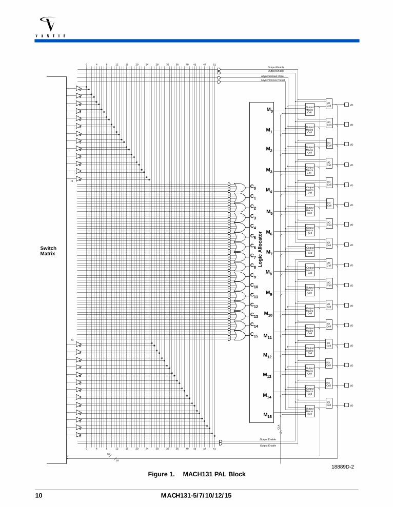
FUNCTIONAL DESCRIPTIONThe MACH131 consists of four PAL blocks connected by a switch matrix. There are 64 I/O pins and 2 dedicated input pins feeding the switch matrix. These signals are distributed to the four PAL blocks for efficient design implementation. There are 4 clock pins that can also be used as dedicated inputs.
The PAL BlocksEach PAL block in the MACH131 (Figure 1) contains a 64-product-term logic array, a logic allocator, 16 macrocells and 16 I/O cells. The switch matrix feeds each PAL block with 26 inputs. This makes the PAL block look effectively like an independent “PALCE26V16”.
There are four additional output enable product terms in each PAL block. For purposes of output enable, the 16 I/O cells are divided into 2 banks of 8 macrocells. Each bank is allocated two of the output enable product terms.
An asynchronous reset product term and an asynchronous preset product term are provided for flip-flop initialization. All flip-flops within the PAL block are initialized together.
The Switch MatrixThe MACH131 switch matrix is fed by the inputs and feedback signals from the PAL blocks. Each PAL block provides 16 internal feedback signals and 16 I/O feedback signals. The switch matrix distributes these signals back to the PAL blocks in an efficient manner that also provides for high performance. The design software automatically configures the switch matrix when fitting a design into the device.
The Product-term ArrayThe MACH131 product-term array consists of 64 product terms for logic use, and 6 special-purpose product terms. Four of the special-purpose product terms provide programmable output enable, one provides asynchronous reset, and one provides asynchronous preset. Two of the output enable product terms are used for the first eight I/O cells; the other two control the last eight macrocells.
The Logic AllocatorThe logic allocator in the MACH131 takes the 64 logic product terms and allocates them to the 16 macrocells as needed. Each macrocell can be driven by up to 12 product terms. The design software automatically configures the logic allocator when fitting the design into the device.
Table 1 illustrates which product term clusters are available to each macrocell within a PAL block. Refer to Figure 1 for cluster and macrocell numbers.
Table 1. Logic Allocation
Output Macrocell Available Clusters Output Macrocell Available Clusters
M0 C0, C1 M8 C7, C8, C9
M1 C0, C1, C2 M9 C8, C9, C10
M2 C1, C2, C3 M10 C9, C10, C11
M3 C2, C3, C4 M11 C10, C11, C12
M4 C3, C4, C5 M12 C11, C12, C13
M5 C4, C5, C6 M13 C12, C13, C14
M6 C5, C6, C7 M14 C13, C14, C15
M7 C6, C7, C8 M15 C14, C15
MACH131-5/7/10/12/15 7
V A N T I S
The Macrocell
The MACH131 macrocells can be configured as either registered or combinatorial, with programmable polarity. The macrocell provides internal feedback whether configured as registered or combinatorial. The flip-flops can be configured as D-type or T-type, allowing for product-term optimization.
The flip-flops can individually select one of four global clock pins, which are also available as logic inputs. The registers are clocked on the LOW-to-HIGH transition of the clock signal. The flip-flops can also be asynchronously initialized with the common asynchronous reset and preset product terms.
The I/O Cell
The I/O cell in the MACH131 consists of a three-state output buffer. The three-state buffer can be configured in one of three ways: always enabled, always disabled, or controlled by a product term. If product term control is chosen, one of two product terms may be used to provide the control. The two product terms that are available are common to eight I/O cells. Within each PAL block, two product terms are available for selection by the first eight three-state outputs; two other product terms are available for selection by the last eight three-state outputs.
These choices make it possible to use the macrocell as an output, an input, a bidirectional pin, or a three-state output for use in driving a bus.
SpeedLocking for Guaranteed Fixed Timing
The unique MACH 1 & 2 architecture is designed for high performance—a metric that is met in both raw speed, but even more importantly, guaranteed fixed speed. Using the design of the central switch matrix, the MACH131 product offers the SpeedLocking feature, which allows a stable fixed pin-to-pin delay, independent of logic paths, routing resources and design refits for up to 12 product terms per output. The MACH products are the only architecture to utilize SpeedLocking. Other non-Vantis CPLDs incur serious timing delays as product terms expand beyond their typical 4 or 5 product term limits. Speed and SpeedLocking combine for continuous, high performance required in today’s demanding designs.
Bus-Friendly Inputs and I/Os
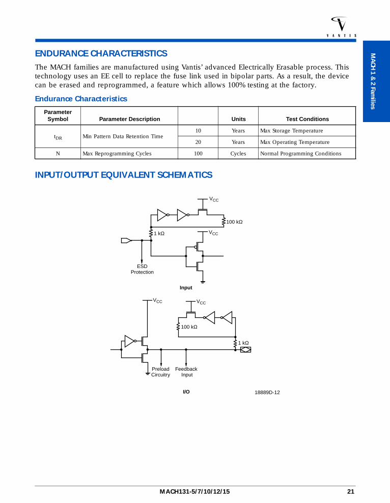
The MACH131 inputs and I/Os include two inverters in series which loop back to the input. This double inversion reinforces the state of the pin and pulls the voltage away from the input threshold voltage. Unlike a pull-up, this configuration cannot cause contention on a bus. For an illustration of this configuration, please turn to Input and Output Equivalent Schematics section.
PCI Compliant
The MACH131-5/7/10/12 is fully compliant with the PCI Local Bus Specification published by the PCI Special Interest Group. The MACH131-5/7/10/12’s predictable timing ensures compliance with the PCI AC specifications independent of the design.
8 MACH131-5/7/10/12/15
MA
CH 1 &
2 Families
V A N T I S
Power-Down Mode
The MACH131 features a programmable low-power mode in which individual signal paths can be programmed as low power. These low-power speed paths will be slightly slower than the non-low-power paths. This feature allows speed critical paths to run at maximum frequency while the rest of the paths operate in the low-power mode, resulting in power savings of up to 50%.
Safe for Mixed Supply Voltage System Designs
The MACH131 is safe for mixed supply voltage system designs. The 5-V device will not overdrive 3.3-V devices above the output voltage of 3.3 V, while it accepts inputs from other 3.3-V devices. Thus, the MACH131 provides easy-to-use mixed-voltage design capability.
MACH131-5/7/10/12/15 9
V A N T I S
Figure 1. MACH131 PAL Block
0 4 8 12 16 20 24 28 4032 4336
0 4 8 12 16 20 24 28 4032 4336
I/OCell I/O
I/O
I/O
I/O
I/O
I/O
I/O
I/O
I/O
I/O
I/O
I/O
I/O
I/O
I/O
I/O
SwitchMatrix
Output EnableOutput Enable
Asynchronous Reset
Asynchronous Preset
Output Enable
Output Enable
CLK
16
I/OCell
I/OCell
I/OCell
I/OCell
I/OCell
I/OCell
I/OCell
I/OCell
I/OCell
I/OCell
I/OCell
I/OCell
I/OCell
I/OCell
I/OCell
OutputMacro Cell
OutputMacro Cell
OutputMacro Cell
OutputMacro Cell
OutputMacro Cell
OutputMacro Cell
OutputMacro Cell
OutputMacro Cell
16
OutputMacro Cell
OutputMacro Cell
OutputMacro Cell
OutputMacro Cell
OutputMacro Cell
OutputMacro Cell
OutputMacro Cell
OutputMacro Cell
4
47 51
47 51
0
Lo
gic
Allo
cato
r
63
C0
C1
C2
C3
C4
C5
C6
C7
C8
C9
C10
C11
C12
C13
C14
C15
M3
M6
M5
M4
M2
M1
M0
M9
M8
M7
M10
M11
M12
M13
M14
M15
18889D-2
10 MACH131-5/7/10/12/15
V A N T I S
MA
CH 1 &
2 Families
ABSOLUTE MAXIMUM RATINGSStorage Temperature . . . . . . . . . . . . . .-65°C to +150°CAmbient Temperaturewith Power Applied . . . . . . . . . . . . . .-55°C to +125°CDevice Junction Temperature . . . . . . . . . . . . . +150°CSupply Voltage withRespect to Ground . . . . . . . . . . . . . . -0.5 V to +7.0 V
DC Input Voltage . . . . . . . . . . . . -0.5 V to VCC + 0.5 V
DC Output or I/OPin Voltage . . . . . . . . . . . . . . . . . -0.5 V to VCC + 0.5 V
Static Discharge Voltage . . . . . . . . . . . . . . . . . 2001 V
Latchup Current(TA = 0°C to 70°C) . . . . . . . . . . . . . . . . . . . . . 200 mA
Stresses above those listed under Absolute Maximum Ratingsmay cause permanent device failure. Functionality at or abovethese limits is not implied. Exposure to Absolute MaximumRatings for extended periods may affect device reliability.
OPERATING RANGESCommercial (C) DevicesAmbient Temperature (TA)Operating in Free Air . . . . . . . . . . . . . . . 0°C to +70°CSupply Voltage (VCC)with Respect to Ground . . . . . . . . . +4.75 V to +5.25 V
Operating ranges define those limits between which thefunctionality of the device is guaranteed.
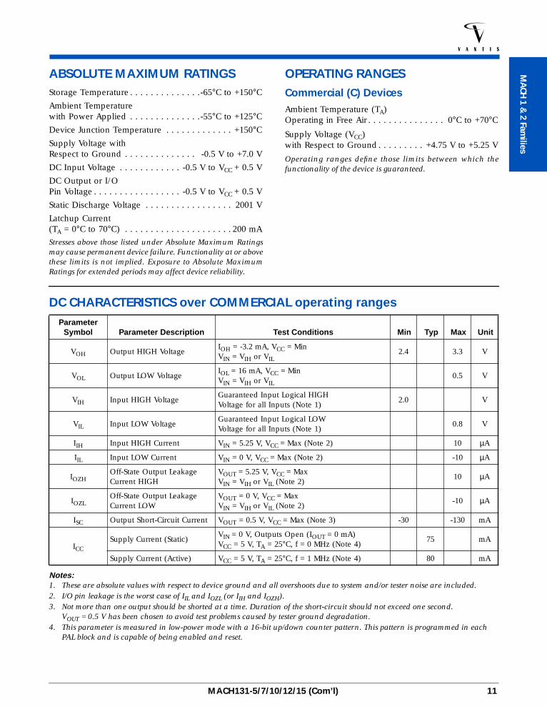
DC CHARACTERISTICS over COMMERCIAL operating ranges
Notes:1. These are absolute values with respect to device ground and all overshoots due to system and/or tester noise are included.2. I/O pin leakage is the worst case of IIL and IOZL (or IIH and IOZH).3. Not more than one output should be shorted at a time. Duration of the short-circuit should not exceed one second.
VOUT = 0.5 V has been chosen to avoid test problems caused by tester ground degradation.4. This parameter is measured in low-power mode with a 16-bit up/down counter pattern. This pattern is programmed in each
PAL block and is capable of being enabled and reset.
Parameter Symbol Parameter Description Test Conditions Min Typ Max Unit
VOH Output HIGH VoltageIOH = -3.2 mA, VCC = MinVIN = VIH or VIL
2.4 3.3 V
VOL Output LOW VoltageIOL = 16 mA, VCC = Min VIN = VIH or VIL
0.5 V
VIH Input HIGH VoltageGuaranteed Input Logical HIGHVoltage for all Inputs (Note 1)
2.0 V
VIL Input LOW VoltageGuaranteed Input Logical LOWVoltage for all Inputs (Note 1)
0.8 V
IIH Input HIGH Current VIN = 5.25 V, VCC = Max (Note 2) 10 µA
IIL Input LOW Current VIN = 0 V, VCC = Max (Note 2) -10 µA
IOZHOff-State Output LeakageCurrent HIGH
VOUT = 5.25 V, VCC = MaxVIN = VIH or VIL (Note 2)
10 µA
IOZLOff-State Output LeakageCurrent LOW
VOUT = 0 V, VCC = MaxVIN = VIH or VIL (Note 2)
-10 µA
ISC Output Short-Circuit Current VOUT = 0.5 V, VCC = Max (Note 3) -30 -130 mA
ICC
Supply Current (Static)VIN = 0 V, Outputs Open (IOUT = 0 mA)VCC = 5 V, TA = 25°C, f = 0 MHz (Note 4)
75 mA
Supply Current (Active) VCC = 5 V, TA = 25°C, f = 1 MHz (Note 4) 80 mA
MACH131-5/7/10/12/15 (Com’l) 11
V A N T I S
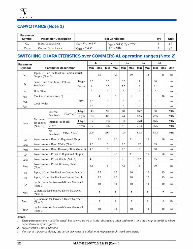
CAPACITANCE (Note 1)
SWITCHING CHARACTERISTICS over COMMERCIAL operating ranges (Note 2)
Notes:1. These parameters are not 100% tested, but are evaluated at initial characterization and at any time the design is modified where
capacitance may be affected.2. See Switching Test Conditions.3. If a signal is powered down, this parameter must be added to its respective high-speed parameter.
Parameter Symbol Parameter Description Test Conditions Typ Unit
CIN Input Capacitance VIN = VCC -0.5 V VCC = 5.0 V, TA = 25°C f = 1 MHz
6 pF
COUT Output Capacitance VOUT = 2.0 V 8 pF
Parameter Symbol Parameter Description
-5 -7 -10 -12 -15
UnitMin Max Min Max Min Max Min Max Min Max
tPDInput, I/O, or Feedback to Combinatorial Output (Note 3)
5.5 7.5 10 12 15 ns
tSSetup Time from Input, I/O, or Feedback
T-type 3.5 5.5 6.5 7 10 ns
D-type 4 6.5 7.5 8 11 ns
tH Hold Time 0 0 0 0 0 ns
tCO Clock to Output (Note 3) 4 5 6 8 10 ns
tWLClock Width
LOW 2.5 3 5 6 6 ns
tWH HIGH 2.5 3 5 6 6 ns
fMAX
Maximum Frequency (Note 1 )
External Feedback
1/(tS + tCO)T-type 143 95 80 66.7 50 MHz
D-type 133 87 74 62.5 47.6 MHz
Internal Feedback (fCNT)
T-type 182 133 100 76.8 66.6 MHz
D-type 167 125 91 71.4 55.5 MHz
No Feedback
1/(tWL + tWH) 200 166.7 100 83.3 83.3 MHz
tAR Asynchronous Reset to Registered Output 8.5 9.5 11 16 20 ns
tARW Asynchronous Reset Width (Note 1) 4.5 5 7.5 12 15 ns
tARR Asynchronous Reset Recovery Time (Note 1) 4.5 5 7.5 8 10 ns
tAP Asynchronous Preset to Registered Output 9.5 11 16 20 ns
tAPW Asynchronous Preset Width (Note 1) 4.5 5 7.5 12 15 ns
tAPRAsynchronous Preset Recovery Time(Note 1)
4.5 5 7.5 8 10 ns
tEA Input, I/O, or Feedback to Output Enable 7.5 9.5 10 12 15 ns
tER Input, I/O, or Feedback to Output Disable 7.5 9.5 10 12 15 ns
tLPtPD Increase for Powered-Down Macrocell (Note 3)
10 10 10 10 10 ns
tLPStS Increase for Powered-Down Macrocell (Note 3)
7 7 7 7 7 ns
tLPCOtCO Increase for Powered-Down Macrocell (Note 3)
3 3 3 3 3 ns
tLPEAtEA Increase for Powered-Down Macrocell (Note 3)
10 10 10 10 10 ns
12 MACH131-5/7/10/12/15 (Com’l)
V A N T I S
MA
CH 1 &
2 Families
ABSOLUTE MAXIMUM RATINGSStorage Temperature . . . . . . . . . . . . . –65°C to +150°CAmbient Temperature with Power Applied . . . . . . . . . . . . . –55°C to +125°CDevice Junction Temperature . . . . . . . . . . . . . +150°CSupply Voltage with Respect to Ground . . . . . . . . . . –0.5 V to +7.0 V
DC Input Voltage . . . . . . . . . . . .–0.5 V to VCC + 0.5 V
DC Output or I/O Pin Voltage. . . . . . . . . . . –0.5 V to VCC + 0.5 V
Static Discharge Voltage . . . . . . . . . . . . . . . . . 2001 V
Latchup Current (TA = –40°C to +85°C) . . . . . . 200 mA
Stresses above those listed under Absolute Maximum Ratingsmay cause permanent device failure. Functionality at or abovethese limits is not implied. Exposure to Absolute Maximum Rat-ings for extended periods may affect device reliability.
OPERATING RANGESIndustrial (I) DevicesTemperature (TA)Operating in Free Air . . . . . . . . . . . . . . –40°C to +85°CSupply Voltage (VCC)with Respect to Ground . . . . . . . . . . . +4.5 V to +5.5 V
Operating ranges define those limits between which the func-tionality of the device is guaranteed.
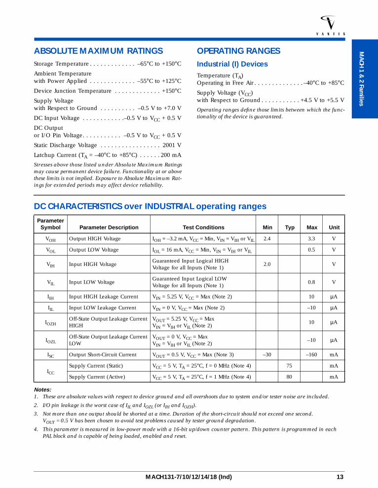
DC CHARACTERISTICS over INDUSTRIAL operating ranges
Notes:1. These are absolute values with respect to device ground and all overshoots due to system and/or tester noise are included.
2. I/O pin leakage is the worst case of IIL and IOZL (or IIH and IOZH).
3. Not more than one output should be shorted at a time. Duration of the short-circuit should not exceed one second.VOUT = 0.5 V has been chosen to avoid test problems caused by tester ground degradation.
4. This parameter is measured in low-power mode with a 16-bit up/down counter pattern. This pattern is programmed in each PAL block and is capable of being loaded, enabled and reset.
Parameter Symbol Parameter Description Test Conditions Min Typ Max Unit
VOH Output HIGH Voltage IOH = –3.2 mA, VCC = Min, VIN = VIH or VIL 2.4 3.3 V
VOL Output LOW Voltage IOL = 16 mA, VCC = Min, VIN = VIH or VIL 0.5 V
VIH Input HIGH VoltageGuaranteed Input Logical HIGHVoltage for all Inputs (Note 1)
2.0 V
VIL Input LOW VoltageGuaranteed Input Logical LOWVoltage for all Inputs (Note 1)
0.8 V
IIH Input HIGH Leakage Current VIN = 5.25 V, VCC = Max (Note 2) 10 µA
IIL Input LOW Leakage Current VIN = 0 V, VCC = Max (Note 2) –10 µA
IOZHOff-State Output Leakage Current HIGH
VOUT = 5.25 V, VCC = MaxVIN = VIH or VIL (Note 2)
10 µA
IOZLOff-State Output Leakage Current LOW
VOUT = 0 V, VCC = MaxVIN = VIH or VIL (Note 2)
–10 µA
ISC Output Short-Circuit Current VOUT = 0.5 V, VCC = Max (Note 3) –30 –160 mA
ICC
Supply Current (Static) VCC = 5 V, TA = 25°C, f = 0 MHz (Note 4) 75 mA
Supply Current (Active) VCC = 5 V, TA = 25°C, f = 1 MHz (Note 4) 80 mA
MACH131-7/10/12/14/18 (Ind) 13

V A N T I S
CAPACITANCE (Note 1)
SWITCHING CHARACTERISTICS over INDUSTRIAL operating ranges (Note 2)
Notes:1. These parameters are not 100% tested, but are evaluated at initial characterization and at any time the design is modified where
capacitance may be affected.
2. See Switching Test Conditions.
3. If a signal is powered down, this parameter must be added to its respective high-speed parameter.
Parameter Symbol Parameter Description Test Conditions Typ Unit
CIN Input Capacitance VIN = 2.0 V VCC = 5.0 V, TA = 25°C
f = 1 MHz
6 pF
COUT Output Capacitance VOUT = 2.0 V 8 pF
Parameter Symbol Parameter Description
-7 -10 -12 -14 -18
UnitMin Max Min Max Min Max Min Max Min Max
tPDInput, I/O, or Feedback to Combinatorial Output (Note 2)
7.5 10 12 14 18 ns
tSSetup Time from Input, I/O, or Feedback to Clock
D-type 5.5 6.5 7 8.5 12 ns
T-type 6.5 7.5 8 10 13.5 ns
tH Register Data Hold Time 0 0 0 0 0 ns
tCO Clock to Output (Note 2) 5 6 8 10 12 ns
tWLClock Width (Note 1)
LOW 3 5 6 6 7.5 ns
tWH HIGH 3 5 6 6 7.5 ns
fMAX
Maximum Frequency (Note 1)
External Feedback
1/(tS + tCO)D-type 95 80 66.7 54 40 MHz
T-type 87 74 62.5 50 38 MHz
Internal Feedback (fCNT)D-type 133 100 76.9 61.5 53 MHz
T-type 125 91 71.4 57 44 MHz
No Feedback
1/(tWL + tWH) 166.7 100 83.3 83.3 61.5 MHz
tAR Asynchronous Reset to Registered Output 9.5 11 16 19.5 24 ns
tARW Asynchronous Reset Width (Note 1) 5 7.5 12 14.5 18 ns
tARR Asynchronous Reset Recovery Time (Note 1) 5 7.5 8 10 12 ns
tAP Asynchronous Preset to Registered Output 9.5 11 16 19.5 24 ns
tAPW Asynchronous Preset Width (Note 1) 5 7.5 12 14.5 18 ns
tAPR Asynchronous Preset Recovery Time (Note 1) 5 7.5 8 10 12 ns
tEA Input, I/O, or Feedback to Output Enable (Note 1) 9.5 10 12 14.5 18 ns
tER Input, I/O, or Feedback to Output Disable (Note 1) 9.5 10 12 14.5 18 ns
tLP tPD Increase for Powered-Down Macrocell (Note 3) 10 10 10 10 10 ns
tLPS tS Increase for Powered-Down Macrocell (Note 3) 7 7 7 7 7 ns
tLPCO tCO Increase for Powered-Down Macrocell (Note 3) 3 3 3 3 3 ns
tLPEA tEA Increase for Powered-Down Macrocell (Note 3) 10 10 10 10 10 ns
14 MACH131-7/10/12/14/18 (Ind)
MA
CH 1 &
2 Families
V A N T I S
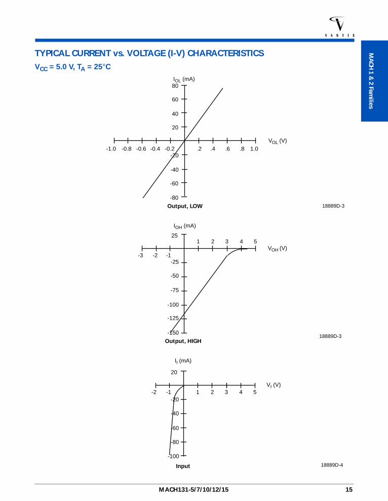
TYPICAL CURRENT vs. VOLTAGE (I-V) CHARACTERISTICSVCC = 5.0 V, TA = 25°C
-0.8 -0.6 -0.4 .2-0.2-1.0 .4 .6 1.0.8
60
40
20
-20
-40
80
-60
-8018889D-3Output, LOW
VOL (V)
IOL (mA)
18889D-4Input
II (mA)
VI (V)
20
-40
-60
-80
-2 -1 1 2 3-20
4 5
-100
18889D-3
IOH (mA)
VOH (V)
25
-50
-75
-100
-3 -2 -1
1 2 3
-25
-125
-150
4 5
Output, HIGH
MACH131-5/7/10/12/15 15
V A N T I S
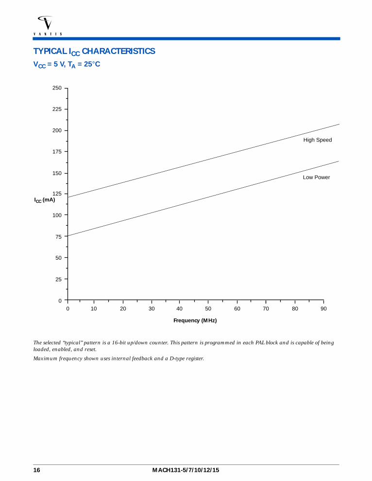
TYPICAL ICC CHARACTERISTICSVCC = 5 V, TA = 25°C
The selected “typical” pattern is a 16-bit up/down counter. This pattern is programmed in each PAL block and is capable of being loaded, enabled, and reset.
Maximum frequency shown uses internal feedback and a D-type register.
250
225
200
175
150
125
100
75
50
25
00 10 20 30 40 50 60 70
ICC (mA)
Frequency (MHz)
80 90
High Speed
Low Power
16 MACH131-5/7/10/12/15
MA
CH 1 &
2 Families
V A N T I S
TYPICAL THERMAL CHARACTERISTICSMeasured at 25°C ambient. These parameters are not tested.
Plastic θ jc ConsiderationsThe data listed for plastic θjc are for reference only and are not recommended for use in calculating junction temperatures. Theheat-flow paths in plastic-encapsulated devices are complex, making the θjc measurement relative to a specific location on thepackage surface. Tests indicate this measurement reference point is directly below the die-attach area on the bottom center of thepackage. Furthermore, θjc tests on packages are performed in a constant-temperature bath, keeping the package surface at aconstant temperature. Therefore, the measurements can only be used in a similar environment.
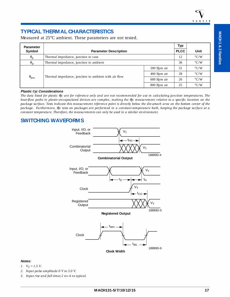
SWITCHING WAVEFORMS
Notes:1. VT = 1.5 V.
2. Input pulse amplitude 0 V to 3.0 V.
3. Input rise and fall times 2 ns–4 ns typical.
Parameter Symbol Parameter Description
Typ
UnitPLCC
θjc Thermal impedance, junction to case 12 °C/W
θja Thermal impedance, junction to ambient 36 °C/W
θjma Thermal impedance, junction to ambient with air flow
200 lfpm air 31 °C/W
400 lfpm air 28 °C/W
600 lfpm air 26 °C/W
800 lfpm air 25 °C/W
18889D-4Combinatorial Output
tPD
Input, I/O, orFeedback
CombinatorialOutput
VT
VT
18889D-5 Registered Output
VTInput, I/O, or
Feedback
RegisteredOutput
tS
tCO
VT
tH
VTClock
18889D-6Clock Width
tWH
Clock
tWL
MACH131-5/7/10/12/15 17
V A N T I S
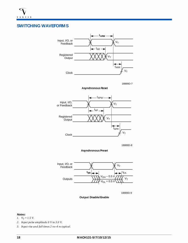
SWITCHING WAVEFORMS
Notes:1. VT = 1.5 V.
2. Input pulse amplitude 0 V to 3.0 V.
3. Input rise and fall times 2 ns–4 ns typical.
VT
VT
tARW
VT
tAR
Input, I/O, orFeedback
RegisteredOutput
Clock
tARR
18889D-7
Asynchronous Reset
Input, I/O,or Feedback
VT
VT
tAPW
VT
tAP
tAPR
RegisteredOutput
Clock
18889D-8
Asynchronous Preset
18889D-9
Output Disable/Enable
VT
VTOutputs
tER tEA
VOH – 0.5 V
VOL + 0.5 V
Input, I/O, orFeedback
18 MACH131-5/7/10/12/15
MA
CH 1 &
2 Families
V A N T I S
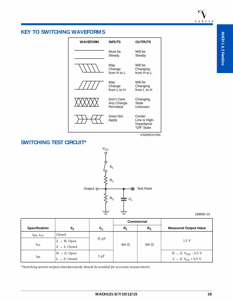
KEY TO SWITCHING WAVEFORMS
SWITCHING TEST CIRCUIT*
* Switching several outputs simultaneously should be avoided for accurate measurement.
Specification S1 CL
Commercial
Measured Output ValueR1 R2
tPD, tCO Closed35 pF
300 Ω 390 Ω1.5 V
tEAZ → H: Open
Z → L: Closed
tERH → Z: Open
L → Z: Closed5 pF
H → Z: VOH – 0.5 V
L → Z: VOL + 0.5 V
Must beSteady
MayChangefrom H to L
MayChangefrom L to H
Does Not Apply
Don’t Care,Any ChangePermitted
Will beSteady
Will beChangingfrom H to L
Will be Changing from L to H
Changing,StateUnknown
Center Line is High-Impedance“Off” State
WAVEFORM INPUTS OUTPUTS
KS000010-PAL
18889D-10
CL
Output
R1
R2
S1
Test Point
VCC
MACH131-5/7/10/12/15 19
V A N T I S
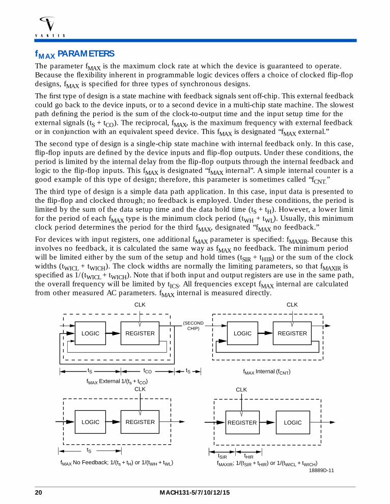
fMAX PARAMETERSThe parameter fMAX is the maximum clock rate at which the device is guaranteed to operate. Because the flexibility inherent in programmable logic devices offers a choice of clocked flip-flop designs, fMAX is specified for three types of synchronous designs.
The first type of design is a state machine with feedback signals sent off-chip. This external feedback could go back to the device inputs, or to a second device in a multi-chip state machine. The slowest path defining the period is the sum of the clock-to-output time and the input setup time for the external signals (tS + tCO). The reciprocal, fMAX, is the maximum frequency with external feedback or in conjunction with an equivalent speed device. This fMAX is designated “fMAX external.”
The second type of design is a single-chip state machine with internal feedback only. In this case, flip-flop inputs are defined by the device inputs and flip-flop outputs. Under these conditions, the period is limited by the internal delay from the flip-flop outputs through the internal feedback and logic to the flip-flop inputs. This fMAX is designated “fMAX internal”. A simple internal counter is a good example of this type of design; therefore, this parameter is sometimes called “fCNT.”
The third type of design is a simple data path application. In this case, input data is presented to the flip-flop and clocked through; no feedback is employed. Under these conditions, the period is limited by the sum of the data setup time and the data hold time (tS + tH). However, a lower limit for the period of each fMAX type is the minimum clock period (tWH + tWL). Usually, this minimum clock period determines the period for the third fMAX, designated “fMAX no feedback.”
For devices with input registers, one additional fMAX parameter is specified: fMAXIR. Because this involves no feedback, it is calculated the same way as fMAX no feedback. The minimum period will be limited either by the sum of the setup and hold times (tSIR + tHIR) or the sum of the clock widths (tWICL + tWICH). The clock widths are normally the limiting parameters, so that fMAXIR is specified as 1/(tWICL + tWICH). Note that if both input and output registers are use in the same path, the overall frequency will be limited by tICS. All frequencies except fMAX internal are calculated from other measured AC parameters. fMAX internal is measured directly.
LOGIC REGISTER
CLK
LOGIC REGISTER
CLK
tCOtS tS
tS
fMAX Internal (fCNT)
fMAX External 1/(ts + tCO)
LOGIC REGISTER
CLK
fMAX No Feedback; 1/(ts + tH) or 1/(tWH + tWL)
(SECONDCHIP)
REGISTER LOGIC
CLK
fMAXIR; 1/(tSIR + tHIR) or 1/(tWICL + tWICH)tSIR tHIR
18889D-11
20 MACH131-5/7/10/12/15
MA
CH 1 &
2 Families
V A N T I S
ENDURANCE CHARACTERISTICSThe MACH families are manufactured using Vantis’ advanced Electrically Erasable process. This technology uses an EE cell to replace the fuse link used in bipolar parts. As a result, the device can be erased and reprogrammed, a feature which allows 100% testing at the factory.
Endurance Characteristics
INPUT/OUTPUT EQUIVALENT SCHEMATICS
Parameter Symbol Parameter Description Units Test Conditions
tDR Min Pattern Data Retention Time10 Years Max Storage Temperature
20 Years Max Operating Temperature
N Max Reprogramming Cycles 100 Cycles Normal Programming Conditions
VCC
ESD Protection
1 kΩ
Input
VCC
100 kΩ
Preload Circuitry
Feedback Input
I/O
VCCVCC
100 kΩ
1 kΩ
18889D-12
MACH131-5/7/10/12/15 21
V A N T I S
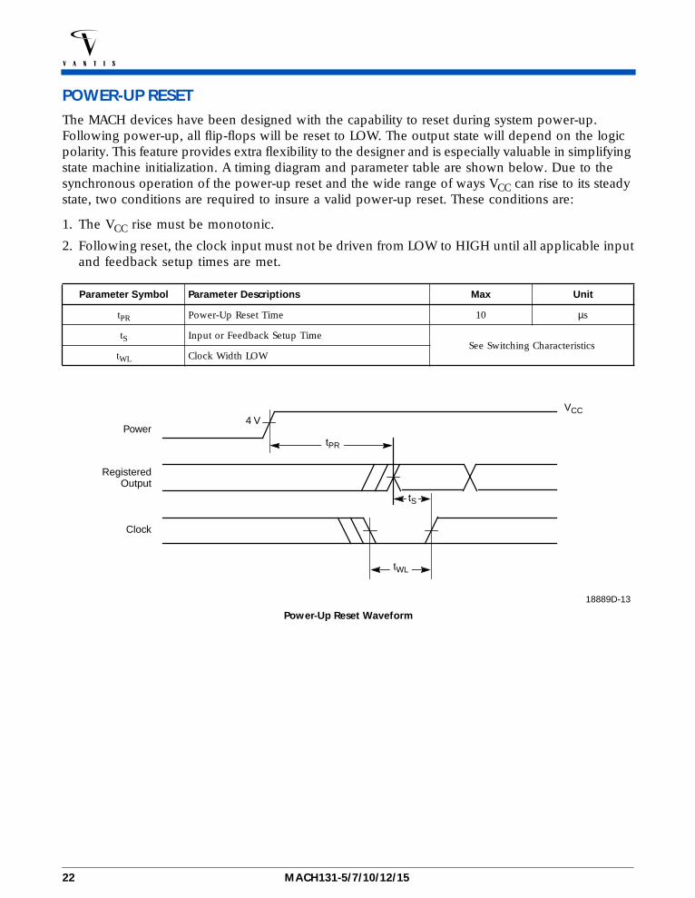
POWER-UP RESETThe MACH devices have been designed with the capability to reset during system power-up. Following power-up, all flip-flops will be reset to LOW. The output state will depend on the logic polarity. This feature provides extra flexibility to the designer and is especially valuable in simplifying state machine initialization. A timing diagram and parameter table are shown below. Due to the synchronous operation of the power-up reset and the wide range of ways VCC can rise to its steady state, two conditions are required to insure a valid power-up reset. These conditions are:
1. The VCC rise must be monotonic.
2. Following reset, the clock input must not be driven from LOW to HIGH until all applicable inputand feedback setup times are met.
Parameter Symbol Parameter Descriptions Max Unit
tPR Power-Up Reset Time 10 µs
tS Input or Feedback Setup TimeSee Switching Characteristics
tWL Clock Width LOW
18889D-13
Power-Up Reset Waveform
tPR
tWL
tS
4 VVCC
Power
RegisteredOutput
Clock
22 MACH131-5/7/10/12/15
MA
CH 1 &
2 Families
V A N T I S
DEVELOPMENT SYSTEMS (subject to change)For more information on the products listed below, please consult the local Vantis sales office.
MANUFACTURER SOFTWARE DEVELOPMENT SYSTEMS
Vantis CorporationP.O. Box 3755920 DeGuigne DriveSunnyvale, CA 94088(408) 732-0555 or 1(888) 826-8472 (VANTIS2)http://www.vantis.com
MACHXL SoftwareVantis-ABEL Software
Vantis-Synario Software
Aldec, Inc.3 Sunset Way, Suite FHenderson, NV 89014(702) 456-1222 or (800) 487-8743
ACTIVE-CAD
Cadence Design Systems555 River Oaks PkwySan Jose, CA 95134(408) 943-1234 or (800) 746-6223
PIC DesignerConcept/Composer
SynergyLeapfrog/Verilog-XL
Exemplar Logic, Inc.815 Atlantic Avenue, Suite 105Alameda, CA 94501(510) 337-3700
Leonardo™Galileo™
Logic Modeling19500 NW Gibbs Dr.P.O. Box 310Beaverton, OR 97075(800) 346-6335
SmartModel® Library
Mentor Graphics Corp.8005 S.W. Boeckman Rd.Wilsonville, OR 97070-7777(800) 547-3000 or (503) 685-7000
Design Architect, PLDSynthesis™ II
Autologic II Synthesizer, QuickSim Simulator, QuickHDL Simulator
MicroSim Corp.20 FairbanksIrvine, CA 92718(714) 770-3022
MicroSim Design Lab
PLogic, PLSyn
MINC Inc.6755 Earl Drive, Suite 200Colorado Springs, CO 80918(800) 755-FPGA or (719) 590-1155
PLDesigner-XL™ Software
Model Technology8905 S.W. Nimbus Avenue, Suite 150Beaverton, OR 97008(503) 641-1340
V-System/VHDL
OrCAD, Inc.9300 S.W. Nimbus AvenueBeaverton, OR 97008(503) 671-9500 or (800) 671-9505
OrCAD Express
Synario® Design Automation10525 Willows Road N.E.P.O. Box 97046Redmond, WA 98073-9746(800) 332-8246 or (206) 881-6444
ABEL™
Synario™ Software
MACH131-5/7/10/12/15 23

V A N T I S
Vantis is not responsible for any information relating to the products of third parties. The inclusion of such information is not a rep-resentation nor an endorsement by Vantis of these products.
Synopsys700 E. Middlefield Rd.Mountain View, CA 94040(415) 962-5000 or (800) 388-9125
FPGA or Design Compiler(Requires MINC PLDesigner-XL™)
VSS Simulator
Synplicity, Inc.624 East Evelyn Ave.Sunnyvale, CA 94086(408) 617-6000
Synplify
Teradyne EDA321 Harrison Ave.Boston, MA 02118(800) 777-2432 or (617) 422-2793
MultiSIM Interactive SimulatorLASAR
VeriBest, Inc.6101 Lookout Road, Suite ABoulder, CO 80301(800) 837-4237
VeriBest PLD
Viewlogic Systems, Inc.293 Boston Post Road WestMarlboro, MA 01752(800) 873-8439 or (508) 480-0881
Viewdraw, ViewPLD, Viewsynthesis
Speedwave Simulator, ViewSim Simulator, VCS Simulator
MANUFACTURER TEST GENERATION SYSTEM
Acugen Software, Inc.427-3 Amherst St., Suite 391Nashua, NH 03063(603) 881-8821
ATGEN™ Test Generation Software
iNt GmbHBusenstrasse 6D-8033 Martinsried, Munich, Germany(87) 857-6667
PLDCheck 90
MANUFACTURER SOFTWARE DEVELOPMENT SYSTEMS
24 MACH131-5/7/10/12/15

MA
CH 1 &
2 Families
V A N T I S
APPROVED PROGRAMMERS (subject to change)For more information on the products listed below, please consult the local Vantis sales office.
MANUFACTURER PROGRAMMER CONFIGURATION
Advin Systems, Inc.1050-L East Duane Ave.Sunnyvale, CA 940 86(408) 243-7000 or (800) 627-2456BBS (408) 737-9200Fax (408) 736-2503
Pilot-U40 Pilot-U84 MVP
BP Microsystems1000 N. Post Oak Rd., Suite 225Houston, TX 77055-7237(800) 225-2102 or (713) 688-4600BBS (713) 688-9283Fax (713) 688-0920
BP1200 BP1400 BP2100 BP2200
Data I/O Corporation10525 Willows Road N.E.P.O. Box 97046Redmond, WA 98073-9746(800) 426-1045 or (206) 881-6444BBS (206) 882-3211Fax (206) 882-1043
UniSite™ Model 2900 Model 3900 AutoSite
Hi-Lo Systems4F, No. 2, Sec. 5, Ming Shoh E. RoadTaipei, Taiwan(886) 2-764-0215Fax (886) 2-756-6403orTribal Microsystems / Hi-Lo Systems44388 South Grimmer Blvd.Fremont, CA 94538(510) 623-8859BBS (510) 623-0430Fax (510) 623-9925
ALL-07 FLEX-700
SMS GmbHIm Grund 1588239 WangenGermany(49) 7522-97280Fax (49) 7522-972850orSMS USA544 Weddell Dr. Suite 12Sunnyvale, CA 94089(408) 542-0388
Sprint Expert Sprint Optima Multisite
Stag HouseSilver Court Watchmead, Welwyn Garden CityHerfordshire UK AL7 1LT44-1-707-332148Fax 44-1-707-371503
Stag Quazar
MACH131-5/7/10/12/15 25
V A N T I S
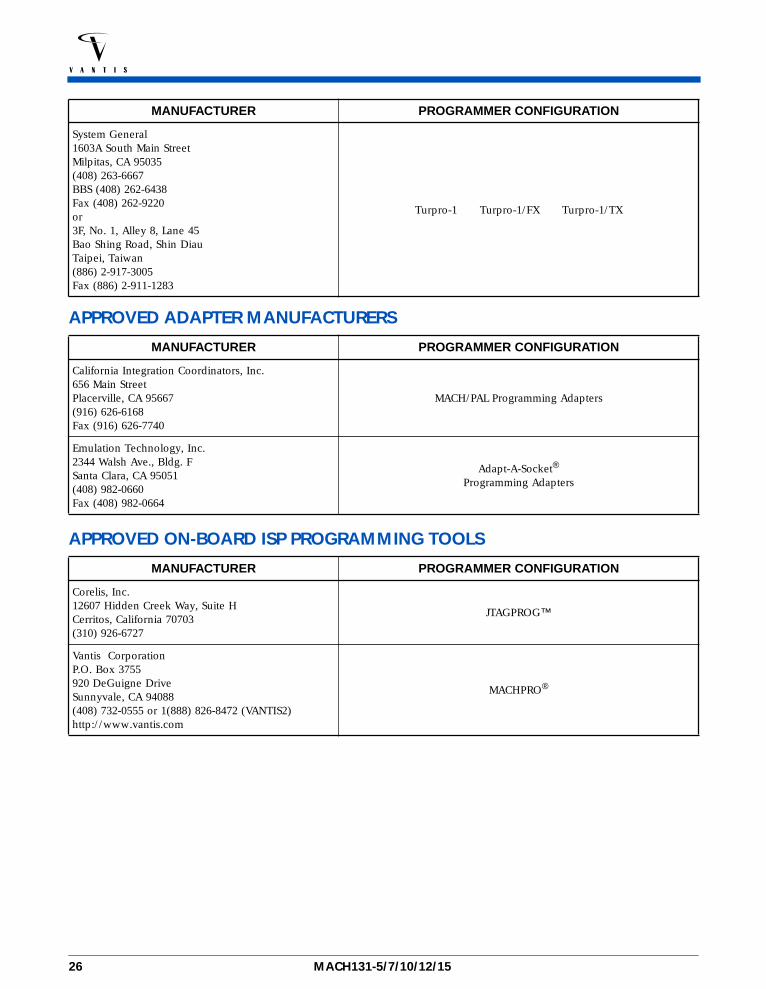
APPROVED ADAPTER MANUFACTURERS
APPROVED ON-BOARD ISP PROGRAMMING TOOLS
System General1603A South Main StreetMilpitas, CA 95035(408) 263-6667BBS (408) 262-6438Fax (408) 262-9220or3F, No. 1, Alley 8, Lane 45Bao Shing Road, Shin DiauTaipei, Taiwan(886) 2-917-3005Fax (886) 2-911-1283
Turpro-1 Turpro-1/FX Turpro-1/TX
MANUFACTURER PROGRAMMER CONFIGURATION
California Integration Coordinators, Inc.656 Main StreetPlacerville, CA 95667(916) 626-6168Fax (916) 626-7740
MACH/PAL Programming Adapters
Emulation Technology, Inc.2344 Walsh Ave., Bldg. FSanta Clara, CA 95051(408) 982-0660Fax (408) 982-0664
Adapt-A-Socket®
Programming Adapters
MANUFACTURER PROGRAMMER CONFIGURATION
Corelis, Inc.12607 Hidden Creek Way, Suite HCerritos, California 70703(310) 926-6727
JTAGPROG™
Vantis CorporationP.O. Box 3755920 DeGuigne DriveSunnyvale, CA 94088(408) 732-0555 or 1(888) 826-8472 (VANTIS2)http://www.vantis.com
MACHPRO®
MANUFACTURER PROGRAMMER CONFIGURATION
26 MACH131-5/7/10/12/15
MA
CH 1 &
2 Families
V A N T I S
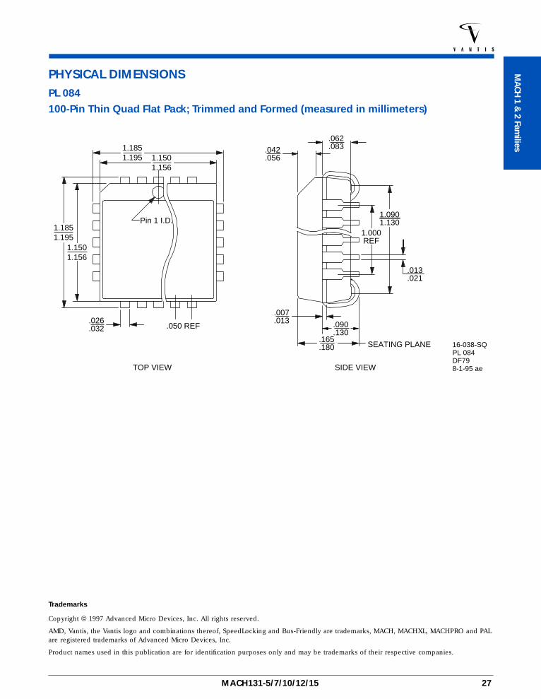
PHYSICAL DIMENSIONSPL 084
100-Pin Thin Quad Flat Pack; Trimmed and Formed (measured in millimeters)
Trademarks
Copyright © 1997 Advanced Micro Devices, Inc. All rights reserved.
AMD, Vantis, the Vantis logo and combinations thereof, SpeedLocking and Bus-Friendly are trademarks, MACH, MACHXL, MACHPRO and PAL are registered trademarks of Advanced Micro Devices, Inc.
Product names used in this publication are for identification purposes only and may be trademarks of their respective companies.
TOP VIEW
SEATING PLANE
1.1851.195 1.150
1.156
Pin 1 I.D.
.026
.032 .050 REF
.042
.056
.062
.083
.013
.021
1.000REF
.007
.013
.165
.180
.090
.130
16-038-SQPL 084DF798-1-95 aeSIDE VIEW
1.1851.195
1.1501.156
1.0901.130
MACH131-5/7/10/12/15 27