Embed Size (px)
Citation preview

Freescale SemiconductorAdvance Information
MAC7100ECRev. 1.2, 02/2006
MAC7100 Microcontroller Family Hardware SpecificationsCovers MAC7101, MAC7106, MAC7111, MAC7116, MAC7121, MAC7126, MAC7131, MAC7136, MAC7141132-bit Embedded Controller Division
1. With preliminary information on MAC7112, MAC7122, MAC7142 devices.
Table of Contents
1 Overview .................................................................12 Ordering Information ...............................................23 Electrical Characteristics.........................................43.1 Parameter Classification......................................43.2 Absolute Maximum Ratings.................................43.3 ESD Protection and Latch-up Immunity ..............53.4 Operating Conditions...........................................63.5 Input/Output Characteristics................................73.6 Power Dissipation and Thermal Characteristics..83.7 Power Supply ....................................................113.8 Clock and Reset Generator ...............................153.9 External Bus Timing ..........................................203.10 Analog-to-Digital Converter ...............................243.11 Serial Peripheral Interface .................................293.12 FlexCAN Interface .............................................323.13 Common Flash Module .....................................324 Device Pin Assignments .......................................364.1 MAC7141 Pin Diagram......................................414.2 MAC7142 Pin Diagram......................................424.3 MAC7121 / MAC7126 Pin Diagram...................434.4 MAC7122 Pin Diagram......................................444.5 MAC7101 / MAC7106 Pin Diagram...................454.6 MAC7111 / MAC7116 Pin Diagram...................464.7 MAC7112 Pin Diagram......................................474.8 MAC7131 Pin Diagram......................................484.9 MAC7136 Pin Diagram......................................495 Mechanical Information.........................................50
Revision History ....................................................51
This document provides electrical specifications, pin assignments, and package diagrams for MAC7100 family of microcontroller devices. For functional characteristics, refer to the MAC7100 Microcontroller Family Reference Manual (MAC7100RM).
1 OverviewThe MAC7100 Family of microcontrollers (MCUs) are members of a pin-compatible family of 32-bit Flash-memory-based devices developed specifically for embedded automotive applications. The pin-compatible family concept enables users to select between different memory and peripheral options for scalable designs. All MAC7100 Family members are composed of a 32-bit ARM7TDMI-S™ central processing unit, up to 1 Mbyte of embedded Flash EEPROM for program storage, up to 32 Kbytes of embedded Flash for data and/or program storage, and up to 48 Kbytes of RAM. The family is implemented with an enhanced DMA (eDMA) controller to improve performance for transfers between memory and many of the on-chip peripherals. The peripheral set includes asynchronous serial communications interfaces (eSCI), serial peripheral interfaces (DSPI),
© Freescale Semiconductor, Inc., 2004-2006. All rights reserved.
• Preliminary
This document contains information on a new product under development. Freescale Semiconductor reserves the right to change or discontinue this product without notice.

Ordering Information
inter-integrated circuit (I2C™) bus controllers, FlexCAN interfaces, an enhanced modular I/O subsystem (eMIOS), 10-bit analog-to-digital converter (ATD) module(s), general-purpose timers (PIT) and two special-purpose timers (RTI and SWT). The peripherals share a large number of general purpose input-output (GPIO) pins, all of which are bidirectional and available with interrupt capability to trigger wake-up from low-power chip modes. Refer to Table 2 for a comparison of family members and availability of peripheral modules on each device.
The use of a PLL allows power drain and performance to be balanced to best fit requirements. The operating frequency of devices in the family is up to a maximum of 50 MHz. The internal data paths between the CPU core, eDMA, memory and peripherals are all 32 bits wide, further improving performance for 32-bit applications. The MAC7111, MAC7116, MAC7131 and MAC7136 also offer a 16-bit wide external data bus with 22 address lines. The family of devices is capable of operating over a junction temperature range of –40° C to 150° C.
2 Ordering Information
Figure 1. Order Part Number Example
The mask set of a device is marked with a four-character code consisting of a letter, two numerical digits, and a letter, for example L49P. Slight variations to the mask set identification code may result in an optional numerical digit preceding the standard four-character code, for example 0L49P.
Table 1. MAC7100 Family Mask Set to Part Number Correspondence
Mask Set Status Part Number(s)
0L49P Engineering samples PAC7101, PAC7111, PAC7121, PAC7131, PAC7141
1L49P Limited production, pre-qualification PAC7101, PAC7111, PAC7121, PAC7131, PAC7141
0L47W Limited production, pre-qualification PAC7101, PAC7111, PAC7121, PAC7131, PAC7141
1L47W Fully-qualified, production MAC7101, MAC7111, MAC7121, MAC7131, MAC7141
0L61W Engineering samples PAC7112, PAC7122, PAC7142
0L38Y Engineering samples PAC7106, PAC7116, PAC7126, PAC7136
1L38Y Fully-qualified, production MAC7106, MAC7116, MAC7126, MAC7136
M AC 7 1 0 1 C PV 50 xx
Qualification StatusCore Code
Core NumberGeneration / Family
Package OptionDevice Number
Temperature RangePackage Identifier
Speed (MHz)Optional Package Identifiers
Temperature OptionC = –40° C to 85° CV = –40° C to105° CM = –40° C to125° C
Package OptionFU = 100 LQFPAF = 100 LQFP, RoHSPV = 112 / 144 LQFPAG = 112 / 144 LQFP, RoHSVF = 208 MAP BGAVM= 208 MAP BGA, RoHS
MAC7100 Microcontroller Family Hardware Specifications, Rev. 1.2
Preliminary Freescale Semiconductor2

Ordering Information
Table 2. MAC7100 Family Device Derivatives
Module Options
MA
C71
01
MA
C71
11
MA
C71
21
MA
C71
31
MA
C71
41
MA
C71
12
MA
C71
22
MA
C71
42
MA
C71
06
MA
C71
16
MA
C71
26
MA
C71
36
Program Flash 512 KBytes 256 KBytes 1 MByte
Data Flash 32 KBytes
SRAM 32 KBytes 16 KBytes 48 KBytes
External Bus — Yes — Yes — — — — — Yes — Yes
ATD Modules 1
NOTES:1. 16 channels, 8/10-bit, per module.
A Yes Yes Yes Yes Yes Yes Yes Yes Yes Yes Yes Yes
B Yes — — Yes — — — — Yes — — Yes
CAN Modules A Yes Yes Yes Yes Yes Yes Yes Yes Yes Yes Yes Yes
B Yes Yes Yes Yes Yes Yes Yes Yes Yes Yes Yes Yes
C Yes Yes Yes Yes — — — — Yes Yes Yes Yes
D Yes Yes Yes Yes — — — — Yes Yes Yes Yes
eSCI Modules A Yes Yes Yes Yes Yes Yes Yes Yes Yes Yes Yes Yes
B Yes Yes Yes Yes Yes Yes Yes Yes Yes Yes Yes Yes
C Yes Yes Yes Yes — Yes Yes — Yes Yes Yes Yes
D Yes Yes Yes Yes Yes — — — Yes Yes Yes Yes
DSPI Modules A Yes Yes Yes Yes Yes Yes Yes Yes Yes Yes Yes Yes 2
2. Four additional chip selects available.
B Yes Yes Yes 3
3. PB11 / PCS2_B not available on non-L49P-mask devices; PB10 / PCS5_B / PCSS_B not available on mask L47W devices.
Yes Yes Yes Yes 3 Yes Yes Yes Yes 3 Yes 2
I2C Module Yes Yes Yes Yes Yes Yes Yes Yes Yes Yes Yes Yes
eMIOS Module 16 channels, 16-bit
Timer Module 10 channels, 24-bit
Gen
eral
-Pur
pose
I/O P
orts
/Pin
s
A 10 16 10 16 4 16 10 4 10 16 10 16
B 16 16 15 16 16 16 15 16 16 16 15 16
C 12 16 1 16 — 16 1 — 12 16 1 16
D 10 4
4. Reduce these values by one for mask set L49P devices (PD2 is not available for general-purpose use).
16 4 11 4 16 4 10 4 16 11 10 10 16 11 16
E 16 16 16 16 16 16 16 16 16 16 16 16
F 16 16 16 16 16 16 16 16 16 16 16 16
G 16 16 16 16 10 16 16 10 16 16 16 16
H 16 — — 16 — — — — 16 — — 16
I — — — — — — — — — — — 16
Total (max.) 112 4 112 4 85 4 128 4 72 4 112 85 72 112 112 85 144
Package 144 LQFP
144 LQFP
112 LQFP
208 BGA
100 LQFP
144 LQFP
112 LQFP
100 LQFP
144 LQFP
144 LQFP
112 LQFP
208 BGA
MAC7100 Microcontroller Family Hardware Specifications, Rev. 1.2
PreliminaryFreescale Semiconductor 3

Electrical Characteristics
3 Electrical CharacteristicsThis section contains electrical information for MAC7100 Family microcontrollers. The information is preliminary and subject to change without notice.
MAC7100 Family devices are specified and tested over the 5 V and 3.3 V ranges. For operation at any voltage within that range, the 3.3 V specifications generally apply. However, no production testing is done to verify operation at intermediate supply voltage levels.
3.1 Parameter ClassificationThe electrical parameters shown in this appendix are derived by various methods. To provide a better understanding to the designer, the following classification is used. Parameters are tagged accordingly in the column labeled “C” of the parametric tables, as appropriate.
3.2 Absolute Maximum RatingsAbsolute maximum ratings are stress ratings only. Functional operation outside these maximums is not guaranteed. Stress beyond these limits may affect reliability or cause permanent damage to the device.
MAC7100 Family devices contain circuitry protecting against damage due to high static voltage or electrical fields; however, it is advised that normal precautions be taken to avoid application of any voltages higher than maximum-rated voltages to this high-impedance circuit. Reliability of operation is enhanced if unused inputs are tied to an appropriate logic voltage level (for example, either VSS51 or VDD51).
Table 3. Parametric Value Classification
P Parameters guaranteed during production testing on each individual device.
C Parameters derived by the design characterization and by measuring a statistically relevant sample size across process variations.
T Parameters derived by design characterization on a small sample size from typical devices under typical conditions (unless otherwise noted). All values shown in the typical column are within this classification, even if not so tagged.
D Parameters derived mainly from simulations.
1. Refer to Section 3.7, “Power Supply,” for definition of VSS5 and VDD5.
Table 4. Absolute Maximum Ratings
Num Rating Symbol Min Max Unit
A1a I/O Drivers Supply Voltage VDDX –0.3 +6.0 V
A2 Digital Logic Supply Voltage 1 VDD2.5 –0.3 +3.0 V
A3 PLL Supply Voltage 1 VDDPLL –0.3 +3.0 V
A4 Analog Supply Voltage VDDA –0.3 +6.0 V
A5 Analog Reference VRH, VRL –0.3 +6.0 V
A6 Voltage difference VDDX to VDDA ΔVDDX –0.3 +0.3 V
A7 Voltage difference VSSX to VSSA ΔVSSX –0.3 +0.3 V
A8 Voltage difference VRH – VRL VRH – VRL –0.3 +6.0 V
MAC7100 Microcontroller Family Hardware Specifications, Rev. 1.2
Preliminary Freescale Semiconductor4
Electrical Characteristics
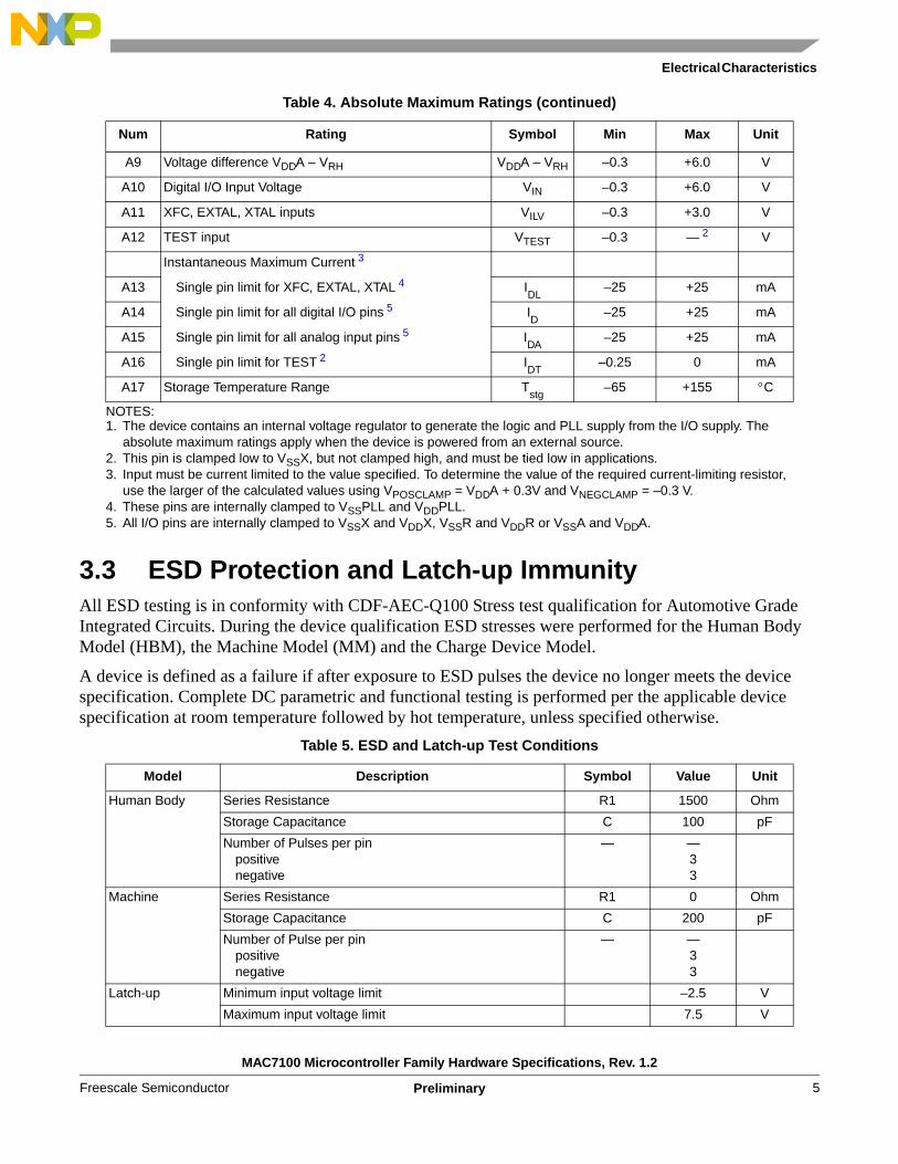
3.3 ESD Protection and Latch-up ImmunityAll ESD testing is in conformity with CDF-AEC-Q100 Stress test qualification for Automotive Grade Integrated Circuits. During the device qualification ESD stresses were performed for the Human Body Model (HBM), the Machine Model (MM) and the Charge Device Model.
A device is defined as a failure if after exposure to ESD pulses the device no longer meets the device specification. Complete DC parametric and functional testing is performed per the applicable device specification at room temperature followed by hot temperature, unless specified otherwise.
A9 Voltage difference VDDA – VRH VDDA – VRH –0.3 +6.0 V
A10 Digital I/O Input Voltage VIN –0.3 +6.0 V
A11 XFC, EXTAL, XTAL inputs VILV –0.3 +3.0 V
A12 TEST input VTEST –0.3 — 2 V
Instantaneous Maximum Current 3
A13 Single pin limit for XFC, EXTAL, XTAL 4 IDL
–25 +25 mA
A14 Single pin limit for all digital I/O pins 5 ID
–25 +25 mA
A15 Single pin limit for all analog input pins 5 IDA
–25 +25 mA
A16 Single pin limit for TEST 2 IDT
–0.25 0 mA
A17 Storage Temperature Range Tstg
–65 +155 °C
NOTES:1. The device contains an internal voltage regulator to generate the logic and PLL supply from the I/O supply. The
absolute maximum ratings apply when the device is powered from an external source.2. This pin is clamped low to VSSX, but not clamped high, and must be tied low in applications.3. Input must be current limited to the value specified. To determine the value of the required current-limiting resistor,
use the larger of the calculated values using VPOSCLAMP = VDDA + 0.3V and VNEGCLAMP = –0.3 V.4. These pins are internally clamped to VSSPLL and VDDPLL.5. All I/O pins are internally clamped to VSSX and VDDX, VSSR and VDDR or VSSA and VDDA.
Table 5. ESD and Latch-up Test Conditions
Model Description Symbol Value Unit
Human Body Series Resistance R1 1500 Ohm
Storage Capacitance C 100 pF
Number of Pulses per pinpositivenegative
— —33
Machine Series Resistance R1 0 Ohm
Storage Capacitance C 200 pF
Number of Pulse per pinpositivenegative
— —33
Latch-up Minimum input voltage limit –2.5 V
Maximum input voltage limit 7.5 V
Table 4. Absolute Maximum Ratings (continued)
Num Rating Symbol Min Max Unit
MAC7100 Microcontroller Family Hardware Specifications, Rev. 1.2
PreliminaryFreescale Semiconductor 5
Electrical Characteristics
3.4 Operating ConditionsUnless otherwise noted, the following conditions apply to all parametric data. Refer to the temperature rating of the device (C, V, M) with respect to ambient temperature (TA) and junction temperature (TJ). For power dissipation calculations refer to Section 3.6, “Power Dissipation and Thermal Characteristics.”
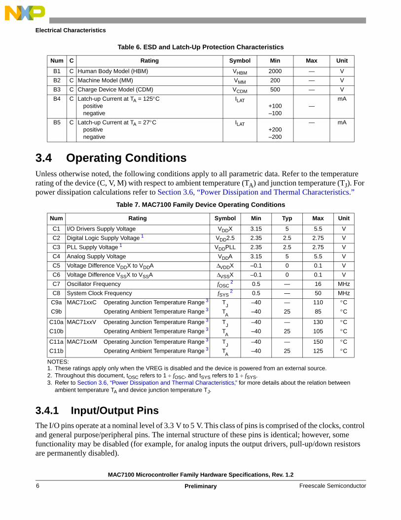
3.4.1 Input/Output PinsThe I/O pins operate at a nominal level of 3.3 V to 5 V. This class of pins is comprised of the clocks, control and general purpose/peripheral pins. The internal structure of these pins is identical; however, some functionality may be disabled (for example, for analog inputs the output drivers, pull-up/down resistors are permanently disabled).
Table 6. ESD and Latch-Up Protection Characteristics
Num C Rating Symbol Min Max Unit
B1 C Human Body Model (HBM) VHBM 2000 — V
B2 C Machine Model (MM) VMM 200 — V
B3 C Charge Device Model (CDM) VCDM 500 — V
B4 C Latch-up Current at TA = 125°Cpositivenegative
ILAT+100–100
—mA
B5 C Latch-up Current at TA = 27°Cpositivenegative
ILAT+200–200
— mA
Table 7. MAC7100 Family Device Operating Conditions
Num Rating Symbol Min Typ Max Unit
C1 I/O Drivers Supply Voltage VDDX 3.15 5 5.5 V
C2 Digital Logic Supply Voltage 1
NOTES:1. These ratings apply only when the VREG is disabled and the device is powered from an external source.
VDD2.5 2.35 2.5 2.75 V
C3 PLL Supply Voltage 1 VDDPLL 2.35 2.5 2.75 V
C4 Analog Supply Voltage VDDA 3.15 5 5.5 V
C5 Voltage Difference VDDX to VDDA ΔVDDX –0.1 0 0.1 V
C6 Voltage Difference VSSX to VSSA ΔVSSX –0.1 0 0.1 V
C7 Oscillator Frequency fOSC 2
2. Throughout this document, tOSC refers to 1 ÷ fOSC, and tSYS refers to 1 ÷ fSYS.
0.5 — 16 MHz
C8 System Clock Frequency fSYS 2 0.5 — 50 MHz
C9a MAC71xxC Operating Junction Temperature Range 3
3. Refer to Section 3.6, “Power Dissipation and Thermal Characteristics,” for more details about the relation between ambient temperature TA and device junction temperature TJ.
TJ
–40 — 110 °C
C9b Operating Ambient Temperature Range 3 TA
–40 25 85 °C
C10a MAC71xxV Operating Junction Temperature Range 3 TJ
–40 — 130 °C
C10b Operating Ambient Temperature Range 3 TA
–40 25 105 °C
C11a MAC71xxM Operating Junction Temperature Range 3 TJ
–40 — 150 °C
C11b Operating Ambient Temperature Range 3 TA
–40 25 125 °C
MAC7100 Microcontroller Family Hardware Specifications, Rev. 1.2
Preliminary Freescale Semiconductor6

Electrical Characteristics
3.4.2 Oscillator PinsThe pins XFC, EXTAL, XTAL are dedicated to the oscillator and operate at a nominal level of 2.5V.
3.5 Input/Output CharacteristicsThis section describes the characteristics of all I/O pins in both 3.3 V and 5 V operating conditions. All parameters are not always applicable; for example, not all pins feature pull up/down resistances.
Table 8. 5.0 V I/O Characteristics
Conditions shown in Table 7 unless otherwise noted
Num C Rating Symbol Min Typ Max Unit
D1a P Input High Voltage VIH
0.65 × VDD5 1
NOTES:1. Refer to Section 3.7, “Power Supply,” for definition of VSS5 and VDD5.
— — V
D1b T Input High Voltage VIH — — VDD5 + 0.3 1
V
D2a P Input Low Voltage VIL
— — 0.35 × VDD5 1
V
D2b T Input Low Voltage VIL VSS5 – 0.3 1
— — V
D3 C Input Hysteresis VHYS
— 250 — mV
D4 P Input Leakage Current (pins in high impedance input mode)V
in = VDD
5 or VSS
5 1Iin
–1 2
2. Maximum leakage current occurs at maximum operating temperature. Current decreases by approximately one-half for each 8°C to 12°C in the temperature range from 50°C to 125°C.
— 1 2 μA
D5 P Output High Voltage (pins in output mode)Partial Drive IOH = –2mAFull Drive IOH = –10mA
VOH
VDD5 – 0.8
— — V
D6 P Output Low Voltage (pins in output mode)Partial Drive IOL = +2mAFull Drive IOL = +10mA
VOL
— — 0.8 V
D7 P Internal Pull Up Device Current,tested at V
IL Max.
IPUL — — –130 μA
D8 P Internal Pull Up Device Current,tested at V
IH Min.
IPUH –10 — — μA
D9 P Internal Pull Down Device Current,tested at V
IH Min.
IPDH — — 130 μA
D10 P Internal Pull Down Device Current,tested at V
IL Max.
IPDL 10 — — μA
D11 D Input Capacitance Cin — 6 — pF
D12 T Injection current 3
Single Pin limitTotal Device Limit. Sum of all injected currents
3. Refer to Section 3.7.1, “Current Injection,” for more details
IICSIICP
–2.5–25
—2.525
mA
D13 P Port Interrupt Input Pulse filtered 4
4. Parameter only applies in STOP or Pseudo STOP mode.
tPULSE — — 3 μs
D14 P Port Interrupt Input Pulse passed 4 tPULSE 10 — — μs
MAC7100 Microcontroller Family Hardware Specifications, Rev. 1.2
PreliminaryFreescale Semiconductor 7

Electrical Characteristics
3.6 Power Dissipation and Thermal CharacteristicsPower dissipation and thermal characteristics are closely related. The user must assure that the maximum operating junction temperature is not exceeded.
Table 9. 3.3 V I/O Characteristics
Conditions shown in Table 7, with VDDX = 3.3 V –5%/+10% and a temperature maximum of +140°C unless otherwise noted.
Num C Rating Symbol Min Typ Max Unit
E1a P Input High Voltage VIH
0.65 × VDD5 1
NOTES:1. Refer to Section 3.7, “Power Supply,” for definition of VSS5 and VDD5.
— — V
E1b T Input High Voltage VIH — — VDD5 + 0.3 1
V
E2a P Input Low Voltage VIL
— — 0.35 × VDD5 1
V
E2b T Input Low Voltage VIL VSS5 – 0.3 1
— — V
E3 C Input Hysteresis VHYS
— 250 — mV
E4 P Input Leakage Current (pins in high impedance input mode)V
in = VDD
5 or VSS
5 1Iin
–1 2
2. Maximum leakage current occurs at maximum operating temperature. Current decreases by approximately one-half for each 8°C to 12°C in the temperature range from 50°C to 125°C.
— 1 2 μA
E5 P Output High Voltage (pins in output mode)Partial Drive IOH = –0.75mAFull Drive IOH = –4.5mA
VOH
VDD5 – 0.4
— — V
E6 P Output Low Voltage (pins in output mode)Partial Drive IOL = +0.9mAFull Drive IOL = +5.5mA
VOL
— — 0.4 V
E7 P Internal Pull Up Device Current,tested at V
IL Max.
IPUL — — –60 μA
E8 P Internal Pull Up Device Current,tested at V
IH Min.
IPUH –6 — — μA
E9 P Internal Pull Down Device Current,tested at V
IH Min.
IPDH — — 60 μA
E10 P Internal Pull Down Device Current,tested at V
IL Max.
IPDL 6 — — μA
E11 D Input Capacitance Cin — 6 — pF
E12 T Injection current 3
Single Pin limitTotal Device Limit. Sum of all injected currents
3. Refer to Section 3.7.1, “Current Injection,” for more details
IICSIICP
–2.5–25
—2.525
mA
E13 P Port Interrupt Input Pulse filtered 4
4. Parameter only applies in STOP or Pseudo STOP mode.
tPULSE — — 3 μs
E14 P Port Interrupt Input Pulse passed 4 tPULSE 10 — — μs
MAC7100 Microcontroller Family Hardware Specifications, Rev. 1.2
Preliminary Freescale Semiconductor8

Electrical Characteristics
Note that the JEDEC specification reserves the symbol RθJA or θJA (Theta-JA) strictly for junction-to- ambient thermal resistance on a 1s test board in natural convection environment. RθJMA or θJMA (Theta-JMA) will be used for both junction-to-ambient on a 2s2p test board in natural convection and for junction-to-ambient with forced convection on both 1s and 2s2p test boards. It is anticipated that the generic name, θJA, will continue to be commonly used.
The average chip-junction temperature (TJ) in °C is obtained from the formula:
Eqn. 1
where
The total power dissipation is calculated as:
Eqn. 2
where
Two cases must be considered for PINT:1. Internal voltage regulator enabled:
Eqn. 3
2. Internal voltage regulator disabled (VDDR = VSSR = system ground):
Eqn. 4
PIO is the sum of all output currents on input/output pins associated with VDDX:
Eqn. 5
where
Eqn. 6
or
Eqn. 7
Table 10. Thermal Resistance 1/8 Simulation Model Packaging Parameters
Component ConductivityMold Compound 0.9 W/m K
Leadframe (Copper) 263 W/m K
Die Attach 1.7 W/m K
TJ TA PD ΘJA⋅+=
TJ Junction Temperature (°C)=TA Ambient Temperature (°C)=PD Total Chip Power Dissipation (W)=ΘJA Package Thermal Resistance (°C/W)=
PD PINT PIO+=
PINT Chip Internal Power Dissipation (W)=PIO Input / Output Power Dissipation (W)=
PINT IDDR VDDR×( ) IDDA VDDA×( )+=
PINT IDD2.5 VDD2.5×( ) IDDPLL VDDPLL×( ) IDDA VDDA×( )+ +=
PIO RDSON
i
∑ IIOi( )2⋅=
RDSON
VOL
IOL--------- (for outputs driven low)=
RDSON
VDDX VOH–IOL
------------------------------- (for outputs driven high)=
MAC7100 Microcontroller Family Hardware Specifications, Rev. 1.2
PreliminaryFreescale Semiconductor 9

Electrical Characteristics
3.6.1 Thermal Resistance Simulation Details
Comments:1. Junction temperature is a function of die size, on-chip power dissipation, package thermal resistance, mounting site (board) temperature,
ambient temperature, air flow, power dissipation of other components on the board, and board thermal resistance.2. Per SEMI G38-87 and JEDEC JESD51-2 with the single layer board (JESD51-3) horizontal.3. Per JEDEC JESD51-6 with the board (JESD51-7) horizontal.4. Thermal resistance between the die and the printed circuit board per JEDEC JESD51-8. Board temperature is measured on the top surface
of the board at the center lead. For fused lead packages, the adjacent lead is used.5. Thermal resistance between the die and the case top surface as measured by the cold plate method (MIL SPEC-883 Method 1012.1).6. Thermal characterization parameter indicating the temperature difference between package top and junction temperature per JEDEC
JESD51-2. When Greek letters are not available, the thermal characterization parameter is written as Psi-JT.
Table 11. Thermal Resistance for Case Outline 983–02, 100 Lead 14x14 mm LQFP, 0.5 mm Pitch
Rating Environment Symbol Value Unit Comments
Junction to Ambient (Natural Convection) Single layer board (1s) RθJA 44 °C/W 1, 2Junction to Ambient (Natural Convection) Four layer board (2s2p) RθJMA 34 °C/W 1, 3Junction to Ambient (@ 200 ft./min.) Single layer board (1s) RθJMA 37 °C/W 1, 3Junction to Ambient (@ 200 ft./min.) Four layer board (2s2p) RθJMA 29 °C/W 1, 3Junction to Board RθJB 18 °C/W 4Junction to Case RθJC 7 °C/W 5Junction to Package Top Natural Convection ΨJT 2 °C/W 6
Table 12. Thermal Resistance for Case Outline 987–01, 112 Lead 20x20 mm LQFP, 0.65 mm Pitch
Rating Environment Symbol Value Unit Comments
Junction to Ambient (Natural Convection) Single layer board (1s) RθJA 42 °C/W 1, 2Junction to Ambient (Natural Convection) Four layer board (2s2p) RθJMA 34 °C/W 1, 3Junction to Ambient (@ 200 ft./min.) Single layer board (1s) RθJMA 35 °C/W 1, 3Junction to Ambient (@ 200 ft./min.) Four layer board (2s2p) RθJMA 30 °C/W 1, 3Junction to Board RθJB 22 °C/W 4Junction to Case RθJC 7 °C/W 5Junction to Package Top Natural Convection ΨJT 2 °C/W 6
Table 13. Thermal Resistance for Case Outline 918–03, 144 Lead 20x20 mm LQFP, 0.5 mm Pitch
Rating Environment Symbol Value Unit Comments
Junction to Ambient (Natural Convection) Single layer board (1s) RθJA 42 °C/W 1, 2Junction to Ambient (Natural Convection) Four layer board (2s2p) RθJMA 34 °C/W 1, 3Junction to Ambient (@ 200 ft./min.) Single layer board (1s) RθJMA 35 °C/W 1, 3Junction to Ambient (@ 200 ft./min.) Four layer board (2s2p) RθJMA 30 °C/W 1, 3Junction to Board RθJB 22 °C/W 4Junction to Case RθJC 7 °C/W 5Junction to Package Top Natural Convection ΨJT 2 °C/W 6
Table 14. Thermal Resistance for Case Outline 1159A-01, 208 Lead 17x17 mm MAP BGA, 1.0 mm Pitch
Rating Environment Symbol Value Unit Comments
Junction to Ambient (Natural Convection) Single layer board (1s) RθJA 46 °C/W 1, 2Junction to Ambient (Natural Convection) Four layer board (2s2p) RθJMA 29 °C/W 1, 3Junction to Ambient (@ 200 ft./min.) Single layer board (1s) RθJMA 38 °C/W 1, 3Junction to Ambient (@ 200 ft./min.) Four layer board (2s2p) RθJMA 26 °C/W 1, 3Junction to Board RθJB 19 °C/W 4Junction to Case RθJC 7 °C/W 5Junction to Package Top Natural Convection ΨJT 2 °C/W 6
MAC7100 Microcontroller Family Hardware Specifications, Rev. 1.2
Preliminary Freescale Semiconductor10

Electrical Characteristics
3.7 Power SupplyThe MAC71xx Family utilizes several pins to supply power to the oscillator, PLL, digital core, I/O ports and ATD. In the context of this section, VDD5 is used for VDDA, VDDR or VDDX; VSS5 is used for VSSA, VSSR or VSSX unless otherwise noted. IDD5 denotes the sum of the currents flowing into the VDDA, VDDX, and VDDR. VDD is used for VDD2.5, and VDDPLL, VSS is used for VSS2.5 and VSSPLL. IDD is used for the sum of the currents flowing into VDD2.5 and VDDPLL.
3.7.1 Current InjectionThe power supply must maintain regulation within the VDD5 or VDD2.5 operating range during instantaneous and operating maximum current conditions. If positive injection current (Vin > VDD5) is greater than IDD5, the injection current may flow out of VDD5 and could result in the external power supply going out of regulation. It is important to ensure that the external VDD5 load will shunt current greater than the maximum injection current. The greatest risk will be when the MCU is consuming very little power (for example, if no system clock is present, or if the clock rate is very low).
3.7.2 Power Supply PinsThe VDDR – VSSR pair supplies the internal voltage regulator. The VDDA – VSSA pair supplies the A/D converter and the reference circuit of the internal voltage regulator. The VDDX – VSSX pair supplies the I/O pins. VDDPLL – VSSPLL pair supplies the oscillator and PLL.
All VDDX pins are internally connected by metal. All VSSX pins are internally connected by metal. All VSS2.5 pins are internally connected by metal. VDDA, VDDX and VDDR as well as VSSA, VSSX and VSSR are connected by anti-parallel diodes for ESD protection.
3.7.3 Supply Current CharacteristicsTable 15 and Table 16 list supply current characteristics for MAC71x1 and MAC71x6 devices at 40 MHz and 50 MHz operation, respectively. Characteristics for MAC71x2 devices are to be determined (TBD).
All current measurements are without output loads. Unless otherwise noted the currents are measured in single chip mode, internal voltage regulator enabled at the specified system frequency, using a 4 MHz oscillator in low power mode. Production testing is performed using a square wave signal at the EXTAL input. In expanded modes, the currents are highly dependent on the load and duty cycle on the address, data and control signals, thus no general numbers can be given. A good estimate is to take the single chip currents and add the currents due to the external loads.
MAC7100 Microcontroller Family Hardware Specifications, Rev. 1.2
PreliminaryFreescale Semiconductor 11

Electrical Characteristics
Table 15. MAC71x1/6 1 Device Supply Current Characteristics – 40 MHz
NOTES:1. MAC71x2 characteristics are to be determined (TBD).
Conditions shown in Table 7, with fSYS = 40 MHz.
Num C Rating Symbol Typ Max Unit
F1 P Run Supply Current, Single Chip IDDRreg 100 130 mA
F2 C Doze Supply Current IDDDreg Run ≥ Doze ≥ Pseudo Stop
F3 P Pseudo Stop Supply Current(OSC on)
–40° C 2
2. 85°C, 105°C, and 125°C refer to the "C", "V", and "M" Temperature Options, respectively.
IDDPSreg 400 / 500 3
3. RTI disabled / enabled.
600 / 700 3 μA
P 25° C 2 400 / 500 3 600 / 700 3 μA
C 85° C 2 800 / 1000 3 2000 / 2500 3 μA
C 105° C 2 1200 / 1500 3 3500 / 4000 3 μA
P 125° C 2 1500 / 2000 3 5500 / 6000 3 μA
F4 P Stop Supply Current(TJ = TA assumed)
–40° C 2 IDDSreg 30 150 μA
P 25° C 2 30 150 μA
C 85° C 2 330 2500 μA
C 105° C 2 470 3500 μA
P 125° C 2 660 5000 μA
Table 16. MAC71x1/6 1 Device Supply Current Characteristics – 50 MHz
NOTES:1. MAC71x2 characteristics are to be determined (TBD).
Conditions shown in Table 7, with fSYS = 50 MHz.
Num C Rating Symbol Typ Max Unit
G1 P Run Supply Current, Single Chip IDDRreg 120 150 mA
G2 C Doze Supply Current IDDDreg Run ≥ Doze ≥ Pseudo Stop
G3 P Pseudo Stop Supply Current(OSC on)
–40° C 2
2. 85°C, 105°C, and 125°C refer to the "C", "V", and "M" Temperature Options, respectively.
IDDPSreg 400 / 500 3
3. RTI disabled / enabled.
600 / 700 3 μA
P 25° C 2 400 / 500 3 600 / 700 3 μA
C 85° C 2 800 / 1000 3 2000 / 2500 3 μA
C 105° C 2 1200 / 1500 3 3500 / 4000 3 μA
P 125° C 2 1500 / 2000 3 5500 / 6000 3 μA
G4 P Stop Supply Current(TJ = TA assumed)
–40° C 2 IDDSreg 30 150 μA
P 25° C 2 30 150 μA
C 85° C 2 330 2500 μA
C 105° C 2 470 3500 μA
P 125° C 2 660 5000 μA
MAC7100 Microcontroller Family Hardware Specifications, Rev. 1.2
Preliminary Freescale Semiconductor12

Electrical Characteristics
3.7.4 Voltage Regulator CharacteristicsTable 17. VREG Operating Conditions
Num C Characteristic Symbol Min Typical Max Unit
H1 P Input Voltages VVDDRA 3.15 — 5.5 V
H2 P Output Voltage, Digital LogicFull Performance ModeReduced Power ModeShutdown Mode
VDD2.52.451.60— 1
NOTES:1. High impedance output.
2.52.5— 1
2.752.75— 1
VVV
H3 P Output Voltage, PLLFull Performance ModeReduced Power Mode 2
Reduced Power Mode 3
Shutdown Mode
2. Current IDDPLL = 1 mA (Low Power Oscillator).3. Current IDDPLL = 3 mA (Standard Oscillator).
VDDPLL2.352.001.60— 1
2.52.52.5— 1
2.752.752.75— 1
VVVV
H4 P Low Voltage Interrupt 4
Assert LevelNegate Level
4. Monitors VDDA, active only in full performance mode. This interrupt indicates that I/O and ATD performance may be degraded due to low supply voltage.
VLVIAVLVID
4.104.25
4.374.52
4.664.77
VV
H5 P Low Voltage Reset 5
Assert Level
5. Monitors VDD2.5, active only in full performance mode. Only POR is active in reduced performance mode.
VLVRA 2.25 2.35 — V
H6 P Power On Reset 6
Assert LevelNegate Level
6. Monitors VDD2.5, active in all modes.
VPORAVPORD
0.97—
——
—2.05
VV
MAC7100 Microcontroller Family Hardware Specifications, Rev. 1.2
PreliminaryFreescale Semiconductor 13

Electrical Characteristics
3.7.5 Chip Power Up and Voltage DropsThe VREG sub-modules LVI (low voltage interrupt), POR (power on reset) and LVR (low voltage reset) handle chip power-up or drops of the supply voltage. Refer to Figure 2.
Figure 2. VREG Chip Power-up and Voltage Monitoring
3.7.6 Output LoadsThe on-chip voltage regulator is intended to supply the internal logic and oscillator circuits. No external DC load is allowed. Capacitive loads are specified in Table 18. Capacitors with X7R dielectricum are required.
Table 18. VREG Recommended Load Capacitances
Rating Symbol Min Typ Max Unit
Load Capacitance per VDD2.5 pin 1
NOTES:1. Refer to Table 38 for the specific number of VDD2.5 pins on various packages. Each VDD2.5 pin should have the
recommended loading as described in Section 3.7.3, “Circuit Board Layout,” of the MAC7100 Microcontroller Family Reference Manual (MAC7100RM).
CLVDD 200 220 12000 nF
Load Capacitance on VDDPLL pin CLVDDfcPLL 90 220 5000 nF
LVI Disableddue to LVR
VLVID
VLVRD
LVR
POR
LVI
VPORD
VLVRA
VLVIA
TimeLVI Enabled
VDDA
VDD2.5
Voltage
Note: Not to scale.
MAC7100 Microcontroller Family Hardware Specifications, Rev. 1.2
Preliminary Freescale Semiconductor14

Electrical Characteristics
3.8 Clock and Reset GeneratorThis section describes the electrical characteristics for the oscillator, phase-locked loop, clock monitor and reset generator.
3.8.1 Oscillator CharacteristicsThe MAC7100 Family features an internal low power loop controlled Pierce oscillator and a full swing Pierce oscillator/external clock mode. The selection of loop controlled Pierce oscillator or full swing Pierce oscillator/external clock depends on the level of the XCLKS signal at the rising edge of the RESET signal. Before asserting the oscillator to the internal system clock distribution subsystem, the quality of the oscillation is checked for each start from either power on, STOP or oscillator fail. tCQOUT specifies the maximum time before switching to the internal self clock mode after POR or STOP if a proper oscillation is not detected. The quality check also determines the minimum oscillator start-up time tUPOSC. The device also features a clock monitor. A Clock Monitor Failure is asserted if the frequency of the incoming clock signal is below the Clock Monitor Assert Frequency fCMFA.
Table 19. Oscillator Characteristics
Num C Rating Symbol Min Typ Max Unit
J1a C Crystal oscillator range (loop controlled Pierce) fOSC 1
NOTES:1. If CLKSEL[PLLSEL] is clear then the system clock (fSYS) is equal to fOSC, otherwise it is equal to fVCO (table
Table 20, K3). Throughout this document, tSYS is used to specify a unit of time equal to 1 ÷ fSYS.
4.0 — 16 MHz
J1b C Crystal oscillator range (full swing Pierce) 2 3
2. Depending on the crystal; a damping series resistor might be necessary3. XCLKS asserted (low) during reset
fOSC 1 0.5 — 40 MHz
J2 P Startup Current IOSC 100 — — μA
J3 C Oscillator start-up time (loop controlled Pierce) tUPOSC — 3 4
4. fOSC = 4 MHz, C = 22 pF (refer to the MAC7100 Microcontroller Family Reference Manual (MAC7100RM) for circuit board layout recommendations, including oscillator capacitor placement and values).
50 5
5. Maximum value is for extreme cases using high Q, low frequency crystals
ms
J4 D Clock Quality check time-out tCQOUT 0.45 — 2.5 s
J5 P Clock Monitor Failure Assert Frequency fCMFA 50 100 200 KHz
J6 P External square wave input frequency 3 fEXT 0.5 — 50 MHz
J7 D External square wave pulse width low tEXTL 9.5 — — ns
J8 D External square wave pulse width high tEXTH 9.5 — — ns
J9 D External square wave rise time tEXTR — — 1 ns
J10 D External square wave fall time tEXTF — — 1 ns
J11 D Input Capacitance (EXTAL, XTAL pins) CIN — 7 — pF
MAC7100 Microcontroller Family Hardware Specifications, Rev. 1.2
PreliminaryFreescale Semiconductor 15

Electrical Characteristics
3.8.2 PLL Filter CharacteristicsThe oscillator provides the reference clock for the PLL as shown in Figure 3. The voltage controlled oscillator (VCO) of the PLL is also the system clock source in self clock mode. In order to operate reliably, care must be taken to select proper values for external loop filter components.
Figure 3. Basic PLL Functional Diagram
The procedure described below can be used to calculate the resistance and capacitance values using typical values for K1, f1 and ich from Table 20. First, the VCO Gain at the desired VCO output frequency is approximated by:
Eqn. 8
The phase detector relationship is given by:Eqn. 9
ich is the current in tracking mode. The loop bandwidth fC should be chosen to fulfill the Gardner’s stability criteria by at least a factor of 10, a typical value for the stability factor is 50. ζ = 0.9 ensures a good transient response.
Eqn. 10
And finally the frequency relationship is defined as:
Eqn. 11
With the above inputs the resistance can be calculated as:
Eqn. 12
The capacitance CS can now be calculated as:
Eqn. 13
PhaseDetector
1
REFDV+1Kφ
fREF
VDDPLL
R
CPCS
KV
Loop Divider
1
SYNR+1
fVCOfOSC
1
2
fCMP
VCO
Δ
KV K1 e
f1 fVCO–( )K1 1V⋅
--------------------------
⋅=
KΦ ich– KV⋅=
fC2 ζ fREF⋅ ⋅
π ζ 1 ζ2++( )⋅---------------------------------------- 1
10------ fC
fREF
4 10⋅-------------- ζ 0.9=( );<→<
nfVCO
fREF---------- 2 SYNR 1+( )⋅= =
R2 π n fC⋅ ⋅ ⋅
KΦ----------------------------=
CS2 ζ2⋅
π fC R⋅ ⋅--------------------- 0.516
fC R⋅------------- ζ 0.9=( );≈=
MAC7100 Microcontroller Family Hardware Specifications, Rev. 1.2
Preliminary Freescale Semiconductor16
Electrical Characteristics
The capacitance CP should be chosen in the range of:Eqn. 14
The stabilization delays shown in Table 20 are dependant on PLL operational settings and external component selection (for example, the crystal and XFC filter).
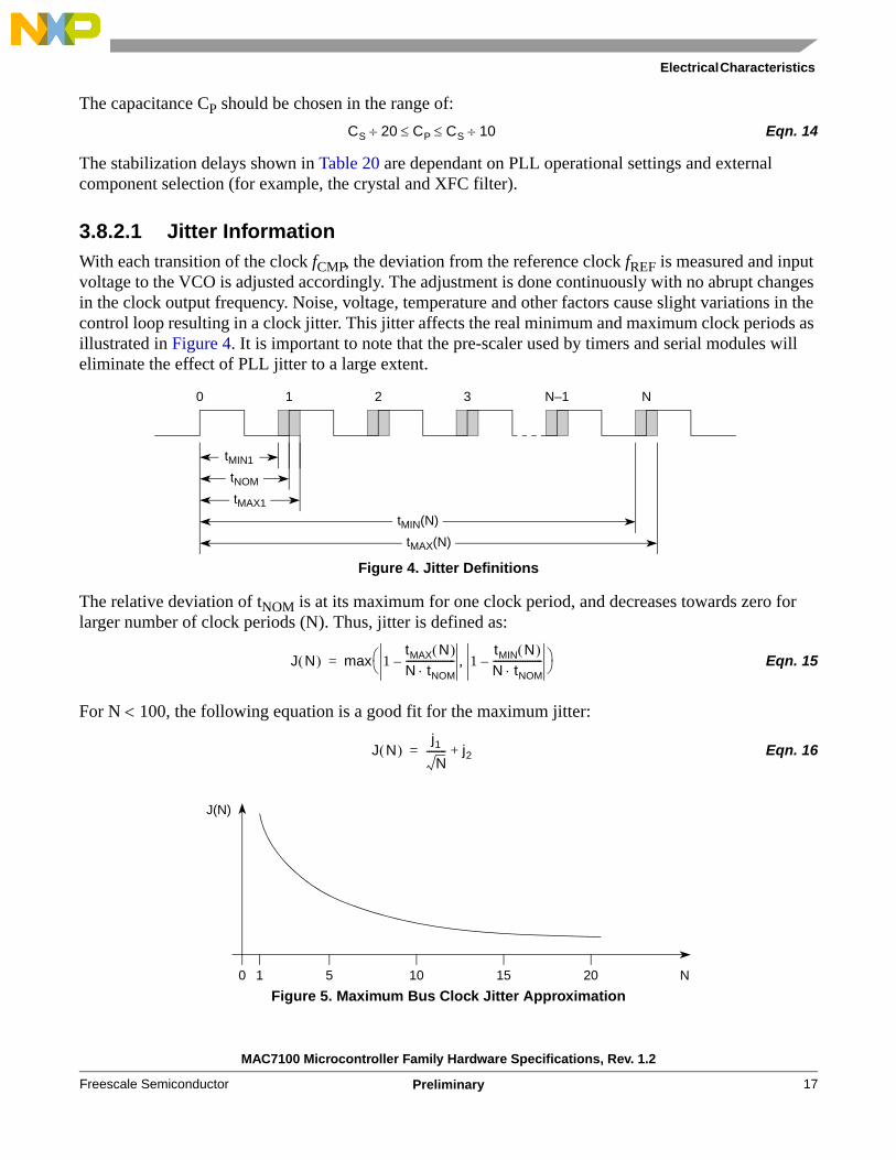
3.8.2.1 Jitter InformationWith each transition of the clock fCMP, the deviation from the reference clock fREF is measured and input voltage to the VCO is adjusted accordingly. The adjustment is done continuously with no abrupt changes in the clock output frequency. Noise, voltage, temperature and other factors cause slight variations in the control loop resulting in a clock jitter. This jitter affects the real minimum and maximum clock periods as illustrated in Figure 4. It is important to note that the pre-scaler used by timers and serial modules will eliminate the effect of PLL jitter to a large extent.
Figure 4. Jitter Definitions
The relative deviation of tNOM is at its maximum for one clock period, and decreases towards zero for larger number of clock periods (N). Thus, jitter is defined as:
Eqn. 15
For N < 100, the following equation is a good fit for the maximum jitter:
Eqn. 16
Figure 5. Maximum Bus Clock Jitter Approximation
CS 20÷ CP CS 10÷≤ ≤
0
tMIN1
1 2 3 N–1 N
tNOM
tMAX1
tMIN(N)
tMAX(N)
J N( ) max 1tMAX N( )N tNOM⋅--------------------– 1
tMIN N( )N tNOM⋅--------------------–,⎝ ⎠
⎛ ⎞=
J N( )j1N
-------- j2+=
0 1 5 10 2015 N
J(N)
MAC7100 Microcontroller Family Hardware Specifications, Rev. 1.2
PreliminaryFreescale Semiconductor 17

Electrical Characteristics
3.8.3 PLL Characteristics
3.8.4 Crystal Monitor Time-outThe time-out Table 21 shows the delay for the crystal monitor to trigger when the clock stops, either at the high or at the low level. The corresponding clock period with an ideal 50% duty cycle is twice this time-out value.
3.8.5 Clock Quality CheckerThe timing for the clock quality check is derived from the oscillator and the VCO frequency range in Table 20. These numbers define the upper time limit for the individual check windows to complete.
Table 20. PLL Characteristics
Num C Rating Symbol Min Typ Max Unit
K1 PLL reference frequency, crystal oscillator range fREF 0.5 — 16 MHz
K2 P Self Clock Mode frequency fSCM 2 — 5.5 MHz
K3 D VCO locking range fVCO 1
NOTES:1. If CLKSEL[PLLSEL] is set then the system clock (fSYS) is equal to fVCO, otherwise it is equal to fOSC (table Table 19,
J1a or J1b). Throughout this document, tSYS is used to specify a unit of time equal to 1 ÷ fSYS.
8 — 50 MHz
K4 D Lock Detector transition from Acquisition to Tracking mode |Δtrk| 3 — 4 % 2
2. Percentage deviation from target frequency
K5 D Lock Detection |ΔLock| 0 — 1.5 % 2
K6 D Un-Lock Detection |Δunl| 0.5 — 2.5 % 2
K7 D Lock Detector transition from Tracking to Acquisition mode |Δunt| 6 — 8 % 2
K8 C PLLON Total Stabilization delay (Auto Mode) 3
3. PLL stabilization delay is highly dependent on operational requirement and external component values (for example, crystal and XFC filter component values). Notes 4 and 5 show component values for a typical configurations. Appropriate XFC filter values should be chosen based on operational requirement of system.
tstab — 0.5 4
4. fOSC = 4 MHz, fVCO = 40 MHz (REFDV = 0x00, SYNR = 0x04), CS = 2.2 nF, CP = 220 pF, RS = 5.6 KΩ.
3 5
5. fOSC = 4 MHz, fVCO = 16 MHz (REFDV = 0x00, SYNR = 0x01), CS = 4.7 nF, CP = 470 pF, RS = 2.7 KΩ.
ms
K9 D PLLON Acquisition mode stabilization delay 3 tacq — 0.3 4 1 5 ms
K10 D PLLON Tracking mode stabilization delay 3 tal — 0.2 4 2 5 ms
K11 D Charge pump current acquisition mode | ich | — 38.5 — μA
K12 D Charge pump current tracking mode | ich | — 3.5 — μA
K13 D Jitter fit VCO loop gain parameter K1 — –195 — MHz/V
K14 D Jitter fit VCO loop frequency parameter f1 — 126 — MHz
K15 C Jitter fit parameter 1 j1 — — 1.3 % 4
K16 C Jitter fit parameter 2 j2 — — 0.12 % 4
Table 21. Crystal Monitor Time-Outs
Min Typ Max Unit6 10 18.5 μs
Table 22. CRG Maximum Clock Quality Check Timings
Clock Check Windows Value UnitCheck Window 9.1 to 20.0 ms
Timeout Window 0.46 to 1.0 s
MAC7100 Microcontroller Family Hardware Specifications, Rev. 1.2
Preliminary Freescale Semiconductor18

Electrical Characteristics
3.8.6 StartupTable 23 summarizes several startup characteristics. Refer to Section 4.3.6.10, “CRG Operating Mode Details,” in the MAC7100 Microcontroller Family Reference Manual (MAC7100RM) for details.
3.8.6.1 Power On and Low Voltage Reset (POR and LVR)The VPORR and VPORA levels are derived from VDD2.5. The VLVRA level is derived from VDD2.5. They are also valid if the device is powered externally. After releasing a POR or LVR reset, the oscillator and clock quality checks start. After tCQOUT (Table 19, J4) if no valid oscillation is detected, the MCU will start using the internal self-generated clock. The minimum startup time is given by tuposc (Table 19, J3).
3.8.6.2 SRAM Data RetentionSRAM content integrity is guaranteed if the CRGFLG[PORF] bit is not set following a reset operation.
3.8.6.3 External ResetWhen external reset is asserted for a time greater than PWRSTL, the CRG generates an internal reset and the CPU fetches the reset vector without a clock quality check, if there was stable oscillation before reset.
3.8.6.4 Stop RecoveryThe MCU can return from stop to run mode in response to an external interrupt or an API. Two delays occur before the MCU resumes execution. First, the voltage regulator must exit reduced power mode and return to full performance mode (this assumes that the internal regulator is used rather than driving VDD2.5 and VDDPLL with an external regulator). Second, a clock quality check is performed in the same manner as for a power-on reset before releasing the clocks to the system.
3.8.6.5 Pseudo Stop RecoveryRecovery from pseudo stop mode is similar to stop mode in that the VREG must return to FPM, but since the oscillator is not stopped there is no delay for clock stabilization. The MCU is returned to run mode by internal or external interrupts.
3.8.6.6 Doze RecoveryRecovery from doze mode avoids both the VREG and oscillator recovery periods. The MCU is returned to run mode by internal or external interrupts.
Table 23. CRG Startup Characteristics
Num C Rating Symbol Min Typ Max Unit
L1 D Reset input pulse width PWRSTL 2 — — tOSC
L2 D Startup from Reset nRST 192 — 196 tOSC
L3 D XIRQ, IRQ pulse width, edge-sensitive mode PWIRQ 20 — — ns
MAC7100 Microcontroller Family Hardware Specifications, Rev. 1.2
PreliminaryFreescale Semiconductor 19

Electrical Characteristics
3.9 External Bus TimingTable 24 lists processor bus input timings, which are shown in Figure 6, Figure 7 and Figure 8.
NOTEAll processor bus timings are synchronous; that is, input setup/hold and output delay with respect to the rising edge of a reference clock. The reference clock is the CLKOUT output. All other timing relationships can be derived from these values.
Figure 6. General Input Timing Requirements
Table 24. External Bus Input Timing Specifications 1
NOTES:1. Assumes CLKOUT is configured for full drive strength (via the PIM CONFIG2_D[RDS] bit).
Num C Rating Symbol Min Max Unit
M1 P CLKOUT period 2
2. CLKOUT is equal to the system clock, fSYS. If CLKSEL[PLLSEL] is set then fSYS is equal to fVCO (table Table 20, K3); if it is clear then fSYS is equal to fOSC (table Table 19, J1a or J1b). Throughout this document, tCYC is used to specify a unit of time equal to 1 ÷ CLKOUT (which is equal to tfsys).
tCYC 20 — ns
Control Inputs
M2a P Control input valid to CLKOUT high 3
3. The TA pin is the only control input on MAC7100 family devices.
tCVCH 13 — ns
M3a P CLKOUT high to control inputs invalid 3 tCHCII 0 — ns
Data Inputs
M4 P Data input (DATA[15:0]) valid to CLKOUT high tDIVCH 9 — ns
M5 P CLKOUT high to data input (DATA[15:0]) invalid tCHDII 0 — ns
CLKOUT (50 MHz)
1.5 V 1.5 VValid InvalidInvalid
tSETUPtHOLD
Input Setup & Hold
Input Rise TimeVH = VIHVL = VIL
tRISE = 1.5 ns
Input Fall TimeVH = VIHVL = VIL
tFALL = 1.5 ns
CLKOUT
Inputs
1.5 V
M4 M5
MAC7100 Microcontroller Family Hardware Specifications, Rev. 1.2
Preliminary Freescale Semiconductor20

Electrical Characteristics
3.9.1 Read and Write Bus CyclesTable 25 lists processor bus output timings. Read/write bus timings listed in Table 25 are shown in Figure 7 and Figure 8.
Table 25. External Bus Output Timing Specifications 1
NOTES:1. Assumes CLKOUT, CSn, BSn, OE, AS, ADDR[21:0] and DATA[15:0] are configured for full drive strength (via the PIM).
Num C Rating Symbol Min Max Unit
Control Outputs
M6a P CLKOUT high 2 to chip selects (CS[2:0]) valid
2. The CSn, BSn, OE and AS signals are synchronous to the falling edge of CLKOUT. Therefore, changes on these signals are triggered by the falling edge of CLKOUT, even though they are specified in relation to the rising edge.
tCHCV — 0.5tCYC + 10 ns
M6b P CLKOUT high 2 to byte selects (BS[1:0]) valid tCHBV — 0.5tCYC + 10 ns
M6c P CLKOUT high 2 to output select (OE) valid tCHOV — 0.5tCYC + 10 ns
M6d P CLKOUT high 2 to address strobe (AS) valid tCHASV — 0.5tCYC + 10 ns
M7a P CLKOUT high 2 to control output (BS[1:0], OE) invalid tCHCOI 0.5tCYC + 2 — ns
M7b P CLKOUT high 2 to chip selects (CS[2:0]) invalid tCHCI 0.5tCYC + 2 — ns
M7c P CLKOUT high 2 to address strobe (AS) invalid tCHASI 0.5tCYC + 2 — ns
Address and Attribute Outputs
M8 P CLKOUT high to address (ADDR[21:0]) and control (R/W) valid
tCHAV — 10 ns
M9 P CLKOUT high to address (ADDR[21:0]) and control (R/W) invalid
tCHAI 2 — ns
Data Outputs
M10 P CLKOUT high to data output (DATA[15:0]) valid tCHDOV — 13 ns
M11 P CLKOUT high to data output (DATA[15:0]) invalid tCHDOI 2 — ns
M12 D CLKOUT high to data output (DATA[15:0]) high impedance tCHDOZ — 9 ns
MAC7100 Microcontroller Family Hardware Specifications, Rev. 1.2
PreliminaryFreescale Semiconductor 21

Electrical Characteristics
Figure 7. Read/Write Bus Cycles, Internal Termination
AS(1)
CLKOUT
CSn
ADDR[21:0]
OE
R/W
BS[1:0]
S0 S2S1 S3 S4 S5 S0 S1 S2 S3 S4 S5
DATA[15:0]
M6aM7b
M6aM7b
M8 M8
M8
M9
M6cM7a
M1
M9
M6b M6bM7a M7a
M4
M5
M10M11
M12
M6dM7c M7c
M6d
1. The TA / AS signals are multiplexed on a single pin, so only one function may be used during bus transactions.
TA(1)
MAC7100 Microcontroller Family Hardware Specifications, Rev. 1.2
Preliminary Freescale Semiconductor22

Electrical Characteristics
Figure 8. Read Bus Cycle, External Termination
TA(1)
CLKOUT
CSn
ADDR[21:0]
OE
R/W
BS[1:0]
S0 S2S1 S3 S4 S5 S0
DATA[15:0]
S1
M6aM7b
M7a
M7a
M8M9
M6c
M6b
M4M5
M2aM3a
1. The TA / AS signals are multiplexed on a single pin, so AS is not available when external cycle termination is used.
MAC7100 Microcontroller Family Hardware Specifications, Rev. 1.2
PreliminaryFreescale Semiconductor 23

Electrical Characteristics
3.10 Analog-to-Digital ConverterTable 26 and Table 27 show conditions under which the ATD operates. The following constraints exist to obtain full-scale, full range results: VSSA ≤ VRL ≤ VIN ≤ VRH ≤ VDDA. This constraint exists because the sample buffer amplifier cannot drive beyond the ATD power supply levels. If the input level goes outside of this range it will effectively be clipped.
Table 26. ATD Operating Characteristics in 5.0 V Range
Conditions shown in Table 7 unless otherwise noted
Num C Rating Symbol Min Typ Max Unit
N1 D Reference Potential LowHigh
VRLVRH
VSSAVDDA ÷ 2
——
VDDA ÷ 2VDDA
VV
N2 C Differential Reference Voltage 1
NOTES:1. Full accuracy is not guaranteed when differential voltage is less than 4.50 V
VRH – VRL 4.50 5.00 5.50 V
N3 D ATD Clock Frequency fATDCLK 0.5 — 2.0 MHz
N4 D ATD 10-bit Conversion PeriodfATDCLK Cycles 2
@ 2.0MHz fATDCLK
2. Minimum time assumes a sample period of 2 ATD clocks; maximum time assumes a sample period of 16 ATD clocks.
NCONV10TCONV10
147
——
2814
Cyclesμs
N5 D ATD 8-bit Conversion PeriodfATDCLK Cycles 2
@ 2.0MHz fATDCLK
NCONV8TCONV8
126
——
2613
Cyclesμs
N6 D Stop Recovery Time (VDDA = 5.0 V) TREC — — 20 μs
N7 P Reference Supply current 1 ATD module on IREF — 0.200 0.255 mA
N8 P Reference Supply current 2 ATD modules on IREF — 0.400 0.510 mA
Table 27. ATD Operating Characteristics in 3.3 V Range
Conditions shown in Table 7, with VDDX = 3.3 V –5/+10% and a temperature maximum of +140°C unless otherwise noted.
Num C Rating Symbol Min Typ Max Unit
P1 D Reference Potential LowHigh
VRLVRH
VSSAVDDA ÷ 2
——
VDDA ÷ 2VDDA
VV
P2 C Differential Reference Voltage 1
NOTES:1. Full accuracy is not guaranteed when differential voltage is less than 3.15 V
VRH – VRL 3.15 3.3 3.6 V
P3 D ATD Clock Frequency fATDCLK 0.5 — 2.0 MHz
P4 D ATD 10-bit Conversion PeriodfATDCLK Cycles 2
@ 2.0MHz fATDCLK
2. Minimum time assumes a sample period of 2 ATD clocks; maximum time assumes a sample period of 16 ATD clocks.
NCONV10TCONV10
147
——
2814
Cyclesμs
P5 D ATD 8-bit Conversion PeriodfATDCLK Cycles 2
@ 2.0MHz fATDCLK
NCONV8TCONV8
126
——
2613
Cyclesμs
P6 D Stop Recovery Time (VDDA = 3.3 V) TREC — — 20 μs
P7 P Reference Supply current 1 ATD module on IREF — 0.130 0.170 mA
P8 P Reference Supply current 2 ATD modules on IREF — 0.260 0.340 mA
MAC7100 Microcontroller Family Hardware Specifications, Rev. 1.2
Preliminary Freescale Semiconductor24

Electrical Characteristics
3.10.1 Factors Influencing AccuracyThree factors—source resistance, source capacitance and current injection—have an influence on the accuracy of the ATD.
3.10.1.1 Source ResistanceDue to the input pin leakage current as specified in Table 8 in conjunction with the source resistance there will be a voltage drop from the signal source to the ATD input. The maximum specified source resistance RS, results in an error of less than 1/2 LSB (2.5 mV) at the maximum leakage current. If the device or operating conditions are less than the worst case, or leakage-induced errors are acceptable, larger values of source resistance are allowed.
3.10.1.2 Source CapacitanceWhen sampling, an additional internal capacitor is switched to the input. This can cause a voltage drop due to charge sharing with the external capacitance and the pin capacitance. For a maximum sampling error of the input voltage ≤ 1 LSB, then the external filter capacitor must be calculated as, Cf ≥ 1024 × (CINS – CINN).
3.10.1.3 Current InjectionThere are two cases to consider:
1. A current is injected into the channel being converted. The channel being stressed has conversion values of 0x3FF (0xFF in 8-bit mode) for analog inputs greater than VRH and 0x000 for values less than VRL unless the current is higher than specified as disruptive condition.
2. Current is injected into pins in the neighborhood of the channel being converted. A portion of this current is picked up by the channel (coupling ratio K), This additional current impacts the accuracy of the conversion depending on the source resistance. The additional input voltage error on the converted channel can be calculated as VERR = K × RS × IINJ, with IINJ being the sum of the currents injected into the two pins adjacent to the converted channel.
Table 28. ATD Electrical Characteristics
Conditions are shown in Table 7 unless otherwise noted
Num C Rating Symbol Min Typ Max Unit
Q1 C Max input Source Resistance RS — — 1 kΩ
Q2 C Total Input CapacitanceNon SamplingSampling
CINNCINS
——
1022
——
pFpF
Q3 C Disruptive Analog Input Current INA –2.5 — 2.5 mA
Q4 C Coupling Ratio positive current injection Kp — — TBD A / A
Q5 C Coupling Ratio negative current injection Kn — — TBD A / A
MAC7100 Microcontroller Family Hardware Specifications, Rev. 1.2
PreliminaryFreescale Semiconductor 25

Electrical Characteristics
3.10.2 ATD AccuracyTable 29 and Table 30 specify the ATD conversion performance excluding any errors due to current injection, input capacitance and source resistance.
For the following definitions, see Figure 9.
Differential Non-Linearity (DNL) is defined as the difference between two adjacent switching steps:
Eqn. 17
The Integral Non-Linearity (INL) is defined as the sum of all DNLs:
Eqn. 18
Table 29. ATD Conversion Performance in 5.0 V Range
Conditions shown in Table 7 except as noted here:fATDCLK = 2.0 MHz, 4.5 V ≤ VDDA ≤ 5.5 V
Num C Rating Symbol Min Typ Max Unit
R1 P 10-bit Resolution LSB — 5 1
NOTES:1. Assumes VREF = VRH – VRL = 5.12 V, other VREF conditions result in different LSB resolutions.
— mV
R2 P 10-bit Differential Nonlinearity DNL –1 — 1 Counts
R3 P 10-bit Integral Nonlinearity INL –2.5 ±1.5 2.5 Counts
R4 P 10-bit Absolute Error 2
2. These values include the quantization error which is inherently ½ count for any A/D converter.
AE –3 ±2.0 3 Counts
R5 P 8-bit Resolution LSB — 20 1 — mV
R6 P 8-bit Differential Nonlinearity DNL –0.5 — 0.5 Counts
R7 P 8-bit Integral Nonlinearity INL –1.0 ±0.5 1.0 Counts
R8 P 8-bit Absolute Error 2 AE –1.5 ±1.0 1.5 Counts
Table 30. ATD Conversion Performance in 3.3 V Range
Conditions shown in Table 7 except as noted here:fATDCLK = 2.0 MHz, 3.15 V ≤ VDDA ≤ 3.6 V
Num C Rating Symbol Min Typ Max Unit
S1 P 10-bit Resolution LSB — 3.25 1
NOTES:1. Assumes VREF = VRH – VRL = 3.33 V, other VREF conditions result in different LSB resolutions.
— mV
S2 P 10-bit Differential Nonlinearity DNL –1.5 — 1.5 Counts
S3 P 10-bit Integral Nonlinearity INL –3.5 ±1.5 3.5 Counts
S4 P 10-bit Absolute Error 2
2. These values include the quantization error which is inherently ½ count for any A/D converter.
AE –5 ±2.0 5 Counts
S5 P 8-bit Resolution LSB — 13 1 — mV
S6 P 8-bit Differential Nonlinearity DNL –0.5 — 0.5 Counts
S7 P 8-bit Integral Nonlinearity INL –1.5 ±1.0 1.5 Counts
S8 P 8-bit Absolute Error 2 AE –1.5 ±1.0 1.5 Counts
DNL i( )Vi Vi 1––1 LSB
---------------------- 1–=
INL n( ) DNL i( )
i 1=
n
∑Vn V0–1 LSB------------------- n–= =
MAC7100 Microcontroller Family Hardware Specifications, Rev. 1.2
Preliminary Freescale Semiconductor26

Electrical Characteristics
Figure 9. ATD Accuracy Definitions
NOTEFigure 9 shows only definitions, for specification values refer to Table 29.
0x3FF
0x3FE
0x3FD
0x3FC
0x3FB
0x3FA
0x3F9
0x3F8
0x3F7
0x3F6
0x3F5
0x3F4
0x3F3
9
8
7
6
5
4
3
2
1
00 10 20 30 40 50 5055 5065 5075 5085 5095 5105 5115
5060 5070 5080 5090 5100 5110 51205 15 25 35
1
2
0xFD
0xFE
0xFF
10-bit Absolute Error Boundary
Ideal Transfer Curve
8-bit Transfer Curve
10-bit Transfer Curve
8-bit Absolute Error Boundary
10-b
it R
eso
luti
on
8-b
it R
eso
luti
on
LSB
DNL
VI–1 VI
VIN
mV
MAC7100 Microcontroller Family Hardware Specifications, Rev. 1.2
PreliminaryFreescale Semiconductor 27

Electrical Characteristics
3.10.3 ATD Timing Specifications
Figure 10. ATD External Trigger Timing Diagram
Table 31. ATD External Trigger Timing Specifications
Num C Parameter Symbol Min Max Unit
T1 D ETRIG Period (Level-Sensitive Trigger Mode) TPERIOD 1 + NCONVn 1
NOTES:1. NCONVn denotes 8- or 10-bit conversion time (refer to specifications N4, N5, P4 and P5). In order to achieve the
minimum period between conversions when using level-sensitive triggering, ETRIG must remain asserted this long.
— fATDCLK Cycles
T2 D ETRIG Minimum Pulse WidthEdge-Sensitive Trigger ModeLevel-Sensitive Trigger Mode
tPW12
——
fATDCLK Cycles
T3 D ETRIG Level Recovery 2
2. Time prior to the end of a conversion that ETRIG must be negated in order to prevent the start of another conversion.
tLR 1 — fATDCLK Cycles
T4 D Conversion Start Delay tDLY — 2 fATDCLK Cycles
Level Sensitive
Low Active
Sequence
Conversion Activity
Complete Flag
Low Active
SequenceComplete Flag
Conversion Activity
Level Sensitive
Falling Edge Active
Conversion Activity
Edge Sensitive
ETRIG
ANn_x
ETRIG
ASCIF
ANn_x
ETRIG
ASCIF
ANn_x
T2
T1
T4 T4
T2
T4 T4
T4
T3
MAC7100 Microcontroller Family Hardware Specifications, Rev. 1.2
Preliminary Freescale Semiconductor28

Electrical Characteristics
3.11 Serial Peripheral Interface
3.11.1 Master ModeMaster mode timing values are shown in Table 32 and illustrated in Figure 11 and Figure 12.
3.11.2 Slave ModeSlave mode timing values are shown in Table 33 and illustrated in Figure 13 and Figure 14.
Table 32. SPI Master Mode Timing Characteristics
Conditions are shown in Table 7 unless otherwise noted, CLOAD = 200 pF on all outputs
Num C Rating Symbol Min Typ Max Unit
U1a P Operating Frequency (baud rate) fOP 1
NOTES:1. Refer to MAC7100 Microcontroller Family Reference Manual (MAC7100RM) Chapter 22 for all available baud rates.
— ½ 2
2. On mask set L49P and L47W devices, U1a maximum = ¼ and U1b minimum = 4.
fIPS
U1b P SCK Period (tSCK = 1 ÷ fOP, tIPS = 1 ÷ fIPS) tSCK 1 2 2 — 7 × 32,768 tIPS
U2 D Enable Lead Time tlead ½ — — tSCK
U3 D Enable Lag Time tlag ½ — — tSCK
U4 D Clock (SCK) High or Low Time twsck tIPS − 30 — 1024 tIPS ns
U5 D Data Setup Time (Inputs) tsu 25 — — ns
U6 D Data Hold Time (Inputs) thi 0 — — ns
U9 D Data Valid (after Enable Edge) tv — — 25 ns
U10 D Data Hold Time (Outputs) tho 0 — — ns
U11 D Rise Time Inputs and Outputs tr — — 25 ns
U12 D Fall Time Inputs and Outputs tf — — 25 ns
Table 33. SPI Slave Mode Timing Characteristics
Conditions are shown in Table 7 unless otherwise noted, CLOAD = 200 pF on all outputs
Num C Rating Symbol Min Typ Max Unit
V1a P Operating Frequency fOP — ½ 1
NOTES:1. On mask set L49P and L47W devices, V1a maximum = ¼ and V1b minimum = 4.
fIPS
V1b P SCK Period (tSCK = 1 ÷ fOP, tIPS = 1 ÷ fIPS) tSCK 2 1 — 7 × 32,768 tIPS
V2 D Enable Lead Time tlead 1 — — tIPS
V3 D Enable Lag Time tlag 1 — — tIPS
V4 D Clock (SCK) High or Low Time twsck tIPS − 30 — — ns
V5 D Data Setup Time (Inputs) tsu 25 — — ns
V6 D Data Hold Time (Inputs) thi 25 — — ns
V7 D Slave Access Time ta — — 1 tIPS
V8 D Slave SIN Disable Time tdis — — 1 tIPS
V9 D Data Valid (after SCK Edge) tv — — 25 ns
V10 D Data Hold Time (Outputs) tho 0 — — ns
V11 D Rise Time Inputs and Outputs tr — — 25 ns
V12 D Fall Time Inputs and Outputs tf — — 25 ns
17 32 678,×-----------------------------
17 32 678,×-----------------------------
MAC7100 Microcontroller Family Hardware Specifications, Rev. 1.2
PreliminaryFreescale Semiconductor 29

Electrical Characteristics
Figure 11. SPI Master Timing (CPHA = 0)
Figure 12. SPI Master Timing (CPHA = 1)
MSB Out(2)
MSB In(2)
PCSx
SCK(CPOL = 0)(OUTPUT)
SCK(CPOL = 1)(OUTPUT)
(OUTPUT)
Bit 6 ... 1
SIN(INPUT)
SOUT(OUTPUT) LSB Out
LSB InBit 6 ... 1
U2U1b U3
U4U4 U12
U5U6
U11
U9U9 U10
1. If configured as output.2. LSBFE = 0. For LSBFE = 1, bit order is LSB, bit 1, ..., bit 6, MSB.
PCSx
SCK(CPOL = 0)(OUTPUT)
SCK(CPOL = 1)(OUTPUT)
(OUTPUT)
Bit 6 ... 1
SIN(INPUT)
SOUT(OUTPUT)
LSB InBit 6 ... 1
Port DataPort Data Master LSB Out
U10U9
U6
U11U12
U11
U5
U4U4
U2U1b U3
U12
MSB Out(2)
MSB In(2)
1. If configured as output.2. LSBFE = 0. For LSBFE = 1, bit order is LSB, bit 1, ..., bit 6, MSB.
MAC7100 Microcontroller Family Hardware Specifications, Rev. 1.2
Preliminary Freescale Semiconductor30

Electrical Characteristics
Figure 13. SPI Slave Timing (CPHA = 0)
Figure 14. SPI Slave Timing (CPHA = 1)
SS
SCK(CPOL = 0)
(INPUT)
SCK(CPOL = 1)
(INPUT)
(INPUT)
SOUT(OUTPUT)
SIN(INPUT)
Slave MSB Out Bit 6 ... 1 Slave LSB Out
MSB In LSB InBit 6 ... 1
V2V1b
V4V4
V5V6
V7 V8V9 V10
V10
V12
V12
V11
V11V3
SS
SCK(CPOL = 0)
(INPUT)
SCK(CPOL = 1)
(INPUT)
(INPUT)
Bit 6 ... 1SOUT(OUTPUT)
SIN(INPUT)
Slave MSB Out Slave LSB Out
MSB In LSB InBit 6 ... 1
V2V1b
V4V4
V5V6
V7V8V9
V10
V12
V12
V11
V11V3
MAC7100 Microcontroller Family Hardware Specifications, Rev. 1.2
PreliminaryFreescale Semiconductor 31

Electrical Characteristics
3.12 FlexCAN Interface
3.13 Common Flash ModuleNOTE
Unless otherwise noted the abbreviation NVM (Non-Volatile Memory) is used for both program Flash and data Flash.
The time base for all program and data Flash operations, fNVMOP, is derived from the IPS bus clock, fIPS, using the CFMCLKD register to control the divider ratio. Throughout this section, tIPS refers to 1 ÷ fIPS, and tNVMOP refers to 1 ÷ fNVMOP. An fNVMOP frequency range limit is imposed for performing program or erase operations. The CFM does not monitor the frequency and will not prevent program or erase operation at frequencies above or below the following limits:
Eqn. 19
fNVMOP = 200 KHz gives the fastest program and erase performance. Setting CFMCLKD to a value such that fNVMOP < 150 KHz should be avoided, as this can damage the Flash memory due to overstress. Setting CFMCLKD to a value such that fNVMOP > 200 KHz can result in incomplete programming or erasure of the Flash memory array cells.
3.13.1 Mass Erase TimingThe time required to erase the entire NVM array (both program and data) is calculated using the formula:
Eqn. 20
The setup time can be ignored for this operation.
3.13.2 Blank Check TimingThe time it takes to perform a blank check on the program or data Flash is dependant on the location of the first non-blank word, starting from relative address zero. One fIPS cycle is required per word to be verified, and the time required for the operation is calculated using the formula:
Eqn. 21
Table 34. FlexCAN Wake-up Pulse Characteristics
Conditions are shown in Table 7 unless otherwise noted
Num C Rating Symbol Min Typ Max Unit
W1 P FlexCAN Wake-up dominant pulse filtered tWUP — — 2 μs
W2 P FlexCAN Wake-up dominant pulse passed tWUP 5 — — μs
150 KHz fNVMOP 200 KHz≤<
tmass ≈ 20000 tNVMOP⋅
tcheck locations 15+( ) tIPS⋅=
MAC7100 Microcontroller Family Hardware Specifications, Rev. 1.2
Preliminary Freescale Semiconductor32

Electrical Characteristics
3.13.3 Page Erase TimingThe time required to erase a 4 Kbyte program or 1 Kbyte data Flash logical page is calculated using the formulas:
Eqn. 22
Eqn. 23
3.13.4 Page Erase Verify TimingThe time required to verify that a program Flash page is erased depends on the location of the first non-blank word. The time required for the operation is calculated using the formula:
Eqn. 24
The time required to verify that a data Flash page is erased is calculated using the formula:
Eqn. 25
3.13.5 Programming TimingProgramming time is dependant on the fIPS and fNVMOP frequencies, and is calculated for a single word using the formula:
Eqn. 26
Burst programming can be utilized with the program Flash, where up to 32 words in a row can be programmed consecutively by keeping the command pipeline filled. The time to program a consecutive word is calculated using the formula:
Eqn. 27
Therefore, the time to program a 32-word row is calculated using the formula:Eqn. 28
Note that burst programming is more than 2 times faster than single word programming.
3.13.6 Data Signature Timing1
The time required to perform a data signature command is dependant on the number of words or half-words compressed during the operation, and is calculated using the formula:
Eqn. 29
1. This feature is not available on mask set L49P and L47W devices.
terap 4096 tNVMOP⋅ 15+ tIPS⋅=
terad 1024 tNVMOP⋅ 15+ tIPS⋅=
tpevp4 1024×
4----------------------⎝ ⎠
⎛ ⎞ 15+ tIPS×=
tpevd1 1024×
4----------------------⎝ ⎠
⎛ ⎞ 15+ tIPS×=
tswpgm 9 tNVMOP⋅ 25 tIPS⋅+=
tbwpgm 4 tNVMOP⋅ 9 tIPS⋅+=
tbrpgm tswpgm 31 tbwpgm⋅+=
tdsig Words or Half-Words 15+( ) tIPS⋅=
MAC7100 Microcontroller Family Hardware Specifications, Rev. 1.2
PreliminaryFreescale Semiconductor 33

Electrical Characteristics
3.13.7 CFM Timing SpecificationsTable 35 lists the time required to execute various operations described in the Section 3.13.1 through Section 3.13.6. For operating conditions other than those assumed below, Equation 19 through Equation 29 must be used to calculate the timing for specific commands under those conditions.
Table 35. CFM Timing Characteristics
Conditions are shown in Table 7 unless otherwise noted
Num C Rating Symbol Min Typ Max Unit
X1 D System Clock fNVMfsys 0.5 — 50 1
NOTES:1. Subject to restrictions in Table 19 and Table 20 for operating characteristics of the oscillator and PLL.
MHz
X2 D Bus frequency for Programming or Erase Operations fNVMfips 1 — — MHz
X3 D Program/Erase Operating Frequency fNVMOP 150 — 200 kHz
X4 P Programming Time, 2 Single Word
2. Minimum erase and programming times are achieved with the indicated maximum fSYS (which is fIPS × 2, and subject to the limits of Table 19 and Table 20) and corresponding maximum fNVMOP. Maximum erase and programming times are dependent on the combination of fNVMOP and fIPS; values shown are calculated for fIPS = 2 MHz and fNVMOP = 154 KHz.
fSYS = 50 MHz tswpgm 47.1 — 71.0 μs
fSYS = 40 MHz 48.1 — 71.0
X5 D Programming Time, 2 Consecutive Word Burst
fSYS = 50 MHz tbwpgm 20.8 — 30.5 μs
fSYS = 40 MHz 21.3 — 30.5
X6 D Programming Time, 2 32-word Row Burst
fSYS = 50 MHz tbrpgm 693.1 — 1,016.5 μs
fSYS = 40 MHz 706.8 — 1,016.5
X7a P Page Erase Time, 2 Program Flash
fSYS = 50 MHz terap 21.0 — 26.6 ms
fSYS = 40 MHz 21.3 — 26.6
X7b P Page Erase Time, 2 Data Flash
fSYS = 50 MHz terad 5.2 — 6.7 ms
fSYS = 40 MHz 5.3 — 6.7
X8 P Mass Erase Time 2 tmass 100 — 130 ms
X9a D Blank Check Time, 3 Program Flash per Block
3. Minimum blank check or page erase verify time assumes the first word in the array is blank and the second is not. Maximum blank check or page erase verify time assumes the entire block or page is blank.
MAC71x1, MAC71x6 tbcheckp 16 — 131,087 tIPS
MAC71x2 16 — 65,551
X9b D Blank Check Time, 3 Data Flash per Block
tbcheckd 16 — 8,207 tIPS
X9c D Page Erase Verify Time 3 Program Flash tpevp 16 — 1,039 tIPS
Data Flash tpevd 16 — 271
X10 D Data Signature Time 4
4. Data signature timing is dependant on the number of words or half-words compressed for the program and data arrays, respectively. Minimum time is for two words or half-words; maximum time is for the entire array.
MAC71x6, Program tdsig 17 — 262,159 tIPS
MAC71x1, Program 17 — 131,087
MAC71x2, Program 17 — 65,551
MAC71xx, Data 17 — 16,399
MAC7100 Microcontroller Family Hardware Specifications, Rev. 1.2
Preliminary Freescale Semiconductor34

Electrical Characteristics
3.13.8 NVM ReliabilityThe reliability of the NVM blocks is guaranteed by stress test during qualification, constant process monitors and burn-in to screen early life failures. The failure rates for data retention and program/erase cycling are specified at the operating conditions noted. The program/erase cycle count on the sector is incremented every time a sector or mass erase event is executed.
NOTEAll values shown in Table 36 are target values and subject to characterization. For Flash cycling performance, each program operation must be preceded by an erase.
Table 36. NVM Reliability Characteristics
Conditions shown in Table 7 unless otherwise noted.
Num C Rating Min Unit
X11 C Program/Data Flash Program/Erase endurance (–40C to +125C) 10,000 Cycles
X12 C Program/Data Flash Data Retention Lifetime 15 Years
MAC7100 Microcontroller Family Hardware Specifications, Rev. 1.2
PreliminaryFreescale Semiconductor 35

Device Pin Assignments
4 Device Pin AssignmentsThe MAC7100 Family is available in 208-pin ball grid array (MAP BGA), 144-pin low profile quad flat (LQFP), 112-pin LQFP, and 100-pin LQFP package options. The family of devices offer pin-compatible packaged devices to assist with system development and accommodate a direct application enhancement path. Refer to Table 2 for a comparison of the peripheral sets and package options for each device.
Most pins perform two or more functions, which are described in more detail in the MAC7100 Microcontroller Family Reference Manual (MAC7100RM). Table 37, Table 38 and Figure 15 through Figure 22 show the pin assignments for various devices and packages.
Table 37. Signal Pin Assignments
Primary / GPIO
Function
Peripheral Function 1
External Bus
Function 1
Debug Function 1
Read on Reset
Pin Number (by Device)71017106
71117116
711271217126
7122 7131 713671417142
EXTAL — — — — 60 60 60 48 48 T10 T10 45XTAL — — — — 61 61 61 49 49 T11 T11 46
XFC — — — — 58 58 58 46 46 T9 T9 43
RESET — — — — 48 48 48 36 36 T7 T7 33TDI — — — — 128 128 128 102 102 A8 A8 93
TDO — — — — 129 129 129 103 103 B8 B8 94
TCK — — — — 130 130 130 104 104 A7 A7 95TMS — — — — 131 131 131 105 105 B7 B7 96
— — TA / AS 2 — — — 79 — — — M14 M14 —
PA0 — DATA0 3 MCKO 4 — 138 138 138 106 106 B5 B5 —PA1 — DATA1 3 EVTO — 137 137 137 — — C5 C5 —
PA2 — DATA2 3 EVTI — 136 136 136 — — A5 A5 —
PA3 — DATA3 3 MDO0 — 135 135 135 — — C6 C6 —PA4 — DATA4 3 MDO1 — 134 134 134 — — B6 B6 —
PA5 — DATA5 3 MSEO — 133 133 133 — — A6 A6 —
PA6 — DATA6 3 RDY — 132 132 132 — — C7 C7 —PA7 — DATA7 3 — — — 98 98 74 74 H15 H15 65
PA8 — DATA8 3 — — — 97 97 73 73 H13 H13 64
PA9 — DATA9 3 — — — 96 96 72 72 H14 H14 63PA10 — DATA10 3 — — — 95 95 71 71 H16 H16 —
PA11 — DATA11 3 — — — 94 94 70 70 J15 J15 —
PA12 — DATA12 3 — — — 93 93 69 69 J14 J14 —PA13 — DATA13 3 — — 67 67 67 53 53 R12 R12 —
PA14 — DATA14 3 — PS 3 66 66 66 52 52 T12 T12 —
PA15 — DATA15 3 — AA 3 65 65 65 51 51 P11 P11 48PB0 SDA — — — 15 15 15 11 11 G1 G1 8
PB1 SCL — — — 16 16 16 12 12 H3 H3 9
PB2 SIN_A — — — 17 17 17 13 13 H2 H2 10PB3 SOUT_A — — — 18 18 18 14 14 H1 H1 11
PB4 SCK_A — — — 19 19 19 15 15 J3 J3 12
PB5 PCS0_A / SS_A
— — — 20 20 20 16 16 J1 J1 13
PB6 PCS1_A — — — 21 21 21 17 17 J2 J2 14
PB7 PCS2_A — — — 22 22 22 18 18 K1 K1 15
MAC7100 Microcontroller Family Hardware Specifications, Rev. 1.2
Preliminary Freescale Semiconductor36

Device Pin Assignments
PB8 PCS5_A / PCSS_A
— — — 23 23 23 19 19 K2 K2 16
PB9 PCS0_B / SS_B
— — — 72 72 72 56 56 T14 T14 51
PB10 PCS5_B / PCSS_B
— — — 73 73 73 57 5 57 R14 R14 52
PB11 PCS2_B — — — 74 74 74 — 5 — N14 N14 53PB12 PCS1_B — — — 75 75 75 58 58 P15 P15 54
PB13 SCK_B — — — 76 76 76 59 59 P16 P16 55
PB14 SOUT_B — — — 77 77 77 60 60 N15 N15 56PB15 SIN_B — — — 78 78 78 61 61 N16 N16 57
PC0 — ADDR0 3 — — 9 9 9 — — F1 F1 —
PC1 — ADDR1 3 — — 10 10 10 — — F3 F3 —PC2 — ADDR2 3 — — 11 11 11 — — G2 G2 —
PC3 — ADDR3 3 — — 12 12 12 — — G3 G3 —
PC4 — ADDR4 3 — — 28 28 28 — — L3 L3 —PC5 — ADDR5 3 — — 29 29 29 — — M2 M2 —
PC6 — ADDR6 3 — — 30 30 30 — — M3 M3 —
PC7 — ADDR7 3 — — 31 31 31 — — N3 N3 —PC8 — ADDR8 3 — — 44 44 44 — — P5 P5 —
PC9 — ADDR9 3 — — 45 45 45 — — R6 R6 —
PC10 — ADDR10 3 — — 46 46 46 — — P6 P6 —PC11 — ADDR11 3 — — 47 47 47 — — T6 T6 —
PC12 — ADDR12 3 — — — 88 88 — — K14 K14 —
PC13 — ADDR13 3 — — — 89 89 — — K13 K13 —PC14 — ADDR14 3 — — — 90 90 — — K15 K15 —
PC15 — ADDR15 3 — — — 91 91 67 67 J16 J16 —
PD0 — BS0 3 — MODB 70 70 70 54 54 T13 T13 49PD1 — BS1 3 — MODA 71 71 71 55 55 R13 R13 50
PD2 6 — CLKOUT — XCLKS 80 80 80 62 62 M16 M16 58
PD3 XIRQ — — — 81 81 81 63 63 M15 M15 59PD4 IRQ — — — 82 82 82 64 64 L16 L16 60
PD5 — ADDR16 3 — — — 92 92 68 68 J13 J13 —
PD6 — ADDR17 3 — — — 119 119 95 95 C10 C10 86PD7 — ADDR18 3 — — — 120 120 96 96 D10 D10 87
PD8 — ADDR19 3 — — — 121 121 97 97 D9 D9 88
PD9 — ADDR20 3 — — — 122 122 98 98 B9 B9 89PD10 — ADDR21 3 — — — 123 123 99 99 D8 D8 90
PD11 — OE 3 — — 68 68 68 — — P12 P12 —
PD12 — CS2 3 — — 69 69 69 — — P13 P13 —PD13 — CS1 3 — — 83 83 83 — — L13 L13 —
PD14 — CS0 3 — — 84 84 84 — — L14 L14 —
PD15 — R/W 3 — — 85 85 85 — — L15 L15 —
PE0 AN0_A — MCKO' — 89 99 99 75 75 G16 G16 66PE1 AN1_A — EVTO' — 91 100 100 76 76 G15 G15 67
Table 37. Signal Pin Assignments (continued)
Primary / GPIO
Function
Peripheral Function 1
External Bus
Function 1
Debug Function 1
Read on Reset
Pin Number (by Device)71017106
71117116
711271217126
7122 7131 713671417142
MAC7100 Microcontroller Family Hardware Specifications, Rev. 1.2
PreliminaryFreescale Semiconductor 37

Device Pin Assignments
PE2 AN2_A — EVTI' — 93 101 101 77 77 F13 F13 68
PE3 AN3_A — MDO0' — 95 102 102 78 78 F14 F14 69
PE4 AN4_A — MDO1' — 97 103 103 79 79 E13 E13 70
PE5 AN5_A — MSEO' — 99 104 104 80 80 E14 E14 71PE6 AN6_A — RDY' — 101 105 105 81 81 D15 D15 72
PE7 AN7_A — — — 103 106 106 82 82 C15 C15 73
PE8 AN8_A — — — 105 107 107 83 83 C14 C14 74PE9 AN9_A — — — 107 108 108 84 84 D14 D14 75
PE10 AN10_A — — — 113 113 113 89 89 B13 B13 80
PE11 AN11_A — — — 115 114 114 90 90 C12 C12 81PE12 AN12_A — — — 117 115 115 91 91 A12 A12 82
PE13 AN13_A — — — 119 116 116 92 92 B11 B11 83
PE14 AN14_A — — — 121 117 117 93 93 A10 A10 84PE15 AN15_A — — — 123 118 118 94 94 A9 A9 85
PF0 eMIOS0 — Debug Status 7 NEXPS 43 43 43 35 35 T5 T5 32
PF1 eMIOS1 — Debug Status 7 NEXPR 42 42 42 34 34 R5 R5 31PF2 eMIOS2 — Debug Status 7 — 41 41 41 33 33 T4 T4 30
PF3 eMIOS3 — Debug Status 7 — 40 40 40 32 32 R4 R4 29
PF4 eMIOS4 — Debug Status 7 — 39 39 39 31 31 T3 T3 28PF5 eMIOS5 — Debug Status 7 — 38 38 38 30 30 P4 P4 27
PF6 eMIOS6 — Debug Status 7 — 37 37 37 29 29 R3 R3 26
PF7 eMIOS7 — Debug Status 7 — 36 36 36 28 28 R1 R1 25PF8 eMIOS8 — Debug Status 7 — 35 35 35 27 27 P2 P2 24
PF9 eMIOS9 — Debug Status 7 — 34 34 34 26 26 P1 P1 23
PF10 eMIOS10 — Debug Status 7 — 33 33 33 25 25 N2 N2 22PF11 eMIOS11 — Debug Status 7 — 32 32 32 24 24 N1 N1 21
PF12 eMIOS12 — Debug Status 7 — 27 27 27 23 23 M1 M1 20
PF13 eMIOS13 — Debug Status 7 — 26 26 26 22 22 L2 L2 19PF14 eMIOS14 — Debug Status 7 — 25 25 25 21 21 L1 L1 18
PF15 eMIOS15 — Debug Status 7 — 24 24 24 20 20 K3 K3 17
PG0 RXD_B — — — 141 141 141 109 109 A3 A3 97PG1 TXD_B — — — 142 142 142 110 110 C4 C4 98
PG2 RXD_A — — — 143 143 143 111 111 B3 B3 99
PG3 TXD_A — — — 144 144 144 112 112 C2 C2 100PG4 CNTX_A — — — 1 1 1 1 1 D3 D3 1
PG5 CNRX_A — — — 2 2 2 2 2 C1 C1 2
PG6 CNTX_B — — — 7 7 7 7 7 E1 E1 3PG7 CNRX_B — — — 8 8 8 8 8 F2 F2 4
PG8 CNTX_C 8 — — — 3 3 3 3 3 D2 D2 —
PG9 CNRX_C 8 — — — 4 4 4 4 4 D1 D1 —
PG10 CNTX_D 8 — — — 5 5 5 5 5 E3 E3 —PG11 CNRX_D 8 — — — 6 6 6 6 6 E2 E2 —
PG12 RXD_D 8 — — — 51 51 51 39 39 R7 R7 36
PG13 TXD_D 8 — — — 52 52 52 40 40 R8 R8 37
Table 37. Signal Pin Assignments (continued)
Primary / GPIO
Function
Peripheral Function 1
External Bus
Function 1
Debug Function 1
Read on Reset
Pin Number (by Device)71017106
71117116
711271217126
7122 7131 713671417142
MAC7100 Microcontroller Family Hardware Specifications, Rev. 1.2
Preliminary Freescale Semiconductor38

Device Pin Assignments
PG14 RXD_C — — — 139 139 139 107 107 A4 A4 —
PG15 TXD_C — — — 140 140 140 108 108 B4 B4 —
PH0 AN0_B — — — 88 — — — — G13 G13 —
PH1 AN1_B — — — 90 — — — — G14 G14 —PH2 AN2_B — — — 92 — — — — F16 F16 —
PH3 AN3_B — — — 94 — — — — F15 F15 —
PH4 AN4_B — — — 96 — — — — E16 E16 —PH5 AN5_B — — — 98 — — — — E15 E15 —
PH6 AN6_B — — — 100 — — — — D16 D16 —
PH7 AN7_B — — — 102 — — — — C16 C16 —PH8 AN8_B — — — 104 — — — — B16 B16 —
PH9 AN9_B — — — 106 — — — — B14 B14 —
PH10 AN10_B — — — 108 — — — — D13 D13 —PH11 AN11_B — — — 114 — — — — A13 A13 —
PH12 AN12_B — — — 116 — — — — B12 B12 —
PH13 AN13_B — — — 118 — — — — C11 C11 —PH14 AN14_B — — — 120 — — — — A11 A11 —
PH15 AN15_B — — — 122 — — — — B10 B10 —
PI0 PCS3_A — — — — — — — — — C3 —PI1 PCS4_A — — — — — — — — — D5 —
PI2 PCS6_A — — — — — — — — — D4 —
PI3 PCS7_A — — — — — — — — — E4 —PI4 PCS3_B — — — — — — — — — G4 —
PI5 PCS4_B — — — — — — — — — J4 —
PI6 PCS6_B — — — — — — — — — K4 —PI7 PCS7_B — — — — — — — — — L4 —
PI8 — — — — — — — — — — N4 —
PI9 — — — — — — — — — — P3 —PI10 — — — — — — — — — — R2 —
PI11 — — — — — — — — — — R15 —
PI12 — — — — — — — — — — N11 —PI13 — — — — — — — — — — N12 —
PI14 — — — — — — — — — — N13 —
PI15 — — — — — — — — — — P14 —
NOTES:1. The MAC7100 family maximum peripheral configurations are listed in these columns. Some family members do not implement the full
complement of ATD, CAN, DSPI and eSCI peripherals. Refer to Table 2 on page 3 for availability of peripheral functions on various devices.2. AS function not available on mask set L49P devices.3. MAC7111, MAC7116, MAC7131 and MAC7136 only.4. The MCKO function cannot be used on MAC7121 devices (the alternate Nexus port must be used).5. On MAC7121 mask set L49P devices, PB11 / PCS2_B is bonded out on pin 57.6. PD2 function not available on mask set L49P devices.7. Optional debug status port not available on mask set L49P devices.8. CAN C, CAN D and eSCI D not available on MAC7112, MAC7122 and MAC7142 devices.
Table 37. Signal Pin Assignments (continued)
Primary / GPIO
Function
Peripheral Function 1
External Bus
Function 1
Debug Function 1
Read on Reset
Pin Number (by Device)71017106
71117116
711271217126
7122 7131 713671417142
MAC7100 Microcontroller Family Hardware Specifications, Rev. 1.2
PreliminaryFreescale Semiconductor 39

Device Pin Assignments
Table 38. Power Supply, Voltage Regulator and Reference Pin Assignments
Pin Name
Pin Number (by Device)
7101 / 7106 / 7111 / 7112 / 7116
7121 / 7122 / 7126 7131 / 7136 7141 / 7142
VDDX 14, 50, 64, 87, 124 10, 38, 66 C9, H4, K16, P7, P10 6, 35, 62
VSSX 13, 49, 63, 86, 125
7101 / 7106 / 7112 only:79
9, 37, 65 A1, A2, B1, B2, F4, G7, G8, G9, G10, H7, H8, H9, H10, J7, J8, J9, J10, K7, K8, K9, K10, M4, M13, R9, R10, R16, T1, T2,
T15, T16
7131 only:C3, D4, D5, E4, G4, J4, K4, L4, N4, N11, N12, N13, P3, P14, R9, R10
5, 34, 61
VDDR 56 44 P9 41
VSSR 55 43 N5, N6 40
VDD2.5 53, 127 41, 101 C8, P8 38, 92
VSS2.5 54, 126 42, 100 D6, D7, N7, N8 39, 91
VDDPLL 57 45 T8 42
VSSPLL 59 47 N9, N10 44
VDDA 109 85 A16, B15, C13 76
VSSA 112 88 D11, D12 79
VRH 110 86 A15 77
VRL 111 87 A14 78
TEST 1
NOTES:1. This pin is reserved for Freescale factory testing, and must be tied to system ground in all applications.
62 50 R11 47
N/C — — — 7
MAC7100 Microcontroller Family Hardware Specifications, Rev. 1.2
Preliminary Freescale Semiconductor40

Device Pin Assignments
4.1 MAC7141 Pin Diagram
Figure 15. Pin Assignments for MAC7141 in 100-pin LQFP
PG4PG5PG6PG7
PB0PB1PB2PB3PB4PB5PB6PB7PB8PF15PF14PF13PF12PF11PF10PF9PF8PF7
PB11
12345678910111213141516171819202122232425
MAC7141100 LQFP
75747372717069686766656463626160595857565554535251
PE9PE8PE7PE6PE5PE4PE3PE2PE1PE0PA7PA8PA9VDDXVSSXPD4PD3
PB15PB14PB13
PB10PB9
100 99 98 97 96 95 94 93 92 91 90 89 88 87 86 85 84 83 82 81 80 79 78 77 76
PG
3P
G2
PG
1P
G0
TM
ST
CK
TD
OT
DI
VD
D2.
5V
SS2.
5P
D10
PD
9P
D8
PD
7P
D6
PE
15P
E14
PE
13P
E12
PE
11P
E10
VS
SA
VR
LV
RH
VD
DA
26 27 28 29 30 31 32 33 34 35 36 37 38 39 40 41 42 43 44 45 46 47 48 49 50
PF
6P
F5
PF
4P
F3
PF
2P
F1
PF
0R
ES
ET
VS
SX
VD
DX
PG
12P
G13
VD
D2.
5V
SS2.
5V
SSR
VD
DR
VD
DP
LLX
FC
VS
SP
LLE
XT
AL
XT
AL
TE
ST
PA
15P
D0
PD
1
PB12
////
//////////////////
SS_A
PCSS_A
VSSXVDDX
N/C
/
/
CNTX_ACNRX_ACNTX_BCNRX_B
SDASCLSIN_ASOUT_ASCK_APCS0_APCS1_APCS2_APCS5_AeMIOS15eMIOS14eMIOS13eMIOS12eMIOS11eMIOS10eMIOS9eMIOS8eMIOS7
/ / / / / / / / / / /
eMIO
S6
eMIO
S5
eMIO
S4
eMIO
S3
eMIO
S2
eMIO
S1
eMIO
S0
RX
D_D
TX
D_D
MO
DB
MO
DA
NE
XP
RN
EX
PS
/ /
/ PCS2_B
/ AN9_A/ AN8_A/ AN7_A/ AN6_A/ AN5_A/ AN4_A/ AN3_A/ AN2_A/ AN1_A/ AN0_A
/ IRQ/ XIRQ/ CLKOUT/ SIN_B/ SOUT_B/ SCK_B
/ PCS5_B/ PCS0_B
/ PCS1_B
/ RDY'/ MSEO'/ MDO1'/ MDO0'/ EVTI'/ EVTO'/ MCKO'
/ XCLKS
/ PCSS_B/ SS_B
/ TX
D_A
/ RX
D_A
/ TX
D_B
/ RX
D_B
/ AN
15_A
/ AN
14_A
/ AN
13_A
/ AN
12_A
/ AN
11_A
/ AN
10_A
1. PD2 function not available on L49P mask set devices.
PD2(1)
MAC7100 Microcontroller Family Hardware Specifications, Rev. 1.2
PreliminaryFreescale Semiconductor 41

Device Pin Assignments
4.2 MAC7142 Pin Diagram
Figure 16. Pin Assignments for MAC7142 in 100-pin LQFP
PG4PG5PG6PG7
PB0PB1PB2PB3PB4PB5PB6PB7PB8PF15PF14PF13PF12PF11PF10PF9PF8PF7
PB11
12345678910111213141516171819202122232425
MAC7142100 LQFP
75747372717069686766656463626160595857565554535251
PE9PE8PE7PE6PE5PE4PE3PE2PE1PE0PA7PA8PA9VDDXVSSXPD4PD3PD2PB15PB14PB13
PB10PB9
100 99 98 97 96 95 94 93 92 91 90 89 88 87 86 85 84 83 82 81 80 79 78 77 76
PG
3P
G2
PG
1P
G0
TM
ST
CK
TD
OT
DI
VD
D2.
5V
SS2.
5P
D10
PD
9P
D8
PD
7P
D6
PE
15P
E14
PE
13P
E12
PE
11P
E10
VS
SA
VR
LV
RH
VD
DA
26 27 28 29 30 31 32 33 34 35 36 37 38 39 40 41 42 43 44 45 46 47 48 49 50
PF
6P
F5
PF
4P
F3
PF
2P
F1
PF
0R
ES
ET
VS
SX
VD
DX
PG
12P
G13
VD
D2.
5V
SS2.
5V
SSR
VD
DR
VD
DP
LLX
FC
VS
SP
LLE
XT
AL
XT
AL
TE
ST
PA
15P
D0
PD
1
PB12
////
//////////////////
SS_A
PCSS_A
VSSXVDDX
N/C
/
/
CNTX_ACNRX_ACNTX_BCNRX_B
SDASCLSIN_ASOUT_ASCK_APCS0_APCS1_APCS2_APCS5_AeMIOS15eMIOS14eMIOS13eMIOS12eMIOS11eMIOS10eMIOS9eMIOS8eMIOS7
/ / / / / / / / /
eMIO
S6
eMIO
S5
eMIO
S4
eMIO
S3
eMIO
S2
eMIO
S1
eMIO
S0
MO
DB
MO
DA
NE
XP
RN
EX
PS
/ /
/ PCS2_B
/ AN9_A/ AN8_A/ AN7_A/ AN6_A/ AN5_A/ AN4_A/ AN3_A/ AN2_A/ AN1_A/ AN0_A
/ IRQ/ XIRQ/ CLKOUT/ SIN_B/ SOUT_B/ SCK_B
/ PCS5_B/ PCS0_B
/ PCS1_B
/ RDY'/ MSEO'/ MDO1'/ MDO0'/ EVTI'/ EVTO'/ MCKO'
/ XCLKS
/ PCSS_B/ SS_B
/ TX
D_A
/ RX
D_A
/ TX
D_B
/ RX
D_B
/ AN
15_A
/ AN
14_A
/ AN
13_A
/ AN
12_A
/ AN
11_A
/ AN
10_A
MAC7100 Microcontroller Family Hardware Specifications, Rev. 1.2
Preliminary Freescale Semiconductor42

Device Pin Assignments
4.3 MAC7121 / MAC7126 Pin Diagram
Figure 17. Pin Assignments for MAC7121 / MAC7126 in 112-pin LQFP
MAC7121 / MAC7126
(2)
123456789101112131415161718192021222324252627
PG4PG5PG8PG9PG10PG11PG6PG7VSSX
VDDXPB0PB1PB2PB3PB4PB5PB6PB7PB8PF15PF14PF13PF12PF11PF10PF9PF8
112 LQFP
28PF7
848382818079787776757473727170696867666564636261605958
PE9PE8PE7PE6PE5PE4PE3PE2PE1PE0PA7PA8PA9PA10PA11PA12PD5PC15VDDXVSSXPD4PD3
PB15PB14PB13PB12
57 PB10
112
111
110
109
108
107
106
105
104
103
102
101
100 99 98 97 96 95 94 93 92 91 90 89 88 87 86
PG
3P
G2
PG
1P
G0
PG
15P
G14
PA0
TM
ST
CK
TD
OT
DI
VD
D2.
5V
SS2.
5P
D10
PD
9P
D8
PD
7P
D6
PE
15P
E14
PE
13P
E12
PE
11P
E10
VS
SA
VR
LV
RH
85V
DDA
29 30 31 32 33 34 35 36 37 38 39 40 41 42 43 44 45 46 47 48 49 50 51 52 53 54 55
PF
6P
F5
PF
4P
F3
PF
2P
F1
PF
0R
ES
ET
VS
SX
VD
DX
PG
12P
G13
VD
D2.
5V
SS2.
5V
SSR
VD
DR
VD
DP
LLX
FC
VS
SP
LLE
XTA
LX
TAL
TE
ST
PA15
PA14
PA13
PD
0P
D1
56P
B9
////////
//////////////// //
CNTX_ACNRX_ACNTX_CCNRX_CCNTX_DCNRX_DCNTX_BCNRX_B
SDASCLSIN_ASOUT_ASCK_APCS0PCS1_APCS2_APCS5_AeMIOS15eMIOS14eMIOS13eMIOS12eMIOS11eMIOS10eMIOS9eMIOS8eMIOS7
SS_A
PCSS_A
/
/
/ / / / / / / / / / / /
NE
XP
RN
EX
PS
SS
_B
eMIO
S6
eMIO
S5
eMIO
S4
eMIO
S3
eMIO
S2
eMIO
S1
eMIO
S0
RX
D_D
TX
D_D
MO
DB
MO
DA
PC
S0_
B
/ / /
AN9_AAN8_AAN7_AAN6_AAN5_AAN4_AAN3_AAN2_AAN1_AAN0_A
IRQXIRQCLKOUTSIN_BSOUT_BSCK_BPCS1_BPCS5_B
//////////
////////
/ RDY'/ MSEO'/ MDO1'/ MDO0'/ EVTI'/ EVTO'/ MCKO'
/ XCLKS
/ PCSS_B
/ TX
D_A
/ RX
D_A
/ TX
D_B
/ RX
D_B
/ TX
D_C
/ RX
D_C
/ AN
15_A
/ AN
14_A
/ AN
13_A
/ AN
12_A
/ AN
11_A
/ AN
10_A
1. PD2 function not available on L49P mask set devices.2 On L49P mask set devices, PB11 / PCS2_B is bonded out on pin 57.
PD2(1)
MAC7100 Microcontroller Family Hardware Specifications, Rev. 1.2
PreliminaryFreescale Semiconductor 43

Device Pin Assignments
4.4 MAC7122 Pin Diagram
Figure 18. Pin Assignments for MAC7122 in 112-pin LQFP
123456789101112131415161718192021222324252627
PG4PG5PG8PG9PG10PG11PG6PG7VSSX
VDDXPB0PB1PB2PB3PB4PB5PB6PB7PB8PF15PF14PF13PF12PF11PF10PF9PF8
MAC7122112 LQFP
28PF7
848382818079787776757473727170696867666564636261605958
PE9PE8PE7PE6PE5PE4PE3PE2PE1PE0PA7PA8PA9PA10PA11PA12PD5PC15VDDXVSSXPD4PD3PD2PB15PB14PB13PB12
57 PB10
112
111
110
109
108
107
106
105
104
103
102
101
100 99 98 97 96 95 94 93 92 91 90 89 88 87 86
PG
3P
G2
PG
1P
G0
PG
15P
G14
PA0
TM
ST
CK
TD
OT
DI
VD
D2.
5V
SS2.
5P
D10
PD
9P
D8
PD
7P
D6
PE
15P
E14
PE
13P
E12
PE
11P
E10
VS
SA
VR
LV
RH
85V
DDA
29 30 31 32 33 34 35 36 37 38 39 40 41 42 43 44 45 46 47 48 49 50 51 52 53 54 55
PF
6P
F5
PF
4P
F3
PF
2P
F1
PF
0R
ES
ET
VS
SX
VD
DX
PG
12P
G13
VD
D2.
5V
SS2.
5V
SSR
VD
DR
VD
DP
LLX
FC
VS
SP
LLE
XTA
LX
TAL
TE
ST
PA15
PA14
PA13
PD
0P
D1
56P
B9
//
//
//////////////// //
CNTX_ACNRX_A
CNTX_BCNRX_B
SDASCLSIN_ASOUT_ASCK_APCS0_APCS1_APCS2_APCS5_AeMIOS15eMIOS14eMIOS13eMIOS12eMIOS11eMIOS10eMIOS9eMIOS8eMIOS7
SS_A
PCSS_A
/
/
/ / / / / / / / / /
NE
XP
RN
EX
PS
SS
_B
eMIO
S6
eMIO
S5
eMIO
S4
eMIO
S3
eMIO
S2
eMIO
S1
eMIO
S0
MO
DB
MO
DA
PC
S0_
B
/ / /
AN9_AAN8_AAN7_AAN6_AAN5_AAN4_AAN3_AAN2_AAN1_AAN0_A
IRQXIRQ
SIN_BSOUT_BSCK_BPCS1_BPCS5_B
//////////
/// CLKOUT/////
/ RDY'/ MSEO'/ MDO1'/ MDO0'/ EVTI'/ EVTO'/ MCKO'
/ XCLKS
/ PCSS_B
/ TX
D_A
/ RX
D_A
/ TX
D_B
/ RX
D_B
/ TX
D_C
/ RX
D_C
/ AN
15_A
/ AN
14_A
/ AN
13_A
/ AN
12_A
/ AN
11_A
/ AN
10_A
MAC7100 Microcontroller Family Hardware Specifications, Rev. 1.2
Preliminary Freescale Semiconductor44

Device Pin Assignments
4.5 MAC7101 / MAC7106 Pin Diagram
Figure 19. Pin Assignments for MAC7101 / MAC7106 in 144-pin LQFP
MAC7101 / MAC7106
123456789101112131415161718192021222324252627282930313233343536
144
143
142
141
140
139
138
137
136
135
134
133
132
131
130
129
128
127
126
125
124
123
122
121
120
119
118
117
116
115
114
113
112
111
110
109
PG4PG5PG8PG9PG10PG11PG6PG7PC0PC1PC2PC3VSSX
VDDXPB0PB1PB2PB3PB4PB5PB6PB7PB8PF15PF14PF13PF12PC4PC5PC6PC7PF11PF10PF9PF8PF7
37 38 39 40 41 42 43 44 45 46 47 48 49 50 51 52 53 54 55 56 57 58 59 60 61 62 63 64 65 66 67 68 69 70 71 72
108107106105104103102101100
999897969594939291908988878685848382818079787776757473
144 LQFP
CNTX_ACNRX_ACNTX_CCNRX_CCNTX_DCNRX_DCNTX_BCNRX_B
SDASCLSIN_ASOUT_ASCK_APCS0_APCS1_APCS2_APCS5_AeMIOS15eMIOS14eMIOS13eMIOS12
eMIOS11eMIOS10eMIOS9eMIOS8eMIOS7
SS_A
PCSS_A
////// / /
/ / / / / / / / / / / / /
/ / / / /
/
/
PF
6P
F5
PF
4P
F3
PF
2P
F1
PF
0P
C8
PC
9P
C10
PC
11
PG
12P
G13
PA15
PA14
PA13
PD
11P
D12
PD
0P
D1
PB
9
RE
SE
TV
SSX
VD
DX
VD
D2.
5V
SS2.
5V
SSR
VD
DR
VD
DP
LLX
FC
VS
SP
LLE
XTA
LX
TAL
TE
ST
VS
SX
VD
DX
eMIO
S6
eMIO
S5
eMIO
S4
eMIO
S3
eMIO
S2
eMIO
S1
eMIO
S0
RX
D_D
TX
D_D
MO
DB
MO
DA
PC
S0_
B
NE
XP
RN
EX
PS
SS
_B
/ / / / / / / / / / / /
/ / /
PH10PE9PH9PE8PH8PE7PH7PE6PH6PE5PH5PE4PH4PE3PH3PE2PH2PE1PH1PE0PH0VDDXVSSXPD15PD14PD13PD4PD3
VSSXPB15PB14PB13PB12PB11PB10
/ AN10_B/ AN9_A/ AN9_B/ AN8_A/ AN8_B/ AN7_A/ AN7_B/ AN6_A/ AN6_B/ AN5_A/ AN5_B/ AN4_A/ AN4_B/ AN3_A/ AN3_B/ AN2_A/ AN2_B/ AN1_A/ AN1_B/ AN0_A/ AN0_B
/ IRQ/ XIRQ/ CLKOUT
/ SIN_B/ SOUT_B/ SCK_B/ PCS1_B/ PCS2_B/ PCS5_B
/ RDY'
/ MSEO'
/ MDO1'
/ MDO0'
/ EVTI'
/ EVTO'
/ MCKO'
/ XCLKS
/ PCSS_B
/ TX
D_A
/ RX
D_A
/ TX
D_B
/ RX
D_B
/ TX
D_C
/ RX
D_C
/ MC
KO
/ EV
TO
/ EV
TI
/ MD
O0
/ MD
O1
/ MS
EO
/ RD
YT
MS
TC
KT
DO
TD
IV
DD
2.5
VS
S2.
5V
SSX
VD
DX
/ AN
15_A
/ AN
15_B
/ AN
14_A
/ AN
14_B
/ AN
13_A
/ AN
13_B
/ AN
12_A
/ AN
12_B
/ AN
11_A
/ AN
11_B
/ AN
10_A
VS
SA
VR
LV
RH
VD
DA
PG
3P
G2
PG
1P
G0
PG
15P
G14
PA0
PA1
PA2
PA3
PA4
PA5
PA6
PE
15P
H15
PE
14P
H14
PE
13P
H13
PE
12P
H12
PE
11P
H11
PE
10
1. PD2 function not available on L49P mask set devices.
PD2(1)
MAC7100 Microcontroller Family Hardware Specifications, Rev. 1.2
PreliminaryFreescale Semiconductor 45

Device Pin Assignments
4.6 MAC7111 / MAC7116 Pin Diagram
Figure 20. Pin Assignments for MAC7111 / MAC7116 in 144-pin LQFP
MAC7111 / MAC7116
PF
6P
F5
PF
4P
F3
PF
2P
F1
PF
0P
C8
PC
9P
C10
PC
11
PG
12P
G13
PA15
PA14
PA13
PD
11P
D12
PD
0P
D1
PB
9
123456789101112131415161718192021222324252627282930313233343536
144
143
142
141
140
139
138
137
136
135
134
133
132
131
130
129
128
127
126
125
124
123
122
121
120
119
118
117
116
115
114
113
112
111
110
109
PE9PE8PE7PE6PE5PE4PE3PE2PE1PE0PA7PA8PA9PA10PA11PA12PD5PC15PC14PC13PC12VDDXVSSXPD15PD14PD13PD4PD3
TA / ASPB15PB14PB13PB12PB11PB10
PG4PG5PG8PG9PG10PG11PG6PG7PC0PC1PC2PC3VSSXVDDXPB0PB1PB2PB3PB4PB5PB6PB7PB8PF15PF14PF13PF12PC4PC5PC6PC7PF11PF10PF9PF8PF7
37 38 39 40 41 42 43 44 45 46 47 48 49 50 51 52 53 54 55 56 57 58 59 60 61 62 63 64 65 66 67 68 69 70 71 72
108107106105104103102101100
999897969594939291908988878685848382818079787776757473
RE
SE
TV
SSX
VD
DX
VD
D2.
5V
SS2.
5V
SSR
VD
DR
VD
DP
LLX
FC
VS
SP
LLE
XTA
LX
TAL
TE
ST
VS
SX
VD
DX
144 LQFP
/ TX
D_A
/ RX
D_A
/ TX
D_B
/ RX
D_B
/ TX
D_C
/ RX
D_C
/ DAT
A0
/ DAT
A1
/ DAT
A2
/ DAT
A3
/ DAT
A4
/ DAT
A5
/ DAT
A6
TM
ST
CK
TD
OT
DI
VD
D2.
5V
SS2.
5V
SSX
VD
DX
/ AD
DR
21/ A
DD
R20
/ AD
DR
19/ A
DD
R18
/ AD
DR
17/ A
N15
_A/ A
N14
_A/ A
N13
_A/ A
N12
_A/ A
N11
_A/ A
N10
_AV
SSA
VR
LV
RH
VD
DA
CNTX_ACNRX_ACNTX_CCNRX_CCNTX_DCNRX_DCNTX_BCNRX_BADDR0ADDR1ADDR2ADDR3
SDASCLSIN_ASOUT_ASCK_APCS0_APCS1_APCS2_APCS5_AeMIOS15eMIOS14eMIOS13eMIOS12ADDR4ADDR5ADDR6ADDR7eMIOS11eMIOS10eMIOS9eMIOS8eMIOS7
SS_A
PCSS_A
////// / / / / / /
/ / / / / / / / / / / / / / / / / / / / / /
/
/
eMIO
S6
eMIO
S5
eMIO
S4
eMIO
S3
eMIO
S2
eMIO
S1
eMIO
S0
AD
DR
8A
DD
R9
AD
DR
10A
DD
R11
RX
D_D
TX
D_D
DAT
A15
DAT
A14
DAT
A13
OE
CS
2B
S0
BS
1P
CS
0_B
NE
XP
RN
EX
PS
MO
DB
M
OD
AS
S_B
/ / / / / / / / / / / / / / / / / / / / /
/ / /
/ AN9_A/ AN8_A/ AN7_A/ AN6_A/ AN5_A/ AN4_A/ AN3_A/ AN2_A/ AN1_A/ AN0_A/ DATA7/ DATA8/ DATA9/ DATA10/ DATA11/ DATA12/ ADDR16/ ADDR15/ ADDR14/ ADDR13/ ADDR12
/ R/W/ CS0/ CS1/ IRQ/ XIRQ/ CLKOUT
/ SIN_B/ SOUT_B/ SCK_B/ PCS1_B/ PCS2_B/ PCS5_B
/ RDY'/ MSEO'/ MDO1'/ MDO0'/ EVTI'/ EVTO'/ MCKO'
/ XCLKS
/ PCSS_B
PG
3P
G2
PG
1P
G0
PG
15P
G14
PA0
PA1
PA2
PA3
PA4
PA5
PA6
PD
10P
D9
PD
8P
D7
PD
6P
E15
PE
14P
E13
PE
12P
E11
PE
10
/ MC
KO
/ EV
TO
/ EV
TI
/ MD
O0
/ MD
O1
/ MS
EO
/ RD
Y
1. PD2 function not available on L49P mask set devices.
PD2(1)
MAC7100 Microcontroller Family Hardware Specifications, Rev. 1.2
Preliminary Freescale Semiconductor46

Device Pin Assignments
4.7 MAC7112 Pin Diagram
Figure 21. Pin Assignments for MAC7112 in 144-pin LQFP
PF
6P
F5
PF
4P
F3
PF
2P
F1
PF
0P
C8
PC
9P
C10
PC
11
PG
12P
G13
PA15
PA14
PA13
PD
11P
D12
PD
0P
D1
PB
9
123456789101112131415161718192021222324252627282930313233343536
144
143
142
141
140
139
138
137
136
135
134
133
132
131
130
129
128
127
126
125
124
123
122
121
120
119
118
117
116
115
114
113
112
111
110
109
PE9PE8PE7PE6PE5PE4PE3PE2PE1PE0PA7PA8PA9PA10PA11PA12PD5PC15PC14PC13PC12VDDXVSSXPD15PD14PD13PD4PD3PD2VSSXPB15PB14PB13PB12PB11PB10
PG4PG5PG8PG9PG10PG11PG6PG7PC0PC1PC2PC3VSSXVDDXPB0PB1PB2PB3PB4PB5PB6PB7PB8PF15PF14PF13PF12PC4PC5PC6PC7PF11PF10PF9PF8PF7
37 38 39 40 41 42 43 44 45 46 47 48 49 50 51 52 53 54 55 56 57 58 59 60 61 62 63 64 65 66 67 68 69 70 71 72
108107106105104103102101100
999897969594939291908988878685848382818079787776757473
RE
SE
TV
SSX
VD
DX
VD
D2.
5V
SS2.
5V
SSR
VD
DR
VD
DP
LLX
FC
VS
SP
LLE
XTA
LX
TAL
TE
ST
VS
SX
VD
DX
MAC7112144 LQFP
/ TX
D_A
/ RX
D_A
/ TX
D_B
/ RX
D_B
/ TX
D_C
/ RX
D_C
/ MC
KO
/ EV
TO
/ EV
TI
/ MD
O0
/ MD
O1
/ MS
EO
/ RD
YT
MS
TC
KT
DO
TD
IV
DD
2.5
VS
S2.
5V
SSX
VD
DX
/ AN
15_A
/ AN
14_A
/ AN
13_A
/ AN
12_A
/ AN
11_A
/ AN
10_A
VS
SA
VR
LV
RH
VD
DA
CNTX_ACNRX_A
CNTX_BCNRX_B
SDASCLSIN_ASOUT_ASCK_APCS0_APCS1_APCS2_APCS5_AeMIOS15eMIOS14eMIOS13eMIOS12
eMIOS11eMIOS10eMIOS9eMIOS8eMIOS7
SS_A
PCSS_A
//
/ /
/ / / / / / / / / / / / /
/ / / / /
/
/
eMIO
S6
eMIO
S5
eMIO
S4
eMIO
S3
eMIO
S2
eMIO
S1
eMIO
S0
MO
DB
MO
DA
PC
S0_
B
NE
XP
RN
EX
PS
SS
_B
/ / / / / / / / / /
/ / /
/ AN9_A/ AN8_A/ AN7_A/ AN6_A/ AN5_A/ AN4_A/ AN3_A/ AN2_A/ AN1_A/ AN0_A
/ IRQ/ XIRQ/ CLKOUT
/ SIN_B/ SOUT_B/ SCK_B/ PCS1_B/ PCS2_B/ PCS5_B
/ RDY'/ MSEO'/ MDO1'/ MDO0'/ EVTI'/ EVTO'/ MCKO'
/ XCLKS
/ PCSS_B
PG
3P
G2
PG
1P
G0
PG
15P
G14
PA0
PA1
PA2
PA3
PA4
PA5
PA6
PD
10P
D9
PD
8P
D7
PD
6P
E15
PE
14P
E13
PE
12P
E11
PE
10
MAC7100 Microcontroller Family Hardware Specifications, Rev. 1.2
PreliminaryFreescale Semiconductor 47

Device Pin Assignments
4.8 MAC7131 Pin Diagram1 2 3 4 5 6 7 8 9 10 11 12 13 14 15 16
AVSSX VSSX PG0 PG14 PA2 PA5 TCK TDI PE15 PE14 PH14 PE12 PH11 VRL VRH VDDA
BVSSX VSSX PG2 PG15 PA0 PA4 TMS TDO PD9 PH15 PE13 PH12 PE10 PH9 VDDA PH8
CPG5 PG3 VSSX PG1 PA1 PA3 PA6 VDD2.5 VDDX PD6 PH13 PE11 VDDA PE8 PE7 PH7
DPG9 PG8 PG4 VSSX VSSX VSS2.5 VSS2.5 PD10 PD8 PD7 VSSA VSSA PH10 PE9 PE6 PH6
EPG6 PG11 PG10 VSSX PE4 PE5 PH5 PH4
FPC0 PG7 PC1 VSSX PE2 PE3 PH3 PH2
GPB0 PC2 PC3 VSSX VSSX VSSX VSSX VSSX PH0 PH1 PE1 PE0
HPB3 PB2 PB1 VDDX VSSX VSSX VSSX VSSX PA8 PA9 PA7 PA10
JPB5 PB6 PB4 VSSX VSSX VSSX VSSX VSSX PD5 PA12 PA11 PC15
KPB7 PB8 PF15 VSSX VSSX VSSX VSSX VSSX PC13 PC12 PC14 VDDX
LPF14 PF13 PC4 VSSX PD13 PD14 PD15 PD4
MPF12 PC5 PC6 VSSX VSSX TA/AS(1) PD3 PD2(1)
NPF11 PF10 PC7 VSSX VSSR VSSR VSS2.5 VSS2.5 VSSPLL VSSPLL VSSX VSSX VSSX PB11 PB14 PB15
PPF9 PF8 VSSX PF5 PC8 PC10 VDDX VDD2.5 VDDR VDDX PA15 PD11 PD12 VSSX PB12 PB13
RPF7 VSSX PF6 PF3 PF1 PC9 PG12 PG13 VSSX VSSX TEST PA13 PD1 PB10 VSSX VSSX
TVSSX VSSX PF4 PF2 PF0 PC11 RESET VDDPLL XFC EXTAL XTAL PA14 PD0 PB9 VSSX VSSX
1. AS and PD2 functions not available on L49P mask set devices.
Figure 22. Pin Assignments for MAC7131 in 208-pin MAP BGA
MAC7100 Microcontroller Family Hardware Specifications, Rev. 1.2
Preliminary Freescale Semiconductor48

Device Pin Assignments
4.9 MAC7136 Pin Diagram1 2 3 4 5 6 7 8 9 10 11 12 13 14 15 16
AVSSX VSSX PG0 PG14 PA2 PA5 TCK TDI PE15 PE14 PH14 PE12 PH11 VRL VRH VDDA
BVSSX VSSX PG2 PG15 PA0 PA4 TMS TDO PD9 PH15 PE13 PH12 PE10 PH9 VDDA PH8
CPG5 PG3 PI0 PG1 PA1 PA3 PA6 VDD2.5 VDDX PD6 PH13 PE11 VDDA PE8 PE7 PH7
DPG9 PG8 PG4 PI2 PI1 VSS2.5 VSS2.5 PD10 PD8 PD7 VSSA VSSA PH10 PE9 PE6 PH6
EPG6 PG11 PG10 PI3 PE4 PE5 PH5 PH4
FPC0 PG7 PC1 VSSX PE2 PE3 PH3 PH2
GPB0 PC2 PC3 PI4 VSSX VSSX VSSX VSSX PH0 PH1 PE1 PE0
HPB3 PB2 PB1 VDDX VSSX VSSX VSSX VSSX PA8 PA9 PA7 PA10
JPB5 PB6 PB4 PI5 VSSX VSSX VSSX VSSX PD5 PA12 PA11 PC15
KPB7 PB8 PF15 PI6 VSSX VSSX VSSX VSSX PC13 PC12 PC14 VDDX
LPF14 PF13 PC4 PI7 PD13 PD14 PD15 PD4
MPF12 PC5 PC6 VSSX VSSX TA / AS PD3 PD2
NPF11 PF10 PC7 PI8 VSSR VSSR VSS2.5 VSS2.5 VSSPLL VSSPLL PI12 PI13 PI14 PB11 PB14 PB15
PPF9 PF8 PI9 PF5 PC8 PC10 VDDX VDD2.5 VDDR VDDX PA15 PD11 PD12 PI15 PB12 PB13
RPF7 PI10 PF6 PF3 PF1 PC9 PG12 PG13 VSSX VSSX TEST PA13 PD1 PB10 PI11 VSSX
TVSSX VSSX PF4 PF2 PF0 PC11 RESET VDDPLL XFC EXTAL XTAL PA14 PD0 PB9 VSSX VSSX
Figure 23. Pin Assignments for MAC7136 in 208-pin MAP BGA
MAC7100 Microcontroller Family Hardware Specifications, Rev. 1.2
PreliminaryFreescale Semiconductor 49

Mechanical Information
5 Mechanical InformationAs indicated in Table 2, MAC7100 Family devices are available in several packages. Please refer to the freescale.com web site for the most up-to-date package availability and mechanical information. The table below lists available package identifiers and Freescale document numbers for reference.
Table 39. Package Identifiers and Mechanical Specifications
Package Type Case IdentifierMechanical Specification
Document
100-lead LQFP 983-02 98ASS23308W
112-lead LQFP 987-02 98ASS23330W
144-lead LQFP 918-03 98ASS23177W
208-lead MAP BGA 1159A-01 98ARS23882W
MAC7100 Microcontroller Family Hardware Specifications, Rev. 1.2
Preliminary Freescale Semiconductor50

Mechanical Information
Revision History
Revision History
Version No.Release Date
Description of ChangesPage
Numbers
v0.129-Oct-03
First public customer release (preliminary).
v1.014-Sep-04
General • Converted to Freescale identity, with blue cross-reference highlights for enhanced PDF
navigation, and miscellaneous updates for presentation consistency. • The order of Section 3.5 and Section 3.6 were reversed for better content flow. This has
caused specification numbering to change as detailed below.
Note: Content consolidation and reorganization has resulted in the following table and specification number changes (the first spec number of each table is shown):
7, 8
Section 2, “Ordering Information” • Added Table 1, mask set information • Updated Table 2 with expanded port pin counts, MAC71x2 and MAC71x6 family members • Pin assignment changes for mask set L47W devices:
— In Table 37, PB10 / PCS5_B / PCSS_B changed to pin 57, footnote for L49P
23
36
Table Title Rev. 1.0 Rev. 0.1
5.0 V I/O Characteristics Table 8 D1a Table 15 F13.3 V I/O Characteristics Table 9 E1a Table 16 G1Section 3.6, “Power Dissipation and Thermal Characteristics” Table 10 to
Table 14Table 7 toTable 11
MAC71x1/6 Device Supply Current Characteristics – 40 MHz Table 15 F1 Table 12 D1aMAC71x1/6 Device Supply Current Characteristics – 50 MHz Table 16 G1 N/AVREG Operating Conditions Table 17 H1 Table 13 E1VREG Recommended Load Capacitances Table 18 Table 14Oscillator Characteristics Table 19 J1a Table 17 H1aPLL Characteristics Table 20 K1 Table 18 J1Crystal Monitor Time-Outs Table 21 Table 19CRG Maximum Clock Quality Check Timings Table 22 Table 20CRG Startup Characteristics Table 23 L1 Table 21 K1External Bus Input Timing Specifications Table 24 M1 Table 22 L1External Bus Output Timing Specifications Table 25 M6a Table 23 L6aATD Operating Characteristics in 5.0 V Range Table 26 N1 Table 24 M1ATD Operating Characteristics in 3.3 V Range Table 27 P1 Table 25 N1ATD Electrical Characteristics Table 28 Q1 Table 26 P1ATD Conversion Performance in 5.0 V Range Table 29 R1 Table 27 Q1ATD Conversion Performance in 3.3 V Range Table 30 S1 Table 28 R1ATD Electrical Characteristics (Operating) N/A Table 29 S1ATD Performance Specifications N/A Table 30 T1ATD Timing Specifications N/A Table 31 U1ATD External Trigger Timing Specifications Table 31 T1 Table 32 V1SPI Master Mode Timing Characteristics Table 32 U1a Table 33 W1aSPI Slave Mode Timing Characteristics Table 33 V1a Table 34 X1aFlexCAN Wake-up Pulse Characteristics Table 34 W1 Table 35 Y1CFM Timing Characteristics Table 35 X1 Table 36 Z1NVM Reliability Characteristics Table 36 X9b Table 37 Z10
MAC7100 Microcontroller Family Hardware Specifications, Rev. 1.2
PreliminaryFreescale Semiconductor 51

Mechanical Information
v1.014-Sep-04(continued)
Section 3, “Electrical Characteristics” • Section 3.2, “Absolute Maximum Ratings”
— A1a renamed to VDDX — A4 “rating” changed to Analog (from ATD) — A9 minimum changed to –0.3 — A12 maximum value removed, footnote reference added — Table 8, Table 9 footnotes added regarding VDD5/VSS5
• Section 3.4, “Operating Conditions” — C1 renamed to VDDX — C4 added (C5 to C11b renumbered) — C8 maximum changed from 40 MHz to 50 MHz
• Section 3.5, “Input/Output Characteristics” — Table 8 spec D4 updated (from TBD) — Table 9 spec E4 changed to 1 μA to match D4
• Section 3.6, “Power Dissipation and Thermal Characteristics” — Reworked Equation 1 through Equation 4 and supporting text — Section 3.6.1 and Table 10 name changed from “Power Dissipation...”
• Section 3.7, “Power Supply” — Added MAC71x1 designation and footnotes to Table 15 / Table 16 — Table 15 designated for 40 MHz, and
– Numerous TBD entries replaced with values– Run Supply Current collapsed from fifteen spec items to one– Removed separate Core/Regulator/Pins specs for Run/Pseudo Stop/Stop modes– F1 and F3 descriptions changed– F1, F2, F3 and F4 values updated
— Table 16 added for 50 MHz specifications — Table 17, deleted IREG spec (Regulator Current in Reduced Power, Shutdown Modes) — Table 18, VDD2.5 load capacitance typical changed, with clarification footnote
• Section 3.8, “Clock and Reset Generator” — Table 19 updates
– Changed specs J1b and J6 maximum from 40 MHz to 50 MHz– Reversed polarity of XCLKS reference in footnote (3)– J1b maximum changed to 40 MHz– VDCBIAS removed– Added footnote to define tfsys as 1 ÷ fSYS for use elsewhere in the document
— Updated Section 3.8.2, “PLL Filter Characteristics” — Table 20 updates
– Changed spec K3 maximum from 40 MHz to 50 MHz– Added footnote to define tfsys as 1 ÷ fSYS for use elsewhere in the document
— Table 23 updates– Removed VPORR and VPORA, as they duplicated H6– Removed tWRS
• Section 3.9, “External Bus Timing” — Table 24 updates
– M1 minimum changed from 25 ns to 20 ns (Figure 6 also updated)– Reworded footnote (1)– Added footnote (2) to define tCYC as 1 ÷ CLKOUT
— Table 25 updates– Added footnote (1)– Consolidated previous NOTES into footnote (2), (Figure 7, Figure 8 also updated)
4455
7, 8
666
78
910
12
121314
15
1618
19
20
21
Revision History (continued)
Version No.Release Date
Description of ChangesPage
Numbers
MAC7100 Microcontroller Family Hardware Specifications, Rev. 1.2
Preliminary Freescale Semiconductor52

Mechanical Information
v1.014-Sep-04(continued)
Section 3, “Electrical Characteristics” (continued) • Section 3.10, “Analog-to-Digital Converter”
— Rev. 0.1 redundant and superfluous content deleted– Section 3.10.3, “ATD Electrical Specifications,” (included Table 29 and Table 30) – Table 31, “ATD Performance Specifications” (redundant with v0.1 Table 27 and
Table 28, now Table 29 and Table 30) — Table 26 updates
– Deleted previous spec M6– Changed spec N7 and N8 values
— Table 27 updates– Deleted previous spec N6– Changed spec P7 and P8 values– Changed spec P2 and footnote (1) to specify 3.15 V
— Table 28 updates– Changed spec Q2 parameter classification from T to C and 10 pF and 22 pF values
moved from maximum to typical — Table 29 updates
– Operating conditions VDDA minimum changed to 4.5 V– VREF description moved from “conditions” header to new footnote (1)
— Table 30 updates– Operating conditions VDDA minimum changed to 3.15 V– VREF description moved from “conditions” header to new footnote (1)
— Table 31 updates– Spec T1 description clarified, max removed, min added with footnote– Spec T2 modified to show both edge- and level-sensitive modes
— Figure 10 modified to remove “Max Frequency” label and clearly separate edge- and level-sensitive mode timing examples
• Section 3.11, “Serial Peripheral Interface” — Table 32 updates
– Changed specs U1a, U1b and U4 to use fIPS and tIPS for clarity and consistency with MAC7100RM
– Changed U1a max to ½ and U1b min to 2 to account for the DBR bit — Table 33 updates
– Changed specs V1a, V1b, V2, V3, V4, V7, V8 to use fIPS and tIPS for clarity and consistency with MAC7100RM
– Changed V1a max to ½ and V1b min to 2 to account for the DBR bit • Section 3.13, “Common Flash Module”
— Significant rework to match MAC7100RM clock naming, references and timing calculations for clarity and consistency
— Changed X1 maximum from 40 MHz to 50 MHz (Table 35)
24
24
24
25
26
26
28
28
29
29
32 to 35
34
Revision History (continued)
Version No.Release Date
Description of ChangesPage
Numbers
MAC7100 Microcontroller Family Hardware Specifications, Rev. 1.2
PreliminaryFreescale Semiconductor 53

Mechanical Information
v1.014-Sep-04(continued)
Section 4, “Device Pin Assignments” • Table 37 and Table 38 added • Added PD2 label / footnote to Figure 15, Figure 17, Figure 19, Figure 20 and Figure 22 • Section 4.2, “MAC7142 Pin Diagram” / Figure 16 added • Section 4.3, “MAC7121 / MAC7126 Pin Diagram” / Figure 17 updated
— PB10 / PCS5_B / PCSS_B bonded out on pin 57, footnote for L49P — Added MAC71x6 device information
• Section 4.4, “MAC7122 Pin Diagram” / Figure 18 added • Section 4.5, “MAC7101 / MAC7106 Pin Diagram” / Figure 19 updated
— Added MAC71x6 device information • Section 4.6, “MAC7111 / MAC7116 Pin Diagram” / Figure 20 updated
— Added AS to TA pin — Added MAC71x6 device information
• Section 4.7, “MAC7112 Pin Diagram” / Figure 21 added • Section 4.8, “MAC7131 Pin Diagram” / Figure 22 corrected, updated
— Changed pins C8 & P8 from VSS2.5 to VDD2.5 — Changed pin T8 from VSSPLL to VDDPLL — Added AS to TA pin
• Section 4.9, “MAC7136 Pin Diagram” / Figure 23 added
36, 4041, 43, 45, 46, 48
4243
4445
46
4748
49
v1.11-Dec-04
Section 3, “Electrical Characteristics” • Section 3.7, “Power Supply”
— Table 15 spec F4 –40° C and 25° C max value changed — Table 16 spec G4 –40° C and 25° C max value changed
• Section 3.8, “Clock and Reset Generator” — Table 19 spec J3 typical TBD entry replaced with value — Table 20 specs K15 and K16 maximum TBD entries replaced with values
1212
1518
v1.1.13-Dec-04
Section 3, “Electrical Characteristics” • Section 3.7, “Power Supply”
— Table 15 spec F3 –40° C, 25° C and 125° C typ and max values and unit changed — Table 16 spec G3 –40° C, 25° C and 125° C typ and max value and unit changed
1212
v1.210-Feb--06
Section 1, “Overview” • Moved 71x6 device numbers from footnote to “covered” list
Section 2, “Ordering Information” • Added AF, AG and VM package identifiers to Figure 1 • Added 1L38Y to Table 1
Section 3, “Electrical Characteristics” • Replaced TBD values in Table 15 and Table 16 with final qualification data, changed table
titles and footnotes to reflect 71x6 inclusion.
Section 5, “Mechanical Information” • Removed obsolete package diagrams, replaced with document IDs available on web site.
1
22
12
50
Revision History (continued)
Version No.Release Date
Description of ChangesPage
Numbers
MAC7100 Microcontroller Family Hardware Specifications, Rev. 1.2
Preliminary Freescale Semiconductor54

MAC7100 Microcontroller Family Hardware Specifications, Rev. 1.2
Preliminary Freescale Semiconductor55
This page intentionally left blank.

MAC7100ECRev. 1.2, 02/2006
How to Reach Us:
Home Page:www.freescale.com
E-mail:[email protected]
USA/Europe or Locations Not Listed:Freescale SemiconductorTechnical Information Center, CH3701300 N. Alma School Road Chandler, Arizona 85224 +1-800-521-6274 or [email protected]
Europe, Middle East, and Africa:Freescale Halbleiter Deutschland GmbHTechnical Information CenterSchatzbogen 781829 Muenchen, Germany+44 1296 380 456 (English)+46 8 52200080 (English)+49 89 92103 559 (German)+33 1 69 35 48 48 (French)[email protected]
Japan:Freescale Semiconductor Japan Ltd. Headquarters ARCO Tower 15F 1-8-1, Shimo-Meguro, Meguro-ku, Tokyo 153-0064 Japan 0120 191014 or +81 3 5437 [email protected]
Asia/Pacific:Freescale Semiconductor Hong Kong Ltd.Technical Information Center 2 Dai King Street Tai Po Industrial Estate Tai Po, N.T., Hong Kong +800 2666 [email protected]
For Literature Requests Only:Freescale Semiconductor Literature Distribution CenterP.O. Box 5405Denver, Colorado 802171-800-441-2447 or 303-675-2140Fax: [email protected]
Information in this document is provided solely to enable system and software implementers to use Freescale Semiconductor products. There are no express or implied copyright licenses granted hereunder to design or fabricate any integrated circuits or integrated circuits based on the information in this document.
Freescale Semiconductor reserves the right to make changes without further notice to any products herein. Freescale Semiconductor makes no warranty, representation or guarantee regarding the suitability of its products for any particular purpose, nor does Freescale Semiconductor assume any liability arising out of the application or use of any product or circuit, and specifically disclaims any and all liability, including without limitation consequential or incidental damages. “Typical” parameters that may be provided in Freescale Semiconductor data sheets and/or specifications can and do vary in different applications and actual performance may vary over time. All operating parameters, including “Typicals”, must be validated for each customer application by customer’s technical experts. Freescale Semiconductor does not convey any license under its patent rights nor the rights of others. Freescale Semiconductor products are not designed, intended, or authorized for use as components in systems intended for surgical implant into the body, or other applications intended to support or sustain life, or for any other application in which the failure of the Freescale Semiconductor product could create a situation where personal injury or death may occur. Should Buyer purchase or use Freescale Semiconductor products for any such unintended or unauthorized application, Buyer shall indemnify and hold Freescale Semiconductor and its officers, employees, subsidiaries, affiliates, and distributors harmless against all claims, costs, damages, and expenses, and reasonable attorney fees arising out of, directly or indirectly, any claim of personal injury or death associated with such unintended or unauthorized use, even if such claim alleges that Freescale Semiconductor was negligent regarding the design or manufacture of the part.
Freescale™ and the Freescale logo are trademarks of Freescale Semiconductor, Inc. The ARM POWERED logo is a registered trademark of ARM Limited. ARM7TDMI-S is a trademark of ARM Limited. All other product or service names are the property of their respective owners.
RoHS-compliant and/or Pb-free versions of Freescale products have the functionality and electrical characteristics of their non-RoHS-compliant and/or non-Pb-free counterparts. For further information, see www.freescale.com or contact your Freescale sales representative.
For information on Freescale’s Environmental Products program, go to www.freescale.com/epp.
© Freescale Semiconductor, Inc. 2004-2006. All rights reserved.