Embed Size (px)
Citation preview
M66 Hardware Design
GSM/GPRS Module Series
Rev. M66_Hardware_Design_V1.0
Date: 2014-08-07
www.quectel.com
GSM/GPRS Module Series M66 Hardware Design
M66_Hardware_Design Confidential / Released 1 / 79
Our aim is to provide customers with timely and comprehensive service. For any
assistance, please contact our company headquarters:
Quectel Wireless Solutions Co., Ltd.
Office 501, Building 13, No.99, Tianzhou Road, Shanghai, China, 200233
Tel: +86 21 5108 6236
Mail: [email protected]
Or our local office, for more information, please visit:
http://www.quectel.com/support/salesupport.aspx
For technical support, to report documentation errors, please visit:
http://www.quectel.com/support/techsupport.aspx
GENERAL NOTES
QUECTEL OFFERS THIS INFORMATION AS A SERVICE TO ITS CUSTOMERS. THE INFORMATION
PROVIDED IS BASED UPON CUSTOMERS’ REQUIREMENTS. QUECTEL MAKES EVERY EFFORT
TO ENSURE THE QUALITY OF THE INFORMATION IT MAKES AVAILABLE. QUECTEL DOES NOT
MAKE ANY WARRANTY AS TO THE INFORMATION CONTAINED HEREIN, AND DOES NOT ACCEPT
ANY LIABILITY FOR ANY INJURY, LOSS OR DAMAGE OF ANY KIND INCURRED BY USE OF OR
RELIANCE UPON THE INFORMATION. ALL INFORMATION SUPPLIED HEREIN IS SUBJECT TO
CHANGE WITHOUT PRIOR NOTICE.
COPYRIGHT
THIS INFORMATION CONTAINED HERE IS PROPRIETARY TECHNICAL INFORMATION OF
QUECTEL CO., LTD. TRANSMITTABLE, REPRODUCTION, DISSEMINATION AND EDITING OF THIS
DOCUMENT AS WELL AS UTILIZATION OF THIS CONTENTS ARE FORBIDDEN WITHOUT
PERMISSION. OFFENDERS WILL BE HELD LIABLE FOR PAYMENT OF DAMAGES. ALL RIGHTS ARE
RESERVED IN THE EVENT OF A PATENT GRANT OR REGISTRATION OF A UTILITY MODEL OR
DESIGN.
Copyright © Quectel Wireless Solutions Co., Ltd. 2014. All rights reserved.
Quectel
Confidential
GSM/GPRS Module Series M66 Hardware Design
M66_Hardware_Design Confidential / Released 2 / 79
About the Document
History
Revision Date Author Description
1.0 2014-08-07 Felix YIN Initial
Quectel
Confidential
GSM/GPRS Module Series M66 Hardware Design
M66_Hardware_Design Confidential / Released 3 / 79
Contents
About the Document ................................................................................................................................... 2
Contents ....................................................................................................................................................... 3
Table Index ................................................................................................................................................... 6
Figure Index ................................................................................................................................................. 7
1 Introduction .......................................................................................................................................... 9
1.1. Safety Information.................................................................................................................... 10
2 Product Concept ................................................................................................................................ 11
2.1. General Description ................................................................................................................. 11
2.2. Key Features ........................................................................................................................... 11
2.3. Functional Diagram ................................................................................................................. 14
2.4. Evaluation Board ..................................................................................................................... 14
3 Application Interface ......................................................................................................................... 15
3.1. Pin of Module ........................................................................................................................... 16
3.1.1. Pin Assignment .............................................................................................................. 16
3.1.2. Pin Description ............................................................................................................... 17
3.2. Operating Modes ..................................................................................................................... 21
3.3. Power Supply ........................................................................................................................... 22
3.3.1. Power Features of Module ............................................................................................. 22
3.3.2. Decrease Supply Voltage Drop ...................................................................................... 22
3.3.3. Reference Design For Power Supply ............................................................................ 23
3.3.4. Monitor Power Supply .................................................................................................... 24
3.4. Power On and Down Scenarios .............................................................................................. 24
3.4.1. Power On ....................................................................................................................... 24
3.4.2. Power Down ................................................................................................................... 26
3.4.2.1. Power Down Module Using the PWRKEY Pin .................................................. 26
3.4.2.2. Power Down Module Using AT Command ........................................................ 27
3.4.2.3. Over-voltage or Under-voltage Automatic Shutdown ........................................ 28
3.4.3. Restart ............................................................................................................................ 28
3.5. Power Saving ........................................................................................................................... 29
3.5.1. Minimum Functionality Mode ......................................................................................... 29
3.5.2. SLEEP Mode .................................................................................................................. 30
3.5.3. Wake Up Module From SLEEP Mode ........................................................................... 30
3.5.4. Summary of State Transition .......................................................................................... 30
3.6. RTC Backup............................................................................................................................. 31
3.7. Serial Interfaces ....................................................................................................................... 32
3.7.1. UART Port ...................................................................................................................... 34
3.7.1.1. The Feature of UART Port................................................................................. 34
3.7.1.2. The Connection of UART .................................................................................. 35
3.7.1.3. Firmware Upgrade ............................................................................................. 36
3.7.2. Debug Port ..................................................................................................................... 37
Quectel
Confidential
GSM/GPRS Module Series M66 Hardware Design
M66_Hardware_Design Confidential / Released 4 / 79
3.7.3. Auxiliary UART Port ....................................................................................................... 38
3.7.4. UART Application ........................................................................................................... 38
3.8. Audio Interfaces ....................................................................................................................... 39
3.8.1. Decrease TDD Noise and other Noise .......................................................................... 40
3.8.2. Microphone Interfaces Design ....................................................................................... 41
3.8.3. Receiver and Speaker Interface Design ........................................................................ 41
3.8.4. Earphone Interface Design ............................................................................................ 43
3.8.5. Audio Characteristics ..................................................................................................... 43
3.9. PCM Interface .......................................................................................................................... 44
3.9.1. Configuration .................................................................................................................. 44
3.9.2. Timing ............................................................................................................................. 45
3.9.3. Reference Design .......................................................................................................... 46
3.9.4. AT Command ................................................................................................................. 47
3.10. SIM Card Interface................................................................................................................... 48
3.10.1. SIM Card Application ...................................................................................................... 48
3.10.2. 6-Pin SIM Cassette ........................................................................................................ 50
3.11. ADC ......................................................................................................................................... 51
3.12. Behaviors of The RI ................................................................................................................. 51
3.13. Network Status Indication ........................................................................................................ 53
3.14. RF Transmitting Signal Indication ............................................................................................ 54
4 Antenna Interface ............................................................................................................................... 55
4.1. GSM Antenna Interface ........................................................................................................... 55
4.1.1. Reference Design .......................................................................................................... 55
4.1.2. RF Output Power ........................................................................................................... 57
4.1.3. RF Receiving Sensitivity ................................................................................................ 57
4.1.4. Operating Frequencies................................................................................................... 58
4.1.5. RF Cable Soldering ........................................................................................................ 58
4.2. Bluetooth Antenna Interface .................................................................................................... 58
5 Electrical, Reliability and Radio Characteristics ............................................................................ 60
5.1. Absolute Maximum Ratings ..................................................................................................... 60
5.2. Operating Temperature ............................................................................................................ 60
5.3. Power Supply Ratings ............................................................................................................. 61
5.4. Current Consumption .............................................................................................................. 62
5.5. Electro-static Discharge ........................................................................................................... 64
6 Mechanical Dimensions .................................................................................................................... 65
6.1. Mechanical Dimensions of Module .......................................................................................... 65
6.2. Recommended Footprint ......................................................................................................... 67
6.3. Top View of the Module ........................................................................................................... 68
6.4. Bottom View of the Module ...................................................................................................... 68
7 Storage and Manufacturing .............................................................................................................. 69
7.1. Storage..................................................................................................................................... 69
7.2. Soldering .................................................................................................................................. 70
Quectel
Confidential
GSM/GPRS Module Series M66 Hardware Design
M66_Hardware_Design Confidential / Released 5 / 79
7.3. Packaging ................................................................................................................................ 70
7.3.1. Tape and Reel Packaging .............................................................................................. 71
8 Appendix A Reference ....................................................................................................................... 72
9 Appendix B GPRS Coding Scheme ................................................................................................. 77
10 Appendix C GPRS Multi-slot Class .................................................................................................. 79
Quectel
Confidential
GSM/GPRS Module Series M66 Hardware Design
M66_Hardware_Design Confidential / Released 6 / 79
Table Index
TABLE 1: MODULE KEY FEATURES ............................................................................................................... 12
TABLE 2: CODING SCHEMES AND MAXIMUM NET DATA RATES OVER AIR INTERFACE ........................ 13
TABLE 3: IO PARAMETERS DEFINITION ........................................................................................................ 17
TABLE 4: PIN DESCRIPTION ........................................................................................................................... 17
TABLE 5: OVERVIEW OF OPERATING MODES ............................................................................................. 21
TABLE 6: SUMMARY OF STATE TRANSITION ............................................................................................... 30
TABLE 7: LOGIC LEVELS OF THE UART INTERFACE .................................................................................. 33
TABLE 8: PIN DEFINITION OF THE UART INTERFACES .............................................................................. 33
TABLE 9: PIN DEFINITION OF AUDIO INTERFACE ....................................................................................... 39
TABLE 10: TYPICAL ELECTRET MICROPHONE CHARACTERISTICS ......................................................... 43
TABLE 11: TYPICAL SPEAKER CHARACTERISTICS ..................................................................................... 43
TABLE 12: PIN DEFINITION OF PCM INTERFACE ......................................................................................... 44
TABLE 13: CONFIGURATION ........................................................................................................................... 44
TABLE 14: QPCMON COMMAND DESCRIPTION .......................................................................................... 47
TABLE 15: QPCMVOL COMMAND DESCRIPTION ......................................................................................... 48
TABLE 16: PIN DEFINITION OF THE SIM INTERFACE .................................................................................. 48
TABLE 17: PIN DESCRIPTION OF AMPHENOL SIM CARD HOLDER ........................................................... 50
TABLE 18: PIN DEFINITION OF THE ADC ...................................................................................................... 51
TABLE 19: CHARACTERISTICS OF THE ADC ................................................................................................ 51
TABLE 20: BEHAVIORS OF THE RI ................................................................................................................. 51
TABLE 21: WORKING STATE OF THE NETLIGHT .......................................................................................... 53
TABLE 22: PIN DEFINITION OF THE RFTXMON ............................................................................................ 54
TABLE 23: PIN DEFINITION OF THE RF_ANT ................................................................................................ 55
TABLE 24: ANTENNA CABLE REQUIREMENTS ............................................................................................. 56
TABLE 25: ANTENNA REQUIREMENTS .......................................................................................................... 56
TABLE 26: THE MODULE CONDUCTED RF OUTPUT POWER .................................................................... 57
TABLE 27: THE MODULE CONDUCTED RF RECEIVING SENSITIVITY ....................................................... 57
TABLE 28: THE MODULE OPERATING FREQUENCIES ................................................................................ 58
TABLE 29: PIN DEFINITION OF THE BT_ANT ................................................................................................ 59
TABLE 30: ABSOLUTE MAXIMUM RATINGS .................................................................................................. 60
TABLE 31: OPERATING TEMPERATURE ........................................................................................................ 60
TABLE 32: THE MODULE POWER SUPPLY RATINGS .................................................................................. 61
TABLE 33: THE MODULE CURRENT CONSUMPTION .................................................................................. 62
TABLE 34: THE ESD ENDURANCE (TEMPERATURE: 25ºC, HUMIDITY: 45%) ............................................ 64
TABLE 35: RELATED DOCUMENTS ................................................................................................................ 72
TABLE 36: TERMS AND ABBREVIATIONS ...................................................................................................... 73
TABLE 37: DESCRIPTION OF DIFFERENT CODING SCHEMES .................................................................. 77
TABLE 38: GPRS MULTI-SLOT CLASSES ...................................................................................................... 79
Quectel
Confidential
GSM/GPRS Module Series M66 Hardware Design
M66_Hardware_Design Confidential / Released 7 / 79
Figure Index
FIGURE 1: MODULE FUNCTIONAL DIAGRAM ............................................................................................... 14
FIGURE 2: PIN ASSIGNMENT ......................................................................................................................... 16
FIGURE 3: VOLTAGE RIPPLE DURING TRANSMITTING .............................................................................. 22
FIGURE 4: REFERENCE CIRCUIT FOR THE VBAT INPUT ........................................................................... 23
FIGURE 5: REFERENCE CIRCUIT FOR POWER SUPPLY ............................................................................ 24
FIGURE 6: TURN ON THE MODULE WITH AN OPEN-COLLECTOR DRIVER .............................................. 24
FIGURE 7: TURN ON THE MODULE WITH A BUTTON .................................................................................. 25
FIGURE 8: TURN-ON TIMING .......................................................................................................................... 26
FIGURE 9: TURN-OFF TIMING ........................................................................................................................ 27
FIGURE 10: TIMING OF RESTARTING SYSTEM ............................................................................................ 29
FIGURE 11: RTC SUPPLY FROM A NON-CHARGEABLE BATTERY ............................................................. 31
FIGURE 12: RTC SUPPLY FROM A RECHARGEABLE BATTERY ................................................................. 31
FIGURE 13: RTC SUPPLY FROM A CAPACITOR ........................................................................................... 31
FIGURE 14: CHARGING CHARACTERISTICS OF SEIKO’S XH414H-IV01E ................................................ 32
FIGURE 15: REFERENCE DESIGN FOR FULL-FUNCTION UART ................................................................ 35
FIGURE 16: REFERENCE DESIGN FOR UART PORT ................................................................................... 36
FIGURE 17: REFERENCE DESIGN FOR UART PORT WITH HARDWARE FLOW CONTROL .................... 36
FIGURE 18: REFERENCE DESIGN FOR FIRMWARE UPGRADE ................................................................. 37
FIGURE 19: REFERENCE DESIGN FOR DEBUG PORT ............................................................................... 37
FIGURE 20: REFERENCE DESIGN FOR AUXILIARY UART PORT ............................................................... 38
FIGURE 21: LEVEL MATCH DESIGN FOR 3.3V SYSTEM .............................................................................. 38
FIGURE 22: LEVEL MATCH DESIGN FOR RS-232 ......................................................................................... 39
FIGURE 23: REFERENCE DESIGN FOR AIN ................................................................................................. 41
FIGURE 24: REFERENCE DESIGN FOR AOUT1 ........................................................................................... 41
FIGURE 25: HANDSET INTERFACE DESIGN FOR AOUT2 ........................................................................... 42
FIGURE 26: SPEAKER INTERFACE DESIGN WITH AN AMPLIFIER FOR AOUT2 ....................................... 42
FIGURE 27: EARPHONE INTERFACE DESIGN .............................................................................................. 43
FIGURE 28: LONG SYNCHRONIZATION & SIGN EXTENSION DIAGRAM ................................................... 45
FIGURE 29: LONG SYNCHRONIZATION & ZERO PADDING DIAGRAM....................................................... 46
FIGURE 30: SHORT SYNCHRONIZATION & SIGN EXTENSION DIAGRAM ................................................. 46
FIGURE 31: SHORT SYNCHRONIZATION & ZERO PADDING DIAGRAM .................................................... 46
FIGURE 32: REFERENCE DESIGN FOR PCM ............................................................................................... 47
FIGURE 33: REFERENCE CIRCUIT FOR SIM INTERFACE WITH THE 6-PIN SIM CARD HOLDER ........... 49
FIGURE 34: AMPHENOL C707 10M006 512 2 SIM CARD HOLDER .............................................................. 50
FIGURE 35: RI BEHAVIOR OF VOICE CALLING AS A RECEIVER ................................................................ 52
FIGURE 36: RI BEHAVIOR AS A CALLER ....................................................................................................... 52
FIGURE 37: RI BEHAVIOR OF URC OR SMS RECEIVED ............................................................................. 52
FIGURE 38: REFERENCE DESIGN FOR NETLIGHT ..................................................................................... 53
FIGURE 39: RFTXMON SIGNAL DURING TRANSMITTING BURST ............................................................. 54
FIGURE 40: REFERENCE DESIGN FOR GSM ANTENNA ............................................................................. 56
FIGURE 41: RF SOLDERING SAMPLE ........................................................................................................... 58
Quectel
Confidential
GSM/GPRS Module Series M66 Hardware Design
M66_Hardware_Design Confidential / Released 8 / 79
FIGURE 42: REFERENCE DESIGN FOR BLUETOOTH ANTENNA ............................................................... 59
FIGURE 43: M66 MODULE TOP AND SIDE DIMENSIONS (UNIT: MM) ......................................................... 65
FIGURE 44: M66 MODULE BOTTOM DIMENSIONS (UNIT: MM) ................................................................... 66
FIGURE 45: RECOMMENDED FOOTPRINT (UNIT: MM) ................................................................................ 67
FIGURE 46: TOP VIEW OF THE MODULE ...................................................................................................... 68
FIGURE 47: BOTTOM VIEW OF THE MODULE .............................................................................................. 68
FIGURE 48: RAMP-SOAK-SPIKE REFLOW PROFILE .................................................................................... 70
FIGURE 49: TAPE AND REEL SPECIFICATION .............................................................................................. 71
FIGURE 50: DIMENSIONS OF REEL ............................................................................................................... 71
FIGURE 51: RADIO BLOCK STRUCTURE OF CS-1, CS-2 AND CS-3 ........................................................... 77
FIGURE 52: RADIO BLOCK STRUCTURE OF CS-4 ....................................................................................... 78
Quectel
Confidential
GSM/GPRS Module Series M66 Hardware Design
M66_Hardware_Design Confidential / Released 9 / 79
1 Introduction
This document defines the M66 module and describes its hardware interface which are connected with
the customer application and the air interface.
This document can help you quickly understand module interface specifications, electrical and
mechanical details. Associated with application note and user guide, you can use M66 module to design
and set up mobile applications easily.
Quectel
Confidential
GSM/GPRS Module Series M66 Hardware Design
M66_Hardware_Design Confidential / Released 10 / 79
1.1. Safety Information
The following safety precautions must be observed during all phases of the operation, such as usage,
service or repair of any cellular terminal or mobile incorporating M66 module. Manufacturers of the
cellular terminal should send the following safety information to users and operating personnel and to
incorporate these guidelines into all manuals supplied with the product. If not so, Quectel does not take on
any liability for customer failure to comply with these precautions.
Full attention must be given to driving at all times in order to reduce the risk of an
accident. Using a mobile while driving (even with a handsfree kit) cause distraction
and can lead to an accident. You must comply with laws and regulations restricting
the use of wireless devices while driving.
Switch off the cellular terminal or mobile before boarding an aircraft. Make sure it
switched off. The operation of wireless appliances in an aircraft is forbidden to
prevent interference with communication systems. Consult the airline staff about
the use of wireless devices on boarding the aircraft, if your device offers a Airplane
Mode which must be enabled prior to boarding an aircraft.
Switch off your wireless device when in hospitals or clinics or other health care facilities. These requests are desinged to prevent possible interference with sentitive medical equipment.
GSM cellular terminals or mobiles operate over radio frequency signal and cellular
network and cannot be guaranteed to connect in all conditions, for example no
mobile fee or an invalid SIM card. While you are in this condition and need
emergent help, please remember using emergency call. In order to make or
receive call, the cellular terminal or mobile must be switched on and in a service
area with adequate cellular signal strength.
Your cellular terminal or mobile contains a transmitter and receiver. When it is ON ,
it receives and transmits radio frequency energy. RF interference can occur if it is
used close to TV set, radio, computer or other electric equipment.
In locations with potencially explosive atmospheres, obey all posted signs to turn
off wireless devices such as your phone or other cellular terminals. Areas with
potencially exposive atmospheres including fuelling areas, below decks on boats,
fuel or chemical transfer or storage facilities, areas where the air contains
chemicals or particles such as grain, dust or metal powders.
Quectel
Confidential
GSM/GPRS Module Series M66 Hardware Design
M66_Hardware_Design Confidential / Released 11 / 79
2 Product Concept
2.1. General Description
M66 is a Quad-band GSM/GPRS engine that works at frequencies of GSM850MHz, GSM900MHz,
DCS1800MHz and PCS1900MHz. The M66 features GPRS multi-slot class 12 and supports the GPRS
coding schemes CS-1, CS-2, CS-3 and CS-4. For more details about GPRS multi-slot classes and coding
schemes, please refer to the Appendix B & C.
With a tiny profile of 15.8mm × 17.7mm × 2.3mm, the module can meet almost all the requirements for
M2M applications, including Vehicles and Personal Tracking, Security System, Wireless POS, Industrial
PDA, Smart Metering, and Remote Maintenance& Control, etc.
M66 is an SMD type module with LCC package, which can be easily embedded into applications. It
provides abundant hardware interfaces like PCM Interface.
Designed with power saving technique, the current consumption of M66 is as low as 1.3 mA in SLEEP
mode when DRX is 5.
M66 is integrated with Internet service protocols, such as TCP/UDP, FTP and PPP. Extended AT
commands have been developed for you to use these Internet service protocols easily.
M66 supports Bluetooth interface, It is fully compliant with Bluetooth specification 3.0.
The module fully complies with the RoHS directive of the European Union.
2.2. Key Features
The following table describes the detailed features of M66 module.
Quectel
Confidential
GSM/GPRS Module Series M66 Hardware Design
M66_Hardware_Design Confidential / Released 12 / 79
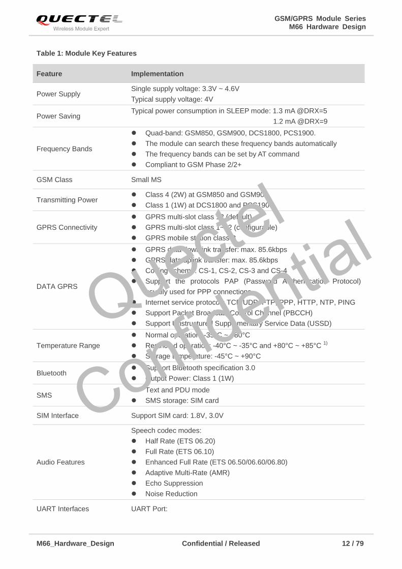
Table 1: Module Key Features
Feature Implementation
Power Supply Single supply voltage: 3.3V ~ 4.6V
Typical supply voltage: 4V
Power Saving Typical power consumption in SLEEP mode: 1.3 mA @DRX=5
1.2 mA @DRX=9
Frequency Bands
Quad-band: GSM850, GSM900, DCS1800, PCS1900.
The module can search these frequency bands automatically
The frequency bands can be set by AT command
Compliant to GSM Phase 2/2+
GSM Class Small MS
Transmitting Power Class 4 (2W) at GSM850 and GSM900
Class 1 (1W) at DCS1800 and PCS1900
GPRS Connectivity
GPRS multi-slot class 12 (default)
GPRS multi-slot class 1~12 (configurable)
GPRS mobile station class B
DATA GPRS
GPRS data downlink transfer: max. 85.6kbps
GPRS data uplink transfer: max. 85.6kbps
Coding scheme: CS-1, CS-2, CS-3 and CS-4
Support the protocols PAP (Password Authentication Protocol)
usually used for PPP connections
Internet service protocols TCP/UDP, FTP, PPP, HTTP, NTP, PING
Support Packet Broadcast Control Channel (PBCCH)
Support Unstructured Supplementary Service Data (USSD)
Temperature Range
Normal operation: -35°C ~ +80°C
Restricted operation: -40°C ~ -35°C and +80°C ~ +85°C 1)
Storage temperature: -45°C ~ +90°C
Bluetooth Support Bluetooth specification 3.0
Output Power: Class 1 (1W)
SMS Text and PDU mode
SMS storage: SIM card
SIM Interface Support SIM card: 1.8V, 3.0V
Audio Features
Speech codec modes:
Half Rate (ETS 06.20)
Full Rate (ETS 06.10)
Enhanced Full Rate (ETS 06.50/06.60/06.80)
Adaptive Multi-Rate (AMR)
Echo Suppression
Noise Reduction
UART Interfaces UART Port:
Quectel
Confidential
GSM/GPRS Module Series M66 Hardware Design
M66_Hardware_Design Confidential / Released 13 / 79
1) When the module works within this temperature range, the deviations from the GSM specification may
occur. For example, the frequency error or the phase error will be increased.
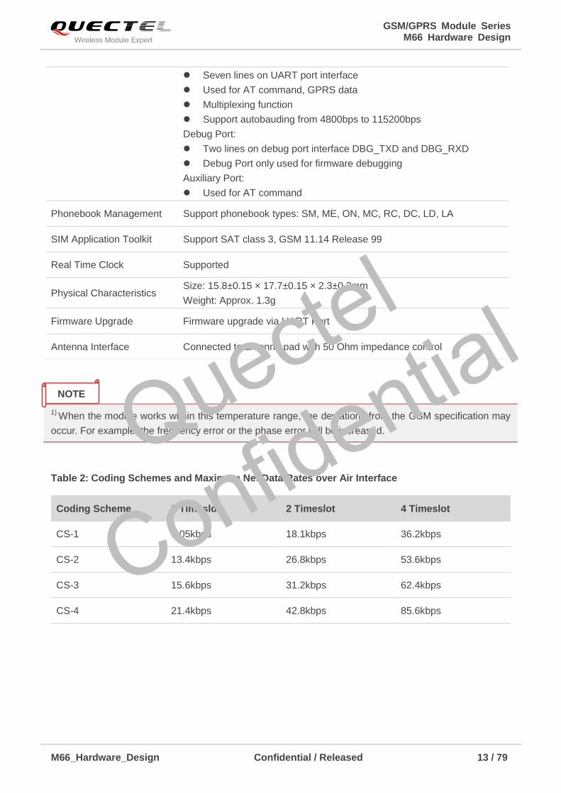
Table 2: Coding Schemes and Maximum Net Data Rates over Air Interface
Seven lines on UART port interface
Used for AT command, GPRS data
Multiplexing function
Support autobauding from 4800bps to 115200bps
Debug Port:
Two lines on debug port interface DBG_TXD and DBG_RXD
Debug Port only used for firmware debugging
Auxiliary Port:
Used for AT command
Phonebook Management Support phonebook types: SM, ME, ON, MC, RC, DC, LD, LA
SIM Application Toolkit Support SAT class 3, GSM 11.14 Release 99
Real Time Clock Supported
Physical Characteristics Size: 15.8±0.15 × 17.7±0.15 × 2.3±0.2mm
Weight: Approx. 1.3g
Firmware Upgrade Firmware upgrade via UART Port
Antenna Interface Connected to antenna pad with 50 Ohm impedance control
Coding Scheme 1 Timeslot 2 Timeslot 4 Timeslot
CS-1 9.05kbps 18.1kbps 36.2kbps
CS-2 13.4kbps 26.8kbps 53.6kbps
CS-3 15.6kbps 31.2kbps 62.4kbps
CS-4 21.4kbps 42.8kbps 85.6kbps
NOTE
Quectel
Confidential
GSM/GPRS Module Series M66 Hardware Design
M66_Hardware_Design Confidential / Released 14 / 79
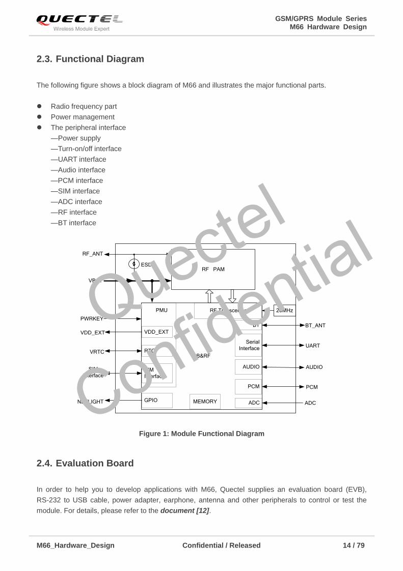
2.3. Functional Diagram
The following figure shows a block diagram of M66 and illustrates the major functional parts.
Radio frequency part
Power management
The peripheral interface
—Power supply
—Turn-on/off interface
—UART interface
—Audio interface
—PCM interface
—SIM interface
—ADC interface
—RF interface
—BT interface
BB&RF
RF PAM
26MHzRF Transceiver
RTC
AUDIO
Serial
Interface
SIM
Interface
RF_ANT
VBAT
PWRKEY
VRTC
NETLIGHT
UART
SIM
Interface
ESD
PMU
MEMORY
BT_ANT
GPIO
AUDIO
PCM PCM
ADC ADC
BT
VDD_EXTVDD_EXT
Figure 1: Module Functional Diagram
2.4. Evaluation Board
In order to help you to develop applications with M66, Quectel supplies an evaluation board (EVB),
RS-232 to USB cable, power adapter, earphone, antenna and other peripherals to control or test the
module. For details, please refer to the document [12].
Quectel
Confidential
GSM/GPRS Module Series M66 Hardware Design
M66_Hardware_Design Confidential / Released 15 / 79
3 Application Interface
The module adopts LCC package and has 44 pins. The following chapters provide detailed descriptions
about these pins.
Power supply
Power on/down
Power Saving
RTC
Serial interfaces
Audio interfaces
PCM interface
SIM Card interface
ADC
Quectel
Confidential
GSM/GPRS Module Series M66 Hardware Design
M66_Hardware_Design Confidential / Released 16 / 79
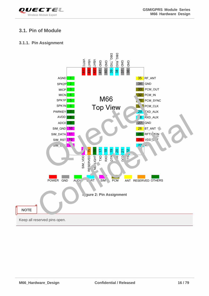
3.1. Pin of Module
3.1.1. Pin Assignment
AGND
SPK2P
MICP
MICN
SPK1P
SPK1N
PWRKEY
SIM_RST
SIM_CLK
CT
SV
RT
C
VB
AT
GN
D
GN
D
DB
G_
TX
D
DB
G_
RX
D
GN
D
GN
DRF_ANT
14
M66
Top View
15
16
17
18
19
20
21
22
36
37
38
39
40
41
42
43
44
1
2
3
4
5
6
7
8
9
10
11
12
13 23
24
25
26
27
28
29
30
31
32
33
34
35
AVDD
ADC0
SIM_GND
SIM_DATA
GND
PCM_OUT
PCM_IN
PCM_SYNC
PCM_CLK
TXD_AUX
RXD_AUX
GND
BT_ANT
RFTXMON
VDD_EXT
RTS
DC
DRI
DT
R
TX
D
RX
D
NE
TL
IGH
T
RE
SE
RV
ED
SIM
_V
DD
VB
AT
POWER GND AUDIO UART SIM PCM ANT OTHERSRESERVED
Figure 2: Pin Assignment
Keep all reserved pins open.
NOTE
Quectel
Confidential
GSM/GPRS Module Series M66 Hardware Design
M66_Hardware_Design Confidential / Released 17 / 79
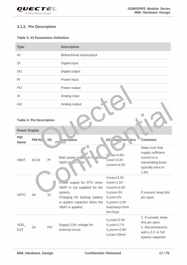
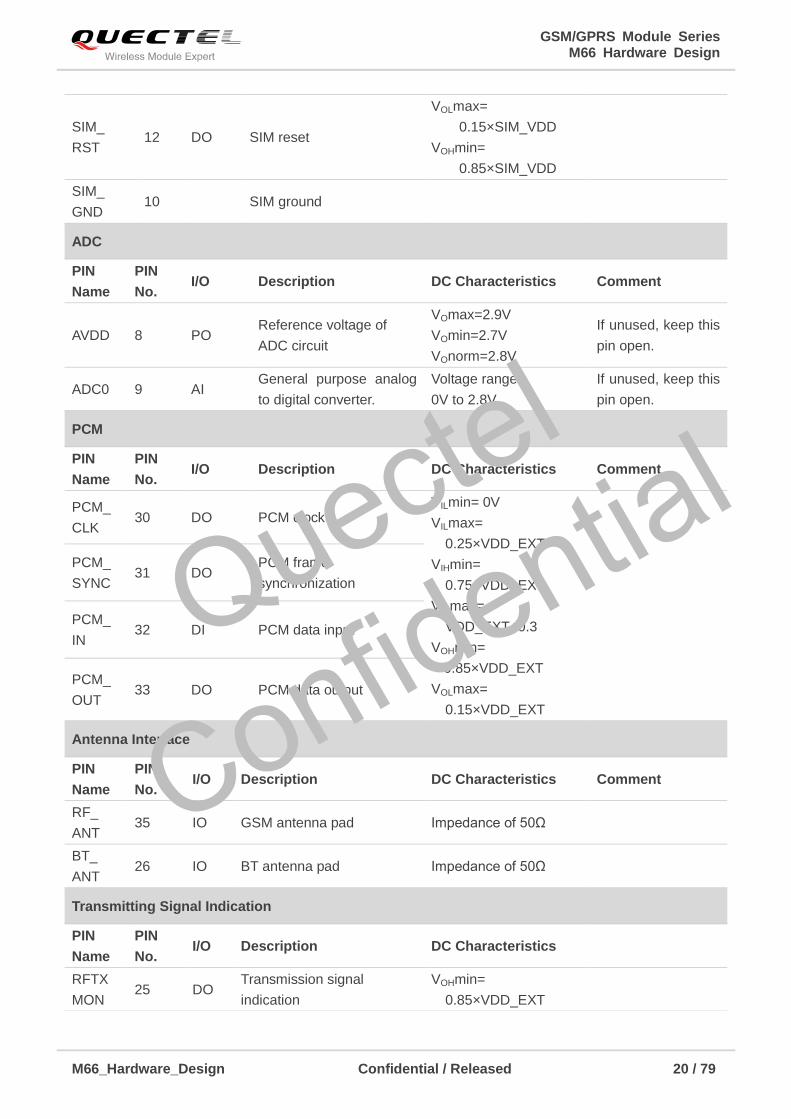
3.1.2. Pin Description
Table 3: IO Parameters Definition
Type Description
IO Bidirectional input/output
DI Digital input
DO Digital output
PI Power input
PO Power output
AI Analog input
AO Analog output
Table 4: Pin Description
Power Supply
PIN
Name PIN No. I/O Description DC Characteristics Comment
VBAT 42,43 PI Main power supply of module:
VBAT=3.3V~4.6V
VImax=4.6V
VImin=3.3V
VInorm=4.0V
Make sure that
supply sufficient
current in a
transmitting burst
typically rises to
1.6A.
VRTC 44 IO
Power supply for RTC when
VBAT is not supplied for the
system.
Charging for backup battery
or golden capacitor when the
VBAT is applied.
VImax=3.3V
VImin=1.5V
VInorm=2.8V
VOmax=3V
VOmin=2V
VOnorm=2.8V
Iout(max)=2mA
Iin≈10uA
If unused, keep this
pin open.
VDD_
EXT 24 PO
Supply 2.8V voltage for
external circuit.
VOmax=2.9V
VOmin=2.7V
VOnorm=2.8V
IOmax=20mA
1. If unused, keep
this pin open.
2. Recommend to
add a 2.2~4.7uF
bypass capacitor,
Quectel
Confidential
GSM/GPRS Module Series M66 Hardware Design
M66_Hardware_Design Confidential / Released 18 / 79
when using this pin
for power supply.
GND
27,34
36,37
40,41
Ground
Turn On/off
PIN
Name
PIN
No. I/O Description DC Characteristics Comment
PWR
KEY 7 DI
Power on/off key. PWRKEY
should be pulled down for a
moment to turn on or turn off
the system.
VILmax=
0.1×VBAT
VIHmin=
0.6×VBAT
VIHmax=3.1V
Audio Interface
PIN
Name
PIN
No. I/O Description DC Characteristics Comment
MICP
MICN
3,
4 AI
Positive and negative voice
input
Refer to Section 3.8
If unused, keep
these pins open.
SPK1P
SPK1N
5,
6 AO
Channel 1 positive and
negative voice output
If unused, keep
these pins open.
Support both voice
and ringtone
output.
SPK2P 2 AO Channel 2 voice output
AGND 1
Analog ground. Separate
ground connection for external
audio circuits.
If unused, keep this
pin open.
Network Status Indicator
PIN
Name
PIN
No. I/O Description DC Characteristics Comment
NETLIG
HT 16 DO Network status indication
VOHmin=
0.85×VDD_EXT
VOLmax=
0.15×VDD_EXT
If unused, keep this
pin open.
UART Port
PIN
Name
PIN
No. I/O Description DC Characteristics Comment
TXD 17 DO Transmit data VILmin=0V
VILmax=
0.25×VDD_EXT
If only use TXD,
RXD and GND to
communicate, RXD 18 DI Receive data
Quectel
Confidential
GSM/GPRS Module Series M66 Hardware Design
M66_Hardware_Design Confidential / Released 19 / 79
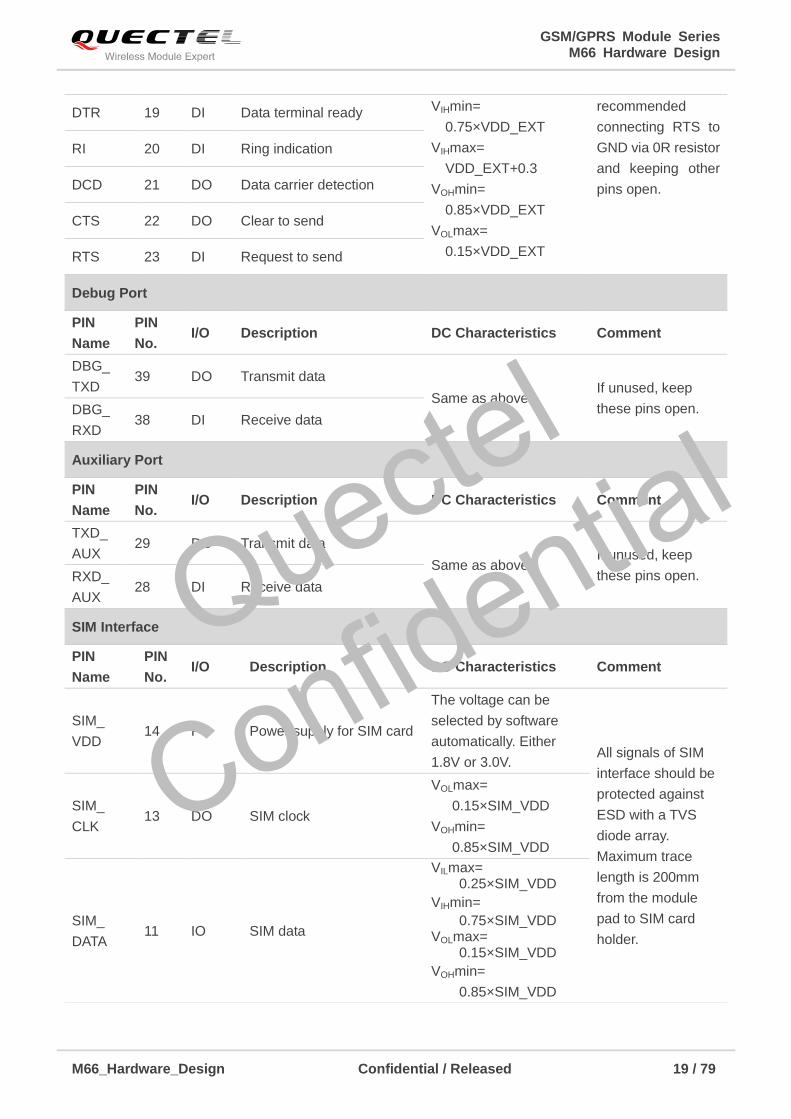
DTR 19 DI Data terminal ready VIHmin=
0.75×VDD_EXT
VIHmax=
VDD_EXT+0.3
VOHmin=
0.85×VDD_EXT
VOLmax=
0.15×VDD_EXT
recommended
connecting RTS to
GND via 0R resistor
and keeping other
pins open.
RI 20 DI Ring indication
DCD 21 DO Data carrier detection
CTS 22 DO Clear to send
RTS 23 DI Request to send
Debug Port
PIN
Name
PIN
No. I/O Description DC Characteristics Comment
DBG_
TXD 39 DO Transmit data
Same as above If unused, keep
these pins open. DBG_
RXD 38 DI Receive data
Auxiliary Port
PIN
Name
PIN
No. I/O Description DC Characteristics Comment
TXD_
AUX 29 DO Transmit data
Same as above If unused, keep
these pins open. RXD_
AUX 28 DI Receive data
SIM Interface
PIN
Name
PIN
No. I/O Description DC Characteristics Comment
SIM_
VDD 14 PO Power supply for SIM card
The voltage can be
selected by software
automatically. Either
1.8V or 3.0V. All signals of SIM
interface should be
protected against
ESD with a TVS
diode array.
Maximum trace
length is 200mm
from the module
pad to SIM card
holder.
SIM_
CLK 13 DO SIM clock
VOLmax=
0.15×SIM_VDD
VOHmin=
0.85×SIM_VDD
SIM_
DATA 11 IO SIM data
VILmax= 0.25×SIM_VDD
VIHmin=
0.75×SIM_VDD VOLmax=
0.15×SIM_VDD
VOHmin=
0.85×SIM_VDD
Quectel
Confidential
GSM/GPRS Module Series M66 Hardware Design
M66_Hardware_Design Confidential / Released 20 / 79
SIM_
RST 12 DO SIM reset
VOLmax=
0.15×SIM_VDD
VOHmin=
0.85×SIM_VDD
SIM_
GND 10 SIM ground
ADC
PIN
Name
PIN
No. I/O Description DC Characteristics Comment
AVDD 8 PO Reference voltage of
ADC circuit
VOmax=2.9V
VOmin=2.7V
VOnorm=2.8V
If unused, keep this
pin open.
ADC0 9 AI General purpose analog
to digital converter.
Voltage range:
0V to 2.8V
If unused, keep this
pin open.
PCM
PIN
Name
PIN
No. I/O Description DC Characteristics Comment
PCM_
CLK 30 DO PCM clock
VILmin= 0V
VILmax=
0.25×VDD_EXT
VIHmin=
0.75×VDD_EXT
VIHmax=
VDD_EXT+0.3
VOHmin=
0.85×VDD_EXT
VOLmax=
0.15×VDD_EXT
PCM_
SYNC 31 DO
PCM frame
synchronization
PCM_
IN 32 DI PCM data input
PCM_
OUT 33 DO PCM data output
Antenna Interface
PIN
Name
PIN
No. I/O Description DC Characteristics Comment
RF_
ANT 35 IO GSM antenna pad Impedance of 50Ω
BT_
ANT 26 IO BT antenna pad Impedance of 50Ω
Transmitting Signal Indication
PIN
Name
PIN
No. I/O Description DC Characteristics
RFTX
MON 25 DO
Transmission signal
indication
VOHmin=
0.85×VDD_EXT
Quectel
Confidential
GSM/GPRS Module Series M66 Hardware Design
M66_Hardware_Design Confidential / Released 21 / 79
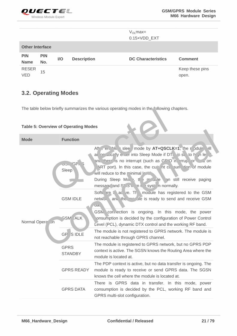
3.2. Operating Modes
The table below briefly summarizes the various operating modes in the following chapters.
Table 5: Overview of Operating Modes
VOLmax=
0.15×VDD_EXT
Other Interface
PIN
Name
PIN
No. I/O Description DC Characteristics Comment
RESER
VED 15
Keep these pins
open.
Mode Function
Normal Operation
GSM/GPRS
Sleep
After enabling sleep mode by AT+QSCLK=1, the module will
automatically enter into Sleep Mode if DTR is set to high level
and there is no interrupt (such as GPIO interrupt or data on
UART port). In this case, the current consumption of module
will reduce to the minimal level.
During Sleep Mode, the module can still receive paging
message and SMS from the system normally.
GSM IDLE
Software is active. The module has registered to the GSM
network, and the module is ready to send and receive GSM
data.
GSM TALK
GSM connection is ongoing. In this mode, the power
consumption is decided by the configuration of Power Control
Level (PCL), dynamic DTX control and the working RF band.
GPRS IDLE The module is not registered to GPRS network. The module is
not reachable through GPRS channel.
GPRS
STANDBY
The module is registered to GPRS network, but no GPRS PDP
context is active. The SGSN knows the Routing Area where the
module is located at.
GPRS READY
The PDP context is active, but no data transfer is ongoing. The
module is ready to receive or send GPRS data. The SGSN
knows the cell where the module is located at.
GPRS DATA
There is GPRS data in transfer. In this mode, power
consumption is decided by the PCL, working RF band and
GPRS multi-slot configuration.
Quectel
Confidential
GSM/GPRS Module Series M66 Hardware Design
M66_Hardware_Design Confidential / Released 22 / 79
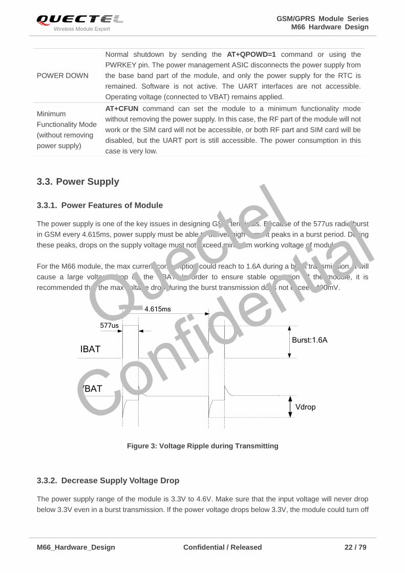
3.3. Power Supply
3.3.1. Power Features of Module
The power supply is one of the key issues in designing GSM terminals. Because of the 577us radio burst
in GSM every 4.615ms, power supply must be able to deliver high current peaks in a burst period. During
these peaks, drops on the supply voltage must not exceed minimum working voltage of module.
For the M66 module, the max current consumption could reach to 1.6A during a burst transmission. It will
cause a large voltage drop on the VBAT. In order to ensure stable operation of the module, it is
recommended that the max voltage drop during the burst transmission does not exceed 400mV.
Vdrop
4.615ms
577us
IBAT
VBAT
Burst:1.6A
Figure 3: Voltage Ripple during Transmitting
3.3.2. Decrease Supply Voltage Drop
The power supply range of the module is 3.3V to 4.6V. Make sure that the input voltage will never drop
below 3.3V even in a burst transmission. If the power voltage drops below 3.3V, the module could turn off
POWER DOWN
Normal shutdown by sending the AT+QPOWD=1 command or using the
PWRKEY pin. The power management ASIC disconnects the power supply from
the base band part of the module, and only the power supply for the RTC is
remained. Software is not active. The UART interfaces are not accessible.
Operating voltage (connected to VBAT) remains applied.
Minimum
Functionality Mode
(without removing
power supply)
AT+CFUN command can set the module to a minimum functionality mode
without removing the power supply. In this case, the RF part of the module will not
work or the SIM card will not be accessible, or both RF part and SIM card will be
disabled, but the UART port is still accessible. The power consumption in this
case is very low.
Quectel
Confidential
GSM/GPRS Module Series M66 Hardware Design
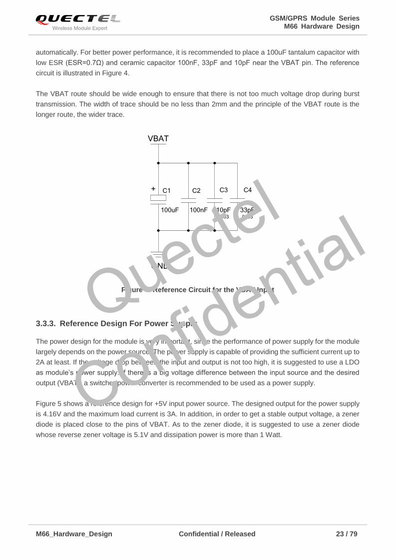
M66_Hardware_Design Confidential / Released 23 / 79
automatically. For better power performance, it is recommended to place a 100uF tantalum capacitor with
low ESR (ESR=0.7Ω) and ceramic capacitor 100nF, 33pF and 10pF near the VBAT pin. The reference
circuit is illustrated in Figure 4.
The VBAT route should be wide enough to ensure that there is not too much voltage drop during burst
transmission. The width of trace should be no less than 2mm and the principle of the VBAT route is the
longer route, the wider trace.
VBAT
C2C1+ C3 C4
GND
100uF 100nF 10pF0603
33pF0603
Figure 4: Reference Circuit for the VBAT Input
3.3.3. Reference Design For Power Supply
The power design for the module is very important, since the performance of power supply for the module
largely depends on the power source. The power supply is capable of providing the sufficient current up to
2A at least. If the voltage drop between the input and output is not too high, it is suggested to use a LDO
as module’s power supply. If there is a big voltage difference between the input source and the desired
output (VBAT), a switcher power converter is recommended to be used as a power supply.
Figure 5 shows a reference design for +5V input power source. The designed output for the power supply
is 4.16V and the maximum load current is 3A. In addition, in order to get a stable output voltage, a zener
diode is placed close to the pins of VBAT. As to the zener diode, it is suggested to use a zener diode
whose reverse zener voltage is 5.1V and dissipation power is more than 1 Watt.
Quectel
Confidential

GSM/GPRS Module Series M66 Hardware Design
M66_Hardware_Design Confidential / Released 24 / 79
DC_IN
C1 C2
MIC29302WU U1
IN OUT
EN
GN
D
AD
J
2 4
1 3 5
VBAT
100nF
C3
470uF
C4
100nF
R1
D1120K
51KR2
470uF 5.1V
R3
470R
Figure 5: Reference Circuit for Power Supply
3.3.4. Monitor Power Supply
To monitor the supply voltage, customer can use the AT+CBC command which includes three
parameters: charging status, remaining battery capacity and voltage value (in mV). It returns the 0-100
percent of battery capacity and actual value measured between VBAT and GND. The voltage is
automatically measured in period of 5s. The displayed voltage (in mV) is averaged over the last
measuring period before the AT+CBC command is executed.
For details, please refer to the document [1].
3.4. Power On and Down Scenarios
3.4.1. Power On
The module can be turned on by driving the pin PWRKEY to a low level voltage. An open collector driver
circuit is suggested to control the PWRKEY. A simple reference circuit is illustrated as below.
Turn on pulse
PWRKEY
4.7K
47K
Figure 6: Turn on the Module with an Open-collector Driver
Quectel
Confidential
GSM/GPRS Module Series M66 Hardware Design
M66_Hardware_Design Confidential / Released 25 / 79
M66 module is set to autobauding mode (AT+IPR=0) by default. In the autobauding mode, URC RDY is
not reported to the host controller after module is powered on. When the module is powered on after a
delay of 2 or 3 seconds, it can receive AT command. Host controller should first send an AT or at string in
order that the module can detect baud rate of host controller, and it should send the second or the third AT
or at string until receiving OK string from the module. Then enter AT+IPR=x;&W to set a fixed baud rate
for the module and save the configuration to flash memory of the module. After these configurations, the
URC RDY would be received from the UART port of the module every time when the module is powered
on. For more details, refer to the section AT+IPR in document [1].
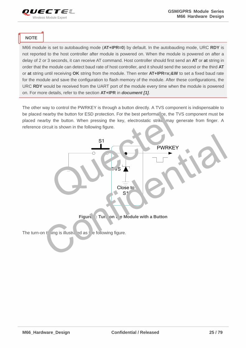
The other way to control the PWRKEY is through a button directly. A TVS component is indispensable to
be placed nearby the button for ESD protection. For the best performance, the TVS component must be
placed nearby the button. When pressing the key, electrostatic strike may generate from finger. A
reference circuit is shown in the following figure.
PWRKEY
S1
Close to
S1
TVS
Figure 7: Turn on the Module with a Button
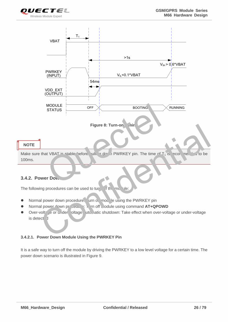
The turn-on timing is illustrated as the following figure.
NOTE
Quectel
Confidential
GSM/GPRS Module Series M66 Hardware Design
M66_Hardware_Design Confidential / Released 26 / 79
VDD_EXT(OUTPUT)
VIL<0.1*VBAT
VIH > 0.6*VBAT
VBAT
PWRKEY(INPUT)
54ms
>1s
T1
OFF BOOTINGMODULE
STATUSRUNNING
Figure 8: Turn-on Timing
Make sure that VBAT is stable before pulling down PWRKEY pin. The time of T1 is recommended to be
100ms.
3.4.2. Power Down
The following procedures can be used to turn off the module:
Normal power down procedure: Turn off module using the PWRKEY pin
Normal power down procedure: Turn off module using command AT+QPOWD
Over-voltage or under-voltage automatic shutdown: Take effect when over-voltage or under-voltage
is detected
3.4.2.1. Power Down Module Using the PWRKEY Pin
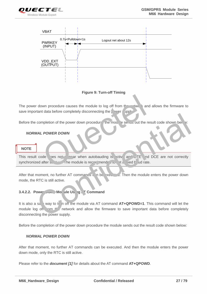
It is a safe way to turn off the module by driving the PWRKEY to a low level voltage for a certain time. The
power down scenario is illustrated in Figure 9.
NOTE
Quectel
Confidential
GSM/GPRS Module Series M66 Hardware Design
M66_Hardware_Design Confidential / Released 27 / 79
VBAT
PWRKEY(INPUT)
VDD_EXT (OUTPUT)
Logout net about 12s0.7s<Pulldown<1s
Figure 9: Turn-off Timing
The power down procedure causes the module to log off from the network and allows the firmware to
save important data before completely disconnecting the power supply.
Before the completion of the power down procedure, the module sends out the result code shown below:
NORMAL POWER DOWN
This result code does not appear when autobauding is active and DTE and DCE are not correctly
synchronized after start-up. The module is recommended to set a fixed baud rate.
After that moment, no further AT commands can be executed. Then the module enters the power down
mode, the RTC is still active.
3.4.2.2. Power Down Module Using AT Command
It is also a safe way to turn off the module via AT command AT+QPOWD=1. This command will let the
module log off from the network and allow the firmware to save important data before completely
disconnecting the power supply.
Before the completion of the power down procedure the module sends out the result code shown below:
NORMAL POWER DOWN
After that moment, no further AT commands can be executed. And then the module enters the power
down mode, only the RTC is still active.
Please refer to the document [1] for details about the AT command AT+QPOWD.
NOTE Quectel
Confidential
GSM/GPRS Module Series M66 Hardware Design
M66_Hardware_Design Confidential / Released 28 / 79
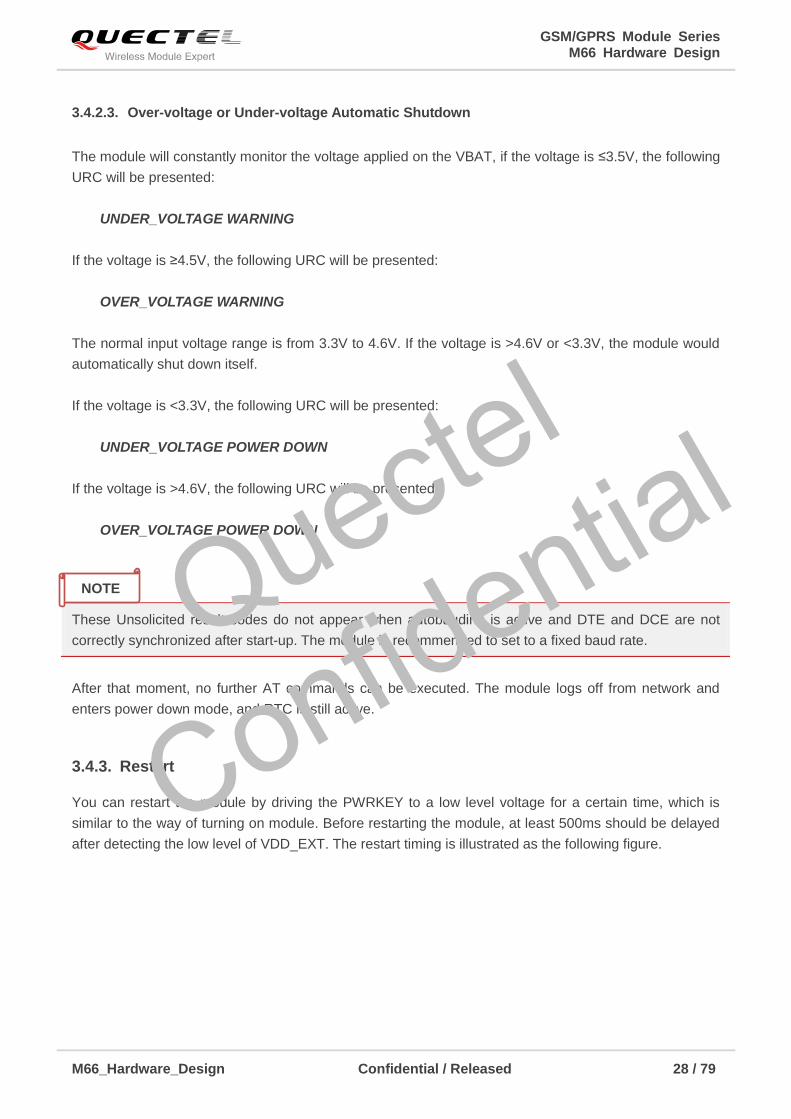
3.4.2.3. Over-voltage or Under-voltage Automatic Shutdown
The module will constantly monitor the voltage applied on the VBAT, if the voltage is ≤3.5V, the following
URC will be presented:
UNDER_VOLTAGE WARNING
If the voltage is ≥4.5V, the following URC will be presented:
OVER_VOLTAGE WARNING
The normal input voltage range is from 3.3V to 4.6V. If the voltage is >4.6V or <3.3V, the module would
automatically shut down itself.
If the voltage is <3.3V, the following URC will be presented:
UNDER_VOLTAGE POWER DOWN
If the voltage is >4.6V, the following URC will be presented:
OVER_VOLTAGE POWER DOWN
These Unsolicited result codes do not appear when autobauding is active and DTE and DCE are not
correctly synchronized after start-up. The module is recommended to set to a fixed baud rate.
After that moment, no further AT commands can be executed. The module logs off from network and
enters power down mode, and RTC is still active.
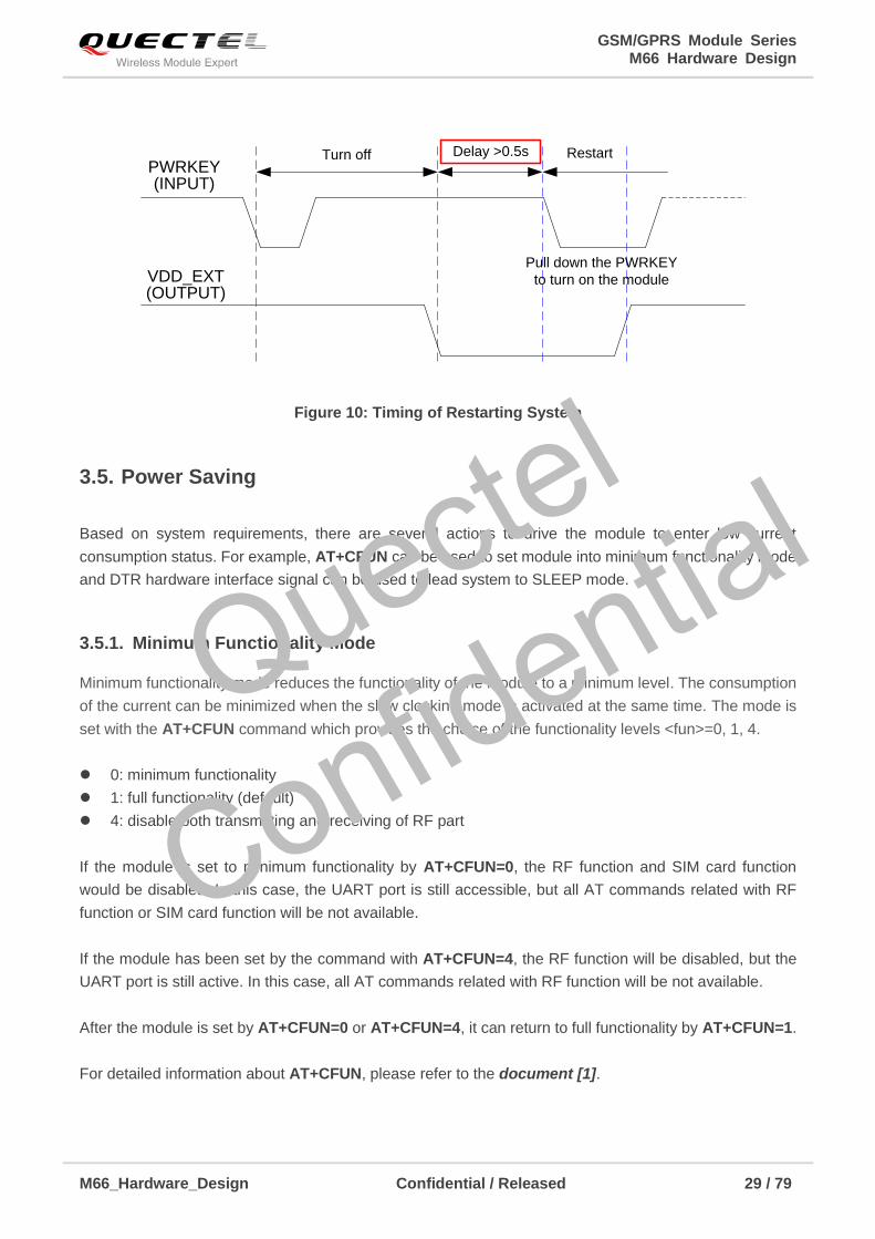
3.4.3. Restart
You can restart the module by driving the PWRKEY to a low level voltage for a certain time, which is
similar to the way of turning on module. Before restarting the module, at least 500ms should be delayed
after detecting the low level of VDD_EXT. The restart timing is illustrated as the following figure.
NOTE Quectel
Confidential
GSM/GPRS Module Series M66 Hardware Design
M66_Hardware_Design Confidential / Released 29 / 79
PWRKEY(INPUT)
VDD_EXT(OUTPUT)
Delay >0.5sTurn off Restart
Pull down the PWRKEY
to turn on the module
Figure 10: Timing of Restarting System
3.5. Power Saving
Based on system requirements, there are several actions to drive the module to enter low current
consumption status. For example, AT+CFUN can be used to set module into minimum functionality mode
and DTR hardware interface signal can be used to lead system to SLEEP mode.
3.5.1. Minimum Functionality Mode
Minimum functionality mode reduces the functionality of the module to a minimum level. The consumption
of the current can be minimized when the slow clocking mode is activated at the same time. The mode is
set with the AT+CFUN command which provides the choice of the functionality levels <fun>=0, 1, 4.
0: minimum functionality
1: full functionality (default)
4: disable both transmitting and receiving of RF part
If the module is set to minimum functionality by AT+CFUN=0, the RF function and SIM card function
would be disabled. In this case, the UART port is still accessible, but all AT commands related with RF
function or SIM card function will be not available.
If the module has been set by the command with AT+CFUN=4, the RF function will be disabled, but the
UART port is still active. In this case, all AT commands related with RF function will be not available.
After the module is set by AT+CFUN=0 or AT+CFUN=4, it can return to full functionality by AT+CFUN=1.
For detailed information about AT+CFUN, please refer to the document [1].
Quectel
Confidential
GSM/GPRS Module Series M66 Hardware Design
M66_Hardware_Design Confidential / Released 30 / 79
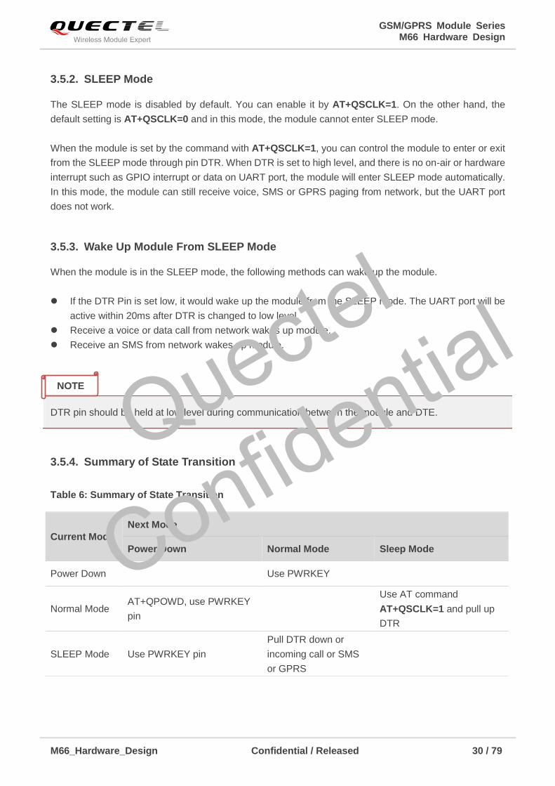
3.5.2. SLEEP Mode
The SLEEP mode is disabled by default. You can enable it by AT+QSCLK=1. On the other hand, the
default setting is AT+QSCLK=0 and in this mode, the module cannot enter SLEEP mode.
When the module is set by the command with AT+QSCLK=1, you can control the module to enter or exit
from the SLEEP mode through pin DTR. When DTR is set to high level, and there is no on-air or hardware
interrupt such as GPIO interrupt or data on UART port, the module will enter SLEEP mode automatically.
In this mode, the module can still receive voice, SMS or GPRS paging from network, but the UART port
does not work.
3.5.3. Wake Up Module From SLEEP Mode
When the module is in the SLEEP mode, the following methods can wake up the module.
If the DTR Pin is set low, it would wake up the module from the SLEEP mode. The UART port will be
active within 20ms after DTR is changed to low level.
Receive a voice or data call from network wakes up module.
Receive an SMS from network wakes up module.
DTR pin should be held at low level during communication between the module and DTE.
3.5.4. Summary of State Transition
Table 6: Summary of State Transition
Current Mode
Next Mode
Power Down Normal Mode Sleep Mode
Power Down Use PWRKEY
Normal Mode AT+QPOWD, use PWRKEY
pin
Use AT command
AT+QSCLK=1 and pull up
DTR
SLEEP Mode Use PWRKEY pin
Pull DTR down or
incoming call or SMS
or GPRS
NOTE
Quectel
Confidential
GSM/GPRS Module Series M66 Hardware Design
M66_Hardware_Design Confidential / Released 31 / 79
3.6. RTC Backup
The RTC (Real Time Clock) function is supported by M66 module. The RTC is designed to work with an
internal power supply. If VBAT voltage is not present, a backup power supply such as a coin-cell battery
(rechargeable or non-chargeable) or a super-cap can be used. The VRTC pin is voltage input for RTC
and a 1.5K resistor is integrated in the module for peak current limit.
The following figures show various sample circuits for RTC backup.
Module
RTC
Core
1.5KVRTC
Non-chargeable
Backup Battery
Figure 11: RTC Supply from a Non-chargeable Battery
VRTC
Rechargeable
Backup Battery
Module
RTC
Core
1.5K
Figure 12: RTC Supply from a Rechargeable Battery
VRTC
Large Capacitance
Capacitor
Module
RTC
Core
1.5K
Figure 13: RTC Supply from a Capacitor
Quectel
Confidential
GSM/GPRS Module Series M66 Hardware Design
M66_Hardware_Design Confidential / Released 32 / 79
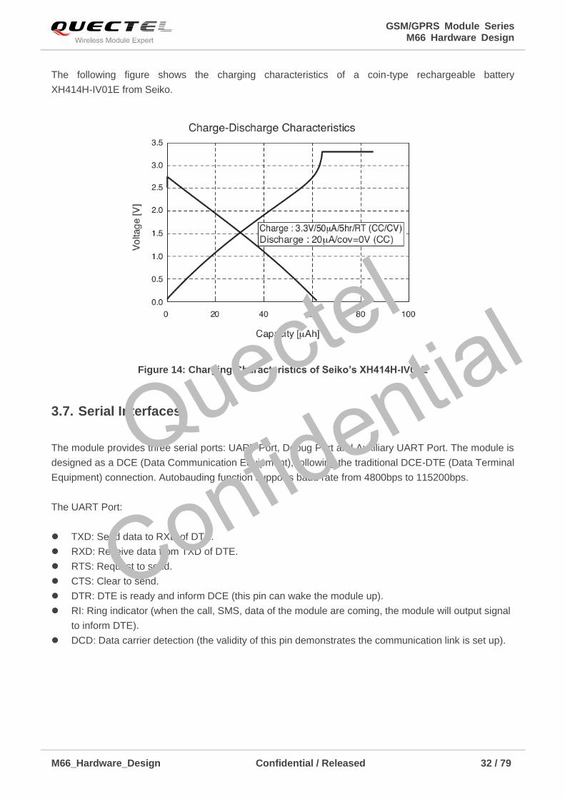
The following figure shows the charging characteristics of a coin-type rechargeable battery
XH414H-IV01E from Seiko.
Figure 14: Charging Characteristics of Seiko’s XH414H-IV01E
3.7. Serial Interfaces
The module provides three serial ports: UART Port, Debug Port and Auxiliary UART Port. The module is
designed as a DCE (Data Communication Equipment), following the traditional DCE-DTE (Data Terminal
Equipment) connection. Autobauding function supports baud rate from 4800bps to 115200bps.
The UART Port:
TXD: Send data to RXD of DTE.
RXD: Receive data from TXD of DTE.
RTS: Request to send.
CTS: Clear to send.
DTR: DTE is ready and inform DCE (this pin can wake the module up).
RI: Ring indicator (when the call, SMS, data of the module are coming, the module will output signal
to inform DTE).
DCD: Data carrier detection (the validity of this pin demonstrates the communication link is set up).
Quectel
Confidential
GSM/GPRS Module Series M66 Hardware Design
M66_Hardware_Design Confidential / Released 33 / 79
The module disables hardware flow control by default. When hardware flow control is required, RTS and
CTS should be connected to the host. AT command AT+IFC=2,2 is used to enable hardware flow control.
AT command AT+IFC=0,0 is used to disable the hardware flow control. For more details, please refer to
the document [1].
The Debug Port:
DBG_TXD: Send data to the COM port of computer.
DBG_RXD: Receive data from the COM port of computer.
The Auxiliary UART Port:
TXD_AUX: Send data to the RXD of DTE.
RXD_AUX: Receive data from the TXD of DTE.
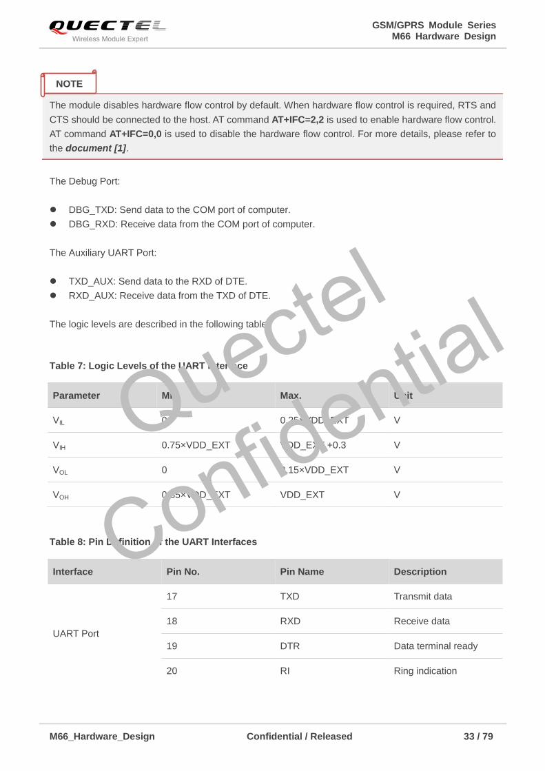
The logic levels are described in the following table.
Table 7: Logic Levels of the UART Interface
Table 8: Pin Definition of the UART Interfaces
Parameter Min. Max. Unit
VIL 0 0.25×VDD_EXT V
VIH 0.75×VDD_EXT VDD_EXT +0.3 V
VOL 0 0.15×VDD_EXT V
VOH 0.85×VDD_EXT VDD_EXT V
Interface Pin No. Pin Name Description
UART Port
17 TXD Transmit data
18 RXD Receive data
19 DTR Data terminal ready
20 RI Ring indication
NOTE
Quectel
Confidential
GSM/GPRS Module Series M66 Hardware Design
M66_Hardware_Design Confidential / Released 34 / 79
3.7.1. UART Port
3.7.1.1. The Feature of UART Port
Seven lines on UART interface
Contain data lines TXD and RXD, hardware flow control lines RTS and CTS, other control lines DTR,
DCD and RI.
Used for AT command, GPRS data, etc. Multiplexing function is supported on the UART Port. So far
only the basic mode of multiplexing is available.
Support the communication baud rates as the following:
300, 600, 1200, 2400, 4800, 9600, 14400, 19200, 28800, 38400, 57600, 115200.
The default setting is autobauding mode. Support the following baud rates for Autobauding function:
4800, 9600, 19200, 38400, 57600, 115200.
The module disables hardware flow control by default. AT command AT+IFC=2,2 is used to enable
hardware flow control.
After setting a fixed baud rate or autobauding, please send “AT” string at that rate. The UART port is
ready when it responds “OK”.
Autobauding allows the module to detect the baud rate by receiving the string “AT” or “at” from the host or
PC automatically, which gives module flexibility without considering which baud rate is used by the host
controller. Autobauding is enabled by default. To take advantage of the autobauding mode, special
attention should be paid according to the following requirements:
Synchronization between DTE and DCE:
When DCE (the module) powers on with the autobauding enabled, it is recommended to wait 2 to 3
seconds before sending the first AT character. After receiving the “OK” response, DTE and DCE are
correctly synchronized.
21 DCD Data carrier detection
22 CTS Clear to send
23 RTS Request to send
Debug Port
38 DBG_RXD Receive data
39 DBG_TXD Transmit data
Auxiliary UART Port
28 RXD_AUX Receive data
29 TXD_AUX Transmit data
Quectel
Confidential
GSM/GPRS Module Series M66 Hardware Design
M66_Hardware_Design Confidential / Released 35 / 79
If the host controller needs URC in the mode of autobauding, it must be synchronized firstly. Otherwise
the URC will be discarded.
Restrictions on autobauding operation:
The UART port has to be operated at 8 data bits, no parity and 1 stop bit (factory setting).
The “At” and “aT” commands cannot be used.
Only the strings “AT” or “at” can be detected (neither “At” nor “aT”).
The Unsolicited Result Codes like RDY, +CFUN: 1 and +CPIN: READY will not be indicated when
the module is turned on with autobauding enabled and not be synchronized.
Any other Unsolicited Result Codes will be sent at the previous baud rate before the module detects
the new baud rate by receiving the first “AT” or “at” string. The DTE may receive unknown characters
after switching to new baud rate.
It is not recommended to switch to autobauding from a fixed baud rate.
If autobauding is active it is not recommended to switch to multiplex mode.
To assure reliable communication and avoid any problems caused by undetermined baud rate between
DCE and DTE, it is strongly recommended to configure a fixed baud rate and save it instead of using
autobauding after start-up. For more details, please refer to the Section AT+IPR in document [1].
3.7.1.2. The Connection of UART
The connection between module and host using UART Port is very flexible. Three connection styles are
illustrated as below.
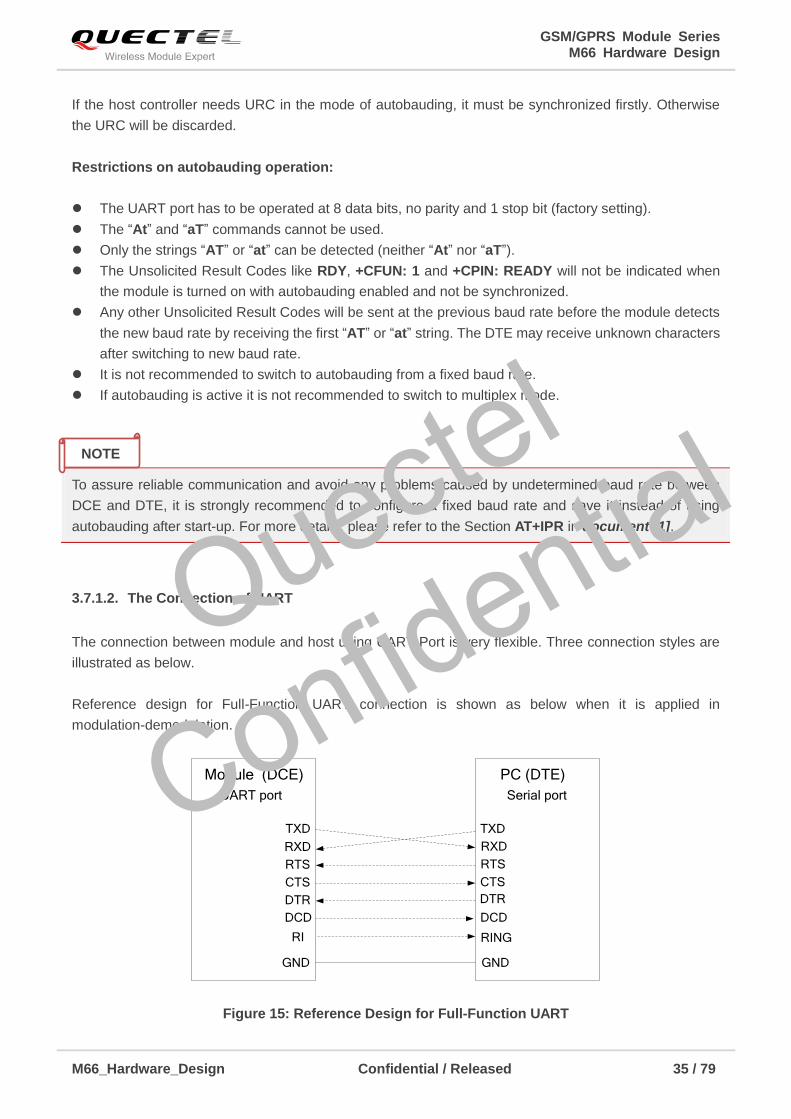
Reference design for Full-Function UART connection is shown as below when it is applied in
modulation-demodulation.
TXD
RXD
RTS
CTS
DTR
DCD
RI
TXD
RXD
RTS
CTS
DTR
DCD
RING
Module (DCE)
Serial portUART port
GND GND
PC (DTE)
Figure 15: Reference Design for Full-Function UART
NOTE
Quectel
Confidential
GSM/GPRS Module Series M66 Hardware Design
M66_Hardware_Design Confidential / Released 36 / 79
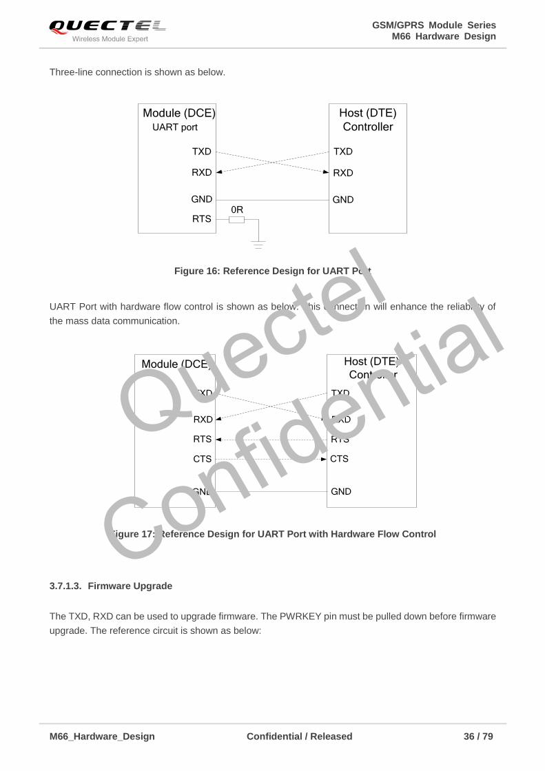
Three-line connection is shown as below.
TXD
RXD
GND
UART port
RTS0R
TXD
RXD
GND
Module (DCE) Host (DTE)
Controller
Figure 16: Reference Design for UART Port
UART Port with hardware flow control is shown as below. This connection will enhance the reliability of
the mass data communication.
RTS
CTS
RTS
CTS
GND
RXD
TXD TXD
RXD
GND
Module (DCE) Host (DTE)
Controller
Figure 17: Reference Design for UART Port with Hardware Flow Control
3.7.1.3. Firmware Upgrade
The TXD, RXD can be used to upgrade firmware. The PWRKEY pin must be pulled down before firmware
upgrade. The reference circuit is shown as below:
Quectel
Confidential
GSM/GPRS Module Series M66 Hardware Design
M66_Hardware_Design Confidential / Released 37 / 79
IO Connector
TXD
RXD
GND
PWRKEY
Module (DCE) UART port
TXD
RXD
GND
PWRKEY
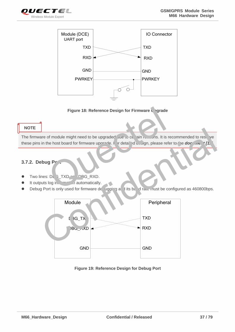
Figure 18: Reference Design for Firmware Upgrade
The firmware of module might need to be upgraded due to certain reasons. It is recommended to reserve
these pins in the host board for firmware upgrade. For detailed design, please refer to the document [11].
3.7.2. Debug Port
Two lines: DBG_TXD and DBG_RXD.
It outputs log information automatically.
Debug Port is only used for firmware debugging and its baud rate must be configured as 460800bps.
Peripheral
TXD
RXD
GND
Module
DBG_TXD
DBG_RXD
GND
Figure 19: Reference Design for Debug Port
NOTE
Quectel
Confidential
GSM/GPRS Module Series M66 Hardware Design
M66_Hardware_Design Confidential / Released 38 / 79
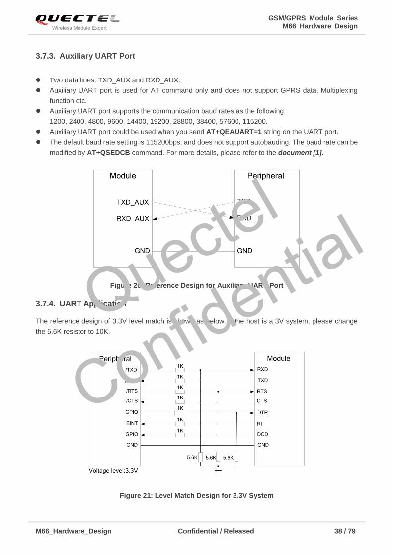
3.7.3. Auxiliary UART Port
Two data lines: TXD_AUX and RXD_AUX.
Auxiliary UART port is used for AT command only and does not support GPRS data, Multiplexing
function etc.
Auxiliary UART port supports the communication baud rates as the following:
1200, 2400, 4800, 9600, 14400, 19200, 28800, 38400, 57600, 115200.
Auxiliary UART port could be used when you send AT+QEAUART=1 string on the UART port.
The default baud rate setting is 115200bps, and does not support autobauding. The baud rate can be
modified by AT+QSEDCB command. For more details, please refer to the document [1].
Peripheral
TXD
RXD
GND
Module
TXD_AUX
RXD_AUX
GND
Figure 20: Reference Design for Auxiliary UART Port
3.7.4. UART Application
The reference design of 3.3V level match is shown as below. If the host is a 3V system, please change
the 5.6K resistor to 10K.
Peripheral
/TXD
/RXD
1K
TXD
RXD
RTS
CTS
DTR
RI
/RTS
/CTS
GPIO
EINT
GPIO DCD
Module
1K
1K
Voltage level:3.3V
5.6K5.6K5.6K
1K
1K
1K
1K
GND GND
Figure 21: Level Match Design for 3.3V System
Quectel
Confidential
GSM/GPRS Module Series M66 Hardware Design
M66_Hardware_Design Confidential / Released 39 / 79
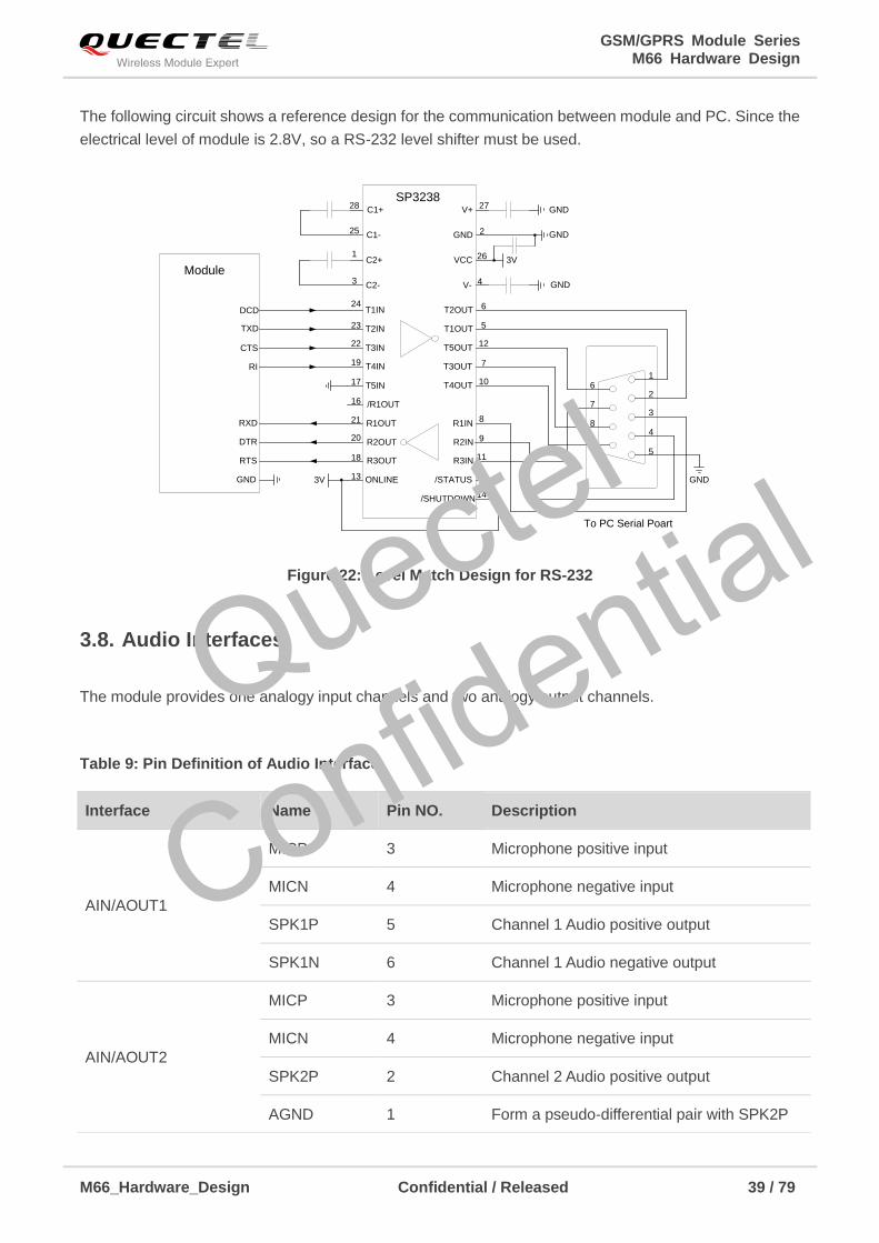
The following circuit shows a reference design for the communication between module and PC. Since the
electrical level of module is 2.8V, so a RS-232 level shifter must be used.
TXD
RXD
RTS
CTS
DTR
RI
DCD
Module
GND
C1+
C1-
C2+
C2-
28
25
1
3
V+
VCC
GND
V-
3V
27
2
26
4
T1IN
T2IN
T3IN
T4IN
R1IN
R2IN
R3IN
R1OUT
R2OUT
R3OUT
T1OUT
T2OUT
T5OUT
T3OUT
T4OUTT5IN
ONLINE /STATUS
/SHUTDOWN
SP3238
GND
GND
/R1OUT
24
23
22
19
17
16
21
20
18
13
14
10
6
7
5
12
8
9
11
15
1
2
3
4
5
6
7
8
9
GND3V
To PC Serial Poart
GND
Figure 22: Level Match Design for RS-232
3.8. Audio Interfaces
The module provides one analogy input channels and two analogy output channels.
Table 9: Pin Definition of Audio Interface
Interface Name Pin NO. Description
AIN/AOUT1
MICP 3 Microphone positive input
MICN 4 Microphone negative input
SPK1P 5 Channel 1 Audio positive output
SPK1N 6 Channel 1 Audio negative output
AIN/AOUT2
MICP 3 Microphone positive input
MICN 4 Microphone negative input
SPK2P 2 Channel 2 Audio positive output
AGND 1 Form a pseudo-differential pair with SPK2P
Quectel
Confidential
GSM/GPRS Module Series M66 Hardware Design
M66_Hardware_Design Confidential / Released 40 / 79
AIN can be used for input of microphone and line. An electret microphone is usually used. AIN are
differential input channels.
AOUT1 is used for output of the receiver. This channel is typically used for a receiver built into a handset.
AOUT1 channel is a differential channel.
AOUT2 is typically used with earphone. It is a single-ended and mono channel. SPK2P and AGND can
establish a pseudo differential mode.
All of these three audio channels support voice and ringtone output, and so on, and can be switched by
AT+QAUDCH command. For more details, please refer to the document [1].
Use AT command AT+QAUDCH to select audio channel:
0--AIN/AOUT1, the default value is 0.
1--AIN/AOUT2, this channel is always used for earphone.
For each channel, you can use AT+QMIC to adjust the input gain level of microphone. You can also use
AT+CLVL to adjust the output gain level of receiver and speaker. AT+QSIDET is used to set the
side-tone gain level. For more details, please refer to the document [1].
3.8.1. Decrease TDD Noise and other Noise
The 33pF capacitor is applied for filtering out 900MHz RF interference when the module is transmitting at
GSM900MHz. Without placing this capacitor, TDD noise could be heard. Moreover, the 10pF capacitor
here is for filtering out 1800MHz RF interference. However, the resonant frequency point of a capacitor
largely depends on the material and production technique. Therefore, customer would have to discuss
with its capacitor vendor to choose the most suitable capacitor for filtering out GSM850MHz,
GSM900MHz, DCS1800MHz and PCS1900MHz separately.
The severity degree of the RF interference in the voice channel during GSM transmitting period largely
depends on the application design. In some cases, GSM900 TDD noise is more severe; while in other
cases, DCS1800 TDD noise is more obvious. Therefore, you can have a choice based on test results.
Sometimes, even no RF filtering capacitor is required.
The capacitor which is used for filtering out RF noise should be close to audio interface or other audio
interfaces. Audio alignment should be as short as possible.
In order to decrease radio or other signal interference, the position of RF antenna should be kept away
from audio interface and audio alignment. Power alignment and audio alignment should not be parallel,
and power alignment should be far away from audio alignment.
The differential audio traces have to be placed according to the differential signal layout rule.
Quectel
Confidential
GSM/GPRS Module Series M66 Hardware Design
M66_Hardware_Design Confidential / Released 41 / 79
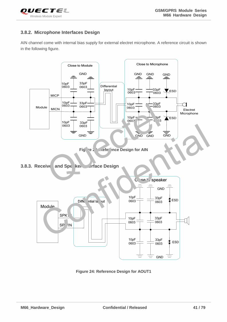
3.8.2. Microphone Interfaces Design
AIN channel come with internal bias supply for external electret microphone. A reference circuit is shown
in the following figure.
MICP
Differential
layout
Module10pF 33pF
33pF
33pF
GND
GND
Electret
Microphone
GND
GND
10pF
10pF
GND
GND
ESD
ESD
Close to Module
MICN
GND
GND
Close to Microphone
0603
0603
0603
0603
0603
0603
33pF
0603
33pF0603
33pF0603
10pF0603
10pF0603
10pF0603
Figure 23: Reference Design for AIN
3.8.3. Receiver and Speaker Interface Design
SPK1P
SPK1N
Differential layout
Module
10pF
0603
Close to speaker
GND
ESD 33pF
0603
33pF
0603
GND
10pF
0603 ESD
10pF
0603
33pF
0603
Figure 24: Reference Design for AOUT1
Quectel
Confidential
GSM/GPRS Module Series M66 Hardware Design
M66_Hardware_Design Confidential / Released 42 / 79
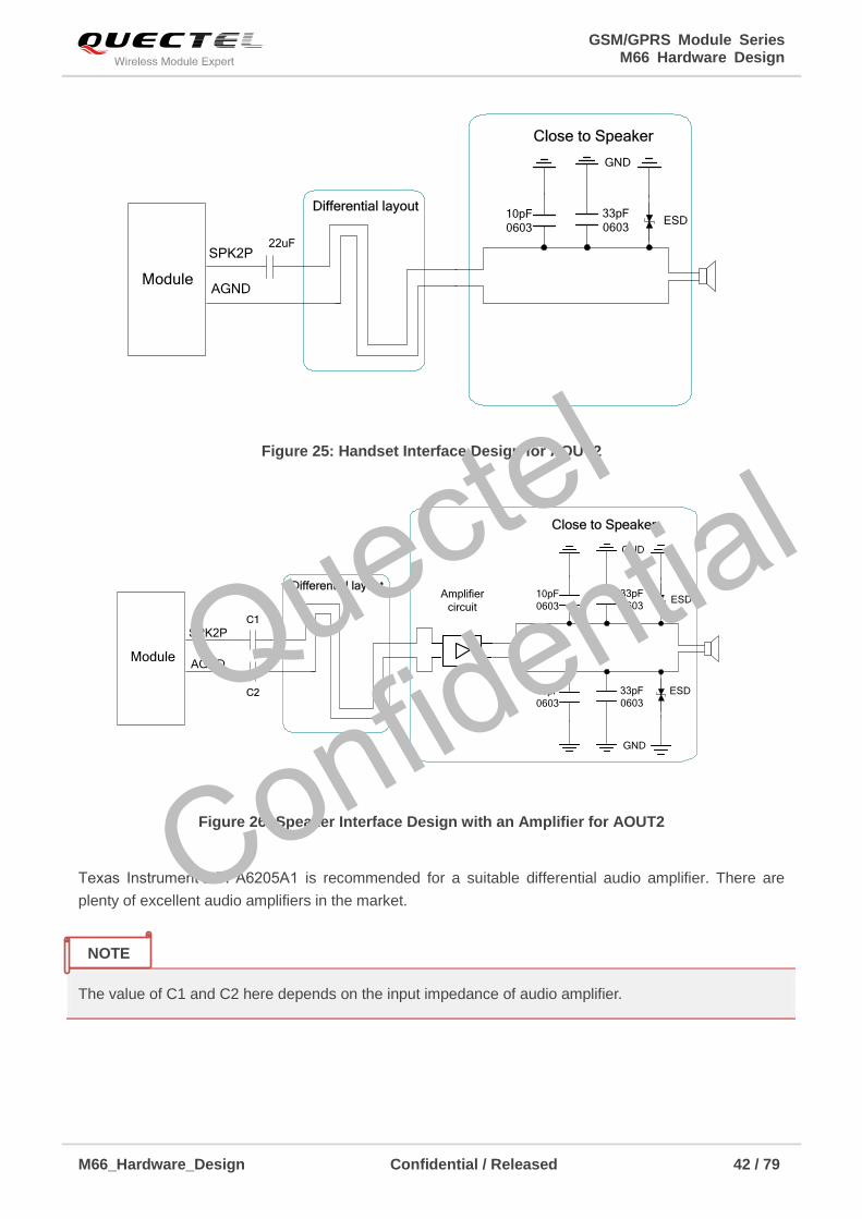
SPK2P
AGND
Differential layout10pF
0603
33pF
0603
Close to Speaker
GND
ESD
Module
22uF
Figure 25: Handset Interface Design for AOUT2
Module
SPK2P
AGND
Differential layoutAmplifier
circuit
10pF
0603
10pF
0603
33pF
0603
33pF
0603
Close to Speaker
GND
GND
ESD
ESD C2
C1
Figure 26: Speaker Interface Design with an Amplifier for AOUT2
Texas Instrument’s TPA6205A1 is recommended for a suitable differential audio amplifier. There are
plenty of excellent audio amplifiers in the market.
1.
The value of C1 and C2 here depends on the input impedance of audio amplifier.
NOTE
Quectel
Confidential
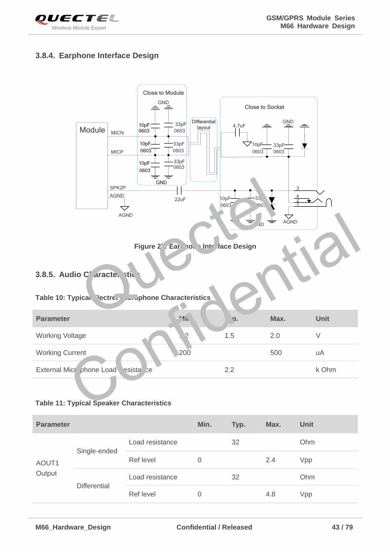
GSM/GPRS Module Series M66 Hardware Design
M66_Hardware_Design Confidential / Released 43 / 79
3.8.4. Earphone Interface Design
124
3
MICP
22uF
33pF
GND
AGND
Close to Socket
AGND
33pF10pF
GND
AGND
Module4.7uF
SPK2P
Close to Module
GND
33pF
33pF
Differential
layout33pF
MICN 0603
0603
0603 0603
06030603
0603
10pF
GND
10pF0603
0603
0603
10pF
10pF
Figure 27: Earphone Interface Design
3.8.5. Audio Characteristics
Table 10: Typical Electret Microphone Characteristics
Table 11: Typical Speaker Characteristics
Parameter Min. Typ. Max. Unit
Working Voltage 1.2 1.5 2.0 V
Working Current 200 500 uA
External Microphone Load Resistance 2.2 k Ohm
Parameter Min. Typ. Max. Unit
AOUT1
Output
Single-ended
Load resistance 32 Ohm
Ref level 0 2.4 Vpp
Differential
Load resistance 32 Ohm
Ref level 0 4.8 Vpp
Quectel
Confidential
GSM/GPRS Module Series M66 Hardware Design
M66_Hardware_Design Confidential / Released 44 / 79
3.9. PCM Interface
M66 supports PCM interface. It is used for digital audio transmission between the module and the device.
This interface is composed of PCM_CLK, PCM_SYNC, PCM_IN and PCM_OUT signal lines.
Pulse-code modulation (PCM) is a converter that changes the consecutive analog audio signal to discrete
digital signal. The whole procedure of Pulse-code modulation contains sampling, quantizing and
encoding.
Table 12: Pin Definition of PCM Interface
3.9.1. Configuration
M66 module supports 13-bit line code PCM format. The sample rate is 8 KHz, and the clock source is 256
KHz, and the module can only act as master mode. The PCM interface supports both long and short
synchronization simultaneously. Furthermore, it only supports MSB first. For detailed information, please
refer to the table below.
Table 13: Configuration
AOUT2
Output Single-ended
Load resistance 32 Load Resistance
Reference level 0 2.4 Vpp
Pin NO. Pin Name Description
30 PCM_CLK PCM clock output
31 PCM_SYNC PCM frame synchronization output
32 PCM_IN PCM data input
33 PCM_OUT PCM data output
PCM
Line Interface Format Linear
Data Length Linear: 13 bits
Quectel
Confidential
GSM/GPRS Module Series M66 Hardware Design
M66_Hardware_Design Confidential / Released 45 / 79
3.9.2. Timing
The sample rate of the PCM interface is 8 KHz and the clock source is 256 KHz, so every frame contains
32 bits data, since M66 supports 16 bits line code PCM format, the left 16 bits are invalid. The following
diagram shows the timing of different combinations. The synchronization length in long synchronization
format can be programmed by firmware from one bit to eight bits. In the Sign extension mode, the high
three bits of 16 bits are sign extension, and in the Zero padding mode, the low three bits of 16 bits are
zero padding.
Under zero padding mode, you can configure the PCM input and output volume by executing
AT+QPCMVOL command. For more details, please refer to Chapter 3.9.4.
12 11 10 9 8 7 6 5 4 3 2 1 0
12 11 10 9 8 7 6 5 4 3 2 1 0
PCM_CLK
PCM_SYNC
PCM_OUT
PCM_IN
MSB
MSB
Sign
extension
Sign
extension
Figure 28: Long Synchronization & Sign Extension Diagram
Sample Rate 8KHz
PCM Clock/Synchronization Source PCM master mode: clock and synchronization is
generated by module
PCM Synchronization Rate 8KHz
PCM Clock Rate PCM master mode: 256 KHz (line)
PCM Synchronization Format Long/short synchronization
PCM Data Ordering MSB first
Zero Padding Yes
Sign Extension Yes
Quectel
Confidential
GSM/GPRS Module Series M66 Hardware Design
M66_Hardware_Design Confidential / Released 46 / 79
12 11 10 9 8 7 6 5 4 3 2 1 0
12 11 10 9 8 7 6 5 4 3 2 1 0
PCM_CLK
PCM_SYNC
PCM_OUT
PCM_IN
MSB
MSB
Zero padding
Zero padding
Figure 29: Long Synchronization & Zero Padding Diagram
PCM_CLK
PCM_SYNC
PCM_OUT
PCM_IN
12 11 10 9 8 7 6 5 4 3 2 1 0
12 11 10 9 8 7 6 5 4 3 2 1 0
MSB
MSB
Sign extension
Sign extension
Figure 30: Short Synchronization & Sign Extension Diagram
PCM_CLK
PCM_SYNC
PCM_OUT
PCM_IN
12 11 10 9 8 7 6 5 4 3 2 1 0
12 11 10 9 8 7 6 5 4 3 2 1 0
MSB
MSB
Zero padding
Zero padding
Figure 31: Short Synchronization & Zero Padding Diagram
3.9.3. Reference Design
M66 can only work as a master, providing synchronization and clock source. The reference design is
shown as below.
Quectel
Confidential
GSM/GPRS Module Series M66 Hardware Design
M66_Hardware_Design Confidential / Released 47 / 79
PCM_SYNC
PCM_CLK
PCM_OUT
PCM_IN
PCM_SYNC
PCM_CLK
PCM_IN
PCM_OUT
Module
(Master)
Peripheral
(Slave)
Figure 32: Reference Design for PCM
3.9.4. AT Command
There are two AT commands about the configuration of PCM, listed as below.
AT+QPCMON can configure operating mode of PCM.
AT+QPCMON=mode, Sync_Type, Sync_Length, SignExtension, MSBFirst.
Table 14: QPCMON Command Description
AT+QPCMVOL can configure the volume of input and output.
AT+QPCMVOL=vol_pcm_in, vol_pcm_out
Parameter Scope Description
Mode 0~2
0: Close PCM
1: Open PCM
2: Open PCM when audio talk is set up
Sync_Type 0~1 0: Short synchronization
1: Long synchronization
Sync_Length 1~8 Programmed from one bit to eight bit
SignExtension 0~1 0: Zero padding
1: Sign extension
MSBFirst 0~1 0: MSB first
1: Not support
Quectel
Confidential
GSM/GPRS Module Series M66 Hardware Design
M66_Hardware_Design Confidential / Released 48 / 79
Table 15: QPCMVOL Command Description
3.10. SIM Card Interface
3.10.1. SIM Card Application
The SIM interface supports the functionality of the GSM Phase 1 specification and also supports the
functionality of the new GSM Phase 2+ specification for FAST 64 kbps SIM card, which is intended for
use with a SIM application Tool-kit.
The SIM interface is powered by an internal regulator in the module. Both 1.8V and 3.0V SIM Cards are
supported.
Table 16: Pin Definition of the SIM Interface
Parameter Scope Description
vol_pcm_in 0~32767 Set the input volume
vol_pcm_out 0~32767 Set the output volume
The voice may be distorted when this value exceeds 16384.
Pin NO. Name Description
14 SIM_VDD Supply power for SIM card. Automatic detection of SIM card voltage.
3.0V±5% and 1.8V±5%. Maximum supply current is around 10mA.
13 SIM_CLK SIM card clock.
11 SIM_DATA SIM card data I/O.
12 SIM_RST SIM card reset.
10 SIM_GND SIM card ground.
Quectel
Confidential
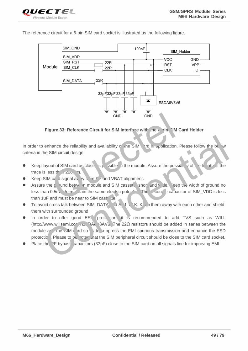
GSM/GPRS Module Series M66 Hardware Design
M66_Hardware_Design Confidential / Released 49 / 79
The reference circuit for a 6-pin SIM card socket is illustrated as the following figure.
Module
SIM_VDD
SIM_GND
SIM_RST
SIM_CLK
SIM_DATA 22R
22R
22R
100nFSIM_Holder
GND
ESDA6V8V6
33pF33pF 33pF
VCC
RST
CLK IO
VPP
GND
GND
33pF
Figure 33: Reference Circuit for SIM Interface with the 6-pin SIM Card Holder
In order to enhance the reliability and availability of the SIM card in application. Please follow the below
criteria in the SIM circuit design:
Keep layout of SIM card as close as possible to the module. Assure the possibility of the length of the
trace is less than 200mm.
Keep SIM card signal away from RF and VBAT alignment.
Assure the ground between module and SIM cassette short and wide. Keep the width of ground no
less than 0.5mm to maintain the same electric potential. The decouple capacitor of SIM_VDD is less
than 1uF and must be near to SIM cassette.
To avoid cross talk between SIM_DATA and SIM_CLK. Keep them away with each other and shield
them with surrounded ground
In order to offer good ESD protection, it is recommended to add TVS such as WILL
(http://www.willsemi.com) ESDA6V8AV6. The 22Ω resistors should be added in series between the
module and the SIM card so as to suppress the EMI spurious transmission and enhance the ESD
protection. Please to be noted that the SIM peripheral circuit should be close to the SIM card socket.
Place the RF bypass capacitors (33pF) close to the SIM card on all signals line for improving EMI.
Quectel
Confidential
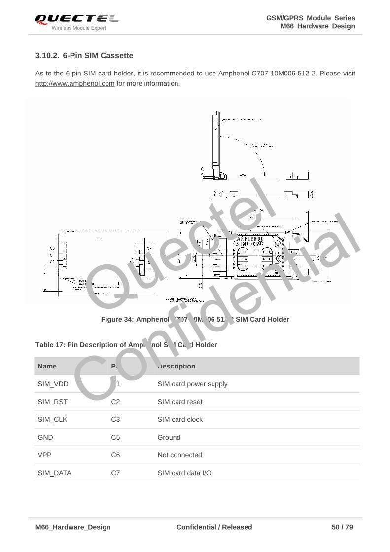
GSM/GPRS Module Series M66 Hardware Design
M66_Hardware_Design Confidential / Released 50 / 79
3.10.2. 6-Pin SIM Cassette
As to the 6-pin SIM card holder, it is recommended to use Amphenol C707 10M006 512 2. Please visit
http://www.amphenol.com for more information.
Figure 34: Amphenol C707 10M006 512 2 SIM Card Holder
Table 17: Pin Description of Amphenol SIM Card Holder
Name Pin Description
SIM_VDD C1 SIM card power supply
SIM_RST C2 SIM card reset
SIM_CLK C3 SIM card clock
GND C5 Ground
VPP C6 Not connected
SIM_DATA C7 SIM card data I/O
Quectel
Confidential
GSM/GPRS Module Series M66 Hardware Design
M66_Hardware_Design Confidential / Released 51 / 79
3.11. ADC
The module provides an ADC channel to measure the value of voltage. Please give priority to the use of
ADC0 channel. The command AT+QADC can read the voltage value applied on ADC0 pin. For details of
this AT command, please refer to the document [1]. In order to improve the accuracy of ADC, the layout
of ADC should be surrounded by ground.
Table 18: Pin Definition of the ADC
Table 19: Characteristics of the ADC
3.12. Behaviors of The RI
Table 20: Behaviors of the RI
Pin NO. Pin Name Description
8 AVDD Reference voltage of ADC circuit
9 ADC0 Analog to digital converter.
Item Min. Typ. Max. Units
Voltage Range 0 2.8 V
ADC Resolution 10 bits
ADC Accuracy 2.7 mV
State RI Response
Standby HIGH
Voicecall
Change to LOW, then:
1. Change to HIGH when call is established.
2. Use ATH to hang up the call, RI changes to HIGH.
3. Calling part hangs up, RI changes to HIGH first, and changes to LOW for
120ms indicating “NO CARRIER” as an URC, then changes to HIGH again.
4. Change to HIGH when SMS is received.
SMS When a new SMS comes, the RI changes to LOW and holds low level for about
Quectel
Confidential
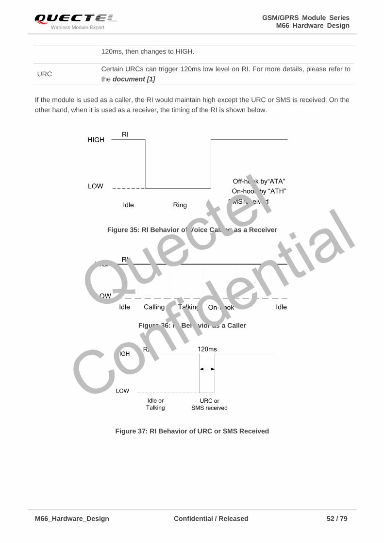
GSM/GPRS Module Series M66 Hardware Design
M66_Hardware_Design Confidential / Released 52 / 79
If the module is used as a caller, the RI would maintain high except the URC or SMS is received. On the
other hand, when it is used as a receiver, the timing of the RI is shown below.
RI
Idle Ring
Off-hook by“ATA”
On-hook by “ATH”
SMS received
HIGH
LOW
Figure 35: RI Behavior of Voice Calling as a Receiver
RI
Idle Calling On-hookTalking
HIGH
LOW
Idle
Figure 36: RI Behavior as a Caller
RI
Idle or
Talking URC or
SMS received
HIGH
LOW
120ms
Figure 37: RI Behavior of URC or SMS Received
120ms, then changes to HIGH.
URC Certain URCs can trigger 120ms low level on RI. For more details, please refer to
the document [1]
Quectel
Confidential
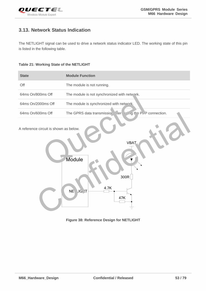
GSM/GPRS Module Series M66 Hardware Design
M66_Hardware_Design Confidential / Released 53 / 79
3.13. Network Status Indication
The NETLIGHT signal can be used to drive a network status indicator LED. The working state of this pin
is listed in the following table.
Table 21: Working State of the NETLIGHT
A reference circuit is shown as below.
Module
NETLIGHT4.7K
47K
300R
VBAT
Figure 38: Reference Design for NETLIGHT
State Module Function
Off The module is not running.
64ms On/800ms Off The module is not synchronized with network.
64ms On/2000ms Off The module is synchronized with network.
64ms On/600ms Off The GPRS data transmission after dialing the PPP connection.
Quectel
Confidential
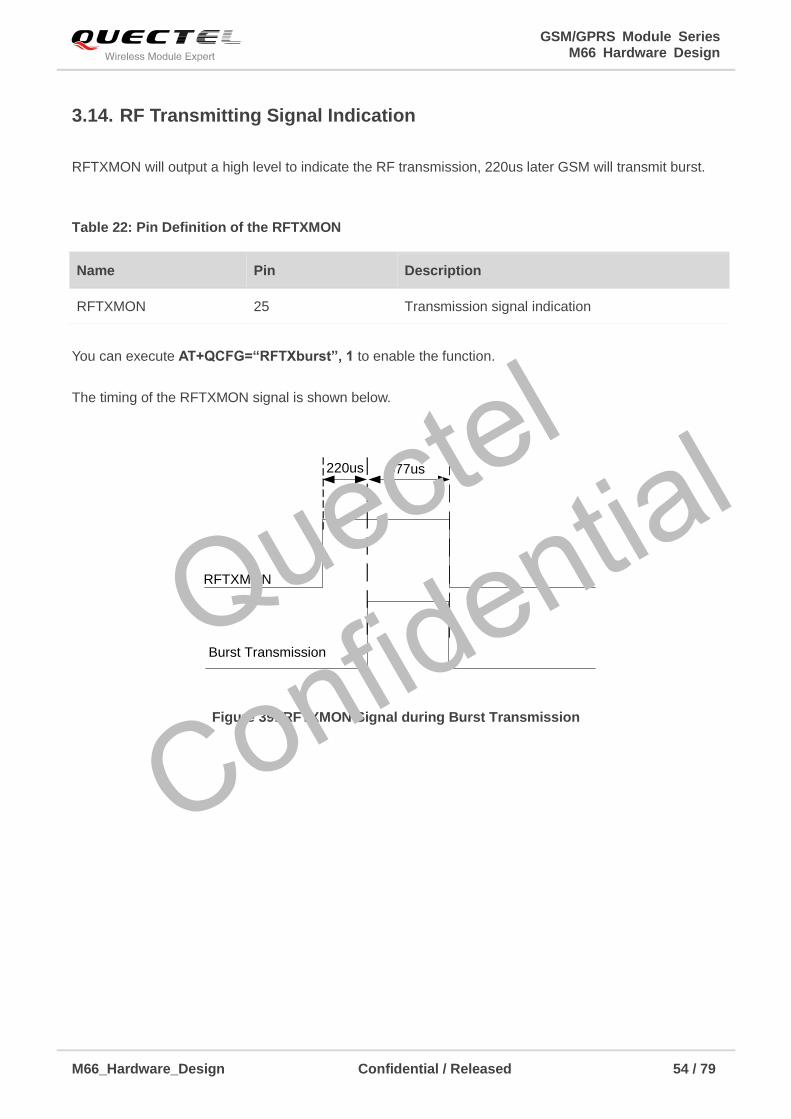
GSM/GPRS Module Series M66 Hardware Design
M66_Hardware_Design Confidential / Released 54 / 79
3.14. RF Transmitting Signal Indication
RFTXMON will output a high level to indicate the RF transmission, 220us later GSM will transmit burst.
Table 22: Pin Definition of the RFTXMON
You can execute AT+QCFG=“RFTXburst”, 1 to enable the function.
The timing of the RFTXMON signal is shown below.
Burst Transmission
RFTXMON
577us220us
Figure 39: RFTXMON Signal during Burst Transmission
Name Pin Description
RFTXMON 25 Transmission signal indication
Quectel
Confidential
GSM/GPRS Module Series M66 Hardware Design
M66_Hardware_Design Confidential / Released 55 / 79
4 Antenna Interface
M66 have two antenna interfaces, GSM antenna and BT antenna. The Pin 26 is the Bluetooth antenna
pad. The Pin 35 is the GSM antenna pad. The RF interface of the two antenna pad has an impedance of
50Ω.
4.1. GSM Antenna Interface
There is a GSM antenna pad named RF_ANT for M66.
Table 23: Pin Definition of the RF_ANT
4.1.1. Reference Design
The external antenna must be matched properly to achieve best performance, so the matching circuit is
necessary, the reference design for RF is shown as below.
Name Pin Description
GND 34 Ground
RF_ANT 35 GSM antenna pad
GND 36 Ground
GND 37 Ground
Quectel
Confidential
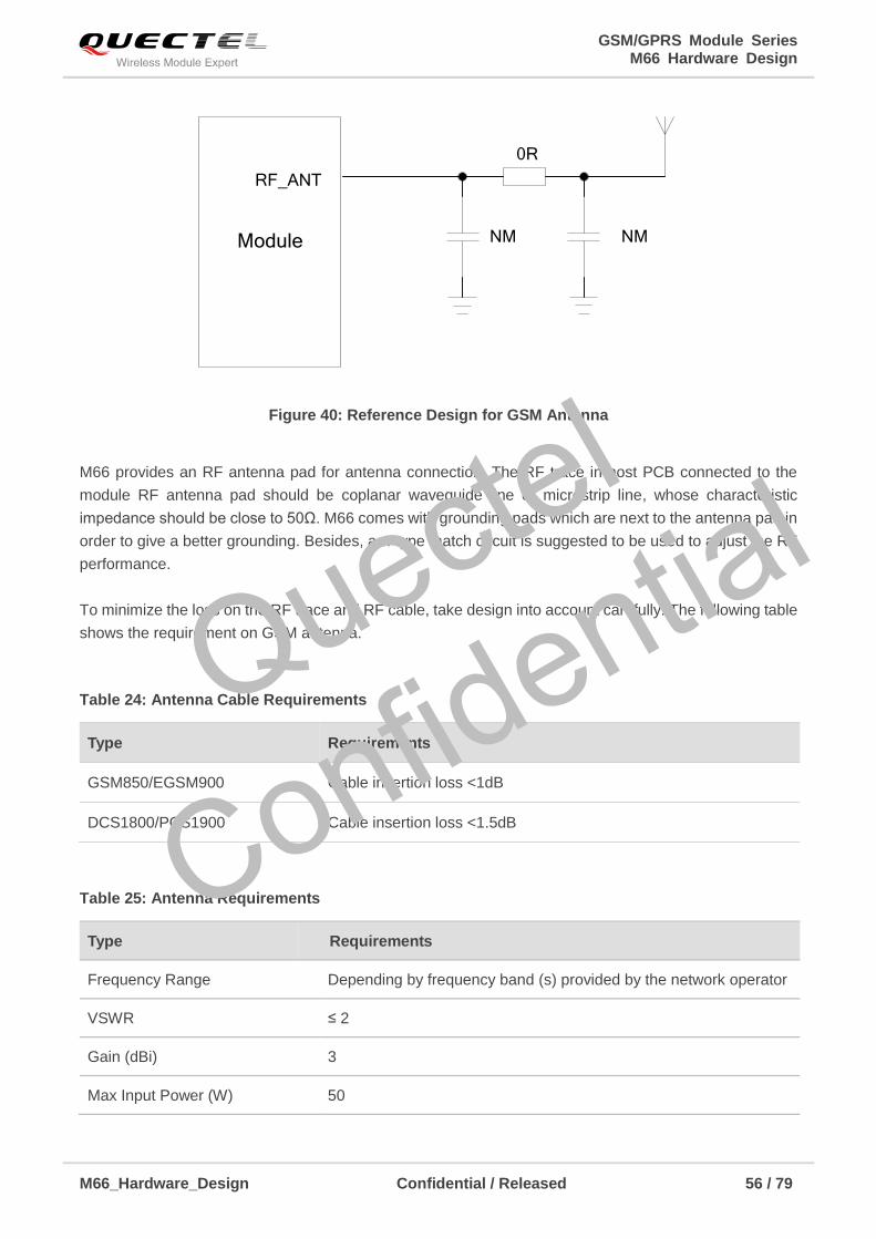
GSM/GPRS Module Series M66 Hardware Design
M66_Hardware_Design Confidential / Released 56 / 79
Module
RF_ANT
0R
NM NM
Figure 40: Reference Design for GSM Antenna
M66 provides an RF antenna pad for antenna connection. The RF trace in host PCB connected to the
module RF antenna pad should be coplanar waveguide line or microstrip line, whose characteristic
impedance should be close to 50Ω. M66 comes with grounding pads which are next to the antenna pad in
order to give a better grounding. Besides, a π type match circuit is suggested to be used to adjust the RF
performance.
To minimize the loss on the RF trace and RF cable, take design into account carefully. The following table
shows the requirement on GSM antenna.
Table 24: Antenna Cable Requirements
Type Requirements
GSM850/EGSM900 Cable insertion loss <1dB
DCS1800/PCS1900 Cable insertion loss <1.5dB
Table 25: Antenna Requirements
Type Requirements
Frequency Range Depending by frequency band (s) provided by the network operator
VSWR ≤ 2
Gain (dBi) 3
Max Input Power (W) 50
Quectel
Confidential
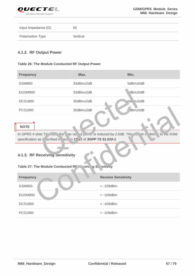
GSM/GPRS Module Series M66 Hardware Design
M66_Hardware_Design Confidential / Released 57 / 79
Input Impedance (Ω) 50
Polarization Type Vertical
4.1.2. RF Output Power
Table 26: The Module Conducted RF Output Power
In GPRS 4 slots TX mode, the max output power is reduced by 2.5dB. This design conforms to the GSM
specification as described in section 13.16 of 3GPP TS 51.010-1.
4.1.3. RF Receiving Sensitivity
Table 27: The Module Conducted RF Receiving Sensitivity
Frequency Max. Min.
GSM850 33dBm±2dB 5dBm±5dB
EGSM900 33dBm±2dB 5dBm±5dB
DCS1800 30dBm±2dB 0dBm±5dB
PCS1900 30dBm±2dB 0dBm±5dB
Frequency Receive Sensitivity
GSM850 < -109dBm
EGSM900 < -109dBm
DCS1800 < -109dBm
PCS1900 < -109dBm
NOTE
Quectel
Confidential
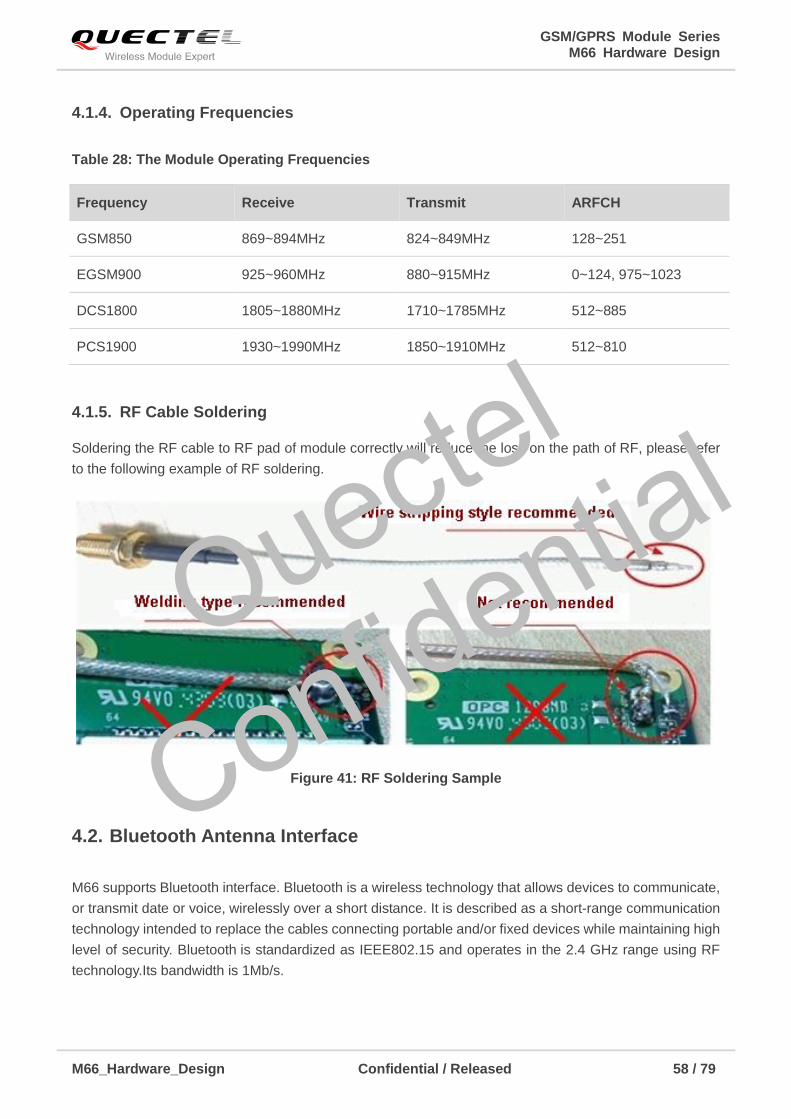
GSM/GPRS Module Series M66 Hardware Design
M66_Hardware_Design Confidential / Released 58 / 79
4.1.4. Operating Frequencies
Table 28: The Module Operating Frequencies
4.1.5. RF Cable Soldering
Soldering the RF cable to RF pad of module correctly will reduce the loss on the path of RF, please refer
to the following example of RF soldering.
Figure 41: RF Soldering Sample
4.2. Bluetooth Antenna Interface
M66 supports Bluetooth interface. Bluetooth is a wireless technology that allows devices to communicate,
or transmit date or voice, wirelessly over a short distance. It is described as a short-range communication
technology intended to replace the cables connecting portable and/or fixed devices while maintaining high
level of security. Bluetooth is standardized as IEEE802.15 and operates in the 2.4 GHz range using RF
technology.Its bandwidth is 1Mb/s.
Frequency Receive Transmit ARFCH
GSM850 869~894MHz 824~849MHz 128~251
EGSM900 925~960MHz 880~915MHz 0~124, 975~1023
DCS1800 1805~1880MHz 1710~1785MHz 512~885
PCS1900 1930~1990MHz 1850~1910MHz 512~810
Quectel
Confidential
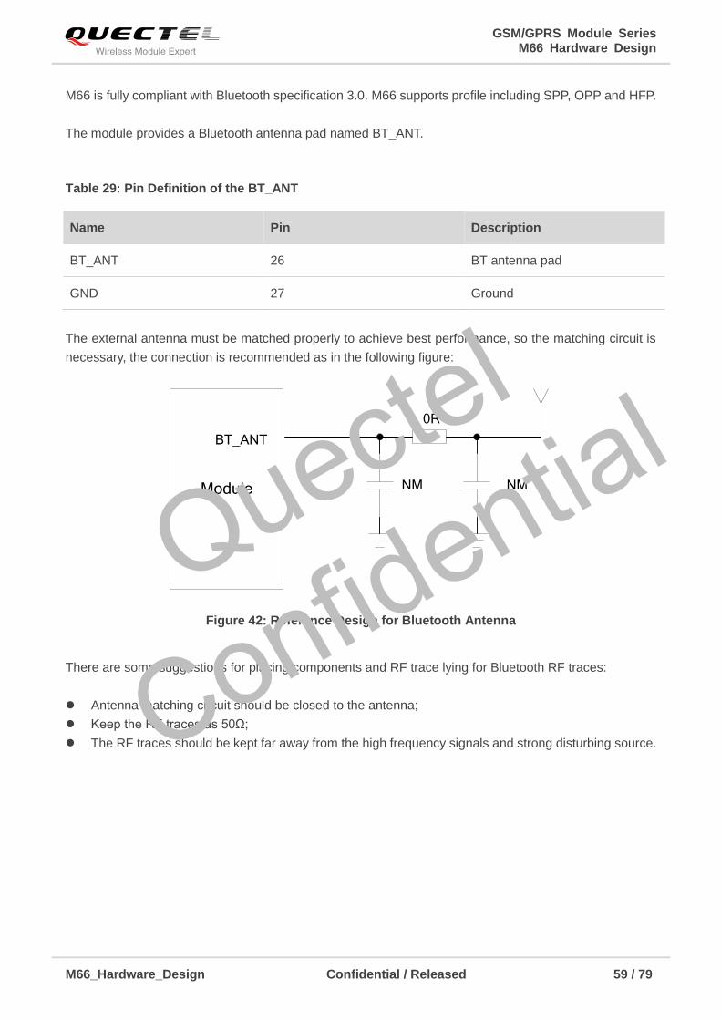
GSM/GPRS Module Series M66 Hardware Design
M66_Hardware_Design Confidential / Released 59 / 79
M66 is fully compliant with Bluetooth specification 3.0. M66 supports profile including SPP, OPP and HFP.
The module provides a Bluetooth antenna pad named BT_ANT.
Table 29: Pin Definition of the BT_ANT
The external antenna must be matched properly to achieve best performance, so the matching circuit is
necessary, the connection is recommended as in the following figure:
Module
BT_ANT
0R
NM NM
Figure 42: Reference Design for Bluetooth Antenna
There are some suggestions for placing components and RF trace lying for Bluetooth RF traces:
Antenna matching circuit should be closed to the antenna;
Keep the RF traces as 50Ω;
The RF traces should be kept far away from the high frequency signals and strong disturbing source.
Name Pin Description
BT_ANT 26 BT antenna pad
GND 27 Ground
Quectel
Confidential
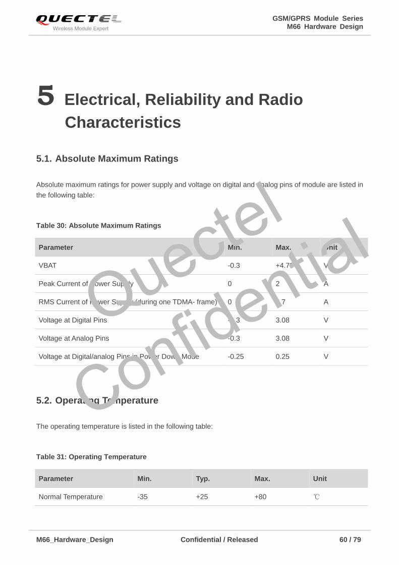
GSM/GPRS Module Series M66 Hardware Design
M66_Hardware_Design Confidential / Released 60 / 79
5 Electrical, Reliability and Radio
Characteristics
5.1. Absolute Maximum Ratings
Absolute maximum ratings for power supply and voltage on digital and analog pins of module are listed in
the following table:
Table 30: Absolute Maximum Ratings
5.2. Operating Temperature
The operating temperature is listed in the following table:
Table 31: Operating Temperature
Parameter Min. Max. Unit
VBAT -0.3 +4.73 V
Peak Current of Power Supply 0 2 A
RMS Current of Power Supply (during one TDMA- frame) 0 0.7 A
Voltage at Digital Pins -0.3 3.08 V
Voltage at Analog Pins -0.3 3.08 V
Voltage at Digital/analog Pins in Power Down Mode -0.25 0.25 V
Parameter Min. Typ. Max. Unit
Normal Temperature -35 +25 +80 ℃
Quectel
Confidential
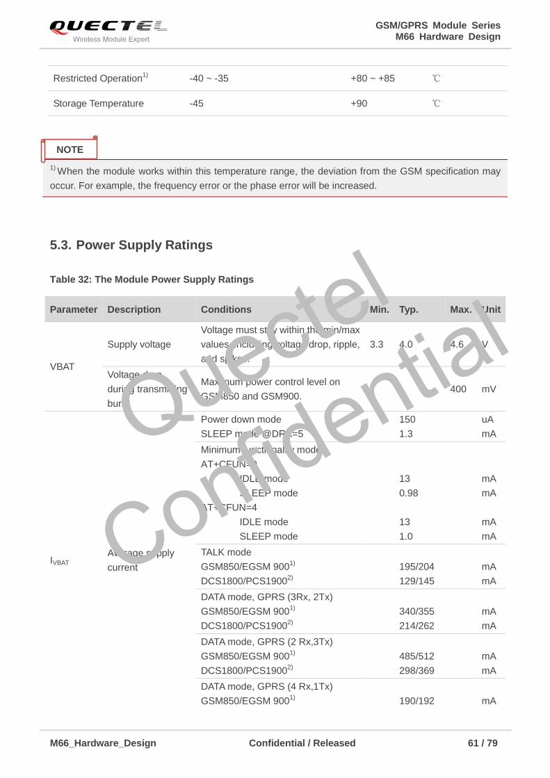
GSM/GPRS Module Series M66 Hardware Design
M66_Hardware_Design Confidential / Released 61 / 79
1) When the module works within this temperature range, the deviation from the GSM specification may
occur. For example, the frequency error or the phase error will be increased.
5.3. Power Supply Ratings
Table 32: The Module Power Supply Ratings
Restricted Operation1)
-40 ~ -35 +80 ~ +85 ℃
Storage Temperature -45 +90 ℃
Parameter Description Conditions Min. Typ. Max. Unit
VBAT
Supply voltage
Voltage must stay within the min/max
values, including voltage drop, ripple,
and spikes.
3.3 4.0 4.6 V
Voltage drop
during transmitting
burst
Maximum power control level on
GSM850 and GSM900. 400 mV
IVBAT Average supply
current
Power down mode
SLEEP mode @DRX=5
150
1.3
uA
mA
Minimum functionality mode
AT+CFUN=0
IDLE mode
SLEEP mode
AT+CFUN=4
IDLE mode
SLEEP mode
13
0.98
13
1.0
mA
mA
mA
mA
TALK mode
GSM850/EGSM 9001)
DCS1800/PCS19002)
195/204
129/145
mA
mA
DATA mode, GPRS (3Rx, 2Tx)
GSM850/EGSM 9001)
DCS1800/PCS19002)
340/355
214/262
mA
mA
DATA mode, GPRS (2 Rx,3Tx)
GSM850/EGSM 9001)
DCS1800/PCS19002)
485/512
298/369
mA
mA
DATA mode, GPRS (4 Rx,1Tx)
GSM850/EGSM 9001)
190/192
mA
NOTE
Quectel
Confidential
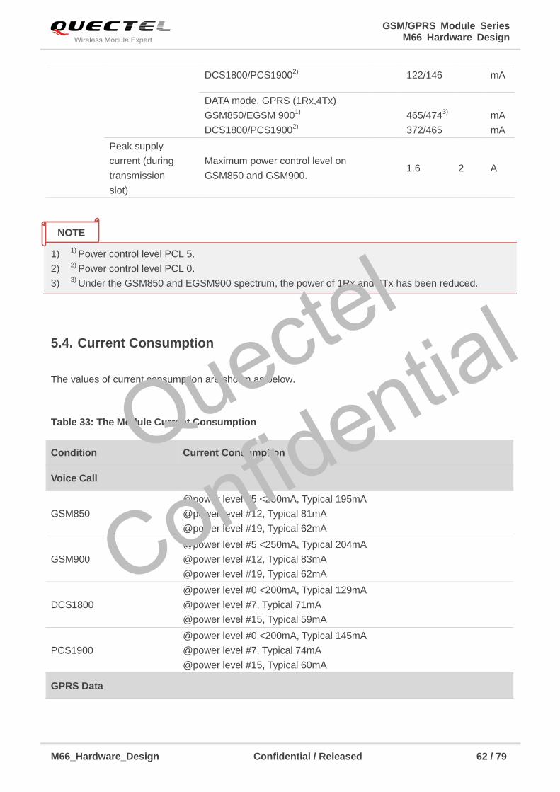
GSM/GPRS Module Series M66 Hardware Design
M66_Hardware_Design Confidential / Released 62 / 79
1) 1)
Power control level PCL 5.
2) 2)
Power control level PCL 0.
3) 3)
Under the GSM850 and EGSM900 spectrum, the power of 1Rx and 4Tx has been reduced.
5.4. Current Consumption
The values of current consumption are shown as below.
Table 33: The Module Current Consumption
DCS1800/PCS19002)
122/146 mA
DATA mode, GPRS (1Rx,4Tx)
GSM850/EGSM 9001)
DCS1800/PCS19002)
465/4743)
372/465
mA
mA
Peak supply
current (during
transmission
slot)
Maximum power control level on
GSM850 and GSM900. 1.6 2 A
Condition Current Consumption
Voice Call
GSM850
@power level #5 <250mA, Typical 195mA
@power level #12, Typical 81mA
@power level #19, Typical 62mA
GSM900
@power level #5 <250mA, Typical 204mA
@power level #12, Typical 83mA
@power level #19, Typical 62mA
DCS1800
@power level #0 <200mA, Typical 129mA
@power level #7, Typical 71mA
@power level #15, Typical 59mA
PCS1900
@power level #0 <200mA, Typical 145mA
@power level #7, Typical 74mA
@power level #15, Typical 60mA
GPRS Data
NOTE
Quectel
Confidential
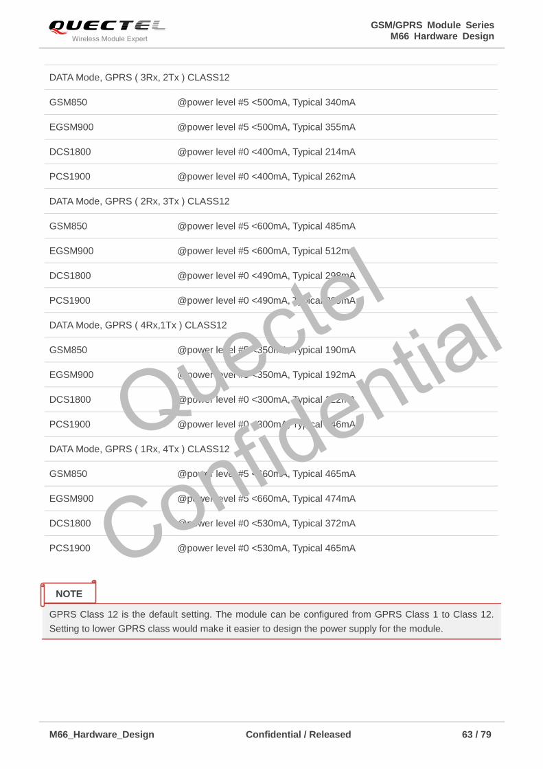
GSM/GPRS Module Series M66 Hardware Design
M66_Hardware_Design Confidential / Released 63 / 79
GPRS Class 12 is the default setting. The module can be configured from GPRS Class 1 to Class 12.
Setting to lower GPRS class would make it easier to design the power supply for the module.
DATA Mode, GPRS ( 3Rx, 2Tx ) CLASS12
GSM850 @power level #5 <500mA, Typical 340mA
EGSM900 @power level #5 <500mA, Typical 355mA
DCS1800 @power level #0 <400mA, Typical 214mA
PCS1900 @power level #0 <400mA, Typical 262mA
DATA Mode, GPRS ( 2Rx, 3Tx ) CLASS12
GSM850 @power level #5 <600mA, Typical 485mA
EGSM900 @power level #5 <600mA, Typical 512mA
DCS1800 @power level #0 <490mA, Typical 298mA
PCS1900 @power level #0 <490mA, Typical 369mA
DATA Mode, GPRS ( 4Rx,1Tx ) CLASS12
GSM850 @power level #5 <350mA, Typical 190mA
EGSM900 @power level #5 <350mA, Typical 192mA
DCS1800 @power level #0 <300mA, Typical 122mA
PCS1900 @power level #0 <300mA, Typical 146mA
DATA Mode, GPRS ( 1Rx, 4Tx ) CLASS12
GSM850 @power level #5 <660mA, Typical 465mA
EGSM900 @power level #5 <660mA, Typical 474mA
DCS1800 @power level #0 <530mA, Typical 372mA
PCS1900 @power level #0 <530mA, Typical 465mA
NOTE
Quectel
Confidential
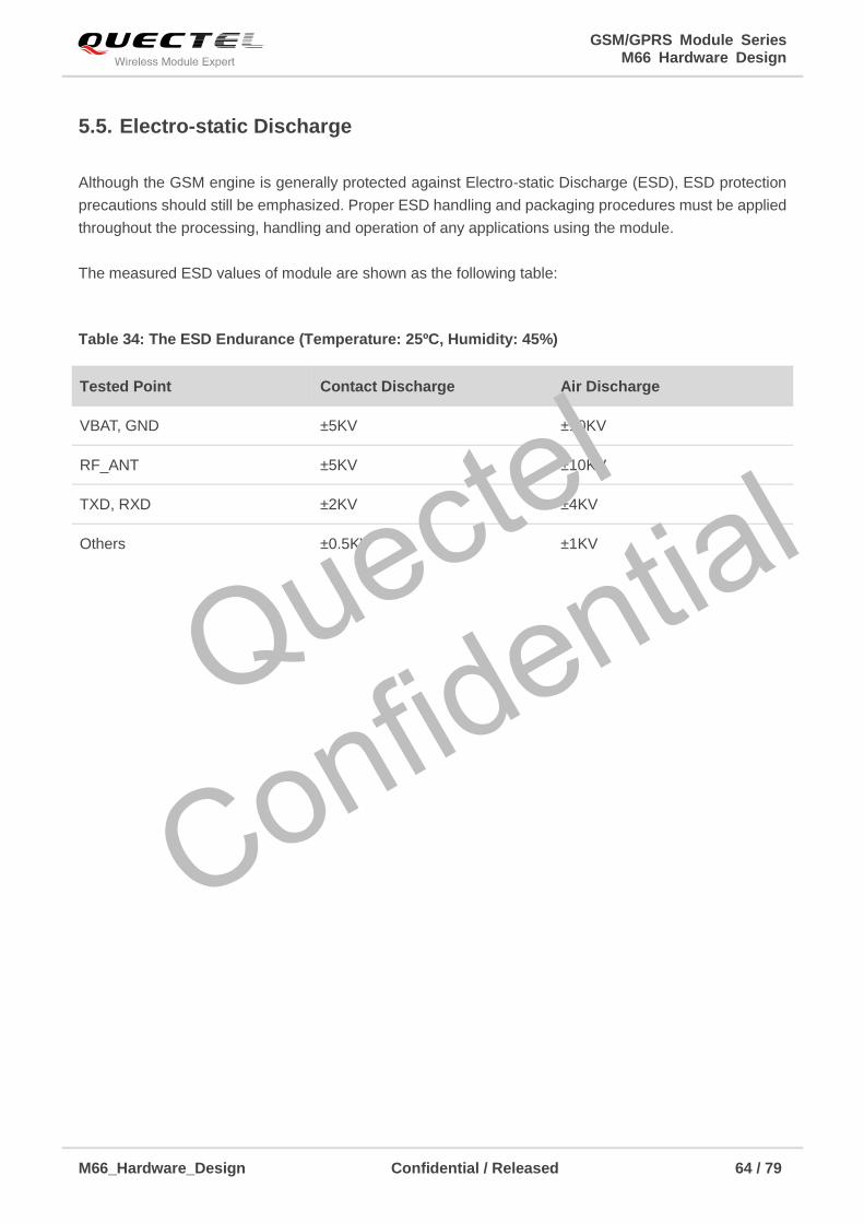
GSM/GPRS Module Series M66 Hardware Design
M66_Hardware_Design Confidential / Released 64 / 79
5.5. Electro-static Discharge
Although the GSM engine is generally protected against Electro-static Discharge (ESD), ESD protection
precautions should still be emphasized. Proper ESD handling and packaging procedures must be applied
throughout the processing, handling and operation of any applications using the module.
The measured ESD values of module are shown as the following table:
Table 34: The ESD Endurance (Temperature: 25ºC, Humidity: 45%)
Tested Point Contact Discharge Air Discharge
VBAT, GND ±5KV ±10KV
RF_ANT ±5KV ±10KV
TXD, RXD ±2KV ±4KV
Others ±0.5KV ±1KV
Quectel
Confidential
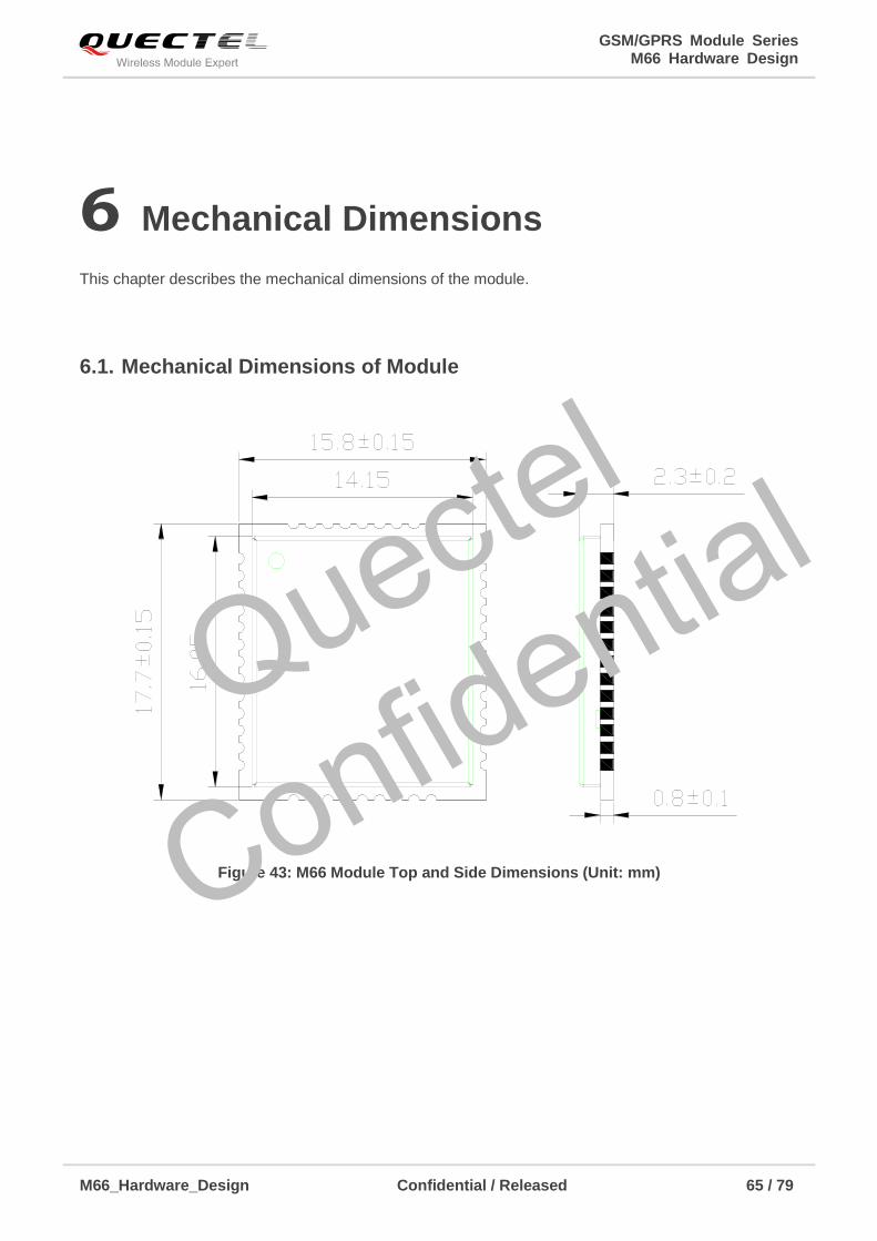
GSM/GPRS Module Series M66 Hardware Design
M66_Hardware_Design Confidential / Released 65 / 79
6 Mechanical Dimensions
This chapter describes the mechanical dimensions of the module.
6.1. Mechanical Dimensions of Module
Figure 43: M66 Module Top and Side Dimensions (Unit: mm)
Quectel
Confidential
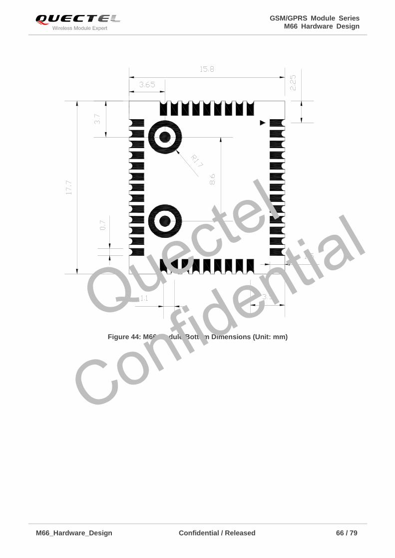
GSM/GPRS Module Series M66 Hardware Design
M66_Hardware_Design Confidential / Released 66 / 79
Figure 44: M66 Module Bottom Dimensions (Unit: mm)
Quectel
Confidential
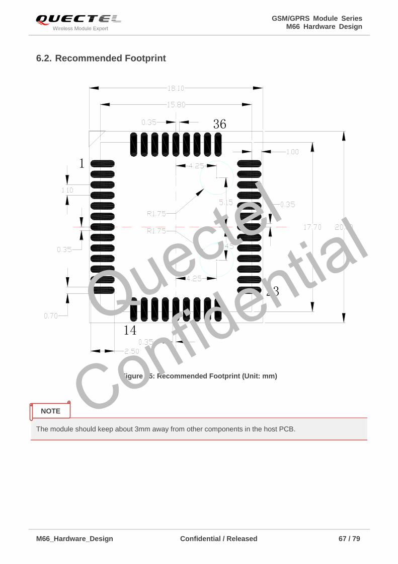
GSM/GPRS Module Series M66 Hardware Design
M66_Hardware_Design Confidential / Released 67 / 79
6.2. Recommended Footprint
1
14
23
36
Figure 45: Recommended Footprint (Unit: mm)
The module should keep about 3mm away from other components in the host PCB.
NOTE
Quectel
Confidential
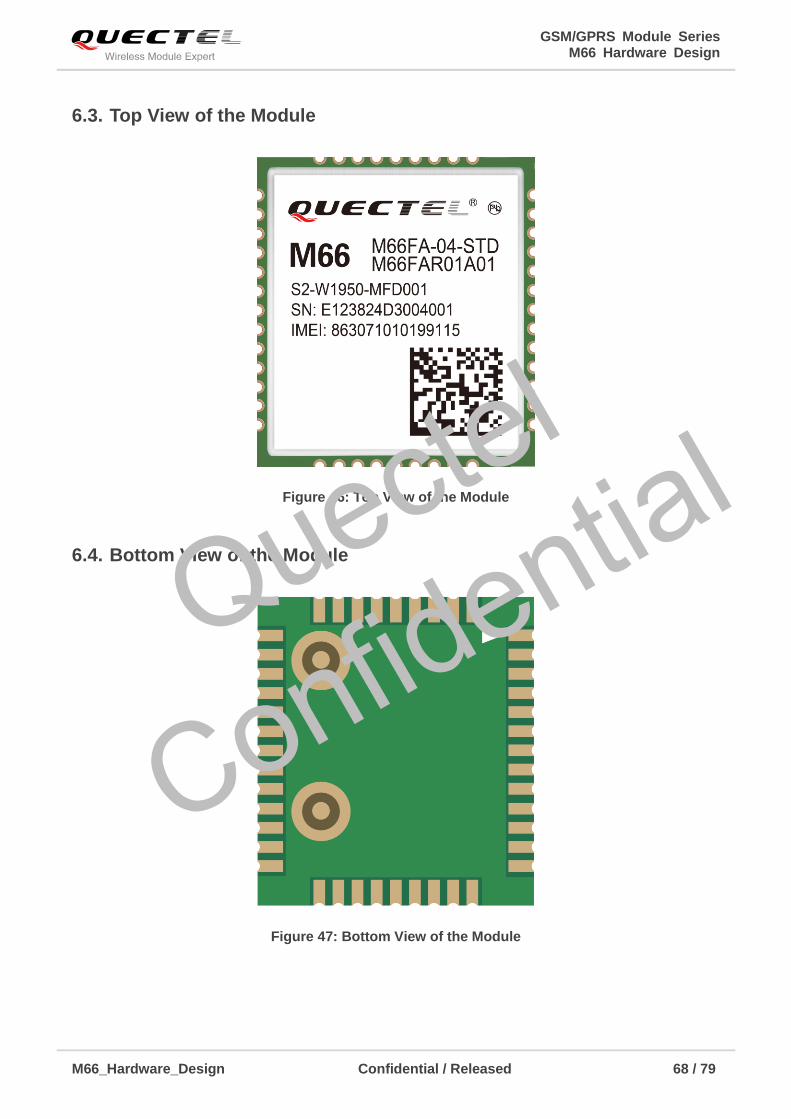
GSM/GPRS Module Series M66 Hardware Design
M66_Hardware_Design Confidential / Released 68 / 79
6.3. Top View of the Module
Figure 46: Top View of the Module
6.4. Bottom View of the Module
Figure 47: Bottom View of the Module
Quectel
Confidential
GSM/GPRS Module Series M66 Hardware Design
M66_Hardware_Design Confidential / Released 69 / 79
7 Storage and Manufacturing
7.1. Storage
M66 module is distributed in a vacuum-sealed bag. The restriction for storage is shown as below.
Shelf life in the vacuum-sealed bag: 12 months at environments of <40ºC temperature and <90%RH.
After the vacuum-sealed bag is opened, devices that need to be mounted directly must be:
Mounted within 72 hours at the factory environment of ≤30ºC temperature and <60% RH.
Stored at <10% RH.
Devices require baking before mounting, if any circumstance below occurs.
When the ambient temperature is 23ºC±5ºC, humidity indication card shows the humidity is >10%
before opening the vacuum-sealed bag.
If ambient temperature is <30ºC and the humidity is <60%, the devices have not been mounted
during 72hours.
Stored at >10% RH.
If baking is required, devices should be baked for 48 hours at 125ºC±5ºC.
As plastic container cannot be subjected to high temperature, devices must be removed prior to high
temperature (125ºC) bake. If shorter bake times are desired, refer to the IPC/JEDECJ-STD-033 for bake
procedure.
NOTE
Quectel
Confidential
GSM/GPRS Module Series M66 Hardware Design
M66_Hardware_Design Confidential / Released 70 / 79
7.2. Soldering
The squeegee should push the paste on the surface of the stencil that makes the paste fill the stencil
openings and penetrate to the PCB. The force on the squeegee should be adjusted so as to produce a
clean stencil surface on a single pass. To ensure the module soldering quality, the thickness of stencil at
the hole of the module pads should be 0.2 mm for M66.For more details, please refer to document [13]
It is suggested that peak reflow temperature is from 235ºC to 245ºC (for SnAg3.0Cu0.5 alloy). Absolute
max reflow temperature is 260ºC. To avoid damage to the module when it was repeatedly heated, it is
suggested that the module should be mounted after the first panel has been reflowed. The following
picture is the actual diagram which we have operated.
Time(s)
50 100 150 200 250 300
50
100
150
200
250
160℃
200℃
217
0
70s~120s
40s~60s
Between 1~3℃/S
Preheat Heating Cooling℃
s
Liquids
Temperature
Figure 48: Ramp-Soak-Spike Reflow Profile
7.3. Packaging
The modules are stored in a vacuum-sealed bag which is ESD protected. It should not be opened until the
devices are ready to be soldered onto the application.
Quectel
Confidential
GSM/GPRS Module Series M66 Hardware Design
M66_Hardware_Design Confidential / Released 71 / 79
7.3.1. Tape and Reel Packaging
The reel is 330mm in diameter and each reel contains 250 modules.
Figure 49: Tape and Reel Specification
Figure 50: Dimensions of Reel
Quectel
Confidential
GSM/GPRS Module Series M66 Hardware Design
M66_Hardware_Design Confidential / Released 72 / 79
8 Appendix A Reference
Table 35: Related Documents
SN Document Name Remark
[1] Quectel_M66_AT_Commands_Manual AT commands manual
[2] ITU-T Draft new recommendation
V.25ter Serial asynchronous automatic dialing and control
[3] GSM 07.07 Digital cellular telecommunications (Phase 2+); AT
command set for GSM Mobile Equipment (ME)
[4] GSM 07.10 Support GSM 07.10 multiplexing protocol
[5] GSM 07.05
Digital cellular telecommunications (Phase 2+); Use of
Data Terminal Equipment – Data Circuit terminating
Equipment (DTE – DCE) interface for Short Message
Service (SMS) and Cell Broadcast Service (CBS)
[6] GSM 11.14
Digital cellular telecommunications (Phase 2+);
Specification of the SIM Application Toolkit for the
Subscriber Identity module – Mobile Equipment (SIM –
ME) interface
[7] GSM 11.11
Digital cellular telecommunications (Phase 2+);
Specification of the Subscriber Identity module – Mobile
Equipment (SIM – ME) interface
[8] GSM 03.38 Digital cellular telecommunications (Phase 2+);
Alphabets and language-specific information
[9] GSM 11.10
Digital cellular telecommunications (Phase 2); Mobile
Station (MS) conformance specification; Part 1:
Conformance specification
[10] GSM_UART_Application_Note UART port application note
[11] GSM_FW_Upgrade_AN01 GSM Firmware upgrade application note
[12] GSM_EVB_User_Guide GSM EVB user guide
[13] Module_Secondary_SMT_User_Guide Module secondary SMT user guide
Quectel
Confidential
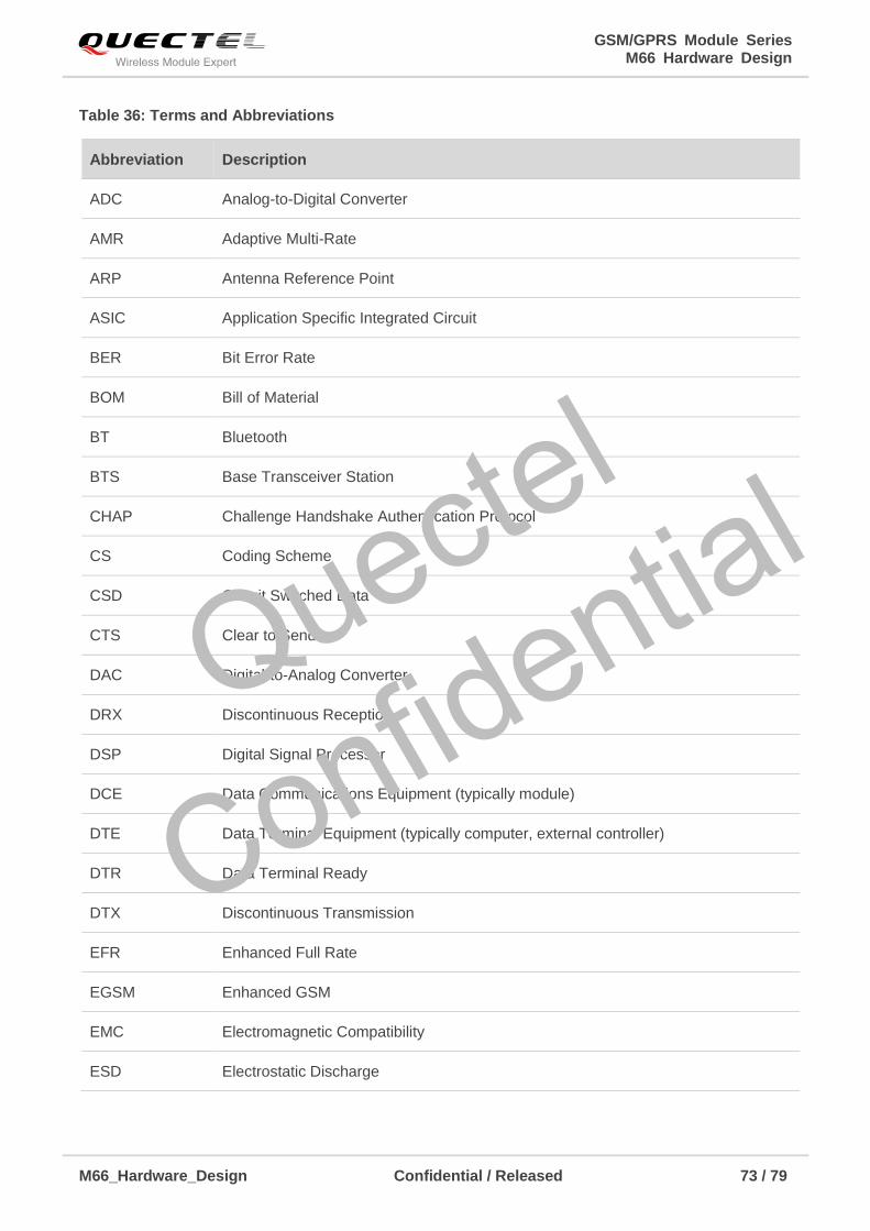
GSM/GPRS Module Series M66 Hardware Design
M66_Hardware_Design Confidential / Released 73 / 79
Table 36: Terms and Abbreviations
Abbreviation Description
ADC Analog-to-Digital Converter
AMR Adaptive Multi-Rate
ARP Antenna Reference Point
ASIC Application Specific Integrated Circuit
BER Bit Error Rate
BOM Bill of Material
BT Bluetooth
BTS Base Transceiver Station
CHAP Challenge Handshake Authentication Protocol
CS Coding Scheme
CSD Circuit Switched Data
CTS Clear to Send
DAC Digital-to-Analog Converter
DRX Discontinuous Reception
DSP Digital Signal Processor
DCE Data Communications Equipment (typically module)
DTE Data Terminal Equipment (typically computer, external controller)
DTR Data Terminal Ready
DTX Discontinuous Transmission
EFR Enhanced Full Rate
EGSM Enhanced GSM
EMC Electromagnetic Compatibility
ESD Electrostatic Discharge
Quectel
Confidential
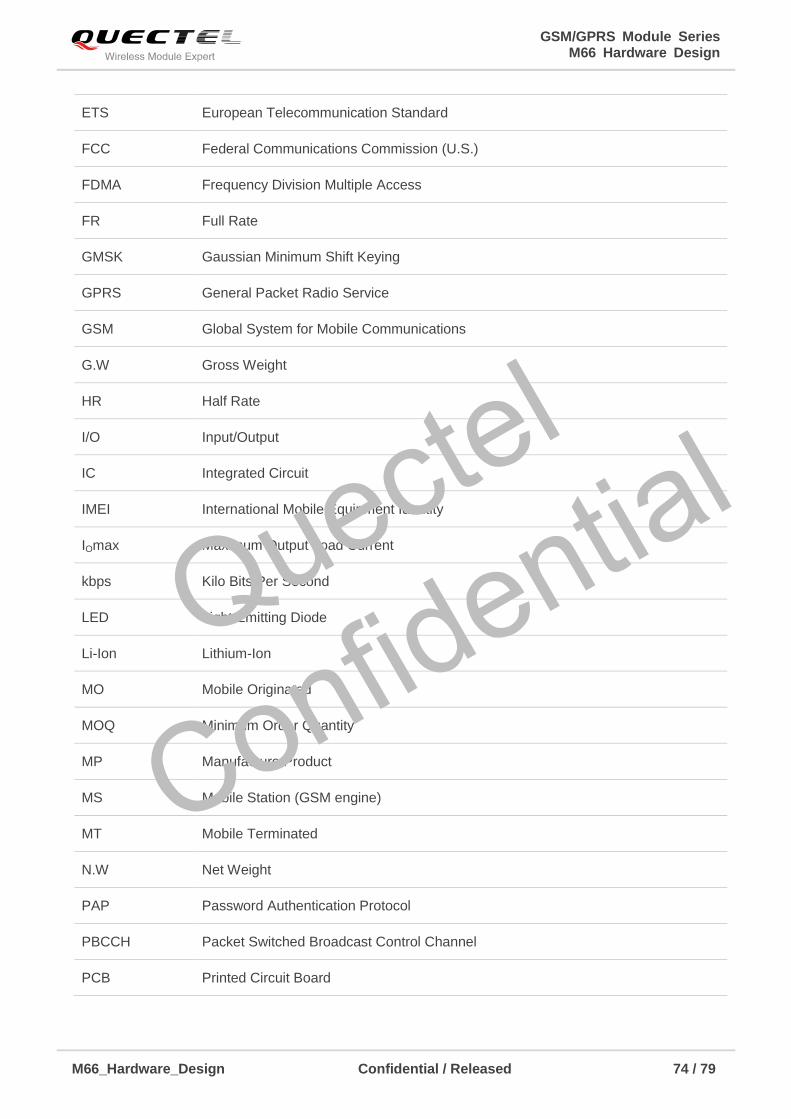
GSM/GPRS Module Series M66 Hardware Design
M66_Hardware_Design Confidential / Released 74 / 79
ETS European Telecommunication Standard
FCC Federal Communications Commission (U.S.)
FDMA Frequency Division Multiple Access
FR Full Rate
GMSK Gaussian Minimum Shift Keying
GPRS General Packet Radio Service
GSM Global System for Mobile Communications
G.W Gross Weight
HR Half Rate
I/O Input/Output
IC Integrated Circuit
IMEI International Mobile Equipment Identity
IOmax Maximum Output Load Current
kbps Kilo Bits Per Second
LED Light Emitting Diode
Li-Ion Lithium-Ion
MO Mobile Originated
MOQ Minimum Order Quantity
MP Manufacture Product
MS Mobile Station (GSM engine)
MT Mobile Terminated
N.W Net Weight
PAP Password Authentication Protocol
PBCCH Packet Switched Broadcast Control Channel
PCB Printed Circuit Board
Quectel
Confidential
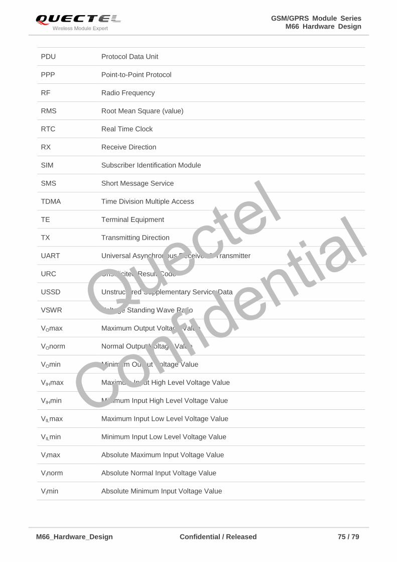
GSM/GPRS Module Series M66 Hardware Design
M66_Hardware_Design Confidential / Released 75 / 79
PDU Protocol Data Unit
PPP Point-to-Point Protocol
RF Radio Frequency
RMS Root Mean Square (value)
RTC Real Time Clock
RX Receive Direction
SIM Subscriber Identification Module
SMS Short Message Service
TDMA Time Division Multiple Access
TE Terminal Equipment
TX Transmitting Direction
UART Universal Asynchronous Receiver & Transmitter
URC Unsolicited Result Code
USSD Unstructured Supplementary Service Data
VSWR Voltage Standing Wave Ratio
VOmax Maximum Output Voltage Value
VOnorm Normal Output Voltage Value
VOmin Minimum Output Voltage Value
VIHmax Maximum Input High Level Voltage Value
VIHmin Minimum Input High Level Voltage Value
VILmax Maximum Input Low Level Voltage Value
VILmin Minimum Input Low Level Voltage Value
VImax Absolute Maximum Input Voltage Value
VInorm Absolute Normal Input Voltage Value
VImin Absolute Minimum Input Voltage Value
Quectel
Confidential
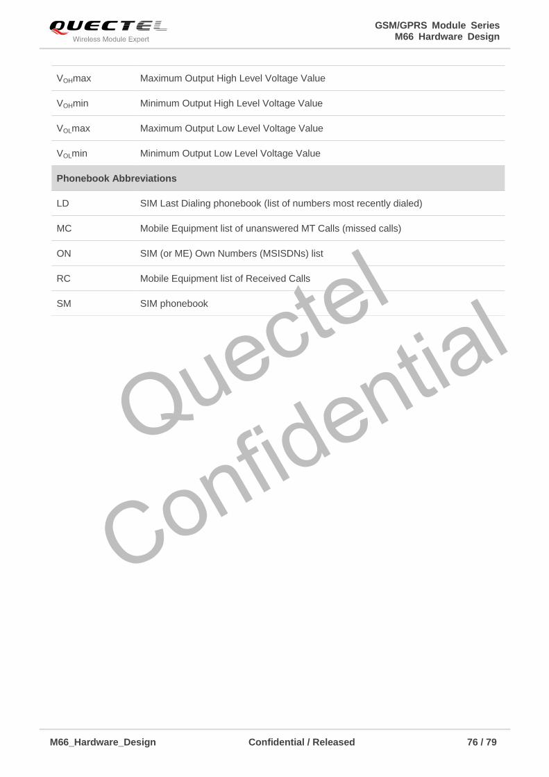
GSM/GPRS Module Series M66 Hardware Design
M66_Hardware_Design Confidential / Released 76 / 79
VOHmax Maximum Output High Level Voltage Value
VOHmin Minimum Output High Level Voltage Value
VOLmax Maximum Output Low Level Voltage Value
VOLmin Minimum Output Low Level Voltage Value
Phonebook Abbreviations
LD SIM Last Dialing phonebook (list of numbers most recently dialed)
MC Mobile Equipment list of unanswered MT Calls (missed calls)
ON SIM (or ME) Own Numbers (MSISDNs) list
RC Mobile Equipment list of Received Calls
SM SIM phonebook
Quectel
Confidential
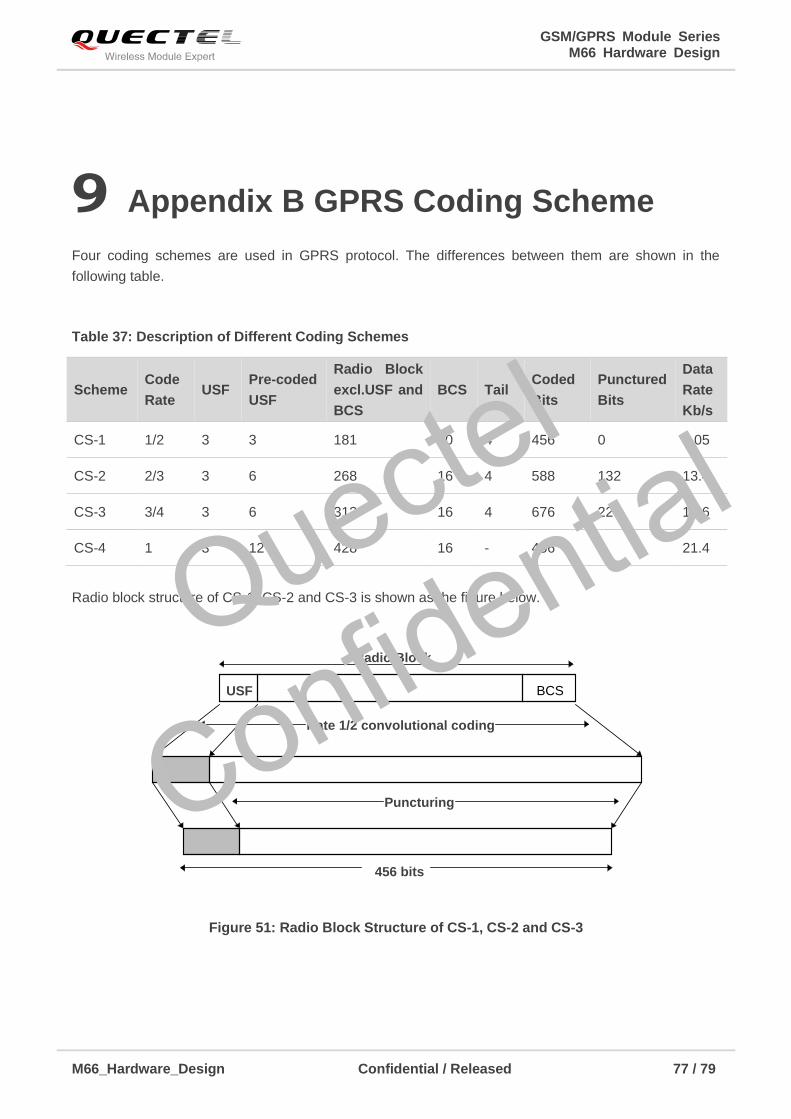
GSM/GPRS Module Series M66 Hardware Design
M66_Hardware_Design Confidential / Released 77 / 79
9 Appendix B GPRS Coding Scheme
Four coding schemes are used in GPRS protocol. The differences between them are shown in the
following table.
Table 37: Description of Different Coding Schemes
Scheme Code
Rate USF
Pre-coded
USF
Radio Block
excl.USF and
BCS
BCS Tail Coded
Bits
Punctured
Bits
Data
Rate
Kb/s
CS-1 1/2 3 3 181 40 4 456 0 9.05
CS-2 2/3 3 6 268 16 4 588 132 13.4
CS-3 3/4 3 6 312 16 4 676 220 15.6
CS-4 1 3 12 428 16 - 456 - 21.4
Radio block structure of CS-1, CS-2 and CS-3 is shown as the figure below.
Figure 51: Radio Block Structure of CS-1, CS-2 and CS-3
Rate 1/2 convolutional coding
Puncturing
456 bits
USF BCS
Radio Block
Quectel
Confidential
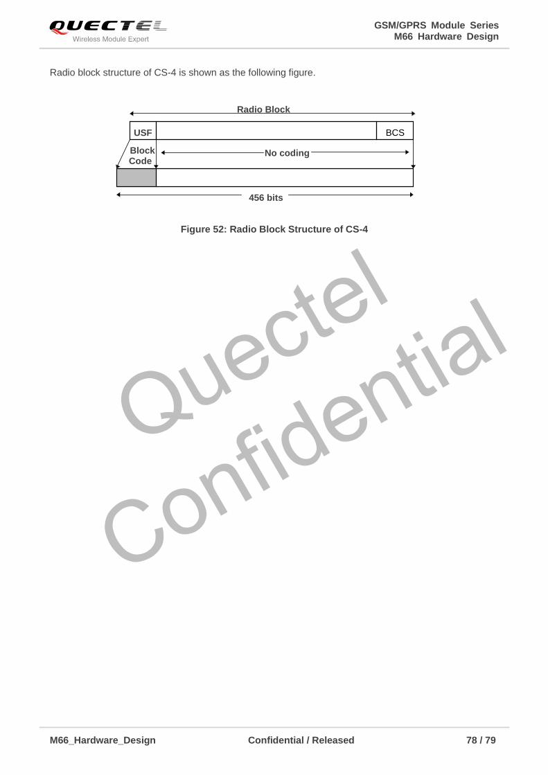
GSM/GPRS Module Series M66 Hardware Design
M66_Hardware_Design Confidential / Released 78 / 79
Radio block structure of CS-4 is shown as the following figure.
Figure 52: Radio Block Structure of CS-4
Block Code
No coding
456 bits
USF BCS
Radio Block
Quectel
Confidential
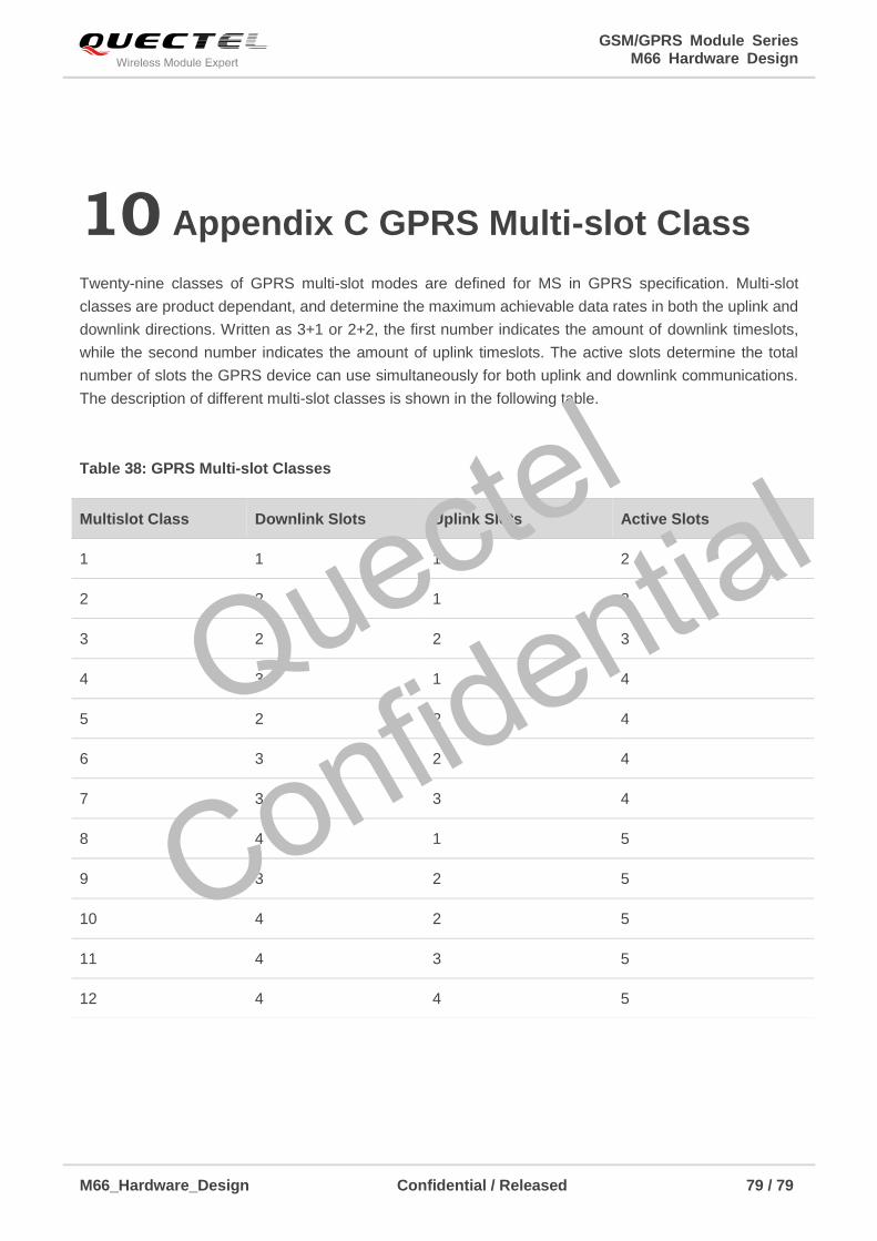
GSM/GPRS Module Series M66 Hardware Design
M66_Hardware_Design Confidential / Released 79 / 79
10 Appendix C GPRS Multi-slot Class
Twenty-nine classes of GPRS multi-slot modes are defined for MS in GPRS specification. Multi-slot
classes are product dependant, and determine the maximum achievable data rates in both the uplink and
downlink directions. Written as 3+1 or 2+2, the first number indicates the amount of downlink timeslots,
while the second number indicates the amount of uplink timeslots. The active slots determine the total
number of slots the GPRS device can use simultaneously for both uplink and downlink communications.
The description of different multi-slot classes is shown in the following table.
Table 38: GPRS Multi-slot Classes
Multislot Class Downlink Slots Uplink Slots Active Slots
1 1 1 2
2 2 1 3
3 2 2 3
4 3 1 4
5 2 2 4
6 3 2 4
7 3 3 4
8 4 1 5
9 3 2 5
10 4 2 5
11 4 3 5
12 4 4 5
Quectel
Confidential