Embed Size (px)
Citation preview
M32632 V2 Architecture
Udo Möller11.8.2016 1
Architecture ofM32632 V2
M32632 V2 Architecture
Udo Möller11.8.2016 2
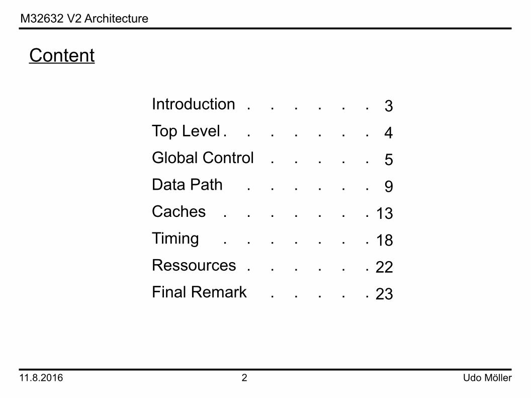
Content
Introduction . . . . . .
Top Level . . . . . . .
Global Control . . . . .
Data Path . . . . . .
Caches . . . . . . .
Timing . . . . . . .
Ressources . . . . . .
Final Remark . . . . .
3
4
5
9
13
18
22
23
M32632 V2 Architecture
Udo Möller11.8.2016 3
IntroductionThe M32632 is an implementation of the Series 32000 architecture of National Semiconductor. It is 100% software compatible to the NS32532 CPU and NS32381 FPU. The implementation is written in Verilog.
The M32632 is a very powerful 32-bit microprocessor. It features a rich instruction set with datatypes ranging fom bits to strings, a memory management unit which supports demand-paging virtual memory and a floating point unit for single and double precision operands supporting basic arithmetic operations.
This manual gives an overview of the internal structure and the principal operation of M32632.
The target application for this processor was a software MP3 decoder. The original NS32532 CPU together with the NS32381 FPU at 25 MHz clock speed was 10 times too slow to decode MP3 in real-time. The M32632 V2 achieves 50 MHz in a cheap Cyclone IV -6 FPGA. This clock speed is sufficient to decode MP3 in real-time.
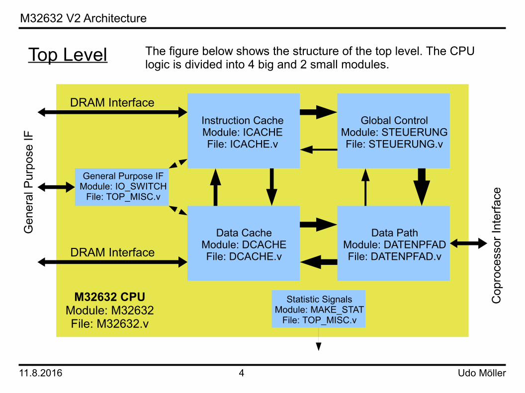
The figure on the next page shows the top level of M32632.
M32632 V2 Architecture
Udo Möller11.8.2016 4
Top Level
Instruction CacheModule: ICACHEFile: ICACHE.v
Data CacheModule: DCACHEFile: DCACHE.v
Global ControlModule: STEUERUNGFile: STEUERUNG.v
Data PathModule: DATENPFADFile: DATENPFAD.v
General Purpose IFModule: IO_SWITCH
File: TOP_MISC.v
Cop
roce
ssor
Inte
rface
DRAM Interface
DRAM Interface
Gen
eral
Pur
pose
IF
Statistic SignalsModule: MAKE_STAT
File: TOP_MISC.v
M32632 CPUModule: M32632File: M32632.v
The figure below shows the structure of the top level. The CPUlogic is divided into 4 big and 2 small modules.
M32632 V2 Architecture
Udo Möller11.8.2016 5
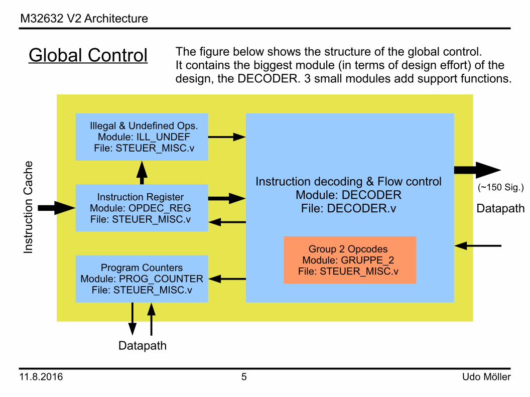
Global Control
Instruction RegisterModule: OPDEC_REGFile: STEUER_MISC.v
Instruction decoding & Flow controlModule: DECODERFile: DECODER.v
Program CountersModule: PROG_COUNTER
File: STEUER_MISC.v
Illegal & Undefined Ops.Module: ILL_UNDEF
File: STEUER_MISC.v
Group 2 OpcodesModule: GRUPPE_2
File: STEUER_MISC.v
Datapath
Inst
ruct
ion
Cac
he
Datapath
(~150 Sig.)
The figure below shows the structure of the global control.It contains the biggest module (in terms of design effort) of thedesign, the DECODER. 3 small modules add support functions.
M32632 V2 Architecture
Udo Möller11.8.2016 6
Global Control
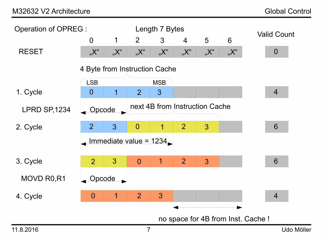
The three most important elements of STEUERUNG are the architecture program counter PC_ARCHI inside the module PROG_COUNTER, the register OPREG in the module OPDEC_REG and the register phase_reg in the module DECODER.PC_ARCHI is the program counter (PC) which holds the address of the first byte of an instruction. In the Series 32000 architecture the PC is used for the addressing mode PC relative. For branches the PC is used to calculate the target address. There are two more program counters inside the module PROG_COUNTER. pc_adduse is advancing in small steps. A step is an opcode (1..3 bytes), an index operand (1..2 bytes), an immediate value (1..4 bytes) or a displacement (1..4 bytes). Therefore pc_adduse points to every part of an instruction. The third program counter is PC_ICACHE. It is used for accessing the instruction cache and advances in steps of 4 bytes until it is updated to a new location by a jump.The register OPREG in the module OPDEC_REG holds the data from the instruction cache for decoding by the module DECODER. It is 7 bytes wide and can be updated every clock cycle. The data to decode is located starting at byte 0. The lenght depends on the kind of information to evaluate. For example instruction definitions can be 1, 2 or 3 bytes long. The instruction cache always fill the OPREG with 4 bytes until there is no space available. On the next page the operation of OPREG is visualized. The register phase_reg in the module DECODER is the state register of M32632. It is 8 bits wide. Sequences of states are defined for all instructions. Similar instructions have the same sequence. For example the instructions for add (ADD) and subtract (SUB) differ only in the data operation. State 0 is the opcode decoding state of any instruction.
M32632 V2 Architecture
Udo Möller11.8.2016 7
Operation of OPREG :
LPRD SP,1234
1. Cycle
RESET
Immediate value = 1234
MOVD R0,R1
2. Cycle
3. Cycle
4. Cycle
Length 7 BytesValid Count
4 Byte from Instruction Cache
LSB MSB
1 2
0
4
4
6
6
32 0 1 2 3
2 3 0 1 2 3
0 1 2 3
0 1 2 3 4 5 6
no space for 4B from Inst. Cache !
„X“ „X“ „X“ „X“ „X“ „X“ „X“
Opcode
0 3
Opcode
next 4B from Instruction Cache
Global Control
M32632 V2 Architecture
Udo Möller11.8.2016 8
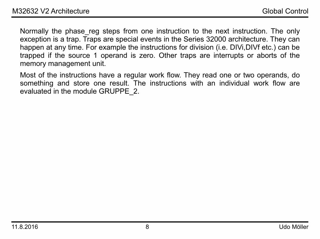
Normally the phase_reg steps from one instruction to the next instruction. The only exception is a trap. Traps are special events in the Series 32000 architecture. They can happen at any time. For example the instructions for division (i.e. DIVi,DIVf etc.) can be trapped if the source 1 operand is zero. Other traps are interrupts or aborts of the memory management unit.Most of the instructions have a regular work flow. They read one or two operands, do something and store one result. The instructions with an individual work flow are evaluated in the module GRUPPE_2.
Global Control

M32632 V2 Architecture
Udo Möller11.8.2016 9
Data Path
Register Set 2Module: REGISTERFile: REGISTERS.v
Register Set 1Module: REGISTERFile: REGISTERS.v
Immediate DataMemory Data
Sou
rce
1
Sou
rce
2
The figure below shows the data path structure. Only the dataconnections are indicated. Every arrow is a 32 bit wide bus.
Data
Address
(Des
tinat
ion)
Res
ult
DC
AC
HE
DC
AC
HE
, D
EC
OD
ER
Integer Data PathModule: I_PFADFile: I_PFAD.v
Single Precision FP UnitModule: SP_FPUFile: SP_FPU.v
Long Operations Data P.Module: DP_FPUFile: DP_FPU.v
Address GeneratorModule: ADDR_UNITFile: ADDR_UNIT.v
FP Status RegisterModule: FP_STAT_REG
File: REGISTERS.v
Configuration & DebugModule: CONFIG
File: REGISTERS.v
M32632 V2 Architecture
Udo Möller11.8.2016 10
Data Path
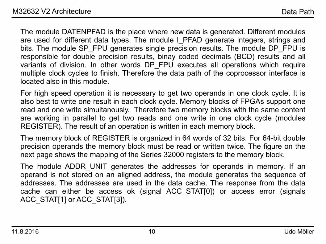
The module DATENPFAD is the place where new data is generated. Different modules are used for different data types. The module I_PFAD generate integers, strings and bits. The module SP_FPU generates single precision results. The module DP_FPU is responsible for double precision results, binay coded decimals (BCD) results and all variants of division. In other words DP_FPU executes all operations which require multiple clock cycles to finish. Therefore the data path of the coprocessor interface is located also in this module.For high speed operation it is necessary to get two operands in one clock cycle. It is also best to write one result in each clock cycle. Memory blocks of FPGAs support one read and one write simultanously. Therefore two memory blocks with the same content are working in parallel to get two reads and one write in one clock cycle (modules REGISTER). The result of an operation is written in each memory block.The memory block of REGISTER is organized in 64 words of 32 bits. For 64-bit double precision operands the memory block must be read or written twice. The figure on the next page shows the mapping of the Series 32000 registers to the memory block.The module ADDR_UNIT generates the addresses for operands in memory. If an operand is not stored on an aligned address, the module generates the sequence of addresses. The addresses are used in the data cache. The response from the data cache can either be access ok (signal ACC_STAT[0]) or access error (signals ACC_STAT[1] or ACC_STAT[3]).
M32632 V2 Architecture
Udo Möller11.8.2016 11
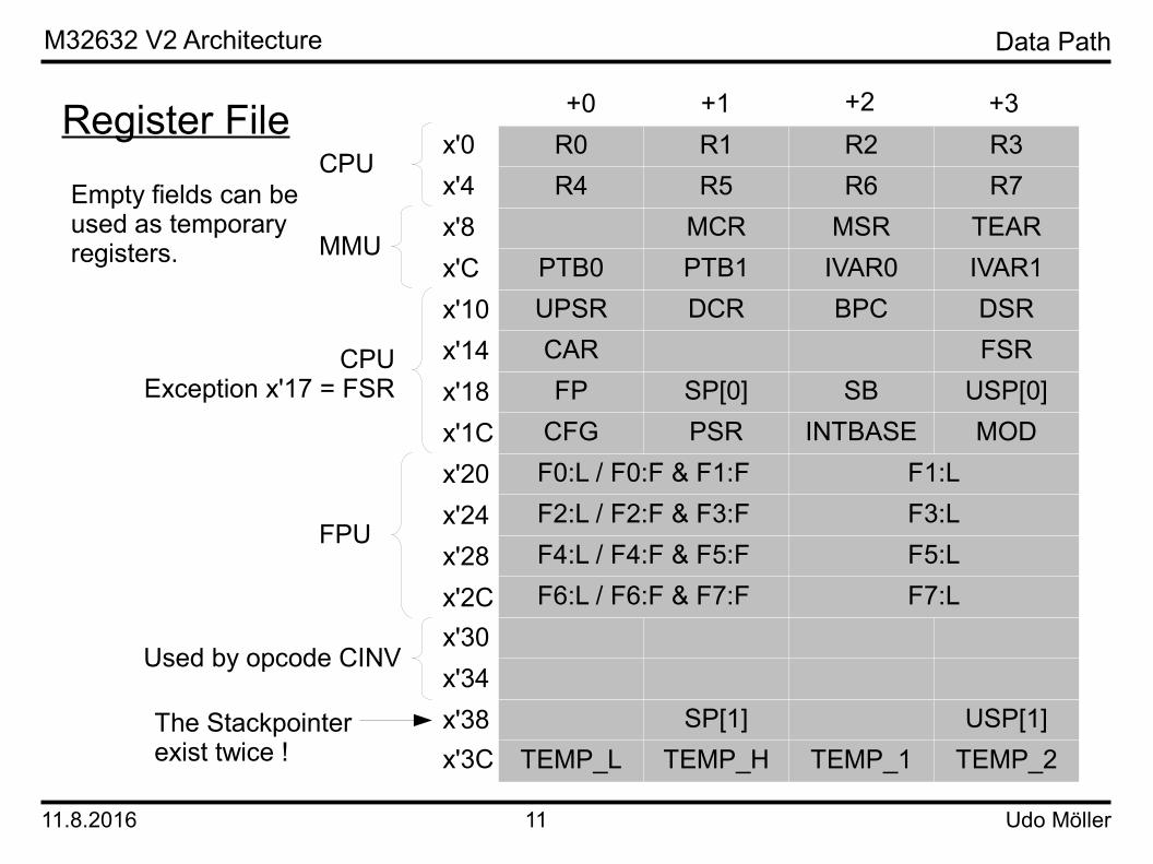
The Stackpointerexist twice !
R0 R1 R2 R3R4 R5 R6 R7
MCR MSR TEARPTB0 PTB1 IVAR0 IVAR1UPSR DCR BPC DSRCAR FSRFP SP[0] SB USP[0]
CFG PSR INTBASE MODF0:L / F0:F & F1:F F1:LF2:L / F2:F & F3:F F3:LF4:L / F4:F & F5:F F5:LF6:L / F6:F & F7:F F7:L
SP[1] USP[1]TEMP_L TEMP_H TEMP_1 TEMP_2
x'0x'4x'8x'Cx'10x'14x'18x'1Cx'20x'24x'28x'2Cx'30x'34x'38x'3C
+0 +1 +2 +3
Empty fields can beused as temporaryregisters.
Used by opcode CINV
CPU
MMU
CPUException x'17 = FSR
FPU
Register File
Data Path
M32632 V2 Architecture
Udo Möller11.8.2016 12
Access errors can only happen if virtual addresses are used. In case of an error the ADDR_UNIT stops the access and informs the DECODER that an abort had occured.The Series 32000 architecture implements two stack pointers (SP). One is for user programs, the other is for programs in supervisor mode. The M32632 doubles each stack pointer. This is done because every instruction is restartable in case of an MMU abort. For exampe the instruction MOVD R0,TOS moves the content of register R0 to the stack. The stack pointer is decremented before the write operation. In case of an abort during the write operation the modified stack pointer has to be restored. This is the purpose of the second register for the same stack pointer which always store the old content of the SP.The signal OPCODE inside DATENPFAD shows which operation is executed. The signal is 8 bits wide. It is build from the instruction table of Series 32000 architecture. For example the instruction MOVi (i = integer) is a format 4 instruction with a subcode of 5. The result for OPCODE is 8'h45.Other important signals are BWD[1:0] = size of integers and FL = size of FP operands. Together with OPCODE they are transferred from the DECODER as the signal OPER.
Data Path
M32632 V2 Architecture
Udo Möller11.8.2016 13
CachesCaches are essential to achieve high speed operation. Separate caches for instructions and data speeds up even further.The M32632 implements instruction and data caches with a size of 8 Kbytes each. They are 2 way-associativ, physically indexed and have a line size of 16 bytes. Each cache delivers 4 bytes each clock cycle.Both caches are not identical. The main difference is that the data cache can be written from the data path. The write policy of the data cache is „write through“. If a write occurs the external memory is updated instantly. Another important difference is that the instruction cache contains a second set of tag memories. The second set is used for detection of address collisions between the instruction cache and data writes. If a write occurs it is possible that the address written has been used for storing instructions in the past. Therefore the write invalidates the old content and the collision indicates to the instruction cache that the entry has to be marked invalid.Two sets are used in parallel for fetching of instructions and detection of collisions. This is necessary because a write operation can happen at any time.On the next two pages the components of the caches are listed.
M32632 V2 Architecture
Udo Möller11.8.2016 14
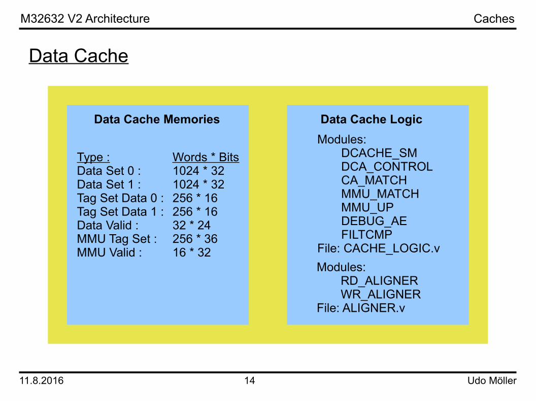
Data Cache
Modules:DCACHE_SMDCA_CONTROLCA_MATCHMMU_MATCHMMU_UPDEBUG_AEFILTCMP
File: CACHE_LOGIC.v
Data Cache LogicData Cache Memories
Type : Words * BitsData Set 0 : 1024 * 32Data Set 1 : 1024 * 32Tag Set Data 0 : 256 * 16Tag Set Data 1 : 256 * 16Data Valid : 32 * 24MMU Tag Set : 256 * 36MMU Valid : 16 * 32
Caches
Modules:RD_ALIGNERWR_ALIGNER
File: ALIGNER.v
M32632 V2 Architecture
Udo Möller11.8.2016 15
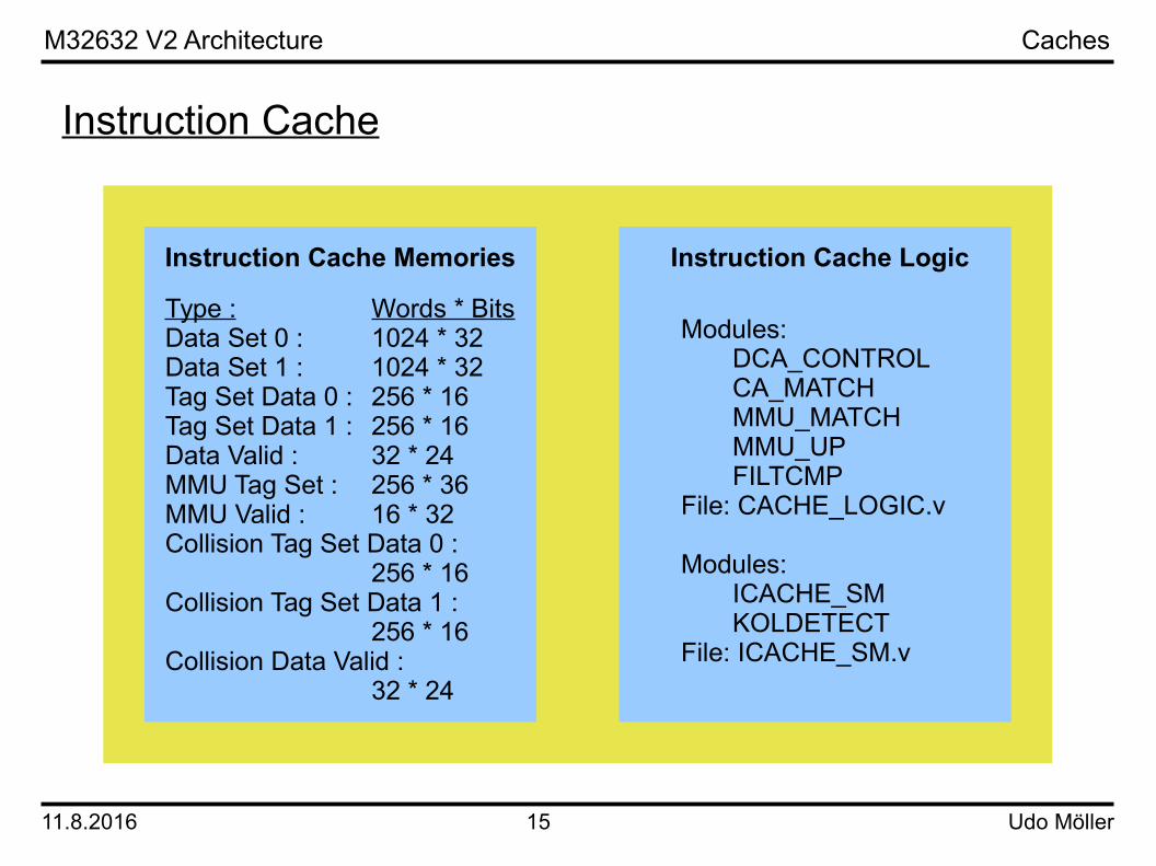
Caches
Instruction Cache
Modules:DCA_CONTROLCA_MATCHMMU_MATCHMMU_UPFILTCMP
File: CACHE_LOGIC.v
Modules:ICACHE_SMKOLDETECT
File: ICACHE_SM.v
Instruction Cache LogicInstruction Cache Memories
Type : Words * BitsData Set 0 : 1024 * 32Data Set 1 : 1024 * 32Tag Set Data 0 : 256 * 16Tag Set Data 1 : 256 * 16Data Valid : 32 * 24MMU Tag Set : 256 * 36MMU Valid : 16 * 32Collision Tag Set Data 0 :
256 * 16Collision Tag Set Data 1 :
256 * 16Collision Data Valid :
32 * 24
M32632 V2 Architecture
Udo Möller11.8.2016 16
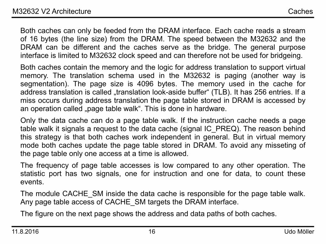
Both caches can only be feeded from the DRAM interface. Each cache reads a stream of 16 bytes (the line size) from the DRAM. The speed between the M32632 and the DRAM can be different and the caches serve as the bridge. The general purpose interface is limited to M32632 clock speed and can therefore not be used for bridgeing.Both caches contain the memory and the logic for address translation to support virtual memory. The translation schema used in the M32632 is paging (another way is segmentation). The page size is 4096 bytes. The memory used in the cache for address translation is called „translation look-aside buffer“ (TLB). It has 256 entries. If a miss occurs during address translation the page table stored in DRAM is accessed by an operation called „page table walk“. This is done in hardware.Only the data cache can do a page table walk. If the instruction cache needs a page table walk it signals a request to the data cache (signal IC_PREQ). The reason behind this strategy is that both caches work independent in general. But in virtual memory mode both caches update the page table stored in DRAM. To avoid any misseting of the page table only one access at a time is allowed.The frequency of page table accesses is low compared to any other operation. The statistic port has two signals, one for instruction and one for data, to count these events.The module CACHE_SM inside the data cache is responsible for the page table walk. Any page table access of CACHE_SM targets the DRAM interface.The figure on the next page shows the address and data paths of both caches.
Caches
M32632 V2 Architecture
Udo Möller11.8.2016 17
Use of addresses in cache : VA = virtual address , RA = real address
VA[11..2]
2 * 256 * 16 B
VA[11..4]
2 * 256 Entries
VA[19..12]
256 Entries
VA[31..20]= ?
Tag = VA
RA[31..12]
RA[31..12]
= ?= ?(16B)
(4kB)
DataPath
Tag = RA
RA[31..12]
SR
AMA
ddr./
Tag
SR
AMTa
g
SRAMData
MMU_HIT
CA_HIT
CA_HIT
4 Byte
Con
trol L
ogicAddress
Path
Select
Data Set 0Data Set 1(4B)
(1MB)
CachesA
DD
R_U
NIT
M32632 V2 Architecture
Udo Möller11.8.2016 18
0
Instruction Cache
Opcode Decoder
Data Path
Clock
Phase 0 0
Fetch 1
Decode 1
Execute 1 Execute 2 Execute 3
Fetch 2 Fetch 3
Decode 2 Decode 3
Timing
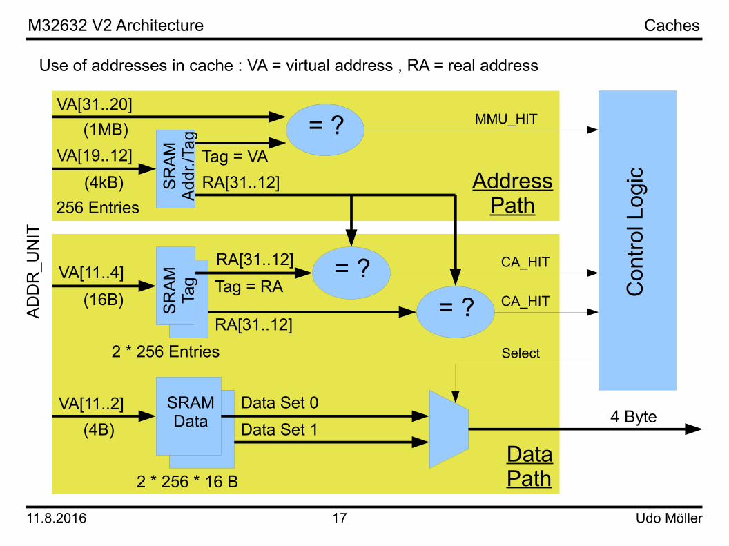
The M32632 has a three stage pipeline. The first stage is instruction fetching from the instruction cache. The second stage is instruction decoding in the module DECODER. Finally the instruction is executed in the module DATANPFAD.All three stages work in parallel. The figure below shows a sequence of three instructions running through the pipeline. The throughput in this case is one instruction per clock cycle. But this sequence is only possible if the instructions have their operands in internal registers.
M32632 V2 Architecture
Udo Möller11.8.2016 19
Timing
0 0
Decode
ADDB
Decode
Address Unit
Opcode Decoder
Data Path
Clock
Phase
Data Cache (DC)
calc.4(SB) Wait DC
Read
Disp. = 4
7 8'h27
Disp. = 5
calc.5(SB)
Write
Wait DC
3 clock cycles
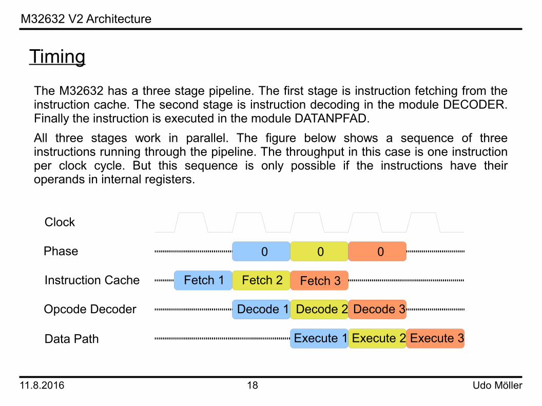
If one operand is in memory throughput goes down to one instruction per 3 clock cycles. But this is true only for a cache hit.The figure below shows the internal operations if the data cache is read or written. The first instruction (blue) is for example an „ADDB 4(SB),R0“. It reads a byte from the address in the register „Static Base“ (SB) offset by 4 bytes and adds the byte to register 0. The next instruction (yellow) is for example „NEGB R0,5(SB)“. It reads the byte from register 0, negates it and stores the result at address 5(SB).
3 clock cycles
NEGB
idle idle
M32632 V2 Architecture
Udo Möller11.8.2016 20
Timing
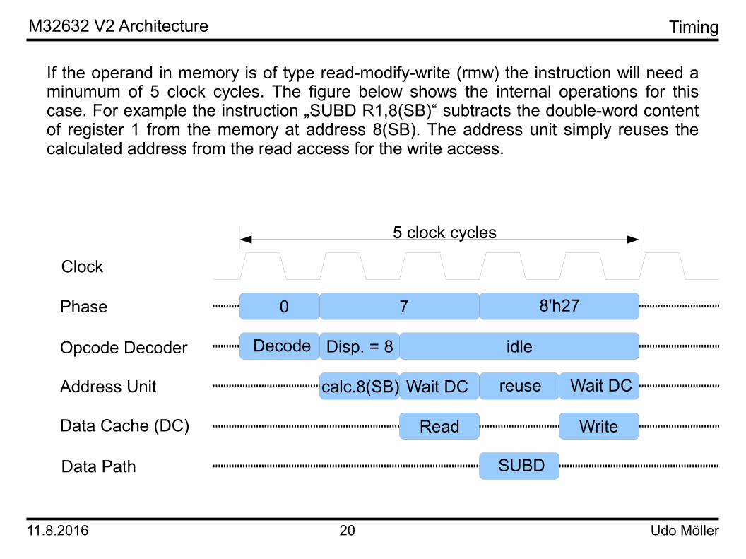
If the operand in memory is of type read-modify-write (rmw) the instruction will need a minumum of 5 clock cycles. The figure below shows the internal operations for this case. For example the instruction „SUBD R1,8(SB)“ subtracts the double-word content of register 1 from the memory at address 8(SB). The address unit simply reuses the calculated address from the read access for the write access.
0
Decode
SUBD
calc.8(SB) Wait DC
Read
Disp. = 8
7 8'h27
reuse
Write
Wait DC
5 clock cycles
Address Unit
Opcode Decoder
Data Path
Clock
Phase
Data Cache (DC)
idle
M32632 V2 Architecture
Udo Möller11.8.2016 21
If the data cache is accessed the module DECODER is not active every clock cycle (= idle). The reason for this not ideal behaviour is the virtual memory support. If the cache detects an abort the state of M32632 is reset to the beginning of the instruction. The task of reseting is simplified if the DECODER is waiting for the data cache finishing the current access.If an operand of type „rmw“ is accessed the cache checks during the read access whether a write access is not allowed. If this is true the read access is already aborted. This early abort prevents changing the content of the „processor status register“ (PSR) by the operation.The limiting timing path of the M32632 is the detection of an overflow during a single precision FP operation. An overflow occurs if a result is too big to be represented in the desired format. In this case the instruction is aborted and the result must not be written either to register nor to memory. For the register write the signal DOWR in the module DATENPFAD must be suppressed. The combinatorial path to achieve this is the longest path in the design.In version 2.0 the single precision floating-point operations need 2 clock cylces. This allows a higher clock speed for the whole M32632.
Timing
M32632 V2 Architecture
Udo Möller11.8.2016 22
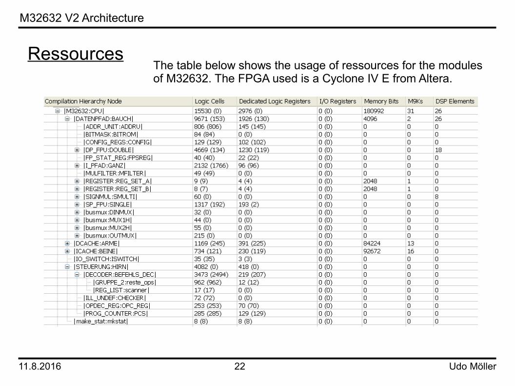
RessourcesThe table below shows the usage of ressources for the modulesof M32632. The FPGA used is a Cyclone IV E from Altera.
M32632 V2 Architecture
Udo Möller11.8.2016 23
Final RemarkOne of the last sentences in the „Final Remark“ of the first version of this document said „The version 1.0 of M32632 is to my knowledge free of errors.“This was pretty optimistic. Every new system showed new bugs. One bug became a feature. The NS32016 is able to multiply and divide an odd numbered register pair. This is not specified but it was used in the BBC 32016 Second Processor. I had to implement this functionality also in the M32632 to be able to run the BBC software.Version 2.0 has all bugs fixed. In addition it delivers a higher clock speed. 50 MHz compared to 35 MHz is a big improvement. The drawback is a slower speed for single precision floating-point operations.This time I am quiet sure (again) that there are no bugs.


![Cse120wi11lec06[1] Encoding Bits Bytes Letters](https://img.pdfslide.us/doc/110x75/577d2a461a28ab4e1ea8d7c2/cse120wi11lec061-encoding-bits-bytes-letters.jpg)