Embed Size (px)
Citation preview
Preliminary Data
This is preliminary information on a new product now in development or undergoing evaluation. Details are subject to change without notice.
November 2008 Rev 4 1/69
1
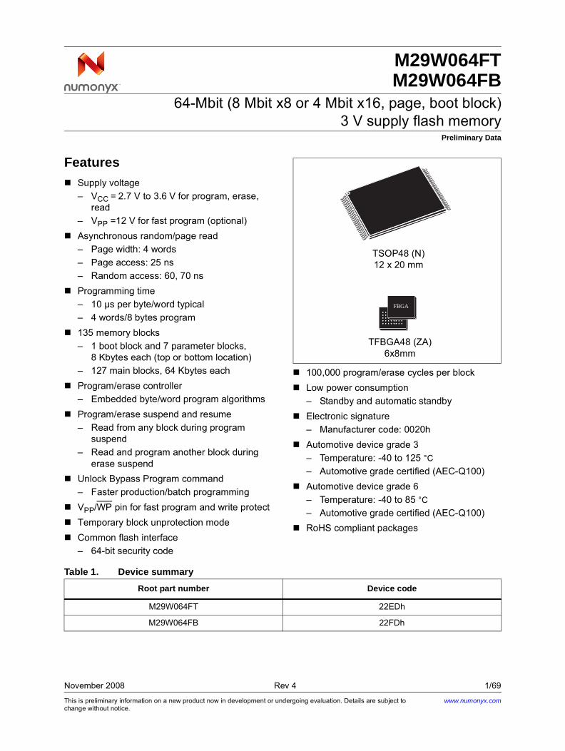
M29W064FTM29W064FB
64-Mbit (8 Mbit x8 or 4 Mbit x16, page, boot block)3 V supply flash memory
Features
Supply voltage
– VCC = 2.7 V to 3.6 V for program, erase, read
– VPP =12 V for fast program (optional)
Asynchronous random/page read
– Page width: 4 words
– Page access: 25 ns
– Random access: 60, 70 ns
Programming time
– 10 μs per byte/word typical
– 4 words/8 bytes program
135 memory blocks
– 1 boot block and 7 parameter blocks, 8 Kbytes each (top or bottom location)
– 127 main blocks, 64 Kbytes each
Program/erase controller
– Embedded byte/word program algorithms
Program/erase suspend and resume
– Read from any block during program suspend
– Read and program another block during erase suspend
Unlock Bypass Program command
– Faster production/batch programming
VPP/WP pin for fast program and write protect
Temporary block unprotection mode
Common flash interface
– 64-bit security code
100,000 program/erase cycles per block
Low power consumption
– Standby and automatic standby
Electronic signature
– Manufacturer code: 0020h
Automotive device grade 3
– Temperature: -40 to 125 °C
– Automotive grade certified (AEC-Q100)
Automotive device grade 6
– Temperature: -40 to 85 °C
– Automotive grade certified (AEC-Q100)
RoHS compliant packages
FBGA
TSOP48 (N)12 x 20 mm
TFBGA48 (ZA)6x8mm
Table 1. Device summary
Root part number Device code
M29W064FT 22EDh
M29W064FB 22FDh
www.numonyx.com
Contents M29W064FT, M29W064FB
2/69
Contents
1 Description . . . . . . . . . . . . . . . . . . . . . . . . . . . . . . . . . . . . . . . . . . . . . . . . . 7
2 Signal descriptions . . . . . . . . . . . . . . . . . . . . . . . . . . . . . . . . . . . . . . . . . 11
2.1 Address inputs (A0-A21) . . . . . . . . . . . . . . . . . . . . . . . . . . . . . . . . . . . . . .11
2.2 Data inputs/outputs (DQ0-DQ7) . . . . . . . . . . . . . . . . . . . . . . . . . . . . . . . . .11
2.3 Data inputs/outputs (DQ8-DQ14) . . . . . . . . . . . . . . . . . . . . . . . . . . . . . . . .11
2.4 Data input/output or address input (DQ15A–1) . . . . . . . . . . . . . . . . . . . . .11
2.5 Chip Enable (E) . . . . . . . . . . . . . . . . . . . . . . . . . . . . . . . . . . . . . . . . . . . . .11
2.6 Output Enable (G) . . . . . . . . . . . . . . . . . . . . . . . . . . . . . . . . . . . . . . . . . . .11
2.7 Write Enable (W) . . . . . . . . . . . . . . . . . . . . . . . . . . . . . . . . . . . . . . . . . . . 12
2.8 VPP/write protect (VPP/WP) . . . . . . . . . . . . . . . . . . . . . . . . . . . . . . . . . . . 12
2.9 Reset/block temporary unprotect (RP) . . . . . . . . . . . . . . . . . . . . . . . . . . . 13
2.10 Ready/busy output (RB) . . . . . . . . . . . . . . . . . . . . . . . . . . . . . . . . . . . . . . 13
2.11 Byte/word organization select (BYTE) . . . . . . . . . . . . . . . . . . . . . . . . . . . 13
2.12 VCC supply voltage (2.7 V to 3.6 V) . . . . . . . . . . . . . . . . . . . . . . . . . . . . . 14
2.13 VSS ground . . . . . . . . . . . . . . . . . . . . . . . . . . . . . . . . . . . . . . . . . . . . . . . . 14
3 Bus operations . . . . . . . . . . . . . . . . . . . . . . . . . . . . . . . . . . . . . . . . . . . . 15
3.1 Bus read . . . . . . . . . . . . . . . . . . . . . . . . . . . . . . . . . . . . . . . . . . . . . . . . . . 15
3.2 Bus write . . . . . . . . . . . . . . . . . . . . . . . . . . . . . . . . . . . . . . . . . . . . . . . . . . 15
3.3 Output disable . . . . . . . . . . . . . . . . . . . . . . . . . . . . . . . . . . . . . . . . . . . . . 15
3.4 Standby . . . . . . . . . . . . . . . . . . . . . . . . . . . . . . . . . . . . . . . . . . . . . . . . . . 15
3.5 Automatic standby . . . . . . . . . . . . . . . . . . . . . . . . . . . . . . . . . . . . . . . . . . 16
3.6 Special bus operations . . . . . . . . . . . . . . . . . . . . . . . . . . . . . . . . . . . . . . . 16
3.6.1 Electronic signature . . . . . . . . . . . . . . . . . . . . . . . . . . . . . . . . . . . . . . . . 16
3.6.2 Block protect and chip unprotect . . . . . . . . . . . . . . . . . . . . . . . . . . . . . . 16
4 Command interface . . . . . . . . . . . . . . . . . . . . . . . . . . . . . . . . . . . . . . . . . 18
4.1 Standard commands . . . . . . . . . . . . . . . . . . . . . . . . . . . . . . . . . . . . . . . . 18
4.1.1 Read/Reset command . . . . . . . . . . . . . . . . . . . . . . . . . . . . . . . . . . . . . . 18
4.1.2 Auto Select command . . . . . . . . . . . . . . . . . . . . . . . . . . . . . . . . . . . . . . 18
4.1.3 Read CFI Query command . . . . . . . . . . . . . . . . . . . . . . . . . . . . . . . . . . 18
M29W064FT, M29W064FB Contents
3/69
4.1.4 Chip Erase command . . . . . . . . . . . . . . . . . . . . . . . . . . . . . . . . . . . . . . 19
4.1.5 Block Erase command . . . . . . . . . . . . . . . . . . . . . . . . . . . . . . . . . . . . . . 20
4.1.6 Erase Suspend command . . . . . . . . . . . . . . . . . . . . . . . . . . . . . . . . . . . 20
4.1.7 Erase Resume command . . . . . . . . . . . . . . . . . . . . . . . . . . . . . . . . . . . 21
4.1.8 Program Suspend command . . . . . . . . . . . . . . . . . . . . . . . . . . . . . . . . . 21
4.1.9 Program Resume command . . . . . . . . . . . . . . . . . . . . . . . . . . . . . . . . . 21
4.1.10 Program command . . . . . . . . . . . . . . . . . . . . . . . . . . . . . . . . . . . . . . . . 22
4.2 Fast program commands . . . . . . . . . . . . . . . . . . . . . . . . . . . . . . . . . . . . . 23
4.2.1 Double Byte Program command . . . . . . . . . . . . . . . . . . . . . . . . . . . . . . 23
4.2.2 Quadruple Byte Program command . . . . . . . . . . . . . . . . . . . . . . . . . . . 23
4.2.3 Octuple Byte Program command . . . . . . . . . . . . . . . . . . . . . . . . . . . . . . 24
4.2.4 Double Word Program command . . . . . . . . . . . . . . . . . . . . . . . . . . . . . 24
4.2.5 Quadruple Word Program command . . . . . . . . . . . . . . . . . . . . . . . . . . . 25
4.2.6 Unlock Bypass command . . . . . . . . . . . . . . . . . . . . . . . . . . . . . . . . . . . 25
4.2.7 Unlock Bypass Program command . . . . . . . . . . . . . . . . . . . . . . . . . . . . 25
4.2.8 Unlock Bypass Reset command . . . . . . . . . . . . . . . . . . . . . . . . . . . . . . 25
4.3 Block Protection commands . . . . . . . . . . . . . . . . . . . . . . . . . . . . . . . . . . . 26
4.3.1 Block Protect and Chip Unprotect commands . . . . . . . . . . . . . . . . . . . . 26
5 Status register . . . . . . . . . . . . . . . . . . . . . . . . . . . . . . . . . . . . . . . . . . . . . 30
5.1 Data polling bit (DQ7) . . . . . . . . . . . . . . . . . . . . . . . . . . . . . . . . . . . . . . . . 30
5.2 Toggle bit (DQ6) . . . . . . . . . . . . . . . . . . . . . . . . . . . . . . . . . . . . . . . . . . . . 30
5.3 Error bit (DQ5) . . . . . . . . . . . . . . . . . . . . . . . . . . . . . . . . . . . . . . . . . . . . . 31
5.4 Erase timer bit (DQ3) . . . . . . . . . . . . . . . . . . . . . . . . . . . . . . . . . . . . . . . . 31
5.5 Alternative toggle bit (DQ2) . . . . . . . . . . . . . . . . . . . . . . . . . . . . . . . . . . . 31
6 Maximum ratings . . . . . . . . . . . . . . . . . . . . . . . . . . . . . . . . . . . . . . . . . . . 34
7 DC and AC parameters . . . . . . . . . . . . . . . . . . . . . . . . . . . . . . . . . . . . . . 35
8 Package mechanical . . . . . . . . . . . . . . . . . . . . . . . . . . . . . . . . . . . . . . . . 44
9 Ordering information . . . . . . . . . . . . . . . . . . . . . . . . . . . . . . . . . . . . . . . 46
Appendix A Block addresses . . . . . . . . . . . . . . . . . . . . . . . . . . . . . . . . . . . . . . . . 47
Appendix B Common flash interface (CFI). . . . . . . . . . . . . . . . . . . . . . . . . . . . . . 57
Contents M29W064FT, M29W064FB
4/69
Appendix C Block protection. . . . . . . . . . . . . . . . . . . . . . . . . . . . . . . . . . . . . . . . . 62
C.1 Programmer technique . . . . . . . . . . . . . . . . . . . . . . . . . . . . . . . . . . . . . . . 62
C.2 In-system technique . . . . . . . . . . . . . . . . . . . . . . . . . . . . . . . . . . . . . . . . . 62
10 Revision history . . . . . . . . . . . . . . . . . . . . . . . . . . . . . . . . . . . . . . . . . . . 68
M29W064FT, M29W064FB List of tables
5/69
List of tables
Table 1. Device summary . . . . . . . . . . . . . . . . . . . . . . . . . . . . . . . . . . . . . . . . . . . . . . . . . . . . . . . . . . 1Table 2. Signal names . . . . . . . . . . . . . . . . . . . . . . . . . . . . . . . . . . . . . . . . . . . . . . . . . . . . . . . . . . . . 8Table 3. Hardware protection . . . . . . . . . . . . . . . . . . . . . . . . . . . . . . . . . . . . . . . . . . . . . . . . . . . . . . 12Table 4. Bus operations, BYTE = VIL . . . . . . . . . . . . . . . . . . . . . . . . . . . . . . . . . . . . . . . . . . . . . . . . 17Table 5. Bus operations, BYTE = VIH . . . . . . . . . . . . . . . . . . . . . . . . . . . . . . . . . . . . . . . . . . . . . . . . 17Table 6. Commands, 16-bit mode, BYTE = VIH . . . . . . . . . . . . . . . . . . . . . . . . . . . . . . . . . . . . . . . . . . . . . . . . . . . 27Table 7. Commands, 8-bit mode, BYTE = VIL. . . . . . . . . . . . . . . . . . . . . . . . . . . . . . . . . . . . . . . . . . . . . . . . . . . . . 28Table 8. Program, erase times and program, erase endurance cycles . . . . . . . . . . . . . . . . . . . . . . 29Table 9. Status register bits . . . . . . . . . . . . . . . . . . . . . . . . . . . . . . . . . . . . . . . . . . . . . . . . . . . . . . . 32Table 10. Absolute maximum ratings . . . . . . . . . . . . . . . . . . . . . . . . . . . . . . . . . . . . . . . . . . . . . . . . . 34Table 11. Operating and AC measurement conditions. . . . . . . . . . . . . . . . . . . . . . . . . . . . . . . . . . . . 35Table 12. Device capacitance. . . . . . . . . . . . . . . . . . . . . . . . . . . . . . . . . . . . . . . . . . . . . . . . . . . . . . . 36Table 13. DC characteristics. . . . . . . . . . . . . . . . . . . . . . . . . . . . . . . . . . . . . . . . . . . . . . . . . . . . . . . . 36Table 14. Read AC characteristics . . . . . . . . . . . . . . . . . . . . . . . . . . . . . . . . . . . . . . . . . . . . . . . . . . . 38Table 15. Write AC characteristics, write enable controlled . . . . . . . . . . . . . . . . . . . . . . . . . . . . . . . . 40Table 16. Write AC characteristics, chip enable controlled. . . . . . . . . . . . . . . . . . . . . . . . . . . . . . . . . 42Table 17. Reset/block temporary unprotect AC characteristics . . . . . . . . . . . . . . . . . . . . . . . . . . . . . 43Table 18. TSOP48 – 48 lead plastic thin small outline, 12 x 20 mm, package mechanical data . . . . 44Table 19. TFBGA48 6x8mm - 6x8 active ball array, 0.8mm pitch, package mechanical data . . . . . . 45Table 20. Ordering information scheme . . . . . . . . . . . . . . . . . . . . . . . . . . . . . . . . . . . . . . . . . . . . . . . 46Table 21. Top boot block addresses, M29W064FT . . . . . . . . . . . . . . . . . . . . . . . . . . . . . . . . . . . . . . 47Table 22. Bottom boot block addresses, M29W064FB . . . . . . . . . . . . . . . . . . . . . . . . . . . . . . . . . . . 52Table 23. Query structure overview . . . . . . . . . . . . . . . . . . . . . . . . . . . . . . . . . . . . . . . . . . . . . . . . . . 57Table 24. CFI query identification string . . . . . . . . . . . . . . . . . . . . . . . . . . . . . . . . . . . . . . . . . . . . . . . 58Table 25. CFI query system interface information . . . . . . . . . . . . . . . . . . . . . . . . . . . . . . . . . . . . . . . 58Table 26. Device geometry definition . . . . . . . . . . . . . . . . . . . . . . . . . . . . . . . . . . . . . . . . . . . . . . . . . 59Table 27. Primary algorithm-specific extended query table . . . . . . . . . . . . . . . . . . . . . . . . . . . . . . . . 60Table 28. Security code area . . . . . . . . . . . . . . . . . . . . . . . . . . . . . . . . . . . . . . . . . . . . . . . . . . . . . . . 61Table 29. Programmer technique bus operations, BYTE = VIH or VIL . . . . . . . . . . . . . . . . . . . . . . . . . . . . . . . 63Table 30. Document revision history . . . . . . . . . . . . . . . . . . . . . . . . . . . . . . . . . . . . . . . . . . . . . . . . . 68
List of figures M29W064FT, M29W064FB
6/69
List of figures
Figure 1. Logic diagram . . . . . . . . . . . . . . . . . . . . . . . . . . . . . . . . . . . . . . . . . . . . . . . . . . . . . . . . . . . . 8Figure 2. TSOP connections . . . . . . . . . . . . . . . . . . . . . . . . . . . . . . . . . . . . . . . . . . . . . . . . . . . . . . . . 9Figure 3. TFBGA48 connections (top view through package) . . . . . . . . . . . . . . . . . . . . . . . . . . . . . . 10Figure 4. Data polling flowchart . . . . . . . . . . . . . . . . . . . . . . . . . . . . . . . . . . . . . . . . . . . . . . . . . . . . . 32Figure 5. Data toggle flowchart . . . . . . . . . . . . . . . . . . . . . . . . . . . . . . . . . . . . . . . . . . . . . . . . . . . . . 33Figure 6. AC measurement I/O waveform . . . . . . . . . . . . . . . . . . . . . . . . . . . . . . . . . . . . . . . . . . . . . 35Figure 7. AC measurement load circuit . . . . . . . . . . . . . . . . . . . . . . . . . . . . . . . . . . . . . . . . . . . . . . . 35Figure 8. Read mode AC waveforms. . . . . . . . . . . . . . . . . . . . . . . . . . . . . . . . . . . . . . . . . . . . . . . . . 37Figure 9. Page read AC waveforms. . . . . . . . . . . . . . . . . . . . . . . . . . . . . . . . . . . . . . . . . . . . . . . . . . 37Figure 10. Write AC waveforms, write enable controlled . . . . . . . . . . . . . . . . . . . . . . . . . . . . . . . . . . . 39Figure 11. Write AC waveforms, chip enable controlled . . . . . . . . . . . . . . . . . . . . . . . . . . . . . . . . . . . 41Figure 12. Reset/block temporary unprotect AC waveforms . . . . . . . . . . . . . . . . . . . . . . . . . . . . . . . . 42Figure 13. Accelerated program timing waveforms . . . . . . . . . . . . . . . . . . . . . . . . . . . . . . . . . . . . . . . 43Figure 14. TSOP48 – 48 lead plastic thin small outline, 12 x 20 mm, top view package outline . . . . . 44Figure 15. TFBGA48 6x8mm - 6x8 active ball array, 0.8mm pitch, package outline . . . . . . . . . . . . . . 45Figure 16. Programmer equipment group protect flowchart . . . . . . . . . . . . . . . . . . . . . . . . . . . . . . . . 64Figure 17. Programmer equipment chip unprotect flowchart . . . . . . . . . . . . . . . . . . . . . . . . . . . . . . . . 65Figure 18. In-system equipment group protect flowchart . . . . . . . . . . . . . . . . . . . . . . . . . . . . . . . . . . . 66Figure 19. In-system equipment chip unprotect flowchart . . . . . . . . . . . . . . . . . . . . . . . . . . . . . . . . . . 67
Important Notes and Warnings
Important Notes and Warnings
Micron Technology, Inc. ("Micron") reserves the right to make changes to information published in this
document, including without limitation specifications and product descriptions. This document
supersedes and replaces all information supplied prior to the publication hereof. You may not rely on any
information set forth in this document if you obtain the product described herein from any unauthorized
distributor or other source not authorized by Micron.
Automotive Applications. Products are not designed or intended for use in automotive applications
unless specifically designated by Micron as automotive-grade by their respective data sheets. Distributor
and customer/distributor shall assume the sole risk and liability for and shall indemnify and hold Micron
harmless against all claims, costs, damages, and expenses and reasonable attorneys' fees arising out of,
directly or indirectly, any claim of product liability, personal injury, death, or property damage resulting
directly or indirectly from any use of nonautomotive-grade products in automotive applications.
Customer/distributor shall ensure that the terms and conditions of sale between customer/distributor and
any customer of distributor/customer (1) state that Micron products are not designed or intended for use
in automotive applications unless specifically designated by Micron as automotive-grade by their
respective data sheets and (2) require such customer of distributor/customer to indemnify and hold
Micron harmless against all claims, costs, damages, and expenses and reasonable attorneys' fees
arising out of, directly or indirectly, any claim of product liability, personal injury, death, or property
damage resulting from any use of non-automotive-grade products in automotive applications.
Critical Applications. Products are not authorized for use in applications in which failure of the Micron
component could result, directly or indirectly in death, personal injury, or severe property or
environmental damage ("Critical Applications"). Customer must protect against death, personal injury,
and severe property and environmental damage by incorporating safety design measures into
customer's applications to ensure that failure of the Micron component will not result in such harms.
Should customer or distributor purchase, use, or sell any Micron component for any critical application,
customer and distributor shall indemnify and hold harmless Micron and its subsidiaries, subcontractors,
and affiliates and the directors, officers, and employees of each against all claims, costs, damages, and
expenses and reasonable attorneys' fees arising out of, directly or indirectly, any claim of product liability,
personal injury, or death arising in any way out of such critical application, whether or not Micron or its
subsidiaries, subcontractors, or affiliates were negligent in the design, manufacture, or warning of the
Micron product.
Customer Responsibility. Customers are responsible for the design, manufacture, and operation of
their systems, applications, and products using Micron products. ALL SEMICONDUCTOR PRODUCTS
HAVE INHERENT FAILURE RATES AND LIMITED USEFUL LIVES. IT IS THE CUSTOMER'S SOLE
RESPONSIBILITY TO DETERMINE WHETHER THE MICRON PRODUCT IS SUITABLE AND FIT FOR
THE CUSTOMER'S SYSTEM, APPLICATION, OR PRODUCT. Customers must ensure that adequate
design, manufacturing, and operating safeguards are included in customer's applications and products to
eliminate the risk that personal injury, death, or severe property or environmental damages will result
from failure of any semiconductor component.
Limited Warranty. In no event shall Micron be liable for any indirect, incidental, punitive, special or
consequential damages (including without limitation lost profits, lost savings, business interruption, costs
related to the removal or replacement of any products or rework charges) whether or not such damages
are based on tort, warranty, breach of contract or other legal theory, unless explicitly stated in a written
agreement executed by Micron's duly authorized representative.
M29W064FT, M29W064FB Description
7/69
1 Description
The M29W064F is a 64-Mbit (8 Mbit x 8 or 4 Mbit x 16) non-volatile memory that can be read, erased and reprogrammed. These operations can be performed using a single low voltage (2.7 to 3.6 V) supply. On power-up the memory defaults to its read mode.
The memory is divided into blocks that can be erased independently so it is possible to preserve valid data while old data is erased. Blocks can be protected in units of 256 Kbytes (generally groups of four 64 Kbyte blocks), to prevent accidental program or erase commands from modifying the memory. Program and erase commands are written to the command interface of the memory. An on-chip program/erase controller simplifies the process of programming or erasing the memory by taking care of all of the special operations that are required to update the memory contents. The end of a program or erase operation can be detected and any error conditions identified. The command set required to control the memory is consistent with JEDEC standards.
The device features an asymmetrical blocked architecture. The device has an array of 135 blocks:
8 parameters blocks of 8 Kbytes each (or 4 Kwords each)
127 main blocks of 64 Kbytes each (or 32 Kwords each)
M29W064FT has the parameter blocks at the top of the memory address space while the M29W064FB locates the parameter blocks starting from the bottom.
Chip Enable, Output Enable and Write Enable signals control the bus operation of the memory. They allow simple connection to most microprocessors, often without additional logic.
The VPP/WP signal is used to enable faster programming of the device, enabling multiple word/byte programming. If this signal is held at VSS, the boot block, and its adjacent parameter block, are protected from program and erase operations.
The device supports asynchronous random read and page read from all blocks of the memory array.
The memories are offered in TSOP48 (12 x 20 mm) and in TFBGA48 (6 x 8 mm) package.
Description M29W064FT, M29W064FB
8/69
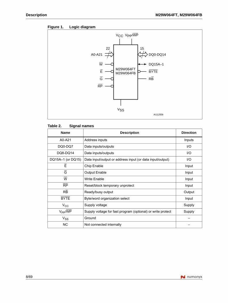
Figure 1. Logic diagram
Table 2. Signal names
Name Description Direction
A0-A21 Address inputs Inputs
DQ0-DQ7 Data inputs/outputs I/O
DQ8-DQ14 Data inputs/outputs I/O
DQ15A–1 (or DQ15) Data input/output or address input (or data input/output) I/O
E Chip Enable Input
G Output Enable Input
W Write Enable Input
RP Reset/block temporary unprotect Input
RB Ready/busy output Output
BYTE Byte/word organization select Input
VCC Supply voltage Supply
VPP/WP Supply voltage for fast program (optional) or write protect Supply
VSS Ground –
NC Not connected internally –
AI11250b
22
A0-A21
W
DQ0-DQ14
VCC
M29W064FTM29W064FBE
VSS
15
G
RP
DQ15A–1
BYTE
RB
VPP/WP
M29W064FT, M29W064FB Description
9/69
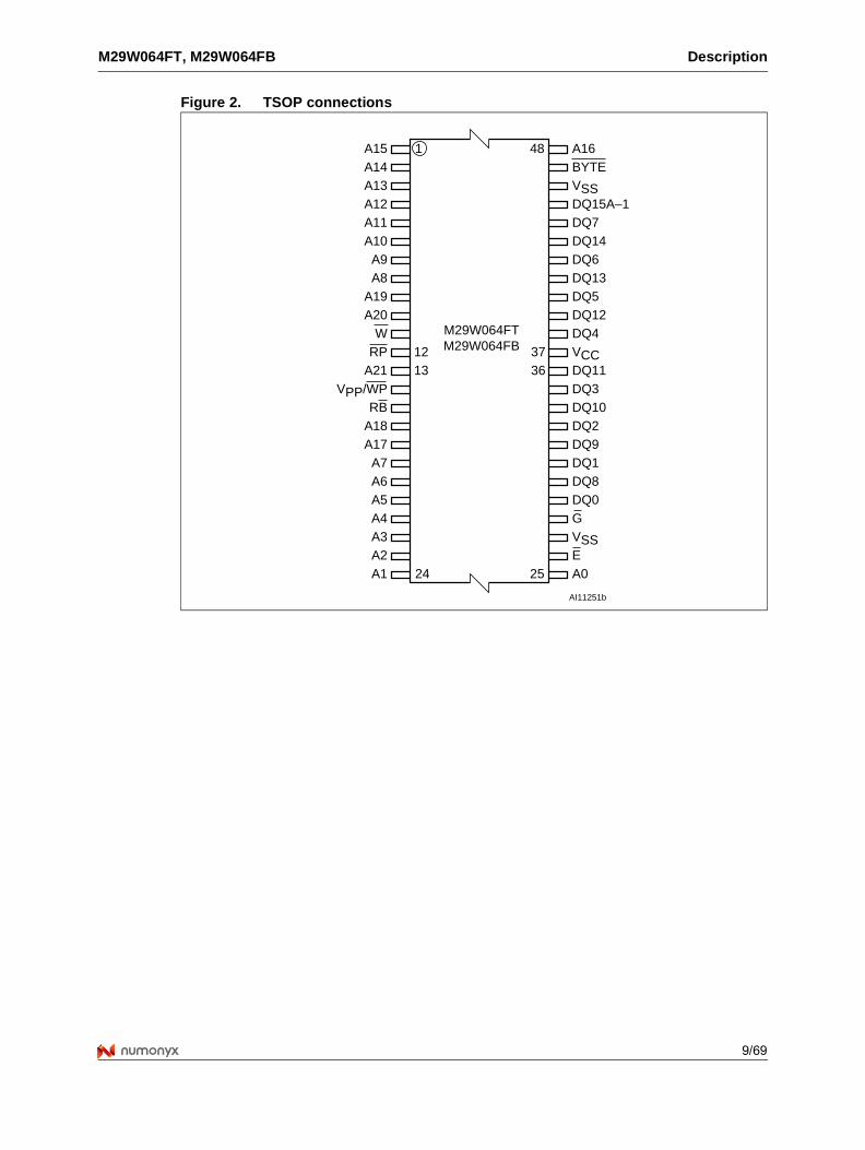
Figure 2. TSOP connections
DQ3
DQ9DQ2
A6DQ0
W
A3
RB
DQ6A8A9
DQ13
A17
A10 DQ14
A2
DQ12
DQ10
DQ15A–1
VCC
DQ4
DQ5
A7
DQ7
VPP/WPA21
M29W064FTM29W064FB12
1
13
24 25
3637
48
DQ8
A20A19
A1
A18
A4A5
DQ1
DQ11
G
A12A13
A16
A11
BYTEA15A14
VSS
EA0
RP
VSS
AI11251b
Description M29W064FT, M29W064FB
10/69
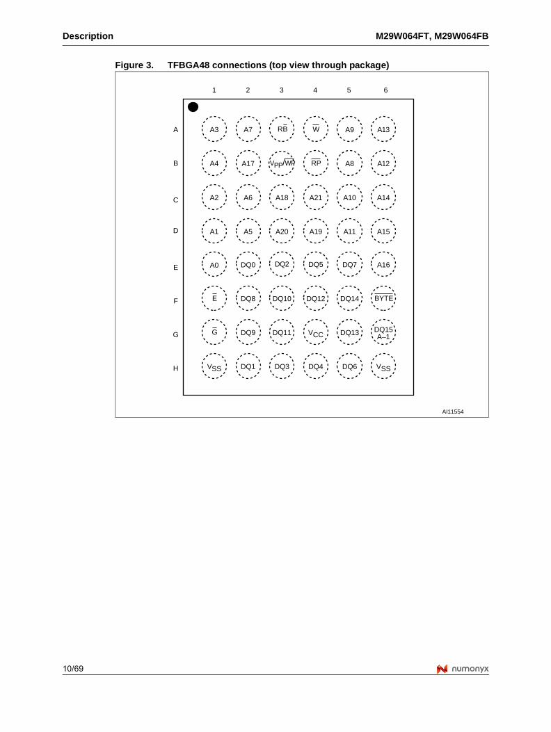
Figure 3. TFBGA48 connections (top view through package)
654321
VSS
A15
A14
A12
A13
DQ3
DQ11
DQ10
A18
VPP/WP
RB
DQ1
DQ9
DQ8
DQ0
A6
A17
A7
G
E
A0
A4
A3
DQ2
DQ6
DQ13
DQ14
A10
A8
A9
DQ4
VCC
DQ12
DQ5
A19
A21
RP
W
A11
DQ7
A1
A2
VSS
A5 A20
A16
BYTE
C
B
A
E
D
F
G
H
DQ15A–1
AI11554
M29W064FT, M29W064FB Signal descriptions
11/69
2 Signal descriptions
See Figure 1: Logic diagram, and Table 2: Signal names, for a brief overview of the signals connected to this device.
2.1 Address inputs (A0-A21)
The address inputs select the cells in the memory array to access during bus read operations. During bus write operations they control the commands sent to the command interface of the program/erase controller.
2.2 Data inputs/outputs (DQ0-DQ7)
The data I/O outputs the data stored at the selected address during a bus read operation. During bus write operations they represent the commands sent to the command interface of the program/erase controller.
2.3 Data inputs/outputs (DQ8-DQ14)
The data I/O outputs the data stored at the selected address during a bus read operation when BYTE is High, VIH. When BYTE is Low, VIL, these pins are not used and are high impedance. During bus write operations the command register does not use these bits. When reading the status register these bits should be ignored.
2.4 Data input/output or address input (DQ15A–1)
When BYTE is High, VIH, this pin behaves as a data input/output pin (as DQ8-DQ14). When BYTE is Low, VIL, this pin behaves as an address pin; DQ15A–1 Low will select the LSB of the addressed word, DQ15A–1 High will select the MSB. Throughout the text consider references to the Data input/output to include this pin when BYTE is High and references to the address inputs to include this pin when BYTE is Low except when stated explicitly otherwise.
2.5 Chip Enable (E)
The Chip Enable, E, activates the memory, allowing bus read and bus write operations to be performed. When Chip Enable is High, VIH, all other pins are ignored.
2.6 Output Enable (G)
The Output Enable, G, controls the bus read operation of the memory.
Signal descriptions M29W064FT, M29W064FB
12/69
2.7 Write Enable (W)
The Write Enable, W, controls the bus write operation of the memory’s command interface.
2.8 VPP/write protect (VPP/WP)
The VPP/write protect pin provides two functions. The VPP function allows the memory to use an external high voltage power supply to reduce the time required for unlock bypass program operations. The write protect function provides a hardware method of protecting the two outermost boot blocks. The VPP/write protect pin must not be left floating or unconnected.
When VPP/write protect is Low, VIL, the memory protects the two outermost boot blocks; program and erase operations in this block are ignored while VPP/Write Protect is Low, even when RP is at VID.
When VPP/write protect is High, VIH, the memory reverts to the previous protection status of the two outermost boot blocks. Program and erase operations can now modify the data in the two outermost boot blocks unless the block is protected using block protection.
Applying VPPH to the VPP/WP pin will temporarily unprotect any block previously protected (including the two outermost parameter blocks) using a high voltage block protection technique (in-system or programmer technique). See Table 3: Hardware protection for details.
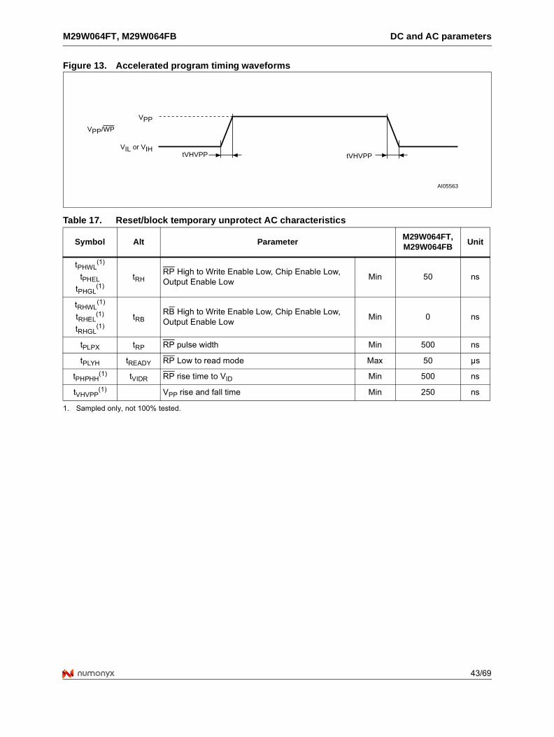
When VPP/write protect is raised to VPP the memory automatically enters the unlock bypass mode. When VPP/write protect returns to VIH or VIL normal operation resumes. During unlock bypass program operations the memory draws IPP from the pin to supply the programming circuits. See the description of the Unlock Bypass command in Section 4: Command interface. The transitions from VIH to VPP and from VPP to VIH must be slower than tVHVPP, see Figure 13: Accelerated program timing waveforms.
Never raise VPP/Write Protect to VPP from any mode except read mode, otherwise the memory may be left in an indeterminate state.
A 0.1 μF capacitor should be connected between the VPP/write protect pin and the VSS ground pin to decouple the current surges from the power supply. The PCB track widths must be sufficient to carry the currents required during unlock bypass program, IPP.
Table 3. Hardware protection
VPP/WP RP Function
VIL
VIH 2 outermost parameter blocks protected from program/erase operations
VID All blocks temporarily unprotected except the 2 outermost blocks
VIH or VID VID All blocks temporarily unprotected
VPPH VIH or VID All blocks temporarily unprotected
M29W064FT, M29W064FB Signal descriptions
13/69
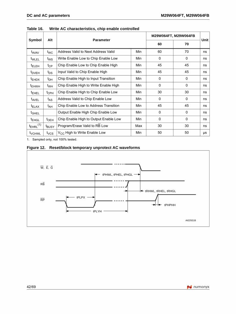
2.9 Reset/block temporary unprotect (RP)
The reset/block temporary unprotect pin can be used to apply a hardware reset to the memory or to temporarily unprotect all blocks that have been protected.
Note that if VPP/WP is at VIL, then the two outermost boot blocks will remain protected even if RP is at VID.
A hardware reset is achieved by holding reset/block temporary unprotect Low, VIL, for at least tPLPX. After reset/block temporary unprotect goes High, VIH, the memory will be ready for bus read and bus write operations after tPHEL or tRHEL, whichever occurs last. See Section 2.10: Ready/busy output (RB), Table 17: Reset/block temporary unprotect AC characteristics and Figure 12: Reset/block temporary unprotect AC waveforms, for more details.
Holding RP at VID will temporarily unprotect the protected blocks in the memory. Program and erase operations on all blocks will be possible. The transition from VIH to VID must be slower than tPHPHH.
2.10 Ready/busy output (RB)
The ready/busy pin is an open-drain output that can be used to identify when the device is performing a program or erase operation. During program or erase operations ready/busy is Low, VOL. Ready/busy is high-impedance during read mode, Auto select mode and erase suspend mode.
After a hardware reset, bus read and bus write operations cannot begin until ready/busy becomes high-impedance. See Table 17: Reset/block temporary unprotect AC characteristics and Figure 12: Reset/block temporary unprotect AC waveforms, for more details.
The use of an open-drain output allows the ready/busy pins from several memories to be connected to a single pull-up resistor. A Low will then indicate that one, or more, of the memories is busy.
2.11 Byte/word organization select (BYTE)
The byte/word organization select pin is used to switch between the x8 and x16 bus modes of the memory. When byte/word organization select is Low, VIL, the memory is in x8 mode, when it is High, VIH, the memory is in x16 mode.
Signal descriptions M29W064FT, M29W064FB
14/69
2.12 VCC supply voltage (2.7 V to 3.6 V)
VCC provides the power supply for all operations (read, program and erase).
The command interface is disabled when the VCC supply voltage is less than the lockout voltage, VLKO. This prevents bus write operations from accidentally damaging the data during power-up, power-down and power surges. If the program/erase controller is programming or erasing during this time then the operation aborts and the memory contents being altered will be invalid.
A 0.1 μF capacitor should be connected between the VCC supply voltage pin and the VSS ground pin to decouple the current surges from the power supply. The PCB track widths must be sufficient to carry the currents required during program and erase operations, ICC3.
2.13 VSS ground
VSS is the reference for all voltage measurements. The device features two VSS pins which must be both connected to the system ground.
M29W064FT, M29W064FB Bus operations
15/69
3 Bus operations
There are five standard bus operations that control the device. These are bus read, bus write, output disable, standby and automatic standby. See Table 4: Bus operations, BYTE = VIL and Table 5: Bus operations, BYTE = VIH, for a summary. Typically glitches of less than 5 ns on Chip Enable or Write Enable are ignored by the memory and do not affect bus operations.
3.1 Bus read
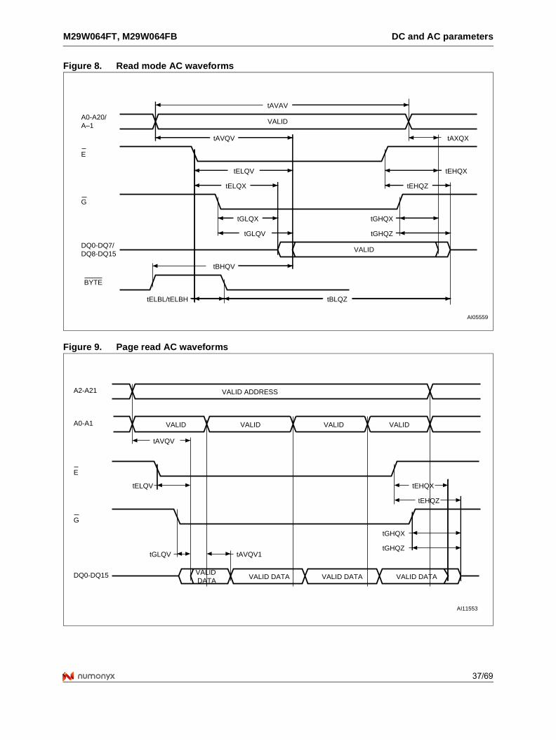
Bus read operations read from the memory cells, or specific registers in the command interface. A valid bus read operation involves setting the desired address on the address inputs, applying a Low signal, VIL, to Chip Enable and Output Enable and keeping Write Enable High, VIH. The data inputs/outputs will output the value, see Figure 8: Read mode AC waveforms, and Table 14: Read AC characteristics, for details of when the output becomes valid.
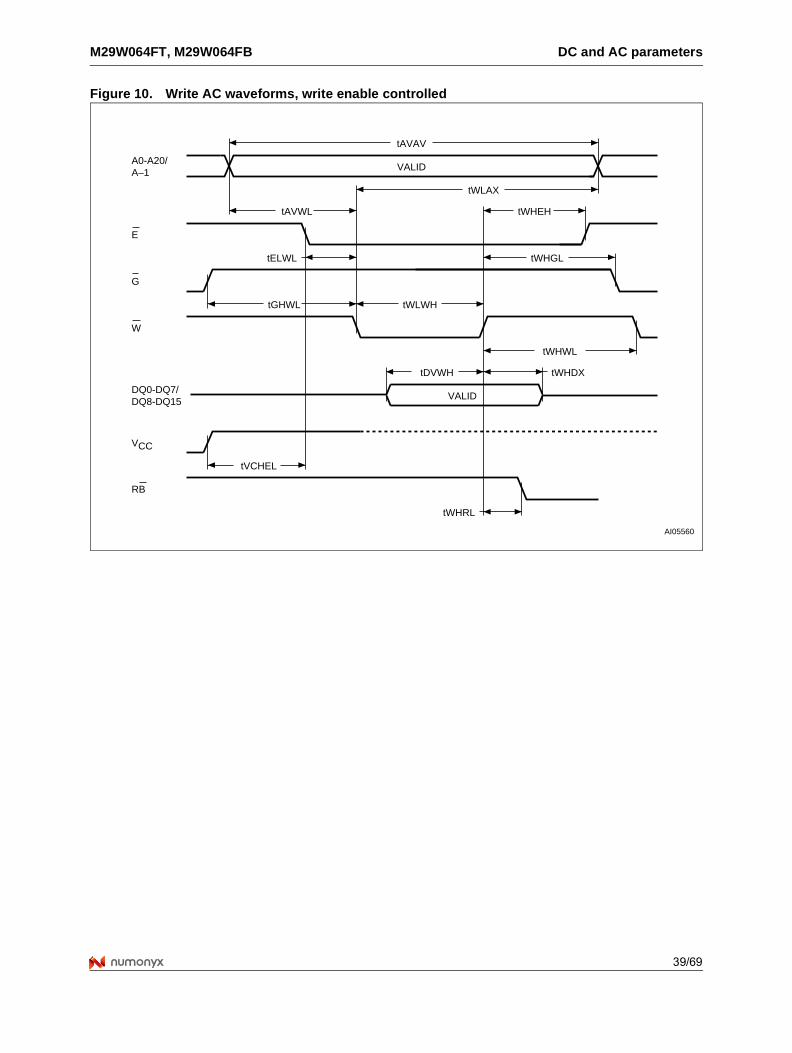
3.2 Bus write
Bus write operations write to the command interface. To speed up the read operation the memory array can be read in page mode where data is internally read and stored in a page buffer. The page has a size of 4 words and is addressed by the address inputs A0-A1.
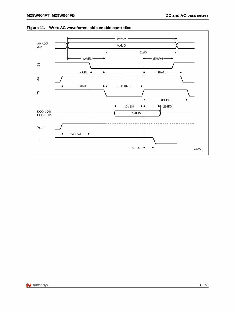
A valid bus write operation begins by setting the desired address on the address inputs. The address inputs are latched by the command interface on the falling edge of Chip Enable or Write Enable, whichever occurs last. The data inputs/outputs are latched by the command interface on the rising edge of Chip Enable or Write Enable, whichever occurs first. Output Enable must remain High, VIH, during the whole bus write operation. See Figure 10: Write AC waveforms, write enable controlled, Figure 11: Write AC waveforms, chip enable controlled, and Table 15: Write AC characteristics, write enable controlled and Table 16: Write AC characteristics, chip enable controlled, for details of the timing requirements.
3.3 Output disable
The data inputs/outputs are in the high impedance state when Output Enable is High, VIH.
3.4 Standby
When Chip Enable is High, VIH, the memory enters standby mode and the data inputs/outputs pins are placed in the high-impedance state. To reduce the supply current to the standby supply current, ICC2, Chip Enable should be held within VCC ± 0.2 V. For the standby current level see Table 13: DC characteristics.
During program or erase operations the memory will continue to use the program/erase supply current, ICC3, for program or erase operations until the operation completes.
Bus operations M29W064FT, M29W064FB
16/69
3.5 Automatic standby
If CMOS levels (VCC ± 0.2 V) are used to drive the bus and the bus is inactive for 300 ns or more the memory enters automatic standby where the internal supply current is reduced to the standby supply current, ICC2. The data inputs/outputs will still output data if a bus read operation is in progress.
3.6 Special bus operations
Additional bus operations can be performed to read the electronic signature and also to apply and remove block protection. These bus operations are intended for use by programming equipment and are not usually used in applications. They require VID to be applied to some pins.
3.6.1 Electronic signature
The memory has two codes, the manufacturer code and the device code, that can be read to identify the memory. These codes can be read by applying the signals listed in Table 4: Bus operations, BYTE = VIL and Table 5: Bus operations, BYTE = VIH.
3.6.2 Block protect and chip unprotect
Groups of blocks can be protected against accidental program or erase. The protection groups are shown in Appendix A: Block addresses, Table 21 and Table 22. The whole chip can be unprotected to allow the data inside the blocks to be changed.
The VPP/write protect pin can be used to protect the two outermost boot blocks. When VPP/write protect is at VIL the two outermost boot blocks are protected and remain protected regardless of the block protection status or the reset/block temporary unprotect pin status.
Block protect and chip unprotect operations are described in Appendix C: Block protection.
M29W064FT, M29W064FB Bus operations
17/69
Table 4. Bus operations, BYTE = VIL(1)
Operation E G WAddress inputs
DQ15A–1, A0-A21
Data inputs/outputs
DQ14-DQ8 DQ7-DQ0
Bus read VIL VIL VIH Cell address Hi-Z Data output
Bus write VIL VIH VIL Command address Hi-Z Data input
Output disable X VIH VIH X Hi-Z Hi-Z
Standby VIH X X X Hi-Z Hi-Z
Read manufacturer code VIL VIL VIHA0-A3 = VIL, A6 = VIL, A9 = VID, Others VIL or VIH
Hi-Z 20h
Read device code VIL VIL VIH
A0 = VIH, A1-A3 = VIL, A6 = VIL, A9 = VID, Others VIL or VIH
Hi-ZEDh (M29W064FT)
FDh (M29W064FB)
Read block protection status
VIL VIL VIH
A0, A2, A3, A6 = VIL, A1 = VIH, A9 = VID,A12-A21 = Block address, Others VIL or VIH
Hi-Z01h (protected)
00h (unprotected)
1. X = VIL or VIH.
Table 5. Bus operations, BYTE = VIH(1)
Operation E G WAddress inputs
A0-A21Data inputs/outputs
DQ15A–1, DQ14-DQ0
Bus read VIL VIL VIH Cell address Data output
Bus write VIL VIH VIL Command address Data input
Output disable X VIH VIH X Hi-Z
Standby VIH X X X Hi-Z
Read manufacturer code VIL VIL VIHA0-A3 = VIL, A6 = VIL, A9 = VID, others VIL or VIH
0020h
Read device code VIL VIL VIHA0 = VIH, A1-A3= VIL, A6 = VIL, A9 = VID, Others VIL or VIH
22EDh (M29W064FT)
22FDh (M29W064FB)
Read block protection status
VIL VIL VIH
A0, A2, A3, A6 = VIL, A1 = VIH, A9 = VID,A12-A21 = Block address, others VIL or VIH
0001h (protected)
0000h (unprotected)
1. X = VIL or VIH.
Command interface M29W064FT, M29W064FB
18/69
4 Command interface
All bus write operations to the memory are interpreted by the command interface. Commands consist of one or more sequential bus write operations. Failure to observe a valid sequence of bus write operations will result in the memory returning to read mode. The long command sequences are imposed to maximize data security.
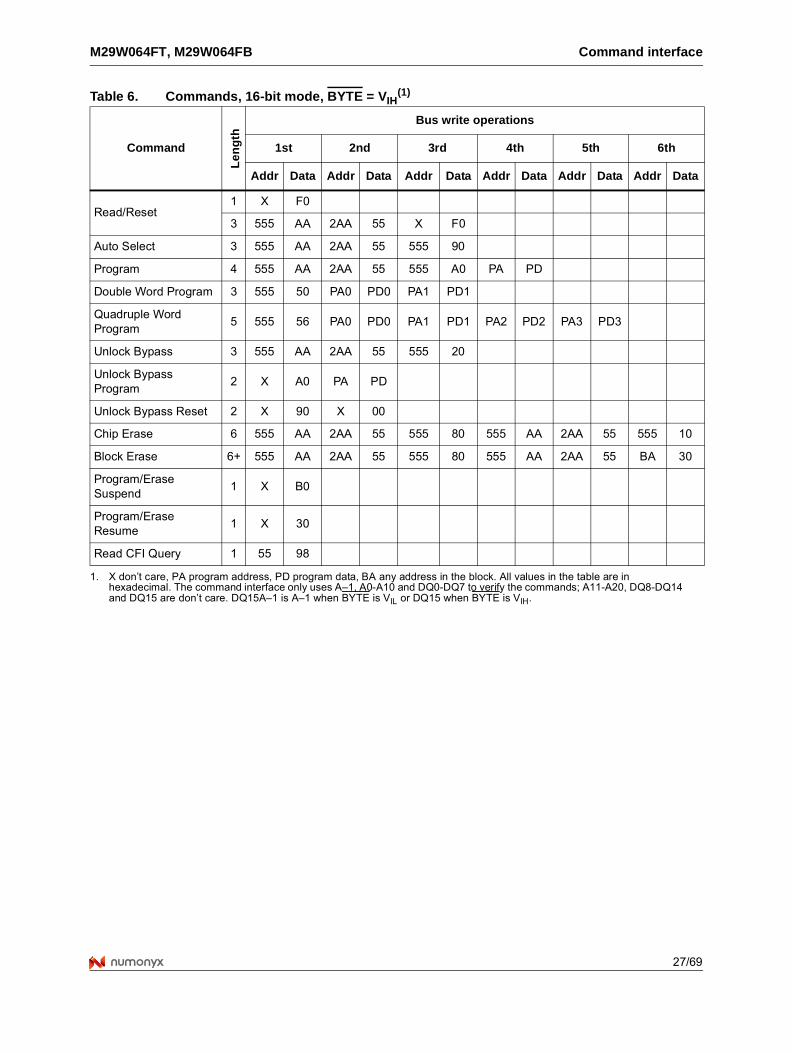
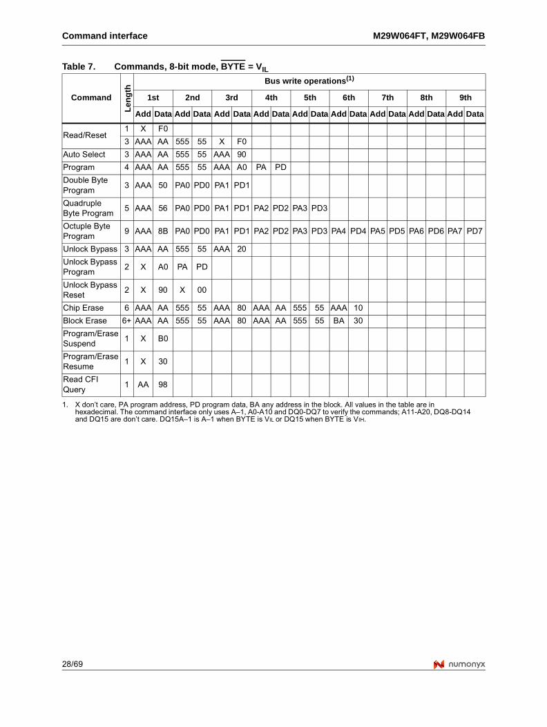
The address used for the commands changes depending on whether the memory is in 16-bit or 8-bit mode. See either Table 6, or Table 7, depending on the configuration that is being used, for a summary of the commands.
4.1 Standard commands
4.1.1 Read/Reset command
The Read/Reset command returns the memory to its read mode. It also resets the errors in the status register. Either one or three bus write operations can be used to issue the Read/Reset command.
The Read/Reset command can be issued, between bus write cycles before the start of a program or erase operation, to return the device to read mode. If the Read/Reset command is issued during the timeout of a block erase operation then the memory will take up to 10 μs to abort. During the abort period no valid data can be read from the memory. The Read/Reset command will not abort an erase operation when issued while in erase suspend.
4.1.2 Auto Select command
The Auto Select command is used to read the manufacturer code, the device code, and the block protection status. Three consecutive bus write operations are required to issue the Auto Select command. Once the Auto Select command is issued the memory remains in auto select mode until a Read/Reset command is issued. Read CFI Query and Read/Reset commands are accepted in auto select mode, all other commands are ignored.
In auto select mode, the manufacturer code and the device code can be read by using a bus read operation with addresses and control signals set as shown in Table 4: Bus operations, BYTE = VIL and Table 5: Bus operations, BYTE = VIH, except for A9 that is ‘don’t care’.
The block protection status of each block can be read using a bus read operation with addresses and control signals set as shown in Table 4: Bus operations, BYTE = VIL and Table 5: Bus operations, BYTE = VIH, except for A9 that is ‘don’t care’. If the addressed block is protected then 01h is output on data inputs/outputs DQ0-DQ7, otherwise 00h is output (in 8-bit mode).
4.1.3 Read CFI Query command
The Read CFI Query command is used to read data from the common Flash interface (CFI) memory area. This command is valid when the device is in the read array mode, or when the device is in auto selected mode.
M29W064FT, M29W064FB Command interface
19/69
One bus write cycle is required to issue the Read CFI Query command. Once the command is issued subsequent bus read operations read from the common flash interface memory area.
The Read/Reset command must be issued to return the device to the previous mode (the read array mode or auto selected mode). A second Read/Reset command would be needed if the device is to be put in the read array mode from auto selected mode.
See Appendix B: Common flash interface (CFI), Tables 23, 24, 25, 26, 27 and 28 for details on the information contained in the common flash interface (CFI) memory area.
4.1.4 Chip Erase command
The Chip Erase command can be used to erase the entire chip. Six bus write operations are required to issue the Chip Erase command and start the program/erase controller.
If any blocks are protected then these are ignored and all the other blocks are erased. If all of the blocks are protected the chip erase operation appears to start but will terminate within about 100 μs, leaving the data unchanged. No error condition is given when protected blocks are ignored.
During the erase operation the memory will ignore all commands, including the Erase Suspend command. It is not possible to issue any command to abort the operation. Typical chip erase times are given in Table 8: Program, erase times and program, erase endurance cycles. All bus read operations during the chip erase operation will output the status register on the data inputs/outputs. See the section on the status register for more details.
After the chip erase operation has completed the memory will return to the read mode, unless an error has occurred. When an error occurs the memory will continue to output the status register. A Read/Reset command must be issued to reset the error condition and return to read mode.
The Chip Erase command sets all of the bits in unprotected blocks of the memory to ’1’. All previous data is lost.
Command interface M29W064FT, M29W064FB
20/69
4.1.5 Block Erase command
The Block Erase command can be used to erase a list of one or more blocks. Six bus write operations are required to select the first block in the list. Each additional block in the list can be selected by repeating the sixth bus write operation using the address of the additional block. The block erase operation starts the program/erase controller about 50 μs after the last bus write operation. Once the program/erase controller starts it is not possible to select any more blocks. Each additional block must therefore be selected within 50 μs of the last block. The 50 μs timer restarts when an additional block is selected. The status register can be read after the sixth bus write operation. See the status register section for details on how to identify if the program/erase controller has started the block erase operation.
If any selected blocks are protected then these are ignored and all the other selected blocks are erased. If all of the selected blocks are protected the block erase operation appears to start but will terminate within about 100 μs, leaving the data unchanged. No error condition is given when protected blocks are ignored.
During the block erase operation the memory will ignore all commands except the Erase Suspend command. Typical block erase times are given in Table 8: Program, erase times and program, erase endurance cycles. All bus read operations during the block erase operation will output the status register on the data inputs/outputs. See the section on the status register for more details.
After the block erase operation has completed the memory will return to the read mode, unless an error has occurred. When an error occurs the memory will continue to output the status register. A Read/Reset command must be issued to reset the error condition and return to read mode.
The Block Erase command sets all of the bits in the unprotected selected blocks to ’1’. All previous data in the selected blocks is lost.
4.1.6 Erase Suspend command
The Erase Suspend command may be used to temporarily suspend a block erase operation and return the memory to read mode. The command requires one bus write operation.
The program/erase controller will suspend within the erase suspend latency time of the Erase Suspend command being issued. Once the program/erase controller has stopped the memory will be set to read mode and the erase will be suspended. If the Erase Suspend command is issued during the period when the memory is waiting for an additional block (before the program/erase controller starts) then the erase is suspended immediately and will start immediately when the Erase Resume command is issued. It is not possible to select any further blocks to erase after the erase resume.
During erase suspend it is possible to read and program cells in blocks that are not being erased; both read and program operations behave as normal on these blocks. If any attempt is made to program in a protected block or in the suspended block then the Program command is ignored and the data remains unchanged. The status register is not read and no error condition is given. Reading from blocks that are being erased will output the status register.
It is also possible to issue the Auto Select, Read CFI Query and Unlock Bypass commands during an erase suspend. The Read/Reset command must be issued to return the device to read array mode before the Resume command will be accepted.
M29W064FT, M29W064FB Command interface
21/69
4.1.7 Erase Resume command
The Erase Resume command must be used to restart the program/erase controller after an erase suspend. The device must be in read array mode before the Resume command will be accepted. An erase can be suspended and resumed more than once.
4.1.8 Program Suspend command
The Program Suspend command allows the system to interrupt a program operation so that data can be read from any block. When the Program Suspend command is issued during a program operation, the device suspends the program operation within the program suspend latency time (see Table 8: Program, erase times and program, erase endurance cycles for value) and updates the status register bits.
After the program operation has been suspended, the system can read array data from any address. However, data read from program-suspended addresses is not valid.
The Program Suspend command may also be issued during a program operation while an erase is suspended. In this case, data may be read from any addresses not in erase suspend or program suspend.
The system may also issue the Auto Select command sequence when the device is in the program suspend mode. The system can read as many auto select codes as required. When the device exits the auto select mode, the device reverts to the program suspend mode, and is ready for another valid operation. See Auto Select command sequence for more information.
4.1.9 Program Resume command
After the Program Resume command is issued, the device reverts to programming. The controller can determine the status of the program operation using the DQ7 or DQ6 status bits, just as in the standard program operation. See write operation status for more information.
The system must write the Program Resume command, to exit the program suspend mode and to continue the programming operation.
Further issuing of the Resume command is ignored. Another Program Suspend command can be written after the device has resumed programming.
Command interface M29W064FT, M29W064FB
22/69
4.1.10 Program command
The Program command can be used to program a value to one address in the memory array at a time. The command requires four bus write operations, the final write operation latches the address and data, and starts the program/erase controller.
Programming can be suspended and then resumed by issuing a Program Suspend command and a Program Resume command, respectively (see Section 4.1.8: Program Suspend command and Section 4.1.9: Program Resume command).
If the address falls in a protected block then the Program command is ignored, the data remains unchanged. The status register is never read and no error condition is given.
During the program operation the memory will ignore all commands. It is not possible to issue any command to abort or pause the operation. Typical program times are given in Table 8: Program, erase times and program, erase endurance cycles. Bus read operations during the program operation will output the status register on the data inputs/outputs. See the section on the status register for more details.
After the program operation has completed the memory will return to the read mode, unless an error has occurred. When an error occurs the memory will continue to output the status register. A Read/Reset command must be issued to reset the error condition and return to read mode.
Note that the Program command cannot change a bit set to ’0’ back to ’1’. One of the erase commands must be used to set all the bits in a block or in the whole memory from ’0’ to ’1’.
M29W064FT, M29W064FB Command interface
23/69
4.2 Fast program commands
There are four fast program commands available to improve the programming throughput, by writing several adjacent words or bytes in parallel. The Double, Quadruple and Octuple Byte Program commands are available for x8 operations, while the Double, Quadruple Word Program commands are available for x16 operations.
Fast program commands can be suspended and then resumed by issuing a Program Suspend command and a Program Resume command, respectively (see Section 4.1.8: Program Suspend command and Section 4.1.9: Program Resume command).
When VPPH is applied to the VPP/write protect pin the memory automatically enters the fast program mode. The user can then choose to issue any of the fast program commands. Care must be taken because applying a VPPH to the VPP/WP pin will temporarily unprotect any protected block.
4.2.1 Double Byte Program command
The Double Byte Program command is used to write a page of two adjacent bytes in parallel. The two bytes must differ only in DQ15A-1. Three bus write cycles are necessary to issue the Double Byte Program command.
1. The first bus cycle sets up the Double Byte Program command
2. The second bus cycle latches the address and the data of the first byte to be written
3. The third bus cycle latches the address and the data of the second byte to be written.
4.2.2 Quadruple Byte Program command
The Quadruple Byte Program command is used to write a page of four adjacent bytes in parallel. The four bytes must differ only for addresses A0, DQ15A-1. Five bus write cycles are necessary to issue the Quadruple Byte Program command.
1. The first bus cycle sets up the Quadruple Byte Program command
2. The second bus cycle latches the Address and the data of the first byte to be written
3. The third bus cycle latches the address and the data of the second byte to be written
4. The fourth bus cycle latches the address and the data of the third byte to be written
5. The fifth bus cycle latches the address and the data of the fourth byte to be written and starts the program/erase controller.
Command interface M29W064FT, M29W064FB
24/69
4.2.3 Octuple Byte Program command
This is used to write eight adjacent bytes, in x 8 mode, simultaneously. The addresses of the eight bytes must differ only in A1, A0 and DQ15A-1.
Nine bus write cycles are necessary to issue the command:
1. The first bus cycle sets up the command
2. The second bus cycle latches the address and the data of the first byte to be written
3. The third bus cycle latches the address and the data of the second byte to be written
4. The fourth bus cycle latches the address and the data of the third byte to be written
5. The fifth bus cycle latches the address and the data of the fourth byte to be written
6. The sixth bus cycle latches the address and the data of the fifth byte to be written
7. The seventh bus cycle latches the address and the data of the sixth byte to be written
8. The eighth bus cycle latches the address and the data of the seventh byte to be written.
9. The ninth bus cycle latches the address and the data of the eighth byte to be written and starts the program/erase controller.
4.2.4 Double Word Program command
The Double Word Program command is used to write a page of two adjacent words in parallel. The two words must differ only for the address A0.
Three bus write cycles are necessary to issue the Double Word Program command:
The first bus cycle sets up the Quadruple Word Program command.
The second bus cycle latches the address and the data of the first word to be written
The third bus cycle latches the address and the data of the second word to be written and starts the program/erase controller.
After the program operation has completed the memory will return to the read mode, unless an error has occurred. When an error occurs bus read operations will continue to output the status register. A Read/Reset command must be issued to reset the error condition and return to read mode.
Note that the fast program commands cannot change a bit set to ’0’ back to ’1’. One of the erase commands must be used to set all the bits in a block or in the whole memory from ’0’ to ’1’.
Typical program times are given in Table 8: Program, erase times and program, erase endurance cycles.
M29W064FT, M29W064FB Command interface
25/69
4.2.5 Quadruple Word Program command
This is used to write a page of four adjacent words (or 8 adjacent bytes), in x16 mode, simultaneously. The addresses of the four words must differ only in A1 and A0.
Five bus write cycles are necessary to issue the command:
The first bus cycle sets up the command
The second bus cycle latches the address and the data of the first word to be written
The third bus cycle latches the address and the data of the second word to be written
The fourth bus cycle latches the address and the data of the third word to be written
The fifth bus cycle latches the address and the data of the fourth word to be written and starts the program/erase controller.
4.2.6 Unlock Bypass command
The Unlock Bypass command is used in conjunction with the Unlock Bypass Program command to program the memory faster than with the standard program commands. When the cycle time to the device is long, considerable time saving can be made by using these commands. Three bus write operations are required to issue the Unlock Bypass command.
Once the Unlock Bypass command has been issued the memory will only accept the Unlock Bypass Program command and the Unlock Bypass Reset command. The memory can be read as if in read mode.
When VPP is applied to the VPP/write protect pin the memory automatically enters the unlock bypass mode and the Unlock Bypass Program command can be issued immediately.
4.2.7 Unlock Bypass Program command
The Unlock Bypass command is used in conjunction with the Unlock Bypass Program command to program the memory. When the cycle time to the device is long, considerable time saving can be made by using these commands. Three bus write operations are required to issue the Unlock Bypass command.
Once the Unlock Bypass command has been issued the memory will only accept the Unlock Bypass Program command and the Unlock Bypass Reset command. The memory can be read as if in read mode.
The memory offers accelerated program operations through the VPP/write protect pin. When the system asserts VPP on the VPP/write protect pin, the memory automatically enters the unlock bypass mode. The system may then write the two-cycle unlock bypass program command sequence. The memory uses the higher voltage on the VPP/write protect pin, to accelerate the unlock bypass program operation.
Never raise VPP/write protect to VPP from any mode except read mode, otherwise the memory may be left in an indeterminate state.
4.2.8 Unlock Bypass Reset command
The Unlock Bypass Reset command can be used to return to read/reset mode from Unlock bypass mode. Two bus write operations are required to issue the Unlock Bypass Reset command. Read/Reset command does not exit from unlock bypass mode.
Command interface M29W064FT, M29W064FB
26/69
4.3 Block Protection commands
4.3.1 Block Protect and Chip Unprotect commands
Groups of blocks can be protected against accidental program or erase. The protection groups are shown in Appendix A: Block addresses, Table 21: Top boot block addresses, M29W064FT and Table 22: Bottom boot block addresses, M29W064FB. The whole chip can be unprotected to allow the data inside the blocks to be changed.
Block protect and chip unprotect operations are described in Appendix C: Block protection.
M29W064FT, M29W064FB Command interface
27/69
Table 6. Commands, 16-bit mode, BYTE = VIH(1)
Command
Le
ng
th
Bus write operations
1st 2nd 3rd 4th 5th 6th
Addr Data Addr Data Addr Data Addr Data Addr Data Addr Data
Read/Reset1 X F0
3 555 AA 2AA 55 X F0
Auto Select 3 555 AA 2AA 55 555 90
Program 4 555 AA 2AA 55 555 A0 PA PD
Double Word Program 3 555 50 PA0 PD0 PA1 PD1
Quadruple Word Program
5 555 56 PA0 PD0 PA1 PD1 PA2 PD2 PA3 PD3
Unlock Bypass 3 555 AA 2AA 55 555 20
Unlock Bypass Program
2 X A0 PA PD
Unlock Bypass Reset 2 X 90 X 00
Chip Erase 6 555 AA 2AA 55 555 80 555 AA 2AA 55 555 10
Block Erase 6+ 555 AA 2AA 55 555 80 555 AA 2AA 55 BA 30
Program/Erase Suspend
1 X B0
Program/Erase Resume
1 X 30
Read CFI Query 1 55 98
1. X don’t care, PA program address, PD program data, BA any address in the block. All values in the table are in hexadecimal. The command interface only uses A–1, A0-A10 and DQ0-DQ7 to verify the commands; A11-A20, DQ8-DQ14 and DQ15 are don’t care. DQ15A–1 is A–1 when BYTE is VIL or DQ15 when BYTE is VIH.
Command interface M29W064FT, M29W064FB
28/69
Table 7. Commands, 8-bit mode, BYTE = VIL
Command
Le
ng
th
Bus write operations(1)
1st 2nd 3rd 4th 5th 6th 7th 8th 9th
Add Data Add Data Add Data Add Data Add Data Add Data Add Data Add Data Add Data
Read/Reset1 X F0
3 AAA AA 555 55 X F0
Auto Select 3 AAA AA 555 55 AAA 90
Program 4 AAA AA 555 55 AAA A0 PA PD
Double Byte Program
3 AAA 50 PA0 PD0 PA1 PD1
Quadruple Byte Program
5 AAA 56 PA0 PD0 PA1 PD1 PA2 PD2 PA3 PD3
Octuple Byte Program
9 AAA 8B PA0 PD0 PA1 PD1 PA2 PD2 PA3 PD3 PA4 PD4 PA5 PD5 PA6 PD6 PA7 PD7
Unlock Bypass 3 AAA AA 555 55 AAA 20
Unlock Bypass Program
2 X A0 PA PD
Unlock Bypass Reset
2 X 90 X 00
Chip Erase 6 AAA AA 555 55 AAA 80 AAA AA 555 55 AAA 10
Block Erase 6+ AAA AA 555 55 AAA 80 AAA AA 555 55 BA 30
Program/Erase Suspend
1 X B0
Program/Erase Resume
1 X 30
Read CFI Query
1 AA 98
1. X don’t care, PA program address, PD program data, BA any address in the block. All values in the table are in hexadecimal. The command interface only uses A–1, A0-A10 and DQ0-DQ7 to verify the commands; A11-A20, DQ8-DQ14 and DQ15 are don’t care. DQ15A–1 is A–1 when BYTE is VIL or DQ15 when BYTE is VIH.
M29W064FT, M29W064FB Command interface
29/69
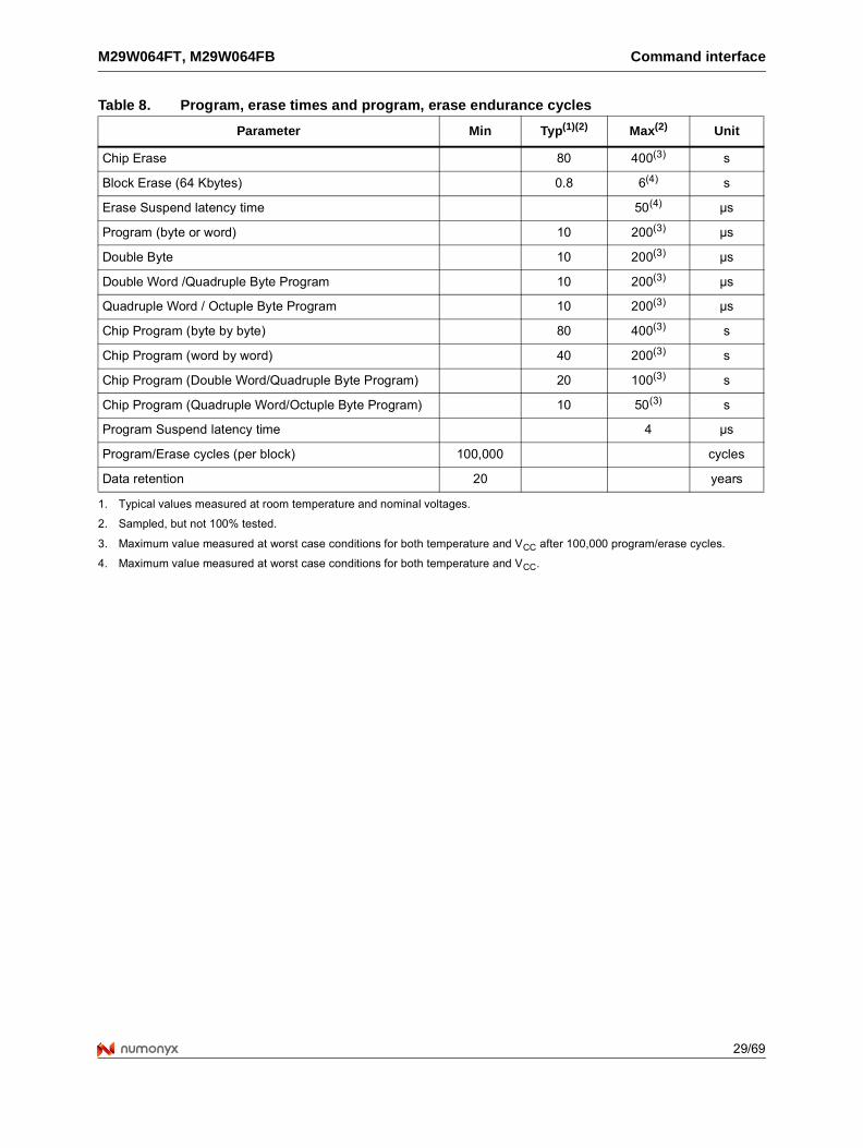
Table 8. Program, erase times and program, erase endurance cycles
Parameter Min Typ(1)(2) Max(2) Unit
Chip Erase 80 400(3) s
Block Erase (64 Kbytes) 0.8 6(4) s
Erase Suspend latency time 50(4) μs
Program (byte or word) 10 200(3) μs
Double Byte 10 200(3) μs
Double Word /Quadruple Byte Program 10 200(3) μs
Quadruple Word / Octuple Byte Program 10 200(3) μs
Chip Program (byte by byte) 80 400(3) s
Chip Program (word by word) 40 200(3) s
Chip Program (Double Word/Quadruple Byte Program) 20 100(3) s
Chip Program (Quadruple Word/Octuple Byte Program) 10 50(3) s
Program Suspend latency time 4 μs
Program/Erase cycles (per block) 100,000 cycles
Data retention 20 years
1. Typical values measured at room temperature and nominal voltages.
2. Sampled, but not 100% tested.
3. Maximum value measured at worst case conditions for both temperature and VCC after 100,000 program/erase cycles.
4. Maximum value measured at worst case conditions for both temperature and VCC.
Status register M29W064FT, M29W064FB
30/69
5 Status register
Bus read operations from any address always read the status register during program and erase operations. It is also read during erase suspend when an address within a block being erased is accessed.
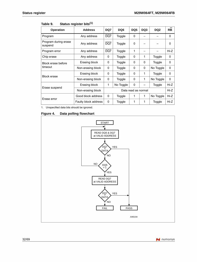
The bits in the status register are summarized in Table 9: Status register bits.
5.1 Data polling bit (DQ7)
The data polling bit can be used to identify whether the program/erase controller has successfully completed its operation or if it has responded to an erase suspend. The data polling bit is output on DQ7 when the status register is read.
During program operations the data polling bit outputs the complement of the bit being programmed to DQ7. After successful completion of the program operation the memory returns to read mode and bus read operations from the address just programmed output DQ7, not its complement.
During erase operations the data polling bit outputs ’0’, the complement of the erased state of DQ7. After successful completion of the erase operation the memory returns to read mode.
In erase suspend mode the data polling bit will output a ’1’ during a bus read operation within a block being erased. The data polling bit will change from a ’0’ to a ’1’ when the program/erase controller has suspended the erase operation.
Figure 4: Data polling flowchart, gives an example of how to use the data polling bit. A valid address is the address being programmed or an address within the block being erased.
5.2 Toggle bit (DQ6)
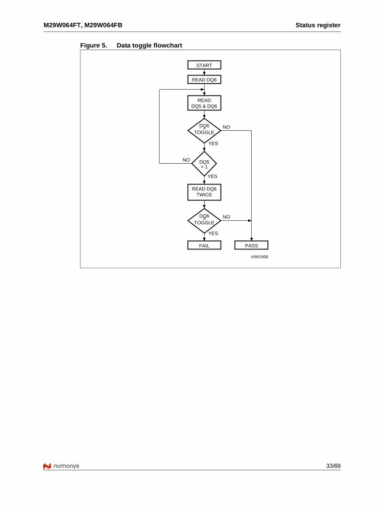
The toggle bit can be used to identify whether the program/erase controller has successfully completed its operation or if it has responded to an erase suspend. The toggle bit is output on DQ6 when the status register is read.
During program and erase operations the toggle bit changes from ’0’ to ’1’ to ’0’, etc., with successive bus read operations at any address. After successful completion of the operation the memory returns to read mode.
During erase suspend mode the toggle bit will output when addressing a cell within a block being erased. The toggle bit will stop toggling when the program/erase controller has suspended the erase operation.
Figure 5: Data toggle flowchart, gives an example of how to use the toggle bit.
M29W064FT, M29W064FB Status register
31/69
5.3 Error bit (DQ5)
The error bit can be used to identify errors detected by the program/erase controller. The error bit is set to ’1’ when a program, block erase or chip erase operation fails to write the correct data to the memory. If the error bit is set a Read/Reset command must be issued before other commands are issued. The error bit is output on DQ5 when the status register is read.
Note that the Program command cannot change a bit set to ’0’ back to ’1’ and attempting to do so will set DQ5 to ‘1’. A bus read operation to that address will show the bit is still ‘0’. One of the erase commands must be used to set all the bits in a block or in the whole memory from ’0’ to ’1’.
5.4 Erase timer bit (DQ3)
The erase timer bit can be used to identify the start of program/erase controller operation during a Block Erase command. Once the program/erase controller starts erasing the erase timer bit is set to ’1’. Before the program/erase controller starts the erase timer bit is set to ’0’ and additional blocks to be erased may be written to the command interface. The erase timer bit is output on DQ3 when the status register is read.
5.5 Alternative toggle bit (DQ2)
The alternative toggle bit can be used to monitor the program/erase controller during erase operations. The alternative toggle bit is output on DQ2 when the status register is read.
During chip erase and block erase operations the toggle bit changes from ’0’ to ’1’ to ’0’, etc., with successive bus read operations from addresses within the blocks being erased. A protected block is treated the same as a block not being erased. Once the operation completes the memory returns to read mode.
During erase suspend the alternative toggle bit changes from ’0’ to ’1’ to ’0’, etc. with successive bus read operations from addresses within the blocks being erased. Bus read operations to addresses within blocks not being erased will output the memory cell data as if in read mode.
After an erase operation that causes the error bit to be set the alternative toggle bit can be used to identify which block or blocks have caused the error. The alternative toggle bit changes from ’0’ to ’1’ to ’0’, etc. with successive bus read operations from addresses within blocks that have not erased correctly. The alternative toggle bit does not change if the addressed block has erased correctly.
Status register M29W064FT, M29W064FB
32/69
Figure 4. Data polling flowchart
Table 9. Status register bits(1)
1. Unspecified data bits should be ignored.
Operation Address DQ7 DQ6 DQ5 DQ3 DQ2 RB
Program Any address DQ7 Toggle 0 – – 0
Program during erase suspend
Any address DQ7 Toggle 0 – – 0
Program error Any address DQ7 Toggle 1 – – Hi-Z
Chip erase Any address 0 Toggle 0 1 Toggle 0
Block erase before timeout
Erasing block 0 Toggle 0 0 Toggle 0
Non-erasing block 0 Toggle 0 0 No Toggle 0
Block eraseErasing block 0 Toggle 0 1 Toggle 0
Non-erasing block 0 Toggle 0 1 No Toggle 0
Erase suspendErasing block 1 No Toggle 0 – Toggle Hi-Z
Non-erasing block Data read as normal Hi-Z
Erase errorGood block address 0 Toggle 1 1 No Toggle Hi-Z
Faulty block address 0 Toggle 1 1 Toggle Hi-Z
READ DQ5 & DQ7at VALID ADDRESS
START
READ DQ7at VALID ADDRESS
FAIL PASS
AI90194
DQ7=
DATA
YES
NO
YES
NO
DQ5= 1
DQ7=
DATA
YES
NO
M29W064FT, M29W064FB Status register
33/69
Figure 5. Data toggle flowchart
READ DQ6
START
READ DQ6TWICE
FAIL PASS
AI90195B
DQ6=
TOGGLENO
NO
YES
YES
DQ5= 1
NO
YES
DQ6=
TOGGLE
READDQ5 & DQ6
Maximum ratings M29W064FT, M29W064FB
34/69
6 Maximum ratings
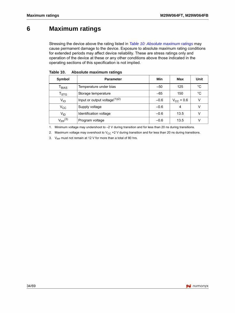
Stressing the device above the rating listed in Table 10: Absolute maximum ratings may cause permanent damage to the device. Exposure to absolute maximum rating conditions for extended periods may affect device reliability. These are stress ratings only and operation of the device at these or any other conditions above those indicated in the operating sections of this specification is not implied.
Table 10. Absolute maximum ratings
Symbol Parameter Min Max Unit
TBIAS Temperature under bias –50 125 °C
TSTG Storage temperature –65 150 °C
VIO Input or output voltage(1)(2)
1. Minimum voltage may undershoot to –2 V during transition and for less than 20 ns during transitions.
2. Maximum voltage may overshoot to VCC +2 V during transition and for less than 20 ns during transitions.
–0.6 VCC + 0.6 V
VCC Supply voltage –0.6 4 V
VID Identification voltage –0.6 13.5 V
VPP(3)
3. VPP must not remain at 12 V for more than a total of 80 hrs.
Program voltage –0.6 13.5 V
M29W064FT, M29W064FB DC and AC parameters
35/69
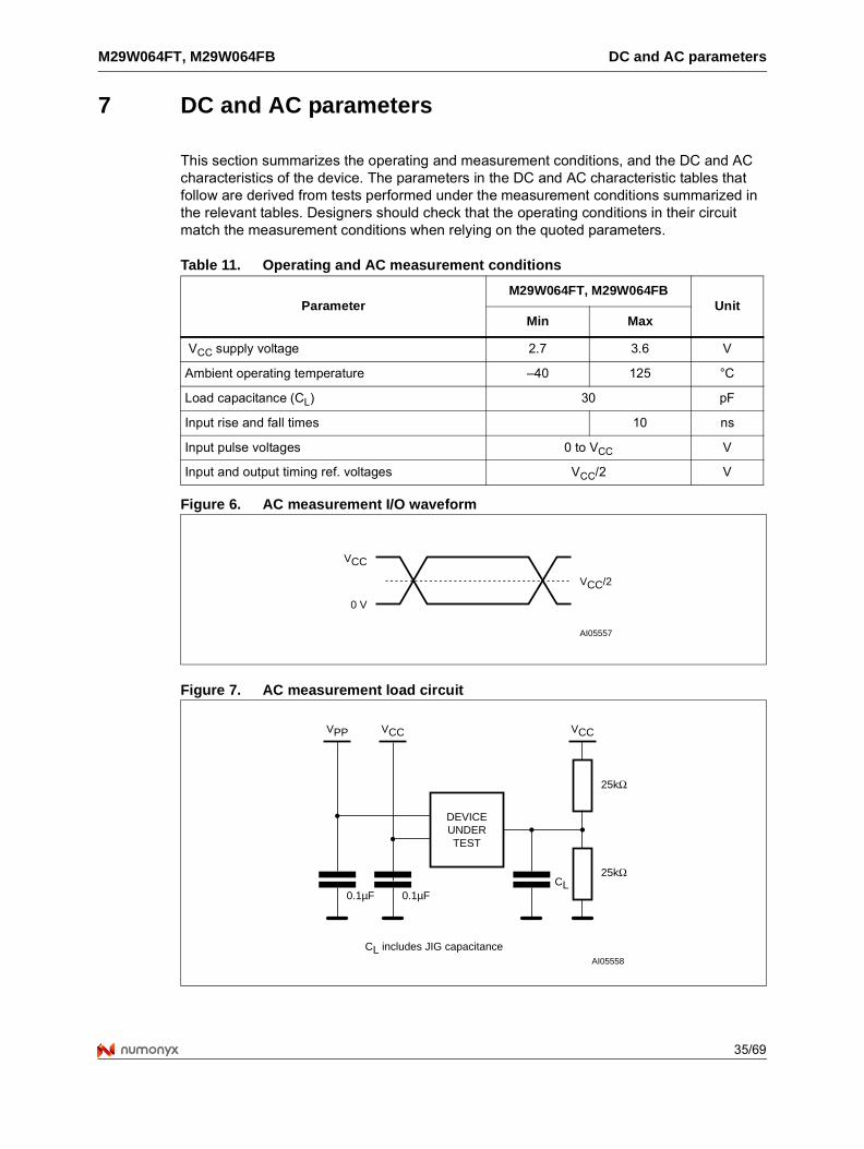
7 DC and AC parameters
This section summarizes the operating and measurement conditions, and the DC and AC characteristics of the device. The parameters in the DC and AC characteristic tables that follow are derived from tests performed under the measurement conditions summarized in the relevant tables. Designers should check that the operating conditions in their circuit match the measurement conditions when relying on the quoted parameters.
Figure 6. AC measurement I/O waveform
Figure 7. AC measurement load circuit
Table 11. Operating and AC measurement conditions
ParameterM29W064FT, M29W064FB
UnitMin Max
VCC supply voltage 2.7 3.6 V
Ambient operating temperature –40 125 °C
Load capacitance (CL) 30 pF
Input rise and fall times 10 ns
Input pulse voltages 0 to VCC V
Input and output timing ref. voltages VCC/2 V
AI05557
VCC
0 V
VCC/2
AI05558
CL
CL includes JIG capacitance
DEVICEUNDERTEST
25kΩ
VCC
25kΩ
VCC
0.1µF
VPP
0.1µF
DC and AC parameters M29W064FT, M29W064FB
36/69
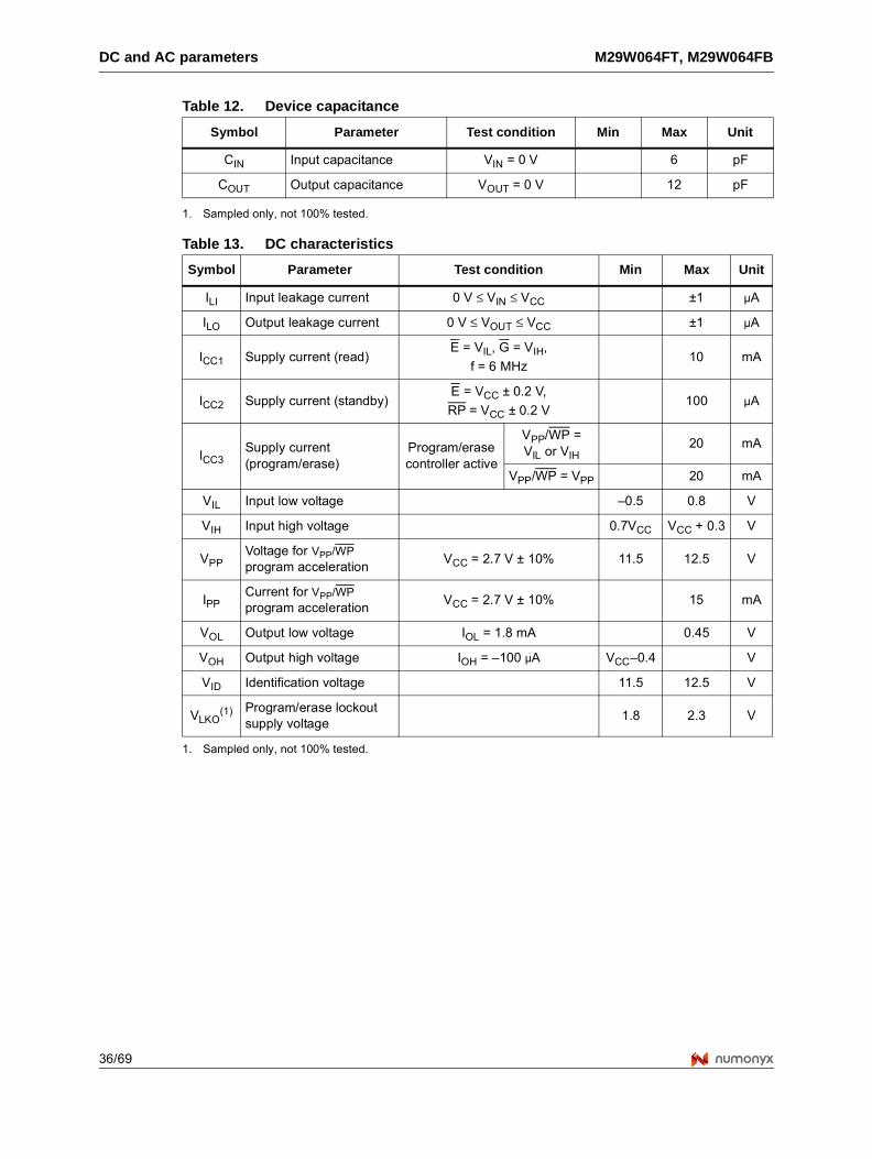
1. Sampled only, not 100% tested.
Table 12. Device capacitance
Symbol Parameter Test condition Min Max Unit
CIN Input capacitance VIN = 0 V 6 pF
COUT Output capacitance VOUT = 0 V 12 pF
Table 13. DC characteristics
Symbol Parameter Test condition Min Max Unit
ILI Input leakage current 0 V ≤ VIN ≤ VCC ±1 μA
ILO Output leakage current 0 V ≤ VOUT ≤ VCC ±1 μA
ICC1 Supply current (read)E = VIL, G = VIH,
f = 6 MHz10 mA
ICC2 Supply current (standby)E = VCC ± 0.2 V,
RP = VCC ± 0.2 V100 μA
ICC3Supply current (program/erase)
Program/erasecontroller active
VPP/WP = VIL or VIH
20 mA
VPP/WP = VPP 20 mA
VIL Input low voltage –0.5 0.8 V
VIH Input high voltage 0.7VCC VCC + 0.3 V
VPPVoltage for VPP/WP program acceleration
VCC = 2.7 V ± 10% 11.5 12.5 V
IPPCurrent for VPP/WP program acceleration
VCC = 2.7 V ± 10% 15 mA
VOL Output low voltage IOL = 1.8 mA 0.45 V
VOH Output high voltage IOH = –100 μA VCC–0.4 V
VID Identification voltage 11.5 12.5 V
VLKO(1)
1. Sampled only, not 100% tested.
Program/erase lockout supply voltage
1.8 2.3 V
M29W064FT, M29W064FB DC and AC parameters
37/69
Figure 8. Read mode AC waveforms
Figure 9. Page read AC waveforms
AI05559
tAVAV
tAVQV tAXQX
tELQX tEHQZ
tGLQV
tGLQX tGHQX
VALID
A0-A20/A–1
G
DQ0-DQ7/DQ8-DQ15
E
tELQV tEHQX
tGHQZ
VALID
tBHQV
tELBL/tELBH tBLQZ
BYTE
AI11553
A2-A21
E
G
A0-A1 VALID
DQ0-DQ15
VALID VALID VALID
VALID ADDRESS
VALID DATAVALID DATA VALID DATA VALID DATA
tAVQV1tGLQV
tAVQV
tELQV tEHQX
tEHQZ
tGHQX
tGHQZ
DC and AC parameters M29W064FT, M29W064FB
38/69
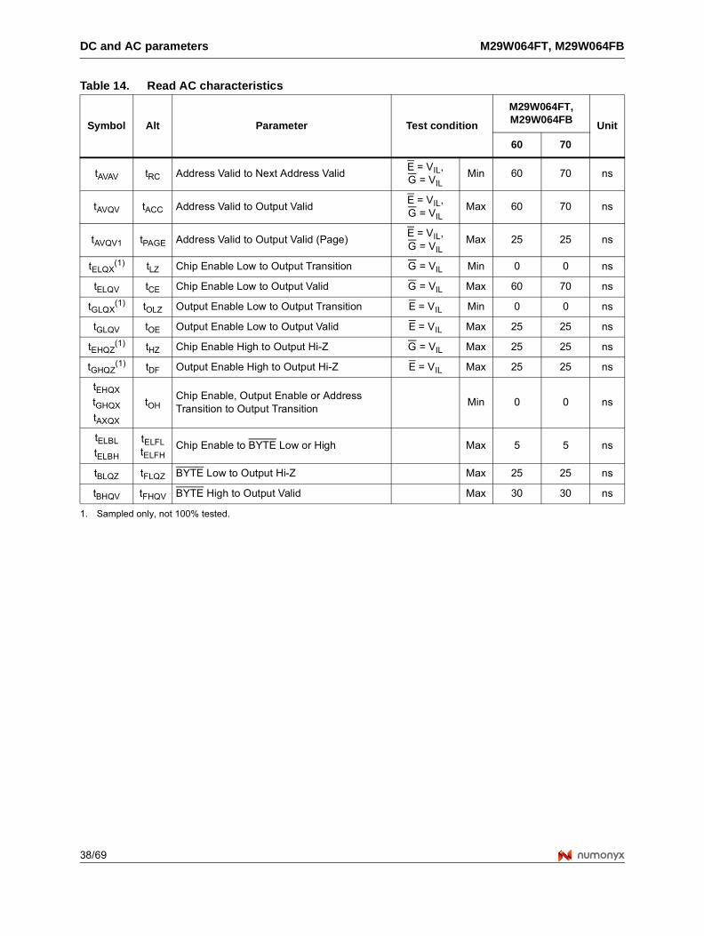
Table 14. Read AC characteristics
Symbol Alt Parameter Test condition
M29W064FT, M29W064FB
Unit
60 70
tAVAV tRC Address Valid to Next Address ValidE = VIL,G = VIL
Min 60 70 ns
tAVQV tACC Address Valid to Output ValidE = VIL,G = VIL
Max 60 70 ns
tAVQV1 tPAGE Address Valid to Output Valid (Page)E = VIL,G = VIL
Max 25 25 ns
tELQX(1) tLZ Chip Enable Low to Output Transition G = VIL Min 0 0 ns
tELQV tCE Chip Enable Low to Output Valid G = VIL Max 60 70 ns
tGLQX(1) tOLZ Output Enable Low to Output Transition E = VIL Min 0 0 ns
tGLQV tOE Output Enable Low to Output Valid E = VIL Max 25 25 ns
tEHQZ(1) tHZ Chip Enable High to Output Hi-Z G = VIL Max 25 25 ns
tGHQZ(1) tDF Output Enable High to Output Hi-Z E = VIL Max 25 25 ns
tEHQX
tGHQX
tAXQX
tOHChip Enable, Output Enable or Address Transition to Output Transition
Min 0 0 ns
tELBL
tELBH
tELFL tELFH
Chip Enable to BYTE Low or High Max 5 5 ns
tBLQZ tFLQZ BYTE Low to Output Hi-Z Max 25 25 ns
tBHQV tFHQV BYTE High to Output Valid Max 30 30 ns
1. Sampled only, not 100% tested.
M29W064FT, M29W064FB DC and AC parameters
39/69
Figure 10. Write AC waveforms, write enable controlled
AI05560
E
G
W
A0-A20/A–1
DQ0-DQ7/DQ8-DQ15
VALID
VALID
VCC
tVCHEL
tWHEH
tWHWL
tELWL
tAVWL
tWHGL
tWLAX
tWHDX
tAVAV
tDVWH
tWLWHtGHWL
RB
tWHRL
DC and AC parameters M29W064FT, M29W064FB
40/69
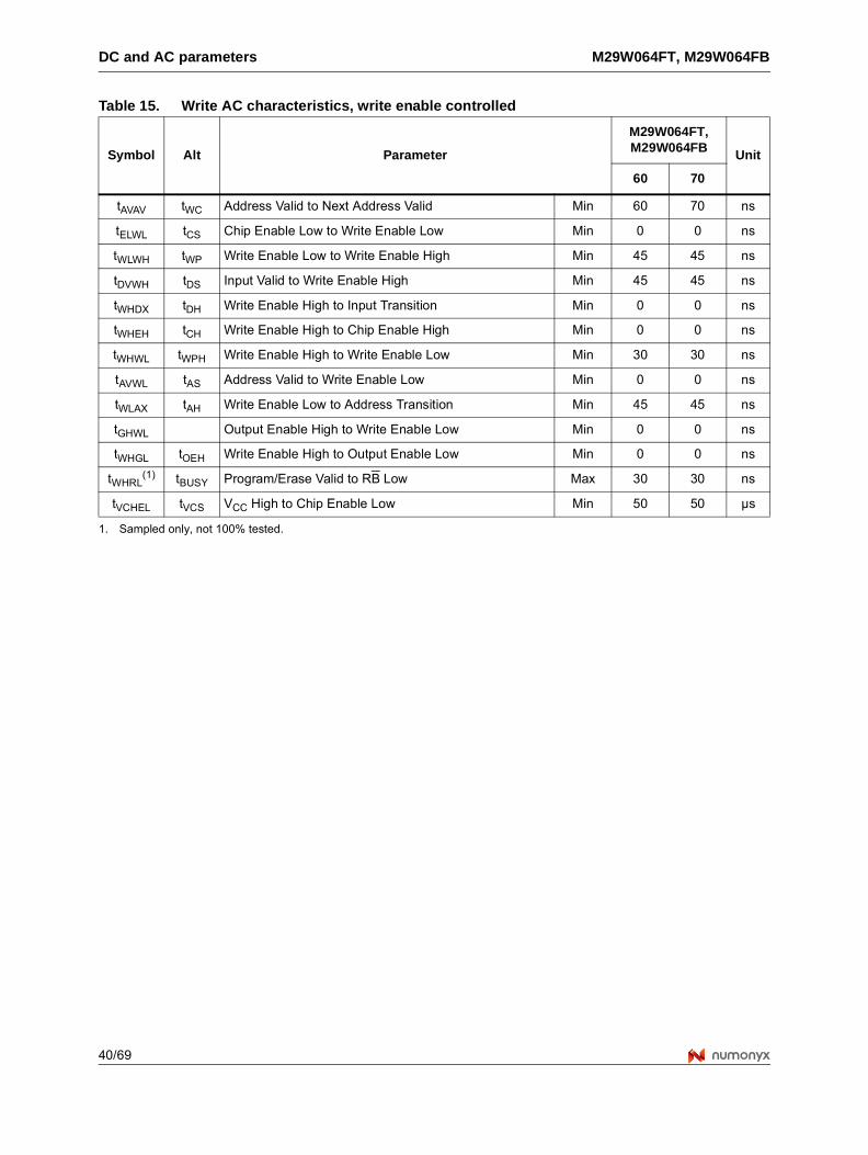
Table 15. Write AC characteristics, write enable controlled
Symbol Alt Parameter
M29W064FT, M29W064FB
Unit
60 70
tAVAV tWC Address Valid to Next Address Valid Min 60 70 ns
tELWL tCS Chip Enable Low to Write Enable Low Min 0 0 ns
tWLWH tWP Write Enable Low to Write Enable High Min 45 45 ns
tDVWH tDS Input Valid to Write Enable High Min 45 45 ns
tWHDX tDH Write Enable High to Input Transition Min 0 0 ns
tWHEH tCH Write Enable High to Chip Enable High Min 0 0 ns
tWHWL tWPH Write Enable High to Write Enable Low Min 30 30 ns
tAVWL tAS Address Valid to Write Enable Low Min 0 0 ns
tWLAX tAH Write Enable Low to Address Transition Min 45 45 ns
tGHWL Output Enable High to Write Enable Low Min 0 0 ns
tWHGL tOEH Write Enable High to Output Enable Low Min 0 0 ns
tWHRL(1) tBUSY Program/Erase Valid to RB Low Max 30 30 ns
tVCHEL tVCS VCC High to Chip Enable Low Min 50 50 μs
1. Sampled only, not 100% tested.
M29W064FT, M29W064FB DC and AC parameters
41/69
Figure 11. Write AC waveforms, chip enable controlled
AI05561
E
G
W
A0-A20/A–1
DQ0-DQ7/DQ8-DQ15
VALID
VALID
VCC
tVCHWL
tEHWH
tEHEL
tWLEL
tAVEL
tEHGL
tELAX
tEHDX
tAVAV
tDVEH
tELEHtGHEL
RB
tEHRL
DC and AC parameters M29W064FT, M29W064FB
42/69
Figure 12. Reset/block temporary unprotect AC waveforms
Table 16. Write AC characteristics, chip enable controlled
Symbol Alt ParameterM29W064FT, M29W064FB
Unit60 70
tAVAV tWC Address Valid to Next Address Valid Min 60 70 ns
tWLEL tWS Write Enable Low to Chip Enable Low Min 0 0 ns
tELEH tCP Chip Enable Low to Chip Enable High Min 45 45 ns
tDVEH tDS Input Valid to Chip Enable High Min 45 45 ns
tEHDX tDH Chip Enable High to Input Transition Min 0 0 ns
tEHWH tWH Chip Enable High to Write Enable High Min 0 0 ns
tEHEL tCPH Chip Enable High to Chip Enable Low Min 30 30 ns
tAVEL tAS Address Valid to Chip Enable Low Min 0 0 ns
tELAX tAH Chip Enable Low to Address Transition Min 45 45 ns
tGHEL Output Enable High Chip Enable Low Min 0 0 ns
tEHGL tOEH Chip Enable High to Output Enable Low Min 0 0 ns
tEHRL(1) tBUSY Program/Erase Valid to RB Low Max 30 30 ns
tVCHWL tVCS VCC High to Write Enable Low Min 50 50 μs
1. Sampled only, not 100% tested.
AI02931B
RB
W,
RPtPLPX
tPHWL, tPHEL, tPHGL
tPLYH
tPHPHH
E, G
tRHWL, tRHEL, tRHGL
M29W064FT, M29W064FB DC and AC parameters
43/69
Figure 13. Accelerated program timing waveforms
AI05563
VPP/WP
VPP
VIL or VIHtVHVPP tVHVPP
Table 17. Reset/block temporary unprotect AC characteristics
Symbol Alt ParameterM29W064FT, M29W064FB
Unit
tPHWL(1)
tPHEL
tPHGL(1)
tRHRP High to Write Enable Low, Chip Enable Low, Output Enable Low
Min 50 ns
tRHWL(1)
tRHEL(1)
tRHGL(1)
tRBRB High to Write Enable Low, Chip Enable Low, Output Enable Low
Min 0 ns
tPLPX tRP RP pulse width Min 500 ns
tPLYH tREADY RP Low to read mode Max 50 μs
tPHPHH(1) tVIDR RP rise time to VID Min 500 ns
tVHVPP(1) VPP rise and fall time Min 250 ns
1. Sampled only, not 100% tested.
Package mechanical M29W064FT, M29W064FB
44/69
8 Package mechanical
To meet environmental requirements, Numonyx offers these devices in RoHS compliant packages. RoHS packages are lead-free. The category of second level interconnect is marked on the package and on the inner box label, in compliance with JEDEC Standard JESD97. The maximum ratings related to soldering conditions are also marked on the inner box label.
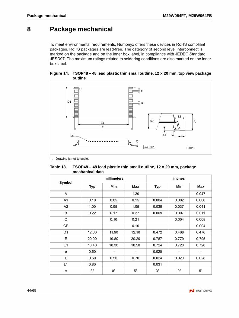
Figure 14. TSOP48 – 48 lead plastic thin small outline, 12 x 20 mm, top view package outline
1. Drawing is not to scale.
Table 18. TSOP48 – 48 lead plastic thin small outline, 12 x 20 mm, package mechanical data
Symbolmillimeters inches
Typ Min Max Typ Min Max
A 1.20 0.047
A1 0.10 0.05 0.15 0.004 0.002 0.006
A2 1.00 0.95 1.05 0.039 0.037 0.041
B 0.22 0.17 0.27 0.009 0.007 0.011
C 0.10 0.21 0.004 0.008
CP 0.10 0.004
D1 12.00 11.90 12.10 0.472 0.468 0.476
E 20.00 19.80 20.20 0.787 0.779 0.795
E1 18.40 18.30 18.50 0.724 0.720 0.728
e 0.50 – – 0.020 – –
L 0.60 0.50 0.70 0.024 0.020 0.028
L1 0.80 0.031
α 3° 0° 5° 3° 0° 5°
TSOP-G
B
e
DIE
C
LA1 α
E1
E
AA2
1
24
48
25
D1
L1
CP
M29W064FT, M29W064FB Package mechanical
45/69
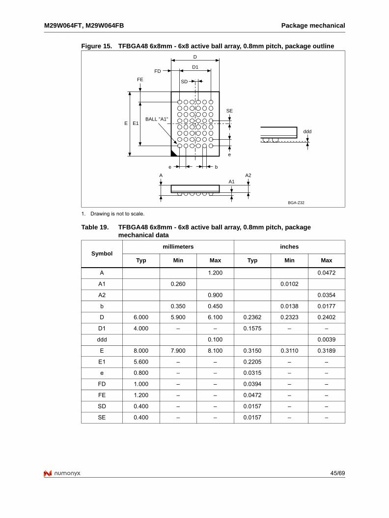
Figure 15. TFBGA48 6x8mm - 6x8 active ball array, 0.8mm pitch, package outline
1. Drawing is not to scale.
Table 19. TFBGA48 6x8mm - 6x8 active ball array, 0.8mm pitch, package mechanical data
Symbolmillimeters inches
Typ Min Max Typ Min Max
A 1.200 0.0472
A1 0.260 0.0102
A2 0.900 0.0354
b 0.350 0.450 0.0138 0.0177
D 6.000 5.900 6.100 0.2362 0.2323 0.2402
D1 4.000 – – 0.1575 – –
ddd 0.100 0.0039
E 8.000 7.900 8.100 0.3150 0.3110 0.3189
E1 5.600 – – 0.2205 – –
e 0.800 – – 0.0315 – –
FD 1.000 – – 0.0394 – –
FE 1.200 – – 0.0472 – –
SD 0.400 – – 0.0157 – –
SE 0.400 – – 0.0157 – –
E1E
D1
D
e b
A2A1
A
BGA-Z32
ddd
FD
FE SD
SE
e
BALL "A1"
Ordering information M29W064FT, M29W064FB
46/69
9 Ordering information
Note: Devices are shipped from the factory with the memory content bits erased to ‘1’. For a list of available options (speed, package, etc.) or for further information on any aspect of this device, please contact your nearest Numonyx sales office.
Table 20. Ordering information scheme
Example: M29W064FB 70 N 3 F
Device type
M29
Operating voltage
W = VCC = 2.7 to 3.6 V
Device function
064F = 64 Mbits (x8 / x16), boot block
Array matrix
T = top boot
B = bottom boot
Speed
60 = 60 ns
70 = 70 ns
6A = 60 ns automotive grade 6, −40 to 85 °C
7A = 70 ns automotive grade 6, −40 to 85 °C
Package
N = TSOP48: 12 x 20 mm
ZA = TFBGA48: 6 X 8 mm - 0.8 mm pitch
Temperature range
3 = automotive grade certified(1), −40 to 125 °C
1. Qualified and characterized according to AEC Q100 & Q003 or equivalent, advanced screening according to AEC Q001 & Q002 or equivalent.
6 = automotive grade certified(1), −40 to 85 °C
Option
E = ECOPACK package, standard packing
F = ECOPACK package, tape & reel packing
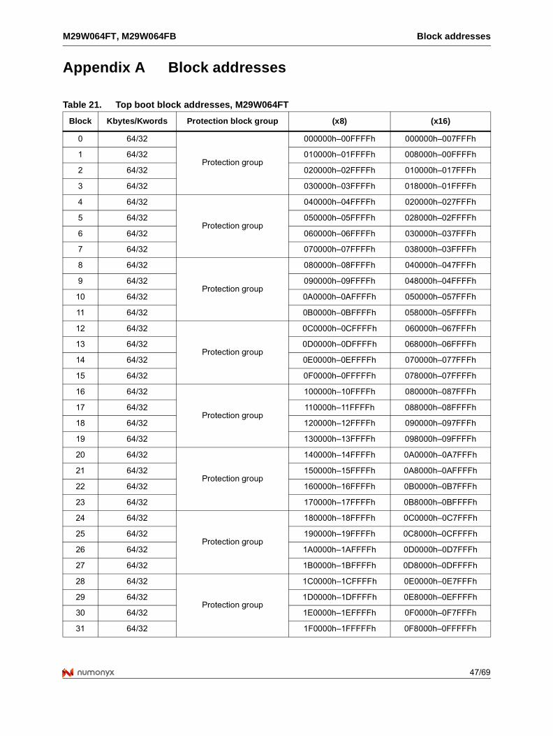
M29W064FT, M29W064FB Block addresses
47/69
Appendix A Block addresses
Table 21. Top boot block addresses, M29W064FT
Block Kbytes/Kwords Protection block group (x8) (x16)
0 64/32
Protection group
000000h–00FFFFh 000000h–007FFFh
1 64/32 010000h–01FFFFh 008000h–00FFFFh
2 64/32 020000h–02FFFFh 010000h–017FFFh
3 64/32 030000h–03FFFFh 018000h–01FFFFh
4 64/32
Protection group
040000h–04FFFFh 020000h–027FFFh
5 64/32 050000h–05FFFFh 028000h–02FFFFh
6 64/32 060000h–06FFFFh 030000h–037FFFh
7 64/32 070000h–07FFFFh 038000h–03FFFFh
8 64/32
Protection group
080000h–08FFFFh 040000h–047FFFh
9 64/32 090000h–09FFFFh 048000h–04FFFFh
10 64/32 0A0000h–0AFFFFh 050000h–057FFFh
11 64/32 0B0000h–0BFFFFh 058000h–05FFFFh
12 64/32
Protection group
0C0000h–0CFFFFh 060000h–067FFFh
13 64/32 0D0000h–0DFFFFh 068000h–06FFFFh
14 64/32 0E0000h–0EFFFFh 070000h–077FFFh
15 64/32 0F0000h–0FFFFFh 078000h–07FFFFh
16 64/32
Protection group
100000h–10FFFFh 080000h–087FFFh
17 64/32 110000h–11FFFFh 088000h–08FFFFh
18 64/32 120000h–12FFFFh 090000h–097FFFh
19 64/32 130000h–13FFFFh 098000h–09FFFFh
20 64/32
Protection group
140000h–14FFFFh 0A0000h–0A7FFFh
21 64/32 150000h–15FFFFh 0A8000h–0AFFFFh
22 64/32 160000h–16FFFFh 0B0000h–0B7FFFh
23 64/32 170000h–17FFFFh 0B8000h–0BFFFFh
24 64/32
Protection group
180000h–18FFFFh 0C0000h–0C7FFFh
25 64/32 190000h–19FFFFh 0C8000h–0CFFFFh
26 64/32 1A0000h–1AFFFFh 0D0000h–0D7FFFh
27 64/32 1B0000h–1BFFFFh 0D8000h–0DFFFFh
28 64/32
Protection group
1C0000h–1CFFFFh 0E0000h–0E7FFFh
29 64/32 1D0000h–1DFFFFh 0E8000h–0EFFFFh
30 64/32 1E0000h–1EFFFFh 0F0000h–0F7FFFh
31 64/32 1F0000h–1FFFFFh 0F8000h–0FFFFFh
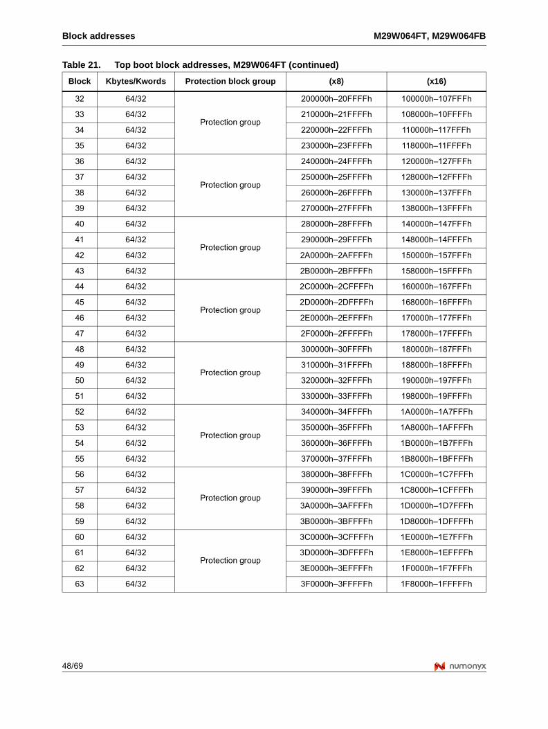
Block addresses M29W064FT, M29W064FB
48/69
32 64/32
Protection group
200000h–20FFFFh 100000h–107FFFh
33 64/32 210000h–21FFFFh 108000h–10FFFFh
34 64/32 220000h–22FFFFh 110000h–117FFFh
35 64/32 230000h–23FFFFh 118000h–11FFFFh
36 64/32
Protection group
240000h–24FFFFh 120000h–127FFFh
37 64/32 250000h–25FFFFh 128000h–12FFFFh
38 64/32 260000h–26FFFFh 130000h–137FFFh
39 64/32 270000h–27FFFFh 138000h–13FFFFh
40 64/32
Protection group
280000h–28FFFFh 140000h–147FFFh
41 64/32 290000h–29FFFFh 148000h–14FFFFh
42 64/32 2A0000h–2AFFFFh 150000h–157FFFh
43 64/32 2B0000h–2BFFFFh 158000h–15FFFFh
44 64/32
Protection group
2C0000h–2CFFFFh 160000h–167FFFh
45 64/32 2D0000h–2DFFFFh 168000h–16FFFFh
46 64/32 2E0000h–2EFFFFh 170000h–177FFFh
47 64/32 2F0000h–2FFFFFh 178000h–17FFFFh
48 64/32
Protection group
300000h–30FFFFh 180000h–187FFFh
49 64/32 310000h–31FFFFh 188000h–18FFFFh
50 64/32 320000h–32FFFFh 190000h–197FFFh
51 64/32 330000h–33FFFFh 198000h–19FFFFh
52 64/32
Protection group
340000h–34FFFFh 1A0000h–1A7FFFh
53 64/32 350000h–35FFFFh 1A8000h–1AFFFFh
54 64/32 360000h–36FFFFh 1B0000h–1B7FFFh
55 64/32 370000h–37FFFFh 1B8000h–1BFFFFh
56 64/32
Protection group
380000h–38FFFFh 1C0000h–1C7FFFh
57 64/32 390000h–39FFFFh 1C8000h–1CFFFFh
58 64/32 3A0000h–3AFFFFh 1D0000h–1D7FFFh
59 64/32 3B0000h–3BFFFFh 1D8000h–1DFFFFh
60 64/32
Protection group
3C0000h–3CFFFFh 1E0000h–1E7FFFh
61 64/32 3D0000h–3DFFFFh 1E8000h–1EFFFFh
62 64/32 3E0000h–3EFFFFh 1F0000h–1F7FFFh
63 64/32 3F0000h–3FFFFFh 1F8000h–1FFFFFh
Table 21. Top boot block addresses, M29W064FT (continued)
Block Kbytes/Kwords Protection block group (x8) (x16)
M29W064FT, M29W064FB Block addresses
49/69
64 64/32
Protection group
400000h–40FFFFh 200000h–207FFFh
65 64/32 410000h–41FFFFh 208000h–20FFFFh
66 64/32 420000h–42FFFFh 210000h–217FFFh
67 64/32 430000h–43FFFFh 218000h–21FFFFh
68 64/32
Protection group
440000h–44FFFFh 220000h–227FFFh
69 64/32 450000h–45FFFFh 228000h–22FFFFh
70 64/32 460000h–46FFFFh 230000h–237FFFh
71 64/32 470000h–47FFFFh 238000h–23FFFFh
72 64/32
Protection group
480000h–48FFFFh 240000h–247FFFh
73 64/32 490000h–49FFFFh 248000h–24FFFFh
74 64/32 4A0000h–4AFFFFh 250000h–257FFFh
75 64/32 4B0000h–4BFFFFh 258000h–25FFFFh
76 64/32
Protection group
4C0000h–4CFFFFh 260000h–267FFFh
77 64/32 4D0000h–4DFFFFh 268000h–26FFFFh
78 64/32 4E0000h–4EFFFFh 270000h–277FFFh
79 64/32 4F0000h–4FFFFFh 278000h–27FFFFh
80 64/32
Protection group
500000h–50FFFFh 280000h–287FFFh
81 64/32 510000h–51FFFFh 288000h–28FFFFh
82 64/32 520000h–52FFFFh 290000h–297FFFh
83 64/32 530000h–53FFFFh 298000h–29FFFFh
84 64/32
Protection group
540000h–54FFFFh 2A0000h–2A7FFFh
85 64/32 550000h–55FFFFh 2A8000h–2AFFFFh
86 64/32 560000h–56FFFFh 2B0000h–2B7FFFh
87 64/32 570000h–57FFFFh 2B8000h–2BFFFFh
88 64/32
Protection group
580000h–58FFFFh 2C0000h–2C7FFFh
89 64/32 590000h–59FFFFh 2C8000h–2CFFFFh
90 64/32 5A0000h–5AFFFFh 2D0000h–2D7FFFh
91 64/32 5B0000h–5BFFFFh 2D8000h–2DFFFFh
92 64/32
Protection group
5C0000h–5CFFFFh 2E0000h–2E7FFFh
93 64/32 5D0000h–5DFFFFh 2E8000h–2EFFFFh
94 64/32 5E0000h–5EFFFFh 2F0000h–2F7FFFh
95 64/32 5F0000h–5FFFFFh 2F8000h–2FFFFFh
Table 21. Top boot block addresses, M29W064FT (continued)
Block Kbytes/Kwords Protection block group (x8) (x16)
Block addresses M29W064FT, M29W064FB
50/69
96 64/32
Protection group
600000h–60FFFFh 300000h–307FFFh
97 64/32 610000h–61FFFFh 308000h–30FFFFh
98 64/32 620000h–62FFFFh 310000h–317FFFh
99 64/32 630000h–63FFFFh 318000h–31FFFFh
100 64/32
Protection group
640000h–64FFFFh 320000h–327FFFh
101 64/32 650000h–65FFFFh 328000h–32FFFFh
102 64/32 660000h–66FFFFh 330000h–337FFFh
103 64/32 670000h–67FFFFh 338000h–33FFFFh
104 64/32
Protection group
680000h–68FFFFh 340000h–347FFFh
105 64/32 690000h–69FFFFh 348000h–34FFFFh
106 64/32 6A0000h–6AFFFFh 350000h–357FFFh
107 64/32 6B0000h–6BFFFFh 358000h–35FFFFh
108 64/32
Protection group
6C0000h–6CFFFFh 360000h–367FFFh
109 64/32 6D0000h–6DFFFFh 368000h–36FFFFh
110 64/32 6E0000h–6EFFFFh 370000h–377FFFh
111 64/32 6F0000h–6FFFFFh 378000h–37FFFFh
112 64/32
Protection group
700000h–70FFFFh 380000h–387FFFh
113 64/32 710000h–71FFFFh 388000h–38FFFFh
114 64/32 720000h–72FFFFh 390000h–397FFFh
115 64/32 730000h–73FFFFh 398000h–39FFFFh
116 64/32
Protection group
740000h–74FFFFh 3A0000h–3A7FFFh
117 64/32 750000h–75FFFFh 3A8000h–3AFFFFh
118 64/32 760000h–76FFFFh 3B0000h–3B7FFFh
119 64/32 770000h–77FFFFh 3B8000h–3BFFFFh
120 64/32
Protection group
780000h–78FFFFh 3C0000h–3C7FFFh
121 64/32 790000h–79FFFFh 3C8000h–3CFFFFh
122 64/32 7A0000h–7AFFFFh 3D0000h–3D7FFFh
123 64/32 7B0000h–7BFFFFh 3D8000h–3DFFFFh
Table 21. Top boot block addresses, M29W064FT (continued)
Block Kbytes/Kwords Protection block group (x8) (x16)
M29W064FT, M29W064FB Block addresses
51/69
124 64/32
Protection group
7C0000h–7CFFFFh 3E0000h–3E7FFFh
125 64/32 7D0000h–7DFFFFh 3E8000h–3EFFFFh
126 64/32 7E0000h–7EFFFFh 3F0000h–3F7FFFh
127 8/4 7F0000h–7F1FFFh 3F8000h–3F8FFFh
128 8/4 7F2000h–7F3FFFh 3F9000h–3F9FFFh
129 8/4 7F4000h–7F5FFFh 3FA000h–3FAFFFh
130 8/4 7F6000h–7F7FFFh 3FB000h–3FBFFFh
131 8/4 7F8000h–7F9FFFh 3FC000h–3FCFFFh
132 8/4 7FA000h–7FBFFFh 3FD000h–3FDFFFh
133 8/4 7FC000h–7FDFFFh 3FE000h–3FEFFFh
134 8/4 7FE000h–7FFFFFh 3FF000h–3FFFFFh
Table 21. Top boot block addresses, M29W064FT (continued)
Block Kbytes/Kwords Protection block group (x8) (x16)
Block addresses M29W064FT, M29W064FB
52/69
Table 22. Bottom boot block addresses, M29W064FB
Block Kbytes/Kwords Protection block group (x8) (x16)
0 8/4
Protection group
000000h-001FFFh 000000h–000FFFh
1 8/4 002000h-003FFFh 001000h–001FFFh
2 8/4 004000h-005FFFh 002000h–002FFFh
3 8/4 006000h-007FFFh 003000h–003FFFh
4 8/4 008000h-009FFFh 004000h–004FFFh
5 8/4 00A000h-00BFFFh 005000h–005FFFh
6 8/4 00C000h-00DFFFh 006000h–006FFFh
7 8/4 00E000h-00FFFFh 007000h–007FFFh
8 64/32 010000h-01FFFFh 008000h–00FFFFh
9 64/32 020000h-02FFFFh 010000h–017FFFh
10 64/32 030000h-03FFFFh 018000h–01FFFFh
11 64/32
Protection group
040000h-04FFFFh 020000h–027FFFh
12 64/32 050000h-05FFFFh 028000h–02FFFFh
13 64/32 060000h-06FFFFh 030000h–037FFFh
14 64/32 070000h-07FFFFh 038000h–03FFFFh
15 64/32
Protection group
080000h-08FFFFh 040000h–047FFFh
16 64/32 090000h-09FFFFh 048000h–04FFFFh
17 64/32 0A0000h-0AFFFFh 050000h–057FFFh
18 64/32 0B0000h-0BFFFFh 058000h–05FFFFh
19 64/32
Protection group
0C0000h-0CFFFFh 060000h–067FFFh
20 64/32 0D0000h-0DFFFFh 068000h–06FFFFh
21 64/32 0E0000h-0EFFFFh 070000h–077FFFh
22 64/32 0F0000h-0FFFFFh 078000h–07FFFFh
23 64/32
Protection group
100000h-10FFFFh 080000h–087FFFh
24 64/32 110000h-11FFFFh 088000h–08FFFFh
25 64/32 120000h-12FFFFh 090000h–097FFFh
26 64/32 130000h-13FFFFh 098000h–09FFFFh
27 64/32
Protection group
140000h-14FFFFh 0A0000h–0A7FFFh
28 64/32 150000h-15FFFFh 0A8000h–0AFFFFh
29 64/32 160000h-16FFFFh 0B0000h–0B7FFFh
30 64/32 170000h-17FFFFh 0B8000h–0BFFFFh
31 64/32
Protection group
180000h-18FFFFh 0C0000h–0C7FFFh
32 64/32 190000h-19FFFFh 0C8000h–0CFFFFh
33 64/32 1A0000h-1AFFFFh 0D0000h–0D7FFFh
34 64/32 1B0000h-1BFFFFh 0D8000h–0DFFFFh
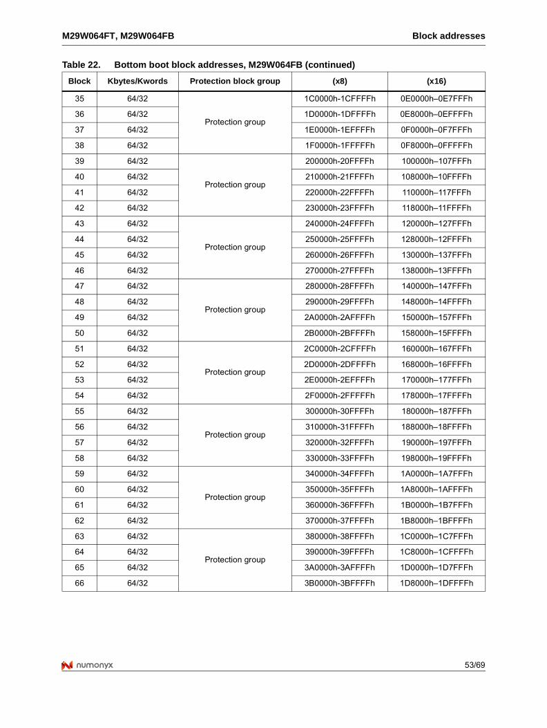
M29W064FT, M29W064FB Block addresses
53/69
35 64/32
Protection group
1C0000h-1CFFFFh 0E0000h–0E7FFFh
36 64/32 1D0000h-1DFFFFh 0E8000h–0EFFFFh
37 64/32 1E0000h-1EFFFFh 0F0000h–0F7FFFh
38 64/32 1F0000h-1FFFFFh 0F8000h–0FFFFFh
39 64/32
Protection group
200000h-20FFFFh 100000h–107FFFh
40 64/32 210000h-21FFFFh 108000h–10FFFFh
41 64/32 220000h-22FFFFh 110000h–117FFFh
42 64/32 230000h-23FFFFh 118000h–11FFFFh
43 64/32
Protection group
240000h-24FFFFh 120000h–127FFFh
44 64/32 250000h-25FFFFh 128000h–12FFFFh
45 64/32 260000h-26FFFFh 130000h–137FFFh
46 64/32 270000h-27FFFFh 138000h–13FFFFh
47 64/32
Protection group
280000h-28FFFFh 140000h–147FFFh
48 64/32 290000h-29FFFFh 148000h–14FFFFh
49 64/32 2A0000h-2AFFFFh 150000h–157FFFh
50 64/32 2B0000h-2BFFFFh 158000h–15FFFFh
51 64/32
Protection group
2C0000h-2CFFFFh 160000h–167FFFh
52 64/32 2D0000h-2DFFFFh 168000h–16FFFFh
53 64/32 2E0000h-2EFFFFh 170000h–177FFFh
54 64/32 2F0000h-2FFFFFh 178000h–17FFFFh
55 64/32
Protection group
300000h-30FFFFh 180000h–187FFFh
56 64/32 310000h-31FFFFh 188000h–18FFFFh
57 64/32 320000h-32FFFFh 190000h–197FFFh
58 64/32 330000h-33FFFFh 198000h–19FFFFh
59 64/32
Protection group
340000h-34FFFFh 1A0000h–1A7FFFh
60 64/32 350000h-35FFFFh 1A8000h–1AFFFFh
61 64/32 360000h-36FFFFh 1B0000h–1B7FFFh
62 64/32 370000h-37FFFFh 1B8000h–1BFFFFh
63 64/32
Protection group
380000h-38FFFFh 1C0000h–1C7FFFh
64 64/32 390000h-39FFFFh 1C8000h–1CFFFFh
65 64/32 3A0000h-3AFFFFh 1D0000h–1D7FFFh
66 64/32 3B0000h-3BFFFFh 1D8000h–1DFFFFh
Table 22. Bottom boot block addresses, M29W064FB (continued)
Block Kbytes/Kwords Protection block group (x8) (x16)
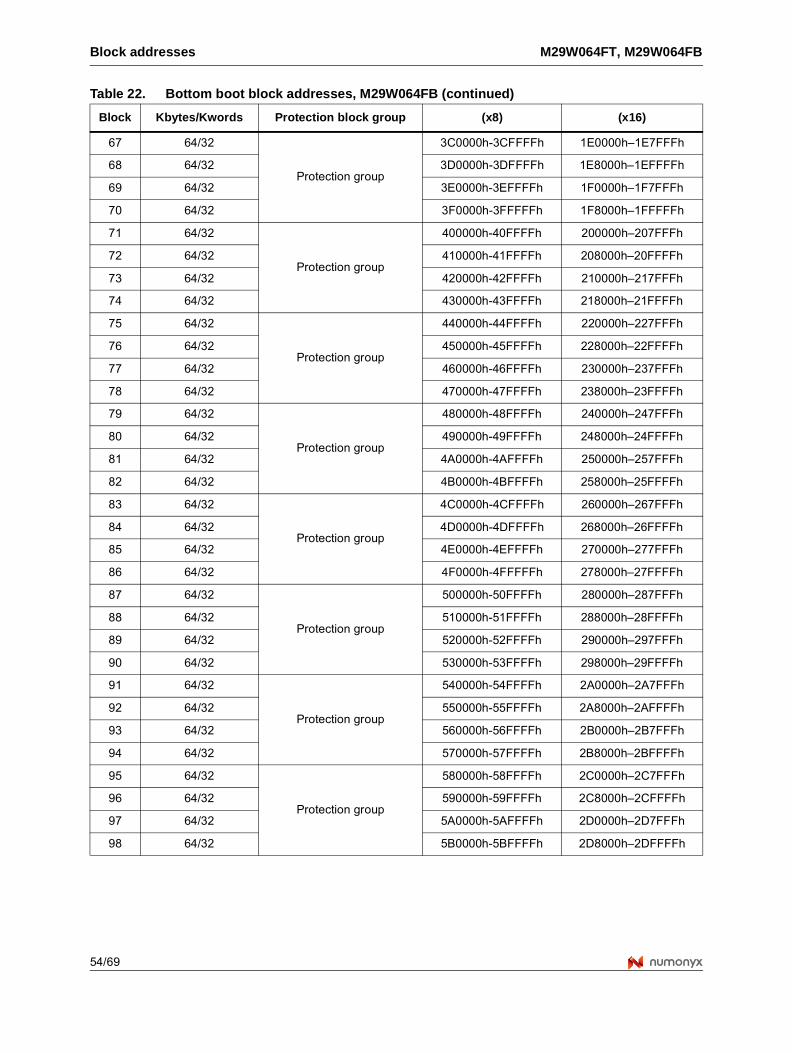
Block addresses M29W064FT, M29W064FB
54/69
67 64/32
Protection group
3C0000h-3CFFFFh 1E0000h–1E7FFFh
68 64/32 3D0000h-3DFFFFh 1E8000h–1EFFFFh
69 64/32 3E0000h-3EFFFFh 1F0000h–1F7FFFh
70 64/32 3F0000h-3FFFFFh 1F8000h–1FFFFFh
71 64/32
Protection group
400000h-40FFFFh 200000h–207FFFh
72 64/32 410000h-41FFFFh 208000h–20FFFFh
73 64/32 420000h-42FFFFh 210000h–217FFFh
74 64/32 430000h-43FFFFh 218000h–21FFFFh
75 64/32
Protection group
440000h-44FFFFh 220000h–227FFFh
76 64/32 450000h-45FFFFh 228000h–22FFFFh
77 64/32 460000h-46FFFFh 230000h–237FFFh
78 64/32 470000h-47FFFFh 238000h–23FFFFh
79 64/32
Protection group
480000h-48FFFFh 240000h–247FFFh
80 64/32 490000h-49FFFFh 248000h–24FFFFh
81 64/32 4A0000h-4AFFFFh 250000h–257FFFh
82 64/32 4B0000h-4BFFFFh 258000h–25FFFFh
83 64/32
Protection group
4C0000h-4CFFFFh 260000h–267FFFh
84 64/32 4D0000h-4DFFFFh 268000h–26FFFFh
85 64/32 4E0000h-4EFFFFh 270000h–277FFFh
86 64/32 4F0000h-4FFFFFh 278000h–27FFFFh
87 64/32
Protection group
500000h-50FFFFh 280000h–287FFFh
88 64/32 510000h-51FFFFh 288000h–28FFFFh
89 64/32 520000h-52FFFFh 290000h–297FFFh
90 64/32 530000h-53FFFFh 298000h–29FFFFh
91 64/32
Protection group
540000h-54FFFFh 2A0000h–2A7FFFh
92 64/32 550000h-55FFFFh 2A8000h–2AFFFFh
93 64/32 560000h-56FFFFh 2B0000h–2B7FFFh
94 64/32 570000h-57FFFFh 2B8000h–2BFFFFh
95 64/32
Protection group
580000h-58FFFFh 2C0000h–2C7FFFh
96 64/32 590000h-59FFFFh 2C8000h–2CFFFFh
97 64/32 5A0000h-5AFFFFh 2D0000h–2D7FFFh
98 64/32 5B0000h-5BFFFFh 2D8000h–2DFFFFh
Table 22. Bottom boot block addresses, M29W064FB (continued)
Block Kbytes/Kwords Protection block group (x8) (x16)
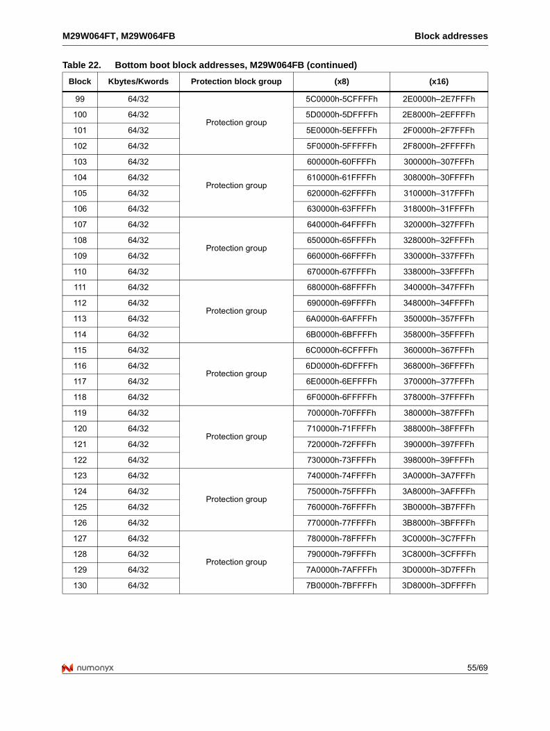
M29W064FT, M29W064FB Block addresses
55/69
99 64/32
Protection group
5C0000h-5CFFFFh 2E0000h–2E7FFFh
100 64/32 5D0000h-5DFFFFh 2E8000h–2EFFFFh
101 64/32 5E0000h-5EFFFFh 2F0000h–2F7FFFh
102 64/32 5F0000h-5FFFFFh 2F8000h–2FFFFFh
103 64/32
Protection group
600000h-60FFFFh 300000h–307FFFh
104 64/32 610000h-61FFFFh 308000h–30FFFFh
105 64/32 620000h-62FFFFh 310000h–317FFFh
106 64/32 630000h-63FFFFh 318000h–31FFFFh
107 64/32
Protection group
640000h-64FFFFh 320000h–327FFFh
108 64/32 650000h-65FFFFh 328000h–32FFFFh
109 64/32 660000h-66FFFFh 330000h–337FFFh
110 64/32 670000h-67FFFFh 338000h–33FFFFh
111 64/32
Protection group
680000h-68FFFFh 340000h–347FFFh
112 64/32 690000h-69FFFFh 348000h–34FFFFh
113 64/32 6A0000h-6AFFFFh 350000h–357FFFh
114 64/32 6B0000h-6BFFFFh 358000h–35FFFFh
115 64/32
Protection group
6C0000h-6CFFFFh 360000h–367FFFh
116 64/32 6D0000h-6DFFFFh 368000h–36FFFFh
117 64/32 6E0000h-6EFFFFh 370000h–377FFFh
118 64/32 6F0000h-6FFFFFh 378000h–37FFFFh
119 64/32
Protection group
700000h-70FFFFh 380000h–387FFFh
120 64/32 710000h-71FFFFh 388000h–38FFFFh
121 64/32 720000h-72FFFFh 390000h–397FFFh
122 64/32 730000h-73FFFFh 398000h–39FFFFh
123 64/32
Protection group
740000h-74FFFFh 3A0000h–3A7FFFh
124 64/32 750000h-75FFFFh 3A8000h–3AFFFFh
125 64/32 760000h-76FFFFh 3B0000h–3B7FFFh
126 64/32 770000h-77FFFFh 3B8000h–3BFFFFh
127 64/32
Protection group
780000h-78FFFFh 3C0000h–3C7FFFh
128 64/32 790000h-79FFFFh 3C8000h–3CFFFFh
129 64/32 7A0000h-7AFFFFh 3D0000h–3D7FFFh
130 64/32 7B0000h-7BFFFFh 3D8000h–3DFFFFh
Table 22. Bottom boot block addresses, M29W064FB (continued)
Block Kbytes/Kwords Protection block group (x8) (x16)
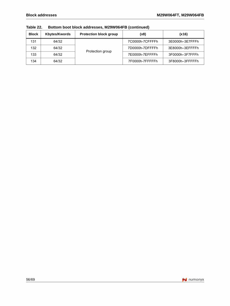
Block addresses M29W064FT, M29W064FB
56/69
131 64/32
Protection group
7C0000h-7CFFFFh 3E0000h–3E7FFFh
132 64/32 7D0000h-7DFFFFh 3E8000h–3EFFFFh
133 64/32 7E0000h-7EFFFFh 3F0000h–3F7FFFh
134 64/32 7F0000h-7FFFFFh 3F8000h–3FFFFFh
Table 22. Bottom boot block addresses, M29W064FB (continued)
Block Kbytes/Kwords Protection block group (x8) (x16)
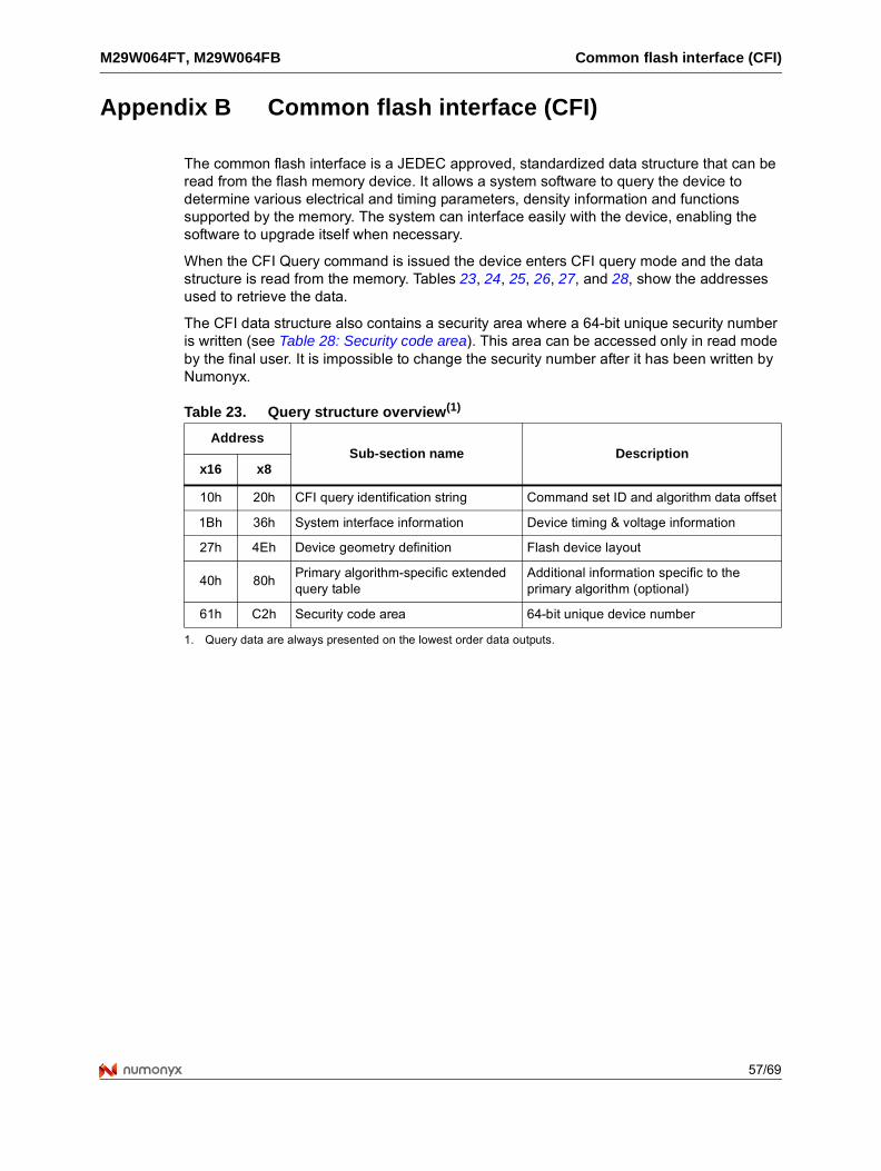
M29W064FT, M29W064FB Common flash interface (CFI)
57/69
Appendix B Common flash interface (CFI)
The common flash interface is a JEDEC approved, standardized data structure that can be read from the flash memory device. It allows a system software to query the device to determine various electrical and timing parameters, density information and functions supported by the memory. The system can interface easily with the device, enabling the software to upgrade itself when necessary.
When the CFI Query command is issued the device enters CFI query mode and the data structure is read from the memory. Tables 23, 24, 25, 26, 27, and 28, show the addresses used to retrieve the data.
The CFI data structure also contains a security area where a 64-bit unique security number is written (see Table 28: Security code area). This area can be accessed only in read mode by the final user. It is impossible to change the security number after it has been written by Numonyx.
Table 23. Query structure overview(1)
1. Query data are always presented on the lowest order data outputs.
AddressSub-section name Description
x16 x8
10h 20h CFI query identification string Command set ID and algorithm data offset
1Bh 36h System interface information Device timing & voltage information
27h 4Eh Device geometry definition Flash device layout
40h 80hPrimary algorithm-specific extended query table
Additional information specific to the primary algorithm (optional)
61h C2h Security code area 64-bit unique device number
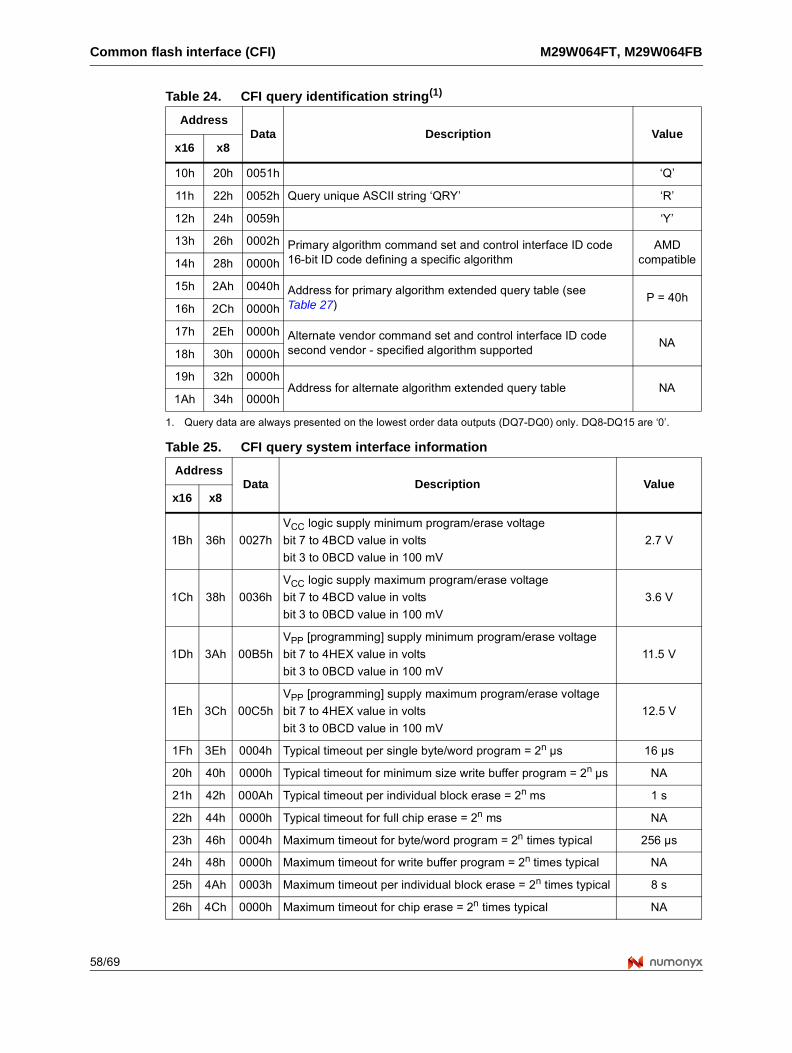
Common flash interface (CFI) M29W064FT, M29W064FB
58/69
Table 24. CFI query identification string(1)
1. Query data are always presented on the lowest order data outputs (DQ7-DQ0) only. DQ8-DQ15 are ‘0’.
AddressData Description Value
x16 x8
10h 20h 0051h ‘Q’
11h 22h 0052h Query unique ASCII string ‘QRY’ ‘R’
12h 24h 0059h ‘Y’
13h 26h 0002h Primary algorithm command set and control interface ID code 16-bit ID code defining a specific algorithm
AMDcompatible14h 28h 0000h
15h 2Ah 0040h Address for primary algorithm extended query table (see Table 27)
P = 40h16h 2Ch 0000h
17h 2Eh 0000h Alternate vendor command set and control interface ID code second vendor - specified algorithm supported
NA18h 30h 0000h
19h 32h 0000hAddress for alternate algorithm extended query table NA
1Ah 34h 0000h
Table 25. CFI query system interface information
AddressData Description Value
x16 x8
1Bh 36h 0027h
VCC logic supply minimum program/erase voltage
bit 7 to 4BCD value in volts
bit 3 to 0BCD value in 100 mV
2.7 V
1Ch 38h 0036h
VCC logic supply maximum program/erase voltage
bit 7 to 4BCD value in volts
bit 3 to 0BCD value in 100 mV
3.6 V
1Dh 3Ah 00B5h
VPP [programming] supply minimum program/erase voltage
bit 7 to 4HEX value in volts
bit 3 to 0BCD value in 100 mV
11.5 V
1Eh 3Ch 00C5h
VPP [programming] supply maximum program/erase voltage
bit 7 to 4HEX value in volts
bit 3 to 0BCD value in 100 mV
12.5 V
1Fh 3Eh 0004h Typical timeout per single byte/word program = 2n μs 16 μs
20h 40h 0000h Typical timeout for minimum size write buffer program = 2n μs NA
21h 42h 000Ah Typical timeout per individual block erase = 2n ms 1 s
22h 44h 0000h Typical timeout for full chip erase = 2n ms NA
23h 46h 0004h Maximum timeout for byte/word program = 2n times typical 256 μs
24h 48h 0000h Maximum timeout for write buffer program = 2n times typical NA
25h 4Ah 0003h Maximum timeout per individual block erase = 2n times typical 8 s
26h 4Ch 0000h Maximum timeout for chip erase = 2n times typical NA
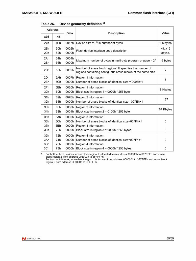
M29W064FT, M29W064FB Common flash interface (CFI)
59/69
Table 26. Device geometry definition(1)
1. For bottom boot devices, erase block region 1 is located from address 000000h to 007FFFh and erase block region 2 from address 008000h to 3FFFFFh. For top boot devices, erase block region 1 is located from address 000000h to 3F7FFFh and erase block region 2 from address 3F8000h to 3FFFFFh.
AddressData Description Value
x16 x8
27h 4Eh 0017h Device size = 2n in number of bytes 8 Mbytes
28h
29h
50h
52h
0002h
0000hFlash device interface code description
x8, x16
async.
2Ah
2Bh
54h
56h
0004h
0000hMaximum number of bytes in multi-byte program or page = 2n 16 bytes
2Ch 58h 0002hNumber of erase block regions. It specifies the number of regions containing contiguous erase blocks of the same size.
2
2Dh
2Eh
5Ah
5Ch
0007h
0000h
Region 1 information
Number of erase blocks of identical size = 0007h+18
2Fh
30h
5Eh
60h
0020h
0000h
Region 1 information
Block size in region 1 = 0020h * 256 byte8 Kbytes
31h
32h
62h
64h
007Eh
0000h
Region 2 information
Number of erase blocks of identical size= 007Eh+1127
33h
34h
66h
68h
0000h
0001h
Region 2 information
Block size in region 2 = 0100h * 256 byte64 Kbytes
35h
36h
37h
38h
6Ah
6Ch
6Eh
70h
0000h
0000h
0000h
0000h
Region 3 information
Number of erase blocks of identical size=007Fh+1
Region 3 information
Block size in region 3 = 0000h * 256 bytes
0
0
39h
3Ah
3Bh
3Ch
72h
74h
76h
78h
0000h
0000h
0000h
0000h
Region 4 information
Number of erase blocks of identical size=007Fh+1
Region 4 information
Block size in region 4 = 0000h * 256 bytes
0
0
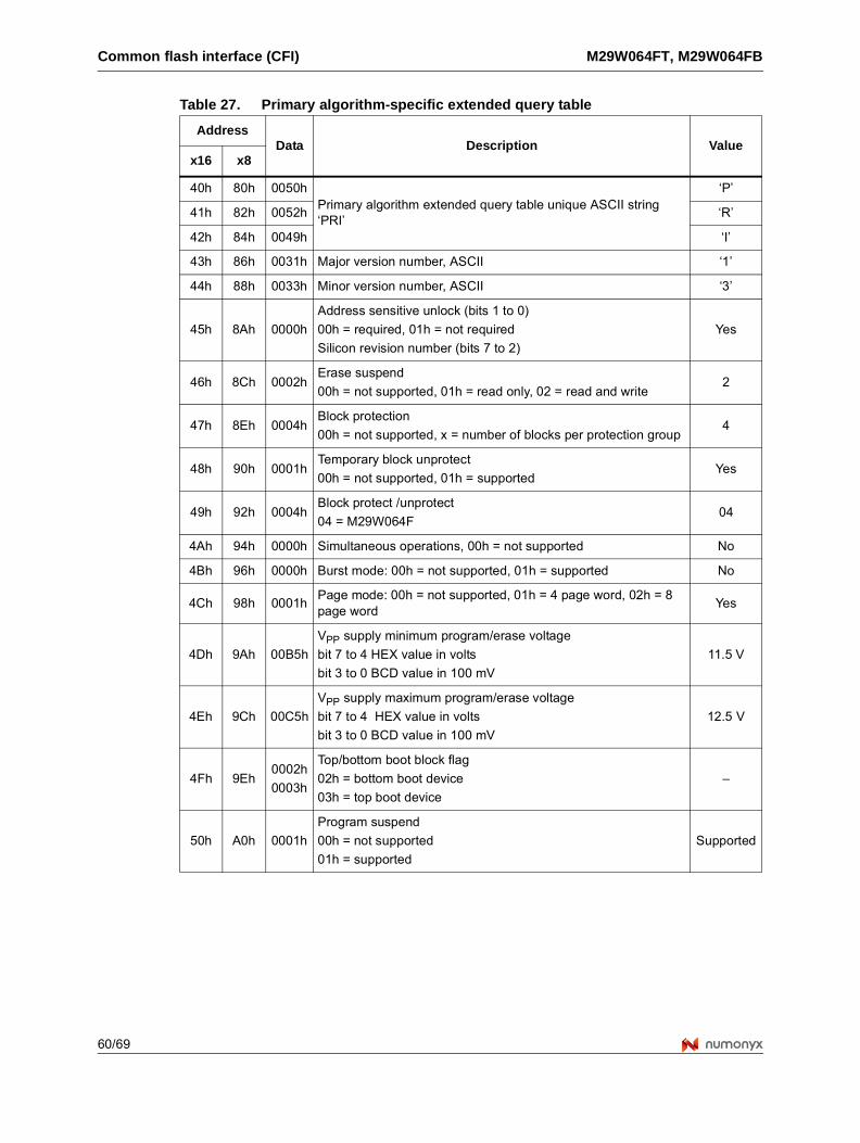
Common flash interface (CFI) M29W064FT, M29W064FB
60/69
Table 27. Primary algorithm-specific extended query table
AddressData Description Value
x16 x8
40h 80h 0050hPrimary algorithm extended query table unique ASCII string ‘PRI’
‘P’
41h 82h 0052h ‘R’
42h 84h 0049h ‘I’
43h 86h 0031h Major version number, ASCII ‘1’
44h 88h 0033h Minor version number, ASCII ‘3’
45h 8Ah 0000h
Address sensitive unlock (bits 1 to 0)
00h = required, 01h = not required
Silicon revision number (bits 7 to 2)
Yes
46h 8Ch 0002hErase suspend
00h = not supported, 01h = read only, 02 = read and write2
47h 8Eh 0004hBlock protection
00h = not supported, x = number of blocks per protection group4
48h 90h 0001hTemporary block unprotect
00h = not supported, 01h = supportedYes
49h 92h 0004hBlock protect /unprotect
04 = M29W064F04
4Ah 94h 0000h Simultaneous operations, 00h = not supported No
4Bh 96h 0000h Burst mode: 00h = not supported, 01h = supported No
4Ch 98h 0001hPage mode: 00h = not supported, 01h = 4 page word, 02h = 8 page word
Yes
4Dh 9Ah 00B5h
VPP supply minimum program/erase voltage
bit 7 to 4 HEX value in volts
bit 3 to 0 BCD value in 100 mV
11.5 V
4Eh 9Ch 00C5h
VPP supply maximum program/erase voltage
bit 7 to 4 HEX value in volts
bit 3 to 0 BCD value in 100 mV
12.5 V
4Fh 9Eh0002h
0003h
Top/bottom boot block flag
02h = bottom boot device
03h = top boot device
–
50h A0h 0001h
Program suspend
00h = not supported
01h = supported
Supported
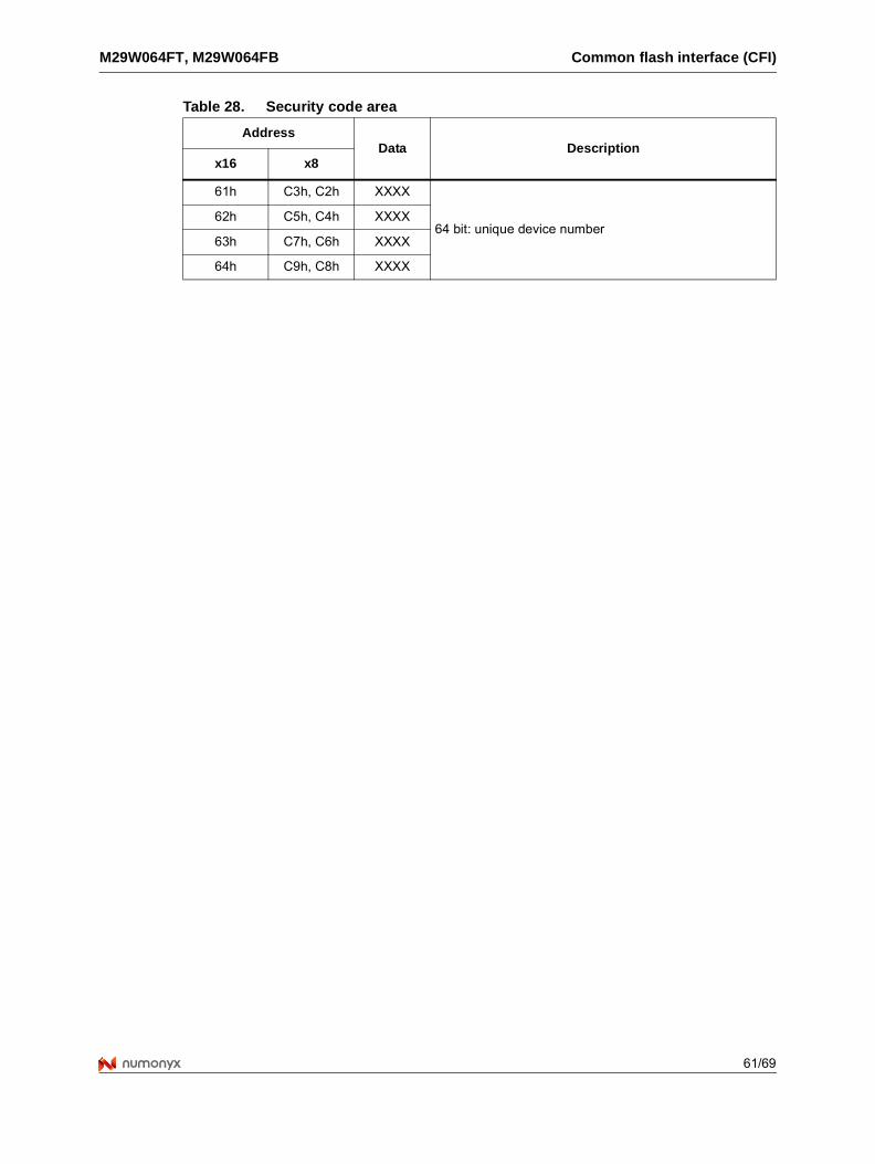
M29W064FT, M29W064FB Common flash interface (CFI)
61/69
Table 28. Security code area
AddressData Description
x16 x8
61h C3h, C2h XXXX
64 bit: unique device number62h C5h, C4h XXXX
63h C7h, C6h XXXX
64h C9h, C8h XXXX
Block protection M29W064FT, M29W064FB
62/69
Appendix C Block protection
Block protection can be used to prevent any operation from modifying the data stored in the memory. The blocks are protected in groups, refer to Appendix A: Block addresses, Table 21 and Table 22 for details of the protection groups. Once protected, program and erase operations within the protected group fail to change the data.
There are three techniques that can be used to control block protection, these are the programmer technique, the in-system technique and temporary unprotection. Temporary unprotection is controlled by the reset/block temporary unprotection pin, RP; this is described in the Section 2: Signal descriptions.
C.1 Programmer technique
The programmer technique uses high (VID) voltage levels on some of the bus pins. These cannot be achieved using a standard microprocessor bus, therefore the technique is recommended only for use in programming equipment.
To protect a group of blocks follow the flowchart in Figure 16: Programmer equipment group protect flowchart. To unprotect the whole chip it is necessary to protect all of the groups first, then all groups can be unprotected at the same time. To unprotect the chip follow Figure 17: Programmer equipment chip unprotect flowchart. Table 29: Programmer technique bus operations, BYTE = VIH or VIL, gives a summary of each operation.
The timing on these flowcharts is critical. Care should be taken to ensure that, where a pause is specified, it is followed as closely as possible. Do not abort the procedure before reaching the end. Chip unprotect can take several seconds and a user message should be provided to show that the operation is progressing.
C.2 In-system technique
The in-system technique requires a high voltage level on the reset/blocks temporary unprotect pin, RP. This can be achieved without violating the maximum ratings of the components on the microprocessor bus, therefore this technique is suitable for use after the memory has been fitted to the system.
To protect a group of blocks follow the flowchart in Figure 18: In-system equipment group protect flowchart. To unprotect the whole chip it is necessary to protect all of the groups first, then all the groups can be unprotected at the same time. To unprotect the chip follow Figure 19: In-system equipment chip unprotect flowchart.
The timing on these flowcharts is critical. Care should be taken to ensure that, where a pause is specified, it is followed as closely as possible. Do not allow the microprocessor to service interrupts that will upset the timing and do not abort the procedure before reaching the end. Chip unprotect can take several seconds and a user message should be provided to show that the operation is progressing.
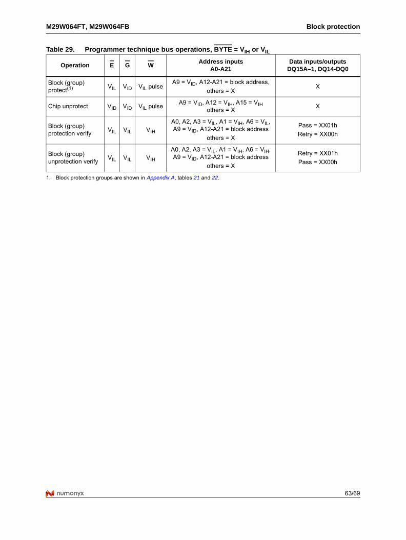
M29W064FT, M29W064FB Block protection
63/69
Table 29. Programmer technique bus operations, BYTE = VIH or VIL
Operation E G WAddress inputs
A0-A21Data inputs/outputs
DQ15A–1, DQ14-DQ0
Block (group) protect(1) VIL VID VIL pulse
A9 = VID, A12-A21 = block address,
others = XX
Chip unprotect VID VID VIL pulseA9 = VID, A12 = VIH, A15 = VIH
others = XX
Block (group) protection verify
VIL VIL VIH
A0, A2, A3 = VIL, A1 = VIH, A6 = VIL, A9 = VID, A12-A21 = block address
others = X
Pass = XX01h
Retry = XX00h
Block (group) unprotection verify
VIL VIL VIH
A0, A2, A3 = VIL, A1 = VIH, A6 = VIH, A9 = VID, A12-A21 = block address
others = X
Retry = XX01h
Pass = XX00h
1. Block protection groups are shown in Appendix A, tables 21 and 22.
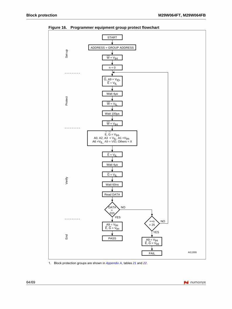
Block protection M29W064FT, M29W064FB
64/69
Figure 16. Programmer equipment group protect flowchart
1. Block protection groups are shown in Appendix A, tables 21 and 22.
ADDRESS = GROUP ADDRESS
AI11555
G, A9 = VID,E = VIL
n = 0
Wait 4µs
Wait 100µs
W = VIL
W = VIH
E, G = VIH,A0, A2, A3 = VIL, A1 =VIH,
A6 =VIL, A9 = VID, Others = X
A9 = VIHE, G = VIH
++n= 25
START
FAIL
PASS
YES
NO
DATA=
01hYES
NO
W = VIH
E = VIL
Wait 4µs
G = VIL
Wait 60ns
Read DATA
Ver
ifyP
rote
ctS
et-u
pE
nd
A9 = VIHE, G = VIH

M29W064FT, M29W064FB Block protection
65/69
Figure 17. Programmer equipment chip unprotect flowchart
1. Block protection groups are shown in Appendix A, tables 21 and 22.
PROTECT ALL GROUPS
AI11556b
A6, A12, A15 = VIH(1)
E, G, A9 = VID
DATA
W = VIH
E, G = VIH
ADDRESS = CURRENT GROUP ADDRESSA0, A2, A3 = VIL, A1 =VIH,
A6 =VIH, A9 = VID, Others = X
Wait 10ms
=00h
INCREMENTCURRENT GROUP
n = 0CURRENT GROUP = 0
Wait 4µs
W = VIL
++n= 1000
START
YES
YESNO
NO LASTGROUP
YES
NO
E = VIL
Wait 4µs
G = VIL
Wait 60ns
Read DATA
FAIL PASS
Ver
ifyU
npro
tect
Set
-up
End
A9 = VIHE, G = VIH
A9 = VIHE, G = VIH
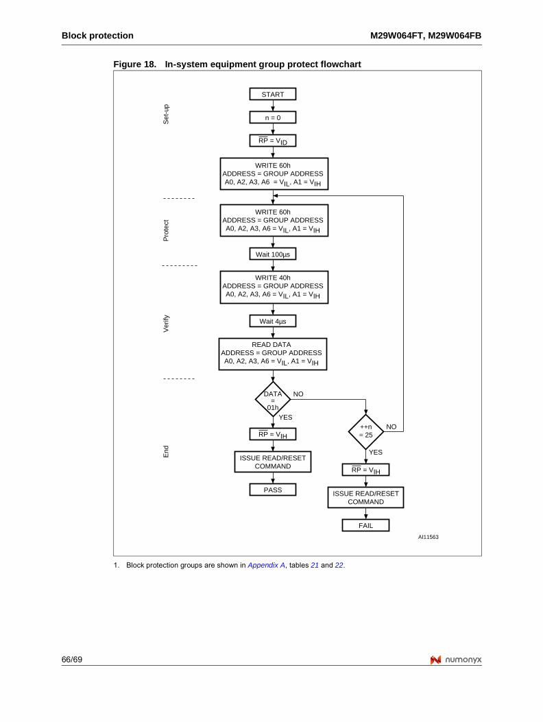
Block protection M29W064FT, M29W064FB
66/69
Figure 18. In-system equipment group protect flowchart
1. Block protection groups are shown in Appendix A, tables 21 and 22.
AI11563
WRITE 60hADDRESS = GROUP ADDRESSA0, A2, A3, A6 = VIL, A1 = VIH
n = 0
Wait 100µs
WRITE 40hADDRESS = GROUP ADDRESSA0, A2, A3, A6 = VIL, A1 = VIH
RP = VIH++n= 25
START
FAIL
PASS
YES
NO
DATA=
01hYES
NO
RP = VIH
Wait 4µs
Ver
ifyP
rote
ctS
et-u
pE
nd
READ DATAADDRESS = GROUP ADDRESSA0, A2, A3, A6 = VIL, A1 = VIH
RP = VID
ISSUE READ/RESETCOMMAND
ISSUE READ/RESETCOMMAND
WRITE 60hADDRESS = GROUP ADDRESSA0, A2, A3, A6 = VIL, A1 = VIH
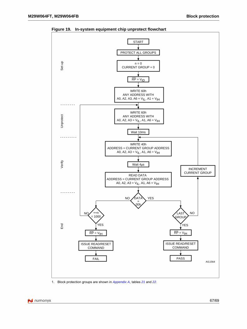
M29W064FT, M29W064FB Block protection
67/69
Figure 19. In-system equipment chip unprotect flowchart
1. Block protection groups are shown in Appendix A, tables 21 and 22.
AI11564
WRITE 60hANY ADDRESS WITH
A0, A2, A3 = VIL, A1, A6 = VIH
n = 0CURRENT GROUP = 0
Wait 10ms
WRITE 40hADDRESS = CURRENT GROUP ADDRESS
A0, A2, A3 = VIL, A1, A6 = VIH
RP = VIH
++n= 1000
START
FAIL PASS
YES
NO
DATA=
00h
YESNO
RP = VIH
Wait 4µs
READ DATAADDRESS = CURRENT GROUP ADDRESS
A0, A2, A3 = VIL, A1, A6 = VIH
RP = VID
ISSUE READ/RESETCOMMAND
ISSUE READ/RESETCOMMAND
PROTECT ALL GROUPS
INCREMENTCURRENT GROUP
LASTGROUP
YES
NO
WRITE 60hANY ADDRESS WITH
A0, A2, A3, A6 = VIL, A1 = VIH
Ver
ifyU
npro
tect
Set
-up
End
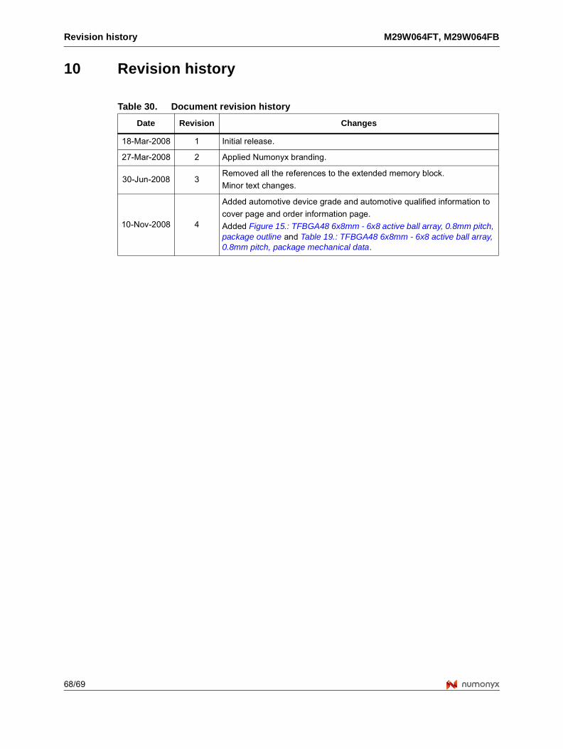
Revision history M29W064FT, M29W064FB
68/69
10 Revision history
Table 30. Document revision history
Date Revision Changes
18-Mar-2008 1 Initial release.
27-Mar-2008 2 Applied Numonyx branding.
30-Jun-2008 3Removed all the references to the extended memory block.
Minor text changes.
10-Nov-2008 4
Added automotive device grade and automotive qualified information to
cover page and order information page.
Added Figure 15.: TFBGA48 6x8mm - 6x8 active ball array, 0.8mm pitch, package outline and Table 19.: TFBGA48 6x8mm - 6x8 active ball array, 0.8mm pitch, package mechanical data.
M29W064FT, M29W064FB
69/69
Please Read Carefully:
INFORMATION IN THIS DOCUMENT IS PROVIDED IN CONNECTION WITH NUMONYX™ PRODUCTS. NO LICENSE, EXPRESS OR IMPLIED, BY ESTOPPEL OR OTHERWISE, TO ANY INTELLECTUAL PROPERTY RIGHTS IS GRANTED BY THIS DOCUMENT. EXCEPT AS PROVIDED IN NUMONYX'S TERMS AND CONDITIONS OF SALE FOR SUCH PRODUCTS, NUMONYX ASSUMES NO LIABILITY
WHATSOEVER, AND NUMONYX DISCLAIMS ANY EXPRESS OR IMPLIED WARRANTY, RELATING TO SALE AND/OR USE OF NUMONYX PRODUCTS INCLUDING LIABILITY OR WARRANTIES RELATING TO FITNESS FOR A PARTICULAR PURPOSE, MERCHANTABILITY, OR INFRINGEMENT OF ANY PATENT, COPYRIGHT OR OTHER INTELLECTUAL PROPERTY RIGHT.
Numonyx products are not intended for use in medical, life saving, life sustaining, critical control or safety systems, or in nuclear facility applications.
Numonyx may make changes to specifications and product descriptions at any time, without notice.
Numonyx, B.V. may have patents or pending patent applications, trademarks, copyrights, or other intellectual property rights that relate to the presented subject matter. The furnishing of documents and other materials and information does not provide any license, express or implied,
by estoppel or otherwise, to any such patents, trademarks, copyrights, or other intellectual property rights.
Designers must not rely on the absence or characteristics of any features or instructions marked “reserved” or “undefined.” Numonyx reserves these for future definition and shall have no responsibility whatsoever for conflicts or incompatibilities arising from future changes to them.
Contact your local Numonyx sales office or your distributor to obtain the latest specifications and before placing your product order.
Copies of documents which have an order number and are referenced in this document, or other Numonyx literature may be obtained by visiting Numonyx's website at http://www.numonyx.com.
Numonyx StrataFlash is a trademark or registered trademark of Numonyx or its subsidiaries in the United States and other countries.
*Other names and brands may be claimed as the property of others.
Copyright © 2008, Numonyx, B.V., All Rights Reserved.