Embed Size (px)
Citation preview
ESMT M13S128168A (2N) Automotive Grade
Elite Semiconductor Memory Technology Inc. Publication Date : Mar. 2013 Revision : 1.1 1/49
DDR SDRAM 2M x 16 Bit x 4 Banks
Double Data Rate SDRAM
Features
Double-data-rate architecture, two data transfers per clock cycle
Bi-directional data strobe (DQS)
Differential clock inputs (CLK and CLK )
DLL aligns DQ and DQS transition with CLK transition
Four bank operation
CAS Latency : 2.5, 3, 4
Burst Type : Sequential and Interleave
Burst Length : 2, 4, 8
All inputs except data & DM are sampled at the rising edge of the system clock (CLK)
Data I/O transitions on both edges of data strobe (DQS)
DQS is edge-aligned with data for READs; center-aligned with data for WRITEs
Data mask (DM) for write masking only
VDD = 2.5V ± 0.2V, VDDQ = 2.5V ± 0.2V
15.6us refresh interval for V grade; 3.9us refresh interval for VA grade
Auto & Self refresh (self refresh is not supported for VA grade)
2.5V I/O (SSTL_2 compatible)
ESMT M13S128168A (2N) Automotive Grade
Elite Semiconductor Memory Technology Inc. Publication Date : Mar. 2013 Revision : 1.1 2/49
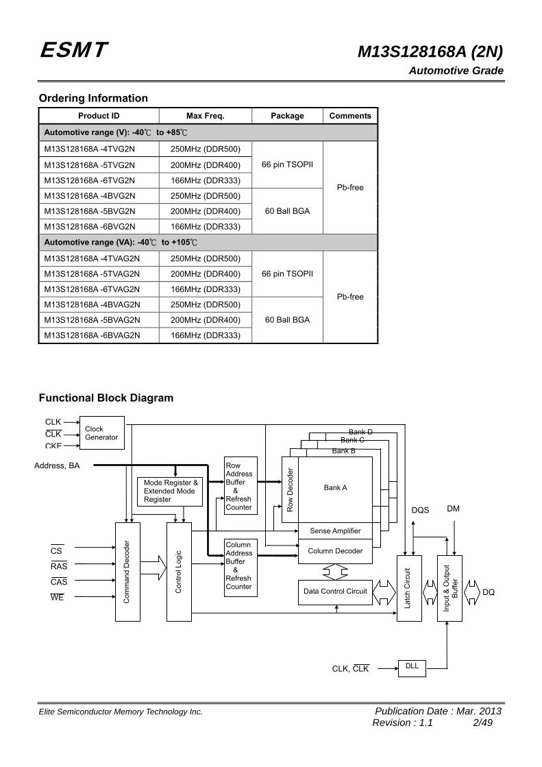
Ordering Information
Product ID Max Freq. Package Comments
Automotive range (V): -40℃ to +85℃
M13S128168A -4TVG2N 250MHz (DDR500)
M13S128168A -5TVG2N 200MHz (DDR400)
M13S128168A -6TVG2N 166MHz (DDR333)
66 pin TSOPII
M13S128168A -4BVG2N 250MHz (DDR500)
M13S128168A -5BVG2N 200MHz (DDR400)
M13S128168A -6BVG2N 166MHz (DDR333)
60 Ball BGA
Pb-free
Automotive range (VA): -40℃ to +105℃
M13S128168A -4TVAG2N 250MHz (DDR500)
M13S128168A -5TVAG2N 200MHz (DDR400)
M13S128168A -6TVAG2N 166MHz (DDR333)
66 pin TSOPII
M13S128168A -4BVAG2N 250MHz (DDR500)
M13S128168A -5BVAG2N 200MHz (DDR400)
M13S128168A -6BVAG2N 166MHz (DDR333)
60 Ball BGA
Pb-free
Functional Block Diagram
CLK, CLK
Bank A
Com
man
d D
eco
der
Con
trol
Log
ic
Latc
h C
ircui
t
Bank B
DM
DQ
Mode Register & Extended Mode Register
ColumnAddressBuffer & RefreshCounter
Row AddressBuffer & RefreshCounter R
ow D
ecod
er
Sense Amplifier
Column Decoder
Data Control Circuit
Inpu
t & O
utpu
t B
uffe
r
Address, BA
Clock Generator
CLK
CLK
CKE
CS
RAS
CAS
WE
DLL
DQS
Bank CBank D
ESMT M13S128168A (2N) Automotive Grade
Elite Semiconductor Memory Technology Inc. Publication Date : Mar. 2013 Revision : 1.1 3/49
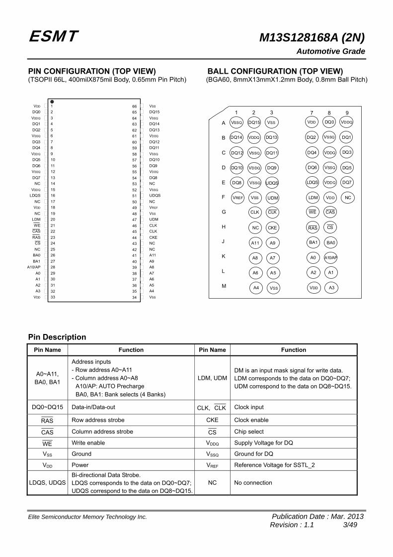
PIN CONFIGURATION (TOP VIEW) BALL CONFIGURATION (TOP VIEW) (TSOPII 66L, 400milX875mil Body, 0.65mm Pin Pitch) (BGA60, 8mmX13mmX1.2mm Body, 0.8mm Ball Pitch)
Pin Description
Pin Name Function Pin Name Function
A0~A11, BA0, BA1
Address inputs - Row address A0~A11 - Column address A0~A8
A10/AP: AUTO Precharge BA0, BA1: Bank selects (4 Banks)
LDM, UDMDM is an input mask signal for write data. LDM corresponds to the data on DQ0~DQ7; UDM correspond to the data on DQ8~DQ15.
DQ0~DQ15 Data-in/Data-out CLK, CLK Clock input
RAS Row address strobe CKE Clock enable
CAS Column address strobe CS Chip select
WE Write enable VDDQ Supply Voltage for DQ
VSS Ground VSSQ Ground for DQ
VDD Power VREF Reference Voltage for SSTL_2
LDQS, UDQS Bi-directional Data Strobe. LDQS corresponds to the data on DQ0~DQ7; UDQS correspond to the data on DQ8~DQ15.
NC No connection
1
2
3
4
5
6
7
8
9
10
11
12
13
14
15
16
17
18
19
20
21
22
23
24
25
26
27
28
29
30
31
32
33
66
65
64
63
62
61
60
59
58
57
56
55
54
53
52
51
50
49
48
47
46
45
44
43
42
41
40
39
38
37
36
35
34
VDD
DQ0
VDDQ
DQ1
DQ2
VSSQ
DQ3
DQ4
VDDQ
DQ5
DQ6
VSSQ
DQ7
NC
VDDQ
LDQS
NC
VDD
NC
LDM
WE
CAS
RAS
CS
NC
BA0
BA1
A10/AP
A0
A1
A2
A3
VDD
VSS
DQ15
VSSQ
DQ14
DQ13
VDDQ
DQ12
DQ11
VSSQ
DQ10
DQ9
VDDQ
DQ8
NC
VSSQ
UDQS
NC
VREF
VSS
UDM
CLK
CLK
CKE
NC
NC
A11
A9
A8
A7
A6
A5
A4
VSS
VSSQ
DQ14
DQ12
DQ10
DQ8
VREF
A
B
C
D
E
F
G
H
J
K
L
M
DQ15
VDDQ
VSSQ
VDDQ
VSSQ
VSS
CLK
NC
A11
A8
A6
A4
VSS
DQ13
DQ11
DQ9
UDQS
UDM
CLK
CKE
A9
A7
A5
VSS
VDDQ
DQ1
DQ3
DQ5
DQ7
NC
VDD
DQ2
DQ4
DQ6
LDQS
LDM
WE
RAS
BA1
A0
A2
VDD
DQ0
VSSQ
VDDQ
VSSQ
VDDQ
VDD
CAS
CS
BA0
A10/AP
A1
A3
1 2 3 7 8 9
ESMT M13S128168A (2N) Automotive Grade
Elite Semiconductor Memory Technology Inc. Publication Date : Mar. 2013 Revision : 1.1 4/49
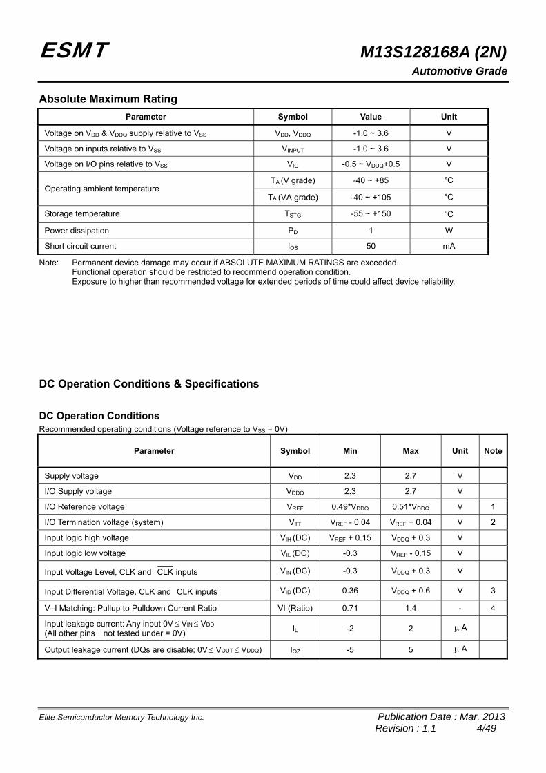
Absolute Maximum Rating
Parameter Symbol Value Unit
Voltage on VDD & VDDQ supply relative to VSS VDD, VDDQ -1.0 ~ 3.6 V
Voltage on inputs relative to VSS VINPUT -1.0 ~ 3.6 V
Voltage on I/O pins relative to VSS VIO -0.5 ~ VDDQ+0.5 V
TA (V grade) -40 ~ +85 C° Operating ambient temperature
TA (VA grade) -40 ~ +105 C°
Storage temperature TSTG -55 ~ +150 C°
Power dissipation PD 1 W
Short circuit current IOS 50 mA
Note: Permanent device damage may occur if ABSOLUTE MAXIMUM RATINGS are exceeded. Functional operation should be restricted to recommend operation condition. Exposure to higher than recommended voltage for extended periods of time could affect device reliability.
DC Operation Conditions & Specifications
DC Operation Conditions Recommended operating conditions (Voltage reference to VSS = 0V)
Parameter Symbol Min Max Unit Note
Supply voltage VDD 2.3 2.7 V
I/O Supply voltage VDDQ 2.3 2.7 V
I/O Reference voltage VREF 0.49*VDDQ 0.51*VDDQ V 1
I/O Termination voltage (system) VTT VREF - 0.04 VREF + 0.04 V 2
Input logic high voltage VIH (DC) VREF + 0.15 VDDQ + 0.3 V
Input logic low voltage VIL (DC) -0.3 VREF - 0.15 V
Input Voltage Level, CLK and CLK inputs VIN (DC) -0.3 VDDQ + 0.3 V
Input Differential Voltage, CLK and CLK inputs VID (DC) 0.36 VDDQ + 0.6 V 3
V–I Matching: Pullup to Pulldown Current Ratio VI (Ratio) 0.71 1.4 - 4
Input leakage current: Any input 0V VIN VDD (All other pins not tested under = 0V)
IL -2 2 A
Output leakage current (DQs are disable; 0V VOUT VDDQ) IOZ -5 5 A
ESMT M13S128168A (2N) Automotive Grade
Elite Semiconductor Memory Technology Inc. Publication Date : Mar. 2013 Revision : 1.1 5/49
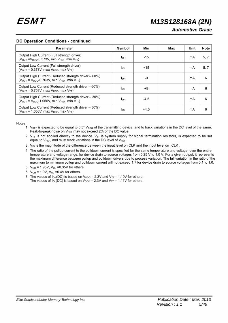
DC Operation Conditions - continued
Parameter Symbol Min Max Unit Note
Output High Current (Full strength driver) (VOUT =VDDQ-0.373V, min VREF, min VTT)
IOH -15 mA 5, 7
Output Low Current (Full strength driver) (VOUT = 0.373V, max VREF, max VTT)
IOL +15 mA 5, 7
Output High Current (Reduced strength driver – 60%) (VOUT = VDDQ-0.763V, min VREF, min VTT)
IOH -9 mA 6
Output Low Current (Reduced strength driver – 60%) (VOUT = 0.763V, max VREF, max VTT)
IOL +9 mA 6
Output High Current (Reduced strength driver – 30%) (VOUT = VDDQ-1.056V, min VREF, min VTT)
IOH -4.5 mA 6
Output Low Current (Reduced strength driver – 30%) (VOUT = 1.056V, max VREF, max VTT)
IOL +4.5 mA 6
Notes: 1. VREF is expected to be equal to 0.5* VDDQ of the transmitting device, and to track variations in the DC level of the same.
Peak-to-peak noise on VREF may not exceed 2% of the DC value. 2. VTT is not applied directly to the device. VTT is system supply for signal termination resistors, is expected to be set
equal to VREF, and must track variations in the DC level of VREF.
3. VID is the magnitude of the difference between the input level on CLK and the input level on CLK .
4. The ratio of the pullup current to the pulldown current is specified for the same temperature and voltage, over the entire temperature and voltage range, for device drain to source voltages from 0.25 V to 1.0 V. For a given output, it represents the maximum difference between pullup and pulldown drivers due to process variation. The full variation in the ratio of the maximum to minimum pullup and pulldown current will not exceed 1.7 for device drain to source voltages from 0.1 to 1.0.
5. VOH = 1.95V, VOL =0.35V for others. 6. VOH = 1.9V, VOL =0.4V for others. 7. The values of IOH(DC) is based on VDDQ = 2.3V and VTT = 1.19V for others.
The values of IOL(DC) is based on VDDQ = 2.3V and VTT = 1.11V for others.
ESMT M13S128168A (2N) Automotive Grade
Elite Semiconductor Memory Technology Inc. Publication Date : Mar. 2013 Revision : 1.1 6/49
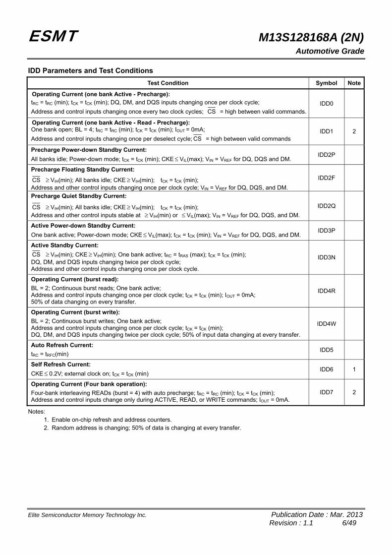
IDD Parameters and Test Conditions
Test Condition Symbol Note
Operating Current (one bank Active - Precharge): tRC = tRC (min); tCK = tCK (min); DQ, DM, and DQS inputs changing once per clock cycle;
Address and control inputs changing once every two clock cycles; CS = high between valid commands. IDD0
Operating Current (one bank Active - Read - Precharge): One bank open; BL = 4; tRC = tRC (min); tCK = tCK (min); IOUT = 0mA;
Address and control inputs changing once per deselect cycle; CS = high between valid commands IDD1 2
Precharge Power-down Standby Current:
All banks idle; Power-down mode; tCK = tCK (min); CKE VIL(max); VIN = VREF for DQ, DQS and DM. IDD2P
Precharge Floating Standby Current:
CS VIH(min); All banks idle; CKE VIH(min); tCK = tCK (min); Address and other control inputs changing once per clock cycle; VIN = VREF for DQ, DQS, and DM.
IDD2F
Precharge Quiet Standby Current:
CS VIH(min); All banks idle; CKE VIH(min); tCK = tCK (min); Address and other control inputs stable at VIH(min) or VIL(max); VIN = VREF for DQ, DQS, and DM.
IDD2Q
Active Power-down Standby Current:
One bank active; Power-down mode; CKE VIL(max); tCK = tCK (min); VIN = VREF for DQ, DQS, and DM. IDD3P
Active Standby Current:
CS VIH(min); CKE VIH(min); One bank active; tRC = tRAS (max); tCK = tCK (min); DQ, DM, and DQS inputs changing twice per clock cycle; Address and other control inputs changing once per clock cycle.
IDD3N
Operating Current (burst read):
BL = 2; Continuous burst reads; One bank active; Address and control inputs changing once per clock cycle; tCK = tCK (min); IOUT = 0mA; 50% of data changing on every transfer.
IDD4R
Operating Current (burst write):
BL = 2; Continuous burst writes; One bank active; Address and control inputs changing once per clock cycle; tCK = tCK (min); DQ, DM, and DQS inputs changing twice per clock cycle; 50% of input data changing at every transfer.
IDD4W
Auto Refresh Current:
tRC = tRFC(min) IDD5
Self Refresh Current:
CKE 0.2V; external clock on; tCK = tCK (min) IDD6 1
Operating Current (Four bank operation):
Four-bank interleaving READs (burst = 4) with auto precharge; tRC = tRC (min); tCK = tCK (min); Address and control inputs change only during ACTIVE, READ, or WRITE commands; IOUT = 0mA.
IDD7 2
Notes: 1. Enable on-chip refresh and address counters. 2. Random address is changing; 50% of data is changing at every transfer.
ESMT M13S128168A (2N) Automotive Grade
Elite Semiconductor Memory Technology Inc. Publication Date : Mar. 2013 Revision : 1.1 7/49
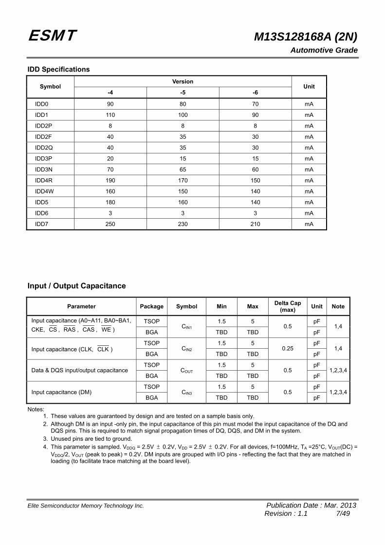
IDD Specifications
Version Symbol
-4 -5 -6 Unit
IDD0 90 80 70 mA
IDD1 110 100 90 mA
IDD2P 8 8 8 mA
IDD2F 40 35 30 mA
IDD2Q 40 35 30 mA
IDD3P 20 15 15 mA
IDD3N 70 65 60 mA
IDD4R 190 170 150 mA
IDD4W 160 150 140 mA
IDD5 180 160 140 mA
IDD6 3 3 3 mA
IDD7 250 230 210 mA
Input / Output Capacitance
Parameter Package Symbol Min Max Delta Cap
(max) Unit Note
TSOP 1.5 5 pF Input capacitance (A0~A11, BA0~BA1,
CKE, CS , RAS , CAS , WE ) BGA CIN1
TBD TBD 0.5
pF 1,4
TSOP 1.5 5 pF Input capacitance (CLK, CLK )
BGA CIN2
TBD TBD 0.25
pF 1,4
TSOP 1.5 5 pF Data & DQS input/output capacitance
BGA COUT
TBD TBD 0.5
pF 1,2,3,4
TSOP 1.5 5 pF Input capacitance (DM)
BGA CIN3
TBD TBD 0.5
pF 1,2,3,4
Notes: 1. These values are guaranteed by design and are tested on a sample basis only. 2. Although DM is an input -only pin, the input capacitance of this pin must model the input capacitance of the DQ and
DQS pins. This is required to match signal propagation times of DQ, DQS, and DM in the system. 3. Unused pins are tied to ground. 4. This parameter is sampled. VDDQ = 2.5V ± 0.2V, VDD = 2.5V ± 0.2V. For all devices, f=100MHz, TA =25°C, VOUT(DC) =
VDDQ/2, VOUT (peak to peak) = 0.2V. DM inputs are grouped with I/O pins - reflecting the fact that they are matched in loading (to facilitate trace matching at the board level).
ESMT M13S128168A (2N) Automotive Grade
Elite Semiconductor Memory Technology Inc. Publication Date : Mar. 2013 Revision : 1.1 8/49
AC Operation Conditions & Timing Specifications
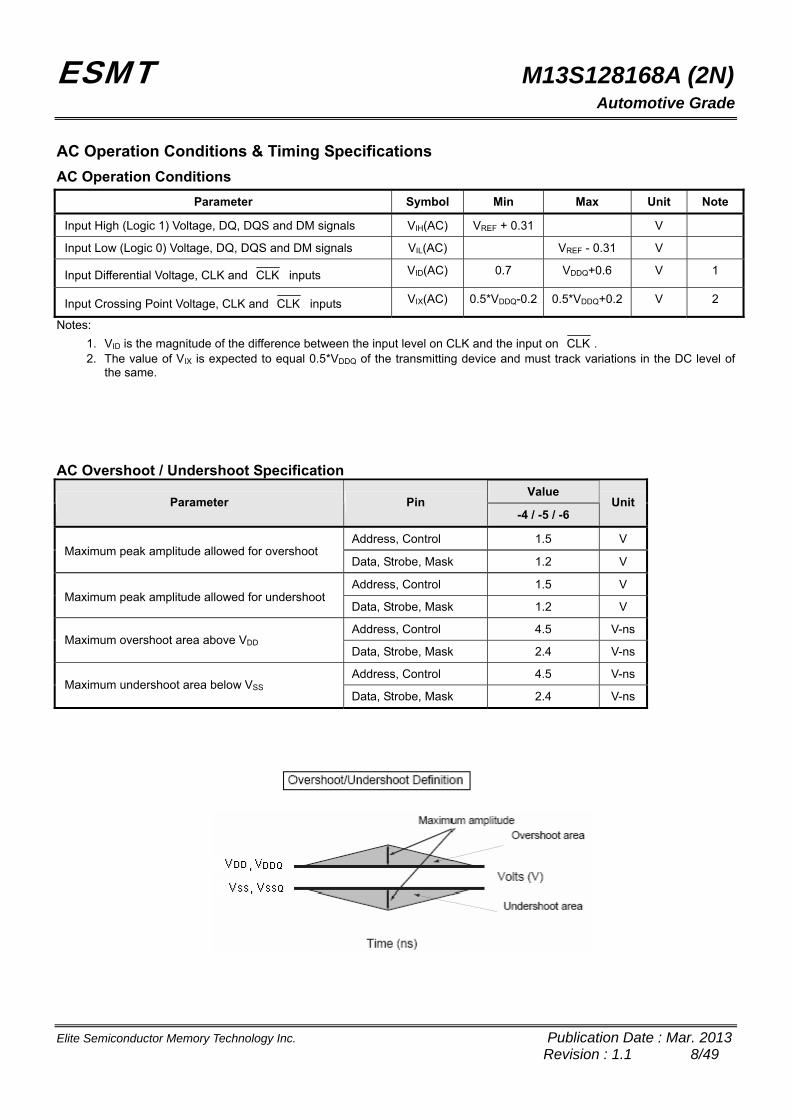
AC Operation Conditions
Parameter Symbol Min Max Unit Note
Input High (Logic 1) Voltage, DQ, DQS and DM signals VIH(AC) VREF + 0.31 V
Input Low (Logic 0) Voltage, DQ, DQS and DM signals VIL(AC) VREF - 0.31 V
Input Differential Voltage, CLK and CLK inputs VID(AC) 0.7 VDDQ+0.6 V 1
Input Crossing Point Voltage, CLK and CLK inputs VIX(AC) 0.5*VDDQ-0.2 0.5*VDDQ+0.2 V 2
Notes:
1. VID is the magnitude of the difference between the input level on CLK and the input on CLK . 2. The value of VIX is expected to equal 0.5*VDDQ of the transmitting device and must track variations in the DC level of
the same. AC Overshoot / Undershoot Specification
Value Parameter Pin
-4 / -5 / -6 Unit
Address, Control 1.5 V Maximum peak amplitude allowed for overshoot
Data, Strobe, Mask 1.2 V
Address, Control 1.5 V Maximum peak amplitude allowed for undershoot
Data, Strobe, Mask 1.2 V
Address, Control 4.5 V-ns Maximum overshoot area above VDD
Data, Strobe, Mask 2.4 V-ns
Address, Control 4.5 V-ns Maximum undershoot area below VSS
Data, Strobe, Mask 2.4 V-ns
ESMT M13S128168A (2N) Automotive Grade
Elite Semiconductor Memory Technology Inc. Publication Date : Mar. 2013 Revision : 1.1 9/49
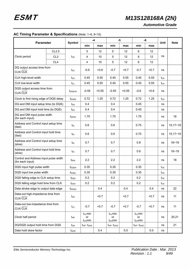
AC Timing Parameter & Specifications (Note: 1~6, 9~10)
-4 -5 -6 Parameter Symbol
min max min max min max Unit Note
CL2.5 5 12 5 12 6 12
CL3 4 10 5 12 6 12 Clock period
CL4
tCK
4 10 5 12 6 12
ns
DQ output access time from
CLK/ CLK tAC -0.6 +0.6 -0.7 +0.7 -0.7 +0.7 ns
CLK high-level width tCH 0.45 0.55 0.45 0.55 0.45 0.55 tCK
CLK low-level width tCL 0.45 0.55 0.45 0.55 0.45 0.55 tCK
DQS output access time from
CLK/ CLK tDQSCK -0.55 +0.55 -0.55 +0.55 -0.6 +0.6 ns
Clock to first rising edge of DQS delay tDQSS 0.72 1.25 0.72 1.25 0.72 1.25 tCK
DQ and DM input setup time (to DQS) tDS 0.4 0.4 0.45 ns
DQ and DM input hold time (to DQS) tDH 0.4 0.4 0.45 ns
DQ and DM input pulse width (for each input)
tDIPW 1.75 1.75
1.75 ns 18
Address and Control input setup time (fast)
tIS 0.6 0.6
0.75 ns 15,17~19
Address and Control input hold time (fast)
tIH 0.6 0.6
0.75 ns 15,17~19
Address and Control input setup time (slow)
tIS 0.7 0.7
0.8 ns 16~19
Address and Control input hold time (slow)
tIH 0.7 0.7
0.8 ns 16~19
Control and Address input pulse width (for each input)
tIPW 2.2 2.2
2.2 ns 18
DQS input high pulse width tDQSH 0.35 0.35 0.35 tCK
DQS input low pulse width tDQSL 0.35 0.35 0.35 tCK
DQS falling edge to CLK setup time tDSS 0.2 0.2 0.2 tCK
DQS falling edge hold time from CLK tDSH 0.2 0.2 0.2 tCK
Data strobe edge to output data edge tDQSQ 0.4 0.4 0.4 ns 22
Data-out high-impedance time from
CLK/ CLK tHZ +0.7 +0.7 +0.7 ns 11
Data-out low-impedance time from
CLK/ CLK tLZ -0.7 +0.7 -0.7 +0.7 -0.7 +0.7 ns 11
Clock half period tHP
tCLmin or
tCHmin
tCLmin or
tCHmin
tCLmin or
tCHmin ns 20,21
DQ/DQS output hold time from DQS tQH tHP- tQHS tHP- tQHS tHP- tQHS ns 21
Data hold skew factor tQHS 0.4 0.5 0.5 ns
ESMT M13S128168A (2N) Automotive Grade
Elite Semiconductor Memory Technology Inc. Publication Date : Mar. 2013 Revision : 1.1 10/49
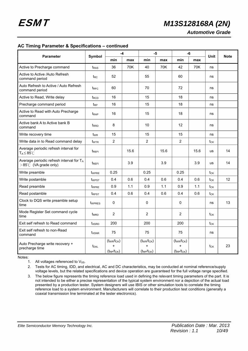
AC Timing Parameter & Specifications – continued
-4 -5 -6 Parameter Symbol
min max min max min max Unit Note
Active to Precharge command tRAS 36 70K 40 70K 42 70K ns
Active to Active /Auto Refresh command period
tRC 52 55
60 ns
Auto Refresh to Active / Auto Refresh command period
tRFC 60 70
72 ns
Active to Read, Write delay tRCD 16 15 18 ns
Precharge command period tRP 16 15 18 ns
Active to Read with Auto Precharge command
tRAP 16 15
18 ns
Active bank A to Active bank B command
tRRD 8 10
12 ns
Write recovery time tWR 15 15 15 ns
Write data in to Read command delay tWTR 2 2 2 tCK
Average periodic refresh interval for TA 85℃ tREFI 15.6 15.6 15.6 us 14
Average periodic refresh interval for TA
>85℃ (VA grade only) tREFI 3.9 3.9 3.9 us 14
Write preamble tWPRE 0.25 0.25 0.25 tCK
Write postamble tWPST 0.4 0.6 0.4 0.6 0.4 0.6 tCK 12
Read preamble tRPRE 0.9 1.1 0.9 1.1 0.9 1.1 tCK
Read postamble tRPST 0.4 0.6 0.4 0.6 0.4 0.6 tCK
Clock to DQS write preamble setup time
tWPRES 0 0 0 ns 13
Mode Register Set command cycle time
tMRD 2 2 2 tCK
Exit self refresh to Read command tXSRD 200 200 200 tCK
Exit self refresh to non-Read command
tXSNR 75 75 75 ns
Auto Precharge write recovery + precharge time
tDAL (tWR/tCK)
+ (tRP/tCK)
(tWR/tCK)
+ (tRP/tCK)
(tWR/tCK)
+ (tRP/tCK)
tCK 23
Notes: 1. All voltages referenced to VSS. 2. Tests for AC timing, IDD, and electrical, AC and DC characteristics, may be conducted at nominal reference/supply
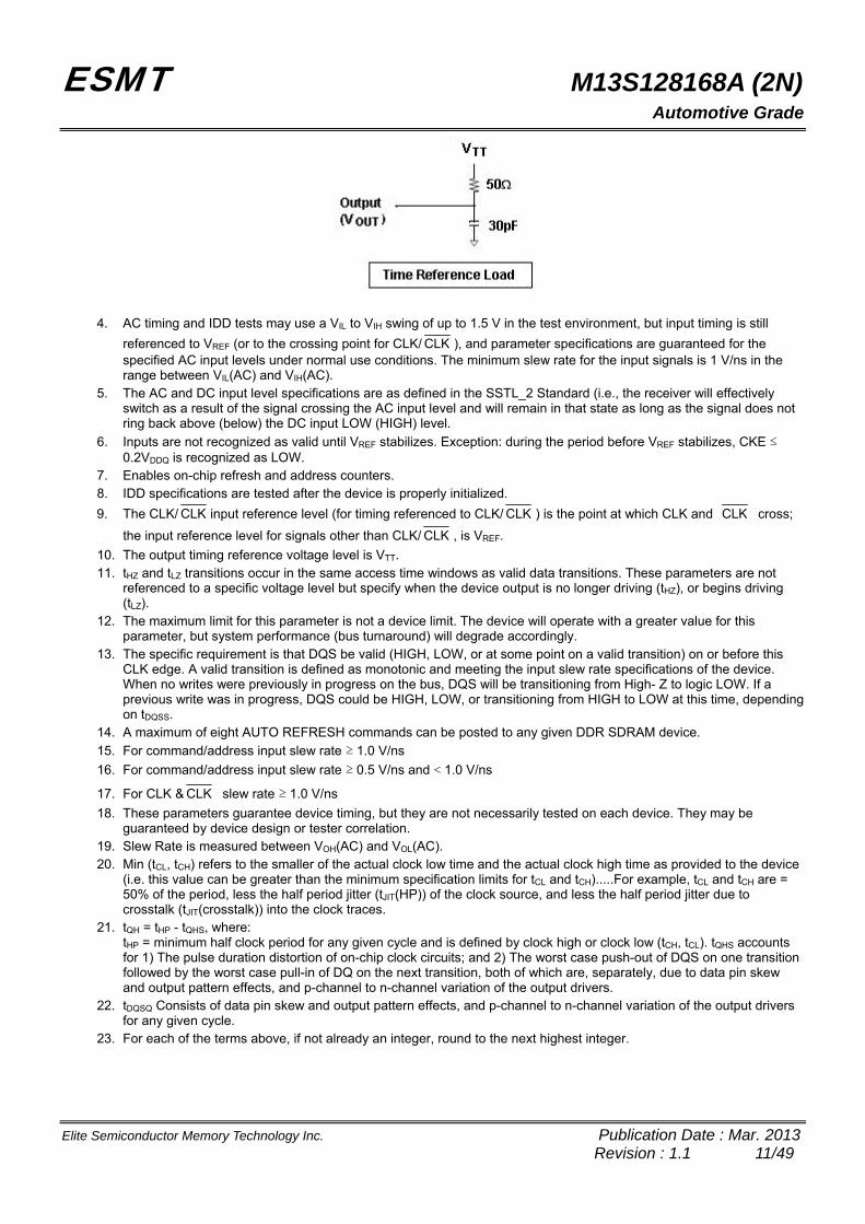
voltage levels, but the related specifications and device operation are guaranteed for the full voltage range specified. 3. The below figure represents the timing reference load used in defining the relevant timing parameters of the part. It is
not intended to be either a precise representation of the typical system environment nor a depiction of the actual load presented by a production tester. System designers will use IBIS or other simulation tools to correlate the timing reference load to a system environment. Manufacturers will correlate to their production test conditions (generally a coaxial transmission line terminated at the tester electronics).
ESMT M13S128168A (2N) Automotive Grade
Elite Semiconductor Memory Technology Inc. Publication Date : Mar. 2013 Revision : 1.1 11/49
4. AC timing and IDD tests may use a VIL to VIH swing of up to 1.5 V in the test environment, but input timing is still
referenced to VREF (or to the crossing point for CLK/ CLK ), and parameter specifications are guaranteed for the specified AC input levels under normal use conditions. The minimum slew rate for the input signals is 1 V/ns in the range between VIL(AC) and VIH(AC).
5. The AC and DC input level specifications are as defined in the SSTL_2 Standard (i.e., the receiver will effectively switch as a result of the signal crossing the AC input level and will remain in that state as long as the signal does not ring back above (below) the DC input LOW (HIGH) level.
6. Inputs are not recognized as valid until VREF stabilizes. Exception: during the period before VREF stabilizes, CKE ≤ 0.2VDDQ is recognized as LOW.
7. Enables on-chip refresh and address counters. 8. IDD specifications are tested after the device is properly initialized.
9. The CLK/ CLK input reference level (for timing referenced to CLK/ CLK ) is the point at which CLK and CLK cross;
the input reference level for signals other than CLK/ CLK , is VREF.
10. The output timing reference voltage level is VTT. 11. tHZ and tLZ transitions occur in the same access time windows as valid data transitions. These parameters are not
referenced to a specific voltage level but specify when the device output is no longer driving (tHZ), or begins driving (tLZ).
12. The maximum limit for this parameter is not a device limit. The device will operate with a greater value for this parameter, but system performance (bus turnaround) will degrade accordingly.
13. The specific requirement is that DQS be valid (HIGH, LOW, or at some point on a valid transition) on or before this CLK edge. A valid transition is defined as monotonic and meeting the input slew rate specifications of the device. When no writes were previously in progress on the bus, DQS will be transitioning from High- Z to logic LOW. If a previous write was in progress, DQS could be HIGH, LOW, or transitioning from HIGH to LOW at this time, depending on tDQSS.
14. A maximum of eight AUTO REFRESH commands can be posted to any given DDR SDRAM device.
15. For command/address input slew rate ≥ 1.0 V/ns
16. For command/address input slew rate ≥ 0.5 V/ns and < 1.0 V/ns
17. For CLK & CLK slew rate ≥ 1.0 V/ns
18. These parameters guarantee device timing, but they are not necessarily tested on each device. They may be guaranteed by device design or tester correlation.
19. Slew Rate is measured between VOH(AC) and VOL(AC). 20. Min (tCL, tCH) refers to the smaller of the actual clock low time and the actual clock high time as provided to the device
(i.e. this value can be greater than the minimum specification limits for tCL and tCH).....For example, tCL and tCH are = 50% of the period, less the half period jitter (tJIT(HP)) of the clock source, and less the half period jitter due to crosstalk (tJIT(crosstalk)) into the clock traces.
21. tQH = tHP - tQHS, where: tHP = minimum half clock period for any given cycle and is defined by clock high or clock low (tCH, tCL). tQHS accounts for 1) The pulse duration distortion of on-chip clock circuits; and 2) The worst case push-out of DQS on one transition followed by the worst case pull-in of DQ on the next transition, both of which are, separately, due to data pin skew and output pattern effects, and p-channel to n-channel variation of the output drivers.
22. tDQSQ Consists of data pin skew and output pattern effects, and p-channel to n-channel variation of the output drivers for any given cycle.
23. For each of the terms above, if not already an integer, round to the next highest integer.
ESMT M13S128168A (2N) Automotive Grade
Elite Semiconductor Memory Technology Inc. Publication Date : Mar. 2013 Revision : 1.1 12/49
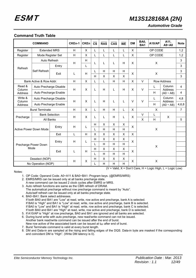
Command Truth Table
COMMAND CKEn-1 CKEn CS RAS CAS WE DMBA0, BA1
A10/AP A11,
A9~A0 Note
Register Extended MRS H X L L L L X OP CODE 1,2
Register Mode Register Set H X L L L L X OP CODE 1,2
Auto Refresh H 3
Entry H
L L L L H X X
3
L H H H 3 Refresh
Self Refresh Exit L H
H X X X X X
3
Bank Active & Row Addr. H X L L H H X V Row Address
Auto Precharge Disable L 4 Read & Column Address Auto Precharge Enable
H X L H L H X V H
Column Address (A0 ~ A8) 4
Auto Precharge Disable L 4,8Write & Column Address Auto Precharge Enable
H X L H L L V V H
Column Address (A0 ~ A8) 4,6,8
Burst Terminate H X L H H L X X 7
Bank Selection V L Precharge
All Banks H X L L H L X
X H X
5
H X X X Entry H L
L H H H X
Active Power Down Mode
Exit L H X X X X X
X
H X X X Entry H L
L H H H X
H X X X
Precharge Power Down Mode
Exit L H L H H H
X
X
Deselect (NOP) H X X X
No Operation (NOP) H X
L H H H X X
(V = Valid, X = Don’t Care, H = Logic High, L = Logic Low) Notes:
1. OP Code: Operand Code. A0~A11 & BA0~BA1: Program keys. (@EMRS/MRS) 2. EMRS/MRS can be issued only at all banks precharge state.
A new command can be issued 2 clock cycles after EMRS or MRS. 3. Auto refresh functions are same as the CBR refresh of DRAM.
The automatical precharge without row precharge command is meant by “Auto”. Auto/self refresh can be issued only at all banks precharge state.
4. BA0~BA1: Bank select addresses. If both BA0 and BA1 are “Low” at read, write, row active and precharge, bank A is selected. If BA0 is “High” and BA1 is “Low” at read, write, row active and precharge, bank B is selected. If BA0 is “Low” and BA1 is “High” at read, write, row active and precharge, bank C is selected. If both BA0 and BA1 are “High” at read, write, row active and precharge, bank D is selected.
5. If A10/AP is “High” at row precharge, BA0 and BA1 are ignored and all banks are selected. 6. During burst write with auto precharge, new read/write command can not be issued.
Another bank read/write command can be issued after the end of burst. New row active of the associated bank can be issued at tRP after end of burst.
7. Burst Terminate command is valid at every burst length. 8. DM and Data-in are sampled at the rising and falling edges of the DQS. Data-in byte are masked if the corresponding
and coincident DM is “High”. (Write DM latency is 0).
ESMT M13S128168A (2N) Automotive Grade
Elite Semiconductor Memory Technology Inc. Publication Date : Mar. 2013 Revision : 1.1 13/49
Basic Functionality Power-Up and Initialization Sequence DDR SDRAM must be powered up and initialized in a predefined manner. Operational procedures other than those specified may result in undefined operation. No power sequencing is specified during power up and power down given the following criteria: VDD and VDDQ are driven from a single power converter output, AND VTT is limited to 1.35 V, AND VREF tracks VDDQ /2
OR, the following relationships must be followed: VDDQ is driven after or with VDD such that VDDQ < VDD + 0.3 V, AND VTT is driven after or with VDDQ such that VTT < VDDQ + 0.3 V, AND VREF is driven after or with VDDQ such that VREF < VDDQ + 0.3 V.
At least one of these two conditions must be met. Except for CKE, inputs are not recognized as valid until after VREF is applied. CKE is an SSTL_2 input, but will detect an LVCMOS LOW level after VDD is applied. Maintaining an LVCMOS LOW level on CKE during power-up is required to guarantee that the DQ and DQS outputs will be in the High-Z state, where they will remain until driven in normal operation (by a read access). After all power supply and reference voltages are stable, and the clock is stable, the DDR SDRAM requires a 200 μs delay prior to applying an executable command. Once the 200 μs delay has been satisfied, a DESELECT or NOP command should be applied, and CKE should be brought HIGH. Following the NOP command, a PRECHARGE ALL command should be applied. Next a MODE REGISTER SET command should be issued for the Extended Mode Register, to enable the DLL, and then a MODE REGISTER SET command should be issued for the Mode Register, to reset the DLL, and to program the operating parameters. 200 clock cycles are required between the DLL reset and any executable command. A PRECHARGE ALL command should be applied, placing the device in the ”all banks idle” state. Once in the idle state, two AUTO refresh cycles must be performed. Additionally, a MODE REGISTER SET command for the Mode Register, with the reset DLL bit deactivated (i.e., to program operating parameters without resetting the DLL) must be performed. Following these cycles, the DDR SDRAM is ready for normal operation.
ESMT M13S128168A (2N) Automotive Grade
Elite Semiconductor Memory Technology Inc. Publication Date : Mar. 2013 Revision : 1.1 14/49
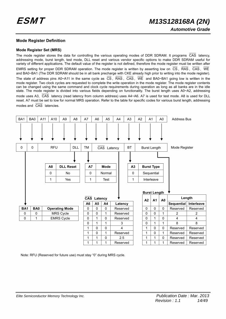
Mode Register Definition Mode Register Set (MRS)
The mode register stores the data for controlling the various operating modes of DDR SDRAM. It programs CAS latency, addressing mode, burst length, test mode, DLL reset and various vendor specific options to make DDR SDRAM useful for variety of different applications. The default value of the register is not defined, therefore the mode register must be written after
EMRS setting for proper DDR SDRAM operation. The mode register is written by asserting low on CS , RAS , CAS , WE and BA0~BA1 (The DDR SDRAM should be in all bank precharge with CKE already high prior to writing into the mode register).
The state of address pins A0~A11 in the same cycle as CS , RAS , CAS , WE and BA0~BA1 going low is written in the mode register. Two clock cycles are requested to complete the write operation in the mode register. The mode register contents can be changed using the same command and clock cycle requirements during operation as long as all banks are in the idle state. The mode register is divided into various fields depending on functionality. The burst length uses A0~A2, addressing
mode uses A3, CAS latency (read latency from column address) uses A4~A6. A7 is used for test mode. A8 is used for DLL reset. A7 must be set to low for normal MRS operation. Refer to the table for specific codes for various burst length, addressing
modes and CAS latencies.
BA1 BA0 A11 A10 A9 A8 A7 A6 A5 A4 A3 A2 A1 A0 Address Bus
0 0 RFU DLL TM CAS Latency BT Burst Length Mode Register
A8 DLL Reset A7 Mode A3 Burst Type
0 No 0 Normal 0 Sequential
1 Yes 1 Test 1 Interleave
Burst Length CAS Latency Length
A6 A5 A4 Latency A2 A1 A0
Sequential Interleave
BA1 BA0 Operating Mode 0 0 0 Reserved 0 0 0 Reserved Reserved
0 0 MRS Cycle 0 0 1 Reserved 0 0 1 2 2
0 1 EMRS Cycle 0 1 0 Reserved 0 1 0 4 4
0 1 1 3 0 1 1 8 8
1 0 0 4 1 0 0 Reserved Reserved
1 0 1 Reserved 1 0 1 Reserved Reserved
1 1 0 2.5 1 1 0 Reserved Reserved
1 1 1 Reserved 1 1 1 Reserved Reserved
Note: RFU (Reserved for future use) must stay “0” during MRS cycle.
ESMT M13S128168A (2N) Automotive Grade
Elite Semiconductor Memory Technology Inc. Publication Date : Mar. 2013 Revision : 1.1 15/49
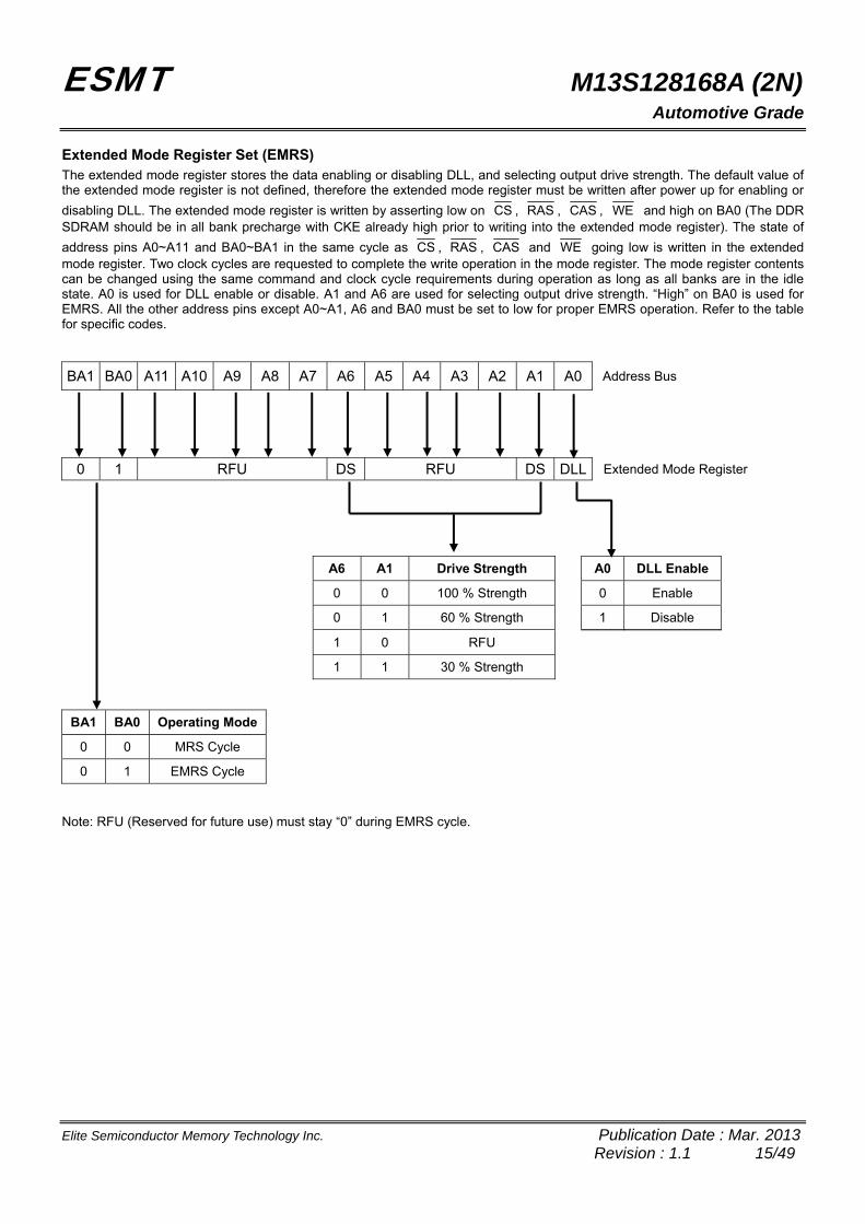
Extended Mode Register Set (EMRS) The extended mode register stores the data enabling or disabling DLL, and selecting output drive strength. The default value of the extended mode register is not defined, therefore the extended mode register must be written after power up for enabling or
disabling DLL. The extended mode register is written by asserting low on CS , RAS , CAS , WE and high on BA0 (The DDR SDRAM should be in all bank precharge with CKE already high prior to writing into the extended mode register). The state of
address pins A0~A11 and BA0~BA1 in the same cycle as CS , RAS , CAS and WE going low is written in the extended mode register. Two clock cycles are requested to complete the write operation in the mode register. The mode register contents can be changed using the same command and clock cycle requirements during operation as long as all banks are in the idle state. A0 is used for DLL enable or disable. A1 and A6 are used for selecting output drive strength. “High” on BA0 is used for EMRS. All the other address pins except A0~A1, A6 and BA0 must be set to low for proper EMRS operation. Refer to the table for specific codes.
BA1 BA0 A11 A10 A9 A8 A7 A6 A5 A4 A3 A2 A1 A0 Address Bus
0 1 RFU DS RFU DS DLL Extended Mode Register
A6 A1 Drive Strength A0 DLL Enable
0 0 100 % Strength 0 Enable
0 1 60 % Strength 1 Disable
1 0 RFU
1 1 30 % Strength
BA1 BA0 Operating Mode
0 0 MRS Cycle
0 1 EMRS Cycle
Note: RFU (Reserved for future use) must stay “0” during EMRS cycle.
ESMT M13S128168A (2N) Automotive Grade
Elite Semiconductor Memory Technology Inc. Publication Date : Mar. 2013 Revision : 1.1 16/49
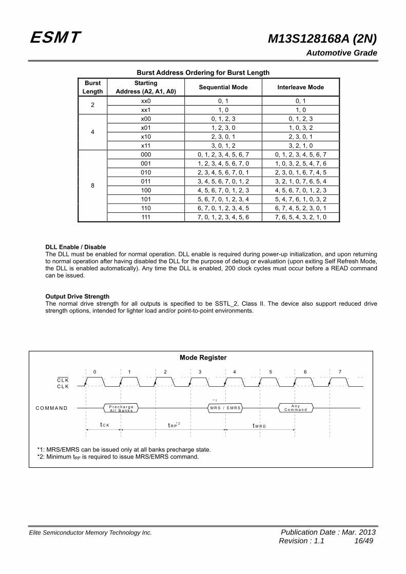
Burst Address Ordering for Burst Length
Burst Length
Starting Address (A2, A1, A0)
Sequential Mode Interleave Mode
xx0 0, 1 0, 1 2
xx1 1, 0 1, 0
x00 0, 1, 2, 3 0, 1, 2, 3
x01 1, 2, 3, 0 1, 0, 3, 2
x10 2, 3, 0, 1 2, 3, 0, 1 4
x11 3, 0, 1, 2 3, 2, 1, 0
000 0, 1, 2, 3, 4, 5, 6, 7 0, 1, 2, 3, 4, 5, 6, 7
001 1, 2, 3, 4, 5, 6, 7, 0 1, 0, 3, 2, 5, 4, 7, 6
010 2, 3, 4, 5, 6, 7, 0, 1 2, 3, 0, 1, 6, 7, 4, 5
011 3, 4, 5, 6, 7, 0, 1, 2 3, 2, 1, 0, 7, 6, 5, 4
100 4, 5, 6, 7, 0, 1, 2, 3 4, 5, 6, 7, 0, 1, 2, 3
101 5, 6, 7, 0, 1, 2, 3, 4 5, 4, 7, 6, 1, 0, 3, 2
110 6, 7, 0, 1, 2, 3, 4, 5 6, 7, 4, 5, 2, 3, 0, 1
8
111 7, 0, 1, 2, 3, 4, 5, 6 7, 6, 5, 4, 3, 2, 1, 0
DLL Enable / Disable The DLL must be enabled for normal operation. DLL enable is required during power-up initialization, and upon returning to normal operation after having disabled the DLL for the purpose of debug or evaluation (upon exiting Self Refresh Mode, the DLL is enabled automatically). Any time the DLL is enabled, 200 clock cycles must occur before a READ command can be issued.
Output Drive Strength The normal drive strength for all outputs is specified to be SSTL_2, Class II. The device also support reduced drive strength options, intended for lighter load and/or point-to-point environments.
Mode Register
0 1 2 3 4 5 6 7
C O M M A N D
t C K
P r e c h a r g eA l l B a n k s
M R S / E M R S
t R P* 2
* 1
C L KC L K
A n yC o m m a n d
t M R D
*1: MRS/EMRS can be issued only at all banks precharge state. *2: Minimum tRP is required to issue MRS/EMRS command.
ESMT M13S128168A (2N) Automotive Grade
Elite Semiconductor Memory Technology Inc. Publication Date : Mar. 2013 Revision : 1.1 17/49
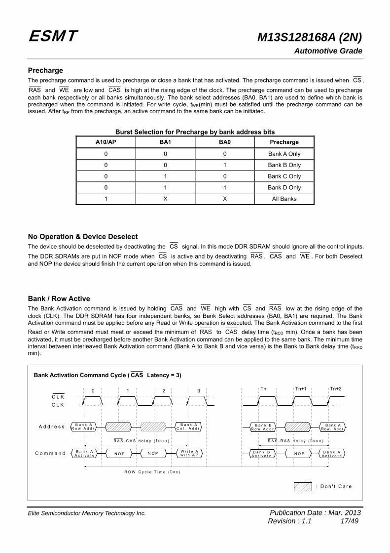
Precharge The precharge command is used to precharge or close a bank that has activated. The precharge command is issued when CS ,
RAS and WE are low and CAS is high at the rising edge of the clock. The precharge command can be used to precharge each bank respectively or all banks simultaneously. The bank select addresses (BA0, BA1) are used to define which bank is precharged when the command is initiated. For write cycle, tWR(min) must be satisfied until the precharge command can be issued. After tRP from the precharge, an active command to the same bank can be initiated.
Burst Selection for Precharge by bank address bits
A10/AP BA1 BA0 Precharge
0 0 0 Bank A Only
0 0 1 Bank B Only
0 1 0 Bank C Only
0 1 1 Bank D Only
1 X X All Banks
No Operation & Device Deselect The device should be deselected by deactivating the CS signal. In this mode DDR SDRAM should ignore all the control inputs.
The DDR SDRAMs are put in NOP mode when CS is active and by deactivating RAS , CAS and WE . For both Deselect and NOP the device should finish the current operation when this command is issued. Bank / Row Active The Bank Activation command is issued by holding CAS and WE high with CS and RAS low at the rising edge of the clock (CLK). The DDR SDRAM has four independent banks, so Bank Select addresses (BA0, BA1) are required. The Bank Activation command must be applied before any Read or Write operation is executed. The Bank Activation command to the first
Read or Write command must meet or exceed the minimum of RAS to CAS delay time (tRCD min). Once a bank has been activated, it must be precharged before another Bank Activation command can be applied to the same bank. The minimum time interval between interleaved Bank Activation command (Bank A to Bank B and vice versa) is the Bank to Bank delay time (tRRD min).
Bank Activation Command Cycle ( CAS Latency = 3)
A d d r e s s
0 1 2 3
C o m m a n d
B a n k AR o w A d d r .
B a n k AR o w . Ad d r .
B a n k BR o w A d d r .
B a n k AA c t i v a t e N O P B a n k B
A c t i v a t eN O P B a n k A
A c t i v a t e
R A S - C A S d e l a y ( t R C D ) R A S - R A S d e l a y ( t R R D )
R O W C y c l e T i m e ( t R C )
: D o n ' t C a r e
C L K
C L K
N O P
Tn Tn+1 Tn+2
B a n k AC o l . A d d r .
W r i t e Aw i t h A P
ESMT M13S128168A (2N) Automotive Grade
Elite Semiconductor Memory Technology Inc. Publication Date : Mar. 2013 Revision : 1.1 18/49
Read This command is used after the row activate command to initiate the burst read of data. The read command is initiated by
activating CS , RAS , CAS , and deasserting WE at the same clock rising edge as described in the command truth table. The length of the burst and the CAS latency time will be determined by the values programmed during the MRS command. Write This command is used after the row activate command to initiate the burst write of data. The write command is initiated by
activating CS , RAS , CAS , and WE at the same clock rising edge as describe in the command truth table. The length of the burst will be determined by the values programmed during the MRS command.
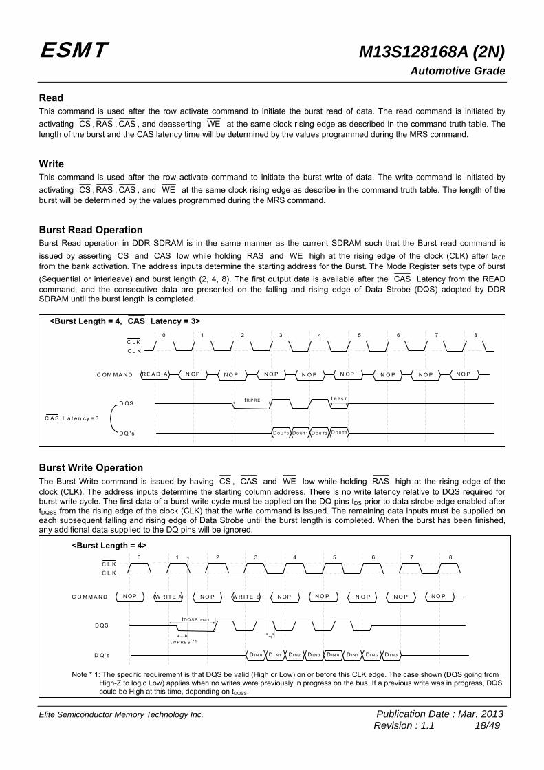
Burst Read Operation Burst Read operation in DDR SDRAM is in the same manner as the current SDRAM such that the Burst read command is
issued by asserting CS and CAS low while holding RAS and WE high at the rising edge of the clock (CLK) after tRCD from the bank activation. The address inputs determine the starting address for the Burst. The Mode Register sets type of burst
(Sequential or interleave) and burst length (2, 4, 8). The first output data is available after the CAS Latency from the READ command, and the consecutive data are presented on the falling and rising edge of Data Strobe (DQS) adopted by DDR SDRAM until the burst length is completed.
<Burst Length = 4, CAS Latency = 3>
Burst Write Operation The Burst Write command is issued by having CS , CAS and WE low while holding RAS high at the rising edge of the clock (CLK). The address inputs determine the starting column address. There is no write latency relative to DQS required for burst write cycle. The first data of a burst write cycle must be applied on the DQ pins tDS prior to data strobe edge enabled after tDQSS from the rising edge of the clock (CLK) that the write command is issued. The remaining data inputs must be supplied on each subsequent falling and rising edge of Data Strobe until the burst length is completed. When the burst has been finished, any additional data supplied to the DQ pins will be ignored.
<Burst Length = 4>
Note * 1: The specific requirement is that DQS be valid (High or Low) on or before this CLK edge. The case shown (DQS going from High-Z to logic Low) applies when no writes were previously in progress on the bus. If a previous write was in progress, DQS could be High at this time, depending on tDQSS.
0 1 2 3 4 5 6 7 8
C OM M A N D R E A D A N OP N O P N O P N O P N OP N O P N O P N O P
C L K
C L K
C A S L a t e n cy = 3
D QS
D Q ' s D O U T 0 D O U T 1 D O U T 2 D O U T 3
tR P RE t RP S T
0 1 2 3 4 5 6 7 8
C O M M A N D N OP W R IT E A N O P N OP N O P N O P N O P N O P
C L K
C L K
D QS
D Q' s D IN 0
W R IT E B
D I N1 DI N2 D I N3
tDQ S S m ax
tW P RE S * 1*1
*1
D IN 0 D IN1 DI N 2 D I N3
ESMT M13S128168A (2N) Automotive Grade
Elite Semiconductor Memory Technology Inc. Publication Date : Mar. 2013 Revision : 1.1 19/49
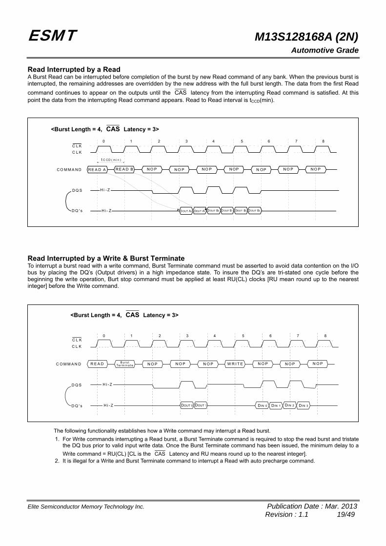
Read Interrupted by a Read A Burst Read can be interrupted before completion of the burst by new Read command of any bank. When the previous burst is interrupted, the remaining addresses are overridden by the new address with the full burst length. The data from the first Read
command continues to appear on the outputs until the CAS latency from the interrupting Read command is satisfied. At this point the data from the interrupting Read command appears. Read to Read interval is tCCD(min).
<Burst Length = 4, CAS Latency = 3>
Read Interrupted by a Write & Burst Terminate To interrupt a burst read with a write command, Burst Terminate command must be asserted to avoid data contention on the I/O bus by placing the DQ’s (Output drivers) in a high impedance state. To insure the DQ’s are tri-stated one cycle before the beginning the write operation, Burt stop command must be applied at least RU(CL) clocks [RU mean round up to the nearest integer] before the Write command.
<Burst Length = 4, CAS Latency = 3>
0 1 2 3 4 5 6 7 8
C O M M A N D
D Q S
D Q ' s
R E A D N O P N O P N O P N O P N O P
DOUT 0
B u r s tTe rm i n a t e
DIN 0DOUT 1 DIN 1 DIN 2 DIN 3
C L K
C L K
N O P W R I T E
The following functionality establishes how a Write command may interrupt a Read burst.
1. For Write commands interrupting a Read burst, a Burst Terminate command is required to stop the read burst and tristate the DQ bus prior to valid input write data. Once the Burst Terminate command has been issued, the minimum delay to a
Write command = RU(CL) [CL is the CAS Latency and RU means round up to the nearest integer]. 2. It is illegal for a Write and Burst Terminate command to interrupt a Read with auto precharge command.
0 1 2 3 4 5 6 7 8
C O M M A N D
D Q S
D Q ' s
R E A D A N O P N O P N O P N OP N OP N O P N O P
DOUT A0
R E A D B
DOUT A1 DOUT B2 DOUT B3DOUT B0 DOUT B 1
C L K
C L K
t C CD ( m i n )
H i - Z
H i - Z
ESMT M13S128168A (2N) Automotive Grade
Elite Semiconductor Memory Technology Inc. Publication Date : Mar. 2013 Revision : 1.1 20/49
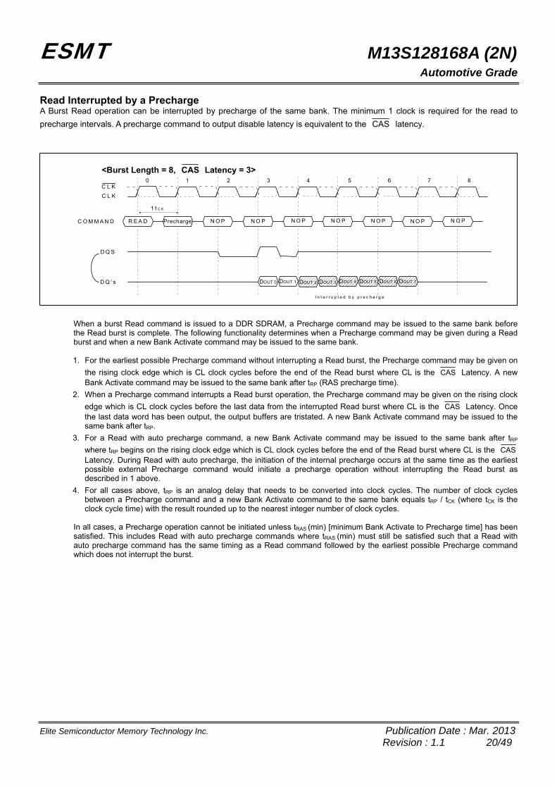
Read Interrupted by a Precharge A Burst Read operation can be interrupted by precharge of the same bank. The minimum 1 clock is required for the read to
precharge intervals. A precharge command to output disable latency is equivalent to the CAS latency.
<Burst Length = 8, CAS Latency = 3> 0 1 2 3 4 5 6 7 8
C O M M A N D
D Q S
D Q ' s
R E A D N O P N O P N O P N O P N O P N O P
DOUT 0
Precharge
1 t C K
N O P
I n t e r r u p t e d b y p r e c h a r g e
C L K
C L K
DOUT 1 DOUT 2 DOUT 3 DOUT 4 DOUT 5 DOUT 6 DOUT 7
When a burst Read command is issued to a DDR SDRAM, a Precharge command may be issued to the same bank before the Read burst is complete. The following functionality determines when a Precharge command may be given during a Read burst and when a new Bank Activate command may be issued to the same bank.
1. For the earliest possible Precharge command without interrupting a Read burst, the Precharge command may be given on
the rising clock edge which is CL clock cycles before the end of the Read burst where CL is the CAS Latency. A new Bank Activate command may be issued to the same bank after tRP (RAS precharge time).
2. When a Precharge command interrupts a Read burst operation, the Precharge command may be given on the rising clock
edge which is CL clock cycles before the last data from the interrupted Read burst where CL is the CAS Latency. Once the last data word has been output, the output buffers are tristated. A new Bank Activate command may be issued to the same bank after tRP.
3. For a Read with auto precharge command, a new Bank Activate command may be issued to the same bank after tRP
where tRP begins on the rising clock edge which is CL clock cycles before the end of the Read burst where CL is the CAS Latency. During Read with auto precharge, the initiation of the internal precharge occurs at the same time as the earliest possible external Precharge command would initiate a precharge operation without interrupting the Read burst as described in 1 above.
4. For all cases above, tRP is an analog delay that needs to be converted into clock cycles. The number of clock cycles between a Precharge command and a new Bank Activate command to the same bank equals tRP / tCK (where tCK is the clock cycle time) with the result rounded up to the nearest integer number of clock cycles.
In all cases, a Precharge operation cannot be initiated unless tRAS (min) [minimum Bank Activate to Precharge time] has been satisfied. This includes Read with auto precharge commands where tRAS (min) must still be satisfied such that a Read with auto precharge command has the same timing as a Read command followed by the earliest possible Precharge command which does not interrupt the burst.
ESMT M13S128168A (2N) Automotive Grade
Elite Semiconductor Memory Technology Inc. Publication Date : Mar. 2013 Revision : 1.1 21/49
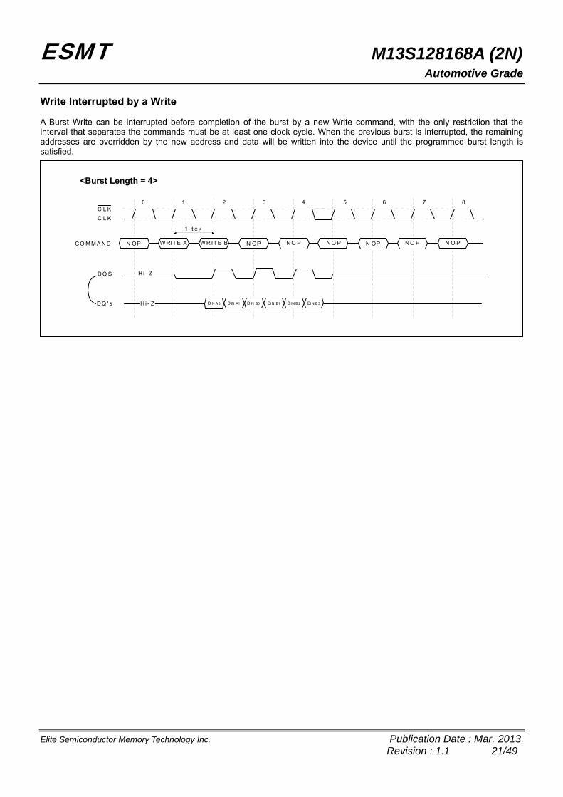
Write Interrupted by a Write A Burst Write can be interrupted before completion of the burst by a new Write command, with the only restriction that the interval that separates the commands must be at least one clock cycle. When the previous burst is interrupted, the remaining addresses are overridden by the new address and data will be written into the device until the programmed burst length is satisfied.
<Burst Length = 4>
0 1 2 3 4 5 6 7 8
C O M M A N D
D Q S
D Q ' s
N OP N OP N O P N O P N OP N O P N O P
DIN A0
W RITE A
DIN A1 DIN B 2 DIN B3DIN B0 DIN B1
C L K
C L K
1 t C K
H i - Z
H i - Z
W R IT E B
ESMT M13S128168A (2N) Automotive Grade
Elite Semiconductor Memory Technology Inc. Publication Date : Mar. 2013 Revision : 1.1 22/49
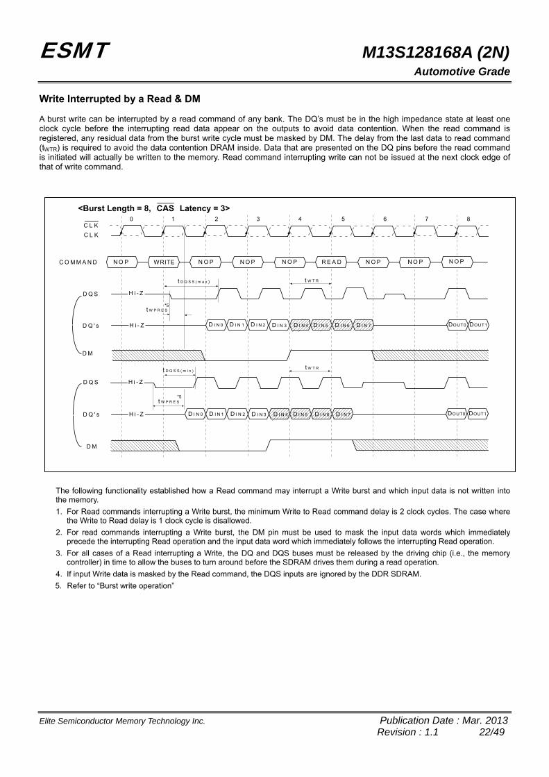
Write Interrupted by a Read & DM A burst write can be interrupted by a read command of any bank. The DQ’s must be in the high impedance state at least one clock cycle before the interrupting read data appear on the outputs to avoid data contention. When the read command is registered, any residual data from the burst write cycle must be masked by DM. The delay from the last data to read command (tWTR) is required to avoid the data contention DRAM inside. Data that are presented on the DQ pins before the read command is initiated will actually be written to the memory. Read command interrupting write can not be issued at the next clock edge of that of write command.
<Burst Length = 8, CAS Latency = 3> 0 1 2 3 4 5 6 7 8
C O M M A N D
D Q S
D Q ' s
D Q S
D Q ' s
N O P N O P N O P N O P R E A D N O P
t D Q S S ( m a x )
D I N 0
WRITE
t D Q S S ( m i n )
D M
C L K
C L K
D M
N O P N O P
H i - Z
H i - Z
t W P R E S
t W T R
*5
H i - Z
H i - Z
t W T R
t W P R E S*5
D I N 1 D I N 2 D I N 3 D I N 4 D I N 5 D I N 6 D I N 7 DOUT0 DOUT1
DOUT0 DOUT1D I N 0 D I N 1 D I N 2 D I N 3 D I N 4 D I N 5 D I N 6 D I N 7
The following functionality established how a Read command may interrupt a Write burst and which input data is not written into the memory.
1. For Read commands interrupting a Write burst, the minimum Write to Read command delay is 2 clock cycles. The case where the Write to Read delay is 1 clock cycle is disallowed.
2. For read commands interrupting a Write burst, the DM pin must be used to mask the input data words which immediately precede the interrupting Read operation and the input data word which immediately follows the interrupting Read operation.
3. For all cases of a Read interrupting a Write, the DQ and DQS buses must be released by the driving chip (i.e., the memory controller) in time to allow the buses to turn around before the SDRAM drives them during a read operation.
4. If input Write data is masked by the Read command, the DQS inputs are ignored by the DDR SDRAM.
5. Refer to “Burst write operation”
ESMT M13S128168A (2N) Automotive Grade
Elite Semiconductor Memory Technology Inc. Publication Date : Mar. 2013 Revision : 1.1 23/49
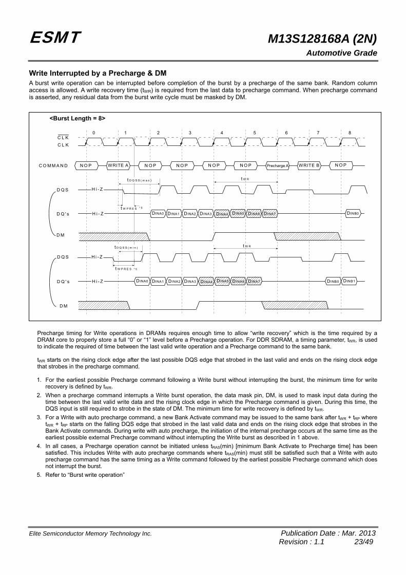
Write Interrupted by a Precharge & DM A burst write operation can be interrupted before completion of the burst by a precharge of the same bank. Random column access is allowed. A write recovery time (tWR) is required from the last data to precharge command. When precharge command is asserted, any residual data from the burst write cycle must be masked by DM.
<Burst Length = 8>
0 1 2 3 4 5 6 7 8
C O M M A N D
D Q S
D Q ' s
D Q S
D Q ' s
N O P N O P N O P N O P N O P
DINA0
WRITE A
D M
C L K
C L K
D M
Precharge A
H i - Z
H i - Zt W P R E S * 5
t W R
H i - Z
H i - Z
t W R
N O P WRITE B
t W P R E S * 5
t D Q S S ( m a x )
t D Q S S ( m i n )
DINA1 DINA2 DINA3 DINA4 DINA5 DINA6 DINA7 DINB0
DINB0 DINB1DINA0 DINA1 DINA2 DINA3 DINA4 DINA5 DINA6 DINA7
Precharge timing for Write operations in DRAMs requires enough time to allow “write recovery” which is the time required by a DRAM core to properly store a full “0” or “1” level before a Precharge operation. For DDR SDRAM, a timing parameter, tWR, is used to indicate the required of time between the last valid write operation and a Precharge command to the same bank.
tWR starts on the rising clock edge after the last possible DQS edge that strobed in the last valid and ends on the rising clock edge that strobes in the precharge command. 1. For the earliest possible Precharge command following a Write burst without interrupting the burst, the minimum time for write
recovery is defined by tWR.
2. When a precharge command interrupts a Write burst operation, the data mask pin, DM, is used to mask input data during the time between the last valid write data and the rising clock edge in which the Precharge command is given. During this time, the DQS input is still required to strobe in the state of DM. The minimum time for write recovery is defined by tWR.
3. For a Write with auto precharge command, a new Bank Activate command may be issued to the same bank after tWR + tRP where tWR + tRP starts on the falling DQS edge that strobed in the last valid data and ends on the rising clock edge that strobes in the Bank Activate commands. During write with auto precharge, the initiation of the internal precharge occurs at the same time as the earliest possible external Precharge command without interrupting the Write burst as described in 1 above.
4. In all cases, a Precharge operation cannot be initiated unless tRAS(min) [minimum Bank Activate to Precharge time] has been satisfied. This includes Write with auto precharge commands where tRAS(min) must still be satisfied such that a Write with auto precharge command has the same timing as a Write command followed by the earliest possible Precharge command which does not interrupt the burst.
5. Refer to “Burst write operation”
ESMT M13S128168A (2N) Automotive Grade
Elite Semiconductor Memory Technology Inc. Publication Date : Mar. 2013 Revision : 1.1 24/49
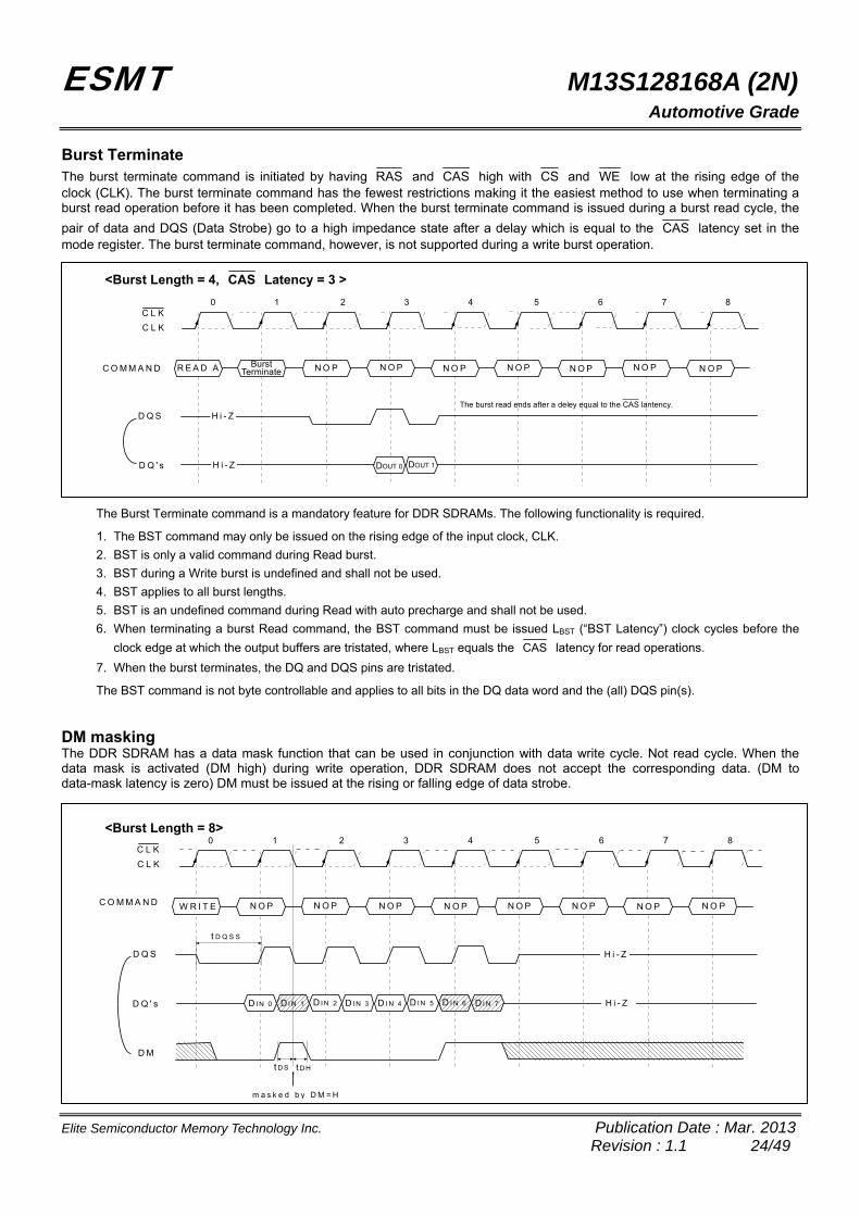
Burst Terminate The burst terminate command is initiated by having RAS and CAS high with CS and WE low at the rising edge of the clock (CLK). The burst terminate command has the fewest restrictions making it the easiest method to use when terminating a burst read operation before it has been completed. When the burst terminate command is issued during a burst read cycle, the
pair of data and DQS (Data Strobe) go to a high impedance state after a delay which is equal to the CAS latency set in the mode register. The burst terminate command, however, is not supported during a write burst operation.
<Burst Length = 4, CAS Latency = 3 >
0 1 2 3 4 5 6 7 8
C O M M A N D R E A D A N O P N O P N O P N O P N O P N O P N O PBurstTerminate
C L K
C L K
D Q S
D Q ' s DOUT 0
H i - Z
H i - Z
The burst read ends after a deley equal to the CAS lantency.
DOUT 1
The Burst Terminate command is a mandatory feature for DDR SDRAMs. The following functionality is required.
1. The BST command may only be issued on the rising edge of the input clock, CLK.
2. BST is only a valid command during Read burst.
3. BST during a Write burst is undefined and shall not be used.
4. BST applies to all burst lengths.
5. BST is an undefined command during Read with auto precharge and shall not be used.
6. When terminating a burst Read command, the BST command must be issued LBST (“BST Latency”) clock cycles before the
clock edge at which the output buffers are tristated, where LBST equals the CAS latency for read operations.
7. When the burst terminates, the DQ and DQS pins are tristated.
The BST command is not byte controllable and applies to all bits in the DQ data word and the (all) DQS pin(s). DM masking The DDR SDRAM has a data mask function that can be used in conjunction with data write cycle. Not read cycle. When the data mask is activated (DM high) during write operation, DDR SDRAM does not accept the corresponding data. (DM to data-mask latency is zero) DM must be issued at the rising or falling edge of data strobe.
<Burst Length = 8> 0 1 2 3 4 5 6 7 8
C O M M A N D W R I T E N O P N O P N O P N O P N O P N O P N O P
C L K
C L K
N O P
D Q S
D Q ' s
t D Q S S
D M
D I N 0
H i - Z
H i - Z
m a s k e d b y D M = H
D I N 1 D I N 2 D I N 3 D I N 4 D I N 5 D I N 6 D I N 7
t D S t D H
ESMT M13S128168A (2N) Automotive Grade
Elite Semiconductor Memory Technology Inc. Publication Date : Mar. 2013 Revision : 1.1 25/49
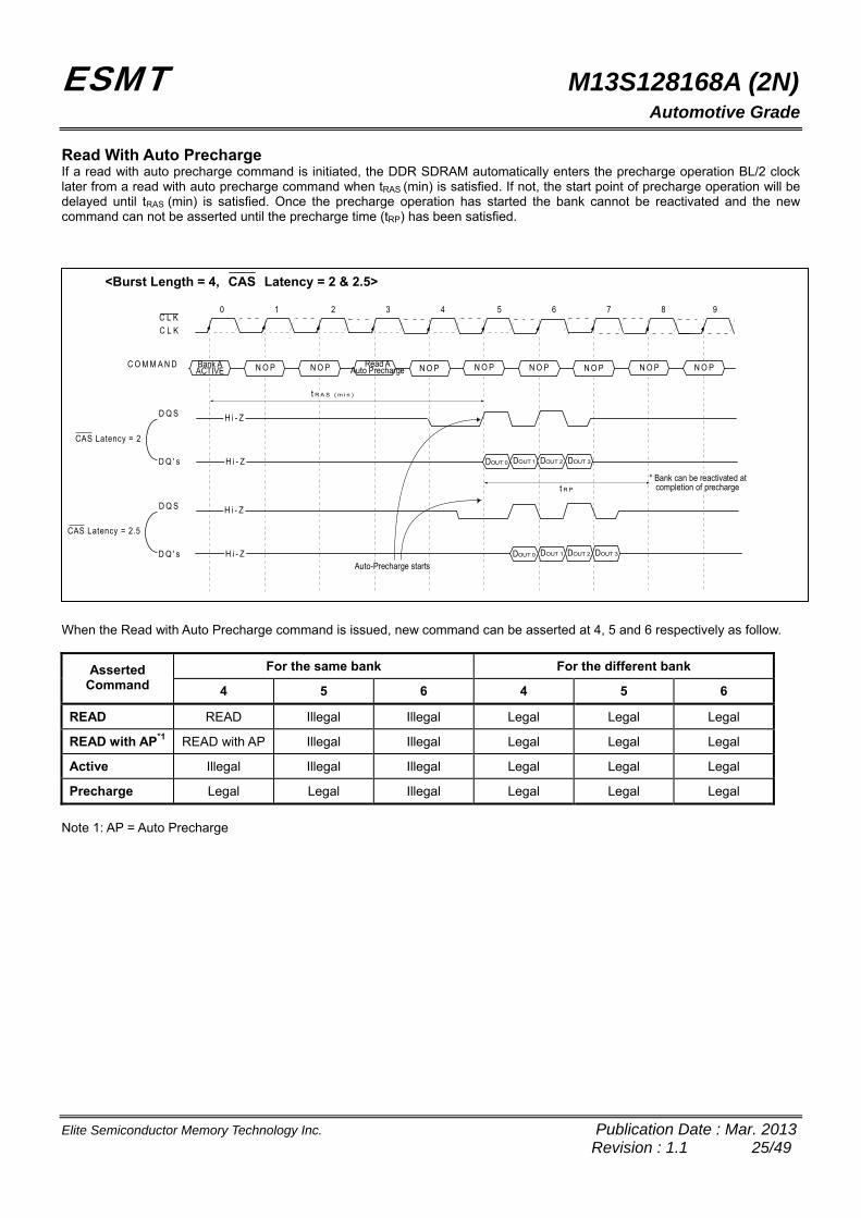
Read With Auto Precharge If a read with auto precharge command is initiated, the DDR SDRAM automatically enters the precharge operation BL/2 clock later from a read with auto precharge command when tRAS (min) is satisfied. If not, the start point of precharge operation will be delayed until tRAS (min) is satisfied. Once the precharge operation has started the bank cannot be reactivated and the new command can not be asserted until the precharge time (tRP) has been satisfied.
<Burst Length = 4, CAS Latency = 2 & 2.5>
0 1 2 3 4 5 6 7 8 9
C O M M A N D Bank AACTIVE N O P N O P N O P N O P N O P N O P N O PRead A
Auto Precharge
C L K
C L K
D Q S
D Q ' s
CAS Latency = 2
CAS Latency = 2.5
DOUT 0
t R P
N O P
* Bank can be reactivated atcompletion of precharge
Auto-Precharge starts
H i - Z
H i - Z
t R A S ( m i n )
DOUT 1 DOUT 2 DOUT 3
D Q S
D Q ' s DOUT 0
H i - Z
H i - Z DOUT 1 DOUT 2 DOUT 3
When the Read with Auto Precharge command is issued, new command can be asserted at 4, 5 and 6 respectively as follow.
For the same bank For the different bank Asserted Command 4 5 6 4 5 6
READ READ Illegal Illegal Legal Legal Legal
READ with AP*1 READ with AP Illegal Illegal Legal Legal Legal
Active Illegal Illegal Illegal Legal Legal Legal
Precharge Legal Legal Illegal Legal Legal Legal Note 1: AP = Auto Precharge
ESMT M13S128168A (2N) Automotive Grade
Elite Semiconductor Memory Technology Inc. Publication Date : Mar. 2013 Revision : 1.1 26/49
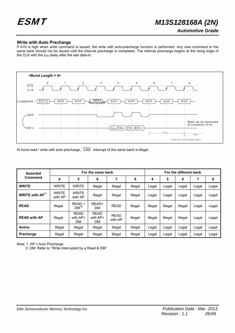
Write with Auto Precharge If A10 is high when write command is issued, the write with auto-precharge function is performed. Any new command to the same bank should not be issued until the internal precharge is completed. The internal precharge begins at the rising edge of the CLK with the tWR delay after the last data-in.
<Burst Length = 4>
0 1 2 3 4 5 6 7 8
C O M M A N D
D Q S
D Q ' s
B a n k AA C T I V E N O P N O P N O P N O P N O P N O P N O P
DIN 0
Write AAuto Precharge
*Bank can be reactivatedat completion of tRP
t W Rt R P
I n t e r n a l p r e c h a r g e s t a r t
C L K
C L K
DIN 1 DIN 2 DIN 3
At burst read / write with auto precharge, CAS interrupt of the same bank is illegal.
For the same bank For the different bank Asserted Command 4 5 6 7 8 4 5 6 7 8
WRITE WRITE WRITE Illegal Illegal Illegal Legal Legal Legal Legal Legal
WRITE with AP*1 WRITE with AP
WRITE with AP
Illegal Illegal Illegal Legal Legal Legal Legal Legal
READ Illegal READ + DM*2
READ+ DM
READ Illegal Illegal Illegal Illegal Legal Legal
READ with AP Illegal READ
with AP+ DM
READ with AP+
DM READ
with APIllegal Illegal Illegal Illegal Legal Legal
Active Illegal Illegal Illegal Illegal Illegal Legal Legal Legal Legal Legal
Precharge Illegal Illegal Illegal Illegal Illegal Legal Legal Legal Legal Legal
Note: 1. AP = Auto Precharge 2. DM: Refer to “Write Interrupted by a Read & DM“
ESMT M13S128168A (2N) Automotive Grade
Elite Semiconductor Memory Technology Inc. Publication Date : Mar. 2013 Revision : 1.1 27/49
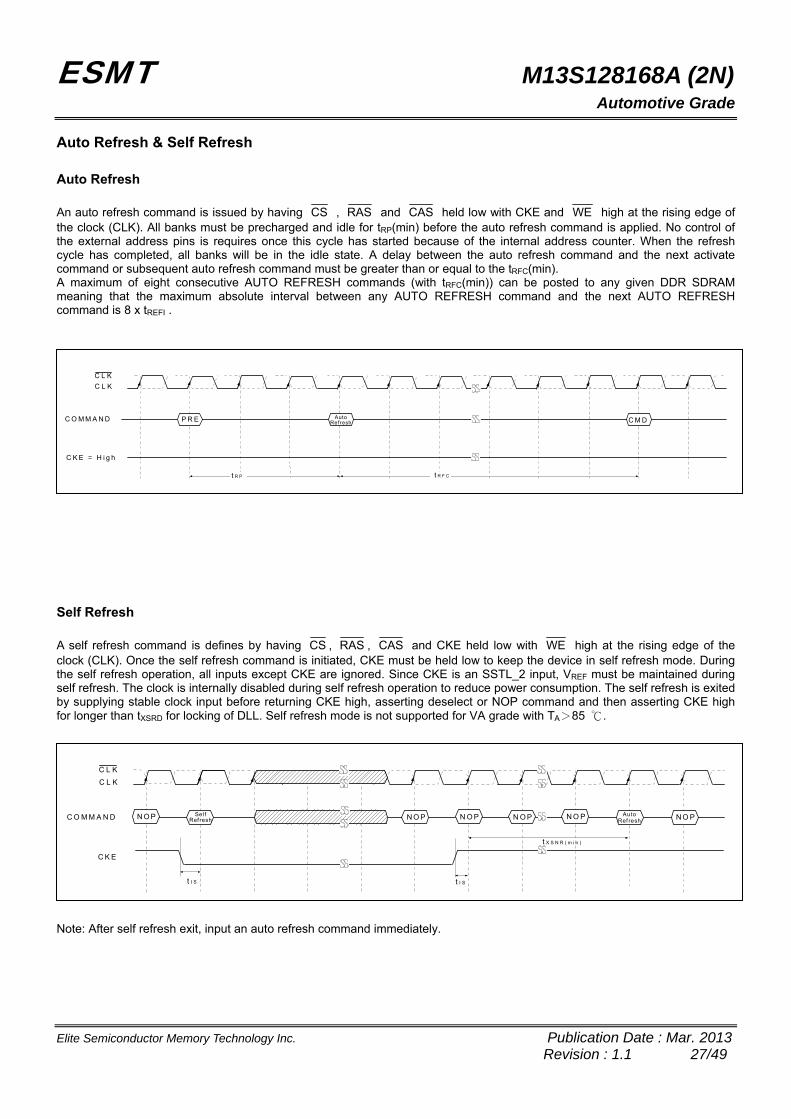
Auto Refresh & Self Refresh Auto Refresh
An auto refresh command is issued by having CS , RAS and CAS held low with CKE and WE high at the rising edge of the clock (CLK). All banks must be precharged and idle for tRP(min) before the auto refresh command is applied. No control of the external address pins is requires once this cycle has started because of the internal address counter. When the refresh cycle has completed, all banks will be in the idle state. A delay between the auto refresh command and the next activate command or subsequent auto refresh command must be greater than or equal to the tRFC(min). A maximum of eight consecutive AUTO REFRESH commands (with tRFC(min)) can be posted to any given DDR SDRAM meaning that the maximum absolute interval between any AUTO REFRESH command and the next AUTO REFRESH command is 8 x tREFI .
C O M M A N D
C K E = H i g h
t R P
P R E AutoRefresh C M D
t R F C
C L K
C L K
Self Refresh
A self refresh command is defines by having CS , RAS , CAS and CKE held low with WE high at the rising edge of the clock (CLK). Once the self refresh command is initiated, CKE must be held low to keep the device in self refresh mode. During the self refresh operation, all inputs except CKE are ignored. Since CKE is an SSTL_2 input, VREF must be maintained during self refresh. The clock is internally disabled during self refresh operation to reduce power consumption. The self refresh is exited by supplying stable clock input before returning CKE high, asserting deselect or NOP command and then asserting CKE high for longer than tXSRD for locking of DLL. Self refresh mode is not supported for VA grade with TA>85 ℃.
C O M M A N D
C K E
t X S N R ( m i n )
Sel fRef resh
AutoRef resh N O P
t I S
C L K
C L K
N O P N O P N O P N O P N O P
t I S
Note: After self refresh exit, input an auto refresh command immediately.
ESMT M13S128168A (2N) Automotive Grade
Elite Semiconductor Memory Technology Inc. Publication Date : Mar. 2013 Revision : 1.1 28/49
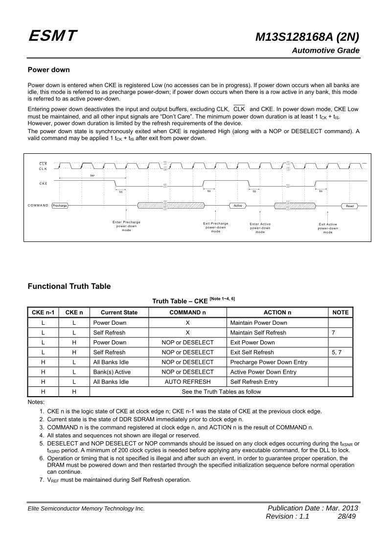
Power down
Power down is entered when CKE is registered Low (no accesses can be in progress). If power down occurs when all banks are idle, this mode is referred to as precharge power-down; if power down occurs when there is a row active in any bank, this mode is referred to as active power-down.
Entering power down deactivates the input and output buffers, excluding CLK, CLK and CKE. In power down mode, CKE Low must be maintained, and all other input signals are “Don’t Care”. The minimum power down duration is at least 1 tCK + tIS. However, power down duration is limited by the refresh requirements of the device. The power down state is synchronously exited when CKE is registered High (along with a NOP or DESELECT command). A valid command may be applied 1 tCK + tIS after exit from power down.
C O M M A N D
C K E
C L K
C L K
Precharge Read
Enter Prechargepower-down
mode
tIS tIStIStIS
Active
Exi t Prechargepower -down
mo de
Enter Ac tivepower-down
mode
Exit Act ivepower -down
mo de
tRP
Functional Truth Table
Truth Table – CKE [Note 1~4, 6]
CKE n-1 CKE n Current State COMMAND n ACTION n NOTE
L L Power Down X Maintain Power Down
L L Self Refresh X Maintain Self Refresh 7
L H Power Down NOP or DESELECT Exit Power Down
L H Self Refresh NOP or DESELECT Exit Self Refresh 5, 7
H L All Banks Idle NOP or DESELECT Precharge Power Down Entry
H L Bank(s) Active NOP or DESELECT Active Power Down Entry
H L All Banks Idle AUTO REFRESH Self Refresh Entry
H H See the Truth Tables as follow
Notes:
1. CKE n is the logic state of CKE at clock edge n; CKE n-1 was the state of CKE at the previous clock edge. 2. Current state is the state of DDR SDRAM immediately prior to clock edge n. 3. COMMAND n is the command registered at clock edge n, and ACTION n is the result of COMMAND n. 4. All states and sequences not shown are illegal or reserved. 5. DESELECT and NOP DESELECT or NOP commands should be issued on any clock edges occurring during the tXSNR or
tXSRD period. A minimum of 200 clock cycles is needed before applying any executable command, for the DLL to lock. 6. Operation or timing that is not specified is illegal and after such an event, in order to guarantee proper operation, the
DRAM must be powered down and then restarted through the specified initialization sequence before normal operation can continue.
7. VREF must be maintained during Self Refresh operation.
ESMT M13S128168A (2N) Automotive Grade
Elite Semiconductor Memory Technology Inc. Publication Date : Mar. 2013 Revision : 1.1 29/49
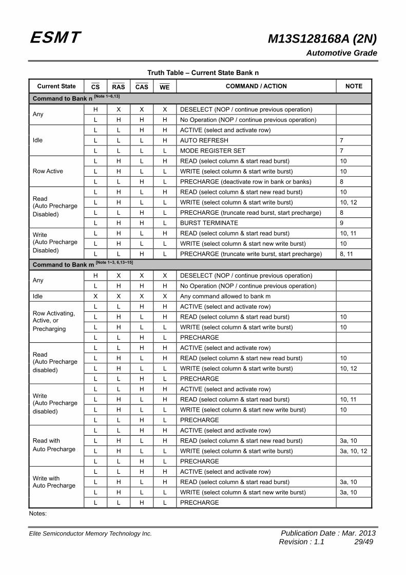
Truth Table – Current State Bank n
Current State CS RAS CAS WE COMMAND / ACTION NOTE
Command to Bank n [Note 1~6,13]
H X X X DESELECT (NOP / continue previous operation) Any
L H H H No Operation (NOP / continue previous operation)
L L H H ACTIVE (select and activate row)
L L L H AUTO REFRESH 7 Idle
L L L L MODE REGISTER SET 7
L H L H READ (select column & start read burst) 10
L H L L WRITE (select column & start write burst) 10 Row Active
L L H L PRECHARGE (deactivate row in bank or banks) 8
L H L H READ (select column & start new read burst) 10
L H L L WRITE (select column & start write burst) 10, 12
L L H L PRECHARGE (truncate read burst, start precharge) 8
Read (Auto Precharge Disabled)
L H H L BURST TERMINATE 9
L H L H READ (select column & start read burst) 10, 11
L H L L WRITE (select column & start new write burst) 10
Write (Auto Precharge Disabled)
L L H L PRECHARGE (truncate write burst, start precharge) 8, 11
Command to Bank m [Note 1~3, 6,13~15]
H X X X DESELECT (NOP / continue previous operation) Any
L H H H No Operation (NOP / continue previous operation)
Idle X X X X Any command allowed to bank m
L L H H ACTIVE (select and activate row)
L H L H READ (select column & start read burst) 10
L H L L WRITE (select column & start write burst) 10
Row Activating, Active, or Precharging
L L H L PRECHARGE
L L H H ACTIVE (select and activate row)
L H L H READ (select column & start new read burst) 10
L H L L WRITE (select column & start write burst) 10, 12
Read (Auto Precharge disabled)
L L H L PRECHARGE
L L H H ACTIVE (select and activate row)
L H L H READ (select column & start read burst) 10, 11
L H L L WRITE (select column & start new write burst) 10
Write (Auto Precharge disabled)
L L H L PRECHARGE
L L H H ACTIVE (select and activate row)
L H L H READ (select column & start new read burst) 3a, 10
L H L L WRITE (select column & start write burst) 3a, 10, 12
Read with Auto Precharge
L L H L PRECHARGE
L L H H ACTIVE (select and activate row)
L H L H READ (select column & start read burst) 3a, 10
L H L L WRITE (select column & start new write burst) 3a, 10
Write with Auto Precharge
L L H L PRECHARGE
Notes:
ESMT M13S128168A (2N) Automotive Grade
Elite Semiconductor Memory Technology Inc. Publication Date : Mar. 2013 Revision : 1.1 30/49
1. This table applies when CKEn-1 was HIGH and CKEn is HIGH and after tXSNR or tXSRD has been met (if the previous state was self refresh).
2. This table is bank - specific, except where noted, i.e., the current state is for a specific bank and the commands shown are those allowed to be issued to that bank when in that state. Exceptions are covered in the notes below.
3. Current state definitions:
Idle: The bank has been precharged, and tRP has been met. Row Active: A row in the bank has been activated, and tRCD has been met. No data bursts/accesses and no
register accesses are in progress. Read / Write: A READ / WRITE burst has been initiated, with AUTO PRECHARGE disabled, and has not yet
terminated or been terminated. Read / Write with Auto Precharge Enabled: See following text, notes 3a, 3b:
3a. For devices which do not support the optional “concurrent auto precharge” feature, the Read with Auto Precharge Enabled or Write with Auto Precharge Enabled states can each be broken into two parts: the access period and the precharge period. For Read with Auto Precharge, the precharge period is defined as if the same burst was executed with Auto Precharge disabled and then followed with the earliest possible PRECHARGE command that still accesses all of the data in the burst. For Write with Auto Precharge, the precharge period begins when tWR ends, with tWR measured as if Auto Precharge was disabled. The access period starts with registration of the command and ends where the precharge period (or tRP) begins. During the precharge period of the Read with Auto Precharge Enabled or Write with Auto Precharge Enabled states, ACTIVE, PRECHARGE, READ and WRITE commands to the other bank may be applied; during the access period, only ACTIVE and PRECHARGE commands to the other bank may be applied. In either case, all other related limitations apply (e.g., contention between READ data and WRITE data must be avoided).
3b. For devices which do support the optional “concurrent auto precharge” feature, a read with auto precharge enabled, or a write with auto precharge enabled, may be followed by any command to the other banks, as long as that command does not interrupt the read or write data transfer, and all other related limitations apply (e.g., contention between READ data and WRITE data must be avoided.)
4. The following states must not be interrupted by a command issued to the same bank. DESELECT or NOP commands, or allowable commands to the other bank should be issued on any clock edge occurring during these states. Allowable commands to the other bank are determined by its current state and Truth Table.
Precharging: Starts with registration of a PRECHARGE command and ends when tRP is met. Once tRP is met, the bank will be in the idle state.
Row Activating: Starts with registration of an ACTIVE command and ends when tRCD is met. Once tRCD is met, the bank will be in the ”row active” state.
Read/ Write with Auto - Precharge Enabled: Starts with registration of a READ / WRITE command with AUTO PRECHARGE enabled
and ends when tRP has been met. Once tRP is met, the bank will be in the idle state. 5. The following states must not be interrupted by any executable command; DESELECT or NOP commands must be
applied on each positive clock edge during these states.
Refreshing: Starts with registration of an AUTO REFRESH command and ends when tRC is met. Once tRFC is met, the DDR SDRAM will be in the ”all banks idle” state. Accessing Mode Register: Starts with registration of a MODE REGISTER SET command and ends when tMRD
has been met. Once tMRD is met, the DDR SDRAM will be in the ”all banks idle” state. Precharging All: Starts with registration of a PRECHARGE ALL command and ends when tRP is met. Once tRP is met, all banks will be in the idle state.
6. All states and sequences not shown are illegal or reserved. 7. Not bank - specific; requires that all banks are idle and no bursts are in progress. 8. May or may not be bank - specific; if multiple banks are to be precharged, each must be in a valid state for precharging. 9. Not bank - specific; BURST TERMINATE affects the most recent READ burst, regardless of bank. 10. Reads or Writes listed in the Command/Action column include Reads or Writes with AUTO PRECHARGE enabled and
Reads or Writes with AUTO PRECHARGE disabled. 11. Requires appropriate DM masking. 12. A WRITE command may be applied after the completion of the READ burst; otherwise, a Burst Terminate must be
used to end the READ prior to asserting a WRITE command, 13. Operation or timing that is not specified is illegal and after such an event, in order to guarantee proper operation, the
DRAM must be powered down and then restarted through the specified initialization sequence before normal operation can continue.
14. AUTO REFRESH and MODE REGISTER SET commands may only be issued when all banks are idle. 15. A BURST TERMINATE command cannot be issued to another bank; it applies to the bank represented by the current
state only.
ESMT M13S128168A (2N) Automotive Grade
Elite Semiconductor Memory Technology Inc. Publication Date : Mar. 2013 Revision : 1.1 31/49
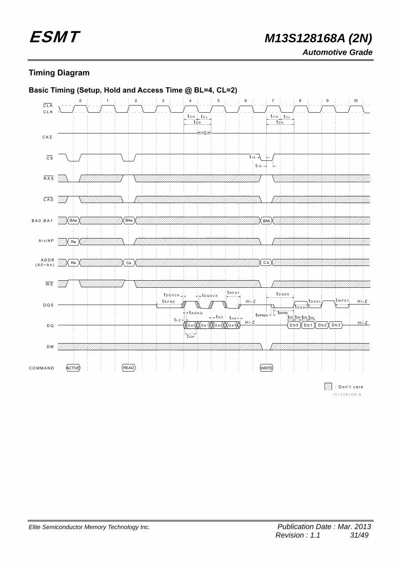
Timing Diagram Basic Timing (Setup, Hold and Access Time @ BL=4, CL=2)
C K E
C S
R A S
C A S
B A 0 , B A 1
A D D R( A 0 ~ A n )
W E
D Q S
D Q
0 1 2 3 4 5 6 7 8 9 10
H I G H
D M
C O M M A N D
A 1 0 / A P
BAa BAb
C b
D b 0 D b 1 D b 3D b 2
t C K
t I S
t I H
t D Q S C K
t R P R E
t D Q S C K
Q a 0 Q a 1 Q a 2 Q a 3
t R P S T
H i - Z
t D Q S S
tWPRE
t D Q S H
t D Q S L
tDS tDH tDS tDH
t W P S T H i - Z
H i - Z
READ WRITE
C L K
C L Kt C Lt C H
t C K
t C Lt C H
BAa
Ra
CaRa
ACTIVE
t D Q S Q
t Q H
: D o n ’ t c a r e
H i - Zt L Z
t A C t H ZtWPRES
1 0 1 2 2 B 1 6 R . B
ESMT M13S128168A (2N) Automotive Grade
Elite Semiconductor Memory Technology Inc. Publication Date : Mar. 2013 Revision : 1.1 32/49
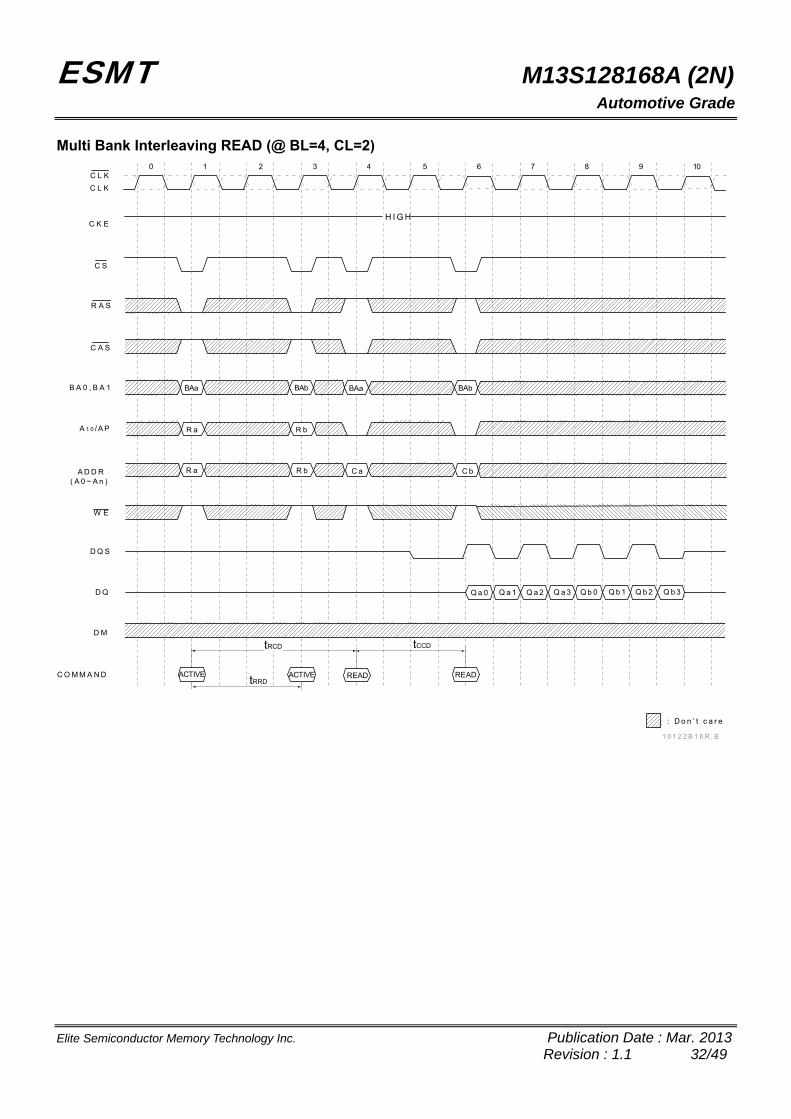
Multi Bank Interleaving READ (@ BL=4, CL=2)
C K E
C S
R A S
C A S
B A 0 , B A 1
W E
D Q S
D Q
0 1 2 3 4 5 6 7 8 9 10
H I G H
D M
C O M M A N D
A 1 0 / A P
A D D R( A 0 ~ A n )
BAa
Q b 0 Q b 1 Q b 3Q b 2
ACTIVE
BAb BAa BAb
R a R b
R a C a C b
Q a 0 Q a 1 Q a 3Q a 2
ACTIVE READREAD
R b
C L K
C L K
tCCD
: D o n ’ t c a r e
1 0 1 2 2 B 1 6 R . B
tRCD
tRRD
ESMT M13S128168A (2N) Automotive Grade
Elite Semiconductor Memory Technology Inc. Publication Date : Mar. 2013 Revision : 1.1 33/49
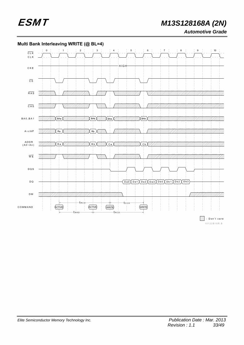
Multi Bank Interleaving WRITE (@ BL=4)
C K E
C S
R A S
C A S
B A 0 , B A 1
W E
D Q S
D Q
0 1 2 3 4 5 6 7 8 9 10
H I G H
D M
C O M M A N D
A 1 0 / A P
A D D R( A 0 ~ A n )
BAa
D b 0 D b 1 D b 3D b 2
ACTIVE
BAb BAa BAb
R a C a C b
D a 0 D a 1 D a 3D a 2
ACTIVE WRITE
t R C D
WRITE
t R R D
t C C D
R b
C L K
C L K
Ra Rb
: D o n ’ t c a r e
1 0 1 2 2 B 1 6 R . B
t R C D
ESMT M13S128168A (2N) Automotive Grade
Elite Semiconductor Memory Technology Inc. Publication Date : Mar. 2013 Revision : 1.1 34/49
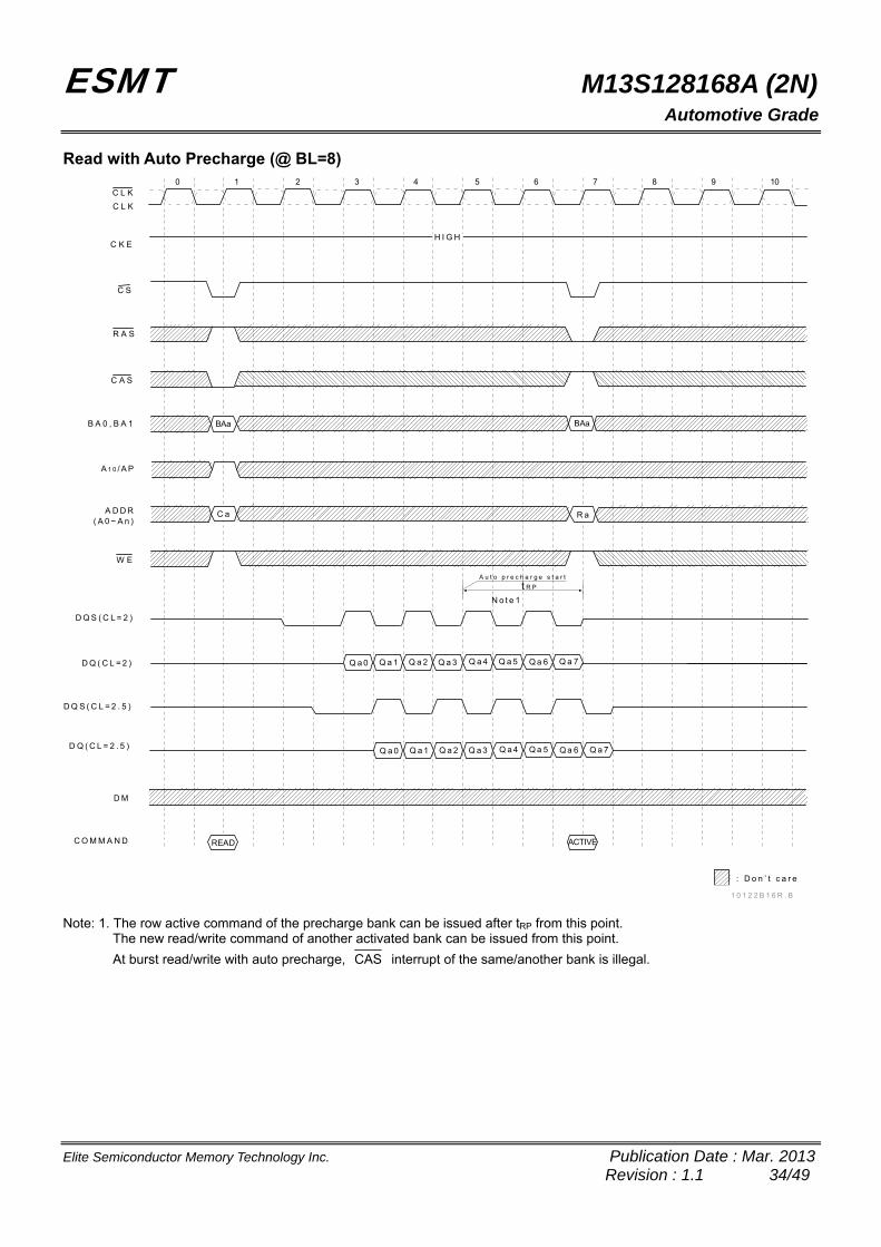
Read with Auto Precharge (@ BL=8)
C K E
C S
R A S
C A S
B A 0 , B A 1
W E
D Q S ( C L = 2 )
D Q ( C L = 2 )
0 1 2 3 4 5 6 7 8 9 10
H I G H
D M
C O M M A N D
A 1 0 / A P
A D D R( A 0 ~ A n )
BAa
Q a 4 Q a 5 Q a 7Q a 6
BAa
t R P
Q a 0 Q a 1 Q a 3Q a 2
ACTIVEREAD
C a
A u t o p r e c h a r g e s t a r t
N o t e 1
C L K
C L K
R a
D Q S ( C L = 2 . 5 )
D Q ( C L = 2 . 5 ) Q a 4 Q a 5 Q a 7Q a 6Q a 0 Q a 1 Q a 3Q a 2
: D o n ’ t c a r e
1 0 1 2 2 B 1 6 R . B Note: 1. The row active command of the precharge bank can be issued after tRP from this point.
The new read/write command of another activated bank can be issued from this point.
At burst read/write with auto precharge, CAS interrupt of the same/another bank is illegal.
ESMT M13S128168A (2N) Automotive Grade
Elite Semiconductor Memory Technology Inc. Publication Date : Mar. 2013 Revision : 1.1 35/49
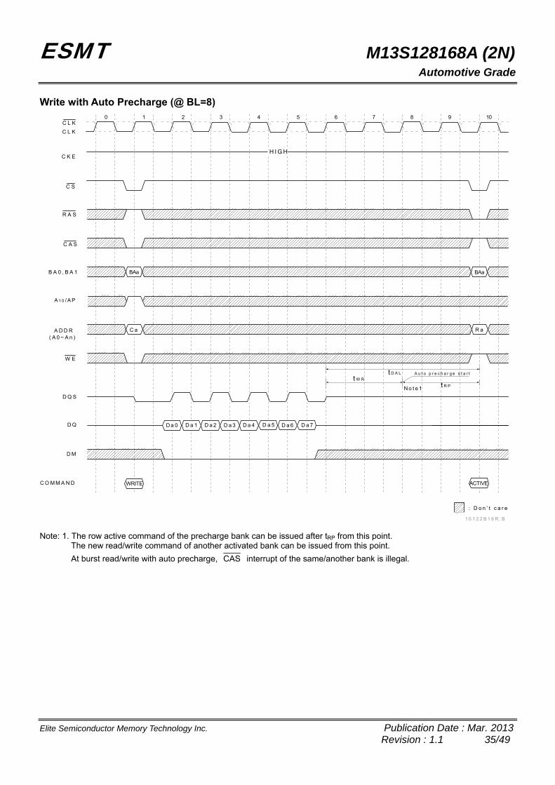
Write with Auto Precharge (@ BL=8)
C K E
C S
R A S
C A S
B A 0 , B A 1
W E
D Q S
D Q
0 1 2 3 4 5 6 7 8 9 10
H I G H
D M
C O M M A N D
A 1 0 / A P
A D D R( A 0 ~ A n )
BAa
D a 4 D a 5 D a 7D a 6
t R P
D a 0 D a 1 D a 3D a 2
ACTIVEWRITE
C a
A u t o p r e c h a r g e s t a r t
N o t e 1
BAa
R a
t W R
C L K
C L K
t D A L
: D o n ’ t c a r e
1 0 1 2 2 B 1 6 R . B Note: 1. The row active command of the precharge bank can be issued after tRP from this point.
The new read/write command of another activated bank can be issued from this point.
At burst read/write with auto precharge, CAS interrupt of the same/another bank is illegal.
ESMT M13S128168A (2N) Automotive Grade
Elite Semiconductor Memory Technology Inc. Publication Date : Mar. 2013 Revision : 1.1 36/49
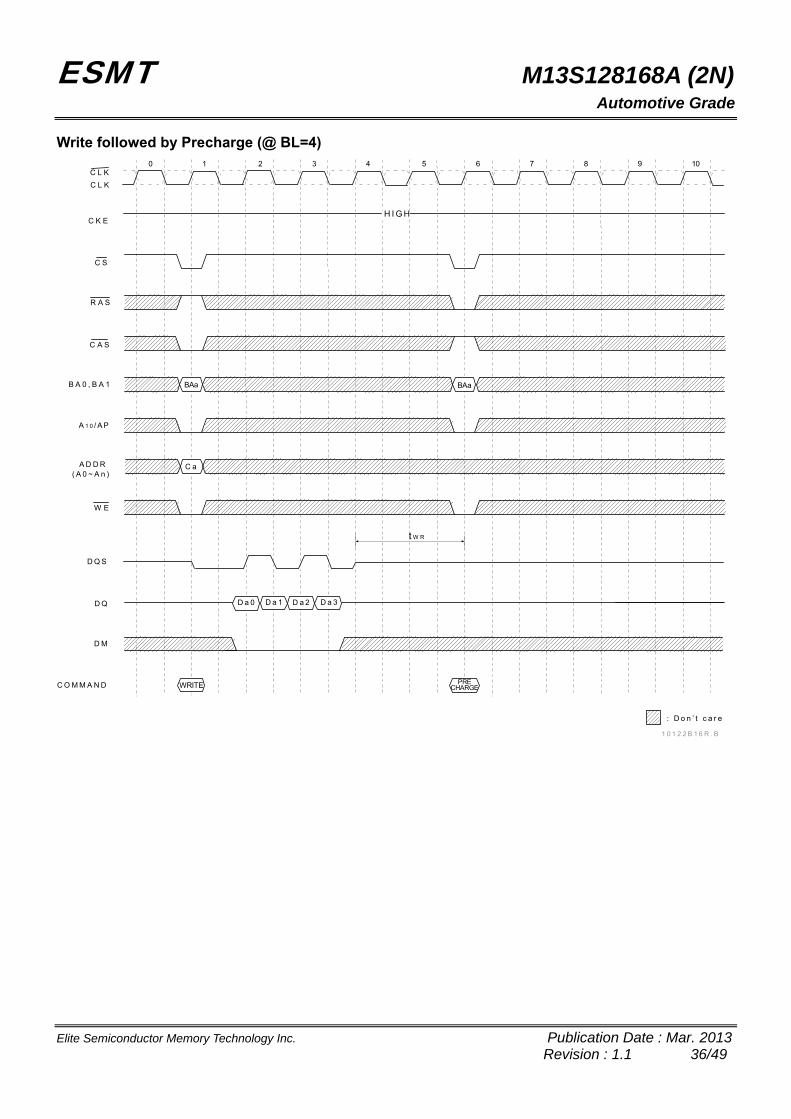
Write followed by Precharge (@ BL=4)
C K E
C S
R A S
C A S
B A 0 , B A 1
W E
D Q S
D Q
0 1 2 3 4 5 6 7 8 9 10
H I G H
D M
C O M M A N D
A 1 0 / A P
A D D R( A 0 ~ A n )
BAa BAa
t W R
D a 0 D a 1 D a 3D a 2
PRECHARGEWRITE
C a
C L K
C L K
: D o n ’ t c a r e
1 0 1 2 2 B 1 6 R . B
ESMT M13S128168A (2N) Automotive Grade
Elite Semiconductor Memory Technology Inc. Publication Date : Mar. 2013 Revision : 1.1 37/49
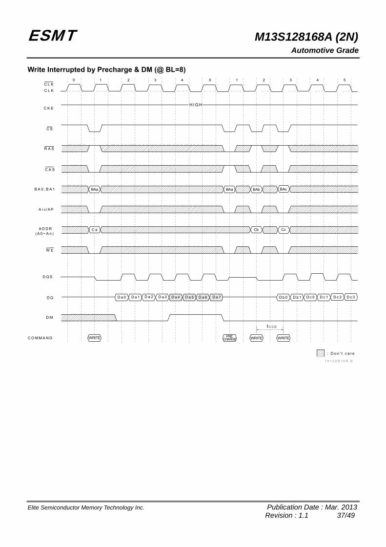
Write Interrupted by Precharge & DM (@ BL=8)
C K E
C S
R A S
C A S
B A 0 , B A 1
W E
D Q S
D Q
0 1 2 3 4 0 1 2 3 4 5
H I G H
D M
C O M M A N D
A 1 0 / A P
A D D R( A 0 ~ A n )
BAa BAa
D a 0 D a 1 D a 3D a 2
PRECHARGEWRITE WRITE WRITE
C a
C L K
C L K
BAb BAc
Cb Cc
D b 0 D b 1 D c 1D c 0 D c 3D c 2
t C C D
D a 4 D a 5 D a 7D a 6
: D o n ’ t c a r e
1 0 1 2 2 B 1 6 R . B
ESMT M13S128168A (2N) Automotive Grade
Elite Semiconductor Memory Technology Inc. Publication Date : Mar. 2013 Revision : 1.1 38/49
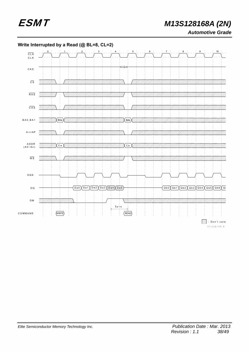
Write Interrupted by a Read (@ BL=8, CL=2)
C K E
C S
R A S
C A S
B A 0 , B A 1
W E
D Q S
D Q
0 1 2 3 4 5 6 7 8 9 10
H I G H
D M
C O M M A N D
BAa
t W T R
D a 0 D a 1 D a 3D a 2
WRITE READ
C a
C L K
C L K
BAb
C b
D a 5D a 4 Q b 1 Q b 3Q b 2 Q b 4 Q b 5
A 1 0 / A P
A D D R( A 0 ~ A n )
Q b 6Q b 0 Q b 6
: D o n ’ t c a r e
1 0 1 2 2 B 1 6 R . B
ESMT M13S128168A (2N) Automotive Grade
Elite Semiconductor Memory Technology Inc. Publication Date : Mar. 2013 Revision : 1.1 39/49
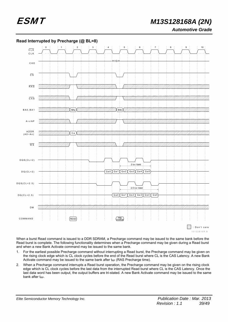
Read Interrupted by Precharge (@ BL=8)
C K E
C S
R A S
C A S
B A 0 , B A 1
W E
D Q S ( C L = 2 )
D Q ( C L = 2 )
0 1 2 3 4 5 6 7 8 9 10
H I G H
C O M M A N D
A 1 0 / A P
A D D R( A 0 ~ A n )
BAa
Q a 0 Q a 1
READ
BAb
C a
PRECHARGE
C L K
C L K
Q a 2 Q a 3 Q a 4 Q a 5
D M
2 tCK Valid
D Q S ( C L = 2 . 5 )
D Q ( C L = 2 . 5 ) Q a 0 Q a 1 Q a 2 Q a 3 Q a 4 Q a 5
2.5 tCK Valid
: D o n ’ t c a r e
1 0 1 2 2 B 1 6 R . B When a burst Read command is issued to a DDR SDRAM, a Precharge command may be issued to the same bank before the Read burst is complete. The following functionality determines when a Precharge command may be given during a Read burst and when a new Bank Activate command may be issued to the same bank.
1. For the earliest possible Precharge command without interrupting a Read burst, the Precharge command may be given on the rising clock edge which is CL clock cycles before the end of the Read burst where CL is the CAS Latency. A new Bank Activate command may be issued to the same bank after tRP (RAS Precharge time).
2. When a Precharge command interrupts a Read burst operation, the Precharge command may be given on the rising clock edge which is CL clock cycles before the last data from the interrupted Read burst where CL is the CAS Latency. Once the last data word has been output, the output buffers are tri-stated. A new Bank Activate command may be issued to the same bank after tRP.
ESMT M13S128168A (2N) Automotive Grade
Elite Semiconductor Memory Technology Inc. Publication Date : Mar. 2013 Revision : 1.1 40/49
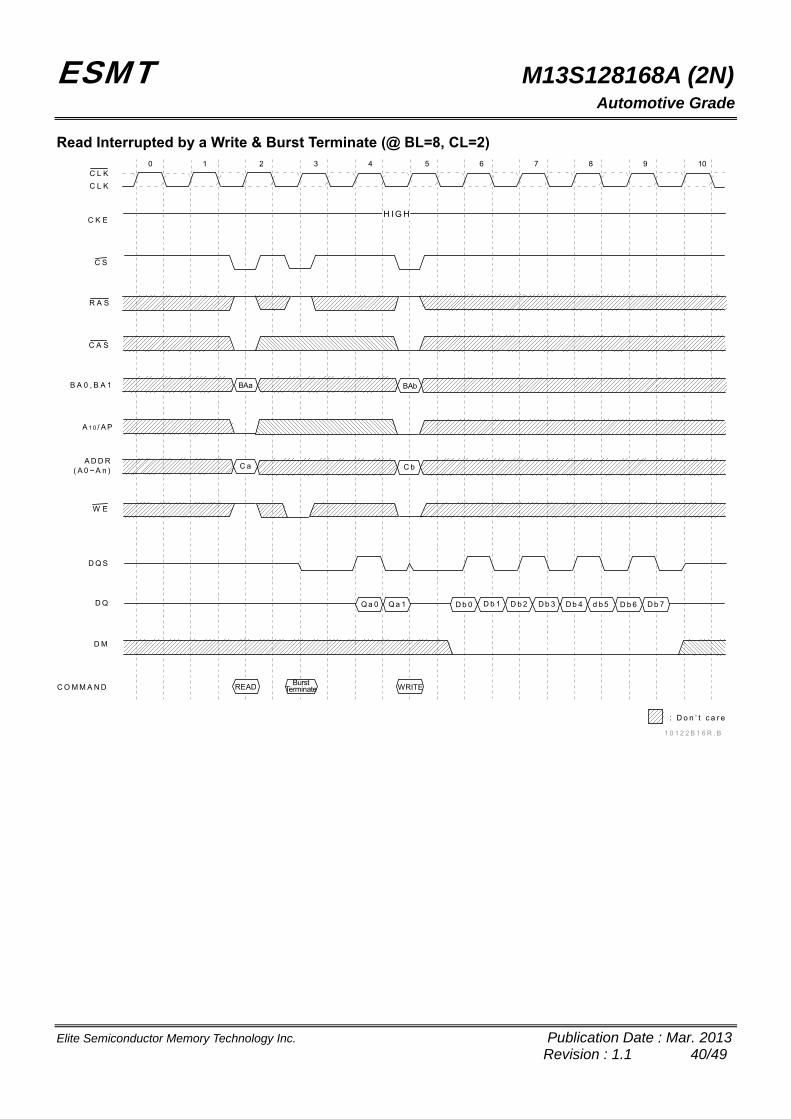
Read Interrupted by a Write & Burst Terminate (@ BL=8, CL=2)
C K E
C S
R A S
C A S
B A 0 , B A 1
W E
D Q S
D Q
0 1 2 3 4 5 6 7 8 9 10
H I G H
D M
C O M M A N D
BAa
Q a 0 Q a 1
READ
D b 0 d b 5D b 1 D b 4D b 3D b 2 D b 6
BAb
C b
BurstTerminate WRITE
D b 7
C L K
C L K
A 1 0 / A P
A D D R( A 0 ~ A n )
C a
: D o n ’ t c a r e
1 0 1 2 2 B 1 6 R . B
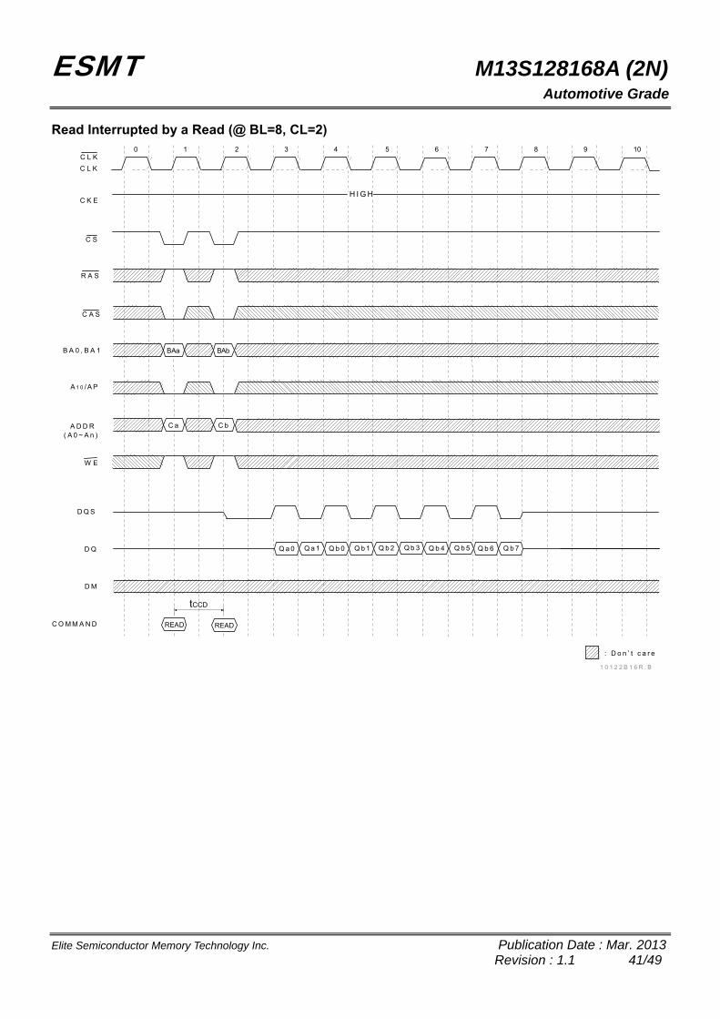
ESMT M13S128168A (2N) Automotive Grade
Elite Semiconductor Memory Technology Inc. Publication Date : Mar. 2013 Revision : 1.1 41/49
Read Interrupted by a Read (@ BL=8, CL=2)
C K E
C S
R A S
C A S
B A 0 , B A 1
W E
D Q S
D Q
0 1 2 3 4 5 6 7 8 9 10
H I G H
D M
C O M M A N D
A 1 0 / A P
A D D R( A 0 ~ A n )
BAa
Q b 2 Q b 3 Q b 5Q b 4Q a 0 Q a 1 Q b 1Q b 0
READ
C a
C L K
C L K
BAb
C b
Q b 7Q b 6
READ
tCCD
: D o n ’ t c a r e
1 0 1 2 2 B 1 6 R . B
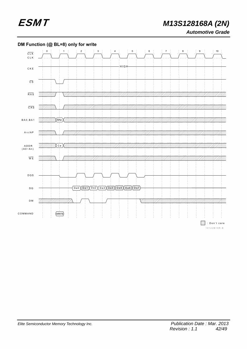
ESMT M13S128168A (2N) Automotive Grade
Elite Semiconductor Memory Technology Inc. Publication Date : Mar. 2013 Revision : 1.1 42/49
DM Function (@ BL=8) only for write
C K E
C S
R A S
C A S
B A 0 , B A 1
W E
D Q S
D Q
0 1 2 3 4 5 6 7 8 9 10
H I G H
D M
C O M M A N D
A 1 0 / A P
A D D R( A 0 ~ A n )
BAa
D a 4 D a 5 D a 7D a 6D a 0 D a 1 D a 3D a 2
WRITE
C a
C L K
C L K
: D o n ’ t c a r e
1 0 1 2 2 B 1 6 R . B
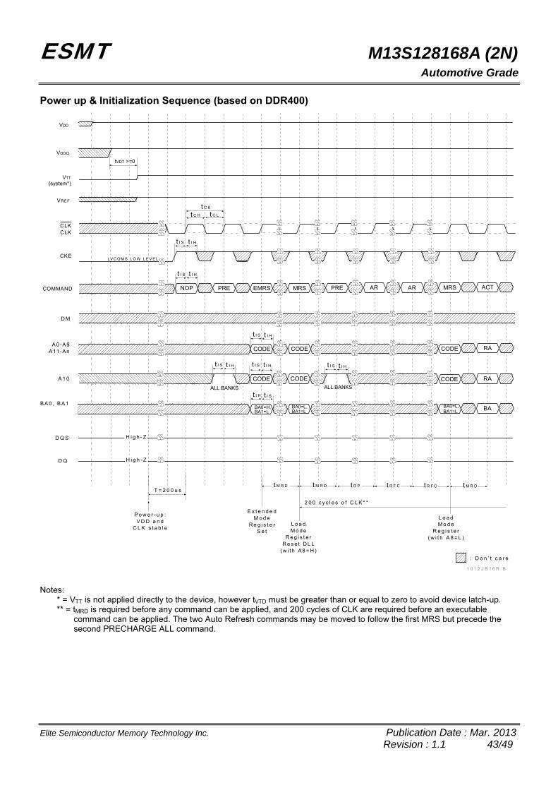
ESMT M13S128168A (2N) Automotive Grade
Elite Semiconductor Memory Technology Inc. Publication Date : Mar. 2013 Revision : 1.1 43/49
Power up & Initialization Sequence (based on DDR400)
VDDQ
VREF
A 0 -A9A11 -An
P o w e r - u p :V D D a n d
C L K s t a b l e
B A 0 , B A 1
E x t e n d e dM o d e
R e g i s t e rS e t
COMMAND
D M
D Q S
t M R D t M R D
2 0 0 c y c l e s o f C L K * *
L o a dM o d e
R e g i s t e rR e s e t D L L
( w i t h A 8 = H )
L o a dM o d e
R e g i s t e r( w i t h A 8 = L )
VDD
A 1 0
T = 2 0 0 u s
VTT
(system*)
tVDT >=0
CLKCLK
CKE
NOP
t C H t C L
t C K
t I S t I H
PRE EMRS MRS PRE AR AR MRS ACT
t I Ht I S
CODE
t I Ht I S
LV C O M S L O W L E V E L
CODE CODE RA
t I Ht I S
CODE CODE CODE RA
BA0=L,BA1=L BA
t I Ht I S
t I H t I S
BA0=L,BA1=L
H i g h - Z
D Q H i g h - Z
t R P t R F C t M R D
ALL BANKS ALL BANKS
t R F C
BA0=H,BA1=L
t I Ht I S
: D o n ’ t c a r e
1 0 1 2 2 B 1 6 R . B Notes:
* = VTT is not applied directly to the device, however tVTD must be greater than or equal to zero to avoid device latch-up. ** = tMRD is required before any command can be applied, and 200 cycles of CLK are required before an executable
command can be applied. The two Auto Refresh commands may be moved to follow the first MRS but precede the second PRECHARGE ALL command.
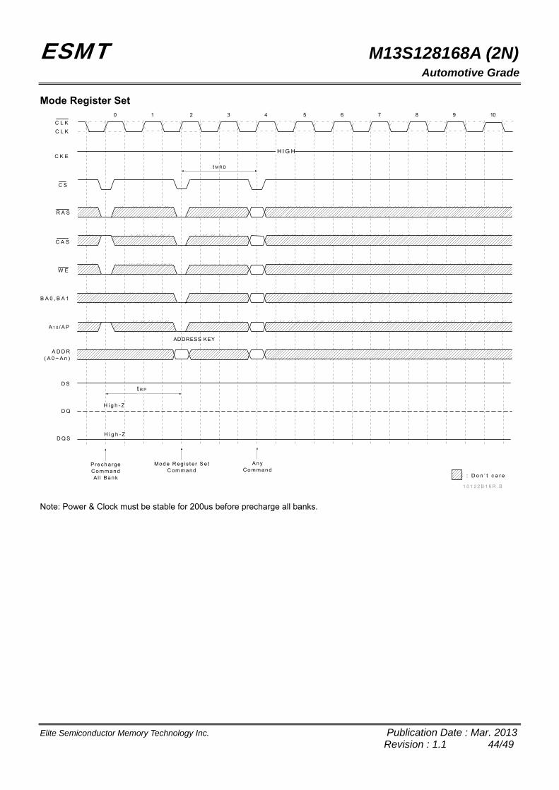
ESMT M13S128168A (2N) Automotive Grade
Elite Semiconductor Memory Technology Inc. Publication Date : Mar. 2013 Revision : 1.1 44/49
Mode Register Set
C K E
C S
R A S
C A S
B A 0 , B A 1
W E
D S
D Q
0 1 2 3 4 5 6 7 8 9 10
H I G H
D Q S
A 1 0 / A P
A D D R( A 0 ~ A n )
t R P
t M R D
C L K
C L K
H i g h - Z
H i g h - Z
Pre ch a rgeComman dAl l Ban k
Mod e R eg is t e r S e tC om mand
AnyComman d
ADDRESS KEY
: D o n ’ t c a r e
1 0 1 2 2 B 1 6 R . B Note: Power & Clock must be stable for 200us before precharge all banks.
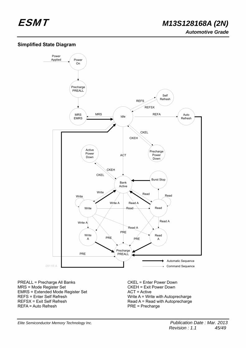
ESMT M13S128168A (2N) Automotive Grade
Elite Semiconductor Memory Technology Inc. Publication Date : Mar. 2013 Revision : 1.1 45/49
Simplified State Diagram
MRSEMRS
SelfRefresh
IdleAuto
Refresh
PrechargePower Down
REFS
REFA
REFSX
MRS
BankActive
ActivePowerDown
CKEH
CKEL
CKEL
ReadWrite
Write Read
WriteA
PrechargePREALL
Write
Read
Read A
Read A
Read A
Write A
Write A
PRE PRE
PRE
Read
CKEH
ACT
Automatic Sequence
Command Sequence
Precharge PREALL
Power On
PowerApplied
Burst Stop
ReadA
PRE
0911R.A PREALL = Precharge All Banks MRS = Mode Register Set EMRS = Extended Mode Register Set REFS = Enter Self Refresh REFSX = Exit Self Refresh REFA = Auto Refresh
CKEL = Enter Power Down CKEH = Exit Power Down ACT = Active Write A = Write with Autoprecharge Read A = Read with Autoprecharge PRE = Precharge
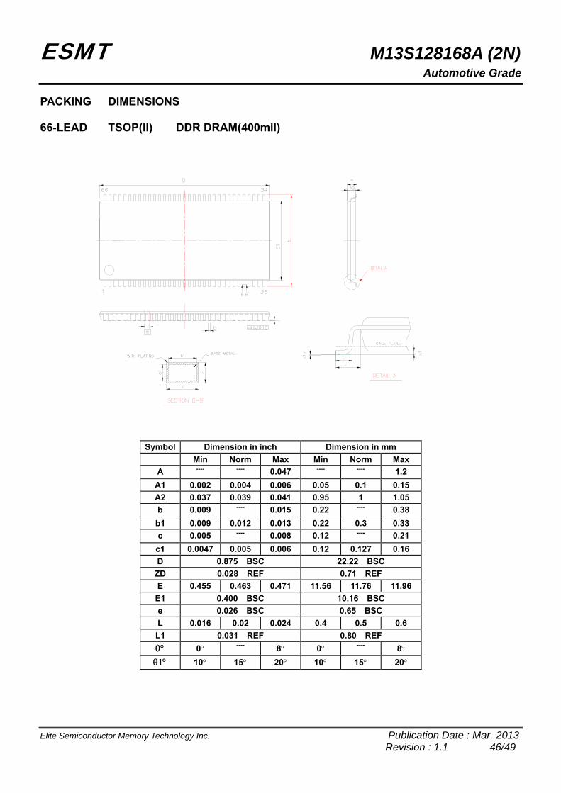
ESMT M13S128168A (2N) Automotive Grade
Elite Semiconductor Memory Technology Inc. Publication Date : Mar. 2013 Revision : 1.1 46/49
PACKING DIMENSIONS 66-LEAD TSOP(II) DDR DRAM(400mil)
Symbol Dimension in inch Dimension in mm
Min Norm Max Min Norm Max
A ---- ---- 0.047 ---- ---- 1.2
A1 0.002 0.004 0.006 0.05 0.1 0.15
A2 0.037 0.039 0.041 0.95 1 1.05
b 0.009 ---- 0.015 0.22 ---- 0.38
b1 0.009 0.012 0.013 0.22 0.3 0.33
c 0.005 ---- 0.008 0.12 ---- 0.21
c1 0.0047 0.005 0.006 0.12 0.127 0.16
D 0.875 BSC 22.22 BSC
ZD 0.028 REF 0.71 REF
E 0.455 0.463 0.471 11.56 11.76 11.96
E1 0.400 BSC 10.16 BSC
e 0.026 BSC 0.65 BSC
L 0.016 0.02 0.024 0.4 0.5 0.6
L1 0.031 REF 0.80 REF
0 ---- 8 0 ---- 8
1 10 15 20 10 15 20
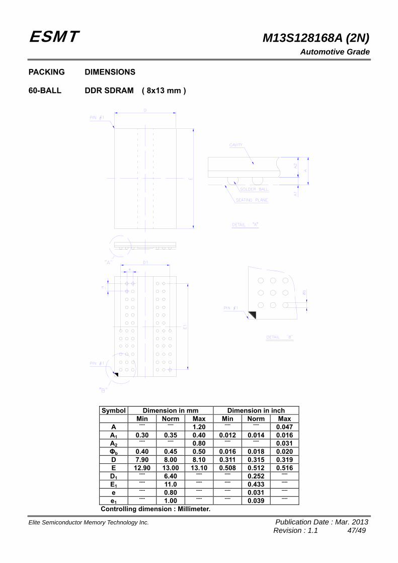
ESMT M13S128168A (2N) Automotive Grade
Elite Semiconductor Memory Technology Inc. Publication Date : Mar. 2013 Revision : 1.1 47/49
PACKING DIMENSIONS 60-BALL DDR SDRAM ( 8x13 mm )
Symbol Dimension in mm Dimension in inch Min Norm Max Min Norm Max
A ---- ---- 1.20 ---- ---- 0.047 A1 0.30 0.35 0.40 0.012 0.014 0.016 A2
---- ---- 0.80 ---- ---- 0.031 Φb 0.40 0.45 0.50 0.016 0.018 0.020 D 7.90 8.00 8.10 0.311 0.315 0.319 E 12.90 13.00 13.10 0.508 0.512 0.516 D1
---- 6.40 ---- ---- 0.252 ----
E1 ---- 11.0 ---- ---- 0.433 ----
e ---- 0.80 ---- ---- 0.031 ----
e1 ---- 1.00 ---- ---- 0.039 ----
Controlling dimension : Millimeter.
ESMT M13S128168A (2N) Automotive Grade
Elite Semiconductor Memory Technology Inc. Publication Date : Mar. 2013 Revision : 1.1 48/49
Revision History
Revision Date Description
1.0 2012.10.29 Original
1.1 2013.03.04 Delete CAS Latency:2
ESMT M13S128168A (2N) Automotive Grade
Elite Semiconductor Memory Technology Inc. Publication Date : Mar. 2013 Revision : 1.1 49/49
Important Notice
All rights reserved. No part of this document may be reproduced or duplicated in any form or by any means without the prior permission of ESMT. The contents contained in this document are believed to be accurate at the time of publication. ESMT assumes no responsibility for any error in this document, and reserves the right to change the products or specification in this document without notice. The information contained herein is presented only as a guide or examples for the application of our products. No responsibility is assumed by ESMT for any infringement of patents, copyrights, or other intellectual property rights of third parties which may result from its use. No license, either express , implied or otherwise, is granted under any patents, copyrights or other intellectual property rights of ESMT or others. Any semiconductor devices may have inherently a certain rate of failure. To minimize risks associated with customer's application, adequate design and operating safeguards against injury, damage, or loss from such failure, should be provided by the customer when making application designs. ESMT's products are not authorized for use in critical applications such as, but not limited to, life support devices or system, where failure or abnormal operation may directly affect human lives or cause physical injury or property damage. If products described here are to be used for such kinds of application, purchaser must do its own quality assurance testing appropriate to such applications.