Embed Size (px)
Citation preview

1984 Harris Bipolar Digital Data Book
Harris Semiconductor Bipolar Digital Products represent state-of-the-art production in density and performance. HARRIS expertise in design and processing offers the user leadership in quality and reliability of products in a wide choice of formats, options, and package types. With continuing research and development and the introduction of new products, Harris will provide its customers with the most advanced technology.
This book describes Harris Semiconductor Digital Products Division's complete line of bipolar memory and programmable logic products, including a complete set of product specifications and data sheets. Also included are sections on reliability, programming, packaging, and custom/semi-custom capabilities.
Please fill out the request for information/action card at the back of this book and return it to us so we may keep you informed of our latest new product developments over the next year.
If you need more information on these and other HARRIS products, please contact the nearest HARRIS sales office listed in the back of this data book.
Harris Semiconductor's products are sold by description only. HARRIS reserves the right to make changes in circuit design, specifications and other information at any time without prior notice. Accordingly, the reader is cautioned to verify that data sheets and other information in this publication are current before placing orders. Information contained in application notes is intended soley for general guidancei use of the information for user's specific application is at user's risk. Reference to products of other manufacturers are solely for convenience of comparison and do nat imply total equivalence of design, performance, or otherwise.
Copyright © Harris Corporation 1984
(All rights reserved I
Printed in USA
$5.00


General Information _
Ordering Information _
Quality and Reliability _
Bipolar Memory III
Harris Programmable Logic (HPL) III
Applications III Hi-Rei _
Custom Integrated Circuits Division _
Packaging •
Harris Total Product Index/Sales Locations •
iii

Table of Contents
PAGE SECTION 1 GENERAL INFORMATION
Bipolar Alpha-Numeric Index 1-2 Bipolar Family Tree 1-3 Bipolar PROM Cross-Reference 1-4 Bipolar HPL Cross-Reference 1-10 PROM Functional Index and Selection Guide 1-12 HPL Functional Index and Selection Guide 1-13 Harris Semiconductor Sector Overview 1-14 Classification of Literature 1-15 I.C. Handling Procedures 1-15 Definition of Terms 1-17
SECTION 2 ORDERING INFORMATION
Bipolar Alpha-Numeric Index 2-2 Product Code 2-3 Dash 8 Program 2-3 JAN Qualified Products 2-3 Special Orders 2-3
SECTION 3 QUALITY AND RELIABILITY
Introduction 3-2 Quality Control 3-2 Quality Assurance 3-4 Reliability 3-4 AQL/AOQ Terminology 3-8 Fusing Mechanism of Nickel-Chromium Fusible Links 3-8 Microscopic Observations of Fuses 3-20 Burn-in Circuit Diagrams 3-25
SECTION 4 BIPOLAR MEMORY
PROM Functional Index and Selection Guide 4-3 Harris Generic Programmable Read Only Memories 4-4 Product Information 4-6 Generic PROM Programming 4-56 Programmer Evaluation 4-59 Data Entry Formats for Harris Custom Programming 4-60
SECTION 5 HARRIS PROGRAMMABLE LOGIC (HPL)
HPL Functional Index and Selection Guide 5-2 Introduction 5-3 Product Information 5-4 HPL Programming Philosophy 5-46 HPL Programmer Evaluation 5-47
iv

PAGE SECTION 6 APPLICATIONS
Applications Index 6-2 HPL Modules 6-3 HPL Application Notes 6-37 Power Strobe Applications Note 6-44
SECTION 7 HI-REL
Introduction to Hi-Rei 7-3 Bipolar Military Cross-Reference 7-4 JAN PROMs 7-5 Bipolar Flows and Screening Procedures 7-6 Military Products Packaging 7-8 Mechanical Information 7-9 Standard Harris Programs 7-10 How to Order 7-10
SECTION 8 CUSTOM INTEGRATED CIRCUITS DIVISION
Introduction 8-2 Bipolar Digital Design Techniques 8-3 Bipolar Digital Technologies 8-5 Specialized Products 8-11 Future of Bipolar Digital IC's 8-13 CICD Sales Office Locations 8-14
SECTION 9 PACKAGING
Package Availability 9-3 Package Dimensions 9-5 Thermal Resistance Measurements 9-8 Bipolar Memory Products General Chip Information 9-10
SECTION 10 SALES LOCATIONS
Sector Alpha-Numeric Product Index 10-2 Harris Sales Locations 10-7
REQUEST FOR INFORMATION/ACTION REPLY CARDS
v


Z ...J!: «f-a:« w::;;; Za: wo t!lu..
Bipolar Alpha-Numeric Index 1-2 '!':
Bipolar Family Tree 1-3
Bipolar PROM Cross-Reference 1-4
Bipolar HPL Cross-Reference 1-10
PROM Functional Index and Selection Guide 1-12
HPL Functional Index and Selection Guide 1-13
Harris Semiconductor Sector Overview 1-14
Classification of Literature 1-15
I.C. Handling Procedures 1-15
Definition of Terms 1-17
1-1

PART NUMBER
HD-6600 HM-0104 HM-0168 HM-0186 HM-0198 HM-0410 HM-7602/03 HM-7610/11 HM-7610A/11A HM-7610B/11B HM-7620/21 HM-7620A/21A HM-7620B/21 B HM-7640/41 HM-7640A/41A HM-7649 HM-7649A HM-7642/43 HM-7642A/43A HM-7642B/43B HM-7681 HM-7681A HM-7685 HM-7685A HM-76161 HM-76161A HM-76161B HM-76165 HM-76321 HM-76641 HM-76641A JAN-0512 HPL-77061 HPL-77153/82S153 HPL-77209/16L8 HPL-77210/16R4 HPL-77211/16R6 HPL-77212/16R8 HPL-77215/16H8 HPL-77216/16P8 HPL--77317/16LD8 HPL-77318/16HD8 HPL-77319/16LE8 HPL-77320/16HE8 M3851 0/20701 BEB M3851 0/20702B E B M3851 0/201 01 BJ B M38510/20301 BEB M3851O/20302BEB M3851 0/2040 1 BE B M38510/20402BE B M3851 0/2080 1 BJ B M3851 0/20802 BJ B M3851 0/20601 BVg M3851 0/20602BV B M38510/20904BJB M38510/20902BVB M38510/21002BJB
Bipolar Alpha-Numeric Index
Quad Power Strobe 10 x 4 Diode Matrix 6 x 8 Diode Matrix 8 x 6 Diode Matrix 9 x 8 Diode Matrix 4 x 10 Diode Matrix 32 x 8 Bit Generic PROM 256 x 4 Bit Generic PROM
DESCRIPTION
256 x 4 Bit High Speed Generic PROM 256 x 4 Bit Very High Speed Generic PROM 512 x 4 Bit Generic PROM 512 x 4 Bit High Speed Generic PROM 512 x 4 Bit Very High Speed Generic PROM 512 x 8 Bit Generic PROM (24-Pin) 512 x 8 Bit High Speed Generic PROM (24-Pin) 512 x 8 Bit Generic PROM (20-Pin) 512 x 8 Bit High Speed Generic PROM (20-Pin) 1024 x 4 Bit Generic PROM 1024 x 4 Bit High Speed Generic PROM 1024 x 4 Bit Very High Speed Generic PROM 1024 x 8 B it Generic PROM 1024 x 8 Bit High Speed Generic PROM 2048 x 4 Bit Generic PROM 2048 x 4 Bit High Speed Generic PROM 2048 x 8 Bit Generic PROM 2048 x 8 Bit High Speed Generic PROM 2048 x 8 Bit Very High Speed Generic PROM 4096 x 4 Bit Generic PROM 4096 x 8 Bit Generic PROM 8192x 8 Bit Generic PROM 8192 x 8 Bit High Speed Generic PROM 64 x 8 HPROM 24-Pin Field Programmable Address Decoder 20-Pin Field Programmable Logic Array 20-Pin Field Programmable Array Logic (Active Low Outputs) 20-Pin Field Programmable Array Logic (Four Registered Outputs) 20-Pin Field Programmable Array Logic (Six Registered Outputs) 20-Pin Field Programmable Array Logic (Eight Registered Outputs) 20-Pin Field Programmable Array Logic (Active High Outputs) 20-Pin Field Programmable Array Logic (Programmable Output Polarity) 20-Pin Field Programmable Array Logic (Active Low Dedicated Outputs) 20-Pin Field Programmable Array Logic (Active High Dedicated Outputs) 20-Pin Field Programmable Array Logic (Enhanced HPL--77317/16LD8) 20-Pin Field Programmable Array Logic (Enhanced HPL-77318/16HD8) 32 x 8 Open Collector OPL1 PROM 32 x 8 Three State OPL1 PROM 64 x 8 Open Collector QPL1 PROM 256 x 4 Open Collector QPL1 PROM 256 x 4 Three State OPL1 PROM 512 x 4 Open Collector OPL1 PROM 512 x 4 Three State QPL1 PROM 512 x 8 Open Collector OPL1 PROM 512 x 8 Three State OPL1 PROM 1024 x 4 Open Collector OPL 1 PROM 1024 x 4 Three State OPL 1 PROM 1024 x 8 Three State QPL1 PROM 2048 x 4 Three State QPL1 PROM 2048 x 8 Three State QPL1 PROM
1-2
PAGE
4-6 4-9 4-9 4-9 4-9 4-9 4-13 4-16 4-16 4-16 4-19 4-19 4-19 4-22 4-22 4-28 4--28 4-25 4-25 4-25 4-31 4-31 4-34 4-34 4-37 4-37 4-40 4-41 4-44 4-47 4-50 4-51 5-4 5-6 5-15 5-42 5-42 5-42 5-15 5-15 5-24 5-24 5-33 5-33 7-5 7-5 7-5 7-5 7--5 7-5 7-5 7--5 7-5 7-5 7-5 7-5 7--5 7--5

Bipolar Family Tree
HPL-77209/16L8 HPL-77215/16H8
HPL-77317/16LD8 HPL-77318/16HD8
HPL-77319/16LE8 HPL-77320/16HE8
OC - Open Collector Outputs
TS - Three State Outputs
1-3
Z
...J~ <X:fa: <X: w::;: Za: wo C!Ju...
Z

Bipolar PROM Cross-Reference
HARRIS FAIRCHILD HARRIS AMDPART ORGANIZATION PIN-FOR-PIN PART ORGANIZATION PIN-FOR-PIN NUMBER AND OUTPUT REPLACEMENT NUMBER AND OUTPUT REPLACEMENT
27S18 32 X 8 OC HM-7602 93417 256 X 4 OC HM-7610 27S18A HM-7610A
HM-7610B 27S19 32 X 8 TS HM-7603 27S19A 93427 256 X 4 TS HM-7611
HM-7611A 27S20 256 X 4 OC HM-7610 HM-7611B 27S20A HM-7610A
HM-7610B 93436 512X40C HM-7620 HM-7620A
27S21 256 X 4 TS HM-7611 HM-7620B 27S21A HM-7611A
HM-7611 B 93446 512X4TS HM-7621 HM-7621A
27S12 512X40C HM-7620 HM-7621 B 27S12A HM-7620A
HM-7620B 93438 512X80C HM-7640 HM-7640A
27S13 512 X 4 TS HM-7621 27S13A HM-7621A 93448 512X8TS HM-7641
HM-7621 B HM-7641A
27S30 512X80C HM-7640 93452 1024 X 4 OC HM-7642 27S30A HM-7640A HM-7642A
HM-7642B 27S31 512X8TS HM-7641 27S31A HM-7641A 93453 1024 X 4 TS HM-7643
HM-7643A 27S29 512 X 8 TS HM-7649 HM-7643B 27S29A HM-7649A
93451 1024 X 8 TS HM-7681 27S32 1024X40C HM-7642 93Z451 HM-7681A 27S32A HM-7642A
HM-7642B 93Z511 2048 X 8 TS HM-76161 HM-76161A
27S33 1024 X 4 TS HM--7643 HM-76161B 27S33A HM-7643A
HM-7643B 93515 4096 X 4 TS HM-76165
27S181 1024 X 8 TS HM-7681 93Z565 8192 X 8 TS HM-76641 27S181A HM-7681A 93Z565A HM-76641A
27S185 2048 X 4 TS HM-7685 27S185A HM-7685A
27S191 2048 X 8 TS HM-76161 27S191A HM-76161A
HM-76161B
27S41 4096 X 4 TS HM-76165 27S41A
27S43 4096 X 8 TS HM-76321 27S43A
1-4

Bipolar PROM Cross-Reference (Continued)
FUJITSU HARRIS INTEL HARRIS PART ORGANIZATION PIN-FOR-PIN PART ORGANIZATION PIN-FOR-PIN
NUMBER AND OUTPUT REPLACEMENT NUMBER AND OUTPUT REPLACEMENT
MB7124E 512 X 8 TS HM-7649 3601 256 X 4 OC HM-7610 MB7124H HM-7649A 3601-1 HM-7610A
HM-7610B MB7121 E 1024 X 4 OC HM-7642 MB7121H HM-7642A 3621 256 X 4 TS HM-7611
HM-7642B 3621-1 HM-7611A HM-7611B
MB7122E 1024 X 4 TS HM-7643 MB7122H HM-7643A 3602 512 X 4 OC HM-7620
HM-7643B 3602A HM-7620A 3602A-2 HM-7620B
MB7132E 1024 X 8 TS HM-7681 MB7132H HM-7681A 3622 512 X 4 TS HM-7621
3622A HM-7621A MB7128E 2048 X 4 TS HM-7685 3622A-2 HM-7621 B MB7128H HM-7685A
3604-4 512X80C HM-7640 MB7138E 2048 X 8 TS HM-76161 3604 HM-7640A MB7138H HM-76161A 3604A
HM-761618 3604A-2
MB7134E 4096 X 4 TS HM-76165 3624-4 512X8TS HM-7641 MB7134H 3624 HM-7641A
3624A MB7142E 4096 X 8 TS HM-76321 3624A-2 MB7142H
3605 1024X40C HM-7642 MB7144E 8192 X 8 TS HM-76641 3605-2 HM-7642A MB7144H HM-76641A HM-7642B
3625 1024 X 4 TS HM-7643
HITACHI HARRIS PART ORGANIZATION PIN-FOR-PIN
3625-2 HM-7643A HM-7643B
NUMBER AND OUTPUT REPLACEMENT 3628A-4 1024 X 8 TS HM-7681
HN25089 1024 X 8 TS HM-7681 HN25089S HM-7681A
3628A-3 HM-7681A 3628A-1
HN25085 2048 X 4 TS HM-7685 HN25085S HM-7685A
3636B 2048 X 8 TS HM-76161 3636B-2 HM-76161A 3636B-1 HM-76161B
HN25169 2048 X 8 TS HM-76161 HN25169S HM-76161A
HM-76161B
3632 4096 X 8 TS HM-76321 3632-1
1-5

Bipolar PROM Cross-Reference (Continued)
HARRIS INTERSIL HARRIS NEC PART ORGANIZATION PIN-FOR-PIN PART ORGANIZATION PIN-FOR-PIN NUMBER AND OUTPUT REPLACEMENT NUMBER AND OUTPUT REPLACEMENT
IlPB403 256 X 4 OC HM-7610 IM5600 32 X 8 OC HM-7602 HM-7610A HM-7610B IM5610 32 X 8 TS HM-7603
IlPB423 256 X 4 TS HM-7611 IM5603 256 X 4 OC HM-7610 HM-7611A HM-7610A HM-7611B HM-7610B
IlPB405 512X80C HM-7640 IM5623 256 X 4 TS HM-7611 HM-7640A HM-7611A
HM-7611B IlPB425 512X8TS HM-7641
HM-7641A IM5604 512X40C HM-7620 HM-7620A
IlPB406 1024 X 4 OC HM-7642 HM-7620B HM-7642A HM-7642B IM5624 512X4TS HM-7621
HM-7621A IlPB426 1024 X 4 TS HM-7643 HM-7621B
HM-7643A HM-7643B IM5605 512X80C HM-7640
HM-7640A IlPB428 1024 X 8 TS HM-7681
HM-7681A IM5625 512X8TS HM-7641 HM-7641A
IlPB429 2048 X 8 TS HM-76161 HM-761R1A HM-76161B
1-6

Bipolar PROM Cross-Reference (Continued)
HARRIS MOTOROLA MMI PART ORGANIZATION PIN-FOR-PIN PART ORGANIZATION NUMBER AND OUTPUT REPLACEMENT NUMBER AND OUTPUT
6330-1 32 X 8 OC HM-7602 MCM7620 512X40C
6331-1 32 X 8 T5 HM-7603
6300-1 256 X 4 OC HM-7610 MCM7621 512X4T5 635140 HM-7610A
HM-7610B
6301-1 256 X 4 T5 HM-7611 MCM7640 512X80C 635141 HM-7611A
HM-7611B MCM7641 512 X 8 T5
6305-1 512X40C HM-7620 635240 HM-7620A
HM-7620B MCM7642 1024 X 4 OC
6306--1 512 X 4 T5 HM-7621 635241 HM-7621A
HM-7621 B MCM7643 1024 X 4 T5
6340-1 512 X 80C HM-7640 6340-2 HM-7640A
MCM7681 1024 X 8 T5 6341-1 512 X 8 T5 HM-7641 6341-2 HM-7641A
MCM7685 2048 X 4 T5 6349-1 512X8T5 HM-7649 6349-2 HM-7649A
MCM76161 2048 X 8 T5 6352-1 1024 X 4 OC HM-7642
HM-7642A HM-7642B
6353-1 1024 X 4 T5 HM-7643 HM-7643A HM-7643B
6381-1 1024 X 8 T5 HM-7681 6381-2 HM-7681A
6389-1 2048 X 4 T5 HM-7685 6389-2 HM-7685A
6351681 2048 X 8 T5 HM-76161 HM-76161A HM-76161B
6351641 4096 X 4 T5 HM-76165
6353281 4096 X 8 T5 HM-76321
1-7
HARRIS PIN-FOR-PIN
REPLACEMENT
HM-7620 HM-7620A HM-7620B
HM-7621 HM-7621A HM-7621B
HM-7640 HM-7640A
HM-7641 HM-7641A
HM-7642 HM-7642A HM-7642B
HM-7643 HM-7643A HM-7643B
HM-7681 HM-7681A
HM-7685 HM-7685A
HM-76161 HM-76161A HM-76161B
Z
...J~ «Ic::« UJ:;: Zc:: UJo <!>u.
Z

Bipolar PROM Cross-R~ference (Continued)
NATIONAL HARRIS RAYTHEON HARRIS PART ORGANIZATION PIN-FOR-PIN PART ORGANIZATION PIN-FOR-PIN
NUMBER AND OUTPUT REPLACEMENT NUMBER AND OUTPUT REPLACEMENT
74S188 32 X 8 OC HM-7602 29660 256 X 4 OC HM-7610 87S188 HM-7610A
HM-7610B 74S288 32 X 8 TS HM-7603 87S288 29661 256 X 4 TS HM-7611
HM-7611A 74S387 256 X 4 OC HM-7610 HM-7611B
HM-7610A HM-7610B 29610 512X40C HM-7620
HM-7620A 74S287 256 X 4 TS HM-7611 HM-7620B
HM-7611A HM-7611B 29611 512 X 4 TS HM-7621
HM-7621A 74S570 512X40C HM-7620 HM-7621B 74S570A HM-7620A
HM-7620B 29624 512X80C HM-7640 HM-7640A
74S571 512 X 4 TS HM-7621 74S571A HM-7621A 29625 512X8TS HM-7641
HM-7621B HM-7641A
74S475 512X80C HM-7640 29621 512X8TS HM-7649 74S475A HM-7640A 29621A HM-7649A
74S474 512 X 8 TS HM-7641 29635 1024 X 8 TS HM-7681 74S474A HM-7641A HM-7681A 74S474B
29651 2048 X 4 TS HM-7685 74S472 512X8TS HM-7649 29651A HM-7685A 74S472A HM-7649A 74S472B 29681 2048 X 8 TS HM-76161
29681A HM-76161A 74S572 1024 X 4 OC HM-7642 HM-76161B 74S572A HM-7642A
HM-7642B 29641 4096 X 4 TS HM-76165 29641A
74S573 1024 X 4 TS HM-7643 74S573A HM-7643A 29671 4096 X 8 TS HM-76321 74S573B HM-7643B 29671A
87S181 1024 X 8 TS HM-7681 87S181A HM-7681A
87S185 2048 X 4 TS HM-7685 87S185A HM-7685A
87S191 2048 X 8 TS HM-76161 87S191A HM-76161A
HM-76161B
1-8

SIGNETICS PART
NUMBER
82523
825123
825126
825129
825130
825131
825140
825141
825147 82H5147
825136
825137 825137A 825137B
825181 825181A 825181B
825185 825185A 825185B
825191 82H5191
825195 82H5195
825321
Bipolar PROM Cross-Reference (Continued)
HARRIS ORGANIZATION PIN-FOR-PIN T.I. PART ORGANIZATION
AND OUTPUT REPLACEMENT NUMBER AND OUTPUT
32 X80C HM-7602 5N745188 32 X 8 OC TBP185A030
32 X 8 T5 HM-7603 5N745288 32 X 8 T5
256 X 4 OC HM-7610 T8P185030 HM-7610A HM-7610B 5N745387 256 X 4 OC
TBP145A10 256X4T5 HM-7611 TBP245A10
HM-7611A HM-7611B 5N745287 256X4T5
TBP14510 512X40C HM-7620 TBP24510
HM-7620A HM-7620B 5N745475 512X80C
T8P185A46 512X4T5 HM-7621 TBP285A46
HM-7621A HM-7621B 5N745A74 512 X 8 T5
TBP18S46 512X80C HM-7640 TBP28S46
HM-7640A 5N74S472 512 X 8 T5
512X8T5 HM-7641 TBP18S42 HM-7641A TBP28S42
512X8T5 HM-7649 5N745477 1024 X 4 OC HM-7649A TBP245A41
1024X40C HM-7642 HM-7642A 5N745476 1024 X 4 T5 HM-7642B TBP24541
1024X4T5 HM-7643 HM-7643A 5N745478 1024 X 8 T5 HM-7643B T8P28586
1024 X8 T5 HM-7681 5N74S454 2048 X 4 T5 HM-7681A TBP24581
TBP285166 2048 X 8 T5 2048 X 4 T5 HM-7685
HM-7685A
2048 X 8 T5 HM-76161 HM-76161A HM-76161B
4096 X 4 T5 HM-76165
4096 X 8 T5 HM-76321
1-9
HARRIS PIN-FOR-PIN
REPLACEMENT
HM-7602
HM-7603
HM-7610 HM-7610A HM-7610B
HM-7611 HM-7611A HM-7611B
HM-7640 HM-7640A
HM-7641 HM-7641A
HM-7649 HM-7649A
HM-7642 HM-7642A HM-7642B
HM-7643 HM-7643A HM-7643B
HM-7681 HM-7681A
HM-7685 HM-7685A
HM-76161 HM-76161A HM-76161B
Z .... S! «fcc« w:e: Zcc wo Clu..
~

Bipolar HPL Cross-Reference
AMD HARRIS PART ARRAY MATRIX PART
NUMBER INPUTS ARCHITECTURE LOGIC NUMBER
AmPAL16L8 Ten Dedicated Programmable AND-Fixed OR Eight 7-Wide AND-DR-INVERT HPL-77209 Six Bidirectional (Active Low Outputs) /16L8
AmPAL16H8 Ten Dedicated Programmable AND-Fixed OR Eight 7-Wide AND-OR HPL-77215 Six Bidirectional (Active High Outputs) /16H8
AmPAL16LD8 Ten Dedicated Programmable AND-Fixed OR Eight 8-Wide AND-DR-INVERT HPL-77317 Six Feedback (Active Low Outputs) /16LD8
AmPAL16HD8 Ten Dedicated Programmable AND-Fixed OR Eight 8-Wide AND-OR HPL-77318 Six Feedback (Active High Outputs) /16HD8
Eight Dedicated Programmable AND-Fixed OR Four 8-Wide AND-OR HPL-77210 AmPAL16R4 Four Feedback Four 7-Wide AND-DR-INVERT /16R4
Four Bidirectional
Eight Dedicated Programmable AND-Fixed OR Six 8-Wide AND-OR HPL-77211 AmPAL16R6 Six Feedback Two 7-Wide AND-DR-INVERT /16R6
Two Bidirectional
AmPAL16R8 Eight Dedicated Programmable AND-Fixed OR Eight 8-Wide AND-OR HPL-77212 Eight Feedback /16R8
MMI HARRIS PART ARRAY MATRIX PART
NUMBER INPUTS ARCHITECTURE LOGIC NUMBER
PAL16L8 Ten Dedicated Programmable AND-Fixed OR Eight 7-Wide AND-OR-INVERT HPL-77209 Six Bidirectional (Active Low Outputs) /16L8
PAL16H8 Ten Dedicated Programmable AND-Fixed OR Eight 7-Wide AND-OR HPL-77215 Six Bidirectional (Active High Outputs) /16H8
Eight Dedicated Programmable AND--Fixed OR Four 8-Wide AND-OR HPL-77210 PAL16R4 Four Feedback Four 7-Wide AND-DR-INVERT /16R4
Four Bidirectional
Eight Dedicated Programmable AND-Fixed OR Six 8-Wide AND-OR HPL-77211 PAL16R6 Six Feedback Two 7-Wide AND-DR-INVERT /16R6
Two Bidirectional
PAL16R8 Eight Dedicated Programmable AND-Fixed OR Eight 8-Wide AND-OR HPL-77212 Eight Feedback /16R8
1-10

Bipolar HPL Cross- Reference (Continued)
NATIONAL PART ARRAY MATRIX
NUMBER INPUTS ARCHITECTURE LOGIC
PAL16L8 Ten Dedicated Programmable AND-Fixed OR Eight 7-Wide AND-DR-INVERT Six Bidirectional (Active Low Outputs)
Eight Dedicated Programmable AND-Fixed OR Four 8-Wide AND-OR PAL16R4 Four Feedback Four 7-Wide AND-DR-INVERT
Four Bidirectional
Eight Dedicated Programmable AND-Fixed OR Six 8-Wide AND-OR PAL16R6 Six Feedback Two 7-Wide AND-DR-INVERT
Two Bidirectional
PAL16R8 Eight Dedicated Programmable AND-Fixed OR Eight 8-Wide AND-OR Eight Feedback
T.I. PART ARRAY MATRIX
NUMBER INPUTS ARCHITECTURE LOGIC
FP74ALS16L8 Ten Ded i cated Programmable AND··Fixed OR Eight 7-Wide AND-DR-INVERT Six Bidirectional (Active Low Outputs)
Eight Dedicated Programmable AND-Fixed OR Four 8-Wide AND-OR FP74ALS16R4 Four Feedback Four 7-Wide AND-OR-INVERT
Four Bidirectional
Eight Dedicated Programmable AND-Fixed OR Six 8-Wide AND-OR FP74ALS16R6 Six Feedback Two 7-Wide AND-OR-INVERT
Two Bidirectional
FP74ALS16R8 Eight Dedicated Programmable AND-Fixed OR Eight 8-Wide AND-OR Eight Feedback
SIGNETICS PART ARRAY MATRIX
NUMBER INPUTS ARCHITECTURE LOGIC
82S153 Eight Dedicated Programmable AND-Prog. OR Ten 32-Wide AND-OR Ten Bidirectional (Programmable Output Polarity)
1-11
HARRIS PART
NUMBER
HPL-77209 /16L8
HPL-77210 /16R4
HPL-77211 /16R6
HPL-77212 /16R8
HARRIS PART
NUMBER
HPL-77209 /16L8
HPL-77210 /16R4
HPL-77211 /16R6
HPL-77212 /16R8
HARRIS PART
NUMBER
HPL-77153 /82S153
Z
...J~ «fa::« UJ2 Za:: UJo <!lu.
Z

PROM Functional Index and Selection Guide
TAA COMMERCIAL! (1)
PART ORGANI- NUMBER MILITARY ICC PACKAGE NUMBER ZATION OUTPUT OF PINS (n,MAX) (mAMAX) AVAILABILITY PAGE
--
HM-7602 32 x 8 OC 16 00/60 130 D, P 4-13
HM-7603 32 x 8 TS 16 50/60 130 D, P 4-13
JAN-0512 64 x 8 OC 24 140/140 100 D, F 4-51
HM-7610 60/75 130 HM-7610A 256 x 4 OC 16 45/65 110 D, P, F 4-16 HM-7610B 35/50 110
HM-7611 60175 130 HM-7611A 256 x 4 TS 16 45/65 110 D,P,F 4-16 HM-7611 B 35/50 110
HM-7620 70/85 130 HM-7620A 512 x 4 OC 16 50/70 120 D,P,F 4-19 HM--7620B 40/55 120
HM-7621 70/85 130 HM-7621A 512 x 4 TS 16 50170 120 D,P,F 4-19
HM-7621 B 40/55 120
HM-7640 70/85 170 HM-7640A 512 x 8 OC 24
50/65 170 D,P,F,SD 4-22
HM-7641 70/85 170 HM-7641A 512 x 8 TS 24 45/60 170 D,P,F,SD 4-22
HM-7649 60/80 170 4-28
HM-7649A 512 x 8 TS 20 45/60 170 D,P,F
HM-7642 60/85 140 HM-7642A 1024 x 4 OC 18 50170 140 D,P,F 4-25 HM-7642B 45/55 140
HM-7643 60/85 140 HM-7643A 1024 x 4 TS 18 50/70 140 D,P,F 4-25
HM-7643B 45/55 140
HM-7681 70/90 170 HM-7681A 1024 x 8 TS 24
50/- 170 D,P, L,F,SD 4-31
HM-7685 HM-7685A 2048 x 4 TS 18
70/90 170 50/60 170
D, P 4-34
HM-76161 60/80 180 4-37 HM-76161A 2048 x 8 TS 24 50/- 180
D,P,L,F,SD 4-37 HM-76161B 35/- 180 4-40
HM-76165 4096 x 4 TS 20 60/80 170 D 4-41
HM-76321 4096 x 8 TS 24 65/85 190 D,L 4-44
HM-76641 8192 x 8 TS 24 85/100 190 D,L 4-47 HM-76641A 50/- 190 4-50
(1) 0 ~ Ceramic DIP; P = Plastic DIP; L'= Leadless Chip Carrier; F = Flatpack; SO = Slimline Ceramic DIP
1-12

.... I .... W
HPL Functional Index and Selection Guide
I I I PART I ARRAY MATRIX OUTPUT NUMBER INPUTS ARCHITECTURE LOGIC ENABLE
HPL-770S1 Twelve Dedicated Programmable AND-Fixed OR Ten 2-Wide AND-OR Programmable Six Bidirectional (Programmable Output Polarity)
HPL-77153 Eight Dedicated Programmable AN D-Prog. OR Ten 32-Wide AND-OR Programmable /825153 Ten Bidirectional (Programmable Output Polarity)
HPL-77209 Ten Dedicated Programmable AND-Fixed OR Eight 7-Wide AND-DR-INVERT Programmable /1SL8 Six Bidirectional (Active Low Outputs)
HPL-77210 Eight Dedicated Programmable AND-Fixed OR Four a-Wide AND-OR Dedicated /1SR4 Four Feedback Four 7-Wide AND-DR-INVERT Programmable
Four Bidirectional
I HPL-77211 Eight Dedicated Programmable AND-Fixed OR I Six a-Wide AND-OR I Dedicated /1SRS Six Feedback Two 7-Wide AND-DR-INVERT Programmable
Two Bidirectional
HPL-77212 Eight Dedicated Programmable AND-Fixed OR I Eight 8-Wide AND-OR I Dedicated /1SR8 Eight Feedback
HPL-77215 Ten Dedicated Programmable AND-Fixed OR Eight 7-Wide AND-OR Programmable
/1SH8 Six Bidirectional (Active High Outputs)
HPL-77216 Ten Dedicated Programmable AND-Fixed OR Eight 7-Wide AND-OR Programmable /1SP8 Six Bidirectional (Programmable Output Polarity)
HPL-77317 Ten Dedicated Programmable AND-Fixed OR Eight 8-Wide AND-OR-INVERT -/1SLD8 Six Feedback (Active Low Outputs)
HPL-77318 Ten Dedicated Programmable AND-Fixed OR Eight 8-Wide AND-OR I /1SHD8 5i x Feedback (Active High Outputs)
HPL-77319 Ten Dedicated Programmable AND-FIxed OR Eight 8-Wide AND-DR-INVERT Six Single-Fuse /1SLE8 Six Fuse Selectable (Active Low Outputs) Programmable
HPL-77320 Ten Dedicated Programmable AND-Fixed OR Eight 8-Wide AND-OR Six Single-Fuse
/1SHE8 Six Fuse Selectable (Active HIgh Outputs) Programmable
NOTE: All HPL products are available in Ceramic and Plastic DIPs. Please see section 9 (Packaging) of this Data Book.
I PROPAGATION I REGISTER I CLOCK TO
DELAY SETUP TIME OUTPUT TIME I DOC to +750 C DOC to +750 C DOC to +750 C I PAG OUTPUTS
Six Bidirectional I 25 nsec Four Dedicated
Ten Bidirectional I 40 nsec
Six Bidirectional I 35 nsec Two Dedicated
Four Registered
Four Bidirectional I 35 nsee
I Six Registered I 35 nsee Two Bidirectional
I Eight Registered I -
Six Bidirectional
Two Dedicated I 35 nsee
Six Bidirectional I 35 nsec Two Dedicated
Eight Dedicated I 35 nsee
I Eight Dedicated I 35 nsec
Six Fu,e se,ectablej 35 nsee
Two Dedicated
Six Fuse Selectable I 35 nsec
Two Dedicated
GENERAL INFORMATION
I - I - I 5-4
I - I - I 5--6
I -
I I 5-1
I 35 nsec I 25 nsec I 5-42
I 35 nsec I 25 nsec I 5-4
I 35 nsec I 25 nsec I 5-4
I - I - I 5-1
I - I - I 5-1
I - I -
I 5-24
I I I 5-2
I - I - I 5-3
I - I - I 5-3

Harris Semiconductor Sector Overview
Harris Semiconductor is one of the five management groups of Harris Corporation, a producer of high-technology communication and information processing systems sold in over 160 countries. Four main operations of Harris Semiconductor produce standard and custom semiconductor devices. These operations are:
ANALOG PRODUCTS DIVISION Harris is a major force in analog integrated circuitry, offering a broad line of products including: analog-to-digital converters, digital-lo-analog converters, switches, multiplexers, voltage references, operational amplifiers, speech processing products, telecommunications filters, and Subscriber Loop Interface Circuits (SUC).
DIGITAL PRODUCTS DIVISION Harris introduced the industry's first bipolar programma~le read only memory (PROM) in 1970, and has continued as a leader in the field of bipolar PROMs. Harris offers a complete spectrum of bipolar PROMs from 256 bits to 64K bits. In 1982, Harris became the first supplier of a new family of programmable logic (HPL) featuring patented on-chip testability. The Harris line includes both programmable array logic and integrated fuse logic architectures.
Harris is a pioneer in developing and producing digital CMOS products including: CMOS RAMs, CMOS PROMs, CMOS microprocessors, CMOS peripherals, CMOS data communications products; and introduced a full line of 80CXX products and peripherals in 1983.
CUSTOM INTEGRATED CIRCUITS DIVISION Harris designs, develops and manufactures custom analog, digital bipolar, radiation-hardened, and CMOS circuits for specialized military and commercial applications.
MICROWAVE SEMICONDUCTOR, INC. Harris Microwave Semiconductor, Inc., develops and manufactures gallium arsenide transistors, integrated circuits and microwave amplifiers.
1-14

Classification of Literature
CLASSI FICATION PRODUCT STAGE DISCLAIMERS
Preview Formative or This document contains the design specifications DATA Design for product under development. Specifications SHEET may be changed in any manner without notice.
Advance Sampling or This is advanced information, and specifications Information Pre-Production are subject to change without notice. DATA SHEET
Preliminary First Production Supplementary data may be published at a DATA SHEET later date.
Harris reserves the right to make changes at any-time without notice, in order to improve design and supply the best product possible.
I. C. Handling Procedures
Harris IC processes produce circuits more rugged than similar ones. However, no semiconductor is immune from damage resulting from the sudden application of many thousands of volts of static electricity, While the phenomenon of catastrophic failure of devices containing MOS transistors or capacitors is well known, even bipolar circuits can be damaged by static discharge, with altered electrical properties, and diminished reliability with resulting latent problems in the field. None of the common IC internal protection networks operates quickly enough to positively prevent damage.
It is therefore recommended that ,semiconductor integrated circuits be handled, tested, and installed using standard static control handling procedures consisting of the proper grounding of personnel, work area, and equipment. Parts and sub-assemblies should never be in contact with untreated (i.e., not-antistatic) plastic bags or wrapping materials. Especially high impedance IC inputs wirea to a P.C. connector should have a path to ground on the card; placing conductive shunting bars across the PC connector is standard practice.
Specific Handling Rules
Since the introduction of integrated circuits with MOS structures and high quality (bipolar) junctions, a safe and effective means of handling integrated circuits has been of primary importance. If electrostatic discharge occurs at sufficient magnitude (2kV or more), some damage or degradation will usually occur. It has been found that handling equipment and personnel can generate static potentials well in excess of 10kV in a low humidity environment; thus, it becomes necessary for additional measures to be implemented to eliminate static. It is evident, therefore, that proper handling procedures or rules should be adopted.
To establish a static controlled environment when handling integrated circuits, the following procedures must be implemented:
• Do not remove product from its protective Faraday cage static shielding bags
1·-15
Z
-'~ «Ia:« W::;; Za: Wo ""u.. ~

(transparent or opaque) unless located at a static controlled work station with the person handling the product always grounded by a static controlled wrist strap. Remember that anti-static shipping tubes do not provide protection against electrostatic fields!
• The static controlled work station must consist of: (a) grounded dissipative covering 105 - 109 ohms/square (never use metal as this will cause sudden discharge and a "zap" effect); (b) absence of any plastic objects (e.g., plastic bags, foam coffee cups, polystyrene "snow", etc.) on the bench; if the use of plastic containers and other similar objects is unavoidable, an ionized airblower must be used to neutralize the objects to eliminate the static field generated by these objects; (c) all equipment must be grounded.
• Ground all personnel handling the product with a static controlled wrist strap which includes a one megohm safety resistor. The latter is required to prevent electroshock injury. I nsure that the wrist strap always makes contact to the bare skin (check with an ohmmeter), and if dry skin creates a contact problem, apply a hand lotion to the wrist. Since the wrist strap is the first line of defense against ESD damage, a daily check of the wrist strap is necessary.
• To avoid transient personnel (e.g., visiting supervisor) from inducing damaging electrostatic fields, the presence of an ionized airblower is essential. Transient personnel must never touch product unless also grounded by a wrist strap.
• Wear a conductive jacket/coat consisting of, e.g., 65% polyester, 34% cotton, and 1 % stainless steel thread. The latter is essential to block out the electrostatic field generated by the clothing worn underneath. Grounding by means of the wrist strap will not help since clothing does not conduct, and therefore, will not bleed off the static charge.
• Use a static charge meter to insure that work stations and personnel do not generate/carry static charge.
• Keep dual in-line and LCC devices in their anti.-static shipping tubes (or conductive foam protected containers if other package styles are used) as long as possible.
• Despite being grounded via the wrist strap, avoid directly touching the leads of the device.
• Always transport product inside a static shielding or non-transparent conductive bag.
• In dealing with automated handling equipment, the belt, chutes or other surfaces should be made of (or covered with) conducting material. If this is not possible, ionized airblowers or nuclear ionized bars may be a good alternative. Definite verification of any of these fixes will always be required.
For further detailed points, please consult Technical Brief # 52, which is available through Harris distribution.
1-16

Definition of Terms
This section will aid in explaining symbols (i.e., acronyms and data sheet parameters) which may be found throughout this data book. Please consult individual data sheets for specific test conditions.
Acronyms
a-d Analog to Digital JFET Junction Field Effect Transistor ALS Advanced Low-Power Schottky JI Junction Isolation ALU Arithmetic/Logic Unit LCC Leadless Chip Carrier AOI AND/OR Invert LSI Large Scale Integration ASCII American National Standard Code LSTTL Low Power Schottky Transistor-
for Information Intercharge Transistor Logic ATE Automatic Test Equipment MOS Metal Oxide Semiconductor CAD Computer-Aided Design I1 P Microprocessor d-a Digital to Analog MPU Microprocessor Unit DI Dielectric Isolation MSI Medium Scale Integration DIP Dual In-Line Package MTBF Mean Time Between Failure EBCDIC Extended Binary Coded-Decimal MTTF Mean Time to Failure
I nterchange Code NAND Inverted AND Gate ECL Emitter-Coupled Logic NiCr Nickel-Chromium EEPROM Electrically Erasable PROM OE Open Emitter EFL Emitter-Follower Logic OC Open Collector EPROM Erasable Programmable Read PAL™ Programmable Array Logic
Only Memory PLA Programmable Logic Array ESD Electrostatic Discharge PLL Phase Locked Loop FET Field-Effect Transistor POS Product of Sums FPAD Field Programmable Address Decoder PPFY Post Programming Functional Yield FPLA Field Programmable Logic Array PROM Programmable Read Only Memory FPGA Field Programmable Gate Array PT Product Term FPLS Field Programmable Logic Sequencer QPL Qualified Product Line HELP Harris Enhanced Language for ROM Read Only Memory
Programmable Logic R/W Read/Write HPL Harris Programmable Logic SOP Sum of Products IC Integrated Circuit SSI Small Scale Integration IFL Integrated Fuse Logic STL Schottky Transistor Logic I/O I n put/Output TS Th ree-State IPOS Inverted Product of Sums TTL Transistor-Transistor Logic ISOP Inverted Sum of Products VLSI Very Large Scale Integration JAN Joint Army Navy XOR Exclusive 0 R Gate
Data Sheet Parameters
PROMs and PROGRAMMABLE LOGIC
Defined below are the symbols for parameters which apply to PROMs and PROG RAMMABLE LOGIC.
IIH - High-level input current. The current into' an input when a high-level voltage is applied to that input.
II L - Low-level input current. The current into • an input when a low-level voltage is applied to that input.
VIH - High-level input voltage. An input voltage within the more positive (less negative) of the two ranges of values used to represent the binary variables. NOTE: A minimum is specified that is
• Current out of a terminal is given as a negative value. TM PAL is a trademark of Monolithic Memories Incorporated
1-17
the least positive value of high-level voltage for which operation of the logic element within specification limits is guaranteed.
VIL - Low-level input voltage. An input voltage level within the less positive (more negative) of the two ranges of values used to represent the binary variables. NOTE: A maximum is specified that is the most positive value of low-level input voltage for which operation of the logic
Z ....J~ <Ia:< w::;;: Za: wo C!Ju..
Z

element within specification limits is guarantEled.
IOH - High-level output current. The current into * an. output with input conditions applied that according to the product specification will establish a high level at the output.
IOl - low-level output current. The current into * an output with input conditions applied that according to the product specification will establish a low level at the output.
VOH - High-level output voltage. The voltage at an output terminal with input conditions applied that according to the product specification will establish a high level at the output.
VOL - low-level output Voltage. The voltage at an output terminal with input conditions applied that according to the product specification will establish a low level at the output.
IOHE - Output disable current (High). The current into * an output (with a logical
PROMs
high voltage level applied to the output) when the input conditions are such that, according to the product specification, the output is in the high impedance state.
IOlE - Output disable current (low). The current into * an output (with a logical low voltage level applied to that output) when the input conditions are such that, according to the product specification, the output is in the high impedance state.
VCl - Input clamp voltage. An input voltage in a region of relatively low differential resistance that serves to limit the input voltage swing.
lOS - Short-circuit output current. The current into * an output when that output is short-circuited to ground (or other specified potential) with input conditions applied to establish the output logic level farthest from ground potential (or other specified potenial).
ICC - Supply Current. The current into' the VCC supply terminal of an integrated circuit.
Defined below are symbols for parameters which apply to PROMs ON L Y.
T AA - is the address (to output) access time of memory devices.
TEA - is the output enable access time of memory devices.
TOA - is the output disable (enable recovery) time of memory devices.
CINA - Input Capacitance, Address Input. The
Programmable Logic
capacitance between an address input and ground.
CINCE-Input Capacitance, Output Enable Input. The capacitance between an output enable input and ground.
COUT - Output Capacitance. The capacitance between an output pin and ground.
Defined below are the symbols for parameters which apply to PROG RAMMAB LE LOGIC ONLY.
I FZH - Output Current, High-Z State. The current into' an output pin when It IS the high impedance state and a high-level voltage is applied to that pin.
I FZl - Output Current, High-Z State. The current into * an output pin when it is the high impedance state and a low-level voltage is applied to that pin.
IBZH - Bidirectional Pin Current, High-Z State. The current into * a bidirectional pin when a high-level voltage is applied to that pin .
• Current out of a terminal is given as a negative value.
IBZl -
CI
CB-
Timing Symbols for Harris Programmable Logic (HPL)
Bidirectional Pin Current, High-Z State. The current into * a bidirectional pin when a low-level voltage is applied to that pin. Input Capacitance. The capacitance be-tween an input pin and ground. ' Bidirectional Pin Capacitance. The capacitance between a bidirectional pin and ground. Output Capacitance. The capacitance between an output pi n and ground.
This data book utilizes a new set of timing specification nomenclature applicable to Harris Programmable Logic (HPL). This new format is derived from an I EEE and JEDEC supported standard for semiconductor memories. It is intended to clarify the symbols, abbreviations
1-18

and definitions, and to make all memory data sheets consistent. We believe that once acclimated, you will find this standard format easy to read and use.
Timing Parameter Abbreviations
All timing abbreviations use upper case characters with no subscripts. The initial character is always T and is followed by four descriptors. ** These characters specify two signal points arranged in a "from to'.' sequence that defines a timing interval. The two descriptors for each signal point specify the signal name and the signal transitions. Thus, the format is:
Signal name from which interval is defined __ T_---'f I XI XI Transition direction for first signal--------....J· Signal name to which interval is defined--------....J Transition direction for second signal-----------....J
Signal Definitions:
A = Address D = Data In Q = Data Out E = Chip Enable S = Chip Select G = Output Enable
Transition Definitions:
H = Transition to High L = Transition to Low V = Transition to Valid X = Transition to Invalid or Don't Care Z = Transition to Off (High Impedance)
* * NOTE: It is possible that four descriptors may not exclusively define all possible timing parameters. I n this case, it is acceptable to add an extra descriptor (i .e., 1 or 2) to the end of the symbol.
Examples:
A) TDVQH1 - Propagation Delay - Input or I/O to Active High Output
INPUT ~ Ixor BX
DATA ~ T-DV-Q-H~-1-.-------
OUTPUT _ BX or FX
DATA
B) TCHDX - Data Hold Time
INPUT ~ IX or BX
DATA __ -1:0<0;:= CLOCK ClK *
Timing Limits
The table of timing values on each data sheet shows either a minimum or a maximum limit for each parameter. Input requirements are specified from the external system point of view. Thus, address set up time is shown as a minimum since the system must supply at least that much time (even though most devices do not require it). On the other hand, responses from the memory are specified from the device point of view. Thus, the access time is shown as a maximum since the device never provides data later than that time.
1-19
Z
...J!: «fa::« UJ:;;; Za:: UJo C!Ju..
Z

Waveforms
WAVEFORM SYMBOL
IIII!!/! II /h
-~>-Quad Power Strobe (HD-6600)
INPUT
MUST BE VALID
CHANGE FROM H TO L
CHANGE FROM L TO H
DON'T CARE: ANY CHANGE PERMITTED
OUTPUT
WILL BE VALID
WILL CHANGE FROM HTO L
WILL CHANGE FROM L TO H
CHANGING: STATE UNKNOWN
HIGH IMPEDANCE
Defined below are the symbols for parameters which apply to the QUAD POWE R STROBE ONLY.
IIR - High-level input current. The current into' an input when a high-level voltage is applied to that input. Low-level input current. The current into * an input when a low-level voltage is applied to that input .
• Current out of a terminal is given as a negative value.
Monolithic Diode Matrices (HM-OXXX)
ton -toff -tr -tf -
Turn On Delay. Tu rn Off Delay. Rise Time. Fall Time.
Defined below are the symbols for parameters which apply to the MONOLITHIC DIODE MATRICES ONLY.
Foward Voltage. Reverse Breakdown Voltage. Reverse Recovery Time. Crosspoint Capacitance.
1-20

Bipolar Alpha-Numeric Index 2-2
Product Code 2-3
Dash 8 Program 2-3
JAN Qualified Products 2-3
Special Orders 2-3
2-1
z C!l0 zi= -« ffi::;; oc:: c::0 0 ..... z

PART NUMBER
HD-6600 HM-0104 HM-0168 HM-0186 HM-0198 HM-0410 HM-7602/03 HM-7610/11 HM-7610A/11A HM-7610B/11B HM-7620/21 HM-7620A/21A HM-7620B/21 B HM-7640/41 HM-7640A/4JA HM-7649 HM-7649A HM-7642/43 HM-7642A/43A HM-7642B/43B HM-7681 HM-7681A HM-7685 HM-7685A HM-76161 HM-76161A HM-76161B HM-76165 HM-76321 HM-76641 HM-76641A JAN-0512 HPL-77061 HPL-77153/82S153 HPL-77209/16L8 HPL-77210/16R4 HPL-77211/16R6 HPL-77212/16R8 HPL-77215/16H8 HPL-77216/16P8 HPL-77317/16LD8 HPL-77318/16HD8 HPL-77319/16LE8 HPL-77320/16HE8 M38510/20701 BEB M3851 0/20702B E B M38510/20101 BJB M3851 0/20301 BEB M3851 0/20302 B E B M3851 0/20401 BE B M3851 0/20402BE B M38510/20801 BJB M3851 0/20802 BJ B M3851 0/20601 BV!3 M3851 0/20602 B V B M3851 0/20904BJ B M38510/20902BVB M38510/21002BJB
Bipolar Alpha-Numeric Index
Quad Power Strobe , 10 x 4 Diode Matrix 6 x 8 Diode Matrix 8 x 6 Diode Matrix 9 x 8 Diode Matrix 4 x 10 Diode Matrix 32 x 8 Bit Generic PROM 256 x 4 Bit Generic PROM
DESCRIPTION
256 x 4 Bit High Speed Generic PROM 256 x 4 Bit Very High Speed Generic PROM 512 x 4 Bit Generic PROM 512 x 4 Bit High Speed Generic PROM 512 x 4 Bit Very High Speed Generic PROM 512 x 8 Bit Generic PROM (24-Pin) 512 x 8 Bit High Speed Generic PROM (24-Pin) 512 x 8 Bit Generic PROM (20-Pin) 512 x 8 Bit High Speed Generic PROM (20-Pin) 1024 x 4 Bit Generic PROM 1024 x 4 Bit High Speed Generic PROM 1024 x 4 Bit Very High Speed Generic PROM 1024 x 8 Bit Generic PROM 1024 x 8 Bit High Speed Generic PROM 2048 x 4 Bit Generic PROM 2048 x 4 Bit High Speed Generic PROM 2048 x 8 Bit Generic PROM 2048 x 8 Bit High Speed Generic PROM 2048 x 8 Bit Very High Speed Generic PROM 4096 x 4 Bit Generic PROM 4096 x 8 Bit Generic PROM 8192 x 8 Bit Generic PROM 8192 x 8 Bit High Speed Generic PROM 64 x 8 HPROM 24-Pin Field Programmable Address Decoder 20-Pin Field Programmable Logic Array 20-Pin Field Programmable Array Logic (Active Low Outputs) 20-Pin Field Programmable Array Logic (Four Registered Outputs) 20-Pin Field Programmable Array Logic (Six Registered Outputs) 20-Pin Field Programmable Array Logic (Eight Registered Outputs) 20-Pin Field Programmable Array Logic (Active High Outputs) 20-Pin Field Programmable Array Logic (Programmable Output Polarity) 20-Pin Field Programmable Array Logic (Active Low Dedicated Outputs) 20-Pin Field Programmable Array Logic (Active High Dedicated Outputs) 20-Pin Field Programmable Array Logic (Enhanced HPL-77317/16LD8) 20-Pin Field Programmable Array Logic (Enhanced HPL-77318/16HD8) 32 x 8 Open Collector QPL1 PROM 32 x 8 Three State QPL1 PROM 64 x 8 Open Collector QPL1 PROM 256 x 4 Open Collector QPL1 PROM 256 x 4 Three State QPL1 PROM 512 x 4 Open Collector QPL1 PROM 512 x 4 Three State QPL1 PROM 512 x 8 Open Collector QPL1 PROM 512 x 8 Three State QPL1 PROM 1024 x 4 Open Collector QPL 1 PROM 1024 x 4 Three State QPL 1 PROM 1024 x 8 Three State QPL1 PROM 2048 x 4 Three State QPL1 PROM 2048 x 8 Three State QPL1 PROM
2-2

Product Code
H M B
~ -I""
T PREFIX
H - (Harris)
FAMILY --------'
A - Analog C - Communications D - Digital I - Interface M - Memory PL - Programmable
Logic S - CICD
PACKAGE* - Ceramic DIP
1 B - Braze Seal 2 - TO -5 Type 3 - Epoxy DIP 4 - Leadless Carrier 5 - Ceram ic Su bstrate
BIPOLAR PERFORMANCE GRADE*
- Standard Speed A - High Speed B - Very High Speed
~ BIPOLAR PART NUMBER
OXXX - Diode Matrix 6600 - Power Strobe 76XXX -PROM 77XXX - Programmable
Logic
6 - Slimline Ceramic DIP 7 - Mini DIP 9 - Flatpack o - Chip Form
• All products may not be available in all package, performance grade, and temperature options. Please consult the factory or your local Harris representative.
HARRIS DASH 8 PROGRAM
8
T TEMPERATURE*
1 - -550C to +200oC 2 - -550C to +1250C 4 - -250C to +850C 5 - OOC to + 750C 6 100% 250C Probe
(Dice Only) 7 - Dash 7 Program,
High Reliability -5 Temp Range
8 - Dash 8 Program 9 - -40oC to +850C 9+ - -40oC to +850C
With Burn-I n RH - Radiation Hardeneo
The Harris Dash 8 Program is designed to provide products screened to meet the needs of high rei users. The Dash 8 Program provides users with a cost savings by using a standard processing flow and allows for "off the shelf" delivery. Harris Dash 8 products are available worldwide from authorized distributors. For additional information on the Dash 8 processing flow, see Section 7 of this catalog, Hi-ReI.
JAN aUAlIFIED PRODUCTS
JAN qualified products offer high rei users the highest level of quality and reliability available in a standard product. All Harris JAN qualified products are manufactured and tested in a government certified facility to MI L-M-38510, and applicable device slash sheet specifications. Quality conformance testing per Method 5005 for Group A, B, C and D, is completed on JAN qualified products prior to shipment. The use of a standard process flow in place of a custom flow, allows for cost savings and "off the shelf" delivery. The Harris nomenclature for JAN qualified devices is the same as the slash sheet number; e.g., MI L-M38510/20602BVB, is Harris Part Number 20602BVB. JAN qualified devices are available from authorized distributors.
SPECIAL ORDERS
Should a user need additional electrical or reliability screening not available in the standard products, Dash 8 program, or JAN qualified products, a special order may be requested. A request for quotation and a complete device specification or Source Control Drawing should be submitted through the local Harris sales office or sales representative.
Harris reserves the right to decline a quote or to request modification to special screening requirements.
2-3
z C!l0 zj:: -« ~:;; 00:: 0::0 OLL
Z


Introduction 3-2
Quality Control 3-2 al:I~ >--1-= -co
Quality Assurance 3-4 -'e:( e:(-::::1-' OW a:
Reliability 3-4
AQL/AOQ Terminology 3-8
Fusing Mechanism of Nickel-Chromium
Fusible Links 3-8
Microscopic Observations of Fuses 3-20
Burn-in Circuit Diagrams 3-25
3-1

Harris Quality & Reliability
Introduction
The Product Assurance Department at Harris Semiconductor Products Group is responsible for assuring that the quality and reliability of all products shipped to customers nieet their requirements. During all phases of product fabrication, there are many independent visual and electrical checks performed by Product Assurance personnel.
Prior to shipment, a final inspection is performed at Quality Assurance Plant Clearance to insure that all requirements of the purchase order and customer specifications are met.
The following military documents provide the foundation for HARRIS Product Assurance Program.
MIL-M-38510D MI L-Q-9858A MI L-STD-883B NASA Publication 200-3 M I L-C-45662A MI L-I-4508A
"General Specification of Microcircuits" "Quality Program Requirements" "Test Methods and Procedures for Microelectronics" "Inspection System Provisions'; "Calibration System Requirements" "Inspection System Requirements"
The Harris Semiconductor Reliability and Quality Manual, which is available upon request, describes the total function and policies of the organization to assure product reliability and quality. All customers are encouraged to visit the Harris Semiconductor facilities and survey the deployment of the Product Assurance function.
Quality Control
The Quality Control Department consists of Process Control with Chemical Mix as an available supporting service.
Process Quality Control is responsible for quality engineering and controls in the wafer processing modules, assembly, mask and materials production areas, and electrical wafer probe.
The primary responsibilities of Process Quality Control are:
a. To establish and maintain effective controls for monitoring manufacturing processes and equipment;
b. to provide rapid feedback of information concerning the state of control;
c. to initiate, design, and develop statistically controlled experiments to further improve product reliability and quality levels.
Statistical control charts on processes and operating procedures are used in the manufacturing areas and in the evaluation of process and product parameters utilized to qualify new processes.
When necessary, fixed gate inspections are permanently employed to assure specified quality levels.
On a regular basis, process audits are performed to verify conformance to operating procedures.
3-2

Statistical control charts are maintained on processes and workmanship for all phases of assembly and environmental testing.
PROCESS CONTROL WAFER FABRICATION - GENERAL PROCESS FLOW
INCOMING MATERIALS 0 (SILICON, CHEMICALS, GASES, DOPANTS, PIECE PARTS)
RUN SETUP/MATERIALS PREP.
OXIDATION DIFFUSION, IMPLANT 0 0 PHOTORESIST/ETCH
THIN FILM (RESISTORS, INTER-CONNECTS)
PASSIVATION/GLASSIVATION 0 0 (SILOX, DOPED SILICON)
WAFER/DIE FINAL INSPECTION
PROBE 0 0 WAFER SAW/BREAK 0 0
o PRODUCTION
o PRODUCTION INSPECTION
o QUALITY CONTROL LOT ACCEPTANCE
& QUALITY CONTROL MONITOR/AUDIT
3-3
0
&
&
£ &
""~ >-::::; 1---«l -'« «-:::J-' CjUJ
a::

Quality Assurance
The primary responsibility of the Quality Assurance Department is to assure that all delivered products meet the rigid standard of reliability and quality of Harris Semiconductor Products Group. The Quality Assurance department is responsible for process control and product quality from product test to shipment. Random sampling of products at specified points and intervals is used to ensure quality. This includes performance and analysis of sample electrical testing (Group A) and environmental and life testing (Groups B, C and D). In addition, mechanical and visual inspections specified by the Quality Assurance Test Plans, as well as customer and military specifications are performed. The random selection and distribution of samples, the routing of devices through specified testing and adherence to inspection programs are controlled and implemented by Quality Assurance.
All packaged microcircuits are marked by a code indicating the date the lot was sealed. This code provides product traceability and meets customer date coding requirements. Traceability is maintained through lot acceptance, testing and shipment to the customer.
Reliability
The primary responsibility of the Reliability Department is to assure that high and consistent reliability prevails among product produced. The Reliability Department establishes, defines and maintains evaluation programs to determine both product and process reliability, to monitor failure rates and to maintain them within specified limits.
The Reliability Department assists Research and Development and Product Engineering as each new product type is designed, developed, and transferred to manufacturing. Formal and progressive concept, design, and layout reviews are held at scheduled dates during product development.
Throughout the process, reliability based ground rules are invoked to ensure that guidelines for a reliable product are met.
During product development, the Reliability Department defines critical processes requiring stand-alone new technology qualification. Formal transfer of new products from preproduction to manufacturing cannot be authorized until all Quality Control procedures are written, critical processes defined and evaluated, and preliminary product qualifications performed by Reliability. This is required as an essential input to each new product internal specification.
Product reliability standards are established by the evaluation of all products through life tests, stress tests, and process capability studies. Comparisons of test results with general industry performance, requirements of the marketplace and product concept goals form the baseline for product reliabil ity.
The evaluation of new products and the resultant reliability estimates begin in the new product development cycle. All products are evaluated for process compatibility in the initial design stages. Test pattern drop-ins, expanded contact devices and actual devices are produced and evaluated through a series of accelerated stress tests. Results for known processes and accepted standards are compared to specific data for the new product.
In the Failure Analysis Laboratory, failures are analyzed and identified failure modes are utilized to precipitate corrective action.
All products are subjected to elevated temperature operation life tests. Based on the review of these results with appropriate engineering groups, recommendations are made to:
a. take corrective action in design, processing or screening, verify that the implemented corrective action has solved the problem;
b. authorize the transfer of product to Manufacturing.
3-4

The completion of new product development and the initiation of volume production does not take place until the Reliability Department has granted full qualification. This is done only on the successful completion of life test of devices from a standard production flow. This results in the identification of critical screens and process controls to ensure consistent high product performance capable of meeting the specified reliability objectives.
It is the responsibility of the Reliability Department to initiate continuing evaluations of reliability (add-on) during the volume production phase. These tests are performed to verify the conclusions reached during product development, to provide additional reliability data and to recommend process improvements to further improve product reliability.
RELIABILITY PROCEDURES
Harris Semiconductor Products Group employs a comprehensive approach to reliability evaluation to ensure that reliability is designed and built into all products. This approach is referred to as the Reliability Evaluation Procedures and outlines the basic guidelines for evaluation of the total inherent reliability capability of all products types. The Reliability Evaluation Procedures are applied as an overlay during the early product development phase, subsequent prove-in via preproduction and final maturity in the manufacturing of all new product types. They also provide guidelines for evaluation of new process technologies deployed in all applicable products. The Reliability Evaluation Procedures also encompass a package qualification procedure, and the "Add-on" program which is a quarterly reliability monitor of all process groups. These documents are available upon request. The following test matrix (Table 1) outlines the minimum requirements necessary for product qualification.
TABLE I. TEST MATRIX
DESIGN NEW NEW NEW NEW EXIST EXIST EXIST EXIST PACKAGE NEW NEW EXIST EXIST NEW NEW EXIST EXIST PROCESS NEW EST. NEW EST. NEW EST. NEW EST.
Abuse Tests 20 Units X X X X X X X
Max. Ratings 20 Units No failures X X X X X X
85/85 or Autoclave 50 Units No failures X X X X X X
Constr. Analysis 5 Units No failures X X X X X X X X
Centrifuge 50 Units No failures X X X X
Elec. Characteristics 20 Units No failures X X X X X X X
ESD Immunity 20 Units No failures X X X X X X X
Figure Test 20 Units No failures X X X X X X
HTOL Sample Groups 200 200 200 200 200 200 200 200 (min) (min) (min) (min) (min) (min) (min) {min}
Latch-up 20 Units No failures X X X X X
Lead Integrity 20 Units No failures X X X X X X
Mech. Characteristics 20 Units No failures X X X X
Mechanical Shock 50 Units No failures X X X X
Moisture Resist 50 Units No failures X X X X
9ja/9jc 20 Units X X X X
Solvent Resistance 4 Units No failures X X X X
Solderability 20 Units No failures X X X X
Temperature Cycling 50 Units No failures X X X X
Thermal Shock 50 Units No failures X X X X
Vibration 50 Units No failures X X X X
3-5

The Harris bipolar product line has had a continual evolution of new and enhanced processes based on junction isolation (JI) technology. From the gold doped process that produced the industry's first bipolar PROM (the HPROM-0512), to the current shallow diffused, duallevel metal J I process which utilized advanced ground rules, there has been an on-going effort to increase performance, density and reliability. Table II is a summary of recent reliability data taken on the various bipolar processes. Table III lists the activation energies of the most common defects associated with bipolar products. Table IV gives a breakdown of field returns by failure mechanism.
At Harris, accelerated life tests are utilized to estimate the field failure rate of our product. A typical life test consists of 200 devices tested at +1250C to +1500C ambient, dynamic or static operation, 5.5V to 6.5V, for 1000 hours. All failures are carefully analyzed to determine the failure mechanism and associated activation energy (EA) utilizing the Arrehnius equation derating factors back to +550C ambient, 5.5 volts of operation are determined.
Derating factor = D. F. = e _(EA) (..l _ -D K T2 T1J where Activation Energy
Boltzman's Constant Life Test Junction Temp. Junction Temp. at +550C Ambient
Projected field failure rates are calculated at 60% and 95% confidence levels. This means that either 60% or 95% of the product will meet or exceed the reliability demonstrated in the test. We also ensure that the failure rate is decreasing with time to prevent any wearout mechanism from reaching our customers.
TABLE II. SUMMARY OF BIPOLAR RELIABILITY DATA
FAILURE RATE (%/K HOURS)
DEVICE NO.OF TA = 550 C
NO.OF HOURS FAIL- EA 06- 60% CONFI- 95% CONFI-PROCESS TYPE DEVICES (+1250 C) URES (eV) SERVED DENCE DENCE
PROM Gold Doped Junction Isolation 616 616,000 2 0.7 0.0078 0.0115 0.234
Junction Isolation, Schottky Diode, Deep Diffused, 2,740 2,740,000 2 0.7 0.0037 0.005 0.0012 Single Level Metal 2 0.8
Junction Isolated, Schottky Diode, 2,785 11,242,220 5 0.5 0.0051 0.0064 0.0113 Shallow Diffused, 2 0.7 Double Level Metal 5 0.8
Junction Isolated, Schottky Diode, Shallow Diffused, 546 16,178,780 2 0.5 0.0177 0.0261 0.0544 Double Level Metal, 1 0.6 Adv. Ground Rules 5 0.8
PROGRAMMABLE LOGIC
Junction Isolated, Shallow Diffused, Double Level Metal 273 1,987,509 3 0.5 0.0120 0.0170 0.0320
POWER STROBE & DIODE MATRICES
Dielectric Isolation 150 105,745 0 N/A 0.0061 0.020
3-6

GOOD
PHOTORESIST FLAWS
TABLE III. BIPOLAR PROOUCTS - ACTIVATION ENERGY
ACTIVATION FAILURE ENERGY
MECHANISM EA
Oxide Defects O.5eV
Defective Apertures O.6eV
Photoresist Flaws O.7eV
Assembly Defects O.8eV
TABLE IV. FIELD RETURNS BY FAILURE MECHANISM
MISC. PROCESSING DEFECTS
o 5 10 15 20 25 3D 35 40 45 50 55 60 65 70 75 80 85 90 95 100
PERCENT OF RETURNS
NOTE: Returned units are less than 1 % of the total shipped.
3-7
ell;: >-::; f--<Xl -'« «:::J-' CjUJ
a:

AOl/AOO Terminology
AQL SAMPLING PLAN: An AQL (Acceptable Quality Level) Sampling Plan is determined by knowing the lot size and specifying the AQL (expressed as percent defective and typically considered as an acceptable process average). A unique sample size and accept number is determined by these facts. Given a lot size and sampling to an AQL of 0.4%, for example, means that over time, lots 0.4% defective will be accepted "95%" of the time. (The quotes denote that this number varies around 95%). Relating this to confidence levels means that a producer has a 95% confidence level that lots 0.4% defective or better will be accepted.
Note that sampling to a 0.4% AQL does not guarantee any percent defective in a lot. A 5,000 piece lot sampled to a 0.4% AQL (ss = 200, accept tt = 2) could contain 1,000 rejects (percent defective = 20) and still theoretically pass the sampling. An AQL sampling does not guarantee any specified lot acceptance rate - this is totally determined by the lot quality.
PRODUCER'S RISK (Of): This is the probability that a lot with an acceptable quality level (AQL) will be rejected. I n our above example, 0.4% defective material has a "95%" probability of acceptance; therefore, a "5%" probability of rejection. The "5%" is the producer's risk.
L TPD SAMPLING PLAN: An L TPD (Lot Tolerance Percent Defective) Sampling Plan assumes a statistically large lot size and is determined by specifying an L TPD (expressed as percent defective), and and accept number. A given L TPD requires an increasing sample size as the accept number increases. The L TPD, for example 2.0%, means that a lot sampled to this L TPD (specify accept number to get unique sample size), will be accepted only 10% of the time if the lot quality is 2.0% defective. The L TPD is sometimes referred to as the unacceptable quality level. Once again, sampling to a specified L TPD does not quarantee any specified lot acceptance rate - this is determined by the lot quality.
CONSUMER'S RISK (fJ): This is the probability that a lot with an unacceptable quality level (L TPD) would be accepted. I n our above example, the consumer's risk is 10% because a product 2% defective (considered bad) has a 10% chance of passing the L TPD sampling plan.
AQL & L TPD are obviously related. A specified sampling plan (sample size & accept # ) defines an AQL & L TPD if we set these values at 95% and 10% probability of acceptance. You cannot identify an AQL sampling plan & force it through a specified L TPD. The AQL sampling plan mathematically gives an L TPD.
AOQ: AOQ (Average Outgoing Quality) is expressed as a percent, or more commonly, parts per million (ppm, 1% = 10,000 ppm).
AOQ calculations assume that rejected lots are 100% screened with defective units replaced by good units; thus improving AOQ.
Because of the above procedure, the lowest AOQ is obtained when lots are perfect or totally defective (because of 100% screening and replacing bad with good). An AOQ curve lists incoming quality on the X-axis and AOQ on the Y-axis. The curve starts at 0% AOQ for 0% incoming quality and ends at 0% AOQ for 100% defective incoming quality.
The statistical calculations for AOQ involve lot size, sample size and the percent defective incoming. This will yield an AOQ point on the above mentioned curve. It should, therefore, be noted that by specifying sampling plan and knowing the incoming percent defective, an AOQ is determined.
However, because of some slight deviations to the rescreening procedure and to simplify calculations, many companies have elected to determine AOQ merely by investigating lot history. The total percent defective in all samples is multiplied by the percent of lots accepted.
AOQL: AOQL (Average Outgoing Quality Limit) is the maximum (worse or limit) of the AOQ's determined from our sampling plan. It is the maximum point on our AOQ curve. Sampling plans can be based on AOQL. Sampling to a 0.8% AOQL means that the AOQ will be no greater than 0.8% defective.
Specifying the AQL sampling plan or an L TPD sampling plan (sample size and accept#) will mathematically yield the AOQL.
Fusing Mechanism of Nickel-Chromium Thin Film Links Nickel-chromium fusible link programmable read-only memories, (PROMs) have been developed and utilized since their inception during the early 1970'Sl . The physical mechanism of fusing these links has been generally described as melting2, but only with the advent of a successful transmission electron microscopy technique 3 , has detailed information on the structure of the programmed fuse gap become available. These observations, coupled with electrical and thermodynamic characterization of the fusing event, have led to a clearer understanding of this phenomenon with concurrent definition of programming conditions for reliable operation of programmed PROMs.
3-8
SOME RELEVANT GENERAL PROPERTIES OF NICKEL-CHROMIUM
Fundamental to the mechanism of NiCr fusing are those physical properties that make it an excellent resistor material from processing, design and applications perspective. It is no accident of history that NiCr is widely used for resistors on solid state devices.
To begin with, NiCr is a resistive material comprised of two transition metals-nickel and chromium. In transition metals, the outer electron shells contain only one or two electrons and some of the conduction electrons must come from inner shells. The inner shell conduction electrons are shielded by the outer shell resulting in a high scattering and trapping site density. Thus, transition metals are inherently less conductive than normal metals4 . In the case of NiCr, an alloy effect 4 occurs to further enhance electron scattering. The result is that the resistance of the alloy is much higher than the arithmetic average of its two components 5 as illustrated in Figure 1 **.
The resistivity of NiCr makes it well suited for small geometry thin film resistors that are size compatible with high density fuse design requirements. Due to its high resistivity the thickness of NiCr that is necessary to achieve a typical fuse resistance of 200 ohms is an advantageous property for a fuse, as will be described later. There is also the elimination of step coverage problems where the metallization (aluminum) contacts the NiCr.
A consequence of the extensive electron scattering in NiCr is a short mean free path of the conduction electrons. For example, the mean free path in gold is 380A 6 compared to an estimated 40A for NiCr. As a consequence, films greater than 100A thick have bulk resistivity properties (i.e., surface effects are not dominant). As Figure 2 shows, surface scatteringoeffects which reduce conduction are absent by the time the resistor film is greater than 1 OOA 7 in thickness. The practical ramification of this property is reproducibility in the fabrication process. Because there is no dependence on surface effects to achieve the desired sheet resistivity, thin film resistors may be produced with excellent tolerance and stabilityB.
The short mean free path is also relevant to describing the fusing mechanism, discussed in the Mass Transport Models section.
NiCr is a material that forms a self-limiting oxide skin. That is, the oxide of NiCr is known to be a coherent spinel 9•10 , see Figure 3. It is postulated that in the course of processing NiCr resistors, this thin spinel sheath will form around the NiCr to a thickness of ~ 20)C This sheath serves to stabilize the resistors and is partly responsible for the excellent thermal stability of NiCr 11. This spinel may also be a factor in the fusing phenomenon.
MICROSTRUCTURE OF A PROGRAMMED NICKEL-CHROMIUM FUSE
The technique of using transmission electron microscopy (TEM) to examine programmed fuse gaps was developed by Dr. Kinsey Jones at C.S. Draper Labs 3,12 . It is the only technique which mutually satisfies the requirements of sufficient resolution to analyze the gap and not destroy in sample preparation the structure to be analyzed. It is this latter point that has severely limited the utility of the scanning electron microscope (SEM) in endeavors to analyze programmed NiCr fuses. In depassivating devices, necessary with the SEM, microstructural details of the fuse gap are destroyed. Many interpretations of the fusing phenomenon based on SEM results have been erroneous or misleading because what was seen was an artifact of sample preparation.
Figure 4 illustrates schematically the utilization of transmission electron microscopy for fuse gap analysis. Of course, besides direct structure observation, composition of various phases may be ascertained by electron probing.
The microstructure of a programmed fuse gap in a PROM circuit via TEM is shown in Figure 5. The relevance of those programming conditions will be discussed further in following sections, but Figure 5 is representative of the gap created in a NiCr fuse under programming power conditions specified 13 for PROMs.
3-9
ol!~ >-f-= -co -'« «::>-' oUJ a:
The TEM micro photograph indicates the elemental distribution found by microprobing. The following observations are made:
a. The visual appearance indicates that the neck of the fuse was in the molten state during programming.
b. Mass transport of the nickel and chromium from the gap region has occurred.
c. There is asymmetry to the melted NiCr distribution. That is, there is more densified Nickel-chromium on what was the cathode (negative) side of the fuse which suggests the molten N iCr moved in a direction opposite to electron flow during programming.
d. The gray phase (region C) of the gap which comprises the insulative separation of the two sides of the fuse is devoid of nickel and composed of oxides of silicon and chromium 14. The typical separation is 0.6-1.0 microns. The resistance across the gap is > 10 megohms and it will not break down, electrically or structurally to voltages in excess of 100 volts.
e. The white spots, dark spots and filaments are described by the fluid dynamics of a disintegrating liquid sheet 12. Brieflv. that model describes how minute discontinuities in a liquid sheet perturbate into larger holes, and finally into droplets and filaments because of surface tension effects. The structure looks similar to a "frozen splash".
MASS TRANSPORT MODELS
In the previous section, it has been demonstrated that programmed NiCr fuses melt and that mass transport takes place. But what is the mechanism, the driving force for mass transport? Table 1 lists the possibilities.
Table 1
(1) Electromigration (Huntington & Grone 15 ): Mass flux occurs under the influence of high current flow because electron collisions with atoms of the conducting medium provide a net motion vector in the direction of electron flow.
(2) Thermal gradient (Soret 16 ): In the presence of a thermal differential, material will diffuse from the high temperature to the low temperature region.
(3) Concentration gradient (Fick 17): In an imbalanced distribution of concentration, mass will diffuse from regions of higher concentration to lower concentration.
(4) Field enhanced ionic mobility (Eyring and Jost 18): Molten metals will ionize, lose electrons and become cations. In the presence of an electric field, they will be driven towards the cathode.
Considering each possible mechanism in turn:
(1) Electromigration - On the surface, this seems a most logical explanation for programming. It is known that the current densities in a fuse neck at programming are very high ( rv 5 x 10⁷ amps/cm2), and it could be postulated that this electron flux sweeps the nickel and chromium from the gap. But empirical data and theoretical considerations show this not to be the case.
a. TEM of the fuse gap indicates the molten NiCr has moved in a direction opposite to electron flow.
b. Theoretical calculations of the kinetic energy of conduction electrons in NiCr demonstrate that because the mean free path is short and the lattice binding energy is high (transition metals typically have high melting points), the electrons have insufficient energy to impart the mobil ity to the nickel and chromium atoms necessary for electromigration in the direction of electron flow.
3-10

However, general treatments of electromigration theory 15, 24 identify two forces acting on atoms of the conducting medium. One is the aforementioned electron momentum ("electron wind") in the direction of electron flow. The other is the electrostatic force from the applied electric field that causes ions of the conducting material to move opposite to the direction of electron flow. See mechanism (4).
Obviously, the joule heating that leads to melting the fuse is coming from electron interaction with the NiCr film. There is no incongruity with the fact that this is not leading to electromigration such as observed in aluminum. Because the mean free path is short, the energy exchanged per collision is small. But because electron scattering is a dominant factor in resistive materials, the frequency of collisions is high. Thus, thermal energy (lattice vibration) is added to the metal atoms. The electron collisions increase the amplitude of the atomic vibration and increase the temperature. This is why NiCr is an efficient material for converting electrical energy into thermal energy (toaster effect).
(2) Thermal Gradient - From an analysis of heat flow in a fuse, it has been shown (see the Transient Heat Flow Analysis section), Figure 6, that the temperature profile across a fuse neck is flat. The gradient occurs at the neck-to-fuse body interface. But the programmed gap occurs in a region where there is no temperature gradient. Further, this model would predict a symmetric distribution of mass, post-programming which is not observed. Temperature gradient does not cause the mass transport.
(3) Concentration Gradient - It has been shown in unprogrammed fuses that no concentration gradient exists. Laterally in the fuse film this is borne out by the TEM/ probe analysis. That is, no nickel or chromium concentration variations are observed across an unprogrammed fuse. Vertically (distribution of nickel, chromium through a cross section of the resistor) it has been shown 20 , from sputter etching Auger analysis that the nickel and chromium are distributed uniformly through the film (no concentration layering effects).
Because there is no concentration gradient initially, this is ruled out as a starting mechanism for fusing.
(4) Field Enhanced Ionic Mobility - Eyring and Jost 18 have observed that liquids have a fixed ratio between their energy as a liquid and the energy required for vaporization; see Figure 7. Stated simply, the principal is, the more cohesive the liquid, the more energy is required to transform it to the gaseous phase, and the ratio is a constant. This rule held for all types of liquids (gases, solvents, organics, etc.) except metals. But by accounting for ionization of molten metals and the subsequent reduction in atomic radii, see Table II, they found that metals obeyed the liquid:gas constant energy ratio. In other words, molten metals are ionic.
It follows then that these positive ions (they have given up outer shell electrons) will move in the presence of an electric field (from the programming pulse) toward the negative terminal, opposite to the direction of electron flow. This is consistent with the TEM observations and with some investigations of electromigration. For example, Wever 25 observed in copper above 9500 C, that mass flux was toward the cathode.
In summary, NiCr fuses program as follows: A programming pulse of sufficient power is applied across the fuse. Power dissipation in the fuse neck heats this region into the molten state and the nickel and chromium atoms become ionized. They move toward the negative side of the fuse and the liquid film begins to disintegrate. The film becomes electrically discontinuous and rapidly returns to the solid state, the final structure resembling a frozen splash described by fluid dynamics. The fuse gap consists of insulative oxides of silicon and chrome, with resistance> 1 0 megohms.
Footnote: Arguments have also been advanced that oxidation is the mechanism of fusing 19, If this were SO', the probe data, which discerns elemental presence, would not show nickel and chromium depletion in the gap region, i. e., mass transport, per se, would not have occurred. Because the TEM data clearly indicates mass transport, attention is focused here on identifying the driving force for that mass transport.
3-11
oll~ >--1-= - cc --'<c <c:::>--' OW
II:

TRANSIENT HEAT FLOW ANALYSIS
The previous discussions dealt with the fusing event postfacto, describing the microscopic material structure created by programming. The dynamics of the fusing event can also be characterized. By modeling the fuse structure and its environment in terms of classical heat flow, the connection between electrical and material behavior of fuses can be established.
A computer thermal analysis program called "THEROS"21 was used to calculate the dynamic temperature effects in a PROM-fuse structure as a function of applied power density.
This computer program can thermally model a multicomponent structure and calculate the temperature as a function of time for given power dissipation conditions. The program takes into account temperature dependent thermal properties of the various materials and models a 2-dimensional multimaterial, multigeometrical structure into a RC circuit network that can be analyzed by sophisticated transient circuit analysis programs. This approach is convenient because the differential equations that describe heat flow problems have the same form as differential equations for RC circuit networks. For example, specific heat is analogous to capacitance, thermal conductivity is analogous to the inverse of resistance, temperature is analogous to voltage and heat flow is analogous to current. By way of the "THEROS" heat flow to electrical analog program, the sophistication available with present circuit analysis programs can be utilized to solve complex heat flow problems without consuming hours of computer time and without the errors prevalent in more simplified calculations. For the heat flow model to be truly representative of the actual device, the immediate environment of the fuse must be completely accounted for. For example, the passivating oxide layer on top of the fuse will affect the heat flow and the subsequent structure of the programmed fuse. Programming a fuse without the passivating oxide 22 will result in a different structure than occurs in an actual PROM circuit.
The term "power density" is defined as the amount of power that is dissipated in the fuse neck region divided by the area of the fuse neck (mW/ /.L 2 ), see Figure 8. The concept of defining power density as power per unit surface area is applicable to thin film heat flow problems where the heat is dissipated through a surface. (The concept is analogous to defining current density as current per cross sectional area). Figure 9 shows a plot of the computer results giving the temperature in the center of the NiCr fuse that would be achieved if a constant power were applied for a time t. The curves show that the fuse can easily reach the melt temperature of NiCr 23 within 10 microseconds for power densities > 5mW/ /.L 2 .
Figure 10 is a plot of the intercept of the time to reach the melt temperature (14500 C) vs. the power density. This theoretical prediction of the power density versus time to reach the melt temperatures compares well with experimental data on time to fuse. The data in Figure 10 was taken from test vehicle fuses, processed identically to circuit fuses, but free of interfacing circuitry. This allowed precise characterization of fuse-pulse interactions. The data matches for long fusing time but deviates for short fusing time. This difference can be accounted for by considering the definition of "time to fuse". The experimental data points represent total time to fuse which includes rise time of the programming pulse, time for the fuse to heat to sufficient temperature, and time of the actual fusing event. For example, Figure 11 shows a typical current trace for a fuse programmed under constant voltage conditions. The trace shows a fixed rise time, tr (about 100 nanoseconds for this data), a response time, tm, for the NiCr to reach the melt temperature, and a time for the fuse neck to enter the melt phase and program, tf. Plotting the time defined as tm shows excellent correlation with the theoretical prediction of the time to reach melt temperature. The difference between the theoretical prediction to reach melt and the actual time to fuse agrees with the measured values of tr + tf. Figure 10, therefore, shows that fusing follows a heat flow dependence that requires the NiCr to achieve melt. Proper PROM design necessitates taking into account thermal factors that affect the heat flow conditions in the neighborhood of the fuse. Concentrating power by optimum fuse geometry and ensuring sufficient power to the fuse will achieve fast, uniform programming.
3-12

For power density conditions below the programming threshold level, the fuse temperature as a function of power density into a fuse for a sustained pulse (t ----+ 0> ) is shown in Figure 12. There is good agreement of the computer model with experimental data. The experimental data was derived from measuring the fuse resistance (at reduced current, avoiding 12R heating) of an externally heated fuse and comparing that to the power necessary to generate the same resistance at an ambient temperature of 250C. The agreement between model and experimental data is a further indication that the heat flow analysis is correctly projecting the temperature in the fuse.
It is also relevant to note the low power density on a fuse in the read mode, 10% of the threshold power density to melt the NiCr fuse. Test vehicle fuses were stressed at 1.2mW/ IL 2 which is 60% of the fusing threshold level and equivalent to a fuse temperature of 8000C. No failure occurred after 4000 hours of continuous operation. Thus, the designed power density for P ROM operation in the read mode avoids the occurrence of unprogrammed fuses becoming open.
In summary, the power density versus time to program curve, Figure 10, agrees with the heat flow model and implies a single mechanism, heat transfer for both fast and slow fusing. High power fusing (fast blow) approaches adiabatic heating conditions, and therefore gives a large melted region and a wide gap due to the large electric field present during programming. Restricted power programming (slow blow) allows much of the heat to diffuse away, taking longer for the fuse to reach the melt temperature and produces a smaller melted region with a narrower gap due to the smaller electric field present.
MARGINALLY PROGRAMMED FUSE
By grossly violating recommended programming procedures for fuses, it is possible to create a mar!linal fuse !lap that may be subject to reverting state ("growback"). This anomaly was induced in a test vehicle fuse by restricting the power input to a value on the t __ oo asymptote (rv2mW/1L2) of the power density versus time to fuse curve (Reference previous section, Figure 10). Under these conditions, a fuse was induced to program, become electrically discontinuous, after 5 minutes of sustained power. This effect, programming under an anomalously reduced power, was not found to be reproducible. Many fuses at this power would not program after days.
This deliberately improperly programmed fuse was subsequently subjected to a slowly applied DC voltage ramp under current limited conditions (10MU resistor in series). At 12 volts, the fuse resistance dropped to '" 5000 ohms. The TEM photograph of this fuse is shown in Figure 13. It is obvious from this photograph that the reduced power condition has resulted in a fuse that has marginally programmed. That is, the gap created after programming is very narrow (approximately a few hundred angstroms) and subject to a voltage breakdown effect.
Fuses programmed per the recommended power levels will program rapidly with a wide gap as illustrated in the Mass Transport Models section. These fuses can be subjected to more that 100 volts and will undergo no change in electrical or physical condition.
As indicated in Figure 13, if a restricted amount of power is applied to a fuse, it is possible to create a very narrow gap. Under the presence of high voltage and extreme current limiting, it is then possible to force a voltage breakdown across the gap. It is postulated that this voltage discharge results in the establishment of a low conductivity relink at one or a few points of closest approach in the marginally blown gap. This specific structure could not be confirmed with the TEM study because even the TEM did not have resolution to examine microstructure at < 300 angstroms.
This mechanism of marginal programming is precluded from occurring in an actual PROM circuit because the programming specification; specifically, the power and pulse widths have been established to only generate well blown, wide gap fuses. That is, if the power actually reaching a fuse is lower than that required to blow the fuse properly, the fuse will not program in the time allotted for the programming pulse. The device, therefore, becomes a programming reject (won't program) and is scrapped.
3-13
c1l~ >-.-= -cc ..J< <:::l..J ClUJ a:

In summary, the observation that a NiCr fuse can be marginally programmed has no connection with the reliability of the PROM circuit. Recall, to generate this anomaly, a power density four times less than the designed value and a program time rv 108 times longer than the maximum specified programming time was required. Further, a voltage "-'10 times higher than the maximum that would be seen in an actual PROM, (with current limiting) was required to cause the relink.
Obviously, these observations and conclusions are based on NiCr fuses, PROM design, and control procedures as deployed by Harris. Contentions by others that a specific fuse material, NiCr or something else, is more or less reliable must be interpreted in perspective of the manufacturer's technology and not necessarily be construed as being generally representative.
SUMMARY
(1) Conduction electrons in NiCr have a short mean-free path. This maximizes 12R heating and precludes electromigration in the direction of electron flow as a fusing mechanism.
(2) Transmission electron microscopy is the only effective analytical tool to characterize the programmed fuse gap structure.
(3) NiCr fuses program of an electric field. fluid dynamics.
by molten metal (nickel, chrome), ions moving in the presence The final structure resembles a frozen splash and is described by
(4) Thermal analysis coupled with empirical programmed fuse data indicate a threshold power density for fusing. If this power density is exceeded, which can be assured if the programming time utilized is as specified, the fuse gap will be wide and reliable. If this power density threshold is only matched, it is possible to create a marginal fuse.
(5) Life test results indicate programmed PROM reliability is equivalent to devices of the same complexity that do not utilize fusible links.
(NOTE: This paper originally appeared in the Proceedings of the IEEE International Reliability Physics Symposium, 1976. It has since been revised to reflect current Harris circuit geometries and other details. The original intent of the paper is unchanged.)
REFERENCES
1. Press Release, HarrIS Semiconductor, May 4 1970
2. MO,R. S. and Gilbert, D. J., J. Electrochem. Soc., 120, 7 pp. 100-1003, (1973J.
3. Jones, K. W., Plasma Etching as Applied to Failure Analysis, 12 Annual Proceedings IEEE, Reliability Physics Symposium, pp. 43-47,1975.
4. Ziman, J. M., Electron and Phonons - The Theory of Transport Phenomena in Solids, Oxford Press, 1972.
5. Coles, B. R" Phys. Soc., B, 65, 221.
6 Chopra, K. L., Thin Film Phenomena, McGraw-Hili, 1969.
7. Nagata, M. et aI., Proc. Elec. Compo Conf., '1969,
8. L. Holland, "Thin Film Microelectronics", p. 17-19, Chapman and Hall, ltd., (1966).
9, Nat. Bur. of Standards Publ. 296, Ed, by Wachtmon, J. B., et aI., p. 125, (1968l.
10. Wells. A, F. "StrucTural Inorganic Chemistry", P. 379, Oxford Press (1950)
11 Philofsky, E. et aI., Observations on the Reliability of NiCr Res:stors, 8th Annual Proceedings IEEE, Reliability Physics Symposium, pp. 191-199,1970,
12 Jones, K. W., et al., Fusing Mechansim of Nichrome Resistor Links in PROM Devices, 14th Annual Proceedings I EEE, Reliability Physics Symposium, 1976.
13. Harris InTegraTed CirCUits Data Book, pp. Me-28-55, August, 1975,
14. Kenny, G. B., Fusing Mechanism of Nichrome Resistors in PROM devices, M. S. Thesis, MIT. June, 1975.
15 Huntington, H. B., and Grone, A. J., Phys. Chern. Solids, 20,76 (1961).
16. Soret, Ch., Arch. de (Geneva. 3, 48 (1879).
17. Fick, A., Pogg. Ann, 95, 59 (1885).
18. Jost. W., Diffusion in Solids, Liguids, Gases, P. 470, Academic Press (1960).
19. Franklin, P. and Burgess, 0., Reliability Aspects of Nichrome Fusible Link PROM's, 12th Annual Proceedings IEEE, Reliability Physics Symposium, pp. 82-86, 1974.
20. Davidson. J. L., PROM Reliability, Presentation at NEPCON, Boston, Mass., October 1974.
21. Rossiter. T. J., THEROS. A Computer Program for Heat Flow Analysis, RADC Technical Report - 74-113, 1974.
22. Advertisement, Fairchild Semiconductor. "ELECTRONICS", p. 39, July 24, 1975.
23. Bechtoldt, C. J. and Vacher, H. C., Trans AI ME Va. 221, p. 14, (1961).
24. D'Heurle, F. M., Proc. IEEE, 59,10 (Oct. 1971).
25. Wever, H., Z. Elektrochem., 60, p. 1170 (1956).
3-14

CONDUCTION PROPERTIES OF NiCr
eNICKEl AND CHROMIUM ARE TRANSITION METALS.
• INNER SHELL ELECTRONS CONDUCT. OUTER SHELL SHIELDS. HIGHER RESISTANCE.
eAlLOY EFFECT ENHANCES SHIELDING/RESISTIVITY,
150
-x
0/ " / \
/ \ I O-REF.A \ 0- REF. B
X-REF.C
120
(Il ncm )
90
60
30
20 40 60 80 Ni
WEIGHT %
A - Handbook 01 Chemistry and PhySICS
Thm Film Technology. R, W. Berry, et. al Japanese Metal Material Handbook, Y. Yamamoto, el al
Figure 1
FILM VS. BULK PROPERTIES
• SHORT MEAN FREE PATH LENGTH OF ELECTRONS
• BULK RESISTIVITY IN THIN FILM
• GOOD FILM REPRODUCIBILITY
I I Pf FILM RESISTIVITY Pb BULK RESISTIVITY
\ 1
NiC, A,
1\ (ret A) (ref. B)
\ \ I"- r--.....
r-- -- ----- --- -- ---- --- ---
10 20 50 100 200 500 1000 o
FILM THICKNESS (A)
A M. Nagata, et. al., Prae. Elee, Compo Conf 1969. B - K. L. Chopra, Thin Film Phenomena, McGraw-Hili, 1969.
Figure 2
3-15
OXIDATION OF NiCr
• NiCr FORMS SELF LIMITING SKIN OXIDE
o • SPINEL THICKNESS"" 20 A
• PROMOTES RESISTOR STABILITY
DIFFUSION COEFFICIENT
o (cm2) SEC
SPINEL GENERAL FORM (REF. B)
AB204
( NiCr204)
10-10
+ 10- 13
\ I I ~···1··L .. I
, .. 1
. " .l.. . I
'\... I I
Cr in NiCr204 -',
Ni in NiCr204 -
o in NiCr204 (REF. A}
FUSE
METALLIC NICr OXIDE SHEATH
Ref. A ~ "Mass Transport In Oxides," NBS Publ. 296, (1968) Ref, B - A. F. Wells, "Structural Inorganic Chemistry", Oxford Press (1950).
Figure 3
SCANNING TRANSMISSION ELECTRON
MICROSCOPY ANALYSIS OF FUSES
I DETECTOR I
Figure 4
<XI~ >::::; f--CD ...J<t <t:;:)...J c:JLU
a::

STEM PROGRAMMED FUSE PROGRAMMING CONDITIONS: POWER = 150 mW. TIME TO FUSE = 2 ,uSEe.
POINT MICROPROBE ANALYSIS
A - NiCr B - MEL TED NiCr C - Si02, CHROMIUM OXIDE O-Si02 E - DENSIFIEO NiCr F - FIELD oXIDe (Si02)
NOTE: (A) "FROZEN SPLASH" EFFECT PROGRAMMING HAS MELTED NiCr IN GAP REGION.
(B) MASS TRANSPORT IN GAP. ie) MASS ASYMMETRY TO NEG
liVE TERMINAL.
I-- GA,PR~GION --l
--0---0.'1 (0---0---0-
\ ! , , PROBE \ I
"'"0---0---0' I"'TENSITY L--+--+_+---+_+-~ ____ '-
--0---0--\ ,- -0---0---0-
Figure 5
'0 __ , ,--eI , , ,! 1:1 -0
TEMPERATURE PROFILE IN FUSE NECK FROM HEAT FLOW MODEL
FUSE STRUCTURE
POST PROGRAMMING
10r-------------------------------, • Liquified gases o Other liquids " Alcohols
10 AE of vaporization
15
Fig. 11-24. Empirical relation between free energy of activation in liquids, t:..F, and energy of evaporation, aE, Rosevaere, Powell and Eyring.
TABLE II
Corrected ratio of energy of vaporization and activation for viscous flow
~Iotal
N. K AS Zn Cd a. Ph Hg Hg Sn Sn
Average ,j Evap kesl. .1 E,·;.rkcal. .1 EV4P dE,.. (''''")' temp. cc. AE",#r ,JE,·,'.r Tatom
500 23.4 1.45 16.1 2.52 480 19.0 1.13 16.7 3.41
WlO 60.7 4.82 12.5 3.79 850 26.15 3.09 8.6 2.10 750 22.5 1.85 13.5 3.96 800 34.1 1.13 30.3 2.53 700 42.6 2.80 15.9 4.97 250 13.6 0.6.5 20.8 2.37 600 12.3 0.55 22.2 3 ... 600 16.3 1.44 10.6 4.07
1000 14.5 1.70 8.6 3.30
From "Diffusion in Solids, liQuids, Gases", W .• lost.
Figure 7
POWER DENSITY IN FUSE NECK REGION
POWER DENSITY = 12 ( p,Jjw) (l·w)
p~~~iC:~~~~~G (_TI_I_I-_T_,) 0.750 ~---t---~ p,l/w = RESISTANCE OF THE 1= LENGTH OF FUSE
PROGRAMMING Tmax - til FUSE NECK (OHMS) NECK
p, = SHEET RESISTIVITY OF w= WIDTH OF FUSE NECK NICHROME (OHMS/Sa)
1 = PROGRAMMING l.w= AREA OF FUSE NECK CURRENT ( 1 = VF/RF)
(MIL.2)
Figure 6 Figure 8
3-16

~ w II:
" !( II: w
~ ..
.... 3000
2&00
2000
1600
1000
.00
0.1
11
10
~ 1 6
I 6
I
0.1
DYNAMIC HEATING OF NiCr FUSE VS.
POWER DENSITY
POWER DENSITV tmW/~21
7.6
6.1
______ ~9 _____ _
10 100
TIME IIlSECI
Figure 9
POWER DENSITY VS. TIME TO FUSE
2.6
1000
MELT TEMPERATURE
OF NiCr
10000
~ '""or NICr IN MELT PHASE "2 !iw , ii!1I: , sa : II: '
L I'-""-I,!--" q
t,o: RISE TIME tnt • TIME fOR Nier TO REACH
MELT tf • TIME FOR NICr TO PROGRAM
COMPUTER PREDICTION OF TIME - FOR Nier TO REACH MELT (tnt)
.... ~~;:~~~~:~trR:S~~~)O~'-O::;'1 EXPERIMENTAL RESULTS OF TIME TO
• MELT (tm)
10 100 1000 TIME 1#81
Figure 10
3-17
..
, ..
. .
,.1 "6
~~ >-1-= -CCI -'< <:::1-' d W ex:

::;~ ",w -a: a: " ~~ -a: "w 0 .. w::;
w ...
J ~ .... z w a: a:
'" u
PROGRAMMING PULSE CHARACTERISTICS
TIME (500n./cm) n OLIO PHASE (fuse reslstanc~ Increases 8S fuse temperature Increases)
MELT PHASE
I I I I L-
~t+-tm-+t'1
t, = RISE TIME OF PROGRAMMING PULSE
tm = TIME FOR NiCr TO REACH MELT
t, = TIME OF THE FUSING EVENT (IONIC MASS TRANSPORT)
Figure 11
MAXIMUM FUSE TEMPERATURE VS. POWER DENSITY
101 0.01
I
/ PROGRAMMING
MODE
--MODEL
- x - eXPERIMENTAL DATA
NiCr MELT TEMPERATURE
I---t READ MODE
0.1 1 10 100
POWER DENSITY ImW/1'21
Figure 12
3-18

MARGINALLY PROGRAMMED TEST VEHICLE FUSE
PROGRAMMING CONDITIONS: POWER DENSITY == 1.5 WATTS/MIL2 TIME TO FUSE = 300 SEC.
FORCED RELINK OF MARGINALLY PROGRAMMED TEST FUSE
SLOW RAMP D.C.
10Mn
PROGRAMMED TEST VEHICLE FUSE
Figure 13
3-19
AT 12 VOLTS, RF DROPPED TO:::::5K,Q
~~ >-~= - CO -'« «:::>-' 0'" a::

Microscopic Observations of Fuses
Beauty is in the eye of the beholder. When the eye is attached to a microscope, beauty can take strange forms. Nowhere is this more evident than when the realm of blown fuses in PROMs is entered. This paper will "shed some light" on the misinformation which has been generated regarding the nature of NiCr fuse gaps as viewed by different microscopic techniques.
WHAT YOU SEE OPTICALLY
Using a light microscope to examine fuse structures is a futile exercise because the wavelength of visible light is within an order of magnitude of the total fuse dimensions. The microstructure of the fusing process reaction zone contains formations that are smaller than a wavelength of light. In addition, the overlying passivation acts like an aberrant lens and distorts the image which is visible. The most that can be reliably ascertained regarding the nature of a fuse with optical microscopy is whether the fuse is physically present or absent.
Photo 1 * illustrates this physical phenomenon. The photograph is of photoresist after exposure to ultraviolet light and normal developing solutions. The ridges in the vertical portion of the photoresist are produced by the standing wave that is present due to reflection of the U.V. light from the oxidized silicon during resist exposure. As can be seen, the ridge pattern has a wavelength )... of the incident light ( )... = 3650nm), the index of refraction of the photoresist is n = 1.58; thus, for visible light on the order of )... = 5000nm, less than ten wavelengths are needed to span the fuse neck region.
WHAT THE SCANNING ELECTRON MICROSCOPE SHOWS
The SEM is a useful analytical tool for many applications. This is amply demonstrated by Photo 1 that showed us the standing wave pattern in photoresist.
The SEM does have limitations in observing fuses, however. For one, it cannot "see" through the passivation layer on top of the fuse. This necessitates the removal of the glassivation and hence, physical and chemical alteration of the fuse gap microstructure. In addition, the results after depassivation are misleading. A SEM of a depassivated typical programmed NiCr fuse is shown in Photo 2. Photo 3 is a typical programmed polysilicon fuse as deployed in the CMOS PROM.
Previous observers have never reached satisfactory explanations for the fusing phenomena based on SEM photographic evidence. The important facts to consider here are that for both fuses, an electrical discontinuity has been achieved through programming. In both cases, the observer is hard pressed to determine how this was achieved, for his eyes tell him that both fuses appear physically connected in various areas. Electrically, we know this is not the case.
This brings us to the crucial observation that the SEM cannot distinguish between electrical conductors and electrical insulators. This is readily confirmed by observing the lack of differentiation afforded in the SEM view of the adjacent aluminum interconnect (an excellent conductor) and the underlying silicon dioxide (an excellent insulator). Since both of the above fuses are electrically discontinuous, some portion of their makeup is insulative, but the Scanning Electron Microscope gives us no clues as to the integrity of the insulator.
·Photos found on pages 7-25 thru 7-27.
3-20

TRANSMISSION ELECTRON MICROSCOPY ANALYSIS OF FUSES
A fresh approach in fuse analysis has been developed to view a fuse without disturbing the conditions present at the time of programming. Basically, the technique uses a thinned specimen PROM with the fuses sandwiched between the two normal glass sheets found on the PROM (the passivation above and thermal oxide below) with the underlying silicon substrate etched away as shown in Photo 4. Now standard high resolution bright and dark field TEM (Transmission Electron Microscopy) analytical techniques are available.
Photo 4 is a TEM photograph of a typical programmed NiCr fuse. Now we can see which regions of the blown fuse are conductive metal and which are not. The well-defined darkened regions are metallic while the overlying gray, which is all that was seen by SEM, has proven by electron diffraction analysis to be a stable insulating oxide compound with crystalline order that resembles a NiCr204 spinel. The surrounding region of high transmission are characteristic of the undisturbed passivation and underlying thermal Si02.
Therefore, Transmission Electron Microscopy has the capability of determining the true chemistry of programmed NiCr fuses.
3-21
o1j~ >::::i 1--cc ....1« «::::l....l OW
a::

PHOTO 1A
PHOTO 1B
3-22

PHOT02A
PHOTO 28
3-23
SEM Photographs of Programmed Fuses
PHOTO 3A
PHOTO 38
c1l~ >-:::; 1--co ...J« «:::>...J OW
a::

PHOi0 4

Burn-In Circuit Diagrams
MIL-STO-883B, method 1015.2, paragraph 1 states, "The Burn-In test is performed for the purpose of screening or eliminating marginal devices, those with inherent defects, or defects resulting from manufacturing aberrations which cause time and stress dependent failures.". In the absence of Burn-In, these defective devices would be expected to result in infant mortality or early lifetime failures under use conditions. Therefore, it is the intent of this screen to stress microcircuits at or above maximum rated operating conditions or to apply equivalent screening conditions which will reveal time and stress dependent failure modes with equal or greater sensitivity without impairing long term reliability of the Burn-In surviving microciruits.
Typically a dynamic type of Burn-I n is preferred at Harris because of its worst case conditions. Static Burn-In is applied only where there is a specific customer requirement.
Capability exists for +1250 C through +1500 C Burn-In, usually at Harris option. This enables higher throughput of devices by performing, for example, a +1500 C, 80-hour BurnIn which is equivalent to the standard +1250 C, 160-hour cycle.
Actual Burn-I n circuits are available on request through Harris field sales office and may include a variety of schematics, due to the differences in Burn-I n oven systems, all of which are functionally equivalent with regard to the Burn-In objectives.
3-25
c1l~ >-::::; 1--0:> ...let et::::l-' OW
a::


PROM Functional Index and Selection Guide 4-3
Harris Generic Programmable Read Only Memories 4-4
Product Information 4-6 0:>-«0: -'0
Generic PROM Programming 4-56 0:;;; "-LU iii:;;;
Programmer Evaluation 4-59
Data Entry Formats for Harris Custom 4-60 Programming
4-1


PROM Functional Index and Selection Guide
TAA COMMERCIALI (1 )
PART ORGANI- NUMBER MILITARY ICC PACKAGE NUMBER ZATION OUTPUT OF PINS (ns MAX) (mAMAX) AVAILABILITY
HM-7602 32 x 8 OC 16 50/60 130 0, P
HM-7603 32 x 8 TS 16 50/60 130 D, P
JAN-0512 64 x 8 OC 24 140/140 100 D, F
HM-7610 60/75 130 HM-7610A 256 x 4 OC 16 45/65 110 D,P,F HM-7610B 35/50 110
HM-7611 60/75 130 HM-7611A 256 x 4 TS 16 45/65 110 D, P, F HM-7611 B 35/50 110
HM-7620 70/85 130 HM-7620A 512 x 4 OC 16 50/70 120 D,P,F HM-7620B 40/55 120
HM-7621 70/85 130 HM-7621A 512 x 4 TS 16 50/70 120 D,P,F HM-7621 B 40/55 120
HM-7640 70/85 170 HM-7640A 512 x 8 OC 24 50/65 170
D,P,F,SD
HM-7641 70/85 170 HM-7641A 512 x 8 TS 24 45/60 170 D,P,F,SD
HM-7649 60/80 170 HM-7649A 512 x 8 TS 20 45/60 170 D,P,F
HM-7642 60/85 140 HM-7642A 1024 x 4 OC 18 50/70 140 D, P, F HM-7642B 45/55 140
HM-7643 60/85 140 HM-7643A 1024 x 4 TS 18 50/70 140 D, P, F HM-7643B 45/55 140
HM-7681 70/90 170 HM-7681A 1024 x 8 TS 24
50/- 170 D,P, L,F,SD
HM-7685 70/90 170 HM-7685A 2048 x 4 TS 18
50/60 170 D, P
HM-76161 60/80 180 HM-76161A 2048 x 8 TS 24 50/- 180 D,P,L,F,SD
HM-76161B 35/- 180
HM-76165 4096 x 4 TS 20 60/80 170 D
HM-76321 4096 x 8 TS 24 65/85 190 D, L
HM-76641 8192 x 8 TS 24 85/100 190 D, L HM-76641A 50/- 190
11) D = Ceramic DIP; P = Plastic DIP; L = Leadless Chip Carrier; F = Flatpack; SD = Slimline Ceramic DIP
4-3
PAGE
4-13
4-13
4-51
4-16
4-16
4-19
4-19
4-22
4-22
4-28
4-25
4-25
4-31
4-34
4-37 4-37 4-40
4-41
4-44
4-47 4-50
"'><c'" -'0 0::;; O-UJ 0;::;;

Harris Generic Programmable Read Only Memories
In 1970, Harris offered the industry's first bipolar Programmable Read Only Memory, and has been a leader in the field of bipolar PROMs from 1970 to date. Harris PROMs are manufactured using the bipolar Junction Isolation process with reliability proven nickel chromium fusible links. Harris has had experience with nickel chromium since 1964 when it was first used for high reliability military circuits because of its high stability characteristics. Harris has been manufacturing nickel chromium fuse links since 1970 when the first PROM was manufactured, and this technology has since developed into the industry's most extensive Programmable Read Only Memory concept. This history has been a factor in giving Harris PROMs their high programming yield and a proven level of quality and reliability.
We now employ a shallow diffused self-aligned emitter aperture process combined with two level aluminum interconnect. This state-of-the-art process technology has been deployed to produce large format devices with the high speed and versatility required by the industry.
Today Harris offers a family of Programmable Read Only Memories which we call the Generic PROMs. They have the following characteristics:
• Coherent part numbering scheme, the 76xxx series.
• Identical programming procedure for all Generic PROMs.
• All parameters are guaranteed over full temperature and voltage.
• The family comprises a complete range of formats.
TESTABILITY
Bipolar memory products from Harris Semiconductor receive extensive testing prior to shipment to the customer. The following is an overview of the testing done on all memory products, as well as a brief description of the test conditions.
D.C. specifications found in this data book and on separate data sheets are tested at wafer probe and at each temperature during package test. These specifications are tested on each device using the loading conditions specified in the data book. All D.C. specifications can be tested, including zero state conditions, through the use of internal test circuitry.
Fusibility is tested at wafer probe by fusing one fuse in each row and column on every device. The inclusion of additional test rows and columns allows this, and the nature of the fusing pattern insures the functionality of the device.
On-board circuitry allows A.C. testing of unprogrammed devices prior to shipment. Characterization has shown that results obtained using this circuitry correlates with the observed performance of patterned devices. This testing allows Harris to guarantee the performance of each device to its corresponding data book specification.
As part of an on-going effort to improve quality and to monitor outgoing fusibility, Quality Assurance statistically samples all product lines, and programs lot samples to a 50% pattern.
This combination of testing procedures and the fact that all devices are tested at each temperature, allows Harris to guarantee each product's specifications over the entire temperature range.
4-4

JAN QUALIFIED PROMs
The Harris Semiconductor Bipolar manufacturing line has received certification for processing JAN products. There are fourteen QPL I qualified PROMs. Additional HARRIS PROMs are at various stages of qualification and the status of each at press time is listed below. As the status of these products will change rapidly, we suggest that you contact the nearest Harris Representative or Harris Sales Office for cu rrent status.
HARRIS MIL-GRADE BIPOLAR PROMs
SLASH PART NUMBER ORGANI- NUMBER NUMBER NUMBER OF BITS ZATION DESCRIPTION OF PINS
20101BJB JAN-0512 512 64 x 8 Open-Collector Output 24
20701 BEB HM-7602 256 32 x 8 Open-Collector Output 16 20702BEB HM-7603 256 32 x 8 Three-State Output 16
20301 BEB HM-7610 1024 256 x 4 Open-Collector Output 16 20302BEB HM-7611 1024 256 x 4 Three-State Output 16
20401 BEB HM-7620 2048 512 x 4 Open-Collector Output 16 20402BEB HM··7621 2048 512 x 4 Three-State Output 16
20801BJB HM-7640 4096 512 x 8 Open-Collector Output 24 20802BJB HM-7641 4096 512 x 8 Three-State Output 24
20601 BVB HM-7642 4096 1 K x 4 Open-Collector Output 18 20602BVB HM-7643 4096 1K x 4 Three-State Output 18
20904BJB HM-7681 8192 1K x 8 Three-State Output 24
20902BVB HM-7685 8192 2K x 4 Three-State Output 18
21002BJB HM-76161 16384 2K x 8 Three-State Output 24
21102BJB HM-76321 * 32768 4K x 8 Three-State Output 24
21202BJB HM··76641 * 65536 8K x 8 Three-State Output 24
* Qualification to be scheduled upon release of finalized issue of applicable 38510 Slash Sheet.
4-5
a:>«a: --'0 0:;;; "-w 0;:;;;

m HARRIS HD-6600
QUAD POWER STROBE
Features
• HIGH DRIVE CURRENT-150mA logic Diagram
• HIGH SPEED 50ns TYPICAL
• TTL COMPATIBLE INPUTS
• DIELECTRIC ISOLATION
• QUAD MONOLITHIC CONSTRUCTION
• POWER SUPPL Y FLEXIBILITY
• LOW POWER:
STANDBY-30mW/CIRCUIT
ACTIVE-95mW/CIRCUIT
Description
The HD-6600 Quad Power Strobe is constructed with Harris Dielectric Isolation Bipolar Monolithic Process. The design incorporates power supply flexibility with TTL compatible inputs and high current outputs. This circuit is intended for use in power switched PROM arrays.
Circuit Diagram
NC
4
6
GND
(ONE OF FOUR IDENTICAL STROBES) r----------.--------~ VCC2
.---""'1;1 VCC3
~--"'----------~-------f----oOUTPUT
INPUT o----... ~
~--------~~---------------------4~--OGND
4-6
VCC3
NC
14
13
12
11
10

Specifications ND-6600 ABSOLUTE MAXIMUM RATINGS
Power Supply Voltage VCC1 VCC2 VCC3
Input Voltage VIN Storage Temperature TSTG Output Current I L Power Dissipation at 250 C
+8VDC +18VDC +18VDC
-0.5 VDC to +5.5 VDC -650 C to +150oC
-200m A 1000mW
(Derate 9mW/oC Above 600 C)
RECOMMENDED OPERATING CONDITIONS
Power Supplies: VCC1 VCC2 VCC3
5VDC±10% 12 VDC± 15% 5 VDC±20%
ELECTRICAL CHARACTERISTICS TA = -550 C to +1250 C HDl-6600-2 TA = OOC to +750 C HDl-6600-5
VCC2 = 12.0 VDC VCC3 = 5.0 VDC
D.C.
A.C.
SYMBOL PARAMETER MIN. TYP. MAX. UNITS TEST CONDITIONS
IIR 60 j.l.A VIN = 2.4 VDC
IIF I nput Current
-1.6 mA VIN = 0.4 VDC VCCl = 5.5 VDC
VIH Input Threshold 2.0 V
VIL Voltage (Note 1) 0.8 V VCCl = 4.5 VDC
VOH 4.75 4.85 V VCCl = 5.0 VDC Output Voltage VIN = 0.4 VDC IL = -150mA DC
VOL (Note 2)
1.0 V VCCl = 5.0 VDC IL = 500j.l.A DC
ICCl 4 6.0 mA VCCl = 5.5 VDC VIN = 2.4 VDC Supply Current
ICC2 (Note 3) 40 70 mA VCCl = 5.5 VDC
VIN = 0.4 VDC IL = -150mA DC
ICC2 Supply Current 8 15 mA VCCl = 5.5 VDC (Note 4) VIN =2.4VDC IL = 0
SYMBOL PARAMETER TYP. MAX. UNITS CONDITIONS TA = 250C
tON Turn On Delay 50 75 ns VCCl = 5.0 VDC
tOFF Turn Off Delay 50 75 ns VCC2 = 12 VDC
VCC3 = 5.0 VDC
tR Rise Time 40 65 ns RL = 33rl
tF Fall Time 40 65 ns CL = 620 pF
NOTE (11 These are absolute voltages with respect to ground pin and include all overshoots due to system and/or tester noise. Do not attempt to test these values without suitable equipment.
(2) One strobe enabled. (3) All strobes enabled. (4) All strobes disabled,
Switching Time Definitions r-----__ r--------3~
...... -----ovoc
OUTPUT
VOL tF tR
4-7
a:)<ca: ...JO 0:; <>-w iii:;
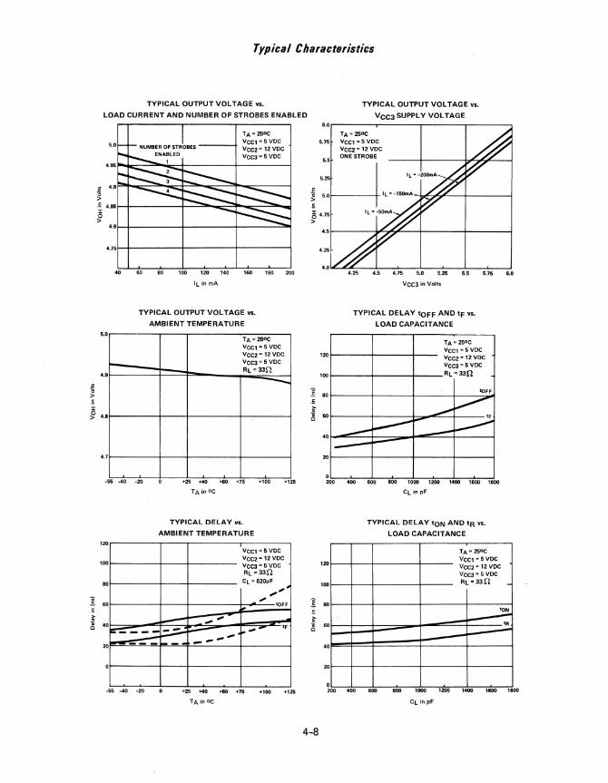
Typical Characteristics
TYPICAL OUTPUT VOL TAGE vs. TYPICAL OUTPUT VOLTAGE vs. LOAD CURRENT AND NUMBER OF STROBES ENABLED VCC3 SUPPLY VOLTAGE
5.0
~ < 4.86 :t: 0 >
4.S
4.16
40
5. 0
..... 4. •
s
4. 7
NUMBER OF STROBES ----f
80 so 100 120 '40
IL inmA
TA '" 250 C VCC,-5VDC VCC2-'2VDC VCC3"5VDC
160 180 200
TYPICAL OUTPUT VOLTAGE vs.
AMBIENT TEMPERATURE
TA "" 250 C Vcc, =5VDC VCC2" '2VDC VCC3 = 5VDC RL=33n -
-56 -40 -20 +25 +40 +60 +75 +100 +125
TA in oc
TYPICAL DELAY vs.
AMBIENT TEMPERATURE 120
VCC, =5VDC VCC2-'2VDC VCC3-5VDC 100
RL "33n
80 CL = 6200F
,,' , tOFF
.....- -.... 0 tF I:':. __ -=
~ - -..... --- -_ ...
20
0
-66 -40 -20 +25 +40 +60 +75 +100 +125
TA in OC
6.0,.-----.-----,-----,-----,
5.75
5.5
5.25
..
TA = 250C VCC, =5VDC VCC2' '2VDC ONE STROBE
~ 6.0t-----1-.5 is 4.75 >
4.6t-----j....,:oo'!i~--+----+----_i
4.75 5.0 5.26 5.6 6.76 6.0
VeC3 in Volts
TYPICAL DELAY tOFF AND tF VS.
LOAD CAPACITANCE
TA" 250 C VCC, =5VDC VCC2" ,2VDC 120
VCC3" 5VDC
100 RL=33n
! 80 toFF
...,..,. ~ ~
I""" V -- -40
1-20
0 ~ - ~ -~ ~ ~ ~~
CL in pF
TYPICAL DELAY tON AND tR ...
LOAD CAPACITANCE
TA" 25oC'
12 0 VCC,-5VDC VCC2"'2VDC VCC3-5VDC
'00 RL=33n
! 80 ..:::-0 tR -
<
.f 6 C
0
20
0 200 400 600 - 1000 1200 1400 1600 1800
CL in pF
4-8

m HARRIS Not Recommended for New Designs
Features
• FIELD PROGRAMMABLE
• CMOS COMPATIBLE
• ZERO POWER DISSIPATION
• FAST SWITCHING
• FIVE POPULAR ORGANIZATIONS
MONOLITHIC DIODE
MATRICES
Description
Designed with the CMOS circuit engineer in mind, these versatile diode matrices allow the application of logically powerful programmable solutions to low power CMOS system appl ications.
These devices incorporate an advanced dielectric isolation process to eliminate the need for power supply pins and allow parasitic free operation.
Programming is accomplished by cleanly vaporizing a fusible link by application of a brief high voltage pulse to a selected array element. This operation open circuits a row to column orring diode eliminating their former interaction.
Monolithic Structure
DIELECTRIC LAYER
DISCONN ECTE D DIODE
FUSED LINK
Fusible link System
4-9
SILICON DIOXIDE
"P" TYPE SILICON
METALIZED INTERCONNECT LINE
INTACT LINK
CONNECTED DIODE

Monolithic Diode Matrices
HM-0168 6 x 8 DIODE MATRICES
HM-0186 8 x 6 DIODE MATRICES
HM-0410 4 x 10 DIODE MATRICES
HM-0104 10 x 4 DIODE MATRICES
HM-0198 9 x 8 DIODE MATRICES
HM-0104
COLUMN CONNECTION PIN NO.
, 14 7 8
HM-0410
COLUMN CONNECTION PIN NO.
CUSTOM PATTERNS
HM-0198
COLUMN CONNECTION PIN NO.
2 8 9 17 16 11 10
HM-0168
COLUMN CONNECTION PIN NO.
7 14 8 13 9 12 10
HM-0186
COLUMN CONNECTION PIN NO
7 14 8 13 9
When ordering a matrix with a custom pattern: Send a paper tape, or copy a matrix pattern and circle out those diodes to be removed from the matrix. Another method to clearly identify a pattern is to call out respective anode and cathode for each diode to be removed, by package pin number.
4-10

Specifications Diode Matrices ABSOLUTE MAXIMUM RATINGS
Forward Current
Surge Current (lOOMs Max.)
Total Ckt. Dissipation (Still Air)
Storage Temperature (Ambient)
lOOmA
200mA
450mW
-650 C to +1500 C
Maximum Ratings are limiting values above which permanent damage may occur.
ELECTRICAL CHARACTERISTICS
ITA
SYMBOL PARAMETER
VF Forward Voltage
BVR Reverse Breakdown Voltage
trr Reverse Recovery Time
Cc Crosspoint Capacitance (1)
(1) Guaranteed but not 100% tested.
(2) Cc 0( _1_ VBIAS
TYPICAL PERFORMANCE CURVES
CURRENT -mA
10
1
o. 5
o. 3
0.' O. 1
0.'
HM-OXXX-2
HM-OXXX-5 HM-OXXX-8
OOC to + 75°C -550C to + 1250C
MIN MAX MIN MAX UNITS CONDITIONS
1.5 1.5 V IF ~ 20mA
0.9 .9 V IF ~lmA
20 30 V IBV ~ 100MA
25°C 25°C
100 50 ns IF ~ 10mA to IR ~ 10mA
Recovery to 1mA
8 pF VR ~ 5V; f ~ 1MHz (2)
VOLTAGE Vf
// V
,lwORSTief DIODE@2SOC I 1// WORST
DIODE @ -65OC
I
/ / I 1/
I J I I
1/ 1/ 250 c.,L v..oc
0.' 0.6 0 .• 1.0 1.' 1.' VOLTS
4-11
a:><ea: ..... 0 0:;: Q..UJ iii:;:

Programming
Use a simple supply capable of driving a 27 ohm resistor (carbon) with a clean transition from 0 to 20-24 volts in less than 500lls, for at least 10ms. The diode to be disconnected is selected by setting the row and column switches S2 and S3 respectively as required. When switch Sl is depressed, programming current is provided to column contacts in the matrix. This current opens the fusible link, in series with the selected diode. The peak fusing current required to open a fusible link is approximately 750 milliamperes. As the temperature of. the fuse is raised, the aluminum begins to melt. This melting continues until the fuse link separates. The cohesive forces of the melting aluminum retracts the remaining portions of the metal, thereby preventing formation of loose aluminum residues. The melting temperature of aluminum (approximately 6500 C) will not affect the passivating layer of silicon dioxide, whose melting temperature is about 13500 C. Test verification is obtained by an indicator lamp or LED placed in series with the column and row switches through the verify contacts of Sl to give electrical indication of the condition of each diode in the matrix before and after fusing.
Caution: Programming is limited to one fuse at a time.
SIMPLE PROGRAMMER
8, DPDT MOMENTARY 82 17 POS, 1 POLE 83 ROTARY 01 Q2 - 2N1613 INDICATOR LIGHT, LED
MATRIX UNDER TEST
4-12
PROGRAMMER TEST CONFIGURATION
22 I Acceptable
200 500 ~10ms MICROSECONDS"
• Typ TRISE = 200 /Jsec to 10V Reference
NOTE: The 27 ohm resistor is only used for oscilloscope measurements of the Power Supply Characteristics becaues it represents a typical unprogrammed fuse/diode.

HM-7602/03 m HARRIS 32 x 8 PROM
HM-7602 - Open Collector Outputs HM-7603 - "Three State" Outputs
Features
• 50ns MAXIMUM ADDRESS ACCESS TIME
• "THREE STATE" OUTPUTS WITH ONE ACTIVE LOW CHIP ENABLE
• FAST ACCESS TIME - GUARANTEED FOR WORST CASE N2 SEQUENCING OVER COMMERCIAL AND MILITARY TEMPERATURE AND VOLTAGE RANGES
• INDUSTRY STANDARD 0.300 INCH 16 PIN PACKAGE
• PRODUCED ON MIL-M-38510 QUALI FlED WAFER FAB LINE
• SIMPLE HIGH SPEED PROGRAMMING PROCEDURE - ONE PULSE/BIT TYPICALLY ASSURES FAST PROGRAMMING AND SUPERIOR RELIABILITY
Description
The HM-7602/03 is a fully decoded high speed Schottky TTL 256/Bit Field Programmable ROM in a 32 word by 8 bit/word format with open collector (HM-7602) or "Three State" (HM-7603) outputs. These PROMs are available in a 16 pin D.I.P. (ceramic or power plastic).
All bits are manufactured storing a logical "1" (Positive Logic) and can be selectively programmed for a logical "0" in anyone bit position.
Nickel-chromium fuse technology is used on this and all other Harris Bipolar PROMs.
The HM-7602/03 contains test rows which are in addition to the storage array to assure high programmability and guarantee parametric and A.C. performance. The fuses in these test rows are blown prior to shipment.
There is one chip enable input on the HM-7602/03. CE low enables the chip.
Functional Diagram
AOll01 Al1111
A2(121
A3(131
A4(141
CE(151
5 ROW ADDRESS BUFFERS
1 OF 32 ROW
DECODER
Pinout TOP VIEW - DIP
01 VCC
°2 CE
03 A4
°4 A3
°5 A2
06 A,
07 Ao
GND 08
PIN NAMES
AO-A4 0, -08
a Address Inputs Data Outputs Chip Enable Input
Logic Symbol
AO Al A2 A3-A4
32 x 8 MEMORY ARRAY
01
02 03 04 Os 06 07
Os
(161 = VCC (81 = GND
(91 171 (61 (51 (41 (31 (21 (1 I 08 07 06 05 04 03 02 01
4-13
0:>-«0: -'0 0::;;: o...w iii::;;:

Specifications HM-7602/03
ABSOLUTE MAXIMUM RATINGS
Output or Supply Voltage (Operating) Address/Enable Input Voltage Address/Enable Input Current
-0.3 to +7.0V 5.5V
-20mA 100mA
Storage Temperature -650 e to +1500 e Operating Temperature (Ambient) -550 e to +1250 e Maximum Junction Temperature +1750 e
Output Sink Current
CAUTION: Stresses above those listed under the "Absolute Maximum Ratings" may cause permanent damage to the device. This is a stress only rating and functional operation of the device at these or at any other conditions above those indicated in the operational sections of this specification is not implied. (While programming, follow the programming specifications.)
D.C. ELECTRICAL CHARACTERISTICS (Operating) HM-7602/03-5 (Vee ~ 5.0V ±5%, TA = ooe to +750 e) HM-7602/03-2/-8 (Vee ~ 5.0V 2:10%, T A ~ -550 e to +1250 e) Typical measurements are at TA ~ 250 e, Vee ~ +5V NOTE: Positive current defined as into device terminals.
SYMBOL PARAMETER MIN TYP MAX UNITS TEST CONDITIONS
IIH Address/Enable "1" - - +40 fJ.A VIH = Vee Max. IlL Input Current "0" - -50.0 -250 fJ.A VIL = 0.45V
VIH Input Threshold "1" 2.0' 1.5 - V Vee = vee Min Vil Voltage "0" - 1.5 0.8' V Vec = Vee Max.
VOH Output Voltage "1" 2.4** 3.2 ** - V 10H = -2.0rnA, Vee = Vee Min. VOL "0" - 0.35 0.45 V 10l = +16rnA, Vee = vee Min.
10HE Output Disable "1" - - +100 fJ.A VOH, Vee = Vee Max. 10lE Current "0" - - -100 fJ.A VOL = 0.3V, Vee = Vee Max.
VeL Input elarnp Voltage - - -1.2 V IIN=-18rnA
lOS Output Short Circuit -15 ** - -100" rnA Vee = vee Max., VOUT = O.OV Current One Output Only for a Max.
of 1 Second.
ICC Power Supply Current - 90 130 rnA Vee = vee Max. All Inputs Grounded
* These are absolute voltages with respect to ground pin and include all overshoots due to system and/or tester noise. Do not attempt to test these values without suitable equipment.
** "Three-State" only.
A.C. ELECTRICAL CHARACTERISTICS (Operating) Typical measurements are at T A ~ +250 e, Vee ~ +5V
HM-7602/03-5 5V±5%
OOC to +750 C
SYMBOL PARAMETER TYPICAL MAXIMUM"
TAA Address Access Time 30 50
TEA Chip Enable Access Time 20 35
HM-7602/03-2/-8 5V ±10%
-550 C to + 1250 C
TYPICAL MAXIMUM" UNITS
- 60 ns
- 50 ns
*A.C. limits guaranteed for worst case N2 sequencing with maximum test frequency of 5MHz.
CAPACITANCE: TA ~ 250 e
SYMBOL PARAMETER TYPICAL UNITS TEST CONDITIONS
elNA,elNeE I nput Capacitance 12 pF Vee = 5V, VIN = 2.0V, f = lMHz
eOUT Output Capacitance 12 pF Vee = 5V, VOUT = 2.0V, f = lMHz
4-14

HM-7602/03 SWITCHING TIME DEFINITIONS
~------- 3.0V ADDRESSES~, .'_.S_V _____ _
- O.OV
OUTPUTS
NOTE; As is common to all memory devices, output levels can be undefined during the address access period (TAA); however, the outputs are guaranteed to reach stable levels by T AA. It is not recommended that outputs from this clan of devices be used to drive edge triggered inputs on subsequent devices (counters, flip-flops, etc.) without proper intermediate synchronization.
OUTPUTS --~--K==!=~
A.C. TEST LOAD
PROM
OUTPUT
Vee
g
Ox 0---t--"'"'1>--0 TEST POINT
600n 30pP
* I neludes jig & probe
total capacitance
4-15
This is the A.C. Test Load which Harris Semiconductor uses in its automatic test equipment, and it is recommended that users of Harris bipolar devices use the same or an equivalent load in performing A.C. testing.
T.S.
0:>«0: -'0 0:;;; C1.w 00:;;;

HM-7610/11 m HARRIS HIGH SPEED 256 x 4 PROM
HM-7610 - Open Collector Outputs HM-7611 - "Three State" Outputs
Features
•
•
•
•
FAST ADDRESS ACCESS TIME HM-7610/11 _______________ _ HM-7610A/11A ______________ _
HM-7610B/llB ______________ _
60 ns MAXIMUM 45 ns MAXIMUM 35 ns MAXIMUM
"THREE STATE" OR OPEN COLLECTOR OUTPUTS AND TWO CHIP ENABLE INPUTS
SIMPLE HIGH SPEED PROGRAMMING PROCEDURE-ONE PULSE/BIT ASSURES FAST PROGRAMMING AND SUPERIOR RELIABILITY_
INPUTS AND OUTPUTS TTL COMPATIBLE
• FAST ACCESS TIME - GUARANTEED FOR WORST CASE N2 SEQUENCING OVER COMMERCIAL AND MILITARY TEMPERATURE AND VOLTAGE RANGES_
• PIN COMPATIBLE WITH INDUSTRY STANDARD 1 K PROMs_
Description The HM-7610/11 are fully decoded high speed Schottky TTL 1024 bit Field Programmable ROM's in a 256 word by 4 bit/word format with open collector (HM-7610) or "three state" (HM-7611) outputs_ The PROMs are available in 16 pin D_I-P_ (ceramic or power plastic)_
All bits are manufactured storing a logical "1" (positive logic) and can be selectively programmed for a logical "0" in any bit position_
The HM-7610/11 contain test rows and columns which are in addition to the storage array to assure high programmability and guarantee parametric and A.C. performance. The fuses in these test rows and columns are blown prior to shipment.
This PROM is intended for use in state of the art high speed logic systems.
Nickel-chromium fuse technology is used on these and all other Harris Bipolar PROMs.
There are two chip enable inputs on the HM-7610/11 where CEl and CE2 low enables the chip.
Functional Diagram
A7 1 OF 16
A6 ROW
DECODER '6 AS
A,
A3 '6
A2
A,
AO
CE2
CE,
11.1 0,
4-16
16 x 64 MEMORY ARRAY
'6 '6
113} 112}
02 03
Pinouts TOP VIEW-DIP
PIN NAMES AO - A 7 Address Inputs
0, - 04 Data Outputs
CE,. CE2 Chip Enable Inputs
logic Symbol
eE,
eE2 AO A, 0, A2 °2 A3 03 A4 °4 A5 A6 A7
'6
'6
111}
o.

Specifications HM-7610/11
ABSOLUTE MAXIMUM RATINGS
Output or Supply Voltage (Operating) -0.3 to +7.0V Address/Enable I nput Voltage 5.5V Address/Enable Input Current Output Sink Current
-20mA 100mA
Storage Temperature -650 e to +1500 e Operating Temperature (Ambient) -550 e to +1250 e Maximum Junction Temperature +1750 e
CAUTION: Stresses above those listed under the "Absolute Maximum RBtingsN may cause permanent damage to the device. This is a stress onlv rating and functional operation of the device at these or at any other conditions above those indicated in the operational sections of this specification ;s not implied. (While programming, follow the programming specifications.)
D.C. ELECTRICAL CHARACTERISTICS (Operating) HM-7610/11-5 (Vee = 5.0V ± 5%, TA = ooe to +750 e) HM-7610/11-2/-8 (Vee = 5.0V ± 10%, TA = -550 eto +1250 e) Typical measurements are at T A = 250 e, Vee = +5V. NOTE: Multiple entries refer to parameter values for "A", "B"/Std.
Positive current defined as into device terminals.
SYMBOL PARAMETER MIN TYP MAX UNITS TEST CONOITIONS
IIH Address/Enable "1" - - +40 I1A VIH = Vee Max. IlL Input Current "0" - - -1001-250 I1A Vil = 0.45V
VIH Input Threshold "1" 2.0* 1.5 - V Vee = vee Min. Vil Voltage "0" - 1.5 0.8* V Vee = vee Max.
VOH Output "1" 2.4** 3.2.** - V 10H - -2.0mA, Vee - Vee Min. VOL Voltage "0" - 0.35 0.50 V 10l = +16mA, Vee = Vee Min.
10HE Output Disable "1" - - +40/+100 I1A VOH, Vee = Vee Max. 10lE Current "0" - - -40/-100" I1A VOL = 0.3V, Vee = Vec Max.
Vel Input Clamp Voltage - - -1.2 V liN = -18mA
lOS Output Short Circuit -15** - -100** mA Vee = Vee Max. VOUT = O.OV Current One Output Only for a Max.
of 1 Second
ICC Power Supply Current - 90 110/130 mA Vee = Vee Max. All Inputs Grounded
-I< These are absolute voltages with respect to ground pin and include all overshoots due to system and/or tester noise. Do not attempt to test these values without suitable equipment.
** "Three-State" only.
A.C. ELECTRICAL CHARACTERISTICS (Operating) Typical measurements are at TA = 250 e, Vee = +5V.
HM·7610111·5 5V ±5%
(lOC to +750C
"B" "A"
SYMBOL PARAMETER TYP MAX TYP MAX
TAA Address Access Time 25 35 35 45
TEA Chip Enable Access Time - 25 - 25
TDA Chip Disable Access Time - 25 - 25
HM-7610111-21-8 5V:!:.10%
-550C to + 1250C
STD "B" "A" STD
TYP MAX TYP MAX TYP MAX TYP MAX
40 60 - 50 - 65 - 75 - 25 - 30 - 30 - 30 - 25 - 30 - 30 - 30
A.C. limits guaranteed for worst case N2 sequencing with maximum test frequency of 5MHz.
CAPACITANCE: TA = 250 e
SYMBOL PARAMETER TYPICAL UNITS TEST CONDITIONS
eINA, elNeE Input Capacitance 8 pF Vee = 5V, VIN = 2.0V, f = 1MHz
UNITS
ns ns
COUT Output Capacitance 10 pF Vee = 5V, VOUT = 2.0V, f = 1MHz
4-17
0::>«0:: ....10 0:;0; c..UJ ;;;:;0;

HM-7610/11 SWITCHING TIME DEFINITIONS
ADDRESSES ~ 1.5V 3.0V
O.OV , I I ,
~XX~ VOH
OUTPUTS VOL , ,
--l TAA f--I I
NOTE: As is common to all memory devices, output levels can be undefined during the addrass access period (T AA); however, the outputs are guaranteed to reach stable levels by TAA. It is not recommended that outputs from this class of devices be used to drive edge triggered inputs on subsequent devices (counters, flip-flops, etc.) without proper intermediate synchronization.
Vce
g
3.0V CE"1, CE2
O,OV
TDAl TEAl
OUTPUTS VOHAC'
TDA2 TEA2
OUTPUTS
VOLAC'
tr, tf < 5ns
'VOLAC AND VOHAC ARE THE MEASURED OUTPUT VOL TAGE LEVELS
WHILE ENABLED.
A.C. TEST LOAD
PROM OUTPUT
Ox O----+-----.r-<:> TEST POINT
This is the A.C. Test Load which Harris Semiconductor uses in its automatic test equipment, and it is recommended that users of Harris bipolar devices use the same or an equivalent load in performing A.C. testing. 600n
SYMBOL
TAA
*TEA l
TEA2
*TDA l
TDA2
30pP
* I neludes jig & probe
total capacitance
PARAMETER
Address Access Time
Chip Enable Access r,me from
"Th ree State" to V 0 H
Chip Enable Access Time to VOL
Chip Disable Access Time from
VOH to "Three State"
Chip Disable Access Time from
VOL
* Applies to "Three-8tate" only.
4-18
51
Closed
Open
Closed
Open
Closed

mHARRIS HM-7620/21 HIGH SPEED 512 x 4 PROM
HM-7620- Open Collector Outputs HM-7621 - "Three State" Outputs
Features • FAST ADDRESS ACCESS TIME
HM-7620121 _ _ • • • • • • • • • • • • • •• 70 ns MAXIMUM HM-7620A/21A. • • • • • • • • • . • • • •• 50 ns MAXIMUM HM-7620B/21B • • • • • • • • • • • • • • •• 40 ns MAXIMUM
• "THREE STATE" OR OPEN COLLECTOR OUTPUTS AND A SINGLE CHIP ENABLE INPUT
• SIMPLE HIGH SPEED PROGRAMMING PROCEDURE-ONE PULSE/BIT ASSURES FAST PROGRAMMING AND SUPERIOR RELIABILITY.
• INPUTS AND OUTPUTS TTL COMPATIBLE
• FAST ACCESS TIME-GUARANTEED FOR WORST CASE N2 SEQUENCING OVER COMMERCIAL AND MILITARY TEMPERATURE AND VOLTAGE RANGES.
• PIN COMPATIBLE WITH INDUSTRY STANDARD 2K PROMs.
Description The HM-7620/21 are fully decoded high speed Schottky TTL 2048 bit Field Programmable ROM's in a 512 word by 4 bit/word format with open collector (HM-7620) or "three state" (HM-7621) outputs. These PROMs are available in 16 pin D.I.P. (ceramic or power plastic). All bits are manufactured storing a logical "1" (positive logic) and can be selectively programmed for a logical "0" in any bit position.
The HM-7620/21 contain test rows and columns which are in addition to the storage array to assure high programmability and guarantee parametric and A. C. performance. The fuses in these test rows and columns are blown prior to shipment.
This PROM is intended for use in state of the art high speed logic systems.
Nickel-chromium fuse technology is used on these and all other Harris Bipolar PROMs.
There is a single chip enable input on the HM-7620/21 where CE low enables the chip.
Functional Diagram
A. A7
A6
A5
A4 --.... '1-__ .....
,OF32 ROW
DECODER 32
4-19
(12)
0, 1111 02
32.x84
MEMORY ARRAY
('D)
03
Pinout
TOP VIEW - DIP
A6 Vee
A5 A7
"" AB
A3 C-
AD 0,
A, 02
A2 03
GNO 04
PIN NAMES
AO - AS Address Inputs '1:E Chip Enable Input
01 - 04 Data Outputs
logic Symbol
ce AO AI
A2
A3 A4
A5
AS A7
AS
(9)
04
a:>«a: ...JO o:!! a..w iii:!!

ABSOLUTE MAXIMUM RATINGS
Specifications HM-7620/21
Storage Temperature -650 C to +1500 C Operating Temperature (Ambient) -550 C to +1250 C
Output or Supply Voltage (Operating) Address/Enable Input Voltage Address/Enable Input Current
-0.3 to +7 .OV 5.5V
-20mA 100mA
Maximum Junction Temperature +1750 C Output Sink Current
CAUTION: Stresses above those listed under the "Absolute Maximum Ratings'; may cause permanent damage to the device. This is a stress only rating and functional operation of the device at these or at any other conditions above those indicated In the operational sections of this specification is not implied. (While programming, follow the programming specifications,)
D.C. ELECTRICAL CHARACTERISTICS (Operating) HM-7620/21-5 (VCC = 5.0V ±5%, TA = ooC to +750 C) HM-7620/21-2/-8 (VCC = 5.0V ± 10%, TA = -550 C to +1250 C) Typical measurements are at T A = 250 C, VCC = +5V. NOTE: Multiple entries refer to parameter values for "A", "B"/Std.
Positive current defined as into device term inals.
SYMBOL PARAMETER MIN TYP MAX UNITS TEST CONDITIONS
ilH Address/enable "1" - - +40 JlA VIH = VCC Max. IlL I nput Current "0" - - -100/-250 JlA VIL = 0.45V
VIH Input Threshold "1" 2.0' - - V VCC = VCC Min. VIL Voltage "0" - - 0.8* V VCC = VCC Max.
VOH Output "1" 2.4 ** 3.2** - V 10H = -2.0mA, VCC = VCC Min. VOL Voltage "0" - 0.35 0.50 V 10L = +16mA, VCC = VCC Min.
10HE Output Disable "1" - - +40/+100 JlA VOH, VCC - VCC Max. 10LE Current "0" - - -40/-100** JlA VOL = 0.3V, VCC = VCC Max.
VCL Input Clamp Voltage - - -1.2 V liN = -18mA
lOS Output Short Circuit -15** - -100" mA VCC = VCC Max. VOUT = O.OV Current One Output Only for a Max.
of 1 Second
ICC Power Supply Current - 90 120/130 mA VCC = VCC Max. All Inputs Grounded
• These are absolute voltages with respect to ground pin and include all overshoots due to system and/or tester noise. Do not attempt to test these values without suitable equipment .
•• "Three-State" only.
A.C. ELECTRICAL CHARACTERISTICS (Operating) Typical Measurements are at T A = 250 C, V CC = +5V.
HM·7620!21 ·5 5V±5%
OOCto +75OC
"B" "A"
SYMBOL PARAMETER TYP MAX TYP MAX
TAA Address Access Time 30 40 40 50 TEA Chip Enable Access Time - 25 - 25
TDA Chip Disable Access Time - 25 - 25
HM-7620!21·2!8
5V±'0% -550C to + 1250C
STD "B" "Au STD
TYP MAX YP MAX TYP MAX TYP MAX
50 70 - 55 - 70 - 85 - 25 - 30 - 30 - 30 - 25 - 30 - 30 - 30
A.C, limits guaranteed for worst case N2 sequencing with maximum test frequency of 5MHz.
CAPACITANCE: TA = 250 C
SYMBOL PARAMETER TYPICAL UNITS TEST CONDITIONS
CINA, CINCE Input Capacitance 8 pF VCC = 5V, VIN = 2.0V, f = lMHz
COUT Output Capacitance 10 pF VCC = 5V, VOUT = 2.0V, f = lMHz
4-20
UNITS
ns ns ns

HM-7620/21 SWITCHING TIME DEFINITIONS
--:soc 3.0V ADDRESSES --7:" ... '_.5_V ______ O.OV
OUTPUTS
, , , ,
>o<x~~:: , , ----l TAA I-, , , ,
NOTE: As is common to all memory devices, output levals can be undefined during the address access period (TAA): however, the outputs are guaranteed to reach stable levels by T AA. It is not recommended that outputs from this class of devices be used to drive edge triggered inputs on subsequent devices (counters, flip-flops, etc.) without proper intermediate synchronization.
VCC
6
3.0V
CE O.OV
TDA,
OUTPUTS VDHAC'
TDA2
OUTPUTS
VOLAC'
tr,tf<5ns
'VOLAC AND VOHAC ARE THE MEASURED OUTPUT VOL TAGE LEVELS
WHILE ENABLED.
A.C. TEST LOAD
PROM
OUTPUT Ox 0---+---'0--0 TEST POINT
This is the A.C. Test Load which Harris Semiconductor uses in its automatic test equipment, and it is recommended that users of Harris bipolar devices use the same or an equivalent load in performing A.C. testing. 600n
SYMBOL
TAA
*TEAI
TEA2
*TOA1
TOA2
30pF*
* I neludes jig & probe
total capacitance
PARAMETER
Address Access Time
Chip Enable Access Time from
"Three State" to VOH
Chip Enable Access Time to VOL
Chip Disable Access Time from
VOH to "Three State"
Chip Disable Access Time from
VOL
* Applies to "Three-State" only.
4-21
S1
Closed
Open
Closed
Open
Closed
0::>...:0:: -'0 0:;: C>.LU co:;:

HM-7640/41 mHARRIS HIGH SPEED 512 x 8 PROM
HM-7640 - Open Collector Outputs HM-7641- "Three State" Outputs
Features • FAST ADDRESS ACCESS TIME
HM·7640/41. • • • . • • • . • • . • . •.•• 70 ns MAXIMUM HM·7640A/41A· . • . • • • • . . • • • • . • 45 ns MAXIMUM
• "THREE STATE" OR OPEN COLLECTOR OUTPUTS AND FOUR CHIP ENABLE INPUTS.
• SIMPLE HIGH SPEED PROGRAMMING PROCEDURE - ONE PULSE/BIT ASSURES FAST PROGRAMMING AND SUPERIOR RELIABILITY.
• FAST ACCESS TIME - GUARANTEED FOR WORST CASE N2 SEQUENCING OVER COMMERCIAL AND MILITARY TEMPERATURE AND VOLTAGE RANGES.
• PIN COMPATIBLE WITH INDUSTRY STANDARD 4K PROM •.
Pinouts
TOP VI EW - DIP
A7 Vcc A6 AS A5 NC A4 CEI
CE2
CE3
CE4
Os 07 06 05
GNO 04
Description PIN NAMES
The HM-7640/41 are fully decoded high speed Schottky TTL 4096 bit Field Programmable ROMs in a 512 word by 8 bit/word format with open collector (HM-7640) or "three-state" (HM-7641) outputs. These PROMs are available in a 24 pin DIP (ceramic or power plastic).
All bits are manufactured storing a logical "1" (positive logic) and can be selectively programmed for a logical "0" in any bit position.
Nickel-chromium fuse technology is used on this and all other Harris Bipolar PROMs.
The HM-7640/41 contain test rows and columns which are in addition to the storage array to assure high programmability and guarantee parametric and A.C. performance. The fuses in these test rows and columns are blown prior to shipment.
There are four chip enable inputs on the HM-7640/41 where CEl and CE2 low and CE3 and CE4 high enables the chip.
Functional Diagram
As A, A, A,
A3~~+L __ .J
A, A, AO
~1~~~----'
AO - AS Address Inputs
o 1 - Os Data Outputs
CEl. CE2. CE3. CE4 Chip Enable Inputs
logic Symbol
eE, 1-----+1 ~:! ~,_--~---r---,_--_r--_;---~--,_-J
f I .. PIN NUMBER 124)"VCC (121-GND
(221-N.C.
,., 0, 110)
0,
4-22
(14) 0, (151 0,
(16) 0, 117) 0,

Specifications HM-7640/41
ABSOLUTE MAXIMUM RATINGS
Output or Supply Voltage (Operating) Address/Enable Input Voltage Address/Enable Input Current
-0.3 to +7.0V 5.5V
-20m A 100mA
Storage Temperature -650C to +1500C Operating Temperature (Ambient) -550C to +1250C Maximum Junction Temperature +1750C
Output Sink Current
CAUTION: Stresses above those listed under the "Absolute Maximum Ratings" may cause permanent damage to the device. These are stress only ratings and functional operation of the device at these or at any other conditions above those indicated in the operational sections of this specification is not implied. (While programming, follow the programming specifications.)
D.C. ELECTRICAL CHARACTERISTICS (Operating) HM-7640/41-5 (VCC = 5.0V ±5%, TA = ooC to +750C) HM-7640/41-2/-8 (VCC = 5.0V ± 10%, T A = -550C to +1250C) Typical measurements are at T A = 250C, VCC = +5V. NOTE: Multiple entries refer to parameter values for "A"/Std.
Positive current defined as into device terminals.
SYMBOL PARAMETER MIN TYP MAX UNITS TEST CONDITIONS
IIH Address/Enable "1" - - +40 IJ.A VIH = Vee Max. IlL Input Current "0" - - -100/-250 IJ.A VIL = 0.45V
VIH Input Threshold "1" 2.0' - - V Vee = vee Min. VIL Voltage "0" - - O.S" V Vee = Vee Max.
VOH Output "1" 2.4** 3.2** - V 10H = -2.0mA, Vee = Vee Min. VOL Voltage "0" - 0.35 0.50 V 10L = +16mA, Vee = Vee Min.
10HE Output Disable "1" - - +40/+100 IJ.A VOH, Vee = vee Max. IOLE Current "0" - - -40/-100" • IJ.A VOL = 0.3V, Vee = vee Max.
VeL Input elamp Voltage - - -1.2 V liN = -18mA
lOS Output Short Circuit -15** - -100' mA Vee = Vee Max. VOUT = O.OV Current One Output at a TimeforMax.
of 1 Second
lee Power Supply Current - 125 170 mA Vee = Vee Max., All Inputs Grounded.
* These are absolute voltages with respect to ground pin and include all overshoots due to system and/or tester noise. Do not attempt to test these values without suitable equipment.
* * "Three-State" only.
A.C, ELECTRICAL CHARACTERISTICS (Operating) Typical Measurements are at TA = 250C, VCC = +5V.
HM·7640/41·5 5V:!:5%
OOC to +750 C
"A" STD
SYMBOL PARAMETER TYP MAX TYP MAX
TAA Address Access Time 35 45" 50 70 TEA ehip Enable Access Time - 35 - 40 TOA ehip Disable Access Time - 35 - 40
HM-7640/41·2/·8 5V:!:10%
-550 C to + 1250 C
"A" STD
TYP MAX TYP MAX UNITS
- 60" - 85 ns - 45 - 50 ns - 45 - 50 ns
A.C. limits guaranteed for worst case N2 sequencing with maximum test frequency of 5MHz.
"T AA is SOns for HM-7640A-5 and 65ns for HM-7640A-2/-8
CAPACITANCE: T A = 250C
SYMBOL PARAMETER TYPICAL
eINA, elNeE I nput Capacitance 8
eOUT Output Capacitance 10
4-23
UNITS TEST CONDITIONS
pF Vee = 5V, VIN = 2.0V, f = lMHz
pF Vee = 5V, VOUT = 2.0V, f = lMHz
a:>-0: a: -'0 0:;; Q..LU <Xi:;;

HM-7640/41 SWITCHING TIME DEFINITIONS
3.0V
o.OV ADDRESSES ~_l_.5_V _____ _
I I I
VDH
VOL OUTPUTS lXxx~
I
---I TAA f--I I I ,
NOTE: As is common to all memory devices, output levels can be undefined during the address access period (TAAI; however, the outputs are guaranteed to reach stable levels by T AA. It is not recommended that outputs from this class of devices be used to drive edge triggered inputs on subsequent devices (counters, flip-flops, etc.) without proper intermediate synchronization.
VCC
CE3,CE4 .,-___ 3.0V
eEl,cE2 '-___ O.OV
TDAl
OUTPUTS
TDA2
OUTPUTS
tr, tf<5n5
'VOLAC AND VOHAC ARE THE MEASURED OUTPUT VOLTAGE LEVELS
WHILE ENABLED.
A.C. TEST LOAD
PROM
OUTPUT Ox o---+----<o----{) TEST POINT
This is the A.C. Test Load which Harris Semiconductor uses in its automatic test equipment, and it is recommended that users of Harris bipolar devices use the same or an equivalent load in performing A.C. testing.
GOOn
SYMBOL
TAA
'TEAl
TEA2
'TOAl
TOA2
30pF'
'* Includes jig & probe
total capacitance
PARAMETER
Address Access Time
Chip Enable Access Time from
··Three State·' to VOH
Chip Enable Access Time to VOL
Chip Disable Access Time from
VOH to "Three State"
Chip Disable Access Time from
VOL
* Applies to "Three-State" only.
4-24
51
Closed
Open
Closed
Open
Closed

HM-7642/43 mHARRIS HIGH SPEED 1K x 4 PROM
H M-7642 - Open Collector Outputs HM-7643 - "Three State" Outputs
Features • FAST ADDRESS ACCESS TIME
HM-7642/43 .......................... 60ns MAXIMUM HM-7642A/43A ...•............•....... 50ns MAXIMUM HM-7642B/43B ....•.................•. 45ns MAXIMUM
• '"THREE STATE" OR OPEN COLLECTOR OUTPUTS AND TWO CHIP ENABLE INPUTS
• SIMPLE HIGH SPEED PROGRAMMING PROCEDURE - ONE PULSE/BIT ASSURES FAST PROGRAMMING AND SUPERIOR RELIABILITY.
• FAST ACCESS TIME - GUARANTEED FOR WORST CASE N2 SEQUENCING OVER COMMERCIAL AND MILITARY TEMPERATURE ANO VOLTAGE RANGES.
• PIN COMPATIBLE WITH INDUSTRY STANDARD 4K PROMs.
Description The HM-7642/43 are fully decoded high speed Schottky TTL 4096 bit Field Programmable ROMs in a 1 K word by 4 bit/word format with open collector (HM-7642) or "three state" (HM-7643) outputs. These PROM's are available in an 18 pin DIP (ceramic or power plastic).
All bits are manufactured storing a logical "'" (positive logic) and can be selectively programmed for a logical "0" in any bit position.
Nickel-Chromium fuse technology is used on these and all other Harris Bipolar PROMs.
The HM-7642/43 contains test rows and columns which are in addition to the storage array to assure high programmability and guarantee parametrics and A.C. performance. The fuses in these test rows and columns are blown prior to shipment.
There are two chip enable inputs on the HM-7642/43. CEl and CE2 low enables the chip.
Functional Diagram
Ay
A. AS A4 ----0'\-__ -'
CE2
CE,
64
'6 TRANS
MISSION GATES
t141 0,
4-25
Pinout
TOP VIEW-DIP
A6 VCC
AS A7
A4 AS
A3 Ag
AO 01
A1 02
A2 03
CE1 04
GND CE2
PIN NAMES
AO -Ag ADDRESS INPUTS
01 -04 DATA OUTPUTS
CE1, CE2 CHIP ENABLE INPUTS
eE,
eE2 Ao A, A2 A3
A4 AS
A6 Ay AS Ag
64 x64 MEMORY ARRAY
'6 TRANS
MISSION GATES
(13\
02
,. TRANSMISSION
GATES
(12j
03
logic Symbol
,. TRANSMISSION
GATES
(111
04
0,
02
03
04
0::>-«0:: -'0 0::;;; "-w C5::;;;

Specifications HM-7642143
ABSOLUTE MAXIMUM RATINGS
Output or Supply Voltage (Operating) Address/Enable I nput Voltage Address/Enable Input Current
-0.3 to +7.0V 5.5V
-20mA 100mA
Storage Temperature -650C to +1500C Operating Temperature (Ambient) -550C to +1250C Maximum Junction Temperature +1750C
Output Sink Current
CAUTION: Stresses above those listed under the "Absolute Maximum Ratings" may cause permanent damage to the device. These are stress only ratings and functional operation of the device at these Of at any other conditions ab'Ove those indicated in the operational sections of this specification is not implied. (While programming, follow the programming speCifications.)
D.C. ELECTRICAL CHARACTERISTICS (Operating) HM-7642/43-5 (VCC = 5.0V ± 5%, TA= OOC to +750C) HM-742/43-2/-B (VCC = 5.0V ± 10%, T A = -550C to +1250C) Typical measurements are at TA = 250C, VCC = +5V. NOTE: Multiple entries refer to parameter values for "B"/"A"/Std.
Positive current defined as into device terminals.
SYMBOL PARAMETER MIN TYP MAX UNITS I TEST CONDITIONS
"H Address/Enable "1" - - +40 J1A V,H ~ Vee Max. ',l Input Current "0" - - -100/ -250/ -250 fJA V,L = 0.45V
V,H Input Threshold "1" 2.0" - - V Vee = Vee Min. V,l Voltage "0" - - 0.8" V Vee ~ Vee Max.
VOH Output "1" 2.4** 3.2** - V IOH = -2.0mA, Vee = vee Min. V0l Voltage "0" - 0.35 0.50 V IOl = +16mA, Vee = Vee Min.
IOHE Output Disable "1" - - +40/+40/+100 fJA VOH, Vee = Vee Max. IOlE Current "0" - - -40/-40/-100 ** J1A VOL = 0.3V, Vee = Vee Max.
Vel Input Clamp Voltage - - -1.2 V liN = -18mA
lOS Output Short Circuit -15** - -100** mA Vee = Vee Max. VOUT = O.OV, Current One Output at a Time for a Max.
of 1 Second
ICC Power Supply Current - 100 140 mA Vee = Vee Max., All Inputs Grounded.
* These are absolute voltages with respect to ground pin and include all overshoots due to system and/or tester noise. Do not attempt to test these values without suitable equipment.
** "Three-State" only.
A.C. ELECTRICAL CHARACTERISTICS (Operating) Typical Measurements are at TA.= 250C, VCC = +5V.
HM·7642143·5 5Vt5%
ooe to +750e
"B" "A"
SYMBOL PARAMETER TYP MAX TYP MAX
TAA Address Access Time 35 45 40 50
TEA Chip Enable Access Time - 25 - 25
TDA Chip Disable Access Time - 25 - 25
HM·7642/43·2/·8 5Vtl0%
-550C to + 1250C
STD "B" "A" STD
TYP MAX TYP MAX TYP MAX TYP MAX
45 60 - 55 - 70 - 85 - 25 - 30 - 30 - 30 - 25 - 30 - 30 - 30
A.C. limits guarant'eed for worst case N2 sequencing with maximum test frequency of SMHz.
CAPACITANCE: T A; 250C
SYMBOL PARAMETER TYPICAL UNITS TEST CONDITIONS
eINA, elNeE I nput Capacitance 8 pF Vee = 5V. VIN = 2.0V, f ~ 1MHz
UNITS
ns ns ns
eOUT Output Capacitance 10 pF Vee = 5V, VOUT = 2.0V, f ~ 1MHz
4-26

HM-7642/43 SWITCHING TIME DEFINITIONS
~ J.OV ADDRESSES -J:' ... I_.S_V ______ O.OV
OUTPUTS
, , I I
~xx~::: I I
-I TAA l-I I I ,
NOTE: A. is common to III memory devices, output IIV,II can be undefined during the addr •• acceu period (T AA); however. the outputs ar. guaranteed to reach stabl. lev,l. by T AA. It is not recommanded that outputs from this class of devices be used to drive edge triggered inpuu on subsequent device. (counters, flip-flops. etc.) without proper intermediate synchronization.
VCC
g SI
C£"I,CE2~ ~1.SV J.OV
o.ov
OUTPUTS 1.1"--- VOHAC"
OUTPUTS ---..07'1 VOLAC'
tr, tf < 5ns
*VOLAC AND VOHAC ARE THE MEASURED OUTPUT VOL TAGE LEVELS
WHILE ENABLED.
A.C. TEST LOAD
JOon
This is the A.G. Test Load which Harris Semiconductor uses in its automatic test equipment, and it is recommended that users of Harris bipolar devices use the same or an equivalent load in performing A.G. testing.
PROM OUTPUT
Ox O---+--~r--o TEST POINT
600n
SYMBOL
TAA
"TEAl
TEA2
*TOAI
TOA2
30pF*
* I neludes jig &: probe
total capacitance
PARAMETER
Address Access Time
Chip Enable Access Time from
"Three State" to VOH
Chip Enable Access Time to VOL
Chip Disable Access Time from
VOH to "Three State"
Chip Disable Access Time from
VOL
* Applies to "Three-Stat." only.
4-27
SI
Closed
Open
Closed
Open
Closed
0::>«0:: -'0 0::;; C>.LU ii;::;;

{II HARRIS HM-7649
HIGH SPEED 512 x 8 PROM
Features
• FAST ADDRESS ACCESS TIME HM-7649 __ HM-7649A _ _ _ _ _ _ _ _ _ _ _ _ _ _ _ _ _
60 ns MAXIMUM 45 ns MAXIMUM
• "THREE STATE" OUTPUTS AND A SINGLE CHIP ENABLE INPUT
• SIMPLE HIGH SPEED PROGRAMMING PROCEDURE - ONE PULSE/BIT ASSURES FAST PROGRAMMING AND SUPERIOR RELIABILITY.
• FAST ACCESS TIME - GUARANTEED FOR WORST CASE N2 SEQUENCING OVER COMMERCIAL AND MILITARY TEMPERATURE AND VOLTAGE RANGES.
• PIN COMPATIBLE WITH THE 745473
• LOW INPUT LOADING
Description The HM-7949 is a fully decoded high speed Schottky TTL 4096 bit Field Programmable ROM in a 512 word by 8 bit/word format with "Three-State" outputs. This PROM is available in a 20 pin DIP (ceramic or power plastic).
All bits are manufactured storing a logical "1" (positive logic) and can be selectively programmed for a logical "0" in any bit position.
Nickel Chromium fuse technology is used on this and all other Harris Bipolar PROMs.
The pinout is identical to the 74S473 PROM.
The HM-7649 contains test rows and columns which are in addition to the storage array to assure high programmability and guarantee parametric and A.C. performance. The fuses in these test rows and columns are blown prior to shipment.
There is a chip enable input on the HM-7649 where CE low enables the device.
Functional Diagram
A, A, A, A,
A,
(19)
AO--~ __ .J
A, A,
( J - PIN NUMBER (201 -vee (lO)"GND
'" 0, {71 0,
4-28
'" 0, (11) 0, (12) 0,
Pinout
AO VCC
A, AS
A2 A7
A3 A6
A4 A5
0, CE
°2 Os 03 °7
°4 06
GND °5
TOP VIEW - D.I.P.
CE AO
A,
A2
A3
A4
A5
AS
A7
AS
(13) 0,
PIN NAMES Address Inputs Data Outputs Chip Enable Input
Logic Symbol
(14) 0,
0,
02
03
04
°5 06
07
Os

Specifications HM-7649 ABSOLUTE MAXIMUM RATINGS
Output or Supply Voltage (Operating) Address/Enable Input Voltage Address/Enable Input Current
-0.3 to +7 .OV 5.5V
-20m A 100mA
Storage Temperature -650 C to +1500 C Operating Temperature (Ambient) -550 C to +1250 C Maximum Junction Temperature +1750 C
Output Sink Current
CAUTION: Stresses above those listed under the "Absolute Maximum Ratings" may cause permanent damage to the device. This is a stress only rating and functional operation of the device at these or at any other conditions above those indicated in the operational sections of this specification ;s not implied. (While programming, follow the programming specifications.)
D.C. ELECTRICAL CHARACTERISTICS (Operating) HM-7649-5 (VCC = 5.0V ± 5%, T A = OOC to +750 C) HM-7649-2/-8 (VCC = 5.0V ± 10%, TA = -550 C to +1250 C) Typical measurements are at T A = 250 C, V CC = +5V. NOTE: Multiple entries refer to parameter values for "A"/Std.
Positive current defined as into device terminals.
SYMBOL PARAMETER MIN TYP MAX UNITS TEST CONDITIONS
IIH Address/Enable "1" - - +25 /-lA VIH = Vec Max. IlL I nput Current "0" - - _100/_250 /-lA VIL = 0.45V
VIH Input Threshold "1" 2.0' - - V Vee = vee Min. VIL Voltage "0" - - 0.80' V Vee = vee Max.
VOH OUlPut "1" 2.4 3.2 - V 10H = -2.0mA, Vee = Vee Min. VOL Voltage "0" - 0.35 0.50 V 10L = +16mA, Vee = Vee Min.
10HE Output Disable "1" - - +40 /-lA VOH, vee - vee Max. 10LE Current "0" - - -40 /-lA VOL = 0.3V, Vee = Vee Max.
VeL Input elamp Voltage - - -1.2 V liN = -18mA
lOS Output Short Circuit -20 - -100 rnA Vee=Vee Max. VOUT=O.OV, Current One Output Only for a Max.
of 1 Second
lee Power Supply Current - 120 170 rnA Vee = Vee Max. All Inputs Grounded
* These are absolute voltages with respect to ground pin and include all overshoots due to system and/or tester noise. Do not attempt to test these values without suitable equipment.
A.C. ELECTRICAL CHARACTERISTICS (Operating)
Typical Measurements are at T A = 250 C, V CC = +5V.
HM-7649-5 5V:!:5%
OOCto +750C
"A" STD
HM-7649-2/-8 5V!10%
-550C to + 1250C
"A" STD
SYMBOL PARAMETER TYP MAX TYP MAX TYP MAX TYP MAX UNITS
TAA Address Access Time 35 45 40 60 - 60 - 80 ns
TEA Chip Enable Access TIme - 35 - 40 - 45 - 50 ns
TDA Olip Disable Access Time - 35 - 40 - 45 - 50 ns
A.C. limits guaranteed for worst case N2 sequencing with maximum test frequency of SMHz.
CAPACITANCE: T A = 250 C
SYMBOL PARAMETER TYPICAL UNITS TEST CONDITIONS
eINA,eINeE Input Capacitance 8 pF Vee = 5V, VIN = 2.0V, f = lMHz
eOUT Output Capacitance 10 pF Vee = 5V, VOUT = 2.0V, f = lMHz
4-29
a:>«a: --'0 0::;: o..UJ a:i::;:
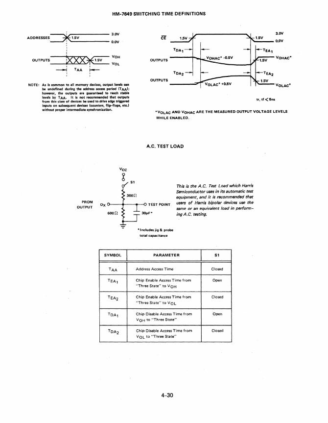
HM-7649 SWITCHING TIME DEFINITIONS
~ 3.0V ADDRESSES~, L'_.5_V _____ _
- O.OV
OUTPUTS
, I I I
~xx~ I I
---I TAA t--I I I ,
CE
TDAI
OUTPUTS
TDA2
OUTPUTS
3.0V
O.OV
TEAl
VOHAC·
TEA2
VOLAC·
tr, tf<5ns
NOTE: As is common to all memory devices, output levels can be undefined during the address access period (TAA); however, the outputs are guaranteed to reach stable levels by T AA. It is not recommended that outputs from this class of deyjces be used to drive edge triggered inputs on subsequent devices (counters, flip-flop., etc.) without proper intermediate synchronization.
·VOLAC AND VOHAC ARE THE MEASURED OUTPUT VOLTAGE LEVELS
WHilE ENABLED.
PROM
OUTPUT
A.C. TEST LOAD
VCC
b Sl
300n
This is the A.C. Test Load which Harris Semiconductor uses in its automatic test equipment, and it is recommended that users of Harris bipolar devices use the same or an equivalent load in performing A. C. testing.
Ox o---+---<t--<J TEST POINT
600n
SYMBOL
TAA
TEAl
TEA2
TDAI
TDA2
30pP
* I neludes jig & probe
total capacitance
PARAMETER
Address Access Time
Chip Enable Access Time from
"Three State" to VOH
Chip Enable Access Time from
"Three State" to Vo L
Chip Disable Access Time from
VOH to "Three State"
Chip Disable Access Time from
VOL to "Three State"
4-30
51
Closed
Open
Closed
Open
Closed

m HARRIS HM-7681 HIGH SPEED 1K x 8 PROM
Features • FAST ADDRESS ACCESS TIME
HM-7681 _ _ _ _ _ • • • • • • • • • . • • • . 70 ns MAXIMUM
HM-7681A • • • • • • • • • . • • • • • • • • 50 ns MAXIMUM
• "THREE STATE" OUTPUTS AND FOUR CHIP ENABLE INPUTS
• SIMPLE HIGH SPEED PROGRAMMING PROCEDURE-ONE PULSE/BIT ASSURES FAST PROGRAMMING AND SUPERIOR RELIABILITY
• FAST ACCESS TIME - GUARANTEED FOR WORST CASE N2 SEQUENCING OVER COMMERCIAL AND MILITARY TEMPERATURE AND VOLTAGE RANGES
• PIN COMPATIBLE WITH INDUSTRY STANDARD 8K PROMs
Description
Pinouts TOP VIEW - DIP
Vcc AS
Ag eEl eE2 CE3
Al CE4
AO Os
07 06 05
GND 04 .
PIN NAMES
AO - A9 Address Inputs
01 - 08 Data Outputs
The HM-7681 is a fully decoded high speed Schottky TTL 8192 bit Field Programmable ROM in a 1 K word by 8 bit/word format with "Three State" outputs. This PROM is available in a 24 pin D.i.P. (ceramic or power plastic).
eE,. eE2. CE3. CE4 Chip Enable Inputs
All bits are manufactured storing a logic "1" (Positive Logic) and can be selectively programmed for a logical "0" in anyone bit position.
Nickel-chromium fuse technology is used on this and all other HARRIS Bipolar PROMs.
The HM-7681 contains test rows and columns which are in addition to the storage array to assure high programmability and guarantee parametric and A.C. performance. The fuses in these test rows and columns are blown prior to shipment.
There are four chip enable inputs on the HM-7681. CE1, CE2 low, and CE3, CE4 high enables the chip.
Functional Diagram
A9~ A8~ A7~ A6~
GROW ADDRESS
10F64 ROW
DECODER 64
64 x 128 MEMORY ARRAY
A3
CE2 CE3
BUFFERS 12 131
CE4~~_"" ___ "'"
( ) = PIN NUMBER (24) =VCC (12)=GND
191 0,
16 TRANSMISSION GATES
1101 02
16 TRANSMISSION GATES
4-31
1111 03
16 TRANSMISSION GATES
1'31 04
16 TRANSMISSION GATES
(14)
06
logic Symbol eE, CE2 CE3 CE4
AO A, A2 A3 A4 A5 AS A7 AS Ag
16 TRANSMISSION GATES
1151 o.
16 TRANSMISSION GATES
1161 07
0,
°2 03 04
°5 Os
°7 Os
16 TRANSMISSION GATES
1171 08
0:><0: ..JO O::ii "-w iii::ii

Specifications HM-1681
ABSOLUTE MAXIMUM RATINGS
Output or Supply Voltage (Operating) Address/Enable Input Vol.tage Address/Enable Input Current Output Sink Current
-0.3 to +7.0V 5.5V
-20mA 100mA
Storage Temperature Operating Temperature (Ambient) Maximum Junction Temperature
-650C to +1500C ooCto+ 750C
+1750C .
CAUTION: Stresses above those listed under the "Absolute Maximum Ratings" may cause permanent damage to the device. This is a stress only rating and functional operation of the device at these or at any other conditions above those indicated in the operational sections of this specification is not implied. (While programming, follow the programming specifications.)
D.C. ELECTRICAL CHARACTERISTICS (Operating) HM-7681-5 (VCC = 5.0V ± 5%, T A = ooC to +750C) HM-7681-2/-8 (VCC = 5.0V ± 10%, T A = -550 C to +1250 C) Typical measurements are at T A = 250 C, V CC = +5V. NOTE: Multiple entries refer to parameter values for "A"/Std.
Positive current defined as into device terminals.
SYMBOL PARAMETER MIN TYP MAX UNITS TEST CONOITIONS
IIH Address/enable "I" - - +40 f.lA VIH = Vee Max. ilL Input Current "0" - - -100/-250 f.lA VIL = 0.45V
VIH I nput Threshold "I" 2.0' - - V Vee = vee Min. VIL Voltage "0" - - 0.8' V Vee = vee Max.
VOH Output "I" 2.4 3.2 - V IOH - -2.0mA, Vee = Vee Min. VOL Voltage "0" - 0.35 0.50 V IOL = +16mA, Vee = Vee Min.
IOHE Output Disable "I" - - +40 f.lA VOH, Vee = Vee Max. IOLE Current "0" - - -40 f.lA VOL = 0.3V, Vee = vee Max.
VeL Input Clamp Voltage - - -1.2 V liN = -18mA
lOS Output Short Circuit -15 - -100 mA Vee = Vee Max., VOUT = O.OV Current One Output Only for a Max.
of 1 Second
ICC Power Supply Current - 130 170 mA Vee = Vee Max. All Inputs Grounded
* These are absolute voltages with respect to ground pin and include all overshoots due to system and/or tester noise. Do not attempt to test these values without suitable equipment.
A.C. ELECTRICAL CHARACTERISTICS (Operating) Typical Measurements are at TA = 250 C, VCC = +5V.
"A"
SYMBOL PARAMETER TYP
TAA Address Access Time 40 TEA Chip Enable Access Time -TDA Chip Disable Access Time -
HM·7681·5 5V±5%
ooc to +750 C
STD
MAX TYP
50 50
35 -35 -
HM-7681-2/8 5V±10%
-55°C to +125OC
STD
MAX TYP MAX UNITS
70 - 90 ns 40 - 50 ns 40 - 50 ns
A.C. Limits guaranteed for worst case N2 sequencing with maximum test frequency of SMHz.
CAPACITANCE: T A = 250C
SYMBOL PARAMETER TYPICAL UNITS TEST CONDITIONS
eINA,eINeE Input eapacltence 8 pF Vee = 5V, VIN = 2.0V, f = lMHz
eOUT Output Capacitance 10 pF Vee = 5V, VOUT = 2.0V, f = lMHz
4-32

HM-7681 SWITCHING TIME DEFINITIONS
, ADDRESSES ~, ... '_.5_V ______ 3.OV
O.OV
OUTPUTS
, , I ,
Xxx~~:: , , ---I TAA I--
I , , ,
NOTE: As is common to all memory devices, output lavels can be undefined during the address access period (T AA); however, the outputs are guaranteed to reach stable lavels by T AA. It is not recommended that outputs from this el.s. of devicet be ulld to drive adge triggered inputs on lubHquent devices (counters, flip-flops, etc.) without proper intermediate synchronization.
VCC
g S,
300n
CE3~E4----'I~-------~ ~---3.OV
CE,.CE2 ____ J '-, ______ -J '-___ O.OV
OUTPUTS VOHAC'
OUTPUTS
tr, tf<Sns
'VOLAC AND VOHAC ARE THE MEASURED OUTPUT VOL TAGE LEVELS
WHILE ENABLED.
A.C. TEST LOAD
PROM
OUTPUT Ox ().----+---_.-<l TEST POINT
This is the A.C. Test Load which Harris Semiconductor uses in its automatic test equipment, and it is recommended that users of Harris bipolar devices use the same or an equivalent load in performing A.C. testing. 600n
SYMBOL
TAA
TEA,
TEA2
TOA,
TOA2
30pF*
* Includes jig & probe
total capacitance
PARAMETER
Address Access Time
Chip Enable Access Time from
"Three State" to VOH
Chip Enable Access Time from
'Three State" to Va L
Chip Disable Access Time from
VOH to "Three State"
Chip Disable Access Time from
V a L to "Three State"
4-33
S,
Closed
Open
Closed
Open
Closed

mHARRIS HM-7685 HIGH SPEED 2K x 4 PROM
Features • FAST ADDRESS ACCESS TIME
HM-7685 • • . • . • • • • • • • . . . • • • . • • • • • • • • 70no MAXIMUM HM-7685A ••••.••.•.•••••••••••••••• 50no MAXIMUM
• "THREE STATE" OUTPUTS AND A SINGLE CHIP ENABLE INPUT
• SIMPLE HIGH SPEED PROGRAMMING PROCEDURE - ONE PULSE/BIT ASSURES FAST PROGRAMMING AND SUPERIOR RELIABILITY
• FAST ACCESS TIME - GUARANTEED FOR WORST CASE N2 SEQUENCING OVER COMMERCIAL AND MILITARY TEMPERATURE AND VOLTAGE RANGES
• PIN COMPATIBLE WITH INDUSTRY STANDARD 8K PROMs
Description The HM-7685 is a fully decoded high speed Schottky TTL 8192- bit Field Programmable ROM in a 2K word by a 4 bit/word format with "Three State" outputs. This PROM is available in an 18 pin DIP (ceramic or power plastic).
All bits are manufactured storing a logical "1" (positive logic) and can be selectively programmed for a logical "0" in any bit position.
Nickel-chromium fuse technology is used on this and all other Harris Bipolar PROMs.
The HM-7685 contains test rows and columns which are in addition to the storage array to assure high programmability and guarantee parametrics and A. C. performance. The fuses in these test rows and columns are blown prior to shipment.
There is a chip enable on the HM-7685. CE low enables the chip.
Functional Diagram A9
AS
A, A6
A5 A4---OO'L... __ ....I
A'D -..:::.-..,----,
A3
A2
A, AD-= .... L---.....
CE
, OF 64
ROW
DECODER 64
1'41 0,
1131 D2
64 x 128 MEMORY
ARRAY
1121 0,
Pinouts TOP VIEW - DIP
A6 VCC
A5 A7
A4 AS
A3 Ag
AO 01
A1 02
A2 03
Al0 04
GND CE
PIN NAMES
AO - Al 0 Address Inputs 01 - 04 Data Outputs
CE Chip Enable Input
Logic Symbol
1111 04

Specifications HM-7685
ABSOLUTE MAXIMUM RATINGS
Output or Supply Voltage (Operating) -0.3 to +7 .OV Address/Enable Input Voltage 5.5V
Storage Temperature -650C to +1500C Operating Temperature (Ambient) -550C to +1250C
Address/Enable Input Current Output Sink Current
-20m A 100mA
Maximum Junction Temperature +1750C
CAUTION: Stresses above those listed under the "Absolute Maximum Ratings" may cause permanent damage to the device. These are stress only ratings and functional operation of the device at these or at any other conditions above those indicated in the operational sections of this specification is not implied. (While programming, follow the programming specifications.)
D.C. ELECTRICAL CHARACTERISTICS (Operating) HM-7685-5 (VCC = 5.0V ± 5%, T A = ooC to +750C) HM-7685-2/-8 (VCC = 5.0V ± 10%, T A = -550C to +1250C) Typical measurements are at T A = 250C, VCC = +5V NOTE: Multiple entries refer to parameter values of "A"/Std.
Positive current defined as into device terminals.
SYMBOL PARAMETER MIN TYP MAX UNITS TEST CONDITIONS
IIH Address/Enable "1" - - +40 J.l.A VIH = Vee Max.
ilL I nput Current "0" - - -100/-250 J.l.A VIL = 0.45V
VIH Input Threshold "1" 2.0" - - V Vee = Vee Min. VIL Voltage "0" - - 0.8" V Vee = vee Max.
VOH Output '"1" 2.4 3.2 - V IOH = -2.0mA, Vee = vee Min.
VOL Voltage "0" - 0.35 0.50 V 10l = +16mA, Vec = VCC Min.
10HE Output Disable "1'" - - +40 J.l.A VOH, Vee = Vee Max. 10lE Current "0" - - -40 J.l.A VOL = 0.3V, Vee = vee Max.
Vel Input elamp Voltage - - -1.2 V liN = -18mA
lOS Output Short Circuit -15 - -100 mA Vee=Vcc Max. VOUT=O.OV, One Output at a Time fot a Max.
Current of 1 Second
lee Power Supply Current - 120 170 mA vee = Vec Max., All Inputs Grounded.
* These are absolute voltages with respect to ground pin and include aU overshoots due to system and/or tester noise. Do not attempt to test these values without suitable equipment.
A.C. ELECTRICAL CHARACTERISTICS (Operating) Typical measurements are at T A = 250 C, V CC = +5V.
HM·7685-5 5V;t5%
ooe to +750e
"A" STD
SYMBOL PARAMETER TYP MAX TYP
TAA Address Access Time 40 50 50
TEA Chip Enable Access Time - 30 -TDA ehip Disable Access Time - 30 -
HM·7685·2/-8 5V:!:10%
_550C to + 125°C
"A" STD
MAX TYP MAX TYP MAX
70 - 60 - 90 40 - 35 - 50 40 - 35 - 50
A.C. limits guaranteed for worst case N2 sequencing with maximum test frequency of 5MHz.
CAPACITANCE: T A = 250C
SYMBOL PARAMETER TYPICAL UNITS TEST CONDITIONS
eINA, elNCE Input Capacitance 8 pF Vee = 5V, VIN = 2.0V, f = 1MHz
eOUT Output Capacitance 10 pF vce = 5V, VOUT = 2.0V, f = 1MHz
4-35
UNITS
ns ns ns
0::>«0:: ..JO 0:;: o..UJ a;:;:

HM-7685 SWITCHING TIME DEFINITIONS
, ADDRESSES ~ .. I_.5_V _____ _
, I I o
OUTPUTS !><XX~ o 0
-I TAA t-o I o ,
3.0V
O.OV
VOH
VOL
NOTE: As is common to all memory devices, output levels can be undefined during the address access period (T AA); however, the outputs are guaranteed to reach stable levels by T AA. It is not recommended that outputs from this class of devices be used to drive. edge triggered inputs on subsequent devices (counters, flip-flops, etc.) without proper intermediate synchronization.
VCC
Z SI
300n
3.0V
CE O.OV
TDAI TEAl
OUTPUTS VOHAC'
TDA2 TEA2
OUTPUTS 1.5V VOLAC'
*VOLAC AND VOHAC ARE THE MEASURED OUTPUT VOL TAGE LEVELS
WHILE ENABLED.
A.C. TEST LOAD
PROM
OUTPUT Ox o---..... -~o---<l TEST POINT
This is the A. C. Test Load which Harris Semiconductor uses in its automatic test equipment, and it is recommended that users of Harris bipolar devices use the same or an equivalent load in performing A. C. testing. 600 I!
SYMBOL
TAA
TEAl
TEA2
TOAI
TOA2
30pF*
* I neludes jig & probe
total capacitance
PARAMETER
Address Access Time
Chip Enable Access Time from
"Th ree State" to V a H
Chip Enable Access Time from
"Three State" to VOL
Chip Disable Access Time from
VOH to "Three State"
Chip Disable Access Time from
VOL to "Three State"
4-36
SI
Closed
Open
Closed
Open
Closed

m HARRIS HM-76161 HIGH SPEED 2K x 8 PROM
Features • FAST ADDRESS ACCESS TIME
HM-76161 .......................... 60ns MAXIMUM HM-76161A ......................... SOns MAXIMUM
• "THREE STATE" OUTPUTS AND THREE CHIP ENABLE INPUTS
• SIMPLE HIGH SPEED PROGRAMMING PROCEDURE - ONE PULSE/BIT ASSURES FAST PROGRAMMING AND SUPERIOR RELIABILITY
• FAST ACCESS TIME - GUARANTEED FOR WORST CASE N2 SEQUENCING OVER COMMERCIAL AND MILITARY TEMPERATURE AND VOLTAGE RANGES
• PIN COMPATIBLE WITH INDUSTRY STANDARD 16K PROMs
Description
The HM-76161 is a fully decoded high speed Schottky TTL 16,384 bit Field Programmable ROM in a 2K word by 8 bit/word format with "Three State" outputs. This PROM is available in a 24 pin DIP (ceramic or power plastic).
All bits are manufactured storing a logical "1" (Positive Logic) and can be selectively programmed for a logical "0" in any bit position.
The nickel-chromium fuse technology used is the same as all other Harris Bipolar PROMs and the JAN approved MIL-M-38510 PROMs.
The HM-76161 contains test rows and columns which are in addition to the storage array to assure high programmability and guarantee parametrics and A.C. performance. The fuses in these test rows and columns are blown prior to shipment.
There are three chip enable inputs on the HM-76161. CE1 low, CE2 high, and CE3 high enables the device.
Functional Diagram
128 x 128 MEMORV ARRAY
A6
AS
A4
A,
A2
A,
AO
COLUMN ADDRESS BUFFERS
( ) = PIN NUMBER (24);: vee (12) = GND
191 0,
(lO)
02 (111 0,
4-37
(13) 04
(14)
05
Pinout TOP VIEW - DIP
A7 VCC
A6 AS
AS As
A4 Al0
Aa eel
A2 CE2
Al CEa
AO Os
01 07
02 06
Oa 05
GND 04
PIN NAMES
AO-AlO Address Inputs 01- 0 8 Data Outputs
CE1, CE2, CEa Chip Enable Inputs
Logic Symbol
(15)
06
(17)
Os
0:>«0: ...JO 0:;: "-uu ;;:;:

Specifications HM-76161
ABSOLUTE MAXIMUM RATINGS
Output or Supply Voltage (Operating) Address/Enable Input Voltage Address/Enable Input Current
-0.3 to +7.0V 5.5V
-20mA 100mA
,Storage Temperature -650 C to +1500 C 'Operating Temperature (Ambient) -550 C to +1250 C Maximum Junction Temperature +1750 C
Output Sink Current
CAUTION: Stresses above those listed under the, "Absolute Maximum Ratings" may cause permanent damage to the device. These are stress only ratings and functional operation of the device at these or at any other conditions above those indicated in the operational sections of this specification ;s not implied. (While programming, follow the programming specifications.)
D.C. ELECTRICAL CHARACTERISTICS (Operating) HM-76161-5 (VCC = 5.0V ± 5%, TA = ooC to +750 C) HM-76161-2/-8 (VCC = 5.0V ± 10%, TA = -550 C to +1250 C) Typical measurements are at T A = 250 C, VCC = +5V. NOTE: Positive current defined as into device terminals.
SYMBOL PARAMETER MIN TYP MAX UNITS TEST CONDITIONS
IIH Address/Enable "1" - +40 J.lA VIH = Vee Max.
ilL Input Current "0" - - -100 J.lA Vil = 0.45V
VIH I nput Threshold "1" 2.0' - - V Vee = vee Min. Vil Voltage "0" - - 0.8' V Vee = Vee Max.
VOH Output "1" 2.4 3.2 - V IOH = -2.0mA, Vee = vee Min. VOL Voltage "0" - 0.35 0.50 V 10l = +16mA, Vee = Vee Min.
10HE Output Disable "1" - - +40 J.lA VOH, Vee = vee Max. 10lE Current "0" - - -40 J.lA VOL = 0.3V, Vee = vee Max.
Vel Input elamp Voltage - - -1.2 V liN = -18mA
lOS Output Short Circuit -15 - -100 mA Vee = Vee Max. VOUT = O.OV Current One Output at a Time for
Max. of 1 SeCOnd
lee Power Supply Current - 130 180 mA Vee = vee Max., All Inputs Grounded.
* These are absolute voltages with respect to ground pin and include all overshoots due to system and/or tester noise. Do not attempt to test these values without suitable equipment.
A.C. ELECTRICAL CHARACTERISTICS (Operating) Typical measurements are at T A = 250 C, VCC = +5V
"A"
HM,76161·5 5V+5%
DOC t';-+750 C
HM·76161·2/-8 5V+l0%
-550 e to+1250 e
STD STD
SYMBOL PARAMETER TYP MAX TYP MAX TYP MAX UNITS
TAA Address Access Time 40 50 45 60 - 80 ns
TEA ehip Enable Access Time - 40 - 40 - 50 ns
TOA ehip Disable Access Time - 40 - 40 - 50 ns
A.C. limits guaranteed for worst case N2 sequ8nc~ng with maximum test frequency of 5MHz
CAPACITANCE: T A = 250 C
SYMBOL PARAMETER TYPICAL UNITS TEST eONDITIONS
eINA, elNeE Input Capacitance 8 pF Vee = 5V, VIN = 2.0V, f = 1MHz
eOUT Output Capacitance 10 pF Vee = 5V, VOUT = 2.0V, f = 1MHz
4-38

HM-76161 SWITCHING TIME DEFINITIONS
, ADDREUES~~'_~_V __________ _
OUTPUTS
, , ,
b<xx~ , , ---I TAA I-, , , ,
3.0V
O.OV
VOH
VOL
NOTE: As il common to all mamory devices, output laval. can be undefined during tho .dd ......... porlod (TAA): however, the outputs are guaranteed to reach stable 1 ••• 1. by TAA. It i. not racomm.ndod that output. from this claa of devices be used to drive edge triggered inputs on JUbsaquant devices (counters, flip--floPI, etc.) without proper Intermediate synchronization.
VCC
g
CE2.CE3 ,..---3.OV
CE, '-~ ______ -'I'" ___ O.OV
TDA,
OUTPUTS , .... --- VOHAC'
TDA2
OUTPUTS
VOLAC'
'VOLAC AND VOHAC ARE THE MEASURED OUTPUT VOLTAGE LEVELS
WHILE ,ENABLED.
A.C. TEST LOAD
PROM OUTPUT
Ox 0---+--...... ..--0 TEST POINT
This is the AC. Test Load which Harris Semiconductor uses in its automatic test equipment, and it is recommended that users of Harris bipolar devices use the same or an' equivalent load in performing A.C. testing. 600n
SYMBOL
TAA
TEA1
TEA2
TOA1
TOA2
30pF*
* Includes jig & probe
total capacitance
PARAMETER
Address Access Time
Chip Enable Access Time from "Three State" to VOH
Chip Enable Access Time from
"Three State" to VOL
Chip Disable Access Time from
VOH to "Three State"
Chip Disable Access Time from
Vo L to "Three State"
4-39
51
Closed
Open
Closed
Open
Closed
a::)«ee ....10 0:;: Cl-L.U a;:;:

mJ HARRIS HM-76161B HIGH SPEED 2K x 8 PROM
Preview Features
• 35 nsec MAXIMUM ADDRESS ACCESS TIME (OOC TO +75OC)
• "THREE STATE" OUTPUTS AND THREE CHIP ENABLE INPUTS
• SIMPLE HIGH SPEED PROGRAMMING PROCEDURE - ONE PULSE/BIT ASSURES FAST PROGRAMMING AND SUPERIOR RELIABILITY.
• FAST ACCESS TIME - GUARANTEED FOR WORST CASE N2 SEQUENCING OVER COMMERCIAL AND MILITARY TEMPERATURE AND VOLTAGE RANGES
• PIN COMPATIBLE WITH INDUSTRY STANDARD 16K PROMs.
Description
The HM-76161 is a fully decoded high speed Schottky TTL 16,384 bit Field Programmable ROM in a 2K word by 8 bit/word format with "Three State" outputs. This PROM is available in a 24 pin DIP (ceramic or power plastic).
All bits are manufactured storing a logical "1" (Positive Logic) and can be selectively programmed for a logical "0" in any bit position.
The nickel-chromium fuse technology used is the same as all other Harris Bipolar PROMs and the JAN approved MIL-M-38510 PROMs.
The HM-76161 contains test rows and columns which are in addition to the storage array to assure high programmability and guarantee parametrics and A.C. performance. The fuses in these test rows and columns are blown prior to shipment.
There are three chip enable inputs on the HM-76161. CE1 low, CE2 high, and CE3 high enables the device.
Functional Diagram
128 x 128 MEMORY ARRAY
A3
A2
A,
AO
4 COLUMN ADDRESS BUFFERS
I I .. PIN NUMBER (24) = vee "2). GND
'9' 0, (10)
02 (111 03
4-40
(13)
04 "4) O.
Pinout TOPVIEW-D I P
A7 Vce
A6 AS Ag
A,a
A3 9El A2 CE2
AI CE3
AO Os
0, 07
02 06
03 06
04
PIN NAMES
AO-AIO Address Inputs 0,- 0 8 Data Outputs
CE,. CE2. CE3 Ch ip Enable Inputs
Logic Symbol
(15)
o. (16) 0,
(17)
08

m HARRIS
Features • 60ns MAXIMUM ADDRESS ACCESS TIME
• "THREE STATE" OUTPUTS WITH TWO ACTIVE LOW CHIP ENABLES
• FAST ACCESS TIME - GUARANTEED FOR WORST CASE N2 SEQUENCING OVER COMMERCIAL AND MILITARY TEMPERATURE AND VOLTAGE RANGES
• INDUSTRY STANDARD 0.300 INCH 20 PIN PACKAGE
• PRODUCED ON MIL-M-38510 QUALIFIED WAFER FAB LINE
• SIMPLE HIGH SPEED PROGRAMMING PROCEDURE - ONE PULSE/BIT TYPICALLY ASSURES FAST PROGRAMMING AND SUPERIOR RELIA
BILITY
Description The HM-76165 PROM is a fully decoded Schottky TTL 16,384 bit field programmable ROM in a 4K word by 4 bit/word format with "Three State" outputs. This PROM is available in a 20 pin 0.300 inch wide DIP.
All bits are manufactured storing a logical "1" and can be selectively programmed for a logical "0" in any bit position.
MIL-M-38510 qualified NiCr technology is used on the HM-76165 and all other HARRIS bipolar PROMs.
The HM-76165 contains test rows and columns which are in addition to the storage array to assure high programmability and guarantee parametrics
and A.C. performance. The fuses in these test rows and columns are blown prior to shipment.
The HM-76165 utilizes two chip enables where CE1 low and CE2 low enables the device.
Functional Diagram
A,. A. AS
A7
A6
A5----~L_ ____ ~~~ __ ~
0,
4-41
128x 128 MEMORY ARRAY
HM-76165 4K x 4 PROM
Pinout TOP VIEW - DIP
AS VCC
A7 Ag
A6 AlO
A5 Al1
A4 CE,
A3 CE2
A2 0,
A, 02
AO 03
GND 04
PIN NAMES AO - A11 Address Inputs 0, - 04 Data Outputs
eEl. eE2 Chip Enable Inputs
logic Symbol
CEl
CE2
AO
Al
A2
A3
A4
A5
A6
A7
AS
Ag
AlO
A11
(20) '" Vee (10) = GND
0,
02
03
04
0:>«0: -10 02 Q..UJ ;;;2
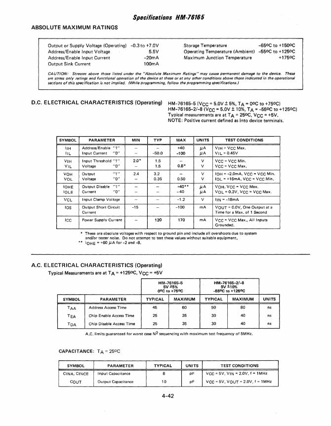
Specifications HM-76165
ABSOLUTE MAXIMUM RATINGS
Output or Supply Voltage (Operating) Address/Enable Input Voltage Address/Enable Input Current
-0.3to +7.0V 5.5V
-20mA 100mA
Storage Tem peratu re -650 C to + 1500 C Operating Temperature (Ambient) -550 C to +1250 C Maximum Junction Temperature +1750 C
Output Sink Current
CAUTION: Stresses above those listed under the "Absolute Maximum Ratings" may cause permanent damage to the device. These are stress only ratings and functional operation of the device at these or at any other conditions above those indicated in the operational sections of this specification is not implied. (While programming, follow the programming specifications.)
D.C. ELECTRICAL CHARACTERISTICS (Operating) HM-76165-5 (VCC = 5.0V ± 5%, TA = OoC to +750 C) HM-76165-2/-8 (VCC = 5.0V ± 10%, TA = -550 C to +1250 C) Typical measurements are at T A = 250 C, VCC = +5V. NOTE: Positive current defined as into device terminals.
SYMBOL PARAMETER MIN TYP MAX UNITS TEST CONDITIONS
IIH Address/Enable "1" - - +40 pA VIH = VCC Max.
IlL Input Current "0" - -50.0 -100 pA Vll=0.45V
VIH Input Threshold "1" 2.0' 1.5 - V VCC = VCC Min.
Vil Voltage "a" - 1.5 O.S' V VCC = VCC Max.
VOH Output "1" 2.4 3.2 - V 10H = -2.0mA, VCC = VCC Min.
VOL Voltage "a" - 0.35 0.50 V 10l = +16mA, VCC = VCC Min.
10HE Output Disable "1" - - +40** pA VOH, VCC = VCC Max. 10lE Current "a" - - -40 pA VOL = 0.3V, VCC = VCC Max.
VCl Input Clamp Voltage - - -1.2 V liN = -lSmA
105 Output Short Circuit -15 - -100 mA VOUT = O.OV, One Output at a Current Time for a Max. of 1 Second
ICC Power Supply Current - 120 170 rnA VCC = VCC Max., All Inputs Grounded.
* These are absolute voltages with respect to ground pin and include all overshoots due to system and/or tester noise. Do not attempt to test these values without suitable equipment. 10HE = +60 PA for -2 and -S.
A.C. ELECTRICAL CHARACTERISTICS (Operating)
Typical Measurements are at T A = +1250 C, VCC = +5V
HM-76165-5 5V±S%
ooc to +750 C
SYMBOL PARAMETER TYPICAL MAXIMUM
TAA Address Access Time 45 60
TEA Chip Enable Access Time 25 35
TDA Chip Disable Access Time 25 35
HM-76165-2/-8 SV ±10%
-550 C to + 12SoC
TYPICAL MAXIMUM UNITS
50 SO ns
30 40 ns
30 40 ns
A.C. limits guaranteed for worst case N2 sequencing with maximum test frequency of SMHz.
CAPACITANCE: T A = 250 C
SYMBOL PARAMETER TYPICAL UNITS TEST CONDITIONS
CINA, CINCE Input Capacitance 8 pF VCC = 5V, VIN = 2.0V, f = 1 MHz
COUT Output Capacitance 10 pF VCC = 5V, VOUT = 2.0V, f = 1 MHz
4-42

HM-76165 SWITCHING TIME DEFINITIONS
ADDRESSES~~I_.5_V __________ ___
OUTPUTS b<xx~ I
.-j TAA I I
, f--I
3.0V
O.OV
VOH
VOL
NOTE: As is common to all memory devices, output levels can be undefined during the address access period (TAA); however. the outputs are guaranteed to reach stable levels by T AA. It is not recommended that outputs from this class of devices be used to drive edge triggered inputs on subsequent devices (counters, flip-flops, etc.) without proper intermediate synchronization.
VCC
g
3.OV
CE,. CE2 O.OV
TDAI TEA1
OUTPUTS VOHAC'
TDA2 TEA2
OUTPUTS VOLAC'
tr. tf < 5ns
"VOLAC AND VOHAC ARE THE MEASURED OUTPUT VOLTAGE LEVELS
WHILE ENABLED.
A.C. TEST LOAD
PROM
OUTPUT Ox 0---+--_--0 TEST POINT
This is the A.C. Test Load which Harris Semiconductor uses in its automatic test equipment, and it is recommended that users of Harris bipolar devices use the same or an equivalent load in performing A. C. testing. 600n
SYMBOL
TAA
TEAl
TEA2
TDAl
TDA2
30pF"
11-, neludes jig & probe
total capacitance
PARAMETER
Address Access Time
Chip Enable Access Time from
"Three State" to V a H
Chip Enable Access Time from
"Three State" to VOL
Chip Disable Access Time from
VOH to "Three State"
Chip Disable Access Time from
VOL to "Three State"
4-43
S1
Closed
Open
Closed
Open
Closed
0::><0:: ....10 0::;0 a..UJ iii::;o

m HARRIS
Features
• 65ns MAXIMUM ADDRESS ACCESS TIME
• "THREE STATE" OUTPUTS AND TWO CHIP ENABLE CONTROLS
• SIMPLE HIGH SPEED PROGRAMMING - ONE PULSE/BIT TYPICAL
• FAST ACCESS TIME - GUARANTEED FOR WORST CASE N2 SEQUENCING
OVER COMMERCIAL AND MILITARY TEMPERATURE AND VOLTAGE
• PRODUCED ON MIL-M-3B51O QUALIFIED WAFER FAB LINE
• INDUSTRY STANDARD 24 PIN PACKAGE
Description
The HM-76321 is a fully decoded Schottky TTL 32,768 bit field programmable ROM in a 4K word by 8 bit/word format with "Three State" outputs. This PROM is available in a 24 pin DIP.
All bits are manufactured storing a logical "1" (Positive Logic) and can be selectively programmed for a logical "0" in any bit position.
MIL-M-38510 qualified NiCr technology is used on the HM-76321 and all other HARRIS Bipolar PROMs.
The HM-76321 contains test rows and columns which are in addition to the storage array to assure high programmability and guarantee parametrics and A.C. performance. The fuses in these test rows and columns are blown prior to shipment.
The HM-76321 utilizes two chip enable controls, where CE1 low and CE2 high enables the device.
Functional Diagram
A.-=~----~~----' A,
A,
A, Ao~'+L ____ ..r'+L ____ -'
(241" vee (12I-GND
'01 0, ". 0, (11)
0,
(13)
0,
4-44
(3) (1) (231 (22) (21) "9)
As At! A7 As As A'0 AU
HM-76321 4K x 8 PROM
Pinout TOP VIEW - DIP
A7 VCC A6 Aa A5 Ag
A4 A10 A3 CE,
A2 A11 A, CE2
Ao Oa 0, 07 02 06 03 05
GND 04
PIN NAMES AO - A 11 Address Inputs
01 - Oa Data Outputs eEl, CE2 Chip Enable Inputs
logic Symbol
CE,
CE2
Ao A,
A2 A3 A4
A5
A6 A7
Aa Ag
A10 All
(14)
Os (15)
Os
0,
02
03 04 05
06 07
08
(17)
Os

Specifications HM-76321
ABSOLUTE MAXIMUM RATINGS
Output or Supply Voltage (Operating) Address/Enable I nput Voltage Address/Enable Input Current
-0.3 to + 7 .OV 5.5V
-20mA 100mA
Storage Temperature -650 C to +1500 C Operating Temperature (Ambient) ··550 C to +1250 C Maximum Junction Temperature +1750 C
Output Sink Current
CAUTION: Stresses above those listed under the "Absolute Maximum Ratings" may cause permanent damage to the device. These are stress only ratings and functional operation of the device at these or at any other conditions above those indicated in the operational sections of this specification is not implied. (While programming, follow the programming specifications.)
D.C. ELECTRICAL CHARACTERISTICS (Operating) HM-76321-5 (VCC; 5.0V ± 5%, TA; ooC to +750 C) HM-76321-2/-B (VCC; 5.0V ± 10%, T A; -550 C to +1250 C) Typical measurements are at TA ; 250 C, VCC; +5V. NOTE: Positive current defined as into device terminals.
SYMBOL PARAMETER MIN TYP MAX UNITS TEST CONDITIONS
IIH Address/Enable "1" - - +40 Il A VIH = VCC Max. IlL Input Current "0" - -50.0 -100 Il A VI L = 0.45V
VIH Input Threshold "1" 2.0* 1.5 - V Vce = Vce Min. VIL Voltage "a" - 1.5 0.8* V Vee = Vee Max.
VOH Output "1" 2.4 3.2 - V IOH = -2.0mA, Vee = vee Min. VOL Voltage "a" - 0.35 0.50 V IOL = +16mA. vee = vee Min.
IOHE Output Disable "1" - - +40** Il A VOH. Vee = Vee Max. IOLE Current "a" - - -40 Il A VOL = 0.3V, Vee = Vee Max.
VeL Input Clamp Voltage - - -1.2 V liN = -18mA
lOS Output Short Circuit -15 - -100 mA VOUT = O.OV. One Output at a Current Time for a Max. of 1 Second
lee Power Supply Current - - 190 mA Vee = vee Max., All Inputs Grounded.
* These are absolute voltages with respect to ground pin and include all overshoots due to system and/or tester noise. Do not attempt to test these values without suitable equipment.
** IOHE = +100 IlA for -2 and-8.
A.C. ELECTRICAL CHARACTERISTICS (Operating) Typical measurements are at T A = +250 C, VCC ; +5V
HM-76321-5 5V±5%
OOC to +750C
SYMBOL PARAMETER TYPICAL MAXIMUM
TAA Address Access Time 45 65
TEA Chip Enable Access Time 25 35
TDA Chip Disable Access Time 25 35
HM-76321-2/-8 5V±10%
-550C to +1250e
TYPICAL MAXIMUM UNITS
- 85 ns
- 40 ns
- 40 ns
A.C. limits guaranteed for worst case N2 sequencing with maximum test frequency of 5MHz.
CAPACITANCE: T A = 250 C
SYMBOL PARAMETER TYPICAL UNITS TEST CONDITIONS
eINA, elNeE Input Capacitance 8 pF Vee = 5V. VIN = 2.0V, f = 1 MHz
eOUT Output Capacitance 10 pF Vee = 5V. VOUT = 2.0V, f = 1MHz
4-45
0:>«0: -'0 0::;; "-w iii::;;
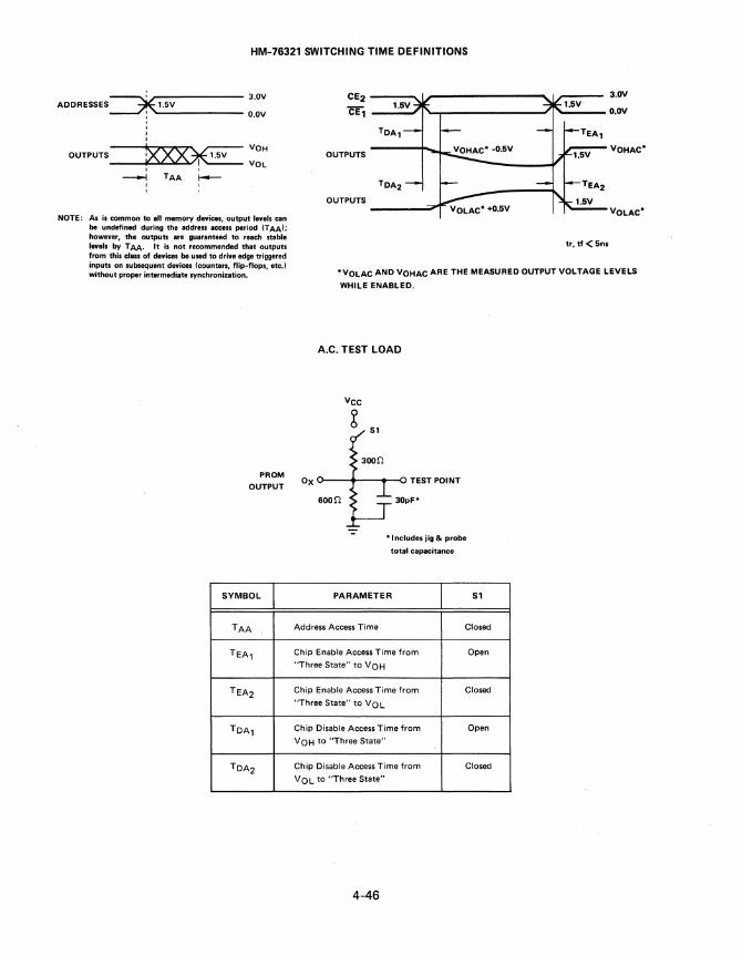
HM-76321 SWITCHING TIME DEFINITIONS
---:s.c 3.0V ADDRESSES~, .'_.5_V _____ _
- O.OV
OUTPUTS ><XX~ ::: I I
--l TAA t---I
NOTE: As is common to aU memory devices, output levels can be undefined during the address aceess period (TAA); however. the outputs are guaranteed to reach stabl. le.als by TAA. It is not recommended that outputs from this class of devices be used to drive edge triggered inputs on subsequent devices (counter., flip-flops, etc.) without proper intermediate synchronization.
PROM OUTPUT
SYMBOL
TAA
TEA,
TEA2
TDAI
TDA2
CE2 3.OV
CEI O.OV
TOA, TEA,
OUTPUTS VOHAC·
TDA2 TEA2
OUTPUTS VOLAC·
tr, tf<5ns
'VOLAC AND VOHAC ARE THE MEASURED OUTPUT VOLTAGE LEVELS
WHILE ENABLED.
A.C. TEST LOAD
VCC
g s,
300!'!
Ox O----1~-..... --IO TEST POINT
600!'!
,* Includes jig &: probe
total capacitance
PARAMETER SI
Address Access Time Closed
Chip Enable Access Time from Open
"Three State" to VOH
Chip Enable Access Time from Closed
"Three State" to Va L
Chip Disable Access Time from Open
VOH to "Three State"
Chip Disable Access Time from Closed
VOL to ''Three State"
4-46

;II HARRIS
Features • 85ns MAXIMUM ADDRESS ACCESS TIME
• "THREE STATE" OUTPUTS
• ACTIVE LOW CHIP ENABLE CONTROL
• HIGHEST DENSITY AVAILABLE IN THE INDUSTRY
• FOUR FOLD INCREASE IN DENSITY OVER CURRENTLY AVAILABLE 16K PROMs WITH 114 POWER DISSIPATION PER BIT
• INDUSTRY STANDARD 24 PIN PACKAGE
• SIMPLE HIGH SPEED PROGRAMMING - ONE PULSE/BIT TYPICAL
• FAST ACCESS TIME - GUARANTEED FOR WORST CASE N2 SEQUENCING OVER COMMERCIAL AND MILITARY TEMPERATURE AND VOLTAGE
• PRODUCED ON MIL-M-38510 QUALIFIED WAFER FAB LINE
Description The HM-76641 is a fully decoded Schottky TTL 65,536 bit field programmable ROM in an 8K word by 8 bit/word format with "Three State" outputs. This PROM is available in a 24 pin DIP.
All bits are manufactured storing a logical "1" (Positive Logic) and can be selectively programmed for a logical "0" in any bit position.
MIL-M-38510 qualified NiCr technology is used on the HM-76641 and all other HARRIS bipolar PROMs.
The HM-76641 contains test rows and columns which are in addition to the storage array to assure high programmability and guarantee parametrics and A.C. performance. The fuses in these test rows and columns are blown prior to shipment.
The HM-76641 utilizes a single chip enable, CE, which when low enables the device.
Functional Diagram
" " " " 'O-~L-_---I~_---'
(24(-VCC
(12)"GND
256 x 128 MEMORY ARRAY
(10)
0, (13)
0,
l31 (21 (11 (23) 1221 1211 (19) (18)
AS AS A7 As AS A'0 AU A12
4-47
HM-76641 8K x 8 PROM
Pinout TOP VIEW - DIP
A7 Vee AS AS
A5 Ag
A4 A10
A3 IT A2 All
Al A12
Ao Os 01 07
°2 Os 03 05
GND °4
PIN NAMES
AO - A12 01 -08
CE
Address Inputs Data Outputs Chip Enable Inputs
IT AO
Al
A2
A3
A4
A5
AS
A7
AS
Ag
AlO
All
A12
(14)
Os
logic Symbol
(15) 0, (16)
0,
01
°2 03
04
05
Os 07
Os
(17)
0,
a:>«a: -'0 0:;; a..w iii:;;

Specifications HM-76641
ABSOLUTE MAXIMUM RATINGS
Output or Supply Voltage (Operating) Address/Enable I nput Voltage Address/Enable Input Current
-0.3 to +7 .OV 5.5V
-20mA 100mA
Storage Temperature -650C to +1500C Operating Temperature (Ambient) -550C to +1250C Maximum Junction Temperature +1750C
Output Sink Current
CAUTION: Stresses above those listed under the "Absolute Maximum Ratings" may cause permanent damage to the device. These are stress only ratings and functional operation of the device at these or at any other conditions above those indicated in the operational sections of this specification is not implied. (While programming, follow the programming specifications.)
D.C. ELECTRICAL CHARACTERISTICS (Operating) HM-76641-5 (VCC; 5.0V ± 5%, TA; ooC to +750C) HM-76641-2/-8 (VCC; 5.0V ± 10%, TA; -550C to +1250C) Typical measurements are at T A; 250C, VCC ; +5V. NOTE: Positive current defined as into device terminals.
SYMBOL PARAMETER MIN TYP MAX UNITS TEST CONDITIONS
IIH Address/Enable "1" - - +40 )1A VIH = Vee Max.
IlL Input Current "0" - -50.0 -100 )1A VI L = 0.45V
VIH Input Threshold "1" 2.0* 1.5 - V Vee = Vee Min. VIL Voltage "0" - 1.5 0.8* V Vee = Vee Max.
VOH Output "1" 2.4 3.2 - V IOH = -2.0mA, Vee = Vee Min. VOL Voltage "0" - 0.35 0.50 V IOL = +16mA, Vee = vee Min.
10HE Output Disable "1" - - +40** )1A VOH, Vee = vee Max. 10LE Current "0" - - -40 )1A VOL = 0.3V, Vee = Vee Max.
VeL Input Clamp Voltage - - -1.2 V liN = -18mA
las Output Short Circuit -15 - -100 mA VQUT = O.OV, One Output at a Current Time for a Max. of 1 Second
lee Power Supply Current - - 190 mA vee = vee Max., All Inputs Grounded.
* These are absolute voltages with respect to ground pin and include all overshoots due to system and/or tester noise. Do not attempt to test these values without suitable equipment •
• * 10HE = +100)1A lor -2 and -8.
A.C. ELECTRICAL CHARACTERISTICS (Operating)
Typical Measurements are at T A = +250C, VCC; +5V
HM-76641-S SV±S%
ooe to +7SOC
SYMBOL PARAMETER TYPICAL MAXIMUM
TAA Address Access Time 50 85
TEA Chip Enable Access Time 30 40
TDA Chip Disable Access Time 30 40
HM-76641-2/-B SV ±10%
-SSOC to + 12soe
TYPICAL MAXIMUM UNITS
- 100 ns
- 45 ns
- 45 ns
A.C. limits guaranteed for worst case N2 sequencing with maximum test frequency of 5MHz.
CAPACITANCE: T A = 250C
SYMBOL PARAMETER TYPICAL UNITS TEST CONDITIONS
eINA, elNeE Input Capacitance 8 pF Vee = 5V, VIN = 2.0V, 1= lMHz
eOUT Output Capacitance 10 pF Vee ~ 5V, VQUT = 2.0V, f = 1 MHz
4-48

HM-76641 SWITCHING TIME DEFINITIONS
ADDRESSES ~ 1.SV 3.0V 3.0V
O.OV Ce O.OV
TDAl ,
~XX~ VOH VOHAC'
OUTPUTS OUTPUTS VOL
--l TAA r--, TDA2
OUTPUTS
tf, tf < 5ns
NOTE: As is common to all memory devices, output levels can be undefined during the address access period (T AA); however, the outputs are guaranteed to reach stable levels by T AA. It is not recommended that outputs from this class of devices be used to drive edge triggered inputs on subsequent devices (counters, flip-flops, etc,) without proper intermediate synchronization. 'VOLAC AND VOHAC ARE THE MEASURED OUTPUT VOL TAGE LEVELS
WHILE ENABLED.
PROM
OUTPUT
A.C. TEST LOAD
VCC
g Sl
Ox o---~--.>--o TEST POINT
This is the A. C. Test Load which Harris Semiconductor uses in its automatic test equipment, and it is recommended that users of Harris bipolar devices use the same or an equivalent load in performing A. C. testing. GOOn
SYMBOL
TAA
TEAl
TEA2
TDAl
TDA2
30pF*
* Includes jig & probe
total capacitance
PARAMETER
Address Access Time
Chip Enable Access Time from
"Three State" to VOH
Chip Enable Access Time from
"Three State" to VOL
Chip Disable Access Time from
VOH to "Three State"
Chip Disable Access Time from
VOL to "Three State"
4-49
S1
Closed
Open
Closed
Open
Closed
0::>«0:: -'0 0::;; O-UJ iii::;;

m HARRIS HM-76641A Preview
Features • 50nsMAXIMUM ADDRESS ACCESS TIME (O°C TO +750 C)
• "THREE STATE" OUTPUTS
• ACTIVE LOWCHIP ENABLE CONTROL
• HIGHEST DENSITY AVAILABLE IN THE INDUSTRY
• FOUR FOLD INCREASE IN DENSITY OVER CURRENTLY AVAILABLE 16K PROMs WITH 1/4 POWER DISSIPATION PER BIT
• INDUSTRY STANDARD 24 PIN PACKAGE
• SIMPLE HIGH SPEED PROGRAMMING - ONE PULSE/BIT TYPICAL
• FAST ACCESS TIME - GUARANTEED FOR WORST CASE N2 SEQUENCING OVER COMMERCIAL AND MILITARY TEMPERATURE AND VOLTAGE
Description The HM-76641 is a fully decoded SchottkY TTL 65,536 bit field programmable ROM in an 8K word by 8 bit/word format with "Three State" outputs. This PROM is available in a 24 pin DIP.
All bits are manufactured storing a logical "1" (Positive Logic) and can be selectively programmed for a logical "0" in any bit position.
MIL-M-38510 qualified NiCr technology is used on the HM-76641 and all other HAR R IS bipolar PROMs.
The HM-76641 contains test rows and columns which are in addition to the storage array to assure high programmability and guarantee parametrics and A.C. performance. The fuses in these test rows and columns are blown prior to shipment.
The HM-76641 utilizes a single chip enable, CE, which when low enables
the device.
Functional Diagram
A, A, A, A, A,
(241- VCC (12)-GND 0,
(10)
0,
(2) 111 1231 12211211 11911181 A5 A6 AS Ag A,O A11 AI2
(13)
0,
4-50
A7
A6
A5
A4
A3
A2
Al
AO
01
°2 03
GNO
8K x 8 PROM
Pinout TOP VIEW - DIP
vee AS
Ag
AlO
IT All
A12
Os 07
06
05
04
PIN NAMES
Add ress Inputs Data Outputs Chip Enable Inputs
logic Symbol

m HARRIS JAN-0512 512 BIT, BIPOLAR PROM
MIL/M38510/20101
Features
• FIELD PROGRAMMABLE
• 64 WORDS/S BITS PER WORD
• FULLY DECODED
DTL/TTL COMPATIBLE
• 140n5 ACCESS TIME
Description
The JAN-0512 is a field programmable 64 word by 8 bit PROM. In an unprogrammed memory, all "Memory Elements" are short circuits so that logical "zeros" appear at each output bit position for any address input. "Electronic Programming" involves the alteration of specific "Memory Elements" to create logical "ones" in selected bit positions. This alteration is irreversible and cannot be accomplished under normal operating conditions.
Block Diagram
ENABLE
OUTPUT BUFFERS
MEMORY ELEMENTS
& DECODING
MATRIX
IC· NC
4-51
Pinout
TOP VIEW - D.i.P.
N.C. VCC
N.C. G2'
AO BO
Al Bl
A2 B2
El B3
E2 B4
A3 B5
A4 B6
A5 B7
Gl N.C.
IC' G2
*Must be left open circuit
BO
-Ie - Intarnal Connection must be left open
NOTE: For operational condition, return pins 11,13, and 23 to system ground.

Specifications JAN-0512
ABSOLUTE MAXIMUM RATINGS
Supply Voltage Range Input Voltage Range Storage Temperature Range Lead Temperature (Soldering 10 Seconds) Thermal Resistance, Junction-to-Case
Output Supply Voltage Output Sink Current Maximum Power Dissipation, PD Maximum Junction Temperature, T J
RECOMMENDED OPERATING CONDITIONS
Supply Voltage Minimum High Level Input Voltage Maximum Low Level Input Voltage Normalized Fanout (Each Output) Ambient Operating Temperature Range
ELECTRICAL CHARACTERISTICS
-0.5 VDC to 7.0 VDC -1.5 VDC at -12mA to 5.5VDC
-650 C to + l500 C 3000 C
JC' Case J = 30oC/w
-0.5VDC to 7.0VDC +30mA
575mWdc l750 C
4.75 VDC Min. to 5.25VDC Maximum 2.0VDC 0.8VDC
6 Maximum (10mA) -550 C to +1250 C
The electrical characteristics are as specified in the table and apply over the full recommended ambient operating temperature range, unless otherwise specified.
SYMBOL
VOL
VIC
leEX1
leEX2
IIH1
IIH2
IlL
ICC
tPHL
tPLH
LIMITS
TEST MIN MAX UNITS
Low Level Output Voltage 0.45 Volts
Input Clamp Voltage -1.5 Volts
100 J.1A
Maximum Collector Cut-Off Current
200 J.1A
60 J.1A
High Level Input Current 100 J.1A
Low Level Input Current -0.2 -1.6 mA
Supply Current 100 mA
Propagation Delay Time 85 140 ns High-to-Low Level Logic
Propagation Delay Time Low-to-H igh Level Logic
85 140 ns
NOTES: 1. When testing one E input, apply 5.25V to the other. 2. When testing one E input, apply GND to the other.
4-52
TEST CONDITIONS
Vee - 4.75V VIN = 2.0V IOL = 10mA
Vee = 4.75V liN = -12mA TA = 250 e
Vee = 5.25V VOH = 2.8V VIN = 0.8V
Vee = 5.25V VOH = 5.25V VIN = 0.8V
Vee = 5.25V VIN = 2.4V;
Vee = 5.25V VIN = 5.25;(j)
Vee = 5.25V VIN = O.4V;<%>
Vee = 5.25V VIN =0
Vee = 5.0V eL = 30pF Min. R1 =470n ±5%

Switching Time Test Circuits
INPUT +5.0V
5.0V AO VCC BO
A1 B1
A2 B2 -PULSE SEE A3 B3
GENERATOR D.U.T. B4 NOTE 2 A4
AS B5
PRR = 1MHz = 20% R1 E1 B6
INPUT
OUTPUT
E2
1--10n5
,""'.:.;....;.-----Ov ~----VOH
1.5V
r-------+_,- ----- VOH
1.5V
~-VOL
NOTES:
1. Pins 12 and 14 shall be left open.
2. The applicable test table should be selected from the altered item drawing.
3. C1 = 0.5pF ±10%; R1 = 5011 ±5%; R2 = 470". ±5%; R3 = 1kl1 ±5%; CL = 30pF including jig and probe capacitance.
4-53
CL
a:>«a: -'0 0::;;: Q..w 00::;;:

< ! t-Z III a: a: :;)
" t-:;) .. t-:;) 0
1 t-Z w a: a: :;)
" > ...J
t :;) <II a: III
~ ..
40
35
30
25
20
15
10
5
o o
100
75
50
25
o -55
Characteristic Curves
OUTPUT CHARACTERISTICS
Vee-5V
)" ~/ ./
v
~. oGV V
",C/ .-f$ -f>oG,/ -\., ~V
/ ./-\
/ // V"
0.1 0.2 0.3 0.4 0.5 0.6 0.7
OUTPUT VOLTAGE (VOL TSI
POWER SUPPLY CURRENT vs. TEMPERATURE
VA,VE-OV
o
/ Vee - 5.0V
25
TEMPERATURE (OCI
70
vec-t25V
--, -vcc - 4.75V
125
4-54
1 t-z w a: a: :;)
" t-:;)
~ :;) 0
40
35
30
25
20
15
10
o -65
100
] 75 > :5 III o i5 50
~ ~ a: 25 ..
o -55
OUTPUT CURRENT vs. TEMPERATURE
Vcc - 5V
--.... VOL -0.4V ---- --I--- .......
o 25 70 125
CASE TEMPERATURE (OCI
PROPAGATION DELAY vs. TEMPERATURE
IOL -10mA VCC' 5V
CL - 30pF ...-
------ ~ V--~
25 70 125
TEMPERATURE (OCI

JAN-0512 Programming Procedure
PROGRAMMING SPECIFICATIONS
PARAMETER VALUE
Address Input Voltage
High Logic Level Open Circuit CD Low Logic Level -S.OV
Power Supply Voltage +S.OV +S%, -0%
G1 Voltage@ -S.OV
G2 Voltage OV
G2' Voltage
For Device Type 01 Circuit A Open
Maximum Programming Voltage -7.0V
Maximum Programming Current 100mA
Maximum Number or Attempts 2 to Program a Given Bit
Maximum Case Temperature 7SoC During Programming
1. Open collector TTL gates meet this reqUirement. 2. G1 must be connected to -5.0V prior to applying Vee or pro
gramming voltage.
PROGRAMMING PROCEDURES
Using the test conditions of the table, the following procedures shall be used for programming the device:
(a) Connect the device as shown in Figure 1, using the fusing generator of Figure 1 or the alternate circuit of Figure 2. The circuit shown in Figure 2 can be used in more automated programming systems. This circuit
NOTES: 1. Connect -5.0V to Gt before applYing Vee or programming voltage. 2. For device type 01, G2' shall be open. 3. Generator characteriSltlCs are defined In Programming Procedures.
FIGURE 1 PROGRAMMING CONNECTIONS
4-55
generates a current pulse which is at the proper voltage and current levels for fast reliable programming. The input programming pulse width shall be 750ms ±50ms. The number of attempts to program a given bit shall be as specified in the table.
(b) To address a particular word in the memory, set the input switches to the binary equivalent of that word, where a logical low level is -5.0V and a logical high level is an open circuit. (Do not return to supply). All output bits (BO, B1, ... B7) of this word are available for programming.
(c) With the output current limited (as specified in the table), apply a negative going current pulse to the pin associated with the fi rst bit to be changed from a logical low level to a logical high level. This is most easily accomplished by connecting the negative terminal of a variable power supply to the proper output pin and manually increasing the voltage to approximately 6.0V.
(d) Skipping any bit which is to remain a logical low level, repeat step (c) for each logical low level in the word being addressed. Not more than one bit shall be programmed at a time.
(e) Set the next input address and repeat steps (c) and (d). This procedure is repeated for each input address for which a specific output word pattern is desired. Note that all addresses do not have to be programmed at the same time, nor do all output bits for a given address. A logical low level can always be changed to a logical high level, simply by repeating steps (b) and (c). A logical low level, once programmed to a logical high level, cannot be reprogrammed.
+5,OV
lKn
..,----<r+ 8 ;
-15,OV
FIGURE 2 PROGRAMMING CIRCUIT
0:><co: -'0 0:;;; o..w iii:;;;

Generic PROM Programming
All 76xxx series devices utilize the same programming method which is one of the characteristics that lends to the term "Generic" PROM.
Harris Generic PROMs have the industry's highest programming yield and exhibit an extremely high level of reliability in the field; however, this level of device quality can only be obtained if the PROM has been properly programmed to the data sheet specifications. Outlined below are the key points which deserve attention to assure that programming has been optimally performed.
• Be certain that you are following the latest revision status of programming specifications.
• If you are utilizing a commercial programmer, be sure that the module for Harris Generic PROMs is certified for the most recent revision level.
• Have the Programmer calibrated at routine intervals to assure that the electrical and mechanical characteristics are acceptable. This would include such things as:
~ Making certain that the socket which the device is placed into is clean, free of corrosion and is mechanically sound.
~ Check ribbon cable connectors for good continuity.
~ Making sure that all voltage levels conform to the programming specifications.
~ Assuring that all pulses are clean of distortion and exhibit the correct timing characteristics.
• The typical programming failure mode of Harris Generic PROMs should be underprogrammed (won't blow a fuse or fuses). This is usually due to the pyrotechnic nature of PROMs. You won't know for sure whether any given fuse will program until you try. Overprogramming (undesired fuses program) is an extremIy low incidence problem, and any measurable percentage of overprogramming is a glaring indication of programming equipment malfunction. PROMs that fail at the same location also indicates a problem with the programmer as untestable flaws in PROMs are random in nature.
If there is any problem in determining how to follow any of the guidelines, contact a local Harris office for assistance.
PROGRAMMING PROCEDURE
The following is a generic programming procedure which is used for all Harris Generic 76xxx PROMs.
The HM-76xxx PROMs are manufactured with all bits storing a logical "1" (output high). Any desired bit can be programmed to a logical "0" (output low) by following the simple procedure shown below. One may build his own programmer to satisfy the specifications described in the table, or use any of the commercially available programmers which meet these specifications. These PROMs can be programmed automatically or by the manual procedure shown on the next page.
4-56

Programming the HM-76xxx PROMs
The HM-76xxx PROMs are manufactured with all bits storing a logical "1" (output high). Any desired bit can be programmed to a logical "0" (output low) by following the simple procedure shown below. One may build his own programmer to satisfy the specifications described in the table, or use any of the commercially available programmers which can meet these specifications.
PROGRAMMING SPECI FICATIONS
RECOMMENDED
SYMBOL PARAMETER MINIMUM OR TYPICAL MAXIMUM UNITS
VIH Address Input 2.4 5.0 5.0 V
Vll Voltage 11 I 0.0 0.4 0.5 V
VPH 121 Programming/Verify 12.0 12.0 12.5 V
VPll31 Voltage to VCC 4.5 4.5 5.5 V
IllP Programming Input - -300 -600 J.lA Low Current at VPH
tr Programming IVCC I 1.0 1.0 10.0 J.ls If Voltage Rise and Fall Time 1.0 1.0 10.0 J.ls
td Programming Delay 10 10 100 J.ls
tp Programming Pulse Width (4) 90 100 110 Us
P.D.C. Programming Duty Cycle 151 - 50 60 %
VOPE Output Voltage Enable 161 10.5 10.5 11.0 V
VOPD Output Voltage Disable 0.0 5.0 5.5 V
Ta Ambient Temperature - 25 30 oC
During programming the chip must be disabled for proper operation.
NOTES: 1. No inputs should be left open for VIH. 2. VPH source must be capable of supplying one ampere. 3. It is recommended that dual verification be made at VPL min and VPL max. 4. Note step 9 in programming procedure. 5. Programming Duty Cycle applies to DIPs only, 6. VOPE source must be capable of supplying 10mA minimum.
PROGRAMMING PROCEDURE
1. Address the PROM with the binary address of the word to be programmed. Address inputs are TTL compatible. An open circuit should not be used to address the PROM.
2. Bring the CEx input(s) high and the CEx input(s) low to disable the device. The disabling of the device during programming is an essential step in correctly programming all HARRIS PROMs. The chip enables are TTL compatible. An open circuit should not be used to disable the device.
3. Disable the programming circuitry by applying a voltage of VOPD to the outputs of the PROM.
4. Raise VCC to VPH with rise time less than or equal to tr.
5. After a delay equal to or greater than td apply a pulse with amplitude of VOPE and duration of tp to the output selected for programming. Note that the PROM is supplied with fuses intact, which generates an output high. Programming a fuse will cause the output to go low.
6. Other bits in the same word may be programmed while the VCC input is raised to VPH by applying output enable pulses to each output which is to be program-
med. The output enable pulses must be separated by a minimum interval of td.
7. Lower VCC to 4.5 volts following a delay of td from last programming enable pulse applied to an output.
8. Enable the PROM for verification by applying VIL to CEx and VIH to CEx.
9. Repeat verification (step 8) at VCC; 5.5 volts.
10. If any bit does not verify as programmed, repeat steps 2 through 9 until the bit has received a total of 1 ms of programming time. Bits which do not program within 1 ms are programming rejects. No further attempt to program these parts should be made.
11. Repeat steps 1 through 10 for all other bits to be programmed in the PROM.
12. Programming rejects returned to the factory must be accompanied by data giving address, desired data, and actual output data of the location in which a programming failure has occurred.
4-57
""><t"" --'0 0:;: Q..UJ co:;:

TYPICAL PROGRAMMING CIRCUIT
The circuit and timing diagrams shown in Figures 1 and 2 will establish the proper programming conditions for the output enable pulses. This allows the use of standard TTL
Vp
parts for all logic inputs to the PROM. Note the gate which senses the output must withstand inputs up to 11.0 volts during programming.
390n
-----I AO cc Oxt--1~---t----i-.,.'VI""'o( 22011
DATA-x
DEVICE BEING PRO-
GRAMMED
220n
HIGHVOLTAGEI CURRENT TTL GATE
L-__ --I '::>--- 0 1
1--------.-1 '::>--- Ox "-
SENSE GATE
FIGURE 1
CEx -------~ ______________ __ll _______ :::
CEx-----------~
1----- --:II~
VPH------ib~~O -----..1
VCC JJ/190% VPL 10%' '--------VIL
~~----~-~--------VOPD1
~--I--------------VOPDX
FIGURE 2
Waveforms Applied to the Device Pins During Programming
4-58

Programmer Evaluation
Programmer equipment manufacturers identified in the accompanying list have previously produced equipment determined to be capable of properly programming Harris Semiconductor PROMs. This list is provided only as a convenience to purchasers of HARRIS PROMs to identify programmer manufacturers potentially suitable for programming the PROMs. It is neither intended to be a representation or warranty by Harris of the capability of all listed manufacturers models nor an indication of unsuitability of other manufacturers not contained in the list. PROM purchasers are advised to adhere to the programming requirements specified in HARRIS current data sheets applicable to the PROMs to be programmed and to the programming equipment manufacturer's specifications. Responsibility for programming equipment performance lies solely with the equipment manufacturer. The programmer user is cautioned to verify operation and performance according to the manufacturer's instructions and specifications prior to each use, and to determine that the programming complies with the applicable HARRIS PROM data sheet. Harris accepts no responsibility for PROMs which have been subjected to incorrect or faulty programming.
DIGILEC USA Suite 103 7335 E. Acoma Dr. Scottsdale, AZ 85260 Phone: 602-991-7268
STAG MICROSYSTEMS, INC. 528-5 Weddell Drive Sunnyvale, CA 94086 Phone: 408-745-1991
PROM Programmer Manufacturers
INTERNATIONAL KONTRON MICROSYSTEMS, INC. ELECTRONICS 11554 C Avenue 630 Price Avenue Auburn, CA 95603 Redwood City, CA 94063 Phone: 916-885-7262 Phone: 415-361-1012
SUNRISE ELECTRONICS DATA I/O 524 South Vermont Avenue 10525 Willows Road N.E. Glendora, CA 91740 C46 Phone: 213-963-8775 Redmond, WA 98052
Phone: 206-881-6444
PRO-LOG 2411A Garden Rd. Monterey, CA 93940 Phone: 408-372-4593
STOLZ AG Tafernstrasse 15 5405 Braden-Dattwil Switzerland Phone: 056840151
NOTE: Programmer manufacturers are changing from modules or card sets to a universal type of programming system. Contact the programmer manufacturer for their latest up-dates of hardware and software.
4-59
ex:><ex: -'0 o~ C-UJ iii~

Data Entry Formats for Harris Custom Programming*
For Harris to custom program to a user data pattern specification, the user must supply the data in one of the following formats:
1. Master PROM of same organization and pinout as device ordered. Two pieces required, three preferred.
2. Paper tape in Binary or ASCII BPNF.
* BINARY PAPER TAPE FORMAT
• A minimum of six inches of leader.
• A rubout (all eight locations punched).
• Data words beginning with the first word (word "0"), proceeding sequentially, ending with the last word (word "N"), with no interruptions or extraneous characters of any kind.
• Specify whether a punched hole is a VOH = "1" = logic high or is a VOL = "0" = logic low.
• A minimum trailer of six inches of tape.
* ASCII BPNF FORMAT
• A minimum leader of twenty rubouts (all eight locations punched).
• Any characters desired (none necessary) except "B".
• Data words beginning with the first word (word "0"), proceeding sequentially, ending with the last word (word "N").
• Data words consist of:
1. The character "B" denoting the beginning of a data word.
2. A sequence of characters, only "P" or "N", one character for each bit in the word.
3. The character "F" denoting the finish of the data word.
• No extraneous characters of any kind may appear within a data word (between any "B" and the next "F").
• Errors may be deleted by rubouts superimposed over the entire word including the "B", and beginning the word again with a new "B".
• Any text of any kind (except the character "B") is allowed between data words (between any "F" and the next "B"), including carriage return and line feed.
• A minimum trailer of twenty-five rubouts.
• Specify whether a "P" is a "1" = VOH = logic high or is a "0" = VOL = logic low.
• The use of even or odd parity is optional.
* Harris can not assume responsibility for PROMs programmed to data tapes or masters which contain errors. The user must insure the accuracy of the data provided to Harris. Harris guarantees that the programmed PROMs will contain the information provided if either of the following formats are followed.
4-60

.j:>
~
ASCII BPNF PAPER TAPE EXAMPLE
Direction of - Ai Tape Flow
HM-7611
HM-7649
RUBOUTS
')111
FIRST WORD / A'-_____ ,
B N P N N N P N P F FREE
I I I I I I I I I I FIELD
SECOND WORD LAST WORD
~ __ -JA A~ ____ ~
f ~ I r ~ r ~ ~ ~ ~ f ~ r ~ ~ ~ ~ ~ ~ f ((r?( ------------- --------~
• • • • Parity is optional. •••••
•••••••••••••• • ••••••••••••••••••••••••• ••••• ••••• •••• • • • •• ••• • • • • • •••• •••• • ••• • • • • •• • •• • • ••••• 000000000000000000000000000000000000000000
•••• • ••• • •••••• ••• • ••••
16 Pin Pkg.
20 Pin Pkg.
I I I I I I I I
1211 10 9
141312119876
•• • • • • • • • • ••• • •• • ••••••• • ••••• •• • . ...... )
1!'1 •••••
Truth Table Character "0" = "1" = VOH = Logic High Character .'V" = "0" = VOL = Logic Low
I!'
EXAMPLE PACKAGE TYPE DEVICE OUTPUT PINS PROM Outputs Data <D
BIPOLAR MEMORY
Word
AX····A2 Al AO
0·····0 0·····0
1 ·····0
NOTES:
o o
o
o
First
Second.,J..
Last T
Os 07 06 05 04 03 02 0,
o
o
o 1
o
o o o
o 1 o o
o o
1 o o
0) In the ASCII BPNF format, MSB data is punched after "B", On
devices with 8 outputs, Os (Output 8) data is punched after "B",
On devices with 4 outputs, 04 (Output 4) data is punched
after "B"

BINARY PAPER TAPE EXAMPLE
t D;'ection t of Tape
Flow
j@ - -0
o • Sprocket
I Holes 0 ~ Channel 1
! 0 I 0 n-Channel B
0
•• .0. ••• • r-Rubout
• o. •• l "," WoO ••• 0 • •• 0 • • O.
• .0 • •• '" • • 0 •• • "'ro- Last Word
0
-- .-......
DEVICE OUTPUT PACKAGE PINS
EXAMPLE:
""o 0._.-----;- ~~~~:ket o
91011012 67 B 0911121314
t ~ 4- Output a (Oa)
I~~~~i~~;r-I Output 1 (01) ?/// all/./
Punched Hole = "0" = VOL = Logic Low
Word PROM Output Data <D
AX···A2 A1
o .... 0 0 o ····0 0 o .... 0 , o .... 0 1 0 .... 1 0
1 ····1 1
NOTES,
CD
0
4-62
Channel a 7 6 5 4 3 2 AO Output Oa 07 06 05 04 03 02
0 First 0 1 0 0 0 1 0
1 Second 1 1 1 0 1 0 0
0 Third 0 1 0 1 1 1 0 1 Fourth 0 1 1 1 0 1 1
0 Fifth 1 0 0 1 0 0 0
1 ~
Last T 0 1 0 0 1 0 1
PROMs with 4 bit wide data outputs require punching only
first 4 channels on tape (Channels 1 thru 4).
On HARRIS PROMsOX (Example: 011 designates a respective
output pin on the device. 0, (Output 1) is always LSB.
Package
16-Pin 20-Pin
Device Type
HM-7611 HM-7649
1 0,
1 0 0 0 1
0

HPL Functional Index 5-2 and Selection Guide
. Introduction 5-3
Product Information 5-4
HPL Programming Philosophy 5-46
--'
HPL Programmer Evaluation 5-47 <>. :x:
5-1

PART ARRAY MATRIX OUTPUT NUMBER INPUTS ARCHITECTURE LOGIC ENABLE
HPL~77061 Twelve Dedicated Programmable AND-Fixed OR Ten 2-Wide AND-OR Programmable Six Bidirectional (Programmable Output Polarity)
HPL~77153 Eight Dedicated Programmable ANO-Prog. OR Ten 32-Wide AND-OR Programmable /S2S153 Ten Bidirectional (Programmable Output Polarity)
HPL-77209 Ten Dedicated Programmable AND-Fixed OR Eight 7-Wide AND-DR-INVERT Programmable
/16LS Six Bidirectional (Active Low Outputs)
HPL-7721Q Eight Dedicated Programmable AND-Fixed OR Four a-Wide AND-OR Dedicated /16R4 Four Feedback Four 7-Wide AND-OR-INVERT Programmable
Four Bidirectional
HPL~77211 Eight Dedicated Programmable AND-Fixed OR Six a-Wide AND-OR Dedicated /16R6 Six Feedback Two 7-Wide AND-OR-INVERT Programmable
Two Bidirectional en r!.J HPL-77212 Eight Dedicated Programmable AND-Fixed OR Eight a-Wide AND-OR Dedicated
/16RS Eight Feedback
HPL-77215 Ten Dedicated Programmable AND-Fixed OR Eight 7-Wide AND-OR Programmable /16HS Six Bidirectional (Active High Outputs)
HPL~77216 Ten Dedicated Programmable AND-Fixed OR Eight 7-Wide AND-OR Programmable /16PS Six Bidirectional (Programmable Output Polarity)
HPL-77317 Ten Dedicated Programmable AND-Fixed OR Eight a-Wide AND-DR-INVERT -/16LDS Six Feedback (Active Low Outputs)
HPL-77318 Ten Dedicated Programmable AND-Fixed OR Eight a-Wide AND-OR
/16HD8 Six Feedback (Active High Outputs) -
HPL-77319 Ten Dedicated Programmable AND-Fixed OR Eight a-Wide AND-DR-INVERT Six Single-Fuse
/16LES Six Fuse Selectable (Active Low Outputs) Programmable
HPL~77320 Ten Dedicated Programmable AND-Fixed OR Eight 8-Wide AND-OR Six Single-Fuse
116HES Six Fuse Selectable (Active High Outputs) Programmable
NOTE: All HPL products are available in Ceramic and Plastic DIPs. Please see section 9 (Packaging) of this Data Book.
PROPAGATION REGISTER DelAY SETUP TIME
OUTPUTS oDe to +750C oDe to +750C
Six Bidirectional 25 nsee -Four Dedicated
Ten Bidirectional 40 nsee -
Six Bidirectional 35 nsee -
Two Dedicated
Four Registered Four Bidirectional 35 nsee 35 nsee
Six Registered 35 nsee 35 nsee Two Bidirectional
Eight Registered - 35 nsee
Six Bidirectional 35 nsee -Two Dedicated
Six Bidirectional 35 nsec -Two Dedicated
Eight Dedicated 35 nsec -
Eight Dedicated 35 nsee -
Six Fuse Selectable 35 nsec -Two Dedicated
Six Fuse Selectable 35 nsec -Two Dedicated
CLOCK TO OUTPUT TIME oDe to +750C
-
-
-
25 nsee
25 nsee
25 nsee
-
-
-
-
-
-
PAGE
5-4
5-6
5-15
5-42
542
5-42
5~15
5~15
5~24
5~24
5~33
5-33
'-------
J: "tJ r-"T1 s:::: :::l (') r+
o :::l Q)
:::l C. CD >< Q)
:::l C.
en CD CD (') r+
o :::l
c;) s::::
c. CD

mHARRIS HPL™ The Logical Solution
Harris Programmable Logic
Introduction
Harris Programmable Logic (HPL) is a family of user configurable logic elements designed to be space and power saving replacements for random logic designs implemented in TTL or LSTTL. HPL products are a natural progression for Harris Semiconductor, already a major PROM supplier with over ten years experience in the field of nickel-chromium fuse programmable devices. The HPL family contains devices which are functional and pinout replacements for existing industry standard devices, and also includes new devices with enhanced architectural features designed for applications which are not served by existing devices.
Family The HPL family is divided into three architecturally distinct groups, each with its own advantages and areas of application, The three HPL groups are: I FL TM, PAL ® and PROM, and are all similar in that they contain two logic arrays. The first array is an AND array which is used to form PRODUCT terms from combinations of feedback and/or input variables. The second array is an OR array which is used to form SUM terms from combinations of product terms generated by the first array. The difference between the three architectural groups results from various combinations of user configurable and fixed arrays.
The PAL type devices have a programmable first array (AND) and a fixed second array (OR). The PROM type devices have this configuration reversed; they have a fixed first array (AN D) and a programmable second array (OR).
The IF L ™ architectural group is different again, with both its first (AND) and second (OR) logic arrays being programmable.The various combinations of fixed and programmable arrays are shown graphically in Figure 1 below. No one architectural group is the optimum solution for all designs, and for this reason Harris offers a wide range of devices to suit almost any design requirement.
Duality One of the fundamental requirements for high quality is the ability to perform testing on unprogrammed devices as they are manufactured. It was only after the appearance on the market of early Programmable Array Logic devices that both
manufacturers and users became aware of the inherent nontestability of those devices. The reasons for this difficulty is testing blank devices stemmed from architectural differences between programmable logic and programmable memory.
In a programmable memory device, such as a PROM, the same circuitry that is used at manufacture to verify the existence of fuses is used during the normal operation of the device. Therefore, if a PROM passes a fuse array verification test, then the logic paths from input to output are automatically tested for functionality. This simplicity of testing is not, however, present in programmable logic devices because the fuse array is verified using totally separate circuitry to that which is used to carry logic signals during normal device operation. Consequently, verification of the fuse array at manufacture does not guarantee correct operation of the logic paths, and because of this, fuse pattern verification by the user does not guarantee correct device functionality. It is apparent that, unlike a PROM, there are two components of FUNCTIONAL YIELD in a Programmable Logic device: FUSING YIELD and LOGIC PATH YIELD. The FUSING YIELD of a programmable logic device is similar to a PROM and is close to 100%. However, the LOGIC PATH YIELD is an unknown quantity and varies from device to device. The components of FUNCTIONAL YIELD for a programmable logic and programmable memory device are shown below.
FUNCTIONAL YIELD (PROM) = FUSING YIELD
FUNCTIONAL YIELD (PROGRAMMABLE LOGIC) = FUSING YIELD x LOGIC PATH YIELD
Responding to customer requirements for high quality devices, Harris developed unique on-chip test circuitry, patent pending, which is enabled at the time of manufacture to allow complete testing of all logic paths, eliminating the uncertain factor of LOGIC PATH YIELD. One of the benefits of this test circuitry is that the user receives a completely tested device which, providing the fuse array programs correctly, is guaranteed to be functional, eliminating the problem of devices that verify on the programmer but fail in the circuit board. A second benefit of on-chip test circuitry is the ability to perform AC/DC parametric testing at the time of manufacture. This allows Harris to ship devices which are TESTED AND GUARANTEED, and not simply GUARANTEED.
HPl PRODUCT LINE
The HPL product range includes devices from all three of the possible programmable logic architectures, in recognition of the fact that no one architecture is the optimum solution for all designs.
HPL ;s a Trademark of Harris Corporation IFL is a Trademark of Signetics Corporation PAL is a Registered Trademark of MMI 5-3
FIRST ARRAY
Programmable "AND"
Fixed "AND"
IFL TM PROM Programmable SECOND "OR" ARRAY r------------i~TT77,,~TT~
PAL rM Fixed "OR"
Figure 1

mHARRIS HPL-77061
Product Preview HPL!"M Harris Programmable Logic
The HPL-77061 is a proprietary device designed by Harris Semiconductor. It is a 24 pin device with 12 input pins,
6 bi-directional pins, and 4 output pins. The architecture consists of a programmable AND array, followed by a fixed
OR array, followed by a programmable INVERTER. This configuration generates a device that implements logic
expressions in either SUM OF PRODUCTS (SOP) or INVERTED SUM OF PRODUCTS (ISOP) form. Two fuses
associated with each output and bi-directional pin allow their three state buffers to be configured as permanently
active, permanently inactive, or under the control of a common CHIP SELECT(CS) signal. When under the control of
the CS signal, they may be configured to be active when CS is high and inactive when low,
or active when CS is low and inactive when high.
The HPL-77061 is intended to be used as an address decoder in 8, 16 or 32 bit microprocessor systems, and is known
as a FIELD PROGRAMMABLE ADDRESS DECODER (FPAD). When used as an address decoder, it is possible to
contiguously concatenate the address spaces of large and small system components. This allows more efficient use to
be made of available memory space, as well as making the memory decoder design easier. The HPL-77061 may also
be used to replace several TTL packages in many random logic designs. In both the above applications, a significant
reduction in board space, power consumption, package count, and an increase in reliability may be realized. The HPL-
77061 incorporates Harris designed test circuitry which allows complete parametric and logical testing of unprogram
med devices at the time of manufacture. The benefits for the user of this exhaustive testing are very high POST
PROGRAMMING FUNCTIONAL YIELD (95% guaranteed; 97% typically) and pretested AC and DC parametrics.
The HPL-77061 uses the standard HPL programming algorithm which is also used for all Harris Programmable Logic
parts. Special test fuses are included in the HPL-77061. These are selectively programmed during post manufacturing
testing. This allows all the programming circuitry to be tested for correct operation.
The Harris policy is to ship pretested devices, removing the test burden from the small user and assuring the large user
the highest possible quality.
• PROPAGATION DELAY
• SUPPLY CURRENT
• PACKAGE
• TEMPERATURE OPTIONS
• AC/DC SPECS
• FUNCTIONALITY
• PROGRAMMING
• TTL COMPATIBLE
• SUPPORTED BY HELPTM SOFTWARE
HPL is a trademark of Harris Corporation HELP is a trademark of Harris Corporation
5-4
25ns MAX COMMERCIAL
140mA MAX COMMERCIAL
24 PIN SLIMLINE (POWER PLASTIC & CERAMIC)
COMMERCIAL, MILITARY & 883B
PRETESTED
PRETESTED
GENERIC

10
13
14
15
17
18
19
EXCLU FUSES
1
..... 2
0--8--v
5
~
0--s
9
~
0--v
§--v
13
SIVE OR
-=i::-
ELECT CHIPS CONTR Ol FUSES
-:;:-
Functional Diagram HPL-l1061
~ 1-
I--
I--
J-j
C9 Cs C7 Cs C5 C4 C3 C2 C1 Co
~(J~(J~(J~(J~( J~( JS8(J~(J~( J~( Eg Ea E7 E6 ES E4 E3 E2 E 1 EO
~ Q Q Q Q Q Q 0 Q Q G9 Gs G7 Gs G5 G4 G3 G2 G1 Go
~~~~~~~~~~ • DENOTES FIXED
17 18 19 20 l' 15 1S 21 22 23 CONNECTION
Fa Ft F2 F3 80 81 82 83 84 85
5-5
--' c... ::t:

miHARRIS HPL-77153/82S153 H pl2M Harris Programmable Logic
Features
• LOGIC PATHS TESTED TO ENSURE FUNCTIONALITY
• FAST ACCESS (INPUT TO OUTPUTI ••••• 40nsec MAX
• LOW ICC ••.••••••••••.•••••••• 155mA MAX
• ALLOWS SIGNIFICANT PACKAGE COUNT SAVINGS.
• FUNCTIONALLY IDENTICAL TO EXISTING 82S153
• 20 PIN SLIMLINE DIP
• HIGH SPEED PROGRAMMING PROCEDURE - ONE PULSE/BIT ASSURES SUPERIOR RELIABILITY
• SUPPORTED BY HELPTM SOFTWARE
Applications
• RANDOM LOGIC REPLACEMENT
• CODE CONVERTORS
• ADDRESS DECODING
• FAULT DETECTORS
• BOOLEAN FUNCTION GENERATORS
• DIGITAL MULTIPLEXERS
• PARITY GENERATORS
• PATTERN RECOGNITION
• ROM PATCHING
Description
The HPL-77153/82S153 is a programmable logic device designed to be cost effective and space saving replacement for discrete logic designs. This device is a two-level logic element, consisting of 32 product terms (AND) and 10 sum terms (OR) with fusible links for programming I/O polarity and direction.
All product terms can be linked to 8 inputs (I) and 10 bidirectional I/O lines (B) allowing variable I/O configurations using the 10 direction control gates (Dl, ranging from 17 inputs and 1 output to 8 inputs and 10 outputs.
On chip T /C buffers allow either True (I,B) and/or Complement (1.8) signals to be linked to any of the product terms, the outputs of which may be used as inputs to any or all of the sum terms. The output polarity of the sum terms is individually program-
• PROGRAMMABLE SUBSTITUTE FOR TTL SSI/MSI LOGIC CIRCUITS
• REDUCTION OF IC INVENTORIES
• EASE OF PROTOTYPING AND BOARD LAYOUT
• TTL COMPATIBLE INPUTS AND OUTPUTS
• "THREE STATE" OUTPUTS
• PROGRAMMABLE OUTPUT POLARITY
• HARRIS· RELIABLE NICKEL-CHROMIUM FUSE TECHNOLOGY
Pinout
HPL-77153/82S153
Vee 89
88
87
BfI
B5
84
83
82
GND 81
mabie by means of a fuse link controlled EX-OR gate to allow implemention of Sum Of Products (SOP) or Inverted Sum Of Products (lSOP) expressions.
The HPL-77153/82S153 is field programmable, enabling the user to quickly generate custom patterns using standard programming equipment.
Nickel-chromium fuse technology is used on these and all other HARRIS HPL-77XXX programmable logic devices. The HPL-77153/82S153 is available in 20 pin slimline DIP packages with a pinout identical to the 82S153.
The HPL-77153/82S153 contains unique test circuitry developed by HARRIS which is enabled at the time of manufacture to allow complete AC and DC testing.
CAUTION: Electronic devices are sensitive to electrostatic discharge. Proper I.C. handling procedures should be followed. HPL is a trademark of Harris Corporation. HELP is a trademark of Harris Corporation. 5-6

Functional Diagram HPl-77153182S153
10 1
2
12 3 ~
13 4 1
5 1
6
7
8 80
8,
82
83
84
85
86
87
88
8g
59
58
5)
56 (5U M TERMS)
55
54
53
52
5,
50
(PRODUCT TERMS) pppppppp PPPPPPPP pppppppp PPPPPPPP 3130292827262524 2322212019181116 151413121110 9 8 7 6 5 4 3 2 1 0
)( (
5-7
~
....f)..
~
~
-D-
-D-:
-f>-
~
~
(CONTROL TERMS)
1
1
1
)(1 )l -' 0-x
-.I~ 19 89
-~ 18 88
-- 17 87
,~ -- 16 B6
,""",
-~ 15 85
:::jD 14 84
::::)D 13 B3
-, 12 B2
---', 11 81
-- 9 80
• DENOTES FIXEO CONNECTION
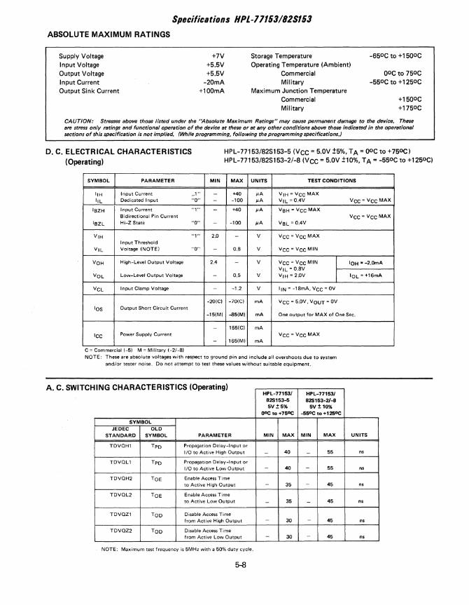
Specifications HPl-17153182S153
ABSOLUTE MAXIMUM RATINGS
Supply Voltage +7V Storage Temperature -650C to +150oC I nput Voltage +5.5V Operating Temperature (Ambient) Output Voltage +5.5V Commercial OoC to 750C Input Current -20mA Military -550C to +1250C Output Sink Current +100mA Maximum Junction Temperature
Commercial +150oC Military +1750C
CAUTION: Stresses above those listed under the "Absolute Maximum Ratings" may cause permanent damage to the device. These are stress only ratings and functional operation of the device at these or at any other conditions above those indicated in the operational sections of this specification ;s not implied. (While programming, fol/owing the programming specifications.)
D. C. ELECTRICAL CHARACTERISTICS (Operating)
HPL-77153/82S153-5 (VCC = 5.0V ±5%, T A = OoC to +750C) HPL-77153/82S153-2/-8 (VCC = 5.0V ±10%, TA = -550C to +1250C)
SYMBOL PARAMETER MIN MAX UNITS TEST CONDITIONS
IIH Input Current ,,1" - +40 ~A VIH = Vec MAX IlL Dedicated Input "0" - -100 ~A VIL=0.4V Vee = Vee MAX
IBZH Input Current "1" - +40 ~A VBH = Vee MAX Bidirectional Pin Current Vee = Vee MAX
IBZL Hi-Z State "0" - -100 ~A VBL = 0.4V
VIH "1" 2.0 - V Vee = Vee MAX Input Threshold
VIL Voltage (NOTE) "a" - 0.8 V Vee = Vee MIN
VOH High-Level Output Voltage 2.4 - V Vee = Vee MIN I 10H' -2.0mA VIL = 0.8V
VOL Low-Level Output Voltage - 0.5 V VIH = 2.0V I 10L = +16mA
VeL Input Clamp Voltage - -1.2 V liN = -18mA. Vee = OV
-20IC) -laic) mA Vee = 5.0V, VOUT = OV
lOS Output Short Circuit Current -151M) -85(M) mA One output for MAX of One Sec.
- 1551e) mA
lee Power Supply Current Vee = Vee MAX - 1651M) mA
C "" Commercial (-5) M "" Military (-2/-8) NOTE: These are absolute voltages with respect to ground pin and include all overshoots due to system
and/or tester noise. Do not attempt to test these values without suitable equipment.
A. C. SWITCHING CHARACTERISTICS (0 at' per mg HPL-77153! HPL-771531
825153-5 82S153-2/-8 5V.:t5% 5V ± 10%
OOC to +750 C -55OC to +125OC
SYMBOL JEDEe OLD
STANDARD SYMBOL PARAMETER MIN MAX MIN MAX
TDVQH1 TpD Propagation Delay-Input or I/O to Active High Output - 40 - 55
TDVOL1 TPD Propagation Delay-Input or I/O to Active Low Output - 40 - 55
TDVOH2 TOE Enable Access Time to Active High Output - 35 - 45
TDVQL2 TOE Enable Access Time to Active Low Output - 35 - 45
TOVOZ1 TOD Disable Access Time from Active High Output - 30 - 45
TDVQZ2 TOD Disable Access Time from Active Low Output - 30 - 45
NOTE: Maximum test frequency is 5MHz with a 50% duty cycle.
5-8
UNITS
ns
ns
ns
ns
ns
ns

CAPACITANCE: TA = 250C (NOTE: Sampled and guaranteed - but not 100% tested)
SYMBOL PARAMETER MAXIMUM UNITS TEST CONDITIONS
CI Input Capacitance 12 pF Vce = 5.0V, VI = 2.0V, f = 1MHz
CB Bidirectional Pin Cap 15 pF VCC = 5.0V, VB = 2.0V, f = 1MHz
SWITCHING TIME DEFINITIONS
INPUTS r------ 3.0V INPUTS 3.0V
Ilx,Bx) '-----O.OV (lx,Bxl '------ O.OV
OUTPUTS VOHA OUTPUTS --+-~.J
IBx) --+---' IBx)
OUTPUTS -----... OUTPUTS
IBx) VOLA IBx) ----"
INPUT CONDITIONS: tr,tf = 5ns 110% to 90%)
NOTE: Disable access time is the time taken for the output to reach a high impedance state when the director control product term drives the output inactive. The high impedance state is defined as a point on the output waveform equal to a /j.V of 0.5 from VOHA or VOLA, the active output level.
ACTEST LOAD
+5V
VOHA
VOLA
=ii From Output (Bx) Under Te~L TEST POINT
10000 CL'
This simulates the A.C. Test Load which Harris Semiconductor uses in its automatic test equipment, and it is recommended that users of Harris bipolar devices use the same or an equivalent load in performing A.C. testing.
*CL Includes Jig and Probe Total Capacitance
SYMBOL PARAMETER
TDVOH1 Propagation Delay from Input or I/O to Active High Output
TDVOL1 Propagation Delay from Input or I/O to Active Low Output
TDVOH2 Enable Access Time to Active High Output
TDVOL2 Enable Access Time to Active Low Output
TDVOZ1 Disable Access Time from Active High Output
TDVOZ2 Disable Access Time from Active Low Output
5-9
R(m CL (pF)
470 30
470 30
00 30
470 30
00 5
470 5

Programming
Following is the programming procedure which is used for the Harris Bipolar HPL-77153/B2S153. This device is manufactured with all fuses intact. Any desired fuse can be programmed by following the simple procedure shown below. One may build a programmer to satisfy the specifications described in the table, or use any of the commercially available programmers which meets these specifications.
PROGRAMMING SPECIFICATIONS
TABLE 1
LIMITS
SYMBOL PARAMETER TEST CONDITIONS MIN TYP MAX
Vccp V CC Supply During Programming 1 8.25 8.5 8.75
ICCp ICC Limit During Programming 550 - 1000
VIH Input Voltage (High) 2.4 5.5
VIL Input Voltage (Low) 0.0 0.8
IIHP Input Current (High) During Prog. VIH - +5.5V - - 50
IILP I nput Current (Low) During Prog. VIL~OV - -500
VOPF Forced Output Voltage 2 Transient or Steady State 17.0 17.5 18.0
IOPF Forced Output Current 100 325
PWV Verify Pulse Width 1 5 50
PWp Programming Pulse Width 90 100 110
TO Pulse Sequence Delay 1 5 50
tr2 Forced Output Voltage Rise Time 10% to 90% 4 14 40
trl Vce Supply Rise Time 10% to 90% 2 7 20
tf2 Forced output Voltage Fall Time 90% to 10% 2 7 20
tfl Vce Supply Fall Time 90% to 10% 1 4 10
Tpp Programming Period 100 160 350
FL Fusing Attempts per Link - 1 2
Vs Verify Threshold3 1.4 1.5 1.6
NOTES:
1. Bypass Vce to GNO with a O.OIP.f capacitor to reduce voltage spikes. The Vee power supply must be capable of handling 1 Ampere maximum.
2. Care shou,ld be taken to ensure that the voltage is maintained during the entire fusing cycle. The recommended supply is a constant current source clamped at the specified voltage limit.
3. Vs is the sensing threshold of the device output voltage for a programmed link. It normally constitutes the reference voltage applied to a comparator circuit to verify a successful fusing attempt.
Figure 1
Vcc
PROGRAM ENABLE
PROGRAMNERI FV
SENSE FUSE
RO
Rl
R2
R3
STROBE
EDIT MODE PINOUT HPL-77153/82S153
NOTE: While programming the HPL-77153/82S153. no pins should be left floating. Pin 16 (Sense Fuse) appears as an open collector output during programming. It should be tied to Vee through a 10K ohm resistor.
5-10
UNITS
V
mA
V
V
P.A
P.A
V
mA
P.S
P.S
P.S
P.S
P.S
P.S
P.S
P.S
Cycle
V

PROGRAMMING PROCEDURE
1. Set-Up:
a. During programming, no pins should be left floating. Pin 16 should be terminated with a 10k ohm resistor to Vee.
b. Set GND (Pin 10) to OV.
2. Select the EDIT Mode:
a. Apply OV to Pin 20.
b. Apply VIL to Pin 18.
c. Apply VIH to Pin 11.
d. Apply VIL to Pin 17.
3. Select the Fuse to be Programmed:
a. Wait TD and select a ROW by specifying the appropriate binary ROW address according to TABLE 2.
b. Select a COLUMN by specifying the appropriate binary COLUMN address according to TABLE 3.
4. Program the Fuse:
a. Wait TD and raise Pin 20 to Veep.
b. Wait TD and raise Pin 17 to VIH.
c. Wait TD and raise Pin 18 to VOPF.
d. Wait TD and pulse Pin 11 to VI L for a duration of PWp.
e. Return Pin 11 to VIH.
f. Wait TD and lower Pin 18 to VI L.
g. Wait TD and lower Pin 17 to VI L.
5. Verify Programmed Fuse:
a. Wait TD and lower Pin 11 to VIL.
b. At the end of PWV, monitor Pin 16 for a level of VOH.
c. Return Pin 11 to VIH.
d. Wait TD and lower Pin 20 to OV.
e. If Pin 16 has indicated a VOL. return to step 4 and repeat so that the fuse receives a maximum of two (2) fusing attempts.
6. Repeat Steps 3 Through 5 for All Fuses to be Blown.
PROGRAMMING WAVEFORMS
1--1 ,..._-----FUSE Fo------tl I.. FUSE FN ·1
PINS 8, 9,12-15 ~~ EDIT MOOE ROW SELECT ~ = = = = = = ~::-_ ~ -_--= = := := := ~ ~:~ PINS 1-6 "'~"'~L-. ___ E_O_IT_M_O_O_E_CO_L_U_M_N_S_EL_E_eT_--::-_r.>'~"'" = -= := ~-=--=--=--=---= ~ -=--=-~ ~::
y'l To='l~~t ,------------,- Vecp PIN 20 jl--I • ..._----TpP-____ .~. / \
(Vee) To '-_ Ov
To~ ~To PROGRAM PIN 17 r------'.;.;;.;;~""'---....... r----- - ---.., -- VIH
(PROGRAMIVERIFY)
PIN 18 (PROGRAM ENABLE)
PIN 11 (STROBE)
VERIFY_ -l L _ _ _ VIL
r------,---- VOPF
I \ I \
I \ / \
L ____ VIL
I--To To-t f- To \"'\\<"<r"\\1---'"'b:--=PWP~ ~----..., r--, r-- VIH ~ _ ---.J LJ' L _____ -.J LJ - VIL
Figure 2
5-11
VOH
VOL

R5 R'
Pin 8 Pin 9
L L L L L L
L L L H L H L H L H L H L H L H L H L H L H L H L H L H L H H L H L H L H L
H H H H H H H H H H H H H H H H H H H H
H H
TABLE 2 TABLE 3 EDIT MODE ROW SELECT EDIT MODE COLUMN SELECT
RJ RZ Rl
Pin 12 Pin 13 Pin 14
L L L L L L L L H L L H L H L L H L L H H L H H H L L H L L H L H II L H II H L H H L II H H H H H L L L L L L L L H L L H L H L L H L L H H L H H H L L H L L H L H H L H H H L H H L H H H H H H L L L L L L L L H L L H
L L L L L L L L H L L H L H L L H L L H H L H H H L L H L L
H L H
RO SELECTED C5 c. CJ CZ
Pin 15 ROW
Pin' Pin 2 Pin 3 Pin4
L JO L L L L H lO L L L L Il L L L H TI L L L L 12 L L H H f2 L L II L 13 L L II H I3 L L H L 14 L H L H i4 L H L L 15 L H L H is L H L L 16 A H I6 N
L 17 0
L H H L H H L H H
H 17 A L B9 R H B9 R
L H H H L L H L L
L B8 A H L L H BB y H L L L B7 H L H H il7 H L H L B6 H L H H ill> H L H L B5 H H L H il5 H H L L B4 H H L H B4 H H L L B3 H H H H ill H H II L B2 H B2 L
H H H H H II
L B1 H lfi L BO
H t t L H L
H SO H L H L
L B9 H H H 88 0 H H L B7 R H H H B6 H H L 85 A H B4 R
L B3 R A
H B2 y L 81
H L
L H H L
H L H L H L H L
H BO H L H H H L H H
L OUTPUT POLARITY ENABLE H L H H H L H H H H L L H H L L H H L L H H L L
NOTES: 1) Pin 7 IR6) and Pin 191C6) are used for programming other HPL devices and should be held at or less than VI L during programming.
2)OV~L~VIL
VIH~H~5V
5-12
Cl co SELECTED
Pin 5 Pin 8 COLUMN
L L 0 L H 1 H L 2 H H 3 L L 4 L H 5 H L 6 H H 7 L L 8 L H 9 H L 10 H H 11 L L 12 L H 13 PRODUCT H L 14 H H 15
TERMS
L L 16 L H 17 H L 18 H H 19 L L 20 L H 21 H L 22 H H 23 L L 24 L H 25 H L 26 H H 27 L L 28 L H 29 H L 30 H H 31
L L 00 L H 01 H L 02 H H 03 CONTROL L L 04 TERMS L H 05 H L 06 H H 07 L L 08 L H 09
H L BO H H B1 L L B2 L H B3 POLARITY H L B4 TERMS H H B5 L L B6 L H B7 L H B8 H L B9

HPL-77153 FPLA Programming Form
PROGRAM TABLE ENTRIES: I 1,8(1) I
NOTES INACTIVE 0 8(0) 8(0) I 1. The FPLA is shipped with all links intact. Thus a background of
I •• H .envEI'lm I entries corresponding to states of virgin links exists in the table,
L INACTIVe I • I LOW L I shown BLANK for clarity. I .• 2. Unused land B bits in the AND array are normally programmed Don't Don't C .... - (OR) (POL) I Care (-).
(AND) I 3. Unused product terms can be lett blank.
I 1 POLARITY
I I I I I I I I I T AND OR E I B(I) B(O) R M 7 6 5 4 3 2 1 0 9 8 7 6 5 4 3 2 1 0 9 8 7 6 5 4 3 2 1 0
0
1
2
3
4
5
6
7
8
9
10
11
12
13
14
15
16
17
18
19
20
21
22
23
24
25
26
27
28
29
30
31
09
~T 08
07
06
05
04
03
02
01
DO
PIN 8 7 6 5 4 3 2 1 19 18 17 16 15 14 13 12 11 9
Figura 3
5-13
...J .... :l:

USE OF THE PROGRAMMING FORM
The programming form for th,e HPL-77153 is shown in Figure 3. This device has ten bi-directional pins (BO-B9) which may be used as outputs or inputs. Any pin used as an output cim have from 1 to 32 product terms (AND) summed (OR'D) to it. Each product term can have from one to eighteen variables. In addition, each bi-directional pin has an extra product term (CONTROL TERM) which may be used to drive those pins into a high impedance state. This allows the ten bi-directional pins to be used as inputs if desired.
The HPL-77153 has the capability for its output polarity to be user determined. Output polarity selection is made possible by the addition of 10 extra fuses associated with the ten bi-directional pins. The HPL-77153 is supplied with the polarity fuses intact, causing the outputs to be non-inverting. If a particular polarity fuse is blown, then the output associated with that fuse will be inverting. Referring to the programming form (Figure 3), it can be seen that the product term and control term numbers are listed at the left hand side. Across the top, the input variables are listed. In order to include an input variable in a product term, an "L" or "H" should be placed in the box at the intersection of the input variable and the product term. An "L" causes the inverted form of an input variable to be included, and an "H", the true form. If it is not desired to include either form for an input variable in a product term, a dash (-) should be placed in the box. Notice that for every product term, a "0" in any single box or any combination of' boxes will cause that product term to be unconditionally disabled (A./A=O), and will not contribute to any output. If it is desired, not to use a product term, then all its boxes may be left blank. This has the same effec;t as including a "0".
Exactly the same procedure is used for the control terms. But in this case, the bi-directional pins may have dynamic three-state control by including "H's" and "L's", or may be forced permanently three-stated by including one or more "D's", or by leaving the control term blank. The bi-directional pins may also be forced permanently active by placing dashes in all the boxes of the associated control term. At the right hand side of the programming form, the sum terms (OR) are shown. Placing an "A" in a box at the intersection of a product ter.m and a bi-directional pin will cause the product term to be summed to that output. Because the product terms are not dedicated to any specific output, any product term may be summed to any of the ten outputs. In this way, product terms may be shared thereby reducing the total numbe'r of product
5-14
terms required for a given application. If it is not desired to sum a product term to an output, a dot (.) should be placed at the intersection of the product term and the output. Any unused product terms (which contribute a logical "0") should be summed to all outputs by placing an "A" at all product term and output intersections. This preserves maximum flexibility for future modifications since product terms which are no longer required may be disconnected in the OR array and unused product terms may be substituted. This capability for "logical surgery" is unique to the FPLA architecture because product terms in an unprogrammed part are not committed to any specific output pin.
The HPL-77153 experiences propagation delay variations as a function of the pattern used in the OR arrray. Although all devices are pre-tested and guaranteed to meet the AC switching characteristics with a worst case pattern, it is possible to minimize propagation delays by disconnecting unused product terms. This can be done by placing dots in all the product term and output intersections. Harris Semiconductor does not specify or guarantee a particular decrease in propagation delay; it is left to customers to measure this for themselves.
Care ,should be taken when using a signal from an output pin as input variable for the same output pin, as this may cause a latched or oscillatory condition to occur if a positive or negative feedback loop is formed.
HPL devices are supplied with all fuses intact and undesired fuses or connections must be blown. For information concerning the entry of fuse data from the programming form into a suitable HPL programmer, refer to the operating guide for that programmer. If it is desired that device programming should be performed by Harris, programming information may be supplied in one or more of the following forms:
1. Master devices (Harris or other).
2. Boolean equations.
3. Paper tapes.
4. Programming form.
5. Marked up logic diagrams (a substantial charge may be made for this entry format).
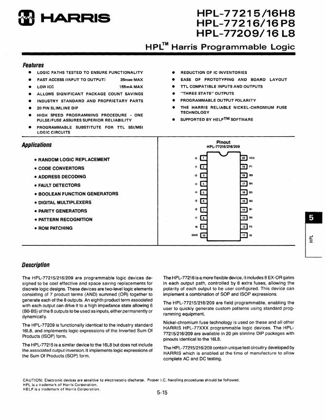
mHARRIS HPL-77215/16H8 HPL-77216/16P8 HPL-77209/16 L8
HPI!M Harris Programmable Logic
Features • LOGIC PATHS TESTED TO ENSURE FUNCTIONALITY
• FAST ACCESS (INPUT TO OUTPUT) 35n.8C MAX
• LOW ICC 155mAMAX
• ALLOWS SIGNIFICANT PACKAGE COUNT SAVINGS
• INDUSTRY STANDARD AND PROPRIETARY PARTS
• 20 PIN SLIM LINE DIP
• HIGH SPEED PROGRAMMING PROCEDURE - ONE PULSE/FUSE ASSURES SUPERIOR RELIABILITY
• PROGRAMMABLE SUBSTITUTE FOR TTL SSI/MSI LOGIC CIRCUITS
Applications
• RANDOM LOGIC REPLACEMENT
• CODE CONVERTORS
• ADDRESS DECODING
• FAULT DETECTORS
• BOOLEAN FUNCTION GENERATORS
• DIGITAL MULTIPLEXERS
• PARITY GENERATORS
• PATTERN RECOGNITION
• ROM PATCHING
Description
The HPL-77215/216/209 are programmable logic devices designed to be cost effective and space saving replacements for discrete logic designs. These devices are two-level logic elements consisting of 7 product terms (AND) summed (OR) together to generate each of the 8 outputs. An eighth product term associated with each output can drive it to a high impedance state allowing 6 (80-85) of the 8 outputs to be used as inputs, either permanently or dynamically.
The HPL-77209 is functionally identical to the industry standard 16L8, and implements logic expressions of the Inverted Sum Of Products (ISOP) form.
The HPL-77215 is a similar device to the 16L8 but does not include the associated output inversion. It implements logic expressions of the Sum Of Products (SOP) form.
• REDUCTION OF IC INVENTORIES
• EASE OF PROTOTYPING AND BOARD LAYOUT
• TTL COMPATIBLE INPUTS AND OUTPUTS
• "THREE STATE" OUTPUTS
• PROGRAMMABLE OUTPUT POLARITY
• THE HARRIS RELIABLE NICKEL-CHROMIUM FUSE TECHNOLOGY
• SUPPORTED BY HELpTM SOFTWARE
Pinout HPL-77215/216/209
The HPL-77216 is a more flexible device, it includes 8 EX-OR gates in each output path, controlled by 8 extra fuses, allowing the polarity of each output to be user configured. This device can implement a combination of SOP and ISOP expressions.
The HPL-77215/216/209 are field programmable, enabling the user to quickly generate custom patterns using standard programming equipment.
Nickel-chromium fuse technology is used on these and all other HARRIS HPL-77XXX programmable logic devices. The HPL-77215/216/209 are available in 20 pin slim line DIP packages with pinouts identical to the 16L8.
The HPL-77215/216/209 contain unique test circuitry developed by HARRIS which is enabled at the time of manufacture to allow complete AC and DC testing.
CAUTION: Electronic devices are sensitive to electrostatic discharge. Proper I.C. handling procedures should be followed. HPL is a trademark of Harris Corporation. HELP is a trademark of Harris Corporation.
5-15

Functional Diagrams
o 1 2 3 · · ,
..... 7
· · 10 11 12 13 14
" " " " " 20 21
" 23
" " " 27 28 28 30 31
32 33 34
" " 37 38 39
.. 41 42 43 .. " " 47
.. .. 50
" 52 53 54
" " 67
" " eo
" " 63
HPL-77209/16LB
0123 4667 8910111213141616171818202122232425262728293031
0123 4567 8910111213141516171S192021222324252627 28293031
HPL-77215/16HB HPL-77216/16PB
5-16

Specifications HPL-7721512161209
ABSOLUTE MAXIMUM RATINGS
Supply Voltage Input Voltage Output Voltage Input Current Output Sink Current
+7V +5.5V +5.5V
-20mA +100mA
Storage Temperature Operating Temperature (Ambient)
Commercial Military
Maximum Junction Temperature Commercial Military
-65°C to +150°C
O°C to +75°C - 55°C to + 125°C
+ 150°C +175°C
CAUTION: Stresses above those listed under the ''Absolute Maximum Ratings" may cause permanent damage to the device. These are stress only ratings and functional operation of the device at these or at any other conditions above those indicated In the operational sections of this specification is not Implied. (While programming, following the programming specifications.)
D,C, ELECTRICAL CHARACTERISTICS (Operating)
SYMBOL PARAMETER
IIH Input Current III Dedicated Input
IFzH Output Current
IFzl HI-Z State
lezH Bidirectional Pin Current
lezl Hi-ZState
V,H Input Threshold (1)
V,l Voltage
VOH High-Level Output Voltage (2)
VOL Low-Level Output Voltage (2)
Vel Input Clamp Voltage (1)
"1" "0"
"1"
"0"
"1"
"0"
"1"
"0"
los Output Short Circuit Current (2)
Icc Power Supply Current
" C = Commercial (-51 M - M,litary (-2/-81
MIN
-----
-2.0
-
2.4
--
-30
--
(1 I These specifications apply to both Input (I) & Bi-Directional (BI pins. These are absolute voltages with respect to ground
HPL-77215/216/209 -5 (Vee = 5.0V±5%, TA = O°C to + 75°C) HPL-77215/216/209 -2/-8 (Vee = 5.0V±10%, TA = -55°C to +125°C)
MAX UNITS TEST CONDITIONS
+25 ".A V,H = Vee MAX -100 ".A V,l = 0.4 V Vee = Vee MAX
+40 ".A VFH = Vee MAX Vee = Vee MAX
-40 ".A VFl = O.4V
+40 ".A VeH = Vee MAX Vee = Vee MAX
-100 ".A Vel = O.4V
- V Vee = Vee MAX
O.B V Vee = Vee MIN
10H = -2.0mA (M) - V Vee = Vee MIN 10H = -3.2mA (C)
V,l = O.BV 10l = +16mA (M) 0.5 V VIH = 2,OV 10l = +24mA (C) (3)
-1.2 V liN = -lBmA, Vee = OV
Vee = 5.0V, VOUT = OV -130 mA
One Output for MAX of One Sec.
155 (C) mA Vee = Vee MAX
165(M) mA
(21 These specifications apply to both Output (FI and BI-Dlrectional (BI pins.
(31 One output at a time, otherwise 16mA. pin & include all overshoots due to system and/or tester noise. Do not attempt to test these values without suitable equipment.
A, C SWITCHING CHARACTERISTICS (0 t" pera '"g HPL-n215-5 HPL-77215-21-B HPL-77218-5 HPL-n218-21-B HPL-n209-5 HPL-77209-21-B
5V±5% 5V±10% O°Cto +7SOC -55°C to +125°C
SYMBOL
JEDEC OLD STANDARD SYMBOL PARAMETER MIN MAX MIN MAX UNITS
TDVQHl TPD Propagation Delay -Input or I/O to Active High Output - 35 - 45 ns
TDVQLl TPD Propagation Delay -Input or I/O to Active Low Output - 35 - 45 ns
TDVQH2 Tpzx Enable Access Time to Active High Output (1) TDVQZ1 35 TDVQZl 45 ns
TDVQL2 Tpzx Enable Access Time to Active Low Output (1) TDVQZ2 35 TDVQZ2 45 ns
TDVQZl Tpxz Disable Access Time from Active High Output - 30 - 35 ns
TDVQZ2 Tpxz Disable Access Time from Active Low Output - 30 - 35 ns
(1) Enable Access Time IS guaranteed greater than Disable Access Time to aVOid device contention. NOTE: Maximum test frequency Is 5MHz with a 50% duty cycle.
5-17
-' Q"
:r:

CAPACITANCE: TA = 25°C (NOTE: Sampled and guaranteed-but not 100% tested.)
SYMBOL
CI
CF
CB
INPUTS
(lx,Bx)
OUTPUTS
(Bx,Fx)
. OUTPUTS
(Bx,Fx)
PARAMETER
Input Capacitance
Output Capacitance
Bidirectional Pin Cap.
3.0V
O.OV
VOHA
VOLA
MAXIMUM UNITS TEST CONDITIONS
12 pF Vee = 5.0V, VI = 2.0V, f = 1 MHz
15 pF Vee = 5.0V, VF = 2.0V, f = 1 MHz
15 pF Vee = 5.0V, VB = 2.0V, f = 1 MHz
SWITCHING TIME DEFINITIONS
INPUTS
(lx,Bx)
OUTPUTS
(Bx,Fx)
OUTPUTS (Bx,Fx)
INPUT CONDITIONS: tr, tl = 5n8 (10% to 90%)
3.0V
O.OV
VOHA
VOLA
NOTE: Disable access lime Is the time taken for the output to reach a high impedance state when the three-state product term drives the output Inactive. The high Impedance state is defined as a point on the output waveform equal to a .:l V of 0.5 from VOHA or VOLA, the active output level.
ACTESTlOAD
+5V
From outt"~J::;::1 o---~""---"'--O TEST POINT
SYMBOL
TDVQHl
TDVQll
TDVQH2
TDVQL2
TDVQZl
TDVQZ2
CL'
·CL Includes Jig and Probe TotalCapacilance
PARAMETER
Propagation Delay from Input or I/O to Active High Output
Propagation Delay from Input or I/O to Active Low Output
Enable Access Time to Active High Output
Enable Access Time to Active Low Output
Disable Access Time from Active High Output
Disable Access Time from Active Low Output
5-18
This simlllates the A.C. Test Loed whIch Harrl. Semiconductor uses in its automatic test equipment, and it ;s recommended that USBrs of Harris bipolar device. use the .ame or an equivalent load in performing A.C. testing.
R(O) CL(pF)
300 50
300 50
'" 50
300 50
'" 5
300 5

Programming
Following is the programming procedure which is used for the HPL-77216/215/209 devices. These devices are manufactured with all fuses intact. Any desired fuse can be programmed by following the simple procedure shown on the following
page. One may build a programmer to satisfy the specifications described in the table, or use any of the commercially available programmers which meet these specifications.
SYMBOL
Veep
leep
V,H
V,L
IiHP
IilP
VOPF
10PF
PWv
PWP
To
tr2
tn
1f2
If' Tpp
Fl
Vs
PROGRAMMING SPECIFICATIONS TABLE 1
PARAMETER TEST CONDITIONS
Vee Supply During Programming'
lee Limit During Programming
Input Voltage (High)
Input Voltage (Low)
Input Current (High) During Prog. V,H = +5.5V
Input Current (Low) During Prog. V,l = OV
Forced Output Voltage' Transient or Steady State
Forced Output Current
Verify Pulse Width
Programming Pulse Width
Pulse Sequence Delay
Forced Output Voltage Rise Time 10% to 90%
Vcc Supply Rise Time 10% to 90%
Forced Output Voltage Fall Time 90% to 10%
Vcc Supply Fall Time 90% to 10%
Programming Period
Fusing Attempts per Link
Verify Threshold'
MIN
8.25
550
2.4
0.0
--
16.0
275
1
90
1
4
2
2
1
100
-1.4
LIMITS
TYP MAX UNITS
8.5 8.75 V
- 1000 mA
- 5.5 V
- 0.8 V
- 50 p.A
- -500 p.A
16.5 18.0 V
300 325 mA
5 50 p.S
100 110 p.S
5 50 p.S
14 40 p.S
7 20 p.S
7 20 p.S
4 10 p.S
160 350 p.S
1 2 Cycle
1.5 1.6 V
NOTES: 1. 2.
3.
Bypass vee to GND with a 0.01 fJ.F capacitor to reduce voltage spikes. The Vee power supply must be capable of handling 1 Ampere maximum.
Care should be taken to ensure that the voltage is maintained during the entire fusing cycle. The recommended supply is a constant current source clamped at the specified voltage limit.
Vs is the sensing threshold of the device output voltage for a programmed link. It normally constitutes the reference voltage applied to a comparator circuit to verify a successful fusing attempt.
Co
C.
Co
R.
R.
GND
Figure 1 EDIT MODE PINOUT HPL-77216/215/209
Vcc
C.
PROGRAM ENABLE
PROGRAM/vERIFY
SENSE FUSE
Ro
STROBE
NOTE: While programming the HPL-77216/215/209 no pins should be left floating. Pin 16 (SENSE FUSE) appears as an open collector outpu1 during programming. 11 should be tied to vee through a 10K ohm resistor.
5-19

PROGRAMMING PROCEDURE
1. Set-Up: a. During programming. no pins should be left floating. Pin
16 should be terminated with a 10k ohm resistor to Vee. b. Set GND (Pin 10) to OV.
2. Select the EDIT Mode: a. Apply OV to Pin 20. b. Apply VIL to Pin 18. c. Apply VIH to Pin 11. d. Apply VIL to Pin 17.
3. Select the Fuse to be Programmed: a. Wait TD and select a ROW by specifying the appropriate
binary ROW address according to Table 2. b. Select a COLUMN by specifying the appropriate binary
COLUMN address according to Table 3.
4. Program the Fuse: a. Wait To and raise Pin 20 to Veep.
b. Wait To and raise Pin 17 to VIH. c. Wait To and raise Pin 18 to VOPF. d. Wait To and pulse Pin 11 to VIL for a duration of PWp. e. Return Pin 11 to VIH. f. Wait TD and lower Pin 18 to VIL. g. Wait To and lower Pin 17 to VIL.
5. Verify Programmed Fuse: a. Wait To and lower Pin 11 to VIL. b. At the end of PWv. monitor Pin 16 for a level of Vs. c. Return Pin 11 to VIH. d. Wait To and lower Pin 20 to OV. e. If Pin 16 has indicated a VOL. return to step 4 and repeat
so that the fuse receives a maximum of two (2) fusing attempts.
6. Repeat Steps 3 Through 5 for All Fuses to be Blown.
PROGRAMMING WAVEFORMS
.... 1~-----FusEFO ------...... '"111. FUSEFN 01
PINS7-9,12-15~ ....... ----E-D-IT-M-OD-E-R-OW-SE-L-EC-T-----ioo~ .... ::::.:_:_=_.:_:_=__=__=__=_:_-___ -_-_-_~ ::~
PINS 1-6.19~ .. =-____ ED_IT_M_O_DE_C_O_LU_M_N_S_EL_E_CT ___ --:-~~-: :: :::::::=:: ::-_=_ _=_ _=_ ::::~ ~:: ~ _________ T°=:ir r---------------i - Veep
PIN 18 (PROGRAM ENABLE)
PIN11 (STROBE)
PIN16 (OUTPUTFo)
Tpp o~tf11 \
PROGRAM ~' L_ 0,
r------------, V,H !--t-V;.,;;E;.,;;RIF,:! _ J L - _ _ VIL
VOPF r--------, , \
/ \ , \ I \
To---l ~To L ____ VIL
--r-::::l c::::::"PiYv - - - - -, r- - , r - - V,H ----=.J ----u---. n • L _______ ...J LJ _ VIL
Figure 2
5-20
VOH
VOL

TABLE 2 EDIT MODE ROW SELECT
ROW RS R4 R3 R2 R1 RO NUMBER Pln8 PinS Pin 12 Pin 13 Pin 14 Pin 15 VARIABLE
0 L L L L L L 11 1 L L L L L H Ii 2 L L L L H L 10_ 3 L L L L H H 10 4 L L L H L L 12 _ 5 L L L H L H 12 6 L L L H H L B5_ 7 L L L H H H B5 8 L L H L L L 13 _ 9 L L H L L H 13
10 L L H L H L B4 _ 11 L L H L H H B4 12 L L H H L L 14 _ 13 L L H H L H 14 14 L L H H H L 83_ 15 L L H H H H B3 16 L H L L L L 15 IS 17 L H L L L H 18 L H L L H L B2 n2 19 L H L L H H 20 L H L H L L 16 _ 21 L H L H L H 16 22 L H L H H L Bl !!1 23 L H L H H H 24 L H H L L L 17 25 L H H L L H i7 26 L H H L H L BO _ 27 L H H L H H BO 28 L H H H L L 18 _ 29 L H H H L H 18 30 L H H H H L 19 _ 31 L H H H H H 19 32 H L L L L L EX-OR SELECT
NOTES:
(1) ~~_~~~I~~~~:hOUld only be selected when programming the
(2) Pin 7 (R6) is used for programming other HPL davices and should be held at or less than VIL during programming.
(3) Ov .. L .. VIL VIH"'H"'5v
COLUMN NUMBER
0 1 2 3 4 5 6 7 8 9
10 11 12 13 14 15 16 17 18 19 20 21 22 23 24 25 26 27 28 29 30 31 32 33 34 35 36 37 36 39 40 41 42 43 44 45 46 47 48 49 50 51 52 53 54 55 56 57 58 59 60 61 62 63 64 65 66 67 68 69 70 71
5-21
TABLE 3 EDIT MODE COLUMN SELECT
C6 CS C4 C3 C2 C1 Pln1S Pin 1 Pin 2 Pin 3 Pin 4 Pin 5
L L L L L L L L L L L L L L L L L H L L L L L H L L L L H L L L L L H L L L L L H H L L L L H H L L L H L L L L L H L L L L L H L H L L L H L H L L L H H L L L L H H L L L L H H H L L L H H H L L H L L L L L H L L L L L H L L H L L H L L H L L' H L H L L L H L H L L L H L H H L L H L H H L L H H L L L L H H L L L L H H L H L L H H L H L L H H H L L L H H H L L L H H H H L L H H H H L H L L L L L H L L L L L H L L L H L H L L L H L H L L H L L H L L H L L H L L H H L H L L H H L H L H L L L H L H L L L H L H L H L H L H L H L H L H H L L H L H H L L H L H H H L H L H H H L H H L L L L H H L L L L H H L L H L H H L L H L H H L H L L H H L H L L H H L H H L H H L H H L H H H L L L H H H L "L L H H H L H L H H H L H L H H H H L L H H H H L L H H H H H L H H H H H H L L L L L H L L L L L H L L L L H H L L L L H H L L L H L H L L L H L H L L L H H H L L L H H
CO PinS
L H L H L H L H L H L H L H L H L H L H L H L H L H L H L H L H L H L H L H L H L H L H L H L H L H L H L H L H L H L H L H L H L H L H L H L H
PART NUMBER
HPL77215
HPL77216
HPL77209
HPL77216 ONLY
ROW 32 ONLY
....I ... :z:

Programming Form HPl-7121512161209
Figure 3
5-22

USE OF THE PROGRAMMING FORM
The programming form for the HPL-77215/216/209 is shown in Figure 3. All three devices have two output pins (FO-F1), and six bi-directional pins (BO-B5) which may be used as outputs or inputs. Any pin used as an output can have from one to seven product terms (AND) summed (OR'O) to it. Each product term can have from one to sixteen variables. In addition, each output and bi-directional pin has an extra product term which may be used to drive those pins into a high impedance state. This allows the six bi-directional pins to be used as inputs if desired. The HPL-77209/16L8 has inverting outputs; the HPL-77215/16H8 has non-inverting outputs, and the HPL-77216/16P8 has the capability for its output polarity to be user determined. Output polarity selection is made possible by the addition of eight extra fuses associated with the eight outpul/bi-directional pins. The HPL-77216/16P8 is supplied with the polarity fuses intact, causing the outputs to be non-inverting. If a particular polarity fuse is blown, then the output associated with that fuse will be inverting.
Referring to the programming form (Figure 3), it can be seen that the column numbers or product term numbers are listed at the left hand side. Across the top, the row numbers or input variables are listed. In order to include an input variable in a product term, a "1" should be placed in the box at the intersection of the input variable and the product term. Notice that for every product term, if any input variable has both its true and complement forms included, then the entire product term will be unconditionally disabled (A./A=O), and will not contribute to the associated output. If it is desired not to use a product term, then all boxes for that column number should
5-23
be left blank. Notice that row 32 has the input symbol";' , this indicates that this row is at ground potential or logical "0". If a "1" is placed in a box at an intersection of row 32 and an INVERT product term, then the associated output will be non-inverting, if a "0" is used, then the output will be inverting. The polarity of each output can be defined independently of all other outputs.
Each of the six bi-directional pins (BO-B5) has a gray area shown on the programming form at the intersection of their product terms and feedback variables. These gray areas may be used, but a latched or oscillatory condition could occur if a positive or negative feedback loop is formed.
The programming form is shown with all boxes blank which is equivalent to all fuses being blown. HPL devices are supplied with all fuses intact and undesired fuses or connections must be blown.
For information concerning the entry of fuse data from the programming form into a suitable HPL programmer, refer to the operating guide for that programmer.
If it is desired that device programming should be performed by Harris, programming information may be supplied in one or more of the following forms:
1. Master devices (Harris or other) 2. Boolean equations 3. Paper tapes 4. Programming form 5. Marked up logic diagrams (A charge may
be made for this entry format)

mHARRIS HPL-77317/16LDS HPL-7731S/16HDS
Preliminary HPI!M Harris Programmable Logic
Features • LOGIC PATHS TESTED TO INSURE FUNCTIONALITY
• FAST ACCESS (INPUT TO OUTPUTI 36 nsecMAX
• LOW ICC 156mAMAX
• ALLOWS SIGNIFICANT PACKAGE COUNT SAVINGS
• 8 PRODUCT TERMS PER OUTPUT
• 20 PIN SLIMLINE DIP
• HIGH SPEED PROGRAMMING PROCEDURE - ONE PULSE/FUSE ASSURES SUPERIOR RELIABILITY
• PROGRAMMABLE SUBSTITUTE FOR TTL SSI/MSI LOGIC CIRCUITS
Applications
• RANDOM LOGIC REPLACEMENT
• CODE CONVERTERS
• ADDRESS DECOOING
• FAULT DETECTORS
• BOOLEAN FUNCTION GENERATORS
• DIGITAL MULTIPLEXERS
• PARITY GENERATORS
• PATTERN RECOGNITION
• ROM PATCHING
Description The HPL-77317/318 are programmable logic devices designed to be cost effective and space saving replacements for discrete logic designs. These devices are two-level logic elements consisting of 8 product terms (AND) summed (OR) together to generate each of the 8 outputs. To achieve 8 product terms per output, the ability to force the outputs to a high impedance state has not been included. All eight outputs are permanently active.
The HPL-77317 is similar to the industry standard 16L8, and implements logic expressions of the Inverted Sum Of Products (ISOP) form.
The HPL-77318 is a similar device to the HPL-77317, but does not include the associated output inversion. It implements logic expressions of the Sum Of Products (SOP) form.
• REDUCTION OF IC INVENTORIES
• EASE OF PROTOTYPING AND BOARD LAYOUT
• TTL COMPATIBLE INPUTS AND OUTPUTS
• "THREE STATE" OUTPUTS
• THE HARRIS RELIABLE NICKEL-CHROMIUM FUSE TECHNOLOGY
• SUPPORTED BY HELPTM SOFTWARE
Pinout HPL-773171318
Six of the 8 outputs feature feedback into the fuse matrix, allowing output functions to be utilized for other output functions.
The HPL-77317/318 are field programmable, enabling the user to quickly generate custom patterns using standard programming equipment.
Nickel-chromium fuse technology is used on these and all other HARRIS HPL-77XXX programmable logic devices. The HPL-77317/318 are available in 20 pin slimline DIP packages with pinouts similar to the 16L8.
The HPL-77317/318 contain unique test circuitry developed by HAR R IS, which is enabled at the time of manufacture to allow complete AC, DC and functional testing.
CAUTION: Electronic devices are sensitive to electrostatic discharge. Proper I.C. handling procedures should be followed. HPL is a trademark of Harris Corporation. HELP is a trademark of Harris Corporation.
5-24

0 1 1 3 4 • 6 1
~ ....
8 • 10 11 11 13
" " "
16 11 18 19 20 11 11 23
14
" 26 11 18 19 JO J1
v
31 33 J4 J5 36 11 38 39
40 41
" 43 44 .. 46 41
" 1 .. 48 49 50
" " " " 55
" 8 V
;S
" 58 5' on 61 61 63
• ..
Functional Diagrams
HPL-77317/16LD8
01234567891011121314151617181920212223242&2627282930]1
F ~
~
~
./
=J::::C:=
~
~
W o 1 2] 456] 8 91011 1?13141~ lb 1718192021222324252621 l82~3031
5-25
:j-
::}-
A
::J-
:j-
:J-
::J-
1
1
1
16
15
HPL-77318/16HD8
===<}--"
...J 0.. :I:

Specifications HPL-773171318
ABSOLUTE MAXIMUM RATINGS
Supply Voltage Input Voltage Output Voltage Input Current Output Sink Current
+7V +5.5V +5.5V
-20mA +100mA
Storage Temperature Operating Temperature (Ambient)
Commercial Military
Maximum Junction Temperature Commercial Military
-65'C to +150'C
O°C to +75°C - 55°C to + 125'C
+150'C +175'C
CAUTION: Stresses above those listed under the Absolute Maximum Ratmqs may cause permanent damaqe to the device. These are stress only ratmqs and functional operation of the device at these or at any other conditions above those mOlcated In the operatIOnal sections of this specification IS not implied. (While programming, fol/owmg the proqramminq specificatIOns.)
D.C. ELECTRICAL CHARACTERISTICS (Operating)
SYMBOL PARAMETER
IiH Input Current III Dedicated Input
V,H Input Threshold
V,L Voltage 111
VOH High-Level Output Voltage
VOL Low-Level Output Voltage
VeL Input Clamp Voltage 121
los Output Short Circuit Current
Icc Power Supply Current
C = Commercial (-5) M = Military (-2/-8)
MIN
"1"" -"0" -
'"1"" 2.0
"0" -
2.4
-
-
-30
--
-
(1) These specifications apply to both Input (I) & Bi-directional (B) pins. These are absolute voltages with respect to ground pin & include all overshoots due to system and/or tester noise. Do not attempt to test these values without suitable equipment.
A. C SWITCHING CHARACTERISTICS (0 f pera Ing
SYMBOL
JEDEC OLD STANDARD SYMBOL PARAMETER
TDVQH TPD Propagation Delay - Input to Active High Output
TDVQL TPD Propagation Delay - Input to Active low Output
NOTE: MaXimum test frequency IS 5MHz With a 50% duty cycle.
HPL-77317/318 -5 (Vee = 5.0V+5%, TA = DoC to +750 C) HPL-77317/318 -2/-8 (Vee = 5.0V+l0%, T A = -550 e to +1250 C)
MAX UNITS TEST CONDITIONS
+25 ,.,.A VIH 0 Vee MAX -100 ,.,.A 'IlL 0.4 V Vee" Vee MAX
- V Vee - Vee MAX
0.8 V Vee = Vee MIN
10H = -2.0mA (M) - V Vee = Vee MIN 10H = -3.2mA (C)
VIL = O.BV 10L = +16mA (M) 0.5 V V,H = 2.0V 10L = +24mA (C) (1)
-1.2 V liN = -18mA, Vee = OV
Vee = 5.0V, VOUT = OV -130 mA
One Output for MAX of One Sec.
155 (C) mA Vee = Vee MAX
165 (M) mA
(2) One output at a time, otherwise 16mA.
HPL-77317-5 HPL-77317-2/-8 HPL-77318-5 HPL-77318-2/-8
5V±5% 5V±10% O°C to +75°C -55°C to +125°C
MIN MAX MIN MAX UNITS
- 35 - 45 ns
- 35 - 45 ns
5-26

CAPACITANCE: TA = 25°C (NOTE: Sampled and guaranteed - but not 100% tested.)
SYMBOL PARAMETER
CI Input Capacitance
CF Output Capacitance
+5V
MAXIMUM UNITS TEST CONDITIONS
12 pF Vee = 5.0V. V, = 2.0V. I = 1 MHz
15 pF Vec = 5.0V. VF = VOL or VOH. I = 1 MHz
SWITCHING TIME DEFINITIONS
INPUTS
(Ix)
OUTPUTS
(Fx)
OUTPUTS
(Fx)
3.0V
O.OV
VOHA
VOLA
INPUT CONDITIONS: t" tf = 5ns (10% to 90%)
AC TEST LOAD
From ~~~~: re~l o---~~---... -~t) TEST POINT
This simulates the A.C. Test Load which Harris Semiconductor uses in its automatic test equipment, and it is recommended that users of Harris bipolar devices use the same or an equivalent load in performing A. C. testing.
SYMBOL
TDVQH
TDVQL
6000 c,'
'CL Includes Jig and Probe Total Capacitance
PARAMETER
Propagation Delay Irom Input to Active High Output
Propagation Delay lrom Input to Active Low Output
5-27
R(fl) CL (pF)
300 50
300 50
...J a.. ~

..
Programming
Following is the programming procedure which is used for the HPL-77317/318 devices. These devices are manufactured with all fuses intact. Any desired fuse can be programmed by following the simple procedure shown on the
following page. One may build a programmer to satisfy the specifications described in the table, or use any of the commercially available programmers which meet these specifications.
SYMBOL
Veep
Icep 1----.
V,H
V,L
IIHP
IILP
VOPF
10PF
PWv
PWP
To
tr2
tn
tf2
tf1
Tpp
FL
Vs
NOTES:
PROGRAMMING SPECIFICATIONS TABLE 1
PARAMETER TEST CONDITIONS
Vee Supply During Programming'
lee Limit During Programming
Input Voltage (High)
Input Voltage (Low)
Input Current (High) During Prog. V,H ~ +5.5V
Input Current (Low) During Prog. V,L ~ OV
Forced Output Voltage' Transient or Steady State
Foreed Output Current
Verify Pulse Width
Programming Pulse Width
Pulse Sequence Delay
Forced Output Voltage Rise Time 10% to 90%
Vec Supply Rise Time 10% to 90%
Forced Output Voltage Fall Time 90% to 10%
Vee Supply Fall Time 90% to 10%
Programming Period
Fusing Attempts per Link
Verify Threshold3
--
LIMITS MIN TYP MAX
8.25 8.5 8.75
550 - 1000
2.4 - 5.5
0.0 - 0.8
- - 50
- - -500
16.0 16.5 1B.0
- 100 325 t--. 1
5 50
90 100 110
1 5 50
4 14 40
2 7 20
2 7 20
1 4 10
100 160 350
- 1 2
1.4 1.5 1.6
1. Bypass vee to GND with a 0.01 ,uF capacitor to reduce voltage spikes. The vee power supply must be capable of handling 1 Ampere maximum.
UNITS
V
mA
V
V
p.A
p.A
V mA
p.S
p.S
p.S
p.S
p.S
p.S
~s p.S
Cycle
V
2. Care should be taken to ensure that the voltage is maintained during the entire fusing cycle. The recommended supply is a constant current source clamped at the specified voltage limit.
3. Vs is the senSing threshold of the device output voltage for a programmed link. It normally constJtutes the reference voltage applied to a comparator circuit to verify a successful fusing attempt.
Figure 1 EDIT MODE PtNOUT
HPL-77317/318
NOTE: While programming the HPL-77317/318 no pins should be left floating. Pin 16 (SENSE FUSE) appears as an open collector output during programming. It should be tied to vee through a 10K ohm resistor.
5-28

PROGRAMMING PROCEDURE
1. Set-Up: a. During programming, no pins should be left floating. Pin
16 should be terminated with a 10k ohm resistor to Vee. b. Set GND (Pin 10) to OV.
2. Select the EDIT Mode: a. Apply OV to Pin 20. b. Apply V,L to Pin 18. c. Apply V,H to Pin 11. d. Apply V,L to Pin 17.
3. Select the Fuse to be Programmed: a. Wait To and select a ROW by specifying the appropriate
binary ROW address according to Table 2. b. Select a COLUMN by specifying the appropriate binary
COLUMN address according to Table 3.
4. Program the Fuse: a. Wait To and raise Pin 20 to Veep.
b. Wait To and raise Pin 17 to V'H. c. Wait To and raise Pin 18 to VOPF. d. Wait To and pulse Pin 11 to V,L for a duration of PWp. e. Return Pin 11 to V'H. f. Wait To and lower Pin 18 to V,L. g. Wait To and lower Pin 17 to V,L.
5. Verify Programmed Fuse: a. Wait To and lower Pin 11 to V,L. b. At the end of PWv, monitor Pin 16 for a level of Vs. c. Return Pin 11 to V'H. d. Wait To and lower Pin 20 to OV. e. If Pin 16 has indicated a VOL, return to step 4 and repeat
so that the fuse receives a maximum of two (2) fusing attempts.
6. Repeat Steps 3 Through 5 for All Fuses to be Blown.
PROGRAMMING WAVEFORMS
1"'1'----- FUSE Fo ------....... "il I' FUSE FN 'I PINS 7·9, 12'15~ ~g.-----ED--,T--M--O--D--E-R-OW--SE--L--EC--T-----i~m- -: = ==:--=--=--=--=--=--=--=--=--=-_____ -_-_ -_~ :::
PINS 1-6, 19 ",,~ ...... ____ E_DI_T_MO_D_E_C_O_LU_M_N_S_EL_E_CT _____ ---:rlml ...... _-: = = = = = == = = = :--=--=--=--=-==~ ::: ____ TO_=il..-j. ~,r m --- m ______ \~ :_
PIN17 (PROGRAMIVERIFy)
PIN18 (PROGRAM ENABLE)
PIN 11 (STROBE)
PIN16 (OUTPUTFo)
i-____ PR_O_G_R_AM ___ --. r - - - - - - - - -- - -, V,"
,-+-V.:..:E;;..:;RIF.! _ .J t- _ _ _ v"
r--------, I \ " \
VOPF
I \ I ,
TO--.j ~To L ____ V"
---.r-:::=:J c::="PWv - - - - -, r - , r - - VI" ---=:J -U-.... L _______ .J L.J _ V"
Figure 2
5-29
VO"
VOL

TABLE 2 EDIT MODE ROW SELECT
ROW R5 R4 R3 R2 R1 RO NUMBER Pin 8 Pin 9 Pin 12 Pin 13 Pin 14 Pin 15 VARIABLE
0 L L L L L L 11 1 L L L L L H IT 2 L L L L H L 10_ 3 L L L L H H 10 4 L L L H L L 12 5 L L L H L H i2 6 L L L H H L F6 _ 7 L L L H H H F6 8 L L H L L L 13 9 L L H L L H i3
10 L L H L H L F5 _ 11 L L H L H H F5 12 L L H H L L 14 13 L L H H L H i4 14 L L H H H L F4 _ 15 L L H H H H F4 16 L H L L L L 15 17 L H L L L H is 18 L H L L H L F3 19 L H L L H H F3 20 L H L H L L 16 _ 21 L H L H L H 16 22 L H L H H L F2 _ 23 L H L H H H F2 24 L H H L L L 17 25 L H H L L H i7 26 L H H L H L F1_ 27 L H H L H H F1 28 L H H H L L 18 _ 29 L H H H L H 18 30 L H H H H L 19 _ 31 L H H H H H 19
NOTES: (1) Pin 7 (R6) is used for programming other HPL devices and should be held at
or les9 than VIL dUring programming. (2) OV,;L,;VIL
VIH~H,,;;5v
COLUMN NUMBER
0 1 2 3 4 5 6 7 8 9
10 11 12 13 14 15 16 17 18 19 20 21 22 23 24 25 26 27 28 29 30 31 32 33 34 35 36 37 38 39 40 41 42 43 44 45 46 47 48 49 50 51 52 53 54 55 56 57 58 59 60 61 62 63
5-30
TABLE 3 EDIT MODE COLUMN SELECT
C6 C5 C4 C3 C2 C1 CO PART Pin 19 Pin 1 Pin 2 Pin 3 Pin4 Pin 5 Pin 6 NUMBER
L L L L L L L L L L L L L H L L L L L H L L L L L L H H L L L L H L L L L L L H L H L L L L H H L L L L L H H H L L L H L L L L L L H L L H L L L H L H L L L L H L H H L L L H H L L L L L H H L H L L L H H H L L L L H H H H L L H L L L L L L H L L L H L L H L L H L L L H L L H H L L H L H L L L L H L H L H HPL-77317
L L H L H H L HPL_7731B
L L H L H H H L L H H L L L L L H H L L H L L H H L H L L L H H L H H L L H H H L L L L H H H L H L L H H H H L L L H H H H H L H L L L L L L H L L L L H L H L L L H L L H L L L H H L H L L H L L L H L L H L H L H L L H H L L H L L H H H L H L H L L L L H L H L L H L H L H L H L L H L H L H H L H L H H L L L H L H H L H L H L H H H L L H L H H H H L H H L L L L L H H L L L H L H H L L H L L H H L L H H L H H L H L L L H H L H L H L H H L H H L L H H L H H H L H H H L L L L H H H L L H L H H H L H L L H H H L H H L H H H H L L L H H H H L H L H H H H H L L H H H H H H

Programming Form HPL-773171318
Figure 3
5-31

USE OF THE PROGRAMMING FORM
The programming form for the HPL-77317/318 is shown in Figure 3. Both devices have eight output pins (FO-F7). Any output can have from one to eight product terms (AND) summed (OR'D) to it. Each product term can have from one to sixteen variables. The HPL-77317/16LD8 has inverting outputs; the HPL-77318/16HD8 has noninverting outputs.
Referring to the programming form (Figure 3). it can be seen that the column numbers or product term numbers are listed at the left hand side. Across the top, the row numbers or input variables are listed. In order to include an input variable in a product term, a "1" should be placed in the box at the intersection of the input variable and the product term. Notice that for every product term, if any input variable has both its true and complement forms included, then the entire product term will be unconditionally disabled (A./A=O). and will not contribute to the associated output. If it is desired not to use a product term, then all boxes for that column number should be left blank.
Six of the eight output pins (F1-F6) have a gray area
shown on the programming form at the intersection of their product terms and feedback variables. These gray areas may be used, but a latched or oscillatory condition could occur if a positive or negative feedback loop is formed.
The programming form is shown with all boxes blank which is equivalent to all fuses being blown. HPL devices are supplied with all fuses intact and undesired fuses or connections must be blown.
For information concerning the entry of fuse data from the programming form into a suitable HPL programmer, refer to the operating guide for that programmer.
If it is desired that device programming should be performed by Harris, programming information may be supplied in one of more of the following forms:
5-32
1. Master devices (Harris or other) 2. Boolean equations 3. Paper tapes 4. Programming form 5. Marked up logic diagrams (A substantial charge may
be made for this entry format)

mHARRIS HPL-77319/16LE8 HPL-77320/16HE8
Preliminary H pC"M Harris Programmable Logic
Features
• LOGIC PATHS TESTED TO ENSURE FUNCTIONALITY
• FAST ACCESS (INPUT TO OUTPUT) 35 nsoc MAX
• LOW ICC 155mAMAX
• ALLOWS SIGNIFICANT PACKAGE COUNT SAVINGS
• 8 PRODUCT TERMS PER OUTPUT
• 20 PIN SLIMLINE DIP
• HIGH SPEED PROGRAMMING PROCEDURE-ONE PULSE/FUSE ASSURESSUPERIOR RELIABILITY
• ENHANCED VERSIONS OF HPL77317/16LD8 AND HPL77318116HD8
Applications
• RANDOM LOGIC REPLACEMENT
• CODE CONVERTERS
• ADDRESS DECODING
• FAULT DETECTORS
• BOOLEAN FUNCTION GENERATORS
• DIGITAL MULTIPLEXERS
• PARITY GENERATORS
• PATTERN RECOGNITION
• ROM PATCHING
Description
The HPL-77319/320 are programmable logic devices designed to be cost effective and space saving replacements for discrete logic designs. These devices are two-level logic elements consisting of 8 product terms (AND) summed (OR) together to generate each of the 8 outputs. An extra fuse associated with each bi-directional pin can drive it to a high impedance state allowing 6 (80-85) of the 8 outputs to be used as inputs.
An extra fuse associated with each output pin can be used to control output polarity which is active high on an unprogrammed part.
The HPL-77319 is similar to the industry standard 16L8, and implements logic expressions of the Inverted Sum of Products (lSOP) form.
The HPL-77320 is a similar device to the HPL-77319 but
• PROGRAMMABLE SUBSTITUTE FOR TTL SSI MSI LOGIC CIRCUITS
• REDUCTION OF IC INVENTORIES
• EASE OF PROTOTYPING AND BOARD LAYOUT
• TTL COMPATIBLE INPUTS AND OUTPUTS
• "THREE STATE" OUTPUTS
• PROGRAMMABLE OUTPUT POLARITY
• THE HARRIS RELIABLE NICKEL-CHROMIUM FUSE TECHNOLOGY
• SUPPORTED BY HELPTM SOFTWARE
Pinout HPL-77319/320
does not include the associated output inversion. It implements logic expressions of the Sum of Products (SOP) form.
The HPL-77319/320 are field programmable, enabling the user to quickly generate custom patterns using standard programming equipment.
Nickel-chromium fuse technology is used on these and all other HARRIS HPL-77XXX programmable logic devices. The HPL-77319/320 are available in 20 pin slim line DIP packages with pinouts identical to 16L8.
The HPL-77319/320 contain unique test circuitry developed by HAR R IS which is enabled at the time of manufacture to allow complete AC, DC and functional testing.
CAUTION: Electronic devices are sensitive to electrostatic discharge. Proper I. C. handling procedures should be followed. HPL is a trademark of Harris Corporation HELP is a trademark of Harris Corporation. 5-33
...J a.. ::I:

0 1 2 3 • , • ,
~ 8 ,
10 11 12 13
" 15
I"-
V
16 11 16 19 20 21 22 23
... v
" " 26 21 28
" 30 31
, v
32 33 34 35 36 31 38 39
... • V
40 41 42
" 44
" .. 41
... , .. .. .. " " " 53
" " ....
8 V
" " " " " 61
" 83
, ...
Functional Diagrams HPL-77319/16LEB
01 Z J 4581 89101112131415161118192021222]2425262728293031
~.~D- 1--'
(f-
~ ~~r-1
::}--
~~r-1 ~32 "
;1
~ =~r-1 ~32
"
1-....
~ ~ ~~1 ~ ..
(f-
~~r-.' ~32 "
~
-~ :.t:F= r-
~,,~2 13
(}-
F D-~"
32 12
"::"
11
0' 2 3 4567 891011121314t5Hil118192D21222l24252627282930Jl
5-34
HPL-77320116HEB
~D-I--19 =f;'F ====<J-
~18 32
"
~" 32
"
~16 32
"
32 .. ~15
~" 32
"
32 10 ~13
~D-12 ~fP ~11
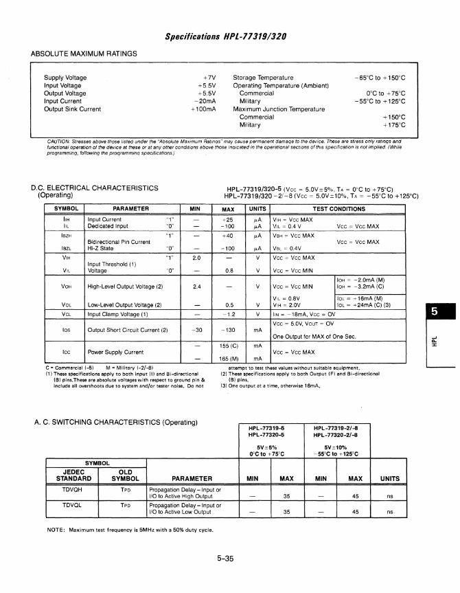
Specifications HPl-77319/320
ABSOLUTE MAXIMUM RATINGS
Supply Voltage Input Voltage Output Voltage Input Current Output Sink Current
+7V +5.5V +5.5V
-20mA
+IOOmA
Storage Temperature Operating Temperature (Ambient)
Commercial Military
Maximum Junction Temperature Commercial Military
-65°C to + 150'C
O°C to + 75'C - 55'C to + 125'C
+150'C +175'C
CAUTION. Stresses above those listed under the Absolute Maximum Ratmqs may cause permanent damaqe to the device. These are stress only ratmgs and functional operation of the device at these or at any other conditions above those inoicated in the operational sections of this specification is not implied. (While programming, following the programminq specifications.)
D.C. ELECTRICAL CHARACTERISTICS (Operating)
SYMBOL PARAMETER
IIH Input Current III Dedicated Input
IBzH Bidirectional Pin Current
IBzl Hi-Z State
V,H Input Threshold (1)
V,l Voltage
VOH High-Level Output Voltage (2)
Val Low-Level Output Voltage (2)
Vel Input Clamp Voltage (1)
MIN
"1" -"0" -"1" -
"0" -
"1" 2.0
"a" -
2.4
-
-
los Output Short Circuit Current (2) -30
-Icc Power Supply Current
-c = Commercial I-51 M = Military 1-2/-81 (1) These specifications apply to both input (I) and Bi-directional
(B) pins.These are absolute voltages with respect to ground pin & include all overshoots due to system and/or tester noise. Do not
A. C SWITCHING CHARACTERISTICS (0 t' pera Ing
SYMBOL
JEDEC OLD STANDARD SYMBOL PARAMETER
HPL-77319/320-5 (Vee = 5.0V±5%, TA = O°C to + 75°C) HPL-77319/320 -2/-8 (Vee = 5.0V±IO%, TA = -55"C to +125'C)
MAX UNITS TEST CONDITIONS
+25 J1.A V,H = Vee MAX -100 J1.A V,l = 0.4 V Vee = Vee MAX
+40 J1.A VBH = Vee MAX Vee = Vee MAX
-100 J1.A VBl = O.4V
- V Vee = Vee MAX
0.8 V Vee = Vee MIN
10H = -2.0mA (M) - V Vee = Vee MIN 10H = -3.2mA (C)
V,l = 0.8V 10l = +16mA (M) 0.5 V V,H = 2.0V 10l = +24mA (C) (3)
-1.2 V liN = -18mA, Vee = OV
Vee = 5.0V, VOUT = OV -130 mA
One Output for MAX of One Sec.
155 (C) mA Vce = Vee MAX
165 (M) mA
attempt to test these values without sUitable equipment. (2) These specifications apply to both Output (F) and Bi-directional
181 pins. (3) One output at a time, otherwise 16mA.
HPL-77319-5 HPL-77319-21-8 HPL-17320-5 HPL-17320-21-B
SV±S% 5V±10% O°C to +75'C -55'C to +125'C
MIN MAX MIN MAX UNITS
TDVQH TPD Propagation Delay - Input or 110 to Active High Output - 35 - 45 ns
TDVQL TPD Propagation Delay -Input or 110 to Active Low Output - 35 - 45 ns
NOTE: Maximum test frequency is 5MHz with a 50% duty cycle.
5-35

CAPACITANCE: TA = 25°C (NOTE: Sampled and guaranteed - but ,not 100% tested.)
SYMBOL PARAMETER
CI Input Capacitance
CF Output Capacitance
CB Bidirectional Pin Cap.
+sv
MAXIMUM UNITS TEST CONDITIONS
12 pF Vee = 5.0V, V, = 2.0V, f = 1 MHz
15 pF Vee = 5.0V, VF = VOL or VOH, f = 1 MHz
15 pF Vee = 5.0V, VB = 2.0V, f = 1 MHz
SWITCHING TIME DEFINITIONS
INPUTS
(lx,Bx)
OUTPUTS
(Bx,Fx)
OUTPUTS
(Bx,Fx)
3.0V
O.OV
VOHA
VOLA
INPUT CONDITIONS: tr, tf = 5ns (10% to 90%)
AC TEST LOAD
From Out~~J::!e:l o---~""---+--C ~~~~T
This simulates the A.C. Test Load which Harris Semiconductor uses in its automatic test equip":' mentl and it is recommended that users of Harris bipolar devices use the same or an equivalent load in performing A.C. testing.
TOVQH
TDVQl
600!! ClO
'CL Includes Jig and Probe Total Capacitance
PARAMETER
Propagation Delay from Input or 110 to Active low Output
5-36
R(n) CL(pF)
300 50 ---~--------t-----+------j
300 50

ProgrlJmming
Following is the programming procedure which is used for the HPL-77319/320 devices. These devices are manufactured with all fuses intact. Any desired fuse can be programmed by following the simple procedure shown on the following
page. One may build a programmer to satisfy the specifications described in the table, or use any of the commercially available programmers which meet these specifications.
SYMBOL
Veep
Icep
VIH
Vil
IIHP
IilP
VOPF
10PF
PWv
PWp
To
tr2
tn
112
th
Tpp
FL
Vs
PROGRAMMING SPECIFICATIONS TABLE 1
PARAMETER TEST CONDITIONS
Vee Supply During Programming'
Icc Limit During Programming
Input Voltage (High)
Input Voltage (Low)
Input Current (High) During Prog. VIH = +5.5V
Input Current (Low) During Prog. Vil = OV
Forced Output Voltage" Transient or Steady State
Forced Output Current
Verify Pulse Width
Programming Pulse Width
Pulse Sequence Delay
Forced Output Voltage Rise Time 10% to 90%
Vee Supply Rise Time 10% to 90%
Forced Output Voltage Fall Time 90% to 10%
Vee Supply Fall Time 90% to 10%
Programming Period
Fusing Attempts per Link
Verify Threshold3
MIN
8.25
550
2.4
0.0
--
16.0
-1
90
1
4
2
2
1
100
-1.4
LIMITS TYP MAX UNITS
8.5 8.75 V
- 1000 mA
- 5.5 V
- 0.8 V
- 50 /LA
- -500 /LA
16.5 18.0 V
100 325 mA
5 50 /LS 100 110 /LS 5 50 /LS 14 40 /LS 7 20 /LS 7 20 /LS 4 10 /LS
160 350 /LS 1 2 Cycle
1.5 1.6 V
NOTES: 1. Bypass vec to GND with a 0.01 p.F capacrtor to reduce voltage spikes. The vee power supply must be capable of handling 1 Ampere maximum. 2.
3.
Care should be taken to ensure that the voltage is maintained during the entire fusing cycle. The recommended supply is a constant current source clamped at the specified voltage limit. vs is the sensing threshold of the device output voltage for a programmed link. It normally constitutes the reference voltage applied to a comparator circuit to verify a successful fusing attempt.
Figure 1 EDIT MODE PINOUT
HPL-77319/320
NOTE: While programming the HPL-77319/320 no pins should be left floating. Pin 16 (SENSE FUSE) appears as an open collector output during programming. It should be tied to vee through 10K ohm resistor.
5-37

PROGRAMMING PROCEDURE
1. Set-Up: a. During programming, no pins should be left floating. Pin
16 should be terminated with a 10k ohm resistor to Vee. b. Set GND (Pin 10) to Ov.
2. Select the EDIT Mode: a. Apply OV to Pin 20. b. Apply V,L to Pin 18. c. Apply V,H to Pin 11. d. Apply V,L to Pin 17.
3. Select the Fuse to be Programmed: a. Wait To and select a ROW by specifying the appropriate
binary ROW address according to Table 2. b. Select a COLUMN by specifying the appropriate binary
COLUMN address according to Table 3.
4. Program the Fuse: a. Wait To and raise Pin 20 to Veep.
b. Wait To and raise Pin 17 to V,H. c. Wait To and raise Pin 18 to VOPF. d. Wait To and pulse Pin 11 to V,L for a duration of PWp. e. Return Pin 11 to V'H. f. Wait To and lower Pin 18 to V,L. g. Wait To and lower Pin 17 to V,L.
5. Verify Programmed Fuse: a. Wait To and lower Pin 11 to V,L. b. At the end of PWv, monitor Pin 16 for a level of Vs. c. Return Pin 11 to V,H. d. Wait To and lower Pin 20 to OV. e. If Pin 16 has indicated a VOL, return to step 4 and repeat
so that the fuse receives a maximum of two (2) fusing attempts.
6. Repeat Steps 3 Through 5 for All Fuses to be Blown.
PROGRAMMING WAVEFORMS
I' FUSE Fo ------..... ",--11 " FUSE FN .,
PINS 7-9, 12-15~ ~!lT----EO-,T-M-O--O-E-R-OW-SE-L-EC--T----.....,~~ ~ = -=-= ~ :: ~-=--=-~:-=--=-_-___ -_ -_ -_~ ::~
PINSl-6,19 ",,~ ______ E_DI_T_MO_D_E_C_O_LU_M_N_S_EL_E_CT _____ ;-!~ ....... _~=-=--=-========--=--=--=--=-=-=-~ ::: ___ T_0:::;l..,. ~~1,''- - - - - - - - - - - - ---- ilL ~
PIN 17 (PROGRAMIVERIFV)
PIN 18 (PROGRAM ENABLE)
PIN 11 (STROBE)
PIN 16 (OUTPUT Fo)
Veep
Ov PROGRAM r-----------------, r------------, V,H
,-+-V_E_RIF! _ J L _ _ _ VOL
Figure 2
5-38
VOPF ,---------, , \ " \ , \ I \
L ____ VIL
VOH
Vo,

TABLE 2 EDIT MODE ROW SELECT
ROW R5 R4 R3 R2 R1 RO NUMBER PinS Pin 9 Pin 12 Pin 13 Pin 14 Pin 15 VARIABLE
a L L L L L L 11 1 L L L L L H i1 2 L L L L H L 10 _ 3 L L L L H H 10 4 L L L H L L 12 _
5 L L L H L H 12 6 L L L H H L B5 _ 7 L L L H H H B5 8 L L H L L L 13 9 L L H L L H i3
10 L L
H L H L B4 _ 11 L H L H H B4 12 L L H H L L 14 _ 13 L L H H L H 14 14 L L H H H L B3 15 L L H H H H 83 16 L H L L L L 15 17 L H L L L H i5 18 L H L L H L B2 19 L H L L H H i'i2 20 L H L H L L 16 _ 21 L H L H L H 16 22 L H L H H L B1 23 L H L H H H B1 24 L H H L L L 17 25 L H H L L H i7 26 L H H L H L BO _ 27 L H H L H H BO 28 L H H H L L 18 29 L H H H L H iii 30 L H H H H L 19 _ 31 L H H H H H 19 32 H L L L L L CONFIGURE
NOTES: (1) Row number 32 should only be selected when proqrammtnq the
configuration fuses. (2) Pin 7 (R6) is used forproqrammmq other HPLdevlces and should be held at
or les~ than VIL dunnq proqrammlnq
(3) OV$ChVIL VIH.:sH~5v
COLUMN C6 NUMBER Pin 19
0 L 1 L 2 L 3 L 4 L 5 L 6 L 7 L 8 L 9 L
10 L 11 L 12 L 13 L 14 L 15 L 16 L 17 L 18 L 19 L 20 L 21 L 22 L 23 L 24 L 25 L 26 L 27 L 28 L 29 L 30 L 31 L 32 L 33 L 34 L 35 L 36 L 37 L 38 L 39 L 40 L 41 L 42 L 43 L 44 L 45 L 46 L 47 L 48 L 49 L 50 L 51 L 52 L 53 L 54 L 55 L 56 L 57 L 58 L 59 L 60 L 61 L 62 L 63 L 64 H 65 H 66 H 67 H 68 H 69 H 70 H 71 H
5-39
TABLE 3 EDIT MODE COLUMN SELECT
CS C4 C3 C2 Cl Pin 1 Pin 2 Pin 3 Pin4 Pin 5
L L L L L L L L L L L L L L H L L L L H L L L H L L L L H L L L L H H L L L H H L L H L L L L H L L L L H L H L L H L H L L H H L L L H H L L L H H H L L H H H L H L L L L H L L L L H L L H L H L L H L H L H L L H L H L L H L H H L H L H H L H H L L L H H L L L H H L H L H H L H L H H H L L H H H L L H H H H L H H H H H L L L L H L L L L H L L L H H L L L H H L L H L H L L H L H L L H H H L L H H H L H L L H L H L L H L H L H H L H L H H L H H L H L H H L H L H H H H L H H H H H L L L H H L L L H H L L H H H L L H H H L H L H H L H L H H L H H H H L H H H H H L L H H H L L H H H L H H H H L H H H H H L H H H H L H H H H H H H H H H
L L L L L L L L L L L L L L H L L L L H L L L H L L L L H L L L L H H L L L H H
CO Pin 6
L H L H L H L H L H L H L H L H L H L H L H L H L H L H L H L H L H L H L H L H L H L H L H L H L H L H L H L H L H L H L H L H L H L H L H L H
PART NUMBER
HPL77319
HPL77320
ROW 32 ONLY
-' Q..
:I:

Programming Form HPl-113191320
Figure 3
5-40

USE OF THE PROGRAMMING FORM
The programming form for the HPL-77319/320 is shown in Figure 3. Both devices have two output pins (FO-F1), and six bi-directional pins (BO-B5) which may be used as outputs or inputs. Any pin used as an output can have from one to eight product terms (AND) summed (OR'D) to it. Each product term can have from one to sixteen variables. In addition, each output and bi-directional pin has an extra configuration fuse which may be used to drive the bi-directional pins into a high impedance state allowing them to be used as inputs if desired, and to invert the polarity of the output pins. The HPL-77318/16LE8 has six inverting bidirectionals; the HPL-77320/16HE8 has six non-inverting bi-directionals.
Referring to the programming form (Figure 3), it can be seen that the column numbers or product term numbers are listed at the left hand side. Across the top, the row number or input variables are listed. In order to include an input variable in a product term, a "1" should be placed in the box at the intersection of the input variable and the product term. Notice that for every product term, if any input variable has both its true and complement forms included, then the entire product term will be unconditionally disabled (A./ A=O)' and will not contribute to the associated output. If it is desired not to use a product term, then all boxes for that column number should be left blank, notice that row 32 has the input symbol -::l:- ; this indicates that this row is at ground potential or logiCal "0". If a "1" is placed in a box at the intersection of Row 32 and an INVERT product term, then the associated output will be non-inverting; if a "0" is used, then the output will be inverting.
5-41
If a "1" is placed in a box at the intersection of Row 32 and a Three-State product term, then the associated bi-directional pin will be active (output). If a "0" is used, then it will be inactive (input). In this way the device's I/O ratio may be varied.
Each of the six bi-directional pins (BO-B5) has a gray area shown on the programming form at the intersection of their product terms and feedback variables. These gray areas may be be used, but a latched or oscillatory condition could occur if a positive or negative feedback loop is formed.
The programming form is shown with all boxes blank which is equivalent to all fuses being blown. HPL devices are supplied with all fuses intact and undesired fuses or connections must be blown.
For information concerning the entry of fuse data from the programming form into a suitable HPL programmer, refer the operating guide for that programmer.
If it is desired that device programming should be performed by Harris, programming information may be supplied in one or more of the following forms:
1. Master devices (Harris or other) 2. Boolean equations 3. Paper tapes 4. Programming form 5. Marked up logic diagrams (A substantial charge may
be made for this entry format)
-' a.. ::J:
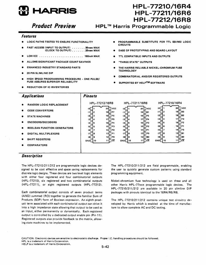
mtHARRIS HPL-77210/16R4 HPL-77211/16R6 HPL-77212/16R8
Product Preview HPLTM Harris Programmable Logic
Features • LOGIC PATHS TESTED TO ENSURE FUNCTIONALITY
• FAST ACCESS (INPUT TO OUTPUT) •.••.•. 35nsac MAX (CLOCK TO OUTPUT) ......• 25nsac MAX
• LOW ICC .•....•..........•..•.. 180mA MAX
• ALLOWS SIGNIFICANT PACKAGE COUNT SAVINGS
• ENHANCED INDUSTRY STANDARD PARTS
• 20 PIN SLIMLINE DIP
• HIGH SPEED PROGRAMMING PROCEDURE - ONE PULSE/ FUSE ASSURES SUPERIOR RELIABILITY
• REDUCTION OF IC INVENTORIES
Applications Pinouts
• PROGRAMMABLE SUBSTITUTE FOR TTL SSI/MSI LOGIC CIRCUITS
• EASE OF PROTOTYPING AND BOARD LAYOUT
• TTL COMPATIBLE INPUTS AND OUTPUTS
• "THREE STATE" OUTPUTS
• THE HARRIS RELIABLE NICKEL-CHROMIUM FUSE TECHNOLOGY
• COMBINATORIAL AND/OR REGISTERED OUTPUTS
• SUPPORTED BY HELpTM SOFTWARE
• RANDOM LOGIC REPLACEMENT HPL-77212/16R8 HPL-77211/16R6 HPL-77210/16R4
• CODE CONVERTORS
• STATE MACHINES
• ENCODERS/DECODERS
• BOOLEAN FUNCTION GENERATORS
• DIGITAL MULTIPLEXERS
• SHIFT REGISTERS
• COMPARATORS
Description
The HPL-77210/211/212 are programmable logic devices designed to be cost effective and space saving replacements for discrete logic designs. These devices are two level logic elements with either four registered and four combinatorial outputs (HPL-77210), six registered and two combinatorial outputs (HPL-77211), or eight registered outputs (HPL-77212).
Each combinatorial output consists of seven product terms
(AND) summed (RO) together to generate the familiar Sum of Products (SOP) form of Boolean expression. An eighth product term associated with each conbinatorial output can drive it into a high impedance state allowing that output to be used as an input, either permanently or dynamically. Each registered output is controlled by a dedicated output enable pin (Pin 11). Registered outputs also provide feedback to the matrix, allowing state machines to be implemented.
vcc vcc 10 vcc
F7 11 81 11 83
F6 F5 82
F5 F4 F3
F4 F3 14 F2
F3 F2 15 Fl
F2 Fl Fa
Fl Fa 17 81
Fa 80 18 80
CE CE GND CE
The HPL-77210/211/212 are field programmable, enabling the user to quickly generate custom patterns using standard programming equipment.
Nickel-chromium fuse technology is used on these and all other Harris HPL-77xxx programmable logic devices. The HPL-77210/211/212 are available in 20 pin slimline DIP packages with pinouts identical to the 16R4/R6/R8.
The HPL-7721 0/211 1212 contains unique test circuitry developed by Harris which is enabled at the time of manufacture to allow complete AC and DC testing.
CAUTION: Electronic devices are sensitive to electrostatic discharge. Proper I.C. handling procedures should be followed. HPL is a trademark of Harris Corporation. HELP is a trademark of Harris Corporation.
5-42

~ a: w l-
t; :::> c c a: a..
4
9
0 1 , 3 4 , 6 7
.-{>== 8 9
l~ " 13 14
"
" V
16
" 18
" " 21
" 73
.... v
,. " 26 11
" " 30 31
...
37 33 34 35 36 37 38 39
40 41 47 43 44
" 46 47
... v
48 49
" " " 53
" " '" ...
" " " " 60 61
" 63
HPL-77210/16R4 INPUTS (0 31) -
012) 4561 891011121314151611181920212223242526112829)O31
f:f~ /1
kJ/ J"l
F ~
./
F9/
"
F s== .-1
"
~
~ --1 "
~ l.-r- K ~
.-1
~ })--1) ~
,.., "
o 1 'l 3 ~"6 I 8 91011 1213141~ 1611T8192021 2223242526212829JO]1
5-43
1 9
1
roGr-F{>-1
~'l
FC>-1 r--o Dt-- 6
~il
ro-o:~ ~1 ~~
~1 r--o Of-- 4
~'l
1
12
11

! I a: w l-t; = Cl Cl
f
2
4
...
"
...
....
....
" ~
0 , , J • 5 • ,
8 • 10 II 12 IJ 14
"
" 11 18 18 10 11 22 2J
14 25
" 21 28
'8 I,
II J8 J8
40
" 42
II .. .. .,
.. .. SO
" 51 53 54 55
58
" !I I' " 8J
HPL-77211/16R6 INPUTS (0 31) -
111234561 8910111213141516'1181920212223242&26272829J031
:R:::=:::1
~.
19 ~
F ~
0----\ :H ~ H===r -....r
~ :t::S== ~ -,..,
~
~
F ~
::)---(
:B:::=::l ~
012 J 4 S 6 7 8 91D111213141~16HIB1II2021222324252S272829J031
5-44
A 1 9
A
roIir-F{)--1 t...!~
'"
1jj""Qf-Fe>--1 E:....2~
..--D Q-tc>--1 ~l
Dar-R>--15
A ~il ""
R>-..--D Qt- 14
A ~'l '"
Fe>--r--D Qt- 13
A ~~ ""
A 12
L<J-11

! I lie III
2
3
4
I- 5 t ::0 CI CI lie ...
6
7
8
9
---... • • " 11
12 13 .. "
,... ...
I! " " " II 23
.....
.. Z5
n H
It
... .. Il .. n .. "
"
~
...
" ...
r
HPL-77212!16RB INPUTS (0-31)
0123 4581 ."011 12131415111111112021222324218272121313'
ts== l-1
"'-'
~ l-1 ;cs::::= -0---
..r"'o
;cs::::= :t-< =t:S==
-0-----4 l-1 :t:1=====I ~ "'-'
~
i==
F1 ~ "'-'
--'""'
:R::=
i==
F-~
I 0121 4561 8910"1213,415161118192DZnU124252&Z12129lO3,
5-45
....
A
~
.A
A
....
A
.....
...... ~
.....
.A
iDr--K>-18
L~
ro-iir--~ 18
t...!1j
ro-iir--~ 17
I::....! '1
iCi-=t>-16
t....!]
=t>-r--D Q- 15
t...!~
rar--FC>--14
E:....!1j
r--D Qr--FC>-- 13
t....!Q
- ~ D Q- 12
UJ -<}- 11
-' ... :x:

HPL Programming Philosophy
Harris Semiconductor is the only vendor who manufactures both IFL and PAL type devices, and all HPL products (IFLs and PALs) program generically o'n any conventional programmer fitted with the appropriate Harris Programming/Testing Adaptor.
The HPL generic programming method employs a simple programming algorithm which does not require stress,..inducing high voltages for individual fuse addressing; instead, program mode fuse addressing is done using TTL logic level signals. By using low voltages during programming, functional yield and in-circuit device reliability are maximized.
Another advantage of family wide generic programming is a reduction in the number of programmer adaptors required to program a wide range of devices, and therefore a reduction in the time required for familiarization by the operator. The HPL generic programming philosophy will be used on all future products, helping to ensure nonobsolescence of programming equipment.
All HPL products feature three distinct modes of operation. Two modes are always available to the user: the PROGRAMMING MODE (MODE 2) and the FUNCTIONAL MODE (MODE 3). The TEST MODE (MODE 1) is not generally available to the user because of its proprietary nature. For further information on MODES 1 and 3, please contact Harris Semiconductor, or consult Module 5, on page 6-32 (Section 6 - Applications) of this data book.
In MODE 2 (PROGRAMMING MODEl. the integrity of the fuse matrix is verifiable; in other words, it is possible to verify that all the fuses in an unprogrammed device are intact. Also, individual fuses are capable of being selectively programmed in order to generate the overall logical functionality required by the user. Lastly, it is possible to verify that programmed fuses have programmed correctly, and that fuses desired not to be programmed are still intact. In summary, the basic features of the programming mode are:
1. The ability to selectively read all fuses to determine whether they are intact or programmed. This feature is functional both before and after programming.
2. The ability to selectively program individual fuses without erroneously programming nonselected fuses, or electrically or thermally overstressing or damaging the device.
--'" FUSE ADDRESS DATA > FUSE VERIFY DATA
HPL-71XXX
PROGRAM CONTROL DATA
PROGRAM MODE BLOCK DIAGRAM
Complete information on the programming and subsequent verification of HPL parts can be found in the individual device data sheets. The HPL programming mode pinout and programming algorithm is generic to all HPL products to this date; however, in accord with the Harris policy of supplying the customer with the highest possible quality, future products may include enhancements to the basic programming scheme.
5-46
HPL Programmer Evaluation
Programmer equipment manufacturers identified in the accompanying list have previously produced equipment determined to be capable of properly programming Harris Semiconductor Programmable Logic (HPL). This list is provided only as a convenience to purchasers of HPLs to identify programmer manufacturers potentially suitable for programming the HPLs. It is neither intended to be a representation or warranty by Harris of the capability of all listed manufacturer's models nor an indication of unsuitability of other manufacturers not contained in the list. HPL purchasers are advised to adhere to the programming requirements specified in HARRIS current data sheets applicable to the HPLs to be programmed and to the programming equipment manufacturer's specifications. Responsibility for programming equipment performance lies solely with the equipment manufacturer. The programmer user is cautioned to verify operation and performance according to the manufacturer's instructions and specifications prior to each use, and to determine that the programming complies with the applicable HPL data sheet. Harris accepts no responsibility for HPLs which have been subjected to incorrect or faulty programming.
DATA I/O 10525 Willows Road N. E. C46 Redmond, WA 09052 Phone: 206-881-6444
HPL Programmer Manufacturers
STAG MICROSYSTEMS, INC. 528-5 Weddell Drive Sunnyvale, CA 94086 Phone: 408-745-1991
• In approval process at present time.
DIGILEC USA * Suite 103 7335 East Acoma Drive Scottsdale, AZ 85260 Phone: 602-991-7268
NOTE: Programmer manufacturers are changing from modular or card sets to a universal type of programming system. Contact the programmer manufacturer for their latest updates of hardware and software.
5-47
-' ~ :r:


Applications Index 6-2
HPL Modules 6-3
HPL Application Notes 6-37
Power Strobe Application Note 6-44
6-1
en Z o
~ c..> ::; I>. I>. «

Applications Index
Introduction to Harris Programmable Logic 6-3
Module 1 Introduction to the HPL Family 6-8
Module 2 Introduction to Boolean Algebra 6-12
Module 3 HPL-77215/16H8, HPL-77216/16P8, 6-20 H P L -77209/16 L8 Applications
Module 4 HPL-77513/82S153 FPLA Applications 6-27
Module 5 Testability For Programmable Logic 6-33
Application Note 106 Hazard Free Logic Design 6-37
Application Note 107 Speed Optimization for the HPL-77153 Field 6-40 Programmable Logic Array (FPLA) and Other Programmable Logic Architectures
Application Note 201 Power Strobing Large Memory Arrays 6-44
6-2

m HARRIS HPLTM The Logical Solution
INTRODUCTION TO HARRIS PROGRAMMABLE LOGIC.
Introduction Harris Programmable Logic (HPL) is a family of user configurable logic elements designed to be space and power saving replacements for random logic designs implemented in TTL or LSTTL. HPL products are a natural progression for Harris Semiconductor, already a major PROM supplier with over ten years experience in the field of nichrome fuse programmable devices. The HPL family contains devices which are functional and pinout replacements for existing industry standard devices, and also includes new devices with enhanced architectural features designed for applications which are not served by existing devices.
Family The HPL family is divided into three architecturally distinct groups, each with its own advantages and areas of application. The three HPL groups are: IFLTM, PAL <!> and PROM, and are all similar in that they contain two logic arrays. The first array is an AND array which is used to form PRODUCT terms from combinations of feedback and/or input variables. The second array is an OR array which is used to form SUM terms from combinations of product terms generated by the first array. The difference between the three architectural groups results from various combinations of user configurable and fixed arrays.
The PAL type devices have a programmable first array (AND) and a fixed second array (OR). The PROM type devices have this configuration reversed; they have a fixed first array (AND) and a programmable second array (OR).
The IFL architectural group is different again, with both its first (AND) and second (OR) logic arrays being programmable. The various combinations of fixed and programmable arrays are shown graphically in FIG 2 on the following page. No one architectural group is the optimum solution for all designs, and for this reason Harris offers a wide range of devices to suit almost any design requirement.
Programming All HPL devices, with the exception of the high speed PROM group, program generically on any conventional programmer fitted with the appropriate adaptor. The HPL generic programming method employs a simple programming algorithm which does not require stress-inducing high voltages for individual fuse addressing; instead, program mode fuse addressing is done using TTL logic level signals. By using low voltages during programming, functional yield and in-circuit device reliability are maximized. Another advantage of family wide generic programming is a reduction in the number of proQrammer adaptors required to program a wide range of deVices, and therefore a reduction in the time required for familiarization by the operator. The HPL generic programming philosophy will be used on all future products, helping to ensure non-obsolescence of programming equipment.
Quality One of the fundamental requirements for high quality is the ability to perform testing on unprogrammed devices as they are manufactured. It was only after the appearance on the
HPL is a Trademark of Harris Corporation IF L is a Trademark of Signetics Corporation PAL is a Trademark of MMI
6-3
market of early Programmable Array Logic devices that both manufacturers and users became aware of the inherent non-testability of those devices. The reasons for this difficulty in testing blank devices stemmed from architectural differences between programmable logic and programmable memory.
In a programmable memory device, such as a PROM, the same circuitry that is used at manufacture to verify the existence of fuses is used during the normal operation of the device. Therefore, if a PROM passes a fuse array verification test, then the logic paths from input to output are automatically tested for functionality. This simplicity of testing is not, however, present in programmable logic devices because the fuse array is verified using totally separate circuitry to that which is used to carry logic signals during normal device operation. Consequently, verification of the fuse array at manufacture does not guarantee correct operation of the logic paths, and because of this, fuse pattern verification by the user does not guarantee correct device functionality. It is apparent that, unlike a PROM, there are two components of FUNCTIONAL YIELD in a Programmable Logic device: FUSING YIELD and LOGIC PATH YIELD. The FUSING YIELD of a programmable logic device is similar to a PROM and is close to 100%. However, the LOGIC PATH YIELD is an unknown quantity and varies from device to device. The components of FUNCTIONAL YIELD for a programmable logic and programmable memory device are shown in FIG 1.
FUNCTIONAL YIELD (PROM) = FUSING YIELD
FUNCTIONAL YIELD (PROGRAMMABLE LOGIC) = FUSING YIELD X LOGIC PATH YIELD
FIG. 1
Responding to customer requirements for high quality devices, Harris developed unique on-chip test circuitry, which is enabled at the time of manufacture to allow complete testing of all logic paths, eliminating the uncertain factor of LOGIC PATH YI ELD. One olthe benefits olthis test circuitry is thatthe user receives a completely tested device which, providing the fuse array programs correctly, is guaranteed to be functional, eliminating the problem of devices that verify on the programmer but fail in the circuit board. A second benefit of on-chip test circuitry is the ability to perform AC/DC parametric testing at the time of manufacture. This allows Harris to ship devices which are TESTED AND GUARANTEED, and not simply GUARANTEED.
Family Features and Characteristics • Broad range of device types
• Generic "Low Voltage" programming
• Industry standard and proprietary devices
• Quality "TESTED AND GUARANTEED" devices
• MIL-M-38510 approved NiCr fuse technology
• Slimline packages including "Power Plastic"

mHARRIS HPLTM The Logical Solution
HPL PRODUCT LINE The HPL product range includes devices from all three of the possible programmable logic architectures, in recognition of
the fact that no one architecture is the optimu m solution for all designs.
PART NUMBER
HPL-77153 HPL-77209 HPL-77210 HPL-77211 HPL-77212 HPL-77215 HPL-77216 HPL-77317 HPL-77318 HPL-77319 HPL-77320 HPL-77209B HPL-77215B HPL-77216B HPL-77210B HPL-77211B HPL-77212B HPL-77061 HPL·77209A HPL·77215A HPL-77216A HPL·77210A HPL·77211A HPL·77212A
FIRST ARRAY
Programmable "AND"
FIG 2
ALTERNATIVE
Fixed "AND"
PART NUMBER ARCHITECTURE
82S153 FPLA 16L8 PAL 16R4 PAL 16R6 PAL 16R8 PAL
*16H8 PAL *16P8 PAL 16LD8 PAL 16HD8 PAL
*16LE8 PAL *16HE8 PAL
PAL PAL PAL PAL PAL PAL FPAD
16L8A PAL 16H8A PAL
*16P8A PAL 16R4A PAL 16R6A PAL 16R8A PAL
Programmable "OR"
Fixed "OR"
SPEED
40 nS 35 nS 17MHz 17 MHz 17MHz 35 nS 35 nS 35 nS 35 nS 35 nS 35 nS 15 nS 15nS 15 nS 40 MHz 40 MHz 40 MHz 25 nS 25 nS 25 nS 25 nS 25 MHz 25 MHz 25 MHz
NOTE: SPECIFICA TlONS FOR THOSE PARTS NOT IN PRODUCTION MA Y BE CHANGED WITHOUT NOTICE. PLEASE CONTACT FACTORY FOR UPDATED AVAILIBILITY. * ARCHITECTURE DEFINED BY HARRIS.
6-4
AVAILABILITY
NOW NOW CY84 CY84 CY84 NOW NOW CY84 CY84 CY84 CY84 CY85 CY85 CY8S CY8S CY85 CY85 CY84 CY84 CY84 CY84 CY84 CY84 CY84

mHARRIS HPLTM The Logical Solution
HPL-77209/16L8 HPL-77215/16H8 HPL-77216/16P8
Functional Diagrams
..
..
.
..
. ..
HPL·77209 /16L8
"" ... , .... ",.,,,.,,,,,,,, .... ,, ................. ,,
"" ... , .. """""""""" ......................
Description
B .. :l:l:f 1, ..
I ~ ..
I
Pr· ~lr" Pr .. ~ .. ~ ],. ..
HPL·77215 HPL·77216 /16H8 /16P8
S· i2J. 12r 12r .. B· 12r" Er 12r. Er 12r .. Er 12r .. . "
B· Er .. p-.. =-.. ~. ~-..
The HPL-77215/216/209 are programmable logic devices designed to be cost effective and space saving replacements for discrete logic designs. These devices are two-level logic elements consisting of 7 product terms (AND) summed (OR) together to generate each of the 8 outputs. An eighth product term associated with each output can drive it to a high impedance state allowing 6 (BO-B5) of the 8 outputs to be used as inputs, either permanently or dynamically.
The HPL-77209 is functionally identical to the industry standard 16L8, and implements logic expressions of the Inverted Sum Of Products (lSOP) form.
The HPL-77215 is a similar device to the 16L8 but does not include the associated output inversion, it implements logic expressions of the Sum Of Products (SOP) form.
D.C. ELECTRICAL CHARACTERISTICS (Operating)
HPL-77215/216/209 -5 (Vcc = 5.0V±5%, TA = O°C to +75°C) HPL-77215/216/209 -2/-8 (Vcc = 5.0V±10%, TA = -55°C to +125°C)
6-5
h~ Input Current IlL Ded,eB\edlnput
OutputCurrenl HI·ZStale
Input Threshold (t) Voltage
High-Leval Qutput Voltage 12)
Low-L8I'el Quipul Voltage (2)
Input Clamp VoIlage 11)
T
"
Qulpul Short Circu,t CU"lInt (2)
PowerSupplyCurrenl
+25 1'-" V1H _ Vee MAX -tOO JAA V" ~ 0.4 V
p.A VFt
"
l::~ .. -~·~~::~i I :~~ : :~:;::: ~~,l (3)
V'L ~ 0.8V V U'H ~ 20V
Vee SOV,VOUT-OV
Onll Oulput 10' MAX Of One Sec
15SIC)
165(1,4)
C ~mmercl.11 iii M M,IIIarYI-2i 0) 12jTI>e.espoc,f,cOIo"" •• pplytobOlnOulpullf).nd Bodorscl,,,,,"IIBI p,n. 11IT1> .. e.pec'!'oal,on •• pplytobOllolnpul(lIandB,d"""t,onaIIBI"'II5 f31 One outpul.t. "me otn .. " ... ,emA
A. C. SWITCHING CHARACTERISTICS (Operating)
JEDEC OLD STANDARD SYMBOL PARAMETER
F'ropagatlOllDelay-lnputor IIOtoAcb~eHlgl1Oulput
PropagatoonOelay-Inputor IIOtoAct,~eLowOutput
EnebleAccessT,me to Act,vsHlgh Output (11
EnabloAccessT,me to Act,~e Low Output (11
D,sableAccessT,me f!om Act,ve HlghOll1put
DlsableAccessT'mD lromAel1V<:I Low Output
~:t:~~:=: HPL·T7208-S
O'i~;!;!;-5·C
111 En.bleAc<:e •• T,me'.gu ... nt.edgrMlertn.nO,oableAoo ... T'm.to""'"dde.,cec""tent,on NOTE M.,,,,,um 1.'llnIquency IS 51.11'1 • ... !tl • ~O'" duly CYOIf!
HPL-77215 2J 8 HPL·T7t18-2J-1
HPL57J~o%2J-8
-5S'Cto+t25"C
MAX UNITS
The HPL-77216 is a more flexible device, it includes 8 EX-OR gates in each output path, controlled by 8 extra fuses, allowing the polarity of each output to be user configured. This device can implement a combination of SOP and ISOP expressions.
The HPL-77215/216/209 are field programmable, enabling the user to quickly generate custom patterns using standard programming equipment.
Nickel-chromium fuse technology is used on these and all other HARRIS HPL-77XXX programmable logic devices. The HPL-77215/216/209 are available in 20 pin slimline DIP packages with pinouts identical to the 16L8,
The HPL-77215/216/209 contain unique test circuitry developed by HARRIS which is enabled at the time of manufacture to allow complete AC and DC testing.
<I) Z o
~ (.)
:::; 0. 0.
<

, @
0-. ~ . f'1. , .
m HARRIS HPLTM The Logical Solution
Functional Diagram
HPL-77153/82S153
HPL-77153/82S153
lPROIlUCTTERMSI (CONTROL TERMS)
31301982126252' 232Z21HI9181111 151413121110 18543210 0981080643210
.. " " " B.
B,
" " .. "
D.C. ELECTRICAL CHARACTERISTICS (Operating)
HPL-HPL-
77153/825153 -5 (Vee; 5.0V ±5%, T A; ooe to + 750 e) 77153/82S153 -2/-8 (Vee; 5.0V 2:.10%, TA; -550 e to +1250 e)
~ l-/1slB
BB
" ta'
''" InpuICurram
'" Dedic.l"dlnpu!
'BZH Input Current Bidirectional p,n Current
IBZL H,-ZState
v'" lnputThre'hold
V" Voltage
VO" High_LevelOutputVoltaQe
VOC Low_Laval Outpul VQltaga
V" InpUt Clamp Voitage
'OS Output ShOrt C"cuit Current"
''''' POW<lrSupplyCurrent
c ~ Commercial I-51 M ~ M,litary 1-2/-81
,,1" "0"
"0 -100
Vlfj-VCC MAX VIL ~ 0 4V
veH-Vcc MAX
Vee ~ Vee MAX
Vee ~ Vee MIN
Vee ~ Vee MIN VIL ~O"8V VIH-2.0V
IIN--18mA, Vee
Vee ~ Vee MAX
VCC~VCCMAX
! IOH --2.0mA
! IOL-+16mA
Vee - 5.0V, VOUT - OV
Vee -Vee MAX
A. C. SWITCHING CHARACTERISTICS (Operating)
UMTE/lMSI ~ fB B,
Description
The HPL-77153/82S153 is a programmable logic device designed to be cost effective and space saving replacement for discrete logic designs. This device is a two-level logic element, consisting of 32 productterms (AND) and 10 sum terms (OR) with fusible links for programming I/O polarity and direction.
All product terms can be linked to 8 inputs (I) and 10 bidirectional I/O lines (8) allowing variable I/O configurations using the 10 direction control gates (C), ranging from 17 inputs and 1 output to 8 inputs and 10 outputs.
On chip T/C buffers allow either True (I, 8) and/or Complement (I, 8) signals to be linked to any of the product terms, the outputs of which may be used as inputs to any or all of the sum terms. The output polarity of the sum terms is individually programmable by means of a fuse-link controlled EX-OR gate to allow implementa-
BS
"" .. ~ Hiil
B,
" f8 l{i] '0
6-6
HPL-77163! HPL-77163! 82S163-S 82$153-21-8 5V+S% SV+10%
JEDEC oCO STANDARD SYMBOL
TDVQH1 'eo PropaQ.tlonDel.y_lnputor I/Oto Aot.ve High Output
TDVOll 'eo PrOpa9"tionDel.y_lnputor l/otoAotive low Output
TDVQH2 '0' to Active High Output
'0' to Active low Output
"'--TOVQZ1 '00
from Aotlv. High Output
TDVQZ2 '00 from AOllve LowOutput
NOTE" Maximum test frequencY" 5MHz with a 50% duty oycle.
tion of Sum Of Products (SOP) or inverted Sum Of Products (ISOP) expressions.
The HPL-77153/82S153 is field programmable, enabling the user to quickly generate custom patterns using standard programming equipment.
Nickel-chromium fuse technology is used on these and all other HARRIS HPL-77XXX programmable logic devices. The HPL-77153/82S153 is available in a 20 pin slimline ceramic DIP with a pinout identical to the 82S153. NOTE: The HPL-77152/82S152 (open collector outputs) can also be made available.
The HPL-77153/82S153 contains unique test circuitry developed by HARRIS which is enabled at the time of manufacture to allow complete AC and DC testing.

m HARRIS HPLTM The Logical Solution
CHOOSING AND USING PROGRAMMABLE LOGIC
Because of the wide range of HPL products available, some method of selecting the right device for a given application is necessary. The method offered below is one way of selecting a device based on input, output and product term usage. This is only one method; other selection criteria, such as speed or
FOUR CRITERIA ARE IMPORTANT
A r-------------------I
01 B
c 0
E 02
F
G
1 ______ --------------
HPL.-77209116L8 HPL·77210/16R4 HPL·771531825153 HPl-77215116H8 HPL·77211116R8 HPL·77216116P8 HPL-77212116RB HPl-77317118L.DB HPL·77318/16HD8 HPL·77319116L.EB HPl-77320/1SHE8
power, may require a different selection procedure and will be different from user to user. However, the method shown is a good first approach. Decisions based on other criteria can be made after a device is initially selected.
01
1. DRAW BOX AROUND SECTION OF CIRCUIT TO BE REPLACED, COUNT NUMBER OF INPUTS = I
2. COUNT NUMBER OF OUTPUTS = ¢ 3. DERIVE LOGIC EQUATIONS FOR EACH OUTPUT e.g.:
,-product Terms----y
A. B. C. + 0.0. E. F.
~"nput~ COUNT NUMBER OF PRODUCT TERMS FOR ALL OUTPUTS = PT
4. HOW MANY PRODUCT TERMS ARE USED ON THE OUTPUT WITH MOST PRODUCT TERMS = PM
USE APPROPRIATE GATE CUSTOM DESIGN PROM HM76XX ARRAY
T~ ______ ~ ____ ~n T l
SEMICONDUCTOR BIPOLAA DIOITAl PRODUCTS DIVISION
6-7
CUSTOM INTEGRATED CIRCUITS DIVISION

m HARRIS HPL™'The Logical Solution
Module 1 Introduction to the HPL Family
By Steven Bennett - HPL Product Marketing
1.1 THE HPL FAMILY IS THE ANSWERI
In the 1970's, the microprocessor, after some reticence by engineers, was hailed as the panacea for many logic circuit design problems which previously had been the domain of large arrays of discrete logic.
The microprocessor could offer many advantages over discrete logic arrays, including reduced system power, much reduced package count, improved reliability, the ability to implement logic functions not available in discrete packages, and the flexibility to reprogram the emulated logic function by simple software changes.
These advantages were quickly realized by engineers working in many different application areas, and were partly responsible for the astonishing success enjoyed by the microprocessor.
Useful though the microprocessor is, it does suffer from one important disadvantage-speed. Any emulation of a discrete logic array cannot, with today's technology, hope to even approach the speed of the discrete design.
Speed may not be an important consideration in some designs, but in many others it certainly is. For this class of applications, a new product line is available: the HPL family of programmable logic.
The HPL family consists of many products for implementing large or small, synchronous or asynchronous logic arrays, that could only be emulated in real time by a microprocessor running at several hundred megahertz, which is not possible with today's technology.
The use of HPL products, because they are easily understood by a hardware engineer, can allow him to exercise more control over a project. In the last decade, this control has become more and more the domain of software engineers who have required increasingly large amounts of time and resources to accomplish their task.
In conclusion, there exists a class of applications where HPL devices can be used to produce a cheaper, faster, lower power, fewer parts solution to logic design problems.
*HPL is s Trademark of Hsrris Corporation
1.2 WHAT ARE HPL DEVICES?
HPL devices are a "black box" solution to logic design problems. All the devices in the family are characterized by having a set of inputs and a set of outputs; the logical relationship between any output and the set of all other inputs and outputs is determined by the wayan array of fuses inside the device is programmed (the fuse array is similar to a PROM). The method used for generating the pattern for programming HPL devices may vary according to how the designer views the device.
For those designers who are more familiar with discrete logic design, the HPL device may be viewed as a highly integrated form of discrete logic. Indeed, examination of an HPL device data sheet will reveal a schematic of the internal logic of the device in terms of AND, OR and INVERTOR gates, LATCHES, REGISTERS, and other devices, with which such designers will be familiar.
For those designers who are familiar with Boolean Algebra, and take a "black box" approach to systems deSign, they need only generate the appropriate Boolean logic equations for each device output.
Whichever approach is taken to generate the programming pattern, it is a simple task to use almost any PROM programmer (with a suitable adapter) to program devices with the required pattern.
The ease of programming HPL devices can solve a common problem for designers using discrete logic, which is:
"How do I tell my boss that my design needs a minor modification, which will cause a six week production delay until new printed circuit boards are obtained?"
The programmability of HPL devices can eliminate this problem, as a "minor modification" can be implemented in minutes by programming a new device, or with some HPL devices performing "logical surgery" on a programmed part.
Having covered some areas of application and the advantage of using HPL devices, the following sections will deal with some of the decisions that must be made before choosing an HPL device.
6-8

Module 1
1.3 PROM OR HPL, THAT IS THE QUESTIONI
Programmable read only memories (PROM) have traditionally been used not only for the storage of computer programs, but also to emulate asynchronous random logic arrays.
The emulation of random logic by PROMs is attractive because it allows a Significant reduction in package count, but it is not an optimum solution for the following reasons:
Any random logic array is characterized by having a number of inputs (X) and a number of outputs (Y). To replace a random logic array with a PROM requires the use of a PROM with X inputs, which translates to 2x bytes. For a small number of inputs, say 5, one can use a 25 or 32 byte PROM which is a low cost solution; however, suppose the input field is 13 bits wide, one must now use an BK byte PROM which is an expensive solution.
The high cost involved in replacing random logic arrays with a large number of inputs, with PROMs is mainly due to the inefficient architecture of PROMs when used in this manner. One useful definition of architectural efficiency is:
NUMBER OF DISCRETE OUTPUT EFFICIENCY = CODES USED x 100%
TOTAL NUMBER OF OUTPUT CODES POSSIBLE
Let us now use this definition to compare the efficiency of PROMs versus HPL programmable logic arrays.
Suppose a random logic array exists, having an input field width of ten bits, an output field width of eight bits, and five unique output codes associated with the input field. One solution would be to use a 1K x B PROM which would have the following efficiency:
1K x B PROM EFFICIENCY = 5 x 100 = 0.48% 1024
A better solution would be to use an HPL77209/16LB Programmable Logic Array, which would have the following improved efficiency:
HPL77209/16LB EFFICIENCY = 5 x 100 = 71.42% 7
NOTE: In the calculation used to evaluate the HPL77209/ 16LB efficiency, it is assumed that the seven internal product terms available to each output are used to generate seven unique output codes in a similar manner to a PROM. Although this approach cannot be representative of all applications, it is a useful approximation.
The large difference in device efficiency is reflected in the higher cost of the PROM solution. This is not to say that all PROM applications are inefficient; for example, an ASCII to EBCDIC code convertor using a PROM would have a high efficiency, and in fact, could not be implemented using an HPL device.
The secret is to choose the correct device for one's application, and for the majority of random logic replacement applications, an HPL device should be preferred.
Having shown that HPL devices are far more efficient than PROMs for replacing most random logic arrays, the following is a more detailed explanation of how that efficiency is achieved.
HPLs are programmable AND arrays followed by either a fixed or a programmable OR array, according to the type. PROMs are fixed AND arrays followed by a programmable OR array. Figures 1-1 and 1-2 depict the basic difference.
AABlicc
A ~ B
c
~/C./B./A FO -v-
~/C'/B.A F1 PT1 ~ -
IC.B./A F2 PT2 v
~/C.BA F3
r>-PT3 ~
C./B./A F4 1==1 PT4 v-- t"""-
y
C./B. A F5 1==1 PT5 ~ -- C.B./A F6
PT6 ~ -C.B. A F7
PT7 ..........
1 ! FIXED PROGRAMMABLE "AND" "OR"
Figure 1-1- Elementary PROM
6-9
en 2: o
~ c..> ::; c.. c.. «

Module 1
AABBCC
c
F6 F7 F8 F9
F10 F11
PTO
r r PROGRAMMABLE FIXED "AND" "OR"
Figure 1-2 - Elementary HPL
y
The PROM structure decodes all input combinations using a fixed AND decoder as shown in Fig. 1-1. Because the PROM illustrated has three inputs, the AND decoder must consist of 23 = 8 AND gates. Each gate uniquely defines a product term (PT) which is fuse-linked to the input of the OR matrix as shown. The presence or absence of the fuse determines the programmed function. For example, to program the function
YO = IC./B./A + IC.B.A + C./B./A + C./B.A (PTO) (PT3) (PT4) (PT5)
One would retain fuses for PTO, PT3, PT4, PT5 and blow all others. Note that a blown fuse represents a logical zero to the OR matrix.
NOTES: Symbology used in equations + = OR • = AND I = NOT (INVERT)
Now suppose the following function were desired instead:
Y1 = A + B.C + IB./C
The first term, A, is implemented in the PROM by selecting PT1, PT3, PT5, and PT7. Product terms PT1, PT3, PT5, and PT7 can be reduced using Boolean Algebra as follows:
A = IC./B.A + IC.B.A + C./B.A + C.B.A A = IC.A + C.A = A. (lC+C)
A=A
Similarly, the second term,B.C is generated by selecting PT6 and PT7 and the last term, IB./C by selecting PTO and PT1. The ORing of all product terms implements Y1 in the PROM as follows:
Y1 = IC./B./A + IC./B.A + IC.B.A + C./B.A + C.B./A + C.B.A
Note that the original equation for Y1 contained only three product terms while the PROM implementation required that six product terms be involved. This demonstrates the inefficiency of using a PROM to replace random logic.
A more effective architecture for implementing logic is shown in Fig. 1-2. Y1 can be directly implemented using this structure by simply programming fuses to generate the three product terms as follows:
Y1 = A + B.C + IC./B FO F8, F10 F17, F15
This would involve blowing all fuses except FO, F8, F10, F15, and F17.
Typically, logic designs involve a relatively high number of input variables but do not require that all 2n possible input combinations be completely decoded as in the PROM; for example, a 10 variable logic expression as shown below would require a 2'0 = 1024 location PROM.
Y2 = A./B./C.D.E./F.G.H.I./J + IA./B./C.D.E.F.G.H./I.J
However, the same function can easily be implemented in the basic HPL shown in Fig. 1-3. The HPL structure offers several potential advantages over the PROM, such as:
• GREATER THAN 4 TO 1 REDUCTION IN BOARD SPACE
• LOWER COSTS • FASTER PROGRAMMING • INCREASED SPEED • USER DEFINABLE PINOUT • EFFICIENT PRODUCT TERM COMPRESSION • SMALLER FUSE ARRAY • LOWER POWER • ADVANCED ARCHITECTURE FEATURES
In addition, the price paid for additional input capability when using a PROM as a logic element is usually too high. As an example, consider adding another input variable to the previous 10-input logic expression. The extra input variable would require a 2" = 2048 location PROM, doubling the fuse matrix size required. On the other hand, adding an extra input to the HPL structure of Fig. 1-3 would only increase the fuse matrix size from 120to 132 fuses, only a 10% increase in size.
6-10

Module 1
A
y
Figure 1-3- Basic HPL Logic Structure
As a function of the number of inputs (X), the PROMs' fuse matrix size increases geometrically (cx:2x), whereas the HPLs' array size increases arithmetically (cx:2X).
Harris programmable logic devices exhibit other features which make their use more desirable than PROMs. One such feature is the minimization of output glitches during input transitions. It is not often recognized that the logical output condition of a PROM is undefined for the duration of the device's access time, which means that for tens of nanoseconds after an address line changes, the device outputs may exhibit an undesired state. If the output from such a PROM is then used to drive a synchronous device such as a counter, erroneous counts may be registered. This situation rarely occurs with HPL devices, which can make the design engineers task easier, leading to fewer production problems.
So far, only an elementary form of HPL has been discussed. More complex devices are found in the HPL family, including:
Devices with programmable AND structures and programmable OR structures, which allow the implementation of larger and more powerful logic equations.
Devices with programmable output polarity (using EX-OR gates) allowing outputs to implement the true or inverted form of a logic expression.
Devices with latches and internal feedback allowing the implementation of sophisticated synchronous state machines of the Mealy or Moore type.
These and many other powerful features are dealt with more completely in the following modules.
1.4 THE HARRIS PROGRAMMABLE LOGIC FAMILY
The Harris Programmable Logic family consists of many different parts, some of which are enhanced versions of industry standard parts, while others are powerful propriety parts developed to satisfy a specific area of applications.
The HPL family is available in an advanced Bipolar technology. allowing high speed and low power devices to be fabricated.
Some of the features to be found in the HPL family are:
• SPACE SAVINGS PACKAGES • HIGH SPEED AND LOW POWER • ON-CHIP FUNCTIONAL TEST CIRCUITS • VARIABLE I/O PIN RATIO • PROGRAMMABLE THREE STATE OUTPUTS • BI-DIRECTIONAL PINS • REGISTERS WITH FEEDBACK • PROGRAMMABLE LATCHES • PROGRAMMABLE OUTPUT POLARITY • ARITHMETIC CAPABILITIES • USER DEFINABLE PIN-OUT
Harris programmable logic devices can be programmed and verified using most standard PROM Programmers, with the addition of a suitable personality card.
A user can expect a very high programming yield because special test circuitry, built on chip, is enabled at the time of manufacture, allowing the parts to be exercised and tested for logical functionality and compliance with the published static (DC) and switching (AC) parameters. The ability to test parts at the time of manufacture eliminates a major problem associated with other industry parts; namely, the inability to guarantee the units as fully functional after programming, even though the fuse matrix had "verified".
Built in testability is just one of many unique enhancements included in the HPL family. All the enhancements included in the HPL family were designed in with the intention of providing the user with improved programming yield, superior and more reliable parts.
6-11
en Z o
~ (.)
::; Q. Q. <l:

-
m HARRIS
2.1 INTRODUCTION TO LOGIC
It is ironic to reflect that the foundation of modern logic theory has lain dormant for many years before being utilized in practice. The basis of logic as we know it was set down in the nineteenth century by Boole, De Morgan and others. Many generations were to pass before technologists began to realize the implications of these theories, and even longer before fabrication techniques for the construction of "logical" devices were perfected.
In this introduction to Boolean Algebra, the following Boolean operators are used:
+
:+: ...
Logical Equality Negate (Not, invert) OR (Sum) AND (Product) Exclusive OR Exclusive NOR
In addition, a number of logic theorems and laws will be used to manipulate and reduce logical equations; these theorems and laws are as follows:
THEOREM 1 THEOREM 2 THEOREM 3 THEOREM 4 THEOREM 5 THEOREM 6 THEOREM 7 THEOREM 8
COMMUTATIVE LAW
A+B=B+A A·B = B·A
A+O=A A·O = 0
A + 1 = 1 A·1 =A
A+A=A A·A=A
A + IA = 1 MA = 0
ASSOCIATIVE LAW
A+B+C=~+~+C=A+~+q A·B·C = (A·B)·C = A·(B·q
DISTRIBUTIVE LAW
A + (B·C' D) = (A + B)'(A + C)'(A + D) A·(B + C + D) = A·B + A'C + A'D
HPL is a Trademark of Harris Corporation
HPL" The Logical Solution Module 2
Introduction to Boolean Algebra
By Steven Bennett- HPL Product Marketing
DeMORGAN'S THEOREM
I(A + B + C) = IMB'/C I(A·B·C) = IA + IB + IC
DeMorgan's theorem is one of the most powerful tools for engineering applications and is very useful for designing with HPL programmable logic devices because it provides a quick and simple conversion method between PRODUCT OF SUMS and SUM OF PRODUCTS expressions.
Any logic expression can be reduced to a two level form and expressed as either a SUM OF PRODUCTS (SOP) or PRODUCT OF SUMS (POS). The two basic forms are explained below.
SUM OF PRODUCTS (SOP)
F = (A'B) + (C'D) + (E·F·G) EQ2.0
The above is an example of a SOP logic expression. The reason for the name becomes apparent if one refers to the table of Boolean operators.
PRODUCT OF SUMS (POS)
F = (A + B)'(C + D)·(E + F + G) EQ2.1
The above is an example of a POS logic expression. Again the reason for the name becomes apparent if one refers to the table of Boolean operators.
2.2 REVIEW OF BOOLEAN ALGEBRA
Boolean Algebra is probably the simplest form of Algebra because variables can have only one of two values, either a logical one or logical zero. For example, the Boolean function shown below has at the most four possible solutions since it is a function of two variables and each variable can have one of two states (0 or 1).
F(X, V) = X'V + V'V
The four possible solutions are:
6-12
F(O, 0) = 0·0 + 0·0 = 0 F(O, 1)= 0·1 + 1'1 = 1 F( 1, 0) = 1·0 + 0·0 = 0 F(1, 1) = 1·1 + 1-1 = 1
EQ2.2

Module 2
These solutions can also be written as a "truth table":
x o o
y
o 1 o
~ o 1 o
Because a binary variable can assume only one of two states, it is possible to perform a logical reduction by inspection. The equation (EO 2.2) can be reduced by using the theorems shown earlier, as follows:
F(X, V = X-V + V-V F(X-Y) = X-V + V F(X-Y) = V-(X + 1) F(X-Y) = V-(1) F(X-Y) = V
(Theorem 6) (Distributive Law) (Theorem 3) (Theorem 4)
So, F(X, Y) has been reduced to a function of a single variable F(V) = V. Contrast this process with conventional linear algebra where:
F(X-Y) = X-V + V-V
can only be factored, not simplified, to:
F(X-Y) = V-(X + Y)
Another binary function which can be reduced by inspection is shown below.
F = IA + A-B + IC-D + CoD EO 2.3 F = [(/A + A)-(fA + B)l + IC-D + CoD (Distributive
F = [1-(/A + B)l + IC-D + CoD F = IA + B + IC-D + CoD F = IA + B + D-(/C + C)
F = IA + B + 0-(1) F = IA + B + 0
Law) (Theorem 7) (Theorem 4) (Distributive Law) (Theorem 7) EO 2.4
In terms of logical representation, see Fig 2-1a for the implementation of EO 2.3 in its original form, and compare it to the reduced version Fig. 2-1b (EO 2.4).
The use of logical theorems and laws is not only useful for the reduction of the number of gates needed to implement a function, but can also reduce or eliminate "race hazards" which occur if the propagation delays from all inputs to an output are not identical. Obviously, the more complex a logic circuit, and the more redundant paths included, the more chance there is
for "race hazards" to occur. "Race hazards" manifest themselves as logical glitches at the network output.
ia) Original Implementation
:~ _____ .F (b) Equivalent Implementation
FIGURE 2-1. IMPLEMENTATION OF THE SAME LOGIC FUNCTION
As you can see there are several ways to implement the same function. Figure 2-1 (a) and (b) are only two realizations for F. Although the circuit in (b) is a minimum gate realization, it is not the only one.
Figure 2-2 shows yet another implementation for F. The transposition of Figure 2-1 (b) to Figure 2-2 is made possible by DeMorgan's theorem as follows:
F = IA + B + 0 IF = I(fA + B + D) IF = A-/B-/D F = I(A-/B-/D)
EO 2.5 (Negate Both Sides) (DeMorgan's Theorem) EO 2.6
As can be seen EO 2.5 is in a SUM form, whereas EO 2.6 is in a PRODUCT form. Both equations are logically identical. In a discrete design, the decision as to which form to use may depend on such factors as tile relative speed performance, or even the types of gates left over from other areas of a larger design.
When implementing such logic equations in HPL devices, the preferred form is that which "fits" the device architecture most efficiently, and as can be seen, the reversible transposition from one form to another is a relatively simple procedure.
6-13

Module 2
::_ E\o~.F FIGURE 2-2.ANOTHER IMPLEMENTATION FOR FUNCTION F
By direct substitution of the equivalent representation for ANDs, NORs, NANDs and ORs, a multitude of different circuits can be formulated to implement the same function. When designing with 7400 series gates, the designer tailors his circuits to utilize the minimum number of packages. When a logic design requires an extra two input OR gate, but only inverters and AND gates are left, an extra package can be saved by implementing the OR equivalent using three inverters and an AND gate (if the additional propagation delays are permitted). It's no wonder that logic designs take on so many forms. Simple gate equivalent due to DeMorgan is shown in Fig. 2-3.
< >
<>
< >
=E>- < > :0-FIGURE 2-3.GATE EQUIVALENCY
What is the common denominator in random logic design? All Boolean equations and their logic representations can be expressed in either of two forms: PRODUCT OF SUMS (POS) or a SUM OF PRODUCTS (SOP). All HPL Programmable logic devices internally implement the SOP form but, certain devices have fixed or programmable output invertors that allows them to generate INVERTED SUM OF PRODUCTS (ISOP) expressions. ISOP expressions can be considered equivalent to POS expressions, demonstrating how output invertors allow SOP devices to implement POS expressions.
2.2.1 SUM OF PRODUCTS EXPRESSIONS
A SOP expression is of the form: F = A·B·C + A·/B·/C + D·E + F·G
This expression represents the sum of four product terms. Each product term can consist of one or more variables AND'ed together. The logic circuit for this SOP expression is shown as an AND-OR representation in Figure 2-4.
FIGURE 2-4. GENERAL AND-OR SOP IMPLEMENTATION
Any logic expression can be written in SOP notation. For instance, consider expressing the following in SOP form:
F = (A'B'C + D)'(B + D) + MC'(B + D) Expanding, we have:
F = A·B·C + B·D + A·B·C·D + D + MC'B + MC'D EO 2.7 (SOP)
This six product term expression is in SOP form, but is not a minimum SOP. That is, by using Boolean Algebra, F can be simplified to a minimum SOP as shown below:
F = A'B'C'(1 + D) + D·(B + 1) + MC·B + A·/C·D (Distributive Law)
F = A·B·C + D + MC'B + A·/C·D (Theorem 3)
F = A·B·(C + IC) + D'(1 + MC) (Distributive Law)
F = A'B + D EO 2.8 (Theorem 7)
The minimum SOP expression can now be implemented as the simple AND-OR logic circuit as shown in Figure 2-5.
6-14

Module 2
FIGURE 2·5. MINIMUM SOP IMPLEMENTATION
Instead of using Boolean Algebra to reduce the number of product terms, Karnaugh mapping can be used. For example, consider the mapping of the previous function F onto the Karnaugh map of Figure 2·6. Karnaugh maps are a two dimensional representation of a two level logic expression. Normally Karnaugh maps are used to represent expressions involving from two to five variables, although more variables can be handled with increased difficulty. In the example shown in Figure 2·6 a map accomodating four variables is used to represent the four variable expression of EO 2.7. Note how the six product terms involved are mapped by the intersections of variables, denoted here by ones.
1
1
1
A
r--1
1 1
1 1
1 1 1
L---1 C
FIGURE 2·6. KARNAUGH MAP OF EQUATION
All six product terms are represented on the above Karnaugh map. The minimization of large logic equations, by the use of Karnaugh maps, is done by grouping adjacent pairs of cells containing ones. The grouping of pairs of cells can be extended to include other pairs of cells.
Figure 2-6 shows how the set of ones which represent EO 2.7 can be regrouped into the two sets shown, which represent EO 2.8, the reduced form.
There are many techniques for grouping cells not demonstrated here. For a more complete description, the reader should refer to any comprehensive book covering logic and Boolean Algebra. *
When choosing an HPL device to implement the reduced expression shown in EO 2.8, it is important to select one that can implement SOP expressions, i.e., either one that has true (not inverted) outputs, or one that has programmable output polarity which can be programmed for true outputs. Otherwise, the user may have to add invertors at the device outputs, which will necessitate the use of another package. Alternately the SOP expression can be converted to the ISOP form as shown in section 2.2.3.1, in which case an inverted output HPL device can be used.
* DIGITAL COMPUTER DESIGN - RAYMOND M. KLINE - PRENTICE HALL INC.
2.2.2 PRODUCT OF SUMS EXPRESSIONS
F = (A + /B + C)-(D + E)-(/C + /A)-(/D + /E) EO 2.9
The above pas expression consists of the product of four SUM terms. Each SUM term can consist of one or more variables
. OR'ed together. The logic circuit for this pas expression is shown as an OR·AND representation in FIG 2-7.
FIGURE 2·7. GENERAL OR·AND pos IMPLEMENTATION
Any logic expression can be written in pas notation. For instance, consider expressing the following in pas form.
6-15
F = A-/B-ID-(/C + C) + /A-/B-/D-(C + /C) EO 2.10 Expanding, we have: F = A-/B-/C-/D + A-/B-C-ID + /A-/B-C-ID + /A-/B-/C-/D
EO 2.11
The expression EO 2.11 is now in the SOP form. DeMor· gan's theorem may now be used to convert this expres· sion to the INVERTED PRODUCTS OF SUMS (I paS) form in EO 2.12.IPOS is the negated form of pas, in the same way that ISOP is the negated form of SOP.
F = /[(/A + B + C + D)-(/A + B + /C + D) -(A + B + /C + D)-(A + B + C + D)] EO 2.12
en Z o i= <I: (.)
::i 0.. 0.. <I:
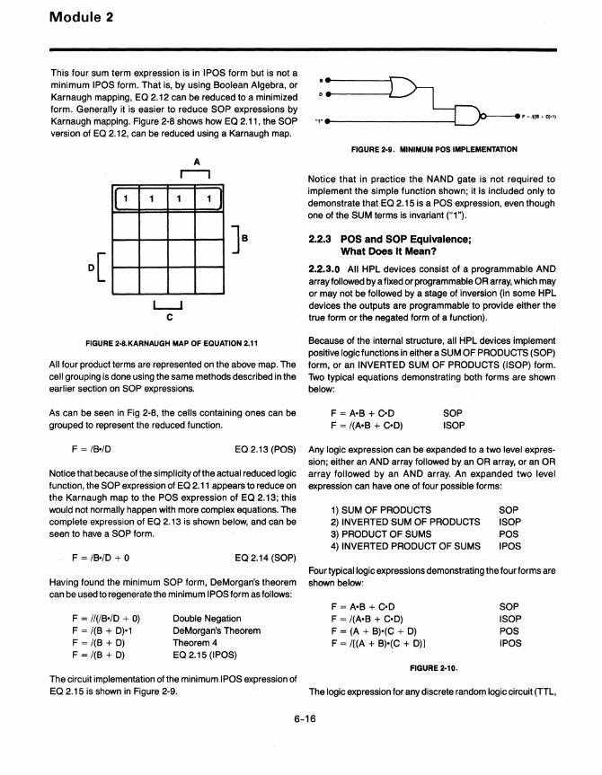
Module 2
This four sum term expression is in IPOS form but is not a minimum IPOS form. That is, by using 800lean Algebra, or Karnaugh mapping, EO 2.12 can be reduced to a minimized form. Generally it is easier to reduce SOP expressions by Karnaugh mapping. Figure 2-8 shows how EO 2.11, the SOP version of EO 2.12, can be reduced using a Karnaugh map.
A
r----1
111 1 1 1
D[ Je
L...J c
FIGURE 2-8.KARNAUGH MAP OF EQUATION 2.11
All four product terms are represented on the above map. The cell grouping is done using the same methods described in the earlier section on SOP expressions.
As can be seen in Fig 2-8, the cells containing ones can be grouped to represent the reduced function.
F = /8·/0 EO 2.13 (POS)
Notice that because of the simplicity of the actual reduced logic function, the SOP expression of EO 2.11 appears to reduce on the Karnaugh map to the POS expression of EO 2.13; this would not normally happen with more complex equations. The complete expression of EO 2.13 is shown below, and can be seen to have a SOP form.
F = /8·/0 + 0 EO 2.14 (SOP)
Having found the minimum SOP form, DeMorgan's theorem can be used to regenerate the minimum IPOS form as follows:
F = //(/8,/0 + 0) F = /(8 + 0)'1 F = /(B + D) F = /(B + D)
Double Negation DeMorgan's Theorem Theorem 4 EO 2.15 (IPOS)
The circuit implementation olthe minimum IPOS expression of
FIGURE 2-9. MINIMUM POS IMPLEMENTATION
Notice that in practice the NAND gate is not required to implement the simple function shown; it is included only to demonstrate that EO 2.15 is a POS expression, even though one of the SUM terms is invariant ("1").
2.2_3 POS and SOP Equivalence; What Does It Mean?
2.2.3.0 All HPL devices consist of a programmable AND array followed by a fixed or programmable OR array, which may or may not be followed by a stage of inversion (in some HPL devices the outputs are programmable to provide either the true form or the negated form of a function).
8ecause of the internal structure, all HPL devices implement positive logic functions in either a SUM OF PRODUCTS (SOP) form, or an INVERTED SUM OF PRODUCTS (ISOP) form. Two typical equations demonstrating both forms are shown below:
F = A·8 + C·D F = /(A·8 + C'D)
SOP ISOP
Any logic expression can be expanded to a two level expression; either an AND array followed by an OR array, or an OR array followed by an AND array. An expanded two level expression can have one of four possible forms:
1) SUM OF PRODUCTS SOP 2) INVERTED SUM OF PRODUCTS ISOP 3) PRODUCT OF SUMS POS 4) INVERTED PRODUCT OF SUMS IPOS
Four typical logic expressions demonstrating the four forms are shown below:
F = A·B + C·D F = /(A·B + C'D) F = (A + 8)·(C + D) F = /[(A + 8)'(C + D)]
FIGURE 2-10.
SOP ISOP POS IPOS
EO 2.15 is shown in Figure 2-9. The logic expression for any discrete random logic circuit (TTL,
6-16
Module 2
CMOS, etc.) can be expanded to one of the four forms shown in Fig 2-10.
Anyone of the four forms of expression can be converted to any of the other three forms by the application of the logic laws and theorems described earlier.
Secause HPL devices implement SOP or ISOP forms of logic expressions, the most useful conversions to understand are:
SOP~ISOP
ISOP ) SOP POS~ISOP
pas ) SOP IPOS ) ISOP IPOS~SOP
In order to demonstrate the techniques used to perform these six conversions, actual examples are shown in the following sections.
2.2.3.1 SOP ---> ISOP
F = /S·/D + S·/C SOP F = //(lS·/D + S·/C) Double Inversion F = /[(S + D)·(lS + C)] DeMorgan's Theorem F = /[S·/S + S·C + /S·D + C·Dl Expand F = /[S·C + /S·D + C·D] Eliminate Zero Terms F = /[S·C·D + S·C·/D + /S·C·D
+ /S·/C·D + S·C·D + /S·C·D]
F = /[S·C·D + S·C·/D + /S·C·D + /S·/C·D]
F = /[S·C + /S·D]
F = /[S·C + /S·D]
Expand to Canonical Form' Combine Common Terms Combine Terms Containing True and Complement Variables Using Distributive Law and Theorem 7 ISOP
, CANONICAL FORM IS A FULLY EXPANDED EXPRESSION
CONTAINING ALL INPUT VARIABLES.
2.2.3.2 ISOP ---> SOP
F = /(S·C + /S·D) ISOP F = (IS + /C)·(S + /0) DeMorgan's Theorem F = /S·S + /S·/D + S·/C + /C·/D Expand F = /S·/D + S·/C + /C·/D Eliminate Zero Terms F = /S·C·/D + /S·/C·/D Expand to Canonical
+ S·/C·D + S·/C·/D Form + S·/C·/D + /S·/C·/D
F = /S·C·/D + S·/C·D + /S·/C·/D + S·/C·/D
F = /S·/D + S·/C
F = /S·/D + S·/C
2.2.3.3 POS ---> ISOP
F = (/S +/C)·(S + /0) F = //[(/S + /C)·(S + /D)] F = /[S·C + /S·D] F = /[S·C + /S·D]
2.2.3.4 POS ---> SOP
Combine Common Terms
Combine Terms Containing True and Complement Variables SOP
pas Double Invert DeMorgan's Theorem ISOP
F = (IS + /C)·(S + /0) pas F = /S·S + /S·/D + S·/C + /C·/D Expand F = /S·/D + S·/C + /C·/D Eliminate Zero Terms F = /S·C·/D + /S·/C·/D + S·/C·D Expand to Canonical
+ S·/C·/D + S·/C·/D + Form /S·/C·/D
F = /S·C·/D + S·/C·D + /S·/C·/DCombine Common + S·/C·/D Terms
F = /S·/D + S·/C Combine Terms Containing True and Complement Variables
F = /S·/D + S·/C
2.2.3.5 IPOS ---> ISOP
F = /[(/S + /C)·(S + /0)] F = /[/S·S + /S·/D + S·/C
+ /C·/D] F = /[/S·/D + S·/C + /C·/D] F = /[/S·C·/D + /S·/C·/D +
S·/C·D + S·/C·/D + S·/C·/D + /S·/C·/D]
F = /[/S·C·/D + S·/C·D + /S·/C·/D + S·/C·/D]
F = /[/S·/D + S·/C]
F = /[/S·/D + S·/C]
SOP
IPOS Expand
Eliminate Zero Terms Expand to Canonical Form
Combine Common Terms Combine Terms Containing True and Complement Variables ISOP
6-17
V)
z o
~ u :::i 0-0-<t

Module 2
2.2.3.6 IPOS -7 SOP The Karnaugh map can be used for expressions with up to five variables, but above this number it becomes difficult to use, as
F = I[(/B + IC)'(B + ID)] F = B·C + IB·D
IPOS it becomes increasingly hard for the human eye to identify cell De Morgan's Theorem groupings.
F = B'C + IB'D SOP
2.2.3.7 The six conversions described in Sections 2.2.3.1 - 6 will allow the user to convert the logic expression for his random logic circuit to either a SOP or ISOP expression, depending on the type of HPL device to be used.
So for example, if the user, after generating an expanded expression for his random logic circuit,finds that he has an IPOS expression, and he has chosen an HPL device which has inverted outputs (ISOP), he should refer to Section 2.2.3.4 (IPOS -7 ISOP) for the appropriate method of conversion.
It should be noted from the earlier sections on format conversion that two conversions, POS -7 ISOP and IPOS -7 SOP, can be performed by a simple application of DeMorgan's theorem. Two of the other conversions, SOP -7 ISOP and ISOP -7 SOP can also be performed simply by using a Karnaugh map technique as follows.
Suppose the following SOP expression is to be converted to the equivalent ISOP form.
F = IB'/D + B'/C SOP
First, the function F is plotted on a three variable Karnaugh map as shown in Fig 2-11.
B .--,
FIGURE 2-11.
2.2.4 Product Term Minimization is Painless
All HPL devices have a maximum number of productterms that are, or can be, assigned to the output OR array.
The maximum number can vary from as little as one to as many as thirty-two product terms (future HPL devices will have more).
The user, after converting his initial logic expression to either a SOP or ISOP form, may find that the HPL device chosen does not have a sufficient number of product terms to implement his expression.
He may then wish to consider product term minimization (PTM) as a possible solution to this problem.
PTM consists of converting a logic expression from the SOP-7IS0P, or from ISOP-7S0P; inspection of the two forms will then reveal which requires fewer product terms.
If the user already has his expression in both SOP and ISOP form, he needs only to inspect these directly.
Two examples of product term minimization are shown below. The first is an extreme example intended to demonstrate a dramatic reduction of product terms; the second is a more general case.
It is not a general rule that either the SOP or ISOP form of an expression will require fewer product terms (in some cases both require the same), but both forms should be inspected if one desires, or is required, to minimize the number used.
2.2.4.1 Extreme Case
If the "O"s or blank cells, which represent IF are grouped, the following expression results: Suppose one must implement the following function in an HPL
device with only seven product terms per output:
IF = B'C + IB'D F = I[B'C + IB·D] ISOP
This result can be seen to be identical to that obtained by the algebraic method shown in Section 2.2.3.1.
An identical technique is used forthe ISOP -7 SOP conversion.
F = A + B + C + D + E + F + G + H + I EQ 2.16
This equation clearly requires nine product terms, which may deter the user from a seven product term device. But there is a way, a simple application of DeMorgan's theorem will reduce the number of product terms to one!
6-18

Module 2
F=A+B+C+D+E+F+G+H+I F = //(A + B + C + 0 + E +
F + G + H + I) Double Invert
F = I(/AoIB·/C·/D·/E·/F·/G·/H·/I) DeMorgan's
F = I[(/AoIB·/C·/D·/E·/F·/G·/H·!I) + 0] F = I(/AoIB·/C·/D·/E·/F·/G·/H·/I)
Theorem Theorem 1 EO 2.17
The minimized form of F (EO 2.17) shows that only one product term is required; this is because the original form (EO 2.16) was a SOP form, and the minimized form is ISOP. This is an extreme case, and such a saving in product terms should not be expected in all cases.
Note that the final equation is in ISOP, and can be implemented in one of three ways.
1) A true output device followed by an external invertor. (Poor solution)
2) A negated output device. (Good solution) 3) A programmable polarity output device with the
appropriate output programmed for inversion. (Good solution)
2.2.4.2 General Case
Suppose one must implement the following three product term function, but use the minimum number of product terms.
F = I AoIB + IC + /D EO 2.18
First, one must convert this SOP expression to the equivalent ISOP form:
F = 11(IAoiB + IC + 10) F = I[(A + B)'(C)'(D)] F = I[A,C'D + B,C'D]
F = I[A·B·C·D + A·/B·C·D + A·B·C·D + IA·B·C·D]
F = I[A·B·C·D + A·/B·C·D + IA·B·C·D]
F = I[A'C'D + IA·B·C·D]
F = I[C'D'(A + IA'B)] F = I[A,C'D + B,C'D]
Double Invert DeMorgan's Theorem Expand Canonical Form
Combine Common Terms
Combine Terms Containing True and Complement Variables Distributive Law EO 2.19
Inspection of EO 2.18 (SOP) and EO 2.19 (ISOP) shows that the ISOP form requires one less product term than the SOP form.
Again this ISOP form can be implemented in any of the three ways detailed in the previous example.
Notice that EO 2.19 appears in the third step of the conversion procedure, this will sometimes happen with simple expressions, but the complete rigorous procedure should always be performed to ensure that the correct result is obtained.
A second method for minimizing product terms for expressions containing five or fewer variables is to use a Karnaugh map technique.
The original equation (EO 2.18) is shown in Karnaugh map form in Fig 2-12.
1 1
1 1
1 0
1 1
A
r-t
1 1
1 1
0 1
0 1
FIGURE 2-12.
The three groupings corresponding to IA'/B or IC or 10 are shown on the Karnaugh map of Fig 2-12, but compare these with the minimum grouping of the "O"s; only two groups include
all the zeros.
Because the zeros on a Karnaugh map represent IF, we have:
IF = A,C'D + B,C'D
F = I[A·C·D + B·C·D] EO 2.20
Compare EO 2.19 and EO 2.20; they are identical. Karnaugh map PTM is a simple and quick method for reducing product terms because this visual representation helps one to see minimal groupings which are not obvious in an algebraic
representation.
6-19
en Z o f= <{
~ ...J Q,. Q,. <{

m HARRIS
THE HPl™_77209/2l5/2l6 are PAl® type devices designed by Harris Semiconductor. The HPl-77209 is a functional equivalent,'for the l6lB, and features invert· ing outputs. The HPl-772l5 is a proprietary device similar to the l6lB, but features non-inverting outputs. The HPL-77216 is also a proprietary device similar to the l6LB, but includes extra circuitry to allow user con figurable output polarity.
The HPL-77209/215/216 parts have been designed to satisfy two requirements. First, they can be used as very effective space saving replacements for existing designs implemented in TTL or lS TTL. Secondly, they are powerful and flexible devices for new designs. They can save the designer from having to think in terms of gates having a fixed number of inputs (74XX Series). This is because full advantage can be taken of their flexible architectures. This contrasts with a 74XX design, where one is often constrained to use parts with more inputs and outputs than are actually needed to implement a particular function. This can be seen if one examines any TTL design; many device inputs are held at a fixed logic level, and some device out-puts are not used.
The HPl-77209/215/216 architecture consists of a programmable AND array, followed by a fixed OR array. In addition the HPL-77216 has a programmable invertor included on each output. These configurations implement logic expressions in either SUM OF PRODUCTS (SOP) or INVERTED SUM OF PRODUCTS (lSOP) form. Logic expressions in any other form can be converted to one of the above forms (see Module 2: An Introduction to Boolean Algebra). SOP or ISOP expressions contain by definition two levels of logic. Two level logic expressions are desirable in any logic design because they minimize input to output propagation delay, and also the propagation delays from any input to any output are equal. This not only maximizes throughput, but also helps to eliminate race hazards and other timing problems, making the task of generating timing diagrams much easier. These desirable features are implicit in the architecture of the HPL-77209/215/216, and because they are monolithic devices, the propagation delays from any input pin to any
HPL is • Trademark of Harris Corporation VOCA L Is a Trademark of Harri. Corporation PAL Is a Trademark of MMI
HPLTM The Logical Solution Module 3
HPL-77215/16HB, HPL-77216/16PB HPL-77209/16LB Applications
Steven Bennett-HPL Product Marketing
output pin are equal and track well with temperature and supply voltage variations.
All three devices contain several unique circuit enhancements which allow complete parametric and logical testing of unprogrammed devices at the time of manufacture. This unique on-chip test circuitry (patent pending) known as VOCAL ™ (Verification of On Chip Array Logic) allows Harris to perform extensive AC and DC parametric testing over temperature, and also to verify that all the internal logic paths work correctly and according to the published functional diagram. This test circuitry is made use of at wafer probe to identify working devices, and very importantly, it is used again at final package test to ensure that no damage has occurred during the assembly operation. The benefits for the user of this exhaustive testing are very high POST PROGRAMMING FUNCTIONAL YIELD (9B%) and pre-tested AC and DC parametrics. The standard HPL programming algorithm is used for all Harris Programmable Logic parts. Special test fuses are included, which are selectively programmed during post manufacturing testing, allowing all the programming circuitry to be tested for correct operation. In addition, this test circuitry allows every fuse in the device to be verified as intact.
Most programmable logic manufacturers guarantee replacement of faulty or out-of-spec devices, but this places the burden of testing functionality and parametrics on the user. Harris' policy is to ship pre-tested devices, removing the test burden from the small user and assuring the large user the highest possible quality.
The following sections of this module cover the design and implementation of a TEN LINE TO BCD/GRAY CODE PRIORITY ENCODER WITH MICROPROCESSOR INTE R FACE. Th is was conceived as a new design and not as a replacement for ao existing TTL circuit. The HPL-77216 is used for this design because a mixture of ACTIVE HIGH and ACTIVE LOW outputs is required; however, the design prinCiples shown apply equally well to the HPL-77209 and HPL-77215 parts.
6-20

Module 3
HPL-77209/16L8 HPL-77215/16H8 Description
HPL-77216/16P8
Functional Diagrams
HPL·77209 116L8
HPL·77215 HPL·77216
The HPL-77215/216/209 are programmable logic devices designed to be cost effective and space saving replacements for discrete logic designs. These devices are two-level logic elements consisting of 7 product terms (AND) summed (OR) together to generate each of the 8 outputs. An eighth product term associated with each output can drive it to a high impedance state allowing 6 (80-85) of the 8 outputs to be used as inputs, either permanently or dynam ically.
116H8 116P8
D.C. E LECTR ICAL CHARACTE R ISTICS (Operating)
HPL-77215/216/209 -5 (Vcc = 5.0V!5%, T A = OOC to +750 C)
HPL-77215/2161209 -2/-8 (Vcc = 5.0V±10%, TA = -550 C to +1250 C)
A.C. SWITCHING CHARACTERISTICS (Operating)
SYMBOL
The HPL-77209 is functionally identical to the industry standard 16L8, and implements logic expressions of the Inverted Sum Of Products (ISOP) form.
THE HPL-77215 is a similar device to the 16L8 but does not include the associated output inversion; it implements logic expressions of the Sum Of Products (SOP) form.
The HPL-77216 is a more flexible device; it includes 8 EX-OR gates in each output path, controlled by 8 extra fuses, allowing the polarity of each output to be user configured. This device can implement a combination of SOP and ISOP expressions.
The HPL-77215/216/209 are field programmable, enabling the user to quickly generate custom patterns using standard programming equipment.
Nickel-chromium fuse technology is used on these and all other HARRIS HPL-77XXX programmable logic devices. The HPL-77215/216/209 are available in 20 pin slim line DIP packages with pinouts identical to the 16L8.
The HPL-77215/216/209 contain unique test circuitry developed by HARRIS which is enabled at the time for manufacture to allow complete AC and DC testing.
TEST CONDITIONS
IIH Input Current ·25 "0 III Ded,catedlnput
OutpUICurrent HI·ZState
B,dlfect.onal Pin Current H,·ZStale
Input ThreShold 11) Voltage
High-Level QutputVoltaqe{2)
low·Lev,,1 Qutpul voila e(2)
Input Ctamp Voltage 0)
Qulput Short Ctrcu,t Curreotl2)
Power Supply Currenl IS5Ie)
t651MI
" v Vee Vee MIN
v Vee Vee MIN
v" oav V,H 20V
I:~: . ~~~::~; I :~~ : ~!~: i~i (3)
One Output for MAX 01 One Sec
I vee vee MAX
C Commere,atl 51 M Mltltarv' 2 81 111 The.e,pocli.cat,ansapplv '0 both Inpul III and B,dlrecMnal IBI PI ns
<21 These ,peclhcaT.ons "PpIV 10 I)oth Ou'~ut iFI.r>d B,dracllon"'18, p~' ,31 One output"l" t,me olherw,se I6mA
JEDEC OL.D STANDARD SYMBOL.
TDVQH,
TDVQlt
PARAMETER
Propagahol1Oeiay-Illputor 1'0 to Active H'gh Output
Propagation Delay-Input or 1 .. 010 Active lowOutpul
Eneble Access T,m9 to AClive H'gM Oulpul (I)
Enable Access Time 10 Active low Oulpul 1'1
D,sableAccess Time l'omActlveH,ghOulput
O,sable Access Time l'omAcllvelowOutput
HPL·77215 5 HPl·77216 5 HPL-77209 5
SY-S% a CIO -75 C
MIN MAX
"IEnableAcces"Tlme,squaranteedq'e"te'lhanD,.a~leAccaS5T'meto"v<llddav,eecanlen"on
NOTE MaXimum les! frequency," 5MHl w,!h 8 50°, ~u!y cycle
HPL-77215 21 8 HPL.17216 2J 8 HPL-77209 2J 8
SY-10'\'0 55 CIO ·125 C
MIN MAX UNITS
6-21
en Z o i= « u ::::; D.. D.. «

Module 3
TEN LINE TO BCD/GRAY CODE PRIORITY ENCODER WITH MICROPROCESSOR INTERFACE
Th is section covers the design and implementation of a ten line priority encoder with user selectable BCD or GRAY code outputs. Also included are all the necessary control signals to allow direct interface with most microprocessor systems. The final implementation of this design uses the HPL-77216, and has been designed to demonstrate many of the features and flexibilities of this device. The HPL-77216 is basically an asynchronous two level logic array (a programmable AND array followed by a fixed OR array) with feedback. Because the device includes six bi-directional lines, a user may choose to expand the number of inputs from the 10 fixed inputs provided. In this particular design, which calls for 13 inputs, three of the bi-directional pins are used as inputs.
This priority encoder has three main functions, which are:
1. The prioritization and encoding of ten active low inputs. The generated code can be selected to be either BCD or GRAY code. This is determined by logic level applied to the CODE SELECT input pin.
2. The provision of a three stateable output port and associated active low CHIP SELECT input pin suitable for direct interface to most microprocessors.
3. The generation of an active high FLAG output to indicate that one or more of the input pins has been taken to a low logic level. The FLAG output may only become active if the device ENABLE pin is taken to a high logic level.
The features of this priority encoder are as follows. Ten active low inputs are provided for direct connection to either a ten switch keyboard or some other electronic system. When one or more of the 10 inputs is taken to a low logic level, the input with the highest priority (19 has the highest priority; 10 has the lowest) is encoded to either BCD or GRAY code according to whether the CODE SELECT input is high or low. Table 1 shows the relationship between the various inputs and the code generated. Note that in order to simplify the table, both the BCD and GRAY codes are shown separated by a slash (/) as are the logic levels of the CODE SELECT pin.
BCD/GRAY 19 18 17 16 15 14 13 12 11 10 0 C B A FLAG
1/0 1 1 1 1 1 1 1 1 1 1 0/0 0/0 0/0 0/0 0 1/0 1 1 1 1 1 1 1 1 1 0 0/0 0/0 0/0 0/0 1 1/0 1 1 1 1 1 1 1 1 0 x 0/0 0/0 0/0 1/1 1 1/0 1 1 1 1 1 1 1 0 X X 0/0 0/0 1/1 0/1 1 1/0 1 1 1 1 1 1 0 X X x 0/0 0/0 1/1 1/0 1 1/0 1 1 1 1 1 0 X X X x 0/0 1/1 0/1 0/0 1 1/0 1 1 1 1 0 X X X X X 0/0 1/1 0/1 1/1 1 1/0 1 1 1 0 X X X X X x 0/0 1/1 1/0 0/1 1 1/0 1 1 0 X X X X X X x 0/0 1/1 1/0 1/0 1 1/0 1 0 X X X X X X X X 1/1 0/1 0/0 0/0 1 1/0 0 x x x x x x x x X 1/1 0/1 0/0 1/1 1
TABLE 1
The four bit code generated by the priority encoder appears at the four bit output port wheneve~ the CHIP SLECT pin is taken to a low logic level; otherwise the port is in a high impedance state. The four bit output port would normally be connected to the least significant nibble of the microprocessor's 8 or 16 bit data bus. The CHIP SELECT pin would normally be connected to the microprocessor's active low READ signal.
An ENABLE input pin is provided to allow the priority encoder to be disabled or enabled under control of the microprocessor. This input pin would normally be connected to a single bit of an output port. When this signal is taken to a low logic level, the four bit output port is forced unconditionally to a high impedance state, and the FLAG output is inhibited. The flag output may be connected to an edge sensitive microprocessor interrupt for fast response, or may be connected to a bit of an input port and polled as desired. Table 2 shows the relationship between the various control signals.
CHIP SELECT ENABLE BCD/GRAY INPUTS OUTPUTS FLAG
0 0 x X HI-Z 0 0 1 X X ACTIVE ACTIVE 1 0 X X HI-Z 0 1 1 X X HI-Z ACTIVE
TABLE 2
The functional block diagram for the priority encoder is shown in Figure 1. An equivalent TTL version for this function would require at least five packages with their attendant increased board space requirement, assembly cost, power consumption, and reduced reliability.
FIGURE 1
6-22

Module 3
INPUTS 1 I I I r-I I I I I I I I I
I I I I I I I I I I I I I n I I I I I I I I I I I
CHIP SELECT I I I I I I I I I I I I I I
ENABLE I I I I U I I I I I I I I I I I I I I I I I I I I I I I I I I I
CODE SELECT I I I U I I I I I I I I I I I I I I I I I I I I I I I I I
FLAG
OUTPUTS --lL....-f
FIGURE 2
The waveform diagram showing the various relationship~ between the input, output, and control signals is shown in Figure 2. Table 3 shows the pin number, pin name, attributed function, and signal flow for the HPL-77216 used in this application.
PIN NO. PIN NAME ATTRIBUTED SIGNAL FUNCTION FLOW
1 10 INPUT ZERO INPUT 2 11 INPUT ONE INPUT 3 12 INPUT TWO INPUT 4 13 INPUT THREE INPUT 5 14 INPUT FOUR INPUT 6 15 INPUT FIVE INPUT 7 16 INPUT SIX INPUT 8 17 INPUT SEVEN INPUT 9 18 INPUT EIGHT INPUT 11 19 INPUT NINE INPUT 12 FO OUTPUT A OUTPUT 13 BO OUTPUT B OUTPUT 14 B1 OUTPUT C OUTPUT 15 B2 OUTPUT D OUTPUT 16 B3 CODE SELECT INPUT 17 B4 CHIP SELECT INPUT 18 B5 ENABLE INPUT 19 F1 FLAG OUTPUT
TABLE 3
6-23
Now that the waveform diagram has been generated (Figure 2), and all the input and output pins have been assigned their desired function, one can now start to develop the various Boolean equations necessary to implement this design. The HPL-77216 is divided into two basic sections. The first section consists of banks of seven product terms; each product term can AND together various combinatiom of the 10 dedicated inputs and the six bi-directional feedbacks. The second section consists of eight SUM terms, each of which OR together seven product terms in each of the eight banks (refer to an HPL-77216 data sheet).
Referring to the waveform diagram of Figure 2 and the functional diagram of Figure 1, it is now possible to extract the logic equations necessary to implement the four code outputs: A, B, C, and D. As mentioned earlier, the logic levels for both the BCD and G RAY codes are listed adjacent to one another separated by a slash(/). In this application, we shall develop logic equations for those input conditions which cause logical "1s" to appear at the output port, as this requires the least number of product terms. This is not always the case however, so one should always examine both options. Note that whenever a bit of the output port is a logical "1" for both the BCD and GRAY code, one need only generate one product term since the logical condition of the CODE SELECT pin is a "don't care" condition. The logical reduction process is shown below for bit "A" when 11 is taken to a low logic level.
A = /11.12.13.14.15.16.17.IB.19.CODE SELECT +/11.12.13.14.15.16.17.IB.l9'/CODE SELECT
A = /11.12.13.14.15.16.17.IB.19.(CODE SELECT + /CODE SELECT)
A = /11.12.13.14.15.16.17.18.19. (1)
A = /11.12.13.14.15.16.17.18.19
The above reduction allows one to use only one product term for both the BCD and G RAY codes. Now one can develop all the equations for each output bit; these are listed in Table 4. Shown below as an example are the equations for bit "D" of the output port. Notice from Table 1 that bit "A" requires seven product terms, bit "B" requires six, bit "C" also requires six, and bit "D" requires only two.
D = /18.19 + /19
Now that the Boolean equations have been developed for the logical prioritization and encoding of the input signals, we can now turn our attention to developing the equations that control the four three state buffers associated with the four bit output port. These control expressions
en z o
~ t.)
::; 0.. 0.. <C

Module 3
are designated by the letter "Z", followed by the bit label in parentheses. Referring to the functional block diagram (Figure 1), one can see that the signal required to force the three state buffer to a driving condition is the logical product of the ENABLE signal and the inverted form of the CHIP SELECT signal. As an example, the three state buffer control equation for bit A is shown below. All four are listed in table 4.
Z(A) = ENABLE./CHIP SELECT
Finally, one must now develop the Boolean equations for the F LAG output. Referring again to the functional block diagram (Figure 1), it can be seen that FLAG is the inverted SUM (NOR) of two internal signals, which are the inverted form of the ENABLE signal and an active low signal produced whenever one or more of the inputs is taken toa low logic level. The Boolean equation for the FLAG output is shown below.
FLAG = /[10.11.I2.13.14.15.16.17.1B.19. + /ENABLEJ
The FLAG output, unlike the four bit output port, is never forced to a high impedance state (Figure 1). The three state buffers of the HPL-77216 require their control product terms to be at a logic high level in order to become active. A logic low forces them to a high impedance condition; therefore, the control equation for the FLAG output is simply a permanent logic one. The equation is shown below.
Z(FLAG) = 1
In a similar way, the control equations for those bi-directional pins used as inputs should be an unconditional logical zero. The control equations for the CODE SELECT, CHIP SELECT, and ENABLE input pins are shown in Table 4.
A = /11.12.13.14.15.16.17.IB.l9 + /12.13.14.15.16.17.IB.19. /CODE SELECT + /13.14.15.16.17.IB.19.CODE SELECT + /15.16.17.IB.19 + /16.17.IB.19./CODE SELECT + /17 .IB.19.CODE SELECT + /19
B = /12.13.14.15.16.17.IB.l9 + /13.14.15.16.17.IB.19 +/14.15.16.17.IB.19./CODE SELECT + /15.16.17.IB.19. /CODE SELECT + /16.17.IB.19.CODE SELECT + /17.IB.19.CODE SELECT
C = /14.15.16.17.1B.19 + /15.16.17.IB.19 + /16.17.IB.19 + /17.IB.19 + /IB.l9'/CODE SELECT + /19./CODE SELECT
D = /IB.19 + /19
FLAG = /[10.11.12.13.14.15.16.17.IB.19 + /ENABLEJ
Z(A) = ENABLE./CHIP SELECT
Z(B) = ENABLE'/CHIP SELECT
Z(C) = ENABLE./CHIP SELECT
Z(D) = ENABLE./CHIP SELECT
Z(FLAG) = 1
Z(CODE SELECT) = 0
Z(CH IP SELECT) = 0
Z(ENABLE) = 0
TABLE 4
A complete listing of all the equations necessary to implement this design can be found in Table 4. Notice that the F LAG output is inverted whereas the other four outputs are not. This requirement is possible using the HPL-77216 because, although it is functionally identical to the PAL 16L8, it includes eight extra fuses which allow the polarity of the eight outputs to be user selected. Harris Semiconductor also manufactures the HPL-77209, which is a functional equivalent for the active low PAL 16LB, and the HPL-77215, which is an active high version of the HPL-77209. In this way, one of these parts will satisfy any combination of true and inverted outputs.
Now that all the Boolean equations have been derived, the only thing left to do is to program a part and insert it into one's system. However, before a part can be programmed, the Boolean equations must be converted into a form that is acceptable to a programmer. One way to do this is to process the equations using the HELP software support package. (Please contact the factory or your sales office for further information.) Another way to convert the equations is to transpose them onto a standard HPL-77216 programming form. A completed form for this particular design is shown in Figure 3. A blank form can be found inside any HPL-77216 data sheet.
Referring to the programming form (Figure 3), the various input and feedback variables are listed across the top of the form. The outputs are listed down the right hand side of the form. Any input or feedback variable included in a product term is represented by a "1" in the box at the
6-24

Module 3
intersection of the variable and the product term. For example, the FLAG output (F1) uses two product terms (product terms 01 and 02), although any two of the seven product terms associated with the FLAG output (F1) could have been used. Notice that there is a direct correspondence between the variables appearing in the 800lean equations for FLAG (Table 4), and the "1 s" on the programming form. The F LAG output is unconditionally active; therefore, the control term (product term 00) should have all its fuses blown which will force it to an unconditional logic high level. In a similar way, the control terms for ENA8LE (85), CHIP SELECT (84), and CODE SELECT (83) should have all their fuses intact forcing the control product terms 08, 16, and 24 to a logic low level. The product terms and control terms used for OUTPUT A (FO)' OUTPUT 8 (80), OUTPUT C (81), and OUTPUT D (82) are completed in a similar manner. Any unused product terms can either be left completely blank or should contain all ones. Also note that the FLAG output is inverted. This is not a problem when using the HPL-77216 as the output polarity is programmable. One simply places a "0" in the box at the intersection of Row 32 and the appropriate output. Those outputs which are required to be noninverting or not specifically inverting should have a "1" placed in their boxes.
6-25
After transposing one's expressions onto the programming form, data can be read from the programming form and entered directly into a suitable programmer. The exact procedure for reading off the data from the programming form will vary according to the selected programmer. One should consult the programmer manufacturer for complete information on this procedure.
In conc;lusion, the author hopes that this module will serve as a worked example of a design using the HPL-77216, and also as a starting point for a user's own designs. The design procedures outlined in this module are equally applicable to other products in the HPL family, including such similar parts as the HPL-77209 and HPL-77215. It should be apparent from this design that the HPL-77216 is eminently suitable for complex and highly integrated new designs, as well as its more traditional role as a replacement for existing random logic designs. Devices of this type are often much more efficient if one uses them to implement new designs and functions, rather than attempting to squeeze old designs into them.

PROGRAMMING FORM HPL-7721512161209
FIGURE 3
6-26
F1
FLAG
.5
ENABLE
B4
CHIP SELECT
.3
CODE SELECT
.2
OUTPUT D
., OUTPUT
C
.0
OUTPUT B
FO
OUTPUT A

mJ HARRIS
The HPLTM_77153 has been designed to be a functional and pinout replacementforthe SIGNETICS82S153. The HPL-77153 contains several unique circuit enhancements which allow complete parametric and logical testing of unprogrammed devices at the time of manufacture. The benefits for the user of this exhaustive testing are very high programming functional yield (98%) and tested AC and DC parametrics. Most programmable logic manufacturers guarantee replacement of faulty or out-of-spec devices, but this places the burden of testing functionality and parametrics on the user. Harris' policy is to ship pre-tested devices, removing the test burden from the small user and assuring the large user the highest possible quality.
The HPL-77153 architecture has been designed to satisfy two requirements. First, it can be used as a very effective space saving replacement for existing designs implemented in TTL or LS TTL. Secondly, it is a powerful and flexible piece of hardware for new designs. It avoids the encumbrance of having to think in terms of gates having a fixed numberof inputs (74XX Series). As with any programmable device, such as a microprocessor, the HPL-77153 exhibits greatest efficiency in terms of gates replaced when it is used for new designs rather than emulating existing ones. This is because full advantage can be taken of the device flexibility, whereas in a 74XX design, one is often constrained to use parts with more inputs and outputs than are actually needed to implement a particular function. This can be seen if one examines any TTL design; many device inputs are held at a fixed logic level and some device outputs are not used.
The HPL-77153 architecture consists of two programmable arrays: an AND array followed by an OR array. This configuration generates a device that implements logic expressions in either SUM OF PRODUCTS (SOP) or INVERTED SUM OF PRODUCTS (ISOP) form. Logic expressions in any other form can be
HPL is a Trademark of Harris Corporation
HPLTM The Logical Solution Module 4
HPL-n153/82S153 FPLA Applications
Steven Bennett - HPL Product Marketing
converted to one of the above forms (see Module 2: An Introduction to Boolean Algebra). SOP or ISOP expressions contain by definition two levels of logic. Two level logic expressions are desirable in any logic design because they minimize input to output propagation delay, and also the propagation delays from any input to any output are equal. This not only maximizes throughput but also helps to eliminate race hazards and other timing problems, making the task of generating timing diagrams much easier. These desirable features are implicit in the architecture of the HPL-77153 since the propagation delays from any input pin to any ouput pin are equal and track well with temperature and supply voltage changes.
The HPL-77153 uses the same programming algorithm as the 82S153.Special testfusesare included in the HPL-77153.These are selectively programmed during post manufacturing testing. This allows all the programming circuitry to be tested for correct operation. In addition, this test circuitry allows every fuse in the device to be verified as intact. In this way, the user can be assured of very high (98%) fusing yield, and as explained earlier, all functional logic paths are fully tested (100%), allowing a final POST PROGRAMMING FUNCTIONAL YIELD which is virtually identical to the fusing yield (98%). Extensive on-chip test circuits assure the user that the yield and performance of the HPL-77153 will not be subject to the random fluctuations of the manufacturing process. Only Harris Semiconductor's HPL series of programmable logic parts incorporate this unique on-chip test circuitry.
The following sections of this module cover the design and implementation of a high speed data processor for ASCII characters. This was conceived as a new design and not as a replacement for an existing TTL circuit. It is hoped that the efficient use of the HPL-77153 in this design is apparent if compared to a typical random logic replacement application.
6-27
en z o f= <C c..:> ...J c.. c.. <C

'i' ,'l'
CD 0-,0-0-,
Module 4
Functional Diagram
HPL-77153/82S153
~PRODUCTTERMS)
3tlD2UUHS25Z4 UU21201t111118 U',.,llZl'" 1154321.
(CONTROL TERMS) 0101 D1D,DSD4D3DZD,DQ
HPL-HPL-
D.C. ELECTRICAL CHARACTERISTICS (Operating)
77153/828153 -5 (Vee = 5.0V :5%, TA = ooe to +750 e) 77153/828153 -2/-8 (Vee = 5.0V :10%, TA = -550 e to +1250 e)
PARAMETER
"" Input Current
'" Dedicated Inpul
ISZH InpulCurrent Bidi,e<:,ion8' Pin Current
"I" "0"
.. 0 -100
VIH z Vee MAX VIL~ DAV
VSH ~ Vee MAX
Vee - Vee MAX
Vee - Vee MAX
7[!} 10
'aZl Hi_Z Sl~te
"" Val eO.4V
Vee - Vee MAX
" '" I, '0" I, '0' .. 'OC
" '0' II
I,
" 'co
Input Threshold Voltage
High_Le~.1 QutputVoltage
Low_Level DutputVoltage
InpUI Clamp Vol18ge
OUlpulShortCncuitCurrenl'
Pow •• SupplyCu ... n!
Vee e Vee MIN
Vee - Vee MIN VIL -O.BV VIH c 2.QV
liN ~ -18mA, Vec - OV
I IOH ~ -2.omA
I IOL ~ +16mA
Vcc = 5.0V, VOUT - OV
One output 10' MAX 01 On. Sec.
Vec = Vec MAX
I, C ~ Co'~mercial (-5) M - Military (-2/-81
&&&&991 )9999 I ~ ~
-,
--f0 SUMTERMSI ~
~ f.r.il
" -s
" -0
~ i-.r;;] I,
" f0 4:!J
I, _0
• DENOTESfllCEO CONNECTION
Description
The HPL-77153/82S153 is a programmable logic device designed to be cost effective and space saving replacement for discrete logic designs. This device is a two-level logic element, consisting of 32 product terms (AND) and 10 sum terms (OR) with fusible links for programming I/O polarity and direction.
All product terms can be linked to 8 inputs (I) and 10 bidirectional I/O lines (B) allowing variable I/O configurations using the 10 direction control gates (C), ranging from 17 inputs and 1 output to 8 inputs and 10 outputs.
On chip T/C buffers allow either True (I, B) and/or Complement (I, B) signals to be linked to any of the product terms, the outputs of which may be used as inputs to any or all of the sum terms. The output polarity of the sum terms is individually programmable by means of a fuse-link controlled EX-OR gate to allow implementa-
6-28
A. C. SWITCHING CHARACTERISTICS (Operating)
JEDEC OLD STANDARD SYM80L
TDVOH2
'DO
'00
P,opagationDeIBy_lnputo. I/O 10 Acli .... HighOutPul
P.opagat,on Delay_lnputo. 110 to ACI,ve LowOutPU!
Enabl.Acou,T,me 10 Ao!ive High Output
to Active Low Output
f.omActoveHighOulput
f,om Actove LowOutpU!
NOTE: Maximum 1eot lrequency io 5MH, wilh. 50% duty cycle
HPl-711631 HPL-71153/ 82S153-6 B2S163-2/~ 6V+6" 6V + 10%
OOCto+76OC -66DCIO+I26OC
tion of Sum Of Products (SOP) or inverted Sum Of Products (ISOP) expressions.
The HPL-77153/82S153 is field programmable, enabling the user to quickly generate custom patterns using standard programming equipment.
Nickel-chromium fuse technology is used on these and all other HARRIS HPL-77XXX programmable logic devices. The HPL-77153/82S153 is available in a 20 pin slimline ceramic DIP with a pinout identical to the 82S153. NOTE: The HPL-77152/82S152 (open collector outputs) can also be made available.
The HPL-77153/82S153 contains unique test circuitry developed by HARRIS which is enabled at the time of manufacture to allow complete AC and DC testing.

Module 4
HIGH SPEED DATA PROCESSOR FOR PARALLEL ASCII CHARACTERS
This application note covers the design and implementation of a multi-function, high speed processing unit for parallel ASCII characters. The final implementation of this design uses the HPL-77153 Field Programmable Logic Array, and has been designed to demonstrate many of the features and flexibilities of this device. The HPL-77153 is basically an asynchronous, two level logic array with feedback; however, careful use of the feedback paths can allow more complex functions, such as latches and flip flops to be implemented. This particular design includes both asynchronous logic and an R.S. flip flop, the designs of which will be shown from first principles.
This ASCII processing unit has three main functions, which are:
1. The detection and flagging of 18 popular ASCII control codes (more could be included if desired).
2. The detection and flagging of two specific control codes. Also, storage of the last control code detected. The two control codes chosen for this particular application are: START OF TEXT (STX) and END OF TEXT (ETX).
3. Removal of the 18 detected control codes from the parallel character stream and their replacement by NULL (NUL) control codes.
The features of this ASCII processing unit are as follows. A seven bit input data bus with an associated input strobe line is used to move ASCII characters into the unit. A seven bit output data bus is used to move the processed ASCII characters out of the unit. This data bus is normally held in a three-state condition, but becomes active whenever a valid character stream is detected, allOWing the bussing of more than one device. A valid data output is provided which goes high when the STX control code is detected, and remains high until the ETX control code clears this signal (because two outputs have to be used to implement this R.S. flip flop function, the inverted form of the valid data signal is also available).
The input character stream consists of back to back seven bit characters in parallel form. An associated active low strobe signal is centered in the middle of the character period as shown in FIG. 1.
CHARACteR J X C ~ ==~==~U~==~==~U~==~==
FIG. 1
The strobe signal is used to enable a control code detection flip flop and to indicate when the characters are stable.
The 18 control codes detected by this unit are a subset of the 32 possible control codes included in the ASCII character set. The chosen control codes could be changed for other applications if desired, or more or less could be included. However, because of limitations of the HPL-77153 all 32 cannot be included, although two devices could be paralleled to achieve this. The chosen control codes together with their hexadecimal and binary equivalents are shown in Table 1.
6-29
ASCII CONTROL BINARY EQUIVALENT CONTROL
HEX CODE 16 15 14 13 12 11 10 CODE
02 STX 0 0 0 0 0 1 0 1 03 ETX 0 0 0 0 0 1 1 1 04 EOT 0 0 0 0 1 0 0 1 05 ENQ 0 0 0 0 1 0 1 1 06 ACK 0 0 0 0 1 1 0 1 07 BEL 0 0 0 0 1 1 1 1 08 BS 0 0 0 1 0 0 0 1 09 HT 0 0 0 1 0 0 1 1 OA LF 0 0 0 1 0 1 0 1 OC FF 0 0 0 1 1 0 0 1 00 CR 0 0 0 1 1 0 1 1 10 OLE 0 0 1 0 0 0 0 1 11 DCl 0 0 1 0 0 0 1 1 12 DC2 0 0 1 0 0 1 0 1 13 DC3 0 0 1 0 0 1 1 1 14 DC4 0 0 1 0 1 0 0 1 15 NAK 0 0 1 0 1 0 1 1 lB ESC 0 0 1 1 0 1 1 1 - - ALL OTHER CODES 0
TABLE 1
The block diagram for this design is shown in FIG. 2 and the associated timing diagram in FIG. 3. Having now defined the deSign, the individual inputs and outputs must be allocated in order implement the block diagram. With reference to the functional diagram of the HPL-77153, Table 2 lists the device pins and their attributed functionality.
INPUT DATA BUB
(INPUT STROBE
HPL-77153 F.P.L.A.
FIG. 2
OUTPUT DATA BUS
OUTPUTYALID
IOUTPUT VAUD
CONTROL CODE
INPUT DATA BUS+-_--1"-+--!'-- ~'-:.:......'1'--=---1'-=~yf.=_.JJ'_
nNPUT STROBE
OUTPUT VALID
IOUTPUTVALlD
CONTROL CODE
OUTPUT DATA BUS
FIG. 3

Module 4
I(I'TRIBUTED SIGNAL PIN NO. PIN NAME FUNCTION FLOW
1 10 INPUT DATA BUS 0 INPUT
2 11 INPUT DATA BUS 1 INPUT
3 12 INPUT DATA BUS 2 INPUT
4 13 INPUT DATA BUS 3 INPUT
5 14 INPUT DATA BUS 4 INPUT
6 15 INPUT DATA BUS 5 INPUT
7 16 INPUT DATA BUS 6 INPUT
8 17 IINPUT STROBE INPUT
9 BO OUTPUT DATA BUS 0 OUTPUT
11 81 OUTPUT DATA BUS 1 OUTPUT
12 B2 OUTPUT DATA BUS 2 OUTPUT
13 B3 OUTPUT DATA BUS 3 OUTPUT
14 B4 OUTPUT DATA BUS 4 OUTPUT
15 85 OUTPUT DATA BUS 5 OUTPUT
16 B6 OUTPUT DATA BUS 6 OUTPUT
17 B7 OUTPUT VALID OUTPUT
18 88 IOUTPUT VALID OUTPUT
19 B9 CONTROL CODE OUTPUT
TABLE 2
Now that the timing diagram FIG. 3 has been generated, and all the input and output pins have been assigned their desired function, one can now start to develop the various Boolean expressions necessary to Implement this design. The HPL-77153 FPLA is divided into two basic sections. The first section consists of 32 product terms; each product term can AND together various combinations of the 8 dedicated inputs and the 10 bi-directional feedbacks. The second section consists of 10 SUM terms, each of which can OR together various combinations of the 32 product terms (see functional diagram).
Because the HPL-77153 is divided into two separate sections, they can be dealt with separately. The first section to be dealt with should be the PRODUCT term array, followed by the SUM term array. Referring to the timing diagram FIG. 3, we shall now develop the logic equations necessary to implement the output signal called CONTROL CODE. Table 1 lists the 18 ASCII control codes to be detected; it can be seen that each control code can be detected using just one product term. For example, let us assign product term 0 (PO) to detect the STX control code. The necessary Boolean expressions can be extracted directly from the binary equivalent code shown.
PO = 110 ·11·/12·/13·/l4·/l50/IS STX
Whenever a 1 appears in the binary equivalent code, it is replaced by the true value of the input signal and whenever a 0 appears, it is replaced by the complemented value. In a similar way, P1 to P17 can be allocated to the other 17 control codes.
The signal CONTROL CODE should go high whenever any olthe 18 control codes are detected; therefore, it should be the logical SUM of the 18 product terms PO to P17.
M=~+~+~+~+~+~+~+~+~+~+~O +P11 +P12+P13+P14+P15+P1S+P17
Note how the flexibility to assign a variable number of product terms to each SUM term allows this design to be implemented. This would not be possible with other devices which have fixed number of product terms per output.
6-30
Having developed the expressions for CONTROL CODE, we can now turn our attention to the output signal called OUTPUT VALID and its complement. These signals are the two outputs from an R.S. flip flop implemented internally using the feedback features found in the HPL-77153. Before we can generate the Boolean expressions, we must first go back to basics and develop the logic circuit necessary to implement this flip flop using simple gates, as shown in FIG. 4.
_~~=P.TIB7 ETX·/STROBE 87
STXo/STROBE'----1
FIG. 4
From FIG. 3, it can be seen that OUTPUT VALID should go high whenever an STX control code is detected and the input strobe goes low; this will be implemented using P21. Also, whenever the ETX control code is detected and the input strobe goes low, then OUTPUT VALID should return low. This is implemented using P20. From FIG. 4, the following" Boolean expressions can be extracted:
P18 = B8 P19 = B7 P20 = 10·11·/120/13·/14
·/15·/IS·/l7 P21 = /100110/120/13·/14
·/150/160/17
B7 = I(P18 + P20) B8 = I(P19 + P21)
R.S. FLIP FLOP FEEDBACK R.S. FLIP FLOP FEEDBACK
ETX·/STROBE
STX·/STROBE
OUTPUT VALID IOUTPUT VALID
The above expressions will implement the R.S. flip flop shown in FIG. 4. Note that because there is no direct feedback from the bi-directional pins to the SUM array, two product terms, P18 and P19, have to be used for this function. When using feedback paths to implement flip flops, two stages of propagation delay are incurred; therefore, in order to change the state of the flip flop, the minimum length of the INPUT STROBE signal should be equal to or greater than twice the device propagation delay specified in the data sheet.
Referring again to FIG. 3, the last output for which Boolean expressions must be generated are the seven outputs used to form the OUTPUT DATA BUS (BO-B6). One of the functions of this design is to replace the 18 detected control codes by NUL codes (all outputs low). All normal data characters are passed straight through the device. The signal used to force a NUL character onto the OUTPUT DATA BUS is CONTROL CODE. Therefore, each OUTPUT
DATA BUS line should consist of the appropriate INPUT DATA BUS line logically AND'd with the complement of the CONTROL CODE signal. As an example, the Boolean expressions for OUTPUT DATA BUS 0 are shown below.
P22 = I 00/B9
BO = P22
INPUT DATA BUS 0 ·/CONTROL CODE
OUTPUT DATA BUS 0

Module 4
In a similar way, the other six sets of expressions for B1-B6 can be developed.
The last function that must be implemented for this design is the three-state control of the OUTPUT DATA BUS. Whenever OUTPUT VALID is active, then the OUTPUT DATA BUS is also active; otherwise, it is held in a threestate condition. It can be seen from the functional diagram of the HPL-77153 that there are 10 control terms (00-09) which are used to disable the output drivers on the 10 bi-directional lines (BO-B9). Because we want all seven lines of the OUTPUT DATA BUS (BO-B6) to be active or three-state at the same time, the Boolean expressions for each associated control term will be identical. For example, the expression for the three-state control product term for OUTPUT DATA BUS 0 is shown below:
DO = B7 BO THREE-STATE CONTROL
Lastly, note that 10 EXCLUSIVE OR gates, controlled by 10 fuses, are included in the HPL-77153. This allows the user to invert the polarity of any or all of the outputs. In this example, the only outputs which are required to be inverted are B7 and B8. How the condition of these fuses is specified will be dealt with later, in the section covering conversions of Boolean expressions to the final programming table. Table 3 is a complete listing of all expressions developed so far.
Now that all the Boolean expressions have been derived, the only thing left to do is to program a part and plug into one's system. However, before a part can be programmed, the Boolean expressions must be converted into a form that is acceptable to a programmer. One way to do this is to
PRODUCT TERMS PO = /10·11-112·/13·/14·/150/16 STX P1 = IQoI1·/12·/13·/14·/I50/16 ETX P2 = /IQo/11-I2-/I30/14·/IS·/16 EOT P3 = IQo/11·12·/13·/I40/IS·/16 ENQ P4 = /IQoI1-l2·/l3·/14·/I50/16 ACK PS = 10·11-I2·/13·/14·/lS·/l6 BEL P6 = /IQo/11-I12·13·/I40/I50/16 BS P7 = IQo/11·/12·13·/I40/IS·/16 HT P8 = /IQoI1-l12·130/14·/IS·/16 LF P9 = /IQo/11-I2·13·/I40/IS·/16 FF P10 = IQo/11·12·13·/14·/lS·/16 CR P11 = /IQo/11-I12·/13·140/I50/16 OLE P12 = 10·/11-I12·/l3·140/IS·/16 DC1 P13 = /IQoI1-l12·/13·140/IS·/16 DC2 P14 = IQoI1·/INI3·14·/I50/16 DC3 P1S = /10·/11·12·/13014·/150/16 DC4 P16 = 10·/11-I2·/13·14·/IS·/16 NAK P17 = 10·11-112·13·14·/150/16 ESC P18 = B8 R.S. FLIP FLOP FEEDBACK P19 = B7 R.S. FLIP FLOP FEEDBACK P20 = 10·11-112·/13·/14·/150/1&/17 ETX·/STROBE P21 = /10·11-I12·/13·/14·/I50/16·/17STX·/STROBE P22 = IQo/B9 INPUT DATA BUS Qo/CONTROL
CODE P23 = 11-IB9 INPUT DATA BUS 1-ICONTROL
CODE P24 = 12·/B9 INPUT DATA BUS NCONTROL
CODE P2S = 13·/B9 INPUT DATA BUS 3·/CONTROL
CODE P26 = 14·/B9 INPUT DATA BUS 4·/CONTROL
CODE P27 = IS·/B9 INPUT DATA BUS S·/CONTROL
CODE P28 = 16·/B9 INPUT DATA BUS &/CONTROL
CODE P29 = NOT USED P30 = NOT USED P31 = NOT USED TABLE 3
6-31
process the expressions using the H.E.L.P. software support package. H.E.L.P. is a large and sophisticated software support package available on-line from Harris Semiconductor's Melbourne facility. (Please contact the factory or your local sales office for further information.) Tire final output from H.E.L.P. can be used to generate a paper tape or can be fed directly into a suitable programmer via a communications link. Another way to convert the el<pressions is to transpose them onto a standard HPL-77153 programming form. A completed form for this particular design is shown in FIG. 5. The transposition is fairly simple, and its execution should become apparent if one compares the expressions listed in Table 3 with the completed programming form.
After transposing one's expressions onto the programming form, data can be read from the programming form and entered directly into a suitable programmer. The exact procedure for reading off the data from the programming form will vary according to the selected programmer. One should consult the manufacturer of one's programmer for complete information on this procedure.
In conclusion, the author hopes that this module will serve as a worked example of a design using the HPL-77153, and also as a starting point for a user's own designs. It should be apparent from this design that the HPL-77153 is eminently suitable for complex and highly integrated new designs, as well as its more traditional role as a replacement for existing random logic designs. Devices ofthis type are often much more efficient if one uses them to implement new designs and functions, rather than attempting to squeeze old designs into them.
SUM TERMS BO = P22 OUTPUT DATA BUS 0 B1 = P23 OUTPUT DATA BUS 1 B2 = P24 OUTPUT DATA BUS 2 B3 = P2S OUTPUT DATA BUS 3 B4 = P26 OUTPUT DATA BUS 4 BS = P27 OUTPUT DATA BUS S B6 = P28 OUTPUT DATA BUS 6 B7 = /(P18 + P20) OUTPUT VALID B8 = /(P19 + P21) /OUTPUT VALID B9 = PO+P1 +P2+P3+P4+PS+P6+P7+P8+P9
+P10+P11 +P12+P13+P14+P1S+P16+P17
CONTROL TERMS DO = B7 01 = B7 02 = B7 03 = B7 04 = B7 OS = B7 06 = B7 07= 1 08 = 1 09 = 1
EXCLUSIVE OR FUSES BO = INTACT B1 = INTACT B2 = INTACT 83 = INTACT B4 = INTACT 85 = INTACT B6= INTACT B7 = PROGRAMMED B8 = PROGRAMMED B9 = INTACT
BO THREE-STATE CONTROL B1 THREE-STATE CONTROL B2 THREE-STATE CONTROL B3 THREE-STATE CONTROL B4 THREE-STATE CONTROL BS THREE-STATE CONTROL B6 THREE-STATE CONTROL UNCONDITIONALLY ACTIVE UNCONDITIONALLY ACTIVE UNCONDITIONALLY ACTIVE
NON-INVERTING NON-INVERTING NON-INVERTING NON-INVERTING NON-INVERTING NON-INVERTING NON-INVERTING INVERTING INVERTING NON-INVERTING
en z o
~ ... ::::; ... ~

Module 4
HPL-77153 FPLA PROGRAMMING FORM
PROGRAM TABLE ENTRIES: I 1,8(1) I
NOTES INACTIVE 0(0) 0(0) I 1. The FPLA is shipped with all links intact. Thus a background of I,B ACTIVE I A I HIGH I entries corresponding to states of virgin links exists in the table,
INACTIVE I • I LOW I shown BLANK for clarity, I,B 2. Unused I and B bits inthe AND array are normally programme~Don't Don'IC.re
(OR) (POL) I Care(-),
(AND) I 3. Unused product terms can be left blank.
I I POLARITY
I HI L LIHIHIHIHI HIHIH
T ANO OR E
B(I) B(O) R M 3 2
L H L A
L H H A
H A
H H A
4 H H A
5 H H H A
6 H A
7 H H A
8 H H A
9 H H A
10 H H H A
11 H A
12 H H A
13 L H L H L A
14 L H H H A
15 L H H A
16 H H H A
17 H H H H A
18 H A
19 H A
20 H L A
21 H H A
22 H A
23 H A
24 H A
25 H A
26 H A
27 H A
28 H A
29 0 0 0 0 0 0 0 0 0 0 0 0 0 0 0 0 0 0 A A A A A A A A A A
30 0 0 0 0 0 0 0 0 0 0 0 0 0 0 0 0 0 0 A A A A A A A A A A
31 0 0 0 0 0 0 0 0 0 0 0 0 0 0 0 0 0 0 A A A A A A A A A A
09 -
~T 08
07
06 H
05 H
04 H
03 H
02 H
01 H
00 H
PIN 8 7 6 1 19 18 17 16 15 14 13 12 11 9
FIG. 5
6-32

mHARRIS
WHY TEST SEMICONDUCTOR DEVICES?
The obvious answer to this question is, "to be sure that they work", but what do we mean by "work"? A generally accepted description of a working part is one which will perform correctly in any system that does not violate the part's published specifications. Specifications for digital integrated circuits can be divided into three easily identifiable sections as shown below.
1. FUNCTIONAL SPECIFICATION: Describes pre-cisely the way in which the device operates. Input stimuli (if any) and subsequent output response are presented in a rigorous and generally understood format. The functional specification is generally independent of the technology employed; for example, an "AND" gate is an "AND" gate whether it is implemented using Schottky TTL or relays.
2. STATIC ELECTRICAL (DC) SPECIFICATIONS: Describe precisely what input voltages are required to guarantee particular logic levels, what output voltages are used to represent particular logic levels, what currents flow at device inputs, what drive current capability the outputs have, what supply current is consumed, and several other less important specifications. In contrast to the functional specification, the DC specifications depend to a greater extent on the technology employed. For example, one would expect the supply current of a CMOS part to be much less than an equivalent BIPOLAR part, although the output drive capability could be similar.
3. DYNAMIC SWITCHING (AC) SPECIFICATIONS: Describe precisely what maximum (and in some cases minimum) propagation delay can be expected at an output in response to some external or internal stimulus, what input timing requirements must be met to insure correct operation, such as set up and hold times, pulse widths and others. In contrast to the functional specification, the AC specifications are almost totally dependent on the technology employed.
Every integrated circuit, whether it is a complex microprocessor or a simple logic gate, should have an associated data sheet showing the FUNCTIONAL, STATIC, and DYNAMIC specifications. Semiconductor manufacturers may at their discretion TEST, GUARANTEE, or TEST AND GUARANTEE the various specifications. TEST means that a specification is actually tested at the time of manufacture; GUARANTEE means that a specification is not tested, but the manufacturer will take back any part not meeting that specification. TEST AND GUARANTEE
HPl, VOCAL and TRI-MODE are Trademarks of Harris Corporation PAL is a Trademark of MMI. IF L is a Trademark of Signetics.
HPLTM The Logical Solution
Module 5 Testability For Programmable Logic
By Steven Bennett-HPL Product Marketing
means that a specification is not only tested at the time of manufacture, but the manufacturer will take back any part not meeting that specification (an unlikely event). Manufacturers TEST AND GUARANTEE most specifications with 1l few exceptions, such as input and output capacitances, which are difficult to measure in a manufacturing environment, and normally do not fluctuate to any great degree. Such specifications are normally only GUARANTEED.
All specifications discussed so far have been boundary specifications (minimum or maximum). Some manufacturers show "TYPICAL" specifications, which are of little use to anyone but the most casual designer, because generally these specifications are not only untested but are not even guaranteed. Designing a system using the typical specifications of integrated circuits could cause a system to fail permanently or intermittently with variations of temperature or power supply.
PROGRAMMABLE LOGIC IS NO EXCEPTION
Since the first integrated circuit was developed, FUNCTIONAL and PARAMETRIC testing was a relatively simple matter because the devices performed the same function at the time of manufacture as they did when they were in the customer's equipment; therefore, they could be exhaustively tested. A hint that this utopian state of affairs was not to last came with the invention of the non-erasable PROM. This was the first device where the customer had control over the final function. The FUSIBLE LINK had arrived and offered customers tremendous flexibility to generate their own proprietary designs, but at the same time generated increased testing difficulties for the manufacturer. Ingenious schemes were devised to allow predictions of FUSING YIELD, such as the inclusion of extra fuses not available to the user, which could be programmed and verified at manufacture. Additional schemes allowed measurement of DC and AC parameters. A simple form of test circuitry had been invented .and, because PROMs were simple repetitive structures, it worked reliably and effiCiently.
The floodgates were finally flung open with the invention of PROGRAMMABLE LOGIC devices. The first manufacturers of these devices made a fundamental error by only including the same type of simple test circuitry that was used for PROMs; such devices are called FI RST GENERATION. A programmable logic device can be considered as an array of LOGICAL ELEMENTS, the function of which is controlled by an EMBEDDED PROM. The manufacturers of first generation devices incorporated all the test circuitry necessary to test the EMBEDDED PROM,
6-33
tn :2 o j::: <C u ...J a.. a.. <C

Module 5
but unfortunately, they did not include any circuitry to test the integrity, functionality and specifications of the LOGICAL ELEMENTS. As a result, the early manufacturers could predict the FUSING YIELD of their parts, but had absolutely no information to indicate whether the part would function correctly after programming. These difficulties were compounded by the inclusion on almost all devices of a new feature called USER CONFIGURABLE DYNAMIC THREE-STATE. This facility allowed the user to decide when the outputs should be active, and when they should not. Unfortunately, one of the results of this feature was that all the outputs of an unprogrammed part were unconditionally in a HIGH IMPEDANCE condition. This prevented many important device parameters from being measured, and resulted in virtually untested parts being shipped. The only parameters which could be measured on a FIRST GENERATION device were INPUT CURRENT, OUTPUT LEAKAGE and SUPPLY CURRENT. Vitally important specifications, such as INPUT THRESHOLDS, OUTPUT VOLTAGES and CURRENTS, DYNAMIC (AC), and FUNCTIONALITY were not being tested. One manufacturer of programmable logic devices recognized some of the problems, and attempted a correction on some of their later parts. They did this by including test circuitry which could be used to activate the THREE-STATE output buffers, allowing some STATIC (DC) parametric testing to be done at WAFER PROBE. This testing could only be performed at WAFER PROBE because the signals that activated the test circuitry were connected to extra BO N D PADs on the DIE wh ich were not bonded out at PACKAGE ASSEMBLY.
The result was that packaged devices could still not be tested, so it was not possible to measure parameters over temperature.
The testability of FI RST GENERATION programmable logic devices was to remain in this primitive state for a number of years; indeed, such parts are still being manufactured today. This lack of testability has been responsible for much user frustration with marginally and nonworking parts. However, this did not deter the use of such parts because, even with all their limitations, programmable logic gave the customer some very valuable and cost-effective featu res.
HPL GENERIC TESTABILITY IS THE ANSWER
It was only with the emergence of HPL (Harris Programmable Logic) from Harris Semiconductor in 1982 that the problems of functional and parametric testing were finally addressed in a complete and rational way. HPL is an advanced SECOND GENERATION range of products which feature complete FUNCTIONAL and PARAMETRIC testing OVER TEMPERATURE in PACKAGED FORM on UNPROGRAMMED DEVICES. The implementation of this test philosophy is so novel that at this date a patent is pending. The HPL test philosophy is known as VOCAL ™ (Verification of On Chip Array Logic), and is incorporated in all HPL products, including PAL®, IFL TM, and Harris proprietary parts.
All non-erasable programmable devices, including PROMs
and programmable logic, should exhibit three distinct modes of operation. The three modes have been defined as shown below:
MODE 1 TEST MODE (Parametric and Functional)
MODE 2 PROGRAMMING MODE (Fuse Program and Verify)
MODE 3 FUNCTIONAL MODE (Normal Operational Mode)
A PROM is not normally equipped for MODE 1 operation because its architecture allows parametric and functional testing to be performed in MODE 3, before it is programmed. Test fusing can be performed in MODE 2. However, this is not the case with programmable logic parts, since unlike a PROM they will not operate in MODE 3 until they have been programmed. So, in order to effectively test programmable logic, MODE 1 is essential; and as was implied earlier, most programmable logic parts, with the exception of HPL, do not exhibit MODE 1 operation. This is why HPL devices are said to have TRI-MODE TM functionality. If a part does not have MODE 1 capability, how can it be tested? The answer is it cannot be tested until it has been programmed either by the user or the manufacturer. This involves the writing of a special test program for each different pattern, an expensive process. The VOCAL test scheme allows the user to achieve in excess of 98% PPFY (POST PROGRAMMING FUNCTIONAL YIELD - those parts meeting AC, DC, and functional specifications after programming) without performing exhaustive POST PROGRAMMING VECTOR TESTING. MODE 1 operation allows parts not meeting specification to be eliminated during the manufacturing process. Faulty parts without MODE 1 operation cannot be detected until they reach the customer. Therefore, a user of parts without MODE 1 operation will experience a fluctuating PPFY within the range 0% to 95% (average approximately 50% to 80%). HPL devices offer the user virtually the maximum theoretical PPFY attainable today.
HPL FEATURES TRI-MODE™ OPERATION
All HPL products feature three distinct modes of operation, as explained earlier. Two modes are always available to the user: the PROGRAMMING MODE (MODE 2) and the FUNCTIONAL MODE (MODE 3). The TEST MODE (MODE 1) is not generally available to the user because of its proprietary nature; please contact Harris Semiconductor
for further information. A complete explanation of the three operational modes follows:
MODE 1 (TEST MODE)
In this mode, the FUNCTIONAL MODE parametrics, both dynamic (A.C.) and static (D.C.), can be measured and verified as being within the published data sheet specifications. The logical functionality can also be verified; in other words, it is possible to verify logically correct operation of all the internal data paths, logic gates, input and output buffers, and miscellaneous circuitry. Note that in this
6-34

Module 5
mode, the integrity of the fuse matrix is not checked as this function is reserved for Mode 2. In summary, the basic features of the test mode are:
1. The ability to verify functional DC voltage and current specifications.
2. The ability to verify functional AC switching specifications.
3. The ability to verify logical continuity and functionality of internal data paths and circuit elements.
The TEST MODE is enabled by the correct manipulation of special TEST MODE control pins. TEST MODE control pins are heirarchical functions of the normal FUNCTIONAL MODE pinout. The TEST MODE block diagram for HPL products is shown below.
TEST CONTROL DATA ~ r TEST OUTPUT DATA
HPL-77XXX
TEST INPUT DATA
L--___ -'
TEST MODE BLOCK DIAGRAM
The various TEST MODE control signals (when activated) cause specific functional modifications to occur within the device. Various combinations of control signal activation allow many different tests to be performed on unprogrammed parts. The test flow for both wafer and package level devices is shown below. Each test performed actually consists of many sub-tests, as a large number of input/output configurations must be examined.
PACKAGED TEST PERFORMED HARRIS HPLs OTHERS MODE USED
VCl YES - NfA
ICC YES - 3 (FUNCTIONALl
IlL. 'BZl, IFZL YES - 3 (FUNCTIONAL)
IIH. IBZH. IFZH YES - 3 (FUNCTIONAL)
Val YES - 1 (TEST)
VOH YES - 1 (TEST)
lOS YES - 1 (TEST)
OUTPUT LOGIC FUNCTIONAL YES - 1 (TEST)
INPUT BUFFERS FUNCTIONAL YES - 1 (TEST)
COLUMN DECODE FUNCTIONAL YES - 2 (PROGRAM) ROW DECODE FUNCTIONAL YES - 2 (PROGRAM)
TEST ROW FUSIBILITY YES - 2 (PROGRAM)
TEST COLUMN FUSIBILITY YES - 2 (PROGRAM)
FUSE MATRIX INTEGRITY YES - 2 (PROGRAM)
VrH, VIL YES - 1 (TEST) DYNAMIC (AC) TEST YES - 1 (TEST)
PACKAGE DEVICE TESTS PERFORMED AT MANUFACTURE
The above table shows the tests performed on all HPL parts at the time of manufacture. A blank column has been left so the reader may check off any tests performed by other manufacturers for comparison. Note that all these tests are performed on packaged devices; some manufacturers can do some of these tests on unpackaged die, but this is no guarantee that the final packaged parts will work.
Most of the above tests are self-explanatory, with the possible exception of "OUTPUT LOGIC FUNCTIONAL". Some HPL products include user configurable output logic,
or output conditioning, such as EX-OR GATES, THREESTATE BUFFERS and others, which are controlled by configuration fuses. It is this logic which is verified as working correctly during the "OUTPUT LOGIC FUNCTIONAL" test.
POST PROGRAMMING TEST CAPABILITY
The TEST MODE capability is retained even after device programming, allowing detailed non-invasive analysis of any parts returned to Harris Semiconductor as non-functional or programming failures. This ability to take an electronic "X- RAY" of returned parts allows Harris to advise the customer of the exact nature of the fault.
MODE 2 (PROGRAMMING MODE)
In this mode, the integrity of the fuse matrix is verifiable; in other words, it is possible to verify that all the fuses in an unprogrammed device are intact. Also, individual fuses are capable of being selectively programmed in order to generate the overall logical functionality required by the user. Lastly, it is possible to verify that programmed fuses have programmed correctly, and that fuses desired not to be programmed are still intact. In summary, the basic features of the programming mode are:
1. The ability to selectively read all fuses to determine whether they are intact or programmed. This feature is functional both before and after programming.
2. The ability to selectively program individual fuses without erroneously programming non-selected fuses, or electrically or thermally overstressing or damaging the device.
FUSE ADDRESS DATA ~L. ____ ..JIFUSE VERIFY DATA HPL-77XXX
PROGRAM CONTROL DATA
PROGRAM MODE BLOCK DIAGRAM
Complete information on the programming and subsequent verification of HPL parts can be found in the individual device data sheets. The HPL programming mode pinout and programming algorithm is generic to all HPL products to this date; however, in accord with Harris' policy of supplying the customer with the highest possible quality, future products may include enhancements to the basic programming scheme. The programming scheme has been designed to minimize stresses to the device being programmed; this is another difference between FIRST and SECOND GENERATION parts.
MODE 3 (FUNCTIONAL MODE)
In this mode, the device functions and meets all the AC and DC parametrics shown in the published data sheet. It will also exhibit the logical functionality which the user creates by selectively progamming fuses. In summary, the basic
6-35
en z o i= « (.)
:::::; ""«

Module 5
features of the functional mode are:
1. Exhibition of correct AC and DC and logical functionality.
INPUTSi ~OUTPUTS HPL-77XXX
'--____ ...J BI-DIRECTIONALS
FUNCTIONAL MODE BLOCK DIAGRAM
Complete information on the functional mode operation of HPL parts can be found in the individual device data sheets. In this mode, non-proprietary HPL parts are functionally equivalent to the industry standard architectures from which
they were developed. All HPL products are designed by Harris Semiconductor and feature many enhancements over earlier products.
SUMMARY
It is hoped that this module has identified the problems associated with the testing of programmable logiC devices, and explained in some detail the very comprehensive approach taken by Harris Semiconductor to alleviate these problems. Future Harris products will continue to make use of the VOCAL test philosophy. Enhancements and improvements will be made which will be functionally compatible with existing products using VOCAL.
For further information on this or related subjects, contact ADVANCED PRODUCTS GROUP of SEMICONDUCTOR BIPOLAR DIGITAL PRODUCTS DIVISION.
6-36

m HARRIS
Harris Programmable Logic (HPL™) Application Note 106
HAZARD FREE LOGIC DESIGN
By Steven Bennett, Senior Marketing Engineer
INTRODUCTION
One of the more insidious pitfalls of logic design is the unwitting inclusion of static* (race) hazards into a circuit. Static hazards can cause undesirable glitches (transitory incorrect logic levels) to occur at the output of a logical network under certain input transition conditions. Static hazard is a somewhat inappropriate name for an effect which is only present as a consequence of an input signal transition. Such hazards are caused by unequal propagation delays in different parts of a logical network. This may result from unequal numbers of logical elements in different paths, or using logical elements with different propagation delays, or simply using devices which exhibit propagation delay variation due to transition direction sensitivity (most logical devices). No matter how carefully the various paths are matched within a network, changes in supply voltage, temperature, and node loading will conspire to unbalance them.
Having static hazards present in logical networks is not always undesirable; for example, any network outputs driving other devices not adversely affected by glitches would not be a cause for concern. Devices not sensitive to glitches are LEOs, filament lamps, solenoids, and other level activated components. However, many devices are sensitive to glitches, and these are mainly edge triggered or level sampling digital components, such as latches, registers, flip flops, and counters, to name but a few. Driving edge sensitive inputs on these types of components with the output of network containing static hazards can cause permanent or intermittent system failures.
Static hazards can be a problem, but are they avoidable? Fortunately yes; static hazards can be eliminated by employing well established techniques of Boolean Algebra in one or more of its diverse forms. The following sections show various solutions to this problem, with application to discrete logic, PROM, or programmable logic designs.
* Static hazards in the context of this paper are defined as logical abnormalities in a digital system, and should not be confused with electrostatic discharge induced damage in semiconductor devices.
HPL is a trademark of Harris Corporation
6-37
KARNAUGH MAP EXAMPLE
Consider the simple Boolean expression shown below:
F = IA.C + B./C
It is not immediately obvious that a minimum network implementation of this function would suffer from a static hazard. However, inspection of the Karnaugh Map representation of this function (Figure 1) can make this clear.
c C 1
IC 1 1 )
1 )
L---l B
FIGURE 1
The technique for identifying a possible stacic hazard is to search for any adjacent (not diagonally adjacent) cells not grouped together? As can be seen from Figure 1, two cells satisfy this criteria. They are identified by the coordinates IA.B./C and IA.B.C. The gate implementation of Function F is shown in Figure 2.
FIGURE 2
The input variable which is different between the two cells, IA.B./C and IA.B.C, is obviously C. Therefore, this is the input variable which could give rise to a static hazard. The waveform diagram generated by holding
en Z o f= « c..> ::::; "" "" «

A at a low level, B at a high level, and changing C is shown in Figure 3.
A
B
C
IC
F I--
fiGURE 3
Notice how the delay introduced by the C invertor causes a glitch to occur each time C is taken low. The duration of the glitch is approximately equal to the propagation delay of the invertor. Having identified the cause of the glitch, what steps can one take to eleminate it? The solution is elegantly simple: one simply needs to group the two cells, IA.B./C and IA.B.C. This is shown in Figure 4.
C I ( 1
I(~
~D
A r-.
1}
L---.J B
FIGURE 4
Now, the glitch detection criterion mentioned earlier is no longer satisfied. There are now no adjacent cells not grouped together. What implication does this have for the gate level implementation of this function? The new expression for F is shown below:
F' = IA.C + B./C + IA.B
Notice that a new product (AND) term has been generated: IA.B. In terms of gates, one more AND gate, and a three rather than two input OR gate are required. The gate implementation of the new expression for F is shown in Figure 5.
fiGURE 5
6-38
It is left to the reader to show that the circuit of Figure 5 is not prone to glitches caused by changing the state of input C, nor for that matter, A or B. The Karnaugh Map technique shown works well for logic network with up to four or five input variables, but above this number, it becomes increasingly difficult to visualize the cell interrelationships. The next section demonstrates an algebraic method leading up to a more general solution applicable to multi-input programmable logic devices.
ALGEBRAIC EXAMPLE
Examine the function F, from the previous example, shown below.
F = IA.C + B./C
What clue lies locked in this expression that would suggest a possible static hazard? First, the two product terms contain variables that are not mutually exclusive, A and B, and secondly, they contain the true and complement forms of a third variable, C. These two conditions set the stage for a possible static hazard as demonstrated in the previous section. What procedure can we employ to eliminate this problem? Consider the approach taken when using a Karnaugh Map, which is to generate and include a product term to overlay any two product terms contributing to glitch generation. It is possible to use the same approach for the algebraic method as shown below:
F" IA.C + B./C OLD
F" /"'" /'" I\.C~C + X/ IC EXPAND
F" IA.C(B + IBI + IA.B.(C + ICI B./C(A + IAI COMBINE
F' " ~ t t
IA.C + IA.B + B./C NEW
The first step is to expand the old expression (F) to its cannonical form, This means expand each product term to include all combinations of "don't care" input variables. For example, B is a "don't care" variable in the product IA,C., and similarly, A is a "don't care" variable in the product B./C. The cannonical form not only would require more gates to implement but would also be prone to gl itch generation. The reader may verify this by drawing a Karaugh Map of the cannonical expression; three sets of adjacent cells will be found. The second step is to develop a new product term which overlays the original two product terms. This new product term should be selected from cannonical product terms which differ only by the state of the glitch producing variable, in this case C. This new product term, IA.B, overlays the two original product terms, The cannonical expression can now be reduced with the inclusion of the new product term, IA.B, to the new expression, F'.
This algebraic method is applicable to any Boolean expression, and particularly so for expressions containing five or more input variables. The next section shows how algebraic glitch elimination techniques can be ap-

plied to a real world design using an HPLTM programmable logic device.
PROGRAMMABLE LOGIC EXAMPLE
This example is based around the HPL-77215/16H8, which is a proprietary device designed by Harris Semicondutor. The HPL-77215 is functionally similar to the 16L8, but features active high outputs. It contains two logical arrays: a programmable AND array followed by a fixed OR array. It has 10 fixed inputs, 2 fixed outputs, and 6 bi-directionals. Each output (and bi-directionall has seven product terms OR'd to it. Refer to the HPL-77215 data sheet for further information. The "black box" diagram for the HPL-77215 used in this example is shown in Figure 6.
FIGURE6
Suppose one wishes to implement the expression shown below:
F = A.B.C.D.E + A.B.C./E + A./C.D./E
Function F is intended to drive the clock input of a binary counter. We must therefore check this expression for possible glitch generation and eliminate that possibility if necessary. The first step is to expand F to its cannonical form which is shown below:
r---GLITCH 1
I r GLITCH 3, I F = A.B.C.D.E + A.B.C.D./E + A.B.D./D./E + A.B./C.D.E + A./B./C.D.E
'-<,LlTCH 2J kLiTCH 4-'
Notice that the cannonical form has four possible glitch generating transitions; however, Glitch 3 and Glitch 4
6-39
have been artifically introduced as a result of the expansion process as described earlier. They will disappear when the product terms are recombined and can be ignored. Glitch 1 and 2 are, by contrast, permanent and implicit in the original expression for F. They must be eliminated by developing overlaying product terms as shown below.
GLITCH 1
GLITCH 2
A.B.C.D.E + A.B./C.D.E
\ I A.B.D.Ef(C + IC)
A.B.D.E.
A.B.C,.E + A}C.D'/E
A.D.C.D.(E + IE)
A.B.C.D
The cannonical form of F may now be reduced to its original form, and the two overlay product terms, A.B.D.E and A.B.C.D, appended as shown below.
F'=A.B.C.D.E + A.B.C./E + A./C.D.E + A.B.D.E + A.B.C.D
,Notice that the new expression, F', contains five product terms, whereas the original expression F had only three. This can be accommodated in the HPL-77215 as each output has 7 product terms available.
Now F' can safely be used to drive a binary counter since gl itch free operation has been assured by means of two overlay terms. The same procedure can be applied to expressions using more variables which in the case of the HPL-77215 could be up to 16.
CONCLUSION
It is hoped that this application note will prove useful to experienced and inexperienced logic designers alike. The essential theme throughout this paper is that any logic network driving or incorporating edge sensitive devices should be analyzed for possible static hazards. Remember that any such design involving discrete gates, PROMs, or HPL products should be investigated for this possibility. This is particularly important for man-rated applications such as avionics - GOOD HUNTING!
en Z o ~ <C c..> :::; 0.. 0.. <C

mHARRIS
Harris Programmable Logic (HPL TM) Application Note 107
SPEED OPTIMIZATION FOR THE HPL-77153 FIELD PROGRAMMABLE LOGIC ARRAY (FPLA) AND OTHER PROGRAMMABLE LOGIC ARCHITECTURES By Steven Bennett, Senior Marketing Engineer and Barbara J. Fisher, Design Engineer
INTRODUCTION
This application note explains how to minimize input to output propagation delay when using the HPL-77153 (FPLA). The techniques described are applicable to other devices with similar architectures. Any reduction in propagation delay achieved by these methods is not specified or guaranteed by Harris Semiconductor. These techniques should only be used by customers who have the equipment necessary to perform accurate post-programming propagation delay measurements on every part to be so used. Customers without this equipment should design their systems to tolerate the maximum propagation delay specified in the device data sheet, or contact Harris Semiconductor for information on in house programming and speed optimization.
The HPL-77153 FPLA is a programmable logic device designed by Harris Semiconductor. It is intended to be a highly integrated replacement for designs implemented in low power Schottky TTL. It can also be used to generate totally new designs. The HPL-77153 incorporates the VOCAL TM (Verification of On Chip Array Logic) test system (patent pending). This on-chip test system allows Harris to measure all dynamic (AC) and static (DC) parameters, and to perform functional testing on unprogrammed parts at the time of manufacture.
The HPL-77153 has two main sections. The first section is a fuse programmable AN D array where input and feedback variables can be linked to any of 32 PRODUCT terms. The second section is a fuse programmable OR array where PRODUCT terms can be linked to any of 10 SUM terms. Other logical components, such as PROGRAMMABLE OUTPUT INVERTORS, INPUT INVERTORS, and THREE-STATE BUFFERS support these two main sections, but will not be discussed further as they are not relevant to this application note. A symbolic representation of a small part of the HPL-77153 is shown in Figure 1.
The symbols used in Figure 1 are now a standard for representing the internal logic of programmable logic parts. The HPL-77153 operates as follows: true and inverted versions of the input variables, in this case A
HPL and VOCAL are trademarks of Harris Corporation. 6-40
~~ __ ~F~3*-__ ~F~1r-__________ A A A>---.:F~2+-__ .,.;F..:o6~ _________ fA
( A./B + IA.B)
(JA.B)
( A./B) (/A.S \
FIGURE 1.
and B, are generated internally and are available for linking to any of the product terms. A fuse is included at each intersection of an INPUT VARIABLE and a PRODUCT term. This causes each product term, in this example, to be a four input AND gate. In a similar manner, a fuse is included at each PRODUCT term and SUM term intersection, causing each SUM term to be a two input 0 R gate. At any intersection where it is not desired to make a connection, the fuse at that inter~ section must be programmed. Unprogrammed fuses may be represented by an X symbol at the intersections.
A~ __ ----__ ----~------~------____ -A
.>------,.+------"t-f----------- -/A
~--------4r+_t_--~rt+-----------B
»--HH-+--~++_r-----------/B
FOF1F2F3
FB
F. (A./B+/A.8\
F10
F" (fA.sI
(A,/B) (/A.B)
FIGURE 2.

The pattern of fuses shown in Figure 1 generates two different logical expressions and demonstrates the inherent flexibility of the device architecture. An equivalent representation using discrete gates is shown in Figure 2, and has been configured to generate the same logical expressions as Figure 1, to allow the reader to make a direct comparison.
WHY ARE FPLAs PATTERN SENSITIVE
After comparing Figures 1 and 2, it should be obvious that when different fuse patterns are used to generate different output expressions, the load seen by each gate varies. This load is complex and consists of resistive and capacitive components which can significantly affect propagation delays. An analogous situation exists in a discrete TTL design where propagation delays increase as more gates are driven from a particular logical node. For example, in Figures 1 and 2, PRODUCT term 2 (PT2) drives both SUM terms 1 and 2 (ST1 and ST2), whereas PRODUCT term 1 (PT1) only drives ST1. Therefore, it is reasonable to assume that an input condition causing PT1 to become active would propagate to ST1 more quickly than an input condition causing PT2 to become active. It is this effect which forms the basis for the delay minimization examples in the following sections.
OPTIMIZATION IS POSSIBLE
Four basic rules can be deduced which if followed will allow minimization of propagation delays. These four rules are concerned mainly with the programmable OR array of the HPL-77153. Speed optimization by maninpulating the programmable AND array is not discussed in this application note because the highly interactive nature of this array makes optimization very complex. Also, improvements that can be made in the AND array are not significant compared to those that can be made in the 0 R array.
The following sections explain in detail the four basic rules for minimization, and give practical examples using Boolean expressions.
RULE 1
ANY PRODUCT TERM SHOULD NOT BE ALLOWED TO DRIVE NON-FUNCTIONING OUTPUTS (BIDIRECTIONALS USED AS INPUTS).
When an HPL-77153 is unprogrammed, all PRODUCT terms are connected to all outputs. Fuses may be programmed to selectively disconnect PRODUCT terms from outputs; however, any outputs wh ich are not active, such as bi-directional pins used as inputs, may or may not be connected to PRODUCT terms. Figure 3 shows a simple set of Boolean expressions with 5 outputs and 5 inputs. Notice that the 3 PRODUCT TERMS drive all 5 bi-directional pins used as inputs.
6-41
BO (INPUT) PTO + PT1 + PT31 B1 (OUTPUT) PT1 + PT31 B2 (OUTPUT) PTO + PT1 B3 (INPUT) PTO + PT1 + PT31 B4 (OUTPUT) PTO + PT1 + PT31 B5 (INPUT) PTO + PT1 + PT31 B6 (OUTPUT) PTO + PT31 B7 (INPUT) PTO + PT1 + PT31 88 (INPUT) PTO + PT1 + PT31 B9 (OUTPUT) PTO
FIGURE 3.
As it is of no logical consequence whether a non-functional output (input) is driven by PRODUCT terms or not, it may safely be disconnected from all PRODUCT terms to minimize propagation delays. Figure 4 shows how PTO, PT1, and PT31 may be disconnected from those outputs not requiring their contribution.
BO (INPUT) B1 (OUTPUT) PT1 + PT31 82 (OUTPUT) PTO + PT1 83 (INPUT) 84 (OUTPUT) PTO + PT1 + PT31 85 (INPUT) 86 (OUTPUT) PTO + PT31 87 (INPUT) BB (INPUT) 89 (OUTPUT) PTO
FIGURE 4.
This rule should be observed at all times since it does not call for any extra circuitry to be committed, which is not the case with all the speed optimization rules.
RULE 2
ANY UNUSED PRODUCT TERMS SHOULD BE DISCONNECTED FROM ALL THE SUM TERMS.
Unused PRODUCT terms normally contribute a logical "0" to the SUM array, and are normally left connected so they can be used for new PRODUCT terms, or to replace undesired PRODUCT terms at a later date Figure 5 shows a set of Boolean expressions where PT2 and PT3 are unused. All PRODUCT terms have been disconnected from the bi-directional pins used as inputs, according to RULE 1.
80 (INPUT) 81 (OUTPUT) PT1 + PT2 + PT3 + PT31 82 (OUTPUT) PTO + PT1 + PT2 + PT3 + 83 (INPUT) 84 (OUTPUT) PTO + PT1 + PT2 + PT3 + PT31 B5 (INPUT) 86 (OUTPUT) PTO + PT2 + PT3 + PT31 B7 (INPUT) 88 (INPUT) 89 (OUTPUT) PTO PT2 + PT3
FIGURE 5.
en Z o i= <C t.> :::; 0.. 0.. <C

The unused PRODUCT terms, PT2 and PT3,wiliioad the SUM terms of those pins used as outputs and should be disconnected. This results in a new set of expressions as shown in Figure 6.
BO (INPUT) B1 (OUTPUT) PT1 + PT31 B2 (OUTPUT) PTO + PT1 B3 (INPUT) B4 (OUTPUT) PTO + PT1 + PT31 B5 (INPUT) B6 (OUTPUT) PTO + PT31 B7 (INPUT) B8 (INPUT) B9 (OUTPUT) PTO
FIGURE 6.
The user should note that while disconnecting PRODUCT TERMS will enhance speed, some of the flexibility for performing "LOGICAL SURGERY" (replacing incorrectly programmed PRODUCT TERMS by new ones) will be lost.
RULE 3
ANY PRODUCT TERMS DRIVING A PARTICULAR OUTPUT SHOULD NOT BE USED TO DRIVE ANY OTHER OUTPUTS (NO PRODUCT TERM SHARING).
If a PRODUCT term is used to drive more than one output (2-10 for the HPL-77153j, it must drive the large capacitive loads associated with the SUM term interconnect metallization. Each extra SUM term driven adds more load capacitance and results in longer propagation delays. Consider the expressions shown in Figure 7. Three product terms are generated from six input variables; two outputs are constructed from combinations of the three product terms.
PTO A.B PT1 C.D PT2 E.F
BO (OUTPUT) PTO + PT1 B1 (OUTPUT) PT1 + PT2
FIGURE 7.
Notice that PT1 is shared between BO and B1. This is good practice for minimizing the number of PRODUCT terms used, but will not minimize the propagation delay. A better solution would be to use an extra PRODUCT term. so that each PRODUCT term only drives one output as shown in Figure 8.
PTO A.B PT1 C.D PT2 C.D PT3 E.F
BO (OUTPUT) PTO B1 (OUTPUT) PT2
FIGURE 8.
+ PT1 + PT3
6-42
An easy way to identify shared PRODUCT terms is to examine the SUM term expressions and search for any PRODUCT terms that appear in more than one SUM term. Such shared PRODUCT terms should be replaced by duplicated PRODUCT terms as shown above. This procedure may be repeated until no shared PRODUCT terms are left, or until all spare PRODUCT terms are used up.
RULE 4
IF SPARE PRODUCT TERMS ARE AVAILABLE, USE THEM TO DUPLICATE FUNCTIONING PRODUCT TERMS IN CRITICAL PATHS.
Every PRODUCT term driving an output has to contend with the capacitance of the associated SUM term. If spare PRODUCT terms are available, they can be used to drive the SUM terms in parallel, effectively multiplying the available drive to the SUM terms by the number of duplicated PRODUCT terms.
PTO = A.B
80 (OUTPUT) = PTO
FIGURE 9.
Figure 9 shows an example of an output being driven by one PRODUCT term, and Figure 10 shows the same output being driven by four PRODUCT terms. Both Figures 9 and 10 exhibit the same logical functionality, but the implementation of Figure 10 will usually have a lower propagation delay.
PTO A.B PT1 A.B PT2 A.B PT3 A.B
BO (OUTPUT) PTO + PT1 + PT2 + PT3
FIGURE 10.
This procedure may be extended to include more PRODUCT terms, but importantly, the user should be aware that as more PRODUCT terms are duplicated, the loading imposed on the input buffers will cause delays in the AND array which will increasingly negate any speed improvement in the OR array. The extra loading on the input buffers may also be reflected in extra delays for outputs not associated with the output being optimized. For any given logical function there will be an optimum value for the number of duplicated PRODUCT terms. It is left to the user to determine empirically the optimum number of PRODUCT terms duplicated.
CONCLUSION
As mentioned earlier, Harris Semiconductor does not guarantee that any specific speed improvement will be brought about by employing any of the techniques shown in this application paper. However, characterization data generated from best case and worse case patterned parts suggests that an improvement of several nano-seconds may be expected.

Generally, when minimizing device propagation delays, RULES 1,2,3, and 4 should be exercised in that order although specific user requirements may dictate otherwise.
The four rules shown in this application note are applicable to devices having two programmable arrays (AND and OR); however, RULE 4 is applicable to devices having only one programmable array (AND), such as PALR type and proprietary devices manufactured by Harris Semiconductor.
Applications assistance is available from Harris Semicon-
PAL is a registered trademark of MMI.
6-43
ductor with regard to speed optimization.
THE VOCAL TEST CIRCUITRY INCORPORATED IN THE HPL-77153 (AND ALL OTHER HPL PRODUCTS) IS USED AT THE TIME OF MANUFACTURE TO FORCE THE FPLA INTO A WORST CASE PATTERN CONFIGURATION FOR THE PURPOSE OF PERFORMING DYNAMIC (AC) TESTING. ONLY THE HARRIS FPLA IS GUARANTEED TO MEET THEDYNAMIC (AC) AND STATIC (DC) SPECIFICATIONS OVER TEMPERATURE AND WITH A WORST CASE PATTERN.
en 2: o t= « '-' ...J a.. a.. «

m HARRIS
Bipolar Application Note 201
POWER STROBING LARGE MEMORY ARRAYS
by D.R. Burge
INTRODUCTION
As system designs become more complex, software flexibility often demands denser memory arrays. Consequently, memory IC vendors are designing and manufacturing denser memory chips. However, regardless of the density of the memory IC, one memory chip will seldom do the job.
In extremely memory-intensive systems, power consumption can be a critical design factor. Every accomplished designer realizes. however, that reducing power often leads to slower access times. The challenge is to reduce power without significantly affecting access time.
Bipolar PROMs are high-speed, non volatile memories whose matrix contents are not adversely affected by the proper removal of power. In certain applications where access to the memory matrix is required for only a small percentage of time, overall power consumption can be significantly reduced by power strobing.
OPTIONS
There are, in general terms, three distinct methods of power strobing that are available to designers today. Each method is best suited for only a subset of all applications. The methods are:
1) Using ICs with the power strobe function integrated on-chip
2) External power strobing with discrete components 3) External power strobing with an IC designed specifically
for that purpose
The use of Bipolar PROMs with the power strobe function integrated on-chip can be very enticing. These devices are best suited for applications in which only a few PROMs are needed, as there are few vendors supplying these parts, and they can be very expensive. In addition, use of these parts will typically permit power reduction of only approximately 65% to 75%.
Power strobing PROMs with discrete components is another option which is best suited for small volume applications. Using this method can be very space- and time-consuming due to the number of components required. A commonly used discrete power strobing circuit consists of a high-speed, low VCE(sat), PNP transistor with the appropriate bias circuitry as shown in Figure 1. More elaborate discrete power strobing circuits have been used, often at the expense of slower turnon and turn-off times.
6-44
'/674804
P8
TO PROM CHIP ENABLE (CE)
FIGURE 1. Discrete Power Strobe Circuit
VRAIL
R1 =1KO-3KO
R2 = 3000
For large memory arrays, it is often most desirable to choose an integrated circuit specifically designed to reduce overall power consumption. Harris Semiconductor manufactures a device designed to meetthat need - the HD-6600 Quad Power Strobe. Each 14-pin dual in-line package contains four identical monolithic power strobes. The circuit diagram for each strobe is shown in Figure 2.
INPUT
VCC1
FIGURE 2. Circu~ Diagram for HO-6600 (One of Four Identical Strobes)
GND
Typical turn-on and turn-off delay for the HD-6600 is 50 ns. Power requirements for the device are as follows:
ICC1 = 6mA Max ICC2 = 70mA Max (all strobes enabled, IL = -150mA) ICC2 = 15mA Max (all strobes disabled, IL = 0)
Please consult the HD-6600 Data Sheet for more detailed specifications.

Using nominal power supplies of VCC1 = + 5V, VCC2 = + 12V, and VCC3 = + 5V, and simplifying the power calculations by approximating that:
PD = VCC1 ICC1 + VCC2 ICC2 + VCE(sat) ICC3, then,
PD = (5V)(6mA) + (12V)(15mA) = 30mW + 180mW =210mW
for an HD-6600 with no strobes enabled. In this example, in which four PROMs with power supply currents of 150mA each are utilized, the power is reduced from 3 Watts (all four PROMs powered up) to 210mW, a staggering 93%. The absolute power reduction will be even more extreme with larger memory arrays as shown in the example below.
APPLICATION In this example, four HD-6600s are utilized to strobe power for a 16K x 16 memory array which consists of sixteen 4K x 4 PROMs (See Figure 3). This application stresses the fact that access is required to only V4 of the array at any specific instant in time; therefore, the other 3/4 of the array may be powereddown.
The 74S139 One-of-Four-Decoder is required in this application to select the portion of the array to which access is required. Adding the four HD-6600 Quad Power Strobes in this design provides for significant power reduction, as shown below.
AO-All
POWER REQUIREMENTS FOR 16K x 16 ARRAY WITH NO POWER STROBES
PD = (90mA)(5V) + (170mA)(5V)(16) = 0.45W + 13.6W = 14.05 Watts
POWER REQUIREMENTS FOR 16K x 16 ARRAY WITH POWER STROBES V4 of Array Enabled
PD = (90mA)(5V) + (170mA)(5V)(4) + (6mA)(5V)(4) + (V4 )(70mA)(12V)(4) + (3/4)(15mA)(12V)(4)
= 0.45W + 3.4W + 0.12W + 0.B4W + 0.54W = 5.35 Watts
All of Array Disabled (A14 High) PD = (90mA)(5V) + (6mA)(5V)(4) + (15mA)(12V)(4)
= 0.45W + 0.12W + 0.72W = 1.29 Watts
Note that in using A14 to disable the entire array, power has been reduced to approximately 9% of what would be required if the HD-6600s had not been used in the design. Remember that it is absolutely essential to properly decouple the power supplies. Decoupling capacitors should be placed as close as possible to the power strobe.
09- 012
Figure 3. Power Strobed 16K x 16 PROM Array.
CONCLUSION
The purpose of this paper is to simply suggest possible methods for reducing the power requirements of Bipolar PROMs. The information contained herein is intended solely for general guidance. Recognizing that there is no single
6-45
optimum solution for all applications, a method has been presented utilizing the H D-6600 Quad Power Strobe manufactured by Harris Semiconductor Bipolar Digital Products Division. It is hoped that this paper will inspire creative new ideas in the design of large memory arrays.
en Z o ;:: « '-' :::; 0.. 0.. «


Introduction to Hi-Rei 7-3
Bipolar Military Cross-Reference 7-4
JAN PROMs 7-5
Bipolar Flows and Screening Procedures 7-6
Military Products Packaging 7-8
Mechanical Information 7-9
Standard Harris Programs 7-10
How to Order 7-10
7-1


Introduction
Harris Semiconductor Bipolar Products Division offers three standard levels of military device screening to coincide with the three industry levels of quality assurance for military products. This provides the most cost-effective product in relation to its overall quality and reliability.
The three standard levels of processing include: Harris Standard Class B, JM38510 Class B, and Harris Standard Class S. The Harris Standard Class. B flow also includes the DESC part drawings for the 32K and 64K PROMs.
However, Harris Bipolar offers total flexibility in test condition/stress level selection, within the three standard processing levels. This allows Harris to meet individual screening requirements, where standard processing and standard electricals are not permissible by individual contract requirements.
The Division also offers a broad line of packaging for each device:
(a) Ceramic Dual In-line Package (b) Bottom Braze Metal Flatpack (c) Ceramic Flatpack (d) Leadless Chip Carrier
With this packaging variety, Harris can supply to the full spectrum of program requirements.
7-3
...J W a::
I
~

Harris Bipolar Military Cross-Reference Chart
ORGANIZATION HARRIS SIGNETICS MMI AMD FAIRCHILD NATIONAL TI
64 X 8 HPROM 0512-8 JM3851 0/20101
32 X 810C) HM-7602-8 82523 5330 27518 545188 TBP185A030J JM3851 0/20701 JM38510/20701
32 X 81T5) HM-7603-8 825123 5331 27519 545288 TBP185030J JM3851 0/20702 JM3851 0/20702
256 X 410C) HM-7610-8 825126 5300 27520 93417 545387 TBP245Al0J JM38510/20301 JM38510/20301
256 X 4(T5) HM-7611-8 825129 5301 27521 93427 545287 TBP2451OJ JM3851 0/20302 JM38510/20302 JM385101
20302
512X410C) HM-7620-8 825130 5305 27512 93436 545570 JM38510/20401 JM3851 0/20401
512 X 41T5) HM-7621-8 825131 5306 27513 93446 545571 JM38510/20402 JM3851 0/20402
512 X 810C) HM-7640-8 5340 27530 93439 54S475 TBP285A46J JM3851 0/20801
512 X 81T5) HM-7641-8 825141 5341 27531 93448 545474 TBP28S46J JM3851 0/20802 JM38510/20802
1024 X410C) HM-7642-8 6352 27532 93452 545572 TBP24A41J JM38510/20601
1024 X 4 IT5) HM-7643-8 825137 5353 27533 93453 545573 TBP24541J JM38510/20602 JM38510/20602
512 X 81T5) HM-7649-8 82H5147 5349 27529 54S472 TBP28542J
1024 X 8 IT5) HM-7681-8 825181 5381 275181 93451 775181 TBP28586J JM38510/20904 JM3851 0/20904 JM385101
20904
2048 X 4 IT5) HM-7685-8 825185 5389 275185 775185 TBP24581J JM3851 0/20902 JM38510120902
2048 X 81T5) HM-76161··8 825191 275191 93511 775191 TBP285166J JM38510/21002 JM38510/21002 JM385101
21002
4096 X 4 IT5) HM-76165-8 825195 27541 77S195
4096 X 8 IT5) HM-76321-8 825321 27S43 775321
8192 X 8 IT5) HM-76641-8 825641 93Z565
FPLA HPL77153 825153
PAL HPL77209 PAL16L8 AMPAL16L8
PAL HPL77215 PAL16H8 AMPAL16H8
PAL HPL77216 PAL16P8
7-4

JAN PROMs
HARRIS MIL-GRADE BIPOLAR PROMS
SLASH PART NUMBER ORGANI- NUMBER NUMBER NUMBER OF BITS ZATION DESCRIPTION OF PINS
20101BJB JAN-0512 512 64 x 8 Open-Collector Output 24
20701 BEB HM-7602 256 32 x 8 Open-Collector Output 16 20702BEB HM-7603 256 32 x 8 Three-State Output 16
20301 BEB HM-7610 1024 256 x 4 Open-Collector Output 16 20302BEB HM-7611 1024 256 x 4 Three-State Output 16
20401 BEB HM-7620 2048 512 x 4 Open-Collector Output 16 20402BEB HM-7621 2048 512 x 4 Three-State Output 16
20801BJB HM-7640 4096 512 x 8 Open-Collector Output 24 20802BJB HM--7641 4096 512 x 8 Three-State Output 24
20601BVB HM-7642 4096 1K x 4 Open-Collector Output 18 20602BVB HM--7643 4096 1K x 4 Three-State Output 18
20904BJB HM-7681 8192 1K x 8 Th ree-State Output 24
20902BVB HM-7685 8192 2K x 4 Th ree-State Output 18
21002BJB HM-76161 16384 2K x 8 Three-State Output 24
21102BJB HM--76321 * 32768 4K x 8 Three-State Output 24
21202BJB HM-76641 * 65536 8K x 8 Th ree-State Output 24
• Qualification to be scheduled upon release of finalized issue of applicable 38510 Slash Sheet.
7-5
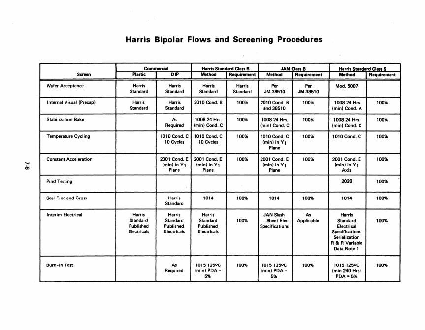
Harris Bipolar Flows and Screening Procedures
Commercial Harris Standard Class B JAN Class B Harris Standard Class S Screen Plastic DIP Method Requirement Method Requirement Method Requirement
Wafer Acceptance Harris Harris Harris Harris Per Per Mod. 5007 Standard Standard Standard Standard JM 38510 JM 38510
Internal Visual (Precap) Harris Harris 2010 Cond. B 100% 2010Cond. B 100% 100824 Hrs. 100% Standard Standard and 38510 (min) Condo A
Stabilization Bake As 100824 Hrs. 100% 100824 Hrs. 100% 100824 Hrs. 100% Required (min) Cond. C (min) Condo C (min) Condo C
Temperature Cycling 1010 Condo C 1010 Condo C 100% 1010 Cond. C 100% 1010 Condo C 100% 10 Cycles 10 Cycles (min) in Yl
Plane
Constant Acceleration 2001 Condo E 2001 Condo E 100% 2001 Condo E 100% 2001 Condo E 100% ....., & (min) in Yl (min) in Yl (min) in Yl (min) in Yl
Plane Plane Plane Axis i
Pind Testing 2020 100% .!
Seal Fine and Gross Harris 1014 100% 1014 100% 1014 100% Standard
Interim Electrical Harris Harris Harris JAN Slash As Harris Standard Standard Standard 100% Sheet Elec. Applicable Standard 100% Published Published Published Specifications Electrical Electricals Electricals Electricals Specifications
Serialization R & R Variable
Data Note 1
Burn-In Test As 10151250C 100% 10151250C 100% 10151250C 100% Required (min) PDA= (min) PDA= (min 240 Hrs)
5% 5% PDA=5%
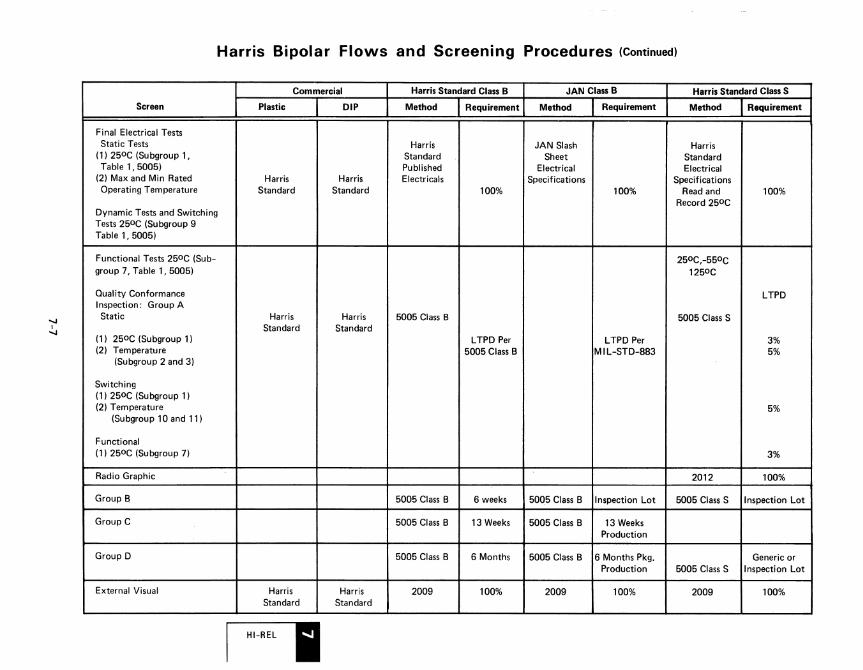
-..J I
-..J
Harris Bipolar Flows and Screening Procedures (Continued)
Commercial Harris Standard Class B JAN ClassB Harris Standard Class S
Screen .Plastic DIP Method Requirement Method Requirement Method Requirement
Final Electrical Tests Static Tests Harris JAN Slash Harris
(1) 250C (Subgroup 1, Standard Sheet Standard Table 1,5005) Published Electrical Electrical
(2) Max and Min Rated Harris Harris Electricals Specifications Specifications Operating Temperature Standard Standard 100% 100% Read and 100%
Record 250C Dynamic Tests and Switching Tests 250C (Subgroup 9 Table 1, 5005)
Functional Tests 250C (Sub- 25OC,-550C group 7, Table 1,5005) 1250C
Quality Conformance LTPD Inspection: Group A Static Harris Harris 5005 Class B 5005 Class S
Standard Standard (1) 250C (Subgroup 1) LTPD Per LTPD Per 3% (2) Temperature 5005 Class B MIL-STO-883 5%
(Subgroup 2 and 3)
Switching (1) 250C (Subgroup 1) (2) Temperature 5%
(Subgroup 10 and 11)
Functional (1) 250 C (Subgroup 7) 3%
Radio Graphic 2012 100%
Group E! 5005 Class B 6 weeks 5005 Class B I
Inspection Lot 5005 Class S Inspection Lot .
Group C 5005 Class B 13 Weeks 5005 Class B 13 Weeks Production
Group D 5005 Class B 6 Months 5005 Class B 6 Months Pkg. Generic or Production 5005 Class S Inspection Lot
External Visual Harris Harris 2009 100% 2009 100% 2009 100% Standard Standard
I'HI-REL I
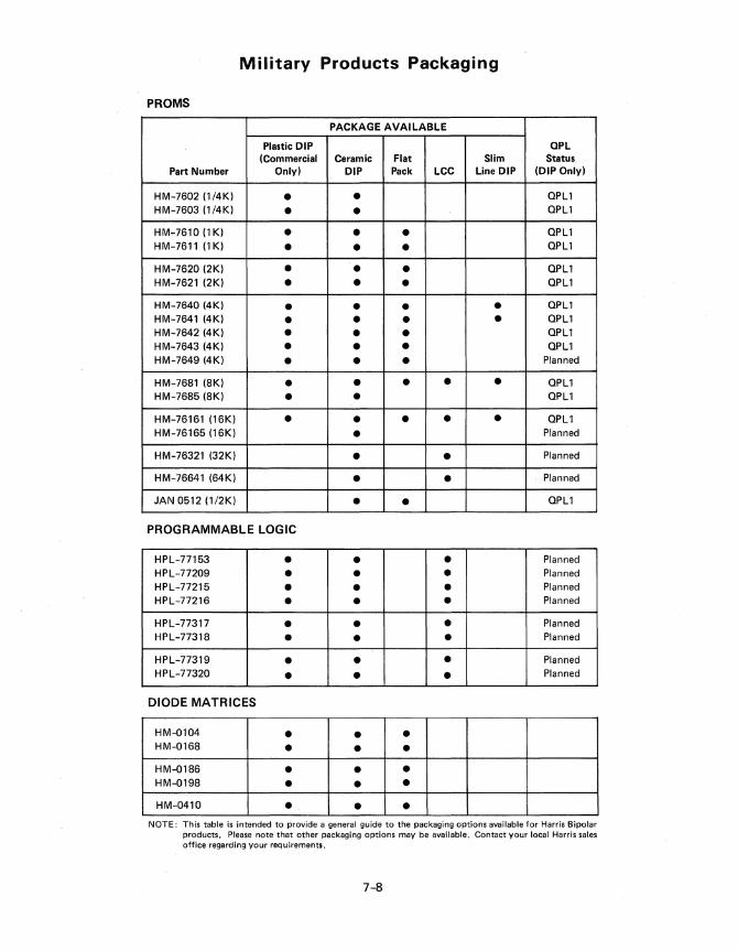
Military Products Packaging
PROMS
PACKAGE AVAILABLE
Plastic DIP OPL (Commercial Ceramic Flat Slim Status
Part Number Only) DIP Pack LCC Line DIP (DIP Only)
HM-7602 (1/4K) • • QPL1 HM-7603 (1/4K) • • QPL1
HM-7610 (1 K) • • • QPL1 HM-7611 (1 K) • • • QPL1
HM-7620 (2K) • • • QPL1 HM-7621 (2K) • • • QPL1
HM-7640 (4K) • • • • QPL1 HM-7641 (4K) • • • • QPL1 HM-7642 (4K) • • • QPL1 HM-7643 (4K) • • • QPL1 HM-7649 (4K) • • • Planned
HM-7681 (8K) • • • • • OPL1 HM-7685 (8K) • • QPL1
HM-76161 (16K) • • • • • QPL1 HM-76165 (16K) • Planned
HM-76321 (32K) • • Planned
HM-76641 (64K) • • Planned
JAN 0512 (1/2K) • • QPL1
PROGRAMMABLE LOGIC
HPL-77153 • • • Planned HPL-77209 • • • Planned HPL-77215 • • • Planned HPL-77216 • • • Planned
HPL-77317 • • • Planned HPL-77318 • • • Planned
HPL-77319 • • • Planned HPL-77320 • • • Planned
DIODE MATRICES
HM-0104 • • • HM-0168 • • • HM-0186 • • • HM-0198 • • • HM-0410 • • •
NOTE: This table is intended to provide a general guide to the packaging options available for Harris Bipolar products. Please note that other packaging options may be available. Contact your local Harris sales office regarding your requirements.
7-8

Mechanical .Information
LEAD FINISHES CASE OUTLINES
A - Kovar or Alloy 42, with hot solder dip
Appendix C Letter Designation Description
B - Kovar or Alloy 42, witn matte tin plate
A F-l 14-lead FP (1/4" X 114") B F-3 14-lead FP (3/16" X 114") C D-l 14-lead DIP (1/4" X 314")
C - Kovar or Alloy 42, 0 F-2 14-lead FP (1/4" X 3/B")
with gold plate E D-2 16-lead DIP (1/4" X 7/S")
X - Any of above, for order-ing purposes only
F F-5 16 lead FP (1/4" X 1-1/4") G A-l S-Iead can H F-4 10-lead FP (1/4" X 114")
Note: Matte tin is reflowed for JM 38510 products. I A-2 10-lead can
J D-3 24-lead DIP (1/4" X 1-114") K F-6 24-lead FP (3/S" X 5/S") L NONE NONE
M A-3 12-lead can N NONE NONE P 0-4 S-Iead DIP (1/4" X 3/S") Q D-5 40-lead DIP (9/16" X 2-1/16")
R D-S 20-lead DIP (1/4" X 1-1/16") S NONE NONE T NONE NONE U NONE NONE
V D-6 lS-lead DIP (.300" Xl") W D-7 22-lead DIP (.400" X 1.1")
X Dual in-line packages not listed above y Flat packages not listed above Z All other configurations not listed above
LCC OUTLINES
LCC Available Dimensions (in.)
C-2 20-Terminal .350 x .350 C-4 2S -Terminal .450 X .450 C-5 44-Terminal .650 X .650 C-ll 2S-Terminal .350 X .350 C-12 32-Terminal .450 X .450
SLIM LINE DIP
Available Dimensions (in)
24-Lead 1.250 X .2SS
NOTE: The information contained on this page has been reprinted from MIL-M-38510 and is provided for reference onlv. It is not intended to be a representation of the packaging capabiJities of Harris Semiconductor Bipolar Digital Products Division.
7-9
..... ... a:
I
i:
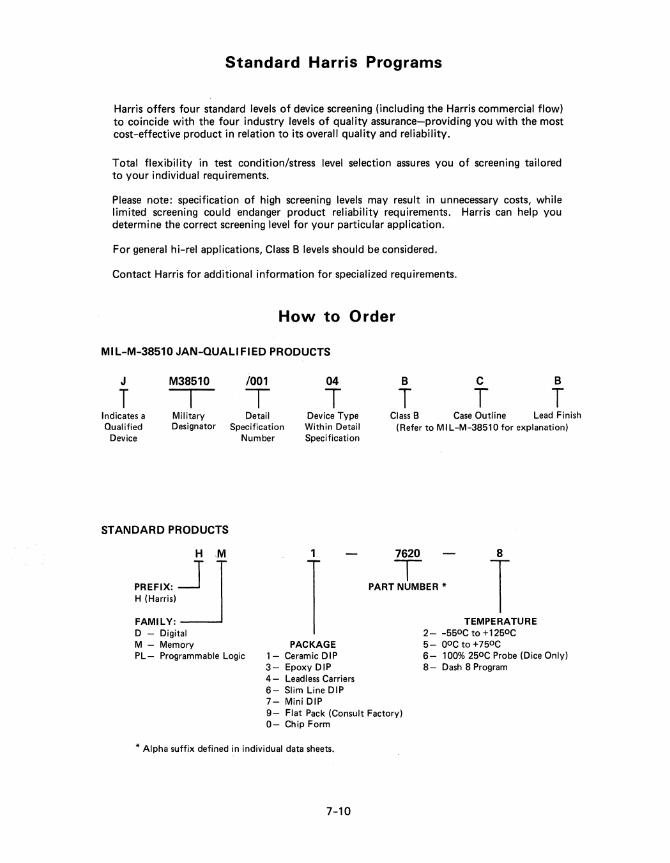
Standard Harris Programs
Harris offers four standard levels of device screening (including the Harris commercial flow) to coincide with the four industry levels of quality assurance-providing you with the most cost-effective product in relation to its overall quality and reliability.
Total flexibility in test condition/stress level selection assures you of screening tailored to your individual requirements.
Please note: specification of high screening levels may result in unnecessary costs, while limited screening could endanger product reliability requirements. Harris can help you determine the correct screening level for your particular application.
For general hi-rei applications, Class B levels should be considered.
Contact Harris for additional information for specialized requirements.
How to Order
MIL-M-38510 JAN-QUALIFIED PRODUCTS
J M38510 /001 04 B C B
T I T T T T T Indicates a Military Detail Device Type Class B Case Outline Lead Finish Qualified Designator
Device
STANDARD PRODUCTS
HM
PREFIX:~ H (Harris)
FAMILY: D - Digital M - Memory
Specification Within Detail Number Specification
1
I PL - Programmable Logic
PACKAGE 1- Ceramic DIP 3- Epoxy DIP 4 - Leadless Carriers 6- Slim Line DIP 7- Mini DIP
(Refer to MIL-M-38510 for explanation)
7620 8
T PART NUMBER * T
TEMPERATURE 2- -550 C to +1250 C 5- OOC to +750 C 6- 100% 250 C Probe (Dice Only) 8 - Dash 8 Program
9- Flat Pack (Consult Factory) 0- Chip Form
* Alpha suffix defined in individual data sheets.
7-10

~n(/--~ Custom Integrated
V~ ::;;:l--~ Circuits Division
Introduction 8-2
Bipolar Digital Design Techniques 8-3
Bipolar Digital Technologies 8-5
Specialized Products 8-11
Future of Bipolar Digital IC's 8-13
CICD Sales Office Locations 8-14
8-1
o t.:l
t.:l

The Custom Integrated Circuits Division
Custom Integrated Circuits Division is an independent division,fully facilitated and staffed, dedicated to the development and production of Custom/Semi-Custom and specialized integrated circuits. CleO employs high performance CMOS andB.ipolar technologies to meet the needs of the marketplace.
During the 1970's, technologies and innovative processes developed in custom circuit work were transferred into diverse standard products for broad-based commercial applications. This successful technology transfer helped make Harris Semiconductor one of the nation's leading IC suppliers.
Custom and Semi-Custom circuit fabrication has continued to thrive in the independent, full-function Custom Integrated Circuits Division (CICD), one of the five major business units within the Harris Semiconductor Sector - Analog Products, Bipolar Digital Products, CMOS Digital Products, Microwave and CICD. Major markets include the military, information systems, communications, industrial and medical equipment areas.
The Custom Integrated Circuits Division has achieved greater than a 20 percent compounded growth rate and has continued strong growth projections through the 1980's.
Organization and Resources
Compared to standard product lines marketed to mUltiple customers by the other divisions, CICD products are customized in Melbourne to serve unique user requirements. In addition to performing special functions in critical environments, custom chips can perform multiple functions at higher speed with lower power requirements, providing the means to reduce equipment size and cost while increasing performance. As a major supplier to such critical systems as Trident, Peacekeeper, B-1 B, and Heart Pacemaker Programs, performance and reliability are of paramount concern.
Because no two customer orders are alike, CICD is oriented to engineering and manufacturing specific customer capabilities. A high level of quality assurance is imperative and technological advantages are emphasized in all customer involvements. The division is also one of the few custom product makers in the IC industry with its own dedicated manufacturing operation and engineering, product assurance, sales and marketing organizations.
The division's marketing program emphasizes the capability to meet specific customer requirements with state of the art products that compare with the best in the IC industry.
Future growth in broader commercial and industrial application areas is assured by expanding engineering and manufacturing facilities and by new capabilities in Semi-Custom Circuitry.
8-2
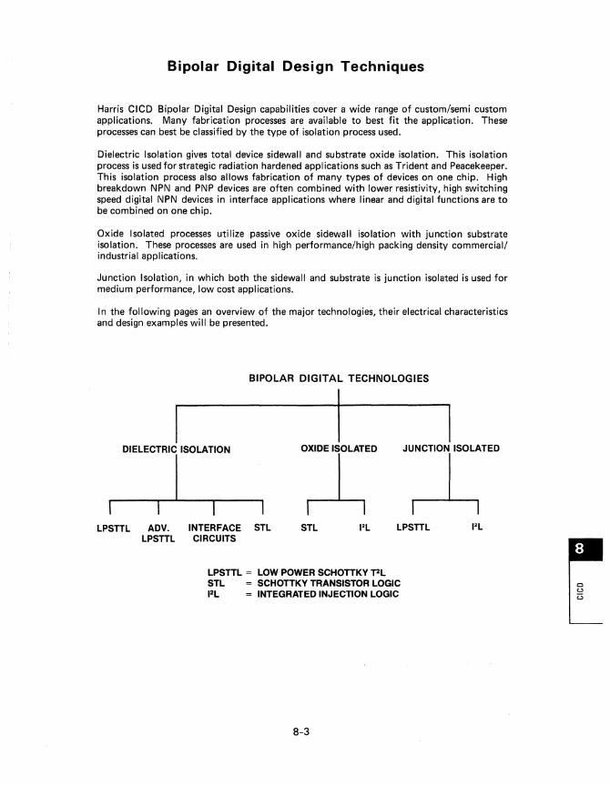
Bipolar Digital Design Techniques
Harris CICD Bipolar Digital Design capabilities cover a wide range of custom/semi custom applications. Many fabrication processes are available to best fit the application. These processes can best be classified by the type of isolation process used.
Dielectric Isolation gives total device sidewall and substrate oxide isolation. This isolation process is used for strategic radiation hardened applications such as Trident and Peacekeeper. This isolation process also allows fabrication of many types of devices on one chip. High breakdown NPN and PNP devices are often combined with lower resistivity, high switching speed digital NPN devices in interface applications where linear and digital functions are to be combined on one chip.
Oxide Isolated processes utilize passive oxide sidewall isolation with junction substrate isolation. These processes are used in high performance/high packing density commercial/ industrial applications.
Junction Isolation, in which both the sidewall and substrate is junction isolated is used for medium performance, low cost applications.
In the following pages an overview of the major technologies, their electrical characteristics and design examples will be presented.
BIPOLAR DIGITAL TECHNOLOGIES
I I I DIELECTRIC ISOLATION
I lPSTTl ADV. INTERFACE STl STl I2l lPSTTl I2l
lPSTTl CIRCUITS
lPSTTl = lOW POWER SCHOTTKY f2l STl SCHOTTKY TRANSISTOR lOGIC 12l = INTEGRATED INJECTION lOGIC
8-3
c c..> C3

1.5
1.4
Ii; 1.3
8 ~ ~ !i 1.2
8
~ ..J 1.1 w a:
1.0
0.9
0.8
DESIGN TECHNIQUE
FULL CUSTOM
GATE ARRAY
MARCO CELL DESIGN
LSI Custom Circuit Cost Comparison
T
o GATE ARRAY
• FULL CUSTOM
~ STANDARD CELL
LSI CUSTOM CIRCUIT COST COMPARISON
- . ___ SC
FC
10 20 30 40 50
VOLUME (K UNITS)
Bipolar LSI/VLSI Design Options
ADVANTAGES/ DESCRIPTION DISADVANTAGES
Every device is custom designed in the • Lowest Production Cost layout for a specific application. • Smallest Ch ip Size
• High Development Cost • Requires Long Design Cycle
Two or three masking levels are designed • Fast Design Cycle to create a new custom circuit • Low Risk, Low Design Cost
• High Production Cost • Not all circuits may fit on a given Array.
A marco cell family is created as a full • Good compromise between custom design. All circuits in the program - Schedule are designed from this macro family. - Cost
- Performance - Risk
8-4
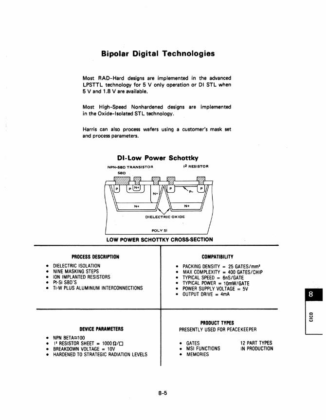
Bipolar Digital Technologies
Most RAO-Hard deSigns are implemented in the advanced LPSTTL technology for 5 V only operation or 01 STL when 5 V and 1.8 V are available.
Most High-Speed Nonhardened designs are implemented in the Oxide-Isolated STL technology.
Harris can also process wafers using a customer's mask set and process parameters.
DI-Low Power Schottky NPN-5aO TRANSISTOR
sao 12 RESISTOR
LOW POWER SCHOTTKY CROSS-SECTION
PROCESS DESCRIPTION CDMPATIBILITY
• DIELECTRIC ISOLATION • PACKING DENSITY = 25 GATES/mml
• NINE MASKING STEPS • ION IMPLANTED RESISTORS • Pt·Si SBD'S • n·w PLUS ALUMINUM INTERCONNECTIONS
DEVICE PARAMETERS
• NPN BETAs100 • II RESISTOR SHEET = 10000/0 • BREAKDOWN VOLTAGE = 10V • HARDENED TO STRATEGIC RADIATION LEVELS
8-5
• MAX COMPLEXITY = 400 GATES/CHIP • TYPICAL SPEED = 6nS/GATE • TYPICAL POWER =10mW/GATE • POWER SUPPLY VOLTAGE = 5V • OUTPUT DRIVE = 4mA
PRODUCT TYPES PRESENTLY USED FOR PEACEKEEPER
• GATES • MSI FUNCTIONS • MEMORIES
12 PART TYPES IN PRODUCTION
CI ... c::;

Ol-Advanced LPSTTL (ALPS)
INSULATING DIELECTRIC 2ND LEVEL AI
PROCESS DESCRIPTION COMPATIBILITY
• DIELECTRIC ISOLATION • PACKING DENSITY = 50 GATE/rnrn2 • ELEVEN MASKING STEPS • RAM CELL AREA = 1d sa MILS • POL YSILICON THIN FILM RESISTORS • MAX COMPLEXITY = 1000 GATES/CHIP • Pt-Si SBD'S • TYPICAL SPEED = 5 ns/GATE • TWO LAYERS OF INTERCONNECT • TYPICAL POWER = 1 rnW/GATE
• POWER SUPPLY VOLTAGE = 5 VOLTS • OUTPUT DRIVE = 8 rnA
DEVICE PARAMETERS PRODUCT TYPES-STRATEGIC HARDNESS
• NPN BETA ~ 100 • 90 ns MAX 256 x 4 STATIC RAM • POLY RESISTOR SHEET = 10000/0 • 120 CGA WITH 14 110 • BREAKDOWN VOLTAGE = 8 V • 312 CGA WITH 46 I/O • HARDENED TO STRATEGIC RADIATION LEVELS • 918 CGA WITH 76 I/O
NOTE: SEE RADIATION-HARDENED PRODUCTS OR THE GATE ARRAY SECTION FOR MORE INFORMATION ON THE ALPS ARRAYS
8-6
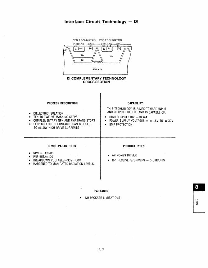
Interface Circuit Technology - 01
NPN TRANSISTOR PNP TRANSISTOR
POLY 51
01 COMPLEMENTARY TECHNOLOGY CROSS·SECTION
PROCESS OESCRIPTION
• DIELECTRIC ISOLATION • TEN TO TWELVE MASKING STEPS • COMPLEMENTARY NPN AND PNP TRANSISTORS • DEEP COLLECTOR CONTACTS CAN BE USED
TO ALLOW HIGH DRIVE CURRENTS
DEVICE PARAMETERS
• NPN BETA~200 • PNP BETA~100 • BREAKDOWN VOLTAGES=30V-60V • HARDENED TO MAN RATED RADIATION LEVELS.
CAPABILITY
THIS TECHNOLOGY IS AIMED TOWARD INPUT AND OUTPUT BUFFERS AND IS CAPABLE OF:
• HIGH OUTPUT DRIVE=100mA • POWER SUPPLY VOLTAGES = ± 15V TO ± 30V • EMP PROTECTION
PRODUCT TYPES
• ARINC-429 ORIVER
• 8-1 RECEIVERS/DRIVERS - 5 CIRCUITS
PACKAGES
• NO PACKAGE LIMITATIONS
8-7
c:l U U

Advanced Schottky Transistor Logic - ASTL
SiN
Si02
P+
p.
Psub
ASTL CROSS - SECTION
PROCESS DESCRIPTION COMPATIBILITY
• OXIDE ISOLATION • MAX SPEED = 0.75 ns • THIRTEEN MASK STEPS • POWER AT MAX SPEED = 0.26 mW • TWO LEVELS OF INTERCONNECT • MAX COMPLEXITY = 3000 GATES/CHIP • THREE MICRON GROUNDRULES • LOGIC POWER SUPPLY = 2.0 V • TiW OUTPUT SBD's • T2L BUFFER POWER SUPPLY = 5 V • PrSi CLAMP SBD's
DEVICE PARAMETERS PRODUCT TYPES
• NPN BETA~BO • GATE ARRAYS • ft;;,. 3 GHz • CUSTOM LOGIC CIRCUITS • BV CEO - B.OV • 125 AND 10000/0 RESISTORS
Oxide Isolated Schottky Transistor Logic (STL)
STL is a low power Bipolar technology capable of high speeds and amiable to gate Array, Macro Cell and full custom designs.
- Basic gate is single input-multiple output - Requires a 2V VBS power supply - Designs have T2L compatible input and.three state output buffers
using a 5V power supply . - Can operate over the full military temperature range - Can use standard packages, DIP's, Flat Packs, LCC's - 1500 Gate CGA now being characterized - 2500 Gate CGA in design
8-8
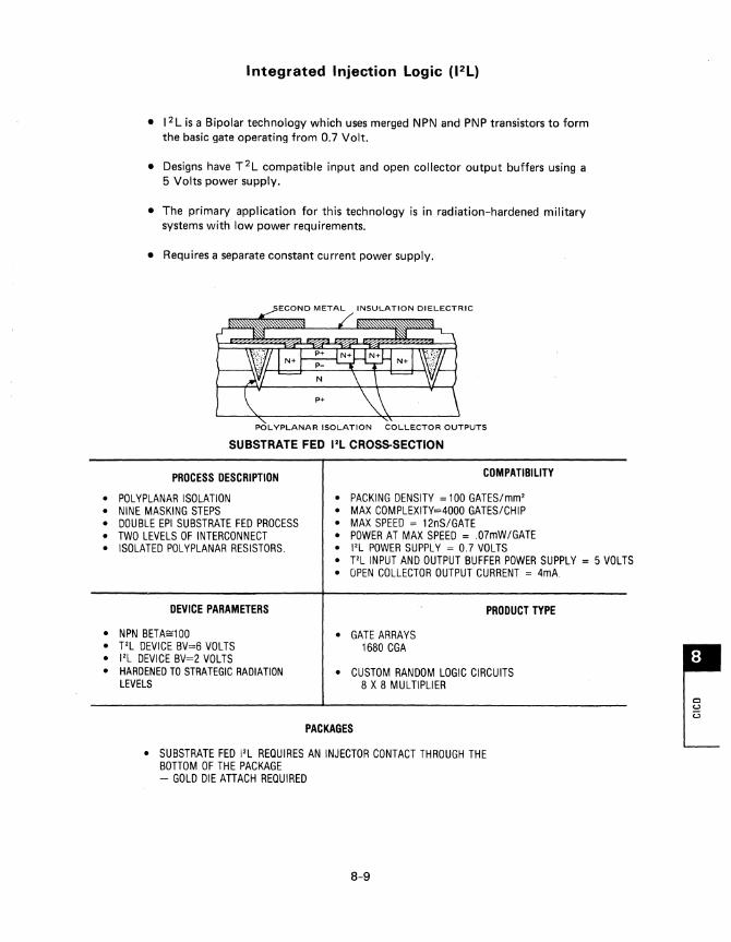
Integrated Injection Logic (PL)
• 12 L is a Bipolar technology which uses merged NPN and PNP transistors to form the basic gate operating from 0.7 Volt.
• Designs have T 2L compatible input and open collector output buffers using a 5 Volts power supply.
• The primary application for this technology is in radiation-hardened military systems with low power requirements.
• Requires a separate constant current power supply.
POLYPLANAR ISOLATION COLLECTOR OUTPUTS
SUBSTRATE FED I'L CROSS·SECTION
PROCESS OESCRIPTION
• POLYPLANAR ISOLATION • NINE MASKING STEPS • DOU BLE EPI SU BSTRATE FED PROCESS • TWO LEVELS OF INTERCONNECT • ISOLATED POLYPLANAR RESISTORS.
DEVICE PARAMETERS
• NPN BETA~100 • T'L DEVICE BV=6 VOLTS • I'L DEVICE BV=2 VOLTS • HARDENED TO STRATEGIC RADIATION
LEVELS
COMPATIBILITY
• PACKING DENSITY = 100 GATES/mm' • MAX COMPLEXITY=4000 GATES/CHIP • MAX SPEED = 12nS/GATE • POWER AT MAX SPEED = .07mW/GATE • I'L POWER SUPPLY = 0.7 VOLTS • T'L INPUT AND OUTPUT BUFFER POWER SUPPLY = 5 VOLTS • OPEN COLLECTOR OUTPUT CURRENT = 4mA
• GATE ARRAYS 1680 CGA
PRODUCT TYPE
• CUSTOM RANDOM LOGIC CIRCUITS 8 X 8 MULTIPLIER
PACKAGES
• SUBSTRATE FED I'L REQUIRES AN INJECTOR CONTACT THROUGH THE BOTTOM OF THE PACKAGE - GOLD DIE ATTACH REQUIRED
8-9

Junction Isolated Bipolar NPN TRANSISTOR PNP TRANSISTOR
JI BIPOLAR CROSS·SECTION
PROCESS DESCRIPTION
• JUNCTION ISOLATION • SEVEN TO TEN MASKING STEPS • PROCESS FLEXIBILITY CAN INCLUDE
- ALUMINUM SBD'S - ION IMPLANTED RESISTORS - MULTILEVEL INTERCONNECTS - POL YPLANAR SIDEWALL ISOLATION
DEVICE PARAMETERS
• NPN BETA~100 • PNP BETA~15 • BREAKDOWN VOLTAGE = 8-30 VOLTS • NOT NORMALLY RAD-HARD
COMPATIBILITY
• PACKING DENSITY = 25 GATES/ mm' • MAX COMPLEXITY = 300 GATES/CHIP • TYPICAL SPEED = 10nS/GATE • TYPICAL POWER = 15mW/GATE • POWER SUPPLY VOLTAGE = 5 TO 30 VOLTS • OUTPUT DRIVE = 16mA
PRODUCT TYPES
• MEMORIES • SPECIAL MSI FUNCTIONS
PACKAGES
• NO PACKAGE LIMITATIONS
Advanced Low Power Schottky Gate Array Radiation·Hardened for Strategic Systems
Arrays Available Now
• 120 gate GCA with 14 I/O pins for MSI 14-16 pin applications
• 312 gate GCA with 46 I/O for multiple MSI replacement
• 918 gate eGA with 76 I/O for LSI application
Strategically Hardened Against
• Total gamma dose
• Logic upset due to total dose rate
• Prompt dose rate latchup/burnout
• Neutron radiation fluence
8-10
Array Features
• 5 Volts ± 10% only supply requirement
• -550 to 1250C operation
• No input buffers required, all array gates T2 L compatible
• Output buffer typically 1 Ons/15mW with 8mA 101
• Internal gate typically 5ns/0,8mW
• Three custom layers; both metal levels and interlevel Via's
• Unused gates and buffers not powered

Specialized Products
HS-3182 ARINC Driver Circuit Feature
• Bipolar differential line driver
• Inputs T2L and CMOS compatible
• Adjustable rise and fall times controlled by 2 external capacitors
• Differential output voltage range programmed via the voltage reference input (VREF)
• Outputs are short circuit proof and over voltage protected
• Operates up to a 100K BPS data rate
• Full military temperature range
HS-3182 ARINC Driver Circuit Block Diagram
DATA (A) (4) LEVEL SHIFTER ROUT/2 (6)
& SLOPE AOUT CONTROL (A)
CLOCK (14)
(8) (1) GND CL VREF
RL
SYNC
LEVEL SHIFTER ROUT/2 (13) AND SLOPE BOUT
DATA (B) CONTROL (B) (11)
Vl (16)
S'i'RciBE (2) -v CB (7) (12) PIN NO. 10,15 = NC
8-11
Q
'-' C3

8-18 Circuits Part Description
CHANNELS POWER PART PART PER SUPPLY PACKAGE
NUMBER NAME PACKAGE VOLTAGES TYPE PART NUMBER
NIOB +12.6V 14 The N I OB converts a fast rise/fall HS-3194 Non-Isolated 4 +5.25V Lead input signal to a slow rise/fall
Output Buffer DIP output signal. 10L = 10mA. inputs are TTL.
SCIB ±30V 18 The SCIB provides a differential HS-3195 Switch 4 +5.25V Lead .constant current at the input to
Closure DIP detect an open or closed switch. Input Buffer Outputs are TTL.
DIB ±30V 18 The DIB accepts differential input HS-3196 Discrete 4 +5.25V Lead voltages with ,1Vin<2V~"0" at
Input DIP output and ,1Vin>2.5V~"1" at Buffer output. Outputs are TTL.
SDOB 14 The SDOB accepts an Open Col-HS-3197 Serial 2 ±15.6V Lead lector TTL input and produces a
Digital DIP differential ±5V output centered Output Buffer around ground. The output pro-
vides 5V across 35n.
SDIB ±20V 16 The SD I B produces differential HS-3198 Serial 2 +5.25V Lead logic "1" and "0" outputs from a
Digital DIP differential input. I nput voltages Input Buffer must be > 2.25V apart or both
outputs are "0".
NOTE: The outputs of all Output Buffers and inputs to all Input Buffers are protected against EMP.
8-12

Peacekeeper Digital Integrated Circuits
(All IC's use DI. 12 Resistors, PT -SI
SBD's, and TI -W-AI Interconnect)
All Parts are Presently in Production
NEAREST PART PEACEKEEPER COMMERCIAL
DESCRIPTION NUMBER 477- EQUIVALENT
Quad 2 NAND 1269 SN54LSOO Dual 4 NAND 1270 SN54LS20 Dual JK Flip-Flop 1271 SN54LS112 Dual 4-1 MUX 1272 SN54LS253 Dual 2-4 DEMUX 1273 SN54LS155 ALU 1274 SN54LS181 4-Bit Counter 1276 SN54LS193 4-Bit Shift Register 1277 SN54LS194 4 x 4 Register File 1284 SN54LS670 High Drive MUX 1789 NONE 256 x 4 PROM 1786 HM-7611
Future of Bipolar Digital IC's
HARRIS PART
NUMBER
3114 3112 3113 3115 3116 3118 3120 3121 3117 3128 3148
• Advanced low power Schottky II Process development under way for Radiation-Hardened 4K RAM and 2000 Gate Array (5V only) applications.
• The first of a family of Dielectrically Isolated Rad-Hard STL Gate Arrays has completed development and prototype parts are being characterized. Requests for proposals on both a 936 gate eGA and 1950 gate eGA are now being accepted. By March 1984 an autoroute 1856 eGA will be developed which will allow up to 1000 gate personalizations.
• ASTL devices being characterized for full custom design applications.
8-13
o u C3

Custom Integrated Circuits Division
SALES OFFICE LOCATIONS
Northeast Region 2600 Virginia Avenue Suite 800 Washington, DC 20037 202~342-3900 Telecopier: 202-338-3612
5 Old Concord Road Burlington, MA 01803 617-273-1020 TWX: 710-332-1074 Quip: 617-272-7956
106 Seventh Street Garden City, NY 11530 516-747-6776 TWX: 510-220-1527
Southeast Region Su ite 113 7040 Lake Ellenor Drive Orlando, FL 32809 305-851-9450 Telex: 808819 Telecopier: 305-851-9450
Central Region Suite 704 2850 Metro Drive Minneapolis, MN 55420 612-854-3224 TWX: 920-576-3418 Telecopier: 612-854-7359
Suite 110 17120 Dallas Parkway Dallas, TX 75248 214-248-3239 TWX: 910-860-5446
Western Region Suite 320 1503 South Coast Drive Costa Mesa, CA 92626 714-957-6557 TWX: 910-595-1533 Telecopier: 714-957-6557
European Sales Office Harris Semiconductor P. O. Box 27 145 Farnham Road Slough SL1 4XD, England 011-447-5334666 Telex: 848174 Harris G
Note: Custom Integrated Circuits Division maintains its own sales force.
8-14
Suite C-100 883 Stierlin Road Mountain View, CA 94043 415-964-6443 TWX: 910-379-6431

Package Availability
Package Dimensions
Thermal Resistance Measurements
Bipolar Memory Products General Chip Information
9-1
9-3
9-5
9-8
9-10


Package Availability
1 " 3" 4" 9"
PLASTIC LEADLESS PART NUMBER CERDIP DIP CARRIER FLATPACK**
BIPOLAR MEMORY
ORGAN IZA TlON MARKETING PART # Quad Power Strobe HD-6600 4D - - -32 x 8 OC PROM HM-7602 4Z 7H - -32 x 8 TS PROM HM-7603 4Z 7H - -64 x 8 OC PROM JAN-0512 4K - - 8F 256 x 4 OC PROM HM-7610 4Z 7H - 8B 256 x 4 TS PROM HM-7611 4Z 7H - 8B 256 x 4 OC PROM HM-7610A 4Z 7H - 8B 256 x 4 TS PROM HM-7611A 4Z 7H - 8B 256 x 4 OC PROM HM-7610B 4Z 7H - 8B 256 x 4 TS PROM HM-7611B 4Z 7H - 8B 512 x 4 OC PROM HM-7620 4Z 7H - 8B 512 x 4 TS PROM HM-7621 4Z 7H - 8B 512 x 4 OC PROM HM-7620A 4Z 7H - 8B 512 x 4 TS PROM HM-7621A 4Z 7H - 8B 512 x 4 OC PROM HM-7620B 4Z 7H - 8B 512 x 4 TS PROM HM-7621B 4Z 7H - 8B 512 x 8 OC PROM HM-7640 4K, DC [1] 7C - 8F 512 x 8 TS PROM HM-7641 4K,DC [1] 7C - 8F 512 x 8 OC PROM HM-7640A 4K, DC [1] 7C - 8F 512 x 8 TS PROM HM-7641A 4K, DC [1] 7C - 8F 512 x 8 TS PROM HM-7649 5Z 7M - 80 512 x 8 TS PROM HM-7649A 5Z 7M - 80 1024 x 4 OC PROM HM-7642 4N 7V - 8C 1024 x 4 TS PROM HM-7643 4N 7V - 8C 1024 x 4 OC PROM HM-7642A 4N 7V - 8C 1024 x 4 TS PROM HM-7643A 4N 7V - 8C 1024 x 4 OC PROM HM-7642B 4N 7V - 8C 1024 x 4 TS PROM HM-7643B 4N 7V - 8C 1024 x 8 TS PROM HM-7681 4K,DC [1] GA LR 8F 1024 x 8 TS PROM HM-7681A 4K, DC [1] GA LR 8F 2048 x 4 TS PROM HM-7685 5E 7V - -2048 x 4 TS PROM HM-7685A 5E 7V - -2048 x 8 TS PROM HM-76161 5J, DC [1] GA LZ 8L 2048 x 8 TS PROM HM-76161A 5J, DC [1] GA LZ 8L 4096 x 4 TS PROM HM-76165 5M - - -4096 x 8 TS PROM HM-76321 DA [2] - LV -8192 x 8 TS PROM HM-76641 DA [2] - LV -DIODE MATRICES
ORGAN IZATION MARKETING PART#
6x8 HM-0168 4U GC - 9H 8x6 HM-0186 4U GC - 9H 4 x 10 HM-0410 4U GC - 9H 10 x 4 HM-0104 4U GC - 9H 9x8 HM-0198 4N 7W - -PROGRAMMABLE LOGIC
ARCHITECTURE MARKETING PART # 20-Pin I FL HPL-77153/82S 153 5Z 7J - -20-Pin PAL HPL-77216/16P8 5Z 7J - -20-Pin PAL HPL-77209/16L8 5Z 7J - -20-Pin PAL HPL-77215/16H8 5Z 7J - -24-Pin FPAD HPL-77061 5Z 7J - -
* These package numbers should be used in the product code when ordering. Other numbers shown in this table and in the Package Dimensions portion of this section are internal numbers to be used only to match the package code of a specific product with the package outline. Please note that other packaging options may be available. Contact your local Harris sales office regarding your requirements. **Not Recommended For New Designs. Consult Factory. NOTES: [11 SlimlineCERDIP.
[21 Side-Brazed CERDIP.
9-3

This table is provided as a quick reference for the approximate dimensions of all flatpacks available from Harris Semiconductor's Bipolar Digital Products Division. For more detailed information, see the package dimension diagrams, pages 9-5 through 9-7.
APPROXIMATE PACKAGE PACKAGE LEAD COUNT DEVICE DIMENSIONS (INCHES)
CERPACKS
9H 14 Diode Matrices (HM-OXXX) .250 x .250 8F 24 1/2K (JAN-0512) .375 x .375 88 16 1 K (HM-7611) .375 x .375 88 16 2K (HM-7621) .375 x .375 8C 18 4K (HM-7643) .375 x .375 8F 24 4K (HM-7641) .375 x .375 8D 20 4K (HM-7649) .375 x .375 8F 24 8K (HM-7681) .375 x .375 8L 24 16K (HM-76161) .500 x .375
LEADLESS CHIP CARRIERS
LR 28 8K (HM-7681) .450 x .450 LZ 28 16K (HM-76161) .450 x .450 LV 28 32K (HM-76321) .450 x .450 LV 28 64K (HM-76641) .450 x .450
9-4

Package Dimensions
4D, 4U, 4Z, 4N, 5E, 5Z, 5M, DC
CERDIP .300
--------0---------
am CERDIP .600
Q 1---------1 It~:::::::::=:::::====;:=====l
m SIDE BRAZED
PKG. LEAD DIM. DIM. DIM. TYPE COUNT A B C
4D 14 .140 :2.!§. .008 MSI ill .at 8 .012
4U 14 .140 .016 .008 SSI .170 .018 :orr
42 16 .140 ,016 .OOB M51 :T7O .018 .012
4N 18 .140 ,016 .008 5E LSI T7i5 .018 .012
5Z 20 .140 ,016 .ooa 5M LSI .170 .018 :012
DC 24 .150 ,016 .008 SLIM :180 .m .012
NOTE: 1) Dimensions are: ::!~'. 2) All DimenSions in inches
LEAD DIM. DIM. COUNT A B
24 .t50 .016 MSI .t80 .018
NOTE: 1) Dimensions are: ~~~'. 2) All Dimensions in inches
i I I D I
~-I~-H
PKG. TYPE
DA
NOTE: t) Dimensions are: ~!~'. 2) All Dimensions in inches -G-
~ I I
I-E-II-c 1-'_1
9-5
DIM. D
.760
.785
.760
.785
.760
.790
.8S5
.915
.940
.970
1,240 1.270
DIM. DIM. DIM. DIM. DIM. DIM. DIM. DIM. E F G H L Q S a
.265 .290 ,050 .090 125 .020 .070 0'
.285 .310 .070 TiO .180 .040 .100 150
.245 .290 .050 ,090 .125 .020 .070 0'
.265 .310 .070 :ITO .180 .040 :wo ;SO
.265 .290 .050 .090 .125 .020 .025 0'
.285 .310 .070 TiD .150 .040 .045 150
.285 .300 .050 .090 .125 .020 .040 0'
.305 .320 .070 .TID .180 ,040 ,060 15"5
.285 .300 ,050 ,090 .125 .020 .020 0'
.305 .320 .070 .iTo" .180 .040 .040 ;SO
.285 .300 ,050 ,090 .125 .020 .060 0'
.305 .320 .070 .TID .180 ,040 .090 W

GC, 7H, 7W, 7V, 7M, 7J
PLASTIC .300
---------0----------
a -.- --
-E-I' c-il_ -F- _u ...
PLASTIC .600
P,.tA: LEADLESS CHIP CARRIER
Package Dimensions
PKG. LEAD DIM. DIM. TYPE COUNT A B
GC 14 .125 ,016 ,140 ,020
7H 16 .125 ,016 l40 ,0-20
7W 18 .125 .016 7V .140 ,020
7M 20 ,130 ,016 7J .145 ,020
NOTE: 11 Dimensions are: ~ 21 All Dimensions in Inches
DIM. C
.OOB :oT2
.008 :oi2
.OOS
.012
.008 :oT2
NOTE: 11 Dimensions are: ~ 2) All Dimensions in inches
PKG. TYPE
LZ, LR, LV
DIM. 0
.750 ,770
.750
.770
,900 .920
1.030 ~
NOTE: 1) Dimensions are: ::~~'. 2) All Dimensions in inches
[lllllllllllllu 9-6
DIM. DIM. DIM. DIM. E F G H
.245 .290 .050 ~
.265 :3TO .070 .110
.245 .290 .050 .090 ]85 3'fO .070 .no ,245 .290 ,050 ~ .265 T10 .070 .110
.250 .290 .050 .090
.270 .m .070 :no
DIM. DIM. L Q
.150 .020 ,170 .040
.150 ,020
.170 ]40
.150 ~
.170 .040
.150 ,QlQ",
.170 .040
DIM. S
,030 .050
.025
.035
• .Q!Q .OBO
.OBO
.OSO
OIM. H
.040
.065
DIM. a
00
150
00
is"
00
150
00
150

p.ftI IiiI
Package Dimensions
050
PIN ONE IDENT.*
16 LEAD CERPACK
~ ~I-
.090 MAX. (2.29)
20 LEAD CERPACK
TOP VIEW PIN ONE IDENT. *
"0 n 10" ~ U
.385 i,OlD SQ. .285 t.015 I ' --I r---- 19.78±.2541 ----(7.24*,381)- .OI8:!:.002 .090 MAX.
(.457.:';0.05) (2.29)
-~~~~li!~1~~'~520081~~~~- nVP.J
.1147 005.!,002 (1.19) 'i5e' ====E~::::::~5::::::::=IR~:=F.I=
285.:1:.015 (7.24i..381)
24 LEAD CERPACK
1 .510*.010
112.95*.2541
--If--.090 MAX.
12.29)
9-7
18 LEAD CERPACK
PIN ONE lOENT, *
.1147 .005:!:.002 (U9)
~.~ -t==E~~~::::-.L:!:
I
24 LEAD CERPACK
~ · · • 018+.002 D (O.4~±D.05) I
:L~f-.- .090 MAX.
12.29)
~05±.0021.121±O.051
T I
.047(1.19IREf'l
14 LEAD FLATPACK
TOPVIEW
J eJi~: O~I 1_,250:1:.005 1_.250:t.015~ .018:.001
I;.m 16.35t..127)-1 (6.3S t ,lBI) (0.46~O.031 TYP. -~-_150!.020 (1!.05:!:a.51l~~-
'ra';"" .250±.005
IS.3Sr271 ~
090~ 1-(1.78) MAX
, ~=~======~ ~5~.002W.13~O,05) L.04o REF
* Pin One Identification for Harris Semiconductor Products Packaged in Flatpacks is accomplished in one of three ways:
1) Shortened Pin One Lead 2) Tab on Pin One Lead 3) Branded Dot
For the sake of clarity. tabs are used here on all diagrams.

Thermal Resistance Measurements
The thermal resistance of a device/package system is defined as:
(}JA = TJ-TA or (}JC = TJ-TC P P
where T J is the junction temperature when operated at power P. T A is the temperature of the surrounding ambient, and TC is the case temperature. (}JA is dependent on the device fixturing and is generally measured with the device in a socket, in still air. (}JC is measured with the case temperature controlled by immersion in a temperature controlled liquid or through other heat sinking.
The junction temperature is measured by calibrating the forward bias voltage of a junction on the device being tested. Generally, a junction of an output transistor is used. The junction is calibrated by immersion in liquid baths of known temperatures. The voltage generated by a 100pA current is measured, and a straight line fitted to the voltage/temperature values.
The thermal resistance is measured using the basic system shown in Figure 1. The VCC of the device under test (DUT) is switched off when the junction temperature is being measured. The switching circuitry is designed to pull VCC to zero volts within three psecs. VCC is kept off for a period of 50 psecs. The signal to the sample and hold triggers a sample period of 14 psecs starting when VCC is switched off. This cycle is repeated every 20 msecs giving a power on duty cycle of greater than 99%. The overall period, VCC off time and sample time, are adjustable.
PULSE GENERATOR
Figure 1.
CURRENT SOURCE
FOR JUNCTION VOLTAGE
DEVICE UNDER TEST
The case temperature is measured by a thermocouple centered under the die and between the case and socket. This configuration allows for the determination of the true case temperature of the device/package under test. The temperature measured by this thermocouple is used to determine the case temperature used to calculate (}JC.
Measurements are done using a comp\Jter controlled system to record the data, calculate the temperature calibration, the thermal resistance, and to switch the VCC, 100pA current and measuring system to one of a series of devices being measured. Presently, capacity is limited to 10 devices at a time. The capability to obtain measurements as a function of air velocity will be available in the near·future.
9-8

The table below summarizes the results of measurements made on the most popular bipolar devices using this automated thermal resistance test system. Please note that the values quoted are typical values and, as such, are provided for general guidance only.
For further information on thermal resistance, contact the factory.
CERAMIC PLASTIC
()JA ()JC ()JA ()JC
PRODUCT PACKAGE oC/WATT oC/WATT oC/WATT oC/WATT
HM-7602/03 16 PIN DIP 75.7 16.7 87.5 28.2 JAN-0512 24 PIN DIP 51.0 15.0 NA NA HM-7610/11 (A,B) 16 PIN DIP 74.2 14.5 85.0 25.0 HM-7620121 (A,B) 16 PIN DIP 70.0 13.0 81.7 22.4 HM-7649 (A) 20 PIN DIP 66.4 13.5 68.0 20.0 HM-7640/41 (A) 24 PIN DIP 48.1 13.9 46.5 25.6 HM-7642/43 (A,B) 18 PIN DIP 69.8 17.8 76.1 28.9 HM-7681 (A) 24 PIN DIP 51.8 13.9 55.7 23.1 HM-7685 (A) 18 PIN DIP 65.1 12.9 78.3 21.7 HM-76161 (A) 24 PIN DIP 45.5 13.0 48.9 17.8 HM-76165 20 PIN DIP 59.1 8.9 NA NA HM-76321 24 PIN DIP 49.2* 12.2* NA NA HM-76641 24 PIN DIP 49.4* 13.4* NA NA HPL-77153 20 PIN DIP 54.8 7.8 60.9 20.3 HPL-77209/215/216 20 PIN DIP 60.9 8.4 58.9 20.6 HM-7681 (A) 28 PAD Lce 67.6 18.8 NA NA HM-76161 (A) 28 PAD Lee 64.1 17.9 NA NA HM-76321 28 PAD Lee 65.2 17.0 NA NA HM-76641 28 PAD Lee 61.0 15.8 NA NA
*Side-Brazed DIP
NOTE: For more details on package configurations, see pages 9-5 through 9-7.
9-9
Bipolar Memory Products General Chip Information
Bipolar memory chips offer reliability and performance comparable to that of the Harris established high standards for packaged parts.
This information describes the following items:
• Product Assurance at Harris
• Standard Chip Processing
• Product Testing
• Mechanical Information
• Passivation
• Storage
• Shipping
• Recommended Handling and Die Attachment
• Recommended Bonding Procedures
• Ordering Information
• Options Available/Special Orders
• Return Policy
• Dice Layout & Geometric Information
Product Assurance at Harris
Our Product Assurance Department strives to insure that the dice shipped to our customers are reliable, of a high quality level, and consistent with customer requirements. During product processing, there are several independent visual and electrical checks performed by Quality Assurance personnel based on various process and control documents. This insures that the dice meet the specifications controlling fabrication and workmanship, thus enhancing the quality and reliability of the product.
A final inspection prior to shipment is performed at Quality Assurance Plant Clearance to insure that all requirements of the purchase order and customer specifications are met. The systems procedures implemented are based on Military Standards.
Standard Chip Processing
Harris maintains the same processing and control requirements for chips destined for dice sales as for those assembled in packages. This insures the continued reliability and high performance of Harris chips. The following diagram shows the processing steps for chips once the wafer has been processed.
9-10
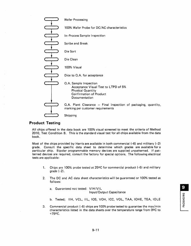
Product Testing
Wafer Processing
100% Wafer Probe for DCI AC characteristics
I n-Process Sample Inspection
Scribe and Break
Die Sort
Die Clean
100% Visual
Dice to Q.A. for acceptance
Q.A. Sample Inspection Acceptance Visual Test to l TPD of 5% Physical Quantity Confirmation of Product Documentation
Q.A. Plant Clearance - Final inspection of packaging, quantity, marking per customer requirements
Shipping
All chips offered in the data book are 100% visual screened to meet the criteria of Method 2010, Test Condition B. This is the standard visual test for all chips available from the data book.
Most of the chips provided by Harris are available in both commercial (-6) and military (-2) grade. Consult the specific data sheet to determine which grades are available for a particular chip. Bipolar programmable memory devices are supplied unpatterned. If patterned devices are required, consult the factory for special options. The following electrical tests are appl icable:
1. Chips are 100% probe tested at 250C for commercial product (-6) and military grade (-2).
2. The DC and AC data sheet characteristics will be guaranteed or 100% tested as follows:
a. Guaranteed not tested: VI H/VI l I nputlOutput Capacitance
b. Tested; IIH, VCl, Ill, lOS, VOH, ICC, VOL, TAA, 10HE, TEA, 10lE
3. Commercial product (-6) chips are 100% probe tested to guarantee the maximin characteristics listed in the data sheets over the temperature range from OOC to +750 C.
9-11
'" z
'" « '" '-' « Q..

These DC and AC characteristics are guaranteed to the following L TPDs at 250C.
a. L TPD of 10/1 for DC characteristics
b. L TPD of 10/1 for AC characteristics
4. Military grade (-2) chips are 100% probe tested at +250C to guarantee the max/min characteristics listed in the data sheets over the temperature range from -550C to +1250C. These DC and AC characteristics are guaranteed to the following L TPDs:
a. L TPD of 10/1 for DC characteristics at +250C. b. L TPD of 15/2 for DC characteristics at +1250C.
c. L TPD of 15/2 for DC characteristics at -550 C. d. L TPD of 10/1 for AC characteristics at +250C.
To assure that the DC and AC characteristics are being consistently met, the chips are sampled systematically by Quality Assurance. The dice are assembled in standard packages and tested at the appropriate temperatures to the L TPDs stated above.
Lot acceptance send ahead testing for DC and AC specifications is available as an option at an additional charge when ordering chips. Sample dice are assembled in a standard package and tested to the indicated L TPDs. Consult the factory when placing an order requiring lot acceptance send ahead test data.
Quality Assurance also systematically samples wafer lots using a Scanning Electron Microscope (SEM) for inspection of the metallization. This test is available as an option at an additional charge for most orders. Please consult the factory for additional information.
Mechanical Information
Dimensions: All chips dimensions given in the layouts in the data sheet section are nominal with a tolerance of ±.003 inches (±.08mm). Die thickness is nominally .020 inches ±.002 inches.
Bonding Pads: Minimum bonding pad size is .004 x .004 inches (,10mm x .10mm).
Passivation
All Harris dice are passivated with a layer of protective material to guard against deterioration of the dice. Passivation is applied to all areas of the die except the bonding pads and scribe lines.
Storage
Harris stores its dice in a dry nitrogen atmosphere and recommends that the customer do the same. If dice are exposed to air, the aluminum metallization will slowly oxidize at the bonding pads. The aluminum oxide will make bonding more difficult, especially if thermal compression gold ball bonding is used.
The humidity should be kept as low as possible with a relative humidity of no more than 50%.
Shipping
Dice are placed in conductive waffle carriers and covered with layer of bibilious paper and with a layer of mylar. The waffle pack is then sealed and labeled. The label contains the
9-12

part number of the chips, the quantity, and the lot number. The waffle pack is placed in a polyethylene bag along with a humidity indicating desiccant. The bag is then heat sealed and packaged in a suitable shipping container.
Recommended Handling
It is suggested that all dice be handled, tested, and installed using standard MOS handling techniques. This includes the use of conductive carriers and grounding of equipment and personnel. It has been found that handling equipment and personnel can generate static potentials in excess of 10kV in a low humidity environment. Therefore, proper handling procedures must be adopted to reduce static charge. Harris recommends using the following procedures when handling dice:
1. Use conductive work stations. Metallic or conductive plastic* tops on work benches connected to ground help eliminate static build-up.
2. Ground all handling equipment. To prevent scratches, it is recommended that a vacuum pick-up with protected tip be used for handling the dice. If tweezers are used, the dice should be gripped only on its sides.
3. Ground all handling personnel with a conductive bracelet through a 1M ohm resistor to ground. The resistor will prevent electroshock to personnel.
4. Smocks, clothing, and especially shoes of certain insulating materials (notably nylon) should not be worn in areas when devices are handled. These materials, highly dielectric in nature, will hold or aid in the generation of a static charge. Instead, natural materials such as cotton should be used to minimize charge generation.
5. Ionized air blowers reduce charge build-Up in areas where grounding is not possible or desirable.
6. Devices should be in conductive carriers during all phases of transport.
*Supplier 3M Company "Velostat"
Recommended Die Attachment
Harris uses gold eutectic die-attach for its packaged circuits and recommends this procedure for use with its chips. The die-attach area of the package should be gold plated. Gold preforms are usually not required. The recommended temperature for die-attachment is 4200 C ±100 C, and should remain constant throughout the procedure. To prevent oxidation, a laminar flow of approximately 30 liters/hour of nitrogen should be provided over the chip surface.
The package should be placed on the heater block and allowed to arrive at a uniform temperature. With tweezers, the die should be picked up and placed on the package. Using an orbital motion, the die should be rubbed on the package until eutectic melt is visible along the entire periphery of the die. There should be no evidence of balling or flaking of dieattach material. The die should be level with respect to the package and the die-attach material should be no higher than the top edges of the die.
Although Harris recommends using gold eutectic die-attach, conductive epoxy die-attach may also be used. Specific directions depend upon the epoxy used.
Recommended Bonding Procedures
Harris uses ultrasonic aluminum wire bonding and recommends this procedure be used by
9-13

our customers for best results. Harris uses an aluminum-silicon alloy wire, 99% aluminum and 1 % silicon. The diameter is 0.00125 inches, tensile strength is 22±2g, and elongation is 1.0 to 4.5%. Harris recommends similar wire be used by the customer. Actual bonding procedure will be governed by the manufacturers' instructions for the particular bonding equipment being used. A minimum bond pull strength of 3g is recommended to assure mechanical bond quality.
Ordering Information
Harris chips are designated by a product code. When ordering standard chips from this data book, please refer to the chips by the full product code. Harris chip codes will always begin with an H. Specific device numbers will always be isolated by hyphens.
Chip Code Example
HMO
PREFIX:~ H (Harris)
FAMILY: -------' D = Digital M = Memory PL = Programmable Logic
PACKAGE 0= Chip
7 6 4 3
I PART
NUMBER
6
LGRADE {DICEI 2 - Military 6 - Commercial
Chips are generally available on new Harris ICs at the time of introduction. Consult a salesman, representative of the factory regarding availablity, specifications, and minimum order requirements.
9-14

Sector Alpha-Numeric Product Index 10-2
Harris Sales Locations 10-7
Action Request Cards
10-1
x w een zw -...J .« gen ct: "-

Alpha-Numeric Product Index
Analog
,PRODUCT
HA-160B HA-2400/04/05 HA-2420/25 HA-2420/02/05 HA-2500/02/05 HA-2510/12/15 HA-2520/22/25 HA-2539 HA-2540 HA-2600/02/05 HA-2620/22/25 HA-2630/35 HA-2640/45 HA-2650/55 HA-2720/25 HA-2730/35 HA-2740 HA-4156 HA-4600/02/05 HA-4620/22/25 HA-4741 HA-4900/0205 HA-5033 HA-5062 HA-5064 HA-50B2 HA-5084 HA-5100/05 HA-5110/15 HA-5130/35 HA-5141/42/44 HA-5160/62
HA-5170 HA-5180/51BOA
HA-5190/95 HA-5320 HC-5116A/5156A HC-5502 HC-5504 HC-5510/5511 HC-5512/5512A HC-55536
HC-55564
DESCRIPTION
+10V Adjustable Voltage Reference PRAM, Four Channel Operational Amplifiers Fast Sample and Hold Operational Amplifiers Precision High Slew Rate Operational Amplifiers Precision High Slew Rate Operational Amplifiers High Slew Rate Operational Amplifiers Uncompensated High Slew Rate Operational Amplifiers Super High Slew Rate Wideband Operational Amplifiers Ultra High Slew Rate Operational Amplifiers Wideband, High Impedance Operational Amplifiers Very Wideband, Uncompensated Operational Amplifiers High Performance Current Booster High Voltage Operational Amplifiers Dual High Performance Operational Amplifiers Wide Range Programmable Operational Amplifiers Wide Range Dual Programmable Operational Amplifiers Quad Programmable Operational Amplifiers High Performance Quad Operational Amplifiers High Performance Quad Operational Amplifiers Wideband, High Performance Quad Operational Amplifiers Quad Operational Amplifier Precision Quad Comparators High-Speed Current Buffer Dual Low Power, JFET Input Operational Amplifier Low Power, JFET Input Quad Operational Amplifier Dul JFET Input Operational Amplifer JFET Input Quad Operational Amplifier Wideband, JFET Input Operational Amplifiers Wideband, JFET Input, Uncompensated Operational Amplifiers Precision Operational Amplifiers Power Operational Amplifier, Single, Dual & Quad Wideband, JFET Input, High Slew Rate, Uncompensated Operational Amplifiers Precision JFET Input Operational Amplifiers Ultra Low IBIAS JFET Input Precision Operational Amplifier Wideband, Fast Settling Operational Amplifiers High Speed Precision Monolithic Sample and Hold Amplifier Monolithic CODECS (Preliminary) SLlC-LC Subscriber Line Interface Circuit (PBX) SLlC-LC Subscriber Line Interface Circuit (PBX) Monolithic CODECs (Preliminary) PCM Monolithic Filter Decode Digital Continuously Variable Slope Delta Modulator (CVSD) Encode and Decode all Digtal Continuously Variable Slope Delta Modulator (CVSD)
10-2

PRODUCT
HD-0165 HI-200 H 1-201 H 1-201 HS HI-300 H 1-301 H 1-302 HI-303 HI-304 HI-305 HI-306 HI-307 HI-381 HI-384 HI-387 HI-390 HI-506/507 H 1-506A/507 A
HI-506L/507L HI-508/509 H 1-508A/509 A.
HI-508L/509L H 1-516
H 1-518
HI-524 HI-539
HI-562A HI-565A
HI-574A
HI-674A
H 1-1818A/1828A HI-5040 HI-5041 HI-5042 HI-5043 HI-5044 HI-5045 HI-5046 HI-5046A HI-5047 HI-5047A HI-5048 HI-5049 HI-5050 HI-5051 HI-5610
Analog (Continued)
DESCRIPTION
Keyboard Encoder Dual SPST CMOS Analog Switch Quad SPST CMOS Analog Switch High Speed Quad SPST CMOS Analog Switch Dual SPST CMOS Analog Switch SPDT CMOS Analog Switch Dual DPST CMOS Analog Switch Dual SPDT CMOS Analog Switch Dual SPST CMOS Analog Switch SPDT CMOS Analog Switch Dual DPST CMOS Analog Switch Dual SPDT CMOS Analog Switch Dual SPST CMOS Analog Switch Dual DPST CMOS Analog Switch SPDT CMOS Analog Switch Dual SPDT CMOS Analog Switch Single 16/Differential 8 Channel CMOS Analog Multiplexers 16 Channel CMOS Analog Multiplexers with Overvoltage Protection Latched, 16/8 Channel Analog Multiplexer Single 8/Differential 4 Channel CMOS Analog Multiplexers 8 Channel CMOS Analog Multiplexers with Overvoltage Protection Latched, 8/4 Channel Analog Multiplexer 16 Channel/Differential 8 Channel CMOS High Speed Analog Multiplexer 8 Channel/Differential 4 Channel CMOS High Speed Analog Multiplexer 4 Channel Video Multiplexer Monolithic, Four Channel, Low Level, Differential Multiplexer 12 Bit High Speed Monol ithic Digital-to-Analog Converter High Speed Monolithic Digital-to-Analog Converter with Reference Fast, Complete 12 Bit A-to-D Converter with
P Interface High Speed, Complete 12-Bit A-to-D Converter with P Interface Low Resistance 8 Channel CMOS Analog Multiplexer Low Resistance SPST Switch Low Resistance Dual SPST Switch Low Resistance SPDT Switch Low Resistance Dual SPDT Switch Low Resistance DPST Switch Low Resistance Dual DPST Switch Low Resistance DPDT Switch Low Resistance DPDT Switch Low Resistance 4PST Switch Low Resistance 4PST Switch Low Resistance Dual SPST Switch Low Resistance Dual DPST Switch Low Resistance SPDT Switch Low Resistance Dual SPDT Switch 10 Bit High Speed Monol ith ic Digital-to-Analog Converter
10-3
X LU 0", ZLU -...J 0« gel) a: "-

PRODUCT
HI-5618A/18B HI-5660 HI-5680 HI-5685 HI-5687
H 1-5712/12A HI-5900 HI-5901 HI-7541 HI-DAC801 HI-DAC16B/C HV-1000/1000A LF347 LF353 LF355 Series LF356 Series LF357 Series
LM118/318 LM143/343
Analog (Continued)
DESCRIPTION
8 Bit High Speed Digital-to-Analog Converters High Speed Monolithic D-to-A Converter 12 Bit Low Cost Monolithic D-to-A Converter High Performance Monolithic 12 .Bit D-to-A Converter Wide Temperature Range Monolith ic 12 Bit D-to-A Converter High Performance 12 Bit Analog-to-Digital Converters Analog Data Acquisition Signal Processor Analog Data Acquisition Signal Processor 12 Bit Multiplying Monolithic Digital-to-Analog Converter 12 Bit High Speed Monolithic Digital-to-Analog Converter 16 Bit D-to-A Converter Single-Phase Induction Motor Energy Saver Wideband Quad JFET Input Operational Amplifiers Wideband Dual JFET Input Operational Amplifier Monolithic JFET Input Operational Amplifiers Wideband Monolithic JFET Input OPerational Amplifiers Decompensated Wideband Monolithic JFET Input Operational Amplifiers Operational Ampl ifiers High Voltage Operational Amplifiers
10-4

PART NUMBER
HD-6600 HM-0104 HM-0168 HM-0186 HM-0198 HM-0410 HM-7602/03 HM-7610/11 HM-7610A/11A HM-7610B/11B HM-7620/21 H M-7620A/21 A HM-7620B/21 B HM-7640/41 HM-7640A/41A HM-7649 HM-7649A HM-7642/43 HM-7642A/43A HM-7642B/43B HM-7681 HM-7681A HM-7685 HM-7685A HM-76161 HM-76161A HM-76161B HM-76165 HM-76321 HM-76641 HM-76641A JAN-0512 HPL-77061 HPL-77153/82S153 HPL-77209/16L8 HPL-77210/16R4 HPL-77211/16R6 HPL-77212/16R8 HPL-77215/16H8 HPL-77216/16P8 HPL-77317/16LD8 HPL-77318/16HD8 HPL-77319/16LE8 HPL-77320/16HE8 M38510/20701 BEB M38510/20702BEB M3851 0/201 01 BJB M38510/20301 BEB M38510/20302BEB M3851 0/20401 BEB M38510/20402BEB M38510/20801 BJB M3851 0/20802 BJ B M3851 0/20601 BV8 M38510/20602BVB M38510/20904BJB M38510/20902BVB M3851 0/21 002BJ B
Bipolar
Quad Power Strobe 10 x 4 Diode Matrix 6 x 8 Diode Matrix 8 x 6 Diode Matrix 9 x 8 Diode Matrix 4 x 10 Diode Matrix 32 x 8 Bit Generic PROM 256 x 4 Bit Generic PROM
DESCRIPTION
256 x 4 Bit High Speed Generic PROM 256 x 4 Bit Very High Speed Generic PROM 512 x 4 Bit Generic PROM 512 x 4 Bit High Speed Generic PROM 512 x 4 Bit Very High Speed Generic PROM 512 x 8 Bit Generic PROM (24-Pin) 512 x 8 Bit High Speed Generic PROM (24-Pin) 512 x 8 Bit Generic PROM (20-Pin) 512 x 8 Bit High Speed Generic PROM (20-Pin) 1024 x 4 Bit Generic PROM 1024 x 4 Bit High Speed Generic PROM 1024 x 4 Bit Very High Speed Generic PROM 1024 x 8 Bit Generic PROM 1024 x 8 Bit High Speed Generic PROM 2048 x 4 Bit Generic PROM 2048 x 4 Bit High Speed Generic PROM 2048 x 8 Bit Generic PROM 2048 x 8 Bit High Speed Generic PROM 2048 x 8 Bit Very High Speed Generic PROM 4096 x 4 Bit Generic PROM 4096 x 8 Bit Generic PROM 8192 x 8 Bit Generic PROM 8192 x 8 Bit High Speed Generic PROM 64 x 8 HPROM 24-Pin Field Programmable Address Decoder 20-Pin Field Programmable Logic Array 20-Pin Field Programmable Array Logic (Active Low Outputs) 20-Pin Field Programmable Array Logic (Four Registered Outputs) 20-Pin Field Programmable Array Logic (Six Registered Outputs) 20-Pin Field Programmable Array Logic (Eight Registered Outputs) 20-Pin Field Programmable Array Logic (Active High Outputs) 20-Pin Field Programmable Array Logic (Programmable Output Polarity) 20-Pin Field Programmable Array Logic (Active Low Dedicated Outputs) 20-Pin Field Programmable Array Logic (Active High Dedicated Outputs) 20-Pin Field Programmable Array Logic (Enhanced HPL-77317/16LD8) 20-Pin Field Programmable Array Logic (Enhanced HPL-77318/16HD8) 32 x 8 Open Collector QPL1 PROM 32 x 8 Three State QPL 1 PROM 64 x 8 Open Collector QPL1 PROM 256 x 4 Open Collector QPL1 PROM 256 x 4 Three State QPL1 PROM 512 x 4 Open Collector QPL1 PROM 512 x 4 Three State QPL1 PROM 512 x 8 Open Collector QPL1 PROM 512 x 8 Three State QPL1 PROM 1024 x 4 Open Collector QPL1 PROM 1024 x 4 Three State QPL1 PROM 1024 x 8 ThreE' State QPL1 PROM 2048 x 4 Three State QPU PROM 2048 x 8 Three State QPL1 PROM
10-5

PRODUCT
HD-15530 HD-15531 HD-4702 HD-6101 HD-6120 HD-6121 HD-6402 HD-6406 HD-6408 HD-6409 HD-6431 HD-6432 HD-6433 HD-6434 HD-6436 HD-6440 HD-6495 HM-6100 HM-6504 HM-6508 HM-6514 HM-6516 HM-65162 HM-65172 HM-6518 HM-65262 HM-6551 HM-6561 HM-6564 HM-6616 HM-6641 HM-6664 HM-92560 HM-92570 HPL- 16LC8 HPL-16RC4 HPL-16RC6 HPL-16RC8 8UC86 80C88 82C37A 82C52 82C54 82C55A 82C59A 82C82 82C83 82C84A 82C86 82C87 82C88 82C89
CMOS DESCRIPTION
Manchester Encoder-Decoder Manchester Encoder-Decoder Programmable Bit Rate Generator Parallel Interface Element 12 Bit High Performance Microprocessor I/O Controller LS I Universal Asynchronous Receiver Transmitter Programmable Asynchronous Communication Interface Asynchronous Manchester Adapter Manchester Encoder-Decoder Hex Latching Bus Driver Hex Bi-directional Bus Driver Quad Bus Separator/Driver Octal Resettable Latch Octal Bus Buffer/Driver Latch Decoder/Driver Hex Bus Driver 12 Bit Static Microprocessor 4K X 1 Synchronous RAM 1 K X 1 Synchronous RAM 1 K X 4 Synchronous RAM 2K X 8 Synchronous RAM 2K X 8 Asynchronous RAM 2K X B Asynchronous RAM 1 K X 1 Synchronous RAM 16K X 1 Asynchronous RAM 256 X 4 Synchronous RAM 256 X 4 Synchronous RAM 64K Synchronous RAM Module 2K X B Fuse Link PROM 512 X B PROM BK X B Fuse Link PROM 256K Synchronous RAM Module 256K Synchronous RAM Module - Buffered Programmable Logic Programmable Logic Programmable Logic Programmable Logic 16 Bit Microprocessor B Bit Microprocessor High Performance Programmable DMA Controller Serial Controller Interface Programmable Interval Timer Programmable Peripheral Interface Priority Interrupt Controller Octal Latch Octal Latching I nverting Bus Driver Clock Generator/Driver Octal Bus Transceiver Octal Inverting Bus Transceiver Bus Controller Bus Arbiter
10-6

Harris Sales Locations
OEM Sales
EASTERN REGION Suite Cl00 Harris/Matra-Harris Semiconductor 883 Stierlin Road Walsroderstrasse 71
Suite 215 Mt. View, CA 94043 D-3012 Langenhagen 1 3890 West Commercial Blvd. (415) 964-6443 Tel: 49-511-737037 Ft. Lauderdale, FL 33309 TWX: 9230474HMHHD (305) 739-0016 Suite 205
6400 Canoga Avenue EUROPEAN DISTRIBUTORS Suite 400 Woodland Hills, CA 91367 875 Johnson Ferry Road (213) 992-0686 AUSTRIA Atlanta, GA 30342 (404) 256-4000 33919 9th Avenue South Transistor Vetriebsgesellschaft
Federal Way, WA 98003 mbH &Co. KG. Suite 308 (206) 838-4878 Auhofstr. 41 A 1 Burlington Woods Drive A-1130 Wi en Burlington, MA 01803 Suite 8 Tel: 43-0222-82-94-01 (617) 273-5942 2005 Broadway TWX: 133738 TVGWN
Vancouver, WA 98663 P. O. Box 31747 (206) 696-0043 BELGIUM Raleigh, NC 27622
International Sales Betea S.A
Suite 1101 755 Chaussee de Louvain 996 Old Eagle School Road B-1140 Brussels Wayne, PA 19087 Europe Tel: 32-2-7368050 (215) 687-6680 TWX 23188
HEADQUARTERS Suite 273 DENMARK 555 Broadhollow Road Harris/MHS GMBH Melville, L. I., NY 11747 Headquarters Ditz Schweitzer A. S. (516) 249-4500 Erfurterstrasse 29 Vallensbaekvej 41
8057 Echfrig DK-2600 Glostrup CENTRAL REGION West Germany Tel: 45-2-453044
TEL: 49-89-319-1035 TWX: 33257 Suite 300 TWX: 5-213-866 6400 Shafer Court FINLAND Rosemont, IL 60018 (312) 692-4960 SALES OFFICES Yleiselektronikka OY
Suite 101 Atomitie 5 B (P,O. Box 33)
ENGLAND SF-00370 Helsinki 37 1717 East 116th Street Tel.: 358-0-90-562-1122 Carmel, IN 46032 Harris Systems Ltd. (317) 844-8011 Harris Semiconductor Div. FRANCE
153 Farnham Road Suite 703 Slough SL1 4XD Matra-Harris Semiconductor 2850 Metro Drive Int'l. Tel.: 44-753-34666 Harris S. A Minneapolis, MN 55420 TWX: 848174 Harris Semi. Division (612) 854-3558 6 Av Charles de Gaulle
ITALY F-78150 Le Chesnay Suite 110 Tel: 33-3-9548000 17120 Dallas Parkway Harris Italiana, Inc. TWX: 696514 Dallas, TX 75248 20092 Cinisello Balsamo (Milano) (214) 248-3237 Via Fratelli Cracchi 48 Matra Harris Semiconductor
Tel 39-2~6187249/6188282 B.P.942 WESTERN REGION TWX: 311164 Agerisi Nantes Cedex
Suite 250 Tel: 33-40-490820
1717 E Morten Avenue WEST GERMANY TWX: 711930
Phoenix, AZ 85020 Harris/Matra-Harris Semiconductor (602) 870-0080 x
Deutschland GmbH w c'"
Suite 320 Erfu rterstrasse 29 ZW -....J
1503 South Coast Drive 8057 Eching .< Costa Mesa, CA 92626 Tel: 49-89-319-1035 g'"
a: (714) 540-2176 TWX: 5-213-866 ...
10-7

WEST GERMANY
Alfred Neye-Enatechnik BmbH Schillerstr.14 Postfach 1240 D-20850uickborn
Tel: 49-4106-6121 TWX:213590
Jermyn GmbH Schulster. 84 Postfach 1180 D-6277 Camberg-Wuerges
Tel: 49-6434-231 TWX: 4884426
Kontrol Halbleiter GmbH Breslauer Str. 2 Postfach 1251 D-8057 Eching bei Muenchen
Tel. 49-89-319011 TWX 522122
SASCO GmbH Hermann-Oberth-Strasse 16 D-8011 Putzbrunn
Tel: 49-89-4611-1
Spoerle Electronic KG Max-Planck-Str. 1-3 D-6072 Dreieich Bei Frankfurt
Tel: 49-6103-30-40
iSRAEL
MRBD Industries Ltd. P.O. Box 1717 54 Jaboti nsky street Ramat-Gan 52117
Tel: 972-3-721-918-722-367
TWX 352073
ITALY
ELEDRA 3S SPA Viale Elvezia 18 20154 Mi lano Int'l. Tel.: 39-2-349751
TWX: 331612
Lasi Elettronica Via Le lombardia, 6 1-20092 Cinisello Balsamo
Tel.: 39-2-9273578 TWX: 337612
NETHERLANDS
Techmation Electronics BV P.O. Box 9 N L -4175 ZG Haaften
Tel.: 31-04189-2222 TWX: 5Q423 TME Nl
NORWAY
National Elektro Ulveneien 75 P.O. Box 53, Oekern N-Oslo 5
Tel.: 472-64-49-70 TELEX 71265 nen
REPUBLIC OF S. AFRICA
Allied Electronic Components P.O. Box 6090 Du nswart, 1508 Boksburg East Trasvaal
Tel.: 27-11-892-1001 TWX: 4-25559
SPAIN
Unitronics SA Princesa No.1 Torre de Madrid Planta 12 Officina 9 Madrid
Tel: 34-242-5204 TWX 22596
SWEDEN
A. B. Betoma Box 3005 S17103 Solna 3
Tel: 46-8-820280 TWX 19389
SWITZERLAND
W. Stolz A. G. Taefernstr. 15 CH-5405 Baden-Daettwil
Tel: 41-56840151 TWX 54070
UNITED KINGDOM & IRELAND
HYCOMP Ltd. 7, Shield Road Ashford Industrial Estate Ashford, Middlesex TW151AV
Int'l. Tel.: 44-7842-46273 TWX: 923802
Macro Marketing ltd. 396 Bath Road Slough, Berks
Int'!. Tel.: 44-62864422 TWX: 847945
10-8
Radio Resistor Co. Ltd. St. Martins Way Industrial Est. Cambridge Road Bedford MK 42 OlF
Int'l. Tel.: 44-234-47188 TWX: 837508
SDP (Semi Ltd.) Regent House York Road Hartlepool, Cleveland TS26 90U
Int'!. Tel.: 44-429-33721 TWX: 587650 Sempro
Thame Components Ltd. Thame Park I nd. Estate Thame, Oxon OX9 3RS
Int'l. Tel.: 44-84421-3146 TWX 837508
Scotland Representative
Phoenix Electronics ltd. Western Bldg. Vere Road Kirkmuirhill, lankersham Ml11 9 RP, Scotland
Tel.: 44-55589-2393 TWX: 777404
Ireland Representative
Trim Electronics Ltd. Trim County Meath Eire, Ireland
Tel.: 353-46-36263 TWX: 90342
Far East
SALES OFFICES
Harris Semiconductor, Inc. Far East Branch Ace Shoto Bldg. 3F 1-4-7, Shoto Shibuya-ku, Tokyo 150
Tel.: 81-3-485-1031 TWX: 326525

FAR EAST DISTRIBUTORS
AUSTRALIA
VSI Electronics 35-37 Dickson Avenue Artarmon, NSW 2064
Tel.: 61 -439-4655 TWX A22846
TAIWAN
Enterprex Int'l Corp. 3900 E. Whiteside Street Los Angeles, CA 90063
Tel.: 213-267-1145 TWX 69-1159
INDIA
Fegu Electronics Attn: Raj Saraf 106 Mittal Chambers Nariman Point Bombay 400021
Fegu Incorporated Electronics Division 2584 Wyandotte St. Mountain View, CA 94043
Tel: 415-961-2380 TWX: 176-572
Zenith Electronics Attn: Raj Saraf, Mgr. Director 106 Mittal Chambers Nariman Point Bombay
10-9
South America
Elko S. R. L. Av. Belgrano 1661 1093 Buenos Aires Argentina
Tel.: 54-1-40-8971 TWX: CABINA PUBLICA N9
COSELE Representacoes Eletronicas Ltd. Rua da Consolacao 867 - Conj. 22 Sao Paulo, SP 01301 Brazil
Telex: 11 30869 CSEL BR Tel: (PABX): 9-011-55-11-255-1733
HOME OFFICE
P. O. Box 883 Melbourne, FL 32902
Tel: (305) 724-7000 TWX: 510-959-6259
x UJ
""en ZUJ - -' .<{ gen a:: Q..