Embed Size (px)
Citation preview
LYT7503-7504LYTSwitch-7 Family
www.power.com July 2016
Phase-Cut Dimmable Single-Stage LED Driver ICwith Combined PFC and Constant Current Outputfor Buck Topology
This Product is Covered by Patents and/or Pending Patent Applications.
Product HighlightsSingle-Stage PFC + Accurate CC Output• ±3% CC regulation in single line input voltage applications• Power factor >0.9• High efficiency >85%• Robust 725 V MOSFET for increased line voltage surge resistance• Critical Conduction Mode (CrM) buck• Low EMI• Excellent line noise and transient rejection
Dimming Highlights • Fast turn-on (<500 ms)• Low pop-on• Better than 10:1 dimming ratio• Simple passive R-C damper• Monotonic dimming profile
Design Flexibility • Wide input (90 VAC – 308 VAC) and output voltage range operation• 2 family members cover power range for optimum device selection• Requires no inductor bias winding• Small form factor package – SO-8
Highest Reliability • Industry’s lowest component count dimming solution• Comprehensive protection features with auto-restart
• Input and output overvoltage protection (OVP)• Output short-circuit protection• Open-loop protection
• Advanced thermal control• Thermal foldback ensures that light continues to be delivered at
elevated temperatures• Over-temperature shutdown provides protection during fault
conditions
DescriptionThe LYTSwitch™-7 family is ideal for single-stage, high PF, constantcurrent LED dimmable applications.
The family incorporates a high-voltage MOSFET with a variable on-time CrM controller. Extensive protection features with minimum external components provide industry leading power density and functionality.
The CrM operation results in low turn-on losses and reduces cost ofoutput diode (slower reverse-recovery type can be used).
LYTSwitch-7 devices are suitable for applications from 4 W to 22 W. See Graph 1 for selection guidance (based on typical inductance). For more information, see Application section. LYTSwitch-7 peak current mode operation is suitable for TRIAC applications without the need for an active bleeder.
Figure 1. Buck − Typical Application Schematic.
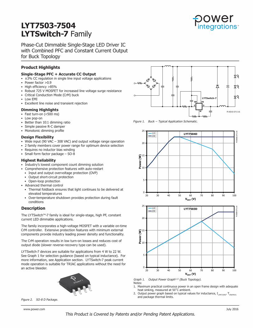
Figure 2. SO-8 D Package.
Graph 1. Output Power Graph(1,2) (Buck Topology).Notes: 1. Maximum practical continuous power in an open frame design with adequate
heat sinking, measured at 50˚C ambient.2. Output power graph based on typical values for inductance, ILIMIT(AR), TON(MAX)
and package thermal limits.
PI-8010-071116
LYTSwitch-7
D
FB
S
M
BP
0
5
10
15
20
25
20 30 40 50 60 70 80 90 100
Pow
er (
W)
VOUT (V)
PI-8
009-
0711
16
LYT7503D115230
0
5
10
15
20
25
20 30 40 50 60 70 80 90 100
Pow
er (
W)
VOUT (V)
115230
PI-8
009a
-071
116
LYT7504D

Rev. C 07/16
2
LYT7503-7504
www.power.com
Pin Functional DescriptionBYPASS (BP) Pin:5.25 V supply rail.
MULTIFUNCTION (M) Pin:Mode 1: MOSFET OFF• Detection of inductor de-magnetization (ZCD) to ensure CrM• Output OVP sensing (120 % of VOUT nominal)• Steady-state operation voltage range is 1 V – 2.4 VMode 2: MOSFET ON• Line OVP
FEEDBACK (FB) Pin:• MOSFET current sensing using external current sense resistor• Normal operating range is VFB(REF) to 0 V
DRAIN (D) Pin:High-voltage internal MOSFET.
SOURCE (S) Pin:Power and signal ground.
Figure 4. Pin Configuration.
Figure 3. Block Diagram.
PI-7907-071316
SOURCE(S)
TONSTATE
MACHINE
UP/DNCOUNTER
BYPASS(BP)
DRAIN(D)
MULTI-FUNCTION
(M)
FEEDBACK(FB)
REGULATOR5.25 V
IVALLEY
0.7 × VFB(REF)
4.5 V
0 V IPK
R2
R1
IOVP
Line_Comp
OOVP
OTP
VOUT_SS
AC_Valley
AC_High
INPUTLINE
SENSE
FAULTHANDLING
ZEROCURRENT
DETECTION
VOUTSENSE
ILIMITSOA
THERMALSHUTDOWN
SYSTEMCLOCK
S Q
R Q
FAULT
UV
CONTROLLOGIC
PI-7908-032216
D Package (SO-8)
BP
M
FB
D
1
2
3
4
8
7
6
5
S
S
S
S

Rev. C 07/16
3
LYT7503-7504
www.power.com
Figure 5. Schematic from DER-561 7.5 W, 60 V, 125 mA Dimmable Non-Isolated A19 LED Driver for Wide Input Range: 90 – 300 V VAC using LYT7503D in Low-Side Buck Configuration.
Applications Design ExampleDER-561 a Low-Line Dimmable 7.5 W, Wide Input, High Power factor LED Bulb Driver.
Circuit Description
The circuit shown in Figure 5 is a LED driver configured as a low-side buck utilizing the LYT7503D from the LYTSwitch-7 family of ICs. This is a low component count (20 parts) dimmable LED driver designed to power a 60 V LED voltage string at 125 mA output current from an input voltage of 90 VAC to 300 VAC. Dimming performance is optimized at low-line input (i.e. 120 VAC), while maintaining accurate regulation for non-dimmable high-line input.
LYTSwitch-7 is a SO-8 package LED driver IC family designed for non-isolated buck applications. The LYTSwitch-7 family provides high efficiency, high power factor and accurate LED current regulation. It incorporates a high-voltage 725 V power MOSFET and a control engine to switch the MOSFET in critical conduction mode (CM) with variable on-time and variable frequency which also helps achieve low EMI, and low THD. The controller also integrates protection features such as input and output overvoltage protection, thermal fold-back, over-temperature shutdown, output short-circuit and over-current protection. The controller also allows natural dimming with only the addition of a damper resistor and an RC network for damping the input current ringing when the TRIAC turns on.
Key Design Considerations
Input StageThe input fusible resistor RF1 provides multiple-purpose function – safety protection, current limiting against differential surge and acts as a damping element reducing inrush-current ringing when TRIAC dimming. Varistor RV1 acts as a voltage clamp that limits the voltage spike on the primary during line transients and surge events. A 250 VAC rated part was selected with a maximum clamping voltage specification of 710 VDC – lower than the device Drain voltage (725 V). The AC input voltage is full wave rectified by BR1 to achieve good power factor and low THD.
The rectified AC supply is filtered by the input capacitors C1 and C2. Too much capacitance degrades power factor and THD, so the values of the input capacitors were set to the minimum necessary to meet EMI (with suitable margin). Inductor L1, C1 and C2 form a π (pi)
filter, which attenuates conducted differential and common mode EMI currents. If required a ≥10 kΩ resistor (not shown) can be added across L1 to damp the Q-factor of the filter inductor to improve the filtering of high frequency EMI without reducing low frequency attenuation.
The addition of the RC damper network R2 and C3 makes the driver compatible with TRAIC (phase-cut) dimmers. The RC damper in the circuit may be placed before or after the bridge rectifier. In this design, the RC damper is located after the bridge rectifier for higher dimming range. Putting the RC damper before the bridge would load the TRIAC dimmer and maintain full output to a lower conduction angle but would result in reduced dimming range.
LYTSwitch-7 Controller StageThe LED driver circuit is a low-side buck configuration operating in critical conduction mode; the controller allows complete transfer of the energy stored in the inductor to the load before starting the next switch cycle. The inductor demagnetization is sensed, detecting when the voltage across the inductor begins to collapse (towards zero) as flywheel diode (D1) conduction ceases.
Capacitor C4 provides local decoupling for the BYPASS (BP) pin IC and provides power to the LYTSwitch-7 controller during the MOSFET on-time. The IC has an internal regulator that draws power from the high-voltage DRAIN (D) pin and charges the bypass capacitor C4 during the power switch off-time. The typical BYPASS pin voltage is 5.22 V. To keep the IC operating normally (especially during the dead time), where VIN < VOUT, and during dimming at low conduction angles, resistors R6 and R10 are employed to keep the bypass capacitor charged. The value of the bypass capacitor should be large enough to keep the bypass voltage above the VBP(RESET) reset value of 4.5 V. The suggested minimum value for the bypass capacitor is 10 µF; an X7R type is recommended if using a ceramic type capacitor.
Constant output current regulation is achieved through the FEED-BACK (FB) pin directly sensing the DRAIN pin current during the MOSFET on-time via external current sense resistors (RFB) R3 and
PI-8023-071416LYTSwitch-7U1
LYT7503D
DS
R8100 kΩ
R1051 kΩ
R651 kΩ
R2510 Ω2 W
L
N
RTN
60 V, 125 mA
+V
D1US1J-13-F
L14.7 mH
T1EE10
4 6
BR1B10S-G1000 V
R30.68 Ω
1%1/3 W
RV1275 VAC
R147 Ω2 W
R451.1 Ω
1%, 1/8 W
R9402 kΩ
1%
R512.4 kΩ
1%1/8 W
C122 nF450 V
C2120 nF450 V
C3220 nF450 V
C6220 µF80 V
C5100 pF1000 V
C410 µF10 V
FB
M
BP
90 - 300VAC

Rev. C 07/16
4
LYT7503-7504
www.power.com
R4. The voltage drop is compared to an internal 279 mV (typical) reference voltage (VFB(REF)). The value for RFB can be calculated from the equation:
/R V k I( )FB FB REF OUT#=
Where: k = 3.6 which is the ratio of IPK : IOUT
Trimming RFB may be necessary to center IOUT to the nominal LED output voltage.
The MULTIFUNCTION (M) pin detects AC line overvoltage events. When the internal MOSFET is in on-state, the MULTIFUNCTION pin is internally connected to the SOURCE (S) pin and can detect the rectified input line voltage which is the voltage across the inductor, i.e. (VIN – VOUT) and current flowing out of the MULTIFUNCTION pin is set by resistor R5. The line overvoltage trigger point (VLINE_OVP) is calculated by;
V I R V5( )LINE OVP IOV OUT#= +
R9 is assumed to be 402 kΩ ±1%.
Once the detected current exceeds the input overvoltage threshold (IIOV = 1 mA typical), the IC will instantaneously inhibit switching and initiate auto-restart to protect the internal MOSFET and the LED load from voltage overstress.
The MULTIFUNCTION pin also monitors the output for overvoltage or undervoltage events. When the internal MOSFET is in off-state, the output voltage is sensed via divider resistors R5 and R9 across the inductor voltage of T1. When an output open-load condition occurs, the voltage at the MULTIFUNCTION pin will rise abruptly. When it exceeds the VOOV threshold of 2.4 V (typical), the IC will inhibit switching and initiate an auto-restart to prevent the output voltage from rising further. The overvoltage cut-off is typically set at 120% of the output voltage, which is equivalent to 2 V on the MULTIFUNC-TION pin
. /V V V V2 4 2( )OUT OVP OUT #=
If desired, a higher overvoltage cut-off can be selected by setting a lower MULTIFUNCTION pin voltage target. Resistor R9 is a fixed value of 402 kΩ ±1% allowing R5 to determine the output overvolt-age limit.
A short-circuit at the output will reduce output voltage and be detected when the MULTIFUNCTION pin voltage falls below the undervoltage threshold (VOUV = 1 V typical). The IC will inhibit switching and initiate auto-restart limiting the average input power to less than 1 W, preventing any component from overheating during a short-circuit.
Resistor R5 can be calculated as follows;
/R V R V V5 2 9 2OUT#= -^ hA small capacitor C5 is needed to couple the high-side referenced analog of the output voltage to the MULTIFUNCTION pin of the IC via resistor divider network R5 and R9. Calculation and practical experience shows that, a capacitance value of 100 pF provides a good compromise between AC line rejection and flatness of the output voltage during the off-time of the switch.
Another function of the MULTIFUNCTION pin is for zero current detection (ZCD). Detecting this condition is necessary for operation in critical conduction mode (CrM). Inductor demagnetization is detected when the voltage across the inductor begins to collapse as flywheel diode (D1) conduction ends.
Output Stage During the MOSFET-switch off-state, free-wheeling diode D1 rectifies and conducts the voltage across T1 and the output is filtered by C6. An ultrafast 1 A, 600 V with 75 ns reverse recovery time (tRR) diode was selected for efficiency and good regulation over line and across temperature . The value of the output capacitor C6 was selected to give peak-to-peak LED ripple current equal to 30% of the mean value. For designs where lower ripple is required, the output capacitance value can be increased. The ripple is dependent on both output capacitance and the bulk resistance of the LED load; it recommended that the actual load be used when sizing the output capacitor in order to correctly achieve the specified ripple current.
A small output pre-load resistor R8 discharges the output capacitor when the driver is turned off, giving a quick and smooth decay of the LED light after turn-off. Recommended pre-load power dissipation is ≤0.25 % of the output power.
LYTSwitch-7 Device Size SelectionThe data sheet power curve (Figure 6) represents the practical maximum continuous output power that can be delivered in an open frame design with adequate heat sinking.
DER-561 is a 7.5 W 60 V driver for a dimming bulb application. Using the power graph we can see that LYT7503D is the appropriate device to use.
Magnetic SelectionThe small output inductor uses a ferrite cored EE10 with an open winding window that allows better convection cooling for the winding. An off-the-shelf “dog-bone” type inductor could also be used.
To ensure proper magnetic design and accurate output current regulation, it is recommended that the LYTSwitch-7 PIXls spreadsheet located at PI Expert web site (https://piexpertonline.power.com/site/login) should be used for magnetics calculations.
EMI ConsiderationsTotal input capacitance affects PF and THD – increasing the value will degrade performance, so these must be minimized. The LYTSwitch-7 control engine operates in CrM mode with variable frequency and variable on-time which provides low EMI enabling the use of only a small pi (π) filter. It also allows simple inductor construction suitable for the auto-winding inductor manufacturing approach used for low-cost high volume production. The recommended location of the
0
5
10
15
20
25
20 30 40 50 60 70 80 90 100
Pow
er (
W)
VOUT (V)
PI-8
009b
-071
916
LYT7503D
60 V, 7.5 W
115230
Figure 6. Output Power Graph.

Rev. C 07/16
5
LYT7503-7504
www.power.com
EMI filter is after the bridge rectifier as this allows the use of regular film capacitors (as opposed to more expensive safety rated X-capaci-tors that would be required if the filter is placed before the bridge).
Since the integrated switch MOSFET for LYTSwitch-7 is referenced to ground, the SOURCE pin acts as an EMI shield. This allows a “dog-bone” inductor to be used in low-side configurations as shown in DER-539 (Figure 7). The Design Engineering Reference (DER) report can be found at https://led-driver.power.com/design-support/ on the PI website.
Thermal and Lifetime ConsiderationsLighting applications present significant thermal challenges to the driver. In many cases the LED load dissipation determines the working ambient temperature, so thermal evaluation should be performed with the driver inside the final enclosure. Temperature has a direct impact on driver and LED lifetime. For every 10 °C rise in tempera-ture, component life is reduced by a factor of 2. Therefore, it is important to verify and minimize the operating temperature of each component.
PCB Layout Considerations
Shown in In Figure 8, the EMI filter components should be located close together to improve filter effectiveness. Place the EMI filter components C1 and L1 as far as possible from any switching nodes on the circuit board especially the U1 drain node, output diode (D1) and the inductor (T1).
Care should be taken in placing the critical IC components, namely R3, R4, R5, R9, R10, C5 and C4. It is strongly recommended that these components be placed very close to the pins of controller U1
to minimize long traces (which act as antennae), and as far away as possible from any high-voltage and/or high current switching nodes in the circuit to avoid potential noise coupling that may affect system operation.
For effective noise decoupling, the bypass supply capacitor C4 should be placed directly across BYPASS pin and SOURCE pin of U1.
Minimizing the loop areas of the following switching circuit elements (as shown in Figure 8) lessen the creation of EMI.
• Loop area formed by the inductor winding (T1), free-wheeling rectifier diode (D1) and output capacitor (C6).
• Loop area formed by input capacitor (C2), controller internal MOSFET (U1), free-wheeling rectifier diode (D1) and sense resistors (R4, R5).
With LYTSwitch-7 in a low-side configuration potential SOURCE pins are used for heat sinking are at ground potential. This allows the designer to maximize the copper area for good thermal management without increasing EMI.
Quick Design Checklist
Maximum Drain VoltageVerify that the peak Drain voltage stress (VDS) does not exceed 725 V under any operating condition, including start-up and fault conditions.
Maximum Drain CurrentMeasure the peak drain current under all operation conditions (including start-up and fault conditions). Look for inductor saturation (usually occurs at highest operating ambient temperatures). Verify that the peak current is less than the stated Absolute Maximum Rating in the data sheet.
Thermal CheckAt maximum output power, for both minimum and maximum line voltage and maximum ambient temperature verify that component temperature limits are not exceeded.
Design Tools
Up-to-date information on design tools can be found at the Power Integrations web site: www.power.com
LYTSwitch-7 PIXls design spreadsheet can be accessed via PI Expert online: https://piexpertonline.power.com/site/login.
Figure 7. DER-539 Dimmable 6.24 W, 52 V, 120 mA Low-Line LED Driver using an Off-the-Shelf ”Dog-Bone” Type Inductor.
Figure 8. Design Example DER-561 PCB Layout Showing the Critical Loop Areas and Components with LYTSwitch-7 in Low-Side Buck Configuration.
Dog BoneInductor
Fusible/DamperResistor R1
INPUT OUTPUT
LYTSwitch-7U1
Tight Loop Area Formed by the Free-Wheeling Diode (D1), Output
Capacitor (C6), Inductor (T1)
BYPASS PinCapacitor C4
Tight Loop Area Formed by InputCapacitor C2, Free-Wheeling Diode D1, MOSFET U1, Sense Resistor R3 and R4
EMI Filter Capacitor C1and Inductor L1
RC Damper Resistor R2and Capacitor C3
Coupling Capacitor C5and MULTIFUNCTION Pin
Divider Resistors R5 and R9
Maximized CopperHeat Sink
PI-8030-071516

Rev. C 07/16
6
LYT7503-7504
www.power.com
Absolute Maximum Ratings(1,3)
DRAIN Pin Voltage: LYT750x ........................... -0.3 V to 725 VDRAIN Pin Peak Current: LYT7503 ...........................1.05 A (1.3 A)(1)
LYT7504 .............................2.1 A (2.6 A)(1) BYPASS Pin Voltage ...................................................-0.3 V to 6.0 VMULTIFUNCTION, FEEDBACK Pin Voltage ................ -0.45 V to 7.0 V(2)
Lead Temperature ................................................................ 260 °CStorage Temperature ...................................................-65 to 150 °COperating Junction Temperature ................................ -40 to 150 °C(4)
Notes:1. The higher peak Drain current (in parentheses) is allowed while the
Drain-Source voltage is simultaneously less than 400 V for the integrated MOSFET.
2. If the SOURCE pin is open circuit, -0.7 V between FEEDBACK pin and SOURCE pin is observed with no degradation in performance.
3. The absolute maximum ratings specified may be applied one at a time without causing permanent damage to the product. Exposure to absolute maximum ratings for extended periods of time may affect product reliability.
4. Normally limited by internal circuitry.
Parameter Symbol
Conditions SOURCE = 0 V
TJ = -40 °C to 125 °C (Unless Otherwise Specified)
Min Typ Max Units
Control Functions
Minimum Switching Frequency fMIN 18 20 22 kHz
Maximum Switch ON-Time TON(MAX) 10 µs
Minimum Switch ON-Time TON(MIN) 1.012 1.1 1.25 µs
FEEDBACK Pin Reference Voltage VFB(REF)
TJ = 25 °CSee Note C -285 -279 -273 mV
Dead Zone Detect Threshold VTH(DZ)
0.3 ×VFB(REF)
V
Maximum Constant Current Zone TCC(MAX) 6 ms
Forced Minimum Constant Current Zone TCC(MIN) 1.2 ms
BYPASS Pin Supply Current
ISBY Standby (MOSFET not switching) 180 µA
IDSS MOSFET SwitchingLYT7503 785
µALYT7504 850
BYPASS Pin Charge Current
ICH1 VBP = 0.0 V, VDS ≥ 36 V -10 -4.5 mA
ICH2 VBP = 5.0 V, VDS ≥ 36 V -6 -2 mA
BYPASS Pin Voltage VBP 5.075 5.22 5.35 V
BYPASS Pin Shunt Voltage VBP(SHUNT) 5.2 5.39 5.55 V
BYPASS Pin Power-Up Reset Threshold Voltage VBP(RESET) 4.35 4.5 4.65 V
Thermal Resistance
Thermal Resistance: SO-8 Package: (qJA) ................................100 °C/W(2), 80 °C/W(3) (qJC)
(1) ................................................ 30 °C/W
Notes:1. Measured on the SOURCE pin close to plastic interface.2. Soldered to 0.36 sq. inch (232 mm2) 2 oz. (610 g/m2) copper clad
pcb, with no external heat sink attached.3. Soldered to 1 sq. in. (645 mm2), 2 oz, (610 g/m2) copper clad pcb.

Rev. C 07/16
7
LYT7503-7504
www.power.com
Circuit Protection
Current Limit for Auto-Restart
ILIMIT(AR)
di/dt = 446 mA/µsTJ = 25 °C LYT7503 1.06 1.15 1.24
Adi/dt = 662 mA/µs
TJ = 25 °C LYT7504 1.61 1.75 1.88
Fault Minimum Switch ON-Time TFAULT(MIN) 250 400 ns
Auto-RestartTAR(OFF)1
TJ = 25 °C100
msTAR(OFF)2 1000
Input Overvoltage Threshold IIOV TJ = 25 °C 0.9 1.0 1.1 mA
MULTIFUNCTIONAL Pin Auto-Restart Threshold Voltage (Output OVP)
VOOV TJ = 25 °C 2.3 2.4 2.48 V
MULTIFUNCTIONAL Pin Undervoltage Threshold (Output Short)
VOUV
TJ = 25 °C See Note B 0.91 0.95 0.99 V
Junction Temperature at Fold-Back TFB See Note B 138 145 152 °C
Thermal Shutdown Temperature TSD See Note A 160 °C
Thermal Shutdown Hysteresis TSD(H) See Note A 75 °C
Parameter Symbol
Conditions SOURCE = 0 V
TJ = -40 °C to 125 °C (Unless Otherwise Specified)
Min Typ Max Units
Output
ON-State Resistance RDS(ON)
LYT7503ID = 139 mA
TJ = 25 °C 4.5 5.2
ΩTJ = 100 °C 6.8 7.8
LYT7504ID = 182 mA
TJ = 25 °C 3.4 3.9
TJ = 100 °C 5.1 5.8
OFF-State Leakage IDSS1
VBP = 5.25 V,VDS = 580 V TJ = 125 °C
LYT7503 55µA
LYT7504 70
Breakdown Voltage BVDSS LYT750x 725 V
NOTES:A. Guaranteed by design.B. This parameter is derived from characterization. Not production tested.C. All parts are individually trimmed in production to deliver the best CC accuracy.

Rev. C 07/16
8
LYT7503-7504
www.power.com
Typical Performance Characteristics
DRAIN Voltage (V)
DR
AIN
Pin
Cur
rent
(A
)
0
0.2
0.4
0.6
0.8
1
1.2
0 4 62 8 10 12 16 1814 20
TCASE = 25 °CTCASE = 100 °C
PI-
8003
-061
616
LYT7503 2.0LYT7504 2.7
Scaling Factors:
DRAIN Voltage (V)
DR
AIN
Pin
Cap
acit
ance
(pF
)
PI-
8004
-061
616
0 50 100 150 200 250 300 350 400 450
1
10
100
1000
LYT7503 2.0LYT7504 2.7
Scaling Factors:
DRAIN Voltage (V)
DR
AIN
Pin
Cur
rent
(A
)(N
orm
aliz
ed t
o A
bsol
ute
Max
Rat
ing)
0
0.2
0.4
0.6
0.8
1
1.2
0 200 300100 400 500 600 700 800
PI-
7972
-052
616
Figure 9. DRAIN Pin Current vs. Drain Pin Voltage. Figure 10. DRAIN Pin Capacitance vs. DRAIN Pin Voltage.
Figure 11. Maximum Allowable DRAIN Pin Current vs. DRAIN Pin Voltage.
Rev. C 07/16
9
LYT7503-7504
www.power.com
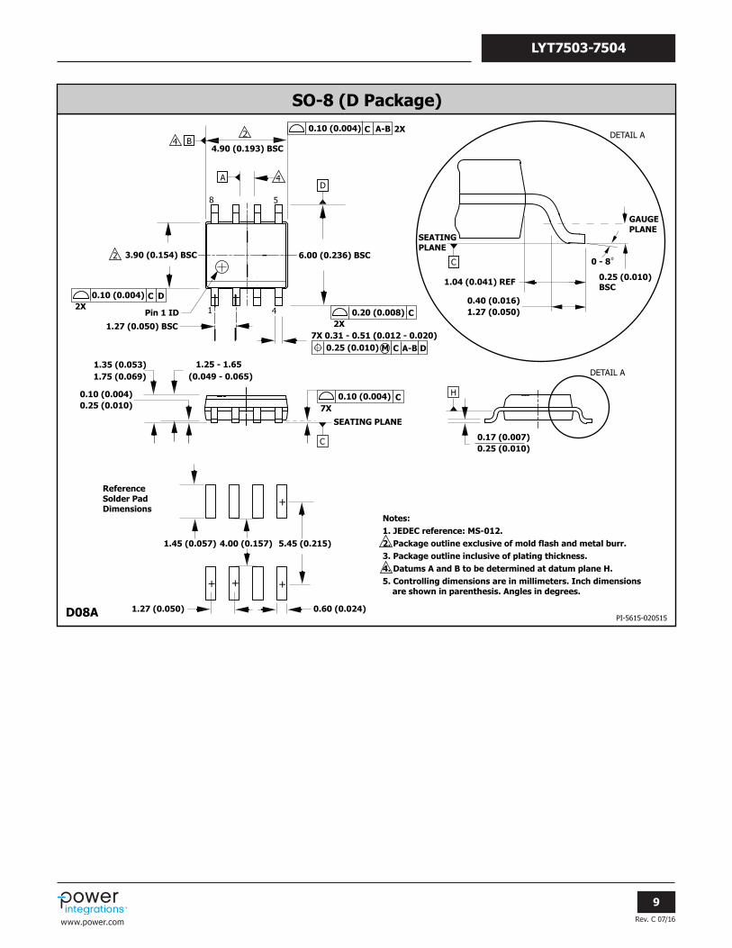
PI-5615-020515D08A
SO-8 (D Package)
3.90 (0.154) BSC
Notes:1. JEDEC reference: MS-012.2. Package outline exclusive of mold flash and metal burr.3. Package outline inclusive of plating thickness.4. Datums A and B to be determined at datum plane H.5. Controlling dimensions are in millimeters. Inch dimensions are shown in parenthesis. Angles in degrees.
0.20 (0.008) C2X
1 4
58
2 6.00 (0.236) BSC
D4A
4.90 (0.193) BSC
2
0.10 (0.004) C2X
D
0.10 (0.004) C 2X A-B
1.27 (0.050) BSC7X 0.31 - 0.51 (0.012 - 0.020)
0.25 (0.010) M C A-B D
0.25 (0.010)0.10 (0.004)
(0.049 - 0.065)1.25 - 1.65
1.75 (0.069)1.35 (0.053)
0.10 (0.004) C7X
C
H
o
1.27 (0.050)0.40 (0.016)
GAUGEPLANE
0 - 8
1.04 (0.041) REF 0.25 (0.010)BSC
SEATINGPLANE
0.25 (0.010)0.17 (0.007)
DETAIL A
DETAIL A
C
SEATING PLANE
Pin 1 ID
B4
+
+ +
5.45 (0.215)
1.27 (0.050) 0.60 (0.024)
1.45 (0.057)
ReferenceSolder PadDimensions
+
4.00 (0.157)

Rev. C 07/16
10
LYT7503-7504
www.power.com
Part Ordering Information
• LYTSwitch-7 Product Family
• Series Number
• Package Identifier
D SO-8
• Tape & Reel and Other Options
Blank Standard Configuration of 100 pcs.
TL Tape & Reel, 2500 pcs min/mult.LYT 7504 D - TL
MSL Table
Part Number MSL Rating
LYT7503D 1
LYT7504D 1
ESD and Latch-Up Table
Test Conditions Results
Latch-up at 125 °C JESD78D > ±100 mA or > 1.5 × V(max) on all pins
Human Body Model ESD ANSI/ESDA/JEDEC JS-001-2012 > ±2000 V on all pins
Machine Model ESD JESD22-A115CA > ±200 V on all pins
Charged Device Model ESD JESD22-C101 > ±500 V on all pins

Revision Notes Date
A Code S. 07/16
B Code A. 07/16
C Added Application Example section. 07/16
For the latest updates, visit our website: www.power.comPower Integrations reserves the right to make changes to its products at any time to improve reliability or manufacturability. Power Integrations does not assume any liability arising from the use of any device or circuit described herein. POWER INTEGRATIONS MAKES NO WARRANTY HEREIN AND SPECIFICALLY DISCLAIMS ALL WARRANTIES INCLUDING, WITHOUT LIMITATION, THE IMPLIED WARRANTIES OF MERCHANTABILITY, FITNESS FOR A PARTICULAR PURPOSE, AND NON-INFRINGEMENT OF THIRD PARTY RIGHTS.
Patent InformationThe products and applications illustrated herein (including transformer construction and circuits external to the products) may be covered by one or more U.S. and foreign patents, or potentially by pending U.S. and foreign patent applications assigned to Power Integrations. A complete list of Power Integrations patents may be found at www.power.com. Power Integrations grants its customers a license under certain patent rights as set forth at http://www.power.com/ip.htm.
Life Support PolicyPOWER INTEGRATIONS PRODUCTS ARE NOT AUTHORIZED FOR USE AS CRITICAL COMPONENTS IN LIFE SUPPORT DEVICES OR SYSTEMS WITHOUT THE EXPRESS WRITTEN APPROVAL OF THE PRESIDENT OF POWER INTEGRATIONS. As used herein:
1. A Life support device or system is one which, (i) is intended for surgical implant into the body, or (ii) supports or sustains life, and (iii) whose failure to perform, when properly used in accordance with instructions for use, can be reasonably expected to result in significant injury or death to the user.
2. A critical component is any component of a life support device or system whose failure to perform can be reasonably expected to cause the failure of the life support device or system, or to affect its safety or effectiveness.
The PI logo, TOPSwitch, TinySwitch, SENZero, SCALE-iDriver, Qspeed, PeakSwitch, LYTSwitch, LinkZero, LinkSwitch, InnoSwitch, HiperTFS, HiperPFS, HiperLCS, DPA-Switch, CAPZero, Clampless, EcoSmart, E-Shield, Filterfuse, FluxLink, StakFET, PI Expert and PI FACTS are trademarks of Power Integrations, Inc. Other trademarks are property of their respective companies. ©2016, Power Integrations, Inc.
World Headquarters5245 Hellyer AvenueSan Jose, CA 95138, USA.Main: +1-408-414-9200Customer Service:Phone: +1-408-414-9665Fax: +1-408-414-9765e-mail: [email protected]
China (Shanghai)Rm 2410, Charity Plaza, No. 88North Caoxi RoadShanghai, PRC 200030Phone: +86-21-6354-6323Fax: +86-21-6354-6325e-mail: [email protected]
China (Shenzhen)17/F, Hivac Building, No. 2, Keji Nan 8th Road, Nanshan District, Shenzhen, China, 518057Phone: +86-755-8672-8689Fax: +86-755-8672-8690e-mail: [email protected]
GermanyLindwurmstrasse 11480337 MunichGermanyPhone: +49-895-527-39110Fax: +49-895-527-39200e-mail: [email protected]
GermanyHellwegForum 159469 EnseGermany Tel: +49-2938-64-39990e-mail: igbt-driver.sales@ power.com
India#1, 14th Main RoadVasanthanagarBangalore-560052 IndiaPhone: +91-80-4113-8020Fax: +91-80-4113-8023e-mail: [email protected]
ItalyVia Milanese 20, 3rd. Fl.20099 Sesto San Giovanni (MI) ItalyPhone: +39-024-550-8701Fax: +39-028-928-6009e-mail: [email protected]
JapanKosei Dai-3 Bldg. 2-12-11, Shin-Yokohama, Kohoku-ku Yokohama-shi, Kanagawa 222-0033 JapanPhone: +81-45-471-1021Fax: +81-45-471-3717e-mail: [email protected]
KoreaRM 602, 6FLKorea City Air Terminal B/D, 159-6Samsung-Dong, Kangnam-Gu,Seoul, 135-728, KoreaPhone: +82-2-2016-6610Fax: +82-2-2016-6630e-mail: [email protected]
Singapore51 Newton Road#19-01/05 Goldhill PlazaSingapore, 308900Phone: +65-6358-2160Fax: +65-6358-2015e-mail: [email protected]
Taiwan5F, No. 318, Nei Hu Rd., Sec. 1Nei Hu Dist.Taipei 11493, Taiwan R.O.C.Phone: +886-2-2659-4570Fax: +886-2-2659-4550e-mail: [email protected]
UKCambridge Semiconductor,a Power Integrations companyWestbrook Centre, Block 5, 2nd FloorMilton RoadCambridge CB4 1YGPhone: +44 (0) 1223-446483e-mail: [email protected]
Power Integrations Worldwide Sales Support Locations


![HYDROVARHYDROVAR Power supply Output to motor Type Rated output Voltage limits 48-62 Hz Recommended Rated current line protection Max. voltage output output HV [kW] [V] [A] [V] [A]](https://img.pdfslide.us/doc/110x75/60b9368db7874e2ac643ec24/hydrovar-hydrovar-power-supply-output-to-motor-type-rated-output-voltage-limits.jpg)